RU2763103C1 - Method for monitoring and controlling the temperature regime of the growth surface of the substrate - Google Patents
Method for monitoring and controlling the temperature regime of the growth surface of the substrate Download PDFInfo
- Publication number
- RU2763103C1 RU2763103C1 RU2020128558A RU2020128558A RU2763103C1 RU 2763103 C1 RU2763103 C1 RU 2763103C1 RU 2020128558 A RU2020128558 A RU 2020128558A RU 2020128558 A RU2020128558 A RU 2020128558A RU 2763103 C1 RU2763103 C1 RU 2763103C1
- Authority
- RU
- Russia
- Prior art keywords
- substrate
- temperature
- ring
- microwave
- platform
- Prior art date
Links
- 239000000758 substrate Substances 0.000 title claims abstract description 94
- 238000000034 method Methods 0.000 title claims abstract description 17
- 238000012544 monitoring process Methods 0.000 title description 8
- 229910003460 diamond Inorganic materials 0.000 claims abstract description 36
- 239000010432 diamond Substances 0.000 claims abstract description 36
- 239000000203 mixture Substances 0.000 claims abstract description 14
- 230000003287 optical effect Effects 0.000 claims abstract description 13
- 238000001816 cooling Methods 0.000 claims abstract description 11
- 239000000956 alloy Substances 0.000 claims abstract description 4
- 229910045601 alloy Inorganic materials 0.000 claims abstract description 4
- 230000008021 deposition Effects 0.000 claims description 11
- 238000000576 coating method Methods 0.000 abstract description 21
- 238000010438 heat treatment Methods 0.000 abstract description 15
- 239000011248 coating agent Substances 0.000 abstract description 14
- 230000001276 controlling effect Effects 0.000 abstract description 10
- 230000000694 effects Effects 0.000 abstract description 7
- 239000000853 adhesive Substances 0.000 abstract description 3
- 230000001070 adhesive effect Effects 0.000 abstract description 3
- 230000001105 regulatory effect Effects 0.000 abstract description 3
- 239000002356 single layer Substances 0.000 abstract description 3
- 239000000126 substance Substances 0.000 abstract description 2
- 239000007789 gas Substances 0.000 description 23
- 230000006641 stabilisation Effects 0.000 description 12
- 238000011105 stabilization Methods 0.000 description 12
- 238000000151 deposition Methods 0.000 description 11
- 230000001052 transient effect Effects 0.000 description 11
- 238000009434 installation Methods 0.000 description 9
- 238000013021 overheating Methods 0.000 description 9
- 238000012360 testing method Methods 0.000 description 6
- OKTJSMMVPCPJKN-UHFFFAOYSA-N Carbon Chemical compound [C] OKTJSMMVPCPJKN-UHFFFAOYSA-N 0.000 description 5
- 238000005086 pumping Methods 0.000 description 4
- 230000033228 biological regulation Effects 0.000 description 3
- 230000015572 biosynthetic process Effects 0.000 description 3
- 229910017052 cobalt Inorganic materials 0.000 description 3
- 239000010941 cobalt Substances 0.000 description 3
- GUTLYIVDDKVIGB-UHFFFAOYSA-N cobalt atom Chemical compound [Co] GUTLYIVDDKVIGB-UHFFFAOYSA-N 0.000 description 3
- 238000005520 cutting process Methods 0.000 description 3
- 238000005137 deposition process Methods 0.000 description 3
- 229910002804 graphite Inorganic materials 0.000 description 3
- 239000010439 graphite Substances 0.000 description 3
- 230000005855 radiation Effects 0.000 description 3
- 238000003786 synthesis reaction Methods 0.000 description 3
- ZOKXTWBITQBERF-UHFFFAOYSA-N Molybdenum Chemical compound [Mo] ZOKXTWBITQBERF-UHFFFAOYSA-N 0.000 description 2
- 229910052799 carbon Inorganic materials 0.000 description 2
- 238000013461 design Methods 0.000 description 2
- 238000006073 displacement reaction Methods 0.000 description 2
- 238000009826 distribution Methods 0.000 description 2
- 238000005516 engineering process Methods 0.000 description 2
- 229910052736 halogen Inorganic materials 0.000 description 2
- 150000002367 halogens Chemical class 0.000 description 2
- 239000010410 layer Substances 0.000 description 2
- 239000000463 material Substances 0.000 description 2
- 238000011089 mechanical engineering Methods 0.000 description 2
- 229910052750 molybdenum Inorganic materials 0.000 description 2
- 239000011733 molybdenum Substances 0.000 description 2
- 239000010453 quartz Substances 0.000 description 2
- 239000004065 semiconductor Substances 0.000 description 2
- 230000035945 sensitivity Effects 0.000 description 2
- VYPSYNLAJGMNEJ-UHFFFAOYSA-N silicon dioxide Inorganic materials O=[Si]=O VYPSYNLAJGMNEJ-UHFFFAOYSA-N 0.000 description 2
- 102100031470 Homeobox protein ARX Human genes 0.000 description 1
- 101000923090 Homo sapiens Homeobox protein ARX Proteins 0.000 description 1
- 238000001237 Raman spectrum Methods 0.000 description 1
- 229910009043 WC-Co Inorganic materials 0.000 description 1
- 239000003054 catalyst Substances 0.000 description 1
- 230000000052 comparative effect Effects 0.000 description 1
- 239000002131 composite material Substances 0.000 description 1
- 230000006835 compression Effects 0.000 description 1
- 238000007906 compression Methods 0.000 description 1
- 239000000112 cooling gas Substances 0.000 description 1
- 238000012937 correction Methods 0.000 description 1
- 239000013078 crystal Substances 0.000 description 1
- 238000009795 derivation Methods 0.000 description 1
- 238000007688 edging Methods 0.000 description 1
- 238000001941 electron spectroscopy Methods 0.000 description 1
- 238000002474 experimental method Methods 0.000 description 1
- 238000011049 filling Methods 0.000 description 1
- 239000005338 frosted glass Substances 0.000 description 1
- 230000004927 fusion Effects 0.000 description 1
- 238000005087 graphitization Methods 0.000 description 1
- 238000000227 grinding Methods 0.000 description 1
- 230000017525 heat dissipation Effects 0.000 description 1
- 210000004283 incisor Anatomy 0.000 description 1
- 230000010354 integration Effects 0.000 description 1
- 239000011229 interlayer Substances 0.000 description 1
- 238000011068 loading method Methods 0.000 description 1
- 238000013507 mapping Methods 0.000 description 1
- 229910052751 metal Inorganic materials 0.000 description 1
- 239000002184 metal Substances 0.000 description 1
- NJPPVKZQTLUDBO-UHFFFAOYSA-N novaluron Chemical compound C1=C(Cl)C(OC(F)(F)C(OC(F)(F)F)F)=CC=C1NC(=O)NC(=O)C1=C(F)C=CC=C1F NJPPVKZQTLUDBO-UHFFFAOYSA-N 0.000 description 1
- 238000005457 optimization Methods 0.000 description 1
- 238000012545 processing Methods 0.000 description 1
- 239000003870 refractory metal Substances 0.000 description 1
- 238000011160 research Methods 0.000 description 1
- 238000006748 scratching Methods 0.000 description 1
- 230000002393 scratching effect Effects 0.000 description 1
- 230000000087 stabilizing effect Effects 0.000 description 1
- 238000012546 transfer Methods 0.000 description 1
- 235000012431 wafers Nutrition 0.000 description 1
Images


Classifications
-
- C—CHEMISTRY; METALLURGY
- C23—COATING METALLIC MATERIAL; COATING MATERIAL WITH METALLIC MATERIAL; CHEMICAL SURFACE TREATMENT; DIFFUSION TREATMENT OF METALLIC MATERIAL; COATING BY VACUUM EVAPORATION, BY SPUTTERING, BY ION IMPLANTATION OR BY CHEMICAL VAPOUR DEPOSITION, IN GENERAL; INHIBITING CORROSION OF METALLIC MATERIAL OR INCRUSTATION IN GENERAL
- C23C—COATING METALLIC MATERIAL; COATING MATERIAL WITH METALLIC MATERIAL; SURFACE TREATMENT OF METALLIC MATERIAL BY DIFFUSION INTO THE SURFACE, BY CHEMICAL CONVERSION OR SUBSTITUTION; COATING BY VACUUM EVAPORATION, BY SPUTTERING, BY ION IMPLANTATION OR BY CHEMICAL VAPOUR DEPOSITION, IN GENERAL
- C23C16/00—Chemical coating by decomposition of gaseous compounds, without leaving reaction products of surface material in the coating, i.e. chemical vapour deposition [CVD] processes
- C23C16/22—Chemical coating by decomposition of gaseous compounds, without leaving reaction products of surface material in the coating, i.e. chemical vapour deposition [CVD] processes characterised by the deposition of inorganic material, other than metallic material
- C23C16/26—Deposition of carbon only
- C23C16/27—Diamond only
-
- C—CHEMISTRY; METALLURGY
- C23—COATING METALLIC MATERIAL; COATING MATERIAL WITH METALLIC MATERIAL; CHEMICAL SURFACE TREATMENT; DIFFUSION TREATMENT OF METALLIC MATERIAL; COATING BY VACUUM EVAPORATION, BY SPUTTERING, BY ION IMPLANTATION OR BY CHEMICAL VAPOUR DEPOSITION, IN GENERAL; INHIBITING CORROSION OF METALLIC MATERIAL OR INCRUSTATION IN GENERAL
- C23C—COATING METALLIC MATERIAL; COATING MATERIAL WITH METALLIC MATERIAL; SURFACE TREATMENT OF METALLIC MATERIAL BY DIFFUSION INTO THE SURFACE, BY CHEMICAL CONVERSION OR SUBSTITUTION; COATING BY VACUUM EVAPORATION, BY SPUTTERING, BY ION IMPLANTATION OR BY CHEMICAL VAPOUR DEPOSITION, IN GENERAL
- C23C16/00—Chemical coating by decomposition of gaseous compounds, without leaving reaction products of surface material in the coating, i.e. chemical vapour deposition [CVD] processes
- C23C16/44—Chemical coating by decomposition of gaseous compounds, without leaving reaction products of surface material in the coating, i.e. chemical vapour deposition [CVD] processes characterised by the method of coating
- C23C16/458—Chemical coating by decomposition of gaseous compounds, without leaving reaction products of surface material in the coating, i.e. chemical vapour deposition [CVD] processes characterised by the method of coating characterised by the method used for supporting substrates in the reaction chamber
- C23C16/4582—Rigid and flat substrates, e.g. plates or discs
- C23C16/4583—Rigid and flat substrates, e.g. plates or discs the substrate being supported substantially horizontally
-
- C—CHEMISTRY; METALLURGY
- C23—COATING METALLIC MATERIAL; COATING MATERIAL WITH METALLIC MATERIAL; CHEMICAL SURFACE TREATMENT; DIFFUSION TREATMENT OF METALLIC MATERIAL; COATING BY VACUUM EVAPORATION, BY SPUTTERING, BY ION IMPLANTATION OR BY CHEMICAL VAPOUR DEPOSITION, IN GENERAL; INHIBITING CORROSION OF METALLIC MATERIAL OR INCRUSTATION IN GENERAL
- C23C—COATING METALLIC MATERIAL; COATING MATERIAL WITH METALLIC MATERIAL; SURFACE TREATMENT OF METALLIC MATERIAL BY DIFFUSION INTO THE SURFACE, BY CHEMICAL CONVERSION OR SUBSTITUTION; COATING BY VACUUM EVAPORATION, BY SPUTTERING, BY ION IMPLANTATION OR BY CHEMICAL VAPOUR DEPOSITION, IN GENERAL
- C23C16/00—Chemical coating by decomposition of gaseous compounds, without leaving reaction products of surface material in the coating, i.e. chemical vapour deposition [CVD] processes
- C23C16/44—Chemical coating by decomposition of gaseous compounds, without leaving reaction products of surface material in the coating, i.e. chemical vapour deposition [CVD] processes characterised by the method of coating
- C23C16/50—Chemical coating by decomposition of gaseous compounds, without leaving reaction products of surface material in the coating, i.e. chemical vapour deposition [CVD] processes characterised by the method of coating using electric discharges
- C23C16/513—Chemical coating by decomposition of gaseous compounds, without leaving reaction products of surface material in the coating, i.e. chemical vapour deposition [CVD] processes characterised by the method of coating using electric discharges using plasma jets
-
- C—CHEMISTRY; METALLURGY
- C23—COATING METALLIC MATERIAL; COATING MATERIAL WITH METALLIC MATERIAL; CHEMICAL SURFACE TREATMENT; DIFFUSION TREATMENT OF METALLIC MATERIAL; COATING BY VACUUM EVAPORATION, BY SPUTTERING, BY ION IMPLANTATION OR BY CHEMICAL VAPOUR DEPOSITION, IN GENERAL; INHIBITING CORROSION OF METALLIC MATERIAL OR INCRUSTATION IN GENERAL
- C23C—COATING METALLIC MATERIAL; COATING MATERIAL WITH METALLIC MATERIAL; SURFACE TREATMENT OF METALLIC MATERIAL BY DIFFUSION INTO THE SURFACE, BY CHEMICAL CONVERSION OR SUBSTITUTION; COATING BY VACUUM EVAPORATION, BY SPUTTERING, BY ION IMPLANTATION OR BY CHEMICAL VAPOUR DEPOSITION, IN GENERAL
- C23C16/00—Chemical coating by decomposition of gaseous compounds, without leaving reaction products of surface material in the coating, i.e. chemical vapour deposition [CVD] processes
- C23C16/44—Chemical coating by decomposition of gaseous compounds, without leaving reaction products of surface material in the coating, i.e. chemical vapour deposition [CVD] processes characterised by the method of coating
- C23C16/52—Controlling or regulating the coating process
Landscapes
- Chemical & Material Sciences (AREA)
- Engineering & Computer Science (AREA)
- Mechanical Engineering (AREA)
- Chemical Kinetics & Catalysis (AREA)
- General Chemical & Material Sciences (AREA)
- Materials Engineering (AREA)
- Metallurgy (AREA)
- Organic Chemistry (AREA)
- Physics & Mathematics (AREA)
- Plasma & Fusion (AREA)
- Inorganic Chemistry (AREA)
- Crystals, And After-Treatments Of Crystals (AREA)
- Chemical Vapour Deposition (AREA)
Abstract
Description
Предлагаемое изобретение относится к области лазерной техники, машиностроения и электронике, в частности, к оптическим технологиям, а именно: к объемно-резонаторным способам передачи СВЧ энергии в область подложки лежащей на охлаждаемой проводящей платформа СВЧ реакторам для плазмохимического синтеза материалов из газовой фазы.The proposed invention relates to the field of laser technology, mechanical engineering and electronics, in particular, to optical technologies, namely: to cavity-resonator methods of transferring microwave energy to the region of the substrate lying on a cooled conducting platform to microwave reactors for plasma-chemical synthesis of materials from the gas phase.
При формировании алмазной пленки в СВЧ реакторе с радиальным волноводом возникает неоднородность распределения поля. Энерговклад в плазму в зоне синтеза возрастает с увеличением расстояния подложки от основной проводящей платформы аксиально резонатору. Размеры и число подложек требует увеличения подводимой мощность СВЧ энергии. Для повышения равномерности роста пленки на каждой из подложек необходимо компенсировать неоднородности температуры, возникающие вследствие неоднородности энерговклада в плазму в результате краевого эффекта, что успешно решается при размещении подложек внутри запредельного кольца. Реализуется нагрев подложки излучением от высокотемпературной плазмы, образуемой периметром запредельного проводящего кольца, служащей источником косвенного нагрева. Одной из технологических задач является осаждение углеродсодержащей пленки на подложках из твердого сплава, в том числе сложной формы с тонким лезвием, или на группе таких подложек с высокой адгезией покрытия к подложке. Негативную роль играет неравномерный профиль поперечного сечения тонкого лезвия, ухудшающий условия теплоотвода, что стимулирует дополнительный нагрев тонкого лезвия вплоть до его перегрева. Для предотвращения перегрева, нарушения адгезии и обеспечения роста алмазной пленки с заданной скоростью на контролируемых участках рельефа, необходимо поддерживать заданную температуру поперечного сечения, в том числе на выступающей части рельефа, не допускающую перегрев подложки как при единичном росте, так и на группе подложек, не изменяя заранее заданных режимов роста. Поэтому решение данной технической проблемы является в настоящее время важной задачей для получения высококачественных изделий такой сложной формы в машиностроении и электронике.When a diamond film is formed in a microwave reactor with a radial waveguide, an inhomogeneity of the field distribution arises. The energy contribution to the plasma in the fusion zone increases with an increase in the distance of the substrate from the main conducting platform axially to the resonator. The size and number of substrates requires an increase in the input power of the microwave energy. To increase the uniformity of film growth on each of the substrates, it is necessary to compensate for temperature inhomogeneities arising from the inhomogeneity of the energy input into the plasma as a result of the edge effect, which is successfully solved by placing the substrates inside the beyond ring. The substrate is heated by radiation from a high-temperature plasma formed by the perimeter of the transverse conducting ring, which serves as a source of indirect heating. One of the technological problems is the deposition of a carbon-containing film on substrates of a hard alloy, including a complex shape with a thin blade, or on a group of such substrates with high adhesion of the coating to the substrate. A negative role is played by the uneven cross-sectional profile of the thin blade, which worsens the heat dissipation conditions, which stimulates additional heating of the thin blade up to its overheating. To prevent overheating, disruption of adhesion and ensure the growth of the diamond film at a given rate in controlled areas of the relief, it is necessary to maintain a given temperature of the cross-section, including on the protruding part of the relief, which does not allow overheating of the substrate both during a single growth and on a group of substrates, not changing the preset growth modes. Therefore, the solution of this technical problem is currently an important task for obtaining high-quality products of such a complex shape in mechanical engineering and electronics.
Известен способ контроля и управления температурным режимом подложки, включающий тепловое контактирование множества термоэлектрических модулей с поверхностью держателя подложки [1].A known method for monitoring and controlling the temperature regime of the substrate, including thermal contacting of a plurality of thermoelectric modules with the surface of the substrate holder [1].
Недостатком известного технического решения является то, что для поддержания необходимой однородной по поверхности температуры низко аспектной подложки или группы таких подложек, постоянное внешнее управление не только усложняет систему и снижает ее надежность, но становится не эффективным. Кроме того, термоэлектрические модули могут влиять на СВЧ поле разряда, создавая помехи.The disadvantage of the known technical solution is that in order to maintain the required temperature uniform over the surface of a low-aspect substrate or a group of such substrates, constant external control not only complicates the system and reduces its reliability, but becomes ineffective. In addition, thermoelectric modules can affect the microwave discharge field, creating interference.
Известен способ контроля и управления температурным режимом подложки, включающий выполнение для равномерного распределения тепла держателя полупроводниковой подложки, расположенного между источником нагрева и полупроводниковой подложкой, из материала с проводимостью выше, чем у графита.A known method for monitoring and controlling the temperature regime of the substrate, including the implementation for uniform heat distribution of the holder of the semiconductor substrate, located between the heating source and the semiconductor substrate, from a material with a conductivity higher than that of graphite.
Недостатком известного технического решения является то, что оно не предполагает возможности эффективного отвода излишка тепла для поддержания оптимальной температуры из зон локального перегрева, связанного с краевым эффектом, вызванным возмущением СВЧ поля при внесении низко аспектной подложки или группы таких подложек [2].The disadvantage of the known technical solution is that it does not imply the possibility of efficient removal of excess heat to maintain the optimal temperature from the zones of local overheating associated with the edge effect caused by the perturbation of the microwave field when introducing a low-aspect substrate or a group of such substrates [2].
Известен способ контроля и управления температурным режимом подложки, включающий установку газового теплообменника, содержащего цилиндрическую камеру, коаксиально с держателем подложки, и выполнение держателя подложки цилиндрическим, осесимметричным, массивным из термостойкого и теплопроводного металла (молибдена), одного из каналов для газа осевым и соединенным с цилиндрической камерой теплообменника, а другого канала для газа соединенным с коллектором, соединение цилиндрической камеры газового теплообменника с обратной по отношению к подложке и СВЧ разряду стороной упомянутого держателя и контактирование с ней по площади от 30 до 90% площади обратной стороны держателя, при этом осевой канал теплообменника является каналом подачи охлаждающего газа с температурой ниже рабочей температуры СВЧ плазменного реактора, а канал, соединенный с коллектором, является каналом откачки газа. Осевой канал может быть выполнен для откачки газа, а канал, соединенный с коллектором, - для подачи газа с температурой выше рабочей температуры реактора [3].There is a method for monitoring and controlling the temperature regime of the substrate, including the installation of a gas heat exchanger containing a cylindrical chamber, coaxially with the substrate holder, and making the substrate holder cylindrical, axisymmetric, massive from a heat-resistant and heat-conducting metal (molybdenum), one of the gas channels axial and connected to the cylindrical chamber of the heat exchanger, and another gas channel connected to the collector, connection of the cylindrical chamber of the gas heat exchanger with the side of the said holder opposite to the substrate and the microwave discharge and contacting with it over the area from 30 to 90% of the area of the reverse side of the holder, while the axial channel of the heat exchanger is a channel for supplying a cooling gas with a temperature below the operating temperature of the microwave plasma reactor, and the channel connected to the collector is a gas pumping channel. The axial channel can be made for pumping gas, and the channel connected to the collector - for supplying gas with a temperature higher than the operating temperature of the reactor [3].
Недостатком известного технического решения является то, что в случае роста алмазного покрытия на подложках меньших размеров, например, с низкоаспектной формой геометрии, равномерность температурного поля нарушается, на периферии подложки в результате краевого эффекта образуются зоны перегрева. В этом случае отвод излишек тепла за счет теплопроводности подложки в охлаждаемый держатель становится не эффективным, а локальный перегрев ростовой поверхности приводит к нарушению кристаллической структуры, однородности зернового состава и качества алмазной пленки, а также алмазного покрытия Наиболее близким техническим решением (прототипом) по постановке задачи и совокупности существенных признаков является способ контроля и управления температурным режимом ростовой поверхности, по крайней мере, одной подложки, включающий установку основной проводящей платформы в герметичной осесимметричной вакуумной камере с СВЧ плазменным реактором с высокой однородностью температурного поля, установку на поверхности равновысоких подложек с низкоаспектной геометрией формы, расположенных внутри стационарного проводящего запредельного кольца в виде плазмообразующей кассеты, охлаждаемого держателя соответствующей подложки в виде радиального волновода как части СВЧ поля, установку плазмообразующей кассеты так, что ее основание обращено к держателю соответствующей подложки, а оси отверстий ориентированы перпендикулярно ей, при этом центральная часть камеры выполнена в виде СВЧ резонатора [4].The disadvantage of the known technical solution is that in the case of the growth of the diamond coating on substrates of smaller sizes, for example, with a low aspect shape of the geometry, the uniformity of the temperature field is disturbed, and overheating zones are formed on the periphery of the substrate as a result of the edge effect. In this case, the removal of excess heat due to the thermal conductivity of the substrate into the cooled holder becomes ineffective, and local overheating of the growth surface leads to a violation of the crystal structure, grain size uniformity and quality of the diamond film, as well as the diamond coating and a set of essential features is a method for monitoring and controlling the temperature regime of the growth surface of at least one substrate, including the installation of the main conducting platform in a sealed axisymmetric vacuum chamber with a microwave plasma reactor with a high uniformity of the temperature field, installation on the surface of equally high substrates with a low aspect geometry of the shape located inside a stationary conducting transient ring in the form of a plasma-forming cassette, a cooled holder of the corresponding substrate in the form of a radial waveguide as part of the microwave field, the installation of a plasma-forming cassette sets so that its base is facing the holder of the corresponding substrate, and the axes of the holes are oriented perpendicular to it, while the central part of the chamber is made in the form of a microwave resonator [4].
Недостатком известного технического решения является то, что при мультислойном росте, или в случае перегрева подложки, стабилизацию температуры достигают изменением режимных параметров осаждения, (подаваемой СВЧ мощности, давления и расхода газовой смеси, и т.д.) что чревато нарушением адгезии покрытия с подложкой, структуры и состава алмазной пленки.The disadvantage of the known technical solution is that during multilayer growth, or in the case of overheating of the substrate, temperature stabilization is achieved by changing the deposition mode parameters (supplied microwave power, pressure and flow rate of the gas mixture, etc.), which is fraught with disruption of the adhesion of the coating to the substrate , structure and composition of the diamond film.
Новым достигаемым техническим результатом предполагаемого изобретения является автоматизация управления температурой подложки, в том числе переменного сечения, при обеспечении управления и стабилизации температуры нагрева подложки и стабилизации скорости роста алмазной пленки для получения адгезионно прочной структуры однослойного или мультислойного покрытия при осаждении из газовой фазы в СВЧ-плазме как на одну, так и группу подложек.A new achieved technical result of the proposed invention is the automation of the temperature control of the substrate, including variable cross-section, while ensuring control and stabilization of the heating temperature of the substrate and stabilization of the growth rate of the diamond film to obtain an adhesive strong structure of a single-layer or multilayer coating during deposition from the gas phase in microwave plasma both one and a group of substrates.
Новый технический результат достигается тем, что в способе контроля и управления температурным режимом ростовой поверхности подложки, включающем установку основной проводящей платформы в герметичной осесимметричной вакуумной камере с СВЧ плазменным реактором с высокой однородностью температурного поля, установку на поверхности равновысоких подложек с низкоаспектной геометрией формы, расположенных внутри стационарного проводящего запредельного кольца в виде плазмообразующей кассеты, охлаждаемого держателя соответствующей подложки в виде радиального волновода как части СВЧ поля, установку плазмообразующей кассеты так, что ее основание обращено к держателю соответствующей подложки, а оси отверстий ориентированы перпендикулярно ей, при этом центральная часть камеры выполнена в виде СВЧ резонатора, напуск и откачку газовой смеси, в отличие от прототипа, внутреннее основание запредельного кольца выполняют подвижным, с зазором, обеспечивающим его относительное перемещение аксиально СВЧ резонатору, и как часть основной проводящей платформы, при этом подвижное основание запредельного кольца и основная проводящая платформа имеют независимые системы охлаждения.The new technical result is achieved by the fact that in the method of monitoring and controlling the temperature regime of the growth surface of the substrate, including the installation of the main conducting platform in a sealed axisymmetric vacuum chamber with a microwave plasma reactor with a high homogeneity of the temperature field, the installation on the surface of equally high substrates with a low aspect geometry of the shape located inside a stationary conducting transient ring in the form of a plasma cassette, a cooled holder of the corresponding substrate in the form of a radial waveguide as part of the microwave field, installation of the plasma cassette so that its base faces the holder of the corresponding substrate, and the axes of the holes are oriented perpendicular to it, while the central part of the chamber is made in in the form of a microwave resonator, filling and pumping out the gas mixture, unlike the prototype, the inner base of the beyond ring is movable, with a gap that ensures its relative movement axially of the microwave resonator torus, and as part of the main conductive platform, while the movable base of the beyond ring and the main conductive platform have independent cooling systems.
Температурным режимом подложки могут управлять по программе ПИД регулятора в режиме стабилизации по показанию оптического инфракрасного пирометра.The temperature regime of the substrate can be controlled according to the PID controller program in the stabilization mode according to the indication of the optical infrared pyrometer.
Температурный режим подложки могут регулировать одновременно со смещением подвижного основания запредельного кольца с помощью актуатора через трубопровод охлаждения, осесимметричный подвижному основанию запредельного кольца.The temperature regime of the substrate can be adjusted simultaneously with the displacement of the movable base of the beyond-limit ring using an actuator through the cooling pipeline, which is axisymmetric to the movable base of the beyond-limit ring.
Способ контроля и управления температурным режимом ростовой поверхности подложки реализуют следующим образом.The method for monitoring and controlling the temperature regime of the growth surface of the substrate is implemented as follows.
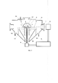
В отверстие запредельного проводящего кольца 1 устанавливают по крайней мере, одну подложку 2 на его подвижном охлаждаемом основании 3 запредельного проводящего кольца 1, связанным с актуатором 4, которое перемещают внутри основной проводящей платформы 5 СВЧ плазменного реактора 6 (фиг. 1, где 7 - боковое кварцевое окно; 8 - инфракрасный пирометр; 9 - ПИД регулятор; 10 - сильфон; 11 - трубопровод охлаждения; 12 - СВЧ прозрачное окно; 13 - откачка газовой смеси; 14 - форсунка подача газовой смеси; 15 - кант СВЧ плазмы).At least one
На фиг. 1 представлено схематическое изображение поперечного сечения СВЧ плазменного реактора 6 с регулированием температуры подложки 2 за счет позиционирования положения подложки 2 путем изменения высоты внутреннего периметра запредельного проводящего кольца 1 аксиально оси резонатора СВЧ плазменного реактора 6 в системе обратной связи с оптическим инфракрасным пирометром 8 с помощью смещения подвижного основания запредельного проводящего кольца 1 аксиально резонатору СВЧ плазменного реактора 6 для единичного или группового роста алмазных покрытий на низкоаспектных подложках 2 с плоской или рельефной формой ростовой поверхности.FIG. 1 shows a schematic representation of a cross-section of a microwave plasma reactor 6 with temperature control of the
Подвижное охлаждаемое основание 3 запредельного проводящего кольца 1 и основная проводящая платформа 5 СВЧ плазменного реактора 6 имеют независимые системы охлаждения, что обеспечивает безопасную и бесперебойную работу реактора на любых режимах процесса осаждения покрытий в СВЧ плазме.The movable cooled
Запредельное проводящее кольцо 1 размещают на основной проводящей платформе 5 СВЧ плазменного реактора 6 аксиально резонатора СВЧ плазменного реактора 6 с возможностью образования на участке генерации стоячей волны канта 15 СВЧ плазмы, который является источником нагрева подложек 2 излучением от СВЧ плазмы. Откачку воздуха в вакуумной камере с СВЧ плазменным реактором 6 обеспечивают вакуумной системой 13. Подачу газовой смеси осуществляют через форсунку 14. Мощность плазмы поддерживают микроволновой энергией, подводимой через СВЧ прозрачное цилиндрическое окно 12. Запредельное проводящее кольцо 1 для каждого типа подложек 2 имеет постоянные размеры: высоту Н, наружный DH и внутренний DBH диаметры. Критичным параметром для нагрева подложки 2 излучением от СВЧ плазмы является расстояние hmax и hmin до канта 13(15) СВЧ плазмы. Приближение к нему увеличивает температуру до Tmax, отдаление снижает температуру до Tmin. Причем температуру регулируют с помощью параметра h, что позволяет сохранить неизменными основные режимы процесса, такие как СВЧ мощность, состав, расход и давление газовой смеси. Особенно это актуально при осаждении алмазных покрытий на резцы из твердого сплава с тонкими лезвиями. Внешний диаметр запредельного проводящего кольца 1 принимают кратным длине волны λ, DBH=n⋅λ, где n коэффициент кратности для данной частоты СВЧ поля. Запредельное проводящее кольцо 1 выполняют из тугоплавкого металла в виде короткозамкнутого отрезка круглого запредельного волновода, в котором возбуждается осесимметричное поле волны типа E01 с вертикальной электрической компонентой внешнего СВЧ поля. Внутри запредельного проводящего кольца 1 СВЧ поле в направлении оси резонатора СВЧ плазменного реактора 6 распространяться не может, так как постоянная распространения волны в запредельном волноводе β=0, то есть фаза волны по высоте запредельного проводящего кольца 1 не изменяется, а ее амплитуда экспоненциально затухает. С учетом затухания СВЧ поля внутри запредельного проводящего кольца 1, заполненного плазмой, последняя смещает показатель преломления пространства в сторону уменьшения показателя преломления n, длина волны в плазме становится больше, чем в вакууме.The transient
При включении системы в СВЧ плазменный реактор 6 подают газовую смесь и микроволновую энергию. В центральной части СВЧ плазменного реактора 6 СВЧ волна распространяется по запредельному проводящему кольцу 1, образуя кант 13(15) СВЧ плазмы с плотностью мощности P/V, квт/см3, где Ρ - подведенная мощность, V - объем плазменного облака, являющегося источником тепла для активации газовой смеси и осаждения алмаза на ростовой поверхности подложек (подложки) 2, расположенных внутри запредельного проводящего кольца 1. Сферический кант 13(15) СВЧ плазмы образуется СВЧ полем, обтекающим периметр запредельного проводящего 1 кольца на высоте Н. Форму поперечного сечения контура диаметром D=n⋅λ можно описать каноническим уравнением эллипса с большой (а=2) и малой (в=1) полуосями, характеризируемым коэффициентом сжатия и фокальным периметром равным 1/2:When the system is turned on, a gas mixture and microwave energy are supplied to the microwave plasma reactor 6. In the central part of the microwave plasma reactor 6, the microwave wave propagates along the transcendent conducting
х2/22+у2/12=1,x 2/2 2 + y 2/1 2 = 1,
и практически измерить и контролировать методом оптической электронной спектроскопии.and practically measure and control by optical electron spectroscopy.
В случае рельефной поверхности роста не все участки подложек 2, лежащих в плоскости большой полуоси эллипса равно удалены от канта 15 СВЧ плазмы, которая служит для них источником косвенного нагрева. Сильнее нагревается выступающая часть рельефа. Косвенный нагрев исключает локальный перегрев от краевого эффекта, но не дает возможность одновременно осаждать равномерные покрытия на выступающих и нижележащих частях подложки 2. В прототипе массивный постамент, выполненный из молибдена, выравнивает температуру по основанию подложек 2 за счет теплопередачи. Таким образом, средняя температура стабилизируется лишь по основанию подложки 2, но в плоскости: роста пленки на выступающей части подложки 2 остается неоднородной. Косвенный нагрев от канта 15 СВЧ плазмы неподвижного запредельного проводящего кольца 1 на неподвижную подложку 2 не позволяет обеспечивать требуемую температуру, а также обеспечивать ее корректировку для получения однородной пленки с заданными структурными характеристиками поликристаллических зерен. Это затрудняет управление размером поликристаллических зерен, а также измельчению микрокристаллических зерен с помощью многослойных покрытий. Поэтому без ущерба качеству алмазной пленки, например, на подложках сложной формы, температурой можно управлять лишь в пределах критического диапазона режимных параметров (мощность, давление газовой смеси, расход газа и др.). Выход за пределы критических высот запредельного проводящего кольца 1 и подложки в меньшую сторону приводит к перегреву выступающей части рельефа подложки за счет приближения к контуру СВЧ плазмы, выход в большую сторону наоборот приводит к падению температуры ниже критической, при которой в покрытии возможно образование трещин, при существенном снижении средней температуры образца.In the case of a relief growth surface, not all sections of the
За основу системы автоматического управления взят классический алгоритм ПИД регулятора 9:The automatic control system is based on the classical PID controller algorithm 9:

где (е=ysp - у) - рассогласование, у - измеряемое значение, ysp - заданное значение (установка), K - пропорциональный коэффициент усиления, Ti - постоянная интегрирования, Td - постоянная дифференцирования, u(t) - управляющий сигнал, имеющий ряд недостатков, ограничивающих его практическую реализацию при регулировании температуры подложки в СВЧ пламенном реакторе 6.where (e = y sp - y) is the mismatch, y is the measured value, y sp is the set value (setting), K is the proportional gain, T i is the integration constant, T d is the derivation constant, u (t) is the control a signal that has a number of disadvantages that limit its practical implementation when regulating the temperature of the substrate in a microwave flame reactor 6.
Для устранения недостатков данного алгоритма добавлены зона нечувствительности, весовой коэффициент установки, фильтр дифференциальной составляющей, компенсация интегрального насыщения [4-10]. Цифровой ПИД регулятор 9 реализован на языке Си [9] с использованием библиотеки GTK [11, 12]. Методы аппроксимации формулы (1) в дискретную форму приведены в [4-7].To eliminate the shortcomings of this algorithm, a dead zone, a weighting factor of the installation, a filter of the differential component, and an integral saturation compensation have been added [4-10].
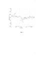
Программа осуществляет прием данных с оптического инфракрасного пирометра 8, их обработку и управление приводом в соответствии с вышеописанным алгоритмом. Используется стандартный графический интерфейс программы ПИД регулятора 9. Тестирование, настройку ПИД регулятора и моделирование стабилизации температуры подложки (нить накаливания галогенной лампы) выполняли на макете (фиг. 2, где 8 - пирометр Williamson PRO-80; 16 - импульсный источник питания Mean Well SDR-120-48; 17 - контроллер SMSD-8.0LAN; 18 - преобразователь ОВЕН АС4; 19 - галогенная лампа накаливания 70 Вт; 20 - автотрансформатор; 21 - шаговый двигатель AD-200; 22 - интерфейсный модуль Williamson).The program receives data from the optical
Для испытания реакции системы ПИД регулятора 9 на температурные возмущения последовательно устанавливали следующие значения температуры: 1300; 1500; 1100; 1500 и 1300°С. Реакция системы на установку требуемого значения показывает стабилизацию за период 5 временные интервалы обновления данных составляют 0,1 с. Испытание реакции системы ПИД регулятора 9 на внесенное возмущение, когда между лампой накаливания и оптическим инфракрасным пирометром 5 было внесено матовое стекло, показывает время стабилизации - 8 с, с обновлением данных - 0,1 с. Испытания реакции системы ПИД регулятора 9 в СВЧ плазменном реакторе 6 на ступенчатое изменение температуры от высоты положения плазмообразующего запредельного проводящего кольца 1 для тестового образца составляют 25°С на 100 мкм с интервалом ~10 с. Испытание реакции системы ПИД регулятора 9 на внесенное возмущение в СВЧ плазменном реакторе 6 путем повышения мощности на 500 Вт показывает время стабилизации температуры подложки - 25 с. Калибровочная зависимость стабилизации температуры нагрева ПРТС по обратной связи с оптическим инфракрасным пирометром 5 на внесенное возмущение в СВЧ плазменном реакторе 6 путем повышения мощности на 500 Вт представлена на фиг. 3.To test the response of the
Интерфейс программы ПИД регулятора 9 (ПИД регулирование) в режиме стабилизации температуры (750-850°С) подложки 2 в СВЧ плазменном реакторе 6, размах вариации температуры, от минимальной - 790°С до максимальной - 799°С, ±4,5°С в регулярном процессе осаждения алмазного покрытия показан на фиг. 4. Как видно на фиг. 3, 4, время стабилизации и температурные колебания с использованием такого регулирования крайне незначительны, что позволяет получать алмазные пленки без существенного градиента характеристик по толщине.PID controller program interface 9 (PID regulation) in temperature stabilization mode (750-850 ° C) of
Пример реализации способа контроля и управления температурным режимом ростовой поверхности подложкиAn example of the implementation of the method for monitoring and controlling the temperature regime of the growth surface of the substrate
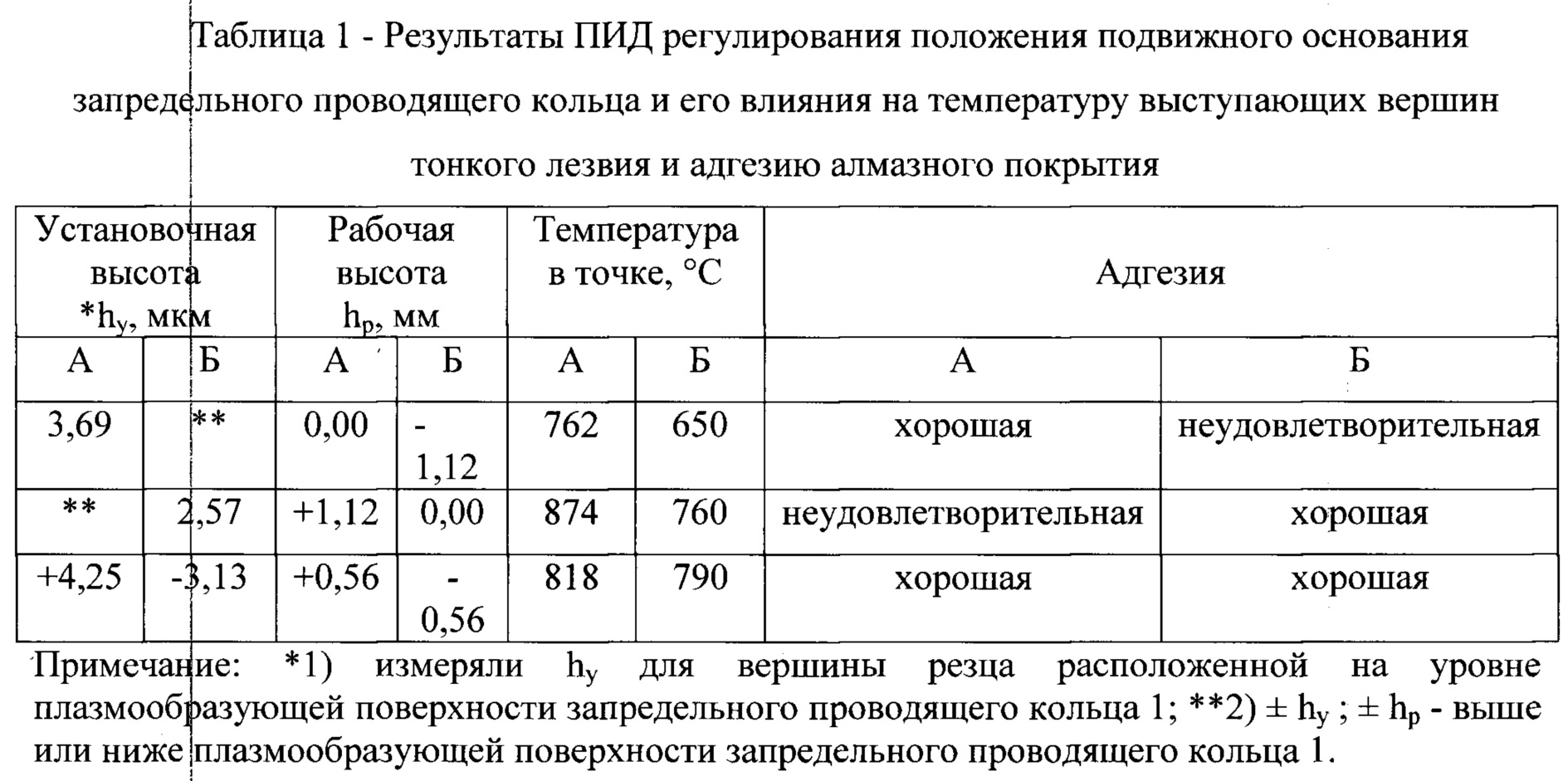
Сравнительный эксперимент осуществляли по осаждению микрокристаллической алмазной пленки (MCD) и нанокристаллической алмазной пленки (NCD) на низко аспектные подложки 2 с выступающей частью рельефа в СВЧ плазменном реакторе 6 с поддержанием температуры тонкого лезвия подложки 2 в стационарном режиме и без него. Образцы выполняли в виде сменных режущих пластин из твердого сплава (WC+Со) типа Nice Cat или Tungaloy, предназначенных для использования в станках с ЧПУ в специальных оправках и корпусных фрезах для обработки композиционных материалов. Эти пластины содержат две заостренные вершины А и Б, с существенно выступающей частью рельефа. Отличие высот относительно основания резца составляет более чем на 1,12 мм (1120 мкм).A comparative experiment was carried out on the deposition of a microcrystalline diamond film (MCD) and a nanocrystalline diamond film (NCD) on low-
Пример позиционирования сменной режущей пластины из твердого сплава (WC+Со) типа Tungaloy для регулирования температуры роста путем смещения подвижного основания запредельного проводящего кольца 1 высотой Н, где hp - рабочая высота; А - высота вершины главной режущей кромки относительно подвижного основания 3 запредельного проводящего кольца 1; Б - высота вершины вспомогательной режущей кромки относительно подвижного основания 3 запредельного проводящего кольца 1; hy - установочная высота подвижного основания 3 запредельного проводящего кольца 1 (фиг. 5).An example of positioning a replaceable cutting insert made of a hard alloy (WC + Co) of the Tungaloy type to regulate the growth temperature by displacing the movable base of the transverse
Поддержание температуры в заданном сечении тонкого лезвия подложки 2 (фиг. 5, точки А и Б) в стационарном режиме осуществляют путем позиционирования подложки 2 относительно плазмообразующей поверхности запредельного проводящего кольца 1 с помощью подвижного основания 3 запредельного проводящего кольца 1, связанного с трубопроводом охлаждения 11 по обратной связи с двухлучевым оптическим инфракрасным пирометром 5 (фиг. 1). Подложку 2 перемещают внутри плазмообразующего запредельного проводящего кольца 1 при подъеме или опускании подвижного основания 3 запредельного проводящего кольца 1 аксиально резонатора СВЧ плазменного реактора 6.Maintaining the temperature in a given section of the thin blade of the substrate 2 (Fig. 5, points A and B) in a stationary mode is carried out by positioning the
Рост поликристаллического алмазного покрытия производили в плазмохимическом реакторе ARDIS-100 (ООО «Оптосистемы», 5 кВт, 2,45 ГГц). Наружный диаметр запредельного проводящего кольца 1 толщиной 4 мм, составлял 60 мм, а внутренний - 50,5 мм. Диаметр запредельного проводящего кольца 1 кратен длине волны на частоте 2,45 ГГц. Диаметр подвижного основания 3 запредельного проводящего кольца 1 составляет 50 мм. Синтез алмазных пленок проводили на постоянном режиме роста: СВЧ мощность - 2,5-2,9 кВт, давление в камере - 9,3-10,6 кПа, газовая смесь Н2/СН4 в отношении - 96/4%, расход газа - 1,0 дм3/мин, длительность процесса осаждения - 5 час. Диапазон допустимых температур обеспечивающих адгезию алмазного покрытия был установлен для указанных выше ре жимов осаждения в пределах 750-850°С. Кобальт служит катализатором графитизации алмаза: углерод из осажденной при температуре выше температуры синтеза алмазной пленки 850°С+75°С активно растворяется в кобальте, а затем, по мере снижения температуры до комнатной (20-25°С), выделяется вновь в виде термодинамически стабильного графита. Прослойка графита между поверхностью WC-Co и алмаза резко снижает адгезию. При концентрации кобальта 2-10, вес. % отслаивание пленки наблюдается в течение нескольких минут после охлаждения образца. Контроль температуры ростовой поверхности подложки 2 осуществляют через прорезь в запредельном проводящем кольце 1 шириной 5 мм инфракрасным пирометром Williamson, модель PRO-81-35-C, диаметр опорного пятна лазера - 2,0 мм, направление луча на боковую поверхность образца осуществляли через боковое кварцевое окно 7 вакуумной камеры CVD-реактора 6 (фиг. 1). Результаты ПИД регулирования положения подвижного основания запредельного проводящего кольца и его влияния на температуру выступающих вершин тонкого лезвия и адгезию алмазного покрытия приведены в таблице 1.The growth of the polycrystalline diamond coating was carried out in an ARDIS-100 plasma-chemical reactor (Optosystems LLC, 5 kW, 2.45 GHz). The outer diameter of the
Адгезию определяли методом измерительного царапания образцов с покрытиями на адгезиметре (скретч тестере) REVETEST фирмы CSM Instruments (Швейцария) при максимальной нагрузке 41 Н, индентор в виде алмазного конуса Rockwell С с радиусом закругления 200 мкм, при скорости нагружения 50 Н/мин и длине царапины 4 мм. Результат демонстрирующий силу адгезии более 35 Η без отслаивания покрытия принимали за хороший.Adhesion was determined by measuring scratching of coated samples on a REVETEST adhesion meter (scratch tester) from CSM Instruments (Switzerland) at a maximum load of 41 N, an indenter in the form of a Rockwell C diamond cone with a radius of 200 μm, at a loading rate of 50 N / min and a scratch length 4 mm. The result showing an adhesion force of more than 35 Η without peeling of the coating was taken as good.
Посредством стабилизации и контроля температуры подложки 2 в диапазоне от 750°С до 850°С с чувствительностью 25°С на каждые 100 мкм смещения подвижного основания запредельного проводящего кольца 1 путем осаждения микрокристаллической алмазной пленки (MCD) и нанокристаллической алмазной пленки (NCD) слоев получают образцы алмазных покрытий на пластинах (WC+Со).By stabilizing and controlling the temperature of the
Найденные методом картирования положение, ширина пика алмазных линий спектров КР и упругих напряжений сжатия демонстрируют плавно нарастающий характер от подложки (0,4 ГПа) к поверхности (0,6 ГПа), хорошую адгезию между слоями, и минимальные упругие напряжения сжатия (0,8 ГПа) на вершине резца.The position and width of the peak of the diamond lines of the Raman spectra and elastic compressive stresses found by the mapping method demonstrate a smoothly increasing character from the substrate (0.4 GPa) to the surface (0.6 GPa), good adhesion between layers, and minimum elastic compressive stresses (0.8 GPa) at the tip of the incisor.
На основании вышеизложенного новым достигаемым техническим результатом предполагаемого изобретения по сравнению с прототипом является:Based on the foregoing, the new achievable technical result of the alleged invention in comparison with the prototype is:
1) автоматизация управления температурой подложки 2, в том числе переменного сечения, за счет системы ПИД регулирования по обратной связи с оптическим инфракрасным пирометром 5 и оптимизация данного управления за счет определения диапазона, времени и чувствительности системы ПИД регулирования.1) automation of the temperature control of the
2) управление и стабилизация температуры нагрева подложки 2 и скорости роста алмазной пленки, что обеспечивает получение адгезионно прочной структуры однослойного или мультислойного покрытия как при одиночном, так и при групповом осаждении из газовой фазы в СВЧ-плазме, за счет регулирования положения подложки 2 относительно канта СВЧ плазмы реактора 15 внутри запредельного проводящего кольца 1, регулирования температуры нагрева подложки 2 по обратной связи с оптическим инфракрасным пирометром 5, задания температурного режима роста алмазной пленки для получения мультислойного покрытия при групповом осаждении мультислойных алмазных покрытий из газовой фазы в СВЧ плазме реактора 15, использования подвижного охлаждаемого основания запредельного проводящего кольца 1 аксиального резонатору СВЧ плазменного реактора 15, обеспечивающего точность регулирования температуры подложки 2 - ±25°С на 100 мкм и предотвращение краевого эффекта, вызывающего неравномерность нагрева подложки 2;2) control and stabilization of the heating temperature of the
3) повышает производительность и качество получения алмазных пленок не менее чем на 20%;3) increases the productivity and quality of obtaining diamond films by at least 20%;
4) позволяет получать в СВЧ плазменном реакторе 6 с косвенным нагревом подложки 2 однородные пленки на высоко- и на низкоаспектных подложках с любым, в том числе и со сложным профилем рельефа, и реализовать метод группового роста нанокристаллических мультислойных покрытий с использованием подвижного основания запредельного проводящего кольца 1 оптимального размера с более высокой производительностью.4) makes it possible to obtain in a microwave plasma reactor 6 with indirect heating of the
Используемые источникиSources used
1. Заявка РСТ WO 9737375, 1997, С23С 16/513.1. PCT Application WO 9737375, 1997,
2. Заявка ЕР 0867538, 1998, С23С 16/513.2. Application EP 0867538, 1998,
3. Патент RU 2403318, 2008, МКИ С23С 16/513, Н05Н 1/30.3. Patent RU 2403318, 2008,
4. Патент RU №2644216, 2018, МКИ С23С 14/00, С23С 16/27, С23С 16/458, С23С 16/4581, С23С 16/54.4. Patent RU No. 2644216, 2018,
4.![]()
![]()
5. ![]()
![]()
![]()
![]()
6. ![]()
![]()
![]()
![]()
7. B. Wittenmark, ![]()
![]()
![]()
![]()
8. E.C. Ifeachor, B.W. Jervis, Digital signal processing: a practical approach, Pearson Education. 2002.8. E.C. Ifeachor, B.W. Jervis, Digital signal processing: a practical approach, Pearson Education. 2002.
9. E. Torstensson, Comparison of schemes for windup protection, ISSN 0280-5316. (2013).9.E. Torstensson, Comparison of schemes for windup protection, ISSN 0280-5316. (2013).
10. M. Darby, G. McMillan, Signal filtering: Why and how, (n.d.).10. M. Darby, G. McMillan, Signal filtering: Why and how, (n.d.).
11. A. Krause, Foundations of GTK+development, Apress, 2007.11.A. Krause, Foundations of GTK + development, Apress, 2007.
12. The GTK Project - A free and open-source cross-platform widget toolkit, (n.d.). URL:12. The GTK Project - A free and open-source cross-platform widget toolkit, (n.d.). Url:
https://www.gtk.org/docs/apis/ (accessed April 24, 2020).https://www.gtk.org/docs/apis/ (accessed April 24, 2020).
Claims (2)
Priority Applications (1)
| Application Number | Priority Date | Filing Date | Title |
|---|---|---|---|
| RU2020128558A RU2763103C1 (en) | 2020-08-27 | 2020-08-27 | Method for monitoring and controlling the temperature regime of the growth surface of the substrate |
Applications Claiming Priority (1)
| Application Number | Priority Date | Filing Date | Title |
|---|---|---|---|
| RU2020128558A RU2763103C1 (en) | 2020-08-27 | 2020-08-27 | Method for monitoring and controlling the temperature regime of the growth surface of the substrate |
Publications (1)
| Publication Number | Publication Date |
|---|---|
| RU2763103C1 true RU2763103C1 (en) | 2021-12-27 |
Family
ID=80039122
Family Applications (1)
| Application Number | Title | Priority Date | Filing Date |
|---|---|---|---|
| RU2020128558A RU2763103C1 (en) | 2020-08-27 | 2020-08-27 | Method for monitoring and controlling the temperature regime of the growth surface of the substrate |
Country Status (1)
| Country | Link |
|---|---|
| RU (1) | RU2763103C1 (en) |
Cited By (1)
| Publication number | Priority date | Publication date | Assignee | Title |
|---|---|---|---|---|
| CN115452882A (en) * | 2022-08-10 | 2022-12-09 | 山东大学 | Device and method for measuring bulk temperature of sample in microwave field |
Citations (4)
| Publication number | Priority date | Publication date | Assignee | Title |
|---|---|---|---|---|
| RU2302484C2 (en) * | 2001-11-07 | 2007-07-10 | Карнеги Инститьюшн Оф Вашингтон | Device and method for forming diamonds |
| US7556982B2 (en) * | 2003-08-07 | 2009-07-07 | Uchicago Argonne, Llc | Method to grow pure nanocrystalline diamond films at low temperatures and high deposition rates |
| RU2398922C2 (en) * | 2005-05-25 | 2010-09-10 | Карнеги Инститьюшн Оф Вашингтон | Colourless monocrystalline diamond obtained via high-growth rate chemical gas-phase deposition |
| GB2486784A (en) * | 2010-12-23 | 2012-06-27 | Element Six Ltd | A microwave plasma reactor for manufacturing synthetic diamond material |
-
2020
- 2020-08-27 RU RU2020128558A patent/RU2763103C1/en active
Patent Citations (5)
| Publication number | Priority date | Publication date | Assignee | Title |
|---|---|---|---|---|
| RU2302484C2 (en) * | 2001-11-07 | 2007-07-10 | Карнеги Инститьюшн Оф Вашингтон | Device and method for forming diamonds |
| US7556982B2 (en) * | 2003-08-07 | 2009-07-07 | Uchicago Argonne, Llc | Method to grow pure nanocrystalline diamond films at low temperatures and high deposition rates |
| RU2398922C2 (en) * | 2005-05-25 | 2010-09-10 | Карнеги Инститьюшн Оф Вашингтон | Colourless monocrystalline diamond obtained via high-growth rate chemical gas-phase deposition |
| GB2486784A (en) * | 2010-12-23 | 2012-06-27 | Element Six Ltd | A microwave plasma reactor for manufacturing synthetic diamond material |
| RU2543986C2 (en) * | 2010-12-23 | 2015-03-10 | Элемент Сикс Лимитед | Microwave plasma reactors and substrates for synthetic diamond manufacturing |
Cited By (1)
| Publication number | Priority date | Publication date | Assignee | Title |
|---|---|---|---|---|
| CN115452882A (en) * | 2022-08-10 | 2022-12-09 | 山东大学 | Device and method for measuring bulk temperature of sample in microwave field |
Similar Documents
| Publication | Publication Date | Title |
|---|---|---|
| US4935303A (en) | Novel diamond-like carbon film and process for the production thereof | |
| US9139909B2 (en) | Microwave plasma reactors | |
| Schwander et al. | A review of diamond synthesis by CVD processes | |
| US10541118B2 (en) | Methods and apparatus for microwave plasma assisted chemical vapor deposition reactors | |
| US9487858B2 (en) | Process and apparatus for diamond synthesis | |
| Zuo et al. | Investigation of diamond deposition uniformity and quality for freestanding film and substrate applications | |
| RU2725428C1 (en) | Modular precipitation reactor using microwave plasma | |
| JP6353986B2 (en) | Apparatus and method for producing free-standing CVD polycrystalline diamond film | |
| US20170183778A1 (en) | Methods and apparatus for microwave plasma assisted chemical vapor deposition reactors | |
| Hemawan et al. | Improved microwave plasma cavity reactor for diamond synthesis at high-pressure and high power density | |
| WO2012158532A1 (en) | Improved microwave plasma reactors | |
| US20080190356A1 (en) | Method and apparatus for producing single crystalline diamonds | |
| Mallik et al. | Influence of the microwave plasma CVD reactor parameters on substrate thermal management for growing large area diamond coatings inside a 915 MHz and moderately low power unit | |
| US12098475B2 (en) | Methods for forming large area single crystal diamond substrates with high crystallographic alignment | |
| RU2763103C1 (en) | Method for monitoring and controlling the temperature regime of the growth surface of the substrate | |
| US10704161B2 (en) | Toroidal plasma processing apparatus with a shaped workpiece holder | |
| Tachibana et al. | Diamond films grown by a 60-kW microwave plasma chemical vapor deposition system | |
| King et al. | Scaling the microwave plasma-assisted chemical vapor diamond deposition process to 150–200 mm substrates | |
| JP2637509B2 (en) | Novel diamond-like carbon film and method for producing the same | |
| RU2644216C2 (en) | Microwave plasma reactor for obtaining a homogeneous nanocrystalline diamond film | |
| KR102835973B1 (en) | Method for growing single crystal diamonds supported by polycrystalline diamond growth | |
| Lee et al. | Diamond thick film deposition in wafer scale using single-cathode direct current plasma assisted chemical vapour deposition | |
| RU2762222C1 (en) | Uhf plasma reactor with regulation of temperature of indirect substrate heating | |
| Ashkinazi et al. | Group growth of polycrystalline diamond coating by MPCVD technique on a hard alloy tool with a thin blade | |
| RU2856292C1 (en) | Plasma-chemical reactor for obtaining a uniform nanocrystalline diamond film on a high-aspect-ratio substrate made of hard alloy |