RU2650729C2 - Solid-state image sensor and camera - Google Patents
Solid-state image sensor and camera Download PDFInfo
- Publication number
- RU2650729C2 RU2650729C2 RU2016118405A RU2016118405A RU2650729C2 RU 2650729 C2 RU2650729 C2 RU 2650729C2 RU 2016118405 A RU2016118405 A RU 2016118405A RU 2016118405 A RU2016118405 A RU 2016118405A RU 2650729 C2 RU2650729 C2 RU 2650729C2
- Authority
- RU
- Russia
- Prior art keywords
- microlens
- axis
- center
- image sensor
- solid
- Prior art date
Links
- 238000000034 method Methods 0.000 claims abstract description 7
- 230000007423 decrease Effects 0.000 claims 1
- 239000000126 substance Substances 0.000 abstract 1
- 101100443272 Arabidopsis thaliana DIR2 gene Proteins 0.000 description 23
- 102100038804 FK506-binding protein-like Human genes 0.000 description 20
- 101001031402 Homo sapiens FK506-binding protein-like Proteins 0.000 description 20
- 239000011159 matrix material Substances 0.000 description 11
- 230000006870 function Effects 0.000 description 6
- 230000000052 comparative effect Effects 0.000 description 4
- 230000002093 peripheral effect Effects 0.000 description 3
- 239000007787 solid Substances 0.000 description 2
- 230000005571 horizontal transmission Effects 0.000 description 1
- 238000012986 modification Methods 0.000 description 1
- 230000004048 modification Effects 0.000 description 1
- 230000003287 optical effect Effects 0.000 description 1
- 230000005570 vertical transmission Effects 0.000 description 1
Images
Classifications
-
- G—PHYSICS
- G02—OPTICS
- G02B—OPTICAL ELEMENTS, SYSTEMS OR APPARATUS
- G02B3/00—Simple or compound lenses
- G02B3/0006—Arrays
- G02B3/0037—Arrays characterized by the distribution or form of lenses
- G02B3/0043—Inhomogeneous or irregular arrays, e.g. varying shape, size, height
-
- H—ELECTRICITY
- H04—ELECTRIC COMMUNICATION TECHNIQUE
- H04N—PICTORIAL COMMUNICATION, e.g. TELEVISION
- H04N23/00—Cameras or camera modules comprising electronic image sensors; Control thereof
- H04N23/50—Constructional details
- H04N23/54—Mounting of pick-up tubes, electronic image sensors, deviation or focusing coils
-
- H—ELECTRICITY
- H01—ELECTRIC ELEMENTS
- H01L—SEMICONDUCTOR DEVICES NOT COVERED BY CLASS H10
- H01L27/00—Devices consisting of a plurality of semiconductor or other solid-state components formed in or on a common substrate
- H01L27/14—Devices consisting of a plurality of semiconductor or other solid-state components formed in or on a common substrate including semiconductor components sensitive to infrared radiation, light, electromagnetic radiation of shorter wavelength or corpuscular radiation and specially adapted either for the conversion of the energy of such radiation into electrical energy or for the control of electrical energy by such radiation
- H01L27/144—Devices controlled by radiation
- H01L27/146—Imager structures
- H01L27/14601—Structural or functional details thereof
- H01L27/14625—Optical elements or arrangements associated with the device
- H01L27/14627—Microlenses
-
- H—ELECTRICITY
- H01—ELECTRIC ELEMENTS
- H01L—SEMICONDUCTOR DEVICES NOT COVERED BY CLASS H10
- H01L27/00—Devices consisting of a plurality of semiconductor or other solid-state components formed in or on a common substrate
- H01L27/14—Devices consisting of a plurality of semiconductor or other solid-state components formed in or on a common substrate including semiconductor components sensitive to infrared radiation, light, electromagnetic radiation of shorter wavelength or corpuscular radiation and specially adapted either for the conversion of the energy of such radiation into electrical energy or for the control of electrical energy by such radiation
- H01L27/144—Devices controlled by radiation
- H01L27/146—Imager structures
-
- G—PHYSICS
- G02—OPTICS
- G02B—OPTICAL ELEMENTS, SYSTEMS OR APPARATUS
- G02B3/00—Simple or compound lenses
- G02B3/0006—Arrays
-
- G—PHYSICS
- G02—OPTICS
- G02B—OPTICAL ELEMENTS, SYSTEMS OR APPARATUS
- G02B3/00—Simple or compound lenses
- G02B3/0006—Arrays
- G02B3/0037—Arrays characterized by the distribution or form of lenses
- G02B3/0056—Arrays characterized by the distribution or form of lenses arranged along two different directions in a plane, e.g. honeycomb arrangement of lenses
-
- G—PHYSICS
- G02—OPTICS
- G02B—OPTICAL ELEMENTS, SYSTEMS OR APPARATUS
- G02B5/00—Optical elements other than lenses
- G02B5/02—Diffusing elements; Afocal elements
- G02B5/0205—Diffusing elements; Afocal elements characterised by the diffusing properties
- G02B5/021—Diffusing elements; Afocal elements characterised by the diffusing properties the diffusion taking place at the element's surface, e.g. by means of surface roughening or microprismatic structures
-
- H—ELECTRICITY
- H01—ELECTRIC ELEMENTS
- H01L—SEMICONDUCTOR DEVICES NOT COVERED BY CLASS H10
- H01L27/00—Devices consisting of a plurality of semiconductor or other solid-state components formed in or on a common substrate
- H01L27/14—Devices consisting of a plurality of semiconductor or other solid-state components formed in or on a common substrate including semiconductor components sensitive to infrared radiation, light, electromagnetic radiation of shorter wavelength or corpuscular radiation and specially adapted either for the conversion of the energy of such radiation into electrical energy or for the control of electrical energy by such radiation
- H01L27/144—Devices controlled by radiation
- H01L27/146—Imager structures
- H01L27/14683—Processes or apparatus peculiar to the manufacture or treatment of these devices or parts thereof
- H01L27/14685—Process for coatings or optical elements
-
- H—ELECTRICITY
- H04—ELECTRIC COMMUNICATION TECHNIQUE
- H04N—PICTORIAL COMMUNICATION, e.g. TELEVISION
- H04N23/00—Cameras or camera modules comprising electronic image sensors; Control thereof
- H04N23/50—Constructional details
- H04N23/55—Optical parts specially adapted for electronic image sensors; Mounting thereof
-
- H—ELECTRICITY
- H04—ELECTRIC COMMUNICATION TECHNIQUE
- H04N—PICTORIAL COMMUNICATION, e.g. TELEVISION
- H04N25/00—Circuitry of solid-state image sensors [SSIS]; Control thereof
-
- H—ELECTRICITY
- H04—ELECTRIC COMMUNICATION TECHNIQUE
- H04N—PICTORIAL COMMUNICATION, e.g. TELEVISION
- H04N25/00—Circuitry of solid-state image sensors [SSIS]; Control thereof
- H04N25/70—SSIS architectures; Circuits associated therewith
- H04N25/71—Charge-coupled device [CCD] sensors; Charge-transfer registers specially adapted for CCD sensors
- H04N25/75—Circuitry for providing, modifying or processing image signals from the pixel array
-
- H—ELECTRICITY
- H04—ELECTRIC COMMUNICATION TECHNIQUE
- H04N—PICTORIAL COMMUNICATION, e.g. TELEVISION
- H04N25/00—Circuitry of solid-state image sensors [SSIS]; Control thereof
- H04N25/70—SSIS architectures; Circuits associated therewith
- H04N25/76—Addressed sensors, e.g. MOS or CMOS sensors
-
- G—PHYSICS
- G02—OPTICS
- G02B—OPTICAL ELEMENTS, SYSTEMS OR APPARATUS
- G02B3/00—Simple or compound lenses
- G02B2003/0093—Simple or compound lenses characterised by the shape
Landscapes
- Physics & Mathematics (AREA)
- Engineering & Computer Science (AREA)
- Power Engineering (AREA)
- General Physics & Mathematics (AREA)
- Multimedia (AREA)
- Signal Processing (AREA)
- Electromagnetism (AREA)
- Condensed Matter Physics & Semiconductors (AREA)
- Computer Hardware Design (AREA)
- Microelectronics & Electronic Packaging (AREA)
- Optics & Photonics (AREA)
- Solid State Image Pick-Up Elements (AREA)
- Transforming Light Signals Into Electric Signals (AREA)
Abstract
Description
ОБЛАСТЬ ТЕХНИКИ, К КОТОРОЙ ОТНОСИТСЯ ИЗОБРЕТЕНИЕFIELD OF THE INVENTION
[0001] Настоящее изобретение относится к твердотельному датчику изображений и камере.[0001] The present invention relates to a solid state image sensor and a camera.
УРОВЕНЬ ТЕХНИКИBACKGROUND
[0002] Японская заявка № 2007-335723 на патент, находящаяся в открытом доступе, описывает некруглую микролинзу. Более конкретно, японская заявка № 2007-335723 на патент, находящаяся в открытом доступе, описывает твердотельный элемент восприятия изображений, который имеет микролинзу, имеющую почти круглую форму на виде сверху, в центральной части области приема света и имеет микролинзу, имеющую каплеобразную форму в части, удаленной от центральной части области приема света. Каплеобразная форма имеет длинную ось и короткую ось, и ее часть, имеющая максимальную ширину в направлении, параллельном короткой оси, является близкой к центральной стороне части в области приема света (Фиг. 2 и абзацы 0021 и 0022 японской заявки № 2007-335723 на патент, находящейся в открытом доступе). Направление длинной оси соответствует направлению прямой линии, проходящей через центральную часть области приема света. Каплеобразная форма выбирается в соответствии с расстоянием от центральной части области приема света.[0002] Japanese Patent Application No. 2007-335723, publicly available, describes a non-circular microlens. More specifically, Japanese Patent Application No. 2007-335723 discloses a solid-state image pickup element that has a microlens having an almost circular shape in a plan view in the central part of the light receiving region and has a microlens having a droplet shape in part remote from the center of the light receiving region. The droplet-shaped has a long axis and a short axis, and its part having a maximum width in the direction parallel to the short axis is close to the central side of the part in the light receiving region (Fig. 2 and paragraphs 0021 and 0022 of Japanese Patent Application No. 2007-335723 publicly available). The direction of the long axis corresponds to the direction of a straight line passing through the central part of the light receiving region. The droplet shape is selected in accordance with the distance from the center of the light receiving region.
[0003] Новая концепция, описанная в японской заявке № 2007-335723 на патент, находящейся в открытом доступе, может быть принята для принятия, в первую очередь, основной формы микролинзы и затем определить форму каждой микролинзы посредством вращения основной формы, в соответствии с позицией, где каждая микролинза должна быть скомпонована. В соответствии с новой концепцией, описанной в японской заявке № 2007-335723 на патент, находящейся в открытом доступе, микролинзы, равные друг другу по расстоянию от центральной части, подразумеваются как имеющие симметрию вращения. Однако, когда множество микролинз, каждая из которых имеет симметричную форму вращения, компонуются в позициях, равных друг другу по расстоянию от центральной части, имеются больше промежутки, в отличие от компоновки множества круглых микролинз. Это может уменьшить эффективность сборки света.[0003] The new concept described in Japanese patent application No. 2007-335723 in the public domain can be accepted for accepting, first of all, the main shape of the microlens and then determine the shape of each microlens by rotating the main form, in accordance with the position where each microlens should be arranged. In accordance with the new concept described in Japanese patent application No. 2007-335723 in the public domain, microlenses equal to each other in distance from the central part are meant to have rotation symmetry. However, when many microlenses, each of which has a symmetrical shape of rotation, are arranged in positions equal to each other in distance from the central part, there are more gaps, in contrast to the arrangement of many round microlenses. This may reduce the light assembly efficiency.
СУЩНОСТЬ ИЗОБРЕТЕНИЯSUMMARY OF THE INVENTION
[0004] Настоящее изобретение предоставляет способ, выгодный при увеличении эффективности сбора света.[0004] The present invention provides a method that is advantageous in increasing light collection efficiency.
[0005] Первый аспект настоящего изобретения предоставляет твердотельный датчик изображений, который включает в себя группу микролинз, в котором множество микролинз группируются для составления множества строк и множества колонок, при этом когда первая ось, параллельная множеству строк и проходящая через центр группы, в качестве центра группы микролинз и вторая ось, параллельная множеству колонок и проходящая через центр группы, определены, причем микролинза, не входящая в упомянутое множество микролинз, помещенных на виртуальный круг, имеющих центр группы в качестве центра, включает в себя первую микролинзу, помещенную на одну из первой и второй оси, и вторую микролинзу, помещенную ни на первую ось, ни на вторую ось, причем каждая из первой микролинзы и второй микролинзы имеет некруглую форму основания, и ширина второй микролинзы во втором направлении, проходящем через вторую микролинзу, и центр группы больше, чем ширина первой микролинзы в первом направлении, проходящем через первую микролинзу и центр группы.[0005] A first aspect of the present invention provides a solid-state image sensor that includes a group of microlenses in which a plurality of microlenses are grouped to form a plurality of lines and a plurality of columns, wherein when the first axis is parallel to the plurality of lines and passing through the center of the group as the center groups of microlenses and a second axis parallel to a plurality of columns and passing through the center of the group are defined; moreover, a microlens not included in the mentioned set of microlenses placed on a virtual circle is group center as a center includes a first microlens placed on one of the first and second axis, and a second microlens placed neither on the first axis nor on the second axis, each of the first microlens and the second microlens has a non-circular base shape, and the width of the second microlens in the second direction passing through the second microlens, and the center of the group is larger than the width of the first microlens in the first direction passing through the first microlens and the center of the group.
[0006] Второй аспект настоящего изобретения предоставляет камеру, содержащую: твердотельный датчик изображений, определенный как первый аспект настоящего изобретения; и процессор, сконфигурированный для обработки сигнала, выходящего из твердотельного датчика изображений.[0006] A second aspect of the present invention provides a camera, comprising: a solid-state image sensor, defined as a first aspect of the present invention; and a processor configured to process a signal output from the solid-state image sensor.
[0007] Дополнительные признаки настоящего изобретения станут очевидными из следующего описания примерных вариантов осуществления со ссылками на прилагаемые чертежи.[0007] Further features of the present invention will become apparent from the following description of exemplary embodiments with reference to the accompanying drawings.
КРАТКОЕ ОПИСАНИЕ ЧЕРТЕЖЕЙBRIEF DESCRIPTION OF THE DRAWINGS
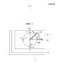
[0008] Фиг. 1 является видом, показывающим компоновку твердотельного датчика изображений, в соответствии с вариантом осуществления настоящего изобретения;[0008] FIG. 1 is a view showing an arrangement of a solid-state image sensor in accordance with an embodiment of the present invention;
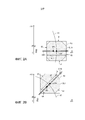
[0009] Фиг. 2А и 2B являются видами, примерно показывающими формы основания первой микролинзы и второй микролинзы, в соответствии с первым вариантом осуществления настоящего изобретения;[0009] FIG. 2A and 2B are views approximately showing the base forms of the first microlens and the second microlens in accordance with the first embodiment of the present invention;
[0010] Фиг. 3А и 3B являются видами, примерно показывающими формы поперечного сечения первой микролинзы и второй микролинзы, показанных на Фиг. 2А и 2B;[0010] FIG. 3A and 3B are views showing approximately cross-sectional shapes of the first microlens and the second microlens shown in FIG. 2A and 2B;
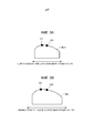
[0011] Фиг. 4А и 4B являются видами, примерно показывающими формы основания первой микролинзы и второй микролинзы, в соответствии со вторым вариантом осуществления настоящего изобретения;[0011] FIG. 4A and 4B are views showing approximately the base forms of the first microlens and the second microlens in accordance with a second embodiment of the present invention;
[0012] Фиг. 5А и 5B являются видами, примерно показывающими формы поперечного сечения первой микролинзы и второй микролинзы, показанных на Фиг. 4А и 4B;[0012] FIG. 5A and 5B are views approximately showing cross-sectional shapes of the first microlens and the second microlens shown in FIG. 4A and 4B;
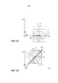
[0013] Фиг. 6А и 6B являются видами, примерно показывающими формы основания первой микролинзы и второй микролинзы в сравнительном примере; и[0013] FIG. 6A and 6B are views approximately showing the base forms of the first microlens and the second microlens in a comparative example; and
[0014] Фиг. 7А и 7B являются видами, примерно показывающими формы поперечного сечения первой микролинзы и второй микролинзы, показанных на Фиг. 6А и 6B.[0014] FIG. 7A and 7B are views approximately showing cross-sectional shapes of the first microlens and the second microlens shown in FIG. 6A and 6B.
ПОДРОБНОЕ ОПИСАНИЕ ВАРИАНТОВ ОСУЩЕСТВЛЕНИЯDETAILED DESCRIPTION OF EMBODIMENTS
[0015] Примерные варианты осуществления настоящего изобретения будут описываться ниже с ссылками на сопроводительные чертежи.[0015] Exemplary embodiments of the present invention will be described below with reference to the accompanying drawings.
[0016] Фиг. 1 показывает компоновку твердотельного датчика 1 изображений, в соответствии с вариантом осуществления настоящего изобретения. Твердотельный датчик 1 изображений включает в себя группу MLA микролинз, в которой множество микролинз группируются для составления множества строк и множества колонок. С другой точки зрения, твердотельный датчик 1 изображений включает в себя пиксельную матрицу PA, в которой множество пикселей, каждый из которых включает в себя микролинзу, группируются для составления множества строк и множества колонок. Каждый пиксель, который составляет пиксельную матрицу PA, включает в себя, дополнительно к микролинзе, фотоэлектрический преобразователь, такой как фотодиод. Каждый пиксель может также включать в себя цветовой фильтр. Каждый пиксель может дополнительно включать в себя схему в пикселе, сконфигурированную для считывания сигнала из фотоэлектрического преобразователя. Каждая схема в пикселе может включать в себя, например, транзистор усиления, который выводит сигнал, соответствующий зарядам, сгенерированным в фотоэлектрическом преобразователе.[0016] FIG. 1 shows an arrangement of a solid-state image sensor 1, in accordance with an embodiment of the present invention. The solid-state image sensor 1 includes an MLA group of microlenses in which multiple microlenses are grouped to form multiple lines and multiple columns. From another point of view, the solid-state image sensor 1 includes a pixel matrix PA in which a plurality of pixels, each of which includes a microlens, are grouped to form a plurality of rows and a plurality of columns. Each pixel that makes up the pixel array PA includes, in addition to the microlens, a photoelectric converter, such as a photodiode. Each pixel may also include a color filter. Each pixel may further include a circuit in a pixel configured to read a signal from a photoelectric converter. Each circuit in a pixel may include, for example, a gain transistor that outputs a signal corresponding to the charges generated in the photoelectric converter.
[0017] Твердотельный датчик 1 изображений может дополнительно включать в себя периферийную схему PC. Когда твердотельный датчик 1 изображений составляется посредством датчика изображений MOS, периферийная схема PC может включать в себя, например, схему выбора строки, схему считывания и схему выбора колонки. Схема выбора строки выбирает каждую строку в пиксельной матрице PA. Схема считывания считывает сигналы из пиксельной матрицы PA. Схема выбора колонки выбирает, из сигнала для одной строки, считанной посредством схемы считывания из пиксельной матрицы PA, один сигнал (сигнал, соответствующий колонке) в предварительно определенном порядке. Таким образом, схема выбора колонки выбирает каждую колонку в пиксельной матрице PA. Когда твердотельный датчик 1 изображений составляется посредством датчика изображения CCD, множество датчиков CCD вертикальной передачи компонуются в пиксельной матрице PA, и периферийная схема PC может включать в себя CCD горизонтальной передачи.[0017] The solid state image sensor 1 may further include a PC peripheral circuit. When the solid-state image sensor 1 is composed by the MOS image sensor, the peripheral circuit PC may include, for example, a line selection circuit, a read circuit, and a column selection circuit. The row selection scheme selects each row in the pixel matrix PA. A read circuit reads signals from the pixel matrix PA. The column selection circuit selects, from the signal for one row read by the reading circuit from the pixel matrix PA, one signal (the signal corresponding to the column) in a predetermined order. Thus, the column selection circuit selects each column in the pixel matrix PA. When the solid-state image sensor 1 is constituted by a CCD image sensor, a plurality of vertical transmission CCD sensors are arranged in the pixel matrix PA, and the peripheral circuit PC may include a horizontal transmission CCD.
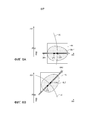
[0018] Следует отметить, что первая ось AX1, параллельная множеству строк группы микролинз MLA и проходящая через центр C группы, такой как центр пиксельной матрицы PA, и вторая ось AX2, параллельная множеству колонок группы микролинз MLA и проходящая через центр C группы, определены для удобства описания. Дополнительно, виртуальный круг VC, имеющий центр C группы в качестве центра, рассматривается. Радиус виртуального круга VC является произвольным. Фиг. 1 показывает некоторые пиксели, которые помещаются на виртуальный круг VC вне множества пикселей, составляющих пиксельную матрицу PA. Более конкретно, Фиг. 1 показывает первые пиксели P11, P12, P13 и P14 и второй пиксель P2, в качестве пикселей, которые помещаются на виртуальный круг VC, вне множества пикселей, составляющих пиксельную матрицу PA. Первые пиксели P11, P12, P13 и P14 помещаются на первую ось AX1 или вторую ось AX2. Второй пиксель P2 не помещается ни на первую ось AX1, ни на вторую ось AX2. Каждый пиксель, помещенный на первую ось AX1 или вторую ось AX2, может включать в себя пиксель с первой осью AX1 или второй осью AX2, пересекающимися в области пикселя, и/или пиксель с первой осью AX1 или второй осью AX2, контактирующими с границей области пикселя. Фиг. 1 показывает только один второй пиксель P2, хотя другой второй пиксель существует. Каждый пиксель, помещенный на виртуальный круг VC, может быть определен в качестве пикселя с виртуальным кругом VC, пересекающимся в области пикселя. Каждый пиксель может иметь площадь значения, полученного посредством разделения площади пиксельной матрицы PA на количество пикселей и, обычно, распознается как многоугольная область, такая как прямоугольная область.[0018] It should be noted that the first axis AX1 parallel to the multiple rows of the MLA microlens group and passing through the center C group, such as the center of the pixel matrix PA, and the second axis AX2 parallel to the multiple columns of the MLA microlens group and passing through the center C group, are defined for convenience of description. Additionally, a VC virtual circle having a center C group as a center is considered. The radius of the VC virtual circle is arbitrary. FIG. 1 shows some pixels that are placed on the virtual circle VC outside the plurality of pixels constituting the pixel matrix PA. More specifically, FIG. 1 shows the first pixels P11, P12, P13, and P14 and the second pixel P2, as pixels that are placed on the virtual circle VC, outside the plurality of pixels constituting the pixel matrix PA. The first pixels P11, P12, P13 and P14 are placed on the first axis AX1 or the second axis AX2. The second pixel P2 does not fit on either the first axis AX1 or the second axis AX2. Each pixel placed on the first axis AX1 or the second axis AX2 may include a pixel with a first axis AX1 or a second axis AX2 intersecting in the pixel region, and / or a pixel with a first axis AX1 or a second axis AX2 in contact with the boundary of the pixel region . FIG. 1 shows only one second pixel P2, although another second pixel exists. Each pixel placed on the VC virtual circle can be defined as a pixel with a VC virtual circle intersecting in the pixel region. Each pixel may have an area of a value obtained by dividing the area of the pixel matrix PA by the number of pixels and is usually recognized as a polygonal region, such as a rectangular region.
[0019] Множество микролинз, составляющих группу микролинз MLA, включает в себя первые микролинзы ML11, ML12, ML13 и ML14 и вторую микролинзу ML2. Первые микролинзы ML11, ML12, ML13 и ML14 являются микролинзами первых пикселей P11, P12, P13 и P14 соответственно. Вторая микролинза ML2 является микролинзой второго пикселя P2. Таким образом, микролинзы, помещенные на виртуальный круг VC вне множества микролинз, составляющих группу микролинз MLA, включают в себя первые микролинзы ML11, ML12, ML13 и ML14 и вторую микролинзу ML2. Первые микролинзы ML11, ML12, ML13 и ML14 помещаются на первую ось AX1 или вторую ось AX2. Вторая микролинза ML2 не помещается ни на первую ось AX1, ни на вторую ось AX2.[0019] The plurality of microlenses constituting the MLA microlens group includes the first ML11, ML12, ML13, and ML14 microlenses and the second ML2 microlens. The first microlenses ML11, ML12, ML13, and ML14 are microlenses of the first pixels P11, P12, P13, and P14, respectively. The second microlens ML2 is the microlens of the second pixel P2. Thus, microlenses placed on the VC virtual circle outside the multiple microlenses that make up the MLA microlens group include the first ML11, ML12, ML13, and ML14 microlenses and the second ML2 microlens. The first lenses ML11, ML12, ML13 and ML14 are placed on the first axis AX1 or the second axis AX2. The second ML2 microlens does not fit on either the first axis AX1 or the second axis AX2.
[0020] Угол, сформированный посредством первой оси AX1 и второго направления DIR2, может быть определен в качестве аргумента θ. Следует отметить, что второе направление DIR2 и аргумент θ могут подразумеваться в качестве параметра, который предоставляет полярные координаты, указывающие позицию второй микролинзы ML2 (второго пикселя P2). Второе направление DIR2 и аргумент θ зависят от позиции второго пикселя P2.[0020] An angle formed by the first axis AX1 and the second direction DIR2 may be determined as an argument θ. It should be noted that the second direction DIR2 and the argument θ can be implied as a parameter that provides polar coordinates indicating the position of the second microlens ML2 (second pixel P2). The second direction DIR2 and the argument θ depend on the position of the second pixel P2.
[0021] Обычно, каждый из первых пикселей и второго пикселя, скомпонованные на предварительно определенном расстоянии или удаленно от центра C группы, могут включать в себя некруглую форму основания. С другой стороны, каждый из первых пикселей и второго пикселя, скомпонованных на предварительно определенном расстоянии или удаленно от центра C группы, могут включать в себя круглую форму основания. Предварительно определенное расстояние может быть определено произвольно и может быть расстоянием 10%, 20%, 30% или 40% каждой короткой стороны пиксельной матрицы PA. Рассматривая виртуальный круг VC с центром C группы в качестве центра и радиусом, большим, чем предварительно определенное расстояние, каждая из первых микролинз первых пикселей P11, P12, P13 и P14 и второй микролинзы второго пикселя P2 имеет некруглую форму основания.[0021] Typically, each of the first pixels and the second pixel arranged at a predetermined distance or remotely from the center C of the group may include a non-circular base shape. On the other hand, each of the first pixels and the second pixel arranged at a predetermined distance or remotely from the center C of the group may include a circular base shape. The predetermined distance may be arbitrarily determined and may be a distance of 10%, 20%, 30%, or 40% of each short side of the pixel matrix PA. Considering a virtual circle VC with the center C of the group as the center and a radius greater than a predetermined distance, each of the first microlenses of the first pixels P11, P12, P13 and P14 and the second microlenses of the second pixel P2 has a non-circular base shape.
[0022] Ширина второй микролинзы ML2 во втором направлении DIR2, проходящем через вторую микролинзу ML2 и центр C группы, больше, чем ширина первой микролинзы ML11 в первом направлении DIR1, проходящем через первую микролинзу ML11 и центр C группы. Аналогично, ширина второй микролинзы ML2 во втором направлении DIR2, проходящем через вторую микролинзу ML2 и центр C группы, больше, чем ширина первой микролинзы ML12 в первом направлении DIR1, проходящем через первую микролинзу ML12 и центр C группы. Аналогично, ширина второй микролинзы ML2 во втором направлении DIR2, проходящем через вторую микролинзу ML2 и центр C группы, больше, чем ширина первой микролинзы ML13 в первом направлении DIR1, проходящем через первую микролинзу ML13 и центр C группы. Аналогично, ширина второй микролинзы ML2 во втором направлении DIR2, проходящем через вторую микролинзу ML2 и центр C группы, больше, чем ширина первой микролинзы ML14 в первом направлении DIR1, проходящем через первую микролинзу ML14 и центр C группы. Следует отметить, что, например, первое направление DIR1 проходит через барицентр каждой первой микролинзы и центр C группы, и второе направление DIR2 проходит через барицентр второй микролинзы и центр группы.[0022] The width of the second microlens ML2 in the second direction DIR2 passing through the second microlens ML2 and the group C center is larger than the width of the first microlens ML2 in the first direction DIR1 passing through the first microlens ML11 and the center C group. Similarly, the width of the second microlens ML2 in the second direction DIR2 passing through the second microlens ML2 and the center C group is greater than the width of the first microlens ML2 in the first direction DIR1 passing through the first microlens ML12 and the center C group. Similarly, the width of the second microlens ML2 in the second direction DIR2 passing through the second microlens ML2 and the center C group is larger than the width of the first microlens ML2 in the first direction DIR1 passing through the first microlens ML13 and the center C group. Similarly, the width of the second microlens ML2 in the second direction DIR2 passing through the second microlens ML2 and the center C group is larger than the width of the first microlens ML14 in the first direction DIR1 passing through the first microlens ML14 and the center C group. It should be noted that, for example, the first direction DIR1 passes through the barycenter of each first microlens and the center C of the group, and the second direction DIR2 passes through the barycenter of the second microlens and the center of the group.
[0023] В одном примере ширина второй микролинзы ML2 во втором направлении DIR2 может быть увеличена, в соответствии с увеличением в θ в диапазонах 0°<θ≤45°, 90°<θ≤135°, 180°<θ≤225° и 270°<θ≤315°. В одном примере ширина второй микролинзы ML2 во втором направлении DIR2 может быть уменьшена, в соответствии с увеличением в θ в диапазонах 45°≤θ<90°, 135°<θ≤180°, 225°<θ≤270° и 315°<θ≤360°. Такая компоновка является преимущественной при улучшении эффективности сбора света относительно фотоэлектрического преобразователя во втором пикселе P2.[0023] In one example, the width of the second microlens ML2 in the second direction DIR2 can be increased, in accordance with the increase in θ in the ranges 0 ° <θ≤45 °, 90 ° <θ≤135 °, 180 ° <θ≤225 ° and 270 ° <θ≤315 °. In one example, the width of the second microlens ML2 in the second direction DIR2 can be reduced, in accordance with the increase in θ in the ranges 45 ° ≤θ <90 °, 135 ° <θ≤180 °, 225 ° <θ≤270 ° and 315 ° < θ≤360 °. Such an arrangement is advantageous in improving the light collection efficiency with respect to the photoelectric converter in the second pixel P2.
[0024] В одном примере каждая из первых микролинз ML11, ML12, ML13 и ML14 может иметь линейно-симметричную форму относительно прямой линии, параллельной первому направлению DIR1, в качестве оси симметрии и вторая микролинза ML2 может иметь линейно-симметричную форму относительно прямой линии, параллельной второму направлению DIR2, в качестве оси симметрии.[0024] In one example, each of the first microlenses ML11, ML12, ML13 and ML14 may have a linearly symmetrical shape with respect to a straight line parallel to the first direction DIR1, as the axis of symmetry, and the second microlens ML2 may have a linearly symmetrical shape with respect to a straight line, parallel to the second direction of DIR2, as the axis of symmetry.
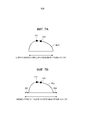
[0025] Фиг. 2А и 2B примерно показывают формы основания первой микролинзы ML11 и второй микролинзы ML2, в соответствии с первым вариантом осуществления настоящего изобретения. Формой основания каждой микролинзы является форма области, которая занимается микролинзой, спроецированной на плоскость, параллельную группе микролинз MLA. Ширина W2 второй микролинзы ML2 во втором направлении DIR2, проходящем через вторую микролинзу ML2 и центр C группы, больше, чем ширина W11 первой микролинзы ML11 в первом направлении DIR1, проходящем через первую микролинзу ML11 и центр C группы. Хотя не показано, то же самое относится к первым микролинзам ML12, ML13 и ML14. Фиг 3A показывает форму поперечного сечения, полученную при разрезе первой микролинзы ML11, показанной на Фиг. 2A, вдоль прямой линии, параллельной первому направлению DIR1. Фиг. 3B примерно показывает форму поперечного сечения, полученную при разрезе второй микролинзы ML2, показанной на Фиг. 2B, вдоль прямой линии, параллельной второму направлению DIR2.[0025] FIG. 2A and 2B roughly show the base forms of the first ML11 microlens and the second ML2 microlens, in accordance with the first embodiment of the present invention. The base shape of each microlens is the shape of the area that deals with the microlens projected onto a plane parallel to the MLA microlens group. The width W2 of the second microlens ML2 in the second direction DIR2 passing through the second microlens ML2 and the center C group is greater than the width W11 of the first microlens ML11 in the first direction DIR1 passing through the first microlens ML11 and the center C group. Although not shown, the same applies to the first ML12, ML13, and ML14 microlenses. FIG. 3A shows a cross-sectional shape obtained by sectioning the first ML11 microlens shown in FIG. 2A along a straight line parallel to the first direction DIR1. FIG. 3B approximately shows the cross-sectional shape obtained by sectioning the second microlens ML2 shown in FIG. 2B, along a straight line parallel to the second direction of DIR2.
[0026] Как примерно представлено на Фиг. 2А, 2B, 3А и 3B, верхняя позиция VP1 первой микролинзы ML11 (так же для ML12, ML13 и ML14) находится в позиции, смещенной в сторону центра C группы от центра CW1 ширины первой микролинзы ML11 в первом направлении DIR1. Верхняя позиция VP2 второй микролинзы ML2 находится в позиции, смещенной в сторону центра C группы от центра CW2 ширины второй микролинзы ML2 во втором направлении DIR2. Такая компоновка является преимущественной при сборе наклонно падающих лучей на микролинзы на фотоэлектрические преобразователи ниже микролинз.[0026] As approximately represented in FIG. 2A, 2B, 3A and 3B, the upper position VP1 of the first microlens ML11 (also for ML12, ML13 and ML14) is in a position offset toward the center C of the group from the center CW1 of the width of the first microlens ML11 in the first direction DIR1. The upper position VP2 of the second microlens ML2 is in a position offset toward the center C of the group from the center CW2 of the width of the second microlens ML2 in the second direction DIR2. Such an arrangement is advantageous when collecting obliquely incident rays on microlenses on photoelectric converters below microlenses.
[0027] Форма поперечного сечения второй микролинзы ML2, разрезанной вдоль прямой линии, параллельной второму направлению DIR2, может включать в себя форму, полученную посредством увеличения по меньшей мере части формы поперечного сечения первой микролинзы ML11 (так же для ML12, ML13 и ML14), разрезанной вдоль прямой линии, параллельной первому направлению DIR1. Это увеличение может быть сделано как относительно первого направления DIR1, так и относительно вертикального направления или может быть сделано относительно только первого направления DIR1.[0027] The cross-sectional shape of the second microlens ML2 cut along a straight line parallel to the second direction DIR2 may include a shape obtained by enlarging at least a portion of the cross-sectional shape of the first microlens ML11 (also for ML12, ML13 and ML14), cut along a straight line parallel to the first direction of DIR1. This increase can be made both with respect to the first direction of DIR1, and with respect to the vertical direction, or can be made with respect to only the first direction of DIR1.
[0028] Альтернативно, форма поперечного сечения второй микролинзы ML2, разрезанной вдоль прямой линии, параллельной второму направлению DIR2, может быть подобна форме поперечного сечения первой микролинзы ML11 (так же для ML12, ML13 и ML14), разрезанной вдоль прямой линии, параллельной первому направлению DIR1.[0028] Alternatively, the cross-sectional shape of the second microlens ML2, cut along a straight line parallel to the second direction DIR2, may be similar to the cross-sectional shape of the first microlens ML2 (also for ML12, ML13 and ML14), cut along a straight line parallel to the first direction DIR1.
[0029] Как примерно представлено на Фиг. 2A, внешняя граница основания первой микролинзы ML11 может включать в себя часть E1, параллельную первому направлению DIR1, и часть E2, перпендикулярную первому направлению DIR1. Как примерно представлено на Фиг. 2B, внешняя граница основания второй микролинзы ML2 может включать в себя часть E3, параллельную второму направлению DIR2, и часть E4, перпендикулярную второму направлению DIR2.[0029] As approximately represented in FIG. 2A, the outer boundary of the base of the first microlens ML11 may include a portion E1 parallel to the first direction DIR1 and a portion E2 perpendicular to the first direction DIR1. As approximately represented in FIG. 2B, the outer boundary of the base of the second microlens ML2 may include a portion E3 parallel to the second direction DIR2, and a portion E4 perpendicular to the second direction DIR2.
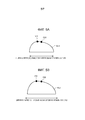
[0030] Фиг. 6А, 6B, 7А и 7B показывают сравнительный пример. В этом сравнительном примере каждая из первой микролинзы ML11' и второй микролинзы ML2', скомпонованные на виртуальном круге VC, имеют симметричную форму вращения. Такая компоновка может быть создана, когда форма первой микролинзы ML11' выбирается и затем форма, полученная посредством вращения первой микролинзы ML11', выбирается в качестве формы второй микролинзы ML2'. Фиг. 6А и 6B примерно показывают форму основания первой микролинзы ML11', разрезанной вдоль прямой линии, параллельной первому направлению DIR1, и форму основания второй микролинзы ML2', разрезанной вдоль прямой линии, параллельной второму направлению DIR2. Фиг. 7A показывает форму поперечного сечения, полученную при разрезе первой микролинзы ML11', показанной на Фиг. 6A, вдоль прямой линии, параллельной первому направлению DIR1. Фиг. 7B примерно показывает форму поперечного сечения, полученную при разрезе второй микролинзы ML2', показанной на Фиг. 6B, вдоль прямой линии, параллельной второму направлению DIR2.[0030] FIG. 6A, 6B, 7A and 7B show a comparative example. In this comparative example, each of the first microlens ML11 ′ and the second microlens ML2 ′ arranged on the virtual circle VC have a symmetrical rotation shape. Such an arrangement can be created when the shape of the first microlens ML11 'is selected and then the shape obtained by rotating the first microlens ML11' is selected as the shape of the second microlens ML2 '. FIG. 6A and 6B approximately show the base shape of the first micro lens ML11 'cut along a straight line parallel to the first direction DIR1, and the base shape of the second micro lens ML2' cut along a straight line parallel to the second direction DIR2. FIG. 7A shows a cross-sectional shape obtained by sectioning the first microlens ML11 ′ shown in FIG. 6A along a straight line parallel to the first direction DIR1. FIG. 7B approximately shows the cross-sectional shape obtained by sectioning the second microlens ML2 ′ shown in FIG. 6B, along a straight line parallel to the second direction of DIR2.
[0031] В этом сравнительном примере необходимо понимать, что область 701 вне внешней границы второй микролинзы ML2' больше, чем в варианте осуществления, показанном на Фиг. 2А, 2B, 3А и 3B, и таким образом эффективность сбора света для фотоэлектрического преобразователя ниже, чем в варианте осуществления.[0031] In this comparative example, it should be understood that the
[0032] Твердотельный датчик 1 изображений, в соответствии со вторым вариантом осуществления настоящего изобретения, описывается ниже с ссылками на Фиг. 4А, 4B, 5А и 5B. Следует отметить, что объекты, не упомянутые во втором варианте осуществления, могут совпадать с первым вариантом осуществления. Фиг. 4А и 4B примерно показывают формы основания первой микролинзы ML11 и второй микролинзы ML2, в соответствии со вторым вариантом осуществления настоящего изобретения. Ширина W2' второй микролинзы ML2 во втором направлении DIR2, проходящем через вторую микролинзу ML2 и центр C группы, больше, чем ширина W11' первой микролинзы ML11 в первом направлении DIR1, проходящем через первую микролинзу ML11 и центр C группы. Хотя не показано, то же самое также относится к первым микролинзам ML12, ML13 и ML14. Фиг. 5A показывает форму поперечного сечения, полученную при разрезе первой микролинзы ML11, показанной на Фиг. 4A, вдоль прямой линии, параллельной первому направлению DIR1. Фиг. 5B примерно показывает форму поперечного сечения, полученную при разрезе второй микролинзы ML2, показанной на Фиг. 4B, вдоль прямой линии, параллельной второму направлению DIR2. В одном примере форма поперечного сечения второй микролинзы ML2, разрезанной вдоль прямой линии, параллельной второму направлению DIR2, может быть аналогичной форме поперечного сечения первой микролинзы ML11 (так же для ML12, ML13 и ML14), разрезанной вдоль прямой линии, параллельной первому направлению DIR1.[0032] A solid-state image sensor 1, in accordance with a second embodiment of the present invention, is described below with reference to FIG. 4A, 4B, 5A and 5B. It should be noted that objects not mentioned in the second embodiment may coincide with the first embodiment. FIG. 4A and 4B roughly show the base forms of the first ML11 microlens and the second ML2 microlens, in accordance with a second embodiment of the present invention. The width W2 ′ of the second microlens ML2 in the second direction DIR2 passing through the second microlens ML2 and the center C group is larger than the width W11 ′ of the first microlens ML2 in the first direction DIR1 passing through the first microlens ML11 and the center C group. Although not shown, the same also applies to the first ML12, ML13 and ML14 microlenses. FIG. 5A shows a cross-sectional shape obtained by sectioning the first microlens ML11 shown in FIG. 4A along a straight line parallel to the first direction DIR1. FIG. 5B approximately shows the cross-sectional shape obtained by sectioning the second microlens ML2 shown in FIG. 4B, along a straight line parallel to the second direction of DIR2. In one example, the cross-sectional shape of the second microlens ML2, cut along a straight line parallel to the second direction DIR2, may be similar to the cross-sectional shape of the first microlens ML2 (also for ML12, ML13 and ML14), cut along a straight line parallel to the first direction DIR1.
[0033] В качестве применения твердотельного датчика изображений, в соответствии с вышеописанными вариантами осуществления, камера, в которой собран твердотельный датчик изображений, примерно описывается ниже. Понятие «камера» включает в себя не только устройство, главным образом, стремящееся фотографировать (снимать), но также и устройство (например, персональный компьютер или портативный терминал), дополнительно имеющее функции фотографирования (съемки). Камера включает в себя твердотельный датчик изображений, в соответствии с настоящим изобретением, как примерно описано выше в вариантах осуществления, и процессор, который обрабатывает сигнал, выходящий из твердотельного датчика изображений. Процессор может включать в себя, например, преобразователь A/D и процессор, который обрабатывает вывод цифровых данных из преобразователя A/D.[0033] As an application of the solid-state image sensor, in accordance with the above-described embodiments, the camera in which the solid-state image sensor is assembled is approximately described below. The concept of “camera” includes not only a device, mainly tending to take pictures (shoot), but also a device (for example, a personal computer or portable terminal), additionally having the functions of photographing (shooting). The camera includes a solid-state image sensor in accordance with the present invention, as described above in embodiments, and a processor that processes a signal output from the solid-state image sensor. The processor may include, for example, an A / D converter and a processor that processes the output of digital data from the A / D converter.
[0034] ДРУГИЕ ВАРИАНТЫ ОСУЩЕСТВЛЕНИЯ[0034] OTHER EMBODIMENTS
Вариант(ы) осуществления настоящего изобретения может также быть реализован(ы) посредством компьютера системы или устройства, которое считывает и выполняет выполняемые компьютером команды (например, одну или более программ), записанные на носителе данных (который может также более полно называться «энергонезависимый считываемый компьютером носитель данных»), для выполнения одной или более функций вышеописанного варианта(ов) осуществления и/или включает в себя одну или более схем (например, программируемую пользователем вентильную матрицу(ASIC)) для выполнения одной или более функций вышеописанных вариантов осуществления и посредством способа, выполняемого посредством компьютера системы или устройства посредством, например, считывания и выполнения выполняемых компьютером команд из носителя данных для выполнения функций одного или более вышеописанных вариантов осуществления и/или управления одной или более схемами для выполнения функций одного или более вышеописанных вариантов осуществления. Компьютер может содержать один или более процессоров (например, центральный процессор (CPU), микропроцессор (микроблок обработки) (MPU)) и может включать в себя сеть отдельных компьютеров или отдельных процессоров для считывания и выполнения выполняемых компьютером команд. Выполняемые компьютером команды могут быть выданы на компьютер, например, из сети или носителя данных. Носитель данных может включать в себя, например, один или несколько жестких дисков, оперативное запоминающее устройство (RAM), постоянное запоминающее устройство (ROM), хранилище распределенных вычислительных систем, оптический диск (такой как компакт-диск (CD), цифровой универсальный диск (DVD) или Диск blu-ray (BD) ™), устройство флэш-памяти, карту памяти и т.п.An embodiment (s) of the present invention may also be implemented (s) by a computer system or device that reads and executes computer-executable instructions (for example, one or more programs) recorded on a storage medium (which may also be more fully referred to as "non-volatile readable computer data carrier "), to perform one or more functions of the above embodiment (s) of implementation and / or includes one or more circuits (for example, a user programmable gate mat ASIC) to perform one or more functions of the above embodiments and by a method performed by a computer of a system or device by, for example, reading and executing computer-executable instructions from a storage medium to perform functions of one or more of the above embodiments and / or control one or more circuits for performing the functions of one or more of the above embodiments. A computer may comprise one or more processors (e.g., a central processing unit (CPU), microprocessor (processing microblock) (MPU)) and may include a network of individual computers or individual processors for reading and executing computer-executed instructions. Computer-executable instructions may be issued to a computer, for example, from a network or storage medium. A storage medium may include, for example, one or more hard drives, random access memory (RAM), read-only memory (ROM), storage for distributed computing systems, an optical disk (such as a compact disc (CD), a digital universal disk ( DVD) or Blu-ray Disc (BD) ™), flash drive, memory card, etc.
[0035] В то время как настоящее изобретение описывается с ссылками на варианты осуществления, необходимо понимать, что изобретение не ограничивается описанными примерными вариантами осуществления. Объем следующей формулы изобретения должен получить самую широкую интерпретацию для охвата всех таких модификаций и эквивалентных структур и функций.[0035] While the present invention is described with reference to embodiments, it should be understood that the invention is not limited to the described exemplary embodiments. The scope of the following claims is to be accorded the broadest interpretation so as to encompass all such modifications and equivalent structures and functions.
Claims (14)
Applications Claiming Priority (2)
| Application Number | Priority Date | Filing Date | Title |
|---|---|---|---|
| JP2015099511A JP6506614B2 (en) | 2015-05-14 | 2015-05-14 | Solid-state imaging device and camera |
| JP2015-099511 | 2015-05-14 |
Publications (2)
| Publication Number | Publication Date |
|---|---|
| RU2016118405A RU2016118405A (en) | 2017-11-16 |
| RU2650729C2 true RU2650729C2 (en) | 2018-04-17 |
Family
ID=55802223
Family Applications (1)
| Application Number | Title | Priority Date | Filing Date |
|---|---|---|---|
| RU2016118405A RU2650729C2 (en) | 2015-05-14 | 2016-05-12 | Solid-state image sensor and camera |
Country Status (9)
| Country | Link |
|---|---|
| US (1) | US10114151B2 (en) |
| EP (1) | EP3093887B1 (en) |
| JP (1) | JP6506614B2 (en) |
| KR (1) | KR20160134502A (en) |
| CN (1) | CN106161891B (en) |
| BR (1) | BR102016009246A2 (en) |
| PH (1) | PH12016000181A1 (en) |
| RU (1) | RU2650729C2 (en) |
| SG (1) | SG10201603687RA (en) |
Families Citing this family (7)
| Publication number | Priority date | Publication date | Assignee | Title |
|---|---|---|---|---|
| US10205894B2 (en) | 2015-09-11 | 2019-02-12 | Canon Kabushiki Kaisha | Imaging device and imaging system |
| JP6688165B2 (en) | 2016-06-10 | 2020-04-28 | キヤノン株式会社 | Imaging device and imaging system |
| JP6727938B2 (en) | 2016-06-10 | 2020-07-22 | キヤノン株式会社 | IMAGING DEVICE, IMAGING DEVICE CONTROL METHOD, AND IMAGING SYSTEM |
| JP6776011B2 (en) | 2016-06-10 | 2020-10-28 | キヤノン株式会社 | Imaging device and imaging system |
| JP7013119B2 (en) | 2016-07-21 | 2022-01-31 | キヤノン株式会社 | Solid-state image sensor, manufacturing method of solid-state image sensor, and image pickup system |
| US10212576B2 (en) | 2016-09-08 | 2019-02-19 | Samsung Electronics Co., Ltd. | Near field communication device |
| CN109842766B (en) * | 2018-12-28 | 2021-05-18 | 上海集成电路研发中心有限公司 | Polar coordinate image sensor and image processing method thereof |
Citations (4)
| Publication number | Priority date | Publication date | Assignee | Title |
|---|---|---|---|---|
| US20060023312A1 (en) * | 2003-10-09 | 2006-02-02 | Boettiger Ulrich C | Ellipsoidal gapless microlens array and method of fabrication |
| US7812302B2 (en) * | 2006-07-14 | 2010-10-12 | Visera Technologies Company Limited | Imaging sensor having microlenses of different radii of curvature |
| EP2362257A1 (en) * | 2009-11-20 | 2011-08-31 | FUJIFILM Corporation | Solid-state imaging device |
| EP2819172A1 (en) * | 2013-06-28 | 2014-12-31 | Canon Kabushiki Kaisha | Optical element array and solid-state imaging device including the array |
Family Cites Families (7)
| Publication number | Priority date | Publication date | Assignee | Title |
|---|---|---|---|---|
| US5662401A (en) * | 1995-12-13 | 1997-09-02 | Philips Electronics North America Corporation | Integrating lens array and image forming method for improved optical efficiency |
| JP2007335723A (en) | 2006-06-16 | 2007-12-27 | Fujifilm Corp | Microlens for solid-state imaging element and its manufacturing method |
| JP4941233B2 (en) | 2007-10-31 | 2012-05-30 | 大日本印刷株式会社 | Solid-state imaging device and imaging apparatus using the same |
| US7687757B1 (en) * | 2009-01-29 | 2010-03-30 | Visera Technologies Company Limited | Design of microlens on pixel array |
| GB2498972A (en) * | 2012-02-01 | 2013-08-07 | St Microelectronics Ltd | Pixel and microlens array |
| JP2015109314A (en) | 2013-12-03 | 2015-06-11 | 株式会社東芝 | Solid-state imaging device |
| JP2016058538A (en) | 2014-09-09 | 2016-04-21 | キヤノン株式会社 | Solid state image sensor and camera |
-
2015
- 2015-05-14 JP JP2015099511A patent/JP6506614B2/en active Active
-
2016
- 2016-04-15 EP EP16165488.4A patent/EP3093887B1/en active Active
- 2016-04-22 US US15/136,017 patent/US10114151B2/en active Active
- 2016-04-26 BR BR102016009246A patent/BR102016009246A2/en not_active Application Discontinuation
- 2016-05-09 KR KR1020160056116A patent/KR20160134502A/en not_active Application Discontinuation
- 2016-05-10 SG SG10201603687RA patent/SG10201603687RA/en unknown
- 2016-05-11 PH PH12016000181A patent/PH12016000181A1/en unknown
- 2016-05-12 RU RU2016118405A patent/RU2650729C2/en active
- 2016-05-13 CN CN201610317738.XA patent/CN106161891B/en active Active
Patent Citations (4)
| Publication number | Priority date | Publication date | Assignee | Title |
|---|---|---|---|---|
| US20060023312A1 (en) * | 2003-10-09 | 2006-02-02 | Boettiger Ulrich C | Ellipsoidal gapless microlens array and method of fabrication |
| US7812302B2 (en) * | 2006-07-14 | 2010-10-12 | Visera Technologies Company Limited | Imaging sensor having microlenses of different radii of curvature |
| EP2362257A1 (en) * | 2009-11-20 | 2011-08-31 | FUJIFILM Corporation | Solid-state imaging device |
| EP2819172A1 (en) * | 2013-06-28 | 2014-12-31 | Canon Kabushiki Kaisha | Optical element array and solid-state imaging device including the array |
Also Published As
| Publication number | Publication date |
|---|---|
| EP3093887B1 (en) | 2018-01-24 |
| RU2016118405A (en) | 2017-11-16 |
| PH12016000181A1 (en) | 2018-01-22 |
| SG10201603687RA (en) | 2016-12-29 |
| CN106161891B (en) | 2019-07-30 |
| BR102016009246A2 (en) | 2016-11-16 |
| US10114151B2 (en) | 2018-10-30 |
| CN106161891A (en) | 2016-11-23 |
| JP2016219469A (en) | 2016-12-22 |
| JP6506614B2 (en) | 2019-04-24 |
| EP3093887A1 (en) | 2016-11-16 |
| US20160334550A1 (en) | 2016-11-17 |
| KR20160134502A (en) | 2016-11-23 |
Similar Documents
| Publication | Publication Date | Title |
|---|---|---|
| RU2650729C2 (en) | Solid-state image sensor and camera | |
| US9881951B2 (en) | Image sensors with phase detection pixels | |
| US9883128B2 (en) | Imaging systems with high dynamic range and phase detection pixels | |
| CN105306786B (en) | Image processing method for the imaging sensor with phase-detection pixel | |
| US10015471B2 (en) | Asymmetric angular response pixels for single sensor stereo | |
| US20170347042A1 (en) | Imaging systems with high dynamic range and phase detection pixels | |
| US20140263980A1 (en) | Imagers with depth sensing capabilities | |
| US20150381951A1 (en) | Pixel arrangements for image sensors with phase detection pixels | |
| US20170374306A1 (en) | Image sensor system with an automatic focus function | |
| JP7012619B2 (en) | Image sensor and image sensor | |
| US10389930B2 (en) | Image pickup device and image pickup system | |
| US20160241772A1 (en) | Dynamic auto focus zones for auto focus pixel systems | |
| JP2008546200A (en) | Asymmetric microlenses on pixel arrays | |
| JPH11150254A (en) | Solid-state image-pickup element | |
| JP5115068B2 (en) | Imaging device | |
| CN113037956A (en) | Imaging device, mobile terminal, and image sensing method | |
| US10074683B2 (en) | Imaging systems having lens substrates with total internal reflection mitigation structures | |
| JP2010178133A (en) | Solid-state imaging device and electronic device | |
| TWI710803B (en) | Image sensors with multipart diffractive lenses | |
| TW200818477A (en) | Solid-state image capturing device and electronic information device | |
| JP2009065095A (en) | Solid-state imaging element | |
| JP2005197747A (en) | Photosensor array layout for monitoring image statistics | |
| US10715745B2 (en) | Constructing an image using more pixel data than pixels in an image sensor |