RU2608565C2 - Wired lighting module with three-dimensional topography - Google Patents
Wired lighting module with three-dimensional topography Download PDFInfo
- Publication number
- RU2608565C2 RU2608565C2 RU2014113346A RU2014113346A RU2608565C2 RU 2608565 C2 RU2608565 C2 RU 2608565C2 RU 2014113346 A RU2014113346 A RU 2014113346A RU 2014113346 A RU2014113346 A RU 2014113346A RU 2608565 C2 RU2608565 C2 RU 2608565C2
- Authority
- RU
- Russia
- Prior art keywords
- lighting module
- plate
- light sources
- solid
- state light
- Prior art date
Links
Images

Classifications
-
- F—MECHANICAL ENGINEERING; LIGHTING; HEATING; WEAPONS; BLASTING
- F21—LIGHTING
- F21S—NON-PORTABLE LIGHTING DEVICES; SYSTEMS THEREOF; VEHICLE LIGHTING DEVICES SPECIALLY ADAPTED FOR VEHICLE EXTERIORS
- F21S4/00—Lighting devices or systems using a string or strip of light sources
-
- F—MECHANICAL ENGINEERING; LIGHTING; HEATING; WEAPONS; BLASTING
- F21—LIGHTING
- F21V—FUNCTIONAL FEATURES OR DETAILS OF LIGHTING DEVICES OR SYSTEMS THEREOF; STRUCTURAL COMBINATIONS OF LIGHTING DEVICES WITH OTHER ARTICLES, NOT OTHERWISE PROVIDED FOR
- F21V23/00—Arrangement of electric circuit elements in or on lighting devices
- F21V23/001—Arrangement of electric circuit elements in or on lighting devices the elements being electrical wires or cables
-
- F—MECHANICAL ENGINEERING; LIGHTING; HEATING; WEAPONS; BLASTING
- F21—LIGHTING
- F21K—NON-ELECTRIC LIGHT SOURCES USING LUMINESCENCE; LIGHT SOURCES USING ELECTROCHEMILUMINESCENCE; LIGHT SOURCES USING CHARGES OF COMBUSTIBLE MATERIAL; LIGHT SOURCES USING SEMICONDUCTOR DEVICES AS LIGHT-GENERATING ELEMENTS; LIGHT SOURCES NOT OTHERWISE PROVIDED FOR
- F21K9/00—Light sources using semiconductor devices as light-generating elements, e.g. using light-emitting diodes [LED] or lasers
- F21K9/20—Light sources comprising attachment means
-
- F—MECHANICAL ENGINEERING; LIGHTING; HEATING; WEAPONS; BLASTING
- F21—LIGHTING
- F21K—NON-ELECTRIC LIGHT SOURCES USING LUMINESCENCE; LIGHT SOURCES USING ELECTROCHEMILUMINESCENCE; LIGHT SOURCES USING CHARGES OF COMBUSTIBLE MATERIAL; LIGHT SOURCES USING SEMICONDUCTOR DEVICES AS LIGHT-GENERATING ELEMENTS; LIGHT SOURCES NOT OTHERWISE PROVIDED FOR
- F21K9/00—Light sources using semiconductor devices as light-generating elements, e.g. using light-emitting diodes [LED] or lasers
- F21K9/90—Methods of manufacture
-
- F—MECHANICAL ENGINEERING; LIGHTING; HEATING; WEAPONS; BLASTING
- F21—LIGHTING
- F21S—NON-PORTABLE LIGHTING DEVICES; SYSTEMS THEREOF; VEHICLE LIGHTING DEVICES SPECIALLY ADAPTED FOR VEHICLE EXTERIORS
- F21S4/00—Lighting devices or systems using a string or strip of light sources
- F21S4/10—Lighting devices or systems using a string or strip of light sources with light sources attached to loose electric cables, e.g. Christmas tree lights
- F21S4/15—Lighting devices or systems using a string or strip of light sources with light sources attached to loose electric cables, e.g. Christmas tree lights the cables forming a grid, net or web structure
-
- F—MECHANICAL ENGINEERING; LIGHTING; HEATING; WEAPONS; BLASTING
- F21—LIGHTING
- F21V—FUNCTIONAL FEATURES OR DETAILS OF LIGHTING DEVICES OR SYSTEMS THEREOF; STRUCTURAL COMBINATIONS OF LIGHTING DEVICES WITH OTHER ARTICLES, NOT OTHERWISE PROVIDED FOR
- F21V11/00—Screens not covered by groups F21V1/00, F21V3/00, F21V7/00 or F21V9/00
-
- F—MECHANICAL ENGINEERING; LIGHTING; HEATING; WEAPONS; BLASTING
- F21—LIGHTING
- F21V—FUNCTIONAL FEATURES OR DETAILS OF LIGHTING DEVICES OR SYSTEMS THEREOF; STRUCTURAL COMBINATIONS OF LIGHTING DEVICES WITH OTHER ARTICLES, NOT OTHERWISE PROVIDED FOR
- F21V23/00—Arrangement of electric circuit elements in or on lighting devices
-
- F—MECHANICAL ENGINEERING; LIGHTING; HEATING; WEAPONS; BLASTING
- F21—LIGHTING
- F21Y—INDEXING SCHEME ASSOCIATED WITH SUBCLASSES F21K, F21L, F21S and F21V, RELATING TO THE FORM OR THE KIND OF THE LIGHT SOURCES OR OF THE COLOUR OF THE LIGHT EMITTED
- F21Y2105/00—Planar light sources
- F21Y2105/10—Planar light sources comprising a two-dimensional array of point-like light-generating elements
-
- F—MECHANICAL ENGINEERING; LIGHTING; HEATING; WEAPONS; BLASTING
- F21—LIGHTING
- F21Y—INDEXING SCHEME ASSOCIATED WITH SUBCLASSES F21K, F21L, F21S and F21V, RELATING TO THE FORM OR THE KIND OF THE LIGHT SOURCES OR OF THE COLOUR OF THE LIGHT EMITTED
- F21Y2115/00—Light-generating elements of semiconductor light sources
- F21Y2115/10—Light-emitting diodes [LED]
-
- Y—GENERAL TAGGING OF NEW TECHNOLOGICAL DEVELOPMENTS; GENERAL TAGGING OF CROSS-SECTIONAL TECHNOLOGIES SPANNING OVER SEVERAL SECTIONS OF THE IPC; TECHNICAL SUBJECTS COVERED BY FORMER USPC CROSS-REFERENCE ART COLLECTIONS [XRACs] AND DIGESTS
- Y10—TECHNICAL SUBJECTS COVERED BY FORMER USPC
- Y10T—TECHNICAL SUBJECTS COVERED BY FORMER US CLASSIFICATION
- Y10T29/00—Metal working
- Y10T29/49—Method of mechanical manufacture
- Y10T29/49002—Electrical device making
- Y10T29/49117—Conductor or circuit manufacturing
Abstract
Description
Область техники, к которой относится изобретениеFIELD OF THE INVENTION
Настоящее изобретение относится к сетчатому осветительному модулю и к способу изготовления такого сетчатого осветительного модуля.The present invention relates to a grid lighting module and to a method for manufacturing such a grid lighting module.
Уровень техникиState of the art
Для различных применений необходимо обеспечивать равномерное освещение относительно большой площади. Такие применения, например, включают в себя подсветку для телевизоров с плоским жидкокристаллическим экраном и светильники для большой площади для освещения и/или создания атмосферы. Такое равномерное освещение может быть достигнуто с использованием традиционных источников света, таких как флуоресцентные лампы с холодным катодом (CCFL). Однако светоизлучающая панель, основанная на CCFL, должна иметь определенную толщину.For various applications, it is necessary to provide uniform illumination over a relatively large area. Such applications, for example, include backlighting for LCD flat panel televisions and large area luminaires for lighting and / or creating an atmosphere. Such uniform illumination can be achieved using conventional light sources such as cold cathode fluorescent lamps (CCFL). However, a CCFL-based light emitting panel must have a certain thickness.
Для обеспечения более тонких светоизлучающих панелей хорошо известно использование светоизлучающих диодов (LED). В этом случае матрица LED может быть размещена на плате с печатной схемой (PCB), которая обеспечивает очень компактную (тонкую) светоизлучающую панель, которая может обеспечивать равномерный свет на относительно большой площади.To provide thinner light emitting panels, the use of light emitting diodes (LEDs) is well known. In this case, the LED matrix can be placed on a printed circuit board (PCB), which provides a very compact (thin) light-emitting panel that can provide uniform light over a relatively large area.
Однако это становится дорогостоящим решением, в особенности для очень больших панелей, где стоимость PCB может быть значительно выше, чем стоимость LED, установленных на PCB.However, this becomes an expensive solution, especially for very large panels, where the cost of the PCB can be significantly higher than the cost of the LEDs installed on the PCB.
WO-2007/122566 обеспечивает альтернативный путь обеспечения матрицы LED без использования дорогостоящей PCB. Вместо этого, согласно WO-2007/122566, LED устанавливают на матрице параллельных электропроводящих проводов. После прикрепления LED к взаимно смежным электропроводящим проводам, матрицу проводов растягивают в направлении ширины для образования сетки матрицы LED.WO-2007/122566 provides an alternative way to provide an LED array without using an expensive PCB. Instead, according to WO-2007/122566, LEDs are mounted on a matrix of parallel conductive wires. After attaching the LEDs to mutually adjacent conductive wires, the wire array is stretched in the width direction to form a grid of the LED array.
Несмотря на то что WО-2007/122566 обеспечивает экономичный путь производства матриц LED для больших площадей, будет необходимо дополнительно улучшать характеристику матрицы LED, например, в отношении ее механических свойств.Although WO-2007/122566 provides an economical way to produce LED arrays for large areas, it will be necessary to further improve the performance of the LED arrays, for example, with respect to their mechanical properties.
Сущность изобретенияSUMMARY OF THE INVENTION
С учетом выше отмеченных и других недостатков известного уровня техники общей задачей настоящего изобретения является обеспечение улучшенного осветительного модуля для светоизлучающей панели, в частности, осветительного модуля, проявляющего улучшенные механические свойства.In view of the above noted and other disadvantages of the prior art, it is a general object of the present invention to provide an improved lighting module for a light emitting panel, in particular a lighting module exhibiting improved mechanical properties.
Таким образом, согласно первому аспекту настоящего изобретения обеспечен сетчатый осветительный модуль, содержащий: множество электропроводящих проводов, задающих сетку с узлами; и множество твердотельных источников света, каждый из которых размещен в соответствующем одном из узлов и соединен с двумя электропроводящими проводами из множества электропроводящих проводов, причем электропроводящие провода уложены так, что сетчатый осветительный модуль проявляет трехмерную топографию.Thus, according to a first aspect of the present invention, there is provided a grid lighting module comprising: a plurality of electrically conductive wires defining a grid with nodes; and a plurality of solid-state light sources, each of which is located in a respective one of the nodes and connected to two electrically conductive wires of a plurality of electrically conductive wires, the electrically conductive wires being laid so that the grid lighting module exhibits a three-dimensional topography.
Каждый из электропроводящих проводов дополнительно уложен так, чтобы проявлять множество сгибов, каждый из которых размещен между двумя взаимно смежными твердотельными источниками света.Each of the electrically conductive wires is further stacked so as to exhibit a plurality of bends, each of which is placed between two mutually adjacent solid state light sources.
Для дополнительной надежности при разнесении каждый из электропроводящих проводов уложен так, чтобы проявлять по меньшей мере один сгиб между каждой взаимно смежной парой твердотельных источников света, соединенных с электропроводящим проводом.For added reliability in diversity, each of the conductive wires is laid so as to exhibit at least one fold between each mutually adjacent pair of solid state light sources connected to the conductive wire.
«Твердотельные источники света» в контексте настоящего документа следует понимать означающими источники света, в которых свет создается посредством рекомбинации электронов и дырок. Примеры твердотельных источников света включают в себя светоизлучающие диоды (LED) и полупроводниковые лазеры."Solid state light sources" in the context of this document should be understood as meaning light sources in which light is created through the recombination of electrons and holes. Examples of solid state light sources include light emitting diodes (LEDs) and semiconductor lasers.
Электропроводящие провода, которые предпочтительно могут представлять собой металлические провода, могут быть изогнуты для проявления сгибов. Сгибы могут быть скругленными или иметь более или менее острые углы в зависимости от свойств электропроводящих проводов и/или назначения сетчатого осветительного модуля.Electrically conductive wires, which may preferably be metal wires, may be bent to exhibit bends. The bends can be rounded or have more or less acute angles depending on the properties of the conductive wires and / or the purpose of the grid lighting module.
Положения твердотельных источников света, содержащихся в сетчатом осветительном модуле, могут вместе по меньшей мере приблизительно определять поверхность источника света в пространстве, такую как плоскость или изогнутая плоскость, а сгибы могут продолжаться перпендикулярно от поверхности источника света.The positions of the solid-state light sources contained in the grid lighting module can together at least approximately determine the surface of the light source in space, such as a plane or a curved plane, and the folds can extend perpendicular to the surface of the light source.
Настоящее изобретение основано на понимании того, что механическая прочность проводного сетчатого осветительного модуля может быть улучшена путем изгибания или укладки электропроводящих проводов, и того, что полученная трехмерная топография сетчатого осветительного модуля может быть дополнительно использована для позиционирования твердотельных источников света в отношении других частей светоизлучающего устройства и/или для защиты твердотельных источников света.The present invention is based on the understanding that the mechanical strength of a wire mesh lighting module can be improved by bending or laying conductive wires, and that the obtained three-dimensional topography of a mesh lighting module can be further used to position solid state light sources with respect to other parts of the light emitting device and / or to protect solid-state light sources.
В частности, различные варианты выполнения сетчатого осветительного устройства могут увеличивать жесткость осветительной панели, например, при зажатии между отражателем и рассеивателем.In particular, various embodiments of a mesh lighting device can increase the rigidity of a lighting panel, for example, when sandwiched between a reflector and a diffuser.
В дополнение, сетчатый осветительный модуль представляет собой открытую конструкцию, которая может считаться «акустически прозрачной». Соответственно, сетчатый осветительный модуль согласно различным вариантам выполнения настоящего изобретения является весьма пригодным для использования в светоизлучающих акустических панелях, так как звукопоглощающий материал может быть размещен за панелью при этом звуковые волны перемещаются свободно сквозь сетчатый осветительный модуль для поглощения звукопоглощающим материалом.In addition, the grid lighting module is an open structure that can be considered “acoustically transparent”. Accordingly, the grid lighting module according to various embodiments of the present invention is very suitable for use in light-emitting acoustic panels, since sound-absorbing material can be placed behind the panel while sound waves travel freely through the grid lighting module to absorb sound-absorbing material.
Более того, осветительные панели, содержащие сетчатый осветительный модуль, согласно различным вариантам выполнения настоящего изобретения могут быть выполнены тонкими, так как трехмерная топография матрицы сетчатого источника света может быть использована для разнесения твердотельных источников света от отражающей пластины, что будет увеличивать распространение света так, что более тонкая осветительная панель может быть выполнена с возможностью излучения равномерного света.Moreover, the lighting panels comprising the grid lighting module according to various embodiments of the present invention can be made thin, since the three-dimensional topography of the grid matrix of the light source can be used to separate solid-state light sources from the reflective plate, which will increase the light distribution so that a thinner lighting panel may be configured to emit uniform light.
Дополнительно, может быть обеспечено улучшенное рассеивание тепла, так как для заданной плотности твердотельных источников света площадь теплообмена увеличивается. Рассеивание тепла может быть еще дополнительно улучшено путем прикрепления трехмерной структуры к теплопоглотителю. В общем, трехмерная структура обеспечивает простое прикрепление компонентов к сетчатому осветительному модулю.Additionally, improved heat dissipation can be provided, since for a given density of solid-state light sources, the heat transfer area increases. Heat dissipation can be further improved by attaching a three-dimensional structure to the heat sink. In general, a three-dimensional structure allows easy attachment of components to a grid lighting module.
Путем размещения сгибов между взаимно смежными твердотельными источниками света сгибы в целях удобства могут быть использованы для разнесения твердотельных источников света в отношении другого конструктивного или оптического элемента, такого, как отражатель и/или рассеиватель. Все сгибы могут иметь по существу одинаковое продолжение от поверхности источника света, определенной твердотельными источниками света, для обеспечения по существу одинакового расстояния между всеми твердотельными источниками света и другим элементом или сгибы могут проявлять различные продолжения от поверхности источника света, если требуется пространственно изменяющееся расстояние.By placing the bends between mutually adjacent solid state light sources, the bends for convenience can be used to span solid state light sources with respect to another structural or optical element, such as a reflector and / or diffuser. All folds may have substantially the same extension from the surface of the light source defined by solid state light sources to provide substantially the same distance between all solid state light sources and the other element, or the folds may exhibit different extensions from the surface of the light source if a spatially variable distance is required.
Более того, согласно различным вариантам выполнения каждый из электропроводящих проводов может проявлять множество сгибов, причем по меньшей мере три сгиба размещены между двумя взаимно смежными твердотельными источниками света.Moreover, according to various embodiments, each of the electrically conductive wires may exhibit multiple bends, with at least three bends being placed between two mutually adjacent solid state light sources.
Таким образом, сгибы могут быть выполнены так, что надежная функциональность разнесения может быть достигнута и «вверх», и «вниз» от поверхности источника света. В особенности это относится к случаю, где сгибы размещены в виде так называемой гофрировки, то есть как направленные в изменяющихся направлениях.Thus, the folds can be made so that reliable diversity functionality can be achieved both “up” and “down” from the surface of the light source. This is especially true for the case where the folds are placed in the form of a so-called corrugation, that is, as directed in varying directions.
Разнесение может быть достигнуто без дополнительных компонентов только с использованием электропроводящих проводов. Однако может быть предпочтительным добавление дополнительных прокладочных компонентов для исключения эффекта затенения, где электропроводящие провода контактируют со структурой, от которой сетчатый осветительный модуль должен быть разнесен. Такие дополнительные прокладочные компоненты предпочтительно должны быть оптически прозрачными и могут содержаться в структуре, от которой сетчатый осветительный модуль должен быть разнесен, или могут быть добавлены к сетчатому осветительному модулю во время его производства.Diversity can be achieved without additional components using only conductive wires. However, it may be preferable to add additional cushioning components to eliminate the effect of shading, where the conductive wires are in contact with the structure from which the grid lighting module should be spaced. Such additional cushioning components should preferably be optically transparent and may be contained in the structure from which the grid lighting module is to be spaced, or can be added to the grid lighting module during its manufacture.
Выражение «оптически прозрачный» следует понимать означающим «позволяющий проходить по меньшей мере фракции падающего света», и оно включает в себя «полностью» прозрачный, а также частично прозрачный (просвечивающий).The expression “optically transparent” should be understood to mean “allowing at least fractions of the incident light to pass through,” and it includes “completely” transparent as well as partially transparent (translucent).
Также для других вариантов выполнения может быть предпочтительно и с точки зрения функциональности, и с точки зрения изготовления образование сгибов в виде гофрировки.Also for other embodiments, it may be preferable both from the point of view of functionality and from the point of view of manufacture, the formation of folds in the form of corrugation.
Более того, сетчатый осветительный модуль согласно различным вариантам выполнения настоящего изобретения предпочтительно может содержаться в светоизлучающем устройстве, дополнительно содержащем первую оптически прозрачную пластину и вторую пластину, причем сетчатый осветительный модуль зажат между первой и второй пластинами и размещен таким образом, что свет, излучаемый твердотельными источниками света, проходит сквозь первую пластину.Moreover, the grid lighting module according to various embodiments of the present invention can preferably be contained in a light-emitting device further comprising a first optically transparent plate and a second plate, the grid lighting module being sandwiched between the first and second plates and arranged so that light emitted by solid state sources light passes through the first plate.
Светоизлучающее устройство может, например, представлять собой осветительную панель большой площади. Такие осветительные панели большой площади могут, например, быть использованы в офисной или домашней средах в качестве, например, замены дневного света.The light emitting device may, for example, be a large area lighting panel. Such large area lighting panels can, for example, be used in office or home environments as, for example, a substitute for daylight.
Согласно различным вариантам выполнения, вторая пластина может иметь отражающую сторону, обращенную к сетчатому осветительному модулю; а сетчатый осветительный модуль может быть размещен таким образом, что твердотельные источники света ориентированы с возможностью излучать свет по направлению к отражающей стороне второй пластины, где он отражается по направлению к первой пластине.According to various embodiments, the second plate may have a reflective side facing the grid lighting module; and the grid lighting module can be arranged so that the solid-state light sources are oriented with the possibility of emitting light towards the reflective side of the second plate, where it is reflected towards the first plate.
Общим практическим правилом считается, что расстояние между твердотельными источниками света и рассеивающей пластиной должно быть приблизительно равным шагу твердотельных источников света для обеспечения картины равномерного света. Согласно различным вариантам выполнения настоящего изобретения с использованием трехмерной топографии сетчатого осветительного модуля для разнесения твердотельных источников света от отражающей пластины противоположно рассеивающей пластине может быть увеличено оптическое расстояние между источниками света и рассеивающей пластиной, что обеспечивает более тонкую осветительную панель, которая по-прежнему обеспечивает равномерное освещение.A general rule of thumb is that the distance between the solid-state light sources and the scattering plate should be approximately equal to the pitch of the solid-state light sources to ensure a uniform light pattern. According to various embodiments of the present invention, using a three-dimensional topography of a grid lighting module for separating solid-state light sources from a reflecting plate of an oppositely diffusing plate, the optical distance between the light sources and the diffusing plate can be increased, which provides a thinner lighting panel that still provides uniform illumination .
Согласно различным вариантам выполнения светоизлучающее устройство может дополнительно содержать ячеистую прокладочную структуру, зажимаемую между первой пластиной и второй пластиной, причем эта ячеистая прокладочная структура образует множество ячеек между первой пластиной и второй пластиной; а сетчатый осветительный модуль может быть размещен так, что каждый из твердотельных источников света, содержащихся в сетчатом осветительном модуле, обеспечен в соответствующей ячейке.According to various embodiments, the light emitting device may further comprise a cellular spacer structure clamped between the first plate and the second plate, wherein this cellular spacer structure forms a plurality of cells between the first plate and the second plate; and the grid lighting module may be arranged such that each of the solid state light sources contained in the grid lighting module is provided in a corresponding cell.
Ячеистая прокладочная структура, которая может представлять собой сотообразную структуру, может увеличивать структурную прочность светоизлучающего устройства и может дополнительно обеспечивать опору для сетчатого осветительного модуля. В дополнение, стенки ячеистой прокладочной структуры могут уменьшать блескость светоизлучающего устройства.A cellular cushioning structure, which may be a honeycomb structure, may increase the structural strength of the light emitting device and may further provide support for the grid lighting module. In addition, the walls of the cellular cushioning structure can reduce the gloss of the light emitting device.
В частности, сетчатый осветительный модуль может быть выполнен так, что каждый электропроводящий провод проявляет по меньшей мере один сгиб между каждой взаимно смежной парой твердотельных источников света, таких как LED. Разнесение сгибов может быть адаптировано к разнесению ячеистых стенок сотообразной структуры так, что сгибы могут быть использованы для расположения твердотельных источников света в ячейках сотообразной структуры.In particular, the grid lighting module may be configured such that each electrically conductive wire exhibits at least one fold between each mutually adjacent pair of solid state light sources, such as LEDs. The spacing of the folds can be adapted to the spacing of the cellular walls of the honeycomb structure so that the folds can be used to arrange solid-state light sources in cells of the honeycomb structure.
Согласно дополнительному варианту выполнения каждый из электропроводящих проводов сетчатого осветительного модуля может проявлять множество сгибов, причем по меньшей мере три сгиба размещены между двумя взаимно смежными твердотельными источниками света; а сетчатый осветительный модуль может быть зажат между первой пластиной и второй пластиной таким образом, что по меньшей мере один из сгибов создает контакт с одной из первой и второй пластин, и по меньшей мере два сгиба создают контакт с другой из первой и второй пластин.According to a further embodiment, each of the electrically conductive wires of the grid lighting module may exhibit a plurality of folds, with at least three folds being placed between two mutually adjacent solid state light sources; and the grid lighting module can be sandwiched between the first plate and the second plate so that at least one of the folds makes contact with one of the first and second plates, and at least two folds make contact with the other of the first and second plates.
Согласно второму аспекту настоящего изобретения, обеспечен способ изготовления сетчатого осветительного модуля, имеющего трехмерную топографию, содержащий этапы, на которых: размещают множество электропроводящих проводов параллельно для создания матрицы проводов, имеющей ширину, продолжающуюся в направлении ширины, перпендикулярном направлению длины проводов, причем направление ширины и направление длины определяют поверхность исходной матрицы; размещают множество твердотельных источников света на матрице проводов так, что каждый из твердотельных источников света электрически соединяют с по меньшей мере двумя взаимно смежными проводами; укладывают матрицу проводов для образования сгибов, продолжающихся в направлении, перпендикулярном поверхности исходной матрицы; и растягивают матрицу проводов так, что увеличивается ширина матрицы проводов.According to a second aspect of the present invention, there is provided a method of manufacturing a grid lighting module having a three-dimensional topography, comprising the steps of: arranging a plurality of electrically conductive wires in parallel to create an array of wires having a width extending in a width direction perpendicular to the length direction of the wires, the width direction and the direction of the length is determined by the surface of the original matrix; placing a plurality of solid state light sources on an array of wires such that each of the solid state light sources is electrically connected to at least two mutually adjacent wires; stacking a matrix of wires to form bends extending in a direction perpendicular to the surface of the original matrix; and stretch the matrix of wires so that the width of the matrix of wires increases.
Этот способ обеспечивает удобный и рациональный путь изготовления матрицы сетчатых твердотельных источников света, имеющей трехмерную топографию.This method provides a convenient and rational way of manufacturing a matrix of solid-state mesh light sources having three-dimensional topography.
Дополнительные технические результаты и изменения способа согласно различным вариантам выполнения настоящего изобретения являются главным образом аналогичными тем, которые обеспечены выше в отношении первого аспекта настоящего изобретения.Additional technical results and changes to the method according to various embodiments of the present invention are mainly similar to those provided above with respect to the first aspect of the present invention.
Краткое описание чертежейBrief Description of the Drawings
Эти и другие аспекты настоящего изобретения далее будут описаны более подробно со ссылкой на приложенные чертежи, показывающие в настоящее время предпочтительные варианты выполнения изобретения, на которых:These and other aspects of the present invention will now be described in more detail with reference to the accompanying drawings, currently showing preferred embodiments of the invention, in which:
Фиг. 1 схематически показывает примерное применение светоизлучающей панели согласно различным вариантам выполнения настоящего изобретения в форме светоизлучающей панели для освещения комнаты;FIG. 1 schematically shows an exemplary application of a light emitting panel according to various embodiments of the present invention in the form of a light emitting panel for lighting a room;
Фиг. 2 представляет собой схематический и с местным разрезом вид в перспективе светоизлучающей панели согласно первому варианту выполнения настоящего изобретения;FIG. 2 is a schematic and sectional perspective view of a light emitting panel according to a first embodiment of the present invention;
Фиг. 3 представляет собой схематический и с местным разрезом вид в перспективе светоизлучающей панели согласно второму варианту выполнения настоящего изобретения;FIG. 3 is a schematic and sectional perspective view of a light emitting panel according to a second embodiment of the present invention;
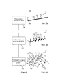
Фиг. 4 представляет собой блок-схему способа изготовления согласно примерному варианту выполнения настоящего изобретения; иFIG. 4 is a flowchart of a manufacturing method according to an exemplary embodiment of the present invention; and
Фиг. 5a-c схематически иллюстрируют результат соответствующих этапов способа на фиг. 4.FIG. 5a-c schematically illustrate the result of the respective steps of the method of FIG. four.
Осуществление изобретенияThe implementation of the invention
Фиг. 1 схематически иллюстрирует примерное применение для вариантов выполнения сетчатого осветительного модуля согласно вариантам выполнения настоящего изобретения в форме светоизлучающей панели 1, размещенной в потолке 2 комнаты 3. Светоизлучающая панель может быть предназначена для замены дневного света и в этом случае должна излучать равномерный белый свет.FIG. 1 schematically illustrates an exemplary application for embodiments of a grid lighting module according to embodiments of the present invention in the form of a light-emitting
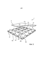
На фиг. 2, которая представляет собой схематический вид в перспективе с местным разрезом светоизлучающей панели на фиг. 1, светоизлучающая панель 1 согласно первому примерному варианту выполнения содержит первую пластину в форме рассеивающей фольги 10 (или удаленной люминесцентной пленки), вторую пластину в форме отражающей фольги 11, сотообразную опорную структуру 12 и сетчатый осветительный модуль 13. Сотообразная опорная структура 12 и сетчатый осветительный модуль 13 зажаты между рассеивающей фольгой 10 и отражающей фольгой, как показано на фиг. 2.In FIG. 2, which is a perspective schematic perspective view of a light emitting panel in FIG. 1, the
Как также указано на фиг. 2, сетчатый осветительный модуль 13 содержит множество электропроводящих проводов, причем здесь металлические провода 15a-b (только двум проводам были присвоены ссылочные позиции для исключения загромождения чертежа) определяют сетку с узлами 16a-c, и множество твердотельных источников света, причем здесь каждый из LED 17a-c размещен в соответствующем узле 16a-c и электрически и механически соединен со взаимно смежными металлическими проводами в узлах 16a-c. Как также может быть видно на фиг. 2, металлические провода 15a-b изогнуты так, чтобы проявлять сгибы 18a-b (сгибам только на одном из металлических проводов были присвоены ссылочные позиции) между взаимно смежными LED 17a-c, соединенными с металлическими проводами.As also indicated in FIG. 2, the
Сетчатый осветительный модуль 13 поддерживается стенками сотообразной опорной структуры 12 в сгибах 18a-b так, что LED 17a-c разнесены между рассеивающей фольгой 10 и отражающей фольгой 11 и направлены к отражающей фольге 11. Таким образом, свет, излучаемый LED 17a-c, будет проходить от LED 17a-c к отражающей фольге 11 и далее от отражающей фольги 11 к рассеивающей фольге 10, что означает, что светоизлучающая панель 1 может быть выполнена относительно тонкой и все равно может обеспечивать равномерное освещение.The
Следует отметить, что фиг. 2 (а также фиг. 3 ниже) представляет собой упрощенную иллюстрацию светоизлучающей панели 1 на фиг. 1, и что различные конструкции, такие как драйвер и электрический(е) соединитель(и) для сетчатого осветительного модуля и конструкции для установки светоизлучающей панели 1 в потолке 2, особо не указаны. Однако, такие конструкции могут быть обеспечены многими различными путями, ясными специалисту в области техники. Светоизлучающая панель также может предпочтительно содержать звукопоглощающий материал.It should be noted that FIG. 2 (and also FIG. 3 below) is a simplified illustration of the
Фиг. 3 схематически показывает светоизлучающую панель 1 согласно второму примерному варианту выполнения, который отличается от первого варианта выполнения, описанного выше со ссылкой на фиг. 2 тем, что он не имеет ячеистую опорную структуру и тем, что конфигурация сетчатого осветительного модуля является другой. В сетчатом осветительном модуле 23 на фиг. 3 металлические провода 15a-b изогнуты для проявления трех сгибов 28a-c между взаимно смежными LED 17a-c. Сгибы 28a-c, как и в варианте выполнения на фиг. 2, представляют собой гофрировку и содержат центральный сгиб 28b, направленный к отражающей фольге 11, и два боковых сгиба 28a,с, направленных к рассеивающей фольге 10. В проиллюстрированном здесь примерном варианте выполнения абсолютные амплитуды боковых сгибов 28a,с равны и меньше амплитуды центрального сгиба 28b. Таким образом, LED 17a-c могут быть надежно разнесены и от отражающей фольги 11, и от рассеивающей фольги 10 без необходимости дополнительного прокладочного средства. Однако может быть целесообразным добавление оптически чистой прокладочной структуры или «расстояния» между боковыми сгибами 28a,с и рассеивающей фольгой 10 для исключения эффектов затенения от металлических проводов 15a-b.FIG. 3 schematically shows a
Наконец, примерный способ изготовления сетчатого осветительного модуля 13 на фиг. 2 будет описан ниже со ссылкой на блок-схему на фиг. 4 и фиг. 5a-c. Сетчатый осветительный модуль 23 на фиг. 3 изготовлен с использованием этого же способа, причем единственная разница заключается в количестве и конфигурации сгибов 28a-c.Finally, an exemplary method of manufacturing a
На первом этапе 100 обеспечивают исходную матрицу 30 электропроводящих проводов, здесь металлических проводов 15a-b, твердотельными источниками света, здесь LED 17a-c, механически и электрически соединенными со взаимно смежными металлическими проводами. LED 17a-c могут, например, припаивать к проводам 15a-b. Способы обеспечения исходной матрицы 30 описаны подробно в WO-2007/122566, которая включена здесь путем ссылки во всей ее полноте.In a
На следующем этапе 101 провода 15a-b исходной матрицы 30 изгибают для образования сгибов 18a-b между взаимно смежными LED 17a-c.In a
Наконец, на этапе 102 исходную матрицу 30 растягивают в направлении ширины, перпендикулярном направлению продолжения длины металлических проводов 15a-b в исходной матрице 30. В результате образуют сетчатый осветительный модуль 13 на фиг. 2.Finally, in
Дополнительно, изменения раскрытых вариантов выполнения могут быть поняты и выполнены специалистом в области техники при осуществлении заявленного изобретения из изучения чертежей, раскрытия и приложенной формулы изобретения. Например, сетчатый осветительный модуль может быть уложен в других конфигурациях.Additionally, changes to the disclosed embodiments may be understood and made by a person skilled in the art in the practice of the claimed invention from the study of the drawings, disclosure and appended claims. For example, a mesh lighting module may be stacked in other configurations.
В формуле изобретения слово «содержащий» не исключает другие элементы или этапы. Сам по себе тот факт, что некоторые признаки перечислены во взаимно различных зависимых пунктах формулы изобретения, не указывает на то, что совокупность этих признаков не может быть использована с выгодой.In the claims, the word “comprising” does not exclude other elements or steps. The mere fact that some features are listed in mutually different dependent claims does not indicate that the combination of these features cannot be used to advantage.
Claims (31)
Applications Claiming Priority (3)
| Application Number | Priority Date | Filing Date | Title |
|---|---|---|---|
| EP11180245.0 | 2011-09-06 | ||
| EP11180245 | 2011-09-06 | ||
| PCT/IB2012/054419 WO2013035012A2 (en) | 2011-09-06 | 2012-08-29 | Wire-based lighting module with 3d topography |
Publications (2)
| Publication Number | Publication Date |
|---|---|
| RU2014113346A RU2014113346A (en) | 2015-10-20 |
| RU2608565C2 true RU2608565C2 (en) | 2017-01-23 |
Family
ID=47080749
Family Applications (1)
| Application Number | Title | Priority Date | Filing Date |
|---|---|---|---|
| RU2014113346A RU2608565C2 (en) | 2011-09-06 | 2012-08-29 | Wired lighting module with three-dimensional topography |
Country Status (7)
| Country | Link |
|---|---|
| US (1) | US9395071B2 (en) |
| EP (1) | EP2753865A2 (en) |
| JP (1) | JP6133296B2 (en) |
| CN (1) | CN103782084B (en) |
| IN (1) | IN2014CN01635A (en) |
| RU (1) | RU2608565C2 (en) |
| WO (1) | WO2013035012A2 (en) |
Families Citing this family (6)
| Publication number | Priority date | Publication date | Assignee | Title |
|---|---|---|---|---|
| ZA74315B (en) * | 1973-01-17 | 1975-03-26 | Diamond Shamrock Corp | Dimensionally stable asbestos diaphragms |
| GB201522394D0 (en) | 2015-12-18 | 2016-02-03 | Ucb Biopharma Sprl | Antibodies |
| US11175018B2 (en) * | 2018-06-08 | 2021-11-16 | Signify Holding B.V. | Rigid lighting unit |
| AT523551B1 (en) * | 2020-02-20 | 2021-12-15 | Molto Luce Gmbh | Device for glare-reduced lighting of separate work areas |
| CN115398147A (en) | 2020-04-21 | 2022-11-25 | 昕诺飞控股有限公司 | LED luminaire with optical element |
| WO2024039359A1 (en) * | 2022-08-17 | 2024-02-22 | Bilous Nazar | An illumination device |
Citations (9)
| Publication number | Priority date | Publication date | Assignee | Title |
|---|---|---|---|---|
| US3052004A (en) * | 1959-04-01 | 1962-09-04 | Wallshein Melvin | Clamping devices for attachment to a wire or cable |
| US20030193801A1 (en) * | 2002-04-16 | 2003-10-16 | Yuan Lin | Flexible rod light and manufacturing method thereof |
| US20050057939A1 (en) * | 2003-09-16 | 2005-03-17 | Fuji Photo Film Co., Ltd. | Light emission device and manufacturing method thereof |
| US20060092634A1 (en) * | 2004-11-04 | 2006-05-04 | Ikuo Hiyama | Lighting source unit, illuminating apparatus using the same and display apparatus using the same |
| DE202005013148U1 (en) * | 2005-08-19 | 2007-01-04 | Rottenbacher, Susanne | Device to produce light effects has passive surface behind and separated from an active layer having distributed LEDs whose light is partly reflected from the passive surface |
| WO2007122566A1 (en) * | 2006-04-25 | 2007-11-01 | Koninklijke Philips Electronics N.V. | Led array grid, method and device for manufacturing said grid and led component for use in the same |
| WO2010132552A1 (en) * | 2009-05-12 | 2010-11-18 | The Board Of Trustees Of The University Of Illinois | Printed assemblies of ultrathin, microscale inorganic light emitting diodes for deformable and semitransparent displays |
| RU2413129C2 (en) * | 2005-06-03 | 2011-02-27 | Медиамеш Гбр | Wire cloth, wire cloth arrangement and illumination method |
| RU103166U1 (en) * | 2010-10-19 | 2011-03-27 | Ильгам Наилович Талипов | FLEXIBLE LIGHT |
Family Cites Families (10)
| Publication number | Priority date | Publication date | Assignee | Title |
|---|---|---|---|---|
| US5971563A (en) * | 1997-01-06 | 1999-10-26 | Maggio; Damian | Flexible meshed decorative light string set for cone-, rectangular-, and dome-shaped, trees, bushes, and like objects |
| CN2677738Y (en) * | 2003-04-18 | 2005-02-09 | 吴政雄 | Decorative lamp string set with pull-resistant strength |
| JP2005039109A (en) * | 2003-07-17 | 2005-02-10 | Matsushita Electric Ind Co Ltd | Circuit board |
| JP4635128B2 (en) * | 2006-01-27 | 2011-02-16 | 株式会社オプトデザイン | Surface illumination light source device and surface illumination device using the same |
| JP2007240829A (en) * | 2006-03-08 | 2007-09-20 | Sharp Corp | Lighting system |
| EP2013529B1 (en) * | 2006-04-25 | 2010-01-13 | Koninklijke Philips Electronics N.V. | Large area led array and method for its manufacture |
| CN201034268Y (en) * | 2007-03-26 | 2008-03-12 | 鹤山丽得电子实业有限公司 | Novel LED lamp string |
| CN101270855A (en) * | 2008-04-16 | 2008-09-24 | 清华大学 | Area lighting source illumination device based on LED |
| JP5383475B2 (en) * | 2009-12-24 | 2014-01-08 | 三菱電機株式会社 | LED lighting device |
| US8343783B2 (en) * | 2010-09-10 | 2013-01-01 | Long Jing International Technology Enterprise Co., Ltd. | LED module and packing method of the same |
-
2012
- 2012-08-29 WO PCT/IB2012/054419 patent/WO2013035012A2/en active Application Filing
- 2012-08-29 RU RU2014113346A patent/RU2608565C2/en not_active IP Right Cessation
- 2012-08-29 EP EP12778795.0A patent/EP2753865A2/en not_active Withdrawn
- 2012-08-29 IN IN1635CHN2014 patent/IN2014CN01635A/en unknown
- 2012-08-29 JP JP2014529099A patent/JP6133296B2/en not_active Expired - Fee Related
- 2012-08-29 CN CN201280043313.4A patent/CN103782084B/en not_active Expired - Fee Related
- 2012-08-29 US US14/238,888 patent/US9395071B2/en not_active Expired - Fee Related
Patent Citations (9)
| Publication number | Priority date | Publication date | Assignee | Title |
|---|---|---|---|---|
| US3052004A (en) * | 1959-04-01 | 1962-09-04 | Wallshein Melvin | Clamping devices for attachment to a wire or cable |
| US20030193801A1 (en) * | 2002-04-16 | 2003-10-16 | Yuan Lin | Flexible rod light and manufacturing method thereof |
| US20050057939A1 (en) * | 2003-09-16 | 2005-03-17 | Fuji Photo Film Co., Ltd. | Light emission device and manufacturing method thereof |
| US20060092634A1 (en) * | 2004-11-04 | 2006-05-04 | Ikuo Hiyama | Lighting source unit, illuminating apparatus using the same and display apparatus using the same |
| RU2413129C2 (en) * | 2005-06-03 | 2011-02-27 | Медиамеш Гбр | Wire cloth, wire cloth arrangement and illumination method |
| DE202005013148U1 (en) * | 2005-08-19 | 2007-01-04 | Rottenbacher, Susanne | Device to produce light effects has passive surface behind and separated from an active layer having distributed LEDs whose light is partly reflected from the passive surface |
| WO2007122566A1 (en) * | 2006-04-25 | 2007-11-01 | Koninklijke Philips Electronics N.V. | Led array grid, method and device for manufacturing said grid and led component for use in the same |
| WO2010132552A1 (en) * | 2009-05-12 | 2010-11-18 | The Board Of Trustees Of The University Of Illinois | Printed assemblies of ultrathin, microscale inorganic light emitting diodes for deformable and semitransparent displays |
| RU103166U1 (en) * | 2010-10-19 | 2011-03-27 | Ильгам Наилович Талипов | FLEXIBLE LIGHT |
Also Published As
| Publication number | Publication date |
|---|---|
| WO2013035012A3 (en) | 2013-06-27 |
| IN2014CN01635A (en) | 2015-05-08 |
| CN103782084A (en) | 2014-05-07 |
| EP2753865A2 (en) | 2014-07-16 |
| JP2014528144A (en) | 2014-10-23 |
| JP6133296B2 (en) | 2017-05-24 |
| WO2013035012A2 (en) | 2013-03-14 |
| US20140168974A1 (en) | 2014-06-19 |
| US9395071B2 (en) | 2016-07-19 |
| CN103782084B (en) | 2018-02-02 |
| RU2014113346A (en) | 2015-10-20 |
Similar Documents
| Publication | Publication Date | Title |
|---|---|---|
| RU2608565C2 (en) | Wired lighting module with three-dimensional topography | |
| RU2608805C2 (en) | Light-emitting panel with transparent cellular support panel | |
| JP5952989B1 (en) | Luminous acoustic panel with duct | |
| WO2015000864A9 (en) | Light-emitting device | |
| EP2386791B1 (en) | Light emitting device array | |
| JP2014116299A (en) | Light source unit and lighting fixture | |
| US8217801B2 (en) | LED (light emitting diode) module | |
| JP2014528144A5 (en) | ||
| JP2010251213A (en) | Light-emitting module and lighting device | |
| JP6796585B2 (en) | Lighting panel adapted for improved uniformity of light output | |
| WO2013001430A1 (en) | Led-based embedded lighting device | |
| JP2011070992A (en) | Led lighting apparatus | |
| JP2016143617A (en) | Luminaire | |
| JP3169011U (en) | Light emitting diode lamp | |
| JP2013098083A (en) | Lighting fixture | |
| JP5534920B2 (en) | lighting equipment | |
| CN204879580U (en) | Emitting diode lamps and lanterns with forward type heat abstractor | |
| TWM579244U (en) | Light emitting module and light emitting device | |
| JP2011077394A (en) | Light emitting device | |
| JP2010176904A (en) | Light emitting device | |
| GB2520344A (en) | LED luminaire | |
| KR101395880B1 (en) | Manufacturing method of led modules and led modules | |
| KR101568386B1 (en) | LED lighting apparatus for both-sided luminescence | |
| JP2019212617A (en) | Lighting fixture and luminaire | |
| JP2011054351A (en) | Lighting device |
Legal Events
| Date | Code | Title | Description |
|---|---|---|---|
| HZ9A | Changing address for correspondence with an applicant | ||
| MM4A | The patent is invalid due to non-payment of fees |
Effective date: 20190830 |