RU2555503C1 - Optical passive limiter of passing radiation - Google Patents
Optical passive limiter of passing radiation Download PDFInfo
- Publication number
- RU2555503C1 RU2555503C1 RU2013155727/28A RU2013155727A RU2555503C1 RU 2555503 C1 RU2555503 C1 RU 2555503C1 RU 2013155727/28 A RU2013155727/28 A RU 2013155727/28A RU 2013155727 A RU2013155727 A RU 2013155727A RU 2555503 C1 RU2555503 C1 RU 2555503C1
- Authority
- RU
- Russia
- Prior art keywords
- radiation
- substrate
- grid
- film
- limiter
- Prior art date
Links
Images
Landscapes
- Optical Modulation, Optical Deflection, Nonlinear Optics, Optical Demodulation, Optical Logic Elements (AREA)
Abstract
Description
Изобретение относится к оптической и оптоэлектронной технике, к устройствам предохранения фоточувствительных элементов оптических и оптоэлектронных систем от разрушающего воздействия мощного излучения.The invention relates to optical and optoelectronic technology, to devices for protecting the photosensitive elements of optical and optoelectronic systems from the damaging effects of powerful radiation.
Для защиты чувствительных приемников излучений от повреждения мощным излучением исследуются оптические пассивные ограничители проходящего излучения, являющиеся аналогами изобретения, основанные на применении жидких золей или твердых золей в виде тонких пленок, содержащих фуллерены, наночастицы углерода или металлов [Каманина Н.В. Фотофизика фуллереносодержащих сред: ограничители лазерного излучения, дифракционные элементы, диспергированные жидкокристаллические модуляторы света // Нанотехника. №1, 2006]. Излучение проходит через слой золя (в виде пленки), обладающий прозрачностью 50-70%, к защищаемому приемнику; при увеличении интенсивности излучения поглощение в среде нелинейно увеличивается до некоторой непрозрачности среды и приемник оказывается защищенным от повреждения мощным излучением.To protect sensitive receivers of radiation from damage by powerful radiation, optical passive limiters of transmitted radiation are studied, which are analogues of the invention, based on the use of liquid sols or solid sols in the form of thin films containing fullerenes, carbon nanoparticles or metals [Kamanina N.V. Photophysics of fullerene-containing media: laser radiation limiters, diffraction elements, dispersed liquid crystal light modulators // Nanotechnology. No. 1, 2006]. The radiation passes through a sol layer (in the form of a film), which has a transparency of 50-70%, to the protected receiver; with increasing radiation intensity, absorption in the medium nonlinearly increases to a certain opacity of the medium and the receiver is protected from damage by powerful radiation.
Недостатком такой защиты является невозможность ограничения излучения среднего и дальнего ИК-диапазонов спектра, так как в основе эффекта ограничения лежит фотоиндуцированное увеличение сечения поглощения наночастиц, проявляющееся только в видимом и ближнем ИК-диапазонах.The disadvantage of this protection is the impossibility of limiting the radiation of the middle and far infrared ranges of the spectrum, since the limiting effect is based on the photoinduced increase in the absorption cross section of nanoparticles, which is manifested only in the visible and near infrared ranges.
Аналогом рассматриваемого изобретения является также сетчатый фильтр длинноволнового ИК-излучения [Длинноволновая инфракрасная спектроскопия. Сборник статей. Пер. с англ. под общей редакцией В.Н. Мурзина. - М.: Мир. 1966. - 320 с., страницы 292-315]. Проволочная сетка с периодом, много меньшим длины волны излучения, и «обратная сетка», получаемая на подложке напылением металла через сетку как через маску являются зеркалами с высокой отражающей способностью в длинноволновом ИК-диапазоне. Условием возможности использования сетчатого фильтра как зеркала является требование, чтобы толщина скин-слоя в металле сеток на данной длине волны была меньше толщины перемычек сетки.An analogue of the present invention is also a mesh filter of long-wave infrared radiation [Long-wave infrared spectroscopy. Digest of articles. Per. from English edited by V.N. Murzina. - M .: World. 1966. - 320 p., Pages 292-315]. A wire mesh with a period much shorter than the radiation wavelength, and a “reverse mesh” obtained on a substrate by sputtering metal through a mesh like a mask are mirrors with high reflectivity in the long-wave infrared range. The condition for the possibility of using a mesh filter as a mirror is the requirement that the thickness of the skin layer in the metal of the grids at a given wavelength be less than the thickness of the jumpers of the grid.
Использование такого фильтра в качестве ограничителя мощных излучений с пропусканием, зависящим от интенсивности излучения, не известно.The use of such a filter as a limiter of powerful radiation with transmittance depending on the radiation intensity is not known.
Прототипом заявленного изобретения является оптический ограничитель, работающий на длине волны 10 мкм, использующий фазовый переход первого рода диэлектрик-металл [Михеева О.П., Сидоров А.И. Особенности ограничения лазерного излучения зеркалами на основе диоксида ванадия // Оптический журнал. Том 68, №4, 2001]. В работе приведены результаты экспериментального исследования ограничения лазерного излучения среднего ИК-диапазона зеркалами на основе диоксида ванадия. Диоксид ванадия является полупроводником, способным при температурах нагревания менее 100°C испытывать фазовый переход диэлектрик-металл с увеличением электропроводимости и увеличением коэффициента отражения в ИК-диапазоне.The prototype of the claimed invention is an optical limiter operating at a wavelength of 10 μm, using a first-order dielectric-metal phase transition [Mikheeva OP, Sidorov A.I. Features of the limitation of laser radiation by vanadium dioxide mirrors // Optical Journal. Volume 68, No. 4, 2001]. The paper presents the results of an experimental study of the limitation of laser radiation of the mid-IR range by vanadium dioxide mirrors. Vanadium dioxide is a semiconductor capable of undergoing a dielectric-metal phase transition at heating temperatures below 100 ° C with an increase in electrical conductivity and an increase in reflectance in the infrared range.
Недостатком такого ограничителя является недостаточное быстродействие - время запаздывания начала ограничения порядка 100 нс.The disadvantage of this limiter is the lack of speed - the delay time of the beginning of the limitation of the order of 100 ns.
Решаемой настоящим изобретением задачей является создание оптического ограничителя проходящего излучения ИК-диапазона спектра с увеличенным быстродействием и уменьшенным порогом ограничения излучения.The problem solved by the present invention is the creation of an optical limiter of transmitted radiation in the infrared range of the spectrum with increased speed and a reduced threshold for limiting radiation.
Задача решается тем, что в оптическом пассивном ограничителе проходящего излучения, содержащем прозрачную изолирующую подложку с полупроводниковой пленкой на поверхности, увеличивающей электрическую проводимость при нагревании проходящим излучением и размещаемой в фокальной плоскости объектива, в соответствии с изобретением пленка структурирована в виде сетки или мозаики пятен со средней периодичностью структуры, меньшей длины волны излучения.The problem is solved in that in an optical passive limiter of transmitted radiation, containing a transparent insulating substrate with a semiconductor film on the surface that increases the electrical conductivity when heated by transmitted radiation and placed in the focal plane of the lens, in accordance with the invention, the film is structured in the form of a grid or mosaic of spots with an average periodicity of the structure, shorter wavelength of radiation.
Предлагается также, что указанная структурированная пленка теплоизолирована от подложки промежуточным прозрачным слоем диэлектрика. Предлагается также, что указанная структурированная пленка размещена на обеих поверхностях подложки, причем толщина подложки не превышает глубину резкости объектива.It is also proposed that said structured film is thermally insulated from the substrate by an intermediate transparent dielectric layer. It is also proposed that the specified structured film is placed on both surfaces of the substrate, and the thickness of the substrate does not exceed the depth of field of the lens.
Предлагается также, что структурированная сетка изготовлена из элементарных полупроводников или полупроводниковых окислов металлов с отрицательным температурным коэффициентом сопротивления, в том числе окислов ванадия, титана, никеля, кобальта, железа, гафния, алюминия или смесей окислов.It is also proposed that the structured grid is made of elementary semiconductors or semiconductor metal oxides with a negative temperature coefficient of resistance, including vanadium, titanium, nickel, cobalt, iron, hafnium, aluminum, or oxide mixtures.
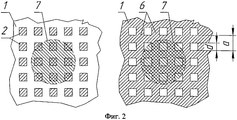
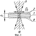
На Фиг.1 показаны схематически устройство и оптическая схема применения ограничителя, на фиг.2 - сеточная структура поглощающей пленки ограничителя по изобретению, на Фиг.3 - устройство по изобретению с сеточными структурами, расположенными на двух сторонах подложек.Figure 1 shows schematically the device and the optical application circuit of the limiter, figure 2 is a grid structure of an absorbing film of a limiter according to the invention, Figure 3 is a device according to the invention with grid structures located on two sides of the substrates.
Фиг.1: 1 - прозрачная подложка, 2 - элементы структуры поглощающего сеточного слоя ограничителя в виде разделенных зазорами квадратных тонкопленочных островков из изменяющего электрическую проводимость при лазерном воздействии материалов, 3 - входящее в ограничитель излучение, 4 - выходящее из ограничителя излучение в отсутствие эффекта ограничения, 5 - отраженное от сеточного слоя излучение при наступлении эффекта ограничения, Л1 и Л2 - софокусные линзы.Figure 1: 1 - transparent substrate, 2 - structure elements of the absorbing grid layer of the limiter in the form of square thin-film islands separated by gaps from changing the electrical conductivity during laser exposure to materials, 3 - radiation entering the limiter, 4 - radiation coming out of the limiter in the absence of the restriction effect , 5 - radiation reflected from the grid layer upon the occurrence of the restriction effect, L1 and L2 - confocal lenses.
Фиг.2: 2 - элементы структуры сеточного слоя ограничителя, расположенные на поверхности прозрачной подложки и имеющие, например, форму квадратных островков, разделенных зазорами, 6 - структура в виде сетки или островков сеточного слоя ограничителя, расположенная на поверхности прозрачной подложки, ячейки сетки могут иметь форму квадрата, как показано на фигуре в качестве примера, или могут иметь другую форму, 7 - зона облучения сеточной структуры лазерным сфокусированным излучением.Figure 2: 2 - the structure elements of the grid layer of the limiter located on the surface of the transparent substrate and having, for example, the shape of square islands separated by gaps, 6 - the structure in the form of a grid or islands of the mesh layer of the limiter located on the surface of the transparent substrate, the mesh cells can have the shape of a square, as shown in the figure as an example, or may have a different shape, 7 - zone of irradiation of the grid structure by laser focused radiation.
Фиг.3: 8 - структура в виде сетки или островков сеточного слоя на стороне подложки 1 толщиной h, противоположной облучаемой; 9 - падающий на подложку световой пучок, создающий на подложке фокальное пятно и имеющий перетяжку диаметром Dф; 10 - прошедший подложку пучок излучения.Figure 3: 8 - structure in the form of a grid or islands of a grid layer on the side of the
Как показано на Фиг.1, ограничиваемое излучение 3 фокусируется линзой Л1 на поверхность подложки 1, на которой расположена тонкая структурированная пленка материала, способного при нагревании изменять (например, увеличивать) свою электрическую проводимость. Фокальное пятно на поверхности должно иметь размеры, при которых на площади пятна приходится несколько (порядка нескольких десятков и более) структурных элементов сетки. Период сетки должен составлять малую долю длины волны излучения. При малой интенсивности излучения нагревание лазерным лучом сетчатого слоя незначительно, его электрическая проводимость мала, отражение от сетчатой структуры мало и излучение проходит структуру ограничителя, практически не изменяя своей интенсивности, и второй линзой собирается в параллельный пучок. Оптическая схема может быть и другой, необходимо лишь обеспечить концентрацию падающего излучения в фокальное пятно малых размеров на подложке с сетчатым слоем. При увеличении интенсивности излучения температура структурных элементов сетки, попавших в пределы фокального пятна, увеличивается и увеличивается их проводимость, что приводит к увеличению коэффициента отражения сетки в области фокального пятна и препятствует увеличению интенсивности проходящего структуру излучения, ограничивает интенсивность излучения. На правом рисунке Фиг.1 показан ход лучей отраженного пучка 5, соответствующий случаю отражения излучения от сетчатой структуры. Отражение излучения близко к зеркальному отражению, роль рассеяния незначительна.As shown in FIG. 1, the limited radiation 3 is focused by the lens L1 on the surface of the
Проведем количественную оценку эффекта ограничения излучения сетками, используя формулу для коэффициента отражения проволочной сетки при нормальном падении излучения на сетку [Длинноволновая инфракрасная спектроскопия. Сборник статей. Пер. с англ. под общей редакцией В.Н. Мурзина. - М.: Мир. 1966. - 320 с. Страницы 292-315]:Let us quantify the effect of radiation restriction by grids using the formula for the reflection coefficient of a wire grid with a normal incidence of radiation on the grid [Long-wave infrared spectroscopy. Digest of articles. Per. from English edited by V.N. Murzina. - M .: World. 1966 .-- 320 s. Pages 292-315]:

где величина G определяет зависимость отражения от электрической проводимости σ материала проволочек, a tgΦ зависит от геометрии решетки:where the quantity G determines the dependence of reflection on the electrical conductivity σ of the wire material, and tgΦ depends on the geometry of the lattice:
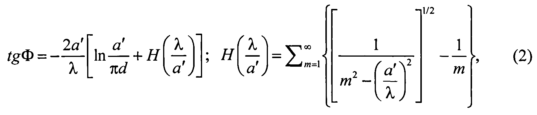
где Φ - фаза отраженной волны, a′ - расстояние между центрами соседних проволочек, d - диаметр проволок, m - целое число, порядковый номер члена ряда.where Φ is the phase of the reflected wave, a ′ is the distance between the centers of adjacent wires, d is the diameter of the wires, m is an integer, the serial number of a member of the series.
При условии 
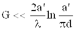
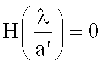
Оценки показывают, что в случае значений параметров, соответствующих нашей задаче, tgΦ=0 и формулу для коэффициента отражения можно представить в виде:Estimates show that in the case of parameter values corresponding to our problem, tgΦ = 0 and the formula for the reflection coefficient can be represented as:

При малой интенсивности излучения электрическая проводимость сетки нулевая, G2→∞, R=0, излучение проходит сетку беспрепятственно.At a low radiation intensity, the electrical conductivity of the grid is zero, G 2 → ∞, R = 0, the radiation passes through the grid unhindered.
При воздействии мощного излучения вследствие фазового перехода диэлектрик-металл вещества сетки проводимость сетки может вырасти до значения одной сотой проводимости меди (σ(Cu)=5.14·1017 с-1 (в системе Гаусса)) и более. На длине волны λ=10 мкм и при параметрах сетки а′=2 мкм, d=0,5 мкм получим уменьшение G2 до 0,01, увеличение отражения до 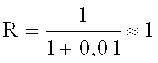
Сеточная структура пленки приводит к рассеянию света вследствие эффектов дифракции на периодических неоднородностях. При малой интенсивности излучения неоднородности пленки влияют на падающее излучение как фазовые неоднородности поверхности прозрачной подложки. В нашем случае неоднородности имеют форму дисков на поверхности или углублений в подложке с поперечником неоднородности много меньше длины волны излучения. В работе [Борн М., Вольф Э. Основы оптики. М.: Наука. Гл. ред. физ.-мат. лит. - 1970. - 855 с.] представлены результаты расчета сечения рассеяния света на одиночных диэлектрических сферах, выполненного на основании теории Ми. При дифракционном параметре сферы 2πρ/λ<<1 (ρ - радиус сферы) сечение рассеяния много меньше реального сечения сферы, что свидетельствует о незначительности эффекта рассеяния. Этот вывод мы распространяем и на рассеяние частицами в виде малых дисков, а также рассеяние малыми углублениями (последнее - в соответствии с принципом Бабине).The grid structure of the film leads to light scattering due to diffraction effects on periodic inhomogeneities. At a low radiation intensity, film inhomogeneities affect the incident radiation as phase inhomogeneities of the surface of a transparent substrate. In our case, the inhomogeneities are in the form of disks on the surface or indentations in a substrate with a heterogeneity diameter much smaller than the radiation wavelength. In the work [Born M., Wolf E. Fundamentals of optics. M .: Science. Ch. ed. Phys.-Math. lit. - 1970. - 855 p.] Presents the results of the calculation of the cross section for scattering of light on single dielectric spheres, based on the Mie theory. With the diffraction parameter of the sphere 2πρ / λ << 1 (ρ is the radius of the sphere), the scattering cross section is much smaller than the real cross section of the sphere, which indicates the insignificance of the scattering effect. We extend this conclusion to scattering by particles in the form of small disks, as well as scattering by small depressions (the latter - in accordance with the Babinet principle).
Таким образом, рассеяние проходящего света через сеточную структуру ограничителя при малой интенсивности излучения пренебрежимо мало.Thus, the scattering of transmitted light through the grid structure of the limiter at a low radiation intensity is negligible.
Необходимым условием функционирования сетчатой структуры на поверхности в качестве ограничителя проходящего излучения является малость параметра периодичности в сравнении с длиной волны ограничиваемого излучения:A necessary condition for the functioning of the mesh structure on the surface as a limiter of transmitted radiation is the smallness of the periodicity parameter in comparison with the wavelength of the limited radiation:

На Фиг.2а) показана сетчатая структура пленки на поверхности подложки, в которой при лазерном облучении индуцируется возникновение электрической проводимости, перемычки сетки заштрихованы, на Фиг.2б) - островковая структура такой же пленки, заштрихованы островки. Структура показана строго периодической с периодичностью а′ как один из возможных вариантов, так как возможно и беспорядочное расположение просветов сетки или островков при условии, что средняя величина расстояний между центрами этих полостей в сетке или островков остается много меньше длины волны излучения. Форма неоднородностей также может быть другой, например просветы в сетке могут быть круглыми, а островки - быть дисками. Фокальное пятно излучения показано заштрихованными кружками.On figa) shows the network structure of the film on the surface of the substrate, in which the occurrence of electrical conductivity is induced during laser irradiation, the network jumpers are shaded, in fig.2b) - the island structure of the same film, the islands are shaded. The structure is shown to be strictly periodic with periodicity a ′ as one of the possible options, since a random arrangement of the gaps of the grid or islands is possible, provided that the average distance between the centers of these cavities in the grid or islands remains much less than the radiation wavelength. The shape of the inhomogeneities can also be different, for example, the gaps in the grid can be round, and the islands can be disks. The focal spot of radiation is shown by shaded circles.
Допускается, что сетчатая и островковая структуры располагаются не непосредственно на поверхности подложки, а отделены от поверхности слоем скрепляющего или теплоизолирующего материала.It is assumed that the mesh and island structures are not located directly on the surface of the substrate, but are separated from the surface by a layer of bonding or heat-insulating material.
Проведем сравнение с прототипом по порогу срабатывания ограничителя, то есть, по величине энергии импульса ограничиваемого излучения, при которой ограничитель переходит в нелинейный режим и начинает ограничивать проходящее излучение.We will compare with the prototype according to the threshold of operation of the limiter, that is, by the magnitude of the pulse energy of the radiation being limited, at which the limiter goes into non-linear mode and begins to limit the transmitted radiation.
В прототипе нагреванию до температуры фазового перехода диэлектрик-металл и до возникновения зеркального отражения необходимо довести массу материала в объеме сплошной пленки на всей поверхности подложки ограничителя;In the prototype, it is necessary to bring the mass of material in the volume of a continuous film on the entire surface of the substrate of the limiter to heating to the temperature of the dielectric-metal phase transition and to the occurrence of specular reflection;
в предложенном решении необходимо нагревать только массу перемычек сетчатой структуры, объем которой много меньше объема сплошной пленки, так как в структуре имеются просветы (или она состоит из островков с зазорами между островками). Таким образом, порог срабатывания ограничителя по изобретению может быть существенно меньше, чем у прототипа.in the proposed solution, it is necessary to heat only the mass of jumpers of the mesh structure, the volume of which is much smaller than the volume of the continuous film, since there are gaps in the structure (or it consists of islands with gaps between the islands). Thus, the threshold of operation of the limiter according to the invention can be significantly less than that of the prototype.
На фиг.3 показано устройство, в котором на подложке нанесены сетчатые структуры на обеих ее сторонах. Сетчатая структура каждой стороны является ограничителем излучения, в результате общее пропускание устройства равно произведению коэффициентов пропускания структур на двух сторонах. Для обеспечения одинакового теплового действия лазерного излучения на сетчатые структуры на сторонах подложки необходимо, чтобы стороны находились в пределах глубины резкости изображения, создаваемого объективом. Глубина резкости характеризует некоторый выбранный допустимый уровень размытия изображения; качество изображения ухудшается постепенно по мере увеличения величины расфокусировки. Допуск глубины резкости, соответствующий, например, четвертьволновому критерию Релея, определяется уравнениемFigure 3 shows a device in which mesh structures are applied on a substrate on both sides thereof. The mesh structure of each side is a radiation limiter, as a result, the total transmittance of the device is equal to the product of the transmittance of the structures on both sides. To ensure the same thermal effect of laser radiation on the mesh structures on the sides of the substrate, it is necessary that the sides are within the depth of field of the image created by the lens. Depth of field characterizes some selected acceptable level of image blur; image quality deteriorates gradually as the amount of defocus increases. The depth of field tolerance, corresponding, for example, to the Rayleigh quarter-wave criterion, is given by the equation

где Um - угол наклона бокового луча на изображении (фокальном пятне), λ - длина волны света, n - показатель преломления среды.where U m is the angle of inclination of the side beam in the image (focal spot), λ is the wavelength of light, n is the refractive index of the medium.
Величина глубины резкости может быть также задана в единицах диаметра фокального пятна как 2-3 диаметра фокального пятна, что требует, чтобы подложка имела оптическую толщину не более 2-х диаметров фокального пятна (диаметров перетяжки лазерного пучка).The depth of field can also be set in units of the diameter of the focal spot as 2-3 diameters of the focal spot, which requires that the substrate has an optical thickness of no more than 2 diameters of the focal spot (diameter of the laser beam waist).
В качестве примеров конструкций ограничителей рассмотрим основанные на использовании пленки из окислов металлов (диоксида ванадия, двуокиси титана) и на основе использования пленки аморфного или поликристаллического кремния.As examples of limiter designs, let us consider films based on the use of metal oxides (vanadium dioxide, titanium dioxide) and based on the use of an amorphous or polycrystalline silicon film.
В первом случае в качестве подложки используются полированные пластины из прозрачного в ИК-диапазоне материала типа фторида кальция, фторида магния, германия. На одну или обе стороны подложки напыляют слой диоксида ванадия или двуокиси титана толщиной порядка 0,1-0,25 мкм и методом фотолитографии создают в напыленных слоях требующиеся структуры. При создании ограничителя на диапазон длин волн 5-10 мкм требуемый параметр периодичности структуры не более 1-2 мкм (a′=2 мкм, d=0,5 мкм, λ=10 мкм). При использовании TiO2 [Физико-химические свойства окислов. Справочник. Под ред. Г.В. Самсонова. М.: Металлургия. - 1969. - 456 с.] расчет дает результаты:In the first case, polished wafers are used as a substrate from an infrared-transparent material such as calcium fluoride, magnesium fluoride, and germanium. On one or both sides of the substrate, a layer of vanadium dioxide or titanium dioxide with a thickness of about 0.1-0.25 microns is sprayed and the required structures are created in the sprayed layers by photolithography. When creating a limiter for the wavelength range of 5-10 μm, the required parameter of the periodicity of the structure is no more than 1-2 μm (a ′ = 2 μm, d = 0.5 μm, λ = 10 μm). When using TiO 2 [Physicochemical properties of oxides. Directory. Ed. G.V. Samsonova. M .: Metallurgy. - 1969. - 456 p.] The calculation gives the results:
573 K: σ=10 Ом-1·м-1=9·1010 c-1, G2=530 →R=0;573 K: σ = 10 Ohm -1 · m -1 = 9 · 10 10 s -1 , G 2 = 530 → R = 0;
1273 K: σ=105 Ом-1·м-1=9·1014 с-1, G2=0,053 →R=1.1273 K: σ = 10 5 Ohm -1 · m -1 = 9 · 10 14 s -1 , G 2 = 0,053 → R = 1.
Из расчета следует, что при лазерном нагревании сеточной структуры до 1273 K зеркало становится полностью отражающим и ограничивает проходящее излучение.It follows from the calculation that when laser heating the grid structure to 1273 K, the mirror becomes completely reflective and limits the transmitted radiation.
Во втором случае подложкой является плоская полированная с двух сторон пластина из монокристаллического кремния; на одной или обеих поверхностях размещены решетка или мозаика пятен из аморфного кремния толщиной 0,1-0,2 мкм; размер элементов структуры и промежутков между ними порядка λ/5. При воздействии лазерного излучения островки аморфного кремния нагреваются до более высокой температуры, чем поверхность подложки между ними, вследствие существенно меньшей теплопроводности, чем у монокристаллического кремния. Этому способствует вариант исполнения устройства, когда аморфный материал наносится поверх слоя окисла кремния на поверхности монокристаллического кремния, так как двуокись кремния обладает малой теплопроводностью и малой температуропроводностью.In the second case, the substrate is a plane polished single-crystal silicon wafer on both sides; on one or both surfaces there is a lattice or mosaic of spots made of amorphous silicon with a thickness of 0.1-0.2 microns; the size of the structural elements and the gaps between them are of the order of λ / 5. When exposed to laser radiation, islands of amorphous silicon are heated to a higher temperature than the surface of the substrate between them, due to significantly lower thermal conductivity than single-crystal silicon. This is facilitated by the embodiment of the device, when an amorphous material is deposited on top of a layer of silicon oxide on the surface of single-crystal silicon, since silicon dioxide has low thermal conductivity and low thermal diffusivity.
В варианте конструкции с двухсторонним нанесением сетчатой структуры толщина подложки может быть в пределах h=10-60 мкм в ограничителе для среднего ИК-диапазона.In a design with double-sided deposition of a mesh structure, the thickness of the substrate can be in the range h = 10-60 μm in the limiter for the mid-IR range.
В качестве материалов сетчатой структуры кроме кремния могут быть применены другие полупроводники, в том числе, в поликристаллическом или аморфном виде, в том числе германий, двойные и тройные полупроводниковые соединения, так как все полупроводники обладают отрицательным температурным коэффициентом сопротивления. В качестве материалов сетчатой структуры могут быть также применены полупроводниковые окислы металлов с отрицательным температурным коэффициентом сопротивления, в том числе окислы ванадия, титана, никеля, кобальта, железа, гафния, алюминия, или смесей окислов.In addition to silicon, other semiconductors can be used as mesh materials, including polycrystalline or amorphous ones, including germanium, double and triple semiconductor compounds, since all semiconductors have a negative temperature coefficient of resistance. Semiconductor metal oxides with a negative temperature coefficient of resistance, including oxides of vanadium, titanium, nickel, cobalt, iron, hafnium, aluminum, or mixtures of oxides, can also be used as mesh materials.
Таким образом, показано, что отличительные особенности изобретения позволяют решить поставленные задачи.Thus, it is shown that the distinctive features of the invention allow to solve the tasks.
Оптический пассивный ограничитель может найти применение в оптоэлектронике в качестве оптического предохранителя, предохраняющего от возможных лучевых повреждений фотоприемные устройства.An optical passive limiter can be used in optoelectronics as an optical fuse that protects photodetector devices from possible radiation damage.
Технический результат изобретения состоит в создании оптического ограничителя излучений ИК-диапазона с повышенным быстродействием, имеющего пониженный порог срабатывания.The technical result of the invention consists in the creation of an optical limiter of infrared radiation with increased speed, having a low threshold.
Claims (4)
Priority Applications (1)
| Application Number | Priority Date | Filing Date | Title |
|---|---|---|---|
| RU2013155727/28A RU2555503C1 (en) | 2013-12-17 | 2013-12-17 | Optical passive limiter of passing radiation |
Applications Claiming Priority (1)
| Application Number | Priority Date | Filing Date | Title |
|---|---|---|---|
| RU2013155727/28A RU2555503C1 (en) | 2013-12-17 | 2013-12-17 | Optical passive limiter of passing radiation |
Publications (1)
| Publication Number | Publication Date |
|---|---|
| RU2555503C1 true RU2555503C1 (en) | 2015-07-10 |
Family
ID=53538421
Family Applications (1)
| Application Number | Title | Priority Date | Filing Date |
|---|---|---|---|
| RU2013155727/28A RU2555503C1 (en) | 2013-12-17 | 2013-12-17 | Optical passive limiter of passing radiation |
Country Status (1)
| Country | Link |
|---|---|
| RU (1) | RU2555503C1 (en) |
Citations (3)
| Publication number | Priority date | Publication date | Assignee | Title |
|---|---|---|---|---|
| US5495101A (en) * | 1994-12-09 | 1996-02-27 | The United States Of America As Represented By The Secretary Of The Army | Enhancement for broadband optical limiter with holographic grating |
| RU2306586C1 (en) * | 2006-04-27 | 2007-09-20 | Александр Константинович Филиппов | Method for manufacturing non-linear limiter of laser radiation and a non-linear limiter of laser radiation |
| CN102681288A (en) * | 2012-05-23 | 2012-09-19 | 上海交通大学 | Silicon-based optical amplitude limiter |
-
2013
- 2013-12-17 RU RU2013155727/28A patent/RU2555503C1/en not_active IP Right Cessation
Patent Citations (3)
| Publication number | Priority date | Publication date | Assignee | Title |
|---|---|---|---|---|
| US5495101A (en) * | 1994-12-09 | 1996-02-27 | The United States Of America As Represented By The Secretary Of The Army | Enhancement for broadband optical limiter with holographic grating |
| RU2306586C1 (en) * | 2006-04-27 | 2007-09-20 | Александр Константинович Филиппов | Method for manufacturing non-linear limiter of laser radiation and a non-linear limiter of laser radiation |
| CN102681288A (en) * | 2012-05-23 | 2012-09-19 | 上海交通大学 | Silicon-based optical amplitude limiter |
Non-Patent Citations (1)
| Title |
|---|
| Михеева О.П., Сидоров А.И. Особенности ограничения лазерного излучения зеркалами на основе диоксида ванадия// Оптический журнал. Том 68, N4, 2001. * |
Similar Documents
| Publication | Publication Date | Title |
|---|---|---|
| Santbergen et al. | Application of plasmonic silver island films in thin-film silicon solar cells | |
| US20110017287A1 (en) | Substrates for photovoltaics | |
| US20080276990A1 (en) | Substrate surface structures and processes for forming the same | |
| US20140034820A1 (en) | Light-detection systems | |
| CN118759618B (en) | Broadband absorption devices based on phase change materials | |
| Ding et al. | Broadband optical absorption copper surface fabricated by femtosecond laser for sensitivity enhancement of thermoelectric photodetector | |
| Beye et al. | Research Article Optimization of SiNx Single and Double Layer ARC for Silicon Thin Film Solar Cells on Glass | |
| CN104362184A (en) | Thin film amorphous silicon solar cell based on antireflective structure and guided-mode resonance | |
| Ye et al. | Broadband antireflection subwavelength structures on fused silica using lower temperatures normal atmosphere thermal dewetted Au nanopatterns | |
| US20100229943A1 (en) | Asymmetric Waveguide | |
| Wang et al. | Plasmonic near-field enhancement for planar ultra-thin photovoltaics | |
| Feit et al. | Analysis of bulk DKDP damage distribution, obscuration, and pulse-length dependence | |
| Bett et al. | Front side antireflection concepts for silicon solar cells with diffractive rear side structures | |
| CN118915341B (en) | Narrow band absorbing device based on phase change material | |
| Heger et al. | Metal island films for optics | |
| Mansoor et al. | Design of three-layer antireflection coating for high reflection index lead chalcogenide | |
| US20190204478A1 (en) | Apparatus and methods of electrically conductive optical semiconductor coating | |
| Park et al. | Investigation of 3-dimensional structural morphology for enhancing light trapping with control of surface haze | |
| US9910200B1 (en) | Increased visible and infrared transmission through radio frequency EMI shields | |
| Qin et al. | Double AAO nanogratings for broad spectrum absorption enhancement in thin film Si solar cells | |
| Belousova et al. | Nonlinear-optical laser-radiation limiters | |
| CN114994809A (en) | Transmission-type dynamic super-structure surface device | |
| Wang et al. | Wide angle and broadband perfect absorber with compact multilayer structures | |
| CN118837982B (en) | Adjustable absorber | |
| RU177027U1 (en) | OPTICAL DIODE |
Legal Events
| Date | Code | Title | Description |
|---|---|---|---|
| MM4A | The patent is invalid due to non-payment of fees |
Effective date: 20181218 |