RU2407110C2 - Light-emitting device - Google Patents
Light-emitting device Download PDFInfo
- Publication number
- RU2407110C2 RU2407110C2 RU2008134528/28A RU2008134528A RU2407110C2 RU 2407110 C2 RU2407110 C2 RU 2407110C2 RU 2008134528/28 A RU2008134528/28 A RU 2008134528/28A RU 2008134528 A RU2008134528 A RU 2008134528A RU 2407110 C2 RU2407110 C2 RU 2407110C2
- Authority
- RU
- Russia
- Prior art keywords
- light
- radiation
- conversion
- emitting device
- primary
- Prior art date
Links
Images

Classifications
-
- H—ELECTRICITY
- H01—ELECTRIC ELEMENTS
- H01L—SEMICONDUCTOR DEVICES NOT COVERED BY CLASS H10
- H01L33/00—Semiconductor devices with at least one potential-jump barrier or surface barrier specially adapted for light emission; Processes or apparatus specially adapted for the manufacture or treatment thereof or of parts thereof; Details thereof
- H01L33/48—Semiconductor devices with at least one potential-jump barrier or surface barrier specially adapted for light emission; Processes or apparatus specially adapted for the manufacture or treatment thereof or of parts thereof; Details thereof characterised by the semiconductor body packages
- H01L33/58—Optical field-shaping elements
-
- C—CHEMISTRY; METALLURGY
- C04—CEMENTS; CONCRETE; ARTIFICIAL STONE; CERAMICS; REFRACTORIES
- C04B—LIME, MAGNESIA; SLAG; CEMENTS; COMPOSITIONS THEREOF, e.g. MORTARS, CONCRETE OR LIKE BUILDING MATERIALS; ARTIFICIAL STONE; CERAMICS; REFRACTORIES; TREATMENT OF NATURAL STONE
- C04B35/00—Shaped ceramic products characterised by their composition; Ceramics compositions; Processing powders of inorganic compounds preparatory to the manufacturing of ceramic products
- C04B35/01—Shaped ceramic products characterised by their composition; Ceramics compositions; Processing powders of inorganic compounds preparatory to the manufacturing of ceramic products based on oxide ceramics
- C04B35/44—Shaped ceramic products characterised by their composition; Ceramics compositions; Processing powders of inorganic compounds preparatory to the manufacturing of ceramic products based on oxide ceramics based on aluminates
-
- C—CHEMISTRY; METALLURGY
- C04—CEMENTS; CONCRETE; ARTIFICIAL STONE; CERAMICS; REFRACTORIES
- C04B—LIME, MAGNESIA; SLAG; CEMENTS; COMPOSITIONS THEREOF, e.g. MORTARS, CONCRETE OR LIKE BUILDING MATERIALS; ARTIFICIAL STONE; CERAMICS; REFRACTORIES; TREATMENT OF NATURAL STONE
- C04B35/00—Shaped ceramic products characterised by their composition; Ceramics compositions; Processing powders of inorganic compounds preparatory to the manufacturing of ceramic products
- C04B35/622—Forming processes; Processing powders of inorganic compounds preparatory to the manufacturing of ceramic products
- C04B35/626—Preparing or treating the powders individually or as batches ; preparing or treating macroscopic reinforcing agents for ceramic products, e.g. fibres; mechanical aspects section B
- C04B35/62605—Treating the starting powders individually or as mixtures
- C04B35/62645—Thermal treatment of powders or mixtures thereof other than sintering
- C04B35/6265—Thermal treatment of powders or mixtures thereof other than sintering involving reduction or oxidation
-
- C—CHEMISTRY; METALLURGY
- C04—CEMENTS; CONCRETE; ARTIFICIAL STONE; CERAMICS; REFRACTORIES
- C04B—LIME, MAGNESIA; SLAG; CEMENTS; COMPOSITIONS THEREOF, e.g. MORTARS, CONCRETE OR LIKE BUILDING MATERIALS; ARTIFICIAL STONE; CERAMICS; REFRACTORIES; TREATMENT OF NATURAL STONE
- C04B35/00—Shaped ceramic products characterised by their composition; Ceramics compositions; Processing powders of inorganic compounds preparatory to the manufacturing of ceramic products
- C04B35/622—Forming processes; Processing powders of inorganic compounds preparatory to the manufacturing of ceramic products
- C04B35/626—Preparing or treating the powders individually or as batches ; preparing or treating macroscopic reinforcing agents for ceramic products, e.g. fibres; mechanical aspects section B
- C04B35/62605—Treating the starting powders individually or as mixtures
- C04B35/62645—Thermal treatment of powders or mixtures thereof other than sintering
- C04B35/6268—Thermal treatment of powders or mixtures thereof other than sintering characterised by the applied pressure or type of atmosphere, e.g. in vacuum, hydrogen or a specific oxygen pressure
-
- C—CHEMISTRY; METALLURGY
- C09—DYES; PAINTS; POLISHES; NATURAL RESINS; ADHESIVES; COMPOSITIONS NOT OTHERWISE PROVIDED FOR; APPLICATIONS OF MATERIALS NOT OTHERWISE PROVIDED FOR
- C09K—MATERIALS FOR MISCELLANEOUS APPLICATIONS, NOT PROVIDED FOR ELSEWHERE
- C09K11/00—Luminescent, e.g. electroluminescent, chemiluminescent materials
- C09K11/08—Luminescent, e.g. electroluminescent, chemiluminescent materials containing inorganic luminescent materials
- C09K11/77—Luminescent, e.g. electroluminescent, chemiluminescent materials containing inorganic luminescent materials containing rare earth metals
- C09K11/7766—Luminescent, e.g. electroluminescent, chemiluminescent materials containing inorganic luminescent materials containing rare earth metals containing two or more rare earth metals
- C09K11/7774—Aluminates
-
- H—ELECTRICITY
- H01—ELECTRIC ELEMENTS
- H01L—SEMICONDUCTOR DEVICES NOT COVERED BY CLASS H10
- H01L33/00—Semiconductor devices with at least one potential-jump barrier or surface barrier specially adapted for light emission; Processes or apparatus specially adapted for the manufacture or treatment thereof or of parts thereof; Details thereof
- H01L33/48—Semiconductor devices with at least one potential-jump barrier or surface barrier specially adapted for light emission; Processes or apparatus specially adapted for the manufacture or treatment thereof or of parts thereof; Details thereof characterised by the semiconductor body packages
- H01L33/50—Wavelength conversion elements
- H01L33/505—Wavelength conversion elements characterised by the shape, e.g. plate or foil
-
- C—CHEMISTRY; METALLURGY
- C04—CEMENTS; CONCRETE; ARTIFICIAL STONE; CERAMICS; REFRACTORIES
- C04B—LIME, MAGNESIA; SLAG; CEMENTS; COMPOSITIONS THEREOF, e.g. MORTARS, CONCRETE OR LIKE BUILDING MATERIALS; ARTIFICIAL STONE; CERAMICS; REFRACTORIES; TREATMENT OF NATURAL STONE
- C04B2235/00—Aspects relating to ceramic starting mixtures or sintered ceramic products
- C04B2235/02—Composition of constituents of the starting material or of secondary phases of the final product
- C04B2235/30—Constituents and secondary phases not being of a fibrous nature
- C04B2235/32—Metal oxides, mixed metal oxides, or oxide-forming salts thereof, e.g. carbonates, nitrates, (oxy)hydroxides, chlorides
- C04B2235/3224—Rare earth oxide or oxide forming salts thereof, e.g. scandium oxide
- C04B2235/3225—Yttrium oxide or oxide-forming salts thereof
-
- C—CHEMISTRY; METALLURGY
- C04—CEMENTS; CONCRETE; ARTIFICIAL STONE; CERAMICS; REFRACTORIES
- C04B—LIME, MAGNESIA; SLAG; CEMENTS; COMPOSITIONS THEREOF, e.g. MORTARS, CONCRETE OR LIKE BUILDING MATERIALS; ARTIFICIAL STONE; CERAMICS; REFRACTORIES; TREATMENT OF NATURAL STONE
- C04B2235/00—Aspects relating to ceramic starting mixtures or sintered ceramic products
- C04B2235/02—Composition of constituents of the starting material or of secondary phases of the final product
- C04B2235/30—Constituents and secondary phases not being of a fibrous nature
- C04B2235/32—Metal oxides, mixed metal oxides, or oxide-forming salts thereof, e.g. carbonates, nitrates, (oxy)hydroxides, chlorides
- C04B2235/3224—Rare earth oxide or oxide forming salts thereof, e.g. scandium oxide
- C04B2235/3229—Cerium oxides or oxide-forming salts thereof
-
- C—CHEMISTRY; METALLURGY
- C04—CEMENTS; CONCRETE; ARTIFICIAL STONE; CERAMICS; REFRACTORIES
- C04B—LIME, MAGNESIA; SLAG; CEMENTS; COMPOSITIONS THEREOF, e.g. MORTARS, CONCRETE OR LIKE BUILDING MATERIALS; ARTIFICIAL STONE; CERAMICS; REFRACTORIES; TREATMENT OF NATURAL STONE
- C04B2235/00—Aspects relating to ceramic starting mixtures or sintered ceramic products
- C04B2235/65—Aspects relating to heat treatments of ceramic bodies such as green ceramics or pre-sintered ceramics, e.g. burning, sintering or melting processes
- C04B2235/652—Reduction treatment
-
- C—CHEMISTRY; METALLURGY
- C04—CEMENTS; CONCRETE; ARTIFICIAL STONE; CERAMICS; REFRACTORIES
- C04B—LIME, MAGNESIA; SLAG; CEMENTS; COMPOSITIONS THEREOF, e.g. MORTARS, CONCRETE OR LIKE BUILDING MATERIALS; ARTIFICIAL STONE; CERAMICS; REFRACTORIES; TREATMENT OF NATURAL STONE
- C04B2235/00—Aspects relating to ceramic starting mixtures or sintered ceramic products
- C04B2235/65—Aspects relating to heat treatments of ceramic bodies such as green ceramics or pre-sintered ceramics, e.g. burning, sintering or melting processes
- C04B2235/658—Atmosphere during thermal treatment
-
- C—CHEMISTRY; METALLURGY
- C04—CEMENTS; CONCRETE; ARTIFICIAL STONE; CERAMICS; REFRACTORIES
- C04B—LIME, MAGNESIA; SLAG; CEMENTS; COMPOSITIONS THEREOF, e.g. MORTARS, CONCRETE OR LIKE BUILDING MATERIALS; ARTIFICIAL STONE; CERAMICS; REFRACTORIES; TREATMENT OF NATURAL STONE
- C04B2235/00—Aspects relating to ceramic starting mixtures or sintered ceramic products
- C04B2235/70—Aspects relating to sintered or melt-casted ceramic products
- C04B2235/74—Physical characteristics
- C04B2235/76—Crystal structural characteristics, e.g. symmetry
- C04B2235/762—Cubic symmetry, e.g. beta-SiC
- C04B2235/764—Garnet structure A3B2(CO4)3
-
- C—CHEMISTRY; METALLURGY
- C04—CEMENTS; CONCRETE; ARTIFICIAL STONE; CERAMICS; REFRACTORIES
- C04B—LIME, MAGNESIA; SLAG; CEMENTS; COMPOSITIONS THEREOF, e.g. MORTARS, CONCRETE OR LIKE BUILDING MATERIALS; ARTIFICIAL STONE; CERAMICS; REFRACTORIES; TREATMENT OF NATURAL STONE
- C04B2235/00—Aspects relating to ceramic starting mixtures or sintered ceramic products
- C04B2235/70—Aspects relating to sintered or melt-casted ceramic products
- C04B2235/96—Properties of ceramic products, e.g. mechanical properties such as strength, toughness, wear resistance
- C04B2235/9646—Optical properties
- C04B2235/9653—Translucent or transparent ceramics other than alumina
-
- F—MECHANICAL ENGINEERING; LIGHTING; HEATING; WEAPONS; BLASTING
- F21—LIGHTING
- F21K—NON-ELECTRIC LIGHT SOURCES USING LUMINESCENCE; LIGHT SOURCES USING ELECTROCHEMILUMINESCENCE; LIGHT SOURCES USING CHARGES OF COMBUSTIBLE MATERIAL; LIGHT SOURCES USING SEMICONDUCTOR DEVICES AS LIGHT-GENERATING ELEMENTS; LIGHT SOURCES NOT OTHERWISE PROVIDED FOR
- F21K9/00—Light sources using semiconductor devices as light-generating elements, e.g. using light-emitting diodes [LED] or lasers
-
- H—ELECTRICITY
- H01—ELECTRIC ELEMENTS
- H01L—SEMICONDUCTOR DEVICES NOT COVERED BY CLASS H10
- H01L2933/00—Details relating to devices covered by the group H01L33/00 but not provided for in its subgroups
- H01L2933/0091—Scattering means in or on the semiconductor body or semiconductor body package
-
- H—ELECTRICITY
- H01—ELECTRIC ELEMENTS
- H01L—SEMICONDUCTOR DEVICES NOT COVERED BY CLASS H10
- H01L33/00—Semiconductor devices with at least one potential-jump barrier or surface barrier specially adapted for light emission; Processes or apparatus specially adapted for the manufacture or treatment thereof or of parts thereof; Details thereof
- H01L33/48—Semiconductor devices with at least one potential-jump barrier or surface barrier specially adapted for light emission; Processes or apparatus specially adapted for the manufacture or treatment thereof or of parts thereof; Details thereof characterised by the semiconductor body packages
- H01L33/50—Wavelength conversion elements
- H01L33/508—Wavelength conversion elements having a non-uniform spatial arrangement or non-uniform concentration, e.g. patterned wavelength conversion layer, wavelength conversion layer with a concentration gradient of the wavelength conversion material
-
- H—ELECTRICITY
- H01—ELECTRIC ELEMENTS
- H01L—SEMICONDUCTOR DEVICES NOT COVERED BY CLASS H10
- H01L33/00—Semiconductor devices with at least one potential-jump barrier or surface barrier specially adapted for light emission; Processes or apparatus specially adapted for the manufacture or treatment thereof or of parts thereof; Details thereof
- H01L33/48—Semiconductor devices with at least one potential-jump barrier or surface barrier specially adapted for light emission; Processes or apparatus specially adapted for the manufacture or treatment thereof or of parts thereof; Details thereof characterised by the semiconductor body packages
- H01L33/52—Encapsulations
- H01L33/54—Encapsulations having a particular shape
Landscapes
- Engineering & Computer Science (AREA)
- Chemical & Material Sciences (AREA)
- Manufacturing & Machinery (AREA)
- Ceramic Engineering (AREA)
- Materials Engineering (AREA)
- Microelectronics & Electronic Packaging (AREA)
- Organic Chemistry (AREA)
- Inorganic Chemistry (AREA)
- Structural Engineering (AREA)
- Computer Hardware Design (AREA)
- Power Engineering (AREA)
- Physics & Mathematics (AREA)
- Thermal Sciences (AREA)
- Led Device Packages (AREA)
Abstract
Description
Изобретение относится к светоизлучающему устройству, обладающему высокой эффективностью и косинусоидальным распределением света, и включает в себя твердофазный источник света и элемент для преобразования света.The invention relates to a light-emitting device having high efficiency and a cosine distribution of light, and includes a solid-phase light source and an element for converting light.
Известны электролюминесцентные устройства с люминофорами (светоизлучающие диоды с люминофорами, СИДл), содержащие электролюминесцентный источник света (СИД) и светопреобразующий слой люминофора, обычно порошковый слой люминофора или поликристаллический люминофор. В таких СИДл, СИД испускает первичное излучение, по меньшей мере, часть которого поглощается слоем люминофора (конверсионным элементом), установленным на СИД, и повторно испускается в виде длинноволнового вторичного излучения. Этот способ также обозначен, как преобразование цвета или света. В зависимости от применения первичное излучение полностью преобразуют во вторичное излучение, или в качестве частичного преобразования, различным образом окрашенный свет, например белый свет, можно получать путем смешения первичного и вторичного излучения. В то время как вторичное излучение распространяется ненаправленно в активном веществе и, таким образом, в основном путем косинусоидального углового распределения из конверсионного элемента в случае порошкового элемента, не преобразованное первичное излучение имеет среднее направление излучения, которое задается слоистой структурой твердофазного источника света и, как правило, значительно отклоняется от направления светоизлучающего слоя. Поэтому, смешанный свет, полученный путем наложения первичного и вторичного излучения, не обладает распределением интенсивности (ламбертовским распределением света), которое косинусоидально зависит от угла зрения, а полученный в результате смешанный цвет значительно изменяется в зависимости от угла излучения. Желательное для пользователя распределение света представляет собой ламбертовское распределение излучения, которое отличается тем, что в прямом направлении интенсивность максимальная.Known electroluminescent devices with phosphors (light emitting diodes with phosphors, LEDs) containing an electroluminescent light source (LED) and a light converting phosphor layer, usually a powder phosphor layer or a polycrystalline phosphor. In such LEDs, the LED emits primary radiation, at least a portion of which is absorbed by a phosphor layer (conversion element) mounted on the LED, and re-emitted as a long-wave secondary radiation. This method is also referred to as color or light conversion. Depending on the application, the primary radiation is completely converted to secondary radiation, or as a partial conversion, variously colored light, such as white light, can be obtained by mixing the primary and secondary radiation. While the secondary radiation propagates non-directionally in the active substance and, thus, mainly by the cosine angular distribution from the conversion element in the case of the powder element, the non-converted primary radiation has a mean radiation direction, which is determined by the layered structure of the solid-phase light source and, as a rule , significantly deviates from the direction of the light-emitting layer. Therefore, the mixed light obtained by superimposing primary and secondary radiation does not have an intensity distribution (Lambertian light distribution), which is cosine dependent on the angle of view, and the resulting mixed color varies significantly depending on the angle of radiation. The light distribution desired by the user is the Lambertian radiation distribution, which is characterized in that in the forward direction the maximum intensity.
В Патенте США 6653765 раскрыт источник света, имеющий компонент, излучающий в синем или ультрафиолетовом спектральном диапазоне (первичное излучение), например СИД, а также слой кристаллофосфора (люминофора), по меньшей мере, для частичного преобразования первичного излучения во вторичное излучение, и слой светорассеивающего материала для генерирования ламбертовского распределения светового излучения для источника света. Светорассеивающие частицы служат в качестве светорассеивающего материала, причем является предпочтительным, чтобы эти частицы были установлены между светоизлучающими компонентами и кристаллофосфором, поскольку оптимальный размер рассеивающих частиц необходимо адаптировать только к длине волны первичного излучения. Размер светорассеивающих частиц должен составлять от 1/10 длины волны до десятикратной длины волны. Оптимальное рассеивание достигается при наличии размера частиц, равного длине волны, например, размера частиц, равного 0,3 мкм для ультрафиолетового первичного излучения.US 6,653,765 discloses a light source having a component emitting in the blue or ultraviolet spectral range (primary radiation), for example an LED, as well as a crystallophosphorus (phosphor) layer, at least for partially converting the primary radiation into secondary radiation, and a light scattering layer material for generating the Lambertian distribution of light radiation for the light source. Light scattering particles serve as light scattering material, and it is preferable that these particles are installed between the light emitting components and crystallophosphorus, since the optimum size of the scattering particles must be adapted only to the wavelength of the primary radiation. The size of the light scattering particles should be from 1/10 wavelength to ten times the wavelength. Optimum dispersion is achieved when there is a particle size equal to the wavelength, for example, a particle size of 0.3 μm for ultraviolet primary radiation.
Кристаллофосфор устанавливают в источнике света, раскрытом в Патенте США 6653765 таким образом, чтобы общее первичное излучение (100%) для получения светового пятна однородного цвета падало на слой люминофора. В одном варианте воплощения СИД полностью окружен слоем люминофора, а в других вариантах воплощения используют отражатели для полного отклонения первичного излучения на люминофор. Люминофоры изготавливают с использованием способа жидких химических реактивов из суспензии, или, при изготовлении порошковых слоев, с использованием несущих матричных материалов. Эти слои обладают высокой мощностью собственного рассеяния. На эффективность (световая отдача) раскрытого светового источника негативно влияют эффекты обратного рассеяния и безизлучательные (повторные) процессы поглощения в кристаллофосфоре.Crystallophosphorus is installed in the light source disclosed in US Patent 6,553,765 so that the total primary radiation (100%) to produce a uniform color light spot is incident on the phosphor layer. In one embodiment, the LEDs are completely surrounded by a phosphor layer, and in other embodiments, reflectors are used to completely deflect the primary radiation onto the phosphor. Phosphors are made using a method of liquid chemicals from suspension, or, in the manufacture of powder layers, using load-bearing matrix materials. These layers have a high intrinsic scattering power. The efficiency (light return) of the open light source is negatively affected by the effects of backscattering and non-radiative (repeated) absorption processes in crystallophosphorus.
Поэтому, задачей настоящего изобретения является обеспечение светоизлучающего устройства, обладающего ламбертовским распределением света, которое характеризуется повышенной световой отдачей.Therefore, it is an object of the present invention to provide a light emitting device having a Lambertian light distribution, which is characterized by increased light output.
Цель настоящего изобретения достигают с помощью светоизлучающего устройства, содержащего твердофазный источник света, по меньшей мере, один конверсионный элемент и светорассеивающий элемент, причем твердофазный источник света обеспечен для испускания первой части первичного излучения, которое должно попадать в светорассеивающий элемент, и второй части первичного излучения, которое должно попадать в конверсионный элемент для, по меньшей мере, частичного преобразования, по меньшей мере, в одно вторичное излучение, причем светорассеивающий элемент обеспечен для генерирования смешанного излучения, обладающего ламбертовским распределением света от первой части первичного излучения, вторичного излучения и доли второй части первичного излучения, которое не было преобразовано в конверсионном элементе, при этом первая часть первичного излучения покидает светоизлучающее устройство без прохождения через конверсионный элемент. Следовательно, потери света, вызванные безизлучательным поглощением в конверсионном элементе, можно избежать, по меньшей мере, для первой части первичного излучения, поскольку оно не проходит через конверсионный элемент ни перед попаданием в светорассеивающий элемент, ни после выхода из светорассеивающего элемента. Согласно изобретению светорассеивающее устройство, таким образом, обладает повышенной эффективностью в той же самой цветовой точке по сравнению с аналогичным состоянием из уровня техники. В качестве твердофазного источника света можно использовать один или несколько неорганических и/или органических СИД или лазерных диодов. Независимый пункт формулы изобретения отчетливо содержит также варианты воплощения светоизлучающих устройств с полным преобразованием второй части первичного излучения во вторичное излучение.An object of the present invention is achieved by means of a light emitting device comprising a solid phase light source, at least one conversion element and a light scattering element, wherein the solid phase light source is provided for emitting a first part of the primary radiation that is to fall into the light scattering element and a second part of the primary radiation, which must fall into the conversion element for at least partial conversion of at least one secondary radiation, and light scattering guide member is provided to generate a mixed radiation having a Lambertian light distribution from the first part of the primary radiation, the secondary radiation and the proportion of the second part of the primary radiation that has not been converted in the conversion element, wherein the first portion of the primary radiation leaves the light-emitting device without passing through the conversion element. Therefore, light losses caused by non-radiative absorption in the conversion element can be avoided for at least the first part of the primary radiation, since it does not pass through the conversion element either before it enters the light-scattering element or after exiting the light-scattering element. According to the invention, the light diffusing device thus has increased efficiency at the same color point as compared with a similar state of the art. As a solid-phase light source, one or more inorganic and / or organic LEDs or laser diodes can be used. The independent claim also clearly contains embodiments of light-emitting devices with the complete conversion of the second part of the primary radiation into secondary radiation.
В одном варианте воплощения конверсионный элемент содержит керамический материал, обладающий плотностью, которая составляет более 97% от теоретической плотности твердой фазы кристаллической структуры. Из-за слабого эффекта собственного рассеяния такой конверсионный элемент испускает повышенную долю вторичного излучения перпендикулярно среднему направлению распространения второй части первичного излучения. Это приводит к лучшей смешиваемости первой части первичного излучения со вторичным излучением. Дополнительно, слабый эффект рассеяния снижает среднюю длину оптического пути первичного и вторичного излучения в направлении конверсионного элемента. Таким образом, доля безизлучательного вторичного поглощения в конверсионном элементе дополнительно снижена, а следовательно, эффективность светоизлучающего устройства дополнительно повышена.In one embodiment, the conversion element comprises a ceramic material having a density that is more than 97% of the theoretical solid phase density of the crystalline structure. Due to the weak intrinsic scattering effect, such a conversion element emits an increased proportion of secondary radiation perpendicular to the average propagation direction of the second part of the primary radiation. This leads to better miscibility of the first part of the primary radiation with secondary radiation. Additionally, a weak scattering effect reduces the average optical path length of the primary and secondary radiation in the direction of the conversion element. Thus, the proportion of non-radiative secondary absorption in the conversion element is further reduced, and therefore, the efficiency of the light-emitting device is further enhanced.
В еще одном варианте воплощения конверсионный элемент обладает толщиной, по меньшей мере, 30 мкм в среднем направлении излучения второй части первичного излучения. При наличии конверсионных элементов такой толщины, для регулировки желаемых цветовых точек смешанного света могут быть достигнуты достаточно большие изменения интенсивности поглощения.In yet another embodiment, the conversion element has a thickness of at least 30 μm in the average radiation direction of the second portion of the primary radiation. In the presence of conversion elements of such a thickness, sufficiently large changes in the absorption intensity can be achieved to adjust the desired color points of the mixed light.
В еще одном варианте воплощения твердофазный источник света, рассматриваемый в направлении излучения смешанного света, имеет светоизлучающую поверхность, которая больше или равна поверхности конверсионного элемента, обращенной к твердофазному источнику света. Таким образом, долю первой части первичного излучения можно повысить до полного первичного излучения. В данном варианте воплощения, по меньшей мере, полное первичное излучение, испускаемое вбок из твердофазного источника света, не проходит через конверсионный элемент. Здесь свет, обозначенный как «испускаемый вбок», покидает твердофазный источник света через поверхность, которая в основном расположена перпендикулярно среднему направлению распространения первичного излучения. Чем больше доля первой части первичного излучения в суммарном первичном излучении, тем меньше потерь первичного излучения за счет безизлучательного вторичного поглощения, и, таким образом, светоизлучающая установка становится более эффективной.In yet another embodiment, the solid-phase light source viewed in the direction of emission of the mixed light has a light emitting surface that is greater than or equal to the surface of the conversion element facing the solid-state light source. Thus, the proportion of the first part of the primary radiation can be increased to complete primary radiation. In this embodiment, at least the full primary radiation emitted sideways from the solid-phase light source does not pass through the conversion element. Here, the light designated as "emitted sideways" leaves the solid-state light source through a surface that is generally located perpendicular to the average direction of propagation of the primary radiation. The larger the proportion of the first part of the primary radiation in the total primary radiation, the lower the loss of the primary radiation due to non-radiative secondary absorption, and thus, the light-emitting installation becomes more efficient.
В еще одном варианте воплощения конверсионный элемент имеет, по меньшей мере, одно отверстие, через которое первичное излучение может проходить без прохождения через сам конверсионный элемент. Требуемое повышение доли первой части первичного излучения для суммарного первичного излучения дополнительно повышает эффективность светоизлучающего устройства. Среднее направление распространения доли первичного излучения, которая проходит через отверстия, по меньшей мере, очень близко к среднему направлению распространения вторичного излучения и делает менее дорогой светоизлучающий элемент пригодным для генерирования излучения с ламбертовским распределением света. Здесь отверстия не считаются частями конверсионного элемента.In yet another embodiment, the conversion element has at least one opening through which primary radiation can pass without passing through the conversion element itself. The required increase in the proportion of the first part of the primary radiation for the total primary radiation further increases the efficiency of the light-emitting device. The average propagation direction of the fraction of primary radiation that passes through the openings is at least very close to the average propagation direction of the secondary radiation and makes the less expensive light emitting element suitable for generating radiation with a Lambertian light distribution. Here, the holes are not considered parts of the conversion element.
В еще одном варианте воплощения конверсионный элемент оптически связан с твердофазным твердым источником света в целях снижения обратных отражений на граничных поверхностях.In yet another embodiment, the conversion element is optically coupled to a solid phase solid light source in order to reduce back reflections at the boundary surfaces.
В еще одном варианте воплощения светорассеивающий элемент вмещает в себя твердофазный источник света и конверсионный элемент. Генерирование структуры ламбертовского распределения света, таким образом, облегчается.In yet another embodiment, the light scattering element houses a solid phase light source and a conversion element. The generation of the structure of the Lambertian light distribution is thus facilitated.
В еще одном варианте воплощения светоизлучающее устройство дополнительно содержит линзу, которая вмещает в себя твердофазный источник света, конверсионный элемент и светорассеивающий элемент. Линза способствует желаемому отклонению или фокусированию смешанного света.In yet another embodiment, the light emitting device further comprises a lens that accommodates a solid phase light source, a conversion element, and a light scattering element. The lens contributes to the desired deflection or focusing of the mixed light.
В еще одном варианте воплощения, цветовой оттенок смешанного света регулируют за счет доли непреобразованного первичного излучения, которое в свою очередь регулируют с помощью рассеивающих свойств светорассеивающего элемента, причем первичное излучение рассеивается назад в направлении конверсионного элемента, где преобразуется во вторичное излучение. Цветовой оттенок можно тонко отрегулировать благодаря соответствующим образом адаптированным рассеивающим свойствам, например, в виде реакции на зависящие от производственного процесса, слегка варьируемые свойства поглощения излучения конверсионными элементами, или на слегка варьируемые длины волн первичного излучения. В качестве альтернативы, таким образом, можно также изготавливать светоизлучающие устройства со световыми точками, адаптированными для различных требований при использовании одинаковых твердофазных источников света и конверсионных элементов.In yet another embodiment, the color cast of the mixed light is controlled by the fraction of the unconverted primary radiation, which in turn is controlled by the scattering properties of the light scattering element, the primary radiation scattering back towards the conversion element, where it is converted to secondary radiation. The color tone can be finely adjusted due to appropriately adapted scattering properties, for example, in the form of a reaction to production-dependent, slightly variable absorption properties of the conversion elements, or to slightly variable primary radiation wavelengths. Alternatively, in this way, it is also possible to manufacture light emitting devices with light points adapted to different requirements using the same solid phase light sources and conversion elements.
В одном варианте воплощения адаптация светорассеивающего элемента может состоять в том, что светорассеивающий элемент содержит отражающие и/или преломляющие частицы одинакового или различных размеров, материала и концентрации, предназначенные для получения смешанного излучения, обладающего ламбертовским распределением света.In one embodiment, the adaptation of the light scattering element may be that the light scattering element contains reflective and / or refractive particles of the same or different sizes, material and concentration, designed to produce mixed radiation having a Lambertian distribution of light.
В еще одном варианте воплощения частицы содержат материалы из группы пигментов для поглощения первичного и/или вторичного излучения. Пигменты могут поглощать исключительно первичное и вторичное излучение, или в другом варианте воплощения, последовательно испускать его повторно с длиной волны, отличной от длины волны до поглощения. С помощью этих пигментов можно еще более целенаправленно отрегулировать коррелированную цветовую температуру светоизлучающего устройства.In yet another embodiment, the particles comprise pigment materials for absorbing primary and / or secondary radiation. Pigments can only absorb primary and secondary radiation, or in another embodiment, sequentially emit it again with a wavelength different from the wavelength before absorption. Using these pigments, the correlated color temperature of the light-emitting device can be further targeted.
Эти и другие особенности изобретения становятся ясными и будут разъяснены со ссылкой на варианты воплощения, описанные здесь и далее.These and other features of the invention will become apparent and will be explained with reference to the embodiments described hereinafter.
На чертежах:In the drawings:
Фиг.1 иллюстрирует вариант воплощения светоизлучающего устройства согласно изобретению, вид сбоку.1 illustrates a side view of an embodiment of a light emitting device according to the invention.
Фиг.2 иллюстрирует светоизлучающее устройство согласно Фиг.1, имеющее типичные размеры, в плоскости пересечения А-В, без светорассеивающего элемента.Figure 2 illustrates the light emitting device according to Figure 1, having typical dimensions, in the plane of intersection AB, without a light scattering element.
Фиг.3 представляет собой вид сверху светоизлучающего устройства из Фиг.2, в плоскости пересечения А-В, без светорассеивающего элемента.Figure 3 is a top view of the light-emitting device of Figure 2, in the plane of intersection AB, without the light-scattering element.
Фиг.4 иллюстрирует зависимость коррелированной цветовой температуры белого смешанного света, выходящего из светоизлучающего устройства согласно Фиг.3, от угла наблюдения для различных направлений наблюдения.Figure 4 illustrates the dependence of the correlated color temperature of the white mixed light coming out of the light-emitting device according to Figure 3, from the viewing angle for different viewing directions.
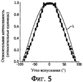
Фиг.5 иллюстрирует график распределения света согласно варианту воплощения светоизлучающего устройства согласно изобретению, показанному на Фиг.1.FIG. 5 illustrates a graph of light distribution according to an embodiment of the light emitting device according to the invention shown in FIG.
Фиг.6 иллюстрирует дополнительный вариант воплощения светоизлучающего устройства согласно изобретению, имеющего линзу, и6 illustrates an additional embodiment of a light emitting device according to the invention having a lens, and
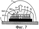
Фиг.7 иллюстрирует дополнительный вариант воплощения светоизлучающего устройства согласно изобретению.7 illustrates an additional embodiment of a light emitting device according to the invention.
Фиг.1 схематически иллюстрирует вариант воплощения светоизлучающего устройства согласно изобретению, имеющего несущий 1 элемент, подложку 2 и твердофазный источник 3 света, обеспеченный на подложке 2 для генерирования первичного излучения 511 и 512, а также конверсионный 4 элемент, установленный на пути лучей первичного излучения, по меньшей мере, для частичного поглощения второй 512 части первичного излучения и вторичного излучения 521 и 522. Твердофазный источник 3 света и конверсионный 4 элемент окружены светорассеивающим 6 элементом, предназначенным для создания смешанного света 5 с ламбертовской структурой распределения. Смешанный 5 свет имеет коррелированную цветовую температуру, которая зависит от первичного и вторичного излучения. Термин «цветовая температура» точно применим только для радиаторов в виде черного тела. Коррелированная цветовая температура означает температуру такого излучателя в виде черного тела, воспринимаемый цвет которого имеет максимальное сходство со спектром смешанного 5 света.Figure 1 schematically illustrates an embodiment of a light emitting device according to the invention having a
Типичный твердофазный источник 3 света содержит электролюминесцентную слоистую структуру, нанесенную на подложку 2, имеющую, по меньшей мере, один органический или неорганический электролюминесцентный слой, который установлен между двумя электродами. Здесь первичное излучение (верхний излучатель) испускается через прозрачный электрод на сторону, обращенную в направлении, противоположном подложке, тогда как электроды, обращенные к подложке 2, и/или подложка 2 являются отражательными. Светоизлучающее устройство также может содержать несколько электролюминесцентных источников света, предназначенных для испускания одинакового и/или различного первичного излучения, например, плоский комплект установок СИД. В других вариантах воплощения, в качестве твердофазных источников света могут быть использованы один или несколько лазерных диодов, возможно соединенных со световодными и/или светораспределительными элементами.A typical solid phase
Первичное излучение, испускаемое твердофазным источником 3 света, распространяется в основном перпендикулярно светоизлучающему слою в твердофазном источнике 3 света и обозначено здесь как вторая 512 часть первичного излучения (см. Фиг.1). Из-за различных коэффициентов преломления слоев в твердофазном источнике света и сопутствующих эффектов полного отражения на граничных поверхностях первая 511 часть первичного излучения, также как и вторая 512 часть первичного излучения испускается вбок из твердофазного источника 3 света под большим углом к среднему направлению излучения 5, не попадая на конверсионный 4 элемент. Благодаря светорассеивающему 6 элементу и полученному в результате ламбертовскому распределению смешанного света первичное излучение, испускаемое вбок под большим углом наблюдения (углом между направлением наблюдения и средним направлением 5 распространения), не приводит к повышенной доле первичного излучения в смешанном свете. Сравнимый эффект можно также получать с помощью конверсионного элемента, который вмещает в себя твердофазный источник света. Однако в данном случае общее первичное излучение, называемое также непреобразованным излучением, должно проходить через конверсионный элемент. Потери на безизлучательное поглощение части первичного излучения в конверсионном элементе приводят к снижению эффективности таких источников излучения. Светоизлучающее устройство согласно изобретению обладает более высокой эффективностью по сравнению с такими СИДл, из-за отсутствия потерь на поглощение, по меньшей мере, для части (первой 511 части) доли, необходимой для настройки желаемой цветовой температуры. Для конкретной требуемой доли первичного излучения смешанного света, для полного непреобразованного первичного излучения эффективность светоизлучающего устройства повышается с повышением доли первой 511 части первичного излучения (в зависимости от структуры конверсионного элемента, его интенсивность поглощения для второй 512 части первичного излучения может составлять менее 100%, вследствие чего непреобразованное первичное излучение также проходит через конверсионный элемент).The primary radiation emitted by the solid-
Конверсионный 4 элемент установлен для, по меньшей мере, частичного поглощения второй 512 части первичного излучения по ходу лучей второй 512 части первичного излучения для преобразования поглощенного первичного излучения во вторичное излучение 521 и 522. Выбор активного материала в конверсионном элементе определяет спектр вторичного излучения. При использовании подходящего первичного и вторичного излучения можно использовать различным образом окрашенный свет, например белый свет, полученный из синего первичного излучения и желтого вторичного излучения. В других вариантах воплощения ультрафиолетовое первичное излучение также можно преобразовывать с помощью подходящих конверсионных материалов и различным образом окрашенного вторичного излучения, например, синего, желтого, зеленого и/или красного вторичного излучения. Для других применений можно получить различные сочетания первичного и вторичного излучения.The
В одном варианте воплощения конверсионный 4 элемент может содержать прессованный керамический материал, изготовленный в основном из светопреобразующего кристаллофосфора или стабильного по размерам матричного материала, например, полиметилметакриллата или других материалов, которые могут быть легированы частицами и содержат внедренные светопреобразующие частицы. В другом варианте воплощения конверсионный 4 элемент содержит керамический материал, обладающий плотностью более 97% от теоретической плотности твердой фазы. Из-за малого эффекта собственного рассеяния такой конверсионный 4 элемент испускает большую долю 521 вторичного излучения перпендикулярно среднему направлению распространения второй 512 части первичного излучения. Это приводит к лучшей смешиваемости первой 511 части первичного излучения с испускаемым вбок вторичным 521 излучением. Дополнительно, эффект малого рассеяния снижает среднюю длину оптического пути второй 521 части первичного излучения в конверсионном 4 элементе до выхода из конверсионного элемента. Таким образом, доля безизлучательного повторного поглощения второй 512 части первичного излучения в конверсионном элементе снижена, а следовательно, эффективность светоизлучающего устройства повышена дополнительно. Эффект рассеяния получают посредством специальных способов спекания, например, путем спекания керамического материала в условиях восстановления при 1700-1750°С в течение 2-8 часов, что приводит к получению материалов, обладающих плотностью >96% от теоретической плотности за вычетом пористости, и путем последующего спекания материала при 1750°С под давлением газообразного аргона (0,500-2 кбар) в течение 10 часов для удаления остаточной пористости. В таких керамических материалах, предназначенных для преобразования света, вторичное излучение содержит значительно более высокую долю вторичного излучения 521, которое испускается вбок из конверсионного элемента (таким образом, оно выходит с поверхности конверсионного элемента, нормальный слой которого, как правило, расположен под прямым углом к направлению распространения второй 512 части первичного излучения), по сравнению с керамическими материалами из прессованного люминофора.In one embodiment, the
В варианте воплощения, показанном на Фиг.1, светорассеивающий 6 элемент вмещает в себя твердофазный источник 3 света и конверсионный 4 элемент. В других вариантах воплощения светорассеивающий 6 элемент, рассматриваемый в направлении распространения смешанного 5 света, можно также устанавливать выше конверсионного 4 элемента, например, в форме плоскости, при условии, что соответствующая отражающая компоновка светоизлучающего устройства приводит к тому, что суммарное первичное излучение 511 и 512 и вторичное излучение 521 и 522 проходят через светорассеивающий элемент с получением ламбертовской схемы распределения света в смешанном 5 свете.In the embodiment shown in FIG. 1, the
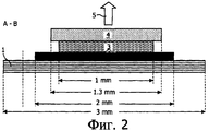
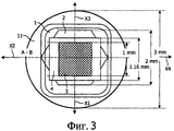
Фиг.2 и Фиг.3 иллюстрируют размеры светоизлучающего устройства согласно Фиг.1, показанные здесь без светорассеивающего 6 элемента ради большей ясности, на виде сбоку (Фиг.2) и на виде сверху (Фиг.3), в плоскости пересечения А-В. Твердофазный источник 3 света имеет поверхность 1 мм × 1 мм и заштрихованную в целях лучшего отображения, хотя она расположена ниже конверсионного 4 элемента на виде сверху и, таким образом, на виде сверху она не является непосредственно видимой. Конверсионный 4 элемент выступает выше твердофазного источника 3 света перпендикулярно среднему направлению распространения света 5 на 0,08 мм, соответственно, в направлениях X1 и Х3, и, соответственно, на 0,15 мм в направлениях Х2 и Х4.Figure 2 and Figure 3 illustrate the dimensions of the light-emitting device according to Figure 1, shown here without a light-diffusing
Несмотря на этот выступ, твердофазный источник 3 света испускает значительную первую 511 часть первичного излучения, которое оценивается в несколько тысяч градусов Кельвина, как показано на Фиг.4, при рассмотрении зависящих от угла измерений коррелированной цветовой температуры, без использования светорассеивающего элемента, за счет смещения коррелированной цветовой температуры между малыми и крупными углами наблюдения. Кривые на Фиг.4 отображают зависящие от угла измерения в четырех направлениях, обозначенных как Х1-Х4 на Фиг.3. Здесь, угол наблюдения 0° соответствует перпендикулярному виду сверху светоизлучающего устройства. В качестве первичного и вторичного излучения было использовано излучение в синем или желтом спектральном диапазоне. На виде сверху получился белый смешанный свет с цветовой температурой в пределах 4700 К, тогда как при больших углах наблюдения цветовая температура белого света составляет до 8000 К и, таким образом, содержит большую долю синего первичного излучения.Despite this protrusion, the solid-
В данном составе материала, толщину конверсионного 4 элемента необходимо адаптировать к желаемому соотношению между первичным и вторичным излучением. Здесь, является благоприятным, чтобы конверсионный 4 элемент имел толщину, по меньшей мере, 30 мкм, при рассмотрении в направлении излучения 5.In this material composition, the thickness of the
В данном случае конверсионный 4 элемент может быть нанесен непосредственно на твердофазный источник 3 света или оптически связан с твердофазным источником 3 света посредством прозрачных материалов. Для создания оптической связи конверсионного 4 элемента с твердофазным источником 3 света между конверсионным 4 элементом и твердофазным источником 3 света можно использовать, например, адгезионные слои или гибкие или жесткие материалы, обладающие показателем преломления 1,4-3, для первичного излучения, например, сшиваемые двухкомпонентные кремнийорганические каучуки, которые сшиты платиновыми нитями, или также материалы из стекла, которые соединены при высоких температурах с твердофазным источником 3 света и с конверсионным 4 элементом. Кроме того, является особо благоприятным, чтобы конверсионный 4 элемент был приведен в тесный контакт с твердофазным источником 3 света.In this case, the
На Фиг.5 схема распределения света из светоизлучающего устройства согласно изобретению, как показано на Фиг.1, показана с размерами, указанными на Фиг.2 и Фиг.3 и являющимися функцией угла испускания первичного излучения при длине волны 470 нм. Здесь светорассеивающий элемент 6 вмещает в себя твердофазный источник 3 света и конверсионный 4 элемент со средней толщиной 600 мкм. Точную толщину здесь следует понимать как толщину вдоль оптического пути первичного и вторичного излучения. Сплошная кривая линия, отмеченная буквой «L» на Фиг.5, отображает идеальное ламбертовское распределение света. Светорассеивающий элемент содержит кремнийорганический матричный материал (коэффициент преломления n=1,45), в который введены рассеивающие частицы со средним диаметром 0,2 мкм и объемной концентрацией 0,05%. Были рассчитаны измерительные кривые для соответствующих частиц, которые отличаются только коэффициентами поглощения n от 1,6 до 2,6. Схемы распределения света, измеренные на Фиг.5, почти не зависят от коэффициента преломления; таким образом, все измерительные точки были отображены одинаковыми символами. При рассмотрении влияния светорассеивающего 6 элемента на распределение света первичного излучения после прохождения через светорассеивающий 4 элемент обнаружены большие различия в размерах частиц. Тогда как частицы диаметром менее приблизительно 500 нм распределяют проходящий свет по всем углам согласно распределению, близкому к ламбертовскому, крупные частицы изменяют угловое распределение пропускаемого света практически только при использовании оптически очень толстого слоя (со слабой силой пропускания). Например, распределение света при первичном излучении с длиной волны 470 нм четко отличается от ламбертовского распределения, если внедренные частицы имеют средний диаметр 1,0 мкм при одинаковой концентрации, как на Фиг.4. Этот результат по существу не зависит от коэффициента преломления частиц.In Fig. 5, the light distribution pattern of the light emitting device according to the invention, as shown in Fig. 1, is shown with the dimensions indicated in Fig. 2 and Fig. 3 and which are a function of the angle of emission of the primary radiation at a wavelength of 470 nm. Here, the
Для среднего диаметра частиц 0,2-0,5 мкм полученная схема распределения света очень близка к идеальному ламбертовскому распределению. Наилучший результат для коэффициента преломления частиц, - от 1,8 до 2,0, получен при средних диаметрах частиц 0,2 мкм. Наилучший результат для коэффициента преломления для частиц, больший или равный 2,1, получен при средних диаметрах частиц 0,3-0,4 мкм. Наилучший результат для коэффициента преломления частиц 1,9-2,3 получен при средних диаметрах частиц 0,5 мкм. Схема распределения света заметно отклоняется от ламбертовского распределения при средних размерах частиц 0,05 мкм и менее. Значения коэффициентов преломления следует понимать в контексте их отличия от коэффициента преломления матричного материала, причем в указанных примерах кремнийорганический материал имеет n=1,45. Для других матричных материалов предпочтительные коэффициенты преломления частиц необходимо подбирать исходя из этого. Дополнительно, принимая во внимание концентрацию Vт в процентах и толщину D светорассеивающего 6 элемента в микронах, предпочтительное произведение концентрации частиц и толщины VT·D светорассеивающего 6 элемента составляет от 0,1 до 3, еще более предпочтительно - от 0,2 до 1. В качестве светорассеивающих частиц можно использовать, например, ZrO2 или TiO2. Однако специалистам в данной области техники также известны светорассеивающие частицы из других материалов. При одинаковом среднем диаметре частиц на светорассеивающие свойства светорассеивающего 6 элемента, зависящие от длины волны, может влиять изменение размера частиц. Это распределение обычно соответствует нормальному логарифмическому распределению с шириной распределения σ. Например, для частиц ZrO2 (n=2,2) с объемной концентрацией в кремнийорганическом веществе, равной 0,05%, с шириной распределения σ диаметра частиц от 0,06 до 0,3 получена характеристика отражения (характеристика рассеяния) частиц, которая лишь немного зависит от длины волны, однако, эта характеристика отражения еще дополнительно зависит от размера частиц.For an average particle diameter of 0.2-0.5 microns, the resulting light distribution pattern is very close to the ideal Lambertian distribution. The best result for the refractive index of particles, from 1.8 to 2.0, was obtained with average particle diameters of 0.2 μm. The best result for the refractive index for particles greater than or equal to 2.1 was obtained with average particle diameters of 0.3-0.4 microns. The best result for a refractive index of 1.9-2.3 particles was obtained with average particle diameters of 0.5 microns. The light distribution pattern deviates markedly from the Lambertian distribution with average particle sizes of 0.05 microns or less. The values of the refractive indices should be understood in the context of their difference from the refractive index of the matrix material, and in these examples, the organosilicon material has n = 1.45. For other matrix materials, the preferred refractive indices of the particles must be selected based on this. Additionally, taking into account the concentration V t in percent and the thickness D of the
Вариант воплощенияEmbodiment
В структуре светоизлучающего устройства, выбранного согласно Фиг.1, СИД, испускающий синий свет с максимальным испусканием при 450 нм, и керамический материал YAG:Ce (YAG - иттриево-алюминевый гранат), нанесенный на твердофазный источник света, были использованы в качестве твердофазного источника света для получения желтого вторичного излучения, выходящего из керамического материала, имеющего плотность 98% от теоретической плотности твердой фазы. Керамический диск имел толщину 250 мкм. Сырьевой материал для керамического диска был изготовлен в течение 12 часов перемалывания 40 г Y2O3, 32 г Al2O3 и 3,44 г СеО2 в изопропаноле с помощью мелющих шаров из Аl2O3 массой 1,5 кг и с последующим отжигом высушенного порошка при 1300°С в атмосфере СО. Полученный порошок YAG:Ce был деагломерирован в этиловом спирте с помощью планетарной шаровой мельницы, имеющей агатовые чашки для размалывания, и были изготовлены затем керамические сырьевые тела (диаметр 100 мм, высота 2 мм) путем шликерной заливки в гипсовую форму. После сушки сырьевые тела были отожжены на графитовых дисках в атмосфере СО при 1700° в течение двух часов. Затем керамический материал YAG был распилен до частиц размером 290 мкм, подвергнут поверхностной обработке и отполирован. Плотность керамического материала составляет 98% от теоретической плотности. Требуемые керамические диски были затем вырезаны лазером и очищены. Пропускание света через керамический материал составляло 80% при длине волны 600 нм. Между керамическим диском и СИД был помещен тонкий слой кремнийорганического геля, имеющий толщину менее 10 мкм, фирмы Gelest Inc PP2-D200 Gelest gel D200 для создания оптической связи между керамическим диском и твердофазным источником света. Затем была установлена сферическая линза, пространство (зазор) 6 внутри которой было заполнено кремнийорганическим гелем, содержащим внедренные в него светорассеивающие частицы. В данном варианте воплощения такой заполненный зазор 6 представляет собой светорассеивающий 6 элемент. Частицы, внедренные в кремнийорганический гель, представляют собой ZrO2 со средним диаметром частиц 0,25 мкм. Распределение света показало 92%-ное сходство с идеальной ламбертовской схемой распределения и, таким образом, оно очень хорошо соответствует ламбертовскому распределению.In the structure of the light-emitting device selected according to FIG. 1, LEDs emitting blue light with a maximum emission at 450 nm and ceramic material YAG: Ce (YAG - yttrium-aluminum garnet) deposited on a solid-state light source were used as a solid-phase source light to obtain yellow secondary radiation emerging from a ceramic material having a density of 98% of the theoretical density of the solid phase. The ceramic disk was 250 μm thick. The raw material for the ceramic disk was made within 12 hours of grinding 40 g of Y 2 O 3 , 32 g of Al 2 O 3 and 3.44 g of CeO 2 in isopropanol using grinding balls of Al 2 O 3 weighing 1.5 kg and with subsequent annealing of the dried powder at 1300 ° C in an atmosphere of CO. The obtained YAG: Ce powder was de-agglomerated in ethanol using a planetary ball mill having agate grinding cups, and then ceramic raw materials (
В другом варианте воплощения, для дополнительного модифицирования коррелированной цветовой температуры, в качестве рассеивающих частиц также можно использовать окрашенные пигменты. В качестве таких материалов, в частности, подходят неорганические материалы, коэффициент преломления которых находится в желательном диапазоне. Такие материалы представляют собой, например, СоО-Аl2O3 и ультрамарин в качестве пигментов синего цвета, TiO2-CoO-NiO-ZrO2, СеО-Сr2О3-ТiO2-Аl2О3, TiO2-ZnO-CoO-NiO в качестве пигментов зеленого цвета и Fе2O3, CdS-CdSe, TaON в качестве пигментов красного цвета.In another embodiment, to further modify the correlated color temperature, colored pigments can also be used as scattering particles. Inorganic materials whose refractive index is in the desired range are particularly suitable as such materials. Such materials are, for example, CoO-Al 2 O 3 and ultramarine as blue pigments, TiO 2 -CoO-NiO-ZrO 2 , CeO-Cr 2 O 3 -TiO 2 -Al 2 O 3 , TiO 2 -ZnO -CoO-NiO as green pigments and Fe 2 O 3 , CdS-CdSe, TaON as red pigments.
Часть упомянутого ранее непреобразованного первичного излучения, отраженного назад в конверсионный элемент при рассеянии в светорассеивающем 6 элементе, может быть использована и в других вариантах воплощения для дополнительной адаптации коррелированной цветовой температуры смешанного 5 света.A portion of the previously untransformed primary radiation reflected back to the conversion element upon scattering in the
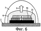
В еще одном варианте воплощения, показанном на Фиг.6, твердофазный источник 3 света, рассматриваемый в направлении излучения смешанного 5 света, имеет светоизлучающую 31 поверхность, которая больше или равна поверхности 41 конверсионного 4 элемента, которая обращена к твердофазному источнику 3 света. Таким образом, доля первой части первичного излучения 511 от общего первичного излучения может быть повышена. В данном варианте воплощения, по меньшей мере, общее первичное излучение, испускаемое вбок из твердофазного источника 3 света, не проходит через конверсионный 4 элемент. Если поверхность 41 конверсионного 4 элемента меньше светоизлучающей 31 поверхности, как показано на Фиг.6, то, помимо испускаемого вбок первичного 511 излучения, часть первичного излучения, испускаемого параллельно среднему направлению излучения 5, не проходит через конверсионный 4 элемент. Таким образом, доля первичного излучения, которая не проходит через конверсионный элемент, дополнительно повышается.In yet another embodiment shown in FIG. 6, the solid state
В еще одном варианте воплощения, показанном на Фиг.7, конверсионный 4 элемент имеет, по меньшей мере, одно отверстие 8, через которое может проходить первичное излучение, не проходя через сам конверсионный 4 элемент. Требуемое повышение доли первой 511 части первичного излучения для повышения суммарного первичного излучения дополнительно повышает эффективность светоизлучающего устройства. Среднее направление распространения доли первичного 511 излучения, которое проходит через отверстия 8, по меньшей мере, очень близко к среднему направлению распространения вторичного излучения и обеспечивает возможность для менее дорогого и тщательного разработанного светорассеивающего 6 элемента генерировать свет с ламбертовским распределением. Отверстия 8 не следует здесь считать частью конверсионного элемента. Отверстия можно заполнять либо газом, например воздухом, либо другим прозрачным и нерассеивающим материалом, например кремнийорганическим материалом.In yet another embodiment shown in FIG. 7, the
Варианты воплощения, разъясненные со ссылкой на Фигуры, и описание, представляют собой только примеры светорассеивающего устройства согласно изобретению для эффективного испускания смешанного света, имеющего ламбертовское распределение, и не должны рассматриваться в качестве вариантов, ограничивающих патентную заявку этими примерами. Специалисты в данной области техники могут также освоить и альтернативные варианты воплощения, которые также находятся в рамках объема прилагаемой формулы изобретения. Под нумерацией независимых пунктов формулы изобретения не следует подразумевать, что сочетания пунктов формулы изобретения не отображают соответствующие варианты воплощения изобретения.The embodiments explained with reference to the Figures and the description are only examples of a diffuser according to the invention for efficiently emitting mixed light having a Lambertian distribution, and should not be construed as limiting the patent application to these examples. Those skilled in the art can also learn alternative embodiments that are also within the scope of the appended claims. The numbering of the independent claims is not to mean that the combinations of the claims do not reflect the corresponding embodiments of the invention.
Claims (12)
Applications Claiming Priority (2)
| Application Number | Priority Date | Filing Date | Title |
|---|---|---|---|
| EP06100745.6 | 2006-01-24 | ||
| EP06100745 | 2006-01-24 |
Publications (2)
| Publication Number | Publication Date |
|---|---|
| RU2008134528A RU2008134528A (en) | 2010-02-27 |
| RU2407110C2 true RU2407110C2 (en) | 2010-12-20 |
Family
ID=37946000
Family Applications (1)
| Application Number | Title | Priority Date | Filing Date |
|---|---|---|---|
| RU2008134528/28A RU2407110C2 (en) | 2006-01-24 | 2007-01-15 | Light-emitting device |
Country Status (8)
| Country | Link |
|---|---|
| US (1) | US7859185B2 (en) |
| EP (1) | EP1979954B1 (en) |
| JP (1) | JP2009524914A (en) |
| KR (1) | KR101358699B1 (en) |
| CN (1) | CN101375420B (en) |
| RU (1) | RU2407110C2 (en) |
| TW (1) | TWI455344B (en) |
| WO (1) | WO2007085977A1 (en) |
Cited By (2)
| Publication number | Priority date | Publication date | Assignee | Title |
|---|---|---|---|---|
| WO2012112073A1 (en) * | 2011-02-17 | 2012-08-23 | Закрытое Акционерное Общество "Научно-Производственная Коммерческая Фирма "Элтан Лтд" | Light-emitting diode source of white light with a remote phosphor converter |
| RU2569312C2 (en) * | 2013-04-05 | 2015-11-20 | Сергей Александрович Панин | Light-emitting diode light source (versions) |
Families Citing this family (46)
| Publication number | Priority date | Publication date | Assignee | Title |
|---|---|---|---|---|
| US20080029720A1 (en) | 2006-08-03 | 2008-02-07 | Intematix Corporation | LED lighting arrangement including light emitting phosphor |
| RU2451366C2 (en) * | 2006-12-05 | 2012-05-20 | Конинклейке Филипс Электроникс Н.В. | Illumination device, particularly with luminescent ceramic |
| US7999283B2 (en) * | 2007-06-14 | 2011-08-16 | Cree, Inc. | Encapsulant with scatterer to tailor spatial emission pattern and color uniformity in light emitting diodes |
| US11114594B2 (en) * | 2007-08-24 | 2021-09-07 | Creeled, Inc. | Light emitting device packages using light scattering particles of different size |
| US7859000B2 (en) * | 2008-04-10 | 2010-12-28 | Cree, Inc. | LEDs using single crystalline phosphor and methods of fabricating same |
| US9287469B2 (en) * | 2008-05-02 | 2016-03-15 | Cree, Inc. | Encapsulation for phosphor-converted white light emitting diode |
| WO2009148543A2 (en) | 2008-05-29 | 2009-12-10 | Cree, Inc. | Light source with near field mixing |
| CN102084507B (en) | 2008-07-01 | 2016-01-20 | 皇家飞利浦电子股份有限公司 | What have reduction does not change photoemissive wavelength convert light-emitting diode |
| ES2667009T3 (en) | 2008-07-22 | 2018-05-09 | Philips Lighting Holding B.V. | An optical element for a light emitting device and a manufacturing method thereof |
| US7973327B2 (en) * | 2008-09-02 | 2011-07-05 | Bridgelux, Inc. | Phosphor-converted LED |
| KR101747688B1 (en) * | 2009-05-19 | 2017-06-16 | 코닌클리케 필립스 엔.브이. | Light scattering and conversion plate for leds |
| US8415692B2 (en) * | 2009-07-06 | 2013-04-09 | Cree, Inc. | LED packages with scattering particle regions |
| US8431423B2 (en) | 2009-07-16 | 2013-04-30 | Koninklijke Philips Electronics N.V. | Reflective substrate for LEDS |
| JP5368913B2 (en) * | 2009-09-02 | 2013-12-18 | スタンレー電気株式会社 | Light emitting device and manufacturing method thereof |
| WO2011033394A1 (en) * | 2009-09-16 | 2011-03-24 | Koninklijke Philips Electronics N.V. | Light emitter with predefined angular color point distribution |
| CN102097425A (en) * | 2009-12-09 | 2011-06-15 | 三星Led株式会社 | Light emitting diode, method for fabricating phosphor layer, and lighting apparatus |
| DE102010021011A1 (en) * | 2010-05-21 | 2011-11-24 | Osram Opto Semiconductors Gmbh | Optoelectronic semiconductor component and method for producing a cover layer |
| US8354784B2 (en) * | 2010-09-28 | 2013-01-15 | Intematix Corporation | Solid-state light emitting devices with photoluminescence wavelength conversion |
| US8614539B2 (en) | 2010-10-05 | 2013-12-24 | Intematix Corporation | Wavelength conversion component with scattering particles |
| KR20130139938A (en) * | 2010-10-05 | 2013-12-23 | 인터매틱스 코포레이션 | Solid-state light emitting devices and signage with photoluminescence wavelength conversion |
| US8957585B2 (en) | 2010-10-05 | 2015-02-17 | Intermatix Corporation | Solid-state light emitting devices with photoluminescence wavelength conversion |
| US8604678B2 (en) | 2010-10-05 | 2013-12-10 | Intematix Corporation | Wavelength conversion component with a diffusing layer |
| US8610341B2 (en) | 2010-10-05 | 2013-12-17 | Intematix Corporation | Wavelength conversion component |
| US9546765B2 (en) | 2010-10-05 | 2017-01-17 | Intematix Corporation | Diffuser component having scattering particles |
| DE102010050832A1 (en) * | 2010-11-09 | 2012-05-10 | Osram Opto Semiconductors Gmbh | Luminescence conversion element, method for its production and optoelectronic component with luminescence conversion element |
| DE102011010118A1 (en) * | 2011-02-02 | 2012-08-02 | Osram Opto Semiconductors Gmbh | Ceramic conversion element, semiconductor chip with a ceramic conversion element and method for producing a ceramic conversion element |
| JP6393187B2 (en) * | 2011-08-16 | 2018-09-19 | 日東電工株式会社 | Phosphor composition and method for producing the same |
| JP5830340B2 (en) * | 2011-10-11 | 2015-12-09 | オリンパス株式会社 | Light source device |
| EP2766936B1 (en) * | 2011-10-13 | 2019-09-18 | Intematix Corporation | Light emitting device with photoluminescence wavelength conversion component |
| KR101251815B1 (en) * | 2011-11-07 | 2013-04-09 | 엘지이노텍 주식회사 | Optical sheet and display device having the same |
| CN102437276A (en) * | 2011-11-25 | 2012-05-02 | 四川新力光源有限公司 | Light emitting diode (LED) device and production method thereof |
| US20130258637A1 (en) * | 2012-03-31 | 2013-10-03 | Michael Dongxue Wang | Wavelength-converting structure for a light source |
| TWI518948B (en) * | 2012-06-08 | 2016-01-21 | Unity Opto Technology Co Ltd | To enhance the luminous angle of the small size of the LED package to improve the structure |
| US9818919B2 (en) * | 2012-06-11 | 2017-11-14 | Cree, Inc. | LED package with multiple element light source and encapsulant having planar surfaces |
| EP2888525B1 (en) * | 2012-08-24 | 2016-11-16 | Philips Lighting Holding B.V. | A lighting device |
| DE102012222475A1 (en) * | 2012-12-06 | 2014-06-12 | Osram Gmbh | LUMINOUS DIODE SHOWING SEVERAL FLUORESCENT RANGE |
| US20140185269A1 (en) | 2012-12-28 | 2014-07-03 | Intermatix Corporation | Solid-state lamps utilizing photoluminescence wavelength conversion components |
| CN105121951A (en) | 2013-03-15 | 2015-12-02 | 英特曼帝克司公司 | Photoluminescence wavelength conversion components |
| JP2016062899A (en) * | 2014-09-12 | 2016-04-25 | 株式会社東芝 | Semiconductor light-emitting device |
| KR101621820B1 (en) * | 2014-12-29 | 2016-05-17 | 삼성전자 주식회사 | Light source, back light unit and liquid crystal display including the light source |
| KR102437550B1 (en) * | 2015-03-09 | 2022-08-29 | 코닌클리케 필립스 엔.브이. | color point variable light emitting device |
| US20170025589A1 (en) * | 2015-07-22 | 2017-01-26 | Epistar Corporation | Light emitting structure and method for manufacturing the same |
| US20170331016A1 (en) * | 2016-05-13 | 2017-11-16 | Maxim Tchoul | A lighting device having an optical lens formed on composite encapsulant comprising nanoparticles covering a light-emitting diode (led) |
| US11081628B2 (en) * | 2016-09-01 | 2021-08-03 | Lumileds Llc | White-appearing semiconductor light-emitting devices having a temperature sensitive low-index particle layer |
| KR20180090002A (en) * | 2017-02-02 | 2018-08-10 | 서울반도체 주식회사 | Light emitting diode package |
| US11205743B2 (en) * | 2018-12-21 | 2021-12-21 | Lumileds Llc | High luminance light emitting device and method for creating a high luminance light emitting device |
Family Cites Families (18)
| Publication number | Priority date | Publication date | Assignee | Title |
|---|---|---|---|---|
| US5001609A (en) * | 1988-10-05 | 1991-03-19 | Hewlett-Packard Company | Nonimaging light source |
| US6653765B1 (en) | 2000-04-17 | 2003-11-25 | General Electric Company | Uniform angular light distribution from LEDs |
| JP2002141559A (en) * | 2000-10-31 | 2002-05-17 | Sanken Electric Co Ltd | Light emitting semiconductor chip assembly and light emitting semiconductor lead frame |
| US7211833B2 (en) * | 2001-07-23 | 2007-05-01 | Cree, Inc. | Light emitting diodes including barrier layers/sublayers |
| TW511303B (en) * | 2001-08-21 | 2002-11-21 | Wen-Jr He | A light mixing layer and method |
| JP2003078165A (en) | 2001-08-31 | 2003-03-14 | Japan Fine Ceramics Center | Light emitting element |
| US7186005B2 (en) * | 2001-10-18 | 2007-03-06 | Ilight Technologies, Inc. | Color-changing illumination device |
| JP2004210921A (en) * | 2002-12-27 | 2004-07-29 | Nichia Chem Ind Ltd | Oxynitride fluorophor and method for producing the same and light-emitting device using the same |
| US7554258B2 (en) * | 2002-10-22 | 2009-06-30 | Osram Opto Semiconductors Gmbh | Light source having an LED and a luminescence conversion body and method for producing the luminescence conversion body |
| JP2004221163A (en) * | 2003-01-10 | 2004-08-05 | Nichia Chem Ind Ltd | Light emitting device, its forming method, planar light emitting device using the light emitting device |
| US6871982B2 (en) * | 2003-01-24 | 2005-03-29 | Digital Optics International Corporation | High-density illumination system |
| JP2007505479A (en) * | 2003-09-08 | 2007-03-08 | グループ フォア セミコンダクター インコーポレイテッド | Solid white light emitter and display using the same |
| US7497581B2 (en) * | 2004-03-30 | 2009-03-03 | Goldeneye, Inc. | Light recycling illumination systems with wavelength conversion |
| US7514867B2 (en) * | 2004-04-19 | 2009-04-07 | Panasonic Corporation | LED lamp provided with optical diffusion layer having increased thickness and method of manufacturing thereof |
| US7361938B2 (en) | 2004-06-03 | 2008-04-22 | Philips Lumileds Lighting Company Llc | Luminescent ceramic for a light emitting device |
| US20060097385A1 (en) * | 2004-10-25 | 2006-05-11 | Negley Gerald H | Solid metal block semiconductor light emitting device mounting substrates and packages including cavities and heat sinks, and methods of packaging same |
| US20070023762A1 (en) * | 2005-07-29 | 2007-02-01 | Luxo Asa And Oec Ag | White light emitting LED-powered lamp |
| DE102006020529A1 (en) * | 2005-08-30 | 2007-03-01 | Osram Opto Semiconductors Gmbh | Optoelectronic component has semiconductor body emitting electromagnetic radiation that passes through an optical element comprising wavelength conversion material |
-
2007
- 2007-01-15 KR KR1020087020438A patent/KR101358699B1/en active IP Right Grant
- 2007-01-15 JP JP2008550887A patent/JP2009524914A/en active Pending
- 2007-01-15 RU RU2008134528/28A patent/RU2407110C2/en active
- 2007-01-15 EP EP07700584.1A patent/EP1979954B1/en active Active
- 2007-01-15 US US12/162,072 patent/US7859185B2/en active Active
- 2007-01-15 CN CN2007800033997A patent/CN101375420B/en active Active
- 2007-01-15 WO PCT/IB2007/050112 patent/WO2007085977A1/en active Application Filing
- 2007-01-19 TW TW096102124A patent/TWI455344B/en active
Cited By (3)
| Publication number | Priority date | Publication date | Assignee | Title |
|---|---|---|---|---|
| WO2012112073A1 (en) * | 2011-02-17 | 2012-08-23 | Закрытое Акционерное Общество "Научно-Производственная Коммерческая Фирма "Элтан Лтд" | Light-emitting diode source of white light with a remote phosphor converter |
| US9347622B2 (en) | 2011-02-17 | 2016-05-24 | Vladimir Nikolaevich Ulasyuk | LED white light source with remote photoluminescent converter |
| RU2569312C2 (en) * | 2013-04-05 | 2015-11-20 | Сергей Александрович Панин | Light-emitting diode light source (versions) |
Also Published As
| Publication number | Publication date |
|---|---|
| CN101375420A (en) | 2009-02-25 |
| KR101358699B1 (en) | 2014-02-07 |
| TW200739961A (en) | 2007-10-16 |
| US7859185B2 (en) | 2010-12-28 |
| CN101375420B (en) | 2010-11-10 |
| WO2007085977A1 (en) | 2007-08-02 |
| RU2008134528A (en) | 2010-02-27 |
| KR20080091240A (en) | 2008-10-09 |
| JP2009524914A (en) | 2009-07-02 |
| EP1979954A1 (en) | 2008-10-15 |
| US20090026908A1 (en) | 2009-01-29 |
| EP1979954B1 (en) | 2015-03-18 |
| TWI455344B (en) | 2014-10-01 |
Similar Documents
| Publication | Publication Date | Title |
|---|---|---|
| RU2407110C2 (en) | Light-emitting device | |
| JP5743548B2 (en) | Lighting device | |
| JP5070222B2 (en) | Light emitting device with non-activated light emitting material | |
| TWI479676B (en) | Side emitting device with hybrid top reflector | |
| RU2512091C2 (en) | Light-emitting diode unit | |
| JP5091023B2 (en) | Light emitting device package using light scattering particles of different sizes | |
| US9671089B2 (en) | Conversion element and illuminant | |
| US20030038596A1 (en) | Light-mixing layer and method | |
| KR101437839B1 (en) | Electroluminescent device | |
| JP2004528714A (en) | UV reflector and UV based light source incorporating UV reflector to reduce UV radiation leakage | |
| JP5709463B2 (en) | Light source device and lighting device | |
| KR20160036489A (en) | Light emitting device | |
| EP2223353B1 (en) | Side-emitting, light emitting device with hybrid, top scattering-reflector | |
| KR20040017926A (en) | Light-mixing layer and method | |
| WO2009074934A1 (en) | Side emitting device with hybrid top reflector | |
| WO2021182096A1 (en) | Light-emitting device, lighting system, and optical communication system | |
| KR20180042727A (en) | Display module and display apparatus of vehicle having the same |
Legal Events
| Date | Code | Title | Description |
|---|---|---|---|
| PD4A | Correction of name of patent owner | ||
| PC41 | Official registration of the transfer of exclusive right |
Effective date: 20190823 |
|
| PD4A | Correction of name of patent owner |