RU2297103C2 - Marker separating device for frame synchronization system - Google Patents
Marker separating device for frame synchronization system Download PDFInfo
- Publication number
- RU2297103C2 RU2297103C2 RU2004135612/09A RU2004135612A RU2297103C2 RU 2297103 C2 RU2297103 C2 RU 2297103C2 RU 2004135612/09 A RU2004135612/09 A RU 2004135612/09A RU 2004135612 A RU2004135612 A RU 2004135612A RU 2297103 C2 RU2297103 C2 RU 2297103C2
- Authority
- RU
- Russia
- Prior art keywords
- analysis
- inputs
- input
- outputs
- stage
- Prior art date
Links
- 239000003550 marker Substances 0.000 title claims abstract description 66
- 230000015572 biosynthetic process Effects 0.000 claims description 21
- 238000000605 extraction Methods 0.000 claims description 2
- 230000036039 immunity Effects 0.000 abstract description 5
- 238000004891 communication Methods 0.000 abstract description 2
- 238000012546 transfer Methods 0.000 abstract description 2
- 238000007493 shaping process Methods 0.000 abstract 10
- 239000000126 substance Substances 0.000 abstract 1
- 239000012634 fragment Substances 0.000 description 43
- 238000000034 method Methods 0.000 description 8
- 238000010586 diagram Methods 0.000 description 5
- 238000009434 installation Methods 0.000 description 3
- 238000002955 isolation Methods 0.000 description 3
- 238000010276 construction Methods 0.000 description 2
- 230000005540 biological transmission Effects 0.000 description 1
- 238000005056 compaction Methods 0.000 description 1
- 230000003993 interaction Effects 0.000 description 1
- 238000012545 processing Methods 0.000 description 1
- 238000012360 testing method Methods 0.000 description 1
Images

Landscapes
- Time-Division Multiplex Systems (AREA)
- Synchronisation In Digital Transmission Systems (AREA)
Abstract
Description
Изобретение относится к области электросвязи и может быть использовано для создания кадровой синхронизации приемников в системах передачи цифровой информации.The invention relates to the field of telecommunications and can be used to create frame synchronization of receivers in digital information transmission systems.
Все возрастающие скорости передачи цифровой информации (120 Мбит/с и выше) в спутниковых линиях связи с временным уплотнением цифрового потока требуют особого внимания к созданию устройств выделения маркера системы кадровой синхронизации, которые работают на частоте входного информационного потока и должны удовлетворять требованиям по быстродействию и высокой помехозащищенности.The ever-increasing digital data transfer rates (120 Mbps and higher) in satellite communication lines with temporary digital stream compaction require special attention to the creation of marker synchronization system marker isolation devices that operate at the input information frequency and must satisfy high-speed and high-speed requirements noise immunity.
Создание таких устройств на основе известных способов (1, 2) довольно трудоемкая задача, поэтому для удовлетворения указанных требований был использован весьма простой способ (3), основанный на преобразовании сигнала из последовательного кода в параллельный и сравнение его в эталонной комбинации маркера.The creation of such devices based on well-known methods (1, 2) is a rather time-consuming task, therefore, to satisfy the indicated requirements, a very simple method (3) was used, based on converting the signal from a serial code to a parallel one and comparing it in a marker marker reference combination.
Этот способ выделения маркера кадровой синхронизации предопределяет модульность и регулярность структуры построения реализующего его устройства. Простота операций на всех ступенях анализа этого способа позволяет создавать чрезвычайно простые, высокоскоростные структурные модули выделения маркера кадровой синхронизации, а его суммирующие и анализирующие элементы способны различать К+2 возможных состояний результатов сравнения фрагментов входной информации последовательности и эталона маркера (К - допустимое количество ошибок в сигнале кадровой синхронизации).This method of marking the frame synchronization marker predetermines the modularity and regularity of the construction structure of the device implementing it. The simplicity of operations at all stages of the analysis of this method allows you to create extremely simple, high-speed structural modules for highlighting the frame synchronization marker, and its summing and analyzing elements are able to distinguish between K + 2 possible states of the results of comparing fragments of the input sequence information and the marker standard (K is the allowable number of errors in frame synchronization signal).
Для понятия сущности работы устройства-прототипа рассмотрим алгоритм обработки информационной последовательности для выделения маркера кадровой синхронизации, который осуществляется в следующей последовательности:For the concept of the essence of the prototype device, we consider an algorithm for processing an information sequence to select a frame synchronization marker, which is carried out in the following sequence:
- входной сигнал с кодово-импульсной модуляцией, представляющий собой последовательную комбинацию двоичных символов, преобразуют из последовательного кода в параллельный;- an input signal with pulse-code modulation, which is a sequential combination of binary characters, is converted from a serial code to a parallel one;
- анализируемый фрагмент входного сигнала разбивают на К-символьные группы, где К - максимально допустимое количество пораженных символов маркера;- the analyzed fragment of the input signal is divided into K-character groups, where K is the maximum allowable number of affected marker characters;
- для каждой из возможных К-элементных групп, независимо от других групп определяют количество символов фрагмента анализируемой входной последовательности, отличающихся от соответствующих символов эталона маркера, причем результат операции представляют в виде кодового слова длиной в (К+1) бит, за каждой позицией которого закрепляется функция регистрации своего, отличного от других, количества несовпадающих символов из множества {0, 1, 2,..., К};- for each of the possible K-element groups, independently of other groups, determine the number of characters of a fragment of the analyzed input sequence that differ from the corresponding symbols of the marker standard, and the result of the operation is represented as a code word with a length of (K + 1) bits, for each position of which the function of registering one’s number of mismatched characters from the set {0, 1, 2, ..., K} is fixed;
- полученные в результате предыдущей операции кодовые слова разбивают на смежные пары и по информации, содержащейся в каждой паре этих слов каждого анализируемого фрагмента входного сигнала длиною в 2К бит, определяют суммарное количество символов, отличающихся от соответствующих символов эталона маркера, при этом форма представления результата операции на отдельной смежной паре кодовых слов в точности совпадает с формой представления результата в предыдущей операции, причем если количество символов в анализируемом фрагменте входного сигнала, не совпадающих с соответствующими символами эталона маркера, превышает допустимое К, то на всех (К+1) позициях кодового слова, полученного в результате данной операции, устанавливают равные между собой значения логических переменных;- the code words obtained as a result of the previous operation are divided into adjacent pairs and from the information contained in each pair of these words of each analyzed fragment of the input signal with a length of 2K bits, the total number of characters that differ from the corresponding symbols of the marker standard is determined, while the form of the operation result presentation on a separate adjacent pair of code words exactly coincides with the form of presentation of the result in the previous operation, and if the number of characters in the analyzed fragment of the input if the signal does not coincide with the corresponding symbols of the marker standard exceeds the allowable K, then at all (K + 1) positions of the codeword obtained as a result of this operation, the values of logical variables are set equal to each other;
- полученные в результате предыдущей операции кодовые слова снова разбивают на смежные пары и повторяют все действия, описанные в предыдущей операции;- the code words obtained as a result of the previous operation are again split into adjacent pairs and repeat all the actions described in the previous operation;
- повторяют предыдущую операцию до тех пор, пока весь результат окажется сосредоточенным в одном кодовом слове длиной в (К+1) бит;- repeat the previous operation until the whole result is concentrated in one codeword with a length of (K + 1) bits;
- по полученному в результате предыдущей операции кодовому слову производят опознавание маркера кадровой синхронизации, при этом в случае равенства логических переменных в К разрядах и наличии в одном из (К+1) разрядах этого слова логической переменной противоположного значения формируется кадровый синхроимпульс, а в случае равенства значений логических переменных во всех (К+1) разрядах этого слова кадровый синхроимпульс не формируется.- the frame synchronization marker is identified by the code word obtained as a result of the previous operation, and in the case of equality of logical variables in K bits and the presence of a logical variable of the opposite value in one of the (K + 1) bits of this word, a frame clock pulse is generated, and in case of equality values of logical variables in all (K + 1) bits of this word, a frame sync pulse is not formed.
Отличительной особенностью устройства-прототипа (3), реализованного в соответствии с указанным способом, является:A distinctive feature of the prototype device (3), implemented in accordance with the specified method, is:
возможность его оперативной перенастройки на различные конфигурации маркера;the possibility of its rapid reconfiguration to various marker configurations;
возможность оперативного изменения допустимого количества ошибок в сигнале кадровой синхронизации при его опознании;the ability to quickly change the allowable number of errors in the frame synchronization signal when it is recognized;
постоянство быстродействия при увеличении элементного состава устройства, вызванного увеличением числа символов маркера кадровой синхронизации.constancy of speed with an increase in the elemental composition of the device caused by an increase in the number of characters of the frame synchronization marker.
К недостаткам устройства-прототипа относится то, что решение предложено для случая, когда допустимое количество ошибок в сигнале кадровой синхронизации не превышает двух, что предполагает работу системы кадровой синхронизации при высоких отношениях сигнал/шум, однако в реальных системах отношение сигнал к шуму лежит в пределах 8-10 дБ и ниже, что указывает на низкую помехозащищенность устройства-прототипа выделения маркера системы кадровой синхронизации.The disadvantages of the prototype device include the fact that the solution is proposed for the case when the permissible number of errors in the frame synchronization signal does not exceed two, which implies the operation of the frame synchronization system at high signal-to-noise ratios, but in real systems the signal-to-noise ratio is within 8-10 dB or lower, which indicates a low noise immunity of the prototype device of the marker allocation of the frame synchronization system.
Целью настоящего изобретения является повышение помехозащищенности устройства выделения маркера системы кадровой синхронизации, устойчиво работающем при допустимом количестве ошибок, в два раза большем, чем в устройстве-прототипе.The aim of the present invention is to increase the noise immunity of the device for allocating a marker of the frame synchronization system, stably working with an allowable number of errors, twice as much as in the prototype device.
Для достижения поставленной цели предлагается устройство выделения маркера для системы кадровой синхронизации, содержащее последовательно соединенные К ступеней анализа, в котором ступени анализа со второй по (К-1) выполнены идентично в виде блоков формирования трехразрядных результатов сравнения, при этом выходы двух предыдущих ступеней анализа подключены ко входам одного соответствующего элемента последующей ступени анализа, а к К ступени анализа, выполненной в виде блока конечного анализирующего элемента, подключены выходы блока формирования трехразрядных результатов сравнения (К-1) ступени анализа, при этом первая ступень анализа содержит регистр сдвига, выполненный в виде последовательно соединенных D-триггеров, вход первого и выход последнего из которых является информационным входом и информационным выходом устройства, а каждый D-триггер регистра сдвига имеет вход установки эталонной кодовой комбинации и вход настройки на длину маркера, при этом каждая смежная пара D-триггеров регистра сдвига входит в состав каждого из N блоков промежуточного анализа первой ступени анализа.To achieve this goal, a marker extraction device for the frame synchronization system is proposed, which contains K analysis stages connected in series, in which the analysis stages from second to (K-1) are identical in the form of three-digit comparison results, with the outputs of the two previous analysis stages connected to the inputs of one corresponding element of the next stage of analysis, and to the stage of analysis, made in the form of a block of the final analyzing element, the outputs of the block are connected the formation of three-digit comparison results (K-1) of the analysis stage, while the first analysis stage contains a shift register made in the form of series-connected D-triggers, the input of the first and the output of the last of which is the information input and information output of the device, and each D-trigger the shift register has an input for setting the reference code combination and an input for setting the marker length, and each adjacent pair of D-triggers of the shift register is a part of each of the N blocks of intermediate analysis of the first steps of analysis.
Согласно изобретению, в состав каждого из N блоков промежуточного анализа первой ступени анализа введены блоки формирования пятиразрядных результатов сравнения, ко входам каждой из которых подключены трехразрядные выходы каждой пары блоков промежуточного анализа, а в состав каждой из последовательно соединенных со второй по (К-1) ступеней анализа введены блоки формирования двухразрядных результатов сравнения, причем ко входам каждого блока формирования трехразрядных результатов сравнения и каждого блока формирования двухразрядных результатов сравнения второй ступени анализа подключены выходы соответствующей пары блоков формирования пятиразрядных результатов сравнения первой ступени анализа, ко входам каждого блока формирования трехразрядных результатов сравнения и каждого блока формирования двухразрядных результатов сравнения каждой с третьей по (К-1) последующих ступеней анализа подключены выходы соответствующей пары блоков формирования пятиразрядных результатов сравнения предыдущей ступени анализа, а выходы блока формирования пятиразрядных результатов сравнения (К-1) ступени анализа подключены к соответствующим дополнительным входам конечного анализирующего элемента К ступени анализа, вторые входы которого являются входами установки допустимого количества ошибок в сигнале кадровой синхронизации, а выход является выходом кадрового синхроимпульса.According to the invention, the composition of each of the N intermediate analysis blocks of the first stage of analysis includes blocks for the formation of five-digit comparison results, the inputs of each of which are connected with the three-digit outputs of each pair of intermediate analysis blocks, and each of them is connected in series with the second through (K-1) stages of analysis introduced blocks for the formation of two-digit comparison results, and to the inputs of each block for the formation of three-digit comparison results and each block for the formation of two-digit p the results of the comparison of the second stage of analysis are connected to the outputs of the corresponding pair of blocks for the formation of five-digit results of comparison of the first stage of analysis, the outputs of the corresponding pair of blocks are connected to the inputs of each block for the formation of three-digit results of comparison and each block for the formation of two-bit results of comparison each with the third (K-1) subsequent stages of analysis the formation of five-digit results of comparison of the previous stage of analysis, and the outputs of the block for the formation of five-digit results comparing (K-1) stage of analysis are connected to respective inputs of a further finite element By analyzing step analyzes the second inputs of which are the inputs setting the allowable number of errors in the frame synchronization signal, and the output is an output frame pulse.
Сочетание отличительных признаков и свойств предлагаемого устройства выделения маркера для системы кадровой синхронизации в литературе не описаны, поэтому оно соответствует критериям новизны и изобретательского уровня.The combination of distinguishing features and properties of the proposed marker isolation device for the frame synchronization system is not described in the literature, therefore, it meets the criteria of novelty and inventive step.
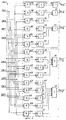
На фиг.1 приведена схема электрическая функциональная предлагаемого устройства выделения маркера кадровой синхронизации.Figure 1 shows the electrical functional diagram of the proposed device highlight marker frame synchronization.
На фиг.2 приведена схема электрическая функциональная элемента первой ступени анализа предлагаемого устройства.Figure 2 shows a diagram of the electrical functional element of the first stage of analysis of the proposed device.
На фиг.3 приведена схема электрическая функциональная элемента второй ступени анализа предлагаемого устройства.Figure 3 shows a diagram of the electrical functional element of the second stage of analysis of the proposed device.
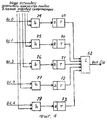
На фиг.4 приведена схема электрическая функциональная элемента конечной ступени анализа предлагаемого устройства.Figure 4 shows a diagram of the electrical functional element of the final stage of analysis of the proposed device.
Предлагаемое устройство выделения маркера кадровой синхронизации (фиг.1) содержит регистр сдвига, выполненный в виде последовательно соединенных четверок D-триггеров, входящих в N элементов первой ступени анализа 1.1, 1.2, 1.3, IN, причем вход регистровой четверки D-триггеров элемента 1.1 является информационным входом устройства, а ее выход является входом регистровой четверки D-триггеров элемента 1.2, выход же регистровой четверки D-триггеров N-го элемента является информационным выходом устройства, каждый из N-элементов первой ступени анализа имеет по четыре входа установки эталонной комбинации маркера, по четыре входа настройки на длину маркера и по пять одноразрядных выходов результатов сравнения символов фрагментов анализируемой входной информационной последовательности и соответствующих символов эталона маркера. Выходы элементов 1.1 и 1.2 первой ступени анализа подключены ко входам элемента 2.1 второй ступени анализа, а выходы элементов 1.3 и 1.4 первой ступени анализа подключены ко входам элемента 2.2 второй ступени анализа. Выходы же элементов 1.(N-1) и 1. N первой ступени анализа подключены ко входам элемента 2. N/2 второй ступени анализа. Каждый из элементов N/2 второй ступени анализа имеет по пять одноразрядных выходов. Выходы элементов 2.1 и 2.2 второй ступени анализа подключены ко входам элемента 3.1 третьей ступени анализа, а выходы элементов 2. N/2-1 и 2N/2 второй ступени анализа подключены к элементу 3 N/4 третьей ступени анализа. Каждый из двух элементов (К-2).1 и (К-2).2 (К-2)-й ступени анализа имеет по десять одноразрядных входов, подключенных к выходам (К-3)-й ступени анализа, и по пять одноразрядных выходов, подключенных ко входам единственного элемента (К-1)-й ступени анализа. Пять одноразрядных выходов элемента К-1 подключены к первым входам конечного анализирующего элемента К, вторые входы которого являются входами установки допустимого количества ошибок в сигнале кадровой синхронизации, а выход является выходом кадрового синхроимпульса.The proposed device for highlighting the frame synchronization marker (Fig. 1) contains a shift register made in the form of series-connected fours of D-flip-flops included in N elements of the first stage of analysis 1.1, 1.2, 1.3, IN, and the input of the register-four of D-flip-flops of element 1.1 is information input of the device, and its output is the input of the register four of D-flip-flops of element 1.2, the output of the register four of D-flip-flops of the Nth element is the information output of the device, each of the N-elements of the first stage of analysis a four input setting reference marker combinations, four input setting by the length of the marker and the five single-symbol outputs comparison results fragments analyzed input information sequence and the corresponding reference symbol marker. The outputs of the elements 1.1 and 1.2 of the first analysis stage are connected to the inputs of the element 2.1 of the second analysis stage, and the outputs of elements 1.3 and 1.4 of the first analysis stage are connected to the inputs of the element 2.2 of the second analysis stage. The outputs of
Все элементы первой ступени анализа выполнены по одной и той же схеме электрической функциональной (фиг.2) и содержат две идентичные схемы I и II блока промежуточного анализа и блок формирования пяти одноразрядных выходов результатов сравнения,All elements of the first stage of analysis are performed according to the same electric functional circuit (Fig. 2) and contain two identical circuits of the I and II intermediate analysis unit and the unit for generating five single-bit outputs of the comparison results,
Схема I блока промежуточного анализа содержит четыре D-триггера 1, 2, 5, 8, три элемента исключающее ИЛИ 3, 4, 7 и два элемента И 6 и 9, причем Д вход триггера 1 является информационным входом элемента первой ступени анализа. Выход D-триггера 1 соединен с D входом D-триггера 2 и первым входом элемента исключающее ИЛИ 3, при этом выход D-триггера 2 соединен с D входом D-триггера 1 схемы II блока промежуточного анализа и первым входом элемента исключающее ИЛИ 4. Вторые входы элементов исключающее ИЛИ 3 и 4 являются входами установки эталонной кодовой комбинации - фрагмента маркера кадровой синхронизации. Выход элемента исключающее ИЛИ 3 соединен с D входом D-триггера 5, прямой выход которого подсоединен к первым входам элемента И 6 и третьего элемента исключающее ИЛИ 7. Выход элемента исключающее ИЛИ 4 соединен с D входом D-триггера 8, прямой выход которого подсоединен ко вторым входам элемента И 6 и третьего элемента исключающее ИЛИ 7. R-входы D-триггеров 5 и 8 являются входами настройки на длину маркера. Инверсные выходы D-триггеров 5 и 8 присоединены ко входам второго элемента И 9, выход которого является промежуточным выходом регистрации совпадения двухбитового фрагмента анализируемой информационной последовательности с соответствующими символами эталона маркера - "ВЫХ. ОП". Выход первого элемента И 6 является промежуточным выходом регистрации несовпадения обоих бит двухбитового фрагмента анализируемой информационной последовательности с соответствующими символами эталона маркера - "ВЫХ. 2П". Выход элемента исключающее ИЛИ 7 является промежуточным выходом регистрации несовпадения одного из двух бит анализируемого фрагмента информационной последовательности с соответствующими символами эталона маркера - "ВЫХ. 1П".Scheme I of the intermediate analysis unit contains four D-flip-
Блок формирования пяти одноразрядных выходов результатов сравнения содержит девятиканальную схему, каждый канал которой содержит последовательно соединенные элемент И и D-триггер и пять элементов ИЛИ. Выход D-триггера 10 первого канала соединен со входом элемента ИЛИ 11, выход которого является выходом регистрации совпадения четырехбитового фрагмента анализируемой информационной последовательности с соответствующими символами эталона маркера - "ВЫХ. О". Выходы D-триггеров 12 и 13 второго и третьего каналов соединены со входами элемента ИЛИ 14, выход которого является выходом регистрации несовпадения одного из четырех бит анализируемого фрагмента информационной последовательности с соответствующими символами эталона маркера - "ВЫХ. 1". Выходы D-триггеров 15, 16 и 17 четвертого, пятого и шестого каналов соединены со входами элемента ИЛИ 18, выход которого является выходом регистрации несовпадения двух из четырех бит анализируемого фрагмента информационной последовательности с соответствующими символами эталона маркера - "ВЫХ. 2". Выходы D-триггеров 19 и 20 седьмого и восьмого каналов соединены со входами элемента ИЛИ 21, выход которого является выходом регистрации несовпадения трех из четырех бит анализируемого фрагмента информационной последовательности с соответствующими символами эталона маркера - "ВЫХ. 3". Выход D-триггера 22 девятого канала соединен со входом элемента ИЛИ 23, выход которого является выходом регистрации несовпадения всех четырех бит анализируемого фрагмента информационной последовательности с соответствующими символами эталона маркера - "ВЫХ. 4".The unit for generating five single-bit outputs of the comparison results contains a nine-channel circuit, each channel of which contains a series-connected And element and a D-trigger and five OR elements. The output of the D-flip-
Первые входы элементов И 24, 25, и 26 первого, третьего и шестого каналов подключены к "ВЫХ. ОП" схемы II блока промежуточного анализа, а первые входы элементов И 27, 28 и 29 второго, пятого и восьмого каналов подключены к "ВЫХ. 1П" той же схемы II блока промежуточного анализа. Первые входы элементов И 30, 31 и 32 четвертого, седьмого и девятого каналов подключены к "ВЫХ. 2П" той же схемы II блока промежуточного анализа. Вторые входы элементов И 19, 21 и 25 первого, второго и четвертого каналов подключены к "ВЫХ. ОП" схемы I блока промежуточного анализа. Вторые входы элементов И 25, 28 и 31 третьего, пятого и седьмого каналов подключены к "ВЫХ. 1П" той же схемы I блока промежуточного анализа. Вторые входы элементов И 26, 29 и 32 шестого, восьмого и девятого каналов подключены к "ВЫХ. 2П" схемы I блока промежуточного анализа, выход второго D-триггера схемы II блока промежуточного анализа является информационным выходом элемента первой ступени анализа - "ВЫХ. ИНФ.".The first inputs of the elements And 24, 25, and 26 of the first, third and sixth channels are connected to the “OUT. OP” circuit II of the intermediate analysis unit, and the first inputs of the elements And 27, 28 and 29 of the second, fifth and eighth channels are connected to the “OUT. 1P "of the same scheme II block of the intermediate analysis. The first inputs of the elements And 30, 31 and 32 of the fourth, seventh and ninth channels are connected to "OUT. 2P" of the same circuit II of the intermediate analysis unit. The second inputs of the elements And 19, 21 and 25 of the first, second and fourth channels are connected to the "EXIT OP" circuit I of the intermediate analysis unit. The second inputs of the elements And 25, 28 and 31 of the third, fifth and seventh channels are connected to "OUT. 1P" of the same circuit I of the intermediate analysis unit. The second inputs of the elements And 26, 29 and 32 of the sixth, eighth and ninth channels are connected to the “EXIT. 2P” circuit I of the intermediate analysis unit, the output of the second D-trigger circuit II of the intermediate analysis unit is the information output of the element of the first analysis stage - “EXIT. INF . ".
Все элементы второй ступени анализа выполнены по одной и той же схеме электрической и функциональной (фиг.3), которая представляет собой блок формирования пяти одноразрядных выходов результатов сравнения.All elements of the second stage of analysis are performed according to the same electrical and functional circuit (Fig. 3), which is a block for the formation of five single-bit outputs of the comparison results.
Блок формирования трех одноразрядных выходов результатов сравнения состоит из шести каналов, каждый из которых содержит последовательно соединенные элемент И и D-триггер, и трех элементов ИЛИ. Выход D-триггера 33 первого канала соединен со входом элемента ИЛИ 34, выход которого является "ВЫХ. 0". Выходы D-триггеров 35, 36 второго и третьего каналов соединены со входами второго элемента ИЛИ 37, выход которого является "ВЫХ. 1". Выходы D-триггеров 38, 39 и 40 четвертого, пятого и шестого каналов соединены со входами третьего элемента ИЛИ 41, выход которого является - "ВЫХ. 2".The block for the formation of three single-bit outputs of the comparison results consists of six channels, each of which contains an And element and a D-trigger connected in series, and three OR elements. The output of the D-flip-
Блок формирования двух одноразрядных выходов результатов сравнения состоит из девяти каналов, каждый из которых содержит последовательно соединенные элемент И и Д-триггер, и двух элементов ИЛИ. Выходы Д-триггеров 42, 43, 44 и 45 седьмого, восьмого, девятого и десятого каналов соединены со входами четвертого элемента ИЛИ 46, выход которого является "ВЫХ. 3". Выходы Д-триггеров 47, 48, 49, 50 и 51 одиннадцатого, двенадцатого, тринадцатого, четырнадцатого и пятнадцатого каналов подсоединены ко входам пятого элемента ИЛИ 52, выход которого является "ВЫХ. 4".The block for the formation of two single-bit outputs of the comparison results consists of nine channels, each of which contains a series-connected element And and D-trigger, and two elements OR. The outputs of the D-flip-
Вход "1ВХ. 0" первой группы входов подключен к первому входу элементов И 53, 54, 55, 56 и 57 первого, третьего, пятого, восьмого и двенадцатого каналов. Вход "1ВХ. 1" первой группы входов подключен к первому входу элементов И 58, 59, 60 и 61 второго, шестого, девятого и тринадцатого каналов. Вход "1.ВХ. 2" первой группы входов подключен к первому входу элементов И 62, 63 и 64 четвертого, десятого и пятнадцатого каналов. Вход "1.ВХ. 3" первой группы входов подключен к первому входу элементов И 65 и 66 седьмого и четырнадцатого каналов. Вход "1.ВХ. 4" первой группы входов подключен к первому входу элемента И 67 одиннадцатого канала. Вход "2.ВХ. 0" второй группы входов подключен ко второму входу элементов И 53, 58, 62, 65 и 67 первого, второго, четвертого, седьмого и одиннадцатого каналов. Вход "2.ВХ.1" второй группы входов подключен ко второму входу элементов И 54, 59, 63 и 66 третьего, шестого, десятого и четырнадцатого каналов. Вход "2.ВХ. 2" второй группы входов подключен ко второму входу элементов И 55, 60 и 64 пятого, девятого и пятнадцатого каналов. Вход "2.ВХ. 3" второй группы входов подключен ко второму входу элементов И 56 и 61 восьмого и тринадцатого каналов. Вход "2.ВХ. 4" второй группы входов подключен ко второму входу элемента И 57 двенадцатого канала.The input "1VX. 0" of the first group of inputs is connected to the first input of the elements And 53, 54, 55, 56 and 57 of the first, third, fifth, eighth and twelfth channels. The input "1BX. 1" of the first group of inputs is connected to the first input of the elements And 58, 59, 60 and 61 of the second, sixth, ninth and thirteenth channels. The input "1.In. 2" of the first group of inputs is connected to the first input of the elements And 62, 63 and 64 of the fourth, tenth and fifteenth channels. The input "1.In. 3" of the first group of inputs is connected to the first input of the elements And 65 and 66 of the seventh and fourteenth channels. The input "1. IN. 4" of the first group of inputs is connected to the first input of the element And 67 of the eleventh channel. Input "2. IN. 0" of the second group of inputs is connected to the second input of the elements And 53, 58, 62, 65 and 67 of the first, second, fourth, seventh and eleventh channels. The input "2.BX.1" of the second group of inputs is connected to the second input of the elements And 54, 59, 63 and 66 of the third, sixth, tenth and fourteenth channels. The input "2.In. 2" of the second group of inputs is connected to the second input of the elements And 55, 60 and 64 of the fifth, ninth and fifteenth channels. The input "2. IN. 3" of the second group of inputs is connected to the second input of the elements And 56 and 61 of the eighth and thirteenth channels. The input "2.In. 4" of the second group of inputs is connected to the second input of the element And 57 of the twelfth channel.
Элемент К-й ступени анализа (фиг.4) содержит блок конечного анализирующего элемента, состоящий из пяти каналов, каждый канал которой содержит последовательно соединенные элемент И и Д-триггер и элемент ИЛИ 68, при этом выходы Д-триггеров 69, 70, 71, 72 и 73 подключены ко входам элемента ИЛИ 68, выход которого является выходом регистрации маркера кадровой синхронизации "ВЫХ. СИ". Входы "ВХ. 0", "ВХ. 1", "BX. 2", "ВХ. 3" и "ВХ. 4" подключены к первым входам элементов И 74, 75, 76, 77 и 78 соответственно первого, второго, третьего, четвертого и пятого каналов, вторые входы которых являются входами установки допустимого количества ошибок в сигнале кадровой синхронизации.The element of the Kth stage of analysis (Fig. 4) contains a block of the final analyzing element, consisting of five channels, each channel of which contains a series-connected element And and D-trigger and element OR 68, while the outputs of D-triggers 69, 70, 71 , 72 and 73 are connected to the inputs of the
Работа устройства рассматривается по схеме электрической функциональной, приведенной на фиг.1.The operation of the device is considered according to the electrical functional diagram shown in figure 1.
Рассмотрение работы устройства выделения маркера кадровой синхронизации проведем в следующей последовательности:An examination of the operation of the frame synchronization marker isolation device will be carried out in the following sequence:
- работа элемента первой ступени анализа;- the work of the element of the first stage of analysis;
- работа элемента второй ступени анализа;- the work of the element of the second stage of analysis;
- работа элемента К-й ступени анализа;- the work of the element of the K-th stage of analysis;
- взаимодействие элементов анализа устройства выделения маркера кадровой синхронизации.- the interaction of the elements of the analysis of the device highlight marker frame synchronization.
Для рассмотрения работы элемента первой ступени анализа воспользуемся фиг.2.To consider the operation of the element of the first stage of analysis, we use figure 2.
Элемент первой ступени анализа содержит две идентичные схемы I и II блока промежуточного анализа и блок формирования пяти одноразрядных выходов результатов сравнения.The element of the first stage of analysis contains two identical schemes I and II of the intermediate analysis unit and the unit for generating five single-bit outputs of the comparison results.
Работу блока промежуточного анализа рассмотрим на примере схемы I блока промежуточного анализа. На D-вход триггера 1 схемы I блока промежуточного анализа подается информационная последовательность, в результате чего в течение первого такта на первых входах элементов исключающее ИЛИ 3, 4 обеих схем промежуточного анализа фиксируется очередной фрагмент входной последовательности из двух бит. На вторых входах элементов исключающее ИЛИ 3, 4 постоянно присутствуют потенциалы, соответствующие двухбитовому фрагменту эталонной четырехбитовой кодовой комбинации маркера. При одновременном совпадении потенциалов на первых и вторых входах обоих элементов исключающее ИЛИ 3, 4 на инверсных выходах триггеров 5 и 8 будут зафиксированы логические единицы и на выходе элементов И 9 - «Вых. ОП» в течение такта будет удерживаться логическая единица, одновременно с которой на выходах элементов 6, 7 («Вых. 1П», «Вых. 2П») будут логические нули.We consider the work of the intermediate analysis unit as an example of the scheme I of the intermediate analysis unit. An information sequence is fed to the D-input of
При одновременном несовпадении потенциалов на первых и вторых входах элементов ИЛИ 3, 4 на прямых входах триггеров 5 и 8 будут зафиксированы логические единицы и на выходе элемента и на входе элемента И 6 - «Вых. 2П» в течение такта будет удерживаться логическая единица, одновременно с которой на выходах элементов 7, 9 («Вых. 0П», «Вых. 1П») будут логические нули.If potentials do not coincide at the first and second inputs of OR
При совпадении потенциалов на первых и вторых входах одного из элементов и несовпадении потенциалов на входах другого элемента ИЛИ 3, 4 на входе элемента исключающее ИЛИ 7 - «Вых 1П» в течение такта будет удерживаться логическая единица, одновременно с которой на выходах элементов И 6, 9 («Вых. 0П», «Вых. 2П») будут логические нули. Если на R-вход триггера 5 подан запирающий потенциал, то на выходе элемента И 6 - «Вых. 2П» будет зафиксирован логический ноль и рассматриваемый элемент первой ступени анализа окажется переведенным в режим анализа однобитового фрагмента входной информационной последовательности.If the potentials coincide at the first and second inputs of one of the elements and the potentials do not coincide at the inputs of the other element OR 3, 4 at the input of the element, the exclusive OR 7 - “Output 1P” during the cycle will hold a logical unit, at the same time at the outputs of the elements And 6, 9 (“Out. 0P”, “Out. 2P”) will be logical zeros. If the locking potential is applied to the R-input of trigger 5, then the output of element And 6 is “Out. 2P ”, a logical zero will be fixed and the considered element of the first stage of analysis will be transferred to the analysis mode of a one-bit fragment of the input information sequence.
Схема II блока промежуточного анализа работает аналогичным образом.Scheme II of the interim analysis unit works in a similar way.
Блок формирования пяти одноразрядных выходов результатов сравнения работает следующим образом.The block for the formation of five single-bit outputs of the comparison results works as follows.
При одновременном появлении на выходах обеих схем блока промежуточного анализа «Вых. 0П» логической единицы, на выходе элемента И 24 установится логическая единица, которая поступит на D-вход триггера 10. При этом на выходе элемента ИЛИ 11 («Вых. 0») в течение такта будет удерживаться логическая единица, что будет свидетельствовать о совпадении четырехбитового фрагмента анализируемой информационной последовательности с соответствующими символами эталона маркера.With the simultaneous appearance at the outputs of both circuits of the block of intermediate analysis “Exit. 0P ”of a logical unit, the logical unit will be set at the output of the AND 24 element, which will go to the D-input of
При одновременном появлении на выходах «Вых. 0П» схемы I блока промежуточного анализа и «Вых. 1П» схемы II блока промежуточного анализа логической единицы, на выходе элемента И 25 установится логическая единица, которая поступит на D-вход триггера 13. При этом на выходе элемента ИЛИ 14 («Вых. 1») в течение такта будет удерживаться логическая единица. Точно к тому же результату приведет одновременное появление логической единицы на выходах «Вых. 0П» схемы II блока промежуточного анализа и «Вых. 1П» схемы I блока промежуточного анализа. Это будет свидетельствовать о несовпадении одного из четырех бит анализируемого фрагмента информационной последовательности с соответствующими символами эталона маркера.With the simultaneous appearance on the outputs of "Exit. 0P "scheme I block intermediate analysis and" Out. 1P ”of the circuit II of the block of intermediate analysis of the logical unit, the logical unit will be installed at the output of the AND 25 element, which will go to the D-input of the
При одновременном появлении на выходах «Вых. 0П» схемы I блока промежуточного анализа и «Вых. 2П» схемы II блока промежуточного анализа логической единицы, на выходе элемента И 26 установится логическая единица, которая поступит на D-вход триггера 17. При этом на выходе элемента ИЛИ 18 («Вых. 2») в течение такта будет удерживаться логическая единица. Точно к тому же результату приведет одновременное появление логической единицы на выходах «Вых. 0П» схемы II блока промежуточного анализа и «Вых. 2П» схемы I блока промежуточного анализа или на выходах «Вых. 1П» обеих схем блока промежуточного анализа. Это будет свидетельствовать о несовпадении двух из четырех бит анализируемого фрагмента информационной последовательности с соответствующими символами эталона маркера.With the simultaneous appearance on the outputs of "Exit. 0P "scheme I block intermediate analysis and" Out. 2P ”of the circuit II of the intermediate unit of analysis of the logical unit, the logical unit will be installed at the output of the And 26 element, which will go to the D-input of the
При одновременном появлении на выходах «Вых. 1П» схемы I блока промежуточного анализа и «Вых. 2П» схемы II блока промежуточного анализа логической единицы, на выходе элемента И 29 установится логическая единица, которая поступит на D-вход триггера 20. При этом на выходе элемента ИЛИ 21 («Вых. 3») в течение такта будет удерживаться логическая единица. Точно к тому же результату приведет одновременное появление логической единицы на выходах «Вых. 1П» схемы II блока промежуточного анализа и «Вых. 2П» схемы I блока промежуточного анализа 1. Это будет свидетельствовать о несовпадении трех из четырех бит анализируемого фрагмента информационной последовательности с соответствующими символами эталона маркера.With the simultaneous appearance on the outputs of "Exit. 1P "scheme I block intermediate analysis and" Out. 2P ”of circuit II of the block of intermediate analysis of the logical unit, the logical unit will be installed at the output of the And 29 element, which will be fed to the D-input of the
При одновременном появлении на выходах обеих схем блока промежуточного анализа «Вых. 2П» логической единицы на выходе элемента И 32 установится логическая единица, которая поступит на D-вход триггера 22. При этом на выходе элемента ИЛИ 23 («Вых. 4») в течение такта будет удерживаться логическая единица, что будет свидетельствовать о несовпадении всех четырех бит анализируемого фрагмента информационной последовательности с соответствующими символами эталона маркера.With the simultaneous appearance at the outputs of both circuits of the block of intermediate analysis “Exit. 2P ”logical unit at the output of the And 32 element will be set to a logical unit that will go to the D-input of
Для рассмотрения работы элемента второй ступени анализа воспользуемся фиг.3.To consider the operation of the element of the second stage of analysis, we use figure 3.
На входы «1 Вх. 0», «1 Вх. 1», «1 Вх. 2», «1 Вх. 3», «1 Bx. 4» поступают сигналы от соответствующих выходов первого элемента первой ступени анализа, на входы «2 Вх. 0», «2 Вх. 1», «2 Вх. 2», «2 Вх. 3», «2 Вх. 4» поступают сигналы от соответствующих выходов второго элемента первой ступени анализа.At the inputs of "1 Entrance. 0 "," 1 In. 1 "," 1 In. 2 "," 1 Entry. 3 "," 1 Bx. 4 "receives signals from the corresponding outputs of the first element of the first stage of analysis, to the inputs of" 2 In. 0 "," 2 In. 1 "," 2 In. 2 "," 2 Entry. 3 "," 2 Entry. 4 ”signals from the corresponding outputs of the second element of the first stage of analysis are received.
При одновременном появлении на входах «1 Вх. 0» и «2 Вх. 0» логической единицы на выходе элемента И 53 установится логическая единица, которая и поступит на D-вход триггера 33. При этом на выходе элемента ИЛИ 34 («Вых. 0») в течение такта будет удерживаться логическая единица, что будет свидетельствовать об отсутствии отличий двух смежных фрагментов анализируемой последовательности и соответствующих фрагментов эталона маркера.With the simultaneous appearance at the inputs of "1 Vh. 0 ”and“ 2 In. 0 ”of a logical unit at the output of AND 53 element will be set to a logical unit that will go to the D-input of
При одновременном появлении на входах «1 Вх. 0» и «2 Вх. 1» логической единицы на выходе элемента И 54 установится логическая единица, которая и поступит на D-вход триггера 36. При этом на выходе элемента ИЛИ 73 («Вых. 1») в течение такта будет удерживаться логическая единица. Точно к такому же результату приведет появление логической единицы на входах «1 Вх. 1» и «2 Вх. 0». Последнее будет свидетельствовать об отличии в одном бите двух смежных фрагментов анализируемой последовательности и соответствующих фрагментов эталона маркера.With the simultaneous appearance at the inputs of "1 Vh. 0 ”and“ 2 In. 1 ”of a logical unit at the output of AND
При одновременном появлении на входах «1 Вх. 0» и «2 Вх. 2» логической единицы на выходе элемента И 55 установится логическая единица, которая и поступит на D-вход триггера 39. При этом на выходе элемента ИЛИ 41 («Вых. 2») в течение такта будет удерживаться логическая единица. Точно к такому же результату приведет появление логической единицы на входах «1 Вх. 2» и «2 Вх. 0» или «1 Вх. 1» и «2 Вх. 1». Последнее будет свидетельствовать об отличии в двух битах двух смежных фрагментов анализируемой последовательности и соответствующих фрагментов эталона маркера.With the simultaneous appearance at the inputs of "1 Vh. 0 ”and“ 2 In. 2 ”logical unit at the output of the AND 55 element, a logical unit will be established, which will go to the D-input of the
При одновременном появлении на входах «1 Вх. 1» и «2 Вх. 2» логической единицы на выходе элемента И 60 установится логическая единица, которая и поступит на D-вход триггера 44. При этом на выходе элемента ИЛИ 46 («Вых. 3») в течение такта будет удерживаться логическая единица. Точно к такому же результату приведет появление логической единицы на входах «1 Вх. 3» и «2 Вх. 0», «1 Вх. 0» и «2 Вх. 3» или «1 Вх. 2» и «2 Вх. 1». Последнее будет свидетельствовать об отличии в двух битах двух смежных фрагментов анализируемой последовательности и соответствующих фрагментов эталона маркера.With the simultaneous appearance at the inputs of "1 Vh. 1 "and" 2 Entry. 2 ”of a logical unit at the output of AND
При одновременном появлении на входах «1 Вх. 0» и «2 Вх. 4» логической единицы на выходе элемента И 57 установится логическая единица, которая и поступит на D-вход триггера 48. При этом на выходе элемента ИЛИ 52 («Вых. 4») в течение такта будет удерживаться логическая единица. Точно к такому же результату приведет появление логической единицы на входах «1 Вх. 4» и «2 Вх. 0», «1 Вх. 1» и «2 Вх. 3» «1 Вх. 3» «2 Вх. 1» или «1 Вх. 2» и «2 Вх. 2». Последнее будет свидетельствовать об отличии в трех битах двух смежных фрагментов анализируемой последовательности и соответствующих фрагментов эталона маркера.With the simultaneous appearance at the inputs of "1 Vh. 0 ”and“ 2 In. 4 ”of a logical unit at the output of AND
При одновременном появлении на входах «1 Вх. 1» и «2 Вх. 4» логической единицы, на выходе элемента ИЛИ 34, 37, 41, 46, 52 («Вых 0», «Вых. 1», «Вых 2», «Вых.3», «Вых. 4» в течение такта будут удерживаться логические нули. Точно к такому же результату приведет появление логической единицы на входах «1 Вх. 4» и «2 Вх. 1», «1 Вх. 4» и «2 Вх. 1», «1 Вх. 4» и «2 Вх. 2», «1 Вх. 4» и «2 Вх 3», «1 Вх 4» и «2 Вх. 4», «2 Вх. 4» и «1 Вх. 2».или «2 Вх. 4» и «1 Вх. 3». Последнее будет свидетельствовать о том, что отличия двух смежных фрагментов анализируемой последовательности и соответствующих фрагментов эталона маркера превышают допустимые четыре бита. Если рассматриваемый элемент анализа используется на третьей, ..., К-й ступени анализа, то возможна ситуация, при которой одновременно на все пять входов «1 Вх. 0», «1 Вх. 1», «1 Вх. 2», «1 Вх. 3», «1 Вх. 4» или одновременно на другие пять входов «2 Вх. 0», «2 Вх. 1», «2 Вх. 2», «3 Вх. 3», «2 Вх. 4» поступит логический ноль, в этом случае на выходах элементов ИЛИ 34, 37, 41, 46, 52 ("Вых. 0», "Вых. 1", "Вых. 2", "Вых. 3", "Вых. 4") в течение такта будут удерживаться логические нули. Последнее будет свидетельствовать о том, что отличия двух смежных фрагментов анализируемой последовательности и соответствующих фрагментов эталона маркера превышают допустимые четыре бита. То есть если отличия двух смежных фрагментов эталона маркера меньше или равны четырем битам, на одном из выходов рассматриваемого элемента («Вых. 0», «Вых. 1», «Вых. 2», «Вых. 3», «Вых. 4») будет присутствовать логический ноль.With the simultaneous appearance at the inputs of "1 Vh. 1 "and" 2 Entry. 4 ”logical units, at the output of the
Для рассмотрения работы элемента К-й ступени анализа воспользуемся фиг.4.To consider the operation of the element of the Kth step of the analysis, we use Fig. 4.
Предположим допустимое количество ошибок в сигнале кадровой синхронизации равно четырем, в этом случае на первые входы элементов И 74, 75, 76, 77, 78 («Вх. 0», «Вх. 1», «Вх. 2», «Вх. 3», «Вх. 4») поступают сигналы от соответствующих выходов элемента (К-1)-й ступени анализа, которые через триггеры 69, 70, 71, 72, 73 попадают на входы элемента ИЛИ 68. При этом если на одном из пяти входов («Вх. 0», «Вх. 1», «Вх. 2», «Вх. 3», «Вх. 4») появится единица, то на выходе элемента ИЛИ 68 в течение такта будет удерживаться логическая единица, которая и будет служить кадровым синхроимпульсом. Если же одновременно на всех пяти входах («Вх. 0», «Вх. 1», «Вх. 2», «Вх. 3», «Вх. 4») будут логические нули, то и на выходе элемента ИЛИ 68 будет логический ноль, что интерпретируется как отсутствие маркера кадровой синхронизации. Предположим допустимое количество ошибок в сигнале кадровой синхронизации равно единице, в этом случае на первые входы элементов И 74, 75, 76, 77 подаются потенциалы, соответствующие логической единице, а на первый вход элемента И 78 подается логический ноль. При этом «Вх. 4» оказывается заблокированным элементом И 78 и кадровый синхроимпульс на выходе элемента ИЛИ 68 появляется только в случае появления логической единицы на одном из входов «Вх. 0», «Вх. 1», «Вх. 2», «Вх. 3». Если мы хотим формировать кадровый синхроимпульс лишь в случае обнаружения безошибочной комбинации маркера кадровой синхронизации, то на первые входы элементов И 75, 76, 77, 78 необходимо подать потенциалы, соответствующие логическому нулю, а на первый вход элемента И 74 - логическую единицу. При этом элементы И 75, 76, 77, 78 заблокируют входы «Вх. 1», «Вх. 2», «Вх. 3», «Вх. 4» и кадровый синхроимпульс на выходе элемента ИЛИ 68 будет регистрироваться лишь при появлении логической единицы на входе «Вх. 0».Suppose the permissible number of errors in the frame synchronization signal is four, in this case, the first inputs of the elements AND 74, 75, 76, 77, 78 ("Input 0", "
Для рассмотрения элементов анализа устройства выделения маркера кадровой синхронизации воспользуемся фиг.1.To consider the elements of the analysis of the device for selecting the marker frame synchronization, we use figure 1.
Предположим, что анализируемый фрагмент информационного потока, находящийся в регистре, входящем в элементы первой ступени анализа 1.1, ..., 1.N, отличается от эталона маркера лишь в последнем и пятом от конца фрагмента битах. В этом случае у элементов 1.1 и 1.2 логическая единица будет присутствовать на выходах «Вых. 1», а у элементов 1.3, ..., 1.N логические единицы появятся на выходах «Вых. 0», все остальные выходы элементов первой ступени анализа содержат логические нули. Такому состоянию выходов элементов первой ступени анализа будет соответствовать появление логической единицы на выходе «Вых. 2» элемента 2.1 и логических единиц на выходах «Вых. 0» элементов 2.2, ..., 2.N/2, при логических нулях на всех остальных выходах элементов второй ступени анализа. При этом на выходе «Вых. 2» элемента 3.1 появится логическая единица, у элементов 3.2, ..., 3.N/4 логические единицы будут на выходах «Вых. 0», а на всех остальных выходах третьей ступени анализа будут присутствовать логические нули. Такое состояние выходов третьей ступени анализа приведет к тому, что у элемента (К-2).1 логическая единица появится на выходе «Вых. 2», а у элемента (К-2).2 логическая единица будет на выходе «Вых. 0» при логических нулях на всех остальных выходах (К-2)-й ступени анализа. При этом у элемента (К-1)-й ступени анализа логическая единица появится на выходе «Вых. 2» и логические нули на выходах «Вых. 0», «Вых. 1». Если задаваемое входами установки допустимое количество ошибок в сигнале кадровой синхронизации равно двум, то при описанном состоянии выходов устройства на выходе К-го элемента появится кадровый синхроимпульс, если же допустимое количество ошибок в сигнале кадровой синхронизации равно нулю или единице, то кадровый синхроимпульс на выходе К-го элемента не появится.Suppose that the analyzed fragment of the information stream located in the register included in the elements of the first stage of analysis 1.1, ..., 1.N differs from the marker standard only in the last and fifth bits from the end of the fragment. In this case, for elements 1.1 and 1.2, a logical unit will be present at the outputs “Out. 1 ”, and for elements 1.3, ..., 1.N, logical units will appear on the outputs“ Out. 0 ”, all other outputs of the elements of the first stage of analysis contain logical zeros. This state of outputs of the elements of the first stage of the analysis will correspond to the appearance of a logical unit at the output of "Output. 2 "element 2.1 and logical units at the outputs" Out. 0 ”elements 2.2, ..., 2.N / 2, with logical zeros at all other outputs of the elements of the second stage of analysis. In this case, the output “Out. 2 ”of element 3.1, a logical unit will appear, for elements 3.2, ..., 3.N / 4, logical units will be at the outputs“ Out. 0 ”, and on all other outputs of the third stage of the analysis there will be logical zeros. This state of the outputs of the third stage of analysis will lead to the fact that the element (K-2) .1 logical unit will appear at the output "Output. 2 ", and the element (K-2) .2 logical unit will be at the output of" Exit. 0 ”with logical zeros at all other outputs of the (K-2) -th stage of analysis. At the same time, the logical unit of the element (K-1) of the analysis step appears at the output “Out. 2 "and logical zeros at the outputs" Out. 0 "," Out. one". If the permissible number of errors in the frame synchronization signal specified by the installation inputs is equal to two, then with the described state of the device outputs, a frame clock will appear at the output of the Kth element, but if the permissible number of errors in the frame synchronization signal is zero or one, then the frame clock at the output K th element will not appear.
Предположим, что анализируемый фрагмент информационного потока, находящийся в регистре, входящем в элементы первой ступени анализа 1.1, ..., 1.N, отличается от эталона маркера лишь последними пятью от конца фрагментами битов. В этом случае у элемента 1.1 логическая единица будет присутствовать на выходе «Вых. 2», у элемента 1.2 логическая единица будет на выходе «Вых. 1», у элементов 1.3, ..., 1.N логические единицы появятся на выходах «Вых. 0», а все остальные выходы элементов первой ступени анализа содержат логические нули. Такому состоянию выходов элементов первой ступени анализа будет соответствовать отсутствие единиц на всех пяти выходах («Вых. 0», «Вых. 1», «Вых. 2», «Вых. 3», «Вых. 4») элемента 2.1, что приведет к появлению логических нулей на всех выходах элементов 3.1, ..., (K-2).1, (K-1), и как следствие этого к логическому нулю на выходе К-го элемента, т.е. кадровый синхроимпульс будет отсутствовать.Suppose that the analyzed fragment of the information stream located in the register included in the elements of the first stage of analysis 1.1, ..., 1.N differs from the marker standard only in the last five bits from the end of the bits. In this case, the element 1.1 logical unit will be present at the output "Out. 2 ", at element 1.2 the logical unit will be at the output" Exit. 1 ”, for elements 1.3, ..., 1.N, logical units will appear on the outputs“ Out. 0 ”, and all other outputs of the elements of the first stage of the analysis contain logical zeros. This state of the outputs of the elements of the first stage of analysis will correspond to the absence of units at all five outputs (“Out. 0”, “Out. 1”, “Out. 2”, “Out. 3”, “Out. 4”) of element 2.1, which will lead to the appearance of logical zeros at all outputs of the elements 3.1, ..., (K-2) .1, (K-1), and as a result, to logical zero at the output of the Kth element, i.e. there will be no frame sync.
Для повышения быстродействия устройства в каждый элемент анализа включены Д-триггеры, которые осуществляют привязку к тактовой частоте сигнала. При таком построении устройства его совокупное быстродействие не зависит от количества входящих в него элементов анализа. Однако при этом следует иметь в виду, что момент фиксации анализируемого фрагмента информационной последовательности в регистре сдвига первой ступени анализа отделен от момента завершения анализа этого фрагмента К тактами.To increase the speed of the device, D-triggers are included in each analysis element, which are linked to the clock frequency of the signal. With this construction of the device, its aggregate performance does not depend on the number of analysis elements included in it. However, it should be borne in mind that the moment of fixation of the analyzed fragment of the information sequence in the shift register of the first stage of the analysis is separated from the moment of completion of the analysis of this fragment With clock cycles.
Результаты испытания макета, реализованного на современной высокоинтегрированной и высокоскоростной базе с использованием перепрограммируемых логических интегральных схем (ПЛИС), подтвердили его высокую помехоустойчивость, обеспечивающую возможность выделения маркера кадровой синхронизации при отношении сигнал к шуму не менее 7 дБ в информационной последовательности, передаваемой со скоростью 120 Мбит/с.The test results of the prototype, implemented on a modern, highly integrated and high-speed base using reprogrammable logic integrated circuits (FPGA), confirmed its high noise immunity, providing the possibility of highlighting the frame synchronization marker with a signal to noise ratio of at least 7 dB in the information sequence transmitted at a speed of 120 Mbps /from.
ЛитератураLiterature
1. Способ выделения маркера кадровой синхронизации и устройство для его осуществления. АС №1821931, Россия, МКИ Н04L 7/4, заявка №4754998/09, заявл. 30.10.1989; Н.Е.Патонов, А.Н.Дядюнов, А.Н.Дятлов, А.Н.Кантор, М.Л.Платонова.1. The method of selection marker frame synchronization and a device for its implementation. AC No. 1821931, Russia,
2. Способ выделения маркера кадровой синхронизации и устройство для его осуществления. АС №1821932, Россия, МКИ H04L 7/4, заявка №4755121/09, заявл. 30.10.1989; Н.Е.Патонов, Ю.Р.Салихов, А.Н., А.Н.Дядюнов, А.Н.Дятлов, А.Н.Кантор.2. A method of allocating marker frame synchronization and a device for its implementation. AC No. 1821932, Russia,
3. Способ выделения маркера кадровой синхронизации и устройство для его осуществления. Патент №2158483, Россия.3. A method for allocating a frame synchronization marker and a device for its implementation. Patent No. 2158483, Russia.
Claims (1)
Priority Applications (1)
| Application Number | Priority Date | Filing Date | Title |
|---|---|---|---|
| RU2004135612/09A RU2297103C2 (en) | 2004-12-06 | 2004-12-06 | Marker separating device for frame synchronization system |
Applications Claiming Priority (1)
| Application Number | Priority Date | Filing Date | Title |
|---|---|---|---|
| RU2004135612/09A RU2297103C2 (en) | 2004-12-06 | 2004-12-06 | Marker separating device for frame synchronization system |
Publications (2)
| Publication Number | Publication Date |
|---|---|
| RU2004135612A RU2004135612A (en) | 2006-05-20 |
| RU2297103C2 true RU2297103C2 (en) | 2007-04-10 |
Family
ID=36657985
Family Applications (1)
| Application Number | Title | Priority Date | Filing Date |
|---|---|---|---|
| RU2004135612/09A RU2297103C2 (en) | 2004-12-06 | 2004-12-06 | Marker separating device for frame synchronization system |
Country Status (1)
| Country | Link |
|---|---|
| RU (1) | RU2297103C2 (en) |
Citations (2)
| Publication number | Priority date | Publication date | Assignee | Title |
|---|---|---|---|---|
| US3760355A (en) * | 1972-03-08 | 1973-09-18 | Motorola Inc | Digital pattern detector |
| RU2158483C2 (en) * | 1996-05-21 | 2000-10-27 | Ростовский научно-исследовательский институт радиосвязи | Method for detection of frame synchronization marker and device which implements said method |
-
2004
- 2004-12-06 RU RU2004135612/09A patent/RU2297103C2/en not_active IP Right Cessation
Patent Citations (2)
| Publication number | Priority date | Publication date | Assignee | Title |
|---|---|---|---|---|
| US3760355A (en) * | 1972-03-08 | 1973-09-18 | Motorola Inc | Digital pattern detector |
| RU2158483C2 (en) * | 1996-05-21 | 2000-10-27 | Ростовский научно-исследовательский институт радиосвязи | Method for detection of frame synchronization marker and device which implements said method |
Also Published As
| Publication number | Publication date |
|---|---|
| RU2004135612A (en) | 2006-05-20 |
Similar Documents
| Publication | Publication Date | Title |
|---|---|---|
| US5200979A (en) | High speed telecommunication system using a novel line code | |
| US4506372A (en) | Method and apparatus for recognizing in a receiver the start of a telegram signal consisting of a bit impulse sequence | |
| KR100336496B1 (en) | Method and apparatus for encoding MB810 line code with the characteristics of minimum bandwidth and DC-free | |
| US6232895B1 (en) | Method and apparatus for encoding/decoding n-bit data into 2n-bit codewords | |
| US8411782B2 (en) | Parallel generation and matching of a deskew channel | |
| US4829300A (en) | Signal generation | |
| US20030161429A1 (en) | Device and method for comma detection and word alignment in serial transmission | |
| JPS6247008B2 (en) | ||
| US3588364A (en) | Adaptive encoder and decoder | |
| US4352129A (en) | Digital recording apparatus | |
| RU2297103C2 (en) | Marker separating device for frame synchronization system | |
| RU2158483C2 (en) | Method for detection of frame synchronization marker and device which implements said method | |
| US3277462A (en) | Parallel-parallel encoding system | |
| JPS607251A (en) | System and apparatus of differential coding | |
| US5548531A (en) | Optical processing system | |
| US6198755B1 (en) | Time multiplexing/demultiplexing method | |
| US5329280A (en) | Adjacent code system | |
| US7123173B1 (en) | Method and system for a feed-forward encoder | |
| US7869107B2 (en) | Optical circuit for comparing two N-bit binary words | |
| US3562433A (en) | Digital speech plus telegraph system | |
| GB1560190A (en) | Device for detecting errors in a digital transmission system | |
| SU1711342A1 (en) | Frame synchronization method and system thereof | |
| CA1074920A (en) | Detection of errors in digital signals | |
| US4852097A (en) | Method for forming data block protection information for serial data bit sequences by means of cyclical binary codes | |
| SU1533013A1 (en) | Discrete information transmission system |
Legal Events
| Date | Code | Title | Description |
|---|---|---|---|
| MM4A | The patent is invalid due to non-payment of fees |
Effective date: 20101207 |