RU2287205C2 - Integrated transistor/memory structures and array of such matrix-addressing structures - Google Patents
Integrated transistor/memory structures and array of such matrix-addressing structures Download PDFInfo
- Publication number
- RU2287205C2 RU2287205C2 RU2004120776/28A RU2004120776A RU2287205C2 RU 2287205 C2 RU2287205 C2 RU 2287205C2 RU 2004120776/28 A RU2004120776/28 A RU 2004120776/28A RU 2004120776 A RU2004120776 A RU 2004120776A RU 2287205 C2 RU2287205 C2 RU 2287205C2
- Authority
- RU
- Russia
- Prior art keywords
- transistor
- electrode
- electrodes
- memory
- source
- Prior art date
Links
Images
Classifications
-
- H—ELECTRICITY
- H01—ELECTRIC ELEMENTS
- H01L—SEMICONDUCTOR DEVICES NOT COVERED BY CLASS H10
- H01L21/00—Processes or apparatus adapted for the manufacture or treatment of semiconductor or solid state devices or of parts thereof
- H01L21/70—Manufacture or treatment of devices consisting of a plurality of solid state components formed in or on a common substrate or of parts thereof; Manufacture of integrated circuit devices or of parts thereof
- H01L21/77—Manufacture or treatment of devices consisting of a plurality of solid state components or integrated circuits formed in, or on, a common substrate
-
- H—ELECTRICITY
- H01—ELECTRIC ELEMENTS
- H01L—SEMICONDUCTOR DEVICES NOT COVERED BY CLASS H10
- H01L27/00—Devices consisting of a plurality of semiconductor or other solid-state components formed in or on a common substrate
- H01L27/02—Devices consisting of a plurality of semiconductor or other solid-state components formed in or on a common substrate including semiconductor components specially adapted for rectifying, oscillating, amplifying or switching and having at least one potential-jump barrier or surface barrier; including integrated passive circuit elements with at least one potential-jump barrier or surface barrier
- H01L27/04—Devices consisting of a plurality of semiconductor or other solid-state components formed in or on a common substrate including semiconductor components specially adapted for rectifying, oscillating, amplifying or switching and having at least one potential-jump barrier or surface barrier; including integrated passive circuit elements with at least one potential-jump barrier or surface barrier the substrate being a semiconductor body
- H01L27/08—Devices consisting of a plurality of semiconductor or other solid-state components formed in or on a common substrate including semiconductor components specially adapted for rectifying, oscillating, amplifying or switching and having at least one potential-jump barrier or surface barrier; including integrated passive circuit elements with at least one potential-jump barrier or surface barrier the substrate being a semiconductor body including only semiconductor components of a single kind
- H01L27/085—Devices consisting of a plurality of semiconductor or other solid-state components formed in or on a common substrate including semiconductor components specially adapted for rectifying, oscillating, amplifying or switching and having at least one potential-jump barrier or surface barrier; including integrated passive circuit elements with at least one potential-jump barrier or surface barrier the substrate being a semiconductor body including only semiconductor components of a single kind including field-effect components only
- H01L27/088—Devices consisting of a plurality of semiconductor or other solid-state components formed in or on a common substrate including semiconductor components specially adapted for rectifying, oscillating, amplifying or switching and having at least one potential-jump barrier or surface barrier; including integrated passive circuit elements with at least one potential-jump barrier or surface barrier the substrate being a semiconductor body including only semiconductor components of a single kind including field-effect components only the components being field-effect transistors with insulated gate
- H01L27/092—Devices consisting of a plurality of semiconductor or other solid-state components formed in or on a common substrate including semiconductor components specially adapted for rectifying, oscillating, amplifying or switching and having at least one potential-jump barrier or surface barrier; including integrated passive circuit elements with at least one potential-jump barrier or surface barrier the substrate being a semiconductor body including only semiconductor components of a single kind including field-effect components only the components being field-effect transistors with insulated gate complementary MIS field-effect transistors
-
- H—ELECTRICITY
- H01—ELECTRIC ELEMENTS
- H01L—SEMICONDUCTOR DEVICES NOT COVERED BY CLASS H10
- H01L21/00—Processes or apparatus adapted for the manufacture or treatment of semiconductor or solid state devices or of parts thereof
- H01L21/70—Manufacture or treatment of devices consisting of a plurality of solid state components formed in or on a common substrate or of parts thereof; Manufacture of integrated circuit devices or of parts thereof
- H01L21/77—Manufacture or treatment of devices consisting of a plurality of solid state components or integrated circuits formed in, or on, a common substrate
- H01L21/78—Manufacture or treatment of devices consisting of a plurality of solid state components or integrated circuits formed in, or on, a common substrate with subsequent division of the substrate into plural individual devices
- H01L21/82—Manufacture or treatment of devices consisting of a plurality of solid state components or integrated circuits formed in, or on, a common substrate with subsequent division of the substrate into plural individual devices to produce devices, e.g. integrated circuits, each consisting of a plurality of components
- H01L21/822—Manufacture or treatment of devices consisting of a plurality of solid state components or integrated circuits formed in, or on, a common substrate with subsequent division of the substrate into plural individual devices to produce devices, e.g. integrated circuits, each consisting of a plurality of components the substrate being a semiconductor, using silicon technology
- H01L21/8232—Field-effect technology
- H01L21/8234—MIS technology, i.e. integration processes of field effect transistors of the conductor-insulator-semiconductor type
- H01L21/8238—Complementary field-effect transistors, e.g. CMOS
- H01L21/823807—Complementary field-effect transistors, e.g. CMOS with a particular manufacturing method of the channel structures, e.g. channel implants, halo or pocket implants, or channel materials
-
- H—ELECTRICITY
- H01—ELECTRIC ELEMENTS
- H01L—SEMICONDUCTOR DEVICES NOT COVERED BY CLASS H10
- H01L21/00—Processes or apparatus adapted for the manufacture or treatment of semiconductor or solid state devices or of parts thereof
- H01L21/70—Manufacture or treatment of devices consisting of a plurality of solid state components formed in or on a common substrate or of parts thereof; Manufacture of integrated circuit devices or of parts thereof
- H01L21/77—Manufacture or treatment of devices consisting of a plurality of solid state components or integrated circuits formed in, or on, a common substrate
- H01L21/78—Manufacture or treatment of devices consisting of a plurality of solid state components or integrated circuits formed in, or on, a common substrate with subsequent division of the substrate into plural individual devices
- H01L21/82—Manufacture or treatment of devices consisting of a plurality of solid state components or integrated circuits formed in, or on, a common substrate with subsequent division of the substrate into plural individual devices to produce devices, e.g. integrated circuits, each consisting of a plurality of components
- H01L21/822—Manufacture or treatment of devices consisting of a plurality of solid state components or integrated circuits formed in, or on, a common substrate with subsequent division of the substrate into plural individual devices to produce devices, e.g. integrated circuits, each consisting of a plurality of components the substrate being a semiconductor, using silicon technology
- H01L21/8232—Field-effect technology
- H01L21/8234—MIS technology, i.e. integration processes of field effect transistors of the conductor-insulator-semiconductor type
- H01L21/8238—Complementary field-effect transistors, e.g. CMOS
- H01L21/823828—Complementary field-effect transistors, e.g. CMOS with a particular manufacturing method of the gate conductors, e.g. particular materials, shapes
Abstract
Description
Область техники, к которой относится изобретениеFIELD OF THE INVENTION
Настоящее изобретение относится к интегрированным транзисторно/запоминающим структурам, содержащим один или более слоев полупроводникового материала, два или более электродных слоев, а также контактирующий с электродами, находящимися в указанных, по меньшей мере, двух электродных слоях, и запоминающий материал. При этом запоминающий материал представляет собой поляризуемый диэлектрический материал, способный проявлять гистерезисные свойства, преимущественно ферроэлектрический или электретный материал. Электроды в каждом из, по меньшей мере, двух электродных слоев выполнены в виде протяженных параллельных структур, не имеющих разрывов. По меньшей мере, один слой полупроводникового материала и, по меньшей мере, два электродных слоя формируют структуру полевого транзистора. При этом электроды первого электродного слоя образуют одну пару электродов истока и стока указанной структуры полевого транзистора, а электрод смежного второго электродного слоя формирует электрод затвора указанной структуры полевого транзистора, ориентированный, по существу, ортогонально электродам первого электродного слоя.The present invention relates to integrated transistor / memory structures containing one or more layers of semiconductor material, two or more electrode layers, and also in contact with electrodes located in said at least two electrode layers, and a storage material. In this case, the storage material is a polarizable dielectric material capable of exhibiting hysteretic properties, mainly a ferroelectric or electret material. The electrodes in each of the at least two electrode layers are made in the form of extended parallel structures that do not have gaps. At least one layer of semiconductor material and at least two electrode layers form the structure of a field effect transistor. In this case, the electrodes of the first electrode layer form one pair of source and drain electrodes of the indicated field-effect transistor structure, and the electrode of the adjacent second electrode layer forms a gate electrode of the indicated field-effect transistor structure, oriented essentially orthogonally to the electrodes of the first electrode layer.
Изобретение относится также к массиву (набору) подобных транзисторно/запоминающих структур с матричной адресацией. Данный массив содержит один или более слоев полупроводникового материала, два или более электродных слоев, а также запоминающий материал, контактирующий с электродами, находящимися в указанных, по меньшей мере, двух электродных слоях. При этом запоминающий материал представляет собой поляризуемый диэлектрический материал, способный проявлять гистерезисные свойства, преимущественно ферроэлектрический или электретный материал. Электроды в каждом из, по меньшей мере, двух электродных слоев выполнены в виде протяженных параллельных структур, не имеющих разрывов. По меньшей мере, один слой полупроводникового материала и, по меньшей мере, два электродных слоя формируют структуры полевых транзисторов. При этом электроды первого электродного слоя образуют пары электродов истока и стока указанных структур полевых транзисторов, а электроды смежного второго электродного слоя формируют электроды затвора указанных структур полевых транзисторов. Данные электроды затвора ориентированы, по существу, ортогонально электродам первого электродного слоя.The invention also relates to an array (set) of such transistor / memory structures with matrix addressing. This array contains one or more layers of semiconductor material, two or more electrode layers, as well as storage material in contact with the electrodes located in the specified at least two electrode layers. In this case, the storage material is a polarizable dielectric material capable of exhibiting hysteretic properties, mainly a ferroelectric or electret material. The electrodes in each of the at least two electrode layers are made in the form of extended parallel structures that do not have gaps. At least one layer of semiconductor material and at least two electrode layers form field-effect transistor structures. In this case, the electrodes of the first electrode layer form pairs of source and drain electrodes of the indicated field-effect transistor structures, and the electrodes of the adjacent second electrode layer form the gate electrodes of the indicated field-effect transistor structures. These gate electrodes are oriented substantially orthogonally to the electrodes of the first electrode layer.
Уровень техникиState of the art
Серьезная проблема современной вычислительной техники заключается в наличии физического разрыва между устройствами хранения данных и процессорными блоками, в частности между центральными процессорами (ЦП) и системным программным обеспечением, программными средствами пользователя, а также данными пользователя. Недавние достижения, касающиеся реального быстродействия ЦП (начиная с процессоров Pentium II и далее), стали возможными благодаря интегрированию больших объемов памяти внутри ЦП за счет использования модулей SRAM/EEPROM (Static Random Access Memory/Electrically Erasable Programmable Read-Only Memory). Однако итоговая скорость по-прежнему сильно ограничивается тем фактом, что большинство программ и данных в качестве основной запоминающей среды все еще используют жесткий диск. Хотя скорость передачи применительно к жестким дискам, а также параметры магистральных шин в последние годы повысились, возможности достижения максимальной производительности все еще ограничиваются очень низкой скоростью доступа к жестким дискам, значения которой за последние 10-15 лет улучшились лишь в незначительной степени. При этом данная скорость не будет существенно повышена до тех пор, пока главным средством хранения данных остается механическое устройство.A serious problem of modern computer technology is the presence of a physical gap between data storage devices and processor units, in particular between central processing units (CPUs) and system software, user software, and user data. Recent advances in real CPU performance (starting with Pentium II processors and beyond) have been made possible by integrating large amounts of memory inside the CPU through the use of SRAM / EEPROM (Static Random Access Memory / Electrically Erasable Programmable Read-Only Memory) modules. However, the final speed is still greatly limited by the fact that most programs and data still use the hard drive as their primary storage medium. Although the transfer speed with respect to hard disks, as well as the parameters of trunk buses have increased in recent years, the possibilities of achieving maximum performance are still limited by the very low speed of access to hard disks, the values of which over the past 10-15 years have improved only slightly. At the same time, this speed will not be significantly increased until the mechanical device remains the main means of data storage.
Если основная часть данных, которая в настоящее время использует жесткий диск, могла бы использовать запоминающие средства, расположенные внутри самого ЦП, был бы достигнут огромный выигрыш по быстродействию. Еще более важным могла бы стать возможность разработки совершенно новых типов процессорных и вычислительных устройств. В частности, открылись бы новые подходы к программному обеспечению с параллельной обработкой данных, намного лучше адаптированному к решению различных сложных задач (например, таких как поиски без предварительного индексирования, непрерывное распознавание речи, искусственный интеллект).If the bulk of the data that currently uses the hard drive could use the storage media located inside the CPU itself, a huge performance gain would be achieved. Even more important could be the possibility of developing completely new types of processor and computing devices. In particular, new approaches to software with parallel processing of data would open up, much better adapted to solving various complex problems (for example, such as searches without preliminary indexing, continuous speech recognition, artificial intelligence).
Возрастающая несовместимость между устройствами хранения данных и процессорными блоками, обусловленная наличием физического разрыва между ними, не только приводит к серьезным проблемам, связанным с ограниченностью памяти, но и ведет к простоям и неэффективному использованию высокопроизводительных процессорных контуров.The growing incompatibility between storage devices and processor units, due to the physical gap between them, not only leads to serious problems associated with limited memory, but also leads to downtime and inefficient use of high-performance processor circuits.
Раскрытие изобретенияDisclosure of invention
Таким образом, главная задача, на решение которой направлено настоящее изобретение, состоит в том, чтобы решить или ослабить названные проблемы путем создания новой архитектуры, позволяющей осуществить интеграцию энергонезависимой памяти и высокоскоростных транзисторных контуров. Новая архитектура должна быть совместима со схемами на основе как органических, так и неорганических материалов, а также с гибридными схемами, при этом она не должна ограничиваться только планарными устройствами, будучи в равной степени применимой и к трехмерным (объемным) устройствам.Thus, the main task to which the present invention is directed is to solve or mitigate these problems by creating a new architecture that allows the integration of non-volatile memory and high-speed transistor circuits. The new architecture should be compatible with schemes based on both organic and inorganic materials, as well as with hybrid schemes, while it should not be limited only to planar devices, being equally applicable to three-dimensional (volumetric) devices.
Решение данной задачи, а также другие достоинства и свойства реализованы созданием интегрированных транзисторно/запоминающих структур. Интегрированные транзисторно/запоминающие структуры по изобретению характеризуются тем, что электроды истока и стока единичной транзисторно/запоминающей структуры разделены узкой вертикальной канавкой, расположенной между ними и доходящей по глубине до полупроводникового слоя. В полупроводниковом слое, под канавкой между электродами истока и стока, выполнен транзисторный канал, а под электродами истока и стока, по обе стороны от транзисторного канала, сформированы истоковая и стоковая области. Транзисторно/запоминающая структура дополнительно содержит запоминающий материал, заполняющий канавку между электродами истока и стока и покрывающий их верхнюю поверхность, а электрод затвора находится в контакте с запоминающим материалом. При этом транзисторный канал выполнен с шириной W, соответствующей ширине электрода затвора, и с длиной L, соответствующей ширине канавки и составляющей долю его ширины W. В результате в объеме запоминающего материала сформированы три ячейки памяти, расположенные соответственно между электродом истока и электродом затвора, между электродом стока и электродом затвора и в канавке между электродами истока и стока.The solution to this problem, as well as other advantages and properties, are implemented by creating integrated transistor / memory structures. The integrated transistor / memory structures of the invention are characterized in that the source and drain electrodes of a single transistor / memory structure are separated by a narrow vertical groove located between them and extending in depth to the semiconductor layer. In the semiconductor layer, under the groove between the source and drain electrodes, a transistor channel is made, and under the source and drain electrodes, on both sides of the transistor channel, the source and drain areas are formed. The transistor / memory structure further comprises a memory material filling the groove between the source and drain electrodes and covering their upper surface, and the gate electrode is in contact with the memory material. In this case, the transistor channel is made with a width W corresponding to the width of the gate electrode, and with a length L corresponding to the width of the groove and making up a fraction of its width W. As a result, three memory cells are formed located respectively between the source electrode and the gate electrode, between a drain electrode and a gate electrode and in a groove between the source and drain electrodes.
В предпочтительном варианте выполнения транзисторно/запоминающих структур согласно изобретению транзисторно/запоминающая структура содержит третий электродный слой из полупроводникового материала, противолежащий электродному слою, содержащему электроды истока и стока, и содержащий второй электрод затвора, ориентированный в том же направлении, что и первый электрод стока и согласованный с ним в вертикальном направлении. В этом варианте транзисторно/запоминающая структура представляет собой двухзатворный полевой транзистор.In a preferred embodiment of the transistor / memory structures according to the invention, the transistor / memory structure comprises a third electrode layer of a semiconductor material, opposite the electrode layer containing the source and drain electrodes, and comprising a second gate electrode oriented in the same direction as the first drain electrode and aligned with it in the vertical direction. In this embodiment, the transistor / memory structure is a two-gate field effect transistor.
В соответствии с изобретением первая ячейка памяти находится в контакте с электродами истока и затвора, вторая ячейка памяти - в контакте с электродами стока и затвора, а третья ячейка памяти - в контакте с электродами истока и стока. При этом желательно, чтобы запоминающий материал в третьей ячейке памяти имел толщину, отличную от его толщины в первой и во второй ячейках памяти. Желательно также, чтобы запоминающий материал являлся ферроэлектрическим или электретным органическим материалом, предпочтительно полимером или сополимером.In accordance with the invention, the first memory cell is in contact with the source and gate electrodes, the second memory cell is in contact with the drain and gate electrodes, and the third memory cell is in contact with the source and drain electrodes. Moreover, it is desirable that the storage material in the third memory cell has a thickness different from its thickness in the first and second memory cells. It is also desirable that the storage material is a ferroelectric or electret organic material, preferably a polymer or copolymer.
Согласно настоящему изобретению полупроводниковый материал предпочтительно является неорганическим материалом, желательно аморфным, поликристаллическим или микрокристаллическим кремнием. Альтернативно полупроводниковый материал является органическим материалом, предпочтительно полупроводниковым полимером или пентаценом.According to the present invention, the semiconductor material is preferably an inorganic material, preferably amorphous, polycrystalline or microcrystalline silicon. Alternatively, the semiconductor material is an organic material, preferably a semiconductor polymer or pentacene.
В соответствии со вторым предпочтительным вариантом выполнения транзисторно/запоминающих структур по изобретению в дополнение к указанной, первой транзисторно/запоминающей структуре они содержат и вторую, дополнительную транзисторно/запоминающую структуру, расположенную со смещением в вертикальном положении относительно транзисторно/запоминающей структуры, с противоположной стороны электрода затвора первой транзисторно/запоминающей структуры, и имеющую обратный порядок слоев относительно первой транзисторно/запоминающей структуры. Дополнительная транзисторно/запоминающая структура имеет общий электрод затвора с первой транзисторно/запоминающей структурой. Сформированная в результате сдвоенная транзисторно/запоминающая структура имеет общий затвор и шесть ячеек памяти.According to a second preferred embodiment of the transistor / memory structures of the invention, in addition to said first transistor / memory structure, they also comprise a second, additional transistor / memory structure located vertically displaced relative to the transistor / memory structure on the opposite side of the electrode the gate of the first transistor / memory structure, and having the reverse order of the layers relative to the first transistor / memory stream tours. The additional transistor / memory structure has a common gate electrode with a first transistor / memory structure. The resulting dual transistor / memory structure has a common gate and six memory cells.
Такая сдвоенная транзисторно/запоминающая структура предпочтительно представляет собой комплементарный полевой транзистор, включенный по схеме с общим затвором. Согласно модификации данного варианта сдвоенная транзисторно/запоминающая структура снабжена, по меньшей мере, одним дополнительным электродом затвора, расположенным на одном из слоев полупроводникового материала и противолежащим электродному слою, содержащему электроды истока и стока.Such a dual transistor / memory structure is preferably a complementary field effect transistor included in a common-gate circuit. According to a modification of this embodiment, the dual transistor / memory structure is provided with at least one additional gate electrode located on one of the layers of the semiconductor material and the opposite electrode layer containing the source and drain electrodes.
Решение данной задачи, а также другие достоинства и свойства реализованы также созданием массива интегрированных транзисторно/запоминающих структур с матричной адресацией. Массив интегрированных транзисторно/запоминающих структур с матричной адресацией согласно изобретению характеризуется тем, что электроды истока и стока единичной транзисторно/запоминающей структуры разделены узкой вертикальной канавкой, расположенной между ними и доходящей по глубине до полупроводникового слоя. В полупроводниковом слое, под канавкой между электродами истока и стока, выполнен транзисторный канал, под электродами истока и стока, по обе стороны от транзисторного канала, сформированы истоковая и стоковая области. Транзисторно/запоминающая структура дополнительно содержит запоминающий материал, заполняющий канавку между электродами истока и стока и покрывающий их верхнюю поверхность, а электрод затвора находится в контакте с запоминающим материалом. При этом транзисторный канал выполнен с шириной W, соответствующей ширине электрода затвора, и с длиной L, соответствующей ширине канавки и составляющей долю его ширины W. В результате в объеме запоминающего материала сформированы три ячейки памяти, расположенные соответственно между электродом истока и электродом затвора, между электродом стока и электродом затвора и в канавке между электродами истока и стока.The solution to this problem, as well as other advantages and properties, are also implemented by creating an array of integrated transistor / memory structures with matrix addressing. An array of integrated transistor / memory structures with matrix addressing according to the invention is characterized in that the source and drain electrodes of a single transistor / memory structure are separated by a narrow vertical groove located between them and extending in depth to the semiconductor layer. In the semiconductor layer, under the groove between the source and drain electrodes, a transistor channel is made, under the source and drain electrodes, on both sides of the transistor channel, the source and drain areas are formed. The transistor / memory structure further comprises a memory material filling the groove between the source and drain electrodes and covering their upper surface, and the gate electrode is in contact with the memory material. In this case, the transistor channel is made with a width W corresponding to the width of the gate electrode, and with a length L corresponding to the width of the groove and making up a fraction of its width W. As a result, three memory cells are formed located respectively between the source electrode and the gate electrode, between a drain electrode and a gate electrode and in a groove between the source and drain electrodes.
Согласно предпочтительному варианту осуществления указанного массив с матричной адресацией по настоящему изобретению транзисторно/запоминающая структура содержит третий электродный слой из полупроводникового материала, противолежащий электродному слою, содержащему электроды истока и стока, и содержащий второй электрод затвора, ориентированный в том же направлении, что и первый электрод затвора и согласованный с ним в вертикальном направлении, причем транзисторно/запоминающая структура представляет собой двухзатворный полевой транзистор.According to a preferred embodiment of said matrix addressing array of the present invention, the transistor / memory structure comprises a third electrode layer of semiconductor material, opposite the electrode layer containing source and drain electrodes, and comprising a second gate electrode oriented in the same direction as the first electrode shutter and aligned with it in the vertical direction, and the transistor / storage structure is a two-gate field tr anzistor.
Согласно изобретению первая ячейка памяти предпочтительно находится в контакте с электродами истока и затвора, вторая ячейка памяти находится в контакте с электродами стока и затвора, а третья ячейка памяти находится в контакте с электродами истока и стока. В данном варианте запоминающий материал в третьей ячейке памяти имеет толщину, отличную от его толщины в первой и во второй ячейках памяти. При этом запоминающий материал является ферроэлектрическим или электретным органическим материалом, предпочтительно полимером или сополимером.According to the invention, the first memory cell is preferably in contact with the source and gate electrodes, the second memory cell is in contact with the drain and gate electrodes, and the third memory cell is in contact with the source and drain electrodes. In this embodiment, the storage material in the third memory cell has a thickness different from its thickness in the first and second memory cells. The storage material is a ferroelectric or electret organic material, preferably a polymer or copolymer.
Далее, в массиве с матричной адресацией согласно изобретению полупроводниковый материал является неорганическим материалом, предпочтительно аморфным, поликристаллическим или микрокристаллическим кремнием. Альтернативно полупроводниковый материал является органическим материалом, предпочтительно полупроводниковым полимером или пентаценом.Further, in a matrix addressing array according to the invention, the semiconductor material is an inorganic material, preferably amorphous, polycrystalline or microcrystalline silicon. Alternatively, the semiconductor material is an organic material, preferably a semiconductor polymer or pentacene.
В соответствии со вторым предпочтительным вариантом своего осуществления массив с матричной адресацией согласно изобретению, помимо указанной транзисторно/запоминающей структуры, содержит дополнительную транзисторно/запоминающую структуру, расположенную со смещением в вертикальном положении относительно указанной транзисторно/запоминающей структуры, с противоположной стороны электрода затвора указанной транзисторно/запоминающей структуры, и имеющую обратный порядок слоев относительно указанной транзисторно/запоминающей структуры, с которой дополнительная транзисторно/запоминающая структура имеет общий электрод затвора с образованием сдвоенной транзисторно/запоминающей структуры с общим затвором и с шестью ячейками памяти. При этом сдвоенная транзисторно/запоминающая структура предпочтительно представляет собой комплементарный полевой транзистор, включенный по схеме с общим затвором. В модификации данного варианта сдвоенная транзисторно/запоминающая структура снабжена, по меньшей мере, одним дополнительным электродом затвора, расположенным на одном из слоев полупроводникового материала и противолежащим электродному спою, содержащему электроды истока и стока.In accordance with a second preferred embodiment, the matrix addressable array according to the invention, in addition to the indicated transistor / memory structure, comprises an additional transistor / memory structure located in a vertical position relative to the specified transistor / memory structure, on the opposite side of the gate electrode of the indicated transistor / memory structure, and having a reverse order of layers relative to the specified transistor / memory string a structure with which the additional transistor / memory structure has a common gate electrode to form a dual transistor / memory structure with a common gate and with six memory cells. In this case, the dual transistor / memory structure is preferably a complementary field-effect transistor included in a common-gate circuit. In a modification of this embodiment, the dual transistor / memory structure is provided with at least one additional gate electrode located on one of the layers of the semiconductor material and opposite the electrode junction containing the source and drain electrodes.
В соответствии с третьим предпочтительным вариантом осуществления данного массива согласно изобретению он выполнен в виде трехмерного массива, сформированного путем сборки в пакет двух или более двумерных массивов транзисторно/запоминающих структур. При этом каждый двумерный массив изолирован от смежного двумерного массива разделительным слоем. В качестве разделительного слоя выбран слой изолирующего материала, слой электропроводящего или полупроводникового материала, снабженный покрытием, образующим изолирующий барьер, или слой электропроводящего или полупроводникового материала с поверхностью, оксидированной для образования изолирующего барьера.According to a third preferred embodiment of this array according to the invention, it is made in the form of a three-dimensional array formed by assembling two or more two-dimensional arrays of transistor / memory structures into a packet. Moreover, each two-dimensional array is isolated from the adjacent two-dimensional array by a separation layer. As the separation layer, an insulating material layer, an electrically conductive or semiconductor material layer provided with a coating forming an insulating barrier, or an electrically conductive or semiconductor material layer with a surface oxidized to form an insulating barrier is selected.
Краткое описание чертежейBrief Description of the Drawings
Настоящее изобретение далее будет описано более подробно со ссылками на необходимые технологические предпосылки, а также на предпочтительные варианты своего осуществления и на прилагаемые чертежи.The present invention will now be described in more detail with reference to the necessary technological background, as well as to preferred options for its implementation and the accompanying drawings.
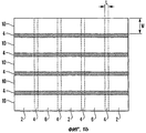
На фиг.1а представлен вид в сечении массива структур полевых транзисторов с плотным расположением электродов.On figa presents a view in section of an array of structures of field-effect transistors with a dense arrangement of electrodes.
Фиг.1b соответствует виду сверху на массив по фиг.1а.Fig.1b corresponds to a top view of the array of figa.
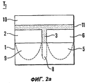
На фиг.2а представлен вид в сечении единичной интегрированной транзисторно/запоминающей структуры согласно изобретению.On figa presents a view in section of a single integrated transistor / memory structure according to the invention.
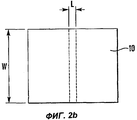
Фиг.2b соответствует виду сверху на транзисторно/запоминающую структуру по фиг.2а.Fig. 2b corresponds to a plan view of the transistor / memory structure of Fig. 2a.
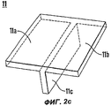
На фиг.2с в перспективном изображении показана геометрическая конфигурация, образованная запоминающим материалом в транзисторно/запоминающей структуре по фиг.2а.On figs in a perspective image shows the geometric configuration formed by the storage material in the transistor / storage structure of figa.
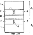
На фиг.3а показана сдвоенная транзисторно/запоминающая структура согласно первому варианту изобретения.Fig. 3a shows a dual transistor / memory structure according to a first embodiment of the invention.
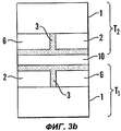
На фиг.3b изображен вариант структуры по фиг.3а.On fig.3b shows a variant of the structure of figa.
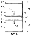
На фиг.3с представлен второй вариант сдвоенной транзисторно/ запоминающей структуры по изобретению.On figs presents a second variant of a dual transistor / memory structure according to the invention.
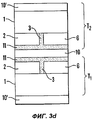
На фиг.3d представлен третий вариант сдвоенной транзисторно/запоминающей структуры по изобретению.3d shows a third embodiment of a dual transistor / memory structure according to the invention.
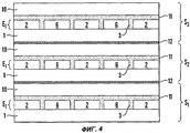
На фиг.4 представлен трехмерный массив с матричной адресацией по настоящему изобретению.Figure 4 presents a three-dimensional array with matrix addressing of the present invention.
Осуществление изобретенияThe implementation of the invention
Далее будут кратко рассмотрены общие предпосылки создания настоящего изобретения. В его основе лежит концепция расположения электродов с высокой плотностью, которая описана в параллельной международной заявке PCT/NO02/00414 (WO 03/041084), принадлежащей заявителю настоящего изобретения. Описанная в указанной заявке плотная схема расположения электродов соответствует конфигурации, показанной в сечении на фиг.1а и на виде сверху на фиг.1b. Данная конфигурация соответствует расположению электродов в электродных слоях Е1 и Е2, как это показано на фиг 1а. Для того чтобы снять ограничения, накладываемые на шаг электродов правилами конструирования, соответствующими традиционной технологии профилирования, например, посредством микрофотолитографии, для формирования электродных слоев Е1; Е2 используются раздельные процессы профилирования и формования. В результате формируются полосковые электроды (в частности, электроды 2, 6 электродного слоя Е1, отстоящие друг от друга на произвольно малое расстояние и взаимно изолированные с помощью изолирующего материала 4, находящегося в канавках 3 между электродами). Аналогичным образом могут быть сформированы и электроды 10 электродного слоя Е2, которые скрещиваются под прямым углом с электродами 2, 6. Электроды 10 затвора взаимно изолированы соответствующим образом, с использованием изолирующего (барьерного) материала 4, как это хорошо видно на фиг.1b.The general background of the present invention will be briefly discussed below. It is based on the concept of the arrangement of electrodes with high density, which is described in parallel international application PCT / NO02 / 00414 (WO 03/041084), which belongs to the applicant of the present invention. The dense arrangement of the electrodes described in this application corresponds to the configuration shown in cross section in Fig. 1a and in a plan view in Fig. 1b. This configuration corresponds to the arrangement of the electrodes in the electrode layers E1 and E2, as shown in FIG. 1a. In order to remove the restrictions imposed on the step of the electrodes by design rules corresponding to the traditional profiling technology, for example, by microphotolithography, for forming the electrode layers E1; E2 uses separate profiling and molding processes. As a result, strip electrodes are formed (in particular,
Расстояние L между электродами 2, 6 не задается какими-либо правилами конструирования и поэтому в принципе может быть равно толщине слоя материала 4, который наносится методами, позволяющими в принципе уменьшить значение L до толщины моноатомного слоя. Благодаря этому схема расположения электродов с высокой плотностью, описанная в указанной международной заявке, позволяет получить плотные матрицы ячеек функционального материала, находящегося, например, между электродными слоями Е1 и Е2 и адресуемого через эти слои.The distance L between the
Настоящее изобретение основано, кроме того, на техническом решении, раскрытом в параллельной международной заявке PCT/NO02/00397 (WO 03/046921), также принадлежащей заявителю настоящего изобретения. В указанной заявке описаны транзисторные матрицы, состоящие из структур полевых транзисторов со сверхкороткой длиной L канала и с произвольно большой шириной W канала. Данное решение открывает казавшиеся недостижимыми перспективы конструирования полевых транзисторов. Фиг.1а можно рассматривать как иллюстрацию поперечного сечения подобных транзисторных структур, организованных в матрицу, что особенно наглядно видно на виде сверху по фиг.1b. На фиг.1а показано, что электрод 2 истока, сформированный в электродном слое Е1, расположен параллельно электроду 6 стока, который имеет примерно такие же размеры.The present invention is also based on the technical solution disclosed in parallel international application PCT / NO02 / 00397 (WO 03/046921), also owned by the applicant of the present invention. This application describes transistor arrays consisting of field-effect transistor structures with an ultrashort channel length L and an arbitrarily large channel width W. This solution opens up the seemingly unattainable prospects of designing field effect transistors. Figa can be considered as an illustration of the cross section of such transistor structures organized in a matrix, which is especially clearly seen in the top view of Fig.1b. On figa shows that the
Электроды 2, 6 истока и стока выполнены на полупроводниковой подложке 1, например, из кремния. С использованием метода, описанного в упомянутой международной заявке, подложка соответствующим образом легирована для образования в ней истоковых областей 9 и стоковых областей 5. Кроме того, подложка дополнительно легирована на участках, расположенных под канавками 3, сформированными между электродами 2, 6 истока и стока, для того, чтобы образовать транзисторные каналы 8 со сверхкороткой длиной L.The source and
Электроды 2, 6 истока и стока взаимно изолированы с помощью изолирующего (барьерного) материала 4, заполняющего канавки 3 между ними и покрывающего их верхние поверхности, образуя тем самым изолирующий слой. Ортогонально ориентированные электроды 10 затвора структур полевых транзисторов расположены так, как это показано на фиг.1b. Длина L транзисторного канала 8 может быть сделана почти произвольно малой, т.е. соответствующей толщине слоя материала 4, причем, как это хорошо известно специалистам, данный материал может быть нанесен с толщиной, соответствующей почти моноатомным слоям. С другой стороны, ширина W канала может задаваться шириной электродов 10 затвора. Как следствие, отношение W/L может быть сделано очень большим. Благодаря этому, если требуется, может быть получен очень большой ток ID стока. Таким образом, современная технология, позволяющая производить профилирование с шагом, превосходящим 0,1 мкм, обеспечивает возможность получения матриц типа представленной на фиг.1b, а также транзисторных структур, имеющих соответственно малый масштаб.The source and
Базовая технология, раскрытая в двух вышеупомянутых международных заявках, создает основу для осуществления транзисторно/запоминающих структур, а также массива транзисторно/запоминающих структур с матричной адресацией в соответствии с настоящим изобретением. Единичная транзисторно/запоминающая структура T1, выполненная согласно изобретению и изображенная на фиг.2а, представляется структурно схожей с соответствующими структурами на фиг.1а. Как и в предыдущем случае, электрод 2 истока и электрод 6 стока сформированы на подложке 1 в виде слоя полупроводникового материала, который легирован соответствующим образом для образования в полупроводниковой подложке истоковой области 9, транзисторного канала 8 сверхкороткой длины и стоковой области 5. Однако теперь барьерный слой изолирующего материала 4, показанный на фиг.1а, заменен запоминающим материалом в форме тонкого слоя 11 поляризуемого диэлектрического материала, способного проявлять гистерезисные свойства, преимущественно ферроэлектрического или электретного материала.The basic technology disclosed in the two aforementioned international applications provides the basis for implementing transistor / memory structures as well as an array of transistor / memory structures with matrix addressing in accordance with the present invention. A single transistor / memory structure T 1 made according to the invention and shown in FIG. 2 a appears structurally similar to the corresponding structures in FIG. 1 a. As in the previous case, the
Как это известно специалистам в данной области, ферроэлектрический материал предпочтительно представляет собой ферроэлектрический полимер или сополимер. В последнем случае этим материалом может являться сополимер винилидендифторида и трифторэтилена - П(ВДФ-ТрФЭ), который может наноситься в виде предельно тонких слоев, вплоть до диапазона нанометров, и который, как известно, представляет собой ферроэлектрический материал, способный обеспечить требуемые изолирующие свойства. Запоминающий материал 11 наносится так, как это показано на фиг.2а, т.е. он заполняет канавки 3 между электродами 2, 6 истока и стока и покрывает их верхние поверхности. Тем самым обеспечивается изоляция или барьер относительно электрода 10 затвора. Таким образом, в транзисторно/запоминающей структуре T1 присутствует запоминающий материал 11, формирующий три отдельные запоминающие ячейки.As is known to those skilled in the art, the ferroelectric material is preferably a ferroelectric polymer or copolymer. In the latter case, this material can be a copolymer of vinylidene difluoride and trifluoroethylene - P (VDF-TrFE), which can be applied in the form of extremely thin layers, down to the nanometer range, and which, as you know, is a ferroelectric material capable of providing the required insulating properties. The
Эти ячейки более наглядно представлены на фиг.2с, на которой в перспективе показан только слой запоминающего материала, в отсутствие каких-либо других элементов. У запоминающего материала можно выделить три отдельные части, а именно первую часть 11а, образующую первую ячейку памяти, к которой можно адресоваться через электрод 10 затвора и электрод 2 истока; вторую часть 11b, образующую вторую ячейку памяти, к которой можно адресоваться через электрод 10 затвора и электрод 6 стока; и третью часть 11с, образующую третью ячейку памяти, которая расположена в канавке 3 между электродами 2, 6 истока и стока и к которой можно адресоваться через эти электроды. Адресация к этим трем ячейкам 11а, 11b и 11с памяти для записи и считывания может осуществляться независимо от функционирования самого полевого транзистора. В этой связи должно быть ясно, что три ячейки памяти могут хранить одно трехразрядное двоичное слово, например, любое из следующих двоичных слов: 000, 001, 010, 011, 100, 101 и 111. Как это хорошо известно специалистам в данной области, запись и считывание подобных трехразрядных двоичных слов будет производиться в соответствии с надлежащим протоколом и в дальнейшем обсуждении этих процессов нет необходимости. Подробное описание работы структуры по изобретению будет приведено далее.These cells are more clearly shown in Fig. 2c, which in perspective shows only a layer of storage material in the absence of any other elements. Three separate parts can be distinguished from the storage material, namely, the
Изображенный на фиг.2а, 2с запоминающий материал 11, образующий три ячейки 11а, 11b и 11с памяти, позволяет, как это будет описано далее, производить переключения в различных направлениях. Первая ячейка 11а памяти соответствует той части запоминающего материала 11, которая расположена между электродом 2 истока и электродом 10 затвора; она будет переключаться в направлении, ортогональном поверхностям этих электродов и собственным поверхностям, при подаче напряжения на электрод 2 стока и электрод 10 затвора, т.е. при наличии электрического потенциала между ними, соответствующего электрическому полю, приложенному к ячейке 11а памяти. Поскольку в ячейке используется ферроэлектрический материал, она способна поляризоваться в прямом или обратном вертикальном направлении, что позволяет хранить в ней одну двоичную цифру. Те же самые соображения применимы и к ячейке 11b памяти, соответствующей той части запоминающего материала 11, которая расположена между электродом 6 стока и электродом 10 затвора.The
Третья ячейка 11с памяти формируется в запоминающем материале в той его части, которая находится в канавке 3 между электродом 2 истока и электродом 6 стока. Эта ячейка будет переключаться аналогичным образом, т.е. за счет подачи напряжения на эти электроды и, соответственно, приложения электрического поля к ячейке 11с памяти, расположенной между ними. В случае использования предпочтительного ферроэлектрического материала, такого как поли(винилидендифторид-трифторэтилен) (П(ВДФ-ТрФЭ)), для того, чтобы поляризовать материал и обеспечить переключение между двумя состояниями поляризации (соответствующими двоичному нулю и двоичной единице), необходимо приложить к нему поле, имеющее достаточную напряженность. Требуемая напряженность поля связана с толщиной тонкопленочного запоминающего материала 11. При этом толщина запоминающего материала в ячейках 11а и 11b памяти может отличаться от толщины того же материала в ячейке 11с памяти.The
Для удобства описания ячейка 11а памяти далее будет именоваться ячейкой памяти исток/затвор (ячейкой памяти И/З), аналогичная ячейка 11b памяти - ячейкой памяти сток/затвор (ячейкой памяти С/З), а ячейка 11с памяти - ячейкой памяти исток/сток (ячейкой памяти И/С). Поскольку толщина материала 11 в ячейках памяти И/З и С/З одинакова, эти ячейки будут переключаться при приложении поля одинаковой напряженности, тогда как в ячейке памяти И/С материал может иметь большую или меньшую толщину по сравнению с его толщиной в двух других ячейках памяти. Как следствие, в данном случае переключение возможно при другой напряженности электрического поля, отличной от напряженности поля между электродами 2, 6 истока и стока. При этом транзисторная структура, образованная электродами 2, 6 истока и стока, легированными областями 5, 8, 9 и электродом 10 затвора, может обеспечить переключения транзистора независимо от переключения ячеек памяти. Это подразумевает, что транзистор должен переключаться при приложении меньших напряжений истока и стока, чем те, которые требуются для переключения ячейки памяти И/С.Соответственно, напряжение затвора должно быть ниже, чем напряжение, необходимое для переключения ячейки памяти И/З или С/З. Реально переключение двух последних ячеек памяти будет полностью независимым от переключения транзистора.For convenience of description, the
Далее будут описаны предпочтительные варианты осуществления транзисторно/запоминающих структур согласно настоящему изобретению.Next, preferred embodiments of the transistor / memory structures according to the present invention will be described.
На фиг.3а представлен первый предпочтительный вариант, в котором над первой транзисторно/запоминающей структурой T1 имеется вторая аналогичная структура Т2. Две транзисторно/запоминающие структуры T1, T2 используют один общий электрод 10 затвора, тогда как электродные слои этих структур, содержащие электроды 2, 6 истока и стока, расположены с противоположных сторон общего электрода 10 затвора. Легированные области транзисторов, как и в предыдущем варианте, находятся в полупроводниковых подложках 1, расположенных на противолежащих сторонах транзисторно/запоминающих структур T1, Т2, как это показано на фиг.3а. Комбинированные структуры такого типа фактически представляют транзисторную структуру с общим электродом затвора при обратном порядке слоев. При соответствующем подключении они образуют контур комплементарного полевого транзистора, включенного по схеме с общим затвором. В подобном контуре структура T1 образует первый транзистор, а структура Т2 - второй транзистор. Разумеется, в этом случае подложки 1 должны быть легированы таким образом, чтобы сформировать каналы с проводимостью n-р-n и р-n-р-типа.On figa presents the first preferred embodiment, in which over the first transistor / memory structure T 1 there is a second similar structure T 2 . Two transistor / memory structures T 1 , T 2 use one
Аналогичная сдвоенная транзисторная структура представлена также на фиг.3b, однако в ней положение электродов 2, 6 истока и стока в структуре T2 является обратным по отношению к их положению в структуре T1. Как можно видеть из фиг.3а, 3b, изображенные на них транзисторно/запоминающие структуры содержат по шесть индивидуально адресуемых ячеек памяти. Следовательно, обеспечивается возможность использовать в каждой из этих структур шесть переключаемых ячеек, т.е. обеспечить хранение шестиразрядного двоичного слова при записи и считывании этого слова с использованием любого приемлемого протокола, как это должно быть понятно специалистам в данной области.A similar dual transistor structure is also shown in Fig. 3b, however, in it the position of the source and
Второй вариант построения сдвоенной транзисторно/запоминающей структуры показан на фиг.3с. В этом варианте вторая транзисторно/запоминающая структура Т2 снабжена вторым электродом 10' затвора. В результате эта структура Т2 представляет собой транзисторно/запоминающую структуру с двухзатворным полевым транзистором.A second embodiment of the construction of a dual transistor / memory structure is shown in FIG. In this embodiment, the second transistor / memory structure T 2 is provided with a second gate electrode 10 '. As a result, this T 2 structure is a transistor / memory structure with a double gate field effect transistor.
Третий вариант выполнения сдвоенной транзисторно/запоминающей структуры показан на фиг.3d. Этот вариант похож на вариант по фиг.3с, но в нем вторым электродом 10' затвора снабжена также первая транзисторно/запоминающая структура T1. В результате обе структуры T1, T2 представляют собой транзисторно/запоминающие структуры с двухзатворным полевым транзистором, т.е. с двумя электродами 10, 10' затвора.A third embodiment of a dual transistor / memory structure is shown in Fig. 3d. This embodiment is similar to the embodiment of FIG. 3c, but in it a second transistor / memory structure T 1 is also provided with a
Подложка 1, т.е. слой полупроводникового материала, предпочтительно выполняется из кремния, который может быть в аморфном, поликристаллическом или микрокристаллическом состоянии. Одним из достоинств использования неорганического материала, такого как кремний, является возможность формирования на нем барьерного слоя путем оксидирования (окисления) его поверхности. Однако, как это хорошо известно специалистам в данной области, ничто не препятствует и тому, чтобы данный слой полупроводникового материала был выполнен из органического полупроводника, например из полупроводникового полимера или из циклического соединения, такого как пентацен. Однако при формировании электродов в электродном слое Е1, лежащем на органическом полупроводниковом материале, необходимо проявлять осторожность в отношении совместимости между материалами электродов и любым органическим полупроводниковым материалом в части температурного режима и других технологических факторов.
Запоминающий материал 11 должен представлять собой диэлектрический и поляризуемый материал, обладающий ферроэлектрическими или электретными свойствами и способный проявлять гистерезисные свойства при приложении к нему электрического поля. Как уже упоминалось, наиболее предпочтительными в данном случае будут органические материалы, такие как полимеры или сополимеры. Наиболее предпочтительным запоминающим материалом является П(ВДФ-ТрФЭ).The
Одним из преимуществ подобных материалов является то, что их диэлектрические свойства позволяют использовать их также в качестве электрически изолирующих (барьерных) материалов. Еще одно преимущество заключается в возможности наносить их в виде цельных слоев крайне малой толщины, вплоть до нескольких нанометров. Кроме того, они могут наноситься, с образованием ячеек памяти, на поверхности, имеющие сложную геометрию. В частности, они способны полностью заполнять канавки 3, которые формируются между электродами 2, 6 истока и стока.One of the advantages of such materials is that their dielectric properties make it possible to use them also as electrically insulating (barrier) materials. Another advantage is the ability to apply them in the form of solid layers of extremely small thickness, up to several nanometers. In addition, they can be applied, with the formation of memory cells, on surfaces having complex geometry. In particular, they are able to completely fill the
Интегрированные транзисторно/запоминающие структуры согласно изобретению могут быть легко реализованы в виде массивов с матричной адресацией, в частности, в виде двумерного массива известного из уровня техники типа. Подобный массив представлен на фиг.1а и 1b. Однако возможно также собрать подобные двумерные массивы в пакет (стопу) с формированием трехмерных массивов, как это показано на фиг.4. Изображенный на фиг.4 трехмерный массив с матричной адресацией по изобретению образован тремя двумерными массивами S1, S2 и S3, собранными в пакет. Базовым элементом такого трехмерного массива является, очевидно, единичная транзисторно/запоминающая структура, изображенная в сечении на фиг.2а и на виде сверху на фиг.2b. Однако трехмерные массивы подобных транзисторно/запоминающих структур не должны ограничиваться только этим вариантом: они могут строиться также на базе сдвоенных структур, например, подобных приведенным на фиг.3a-3d. Возможны также и другие комбинации электродных слоев и слоев полупроводникового материала. При этом единственное ограничение состоит в том, что должна обеспечиваться возможность раздельного переключения собственно транзисторной структуры и ячеек памяти.The integrated transistor / memory structures according to the invention can be easily implemented in the form of arrays with matrix addressing, in particular, in the form of a two-dimensional array of the type known from the prior art. A similar array is shown in figa and 1b. However, it is also possible to assemble such two-dimensional arrays into a packet (stack) with the formation of three-dimensional arrays, as shown in Fig. 4. The three-dimensional array with matrix addressing according to the invention depicted in FIG. 4 is formed by three two-dimensional arrays S 1 , S 2 and S 3 assembled in a packet. The basic element of such a three-dimensional array is, obviously, a single transistor / memory structure, shown in section in figa and in a top view in fig.2b. However, three-dimensional arrays of such transistor / memory structures should not be limited only to this option: they can also be built on the basis of dual structures, for example, similar to those shown in figa-3d. Other combinations of electrode layers and semiconductor material layers are also possible. Moreover, the only limitation is that it should be possible to separately switch the actual transistor structure and memory cells.
Как можно видеть, в представленном на фиг.4 трехмерном массиве с матричной адресацией, включающем три собранных в пакет двумерных массива S, каждый двумерный массив содержит единственный слой 1 полупроводникового материала и первый электродный слой Е1, содержащий электроды 2, 6 истока и стока, разделенные канавками 3. Канавки 3 заполнены, как и в предыдущих вариантах, запоминающим материалом 11, который покрывает также верхние поверхности электродов 2, 6 истока и стока. Над запоминающим материалом расположен электрод 10 затвора, который может быть отделен от следующего смежного массива разделительным слоем 12. Этот разделительный слой может быть выполнен из соответствующего материала, например из диэлектрического запоминающего материала 11; однако он может представлять собой и барьерное покрытие, обладающее изолирующими свойствами, которое нанесено на электроды 10 затвора. Поскольку за электродами 10 затвора в собранных в пакет двумерных массивах S следует слой полупроводникового материала 1, принадлежащий смежному двумерному массиву с матричной адресацией, данный слой полупроводникового материала может быть обработан таким образом, чтобы сформировать барьерный слой на его поверхности, примыкающей к электроду затвора. В частности, поверхность неорганического полупроводникового материала, используемого в качестве слоя 1, может быть подвергнута оксидированию перед тем, как этот материал будет установлен на нижележащий двумерный массив. Естественно, подобная операция может быть легко осуществлена путем выполнения поверхностного оксидирования, когда неорганический полупроводниковый материал представляет собой кремний.As can be seen, in the three-dimensional array with matrix addressing shown in Fig. 4, which includes three two-dimensional arrays S assembled in a packet, each two-dimensional array contains a
В принципе, количество двумерных массивов S, собираемых в пакет для формирования трехмерного массива с матричной адресацией, не ограничено. Вместе с тем, на практике оно будет ограничиваться, например, механическими или температурными факторами, а также необходимостью избежать возрастающей неровности поверхности в собранном пакете двумерных структур с возрастанием их количества. Однако эти технические проблемы вполне понятны и могут быть, хотя бы частично, преодолены с помощью технических мер, хорошо известных специалистам в данной области.In principle, the number of two-dimensional arrays S collected in a packet to form a three-dimensional array with matrix addressing is not limited. At the same time, in practice, it will be limited, for example, by mechanical or temperature factors, as well as the need to avoid an increasing surface roughness in the assembled package of two-dimensional structures with an increase in their number. However, these technical problems are understandable and can be, at least partially, overcome with the help of technical measures well known to specialists in this field.
Итак, было показано, что настоящее изобретение обеспечивает создание массива с матричной адресацией, образованного интегрированными транзисторно/запоминающими структурами, расположенными в двух или в трех измерениях и интегрирующими в себе ячейки памяти и транзисторные ключи. При этом каждая из названных групп составных элементов может переключаться в индивидуальном режиме подачи напряжения, так что переключение, например, ячейки памяти не оказывает влияния на интегрированный с ней транзистор. Информация, подлежащая обработке или необходимая для функционирования устройства, может храниться в ячейках памяти, интегрированных в транзисторные контура. Как следствие, устраняется потребность во внешнем доступе и в периферийных устройствах хранения данных.So, it was shown that the present invention provides the creation of an array with a matrix addressing formed by integrated transistor / memory structures located in two or three dimensions and integrating memory cells and transistor keys. In this case, each of these groups of component elements can be switched in an individual voltage supply mode, so that switching, for example, a memory cell does not affect the transistor integrated with it. Information to be processed or necessary for the operation of the device can be stored in memory cells integrated into transistor circuits. As a result, the need for external access and peripheral storage devices is eliminated.
Должно быть также понятно, что в любом двумерном массиве можно сформировать отдельные группы транзисторно/запоминающих структур и построить на их основе соответствующие схемы. В частности, можно удалить подобные транзисторно/запоминающие структуры из некоторых частей двумерного массива, а затем создать соответствующие соединительные дорожки и межсоединения с наличием, в случае необходимости, изолирующих и барьерных слоев. Таким образом можно сформировать, например, логические ячейки и арифметические регистры с интегрированной памятью, образующие комбинированный процессорный/запоминающий контур. Более того, подобный контур может быть реализован в трехмерной конфигурации, что позволит обеспечить более высокую плотность соединений. Такое решение открывает совершенно новые перспективы для создания интегрированных процессорных/запоминающих структур высокой сложности при высокой плотности расположения элементов. Это позволит достичь высокого быстродействия и предельно быстрого доступа к памяти, поскольку необходимые регистры будут находиться внутри контура. При этом будут сняты обычные топологические ограничения, присущие значительной части современных интегральных схем, основанных, в частности, на кремниевых технологиях.It should also be clear that in any two-dimensional array, it is possible to form separate groups of transistor / memory structures and construct corresponding circuits on their basis. In particular, it is possible to remove such transistor / memory structures from some parts of a two-dimensional array, and then create the corresponding connecting tracks and interconnects with the presence, if necessary, of insulating and barrier layers. Thus, it is possible to form, for example, logic cells and arithmetic registers with integrated memory, forming a combined processor / memory circuit. Moreover, such a circuit can be implemented in a three-dimensional configuration, which will allow for a higher density of connections. Such a solution opens up completely new prospects for creating integrated processor / memory structures of high complexity with a high density of elements. This will allow to achieve high speed and extremely fast memory access, since the necessary registers will be inside the circuit. In this case, the usual topological restrictions inherent in a significant part of modern integrated circuits based, in particular, on silicon technologies, will be removed.
Claims (25)
Applications Claiming Priority (2)
| Application Number | Priority Date | Filing Date | Title |
|---|---|---|---|
| NO20016041A NO20016041A (en) | 2001-12-10 | 2001-12-10 | Matrix addressable group of integrated transistor / memory structures |
| NO20016041 | 2001-12-10 |
Publications (2)
| Publication Number | Publication Date |
|---|---|
| RU2004120776A RU2004120776A (en) | 2005-09-20 |
| RU2287205C2 true RU2287205C2 (en) | 2006-11-10 |
Family
ID=19913138
Family Applications (1)
| Application Number | Title | Priority Date | Filing Date |
|---|---|---|---|
| RU2004120776/28A RU2287205C2 (en) | 2001-12-10 | 2002-11-18 | Integrated transistor/memory structures and array of such matrix-addressing structures |
Country Status (11)
| Country | Link |
|---|---|
| EP (1) | EP1451825B1 (en) |
| JP (1) | JP2005512338A (en) |
| KR (1) | KR100556089B1 (en) |
| CN (1) | CN1602531A (en) |
| AT (1) | ATE357045T1 (en) |
| AU (1) | AU2002366675A1 (en) |
| CA (1) | CA2466153C (en) |
| DE (1) | DE60218887D1 (en) |
| NO (1) | NO20016041A (en) |
| RU (1) | RU2287205C2 (en) |
| WO (1) | WO2003050814A1 (en) |
Families Citing this family (4)
| Publication number | Priority date | Publication date | Assignee | Title |
|---|---|---|---|---|
| WO2007032621A1 (en) * | 2005-09-12 | 2007-03-22 | Iferro Co., Ltd. | Ferroelectric memory device and method of manufacturing the same |
| KR100988227B1 (en) * | 2005-09-12 | 2010-10-18 | 서울시립대학교 산학협력단 | Ferroelectric memory device and method of manufacturing the same |
| KR101245293B1 (en) * | 2006-01-19 | 2013-03-19 | 서울시립대학교 산학협력단 | Ferrodielectric material for ferrodielectric memory |
| CN112908368B (en) * | 2021-02-04 | 2023-03-21 | 清华大学 | Three-state content addressing memory based on monolithic three-dimensional heterogeneous integration |
Family Cites Families (5)
| Publication number | Priority date | Publication date | Assignee | Title |
|---|---|---|---|---|
| US4952031A (en) * | 1987-06-19 | 1990-08-28 | Victor Company Of Japan, Ltd. | Liquid crystal display device |
| JPH07106450A (en) * | 1993-10-08 | 1995-04-21 | Olympus Optical Co Ltd | Ferroelectric gate transistor memory |
| DE69739045D1 (en) * | 1997-08-27 | 2008-11-27 | St Microelectronics Srl | Manufacturing method for electronic memory devices with virtual ground |
| US6072716A (en) * | 1999-04-14 | 2000-06-06 | Massachusetts Institute Of Technology | Memory structures and methods of making same |
| US6473388B1 (en) * | 2000-08-31 | 2002-10-29 | Hewlett Packard Company | Ultra-high density information storage device based on modulated cathodoconductivity |
-
2001
- 2001-12-10 NO NO20016041A patent/NO20016041A/en unknown
-
2002
- 2002-11-18 CA CA002466153A patent/CA2466153C/en not_active Expired - Fee Related
- 2002-11-18 JP JP2003551784A patent/JP2005512338A/en not_active Abandoned
- 2002-11-18 DE DE60218887T patent/DE60218887D1/en not_active Expired - Lifetime
- 2002-11-18 RU RU2004120776/28A patent/RU2287205C2/en not_active IP Right Cessation
- 2002-11-18 AU AU2002366675A patent/AU2002366675A1/en not_active Abandoned
- 2002-11-18 WO PCT/NO2002/000426 patent/WO2003050814A1/en active IP Right Grant
- 2002-11-18 CN CNA028245377A patent/CN1602531A/en active Pending
- 2002-11-18 KR KR1020047008856A patent/KR100556089B1/en not_active IP Right Cessation
- 2002-11-18 EP EP02804659A patent/EP1451825B1/en not_active Expired - Lifetime
- 2002-11-18 AT AT02804659T patent/ATE357045T1/en not_active IP Right Cessation
Also Published As
| Publication number | Publication date |
|---|---|
| CA2466153C (en) | 2007-01-23 |
| CA2466153A1 (en) | 2003-06-19 |
| NO314736B1 (en) | 2003-05-12 |
| EP1451825A1 (en) | 2004-09-01 |
| KR100556089B1 (en) | 2006-03-03 |
| NO20016041A (en) | 2003-05-12 |
| CN1602531A (en) | 2005-03-30 |
| AU2002366675A1 (en) | 2003-06-23 |
| RU2004120776A (en) | 2005-09-20 |
| ATE357045T1 (en) | 2007-04-15 |
| JP2005512338A (en) | 2005-04-28 |
| DE60218887D1 (en) | 2007-04-26 |
| EP1451825B1 (en) | 2007-03-14 |
| WO2003050814A1 (en) | 2003-06-19 |
| KR20040064733A (en) | 2004-07-19 |
| NO20016041D0 (en) | 2001-12-10 |
Similar Documents
| Publication | Publication Date | Title |
|---|---|---|
| KR100392446B1 (en) | Scaleable integrated data processing device | |
| US6768661B2 (en) | Multiple-mode memory and method for forming same | |
| KR100707181B1 (en) | Semiconductor memory device with dual storage node and methods of manufacturing and operating the same | |
| KR20050013221A (en) | Nrom memory cell, memory array, related devices and methods | |
| WO2000070683A1 (en) | Semiconductor memory | |
| US6724028B2 (en) | Matrix-addressable array of integrated transistor/memory structures | |
| KR100437925B1 (en) | Scalable data processing apparatus | |
| RU2287205C2 (en) | Integrated transistor/memory structures and array of such matrix-addressing structures | |
| KR100577544B1 (en) | Electrodes, method and apparatus for memory structure | |
| US11398490B2 (en) | Stacked neural device structure and manufacturing method thereof | |
| WO2015171680A1 (en) | Dram cells storing volatile and nonvolatile data | |
| RU2274913C2 (en) | Three-dimensional memorizing device | |
| KR20040111435A (en) | A volumetric data storage apparatus comprising a plurality of stacked matrix-addressable memory devices | |
| KR102645343B1 (en) | 3D synapse device stack, 3D stackable synapse array using the 3D synapse device stacks and method of fabricating the stack | |
| US20230077181A1 (en) | Three-dimensional nor memory string arrays of thin-film ferroelectric transistors | |
| US20230081427A1 (en) | Three-dimensional memory string array of thin-film ferroelectric transistors formed with an oxide semiconductor channel | |
| CN117135902A (en) | Memory array and preparation method thereof | |
| TW202303862A (en) | Semiconductor structure and method for manufacturing same | |
| KR20230098672A (en) | Memory peripheral circuit having 3D transistor and method of forming the same | |
| KR20050077157A (en) | Mram device and method of fabricating the same | |
| CN115497532A (en) | Memory structure and manufacturing and control method thereof |
Legal Events
| Date | Code | Title | Description |
|---|---|---|---|
| MM4A | The patent is invalid due to non-payment of fees |
Effective date: 20071119 |