RU2196352C2 - Element of liquid-crystal display - Google Patents
Element of liquid-crystal display Download PDFInfo
- Publication number
- RU2196352C2 RU2196352C2 RU2000132989/28A RU2000132989A RU2196352C2 RU 2196352 C2 RU2196352 C2 RU 2196352C2 RU 2000132989/28 A RU2000132989/28 A RU 2000132989/28A RU 2000132989 A RU2000132989 A RU 2000132989A RU 2196352 C2 RU2196352 C2 RU 2196352C2
- Authority
- RU
- Russia
- Prior art keywords
- combs
- substrate
- teeth
- electrodes
- period
- Prior art date
Links
Images
Landscapes
- Liquid Crystal (AREA)
Abstract
Description
Изобретение относится к индикаторной технике, в частности к цветным жидкокристаллическим дисплеям, в которых селекция цветов производится разнесенными по плоскости светофильтрами с тремя первичными цветами (триадами), а модуляция каждого из цветов производится посредством жидкого кристалла (ЖК). The invention relates to indicator technology, in particular to color liquid crystal displays, in which the selection of colors is carried out along the plane with light filters with three primary colors (triads), and the modulation of each of the colors is carried out by means of a liquid crystal (LCD).
Известен элемент ЖК-дисплея, содержащий слой ЖК, размещенного между двумя подложками с прозрачными электродами и ориентирующими покрытиями на внутренних сторонах, и триаду светофильтров, пропускающих свет одной из трех первичных длин волн: R - красный, G - зеленый, В - синий [1]. Светофильтры триады выполнены из полимера, и в каждом из них внедрен краситель одного из первичных цветов. Напротив каждого из светофильтров расположен участок ЖК, который с помощью поляроидов при приложении напряжения регулирует количество света, проходящего сквозь каждый из светофильтров, благодаря чему и создается цветное изображение. A known element of the LCD display containing a layer of an LCD placed between two substrates with transparent electrodes and orienting coatings on the inside, and a triad of filters that transmit light from one of the three primary wavelengths: R - red, G - green, B - blue [1 ]. The filters of the triad are made of polymer, and a dye of one of the primary colors is introduced in each of them. A section of the LCD is located opposite each of the filters, which, with the use of polaroids, regulates the amount of light passing through each of the filters through the application of voltage, which creates a color image.
Недостатками известного дисплея являются малая светосила (большая доля света поглощается светофильтром) и высокая стоимость, обусловленная технологическими трудностями при изготовлении: на обычно легкоплавкий полимер нужно наносить выравнивающие и ориентирующие покрытия, прозрачные электроды, а это процессы обычно высокотемпературные. Долговечность элемента ограничена, т. к. ЖК может химически реагировать с полимером светофильтра и/или с красителем. Это может привести к его деградации и потере работоспособности. The disadvantages of the known display are the low luminosity (a large fraction of the light is absorbed by the light filter) and the high cost due to technological difficulties in manufacturing: usually low-melting polymer must be applied alignment and orientation coatings, transparent electrodes, and these processes are usually high-temperature. The durability of the element is limited, since the LCD can chemically react with the polymer of the light filter and / or with the dye. This can lead to its degradation and loss of performance.
Наиболее близким по технической сущности к изобретению является элемент жидкокристаллического дисплея, содержащий слой жидкого кристалла, заключенного между двумя подложками с прозрачными электродами, один из которых сплошной, а другой выполнен в виде двух гребенок с взаимно проникающими зубцами [2] . Период зубцов одной гребенки 2 d, суммарный период двух гребенок d. Элемент снабжен входной и выходной масками со щелями. Взаимное положение щелей масок согласовано таким образом, что в отсутствие управляющего напряжения свет сквозь маски не проходит. При подаче управляющего напряжения к сплошному общему электроду и одной из гребенок ЖК переориентируется в частях, находящихся под зубцами. Слой ЖК с участками, имеющими исходную ориентацию и переориентированными, представляет собой фазовую дифракционную решетку. Пучки белого света, прошедшие сквозь щели входной маски, дифрагируют на образовавшейся фазовой дифракционной решетке, образуя систему дифракционных спектров в плоскости выходной маски. В тех местах выходной маски, на которые попадают определенные длины волн, например λ, предусмотрены щели, сквозь которые свет этой длины волны проходит. Когда напряжение приложено к общему и двум гребенчатым электродам, в слое ЖК возникает дифракционная решетка с вдвое меньшим периодом и сквозь те же щели будет проходить свет с вдвое большей длиной волны. Таким образом, элемент обеспечивает получение трех оптически различимых состояний: ТЕМНО, ЦВЕТ 1, ЦВЕТ 2, причем длины волн цветов отличаются строго в два раза. Элемент имеет высокие эксплуатационные свойства, как-то: стабильные цвета, независимые от температуры или разбросов толщины, в контакте со слоем нет химически взаимодействующих с ним слоев и потому долговечность его повышена. The closest in technical essence to the invention is an element of a liquid crystal display containing a layer of liquid crystal enclosed between two substrates with transparent electrodes, one of which is solid, and the other is made in the form of two combs with mutually penetrating teeth [2]. The period of the teeth of one comb 2 d, the total period of two combs d. The element is equipped with input and output masks with slots. The mutual position of the slots of the masks is coordinated in such a way that in the absence of control voltage, the light does not pass through the masks. When a control voltage is applied to a continuous common electrode and one of the combs, the LC is reoriented in the parts under the teeth. The LC layer with regions with the initial orientation and reoriented is a phase diffraction grating. The white light beams passing through the slits of the input mask are diffracted on the resulting phase diffraction grating, forming a system of diffraction spectra in the plane of the output mask. In those places of the output mask to which certain wavelengths fall, for example, λ, slots are provided through which light of this wavelength passes. When a voltage is applied to a common and two comb electrodes, a diffraction grating with a half time period appears in the LC layer and light with a double wavelength will pass through the same slits. Thus, the element provides three optically distinguishable states: DARK, COLOR 1,
Недостатком известного элемента является ограниченный набор цветов (всего два) и потому невозможность создания полноцветного дисплея. Кроме того, элемент имеет существенные потери света, поскольку из всей падающей на элемент интенсивности используются только лучи света, параллельные оптической оси, которые приходятся на щели входной маски. A disadvantage of the known element is a limited set of colors (only two) and therefore the inability to create a full-color display. In addition, the element has a significant loss of light, because of the entire incident intensity on the element, only light rays parallel to the optical axis that fall on the slits of the input mask are used.
Возможность реализации полноцветного дисплея осуществляется только при наличии трех независимых цветов и достаточной яркости. Обеспечение такой возможности и является целью изобретения. The possibility of realizing a full-color display is carried out only if there are three independent colors and sufficient brightness. The provision of such an opportunity is the aim of the invention.
Поставленная цель достигается тем, что в известный элемент, содержащий слой жидкого кристалла, заключенного между двумя прозрачными подложками с прозрачными электродами, один из которых выполнен в виде двух гребенок с взаимно проникающими зубцами, входную и выходную маски со щелями, взаимное положение которых согласовано, введены линзовый растр-конденсор в промежуток между входной маской и первой подложкой, линзовый растр-объектив в промежуток между второй подложкой и выходной маской, второй электрод выполнен в виде двух гребенок с взаимно проникающими зубцами, периоды гребенок на первой подложке различаются между собой в дробное число раз и не совпадают с периодом гребенок второй подложки, в местах совпадения зубцов первой и второй гребенок первой подложки предусмотрены разрезы, исключающие электрическое замыкание гребенок. This goal is achieved by the fact that in the known element containing a layer of liquid crystal enclosed between two transparent substrates with transparent electrodes, one of which is made in the form of two combs with mutually penetrating teeth, the input and output masks with slots, the mutual position of which is coordinated, are introduced lens raster-condenser between the input mask and the first substrate, lens raster-lens between the second substrate and the output mask, the second electrode is made in the form of two combs with penetrating teeth, the periods of the combs on the first substrate differ by a fraction of the number of times and do not coincide with the period of the combs of the second substrate, at the points of coincidence of the teeth of the first and second combs of the first substrate, cuts are provided to exclude the electrical closure of the combs.
По п.1 установлены определенные соотношения между периодами гребенок на первой и второй подложках, в частности: период одной гребенки первой подложки равен d, период второй гребенки равен 1,2 d, период гребенки на второй подложке равен 1,5 d. According to claim 1, certain relations are established between the periods of the combs on the first and second substrates, in particular: the period of one comb of the first substrate is d, the period of the second comb is 1.2 d, the period of the comb on the second substrate is 1.5 d.
Благодаря такой конструкции в слое ЖК можно сформировать фазовые решетки трех различных, независимых периодов: 1,5 d, 1,2 d и d, пропускать сквозь щели выходной маски цвет трех длин волн и обеспечить 4 оптически различимых состояния: ТЕМНО, ЦВЕТ 1 (λ), ЦВЕТ 2 (1,2 λ) и ЦВЕТ 3 (1,5 λ). Due to this design, phase gratings can be formed in the LC layer in three different, independent periods: 1.5 d, 1.2 d and d, pass the color of three wavelengths through the slits of the output mask and provide 4 optically distinguishable states: DARK, COLOR 1 (λ ), COLOR 2 (1.2 λ) and COLOR 3 (1.5 λ).
Именно такое соотношение периодов позволяет обеспечить в дисплее цветовые координаты, точно соответствующие принятым международным стандартам (система CIE). It is this ratio of periods that allows us to provide color coordinates in the display that exactly correspond to accepted international standards (CIE system).
Наличие линзовых растров позволяет увеличить КПД использования света и повысить яркость изображений в дисплее за счет обеспечения возможности использования параксиальных лучей от источника света. The presence of lens rasters can increase the efficiency of the use of light and increase the brightness of images in the display by providing the possibility of using paraxial rays from the light source.
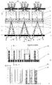
На чертеже изображены:
а - конструкция элемента (для удобства изложения изображены три элемента),
б - форма электродов на первой из подложек,
в - форма электродов на второй из подложек.The drawing shows:
a - element design (for ease of presentation, three elements are depicted),
b - the shape of the electrodes on the first of the substrates,
in - the shape of the electrodes on the second of the substrates.
Элемент жидкокристаллического дисплея (см. а) содержит слой жидкого кристалла 1, заключенного между двумя прозрачными подложками 2 и 3, на внутренние стороны которых нанесены прозрачные электроды 4 и 5. Прозрачный электрод 4 выполнен в виде двух гребенок 4а, 4b с взаимно проникающими зубцами. Период зубцов одной из гребенок dB=d, период второй гребенки dG=1,2 d. Поскольку периоды гребенок 4а и 4b соотносятся между собой дробным отношением, то при любом из значений d возникнет ситуация, при которой зубцы гребенок должны наложиться друг на друга. Для того, чтобы устранить эту возможность, в местах возможного наложения зубцов предусмотрены разрезы каждого из совпадающих зубцов, например посередине каждого из зубцов (см. б).The liquid crystal display element (see a) contains a layer of liquid crystal 1, enclosed between two
Прозрачный электрод 5 выполнен в виде двух гребенок, период зубцов которых dR составляет величину 1,5 d.The
На внешней стороне подложки 2 размещены линзовый растр-конденсор 6 и входная маска 7 со щелями. На внешней стороне подложки 3 размещены линзовый растр-объектив 8 и выходная маска 9. On the outer side of the
Лучи белого неполяризованного света 10 (аксиальные и параксиальные) освещают входную маску 7 и узкие пучки света проходят сквозь щели входной маски. Щели входной маски расположены в фокусах линзового растра-конденсора 6, поэтому на выходе конденсора 6 формируется практически параллельный пучок света, равномерно освещающий площадь ЖК-ячейки с гребенчатым электродом. The rays of white unpolarized light 10 (axial and paraxial) illuminate the
Линзовый растр-объектив 8 формирует изображение источника света (щели входной маски 7) в своей фокальной плоскости, т.е. на выходной маске 9. The
В исходном состоянии в осевом направлении (O-O) на выходной маске будет сформировано яркое белое изображение щели. Поскольку в этих местах выходной маски 9 находятся непрозрачные участки, то все прошедшее излучение будет поглощено и, таким образом, будет реализовано первое из оптических состояний элемента: ТЕМНО. In the initial state in the axial direction (O-O), a bright white image of the slit will be formed on the output mask. Since in these places of the
Три других оптических состояния: ЦВЕТ 1, ЦВЕТ 2, ЦВЕТ 3 могут быть получены при приложении управляющих напряжений к гребенчатым электродам 4 и 5 в различных комбинациях. Three other optical states: COLOR 1,
Примем за систему основных цветов, соответствующую Международному стандарту CIE:
В - синий 0,440 мкм,
G - зеленый 0,528 мкм=(0,440•1,2) мкм,
R - красный 0,660 мкм=(0,440•1,5) мкм.We accept for the system of primary colors that comply with the International Standard CIE:
B - blue 0.440 μm,
G - green 0.528 μm = (0.440 • 1.2) μm,
R - red 0.660 microns = (0.440 • 1.5) microns.
Если управляющее напряжение приложить к электроду 4а и электрически соединенным электродам 5а, 5b (в этом случае они используются как общий, практически сплошной электрод), то в слое ЖК возникнет периодическая система с переориентированным ЖК и ЖК с исходной ориентацией. Система участков с разной ориентацией ЖК представляет собой фазовую дифракционную решетку с периодом d (в данном варианте приложения напряжений). If the control voltage is applied to the
Свет, прошедший сквозь фазовую дифракционную решетку, с помощью линзового растра-объектива 8 сформирует в плоскости выходной маски 9 систему дифракционных спектров ±m порядков. The light transmitted through the phase diffraction grating, using a lens raster-
Углы относительно нулевого максимума (осевое направление О-О), под которыми наблюдаются определенные длины волн, определяются выражением
sinφ = ±mλ/2d,
где φ - угол, под которым распространяется свет с длиной волны λ, m - номер дифракционного максимума (принимает целые значения), d - период гребенки.The angles with respect to the zero maximum (O-O axial direction) at which certain wavelengths are observed are determined by the expression
sinφ = ± mλ / 2d,
where φ is the angle at which light with a wavelength λ propagates, m is the number of the diffraction maximum (takes integer values), d is the comb period.
Под углом φB в плоскости выходной маски 9 будет сфокусирован синий цвет В, под углом φG будет сфокусирован зеленый цвет G, под углом φR будет сфокусирован красный цвет R.At an angle φ B in the plane of the
В местах фокусировки синего цвета (расстояние l под углом φB для периода d) в выходной маске 9 предусмотрены прозрачные участки - щели, которые пропускают свет только заданной длины волны.In places of focusing of blue color (distance l at an angle φ B for period d), transparent sections are provided in the
Таким образом, при описанной выше комбинации вариантов приложения напряжений сквозь щели выходной маски будет проходить ЦВЕТ 1 - синий цвет В (ситуация изображена на правом из трех элементов). Thus, with the combination of voltage application options described above, COLOR 1 — blue color B — will pass through the slots of the output mask (the situation is shown on the right of three elements).
При подаче напряжений к электроду 4b и электрически соединенным электродам 5а, 5b в слое ЖК возникнет фазовая решетка с периодом 1,2 d и через эти же щели выходной маски будет проходить свет с длиной волны, в 1,2 раза большей, т. е. ЦВЕТ 2 - зеленый цвет G (ситуация изображена на среднем из трех элементов). When voltages are applied to the electrode 4b and the electrically connected
При приложении управляющего напряжения между электродами 5а и 5b (к электродам 4а, 4b напряжение не прикладывается вообще) в слое ЖК возникнет периодическая система с переориентированным ЖК (в зазоре между зубцами) и ЖК с исходной ориентацией (над зубцами). Образовавшаяся фазовая решетка имеет период 1,5 d. Сквозь эти щели выходной маски будет проходить свет с длиной волны, в 1,5 раза большей, чем при периоде d (левый из изображенных элементов). Таким образом, будет реализовано четвертое оптическое состояние: ЦВЕТ 3 - красный цвет R. When a control voltage is applied between the
Периоды гребенчатых электродов 4а и 4b различаются в дробное число раз (в конкретном случае в 1,2 раза). Поэтому независимо от величины периодов и ширины зубцов и промежутков между ними при достаточно большом числе зубцов возникнет ситуация, когда зубцы одной гребенки должны наложиться на зубцы другой гребенки. Для того, чтобы устранить возможное электрическое замыкание гребенок, накладывающиеся зубцы разрезаны, например, посередине. Периоды гребенок от разреза зубцов не изменяются и, следовательно, способность функционирования их в качестве дифракционных решеток не теряется. Некоторое количество укороченных зубцов решетки приводит к незначительному уменьшению эффективности. The periods of the
Таким образом, исполнение обоих электродов в форме гребенок с взаимно проникающими зубцами, периоды которых соотносятся в дробное число раз, и введение в состав элемента линзовых растров позволяют получить в элементе три независимых ярких цвета, что позволяет создавать на его основе полноцветные дисплеи. Thus, the execution of both electrodes in the form of combs with mutually penetrating teeth, the periods of which correspond to a fractional number of times, and the introduction of lens rasters into the element make it possible to obtain three independent bright colors in the element, which allows creating full-color displays on its basis.
Источники информации
1. Патент РСТ (WO) 85/04962, МКИ 6 G 02 F 1/133, опубликованный 19.04.1985.Sources of information
1. Patent PCT (WO) 85/04962, MKI 6 G 02 F 1/133, published 04/19/1985.
2. Авт. свид. СССР 488177, МКИ 2 G 02 B 5/24, опубликованное 10.06.1976. 2. Auth. testimonial. USSR 488177, MKI 2 G 02
Claims (2)
Priority Applications (1)
| Application Number | Priority Date | Filing Date | Title |
|---|---|---|---|
| RU2000132989/28A RU2196352C2 (en) | 2000-12-29 | 2000-12-29 | Element of liquid-crystal display |
Applications Claiming Priority (1)
| Application Number | Priority Date | Filing Date | Title |
|---|---|---|---|
| RU2000132989/28A RU2196352C2 (en) | 2000-12-29 | 2000-12-29 | Element of liquid-crystal display |
Publications (2)
| Publication Number | Publication Date |
|---|---|
| RU2000132989A RU2000132989A (en) | 2002-12-10 |
| RU2196352C2 true RU2196352C2 (en) | 2003-01-10 |
Family
ID=20244151
Family Applications (1)
| Application Number | Title | Priority Date | Filing Date |
|---|---|---|---|
| RU2000132989/28A RU2196352C2 (en) | 2000-12-29 | 2000-12-29 | Element of liquid-crystal display |
Country Status (1)
| Country | Link |
|---|---|
| RU (1) | RU2196352C2 (en) |
Cited By (1)
| Publication number | Priority date | Publication date | Assignee | Title |
|---|---|---|---|---|
| WO2022042444A1 (en) * | 2020-08-28 | 2022-03-03 | 宁波舜宇光电信息有限公司 | Period-regulable liquid crystal grating, optical waveguide assembly, and display device |
-
2000
- 2000-12-29 RU RU2000132989/28A patent/RU2196352C2/en not_active IP Right Cessation
Cited By (1)
| Publication number | Priority date | Publication date | Assignee | Title |
|---|---|---|---|---|
| WO2022042444A1 (en) * | 2020-08-28 | 2022-03-03 | 宁波舜宇光电信息有限公司 | Period-regulable liquid crystal grating, optical waveguide assembly, and display device |
Similar Documents
| Publication | Publication Date | Title |
|---|---|---|
| KR0181725B1 (en) | Active matrix liquid crystal subtractive color display with integral light confinement | |
| KR100919716B1 (en) | Image display element and image display device | |
| CA2189780A1 (en) | A subtractive color liquid crystal display utilizing circular notch polarizers | |
| US6819366B2 (en) | Display device with condenser elements | |
| JP2010507134A (en) | LED illuminator filter | |
| KR19980064522A (en) | Color liquid crystal display element | |
| US20220317542A1 (en) | Transparent display panel, display device, and glasses | |
| EP2642335A1 (en) | Optical deflector and liquid crystal display device using same | |
| KR20040054664A (en) | Image display | |
| JPS61210328A (en) | Color display body | |
| RU2196352C2 (en) | Element of liquid-crystal display | |
| JPH09318942A (en) | Color liquid crystal display device | |
| EP0952468B1 (en) | Spatial light modulation device and color display apparatus | |
| CN110136592B (en) | Pixel structure, display panel, display device and display method | |
| JP2002268016A (en) | Device and method for frequency selection type optical multiplexing | |
| JPH08334752A (en) | Color liquid crystal display device formed by using hologram | |
| RU2202817C2 (en) | Liquid-crystal display component | |
| RU2201611C2 (en) | Element of liquid-crystal display | |
| RU2196353C2 (en) | Element of liquid-crystal display | |
| KR100254335B1 (en) | Lcd device | |
| RU2196351C2 (en) | Element of liquid-crystal display | |
| WO2012019878A1 (en) | Display device for displaying stereoscopic images | |
| US20130314631A1 (en) | Pixel structure of liquid crystal display utilizing asymmetrical diffraction | |
| US6086208A (en) | Light valve projector apparatus and technique | |
| RU2264641C2 (en) | Liquid-crystalline display element |
Legal Events
| Date | Code | Title | Description |
|---|---|---|---|
| MM4A | The patent is invalid due to non-payment of fees |
Effective date: 20031230 |