RU2012172C1 - Sealed package for microwave integrated circuits - Google Patents
Sealed package for microwave integrated circuits Download PDFInfo
- Publication number
- RU2012172C1 RU2012172C1 SU4695994A RU2012172C1 RU 2012172 C1 RU2012172 C1 RU 2012172C1 SU 4695994 A SU4695994 A SU 4695994A RU 2012172 C1 RU2012172 C1 RU 2012172C1
- Authority
- RU
- Russia
- Prior art keywords
- rectangular
- transmission line
- microstrip transmission
- metallized
- microstrip
- Prior art date
Links
- 239000000758 substrate Substances 0.000 claims abstract description 45
- 239000002184 metal Substances 0.000 claims abstract description 34
- 230000005540 biological transmission Effects 0.000 claims abstract description 25
- 239000000463 material Substances 0.000 claims abstract description 4
- 230000000694 effects Effects 0.000 abstract description 2
- 239000000126 substance Substances 0.000 abstract 1
- 239000004020 conductor Substances 0.000 description 14
- 238000001465 metallisation Methods 0.000 description 12
- 230000005855 radiation Effects 0.000 description 4
- 238000007789 sealing Methods 0.000 description 4
- 239000000919 ceramic Substances 0.000 description 3
- 239000006185 dispersion Substances 0.000 description 3
- 230000001902 propagating effect Effects 0.000 description 3
- 230000008878 coupling Effects 0.000 description 2
- 238000010168 coupling process Methods 0.000 description 2
- 238000005859 coupling reaction Methods 0.000 description 2
- 230000005670 electromagnetic radiation Effects 0.000 description 2
- 230000008030 elimination Effects 0.000 description 2
- 238000003379 elimination reaction Methods 0.000 description 2
- 238000005516 engineering process Methods 0.000 description 2
- 238000005476 soldering Methods 0.000 description 2
- 230000015572 biosynthetic process Effects 0.000 description 1
- 230000003247 decreasing effect Effects 0.000 description 1
- 239000010410 layer Substances 0.000 description 1
- 239000004065 semiconductor Substances 0.000 description 1
- 239000002356 single layer Substances 0.000 description 1
- 230000009466 transformation Effects 0.000 description 1
- 229910000859 α-Fe Inorganic materials 0.000 description 1
Images
Landscapes
- Shielding Devices Or Components To Electric Or Magnetic Fields (AREA)
Abstract
Description
Изобретение относится к технике СВЧ и может быть использовано при конструировании интегральных полупроводниковых и ферритовых приборов СВЧ. The invention relates to microwave technology and can be used in the design of integrated semiconductor and ferrite microwave devices.
Известен герметичный корпус для интегральных СВЧ-схем, содержащий металлическое основание, металлическую крышку и две керамические рамки, между которыми расположена металлизация, имеющая гантелеобразную форму. Основание крышки и две керамические рамки герметично соединены между собой [1] . Known sealed enclosure for microwave integrated circuits, containing a metal base, a metal cover and two ceramic frames, between which there is a metallization having a dumbbell-shaped. The base of the cover and two ceramic frames are tightly interconnected [1].
Недостатками известной конструкции корпуса являются сложность конструкции, обусловленная наличием двух керамических рамок, необходимостью точного совмещения этих рамок, большим числом спаиваемиых слоев, а также необходимость использования герметизирующей диэлектрической пасты и сравнительно большой уровень электромагнитных потерь, особенно в высокой части СВЧ-диапазона. The disadvantages of the known housing design are the design complexity due to the presence of two ceramic frames, the need for accurate combination of these frames, a large number of soldered layers, the need to use a sealing dielectric paste and a relatively high level of electromagnetic losses, especially in the high part of the microwave range.
Наиболее близким по технической сущности и достигаемому эффекту к изобретению является герметичный корпус для интегральных СВЧ-схем, содержащий металлическое основание, металлическую крышку с отбортовкой и микрополосковые СВЧ-выводы, каждый из которых содержит прямоугольную диэлектрическую подложку, имеющую на одной из широких и на двух узких ее поверхностях сплошную металлизацию, а на другой широкой поверхности вдоль ее продольной оси расположен микрополосковый проводник, при этом диэлектрическая подложка расположена в прямоугольном сквозном вырезе, выполненном в отбортовке крышки, а сплошная металлизация подложки имеет гальваническую связь с металлическим основанием и со стенками выреза [2] . The closest in technical essence and the achieved effect to the invention is a sealed case for integrated microwave circuits, containing a metal base, a metal cover with flanging and microstrip microwave terminals, each of which contains a rectangular dielectric substrate having one of the wide and two narrow its surfaces are continuous metallization, and on the other wide surface along its longitudinal axis there is a microstrip conductor, while the dielectric substrate is located in a rectangular a through cutout made in the flanging of the cover, and the continuous metallization of the substrate has a galvanic connection with the metal base and with the walls of the cutout [2].
Недостатками известного устройства являются сложность конструкции, обусловленная наличием в каждом микрополосковом СВЧ-выводе двух прямоугольных диэлектрических подложек, требующих точного совмещения и их расположения относительно микрополоскового проводника, точность расположения диэлектрических подложек необходима для обеспечения малого уровня коэффициента отражения СВЧ-выводов, большое число элементов, требующих пайки, и необходимость использования в выводах СВЧ герметизирующей диэлектрической пасты еще более усложняет конструкцию устройства, сравнительно большой уровень электромагнитных потерь, особенно в высокой части СВЧ-диапазона, обусловленный сильной концентрацией СВЧ-тока в сравнительно узком микрополосковом проводнике и сравнительно сильным излучением микрополосковой линии. The disadvantages of the known device are the design complexity due to the presence in each microstrip microwave terminal of two rectangular dielectric substrates that require precise alignment and their location relative to the microstrip conductor, the accuracy of the location of the dielectric substrates is necessary to ensure a low level of reflection coefficient of the microwave terminals, a large number of elements requiring soldering, and the need to use in the conclusions of the microwave sealing dielectric paste even more complicates the structure of the device, a relatively high level of electromagnetic losses, especially in the high part of the microwave range, due to the strong concentration of microwave current in a relatively narrow microstrip conductor and the relatively strong radiation of the microstrip line.
Цель изобретения - упрощение конструкции корпуса и снижение уровня электромагнитных потерь. The purpose of the invention is to simplify the design of the housing and reduce the level of electromagnetic losses.
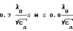
Цель достигается тем, что СВЧ-вывод герметичного корпуса для интегральной схемы СВЧ выполнен в виде микрополосковой линии передачи на прямоугольной диэлектрической подложке, микрополосковая линия передачи выполнена крестообразной формы в виде металлизированных участков прямоугольных расширений с образованием прямоугольного волновода, заполненного диэлектриком шириной 0.7 ![]()
![]()
![]()
![]()
Сущность изобретения заключается в том, что в герметичном корпусе для интегральной схемы СВЧ, содержащем металлическое основание, металлическую крышку с отбортовкой, в прямоугольных сквозных вырезах которой установлены СВЧ-выводы в виде микрополосковой линии передачи на прямоугольной диэлектрической подложке, одна из сторон которой, противоположная размещению микрополосковой линии передачи и две ее торцовые поверхности, параллельные микрополосковой линии передачи и две ее торцовые поверхности, параллельные микрополосковой линии передачи, металлизированы и примыкают к соответствующим поверхностям металлического основания и вертикальным планкам прямоугольных сквозных вырезов отбортовки крышки, согласно изобретению, микрополосковая линия передачи выполнена крестообразной формы в виде металлизированных участков прямоугольных расширений, примыкающих к микрополосковой линии передачи и к двум металлизированным торцовым поверхностям подложки, расстояние между металлизированными торцовыми поверхностями диэлектрической подложки выбрано в пределах
0.7 ![]()
![]()
0.7 ![]()
![]()
Кроме того, герметичный корпус для интегральной схемы СВЧ снабжен штырем, установленным в отверстии металлического основания с возможностью перемещения вдоль оси этого отверстия, в диэлектрической подложке со стороны металлического основания по центру пересечения микрополосковой линии передачи и прямоугольного расширения выполнено глухое отверстие, соосное этому диаметру металлического штыря, не превышающему длину прямоугольного расширения F. In addition, the sealed housing for the microwave integrated circuit is equipped with a pin mounted in the hole of the metal base with the possibility of movement along the axis of this hole, in the dielectric substrate from the side of the metal base at the center of intersection of the microstrip transmission line and the rectangular expansion, a blind hole is made coaxial with this diameter of the metal pin not exceeding the length of the rectangular extension F.
Упрощение конструкции обусловлено снижением более чем на порядок требований к конструктивному допуску на расположение элемента, сочленяемого с токонесущей металлизацией микрополоскового СВЧ-вывода (в предлагаемом устройстве таким элементом является крышка корпуса). Уменьшение уровня электромагнитных потерь обусловлено снижением плотности СВЧ-тока в центральной части токонесущей металлизации микрополоскового СВЧ-вывода из-за расширения ее центральной части и ликвидации паразитного излучения из средней части микрополоскосого проводника. Указанное соотношение для определения F выбрано из условия обеспечения высокого коэффициента трансформации волны квази-ТЕМ-типа, распространяющегося в несимметричной микрополосковой линии, в волну H10, являющуюся основной волной, распространяющейся в прямоугольном микрополосковом расширении.The simplification of the design is due to a decrease by more than an order of requirements for the structural tolerance for the location of the element articulated with current-carrying metallization of the microstrip microwave output (in the proposed device, such an element is the housing cover). The decrease in the level of electromagnetic losses is due to a decrease in the density of the microwave current in the central part of the current-carrying metallization of the microstrip microwave output due to the expansion of its central part and the elimination of spurious radiation from the middle part of the microstrip conductor. The indicated relation for determining F is selected from the condition of ensuring a high coefficient of transformation of a quasi-TEM type wave propagating in an asymmetric microstrip line into an H 10 wave, which is the main wave propagating in a rectangular microstrip extension.
Одинаковый размер ширины диэлектрической подложки и ширины волновода, заполненного диэлектриком, гальваническая связь выреза в отбортовке с микрополосковым расширением позволяет упростить конструкцию корпуса и снизить уровень электромагнитных потерь. Первое обусловлено отсутствием необходимости введения герметизирующей диэлектрической пасты между отбортовкой крышки корпуса и поверхностью диэлектрической подложки вблизи центральной части токонесущей металлизации микрополоскового СВЧ-вывода, а второе - отсутствием излучения из центральной части микрополоскового СВЧ-вывода за счет полной ее экранировки. The same size of the width of the dielectric substrate and the width of the waveguide filled with a dielectric, the galvanic connection of the flanging in the flanging with microstrip expansion makes it possible to simplify the design of the casing and reduce the level of electromagnetic losses. The first is due to the lack of the need to introduce a sealing dielectric paste between the flanging of the housing cover and the surface of the dielectric substrate near the central part of the current-carrying metallization of the microstrip microwave output, and the second due to the absence of radiation from the central part of the microstrip microwave output due to its complete shielding.
Ширина диэлектрической подложки, равная ширине прямоугольного волновода, заполненного диэлектриком W, выбирается из соотношения
0.7 ![]()
![]()
0.7 ![]()
![]()
W>0.7![]()
![]()

Отверстие в диэлектрической подложке микроволнового СВЧ-вывода и металлический штырь, расположенный с возможностью перемещения вдоль оси отверстия, позволяют расширить рабочий диапазон длин волн герметичного корпуса по минимальному уровню электромагнитных потерь за счет уменьшения частотной дисперсии микрополоскового волновода, образованного участками сплошной металлизации и микрополосковым прямоугольным расширением. При величине диаметра металлического штыря более длины микрополоскового прямоугольного расширения ![]()
The hole in the dielectric substrate of the microwave microwave output and a metal pin, located with the possibility of moving along the axis of the hole, allow you to expand the operating range of wavelengths of the sealed enclosure at the minimum level of electromagnetic losses by reducing the frequency dispersion of the microstrip waveguide formed by the areas of continuous metallization and microstrip rectangular expansion. When the diameter of the metal pin is more than the length of the microstrip rectangular expansion ![]()
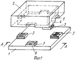
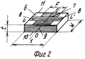
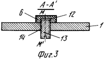
На фиг. 1 корпус с приподнятой крышкой, общий вид; на фиг. 2 - СВЧ-вывод, общий вид; на фиг. 3 - сечение А-А на фиг. 1. In FIG. 1 case with a raised lid, general view; in FIG. 2 - microwave output, general view; in FIG. 3 is a section AA in FIG. 1.
Герметичный корпус содержит металлическое основание 1, металлическую крышку 2 и микрополосковые СВЧ-выводы 3. Крышка 2 имеет отбортовку 4, выполненную перпендикулярно плоскости крышки 2. В отбортовке 4 крышки 2 сделаны прямоугольные сквозные вырезы 5, число которых равно числу микрополосковых СВЧ-выводов 3. Каждый микрополосковый СВЧ-вывод 3 содержит одну прямоугольную диэлектрическию подложку 6, ширина которой равна соответствующему размеру прямоугольного сквозного выреза 5 и ширине прямоугольного микрополоскового расширения W, выбранного из соотношения:
0.7 ![]()
![]()

0.7 ![]()
![]()
На одной из широких поверхностей диэлектрической подложки выполнено микрополосковое прямоугольное расширение 7, оси которого LL' и OO' совпадают с соответствующими осями диэлектрической подложки 6. Длина F прямоугольного микрополоскового расширения 7 определяется рабочим диапазоном частот и составляет

Другие продольные поверхности 9-11 диэлектрической подложки 6 сплошь металлизированы. Диэлектрические подложки 6 расположены в прямоугольных сквозных вырезах 5 отбортовки 4 крышки 2. Толщина отбортовки 4 крышки 2 не превышает длины F микрополоскового прямоугольного расширения 7. Металлическое основание 1, металлизированные поверхности 7,9,10,11 диэлектрической подложки 6 и крышка 2 гальванически связаны, например спаяны между собой так, что отбортовка 4 крышки 2 не выступает за длину F микрополоскового прямоугольного расширения 7 и имеет с ней и с основанием 1 гальваническую связь по всему периметру. Прямоугольный сквозной вырез 5, выполненный в отбортовке 4 крышки 2, также имеет гальваническую связь по периметру с металлизациями 9-11 диэлектрической подложки 6. Other longitudinal surfaces 9-11 of the
Герметичный корпус имеет в диэлектрической подложке 6 глухое отверстие 12, выполненное со стороны основания 1. Ось MM' отверстия 12 проходит через точку пересечения осей OO', LL' и перпендикулярна плоскости диэлектрической подложки 6. В отверстие 12 помещен металлический штырь 13, имеющий возможность перемещения вдоль оси MM' и имеющий контакт по боковой поверхности 14 с металлическим основанием 1. Диаметр штыря 13 не превышает длину F микрополоскового прямоугольного расширения. The sealed enclosure in the
Герметичный корпус работает следующим образом. При возбуждении микрополоскового СВЧ-вывода 3 волна типа квази-ТЕМ распространяется по несимметричной микрополосковой линии, токонесущим проводником которой является микрополосковый проводник 8, имеющий расширение 7, а экранной плоскостью - металлическое основание 1. За счет прямоугольного расширения микрополоскового проводника, ширина W которого выбирается из интервала
0.7 ![]()
![]()

0.7 ![]()
![]()
На выходе микрополоскового волновода волна Н10 трансформируется обратно в волну квази-ТЕМ типа. Длина F, равная 
Уменьшение электромагнитных потерь достигается за счет использования в средней части микрополоскового СВЧ-вывода микрополоскового волновода и, следовательно, снижения концентрации СВЧ-тока в средней части токонесущего проводника, и ликвидации электромагнитного излучения из средней части токонесущего проводника. The reduction of electromagnetic losses is achieved through the use of a microstrip waveguide in the middle part of the microstrip microwave output and, consequently, a decrease in the microwave current concentration in the middle part of the current-carrying conductor, and elimination of electromagnetic radiation from the middle part of the current-carrying conductor.
Герметичность корпуса обеспечивается за счет пайки отбортовки 4 крышки 2 и металлизации 7 диэлектрической подложки 6. The tightness of the housing is ensured by soldering flanging 4 of the
Упрощение конструкции герметичного корпуса связано с использованием однослойного СВЧ-вывода и снижением конструктивного допуска на расположение отбортовки 4 крышки 2 на микрополосковом проводнике 7 диэлектрической подложки 6. The simplification of the design of the sealed enclosure is associated with the use of a single-layer microwave output and a decrease in the structural tolerance for the location of the
Расширение рабочей полосы частот по минимальному уровню электромагнитных потерь и подстройка герметичного корпуса осуществляются путем снижения частотной дисперсии сигнала, распространяющегося в микрополосковом волноводе, образованном металлизированными поверхностями 7,9,10,11 за счет введения металлического штыря 13 в отверстие 12, выполненное в диэлектрической пластине 6. Контакт между боковой поверхностью 14 штыря 13 и основанием 1 позволяет ликвидировать паразитное излучение из корпуса. The extension of the working frequency band for the minimum level of electromagnetic losses and the adjustment of the sealed enclosure are carried out by reducing the frequency dispersion of the signal propagating in the microstrip waveguide formed by the
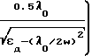
В качестве конкретного примера изготовлен герметичный корпус для интегральных микрополосковых СВЧ-схем. Основание и крышка изготовлены из ковара. Диэлектрическая пластина выполнена из поликора, диэлектрическая проницаемость которого εд равна 9,8. Ширина диэлектрической пластины равна ширине микрополоскового прямоугольного расширения. Последняя выбиралась из соотношения:
0.7 ![]()
![]()
0.7 ![]()
![]()
Корпус, созданный по схеме прототипа, в более низком диапазоне частот (18 ГГц) имеет КСВН= 1,25, а электромагнитные потери 0,5 дБ. The case, created according to the prototype scheme, in the lower frequency range (18 GHz) has a VSWR = 1.25, and the electromagnetic loss is 0.5 dB.
Таким образом, преимуществами герметичного корпуса по сравнению с прототипом являются упрощение конструкции, обусловленное тем, что СВЧ-вывод в корпусе содержит одну диэлектрическую подложку, что позволяет уменьшить число сочленяемых элементов, введение прямоугольного микрополоскового расширения в средней части микрополоскового проводника позволяет снизить более чем на порядок конструктивных допуск на расположение крышки относительно применения герметизирующей диэлектрической пасты в микрополосковых СВЧ-выводах; снижение на 40% уровня электромагнитных потерь путем снижения плотности СВЧ-тока в токонесущем микрополосковом проводнике СВЧ-вывода из-за расширения его центральной части и путем снижения электромагнитного излучения из-за гальванической связи прямоугольного микрополоскового расширения со сплошной металлизацией узких стенок диэлектрической подложки; снижение уровня КСВН до 1,1 и расширение на 10% рабочей полосы частот по минимальному уровню электромагнитных потерь путем уменьшения дисперсии основного типа волны за счет введения микрополоскового прямоугольного расширения, длина которого F определяется из соотношения

Claims (2)
0.7
а длина F прямоугольного расширения вдоль микрополосковой линии передачи выбрана в соответствии с выражением
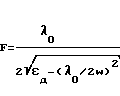
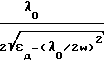
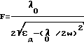
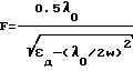
F =

где λ0 - средняя длина рабочего диапазона волн в свободном пространстве,
Eg - диэлектрическая проницаемость материала диэлектрической подложки, при этом металлизированные участки прямоугольных расширений микрополосковой линии передачи электрически контактируют с горизонтальной планкой прямоугольных сквозных вырезов отбортовки крышки.1. A SEALED HOUSING FOR A MICROWAVE INTEGRAL CIRCUIT, comprising a metal base, a flare metal cover, in the rectangular through-cuts of which microwave terminals are installed in the form of a microstrip transmission line on a rectangular dielectric substrate, one side of which is opposite to the placement of the microstrip transmission line, and two its end surfaces parallel to the microstrip transmission line are metallized and are adjacent to the corresponding surfaces of the metal base and vertical bars rim-shaped through-through cut-outs of the flanging of the cover, characterized in that, in order to simplify the design and reduce the level of electromagnetic losses, the microstrip transmission line is made cross-shaped in the form of metallized sections of rectangular extensions adjacent to the microstrip transmission line and to two metallized end surfaces of the substrate, the distance W between the metallized end surfaces of the dielectric substrate is selected within
0.7
and the length F of the rectangular extension along the microstrip transmission line is selected in accordance with the expression
F =
where λ 0 is the average length of the working range of waves in free space,
E g is the dielectric constant of the dielectric substrate material, while the metallized sections of the rectangular extensions of the microstrip transmission line are electrically in contact with the horizontal strip of the rectangular through cut-outs of the flanging of the cover.
Priority Applications (1)
| Application Number | Priority Date | Filing Date | Title |
|---|---|---|---|
| SU4695994 RU2012172C1 (en) | 1989-05-23 | 1989-05-23 | Sealed package for microwave integrated circuits |
Applications Claiming Priority (1)
| Application Number | Priority Date | Filing Date | Title |
|---|---|---|---|
| SU4695994 RU2012172C1 (en) | 1989-05-23 | 1989-05-23 | Sealed package for microwave integrated circuits |
Publications (1)
| Publication Number | Publication Date |
|---|---|
| RU2012172C1 true RU2012172C1 (en) | 1994-04-30 |
Family
ID=21449794
Family Applications (1)
| Application Number | Title | Priority Date | Filing Date |
|---|---|---|---|
| SU4695994 RU2012172C1 (en) | 1989-05-23 | 1989-05-23 | Sealed package for microwave integrated circuits |
Country Status (1)
| Country | Link |
|---|---|
| RU (1) | RU2012172C1 (en) |
Cited By (1)
| Publication number | Priority date | Publication date | Assignee | Title |
|---|---|---|---|---|
| RU2494494C1 (en) * | 2012-04-20 | 2013-09-27 | Федеральное государственное унитарное предприятие "Научно-производственное предприятие "Исток" (ФГУП НПП "Исток") | Method to manufacture body of high-capacity semiconductor microwave instrument |
-
1989
- 1989-05-23 RU SU4695994 patent/RU2012172C1/en active
Cited By (1)
| Publication number | Priority date | Publication date | Assignee | Title |
|---|---|---|---|---|
| RU2494494C1 (en) * | 2012-04-20 | 2013-09-27 | Федеральное государственное унитарное предприятие "Научно-производственное предприятие "Исток" (ФГУП НПП "Исток") | Method to manufacture body of high-capacity semiconductor microwave instrument |
Similar Documents
| Publication | Publication Date | Title |
|---|---|---|
| US5867073A (en) | Waveguide to transmission line transition | |
| US7132905B2 (en) | Input/output coupling structure for dielectric waveguide having conductive coupling patterns separated by a spacer | |
| US5107231A (en) | Dielectric waveguide to TEM transmission line signal launcher | |
| AU2010329983B2 (en) | Microwave transition device between a microstrip line and a rectangular waveguide | |
| US7746191B2 (en) | Waveguide to microstrip line transition having a conductive footprint for providing a contact free element | |
| US20010049266A1 (en) | Structure for connecting non -radiative dielectric waveguide and metal waveguide, millimeter wave transmitting/receiving module and millimeter wave transmitter/receiver | |
| KR100287258B1 (en) | Dielectric Resonator, Dielectric Filter, Duplexer and Communication Device | |
| US3496492A (en) | Microwave strip-in-trough line | |
| US4052683A (en) | Microwave device | |
| CN114188686B (en) | H-face waveguide/microstrip probe conversion device | |
| US4006425A (en) | Dielectric image guide integrated mixer/detector circuit | |
| KR100401964B1 (en) | Filter, multiplexer, and communication apparatus | |
| JP2000101311A (en) | Signal line to wave guide transformer | |
| RU2012172C1 (en) | Sealed package for microwave integrated circuits | |
| EP1605540A1 (en) | Finline type microwave band-pass filter | |
| US20080136550A1 (en) | Line transition device, high-frequency module, and communication apparatus | |
| US6445256B1 (en) | Oscillator and radio equipment | |
| JP3405229B2 (en) | Dielectric line device and transmission device | |
| EP0883204B1 (en) | Nonradiative planar dielectric line and integrated circuit using the same line | |
| US6166614A (en) | Nonradiative planar dielectric line and integrated circuit | |
| KR100358970B1 (en) | Mode Converter | |
| EP0399739A2 (en) | Waveguide switch | |
| JPS60230701A (en) | Radio equipment | |
| KR20050080453A (en) | Non-radiative microstrip line | |
| SU1730697A1 (en) | Stripline antenna |