RU2006103C1 - Integrated circuit of high-voltage rectifier - Google Patents
Integrated circuit of high-voltage rectifier Download PDFInfo
- Publication number
- RU2006103C1 RU2006103C1 SU4951747A RU2006103C1 RU 2006103 C1 RU2006103 C1 RU 2006103C1 SU 4951747 A SU4951747 A SU 4951747A RU 2006103 C1 RU2006103 C1 RU 2006103C1
- Authority
- RU
- Russia
- Prior art keywords
- type
- layer
- conductivity
- type conductivity
- integrated circuit
- Prior art date
Links
- XUIMIQQOPSSXEZ-UHFFFAOYSA-N Silicon Chemical compound [Si] XUIMIQQOPSSXEZ-UHFFFAOYSA-N 0.000 claims description 10
- 230000015556 catabolic process Effects 0.000 claims description 9
- 229910052710 silicon Inorganic materials 0.000 claims description 9
- 239000010703 silicon Substances 0.000 claims description 9
- 239000000758 substrate Substances 0.000 claims description 8
- 238000004377 microelectronic Methods 0.000 abstract description 3
- 238000002347 injection Methods 0.000 abstract 1
- 239000007924 injection Substances 0.000 abstract 1
- 239000000126 substance Substances 0.000 abstract 1
- 238000009792 diffusion process Methods 0.000 description 7
- 239000013078 crystal Substances 0.000 description 3
- 238000005530 etching Methods 0.000 description 3
- 238000000206 photolithography Methods 0.000 description 3
- 229910004298 SiO 2 Inorganic materials 0.000 description 2
- ZOXJGFHDIHLPTG-UHFFFAOYSA-N Boron Chemical compound [B] ZOXJGFHDIHLPTG-UHFFFAOYSA-N 0.000 description 1
- OAICVXFJPJFONN-UHFFFAOYSA-N Phosphorus Chemical compound [P] OAICVXFJPJFONN-UHFFFAOYSA-N 0.000 description 1
- VYPSYNLAJGMNEJ-UHFFFAOYSA-N Silicium dioxide Chemical compound O=[Si]=O VYPSYNLAJGMNEJ-UHFFFAOYSA-N 0.000 description 1
- 229910052796 boron Inorganic materials 0.000 description 1
- 238000005516 engineering process Methods 0.000 description 1
- 238000009413 insulation Methods 0.000 description 1
- 238000001465 metallisation Methods 0.000 description 1
- 238000000034 method Methods 0.000 description 1
- 229910021421 monocrystalline silicon Inorganic materials 0.000 description 1
- 238000002161 passivation Methods 0.000 description 1
- 229910052698 phosphorus Inorganic materials 0.000 description 1
- 239000011574 phosphorus Substances 0.000 description 1
- 229910021420 polycrystalline silicon Inorganic materials 0.000 description 1
- 229920005591 polysilicon Polymers 0.000 description 1
- 238000012552 review Methods 0.000 description 1
- 239000004065 semiconductor Substances 0.000 description 1
- 229910052814 silicon oxide Inorganic materials 0.000 description 1
Images
Landscapes
- Electrodes Of Semiconductors (AREA)
Abstract
Description
Изобретение относится к области микроэлектроники, в частности, к интегральным устройствам, работающим непосредственно от сетевого напряжения 220 В. The invention relates to the field of microelectronics, in particular, to integrated devices operating directly from a mains voltage of 220 V.
Разработка и применение высоковольтного двухполупериодного выпрямителя (диодной сборки и в интегральном исполнении) способствует дальнейшей миниатюризации РЭА с одновременным повышением надежности. The development and application of a high-voltage half-wave rectifier (diode assembly and integrated design) contributes to the further miniaturization of CEA with a simultaneous increase in reliability.
Известно устройство, в котором для создания выпрямительных мостов двухполупериодного выпрямления используются выпрямительные блоки из двух пар диодов: с общим анодом и общим катодом. Выпрямитель, собранный из таких блоков, представляет собой гибридную сборку. A device is known in which rectifier blocks of two pairs of diodes are used to create rectifier bridges of half-wave rectification: with a common anode and a common cathode. A rectifier assembled from such blocks is a hybrid assembly.
Недостатком известного устройства является невысокие значения пробивных напряжений. A disadvantage of the known device is the low value of breakdown voltage.
Наиболее близким техническим решением является интегральная схема высоковольтного выпрямителя, содержащая поликристаллическую несущую подложку, слой высокоомного кремния ориентации [100] n-типа проводимости с приконтактными областями n+-типа проводимости, изолированный от несущей подложки двойным диэлектрическим карманом, в слое n-типа проводимости сформирована область p-типа проводимости, изолированная от высокоомного слоя по торцам V-образными диэлектрическими канавками со всех сторон.The closest technical solution is the integrated circuit of a high-voltage rectifier containing a polycrystalline carrier substrate, a layer of high-resistance silicon of orientation [100] of the n-type conductivity with contact regions of the n + type of conductivity, isolated from the carrier substrate by a double dielectric pocket, in the n-type conductivity layer is formed the p-type region of conductivity isolated from the high-resistance layer at the ends by V-shaped dielectric grooves on all sides.
В таких структурах пробивные напряжения уже достигают 200-300 В. In such structures, breakdown voltages already reach 200-300 V.
Однако использованные в таких структурах технические приемы не позволяют получить пробивные напряжения до 500 В. However, the techniques used in such structures do not allow to obtain breakdown voltages up to 500 V.
Цель изобретения - повышение пробивного напряжения до 500 В и минимизация линейных размеров. The purpose of the invention is to increase the breakdown voltage to 500 V and minimize the linear dimensions.
Поставленная цель достигается тем, что в интегральной схеме высоковольтного выпрямителя, содержащего поликристаллическую несущую подложку, слой высокоомного кремния ориентации [100] n-типа проводимости с приконтактными областями n+-типа проводимости, изолированный от несущей подложки двойным диэлектрическим карманом, в слое n-типа проводимости сформирована область p-типа проводимости, изолированная от высокоомного кремния по торцам V-образными диэлектрическими канавками со всех сторон, расстояние между областями n+-типа и p-типа проводимостей по высокоомному слою вдоль боковых сторон канавок не менее 25 мкм.This goal is achieved by the fact that in the integrated circuit of a high-voltage rectifier containing a polycrystalline carrier substrate, a layer of high-resistance silicon of orientation [100] of the n-type conductivity with contact regions of the n + type conductivity, isolated from the carrier substrate by a double dielectric pocket, in the n-type layer conductivity region is formed p-type conductivity, isolated from the high-resistance silicon at the ends of V-shaped grooves dielectric from all sides, the distance between the regions of n + -type and p-type wire Axle for high resistance layer along the sides of the grooves is not less than 25 microns.
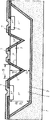
Изобретение поясняется чертежом, на котором представлен поперечный разрез структуры интегральной схемы высоковольтного выпрямителя. The invention is illustrated by the drawing, which shows a cross section of the structure of the integrated circuit of a high-voltage rectifier.
На чертеже обозначено: поликристаллическая несущая подложка 1, области 2 высокоомного кремния ориентации [100] n-типа проводимости, слой 3 диэлектрика, образующий карман с областью 2 высокоомного кремния, пассивирующий слой 4 окиси кремния, области 5 p-типа проводимости, приконтактные области 6 n+-типа проводимости, металлизация 7.The drawing indicates:
Интегральная схема высоковольтного выпрямителя выполнена на структуре КСДИ, которая представляет собой несущую подложку 1 из поликремния, в которой созданы области 2 из монокристаллического кремния с ориентацией [100] с удельным сопротивлением ρ = 20 Ом . см и изолированные диэлектрическим слоем 3, состоящим из термического окисла толщиной 1,2 мкм и пиролитического окисла толщиной 1,5-2 мкм. Глубина исходного кармана перед шлифовкой составляет 30-35 мкм, после вскрытия 20-30 мкм. Структура пассивирована слоем 4 SiO2 (или ССС) толщиной ≥ 1 мкм. Через вскрытые окна в пассивирующем слое 4 созданы активные области 5 p-типа проводимости, имеющие глубину Xjp = 6 ± 1 мкм, поверхностное сопротивление Rs = 100-160 Ом/□ , и области 6 n+-типа проводимости Xjp = 3 мкм, Rs = 2-4 Ом/□ , расстояние между которыми 20 ±1 мкм. Во время диффузии p-область 5 и n+-область 6 диффундируют под маску из слоя 4 на 6 мкм и 3 мкм соответственно. В этом случае расстояние между областью 6 n+-типа проводимости и активной областью 5 p-типа проводимости с учетом растравливания окон при фотолитографии по 1 мкм составляет
20 - (3 + 6 + 2) = 9 мкм, где 20 мкм - расстояние на фотошаблоне между областями 5 и 6,
3 мкм - боковая диффузия n+-типа проводимости,
6 мкм - боковая диффузия p-типа проводимости,
2 мкм - уход размеров при травлении SiO2 при фотолитографиях (под диффузию бора 1 мкм + 1 мкм под диффузию фосфора).The integrated circuit of the high-voltage rectifier is made on the structure of an KSDI, which is a
20 - (3 + 6 + 2) = 9 μm, where 20 μm is the distance on the photomask between regions 5 and 6,
3 μm - lateral diffusion of n + -type conductivity,
6 μm - lateral diffusion of p-type conductivity,
2 μm — size deviation during etching of SiO 2 during photolithography (for
Для кремния удельное сопротивление ρ= 20 Ом . см, что соответствует концентрации N = 2 . 1014 см-3 и ширине области объемного заряда, равной 0-10 мкм, пробивное напряжение Uпроб ≥ 250 В. При напряжениях Uпроб ≥ 250 В происходит смыкание области объемного заряда с n+-областью 6 и пробой диода. Для увеличения пробивных напряжений до 500 В область объемного заряда распространится на ≈ 25 мкм, а напряжение лавинного пробоя для кремния с ρ= 20 Ом . см составит 1000 В.For silicon, the resistivity is ρ = 20 Ohms . cm, which corresponds to a concentration of N = 2 . 10 14 cm -3 and the width of the space charge region equal to 0-10 μm, the breakdown voltage of U samples ≥ 250 V. At voltages U of samples ≥ 250 V, the region of space charge with the n + -region 6 closes and the diode breaks. To increase the breakdown voltages up to 500 V, the space charge region extends to ≈ 25 μm, and the avalanche breakdown voltage for silicon with ρ = 20 Ohms . cm will be 1000 V.
Для реализации в планарном варианте интегральной схемы Uпроб до 500 В общее расстояние между областями 6 и 5 n+-типа проводимости и p-типа проводимости должно быть не менее 36 мкм, которые складываются из:
(1 + 1) мкм - растравливание при фотолитографии,
6 мкм - боковая диффузия активных областей p-типа проводимости;
3 мкм - боковая диффузия n+-типа областей 6;
25 мкм - ширина области объемного заряда при Uпроб = 500 В и ρ = 20 Ом . см.For the implementation in the planar version of the integrated circuit of U samples up to 500 V, the total distance between the regions of 6 and 5 of the n + type of conductivity and p-type conductivity should be at least 36 μm, which are composed of:
(1 + 1) microns - etching during photolithography,
6 μm — lateral diffusion of p-type active regions;
3 μm — lateral diffusion of the n + -type of regions 6;
25 microns - the width of the space charge region at U samples = 500 V and ρ = 20 Ohms . cm.
При зазорах между областями 5 и 6 p-типа и n+-типов проводимости соответственно 36 мкм область объемного заряда при обратном смещении в 500 В не приводит к смыканию с областью n+-типа проводимости и к пробою диода.For gaps between regions 5 and 6 of the p-type and n + types of conductivity, respectively 36 μm, the space charge region with a reverse bias of 500 V does not lead to the closure of the diode with the region of the n + type conductivity.
За счет уменьшения зазоров между областями 5 и 6 соответственно можно уменьшить размер кристалла по каждой его стороне, что увеличит съем кристаллов с пластины. By reducing the gaps between regions 5 and 6, respectively, it is possible to reduce the size of the crystal on each side thereof, which will increase the removal of crystals from the plate.
Изобретение позволяет по сравнению с известными приборами повысить пробивные напряжения до 500 В и увеличить съем кристаллов с пластины КСДИ более, чем на 50% . (56) Зи С. М. Физика полупроводниковых приборов. М. , Мир, т. 1, 1984, с. 295. The invention allows, in comparison with known devices, to increase the breakdown voltage to 500 V and to increase the removal of crystals from the KSDI plate by more than 50%. (56) Zi S.M. Physics of semiconductor devices. M., World, vol. 1, 1984, p. 295.
Брюхно Н. А. и др. Кремниевые структуры с диэлектрической изоляцией для изделий микроэлектроники. Обзоры по электронной технике, серия 3, вып. 4 (1304), 1987, с. 10-11, рис. 66. Bryukhno N. A. et al. Silicon structures with dielectric insulation for microelectronics products. Electronic Technology Reviews,
Claims (1)
Priority Applications (1)
| Application Number | Priority Date | Filing Date | Title |
|---|---|---|---|
| SU4951747 RU2006103C1 (en) | 1991-06-28 | 1991-06-28 | Integrated circuit of high-voltage rectifier |
Applications Claiming Priority (1)
| Application Number | Priority Date | Filing Date | Title |
|---|---|---|---|
| SU4951747 RU2006103C1 (en) | 1991-06-28 | 1991-06-28 | Integrated circuit of high-voltage rectifier |
Publications (1)
| Publication Number | Publication Date |
|---|---|
| RU2006103C1 true RU2006103C1 (en) | 1994-01-15 |
Family
ID=21582570
Family Applications (1)
| Application Number | Title | Priority Date | Filing Date |
|---|---|---|---|
| SU4951747 RU2006103C1 (en) | 1991-06-28 | 1991-06-28 | Integrated circuit of high-voltage rectifier |
Country Status (1)
| Country | Link |
|---|---|
| RU (1) | RU2006103C1 (en) |
-
1991
- 1991-06-28 RU SU4951747 patent/RU2006103C1/en active
Similar Documents
| Publication | Publication Date | Title |
|---|---|---|
| US11107912B2 (en) | Trench gate semiconductor device with dummy gate electrode and manufacturing method of the same | |
| US5321295A (en) | Insulated gate bipolar transistor and method of fabricating the same | |
| JP2988871B2 (en) | Trench gate power MOSFET | |
| US7572683B2 (en) | Semiconductor device, the method of manufacturing the same, and two-way switching device using the semiconductor devices | |
| US6462377B2 (en) | Insulated gate field effect device | |
| JP2585331B2 (en) | High breakdown voltage planar element | |
| US6445038B1 (en) | Silicon on insulator high-voltage switch | |
| EP1227522A2 (en) | High breakdown voltage semiconductor device | |
| US4298881A (en) | Semiconductor device with double moat and double channel stoppers | |
| US20020149051A1 (en) | Superjunction device with self compensated trench walls | |
| JPH07169950A (en) | MOSFET device | |
| EP1290735A1 (en) | A semiconductor device | |
| US5677562A (en) | Planar P-N junction semiconductor structure with multilayer passivation | |
| JPH0457111B2 (en) | ||
| EP0071335B1 (en) | Field effect transistor | |
| CN111816694B (en) | Superjunction semiconductor device and method for manufacturing superjunction semiconductor device | |
| US5323041A (en) | High-breakdown-voltage semiconductor element | |
| US4520382A (en) | Semiconductor integrated circuit with inversion preventing electrode | |
| JP7750425B2 (en) | Semiconductor device and method for manufacturing the same | |
| RU2006103C1 (en) | Integrated circuit of high-voltage rectifier | |
| JP3523458B2 (en) | High avalanche withstand MOSFET and method of manufacturing the same | |
| WO2024262142A1 (en) | Semiconductor device and method for manufacturing semiconductor device | |
| RU2006104C1 (en) | High-voltage integrated circuit | |
| KR19980035251A (en) | Semiconductor device having double epitaxial layer and buried region and manufacturing method thereof | |
| JPS5972764A (en) | Semiconductor device |