NL2005521A - Methods and apparatus for calculating electromagnetic scattering properties of a structure using a normal-vector field and for reconstruction of approximate structures. - Google Patents
Methods and apparatus for calculating electromagnetic scattering properties of a structure using a normal-vector field and for reconstruction of approximate structures. Download PDFInfo
- Publication number
- NL2005521A NL2005521A NL2005521A NL2005521A NL2005521A NL 2005521 A NL2005521 A NL 2005521A NL 2005521 A NL2005521 A NL 2005521A NL 2005521 A NL2005521 A NL 2005521A NL 2005521 A NL2005521 A NL 2005521A
- Authority
- NL
- Netherlands
- Prior art keywords
- normal
- field
- vector
- vector field
- operator
- Prior art date
Links
Classifications
-
- G—PHYSICS
- G03—PHOTOGRAPHY; CINEMATOGRAPHY; ANALOGOUS TECHNIQUES USING WAVES OTHER THAN OPTICAL WAVES; ELECTROGRAPHY; HOLOGRAPHY
- G03F—PHOTOMECHANICAL PRODUCTION OF TEXTURED OR PATTERNED SURFACES, e.g. FOR PRINTING, FOR PROCESSING OF SEMICONDUCTOR DEVICES; MATERIALS THEREFOR; ORIGINALS THEREFOR; APPARATUS SPECIALLY ADAPTED THEREFOR
- G03F7/00—Photomechanical, e.g. photolithographic, production of textured or patterned surfaces, e.g. printing surfaces; Materials therefor, e.g. comprising photoresists; Apparatus specially adapted therefor
- G03F7/70—Microphotolithographic exposure; Apparatus therefor
- G03F7/70483—Information management; Active and passive control; Testing; Wafer monitoring, e.g. pattern monitoring
- G03F7/70605—Workpiece metrology
- G03F7/70616—Monitoring the printed patterns
- G03F7/70625—Dimensions, e.g. line width, critical dimension [CD], profile, sidewall angle or edge roughness
-
- G—PHYSICS
- G03—PHOTOGRAPHY; CINEMATOGRAPHY; ANALOGOUS TECHNIQUES USING WAVES OTHER THAN OPTICAL WAVES; ELECTROGRAPHY; HOLOGRAPHY
- G03F—PHOTOMECHANICAL PRODUCTION OF TEXTURED OR PATTERNED SURFACES, e.g. FOR PRINTING, FOR PROCESSING OF SEMICONDUCTOR DEVICES; MATERIALS THEREFOR; ORIGINALS THEREFOR; APPARATUS SPECIALLY ADAPTED THEREFOR
- G03F7/00—Photomechanical, e.g. photolithographic, production of textured or patterned surfaces, e.g. printing surfaces; Materials therefor, e.g. comprising photoresists; Apparatus specially adapted therefor
- G03F7/70—Microphotolithographic exposure; Apparatus therefor
- G03F7/70483—Information management; Active and passive control; Testing; Wafer monitoring, e.g. pattern monitoring
- G03F7/70491—Information management, e.g. software; Active and passive control, e.g. details of controlling exposure processes or exposure tool monitoring processes
- G03F7/705—Modelling or simulating from physical phenomena up to complete wafer processes or whole workflow in wafer productions
-
- G—PHYSICS
- G01—MEASURING; TESTING
- G01N—INVESTIGATING OR ANALYSING MATERIALS BY DETERMINING THEIR CHEMICAL OR PHYSICAL PROPERTIES
- G01N21/00—Investigating or analysing materials by the use of optical means, i.e. using sub-millimetre waves, infrared, visible or ultraviolet light
- G01N21/84—Systems specially adapted for particular applications
- G01N21/88—Investigating the presence of flaws or contamination
- G01N21/95—Investigating the presence of flaws or contamination characterised by the material or shape of the object to be examined
- G01N21/9501—Semiconductor wafers
-
- G—PHYSICS
- G01—MEASURING; TESTING
- G01N—INVESTIGATING OR ANALYSING MATERIALS BY DETERMINING THEIR CHEMICAL OR PHYSICAL PROPERTIES
- G01N21/00—Investigating or analysing materials by the use of optical means, i.e. using sub-millimetre waves, infrared, visible or ultraviolet light
- G01N21/84—Systems specially adapted for particular applications
- G01N21/88—Investigating the presence of flaws or contamination
- G01N21/95—Investigating the presence of flaws or contamination characterised by the material or shape of the object to be examined
- G01N21/956—Inspecting patterns on the surface of objects
- G01N21/95607—Inspecting patterns on the surface of objects using a comparative method
Description
METHODS AND APPARATUS FOR CALCULATING ELECTROMAGNETIC
SCATTERING PROPERTIES OF A STRUCTURE USING A NORMAL-VECTOR FIELDAND FOR RECONSTRUCTION OF APPROXIMATE STRUCTURES
FIELD
[0001] The present invention relates to calculation of electromagnetic scatteringproperties of periodic structures using a normal-vector field. The invention may beapplied for example in metrology of microscopic structures, for example to assesscritical dimensions (CD) performance of a lithographic apparatus.
BACKGROUND
[0002] A lithographic apparatus is a machine that applies a desired pattern onto asubstrate, usually onto a target portion of the substrate. A lithographic apparatus canbe used, for example, in the manufacture of integrated circuits (ICs). In that instance,a patterning device, which is alternatively referred to as a mask or a reticle, may beused to generate a circuit pattern to be formed on an individual layer of the IC. Thispattern can be transferred onto a target portion (e.g., comprising part of, one, orseveral dies) on a substrate (e.g., a silicon wafer). Transfer of the pattern is typicallyvia imaging onto a layer of radiation-sensitive material (resist) provided on thesubstrate. In general, a single substrate will contain a network of adjacent targetportions that are successively patterned. Known lithographic apparatus include so-called steppers, in which each target portion is irradiated by exposing an entire patternonto the target portion at one time, and so-called scanners, in which each targetportion is irradiated by scanning the pattern through a radiation beam in a givendirection (the “scanning”-direction) while synchronously scanning the substrateparallel or anti-parallel to this direction. It is also possible to transfer the pattern fromthe patterning device to the substrate by imprinting the pattern onto the substrate.
[0003] In order to monitor the lithographic process, it is necessary to measureparameters of the patterned substrate, for example the overlay error betweensuccessive layers formed in or on it. There are various techniques for makingmeasurements of the microscopic structures formed in lithographic processes,including the use of scanning electron microscopes and various specialized tools.One form of specialized inspection tool is a scatterometer in which a beam ofradiation is directed onto a target on the surface of the substrate and properties of the scattered or reflected beam are measured. By comparing the properties of the beambefore and after it has been reflected or scattered by the substrate, the properties of thesubstrate can be determined. This can be done, for example, by comparing thereflected beam with data stored in a library of known measurements associated withknown substrate properties. Two main types of scatterometer are known.Spectroscopic scatterometers direct a broadband radiation beam onto the substrate andmeasure the spectrum (intensity as a function of wavelength) of the radiation scatteredinto a particular narrow angular range. Angularly resolved scatterometers use amonochromatic radiation beam and measure the intensity of the scattered radiation asa function of angle.
[0004] More generally, it would be useful to be able to compare the scatteredradiation with scattering behaviors predicted mathematically from models ofstructures, which can be freely set up and varied until the predicted behavior matchesthe observed scattering from a real sample. Unfortunately, although it is in principleknown how to model the scattering by numerical procedures, the computationalburden of the known techniques renders such techniques impractical, particularly ifreal-time reconstruction is desired, and/or where the structures involved are morecomplicated than a simple structure periodic in one-dimension.
SUMMARY
[0005] It is desirable in the field of semiconductor processing to rapidly performaccurate calculations of electromagnetic scattering properties of periodic structures.
[0006] According to a first aspect of the invention, there is provided a method ofcalculating electromagnetic scattering properties of a structure, the structure includingmaterials of differing properties such as to cause a discontinuity in an electromagneticfield at a material boundary, the method comprising: generating a localized normal-vector field in a region of the structure defined with reference to the materialboundary, constructing a vector field that is continuous at the material boundary byusing the normal-vector field to select continuous components of the electromagneticfield tangential to the material boundary and to select continuous components of acorresponding electromagnetic flux density normal to the material boundary,performing a localized integration of the normal-vector field over the region todetermine coefficients of a field-material interaction operator, numerically determining a component of the electromagnetic field by using the field-materialinteraction operator to operate on the vector field, and calculating electromagneticscattering properties of the structure using the determined component of theelectromagnetic field.
[0007] According to a second aspect of the invention, there is provided a method ofreconstructing an approximate structure of an object from a detected electromagneticscattering property arising from illumination of the object by radiation, the methodcomprising the steps: estimating at least one structural parameter, determining at leastone model electromagnetic scattering property from the at least one structuralparameter, comparing the detected electromagnetic scattering property to the at leastone model electromagnetic scattering property, and determining an approximateobject structure based on the result of the comparison, wherein the modelelectromagnetic scattering property is determined using a method according to thefirst aspect.
[0008] According to a third aspect of the invention, there is provided an inspectionapparatus for reconstructing an approximate structure of an object, the inspectionapparatus comprising: an illumination system configured to illuminate the object withradiation, a detection system configured to detect an electromagnetic scatteringproperty arising from the illumination: a processor configured to: estimate at least onestructural parameter, determine at least one model electromagnetic scattering propertyfrom the at least one structural parameter, compare the detected electromagneticscattering property to the at least one model electromagnetic scattering property, anddetermine an approximate object structure from a difference between the detectedelectromagnetic scattering property and the at least one model electromagneticscattering property, wherein the processor is configured to determine the modelelectromagnetic scattering property using a method according to the first aspect.
[0009] According to a fourth aspect of the invention, there is provided a computerprogram product containing one or more sequences of machine-readable instructionsfor calculating electromagnetic scattering properties of a structure, the instructionsbeing adapted to cause one or more processors to perform a method according to thefirst aspect.
[0010] Further features and advantages of the invention, as well as the structure andoperation of various embodiments of the invention, are described in detail below with reference to the accompanying drawings. It is noted that the invention is not limitedto the specific embodiments described herein. Such embodiments are presentedherein for illustrative purposes only. Additional embodiments will be apparent topersons skilled in the relevant art(s) based on the teachings contained herein.
BRIEF DESCRIPTION OF THE DRAWINGS/FIGURES
[0011] The accompanying drawings, which are incorporated herein and form part ofthe specification, illustrate the present invention and, together with the description,further serve to explain the principles of the invention and to enable a person skilledin the relevant art(s) to make and use the invention.
[0012] Figure 1 depicts a lithographic apparatus.
[0013] Figure 2 depicts a lithographic cell or cluster.
[0014] Figure 3 depicts a first scatterometer.
[0015] Figure 4 depicts a second scatterometer.
[0016] Figure 5 depicts a first example process using an embodiment of the invention for reconstruction of a structure from scatterometer measurements.
[0017] Figure 6 depicts a second example process using an embodiment of theinvention for reconstruction of a structure from scatterometer measurements.
[0018] Figure 7a is a flowchart of the Rigorous Coupled Wave Analysis (RCWA)method of calculating electromagnetic scattering properties of a structure.
[0019] Figure 7b is a flowchart of the differential method of calculating electromagnetic scattering properties of a structure.
[0020] Figure 8 depicts the scattering geometry that may be reconstructed in accordance with an embodiment of the present invention.
[0021] Figure 9 depicts the structure of the background and illustrates use of aGreen’s function to calculate the interaction of the incident field with the layeredmedium.
[0022] Figure 10 is a flow chart of the high level method of solving the linear systemcorresponding to the VIM formula.
[0023] Figure 11 is a flow chart of the computation of update vectors using the VIMformula as known in the prior art.
[0024] Figure 12 depicts an embodiment of the present invention using a continuousvector field to numerically solve the VIM formula.
[0025] Figure 13 is a flow chart of the computation of update vectors in accordancewith an embodiment of present invention.
[0026] Figure 14 is a flow chart of a method of calculating electromagnetic scatteringproperties of a structure in accordance with an embodiment of present invention.
[0027] Figure 15a is a definition of global (x, y) and local (x", y") coordinate systems for the rotated ellipse with offset c0.
[0028] Figure 15b illustrates a NV field for the elliptical coordinate system.
[0029] Figure 15c illustrates conformal mapping for an ellipse.
[0030] Figure 16a illustrates continuous NV field for the rectangle.
[0031] Figure 16b illustrates discontinuous NV field for the rectangle.
[0032] Figure 17 illustrates meshing a ‘dogbone’ in elementary shapes.
[0033] Figure 18 illustrates building the normal-vector field of a prism with a crosssection of a rounded rectangle from smaller rectangles and circle segments inaccordance with an embodiment of the present invention.
[0034] Figure 19 illustrates rotated and shifted triangle with NV field and localcoordinate system.
[0035] Figure 20 illustrates a rotated and shifted trapezoid with NV field and localcoordinate system.
[0036] Figure 21 illustrates rotated and shifted circle segment with NV field and localcoordinate system.
[0037] The features and advantages of the present invention will become moreapparent from the detailed description set forth below when taken in conjunction withthe drawings, in which like reference characters identify corresponding elementsthroughout. In the drawings, like reference numbers generally indicate identical,functionally similar, and/or structurally similar elements. The drawing in which anelement first appears is indicated by the leftmost digit(s) in the correspondingreference number.
DETAILED DESCRIPTION
[0038] This specification discloses one or more embodiments that incorporate thefeatures of this invention. The disclosed embodiment(s) merely exemplify theinvention. The scope of the invention is not limited to the disclosed embodiment(s).The invention is defined by the clauses appended hereto.
[0039] The embodiment(s) described, and references in the specification to "oneembodiment", "an embodiment", "an example embodiment", etc., indicate that theembodiment(s) described may include a particular feature, structure, or characteristic,but every embodiment may not necessarily include the particular feature, structure, orcharacteristic. Moreover, such phrases are not necessarily referring to the sameembodiment. Further, when a particular feature, structure, or characteristic isdescribed in connection with an embodiment, it is understood that it is within theknowledge of one skilled in the art to effect such feature, structure, or characteristic inconnection with other embodiments whether or not explicitly described.
[0040] Embodiments of the invention may be implemented in hardware, firmware,software, or any combination thereof. Embodiments of the invention may also beimplemented as instructions stored on a machine-readable medium, which may beread and executed by one or more processors. A machine-readable medium mayinclude any mechanism for storing or transmitting information in a form readable by amachine (e.g., a computing device). For example, a machine-readable medium mayinclude read only memory (ROM); random access memory (RAM); magnetic diskstorage media; optical storage media; flash memory devices; electrical, optical,acoustical or other forms of propagated signals (e.g., carrier waves, infrared signals,digital signals, etc.), and others. Further, firmware, software, routines, instructionsmay be described herein as performing certain actions. However, it should beappreciated that such descriptions are merely for convenience and that such actions infact result from computing devices, processors, controllers, or other devices executingthe firmware, software, routines, instructions, etc.
[0041] Before describing such embodiments in more detail, however, it is instructiveto present an example environment in which embodiments of the present inventionmay be implemented.
[0042] Figure 1 schematically depicts a lithographic apparatus. The apparatuscomprises: an illumination system (illuminator) IL configured to condition a radiationbeam B (e.g., UV radiation or DUV radiation), a support structure (e.g., a mask table)MT constructed to support a patterning device (e.g., a mask) MA and connected to afirst positioner PM configured to accurately position the patterning device inaccordance with certain parameters, a substrate table (e.g., a wafer table) WTconstructed to hold a substrate (e.g., a resist-coated wafer) W and connected to a second positioner PW configured to accurately position the substrate in accordancewith certain parameters, and a projection system (e.g., a refractive projection lenssystem) PL configured to project a pattern imparted to the radiation beam B bypatterning device MA onto a target portion C (e.g., comprising one or more dies) ofthe substrate W.
[0043] The illumination system may include various types of optical components,such as refractive, reflective, magnetic, electromagnetic, electrostatic or other types ofoptical components, or any combination thereof, for directing, shaping, or controllingradiation.
[0044] The support structure supports, i.e. bears the weight of, the patterning device.It holds the patterning device in a manner that depends on the orientation of thepatterning device, the design of the lithographic apparatus, and other conditions, suchas for example whether or not the patterning device is held in a vacuum environment.The support structure can use mechanical, vacuum, electrostatic or other clampingtechniques to hold the patterning device. The support structure may be a frame or atable, for example, which may be fixed or movable as required. The support structuremay ensure that the patterning device is at a desired position, for example with respectto the projection system. Any use of the terms “reticle” or “mask” herein may beconsidered synonymous with the more general term “patterning device.”
[0045] The term “patterning device” used herein should be broadly interpreted asreferring to any device that can be used to impart a radiation beam with a pattern in itscross-section such as to create a pattern in a target portion of the substrate. It shouldbe noted that the pattern imparted to the radiation beam may not exactly correspond tothe desired pattern in the target portion of the substrate, for example if the patternincludes phase-shifting features or so called assist features. Generally, the patternimparted to the radiation beam will correspond to a particular functional layer in adevice being created in the target portion, such as an integrated circuit.
[0046] The patterning device may be transmissive or reflective. Examples ofpatterning devices include masks, programmable mirror arrays, and programmableLCD panels. Masks are well known in lithography, and include mask types such asbinary, alternating phase-shift, and attenuated phase-shift, as well as various hybridmask types. An example of a programmable mirror array employs a matrixarrangement of small mirrors, each of which can be individually tilted so as to reflect an incoming radiation beam in different directions. The tilted mirrors impart a patternin a radiation beam, which is-reflected by the mirror matrix.
[0047] The term “projection system” used herein should be broadly interpreted asencompassing any type of projection system, including refractive, reflective,catadioptric, magnetic, electromagnetic and electrostatic optical systems, or anycombination thereof, as appropriate for the exposure radiation being used, or for otherfactors such as the use of an immersion liquid or the use of a vacuum. Any use of theterm “projection lens” herein may be considered as synonymous with the moregeneral term “projection system”.
[0048] As here depicted, the apparatus is of a transmissive type (e.g., employing atransmissive mask). Alternatively, the apparatus may be of a reflective type (e.g.,employing a programmable mirror array of a type as referred to above, or employinga reflective mask).
[0049] The lithographic apparatus may be of a type having two (dual stage) or moresubstrate tables (and/or two or more mask tables). In such “multiple stage” machinesthe additional tables may be used in parallel, or preparatory steps may be carried outon one or more tables while one or more other tables are being used for exposure.
[0050] The lithographic apparatus may also be of a type wherein at least a portion ofthe substrate may be covered by a liquid having a relatively high refractive index, e.g.,water, so as to fill a space between the projection system and the substrate.-Animmersion liquid may also be applied to other spaces in the lithographic apparatus, forexample, between the mask and the projection system. Immersion techniques are wellknown in the art for increasing the numerical aperture of projection systems. Theterm “immersion” as used herein does not mean that a structure, such as a substrate,must be submerged in liquid, but rather only means that liquid is located between theprojection system and the substrate during exposure.
[0051] Referring to Figure 1, the illuminator IL receives a radiation beam from aradiation source SO. The source and the lithographic apparatus may be separateentities, for example when the source is an excimer laser. In such cases, the source isnot considered to form part of the lithographic apparatus and the radiation beam ispassed from the source SO to the illuminator IL with the aid of a beam deliverysystem BD comprising, for example, suitable directing mirrors and/or a beamexpander. In other cases the source may be an integral part of the lithographic apparatus, for example when the source is a mercury lamp. The source SO and theilluminator IL, together with the beam delivery system BD if required, may bereferred to as a radiation system.
[0052] The illuminator IL may comprise an adjuster AD for adjusting the angularintensity distribution of the radiation beam. Generally, at least the outer and/or innerradial extent (commonly referred to as σ-outer and σ-inner, respectively) of theintensity distribution in a pupil plane of the illuminator can be adjusted. In addition,the illuminator IL may comprise various other components, such as an integrator INand a condenser CO. The illuminator may be used to condition the radiation beam, tohave a desired uniformity and intensity distribution in its cross-section.
[0053] The radiation beam B is incident on the patterning device (e.g., mask MA),which is held on the support structure (e.g., mask table MT), and is patterned by thepatterning device. Having traversed the mask MA, the radiation beam B passesthrough the projection system PL, which focuses the beam onto a target portion C ofthe substrate W. With the aid of the second positioner PW and position sensor IF(e.g., an interferometric device, linear encoder, 2-D encoder or capacitive sensor), thesubstrate table WT can be moved accurately, e.g., so as to position different targetportions C in the path of the radiation beam B. Similarly, the first positioner PM andanother position sensor (which is not explicitly depicted in Figure 1) can be used toaccurately position the mask MA with respect to the path of the radiation beam B,e.g., after mechanical retrieval from a mask library, or during a scan. In general,movement of the mask table MT may be realized with the aid of a long-stroke module(coarse positioning) and a short-stroke module (fine positioning), which form part ofthe first positioner PM. Similarly, movement of the substrate table WT may berealized using a long-stroke module and a short-stroke module, which form part of thesecond positioner PW. In the case of a stepper (as opposed to a scanner) the masktable MT may be connected to a short-stroke actuator only, or may be fixed. MaskMA and substrate W may be aligned using mask alignment marks Ml, M2 andsubstrate alignment marks PI, P2. Although the substrate alignment marks asillustrated occupy dedicated target portions, they may be located in spaces betweentarget portions (these are known as scribe-lane alignment marks). Similarly, insituations in which more than one die is provided on the mask MA, the maskalignment marks may be located between the dies.
[0054] The depicted apparatus could be used in at least one of the following modes: 1. In step mode, the mask table MT and the substrate table WT are keptessentially stationary, while an entire pattern imparted to the radiation beam isprojected onto a target portion C at one time (i.e. a single static exposure). Thesubstrate table WT is then shifted in the X and/or Y direction so that a different targetportion C can be exposed. In step mode, the maximum size of the exposure fieldlimits the size of the target portion C imaged in a single static exposure.
2. In scan mode, the mask table MT and the substrate table WT are scannedsynchronously while a pattern imparted to the radiation beam is projected onto atarget portion C (i.e. a single dynamic exposure). The velocity and direction of thesubstrate table WT relative to the mask table MT may be determined by the (de-)magnification and image reversal characteristics of the projection system PL. In scanmode, the maximum size of the exposure field limits the width (in the non-scanningdirection) of the target portion in a single dynamic exposure, whereas the length of thescanning motion determines the height (in the scanning direction) of the targetportion.
3. In another mode, the mask table MT is kept essentially stationary holding aprogrammable patterning device, and the substrate table WT is moved or scannedwhile a pattern imparted to the radiation beam is projected onto a target portion C. Inthis mode, generally a pulsed radiation source is employed and the programmablepatterning device is updated as required after each movement of the substrate tableWT or in between successive radiation pulses during a scan. This mode of operationcan be readily applied to maskless lithography that utilizes programmable patterningdevice, such as a programmable mirror array of a type as referred to above.
[0055] Combinations and/or variations on the above described modes of use orentirely different modes of use may also be employed.
[0056] As shown in Figure 2, the lithographic apparatus LA forms part of alithographic cell LC, also sometimes referred to a lithocell or cluster, which alsoincludes apparatus to perform pre- and post-exposure processes on a substrate.Conventionally these include spin coaters SC to deposit resist layers, developers DEto develop exposed resist, chill plates CH and bake plates BK. A substrate handler, orrobot, RO picks up substrates from input/output ports I/O 1, 1/02, moves thembetween the different process apparatus and delivers then to the loading bay LB of the lithographic apparatus. These devices, which are often collectively referred to as thetrack, are under the control of a track control unit TCU which is itself controlled bythe supervisory control system SCS, which also controls the lithographic apparatusvia lithography control unit LACU. Thus, the different apparatus can be operated tomaximize throughput and processing efficiency.
[0057] In order that the substrates that are exposed by the lithographic apparatus areexposed correctly and consistently, it is desirable to inspect exposed substrates tomeasure properties such as overlay errors between subsequent layers, line thicknesses,critical dimensions (CD), etc. If errors are detected, adjustments may be made toexposures of subsequent substrates, especially if the inspection can be done soon andfast enough that other substrates of the same batch are still to be exposed. Also,already exposed substrates may be stripped and reworked - to improve yield - ordiscarded, thereby avoiding performing exposures on substrates that are known to befaulty. In a case where only some target portions of a substrate are faulty, furtherexposures can be performed only on those target portions which are good.
[0058] An inspection apparatus is used to determine the properties of the substrates,and in particular, how the properties of different substrates or different layers of thesame substrate vary from layer to layer. The inspection apparatus may be integratedinto the lithographic apparatus LA or the lithocell LC or may be a stand-alone device.To enable most rapid measurements, it is desirable that the inspection apparatusmeasure properties in the exposed resist layer immediately after the exposure.However, the latent image in the resist has a very low contrast - there is only a verysmall difference in refractive index between the parts of the resist which have beenexposed to radiation and those which have not - and not all inspection apparatus havesufficient sensitivity to make useful measurements of the latent image. Thereforemeasurements may be taken after the post-exposure bake step (PEB) which iscustomarily the first step carried out on exposed substrates and increases the contrastbetween exposed and unexposed parts of the resist. At this stage, the image in theresist may be referred to as semi-latent. It is also possible to make measurements ofthe developed resist image - at which point either the exposed or unexposed parts ofthe resist have been removed - or after a pattern transfer step such as etching. Thelatter possibility limits the possibilities for rework of faulty substrates but may stillprovide useful information.
[0059] Figure 3 depicts a scatterometer which may be used in an embodiment of thepresent invention. It comprises a broadband (white light) radiation projector 2 whichprojects radiation onto a substrate W. The reflected radiation is passed to aspectrometer detector 4, which measures a spectrum 10 (intensity as a function ofwavelength) of the specular reflected radiation. From this data, the structure orprofile giving rise to the detected spectrum may be reconstructed by processing unitPU, e.g., conventionally by Rigorous Coupled Wave Analysis (RCWA) and non¬linear regression or by comparison with a library of simulated spectra as shown at thebottom of Figure 3. In general, for the reconstruction the general form of the structureis known and some parameters are assumed from knowledge of the process by whichthe structure was made, leaving only a few parameters of the structure to bedetermined from the scatterometry data. Such a scatterometer may be configured as anormal-incidence scatterometer or an oblique-incidence scatterometer.
[0060] Another scatterometer that may be used in an embodiment of the presentinvention is shown in Figure 4. In this device, the radiation emitted by radiationsource 2 is focused using lens system 12 through interference filter 13 and polarizer17, reflected by partially reflected surface 16 and is focused onto substrate W via amicroscope objective lens 15, which has a high numerical aperture (NA), preferably atleast 0.9 and more preferably at least 0.95. Immersion scatterometers may even havelenses with numerical apertures over 1. The reflected radiation then transmits throughpartially reflective surface 16 into a detector 18 in order to have the scatter spectrumdetected. The detector may be located in the back-projected pupil plane 11, which isat the focal length of the lens system 15, however the pupil plane may instead be re¬imaged with auxiliary optics (not shown) onto the detector. The pupil plane is theplane in which the radial position of radiation defines the angle of incidence and theangular position defines azimuth angle of the radiation. The detector is preferably atwo-dimensional detector so that a two-dimensional angular scatter spectrum of asubstrate target 30 can be measured. The detector 18 may be, for example, an array ofCCD or CMOS sensors, and may use an integration time of, for example, 40milliseconds per frame.
[0061] A reference beam is often used for example to measure the intensity of theincident radiation. To do this, when the radiation beam is incident on the beamsplitter 16 part of it is transmitted through the beam splitter as a reference beam towards a reference mirror 14. The reference beam is then projected onto a differentpart of the same detector 18.
[0062] A set of interference filters 13 is available to select a wavelength of interest inthe range of, say, 405 - 790 nm or even lower, such as 200 - 300 nm. The interferencefilter may be tunable rather than comprising a set of different filters. A grating couldbe used instead of interference filters.
[0063] The detector 18 may measure the intensity of scattered light at a singlewavelength (or narrow wavelength range), the intensity separately at multiplewavelengths or integrated over a wavelength range. Furthermore, the detector mayseparately measure the intensity of transverse magnetic- and transverse electric-polarized light and/or the phase difference between the transverse magnetic- andtransverse electric-polarized light.
[0064] Using a broadband light source (i.e. one with a wide range of light frequenciesor wavelengths - and therefore of colors) is possible, which gives a large etendue,allowing the mixing of multiple wavelengths. The plurality of wavelengths in thebroadband preferably each has a bandwidth of Δλ and a spacing of at least 2 Δλ (i.e.twice the bandwidth). Several “sources” of radiation can be different portions of anextended radiation source which have been split using fiber bundles. In this way,angle resolved scatter spectra can be measured at multiple wavelengths in parallel. A3-D spectrum (wavelength and two different angles) can be measured, which containsmore information than a 2-D spectrum. This allows more information to be measuredwhich increases metrology process robustness. This is described in more detail inEP1,628,164A.
[0065] The target 30 on substrate W may be a grating, which is printed such that afterdevelopment, the bars are formed of solid resist lines. The bars may alternatively beetched into the substrate. This pattern is sensitive to chromatic aberrations in thelithographic projection apparatus, particularly the projection system PL, andillumination symmetry and the presence of such aberrations will manifest themselvesin a variation in the printed grating. Accordingly, the scatterometry data of the printedgratings is used to reconstruct the gratings. The parameters of the grating, such as linewidths and shapes, may be input to the reconstruction process, performed byprocessing unit PU, from knowledge of the printing step and/or other scatterometryprocesses.
Modelling
As described above, the target is on the surface of the substrate. This target will often take theshape of a series of lines in a grating or substantially rectangular structures in a 2-D array.
The purpose of rigorous optical diffraction theories in metrology is effectively the calculationof a diffraction spectrum that is reflected from the target. In other words, target shapeinformation is obtained for CD (critical dimension) uniformity and overlay metrology.Overlay metrology is a measuring system in which the overlay of two targets is measured inorder to determine whether two layers on a substrate or aligned or not. CD uniformity issimply a measurement of the uniformity of the grating on the spectrum to determine how theexposure system of the lithographic apparatus is functioning. Specifically, CD, or criticaldimension, is the width of the object that is "written" on the substrate and is the limit at whicha lithographic apparatus is physically able to write on a substrate.
[0066] Using one of the scatterometers described above in combination withmodeling of a target structure such as the target 30 and its diffraction properties,measurement of the shape and other parameters of the structure can be performed in anumber of ways. In a first type of process, represented by Figure 5, a diffractionpattern based on a first estimate of the target shape (a first candidate structure) iscalculated and compared with the observed diffraction pattern. Parameters of themodel are then varied systematically and the diffraction re-calculated in a series ofiterations, to generate new candidate structures and so arrive at a best fit. In a secondtype of process, represented by Figure 6, diffraction spectra for many differentcandidate structures are calculated in advance to create a ‘library’ of diffractionspectra. Then the diffraction pattern observed from the measurement target iscompared with the library of calculated spectra to find a best fit. Both methods can beused together: a coarse fit can be obtained from a library, followed by an iterativeprocess to find a best fit.
[0067] Referring to Figure 5 in more detail, the way the measurement of the targetshape and/or material properties is carried out will be described in summary. Thetarget will be assumed for this description to be a 1-dimensional (1-D) structure. Inpractice it may be 2-dimensional, and the processing will be adapted accordingly.
[0068] In step 502, the diffraction pattern of the actual target on the substrate ismeasured using a scatterometer such as those described above. This measured diffraction pattern is forwarded to a calculation system such as a computer. Thecalculation system may be the processing unit PU referred to above, or it may be aseparate apparatus.
[0069] In step 503, a ‘model recipe’ is established which defines a parameterizedmodel of the target structure in terms of a number of parameters p; (pi, p2, p3 and soon). These parameters may represent for example, in a ID periodic structure, theangle of a side wall, the height or depth of a feature, the width of the feature.Properties of the target material and underlying layers are also represented byparameters such as refractive index (at a particular wavelength present in thescatterometry radiation beam). Specific examples will be given below. Importantly,while a target structure may be defined by dozens of parameters describing its shapeand material properties, the model recipe will define many of these to have fixedvalues, while others are to be variable or ‘floating’ parameters for the purpose of thefollowing process steps. Further below we describe the process by which the choicebetween fixed and floating parameters is made. Moreover, we shall introduce ways inwhich parameters can be permitted to vary without being fully independent floatingparameters. For the purposes of describing Figure 5, only the variable parameters areconsidered as parameters p;.
[0070] In step 504: A model target shape is estimated by setting initial values pi(0) forthe floating parameters (i.e. p/0), p2<0), P3(0) and so on). Each floating parameter willbe generated within certain predetermined ranges, as defined in the recipe.
[0071] In step 506, the parameters representing the estimated shape, together with theoptical properties of the different elements of the model, are used to calculate thescattering properties, for example using a rigorous optical diffraction method such asRCWA or any other solver of Maxwell equations. This gives an estimated or modeldiffraction pattern of the estimated target shape.
[0072] In steps 508 and 510, the measured diffraction pattern and the modeldiffraction pattern are then compared and their similarities and differences are used tocalculate a "merit function" for the model target shape.
[0073] In step 512, assuming that the merit function indicates that the model needs tobe improved before it represents accurately the actual target shape, new parameterspi(1), p2(1), P3(1), etc. are estimated and fed back iteratively into step 506. Steps 506-512 are repeated.
[0074] In order to assist the search, the calculations in step 506 may further generatepartial derivatives of the merit function, indicating the sensitivity with whichincreasing or decreasing a parameter will increase or decrease the merit function, inthis particular region in the parameter space. The calculation of merit functions andthe use of derivatives is generally known in the art, and will not be described here indetail.
[0075] In step 514, when the merit function indicates that this iterative process hasconverged on a solution with a desired accuracy, the currently estimated parametersare reported as the measurement of the actual target structure.
[0076] The computation time of this iterative process is largely determined by theforward diffraction model used, i.e. the calculation of the estimated model diffractionpattern using a rigorous optical diffraction theory from the estimated target structure.If more parameters are required, then there are more degrees of freedom. Thecalculation time increases in principle with the power of the number of degrees offreedom.
[0077] The estimated or model diffraction pattern calculated at 506 can be expressedin various forms. Comparisons are simplified if the calculated pattern is expressed inthe same form as the measured pattern generated in step 510. For example, a modeledspectrum can be compared easily with a spectrum measured by the apparatus ofFigure 3; a modeled pupil pattern can be compared easily with a pupil patternmeasured by the apparatus of Figure 4.
[0078] Throughout this description from Figure 5 onward, the term ‘diffractionpattern’ will be used, on the assumption that the scatterometer of Figure 4 is used. Theskilled person can readily adapt the teaching to different types of scatterometer, oreven other types of measurement instrument.
[0079] Figure 6 illustrates an alternative example process in which plurality of modeldiffraction patterns for different estimated target shapes (candidate structures) arecalculated in advance and stored in a library for comparison with a real measurement.The underlying principles and terminology are the same as for the process of Figure 5.The steps of the Figure 6 process are:
[0080] In step 602, the process of generating the library is performed. A separatelibrary may be generated for each type of target structure. The library may be generated by a user of the measurement apparatus according to need, or may be pre¬generated by a supplier of the apparatus.
[0081] In step 603, a ‘model recipe’ is established which defines a parameterizedmodel of the target structure in terms of a number of parameters p, (pi, p2, P3 and soon). Considerations are similar to those in step 503 of the iterative process.
[0082] In step 604, a first set of parameters pi(0), p2<0), P3<0), etc. is generated, forexample by generating random values of all the parameters, each within its expectedrange of values.
[0083] In step 606, a model diffraction pattern is calculated and stored in a library,representing the diffraction pattern expected from a target shape represented by theparameters.
[0084] In step 608, a new set of shape parameters pi(1), p2(1), P3(1), etc. is generated.Steps 606-608 are repeated tens, hundreds or even thousands of times, until the librarywhich comprises all the stored modeled diffraction patterns is judged sufficientlycomplete. Each stored pattern represents a sample point in the multi-dimensionalparameter space. The samples in the library should populate the sample space with asufficient density that any real diffraction pattern will be sufficiently closelyrepresented.
[0085] In step 610, after the library is generated (though it could be before), the realtarget 30 is placed in the scatterometer and its diffraction pattern is measured.
[0086] In step 612, the measured pattern is compared with the modeled patternsstored in the library to find the best matching pattern. The comparison may be madewith every sample in the library, or a more systematic searching strategy may beemployed, to reduce computational burden.
[0087] In step 614, if a match is found then the estimated target shape used togenerate the matching library pattern can be determined to be the approximate objectstructure. The shape parameters corresponding to the matching sample are output asthe measured shape parameters. The matching process may be performed directly onthe model diffraction signals, or it may be performed on substitute models which areoptimized for fast evaluation.
[0088] In step 616, optionally, the nearest matching sample is used as a starting point,and a refinement process is used to obtain the final parameters for reporting. This refinement process may comprise an iterative process very similar to that shown inFigure 5, for example.
[0089] Whether refining step 616 is needed or not is a matter of choice for theimplementer. If the library is very densely sampled, then iterative refinement may notbe needed because a good match will always be found. On the other hand, such alibrary might too large for practical use. A practical solution is thus to use a librarysearch for a coarse set of parameters, followed by one or more iterations using themerit function to determine a more accurate set of parameters to report the parametersof the target substrate with a desired accuracy. Where additional iterations areperformed, it would be an option to add the calculated diffraction patterns andassociated refined parameter sets as new entries in the library. In this way, a librarycan be used initially which is based on a relatively small amount of computationaleffort, but which builds into a larger library using the computational effort of therefining step 616. Whichever scheme is used, a further refinement of the value of oneor more of the reported variable parameters can also be obtained based upon thegoodness of the matches of multiple candidate structures. For example, the parametervalues finally reported may be produced by interpolating between parameter values oftwo or more candidate structures, assuming both or all of those candidate structureshave a high matching score.
[0090] The computation time of this iterative process is largely determined by theforward diffraction model at steps 506 and 606, i.e. the calculation of the estimatedmodel diffraction pattern using a rigorous optical diffraction theory from theestimated target shape.
[0091] For CD reconstruction of 2D-periodic structures RCWA is commonly used inthe forward diffraction model, while the Differential Method, the Volume IntegralMethod (VIM), Finite-difference time-domain (FDTD), and Finite element method(FEM) have also been reported.
RCWA
[0092] Figure 7a is a flowchart of the RCWA method of calculating electromagneticscattering properties of a structure. The following steps are depicted.
[0093] In step 701: Input: Specify geometrical setup, material distribution, andincident field
[0094] In step 702: Discretization in transverse plane (x,y): • Set up normal-vector field for each layer, taking into account all thematerial boundaries and compute the Fourier transforms of this normal-vector field • Determine Fourier transforms of the permittivity and inverse permittivityfor each layer
[0095] In step 703: Initialization: • Set up Toeplitz matrices with Fourier coefficients (previous step) for eachlayer for the normal-vector field, the permittivity, and inverse permittivity • Compute the inverse of the inverse permittivity matrices for each layer • Compose (multiply and add) the above matrices to form the total field-material interaction matrices for each layer • Set up matrices with wave vector components kx, ky, k\z, kiz
[0096] In step 704: Discretization in z: Solve eigenvalue system for each layer usingmatrices from previous step
[0097] In step 705: Solve for expansion coefficients'.
• Set up sparse linear system that matches the boundary conditions and useblock LU or alternative method, or • Use stable condensation algorithm to solve sparse linear system, whichtypically results in a forward and backward recursive algorithm involvingRiccati matrices or scattering matrices
[0098] 706: Output'. Typically compute reflection coefficients and/or diffractionefficiencies from obtained expansion coefficients
DIFFERENTIAL METHOD
[0099] Figure 7b is a flowchart of the differential method of method of calculatingelectromagnetic scattering properties of a structure.
[00100] With reference to Figure 7b, the flowchart of the differential method isidentical to RCWA for steps 701, 702, 703, and 706. After step 703, a system of firstorder differential equations in the ^-direction is obtained. As discussed above, RCWAthen solves the system per layer via an eigenvalue decomposition and then matchesthe fields at the interfaces between the layers. In the differential method, the differential equation together with a set of boundary conditions is solved. There areseveral ways to solve the pertaining boundary value problem: a) Shooting: in step 714, the system of boundary conditions is formulated and thedifferential equation is integrated via a shooting method. Step 705 can be left out.This method is almost always unstable.
b) Multiple shooting: step 714 contains the formulation of the boundary conditionsfor each layer and the numerical integration of the boundary value problem foreach layer. In step 715, the fields at the connecting interfaces between the layersare matched, similarly to RCWA.
c) Stabilized march: again step 714 contains the set up of the boundary conditionsfor (sub)layer. Then an orthogonalization step, followed by integration of thedifferential equation on the orthogonalized basis. This process oforthogonalization and integration travels sequentially along the stack of(sub)layers. In this case, the steps 714 and 715 can no longer be separated.
NORMAL-VECTOR FIELDS
[00101] In rigorous diffraction modeling it has been demonstrated [1] that convergenceof the solution can be drastically improved by introducing an auxiliary intermediatefield F that is continuous across material interfaces instead of the E- and D-fields thathave discontinuous components across these interfaces. Improved convergence leadsto more accurate answers at less computational cost, one of the major challenges inoptical scatterometry, in particular for 2D-periodic diffraction gratings.
[00102] This vector field F is formulated using a so-called normal-vector field, afictitious vector field that is perpendicular to the material interface. Algorithms togenerate normal-vector fields have been proposed in [3,5], within the context ofRCWA. Normal-vector fields have been used not only in combination with RCWA,but also in combination with the Differential Method.
[00103] However, one of the major difficulties of the normal-vector field concept isthe actual generation of the normal-vector field itself over the entire domain ofcomputation. There are very few constraints to generate such field, but at the sametime there are many open questions related to its generation. The normal-vector fieldmust be generated for the full geometrical setup and one cannot operate on isolateddomains without taking care of connecting material interfaces. Solutions have been proposed using Schwartz-Christoffel transformations [3], but all these methods sufferfrom either a lack of flexibility to generate normal-vector fields for arbitrary shapes ora flexibility that comes at a high computational cost [5]. Both are devastating for fastreconstruction since for a reconstruction it is important to keep track of a continuouslyvarying normal-vector field under varying dimensions of a grating structure. This isimportant because a discontinuously evolving normal-vector field may disrupt theconvergence of the overall nonlinear solver that guides the reconstruction process. Afurther issue is the time required to set up a normal-vector field. This computationaloverhead should be as low as possible, to allow for fast analysis and reconstruction.
VOLUME INTEGRAL METHOD
[00104] One of the major problems of RCWA is that it requires a large amount ofcentral processing unit (CPU) time and memory for 2D periodic structures, since asequence of eigenvalue / eigenvector problems need to be solved and concatenated.For FDTD and FEM, CPU time is typically also too high.
[00105] Known Volume Integral Methods (as disclosed in [9], US patent no. 6,867,866B1 and US patent no. 7,038,850 B2) are based either on fully spatial discretizationschemes that exhibit slow convergence with respect to mesh refinement or on spectraldiscretization schemes that exhibit poor convergence with respect to an increasingnumber of harmonics. As an alternative, a spectral discretization scheme thatincorporates a heuristic method to improve the convergence has been proposed [9].
[00106] The linear system that has to be solved for VIM is much larger compared toRCWA, but if it is solved in an iterative way, only the matrix-vector product isneeded together with the storage of several vectors. Therefore, the memory usage istypically much lower than for RCWA. The potential bottleneck is the speed of thematrix-vector product itself. If the Li rules [10,11] were to be applied in VIM, thenthe matrix-vector product would be much slower, due to the presence of severalinverse sub-matrices. Alternatively, the Li rules can be ignored and FFTs can be usedto arrive at a fast matrix-vector product, but the problem of poor convergenceremains.
[00107] Figure 8 illustrates schematically the scattering geometry that may bereconstructed in accordance with an embodiment of the present invention. Asubstrate 802 is the lower part of a medium layered in the z direction. Other layers 804 and 806 are shown. A two dimensional grating 808 that is periodic in x and y isshown on top of the layered medium. The x, y and z axes are also shown 810. Anincident field 812 interacts with and is scattered by the structure 802 to 808 resultingin a reflected field 814. Thus the structure is periodic in at least one direction, x, y,and includes materials of differing properties such as to cause a discontinuity in anelectromagnetic field, Etot, that comprises a total of incident, Einc, and scattered, E\electromagnetic field components at a material boundary between the differingmaterials.
[00108] Figure 9 shows the structure of the background and schematically illustratesthe Green’s function that may be used to calculate the interaction of the incident fieldwith the layered medium. The layered medium 802 to 806 is labeled the same as inFigure 8. The x, y and z axes are also shown 810 along with the incident field 812. Adirectly reflected field 902 is also shown. The point source (x\ y', z') 904 representsthe Green’s function interaction with the background that generates a field 906. Inthis case because the point source 904 is above the top layer 806 there is only onebackground reflection 908 from the top interface of 806 with the surroundingmedium. If the point source is within the layered medium then there will bebackground reflections in both up and down directions (not shown).
[00109] The VIM formula to be solved is

(0.1) (0.2)
[00110] In this equation, the incident field Emc is a known function of angle ofincidence, polarization and amplitude, Etot is the total electric field that is unknown and for which the solution is calculated, Jc is the contrast current density, G is theGreen’s function (a 3x3 matrix), ^ is the contrast function given by j(o(e(x,y,z,)-£k(z)),where ε is the permittivity of the structure and Eb is the permittivity of the backgroundmedium, χ is zero outside the gratings.
[00111] The Green’s function G(x,x',y,y',z,z')is known and computable for thelayered medium including 802 to 806. The Green’s function shows a convolutionand/or modal decomposition (mi, m2) in the xy plane and the dominant computation burden along the z axis in G are convolutions.
[00112] For discretization, the total electric field is expanded in Bloch/Floquet modesin the xy plane. Multiplication with χ becomes: (a) discrete convolution in the xyplane (2D FFT); and (b) product in z. The Green’s function interaction in the xy planeis an interaction per mode. The Green’s function interaction in z is a convolution thatmay be performed with one-dimensional (ID) FFTs with a complexity O(MogZV).
[00113] The number of modes in xy is MjM2 and the number of samples in z is N.
[00114] The efficient matrix-vector product has a complexity 0(M 1M2N log(MjM2N))and the storage complexity is 0(M/Μ2Ν).
[00115] The VIM solution method for Ax-b is performed using an iterative solverbased on a Krylov subspace method, e.g., BiCGstab(Z) (Stabilized BiConjugateGradient method), which typically has the steps:
Define residual error as rn = b -AxnCompute update vector(s) v„ via residual errorUpdate solution: xn+i = xn+ On vnUpdate residual error rn+1 = rn- On Avn
[00116] Figure 10 is a flow chart of the high level method of solving the linear systemcorresponding to the VIM formula. This is a method of calculating electromagneticscattering properties of a structure, by numerically solving a volume integral. At thehighest level the first step is pre-processing 1002, including reading the input andpreparing FFTs. The next step is to compute the solution 1004. Finally, post¬processing 1006 is performed in which reflection coefficients are computed. Step1004 includes various steps also shown at the right hand side of Figure 10. Thesesteps are computing the incident field 1008, computing the Green’s Functions 1010,computing the update vectors 1012, updating the solution and residual error (e.g.,using BiCGstab) 1014 and testing to see if convergence is reached 1016. Ifconvergence is not reached control loops back to step 1012 that is the computation ofthe update vectors.
[00117] Figure 11 illustrates the steps in computing update vectors corresponding tostep 1012 of Figure 10 using the volume integral method as known in the prior art,which is a method of calculating electromagnetic scattering properties of a structure,by numerically solving a volume integral equation for an electric field, E.
[00118] In the spectral domain, the integral representation that describes the totalelectric field in terms of the incident field and contrast current density, where thelatter interacts with the Green's function, viz

(1.1) for mi,m2 e TL. Further, G denotes the spectral Green's function of the backgroundmedium, which is planarly stratified in the z direction, e(mi,m2,z) denotes a spectralcomponent of total electric field E(x,y,z), written in a spectral base in the xv plane,and j{m\,m2,z) denotes a spectral component of the contrast current density Jc(x,y,z),also written in a spectral base in the xy plane.
[00119] The second equation is a relation between the total electric field and thecontrast current density, which is essentially a constitutive relation defined by thematerials present in the configuration, viz

(1.2) where J° denotes the contrast current density, ω is the angular frequency, ε (χ,ν,ζ) isthe permittivity of the configuration, £h(z) is the permittivity of the stratifiedbackground, and E denotes the total electric field, all written in a spatial basis.
[00120] A straightforward approach is to transform Eq. (1.2) directly to the spectraldomain, as proposed in [9], i.e.

(1.3) where Mu and M2i are the spectral lower bounds and M]h and M2h the spectral upperbounds that are taken into account for the finite Fourier representation of E and f.Further, %s(k,l,z) are the Fourier coefficients of the contrast function χ(χ,ν,ζ) withrespect to the transverse (xy) plane.
[00121] Step 1102 is reorganizing the vector in a four-dimensional (4D) array. In thisarray the first dimension has three elements Ex, Ey and Ez. The second dimension haselements for all values of m\. The third dimension has elements for all values of m2.The fourth dimension has elements for each value of z. Thus the 4D array stores thespectral (in the xy plane) representation of the total electric field (Ex, Ey, Ez)( m2, m2,z). The three parallel dotted arrows descending from step 1102 in Figure 11 correspond to the processing of three 2D arrays, one each for Ex, Ey and Ezrespectively, by steps 1104 to 1110 carried out for each layer, z. These steps performthe convolution of the spectral (in the xy plane) representation of the electric field (Ex,Ey, Ez)( m2, m2, z) with the material properties to calculate the spectral (in the xyplane) representation of the contrast current density(Jx,/^,/^)(/7^,z) corresponding to Equation (1.3). In detail, step 1104 involves taking out the three 2D arrays (the two dimensions being for m,\ and m2). In step 1106a 2D FFT is computed forward for each of the three arrays into the spatial domain. Instep 1108 each of the three arrays is multiplied by the spatial representation of thecontrast function χ(χ,γ,ζ) that is filtered by the truncation of the Fourierrepresentation. The convolution is completed in step 1110 with the 2D FFTbackwards into the spectral (in the xy plane) domain yielding the spectral contrastcurrent density (Jcx, Jcy, Jcz )(mvm2, z). In step 1112 the calculated spectral contrast current density is placed back into the 4D array.
[00122] Then for each mode (i.e. for all sample points in z, at the same time), steps1114 to 1122 are performed. The three dotted parallel arrows descending from besidestep 1116 correspond to computing the integral term in Equation (1.1), which is thebackground interaction with the contrast current density that has itself arisen from thetotal electric field’s interaction with the structure. This is performed by a convolutionof (./',./' , / Γ)(ml,m2,z) with the spatial (with respect to the z direction) Green’s function, using a multiplication in the spectral domain (with respect to the zdirection).
[00123] In detail, in step 1114 the spectral contrast current density{Jcx,Jcy,Jcz)(ml,m2,z) is taken out as three ID arrays for each of x, y, and z. In step 1116, the convolution begins by computing the ID FFT forward for each of the threearrays into the spectral domain with respect to the z direction to produce(/^:,/^,/^)(//^,///2,kz), where kzis the Fourier variable with respect to the z direction.
In step 1118 the truncated Fourier transform of the contrast current density ismultiplied in the spectral domain (with respect to the z direction) by the Fourier transform of the spatial Green’s function g free. In step 1120 a ID FFT backwards isperformed into the spatial domain with respect to the z direction. In step 1122 background reflections (see 908 in Figure 9) in the spatial domain with respect to zare added. This separation of the background reflections from the Green’s function isa conventional technique and the step may be performed by adding rank-1 projectionsas will be appreciated by one skilled in the art. As each mode is processed then theupdate vectors for the total electric field, (Ex, Ey, Ez)(m2, m2, z), thus calculated areplaced back into the 4D array in step 1124.
[00124] The next step is reorganizing the 4D array in a vector 1126, which is differentfrom step 1102 “reorganizing the vector in a 4D array” , in that it is the reverseoperation: each one-dimensional index is uniquely related to a four-dimensionalindex. Finally in step 1128 the vector output from step 1126 is subtracted from theinput vector, corresponding to the subtraction in the right-hand side of Equation (1.1).The input vector is the vector that enters at step 1102 in Figure 11 and contains (Ex,Ey, Ez)(mu m2, z).
[00125] A problem with the method described in Figure 11 is that it leads to poorconvergence. This poor convergence is caused by concurrent jumps in permittivityand electric field for the truncated Fourier-space representation. As discussed above,in the VIM method the Li inverse rule is not suitable for overcoming the convergenceproblem because in VIM the complexity of the inverse rule leads to a very largecomputational burden because of the very large number of inverse operations that areneeded in the VIM numerical solution. Embodiments of the present inventionovercome the convergence problems caused by concurrent jumps without resorting touse of the inverse rule as described by Li. By avoiding the inverse rule, embodimentsof the present invention do not sacrifice the efficiency of the matrix-vector productthat is required for solving the linear system in an iterative manner in the VIMapproach.
[00126] Figure 12 illustrates an embodiment of the present invention using acontinuous vector field to numerically solve the VIM formula. This involvesnumerically solving a volume integral equation for a vector field, F, that is related tothe electric field, E, by a change of basis, the vector field, F, being continuous at oneor more material boundaries, so as to determine an approximate solution of the vectorfield, F. The vector field, F, is represented by at least one finite Fourier series withrespect to at least one direction, x, y, and the step of numerically solving the volumeintegral equation comprises determining a component of the electric field, E, by convolution of the vector field, F, with a convolution-and-change-of-basis operator,C, and determining a current density, J, by convolution of the vector field, F, with aconvolution operator, M. The convolution-and-change-of-basis operator, C, isinvertible and comprises material and geometric properties of the structure in at leastone direction jt, y and is configured to transform the vector field, F, to the electricfield, E, by performing a change of basis according to the material and geometricproperties. The convolution operator, M, comprises material and geometric propertiesof the structure in the at least one direction, x, y. The current density, J, may be acontrast current density and is represented by at least one finite Fourier series withrespect to the at least one direction, x, y. The convolutions are performed using atransformation such as one selected from a set comprising a fast Fourier transform(FFT) and number-theoretic transform (NTT). The convolution-and-change-of-basisoperator, C, and the convolution operator, M, operate according to a finite discreteconvolution, so as to produce a finite result.
[00127] Figure 12 shows the step 1202 of solving the VIM system for an intermediatevector field, F, with a post-processing step 1204 to obtain a total electric field, E, byconvolution of the approximate solution of the vector field, F, with the convolution-and-change-of-basis operator, C. The convolution may be performed using atransformation such as one selected from a set comprising a fast Fourier transform(FFT) and number-theoretic transform (NTT). Figure 12 also shows at the right handside a schematic illustration of performing an efficient matrix-vector product 1206 to1216 to solve the VIM system iteratively. This starts with an intermediate vectorfield, F, in step 1206. The first time that F is set up, it can be started from zero. Afterthat initial step, the estimates of F are guided by the iterative solver and the residual.Next the total electric field, E, is computed 1208 using the convolution of aconvolution-and-change-of-basis operator, C, with the intermediate vector field, F,via 2D FFTs for each sample point in the z direction. The convolution-and-change-of-basis operator, C, is configured to transform the basis of the intermediate vectorfield, F, to the basis of the total electric field, E. Also, the contrast current density, J,is computed in step 1210 using a convolution of a material convolution operator, M,with the intermediate vector field, F. Step 1210 is performed for each sample point inz with the convolution being performed via 2D FFTs. In step 1212 the convolutionsand rank-1 projections between the Green’s function, G, and the contrast current density, J, are computed to yield the scattered electric field, Es. The convolution maybe performed using a transformation such as one selected from a set comprising a fastFourier transform (FFT) and number-theoretic transform (NTT). Operation 1214subtracts the two computed results Es from E to obtain an approximation of Einc 1216.Because steps 1206 to 1216 produce update vectors then the post-processing step1204 is used to produce the final value of the total electric field, E.
[00128] Rather than a separate post-processing step 1204 the sum of all the updatevectors may be recorded at step 1208 in order to calculate the total electric field, E.However, that approach increases the storage requirements of the method, whereasthe post-processing step 1204 is not costly in storage or processing time, compared tothe iterative steps 1206 to 1216.
[00129] Figure 13 is a flow chart of the computation of update vectors in accordancewith an embodiment of present invention. The flow chart of Figure f3 corresponds tothe right hand side (steps f206 to 1216) of Figure f2.
[00130] In step 1302 the vector is reorganized in a 4D array. Then for each samplepoint in z, steps 1304 to 1318 are performed. In step 1304 three 2D arrays are takenout of the 4D array. These three 2D arrays (Fx,Fy,Fz)(ml,m2,z)correspond to the
Cartesian components of the continuous vector field, F, (as described in Equation (3)below), each having the 2 dimensions corresponding to mi and m2. In 1306 theconvolution of the spectral continuous vector field, represented by(Fx,Fy,Fz)(m1,m2,z) begins with the computation in step 1306 of the 2D FFT
forward into the spatial domain for each of the three arrays, represented by(Fx ,Fy,Fz)(x, y,z). In step 1308 the Fourier transform (Fx ,Fy,Fz )(x, y, z) obtained from step 1306 is multiplied in the spatial domain by the spatial multiplicationoperator C(x,y,z). In step 1310 the product obtained in step 1308 is transformedinto the spectral domain by a 2D FFT backwards.
[00131] With reference to Figure 14, the vector field, F, is constructed 1404 from acombination of field components of the electromagnetic field, E, and a correspondingelectromagnetic flux density, D, by using a normal-vector field, n, to filter outcontinuous components of the electromagnetic field, E, tangential to the at least onematerial boundary, Er, and also to filter out the continuous components of theelectromagnetic flux density, D, normal to the at least one material boundary, Dn.
[00132] The normal-vector field, n, is generated 1402 in a region of the structure defined with reference to the material boundaries, as described herein. In thisembodiment, the region extends to or across the respective boundary. The step ofgenerating the localized normal-vector field may comprise decomposing the regioninto a plurality of sub-regions, each sub-region being an elementary shape selected tohave a respective normal-vector field with possibly a corresponding closed-formintegral. These sub-region normal-vector fields are typically predefined. They canalternatively be defined on-the-fly, but that requires additional processing andtherefore extra time. The sub-region normal-vector field may be predefined to allownumerical integration by programming a function that gives the (Cartesian)components of the normal-vector field as output, as a function of the position in thesub-region (as input). This function may then be called by a quadrature subroutine toperform the numerical integration. This quadrature rule can be arranged in such a waythat all Fourier components are computed with the same sample points (positions inthe sub-region), to further reduce computation time. A localized integration of thenormal-vector field over the region is performed 1406 to determine coefficients of thefield-material interaction operator, which is in this embodiment the convolution-andchange-of-basis operator, C (CE in Equation (4)). In this embodiment, the materialconvolution operator, M - ^CJ defined in Equations (4) and (5)), is also constructed using this localized normal-vector field. The step of performing thelocalized integration may comprise using the respective predefined normal-vectorfield for integrating over each of the sub-regions.
[00133] Components of the electromagnetic field, (Ex, Ey, E-), are numericallydetermined 1408 by using the field-material interaction operator, C, to operate on thevector field, F. The electromagnetic scattering properties of the structure, such asreflection coefficients, can therefore be calculated 1410 using the determinedcomponents of the electromagnetic field, (Ex, Ey, Ez), in this embodiment by solving avolume integral equation for the vector field, F, so as to determine an approximatesolution of the vector field. It should be appreciated that the method is not limited tothe Volume Integral Method, and the determined component of the electromagneticfield may be used in other models to calculate electromagnetic scattering properties,such as RCWA or any other solver of Maxwell equations.
[00134] The region may correspond to the support of the contrast source.
[00135] The step of generating the localized normal-vector field may comprise scalingat least one of the continuous components.
[00136] The step of scaling may comprise using a scaling function (a) that iscontinuous at the material boundary.
[00137] The scaling function may be constant. The scaling function may be equal tothe inverse of a background permittivity.
[00138] The step of scaling may further comprise using a scaling operator (S) that iscontinuous at the material boundary, to account for anisotropic material properties.
[00139] The scaling function may be non-zero. The scaling function may be constant.The scaling function may be equal to the inverse of a background permittivity.
[00140] The scaling may be configured to make the continuous components of theelectromagnetic field and the continuous components of the electromagnetic fluxdensity indistinguishable outside the region.
[00141] The step of generating the localized normal-vector field may comprise using atransformation operator (Tn) directly on the vector field to transform the vector fieldfrom a basis dependent on the normal-vector field to a basis independent of thenormal-vector field.
[00142] The basis independent of the normal-vector field may be the basis of theelectromagnetic field and the electromagnetic flux density.
[00143] With reference again to Figure 13, the spectral total electric field, (Ex, Ey, Ez),is then placed back in the 4D array at step 1312. Furthermore, a copy is fed forward tothe subtract operation 1322 discussed below.
[00144] In step 1314 the Fourier transform (Fn,Ft2,Fn)(x,y,z) obtained from step1306 is multiplied in the spatial domain by the multiplication operator, M. Theproduct of the calculation in step 1314 is transformed in step 1316 by a 2D FFTbackwards into the spectral domain to yield the spectral contrast current density,represented by (Jcx, Jcy,J 1)(^,m2,z). In step 1318 the spectral contrast currentdensity, is placed back in the 4D array.
[00145] In order to complete the calculation of the approximation of the knownincident electrical field, Emc, the Green’s function’s interaction with the background iscalculated for each mode, m\, m2, by steps 1114 to 1122 in the same manner asdescribed with reference to the corresponding identically numbered steps in Figure11.
[00146] In step 1320 the resulting convolution of the spectral Green’s function of the background, G , and the spectral contrast current density, /, is placed back in the 4Darray. Finally in step 1322 the calculation of the approximation of the known incidentelectrical field, Emc, is completed with the subtraction of the result of step 1320 fromthe total electric field fed forward from step 1312 and the final step 1324 reorganizesthe 4D array in a vector. The means every four-dimensional index of the 4D array isuniquely related to a one-dimensional index of the vector.
LOCALIZED NORMAL-VECTOR FIELD
[00147] As mentioned above, the concept of normal-vector fields, as introduced in [1],has been adopted in several computational frameworks, in particular in the differentialmethod (DM) and the rigorously coupled wave analysis (RCWA). The basic ideabehind this concept is that normal-vector fields can act as a filter to the components ofthe electric field E and the electric flux density D. Via this filter, we can extract thecontinuous components of both E and D, which are complementary, and construct avector field F that is continuous everywhere, with the possible exception of isolatedpoints and lines that correspond to geometrical edges and comers of the scatteringobject under investigation. After a general 3D treatment, Section 3 provides a detailedanalysis for 2D normal-vector fields (in the (x, y) -plane of the wafer). The latter iscompatible with a slicing strategy of a 3D geometry along the wafer normal (z -axis),similar to the slicing strategy adopted in RCWA.
[00148] An embodiment of the present invention provides a localized normal-vectorfield. This enables a cut-and-connect technique with basic building blocks that allowsfor a rapid and flexible generation of a normal-vector field for more complicatedshapes. Embodiments of the present invention address the above issues regardingsetup time and continuity under parameter changes mentioned above, by employingparameterized building blocks with normal-vector fields that vary continuously as afunction of the parameters, such as varying dimensions of a grating structure duringiterative reconstruction.
1. Normal-vector field formulation
[00149] A suitable starting point for the discussion is found in the paper [1]. One of themain ideas put forward there, is the introduction of a normal-vector field n(x, y, z) over the entire domain of computation. This normal-vector field satisfies twoconditions • It is pointing orthogonal to every material interface.
• It has unit length at every point in space.
[00150] Apart from these, there are no other restrictions to define this vector field,although it is convenient to include other properties, such as some form of continuity.Once the normal-vector field has been constructed, two tangential-vector fieldstj(A,y,z) and 12(x,y,z) can be generated, such that {n,tj,t2} forms an orthonormal basis at every point in the computational domain. For example, let nx and ny be thex and y components of the normal-vector field, then t, can be constructed as

(1) where ux and denote the unit vectors along the x and _y direction, respectively.Finally, the vector field t2 is generated via the cross product between n and tj.
[00151] The vector field n can be used to filter out the discontinuous component ofthe electric flux density that results in the continuous scalar field Dn = (n, D), where(·,·) denotes the scalar product. The tangential-vector fields can be used to extract thecontinuous components of the electric field as

(2)
[00152] Following [1], we now construct the vector field F as

(3) which is continuous everywhere, with the possible exception of isolated points orlines that correspond to edges and comers in the geometry of the permittivityfunction.
[00153] The key merit of this vector field F is that its continuity allows for field-material interactions in a spectral base via conventional convolution rules. Therefore,it is of prime importance to establish relations between E and D on the one hand andF on the other, i.e., in the notation of [1], the idea is to establish the relations

(4) (5) 2. Towards local normal-vector fields 2.1. Projection operator framework
[00154] To formalize the procedure of filtering out components of the electric field andthe electric flux density, we introduce the operator Pn as

(6) where v is an arbitrary 3D vector field. From the properties of the normal-vector fieldn, we observe that Pn is a projection operator and therefore it is idempotent, i.e.
P„Pn = P„. Similarly, we can introduce the operator PT as

(7) which is also a projection operator. With these projection operators, the vector field Fis constructed as

(8)
[00155] Besides the idempotency property, the projection operators PT and Pn havesome other useful properties. First of all, we have PT=I — Pn, where I is the identityoperator. This property shows that the normal-vector field itself is sufficient togenerate both the operator Pn and the operator PT, which was already observed fromthe construction of the tangential-vector fields. Second, the operator PT is mutuallyorthogonal to Pn, i.e. PTPn = PnPT = 0 .
2.2. Introducing a scaling function
[00156] The first improvement that we introduce to the concept of the normal-vectorfield formalism [1] is the possibility to scale the components of the vector field F.This scaling can take many forms, but for the sake of simplicity we will discuss thescaling of the normal component of the vector field F, i.e.

(9) where Cü is a non-zero scaling function, which is continuous across materialinterfaces. The consequences of this scaling are two-fold. First, it can bring the scaleof the components of the vector field F to the same order of magnitude. This willimprove the conditioning of the linear systems CE and eCE . Second, and more importantly, it has far-reaching consequences for the locality of the normal-vectorfield n, as will be demonstrated below. In fact, the second aspect is so important thatit will usually guide the choices for scaling, even if it results in a sub-optimalconditioning.
2.3. Field-material interactions
[00157] We will now show how these operators Pn and PT can be used to construct the operators in Eq. (4) from the vector field F . To this end, we start from the spatial-domain relations between the electric field and electric flux density on the one handand the definition of the vector field F on the other. We have

(10) (11) (12) where Με is the spatial multiplication operator that multiplies by the, generallyanisotropic, permittivity tensor ε and M y is the multiplication operator that multiplies by the (pointwise) inverse of the permittivity tensor.
[00158] First, we establish a relation between E and F. Since we have

(13) (14)

(15)
[00159] After rearranging the latter equation and employing the idempotency of Pn,we obtain

(16) where (PnM£Pn )_1 is the inverse of (PnMePn) on the range of Pn, i.e.
{ΡηΜεΡη)~\ΡηΜεΡη) = Ρη.
[00160] Hence, the linear operator C£ in Eq. (4) is given by

(17)
[00161] Further, we employ the relations PT - l-Pn and (PnMεΡη)_1 (ΡηΜεΡη) = Pn, toarrive at

(18) where we have introduced the notation ΜξΡη = ΡηΜξ =(ΡηΜεΡη)~1, where Μξ is ascalar multiplication operator.
[00162] In a similar way, we can derive a relation between the electric flux density andthe vector field F:

(19) (20)
[00163] In the second equation, we can now employ Eq. (16) to eliminate E, i.e.
(21)
Hence,


(22)
[00164] By again employing the relation PT =I — Pn and the expression for Ce inEq. (18), we have

(23)
[00165] Owing to the property

(24)
[00166] we finally end up with

(25)
[00167] In the latter operator representation, it is essential that the operator productm£c£ is considered as a single multiplication operator. Otherwise, the rationale behind the Li rules is not maintained since Με and Cr have concurring jumps in thespatial domain.
[00168] From the representations of C£ and eCe in Eqs (18) and (25), we observe thatthe projection operator Pn (including its appearance in Μξ) only occurs incombination with the operator -^1- Mr. Hence, in principle, the support of the latter operator determines the domain over which the normal-vector field n is required togenerate the coefficients of the operators Cf and t'Cf .
2.3.5. Boundary-conforming anisotropy
[00169] In other modeling approaches for electromagnetic scattering, directions ofanisotropy of medium parameters are expressed in terms of a global coordinatesystem, not taking into account the geometry of scattering objects.
[00170] One important application in which anisotropic media are used concerns line-edge roughness (LER) or line-width roughness. Although LER can be modeled as 3-dimensional variations along a line, this rigorous modeling approach is usually verytime consuming. Therefore, LER is typically modeled via an effective mediumapproximation, in which a transition layer captures the part of the line that containsthe roughness. This transition layer is best modeled as an anisotropic medium. Thedirections of anisotropy generally depend on the geometrical features of theroughness, see e.g. [12]. Since a line is automatically aligned with the Cartesiancoordinate system, boundary-conforming anisotropy is automatically equal toanisotropy along the coordinate axes.
[00171] In other approaches, anisotropy is defined independent of the scatteringgeometry. Regarding edge roughness, anisotropic effective-medium models areknown for lines but not for other geometrical shapes, e.g. contact holes with a circularor elliptical cross section.
[00172] Embodiments of the present invention employ normal-vector fields to arrive atbetter numerical convergence. Embodiments may have the ability to model bi-refringent media with respect to the horizontal and vertical directions. It is possible tohandle more general anisotropic media in which the directions of anisotropy arepointing along the boundary and normal to the boundary of a pattern, i.e. theanisotropy is boundary-conforming. Following the line of reasoning for a LEReffective-medium approach [12], such types of anisotropy provide a natural extensionto effective-medium approaches, which are e.g. used to model LER. Moreover, noadditional processing is required, since the normal of each boundary is alreadydetermined within the normal-vector field approach used as described herein.
[00173] We define the vector field F as per equation (12):

(25.1) and we have the relation between the flux density and the field strength as

(25.2)
[00174] Further, we define the boundary-conforming anisotropy for the permittivity as

(25.3) which can be interpreted as a permittivity along the normal direction of a geometryand a different permittivity along the tangential directions of that same geometry.
[00175] The flux density D and the field strength E on the one hand, can be related tothe auxiliary field F on the other. We obtain

(25.4)and

(25.5)
[00176] These formulas maintain the freedom to define normal-vector fields locallyand have only small changes in the multiplying factors for the permittivity, asdiscussed herein.
[00177] For binary gratings or staircase-approximated cases in the vertical direction,the boundary-conforming anisotropy can be further extended by splitting the Pjoperator into a vertical and a horizontal part, i.e. Ργ = Ρζ+Ρτ\, where the latter twooperators are mutually orthogonal. The permittivity can then have even threedirections of boundary-conforming anisotropy, given by

(25.6)
[00178] The formula to express E in terms of F remains identical to equation (25.4)above. The expression for D becomes

(25.7)
[00179] Assuming that this type of anisotropy is only localized to a layer along theboundary, the normal-vector field remains local and the operators Pn and P- arealready available.
[00180] Thus the electromagnetic flux density is related to the electric field using, inthe region in which the localized normal vector field is generated and local to thematerial boundary, a component of permittivity εη normal to the material boundary and at least one other, different, component st, ε- of permittivity tangential to thematerial boundary
[00181] This embodiment widens the range of effective-medium approaches, e.g. foredge roughness on curved boundaries. Moreover, no extra processing is required toset up this model since all ingredients are available. Hence no extra time is spent insetting up the corresponding mathematical and numerical problem.
[00182] Since boundary-conforming anisotropy is a suitable way of dealing with edgeroughness, it leads to significant speed-up of a CD reconstruction process involvingedge roughness.
2.4. Choice of the vector-field basis
[00183] Above, we have observed that the normal-vector field has the potential to belocalized by choosing a proper scaling between the components of the vector field F.However, for typical Maxwell solvers, the tangential-vector fields and normal-vectorfield are not representative for the components of the solver. In many cases aCartesian basis is more suitable, e.g., within VIM, RCWA, or the DifferentialMethod. Since a projection operator does not change the basis of the vector field, anadditional transformation of the electric field and the electric flux density may berequired, to arrive at the required basis for the Maxwell solver. A similar remark holdsfor the permittivity operator Με, which is typically expressed in terms of Cartesiancoordinates. Therefore, if the basis is different, the operator Μ ε must be transformedtoo. We note that the operator M^ also contains the operator Mr. However, sinceMf is a scalar multiplication, its final form is independent of the chosen basis.Further, the definition of the projection operator Pn as given in Eq. (6) is independentof the chosen basis, although its actual matrix representation does depend on thechosen basis for the normal vector field. Therefore, we choose to write Pn as a basis-independent operator.
[00184] Let us now introduce a transformation operator Tn, which transforms a vector field expressed in terms of the normal and tangential basis into e.g., Cartesian vectorfields that are used for the electric field, the electric flux density, and the permittivityoperator Με. Then we can write for the electric field, expressed in Cartesiancoordinates

(26)
[00185] where we have assumed that F is written in the normal and tangential basis.
[00186] The immediate consequence is that the normal-vector field and the tangential-vector fields are required on the entire computational domain, due to the presence ofthe identity operator in C£. However, we can also rearrange the above formula, owing to the fact that Με also contains the same basis transformation, as

(27)
[00187] where we have introduced the operator q£ = I + TnMξΡηΤ~ι (-^/ -M J. This indicates that the transformation operator can act directly on F, which has again thepotential to lead to localized normal-vector field, as long as we consider TnF as theunknown, i.e. we directly write F in the basis of E and D. A similar derivation foreC£ shows

(28)
[00188] owing to the relation TnC£ = as shown above.
2.5. Isotropic media
[00189] A very important class to consider are isotropic media. For such media, themultiplication operator M£ is a scalar multiplier that acts on each component of the field equally. Therefore, the transformation Tn has no impact on Mr. Further, the formulas for C£ and eC£ are significantly simplified. For the isotropic case, we now consider the consequences of expressing F in Cartesian coordinates, as well as Eand D. For this situation we have

(29) (30)
[00190] where we have introduced the multiplication operator as the point-wise αε multiplication by the (scalar) function 1 / (αε), which results in a scalar multiplication of the identity operator. Hence,

(31)
[00191] There are now a number of choices for a: • Choose a to be a constant equal to 1 / , i.e. the inverse of the (local) background permittivity. This leads to the consequence that the normal-vectorfield is only required in regions where the permittivity is different from thebackground permittivity, i.e. in the regions where the contrast function is non¬zero. This choice is particularly interesting if there are only two media presentin the grating structure, one of which is the background material.
• A second choice is also to choose a as being constant. However, dependingon the grating structure, it may be more advantageous to choose a differentconstant. An important case is a grating where the permittivity of thebackground occurs in a domain that does not cross the boundaries of the unitcell. This is for instance the case for a circular contact hole in resist, where thefilling material of the contact hole is chosen as the background medium. Thischoice then leads to simpler formulas for the normal-vector field on a circle, asopposed to a normal-vector field for a unit cell with a circle left out, for whichit is much harder to compute the resulting integrals.
• A third choice is to let a be a continuous function, such that it is a smoothedversion of the original inverse permittivity function, e.g., via tri-linearinterpolation or averaging by a Gaussian window. In that case, the normal-vector field is only required in the direct vicinity of the interface betweenmaterials and it becomes even more localized. However, the resulting integralsthat have to be computed are typically more difficult. By selecting where tostart the transition to gradually change from one permittivity to the other, it ispossible to end up with localized normal-vector fields that are needed on onlyone side of the interface between two media.
[00192] In general, it is more complicated to go outside the boundary if other closestructures are present, since that will make the cut-and-connect strategy, as will bediscussed later on, much more complicated.
2.6. Expressions for the field-material interaction coefficients for isotropicmedia
[00193] Let us now take a closer look at the field-material interaction operators q£and £Qe. We assume that the electric field, the electric flux density, the vector field F, and the normal-vector field n are written in terms of their Cartesian components.Then, we have the following spatial relations, obtained from Eq. (29),

(32)
[00194] where

(33) (34) (35) (36) (37) (38) (39) (40) (41)
[00195] and (42)
[00196] where


(43) (44) (45) (46) (47) (48) (49) (50) (51)
[00197] Since all components of the electric field E , the electric flux density D, andthe auxiliary vector field F are expressed in a spectral basis with respect to the x andy direction, e.g.,
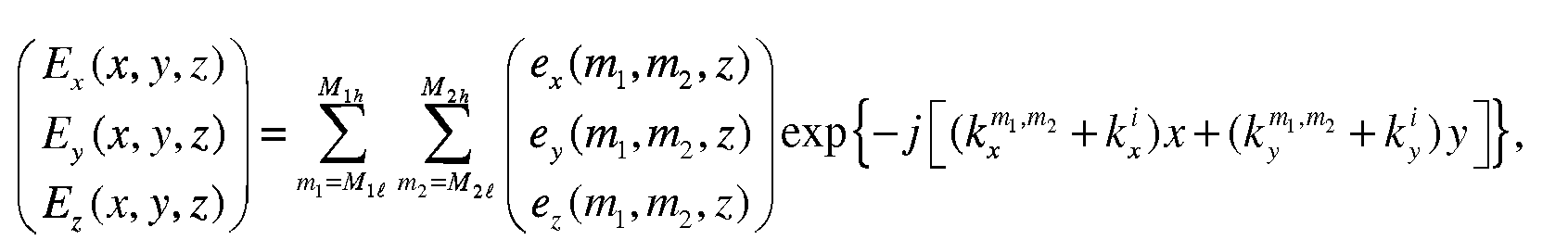
(52)
[00198] where k”1,m2 and k™l,nh depend on the directions of periodicity and k‘x and k‘y depend on the angle of incidence of the incident field. In this spectral base, the field-material interactions above become convolutions in the xy plane. For example, fori,j e {x, y,z} we have

(53)
[00199] where

(54) where S denotes the unit cell in the xy plane and |,V| denotes its area. This means that we have to compute the Fourier integrals in the xy plane of the coefficients C(> and eCy for /, / e (x, y,z} . For certain combinations of normal-vector fields and scattering geometries, this can be performed in closed form, e.g., for circles andrectangles as shown in Section 3. For more general shapes, these coefficients caneither be approximated by a meshing strategy (Section 4) or by numerical quadrature(Section 5).
2.7. Bi-refringence in binary and staircase gratings
[00200] A second important class of problems is the case in which the gratingmaterial(s) have birefringent material properties, where the axis of anisotropy is thez -axis, i.e.

(55)
[00201] where £T and εΝ are, in principle, functions of x, y , and z
[00202] We now consider the case of a binary grating, which has invariant crosssection along the z-axis over the interval ze[z;,zj, as well as permittivity profileindependent of z . For such a binary grating, we choose one of the tangential-vectorfields to be aligned along the z -axis, i.e. t2 = u_. This means that n and t; are two-dimensional vector fields, i.e. their z components are zero. With this choice, thenormal-vector field problem in the xy plane is again an isotropic problem and theconsiderations for the scaling parameter a are now quite similar to those inSection 2.5, e.g., for a two-media problem one should scale the electric flux densitywith respect to £T of the interior or exterior of the object, such that the scaled electricflux density becomes identical to the electric field in a dedicated part of the unit cell.
[00203] For more general grating geometries, one can apply a staircase approximationof the grating, with respect to the z direction. Then, the grating consists of a sequenceof binary gratings and for each of these binary gratings the strategy outlined abovecan be followed.
3. Localized normal-vector fields for binary gratings with elliptical andrectangular cross sections
[00204] In this section, we shall derive the spectral representation of C£ and eC£ for two elementary 2-dimensional shapes: the rectangle and the ellipse. These shapes areoften encountered as an integral or elementary building block in 2D wafer metrologystructures. This derivation will show the construction of a normal-vector field (NV)and the subsequent computation of the Fourier integral of the matrix elements of C£ and eCE . For a given contour, there is not a unique normal-vector field. Infinitely many NV fields can be constructed that have unit length and are perpendicular to thecontour. We shall see that an important motivation for a particular choice is thepossibility to derive an analytical expression for the Fourier coefficients of C£ and εC£ . Also the number of singularities in the NV field should be minimized to optimize convergence of the Fourier series. The ellipse and the rectangle are sofortunate to have analytical expressions for the Fourier integral.
3.1. Fourier integral for an arbitrary unit cell
[00205] In two dimensions, the periodicity of a lattice is described by its Bravais latticevectors (a^a^ . A shift over

(56)
[00206] leads to an equivalent lattice position. A plane wave with the same periodicityas the Bravais lattice will have a wave vector K answering the condition

(57)
[00207] The space of all wave vectors that fulfill this condition is called the reciprocallattice. This space is spanned by two primitive vectors

(58)
(59)
[00208] that answer the orthogonality condition

(60) from which Eq. (2) can be proven. The Fourier integral in an arbitrary 2-dimensionallattice is now defined with respect to the basis of plane waves with wave vectors inthe reciprocal lattice.

(61)
[00209] where the Fourier coefficient is obtained from the integral

(62)
[00210] where 0 < ηί = a,. /1 a, |< 1 is a dimensionless number spanning each Bravaislattice vector. Transforming to a Cartesian coordinate system gives

(63)
[00211] The 2-dimensional integral in Eq. (54) can now be written as

(64)
[00212] where

(65)
[00213] is the reciprocal lattice vector projected on the Cartesian axes.
[00214] Referring to the expressions for Ctj, Eqs (33) - (41), we see that the diagonal elements contain the Fourier integral of unity over the unit cell and the Fourierintegral of the product of normal-vector components and a position-dependentfunction of the scaling factor a(x, y, z) and the permittivity £(x, y, z). The first integral, i.e. the integral of unity over the unit cell, is equal to . The second integral can be substantially simplified for the case of an isotropic medium when thescaling factor a is chosen equal to 1 / eh. This function is then zero outside and constant inside the support of the contrast source. The Fourier coefficientsCy (m], m2, z) can now be expressed in terms of the integral

(66)
[00215] This simplifies the spectral representation of Cf (Eqs (33)-(41)) to

(67)
[00216] and the spectral representation of eCE (Eqs (43) - (51)) to

(68) (69) (70)
[00217] In the following sections, closed expressions will be derived for the E).
integral (Eq. (66)) for the case of the ellipse and the rectangle, but first the integralwill be further simplified for translation and rotation of the scattering object.
3.2. Translation and rotation of the scattering object
[00218] For the case of elementary shapes like ellipses and rectangles, the computationof the Ty integral can be further simplified by transforming to the local coordinate system.
[00219] Figure 15a is a definition of global (x,y) and local (x", y") coordinatesystems for the rotated ellipse with offset c0.
[00220] For an arbitrary offset c0, this amounts to a translation

(71)
[00221] and a rotation

(72)
[00222] The NV field of the scattering object is only affected by rotation. The productof NV components in Eq. (66) in the global (x,y)- and local (x\y")-system arerelated by a linear transformation

(73)
[00223] Combining Eqs. (71), (72) and (73), we can transform the Γ7. integral to r%·as computed in the local coordinate system
(74)
[00224] where Mnn. is the coupling matrix from Eq. (73) and

(75)
[00225] Here we have introduced the effective wave vectors

(76)
[00226] The Γ% integral is still computed over an area that is equal to the support of the contrast source (translation and rotation do not change that), but in the localcoordinate system the integral is more easily evaluated - as we shall see - for theellipse and the rectangle.
[00227] Summarizing, the effect of transforming to the local coordinate system isthreefold: • a constant phase factor to describe the effect of an offset • an effective wave vector describing the orientation of the object with respectto the Bravais lattice • Γ^. becomes a linear combination of all three Γ% in the local coordinate system 3.3. The ellipse
[00228] There are two well-known methods to generate the NV field of an ellipse, • through the elliptic coordinate system

(77) • where a is the radius along the horizontal symmetry axis, b the radius alongthe vertical symmetry axis, φ the azimuthal angle and e = -| the ellipticity.
• through the conformal mapping

(78) • For constant u (0 <u<°°) and 0 < v < 2π this gives an elliptic contour.
[00229] Figure 15b illustrates a NV field for the elliptical coordinate system andFigure 15c illustrates conformal mapping.
[00230] The elliptic coordinate system has the advantage that an analytical expressionfor Γ%· can be derived and that the normal-vector field only has a singularity at (0,0) while the conformal mapping has singular behavior over the line connecting the foci.We shall later see, for the case of the rectangle, that despite the presence ofsingularities good convergence can still be obtained. The presence of singularitiesalone is therefore not a convincing argument to reject a normal-vector field. Thepossibility to derive analytical expressions for the Fourier integral is a much strongerargument since it will result in fast computation of the matrix vector product. Thenormal-vector field can be derived as the vector perpendicular to the tangential vectordr ld<p

(79)
[00231] For this expression, we write the normal-vector products that are required for
Eq. (66)

(80)
[00232] Rewriting the Γ% integral to the elliptic coordinate system gives

(81)
[00233] Fortunately, the r- and φ -dependence can be further separated from theFourier exponent by using the identity [2, p. 973]

(82)
[00234] where J„(z) is the Bessel function of the first kind with integer order n. Byrewriting the argument of the exponent in Eq. (81)

(83)

[00235] the identity in Eq. (82) can be applied to the exponent in the integral inEq. (81) resulting in the following expression for γ"χχ

(84)

[00236] where (85)
[00237] The expressions for Y"xy and Y"yy can be obtained by replacing the numerator in the angular integrals by esin ^>cos φ resp. sin2 φ, The efficiency of this approachfor the ellipse derives from the fact that analytical expressions for the radial andangular integrals can be found. These expressions for the radial integral of the Besselfunction are derived in Appendix A. For the angular integrals they are derived inAppendix B, where they are labeled $>*j(k,<pa,<ph) and Φ°ί(Ιί,φα,φι>) for the angularintegrals running from φα to <ph for index k in resp. the summation over even andodd terms. For the full ellipse, the evaluation of Eq. (84) is simplified by the fact thatΦ° (k, 0,2π) = 0. The angular integral for the even terms is (86)

(87)
[00238] Note that for the case of a circle (e -1) only the (k-l )-terms are non-zero.
[00239] The radial integrals need now only be evaluated for even order n. InAppendix A, a closed-form expression is derived for the indefinite integral
(88)
[00240] where the summation is only computed for n > 1. Substituting Eqs (86) and(88) in Eq. (84) gives

(89)
[00241] where Nb is the number of terms that is retained in the summation over theeven Bessel functions and

(90)
[00242] Note that in the last term the summations over k and m have been swappedto prevent multiple evaluations of Bessel functions of the same argument. For the computation of r% and Y" yy, Φ'α only needs to be substituted by the expressionsfor Φ£’ν and <Pryy (see Appendix B).
3.4. The rectangle
[00243] The generation of a continuous NV field for the rectangle is less obvious thanfor the ellipse. It has been proposed [3] to use the Schwartz-Christoffel transformationfor this purpose [4]. A NV field that closely approximates this solution for therectangle is

(91)
[00244] Figure 16a illustrates a corresponding continuous NV field for the rectangle.This expression, however, does not lend itself for deriving an analytical expression ofthe Ty integral. For this case, we choose to derive a NV field that closely resembles
Eq. (91), but is discontinuous along the diagonals of the rectangle, constant within thetriangles formed by the diagonals, and normal to the edges of the rectangle .
[00245] Figure 16b illustrates a corresponding discontinuous NV field for therectangle. This normal-vector field is constant for each triangle which makes the Γ',,·integral particularly simple to calculate.

(92)
[00246] The evaluation of the surface integral is straightforward. For triangle Δ, (seeFig. 16b) it gives

(93)
[00247] For triangle A2 we only need to swap r rb and kex <-> key . The result fortriangles A3 and A4 is simply the complex conjugate of the integral for resp. Aj andA2.
[00248] For this NV field Γλ = 0 for triangles A2 and Δ4, Γ^, = 0 for triangles Aland Δ3 and Yxy = Γνν = 0 for all triangles. Note that for the limit key —> 0 Eq. (93)becomes

(94) 4. Cut-and-connect strategy
[00249] The previous section on the NV field generation for the rectangle, shows avery powerful method for generating the NV field for more arbitrary shapes. Theseshapes can be decomposed in elementary shapes for which the integral has a closed form suited for fast computation. By summing up the relevant Γ;> integrals foreach elementary shape at a particular Fourier mode index, the spectral representationof C£ and eC£ can be easily obtained. Of course, the class of elementary shapes mustbe large enough to generate all relevant more complex shapes. The class ofelementary shapes comprises: (A) triangles with a constant NV field: if one interfaceis a material interface, the NV field must be perpendicular to this interface. If there isno material interface, the NV field can be chosen arbitrarily; (B) trapezoids with aconstant NV field (the rectangle is a special case): if one interface is a materialinterface, the NV field must be perpendicular to this interface. If there is no materialinterface, the NV field can be chosen arbitrarily; or (C) circle segment with a radialNV field and material interface along the circle edge.
[00250] Any arbitrary shape - or approximation thereof - can in principle bedecomposed in a mesh of these elementary shapes.
[00251] Figure 17 illustrates meshing a ‘dogbone’ in these elementary shapes.
[00252] Figure 18 illustrates building the normal-vector field of a prism with a crosssection of a rounded rectangle from smaller rectangles 1802 and circle segments 1804in accordance with an embodiment of the present invention. Note that the normal-vector field shown by the arrows is perpendicular to the physical interfaces at thosephysical interfaces.
[00253] In an embodiment of the present invention, there is provided a method toconstruct a normal-vector field locally (i.e. over the scattering object or parts thereof)instead of over the entire unit cell. This simplifies the generation of a normal-vectorfield and even gives mathematically very simple expressions for basic shapes likecircles, ellipses and rectangles.
[00254] For more complicated shapes, a cut-and-paste meshing technique is providedwhere the normal-vector field of an arbitrary shape is composed of the normal-vectorfields of two or more elementary shapes selected from: a prism with the followingcross section: a triangle; a rectangle; a trapezoid; or a circular segment; a tetrahedron;a bar; a hexahedron with two parallel faces; an apex truncated pyramid with truncation faceparallel to the ground plane; and spherical segment.
[00255] For these building blocks, the normal-vector field can be very simply andrapidly generated.
[00256] Alternatively, for other complicated shapes, it may be advantageous togenerate a normal-vector field directly from the shape, without applying the abovemeshing strategy to avoid a high mesh density. This results in the use of interpolationmethods to generate normal-vector fields, which are then used to compute certainFourier integrals. An embodiment of the present invention breaks up the Fourierintegrals into several integrals over the support of the various media in thecomputational domain. For each of these domains, dedicated quadrature rules areapplied in combination with an interpolation algorithm to generate the normal-vectorfield on this domain. Interpolation is applied based on basis functions with periodiccontinuation, to avoid artificial discontinuities in the integrants, due to a particularchoice for the boundaries of unit cell. Further, it is possible to further limit the supportof the normal-vector field to a direct neighborhood of a material interface. This leadsto an even more parsimonious approach to generate normal-vector fields for morecomplicated shapes.
4.1. Elementary building blocks
[00257] In this section, closed expressions for the Γ^. integral will be derived for the three elementary building blocks expressed in the coordinates of the shape vertices.
4.2. The triangle
[00258] Figure 19 illustrates rotated and shifted triangle with NV field and localcoordinate system.
[00259] Figure 19 shows an arbitrary triangle with vertices A, B and C. The vertexopposite to the material interface, (B-C) , is chosen as the local origin. Note that thevertices are ordered in a counterclockwise direction. First we translate over vector A
to obtain vectors B' = (B - A) and C' = (C - A). Then we rotate over angle <p0 to getto the local coordinate system. In this system, B" and C” are given by Eq. (72)

(95)
[00260] where

(96)
[00261] With the expressions for the coordinates of B' and C”, we obtain

(97)
[00262] In case B^C* is a material interface, the NV field is (nx ,ny ) = (1,0) leaving only r"xx as a non-zero component. E. in the global coordinate system is obtained through Eq. (74).
4.3. The trapezoid
[00263] Figure 20 illustrates a rotated and shifted trapezoid with NV field and localcoordinate system.
[00264] For the trapezoid, the same line of reasoning can be followed. First, thecoordinates are translated over A giving

(98)
[00265] and subsequently rotated over <p0 to give

(99)
[00266] where

(100)
[00267] In the local coordinate system

(101)
[00268] This result can also be obtained by decomposing the trapezoid in two trianglesand adding Eq. (97) for both triangles. Also for the trapezoid the NV field is (nx , ny ) = (1,0) in case B'C" is a material interface, leaving only T" xx as a non-zerocomponent. ΓΤ in the global coordinate system is obtained through Eq. (74).
4.4. The circle segment
[00269] The circle segment is defined as a section from a circle with origin A, lowerradius endpoint B and section angle (ps.
[00270] Figure 21 illustrates rotated and shifted circle segment with NV field and localcoordinate system.
[00271] The NV component Γ";, can be computed along the same lines as for the fullellipse in Section 3.3. The main difference is that the angular integrals are nowevaluated from 0 to an arbitrary angle (ps. This has the effect that the angular integral over the odd terms in the Bessel summation <i>°j(k,0,<ps) Φ 0 . Also for the odd terms,the radial integral over the Bessel function has an analytical expression (see Appendix

A) (102)
[00272] where the summation only applies to the case n > 1. Substitution of Eq, (102)in Eq. (84) gives

(103) where Nh is the number of terms that is retained in the summation over the evenBessel functions and

(104)
[00273] The primitive of J0 has been rewritten using ([2, p. 633])

(105)
[00274] For r'xy and r' w , the NV components can be easily found by substituting the appropriate expressions for the angular integrals (see Appendix B).
5. Generation of normal-vector fields for more general shapes
[00275] For certain situations, e.g., cases with exotic scattering geometries or caseswhere multiple materials have connecting interfaces between each other, it may bedifficult to apply a meshing strategy that leads to a low number of meshing elementsand that exhibits rapid convergence in the spectral base of the electric field andelectric flux density. For such cases, a more general approach may be needed togenerate the Fourier coefficients of the field-material interaction operators. One suchapproach is to employ numerical quadrature to evaluate the integrals of the form (54).A quadrature rule then invokes the function values of the integrant at a number of points to arrive at an approximation of the desired integral. If we take a look at theintegrants under consideration, we notice that we need to evaluate the permittivity, theexponential function, and the Cartesian components of the normal-vector field at anarbitrary (x, y) point. This is trivial for the former two functions, but non-trivial forthe latter. Owing to the scaling introduced earlier on, the normal-vector field is onlyneeded in regions where (χεφ\. Further, we note that the Fourier coefficients for allFourier indices (mt, m2) can be obtained via the same quadrature rule and function evaluations, except that the exponential function is evaluated for all Fourier indices.Therefore, the main concern is to evaluate the normal-vector field at an arbitraryposition (assuming that αε ^ 1).
[00276] Several recipes to generate normal-vector fields have been discussed in [3,5].The first article discusses the generation of two-dimensional normal-vector fieldswithin the context of RCWA based on Schwarz-Christoffel conformal mappings orvia solving an electrostatic problem. The second article discusses the generation viathe inverse-distance interpolation algorithm, which is a particular example of a so-called scattered-data interpolation algorithm with radial basis functions. However,both articles teach generating the normal-vector field on a regular grid, without takinginto account the possibility that normal-vector field may only be needed locally.Further, regular grids may yield slow convergence for permittivity profiles that do notfit to this regular grid, i.e. for piecewise constant material properties with interfacesthat do not coincide with the regular mesh. Consequently, a very large number of gridpoints may be needed to reach a converged solution. These two observations makethese procedures extremely expensive in terms of CPU time.
[00277] According to an embodiment of the present invention, we use localizednormal-vector fields and apply quadrature rules that take into account the domain ofintegration of the scattering object, i.e. work with integration domains that take intoaccount the shape of the material interfaces. As a consequence, the integration overthe unit cell is replaced by a sequence of integrations over domains that have constantpermittivity. Quadrature rules that integrate over more complicated domains havebeen studied in e.g., [6,7,8]. Since the permittivity per domain of integration isconstant and the exponential function is continuous, the only possible hurdle is againthe normal-vector field. Hence, to maintain the convergence of the quadrature rule,we need to generate a sufficiently smooth normal-vector field over the integration domain of the quadrature rule. This can be achieved by a scattered-data interpolationalgorithm, for which the input data is generated from a description of the boundary ofthe integration domain and a corresponding normal-vector field at this boundary. Forexample, if the boundary is described by a piecewise linear approximation, then thenormal is locally a constant vector. By providing a sufficiently dense sampling of thenormal-vector field along the boundary, sufficient data is generated to apply ascattered-data interpolation algorithm.
5.1. Periodic continuation of normal-vector fields
[00278] Standard scattered-data interpolation algorithms use so-called radial basisfunctions, i.e. basis functions that only depend on the distance between a data pointand the interpolation point. In a general interpolation problem, this is usually a goodidea, since it allows nearby data to have a higher impact on the interpolated data ascompared to data far away. However, in a periodic environment, the distance betweena data point and an interpolation point also becomes periodic. If we do not take thisinto account, the interpolation across a periodic boundary can introduce artificialdiscontinuities, which may deteriorate the convergence of certain quadrature rules oreven the convergence of the solution of the electromagnetic fields projected on thenormal-vector field. Therefore, we look for alternatives for the scattered-datainterpolation with radial basis functions. The key idea is to generate a periodic-distance function that exhibits the periodicity of the configuration and to let thisfunction replace the distance function.
5.2. Periodic distance functions
[00279] In the regular Euclidean space l3, the distance r between two points r and r'is given by

which is non-negative and only zero when the two points coincide.
(106)
[00280] Let us now first consider a ID periodic case along the jc -axis with periodp> 0. For such a case, we first introduce the modulo(p) function as

(107) where [.] denotes the ceiling operator. Hence, we have

(108)
[00281] With the above definition, the Euclidean distance d(x,x) =| x-x'\ between λ:and x becomes dp (x, x') =| (x — x') mod p |, for the periodic case. However, there arealso other ways to define a distance measure, e.g.,

(109) also satisfies the basic criteria for a distance measure d (x, x'), i.e.
1. d(x,x')> 0 (non-negative), 2. d{x,x') = 0 if and only if x = x' (identity of indiscemibles) 3. d(x, x') = d(x\ x) (symmetry), 4. d(x, x”) < d(x, x') + d(x\ x") (triangle inequality).
[00282] For a space with two directions of periodicity, the situation is morecomplicated. Let us denote the periodic lattice vectors by a, and a2, then we canindicate any point r = (jt, y, z) in space as r = xux + yuy + zuz = + η2&2 + zuz, (110) where ηγ and η2 are the coordinates in the transverse plane that relate to jt and y as

(111)
[00283] Further, we note that the scattering configuration in periodic in ηι and η2,both with period 1. The Euclidean distance function in I3 can be expressed in aL anda2 as

(112)
[00284] To arrive at a periodic distance function, we now replace ηγ -ηγ and η2 -η2by a periodic function ƒ (·) with period 1 and /(0) = 0, such that | ƒ (·) | gives rise toa one-dimensional periodic distance functions, i.e.

(113) where f(x) is for example equal to λ;modi or sin(2^x).
5.3. Periodic scattered-data interpolation
[00285] In a scattered-data interpolation algorithm, a basis function <p(r), r > 0, isintroduced, e.g., (p{r) = exp(-/?r2) with /?>(). Further, a set of data points rn andcorresponding functions values F(rB), ns {1,...,/V} are provided. Then, thealgorithms determines coefficients cn such that

(114) for all n = 1,...,N, where d(rm,rn) denotes the distance between the data points rm and r,. If this set of linear equations is non-singular, the coefficients cn can be
determined and the scattered-data interpolation algorithm leads to the followinginterpolation of F

(115)
[00286] For the periodic case, we substitute the distance function d{·,·) in the abovetwo formulas by the periodic distance function in Eq. (113), and we arrive at aperiodic interpolation of the data, which can be used to generate the Cartesiancomponents of the normal-vector field from the Cartesian components of the normal-vectors fields at the material boundaries, in a similar way as in [5], i.e. we first findthe interpolated components as

(116) where je {x, y, z}. Then we normalize the normal-vector field at position r to 1, i.e.n(r) =n(r)/||n(r)||.
6. Localized normal-vector fields in arbitrary anisotropic media
[00287] In the preceding sections, the concept of localized normal-vector fields in theconstruction of a continuous vector field F was achieved by introducing a scalingfunction and a basis transformation in the vector field defined by Popov and Nevière.The localization of the normal-vector field was demonstrated for isotropic media andfor birefringent media with a fixed extra-ordinary axis that is orthogonal to thenormal-vector field everywhere, e.g., due to a staircase approximation of thegeometry of the grating. The concept of localized normal-vector fields will now be carried over to the most general case of arbitrary anisotropic media. However, scalingby a scalar function is not sufficiently flexible to deal with the most general case. Totackle the case of general anisotropic media, we start by modifying the definition ofthe vector field F. This renewed definition of F is given by

(117) where S is a additional scaling operator and a is a non-zero scaling function, whichare both continuous in the vicinity of material discontinuities. Since both PnD andPTE are continuous vector fields, the vector field F is again continuous under therequirements for a and S .
[00288] With the previously outlined algebra for the projection operators, we obtain

(118)
[00289] The operator between square brackets can be made zero locally, for exampleby choosing S = Με , i.e. equal to the medium parameters in a certain area that does not involve discontinuities (e.g., a constant permittivity tensor of the filling medium),and by choosing aPn = (PnSPn)~l (to be understood on the range of Pn), which is anon-zero continuous function owing to the choice for S . For a, this amounts toOL=l/(n,Sn). Hence in a region where Με = Μi: holds, the normal-vector field is not required, provided the basis of the vector field F is independent of the normal-vectorfield, e.g., it is expressed in Cartesian coordinates. Another choice for S is to use asmoothed version of the permittivity distribution. For this choice, the region where thenormal-vector field is required is shrunk even further.
[00290] For isotropic media, the above modification of the vector field F is consistentwith the previous definition, since S will then be a multiple of the identity operatorand hence it will commute with PT and Pn. Consequently, PnSPT is identically zeroand the choice for a reduces to the previously defined cases.
[00291] The main merits of the localized normal-vector field, i.e. the possibility to pre¬compute expressions of the coefficients for the operators C£ and eC£ for each object separately and the possibility to apply the cut-and-connect strategy, are still valid inthe general anisotropic case. However, the coefficients of the operators are typicallymore complicated, since the directions of anisotropy mixes with the direction on thenormal-vector field. This can for example be observed from the operator (ΡηΜεΡη )-1, which was independent of the normal-vector field for isotropic media, whereas it doesdepend on the normal-vector field and the direction of the anisotropy in the generalcase. Therefore, finding closed-form expressions for the Fourier integrals that definethe coefficients is typically harder and a quadrature approach as outlined in Section 5can be a useful alternative. A notable exception is the case where the anisotropy of anobject is constant over the support of the object and the shape of the object isdescribed by mesh elements with a fixed direction of the normal-vector field, e.g., thetriangular or polygonal mesh elements. For this case, the derived closed-formexpressions remain valid, except for a constant scaling factor that depends on theangle between the (constant) normal vector field and the (constant) directions of theanisotropy of the permittivity tensor.
[00292] We have described a projection operator framework to analyze the concept oflocalized normal-vector fields within field-material interactions in a spectral basis, inisotropic and anisotropic media, which may be used in for example RCWA, theDifferential Method, and the Volume-Integral Method. With this framework, we havebeen able to demonstrate that a scaling and basis transformations can lead to thelocalized normal-vector fields, which enable us to work with normal-vector fields fordedicated shapes and to apply a meshing strategy to construct normal-vector fields formore general shapes. This greatly improves the flexibility of the normal-vector fieldapproach and also leads to significant saving of CPU time to set up these fields. Wehave illustrated the examples of closed-form solutions for a number building blocksand the generation of vector fields for more general shapes, including a periodic-distance interpolation algorithm.
[00293] Embodiments of the present invention allow for a faster and more flexiblesetup of normal-vector fields in 2D and 3D, which results in faster CD reconstructiontimes and faster library recipe generation. For a simple example, we have observedspeed up from several minutes to sub-seconds on the same computing hardware.
[00294] Although specific reference may be made in this text to the use of lithographicapparatus in the manufacture of ICs, it should be understood that the lithographicapparatus described herein may have other applications, such as the manufacture ofintegrated optical systems, guidance and detection patterns for magnetic domainmemories, flat-panel displays, liquid-crystal displays (LCDs), thin film magneticheads, etc.. The skilled artisan will appreciate that, in the context of such alternativeapplications, any use of the terms “wafer” or “die” herein may be considered assynonymous with the more general terms “substrate” or “target portion", respectively.The substrate referred to herein may be processed, before or after exposure, in forexample a track (a tool that typically applies a layer of resist to a substrate anddevelops the exposed resist), a metrology tool and/or an inspection tool. Whereapplicable, the disclosure herein may be applied to such and other substrateprocessing tools. Further, the substrate may be processed more than once, for examplein order to create a multi-layer IC, so that the term substrate used herein may alsorefer to a substrate that already contains multiple processed layers.
[00295] The methods according to embodiments of the present invention describedabove may be incorporated into the forward diffraction model for reconstructing anapproximate structure of an object (not limited to ID-periodic) from a detectedelectromagnetic scattering property, such as a diffraction pattern, arising fromillumination of the object by radiation, as described above with reference to Figures 5and 6. The processing unit PU described above with reference to Figures 3 and 4 maybe configured to reconstruct an approximate structure of an object using this method.
[00296] Although specific reference may have been made above to the use ofembodiments of the invention in the context of optical lithography, it will beappreciated that the invention may be used in other applications, for example imprintlithography, and where the context allows, is not limited to optical lithography. Inimprint lithography a topography in a patterning device defines the pattern created ona substrate. The topography of the patterning device may be pressed into a layer ofresist supplied to the substrate whereupon the resist is cured by applyingelectromagnetic radiation, heat, pressure or a combination thereof. The patterningdevice is moved out of the resist leaving a pattern in it after the resist is cured.
[00297] The terms “radiation” and “beam” used herein encompass all types ofelectromagnetic radiation, including ultraviolet (UV) radiation (e.g., having a wavelength of or about 365, 355, 248, 193, 157 or 126 nm) and extreme ultra-violet(EUV) radiation (e.g., having a wavelength in the range of 5-20 nm), as well asparticle beams, such as ion beams or electron beams.
[00298] The term “lens”, where the context allows, may refer to any one orcombination of various types of optical components, including refractive, reflective,magnetic, electromagnetic and electrostatic optical components.
[00299] The term “electromagnetic” encompasses electric and magnetic.
[00300] The term “electromagnetic scattering properties” encompasses reflection andtransmission coefficients and scatterometry measurement parameters includingspectra (such as intensity as a function of wavelength), diffraction patterns (intensityas a function of position/angle) and the relative intensity of transverse magnetic- andtransverse electric-polarized light and/or the phase difference between the transversemagnetic- and transverse electric-polarized light. Diffraction patterns themselves maybe calculated for example using reflection coefficients.
[00301] Thus, although embodiments of the present invention are described in relationto reflective scattering, the invention is also applicable to transmissive scattering.
[00302] While specific embodiments of the invention have been described above, itwill be appreciated that the invention may be practiced otherwise than as described.For example, the invention may take the form of a computer program containing oneor more sequences of machine-readable instructions describing a method as disclosedabove, or a data storage medium (e.g., semiconductor memory, magnetic or opticaldisk) having such a computer program stored therein.
[00303] It is to be appreciated that the Detailed Description section, and not theSummary and Abstract sections, is intended to be used to interpret the clauses. TheSummary and Abstract sections may set forth one or more but not all exemplaryembodiments of the present invention as contemplated by the inventor(s), and thus,are not intended to limit the present invention and the appended clauses in any way.
[00304] The present invention has been described above with the aid of functionalbuilding blocks illustrating the implementation of specified functions andrelationships thereof. The boundaries of these functional building blocks have beenarbitrarily defined herein for the convenience of the description. Alternate boundariescan be defined so long as the specified functions and relationships thereof areappropriately performed.
[00305] The foregoing description of the specific embodiments will so fully reveal thegeneral nature of the invention that others can, by applying knowledge within the skillof the art, readily modify and/or adapt for various applications such specificembodiments, without undue experimentation, without departing from the generalconcept of the present invention. Therefore, such adaptations and modifications areintended to be within the meaning and range of equivalents of the disclosedembodiments, based on the teaching and guidance presented herein. It is to beunderstood that the phraseology or terminology herein is for the purpose ofdescription and not of limitation, such that the terminology or phraseology of thepresent specification is to be interpreted by the skilled artisan in light of the teachingsand guidance.
[00306] The breadth and scope of the present invention should not be limited by any ofthe above-described exemplary embodiments, but should be defined only inaccordance with the following clauses and their equivalents.
[00307] The clauses in the instant application are different than those of the parentapplication or other related applications. The Applicant therefore rescinds anydisclauseer of clause scope made in the parent application or any predecessorapplication in relation to the instant application. The Examiner is therefore advisedthat any such previous disclauseer and the cited references that it was made to avoid,may need to be revisited. Further, the Examiner is also reminded that any disclauseermade in the instant application should not be read into or against the parentapplication..
References [1] Evgeny Popov and Michel Nevière. Maxwell equations in Fourier space: fast¬converging formulation for diffraction by arbitrary shaped, periodic, anisotropicmedia. J. Opt. Soc. Am. A, 18(11):2886-2894, November 2001.
[2] I. S. Gradshteyn and I. M. Ryzhik. Table of Integrals, Series and Products. AcademicPress, 1980.
[3] Thomas Schuster, Johannes Ruoff, Norbert Kerwien, Stephan Rafler, and WolfgangOsten. Normal vector method for convergence improvement using the RCWA forcrossed gratings. J. Opt. Soc. Am. A, 24(9):2880-2890, September 2007.
[4] R.V. Churchill. Complex Variables and Applications. McGraw-Hill, 1960.
[5] Peter Götz, Thomas Schuster, Karsten Frenner, Stephan Rafler, and Wolfgang Osten.Normal vector method for the RCWA with automated vector field generation.OPTICS EXPRESS, 16(22):17295-17301, October 2008.
[6] Alvise Sommariva and Marco Vianello. Gauss-Green cubature and momentcomputation over arbitrary geometries. Journal of Computational and AppliedMathematics, to be published.
[7] Alvise Sommariva and Marco Vianello. Product Gauss cubature over polygons basedon Green’s integration formula. BIT Numerical Mathematics, 47(2):147-177, August2007.
[8] G. Gabard. Exact integration of polynomial-exponential products with application towave-based numerical methods. Commun. Numer. Meth. Engng, 2008.
[9] Yia-Chung Chang, Guangwei Li, Hanyou Chu, and Jon Opsal. Efficient finite-element, Green's function approach for critical-dimension metrology of three-dimensional gratings on multilayer films. J. Opt. Soc. Am. A, 23(3):638-6454, March2006.
[10] Lifeng Li. Use of Fourier series in the analysis of discontinuous periodic structures. J.Opt. Soc. Am. A, 13(9):1870-1876, September 1996.
[11] Lifeng Li. New formulation of the Fourier modal method for crossed surface-reliefgratings. J. Opt. Soc. Am. A, 14(10):2758-2767, October 1997.
[12] Brent C. Bergner, Thomas A. Germer, and Thomas J. Suleski. Effect of Line WidthRoughness on Optical Scatterometry Measurements. Metrology, Inspection, andProcess Control for Microlithography ΧΧΙΠ, edited by John A. Allgair, Christopher J.Raymond. Proc. of SPIE Vol. 7272, 72720U, 2009. DOI: 10.1117/12.813770.
APPENDIX A
Radial integrals of Bessel functions
The radial integration amounts to finding closed expressions for the following integrals

(Al)
These can be found by employing the following recurrence relations for Bessel functions([2])

(A2) (A3)
Substituting n + l = 2k in Eq. (2) and integrating gives a recursive relation for the evenBessel integral

(A4)
The second integral in this equation can be rewritten using Eq. (A3). Substitutingn +1 = 2k -1 and integrating gives

(A5)
Both recursive integral expressions can be explicitly written

(A6) (A7)
Substitution of Eq. (A7) in Eq. (A6) gives

(A8)
The disadvantage of this expression is that the Bessel function has multiple evaluations of thesame argument. Since this is numerically an expensive operation, the double summation isswitched giving

(A9)
The last summation over the k -index can be shown to be equal to

(A10) giving the final closed-form expression for the radial integral over the even Bessel functions
(All) where the summation only applies to n > 1.
The same reasoning can be applied to the radial integral over the odd Bessel functions.Substituting n + \ = 2k + \ in Eq. (A2) and n + \ = 2k in Eq. (A3) and integrating gives thefollowing recursive integrals

(A 12)(A13)
Writing both recursive relations explicitly gives

(A 14)(A15)
Substituting Eq. (A15) in Eq. (A14) and swapping the double summation gives

(A 16)
Using the relation

(A 17) and partially integrating zJ^z) in Eq. (A16) gives the final expression

(A18) where the final summation only applies to n > 1.
APPENDIX B
Angular integrals
The angular integral in its most general form is written as

(Bl) where all combinations of the terms between the curly brackets are possible, (0 < e = ^ < 1) isthe ellipticity, <ps is the angle of the ellipse or circle segment and c is an angle offsetfollowing from geometrical input parameters (see Eq. (83)). Although a closed expression forthis integral can be derived, we shall focus for this report on two particular cases, • the circle segment • the full ellipse
For the circle e = 1 which substantially simplifies the integrals

(B2) where e refers to the even modes and o to the odd modes. Furthermore, all combinations ofterms between the curly brackets are possible. Straightforward integration gives

(B3) (B4) (B5) (B6)

(B7) (B8) (B9) (BIO)
Similar expressions can be derived for the odd angular integrals

(Bit) (BI 2)

(BI 3)
For the case of the full ellipse, e is arbitrary in Eq. (Bl). The even angular integralΦ» (&> 0,2π) can be written

(B14) where the double-angle trigonometric relations have been used to rewrite the squares of thesines and cosines. Further use of the sine - cosine product rules and the fact that alltrigonometric function have 2π periodicity, gives

(B15)
Exploiting the symmetries of the integrands, it can be shown that

(B16)

(BI 7) where an elementary integral has been used in Eq. (B17) (see [2, p. 366]).
With the same symmetry arguments, it can be shown that

(B18)
Patiently repeating this work for Φ^° and Φ^° shows that

(B19) (B20) (B21)
Note that for the case of a circle (e = 1) only the ( k = l)-terms are non-zero. Otheraspects of the invention are set out as in the following numbered clauses: CLAUSES: 1. A method of calculating electromagnetic scattering properties of a structure, thestructure including materials of differing properties such as to cause a discontinuity inan electromagnetic field at a material boundary, the method comprising: - generating a localized normal-vector field in a region of the structure defined withreference to the material boundary; - constructing a vector field that is continuous at the material boundary by using thenormal-vector field to select continuous components of the electromagnetic fieldtangential to the material boundary and to select continuous components of acorresponding electromagnetic flux density normal to the material boundary; - performing a localized integration of the normal-vector field over the region todetermine coefficients of a field-material interaction operator; - numerically determining a component of the electromagnetic field by using thefield-material interaction operator to operate on the vector field; and - calculating electromagnetic scattering properties of the structure using thedetermined component of the electromagnetic field.
2. The method of clause 1, wherein the region corresponds to support of a contrastsource.
3. The method of clause 1 or clause 2, wherein the step of generating the localizednormal-vector field comprises scaling at least one of the continuous components.
4. The method of clause 3, wherein the scaling is configured to make the continuouscomponents of the electromagnetic field and the continuous components of theelectromagnetic flux density indistinguishable outside the region.
5. The method of clause 4, wherein the step of scaling comprises using a scalingfunction that is continuous at the material boundary.
6. The method of clause 5, wherein the scaling function is constant.
7. The method of clause 5, wherein the scaling function is equal to the inverse of abackground permittivity.
8. The method of any of clauses 4 to 7, wherein the step of scaling further comprisesusing a scaling operator that is continuous at the material boundary.
9. The method of any previous clause, wherein the step of generating the localizednormal-vector field comprises using a transformation operator directly on the vectorfield to transform the vector field from a basis dependent on the normal-vector field toa basis independent of the normal-vector field.
10. The method of clause 9, wherein the basis independent of the normal-vector field isthe basis of the electromagnetic field and the electromagnetic flux density.
11. The method of any previous clause, wherein the step of generating a localized normal-vector field comprises decomposing the region into a plurality of sub-regions eachhaving a respective normal-vector field and the step of performing a localizedintegration comprises integrating over each the respective normal-vector field of eachof the sub-regions.
12. The method of clause 11, wherein each sub-region is an elementary shape selected tohave a respective normal-vector field having a corresponding closed-form integral andthe step of performing a localized integration comprises using the correspondingclosed-form integral for integrating over each the respective normal-vector field ofeach of the sub-regions.
13. The method of any previous clause, wherein the step of calculating electromagneticscattering properties of the structure is performed by numerically solving a volumeintegral equation for the vector field, so as to determine an approximate solution ofthe vector field.
14. The method of clause 13, wherein the vector field is related to the electromagneticfield by a change of basis.
15. A method according to clause 14, wherein the vector field is represented by at leastone finite Fourier series with respect to the at least one direction and wherein the stepof numerically solving the volume integral equation comprises determining acomponent of the electromagnetic field by convolution of the vector field with aconvolution-and-change-of-basis operator.
16. The method of any previous clause, further comprising relating the electromagneticflux density to the electric field using, in the region in which the localized normalvector field is generated and local to the material boundary, a component ofpermittivity normal to the material boundary and at least one other, different,component of permittivity tangential to the material boundary.
17. A method of reconstructing an approximate structure of an object from a detectedelectromagnetic scattering property arising from illumination of the object byradiation, the method comprising the steps: - estimating at least one structural parameter; - determining at least one model electromagnetic scattering property from the at least one structural parameter; - comparing the detected electromagnetic scattering property to the at least one model electromagnetic scattering property; and - determining an approximate object structure based on the result of the comparison,wherein the model electromagnetic scattering property is determined using a methodaccording to any previous clause.
18. A method according to clause 17, further comprising the step of arranging a pluralityof the model electromagnetic scattering properties in a library and the step ofcomparing comprises matching the detected electromagnetic scattering property tocontents of the library.
19. A method according to clause 17 or clause 18, further comprising iterating the stepsof determining at least one model electromagnetic scattering property, and comparingthe detected electromagnetic scattering wherein the structural parameter is revisedbased on the result of the step of comparing in a previous iteration.
20. An inspection apparatus for reconstructing an approximate structure of an object, theinspection apparatus comprising: - an illumination system configured to illuminate the object with radiation; - a detection system configured to detect an electromagnetic scattering property arising from the illumination: - a processor configured to: - estimate at least one structural parameter; - determine at least one model electromagnetic scattering property from theat least one structural parameter; - compare the detected electromagnetic scattering property to the at leastone model electromagnetic scattering property; and - determine an approximate object structure from a difference between thedetected electromagnetic scattering property and the at least one modelelectromagnetic scattering property, wherein the processor is configured to determine the model electromagnetic scatteringproperty using a method according to any of clauses 1 to 16.
21. A computer program product containing one or more sequences of machine-readableinstructions for calculating electromagnetic scattering properties of a structure, theinstructions being adapted to cause one or more processors to perform a methodaccording to any of clauses 1 to 16.
22. A method comprising: generating a localized normal vector field in a region of a structure definedwith reference to a material boundary; constructing a vector field that is continuous at the material boundary byusing the normal vector field to select continuous components of an electromagneticfield tangential to the material boundary and to select continuous components of acorresponding electromagnetic flux density normal to the material boundary; performing a localized integration of the normal vector field over the regionto determine coefficients of a field material interaction operator; numerically determining a component of the electromagnetic field by usingthe field material interaction operator to operate on the vector field; and calculating electromagnetic scattering properties of the structure using thedetermined component of the electromagnetic field.
23. The method of clause 22, wherein the region corresponds to support of a contrastsource.
24. The method of clause 22, wherein the generating the localized normal vector fieldcomprises scaling at least one of the continuous components.
25. The method of clause 24, wherein the scaling is configured to make the continuouscomponents of the electromagnetic field and the continuous components of theelectromagnetic flux density indistinguishable outside the region.
26. The method of clause 25, wherein the scaling comprises using a scaling function thatis continuous at the material boundary.
27. The method of clause 26, wherein the scaling function is constant.
28. The method of clause 27, wherein the scaling function is equal to the inverse of abackground permittivity.
29. The method of clause 25, wherein the scaling further comprises using a scalingoperator that is continuous at the material boundary.
30. The method of clause 22, wherein the generating the localized normal vector fieldcomprises using a transformation operator directly on the vector field to transform thevector field from a basis dependent on the normal vector field to a basis independentof the normal vector field.
31. The method of clause 30, wherein the basis independent of the normal vector field isthe basis of the electromagnetic field and the electromagnetic flux density.
32. The method of clause 22, wherein the generating a localized normal vector fieldcomprises decomposing the region into a plurality of sub regions each having arespective normal vector field and the step of performing a localized integrationcomprises integrating over each the respective normal vector field of each of the subregions.
33. The method of clause 32, wherein each sub region is an elementary shape selected tohave a respective normal vector field having a corresponding closed form integral andthe step of performing a localized integration comprises using the correspondingclosed form integral for integrating over each the respective normal vector field ofeach of the sub regions.
34. The method of clause 22, wherein the calculating electromagnetic scatteringproperties of the structure is performed by numerically solving a volume integralequation for the vector field, so as to determine an approximate solution of the vectorfield.
35. The method of clause 34, wherein the vector field is related to the electromagneticfield by a change of basis.
36. The method according to clause 35, wherein the vector field is represented by at leastone finite Fourier series with respect to the at least one direction and wherein the stepof numerically solving the volume integral equation comprises determining acomponent of the electromagnetic field by convolution of the vector field with aconvolution and change of basis operator.
37. The method of clause 22, further comprising relating the electromagnetic flux densityto the electric field using, in the region in which the localized normal vector field isgenerated and local to the material boundary, a component of permittivity normal tothe material boundary and at least one other, different, component of permittivitytangential to the material boundary.
38. A method comprising: estimating at least one structural parameter; determining at least one model electromagnetic scattering property from theat least one structural parameter; comparing a detected electromagnetic scattering property to the at least onemodel electromagnetic scattering property; and determining an approximate object structure based on a result of thecomparison, wherein the model electromagnetic scattering property is determined by: generating a localized normal vector field in a region of a structuredefined with reference to a material boundary; constructing a vector field that is continuous at the materialboundary by using the normal vector field to select continuous components of anelectromagnetic field tangential to the material boundary and to select continuous components of a corresponding electromagnetic flux density normal to the materialboundary; performing a localized integration of the normal vector field overthe region to determine coefficients of a field material interaction operator; numerically determining a component of the electromagnetic fieldby using the field material interaction operator to operate on the vector field; and calculating electromagnetic scattering properties of the structureusing the determined component of the electromagnetic field.
39. Th e method according to clause 38, further comprising: arranging a plurality of the model electromagnetic scattering properties in a library;and comparing comprises matching the detected electromagnetic scattering property tocontents of the library.
40. The method according to clause 38, further comprising: iterating the steps of determining at least one model electromagnetic scatteringproperty, and comparing the detected electromagnetic scattering, wherein the structural parameter is revised based on the result of the step ofcomparing in a previous iteration.
41. An inspection apparatus comprising: an illumination system configured to illuminate an object with radiation;a detection system configured to detect an electromagnetic scatteringproperty arising from the illumination:a processor configured to: estimate at least one structural parameter; determine at least one model electromagnetic scattering propertyfrom the at least one structural parameter; compare the detected electromagnetic scattering property to the atleast one model electromagnetic scattering property; and determine an approximate object structure from a differencebetween the detected electromagnetic scattering property and the at leastone model electromagnetic scattering property, wherein the processor is configured to determine the modelelectromagnetic scattering property by: generating a localized normal vector field in a region of astructure defined with reference to a material boundary; constructing a vector field that is continuous at thematerial boundary by using the normal vector field to select continuous componentsof an electromagnetic field tangential to the material boundary and to selectcontinuous components of a corresponding electromagnetic flux density normal tothe material boundary; performing a localized integration of the normal vectorfield over the region to determine coefficients of a field material interactionoperator; numerically determining a component of theelectromagnetic field by using the field material interaction operator to operate onthe vector field; and calculating electromagnetic scattering properties of thestructure using the determined component of the electromagnetic field.
42. A computer program product containing one or more sequences of machine-readableinstructions for calculating electromagnetic scattering properties of a structure, theinstructions being adapted to cause one or more processors to perform a method, themethod comprising: generating a localized normal vector field in a region of a structure definedwith reference to a material boundary; constructing a vector field that is continuous at the material boundary byusing the normal vector field to select continuous components of an electromagneticfield tangential to the material boundary and to select continuous components of acorresponding electromagnetic flux density normal to the material boundary; performing a localized integration of the normal vector field over the regionto determine coefficients of a field material interaction operator; numerically determining a component of the electromagnetic field by usingthe field material interaction operator to operate on the vector field; and calculating electromagnetic scattering properties of the structure using thedetermined component of the electromagnetic field.
Claims (1)
Applications Claiming Priority (4)
| Application Number | Priority Date | Filing Date | Title |
|---|---|---|---|
| US27269009P | 2009-10-22 | 2009-10-22 | |
| US27269009 | 2009-10-22 | ||
| US35482510P | 2010-06-15 | 2010-06-15 | |
| US35482510 | 2010-06-15 |
Publications (1)
| Publication Number | Publication Date |
|---|---|
| NL2005521A true NL2005521A (en) | 2011-04-26 |
Family
ID=43383504
Family Applications (1)
| Application Number | Title | Priority Date | Filing Date |
|---|---|---|---|
| NL2005521A NL2005521A (en) | 2009-10-22 | 2010-10-14 | Methods and apparatus for calculating electromagnetic scattering properties of a structure using a normal-vector field and for reconstruction of approximate structures. |
Country Status (4)
| Country | Link |
|---|---|
| US (1) | US8706455B2 (en) |
| IL (1) | IL218847A (en) |
| NL (1) | NL2005521A (en) |
| WO (1) | WO2011048008A1 (en) |
Cited By (1)
| Publication number | Priority date | Publication date | Assignee | Title |
|---|---|---|---|---|
| CN114417769A (en) * | 2022-01-18 | 2022-04-29 | 北京智芯仿真科技有限公司 | Integrated circuit electromagnetic simulation method and system based on Bessel function piecewise integration |
Families Citing this family (25)
| Publication number | Priority date | Publication date | Assignee | Title |
|---|---|---|---|---|
| US8314576B2 (en) * | 2009-07-17 | 2012-11-20 | Board Of Regents, The University Of Texas System | Methods and apparatuses for fault management in permanent magnet synchronous machines using the field reconstruction method |
| US8731882B2 (en) * | 2009-09-24 | 2014-05-20 | Asml Netherlands B.V. | Methods and apparatus for modeling electromagnetic scattering properties of microscopic structures and methods and apparatus for reconstruction of microscopic structures |
| NL2008928A (en) * | 2011-07-06 | 2013-01-08 | Asml Netherlands Bv | Method and apparatus for calculating electromagnetic scattering properties of finite periodic structures. |
| US9360662B2 (en) * | 2011-10-20 | 2016-06-07 | Samsung Electronics Co., Ltd. | Optical measurement system and method for measuring critical dimension of nanostructure |
| RU2481555C1 (en) * | 2011-10-20 | 2013-05-10 | Корпорация "САМСУНГ ЭЛЕКТРОНИКС Ко., Лтд." | Optic measuring system, and measuring method of critical size of nanostructures on flat surface |
| NL2013312A (en) * | 2013-09-09 | 2015-03-10 | Asml Netherlands Bv | Methods and apparatus for calculating electromagnetic scattering properties of a structure and for reconstruction of approximate structures. |
| US10955359B2 (en) * | 2013-11-12 | 2021-03-23 | International Business Machines Corporation | Method for quantification of process non uniformity using model-based metrology |
| WO2015078670A1 (en) | 2013-11-26 | 2015-06-04 | Asml Netherlands B.V. | Methods and apparatus for calculating electromagnetic scattering properties of a structure and for estimation of geometrical and material parameters thereof |
| US9076688B1 (en) * | 2014-03-10 | 2015-07-07 | Globalfoundries Inc. | Scatterometry for nested and isolated structures |
| US9696265B2 (en) * | 2014-11-04 | 2017-07-04 | Exnodes Inc. | Computational wafer inspection filter design |
| US9940420B2 (en) | 2015-05-22 | 2018-04-10 | Christine Marie Kennefick | Monolithic structure with a rotation in a shearable medium |
| JP6810734B2 (en) | 2015-07-17 | 2021-01-06 | エーエスエムエル ネザーランズ ビー.ブイ. | Methods and equipment for simulating radiation interactions with structures, metrology methods and equipment, and device manufacturing methods. |
| US20170052458A1 (en) * | 2015-08-21 | 2017-02-23 | Globalfoundries Inc. | Diffractive overlay mark |
| NL2017510A (en) * | 2015-10-12 | 2017-04-24 | Asml Netherlands Bv | Methods and apparatus for simulating interaction of radiation with structures, metrology methods and apparatus, device manufacturing method |
| EP3458838A4 (en) * | 2016-05-19 | 2020-03-04 | The Regents of The University of Colorado, A Body Corporate | Modulus-enforced probe |
| CA2941487A1 (en) * | 2016-09-09 | 2018-03-09 | Oz Optics Ltd. | A multi-view planar near-field scattering tomography system |
| KR102608465B1 (en) * | 2016-10-05 | 2023-12-01 | 삼성전자주식회사 | Display apparatus and method for designing display apparatus |
| WO2018108503A1 (en) * | 2016-12-13 | 2018-06-21 | Asml Netherlands B.V. | Methods and apparatus for calculating electromagnetic scattering properties of a structure and for reconstruction of approximate structures |
| EP3370114A1 (en) | 2017-03-02 | 2018-09-05 | ASML Netherlands B.V. | Methods and apparatus for calculating electromagnetic scattering properties of a structure and for reconstruction of approximate structures |
| EP3570108A1 (en) | 2018-05-14 | 2019-11-20 | ASML Netherlands B.V. | Methods and apparatus for calculating electromagnetic scattering properties of a structure |
| KR101960022B1 (en) * | 2018-08-01 | 2019-03-20 | 주식회사 미래로시스템 | Method and Apparatus for inspecting semi-conductor |
| US20220034824A1 (en) * | 2018-09-26 | 2022-02-03 | Northwestern University | Space-time scattering network for inverse design and tomography |
| CN109362049B (en) * | 2018-10-09 | 2021-09-03 | 中国人民解放军海军航空大学 | Square root volume filtering method based on mixed information weighting consistency |
| US11480868B2 (en) | 2019-03-22 | 2022-10-25 | International Business Machines Corporation | Determination of optical roughness in EUV structures |
| KR20210117550A (en) * | 2020-03-19 | 2021-09-29 | 에스케이하이닉스 주식회사 | Method of measuring critical dimension of 3D feature and apparatus for the same |
Family Cites Families (7)
| Publication number | Priority date | Publication date | Assignee | Title |
|---|---|---|---|---|
| US6377041B1 (en) * | 1998-12-17 | 2002-04-23 | Polhemus Inc. | Method and apparatus for determining electromagnetic field characteristics within a volume |
| US6847925B2 (en) * | 2000-06-21 | 2005-01-25 | Hrl Laboratories, Llc | Method and apparatus for modeling three-dimensional electromagnetic scattering from arbitrarily shaped three-dimensional objects |
| US6867866B1 (en) | 2001-08-10 | 2005-03-15 | Therma-Wave, Inc. | CD metrology analysis using green's function |
| US20050185174A1 (en) * | 2004-02-23 | 2005-08-25 | Asml Netherlands B.V. | Method to determine the value of process parameters based on scatterometry data |
| US7791727B2 (en) | 2004-08-16 | 2010-09-07 | Asml Netherlands B.V. | Method and apparatus for angular-resolved spectroscopic lithography characterization |
| US7643666B2 (en) * | 2006-08-08 | 2010-01-05 | Asml Netherlands B.V. | Method and apparatus for angular-resolved spectroscopic lithography characterization |
| US7710572B2 (en) * | 2006-11-30 | 2010-05-04 | Asml Netherlands B.V. | Inspection method and apparatus, lithographic apparatus, lithographic processing cell and device manufacturing method |
-
2010
- 2010-10-14 NL NL2005521A patent/NL2005521A/en not_active Application Discontinuation
- 2010-10-14 WO PCT/EP2010/065457 patent/WO2011048008A1/en active Application Filing
- 2010-10-15 US US12/905,447 patent/US8706455B2/en active Active
-
2012
- 2012-03-26 IL IL218847A patent/IL218847A/en active IP Right Grant
Cited By (1)
| Publication number | Priority date | Publication date | Assignee | Title |
|---|---|---|---|---|
| CN114417769A (en) * | 2022-01-18 | 2022-04-29 | 北京智芯仿真科技有限公司 | Integrated circuit electromagnetic simulation method and system based on Bessel function piecewise integration |
Also Published As
| Publication number | Publication date |
|---|---|
| IL218847A0 (en) | 2012-06-28 |
| IL218847A (en) | 2016-06-30 |
| WO2011048008A1 (en) | 2011-04-28 |
| US20110098992A1 (en) | 2011-04-28 |
| US8706455B2 (en) | 2014-04-22 |
Similar Documents
| Publication | Publication Date | Title |
|---|---|---|
| NL2005521A (en) | Methods and apparatus for calculating electromagnetic scattering properties of a structure using a normal-vector field and for reconstruction of approximate structures. | |
| EP2515168B1 (en) | Methods and apparatus for calculating electromagnetic scattering properties of a structure and for reconstruction of approximate structures | |
| EP2302360B1 (en) | Method and apparatus for reconstruction of microscopic structures | |
| US9766552B2 (en) | Methods and apparatus for calculating electromagnetic scattering properties of a structure and for reconstruction of approximate structures | |
| US10408753B2 (en) | Method and apparatus for calculating electromagnetic scattering properties of finite periodic structures | |
| US9541500B2 (en) | Method for calibrating a manufacturing process model | |
| NL2008414A (en) | Method and apparatus for determining structure parameters of microstructures. | |
| US10948409B2 (en) | Method and apparatus for calculating electromagnetic scattering properties of finite periodic structures | |
| NL2013303A (en) | Method and inspection apparatus and computer program product for assessing a quality of reconstruction of a value of a parameter of interest of a structure. | |
| US8875078B2 (en) | Reference library generation method for methods of inspection, inspection apparatus and lithographic apparatus | |
| US11347151B2 (en) | Methods and apparatus for calculating electromagnetic scattering properties of a structure | |
| US11041816B2 (en) | Methods and apparatus for calculating electromagnetic scattering properties of a structure and for reconstruction of approximate structures | |
| EP3370114A1 (en) | Methods and apparatus for calculating electromagnetic scattering properties of a structure and for reconstruction of approximate structures |
Legal Events
| Date | Code | Title | Description |
|---|---|---|---|
| WDAP | Patent application withdrawn |
Effective date: 20110726 |