KR940004368B1 - Method of manufacturing a device having an electric resistance layer and the use of the method - Google Patents
Method of manufacturing a device having an electric resistance layer and the use of the method Download PDFInfo
- Publication number
- KR940004368B1 KR940004368B1 KR1019860002342A KR860002342A KR940004368B1 KR 940004368 B1 KR940004368 B1 KR 940004368B1 KR 1019860002342 A KR1019860002342 A KR 1019860002342A KR 860002342 A KR860002342 A KR 860002342A KR 940004368 B1 KR940004368 B1 KR 940004368B1
- Authority
- KR
- South Korea
- Prior art keywords
- layer
- suspension
- tube
- cathode ray
- glass
- Prior art date
Links
Images


Classifications
-
- H—ELECTRICITY
- H01—ELECTRIC ELEMENTS
- H01C—RESISTORS
- H01C7/00—Non-adjustable resistors formed as one or more layers or coatings; Non-adjustable resistors made from powdered conducting material or powdered semi-conducting material with or without insulating material
-
- H—ELECTRICITY
- H01—ELECTRIC ELEMENTS
- H01J—ELECTRIC DISCHARGE TUBES OR DISCHARGE LAMPS
- H01J29/00—Details of cathode-ray tubes or of electron-beam tubes of the types covered by group H01J31/00
- H01J29/86—Vessels; Containers; Vacuum locks
- H01J29/867—Means associated with the outside of the vessel for shielding, e.g. magnetic shields
- H01J29/868—Screens covering the input or output face of the vessel, e.g. transparent anti-static coatings, X-ray absorbing layers
-
- H—ELECTRICITY
- H01—ELECTRIC ELEMENTS
- H01C—RESISTORS
- H01C17/00—Apparatus or processes specially adapted for manufacturing resistors
- H01C17/06—Apparatus or processes specially adapted for manufacturing resistors adapted for coating resistive material on a base
- H01C17/065—Apparatus or processes specially adapted for manufacturing resistors adapted for coating resistive material on a base by thick film techniques, e.g. serigraphy
- H01C17/06506—Precursor compositions therefor, e.g. pastes, inks, glass frits
- H01C17/06513—Precursor compositions therefor, e.g. pastes, inks, glass frits characterised by the resistive component
- H01C17/06533—Precursor compositions therefor, e.g. pastes, inks, glass frits characterised by the resistive component composed of oxides
- H01C17/0654—Oxides of the platinum group
-
- H—ELECTRICITY
- H01—ELECTRIC ELEMENTS
- H01J—ELECTRIC DISCHARGE TUBES OR DISCHARGE LAMPS
- H01J29/00—Details of cathode-ray tubes or of electron-beam tubes of the types covered by group H01J31/00
- H01J29/46—Arrangements of electrodes and associated parts for generating or controlling the ray or beam, e.g. electron-optical arrangement
- H01J29/58—Arrangements for focusing or reflecting ray or beam
- H01J29/62—Electrostatic lenses
-
- H—ELECTRICITY
- H01—ELECTRIC ELEMENTS
- H01J—ELECTRIC DISCHARGE TUBES OR DISCHARGE LAMPS
- H01J2229/00—Details of cathode ray tubes or electron beam tubes
- H01J2229/48—Electron guns
- H01J2229/4824—Constructional arrangements of electrodes
- H01J2229/4827—Electrodes formed on surface of common cylindrical support
-
- Y—GENERAL TAGGING OF NEW TECHNOLOGICAL DEVELOPMENTS; GENERAL TAGGING OF CROSS-SECTIONAL TECHNOLOGIES SPANNING OVER SEVERAL SECTIONS OF THE IPC; TECHNICAL SUBJECTS COVERED BY FORMER USPC CROSS-REFERENCE ART COLLECTIONS [XRACs] AND DIGESTS
- Y10—TECHNICAL SUBJECTS COVERED BY FORMER USPC
- Y10T—TECHNICAL SUBJECTS COVERED BY FORMER US CLASSIFICATION
- Y10T29/00—Metal working
- Y10T29/49—Method of mechanical manufacture
- Y10T29/49002—Electrical device making
- Y10T29/49082—Resistor making
- Y10T29/49099—Coating resistive material on a base
Landscapes
- Engineering & Computer Science (AREA)
- Microelectronics & Electronic Packaging (AREA)
- Manufacturing & Machinery (AREA)
- Physics & Mathematics (AREA)
- Electromagnetism (AREA)
- Non-Adjustable Resistors (AREA)
- Apparatuses And Processes For Manufacturing Resistors (AREA)
- Vessels, Lead-In Wires, Accessory Apparatuses For Cathode-Ray Tubes (AREA)
Abstract
내용 없음.No content.
Description
제1도는 본 발명에 다른 저항층의 비저항 및 가열 온도간의 관계를 도시한 그래프.1 is a graph showing the relationship between the specific resistance and heating temperature of the resistance layer according to the present invention.
제2도는 본 발명에 다른 저항층의 비저항 및 가열시간간의 관계를 도시한 그래프.2 is a graph showing the relationship between the specific resistance of the resistive layer and the heating time according to the present invention.
제3도는 본 발명에 따른 또다른 저항층의 비저항 및 가열시간간의 관계를 도시한 그래프.3 is a graph showing the relationship between specific resistance and heating time of another resistive layer according to the present invention.
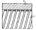
제4도 및 제5도는 본 발명에 따른 제조의 연속 단계에서 소자의 부분적 입면 횡단도.4 and 5 show partial elevational cross-sectional views of the device in successive stages of manufacture in accordance with the present invention.
제6도는 본 발명에 따른 음극선관의 단면도.6 is a cross-sectional view of a cathode ray tube according to the present invention.
제7도는 본 발명에 따른 또다른 음극선관의 단면도.7 is a cross-sectional view of another cathode ray tube according to the present invention.
제8도는 본 발명에 따른 저항의 단면도.8 is a cross-sectional view of a resistor according to the present invention.
* 도면의 주요부분에 대한 부호의 설명* Explanation of symbols for main parts of the drawings
2 : 속이 텅빈 유리관 61, 71 : 유리 봉합체2:
62, 72 : 표시 창 65, 75 : 전자총62, 72:
66, 76 : 접속 전극66, 76: connection electrode
본 발명은 절연판상에 적어도 10Ωcm의 고유저항을 갖는 저항 물질로 이루어진 동질의 전기 저항층이 형성되는 소자의 제조방법에 관한 것이다.The present invention relates to a method for fabricating a device in which a homogeneous electrical resistive layer formed of a resistive material having a resistivity of at least 10 Ωcm is formed on an insulating plate.
종래에는 분사하거나 화학반응에 의해 기상이 절연기판상에 저항층을 적층하는 방법으로 상기 소자를 제조하였다.Conventionally, the device is manufactured by laminating a resistive layer on an insulating substrate by spraying or chemical reaction.
또한, 액체내에 있는 물질의 현탁액에서 꺼내진 절연기판상에 전기 저항층을 형성할 수 있다(미합중국 특허 제3,052,573호를 참조). 상기 경우에서 꺼내진 물질은 동질의 박층이 실크 스크린이나 원심 분리 또는 브러쉬에 의해 기판상에 제공될 수 있는 현탁액이다.It is also possible to form an electrical resistive layer on an insulating substrate taken out of a suspension of material in the liquid (see US Pat. No. 3,052,573). The material taken out in this case is a suspension in which a homogeneous thin layer can be provided on the substrate by silk screen or centrifugation or brush.
상기 목적을 위해, 현탁액은 절연판상에 제공된 후 적당한 열처리로 분해될 수 있는 유리 성질을 가진 농후제, 유화제 및, 결합제(앞으로 결합제로 후술)를 현탁액에 첨가하여 적합한 특성이 주어진다.For this purpose, suspensions are given suitable properties by the addition of thickening agents, emulsifiers, and binders (described below as binders in the future) having glassy properties which can be provided on insulating plates and then decomposed by suitable heat treatment.
현탁액에 유기 부가제를 첨가하여 사용할때 실제적으로 충분히 높은 고유 저항을 갖는 전기 저항층을 얻을 수 없다는 것이 단점이다.The disadvantage is that when using the organic additives in the suspension, it is practically impossible to obtain an electrical resistive layer having a sufficiently high resistivity.
또한, 많은 저항 물질이 전압에 종속되고, 온도에 민감하며, 감광성 저항을 갖는 많은 저항 물질이 발견되고 있다.In addition, many resistive materials have been found that are voltage dependent, temperature sensitive, and have photosensitive resistance.
본 발명의 목적은 상기 단점을 충분히 극복하는 것이다.The object of the present invention is to overcome the above drawbacks sufficiently.
상기 목적을 위해, 본 발명에 따라 서두에 언급된 방법은 수산화 루테늄 및 유리 입자를 포함하는 안정 결합제-유리 현탁액에서 절연기관에 1 내지 6퍼센트의 산화 루테늄을 포함하는 전기 저항층을 가열로서 형성하므로서 층이 제공된다.For this purpose, the method mentioned at the outset according to the present invention is achieved by forming, as a heating, an electrical resistive layer comprising 1 to 6 percent of ruthenium oxide in an insulator in a stable binder-glass suspension comprising ruthenium hydroxide and glass particles. A layer is provided.
본 발명은 현탁액에 유기물의 첨가가 기판상에 동질의 박막층을 형성하는데 필요하지 않는다는 사실을 기초로 한다.The present invention is based on the fact that the addition of organics to the suspension is not necessary to form a homogeneous thin film layer on the substrate.
상당히 높은 비저항 및 판 저항을 가지는 동질의 스크래치 저항력이 있고 비침투성인 전기 저항층은 종래 기술을 사용하는 본 발명에 따른 방법에 의해 절연기판상에 재생 가능한 방식으로 형성될 수 있다.Homogeneous scratch resistant and non-invasive electrical resistive layers with significantly higher resistivity and sheet resistance can be formed in a reproducible manner on an insulating substrate by the method according to the invention using the prior art.
구해진 층의 층 두께는 1 내지 1.5㎛이다. 산화 루테늄은 전압, 온도 및, 빛에 거의 따르지 않는 저항 물질이다.The layer thickness of the obtained layer is 1 to 1.5 mu m. Ruthenium oxide is a resistive material that hardly depends on voltage, temperature and light.
유리 입자 및 물의 혼합물이 스타팅 물질로 양호하게 사용되어, 혼합물에서 수산화 루테늄이 침전된다. 특히, 양호한 분말층이 상기 혼합물로부터 얻어진 현탁액에 의해 기판상에 적층된다. 적어도 수산화 루테늄의 일부분이 접착되는 곳 위의 유리 입자때문에 폐쇄된 구성의 하나의 동기가 되며 연속적인 가열 처리로 쉽게 층을 접착한다.A mixture of glass particles and water is used as a starting material, and ruthenium hydroxide precipitates in the mixture. In particular, a good powder layer is deposited on the substrate by the suspension obtained from the mixture. At least a portion of the ruthenium hydroxide is motivated in a closed configuration because of the glass particles on which it adheres and the layers are easily bonded by a continuous heat treatment.
수산화 루테늄 및 유리 입자의 적층은 암모니아가 첨가된 알콜에서 양호하게 부유된다. 암모니아는 현탁액의 안정성을 위해 중요하게 여겨왔으며, 일정한 층이 상기 현탁액에서 꺼내진 기판상에 매우 간단한 방식으로 제공될 수 있다는 것을 알았다.The lamination of ruthenium hydroxide and glass particles is well suspended in the ammonia-added alcohol. Ammonia has been considered important for the stability of the suspension and it has been found that certain layers can be provided in a very simple manner on the substrate taken out of the suspension.
이소프로패놀이 알콜로서 양호하게 사용된다.Isopropanol is preferably used as an alcohol.
절연기판은 유리 같은 것으로 사용된다. 최종적인 전기 저항층이 형성되도록 수산화 루테늄을 가열하여 산화 루테늄으로 전화하는 동안, 유리 입자는 변하여 혼합물 및 두께에 관해 동질 산화 루테늄으로 된 층을 형성한다.Insulating substrates are used as glass. While ruthenium hydroxide is heated to convert to ruthenium oxide to form a final electrical resistive layer, the glass particles change to form a layer of homogeneous ruthenium oxide with respect to the mixture and thickness.
보통 가열 온도는 저항 값의 조정 가능성에 따라 400 내지 600℃ 사이에서 변한다.Usually the heating temperature varies between 400 and 600 ° C. depending on the possibility of adjusting the resistance value.
유리 입자가 변하여 동질층을 형성할지라도, 가열하는 동안 유리 입자가 불필요하게 넓은 영역으로 흐른다는 것을 의미하지는 않는다. 오히려, 가열전에 층의 크기가 가열후에도 가열하는 동안과 마찬가지로 정확히 유지될 수 있다는 것을 알 수 있다.Although the glass particles change to form a homogeneous layer, it does not mean that the glass particles unnecessarily flow into a large area during heating. Rather, it can be seen that the size of the layer before heating can be maintained exactly as during heating even after heating.
그러므로, 본 발명에 다른 방법의 양호한 실시예에서, 현탁액에서 꺼내진 층을 절연기판상에 제공하고 난 후 가열하기 이전에 층은 성형 처리하는데에 어떤 난점 없이 형성된다.Therefore, in a preferred embodiment of the method according to the invention, the layer is formed without any difficulty in shaping treatment before providing the layer taken out of the suspension onto the insulating substrate and before heating.
상기 형태를 처리하는데는 여러 종류가 있다. 예를 들어, 광화학 기술이 사용되기도 한다. 간단하게는 기계적인 형태 처리가 양호하게 사용된다.There are several types of treatment of this form. For example, photochemical techniques may be used. In brief, mechanical form processing is well used.
본 발명에 따른 방법에서 사용된 현탁액의 안정성 때문에, 재생 가능한 방식으로 기판상에 상기 현탁액에서 꺼낸 층을 제공할 수 있다. 기판상에 층이 제공된 형태만이 있는 것은 아니다라는 것을 알 수 있다.Because of the stability of the suspension used in the process according to the invention, it is possible to provide a layer taken out of the suspension on a substrate in a renewable manner. It will be appreciated that there is not only a form in which a layer is provided on the substrate.
본 발명에 따른 방법의 양호한 실시예에서 절연기판 대신에 속이 텅빈 관의 내측상에 현탁액으로부터 층이 제공된다.In a preferred embodiment of the method according to the invention a layer is provided from the suspension on the inside of the hollow tube instead of the insulating substrate.
양호한 높이까지 관내로 현탁액을 유입한 다음 관에서 현탁액을 배출시키므로서 상기 현탁액이 간단하고 경제적으로 제공된다.The suspension is provided simply and economically by introducing the suspension into the tube to a good height and then withdrawing the suspension from the tube.
또한, 상기 방식으로서 기판상에 현탁액으로부터의 층이 제공될때, 성형 처리가 가능하다. 예를 들어, 비 가열된 층은 속이 텅빈 관의 내측상에 나선형 형태의 기계적인 성형 처리에 의해 양호하게 된다.Also, when the layer from the suspension is provided on the substrate in this manner, a molding treatment is possible. For example, the unheated layer is favored by a mechanical molding process in the form of a spiral on the inside of the hollow tube.
가열후 매우 양호한 나선 형태를 고려하여 볼때 나선형의 피치나, 나선형의 회전부간의 거리는 매우 임계적이 아니며, 작지도 않다. 회전부간의 상기 거리는 50㎛이다. 나선형의 전체 길이에 걸쳐 인가되는 전압은 인접 회전부간에 일어나는 플래시오버 없이 매우 높게 된다. 상호간의 거리는 50㎛에서 그 회전부간의 플래시오버 전압은 1.5KV 이상이다.Considering the very good spiral shape after heating, the spiral pitch or the distance between the spiral rotations is not very critical and is not small. The distance between the rotating parts is 50 mu m. The voltage applied across the entire length of the helical is very high without flashover occurring between adjacent turns. The distance between them is 50 µm, and the flashover voltage between the rotating parts is 1.5 KV or more.
본 발명에 다른 방법에 의해 제조된 속이 텅빈 관의 형태로 상기 소자는 투명형 텔레비젼 표시관 같은 음극선관으로서 사용된다. 상기 음극선관은 표시창, 콘 및, 네크로 이루어지는 유리 봉합체와 네트내에 제공되어 적어도 하나의 집속 전극을 갖는 전자총을 구비한다.The device is used as a cathode ray tube, such as a transparent television display tube, in the form of a hollow tube produced by another method according to the present invention. The cathode ray tube is provided with a display window, a cone, a glass encapsulation body made of a neck, and an electron gun provided in the net and having at least one focusing electrode.
상기 음극선관내의 집속 전극은 본 발명에 따라 얻어지며, 나선형 저항층이 제공되는 속이 텅빈 관의 형태를 갖는다. 상기 저항층은 바람직한 포텐셜이 얼마 안된는 수차 오차를 보이는 전자 렌즈를 위해 필요한 유리관 내측상에 나타나는 분주기로서 사용된다. 피치, 회전부간의 거리, 나선형 저항층의 저항을 변화시키므로서 바람직한 포텐셜을 구할 수 있다. 음극선관 네크의 직경은 작게 선택된다. 저항층은 봉합체의 내측상에 제공된다.The focusing electrode in the cathode ray tube is obtained according to the present invention and has the form of a hollow tube provided with a spiral resistive layer. The resistive layer is used as a divider appearing on the inside of the glass tube that is required for an electronic lens that exhibits aberration errors of lesser desirable potential. The desired potential can be obtained by changing the pitch, the distance between the rotating portions, and the resistance of the spiral resistance layer. The diameter of the cathode ray tube neck is chosen small. The resistive layer is provided on the inner side of the enclosure.
본 발명에 따른 방법을 적절히 응용한다면, 음극선관은 표시창, 콘 및, 네크로 구성되는 유리 봉합체를 구비하며, 적어도 하나의 집속 전극을 갖는 전자총이 네크내에 제공되고, 반전하층이 본 발명에 따른 방법을 사용하므로서 얻어진다. 반전하층은 네크가 너무 높은 포텐셜로 충전되지 않도록 보호한다.If the method according to the invention is suitably applied, the cathode ray tube comprises a display window, a cone and a glass encapsulation consisting of a neck, an electron gun having at least one focusing electrode is provided in the neck, and the inverse underlayer is the method according to the invention. Obtained by using The inverted underlayer protects the neck from filling with too high potential.
적어도 40KV까지의 전압에서 사용하기 위한 고저항은 본 발명에 따른 방법에 의해 얻어질 수 있다.High resistance for use at voltages up to at least 40 KV can be obtained by the method according to the invention.
이하 도면을 참조하면서 본 발명을 더욱 상세히 설명하기로 한다.Hereinafter, the present invention will be described in more detail with reference to the drawings.
절연층상에 재생 가능하고 동질이며 비저항이 높은 전기 저항층을 구하기 위하여, 본 발명에 따라 수산화 루테늄 및 유리 입자를 구비하는 안정된 결합체-유리된 현탁액에서 꺼내진 1 내지 65의 산화 루테늄을 포함하는 전기 저항층이 절연기판(2)상에서 가열되므로서 형성된다.In order to obtain a reproducible, homogeneous and high resistivity electrical resistive layer on the insulating layer, electrical resistivity comprising from 1 to 65 ruthenium oxides taken from a stable conjugate-glass suspension with ruthenium hydroxide and glass particles according to the invention. The layer is formed by heating on the insulating substrate 2.
유리 에나멜은 실질적으로 기판 물질과 동일한 열 팽창 계수와 기판 물질보다 더 낮은 연화점을 갖는다. 본 발명이 표시관에 적용되는 경우, 기판 물질은 전체 중량에 대해 SiO2가 62.4%, PbO가 21%, K2O가 7.3%, Na2O가 6.8%, Al2O3가 1.3% 및, 몇몇의 극소 성분을 포함하는 형태의 납 유리이다. 상기 특수 유리의 연화점은 640℃이다. 적합한 유리 에나멜은 PbO가 80%, B2O3가 16%, ZnO가 4%, 그리고 연화점이 400℃인 납-붕산염 유리이다. 다른 적합한 유리 에나멜은 PbO가 77.2%, B2O3가 13.3%, Al2O3가 55%, ZnO가 25 및, 몇몇의 극소 성분을 포함하는 187명(연화점 415°)와 PbO가 68.1%, B2O3가 17.9%, ZnO가 8%, Al2O3가 3%인 215형이 있다.Glass enamel has a coefficient of thermal expansion substantially lower than the substrate material and a lower softening point than the substrate material. When the present invention is applied to the display tube, the substrate material has 62.4% SiO 2 , 21% PbO, 7.3% K 2 O, 6.8% Na 2 O, 1.3% Al 2 O 3 , and , Lead glass in the form of some microcomponents. The softening point of the special glass is 640 ° C. Suitable glass enamels are lead-borate glasses having 80% PbO, 16% B 2 O 3 , 4% ZnO, and a softening point of 400 ° C. Other suitable glass enamels included 77.2% PbO, 13.3% B 2 O 3 , 55% Al 2 O 3 , 25 ZnO, and 187 (softening point 415 °) with some minor components and 68.1% PbO. , 215 with B 2 O 3 at 17.9%, ZnO at 8%, and Al 2 O 3 at 3%.
점성 현탁액은 먼저 비이커내의 유리 에나멜 분말에 물을 혼합하여 충분히 얻게 되나, 염화 루테늄(RuCl3)은 물에서 융해되고 혼합물에 가해진다. 수산화 루테늄은 암모니아를 첨가하므로서 혼합물에 침적된다. 물이 사이펀으로 옮겨지고 침전물이 건조된 후에 혼합물이 침전되게 한다.A viscous suspension is obtained sufficiently by first mixing water with free enamel powder in a beaker, but ruthenium chloride (RuCl 3 ) is dissolved in water and added to the mixture. Ruthenium hydroxide is deposited in the mixture by adding ammonia. Water is transferred to the siphon and the mixture is allowed to settle after the precipitate has dried.
건조된 침전물이 볼 밀에 놓여져 이조프로패놀 및 암모니아가 첨가된다. 양질의 혼합물을 얻고 가능하면 굵은 입자를 가루로 만들기 위해 약 140시간동안 그라인딩을 실행한다.The dried precipitate is placed in a ball mill to which zopropanol and ammonia are added. Grind for about 140 hours to get a good mixture and to grind coarse particles if possible.
이렇게 얻어진 안정된 현탁액에 의해, 유리 표면은 매우 일정한 저항 분말층으로 피복될 수 있다. 전기 저항층은 가열하므로서 분말층으로부터 형성된다.With the stable suspension thus obtained, the glass surface can be coated with a very constant layer of resistive powder. The electrical resistive layer is formed from the powder layer by heating.
이렇게 생성된 저항층은 층 두께, 산화 루테늄의 퍼센트, 가열 온도 및 가열 시간에 따라 변한다. 산화 루테늄이 1% 미만일때 층을 전기적으로 전도가 충분히 되지 않으며, 65 이상일때 저항이 너무 낮다.The resulting resistive layer varies with layer thickness, percent ruthenium oxide, heating temperature and heating time. When ruthenium oxide is less than 1%, the layer is not electrically conductive enough, and when it is 65 or more, the resistance is too low.
제1도에 있어서, 저항층내의 산화 루테늄 비율은 3%이며, 10분동안 가열된다.In FIG. 1, the ratio of ruthenium oxide in the resistive layer is 3% and is heated for 10 minutes.
제2도에 있어서, 저항층내의 산화 루테늄 비율은 3%이며, 500℃로 가열된다.In FIG. 2, the ruthenium oxide ratio in a resistive layer is 3%, and is heated to 500 degreeC.
제3도에 있어서, 저항층내의 산화 루테늄 비율은 25이며, 500℃로 가열된다. 전기 저항층의 두께는 1 내지 1.5㎛이다.In FIG. 3, the ruthenium oxide ratio in a resistive layer is 25, and it heats at 500 degreeC. The thickness of the electrical resistance layer is 1 to 1.5 mu m.
실제로는, 소정의 가열 온도에서 바람직한 저항값에 상당하는 가열 시간으로 매우 간단하게 소정의 바람직한 저항값을 얻게 된다.In practice, the desired desired resistance value is obtained very simply with a heating time corresponding to the desired resistance value at the predetermined heating temperature.
상기 층이 특수 형태로 되는 것도 가능하다. 절연 기판상에 층을 제공하고, 이 층을 가열하기 이전 형태 처리가 실행된다. 기계적인 형태 처리를 사용하는 것이 유리한다.It is also possible for the layer to be in a special form. A layer is provided on the insulating substrate, and a shape treatment is performed before heating this layer. It is advantageous to use mechanical form processing.
제4도에 도시된 바와 같이, 바람직한 높이까지 관(2)내로 현탁액을 붙고 또한 배출하므로서 속이 텅빈 유리관(2) 내측상에 현탁액으로부터 층(1)이 제공되며, 그후 속이 텅빈 관(2)의 내측상에서 스크래치 하므로서 층을 나선형으로 만든다.As shown in FIG. 4, a layer (1) is provided from the suspension on the inside of the hollow glass tube (2) by attaching and also discharging the suspension into the tube (2) to the desired height, and then of the hollow tube (2). The layer is spiraled by scratching on the inside.
가열후에, 생성된 나선 코일형 저항층이 와인딩 턴(3)이 휼륭하게 둥글려진다. 인접한 턴 간의 플래시오버 전압은 매우 높게 발견된다. 와인딩 턴 간의 공간은 50㎛이며, 피치는 300㎛이다.After heating, the resulting spiral coiled resistive layer rounds the winding turn 3 very well. The flashover voltage between adjacent turns is found to be very high. The space between the winding turns is 50 μm and the pitch is 300 μm.
상기 나선 코일형 저항층은 피치, 턴 간의 공간 및, 저항을 변하게 하므로서 음극선관에서 분주기의 역할을 한다.The spiral coil type resistive layer acts as a divider in the cathode ray tube while varying the pitch, the space between turns, and the resistance.
자주 사용된 집속 렌즈는 구면 수차를 피하기 위해 사용되는 중심부만의 비교적 큰 직경을 갖는다. 본 발명에 따른 방법에 의해 얻어진 나선 코일형 저항층이 집속 렌즈로서 사용될때, 관에는 매우 작은 지름을 갖는 전자총 및 네크와, 큰 직경을 갖는 종래의 렌즈의 중심부와 동일한 전압 분배를 가지며 구면 수차가 작은 집속 렌즈가 사용된다.Frequently used focusing lenses have a relatively large diameter only at the center portion used to avoid spherical aberration. When the spiral coil type resistive layer obtained by the method according to the invention is used as a focusing lens, the tube has an electron gun and neck having a very small diameter, and has the same voltage distribution as the central portion of a conventional lens having a large diameter, and has a spherical aberration. Small focusing lenses are used.
이것은 본 발명에 따른 음극선관의 경우이다(제6도 참조). 음극선관은 표시창(62), 콘(63) 및, 네크(64)를 구성하는 유리 봉합체(61)를 구비한다. 코일형 집속 전극(66)을 갖는 전자총(65)은 네크내에 존재한다. 상기 코일형 집속 전극은 본 발명에 따른 방법에 의해 상기에 설명한 바와 같이 얻어진다. 이것과 함께, 집속하기 위해 바람직한 전압 분배가 얻어질 수 있다.This is the case of the cathode ray tube according to the present invention (see Fig. 6). The cathode ray tube includes a
본 발명에 다른 방법에 의해 얻어진 저항층은 코일형이든 아니든간에 음극선관의 네크내에 너무 높은 포텐셜을 방지하기 위해 반 전하층으로서 사용된다.The resistive layer obtained by the method according to the present invention, whether coiled or not, is used as a semi-charge layer in order to prevent too high potential in the neck of the cathode ray tube.
상기 경우(제7도를 참조)에, 음극선관은 표시창(72), 콘(73), 네크(74) 및, 네크내에 제공될 집속 전극(76)을 갖는 전자총(75)로 구성되는 유리 봉합체(71)를 구비한다. 반전하층(77)은 상기에서 도시된 바와 같이 본 발명에 다른 방법에 의해 얻어진 나선 코일형 저항층의 형태로 네크(74)의 내벽상에 존재한다.In this case (see FIG. 7), the cathode ray tube is a glass encapsulation consisting of a
본 발명에 따른 방법의 또다른 응용에 있어서 고전압에서 사용하기 위한 고저항은 상기에 도시된 바와 같이 본 발명에 따른 방법에 의해 나선 코일형 저항층(82)이 적합한 절연 세라믹 기판상이나 유리관(81)(제8도 참조)내에 제공하므로서 얻게 된다.In another application of the method according to the invention, the high resistance for use at high voltage may be applied on an insulating ceramic substrate or
저항은 금속 접촉부(83)를 갖는 종래의 형태로 제공된다.The resistance is provided in a conventional form with
물론, 본 발명이 상기된 예에 한정되는 것은 아니다. 예를 들어, 상기된 바와 같은 코일형 저항층이 칼라 텔레비젼 표시관(네델란드왕국 특허원 제84007119호)내의 전자 빔을 접속하기 위해 사용된다.Of course, the present invention is not limited to the above examples. For example, a coiled resistive layer as described above is used to connect the electron beams in a color television display tube (Dutch Patent No. 84007119).
본 발명의 범위를 벗어나지 않고 숙련된 기술자에 의해 많은 변화를 할 수 있다.Many changes can be made by a skilled person without departing from the scope of the invention.
Claims (21)
Applications Claiming Priority (2)
| Application Number | Priority Date | Filing Date | Title |
|---|---|---|---|
| NL8500905 | 1985-03-28 | ||
| NL8500905A NL8500905A (en) | 1985-03-28 | 1985-03-28 | METHOD FOR PRODUCING AN ELECTRICAL RESISTANCE COATING DEVICE AND APPLICATION OF THE METHOD |
Publications (2)
| Publication Number | Publication Date |
|---|---|
| KR860007686A KR860007686A (en) | 1986-10-15 |
| KR940004368B1 true KR940004368B1 (en) | 1994-05-23 |
Family
ID=19845748
Family Applications (1)
| Application Number | Title | Priority Date | Filing Date |
|---|---|---|---|
| KR1019860002342A KR940004368B1 (en) | 1985-03-28 | 1986-03-28 | Method of manufacturing a device having an electric resistance layer and the use of the method |
Country Status (8)
| Country | Link |
|---|---|
| US (1) | US4713879A (en) |
| EP (1) | EP0197584B1 (en) |
| JP (1) | JPS61224402A (en) |
| KR (1) | KR940004368B1 (en) |
| CA (1) | CA1249954A (en) |
| DE (1) | DE3680015D1 (en) |
| ES (1) | ES8705696A1 (en) |
| NL (1) | NL8500905A (en) |
Families Citing this family (13)
| Publication number | Priority date | Publication date | Assignee | Title |
|---|---|---|---|---|
| NL8600391A (en) * | 1986-02-17 | 1987-09-16 | Philips Nv | CATHODE JET TUBE AND METHOD FOR MANUFACTURING A CATHODE JET TUBE. |
| GB8701289D0 (en) * | 1987-01-21 | 1987-02-25 | Philips Nv | Electron beam device |
| GB8707169D0 (en) * | 1987-03-25 | 1987-04-29 | Philips Nv | Electron beam device |
| GB8707170D0 (en) * | 1987-03-25 | 1987-04-29 | Philips Nv | Electron beam device |
| EP0497902A1 (en) * | 1989-10-26 | 1992-08-12 | Eastman Kodak Company | Poly(1,4-cyclohexylene dimethylene terephthalate) molding compositions |
| JP3219450B2 (en) * | 1992-01-24 | 2001-10-15 | 旭硝子株式会社 | Method for producing conductive film, low reflection conductive film and method for producing the same |
| US5510670A (en) * | 1994-07-19 | 1996-04-23 | Philips Electronics North American Corporation | Electron beam device having a glass envelope and a focussing lens provided thereon |
| JP2002515165A (en) * | 1994-07-19 | 2002-05-21 | フィリップス エレクトロニクス ネムローゼ フェンノートシャップ | Electron beam device having a resistive focusing lens structure and method of manufacturing the device |
| JPH09293465A (en) * | 1995-11-28 | 1997-11-11 | Matsushita Electric Ind Co Ltd | Manufacture of resistor for cathode-ray tube |
| US6005338A (en) * | 1996-04-18 | 1999-12-21 | Matsushita Electronics Corporation | Cathode-ray tube and process for producing the same |
| JP3546729B2 (en) * | 1998-12-21 | 2004-07-28 | 松下電器産業株式会社 | Electron gun, method for manufacturing electron gun, cathode ray tube device |
| JP2001093448A (en) * | 1999-09-21 | 2001-04-06 | Matsushita Electronics Industry Corp | Cathode-ray tube |
| CN111919268B (en) * | 2018-03-26 | 2022-04-19 | 松下知识产权经营株式会社 | Varistor and method for producing same |
Family Cites Families (16)
| Publication number | Priority date | Publication date | Assignee | Title |
|---|---|---|---|---|
| US1835582A (en) * | 1928-03-30 | 1931-12-08 | Stratford B Allen | Resistance unit |
| US3375390A (en) * | 1966-01-03 | 1968-03-26 | Gen Electric | Electron optical system having spiral collimating electrode adjacent the target |
| GB1195833A (en) * | 1966-06-14 | 1970-06-24 | Plessey Co Ltd | Improvements in or relating to Resistors |
| NL137152C (en) * | 1966-10-24 | |||
| GB1256507A (en) * | 1968-04-10 | 1971-12-08 | ||
| US3673117A (en) * | 1969-12-19 | 1972-06-27 | Methode Dev Co | Electrical resistant material |
| GB1327760A (en) * | 1969-12-22 | 1973-08-22 | Imp Metal Ind Kynoch Ltd | Electrodes |
| JPS5023591B1 (en) * | 1970-01-23 | 1975-08-08 | ||
| US3748514A (en) * | 1971-08-18 | 1973-07-24 | A Standaart | Multi-beam cathode ray tube character display |
| GB1353872A (en) * | 1972-07-05 | 1974-05-22 | Thorn Electrical Ind Ltd | Cathode ray tubes |
| JPS539400A (en) * | 1976-07-14 | 1978-01-27 | Japan Tobacco Inc | Method for increasing packing capacity of tobacco |
| JPS5915629B2 (en) * | 1977-09-12 | 1984-04-10 | 協和醗酵工業株式会社 | Antibiotic manufacturing method |
| US4130671A (en) * | 1977-09-30 | 1978-12-19 | The United States Of America As Represented By The United States Department Of Energy | Method for preparing a thick film conductor |
| US4561996A (en) * | 1977-10-05 | 1985-12-31 | Cts Corporation | Electrical resistor and method of making the same |
| US4366042A (en) * | 1981-03-25 | 1982-12-28 | The Dow Chemical Company | Substituted cobalt oxide spinels |
| JPS583201A (en) * | 1981-06-30 | 1983-01-10 | アルプス電気株式会社 | Resistance paste, thick film integrated circuit produced with same paste, thermal head and method of producing same |
-
1985
- 1985-03-28 NL NL8500905A patent/NL8500905A/en not_active Application Discontinuation
-
1986
- 1986-03-21 DE DE8686200480T patent/DE3680015D1/en not_active Expired - Lifetime
- 1986-03-21 EP EP86200480A patent/EP0197584B1/en not_active Expired - Lifetime
- 1986-03-24 US US06/843,329 patent/US4713879A/en not_active Expired - Fee Related
- 1986-03-25 ES ES553361A patent/ES8705696A1/en not_active Expired
- 1986-03-27 JP JP61067396A patent/JPS61224402A/en active Granted
- 1986-03-27 CA CA000505471A patent/CA1249954A/en not_active Expired
- 1986-03-28 KR KR1019860002342A patent/KR940004368B1/en not_active IP Right Cessation
Also Published As
| Publication number | Publication date |
|---|---|
| JPH0423402B2 (en) | 1992-04-22 |
| ES553361A0 (en) | 1987-05-01 |
| EP0197584A1 (en) | 1986-10-15 |
| DE3680015D1 (en) | 1991-08-08 |
| NL8500905A (en) | 1986-10-16 |
| CA1249954A (en) | 1989-02-14 |
| KR860007686A (en) | 1986-10-15 |
| ES8705696A1 (en) | 1987-05-01 |
| JPS61224402A (en) | 1986-10-06 |
| US4713879A (en) | 1987-12-22 |
| EP0197584B1 (en) | 1991-07-03 |
Similar Documents
| Publication | Publication Date | Title |
|---|---|---|
| KR940004368B1 (en) | Method of manufacturing a device having an electric resistance layer and the use of the method | |
| US2717946A (en) | Electrical resistance elements | |
| US3352009A (en) | Process of producing high temperature resistant insulated wire, such wire and coils made therefrom | |
| US2950995A (en) | Electrical resistance element | |
| US4528613A (en) | Ceramic glass material, capacitor made therefrom and method of making the same | |
| JPS643282B2 (en) | ||
| US2321439A (en) | Method of making vitreous coated bodies | |
| JPS62193046A (en) | Cathode ray tube and manufacture of the same | |
| US4091144A (en) | Article with electrically-resistive glaze for use in high-electric fields and method of making same | |
| US3979625A (en) | Ceramic spaced sensor assembly for a gas leak detector | |
| US3490055A (en) | Circuit structure with capacitor | |
| US3277354A (en) | Glass capacitors having a chrome oxide layer on the electrodes | |
| US4397915A (en) | Electrical resistor material, resistor made therefrom and method of making the same | |
| US4500397A (en) | Method for the preparation of a pyroelectric material | |
| US4322477A (en) | Electrical resistor material, resistor made therefrom and method of making the same | |
| US3919682A (en) | Electrical resistor with a polycrystalline ceramic cover and a process for its manufacture | |
| US4139832A (en) | Glass-coated thick film resistor | |
| JPH0530012B2 (en) | ||
| JPH0552021B2 (en) | ||
| US3437974A (en) | High strength resistor | |
| US6005338A (en) | Cathode-ray tube and process for producing the same | |
| US3457615A (en) | Method of making glass capacitors | |
| US3808574A (en) | Magnesium and magnesium oxide resistor and method of forming | |
| JPS636730A (en) | Electron tube having plural number of internal electrode | |
| US3645784A (en) | Vitreous enamel resistor |
Legal Events
| Date | Code | Title | Description |
|---|---|---|---|
| A201 | Request for examination | ||
| G160 | Decision to publish patent application | ||
| E701 | Decision to grant or registration of patent right | ||
| GRNT | Written decision to grant | ||
| LAPS | Lapse due to unpaid annual fee |