KR910004288B1 - Digital television receiver automatic chroma control system - Google Patents
Digital television receiver automatic chroma control system Download PDFInfo
- Publication number
- KR910004288B1 KR910004288B1 KR1019830001093A KR830001093A KR910004288B1 KR 910004288 B1 KR910004288 B1 KR 910004288B1 KR 1019830001093 A KR1019830001093 A KR 1019830001093A KR 830001093 A KR830001093 A KR 830001093A KR 910004288 B1 KR910004288 B1 KR 910004288B1
- Authority
- KR
- South Korea
- Prior art keywords
- signal
- gain
- color information
- value
- digital
- Prior art date
Links
Images


Classifications
-
- H—ELECTRICITY
- H04—ELECTRIC COMMUNICATION TECHNIQUE
- H04N—PICTORIAL COMMUNICATION, e.g. TELEVISION
- H04N9/00—Details of colour television systems
- H04N9/64—Circuits for processing colour signals
- H04N9/68—Circuits for processing colour signals for controlling the amplitude of colour signals, e.g. automatic chroma control circuits
-
- H—ELECTRICITY
- H04—ELECTRIC COMMUNICATION TECHNIQUE
- H04N—PICTORIAL COMMUNICATION, e.g. TELEVISION
- H04N9/00—Details of colour television systems
- H04N9/64—Circuits for processing colour signals
- H04N9/70—Circuits for processing colour signals for colour killing
- H04N9/71—Circuits for processing colour signals for colour killing combined with colour gain control
-
- H—ELECTRICITY
- H04—ELECTRIC COMMUNICATION TECHNIQUE
- H04N—PICTORIAL COMMUNICATION, e.g. TELEVISION
- H04N9/00—Details of colour television systems
- H04N9/79—Processing of colour television signals in connection with recording
- H04N9/793—Processing of colour television signals in connection with recording for controlling the level of the chrominance signal, e.g. by means of automatic chroma control circuits
Abstract
내용 없음.No content.
Description
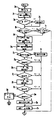
제 1 도는 본 발명에 의해 구성된 텔레비젼 수상기의 디지탈 기본 대역 비데오 처리부의 블럭 계통도.1 is a block diagram of a digital baseband video processing unit of a television receiver constructed in accordance with the present invention.
제 2 도는 제 1 도 구성의 색도 신호 처리부의 이득 제어 범위도.FIG. 2 is a gain control range diagram of a chroma signal processor of FIG.
제 3 도는 제 1 도의 색도 신호 처리부의 동작 설명용 색도 버스트 파형도.3 is a chromaticity burst waveform diagram for explaining the operation of the chromaticity signal processor of FIG.
제 4 도는 제 1 도의 버스트 추출기의 상세도.4 is a detailed view of the burst extractor of FIG.
제 5 도 내지 제 10 도는 제 1 도의 색도 이득 제어 블럭에 소정의 색도 이득을 산정 및 분배하는 마이크로프로세서의 유통도.5 through 10 are flow charts of a microprocessor that calculates and distributes a predetermined chromatic gain to the chromatic gain control block of FIG.
* 도면의 주요부분에 대한 부호의 설명* Explanation of symbols for main parts of the drawings
10 : A/D 변환기 12 : 디지탈 빗형 필터10: A / D converter 12: Digital comb filter
14 : 휘도 신호 처리기 15 : 콘트라스트 제어14 luminance signal processor 15 contrast control
16 : 매트릭스 20 : 12dB 코어스 이득 시프터16: Matrix 20: 12 dB coarse gain shifter
22 : 색도 대역 통과 필터 24, 24' : 버스트 추출기22:
32 : RAM 34 : 버퍼32: RAM 34: Buffer
36 : 가산기 62 : 색도 과부하 기준 비교기36: adder 62: chromatic overload reference comparator
64 : 카운터 80 : 마이크로프로세서64: counter 80: microprocessor
214 : 라인 누산기 220 : 필드 누산기214: line accumulator 220: field accumulator
본 발명은 디지탈 텔레비젼 수상기에 관한 것으로서, 특히 디지탈 텔레비젼 수사기내의 색도 신호 레벨을 자동적으로 제어하기 위한 장치에 관한 것이다.TECHNICAL FIELD The present invention relates to digital television receivers, and more particularly, to an apparatus for automatically controlling chromaticity signal levels in a digital television receiver.
기본 대역 비데오 신호가 아나로그 형태로 처리되는 통상의 텔레비젼 수상기의 경우 색도 신호가 휘도신호로부터 분리되어 색도 저역 통과 필터나 색도 피크기에 인가된다. 색도 피크기는 색도 신호를 통과시키며 고주파 색도 신호 성분을 감쇄시키는 텔레비젼 중간 주파수 응답 특성에 의해 일어나는 크기 변화에 대한 신호를 교정하는 응답 특성을 가지고 있다. 여파된 색도 신호는 먼저 색도 증폭기 즉, 칼라 킬러와 자동색도 제어 회로에 인가된다. 자동 색도 제어 회로는 색도 버스트 신호의 크기를 감지하며 만일 버스트 신호가 너무 낮다면 색 신호를 없게 하거나 색도 신호를 공칭 레벨로 증폭시킨다. 이때 색도 신호는 사용자가 색 제어기를 조정하는데 따라 응답하는 제 2 증폭기에 인가된다.In a typical television receiver in which a baseband video signal is processed in an analog form, the chroma signal is separated from the luminance signal and applied to a chromatic low pass filter or a chromatic peak. Chromatic peaks have a response characteristic that corrects the signal for magnitude changes caused by television intermediate frequency response characteristics that pass the chroma signal and attenuate the high frequency chroma signal components. The filtered chroma signal is first applied to a chroma amplifier, namely a color killer and an automatic chroma control circuit. Automatic chroma control circuitry senses the magnitude of the chroma burst signal and, if the burst signal is too low, eliminates the color signal or amplifies the chroma signal to a nominal level. The chroma signal is then applied to a second amplifier that responds as the user adjusts the color controller.
예로, 칼라 트랙 시리즈의 알 씨 에이 코포레이션 수상기에 있어서 사용자용 색 제어기에는 2개의 제어기가 구비되어 있으며, 이는 포화 제어기와 휘도 콘트라스트 제어 조정에 따라 PIX 제어하는 PIX 제어기이다. 색 복조를 위한 적합한 색도 신호를 만들기 위해 이러한 제어들을 조정하므로써 색도 신호가 증폭되거나 감쇄된다. 이러한 색도 신호는 색도 신호의 피크 이탈을 감지하며 만일 신호 레벨이 너무 크다면 색도 채널 이득을 감소시키는 과부하 검출기에 인가된다. 기본 대역 비데오 신호가 디지탈식으로 처리되는 텔레비젼 수상기의 경우에는 전적으로 디지탈 회로를 사용하는 아나로그 텔레비젼이 상기 기능을 수행하도록 하는 것이 바람직하다. 이와 같이 디지탈적인 방법으로 기능을 수행하기 위한 직접적인 해결 방법은 요구된 자동 색도 제어 이득을 결정하여 디지탈 증배기의 이득 비율에 의해 색도 신호를 증배시키는 것이다. 색도 신호는 사용자용 색 제어기의 조정에 응답하는 제 2 디지탈 증배기의 제 2 이득 비율로 증배된 후 디지탈 과부화 검출기에 의해 필요에 따라 제 3 디지탈 증배기의 제 3 이득 비율로 감쇄된다.For example, in the RCA Corporation receiver of the color track series, the user color controller is provided with two controllers, which are saturation controllers and PIX controllers for PIX control according to luminance contrast control adjustment. By adjusting these controls to produce a suitable chromatic signal for color demodulation, the chroma signal is amplified or attenuated. This chroma signal senses deviations from the peak of the chroma signal and is applied to an overload detector which reduces the chroma channel gain if the signal level is too high. In the case of television receivers in which the baseband video signal is digitally processed, it is desirable to allow analog television using a digital circuit to perform this function. A direct solution for performing this function in a digital way is to determine the required automatic chromatic control gain and multiply the chroma signal by the gain ratio of the digital multiplier. The chroma signal is multiplied by the second gain ratio of the second digital multiplier responsive to adjustment of the user color controller and then attenuated by the digital overload detector to the third gain ratio of the third digital multiplier as needed.
그러나, 디지탈 텔레비젼 수상기내의 증배기를 광범위하게 사용한다는 것은 증배기의 복잡성과 처리 속도가 느리기 때문에 바람직하지 못하다. 따라서, 간단한 방법으로 색도 이득을 공급하고 빠른 처리 속도를 제공하도록 하는 것이 바람직하다. 또한 다른 디지탈 여파 및 복조 처리와 관련시켜 색도 이득을 제어하여 색도 채널로 과도한 잡음 성분이 바람직하다.However, widespread use of multipliers in digital television receivers is undesirable because of their complexity and slow processing speed. Therefore, it is desirable to provide chromatic gain in a simple manner and to provide fast processing speed. It is also desirable to control the chromatic gain in conjunction with other digital filter and demodulation processes so that excessive noise components into the chromaticity channel are desired.
본 발명의 특징에 따르면 디지탈 텔레비젼 수상기내의 색도 신호의 이득은 사용자용 색 제어기와 자동 색도 제어기 색도 과부하등에 의해 공급되는 이득 제어율을 누적시킨 합성된 이득 비율의 값데 따라 제어된다. 합성된 이득 비율에 따르는 이득 제어는 6dB씩 증가되는 색도 신호 이득을 6dB씩 증분시키거나 강분시키는 코어스(coarse) 이득 블럭과, 또는 그 이하의 범위로 이득을 미세 제어하는 미세 이득 블럭에 의해 실시된다. 적합한 실시예에서, 디지탈 색도 이득 시스템은 색도 과부하, 사용자용 제어기 설정 색도 버스트 크기 등을 나타내는 신호를 수신하는 마이크로프로세서의 제어하에 동작된다. 이때 마이크로프로세서는 합성된 색도 신호 이득을 계산하고 코어스 이득 블럭과 미세 이득 제어 블럭 사이의 이득을 분배한다. 본 발명의 적합한 실시예에 있어서, 코어스 이득 블럭은 18dB 범위에서 6dB씩 증분되어 색도 신호 이득을 제어하기 위한 제어식 이동 레지스터를 포함하고 있다. 미세 이득 블럭을 가산기와 마이크로프로세서에 의해 계산된 데이타 표를 포함하는 색도 신호에 의해 어드레스 되는 랜덤 억세스 메모리를 갖고 있다. 또한, 코어스 이득을 수행하는 시프트 레지스터(이하 시프터라 한다)는 색 복조기의 입력과 출력 사이를 분리시키며, 색복조기는 색도 채널에 과도한 잡음을 발생시키지 않고도 색도 복조 및 여파용의 허용 가능한 신호 레벨을 공급한다.According to a feature of the invention, the gain of the chroma signal in the digital television receiver is controlled according to the value of the synthesized gain ratio which accumulates the gain control rate supplied by the user color controller and the automatic chroma controller chromaticity overload. Gain control in accordance with the synthesized gain ratio is implemented by a coarse gain block that increments or intensifies the chroma signal gain in 6 dB increments, or a fine gain block that finely controls the gain in the range below. . In a suitable embodiment, the digital chromatic gain system is operated under the control of a microprocessor that receives a signal indicative of chromaticity overload, a controller set chroma burst size for the user, and the like. The microprocessor then calculates the synthesized chroma signal gain and distributes the gain between the coarse gain block and the fine gain control block. In a suitable embodiment of the present invention, the coarse gain block includes a controlled shift register for controlling the chroma signal gain in increments of 6 dB in the 18 dB range. The fine gain block has a random access memory that is addressed by a chroma signal comprising an adder and a data table calculated by the microprocessor. In addition, a shift register (hereinafter referred to as a shifter) that performs coarse gain separates between the input and the output of the color demodulator, and the color demodulator provides an acceptable signal level for chromatic demodulation and filtering without generating excessive noise in the chromatic channel. Supply.
이하, 첨부된 도면을 참조하여, 본 발명을 더욱 상세히 설명하기로 한다.Hereinafter, with reference to the accompanying drawings, the present invention will be described in more detail.
제 1 도를 참조하면, 디지탈 텔레비젼 수상기의 비디오 처리부를 볼 수 있는데 비데오 입력 신호는 상기 비데오 입력 신호를 추출하여 다시 그 신호를 디지탈 신호 샘플로 변환시키는 아나로그 디지탈(A/D) 변환기(10)의 입력에 인가된다. 디지탈 신호 샘플은 신호를 휘도(Y) 신호 성분과 색도(C) 신호 성분으로 분리시키는 디지탈 빗형 필터(12)에 인가된다. Y 신호 샘플은 콘트라스트 제어기(15)에 의해 공급되는 콘트라스트 신호에 따라 Y 신호를 처리하는 휘도 신호 처리기(14)에 인가된다. 이때 처리된 Y 신호는 매트릭스 회로(16)에 인가된다.Referring to FIG. 1, a video processing unit of a digital television receiver can be seen in which a video input signal is an analog digital (A / D) converter 10 which extracts the video input signal and converts the signal back into a digital signal sample. Is applied to the input of. The digital signal sample is applied to a
분리된 C 신호는 본 발명의 양상에 따라 설계된 색도 이득 제어 장치에 인가되는데 C 신호는 버스트 추출기(24)와 12dB 코어스 이득 시프터(20)의 입력 단자에 연결되어 있다. 코어스 이득 시프터(20)는 이동기 제어 라인(83)의 신호에 의해 조정되는 평행 시프트 레지스터를 갖고 있다. 집적 회로를 설계하므로써 얻을 수 있는 높은(빠른) 속도와 적응성 때문에 1980년 에디슨-웨슬리사에 의해 출판된 메드씨와 콘웨이씨의 저서인 "VLSI 시스템 입문"에서 설명되어진 배럴형 시프터를 시프터(20)로 사용하는 것이 적합하다. 또한 제어 가능한 시프터는 제어라인(83)의 신호에 따라 각기 다른 디지탈 색도 신호의 비트군을 선택하는 멀티플렉서로서 설비될 수도 있다. 클럭형 장치대신 배럴형 시프터나 멀티플렉서와 같은 조합적 논리를 사용하는 제어기능 시프트 레지스터를 설치하는 것이 고속 처리용으로는 더 바람직하다.A separate C signal is applied to the chromatic gain control device designed in accordance with aspects of the present invention, which is connected to the inputs of the
코어스 이득 시프터(20)는 색도 데이타 어를 왼쪽으로(상위 비트 위치로) 1비트, 2비트 또는 0비트씩 이동시키도록 프로그램 되어 있다. 버스트 추출기(24)의 동작은 다음에 설명되어질 것이다. 코어스 이득 시프터(20)의 출력에서 생성된 색도 어는 FIR 필터를 포함하는 색도 기본 대역 필터 또는 피크기(22)등의 입력단자에 인가된다.The
색도 기본 대역 필터(22)의 출력 단자의 색도 신호는 미세 이득 블럭(30)에 연결되어 있으며, 색도 신호들은 RAM(32)의 어드레스 입력과 가산기(36)의 한 입력 단자에 인가된다. RAM(32)의 출력은 가산기(36)의 제 2 입력단자에 인가된다. 가산기(36)의 출력단자에서 색도 신호는 I 신호 처리기(42)와 Q 신호 처리기(44)를 포함하는 색 신호 복조기(40)에 공급된다. I와 Q 신호 처리기는 1981년 8월 31일자로 출원된 미합중국 특허원 제297,556호 명칭 "디지탈 칼라 텔레비젼 신호 복조기"에 칭하는 기재된 바와 같이 구성될 수도 있다. 처리된 I, Q 신호는 처리기(42), (44)로부터 코어스 이득 시프터(50)의 입력 단자로 공급되며, 이 코어스 이득 시스터(50)는 제어라인(83)상의 신호에 의해서 제어되는 +6dB 시프터(52),(54)의 출력단자에서의 I, Q 신호는 Y, I, Q 신호를 매트릭스 시키는 매트릭스 회로(16)의 입력에 공급되어 적, 녹 및 청색 신호를 생성한다.The chroma signal at the output terminal of the chromatic
+6dB 시프터(52)의 출력단자에서 I신호는 색도 과부하 검출기(60)의 색도 과부하 기준 비교기(62)의 입력 단자에 인가된다. 비교기(62)는 I신호 레벨과 데이터 라인(86)에 의해 공급된 기준치를 비교한다. I신호가 기준치를 초과하면, 펄스는 소정 시간 간격동안 펄스를 계수하는 카운터(64)에 인가된다. 카운터(64)의 출력은 마이크로프로세서(80)의 입력단에 연결된 데이터 버스(82)에 공급된다. 신호 추출기(24), PIX래치(74), SAT래치(78)의 출력 또한 데이터 버스(82)에 공급된다. 사용자용 PIX 제어기(72)에 의해 발생된 PIX 제어 어는 PIX 래치(74)의 입력단에 인가되며, 사용자용 SAT 제어기(76)에 의해 발생된 제어 어는 SAT 래치(78)의 입력단에 인가된다. 마이크로프로세서(80)는 제어 라인(81)상의 제어 어에 의해 버스트 추출기(24), PIX래치(74), SAT래치(78)를 제어하게 되며 미세 이득 제어 라인(84)상의 마이크로프로세서 제어 어는 미세 이득 블럭(30)의 RAM(32)의 부하를 제어하고 RAM(32)에 필요한 데이터를 기억시키는데 사용되는 버퍼(34)를 제어한다. 또한 마이크로프로세서는 COD 제어 라인(85)위의 신호들을 통해 색도 과부하 검출기(60)를 제어하며 제어 라인(83)에 의해 코어스 이득 시프터를 제어한다.The I signal at the output terminal of the +
12dB 코어스 이득 시프터(20)는 0, 1, 2비트씩 왼쪽으로 색도 신호 어를 이동시키므로써 1, 2, 4의 이득을 얻을 수 있다. 비슷한 방법으로, +6dB이동기(50)는 0, 1비트씩 왼쪽으로 복조기된 색도 신호를 이동시키므로써 1, 2의 이득을 얻을 수 있다. 이 두 개의 시프터는 시프터(20)나 시프터(50)대신 단 1개의 18dB 시프터로 합해질 수 있다. 그러나 시프터(20) 및 시프터(50)대신 결합된 단일 시프터가 사용되어 복조(40)의 출력에서 전체 8의 이득이 실시되면, 복조기내의 색도 신호 레벨은 색도 신호를 소정의 해상도로 여파 및 복조하는데 불충분해질 수 있다. 또 다른측면에서, 시프터가 색도 채널의 입력단에서 전체 8의 이득(세번 왼쪽으로 이동되므로)을 수행하기 위해 합쳐진다면 입력 색도 신호는 그 어가 왼쪽으로 이동되므로 최하위 비트 3자리는 0이 될 것이다. 세자리의 0비트는 실제적으로는 색도 어값에 관계하지 않으며 따라서, 신호내에서 낮은 값의 잡음으로 존재한다. 그러므로 과도한 잡음성 신호가 색도 채널속에서 여파되고 복조될 것이다. 제 1 도의 적합한 실시예에 있어서는, 색도 채널의 입력에서 왼쪽으로 최대 2번을 이동시키고 출력에서 최대 한 번을 이동시켜 신호를 이동시키도록 절충되어 있다. 12dB 시프터(20)는 여파 및 복조에 필요한 충분한 신호 레벨을 공급하는 반면 신호에는 단지 두 개의 최하위 비트만 잡음으로 나타난다. 이때 색도 신호는 신호 어들이 +6dB 시프터(50)에 의해 최종적으로 왼쪽으로 이동되기 전에 색도 기본 대역 필터(22)와 복조기(40)에 의해 여파되고 복조된다.The 12dB
제 1 도의 구성의 색도 이득 제어 범위는 제 2 도에서 볼 수 있다. 색도 신호의 색 버스트 신호 성분은 40IRE의 정격 대 피크 진폭을 가진다. 이 진폭의 버스트 신호는 색도 이득 제어 시스템의 자동 색도 제어부(ACC)에 의해 증폭되지 않기 때문에 이 시스템의 이득을 0dB로 되게 하여 사용자 제어기와 색도 과부하 검출기(60) 등의 영향이 무시된다. ACC 시스템은 제 2 도의 ACC 제어 범위 라인에 표시된 것처럼 신호 진폭이 18dB까지 내려갔을 때 버스트를 위해 40IRE의 정격 값까지 색도 신호를 증폭하도록 동작한다. 신호 레벨이 ACC 제어기 범위 라인의 파선 부분으로 표시된 것처럼 6dB 더 감소된다면, ACC 이득은 색도 신호를 -18dB까지 증폭시킬 것이다. 그러나 신호 레벨은 버스트 기준치까지 도달하지 못할 것이다. 버스트 신호 레벨이 24dB나 그 이상으로 정격 레벨보다 감쇄된다면 ACC 시스템은 칼라 킬러로 동작하게 될 것이다. ACC 이득 제어 시스템은 또한 지나치게 강한 색도 신호를 64dB까지 감쇄시킬 수 있다. 포화 제어는 제 2 도에서의 SAT 제어 범위 라인에 의해 표시된 것처럼 6dB의 범위를 가진다. 포화 제어 신호는 색도 신호 진곡을 증가시켜 포화를 6dB까지 증가시킬 수 있다. 또한 PIX 제어는 제 2 도의 PIX 제어 범위 라인에서 볼 수 있듯이, 색도 신호를 18dB까지 감쇄시킬 수 있다. 또한 PIX 및 SAT 제어는 필요에 따라 +6dB에서 -18dB까지 색도 이득 제어의 범위를 갖는 단일 제어기로 제어될 수도 있다. 그러나 이들 제어는 위에서 언급한 알 씨 에이 컬러트랙 시스템에서 사용한 것과 비슷한 사용자용 이득 제어기인 제 1 도와 제 2 도내의 것과 같이 분리 제어되는 것으로 도시되어 있다.The chromaticity gain control range of the configuration of FIG. 1 can be seen in FIG. The color burst signal component of the chroma signal has a rated to peak amplitude of 40 IRE. Since the burst signal of this amplitude is not amplified by the automatic chromaticity control unit (ACC) of the chromaticity gain control system, the gain of the system is brought to 0 dB so that the influence of the user controller and the
또한 색도 과부하 이득 비율은 색도 과부하 검출기(60)로부터 유출된다. 기준 레벨을 초과하지 않는 신호들에 대해서도 색도 과부하 이득 COD 이득은 0dB의 정격치를 갖는다. 색도 과부하가 증가할 때 COD 이득치는 제 2 도의 COD 이득 라인에서 볼 수 있듯이 신호를 감쇄시키기 위해 감소된다.In addition, the chromaticity overload gain ratio flows out of the
버스트 추출기(24)는 색 버스트 신호 성분의 레벨을 감지하기 위해 동작된다. 제 3 도를 참조하면, 정격 버스트 신호(110)의 여러개의 사이클을 볼 수 있다. 정격 버스트 신호는 40IRE의 피크 대 피크 진폭을 가진다 디지탈 빗형 필터(12)는 2의 보수법으로 된 디지탈 샘플로 구성된 색도(C) 신호를 발생한다. 2의 보수법에 있어서, 색도 신호의 이들 디지탈 샘플은 디지탈식 진법의 중간부에서 변화되며, 그 값은 8비트 진법에 대해서는 0000000이거사 또는 10진법에 대해서는 0이 된다.
8-비트진법의 다이나믹 범위는 -60IRE에 해당하는 값 10000000(-128)에서 +60IRE에 해당하는 값 01111111(+127)가지이며 제 3 도에 도시되어 있다. 버스트 추출기(24)는 샘플링 포인트 A, B와 C로 표시한 바와 같이 버스트 신호값을 신호 피크에서 샘플한다. 버스트 신호가 정격 40IRE 레벨에 있을대 버스트 피크는 +20IRE 레벨에 있다. 이것은 정격값 42 2/3나 디지탈 값으로 대략 00101011(+43)에 해당한다. 버스트 추출기는 라인당 8 내지 11개의 여러 버스트 사이클 피크를 샘플하도록 조절될 수 있다. 40IRE 버스트 신호에 대하여 이들 샘플중 3개의 합은 10000000(+12 8)이 되어야 하며, 이것은 대략 60IRE에 해당한다. 이는 제 1 도의 실시예에서 정규화된 값 1이다. 그래서, 예를들면, 버스트 추출기(24)는 각각의 128 비데오 라인 사이에 3개의 버스트 신호 피크를 샘플하도록 조절될 수 있다. 이들 샘플값은 그때 합계될 수 있으며, 그 합은 128로 나누어질 수 있다. 이 계산 결과는 정격 버스트 신호 레벨에 대해 1의 정규화 값이 된다.The dynamic range of the 8-bit notation ranges from the value 10000000 (-128) corresponding to -60IRE to the value 01111111 (+127) corresponding to + 60IRE and is shown in FIG.
제 1 도의 버스트 추출기(24)는 제 4 도에 보인 바와 같이 구성될 수 있다. 종래 방법의 텔레비젼 수상기의 편향 시스템(도시하지 않음)에 의해 발생된 수직 구동 펄스는 라인 카운터(224)를 리세트 하며 필드 누산기(220)를 크리어한다. 라인 카운터를 리세트 하므로서, 그것의 128 출력 라인은 낮은 신호를 발생하며 반전기(226)가 높은 신호를 만들게 한다. 이 신호에 응답하여, AND 게이트(190)가 작용하여 편향 시스템에 의해 발생된 다음의 수평 동기 펄스를 통과시킨다. 수평 동기 펄스의 후연부는 지연 회로(200)의 플립플롭(202)을 세트하며, 또한 라인 누산기(214)를 크리어한다. 플립플롭(202)이 셋트될 때, 카운터(204)가 작용하여 3.58MHz의 클럭 신호의 사이클을 계수하기 시작한다. 카운터(204)가 예정된 계수에 도달할 때, 카운트 디코드 논리부(206)는 플립플롭(202)을 리셋트하고 플립플롭(210)을 셋트하는 펄스를 발생한다. 지연 회로(200)의 목적은 비데오 신호의 버스트 신호 간격이 라인 누산기(214)의 입력에 나타날때까지 수평 동기 펄스에 관련된 플립플롭(210)의 셋트를 지연시키는 것이다.The
플립플롭(210)이 셋트될 때 그것은 AND 게이트(212)를 작용하게 하며, AND 게이트(212)는 버스트 샘플링 신호의 펄스를 라인 누산기(214)의 부하 입력 L에 인가한다. 버스트 샘플링 신호는 연속 펄스를 포함한다. 연속 펄스는 색 버스트 신호의 90°축(R-Y축) 위상으로 배열된다. 카운터(204)에 대한 3.58MHz신호와 위상 배열된 버스트 샘플링 신호는 제목 "디지탈 칼라 텔레비젼 신호 복조기"로 1981년 8월 31일자 출원된 미합중국 특허출원 제297,556호의 제 2 도에서 보인 바와 같이 텔레비젼 수상기에 나타난다. 예를들어 라인 누산기는 가산기와 기억 레지스터를 포함한다. 버스트 샘플링 신호에 응답하여, 버스트 신호의 현재 라인 누산기는 가산기와 기억 레지스터를 포함한다. 버스트 샘플링 신호에 응답하여, 버스트 신호의 현재 값은 선행 샘플값과 합산된다. 그리고 새 합계는 기억 레지스터에 기억된다. 각 버스트 샘플링 신호 펄스의 선연부는 새 버스트 신호값을 선행의 기억된 값에 더한다. 그리고 버스트 샘플링 신호 펄스의 후연부는 카운터(216)을 증분시킨다.When flip-
라인 누산기는 제 3 도에서 A, B와 C로 표시한 바와 같이 3개의 버스트 신호 피크의 값을 합한다. 3번째 버스트 샘플링 신호 펄스의 후연부는 카운터(216)를 계수를 3증분시킨다. 이것은 AND 게이트(218)가 그 출력에서 펄스를 발생하게 한다. 이 펄스는 플립플롭(210)을 리셋트하고 AND 게이트(212)를 비작용되게 만든다. 펄스는 또한 카운터(204)를 리셋트 하며 카운터(216)을 리셋트하고 라인 카운터(224)를 증분한다. 그리고 라인 누산기(214)의 내용을 필드 누산기(220)에 부하시킨다. 필드 누산기는 라인 누산기와 비슷한 방법으로 구성된다.The line accumulator sums the values of the three burst signal peaks as indicated by A, B and C in FIG. The trailing edge of the third burst sampling signal pulse increments the counter 216 by three increments. This causes AND gate 218 to generate a pulse at its output. This pulse resets flip-
버스트 추출기는 이 방법으로 비데오 신호와 비슷한 버스트 신호를 계속해서 샘플한다. 샘플된 값은 라인 카운터가 128라인 이상으로 증분됨에 따라 필드 누산기(220)에 기억된다. 128번째 샘플된 라인으로부터 샘플된 값이 필드 누산기에 부하되면, AND 게이트9218)에 의해 발생된 펄스는 라인 카운터를 카운터 128에 증분하여 반전기(226)의 출력이 낮아지게 한다. 이 저신호는 AND 게이트(222)를 비작용하게 하므로서 라인 카운터가 카운트 128에서 유지되게 한다. 라인 카운터(224)의 128 출력에서의 신호는 또한 필드 누산기가 샘플을 128라인에 있게 하고 있다는 것을 마이크로프로세서에 알린다. 마이크로프로세서는 그때 필드 누산기(220)에 기억된 값을 읽을 수 있으며 그것을 128로 나누어 버스트신호 레벨을 표시하는 값을 유도한다. 다음 수직 구동 신호는 라인 카운터를 리셋트 하며 다음 비데오 필드의 버스트 신호를 샘플링 하기 위한 준비로 필드 누산기를 크리어 한다.The burst extractor continues to sample burst signals similar to video signals in this way. The sampled value is stored in the
마이크로프로세서(80)는 제 1 도의 구성에서 다음과 같이 색도 신호 이득을 조절한다. 마이크로프로세서(80)는 먼저 PIX 래치(74)에 기억된 PIX 제어 설정값을 샘플한다. 그리고 SAT 래취에 기억된 포화 제어 설정값을 샘플한다. 마이크로프로세서라는 이들 두 값을 계산하여 PIXSAT라 하는 이득값을 얻게 된다.The microprocessor 80 adjusts the chroma signal gain as follows in the configuration of FIG. The microprocessor 80 first samples the PIX control setting values stored in the PIX latch 74. The saturation control setpoint stored in the SAT latch is sampled. These two values, called microprocessors, are calculated to get a gain called PIXSAT.
제 1 도의 실시예에서 PIX와 SAT값은 기호법으로 표시되는데 최상위 비트값은 2'이며 그 다음의 최상위 비트값 2°를 가진다. 그리고 나머지 비트는 2의 강소하는 제곱값을 (2-1, 2-2, 2-3등)을 가진다. 예를들면, SAT의 값은 제 2 도에 도시된 바와 같이 이득 1(1.00000002)로부터 이득2(10.0000000)로 변화될 수 있다.In the embodiment of FIG. 1, the PIX and SAT values are represented by the symbolic method, with the most significant bit value being 2 'followed by the most
이와 같이, PIX의 값도 이득 1/8(0.0010000)로부터로 변화될 수 있다. 그러나, PIXSAT와 1을 초과하지 않도록 하여 나중에 계산된 합성 이득 비율이 어떤 한계내에 있도록 하는 것이 바람직하다. 그래서, 만약 PIXSAT가 1보다 클 경우 그 값은 반이 되며 그 반은 +6dB 시프터(50)에서 이득 2(왼쪽으로 한 번 이동)를 주므로서 보상된다. 따라서, PIXSAT의 최종값은 그래서 결코 1을 넘지 않을 것이다.As such, the value of PIX can also vary from
PIXSAT값은 COD 이득이라 해도 색도 과부하를 나타내는 이득 비율로 증배된다. COD 이득은 색도 과부하 검출기(60)에 의해 공급된 신호에 응답하여 유도된다. PIXSAT와 COD 이득의 곱을 PRE 이득이라 한다. COD 이득이 최대값 1을 가지므로, 제 2 도에서 나타낸 바와 같이, PIXSAT는 먼저 최대 허용치 1에 제한되었으며, PRE 이득값은 따라서 1을 초과할 수 없다.The PIXSAT value is multiplied by a gain ratio that indicates chromatic overload, even for COD gain. The COD gain is derived in response to the signal supplied by the
마이크로프로세서(80)는 그때 버스트 평균값 BA를 얻는다. 이는 제 3 도에 관련하여 먼저 설명되었다. 정격 BA값은 1(1.00000002)이다. 만약 BA가 1보다 더 크다면, 색도 신호는 최대 6dB(이득 1/2)까지 감쇄될 것이다. 만약 BA가 1보다 더 작다면, 그것은 최대 이득 18dB(이득 8까지) 증폭될 것이다 . BA가 정규화값 1과 관련하여 표시되므로 BA값은 후술할 바와 같이, BA의 값을 반전시키므로서 이득 비율로 직접 변환될 수 있다. 즉, 만약 버스트의 진폭이 6dB까지 강하한다면, BA의 값은 1/2(0.10 000002)이 될 것이다. 이득 2는 그때 색도 신호를 그것의 소정 레벨까지 끌어올릴 것이다. 만약 버스트가 18dB까지 내려간다면, BA값은 이득 8을 필요로 하는 1/8(0.00100002)이 된다.Microprocessor 80 then obtains the burst average value BA. This was first described with reference to FIG. 3. The rated BA value is 1 (1.0000000 2 ). If BA is greater than 1, the chroma signal will be attenuated by up to 6 dB (gain 1/2). If BA is less than 1, it will be amplified to a maximum gain of 18 dB (gain 8). Since BA is indicated in relation to the
ACC 이득 비율은 12dB 코어스 이득 시프터(20)에 의한 코어스 이득항과 미세 이득 블럭(30)에 의한 미세 이득항과의 곱이다. 예를들어, 값은 0.0011000나 3/16이라 가정한다. 이것은 제 2 도에서 포인트(100)로 나타낸 바와 같이, 소정 레벨 이하의 대략 14.5dB인 색도 신호에 해당한다. ACC 이득은 그것이 1/2(0.10000002)보다 더 클때까지 BA를 왼쪽으로 이동시키므로서 계산된다. BA의 각 왼쪽 이동은 이득에 있어서 6dB 증가에 해당한다. BA의 각 왼쪽 이동에 대해, 코어스 이득 시프터(20)는 색도 신호를 왼쪽으로 1비트만큼 이동시킨다. 따라서, 만약 BA값 0.00110002이 2비트만큼 왼쪽으로 이동되고, 새 BA값이 0.11000002이라면, 코어스 이득 시프터는 이득 12dB에 대해 색도 신호를 2만큼 왼쪽으로 이동시키도록 셋트될 것이다. 새로이 정규화된 BA값은 현재 3/4인데 이는 1/2(0.10000002)보다 더 크다. 만약 새로운 BA값이 3/4의 1/3만큼 더 증가된다면 BA는 소정의 정격값 1을 가질 것이다. 이것은 BA값 3/4을 반전시켜 미세 ACC 이득항 4/3를 생성하여 얻는다. 이득 2.5dB에 대응하는 이득 4/3는 그때 미세 이득 블럭(30)에서 실행되어 이득 12dB가 전체 ACC 이득 14.5dB에 대해 코어스 이득 시프터(20)에서 실행된다. 색도 신호는 이에 따라 소정의 레벨까지 증폭된다.The ACC gain ratio is the product of the coarse gain term by the 12 dB
BA는 1/2보다 더 커질때까지 왼쪽으로 이동되기 때문에, BA의 역인 미세 ACC 이득항은 대략 2보다 결코 더 클 수 없다는 것을 알 수 있다. 미세 ACC 이득항은 그때 PRE 이득값만큼 증가된다. 이 값은 앞에서 최대값 1까지 제한되어 2를 초과할 수 없는 미세 이득적항 GP를 만들었다. 따라서 대략 2(6dB)까지의 이득은 그때 미세 이득 블럭(30)에 영향을 미친다.Since BA is shifted to the left until it is larger than 1/2, it can be seen that the inverse of the BA, the fine ACC gain term, can never be greater than approximately 2. The fine ACC gain term is then increased by the PRE gain value. This value was previously limited to a maximum of 1, resulting in a fine gain opposition GP that could not exceed 2. Thus, gains of up to approximately 2 (6 dB) then affect the
이득적항 GP는 RAM(32)에 실리는 데이터 어 표를 계산하는데 사용된다. 이들 데이터 어는 색도 신호에 의해 어드레스 되며, 그때 가산기(30)로 색도 신호를 더한다. 데이터 어는 색도 신호 어드레스 값의 정이나 부(2의 보수)의 끝수 표현일 수 있다. 만약 그것들이 정이라면 가산기(36)에 의해 색도 신호에 부가되며, 2의 보수이면 감산이 행해진다. 그래서 미세 이득 블럭(30)은 색도 신호와 같으며 색도 신호의 어느 부분을 더하거나 뺀다. 미세 이득 블럭은 그래서 색도 이득값을 두배로 할 수 있으며, 색도 신호값은 이득 2(6dB)를 제공한다.The gain-orientation GP is used to calculate the data word on
미세 이득 블럭(30)이 최대 이득 2를 가질 수 있으므로, 가산기(36)에 의해 생긴 신호는 인가된 색도 신호보다 한 비트만 더 가져야 한다. 이것은 가산기(36)에 대해 실행 비트를 갖는 보통의 가산기를 사용하여 쉽게 이를 수 있다. 수학적으로 표현하여, N-비트 색도 신호는 2 N-비트 어를 기억할 수 있는 RAM 사용을 필요로 할 것이다. 그리고 가산기는 N+1 비트 어를 만들 수 있을 것이다. 6-비트 색도 신호는, 예를들어, 64 6-비트 어를 기억할 수 있는 RAM을 필요로 할 것이다. 그리고 가산기는 7-비트 출력 신호를 만들 것이다.Since
전술한 것으로부터, 제 1 도의 실시예의 최대 색도 신호가 시프터(20)에 의해 주어진 12dB, 시프터(50)에 의해 주어진 +6dB, 미세 이득 블럭(30)에 의해 주어진 6dB까지 플러스로 전체 24dB이라는 것을 보인다. 제 2 도를 참조하면, 이 최대 이득이 버스트 진폭이 18dB까지 내려가고 PIX 제어는 이득 1(0dB)로 정해지며 SAT 젱는 완전 6dB이득으로 정해지며, 어떤 색도 과부하(COD 이득의)도 없을 때 주어진다는 것을 알 수 있다.From the foregoing, it is noted that the maximum chromaticity signal of the embodiment of FIG. 1 is a total of 24 dB plus 12 dB given by the
제 1 도의 실시예에서 위에서 설명한 작용은 제 5 도 내지 제 10 도의 유통도에 일치하여 마이크로프로세서를 프로그래밍 하므로서 충족될 수 있다. 제 5 도는 마이크로프로세서 프로그램에서 첫 번째 결과의 유통도이다. 이때 항 PRE 이득이 발생되며 +6dB의 시프터(52),(54)의 이득이 결정된다. PIX 이득이라는 위치에 있는 PIX 래치(74)로부터 그 값을 기억한다. PIX 이득값 범위로 1-1LSB(.111111112)에서 1/8(.0 01000002)까지이다. 표시 1-1LSB는 최하위 표시 비트값 1보다 작은 명목값 1(1.000000002)을 나타낸다. 그 값은 가장 작은 비트값보다 더 작다. 값 1.00000002은 9비트 어이다. 그리고 어 길이는 8비트까지 제한하는 것이 바람직하다. 그래서 값 1은 그다음의 최하위 이진 레벨인 .111111112까지 줄어지며 이것은 8-비트 길이이며 여기서는 1-1LSB로 표시된다. 비슷한 표시법이 바라는 어 길이내에 있도록 플로챠트 전체에 걸쳐 사용된다.The operation described above in the embodiment of FIG. 1 can be satisfied by programming the microprocessor in accordance with the flow diagrams of FIGS. 5 is a flow chart of the first result in the microprocessor program. At this time, a term PRE gain is generated and the gains of the
단계 1b에서 PIX 이득은 만약 그것이 최소값 1/8보다 더 작을 경우를 알기 위해 조사된다. 만약 그렇다면, PIX 이득은 1/8이 되게 된다. SAT 래취(78)로부터 그 값은 SAT 이득이라는 위치에 기억된다. 이득이 1에서 2-2LSB(1.111111012)까지 범위를 가지기 때문에 SAT 이득 범위는 단계 1e에서 1로 나누어져 1 이하의 최대 범위값을 가져온다. 이등분된 범위는 그래서 1-2LSB에 대해 1/2이 된다. 이 분한은 나중에 PRGAIN 위치에 있는 값이 계산될 때 설명될 것이다. SAT 이득은 그때 이 등분된 값이 1/2의 최소값보다 더 작은 경우를 알기 위해 시험된다. 만약 그렇다면, SAT 이득은 1/2이 된다. PIXSAT 위치에 값은 PIX 이득을 SAT 이득으로 곱하여 계산된다.In step 1b the PIX gain is examined to see if it is less than the
단계 1j에서, COD 변이 계수는 카운터(64)로부터 얻어진다. 이 계수는 시간의 수를 나타내게 되는데 이때 색도 신호는 바로 전의 시간 간격동안 비교기(62)에 기억된 기준 레벨을 초과하게 된다. 이 계수는 내부의 임계값과 비교되며 이것은 COD 변이 계수가 만들어진 시간 간격에 일치하게 정해진다. 만약 계수가 임계값을 초과한다면 COD 이득이라는 내부적으로 기억된 위치의 값이 정해진다. 만약 계수가 임계값을 초과하지 않는다면 COD 이득 위치에서 값은 만약 그것이 최소값 1-1LSB에 있지 않다면 증가된다. COD 이득위치에서 값은 색도 과부하에 대한 시스템 응답이며 항상 1보다 작다.In step 1j, the COD variation coefficient is obtained from the
단계 1n에서, 위치 PIXSAT에서 값은 COD 이득 위치에서 값을 증가시켜 위치 PRE 이득에 기억된 값을 산출한다. 따라서 PREGAIN이 1/2과 비교된다. 만약, PREGAIN이 1/2 이상이면, LODFLAG의 위치에서 값 1을 수신한다. FLAG이 1일 때, +6dB 이득 시프트가 I 및 G 신호를 1비트만큼 좌측으로 이동시켜 6dB 이득을 제공한다. FALG이 0일 때, +6dB 시프트는 I 및 Q 신호를 이동시키기 않고, PRE 이득이 1/2보다 적을때의 상태가 된다. 후자의 경우, PREGAIN이 1/2보다 적을 때, PREGAIN은 이중으로 되어 최종 PREGAIN을 발생하게 한다. 스텝 1r에서의 PREGAIN의 이중 또는 스텝 1g에서의 +6dB 시프트 FLAG의 세팅은 스텝 1e에서의 SAT 이득 범위의 반분을 보상한다. 따라서, 최종 PREGAIN은 항상 1보다 적다. 제 6 도에는 제1순서가 존재하고 ACC 이득 시퀀스가 시작되는 프로그램이 나타나 있다. 제 6 도의 순서 2는 개방 루프 버스트 샘플링 배열을 위하여 있으며, 버스트는 색도 이득 제어 시스템에 의해 버스트의 레벨이 변경되기 전에 샘플된다. 2a의 단계에서는 버스트 추출기로부터 얻어진 버스트 배열치는 BA 위치에 저장된다. BA는 위에서 설명한 것처럼 하나의 명목상의 값을 갖는다. BA는 만약 그것이 이전에 얻어진 BA의 값보다 작은가를 보기 위하여 처음 검토되고 3LSB'S(.000000112)의 값보다 작으면(아래 설명되듯이) BAPAST라 이름지어진 장소에 저장된다. 만약 BA가 이 값보다 작지 않으며 BA는 선행 BA값과 3LSB'S의 값을 더한 것보다 큰가를 보기 위해 검사된다. 만약 크지 않다면 버스트 배열은 최후 샘플링 수준으로부터 눈에 보일 정도로는 바뀌지 않았고 ACC 이득은 다시 계산될 필요가 없다. ACC 이득 현재값은 바뀌지 않고 남겨지며 그 프로그램은 순서 2에서 순서 3으로 넘어간다. 만약 BA가 3LSB'S의 값 이상으로 변화하면 그 프로그램은 2d 단계로 진행하고 거기서 선행 BA 위치는 BA 위치에 있는 값을 받는다. 그리고 CG라는 장소에서 코어스 이득 유도자는 0값을 받는다.In step 1n, the value at position PIXSAT increases the value at the COD gain position to yield the value stored in the position PRE gain. Thus PREGAIN is compared to 1/2. If PREGAIN is greater than 1/2, the
다음 단계 2e에서는 BA는 2-2LSB의 BA의 최대 값을 초과하는지를 보기 위해 체크된다. 만약 초과 한다면 BA는 2-2LSB로 넘어간다. 이 BA의 값은 결국 약 1/2의 ACC의 이득값으로 될 것이며 그것은 ACC 이득에 의해 색도 신호에 전해지는 최대 감쇄이다. 만약 BA가 그 최대값보다 작으면 2g 단계에서는 BA가 1/2보다 작거나 같은지를 보기 위해 체크된다. 만약 작거나 같지 않다면 그 프로그램은 단계 2S로 진행한다. 만약 BA가 1/2가 작거나 같으면 BA에 있는 값은 2배가 되며 CG에 있는 값은 1씩 증가되고 그것은 코어스 이득 이동기가 6dB의 이득을 제공하는 원인이 될 것이며, 그것은 BA의 배증을 오프셋 한다. BA의 새 값은 1/2과 다시한번 비교된다. 그리고 만약 1/2과 같거나 작지 않으면 순서는 단계 2S로 옮아간다. 만약 BA가 아직껏 1/2보다 같거나 작으면 BA에 있는 값은 또다시 2배 되고 CG에 있는 값은 1씩 증가되며 그것은 코어스 이득 이동기가 12dB의 이동을 제공하는 원인이 될 것이다. 그 새 BA값은 단계 2l에서 1/2과 다시 비교된다. 만약 그것이 1/2보다 크면 그 순서는 2S 단계로 내려온다. 만약 BA가 1/2과 같거나 작으면 BA는 1/4보다 작은지를 보기 위해 검사된다. 만약 1/4보다 작으면 색도 신호는 그것의 명복상의 수준 아래의 24dB이며 색채 소멸기는 활성화 되고 그 순서는 주 프로그램 M으로 남아간다. 만약 그것이 1/4보다 작지 않으면 BA는 (1/2+1LSB)의 값으로 되며 그것은 약 18dB의 최대 ACC 이득을 제공한다. 최종적으로 위치 ACC 이득의 값은 단계 2S에서 반전 BA에 의해 형성된다. 그 프로그램은 그때 제 7 도의 순서 3으로 넘어간다.In the next step 2e, BA is checked to see if it exceeds the maximum value of BA of 2-2LSB. If it exceeds, BA goes to 2-2LSB. The value of this BA will eventually be the gain of the ACC of about 1/2, which is the maximum attenuation delivered to the chroma signal by the ACC gain. If BA is less than its maximum then step 2g is checked to see if BA is less than or equal to 1/2. If not equal or less than, the program proceeds to step 2S. If BA is less than or equal to 1/2, the value in BA is doubled and the value in CG is increased by one, which will cause the coarse gain mover to provide a gain of 6 dB, which offsets the doubling of BA. . The new value of BA is again compared to 1/2. And if it is not less than or equal to 1/2 the sequence goes to step 2S. If BA is still less than or equal to 1/2, the value in BA is doubled again and the value in CG is increased by 1, which will cause the coarse gain mover to provide 12dB of shift. The new BA value is again compared with 1/2 in step 2l. If it is greater than 1/2, the sequence goes down to step 2S. If BA is less than or equal to 1/2 BA is checked to see if it is less than 1/4. If less than 1/4, the chroma signal is 24dB below its level of clarity and the color decay is activated and the sequence remains in main program M. If it is not less than 1/4, BA will be a value of (1/2 + 1LSB), which provides a maximum ACC gain of about 18dB. Finally, the value of the position ACC gain is formed by the inverting BA in step 2S. The program then proceeds to step 3 of FIG.
제 7 도의 순서 3에서 이전에 계산된 PREGAIN과 ACC 이득에 대한 값은 RAM 32에 대한 케이블을 발생시키는데 사용된다.The values for PREGAIN and ACC gain previously calculated in
단계 3a에서 이득과 GP의 곱을 보유하고 있는 위치는 PRE 이득과 ACC 이득에 따라 계산된다. GP는 2보다 작거나 또는 0에서 2-1LSB의 범위에 있을 것이다.In step 3a, the position holding the product of gain and GP is calculated according to the PRE gain and ACC gain. The GP will be less than 2 or in the range of 0 to 2-1 LSB.
3b 단계에서 GP는 GP의 이전의 값보다 작은지를 보기 위하여 체크되며 3LSB'S의 값보다 작으면 GPOLD의 위치에 저장된다. 만약 작지 않으면 GP는 단계3c에서 GPOLD와 3LSB'S의 값과 더한 것보다 큰지를 보기 위해 체크된다. 만약 크지 않다면 GP는 RAM 테이블의 종전 세대부터 많이 바뀌지는 않았고 새 테이블은 계산될 필요가 없다. RAMOK라는 위치에는 그 사실을 지적하기 위하여 값 1을 받는다. 그리고 그 순서는 주 프로그램 결과 M으로 넘어간다. 만약 GP의 값이 변했다면, GPOLD 위치는 GP에 있는 전해받으며 그 순서는 단계 3e로 간다.In step 3b, the GP is checked to see if it is less than the previous value of the GP. If it is less than the value of 3LSB'S, it is stored in the position of GPOLD. If not small, the GP is checked in step 3c to see if it is greater than the sum of the values of GPOLD and 3LSB'S. If it's not big, the GP hasn't changed much since the previous generation of RAM tables, and the new table doesn't need to be calculated. The RAMOK location has a value of 1 to indicate that fact. The sequence then goes to the main program result M. If the value of GP has changed, the GPOLD position is received in GP and the sequence goes to step 3e.
단계 3e에서는 GP가 1과 같거나 큰가를 보기 위하여 체크한다. 같거나 크다면 GP에 있는 값은 단계 3f에서 감소된다. 정수 부분(원래의 GP값의) 은 색도 신호의 직 결합에 의해 최종 이득 블럭(30)에서 가산기(36)의 한 입력으로 제공되며 분수 부분은 RAM(32)의 출력 신호에 의해 공급될 것이다. 그리고 순서는 단계 3h로 간다.In step 3e we check to see if GP is equal to or greater than one. If equal or greater, the value in GP is reduced in
만약 GP가 1보다 작으면 GP의 위치는 음의 분수인 (1-GP)의 값을 받으며 부의 플렉으로 세트된다. 최종 이득 블럭(30)에서는 RAM(32)이 가산기(36)에서 직결합 색도 신호와 합계되었을 때 양의 분수 이득 소자에 의해 변경된 색도 신호를 발생할 음의 분수값을 발생할 것이다. 그리고 순서는 단계 3h로 넘어간다.If GP is less than 1, the GP's position is set to the negative flex, taking a negative fraction (1-GP). The
그 다음 단계는 256×n 비트 RAM에 대한 RAM 테이블을 발생한다. 3h단계에서 비율 및 정수라는 위치는 0값을 받으며 양의 어드레스 카운터 위치 PAC는 그 0값을 받고 음의 어드레스 카운터 위치 NAC는 256값을 받는다. 그리고 LC라는 이름의 위치인 루우프 카운터는 128값을 받는다. 다음 단계 3j에서는 PAC는 1씩 증가하고 NAC는 1씩 감소한다. 3k 단계에서의 비율은 GP값에 의해 증가한다. 비율은 3l단계에서 그것이 1인지 혹은 그 이상인지를 보기 위해 검사된다. 만약 그렇지 않다면 3q 단계에서 정수 값은 버퍼(34)의 PAC 어드레스에 쓰여지고 그것의 2의 보수인 정수 +1은 NAC 버퍼 위치에 쓰여진다(거기에서![]()
![]()
![]()
![]()
상기의 순서는 상승 또는 하강계에서 2의 보수 시스템의 중앙값인 0으로부터 버퍼를 부하한다는 것을 보여줄 것이다. 예를들면 만약 GP가 0.67과 같으면, 비율은 그 프로그램을 통하여 첫 루프동안 0.67과 같을 것이다. 0의 정수값은 이 첫 루프동안 버퍼 어드레스 위치 1과 -1에 쓰여질 것이다. 두 번째 루프동안 비율은 1.34의 새 값을 산출하기 위하여 0.67씩 증가한다. 만약 정수 플랙이 셋트되지 않으면 1의 정수 값은 버퍼 어드레스 위치 2에 부하된다. 그리고 -1의 정수 +1값은 버퍼 어드레스 위치 -2에 부하된다. 그때 비율은 0.34로 자른다. 3번째 루프동안 비율은 0.67 내지 1.01씩 증가한다. 그때 정수는 2로 증가되고 버퍼 어드레스 위치 3으로 부하되며 -2이 정수 +1의 값은 버퍼 어드레스 위치 -3으로 부하된다. 비율은 그때 0.01로 잘라진다. 4번째 루프동안 비율은 0.68로 증가되고 정수는 바뀌지 않는다. 2의 정수값은 버퍼 어드레스 위치 4로 부하되고 -2의 정수 +1값은 버퍼 어드레스 위치 -4로 부하된다. 순서는 전 버퍼 위치가 부하될때까지 이런 방식으로 계속하며 버퍼 어드레스 위치 0으로 부하된 0의 값으로 종결짓는다.The above sequence will show that it loads the buffer from zero, which is the median of the two's complement system in the ascending or descending system. For example, if GP is equal to 0.67, the ratio will be equal to 0.67 during the first loop through the program. An integer value of zero will be written to buffer
버퍼가 완전히 부하되었을 때 제 8 도에 보여진 주 프로그램은 시스템의 이득을 조절하도록 실행된다. 주 프로그램은 비데오 신호가 수직의 공백 간격에 도착 했는지를 보기 위하여 단계 8a에서 처름 체크한다. 예를들면 위에서 보여주었듯이 수직 공백 펄스에 의한 것이다. 단지 수직 공백 간격동안 텔레비젼 영상의 시청을 방해 하지 않기 위하여 시스템 이득을 바꾸는 것은 고무적인 것이다. 수직 공백 간격이 한 번 시작되면, 프로그램은 단지 2n에서 색깔 소멸기가 활성화 되었는지를 보기 위하여 단계 8b에서 체크된다. 만약 활성화 되었다면 색도 신호는 단계 8c에서 0으로 되고 프로그램은 순서 1로 간다. 이 개방 루프 ACC형 시스템에서 색도는 버스트 추출기(24)에 대한 출발점에 뒤따르는 신호길에서 어떤점에서나 0이 될 것이다. 만약 색깔이 소멸되지 않는다면 그 프로그램은 8d 단계에서 RAMOK가 1과 같은지를 보기 위하여 체크한다. 만약 1과 같다면 RAM(32)을 재부하될 필요가 없으며 그 결과는 단계 8f로 간다. 만약 RAMOK가 1과 같지 않다면 버퍼에서 정보는 단계 8e에서 RAM(32)로 전달된다. RAM(32)이 새 정보 테이블에 부하된 후 12dB 코어스 이득 시프터(20)는 CG의 값에 의해 나타내진 이동의 수에 대해 세트된다. CG=0에 대해서는, 0, CG=1은 하나, CG =2는 둘이다(단계 8f). 다음 단계 8g에서 +6dB 시프터(50)는 플랙=1이면 왼쪽으로 하나 이동되도록 셋트되고 플랙=0이면 이동되지 않는다. 그때 새 COD 기준값은(제 4 도에서 +40IRE에서 보여주듯이)정격 기준 값과 PIXSAT의 곱에 의하여 계산되며 위치 CDO 기준에 기억된다. 이것은 과부하된 검출기의 색도가 포화상태에서 사용자 포화 제어에 의해 증가되는 것을 대비시키지 못하게 한다. 단계 8j에서 COD 기준값은 기준 비교기에 부하된 색도에 전달되며 RAMOK는 0로 셋트된다.When the buffer is fully loaded, the main program shown in Figure 8 is executed to adjust the gain of the system. The main program checks in step 8a to see if the video signal has arrived at the vertical blank interval. For example, as shown above, this is due to the vertical blank pulse. It is encouraging to change the system gains so as not to disturb the viewing of television images only during the vertical blank interval. Once the vertical blanking interval has begun once, the program is checked in step 8b only to see if the color destructor is active at 2n. If enabled, the chroma signal goes to zero in step 8c and the program goes to step 1. In this open loop ACC-type system the chromaticity will be zero at any point on the signal path following the starting point for the
그 시스템은 다시한번 색도 신호를 처리할 준비가 되어 있으며 그 프로그램은 결과 1로 다시 돌아간다. +6dB의 시프터(52)의 출력에 버스트 추출기(24)를 연결시킴으로써 보여진 것처럼 폐쇄 루우프형에서 버스트 추출기(24)를 연결하는 것은 바람직할 것이다. 이 연결은 그와 같은 높은 레벨의 버스트 신호가 이 점에서 처리되는 것이 유리할 것이며, 그것은 예를들면 A/D 변환기(10)의 신호를 샘플하기 위한 조정 신호를 샘플할 것이다. 색도 이득 제어 시스템의 출력에 연결된 버스트 추출기(24)에 의해 제 6 도의 개방 루프 ACC 순서는 제 10 도에 폐쇄 루프 결과에 의해 보여진 것처럼 변경된다. 거기에다 더하여 색깔 소멸기는 행렬(16)에 있는 버스트 추출기(24)에 대한 출발점을 뒤따르는 한점에서 색도 신호가 0이 되도록 해야 한다. 예를들면 제 1 도에서 보여준다.The system is once again ready to process the chroma signal and the program returns to Result 1. It would be desirable to connect the
제 10 도에서 신호 평균값 BA는 단계 2a에서 얻어진다. 폐쇄 루프에 있어서 BA값은 색도 이득 시스템의 이득 소자들 모두를 포함한다. 왜냐하면 BA는 시스템의 출력으로부터 유도되기 때문이다. 다음 단계 2t에서 BA는 이 이득 소자를 제거하는 PRE 이득의 값에 의하여 유도된다. 다음에 구 플랙의 값은 버스트 신호가 +6dB 변위기(52)에 의하여 6dB씩 증가하는지를 보기 위하여 단계 2u에서 체크된다. 만약 그러했다면 BA는 단계 2V에서 2로 나누어진다. 버스트 신호값 BA는 이제 시스템 입력에서 버스트 신호와 ACC 이득 소자의 곱과 같다.In FIG. 10, the signal average value BA is obtained in step 2a. In a closed loop, the BA value includes all of the gain elements of the chroma gain system. Because BA is derived from the system's output. In the next step 2t, BA is derived by the value of the PRE gain that eliminates this gain element. The value of the old flag is then checked in step 2u to see if the burst signal is increased by 6 dB by the +6
다음 단계 2b와 2c에서는, BA값이 버스트와 ACC 이득이 곱에 대한 1의 명목상의 값의 3비트내에 있는지를 보기 위하여 체크된다. 만약 3비트내에 있다면 프로그램은 순서 3으로 내려간다(이미 논술되었음). 만약 BA의 값이 실제로 명목치와는 다르다면 선행 BA라는 위치는 BA에 있는 값을 받으며 BA는 2d 단계에서 한계 ACC 이득에 의해 나누어진다. 그것에 의해서 코어스 이득 시프터의 이득에 대한 것을 제외한 BA 값에서 모든 이득 소자를 제거한다. 다음 단계 2w에서 BA는 BA로부터 코어스 이득 시프트 이득을 제거할 함수(CG2/2)+(CG/2)+1에 의해 나누어진다. 모든 시스템 이득은 따라서 BA로부터 제거되며 그것은 이제 제 6 도의 개방 루프 시스템에서 설명되었듯이 ACC 이득이 2S를 통하여 연속 단계 2e로 어림잡을 수 있게 한다. 버스트 추출기(24)는 개방 루프형이 결합될 때 시스템 하드웨어의 초기치는 일반적으로 시작할때는 필요치 않다. 왜냐하면 버스트 신호 샘플은 시스템에 의해 진행되지는 않는다. 그러나 버스트 샘플러(24)가 폐쇄 루프형에 결합되었을 때 약간의 초기치는 필요하다. 이것은 제 9 도의 초기치 결과에 부가된 힘에 의해 완성될지도 모른다. 이 순서에서, CG는 0으로 세트되고 부수적으로 무이동에 대한 12dB 코어스 이득 시프터(20)를 셋트한다. RAM은 모두 0으로 부하되며 고순도의 이득 블럭(30)이 단위 이득을 갖도록 한다. +6dB 시프터(52),(54)는 무이동을 위해 셋트된다. 그리고 그것은 단위 이득을 제공한다. 정격 기준치는 COD 비교기(60)에 인가되고 내부의 COD 이득은 1-1LSB를 셋트시킨다. 끝으로, ACC 이득은 1로 셋트된다. 폐쇄 루프 시스템은 색도 이득에 대한 올바른 값을 계산할 준비가 되어 있다.In the next steps 2b and 2c, the BA value is checked to see if the burst and ACC gains are within 3 bits of the nominal value of 1 for the product. If it is within 3 bits, the program goes down in step 3 (already described). If the value of BA is actually different from the nominal value, the position of the preceding BA receives the value in BA and BA is divided by the marginal ACC gain in step 2d. This removes all gain elements from the BA value except for the gain of the coarse gain shifter. In the next step 2w BA it is divided by a function to remove the coarse gain from the gain shift BA (CG 2/2) + (CG / 2) +1. All system gain is thus removed from the BA, which allows the ACC gain to be approximated to successive stages 2e through 2S as described in the open loop system of FIG. The
제 1 도의 고순도 이득 블럭(30)은 60dB까지의 이득을 제공할 RAM(32)만을 사용함으로써 변경될지도 모른다. 그리고 그것은 가산기(36)를 필요하지 않게 해준다. RAM의 동적 범위는 0에서 1까지의 이득, 0까지의 이득, 1까지의 이득의 2배가 되어야 하며 각 RAM의 위치값은 순서 3의 RAM 테이블에 대한 나타낸 값을 계산할 때 나타난 각 RAM 위치의 어드레스 값과 정수 값을 더함으로써 각 위치의 값은 증가되어야만 한다. 고순도 이득 블럭을 위한 RAM만이 사용은 같은 크기의 RAM이 사용될 때 고순도 이득 블럭(30)의 동적 범위를 이등분하는 불리한 점을 갖고 있다. 동적 범위는 RAM의 크기를 2배로 함으로써만이 유지될 수 있다.The high
제 1 도의 고순도 이득 블럭(30)의 사용은 N-비트 어가 고순도 이득 블럭의 입력에 적용될때 가산기(36)가 N+1-비트 어를 처리하는데 있어서 유용하다. 게다가 고순도 이득 블럭에 있어서 가산기(36)의 사용은 RAM(32)의 용량을 이등분하는 것이 바람직할 경우에 개선된 최하위 비트를 공급한다. 왜냐하면 색도 신호의 정확한 값은 가산기에 의해서 RAM 출력 신호에 더해진다. 그와 같은 배열에서 정밀 LSB는 더 작은 RAM의 사용에 의해 감소될 것이지만, 정밀한 반 LSB는 색도 신호의 정확한 값을 RAM 출력 신호에 더함으로써 다시 회복될 것이다.The use of the high
Claims (6)
Applications Claiming Priority (2)
| Application Number | Priority Date | Filing Date | Title |
|---|---|---|---|
| US06/359,433 US4447826A (en) | 1982-03-18 | 1982-03-18 | Digital television receiver automatic chroma control system |
| US359,433 | 1982-03-18 |
Publications (2)
| Publication Number | Publication Date |
|---|---|
| KR840004651A KR840004651A (en) | 1984-10-22 |
| KR910004288B1 true KR910004288B1 (en) | 1991-06-25 |
Family
ID=23413773
Family Applications (1)
| Application Number | Title | Priority Date | Filing Date |
|---|---|---|---|
| KR1019830001093A KR910004288B1 (en) | 1982-03-18 | 1983-03-18 | Digital television receiver automatic chroma control system |
Country Status (11)
| Country | Link |
|---|---|
| US (1) | US4447826A (en) |
| JP (1) | JPH0669223B2 (en) |
| KR (1) | KR910004288B1 (en) |
| AT (1) | AT384705B (en) |
| AU (1) | AU563598B2 (en) |
| CA (1) | CA1195768A (en) |
| DE (1) | DE3309680C3 (en) |
| ES (1) | ES520501A0 (en) |
| FR (1) | FR2523793B1 (en) |
| GB (1) | GB2118800B (en) |
| IT (1) | IT1167556B (en) |
Families Citing this family (11)
| Publication number | Priority date | Publication date | Assignee | Title |
|---|---|---|---|---|
| US4485396A (en) * | 1982-09-16 | 1984-11-27 | Ampex Corporation | Automatic chroma filter |
| US4604645A (en) * | 1983-09-30 | 1986-08-05 | Rca Corporation | Coarse/fine automatic chrominance gain control using a gain adjustable IF amplifier in a digital television receiver |
| US4573069A (en) * | 1984-03-29 | 1986-02-25 | Rca Corporation | Chrominance fine gain control in a digital television receiver |
| US4602276A (en) * | 1984-04-12 | 1986-07-22 | Rca Corporation | Digital signal level overload system |
| US4630102A (en) * | 1984-10-10 | 1986-12-16 | Rca Corporation | Digital chroma overload system |
| US4635102A (en) * | 1984-10-24 | 1987-01-06 | Rca Corporation | Chroma signal amplitude control apparatus |
| US4686560A (en) * | 1986-05-30 | 1987-08-11 | Rca Corporation | Phase locked loop system including analog and digital components |
| US4731851A (en) * | 1986-09-24 | 1988-03-15 | Rca Corporation | Digital signal gain control circuitry for varying digital signals in substantially equal db steps |
| FR2669170A1 (en) * | 1990-11-09 | 1992-05-15 | Philips Electronics Nv | METHOD AND DEVICE FOR ADJUSTING THE LEVEL OF VIDEO SIGNALS IN A TELEVISION RECEIVING APPARATUS. |
| JPH06243580A (en) * | 1993-02-15 | 1994-09-02 | Hitachi Ltd | Agc circuit |
| US6177962B1 (en) | 1999-06-30 | 2001-01-23 | Thomson Licensing S.A. | Apparatus and method for preventing oversaturation of chrominance signals |
Family Cites Families (21)
| Publication number | Priority date | Publication date | Assignee | Title |
|---|---|---|---|---|
| US3740462A (en) * | 1972-04-10 | 1973-06-19 | Rca Corp | Automatic chroma gain control system |
| JPS5534613B2 (en) * | 1973-10-08 | 1980-09-08 | ||
| US3943560A (en) * | 1974-05-10 | 1976-03-09 | General Electric Company | Picture level control with compatible automatic chroma control |
| US3983381A (en) * | 1974-12-18 | 1976-09-28 | International Business Machines Corporation | Digital automatic gain control circuit |
| IT1050574B (en) * | 1975-07-01 | 1981-03-20 | Indesit | IMPROVEMENTS OF COLOR TELEVISION SYSTEMS |
| JPS587117B2 (en) * | 1975-10-01 | 1983-02-08 | ソニー株式会社 | Irosingou Shiyori Cairo |
| IT1055629B (en) * | 1975-10-09 | 1982-01-11 | Indesit | AUTOMATIC SATURATION CONTROL IN A COLOR TELEVISION RECEIVER |
| US4021652A (en) * | 1975-12-11 | 1977-05-03 | Northern Electric Company Limited | Incrementally adjustable digital attenuator/amplifier |
| US4240113A (en) * | 1976-10-14 | 1980-12-16 | Micro Consultants, Limited | Picture manipulation in video systems |
| US4240106A (en) * | 1976-10-14 | 1980-12-16 | Micro Consultants, Limited | Video noise reduction |
| JPS5418102U (en) * | 1977-07-08 | 1979-02-06 | ||
| US4213097A (en) * | 1978-10-19 | 1980-07-15 | Racal-Milgo, Inc. | Hybrid automatic gain control circuit |
| DE2854236C2 (en) * | 1978-12-15 | 1982-06-09 | Deutsche Itt Industries Gmbh, 7800 Freiburg | Color television receiver with at least partially digital signal processing and with at least one integrated circuit for the luminance signal and the chrominance signals |
| US4191995A (en) * | 1979-01-02 | 1980-03-04 | Bell Telephone Laboratories, Incorporated | Digital automatic gain control circuit |
| GB2042294B (en) * | 1979-02-06 | 1983-08-17 | Emi Ltd | Automatic gain control |
| GB2052898B (en) * | 1979-06-25 | 1983-09-28 | Tokyo Shibaura Electric Co | Digitally controlled signal level adjusting apparatus |
| US4272648A (en) * | 1979-11-28 | 1981-06-09 | International Telephone And Telegraph Corporation | Gain control apparatus for digital telephone line circuits |
| DE3069073D1 (en) * | 1980-10-30 | 1984-10-04 | Itt Ind Gmbh Deutsche | Colour television receiver comprising at least an integrated digital circuit for processing the composite colour signal |
| US4396938A (en) * | 1981-07-23 | 1983-08-02 | Rca Corporation | Controlled ram signal processor |
| US4415918A (en) * | 1981-08-31 | 1983-11-15 | Rca Corporation | Digital color television signal demodulator |
| DE3136216A1 (en) * | 1981-09-12 | 1983-03-31 | Philips Patentverwaltung Gmbh, 2000 Hamburg | CIRCUIT ARRANGEMENT FOR REGULATING THE AMPLITUDE OF THE COLOR SIGNAL |
-
1982
- 1982-03-18 US US06/359,433 patent/US4447826A/en not_active Expired - Lifetime
-
1983
- 1983-02-22 CA CA000422141A patent/CA1195768A/en not_active Expired
- 1983-03-10 IT IT20004/83A patent/IT1167556B/en active
- 1983-03-11 ES ES520501A patent/ES520501A0/en active Granted
- 1983-03-11 AU AU12390/83A patent/AU563598B2/en not_active Ceased
- 1983-03-17 GB GB08307377A patent/GB2118800B/en not_active Expired
- 1983-03-17 JP JP58045825A patent/JPH0669223B2/en not_active Expired - Lifetime
- 1983-03-17 FR FR8304395A patent/FR2523793B1/en not_active Expired
- 1983-03-17 DE DE3309680A patent/DE3309680C3/en not_active Expired - Fee Related
- 1983-03-18 KR KR1019830001093A patent/KR910004288B1/en not_active IP Right Cessation
- 1983-03-18 AT AT0096683A patent/AT384705B/en not_active IP Right Cessation
Also Published As
| Publication number | Publication date |
|---|---|
| ES8403684A1 (en) | 1984-03-16 |
| IT1167556B (en) | 1987-05-13 |
| DE3309680C2 (en) | 1992-05-14 |
| AT384705B (en) | 1987-12-28 |
| FR2523793A1 (en) | 1983-09-23 |
| FR2523793B1 (en) | 1989-08-18 |
| ES520501A0 (en) | 1984-03-16 |
| CA1195768A (en) | 1985-10-22 |
| DE3309680C3 (en) | 1996-06-20 |
| AU1239083A (en) | 1983-09-22 |
| JPS58170291A (en) | 1983-10-06 |
| AU563598B2 (en) | 1987-07-16 |
| US4447826A (en) | 1984-05-08 |
| IT8320004A1 (en) | 1984-09-10 |
| GB2118800B (en) | 1986-04-03 |
| ATA96683A (en) | 1987-05-15 |
| IT8320004A0 (en) | 1983-03-10 |
| DE3309680A1 (en) | 1983-10-06 |
| GB2118800A (en) | 1983-11-02 |
| GB8307377D0 (en) | 1983-04-27 |
| JPH0669223B2 (en) | 1994-08-31 |
| KR840004651A (en) | 1984-10-22 |
Similar Documents
| Publication | Publication Date | Title |
|---|---|---|
| EP0196825B1 (en) | Scaling circuitry with truncation offset compensation | |
| KR920008630B1 (en) | Compensation circuit of horizontal corner | |
| KR910004288B1 (en) | Digital television receiver automatic chroma control system | |
| US5452016A (en) | Combined digital color control and chroma killer device | |
| US6922209B1 (en) | Imaging apparatus and image signal processing method producing wide dynamic range | |
| US4499486A (en) | Device for correcting color information supplied by a television camera with a view to improving the perception of pictures | |
| EP0396746B1 (en) | Picture receiver controller | |
| JPH0438187B2 (en) | ||
| JPS60216674A (en) | Digital signal processor | |
| EP0331017B1 (en) | Picture quality adjusting circuit with fir filter for digital processing | |
| KR950011820B1 (en) | Video signal peaking circuitry | |
| US4573069A (en) | Chrominance fine gain control in a digital television receiver | |
| US4511922A (en) | Digital television system with truncation error correction | |
| KR970010397B1 (en) | Color signal processing apparatus for a television | |
| KR20000065192A (en) | Black level detection circuit of video signal | |
| US5142365A (en) | Circuit for controlling contrast in a digital television receiver | |
| US5659358A (en) | Image pickup device with digital signal processing for reducing signal distortion | |
| US6400412B1 (en) | Video signal processing apparatus with time adjustment of digital chrominance signal | |
| JPH0630300A (en) | Video signal processor and non-linear signal processor | |
| JP2002152600A (en) | Electronic camera apparatus and multichannel clamp circuit | |
| JP2987917B2 (en) | Video signal correction circuit | |
| US7139037B1 (en) | Circle correction in digital low-pass filter | |
| KR0150959B1 (en) | The compensation circuit of an adaptive picture contour | |
| KR0185930B1 (en) | Noise eliminating apparatus for establishing critical level in according to signal level | |
| KR920009726B1 (en) | Agc circuit of hdtv |
Legal Events
| Date | Code | Title | Description |
|---|---|---|---|
| A201 | Request for examination | ||
| N231 | Notification of change of applicant | ||
| G160 | Decision to publish patent application | ||
| E701 | Decision to grant or registration of patent right | ||
| GRNT | Written decision to grant | ||
| FPAY | Annual fee payment |
Payment date: 20010512 Year of fee payment: 11 |
|
| LAPS | Lapse due to unpaid annual fee |