KR910002827B1 - Method and device for die boding - Google Patents
Method and device for die boding Download PDFInfo
- Publication number
- KR910002827B1 KR910002827B1 KR1019880000342A KR880000342A KR910002827B1 KR 910002827 B1 KR910002827 B1 KR 910002827B1 KR 1019880000342 A KR1019880000342 A KR 1019880000342A KR 880000342 A KR880000342 A KR 880000342A KR 910002827 B1 KR910002827 B1 KR 910002827B1
- Authority
- KR
- South Korea
- Prior art keywords
- waveform
- pressure
- difference
- resin
- ejection
- Prior art date
Links
Images


Classifications
-
- B—PERFORMING OPERATIONS; TRANSPORTING
- B05—SPRAYING OR ATOMISING IN GENERAL; APPLYING FLUENT MATERIALS TO SURFACES, IN GENERAL
- B05C—APPARATUS FOR APPLYING FLUENT MATERIALS TO SURFACES, IN GENERAL
- B05C11/00—Component parts, details or accessories not specifically provided for in groups B05C1/00 - B05C9/00
- B05C11/10—Storage, supply or control of liquid or other fluent material; Recovery of excess liquid or other fluent material
- B05C11/1002—Means for controlling supply, i.e. flow or pressure, of liquid or other fluent material to the applying apparatus, e.g. valves
- B05C11/1034—Means for controlling supply, i.e. flow or pressure, of liquid or other fluent material to the applying apparatus, e.g. valves specially designed for conducting intermittent application of small quantities, e.g. drops, of coating material
-
- H—ELECTRICITY
- H01—ELECTRIC ELEMENTS
- H01L—SEMICONDUCTOR DEVICES NOT COVERED BY CLASS H10
- H01L21/00—Processes or apparatus adapted for the manufacture or treatment of semiconductor or solid state devices or of parts thereof
- H01L21/02—Manufacture or treatment of semiconductor devices or of parts thereof
- H01L21/04—Manufacture or treatment of semiconductor devices or of parts thereof the devices having at least one potential-jump barrier or surface barrier, e.g. PN junction, depletion layer or carrier concentration layer
- H01L21/50—Assembly of semiconductor devices using processes or apparatus not provided for in a single one of the subgroups H01L21/06 - H01L21/326, e.g. sealing of a cap to a base of a container
- H01L21/52—Mounting semiconductor bodies in containers
-
- H—ELECTRICITY
- H01—ELECTRIC ELEMENTS
- H01L—SEMICONDUCTOR DEVICES NOT COVERED BY CLASS H10
- H01L24/00—Arrangements for connecting or disconnecting semiconductor or solid-state bodies; Methods or apparatus related thereto
- H01L24/01—Means for bonding being attached to, or being formed on, the surface to be connected, e.g. chip-to-package, die-attach, "first-level" interconnects; Manufacturing methods related thereto
- H01L24/26—Layer connectors, e.g. plate connectors, solder or adhesive layers; Manufacturing methods related thereto
- H01L24/27—Manufacturing methods
-
- H—ELECTRICITY
- H01—ELECTRIC ELEMENTS
- H01L—SEMICONDUCTOR DEVICES NOT COVERED BY CLASS H10
- H01L24/00—Arrangements for connecting or disconnecting semiconductor or solid-state bodies; Methods or apparatus related thereto
- H01L24/01—Means for bonding being attached to, or being formed on, the surface to be connected, e.g. chip-to-package, die-attach, "first-level" interconnects; Manufacturing methods related thereto
- H01L24/26—Layer connectors, e.g. plate connectors, solder or adhesive layers; Manufacturing methods related thereto
- H01L24/28—Structure, shape, material or disposition of the layer connectors prior to the connecting process
- H01L24/29—Structure, shape, material or disposition of the layer connectors prior to the connecting process of an individual layer connector
-
- H—ELECTRICITY
- H01—ELECTRIC ELEMENTS
- H01L—SEMICONDUCTOR DEVICES NOT COVERED BY CLASS H10
- H01L24/00—Arrangements for connecting or disconnecting semiconductor or solid-state bodies; Methods or apparatus related thereto
- H01L24/74—Apparatus for manufacturing arrangements for connecting or disconnecting semiconductor or solid-state bodies
- H01L24/741—Apparatus for manufacturing means for bonding, e.g. connectors
- H01L24/743—Apparatus for manufacturing layer connectors
-
- H—ELECTRICITY
- H01—ELECTRIC ELEMENTS
- H01L—SEMICONDUCTOR DEVICES NOT COVERED BY CLASS H10
- H01L24/00—Arrangements for connecting or disconnecting semiconductor or solid-state bodies; Methods or apparatus related thereto
- H01L24/80—Methods for connecting semiconductor or other solid state bodies using means for bonding being attached to, or being formed on, the surface to be connected
- H01L24/83—Methods for connecting semiconductor or other solid state bodies using means for bonding being attached to, or being formed on, the surface to be connected using a layer connector
-
- H—ELECTRICITY
- H01—ELECTRIC ELEMENTS
- H01L—SEMICONDUCTOR DEVICES NOT COVERED BY CLASS H10
- H01L2224/00—Indexing scheme for arrangements for connecting or disconnecting semiconductor or solid-state bodies and methods related thereto as covered by H01L24/00
- H01L2224/74—Apparatus for manufacturing arrangements for connecting or disconnecting semiconductor or solid-state bodies and for methods related thereto
- H01L2224/741—Apparatus for manufacturing means for bonding, e.g. connectors
- H01L2224/743—Apparatus for manufacturing layer connectors
-
- H—ELECTRICITY
- H01—ELECTRIC ELEMENTS
- H01L—SEMICONDUCTOR DEVICES NOT COVERED BY CLASS H10
- H01L2224/00—Indexing scheme for arrangements for connecting or disconnecting semiconductor or solid-state bodies and methods related thereto as covered by H01L24/00
- H01L2224/80—Methods for connecting semiconductor or other solid state bodies using means for bonding being attached to, or being formed on, the surface to be connected
- H01L2224/83—Methods for connecting semiconductor or other solid state bodies using means for bonding being attached to, or being formed on, the surface to be connected using a layer connector
- H01L2224/8319—Arrangement of the layer connectors prior to mounting
- H01L2224/83192—Arrangement of the layer connectors prior to mounting wherein the layer connectors are disposed only on another item or body to be connected to the semiconductor or solid-state body
-
- H—ELECTRICITY
- H01—ELECTRIC ELEMENTS
- H01L—SEMICONDUCTOR DEVICES NOT COVERED BY CLASS H10
- H01L2224/00—Indexing scheme for arrangements for connecting or disconnecting semiconductor or solid-state bodies and methods related thereto as covered by H01L24/00
- H01L2224/80—Methods for connecting semiconductor or other solid state bodies using means for bonding being attached to, or being formed on, the surface to be connected
- H01L2224/83—Methods for connecting semiconductor or other solid state bodies using means for bonding being attached to, or being formed on, the surface to be connected using a layer connector
- H01L2224/838—Bonding techniques
- H01L2224/8385—Bonding techniques using a polymer adhesive, e.g. an adhesive based on silicone, epoxy, polyimide, polyester
- H01L2224/83855—Hardening the adhesive by curing, i.e. thermosetting
-
- H—ELECTRICITY
- H01—ELECTRIC ELEMENTS
- H01L—SEMICONDUCTOR DEVICES NOT COVERED BY CLASS H10
- H01L2924/00—Indexing scheme for arrangements or methods for connecting or disconnecting semiconductor or solid-state bodies as covered by H01L24/00
- H01L2924/01—Chemical elements
- H01L2924/01005—Boron [B]
-
- H—ELECTRICITY
- H01—ELECTRIC ELEMENTS
- H01L—SEMICONDUCTOR DEVICES NOT COVERED BY CLASS H10
- H01L2924/00—Indexing scheme for arrangements or methods for connecting or disconnecting semiconductor or solid-state bodies as covered by H01L24/00
- H01L2924/01—Chemical elements
- H01L2924/01006—Carbon [C]
-
- H—ELECTRICITY
- H01—ELECTRIC ELEMENTS
- H01L—SEMICONDUCTOR DEVICES NOT COVERED BY CLASS H10
- H01L2924/00—Indexing scheme for arrangements or methods for connecting or disconnecting semiconductor or solid-state bodies as covered by H01L24/00
- H01L2924/01—Chemical elements
- H01L2924/01014—Silicon [Si]
-
- H—ELECTRICITY
- H01—ELECTRIC ELEMENTS
- H01L—SEMICONDUCTOR DEVICES NOT COVERED BY CLASS H10
- H01L2924/00—Indexing scheme for arrangements or methods for connecting or disconnecting semiconductor or solid-state bodies as covered by H01L24/00
- H01L2924/01—Chemical elements
- H01L2924/01033—Arsenic [As]
-
- H—ELECTRICITY
- H01—ELECTRIC ELEMENTS
- H01L—SEMICONDUCTOR DEVICES NOT COVERED BY CLASS H10
- H01L2924/00—Indexing scheme for arrangements or methods for connecting or disconnecting semiconductor or solid-state bodies as covered by H01L24/00
- H01L2924/01—Chemical elements
- H01L2924/01074—Tungsten [W]
-
- H—ELECTRICITY
- H01—ELECTRIC ELEMENTS
- H01L—SEMICONDUCTOR DEVICES NOT COVERED BY CLASS H10
- H01L2924/00—Indexing scheme for arrangements or methods for connecting or disconnecting semiconductor or solid-state bodies as covered by H01L24/00
- H01L2924/01—Chemical elements
- H01L2924/01082—Lead [Pb]
-
- H—ELECTRICITY
- H01—ELECTRIC ELEMENTS
- H01L—SEMICONDUCTOR DEVICES NOT COVERED BY CLASS H10
- H01L2924/00—Indexing scheme for arrangements or methods for connecting or disconnecting semiconductor or solid-state bodies as covered by H01L24/00
- H01L2924/06—Polymers
- H01L2924/078—Adhesive characteristics other than chemical
- H01L2924/07802—Adhesive characteristics other than chemical not being an ohmic electrical conductor
Abstract
내용 없음.No content.
Description
제1도는 본 발명의 제1실시예에 따른 다이본딩장치의 블록도.1 is a block diagram of a die bonding apparatus according to a first embodiment of the present invention;
제2a도∼제2d도는 압력변동을 나타낸 특성곡선도.Figures 2a to 2d are characteristic curves showing pressure fluctuations.
제3도는 본 발명의 제2실시예에 따른 다이본딩장치의 블록도.FIG. 3 is a block diagram of a die bonding apparatus according to a second embodiment of the present invention. FIG.
제4도는 다이본딩상태를 나타낸 단면도.4 is a cross-sectional view showing a die bonding state.
제5도는 종래 다이본딩장치의 블록도.FIG. 5 is a block diagram of a conventional die bonding apparatus. FIG.
제6도는 수지잔량과 수지분출량의 관계를 나타낸 특성도이다.FIG. 6 is a characteristic diagram showing the relationship between the residual resin amount and the resin discharge amount.
* 도면의 주요부분에 대한 부호의 설명DESCRIPTION OF THE REFERENCE NUMERALS
1 : 기대 2 : 반도체기판1: expectation 2: semiconductor substrate
3 : 수지용기 4 : 수지3: Resin container 4: Resin
7 : 가압장치 8 : 분출시간제어부7: pressurizing device 8: jetting time control section
9 : 분출압력제어부 20 : 보정회로9: blowing pressure control section 20: correction circuit
27 : 압력센서27: Pressure sensor
본 발명은 수지를 이용해서 리이드프레임의 베드부와 같은 피접착부상에 반도체칩을 접착시켜주는 다이본딩방법과 그 장치에 관한 것이다.The present invention relates to a die bonding method for bonding a semiconductor chip onto an adherend such as a bed portion of a lead frame using a resin and an apparatus therefor.
제4도에는 일반적인 다이본딩상태의 단면도가 도시되어 있는 바, 열경화성수지와 같은 수지(42)에 의해 리이드프레임의 베드부(41; bed部)상에 반도체칩(43)이 접착되어 다이본딩이 수행되게 되는데, 이러한 다이본딩시에는 수지(42)의 양이 접착면과 접착강도에 직접적으로 영향을 주게 되므로 수지(42)의 정량공급이 중요하게 되고 있다. 이로 인하여 반도체칩의 종류나 사용수지의 특성등에 의해 스크린인쇄법이나 스탬핑법, 디스펜스법, 공기압 정량분출법등이 적절하게 선택되어 사용되고 있다. 그중에서 공기압 정량분출법은 공기압으로 수지를 분출시키는 방법으로서, 작업성과 수지사용효율의 측면에서 다른 방법보다 우수하기 때문에 종래로부터 많이 사용되어오고 있다.4 is a sectional view of a general die bonding state in which a semiconductor chip 43 is bonded onto a bed portion 41 of a lead frame by a
제5도는 상기한 공기압 정량분출법을 수행하게 되는 다이본딩장치의 종래예를 블록도로 나타낸 도면으로서, 열경화성수지(44)가 충전되어 있는 수지용기(45)의 하단부에는 니들(46; needle)이 장착되어 있는 바, 이 니들(46)은 기대(47; 基臺)에 지지되어 있는 리이드프레임의 베드부(41)위를 향하고 있고, 상기 수지용기(45)내의 수지(44)가 일정량 니들(46)로부터 베드부(41)상에 낙하되도록 되어 있다.5 is a block diagram showing a conventional example of a die bonding apparatus for performing the pneumatic pressure jetting method described above. A needle 46 (needle) is attached to the lower end of a
상기 고압공기는 수지용기(45)측에 접속된 가압장치(50)로부터 유로(48)를 통해서 공급되는 것인 바, 상기 가압장치(50)는 분출시간제어부(51)와 분출압력제어부(52)로 구성되어 있다. 여기에서 상기 분출시간제어부(51)는 고압공기의 공급시간을 조정하는 것으로서, 고압공기를 공급하기 위한 전자밸브등의 구동시간을 제어하고 있다. 한편, 상기 분출압력제어부(52)는 고압공기의 공급압력을 조정하는 것으로서, 고압공기공급원(54)에 접속되어 있다. 이와 같이 구성된 가압장치(50)는 마운트제어부(53)로부터의 분출타이밍에 의해 소정의 분출시간과 분출압력의 에어펄스(55)로 고압공기를 수지용기(45)에 인가해서 이 수지용기(45)내의 수지(44)를 니들(46)로부터 압출시키도록 작용하는 것이다.The high pressure air is supplied from the pressurizing
그런데 종래의 다이본딩장치에는 시간의 흐름에 따라(소위, 경시적으로)수지의 분출량이 변동하게 된다는 문제가 있는바, 이것은 수지용기(45)내에 잔존하는 수지량의 변동이나 분출시간제어부(51)에 있는 전자밸브의 응답성 변동에 기인하는 것이다. 그중 앞의 원인은 수지의 분출에 의해 수지용기(45)의 공기용적이 변화함에 따라 수지용기(45)내의 압력상승 특성이 변화하기 때문이라는 것을 본 발명자는 발견했다. 제6도는 일정한 점도의 실리콘수지를 내부용적이 5cc인 수지용기(45)에 충전시키고 일정한 압력으로 수지를 단속적으로 분출시킨 경우의 분출량변동을 측정한 특성도로서, 분출개시싯점(START)을 [0]으로 한 경우의 수지높이 H(㎜)와 수지분출량 W(g)가 상관되어 있다. 이 특성도에서 알 수 있듯이 종료시(END)의 분출양은 15∼25% 감소되고 있는바, 즉 수지의 분출량은 압력상승특성과 상관되고 있는 것으로서 경시적으로 수지분출량이 변동되어 정량공급이 불가능하게 되는 요인으로 되고 있다. 이러한 점은 점도나 휘발성등이 다른 여러종류의 수지가 출현하고 있고 분출노즐이 다점화(多点化)되고 있으며 수지용기가 대형화됨에 따라 더욱 현저해지고 있기 때문에, 반도체칩의 다양화 및 대형화에 수반하여 품질면에서 문제점이 되고 있다.However, in the conventional die bonding apparatus, there is a problem that the amount of resin spouting fluctuates with time (so-called, with time). This is because the variation of the amount of resin remaining in the
이상에서 설명한 이유로 인해 종래에는 사용하는 수지의 점도특성과 잔량에 따라 실제의 다이본딩상태를 관찰하면서 분칠시간이나 분출압력을 조정할 필요가 있었는바, 이런 점은 장치의 가동률과 생산성, 관리측면에 나쁜 영향을 끼치고 있었다.For the reasons described above, conventionally, it has been necessary to adjust the spraying time and the ejection pressure while observing the actual die bonding state according to the viscosity characteristics and remaining amount of the resin used. This is because the operation rate, productivity, It was affecting.
본 발명은 상기한 실정을 고려해서 발명된 것으로서, 수지분출량의 변동을 자동적으로 수정해서 항상 일정하게 수지분출량을 유지시켜줄 수 있는 다이본딩방법과 그 장치를 제공하고자 함에 목적이 있는 것이다.SUMMARY OF THE INVENTION The present invention has been made in view of the above circumstances, and it is an object of the present invention to provide a die bonding method and apparatus capable of automatically maintaining a constant amount of discharged resin amount by automatically correcting a variation in the amount of discharged resin.
상기한 목적을 달성하기 위한 본 발명은, 고압공기를 소정의 분출조건으로 수지용기에 가하여 피접착부상에 수지를 분출시키고, 이렇게 분출되는 수지로 피접착부에 반도체칩을 접착시키는 다이본딩방법에 있어서, 상기 수지용기에 가해지는 압력파형을 검출하고, 이렇게 검출된 압력파형과 미리 정해져 있는 기준압력파형간의 차이를 보상해주도록 상기 분출조건을 제어함으로써, 상기 수지용기내의 수지량이 변화해도 항상 소정의 수지량을 분출시키도록 한 것을 특징으로 한다.In order to accomplish the above object, the present invention provides a die bonding method for applying a high-pressure air to a resin container under a predetermined jetting condition to eject resin onto a part to be bonded, and bonding the semiconductor chip to the part to be bonded with the resin thus jetted , The pressure waveform applied to the resin container is detected and the ejection condition is controlled so as to compensate for the difference between the detected pressure waveform and the predetermined reference pressure waveform so that the predetermined resin The amount of the liquid is ejected.
또한, 본 발명의 장치는, 반도체칩을 피접착부에 접착시켜주는 수지가 충전되어 있는 수지용기와, 이 수지용기에 소정의 분출시간 및 분출압력으로 고압공기를 공급해서 수지를 분출시키는 가압장치, 상기 수지용기에 가해지는 압력파형을 검출해 내는 압력센서, 이 압력센서에서 검출된 압력파형을 미리 정해져 있는 기준압력파형과 비교해서 그 기준압력파형과의 차이를 보상하도록 상기 가압장치의 분출조건을 제어하는 보정회로를 구비하여 구성돼 있다.According to another aspect of the present invention, there is provided an apparatus including a resin container filled with a resin for bonding a semiconductor chip to an adherend, a pressurizing device for supplying the resin container with high pressure air at a predetermined ejection time and ejection pressure, A pressure sensor for detecting a pressure waveform to be applied to the resin container; a pressure sensor for detecting a pressure waveform detected by the pressure sensor and comparing the reference pressure waveform with a reference pressure waveform, And a correction circuit for controlling the correction circuit.
상기한 구성의 본 발명에서 수지용기에 가해지는 압력파형은 수지량의 변화에 따른 변화량으로서, 보정회로는 이런 검출압력파형을 기준압력파형과 비교해서 그 차이를 보상하도록 분출조건을 제어함으로써 수지분출량의 변동을 자동으로 수정하게 된다.The pressure waveform applied to the resin container in the above-described configuration of the present invention is a variation amount according to the change in the amount of resin. The correction circuit compares the detected pressure waveform with the reference pressure waveform and controls the ejection condition so as to compensate for the difference. It automatically corrects the fluctuation of the output.
이하 예시도면에 의거 본 발명을 구체적으로 설명한다.BEST MODE FOR CARRYING OUT THE INVENTION Hereinafter, the present invention will be described in detail with reference to the accompanying drawings.
제1도는 본 발명의 제1실시예에 따른 다이본딩장치의 구성을 나타낸 도면으로서, 기대(1)상에 설치된 반도체기판(2)의 피접착부상에는 수지용기(3)가 설치되어 있다. 이 수지용기(3)의 내부에는 상기 접착용의 열경화성수지와 같은 수지(4)가 충전되어 있고, 하단부에는 상기 수지(4)를 반도체기판(2)상에 분출시켜주는 니들(5)이 설치되어 있는데, 상기 수지(4)는 가압장치(7)로부터 유로(6)를 통하여 수지용기(3)로 고압공기가 공급됨에 따라 분출되게 된다. 또한, 가압장치(7)는 전자밸브등(도시되지 않았음)을 구비하고 있는 분출시간제어부(8) 및 분출압력제어부(9)를 갖추고 있는 바, 상기 분출시간제어부(8)는 마운트제어부(10)에 접속되어 있고 상기 분출압력제어부(9)는 고압공기공급원(11)에 접속되어 있다. 여기에서 상기 분출시간제어부(8)는 수지(4)를 분출시키는 고압공기의 공급시간, 구체적으로는 전자밸브의 작동시간을 제어하게 되고, 분출압력제어부(9)는 고압공기의 공급압력을 제어하게 된다.FIG. 1 is a diagram showing a configuration of a die bonding apparatus according to a first embodiment of the present invention. A
따라서 고압공기공급원(11)으로부터 공급된 고압공기가 이들 제어부(8, 9)를 통과하면 고압공기의 양 및 압력이 제어되기 때문에 고압공기의 공급에 의해 분출량이 간접적으로 제어되도록 되어 있다.Accordingly, when the high-pressure air supplied from the high-pressure
상기와 같은 다이본딩장치에 있어서는 장치가 동작하는 도중에 수지용기(3)내의 수지(4)가 점차 감소되고 공기용적이 증대되어 수지용기(3)내에 공급되는 고압공기의 압력이 변동되기 때문에 수지(4)의 분출량이 변동된다. 이 분출량의 변동을 수정하기 위해서 보정회로(20)가 설치되어 있는 바, 이 보정회로(20)는 A/D변환기(21)와 메모리(22), 적분회로(23), 비교부(24), 연산부(25)를 구비하고 있고, 더욱이 적분회로(23)와 비교부(24)간에는 기준치 메모리(26)가 접속되어 구성돼 있다. 또한, 수지용기(3)에 고압공기를 공급하는 유로(6)에는 고압공기의 압력을 검출하는 압력센서(27)가 설치되어 있고, 이 압력센서(27)는 보정회로(20)의 A/D변환기(21)에 접속되어 있다. 그리고 보정회로(20)의 연산부(25)는 상기 가압장치(7)의 분출시간제어부(8)에 접속되어 있다.In the die bonding apparatus as described above, the
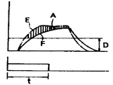
상기한 A/D변환기(21)는 압력센서(27)로부터의 출력파형을 A/D변환시키고, 메모리(22)는 A/D변환된 검출압력파형을 기억하며, 적분회로(23)는 상기 메모리(22)로부터의 검출압력파형을 적분한다. 이러한 적분에 있어서는 제2a도에 도시된 것과 같이 드레숄드값(D)이상의 유효성분을 적분한다. 여기에서 기준치메모리(26)는 미리 임의로 설정된 기준압력파형의 적분치를 기억하고 있는데, 이 기준치도 드레숄드값(D)이상의 유효성분 적분치이다. 한편, 비교부(24)는 상기 기준치 메모리(26)에 기억되어 있는 기준치와 적분회로(23)에서 얻어지는 검출치를 비교하게 되고, 연산부(25)는 이들의 차이(A; 제2b도의 사선부분)를 구한다. 그리고 연산부(25)는 이 차이(A)를 보상하도록 분출시간제어부(8)에 신호를 송출하고, 이에 따라 분출시간제어부(8)의 전자밸브의 작동시간이 제어되게 된다.The A / D converter 21 A / D converts the output waveform from the
다음으로, 이상의 장치를 사용해서 수지용기(3)내에서 수지(4)를 분출시키는 제어원리를 제2도에 의거 설명한다.Next, the control principle for ejecting the
우선, 보정회로(20)의 기준치 메모리(26)에 기준치를 격납하는데, 이런 기준치로서는 반도체칩을 피접착부에 가장 양호하게 접착시키는 수지량이 선택되고, 이 수지량을 분출시키기 위한 분출조건은 예컨대 장치 작동당초에 수지(4)가 충전돼 있는 수지용기(3)로부터 수지(4)를 분출시켜서 정하는 것이 바람직하다. 이러한 분출조건에 의한 압력파형은 제2a도와 같은 고압기체의 압력파형(E)으로서 얻어지는 바, 상기 압력파형(E)중 드레숄드값(D)이상의 유효성분이 적분회로(23)에 의해 적분되어 상기 기준치 메모리(26)에 격납된다. 이 경우, 상기 압력파형(E)은 분출시간제어부(8)의 전자밸브 작동시간(t)에 의존하게 된다. 다음에 가압장치(7)의 작동에 의해 수지(4)의 분출이 시행되어 수지용기(3)내의 수지량이 감소되면, 제2b도의 곡선(F)과 같이 고압기체의 압력이 변동하게 된다. 이러한 압력은 압력센서(27)에 의해 검출되고 A/D변환기(21)에 의해 A/D변환되어 메모리(22)에 기억된다. 그리고, 적분회로(23)에서는 드레숄드값(D)이상의 유효성분이 적분되고 이 적분치와 기준치 메모리(26)로부터의 적분치가 비교된다. 다음에는 상기와 같이 해서 얻어진 검출치와 기준치의 차이가 연산부(25)에서 구해지는데, 이 차이는 드레숄드값(D)이상에서의 곡선(E)과 곡선(F)의 적분치의 차이이며, 제2b도의 사선부분(A)에 상당하는 것이다. 이와 같은 차이(A)는 수지(4)를 분출시키는 압력의 차이이기 때문에, 분출되어지는 수지량은 차이(A)만큼 감소되게 된다. 따라서 상기 차이(A)를 보상해 주기 위해 연산부(25)는 분출시간제어부(8)에 전자밸브의 작동시간을 α만큼 연장시키라는 명령을 송출한다.First, the reference value is stored in the
상기와 같이 연산부(25)가 작동시간을 α만큼 연장시키라는 명령을 송출하면, 상기 분출시간제어부(8)는 전자밸브를 t+α만큼 작동시키게 된다. 이에 따라 전술한 차이(A)에 근사한 면적의 보상량(B; 제2c도에 도시)에 상당하는 고압공기가 증가하기 때문에, 수지(4)의 분출량은 기준압력파형의 경우와 거의 동등하게 되어 균일한 분출량을 유지시키게 된다.As described above, when the
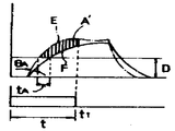
이상에서 설명한 바와 같이, 본 실시예의 제어원리는 제2b도의 적분치 차이(A)를 구해서 그 차이(A)만큼의 면적보상량(B)이 생기도록 제2c도처럼 분출시간 t를 α만큼 연장시키도록 한 데에 있다. 그런데 제2b도에서 알 수 있듯이 전자밸브의 작동에 대해 압력파형의 시간지연이 생긴다. 여기에서 분출시간 t를 연장시킬 것인가 아닌가는 전자밸브의 분출시간인 t내에서 판단할 필요가 있는데, 이런 시간지연 때문에 분출시간 t후의 시간(t1)에서는 차이(A)를 연산하는 것이 어렵다. 이 때문에 상기 차이(A)를 유출하는 방법으로서 다음과 같은 것이 있다(제2d도참조).As described above, the control principle of the present embodiment is such that the integral value difference A in the second diagram is obtained and the ejection time t is extended by? In the second cycle so that the area compensation amount B by the difference A is obtained In order to make it possible. However, as can be seen from FIG. 2b, there is a time delay in the pressure waveform for the operation of the solenoid valve. Here, it is necessary to determine whether or not to extend the ejection time t within the ejection time t, which is the ejection time of the solenoid valve. Due to this time delay, it is difficult to calculate the difference A at the time t1 after the ejection time t. For this reason, there are the following methods for leakage of the difference (A in Fig. 2d).
(1) 분출시간제어부(8)의 작동이 정지하기 직전의 시각(t1)에서의 곡선(E)과 곡선(F)의 차이(A')를 구해서 α로 환산한다. 이 경우 기준치 메모리(26)에는 시간(t1)까지의 적분치가 기준치로서 기억된다.(1) The difference A 'between the curve E and the curve F at the time t1 immediately before the operation of the ejection-time control unit 8 stops is calculated and converted into alpha. In this case, the integrated value up to the time t1 is stored in the
(2) 각 곡선(E 및 F)의 압력상승시간의 차이로부터 α를 구한다. 이것은 곡선(E)과 곡선(F)이 드레숄드값(D)과 엇갈리는 시각의 차이(TA)를 구함으로써 시행할 수 있다. 이 경우 기준치 메모리(26)에는 곡선(E)이 드레숄드값(D)에 도달하는 시각이 기준치로서 기억된다.(2) From the difference in pressure rise times of the curves E and F, a is obtained. This can be done by determining the curve (E) and the curve (F) by the difference (TA) between the threshold value (D) and the staggered time. In this case, the time at which the curve E reaches the threshold value D is stored in the
(3) 각 곡선(E 및 F)이 드레숄드값(D)으로부터 상승하는 각도차이(θA)로부터 α를 구한다. 이 경우 기준치 메모리(26)에는 곡선(E)이 상승하는 각도가 기준치로서 기억된다.(3) From the angle difference? A in which each curve E and F rises from the threshold value D,? Is obtained. In this case, the
(4) 이상의 (1)∼(3)의 방법은 실시간(實時間)에서 면적차이(A)를 유추하는 방법이었지만, 1회 이전에 실행된 작동으로부터 차이(A)를 구하고, 이로부터 유추해서 α를 구하도록 해도 좋다. 즉, 분출되는 수지량이 근소하기 때문에 1회 이전에서의 용기(3)내의 잔존수지량과 이번회의 잔존수지량이 거의 같다고 생각되어, 1회 이전의 정보로부터 이번회의 작동에 있어서의 부가시간(α)를 구한다. 이 경우에 있어서는 곡선(E)과 곡선(F)이 모두 얻어지고 있기 때문에 그 차이(A)로부터 α를 유추해 낸다.(4) The method of (1) to (3) above is a method of estimating the area difference (A) in real time, but the difference (A) is obtained from the operation performed one time before, may be obtained. That is, since the amount of resin to be ejected is small, it is considered that the amount of resin remaining in the
이상에서 설명한 바와 같이, 본 발명의 제1실시예에 의하면, 검출된 압력파형을 기준파형과 비교하는 것에 의해 연장할 분출시간을 정하게 되므로, 항상 거의 동일한 수지량을 분출시킬 수 있게 된다.As described above, according to the first embodiment of the present invention, the ejection time to be extended is determined by comparing the detected pressure waveform with the reference waveform, so that substantially the same amount of resin can be always ejected.
또한, 상기 제1실시예에서는 기준치를 이용해서 차이(A)를 유추하여 부가시간이나 부가압력을 연산하고 있기 때문에, 기준치에 차이가 있는 경우에는 그 연산치가 다를 우려가 있다. 이것을 방지하기 위해 실제로 공기압을 가한 결과에 의해 면적차이 A와 B의 실제측정치를 비교부(24)에서 연산하고, 그 연산결과를 연산부(25)에 피이드백시키도록 해도 좋다. 이와 같은 피이드백의 방법에서는 예컨대 연산부(25)로부터 분출시간제어부(8)로의 출력신호에 곱하여 주는 정수를 변화시키게 된다.Further, in the first embodiment, the difference A is deduced by using the reference value to calculate the additional time or the additional pressure. Therefore, when there is a difference in the reference value, the calculated value may be different. In order to prevent this, the actual measured values of the area differences A and B may be calculated by the comparator 24 based on the result of actually applying the air pressure, and the calculated results may be fed back to the calculating
제3도는 본 발명의 제2실시예에 따른 다이본딩장치를 나타낸 블록도로서, 앞의 제1실시예와 동일한 요소에는 동일한 부호를 대응되게 기재하였다.FIG. 3 is a block diagram showing a die bonding apparatus according to a second embodiment of the present invention. The same reference numerals are assigned to the same elements as those of the first embodiment.
이 제2실시예에서는 보정회로(20)의 연산부(25)가 가압장치(7)의 분출압력제어부(9)에 접속되어 있다. 이 실시예에서도 전술한 제1실시예와 마찬가지의 방법으로 기준치와 검출치의 차이에 기초해서 분출압력의 부가치가 연산부(25)에서 연산되어 분출압력제어부(9)에 출력된다. 이에 따라 분출압력제어부(9)는 예컨대 고압공기의 취출구(吹出口)의 개구지름을 증감시켜서 압력을 보정하게 된다.The
한편, 본 발명에 있어서는 압력센서(27)가 고압공기의 압력을 검출하고 있는데, 이 검출치를 이용해서 다른 동작을 하게할 수도 있다. 예컨대 검출치가 수지의 분출압력에 도달하지 못한 경우에는 경보를 표시하도록 해도 좋다. 또한, 검출치를 수지용기(3)내의 수지(4)의 잔량검출치로 이용할 수도 있다. 즉, 수지용기(3)가 비게 된 경우에는 검출치가 분출압력에 도달하지 못하기 때문에 그러한 검출치를 수지보충의 기준으로 삼을 수 있다. 더욱이 보정회로(20)에서 제어되는 분출시간제어부(8) 및 분출압력제어부(9)의 동작을 감시해서 그 고장의 유무를 확인할 수도 있다.On the other hand, in the present invention, the
이상에서 설명한 본 발명에 의하면, 압력센서에서 검출해낸 검출압력파형을 기준압력파형과 비교해서 그 차이를 보상해 주도록 하였기 때문에 수지분출량의 변동을 자동으로 수정할 수 있고, 이에 따라 항상 일정한 분출량을 유지시킬 수 있게 된다.According to the present invention described above, since the detected pressure waveform detected by the pressure sensor is compared with the reference pressure waveform and the difference is compensated for, the fluctuation of the discharge amount of the resin can be automatically corrected, .
Claims (12)
Applications Claiming Priority (2)
| Application Number | Priority Date | Filing Date | Title |
|---|---|---|---|
| JP62009578A JPS63177530A (en) | 1987-01-19 | 1987-01-19 | Method and device for die bonding |
| JP62-9578 | 1987-01-19 |
Publications (2)
| Publication Number | Publication Date |
|---|---|
| KR880009428A KR880009428A (en) | 1988-09-15 |
| KR910002827B1 true KR910002827B1 (en) | 1991-05-06 |
Family
ID=11724194
Family Applications (1)
| Application Number | Title | Priority Date | Filing Date |
|---|---|---|---|
| KR1019880000342A KR910002827B1 (en) | 1987-01-19 | 1988-01-18 | Method and device for die boding |
Country Status (3)
| Country | Link |
|---|---|
| US (1) | US4874444A (en) |
| JP (1) | JPS63177530A (en) |
| KR (1) | KR910002827B1 (en) |
Families Citing this family (18)
| Publication number | Priority date | Publication date | Assignee | Title |
|---|---|---|---|---|
| US5074443A (en) * | 1989-12-20 | 1991-12-24 | Nordson Corporation | Adaptor for liquid dispensing syringe |
| JPH03290715A (en) * | 1990-04-07 | 1991-12-20 | Iwashita Eng Kk | Pressure change type stabilized discharging volume dispensing controller for quantitative discharging device having pressure sensor |
| DE4092642C1 (en) * | 1990-07-10 | 1995-11-23 | Musashi Engineering Inc | Improved constant viscous liq. delivery device |
| US5423889A (en) * | 1994-06-24 | 1995-06-13 | Harris Corporation | Process for manufacturing a multi-port adhesive dispensing tool |
| JP2716940B2 (en) * | 1994-09-05 | 1998-02-18 | 株式会社東芝 | Die bonding method and apparatus |
| JP3498877B2 (en) * | 1995-12-05 | 2004-02-23 | 株式会社東芝 | Semiconductor manufacturing apparatus and semiconductor device manufacturing method |
| US5772814A (en) * | 1996-01-26 | 1998-06-30 | Branson Ultrasonic Corporation | Welding system and method of setting welding machine parameters |
| JP2804951B2 (en) * | 1996-02-23 | 1998-09-30 | 九州日本電気株式会社 | Precise quantitative discharge method and discharge device |
| US6399425B1 (en) * | 1998-09-02 | 2002-06-04 | Micron Technology, Inc. | Method of encapsulating semiconductor devices utilizing a dispensing apparatus with rotating orifices |
| US20020189541A1 (en) * | 2001-06-14 | 2002-12-19 | Lily Chao | Glue dropping machine |
| US6857543B2 (en) * | 2001-12-01 | 2005-02-22 | Shipley Company, L.L.C. | Low volume dispense unit and method of using |
| TWI286086B (en) * | 2005-04-11 | 2007-09-01 | Unaxis Int Trading Ltd | Method for operating a pneumatic device for the metered delivery of a liquid and pneumatic device |
| JP4749141B2 (en) * | 2005-12-07 | 2011-08-17 | トリニティ工業株式会社 | Painting system |
| US20090317544A1 (en) * | 2008-05-15 | 2009-12-24 | Zao "Intermetcomposit" | Method and Device for Gasodynamically Marking a Surface with a Mark |
| US8464902B2 (en) * | 2009-01-09 | 2013-06-18 | Nordson Corporation | Apparatus and method for pulsed dispensing of liquid |
| US20120040477A1 (en) * | 2010-08-13 | 2012-02-16 | Frank Yu | Ai epoxy adjustment |
| JP5853164B2 (en) * | 2012-04-24 | 2016-02-09 | パナソニックIpマネジメント株式会社 | Liquid supply apparatus, liquid discharge apparatus, and liquid supply method |
| PL3991855T3 (en) * | 2019-06-25 | 2024-03-04 | Changzhou Mingseal Robot Technology Co., Ltd. | Glue dispensing control apparatus and glue outlet control method therefor |
Family Cites Families (8)
| Publication number | Priority date | Publication date | Assignee | Title |
|---|---|---|---|---|
| US3347418A (en) * | 1965-10-23 | 1967-10-17 | Polaroid Corp | Liquid dispenser utilizing controlled gas pressure |
| US3499580A (en) * | 1968-07-02 | 1970-03-10 | Frank B Smith | Pressure pour apparatus and component thereof |
| US3666143A (en) * | 1970-06-22 | 1972-05-30 | Murray Weston | Automatic fluid dispensing apparatus with manual override |
| US4164001A (en) * | 1978-04-04 | 1979-08-07 | Patnaude Edmond J | Speed compensating control system |
| JPS55119471A (en) * | 1979-03-09 | 1980-09-13 | Matsushita Electric Ind Co Ltd | Adhesive coating method |
| US4334636A (en) * | 1979-12-27 | 1982-06-15 | Paul William A | Apparatus for handling gasket-forming material |
| US4675301A (en) * | 1985-04-01 | 1987-06-23 | Eastman Kodak Company | Method for correcting for changes in air pressure above a liquid to be dispensed from a container mounted on a probe |
| JPS6397259A (en) * | 1986-10-14 | 1988-04-27 | Shinkawa Ltd | Paste discharger |
-
1987
- 1987-01-19 JP JP62009578A patent/JPS63177530A/en active Granted
-
1988
- 1988-01-18 KR KR1019880000342A patent/KR910002827B1/en not_active IP Right Cessation
- 1988-01-19 US US07/145,320 patent/US4874444A/en not_active Expired - Lifetime
Also Published As
| Publication number | Publication date |
|---|---|
| JPH0567057B2 (en) | 1993-09-24 |
| US4874444A (en) | 1989-10-17 |
| KR880009428A (en) | 1988-09-15 |
| JPS63177530A (en) | 1988-07-21 |
Similar Documents
| Publication | Publication Date | Title |
|---|---|---|
| KR910002827B1 (en) | Method and device for die boding | |
| JP7066637B2 (en) | Methods and systems for injecting a viscous medium onto a substrate | |
| KR101353661B1 (en) | Substrate coating apparatus | |
| KR101605434B1 (en) | Method for applying liquid material, device therefor and storge medium recording program therefor | |
| CA2476325A1 (en) | Liquid consumption status detecting method, liquid container, and ink cartridge | |
| US8590739B2 (en) | Method for operating a pneumatic device for the metered delivery of a liquid and pneumatic device | |
| WO2000024526A1 (en) | Liquid constant rate discharge method and device | |
| TW201605546A (en) | Remote bulk feed system for a dispensing system and method of supplying viscous material to a dispensing system | |
| CA2976887A1 (en) | Fluid discharge device, fluid discharge method, and fluid application device | |
| JP6500689B2 (en) | Liquid discharge device | |
| JP2804951B2 (en) | Precise quantitative discharge method and discharge device | |
| JP2716940B2 (en) | Die bonding method and apparatus | |
| US9027789B2 (en) | Automated vacuum assisted valve priming system and methods of use | |
| KR101091606B1 (en) | Device of supplying photoresist solution in coater apparatus and control method using same | |
| JP3590300B2 (en) | Method and apparatus for discharging liquid at high speed and precision | |
| JP3590298B2 (en) | Method and apparatus for discharging liquid at high speed and precision | |
| JPH01307470A (en) | Coating applicator for viscous fluid | |
| JPH07232113A (en) | Flow rate stabilizer and method thereof | |
| KR101702932B1 (en) | Bonding material applying apparatus and bonding material applying method | |
| KR102624695B1 (en) | Aerosol jet apparatus and aerosol jet control method | |
| JPH0331105B2 (en) | ||
| JPH10303541A (en) | Coating method of bond for bonding electronic component | |
| JP2000005690A (en) | Method for coating of adhesive | |
| JPH07232112A (en) | Flow rate stabilizer | |
| CN117891133A (en) | Photoresist printing system and printing method |
Legal Events
| Date | Code | Title | Description |
|---|---|---|---|
| A201 | Request for examination | ||
| G160 | Decision to publish patent application | ||
| E701 | Decision to grant or registration of patent right | ||
| GRNT | Written decision to grant | ||
| FPAY | Annual fee payment |
Payment date: 20030430 Year of fee payment: 13 |
|
| LAPS | Lapse due to unpaid annual fee |