KR890004998B1 - Gate circuits for micro computer system - Google Patents
Gate circuits for micro computer system Download PDFInfo
- Publication number
- KR890004998B1 KR890004998B1 KR1019850000791A KR850000791A KR890004998B1 KR 890004998 B1 KR890004998 B1 KR 890004998B1 KR 1019850000791 A KR1019850000791 A KR 1019850000791A KR 850000791 A KR850000791 A KR 850000791A KR 890004998 B1 KR890004998 B1 KR 890004998B1
- Authority
- KR
- South Korea
- Prior art keywords
- gate
- circuit
- transistor
- gate circuit
- stage
- Prior art date
Links
- 230000004888 barrier function Effects 0.000 claims description 3
- 230000008878 coupling Effects 0.000 claims 2
- 238000010168 coupling process Methods 0.000 claims 2
- 238000005859 coupling reaction Methods 0.000 claims 2
- 238000010586 diagram Methods 0.000 description 5
- 238000006243 chemical reaction Methods 0.000 description 3
- 101150096245 SRL1 gene Proteins 0.000 description 1
- 230000000903 blocking effect Effects 0.000 description 1
- 230000000694 effects Effects 0.000 description 1
- 238000003780 insertion Methods 0.000 description 1
- 230000037431 insertion Effects 0.000 description 1
- 238000004904 shortening Methods 0.000 description 1
- 230000001052 transient effect Effects 0.000 description 1
- 230000007704 transition Effects 0.000 description 1
Images


Classifications
-
- G—PHYSICS
- G06—COMPUTING; CALCULATING OR COUNTING
- G06F—ELECTRIC DIGITAL DATA PROCESSING
- G06F13/00—Interconnection of, or transfer of information or other signals between, memories, input/output devices or central processing units
- G06F13/14—Handling requests for interconnection or transfer
-
- H—ELECTRICITY
- H03—ELECTRONIC CIRCUITRY
- H03K—PULSE TECHNIQUE
- H03K19/00—Logic circuits, i.e. having at least two inputs acting on one output; Inverting circuits
- H03K19/003—Modifications for increasing the reliability for protection
- H03K19/00307—Modifications for increasing the reliability for protection in bipolar transistor circuits
-
- G—PHYSICS
- G06—COMPUTING; CALCULATING OR COUNTING
- G06F—ELECTRIC DIGITAL DATA PROCESSING
- G06F7/00—Methods or arrangements for processing data by operating upon the order or content of the data handled
-
- H—ELECTRICITY
- H03—ELECTRONIC CIRCUITRY
- H03K—PULSE TECHNIQUE
- H03K19/00—Logic circuits, i.e. having at least two inputs acting on one output; Inverting circuits
- H03K19/003—Modifications for increasing the reliability for protection
- H03K19/00346—Modifications for eliminating interference or parasitic voltages or currents
- H03K19/00353—Modifications for eliminating interference or parasitic voltages or currents in bipolar transistor circuits
-
- H—ELECTRICITY
- H03—ELECTRONIC CIRCUITRY
- H03K—PULSE TECHNIQUE
- H03K19/00—Logic circuits, i.e. having at least two inputs acting on one output; Inverting circuits
- H03K19/01—Modifications for accelerating switching
- H03K19/013—Modifications for accelerating switching in bipolar transistor circuits
-
- H—ELECTRICITY
- H03—ELECTRONIC CIRCUITRY
- H03K—PULSE TECHNIQUE
- H03K5/00—Manipulating of pulses not covered by one of the other main groups of this subclass
- H03K5/15—Arrangements in which pulses are delivered at different times at several outputs, i.e. pulse distributors
- H03K5/151—Arrangements in which pulses are delivered at different times at several outputs, i.e. pulse distributors with two complementary outputs
Abstract
Description
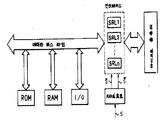
제 1 도는 다수의 SRL(세트/리세트 래치)회로와 게이트회로를 사용하는 마이크로 콤퓨터 시스템의 개략적인 부분개통도.1 is a schematic partial opening diagram of a microcomputer system using a plurality of SRL (set / reset latch) circuits and a gate circuit.
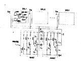
제 2 도는 집적회로로서 사용되는 다수의 SRL회로(SRL1내지 SRLn)와 종래의 게이트회로의 기본회로도.2 is a basic circuit diagram of a plurality of SRL circuits (SRL 1 to SRL n ) used as an integrated circuit and a conventional gate circuit.
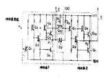
제 3 도는 본 발명의 일실시예에 의한 게이트회로와 제 2 도에 보인 바와같은 동일한 다수의 SRL회로들의 기본회로도.3 is a basic circuit diagram of a gate circuit according to an embodiment of the present invention and the same plurality of SRL circuits as shown in FIG.
제 4a도는 제 2 도에 보인 게이트회로에서 각 스트로브(strobe) 신호를 설명하는 타이밍 도표.4A is a timing diagram illustrating each strobe signal in the gate circuit shown in FIG.
제 4b도는 제 3 도에 보인 게이트회로의 각 스트로브 신호를 설명하는 타이밍 도표.4B is a timing chart for explaining each strobe signal of the gate circuit shown in FIG.
제 5a도, 제 5b도 및 제 5c도는 본 발명의 다른 실시예에 의한 제어 수단의 회로도.5A, 5B and 5C are circuit diagrams of a control means according to another embodiment of the present invention.
본 발명은 게이트회로에 관한 것으로 특히 마이크로 콤퓨터 시스템에 사용 적합한 예를들어 트랜지스터 결합 트랜지스터 로직(transister-coupled transistor logic : TTL)과 다이오드 결합 트랜지스터 로직(diode-transistor logic : DTL)을 한조로 하여 그에 의해 구성된 게이트회로에 관한 것이다.FIELD OF THE INVENTION The present invention relates to gate circuits, in particular suitable for use in microcomputer systems, for example by combining transistor-coupled transistor logic (TTL) and diode-transistor logic (DTL). It relates to a configured gate circuit.
공지된 바와같이 마이크로 콤퓨터 시스템에서 다수의 인터페이스회로(interface circuit)들은 데이타 버스라인을 통하여 중앙처리유니트(central processing unit : CPU)와 판독 전용 메모리(read only memory : ROM), 랜돔억세스 메모리(random access memory : RAM) 및 입/출력(input/output : I/O)유니트사이에 제공된다.As is well known, a number of interface circuits in a microcomputer system are connected to a central processing unit (CPU), read only memory (ROM), and random access memory (random access memory) via data bus lines. memory is provided between RAM) and input / output (I / O) units.
각 인터페이스회로는 예를들어 CPU로 전송될 데이타의 기입(writing) 또는 유지(holding)를 제어하기 위한 다수조의 세트/리세트 래치(set/reset latch : SRL)회로들을 갖고 있다. 데이타를 기입 또는 유지하기 위한 타이밍은 게이트회로로부터 발생되는 반전 스트로브 신호(strobe signal)와 비반전 스트로브 신호에 의해 제어된다. 게이트회로는 이 신호들을 병렬로 각각의 SRL회로들에 인가한다. SRL회로들은 어떤 스트로브 신호들의 변동에도 불구하고 "기입" 및 "유지"양모드에서 고레벨 출력을 유지하도록 할 필요가 있다.Each interface circuit has, for example, a plurality of set / reset latch (SRL) circuits for controlling the writing or holding of data to be transferred to the CPU. Timing for writing or holding data is controlled by an inverted strobe signal and a non-inverted strobe signal generated from the gate circuit. The gate circuit applies these signals to the respective SRL circuits in parallel. SRL circuits need to maintain a high level output in both "write" and "hold" modes despite variations in some strobe signals.
게이트회로에서, 스트로브 신호가 예를들어 저레벨로부터 고레벨로 변동될때 반전신호는 고레벨로부터 저레벨로 전환되고 비반전신호는 저레벨로부터 고레벨로 변동된다.In the gate circuit, when the strobe signal is changed from low level to high level, for example, the inverted signal is switched from high level to low level and the non-inverted signal is changed from low level to high level.
그러나, 비반전신호가 저레벨로부터 고레벨로 변동될때 반전신호의 타이밍에 비해 전환 타이밍에서 시간지연이 생긴다. 그러므로 비반전신호와 반전신호가 모두 동시에 저레벨에 있는 엉뚱한 경우가 생긴다.However, when the non-inverting signal varies from the low level to the high level, there is a time delay in the switching timing compared to the timing of the inverting signal. Therefore, there are cases where the non-inverting signal and the inverting signal are both at the same low level.
이러한 타이밍으로 인하여 소위 "글리치(glitch)"잡음이 SRL회로들의 출력에서 생긴다. 이 글리치 잡음은 CPU와 기타 회로들에서 데이타 오차를 유발한다.Because of this timing, so-called "glitch" noise occurs at the output of the SRL circuits. This glitch noise causes data errors in the CPU and other circuits.
본 발명의 주요목적은 마이크로 콤퓨터 시스템에서 인터페이스회로를 제어하는데 사용되는 게이트회로를 제공하는데 있다.The main object of the present invention is to provide a gate circuit used to control the interface circuit in the microcomputer system.
본 발명의 또 다른 목적은 예를들어 한조의 TTL회로와 DTL회로로 구성된 게이트회로를 제공하여 마이크로 콤퓨터 시스템에서 글리치 잡음을 감소시켜 데이타 오차를 감소시키는데 있다.Another object of the present invention is to provide a gate circuit composed of a set of TTL circuits and a DTL circuit, for example, to reduce data error by reducing glitch noise in a microcomputer system.
본 발명에 의하면, 입력신호의 레벨변동에 반응하기 위한 위상분할 트랜지스터와 위상분할 트랜지스터에 의해 제어되는 반전신호를 출력시키기 위한 출력회로를 갖는 제 1 단 게이트회로와, 제 1 단 게이트회로의 반전스트로브 신호를 입력시키고 비반전신호를 출력시키기 위한 제 1 단 게이트회로의 반전 스트로브 신호를 입력시키기 위한 제 2 단 게이트회로와, 제 1 단 게이트회로내의 입력단자의 레벨을 제어하기 위해 제 1 단 게이트회로내의 위상분할 트랜지스터의 콜렉터와 제 2 단 게이트회로의 입력단사이에 연결되는 장치를 포함하는 입력신호의 반전신호와 비반전신호를 발생시키기 위한 게이트회로가 제공된다.According to the present invention, a first stage gate circuit having a phase dividing transistor for responding to a level change of an input signal and an output circuit for outputting an inverted signal controlled by the phase dividing transistor, and an inverting strobe of the first stage gate circuit A second stage gate circuit for inputting a signal and an inverting strobe signal of a first stage gate circuit for outputting a non-inverted signal, and a first stage gate circuit for controlling the level of an input terminal in the first stage gate circuit. A gate circuit is provided for generating an inverted signal and a non-inverted signal of an input signal comprising a device connected between a collector of a phase division transistor and an input terminal of a second stage gate circuit.
본 발명의 구조에 의하면, 인터페이스회로로서 사용되는 SRL회로로부터 글리치 잡음출력을 현저히 감소시켜 데이타 오차를 없애고 마이크로 콤퓨터 시스템의 고속계산이 가능하다.According to the structure of the present invention, the glitch noise output is remarkably reduced from the SRL circuit used as the interface circuit, thereby eliminating data errors and enabling high-speed calculation of the microcomputer system.
이하 첨부된 도면을 참고로 본 발명의 양호한 실시예들을 상세히 설명하면 다음과 같다.Hereinafter, exemplary embodiments of the present invention will be described in detail with reference to the accompanying drawings.
양호한 실시예들을 설명하기 전에 우선 예를들어 한조의 TTL회로와 DTL회로로 구성된 종래의 게이트회로에 대해 설명한다.Before describing the preferred embodiments, a conventional gate circuit composed of, for example, a set of TTL circuits and a DTL circuit will be described.
제 1 도를 참조하면, 인터페이스회로로서 사용되는 다수의 SRL회로들(SRL1과 SRLn)은 CPU와 ROM, RAM 및 I/O회로 사이에서 데이타 버스라인(data bus line)을 통하여 제공된다.Referring to FIG. 1, a number of SRL circuits SRL 1 and SRL n used as interface circuits are provided through a data bus line between the CPU and ROM, RAM, and I / O circuits.
제 2 도를 참조하면, 각 SRL회로 예를들어 SRL1은 기본적으로 두개의 AND게이트들 AND1과 AND2, NOR게이트 NOR 그리고 반전기 NOT를 포함한다. 고레벨(H) 입력데이타 Din은 데이타 버스라인으로부터 AND게이트 AND1의 한 입력단자에 인가되며, 고레벨 출력데이타 Dout는 데이타 버스라인을 통하여 CPU로 인가된다.Referring to FIG. 2, each SRL circuit, for example SRL 1 , basically includes two AND gates AND 1 and AND 2 , a NOR gate NOR and an inverter NOT. The high level (H) input data D in is applied to one input terminal of AND gate AND 1 from the data bus line, and the high level output data D out is applied to the CPU via the data bus line.
SRL회로 SRL1의 동작모드는 "기입모드"와 "유지모드"사이에서 반전 스트로브 신호와 비반전 스트로브 신호에 의해 변동된다.The operation mode of the SRL circuit SRL1 is changed by the inverted strobe signal and the non-inverted strobe signal between the "write mode" and the "holding mode".
"기입모드"에서 반전 스트로브 신호![]()
![]()
![]()
![]()
"유지모드"에서, 신호![]()
![]()
![]()
![]()
비록 두신호![]()
![]()
![]()
![]()
그러나, 이후 상세히 설명되는 바와같이 신호![]()
![]()
마이크로 콤퓨터내의 클록발생기(도시안됨)로부터 전송된 고레벨 스토로브 또는 저레벨 스트로브 신호 S가 게이트 1내의 입력트랜지스터 Q1의 베이스에 인가될때 신호 S에 대응하는 저 또는 고레벨의 반전 스트로브 신호![]()
![]()
![]()
![]()
![]()
![]()
![]()
![]()
![]()
![]()
![]()
![]()
스트로브 신호 S,![]()
![]()
![]()
![]()
![]()
![]()
![]()
![]()
![]()
![]()
![]()
![]()
![]()
![]()
![]()
![]()
더우기, 여러부하들(일반적으로, 한 게이트회로마다 약 8개의 SRL회로가 한 부하로서 연결됨)이 출력부 P1과 P2에 병렬로 연결된다. 부하가 많으면 많을수록 더 많은 부하용량이 생기며 신호 S의 더 큰 시간지연이 생긴다.Furthermore, several loads (typically about eight SRL circuits per gate circuit are connected as one load) are connected in parallel to the outputs P 1 and P 2 . The higher the load, the more the load capacity and the greater the time delay of the signal S.
이해될 수 있는 바와같이, 이 기간(t2-t1)이 짧으면 짧을수록 글리치 잡음레벨 G는 더 작아진다. 따라서, 본 발명은 시간지연(t2-t1)을 짧게해 줌으로서 글리치 잡음을 감소시킬 수 있는 게이트회로를 제공하는데 있다. 제 3 도를 참조하면, 본 발명에 의한 게이트회로는 일방향소자로서 다이오드 D1(에쇼트키 베리어 다이오드)가 트랜지스터 Q3의 콜렉터와 게이트 2의 입력단자 즉, 트랜지스터 Q7의 베이스 사이에 추가되는 이외에는 종래의 게이트회로와 동일한 회로배열과 소자들을 포함한다. 이 다이오드 D1는 제 2 단 게이트 2의 입력레벨을 제어하기 위해 제어수단 100으로서 동작한다.As can be appreciated, the shorter this period t 2 -t 1 , the smaller the glitch noise level G is. Accordingly, the present invention provides a gate circuit that can reduce glitch noise by shortening the time delay t 2 -t 1 . Referring to FIG. 3, the gate circuit according to the present invention is a unidirectional device in which diode D 1 (Eschottky barrier diode) is added between the collector of transistor Q 3 and the input terminal of
게이트회로의 동작에 대해서 이하 상세히 설명한다. SRL회로 SRL1의 "유지모드"에서 저레벨 스트로브 신호 S가 입력트랜지스터 Q1의 베이스에 인가될때 트랜지스터 Q1은 그것이 PnP트랜지스터이기 때문에 도통된다. 트랜지스터 Q1이 도통될때, 트랜지스터 Q2, 위상분할 트랜지스터 Q3와 출력트랜지스터 Q6은 이들이 nPn트랜지스터들이기 때문에 차단된다. 트랜지스터들 Q4와 Q5가 과도상태동안 고레벨이 되기 때문에 지점 P1의 레벨은 고레벨이 된다. 즉, 스트로브 신호![]()
![]()
한편 트랜지스터 Q3와 Q6양자는 차단되기 때문에 다이오드 D1과 D2를 통하여 전류가 흐르지 않는다. 따라서, 트랜지스터 Q7의 베이스는 높게되고 트랜지스터 Q7은 도통되지 않는다. 왜냐하면 그것은 nPn트랜지스터이기 때문이다. 트랜지스터 Q7은 도통될때 트랜지스터 Q8와 Q11은 도통되고 지점 P2의 레벨은 낮아지게 되고 즉, 스트로브 신호![]()
![]()
그다음, SRL회로 SRL1이 "기입모드"에서 저레벨 스트로브 신호 S는 고레벨로 변동되어 트랜지스터 Q1은 차단되고, 트랜지스터 Q2, Q3와 Q6는 도통된다.Then, when the SRL circuit SRL 1 is changed to the "write mode", the low level strobe signal S is changed to a high level so that the transistor Q 1 is cut off and the transistors Q 2 , Q 3 and Q 6 are turned on.
더우기, 트랜지스터 Q4와 Q5가 차단된다. 따라서, 지점 P1의 레벨은 저가된다. 즉, 신호![]()
![]()
짧은 시간후 전류는 다이오드 D2를 통하여 트랜지스터 Q7의 베이스로부터 트랜지스터 Q6의 콜렉터로 흐른다. 트랜지스터 Q7은 스트로브 신호![]()
![]()
한편, 종래의 게이트회로에는 다이오드 D1이 없다. 단지 다이오드 D2만 제 2 도에 보인 바와같이 게이트 2내에 있다. 따라서 종래의 게이트회로내의 트랜지스터 Q7의 차단타이밍은 본 발명에 의한 회로의 것보다 더 느리다. 결론적으로, 종래의 게이트회로에 의한 스트로브 신호![]()
![]()
![]()
![]()
두 스트로브 신호들![]()
![]()
또한 쇄선으로 제4b도에 보인 바와같이 스트로브 신호![]()
![]()
![]()
![]()
![]()
![]()
이 경우에, 변환타이밍시 신호![]()
![]()
따라서, 본 발명의 효과 즉, 다이오드 D1의 삽입은 게이트회로에 연결된 부하의 증가와 더불어 증가된다.Therefore, the effect of the present invention, that is, the insertion of diode D 1 is increased with the increase of the load connected to the gate circuit.
제어수단 100에 관한 다른 실시예들이 제5a도 제5b도 및 제5c도에 도시되어 있다.Other embodiments of the control means 100 are shown in FIGS. 5A, 5B and 5C.
제5a도는 트랜지스터 Q20과 저항 R1을 포함하는 제어수단 100의 제 2 실시예를 보이고 있다. 트랜지스터 Q20의 제어기는 제 2 단 게이트 2의 입력에 연결된다. 그외 에미터는 위상분할 트랜지스터 Q3의 콜렉터에 연결되며, 그의 베이스는 저항 R1을 통하여 VCC에 연결된다. 이 트랜지스터 Q20은 제 3 도에서 다이오드 D1과 같은 일방향소자로서 동작한다.5a shows a second embodiment of control means 100 comprising transistor Q 20 and resistor R 1 . The controller of transistor Q 20 is connected to the input of the
제5b도는 본 발명의 제어수단 100의 제 3 실시예를 보이는 것이다. 이 실시예에서 저항 R2는 제5a도의 회로로부터 생략된다.5b shows a third embodiment of the control means 100 of the present invention. In this embodiment, the resistor R 2 is omitted from the circuit of FIG. 5A.
제5c도는 본 발명의 제어수단 100의 제 4 실시예를 보이는 것이다. 이 실시예에서 다수에미터 트랜지스터Q22는 제 3 도에서 다이오드를 D1과 D2로서 사용된다. 즉, 제 2 단 게이트회로 2는 제 3 도, 제5a도와 제5b도 와 같은 DTL회로대신에 TTL회로를 포함한다. 그러므로 트랜지스터 Q22는 제 1 단 게이트 1의 출력에 연결된 입력회로용으로 사용된다. 제어수단 100은 일방향소자로서 작용하는 트랜지스터 Q22와 저항 R1을 포함한다.5c shows a fourth embodiment of the control means 100 of the present invention. In this embodiment, the multi-emitter transistor Q 22 uses the diodes as D 1 and D 2 in FIG. 3. That is, the second
실시예에서 설명된 바와같이, 게이트회로의 출력신호![]()
![]()
![]()
![]()
![]()
![]()
![]()
![]()
Claims (11)
Applications Claiming Priority (2)
| Application Number | Priority Date | Filing Date | Title |
|---|---|---|---|
| JP59-022966 | 1984-02-13 | ||
| JP59022966A JPS60172821A (en) | 1984-02-13 | 1984-02-13 | Ttl circuit |
Publications (2)
| Publication Number | Publication Date |
|---|---|
| KR850006088A KR850006088A (en) | 1985-09-28 |
| KR890004998B1 true KR890004998B1 (en) | 1989-12-04 |
Family
ID=12097318
Family Applications (1)
| Application Number | Title | Priority Date | Filing Date |
|---|---|---|---|
| KR1019850000791A KR890004998B1 (en) | 1984-02-13 | 1985-02-08 | Gate circuits for micro computer system |
Country Status (5)
| Country | Link |
|---|---|
| US (1) | US4703202A (en) |
| EP (1) | EP0156477B1 (en) |
| JP (1) | JPS60172821A (en) |
| KR (1) | KR890004998B1 (en) |
| DE (1) | DE3568117D1 (en) |
Families Citing this family (6)
| Publication number | Priority date | Publication date | Assignee | Title |
|---|---|---|---|---|
| US4939391A (en) * | 1986-05-30 | 1990-07-03 | Advanced Micro Devices, Inc. | Programmable logic device with observability and preload circuitry for buried state registers |
| US4839537A (en) * | 1986-11-29 | 1989-06-13 | Kabushiki Kaisha Toshiba | BicMO logic circuit |
| US4777391A (en) * | 1987-07-17 | 1988-10-11 | Signetics Corporation | Bipolar multiplexer having a select buffer circuit with a charging and discharging circuit |
| US4973862A (en) * | 1989-03-07 | 1990-11-27 | National Semiconductor Corporation | High speed sense amplifier |
| US5027010A (en) * | 1989-10-04 | 1991-06-25 | Motorola, Inc. | TTL output driver having an increased high output level |
| JPH05122017A (en) * | 1991-10-29 | 1993-05-18 | Mitsubishi Electric Corp | Schmitt trigger input buffer circuit |
Family Cites Families (6)
| Publication number | Priority date | Publication date | Assignee | Title |
|---|---|---|---|---|
| US3962589A (en) * | 1975-02-10 | 1976-06-08 | National Semiconductor Corporation | Inverter with minimum skew |
| JPS5378159A (en) * | 1976-12-22 | 1978-07-11 | Fujitsu Ltd | Logic circuit |
| JPS544560A (en) * | 1977-06-14 | 1979-01-13 | Nec Corp | Semiconductor inverter circuit |
| JPS5592040A (en) * | 1978-12-29 | 1980-07-12 | Fujitsu Ltd | Ttl gate circuit |
| EP0089441B1 (en) * | 1982-03-24 | 1989-06-21 | International Business Machines Corporation | True/complement generator |
| US4424455A (en) * | 1982-04-22 | 1984-01-03 | Motorola, Inc. | Glitch eliminating data selector |
-
1984
- 1984-02-13 JP JP59022966A patent/JPS60172821A/en active Granted
-
1985
- 1985-02-08 KR KR1019850000791A patent/KR890004998B1/en not_active IP Right Cessation
- 1985-02-11 US US06/700,413 patent/US4703202A/en not_active Expired - Fee Related
- 1985-02-13 EP EP85300929A patent/EP0156477B1/en not_active Expired
- 1985-02-13 DE DE8585300929T patent/DE3568117D1/en not_active Expired
Also Published As
| Publication number | Publication date |
|---|---|
| KR850006088A (en) | 1985-09-28 |
| DE3568117D1 (en) | 1989-03-09 |
| US4703202A (en) | 1987-10-27 |
| EP0156477A1 (en) | 1985-10-02 |
| EP0156477B1 (en) | 1989-02-01 |
| JPH0318770B2 (en) | 1991-03-13 |
| JPS60172821A (en) | 1985-09-06 |
Similar Documents
| Publication | Publication Date | Title |
|---|---|---|
| KR100239099B1 (en) | Electronic flip-flop circuit | |
| US4841233A (en) | Semiconductor integrated circuit adapted to carry out operation test | |
| US4800529A (en) | Semiconductive memory device with current control and comparison means to reduce power consumption and increase operating speed | |
| US5459421A (en) | Dynamic-static master slave flip-flop circuit | |
| KR100284985B1 (en) | An integrated circuit having enable control circuitry | |
| JPH05508975A (en) | Adjustable clock chopper/expander circuit | |
| US5378934A (en) | Circuit having a master-and-slave and a by-pass | |
| KR890004998B1 (en) | Gate circuits for micro computer system | |
| US3953746A (en) | Selector latch gate | |
| US4334157A (en) | Data latch with enable signal gating | |
| US5148052A (en) | Recirculating transparent latch employing a multiplexing circuit | |
| US5086414A (en) | Semiconductor device having latch means | |
| US4845681A (en) | GaAs SCFL RAM | |
| US4733377A (en) | Asynchronous semiconductor memory device | |
| US6998878B2 (en) | Semiconductor integrated circuit and semiconductor logic circuit used in the integrated circuit | |
| JPS6010364A (en) | Directory memory system | |
| US5077495A (en) | Row decoder for a semiconductor memory device with fast turn-off | |
| US4800552A (en) | Semiconductor memory device with reset signal generating circuit | |
| EP0714100A2 (en) | Synchronous memory device | |
| JP2760431B2 (en) | memory | |
| JPH02137189A (en) | Memory circuit and digital device | |
| JP3199883B2 (en) | Semiconductor integrated circuit | |
| JPH023175A (en) | Semiconductor memory device | |
| KR890007290A (en) | Semiconductor memory device with level converter | |
| JPH07312384A (en) | Signal line switching circuit |
Legal Events
| Date | Code | Title | Description |
|---|---|---|---|
| A201 | Request for examination | ||
| E902 | Notification of reason for refusal | ||
| G160 | Decision to publish patent application | ||
| E701 | Decision to grant or registration of patent right | ||
| GRNT | Written decision to grant | ||
| FPAY | Annual fee payment |
Payment date: 19981116 Year of fee payment: 10 |
|
| LAPS | Lapse due to unpaid annual fee |