KR890004473B1 - Semiconductor device - Google Patents
Semiconductor device Download PDFInfo
- Publication number
- KR890004473B1 KR890004473B1 KR1019850005081A KR850005081A KR890004473B1 KR 890004473 B1 KR890004473 B1 KR 890004473B1 KR 1019850005081 A KR1019850005081 A KR 1019850005081A KR 850005081 A KR850005081 A KR 850005081A KR 890004473 B1 KR890004473 B1 KR 890004473B1
- Authority
- KR
- South Korea
- Prior art keywords
- row decoder
- memory cell
- row
- address
- word line
- Prior art date
Links
- 239000004065 semiconductor Substances 0.000 title claims abstract description 21
- 230000015654 memory Effects 0.000 claims abstract description 47
- 238000003491 array Methods 0.000 claims 1
- 239000011159 matrix material Substances 0.000 abstract 2
- 230000003068 static effect Effects 0.000 description 7
- 238000010586 diagram Methods 0.000 description 6
- 238000001514 detection method Methods 0.000 description 5
- 101000949825 Homo sapiens Meiotic recombination protein DMC1/LIM15 homolog Proteins 0.000 description 2
- 101001046894 Homo sapiens Protein HID1 Proteins 0.000 description 2
- 102100022877 Protein HID1 Human genes 0.000 description 2
- 238000000034 method Methods 0.000 description 2
- 238000009825 accumulation Methods 0.000 description 1
- 230000002411 adverse Effects 0.000 description 1
- 239000003990 capacitor Substances 0.000 description 1
- 230000015556 catabolic process Effects 0.000 description 1
- 238000006731 degradation reaction Methods 0.000 description 1
- 230000001934 delay Effects 0.000 description 1
- 230000000694 effects Effects 0.000 description 1
- 230000002441 reversible effect Effects 0.000 description 1
- 238000007493 shaping process Methods 0.000 description 1
- 230000001360 synchronised effect Effects 0.000 description 1
Images


Classifications
-
- H—ELECTRICITY
- H01—ELECTRIC ELEMENTS
- H01L—SEMICONDUCTOR DEVICES NOT COVERED BY CLASS H10
- H01L29/00—Semiconductor devices adapted for rectifying, amplifying, oscillating or switching, or capacitors or resistors with at least one potential-jump barrier or surface barrier, e.g. PN junction depletion layer or carrier concentration layer; Details of semiconductor bodies or of electrodes thereof ; Multistep manufacturing processes therefor
- H01L29/66—Types of semiconductor device ; Multistep manufacturing processes therefor
- H01L29/86—Types of semiconductor device ; Multistep manufacturing processes therefor controllable only by variation of the electric current supplied, or only the electric potential applied, to one or more of the electrodes carrying the current to be rectified, amplified, oscillated or switched
- H01L29/92—Capacitors with potential-jump barrier or surface barrier
- H01L29/94—Metal-insulator-semiconductors, e.g. MOS
-
- G—PHYSICS
- G11—INFORMATION STORAGE
- G11C—STATIC STORES
- G11C11/00—Digital stores characterised by the use of particular electric or magnetic storage elements; Storage elements therefor
- G11C11/21—Digital stores characterised by the use of particular electric or magnetic storage elements; Storage elements therefor using electric elements
- G11C11/34—Digital stores characterised by the use of particular electric or magnetic storage elements; Storage elements therefor using electric elements using semiconductor devices
- G11C11/40—Digital stores characterised by the use of particular electric or magnetic storage elements; Storage elements therefor using electric elements using semiconductor devices using transistors
- G11C11/401—Digital stores characterised by the use of particular electric or magnetic storage elements; Storage elements therefor using electric elements using semiconductor devices using transistors forming cells needing refreshing or charge regeneration, i.e. dynamic cells
- G11C11/406—Management or control of the refreshing or charge-regeneration cycles
Abstract
Description
제 1 도는 본 발명의 일실시예를 반도체장치의 일부를 나타낸 회로 구성도.1 is a circuit diagram showing a part of a semiconductor device according to one embodiment of the present invention.
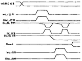
제 2 도는 제 1 도에 따른 타이밍 챠아트.2 is a timing chart according to FIG.
제 3 도는 본 발명이 내장된 반도체 칩을 나타낸 평면도.3 is a plan view showing a semiconductor chip in which the present invention is incorporated.
제 4 도는 본 발명의 다른 실시예인 행디코더계 절환부의 일부를 구체적인 예로 나타낸 회로도.4 is a circuit diagram showing a specific example of a part of the hang decoder system switching unit which is another embodiment of the present invention.
제 5 도는 본 발명의 다른 실시예인 반도체장치의 일부를 나타낸 회로구성도.5 is a circuit diagram showing a part of a semiconductor device according to another embodiment of the present invention.
제 6 도는 종래의 반도체장치중 일부를 나타낸 회로구성도.6 is a circuit diagram showing a part of a conventional semiconductor device.
제 7 도는 제 6 도에 나타낸 반도체장치의 통상동작과 재충전동작의 시간관계를 나타낸 도면.FIG. 7 is a diagram showing a time relationship between a normal operation and a recharging operation of the semiconductor device shown in FIG.
제 8 도는 제 6 도에 나타낸 반도체장치의 동작예에 따른 타이밍 챠아트.8 is a timing chart according to an operation example of the semiconductor device shown in FIG.
제 9 도는 통상동작과 재충전동작의 1사이클내에서 시분할로 행하여지는 반도체장치의 동작예를 나타낸 타이밍도이다.9 is a timing diagram showing an example of the operation of the semiconductor device performed by time division within one cycle of the normal operation and the recharging operation.
* 도면의 주요부분에 대한 부호의 설명* Explanation of symbols for main parts of the drawings
1 : 입력어드레스버퍼 2 : 재충전어드레스발생기1: Input address buffer 2: Recharge address generator
3 : 어드레스멀티플렉서 4 : 출력회로3: address multiplexer 4: output circuit
6 : 선충전회로 8 : 타이밍콘트롤러6: precharge circuit 8: timing controller
10 : 누설감지회로 12 : 제 1 의 행디코더계10: leak detection circuit 12: first row decoder system
14 : 제 2 의 행디코더계 40, 42 : 행디코더계14: second
51, 52 : 열디코더 LR, LR' : 행디코선51, 52: thermal decoder LR, LR ': hang deco line
RD1∼RD1' : 행디코더 WL1∼WL4 : 워드선RD1 to RD1 ': Row decoders WL1 to WL4: Word lines
MC1∼MC4, M11, M21 : 메모리셀 RL,![]()
![]()
DMC1, DMC2 : 보조메모리셀 DW1, DW2 : 보조워드선DMC1, DMC2: auxiliary memory cell DW1, DW2: auxiliary word line
SA : 감지증폭기 LS : 센스래치제어신호선SA: Sense amplifier LS: Sense latch control signal line
SE : 감지신호 CD : 열디코더SE: Detection Signal CD: Thermal Decoder
QB,![]()
![]()
![]()
![]()
CB: 비트선용량 CR: 행디코더선의 용량C B : bit line capacity C R : line decoder line capacity
S1∼S1' : 스위치회로 øn, øR: 절환제어신호S1 to S1 ': switch circuit ø n , ø R : switching control signal
øP: 선충전회로 구동신호 A, B : 어드레스신호ø P : Precharge circuit drive signal A, B: Address signal
본 발명은 반도체 장치에 관한 것으로 특히 다수의 행디코더계통중 1계통을 선택하여 워드선과 접촉상태로 설정하도록된 반도체장치에 관한 것이다.BACKGROUND OF THE
종래의 다이나믹 RAM(random access memory)의 대표적인 구성예중 그 일부를 나타낸 제 6 도를 보면 1개의 콘딘서(CS)와 1개의 전송게이트(Q)로 구성된 메모리셀이 콘덴서(CS)의 축적전하 여부로 정보("0", "1")를 기억하도록 되어있는바, 여기서 축적된 전하는 흔히 누설등과 같은 요인으로 시간에 따라 감소되기 때문에 축적전하가 완전히 소실되지 않았을때 1번독출시키고, 다시 기록한 후 저하를 다시 축적시키는 재충전동작이 필요하게 되는데, 일반적으로 다이나믹 RAM에서는 상기 재충전 동작이 필요하게 되는 것이다. 예컨데 256K비트의 다이나믹 RAM에서는 반드시 4ms에 1번씩 모든 메모리셀을 재충전 해야만 하는 제약을 받게된다.Typical configuration of the (random access memory) the conventional dynamic RAM cases looking at the sixth view showing a part of one cone accumulation of dinseo (C S) and a memory cell composed of one transfer gate (Q) a capacitor (C S) It is supposed to store information ("0", "1") as a charge, and the accumulated charge is read out once when the accumulated charge is not completely lost because it is reduced with time due to factors such as leakage. There is a need for a recharging operation that re-accumulates the degradation after rewriting. Generally, the recharging operation is required in a dynamic RAM. For example, 256K-bit dynamic RAM is constrained by recharging all memory cells once every 4ms.
제 7 도는 상기한 재충전동작을 정기적으로 수행하도록 구성된 메모리의 동작순소를 나타내고 있는바, 에로서 어떤 메로리셀(MC1)이 재충전 되고 있을 경우 재충전 동작에 사용되고 있는 비트선(BL)(![]()
![]()
상기 다이나믹 RAM의 동작을 제 8 도에 도시된 타이밍챠아트를 참조하여 간단히 설명하면 다음과 같다.The operation of the dynamic RAM will be briefly described with reference to the timing chart shown in FIG.
어드레스신호 입력이 변화되든가 또는 칩이네이블 신호(도시되지 않음)가 입력되면 메모리동작의 1사이클이 시작되며, 먼저 비트선(BL,![]()
![]()
![]()
![]()
![]()
![]()
![]()
![]()
![]()
![]()
![]()
![]()
![]()
![]()
![]()
![]()
상기한 바와같이 재충전 동작을 수반하는 다이나믹 RAM을 시스템에 제품에 적용할 때는 항상 재충전의 타이밍을 고려하여 설계해야만 되다는 부담을 사용자에게 주게 될뿐만아니라 사용하기도 어렵다는 결점이 있는밤면 다이나믹 RAM은 재충전 동작을 수반하지 않는 스태틱 RAM에 비해 메모리셀의 면적이 1/4이면 충분하므로 고밀도화에 적합하고 저렴한 가격으로 실현가능한 이점이 있는 것이다.As mentioned above, when applying dynamic RAM to a product in a system, it is not only a burden that the user has to design the timing of recharging at all times, but also the dynamic RAM is recharged at night. Compared with the static RAM, which does not involve a large amount of memory cells, a quarter of the area is sufficient, which is suitable for high density and can be realized at low cost.
상기 재충전 동작을 수반하고 있지만 재충전 동작을 사용자가 의식하지 않고 끝내도록 즉 사용자가 스태틱 RAM으로 간주하여 사용할 수 있도록 통상동작과 재충전 동작을 시분할로 행하도록 된 의사 스태틱 RAM이 제한되어 있는바, 제 9 도를 참조하여 스태틱 RAM의 동작 개요를 설명한다. 상기 동작이 제 8 도를 참조하여 상술한 동작과 다른점(1) 선택된 워드선(예를들면 WL1) 및 소정의 보조워드선(예를들면 DWL1)이 펄스신호에 의해 구동된다는 점(2) 감지증폭기(SA)가 비트선(BL,![]()
![]()
![]()
![]()
또한 상기 동작예에서는 통상 재충전 동작을 위한 셀선택을 억세스 동작을 위한 셀선택보다 나중에 행하고 있지만 역으로 행하도록 하여도 통상동작에 그다지 악 영향을 발생하지 않으며, 상기 동작예 에서는 통상 억세스 동작에 의해 독출된 데이터가 출력회로(4)를 통해 출력되기 전에 재충전 동작을 완전히 끝나지만 만약 재충전 동작시간이 많이 걸림에 따라 통상 억세스 시간을 악화시키게 되더라도 사용자에게 있어서 재충전동작을 알아차리지 못하고 끝나는 의사 스태틱 방식의 잇점이 크다고 판단되는 경우에는 스태틱방식을 채용할 수 있는 것이다.In the above operation example, the cell selection for the normal recharging operation is performed later than the cell selection for the access operation. However, the reverse operation does not adversely affect the normal operation. In the above operation example, the cell selection for the recharging operation is performed. Although the recharging operation is completely completed before the data is output through the output circuit 4, the advantage of the pseudo static method that the user does not notice the recharging operation even if the access time deteriorates as the recharging operation takes much time. If it is determined to be large, the static method can be employed.
또한 상기 재충전 동작을 위해 선택된 워드선이 선택되지 않은 상태로되돌아갈때 까지의 시간은 통상 억세스 동작에 있어서 선택된 워드선이 선택되지 않은 상태로 되돌아 갈때 까지의 시간에 비해서 길어도 좋고, 상기 동작예에서는 하나의 메모리셀내에서 워드선 선택을 2번 행하여 재충전을 행했으나 반드시 각 사이클마다 재충전을 행하지 않아도 좋다. 이것은 긴 시간내에 각 메모리셀에 대하여 1회 재충전을 행하면 좋고, 상기한 동작예는 재충전 하고자 한 메모리셀(MC3)과 비트선(BL,![]()
![]()
상기한 바와같이 하나의 사이클로 워드선 선택을 2번 행할 경우 행 디코더계는 2회 동작할 필요가 있으며 그러기 위해서는 한사이클 내에서 시분할에 의한 입력 어드레스버퍼(1)와 재충전어드레스 발생기(2)로부터 행디코더선(LR)을 2회 구동시킬 필요가 있고, 한편 일반적으로 행디코더선(LR)은 많은 행디코더(RD1, RD2…)에 접속되어 있는 바, 그 용랑(CR)은 크며 특히 대용량의 메모리에서는 10pF가 되는 경우도 있다. 따라서 행디코더선(LR)을 구동시키는 데 필요한 시가은 대단히 길어서 현재는 약 5ns정도이고, 행디크더(RD1, RD2…)는 통상 다입력 낸드게이트로 구성되고 있으며 데이터를 디코딩 하는데 긴 시간(현제 약 6ns정도)를 필요로하므로 행디크더선(LR)에서 행디코더(RD1, RD2…)에 걸쳐 10ns 이상의 지연시간이 발생되며, 더구나 이와같은 행디코더계에서의 10ns 이상의 지연이 1사이클내에서 2번 있게되면 예컨데 억세스시간이 40ns 정도의 메모리 설계는 매우 곤란하게 된다. 또한 행디코더계의 지연은 상기한 바와같은 재충전 동작이 행해지지 않는 메모리에서도 무시할 수 없는 것이다.As described above, when the word line selection is performed twice in one cycle, the row decoder system needs to be operated twice. To do this, the row from the
본 발명은 상기한 문제점을 해결하기 위하여 만들어진 것으로 워드선의 선택동작을 고속화할 수 있고, 억세스 시간의 단축화를 이룰수 있으며, 특히 통상동작과 재충전 동작을 시분할로 행하도록 하는 이상 스태틱 메모리 등에 적합한 반도체 장치를 제공하고자 함에 그 목적이 없는 것이다.SUMMARY OF THE INVENTION The present invention has been made to solve the above-mentioned problems, and it is possible to speed up the word line selection operation, to shorten the access time, and in particular, to provide a semiconductor device suitable for an ideal static memory or the like which performs time division between normal operation and recharging operation. The purpose is not to provide.
이하 본 발명에 따른 일실시예의 구성 및 작용, 효과를 도면에 의거하여 상세히 설명하면 다음과 같다.Hereinafter, the configuration, operation, and effect of an embodiment according to the present invention will be described in detail with reference to the accompanying drawings.
제 1 도는 반도체 메모리 집적회로의 일부를 나타낸 것으로, 이는 제 6 도를 참조하여 상술한 메모리에 비하여 2계통의 행디코더계(12, 14)를 설치하여 두고 2계통의 디코딩출력과 워드선(WL1, WL2…)과의 접속을 스위치회로로써 절환제어 하도록 한점이 다르며, 그외에는 동일하므로 제 6 도와 동일한 부분에는 동일부호를 붙이고 그 설명을 생략한다.FIG. 1 shows a part of a semiconductor memory integrated circuit, which has two systems of
즉, 제 1 의 행디코더계(12)는 종래예만 마찬가지로 입력 어드레스버퍼(1)에 행디코더선(LR) 및 그에 접속된 행디코더(RD1, RD2…)로 이루어 졌으며, 이 행디코더(RD1, RD2…)의 각 출력단(NAD, ND2…)과 워드선(WL1, WL2…)의 각 일단과의 사이에 절환제어신호(øn)에 의해 스위치제어되는 스위치회로(S1, S2…)가 삽입되어 있고, 새롭게 부가된 제 2 의 행디코더계(14)는 재충전어드레스발생기(2)의 출력신호가 공급되는 행디코더선(LR'…) 및 이에 접속된 행디코더(RD1', RD2'…)로 이루어졌으며 이 행디커더(RD1', RD2'…)의 각 출력단(NB1, NB2, 0, …)과 워드선(WL1, WL2…)의 각 다른단자의 사이에 절환제어신호(øR)에 의해 스위치제어되는 스위치회로(S1', S2',…)가 삽입되어 있으며, 절환제어신호(øn, øR)는 선충전회로(6)를 구동하는 신호( øP)와 동시에 타이밍콜트롤러(8)에서 출력된다. 타이밍콘트롤러(8)는 누설감지회로(10)의 신호나 칩이네이블(CE)신호, 감지네이블(SE)신호, 리이트이네이블(WE)신호등에 의해 제어되도록 되어있다.That is, the first row decoder system 12 is made up of the row decoder line LR and the row decoders RD1, RD2, ... connected to the
상기 메모리에 있어서는 øn, øR신호가 동시에 공급되는 일없이 2계통의 행디코더계의 시분할 사용이 가능하도록 되어있다. 이 경우 øn신호에 의해 스위치회로(S1, S2,…)가 닫혀져 있는 사이에 제 1 의 행디크더계(12)에 의한 통상의 억세스 동작을 위한 워드선 선택이 행해지며, 이 사이에 재충전 어드레스발생기(2)는 행디코더선(LR',…)을 구동시키고, 행디코더(RD1', RD2',…)는 재충전어드레스를 디코딩해두는 것이 가능하다. 따라서 상기 통상의 억세스 동작을 위한 워드선 선택이 끝난후 스위치(S1, S2,…)가 열림과 동시에 øR신호에 의해 스위치회로(S1', S2',…)각 닫히면 행디코더(RD1', RD2',…)에 의해 곧장 재충전어드레스에 대응하는 워드선 선택이 행해지게 되며, 디코더선(LR')에 있는대용량(CR)을 충전시키는 시간을 단축할 수 있으므로 행디코더계의 지연이 극히 작아지게 되는 것이다. 이상 서술한 제 1 도의 회로에 따른 각 신호의 타이밀 챠아트를 제 2 도에 나타내고 있으며, 제 3 도에 본 발명을 메모리셀에 적용했을 경우의 전체도를 나타내고 있다.In the above memory, time division use of two systems of row decoder systems is possible without the supply of the? N and? R signals at the same time. In this case, the switch circuit by ø n signals (S1, S2, ...) are closed, the word line selection is used which for a normal access operation of the first row Dijk deogye 12 of between that, recharging the address in between The
또한 스위치회로(S1, S2, …)(S1', S2',…)는 예컨데 CMOS 형의 전송게이트를 이용해도 좋고, 행디코더 (RD1, RD2,…)(RD1', RD2'…)의 출력회로부에 클럭에 의해 제어되는 CMOS회로와 같이 오프시에 출력마디(node)가 고임피던스 되는 회로를 이용해도 좋으며 요는 행디코더에 의한 워드선 제어유무를 절환제어할 수 있으면 된다.The switch circuits S1, S2, ... (S1 ', S2', ...) may use a CMOS transfer gate, for example, and output the row decoders RD1, RD2, ..., RD1 ', RD2'. A circuit in which the output node is high-impedance at the time of off, such as a CMOS circuit controlled by a clock, may be used in the circuit section. In other words, it is only necessary to control switching of word line control by a row decoder.
상기 실시예는 워드선의 양끝부분에 1계통씩의 행디코더계를 설치한 것이므로 행디코더계의 배치가 용이하며 그 회로패턴을 그리기 쉬운 이점이 있으나 제 4 도에 나타낸 바와같이 워드선(WL1,…)의 일끝부분에 2계통의 행디코더계(40, 42)를 설치하고, 각 디코더계의 출력을 절환제어신호(øn, øR)에 의해 스위치제어되는 스위치회로(S1, …)(S1', …)매개한 뒤 오아게이트(G1.…)을 매개하여 워드선(WL1)에 공급되도록 해도 좋다. 또한 상기 실시예는 2계통의 행디코더계를 통상 억세스동작과 재충전 동작으로 구별하여 사용하는 경우를 나타냈으나 이에 한정되지 않고 한쪽의 행디코더계에서 제 1의 어드레스에 의한 워드선 선택을 행하고 계속해서 다른쪽의 행디코더계에서 제 2 의 어드레스에 의한 워드선 선택을 행하도록 절환하는 경우에 본 발명을 적용하면 고속의 억세스 동작이 가능하게 되는 것이다.In the above embodiment, since the row decoder systems are provided at both ends of the word line, the row decoder system can be easily arranged and the circuit pattern can be easily drawn. However, as shown in FIG. Switch circuits (S1, ...) (S1) in which two row decoder systems (40, 42) are provided at one end of the circuit), and the output of each decoder system is controlled by switching control signals (ø n , ø R ). May be supplied to the word line WL1 via the oragate G1... In addition, the above embodiment shows a case in which two row decoder systems are distinguished from one another in a normal access operation and a recharge operation. However, the present invention is not limited thereto, and the word line selection is performed by one address in one row decoder system. In the case where the other row decoder system is switched to perform word line selection by the second address, the present invention enables a high speed access operation.
제 5 도에 제1, 제 2 의 어드레스에 의해 워드선 선택을 행할 경우의 메모리를 나타내고 있는 바, 근레 열 어드레스신호(A)가 메모리셀(M11)에 억세스를 요구하고, 계속해서 열어드레스신호(B)가 메모리셀(M21)에 억세스를 요구할 경우 어드레스(A)과와 어드리스(B)를 멀트플렉서에 인가하여 하나의 열디코더계에서 디코딩하고, 이것으로는 멀티플렉서의 지연, 열디코드선의 지연 밑 열디코더 자신의 디코딩지연등이 부가되며, 고속으로 어디레스(A)가 어드레스(B)로 절환하는 것이 불가능했었다. 본 발명에서는 제 5 도에 도시한 바와같이 열디코더(51, 52)를 2조 준비하고, 1조의 열디코더(51)에는 열어드레스신호(A)를 다른쪽 열디코더(52)에는 열어드레스신호(B)를 인가하여 어드레스(A)에서 WL1을 열고, 메모리셀(M11)을 억세스하고 있는 사이에 어드레스(B)의 어드레스는 시간적으로 병행하여 디코딩되며, N3, N4 절점에 이미 디코딩결과가 나타나 있다. 그렇기 때문에 스위치(S21)를 열고 스위치(S12, S22)를 닫는 것만으로 고속으로 어드레스(A)에서 활성화되고 있었던 WL1은 닫히며, 어디레스(B)에서 활성화 되어야 하며, WL2가 열린다.Fig. 5 shows a memory in the case where word lines are selected by the first and second addresses. The column address signal A requests the memory cell M11 to access and subsequently opens the address signal. When (B) requests access to memory cell M21, address (A) and address (B) are applied to the multiplexer and decoded in one column decoder system, which delays and decodes the multiplexer. The decoding delay of the column decoder itself under the line delay was added, and it was impossible to switch the address A to the address B at high speed. In the present invention, as shown in FIG. 5, two sets of
이와같이 열디코더계를 2조 준비하고 1선이 워드선을 구동하고 있는 다른 디코더계의 출력은 고임피던스가 되며 고속의 어드레스절환이 가능하다. 또 열디코더계는 2조에 한정되는것이 아니라 2조 보다도 많아도 되는 것이다.In this way, two sets of thermal decoder systems are prepared, and the output of another decoder system in which one line drives a word line has high impedance and high-speed address switching is possible. The thermal decoder system is not limited to two sets but may be larger than two sets.
상기한 바와같이 본 발명의 반도체장치에 의하면, 설치된 다수의 행디코더계중 1계통의 사용중에 다른 계통에서 행디코딩 동작을 행할 수 있도록 했기 때문에 행디코더계의 지연을 극히 작게 할 수 있다.As described above, according to the semiconductor device of the present invention, since the row decoding operation can be performed in another system during the use of one of the plurality of installed row decoder systems, the delay of the row decoder system can be made extremely small.
따라서 워드선이 선택동작을 고속화할 수 있으며, 억세스 시간의 단축화를 도모할 수 있고, 특히 통상 동작과 재충전 동작을 1사이클내에 시분할로 행하는 것과 같은 의사스태틱메모리등에 적당하다. 또한 본 발명은 어드레스의 절환을 고속화하는 것이라면 다이나믹 RAM은 물론 기타 SRAM, EPROM, ROM, E2PROM 등 여러가지 메모리에 적용가능할 뿐만 아니라 메모리 부분을 조합하는 LSI에도 일반적으로 적용할 수 있는 특징이 있는 것이다.Therefore, the word lines can speed up the selection operation, shorten the access time, and are particularly suitable for pseudo-static memories such as time division of the normal operation and the recharging operation within one cycle. In addition, the present invention can be applied not only to dynamic RAM but also to various memories such as SRAM, EPROM, ROM, and E 2 PROM, as well as to dynamic address as well as to address switching. .
Claims (6)
Applications Claiming Priority (2)
| Application Number | Priority Date | Filing Date | Title |
|---|---|---|---|
| JP59-163510 | 1984-08-03 | ||
| JP59163510A JPS6142795A (en) | 1984-08-03 | 1984-08-03 | Row decoder system of semiconductor memory device |
Publications (2)
| Publication Number | Publication Date |
|---|---|
| KR860002155A KR860002155A (en) | 1986-03-26 |
| KR890004473B1 true KR890004473B1 (en) | 1989-11-04 |
Family
ID=15775234
Family Applications (1)
| Application Number | Title | Priority Date | Filing Date |
|---|---|---|---|
| KR1019850005081A KR890004473B1 (en) | 1984-08-03 | 1985-07-16 | Semiconductor device |
Country Status (5)
| Country | Link |
|---|---|
| US (1) | US4866677A (en) |
| EP (1) | EP0170286B1 (en) |
| JP (1) | JPS6142795A (en) |
| KR (1) | KR890004473B1 (en) |
| DE (1) | DE3576754D1 (en) |
Families Citing this family (18)
| Publication number | Priority date | Publication date | Assignee | Title |
|---|---|---|---|---|
| JPH0612614B2 (en) * | 1986-06-06 | 1994-02-16 | 日本電気株式会社 | Semiconductor integrated circuit |
| KR900006293B1 (en) * | 1987-06-20 | 1990-08-27 | 삼성전자 주식회사 | Data trasnmission circuit of cmos d-ram |
| JPH01294295A (en) * | 1988-05-20 | 1989-11-28 | Fujitsu Ltd | Partial random access memory |
| JPH0221490A (en) * | 1988-07-07 | 1990-01-24 | Oki Electric Ind Co Ltd | Dynamic random access memory |
| AU622490B2 (en) * | 1988-10-31 | 1992-04-09 | Raytheon Company | Ferroelectric memory |
| US5265061A (en) * | 1989-04-27 | 1993-11-23 | Kabushiki Kaisha Toshiba | Apparatus for preventing glitch for semiconductor non-volatile memory device |
| US5210701A (en) * | 1989-05-15 | 1993-05-11 | Cascade Design Automation Corporation | Apparatus and method for designing integrated circuit modules |
| JP2596180B2 (en) * | 1990-05-28 | 1997-04-02 | 日本電気株式会社 | Semiconductor integrated memory circuit |
| KR970004746B1 (en) * | 1990-11-16 | 1997-04-03 | 세끼자와 다다시 | Semiconductor memory having a high-speed address decoder |
| JP2556208B2 (en) * | 1991-03-19 | 1996-11-20 | 富士通株式会社 | Level conversion circuit |
| EP0698884A1 (en) * | 1994-08-24 | 1996-02-28 | Advanced Micro Devices, Inc. | Memory array for microprocessor cache |
| JP2001052483A (en) * | 1999-08-06 | 2001-02-23 | Mitsubishi Electric Corp | Semiconductor memory |
| JP3376998B2 (en) * | 2000-03-08 | 2003-02-17 | 日本電気株式会社 | Semiconductor storage device |
| JP3726661B2 (en) * | 2000-09-01 | 2005-12-14 | セイコーエプソン株式会社 | Refresh control of semiconductor memory device |
| KR100414393B1 (en) * | 2001-01-12 | 2004-01-07 | 강원도 고성군 | Manufacturing Method for Tea and Beverage Using Rosa rugosa Thunberg |
| US6675272B2 (en) | 2001-04-24 | 2004-01-06 | Rambus Inc. | Method and apparatus for coordinating memory operations among diversely-located memory components |
| US8391039B2 (en) | 2001-04-24 | 2013-03-05 | Rambus Inc. | Memory module with termination component |
| US7301831B2 (en) | 2004-09-15 | 2007-11-27 | Rambus Inc. | Memory systems with variable delays for write data signals |
Family Cites Families (20)
| Publication number | Priority date | Publication date | Assignee | Title |
|---|---|---|---|---|
| DE2366265C3 (en) * | 1972-05-16 | 1981-07-16 | Nippon Electric Co., Ltd., Tokyo | Buffer circuit |
| IT1041882B (en) * | 1975-08-20 | 1980-01-10 | Honeywell Inf Systems | SEMICONDUCTOR DYNAMIC MEMORY AND RELATIVE RECHARGE SYSTEM |
| US4044339A (en) * | 1975-12-15 | 1977-08-23 | Honeywell Inc. | Block oriented random access memory |
| US4104719A (en) * | 1976-05-20 | 1978-08-01 | The United States Of America As Represented By The Secretary Of The Navy | Multi-access memory module for data processing systems |
| JPS53148348A (en) * | 1977-05-31 | 1978-12-23 | Toshiba Corp | Semiconductor dynamic memory unit |
| JPS5525860A (en) * | 1978-08-15 | 1980-02-23 | Toshiba Corp | Memory system |
| US4203159A (en) * | 1978-10-05 | 1980-05-13 | Wanlass Frank M | Pseudostatic electronic memory |
| US4330852A (en) * | 1979-11-23 | 1982-05-18 | Texas Instruments Incorporated | Semiconductor read/write memory array having serial access |
| US4360903A (en) * | 1980-09-10 | 1982-11-23 | Mostek Corporation | Clocking system for a self-refreshed dynamic memory |
| JPS5771574A (en) * | 1980-10-21 | 1982-05-04 | Nec Corp | Siemconductor memory circuit |
| JPS58139399A (en) * | 1982-02-15 | 1983-08-18 | Hitachi Ltd | Semiconductor storage device |
| US4723226A (en) * | 1982-09-29 | 1988-02-02 | Texas Instruments Incorporated | Video display system using serial/parallel access memories |
| JPS5960793A (en) * | 1982-09-30 | 1984-04-06 | Fujitsu Ltd | Semiconductor memory |
| JPS5998365A (en) * | 1982-11-27 | 1984-06-06 | Shigeto Suzuki | Plural simultaneous access type storage device |
| JPS59119592A (en) * | 1982-12-27 | 1984-07-10 | Toshiba Corp | Dynamic ram |
| JPS59175090A (en) * | 1983-03-24 | 1984-10-03 | Toshiba Corp | Semiconductor memory circuit |
| US4658377A (en) * | 1984-07-26 | 1987-04-14 | Texas Instruments Incorporated | Dynamic memory array with segmented bit lines |
| US4623990A (en) * | 1984-10-31 | 1986-11-18 | Advanced Micro Devices, Inc. | Dual-port read/write RAM with single array |
| JPS61160898A (en) * | 1985-01-05 | 1986-07-21 | Fujitsu Ltd | Semiconductor memory device |
| US4740923A (en) * | 1985-11-19 | 1988-04-26 | Hitachi, Ltd | Memory circuit and method of controlling the same |
-
1984
- 1984-08-03 JP JP59163510A patent/JPS6142795A/en active Granted
-
1985
- 1985-07-16 KR KR1019850005081A patent/KR890004473B1/en not_active IP Right Cessation
- 1985-08-02 DE DE8585109700T patent/DE3576754D1/en not_active Expired - Lifetime
- 1985-08-02 EP EP85109700A patent/EP0170286B1/en not_active Expired - Lifetime
-
1988
- 1988-06-17 US US07/208,786 patent/US4866677A/en not_active Expired - Lifetime
Also Published As
| Publication number | Publication date |
|---|---|
| DE3576754D1 (en) | 1990-04-26 |
| US4866677A (en) | 1989-09-12 |
| JPS6142795A (en) | 1986-03-01 |
| EP0170286B1 (en) | 1990-03-21 |
| EP0170286A3 (en) | 1987-10-07 |
| JPH041955B2 (en) | 1992-01-14 |
| KR860002155A (en) | 1986-03-26 |
| EP0170286A2 (en) | 1986-02-05 |
Similar Documents
| Publication | Publication Date | Title |
|---|---|---|
| KR890004473B1 (en) | Semiconductor device | |
| US5214610A (en) | Memory with selective address transition detection for cache operation | |
| EP0129651B1 (en) | Dynamic semiconductor memory having sensing amplifiers | |
| US5490114A (en) | High performance extended data out | |
| US4914630A (en) | Refresh arrangement in a block divided memory including a plurality of shift registers | |
| US5267197A (en) | Read/write memory having an improved write driver | |
| KR920008055B1 (en) | Semiconductor memory device | |
| US5463577A (en) | Semiconductor memory | |
| JP2820460B2 (en) | Static semiconductor memory with improved write recovery and column address circuit | |
| US8446755B2 (en) | Multiple cycle memory write completion | |
| US4241425A (en) | Organization for dynamic random access memory | |
| US5185719A (en) | High speed dynamic, random access memory with extended reset/precharge time | |
| US5642326A (en) | Dynamic memory | |
| US6510094B2 (en) | Method and apparatus for refreshing semiconductor memory | |
| JPH06176598A (en) | Dynamic semiconductor memory circuit | |
| JP3358030B2 (en) | Semiconductor memory device and initialization method thereof | |
| US6477082B2 (en) | Burst access memory with zero wait states | |
| KR0172028B1 (en) | Semiconductor memory device having precharge circuit | |
| US6809984B2 (en) | Multiport memory circuit composed of 1Tr-1C memory cells | |
| KR100247723B1 (en) | Dram array | |
| US5463584A (en) | Semiconductor memory device | |
| US7215595B2 (en) | Memory device and method using a sense amplifier as a cache | |
| EP0321847B1 (en) | Semiconductor memory capable of improving data rewrite speed | |
| KR100221748B1 (en) | Cache memory device of dram configuration without refresh function | |
| US6667919B1 (en) | Semiconductor memory device and test method thereof using row compression test mode |
Legal Events
| Date | Code | Title | Description |
|---|---|---|---|
| A201 | Request for examination | ||
| G160 | Decision to publish patent application | ||
| E701 | Decision to grant or registration of patent right | ||
| GRNT | Written decision to grant | ||
| FPAY | Annual fee payment |
Payment date: 20021030 Year of fee payment: 14 |
|
| LAPS | Lapse due to unpaid annual fee |