KR880000256B1 - Wound foil type film capacitor - Google Patents
Wound foil type film capacitor Download PDFInfo
- Publication number
- KR880000256B1 KR880000256B1 KR8204359A KR820004359A KR880000256B1 KR 880000256 B1 KR880000256 B1 KR 880000256B1 KR 8204359 A KR8204359 A KR 8204359A KR 820004359 A KR820004359 A KR 820004359A KR 880000256 B1 KR880000256 B1 KR 880000256B1
- Authority
- KR
- South Korea
- Prior art keywords
- electrode film
- capacitor
- film
- wound
- electrode
- Prior art date
Links
Images


Classifications
-
- H—ELECTRICITY
- H01—ELECTRIC ELEMENTS
- H01G—CAPACITORS; CAPACITORS, RECTIFIERS, DETECTORS, SWITCHING DEVICES OR LIGHT-SENSITIVE DEVICES, OF THE ELECTROLYTIC TYPE
- H01G4/00—Fixed capacitors; Processes of their manufacture
- H01G4/32—Wound capacitors
-
- H—ELECTRICITY
- H01—ELECTRIC ELEMENTS
- H01G—CAPACITORS; CAPACITORS, RECTIFIERS, DETECTORS, SWITCHING DEVICES OR LIGHT-SENSITIVE DEVICES, OF THE ELECTROLYTIC TYPE
- H01G4/00—Fixed capacitors; Processes of their manufacture
- H01G4/002—Details
- H01G4/005—Electrodes
- H01G4/01—Form of self-supporting electrodes
-
- Y—GENERAL TAGGING OF NEW TECHNOLOGICAL DEVELOPMENTS; GENERAL TAGGING OF CROSS-SECTIONAL TECHNOLOGIES SPANNING OVER SEVERAL SECTIONS OF THE IPC; TECHNICAL SUBJECTS COVERED BY FORMER USPC CROSS-REFERENCE ART COLLECTIONS [XRACs] AND DIGESTS
- Y10—TECHNICAL SUBJECTS COVERED BY FORMER USPC
- Y10T—TECHNICAL SUBJECTS COVERED BY FORMER US CLASSIFICATION
- Y10T29/00—Metal working
- Y10T29/43—Electric condenser making
- Y10T29/435—Solid dielectric type
Abstract
Description
제1도는 권취조건에 있는 일반플라스틱 피막 캐패시터의 투시도.1 is a perspective view of a general plastic film capacitor under winding conditions.
제2도는 완성된 일반플라스틱 피막 캐패시터를 예시한 평면도.2 is a plan view illustrating a completed general plastic film capacitor.
제3도는 종래의 전극 피막을 예시한 도면으로서,3 is a view illustrating a conventional electrode film,
제3a도는 신장된 조건하에 있는 금속피막의 투시도.3A is a perspective view of a metal film under extended conditions.
제3b도는 특정한 폭으로 절단되어 있는 종래의 전곡 피막의 투시도.3B is a perspective view of a conventional whole grain film cut into a specific width.
제3c도는 제3b도에 예시된 절단선 C-C를 따라 절단된 부분을 확대한 평면도.FIG. 3C is an enlarged plan view of a portion cut along the cutting line C-C illustrated in FIG. 3B. FIG.
제4도는 본 발명에 의한 전곡 피막을 예시한 도면으로서,4 is a diagram illustrating the whole grain film according to the present invention,
제4a도는 선제(線材)의 투시도.4a is a perspective view of a preemptive line.
제4b도는 연신(延伸)된 조건하에 있는 선재의 투시도.4b is a perspective view of a wire rod under extended conditions.
제4c도는 제4b도에 예시된 절단선 C-C를 따라 절단된 부분을 확대한 평면도.FIG. 4C is an enlarged plan view of a portion cut along the cutting line C-C illustrated in FIG. 4B. FIG.
제5도는 본 발명과 관련된 선재의 연신처리 공정의 개략도.5 is a schematic view of a process for drawing a wire rod according to the present invention.
제6도는 본 발명에 의한 플라스틱 피막 캐패시터의 권취공정을 예시한 평면도.6 is a plan view illustrating a winding process of the plastic film capacitor according to the present invention.
제7도는 본 발명에 의한 플라스틱 피막 캐패시터의 권취공정으로서,7 is a winding step of the plastic film capacitor according to the present invention,
제7a도는 측면도.7A is a side view.
제7b도는 단면도.7b is a sectional view.
제8도와 제9도는 본 발명에 의한 완성된 플라스틱 피막 캐패시터의 평면도.8 and 9 are plan views of the completed plastic film capacitor according to the present invention.
본 발명은 박막 권취형 피막 캐패시터의 전극 피막에 관한 것이다. 이러한 형식의 캐패시터로는 종이캐패시터, 금속화지(金屬化紙)캐패시터, 플라스틱 피막 캐패시터 및 본 발명에 의한 것들이 있는데 이 캐패시터들은 플라스틱 피막 캐패시터에 적용할 특수한 효과를 나타낸다.The present invention relates to an electrode film of a thin film winding-type film capacitor. Capacitors of this type include paper capacitors, metallized paper capacitors, plastic film capacitors, and those according to the present invention, which exhibit special effects to be applied to plastic film capacitors.
제1도에 예시된 바와 같이 플라스틱 피막 캐패시터의 일반적인 제조공정은 2매의 유전(誘電) 피막(1, 2)과 2매의 전곡피막(3, 4)을 교대로 적층시켜 권취기로 권취한 후 전극피막(3, 4)에 유도단자(誘導端子)(도면에 없음)를 고정시켜 권취된 몸체를 가열 처리하는 것이다.As illustrated in FIG. 1, a general manufacturing process of a plastic film capacitor is obtained by alternately stacking two
제2도는 이와 같이 해서 제조된 종래의 플라스틱 피막 캐패시터의 외부도면으로서 이 캐패시터에 있어서 권취된 몸체(7)로부터 한쪽 방향으로 유도단자(5, 6)를 붙여준 것이다.2 is an external view of a conventional plastic film capacitor manufactured as described above, in which
유전피막(1, 2)은 폴리스티렌, 폴리에티렌과 테레프탈레이트 또는 폴리프로필렌 같은 플라스틱 피막으로 구성된 것인 반면 전극피막(3, 4)은 알루미늄, 구리 또는 주석같은 금속피막으로 구성된 것이다.The
캐패시터의 유전피막(1, 2)의 사용두께는 정격(定格)전압에 따라 수 ㎛에서부터 수십 ㎛으로 한다.The use thickness of the
한편으로 전극피막(1, 2)의 사용두께는 캐패시터의 정전(靜電)캐패시턴스와는 관계가 없으나 피막두께를 두껍게 할 경우 캐패시터의 부피만이 커지므로 해서 재료비의 관점에서 보면 극히 비경제적인 것이다.On the other hand, the use thicknesses of the
따라서 전극피막(3, 4)의 두께를 될 수 있는 한 얇게 해야 하는데 일반적으로 6.5㎛에서부터 수십 ㎛까지의 두께를 선택한다. 박막 권취형 피막 캐패시티의 정전 캐패시턴스(C)는 다음과 같은 식으로 주어진다.Therefore, the thickness of the electrode coating (3, 4) should be as thin as possible, but generally choose a thickness from 6.5㎛ to several tens of ㎛. The electrostatic capacitance C of the thin film winding-type film capacitance is given by the following equation.
C=2εS/3.6πd(F)C = 2εS / 3.6πd (F)
위의 식에서 S : 두개의 전극 피막의 중첩된 면적(㎠)In the above formula, S: overlapped area of two electrode films (㎠)
d : 유전 피막 두께(㎝)d: dielectric film thickness (cm)
ε: 유전 피막의 유전상수이다.ε: dielectric constant of the dielectric film.
일반적으로 플라스틱 피막 캐패시터의 캐패시턴스 범위는 수십PF에서부터 수만PF까지이다. 캐패시터는 선형 온도 특성이 있고 유전흡수 및 유전변형이 거의 없으며 정전캐패시턴스의허용차가 작다는 등 여러가지 장점을 가지고 있기 때문에 여러가지 전자장치에 광범위하게 사용된다.Typically, the capacitance range of the plastic film capacitor is from several tens to P F P F. Capacitors are widely used in various electronic devices because they have many advantages, such as linear temperature characteristics, little dielectric absorption and dielectric strain, and small tolerances of electrostatic capacitance.
그러나 이러한 형식의 캐패시터는 캐패시턴스가 작고 캐패시턴스의 변화가 크며 제조경비가 많이 소요되는데 그 이유는 100PF 이하의 플라스틱 피막 캐패시터, 즉 예를 들자면 수PF에서부터 수십PF까지 범위의 극히 작은 캐패시턴스를 가진 캐패시터를 제조하자면 극히 폭이 좁은 전극 피막을 사용해야 하기 때문이다.However, a capacitor of this type is there is required a lot of production cost large change in capacitance is small capacitance The reason is the very small capacitance of the range from the number of instance a plastic film capacitor, that is for example less than 100 P F P F to tens P F This is because an extremely narrow electrode film must be used to manufacture an excitation capacitor.
다시 말하자면 보통의 전극 피막의 경우에 있어서는 알미미늄 등의 주괴(鑄塊)를 연신(延伸)시켜 제3a도에 예시된 바와 같은 캐패시터의 전극폭에 관계없이 면적이 콘 금속피막(8)을 얻은 후 이 금속피막(8)에 일정한 장력을 주어 연신된 상태에서 슬리터(slitter)로 절단함으로써 제3b도에 예시된 바와 같은 특정한 폭을 가진 전극피막(8a)을 얻는다. 종래에는 사용하는 슬리터의 절단능력이 우수하다 하더라고 피막 자체의 기계적인 강도 때문에 피막의 절단폭이 제한되었던 것이다. 특히 알루미늄 같은 금속은 취약성(胞弱性)과 전성(展性)이 크기 때문에 수십 ㎛이하의 두께를 가진 피막은 약 4㎜ 정도의 최소 피막폭으로 제한되고 있었다. 수십 ㎛ 이상의 두께를 가진 금속피막을 사용할 경우 4㎜ 이하의 두께로 피막을 절단할 수는 있겠으나 피막 자체의 기계적인 강도가 커지므로 해서 절단작업도중 가시같은 것들이 생기지 않는다.In other words, in the case of a normal electrode film, an ingot such as aluminum is stretched so that the area of the electrode metal film 8 is reduced regardless of the electrode width of the capacitor as illustrated in FIG. 3A. After obtaining, the metal film 8 is given a constant tension and cut into slitter in the stretched state to obtain an
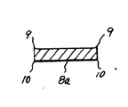
제3도는 기존 피막(8a)의 확대부분의 평면도이다. 도면에 예시된 바와 같은 보통의 피막(8a)을 특정된 폭으로 절단할 때 가시같은 것들(9)이 쉽사리 생기고 가장자리(10)에 모가 나게 된다. 따라서 피막(8a)같은 것을 이용하여 캐패시터를 제조할 경우 가시(9)가 유전피막 속으로 관통하므로 해서 회로가 단락(短絡)되거나 가장자리(10)가 유전피막을 통과하므로 해서 두께가 두꺼워지게 된다.3 is a plan view of an enlarged portion of the existing
결과적으로 유전파괴형상이 자주 일어나게 된다. 한편으로 권취기를 사용하여 플라스틱 피막 캐패시터를 권취하고 있는데 현재 자동권취기를 거의 모두 사용하고 있다. 이러한 자동권취기에는 정전 캐패시턴스, 즉 여러 겹의 권취량이 이미 들어가 있어서 플라스틱 피막과 전극 피막을 교대로 적층한 것들을 자동식으로 권취하여 권취된 몸체의 권취회수, 즉 정전 캐패시턴스가 일정한 값에 도달하도록 한다.As a result, dielectric breakdown often occurs. On the other hand, a winding machine is used to wind a plastic film capacitor, and almost all automatic winding machines are used. The automatic winding machine has an electrostatic capacitance, that is, a plurality of layers of windings already entered, so that the plastic film and the electrode film are alternately laminated automatically so that the number of windings of the wound body, that is, the electrostatic capacitance reaches a constant value.
100pF이하의 작은 캐패시턴스를 가진 캐패시터를 제조할 경우 일반 전극피막의 폭이 4㎜ 이상의 것을 사용할 때에는 불과 몇번만 피막을 감아주면(직경이 약 3㎜일 때 약 2-3회) 소요의 캐패시턴스 값이 된다.When manufacturing a capacitor with a small capacitance of 100 p F or less, the capacitance required when the film is wound only a few times (about 2-3 times when the diameter is about 3 mm) is used when the width of the general electrode film is 4 mm or more. Value.
따라서 캐패시턴스 허용량이 작은 캐패시터를 제조할 때의 수득율은 극히 나빠지는데 실제로 자동권취기를 이용하여 100pF이하의 캐패시턴스를 만들기는 불가능하다. 이러한 배경하에서 현재 100pF이하의 플라스틱 피막 캐패시터를 가진 것을 제조할 경우에 있어서 작업자가 4㎜ 이상의 폭을 가지도록 절단한 전극 피막을 수동식 권취기를 이용하여 유전피막 사이에 수동으로 소요의 길이만큼 삽입하여 권취하고 있다.Therefore, the yield when manufacturing a capacitor with a small capacitance allowance becomes extremely bad, but it is impossible to make a capacitance of 100 p F or less using an automatic winding machine. Under these circumstances, when manufacturing a plastic film capacitor of less than 100 p F, an electrode film cut to have a width of 4 mm or more by a worker is manually inserted into the dielectric film by the required length using a manual winding machine. Is winding up.
이와 같은 여러가지 제조단계를 이용하면 값이 비싼 캐패시터만 생산될 뿐이다.By using these various manufacturing steps, only expensive capacitors are produced.
본 발명의 1차 목적은 위에서 나온 여러가지 단점을 해결하고 전극피막의 단락현상이 없고 유전피막의 유전파괴현상이 없는 고도의 신뢰성을 가진 박막권취형 피막 캐패시터를 제조함이 있다. 본 발명의 2차 목적은 캐패시턴스가 작은 경제적이고도 신뢰성이 큰 플라스틱 피막 캐패시터를 제조함에 있다.The primary object of the present invention is to solve the above-mentioned shortcomings and to manufacture a thin film winding type capacitor having high reliability without short circuit of electrode film and dielectric breakdown of dielectric film. A second object of the present invention is to produce an economical and reliable plastic film capacitor having a small capacitance.
이러한 목적들은 알루미늄, 구리등으로 된 전선재료를 신장하여 권취시에 특정한 폭으로 형성함으로써 최소한 한가지 전극피막을 만들어 이 전극피막과 최소한 2매의 유전피막을 교대로 적층시켜 만든 박막 권취형 피막 캐패시터를 특징으로 하는 제조방법과 박막 권취형 피막 캐패시턴스에 의해 달성이 된다.The objective is to make a thin film winding type capacitor made by stretching an electric material made of aluminum, copper, etc. and forming a specific width at the time of winding to make at least one electrode film, and alternately stacking the electrode film and at least two dielectric films. It is achieved by the manufacturing method characterized by the above-mentioned, and a thin film winding-type film capacitance.
더우기 전극피막의 특정된 치수를 4㎜ 이하로 고정시켜 작은 캐패시턴스값을 가진 박막권취형 피막 캐패시터를 제조함으로써 이러한 목적들을 달성할 수도 있는 것이다.Furthermore, these objects may be achieved by fixing a specified dimension of the electrode coating to 4 mm or less to produce a thin film wound type capacitor having a small capacitance value.
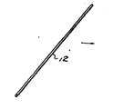
본 발명을 첨부된 도면을 따라 상술한다. 본 발명에 의한 예는 제4도에서부터 제9도까지에서 상술된다. 본 발명에 의한 전극피막(11)(제4b도)은 알루미늄갖은 경합금(經合金)으로 된 선제(12)(제4a도)를 연신시켜 만든 것으로서 단면이 원형이다.The invention is described in detail with reference to the accompanying drawings. Examples according to the invention are detailed in FIGS. 4 to 9. The electrode film 11 (FIG. 4B) which concerns on this invention was made by extending | stretching the wire | wire 12 (FIG. 4A) which consists of hard alloys with aluminum, and is circular in cross section.
이와 동시에 피막을 캐패시터로 사용할 경우 전극피막(11)의 폭이 특정한 치수와 동일한 것이 되도록 연신 공정을 실시해야 한다. 이렇게 해서 만든 전극피막(11)은 종전의 경우와는 달리 제4c도에 예시된 바와 같이 단면이 둥근 가장자리(11a)를 가지며, 가시같은 것들이 생기지 않고 가장자리가 모가 나지 않는 것이다. 이러한 이유로 해서 전극피막(11)을 이용하여 플라스틱피막 캐패시터를 제조할 경우 전극피막의 단락현상이 없고 유전피막의 유전파괴가 일어나지 않는 신뢰성이 큰 캐패시터를 얻을 수 있다.At the same time, when the film is used as a capacitor, the stretching process must be performed so that the width of the electrode film 11 is the same as a specific dimension. Unlike the conventional case, the electrode film 11 thus formed has a rounded edge 11a as illustrated in FIG. 4C, and does not have thorns or edges. For this reason, when manufacturing a plastic film capacitor using the electrode film 11, it is possible to obtain a highly reliable capacitor that there is no short circuit of the electrode film and dielectric breakdown of the dielectric film occurs.
한편으로 본 발명에서는 여러가지 직경을 가진 선재를 제조한 결과 폭이 4㎜ 이하인 극히 엷은 전극피막을 만들 수 있었다. 따라서 현재의 방법으로는 얻기 어려운 100PF이하의 캐패시턴스를 가진 플라스틱 피막 캐패시터를 제조하기 위한 자동권취공정을 실현했다.On the other hand, in the present invention, as a result of manufacturing wire rods having various diameters, extremely thin electrode films having a width of 4 mm or less could be made. Therefore, an automatic winding process for producing a plastic film capacitor having a capacitance of 100 P F or less, which is difficult to obtain by current methods, has been realized.
표 1은 본 발명인들이 실시한 실험에서 나타난 연신된 재료의 두께와 폭과의 사이의 관계를 나타낸 것이다. 단면이 원형인 알루미늄 선재를 본 실험에 이용했다.Table 1 shows the relationship between the thickness and the width of the stretched material shown in the experiment conducted by the inventors. An aluminum wire having a circular cross section was used in this experiment.
<표 1>에서 직경이 0.2-0.6㎜인 재료를 연신하여 두께가 10m-70m인 것으로 만들었을 때의 피막폭을 나타내었다.Table 1 shows the film width when the material having a diameter of 0.2-0.6 mm was drawn to have a thickness of 10 m-70 m.
[표 1]TABLE 1

이 결과에서 보면 직경이 0.2㎜인 알루미늄 선재를 두께가 10m인 판상으로 연신하여 폭이 3.0㎜인 전극 피막을 만들 수 있고 직경이 0.5㎜인 선재를 폭이 50㎛인 판상으로 연신하여 폭이 2.5㎜인 전극피막을 만들 수 있다.In this result, an aluminum wire having a diameter of 0.2 mm was drawn into a plate having a thickness of 10 m to make an electrode film having a width of 3.0 mm, and a wire having a diameter of 0.5 mm was drawn into a plate having a width of 50 μm to have a width of 2.5 μm. An electrode film of mm can be made.
알루미늄 선재로부터 폭이 4㎜ 이하인 전극피막을 제조할 경우에 있어서 선재의 직경이 0.7㎜ 이상일때는 전극피막은 두께가 두꺼워지며 이로 인하여 캐패시터는 크기가 커진다. 다시 말하자면 재료비의 관점에서 보면 비경제적이 된다. 더우기 직경이 0.1㎜인 재료를 사용하면 전극피막의 기계적인 강도는 불충분하게 되어 권취도중 쉽사리 파괴된다. 따라서 직경이 0.2㎜-0.6㎜ 인선재를 두께거 10㎛-70㎛인 판상으로 인신하여 얻은 것을 사용하여 폭이 4㎜인 전극피막을 만들 필요가 있다.In the case of producing an electrode coating having a width of 4 mm or less from an aluminum wire, when the diameter of the wire is 0.7 mm or more, the electrode coating becomes thicker, and thus the capacitor becomes larger. In other words, it becomes uneconomical in terms of material costs. In addition, when a material having a diameter of 0.1 mm is used, the mechanical strength of the electrode film becomes insufficient and is easily broken during winding. Therefore, it is necessary to produce an electrode film having a width of 4 mm by using a 0.2 mm-0.6 mm diameter wire drawn in a plate shape having a thickness of 10 m to 70 m.
이러한 직경과 두께를 구리선과 주석선에도 적용할 수 있다. 제5도에 예시된 바와 같이 리일(reel)(13)로부터 로울러(14, 15)를 통해 리일(reel)(16)까지 통과시킴으로써 선재(12)를 연신한다. 선재(12)를 이용하여 제4b도에 예시된 전극피막(11)으로 만들어 로울러(14, 15)에서 내어 보낸다. 테이프모양의 길이가 극히 긴 전극피막을 이러한 연신법으로 효과적으로 만들 수 있다. 더우기 연신된 전극피막을 300℃-400℃에서 30-60분간 풀림처리(annealing)하여 스트레인을 제거한다.These diameters and thicknesses can also be applied to copper wires and tin wires. As illustrated in FIG. 5, the
이 공정에 의하여 보다 연질의 전극피막을 얻으므로서 권취능력을 향상시킨다. 이 공정에 있어서 내열재료로 리일(16)을 만들 경우 리일(16)을 권취된 전극피막(11)용 가열로 속에 넣고 풀림처리를 효과적으로 할 수 있다.This step improves the winding capability while obtaining a softer electrode coating. In this process, when the rail 16 is made of a heat-resistant material, the rail 16 may be placed in a wound furnace for the wound electrode film 11, and the annealing treatment may be effectively performed.
더우기 자동권취기의 전극피막 권취용 리일로서 리일(16)을 사용하여 자동권취기에다 풀림처리된 재료를 직접 장치할 수 있다. 캐패시턴스가 100pF이하인 플라스틱 피막 캐패시터 제조의 경우 본 발명에 의한 전극피막(11)을 폭이 4㎜ 이하의 것으로 간단히 만들 수 있다.Moreover, the unwinding material can be directly attached to the automatic winding machine by using the rail 16 as the electrode coating winding winding of the automatic winding machine. In the case of the production of a plastic film capacitor having a capacitance of 100 p F or less, the electrode film 11 according to the present invention can be simply made to have a width of 4 mm or less.
따라서 종래의 것보다 극히 긴 피막을 제조할 수 있다. 결과적으로 본 발명에 의하여 종래의 피막에서 얻을 수 있는 것보다 훨씬 권취회수가 많은 전극피막(11)을 만들 수 있기 때문에 작은 캐패시턴스 허용량을 가진 캐패시터를 자동권취기를 사용할 경우에 좋은 수득율로 제조할 수 있다.Therefore, an extremely long film can be manufactured than the conventional one. As a result, according to the present invention, since the electrode coating 11 having a much higher number of turns than can be obtained from the conventional coating, a capacitor having a small capacitance allowance can be manufactured at a good yield rate when using an automatic winding machine. .
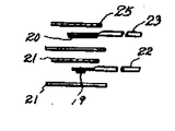
제6도는 본 발명에 의한 플라스틱 캐패시터 권취시의 유도단자 설치구조를 예시한 것이다. 권취측(17)에 있는 권취된 몸체(18)는 2매의 전극피막(19, 20)과 2매의 유전피막(21)(종이 표면에 있는 유전피막 1매는 도면의 편의상에서 되어 있지 않음)을 교대로 적층한 것을 권취하여 만든 것이다. 전극피막(19)은 폭이 4㎜ 이하의 것으로서 앞서 상술된 바 있는 경우처럼 선재를 연신하여 만든다.Figure 6 illustrates the induction terminal installation structure at the time of winding the plastic capacitor according to the present invention. The wound body 18 on the winding side 17 includes two
한편으로 전극피막(20)은 폭이 4㎜ 이상의 것으로서 제3도에 예시된 바와 같이 슬리터로 절단하여 만든다. 본 예에 있어서 도면에 예시된 바와 같이 전극피막(19, 20) 중 한 개는 폭이 좁은 것을 사용하고 유전피막(20)은 동일한 폭의 것을 사용한다.On the other hand, the
따라서 전극피막(19, 20)의 상대적인 위치가 폭방향에서 다소 벗어나더라도 캐패시턴스 값은 거의 변하지 않기 때문에 위에서 상술한 권취회수를 크게 할 수 있는 외에도 캐패시턴스 값의 변화가 거의 없는 작은 캐패시턴스를 가진 플라스틱 캐패시터를 제조할 수 있다.Therefore, even if the relative positions of the
가장자리를 평평하게 만든 유도단자(22, 23)를 전극피막(19)의 적당한 위치에 용접한 후 권취작업시에 권취된 몸체(18)가 되게 권취한다.The
플라스틱 피막으로 되어 있는 직사각형의 보호피막(24, 25)을 유도단자(22, 23)의 용접위치에 해당하는 곳에 배치하여 피막(19, 20, 21)과 함께 권취한다. 보호피막(24, 25)의 기능은 유전파괴와 단락현상을 한층 더 방지하는데 있다.Rectangular
유도단자(22, 23)와 보호피막(24, 25)을 감은 후 추가로 유전피막(21)을 감아줌으로써 외장(外裝)부분을 형성한다. 피막(19, 20, 21)을 잘라낸 후 이렇게 하여 만든 권취된 몸체(18)를 열처리한 후 캐패시터 요소로 사용한다.After winding the
제8도는 제6도에 예시된 권취구조에 의해 제조된 본 발명에 의한 작은 캐패시턴스를 가진 플라스틱 피막 캐패시터이다. 이 캐패시터는 요소(26)의 양쪽에 유도단자(22, 23)로 가지고 있으며, 요소(26)의 중앙은 전극피막(19)의 폭이 좁으므로 해서 돌출해 있다.FIG. 8 is a plastic film capacitor having a small capacitance according to the present invention manufactured by the winding structure illustrated in FIG. This capacitor has
제7a도와 제7b도는 또 다른 형식의 작은 캐패시턴스를 가진 플라스틱 피막 캐패시터를 제조하는 권취공정이다. 유도단자(22, 23)를 동일한 방향으로 끌어내는 지점을 제외하고는 제6도에서 설명한 바와 같은 동일한 권취공정에 의해 이 캐패시터를 제조한다.7A and 7B show a winding process for manufacturing a plastic film capacitor having another type of small capacitance. The capacitor is manufactured by the same winding process as described in FIG. 6 except for the point where the
제9도는 제7도에 있는 권취구조를 하여 제조한 본 발명의 캐패시터인데 이 캐패시터 제조예에 대해 상술한다.FIG. 9 is a capacitor of the present invention manufactured by the winding structure shown in FIG. 7. The capacitor manufacturing example will be described in detail.
직경이 0.3㎜인 알루미늄 선재를 제5도에 연신공정에 따라 두께 45㎛ 및 폭 1.3㎜인 테이프 모양의 전극피막으로 만든 후 자동권취기에 있는 전극피막 권취리일(16)로 권취한다. 두께가 0.5㎛이고 폭이 6㎜인 테이프 모양의 전극피막(20)을 한 리일에 권취하고 두께가 40㎛이고 폭이 10㎜인 유전피막(21)을 또 다른 리일에 권취함으로써 한쌍의 리일을 준비한다. 각 티일을 자동권취기에 장비하고 제8도에 예시된 33pF의 작은 캐패시턴스를 가진 플라스틱 피막 캐패시터를 30회 자동권취하여 만든다.An aluminum wire having a diameter of 0.3 mm is made into a tape-shaped electrode film having a thickness of 45 μm and a width of 1.3 mm according to the stretching process in FIG. 5, and then wound with an electrode film winding rail 16 in an automatic winding machine. A pair of rails are wound by winding a tape-shaped
이들 캐패시터를 특정한 결과 캐패시턴스 분포는 32.7pF에서 34.6pF의 범위였으며 기준편차는 0.5pF였다.As a result of specifying these capacitors, the capacitance distribution ranged from 32.7 p F to 34.6 p F with a reference deviation of 0.5 p F.
한편으로는 종래의 수동식 권취공정에 의해 만든 33pF의 캐패시터의 캐패시턴스 분포는 30.1pF에서부터 36.2pF의 범위였고 기준편차는 1.7pF였다.On the other hand, the capacitance distribution of the 33 p F capacitor produced by the conventional manual winding process ranged from 30.1 p F to 36.2 p F with a reference deviation of 1.7 p F.
위에서 상술한 바와 같이 본 발명에 의한 캐패시터는 캐패시터스 변화에 있어서 종래의 카패시터보다 극히 우수한 것이었다.As described above, the capacitor according to the present invention was extremely superior to the conventional capacitor in the capacitance change.
Claims (6)
Applications Claiming Priority (3)
| Application Number | Priority Date | Filing Date | Title |
|---|---|---|---|
| JP56-158996 | 1981-10-06 | ||
| JP56158996A JPS5860517A (en) | 1981-10-06 | 1981-10-06 | Metal foil for electrode of wound type condenser |
| JP158996 | 1985-07-08 |
Publications (2)
| Publication Number | Publication Date |
|---|---|
| KR840001762A KR840001762A (en) | 1984-05-16 |
| KR880000256B1 true KR880000256B1 (en) | 1988-03-15 |
Family
ID=15683941
Family Applications (1)
| Application Number | Title | Priority Date | Filing Date |
|---|---|---|---|
| KR8204359A KR880000256B1 (en) | 1981-10-06 | 1982-09-28 | Wound foil type film capacitor |
Country Status (5)
| Country | Link |
|---|---|
| US (1) | US4481558A (en) |
| EP (1) | EP0076693B1 (en) |
| JP (1) | JPS5860517A (en) |
| KR (1) | KR880000256B1 (en) |
| DE (1) | DE3270144D1 (en) |
Families Citing this family (18)
| Publication number | Priority date | Publication date | Assignee | Title |
|---|---|---|---|---|
| FR2580854B1 (en) * | 1985-04-17 | 1987-05-22 | Merlin Gerin | MEDIUM AND HIGH VOLTAGE CAPACITORS |
| DE3817903A1 (en) * | 1988-05-26 | 1989-11-30 | Siemens Ag | ELECTRIC CAPACITOR |
| US5170318A (en) * | 1991-10-28 | 1992-12-08 | International Business Machines Corporation | Flexible capacitor |
| US5370663A (en) * | 1993-08-12 | 1994-12-06 | Intermedics, Inc. | Implantable cardiac-stimulator with flat capacitor |
| US20060147712A1 (en) * | 2003-07-09 | 2006-07-06 | Maxwell Technologies, Inc. | Dry particle based adhesive electrode and methods of making same |
| US7352558B2 (en) * | 2003-07-09 | 2008-04-01 | Maxwell Technologies, Inc. | Dry particle based capacitor and methods of making same |
| US20110165318A9 (en) * | 2004-04-02 | 2011-07-07 | Maxwell Technologies, Inc. | Electrode formation by lamination of particles onto a current collector |
| US20070122698A1 (en) * | 2004-04-02 | 2007-05-31 | Maxwell Technologies, Inc. | Dry-particle based adhesive and dry film and methods of making same |
| US7791860B2 (en) * | 2003-07-09 | 2010-09-07 | Maxwell Technologies, Inc. | Particle based electrodes and methods of making same |
| US7920371B2 (en) * | 2003-09-12 | 2011-04-05 | Maxwell Technologies, Inc. | Electrical energy storage devices with separator between electrodes and methods for fabricating the devices |
| US7102877B2 (en) * | 2003-09-12 | 2006-09-05 | Maxwell Technologies, Inc. | Electrode impregnation and bonding |
| US7090946B2 (en) | 2004-02-19 | 2006-08-15 | Maxwell Technologies, Inc. | Composite electrode and method for fabricating same |
| US7440258B2 (en) * | 2005-03-14 | 2008-10-21 | Maxwell Technologies, Inc. | Thermal interconnects for coupling energy storage devices |
| US8518573B2 (en) | 2006-09-29 | 2013-08-27 | Maxwell Technologies, Inc. | Low-inductive impedance, thermally decoupled, radii-modulated electrode core |
| US20080241656A1 (en) * | 2007-03-31 | 2008-10-02 | John Miller | Corrugated electrode core terminal interface apparatus and article of manufacture |
| US20080235944A1 (en) * | 2007-03-31 | 2008-10-02 | John Miller | Method of making a corrugated electrode core terminal interface |
| CN103617889A (en) * | 2013-11-26 | 2014-03-05 | 上海田伏电子科技有限公司 | Copper foil thin film capacitor and manufacturing process thereof |
| CN110896000A (en) * | 2018-08-24 | 2020-03-20 | 东莞市成东电子科技有限公司 | Welding process of thin film capacitor |
Family Cites Families (8)
| Publication number | Priority date | Publication date | Assignee | Title |
|---|---|---|---|---|
| US2627645A (en) * | 1947-03-11 | 1953-02-10 | Western Electric Co | Method of manufacturing condensers |
| US2835153A (en) * | 1955-01-26 | 1958-05-20 | William G Langton | Wire rolling apparatus |
| US3128547A (en) * | 1959-10-06 | 1964-04-14 | Reynolds Metals Co | Method for producing strip conductors having uniformly insulated edges |
| US3049651A (en) * | 1959-10-29 | 1962-08-14 | Sprague Electric Co | Electrical capacitors |
| US3773585A (en) * | 1971-09-10 | 1973-11-20 | Aluminum Co Of America | Method of forming a laminate structure |
| DE2246422B2 (en) * | 1972-09-21 | 1976-08-12 | Siemens AG, 1000 Berlin und 8000 München | ELECTRIC WINDING CAPACITOR, IN PARTICULAR ELECTROLYTE CAPACITOR, WITH HIGH VOLUME CAPACITY AND LOW IMPACT RESISTANCE |
| FR2354152A1 (en) * | 1976-06-08 | 1978-01-06 | Michelin & Cie | METHOD FOR MANUFACTURING BY LAMINATION A STEEL TAPE, AND TAPE RESULTING FROM THIS PROCESS |
| US4233832A (en) * | 1979-01-26 | 1980-11-18 | Rowell Douglas W | Method and apparatus for rolling metal wire or rod into wide, flat strips |
-
1981
- 1981-10-06 JP JP56158996A patent/JPS5860517A/en active Granted
-
1982
- 1982-09-28 KR KR8204359A patent/KR880000256B1/en active
- 1982-09-29 US US06/428,287 patent/US4481558A/en not_active Expired - Fee Related
- 1982-10-05 DE DE8282305290T patent/DE3270144D1/en not_active Expired
- 1982-10-05 EP EP82305290A patent/EP0076693B1/en not_active Expired
Also Published As
| Publication number | Publication date |
|---|---|
| KR840001762A (en) | 1984-05-16 |
| JPS5860517A (en) | 1983-04-11 |
| EP0076693A3 (en) | 1983-06-29 |
| EP0076693B1 (en) | 1986-03-26 |
| DE3270144D1 (en) | 1986-04-30 |
| JPS6358364B2 (en) | 1988-11-15 |
| US4481558A (en) | 1984-11-06 |
| EP0076693A2 (en) | 1983-04-13 |
Similar Documents
| Publication | Publication Date | Title |
|---|---|---|
| KR880000256B1 (en) | Wound foil type film capacitor | |
| US6111743A (en) | Metallized capacitor having increased dielectric breakdown voltage and method for making the same | |
| US4028595A (en) | Multi-voltage capacitor section | |
| US3921041A (en) | Dual capacitor | |
| US4352145A (en) | Multiple element cylindrical metallized film capacitors and method of making the same | |
| KR880000156A (en) | Flat coil and its manufacturing method | |
| US4378620A (en) | Method of making small sized wound capacitors | |
| US3327184A (en) | Wound capacitor and method of making | |
| US4622620A (en) | Electric capacitor with polyethylene terephthalate as a dielectric for use as a solderable chip component | |
| US3906297A (en) | Metallized film capacitor and method of manufacture thereof | |
| US4638402A (en) | Multi-section capacitor electrically coupled in parallel | |
| US3391313A (en) | Capacitor and method of making the same | |
| US4422127A (en) | Substantially small sized wound capacitor and manufacturing method therefor | |
| EP0207549B1 (en) | Electrolytic wound capacitor | |
| JPH08102427A (en) | Film capacitor | |
| DE3517435A1 (en) | ELECTRIC CAPACITOR FROM A STRENGTHENED WRAP AND METHOD FOR THE PRODUCTION THEREOF | |
| US3202592A (en) | Inductance-capacitance device and method of manufacture | |
| KR100341148B1 (en) | Method for fabricating chip type solid electrolytic capacitor | |
| US4509100A (en) | Low inductance wound capacitor | |
| JP3043140B2 (en) | Film capacitor | |
| US4495544A (en) | Electric roll-type capacitor | |
| US4430688A (en) | Small heat resistant film condenser | |
| DE2404759B2 (en) | METHOD OF MANUFACTURING ELECTRIC CAPACITORS | |
| US3333999A (en) | Method of making an insulated strip conductor | |
| KR850001769B1 (en) | Ceramic capacitor and process of making it |