KR840000112B1 - Televizion signal processing system - Google Patents
Televizion signal processing system Download PDFInfo
- Publication number
- KR840000112B1 KR840000112B1 KR1019800003410A KR800003410A KR840000112B1 KR 840000112 B1 KR840000112 B1 KR 840000112B1 KR 1019800003410 A KR1019800003410 A KR 1019800003410A KR 800003410 A KR800003410 A KR 800003410A KR 840000112 B1 KR840000112 B1 KR 840000112B1
- Authority
- KR
- South Korea
- Prior art keywords
- signal
- frequency
- circuit
- aft
- tuning
- Prior art date
Links
- 238000012545 processing Methods 0.000 title claims description 3
- 230000004044 response Effects 0.000 claims description 37
- 239000003990 capacitor Substances 0.000 claims description 16
- 230000002238 attenuated effect Effects 0.000 claims description 4
- 230000001419 dependent effect Effects 0.000 claims description 4
- 230000001747 exhibiting effect Effects 0.000 claims 1
- 230000001360 synchronised effect Effects 0.000 abstract description 16
- 238000001514 detection method Methods 0.000 description 13
- 230000009977 dual effect Effects 0.000 description 6
- 230000008878 coupling Effects 0.000 description 5
- 238000010168 coupling process Methods 0.000 description 5
- 238000005859 coupling reaction Methods 0.000 description 5
- 238000010586 diagram Methods 0.000 description 5
- 230000007704 transition Effects 0.000 description 5
- 239000002131 composite material Substances 0.000 description 4
- 238000013461 design Methods 0.000 description 4
- 230000000694 effects Effects 0.000 description 4
- 238000010587 phase diagram Methods 0.000 description 4
- 230000002829 reductive effect Effects 0.000 description 4
- 239000000969 carrier Substances 0.000 description 3
- 230000005236 sound signal Effects 0.000 description 3
- 230000003068 static effect Effects 0.000 description 3
- 230000008859 change Effects 0.000 description 2
- 238000013016 damping Methods 0.000 description 2
- 230000003247 decreasing effect Effects 0.000 description 2
- 230000036039 immunity Effects 0.000 description 2
- 238000000034 method Methods 0.000 description 2
- 238000011176 pooling Methods 0.000 description 2
- 230000003595 spectral effect Effects 0.000 description 2
- 230000001052 transient effect Effects 0.000 description 2
- 230000002411 adverse Effects 0.000 description 1
- 238000013459 approach Methods 0.000 description 1
- 230000000295 complement effect Effects 0.000 description 1
- 238000012937 correction Methods 0.000 description 1
- 230000007423 decrease Effects 0.000 description 1
- 238000005516 engineering process Methods 0.000 description 1
- 230000001939 inductive effect Effects 0.000 description 1
- 230000010355 oscillation Effects 0.000 description 1
- 230000010363 phase shift Effects 0.000 description 1
- 230000008569 process Effects 0.000 description 1
- 238000001228 spectrum Methods 0.000 description 1
- 238000012546 transfer Methods 0.000 description 1
Images


Classifications
-
- H—ELECTRICITY
- H04—ELECTRIC COMMUNICATION TECHNIQUE
- H04N—PICTORIAL COMMUNICATION, e.g. TELEVISION
- H04N5/00—Details of television systems
- H04N5/44—Receiver circuitry for the reception of television signals according to analogue transmission standards
- H04N5/50—Tuning indicators; Automatic tuning control
Abstract
Description
제1도는 반송파 기준신호의 위상도.1 is a phase diagram of a carrier reference signal.
제2도는 측대역 변조된 반송파 기준신호의 위상도.2 is a phase diagram of a sideband modulated carrier reference signal.
제3도는 대표적 기준신호회로의 통과대역을 나타낸 도면.3 is a diagram showing a passband of a representative reference signal circuit.
제4도는 대표적 AFT회로의 응답특성을 도시한 도면.4 is a diagram showing the response characteristics of a typical AFT circuit.
제5도는 대표적 I.F통과대역내의 정상, 오프셋음성 및 영상반송파의 위치를 나타낸 도면.5 is a diagram showing positions of normal, offset speech, and image carriers in a typical I.F passband.
제6도는 본 발명의 원리에 따라 구성된 동기검파기 및 AFT회로를 나타낸 도면.6 illustrates a synchronous detector and an AFT circuit constructed in accordance with the principles of the present invention.
제7도는 제6도 회로의 대표적 기준신호 응답특성을 나타낸 도면.FIG. 7 is a diagram showing typical reference signal response characteristics of the circuit of FIG. 6. FIG.
제8도는 제6도 회로의 대표적 AFT응답특성을 나타낸 도면.8 shows representative AFT response characteristics of the FIG. 6 circuit.
제9도는 제6도 회로의 교체실시예에 대한 회로도.9 is a circuit diagram of an alternative embodiment of the FIG. 6 circuit.
본 발명은 동기검파기 및 AFT(Automatlc Fine Tuning)회로에 관한 것으로 특히, 동기검파기내의 고조파왜곡을 감소시키며, 회로의 잡음면역능력 및 오프셋동조능력을 개선하는 동조회로를 포함하고 있는 공동선택회로에 관한 것이다.The present invention relates to a synchronous detector and an AFT (Automatlc Fine Tuning) circuit, and more particularly, to a joint selection circuit including a tuning circuit that reduces harmonic distortion in a synchronous detector and improves the noise immunity and offset tuning capability of the circuit. will be.
개선된 선형성, 낮은 신호레벨에서의 동작, 비데오 및 내부반송파 음성신호의 동시검파 등을 요하는 분야에는 포락선검파가 널리 이용된다는 장점때문에, 텔레비젼 수상기 설계자들은 동기검파처리에 많은 관심을 가져왔다. 그러나 동기검파기의 설계는 정확성 및 복잡성 때문에 매우 어렵고 따라서 값이 비싸다는 단점이 있다.Because of the advantages of envelope detection being widely used in applications requiring improved linearity, operation at low signal levels, simultaneous detection of video and internal carrier voice signals, television receiver designers have been interested in synchronous detection processing. However, the design of the synchronous detector has the disadvantage that it is very difficult and expensive because of the accuracy and complexity.
그러나, 텔레비젼 집적회로기술의 출현으로 동기검파는 가격 및 수행면에서 가능하게 되었다. 동기복조기는 일반적으로 중간주파수(I.F)신호가 기준 또는 스위칭신호에 의해 증배되는 이중균형적(積) 검파기로 구성되어 있다. 기준신호가 I.F영상반송파와 동일한 주파수 및 위상을 갖는 스펙트럼형의 순수한 정현파 일때, 상기에 언급된 동기검파가 실현될 수 있다.However, with the advent of television integrated circuit technology, synchronous detection has become possible in terms of price and performance. Synchronous demodulators generally consist of double balanced detectors in which intermediate frequency (I.F) signals are multiplied by a reference or switching signal. When the reference signal is a pure sine wave of spectral type having the same frequency and phase as the I.F image carrier, the synchronous detection mentioned above can be realized.
만일 기준신호가 변조되지 않은 영상반송파나 균열된 이중 측대역을 갖는 영상반송파에 의해 발생된다면, 스펙트럼형의 진폭이 제한된 스위치신호가 발생된다. 그러나 기준신호는 I.F영상반송파와 기준신호의 정확한 위상접합을 유지시키기 위해 적검파기에 인가되는 I.F신호로부터 유도된다. I.F신호는 기준신호를 발생시키기 위해 영상캐리어 부근에서 선택적으로 기준채널회로에 인가된다. 그렇기 때문에, 기준채널의 입력에서의 신호는 변조되지 않은 캐리어 및 이중 측대역신호가 아니라 선택성 및 전송된 신호의 베스티지얼(Vestigial)특성에 의해 I.F신호는 불균형된 이중 측대역신호로서 나타나는 저주파 비데오성분과 단일 측대역신호로서 나타나는 고주파 성분으로 된 비대칭 측대역신호이다.If the reference signal is generated by an unmodulated image carrier or an image carrier having a cracked dual sideband, a spectral amplitude limited switch signal is generated. However, the reference signal is derived from the I.F signal applied to the red detector to maintain the correct phase junction of the I.F image carrier and the reference signal. The I.F signal is selectively applied to the reference channel circuit near the image carrier to generate a reference signal. Therefore, the signal at the input of the reference channel is not an unmodulated carrier and dual sideband signal, but a low frequency video component in which the IF signal appears as an unbalanced dual sideband signal due to the selectivity and the vertical characteristics of the transmitted signal. It is an asymmetrical sideband signal with high frequency components appearing as a single sideband signal.
비대칭 측대역을 갖는 I.F영상반송파가 적검파기에 인가될때 고주파왜곡을 갖는 검파된 비데오 및 인터캐리어 음성신호를 발생하는 기준채널신호내에 동위상인 구적성분이 발생하게 된다. 비데오신호의 고조파는 4.5MHz의 주파수를 갖는 인터캐리어 음성신호에서 발생하게 되므로 음성채널에 버즈(buzz)가 발생된다. 예로 2.25MHz에서의 비데오신호(내부반송파 음성신호의 제2 부고조파)와 1.5MHz에서의 비데오신호(내부반송파 음성신호의 제3 부고조파)가 인터캐리어 음성신호주파수(4.5MHz)에서 나타나는 상위고조파를 가질 수 있다. 기준채널에서 발생된 기준신호는 또한 AFT신호를 발생시키기 위해 이중-균형위상비교기에 연결되어 사용될 수 있다.When an I.F image carrier with an asymmetric sideband is applied to a red detector, quadrature components in phase are generated in a reference channel signal that generates a detected video and an intercarrier audio signal with high frequency distortion. Since the harmonics of the video signal are generated in the intercarrier voice signal having a frequency of 4.5 MHz, buzz is generated in the voice channel. For example, the higher harmonics at which the video signal (second harmonic of the internal carrier speech signal) at 2.25 MHz and the video signal (third harmonic of the internal carrier speech signal) at 1.5 MHz appear at the intercarrier speech signal frequency (4.5 MHz). It can have The reference signal generated in the reference channel can also be used in connection with a dual-balance phase comparator to generate an AFT signal.
기준신호는 제1 직류선로와 동조회로를 포함하는 제2 통로에 의해 위상비교기에 결합된다. 동조회로는 위상비교기에 인가되는 두 신호들이 I.F영상반송파가 교정주파수에 있을 때 구적이 되도록 기준신호에 주파수 의존위상이동을 시킨다. 영상반송파가 원하는 주파수로 변할때, 인가된 신호는 구적으로 되지 않고, 위상비교기의 출력들은 바뀌고, 동조기용 교정전압이 발생하게 된다. AFT회로를 설계할 때에는 여러 인자들이 고려되어야 한다. 상술한 I.F휠터와 비대칭 나이퀴스트(Nyguist) 대역통과는 중간대역을 향하여 더 큰 풀-인(Pull-in)범위를 나타내는 AFT응답특성을 만들게 한다. 이 불균형 응답특성은 잡음에 기인하여 AFT전압이 중간대역을 향하여 표동(drift)하게 한다. 왜냐하면 I.F잡음은 중간대역 주위에 집중된 주파수 스펙트럼을 갖기 때문이다.The reference signal is coupled to the phase comparator by a second passage including a first DC line and a tuning circuit. The tuning circuit performs a frequency dependent phase shift on the reference signal so that the two signals applied to the phase comparator are quadrature when the I.F image carrier is at the calibration frequency. When the image carrier changes to the desired frequency, the applied signal is not quadrature, the outputs of the phase comparators are changed, and the calibration voltage for the tuner is generated. Several factors must be taken into account when designing an AFT circuit. The I.F filter and asymmetric Nyguist bandpass described above result in an AFT response characteristic showing a larger pull-in range towards the midband. This unbalanced response causes the AFT voltage to drift toward the middle band due to noise. This is because I.F noise has a frequency spectrum centered around the middle band.
그러므로, 균형응답특성이 만들어지도록 회로를 설계하는 것이 바람직하다. 또한 텔레비젼 수신기가 마스터 안테나(MATV)와 케이블 텔레비젼(CATV) 시스템으로부터 수신된 신호들을 얻을 수 있고 유지할수 있도록 AFT시스템을 설계하는 것이 바람직하다. 이 시스템들은 주파수 오프셋에 대해 조정되지 않으며, 위상변조와 주파수 오프셋을 발생시키는 공지된 시스템이다. 따라서, 캐리어는 정상방송주파수에서 ±2MHz만큼 벗어나게 된다. 2MHz오프셋트 텔레비젼신호는 적당하게 설계된 시스템과 결합하여 사용할때 미합중국특허 제4,031,549호에 도시된 바와 같은 주파수합성기(FS) 동조시스템에 의해 얻어질 수 있다. FS동조시스템은 전압제어국부발진기를 포함하는 고정위상루프(PLL)를 포함한다. 국부발진기에 의해 만들어진 신호의 주파수는 수신기를 원하는 채널로 동조한다. 국부발진기는 우선 수신기를 선택된 채널용 표준방송주파수로 동조시킨다. 이때 PLL은 AFT신호의 제어상태하에서 동작하게 되고, 동조기는 표준주파수위치의 주위에 집중된 주파수 범위이상의 바람직한 채널의 영상반송파를 찾게 된다. 신호가 얻어지지 않으면, 동조시스템을 국부발진기주파수를 1MHz 증가시키고, 다음에 1MHz 감소시켜가면서 이 국부발진기주파수들 주위에서 주파수범위를 찾는다. 2MHz 오프셋트신호를 얻기 위해서, AFT회로는 증가시키거나 감소시키는 국부발진기 주파수에서 1MHz 떨어진 반송파에 동조기를 직결시킬 수 있어야 한다. 그러므로, AFT시스템이 ±2MHz의 신호오프셋을 얻을 수 있도록 ±1MHz범위의 주파수를 가져야만 한다.Therefore, it is desirable to design the circuit so that a balanced response characteristic is made. It is also desirable to design an AFT system so that a television receiver can obtain and maintain signals received from a master antenna (MATV) and cable television (CATV) system. These systems are well known systems that do not adjust for frequency offset and generate phase modulation and frequency offset. Thus, the carrier deviates by ± 2 MHz from the normal broadcast frequency. The 2 MHz offset television signal can be obtained by a frequency synthesizer (FS) tuning system as shown in US Pat. No. 4,031,549 when used in combination with a suitably designed system. The FS tuning system includes a fixed phase loop (PLL) that includes a voltage controlled local oscillator. The frequency of the signal produced by the local oscillator tunes the receiver to the desired channel. The local oscillator first tunes the receiver to the standard broadcast frequency for the selected channel. At this time, the PLL operates under the control state of the AFT signal, and the tuner finds an image carrier of a desired channel over a frequency range concentrated around a standard frequency position. If no signal is obtained, the tuning system finds the frequency range around these local oscillator frequencies by increasing the local oscillator frequency by 1 MHz and then decreasing it by 1 MHz. To obtain a 2 MHz offset signal, the AFT circuit must be able to connect the tuner to a
임의의 AFT시스템의 풀-인범위는 I.F선택회로의 나이퀴스트기울기와 하위인접 음성트랩(trap)에 의해 하위인접 채널방향으로 제한된다. 하위인접채널을 향하는 주파수오프셋, I.F영상반송파의 진폭은 급속히 감소하게 되며, 상호채널 음성반송파가 상호채널을 성트랩대신에 통과대역내에 위치설정됨에 따라 그 진폭이 커지게 된다. 바람직한 채널의 I.F영상반송파가 1MHz의 오프셋을 가질때 감소된 영상반송파와 상호채널 음성반송파는 AFT풀-인범위의 외부단부에 있게 되므로, AFT시스템내에서 동일 및 반대의 동조 교정전압이 발생한다. 그러므로, 발생된 동조전압은 서로 균형되고, AFT시스템은 수신기의 동조를 변화시키지 않을 정도의 동조전압을 동조기에 제공할 것이다. 그러므로 동조시스템은 오프셋트신호를 얻을 수 없는 상태에서 고정될 것이다. 그러므로, 동조기국부발진기가 표동되었던 신호나 조정주파수에 있지 않고 1MHz까지 오차를 갖는 신호를 얻을 수 있고 유지할 수 있도록 AFT회로를 설계하는 것이 바람직하다.The pull-in range of any AFT system is limited in the lower adjacent channel direction by the Nyquist slope and lower adjacent voice trap of the I.F selection circuit. The frequency offset toward the lower adjacent channel, the amplitude of the I.F video carrier, decreases rapidly, and the amplitude increases as the cross-channel voice carrier is positioned in the passband instead of the sex trap. When the I.F video carrier of the desired channel has an offset of 1 MHz, the reduced video carrier and the interchannel voice carrier are at the outer end of the AFT pull-in range, resulting in the same and opposite tuning correction voltages in the AFT system. Therefore, the generated tuning voltages are balanced with each other, and the AFT system will provide the tuning voltage to the tuner so as not to change the tuning of the receiver. Therefore, the tuning system will be fixed in a state where an offset signal cannot be obtained. Therefore, it is desirable to design the AFT circuit so that the tuner local oscillator is able to obtain and maintain a signal having an error up to 1 MHz without being at the oscillated signal or the adjusting frequency.
또한 AFT회로는 동조기, I.F증폭기 및 AFT검파기 및 증폭기를 포함하는 폐루우프시스템의 일부이기 때문에, 될 수 있는한 적은 수의 간단한 동조회로를 필요로 해야 한다. 고이득상태하에서, I.F선택회로 및 AFT검파기를 포함하는 루우프의 유도성 소자의 극점 및 제로점들은 루우프가 불안정하게 되는 공진검을 만들도록 결합될 수 있다. 이와 같은 문제는 FS동조기가 그 자체의 여러 시정수를 갖는 PLL내에 적분기를 포함하기 때문에, FS동조기시스템내에서 복합적으로 발생된다. 이 불안정문제는 동조회로가 필요할때는 언제든지 간단한 동조회로를 사용하므로서 AFT루우프내의 극과 제로들의 수를 감소시키므로서 감소될 수 있다.Also, because AFT circuits are part of a closed loop system that includes tuners, I.F amplifiers, and AFT detectors and amplifiers, they should require as few simple tuning circuits as possible. Under high gain, the poles and zero points of the inductive element of the loop, including the I.F selection circuit and the AFT detector, can be combined to make a resonant gum in which the loop becomes unstable. This problem is compounded in the FS synchronizer system because the FS tuner includes an integrator in its own PLL with several time constants of its own. This instability problem can be reduced by reducing the number of poles and zeros in the AFT loop by using a simple tuning circuit whenever necessary.
본 발명의 원리에 따르면, 기준동조회로내에 트랩을 포함하는 음성캐리어의 중간주파수인 트랩핑주파수와 검파에 의해 내주반송파음성 제2부 고조주파수에 대응하는 비데오신호로 되는 영상신호 측대역 주파수를 감쇄시키는 선택회로가 동기검파기 기준채널과 AFT회로내에 제공된다. 선택회로는 기준채널회로 양단에 결합되며, I.F영상반송파의 주파수에 동조된 제1 동조회로를 포함한다. 제2 동조회로는 제1 동조회로에 가볍게 결합되고 AFT회로의 두 입력양단에 결합되어 AFT회로에 주파수-의존 위상-전이 기준신호를 제공한다. 제1 동조회로는 상술한 트랩핑 주파수에 동조된 트랩회로를 포함한다. 기준채널 동조회로내의 트랩은, 검파에 의해 인터캐리어 음성신호의 제2 및 제3 부고조파 주파수에 위치하는 비데오신호로 되는 기준채널내의 영상신호 측대역주파수를 감쇄시켜 버즈(buzz)를 야기시키는 기준채널내의 구적왜곡 및 합성고조파 왜곡을 최소화한다. 주파수 노치(notch)기준채널신호는 AFT회로의 풀-인범위를 영상반송파 주파수 주위에서 균형화시키는 AFT동조회로에 연결되므로써 AFT회로를 잡음풀링(pulling)에 대해서 무관하게 해준다. 또한 지시된 주파수에서 AFT회로내의 주파수 노치는 AFT가 주파수 오프셋 상호채널 음성반송파에 대한 효과를 적게받도록하여 하위인접채널을 향하는 주파수에서 오프셋되는 신호를 자동적으로 얻게 한다.According to the principle of the present invention, the video signal sideband frequency, which becomes a video signal corresponding to the second carrier harmonic frequency of the inner carrier wave, is detected by trapping frequency and detection, which are intermediate frequencies of the voice carrier including the trap in the reference tuning circuit. A selection circuit is provided in the synchronous detector reference channel and the AFT circuit. The selection circuit is coupled across the reference channel circuit and includes a first tuning circuit tuned to the frequency of the I.F image carrier. The second tuning circuit is lightly coupled to the first tuning circuit and coupled to both inputs of the AFT circuit to provide a frequency-dependent phase-transfer reference signal to the AFT circuit. The first tuning circuit includes a trap circuit tuned to the trapping frequency described above. The trap in the reference channel tuning circuit is a reference that attenuates the video signal sideband frequency in the reference channel, which is a video signal located at the second and third subharmonic frequencies of the intercarrier audio signal by detection, causing a buzz. Minimize quadrature distortion and synthetic harmonic distortion in the channel. The frequency notch reference channel signal is connected to the AFT tuning circuit which balances the pull-in range of the AFT circuit around the image carrier frequency, thereby making the AFT circuit independent of noise pulling. In addition, the frequency notch in the AFT circuit at the indicated frequency causes the AFT to have less effect on the frequency offset cross-channel voice carrier, thereby automatically obtaining a signal that is offset at the frequency towards the lower adjacent channel.
이에 첨부된 도면을 참조하여 본 발명을 더욱 상세하게 기술하겠다.The present invention will be described in more detail with reference to the accompanying drawings.
재1도를 참조하면, W0라디안/초의 주파수를 갖고있는 영상반송파(20)에 기준된 신호에 관한 위상도표가 도시되어 있다. 영상반송파는 수학적으로 Acoswot로 표시될 수 있다. 동기검파기의 기준신호회로가 이 반송파신호만을 포함하면, 완전한 동기검파가 이루어져서, 검파된 비데오신호는 구적왜곡이 없는 원래의 합성비데오신호의 정확한 복사물이 된다. 이와 마찬가지로, 기준회로가 균형된 이중측대역(12와 14)을 포함하면, 이들의 합성치(16)는 반송파 위상축을 따르게 된다. 이때 합성신호는 동기검파기용의 완전한 기준신호를 다시 만들도록 진폭이 제한된다. 그러나, 비데오신호가 베스티지얼 측대역신호이기 때문에 이러한 균형잡힌 측대역은 생기지 않는다.Referring to FIG. 1 again, a phase diagram of a signal referenced to an
베스티지일 측대역변조는 제2도의 위상도표에 도시한 기준신호를 만들게 한다. 영상반송파(20)은 제1도와 동일형태로 되어 있다. 비데어측대역은 Aej[(W1-W0)t+![]()
![]()
![]()
![]()
![]()
![]()
![]()
![]()
기준회로가 매우 좁은 통과대역을 가진 동조회로를 사용하면, 약간의 구적왜곡이 감소하게 될 것이다. I.F통과대역의 나이퀴스트 기울기는 위상기(22와 30)로 도시한 바와 같이 영상반송파의 두 측면상에 동일하지 않은 측대역을 생성한다. 따라서 합성인 스위칭신호는 작은 구직성분을 갖게되어 검파된 비데오신호내에 적은 왜곡을 발생시킨다.If the reference circuit uses a tuning circuit with a very narrow passband, some quadrature distortion will be reduced. The Nyquist slope of the I.F passband produces unequal sidebands on both sides of the image carrier, as shown by
기준동조회로의 통과대역을 좁히는 것은 다른 문제를 만드는 회로의 Q를 증가시키므로써 행해진다. 좁은 통과대역은 동조기준을 만든다. 즉 신호주파수가 전이하면, 영상반송파는 통과대역외부로 완전히 이동하게 되고 비데오검파는 중단된다. 또한 기준동조회로는 이것의 통과대역이상으로 정적위상전이를 발생하게 되는데, 이 전이는 회로의 3dB점에서 약 ±45°와 같다. 그러므로 기준신호회로는 동조부정확성 및 정적위상전기의 문제면에서 I.F통과대역의 나이퀴스트 기울기에 의해 생긴 구적왜곡을 포함해야 한다. 따라서 이것은 비교적 넓은 대역폭을 가진 기준신호회로를 사용하게 된다.Narrowing the passband of the reference tuning circuit is done by increasing the Q of the circuit, which creates another problem. Narrow passbands create tuning criteria. In other words, when the signal frequency is shifted, the image carrier is completely moved out of the pass band and the video detection is stopped. The reference tuning circuit also generates a static phase transition above its passband, which is equivalent to approximately ± 45 ° at the 3dB point of the circuit. Therefore, the reference signal circuit should include quadrature distortion caused by the Nyquist slope of the I.F pass band in terms of tuning inaccuracy and static phase electrics. Therefore, this uses a reference signal circuit having a relatively wide bandwidth.
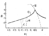
제3도는 기준신호회로의 전형적인 응답곡선을 도시한 것이다. 동조회로는 NTSC 텔레비죤 시스템용의 영상반송파 주파수인 45.75MHz로 등조된다. 응답곡선(40)상에서 45.75MHz이상의 신호주파수의 예리한 롤오프(roll off)로 인한 I.F통과대역의 나이퀴스트 기울기부분(50)이 중첩되어 있다.3 shows a typical response curve of the reference signal circuit. The tuning circuit is tuned to 45.75 MHz, which is the video carrier frequency for NTSC television systems. On the
기준신호내의 구적왜국의 존재는 검파된 비데오신호내에 고조파왜곡을 발생시킬 것이다. 특히, 기준신호내의 43.5MHz측대역들로부터 야기된 구적왜곡은 2.25MHz 합성기본대역 비데오신호의 제2 고조파를 만들게 된다. 이 신호의 제2 고조파는 검파된 인터캐리어 음성신호의 주파수인 4.5MHz가 될 것이다. 이 제2 고조파들은 기본주파수의 14퍼센트인 진폭을 갖고 있지만, 이 작은 신호들은 음성신호내에 버즈를 야기시키기에 충분하다. 이와 비슷한 그러나 약간은 약한 효과가 인터캐리어 음성신호내에서 발생되는 제3고조파를 가지며 44.25MHz의 I.F주파수를 갖는 측대역으로부터 야기된다. 이상적으로는 기준회로내에서 제3도의 응답곡선내에 점선으로된 너치(42로 44)에 표시된 주파수들을 감쇄시키는 것이 바람직하다. 그러나, 본 발명에 따르면, 이와 같은 문제의 해결은 다른 지역내 텔레비젼 수신기에 대한 문제도 동시에 해결함으로써 이루어지게 된다.The presence of quadrature distortion stations in the reference signal will cause harmonic distortion in the detected video signal. In particular, quadrature distortion resulting from the 43.5 MHz sidebands in the reference signal results in a second harmonic of the 2.25 MHz synthesized baseband video signal. The second harmonic of this signal will be 4.5 MHz, which is the frequency of the detected intercarrier speech signal. These second harmonics have an amplitude that is 14 percent of the fundamental frequency, but these small signals are sufficient to cause a buzz in the audio signal. A similar but slightly weak effect results from the sideband with the third harmonic generated in the intercarrier speech signal and with an I. F frequency of 44.25 MHz. Ideally, it is desirable to attenuate the frequencies indicated by the
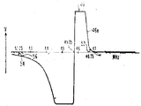
전형적인 AFT응답특성(46)은 제4도에 도시되어 있다. 응답특성은 45.75MHz의 바람직한 주파수부근에서 영상반송파 주파수변화에 대한 예리한 응답을 나타내기 위한 형태로 되어 있다. 이 곡선의 상부기울기(46a)는 I.F휠터회로내 47.25에 인접한 채널음성캐리어를 위치시키므로써, 빨리 롤오프(roll off)된다. 영상반송파주파수 이하에서 I.F대역의 준간을 향해 응답특성은 더욱 점점 롤오프된다. 이 응답특성은 "잡음풀링(pulling)"으로 공지된 것이다.A typical AFT response characteristic 46 is shown in FIG. The response characteristics are in the form of a sharp response to the image carrier frequency change near the desired frequency of 45.75MHz. The upper slope 46a of this curve is rolled off quickly by placing the channel voice carrier adjacent to 47.25 in the I.F filter circuit. Below the image carrier frequency, the response characteristic rolls off more and more toward the quasi-I of the I.F band. This response is known as "pulling".
신호가 약하거나 없는 상태하에서, AFT회로는 동조기가 중간대역을 향하도록 조성된다. 왜냐하면 I.F잡음의 평균주파수가 약 43.5MHz에 위치되고 곡선(46)하부의 영역은 45.75MHz이상의 영역보다 더 크기 때문이다. 그러므로 신호가 약하거나 없는 상태하에서 AFT회로가 45.75MHz 동조전압을 발생시키도록 AFT응답특성이 영상반송파 주파수 주위에서 균형화되게 하는 것이 바람직하다.With the signal weak or absent, the AFT circuit is configured so that the tuner faces the midband. This is because the average frequency of the I.F noise is located at about 43.5 MHz and the area under the curve 46 is larger than the area above 45.75 MHz. Therefore, it is desirable to balance the AFT response characteristics around the image carrier frequency so that the AFT circuit generates a 45.75 MHz tuning voltage with or without a signal.
전형적인 I.F통과대역 응답특성(60)은 제5도에 도시되어 있다. 텔레비젼 수신가가 적당하게 동조되면, 영상반송파는 통과대역의 상부 나이퀴스트 기울기상의 통과대역(60)의 평평한 상부로부터 6dB떨어진 (62)로 도시한 45.75MHz에 위치하게 된다. 이때(64)로 도시된 41.25MHz의 음성반송파는 중간대역직폭으로 부터 약 20dB 떨어진 곳에 위치하게 된다. 이 반송파들이 제4도에 도시한 응답을 갖고있는 AFT회로에 인가되면, 영상반송파는 정확하게 45.75MHz롤 동조하게 되고 음성반송파는 주파수가 너무 낮아 AFT출력전압의 영향을 받지 못하는 주파수에 위치하게 될 것이다.A typical I.F passband response characteristic 60 is shown in FIG. When the television receiver is properly tuned, the video carrier is positioned at 45.75 MHz, shown 62 at 6 dB away from the flat top of the passband 60 on the upper Nyquist slope of the passband. At this time, the voice carrier of 41.25MHz shown in 64 is located about 20 dB away from the middle bandwidth. When these carriers are applied to the AFT circuit with the response shown in Figure 4, the video carrier will tune exactly 45.75 MHz and the voice carrier will be at a frequency that is too low to be affected by the AFT output voltage. .
그러나, 신호가 MATV나 CATV시스템에 의해 공급될때, 생기는 것처럼 비데오신호가 2MHz만큼 주파수가 상방향으로 전이되면, 영상반송파를 탐색하는 동조시스템에 의해 1MHz의 오프셋이 교정되게 될 것이다. AFT회로에 인가되는 신호는 제5도의 (66과 68)의 영상 및 음성반송파위치로 1MHz만큼 오프셋된다. 이렇게 위치하면, 42.25MHz 음성반송파는 중간대역레벨보다 약 6dB만 낮게되고, 46.75영상반송파는 이것의 주파수가 인접채널 음성트랩의 주파수에 접근함에 따라 약 30dB만큼 낮아지게 된다. 이 반송파들이 제4도에 도시한 응답을 갖고있는 AFT회로에 인가되면, 감쇄된 영상반송파는 화살포(52)로 표시한 바와 같이 작은 정(正)동조전압만을 만들게 된다. 주파수 전이음성 반송파는 화살표(54)로 도시한 바와 같이 위치하게 되어 영상반송파에 의해 공급된 것과 비슷한 크기로 된 동조전압에 작은 부(否)전압으로 기여하게 된다.However, if the video signal is shifted upward by 2 MHz as occurs when the signal is supplied by the MATV or CATV system, the 1 MHz offset will be corrected by the tuning system searching for the image carrier. The signal applied to the AFT circuit is offset by 1 MHz to the video and audio carrier positions of (66 and 68) in FIG. In this way, the 42.25 MHz voice carrier is only about 6 dB lower than the midband level, and the 46.75 video carrier is about 30 dB lower as its frequency approaches the frequency of the adjacent channel voice trap. When these carriers are applied to the AFT circuit having the response shown in Fig. 4, the attenuated video carrier produces only a small positive tuning voltage as indicated by the
이 두 동조전압은 서로 효과를 차단시키므로 AFT회로는 오프셋 텔레비젼 신호가 풀(pull)되는 것을 막을 수 있다. 동조시스템이 신호를 탐색할때 동조시스템이 1MHz보정보다 낮게 발생한다면, 두 반송파 주파수는 상측으로 이동되고, 음성 반송파에 의해 공급된 동조전압 성분에는 영상반송파가 우세하게 된다. 이때 AFT회로는 수신기가 45.76영상 반송 파주파수에 동조된 음성반송파로 고정되도록 동조를 조정하려고 할 것이다.Since these two tuning voltages block the effects of each other, the AFT circuit can prevent the offset television signal from being pulled. If the tuning system occurs lower than 1 MHz complement when the tuning system is searching for a signal, the two carrier frequencies are shifted upwards, and the video carrier is predominant in the tuning voltage component supplied by the audio carrier. In this case, the AFT circuit will attempt to adjust the tuning so that the receiver is fixed to the voice carrier tuned to the 45.76 video carrier frequency.
이 문제를 방지하기 위한 한 방법은 제4도에 점선(56)으로 도시한 바와 같은 너치를 오프셋 음성반송파가 위치하게 되는 응답특성 내에 삽입하는 것이다. 그러나, 본 발명의 장치는 상술한 음성 버즈 문제를 해결하고 AFT회로의 잡음플링소거를 개선하는 방법으로 오프셋 반송파 획득문제를 연속적으로 해결하게 된다.One way to avoid this problem is to insert a notch as shown by dashed
본 발명의 원리에 따라 구성된 회로는 제6도에 도시되어 있다. 여기에 도시한 회로는, 칩 외부에 있고, 외부에서 외부 칩단자(7내지 10)에 결합된 동조회로소자(160내지 184)를 제외하면, 단일 모노리딕 집적회로칩상에 유리하게 제조될 수 있다.A circuit constructed in accordance with the principles of the present invention is shown in FIG. The circuit shown here can be advantageously fabricated on a single monolithic integrated circuit chip, except for tuning circuit elements 160 to 184 that are external to the chip and are externally coupled to external chip terminals 7 to 10.
이중 엔디드(ended) I.F신호는 I.F증폭기 (100)로 부터 내부단자(102와 104)에 결합된다. I.F.신호는 동기복조를 하기 위해서 적검파기(130)의 트랜지스터(132와 134)에 인가된다. I.F신호는 적검파기(130)과 AFT위상비교기(150)용 스위칭 신호를 발생시키기 위하여 에미터폴로워 결합트랜지스터(106과 108)를 거쳐 기준 신호회로(110)에 인가된다.The dual ended I.F signal is coupled from the I.F amplifier 100 to the internal terminals 102 and 104. The I.F. signal is applied to the
I.F신호는 기준 신호회로(110)내의 트랜지스터(112와 114)로 구성된 차동증폭기를 구동시킨다. 차동증폭기 트랜지스터(112와 114)의 콜렉터 양단에는 제1 동조회로(160)가 결합되어 있는데 이 동조회로는 외부칩단자(8과 9)에 결합되어 있고 영상반송파주파수(이 예에서는 45.75MHz)로 동조된다. 다이오드(116과 118)는 강함 신호 상태하에서 대부분 구형파 스위칭 신호를 만들도록 기준신호를 제한하거나 클립(clip)시키기 위해서 트랜지스터(112와 114)의 콜렉터 양단에도 결합된다. 구형파 스위칭신호는 동조회로(160)과 결합하여 자동증폭기와 다이오드의 리미터동작에 의하여 최적한 신호상태하에서 I.F영상반송파와 동일한 주파수와 위상으로 될 수 있다.The I.F signal drives a differential amplifier consisting of transistors 112 and 114 in the reference signal circuit 110. A first tuning circuit 160 is coupled across the collectors of the differential amplifier transistors 112 and 114, which are coupled to external chip terminals 8 and 9 and have an image carrier frequency (45.75 MHz in this example). Tuned into Diodes 116 and 118 are also coupled across the collectors of transistors 112 and 114 to limit or clip the reference signal to produce a mostly square wave switching signal under strong signal conditions. The square wave switching signal may be combined with the tuning circuit 160 to have the same frequency and phase as the I.F image carrier under an optimal signal state by the limiter operation of the automatic amplifier and diode.
진폭-제한 스위칭 신호는 에미터폴로워 트랜지스터(122와 124)에 의해 적검파기(130)내에 이중차동 증폭기(136과 138)내에 배열된 4개의 트랜지스터의 베이스 전극들에 인가된다. 차동 증폭기 (136과 138)는 트랜지스터(132와 134)를 거쳐 인가된 푸시-풀 I.F신호에 의해 구동된다. 차동증폭기(136과 138)로 구성된 트랜지스터들은 인입된 신호의 적검파를 이루도록 기준신호에 의해 스위치된다. 각각의 차동증폭기내의 보상 극성스위칭 신호들을 수신하는 이 차동 증폭기 트랜지스터들은 두개의 보상 출력들을 형성하도록 접속된 콜렉터들을 갖고 있다.The amplitude-limiting switching signal is applied by emitter follower transistors 122 and 124 to the base electrodes of four transistors arranged in double differential amplifiers 136 and 138 in red detector 130. Differential amplifiers 136 and 138 are driven by push-pull I. F signals applied via
이 출력들 양단에는 합성 비데오 및 인터캐리어 음성신호가 나타났다. 이 두 출력들은, 원한다면, 검파된 비데오 및 인터케리어 음성 신호들에 대한 단일-앤디드 출력을 만드는 공지된 방법으로 합성될 수 있다. 트랜지스터(112와 114)의 콜렉터에서의 기준신호는 두개의 크랜지스터(142와 144)의 베이스에도 인가된다. 이 트랜지스터들 (142와 144)의 에미터는 함께 결합되고 저항회로(143)에 의해 접지에 결합되므로서 이들의 에미터에서 보상기준 구동신호를 만든다. 이 이중-엔디드 기준신호는 위상비교기(150)의 차동증폭기(156과 158)에 결합된다. 차동증폭기들의 트랜지스터의 베이스들은 I.F 영상반송파와 같은 위상 및 주파수로된 기준신호에 의해 푸시-풀 방법으로 구동된다.Across these outputs was a composite video and intercarrier speech signal. These two outputs can, if desired, be synthesized in a known manner to produce a single-ended output for detected video and intercarrier speech signals. The reference signal at the collector of transistors 112 and 114 is also applied to the base of two transistors 142 and 144. The emitters of these transistors 142 and 144 are coupled together and coupled to ground by a resistor circuit 143 to produce a compensation reference drive signal at their emitters. This double-ended reference signal is coupled to the differential amplifiers 156 and 158 of the
제1동조회로(160) 양단에 나타난 기준 신호는 캐패시터(172와 174)에 의해 기준 신호에 주파수-의존위상 전이를 부과하는 제2 동조회로(180)에 가볍게 결합된다. 영상 반송파가 바람직한 주파수(이 예에서는 45.75MHz)에 있으면, 기준신호는 제2 동조회로에 의해 90°위상전이되며 이 동조회로는 캐패시터(182)와 인덕터(184)를 포함한다. 영상반송파(기준신호)의 주파수가 바람직한 주파수로 변하면, 제2동조 회로는 90°정도로 기준신호의 위상을 전이 시킨다.The reference signal across the first tuning circuit 160 is lightly coupled to the
제2 동조회로(180)는 우선 같이 작은 캐패시터(172와 172)에 의해 제1 동조회로에 가볍게 결합된다. 위상비교기(150)에 더 던 구동신호를 제공하기 위하여 기준동조회로에 AFT동조회로를 더욱 가깝게 결합시켜 기준신호가 감소하게 하는 것이 바람직하다. 기준동조회로는 영상반송파 주파수 부근에서 단일 공진주파수를 갖도록 선계되어 있다. 두개의 동조회로가 아주 가깝게 결합되면, 기준동조회로는 과결합으로 이중-동조된 회로의 응답을 갖게된다 이 이중-험프(hump)응답은 기준회로 내 구적왜곡과 위상비선형성을 야기시켜 검파된 거주파 명도신호의 과도응답이 약하게 된다. 등기검파기의 장점중의 하나는 포락선 검파신호보다 빠른 증가 및 하강시간을 가지며 대칭프리슈트(presboot)와 오버슈트(overshoot)를 갖는 비데오과도 현상을 나태낸다는 것이므로, 두개의 동조회로가 과결합되지 않도록 주의해야 한다. 어떤 경우에 바람직한 단순한 결합이 서로 거의 밀접하게 두개의 동조회로를 위치설정 하므로서 이루어질 수 있으므로, 캐패시터(172와 174)가 필요없게 될 수도 있다.The
제2 동조회로(180)양단에 나타난 위상-전이된 신호는 외부칩단자(7과 10) 및 에미터폴로워 결합트랜지스터(146과 148)를 거쳐 위상검파기(150)에 결합된다. 에미터 폴로워 접지 사이에 결합된 분압기(147)에 의해 제공된다. 분압기(174)로 부터 트랜지스터(148)까지의 D. C선호는 인덕터(184)에 의해 제공된다. 위상-전이된 신호는 에미터폴로워(146과 148)로 부터 차동 결합트랜지스터(152와 154)의 베이스에 결합된다. 트랜지스터(152와 154)는 이것들의 에미터에서 결합되어 일정전류원(153)에 결합된다. 트랜지스터(152)(154)는 이중 차동증폭기(156)(158)를 구동시키기 위해 차동증폭기(156)의 에미터에 연결된 콜렉터들을 갖고있다. 이중 차동증폭기(156)(158)내의 트랜지스터들도 트랜지스터(142와 144)의 베이스 전극에서의 보상신호들에 의해 구동되는데 트랜지스터(142)(144) 각각은 두개의 보상출력을 제공하기 위해 연결된 콜렉터를 가지며, 보상출력에서는 AFT신호가 발생된다. 이 출변들은 공지된 방법에 의해 바람직한 임피던스와 전압범위를 갖는 두개의 반대로 변화하는 AFT출력신호를 차동증폭기에 연결시킬 수도 있다.The phase-shifted signal across the
기준동조회로(160)는 영상반송파주파수, 이 경우에 45.75MHz에 동조되고, 인덕터(162)와 캐패시터(164)를 포함하는 병렬 공진회로를 포함한다. 댐핑저항(168)은 I.F호폭기(100)와 기준회로(110)가 고이득상태로 동작할때 차폐되지 않은 동조회로 (160)내의 발진을 방지하도록 동조회로(160)양단에 결합된다. 쵸크(169)는 트랜지스터(112와 114)의 콜렉터들 사이에 수평 주사주파수 신호들용 저임피던스 신호를 제공하도록 댐핑저항(168)과 병렬로 결합된다.The reference tuning circuit 160 includes a parallel resonant circuit tuned to an image carrier frequency, in this case 45.75 MHz, comprising an inductor 162 and a capacitor 164. Damping resistor 168 is coupled across tuning circuit 160 to prevent oscillation in unshielded tuning circuit 160 when IF amplifier 100 and reference circuit 110 operate at high gain. . Choke 169 is coupled in parallel with damping resistor 168 to provide a low impedance signal for horizontal scan frequency signals between collectors of transistors 112 and 114.
이 쵸크는 기준회로(110)가 수평주사주파수에서 링잉(ringing)하지 못하게 하여, 커네스코포상의 재생된 영상내에서 수직바(bars)로서 나타나는 고조파를 만든다.This choke prevents the reference circuit 110 from ringing at the horizontal scan frequency, creating harmonics that appear as vertical bars in the reproduced image on the Cannesco.
본 발명에 따르면, 기준동조회로는 병력 공진회로인 (162, 164)의 유효인덕턴스와 캐패시터(166)를 포함하위 트랙회로를 포함한다.According to the present invention, the reference tuning circuit includes a sub track circuit including an effective inductance of the force resonance circuits 162 and 164 and a capacitor 166.
캐패시터(166)은 인덕터(162)와 캐패시터(164)의 한 접합부와 단자(8)사이에 결합되고, 인덕터(162)와 캐패시터(164)의 다른 접합부는 단자(9)에 결합된다. 트랩 회로는 1MHz오프셋 음성반송파(42.25MHz)주파수의 중간인 주파수에서 기준회로응답내에 너치를 발생시키도록 동조되며, 영상신호측대역주파수는 검파에 의해 인터캐리어 음성 제2 부고조파 주파수(43.5MHz)에 대응되는 비데오 신호로 된다. 너치는 충분히 넓어 이들 양 주파수에서 충분히 감쇄된다. 이 동조 회로에 의해 생긴 기준 신호는 음성버즈 문제를 야기시키는 제2 고조파를 발생시키는 주파수에서 특히 감소된 구적왜곡을 갖게된다. 기준신호는 칼라부반송파의 주파수 (42.17MHz)에서 감쇄되어 검파된 비데오 신호내에 생기는 색도-음성 비트 문제를 최소화시킨다.Capacitor 166 is coupled between inductor 162 and one junction of capacitor 164 and terminal 8, and the other junction of inductor 162 and capacitor 164 is coupled to terminal 9. The trap circuit is tuned to generate a nugget in the reference circuit response at a frequency intermediate to the 1 MHz offset voice carrier (42.25 MHz) frequency, and the image signal sideband frequency is detected by intercarrier audio second subharmonic frequency (43.5 MHz). It becomes a video signal corresponding to. The notch is wide enough to attenuate sufficiently at these frequencies. The reference signal generated by this tuning circuit has a particularly reduced quadrature distortion at frequencies that produce a second harmonic that causes voice buzz problems. The reference signal is attenuated at the frequency of the color subcarrier (42.17 MHz) to minimize the chroma-to-speech bit problem in the detected video signal.
또한 동조회로(160)로 부터 제2 동조회로(180)에 결합되는 기준신호도 주파수너치를 나타내며, 이 주파수너치는 AFT응답특성의 중간대역 부분의 폭을 감소시킨다. 그러므로, 두개의 AFT응답 특성은 균형화되고, 바람직한 영상반송파주파수의 반대측상의 풀-인(pull-in) 범위가 둘다 같게 되므로, 회로는 잡음풀링에 더욱 무관하게 된다. 너치는 42.25MHz에서 오프셋 음성반송파가 AFT전압에 기여를 못하게 하므로써 AFT회로가 46.75MHz의 주파수 오프셋 영상 반송파를 얻을 수 있게 한다.In addition, the reference signal coupled from the tuning circuit 160 to the
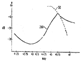
제6도의 회로가 구성이 되어 시험되고, 이에 따른 결과는 제7도 및 제8도의 응답 곡선으로 기록되었다. 기준 동조회로 응답 특성(200)은 I.F통과대역의 나이퀴스트 기울기(50)위에 중첩되어 제7도에 도시되어 있다. 기준 트랩에 의해 생긴 너치는 42.9에 위치하게 되어, 인터캐리어 음성 제2 부고조파주파수(43.5MHz)에 대응하는 영상신호 측대역 주파수를 32dB(제3도의 동일주파수에서의 감쇄레벨은 16dB)감쇄시킨다. 검파에 의해 인터캐리어 제3 부고조파 주파수인 44.25MHz에 대응하는 비데오 신호로 리는 영상신호 즉 대역주파수는 제3도에서의 감쇄레벨 14dB에 비해 제7도에서는 25dB만큼 감쇄된다. 제7도에서, 기준동조회로 응답곡선이 I.F통과대역의 나이퀴스트 기울기에 합성될때, 합성응 답은 45.75MHz의 I.F영상반송주파수 주위에서 대칭되어, 비데오 측대역을 균형화시키는 진폭에 의해 기준회로내에의 구적왜곡을 감소 시킨다.The circuit of FIG. 6 was constructed and tested, and the result was recorded with the response curves of FIG. 7 and FIG. The reference tuner response characteristic 200 is shown in FIG. 7 overlaid on the
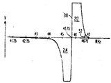
AFT응답의 기준동조회로 트랩의 효과는 제8도 도시되어 있다. AFT응답 곡선(210)은 균형화된 것으로 보이고, 응답곡선(210)과 기준축 사이에 두개의 같은 정 및 부풀-인 영역(212 및 214)를 갖고 있다. 영상 반송주파수의 두 측면상의 동일한 풀-인 영역들은 AFT회로가 잡음풀링에 무관하게 되도록 한다. 또한 넓은 너치는 1MHz오프셋 음성반송파 주파수인 42.25MHz에서 임의의 전압이 기여하는 것을 제거시킨다. 이는 기준동조회로트랩의 너치가 위상검파기(158)내의 차동증폭기(156)(158)에 연결되는 기준신호 및 제2 동조회로(180)를 거쳐 위상검파기(150)에 인가되는 위상전된 기준신호에 영향을 미치기 때문이다. 그러므로, 음성반송파는 자동주파수 제어신호를 발생시키기 위해 위상검파기(150)에 인가되는 두 신호를 트랩아웃(trap-out)시킨다.The effect of the reference tuning circuit trap of the AFT response is shown in FIG. The
이것은 특히 AFT회로가 FS동조 시스템에 결합해서 사용될때 중요하다. FS시스템의 안정도는 제8도에 45.75MHz로 도시된 바람직한 영상반송파주파수 부근의 AFT응답곡선(210)의 선형성에 의존한다. 음성반송파가 AFT검파기 입력을 트랩아웃 할때, 발생된 제어신호는 영상반송파에서 응답하므로, 응답곡선(210)과 일치하는 선형 응답을 만든다. 음성반송파가 AFT검파기 입력을 트랩 아웃하면, 음성반송파는 제어신호에 전압기여를 하게하고 이 전압분배에 의해 45.75MHz부근에서 제어신호의 선형성을 방해된다. 따라서 FS동조기의 안정도는 나쁘게 영향을 받게될 것이다. 그러므로 본 발명의 AFT회로는 46.75 MHz에서 1MHz오프셋 영상반송파에 의해 제어되어, 동조기는 이 오프셋 신호를 성공적으로 얻을 수 있게된다.This is especially important when AFT circuits are used in conjunction with FS tuning systems. The stability of the FS system depends on the linearity of the
본 발명의 동조회로의 교체 실시예는 제9도에 도시되어 있다. 이 실시예는 캐패시터(164)가 단자(8과 9)양단의 캐패시터(166)와 인덕터(162)의 직렬결합에 병렬로 연결된다는 것이 제6도의 배열과 다르다. 캐패시터(164)와 인덕터의 유효인덕턴스(162) 및 캐패시터(166)의 결합은 영상반송파주파수에서 공진되고, 인덕터(162)와 캐패시터(166)의 결합은 상술한 중간 주파수에서 트랩핑을 제공한다. 나머지 소자들은 제6도에 도시한 것과 동일한 형태로 배열될 수 있고 동일 기준번호를 붙였다.An alternative embodiment of the tuning circuit of the present invention is shown in FIG. This embodiment differs from the arrangement of FIG. 6 in that the capacitor 164 is connected in parallel to the series coupling of the capacitor 166 and the inductor 162 across the terminals 8 and 9. The combination of the capacitor 164 and the effective inductance 162 of the inductor and the capacitor 166 is resonant at the image carrier frequency, and the combination of the inductor 162 and the capacitor 166 provides trapping at the intermediate frequency described above. The remaining elements can be arranged in the same form as shown in Fig. 6 and given the same reference numerals.
본 발명은 PAL규격에 의해 동조주파수를 재조정하므로서 PAL텔레비죤 시스템을 사용할 때 쉽게 구성될 수 있다. 이때 기준동조회로는 38.9 MHz의 PAL I.F영상 반송파 주파수에서 공진된다. PAL음성 반송파는 33.4MHz에 위치하므로 인터케리어 음성신호는 5.5MHz의 기본주파수와, I.F대역내의 36.15MHz의 제2 부고조파 주파수를 갖는다. 그러므로 기준동조회로너치는 1MHz만큼 오프셋된 음성반송파의 중간인 34.4MHz에 있게되고, I.F주파수는 인터캐리어 음성주파수 36.15MHz에서 제2 고조파를 갖고 있는 비데오 신호를 대응한다. 제2 종조회로는 PAL I.F영상 반송파 주파수에서 90°위상전이를 하도록 재동조 되어야만 한다.The present invention can be easily configured when using a PAL television system by readjusting the tuning frequency according to the PAL standard. At this time, the reference tuning circuit resonates at the PAL I.F image carrier frequency of 38.9 MHz. Since the PAL speech carrier is located at 33.4 MHz, the intercarrier speech signal has a fundamental frequency of 5.5 MHz and a second sub-harmonic frequency of 36.15 MHz in the I.F band. Therefore, the reference tuning circuit nugget is at 34.4 MHz, which is the middle of the voice carrier offset by 1 MHz, and the I.F frequency corresponds to the video signal having the second harmonic at the intercarrier voice frequency 36.15 MHz. The second slave circuit must be retuned to achieve a 90 ° phase transition at the PAL I.F image carrier frequency.
제6도에 도시한 본 발명의 실시예에서, 적검파기(130)는 비데오 및 인터캐리어 음성신호를 검파한다. 이는 특수한 실시예에서 비데오를 검파하기 전에 분리 채널에서 음성정보를 처리하도록 하는 것이 바람직하다. 이러한 실시예에서, 음성반송파는 기준신호 및 비데오와 AFT검파를 하기전에 IF신호로 부터 트랩될 수 있다. AFT검파기에 의한 음성 버즈나 음성 반송파획득의 문제는 결과적으로 나타나지 않게된다. 그러나, 본 발명의 신규한 선택회로는 텔레비죤 수상기에서 기준신호내의 영상반송파 주위의 비데오 측대역을 균형화시키는데 바람직하게 된다. 너치된 기준신호는 이미 기술한 바와 같이, 바람직한 영상반송파 주파수 주위에서 AFT응답특성을 균형화시킨다. 그러므로 선택회로는 텔레비죤 수상기용 비데오 검파기 내의 구적왜곡을 감소시키며 AFT잡음면역을 개선하여 준다.In the embodiment of the present invention shown in FIG. 6, the red detector 130 detects video and intercarrier speech signals. This may be desirable in certain embodiments to process voice information in a separate channel before detecting the video. In this embodiment, the voice carrier can be trapped from the IF signal before the reference signal and the video and AFT detection. The problem of voice buzz or voice carrier acquisition by the AFT detector is not seen as a result. However, the novel selection circuit of the present invention is desirable to balance video sidebands around an image carrier in a reference signal in a television receiver. The notched reference signal, as already described, balances the AFT response characteristics around the desired image carrier frequency. Therefore, the selection circuit reduces quadrature distortion in the video detector for television receivers and improves the AFT noise immunity.
기준채널에서는 음성반송파 주파수를 감쇄시킬 필요가 없기 때문에, 동조회로(160)의 트랩은 NTSC시스템에서는 43.5MHz에서 동되조며 이 주파수는 음성 및 영상 반송파 주파수와 동일하다. 트랩회로의 Q는 제6도의 실시예에서 보다 높게 될 것이다.Since it is not necessary to attenuate the voice carrier frequency in the reference channel, the trap of the tuning circuit 160 is synchronized at 43.5 MHz in the NTSC system, and this frequency is the same as the audio and video carrier frequency. The Q of the trap circuit will be higher in the embodiment of FIG.
Claims (1)
Applications Claiming Priority (2)
| Application Number | Priority Date | Filing Date | Title |
|---|---|---|---|
| US70903 | 1979-08-29 | ||
| US06/070,903 US4263611A (en) | 1979-08-29 | 1979-08-29 | Television signal processing system |
Publications (1)
| Publication Number | Publication Date |
|---|---|
| KR840000112B1 true KR840000112B1 (en) | 1984-02-11 |
Family
ID=22098069
Family Applications (1)
| Application Number | Title | Priority Date | Filing Date |
|---|---|---|---|
| KR1019800003410A KR840000112B1 (en) | 1979-08-29 | 1980-08-28 | Televizion signal processing system |
Country Status (22)
| Country | Link |
|---|---|
| US (1) | US4263611A (en) |
| JP (1) | JPS5636274A (en) |
| KR (1) | KR840000112B1 (en) |
| AT (1) | AT389198B (en) |
| AU (1) | AU530505B2 (en) |
| BE (1) | BE884972A (en) |
| CA (1) | CA1147453A (en) |
| DE (1) | DE3032622C2 (en) |
| DK (1) | DK159236C (en) |
| ES (1) | ES494570A0 (en) |
| FI (1) | FI70356C (en) |
| FR (1) | FR2464610B1 (en) |
| GB (1) | GB2059700B (en) |
| HK (1) | HK8485A (en) |
| IT (1) | IT1132559B (en) |
| MY (1) | MY8500731A (en) |
| NL (1) | NL190216C (en) |
| NZ (1) | NZ194799A (en) |
| PT (1) | PT71720B (en) |
| SE (1) | SE447779B (en) |
| SG (1) | SG87184G (en) |
| SU (1) | SU1326206A3 (en) |
Families Citing this family (12)
| Publication number | Priority date | Publication date | Assignee | Title |
|---|---|---|---|---|
| US4388649A (en) * | 1981-06-01 | 1983-06-14 | Rca Corporation | AFT Lockout prevention system |
| US4502078A (en) * | 1982-02-22 | 1985-02-26 | Rca Corporation | Digital television receivers |
| GB2126812B (en) * | 1982-08-30 | 1986-05-08 | Rca Corp | Television sound detection system using a phase-locked loop |
| US4513323A (en) * | 1982-11-30 | 1985-04-23 | Rca Corporation | Buzz reduction for intercarrier type television sound detection |
| DE3504045A1 (en) * | 1985-02-04 | 1986-08-07 | Schering AG, 1000 Berlin und 4709 Bergkamen | METHOD FOR PRODUCING SS CARBOLINES BY DEHYDRATION |
| US4639786A (en) * | 1985-10-23 | 1987-01-27 | Rca Corporation | Television sound signal processor |
| US4814887A (en) * | 1988-05-23 | 1989-03-21 | General Instrument Corporation | Automatic frequency control |
| US4974087A (en) * | 1989-04-13 | 1990-11-27 | Rca Licensing Corporation | Parallel sound if with reference carrier derived from quasi-synchronous video detector |
| JPH0398514U (en) * | 1990-01-30 | 1991-10-14 | ||
| US5177613A (en) * | 1990-02-26 | 1993-01-05 | Thomson Consumer Electronics, Inc. | Quasi-parallel if with shared saw filter |
| KR100607837B1 (en) * | 1997-07-25 | 2006-08-04 | 코닌클리케 필립스 일렉트로닉스 엔.브이. | A receiver and a method for receiving a modulated carrier having asymmetrical sidebands, and an integrated circuit for processing a method carrier having asymmetrical sidebands |
| EP1798854A1 (en) * | 2005-12-14 | 2007-06-20 | Dibcom | Enhanced low noise amplifier |
Family Cites Families (9)
| Publication number | Priority date | Publication date | Assignee | Title |
|---|---|---|---|---|
| US3697685A (en) * | 1970-04-13 | 1972-10-10 | Motorola Inc | Synchronous am detector |
| US3760094A (en) * | 1971-02-18 | 1973-09-18 | Zenith Radio Corp | Automatic fine tuning with phase-locked loop and synchronous detection |
| NL173342C (en) * | 1973-08-03 | 1984-06-18 | Philips Nv | TV RECEIVER WITH AN AUTOMATIC TUNING CORRECTION SWITCH. |
| JPS5058623U (en) * | 1974-04-09 | 1975-05-31 | ||
| JPS5318912A (en) * | 1976-08-05 | 1978-02-21 | Hitachi Ltd | Signal reception circuit of television receiver |
| NL7613946A (en) * | 1976-12-16 | 1978-06-20 | Philips Nv | TELEVISION RECEIVER WITH A DEMODULATOR CIRCUIT FOR DEMODULATING A CARRIER WAVE MODULATED TELEVISION SIGNAL. |
| DE2657869C3 (en) * | 1976-12-21 | 1979-12-13 | Norddeutsche Mende Rundfunk Kg, 2800 Bremen | Circuit arrangement for automatic retuning of a receiver oscillator |
| JPS5386116A (en) * | 1977-01-07 | 1978-07-29 | Hitachi Ltd | Video synchronous detector |
| US4091421A (en) * | 1977-04-28 | 1978-05-23 | Zenith Radio Corporation | Television AFC system having complementary sound and picture carrier control effects |
-
1979
- 1979-08-29 US US06/070,903 patent/US4263611A/en not_active Expired - Lifetime
-
1980
- 1980-08-13 IT IT24147/80A patent/IT1132559B/en active
- 1980-08-19 CA CA000358607A patent/CA1147453A/en not_active Expired
- 1980-08-21 PT PT71720A patent/PT71720B/en unknown
- 1980-08-21 GB GB8027185A patent/GB2059700B/en not_active Expired
- 1980-08-22 FI FI802659A patent/FI70356C/en not_active IP Right Cessation
- 1980-08-22 AU AU61684/80A patent/AU530505B2/en not_active Expired
- 1980-08-22 SE SE8005897A patent/SE447779B/en not_active IP Right Cessation
- 1980-08-27 FR FR8018601A patent/FR2464610B1/en not_active Expired
- 1980-08-28 JP JP11964980A patent/JPS5636274A/en active Granted
- 1980-08-28 NL NL8004885A patent/NL190216C/en not_active IP Right Cessation
- 1980-08-28 BE BE0/201906A patent/BE884972A/en not_active IP Right Cessation
- 1980-08-28 ES ES494570A patent/ES494570A0/en active Granted
- 1980-08-28 KR KR1019800003410A patent/KR840000112B1/en active
- 1980-08-28 NZ NZ194799A patent/NZ194799A/en unknown
- 1980-08-28 DK DK367180A patent/DK159236C/en not_active IP Right Cessation
- 1980-08-28 SU SU802977043A patent/SU1326206A3/en active
- 1980-08-29 AT AT0438980A patent/AT389198B/en not_active IP Right Cessation
- 1980-08-29 DE DE3032622A patent/DE3032622C2/en not_active Expired
-
1984
- 1984-12-04 SG SG871/84A patent/SG87184G/en unknown
-
1985
- 1985-01-31 HK HK84/85A patent/HK8485A/en not_active IP Right Cessation
- 1985-12-30 MY MY731/85A patent/MY8500731A/en unknown
Also Published As
Similar Documents
| Publication | Publication Date | Title |
|---|---|---|
| KR820002355B1 (en) | Aft circuit | |
| KR920002046B1 (en) | Receiver | |
| KR840000112B1 (en) | Televizion signal processing system | |
| US4945313A (en) | Synchronous demodulator having automatically tuned band-pass filter | |
| US3787612A (en) | Signal processing system for television receiver having acoustic surface wave devices for improved tuning and video demodulation | |
| US4322751A (en) | Detector circuit for a television receiver | |
| KR890000018B1 (en) | Television automatic flesh color correction system | |
| US3872497A (en) | Signal translating apparatus for composite signal subject to jitter | |
| US3742130A (en) | Television receiver incorporating synchronous detection | |
| US3946148A (en) | Television receiver operable in exact or extended range tuning modes | |
| US4660088A (en) | Quasi-parallel television if suitable for stereo sound reception | |
| US5644368A (en) | Composite signal detecting apparatus having associated filter | |
| US4091421A (en) | Television AFC system having complementary sound and picture carrier control effects | |
| US4850039A (en) | Transistor mixer | |
| US4366498A (en) | I.F. Response control system for a television receiver | |
| US3518363A (en) | Hue control circuitry | |
| US3375325A (en) | Intercarrier television receiver afc circuit | |
| JPS6123849Y2 (en) | ||
| KR930004655Y1 (en) | Tv receiver | |
| JPH09186527A (en) | Device of phase shift fixed loop type to demodulate frequency-modulated signal | |
| KR850000272Y1 (en) | Television receiver | |
| US6169585B1 (en) | Circuit arrangement for demodulating an intermediate-frequency video signal | |
| US4547805A (en) | Television AFC system usable with offset carrier frequencies | |
| KR830000899B1 (en) | Frequency tracking circuit | |
| JPH0362074B2 (en) |