KR20240037943A - imaging device - Google Patents
imaging device Download PDFInfo
- Publication number
- KR20240037943A KR20240037943A KR1020247000479A KR20247000479A KR20240037943A KR 20240037943 A KR20240037943 A KR 20240037943A KR 1020247000479 A KR1020247000479 A KR 1020247000479A KR 20247000479 A KR20247000479 A KR 20247000479A KR 20240037943 A KR20240037943 A KR 20240037943A
- Authority
- KR
- South Korea
- Prior art keywords
- filter
- light
- refractive index
- imaging device
- guide member
- Prior art date
Links
- 238000003384 imaging method Methods 0.000 title claims abstract description 178
- 238000006243 chemical reaction Methods 0.000 claims abstract description 45
- 238000010586 diagram Methods 0.000 description 42
- 238000012986 modification Methods 0.000 description 35
- 230000004048 modification Effects 0.000 description 35
- 238000001514 detection method Methods 0.000 description 24
- 238000012545 processing Methods 0.000 description 24
- 238000004891 communication Methods 0.000 description 18
- 238000005516 engineering process Methods 0.000 description 18
- 239000004065 semiconductor Substances 0.000 description 15
- 239000000758 substrate Substances 0.000 description 14
- 239000010410 layer Substances 0.000 description 12
- 230000003287 optical effect Effects 0.000 description 12
- 230000006870 function Effects 0.000 description 10
- 230000000903 blocking effect Effects 0.000 description 9
- VYPSYNLAJGMNEJ-UHFFFAOYSA-N Silicium dioxide Chemical compound O=[Si]=O VYPSYNLAJGMNEJ-UHFFFAOYSA-N 0.000 description 8
- 229910052814 silicon oxide Inorganic materials 0.000 description 8
- 210000001519 tissue Anatomy 0.000 description 8
- 230000005540 biological transmission Effects 0.000 description 6
- 239000000463 material Substances 0.000 description 6
- 238000000034 method Methods 0.000 description 6
- 238000002156 mixing Methods 0.000 description 6
- 230000008859 change Effects 0.000 description 5
- 230000000694 effects Effects 0.000 description 5
- 238000002674 endoscopic surgery Methods 0.000 description 5
- 238000001356 surgical procedure Methods 0.000 description 5
- 230000005284 excitation Effects 0.000 description 4
- 230000007246 mechanism Effects 0.000 description 4
- 229910021420 polycrystalline silicon Inorganic materials 0.000 description 4
- 229920005591 polysilicon Polymers 0.000 description 4
- 229910052581 Si3N4 Inorganic materials 0.000 description 3
- 238000010336 energy treatment Methods 0.000 description 3
- 239000011159 matrix material Substances 0.000 description 3
- 230000008569 process Effects 0.000 description 3
- HQVNEWCFYHHQES-UHFFFAOYSA-N silicon nitride Chemical compound N12[Si]34N5[Si]62N3[Si]51N64 HQVNEWCFYHHQES-UHFFFAOYSA-N 0.000 description 3
- XUIMIQQOPSSXEZ-UHFFFAOYSA-N Silicon Chemical compound [Si] XUIMIQQOPSSXEZ-UHFFFAOYSA-N 0.000 description 2
- 229910021417 amorphous silicon Inorganic materials 0.000 description 2
- 210000004204 blood vessel Anatomy 0.000 description 2
- 239000003153 chemical reaction reagent Substances 0.000 description 2
- 239000010949 copper Substances 0.000 description 2
- 238000005401 electroluminescence Methods 0.000 description 2
- MOFVSTNWEDAEEK-UHFFFAOYSA-M indocyanine green Chemical compound [Na+].[O-]S(=O)(=O)CCCCN1C2=CC=C3C=CC=CC3=C2C(C)(C)C1=CC=CC=CC=CC1=[N+](CCCCS([O-])(=O)=O)C2=CC=C(C=CC=C3)C3=C2C1(C)C MOFVSTNWEDAEEK-UHFFFAOYSA-M 0.000 description 2
- 229960004657 indocyanine green Drugs 0.000 description 2
- 238000009434 installation Methods 0.000 description 2
- 239000011229 interlayer Substances 0.000 description 2
- 230000001678 irradiating effect Effects 0.000 description 2
- 229910052710 silicon Inorganic materials 0.000 description 2
- 239000010703 silicon Substances 0.000 description 2
- RYGMFSIKBFXOCR-UHFFFAOYSA-N Copper Chemical compound [Cu] RYGMFSIKBFXOCR-UHFFFAOYSA-N 0.000 description 1
- 235000004522 Pentaglottis sempervirens Nutrition 0.000 description 1
- BOTDANWDWHJENH-UHFFFAOYSA-N Tetraethyl orthosilicate Chemical compound CCO[Si](OCC)(OCC)OCC BOTDANWDWHJENH-UHFFFAOYSA-N 0.000 description 1
- 230000001133 acceleration Effects 0.000 description 1
- 230000009471 action Effects 0.000 description 1
- 229910052782 aluminium Inorganic materials 0.000 description 1
- XAGFODPZIPBFFR-UHFFFAOYSA-N aluminium Chemical compound [Al] XAGFODPZIPBFFR-UHFFFAOYSA-N 0.000 description 1
- 230000003321 amplification Effects 0.000 description 1
- 230000000740 bleeding effect Effects 0.000 description 1
- 230000003139 buffering effect Effects 0.000 description 1
- 238000002485 combustion reaction Methods 0.000 description 1
- 230000000295 complement effect Effects 0.000 description 1
- 239000002131 composite material Substances 0.000 description 1
- 229910052802 copper Inorganic materials 0.000 description 1
- 238000012937 correction Methods 0.000 description 1
- 238000013461 design Methods 0.000 description 1
- 238000002073 fluorescence micrograph Methods 0.000 description 1
- 230000004313 glare Effects 0.000 description 1
- 239000011521 glass Substances 0.000 description 1
- 229910000449 hafnium oxide Inorganic materials 0.000 description 1
- WIHZLLGSGQNAGK-UHFFFAOYSA-N hafnium(4+);oxygen(2-) Chemical compound [O-2].[O-2].[Hf+4] WIHZLLGSGQNAGK-UHFFFAOYSA-N 0.000 description 1
- 238000005286 illumination Methods 0.000 description 1
- 238000002955 isolation Methods 0.000 description 1
- 230000031700 light absorption Effects 0.000 description 1
- 239000004973 liquid crystal related substance Substances 0.000 description 1
- 238000012423 maintenance Methods 0.000 description 1
- 229910044991 metal oxide Inorganic materials 0.000 description 1
- 150000004706 metal oxides Chemical class 0.000 description 1
- 239000003595 mist Substances 0.000 description 1
- 230000000116 mitigating effect Effects 0.000 description 1
- 239000000203 mixture Substances 0.000 description 1
- 210000004877 mucosa Anatomy 0.000 description 1
- 238000003199 nucleic acid amplification method Methods 0.000 description 1
- 239000013307 optical fiber Substances 0.000 description 1
- 230000001151 other effect Effects 0.000 description 1
- JMOHEPRYPIIZQU-UHFFFAOYSA-N oxygen(2-);tantalum(2+) Chemical compound [O-2].[Ta+2] JMOHEPRYPIIZQU-UHFFFAOYSA-N 0.000 description 1
- 230000002093 peripheral effect Effects 0.000 description 1
- 238000007789 sealing Methods 0.000 description 1
- 238000000926 separation method Methods 0.000 description 1
- 230000035939 shock Effects 0.000 description 1
- LIVNPJMFVYWSIS-UHFFFAOYSA-N silicon monoxide Chemical compound [Si-]#[O+] LIVNPJMFVYWSIS-UHFFFAOYSA-N 0.000 description 1
- 239000002356 single layer Substances 0.000 description 1
- 239000002344 surface layer Substances 0.000 description 1
- 230000002123 temporal effect Effects 0.000 description 1
- OGIDPMRJRNCKJF-UHFFFAOYSA-N titanium(II) oxide Chemical compound [Ti]=O OGIDPMRJRNCKJF-UHFFFAOYSA-N 0.000 description 1
- 238000012546 transfer Methods 0.000 description 1
- WFKWXMTUELFFGS-UHFFFAOYSA-N tungsten Chemical compound [W] WFKWXMTUELFFGS-UHFFFAOYSA-N 0.000 description 1
- 229910052721 tungsten Inorganic materials 0.000 description 1
- 239000010937 tungsten Substances 0.000 description 1
- 239000011800 void material Substances 0.000 description 1
Images


Classifications
-
- H—ELECTRICITY
- H01—ELECTRIC ELEMENTS
- H01L—SEMICONDUCTOR DEVICES NOT COVERED BY CLASS H10
- H01L27/00—Devices consisting of a plurality of semiconductor or other solid-state components formed in or on a common substrate
- H01L27/14—Devices consisting of a plurality of semiconductor or other solid-state components formed in or on a common substrate including semiconductor components sensitive to infrared radiation, light, electromagnetic radiation of shorter wavelength or corpuscular radiation and specially adapted either for the conversion of the energy of such radiation into electrical energy or for the control of electrical energy by such radiation
- H01L27/144—Devices controlled by radiation
- H01L27/146—Imager structures
- H01L27/14601—Structural or functional details thereof
- H01L27/1462—Coatings
- H01L27/14621—Colour filter arrangements
-
- G—PHYSICS
- G02—OPTICS
- G02B—OPTICAL ELEMENTS, SYSTEMS OR APPARATUS
- G02B5/00—Optical elements other than lenses
- G02B5/20—Filters
-
- H—ELECTRICITY
- H01—ELECTRIC ELEMENTS
- H01L—SEMICONDUCTOR DEVICES NOT COVERED BY CLASS H10
- H01L27/00—Devices consisting of a plurality of semiconductor or other solid-state components formed in or on a common substrate
- H01L27/14—Devices consisting of a plurality of semiconductor or other solid-state components formed in or on a common substrate including semiconductor components sensitive to infrared radiation, light, electromagnetic radiation of shorter wavelength or corpuscular radiation and specially adapted either for the conversion of the energy of such radiation into electrical energy or for the control of electrical energy by such radiation
- H01L27/144—Devices controlled by radiation
- H01L27/146—Imager structures
- H01L27/14601—Structural or functional details thereof
- H01L27/14625—Optical elements or arrangements associated with the device
-
- H—ELECTRICITY
- H01—ELECTRIC ELEMENTS
- H01L—SEMICONDUCTOR DEVICES NOT COVERED BY CLASS H10
- H01L27/00—Devices consisting of a plurality of semiconductor or other solid-state components formed in or on a common substrate
- H01L27/14—Devices consisting of a plurality of semiconductor or other solid-state components formed in or on a common substrate including semiconductor components sensitive to infrared radiation, light, electromagnetic radiation of shorter wavelength or corpuscular radiation and specially adapted either for the conversion of the energy of such radiation into electrical energy or for the control of electrical energy by such radiation
- H01L27/144—Devices controlled by radiation
- H01L27/146—Imager structures
- H01L27/14601—Structural or functional details thereof
- H01L27/14638—Structures specially adapted for transferring the charges across the imager perpendicular to the imaging plane
-
- H—ELECTRICITY
- H01—ELECTRIC ELEMENTS
- H01L—SEMICONDUCTOR DEVICES NOT COVERED BY CLASS H10
- H01L27/00—Devices consisting of a plurality of semiconductor or other solid-state components formed in or on a common substrate
- H01L27/14—Devices consisting of a plurality of semiconductor or other solid-state components formed in or on a common substrate including semiconductor components sensitive to infrared radiation, light, electromagnetic radiation of shorter wavelength or corpuscular radiation and specially adapted either for the conversion of the energy of such radiation into electrical energy or for the control of electrical energy by such radiation
- H01L27/144—Devices controlled by radiation
- H01L27/146—Imager structures
- H01L27/14643—Photodiode arrays; MOS imagers
Abstract
본 개시의 일 실시 형태의 촬상 장치는, 입사광에 대하여 제1 굴절률을 갖는 제1 필터와, 상기 제1 필터를 투과한 광을 광전 변환하는 제1 광전 변환부와, 입사광에 대하여 상기 제1 굴절률보다도 낮은 제2 굴절률을 갖고, 상기 제1 필터와 인접하는 제2 필터와, 상기 제2 필터를 투과한 광을 광전 변환하는 제2 광전 변환부와, 상기 제1 필터에서 볼 때 상기 제1 광전 변환부와 반대측에 마련되고, 입사광에 대하여 제3 굴절률을 갖는 제1 매질과, 상기 제2 필터에서 볼 때 상기 제2 광전 변환부와 반대측에 마련되고, 입사광에 대하여 상기 제3 굴절률보다도 높은 제4 굴절률을 갖는 제2 매질을 구비한다.An imaging device according to an embodiment of the present disclosure includes a first filter having a first refractive index with respect to incident light, a first photoelectric conversion unit that photoelectrically converts light that has passed through the first filter, and a first refractive index with respect to incident light. A second filter having a lower second refractive index and adjacent to the first filter, a second photoelectric conversion unit for photoelectrically converting the light transmitted through the second filter, and a second photoelectric conversion unit that converts light transmitted through the second filter into a photoelectric device, and when viewed from the first filter, the first photoelectric converter A first medium provided on the opposite side of the conversion unit and having a third refractive index with respect to incident light, and a second medium provided on the opposite side from the second photoelectric conversion unit when viewed from the second filter and having a higher refractive index than the third refractive index with respect to incident light. A second medium having a refractive index of 4 is provided.
Description
본 개시는, 촬상 장치에 관한 것이다.This disclosure relates to an imaging device.
절연막이 매립되어 형성된 소자 분리부에 의해 화소 분리가 된 촬상 장치가 제안되어 있다(특허문헌 1).An imaging device in which pixels are separated by an element isolation portion formed by embedding an insulating film has been proposed (Patent Document 1).
촬상 장치에서는, 입사광을 효율적으로 수광하는 것이 요구되고 있다.In imaging devices, it is required to efficiently receive incident light.
효율적으로 수광 가능한 촬상 장치를 제공하는 것이 요망된다.It is desired to provide an imaging device capable of efficiently receiving light.
본 개시의 일 실시 형태로서의 촬상 장치는, 입사광에 대하여 제1 굴절률을 갖는 제1 필터와, 제1 필터를 투과한 광을 광전 변환하는 제1 광전 변환부와, 입사광에 대하여 제1 굴절률보다도 낮은 제2 굴절률을 갖고, 제1 필터와 인접하는 제2 필터와, 제2 필터를 투과한 광을 광전 변환하는 제2 광전 변환부와, 제1 필터에서 볼 때 제1 광전 변환부와 반대측에 마련되고, 입사광에 대하여 제3 굴절률을 갖는 제1 매질과, 제2 필터에서 볼 때 제2 광전 변환부와 반대측에 마련되고, 입사광에 대하여 제3 굴절률보다도 높은 제4 굴절률을 갖는 제2 매질을 구비한다.An imaging device according to an embodiment of the present disclosure includes a first filter having a first refractive index with respect to incident light, a first photoelectric conversion unit that photoelectrically converts light that has passed through the first filter, and a first refractive index lower than the first refractive index with respect to incident light. A second filter having a second refractive index and adjacent to the first filter, a second photoelectric conversion unit for photoelectrically converting the light passing through the second filter, and provided on the opposite side of the first photoelectric conversion unit when viewed from the first filter. and a first medium having a third refractive index for incident light, and a second medium provided on the opposite side of the second photoelectric conversion unit when viewed from the second filter and having a fourth refractive index higher than the third refractive index for incident light. do.
도 1은 본 개시의 실시 형태에 따른 촬상 장치의 전체 구성의 일례를 나타내는 블록도이다.
도 2는 본 개시의 실시 형태에 따른 촬상 장치의 평면 구성의 일례를 나타내는 도면이다.
도 3a는 본 개시의 실시 형태에 따른 촬상 장치의 일부의 구성예를 나타내는 도면이다.
도 3b는 본 개시의 실시 형태에 따른 촬상 장치의 일부의 구성예를 나타내는 도면이다.
도 3c는 본 개시의 실시 형태에 따른 촬상 장치의 일부의 구성예를 나타내는 도면이다.
도 4는 컬러 필터의 굴절률 파장 의존성의 일례를 나타내는 도면이다.
도 5a는 본 개시의 실시 형태에 따른 촬상 장치의 평면 구성의 일례를 나타내는 도면이다.
도 5b는 본 개시의 실시 형태에 따른 촬상 장치의 단면 구성의 일례를 나타내는 도면이다.
도 5c는 본 개시의 실시 형태에 따른 촬상 장치의 단면 구성의 일례를 나타내는 도면이다.
도 6a는 본 개시의 실시 형태에 따른 촬상 장치의 평면 구성의 일례를 나타내는 도면이다.
도 6b는 본 개시의 실시 형태에 따른 촬상 장치의 단면 구성의 일례를 나타내는 도면이다.
도 6c는 본 개시의 실시 형태에 따른 촬상 장치의 단면 구성의 일례를 나타내는 도면이다.
도 7a는 본 개시의 실시 형태에 따른 촬상 장치의 평면 구성의 일례를 나타내는 도면이다.
도 7b는 본 개시의 실시 형태에 따른 촬상 장치의 단면 구성의 일례를 나타내는 도면이다.
도 7c는 본 개시의 실시 형태에 따른 촬상 장치의 단면 구성의 일례를 나타내는 도면이다.
도 8a는 본 개시의 변형예 1에 따른 촬상 장치의 구성예를 나타내는 도면이다.
도 8b는 본 개시의 변형예 1에 따른 촬상 장치의 구성예를 나타내는 도면이다.
도 9a는 본 개시의 변형예 2에 따른 촬상 장치의 구성예를 나타내는 도면이다.
도 9b는 본 개시의 변형예 2에 따른 촬상 장치의 구성예를 나타내는 도면이다.
도 10a는 본 개시의 변형예 3에 따른 촬상 장치의 구성예를 나타내는 도면이다.
도 10b는 본 개시의 변형예 3에 따른 촬상 장치의 구성예를 나타내는 도면이다.
도 11a는 본 개시의 변형예 4에 따른 촬상 장치의 구성예를 나타내는 도면이다.
도 11b는 본 개시의 변형예 4에 따른 촬상 장치의 구성예를 나타내는 도면이다.
도 12a는 본 개시의 변형예 5에 따른 촬상 장치의 구성예를 나타내는 도면이다.
도 12b는 본 개시의 변형예 5에 따른 촬상 장치의 구성예를 나타내는 도면이다.
도 13은 촬상 장치를 갖는 전자 기기의 구성예를 나타내는 블록도이다.
도 14는 차량 제어 시스템의 개략적인 구성의 일례를 나타내는 블록도이다.
도 15는 차외 정보 검출부 및 촬상부의 설치 위치의 일례를 나타내는 설명도이다.
도 16은 내시경 수술 시스템의 개략적인 구성의 일례를 나타내는 도면이다.
도 17은 카메라 헤드 및 CCU의 기능 구성의 일례를 나타내는 블록도이다.1 is a block diagram showing an example of the overall configuration of an imaging device according to an embodiment of the present disclosure.
FIG. 2 is a diagram showing an example of a planar configuration of an imaging device according to an embodiment of the present disclosure.
FIG. 3A is a diagram showing a partial configuration example of an imaging device according to an embodiment of the present disclosure.
FIG. 3B is a diagram showing a partial configuration example of an imaging device according to an embodiment of the present disclosure.
FIG. 3C is a diagram showing a partial configuration example of an imaging device according to an embodiment of the present disclosure.
Figure 4 is a diagram showing an example of the wavelength dependence of the refractive index of a color filter.
FIG. 5A is a diagram showing an example of a planar configuration of an imaging device according to an embodiment of the present disclosure.
FIG. 5B is a diagram showing an example of a cross-sectional configuration of an imaging device according to an embodiment of the present disclosure.
FIG. 5C is a diagram showing an example of a cross-sectional configuration of an imaging device according to an embodiment of the present disclosure.
FIG. 6A is a diagram showing an example of a planar configuration of an imaging device according to an embodiment of the present disclosure.
FIG. 6B is a diagram showing an example of a cross-sectional configuration of an imaging device according to an embodiment of the present disclosure.
FIG. 6C is a diagram showing an example of a cross-sectional configuration of an imaging device according to an embodiment of the present disclosure.
FIG. 7A is a diagram showing an example of a planar configuration of an imaging device according to an embodiment of the present disclosure.
FIG. 7B is a diagram showing an example of a cross-sectional configuration of an imaging device according to an embodiment of the present disclosure.
FIG. 7C is a diagram showing an example of a cross-sectional configuration of an imaging device according to an embodiment of the present disclosure.
FIG. 8A is a diagram showing a configuration example of an imaging device according to
FIG. 8B is a diagram showing a configuration example of an imaging device according to
FIG. 9A is a diagram showing a configuration example of an imaging device according to
FIG. 9B is a diagram showing a configuration example of an imaging device according to
FIG. 10A is a diagram showing a configuration example of an imaging device according to Modification Example 3 of the present disclosure.
FIG. 10B is a diagram showing a configuration example of an imaging device according to Modification Example 3 of the present disclosure.
FIG. 11A is a diagram showing a configuration example of an imaging device according to Modification Example 4 of the present disclosure.
FIG. 11B is a diagram showing a configuration example of an imaging device according to Modification Example 4 of the present disclosure.
FIG. 12A is a diagram showing a configuration example of an imaging device according to Modification Example 5 of the present disclosure.
FIG. 12B is a diagram showing a configuration example of an imaging device according to Modification 5 of the present disclosure.
Fig. 13 is a block diagram showing a configuration example of an electronic device having an imaging device.
Figure 14 is a block diagram showing an example of the schematic configuration of a vehicle control system.
Fig. 15 is an explanatory diagram showing an example of the installation positions of the off-vehicle information detection unit and the imaging unit.
Figure 16 is a diagram showing an example of the schematic configuration of an endoscopic surgery system.
Figure 17 is a block diagram showing an example of the functional configuration of the camera head and CCU.
이하, 본 개시의 실시 형태에 대하여, 도면을 참조하여 상세히 설명한다. 또한, 설명은 이하의 순서로 행한다.Hereinafter, embodiments of the present disclosure will be described in detail with reference to the drawings. In addition, the explanation is carried out in the following order.
1. 실시 형태1. Embodiment
2. 변형예2. Variation example
2-1. 변형예 12-1.
2-2. 변형예 22-2.
2-3. 변형예 32-3. Variation 3
2-4. 변형예 42-4. Variation 4
2-5. 변형예 52-5. Variation 5
3. 적용예3. Application example
4. 응용예4. Application example
<1. 실시 형태><1. Embodiment>
도 1은, 본 개시의 실시 형태에 따른 촬상 장치(촬상 장치(1))의 전체 구성의 일례를 나타내는 블록도이다. 도 2는, 촬상 장치(1)의 평면 구성의 일례를 나타내는 도면이다. 촬상 장치(1)는 예를 들어 CMOS(Complementary Metal Oxide Semiconductor) 이미지 센서이다.1 is a block diagram showing an example of the overall configuration of an imaging device (imaging device 1) according to an embodiment of the present disclosure. FIG. 2 is a diagram showing an example of the planar configuration of the
촬상 장치(1)에서는, 광전 변환부를 갖는 화소 P가 행렬상으로 배치된다. 촬상 장치(1)는 도 2에 도시한 바와 같이, 복수의 화소 P가 행렬상으로 2차원 배치된 영역(화소부(100))을 촬상 에어리어로서 갖고 있다. 촬상 장치(1)는 디지털 스틸 카메라, 비디오 카메라 등의 전자 기기에 이용 가능하다. 또한, 도 2에 도시한 바와 같이, 피사체로부터의 광의 입사 방향을 Z축 방향, Z축 방향에 직교하는 지면 좌우 방향을 X축 방향, Z축 및 X축에 직교하는 지면 상하 방향을 Y축 방향으로 한다. 이후의 도면에 있어서, 도 2의 화살표 방향을 기준으로 하여 방향을 표기하는 경우도 있다.In the
[촬상 장치의 개략 구성][Short configuration of imaging device]
촬상 장치(1)는 광학 렌즈계(도시생략)를 통해 피사체로부터의 입사광(상 광)을 도입한다. 촬상 장치(1)는 피사체의 상(像)을 촬상한다. 촬상 장치(1)는 촬상면 위에 결상된 입사광의 광량을 화소 단위로 전기 신호로 변환하고, 화소 신호로서 출력하는 것이다. 촬상 장치(1)는 촬상 에어리어로서 화소부(100)를 갖는다. 또한, 촬상 장치(1)는 화소부(100)의 주변 영역에, 예를 들어 수직 구동 회로(111), 칼럼 신호 처리 회로(112), 수평 구동 회로(113), 출력 회로(114), 제어 회로(115) 및 입출력 단자(116) 등을 갖고 있다.The
화소부(100)에는, 복수의 화소 P가 행렬상으로 2차원 배치되어 있다. 화소부(100)에는, 수평 방향(지면 가로 방향)으로 배열되는 복수의 화소 P에 의해 구성되는 화소행과, 수직 방향(지면 세로 방향)으로 배열되는 복수의 화소 P에 의해 구성되는 화소열이 각각 복수 마련되어 있다.In the
화소부(100)에는, 예를 들어 화소행마다 화소 구동선 Lread(행 선택선 및 리셋 제어선)가 배선되고, 화소열마다 수직 신호선 Lsig가 배선되어 있다. 화소 구동선 Lread는, 화소로부터의 신호 판독을 위한 구동 신호를 전송하는 것이다. 화소 구동선 Lread의 일단은, 수직 구동 회로(111)의 각 화소행에 대응한 출력단에 접속되어 있다.In the
수직 구동 회로(111)는 시프트 레지스터나 어드레스 디코더 등에 의해 구성된다. 수직 구동 회로(111)는 화소부(100)의 각 화소 P를, 예를 들어 행 단위로 구동하는 화소 구동부이다. 칼럼 신호 처리 회로(112)는 수직 신호선 Lsig마다 마련된 증폭기나 수평 선택 스위치 등에 의해 구성되어 있다. 수직 구동 회로(111)에 의해 선택 주사된 화소행의 각 화소 P로부터 출력되는 신호는, 수직 신호선 Lsig를 통해서 칼럼 신호 처리 회로(112)에 공급된다.The
수평 구동 회로(113)는 시프트 레지스터나 어드레스 디코더 등에 의해 구성되고, 칼럼 신호 처리 회로(112)의 각 수평 선택 스위치를 주사하면서 차례로 구동하는 것이다. 이 수평 구동 회로(113)에 의한 선택 주사에 의해, 수직 신호선 Lsig의 각각을 통해서 전송되는 각 화소의 신호가 차례로 수평 신호선(121)으로 출력되고, 당해 수평 신호선(121)을 통해서 반도체 기판(11)의 외부로 전송된다.The
출력 회로(114)는 칼럼 신호 처리 회로(112)의 각각으로부터 수평 신호선(121)을 통해 순차 공급되는 신호에 대하여 신호 처리를 행하여 출력하는 것이다. 출력 회로(114)는, 예를 들어 버퍼링만을 행하는 경우도 있고, 흑색 레벨 조정, 열 변동 보정 및 각종 디지털 신호 처리 등이 행해지는 경우도 있다.The
수직 구동 회로(111), 칼럼 신호 처리 회로(112), 수평 구동 회로(113), 수평 신호선(121) 및 출력 회로(114)로 이루어지는 회로 부분은, 반도체 기판(11)에 형성되어 있어도 되고, 또는 외부 제어 IC에 배치된 것이어도 된다. 또한, 이들 회로 부분은, 케이블 등에 의해 접속된 다른 기판에 형성되어 있어도 된다.The circuit portion consisting of the
제어 회로(115)는 반도체 기판(11)의 외부로부터 부여되는 클럭이나, 동작 모드를 지령하는 데이터 등을 수취하고, 또한 촬상 장치(1)의 내부 정보 등의 데이터를 출력하는 것이다. 제어 회로(115)는, 각종 타이밍 신호를 생성하는 타이밍 제너레이터를 추가로 갖고, 당해 타이밍 제너레이터로 생성된 각종 타이밍 신호를 기초로 수직 구동 회로(111), 칼럼 신호 처리 회로(112) 및 수평 구동 회로(113) 등의 주변 회로의 구동 제어를 행한다. 입출력 단자(116)는 외부와의 신호의 교환을 행하는 것이다.The
[화소의 구성][Pixel composition]
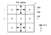
도 3a는, 촬상 장치(1)의 컬러 필터(40r, 40g, 40b)의 평면 구성을 나타내고 있다. 도 3b는, 도 3a에 도시한 컬러 필터(40r, 40g, 40b)의 상층의 평면 구성을 나타내고 있다.FIG. 3A shows the planar configuration of the
컬러 필터(40r, 40g, 40b)는 입사하는 광 중의 특정한 파장 영역의 광을 선택적으로 투과시킨다. 촬상 장치(1)에는, 적색(R)의 광을 투과하는 컬러 필터(40r)가 마련된 화소 Pr과, 녹색(G)의 광을 투과하는 컬러 필터(40g)가 마련된 화소 Pg와, 청색(B)의 광을 투과하는 컬러 필터(40b)가 마련된 화소 Pb가 마련된다. 촬상 장치(1)의 화소부(100)에 있어서, 화소 Pr과 화소 Pg와 화소 Pb가, 베이어 배열에 따라서 배치되어 있다. 화소 Pr, 화소 Pg 및 화소 Pb는, 각각, R 성분의 화소 신호, G 성분의 화소 신호, B 성분의 화소 신호를 생성한다. 촬상 장치(1)는 RGB의 화소 신호를 얻을 수 있다.The
도 4는, 컬러 필터(40)의 굴절률의 파장 의존성의 일례를 나타내고 있다. 도 4에 있어서, 실선 nr은, 적색(R)의 컬러 필터(40r)의 굴절률을 나타내고 있다. 1점 쇄선 ng는, 녹색(G)의 컬러 필터(40g)의 굴절률을 나타내고, 파선 nb는, 청색(B)의 컬러 필터(40b)의 굴절률을 나타내고 있다.FIG. 4 shows an example of the wavelength dependence of the refractive index of the color filter 40. In Fig. 4, the solid line nr represents the refractive index of the red (R)
청색 파장, 예를 들어 460㎚ 근방의 파장에 있어서, 청색 컬러 필터(40b)의 굴절률은, 녹색 컬러 필터(40g)의 굴절률보다도 낮아진다. 이 때문에, 청색 컬러 필터(40b)와 녹색 컬러 필터(40g)가 접하는 영역에 청색 파장(예를 들어 460㎚)의 광이 입사한 경우, 상대적으로 높은 굴절률을 갖는 녹색 컬러 필터(40g) 쪽으로 광이 진행되어버리는 경향이 있다.At a blue wavelength, for example, around 460 nm, the refractive index of the
또한, 녹색 파장, 예를 들어 530㎚ 근방의 파장에 있어서, 녹색 컬러 필터(40g)의 굴절률은, 적색 컬러 필터(40r)의 굴절률보다도 낮아진다. 이 때문에, 녹색 컬러 필터(40g)와 적색 컬러 필터(40r)가 접하는 영역에 녹색 파장(예를 들어 530㎚)의 광이 입사한 경우, 상대적으로 높은 굴절률을 갖는 적색 컬러 필터(40r) 쪽으로 광이 진행되어버리는 경향이 있다. 또한, 적색 파장, 예를 들어 630㎚ 근방의 파장에서는, 적색 컬러 필터(40r)의 굴절률은, 녹색 컬러 필터(40g) 및 청색 컬러 필터(40b)의 각각의 굴절률보다도 높아진다.Additionally, at a green wavelength, for example, around 530 nm, the refractive index of the
이에, 촬상 장치(1)에서는, 청색 컬러 필터(40b)에 있어서의 녹색 컬러 필터(40g)에 인접하는 부분의 위에 녹색 컬러 필터(40g) 위의 매질보다도 높은 굴절률을 갖는 매질이 마련된다. 또한, 녹색 컬러 필터(40g)에 있어서의 적색 컬러 필터(40r)에 인접하는 부분의 위에 적색 컬러 필터(40r) 위의 매질보다도 높은 굴절률을 갖는 매질이 마련된다. 도 3b에 도시한 예에서는, 청색 컬러 필터(40b) 위에 제1 도광 부재(51)가 마련되고, 녹색 컬러 필터(40g) 위에 제2 도광 부재(52)가 마련된다.Accordingly, in the
제1 도광 부재(51)는 청색 컬러 필터(40b)에 있어서의 녹색 컬러 필터(40g)에 인접하는 부분의 위를, 적어도 덮도록 마련된다. 도 3b에 도시한 예에서는, 제1 도광 부재(51)는 청색 컬러 필터(40b) 표면 전체를 덮도록 형성된다. 제1 도광 부재(51)는 인접한 녹색 컬러 필터(40g) 위 중 제2 도광 부재(52)가 존재하지 않는 부분의 굴절률보다도 높은 굴절률을 갖는다.The first
제2 도광 부재(52)는 녹색 컬러 필터(40g)에 있어서의 적색 컬러 필터(40r)에 인접하는 부분의 위를, 적어도 덮도록 마련된다. 제1 도광 부재(51) 및 제2 도광 부재(52)를 구성하는 재료로서는, 예를 들어 질화실리콘(SiN), 산화티타늄(TiO), 산화실리콘(SiO), 산화탄탈(TaO), 산화하프늄(HfO), 아몰퍼스실리콘(a-Si), 폴리실리콘(Poly-Si) 등을 들 수 있다. 제1 도광 부재(51) 및 제2 도광 부재(52)는 다른 재료를 사용하여 구성되어도 된다.The second
도 3c는, 제1 도광 부재(51) 및 제2 도광 부재(52)의 두께(막 두께)의 일례를 나타내고 있다. 제2 도광 부재(52)의 막 두께 L2는, 제1 도광 부재(51)의 막 두께 L1보다도 크다. 제1 도광 부재(51) 및 제2 도광 부재(52)에 입사한 광이 원하는 방향으로 진행하도록, 제1 도광 부재(51) 및 제2 도광 부재(52)의 막 두께, 형상, 굴절률 등이 정해진다. 예를 들어, 제1 도광 부재(51)의 막 두께는, 460㎚의 파장에 있어서의 청색 및 녹색 컬러 필터(40)의 굴절률 차에 따라서 정해진다. 또한, 제2 도광 부재(52)의 막 두께는, 예를 들어 530㎚의 파장에 있어서의 녹색 및 적색 컬러 필터(40)의 굴절률 차에 따라서 정해진다.FIG. 3C shows an example of the thickness (film thickness) of the first
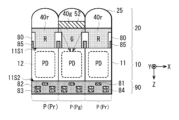
도 5a 내지 도 5c는, 제1 도광 부재(51) 및 제2 도광 부재(52)가 마련된 촬상 장치(1)의 구성예를 나타내는 도면이다. 도 5b는, 도 5a에 도시한 Ⅰ-Ⅰ선의 방향에 있어서의 단면 구성을 나타내고 있다. 도 5c는, 도 5a에 도시한 Ⅱ-Ⅱ선의 방향에 있어서의 단면 구성을 나타내고 있다. 도 5b 또는 도 5c에 도시한 바와 같이, 촬상 장치(1)는, 예를 들어 수광부(10)와, 도광부(20)와, 다층 배선층(90)이 적층된 구성을 갖고 있다.5A to 5C are diagrams showing a configuration example of the
수광부(10)는, 대향하는 제1 면(11S1) 및 제2 면(11S2)을 갖는 반도체 기판(11)을 갖는다. 반도체 기판(11)의 제1 면(11S1) 측에 도광부(20)가 마련되고, 반도체 기판(11)의 제2 면(11S2) 측에 다층 배선층(90)이 마련되어 있다. 피사체로부터의 광이 입사하는 측에 도광부(20)가 마련되고, 광이 입사하는 측과는 반대측에 다층 배선층(90)이 마련된다고도 할 수 있다. 촬상 장치(1)는 소위 이면 조사형의 촬상 장치이다.The
반도체 기판(11)은, 예를 들어 실리콘 기판에 의해 구성된다. 광전 변환부(12)는, 예를 들어 포토다이오드(PD)이며, 반도체 기판(11)의 소정 영역에 pn 접합을 갖고 있다. 반도체 기판(11)에는, 복수의 광전 변환부(12)가 매립 형성되어 있다. 수광부(10)에서는, 반도체 기판(11)의 제1 면(11S1) 및 제2 면(11S2)을 따라서, 복수의 광전 변환부(12)가 마련된다.The
다층 배선층(90)은, 예를 들어 복수의 배선층(81, 82, 83)이, 층간 절연층(84)을 사이에 적층된 구성을 갖고 있다. 반도체 기판(11) 및 다층 배선층(90)에는, 광전 변환부(12)에서 생성된 전하에 기초하는 화소 신호를 판독하기 위한 회로(예를 들어, 전송 트랜지스터, 리셋 트랜지스터, 증폭 트랜지스터 등)가 형성된다. 또한, 반도체 기판(11) 및 다층 배선층(90)에는, 예를 들어 상술한 수직 구동 회로(111), 칼럼 신호 처리 회로(112), 수평 구동 회로(113), 출력 회로(114), 제어 회로(115) 및 입출력 단자(116) 등이 형성되어 있다.The
배선층(81, 82, 83)은, 예를 들어 알루미늄(Al), 구리(Cu) 또는 텅스텐(W) 등을 사용하여 형성되어 있다. 이밖에, 배선층(81, 82, 83)은, 폴리실리콘(Poly-Si)을 사용하여 형성하도록 해도 된다. 층간 절연층(84)은, 예를 들어 산화실리콘(SiOx), TEOS, 질화실리콘(SiNx) 및 산질화실리콘(SiOxNy) 등 중 1종으로 이루어지는 단층막, 또는 이들 중 2종 이상으로 이루어지는 적층막에 의해 형성되어 있다.The wiring layers 81, 82, and 83 are formed using, for example, aluminum (Al), copper (Cu), or tungsten (W). In addition, the wiring layers 81, 82, and 83 may be formed using polysilicon (Poly-Si). The interlayer insulating
도광부(20)는 광을 집광하는 렌즈부(온 칩 렌즈)(25)와, 제1 도광 부재(51)와, 제2 도광 부재(52)와, 컬러 필터(40)를 갖고, 입사한 광을 수광부(10) 측으로 유도한다. 도광부(20)는 반도체 기판(11)의 제1 면(11S1)과 직교하는 두께 방향에 있어서, 수광부(10)에 적층된다.The
인접하는 화소 P의 사이의 경계 부분에는, 도파로(80)와, 광을 차단하는 차광부(85)가 마련된다. 도파로(80)는 입사한 광을 차광부(85)로 유도한다. 차광부(85)는, 예를 들어 광을 흡수하는 재료에 의해 구성되고, 입사한 광을 흡수한다.At the boundary between adjacent pixels P, a
제1 도광 부재(51)는 도 5b에 도시한 바와 같이, 렌즈부(25)와 청색 컬러 필터(40b)의 사이에 마련된다. 제1 도광 부재(51)는 청색 컬러 필터(40b)의 위에 위치한다. 제1 도광 부재(51)는 주위의 매질의 굴절률보다도 높은 굴절률을 갖는다. 제1 도광 부재(51)의 주위의 매질로서는, 산화실리콘(SiOx), 공기(공극) 등을 들 수 있다. 도 5b에 도시한 예에서는, 제1 도광 부재(51)는 X축 방향에 인접하는 화소 Pg의 렌즈부(25)의 굴절률보다도 높은 굴절률을 갖는 재료에 의해 구성된다.As shown in FIG. 5B, the first
제1 도광 부재(51)는 제1 도광 부재(51)와 그 주위의 매질의 굴절률의 차에 의해, 입사하는 광에 위상 지연을 부여한다. 제1 도광 부재(51)에서는, 위상 지연이 발생하는 것에 기인하여 입사한 광의 전파 방향이 바뀐다. 이 때문에, 제1 도광 부재(51)는 광의 진행 방향을 변화시키는 것이 가능해진다. 제1 도광 부재(51)는 광을 편향하는 편향부(편향 소자)(51)라고도 할 수 있다.The first
제2 도광 부재(52)는 도 5c에 도시한 바와 같이, 렌즈부(25)와 녹색 컬러 필터(40g)의 사이에 마련된다. 제2 도광 부재(52)는 녹색 컬러 필터(40g)의 위에 위치한다. 제2 도광 부재(52)는 주위의 매질의 굴절률보다도 높은 굴절률을 갖는다. 제2 도광 부재(52)의 주위의 매질로서는, 산화실리콘(SiOx), 공기(공극) 등을 들 수 있다. 도 5c에 도시한 예에서는, 제2 도광 부재(52)는 X축 방향에 인접하는 화소 Pr의 렌즈부(25)의 굴절률보다도 높은 굴절률을 갖는 재료에 의해 구성된다.As shown in FIG. 5C, the second
제2 도광 부재(52)는 제2 도광 부재(52)와 그 주위의 매질의 굴절률의 차에 의해, 입사하는 광에 위상 지연을 부여한다. 제2 도광 부재(52)에서는, 위상 지연이 발생하는 것에 기인하여 입사한 광의 전파 방향이 바뀐다. 이 때문에, 제2 도광 부재(52)는 광의 진행 방향을 변화시키는 것이 가능해진다. 제2 도광 부재(52)는 광을 편향하는 편향부(편향 소자)(52)라고도 할 수 있다.The second
도 5a 내지 도 5c를 참조하여, 460㎚의 청색의 파장 영역의 광이 입사한 경우에 대하여 설명한다. 도 5b에 있어서 상방으로부터 렌즈부(25)를 통해 제1 도광 부재(51)에 입사한 청색 파장광은, 인접하는 화소 Pg와 화소 Pb 중, 화소 Pb의 컬러 필터(40b)로 진행된다. 제1 도광 부재(51)의 단부에 입사한 광도, 도 5b에 있어서 화살표로 나타낸 바와 같이, 제1 도광 부재(51)에 의해 편향되어 화소 Pb의 컬러 필터(40b) 및 광전 변환부(12) 쪽으로 진행된다. 이렇게 하여, 도 5a에 있어서 화살표로 나타낸 바와 같이, 제1 도광 부재(51)는 입사하는 청색 파장광을 화소 Pb의 컬러 필터(40b) 및 광전 변환부(12)로 집광할 수 있다. 촬상 장치(1)가 제1 도광 부재(51)를 갖지 않는 경우와 비교하여, 화소 Pb의 광전 변환부(12)는 청색 파장광을 효율적으로 수광하여 광전 변환을 행할 수 있다.Referring to FIGS. 5A to 5C, a case where light in the blue wavelength region of 460 nm is incident will be described. In FIG. 5B , the blue wavelength light incident on the first
도 5c에 있어서 상방으로부터 렌즈부(25)를 통해 제2 도광 부재(52)에 입사한 청색 파장광은, 인접하는 화소 Pr과 화소 Pg 중, 화소 Pg의 컬러 필터(40g)로 진행된다. 제2 도광 부재(52)의 단부에 입사한 광도, 도 5c에 있어서 화살표로 나타낸 바와 같이, 제2 도광 부재(52)에 의해 편향되어 화소 Pg의 컬러 필터(40g) 쪽으로 진행된다. 녹색 컬러 필터(40g)에 입사한 청색 파장광은, 녹색 컬러 필터(40g)에 의해 흡수된다. 이 때문에, 불필요한 광이 주위로 새나가는 것을 억제하여 혼색이 발생하는 것을 억제할 수 있다.In FIG. 5C , the blue wavelength light incident on the second
다음으로, 도 6a 내지 도 6c를 참조하여, 530㎚의 녹색의 파장 영역의 광이 입사한 경우에 대하여 설명한다. 도 6b는, 도 6a에 도시한 Ⅰ-Ⅰ선의 방향에 있어서의 단면 구성을 나타내고 있다. 도 6c는, 도 6a에 도시한 Ⅱ-Ⅱ선의 방향에 있어서의 단면 구성을 나타내고 있다. 도 6b에 있어서 상방으로부터 렌즈부(25)를 통해 제1 도광 부재(51)에 입사한 녹색 파장광은, 화소 Pb의 컬러 필터(40b) 또는 차광부(85)를 향해 진행되고, 청색 컬러 필터(40b) 또는 차광부(85)에 의해 흡수된다. 이 때문에, 불필요한 광이 주위로 새나는 것을 억제하여 혼색이 발생하는 것을 억제할 수 있다.Next, with reference to FIGS. 6A to 6C, a case where light in the green wavelength range of 530 nm is incident will be described. FIG. 6B shows the cross-sectional configuration in the direction of line I-I shown in FIG. 6A. FIG. 6C shows the cross-sectional configuration in the direction of line II-II shown in FIG. 6A. In FIG. 6B, green wavelength light incident on the first
도 6c에 있어서 렌즈부(25)를 통해서 제2 도광 부재(52)에 입사한 녹색 파장광은, 인접하는 화소 Pr과 화소 Pg 중, 화소 Pg의 컬러 필터(40g)로 진행된다. 제2 도광 부재(52)의 단부에 입사한 광도, 도 6c에 있어서 화살표로 나타낸 바와 같이, 제2 도광 부재(52)에 의해 편향되어 화소 Pg의 컬러 필터(40g) 및 광전 변환부(12) 쪽으로 진행된다. 이렇게 해서, 도 6a에 있어서 화살표로 나타낸 바와 같이, 제2 도광 부재(52)는 입사하는 녹색 파장광을 화소 Pg의 컬러 필터(40g) 및 광전 변환부(12)로 집광할 수 있다. 화소 Pg의 광전 변환부(12)는 녹색 파장광을 효율적으로 수광하여 광전 변환을 행할 수 있다.In FIG. 6C, green wavelength light incident on the second
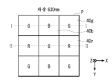
다음으로, 도 7을 참조하여, 630㎚의 적색의 파장 영역의 광이 입사한 경우에 대하여 설명한다. 도 7b는, 도 7a에 도시한 Ⅰ-Ⅰ선의 방향에 있어서의 단면 구성을 나타내고 있다. 도 7c는, 도 7a에 도시한 Ⅱ-Ⅱ의 방향에 있어서의 단면 구성을 나타내고 있다. 도 7b에 있어서 상방으로부터 렌즈부(25)를 통해 제1 도광 부재(51)에 입사한 적색 파장광은, 화소 Pb의 컬러 필터(40b) 또는 차광부(85)로 진행되고, 청색 컬러 필터(40b) 또는 차광부(85)에 의해 흡수된다. 이 때문에, 불필요한 광이 주위로 새나는 것을 억제하여 혼색이 발생하는 것을 억제할 수 있다.Next, with reference to FIG. 7, a case where light in the red wavelength range of 630 nm is incident is explained. FIG. 7B shows the cross-sectional configuration in the direction of line I-I shown in FIG. 7A. FIG. 7C shows the cross-sectional configuration in the direction II-II shown in FIG. 7A. In FIG. 7B, the red wavelength light incident on the first
도 7c에 있어서 상방으로부터 제2 도광 부재(52)에 입사한 적색 파장광은, 화소 Pg의 컬러 필터(40g) 또는 차광부(85)로 진행되고, 녹색 컬러 필터(40g) 또는 차광부(85)에 의해 흡수된다. 이 때문에, 혼색이 발생하는 것을 억제할 수 있다.In FIG. 7C, the red wavelength light incident on the second
[작용·효과][Action/Effect]
본 실시 형태에 따른 촬상 장치(1)는 입사광에 대하여 제1 굴절률을 갖는 제1 필터(예를 들어 녹색 컬러 필터(40g))와, 제1 필터를 투과한 광을 광전 변환하는 제1 광전 변환부(화소 Pg의 광전 변환부(12))를 갖는다. 또한, 촬상 장치(1)는 입사광에 대하여 제1 굴절률보다도 낮은 제2 굴절률을 갖고, 제1 필터와 인접하는 제2 필터(예를 들어 청색 컬러 필터(40b))와, 제2 필터를 투과한 광을 광전 변환하는 제2 광전 변환부(화소 Pb의 광전 변환부(12))를 갖는다. 또한, 촬상 장치(1)는 제1 필터에서 볼 때 제1 광전 변환부와 반대측에 마련되고, 입사광에 대하여 제3 굴절률을 갖는 제1 매질(예를 들어 화소 Pg의 렌즈부(25)와 동일한 재료)과, 제2 필터에서 볼 때 제2 광전 변환부와 반대측에 마련되고, 입사광에 대하여 제3 굴절률보다도 높은 제4 굴절률을 갖는 제2 매질(예를 들어 제1 도광 부재(51))을 구비한다.The
촬상 장치(1)에서는, 인접하는 컬러 필터(40) 중, 굴절률이 낮은 쪽의 컬러 필터(40) 위에 제1 도광 부재(51)(또는 제2 도광 부재(52))가 마련된다. 이에 의해, 상대적으로 낮은 굴절률을 갖는 컬러 필터(40)가 마련된 화소 P에 있어서, 집광 효율이 저하되는 것을 억제할 수 있다. 효율적으로 집광을 행할 수 있어, 양자 효율(QE)을 향상시킬 수 있다. 또한, 혼색이 발생하는 것을 억제할 수 있다.In the
다음으로, 본 개시의 변형예에 대하여 설명한다. 이하에서는, 상기 실시 형태와 마찬가지의 구성 요소에 대해서는 동일한 부호를 부여하고, 적절히 설명을 생략한다.Next, modifications of the present disclosure will be described. In the following, the same reference numerals are given to the same components as those in the above-described embodiments, and descriptions are omitted as appropriate.
<2. 변형예><2. Variation example>
(2-1. 변형예 1)(2-1. Modification 1)
상술한 실시 형태에서는, 제1 도광 부재(51) 및 제2 도광 부재(52)의 구성예에 대하여 설명하였지만, 제1 도광 부재(51) 및 제2 도광 부재(52)의 구성은 이것에 한정되지는 않는다. 도 8a는, 변형예 1에 따른 촬상 장치(1)의 구성예를 나타내는 도면이다.In the above-described embodiment, configuration examples of the first
예를 들어, 도 8a에 도시한 바와 같이, 화소 P의 광전 변환부(12) 또는 컬러 필터(40)를 둘러싸도록, 제1 도광 부재(51) 및 제2 도광 부재(52)를 마련하도록 해도 된다. 도 8b는, 제1 도광 부재(51) 및 제2 도광 부재(52)의 막 두께의 일례를 나타내고 있다. 본 변형예의 경우에도, 제2 도광 부재(52)의 막 두께 L2를, 제1 도광 부재(51)의 막 두께 L1보다도 크게 해도 된다. 본 변형예에 있어서도, 효율적으로 집광을 행할 수 있어 양자 효율(QE)을 향상시킬 수 있다. 또한, 혼색이 발생하는 것을 억제할 수 있다.For example, as shown in FIG. 8A, the first
(2-2. 변형예 2)(2-2. Modification 2)
도 9a는, 변형예 2에 따른 촬상 장치(1)의 평면 구성의 일례를 나타내는 도면이다. 도 9b는, 도 9a에 도시한 제1 도광 부재(51) 및 제2 도광 부재(52)의 막 두께의 일례를 나타내고 있다. 본 변형예에서는, 제2 도광 부재(52)의 굴절률이 제1 도광 부재(51)의 굴절률보다도 커지도록, 제1 도광 부재(51) 및 제2 도광 부재(52)가 형성된다. 또한, 제1 도광 부재(51)의 막 두께와 제2 도광 부재(52)의 막 두께는 대략 동등하다. 본 변형예의 경우에도, 상기 실시 형태의 촬상 장치와 마찬가지의 효과를 얻을 수 있다.FIG. 9A is a diagram showing an example of the planar configuration of the
(2-3. 변형예 3)(2-3. Modification 3)
도 10a는, 변형예 3에 따른 촬상 장치(1)의 평면 구성의 일례를 나타내는 도면이다. 도 10b는, 도 10a에 도시한 제1 도광 부재(51) 및 제2 도광 부재(52)의 막 두께의 일례를 나타내고 있다. 제1 도광 부재(51) 및 제2 도광 부재(52)는 도 10a에 도시한 바와 같이, 격자형으로 마련된다. 제2 도광 부재(52)의 굴절률은, 제1 도광 부재(51)의 굴절률보다도 크다. 또한, 제1 도광 부재(51)의 막 두께와 제2 도광 부재(52)의 막 두께는 대략 동등하다. 본 변형예의 경우에도, 상기 실시 형태의 촬상 장치와 마찬가지의 효과를 얻을 수 있다.FIG. 10A is a diagram showing an example of the planar configuration of the
(2-4. 변형예 4)(2-4. Modification 4)
도 11a는, 변형예 4에 따른 촬상 장치(1)의 평면 구성의 일례를 나타내는 도면이다. 도 11b는, 도 11a에 도시한 제1 도광 부재(51) 및 제2 도광 부재(52)의 막 두께(높이)의 일례를 나타내고 있다.FIG. 11A is a diagram showing an example of the planar configuration of the
제1 도광 부재(51) 및 제2 도광 부재(52)는 각각, 복수의 구조체를 갖는다. 이 구조체는, 입사하는 광의 소정 파장 이하, 예를 들어 가시광의 파장 이하의 크기의 미세(미소)한 구조체이다. 구조체는, 주위의 매질의 굴절률보다도 높은 굴절률을 갖는다. 구조체의 주위의 매질로서는, 공기(공극), 산화실리콘(SiOx) 등을 들 수 있다. 구조체는, 예를 들어 도 11b에 도시한 바와 같이, Z축 방향에 있어서의 두께(길이) L의 기둥형(필러형)의 구조체이다.The first
제1 도광 부재(51) 및 제2 도광 부재(52)는 상술한 미세 구조체를 갖고, 미세 구조체와 그 주변과 굴절률 차에 의해, 입사한 광의 진행 방향을 변화시키는 것이 가능해진다. 제1 도광 부재(51) 및 제2 도광 부재(52)는 메타물질(메타표면) 기술을 이용하여 광을 편향하는 편향부(편향 소자)라고도 할 수 있다.The first
본 변형예에 따른 촬상 장치(1)는 제1 도광 부재(51) 및 제2 도광 부재(52)를 갖는다. 제1 도광 부재(51) 및 제2 도광 부재(52)는 미세 구조체에 의해 구성되고, 입사광을 편향한다. 본 변형예의 경우도, 상기 실시 형태의 촬상 장치와 마찬가지의 효과를 기대할 수 있다.The
(2-5. 변형예 5)(2-5. Modification 5)
도 12a는, 변형예 5에 따른 촬상 장치(1)의 평면 구성의 일례를 나타내는 도면이다. 도 12b는, 도 12a에 도시한 제1 도광 부재(51) 및 제2 도광 부재(52)의 막 두께(높이)의 일례를 나타내고 있다. 제1 도광 부재(51) 및 제2 도광 부재(52)는 도 11a 및 도 11b의 경우와 마찬가지로, 복수의 구조체를 사용하여 구성된다.FIG. 12A is a diagram showing an example of the planar configuration of the
제1 도광 부재(51) 및 제2 도광 부재(52)는 각각, 형상, 높이, 배치 간격 등이 서로 다른 복수종의 미세 구조체를 갖고 있어도 된다. 예를 들어, 제1 도광 부재(51) 및 제2 도광 부재(52)는 도 12a 및 도 12b에 도시한 예과 같이, 직경이 다른 복수의 기둥형(필러형)의 구조체를 갖고 있어도 된다. 또한, 예를 들어 제1 도광 부재(51) 및 제2 도광 부재(52)는 높이가 다른 복수의 필러형의 구조체를 갖고 있어도 된다.The first
제1 도광 부재(51) 및 제2 도광 부재(52)는, 예를 들어 직경, 높이 등이 다른 복수의 구조체를 사용하여, 위치에 따라서 서서히 위상 지연량이 바뀌도록 구성된다. 본 변형예에 따른 촬상 장치(1)에서는, 직경, 높이 등이 다른 복수의 구조체를 사용한 렌즈(메타물질 렌즈)가 구성되고, 위상 구배를 실현할 수 있다. 색 분리 성능, 집광 성능을 보다 향상시키는 것이 가능해진다.The first
<3. 적용예><3. Application example>
상기 촬상 장치(1) 등은, 예를 들어 디지털 스틸 카메라나 비디오 카메라 등의 카메라 시스템이나, 촬상 기능을 갖는 휴대 전화 등, 촬상 기능을 구비한 모든 타입의 전자 기기에 적용할 수 있다. 도 13은, 전자 기기(1000)의 개략 구성을 나타낸 것이다.The
전자 기기(1000)는, 예를 들어 렌즈군(1001)과, 촬상 장치(1)와, DSP(Digital Signal Processor) 회로(1002)와, 프레임 메모리(1003)와, 표시부(1004)와, 기록부(1005)와, 조작부(1006)와, 전원부(1007)를 갖고, 버스 라인(1008)을 통해 서로 접속되어 있다.The electronic device 1000 includes, for example, a
렌즈군(1001)은, 피사체로부터의 입사광(상광)을 도입하여 촬상 장치(1)의 촬상면 위에 결상하는 것이다. 촬상 장치(1)는 렌즈군(1001)에 의해 촬상면 위에 결상된 입사광의 광량을 화소 단위로 전기 신호로 변환하여 화소 신호로서 DSP 회로(1002)에 공급한다.The
DSP 회로(1002)는, 촬상 장치(1)로부터 공급되는 신호를 처리하는 신호 처리 회로이다. DSP 회로(1002)는, 촬상 장치(1)로부터의 신호를 처리하여 얻어지는 화상 데이터를 출력한다. 프레임 메모리(1003)는 DSP 회로(1002)에 의해 처리된 화상 데이터를 프레임 단위로 일시적으로 유지하는 것이다.The
표시부(1004)는, 예를 들어 액정 패널이나 유기 EL(Electro Luminescence) 패널 등의 패널형 표시 장치로 이루어지고, 촬상 장치(1)에서 촬상된 동화상 또는 정지 화상의 화상 데이터를, 반도체 메모리나 하드 디스크 등의 기록 매체에 기록한다.The
조작부(1006)는, 유저에 의한 조작에 따라서, 전자 기기(1000)가 소유하는 각종 기능에 대한 조작 신호를 출력한다. 전원부(1007)는, DSP 회로(1002), 프레임 메모리(1003), 표시부(1004), 기록부(1005) 및 조작부(1006)의 동작 전원이 되는 각종 전원을, 이들 공급 대상에 대하여 적절히 공급하는 것이다.The
<4. 응용예><4. Application example>
(이동체에 대한 응용예)(Application example for moving object)
본 개시에 따른 기술(본 기술)은 다양한 제품으로 응용할 수 있다. 예를 들어, 본 개시에 따른 기술은, 자동차, 전기 자동차, 하이브리드 전기 자동차, 자동 이륜차, 자전거, 퍼스널 모빌리티, 비행기, 드론, 선박, 로봇 등의 어떠한 종류의 이동체에 탑재되는 장치로서 실현되어도 된다.The technology according to the present disclosure (this technology) can be applied to various products. For example, the technology according to the present disclosure may be implemented as a device mounted on any type of moving object, such as a car, electric vehicle, hybrid electric vehicle, two-wheeled vehicle, bicycle, personal mobility, airplane, drone, ship, or robot.
도 14는, 본 개시에 따른 기술이 적용될 수 있는 이동체 제어 시스템의 일례인 차량 제어 시스템의 개략적인 구성예를 나타내는 블록도이다.FIG. 14 is a block diagram showing a schematic configuration example of a vehicle control system, which is an example of a moving object control system to which the technology according to the present disclosure can be applied.
차량 제어 시스템(12000)은, 통신 네트워크(12001)를 통해 접속된 복수의 전자 제어 유닛을 구비한다. 도 14에 도시한 예에서는, 차량 제어 시스템(12000)은, 구동계 제어 유닛(12010), 보디계 제어 유닛(12020), 차외 정보 검출 유닛(12030), 차내 정보 검출 유닛(12040) 및 통합 제어 유닛(12050)을 구비한다. 또한, 통합 제어 유닛(12050)의 기능 구성으로서, 마이크로컴퓨터(12051), 음성 화상 출력부(12052) 및 차량 탑재 네트워크 I/F(interface)(12053)가 도시되어 있다.The
구동계 제어 유닛(12010)은 각종 프로그램에 따라서 차량의 구동계에 관련된장치의 동작을 제어한다. 예를 들어, 구동계 제어 유닛(12010)은 내연 기관 또는 구동용 모터 등의 차량의 구동력을 발생시키기 위한 구동력 발생 장치, 구동력을 차륜에 전달하기 위한 구동력 전달 기구, 차량의 타각을 조절하는 스티어링 기구 및 차량의 제동력을 발생시키는 제동 장치 등의 제어 장치로서 기능한다.The drive
보디계 제어 유닛(12020)은 각종 프로그램에 따라서 차체에 장비된 각종 장치의 동작을 제어한다. 예를 들어, 보디계 제어 유닛(12020)은 키리스 엔트리 시스템, 스마트 키 시스템, 파워 윈도우 장치, 혹은 헤드 램프, 백 램프, 브레이크 램프, 방향 지시등 또는 안개등 등의 각종 램프의 제어 장치로서 기능한다. 이 경우, 보디계 제어 유닛(12020)에는, 키를 대체하는 휴대기로부터 발신되는 전파 또는 각종 스위치의 신호가 입력될 수 있다. 보디계 제어 유닛(12020)은 이들 전파 또는 신호의 입력을 접수하고, 차량의 도어록 장치, 파워 윈도우 장치, 램프 등을 제어한다.The body
차외 정보 검출 유닛(12030)은, 차량 제어 시스템(12000)을 탑재한 차량의 외부의 정보를 검출한다. 예를 들어, 차외 정보 검출 유닛(12030)에는, 촬상부(12031)가 접속된다. 차외 정보 검출 유닛(12030)은, 촬상부(12031)에 차외의 화상을 촬상시킴과 함께, 촬상된 화상을 수신한다. 차외 정보 검출 유닛(12030)은, 수신한 화상에 기초하여, 사람, 차량, 장해물, 표지 또는 노면 위의 문자 등의 물체 검출 처리 또는 거리 검출 처리를 행해도 된다.The external
촬상부(12031)는 광을 수광하고, 그 광의 수광량에 따른 전기 신호를 출력하는 광 센서이다. 촬상부(12031)는 전기 신호를 화상으로서 출력할 수도 있고, 측거의 정보로서 출력할 수도 있다. 또한, 촬상부(12031)가 수광하는 광은, 가시광이어도 되고, 적외선 등의 비가시광이어도 된다.The
차내 정보 검출 유닛(12040)은 차내의 정보를 검출한다. 차내 정보 검출 유닛(12040)에는, 예를 들어 운전자의 상태를 검출하는 운전자 상태 검출부(12041)가 접속된다. 운전자 상태 검출부(12041)는, 예를 들어 운전자를 촬상하는 카메라를 포함하고, 차내 정보 검출 유닛(12040)은, 운전자 상태 검출부(12041)로부터 입력되는 검출 정보에 기초하여, 운전자의 피로 정도 또는 집중 정도를 산출해도 되고, 운전자가 졸고 있지 않는지를 판별해도 된다.The in-vehicle
마이크로컴퓨터(12051)는, 차외 정보 검출 유닛(12030) 또는 차내 정보 검출 유닛(12040)에서 취득되는 차 내외의 정보에 기초하여, 구동력 발생 장치, 스티어링 기구 또는 제동 장치의 제어 목푯값을 연산하고, 구동계 제어 유닛(12010)에 대하여 제어 지령을 출력할 수 있다. 예를 들어, 마이크로컴퓨터(12051)는, 차량의 충돌 회피 또는 충격 완화, 차간 거리에 기초하는 추종 주행, 차속 유지 주행, 차량의 충돌 경고, 또는 차량의 레인 일탈 경고 등을 포함하는 ADAS(Advanced Driver Assistance System)의 기능 실현을 목적으로 한 협조 제어를 행할 수 있다.The
또한, 마이크로컴퓨터(12051)는, 차외 정보 검출 유닛(12030) 또는 차내 정보 검출 유닛(12040)에서 취득되는 차량의 주위 정보에 기초하여 구동력 발생 장치, 스티어링 기구 또는 제동 장치 등을 제어함으로써, 운전자의 조작에 따르지 않고 자율적으로 주행하는 자동 운전 등을 목적으로 한 협조 제어를 행할 수 있다.In addition, the
또한, 마이크로컴퓨터(12051)는, 차외 정보 검출 유닛(12030)에서 취득되는 차외의 정보에 기초하여, 보디계 제어 유닛(12020)에 대하여 제어 지령을 출력할 수 있다. 예를 들어, 마이크로컴퓨터(12051)는, 차외 정보 검출 유닛(12030)에서 검지한 선행차 또는 대향차의 위치에 따라서 헤드 램프를 제어하고, 하이 빔을 로우 빔으로 전환하는 등의 눈부심 방지를 도모하는 것을 목적으로 한 협조 제어를 행할 수 있다.Additionally, the
음성 화상 출력부(12052)는 차량의 탑승자 또는 차외에 대하여 시각적 또는 청각적으로 정보를 통지하는 것이 가능한 출력 장치에 음성 및 화상 중 적어도 한쪽의 출력 신호를 송신한다. 도 14의 예에서는, 출력 장치로서, 오디오 스피커(12061), 표시부(12062) 및 인스트루먼트 패널(12063)이 예시되어 있다. 표시부(12062)는, 예를 들어 온보드 디스플레이 및 헤드업 디스플레이 중 적어도 하나를 포함하고 있어도 된다.The audio and
도 15는, 촬상부(12031)의 설치 위치의 예를 나타내는 도면이다.FIG. 15 is a diagram showing an example of the installation position of the
도 15에서는, 차량(12100)은 촬상부(12031)로서, 촬상부(12101, 12102, 12103, 12104, 12105)를 갖는다.In FIG. 15, the
촬상부(12101, 12102, 12103, 12104, 12105)는, 예를 들어 차량(12100)의 프론트 노즈, 사이드미러, 리어 범퍼, 백 도어 및 차 실내의 프론트 글래스의 상부 등의 위치에 마련된다. 프론트 노즈에 구비되는 촬상부(12101) 및 차 실내의 프론트 글래스의 상부에 구비되는 촬상부(12105)는 주로 차량(12100)의 전방의 화상을 취득한다. 사이드미러에 구비되는 촬상부(12102, 12103)는 주로 차량(12100)의 측방의 화상을 취득한다. 리어 범퍼 또는 백 도어에 구비되는 촬상부(12104)는 주로 차량(12100)의 후방의 화상을 취득한다. 촬상부(12101 및 12105)에서 취득되는 전방의 화상은, 주로 선행 차량, 또는 보행자, 장해물, 신호기, 교통 표지 또는 차선 등의 검출에 사용된다.The
또한, 도 15에는, 촬상부(12101 내지 12104)의 촬영 범위의 일례가 도시되어 있다. 촬상 범위(12111)는 프론트 노즈에 마련된 촬상부(12101)의 촬상 범위를 나타내고, 촬상 범위(12112, 12113)는 각각 사이드미러에 마련된 촬상부(12102, 12103)의 촬상 범위를 나타내고, 촬상 범위(12114)는 리어 범퍼 또는 백 도어에 마련된 촬상부(12104)의 촬상 범위를 나타낸다. 예를 들어, 촬상부(12101 내지 12104)에서 촬상된 화상 데이터를 중첩할 수 있음으로써, 차량(12100)을 상방에서 본 부감 화상이 얻어진다.Additionally, FIG. 15 shows an example of the imaging range of the
촬상부(12101 내지 12104) 중 적어도 하나는, 거리 정보를 취득하는 기능을 갖고 있어도 된다. 예를 들어, 촬상부(12101 내지 12104) 중 적어도 하나는, 복수의 촬상 소자로 이루어지는 스테레오 카메라여도 되고, 위상차 검출용 화소를 갖는 촬상 소자여도 된다. At least one of the
예를 들어, 마이크로컴퓨터(12051)는, 촬상부(12101 내지 12104)로부터 얻어진 거리 정보를 기초로, 촬상 범위(12111 내지 12114) 내에 있어서의 각 입체물까지의 거리와, 이 거리의 시간적 변화(차량(12100)에 대한 상대 속도)를 구함으로써, 특히 차량(12100)의 진행로 위에 있는 가장 가까운 입체물이고, 차량(12100)과 대략 동일한 방향으로 소정의 속도(예를 들어, 0㎞/h 이상)로 주행하는 입체물을 선행차로서 추출할 수 있다. 또한, 마이크로컴퓨터(12051)는, 선행차의 앞쪽에 미리 확보해야 할 차간 거리를 설정하고, 자동 브레이크 제어(추종 정지 제어도 포함함)나 자동 가속 제어(추종 발진 제어도 포함함) 등을 행할 수 있다. 이와 같이 운전자의 조작에 따르지 않고 자율적으로 주행하는 자동 운전 등을 목적으로 한 협조 제어를 행할 수 있다.For example, based on the distance information obtained from the
예를 들어, 마이크로컴퓨터(12051)는, 촬상부(12101 내지 12104)로부터 얻어진 거리 정보를 기초로, 입체물에 관한 입체물 데이터를, 이륜차, 보통차량, 대형 차량, 보행자, 전신주 등 그 밖의 입체물로 분류하여 추출하고, 장해물의 자동 회피에 사용할 수 있다. 예를 들어, 마이크로컴퓨터(12051)는, 차량(12100)의 주변 장해물을, 차량(12100)의 드라이버가 시인 가능한 장해물과 시인 곤란한 장해물로 식별한다. 그리고, 마이크로컴퓨터(12051)는, 각 장해물과의 충돌의 위험도를 나타내는 충돌 리스크를 판단하여, 충돌 리스크가 설정값 이상으로 충돌 가능성이 있는 상황일 때에는, 오디오 스피커(12061)나 표시부(12062)를 통해 드라이버에게 경보를 출력하는 것이나, 구동계 제어 유닛(12010)을 통해 강제 감속이나 회피 조타를 행함으로써, 충돌 회피를 위한 운전 지원을 행할 수 있다.For example, the
촬상부(12101 내지 12104) 중 적어도 하나는, 적외선을 검출하는 적외선 카메라여도 된다. 예를 들어, 마이크로컴퓨터(12051)는, 촬상부(12101 내지 12104)의 촬상 화상 중에 보행자가 존재하는지 여부를 판정함으로써 보행자를 인식할 수 있다. 이러한 보행자의 인식은, 예를 들어 적외선 카메라로서의 촬상부(12101 내지 12104)의 촬상 화상에 있어서의 특징점을 추출하는 수순과, 물체의 윤곽을 나타내는 일련의 특징점에 패턴 매칭 처리를 행하여 보행자인지 여부를 판별하는 수순에 의해 행해진다. 마이크로컴퓨터(12051)가, 촬상부(12101 내지 12104)의 촬상 화상 중에 보행자가 존재한다고 판정하고, 보행자를 인식하면, 음성 화상 출력부(12052)는 당해 인식된 보행자에게 강조를 위한 사각형 윤곽선을 중첩 표시하도록, 표시부(12062)를 제어한다. 또한, 음성 화상 출력부(12052)는 보행자를 나타내는 아이콘 등을 원하는 위치에 표시하도록 표시부(12062)를 제어해도 된다.At least one of the
이상, 본 개시에 따른 기술이 적용될 수 있는 이동체 제어 시스템의 일례에 대하여 설명하였다. 본 개시에 따른 기술은, 이상 설명한 구성 중, 예를 들어 촬상부(12031)에 적용될 수 있다. 구체적으로는, 예를 들어 촬상 장치(1)는 촬상부(12031)에 적용할 수 있다. 촬상부(12031)에 본 개시에 따른 기술을 적용함으로써, 노이즈가 적은 고정밀의 촬영 화상을 얻을 수 있고, 이동체 제어 시스템에 있어서 촬영 화상을 이용한 고정밀도의 제어를 행할 수 있다.Above, an example of a mobile control system to which the technology according to the present disclosure can be applied has been described. The technology according to the present disclosure can be applied to, for example, the
(내시경 수술 시스템에 대한 응용예)(Application example for endoscopic surgery system)
본 개시에 따른 기술(본 기술)은 다양한 제품에 응용할 수 있다. 예를 들어, 본 개시에 따른 기술은, 내시경 수술 시스템에 적용되어도 된다.The technology according to the present disclosure (this technology) can be applied to various products. For example, the technology according to the present disclosure may be applied to an endoscopic surgical system.
도 16은, 본 개시에 따른 기술(본 기술)이 적용될 수 있는 내시경 수술 시스템의 개략적인 구성의 일례를 나타내는 도면이다.FIG. 16 is a diagram showing an example of the schematic configuration of an endoscopic surgery system to which the technology according to the present disclosure (the present technology) can be applied.
도 16에서는, 시술자(의사)(11131)가 내시경 수술 시스템(11000)을 사용하여, 환자 베드(11133) 위의 환자(11132)에게 수술을 행하고 있는 모습이 도시되어 있다. 도시한 바와 같이, 내시경 수술 시스템(11000)은, 내시경(11100)과, 기복 튜브(11111)나 에너지 처치구(11112) 등의, 기타 수술 도구(11110)와, 내시경(11100)을 지지하는 지지 암 장치(11120)와, 내시경하 수술을 위한 각종 장치가 탑재된 카트(11200)로 구성된다.In FIG. 16, an operator (doctor) 11131 is shown using an endoscopic
내시경(11100)은 선단으로부터 소정의 길이의 영역이 환자(11132)의 체강 내에 삽입되는 경통(11101)과, 경통(11101)의 기단에 접속되는 카메라 헤드(11102)로 구성된다. 도시한 예에서는, 경성의 경통(11101)을 갖는 소위 경성경으로서 구성되는 내시경(11100)을 도시하고 있지만, 내시경(11100)은 연성의 경통을 갖는 소위 연성경으로서 구성되어도 된다.The
경통(11101)의 선단에는, 대물 렌즈가 끼워진 개구부가 마련되어 있다. 내시경(11100)에는 광원 장치(11203)가 접속되어 있으며, 당해 광원 장치(11203)에 의해 생성된 광이, 경통(11101)의 내부에 연장 설치되는 라이트 가이드에 의해 당해 경통의 선단까지 도광되고, 대물 렌즈를 통해 환자(11132)의 체강 내의 관찰 대상을 향해 조사된다. 또한, 내시경(11100)은 직시경이어도 되고, 사시경 또는 측시경이어도 된다.At the tip of the
카메라 헤드(11102)의 내부에는 광학계 및 촬상 소자가 마련되어 있으며, 관찰 대상으로부터의 반사광(관찰광)은 당해 광학계에 의해 당해 촬상 소자에 집광된다. 당해 촬상 소자에 의해 관찰광이 광전 변환되고, 관찰광에 대응하는 전기 신호, 즉 관찰 상에 대응하는 화상 신호가 생성된다. 당해 화상 신호는, RAW 데이터로서 카메라 컨트롤 유닛(CCU: Camera Control Unit)(11201)에 송신된다.An optical system and an imaging device are provided inside the
CCU(11201)는, CPU(Central Processing Unit)나 GPU(Graphics Processing Unit) 등으로 구성되고, 내시경(11100) 및 표시 장치(11202)의 동작을 통괄적으로 제어한다. 또한, CCU(11201)는, 카메라 헤드(11102)로부터 화상 신호를 수취하고, 그 화상 신호에 대하여 예를 들어 현상 처리(디모자이크 처리) 등의, 당해 화상 신호에 기초하는 화상을 표시하기 위한 각종 화상 처리를 실시한다.The
표시 장치(11202)는 CCU(11201)로부터의 제어에 의해, 당해 CCU(11201)에 의해 화상 처리가 실시된 화상 신호에 기초하는 화상을 표시한다.Under control from the
광원 장치(11203)는 예를 들어 LED(Light Emitting Diode) 등의 광원으로 구성되고, 수술 부위 등을 촬영할 때의 조사광을 내시경(11100)에 공급한다.The
입력 장치(11204)는 내시경 수술 시스템(11000)에 대한 입력 인터페이스이다. 유저는, 입력 장치(11204)를 통해 내시경 수술 시스템(11000)에 대하여 각종 정보의 입력이나 지시 입력을 행할 수 있다. 예를 들어, 유저는, 내시경(11100)에 의한 촬상 조건(조사광의 종류, 배율 및 초점 거리 등)을 변경한다는 취지의 지시 등을 입력한다.
처치구 제어 장치(11205)는 조직의 소작, 절개 또는 혈관의 밀봉 등을 위한 에너지 처치구(11112)의 구동을 제어한다. 기복 장치(11206)는 내시경(11100)에 의한 시야의 확보 및 시술자의 작업 공간의 확보를 목적으로, 환자(11132)의 체강을 부풀리기 위해서, 기복 튜브(11111)를 통해 당해 체강 내로 가스를 보낸다. 레코더(11207)는, 수술에 관한 각종 정보를 기록 가능한 장치이다. 프린터(11208)는, 수술에 관한 각종 정보를, 텍스트, 화상 또는 그래프 등 각종 형식으로 인쇄 가능한 장치이다.The treatment tool control device 11205 controls the operation of the
또한, 내시경(11100)에 수술 부위를 촬영할 때의 조사광을 공급하는 광원 장치(11203)는 예를 들어 LED, 레이저 광원 또는 이들 조합에 의해 구성되는 백색 광원으로 구성할 수 있다. RGB 레이저 광원의 조합에 의해 백색 광원이 구성되는 경우에는, 각 색(각 파장)의 출력 강도 및 출력 타이밍을 고정밀도로 제어할 수 있기 때문에, 광원 장치(11203)에 있어서 촬상 화상의 화이트 밸런스의 조정을 행할 수 있다. 또한, 이 경우에는, RGB 레이저 광원 각각으로부터의 레이저광을 시분할로 관찰 대상으로 조사하고, 그 조사 타이밍에 동기하여 카메라 헤드(11102)의 촬상 소자 구동을 제어함으로써, RGB 각각에 대응한 화상을 시분할로 촬상하는 것도 가능하다. 당해 방법에 의하면, 당해 촬상 소자에 컬러 필터를 마련하지 않아도, 컬러 화상을 얻을 수 있다.In addition, the
또한, 광원 장치(11203)는 출력하는 광의 강도를 소정의 시간마다 변경하도록 그 구동이 제어되어도 된다. 그 광이 강도 변경의 타이밍에 동기하여 카메라 헤드(11102)의 촬상 소자 구동을 제어하여 시분할로 화상을 취득하고, 그 화상을 합성함으로써, 소위 흑색 포화 및 백색 날림이 없는 고 다이내믹 레인지의 화상을 생성할 수 있다.Additionally, the driving of the
또한, 광원 장치(11203)는 특수 광 관찰에 대응한 소정의 파장 대역의 광을 공급 가능하게 구성되어도 된다. 특수 광 관찰에서는, 예를 들어 체조직에 있어서의 광의 흡수 파장 의존성을 이용하여, 통상의 관찰 시에 있어서의 조사광(즉, 백색광)에 비하여 협대역의 광을 조사함으로써, 점막 표층의 혈관 등의 소정의 조직을 고 콘트라스트로 촬영하는, 소위 협대역 광 관찰(Narrow Band Imaging)이 행해진다. 또는, 특수 광 관찰에서는, 여기광을 조사함으로써 발생하는 형광에 의해 화상을 얻는 형광 관찰이 행해져도 된다. 형광 관찰에서는, 체조직에 여기광을 조사하고 당해 체조직으로부터의 형광을 관찰하는 것(자가 형광 관찰), 또는 인도시아닌 그린(ICG) 등의 시약을 체조직에 국주함과 함께 당해 체조직에 그 시약의 형광 파장에 대응한 여기광을 조사하고 형광 상을 얻는 것 등을 행할 수 있다. 광원 장치(11203)는, 이와 같은 특수 광 관찰에 대응한 협대역 광 및/또는 여기광을 공급 가능하게 구성될 수 있다.Additionally, the
도 17은, 도 16에 도시한 카메라 헤드(11102) 및 CCU(11201)의 기능 구성의 일례를 나타내는 블록도이다.FIG. 17 is a block diagram showing an example of the functional configuration of the
카메라 헤드(11102)는, 렌즈 유닛(11401)과, 촬상부(11402)와, 구동부(11403)와, 통신부(11404)와, 카메라 헤드 제어부(11405)를 갖는다. CCU(11201)는, 통신부(11411)와, 화상 처리부(11412)와, 제어부(11413)를 갖는다. 카메라 헤드(11102)와 CCU(11201)는, 전송 케이블(11400)에 의해 서로 통신 가능하게 접속되어 있다.The
렌즈 유닛(11401)은, 경통(11101)과의 접속부에 마련되는 광학계이다. 경통(11101)의 선단으로부터 도입된 관찰광은, 카메라 헤드(11102)까지 도광되고, 당해 렌즈 유닛(11401)에 입사한다. 렌즈 유닛(11401)은, 줌 렌즈 및 포커스 렌즈를 포함하는 복수의 렌즈가 조합되어 구성된다.The
촬상부(11402)는 촬상 소자로 구성된다. 촬상부(11402)를 구성하는 촬상 소자는, 1개(소위 단판식)여도 되고, 복수(소위 다판식)여도 된다. 촬상부(11402)가 다판식으로 구성되는 경우에는, 예를 들어 각 촬상 소자에 의해 RGB 각각에 대응하는 화상 신호가 생성되고, 이들이 합성됨으로써 컬러 화상이 얻어져도 된다. 또는, 촬상부(11402)는 3D(Dimensional) 표시에 대응하는 우안용 및 좌안용 화상 신호를 각각 취득하기 위한 한 쌍의 촬상 소자를 갖도록 구성되어도 된다. 3D 표시가 행해짐으로써, 시술자(11131)는 수술 부위에 있어서의 생체 조직의 깊이를 보다 정확하게 파악하는 것이 가능해진다. 또한, 촬상부(11402)가 다판식으로 구성되는 경우에는, 각 촬상 소자에 대응하여, 렌즈 유닛(11401)도 복수 계통 마련될 수 있다.The
또한, 촬상부(11402)는 반드시 카메라 헤드(11102)에 마련되지 않아도 된다. 예를 들어, 촬상부(11402)는 경통(11101)의 내부에, 대물 렌즈의 바로 뒤에 마련되어도 된다.Additionally, the
구동부(11403)는 액추에이터에 의해 구성되고, 카메라 헤드 제어부(11405)로부터의 제어에 의해, 렌즈 유닛(11401)의 줌 렌즈 및 포커스 렌즈를 광축을 따라 소정의 거리만큼 이동시킨다. 이에 의해, 촬상부(11402)에 의한 촬상 화상의 배율 및 초점이 적절히 조정될 수 있다.The
통신부(11404)는 CCU(11201)와의 사이에서 각종 정보를 송수신하기 위한 통신 장치에 의해 구성된다. 통신부(11404)는 촬상부(11402)로부터 얻은 화상 신호를 RAW 데이터로서 전송 케이블(11400)을 통해 CCU(11201)로 송신한다.The
또한, 통신부(11404)는 CCU(11201)로부터, 카메라 헤드(11102)의 구동을 제어하기 위한 제어 신호를 수신하고, 카메라 헤드 제어부(11405)에 공급한다. 당해 제어 신호에는, 예를 들어 촬상 화상의 프레임 레이트를 지정한다는 취지의 정보, 촬상 시의 노출값을 지정한다는 취지의 정보, 그리고/또는 촬상 화상의 배율 및 초점을 지정한다는 취지의 정보 등, 촬상 조건에 관한 정보가 포함된다.Additionally, the
또한, 상기 프레임 레이트나 노출값, 배율, 초점 등의 촬상 조건은, 유저에 의해 적절히 지정되어도 되고, 취득된 화상 신호에 기초하여 CCU(11201)의 제어부(11413)에 의해 자동적으로 설정되어도 된다. 후자의 경우에는, 소위 AE(Auto Exposure) 기능, AF(Auto Focus) 기능 및 AWB(Auto White Balance) 기능이 내시경(11100)에 탑재되어 있게 된다.Additionally, imaging conditions such as the frame rate, exposure value, magnification, and focus may be appropriately specified by the user, or may be automatically set by the
카메라 헤드 제어부(11405)는 통신부(11404)를 통해 수신한 CCU(11201)로부터의 제어 신호에 기초하여, 카메라 헤드(11102)의 구동을 제어한다.The camera
통신부(11411)는 카메라 헤드(11102)와의 사이에서 각종 정보를 송수신하기 위한 통신 장치에 의해 구성된다. 통신부(11411)는 카메라 헤드(11102)로부터, 전송 케이블(11400)을 통해 송신되는 화상 신호를 수신한다.The
또한, 통신부(11411)는 카메라 헤드(11102)에 대하여 카메라 헤드(11102)의 구동을 제어하기 위한 제어 신호를 송신한다. 화상 신호나 제어 신호는, 전기 통신이나 광통신 등에 의해 송신할 수 있다.Additionally, the
화상 처리부(11412)는 카메라 헤드(11102)로부터 송신된 RAW 데이터인 화상 신호에 대하여 각종 화상 처리를 실시한다.The
제어부(11413)는 내시경(11100)에 의한 수술 부위 등의 촬상 및 수술 부위 등의 촬상에 의해 얻어지는 촬상 화상의 표시에 관한 각종 제어를 행한다. 예를 들어, 제어부(11413)는 카메라 헤드(11102)의 구동을 제어하기 위한 제어 신호를 생성한다.The
또한, 제어부(11413)는 화상 처리부(11412)에 의해 화상 처리가 실시된 화상 신호에 기초하여, 수술 부위 등이 찍힌 촬상 화상을 표시 장치(11202)에 표시시킨다. 이때, 제어부(11413)는 각종 화상 인식 기술을 이용하여 촬상 화상 내에 있어서의 각종 물체를 인식해도 된다. 예를 들어, 제어부(11413)는 촬상 화상에 포함되는 물체의 에지 형상이나 색 등을 검출함으로써, 겸자 등의 수술 도구, 특정한 생체 부위, 출혈, 에너지 처치구(11112)의 사용 시 미스트 등을 인식할 수 있다. 제어부(11413)는 표시 장치(11202)에 촬상 화상을 표시시킬 때, 그 인식 결과를 사용하여, 각종 수술 지원 정보를 당해 수술 부위의 화상에 중첩 표시시켜도 된다. 수술 지원 정보가 중첩 표시되고, 시술자(11131)에게 제시됨으로써, 시술자(11131)의 부담을 경감시키는 것이나, 시술자(11131)가 확실하게 수술을 진행시키는 것이 가능해진다.Additionally, the
카메라 헤드(11102) 및 CCU(11201)를 접속하는 전송 케이블(11400)은, 전기 신호의 통신에 대응한 전기 신호 케이블, 광통신에 대응한 광 파이버, 또는 이들의 복합 케이블이다.The
여기서, 도시한 예에서는, 전송 케이블(11400)을 사용하여 유선으로 통신이 행해지고 있었지만, 카메라 헤드(11102)와 CCU(11201) 사이의 통신은 무선으로 행해져도 된다.Here, in the example shown, communication is performed by wire using the
이상, 본 개시에 따른 기술이 적용될 수 있는 내시경 수술 시스템의 일례에 대하여 설명하였다. 본 개시에 따른 기술은, 이상 설명한 구성 중, 예를 들어 내시경(11100)의 카메라 헤드(11102)에 마련된 촬상부(11402)에 적합하게 적용될 수 있다. 촬상부(11402)에 본 개시에 따른 기술을 적용함으로써, 촬상부(11402)를 고감도화할 수 있고, 고정밀의 내시경(11100)을 제공할 수 있다.Above, an example of an endoscopic surgical system to which the technology according to the present disclosure can be applied has been described. The technology according to the present disclosure can be suitably applied to, for example, the
이상, 실시 형태, 변형예 및 적용예 그리고 응용예를 들어 본 개시를 설명하였지만, 본 기술은 상기 실시 형태 등에 한정되는 것이 아니라, 다양한 변형이 가능하다. 예를 들어, 상술한 변형예는, 상기 실시 형태의 변형예로서 설명하였지만, 각 변형예의 구성을 적절히 조합할 수 있다. 예를 들어 본 개시는, 이면 조사형 이미지 센서에 한정되는 것이 아니라, 표면 조사형 이미지 센서에도 적용 가능하다.Although the present disclosure has been described with reference to embodiments, modifications and application examples, and application examples, the present technology is not limited to the above embodiments and the like, and various modifications are possible. For example, the above-described modifications have been described as modifications of the above-described embodiments, but the configurations of each modification can be appropriately combined. For example, the present disclosure is not limited to back-illuminated image sensors, but can also be applied to front-illuminated image sensors.
또한, 본 명세서 중에 기재된 효과는 어디까지나 예시이지 그 기재에 한정되는 것이 아니라, 다른 효과가 있어도 된다. 또한, 본 개시는 이하와 같은 구성을 취하는 것도 가능하다.Additionally, the effects described in this specification are merely examples and are not limited to the description, and other effects may occur. Additionally, the present disclosure can also have the following configuration.
(1) 입사광에 대하여 제1 굴절률을 갖는 제1 필터와,(1) a first filter having a first refractive index with respect to incident light,
상기 제1 필터를 투과한 광을 광전 변환하는 제1 광전 변환부와,a first photoelectric conversion unit that photoelectrically converts the light transmitted through the first filter;
입사광에 대하여 상기 제1 굴절률보다도 낮은 제2 굴절률을 갖고, 상기 제1 필터와 인접하는 제2 필터와,a second filter having a second refractive index lower than the first refractive index with respect to incident light and adjacent to the first filter;
상기 제2 필터를 투과한 광을 광전 변환하는 제2 광전 변환부와,a second photoelectric conversion unit that photoelectrically converts the light transmitted through the second filter;
상기 제1 필터에서 볼 때 상기 제1 광전 변환부와 반대측에 마련되고, 입사광에 대하여 제3 굴절률을 갖는 제1 매질과,a first medium provided on a side opposite to the first photoelectric conversion unit when viewed from the first filter and having a third refractive index with respect to incident light;
상기 제2 필터에서 볼 때 상기 제2 광전 변환부와 반대측에 마련되고, 입사광에 대하여 상기 제3 굴절률보다도 높은 제4 굴절률을 갖는 제2 매질A second medium provided on a side opposite to the second photoelectric conversion unit when viewed from the second filter and having a fourth refractive index higher than the third refractive index with respect to incident light.
을 구비하는 촬상 장치.An imaging device having a.
(2)(2)
상기 제2 매질에 입사한 광은, 상기 제2 매질과 상기 제2 필터를 순차 투과한 후 상기 제2 광전 변환부에 입사하는, 상기 (1)에 기재된 촬상 장치.The imaging device according to (1), wherein the light incident on the second medium sequentially passes through the second medium and the second filter and then enters the second photoelectric conversion unit.
(3)(3)
상기 제2 매질은, 상기 제2 필터에 있어서의 상기 제1 필터에 인접하는 부분을 적어도 덮도록 마련되는, 상기 (1) 또는 (2)에 기재된 촬상 장치.The imaging device according to (1) or (2), wherein the second medium is provided to cover at least a portion of the second filter adjacent to the first filter.
(4)(4)
상기 제2 필터는, 입사광 중 제1 파장의 광에 대하여 상기 제2 굴절률을 갖고,The second filter has the second refractive index with respect to light of a first wavelength among incident light,
상기 제1 필터는, 상기 제1 파장의 광에 대하여 상기 제1 굴절률을 갖고, 상기 제1 파장과는 다른 제2 파장의 광에 대하여 제5 굴절률을 갖는, 상기 (1) 내지 (3) 중 어느 하나에 기재된 촬상 장치.The first filter has the first refractive index for light of the first wavelength, and has a fifth refractive index for light of a second wavelength different from the first wavelength. The imaging device described in any one.
(5)(5)
상기 제1 필터는 녹색의 파장 영역의 광을 투과하는 필터임과 함께 상기 제2 필터는 청색의 파장 영역의 광을 투과하는 필터이며,The first filter is a filter that transmits light in the green wavelength region, and the second filter is a filter that transmits light in the blue wavelength region,
또는,or,
상기 제1 필터는 적색의 파장 영역의 광을 투과하는 필터임과 함께 상기 제2 필터는 녹색의 파장 영역의 광을 투과하는 필터인, 상기 (1) 내지 (4) 중 어느 하나에 기재된 촬상 장치.The imaging device according to any one of (1) to (4) above, wherein the first filter is a filter that transmits light in the red wavelength region, and the second filter is a filter that transmits light in the green wavelength region. .
(6)(6)
상기 제2 파장의 광에 대하여 상기 제5 굴절률보다도 높은 제6 굴절률을 갖고, 상기 제1 필터와 인접하는 제3 필터와,a third filter having a sixth refractive index higher than the fifth refractive index for light of the second wavelength and adjacent to the first filter;
상기 제3 필터를 투과한 광을 광전 변환하는 제3 광전 변환부와,a third photoelectric conversion unit that photoelectrically converts the light transmitted through the third filter;
상기 제1 필터에서 볼 때 상기 제1 광전 변환부와 반대측에 마련되고, 입사광에 대하여 상기 제6 굴절률보다도 높은 제7 굴절률을 갖는 제3 매질A third medium provided on the opposite side of the first photoelectric conversion unit when viewed from the first filter and having a seventh refractive index higher than the sixth refractive index with respect to incident light.
을 갖는, 상기 (4)에 기재된 촬상 장치.The imaging device according to (4) above, having a.
(7)(7)
상기 제3 매질은, 상기 제1 필터에 있어서의 상기 제3 필터에 인접하는 부분을 적어도 덮도록 마련되는, 상기 (6)에 기재된 촬상 장치.The imaging device according to (6), wherein the third medium is provided to cover at least a portion of the first filter adjacent to the third filter.
(8)(8)
상기 제3 매질은, 상기 제1 필터에서 볼 때 상기 제1 광전 변환부와 반대측에 있어서, 상기 제1 매질과 인접하는, 상기 (6) 또는 (7)에 기재된 촬상 장치.The imaging device according to (6) or (7) above, wherein the third medium is adjacent to the first medium on a side opposite to the first photoelectric conversion section when viewed from the first filter.
(9)(9)
상기 제1 필터는, 녹색의 파장 영역의 광을 투과하는 필터이며,The first filter is a filter that transmits light in the green wavelength region,
상기 제2 필터는, 청색의 파장 영역의 광을 투과하는 필터이며,The second filter is a filter that transmits light in the blue wavelength region,
상기 제3 필터는, 적색의 파장 영역의 광을 투과하는 필터인, 상기 (6) 내지 (8) 중 어느 하나에 기재된 촬상 장치.The imaging device according to any one of (6) to (8) above, wherein the third filter is a filter that transmits light in a red wavelength range.
(10)(10)
광이 입사하는 방향에 있어서의 상기 제3 매질의 두께는, 상기 제2 매질의 두께보다도 큰, 상기 (6) 내지 (9) 중 어느 하나에 기재된 촬상 장치.The imaging device according to any one of (6) to (9) above, wherein the thickness of the third medium in the direction in which light enters is greater than the thickness of the second medium.
(11)(11)
상기 제3 매질의 굴절률은, 상기 제2 매질의 굴절률보다도 높은, 상기 (6) 내지 (10) 중 어느 하나에 기재된 촬상 장치.The imaging device according to any one of (6) to (10) above, wherein the refractive index of the third medium is higher than the refractive index of the second medium.
(12)(12)
상기 제2 매질 및 상기 제3 매질은, 각각, 입사광의 파장 이하의 크기의 구조체를 갖는, 상기 (6) 내지 (11) 중 어느 하나에 기재된 촬상 장치.The imaging device according to any one of (6) to (11) above, wherein the second medium and the third medium each have a structure with a size smaller than the wavelength of incident light.
본 출원은, 일본 특허청에 있어서 2021년 8월 6일에 출원된 일본 특허 출원 번호 제2021-129694호를 기초로 하여 우선권을 주장하는 것이며, 이 출원의 모든 내용을 참조에 의해 본 출원에 원용한다.This application claims priority based on Japanese Patent Application No. 2021-129694 filed on August 6, 2021 at the Japan Patent Office, and the entire contents of this application are incorporated herein by reference. .
당업자라면 설계상의 요건이나 다른 요인에 따라서, 다양한 수정, 콤비네이션, 서브 콤비네이션 및 변경을 상도할 수 있지만, 이들은 첨부의 청구범위나 그 균등물의 범위에 포함되는 것임을 이해할 수 있다.Those skilled in the art will understand that various modifications, combinations, sub-combinations and changes may be made depending on design requirements or other factors, but that these are included within the scope of the appended claims and equivalents thereof.
Claims (12)
상기 제1 필터를 투과한 광을 광전 변환하는 제1 광전 변환부와,
입사광에 대하여 상기 제1 굴절률보다도 낮은 제2 굴절률을 갖고, 상기 제1 필터와 인접하는 제2 필터와,
상기 제2 필터를 투과한 광을 광전 변환하는 제2 광전 변환부와,
상기 제1 필터에서 볼 때 상기 제1 광전 변환부와 반대측에 마련되고, 입사광에 대하여 제3 굴절률을 갖는 제1 매질과,
상기 제2 필터에서 볼 때 상기 제2 광전 변환부와 반대측에 마련되고, 입사광에 대하여 상기 제3 굴절률보다도 높은 제4 굴절률을 갖는 제2 매질
을 구비하는 촬상 장치.a first filter having a first refractive index with respect to incident light;
a first photoelectric conversion unit that photoelectrically converts the light transmitted through the first filter;
a second filter having a second refractive index lower than the first refractive index with respect to incident light and adjacent to the first filter;
a second photoelectric conversion unit that photoelectrically converts the light transmitted through the second filter;
a first medium provided on a side opposite to the first photoelectric conversion unit when viewed from the first filter and having a third refractive index with respect to incident light;
A second medium provided on a side opposite to the second photoelectric conversion unit when viewed from the second filter and having a fourth refractive index higher than the third refractive index with respect to incident light.
An imaging device having a.
상기 제2 매질에 입사한 광은, 상기 제2 매질과 상기 제2 필터를 순차 투과한 후 상기 제2 광전 변환부에 입사하는, 촬상 장치.According to paragraph 1,
The light incident on the second medium sequentially passes through the second medium and the second filter and then enters the second photoelectric conversion unit.
상기 제2 매질은, 상기 제2 필터에 있어서의 상기 제1 필터에 인접하는 부분을 적어도 덮도록 마련되는, 촬상 장치.According to paragraph 1,
The imaging device wherein the second medium is provided to cover at least a portion of the second filter adjacent to the first filter.
상기 제2 필터는, 입사광 중 제1 파장의 광에 대하여 상기 제2 굴절률을 갖고,
상기 제1 필터는, 상기 제1 파장의 광에 대하여 상기 제1 굴절률을 갖고, 상기 제1 파장과는 다른 제2 파장의 광에 대하여 제5 굴절률을 갖는, 촬상 장치.According to paragraph 1,
The second filter has the second refractive index for light of a first wavelength among incident light,
The first filter has the first refractive index for light of the first wavelength, and has a fifth refractive index for light of a second wavelength different from the first wavelength.
상기 제1 필터는 녹색의 파장 영역의 광을 투과하는 필터임과 함께 상기 제2 필터는 청색의 파장 영역의 광을 투과하는 필터이며,
또는,
상기 제1 필터는 적색의 파장 영역의 광을 투과하는 필터임과 함께 상기 제2 필터는 녹색의 파장 영역의 광을 투과하는 필터인, 촬상 장치.According to paragraph 1,
The first filter is a filter that transmits light in the green wavelength region, and the second filter is a filter that transmits light in the blue wavelength region,
or,
The imaging device wherein the first filter is a filter that transmits light in a red wavelength region, and the second filter is a filter that transmits light in a green wavelength region.
상기 제2 파장의 광에 대하여 상기 제5 굴절률보다도 높은 제6 굴절률을 갖고, 상기 제1 필터와 인접하는 제3 필터와,
상기 제3 필터를 투과한 광을 광전 변환하는 제3 광전 변환부와,
상기 제1 필터에서 볼 때 상기 제1 광전 변환부와 반대측에 마련되고, 입사광에 대하여 상기 제6 굴절률보다도 높은 제7 굴절률을 갖는 제3 매질
을 갖는, 촬상 장치.According to paragraph 4,
a third filter having a sixth refractive index higher than the fifth refractive index for light of the second wavelength and adjacent to the first filter;
a third photoelectric conversion unit that photoelectrically converts the light transmitted through the third filter;
A third medium provided on the opposite side of the first photoelectric conversion unit when viewed from the first filter and having a seventh refractive index higher than the sixth refractive index with respect to incident light.
Having an imaging device.
상기 제3 매질은, 상기 제1 필터에 있어서의 상기 제3 필터에 인접하는 부분을 적어도 덮도록 마련되는, 촬상 장치.According to clause 6,
The imaging device wherein the third medium is provided to cover at least a portion of the first filter adjacent to the third filter.
상기 제3 매질은, 상기 제1 필터에서 볼 때 상기 제1 광전 변환부와 반대측에 있어서, 상기 제1 매질과 인접하는, 촬상 장치.According to clause 6,
The third medium is adjacent to the first medium on a side opposite to the first photoelectric conversion section when viewed from the first filter.
상기 제1 필터는, 녹색의 파장 영역의 광을 투과하는 필터이며,
상기 제2 필터는, 청색의 파장 영역의 광을 투과하는 필터이며,
상기 제3 필터는, 적색의 파장 영역의 광을 투과하는 필터인, 촬상 장치.According to clause 6,
The first filter is a filter that transmits light in the green wavelength region,
The second filter is a filter that transmits light in the blue wavelength region,
The third filter is a filter that transmits light in a red wavelength region.
광이 입사하는 방향에 있어서의 상기 제3 매질의 두께는, 상기 제2 매질의 두께보다도 큰, 촬상 장치.According to clause 6,
An imaging device wherein the thickness of the third medium in the direction in which light enters is greater than the thickness of the second medium.
상기 제3 매질의 굴절률은, 상기 제2 매질의 굴절률보다도 높은, 촬상 장치.According to clause 6,
An imaging device wherein the refractive index of the third medium is higher than the refractive index of the second medium.
상기 제2 매질 및 상기 제3 매질은, 각각, 입사광의 파장 이하의 크기의 구조체를 갖는, 촬상 장치.According to clause 6,
The second medium and the third medium each have a structure whose size is smaller than the wavelength of incident light.
Applications Claiming Priority (3)
| Application Number | Priority Date | Filing Date | Title |
|---|---|---|---|
| JPJP-P-2021-129694 | 2021-08-06 | ||
| JP2021129694 | 2021-08-06 | ||
| PCT/JP2022/028471 WO2023013444A1 (en) | 2021-08-06 | 2022-07-22 | Imaging device |
Publications (1)
| Publication Number | Publication Date |
|---|---|
| KR20240037943A true KR20240037943A (en) | 2024-03-22 |
Family
ID=85155543
Family Applications (1)
| Application Number | Title | Priority Date | Filing Date |
|---|---|---|---|
| KR1020247000479A KR20240037943A (en) | 2021-08-06 | 2022-07-22 | imaging device |
Country Status (4)
| Country | Link |
|---|---|
| JP (1) | JPWO2023013444A1 (en) |
| KR (1) | KR20240037943A (en) |
| TW (1) | TW202312477A (en) |
| WO (1) | WO2023013444A1 (en) |
Families Citing this family (1)
| Publication number | Priority date | Publication date | Assignee | Title |
|---|---|---|---|---|
| CN117238941B (en) * | 2023-11-15 | 2024-02-20 | 合肥晶合集成电路股份有限公司 | Backside illuminated image sensor and preparation method thereof |
Citations (1)
| Publication number | Priority date | Publication date | Assignee | Title |
|---|---|---|---|---|
| JP2013175494A (en) | 2011-03-02 | 2013-09-05 | Sony Corp | Solid state imaging device, method of fabricating solid state imaging device, and electronic instrument |
Family Cites Families (5)
| Publication number | Priority date | Publication date | Assignee | Title |
|---|---|---|---|---|
| JP2013156463A (en) * | 2012-01-31 | 2013-08-15 | Fujifilm Corp | Imaging device |
| JP2013165216A (en) * | 2012-02-13 | 2013-08-22 | Fujifilm Corp | Image sensor |
| JP6103301B2 (en) * | 2013-07-03 | 2017-03-29 | ソニー株式会社 | Solid-state imaging device, manufacturing method thereof, and electronic apparatus |
| JP2015076475A (en) * | 2013-10-08 | 2015-04-20 | ソニー株式会社 | Solid-state imaging device, method of manufacturing the same, and electronic apparatus |
| JP2020017791A (en) * | 2018-07-23 | 2020-01-30 | シャープ株式会社 | Solid state imaging device |
-
2022
- 2022-07-22 JP JP2023540257A patent/JPWO2023013444A1/ja active Pending
- 2022-07-22 WO PCT/JP2022/028471 patent/WO2023013444A1/en active Application Filing
- 2022-07-22 KR KR1020247000479A patent/KR20240037943A/en unknown
- 2022-07-29 TW TW111128614A patent/TW202312477A/en unknown
Patent Citations (1)
| Publication number | Priority date | Publication date | Assignee | Title |
|---|---|---|---|---|
| JP2013175494A (en) | 2011-03-02 | 2013-09-05 | Sony Corp | Solid state imaging device, method of fabricating solid state imaging device, and electronic instrument |
Also Published As
| Publication number | Publication date |
|---|---|
| TW202312477A (en) | 2023-03-16 |
| JPWO2023013444A1 (en) | 2023-02-09 |
| WO2023013444A1 (en) | 2023-02-09 |
Similar Documents
| Publication | Publication Date | Title |
|---|---|---|
| JP7341141B2 (en) | Imaging devices and electronic equipment | |
| WO2021124975A1 (en) | Solid-state imaging device and electronic instrument | |
| WO2021241019A1 (en) | Imaging element and imaging device | |
| WO2023013444A1 (en) | Imaging device | |
| JPWO2020158443A1 (en) | Imaging equipment and electronic equipment | |
| WO2022131034A1 (en) | Imaging device | |
| WO2018173793A1 (en) | Solid-state image capture element and electronic device | |
| WO2021100338A1 (en) | Solid-state image capture element | |
| WO2021015011A1 (en) | Image capture device | |
| WO2021186911A1 (en) | Imaging device and electronic apparatus | |
| WO2024029408A1 (en) | Imaging device | |
| WO2023013393A1 (en) | Imaging device | |
| WO2023162496A1 (en) | Imaging device | |
| WO2023058326A1 (en) | Imaging device | |
| WO2024075253A1 (en) | Light detection device and electronic equipment | |
| WO2021215299A1 (en) | Imaging element and imaging device | |
| US20240038807A1 (en) | Solid-state imaging device | |
| WO2022138097A1 (en) | Solid-state imaging device and method for manufacturing same | |
| WO2023013394A1 (en) | Imaging device | |
| WO2023132137A1 (en) | Imaging element and electronic apparatus | |
| WO2024057814A1 (en) | Light-detection device and electronic instrument | |
| WO2023195316A1 (en) | Light detecting device | |
| WO2022158170A1 (en) | Photodetector and electronic device | |
| WO2022130987A1 (en) | Solid-state imaging device and method for manufacturing same | |
| WO2021157250A1 (en) | Light receiving element, solid-state imaging device, and electronic apparatus |