KR20240035375A - electromagnetic wave shield - Google Patents
electromagnetic wave shield Download PDFInfo
- Publication number
- KR20240035375A KR20240035375A KR1020237025573A KR20237025573A KR20240035375A KR 20240035375 A KR20240035375 A KR 20240035375A KR 1020237025573 A KR1020237025573 A KR 1020237025573A KR 20237025573 A KR20237025573 A KR 20237025573A KR 20240035375 A KR20240035375 A KR 20240035375A
- Authority
- KR
- South Korea
- Prior art keywords
- electromagnetic wave
- wave shield
- concave portion
- specific direction
- shield
- Prior art date
Links
- 239000007787 solid Substances 0.000 claims abstract description 45
- 238000000034 method Methods 0.000 claims description 16
- 230000002093 peripheral effect Effects 0.000 claims description 4
- 238000012946 outsourcing Methods 0.000 claims 1
- 230000005540 biological transmission Effects 0.000 description 19
- 229920005989 resin Polymers 0.000 description 19
- 239000011347 resin Substances 0.000 description 19
- 230000000052 comparative effect Effects 0.000 description 16
- VZSRBBMJRBPUNF-UHFFFAOYSA-N 2-(2,3-dihydro-1H-inden-2-ylamino)-N-[3-oxo-3-(2,4,6,7-tetrahydrotriazolo[4,5-c]pyridin-5-yl)propyl]pyrimidine-5-carboxamide Chemical compound C1C(CC2=CC=CC=C12)NC1=NC=C(C=N1)C(=O)NCCC(N1CC2=C(CC1)NN=N2)=O VZSRBBMJRBPUNF-UHFFFAOYSA-N 0.000 description 12
- 238000005259 measurement Methods 0.000 description 7
- 239000000463 material Substances 0.000 description 6
- 238000004519 manufacturing process Methods 0.000 description 5
- 238000000465 moulding Methods 0.000 description 5
- -1 polyethylene Polymers 0.000 description 5
- MKYBYDHXWVHEJW-UHFFFAOYSA-N N-[1-oxo-1-(2,4,6,7-tetrahydrotriazolo[4,5-c]pyridin-5-yl)propan-2-yl]-2-[[3-(trifluoromethoxy)phenyl]methylamino]pyrimidine-5-carboxamide Chemical compound O=C(C(C)NC(=O)C=1C=NC(=NC=1)NCC1=CC(=CC=C1)OC(F)(F)F)N1CC2=C(CC1)NN=N2 MKYBYDHXWVHEJW-UHFFFAOYSA-N 0.000 description 4
- AFCARXCZXQIEQB-UHFFFAOYSA-N N-[3-oxo-3-(2,4,6,7-tetrahydrotriazolo[4,5-c]pyridin-5-yl)propyl]-2-[[3-(trifluoromethoxy)phenyl]methylamino]pyrimidine-5-carboxamide Chemical compound O=C(CCNC(=O)C=1C=NC(=NC=1)NCC1=CC(=CC=C1)OC(F)(F)F)N1CC2=C(CC1)NN=N2 AFCARXCZXQIEQB-UHFFFAOYSA-N 0.000 description 4
- 239000004743 Polypropylene Substances 0.000 description 4
- 238000005520 cutting process Methods 0.000 description 4
- 229920001155 polypropylene Polymers 0.000 description 4
- NIPNSKYNPDTRPC-UHFFFAOYSA-N N-[2-oxo-2-(2,4,6,7-tetrahydrotriazolo[4,5-c]pyridin-5-yl)ethyl]-2-[[3-(trifluoromethoxy)phenyl]methylamino]pyrimidine-5-carboxamide Chemical compound O=C(CNC(=O)C=1C=NC(=NC=1)NCC1=CC(=CC=C1)OC(F)(F)F)N1CC2=C(CC1)NN=N2 NIPNSKYNPDTRPC-UHFFFAOYSA-N 0.000 description 3
- 239000000945 filler Substances 0.000 description 3
- 230000003993 interaction Effects 0.000 description 3
- 230000001902 propagating effect Effects 0.000 description 3
- 238000005728 strengthening Methods 0.000 description 3
- 229920002725 thermoplastic elastomer Polymers 0.000 description 3
- 230000003313 weakening effect Effects 0.000 description 3
- KZEVSDGEBAJOTK-UHFFFAOYSA-N 1-(2,4,6,7-tetrahydrotriazolo[4,5-c]pyridin-5-yl)-2-[5-[2-[[3-(trifluoromethoxy)phenyl]methylamino]pyrimidin-5-yl]-1,3,4-oxadiazol-2-yl]ethanone Chemical compound N1N=NC=2CN(CCC=21)C(CC=1OC(=NN=1)C=1C=NC(=NC=1)NCC1=CC(=CC=C1)OC(F)(F)F)=O KZEVSDGEBAJOTK-UHFFFAOYSA-N 0.000 description 2
- HMUNWXXNJPVALC-UHFFFAOYSA-N 1-[4-[2-(2,3-dihydro-1H-inden-2-ylamino)pyrimidin-5-yl]piperazin-1-yl]-2-(2,4,6,7-tetrahydrotriazolo[4,5-c]pyridin-5-yl)ethanone Chemical compound C1C(CC2=CC=CC=C12)NC1=NC=C(C=N1)N1CCN(CC1)C(CN1CC2=C(CC1)NN=N2)=O HMUNWXXNJPVALC-UHFFFAOYSA-N 0.000 description 2
- WZFUQSJFWNHZHM-UHFFFAOYSA-N 2-[4-[2-(2,3-dihydro-1H-inden-2-ylamino)pyrimidin-5-yl]piperazin-1-yl]-1-(2,4,6,7-tetrahydrotriazolo[4,5-c]pyridin-5-yl)ethanone Chemical compound C1C(CC2=CC=CC=C12)NC1=NC=C(C=N1)N1CCN(CC1)CC(=O)N1CC2=C(CC1)NN=N2 WZFUQSJFWNHZHM-UHFFFAOYSA-N 0.000 description 2
- YJLUBHOZZTYQIP-UHFFFAOYSA-N 2-[5-[2-(2,3-dihydro-1H-inden-2-ylamino)pyrimidin-5-yl]-1,3,4-oxadiazol-2-yl]-1-(2,4,6,7-tetrahydrotriazolo[4,5-c]pyridin-5-yl)ethanone Chemical compound C1C(CC2=CC=CC=C12)NC1=NC=C(C=N1)C1=NN=C(O1)CC(=O)N1CC2=C(CC1)NN=N2 YJLUBHOZZTYQIP-UHFFFAOYSA-N 0.000 description 2
- 239000004925 Acrylic resin Substances 0.000 description 2
- 229920000178 Acrylic resin Polymers 0.000 description 2
- KAKZBPTYRLMSJV-UHFFFAOYSA-N Butadiene Chemical compound C=CC=C KAKZBPTYRLMSJV-UHFFFAOYSA-N 0.000 description 2
- 229920001577 copolymer Polymers 0.000 description 2
- 238000009792 diffusion process Methods 0.000 description 2
- 230000002787 reinforcement Effects 0.000 description 2
- 229920001187 thermosetting polymer Polymers 0.000 description 2
- 239000013585 weight reducing agent Substances 0.000 description 2
- LDXJRKWFNNFDSA-UHFFFAOYSA-N 2-(2,4,6,7-tetrahydrotriazolo[4,5-c]pyridin-5-yl)-1-[4-[2-[[3-(trifluoromethoxy)phenyl]methylamino]pyrimidin-5-yl]piperazin-1-yl]ethanone Chemical compound C1CN(CC2=NNN=C21)CC(=O)N3CCN(CC3)C4=CN=C(N=C4)NCC5=CC(=CC=C5)OC(F)(F)F LDXJRKWFNNFDSA-UHFFFAOYSA-N 0.000 description 1
- IHCCLXNEEPMSIO-UHFFFAOYSA-N 2-[4-[2-(2,3-dihydro-1H-inden-2-ylamino)pyrimidin-5-yl]piperidin-1-yl]-1-(2,4,6,7-tetrahydrotriazolo[4,5-c]pyridin-5-yl)ethanone Chemical compound C1C(CC2=CC=CC=C12)NC1=NC=C(C=N1)C1CCN(CC1)CC(=O)N1CC2=C(CC1)NN=N2 IHCCLXNEEPMSIO-UHFFFAOYSA-N 0.000 description 1
- YLZOPXRUQYQQID-UHFFFAOYSA-N 3-(2,4,6,7-tetrahydrotriazolo[4,5-c]pyridin-5-yl)-1-[4-[2-[[3-(trifluoromethoxy)phenyl]methylamino]pyrimidin-5-yl]piperazin-1-yl]propan-1-one Chemical compound N1N=NC=2CN(CCC=21)CCC(=O)N1CCN(CC1)C=1C=NC(=NC=1)NCC1=CC(=CC=C1)OC(F)(F)F YLZOPXRUQYQQID-UHFFFAOYSA-N 0.000 description 1
- 238000010146 3D printing Methods 0.000 description 1
- NLHHRLWOUZZQLW-UHFFFAOYSA-N Acrylonitrile Chemical compound C=CC#N NLHHRLWOUZZQLW-UHFFFAOYSA-N 0.000 description 1
- 229920002943 EPDM rubber Polymers 0.000 description 1
- VGGSQFUCUMXWEO-UHFFFAOYSA-N Ethene Chemical compound C=C VGGSQFUCUMXWEO-UHFFFAOYSA-N 0.000 description 1
- 239000005977 Ethylene Substances 0.000 description 1
- YCKRFDGAMUMZLT-UHFFFAOYSA-N Fluorine atom Chemical compound [F] YCKRFDGAMUMZLT-UHFFFAOYSA-N 0.000 description 1
- 229920000106 Liquid crystal polymer Polymers 0.000 description 1
- 239000004977 Liquid-crystal polymers (LCPs) Substances 0.000 description 1
- 239000004696 Poly ether ether ketone Substances 0.000 description 1
- 229930182556 Polyacetal Natural products 0.000 description 1
- 239000004698 Polyethylene Substances 0.000 description 1
- 239000004793 Polystyrene Substances 0.000 description 1
- 239000004372 Polyvinyl alcohol Substances 0.000 description 1
- PPBRXRYQALVLMV-UHFFFAOYSA-N Styrene Natural products C=CC1=CC=CC=C1 PPBRXRYQALVLMV-UHFFFAOYSA-N 0.000 description 1
- 238000010521 absorption reaction Methods 0.000 description 1
- 229920000800 acrylic rubber Polymers 0.000 description 1
- 229920001893 acrylonitrile styrene Polymers 0.000 description 1
- 239000000654 additive Substances 0.000 description 1
- 150000001336 alkenes Chemical class 0.000 description 1
- 230000002238 attenuated effect Effects 0.000 description 1
- JUPQTSLXMOCDHR-UHFFFAOYSA-N benzene-1,4-diol;bis(4-fluorophenyl)methanone Chemical compound OC1=CC=C(O)C=C1.C1=CC(F)=CC=C1C(=O)C1=CC=C(F)C=C1 JUPQTSLXMOCDHR-UHFFFAOYSA-N 0.000 description 1
- 238000000071 blow moulding Methods 0.000 description 1
- 239000006229 carbon black Substances 0.000 description 1
- 238000004040 coloring Methods 0.000 description 1
- 238000004891 communication Methods 0.000 description 1
- 230000008094 contradictory effect Effects 0.000 description 1
- 150000001925 cycloalkenes Chemical class 0.000 description 1
- 230000001934 delay Effects 0.000 description 1
- 238000013461 design Methods 0.000 description 1
- 238000010586 diagram Methods 0.000 description 1
- 239000003989 dielectric material Substances 0.000 description 1
- 230000005684 electric field Effects 0.000 description 1
- 239000003822 epoxy resin Substances 0.000 description 1
- 238000011156 evaluation Methods 0.000 description 1
- 239000003063 flame retardant Substances 0.000 description 1
- 239000011737 fluorine Substances 0.000 description 1
- 229910052731 fluorine Inorganic materials 0.000 description 1
- 239000003365 glass fiber Substances 0.000 description 1
- LNEPOXFFQSENCJ-UHFFFAOYSA-N haloperidol Chemical compound C1CC(O)(C=2C=CC(Cl)=CC=2)CCN1CCCC(=O)C1=CC=C(F)C=C1 LNEPOXFFQSENCJ-UHFFFAOYSA-N 0.000 description 1
- 238000001746 injection moulding Methods 0.000 description 1
- 229910052500 inorganic mineral Inorganic materials 0.000 description 1
- 239000002184 metal Substances 0.000 description 1
- 239000011707 mineral Substances 0.000 description 1
- JRZJOMJEPLMPRA-UHFFFAOYSA-N olefin Natural products CCCCCCCC=C JRZJOMJEPLMPRA-UHFFFAOYSA-N 0.000 description 1
- 239000004033 plastic Substances 0.000 description 1
- 229920003023 plastic Polymers 0.000 description 1
- 239000004014 plasticizer Substances 0.000 description 1
- 229920003229 poly(methyl methacrylate) Polymers 0.000 description 1
- 229920002492 poly(sulfone) Polymers 0.000 description 1
- 229920000058 polyacrylate Polymers 0.000 description 1
- 229920006122 polyamide resin Polymers 0.000 description 1
- 229920001707 polybutylene terephthalate Polymers 0.000 description 1
- 229920005668 polycarbonate resin Polymers 0.000 description 1
- 239000004431 polycarbonate resin Substances 0.000 description 1
- 229920000647 polyepoxide Polymers 0.000 description 1
- 229920001225 polyester resin Polymers 0.000 description 1
- 239000004645 polyester resin Substances 0.000 description 1
- 229920002530 polyetherether ketone Polymers 0.000 description 1
- 229920000573 polyethylene Polymers 0.000 description 1
- 229920000139 polyethylene terephthalate Polymers 0.000 description 1
- 239000005020 polyethylene terephthalate Substances 0.000 description 1
- 229920001721 polyimide Polymers 0.000 description 1
- 239000009719 polyimide resin Substances 0.000 description 1
- 239000004926 polymethyl methacrylate Substances 0.000 description 1
- 229920006324 polyoxymethylene Polymers 0.000 description 1
- 229920013636 polyphenyl ether polymer Polymers 0.000 description 1
- 229920001955 polyphenylene ether Polymers 0.000 description 1
- 229920000069 polyphenylene sulfide Polymers 0.000 description 1
- 229920002223 polystyrene Polymers 0.000 description 1
- 229920005749 polyurethane resin Polymers 0.000 description 1
- 229920002451 polyvinyl alcohol Polymers 0.000 description 1
- SCUZVMOVTVSBLE-UHFFFAOYSA-N prop-2-enenitrile;styrene Chemical compound C=CC#N.C=CC1=CC=CC=C1 SCUZVMOVTVSBLE-UHFFFAOYSA-N 0.000 description 1
- 239000012779 reinforcing material Substances 0.000 description 1
- 229920002050 silicone resin Polymers 0.000 description 1
- 239000000454 talc Substances 0.000 description 1
- 229910052623 talc Inorganic materials 0.000 description 1
- 229920005992 thermoplastic resin Polymers 0.000 description 1
- 238000002834 transmittance Methods 0.000 description 1
Images


Classifications
-
- H—ELECTRICITY
- H01—ELECTRIC ELEMENTS
- H01Q—ANTENNAS, i.e. RADIO AERIALS
- H01Q1/00—Details of, or arrangements associated with, antennas
- H01Q1/42—Housings not intimately mechanically associated with radiating elements, e.g. radome
-
- H—ELECTRICITY
- H01—ELECTRIC ELEMENTS
- H01Q—ANTENNAS, i.e. RADIO AERIALS
- H01Q1/00—Details of, or arrangements associated with, antennas
- H01Q1/42—Housings not intimately mechanically associated with radiating elements, e.g. radome
- H01Q1/422—Housings not intimately mechanically associated with radiating elements, e.g. radome comprising two or more layers of dielectric material
-
- G—PHYSICS
- G01—MEASURING; TESTING
- G01S—RADIO DIRECTION-FINDING; RADIO NAVIGATION; DETERMINING DISTANCE OR VELOCITY BY USE OF RADIO WAVES; LOCATING OR PRESENCE-DETECTING BY USE OF THE REFLECTION OR RERADIATION OF RADIO WAVES; ANALOGOUS ARRANGEMENTS USING OTHER WAVES
- G01S7/00—Details of systems according to groups G01S13/00, G01S15/00, G01S17/00
- G01S7/02—Details of systems according to groups G01S13/00, G01S15/00, G01S17/00 of systems according to group G01S13/00
- G01S7/027—Constructional details of housings, e.g. form, type, material or ruggedness
-
- H—ELECTRICITY
- H01—ELECTRIC ELEMENTS
- H01Q—ANTENNAS, i.e. RADIO AERIALS
- H01Q1/00—Details of, or arrangements associated with, antennas
- H01Q1/52—Means for reducing coupling between antennas; Means for reducing coupling between an antenna and another structure
- H01Q1/526—Electromagnetic shields
-
- H—ELECTRICITY
- H05—ELECTRIC TECHNIQUES NOT OTHERWISE PROVIDED FOR
- H05K—PRINTED CIRCUITS; CASINGS OR CONSTRUCTIONAL DETAILS OF ELECTRIC APPARATUS; MANUFACTURE OF ASSEMBLAGES OF ELECTRICAL COMPONENTS
- H05K9/00—Screening of apparatus or components against electric or magnetic fields
- H05K9/0073—Shielding materials
- H05K9/0081—Electromagnetic shielding materials, e.g. EMI, RFI shielding
Abstract
전자파 실드(10a)는, 판상의 기부(5)를 구비하고 있다. 기부(5)는, 제1면(11)과, 제2면(12)을 갖는다. 제1면(11)은, 전자파를 입사시키기 위한 면이다. 제2면(12)은, 제1면(11)으로부터 이격된 위치에서 제1면(11)을 따라 연장되어 있다. 전자파 실드(10a)는 유전체를 포함하고 있다. 제1면(11)은, 복수의 제1 오목부(11a)와, 제1 고체부(11b)를 갖는다. 복수의 제1 오목부(11a)는, 제1면(11)을 따른 특정 방향에 있어서 소정의 간격으로 형성되어 있다. 제1 고체부(11b)는, 그 특정 방향에서의 제1 오목부(11a)의 일단부(11c)에 접함과 함께 제1 오목부(11a)의 깊이의 기준이 되는 표면(11s)을 포함한다. 제1 고체부(11b)는, 제1 오목부(11a)의 깊이 방향에 있어서 제1 오목부(11a)의 깊이(D1) 이상의 치수를 갖는다. 제2면(12)은, 특정 방향에 있어서 복수의 제1 오목부(11a)와 교대로 형성된 복수의 제2 오목부(12a)를 갖는다.The electromagnetic wave shield 10a has a plate-shaped base 5. The base 5 has a first surface 11 and a second surface 12. The first surface 11 is a surface for incident electromagnetic waves. The second surface 12 extends along the first surface 11 at a position spaced apart from the first surface 11 . The electromagnetic wave shield 10a includes a dielectric. The first surface 11 has a plurality of first concave portions 11a and a first solid portion 11b. The plurality of first concave portions 11a are formed at predetermined intervals in a specific direction along the first surface 11. The first solid portion 11b includes a surface 11s that is in contact with one end 11c of the first concave portion 11a in a specific direction and serves as a reference for the depth of the first concave portion 11a. do. The first solid portion 11b has a dimension equal to or greater than the depth D1 of the first concave portion 11a in the depth direction of the first concave portion 11a. The second surface 12 has a plurality of first recesses 11a and a plurality of second recesses 12a formed alternately in a specific direction.
Description
본 발명은, 전자파 실드에 관한 것이다.The present invention relates to electromagnetic wave shields.
종래, 레이더 장치를 보호하는 커버가 알려져 있다.Conventionally, covers that protect radar devices are known.
예를 들어, 특허문헌 1에는, 레이더의 지향성 혼란이 억제된, 차량의 레이더 장치용 커버가 기재되어 있다. 이 레이더 장치용 커버는, 유전체판에 요철을 마련한 입체 형상을 갖는다. 이 유전체판 중, 레이더 장치에서 송수신되는 전자파의 파면에 각도를 이루는 제1 부분의 두께는, 유전체판의 다른 부분인 제2 부분의 두께보다도 얇다.For example, Patent Document 1 describes a cover for a vehicle radar device in which confusion in the directionality of the radar is suppressed. This cover for a radar device has a three-dimensional shape in which unevenness is provided on a dielectric plate. Among these dielectric plates, the thickness of the first portion forming an angle to the wavefront of electromagnetic waves transmitted and received by the radar device is thinner than the thickness of the second portion, which is another portion of the dielectric plate.
특허문헌 2에는, 레이더 트랜시버용 측방 실드가 기재되어 있다. 이 측방 실드의 전체에는, 불균일한 지연 구조가 배치되어 있다. 불균일한 지연 구조는, 레이더 신호의 파장 및 레이더 신호가 전파하는 측방 실드에서의 위치에 의해 정해지는 변동량에 의해, 측방 실드를 전파하는 레이더 신호를 지연시킨다. 이에 의해, 측방 실드를 전파 후의 레이더 신호의 지향 및 확산이 이루어진다. 이 측방 실드는, 예를 들어 지그재그 형상의 표면을 갖는다(FIG. 10C 참조). 이 경우, 측방 실드는, 성형을 위한 재료 두께가 균일해진다는 이점을 갖는다.Patent Document 2 describes a side shield for a radar transceiver. A non-uniform delay structure is disposed throughout this side shield. The non-uniform delay structure delays the radar signal propagating across the side shield by a variation determined by the wavelength of the radar signal and the position on the side shield through which the radar signal propagates. As a result, the direction and diffusion of the radar signal after propagating through the side shield is achieved. This side shield has, for example, a zigzag-shaped surface (see Fig. 10C). In this case, the side shield has the advantage that the material thickness for molding becomes uniform.
불필요한 전파의 수신을 방지하는 관점에서 전자파를 차폐하는 것을 생각할 수 있다. 이러한 전자파 차폐의 기능을 발휘할 수 있는 전자파 실드를 경량화하는 관점에서, 전자파 실드에 있어서 오목부를 형성하는 것을 생각할 수 있다.Shielding electromagnetic waves can be considered from the perspective of preventing the reception of unnecessary radio waves. From the viewpoint of reducing the weight of the electromagnetic wave shield capable of performing this electromagnetic wave shielding function, it is conceivable to form a concave portion in the electromagnetic wave shield.
특허문헌 1에 기재된 레이더 장치용 커버는, 유전체판에 요철을 마련한 입체 형상을 갖지만, 유전체판의 제1 부분의 두께를 유전체판의 제2 부분의 두께보다도 얇게 함으로써, 레이더의 지향성 혼란을 억제하는 것이다.The cover for a radar device described in Patent Document 1 has a three-dimensional shape with irregularities provided on the dielectric plate, but suppresses confusion in the directionality of the radar by making the thickness of the first portion of the dielectric plate thinner than the thickness of the second portion of the dielectric plate. will be.
특허문헌 2에 기재된 지그재그 형상의 표면을 갖는 측방 실드는, 성형을 위한 재료 두께가 균일해진다는 이점을 갖지만, 이 측방 실드를 전파 후의 레이더 신호의 확산이 이루어지는지 명확하지는 않다.The side shield having a zigzag-shaped surface described in Patent Document 2 has the advantage of uniform material thickness for molding, but it is not clear whether the radar signal after propagating through this side shield is spread.
그래서, 본 발명은, 전자파를 차폐하면서, 경량화의 관점에서 유리한 전자파 실드를 제공한다.Therefore, the present invention provides an electromagnetic wave shield that is advantageous from the viewpoint of weight reduction while shielding electromagnetic waves.
본 발명은,The present invention,
전자파 실드이며,It is an electromagnetic shield,
전자파를 입사시키기 위한 제1면과, 상기 제1면으로부터 이격된 위치에서 상기 제1면을 따라 연장되어 있는 제2면을 갖는 판상의 기부를 구비하고,It is provided with a plate-shaped base having a first surface for incident electromagnetic waves and a second surface extending along the first surface at a position spaced apart from the first surface,
상기 전자파 실드는, 유전체를 포함하고,The electromagnetic wave shield includes a dielectric,
상기 제1면은, 상기 제1면을 따른 특정 방향에 있어서 소정의 간격으로 형성된 복수의 제1 오목부와, 상기 특정 방향에서의 상기 제1 오목부의 일단부에 접함과 함께 상기 제1 오목부의 깊이의 기준이 되는 표면을 포함하며, 또한, 상기 제1 오목부의 깊이 방향에 있어서 상기 제1 오목부의 상기 깊이 이상의 치수를 갖는 제1 고체부를 갖고,The first surface includes a plurality of first recesses formed at predetermined intervals in a specific direction along the first surface, and abutting one end of the first recess in the specific direction. It includes a surface that serves as a reference for depth, and has a first solid portion having a dimension greater than or equal to the depth of the first concave portion in the depth direction of the first concave portion,
상기 제2면은, 상기 특정 방향에 있어서 상기 복수의 제1 오목부와 교대로 형성된 복수의 제2 오목부를 갖는The second surface has a plurality of second recesses formed alternately with the plurality of first recesses in the specific direction.
전자파 실드를 제공한다.Provides electromagnetic wave shield.
상기 전자파 실드는, 전자파를 차폐하면서, 경량화의 관점에서 유리하다.The electromagnetic wave shield is advantageous in terms of weight reduction while shielding electromagnetic waves.
도 1a는 본 발명에 관한 전자파 실드의 일례를 도시하는 평면도이다.
도 1b는 도 1a에서의 IB-IB선을 절단선으로 하는 전자파 실드의 단면도이다.
도 1c는 전자파 실드의 변형예를 도시하는 단면도이다.
도 1d는 전자파 실드의 변형예를 도시하는 단면도이다.
도 2는 참고예에 관한 부재의 단면도이다.
도 3은 투과 감쇠량의 측정 방법을 모식적으로 도시하는 도면이다.
도 4는 본 발명에 관한 전자파 실드의 다른 일례를 도시하는 단면도이다.
도 5는 본 발명에 관한 전자파 실드의 또 다른 일례를 도시하는 단면도이다.
도 6은 본 발명에 관한 전자파 실드의 또 다른 일례를 도시하는 평면도이다.
도 7은 도 6에서의 VII-VII선을 절단선으로 하는 전자파 실드의 단면도이다.
도 8은 도 6에서의 VIII-VIII선을 절단선으로 하는 전자파 실드의 단면도이다.
도 9는 본 발명에 관한 전자파 실드의 또 다른 일례를 도시하는 평면도이다.1A is a plan view showing an example of an electromagnetic wave shield according to the present invention.
FIG. 1B is a cross-sectional view of the electromagnetic wave shield with the line IB-IB in FIG. 1A as the cutting line.
1C is a cross-sectional view showing a modified example of an electromagnetic wave shield.
1D is a cross-sectional view showing a modified example of an electromagnetic wave shield.
Figure 2 is a cross-sectional view of a member related to a reference example.
Figure 3 is a diagram schematically showing a method for measuring transmission attenuation.
Figure 4 is a cross-sectional view showing another example of the electromagnetic wave shield according to the present invention.
Figure 5 is a cross-sectional view showing another example of the electromagnetic wave shield according to the present invention.
Figure 6 is a plan view showing another example of the electromagnetic wave shield according to the present invention.
FIG. 7 is a cross-sectional view of the electromagnetic wave shield taken along line VII-VII in FIG. 6 as a cutting line.
FIG. 8 is a cross-sectional view of the electromagnetic wave shield taking line VIII-VIII in FIG. 6 as a cutting line.
Fig. 9 is a plan view showing another example of the electromagnetic wave shield according to the present invention.
본 발명의 실시 형태에 대해서, 도면을 참조하면서 설명한다. 또한, 본 발명은, 이하의 실시 형태에 한정되지는 않는다.Embodiments of the present invention will be described with reference to the drawings. Additionally, the present invention is not limited to the following embodiments.
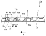
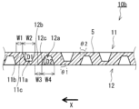
도 1a 및 도 1b에 도시하는 바와 같이, 전자파 실드(10a)는, 판상의 기부(5)를 구비하고 있다. 기부(5)는, 제1면(11)과, 제2면(12)을 갖는다. 제1면(11)은, 전자파를 입사시키기 위한 면이다. 제2면(12)은, 제1면(11)으로부터 이격된 위치에서 제1면(11)을 따라 연장되어 있다. 전자파 실드(10a)는 유전체를 포함하고 있다. 제1면(11)은, 복수의 제1 오목부(11a)와, 제1 고체부(11b)를 갖는다. 복수의 제1 오목부(11a)는, 제1면(11)을 따른 특정 방향(X축 방향)에 있어서 소정의 간격으로 형성되어 있다. 제1 고체부(11b)는, 그 특정 방향에서의 제1 오목부(11a)의 일단부(11c)에 접함과 함께 제1 오목부(11a)의 깊이의 기준이 되는 표면(11s)을 포함한다. 이에 더하여, 제1 고체부(11b)는, 제1 오목부(11a)의 깊이 방향에 있어서 제1 오목부(11a)의 깊이(D1) 이상의 치수를 갖는다. 제2면(12)은, 특정 방향에 있어서 복수의 제1 오목부(11a)와 교대로 형성된 복수의 제2 오목부(12a)를 갖는다.As shown in FIGS. 1A and 1B, the
본 명세서에 있어서, 전자파 실드는, 전자파의 에너지를 감쇠시키는 기능을 발휘할 수 있는 물품이다. 전자파 실드가 전자파의 에너지를 감쇠시키는 원리는, 특정 원리에 한정되지 않는다. 그 원리는, 예를 들어 전자파와 전자파 실드의 상호 작용에 수반하는 반사, 투과, 흡수, 회절 및 간섭 등의 현상, 그리고, 이들 현상에 기인해서 생기는 전자파의 산란 및 확산 등의 현상을 이용한 것일 수 있다. 전자파 실드(10a)에 있어서, 제1면(11)에 소정의 전자파가 입사되면, 그 전자파의 에너지가 감쇠한다.In this specification, an electromagnetic wave shield is an article that can exert the function of attenuating the energy of electromagnetic waves. The principle by which an electromagnetic wave shield attenuates the energy of electromagnetic waves is not limited to a specific principle. The principle may be, for example, utilizing phenomena such as reflection, transmission, absorption, diffraction and interference that accompany the interaction between electromagnetic waves and electromagnetic shields, and phenomena such as scattering and diffusion of electromagnetic waves that occur due to these phenomena. there is. In the
도 2는, 참고예에 관한 부재(30)의 단면도이다. 부재(30)는, 예를 들어 전자파 실드(10a)를 이루는 재료와 동일 종류의 재료로 구성되어 있다. 도 2에 도시하는 바와 같이, 부재(30)는, 제1면(31)과, 제2면(32)을 구비하고 있다. 제1면(31)에는, 복수의 오목부(31a)가 형성되어 있고, 제2면(32)에는, 복수의 오목부(32a)가 형성되어 있다. 복수의 오목부(31a) 및 복수의 오목부(32a)는, 제1면(31)을 따른 특정 방향(X축 방향)으로 교대로 배열되어 있다. 부재(30)는, 예를 들어 지그재그 형상으로 형성된 판재이며, 특정 방향에 있어서 인접하는 한 쌍의 오목부(31a)끼리 접하고 있다. 환언하면, 부재(30)에 있어서, 전자파 실드(10a)의 제1 고체부(11b)에 대응하는 부위의 폭이 실질적으로 제로이다. 제1면(31)에 형성된 오목부의 특정 방향에서의 일단부의 특정 방향에서의 위치는, 제2면(32)에 형성된 오목부의 바닥의 특정 방향에서의 위치와 일치하고 있다. 부재(30)에 의하면, 제1면(31)에 입사한 전자파는, 거의 차폐되지 않는다. 한편, 전자파 실드(10a)에 의하면, 제1면(11)에 입사한 전자파가 차폐된다. 이에 더하여, 전자파 실드(10a)의 제2면(12)에는, 복수의 제1 오목부(11a)와 교대로 복수의 제2 오목부(12a)가 형성되어 있으므로, 전자파 실드(10a)가 경량화되기 쉽다. 이에 더하여, 전자파 실드(10a)는 높은 내충격성을 갖기 쉽다.Fig. 2 is a cross-sectional view of the
전자파 실드(10a)에 입사되는 전자파의 파장(λ)은, 특정 값에 한정되지 않는다. 파장(λ)은, 예를 들어 1mm 내지 30mm이다.The wavelength (λ) of the electromagnetic wave incident on the
도 1b에 도시하는 바와 같이, 제1 고체부(11b)의 양면은, 예를 들어 서로 평행하고 또한 평탄하다.As shown in FIG. 1B, both surfaces of the first
전자파 실드(10a)는, 예를 들어 밀리파 레이더, 밀리파 무선 통신 및 밀리파 센싱 등의 용도를 위한 전자파 실드로서 사용할 수 있다. 전자파 실드(10a)가 적용된 기기는, 예를 들어 자동차 및 무선 기지국 등에 사용할 수 있다. 전자파 실드(10a)가 밀리파 레이더용일 경우, 24GHz대, 60GHz대, 76GHz대 및 79GHz대로 이루어지는 군에서 선택되는 1개의 주파수대의 밀리파 레이더에 전자파 실드(10a)를 사용할 수 있다. 또한, 전자파 실드(10a)는, 특정 파장의 전자파만을 차폐하는 것이 아니라, 넓은 파장 영역의 전자파를 차폐해도 되지만, 특정 파장(λ)의 전자파를 「차폐 대상」으로서 정하여 생각할 수 있다. 예를 들어, 실질적으로 조사되는 전자파의 주파수가 76 내지 77GHz인, 즉 실질적인 조사 파장이 3.89 내지 3.94mm인 차량 탑재용 밀리파 레이더와 함께 설치되어 있는 전자파 실드의 경우에는, 중심 주파수 76.5GHz의 파장인 3.92mm를, 이 전자파 실드의 차폐 대상인 파장(λ)으로서 판단할 수 있다. 사용되는 전자파의 주파수가 77 내지 81GHz인, 즉 사용 전자파의 파장이 3.70 내지 3.89mm인 차량 탑재용 밀리파 레이더를 위한 전자파 실드라고 표기되어 있는 경우에는, 중심 주파수 79GHz의 파장인 3.79mm를, 이 전자파 실드의 차폐 대상인 파장(λ)으로서 판단할 수 있다. 사용되는 전자파의 주파수가 24.05 내지 24.25GHz인, 즉 사용 전자파의 파장이 12.36 내지 12.47mm인 차량 탑재용 밀리파 레이더를 위한 전자파 실드라고 표기되어 있는 경우에는, 중심 주파수 24.15GHz의 파장인 12.41mm를, 이 전자파 실드의 차폐 대상인 파장(λ)으로서 판단할 수 있다. 사용되는 전자파의 주파수가 60.0 내지 60.1GHz인, 즉 사용 전자파의 파장이 4.99 내지 5.00mm인 밀리파 레이더를 위한 전자파 실드라고 표기되어 있는 경우에는, 중심 주파수 60.05GHz의 파장인 4.99mm를, 이 전자파 실드의 차폐 대상인 파장(λ)으로서 판단할 수 있다. 사용되는 전자파의 주파수가 27 내지 29.5GHz인, 즉 사용 전자파의 파장이 10.16 내지 11.10mm인 밀리파 무선을 위한 전자파 실드라고 표기되어 있는 경우에는, 중심 주파수 28.25GHz의 파장인 10.61mm를, 이 전자파 실드의 차폐 대상인 파장(λ)으로서 판단할 수 있다. 전자파 실드가 대응 주파수 70 내지 90GHz, 즉 대응 파장이 3.33 내지 4.28mm라고 표기되어 판매되고 있는 경우 등에는, 중심 주파수 80GHz의 파장인 3.75mm를, 이 전자파 실드의 차폐 대상인 파장(λ)으로서 판단할 수 있다.The
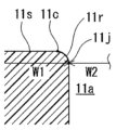
특정 방향에서의 제1 오목부(11a)의 개구 폭(W2)은, 예를 들어 제1 오목부(11a)의 최외부에서의 폭으로서 정의된다. 한편, 도 1c에 도시하는 바와 같이, 전자파 실드(10a)에 있어서, 제1 오목부(11a)의 일단부(11c)의 근방에서, 제1 고체부(11b)는, 곡면(11r)을 갖고 있어도 된다. 이 경우, 개구 폭(W2)은, 제1 오목부(11a)의 내측에서의 곡면(11r)의 단부(11j)를 기준으로 결정된다. 이에 더하여, 제1 고체부(11b)의 폭(W1)도 단부(11j)를 기준으로 결정된다.The opening width W2 of the
제1 오목부(11a)의 깊이(D1), 특정 방향에서의 제1 오목부(11a)의 개구 폭(W2) 및 특정 방향에서의 제1 고체부(11b)의 폭(W1)은, 제1면(11)에 입사한 전자파가 차폐되는 한 특정 값에 한정되지 않는다.The depth D1 of the first
깊이(D1)를 전자파 실드(10a)의 차폐 대상이 되는 특정 파장(λ)과 대비한 경우, 깊이(D1)는, 예를 들어 0.50λ 내지 2.10λ이다. 이와 같은 구성에 의하면, 제1면(11)에 입사한 전자파가 보다 원하는 상태에서 차폐되기 쉽다. 깊이(D1)는, 0.60λ 이상이어도 되고, 0.70λ 이상이어도 되고, 0.80λ 이상이어도 된다. 깊이(D1)는, 2.0λ 이하이어도 되고, 1.9λ 이하이어도 되고, 1.8λ 이하이어도 된다.When the depth D1 is compared with the specific wavelength λ to be shielded by the
개구 폭(W2)을 전자파 실드(10a)의 차폐 대상이 되는 특정 파장(λ)과 대비한 경우, 개구 폭(W2)은, 예를 들어 0.50λ 내지 2.10λ이다. 이와 같은 구성에 의하면, 제1면(11)에 입사한 전자파가 보다 원하는 상태에서 차폐되기 쉽다. 개구 폭(W2)은, 0.60λ 이상이어도 되고, 0.70λ 이상이어도 되고, 0.80λ 이상이어도 된다. 개구 폭(W2)은, 2.0λ 이하이어도 되고, 1.9λ 이하이어도 되고, 1.8λ 이하이어도 된다.When the aperture width W2 is compared with the specific wavelength λ to be shielded by the
폭(W1)을 전자파 실드(10a)의 차폐 대상이 되는 특정 파장(λ)과 대비한 경우, 폭(W1)은, 예를 들어 0.20λ 내지 2.0λ이다. 이와 같은 구성에 의하면, 제1면(11)에 입사한 전자파가 보다 원하는 상태에서 차폐되기 쉽다. 폭(W1)은, 0.30λ 이상이어도 되고, 0.40λ 이상이어도 되고, 0.50λ 이상이어도 된다. 폭(W1)은, 1.9λ 이하이어도 되고, 1.8λ 이하이어도 되고, 1.7λ 이하이어도 된다.When the width W1 is compared with the specific wavelength λ to be shielded by the
전자파 실드(10a)에 있어서, 폭(W1)과 개구 폭(W2)의 합(W1+W2)에 대한, 폭(W1)의 비(W1/(W1+W2))는, 특정 값에 한정되지 않는다. 비(W1/(W1+W2))는, 예를 들어 0.1 내지 0.9이다. 이와 같은 구성에 의하면, 제1면(11)에 입사한 전자파가 보다 원하는 상태에서 차폐되기 쉽다. 비(W1/(W1+W2))는, 0.15 이상이어도 되고, 0.2 이상이어도 되고, 0.3 이상이어도 된다. 비(W1/(W1+W2))는, 0.8 이하이어도 되고, 0.75 이하이어도 되고, 0.7 이하이어도 된다.In the
도 1a에 도시하는 바와 같이, 제1 오목부(11a)는, 예를 들어 제1면(11)의 면 내에서 특정 방향과 수직인 방향을 따라 연장되어 있다. 복수의 제1 오목부(11a)는, 평면으로 보아, 예를 들어 서로 평행하게 직선상으로 연장되어 있다. 복수의 제1 오목부(11a)는, 평면으로 보아 만곡해서 연장되어 있어도 되고, 지그재그로 연장되어 있어도 된다.As shown in FIG. 1A, the first
평면으로 보아, 복수의 제1 오목부(11a)는, 정사각형 격자, 직사각형 격자, 또는 평방 사변형 격자를 이루도록 배치되어 있어도 된다. 이 경우, 평면으로 보았을 때의 각 제1 오목부(11a)의 형상은, 예를 들어 정사각형 및 정육각형 등의 다각 형상이어도 되고, 원 형상이어도 된다.When viewed in plan, the plurality of
도 1b에 도시하는 바와 같이, 전자파 실드(10a)에 있어서, 제1 오목부(11a)의 측면은, 예를 들어 제2면(12)을 향해서 특정 방향에 수직으로 연장되어 있다. 환언하면, 제1 오목부(11a)의 측면은, 특정 방향에 수직인 평면에 대하여 평행하다.As shown in FIG. 1B, in the
제2 오목부(12a)의 형상은, 특정 형상에 한정되지 않는다. 제2 오목부(12a)는, 예를 들어 제1 오목부(11a)와 동일한 형상을 갖는다. 이 경우, 제2 오목부(12a)의 깊이(D2)는, 제1 오목부(11a)의 깊이(D1)와 동일하고, 특정 방향에서의 제2 오목부(12a)의 개구 폭(W4)은, 개구 폭(W2)과 동일하다. 이와 같은 구성에 의하면, 전자파 실드(10a)를 제조하기 쉽다. 제2 오목부(12a)는, 제1 오목부(11a)와 다른 형상을 갖고 있어도 된다.The shape of the second
도 1b에 도시하는 바와 같이, 제2면(12)은, 예를 들어 제2 고체부(12b)를 갖는다. 제2 고체부(12b)는, 특정 방향에서의 제2 오목부(12a)의 일단부(12c)에 접함과 함께 제2 오목부(12a)의 깊이의 기준이 되는 표면(12s)을 포함한다. 이에 더하여, 제2 고체부(12b)는, 제2 오목부(12b)의 깊이 방향에 있어서 제2 오목부(12b)의 깊이(D2) 이상의 치수를 갖는다. 제2 고체부(12b)는, 예를 들어 제1 고체부(11b)와 동일한 형상을 갖는다. 이 경우, 특정 방향에서의 제2 오목부(12a)의 폭(W3)은, 폭(W1)과 동일하다. 이와 같은 구성에 의하면, 전자파 실드(10a)를 제조하기 쉽다.As shown in FIG. 1B, the
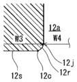
특정 방향에서의 제2 오목부(12a)의 개구 폭(W4)은, 예를 들어 제2 오목부(12a)의 최외부에서의 폭으로서 정의된다. 한편, 도 1d에 도시하는 바와 같이, 전자파 실드(10a)에 있어서, 제2 오목부(11a)의 일단부(12c)의 근방에서, 제2 고체부(11b)는, 곡면(12r)을 갖고 있어도 된다. 이 경우, 개구 폭(W4)은, 제2 오목부(12a)의 내측에서의 곡면(12r)의 단부(12j)를 기준으로 결정된다. 이에 더하여, 제2 고체부(12b)의 폭(W3)도 단부(12j)를 기준으로 결정된다.The opening width W4 of the second
도 1b에 도시하는 바와 같이, 전자파 실드(10a)에 있어서, 제1면(11) 및 제2면(12)은, 단위 구조(15)가 특정 방향으로 반복해서 나타나도록 형성되어 있다. 단위 구조(15)는, 제1 오목부(11a), 제2 오목부(12a), 제1 고체부(11b) 및 제2 고체부(12b)를 포함하는 구조이다. 이와 같은 구성에 의하면, 전자파 실드(10a)가 면 내에서 균일한 전자파 차폐 특성을 갖기 쉽다.As shown in FIG. 1B, in the
도 1b에 도시하는 바와 같이, 제1 오목부(11a)의 깊이 방향에서의 전자파 실드(10a)의 고체부의 치수는, 예를 들어 특정 방향에 있어서 주기적으로 변동하고 있다. 그 치수는, 예를 들어 제1 고체부(11b) 및 제2 고체부(12b)에 있어서 최대이며, 제1 오목부(11a) 및 제2 오목부(12a)에 있어서 보다 작다. 제1 오목부(11a)의 깊이 방향에서의 전자파 실드(10a)의 고체부의 치수는, 특정 방향에 있어서 일정하여도 된다.As shown in FIG. 1B, the size of the solid portion of the
도 1b에 도시하는 바와 같이, 특정 방향에 있어서 인접하는 한 쌍의 제1 오목부(11a) 및 제2 오목부(12a)는, 예를 들어 특정 방향에 있어서 서로 이격되어 형성되어 있다. 특정 방향에 있어서 인접하는 한 쌍의 제1 오목부(11a) 및 제2 오목부(12a)의 일부끼리가 특정 방향에 있어서 겹쳐 있어도 된다.As shown in FIG. 1B, a pair of first
상기한 바와 같이, 전자파 실드(10a)는 유전체를 포함하고 있다. 유전체는 특정 재료에 한정되지 않는다. 전자파 실드(10a)는, 예를 들어 유전체로서 수지를 포함하고 있다. 이 경우, 전자파 실드(10a)의 제조 비용이 저감되기 쉽다. 예를 들어, 10GHz 내지 300GHz의 범위에 포함되는 적어도 하나의 주파수에서의 유전체의 복소 비유전율의 허부(ε")는 0.1 이하이다. 허부(ε")는, 바람직하게는 0.07 이하이며, 보다 바람직하게는 0.05 이하이고, 더욱 바람직하게는 0.01 이하이다.As described above, the
10 내지 300GHz의 범위에 포함되는 적어도 하나의 주파수에서의 수지의 복소 비유전율의 실부(ε')는, 예를 들어 2 이상 4 이하이다. 실부(ε')는, 바람직하게는 2.1 이상 3.5 이하이고, 보다 바람직하게는 2.2 이상 3.0 이하이다. 실부(ε')는, 3.8 이하이어도 되고, 3.6 이하이어도 되고, 3.4 이하이어도 되고, 3.2 이하이어도 되고, 3.0 이하이어도 되고, 2.8 이하이어도 되고, 2.6 이하이어도 되고, 2.4 이하이어도 된다.The real part (ε') of the complex relative dielectric constant of the resin at at least one frequency included in the range of 10 to 300 GHz is, for example, 2 or more and 4 or less. The actual part (ε') is preferably 2.1 or more and 3.5 or less, and more preferably 2.2 or more and 3.0 or less. The actual part (ε') may be 3.8 or less, 3.6 or less, 3.4 or less, 3.2 or less, 3.0 or less, 2.8 or less, 2.6 or less, or 2.4 or less.
전자파 실드(10a)에 포함되는 수지는, 특정 수지에 한정되지 않는다. 수지는, 예를 들어 열가소성 수지이다. 수지는, 예를 들어 폴리에틸렌, 폴리프로필렌, 폴리비닐알코올, 폴리에틸렌테레프탈레이트, 폴리부틸렌테레프탈레이트, 에틸렌·아세트산비닐 공중합체, 폴리스티렌, 아크릴로니트릴스티렌, 아크릴로니트릴·부타디엔·스티렌 공중합체, ASA 수지, AES 수지, PMMA 등의 아크릴 수지, MS 수지, MBS 수지, 시클로올레핀 수지, 폴리아세탈 수지, 폴리아미드 수지, 폴리에스테르 수지, 폴리카르보네이트 수지, 폴리우레탄 수지, 액정 폴리머, EPDM, PPS, PEEK, PPE, 폴리술폰계 수지, 폴리이미드계 수지, 불소계 수지, 올레핀계 열가소성 엘라스토머(TPO) 등의 열가소성 엘라스토머, 또는 아크릴 엘라스토머이다. 수지는, 열경화성 수지이어도 된다. 열경화성 수지는, 예를 들어 에폭시 수지, 아크릴 수지, 또는 실리콘 수지이다. 전자파 실드(10a)는, 단일 종류의 수지만을 포함하고 있어도 되고, 복수 종류의 수지를 포함하고 있어도 된다.The resin contained in the
전자파 실드(10a)는, 예를 들어 필러를 포함하고 있어도 된다. 필러는, 카본 블랙 등의 착색재이어도 되고, 탈크, 유리 섬유 및 광물 등의 무기 보강재이어도 되고, 연화제이어도 된다. 전자파 실드(10a)는, 난연제 및 가소제 등의 첨가제를 포함하고 있어도 된다. 전자파 실드(10a)는, 필러를 포함하고 있지 않아도 된다. 이 경우, 전자파 실드(10a)의 제조 비용이 낮아지기 쉽다.The
전자파 실드(10a)는, 예를 들어 도전성을 갖는 부위를 갖지 않는다. 전자파의 차폐를 위해서, 예를 들어 금속막 등의 도전성을 갖는 부위에 의해 전자파를 반사시키는 것을 생각할 수 있다. 한편, 전자파 실드(10a)에 의하면, 도전성을 갖는 부위를 갖고 있지 않아도, 전자파를 차폐할 수 있다. 전자파 실드(10a)는, 유전체만에 의해 구성되어 있어도 되고, 도전성을 갖는 부위를 포함하고 있어도 된다.The
전자파 실드(10a)는, 예를 들어 수지 성형품이다. 이 경우, 전자파 실드(10a)의 성형 방법은, 특정 방법에 한정되지 않는다. 전자파 실드(10a)는, 사출 성형, 프레스 성형, 블로우 성형, 또는 진공 성형에 의해 제조될 수 있다. 전자파 실드(10a)는, 절삭 가공 또는 3D 프린팅에 의해 제조되어도 된다.The
전자파 실드(10a)에 있어서, 전자파의 차폐를 위해서 생기는 전자파 실드(10a)와 전자파의 상호 작용은, 특정 상호 작용에 한정되지 않는다. 전자파 실드(10a)는, 예를 들어 제1면(11)을 향해서 입사된 전자파의 적어도 일부를 투과시키고, 제2면(12)으로부터 산란 상태의 전자파를 출사시킨다. 환언하면, 전자파 실드(10a)는, 전파 투과 산란체로서 기능할 수 있다. 이에 의해, 간소한 구성으로 전자파의 차폐를 실현할 수 있다. 이 경우, 전자파 실드(10a)에 있어서, 제1 오목부(11a)의 깊이(D1), 특정 방향에서의 제1 오목부의 개구 폭(W2) 및 특정 방향에서의 제1 고체부(11b)의 폭(W1)은, 제1면(11)에 입사한 전자파가 제2면(12)으로부터 산란한 상태에서 출사되도록 정해져 있다.In the
전자파 실드(10a)의 제1면(11)에 수직으로 파장(λ)의 전자파를 입사시켰을 때, 그 전자파의 직진 방향에서의 투과 감쇠량은, 특정 값에 한정되지 않는다. 직진 방향에서의 투과 감쇠량이 클수록, 제1면(11)에 입사한 전자파가 제2면(12)으로부터 산란한 상태에서 보다 출사되기 쉽다고 이해된다. 직진 방향에서의 투과 감쇠량은, 예를 들어 2.0dB 이상이며, 바람직하게는 2.5dB 이상이다.When an electromagnetic wave of wavelength λ is incident perpendicularly to the
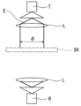
전자파 실드(10a)의 직진 방향에서의 투과 감쇠량은, 예를 들어 일본 산업 규격 JIS R 1679:2007을 참조하여 측정함으로써 결정할 수 있다. 이 측정은, 예를 들어 도 3에 도시하는 측정계를 사용해서 실시할 수 있다. 도 3에 도시하는 바와 같이, 샘플 홀더(SH), 밀리파 렌즈(L), 송신기(T) 및 수신기(R)를 배치한다. 예를 들어, 송신기(T)로부터 송신되며, 또한, 밀리파 렌즈(L)에 의해 30mm의 직경(빔 직경)으로 조정된 전자파(E)가 샘플 홀더(SH)에 조사된다. 샘플 홀더(SH)에는 아무것도 세트하지 않은 상태에서 전자파(E)의 송수신을 행하여, 투과 감쇠량이 0dB(전자파가 전량 투과)인 상태를 각 샘플의 면 방향에 대한 수직 입사의 투과 감쇠량 측정의 기준으로 한다. 이어서, 샘플 홀더(SH)에 전자파 실드(10a)의 샘플을 세트한 후, 전자파 실드(10a)의 제1면(11)에 대응하는 샘플의 주면에 대하여 수직인 방향으로 송신기(T) 및 수신기(R)가 동일 직선 상에 위치하도록, 수신기(R)를 배치한다. 이 상태에서, 파장(λ)을 갖는 전자파(E)의 송수신을 행하여, 직진 방향에서의 투과 감쇠량을 측정한다. 투과 감쇠량은, 이하의 식 (1)로 나타내진다. 식 (1)에서, PI는 수신 전력이며, P0는 송신 전력이다. 「Log」는 상용 대수를 나타낸다.The transmission attenuation amount in the straight direction of the
투과 감쇠량=|10Log(PI/P0)| 식 (1)Transmission attenuation=|10Log(P I /P 0 )| Equation (1)
전자파 실드(10a)는, 예를 들어 회절 격자로서 기능할 수 있다. 광의 회절에 관하여, 직사각형의 단면을 갖는 회절 격자에서의 0차 광투과율(I0)은, 스칼라 회절 이론에 의하면, 이하의 식 (2)에 의해 나타내진다. 식 (2)에서, εR은, 회절 격자를 이루는 재료의 비유전율의 실부이며, sqrt(εR)는, εR의 평방근이다. h는, 회절 격자에서의 볼록부의 높이이다. λ는, 광의 파장이다.The
I0=cos2(π·|sqrt(εR)|-1·(h/λ)) 식 (2)I 0 =cos 2 (π·|sqrt(ε R )|-1·(h/λ)) Equation (2)
브래그의 법칙에 의하면, 회절에 의한 산란 투과파의 방향(산란각)은, 회절 격자에서의 볼록부의 주기에 의해 정해진다. 볼록부와 볼록부 사이를 투과한 회절파끼리의 상호 강화 및 상호 약화에 의해 간섭 줄무늬가 형성된다. 이 경우, 회절파끼리의 상호 강화에 의해 투과 산란파가 관측된다고 생각된다. 회절파끼리의 상호 강화는 식 (3)에 의해 나타낼 수 있고, 회절파끼리의 상호 약화는 식 (4)에 의해 나타낼 수 있다. 식 (3) 및 (4)에서, d는 회절 격자에서의 볼록부의 주기이며, θ는 회절파끼리의 상호 강화 또는 상호 약화가 일어나는 각도이고, m은 0 이상의 정수이고, λ는 입사파의 파장이다. λ가 일정한 경우, 회절 격자에서의 볼록부의 주기에 따라 투과 산란파의 산란각이 변동될 수 있다고 이해된다. 표 1에, 회절파끼리의 상호 강화가 일어나는 산란각(θ)과 주기(d)의 관계의 일례를 나타낸다.According to Bragg's law, the direction (scattering angle) of the transmitted wave scattered by diffraction is determined by the period of the convex portion in the diffraction grating. Interference stripes are formed by mutual strengthening and mutual weakening of diffracted waves that have transmitted between convex parts. In this case, it is thought that transmission and scattering waves are observed due to mutual reinforcement of diffracted waves. Mutual strengthening of diffracted waves can be expressed by equation (3), and mutual weakening of diffracted waves can be expressed by equation (4). In equations (3) and (4), d is the period of the convexities in the diffraction grating, θ is the angle at which mutual strengthening or mutual weakening of diffraction waves occurs, m is an integer greater than 0, and λ is the wavelength of the incident wave. am. It is understood that when λ is constant, the scattering angle of the transmitted scattered wave may vary depending on the period of the convex portion in the diffraction grating. Table 1 shows an example of the relationship between the scattering angle (θ) and the period (d) at which mutual reinforcement of diffracted waves occurs.
dsinθ=mλ 식 (3)dsinθ=mλ Equation (3)
dsinθ=(m+1/2)λ 식 (4)dsinθ=(m+1/2)λ Equation (4)

한편, 이들의 검토에 있어서는, 광의 회절 이론을 참고로 했지만, 이것을 밀리파에 응용하는 것은 용이하지 않다. 왜냐하면, 전파, 특히, 밀리파 및 준밀리파는, 가시광보다 3자리 이상이나 파장이 큰 것도 고려할 필요가 있기 때문이다. 예를 들어, 밀리파는 가시광보다도 직진성이 낮아(회절이 일어나기 쉬워), 가시광과 비교해서 플라스틱 벽 및 종이 등의 물체를 투과하기 쉬운 등의 특징이 있으므로, 이러한 특징을 고려한 설계가 필요해진다.On the other hand, in these studies, the diffraction theory of light was referred to, but it is not easy to apply this to millimeter waves. This is because it is necessary to consider that radio waves, especially millimeter waves and sub-millimeter waves, have wavelengths that are three orders of magnitude larger than visible light. For example, millimeter waves have characteristics such as having a lower straightness than visible light (diffraction easily occurs) and being more likely to penetrate objects such as plastic walls and paper compared to visible light, so design that takes these characteristics into consideration is necessary.
전자파 실드(10a)는, 다양한 관점에서 변경 가능하다. 전자파 실드(10a)는, 도 4에 도시하는 전자파 실드(10b) 또는 도 5에 도시하는 전자파 실드(10c)와 같이 변경되어도 된다. 전자파 실드(10b) 및 전자파 실드(10c)는, 특별히 설명하는 부분을 제외하고, 전자파 실드(10a)와 마찬가지로 구성되어 있다. 전자파 실드(10a)의 구성 요소와 동일하거나 또는 대응하는 전자파 실드(10b) 및 전자파 실드(10c)의 구성 요소에는, 동일한 부호를 부여하고, 상세한 설명을 생략한다. 전자파 실드(10a)에 관한 설명은, 기술적으로 모순되지 않는 한, 전자파 실드(10b) 및 전자파 실드(10c)에도 적용된다.The
도 4 및 도 5에 도시하는 바와 같이, 전자파 실드(10b) 및 전자파 실드(10c)에 있어서, 제1 오목부(11a)의 측면은, 제2면(12)을 향해서 끝이 가늘게 형성되어 있다. 전자파 실드(10b)에 있어서, 제1 오목부(11a)의 특정 방향에서의 중앙에는 평탄한 저면이 형성되어 있다. 전자파 실드(10c)에 있어서, 제1 오목부(11a)는, 쐐기 형상으로 형성되어 있다. 이와 같은 구성에 의하면, 전자파 실드(10b) 및 전자파 실드(10c)를 성형에 의해 제조할 때, 성형품을 다이로부터 취출하기 쉽다.4 and 5, in the
전자파 실드(10b) 및 전자파 실드(10c)에 있어서, 제1 오목부(11a)의 측면이 특정 방향에 수직인 평면에 대하여 이루는 각도(θ1)는, 특정 값에 한정되지 않는다. 각도(θ1)는, 예를 들어 0°를 초과하고 30° 이하이다. 이와 같은 구성에 의하면, 제1면(11)에 입사한 전자파가 보다 원하는 상태에서 차폐되기 쉽다. 예를 들어, 제1 오목부(11a)의 바닥으로부터 제1 오목부(11a)의 일단부(11c)를 향해서 스트레이트로 연장되는 측면에 의해, 각도(θ1)가 특정된다.In the
전자파 실드(10b) 및 전자파 실드(10c)에 있어서, 제2 오목부(12a)의 측면이 특정 방향에 수직인 평면에 대하여 이루는 각도(θ2)는, 특정 값에 한정되지 않는다. 각도(θ2)는, 예를 들어 0°를 초과하고 30° 이하이다. 각도(θ2)는, 각도(θ1)와 동일하여도 되고, 각도(θ1)와 달라도 된다. 예를 들어, 제2 오목부(12a)의 바닥으로부터 제2 오목부(12a)의 일단부(12c)를 향해서 스트레이트로 연장되는 측면에 의해, 각도(θ2)가 특정된다.In the
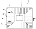
도 6, 도 7 및 도 8에 도시하는 바와 같이, 전자파 실드(10a) 및 기부(5)로 이루어지는 군에서 선택되는 적어도 하나는, 예를 들어 환상체이며, 또한, 그 환상체의 축선을 따라 제1면(11)을 보았을 때 다각 형상 또는 원 형상의 외주를 갖는다. 이와 같은 구성에 의하면, 전자파 실드(10a)에 의해 둘러싸인 공간을 통해서 제1면(11)에 입사하는 전자파를 차폐할 수 있다.As shown in FIGS. 6, 7, and 8, at least one selected from the group consisting of the
도 6, 도 7 및 도 8에 도시하는 바와 같이, 전자파 실드(10a) 및 기부(5)의 적어도 하나는, 예를 들어 다각뿔대 형상의 외형을 갖는다. 전자파 실드(10a) 및 기부(5)의 적어도 하나는, 예를 들어 이 외형에 있어서 다각뿔대의 상측 저면 및 하측 저면에 대응하는 위치에 개구를 갖는 통 형상이다. 전자파 실드(10a) 및 기부(5)의 적어도 하나는, 예를 들어 다각뿔대의 상측 저면에 대응하는 위치에 제1 개구(51)를 갖고, 하측 저면에 대응하는 위치에 제2 개구(52)를 갖는다. 제1면(11)은, 통 형상의 전자파 실드(10a) 또는 기부(5)의 내주면을 이루고 있다. 제2면(12)은, 통 형상의 전자파 실드(10a) 또는 기부(5)의 외주면을 이루고 있다. 이와 같은 구성에 의하면, 전자파 실드(10a)에 의해 전자파의 차폐가 가능한 공간이 넓어지기 쉽다. 이에 더하여, 전자파 실드(10a)에서의 제1 개구(51)를 전자파의 송수신을 위한 안테나를 배치하기 위해서 이용할 수 있다. 전자파 실드(10a) 및 기부(5)의 적어도 하나의 외형은 원뿔대 형상이어도 되고, 타원뿔대 형상이어도 된다. 이 경우, 전자파 실드(10a)는, 그 외형의 원뿔대 또는 타원뿔대의 상측 저면 및 하측 저면에 대응하는 위치에 개구를 갖는다.As shown in FIGS. 6, 7, and 8, at least one of the
전자파 실드(10a)는, 예를 들어 도 9에 도시하는 전자파 실드(10d)와 같이 변경되어도 된다. 전자파 실드(10d)는, 특별히 설명하는 부분을 제외하고, 전자파 실드(10a)와 마찬가지로 구성되어 있다. 도 9에 도시하는 바와 같이, 전자파 실드(10d)는, 예를 들어 접촉부(6)를 더 구비하고 있다. 접촉부(6)는, 전자파 실드(10d)와는 다른 부재에 접촉하기 위한 부위이다. 접촉부(6)는, 환상체인, 전자파 실드(10d) 또는 기부(5)의 축선을 따라 제1면(11)을 보았을 때 시인되는 다각 형상 또는 원 형상의 외주에 접하고 있다. 이와 같은 구성에 의하면, 접촉부(6)를 다른 부재에 접촉시킨 상태에서 전자파 실드(10d)를 다른 부재에 설치할 수 있다. 접촉부(6)는, 예를 들어 플랜지를 이루고 있다.The
도 6, 도 7, 도 8 및 도 9에 도시하는 바와 같이, 예를 들어 전자파 실드(10a 또는 10d)를 구비한 레이더용 커버(50)를 제공할 수 있다. 레이더용 커버(50)에 의하면, 레이더를 향해서 진행하는 불필요한 전자파를 차폐할 수 있다. 이에 의해, 레이더에 있어서 불필요한 전파가 수신되기 어렵다.As shown in FIGS. 6, 7, 8, and 9, for example, a
도 6, 도 8 및 도 9에 도시하는 바와 같이, 레이더용 커버(50)는, 예를 들어 중공의 각뿔대 형상으로 형성되어 있고, 제1 개구(51)와, 제2 개구(52)를 갖는다. 제1 개구(51) 및 제2 개구(52) 각각은 직사각형이다. 제2 개구(52)는, 제1 개구(51)보다도 크다. 예를 들어, 제1 개구(51)에, 레이더(도시 생략)의 송수신 안테나가 배치된다. 레이더용 커버(50)의 내면의 일부가 전자파 실드(10a)의 제1면(11)에 의해 형성되어 있고, 레이더용 커버(50)의 외면의 일부가 전자파 실드(10a)의 제2면(12)에 의해 형성되어 있다.As shown in FIGS. 6, 8, and 9, the
[실시예][Example]
이하, 실시예에 의해 본 발명을 보다 상세하게 설명한다. 단, 본 발명은, 이하의 실시예에 한정되지 않는다. 먼저, 실시예 및 비교예에 관한 평가 방법에 대해서 설명한다.Hereinafter, the present invention will be described in more detail through examples. However, the present invention is not limited to the following examples. First, the evaluation method for Examples and Comparative Examples will be described.
[투과 감쇠량][Transmission attenuation]
키컴사 제조의 전파 송수신기 EAS02를 사용하고, JIS R 1679:2007을 참조하여, 실시예 및 비교예에 관한 샘플의 한쪽 주면에 77GHz의 주파수를 갖는 전파를 30mm의 직경으로 입사시켰을 때의 직진 방향에서의 투과 감쇠량을 측정했다. 이 전파의 파장(λ)은 3.90mm이었다. 이 측정은, 도 3에 도시하는 측정계를 사용한 측정과 마찬가지로 해서 행했다. 안테나와 측정 시료의 거리는, 상기 JIS의 8.2.2 측정 거리 및 부속서(H)를 참조하여 결정된다. 이 측정에 있어서, 오목부가 형성되어 있지 않은 샘플에서는 한쪽의 평탄한 주면에 대하여 수직으로 전파를 입사시키고, 오목부를 갖는 샘플에서는, 한쪽의 주면에 있어서 한 쌍의 오목부 사이에 형성된 평탄면에 대하여 수직인 방향을 따라 전파를 입사시켰다. 또한, 오목부가 존재하는 샘플에서는, 전파의 전계의 진폭 방향이 오목부의 길이 방향과 수직인 방향에 일치하도록 전파를 생기게 했다. 이 측정에 있어서, 오목부가 존재하는 샘플에서는, 오목부의 길이 방향과 수직인 방향으로 샘플을 움직이게 한 상태에서 투과 감쇠량의 절댓값의 최솟값을 특정했다. 투과 감쇠량은, 상기 식 (1)에 따라서 결정했다. 결과를 표 2에 나타낸다.In the straight direction when a radio wave with a frequency of 77 GHz was incident on one main surface of the samples of the examples and comparative examples with a diameter of 30 mm using the radio wave transceiver EAS02 manufactured by Keycom, and with reference to JIS R 1679:2007. The transmission attenuation was measured. The wavelength (λ) of this radio wave was 3.90 mm. This measurement was performed similarly to the measurement using the measuring system shown in FIG. 3. The distance between the antenna and the measurement sample is determined by referring to 8.2.2 Measurement Distance and Annex (H) of the above JIS. In this measurement, for samples without concave portions, radio waves are incident perpendicularly to one flat main surface, and for samples with concave portions, radio waves are incident perpendicular to the flat surface formed between a pair of concave portions on one main surface. Radio waves were incident along the direction. Additionally, in samples with concave portions, radio waves were generated so that the amplitude direction of the electric field of the radio wave coincided with the direction perpendicular to the longitudinal direction of the concave portion. In this measurement, for samples with concave portions, the minimum absolute value of the transmission attenuation amount was specified while the sample was moved in a direction perpendicular to the longitudinal direction of the concave portion. The amount of transmission attenuation was determined according to the above equation (1). The results are shown in Table 2.
<실시예 1-1><Example 1-1>
폴리프로필렌(PP)을 사용하여, 특정 방향으로 배열된 복수의 오목부가 소정의 간격으로 형성된 양면을 갖는 판상의 샘플을 얻었다. 이와 같이 하여 실시예 1에 관한 샘플을 얻었다. 77GHz에서의 PP의 복소 비유전율의 실부(ε')는 2.3이며, 그 복소 비유전율의 허부(ε")는 0.0이었다. 실시예 1에 관한 샘플의 한쪽 주면은 전파가 입사되는 주면(입사측 주면)으로서 형성되어 있고, 그 샘플의 다른 쪽 주면은 전파가 출사되는 주면(출사측 주면)으로서 형성되어 있었다. 입사측 주면에서의 복수의 오목부와, 출사측 주면에서의 복수의 오목부는, 특정 방향에 있어서 교대로 형성되어 있었다. 입사측 주면의 평면으로 보았을 때 또는 출사측 주면의 평면으로 보았을 때, 각 오목부는, 특정 방향(복수의 오목부의 배열 방향)에 수직인 방향을 따라 직선상으로 연장되어 있었다. 각 오목부는 동일한 형상을 갖고 있고, 입사측 주면에 형성된 오목부의 측면은 출사측 주면을 향해서 특정 방향에 수직으로 연장되어 있었다. 각 오목부의 저면은 평탄한 면으로서 형성되어 있었다. 이 때문에, 각 오목부는, 특정 방향 및 오목부의 길이 방향에 수직인 샘플의 단면에 있어서 직사각 형상이었다. 각 오목부의 깊이는 4mm이며, 각 오목부의 특정 방향에서의 폭은 4mm이었다. 실시예 1에 관한 샘플은, 특정 방향에서의 입사측 주면의 오목부의 일단부에 접하고, 또한, 그 오목부의 깊이의 기준이 되는 표면을 이루는 고체부를 갖고 있었다. 그 오목부의 깊이 방향에서의 고체부의 치수는 8mm이었다. 이 고체부의 양면은, 서로 평행하고 또한 평탄했다. 실시예 1에 관한 샘플에 있어서 이 고체부의 두께(오목부의 깊이 방향에서의 치수)가 최대 두께이었다. 특정 방향에서의 고체부의 폭은 4mm이었다.Using polypropylene (PP), a plate-shaped sample having both sides with a plurality of concave portions arranged in a specific direction and formed at predetermined intervals was obtained. In this way, the sample for Example 1 was obtained. The real part (ε') of the complex relative permittivity of PP at 77 GHz was 2.3, and the imaginary part (ε") of the complex relative permittivity was 0.0. One main surface of the sample for Example 1 is the main surface on which radio waves are incident (incident side The other main surface of the sample was formed as a main surface from which radio waves are emitted (the main surface on the emission side). A plurality of concave portions on the main surface on the incident side and a plurality of concave portions on the main surface on the exit side, They were formed alternately in a specific direction. When viewed from the plane of the main surface on the incident side or the plane of the main surface on the exit side, each concave portion was formed in a straight line along a direction perpendicular to a specific direction (the direction of arrangement of a plurality of concave portions). Each concave part had the same shape, and the side of the concave formed on the main surface on the incident side extended perpendicularly in a specific direction toward the main surface on the exit side. The bottom of each concave part was formed as a flat surface. Therefore, each recess was rectangular in the cross section of the sample perpendicular to the specific direction and longitudinal direction of the recess. The depth of each recess was 4 mm, and the width of each recess in the specific direction was 4 mm. The sample had a solid portion that was in contact with one end of the concave portion of the main surface on the incident side in a specific direction and formed a surface that served as a standard for the depth of the concave portion.The size of the solid portion in the depth direction of the concave portion was 8 mm. Both surfaces of this solid portion were parallel to each other and flat. The thickness of this solid portion (dimension in the depth direction of the concave portion) was the maximum thickness in the sample according to Example 1. The width of the solid portion in a specific direction was 4 mm.
<실시예 1-2 내지 실시예 1-7><Example 1-2 to Example 1-7>
하기의 점 이외는, 실시예 1-1과 마찬가지로 하여, 실시예 1-2, 실시예 1-3, 실시예 1-4, 실시예 1-5, 실시예 1-6 및 실시예 1-7에 관한 샘플을 얻었다. 실시예 1-2, 실시예 1-3, 실시예 1-4, 실시예 1-5, 실시예 1-6 및 실시예 1-7에서의 각 오목부의 홈의 깊이를, 각각 2mm, 3mm, 5mm, 6mm, 7mm, 또는 8mm로 조정했다. 실시예 1-2, 실시예 1-3, 실시예 1-4, 실시예 1-5, 실시예 1-6 및 실시예 1-7에서의 고체부의 오목부의 깊이 방향에서의 치수를, 각각 4mm, 6mm, 10mm, 12mm, 14mm, 또는 16mm로 조정했다.Except for the following points, in the same manner as Example 1-1, Example 1-2, Example 1-3, Example 1-4, Example 1-5, Example 1-6, and Example 1-7 A sample was obtained. The groove depths of each concave portion in Example 1-2, Example 1-3, Example 1-4, Example 1-5, Example 1-6, and Example 1-7 were 2 mm, 3 mm, respectively. Adjusted to 5mm, 6mm, 7mm, or 8mm. The dimensions in the depth direction of the concave portions of the solid portions in Examples 1-2, 1-3, 1-4, 1-5, 1-6, and 1-7 were respectively 4 mm. , adjusted to 6mm, 10mm, 12mm, 14mm, or 16mm.
<실시예 2-1 내지 실시예 2-6><Example 2-1 to Example 2-6>
특정 방향에서의 고체부의 폭을 1mm, 2mm, 3mm, 5mm, 6mm, 또는 7mm로 변경한 것 이외는, 실시예 1-1과 마찬가지로 하여, 각각 실시예 2-1, 실시예 2-2, 실시예 2-3, 실시예 2-4, 실시예 2-5 및 실시예 2-6에 관한 샘플을 얻었다.Except that the width of the solid portion in a specific direction was changed to 1 mm, 2 mm, 3 mm, 5 mm, 6 mm, or 7 mm, the same procedure as Example 1-1 was carried out, respectively, Example 2-1, Example 2-2, and Example Samples were obtained for Examples 2-3, Examples 2-4, Examples 2-5, and Examples 2-6.
<실시예 3-1 내지 실시예 3-5><Example 3-1 to Example 3-5>
특정 방향에서의 각 오목부의 폭을 2mm, 5mm, 6mm, 7mm, 또는 8mm로 변경한 것 이외는, 실시예 1-1과 마찬가지로 하여, 각각 실시예 3-1, 실시예 3-2, 실시예 3-3, 실시예 3-4 및 실시예 3-5에 관한 샘플을 얻었다.Except that the width of each concave portion in a specific direction was changed to 2 mm, 5 mm, 6 mm, 7 mm, or 8 mm, the same procedure as Example 1-1 was carried out, respectively, Example 3-1, Example 3-2, and Example Samples for Examples 3-3, Examples 3-4, and Examples 3-5 were obtained.
<실시예 4-1 내지 실시예 4-3><Example 4-1 to Example 4-3>
특정 방향에서의 고체부의 폭 및 특정 방향에서의 각 오목부의 폭의 양쪽을 3mm, 5mm, 또는 6mm로 변경한 것 이외는, 실시예 1-1과 마찬가지로 하여, 각각 실시예 4-1, 실시예 4-2 및 실시예 4-3에 관한 샘플을 얻었다.Except that both the width of the solid portion in a specific direction and the width of each concave portion in a specific direction were changed to 3 mm, 5 mm, or 6 mm, the same procedure as Example 1-1 was carried out, respectively, Example 4-1 and Example Samples for Examples 4-2 and 4-3 were obtained.
<실시예 5><Example 5>
하기의 점 이외는, 실시예 1-1과 마찬가지로 하여, 실시예 5에 관한 샘플을 제작했다. 입사측 주면에서의 오목부가 출사측 주면을 향해서 끝이 가늘어지도록 오목부의 측면을 형성했다. 특정 방향에 수직인 평면에 대하여 그 측면이 이루는 각은 27°이었다.A sample related to Example 5 was produced in the same manner as Example 1-1 except for the points below. The side surface of the concave portion was formed so that the concave portion on the main surface on the incident side tapered toward the main surface on the exit side. The angle formed by its side with respect to a plane perpendicular to a certain direction was 27°.
<실시예 6-1 및 실시예 6-2><Example 6-1 and Example 6-2>
고체부의 오목부의 깊이 방향에서의 치수를 6mm 또는 10mm로 변경한 것 이외는, 실시예 1-1과 마찬가지로 하여, 각각 실시예 6-1 및 실시예 6-2에 관한 샘플을 얻었다.Samples for Example 6-1 and Example 6-2 were obtained in the same manner as in Example 1-1, except that the dimension in the depth direction of the concave portion of the solid portion was changed to 6 mm or 10 mm.
<비교예 1-1 내지 비교예 1-4><Comparative Example 1-1 to Comparative Example 1-4>
하기의 점 이외는, 실시예 1-1과 마찬가지로 하여, 비교예 1-1, 비교예 1-2, 비교예 1-3 및 비교예 1-4에 관한 샘플을 얻었다. 이러한 비교예에 관한 샘플의 양면에는 오목부가 형성되어 있지 않고, 비교예 1-1, 비교예 1-2, 비교예 1-3 및 비교예 1-4에 관한 샘플은, 각각 2mm, 4mm, 6mm, 또는 8mm의 두께를 갖는 평판상이었다.Except for the following points, in the same manner as in Example 1-1, samples for Comparative Example 1-1, Comparative Example 1-2, Comparative Example 1-3, and Comparative Example 1-4 were obtained. Concave portions were not formed on both sides of the samples of these comparative examples, and the samples of Comparative Examples 1-1, 1-2, 1-3, and 1-4 were 2 mm, 4 mm, and 6 mm, respectively. , or a flat plate with a thickness of 8 mm.
<비교예 2><Comparative Example 2>
하기의 점 이외는, 실시예 1-1과 마찬가지로 하여, 비교예 2에 관한 샘플을 얻었다. 비교예 2에 관한 샘플에 있어서 오목부는 V홈으로서 형성되어 있고, 오목부의 측면은, 특정 방향에 수직인 평면에 대하여 45°를 이루고 있었다. 비교예 2에 관한 샘플에 있어서, 실시예 1-1의 고체부에 대응하는 부위는 형성되어 있지 않고, 입사측 주면의 V홈의 오목부의 특정 방향에서의 일단부의 특정 방향에서의 위치가 출사측 주면의 V홈의 오목부의 바닥의 특정 방향에서의 위치와 일치하고 있었다. 이에 더하여, 출사측 주면의 V홈의 오목부의 특정 방향에서의 일단부의 특정 방향에서의 위치가 입사측 주면의 V홈의 오목부의 바닥의 특정 방향에서의 위치와 일치하고 있었다. 각 오목부의 깊이는 2.8mm이며, 각 오목부의 폭은 5.7mm이었다. 비교예 2에 관한 샘플의 두께(오목부의 깊이 방향에서의 치수)는 5.7mm로 일정했다.Except for the following points, the same procedure as in Example 1-1 was performed to obtain a sample for Comparative Example 2. In the sample according to Comparative Example 2, the concave portion was formed as a V groove, and the side surface of the concave portion was at 45° with respect to a plane perpendicular to a specific direction. In the sample related to Comparative Example 2, the portion corresponding to the solid portion of Example 1-1 was not formed, and the position of one end of the concave portion of the V groove on the main surface on the incident side in the specific direction was located on the exit side. It was consistent with the position of the bottom of the concave part of the V-groove on the main surface in a specific direction. In addition, the position in a specific direction of one end of the concave part of the V-groove on the main surface of the emission side in a specific direction coincided with the position of the bottom of the concave part of the V-groove on the main surface of the incident side in a specific direction. The depth of each concave part was 2.8 mm, and the width of each concave part was 5.7 mm. The thickness (dimension in the depth direction of the concave portion) of the sample for Comparative Example 2 was constant at 5.7 mm.
표 2에 나타내는 바와 같이, 각 실시예에 관한 샘플의 직진 방향에서의 투과 감쇠량은, 비교예에 관한 샘플의 직진 방향에서의 투과 감쇠량보다 커서, 각 실시예에 관한 샘플에 입사한 전파는 양호하게 산란된 상태에서 투과하는 것이 시사되었다.As shown in Table 2, the transmission attenuation in the straight direction of the sample for each Example is larger than the transmission attenuation in the straight direction of the sample for Comparative Examples, and the radio wave incident on the sample for each Example is good. It was suggested that it transmits in a scattered state.

Claims (14)
전자파를 입사시키기 위한 제1면과, 상기 제1면으로부터 이격된 위치에서 상기 제1면을 따라 연장되어 있는 제2면을 갖는 판상의 기부를 구비하고,
상기 전자파 실드는, 유전체를 포함하고,
상기 제1면은, 상기 제1면을 따른 특정 방향에 있어서 소정의 간격으로 형성된 복수의 제1 오목부와, 상기 특정 방향에서의 상기 제1 오목부의 일단부에 접함과 함께 상기 제1 오목부의 깊이의 기준이 되는 표면을 포함하며, 또한, 상기 제1 오목부의 깊이 방향에 있어서 상기 제1 오목부의 상기 깊이 이상의 치수를 갖는 제1 고체부를 갖고,
상기 제2면은, 상기 특정 방향에 있어서 상기 복수의 제1 오목부와 교대로 형성된 복수의 제2 오목부를 갖는,
전자파 실드.It is an electromagnetic shield,
It is provided with a plate-shaped base having a first surface for incident electromagnetic waves and a second surface extending along the first surface at a position spaced apart from the first surface,
The electromagnetic wave shield includes a dielectric,
The first surface includes a plurality of first recesses formed at predetermined intervals in a specific direction along the first surface, and abutting one end of the first recess in the specific direction. It includes a surface that serves as a reference for depth, and has a first solid portion having a dimension greater than or equal to the depth of the first concave portion in the depth direction of the first concave portion,
The second surface has a plurality of second recesses formed alternately with the plurality of first recesses in the specific direction,
Electromagnetic shield.
상기 제1 오목부의 깊이는, 0.50λ 내지 2.10λ인, 전자파 실드.The method according to any one of claims 1 to 4, wherein the electromagnetic wave shield targets electromagnetic waves with a wavelength (λ),
The electromagnetic wave shield wherein the depth of the first concave portion is 0.50λ to 2.10λ.
상기 특정 방향에서의 상기 제1 오목부의 개구 폭은, 0.50λ 내지 2.10λ인, 전자파 실드.The method according to any one of claims 1 to 5, wherein the electromagnetic wave shield targets electromagnetic waves with a wavelength (λ),
An electromagnetic wave shield, wherein the opening width of the first concave portion in the specific direction is 0.50λ to 2.10λ.
상기 특정 방향에서의 상기 제1 고체부의 폭은, 0.20λ 내지 2.0λ인, 전자파 실드.The method according to any one of claims 1 to 6, wherein the electromagnetic wave shield targets electromagnetic waves with a wavelength (λ),
The electromagnetic wave shield wherein the width of the first solid portion in the specific direction is 0.20λ to 2.0λ.
상기 특정 방향에서의 상기 제1 고체부의 폭과 상기 특정 방향에서의 상기 제1 오목부의 개구 폭의 합에 대한, 상기 특정 방향에서의 상기 제1 고체부의 폭의 비는, 0.1 내지 0.9인, 전자파 실드.The method according to any one of claims 1 to 7, wherein the electromagnetic wave shield targets electromagnetic waves with a wavelength (λ),
The ratio of the width of the first solid portion in the specific direction to the sum of the width of the first solid portion in the specific direction and the opening width of the first concave portion in the specific direction is 0.1 to 0.9, electromagnetic waves shield.
상기 제2 고체부는, 상기 제1 고체부와 동일한 형상을 갖는, 전자파 실드.The method according to any one of claims 1 to 9, wherein the second surface includes a surface that contacts one end of the second concave portion in the specific direction and serves as a standard for the depth of the second concave portion, , and also has a second solid portion having a dimension equal to or greater than the depth of the second concave portion in the depth direction of the second concave portion,
The second solid portion is an electromagnetic wave shield having the same shape as the first solid portion.
상기 제1 오목부의 상기 측면은, 상기 특정 방향에 수직인 평면에 대하여 0° 이상 30° 이하의 각도를 이루고 있는, 전자파 실드.The method according to any one of claims 1 to 11, wherein a side surface of the first concave portion extends perpendicularly in the specific direction toward the second surface, or is formed to have a tapered end toward the second surface. There is,
The side surface of the first concave portion forms an angle of 0° or more and 30° or less with respect to a plane perpendicular to the specific direction.
상기 전자파 실드는, 상기 전자파 실드와는 다른 부재에 접촉하기 위한 접촉부를 더 구비하고,
상기 접촉부는, 상기 외주에 접하고 있는, 전자파 실드.The method according to any one of claims 1 to 12, wherein at least one of the electromagnetic wave shield and the base is a toroidal body, and has a polygonal shape or a circular shape when viewed from the first surface along the axis of the toroidal body. With outsourcing,
The electromagnetic wave shield further includes a contact portion for contacting a member different from the electromagnetic wave shield,
The contact portion is an electromagnetic wave shield that is in contact with the outer periphery.
상기 제1면은, 통 형상의 상기 전자파 실드 또는 상기 기부의 내주면을 이루고,
상기 제2면은, 통 형상의 상기 전자파 실드 또는 상기 기부의 외주면을 이루고 있는, 전자파 실드.The method according to any one of claims 1 to 13, wherein at least one of the electromagnetic wave shield and the base has an external shape of a polygonal pyramid, a truncated cone, or an elliptical truncated cone, and the external shape is a polygonal pyramid or a truncated cone. , or a cylindrical shape with openings at positions corresponding to the upper and lower bottoms of the elliptical truncated cone,
The first surface forms an inner peripheral surface of the cylindrical electromagnetic wave shield or the base,
The electromagnetic wave shield, wherein the second surface forms an outer peripheral surface of the tubular electromagnetic wave shield or the base.
Applications Claiming Priority (3)
| Application Number | Priority Date | Filing Date | Title |
|---|---|---|---|
| JP2021129338 | 2021-08-05 | ||
| JPJP-P-2021-129338 | 2021-08-05 | ||
| PCT/JP2022/030030 WO2023013753A1 (en) | 2021-08-05 | 2022-08-04 | Electromagnetic wave shield |
Publications (1)
| Publication Number | Publication Date |
|---|---|
| KR20240035375A true KR20240035375A (en) | 2024-03-15 |
Family
ID=85155997
Family Applications (1)
| Application Number | Title | Priority Date | Filing Date |
|---|---|---|---|
| KR1020237025573A KR20240035375A (en) | 2021-08-05 | 2022-08-04 | electromagnetic wave shield |
Country Status (5)
| Country | Link |
|---|---|
| EP (1) | EP4270655A1 (en) |
| JP (1) | JPWO2023013753A1 (en) |
| KR (1) | KR20240035375A (en) |
| CN (1) | CN116802937A (en) |
| WO (1) | WO2023013753A1 (en) |
Citations (2)
| Publication number | Priority date | Publication date | Assignee | Title |
|---|---|---|---|---|
| JP2010230661A (en) | 2009-03-06 | 2010-10-14 | Toyota Central R&D Labs Inc | Cover for radar device of vehicle |
| WO2021058450A1 (en) | 2019-09-24 | 2021-04-01 | Veoneer Sweden Ab | A radar side-shield and a radar transceiver assembly |
Family Cites Families (4)
| Publication number | Priority date | Publication date | Assignee | Title |
|---|---|---|---|---|
| JPS5148435B2 (en) * | 1971-03-11 | 1976-12-21 | ||
| US5364493A (en) * | 1993-05-06 | 1994-11-15 | Litel Instruments | Apparatus and process for the production of fine line metal traces |
| US6665119B1 (en) * | 2002-10-15 | 2003-12-16 | Eastman Kodak Company | Wire grid polarizer |
| JP6910001B2 (en) * | 2016-09-26 | 2021-07-28 | パナソニックIpマネジメント株式会社 | Resin composition for millimeter wave reflection, resin sheet using it, fiber and article for millimeter wave reflection |
-
2022
- 2022-08-04 KR KR1020237025573A patent/KR20240035375A/en unknown
- 2022-08-04 JP JP2023540421A patent/JPWO2023013753A1/ja active Pending
- 2022-08-04 EP EP22853171.1A patent/EP4270655A1/en active Pending
- 2022-08-04 WO PCT/JP2022/030030 patent/WO2023013753A1/en active Application Filing
- 2022-08-04 CN CN202280011984.6A patent/CN116802937A/en active Pending
Patent Citations (2)
| Publication number | Priority date | Publication date | Assignee | Title |
|---|---|---|---|---|
| JP2010230661A (en) | 2009-03-06 | 2010-10-14 | Toyota Central R&D Labs Inc | Cover for radar device of vehicle |
| WO2021058450A1 (en) | 2019-09-24 | 2021-04-01 | Veoneer Sweden Ab | A radar side-shield and a radar transceiver assembly |
Also Published As
| Publication number | Publication date |
|---|---|
| WO2023013753A1 (en) | 2023-02-09 |
| JPWO2023013753A1 (en) | 2023-02-09 |
| CN116802937A (en) | 2023-09-22 |
| EP4270655A1 (en) | 2023-11-01 |
Similar Documents
| Publication | Publication Date | Title |
|---|---|---|
| JP6510439B2 (en) | Antenna device | |
| JP6643203B2 (en) | Radar equipment | |
| EP2659237B1 (en) | High frequency mode generator for radar level gauge | |
| US11374311B2 (en) | Millimeter-wave radar cover | |
| US11629838B2 (en) | Light emitting unit, and lamp device having a radar device covered with light guide | |
| KR20240035375A (en) | electromagnetic wave shield | |
| US20240164073A1 (en) | Electromagnetic shield | |
| WO2023033011A1 (en) | Electromagnetic wave shield | |
| KR20240035936A (en) | Electromagnetic shields and assemblies | |
| WO2023003032A1 (en) | Electromagnetic wave shield | |
| US20240098951A1 (en) | Electromagnetic shield | |
| US20230413499A1 (en) | Electromagnetic shield | |
| WO2023003033A1 (en) | Electromagnetic wave shield and radar cover | |
| EP2738875B1 (en) | Cassegrain microwave antenna | |
| WO2023003035A1 (en) | Electromagnetic wave shield | |
| US20240069154A1 (en) | Radio wave scattering body, and member for attenuating radio waves comprising radio wave scattering body | |
| CN116685862A (en) | Wave scatterer and member for attenuating wave provided with same | |
| JP2022103129A (en) | Radio wave scattering body, and member for attenuating radio waves comprising radio wave scattering body |