KR20240032029A - Display devices, display modules, and electronic devices - Google Patents
Display devices, display modules, and electronic devices Download PDFInfo
- Publication number
- KR20240032029A KR20240032029A KR1020247001484A KR20247001484A KR20240032029A KR 20240032029 A KR20240032029 A KR 20240032029A KR 1020247001484 A KR1020247001484 A KR 1020247001484A KR 20247001484 A KR20247001484 A KR 20247001484A KR 20240032029 A KR20240032029 A KR 20240032029A
- Authority
- KR
- South Korea
- Prior art keywords
- layer
- light
- subpixel
- pixel
- film
- Prior art date
Links
- 238000000034 method Methods 0.000 claims description 153
- 239000003086 colorant Substances 0.000 claims description 11
- 238000004040 coloring Methods 0.000 claims description 10
- 238000001514 detection method Methods 0.000 abstract description 23
- 239000010410 layer Substances 0.000 description 1644
- 239000010408 film Substances 0.000 description 412
- 239000000463 material Substances 0.000 description 214
- 230000006870 function Effects 0.000 description 139
- 239000000758 substrate Substances 0.000 description 129
- 239000004065 semiconductor Substances 0.000 description 84
- 238000002347 injection Methods 0.000 description 63
- 239000007924 injection Substances 0.000 description 63
- 229920005989 resin Polymers 0.000 description 56
- 239000011347 resin Substances 0.000 description 56
- 230000032258 transport Effects 0.000 description 54
- 239000011241 protective layer Substances 0.000 description 48
- 238000004519 manufacturing process Methods 0.000 description 47
- 238000012545 processing Methods 0.000 description 43
- 230000000903 blocking effect Effects 0.000 description 38
- 230000005525 hole transport Effects 0.000 description 38
- 229910052751 metal Inorganic materials 0.000 description 38
- 239000002184 metal Substances 0.000 description 38
- 239000011701 zinc Substances 0.000 description 37
- 230000015572 biosynthetic process Effects 0.000 description 30
- -1 etc.) Substances 0.000 description 29
- 230000008569 process Effects 0.000 description 29
- 239000000203 mixture Substances 0.000 description 27
- QVGXLLKOCUKJST-UHFFFAOYSA-N atomic oxygen Chemical compound [O] QVGXLLKOCUKJST-UHFFFAOYSA-N 0.000 description 26
- 238000005530 etching Methods 0.000 description 26
- 229910052760 oxygen Inorganic materials 0.000 description 26
- 239000001301 oxygen Substances 0.000 description 26
- XLYOFNOQVPJJNP-UHFFFAOYSA-N water Substances O XLYOFNOQVPJJNP-UHFFFAOYSA-N 0.000 description 23
- 239000007789 gas Substances 0.000 description 22
- TWNQGVIAIRXVLR-UHFFFAOYSA-N oxo(oxoalumanyloxy)alumane Chemical compound O=[Al]O[Al]=O TWNQGVIAIRXVLR-UHFFFAOYSA-N 0.000 description 22
- 238000000231 atomic layer deposition Methods 0.000 description 21
- 230000006378 damage Effects 0.000 description 21
- 238000004891 communication Methods 0.000 description 20
- 230000003287 optical effect Effects 0.000 description 20
- PXHVJJICTQNCMI-UHFFFAOYSA-N Nickel Chemical compound [Ni] PXHVJJICTQNCMI-UHFFFAOYSA-N 0.000 description 18
- 238000003384 imaging method Methods 0.000 description 18
- 150000004767 nitrides Chemical class 0.000 description 17
- 239000012535 impurity Substances 0.000 description 16
- 238000004544 sputter deposition Methods 0.000 description 16
- 229910052782 aluminium Inorganic materials 0.000 description 15
- IJGRMHOSHXDMSA-UHFFFAOYSA-N Atomic nitrogen Chemical compound N#N IJGRMHOSHXDMSA-UHFFFAOYSA-N 0.000 description 14
- XAGFODPZIPBFFR-UHFFFAOYSA-N aluminium Chemical compound [Al] XAGFODPZIPBFFR-UHFFFAOYSA-N 0.000 description 14
- 150000001875 compounds Chemical class 0.000 description 14
- 239000010949 copper Substances 0.000 description 14
- 238000001312 dry etching Methods 0.000 description 14
- 229910052581 Si3N4 Inorganic materials 0.000 description 13
- 238000006243 chemical reaction Methods 0.000 description 13
- HQVNEWCFYHHQES-UHFFFAOYSA-N silicon nitride Chemical compound N12[Si]34N5[Si]62N3[Si]51N64 HQVNEWCFYHHQES-UHFFFAOYSA-N 0.000 description 13
- 238000001771 vacuum deposition Methods 0.000 description 13
- VYPSYNLAJGMNEJ-UHFFFAOYSA-N Silicium dioxide Chemical compound O=[Si]=O VYPSYNLAJGMNEJ-UHFFFAOYSA-N 0.000 description 12
- XUIMIQQOPSSXEZ-UHFFFAOYSA-N Silicon Chemical compound [Si] XUIMIQQOPSSXEZ-UHFFFAOYSA-N 0.000 description 12
- 230000004888 barrier function Effects 0.000 description 12
- 238000000151 deposition Methods 0.000 description 12
- 229910052710 silicon Inorganic materials 0.000 description 12
- 239000010703 silicon Substances 0.000 description 12
- RYGMFSIKBFXOCR-UHFFFAOYSA-N Copper Chemical compound [Cu] RYGMFSIKBFXOCR-UHFFFAOYSA-N 0.000 description 11
- 239000000956 alloy Substances 0.000 description 11
- 230000006866 deterioration Effects 0.000 description 11
- 238000001039 wet etching Methods 0.000 description 11
- XLOMVQKBTHCTTD-UHFFFAOYSA-N Zinc monoxide Chemical compound [Zn]=O XLOMVQKBTHCTTD-UHFFFAOYSA-N 0.000 description 10
- 238000005229 chemical vapour deposition Methods 0.000 description 10
- 229910052802 copper Inorganic materials 0.000 description 10
- 229910052738 indium Inorganic materials 0.000 description 10
- APFVFJFRJDLVQX-UHFFFAOYSA-N indium atom Chemical compound [In] APFVFJFRJDLVQX-UHFFFAOYSA-N 0.000 description 10
- 150000002894 organic compounds Chemical class 0.000 description 10
- 239000000126 substance Substances 0.000 description 10
- 239000010409 thin film Substances 0.000 description 10
- 229910052721 tungsten Inorganic materials 0.000 description 10
- GYHNNYVSQQEPJS-UHFFFAOYSA-N Gallium Chemical compound [Ga] GYHNNYVSQQEPJS-UHFFFAOYSA-N 0.000 description 9
- XEEYBQQBJWHFJM-UHFFFAOYSA-N Iron Chemical compound [Fe] XEEYBQQBJWHFJM-UHFFFAOYSA-N 0.000 description 9
- KDLHZDBZIXYQEI-UHFFFAOYSA-N Palladium Chemical compound [Pd] KDLHZDBZIXYQEI-UHFFFAOYSA-N 0.000 description 9
- 239000012790 adhesive layer Substances 0.000 description 9
- 229910052733 gallium Inorganic materials 0.000 description 9
- 229910010272 inorganic material Inorganic materials 0.000 description 9
- 238000000206 photolithography Methods 0.000 description 9
- 229920001721 polyimide Polymers 0.000 description 9
- 229910052814 silicon oxide Inorganic materials 0.000 description 9
- 239000010936 titanium Substances 0.000 description 9
- 239000010937 tungsten Substances 0.000 description 9
- 229910045601 alloy Inorganic materials 0.000 description 8
- 239000011521 glass Substances 0.000 description 8
- 239000011810 insulating material Substances 0.000 description 8
- 239000011777 magnesium Substances 0.000 description 8
- 229910044991 metal oxide Inorganic materials 0.000 description 8
- 150000004706 metal oxides Chemical class 0.000 description 8
- 229910052759 nickel Inorganic materials 0.000 description 8
- 239000011368 organic material Substances 0.000 description 8
- 238000007639 printing Methods 0.000 description 8
- WFKWXMTUELFFGS-UHFFFAOYSA-N tungsten Chemical compound [W] WFKWXMTUELFFGS-UHFFFAOYSA-N 0.000 description 8
- UFHFLCQGNIYNRP-UHFFFAOYSA-N Hydrogen Chemical compound [H][H] UFHFLCQGNIYNRP-UHFFFAOYSA-N 0.000 description 7
- FYYHWMGAXLPEAU-UHFFFAOYSA-N Magnesium Chemical compound [Mg] FYYHWMGAXLPEAU-UHFFFAOYSA-N 0.000 description 7
- 239000004372 Polyvinyl alcohol Substances 0.000 description 7
- BQCADISMDOOEFD-UHFFFAOYSA-N Silver Chemical compound [Ag] BQCADISMDOOEFD-UHFFFAOYSA-N 0.000 description 7
- ATJFFYVFTNAWJD-UHFFFAOYSA-N Tin Chemical compound [Sn] ATJFFYVFTNAWJD-UHFFFAOYSA-N 0.000 description 7
- 239000000853 adhesive Substances 0.000 description 7
- 230000001070 adhesive effect Effects 0.000 description 7
- 238000000576 coating method Methods 0.000 description 7
- 239000004020 conductor Substances 0.000 description 7
- 238000010586 diagram Methods 0.000 description 7
- 238000009792 diffusion process Methods 0.000 description 7
- 239000001257 hydrogen Substances 0.000 description 7
- 229910052739 hydrogen Inorganic materials 0.000 description 7
- 239000007769 metal material Substances 0.000 description 7
- 229910052750 molybdenum Inorganic materials 0.000 description 7
- 229910052757 nitrogen Inorganic materials 0.000 description 7
- BASFCYQUMIYNBI-UHFFFAOYSA-N platinum Chemical compound [Pt] BASFCYQUMIYNBI-UHFFFAOYSA-N 0.000 description 7
- 229920006122 polyamide resin Polymers 0.000 description 7
- 229920002451 polyvinyl alcohol Polymers 0.000 description 7
- 229910052709 silver Inorganic materials 0.000 description 7
- 239000004332 silver Substances 0.000 description 7
- 239000002356 single layer Substances 0.000 description 7
- 229910052718 tin Inorganic materials 0.000 description 7
- 229910052719 titanium Inorganic materials 0.000 description 7
- 238000012546 transfer Methods 0.000 description 7
- 229910052727 yttrium Inorganic materials 0.000 description 7
- 229920000178 Acrylic resin Polymers 0.000 description 6
- 239000004925 Acrylic resin Substances 0.000 description 6
- LFQSCWFLJHTTHZ-UHFFFAOYSA-N Ethanol Chemical compound CCO LFQSCWFLJHTTHZ-UHFFFAOYSA-N 0.000 description 6
- KFZMGEQAYNKOFK-UHFFFAOYSA-N Isopropanol Chemical compound CC(C)O KFZMGEQAYNKOFK-UHFFFAOYSA-N 0.000 description 6
- ZOKXTWBITQBERF-UHFFFAOYSA-N Molybdenum Chemical compound [Mo] ZOKXTWBITQBERF-UHFFFAOYSA-N 0.000 description 6
- NBIIXXVUZAFLBC-UHFFFAOYSA-N Phosphoric acid Chemical compound OP(O)(O)=O NBIIXXVUZAFLBC-UHFFFAOYSA-N 0.000 description 6
- RTAQQCXQSZGOHL-UHFFFAOYSA-N Titanium Chemical compound [Ti] RTAQQCXQSZGOHL-UHFFFAOYSA-N 0.000 description 6
- 238000010521 absorption reaction Methods 0.000 description 6
- 229910052796 boron Inorganic materials 0.000 description 6
- 239000011651 chromium Substances 0.000 description 6
- 230000008021 deposition Effects 0.000 description 6
- 239000003822 epoxy resin Substances 0.000 description 6
- 239000010931 gold Substances 0.000 description 6
- 238000010438 heat treatment Methods 0.000 description 6
- 238000004768 lowest unoccupied molecular orbital Methods 0.000 description 6
- 239000011159 matrix material Substances 0.000 description 6
- 239000011733 molybdenum Substances 0.000 description 6
- 229920000647 polyepoxide Polymers 0.000 description 6
- 229910052715 tantalum Inorganic materials 0.000 description 6
- VWQVUPCCIRVNHF-UHFFFAOYSA-N yttrium atom Chemical compound [Y] VWQVUPCCIRVNHF-UHFFFAOYSA-N 0.000 description 6
- XMWRBQBLMFGWIX-UHFFFAOYSA-N C60 fullerene Chemical compound C12=C3C(C4=C56)=C7C8=C5C5=C9C%10=C6C6=C4C1=C1C4=C6C6=C%10C%10=C9C9=C%11C5=C8C5=C8C7=C3C3=C7C2=C1C1=C2C4=C6C4=C%10C6=C9C9=C%11C5=C5C8=C3C3=C7C1=C1C2=C4C6=C2C9=C5C3=C12 XMWRBQBLMFGWIX-UHFFFAOYSA-N 0.000 description 5
- 229910001111 Fine metal Inorganic materials 0.000 description 5
- 229910052804 chromium Inorganic materials 0.000 description 5
- 239000011248 coating agent Substances 0.000 description 5
- 230000000694 effects Effects 0.000 description 5
- 235000019441 ethanol Nutrition 0.000 description 5
- 230000000193 eyeblink Effects 0.000 description 5
- 229910000449 hafnium oxide Inorganic materials 0.000 description 5
- WIHZLLGSGQNAGK-UHFFFAOYSA-N hafnium(4+);oxygen(2-) Chemical compound [O-2].[O-2].[Hf+4] WIHZLLGSGQNAGK-UHFFFAOYSA-N 0.000 description 5
- 210000003128 head Anatomy 0.000 description 5
- 239000011261 inert gas Substances 0.000 description 5
- 150000002484 inorganic compounds Chemical class 0.000 description 5
- 239000002346 layers by function Substances 0.000 description 5
- 229910052749 magnesium Inorganic materials 0.000 description 5
- 230000007246 mechanism Effects 0.000 description 5
- 229920002037 poly(vinyl butyral) polymer Polymers 0.000 description 5
- 239000009719 polyimide resin Substances 0.000 description 5
- 239000002904 solvent Substances 0.000 description 5
- GUVRBAGPIYLISA-UHFFFAOYSA-N tantalum atom Chemical compound [Ta] GUVRBAGPIYLISA-UHFFFAOYSA-N 0.000 description 5
- 239000011787 zinc oxide Substances 0.000 description 5
- XKRFYHLGVUSROY-UHFFFAOYSA-N Argon Chemical compound [Ar] XKRFYHLGVUSROY-UHFFFAOYSA-N 0.000 description 4
- OKTJSMMVPCPJKN-UHFFFAOYSA-N Carbon Chemical compound [C] OKTJSMMVPCPJKN-UHFFFAOYSA-N 0.000 description 4
- VYZAMTAEIAYCRO-UHFFFAOYSA-N Chromium Chemical compound [Cr] VYZAMTAEIAYCRO-UHFFFAOYSA-N 0.000 description 4
- WHXSMMKQMYFTQS-UHFFFAOYSA-N Lithium Chemical compound [Li] WHXSMMKQMYFTQS-UHFFFAOYSA-N 0.000 description 4
- 239000004642 Polyimide Substances 0.000 description 4
- HCHKCACWOHOZIP-UHFFFAOYSA-N Zinc Chemical compound [Zn] HCHKCACWOHOZIP-UHFFFAOYSA-N 0.000 description 4
- QCWXUUIWCKQGHC-UHFFFAOYSA-N Zirconium Chemical compound [Zr] QCWXUUIWCKQGHC-UHFFFAOYSA-N 0.000 description 4
- 239000012298 atmosphere Substances 0.000 description 4
- WZJYKHNJTSNBHV-UHFFFAOYSA-N benzo[h]quinoline Chemical class C1=CN=C2C3=CC=CC=C3C=CC2=C1 WZJYKHNJTSNBHV-UHFFFAOYSA-N 0.000 description 4
- XJHCXCQVJFPJIK-UHFFFAOYSA-M caesium fluoride Chemical compound [F-].[Cs+] XJHCXCQVJFPJIK-UHFFFAOYSA-M 0.000 description 4
- 239000003990 capacitor Substances 0.000 description 4
- 150000001716 carbazoles Chemical class 0.000 description 4
- 239000001913 cellulose Substances 0.000 description 4
- 229920002678 cellulose Polymers 0.000 description 4
- 230000000295 complement effect Effects 0.000 description 4
- 238000011109 contamination Methods 0.000 description 4
- 238000001723 curing Methods 0.000 description 4
- 238000013461 design Methods 0.000 description 4
- 239000000284 extract Substances 0.000 description 4
- 210000000744 eyelid Anatomy 0.000 description 4
- PCHJSUWPFVWCPO-UHFFFAOYSA-N gold Chemical compound [Au] PCHJSUWPFVWCPO-UHFFFAOYSA-N 0.000 description 4
- 229910052737 gold Inorganic materials 0.000 description 4
- 238000004770 highest occupied molecular orbital Methods 0.000 description 4
- AMGQUBHHOARCQH-UHFFFAOYSA-N indium;oxotin Chemical compound [In].[Sn]=O AMGQUBHHOARCQH-UHFFFAOYSA-N 0.000 description 4
- 239000011147 inorganic material Substances 0.000 description 4
- 229910052742 iron Inorganic materials 0.000 description 4
- MRELNEQAGSRDBK-UHFFFAOYSA-N lanthanum(3+);oxygen(2-) Chemical compound [O-2].[O-2].[O-2].[La+3].[La+3] MRELNEQAGSRDBK-UHFFFAOYSA-N 0.000 description 4
- 239000007788 liquid Substances 0.000 description 4
- 229910052744 lithium Inorganic materials 0.000 description 4
- 239000012528 membrane Substances 0.000 description 4
- 150000002739 metals Chemical class 0.000 description 4
- PLDDOISOJJCEMH-UHFFFAOYSA-N neodymium(3+);oxygen(2-) Chemical compound [O-2].[O-2].[O-2].[Nd+3].[Nd+3] PLDDOISOJJCEMH-UHFFFAOYSA-N 0.000 description 4
- 239000005011 phenolic resin Substances 0.000 description 4
- 239000004800 polyvinyl chloride Substances 0.000 description 4
- 229920000915 polyvinyl chloride Polymers 0.000 description 4
- 150000003222 pyridines Chemical class 0.000 description 4
- 238000007789 sealing Methods 0.000 description 4
- 238000004528 spin coating Methods 0.000 description 4
- JBQYATWDVHIOAR-UHFFFAOYSA-N tellanylidenegermanium Chemical compound [Te]=[Ge] JBQYATWDVHIOAR-UHFFFAOYSA-N 0.000 description 4
- WGTYBPLFGIVFAS-UHFFFAOYSA-M tetramethylammonium hydroxide Chemical compound [OH-].C[N+](C)(C)C WGTYBPLFGIVFAS-UHFFFAOYSA-M 0.000 description 4
- 238000002834 transmittance Methods 0.000 description 4
- 238000007740 vapor deposition Methods 0.000 description 4
- 229910052725 zinc Inorganic materials 0.000 description 4
- 229910052726 zirconium Inorganic materials 0.000 description 4
- XESMNQMWRSEIET-UHFFFAOYSA-N 2,9-dinaphthalen-2-yl-4,7-diphenyl-1,10-phenanthroline Chemical compound C1=CC=CC=C1C1=CC(C=2C=C3C=CC=CC3=CC=2)=NC2=C1C=CC1=C(C=3C=CC=CC=3)C=C(C=3C=C4C=CC=CC4=CC=3)N=C21 XESMNQMWRSEIET-UHFFFAOYSA-N 0.000 description 3
- DHDHJYNTEFLIHY-UHFFFAOYSA-N 4,7-diphenyl-1,10-phenanthroline Chemical compound C1=CC=CC=C1C1=CC=NC2=C1C=CC1=C(C=3C=CC=CC=3)C=CN=C21 DHDHJYNTEFLIHY-UHFFFAOYSA-N 0.000 description 3
- QTBSBXVTEAMEQO-UHFFFAOYSA-N Acetic acid Chemical compound CC(O)=O QTBSBXVTEAMEQO-UHFFFAOYSA-N 0.000 description 3
- 229910001316 Ag alloy Inorganic materials 0.000 description 3
- OKKJLVBELUTLKV-UHFFFAOYSA-N Methanol Chemical compound OC OKKJLVBELUTLKV-UHFFFAOYSA-N 0.000 description 3
- 229910052779 Neodymium Inorganic materials 0.000 description 3
- MUBZPKHOEPUJKR-UHFFFAOYSA-N Oxalic acid Chemical compound OC(=O)C(O)=O MUBZPKHOEPUJKR-UHFFFAOYSA-N 0.000 description 3
- 239000002202 Polyethylene glycol Substances 0.000 description 3
- 239000004373 Pullulan Substances 0.000 description 3
- 229920001218 Pullulan Polymers 0.000 description 3
- 229910052769 Ytterbium Inorganic materials 0.000 description 3
- 230000001133 acceleration Effects 0.000 description 3
- 229910000147 aluminium phosphate Inorganic materials 0.000 description 3
- 150000001408 amides Chemical class 0.000 description 3
- 150000001454 anthracenes Chemical class 0.000 description 3
- 229910052786 argon Inorganic materials 0.000 description 3
- 150000004982 aromatic amines Chemical class 0.000 description 3
- 238000013473 artificial intelligence Methods 0.000 description 3
- 238000004380 ashing Methods 0.000 description 3
- UMIVXZPTRXBADB-UHFFFAOYSA-N benzocyclobutene Chemical compound C1=CC=C2CCC2=C1 UMIVXZPTRXBADB-UHFFFAOYSA-N 0.000 description 3
- 230000008859 change Effects 0.000 description 3
- 229910017052 cobalt Inorganic materials 0.000 description 3
- 239000010941 cobalt Substances 0.000 description 3
- GUTLYIVDDKVIGB-UHFFFAOYSA-N cobalt atom Chemical compound [Co] GUTLYIVDDKVIGB-UHFFFAOYSA-N 0.000 description 3
- 239000000428 dust Substances 0.000 description 3
- 238000010894 electron beam technology Methods 0.000 description 3
- 238000005247 gettering Methods 0.000 description 3
- 150000002390 heteroarenes Chemical class 0.000 description 3
- 238000007654 immersion Methods 0.000 description 3
- 238000007641 inkjet printing Methods 0.000 description 3
- PQXKHYXIUOZZFA-UHFFFAOYSA-M lithium fluoride Chemical compound [Li+].[F-] PQXKHYXIUOZZFA-UHFFFAOYSA-M 0.000 description 3
- 238000002156 mixing Methods 0.000 description 3
- 150000002790 naphthalenes Chemical class 0.000 description 3
- QEFYFXOXNSNQGX-UHFFFAOYSA-N neodymium atom Chemical group [Nd] QEFYFXOXNSNQGX-UHFFFAOYSA-N 0.000 description 3
- 229910052763 palladium Inorganic materials 0.000 description 3
- 229920002120 photoresistant polymer Polymers 0.000 description 3
- IEQIEDJGQAUEQZ-UHFFFAOYSA-N phthalocyanine Chemical compound N1C(N=C2C3=CC=CC=C3C(N=C3C4=CC=CC=C4C(=N4)N3)=N2)=C(C=CC=C2)C2=C1N=C1C2=CC=CC=C2C4=N1 IEQIEDJGQAUEQZ-UHFFFAOYSA-N 0.000 description 3
- 238000000623 plasma-assisted chemical vapour deposition Methods 0.000 description 3
- 229910052697 platinum Inorganic materials 0.000 description 3
- 229920001223 polyethylene glycol Polymers 0.000 description 3
- 229920000036 polyvinylpyrrolidone Polymers 0.000 description 3
- 239000001267 polyvinylpyrrolidone Substances 0.000 description 3
- 235000013855 polyvinylpyrrolidone Nutrition 0.000 description 3
- 235000019423 pullulan Nutrition 0.000 description 3
- 239000002096 quantum dot Substances 0.000 description 3
- 150000003252 quinoxalines Chemical class 0.000 description 3
- 239000000243 solution Substances 0.000 description 3
- 238000003860 storage Methods 0.000 description 3
- ROFVEXUMMXZLPA-UHFFFAOYSA-N Bipyridyl Chemical class N1=CC=CC=C1C1=CC=CC=N1 ROFVEXUMMXZLPA-UHFFFAOYSA-N 0.000 description 2
- ZOXJGFHDIHLPTG-UHFFFAOYSA-N Boron Chemical group [B] ZOXJGFHDIHLPTG-UHFFFAOYSA-N 0.000 description 2
- 229920002284 Cellulose triacetate Polymers 0.000 description 2
- 229910052684 Cerium Inorganic materials 0.000 description 2
- 229920000089 Cyclic olefin copolymer Polymers 0.000 description 2
- MYMOFIZGZYHOMD-UHFFFAOYSA-N Dioxygen Chemical compound O=O MYMOFIZGZYHOMD-UHFFFAOYSA-N 0.000 description 2
- KRHYYFGTRYWZRS-UHFFFAOYSA-N Fluorane Chemical compound F KRHYYFGTRYWZRS-UHFFFAOYSA-N 0.000 description 2
- PEDCQBHIVMGVHV-UHFFFAOYSA-N Glycerine Chemical compound OCC(O)CO PEDCQBHIVMGVHV-UHFFFAOYSA-N 0.000 description 2
- 229910000861 Mg alloy Inorganic materials 0.000 description 2
- 229920001609 Poly(3,4-ethylenedioxythiophene) Polymers 0.000 description 2
- JUJWROOIHBZHMG-UHFFFAOYSA-N Pyridine Chemical group C1=CC=NC=C1 JUJWROOIHBZHMG-UHFFFAOYSA-N 0.000 description 2
- NRCMAYZCPIVABH-UHFFFAOYSA-N Quinacridone Chemical compound N1C2=CC=CC=C2C(=O)C2=C1C=C1C(=O)C3=CC=CC=C3NC1=C2 NRCMAYZCPIVABH-UHFFFAOYSA-N 0.000 description 2
- SMWDFEZZVXVKRB-UHFFFAOYSA-N Quinoline Chemical compound N1=CC=CC2=CC=CC=C21 SMWDFEZZVXVKRB-UHFFFAOYSA-N 0.000 description 2
- 229910020994 Sn-Zn Inorganic materials 0.000 description 2
- 229910009069 Sn—Zn Inorganic materials 0.000 description 2
- FZWLAAWBMGSTSO-UHFFFAOYSA-N Thiazole Chemical group C1=CSC=N1 FZWLAAWBMGSTSO-UHFFFAOYSA-N 0.000 description 2
- NRTOMJZYCJJWKI-UHFFFAOYSA-N Titanium nitride Chemical compound [Ti]#N NRTOMJZYCJJWKI-UHFFFAOYSA-N 0.000 description 2
- NNLVGZFZQQXQNW-ADJNRHBOSA-N [(2r,3r,4s,5r,6s)-4,5-diacetyloxy-3-[(2s,3r,4s,5r,6r)-3,4,5-triacetyloxy-6-(acetyloxymethyl)oxan-2-yl]oxy-6-[(2r,3r,4s,5r,6s)-4,5,6-triacetyloxy-2-(acetyloxymethyl)oxan-3-yl]oxyoxan-2-yl]methyl acetate Chemical compound O([C@@H]1O[C@@H]([C@H]([C@H](OC(C)=O)[C@H]1OC(C)=O)O[C@H]1[C@@H]([C@@H](OC(C)=O)[C@H](OC(C)=O)[C@@H](COC(C)=O)O1)OC(C)=O)COC(=O)C)[C@@H]1[C@@H](COC(C)=O)O[C@@H](OC(C)=O)[C@H](OC(C)=O)[C@H]1OC(C)=O NNLVGZFZQQXQNW-ADJNRHBOSA-N 0.000 description 2
- 229910052783 alkali metal Inorganic materials 0.000 description 2
- 229910052784 alkaline earth metal Inorganic materials 0.000 description 2
- 150000001342 alkaline earth metals Chemical class 0.000 description 2
- 229910021417 amorphous silicon Inorganic materials 0.000 description 2
- 229940027991 antiseptic and disinfectant quinoline derivative Drugs 0.000 description 2
- 230000003190 augmentative effect Effects 0.000 description 2
- 229910052790 beryllium Inorganic materials 0.000 description 2
- ATBAMAFKBVZNFJ-UHFFFAOYSA-N beryllium atom Chemical group [Be] ATBAMAFKBVZNFJ-UHFFFAOYSA-N 0.000 description 2
- 239000000872 buffer Substances 0.000 description 2
- DQXBYHZEEUGOBF-UHFFFAOYSA-N but-3-enoic acid;ethene Chemical compound C=C.OC(=O)CC=C DQXBYHZEEUGOBF-UHFFFAOYSA-N 0.000 description 2
- 229910052792 caesium Inorganic materials 0.000 description 2
- TVFDJXOCXUVLDH-UHFFFAOYSA-N caesium atom Chemical compound [Cs] TVFDJXOCXUVLDH-UHFFFAOYSA-N 0.000 description 2
- 239000011575 calcium Substances 0.000 description 2
- 229910052799 carbon Inorganic materials 0.000 description 2
- 239000000969 carrier Substances 0.000 description 2
- ZMIGMASIKSOYAM-UHFFFAOYSA-N cerium Chemical group [Ce][Ce][Ce][Ce][Ce][Ce][Ce][Ce][Ce][Ce][Ce][Ce][Ce][Ce][Ce][Ce][Ce][Ce][Ce][Ce][Ce][Ce][Ce][Ce][Ce][Ce][Ce][Ce][Ce][Ce][Ce][Ce][Ce][Ce][Ce][Ce][Ce][Ce] ZMIGMASIKSOYAM-UHFFFAOYSA-N 0.000 description 2
- 239000002131 composite material Substances 0.000 description 2
- PMHQVHHXPFUNSP-UHFFFAOYSA-M copper(1+);methylsulfanylmethane;bromide Chemical compound Br[Cu].CSC PMHQVHHXPFUNSP-UHFFFAOYSA-M 0.000 description 2
- XCJYREBRNVKWGJ-UHFFFAOYSA-N copper(II) phthalocyanine Chemical compound [Cu+2].C12=CC=CC=C2C(N=C2[N-]C(C3=CC=CC=C32)=N2)=NC1=NC([C]1C=CC=CC1=1)=NC=1N=C1[C]3C=CC=CC3=C2[N-]1 XCJYREBRNVKWGJ-UHFFFAOYSA-N 0.000 description 2
- 239000013078 crystal Substances 0.000 description 2
- 238000002484 cyclic voltammetry Methods 0.000 description 2
- 230000002950 deficient Effects 0.000 description 2
- 230000003111 delayed effect Effects 0.000 description 2
- 238000011161 development Methods 0.000 description 2
- 150000004826 dibenzofurans Chemical class 0.000 description 2
- IYYZUPMFVPLQIF-ALWQSETLSA-N dibenzothiophene Chemical class C1=CC=CC=2[34S]C3=C(C=21)C=CC=C3 IYYZUPMFVPLQIF-ALWQSETLSA-N 0.000 description 2
- AJNVQOSZGJRYEI-UHFFFAOYSA-N digallium;oxygen(2-) Chemical compound [O-2].[O-2].[O-2].[Ga+3].[Ga+3] AJNVQOSZGJRYEI-UHFFFAOYSA-N 0.000 description 2
- 229910001882 dioxygen Inorganic materials 0.000 description 2
- KPUWHANPEXNPJT-UHFFFAOYSA-N disiloxane Chemical class [SiH3]O[SiH3] KPUWHANPEXNPJT-UHFFFAOYSA-N 0.000 description 2
- 238000006073 displacement reaction Methods 0.000 description 2
- 238000001035 drying Methods 0.000 description 2
- 230000005684 electric field Effects 0.000 description 2
- 238000005516 engineering process Methods 0.000 description 2
- 239000005038 ethylene vinyl acetate Substances 0.000 description 2
- 230000004424 eye movement Effects 0.000 description 2
- 230000005669 field effect Effects 0.000 description 2
- 150000002220 fluorenes Chemical class 0.000 description 2
- 229910003472 fullerene Inorganic materials 0.000 description 2
- 150000002240 furans Chemical class 0.000 description 2
- 229910001195 gallium oxide Inorganic materials 0.000 description 2
- 229910052732 germanium Inorganic materials 0.000 description 2
- GNPVGFCGXDBREM-UHFFFAOYSA-N germanium atom Chemical group [Ge] GNPVGFCGXDBREM-UHFFFAOYSA-N 0.000 description 2
- 230000009477 glass transition Effects 0.000 description 2
- 229910021389 graphene Inorganic materials 0.000 description 2
- 229910052735 hafnium Inorganic materials 0.000 description 2
- VBJZVLUMGGDVMO-UHFFFAOYSA-N hafnium atom Chemical group [Hf] VBJZVLUMGGDVMO-UHFFFAOYSA-N 0.000 description 2
- 229910052734 helium Inorganic materials 0.000 description 2
- 150000002460 imidazoles Chemical class 0.000 description 2
- 150000003949 imides Chemical class 0.000 description 2
- 229910003437 indium oxide Inorganic materials 0.000 description 2
- PJXISJQVUVHSOJ-UHFFFAOYSA-N indium(iii) oxide Chemical compound [O-2].[O-2].[O-2].[In+3].[In+3] PJXISJQVUVHSOJ-UHFFFAOYSA-N 0.000 description 2
- 229940079865 intestinal antiinfectives imidazole derivative Drugs 0.000 description 2
- 229910052741 iridium Inorganic materials 0.000 description 2
- GKOZUEZYRPOHIO-UHFFFAOYSA-N iridium atom Chemical class [Ir] GKOZUEZYRPOHIO-UHFFFAOYSA-N 0.000 description 2
- 238000002955 isolation Methods 0.000 description 2
- 229910052746 lanthanum Inorganic materials 0.000 description 2
- FZLIPJUXYLNCLC-UHFFFAOYSA-N lanthanum atom Chemical group [La] FZLIPJUXYLNCLC-UHFFFAOYSA-N 0.000 description 2
- 239000003446 ligand Substances 0.000 description 2
- PSAFWEIHLJUJOI-UHFFFAOYSA-M lithium;2-pyridin-2-ylphenolate Chemical compound [Li+].[O-]C1=CC=CC=C1C1=CC=CC=N1 PSAFWEIHLJUJOI-UHFFFAOYSA-M 0.000 description 2
- 239000000395 magnesium oxide Substances 0.000 description 2
- CPLXHLVBOLITMK-UHFFFAOYSA-N magnesium oxide Inorganic materials [Mg]=O CPLXHLVBOLITMK-UHFFFAOYSA-N 0.000 description 2
- AXZKOIWUVFPNLO-UHFFFAOYSA-N magnesium;oxygen(2-) Chemical compound [O-2].[Mg+2] AXZKOIWUVFPNLO-UHFFFAOYSA-N 0.000 description 2
- 230000005389 magnetism Effects 0.000 description 2
- 239000011572 manganese Substances 0.000 description 2
- 238000002844 melting Methods 0.000 description 2
- 230000008018 melting Effects 0.000 description 2
- 229910021421 monocrystalline silicon Inorganic materials 0.000 description 2
- 239000003960 organic solvent Substances 0.000 description 2
- 125000002524 organometallic group Chemical group 0.000 description 2
- 230000001151 other effect Effects 0.000 description 2
- 150000004866 oxadiazoles Chemical class 0.000 description 2
- 150000007978 oxazole derivatives Chemical class 0.000 description 2
- 125000002971 oxazolyl group Chemical class 0.000 description 2
- SIWVEOZUMHYXCS-UHFFFAOYSA-N oxo(oxoyttriooxy)yttrium Chemical compound O=[Y]O[Y]=O SIWVEOZUMHYXCS-UHFFFAOYSA-N 0.000 description 2
- BPUBBGLMJRNUCC-UHFFFAOYSA-N oxygen(2-);tantalum(5+) Chemical compound [O-2].[O-2].[O-2].[O-2].[O-2].[Ta+5].[Ta+5] BPUBBGLMJRNUCC-UHFFFAOYSA-N 0.000 description 2
- RVTZCBVAJQQJTK-UHFFFAOYSA-N oxygen(2-);zirconium(4+) Chemical compound [O-2].[O-2].[Zr+4] RVTZCBVAJQQJTK-UHFFFAOYSA-N 0.000 description 2
- 230000035699 permeability Effects 0.000 description 2
- 150000005041 phenanthrolines Chemical class 0.000 description 2
- 238000005240 physical vapour deposition Methods 0.000 description 2
- 229920001200 poly(ethylene-vinyl acetate) Polymers 0.000 description 2
- 239000004417 polycarbonate Substances 0.000 description 2
- 229920000515 polycarbonate Polymers 0.000 description 2
- 229910021420 polycrystalline silicon Inorganic materials 0.000 description 2
- 229920000139 polyethylene terephthalate Polymers 0.000 description 2
- 239000005020 polyethylene terephthalate Substances 0.000 description 2
- 229920000642 polymer Polymers 0.000 description 2
- 239000002861 polymer material Substances 0.000 description 2
- 229920001296 polysiloxane Polymers 0.000 description 2
- 229920001343 polytetrafluoroethylene Polymers 0.000 description 2
- 239000004810 polytetrafluoroethylene Substances 0.000 description 2
- 239000002243 precursor Substances 0.000 description 2
- 230000001681 protective effect Effects 0.000 description 2
- 238000004549 pulsed laser deposition Methods 0.000 description 2
- 125000003373 pyrazinyl group Chemical group 0.000 description 2
- 150000003220 pyrenes Chemical class 0.000 description 2
- 229940083082 pyrimidine derivative acting on arteriolar smooth muscle Drugs 0.000 description 2
- 150000003230 pyrimidines Chemical class 0.000 description 2
- 125000000714 pyrimidinyl group Chemical group 0.000 description 2
- 150000003248 quinolines Chemical class 0.000 description 2
- 125000002943 quinolinyl group Chemical class N1=C(C=CC2=CC=CC=C12)* 0.000 description 2
- 230000005855 radiation Effects 0.000 description 2
- 229910052761 rare earth metal Inorganic materials 0.000 description 2
- 230000004044 response Effects 0.000 description 2
- YYMBJDOZVAITBP-UHFFFAOYSA-N rubrene Chemical compound C1=CC=CC=C1C(C1=C(C=2C=CC=CC=2)C2=CC=CC=C2C(C=2C=CC=CC=2)=C11)=C(C=CC=C2)C2=C1C1=CC=CC=C1 YYMBJDOZVAITBP-UHFFFAOYSA-N 0.000 description 2
- 238000005488 sandblasting Methods 0.000 description 2
- 229920002050 silicone resin Polymers 0.000 description 2
- 239000007787 solid Substances 0.000 description 2
- 238000005507 spraying Methods 0.000 description 2
- 229940042055 systemic antimycotics triazole derivative Drugs 0.000 description 2
- 229910001936 tantalum oxide Inorganic materials 0.000 description 2
- 238000002230 thermal chemical vapour deposition Methods 0.000 description 2
- 150000007979 thiazole derivatives Chemical class 0.000 description 2
- 150000003577 thiophenes Chemical class 0.000 description 2
- 125000005580 triphenylene group Chemical group 0.000 description 2
- 229910052720 vanadium Inorganic materials 0.000 description 2
- GPPXJZIENCGNKB-UHFFFAOYSA-N vanadium Chemical group [V]#[V] GPPXJZIENCGNKB-UHFFFAOYSA-N 0.000 description 2
- 239000013585 weight reducing agent Substances 0.000 description 2
- NAWDYIZEMPQZHO-UHFFFAOYSA-N ytterbium Chemical compound [Yb] NAWDYIZEMPQZHO-UHFFFAOYSA-N 0.000 description 2
- YVTHLONGBIQYBO-UHFFFAOYSA-N zinc indium(3+) oxygen(2-) Chemical compound [O--].[Zn++].[In+3] YVTHLONGBIQYBO-UHFFFAOYSA-N 0.000 description 2
- 229910001928 zirconium oxide Inorganic materials 0.000 description 2
- JYEUMXHLPRZUAT-UHFFFAOYSA-N 1,2,3-triazine Chemical group C1=CN=NN=C1 JYEUMXHLPRZUAT-UHFFFAOYSA-N 0.000 description 1
- FCEHBMOGCRZNNI-UHFFFAOYSA-N 1-benzothiophene Chemical class C1=CC=C2SC=CC2=C1 FCEHBMOGCRZNNI-UHFFFAOYSA-N 0.000 description 1
- QWENRTYMTSOGBR-UHFFFAOYSA-N 1H-1,2,3-Triazole Chemical group C=1C=NNN=1 QWENRTYMTSOGBR-UHFFFAOYSA-N 0.000 description 1
- KXGFMDJXCMQABM-UHFFFAOYSA-N 2-methoxy-6-methylphenol Chemical compound [CH]OC1=CC=CC([CH])=C1O KXGFMDJXCMQABM-UHFFFAOYSA-N 0.000 description 1
- AEJARLYXNFRVLK-UHFFFAOYSA-N 4H-1,2,3-triazole Chemical group C1C=NN=N1 AEJARLYXNFRVLK-UHFFFAOYSA-N 0.000 description 1
- JWBHNEZMQMERHA-UHFFFAOYSA-N 5,6,11,12,17,18-hexaazatrinaphthylene Chemical compound C1=CC=C2N=C3C4=NC5=CC=CC=C5N=C4C4=NC5=CC=CC=C5N=C4C3=NC2=C1 JWBHNEZMQMERHA-UHFFFAOYSA-N 0.000 description 1
- RSRXYYMFVWHYBW-UHFFFAOYSA-N 9,10-bis(methylcarbamoyl)perylene-3,4-dicarboxylic acid Chemical compound C=12C3=CC=C(C(O)=O)C2=C(C(O)=O)C=CC=1C1=CC=C(C(=O)NC)C2=C1C3=CC=C2C(=O)NC RSRXYYMFVWHYBW-UHFFFAOYSA-N 0.000 description 1
- 229910000838 Al alloy Inorganic materials 0.000 description 1
- 229910018137 Al-Zn Inorganic materials 0.000 description 1
- 229910018573 Al—Zn Inorganic materials 0.000 description 1
- AZSFNTBGCTUQFX-UHFFFAOYSA-N C12=C3C(C4=C5C=6C7=C8C9=C(C%10=6)C6=C%11C=%12C%13=C%14C%11=C9C9=C8C8=C%11C%15=C%16C=%17C(C=%18C%19=C4C7=C8C%15=%18)=C4C7=C8C%15=C%18C%20=C(C=%178)C%16=C8C%11=C9C%14=C8C%20=C%13C%18=C8C9=%12)=C%19C4=C2C7=C2C%15=C8C=4C2=C1C12C3=C5C%10=C3C6=C9C=4C32C1(CCCC(=O)OC)C1=CC=CC=C1 Chemical compound C12=C3C(C4=C5C=6C7=C8C9=C(C%10=6)C6=C%11C=%12C%13=C%14C%11=C9C9=C8C8=C%11C%15=C%16C=%17C(C=%18C%19=C4C7=C8C%15=%18)=C4C7=C8C%15=C%18C%20=C(C=%178)C%16=C8C%11=C9C%14=C8C%20=C%13C%18=C8C9=%12)=C%19C4=C2C7=C2C%15=C8C=4C2=C1C12C3=C5C%10=C3C6=C9C=4C32C1(CCCC(=O)OC)C1=CC=CC=C1 AZSFNTBGCTUQFX-UHFFFAOYSA-N 0.000 description 1
- OYPRJOBELJOOCE-UHFFFAOYSA-N Calcium Chemical compound [Ca] OYPRJOBELJOOCE-UHFFFAOYSA-N 0.000 description 1
- 229910000881 Cu alloy Inorganic materials 0.000 description 1
- 229910052693 Europium Inorganic materials 0.000 description 1
- YCKRFDGAMUMZLT-UHFFFAOYSA-N Fluorine atom Chemical compound [F] YCKRFDGAMUMZLT-UHFFFAOYSA-N 0.000 description 1
- 239000004838 Heat curing adhesive Substances 0.000 description 1
- 229910000858 La alloy Inorganic materials 0.000 description 1
- 229910012294 LiPP Inorganic materials 0.000 description 1
- PWHULOQIROXLJO-UHFFFAOYSA-N Manganese Chemical compound [Mn] PWHULOQIROXLJO-UHFFFAOYSA-N 0.000 description 1
- GRYLNZFGIOXLOG-UHFFFAOYSA-N Nitric acid Chemical compound O[N+]([O-])=O GRYLNZFGIOXLOG-UHFFFAOYSA-N 0.000 description 1
- 239000004677 Nylon Substances 0.000 description 1
- 229910001252 Pd alloy Inorganic materials 0.000 description 1
- 229910002668 Pd-Cu Inorganic materials 0.000 description 1
- 229920012266 Poly(ether sulfone) PES Polymers 0.000 description 1
- 239000004962 Polyamide-imide Substances 0.000 description 1
- 229920002873 Polyethylenimine Polymers 0.000 description 1
- 229920000265 Polyparaphenylene Polymers 0.000 description 1
- 239000004743 Polypropylene Substances 0.000 description 1
- 229910008355 Si-Sn Inorganic materials 0.000 description 1
- 229910006453 Si—Sn Inorganic materials 0.000 description 1
- UCKMPCXJQFINFW-UHFFFAOYSA-N Sulphide Chemical compound [S-2] UCKMPCXJQFINFW-UHFFFAOYSA-N 0.000 description 1
- 241000700605 Viruses Species 0.000 description 1
- MCEWYIDBDVPMES-UHFFFAOYSA-N [60]pcbm Chemical compound C123C(C4=C5C6=C7C8=C9C%10=C%11C%12=C%13C%14=C%15C%16=C%17C%18=C(C=%19C=%20C%18=C%18C%16=C%13C%13=C%11C9=C9C7=C(C=%20C9=C%13%18)C(C7=%19)=C96)C6=C%11C%17=C%15C%13=C%15C%14=C%12C%12=C%10C%10=C85)=C9C7=C6C2=C%11C%13=C2C%15=C%12C%10=C4C23C1(CCCC(=O)OC)C1=CC=CC=C1 MCEWYIDBDVPMES-UHFFFAOYSA-N 0.000 description 1
- 238000004847 absorption spectroscopy Methods 0.000 description 1
- NIXOWILDQLNWCW-UHFFFAOYSA-N acrylic acid group Chemical group C(C=C)(=O)O NIXOWILDQLNWCW-UHFFFAOYSA-N 0.000 description 1
- 229920000122 acrylonitrile butadiene styrene Polymers 0.000 description 1
- 239000003570 air Substances 0.000 description 1
- 150000001340 alkali metals Chemical class 0.000 description 1
- 239000010405 anode material Substances 0.000 description 1
- 229940054051 antipsychotic indole derivative Drugs 0.000 description 1
- 239000007864 aqueous solution Substances 0.000 description 1
- 239000004760 aramid Substances 0.000 description 1
- 229920003235 aromatic polyamide Polymers 0.000 description 1
- 210000001367 artery Anatomy 0.000 description 1
- 208000003464 asthenopia Diseases 0.000 description 1
- GPBUGPUPKAGMDK-UHFFFAOYSA-N azanylidynemolybdenum Chemical compound [Mo]#N GPBUGPUPKAGMDK-UHFFFAOYSA-N 0.000 description 1
- 238000007611 bar coating method Methods 0.000 description 1
- 239000002585 base Substances 0.000 description 1
- 238000005452 bending Methods 0.000 description 1
- 125000005605 benzo group Chemical group 0.000 description 1
- 210000000988 bone and bone Anatomy 0.000 description 1
- YVVVSJAMVJMZRF-UHFFFAOYSA-N c1cncc(c1)-c1cccc(c1)-c1cccc(c1)-c1nc(nc(n1)-c1cccc(c1)-c1cccc(c1)-c1cccnc1)-c1cccc(c1)-c1cccc(c1)-c1cccnc1 Chemical compound c1cncc(c1)-c1cccc(c1)-c1cccc(c1)-c1nc(nc(n1)-c1cccc(c1)-c1cccc(c1)-c1cccnc1)-c1cccc(c1)-c1cccc(c1)-c1cccnc1 YVVVSJAMVJMZRF-UHFFFAOYSA-N 0.000 description 1
- 229910052791 calcium Inorganic materials 0.000 description 1
- WUKWITHWXAAZEY-UHFFFAOYSA-L calcium difluoride Chemical compound [F-].[F-].[Ca+2] WUKWITHWXAAZEY-UHFFFAOYSA-L 0.000 description 1
- 229910001634 calcium fluoride Inorganic materials 0.000 description 1
- UBAZGMLMVVQSCD-UHFFFAOYSA-N carbon dioxide;molecular oxygen Chemical compound O=O.O=C=O UBAZGMLMVVQSCD-UHFFFAOYSA-N 0.000 description 1
- 230000015556 catabolic process Effects 0.000 description 1
- 239000000919 ceramic Substances 0.000 description 1
- 229910000420 cerium oxide Inorganic materials 0.000 description 1
- 239000007795 chemical reaction product Substances 0.000 description 1
- 238000004140 cleaning Methods 0.000 description 1
- 238000010276 construction Methods 0.000 description 1
- 229920001577 copolymer Polymers 0.000 description 1
- 150000001893 coumarin derivatives Chemical class 0.000 description 1
- 150000001907 coumarones Chemical class 0.000 description 1
- 238000007766 curtain coating Methods 0.000 description 1
- 150000001925 cycloalkenes Chemical class 0.000 description 1
- 230000007547 defect Effects 0.000 description 1
- 229910003460 diamond Inorganic materials 0.000 description 1
- 239000010432 diamond Substances 0.000 description 1
- 125000005331 diazinyl group Chemical group N1=NC(=CC=C1)* 0.000 description 1
- 238000007607 die coating method Methods 0.000 description 1
- 238000003618 dip coating Methods 0.000 description 1
- 238000007598 dipping method Methods 0.000 description 1
- 238000004090 dissolution Methods 0.000 description 1
- 239000000975 dye Substances 0.000 description 1
- 238000005401 electroluminescence Methods 0.000 description 1
- 230000005674 electromagnetic induction Effects 0.000 description 1
- 125000006575 electron-withdrawing group Chemical group 0.000 description 1
- OGPBJKLSAFTDLK-UHFFFAOYSA-N europium atom Chemical compound [Eu] OGPBJKLSAFTDLK-UHFFFAOYSA-N 0.000 description 1
- 238000007687 exposure technique Methods 0.000 description 1
- 239000011737 fluorine Substances 0.000 description 1
- 229910052731 fluorine Inorganic materials 0.000 description 1
- YZZNJYQZJKSEER-UHFFFAOYSA-N gallium tin Chemical compound [Ga].[Sn] YZZNJYQZJKSEER-UHFFFAOYSA-N 0.000 description 1
- YBMRDBCBODYGJE-UHFFFAOYSA-N germanium oxide Inorganic materials O=[Ge]=O YBMRDBCBODYGJE-UHFFFAOYSA-N 0.000 description 1
- 235000011187 glycerol Nutrition 0.000 description 1
- 239000001307 helium Substances 0.000 description 1
- SWQJXJOGLNCZEY-UHFFFAOYSA-N helium atom Chemical compound [He] SWQJXJOGLNCZEY-UHFFFAOYSA-N 0.000 description 1
- 125000001072 heteroaryl group Chemical group 0.000 description 1
- 125000002883 imidazolyl group Chemical group 0.000 description 1
- BDVZHDCXCXJPSO-UHFFFAOYSA-N indium(3+) oxygen(2-) titanium(4+) Chemical compound [O-2].[Ti+4].[In+3] BDVZHDCXCXJPSO-UHFFFAOYSA-N 0.000 description 1
- 150000002475 indoles Chemical class 0.000 description 1
- VVVPGLRKXQSQSZ-UHFFFAOYSA-N indolo[3,2-c]carbazole Chemical class C1=CC=CC2=NC3=C4C5=CC=CC=C5N=C4C=CC3=C21 VVVPGLRKXQSQSZ-UHFFFAOYSA-N 0.000 description 1
- 239000012212 insulator Substances 0.000 description 1
- 239000011229 interlayer Substances 0.000 description 1
- 238000002361 inverse photoelectron spectroscopy Methods 0.000 description 1
- 238000007737 ion beam deposition Methods 0.000 description 1
- 238000007733 ion plating Methods 0.000 description 1
- 229910052743 krypton Inorganic materials 0.000 description 1
- DNNSSWSSYDEUBZ-UHFFFAOYSA-N krypton atom Chemical compound [Kr] DNNSSWSSYDEUBZ-UHFFFAOYSA-N 0.000 description 1
- 238000010030 laminating Methods 0.000 description 1
- 230000031700 light absorption Effects 0.000 description 1
- NMFYNYFBVADWSC-UHFFFAOYSA-M lithium 2-pyridin-2-ylpyridin-3-olate Chemical compound N1=C(C=CC=C1)C1=NC=CC=C1[O-].[Li+] NMFYNYFBVADWSC-UHFFFAOYSA-M 0.000 description 1
- FUJCRWPEOMXPAD-UHFFFAOYSA-N lithium oxide Chemical compound [Li+].[Li+].[O-2] FUJCRWPEOMXPAD-UHFFFAOYSA-N 0.000 description 1
- 229910001947 lithium oxide Inorganic materials 0.000 description 1
- 229910052748 manganese Inorganic materials 0.000 description 1
- 238000004776 molecular orbital Methods 0.000 description 1
- 229910000476 molybdenum oxide Inorganic materials 0.000 description 1
- 239000002121 nanofiber Substances 0.000 description 1
- LKKPNUDVOYAOBB-UHFFFAOYSA-N naphthalocyanine Chemical class N1C(N=C2C3=CC4=CC=CC=C4C=C3C(N=C3C4=CC5=CC=CC=C5C=C4C(=N4)N3)=N2)=C(C=C2C(C=CC=C2)=C2)C2=C1N=C1C2=CC3=CC=CC=C3C=C2C4=N1 LKKPNUDVOYAOBB-UHFFFAOYSA-N 0.000 description 1
- 229910052754 neon Inorganic materials 0.000 description 1
- GKAOGPIIYCISHV-UHFFFAOYSA-N neon atom Chemical compound [Ne] GKAOGPIIYCISHV-UHFFFAOYSA-N 0.000 description 1
- 229910017604 nitric acid Inorganic materials 0.000 description 1
- QJGQUHMNIGDVPM-UHFFFAOYSA-N nitrogen group Chemical group [N] QJGQUHMNIGDVPM-UHFFFAOYSA-N 0.000 description 1
- 229910052756 noble gas Inorganic materials 0.000 description 1
- 150000002835 noble gases Chemical class 0.000 description 1
- 229920001778 nylon Polymers 0.000 description 1
- 238000007645 offset printing Methods 0.000 description 1
- 235000006408 oxalic acid Nutrition 0.000 description 1
- 230000003647 oxidation Effects 0.000 description 1
- 238000007254 oxidation reaction Methods 0.000 description 1
- BMMGVYCKOGBVEV-UHFFFAOYSA-N oxo(oxoceriooxy)cerium Chemical compound [Ce]=O.O=[Ce]=O BMMGVYCKOGBVEV-UHFFFAOYSA-N 0.000 description 1
- PVADDRMAFCOOPC-UHFFFAOYSA-N oxogermanium Chemical compound [Ge]=O PVADDRMAFCOOPC-UHFFFAOYSA-N 0.000 description 1
- PQQKPALAQIIWST-UHFFFAOYSA-N oxomolybdenum Chemical compound [Mo]=O PQQKPALAQIIWST-UHFFFAOYSA-N 0.000 description 1
- 239000002245 particle Substances 0.000 description 1
- 229920005548 perfluoropolymer Polymers 0.000 description 1
- 230000000737 periodic effect Effects 0.000 description 1
- FVDOBFPYBSDRKH-UHFFFAOYSA-N perylene-3,4,9,10-tetracarboxylic acid Chemical class C=12C3=CC=C(C(O)=O)C2=C(C(O)=O)C=CC=1C1=CC=C(C(O)=O)C2=C1C3=CC=C2C(=O)O FVDOBFPYBSDRKH-UHFFFAOYSA-N 0.000 description 1
- 150000002987 phenanthrenes Chemical class 0.000 description 1
- 229920001568 phenolic resin Polymers 0.000 description 1
- 150000005359 phenylpyridines Chemical class 0.000 description 1
- 238000001420 photoelectron spectroscopy Methods 0.000 description 1
- 239000000049 pigment Substances 0.000 description 1
- 150000003057 platinum Chemical class 0.000 description 1
- 229920003227 poly(N-vinyl carbazole) Polymers 0.000 description 1
- 229920003229 poly(methyl methacrylate) Polymers 0.000 description 1
- 229920000553 poly(phenylenevinylene) Chemical class 0.000 description 1
- 229920000172 poly(styrenesulfonic acid) Polymers 0.000 description 1
- 229920006350 polyacrylonitrile resin Polymers 0.000 description 1
- 229920002312 polyamide-imide Polymers 0.000 description 1
- 229920000728 polyester Polymers 0.000 description 1
- 229920001225 polyester resin Polymers 0.000 description 1
- 239000004645 polyester resin Substances 0.000 description 1
- 239000011112 polyethylene naphthalate Substances 0.000 description 1
- 239000004926 polymethyl methacrylate Substances 0.000 description 1
- 229920001155 polypropylene Polymers 0.000 description 1
- 229920005591 polysilicon Polymers 0.000 description 1
- 229920005990 polystyrene resin Polymers 0.000 description 1
- 229920000123 polythiophene Polymers 0.000 description 1
- 229920005749 polyurethane resin Polymers 0.000 description 1
- 150000004033 porphyrin derivatives Chemical class 0.000 description 1
- 238000003672 processing method Methods 0.000 description 1
- 230000001737 promoting effect Effects 0.000 description 1
- PBMFSQRYOILNGV-UHFFFAOYSA-N pyridazine Chemical group C1=CC=NN=C1 PBMFSQRYOILNGV-UHFFFAOYSA-N 0.000 description 1
- 150000003233 pyrroles Chemical class 0.000 description 1
- 239000010453 quartz Substances 0.000 description 1
- 150000004059 quinone derivatives Chemical class 0.000 description 1
- 150000002910 rare earth metals Chemical class 0.000 description 1
- 230000006798 recombination Effects 0.000 description 1
- 238000005215 recombination Methods 0.000 description 1
- 239000005871 repellent Substances 0.000 description 1
- 230000003252 repetitive effect Effects 0.000 description 1
- 230000002441 reversible effect Effects 0.000 description 1
- PYWVYCXTNDRMGF-UHFFFAOYSA-N rhodamine B Chemical class [Cl-].C=12C=CC(=[N+](CC)CC)C=C2OC2=CC(N(CC)CC)=CC=C2C=1C1=CC=CC=C1C(O)=O PYWVYCXTNDRMGF-UHFFFAOYSA-N 0.000 description 1
- 239000010980 sapphire Substances 0.000 description 1
- 229910052594 sapphire Inorganic materials 0.000 description 1
- 238000007650 screen-printing Methods 0.000 description 1
- 238000010187 selection method Methods 0.000 description 1
- 230000035939 shock Effects 0.000 description 1
- 239000000377 silicon dioxide Substances 0.000 description 1
- LIVNPJMFVYWSIS-UHFFFAOYSA-N silicon monoxide Chemical compound [Si-]#[O+] LIVNPJMFVYWSIS-UHFFFAOYSA-N 0.000 description 1
- 229910000679 solder Inorganic materials 0.000 description 1
- 229910052712 strontium Inorganic materials 0.000 description 1
- CIOAGBVUUVVLOB-UHFFFAOYSA-N strontium atom Chemical compound [Sr] CIOAGBVUUVVLOB-UHFFFAOYSA-N 0.000 description 1
- 238000010897 surface acoustic wave method Methods 0.000 description 1
- 238000010345 tape casting Methods 0.000 description 1
- 150000003518 tetracenes Chemical class 0.000 description 1
- 238000005979 thermal decomposition reaction Methods 0.000 description 1
- 230000003685 thermal hair damage Effects 0.000 description 1
- 150000003918 triazines Chemical class 0.000 description 1
- 210000003462 vein Anatomy 0.000 description 1
- 230000004580 weight loss Effects 0.000 description 1
- 230000037303 wrinkles Effects 0.000 description 1
- 229910052724 xenon Inorganic materials 0.000 description 1
- FHNFHKCVQCLJFQ-UHFFFAOYSA-N xenon atom Chemical compound [Xe] FHNFHKCVQCLJFQ-UHFFFAOYSA-N 0.000 description 1
- TYHJXGDMRRJCRY-UHFFFAOYSA-N zinc indium(3+) oxygen(2-) tin(4+) Chemical compound [O-2].[Zn+2].[Sn+4].[In+3] TYHJXGDMRRJCRY-UHFFFAOYSA-N 0.000 description 1
- OPCPDIFRZGJVCE-UHFFFAOYSA-N zinc indium(3+) oxygen(2-) titanium(4+) Chemical compound [O-2].[Zn+2].[In+3].[Ti+4] OPCPDIFRZGJVCE-UHFFFAOYSA-N 0.000 description 1
Images


Classifications
-
- H—ELECTRICITY
- H10—SEMICONDUCTOR DEVICES; ELECTRIC SOLID-STATE DEVICES NOT OTHERWISE PROVIDED FOR
- H10K—ORGANIC ELECTRIC SOLID-STATE DEVICES
- H10K65/00—Integrated devices, or assemblies of multiple devices, comprising at least one organic light-emitting element and at least one organic radiation-sensitive element, e.g. organic opto-couplers
-
- G—PHYSICS
- G02—OPTICS
- G02B—OPTICAL ELEMENTS, SYSTEMS OR APPARATUS
- G02B5/00—Optical elements other than lenses
- G02B5/20—Filters
-
- G—PHYSICS
- G09—EDUCATION; CRYPTOGRAPHY; DISPLAY; ADVERTISING; SEALS
- G09F—DISPLAYING; ADVERTISING; SIGNS; LABELS OR NAME-PLATES; SEALS
- G09F9/00—Indicating arrangements for variable information in which the information is built-up on a support by selection or combination of individual elements
- G09F9/30—Indicating arrangements for variable information in which the information is built-up on a support by selection or combination of individual elements in which the desired character or characters are formed by combining individual elements
-
- H—ELECTRICITY
- H05—ELECTRIC TECHNIQUES NOT OTHERWISE PROVIDED FOR
- H05B—ELECTRIC HEATING; ELECTRIC LIGHT SOURCES NOT OTHERWISE PROVIDED FOR; CIRCUIT ARRANGEMENTS FOR ELECTRIC LIGHT SOURCES, IN GENERAL
- H05B33/00—Electroluminescent light sources
- H05B33/12—Light sources with substantially two-dimensional radiating surfaces
- H05B33/22—Light sources with substantially two-dimensional radiating surfaces characterised by the chemical or physical composition or the arrangement of auxiliary dielectric or reflective layers
-
- H—ELECTRICITY
- H05—ELECTRIC TECHNIQUES NOT OTHERWISE PROVIDED FOR
- H05B—ELECTRIC HEATING; ELECTRIC LIGHT SOURCES NOT OTHERWISE PROVIDED FOR; CIRCUIT ARRANGEMENTS FOR ELECTRIC LIGHT SOURCES, IN GENERAL
- H05B33/00—Electroluminescent light sources
- H05B33/12—Light sources with substantially two-dimensional radiating surfaces
- H05B33/26—Light sources with substantially two-dimensional radiating surfaces characterised by the composition or arrangement of the conductive material used as an electrode
- H05B33/28—Light sources with substantially two-dimensional radiating surfaces characterised by the composition or arrangement of the conductive material used as an electrode of translucent electrodes
-
- H—ELECTRICITY
- H10—SEMICONDUCTOR DEVICES; ELECTRIC SOLID-STATE DEVICES NOT OTHERWISE PROVIDED FOR
- H10K—ORGANIC ELECTRIC SOLID-STATE DEVICES
- H10K59/00—Integrated devices, or assemblies of multiple devices, comprising at least one organic light-emitting element covered by group H10K50/00
- H10K59/30—Devices specially adapted for multicolour light emission
- H10K59/35—Devices specially adapted for multicolour light emission comprising red-green-blue [RGB] subpixels
-
- H—ELECTRICITY
- H10—SEMICONDUCTOR DEVICES; ELECTRIC SOLID-STATE DEVICES NOT OTHERWISE PROVIDED FOR
- H10K—ORGANIC ELECTRIC SOLID-STATE DEVICES
- H10K59/00—Integrated devices, or assemblies of multiple devices, comprising at least one organic light-emitting element covered by group H10K50/00
- H10K59/30—Devices specially adapted for multicolour light emission
- H10K59/38—Devices specially adapted for multicolour light emission comprising colour filters or colour changing media [CCM]
-
- H—ELECTRICITY
- H10—SEMICONDUCTOR DEVICES; ELECTRIC SOLID-STATE DEVICES NOT OTHERWISE PROVIDED FOR
- H10K—ORGANIC ELECTRIC SOLID-STATE DEVICES
- H10K59/00—Integrated devices, or assemblies of multiple devices, comprising at least one organic light-emitting element covered by group H10K50/00
- H10K59/80—Constructional details
- H10K59/805—Electrodes
- H10K59/8051—Anodes
-
- H—ELECTRICITY
- H10—SEMICONDUCTOR DEVICES; ELECTRIC SOLID-STATE DEVICES NOT OTHERWISE PROVIDED FOR
- H10K—ORGANIC ELECTRIC SOLID-STATE DEVICES
- H10K59/00—Integrated devices, or assemblies of multiple devices, comprising at least one organic light-emitting element covered by group H10K50/00
- H10K59/80—Constructional details
- H10K59/805—Electrodes
- H10K59/8052—Cathodes
-
- H—ELECTRICITY
- H10—SEMICONDUCTOR DEVICES; ELECTRIC SOLID-STATE DEVICES NOT OTHERWISE PROVIDED FOR
- H10K—ORGANIC ELECTRIC SOLID-STATE DEVICES
- H10K59/00—Integrated devices, or assemblies of multiple devices, comprising at least one organic light-emitting element covered by group H10K50/00
- H10K59/90—Assemblies of multiple devices comprising at least one organic light-emitting element
Abstract
광 검출 기능을 가지는 고정세 표시 장치를 제공한다. 제 1 화소, 제 2 화소, 및 제 3 화소를 가지고, 제 1 화소 내지 상기 제 3 화소는 각각 제 1 부화소, 제 2 부화소, 및 제 3 부화소를 가지고, 제 1 화소와 상기 제 2 화소는 제 4 부화소를 공유하고, 제 3 화소는 제 5 부화소를 가지고, 제 1 부화소 내지 상기 제 3 부화소를 사용하여 풀 컬러 표시가 가능하고, 제 4 부화소 및 상기 제 5 부화소는 적외광을 방출하는 발광 디바이스, 제 1 수광 디바이스, 및 제 2 수광 디바이스 중 서로 다른 어느 하나를 가지는 표시 장치이다.A high-definition display device having a light detection function is provided. It has a first pixel, a second pixel, and a third pixel, and the first to the third pixels have a first sub-pixel, a second sub-pixel, and a third sub-pixel, respectively, and the first pixel and the second pixel The pixels share the fourth subpixel, the third pixel has the fifth subpixel, full color display is possible using the first to third subpixels, and the fourth subpixel and the fifth subpixel are capable of displaying full color. A pixel is a display device that has one of a light-emitting device that emits infrared light, a first light-receiving device, and a second light-receiving device.

Description
본 발명의 일 형태는 표시 장치, 표시 모듈, 및 전자 기기에 관한 것이다.One aspect of the present invention relates to display devices, display modules, and electronic devices.
또한 본 발명의 일 형태는 상기 기술분야에 한정되지 않는다. 본 발명의 일 형태의 기술분야로서는 반도체 장치, 표시 장치, 발광 장치, 축전 장치, 기억 장치, 전자 기기, 조명 장치, 입력 장치(예를 들어 터치 센서), 입출력 장치(예를 들어 터치 패널), 이들의 구동 방법, 또는 이들의 제조 방법을 일례로서 들 수 있다.Additionally, one form of the present invention is not limited to the above technical field. Technical fields of one embodiment of the present invention include semiconductor devices, display devices, light-emitting devices, power storage devices, storage devices, electronic devices, lighting devices, input devices (eg, touch sensors), input/output devices (eg, touch panels), These driving methods or their manufacturing methods can be cited as examples.
근년 표시 장치의 고정세(高精細)화가 요구되고 있다. 고정세 표시 장치가 요구되는 기기로서는 예를 들어 가상 현실(VR: Virtual Reality), 증강 현실(AR: Augmented Reality), 대체 현실(SR: Substitutional Reality), 또는 혼합 현실(MR: Mixed Reality)용 기기가 있고, 근년 활발하게 개발되고 있다. 이들 기기에 사용되는 표시 장치는 고정세화와 함께 소형화가 요구되고 있다.In recent years, there has been a demand for higher definition display devices. Devices requiring a high-definition display device include, for example, devices for virtual reality (VR), augmented reality (AR), substitutional reality (SR), or mixed reality (MR). It exists and has been actively developed in recent years. Display devices used in these devices are required to have high definition and miniaturization.
표시 장치로서는 예를 들어 발광 디바이스(발광 소자라고도 함)를 가지는 발광 장치가 개발되고 있다. 일렉트로루미네선스(Electroluminescence, 이하 EL이라고 기재함) 현상을 이용한 발광 디바이스(EL 디바이스, EL 소자라고도 함)는 박형 경량화가 용이하고, 입력 신호에 대한 고속 응답이 가능하고, 직류 정전압 전원을 사용한 구동이 가능하다는 등의 특징을 가지고, 표시 장치에 응용되고 있다.As a display device, for example, a light-emitting device having a light-emitting device (also referred to as a light-emitting element) is being developed. Light-emitting devices (also referred to as EL devices, EL elements) using the electroluminescence (hereinafter referred to as EL) phenomenon are easy to make thin and lightweight, enable high-speed response to input signals, and are driven using a direct current constant voltage power supply. It has features such as being possible, and is applied to display devices.
예를 들어 유기 EL 소자를 사용한 표시 장치의 일례가 특허문헌 1에 기재되어 있다. 특허문헌 1의 표시 장치와 같이 높은 표시 품위가 요구되는 경우에는, 화소수가 높은 고정세 표시 장치가 필요할 경우가 있다.For example, an example of a display device using an organic EL element is described in Patent Document 1. In cases where high display quality is required, such as the display device in Patent Document 1, a high-definition display device with a high number of pixels may be required.
가상 현실(VR)용 기기 및 증강 현실(AR)용 기기에는, 특허문헌 1에 기재된 것과 같은 표시 품위가 높은 표시 장치가 요구되고 있다. 이 경우에는, 안경형 또는 고글형과 같이 장착형 하우징에서 표시를 수행하기 때문에, 표시 장치의 소형화 및 경량화가 중요한 요소가 된다. 장착형 하우징에서는, 예를 들어 표시 장치의 크기를 대략 2인치 이하 또는 1인치 이하 등까지 작게 할 필요가 있다.Display devices with high display quality, such as those described in Patent Document 1, are required for devices for virtual reality (VR) and devices for augmented reality (AR). In this case, since the display is performed in a mounted housing such as a glasses or goggle type, miniaturization and weight reduction of the display device are important factors. In a mounted housing, it is necessary to reduce the size of the display device to, for example, approximately 2 inches or less or 1 inch or less.
또한 VR용 기기 및 AR용 기기는 센서를 이용한 다기능화도 진행되고 있다.In addition, VR and AR devices are being made multifunctional using sensors.
본 발명의 일 형태는 정밀도가 높은 광 검출 기능을 가지는 고정세 표시 장치를 제공하는 것을 과제 중 하나로 한다. 본 발명의 일 형태는 정밀도가 높은 광 검출 기능을 가지는 고해상도 표시 장치를 제공하는 것을 과제 중 하나로 한다. 본 발명의 일 형태는 정밀도가 높은 광 검출 기능을 가지고 신뢰성이 높은 표시 장치를 제공하는 것을 과제 중 하나로 한다.One of the problems of one embodiment of the present invention is to provide a high-definition display device with a high-precision light detection function. One of the problems of one embodiment of the present invention is to provide a high-resolution display device with a high-precision light detection function. One of the problems of one embodiment of the present invention is to provide a highly reliable display device with a high-precision light detection function.
또한 이들 과제의 기재는 다른 과제의 존재를 방해하는 것이 아니다. 본 발명의 일 형태는 이들 과제 모두를 반드시 해결할 필요는 없는 것으로 한다. 명세서, 도면, 청구항의 기재에서 이들 외의 과제를 추출할 수 있다.Additionally, the description of these tasks does not interfere with the existence of other tasks. One form of the present invention does not necessarily solve all of these problems. Issues other than these can be extracted from the description of the specification, drawings, and claims.
본 발명의 일 형태는 제 1 화소, 제 2 화소, 및 제 3 화소를 가지고, 제 1 화소 내지 제 3 화소는 각각 제 1 부화소, 제 2 부화소, 및 제 3 부화소를 가지고, 제 1 화소와 제 2 화소는 제 4 부화소를 공유하고, 제 3 화소는 제 5 부화소를 가지고, 제 1 부화소 내지 제 3 부화소를 사용하여 풀 컬러 표시가 가능하고, 제 4 부화소 및 제 5 부화소는 적외광을 방출하는 발광 디바이스, 제 1 수광 디바이스, 및 제 2 수광 디바이스 중 서로 다른 어느 하나를 가지는 표시 장치이다.One aspect of the present invention has a first pixel, a second pixel, and a third pixel, and the first to third pixels have a first sub-pixel, a second sub-pixel, and a third sub-pixel, respectively, and the first pixel The pixel and the second pixel share the fourth subpixel, the third pixel has the fifth subpixel, full color display is possible using the first to third subpixels, and the fourth subpixel and the third subpixel The five sub-pixels are display devices having different one of a light-emitting device that emits infrared light, a first light-receiving device, and a second light-receiving device.
제 3 화소는 제 6 부화소를 가지는 것이 바람직하다. 제 6 부화소는 발광 디바이스, 제 1 수광 디바이스, 및 제 2 수광 디바이스 중 제 4 부화소 및 제 5 부화소와는 다른 하나를 가지는 것이 바람직하다. 제 1 수광 디바이스를 가지는 부화소는 적어도 적외광을 검출하고, 제 2 수광 디바이스를 가지는 부화소는 적어도 가시광을 검출하는 것이 바람직하다.The third pixel preferably has a sixth subpixel. The sixth sub-pixel preferably has one that is different from the fourth and fifth sub-pixels among the light-emitting device, the first light-receiving device, and the second light-receiving device. Preferably, the subpixel having the first light receiving device detects at least infrared light, and the subpixel having the second light receiving device detects at least visible light.
상기 표시 장치는 제 4 화소를 가지는 것이 바람직하다. 제 4 화소는 제 1 부화소, 제 2 부화소, 제 3 부화소, 및 제 6 부화소를 가지는 것이 바람직하다. 제 6 부화소는 발광 디바이스, 제 1 수광 디바이스, 및 제 2 수광 디바이스 중 제 4 부화소 및 제 5 부화소와는 다른 하나를 가지는 것이 바람직하다. 제 1 수광 디바이스를 가지는 부화소는 적어도 적외광을 검출하고, 제 2 수광 디바이스를 가지는 부화소는 적어도 가시광을 검출하는 것이 바람직하다.The display device preferably has a fourth pixel. The fourth pixel preferably has a first sub-pixel, a second sub-pixel, a third sub-pixel, and a sixth sub-pixel. The sixth sub-pixel preferably has one that is different from the fourth and fifth sub-pixels among the light-emitting device, the first light-receiving device, and the second light-receiving device. Preferably, the subpixel having the first light receiving device detects at least infrared light, and the subpixel having the second light receiving device detects at least visible light.
본 발명의 일 형태는 제 1 화소, 제 2 화소, 및 제 3 화소를 가지고, 제 1 화소 내지 제 3 화소는 각각 제 1 부화소, 제 2 부화소, 및 제 3 부화소를 가지고, 제 1 화소와 제 2 화소는 제 4 부화소를 공유하고, 제 3 화소는 제 5 부화소를 가지고, 제 1 부화소는 제 1 발광 디바이스 및 제 1 착색층을 가지고, 제 2 부화소는 제 2 발광 디바이스 및 제 2 착색층을 가지고, 제 3 부화소는 제 3 발광 디바이스 및 제 3 착색층을 가지고, 제 1 발광 디바이스는 제 1 화소 전극과, 제 1 화소 전극 위의 제 1 EL층과, 제 1 EL층 위의 공통 전극을 가지고, 제 2 발광 디바이스는 제 2 화소 전극과, 제 2 화소 전극 위의 제 2 EL층과, 제 2 EL층 위의 공통 전극을 가지고, 제 3 발광 디바이스는 제 3 화소 전극과, 제 3 화소 전극 위의 제 3 EL층과, 제 3 EL층 위의 공통 전극을 가지고, 제 1 EL층 내지 제 3 EL층은 모두 동일한 구성을 가지며 서로 이격되어 있고, 제 1 착색층 내지 제 3 착색층은 각각 다른 색의 광을 투과시키고, 제 4 부화소 및 제 5 부화소는 적외광을 방출하는 제 4 발광 디바이스, 제 1 수광 디바이스, 및 제 2 수광 디바이스 중 서로 다른 어느 하나를 가지는 표시 장치이다.One aspect of the present invention has a first pixel, a second pixel, and a third pixel, and the first to third pixels have a first sub-pixel, a second sub-pixel, and a third sub-pixel, respectively, and the first pixel The pixel and the second pixel share a fourth sub-pixel, the third pixel has a fifth sub-pixel, the first sub-pixel has a first light-emitting device and a first colored layer, and the second sub-pixel has a second light-emitting device. It has a device and a second colored layer, the third sub-pixel has a third light-emitting device and a third colored layer, the first light-emitting device has a first pixel electrode, a first EL layer over the first pixel electrode, and a first light-emitting device. 1 has a common electrode on the EL layer, the second light-emitting device has a second pixel electrode, a second EL layer on the second pixel electrode, and a common electrode on the second EL layer, and the third light-emitting device has a second pixel electrode. It has three pixel electrodes, a third EL layer on the third pixel electrode, and a common electrode on the third EL layer, and the first to third EL layers all have the same configuration and are spaced apart from each other, and the first The colored layers to the third colored layers transmit light of different colors, and the fourth subpixel and the fifth subpixel are different light-emitting devices among the fourth light-emitting device, the first light-receiving device, and the second light-receiving device that emit infrared light. It is a display device that has one or the other.
제 3 화소는 제 6 부화소를 가지는 것이 바람직하다. 제 4 부화소는 제 2 수광 디바이스를 가지고, 제 5 부화소는 제 4 발광 디바이스를 가지고, 제 6 부화소는 제 1 수광 디바이스를 가지고, 제 4 부화소는 적어도 가시광을 검출하고, 제 6 부화소는 적어도 적외광을 검출하는 것이 바람직하다.The third pixel preferably has a sixth subpixel. The fourth sub-pixel has a second light-receiving device, the fifth sub-pixel has a fourth light-emitting device, the sixth sub-pixel has a first light-receiving device, the fourth sub-pixel detects at least visible light, and the sixth sub-pixel It is desirable that the pixel detects at least infrared light.
상기 표시 장치는 제 4 화소를 가지는 것이 바람직하다. 제 4 화소는 제 1 부화소, 제 2 부화소, 제 3 부화소, 및 제 6 부화소를 가지는 것이 바람직하다. 제 4 부화소는 제 2 수광 디바이스를 가지고, 제 5 부화소는 제 4 발광 디바이스를 가지고, 제 6 부화소는 제 1 수광 디바이스를 가지고, 제 4 부화소는 적어도 가시광을 검출하고, 제 6 부화소는 적어도 적외광을 검출하는 것이 바람직하다. 또는 제 4 부화소는 제 4 발광 디바이스를 가지고, 제 5 부화소는 제 1 수광 디바이스를 가지고, 제 6 부화소는 제 2 수광 디바이스를 가지고, 제 5 부화소는 적어도 적외광을 검출하고, 제 6 부화소는 적어도 가시광을 검출하는 것이 바람직하다.The display device preferably has a fourth pixel. The fourth pixel preferably has a first sub-pixel, a second sub-pixel, a third sub-pixel, and a sixth sub-pixel. The fourth sub-pixel has a second light-receiving device, the fifth sub-pixel has a fourth light-emitting device, the sixth sub-pixel has a first light-receiving device, the fourth sub-pixel detects at least visible light, and the sixth sub-pixel It is desirable that the pixel detects at least infrared light. or the fourth subpixel has a fourth light-emitting device, the fifth subpixel has a first light-receiving device, the sixth subpixel has a second light-receiving device, the fifth subpixel detects at least infrared light, and It is desirable that the 6 subpixels detect at least visible light.
제 4 발광 디바이스는 제 4 화소 전극과, 제 4 화소 전극 위의 제 4 EL층과, 제 4 EL층 위의 공통 전극을 가지고, 제 1 EL층 내지 제 4 EL층은 모두 동일한 구성을 가지며 서로 이격되어 있는 것이 바람직하다.The fourth light-emitting device has a fourth pixel electrode, a fourth EL layer on the fourth pixel electrode, and a common electrode on the fourth EL layer, and the first to fourth EL layers all have the same configuration and are connected to each other. It is desirable to be spaced apart.
제 1 화소의 수와 제 3 화소의 수는 동일하여도 좋다. 제 1 화소의 수는 제 3 화소의 수의 절반 이하이어도 좋다.The number of first pixels and the number of third pixels may be the same. The number of first pixels may be less than half the number of third pixels.
본 발명의 일 형태는 상술한 구성 중 어느 것을 가지는 표시 장치를 가지고, 가요성 인쇄 회로 기판(Flexible Printed Circuit, 이하 FPC라고 기재함) 또는 TCP(Tape Carrier Package) 등의 커넥터가 장착된 표시 모듈, 혹은 COG(Chip On Glass) 방식 또는 COF(Chip On Film) 방식 등으로 집적 회로(IC)가 실장된 표시 모듈 등의 표시 모듈이다.One form of the present invention includes a display module having a display device having any of the above-described configurations and equipped with a connector such as a flexible printed circuit board (hereinafter referred to as FPC) or TCP (Tape Carrier Package); Alternatively, it is a display module such as a display module in which an integrated circuit (IC) is mounted using a COG (Chip On Glass) method or a COF (Chip On Film) method.
본 발명의 일 형태는 상기 표시 모듈과, 하우징, 배터리, 카메라, 스피커, 및 마이크로폰 중 적어도 하나를 가지는 전자 기기이다.One aspect of the present invention is an electronic device having at least one of the display module, a housing, a battery, a camera, a speaker, and a microphone.
본 발명의 일 형태에 의하여 정밀도가 높은 광 검출 기능을 가지는 고정세 표시 장치를 제공할 수 있다. 본 발명의 일 형태에 의하여 정밀도가 높은 광 검출 기능을 가지는 고해상도 표시 장치를 제공할 수 있다. 본 발명의 일 형태에 의하여 정밀도가 높은 광 검출 기능을 가지고 신뢰성이 높은 표시 장치를 제공할 수 있다.According to one embodiment of the present invention, a high-definition display device having a high-precision light detection function can be provided. According to one embodiment of the present invention, a high-resolution display device having a high-precision light detection function can be provided. According to one embodiment of the present invention, a highly reliable display device with a high-precision light detection function can be provided.
또한 이들 효과의 기재는 다른 효과의 존재를 방해하는 것이 아니다. 본 발명의 일 형태는 이들 효과 모두를 반드시 가질 필요는 없다. 명세서, 도면, 청구항의 기재에서 이들 외의 효과를 추출할 수 있다.Additionally, the description of these effects does not preclude the existence of other effects. One form of the present invention does not necessarily have all of these effects. These other effects can be extracted from the description of the specification, drawings, and claims.
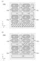
도 1의 (A) 및 (B)는 표시 장치의 일례를 나타낸 상면도이다.
도 2의 (A) 및 (B)는 표시 장치의 일례를 나타낸 상면도이다.
도 3의 (A) 및 (B)는 표시 장치의 일례를 나타낸 상면도이다.
도 4의 (A) 내지 (G)는 화소의 일례를 나타낸 상면도이다.
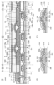
도 5의 (A) 내지 (C)는 표시 장치의 일례를 나타낸 단면도이다.
도 6의 (A) 및 (B)는 표시 장치의 일례를 나타낸 단면도이다.
도 7의 (A) 내지 (C)는 표시 장치의 일례를 나타낸 단면도이다.
도 8의 (A) 내지 (C)는 표시 장치의 일례를 나타낸 단면도이다.
도 9의 (A) 내지 (C)는 표시 장치의 일례를 나타낸 단면도이다.
도 10의 (A) 내지 (C)는 표시 장치의 일례를 나타낸 단면도이다.
도 11의 (A) 및 (B)는 표시 장치의 일례를 나타낸 단면도이다.
도 12의 (A) 내지 (C)는 표시 장치의 일례를 나타낸 단면도이다.
도 13의 (A) 내지 (C)는 표시 장치의 일례를 나타낸 단면도이다.
도 14의 (A) 내지 (D)는 표시 장치의 제작 방법의 일례를 나타낸 단면도이다.
도 15의 (A) 내지 (C)는 표시 장치의 제작 방법의 일례를 나타낸 단면도이다.
도 16의 (A) 내지 (C)는 표시 장치의 제작 방법의 일례를 나타낸 단면도이다.
도 17의 (A) 및 (B)는 표시 장치의 일례를 나타낸 사시도이다.
도 18은 표시 장치의 일례를 나타낸 단면도이다.
도 19는 표시 장치의 일례를 나타낸 단면도이다.
도 20은 표시 장치의 일례를 나타낸 단면도이다.
도 21은 표시 장치의 일례를 나타낸 단면도이다.
도 22는 표시 장치의 일례를 나타낸 단면도이다.
도 23은 표시 장치의 일례를 나타낸 단면도이다.
도 24는 표시 장치의 일례를 나타낸 사시도이다.
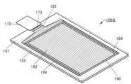
도 25의 (A)는 표시 장치의 일례를 나타낸 단면도이다. 도 25의 (B) 및 (C)는 트랜지스터의 일례를 나타낸 단면도이다.
도 26의 (A) 내지 (D)는 표시 장치의 일례를 나타낸 단면도이다.
도 27의 (A) 내지 (F)는 발광 디바이스의 구성예를 나타낸 도면이다.
도 28의 (A) 및 (B)는 수광 디바이스의 구성예를 나타낸 도면이다. 도 28의 (C) 내지 (E)는 표시 장치의 구성예를 나타낸 도면이다.
도 29의 (A) 내지 (D)는 전자 기기의 일례를 나타낸 도면이다.
도 30의 (A) 내지 (F)는 전자 기기의 일례를 나타낸 도면이다.
도 31의 (A) 내지 (G)는 전자 기기의 일례를 나타낸 도면이다.1 (A) and (B) are top views showing an example of a display device.
Figures 2 (A) and (B) are top views showing an example of a display device.
Figures 3 (A) and (B) are top views showing an example of a display device.
4 (A) to (G) are top views showing an example of a pixel.
Figures 5 (A) to (C) are cross-sectional views showing an example of a display device.
Figures 6 (A) and (B) are cross-sectional views showing an example of a display device.
7 (A) to (C) are cross-sectional views showing an example of a display device.
8 (A) to (C) are cross-sectional views showing an example of a display device.
FIGS. 9A to 9C are cross-sectional views showing an example of a display device.
10 (A) to (C) are cross-sectional views showing an example of a display device.
Figures 11 (A) and (B) are cross-sectional views showing an example of a display device.
12 (A) to (C) are cross-sectional views showing an example of a display device.
13 (A) to (C) are cross-sectional views showing an example of a display device.
14A to 14D are cross-sectional views showing an example of a method for manufacturing a display device.
Figures 15 (A) to (C) are cross-sectional views showing an example of a method for manufacturing a display device.
Figures 16 (A) to (C) are cross-sectional views showing an example of a method for manufacturing a display device.
Figures 17 (A) and (B) are perspective views showing an example of a display device.
Figure 18 is a cross-sectional view showing an example of a display device.
Figure 19 is a cross-sectional view showing an example of a display device.
Figure 20 is a cross-sectional view showing an example of a display device.
Figure 21 is a cross-sectional view showing an example of a display device.
Figure 22 is a cross-sectional view showing an example of a display device.
Figure 23 is a cross-sectional view showing an example of a display device.
Figure 24 is a perspective view showing an example of a display device.
Figure 25(A) is a cross-sectional view showing an example of a display device. Figures 25 (B) and (C) are cross-sectional views showing an example of a transistor.
26 (A) to (D) are cross-sectional views showing an example of a display device.
Figures 27 (A) to (F) are diagrams showing a configuration example of a light-emitting device.
Figures 28 (A) and (B) are diagrams showing a configuration example of a light receiving device. 28(C) to (E) are diagrams showing a configuration example of a display device.
Figures 29 (A) to (D) are diagrams showing an example of an electronic device.
Figures 30 (A) to (F) are diagrams showing examples of electronic devices.
Figures 31 (A) to (G) are diagrams showing an example of an electronic device.
실시형태에 대하여 도면을 사용하여 자세히 설명한다. 다만 본 발명은 이하의 설명에 한정되지 않고, 본 발명의 취지 및 그 범위에서 벗어남이 없이 그 형태 및 자세한 사항을 다양하게 변경할 수 있다는 것은 통상의 기술자라면 용이하게 이해할 수 있다. 따라서 본 발명은 이하의 실시형태의 기재 내용에 한정하여 해석되는 것이 아니다.The embodiment will be described in detail using the drawings. However, the present invention is not limited to the following description, and those skilled in the art can easily understand that the form and details can be changed in various ways without departing from the spirit and scope of the present invention. Therefore, the present invention should not be construed as limited to the description of the embodiments below.
또한 이하에서 설명하는 발명의 구성에서, 동일한 부분 또는 같은 기능을 가지는 부분에는 동일한 부호를 상이한 도면 사이에서 공통적으로 사용하고, 그 반복적인 설명은 생략한다. 또한 같은 기능을 가지는 부분을 가리키는 경우에는, 해치 패턴을 동일하게 하고, 특별히 부호를 붙이지 않는 경우가 있다.In addition, in the configuration of the invention described below, the same symbols are commonly used in different drawings for parts that are the same or have the same function, and repetitive description thereof is omitted. Additionally, when referring to parts with the same function, the hatch patterns may be the same and no special symbols may be added.
또한 도면에 나타낸 각 구성의 위치, 크기, 및 범위 등은 이해를 쉽게 하기 위하여 실제의 위치, 크기, 및 범위 등을 나타내지 않는 경우가 있다. 그러므로 개시(開示)된 발명은 반드시 도면에 개시된 위치, 크기, 범위 등에 한정되지 않는다.Additionally, the location, size, and range of each component shown in the drawings may not represent the actual location, size, and scope for ease of understanding. Therefore, the disclosed invention is not necessarily limited to the location, size, scope, etc. disclosed in the drawings.
또한 "막"이라는 용어와 "층"이라는 용어는 경우 또는 상황에 따라 서로 바꿀 수 있다. 예를 들어 "도전층"이라는 용어를 "도전막"이라는 용어로 변경할 수 있다. 또는 예를 들어 "절연막"이라는 용어를 "절연층"이라는 용어로 변경할 수 있다.Additionally, the terms “membrane” and “layer” can be interchanged depending on the case or situation. For example, the term “conductive layer” can be changed to the term “conductive film.” Or, for example, the term “insulating film” can be changed to the term “insulating layer.”
본 명세서 등에 있어서, 메탈 마스크 또는 FMM(파인 메탈 마스크, 고정세 메탈 마스크)을 사용하여 제작되는 디바이스를 MM(메탈 마스크) 구조의 디바이스라고 부르는 경우가 있다. 또한 본 명세서 등에 있어서, 메탈 마스크 또는 FMM을 사용하지 않고 제작되는 디바이스를 MML(메탈 마스크리스) 구조의 디바이스라고 부르는 경우가 있다.In this specification and the like, a device manufactured using a metal mask or FMM (fine metal mask, high-fine metal mask) may be referred to as a device with an MM (metal mask) structure. Additionally, in this specification and the like, a device manufactured without using a metal mask or FMM may be referred to as a device with an MML (metal maskless) structure.
본 명세서 등에서는 발광 파장이 상이한 발광 디바이스에서 발광층을 구분 형성하는 구조를 SBS(Side By Side) 구조라고 부르는 경우가 있다. SBS 구조는 발광 디바이스마다 재료 및 구성을 최적화할 수 있기 때문에 재료 및 구성의 선택 자유도가 높아 휘도 및 신뢰성을 용이하게 향상시킬 수 있다.In this specification and the like, a structure in which light-emitting layers are separately formed in a light-emitting device with different emission wavelengths is sometimes referred to as a SBS (Side By Side) structure. Since the SBS structure can optimize the materials and configuration for each light-emitting device, luminance and reliability can be easily improved with a high degree of freedom in selecting materials and configurations.
본 명세서 등에서 정공 또는 전자를 "캐리어"라고 하는 경우가 있다. 구체적으로는 정공 주입층 또는 전자 주입층을 "캐리어 주입층"이라고 하고, 정공 수송층 또는 전자 수송층을 "캐리어 수송층"이라고 하고, 정공 차단층 또는 전자 차단층을 "캐리어 차단층"이라고 하는 경우가 있다. 또한 상술한 캐리어 주입층, 캐리어 수송층, 및 캐리어 차단층은 각각 단면 형상 또는 특성 등에 따라 명확히 구별할 수 없는 경우가 있다. 또한 하나의 층이 캐리어 주입층, 캐리어 수송층, 및 캐리어 차단층 중 2개 또는 3개의 기능을 겸하는 경우가 있다.In this specification, etc., holes or electrons are sometimes referred to as “carriers.” Specifically, the hole injection layer or electron injection layer is sometimes called a "carrier injection layer," the hole transport layer or electron transport layer is called a "carrier transport layer," and the hole blocking layer or electron blocking layer is sometimes called a "carrier blocking layer." . Additionally, the carrier injection layer, carrier transport layer, and carrier blocking layer described above may not be clearly distinguished depending on their cross-sectional shape or characteristics. Additionally, there are cases where one layer also functions as two or three of the carrier injection layer, carrier transport layer, and carrier blocking layer.
본 명세서 등에서 발광 디바이스는 한 쌍의 전극 사이에 EL층을 가진다. EL층은 적어도 발광층을 가진다. 수광 디바이스는 한 쌍의 전극 사이에 적어도 광전 변환층으로서 기능하는 활성층을 가진다. 본 명세서 등에서는 한 쌍의 전극 중 한쪽을 화소 전극이라고 기재하고, 다른 쪽을 공통 전극이라고 기재하는 경우가 있다.In this specification and the like, the light emitting device has an EL layer between a pair of electrodes. The EL layer has at least a light emitting layer. The light receiving device has at least an active layer that functions as a photoelectric conversion layer between a pair of electrodes. In this specification and the like, one of a pair of electrodes may be described as a pixel electrode, and the other may be described as a common electrode.
(실시형태 1)(Embodiment 1)
본 실시형태에서는, 본 발명의 일 형태의 표시 장치에 대하여 도 1 내지 도 13을 사용하여 설명한다.In this embodiment, a display device of one form of the present invention will be described using FIGS. 1 to 13.
본 발명의 일 형태의 표시 장치는 제 1 화소, 제 2 화소, 및 제 3 화소를 가진다. 제 1 화소 내지 제 3 화소는 각각 제 1 부화소, 제 2 부화소, 및 제 3 부화소를 가진다. 제 1 화소와 제 2 화소는 제 4 부화소를 공유한다. 제 3 화소는 제 5 부화소를 가진다. 제 1 부화소 내지 제 3 부화소를 사용하여 풀 컬러 표시를 할 수 있다. 제 4 부화소 및 제 5 부화소는 적외광을 방출하는 발광 디바이스(발광 소자라고도 함), 제 1 수광 디바이스(수광 소자라고도 함), 및 제 2 수광 디바이스 중 서로 다른 어느 하나를 가진다.A display device of one embodiment of the present invention has a first pixel, a second pixel, and a third pixel. The first to third pixels have a first subpixel, a second subpixel, and a third subpixel, respectively. The first pixel and the second pixel share the fourth subpixel. The third pixel has a fifth sub-pixel. Full color display can be achieved using the first to third subpixels. The fourth subpixel and the fifth subpixel have different one of a light-emitting device (also referred to as a light-emitting element) that emits infrared light, a first light-receiving device (also referred to as a light-receiving device), and a second light-receiving device.
제 3 화소는 제 6 부화소를 더 가지는 것이 바람직하다. 제 6 부화소로서는 발광 디바이스, 제 1 수광 디바이스, 및 제 2 수광 디바이스 중 제 4 부화소 및 제 5 부화소와는 다른 하나를 들 수 있다.It is preferable that the third pixel further has a sixth sub-pixel. The sixth subpixel may be one that is different from the fourth and fifth subpixels among the light emitting device, the first light receiving device, and the second light receiving device.
또한 본 발명의 일 형태의 표시 장치는 제 4 화소를 더 가지는 것이 바람직하다. 제 4 화소는 제 1 부화소, 제 2 부화소, 제 3 부화소, 및 제 6 부화소를 가진다.Additionally, the display device of one embodiment of the present invention preferably further includes a fourth pixel. The fourth pixel has a first sub-pixel, a second sub-pixel, a third sub-pixel, and a sixth sub-pixel.
제 1 수광 디바이스를 가지는 부화소는 적어도 적외광을 검출하는 것이 바람직하다. 구체적으로 상기 부화소는 본 발명의 일 형태의 표시 장치가 가지는, 적외광을 방출하는 발광 디바이스의 발광을 검출하는 것이 바람직하다.It is desirable that the subpixel having the first light receiving device detects at least infrared light. Specifically, the sub-pixel preferably detects light emission from a light-emitting device that emits infrared light included in the display device of one embodiment of the present invention.
제 2 수광 디바이스를 가지는 부화소는 적어도 가시광을 검출하는 것이 바람직하다. 구체적으로 상기 부화소는 제 1 부화소 내지 제 3 부화소가 나타내는 광 중 적어도 일부의 파장 영역의 광을 검출하는 것이 바람직하다.It is desirable that the subpixel having the second light receiving device detects at least visible light. Specifically, it is preferable that the subpixel detects light in at least a portion of the wavelength region among the light displayed by the first to third subpixels.
본 발명의 일 형태의 표시 장치는 화소에 발광 디바이스 및 수광 디바이스를 가진다. 본 발명의 일 형태의 표시 장치에서는 표시부가 수광 기능을 가지기 때문에 표시부를 사용하여 촬상할 수 있다. 예를 들어 표시부에서는 화상을 표시하면서 촬상을 할 수 있다. 또한 표시부에서는 일부의 부화소로 광원으로서의 광을 나타내고, 다른 부화소로 화상을 표시할 수도 있다.A display device of one embodiment of the present invention has a light emitting device and a light receiving device in a pixel. In the display device of one form of the present invention, since the display unit has a light receiving function, images can be captured using the display unit. For example, the display unit can capture images while displaying images. Additionally, in the display unit, light as a light source can be displayed using some subpixels and images can be displayed using other subpixels.
예를 들어 제 1 부화소 내지 제 3 부화소의 조합으로서는 각각 적색(R)의 광, 녹색(G)의 광, 청색(B)의 광을 나타내는 구성이 있다. 또한 상기 3개의 부화소의 조합으로서는 각각 황색(Y)의 광, 시안(C)의 광, 마젠타(M)의 광을 나타내는 구성도 들 수 있다.For example, a combination of the first to third subpixels may each represent red (R) light, green (G) light, and blue (B) light. Additionally, combinations of the three subpixels include configurations that respectively display yellow (Y) light, cyan (C) light, and magenta (M) light.
제 4 부화소 내지 제 6 부화소 중 수광 디바이스를 가지는 부화소에는 가시광을 검출하는 구성, 적외광을 검출하는 구성, 가시광 및 적외광의 양쪽을 검출하는 구성 중 어느 것을 적용할 수 있다.Among the fourth to sixth subpixels, any of a configuration for detecting visible light, a configuration for detecting infrared light, or a configuration for detecting both visible light and infrared light can be applied to the subpixel having the light receiving device.
화소에 5종류 또는 6종류의 부화소를 가지는 경우, 표시 장치의 제작 공정이 복잡해져 제조 비용이 증대되는 경우가 있다. 그러므로 본 발명의 일 형태의 표시 장치에서는, 표시 디바이스로서 기능하는 발광 디바이스에 동일한 구성의 EL층을 사용하고, 부화소가 나타내는 색마다 착색층을 구분 형성함으로써 풀 컬러 표시를 실현한다.When a pixel has 5 or 6 types of subpixels, the manufacturing process of the display device becomes complicated and manufacturing costs may increase. Therefore, in the display device of one form of the present invention, full-color display is achieved by using an EL layer of the same configuration as the light-emitting device functioning as the display device and separately forming colored layers for each color represented by the sub-pixel.
예를 들어 R, G, B의 광을 나타내는 부화소는 모두 동일한 구성의 EL층을 가지는 발광 디바이스(예를 들어 백색 발광의 발광 디바이스)를 사용하고, R, G, B 각각의 착색층을 구분 형성함으로써 실현할 수 있다. 이때 적외(IR)광을 나타내는 부화소에는 적외광을 방출하는 발광 디바이스를 사용한다.For example, subpixels representing R, G, and B lights all use light-emitting devices (e.g., white light-emitting light-emitting devices) with EL layers of the same configuration, and each color layer for R, G, and B is separated. It can be realized by forming. At this time, a light-emitting device that emits infrared light is used in the subpixel that represents infrared (IR) light.
구체적으로, 본 발명의 일 형태는 제 1 화소, 제 2 화소, 및 제 3 화소를 가지고, 제 1 화소 내지 제 3 화소는 각각 제 1 부화소, 제 2 부화소, 및 제 3 부화소를 가지고, 제 1 화소와 제 2 화소는 제 4 부화소를 공유하고, 제 3 화소는 제 5 부화소를 가지고, 제 1 부화소는 제 1 발광 디바이스 및 제 1 착색층을 가지고, 제 2 부화소는 제 2 발광 디바이스 및 제 2 착색층을 가지고, 제 3 부화소는 제 3 발광 디바이스 및 제 3 착색층을 가지고, 제 1 발광 디바이스는 제 1 화소 전극과, 제 1 화소 전극 위의 제 1 EL층과, 제 1 EL층 위의 공통 전극을 가지고, 제 2 발광 디바이스는 제 2 화소 전극과, 제 2 화소 전극 위의 제 2 EL층과, 제 2 EL층 위의 공통 전극을 가지고, 제 3 발광 디바이스는 제 3 화소 전극과, 제 3 화소 전극 위의 제 3 EL층과, 제 3 EL층 위의 공통 전극을 가지고, 제 1 EL층 내지 제 3 EL층은 모두 동일한 구성을 가지며 서로 이격되어 있고, 제 1 착색층 내지 제 3 착색층은 각각 다른 색의 광을 투과시키고, 제 4 부화소 및 제 5 부화소는 적외광을 방출하는 제 4 발광 디바이스, 제 1 수광 디바이스, 및 제 2 수광 디바이스 중 서로 다른 어느 하나를 가지는 표시 장치이다.Specifically, one aspect of the present invention has a first pixel, a second pixel, and a third pixel, and the first to third pixels have a first sub-pixel, a second sub-pixel, and a third sub-pixel, respectively. , the first pixel and the second pixel share the fourth subpixel, the third pixel has the fifth subpixel, the first subpixel has the first light emitting device and the first colored layer, and the second subpixel has It has a second light-emitting device and a second coloring layer, and the third sub-pixel has a third light-emitting device and a third coloring layer, and the first light-emitting device has a first pixel electrode and a first EL layer over the first pixel electrode. and a common electrode on the first EL layer, and the second light-emitting device has a second pixel electrode, a second EL layer on the second pixel electrode, and a common electrode on the second EL layer, and a third light-emitting device. The device has a third pixel electrode, a third EL layer on the third pixel electrode, and a common electrode on the third EL layer, and the first to third EL layers all have the same configuration and are spaced apart from each other. , the first to third colored layers transmit light of different colors, and the fourth and fifth subpixels are a fourth light-emitting device, a first light-receiving device, and a second light-receiving device that emit infrared light. It is a display device that has one of the following.
제 3 화소는 제 6 부화소를 더 가지는 것이 바람직하다. 예를 들어 제 4 부화소는 제 2 수광 디바이스를 가지고, 제 5 부화소는 제 4 발광 디바이스를 가지고, 제 6 부화소는 제 1 수광 디바이스를 가지고, 제 4 부화소는 적어도 가시광을 검출하고, 제 6 부화소는 적어도 적외광을 검출하는 구성으로 할 수 있다. 이때 제 4 부화소는 제 1 부화소 내지 제 3 부화소가 나타내는 광 중 적어도 일부의 파장 영역의 광을 검출하는 것이 바람직하다. 제 6 부화소는 제 5 부화소가 나타내는 적외광을 검출하는 것이 바람직하다.It is preferable that the third pixel further has a sixth sub-pixel. For example, the fourth sub-pixel has a second light-receiving device, the fifth sub-pixel has a fourth light-emitting device, the sixth sub-pixel has a first light-receiving device, the fourth sub-pixel detects at least visible light, The sixth subpixel can be configured to detect at least infrared light. At this time, it is preferable that the fourth subpixel detects light in at least a partial wavelength range among the light displayed by the first to third subpixels. Preferably, the sixth subpixel detects the infrared light displayed by the fifth subpixel.
또한 본 발명의 일 형태의 표시 장치는 제 4 화소를 더 가지는 것이 바람직하다. 제 4 화소는 제 1 부화소, 제 2 부화소, 제 3 부화소, 및 제 6 부화소를 가진다.Additionally, the display device of one embodiment of the present invention preferably further includes a fourth pixel. The fourth pixel has a first sub-pixel, a second sub-pixel, a third sub-pixel, and a sixth sub-pixel.
예를 들어 제 4 부화소는 제 2 수광 디바이스를 가지고, 제 5 부화소는 제 4 발광 디바이스를 가지고, 제 6 부화소는 제 1 수광 디바이스를 가지고, 제 4 부화소는 적어도 가시광을 검출하고, 제 6 부화소는 적어도 적외광을 검출하는 구성으로 할 수 있다. 이때 제 4 부화소는 제 1 부화소 내지 제 3 부화소가 나타내는 광 중 적어도 일부의 파장 영역의 광을 검출하는 것이 바람직하다. 제 6 부화소는 제 5 부화소가 나타내는 적외광을 검출하는 것이 바람직하다.For example, the fourth sub-pixel has a second light-receiving device, the fifth sub-pixel has a fourth light-emitting device, the sixth sub-pixel has a first light-receiving device, the fourth sub-pixel detects at least visible light, The sixth subpixel can be configured to detect at least infrared light. At this time, it is preferable that the fourth subpixel detects light in at least a partial wavelength range among the light displayed by the first to third subpixels. Preferably, the sixth subpixel detects the infrared light displayed by the fifth subpixel.
또한 예를 들어 제 4 부화소는 제 4 발광 디바이스를 가지고, 제 5 부화소는 제 1 수광 디바이스를 가지고, 제 6 부화소는 제 2 수광 디바이스를 가지고, 제 5 부화소는 적어도 적외광을 검출하고, 제 6 부화소는 적어도 가시광을 검출하는 구성으로 할 수 있다. 이때 제 5 부화소는 제 4 부화소가 나타내는 적외광을 검출하는 것이 바람직하다. 제 6 부화소는 제 1 부화소 내지 제 3 부화소가 나타내는 광 중 적어도 일부의 파장 영역의 광을 검출하는 것이 바람직하다.Also, for example, the fourth subpixel has a fourth light-emitting device, the fifth subpixel has a first light-receiving device, the sixth subpixel has a second light-receiving device, and the fifth subpixel detects at least infrared light. And, the sixth subpixel can be configured to detect at least visible light. At this time, it is preferable that the fifth subpixel detects the infrared light displayed by the fourth subpixel. Preferably, the sixth subpixel detects light in at least a partial wavelength region among the light represented by the first to third subpixels.
또한 R, G, B, IR의 광을 나타내는 부화소에는 동일한 구성의 EL층을 가지는 발광 디바이스를 사용하여도 좋다. 예를 들어 R, G, B, IR의 광을 나타내는 부화소는 모두 백색과 적외광의 양쪽을 방출하는 발광 디바이스를 사용하고, R, G, B 각각의 착색층을 구분 형성함으로써 실현할 수 있다. 또한 R, G, B 중 2개 이상의 착색층을 적층함으로써 가시광이 차단되어 IR의 광을 나타내는 부화소를 실현할 수 있다.Additionally, light emitting devices having EL layers of the same configuration may be used for subpixels representing R, G, B, and IR light. For example, subpixels representing R, G, B, and IR light can be realized by using light-emitting devices that emit both white and infrared light, and forming colored layers for R, G, and B separately. In addition, by stacking two or more colored layers among R, G, and B, visible light is blocked and a subpixel that displays IR light can be realized.
구체적으로, 제 4 발광 디바이스는 제 4 화소 전극과, 제 4 화소 전극 위의 제 4 EL층과, 제 4 EL층 위의 공통 전극을 가지고, 제 1 EL층 내지 제 4 EL층은 모두 동일한 구성을 가지며 서로 이격되어 있어도 좋다.Specifically, the fourth light emitting device has a fourth pixel electrode, a fourth EL layer on the fourth pixel electrode, and a common electrode on the fourth EL layer, and the first to fourth EL layers all have the same configuration. and may be spaced apart from each other.
또한 제 1 수광 디바이스와 제 2 수광 디바이스에 동일한 구성의 수광 디바이스를 사용하여도 좋다. 예를 들어 제 1 수광 디바이스 및 제 2 수광 디바이스에 가시광 및 적외광의 양쪽을 검출하는 수광 디바이스를 사용하고, 가시광을 차단하기 위한 필터를 제 1 수광 디바이스와 중첩시켜 제공함으로써, 제 1 수광 디바이스를 가지는 부화소를 적외광만을 검출하는 구성(즉 제 2 수광 디바이스를 가지는 부화소와는 검출하는 파장 영역이 상이한 구성)으로 할 수 있다.Additionally, light receiving devices of the same configuration may be used for the first light receiving device and the second light receiving device. For example, a light receiving device that detects both visible light and infrared light is used in the first light receiving device and a second light receiving device, and a filter for blocking visible light is provided overlapping with the first light receiving device, thereby forming the first light receiving device. The subpixel having the second light receiving device can be configured to detect only infrared light (i.e., the wavelength range to be detected is different from that of the subpixel having the second light receiving device).
여기서 발광 디바이스를 가지는 부화소에는 섬 형상의 발광층을 제공하고, 수광 디바이스를 가지는 부화소에는 섬 형상의 활성층(광전 변환층이라고도 함)을 제공한다. 또한 R, G, B의 광을 나타내는 부화소와 IR의 광을 나타내는 부화소에서 상이한 구성의 발광 디바이스를 사용하는 경우에는 발광 디바이스에 따라 섬 형상의 발광층을 구분 형성한다. 이와 같이 본 발명의 일 형태의 표시 장치에서는 부화소의 기능에 따라 섬 형상의 발광층과 섬 형상의 활성층을 구분 형성할 필요가 있다.Here, an island-shaped light-emitting layer is provided to the subpixel having the light-emitting device, and an island-shaped active layer (also referred to as a photoelectric conversion layer) is provided to the subpixel having the light-receiving device. Additionally, when light emitting devices of different configurations are used in the subpixels representing R, G, and B light and the subpixels representing IR light, island-shaped light emitting layers are separately formed depending on the light emitting device. As such, in the display device of one form of the present invention, it is necessary to separately form an island-shaped light emitting layer and an island-shaped active layer according to the function of the subpixel.
또한 본 명세서 등에서 섬 형상이란, 동일한 공정에서 동일한 재료를 사용하여 형성된 2개 이상의 층이 물리적으로 분리된 상태를 가리킨다. 예를 들어 섬 형상의 발광층이란, 상기 발광층과, 이에 인접한 발광층이 물리적으로 분리되어 있는 상태인 것을 가리킨다.In addition, in this specification and the like, the island shape refers to a state in which two or more layers formed using the same material in the same process are physically separated. For example, an island-shaped light emitting layer refers to a state in which the light emitting layer and the adjacent light emitting layer are physically separated.
또한 동일한 구성의 EL층을 가지는 발광 디바이스를 사용하는 경우, 발광 디바이스에 포함되는 화소 전극 외의 층(예를 들어 발광층 등)을 복수의 부화소에서 공유할 수 있다. 그러므로 복수의 부화소가 연속된 막을 공유할 수 있다. 그러나 발광 디바이스에 포함되는 층에는 도전성이 비교적 높은 층도 있다. 복수의 부화소가 도전성이 높은 층을 연속된 막으로서 공유함으로써, 부화소들 사이에 누설 전류가 발생하는 경우가 있다. 특히 표시 장치가 고정세화 또는 고개구율화되어 부화소들 사이의 거리가 짧아지면, 상기 누설 전류는 무시할 수 없을 정도로 커지기 때문에 표시 장치의 표시 품위의 저하 등을 일으킬 우려가 있다.Additionally, when using a light-emitting device having an EL layer of the same configuration, layers other than the pixel electrode included in the light-emitting device (eg, a light-emitting layer, etc.) can be shared by a plurality of subpixels. Therefore, multiple subpixels can share a continuous membrane. However, among the layers included in the light-emitting device, there are also layers with relatively high conductivity. When a plurality of subpixels share a highly conductive layer as a continuous film, leakage current may occur between the subpixels. In particular, when the display device becomes high-definition or high-aperture and the distance between sub-pixels becomes short, the leakage current becomes so large that it cannot be ignored, which may cause deterioration of the display quality of the display device.
여기서 본 발명의 일 형태의 표시 장치에서는, 각 부화소에서 EL층을 구성하는 층의 적어도 일부를 섬 형상으로 형성한다. EL층을 구성하는 층의 적어도 일부가 부화소마다 분리되어 있으면, 서로 인접한 부화소들 사이의 크로스토크의 발생을 억제할 수 있다. 이에 의하여, 표시 장치의 고정세화와 높은 표시 품위의 양립을 실현할 수 있다.Here, in the display device of one embodiment of the present invention, at least a part of the layer constituting the EL layer in each subpixel is formed in an island shape. If at least a portion of the layers constituting the EL layer are separated for each subpixel, the occurrence of crosstalk between adjacent subpixels can be suppressed. As a result, it is possible to achieve both high resolution of the display device and high display quality.
예를 들어 메탈 마스크를 사용한 진공 증착법에 의하여 섬 형상의 발광층을 성막할 수 있다. 그러나 이 방법으로는 메탈 마스크의 정밀도, 메탈 마스크와 기판의 위치 어긋남, 메탈 마스크의 휨, 및 증기의 산란 등으로 인한 성막되는 막의 윤곽의 확장 등 다양한 영향을 받아 섬 형상의 발광층의 형상 및 위치가 설계 시와 달라지기 때문에, 표시 장치의 고정세화 및 고개구율화가 어렵다. 또한 증착 시에 층의 윤곽이 흐릿해져 단부의 두께가 얇아지는 경우가 있다. 즉 섬 형상의 발광층은 부분에 따라 두께가 다른 경우가 있다. 또한 대형, 고해상도, 또는 고정세 표시 장치를 제작하는 경우, 메탈 마스크의 낮은 치수 정밀도 및 열 등으로 인한 변형에 기인하여 제조 수율이 저하될 우려가 있다.For example, an island-shaped light emitting layer can be formed by vacuum deposition using a metal mask. However, with this method, the shape and position of the island-shaped light emitting layer are affected by various influences such as the precision of the metal mask, misalignment between the metal mask and the substrate, bending of the metal mask, and expansion of the outline of the film to be formed due to vapor scattering. Because it is different from the design time, it is difficult to achieve high resolution and high aperture ratio of the display device. Additionally, during deposition, the outline of the layer may become blurred and the thickness of the end portion may become thinner. In other words, the island-shaped light emitting layer may have a different thickness depending on the part. Additionally, when manufacturing large-sized, high-resolution, or high-definition display devices, there is a risk that manufacturing yield may decrease due to low dimensional precision of the metal mask and deformation due to heat.
그러므로 본 발명의 일 형태의 표시 장치를 제작하는 경우에는, 메탈 마스크 등의 섀도 마스크를 사용하지 않고 포토리소그래피법에 의하여 발광층을 미세한 패턴으로 가공한다. 구체적으로는 부화소마다 화소 전극을 형성한 후, 복수의 화소 전극에 걸쳐 발광층을 성막한다. 그 후, 상기 발광층을 포토리소그래피법으로 가공하여 하나의 화소 전극에 대하여 하나의 섬 형상의 발광층을 형성한다. 이에 의하여, 발광층이 부화소마다 분할되고, 부화소마다 섬 형상의 발광층을 형성할 수 있다.Therefore, when manufacturing a display device of one type of the present invention, the light emitting layer is processed into a fine pattern by photolithography without using a shadow mask such as a metal mask. Specifically, after forming a pixel electrode for each subpixel, a light emitting layer is formed over the plurality of pixel electrodes. Thereafter, the light emitting layer is processed by photolithography to form one island-shaped light emitting layer for one pixel electrode. As a result, the light emitting layer is divided for each subpixel, and an island-shaped light emitting layer can be formed for each subpixel.
또한 상기 발광층을 섬 형상으로 가공하는 경우, 발광층 바로 위에서 포토리소그래피법을 사용하여 가공하는 구조가 생각된다. 이 구조의 경우, 발광층이 대미지(가공으로 인한 대미지 등)를 받아 신뢰성이 크게 저하하는 경우가 있다. 그러므로 본 발명의 일 형태의 표시 장치를 제작할 때는, 발광층보다 위쪽에 위치하는 층(예를 들어, 캐리어 수송층 또는 캐리어 주입층, 더 구체적으로는 전자 수송층 또는 전자 주입층 등) 위에 마스크층(희생층이라고 하여도 좋음) 등을 형성하고, 발광층을 섬 형상으로 가공하는 방법을 사용하는 것이 바람직하다. 상기 방법을 적용함으로써, 신뢰성이 높은 표시 장치를 제공할 수 있다. 또한 본 명세서 등에서 마스크막 및 마스크층이란, 각각 적어도 발광층(더 구체적으로는 EL층을 구성하는 층 중 섬 형상으로 가공되는 층)의 위쪽에 위치하고, 제조 공정에서 상기 발광층을 보호하는 기능을 가진다.Additionally, when processing the light-emitting layer into an island shape, a structure in which the light-emitting layer is processed using a photolithography method directly above the light-emitting layer is considered. In the case of this structure, there are cases where the light-emitting layer receives damage (damage due to processing, etc.), greatly reducing reliability. Therefore, when manufacturing a display device of one form of the present invention, a mask layer (sacrificial layer) is placed on a layer located above the light emitting layer (for example, a carrier transport layer or a carrier injection layer, more specifically an electron transport layer or an electron injection layer, etc.). It is preferable to use a method of forming a light-emitting layer and processing the light-emitting layer into an island shape. By applying the above method, a highly reliable display device can be provided. In addition, in this specification and the like, the mask film and mask layer are each located above at least a light-emitting layer (more specifically, a layer processed into an island shape among the layers constituting the EL layer) and have a function of protecting the light-emitting layer during the manufacturing process.
상술한 바와 같이, 본 발명의 일 형태의 표시 장치의 제작 방법으로 제작되는 섬 형상의 발광층은 미세한 패턴을 가지는 메탈 마스크를 사용하여 형성되는 것이 아니라, 발광층을 면 전체에 성막한 후에 가공함으로써 형성된다. 구체적으로는, 상기 섬 형상의 발광층은 포토리소그래피법 등을 사용하여 분할되고 미세화된 크기이다. 그러므로 메탈 마스크를 사용하여 형성할 수 있는 크기보다 작게 할 수 있다. 따라서 그동안 실현이 어려웠던 고정세 표시 장치 또는 고개구율 표시 장치를 실현할 수 있다.As described above, the island-shaped light-emitting layer produced by the manufacturing method of one type of display device of the present invention is not formed using a metal mask with a fine pattern, but is formed by forming the light-emitting layer into a film over the entire surface and then processing it. . Specifically, the island-shaped light emitting layer is divided and refined in size using a photolithography method or the like. Therefore, it can be made smaller than the size that can be formed using a metal mask. Therefore, it is possible to realize a high-definition display device or a high-aperture-ratio display device, which has been difficult to realize so far.
또한 포토리소그래피법을 사용한 발광층의 가공은 횟수가 적을수록 제조 비용이 절감되고 제조 수율이 향상될 수 있어 바람직하다. 본 발명의 일 형태의 표시 장치의 제작 방법은 포토리소그래피법을 사용한 발광층의 가공 횟수를 두 번 또는 세 번으로 할 수 있기 때문에 높은 수율로 표시 장치를 제작할 수 있다.In addition, the processing of the light emitting layer using the photolithography method is preferable because manufacturing costs can be reduced and manufacturing yield can be improved as the number of times is reduced. In the method of manufacturing a display device of one embodiment of the present invention, the number of times of processing the light emitting layer using the photolithography method can be doubled or tripled, and thus the display device can be manufactured with high yield.
예를 들어 메탈 마스크를 사용한 형성 방법으로는 인접한 발광 디바이스의 간격을 10μm 미만으로 하는 것은 어렵지만, 상기 방법을 사용하면 10μm 미만, 5μm 이하, 3μm 이하, 2μm 이하, 또는 1μm 이하까지 좁힐 수 있다. 또한 예를 들어 LSI용 노광 장치를 사용함으로써, 인접한 발광 디바이스의 간격을 500nm 이하, 200nm 이하, 100nm 이하, 나아가서는 50nm 이하까지 좁힐 수도 있다. 이에 의하여, 2개의 발광 디바이스 사이에 존재할 수 있는 비발광 영역의 면적을 크게 축소할 수 있고, 개구율을 100%에 가깝게 할 수 있다. 예를 들어 개구율은 50% 이상, 60% 이상, 70% 이상, 80% 이상, 나아가서는 90% 이상이고, 100% 미만을 실현할 수도 있다.For example, it is difficult to reduce the gap between adjacent light-emitting devices to less than 10 μm using a formation method using a metal mask, but using this method, it can be narrowed to less than 10 μm, 5 μm or less, 3 μm or less, 2 μm or less, or 1 μm or less. Additionally, for example, by using an exposure apparatus for LSI, the gap between adjacent light emitting devices can be narrowed to 500 nm or less, 200 nm or less, 100 nm or less, and even 50 nm or less. As a result, the area of the non-emission area that may exist between two light-emitting devices can be greatly reduced, and the aperture ratio can be brought close to 100%. For example, the aperture ratio may be 50% or more, 60% or more, 70% or more, 80% or more, and even 90% or more, and may be less than 100%.
또한 발광층 자체의 패턴(가공 사이즈라고도 할 수 있음)도 메탈 마스크를 사용한 경우에 비하여 매우 작게 할 수 있다. 또한 예를 들어 발광층을 구분 형성하기 위하여 메탈 마스크를 사용한 경우에는, 발광층의 중앙과 끝부분에서 두께에 편차가 발생하기 때문에, 발광층의 면적에 대하여 발광 영역으로서 사용할 수 있는 유효 면적이 작아진다. 한편, 상기 제작 방법에서는 균일한 두께로 성막한 막을 가공하기 때문에, 섬 형상의 발광층을 균일한 두께로 형성할 수 있다. 따라서 미세한 패턴이어도 그 거의 전체 영역을 발광 영역으로서 사용할 수 있다. 그러므로 정세도와 개구율이 모두 높은 표시 장치를 제작할 수 있다. 또한 표시 장치의 소형화 및 경량화를 실현할 수 있다.Additionally, the pattern (which can also be referred to as the processing size) of the light emitting layer itself can be made much smaller than when using a metal mask. Also, for example, when a metal mask is used to separate the light-emitting layers, the thickness varies at the center and end of the light-emitting layer, so the effective area that can be used as a light-emitting area becomes smaller with respect to the area of the light-emitting layer. On the other hand, in the above manufacturing method, since the film formed to a uniform thickness is processed, an island-shaped light emitting layer can be formed to a uniform thickness. Therefore, even if it is a fine pattern, almost the entire area can be used as a light emitting area. Therefore, it is possible to manufacture a display device with both high definition and high aperture ratio. Additionally, miniaturization and weight reduction of the display device can be realized.
구체적으로, 본 발명의 일 형태의 표시 장치로서는 예를 들어 2000ppi 이상, 바람직하게는 3000ppi 이상, 더 바람직하게는 5000ppi 이상, 더 바람직하게는 6000ppi 이상이고, 20000ppi 이하 또는 30000ppi 이하로 할 수 있다.Specifically, in the display device of one embodiment of the present invention, the display device can be, for example, 2000 ppi or higher, preferably 3000 ppi or higher, more preferably 5000 ppi or higher, and still more preferably 6000 ppi or higher, and 20,000 ppi or lower or 30,000 ppi or lower.
수광 디바이스에도 발광 디바이스와 마찬가지로 상술한 제작 방법을 적용할 수 있다. 수광 디바이스가 가지는 섬 형상의 활성층은 미세한 패턴을 가지는 메탈 마스크를 사용하여 형성되는 것이 아니라, 활성층이 되는 막을 면 전체에 성막한 후에 가공함으로써 형성되기 때문에, 섬 형상의 활성층을 균일한 두께로 형성할 수 있다. 또한 활성층 위에 마스크층을 제공함으로써, 표시 장치의 제작 공정 중에 활성층이 받는 대미지를 저감하여 수광 디바이스의 신뢰성을 높일 수 있다.The above-described manufacturing method can be applied to the light-receiving device as well as the light-emitting device. The island-shaped active layer of the light receiving device is not formed using a metal mask with a fine pattern, but is formed by depositing a film to be the active layer over the entire surface and then processing it, so the island-shaped active layer can be formed with a uniform thickness. You can. Additionally, by providing a mask layer on the active layer, damage to the active layer during the manufacturing process of the display device can be reduced, thereby increasing the reliability of the light receiving device.
본 발명의 일 형태의 표시 장치의 제작 방법에 대해서는 실시형태 2에서 자세히 설명한다.The manufacturing method of one type of display device of the present invention will be described in detail in
[화소 레이아웃의 예][Example of pixel layout]
도 1의 (A)는 표시 장치(100)의 상면도이다. 표시 장치(100)는 복수의 화소 유닛(103A)이 매트릭스로 배치된 표시부(102)와, 표시부(102) 외측의 접속부(140)를 가진다.FIG. 1 (A) is a top view of the
도 1의 (A)에서는 상면에서 보았을 때 접속부(140)가 표시부(102)의 아래쪽에 위치하는 예를 나타내었지만, 접속부(140)의 위치는 특별히 한정되지 않는다. 접속부(140)는 상면에서 보았을 때 표시부(102)의 위쪽, 오른쪽, 왼쪽, 및 아래쪽 중 적어도 하나에 제공되면 좋고, 표시부(102)의 4변을 둘러싸도록 제공되어도 좋다. 접속부(140)의 상면 형상으로서는, 띠 형상, L자 형상, U자 형상, 또는 테두리 형상 등으로 할 수 있다. 또한 접속부(140)는 하나이어도 좋고 복수이어도 좋다. 또한 본 명세서 등에서 상면 형상이란 평면에서 보았을 때의 형상, 즉 위에서 보았을 때의 형상을 말한다.Although FIG. 1A shows an example in which the
도 1의 (B)에 화소 유닛(103A)의 구성예를 나타내었다. 화소 유닛(103A)은 2개의 화소(110a)와, 하나의 화소(105a)와, 하나의 화소(105b)의 4개의 화소를 가진다.Figure 1(B) shows an example of the configuration of the
화소(110a)는 5개의 부화소(110R, 110G, 110B, 110IR, 110S1)로 구성된다.The
도 1의 (B) 등에 나타낸 부화소의 상면 형상은 발광 영역 또는 수광 영역의 상면 형상에 상당한다.The top surface shape of the subpixel shown in Figure 1 (B) corresponds to the top shape of the light emitting area or light receiving area.
또한 부화소의 상면 형상으로서는, 예를 들어 삼각형, 사각형(직사각형, 정사각형을 포함함), 오각형 등의 다각형, 이들 다각형의 모서리가 둥근 형상, 타원형, 또는 원형 등이 있다.Additionally, the upper surface shape of the subpixel includes, for example, polygons such as triangles, quadrangles (including rectangles and squares) and pentagons, and shapes with rounded corners of these polygons, ellipses, or circles.
또한 부화소를 구성하는 회로 레이아웃은 도 1의 (B) 등에 나타낸 부화소의 범위에 한정되지 않고, 그 외측에 배치되어도 좋다. 예를 들어 부화소(110R)가 가지는 트랜지스터는 도 1의 (B)에 나타낸 부화소(110R)의 범위 내에 위치하여도 좋고, 일부 또는 모두가 부화소(110R)의 범위 외에 위치하여도 좋다.Additionally, the circuit layout constituting the subpixel is not limited to the range of the subpixel shown in FIG. 1(B) and the like, and may be arranged outside it. For example, the transistors of the
도 1의 (B)에는 하나의 화소(110a)가 3행 2열로 구성된 예를 나타내었다. 화소(110a)는 첫 번째 행에 부화소(110R)를 가지고, 두 번째 행에 부화소(110G)를 가지고, 이 2개의 행에 걸쳐 부화소(110B)를 가진다. 또한 세 번째 행에 2개의 부화소(부화소(110IR, 110S1))를 가진다. 바꿔 말하면 화소(110)는 왼쪽 열(첫 번째 열)에 3개의 부화소(부화소(110R, 110G, 110S1))를 가지고, 오른쪽 열(두 번째 열)에 2개의 부화소(부화소(110B, 110IR))를 가진다.Figure 1(B) shows an example in which one
화소 유닛(103A)은 제 1 배열 패턴과 제 2 배열 패턴이 X 방향으로 반복하여 배치되어 있다고 할 수도 있다. 제 1 배열 패턴은 부화소(110R), 부화소(110G), 부화소(110S1), 부화소(110R), 부화소(110G), 및 부화소(110S2)가 이 순서대로 Y 방향으로 배치되어 있다. 제 2 배열 패턴은 부화소(110B), 부화소(110IR), 부화소(110B), 및 부화소(110S2)가 이 순서대로 Y 방향으로 배치되어 있다. 또한 제 1 배열 패턴과 제 2 배열 패턴은 하나의 부화소(110S2)를 공유한다.The
부화소(110R), 부화소(110G), 부화소(110S1), 및 부화소(110S2)에서 긴 쪽 방향(장변 방향이라고도 함)은 X 방향이다. 부화소(110B)에서 긴 쪽 방향은 Y 방향이다.In the
화소(105a) 및 화소(105b)는 각각 부화소(110R, 110G, 110B)를 가지고, 이에 더하여 부화소(110S2)를 공유한다.The
도 1의 (B)에서는 화소(105a) 및 화소(105b)가 각각 3행 2열로 구성된 예를 나타내었다. 화소(105a) 및 화소(105b)는 각각 첫 번째 행에 부화소(110R)를 가지고, 두 번째 행에 부화소(110G)를 가지고, 이 2개의 행에 걸쳐 부화소(110B)를 가진다. 또한 화소(105a) 및 화소(105b)는 세 번째 행에서 하나의 부화소(110S2)를 공유한다. 즉, 부화소(110S2)는 화소(105a)와 화소(105b)에 걸쳐 제공된다.Figure 1(B) shows an example in which the
부화소(110R)는 적색의 광을 나타낸다. 부화소(110G)는 녹색의 광을 나타낸다. 부화소(110B)는 청색의 광을 나타낸다. 부화소(110IR)는 적외광을 나타낸다.The
부화소(110S1)와 부화소(110S2)는 검출하는 파장 영역의 적어도 일부가 서로 다르다. 본 실시형태에서는 주로 부화소(110S1)가 적외광을 검출하고, 부화소(110S2)가 가시광을 검출하는 경우를 예로 들어 설명한다. 또한 부화소(110S1)가 가시광을 검출하고, 부화소(110S2)가 적외광을 검출하여도 좋다. 또한 부화소(110S1) 및 부화소(110S2) 중 한쪽이 가시광 및 적외광의 양쪽을 검출하여도 좋다.The subpixel 110S1 and the subpixel 110S2 have at least a portion of the detection wavelength range different from each other. In this embodiment, the case where the sub-pixel 110S1 detects infrared light and the sub-pixel 110S2 detects visible light is mainly explained as an example. Additionally, the sub-pixel 110S1 may detect visible light, and the sub-pixel 110S2 may detect infrared light. Additionally, one of the subpixel 110S1 and 110S2 may detect both visible light and infrared light.
부화소(110S1)에서 수광 디바이스는 수광한 광의 강도에 따른 전류를 공급할 수 있다. 본 실시형태의 표시 장치를 웨어러블 기기에 사용하는 경우, 예를 들어 적외광을 검출하는 부화소(110S1)는 상기 웨어러블 기기의 사용자가 눈을 깜박이는 것을 검출하는 데 이용할 수 있다. 부화소(110S1)에서 얻은 데이터는 AI(Artificial Intelligence)를 이용한 시스템에서 사용되어도 좋다. 예를 들어 AI를 이용한 시스템을 사용하여 눈 깜박임의 빈도로부터 사용자의 눈의 피로도를 추정할 수 있다.The light receiving device in the subpixel 110S1 may supply current according to the intensity of the received light. When the display device of this embodiment is used in a wearable device, for example, the subpixel 110S1 that detects infrared light can be used to detect that the user of the wearable device blinks. Data obtained from the subpixel (110S1) may be used in a system using AI (Artificial Intelligence). For example, a system using AI can be used to estimate the user's eye fatigue from the frequency of eye blinks.
또한 본 실시형태의 표시 장치를 웨어러블 기기에 사용하는 경우, 예를 들어 적외광을 검출하는 부화소(110S1)를 사용하여 상기 웨어러블 기기의 사용자의 눈 주변, 눈 표면, 또는 눈 내부(안저 등)를 촬상할 수 있다. 따라서 웨어러블 기기는 사용자의 눈 깜박임의 횟수, 안구의 움직임, 및 눈꺼풀의 움직임 중에서 선택되는 어느 하나 또는 복수를 검출하는 기능을 가질 수 있다.In addition, when the display device of this embodiment is used in a wearable device, for example, the subpixel 110S1 that detects infrared light is used to display the area around the eye, the surface of the eye, or the inside of the eye (fundus, etc.) of the user of the wearable device. can be photographed. Therefore, the wearable device may have the function of detecting one or more of the number of eye blinks, eye movement, and eyelid movement of the user.
또한 본 실시형태의 표시 장치를 웨어러블 기기에 사용하는 경우, 예를 들어 가시광을 검출하는 부화소(110S2)를 사용하여 상기 웨어러블 기기의 사용자의 눈의 화상을 촬상할 수 있다. 부화소(110S2)에서 얻은 데이터는 예를 들어 시선 추적에 이용할 수 있다.Additionally, when the display device of this embodiment is used in a wearable device, for example, an image of the eye of the user of the wearable device can be captured using the subpixel 110S2 that detects visible light. Data obtained from subpixel 110S2 can be used for eye tracking, for example.
또한 부화소(110S1)와 부화소(110S2) 각각에서 취득 가능한 데이터의 용도는 특별히 한정되지 않고, 표시 장치 또는 전자 기기에서의 다양한 처리 및 기능에 이용할 수 있다.Additionally, the use of data that can be acquired from each of the subpixels 110S1 and 110S2 is not particularly limited, and can be used for various processing and functions in a display device or electronic device.
부화소(110R, 110G, 110B, 110IR)는 각각 발광 디바이스를 가지고, 부화소(110S1, 110S2)는 각각 수광 디바이스를 가진다.The subpixels 110R, 110G, 110B, and 110IR each have a light emitting device, and the subpixels 110S1 and 110S2 each have a light receiving device.
발광 디바이스로서는 예를 들어 OLED(Organic Light Emitting Diode) 또는 QLED(Quantum-dot Light Emitting Diode)를 사용하는 것이 바람직하다. 발광 디바이스가 가지는 발광 물질(발광 재료라고도 기재함)로서는, 예를 들어 형광을 방출하는 물질(형광 재료), 인광을 방출하는 물질(인광 재료), 무기 화합물(퀀텀닷(quantum dot) 재료 등), 및 열 활성화 지연 형광을 나타내는 물질(열 활성화 지연 형광(Thermally Activated Delayed Fluorescence: TADF) 재료)가 있다. 또한 발광 디바이스로서 마이크로 LED(Light Emitting Diode) 등의 LED를 사용할 수도 있다.As a light emitting device, it is desirable to use, for example, OLED (Organic Light Emitting Diode) or QLED (Quantum-dot Light Emitting Diode). Light-emitting materials (also referred to as light-emitting materials) included in light-emitting devices include, for example, materials that emit fluorescence (fluorescent materials), materials that emit phosphorescence (phosphorescent materials), and inorganic compounds (quantum dot materials, etc.) , and materials that exhibit thermally activated delayed fluorescence (Thermally Activated Delayed Fluorescence (TADF) materials). Additionally, LEDs such as micro LEDs (Light Emitting Diodes) can be used as light-emitting devices.
발광 디바이스의 발광색은 적외, 적색, 녹색, 청색, 시안, 마젠타, 황색, 또는 백색 등으로 할 수 있다. 또한 발광 디바이스에 마이크로캐비티 구조를 부여함으로써 색 순도를 높일 수 있다.The light emitting device may have an emission color of infrared, red, green, blue, cyan, magenta, yellow, or white. Additionally, color purity can be improved by providing a microcavity structure to the light emitting device.
발광 디바이스의 구성 및 재료에 대해서는 실시형태 4를 참조할 수 있다.Please refer to
수광 디바이스로서는 예를 들어 pn형 또는 pin형 포토다이오드를 사용할 수 있다. 수광 디바이스는 수광 디바이스에 입사하는 광을 검출하고 전하를 발생시키는 광전 변환 디바이스(광전 변환 소자라고도 함)로서 기능한다. 수광 디바이스에 입사하는 광량에 따라 수광 디바이스로부터 발생하는 전하량이 결정된다.As a light receiving device, for example, a pn-type or pin-type photodiode can be used. The light receiving device functions as a photoelectric conversion device (also referred to as a photoelectric conversion element) that detects light incident on the light receiving device and generates electric charge. The amount of charge generated from the light receiving device is determined depending on the amount of light incident on the light receiving device.
수광 디바이스는 가시광 및 적외광 중 한쪽 또는 양쪽을 검출할 수 있다. 가시광을 검출하는 경우, 예를 들어 청색, 자색, 청자색, 녹색, 황록색, 황색, 주황색, 적색 등의 광 중 하나 또는 복수를 검출할 수 있다. 적외광을 검출하는 경우, 어두운 곳에서도 대상물을 검출할 수 있어 바람직하다.The light receiving device can detect one or both of visible light and infrared light. When detecting visible light, for example, one or more lights such as blue, purple, bluish-violet, green, yellow-green, yellow, orange, and red can be detected. When detecting infrared light, it is desirable because the object can be detected even in a dark place.
특히 수광 디바이스로서는 유기 화합물을 포함한 층을 가지는 유기 포토다이오드를 사용하는 것이 바람직하다. 유기 포토다이오드는 박형화, 경량화, 및 대면적화가 용이하고 형상 및 디자인의 자유도가 높기 때문에, 다양한 표시 장치에 적용할 수 있다.In particular, it is preferable to use an organic photodiode having a layer containing an organic compound as a light receiving device. Organic photodiodes can be easily reduced in thickness, weight, and area, and have a high degree of freedom in shape and design, so they can be applied to various display devices.
수광 디바이스의 구성 및 재료에 대해서는 실시형태 5를 참조할 수 있다.Please refer to Embodiment 5 for the configuration and materials of the light receiving device.
화소는 부화소(110R, 110G, 110B)를 사용하여 풀 컬러 표시를 할 수 있다. 부화소(110R, 110G, 110B)의 레이아웃은 소위 S 스트라이프 배열이다. 이에 의하여 높은 표시 품위를 실현할 수 있다.Pixels can display full color using subpixels (110R, 110G, 110B). The layout of the subpixels (110R, 110G, 110B) is a so-called S stripe arrangement. Thereby, high display quality can be realized.
부화소(110IR)는 광원으로서 사용할 수 있고, 부화소(110IR)가 방출하는 적외광을 부화소(110S1)가 검출할 수 있다. 부화소(110IR)는 5개의 부화소 중에서 개구율이 가장 낮아도 좋다.The subpixel 110IR can be used as a light source, and the subpixel 110S1 can detect infrared light emitted by the subpixel 110IR. The subpixel (110IR) may have the lowest aperture ratio among the five subpixels.
도 1의 (B)에서는 부화소(110R, 110G, 110B, 110S1)의 개구율(크기, 발광 영역 또는 수광 영역의 크기라고도 할 수 있음)을 동일하게 또는 실질적으로 동일하게 나타내었지만, 본 발명의 일 형태는 이에 한정되지 않는다. 부화소(110R, 110G, 110B, 110IR, 110S1, 110S2)의 개구율은 각각 적절히 결정할 수 있다. 부화소(110R, 110G, 110B, 110IR, 110S1, 110S2)의 개구율은 각각 달라도 좋고, 이들 중 2개 이상이 동일하거나 실질적으로 동일하여도 좋다.In Figure 1 (B), the aperture ratio (size, which may also be referred to as the size of the light-emitting area or light-receiving area) of the subpixels 110R, 110G, 110B, and 110S1 is shown to be the same or substantially the same, but in accordance with the present invention, The form is not limited to this. The aperture ratios of the subpixels 110R, 110G, 110B, 110IR, 110S1, and 110S2 can be determined appropriately. The aperture ratios of the subpixels 110R, 110G, 110B, 110IR, 110S1, and 110S2 may be different, and two or more of them may be the same or substantially the same.
부화소(110S1)는 부화소(110R, 110G, 110B) 중 적어도 하나보다 개구율이 높아도 좋다. 예를 들어 표시 장치의 정세도 및 부화소의 회로 구성 등에 따라서는, 부화소(110S1)의 개구율이 다른 부화소의 개구율보다 높은 경우가 있다.The subpixel 110S1 may have a higher aperture ratio than at least one of the subpixels 110R, 110G, and 110B. For example, depending on the resolution of the display device and the circuit configuration of the subpixel, the aperture ratio of the subpixel 110S1 may be higher than that of other subpixels.
또한 부화소(110S1)는 부화소(110R, 110G, 110B) 중 적어도 하나보다 개구율이 낮아도 좋다. 부화소(110S1)의 수광 면적이 좁으면 촬상 범위는 좁아지므로, 촬상 결과가 흐릿해지는 것을 억제하고, 해상도를 향상시킬 수 있다. 그러므로 고정세 또는 고해상도의 촬상을 수행할 수 있어 바람직하다.Additionally, the subpixel 110S1 may have a lower aperture ratio than at least one of the subpixels 110R, 110G, and 110B. If the light receiving area of the sub-pixel 110S1 is narrow, the imaging range becomes narrow, so blurring of the imaging results can be suppressed and resolution can be improved. Therefore, it is desirable to be able to perform high-definition or high-resolution imaging.
또한 도 1의 (B)에서는 부화소(110S2)의 개구율이 부화소(110S1)의 개구율보다 높은 예를 나타내었다. 또한 부화소(110S1)의 개구율과 부화소(110S2)의 개구율은 같아도 좋다.Additionally, Figure 1(B) shows an example in which the aperture ratio of the subpixel 110S2 is higher than that of the subpixel 110S1. Additionally, the aperture ratio of the subpixel 110S1 and the aperture ratio of the subpixel 110S2 may be the same.
부화소(110S2)의 수광 면적이 넓으면 대상물을 더 용이하게 검출할 수 있는 경우가 있다. 또한 부화소(110S2)를 사용한 검출에 높은 정세도가 요구되지 않는 경우, 부화소(110S2)를 복수의 화소에서 공유하는 구성으로 함으로써, 트랜지스터의 수를 줄이고 화소 레이아웃을 간소화시킬 수 있다.If the light-receiving area of the sub-pixel 110S2 is large, there are cases where the object can be detected more easily. Additionally, when detection using the subpixel 110S2 does not require high precision, the subpixel 110S2 can be shared by multiple pixels, thereby reducing the number of transistors and simplifying the pixel layout.
상술한 바와 같이, 예를 들어 부화소(110S1)를 사용하여 웨어러블 기기의 사용자의 눈 깜박임의 검출 또는 피로도의 추정을 수행하는 경우, 부화소(110S1)를 사용하여 사용자의 눈의 화상을 높은 정세도로 촬상할 수 있는 것이 바람직하다. 한편, 예를 들어 부화소(110S2)를 사용하여 웨어러블 기기의 사용자의 시선 추적을 수행하는 경우, 부화소(110S1)를 사용한 촬상에 비하여 부화소(110S2)를 사용한 촬상에서는 정세도를 낮게 할 수 있다.As described above, for example, when detecting eye blinks or estimating fatigue of a user of a wearable device using the subpixel 110S1, the subpixel 110S1 is used to capture an image of the user's eye with high definition. It is desirable to be able to capture images on the fly. Meanwhile, for example, when performing eye tracking of a user of a wearable device using the subpixel 110S2, the resolution can be lowered in imaging using the subpixel 110S2 compared to imaging using the subpixel 110S1. there is.
이와 같이, 부화소(110S1)와 부화소(110S2)는 각각 용도에 적합한 검출 파장, 정세도, 및 개구율로 할 수 있다. 이에 의하여 부화소(110S1)와 부화소(110S2)를 표시 장치 또는 전자 기기에서 상이한 기능에 이용할 수 있다.In this way, the subpixel 110S1 and the subpixel 110S2 can each have a detection wavelength, resolution, and aperture ratio suitable for their intended use. Accordingly, the subpixel 110S1 and 110S2 can be used for different functions in a display device or electronic device.
또한 부화소(110S1)가 검출하는 광을 나타내는 부화소는 화소 내에서 부화소(110S1)와 위치가 가까운 것이 바람직하다. 예를 들어 화소 유닛(103A)에서는 부화소(110S1)에 인접한 부화소(110G)가 나타내는 발광을 부화소(110S1)가 검출하는 것이 바람직하다. 이에 의하여 검출 정밀도를 높일 수 있다.Additionally, it is preferable that the subpixel representing the light detected by the subpixel 110S1 is located close to the subpixel 110S1 within the pixel. For example, in the
또한 부화소(110IR)는 부화소(110R, 110G, 110B, 110S1, 110S2) 중 적어도 하나보다 개구율이 낮아도 좋다. 도 1의 (B)에 나타낸 화소(110a)는 5개의 부화소 중 부화소(110IR)의 개구율이 가장 낮은 예를 나타낸 것이다. 예를 들어 부화소(110IR)는 광원으로서 사용되기 때문에 패시브 매트릭스 구동 방식으로 발광 디바이스를 발광시켜도 좋다. 즉, 부화소(110IR)에 트랜지스터 등을 제공하지 않아도 되기 때문에, 부화소(110IR)의 크기를 작게 할 수 있다.Additionally, the subpixel 110IR may have a lower aperture ratio than at least one of the subpixels 110R, 110G, 110B, 110S1, and 110S2. The
도 2의 (A)에 도 1의 (A)와는 다른 표시 장치(100)의 상면도를 나타내었다. 도 2의 (A)에 나타낸 표시 장치(100)는 화소 유닛(103A) 및 화소 유닛(103B)을 가지는 표시부(102)와, 표시부(102)의 외측의 접속부(140)를 가진다.FIG. 2(A) shows a top view of the
도 2의 (A)에 나타낸 화소 유닛(103A)에는 도 1의 (B)에 나타낸 구성을 적용할 수 있기 때문에 자세한 설명은 생략한다.Since the configuration shown in FIG. 1 (B) can be applied to the
도 2의 (B)에 화소 유닛(103B)의 구성예를 나타내었다. 화소 유닛(103B)은 4개의 화소(110a)를 가진다.Figure 2(B) shows an example of the configuration of the
도 1의 (A) 및 (B)는 2개의 화소(110a)에 대하여 한 쌍의 화소(105a 및 105b)를 가지는 구성을 나타낸 것이다. 또한 2개의 부화소(110S1) 또는 2개의 부화소(110IR)에 대하여 하나의 부화소(110S2)를 가지는 구성이라고도 할 수 있다. 또한 도 2의 (A) 및 (B)는 3개의 화소 유닛(103B)에 대하여 하나의 화소 유닛(103A)을 가지는 예를 나타낸 것이다. 즉 14개의 화소(110a)에 대하여 한 쌍의 화소(105a 및 105b)를 가지는 구성이다. 또한 14개의 부화소(110S1) 또는 14개의 부화소(110IR)에 대하여 하나의 부화소(110S2)를 가지는 구성이라고도 할 수 있다.Figures 1 (A) and (B) show a configuration having a pair of pixels (105a and 105b) for two pixels (110a). It can also be said to be a configuration having one subpixel (110S2) for two subpixels (110S1) or two subpixels (110IR). Additionally, Figures 2 (A) and (B) show an example in which there is one pixel unit (103A) for three pixel units (103B). That is, it is configured to have a pair of pixels (105a and 105b) for each of the 14 pixels (110a). It can also be said to be a configuration with one subpixel (110S2) for 14 subpixels (110S1) or 14 subpixels (110IR).
화소 유닛(103B)은 제 1 배열 패턴과 제 2 배열 패턴이 X 방향으로 반복하여 배치되어 있다고 할 수도 있다. 제 1 배열 패턴은 부화소(110R), 부화소(110G), 및 부화소(110S1)가 이 순서대로 Y 방향으로 반복하여 배치되어 있다. 제 2 배열 패턴은 부화소(110B) 및 부화소(110IR)가 이 순서대로 Y 방향으로 반복하여 배치되어 있다.The
부화소(110R), 부화소(110G), 및 부화소(110S1)에서 긴 쪽 방향(장변 방향이라고도 함)은 X 방향이다. 부화소(110B)에서 긴 쪽 방향은 Y 방향이다.In the
표시부(102)가 가지는 화소(110a)의 수, 화소(105a)의 수, 및 화소(105b)의 수는 각각 특별히 한정되지 않는다. 예를 들어 화소(105a) 및 화소(105b)의 수는 화소(110a)의 수와 같아도 좋고, 화소(110a)의 수의 절반 이하이어도 좋고, 화소(110a)의 수의 1/3 이하이어도 좋고, 화소(110a)의 수의 1/14 이하이어도 좋다.The number of
도 1의 (A)의 표시부(102)에, 도 1의 (B)에 나타낸 화소 유닛(103A)을 적용한 구성에서, 화소(105a) 및 화소(105b)의 수는 각각 화소(110a)의 수의 절반이다. 도 1의 (A)의 표시부(102)에, 도 3의 (A) 또는 (B)에 나타낸 화소 유닛(103A)을 적용한 구성에서, 화소(105a) 및 화소(105b)의 수는 각각 화소(110a)의 수와 같다. 도 2의 (A)의 표시부(102)에, 도 1의 (B)에 나타낸 화소 유닛(103A) 및 도 2의 (B)에 나타낸 화소 유닛(103B)을 적용한 구성에서는, 화소(105a) 및 화소(105b)의 수는 각각 화소(110a)의 수의 1/14이다. 예를 들어 부화소(110S2)를 사용한 촬상에 요구되는 정세도에 따라 화소(105a) 및 화소(105b)의 수를 결정할 수 있다.In a configuration in which the
또한 표시부(102)가 가지는 부화소(110S1), 부화소(110S2), 및 부화소(110IR)의 수는 각각 달라도 좋고, 이들 중 어느 2개 이상의 수가 같아도 좋다.Additionally, the number of subpixels 110S1, 110S2, and 110IR of the
또한 도 3의 (A) 및 (B)에 화소 유닛(103A)의 변형예를 나타내었다.Additionally, a modified example of the
도 3의 (A)에 나타낸 화소 유닛(103A)은 화소(110b), 화소(110c), 화소(105a), 및 화소(105b)를 각각 하나씩 가진다. 화소(105a) 및 화소(105b)는 도 1의 (B)에 나타낸 구성과 마찬가지이기 때문에 설명을 생략한다.The
화소(110b)는 4개의 부화소(110R, 110G, 110B, 110S1)로 구성된다.The
화소(110b)는 3행 2열로 구성된다. 화소(110b)는 첫 번째 행에 부화소(110R)를 가지고, 두 번째 행에 부화소(110G)를 가지고, 이 2개의 행에 걸쳐 부화소(110B)를 가진다. 또한 세 번째 행에 부화소(110S1)를 가진다.The
화소(110c)는 4개의 부화소(110R, 110G, 110B, 110IR)로 구성된다.The
화소(110c)는 3행 2열로 구성된다. 화소(110c)는 첫 번째 행에 부화소(110R)를 가지고, 두 번째 행에 부화소(110G)를 가지고, 이 2개의 행에 걸쳐 부화소(110B)를 가진다. 또한 세 번째 행에 부화소(110IR)를 가진다.The
도 3의 (B)에 나타낸 화소 유닛(103A)은 화소(110b), 화소(110d), 화소(105c), 및 화소(105d)를 각각 하나씩 가진다. 화소(110b)는 도 3의 (A)에 나타낸 구성과 마찬가지이기 때문에 설명을 생략한다.The
화소(110d)는 4개의 부화소(110R, 110G, 110B, 110S2)로 구성된다.The
화소(110d)는 3행 2열로 구성된다. 화소(110d)는 첫 번째 행에 부화소(110R)를 가지고, 두 번째 행에 부화소(110G)를 가지고, 이 2개의 행에 걸쳐 부화소(110B)를 가진다. 또한 세 번째 행에 부화소(110S2)를 가진다.The
도 3의 (B)에서는 화소(105c) 및 화소(105d)가 각각 3행 2열로 구성된 예를 나타내었다. 화소(105c) 및 화소(105d)는 각각 첫 번째 행에 부화소(110R)를 가지고, 두 번째 행에 부화소(110G)를 가지고, 이 2개의 행에 걸쳐 부화소(110B)를 가진다. 또한 화소(105c) 및 화소(105d)는 세 번째 행에서 하나의 부화소(110IR)를 공유한다.Figure 3(B) shows an example in which the
도 1의 (B) 및 도 3의 (A)에서는 2개의 화소가 공유하는 부화소가 부화소(110S2)인 예를 나타내었지만 이에 한정되지 않는다. 도 3의 (B)에 나타낸 바와 같이, 부화소(110IR)를 2개의 화소가 공유하여도 좋다. 또한 부화소(110S1)를 2개의 화소가 공유하여도 좋다.1(B) and 3(A) show an example in which the subpixel shared by two pixels is the subpixel 110S2, but the present invention is not limited to this. As shown in FIG. 3(B), the sub-pixel 110IR may be shared by two pixels. Additionally, the subpixel 110S1 may be shared by two pixels.
도 1의 (B)에 나타낸 화소 유닛(103A)은 2개의 부화소(110IR) 및 2개의 부화소(110S1)에 대하여 하나의 부화소(110S2)를 가지는 구성을 가진다. 도 3의 (A) 및 (B)에 나타낸 화소 유닛(103A)은 부화소(110S1), 부화소(110S2), 및 부화소(110IR)의 수가 같은 구성을 가진다.The
도 1의 (B)에 나타낸 화소 유닛(103A)은 도 3의 (A) 및 (B)에 나타낸 화소 유닛(103A)보다 부화소(110S1)의 정세도를 높일 수 있다. 도 1의 (B)에 나타낸 화소 유닛(103A)에서는 하나의 화소에 최대 5개의 부화소를 가지지만, 도 3의 (A) 및 (B)에 나타낸 화소 유닛(103A)에서는 하나의 화소에 최대 4개의 부화소를 가진다. 따라서 도 3의 (A) 및 (B)가 도 1의 (B)보다 하나의 부화소의 개구율을 높일 수 있는 경우가 있고, 설계 및 제조가 용이한 경우가 있다.The
도 4의 (A) 내지 (E)에 화소(110)의 다른 구성예를 나타내었다.Figures 4 (A) to (E) show another configuration example of the
도 4의 (A) 내지 (E)에 나타낸 화소(110)는 각각 5개의 부화소(110R, 110G, 110B, 110IR, 110S1)로 구성된다.The
도 4의 (A)에 나타낸 화소(110)는 도 1의 (B)에 나타낸 화소(110a)에서 부화소(110R)와 부화소(110G)의 위치를 서로 바꾼 구성을 가진다.The
도 4의 (A)에 나타낸 화소(110)는 첫 번째 행에 부화소(110G)를 가지고, 두 번째 행에 부화소(110R)를 가지고, 이 2개의 행에 걸쳐 부화소(110B)를 가진다. 또한 세 번째 행에 2개의 부화소(부화소(110IR, 110S1))를 가진다. 바꿔 말하면 화소(110)는 왼쪽 열(첫 번째 열)에 3개의 부화소(부화소(110G, 110R, 110S1))를 가지고, 오른쪽 열(두 번째 열)에 2개의 부화소(부화소(110B, 110IR))를 가진다.The
도 4의 (B)에 나타낸 화소(110)는 도 1의 (B)에 나타낸 화소(110a)에서 부화소(110S1)와 부화소(110IR)의 위치를 서로 바꾼 구성을 가진다.The
도 4의 (B)에 나타낸 화소(110)는 첫 번째 행에 부화소(110R)를 가지고, 두 번째 행에 부화소(110G)를 가지고, 이 2개의 행에 걸쳐 부화소(110B)를 가진다. 또한 세 번째 행에 2개의 부화소(부화소(110IR, 110S1))를 가진다. 바꿔 말하면 화소(110)는 왼쪽 열(첫 번째 열)에 3개의 부화소(부화소(110R, 110G, 110IR))를 가지고, 오른쪽 열(두 번째 열)에 2개의 부화소(부화소(110B, 110S1))를 가진다.The
도 4의 (C)에 나타낸 화소(110)는 도 1의 (B)에 나타낸 화소(110a)에서 부화소(110R, 110G)보다 부화소(110S1)의 개구율을 높게 한 구성을 가진다.The
도 4의 (C)에 나타낸 화소(110)는 첫 번째 행에 부화소(110R)를 가지고, 두 번째 행에 부화소(110G)를 가지고, 이 2개의 행에 걸쳐 부화소(110B)를 가진다. 또한 세 번째 행에 2개의 부화소(부화소(110IR, 110S1))를 가진다. 바꿔 말하면 화소(110)는 왼쪽 열(첫 번째 열)에 3개의 부화소(부화소(110R, 110G, 110S1))를 가지고, 오른쪽 열(두 번째 열)에 2개의 부화소(부화소(110B, 110IR))를 가진다.The
도 4의 (C)에 나타낸 화소(110)는 부화소(110B)의 개구율과 부화소(110IR)의 개구율이 동일하거나 실질적으로 동일하다. 또한 도 4의 (C)에서는 부화소(110R, 110G)보다 부화소(110S1)의 개구율이 높다. 도 4의 (C)에 나타낸 화소(110)는 부화소(110R, 110G, 110B, 110IR, 110S1) 중 부화소(110S1)의 개구율이 가장 높다.In the
도 4의 (D) 및 (E)에는 하나의 화소(110)가 2행 3열로 구성된 예를 나타내었다. 화소(110)는 첫 번째 행에 3개의 부화소(부화소(110R, 110G, 110B))를 가지고, 두 번째 행에 2개의 부화소(부화소(110IR, 110S1))를 가진다. 바꿔 말하면 화소(110)는 왼쪽 열(첫 번째 열)에 부화소(110R)를 가지고, 가운데 열(두 번째 열)에 부화소(110G)를 가지고, 왼쪽 열에서 가운데 열에 걸쳐 부화소(110S1)를 가진다. 또한 오른쪽 열(세 번째 열)에 2개의 부화소(부화소(110B, 110IR))를 가진다.Figures 4 (D) and (E) show an example in which one
화소는 부화소(110R, 110G, 110B)를 사용하여 풀 컬러 표시를 할 수 있다. 도 4의 (D) 및 (E)에 나타낸 화소(110)에서 부화소(110R, 110G, 110B)의 레이아웃은 소위 스트라이프 배열이다. 이에 의하여 높은 표시 품위를 실현할 수 있다.Pixels can display full color using subpixels (110R, 110G, 110B). The layout of the subpixels 110R, 110G, and 110B in the
부화소(110IR)는 광원으로서 사용할 수 있고, 부화소(110IR)가 방출하는 적외광을 부화소(110S1)가 검출할 수 있다.The subpixel 110IR can be used as a light source, and the subpixel 110S1 can detect infrared light emitted by the subpixel 110IR.
도 4의 (D)에 나타낸 화소(110)는 부화소(110R, 110G, 110B, 110S1)의 개구율이 모두 동일하거나 실질적으로 동일하다. 또한 부화소(110R, 110G, 110B, 110IR, 110S1) 중 부화소(110IR)의 개구율이 가장 낮다.In the
도 4의 (E)에 나타낸 화소(110)는 부화소(110R, 110G, 110B, 110IR)의 개구율이 모두 동일하거나 실질적으로 동일하다. 또한 부화소(110R, 110G, 110B, 110IR, 110S1) 중 부화소(110S1)의 개구율이 가장 높다.In the
화소(110)로서 도 4의 (D) 또는 (E)의 구성을 적용하는 경우, 부화소를 공유하는 한 쌍의 화소로서는 도 4의 (F)에 나타낸 화소(105e) 및 화소(105f)를 사용하는 것이 바람직하다. 이에 의하여 각 화소에서의 부화소(110R, 110G, 110B)의 레이아웃을 스트라이프 배열로 할 수 있다.When applying the configuration of Figure 4 (D) or (E) as the
도 4의 (F)에서는 화소(105e) 및 화소(105f)가 각각 2행 3열로 구성된 예를 나타내었다. 화소(105e) 및 화소(105f)는 각각 첫 번째 행에 3개의 부화소(부화소(110R, 110G, 110B))를 가지고, 두 번째 행에서 하나의 부화소(110S2)를 공유한다.Figure 4(F) shows an example in which the
또한 본 발명의 일 형태의 표시 장치는 2개의 화소가 하나의 부화소를 공유하는 구성에 한정되지 않고, 3개 이상의 화소가 하나의 부화소를 공유하여도 좋다. 도 4의 (G)에서는 3개의 화소(105a, 105b, 및 105g)가 하나의 부화소(110S2)를 공유하는 예를 나타내었다. 마찬가지로 4개, 5개, 또는 6개의 화소가 하나의 부화소를 공유하여도 좋다.Additionally, the display device of one embodiment of the present invention is not limited to a configuration in which two pixels share one subpixel, and three or more pixels may share one subpixel. Figure 4(G) shows an example in which three
[단면 구조예][Example of cross-sectional structure]
도 5 내지 도 13에 본 발명의 일 형태의 표시 장치의 단면도의 일례를 나타내었다.5 to 13 show an example of a cross-sectional view of a display device of one embodiment of the present invention.
도 5의 (A)에 도 1의 (B)에서의 일점쇄선 X1-X2를 따르는 단면도를 나타내고, 도 5의 (B)에 도 1의 (B)에서의 일점쇄선 X3-X4를 따르는 단면도를 나타내고, 도 5의 (C)에 도 1의 (B)에서의 일점쇄선 X5-X6을 따르는 단면도를 나타내었다. 도 6의 (A) 및 (B)에 도 1의 (A)에서의 일점쇄선 Y1-Y2를 따르는 단면도를 나타내었다.Figure 5(A) shows a cross-sectional view along the dashed-dash line X1-X2 in Figure 1(B), and Figure 5(B) shows a cross-sectional view along the dashed-dash line 5(C) shows a cross-sectional view along the dotted chain line X5-X6 in FIG. 1(B). Figures 6 (A) and (B) show cross-sectional views along the dotted chain line Y1-Y2 in Figure 1 (A).
도 5의 (A) 내지 (C)에 나타낸 표시 장치는 적색의 광을 나타내는 부화소(110R), 녹색의 광을 나타내는 부화소(110G), 적외광을 검출하는 부화소(110S1), 청색의 광을 나타내는 부화소(110B), 적외광을 나타내는 부화소(110IR), 및 가시광을 검출하는 부화소(110S2)를 가진다.The display device shown in Figures 5 (A) to (C) includes a
본 발명의 일 형태의 표시 장치는 발광 디바이스가 형성된 기판과는 반대 방향으로 광이 방출되는 전면 발광형 구조(톱 이미션형(top-emission) 구조), 발광 디바이스가 형성된 기판 측에 광이 방출되는 배면 발광형 구조(보텀 이미션형(bottom-emission) 구조), 및 양면에 광이 방출되는 양면 발광형 구조(듀얼 이미션형(dual-emission) 구조) 중 어느 것을 가져도 좋다. 본 실시형태에서는 주로 톱 이미션형 표시 장치를 예로 들어 설명한다.One form of the display device of the present invention has a top-emission structure (top-emission structure) in which light is emitted in the opposite direction to the substrate on which the light-emitting device is formed, and light is emitted on the side of the substrate on which the light-emitting device is formed. It may have either a bottom-emitting structure (bottom-emission structure) or a double-sided emission structure in which light is emitted from both sides (dual-emission structure). In this embodiment, the description mainly takes a top emission type display device as an example.
부화소(110R)는 발광 디바이스(130R)와, 적색의 광을 투과시키는 착색층(132R)을 가진다. 이에 의하여 발광 디바이스(130R)로부터 방출되는 광은 착색층(132R)을 통하여 표시 장치의 외부에 적색의 광으로서 추출된다.The
마찬가지로 부화소(110G)는 발광 디바이스(130G)와, 녹색의 광을 투과시키는 착색층(132G)을 가진다. 이에 의하여 발광 디바이스(130G)로부터 방출되는 광은 착색층(132G)을 통하여 표시 장치의 외부에 녹색의 광으로서 추출된다.Similarly, the
또한 부화소(110B)는 발광 디바이스(130B)와, 청색의 광을 투과시키는 착색층(132B)을 가진다. 이에 의하여 발광 디바이스(130B)로부터 방출되는 광은 착색층(132B)을 통하여 표시 장치의 외부에 청색의 광으로서 추출된다.Additionally, the
부화소(110R, 110G, 110B)를 사용하여 풀 컬러 표시를 할 수 있다.Full color display is possible using subpixels (110R, 110G, 110B).
부화소(110IR)는 적외광을 방출하는 발광 디바이스(130IR)를 가진다. 그러므로 발광 디바이스(130IR)로부터 방출되는 광은 착색층을 통하지 않아도 표시 장치의 외부에 적외광으로서 추출된다.The subpixel 110IR has a light emitting device 130IR that emits infrared light. Therefore, the light emitted from the light emitting device 130IR is extracted as infrared light to the outside of the display device without having to pass through the color layer.
여기서 적외광의 파장으로서는 750nm 이상으로 할 수 있고, 바람직하게는 780nm 이상이다. 적외광으로서는 특히 750nm 이상 2500nm 이하의 파장의 근적외광을 사용하는 것이 바람직하다. 발광 디바이스(130IR)는 750nm 이상 2500nm 이하의 범위에 발광 피크를 가지는 것이 바람직하다.Here, the wavelength of infrared light can be 750 nm or more, and is preferably 780 nm or more. As infrared light, it is particularly preferable to use near-infrared light with a wavelength of 750 nm or more and 2500 nm or less. The light emitting device 130IR preferably has an emission peak in the range of 750 nm to 2500 nm.
부화소(110S1)는 수광 디바이스(150a)와, 적외광을 투과시키는 착색층(132V)을 가진다. 부화소(110S1)는 적외광을 검출한다. 광(Lin)은 표시 장치의 외부로부터 기판(120), 수지층(122), 및 보호층(131)을 통하여 수광 디바이스(150a)에 입사한다.The subpixel 110S1 has a
착색층(132V)은 가시광 차단 필터로서의 기능을 가진다. 도 5의 (A)에는 착색층(132V)으로서 착색층(132G)과 착색층(132R)의 적층을 가지는 예를 나타내었다. 착색층(132V)은 가시광을 차단하고 적외광을 투과시키는 구성이면 특별히 한정되지 않는다. 예를 들어 착색층(132R, 132G, 132B) 중 2개 이상을 적층하여 형성함으로써, 착색층(132V)을 별도로 형성하는 경우에 비하여 공정을 줄일 수 있어 바람직하다.The colored layer (132V) functions as a visible light blocking filter. FIG. 5A shows an example in which the
부화소(110S1)는 특히 부화소(110IR)가 방출하는 적외광을 검출하는 것이 바람직하다. 예를 들어 부화소(110R, 110G, 110B)를 사용하여 화상을 표시하면서, 부화소(110IR)를 광원으로서 사용하고, 상기 광원이 방출하는 광의 반사광을 부화소(110S1)로 검출할 수 있다.It is preferable that the subpixel 110S1 detects infrared light emitted by the subpixel 110IR. For example, while displaying an image using the
부화소(110S2)는 수광 디바이스(150b)를 가진다. 부화소(110S2)는 가시광을 검출한다. 광(Lin)은 표시 장치의 외부로부터 기판(120), 수지층(122), 및 보호층(131)을 통하여 수광 디바이스(150b)에 입사한다.Subpixel 110S2 has a light receiving device 150b. The subpixel 110S2 detects visible light. Light Lin enters the light receiving device 150b from the outside of the display device through the
부화소(110S2)는 특히 부화소(110R, 110G, 110B)가 나타내는 광 중 적어도 일부의 파장 영역의 광을 검출하는 것이 바람직하다. 또한 부화소(110S2)는 착색층을 가져도 좋다.In particular, the subpixel 110S2 preferably detects light in at least a partial wavelength range among the light displayed by the
본 발명의 일 형태에서는, 발광 디바이스로서 유기 EL 디바이스를 사용하고, 수광 디바이스로서 유기 포토다이오드를 사용한다. 유기 EL 디바이스 및 유기 포토다이오드는 동일한 기판 위에 형성할 수 있다. 따라서 유기 EL 디바이스를 사용한 표시 장치에 유기 포토다이오드를 내장시킬 수 있다.In one embodiment of the present invention, an organic EL device is used as a light-emitting device, and an organic photodiode is used as a light-receiving device. Organic EL devices and organic photodiodes can be formed on the same substrate. Therefore, an organic photodiode can be built into a display device using an organic EL device.
발광 디바이스 및 수광 디바이스가 각각 가지는 한 쌍의 전극 중 한쪽은 양극으로서 기능하고, 다른 쪽은 음극으로서 기능한다.Among the pair of electrodes that the light-emitting device and the light-receiving device each have, one functions as an anode and the other functions as a cathode.
수광 디바이스는 화소 전극과 공통 전극 사이에 역바이어스를 인가하여 구동함으로써, 수광 디바이스에 입사하는 광을 검출하고, 전하를 발생시켜 전류로서 추출할 수 있다.The light receiving device can be driven by applying a reverse bias between the pixel electrode and the common electrode to detect light incident on the light receiving device, generate charge, and extract it as a current.
유기 포토다이오드는 유기 EL 디바이스와 공통된 구성으로 할 수 있는 층이 많기 때문에, 공통된 구성으로 할 수 있는 층은 일괄적으로 성막함으로써, 성막 공정 수의 증가를 억제할 수 있다.Since the organic photodiode has many layers that can have a common configuration with the organic EL device, an increase in the number of film formation steps can be suppressed by depositing the layers that can have a common configuration at a time.
예를 들어 한 쌍의 전극 중 한쪽(공통 전극)을 수광 디바이스 및 발광 디바이스에서 공통된 층으로 할 수 있다. 또한 예를 들어 정공 주입층, 정공 수송층, 정공 차단층, 전자 차단층, 전자 수송층, 및 전자 주입층 중 적어도 하나를 수광 디바이스 및 발광 디바이스에서 공통된 층으로 하는 것이 바람직하다.For example, one of a pair of electrodes (common electrode) can be a common layer for the light receiving device and the light emitting device. Also, for example, it is preferable that at least one of a hole injection layer, a hole transport layer, a hole blocking layer, an electron blocking layer, an electron transport layer, and an electron injection layer be a common layer in the light receiving device and the light emitting device.
여기서 본 발명의 일 형태의 표시 장치에서는 수광 디바이스와 발광 디바이스에서 공유되는 층(수광 디바이스와 발광 디바이스가 공유하는 연속된 층이라고도 할 수 있음)이 존재하는 경우가 있다. 이와 같은 층은 발광 디바이스에서의 기능과 수광 디바이스에서의 기능이 상이한 경우가 있다. 본 명세서에서는, 발광 디바이스에서의 기능에 기초하여 구성 요소를 호칭하는 경우가 있다. 예를 들어 정공 주입층은 발광 디바이스에서 정공 주입층으로서 기능하고, 수광 디바이스에서 정공 수송층으로서 기능한다. 마찬가지로, 전자 주입층은 발광 디바이스에서 전자 주입층으로서 기능하고, 수광 디바이스에서 전자 수송층으로서 기능한다. 또한 수광 디바이스와 발광 디바이스에서 공유되는 층은 발광 디바이스와 수광 디바이스에서 기능이 동일한 경우도 있다. 정공 수송층은 발광 디바이스 및 수광 디바이스의 양쪽에서 정공 수송층으로서 기능하고, 전자 수송층은 발광 디바이스 및 수광 디바이스의 양쪽에서 전자 수송층으로서 기능한다.Here, in the display device of one embodiment of the present invention, a layer shared by the light-receiving device and the light-emitting device (can also be referred to as a continuous layer shared by the light-receiving device and the light-emitting device) may exist. Such layers may have different functions in the light-emitting device and in the light-receiving device. In this specification, components may be called based on their functions in the light-emitting device. For example, the hole injection layer functions as a hole injection layer in a light-emitting device and as a hole transport layer in a light-receiving device. Likewise, the electron injection layer functions as an electron injection layer in a light-emitting device and as an electron transport layer in a light-receiving device. Additionally, a layer shared between the light-receiving device and the light-emitting device may have the same function in the light-emitting device and the light-receiving device. The hole transport layer functions as a hole transport layer on both the light emitting device and the light receiving device, and the electron transport layer functions as an electron transport layer on both the light emitting device and the light receiving device.
발광 디바이스(130R)는 화소 전극(111a), 제 1 층(113a), 공통층(114), 및 공통 전극(115)을 가진다. 또한 발광 디바이스(130G)는 화소 전극(111b), 제 1 층(113a), 공통층(114), 및 공통 전극(115)을 가진다. 또한 발광 디바이스(130B)는 화소 전극(111c), 제 1 층(113a), 공통층(114), 및 공통 전극(115)을 가진다. 또한 수광 디바이스(150a)는 화소 전극(111d), 제 2 층(113b), 공통층(114), 및 공통 전극(115)을 가진다. 또한 발광 디바이스(130IR)는 화소 전극(111e), 제 3 층(113c), 공통층(114), 및 공통 전극(115)을 가진다. 또한 수광 디바이스(150b)는 화소 전극(111f), 제 2 층(113b), 공통층(114), 및 공통 전극(115)을 가진다.The
본 명세서 등에서는 발광 디바이스가 가지는 EL층 중, 발광 디바이스마다 섬 형상으로 제공된 층을 제 1 층(113a) 또는 제 3 층(113c)이라고 기재하고, 복수의 발광 디바이스가 공유하는 층을 공통층(114)이라고 기재한다.In this specification and other EL layers, the layer provided in an island shape for each light-emitting device is referred to as the
도 5의 (A) 내지 (C)에 나타낸 구성은, R, G, B의 광을 나타내는 부화소에 모두 동일한 구성의 EL층을 가지는 발광 디바이스를 사용하고, IR의 광을 나타내는 부화소에 적외광을 방출하는 발광 디바이스를 사용하는 경우의 예이다.The configuration shown in Figures 5 (A) to (C) uses a light-emitting device having an EL layer of the same configuration for all sub-pixels representing R, G, and B lights, and a light-emitting device having an EL layer of the same configuration is used for the sub-pixels representing light of IR. This is an example of using a light-emitting device that emits external light.
발광 디바이스(130R, 130G, 130B)는 모두 제 1 층(113a)을 가지고, 이들 제 1 층(113a)은 서로 이격되어 있다.The
발광 디바이스(130R, 130G, 130B)에서 EL층의 구성을 동일하게 함으로써 표시 장치의 제작 공정을 줄일 수 있어 제조 비용의 절감 및 제조 수율의 향상이 가능해진다.By making the composition of the EL layer the same in the
본 실시형태의 발광 디바이스에는 싱글 구조(발광 유닛을 하나만 가지는 구조)를 적용하여도 좋고, 탠덤 구조(발광 유닛을 복수로 가지는 구조)를 적용하여도 좋다. 발광 유닛은 적어도 하나의 발광층을 가진다.The light-emitting device of this embodiment may have a single structure (a structure having only one light-emitting unit) or a tandem structure (a structure having a plurality of light-emitting units). The light emitting unit has at least one light emitting layer.
제 1 층(113a) 및 제 3 층(113c)은 각각 적어도 발광층을 가진다. 또한 제 1 층(113a) 및 제 3 층(113c)은 정공 주입층, 정공 수송층, 정공 차단층, 전하 발생층, 전자 차단층, 전자 수송층, 및 전자 주입층 중 하나 이상을 가져도 좋다.The
발광 디바이스(130R, 130G, 130B)는 제 1 층(113a)을 가진다.Light-emitting
예를 들어 제 1 층(113a)은 청색의 광을 방출하는 발광 재료와, 청색보다 파장이 긴 가시광을 방출하는 발광 재료를 가질 수 있다. 예를 들어 제 1 층(113a)에는, 청색의 광을 방출하는 발광 재료와, 황색의 광을 방출하는 발광 재료를 가지는 구성, 또는 청색의 광을 방출하는 발광 재료와, 녹색의 광을 방출하는 발광 재료와, 적색의 광을 방출하는 발광 재료를 가지는 구성 등을 적용할 수 있다.For example, the
발광 디바이스(130R, 130G, 130B)로서는, 예를 들어 황색(Y)의 광을 방출하는 발광층 및 청색(B)의 광을 방출하는 발광층이라는 2개의 발광층을 가지는 싱글 구조의 발광 디바이스, 또는 적색(R)의 광을 방출하는 발광층, 녹색(G)의 광을 방출하는 발광층, 및 청색의 광을 방출하는 발광층이라는 3개의 발광층을 가지는 싱글 구조의 발광 디바이스를 사용할 수 있다. 예를 들어 발광층의 적층 수와 색의 순서로서는, 양극 측으로부터 R, G, B의 3층 구조, 또는 R, B, G의 3층 구조 등으로 할 수 있다. 또한 2개의 발광층 사이에 다른 층(버퍼층이라고도 함)이 제공되어도 좋다. 버퍼층은 예를 들어 정공 수송층 또는 전자 수송층에 사용할 수 있는 재료를 사용하여 형성할 수 있다.As the light-emitting
또한 탠덤 구조의 발광 디바이스를 사용하는 경우, 황색의 광을 방출하는 발광 유닛과 청색의 광을 방출하는 발광 유닛을 가지는 2단 탠덤 구조, 적색과 녹색의 광을 방출하는 발광 유닛과 청색의 광을 방출하는 발광 유닛을 가지는 2단 탠덤 구조, 또는 청색의 광을 방출하는 발광 유닛과, 황색, 황록색, 또는 녹색의 광과 적색의 광을 방출하는 발광 유닛과, 청색의 광을 방출하는 발광 유닛을 이 순서대로 가지는 3단 탠덤 구조 등을 적용할 수 있다. 예를 들어 발광 유닛의 적층 수와 색의 순서로서는, 양극 측으로부터 B, Y의 2단 구조, B, X의 2단 구조, B, Y, B의 3단 구조, B, X, B의 3단 구조를 들 수 있고, 발광 유닛 X에서의 발광층의 적층 수와 색의 순서로서는, 양극 측으로부터 R, Y의 2층 구조, R, G의 2층 구조, G, R의 2층 구조, G, R, G의 3층 구조, 또는 R, G, R의 3층 구조 등을 들 수 있다. 또한 2개의 발광층 사이에 다른 층이 제공되어도 좋다.Additionally, when using a light emitting device with a tandem structure, a two-stage tandem structure has a light emitting unit that emits yellow light and a light emitting unit that emits blue light, and a light emitting unit that emits red and green light and a light emitting unit that emits blue light. A two-stage tandem structure having a light-emitting unit that emits blue light, a light-emitting unit that emits yellow, yellow-green, or green light, and a light-emitting unit that emits red light, and a light-emitting unit that emits blue light A three-stage tandem structure in this order can be applied. For example, the order of the number of stacks and colors of light emitting units is, from the anode side, a two-stage structure of B and Y, a two-stage structure of B and A single structure may be mentioned, and the order of the number and color of the light emitting layers in the light emitting unit , a three-layer structure of R and G, or a three-layer structure of R, G and R, etc. Additionally, another layer may be provided between the two light emitting layers.
발광 디바이스(130IR)는 제 3 층(113c)을 가진다. 제 3 층(113c)은 적외광을 방출하는 발광 재료를 가진다.Light emitting device 130IR has a
발광 디바이스(130IR)로서는, 예를 들어 적외광을 방출하는 싱글 구조의 발광 디바이스, 또는 적외광을 방출하는 발광 유닛을 2개 이상 가지는 탠덤 구조의 발광 디바이스를 사용할 수 있다.As the light emitting device 130IR, for example, a light emitting device with a single structure that emits infrared light or a light emitting device with a tandem structure having two or more light emitting units that emit infrared light can be used.
R, G, B의 광을 나타내는 부화소와 IR의 광을 나타내는 부화소에서 발광 디바이스를 구분 형성하는 경우, 발광 디바이스(130IR)를 주로 적외광을 방출하는 구성으로 할 수 있다. 즉, 발광 디바이스(130IR)는 가시광이 매우 약하게 방출되거나, 거의 방출되지 않는 구성으로 할 수 있다. 그러므로 부화소(110IR)에 가시광을 차단하기 위한 필터를 제공하지 않아도 된다.When the light emitting device is formed separately from subpixels representing R, G, and B light and subpixels representing IR light, the light emitting device 130IR can be configured to mainly emit infrared light. That is, the light emitting device 130IR can be configured to emit very weak or almost no visible light. Therefore, there is no need to provide a filter to block visible light in the subpixel (110IR).
탠덤 구조의 발광 디바이스를 사용하는 경우, 제 1 층(113a) 또는 제 3 층(113c)은 복수의 발광 유닛을 가진다. 각 발광 유닛 사이에는 전하 발생층을 제공하는 것이 바람직하다.When using a light emitting device with a tandem structure, the
발광 유닛은 적어도 하나의 발광층을 가진다. 예를 들어 복수의 발광 유닛이 방출하는 광이 보색 관계인 경우, 발광 디바이스는 백색의 광을 방출할 수 있다. 또한 발광 유닛은 정공 주입층, 정공 수송층, 정공 차단층, 전자 차단층, 전자 수송층, 및 전자 주입층 중 하나 이상을 가져도 좋다.The light emitting unit has at least one light emitting layer. For example, when the light emitted by a plurality of light emitting units has complementary colors, the light emitting device may emit white light. Additionally, the light emitting unit may have one or more of a hole injection layer, a hole transport layer, a hole blocking layer, an electron blocking layer, an electron transport layer, and an electron injection layer.
또한 마이크로캐비티 구조를 적용함으로써, 백색의 광을 방출하는 구성의 발광 디바이스는 적색, 녹색, 청색, 또는 적외광 등의 특정 파장의 광이 강해진 광을 방출하는 경우도 있다.Additionally, by applying a microcavity structure, a light-emitting device configured to emit white light may emit light with an intensified specific wavelength, such as red, green, blue, or infrared light.
예를 들어 제 1 층(113a) 및 제 3 층(113c)은 각각 정공 주입층, 정공 수송층, 발광층, 및 전자 수송층을 이 순서대로 가져도 좋다. 또한 정공 수송층과 발광층 사이에 전자 차단층을 가져도 좋다. 또한 전자 수송층 위에 전자 주입층을 가져도 좋다.For example, the
또한 예를 들어 제 1 층(113a) 및 제 3 층(113c)은 각각 전자 주입층, 전자 수송층, 발광층, 및 정공 수송층을 이 순서대로 가져도 좋다. 또한 전자 수송층과 발광층 사이에 정공 차단층을 가져도 좋다. 또한 정공 수송층 위에 정공 주입층을 가져도 좋다.Also, for example, the
제 1 층(113a) 및 제 3 층(113c)은 각각 발광층과, 발광층 위의 캐리어 수송층(전자 수송층 또는 정공 수송층)을 가지는 것이 바람직하다. 제 1 층(113a) 및 제 3 층(113c)의 표면은 표시 장치의 제작 공정 중에 노출되기 때문에, 캐리어 수송층을 발광층 위에 제공함으로써 발광층이 가장 바깥쪽으로 노출되는 것이 억제되어 발광층이 받는 대미지를 저감할 수 있다. 이에 의하여 발광 디바이스의 신뢰성을 높일 수 있다.It is preferable that the
도 5의 (A) 및 (C)에 나타낸 구성은 적외광을 검출하는 부화소와 가시광을 검출하는 부화소에, 동일한 구성의 층(제 2 층(113b))을 가지는 수광 디바이스를 사용하는 경우의 예이다.The configuration shown in Figures 5 (A) and (C) is a case where a light receiving device having a layer (
수광 디바이스(150a, 150b)의 양쪽에 제 2 층(113b)을 사용함으로써 표시 장치의 제작 공정을 줄일 수 있어 제조 비용의 절감 및 제조 수율의 향상이 가능해진다.By using the
수광 디바이스(150a, 150b)는 가시광 및 적외광의 양쪽을 검출하는 것이 바람직하다. 부화소(110S1)에서는 착색층(132V)을 사용하기 때문에 가시광이 차단되어 적외광만이 수광 디바이스(150a)에 입사된다. 부화소(110S2)에서는 착색층을 가지지 않기 때문에 가시광 및 적외광의 양쪽이 수광 디바이스(150b)에 입사 가능하다. 부화소(110S2)를 사용한 광 검출에서는, 적외광이 필요하지 않으면 부화소(110IR)에서 적외광을 방출하지 않으면 되고, 부화소(110S2)에 착색층을 제공하지 않아도 수광 디바이스(150b)에 가시광만을 입사시킬 수 있다.The
제 2 층(113b)은 적어도 활성층을 가진다. 수광 디바이스(150a, 150b)가 가지는 제 2 층(113b)은 발광 디바이스가 가지는 제 1 층(113a) 및 제 3 층(113c)과는 따로 제작할 수 있기 때문에, 사용할 수 있는 재료의 선택의 폭이 넓다. 또한 제 2 층(113b)에는 제 1 층(113a) 및 제 3 층(113c)에 사용할 수 있는 각종 재료를 사용하여도 좋다. 제 2 층(113b)은 제 1 층(113a) 및 제 3 층(113c)에 사용할 수 있는 정공 주입층, 정공 수송층, 정공 차단층, 전하 발생층, 전자 차단층, 전자 수송층, 및 전자 주입층 중 하나 이상을 가져도 좋다.The
공통층(114)은 예를 들어 전자 주입층 또는 정공 주입층을 가진다. 또는 공통층(114)은 전자 수송층과 전자 주입층의 적층이어도 좋고, 정공 수송층과 정공 주입층의 적층이어도 좋다. 공통층(114)은 발광 디바이스(130R, 130G, 130B, 130IR) 및 수광 디바이스(150a, 150b)에서 공유되어 있다.The
화소 전극의 단부는 테이퍼 형상을 가지는 것이 바람직하다. 화소 전극의 단부가 테이퍼 형상을 가지는 경우, 화소 전극의 측면을 따라 제공되는 제 1 층(113a), 제 2 층(113b), 및 제 3 층(113c)도 테이퍼 형상을 가진다. 화소 전극의 측면을 테이퍼 형상으로 함으로써, 화소 전극의 측면을 따라 제공되는 제 1 층(113a), 제 2 층(113b), 및 제 3 층(113c)의 피복성을 높일 수 있다. 또한 화소 전극의 측면을 테이퍼 형상으로 함으로써, 제작 공정 중의 이물(예를 들어 먼지 또는 파티클 등이라고도 함)을 세정 등의 처리에 의하여 제거하기 쉬워지므로 바람직하다.The end of the pixel electrode preferably has a tapered shape. When the end of the pixel electrode has a tapered shape, the
또한 본 명세서 등에서 테이퍼 형상이란, 구조의 측면의 적어도 일부가 기판면 또는 피형성면에 대하여 경사져 제공된 형상을 가리킨다. 예를 들어 경사진 측면과 기판면 또는 피형성면이 이루는 각(테이퍼각이라고도 함)이 90° 미만인 영역을 가지는 것이 바람직하다.In addition, in this specification and the like, the tapered shape refers to a shape in which at least part of the side surface of the structure is inclined with respect to the substrate surface or the forming surface. For example, it is desirable to have a region where the angle formed between the inclined side and the substrate surface or the forming surface (also called a taper angle) is less than 90°.
도 5의 (A) 등에서 화소 전극(111a)과 제 1 층(113a) 사이, 화소 전극(111b)과 제 1 층(113a) 사이, 및 화소 전극(111d)과 제 2 층(113b) 사이는 각각 절연층으로 덮여 있지 않다. 그러므로 인접한 발광 디바이스의 간격 및 인접한 발광 디바이스와 수광 디바이스의 간격을 매우 좁게 할 수 있다. 따라서 고정세 또는 고해상도의 표시 장치로 할 수 있다. 또한 상기 절연층을 형성하기 위한 마스크도 불필요하므로 표시 장치의 제조 비용을 절감할 수 있다.In Figure 5 (A), between the
또한 화소 전극과 EL층 사이에 화소 전극의 단부를 덮는 절연층을 제공하지 않는 구성, 바꿔 말하면 화소 전극과 EL층 사이에 절연층이 제공되지 않는 구성으로 함으로써, EL층으로부터의 발광을 효율적으로 추출할 수 있다. 따라서 본 발명의 일 형태의 표시 장치는 시야각 의존성을 매우 작게 할 수 있다. 시야각 의존성을 작게 함으로써 표시 장치의 화상 시인성을 높일 수 있다. 예를 들어 본 발명의 일 형태의 표시 장치에서는, 시야각(비스듬한 방향으로부터 화면을 보았을 때 일정한 콘트라스트비가 유지되는 최대 각도)을 100° 이상 180° 미만, 바람직하게는 150° 이상 170° 이하의 범위로 할 수 있다. 또한 상술한 시야각은 상하 및 좌우 각각에 적용할 수 있다.In addition, by providing a configuration in which no insulating layer covering the end of the pixel electrode is provided between the pixel electrode and the EL layer, in other words, no insulating layer is provided between the pixel electrode and the EL layer, light emission from the EL layer can be efficiently extracted. can do. Accordingly, the display device of one embodiment of the present invention can have very small viewing angle dependence. By reducing viewing angle dependence, image visibility of the display device can be improved. For example, in the display device of one form of the present invention, the viewing angle (the maximum angle at which a constant contrast ratio is maintained when viewing the screen from an oblique direction) is in the range of 100° to 180°, preferably 150° to 170°. can do. Additionally, the above-described viewing angle can be applied to each of the top and bottom and left and right.
또한 공통 전극(115)은 발광 디바이스(130R, 130G, 130B, 130IR)와 수광 디바이스(150a, 150b)에서 공유되어 있다. 복수의 발광 디바이스 및 수광 디바이스가 공유하는 공통 전극(115)은 접속부(140)에 제공된 도전층(123)과 전기적으로 접속된다(도 6의 (A) 및 (B) 참조). 도전층(123)에는 화소 전극과 같은 재료를 사용하여 같은 공정으로 형성된 도전층을 사용하는 것이 바람직하다.Additionally, the
또한 도 6의 (A)에는 도전층(123) 위에 공통층(114)이 제공되고 공통층(114)을 통하여 도전층(123)과 공통 전극(115)이 전기적으로 접속되어 있는 예를 나타내었다. 또한 도 6의 (B)에 나타낸 바와 같이, 접속부(140)에는 공통층(114)을 제공하지 않아도 된다. 도 6의 (B)에서는 도전층(123)과 공통 전극(115)이 직접 접속되어 있다. 예를 들어 성막 영역을 규정하기 위한 마스크(파인 메탈 마스크와 구별하여 에어리어 마스크 또는 러프 메탈 마스크 등이라고도 함)를 사용함으로써, 공통층(114)과 공통 전극(115)에서 성막되는 영역을 다르게 할 수 있다.In addition, Figure 6 (A) shows an example in which a
도 7의 (A)에 도 5의 (B)에서의 일점쇄선 X1-X2를 따르는 단면도를 나타내고, 도 7의 (B)에 도 5의 (B)에서의 일점쇄선 X3-X4를 따르는 단면도를 나타내고, 도 7의 (C)에 도 5의 (B)에서의 일점쇄선 X5-X6을 따르는 단면도를 나타내었다.Figure 7(A) shows a cross-sectional view along the dashed-dash line X1-X2 in Figure 5(B), and Figure 7(B) shows a cross-sectional view along the dashed-dash line 7(C) shows a cross-sectional view along the dotted chain line X5-X6 in FIG. 5(B).
도 7의 (A)에 나타낸 단면 구조는 도 5의 (A)와 마찬가지이다. 도 7의 (B)에 나타낸 단면 구조는 발광 디바이스(130IR)가 제 3 층(113c)을 가지지 않고 제 1 층(113a)을 가지는 점과, 부화소(110IR)에 착색층(132V)이 제공되는 점에서 도 5의 (B)와 상이하다. 도 7의 (C)에 나타낸 단면 구조는 도 5의 (C)와 마찬가지이다.The cross-sectional structure shown in FIG. 7 (A) is the same as that in FIG. 5 (A). The cross-sectional structure shown in (B) of FIG. 7 shows that the light emitting device 130IR does not have a
도 7의 (A) 및 (B)에 나타낸 구성은 R, G, B, IR의 광을 나타내는 부화소에 모두 동일한 구성의 EL층을 가지는 발광 디바이스를 사용하는 경우의 예이다.The configuration shown in Figures 7 (A) and (B) is an example of using a light emitting device having EL layers of the same configuration for all subpixels representing R, G, B, and IR lights.
발광 디바이스(130R, 130G, 130B, 130IR)에서 EL층의 구성을 동일하게 함으로써 표시 장치의 제작 공정을 줄일 수 있어 제조 비용의 절감 및 제조 수율의 향상이 가능해진다.By making the composition of the EL layer the same in the light emitting devices (130R, 130G, 130B, and 130IR), the manufacturing process of the display device can be reduced, thereby reducing manufacturing costs and improving manufacturing yield.
부화소(110R, 110G, 110B, 110S1, 110S2)의 구성에서, 도 5의 (A) 및 (B)와 같은 부분에 대해서는 자세한 설명을 생략한다.In the configuration of the subpixels 110R, 110G, 110B, 110S1, and 110S2, detailed descriptions of parts such as (A) and (B) of FIG. 5 will be omitted.
부화소(110IR)는 발광 디바이스(130IR)와, 적외광을 투과시키는 착색층(132V)을 가진다. 이에 의하여 발광 디바이스(130IR)로부터 방출되는 광은 착색층(132V)을 통하여 표시 장치의 외부에 적외광으로서 추출된다.The subpixel 110IR has a light emitting device 130IR and a
착색층(132V)은 부화소(110S1)와 부화소(IR)에서 동일한 구성으로 할 수 있다.The
예를 들어 제 1 층(113a)은 청색의 광을 방출하는 발광 재료와, 청색보다 파장이 긴 가시광을 방출하는 발광 재료와, 적외광을 방출하는 발광 재료를 가질 수 있다. 예를 들어 제 1 층(113a)에는, 청색의 광을 방출하는 발광 재료와, 황색의 광을 방출하는 발광 재료와, 적외광을 방출하는 발광 재료를 가지는 구성, 또는 청색의 광을 방출하는 발광 재료와, 녹색의 광을 방출하는 발광 재료와, 적색의 광을 방출하는 발광 재료와, 적외광을 방출하는 발광 재료를 가지는 구성 등을 적용할 수 있다.For example, the
발광 디바이스(130R, 130G, 130B, 130IR)로서는, 예를 들어 황색(Y)의 광을 방출하는 발광층, 청색(B)의 광을 방출하는 발광층, 및 적외광(IR)을 방출하는 발광층이라는 3개의 발광층을 가지는 싱글 구조의 발광 디바이스, 또는 적색(R)의 광을 방출하는 발광층, 녹색(G)의 광을 방출하는 발광층, 청색의 광을 방출하는 발광층, 및 적외광을 방출하는 발광층이라는 4개의 발광층을 가지는 싱글 구조의 발광 디바이스를 사용할 수 있다. 예를 들어 발광층의 적층 수와 색의 순서로서는, 양극 측으로부터 IR, R, G, B의 4층 구조, 또는 IR, R, B, G의 4층 구조 등으로 할 수 있다. 또한 2개의 발광층 사이에 다른 층이 제공되어도 좋다.The light-emitting
또한 탠덤 구조의 발광 디바이스를 사용하는 경우, 적외광과 황색의 광을 방출하는 발광 유닛과, 청색의 광을 방출하는 발광 유닛을 가지는 2단 탠덤 구조, 적외광을 방출하는 발광 유닛과, 황색의 광을 방출하는 발광 유닛과, 청색의 광을 방출하는 발광 유닛을 가지는 3단 탠덤 구조, 적외광과 적색 및 녹색의 광을 방출하는 발광 유닛과, 청색의 광을 방출하는 발광 유닛을 가지는 2단 탠덤 구조, 적외광을 방출하는 발광 유닛과, 적색 및 녹색의 광을 방출하는 발광 유닛과, 청색의 광을 방출하는 발광 유닛을 가지는 3단 탠덤 구조, 혹은 청색의 광을 방출하는 발광 유닛과, 황색, 황록색, 또는 녹색의 광과, 적색의 광과, 적외광을 방출하는 발광 유닛과, 청색의 광을 방출하는 발광 유닛을 이 순서대로 가지는 3단 탠덤 구조 등을 적용할 수 있다. 예를 들어 상술한 탠덤 구조의 발광 유닛의 적층 수와 색의 순서의 구성예에서, IR의 발광 유닛을 추가한 구성, 또는 발광 유닛 X에 IR의 광을 방출하는 발광층을 추가한 구성 등을 적용할 수 있다.Additionally, when using a light emitting device with a tandem structure, a two-stage tandem structure having a light emitting unit that emits infrared light and yellow light, a light emitting unit that emits blue light, a light emitting unit that emits infrared light, and a light emitting unit that emits yellow light A three-stage tandem structure with a light-emitting unit that emits light and a light-emitting unit that emits blue light, a two-stage structure with a light-emitting unit that emits infrared light, red and green light, and a light-emitting unit that emits blue light. A tandem structure, a three-stage tandem structure having a light emitting unit that emits infrared light, a light emitting unit that emits red and green light, and a light emitting unit that emits blue light, or a light emitting unit that emits blue light, A three-stage tandem structure having a light-emitting unit that emits yellow, yellow-green, or green light, red light, and infrared light, and a light-emitting unit that emits blue light in this order can be applied. For example, in the configuration example of the number of stacks and color order of the tandem structure light emitting units described above, a configuration in which an IR light emitting unit is added, or a configuration in which a light emitting layer that emits IR light is added to the light emitting unit can do.
도 8의 (A)에 도 5의 (B)에서의 일점쇄선 X1-X2를 따르는 단면도를 나타내고, 도 8의 (B)에 도 5의 (B)에서의 일점쇄선 X3-X4를 따르는 단면도를 나타내고, 도 8의 (C)에 도 5의 (B)에서의 일점쇄선 X5-X6을 따르는 단면도를 나타내었다.Figure 8(A) shows a cross-sectional view taken along the dashed line X1-X2 in Figure 5(B), and Figure 8(B) shows a cross-sectional view taken along the dashed-dash line 8(C) shows a cross-sectional view along the dotted chain line X5-X6 in FIG. 5(B).
도 8의 (A)에 나타낸 단면 구조는 부화소(110S1)에 착색층(132V)이 제공되지 않는 점에서 도 7의 (A)와 상이하다. 도 8의 (B)에 나타낸 단면 구조는 도 7의 (B)와 마찬가지이다. 도 8의 (C)에 나타낸 단면 구조는 부화소(110S2)가 제 2 층(113b)을 가지지 않고 제 4 층(113d)을 가지는 점에서 도 7의 (C)와 상이하다.The cross-sectional structure shown in (A) of FIG. 8 is different from (A) of FIG. 7 in that the
도 8의 (A) 및 (C)에 나타낸 구성은 부화소(110S1)와 부화소(110S2)에서 상이한 구성의 수광 디바이스를 사용하는 경우의 예이다.The configuration shown in FIGS. 8A and 8C is an example of using light receiving devices of different configurations in the subpixel 110S1 and 110S2.
부화소(110R, 110G, 110B, 110IR)의 구성에서, 도 7의 (A) 및 (B)와 같은 부분에 대해서는 자세한 설명을 생략한다.In the configuration of the subpixels 110R, 110G, 110B, and 110IR, detailed descriptions of parts such as (A) and (B) of FIG. 7 will be omitted.
부화소(110S1)에서는 제 2 층(113b)을 가지는 수광 디바이스(150a)를 사용하여 적외광을 검출할 수 있다.In the subpixel 110S1, infrared light can be detected using the
부화소(110S2)에서는 제 4 층(113d)을 가지는 수광 디바이스(150b)를 사용하여 가시광을 검출할 수 있다.The subpixel 110S2 can detect visible light using the light receiving device 150b having the
제 2 층(113b)과 제 4 층(113d)을 구분 형성함으로써, 수광 디바이스(150a)는 적외광을 검출하는 구성으로 하고, 수광 디바이스(150b)는 가시광을 검출하는 구성으로 한다. 따라서 도 8의 (A) 및 (C)에서는 부화소(110S1, 110S2)의 양쪽에 착색층을 제공하지 않아도 된다.By forming the
도 5의 (A) 및 (B) 등에 나타낸 바와 같이, 표시 장치에는 트랜지스터를 포함한 층(101) 위에 절연층이 제공되고, 절연층 위에 발광 디바이스 및 수광 디바이스가 제공되고, 이들 발광 디바이스 및 수광 디바이스를 덮도록 보호층(131)이 제공된다. 보호층(131) 위에는 착색층(132R, 132G, 132B)이 제공되고, 수지층(122)으로 기판(120)이 접합되어 있다. 또한 인접한 발광 디바이스 사이의 영역, 및 발광 디바이스와 수광 디바이스 사이의 영역에는 절연층(125)과, 절연층(125) 위의 절연층(127)이 제공되어 있다.As shown in Figures 5 (A) and (B), the display device is provided with an insulating layer on the
도 5의 (A) 및 (B) 등에서는 절연층(125) 및 절연층(127)의 복수의 단면이 도시되어 있지만, 표시 장치를 상면에서 보았을 때 절연층(125) 및 절연층(127)은 각각 하나로 연결되어 있다. 즉 표시 장치는 예를 들어 절연층(125) 및 절연층(127)을 하나씩 가지는 구성으로 할 수 있다. 또한 표시 장치는 서로 분리된 복수의 절연층(125)을 가져도 좋고, 서로 분리된 복수의 절연층(127)을 가져도 좋다.Although multiple cross-sections of the insulating
트랜지스터를 포함한 층(101)에는, 예를 들어 기판에 복수의 트랜지스터가 제공되고, 이들 트랜지스터를 덮도록 절연층이 제공된 적층 구조를 적용할 수 있다. 트랜지스터 위의 절연층은 단층 구조를 가져도 좋고, 적층 구조를 가져도 좋다. 도 5의 (A) 등에서는 트랜지스터 위의 절연층 중 절연층(255a), 절연층(255a) 위의 절연층(255b), 및 절연층(255b) 위의 절연층(255c)을 나타내었다. 이들 절연층은 인접한 발광 디바이스 사이, 및 발광 디바이스와 수광 디바이스 사이에 오목부를 가져도 좋다. 도 5의 (A) 등에는, 절연층(255c)에 오목부가 제공된 예를 나타내었다. 또한 트랜지스터 위의 절연층(절연층(255a) 내지 절연층(255c))도 트랜지스터를 포함한 층(101)의 일부로 간주하여도 좋다.For the
절연층(255a), 절연층(255b), 및 절연층(255c)으로서는 각각 산화 절연막, 질화 절연막, 산화질화 절연막, 및 질화산화 절연막 등의 각종 무기 절연막을 적합하게 사용할 수 있다. 절연층(255a) 및 절연층(255c)으로서는 각각 산화 실리콘막, 산화질화 실리콘막, 산화 알루미늄막 등의 산화 절연막 또는 산화질화 절연막을 사용하는 것이 바람직하다. 절연층(255b)으로서는 질화 실리콘막, 질화산화 실리콘막 등의 질화 절연막 또는 질화산화 절연막을 사용하는 것이 바람직하다. 더 구체적으로는, 절연층(255a) 및 절연층(255c)으로서 산화 실리콘막을 사용하고, 절연층(255b)으로서 질화 실리콘막을 사용하는 것이 바람직하다. 절연층(255b)은 에칭 보호막으로서의 기능을 가지는 것이 바람직하다.As the insulating
또한 본 명세서 등에서 산화질화물이란 그 조성에서 질소보다 산소의 함유량이 많은 재료를 가리키고, 질화산화물이란 그 조성에서 산소보다 질소의 함유량이 많은 재료를 가리킨다. 예를 들어 산화질화 실리콘이라고 기재한 경우에는, 그 조성에서 질소보다 산소의 함유량이 많은 재료를 가리키고, 질화산화 실리콘이라고 기재한 경우에는, 그 조성에서 산소보다 질소의 함유량이 많은 재료를 가리킨다.In addition, in this specification and the like, oxynitride refers to a material whose composition contains more oxygen than nitrogen, and nitride oxide refers to a material whose composition contains more nitrogen than oxygen. For example, when it is described as silicon oxynitride, it refers to a material whose composition contains more oxygen than nitrogen, and when it is described as silicon nitride oxide, it refers to a material whose composition contains more nitrogen than oxygen.
트랜지스터를 포함한 층(101)의 구성예에 대해서는 실시형태 3 및 실시형태 4에서 설명한다.A configuration example of the
발광 디바이스 및 수광 디바이스 위에 보호층(131)을 가지는 것이 바람직하다. 보호층(131)을 제공함으로써 발광 디바이스 및 수광 디바이스의 신뢰성을 높일 수 있다. 보호층(131)은 단층 구조이어도 좋고 2층 이상의 적층 구조이어도 좋다.It is desirable to have a
보호층(131)의 도전성은 불문한다. 보호층(131)으로서는 절연막, 반도체막, 및 도전막 중 적어도 1종류를 사용할 수 있다.The conductivity of the
보호층(131)이 무기막을 가짐으로써 공통 전극(115)의 산화를 방지하거나 발광 디바이스 및 수광 디바이스에 불순물(수분 및 산소 등)이 들어가는 것을 억제하는 등, 발광 디바이스의 열화를 억제하여 표시 장치의 신뢰성을 높일 수 있다.Since the
보호층(131)에는 예를 들어 산화 절연막, 질화 절연막, 산화질화 절연막, 및 질화산화 절연막 등의 무기 절연막을 사용할 수 있다. 산화 절연막으로서는 산화 실리콘막, 산화 알루미늄막, 산화 마그네슘막, 산화 갈륨막, 산화 저마늄막, 산화 이트륨막, 산화 지르코늄막, 산화 란타넘막, 산화 네오디뮴막, 산화 하프늄막, 및 산화 탄탈럼막 등을 들 수 있다. 질화 절연막으로서는 질화 실리콘막 및 질화 알루미늄막 등을 들 수 있다. 산화질화 절연막으로서는 산화질화 실리콘막 및 산화질화 알루미늄막 등을 들 수 있다. 질화산화 절연막으로서는 질화산화 실리콘막 및 질화산화 알루미늄막 등을 들 수 있다.For example, an inorganic insulating film such as an oxide insulating film, a nitride insulating film, an oxynitride insulating film, and a nitride oxide insulating film can be used for the
특히 보호층(131)은 질화 절연막 또는 질화산화 절연막을 가지는 것이 바람직하고, 질화 절연막을 가지는 것이 더 바람직하다.In particular, the
또한 보호층(131)에는 In-Sn 산화물(ITO라고도 함), In-Zn 산화물, Ga-Zn 산화물, Al-Zn 산화물, 또는 인듐 갈륨 아연 산화물(In-Ga-Zn 산화물, IGZO라고도 함) 등을 포함한 무기막을 사용할 수도 있다. 상기 무기막은 저항이 높은 것이 바람직하고, 구체적으로는 공통 전극(115)보다 저항이 높은 것이 바람직하다. 상기 무기막은 질소를 더 포함하여도 좋다.Additionally, the
발광 디바이스로부터 방출되는 광을 보호층(131)을 통하여 추출하는 경우, 보호층(131)은 가시광에 대한 투과성이 높은 것이 바람직하다. 예를 들어 ITO, IGZO, 및 산화 알루미늄은 각각 가시광에 대한 투과성이 높은 무기 재료이기 때문에 바람직하다.When extracting light emitted from a light emitting device through the
보호층(131)으로서는 예를 들어 산화 알루미늄막과 산화 알루미늄막 위의 질화 실리콘막의 적층 구조, 또는 산화 알루미늄막과 산화 알루미늄막 위의 IGZO막의 적층 구조 등을 사용할 수 있다. 상기 적층 구조를 사용함으로써, 불순물(물 및 산소 등)이 EL층 측에 들어가는 것을 억제할 수 있다.As the
또한 보호층(131)은 유기막을 가져도 좋다. 예를 들어 보호층(131)은 유기막과 무기막의 양쪽을 가져도 좋다.Additionally, the
보호층(131)은 서로 다른 성막 방법을 사용하여 형성된 2층 구조를 가져도 좋다. 구체적으로는, 원자층 퇴적(ALD: Atomic Layer Deposition)법을 사용하여 보호층(131)의 첫 번째 층을 형성하고, 스퍼터링법을 사용하여 보호층(131)의 두 번째 층을 형성하여도 좋다.The
제 1 층(113a), 제 2 층(113b), 및 제 3 층(113c)의 측면은 절연층(125) 및 절연층(127)으로 덮여 있다. 이에 의하여, 공통층(114)(또는 공통 전극(115))이 화소 전극, 제 1 층(113a), 제 2 층(113b), 및 제 3 층(113c) 각각의 측면과 접하는 것이 억제되어 발광 디바이스 및 수광 디바이스의 단락을 억제할 수 있다. 이에 의하여 발광 디바이스 및 수광 디바이스의 신뢰성을 높일 수 있다.The side surfaces of the
절연층(125)은 제 1 층(113a), 제 2 층(113b), 및 제 3 층(113c) 각각의 측면과 접하는 구성으로 할 수 있다. 절연층(125) 또는 절연층(127)이 제 1 층(113a), 제 2 층(113b), 및 제 3 층(113c)과 접하는 구성으로 함으로써, 제 1 층(113a), 제 2 층(113b), 및 제 3 층(113c)의 막 박리를 방지할 수 있다. 절연층과 제 1 층(113a), 제 2 층(113b), 또는 제 3 층(113c)이 밀착함으로써, 인접한 제 1 층(113a) 등이 절연층으로 고정되거나 접착되는 효과가 있다. 이에 의하여 발광 디바이스 및 수광 디바이스의 신뢰성을 높일 수 있다. 또한 발광 디바이스 및 수광 디바이스의 제작 수율을 높일 수 있다.The insulating
도 5의 (A) 및 (B) 등에는, 화소 전극의 단부를 제 1 층(113a), 제 2 층(113b), 또는 제 3 층(113c)이 덮고, 절연층(125)이 제 1 층(113a), 제 2 층(113b), 및 제 3 층(113c)의 측면과 접하는 구성을 나타내었다.5 (A) and (B), the end of the pixel electrode is covered with the
절연층(127)은 절연층(125)의 오목부를 충전(充塡)하도록 절연층(125) 위에 제공된다. 절연층(127)은 절연층(125)을 개재(介在)하여 제 1 층(113a), 제 2 층(113b), 및 제 3 층(113c)의 측면과 중첩되는("측면을 덮는"라고도 할 수 있음) 구성으로 할 수 있다. 이에 더하여, 절연층(127)은 절연층(125)을 개재하여 화소 전극의 측면과 중첩되어 있어도 좋다.The insulating
절연층(125) 및 절연층(127)을 제공함으로써, 인접한 섬 형상의 층 사이를 매립할 수 있기 때문에, 섬 형상의 층 위에 제공하는 층(예를 들어 캐리어 주입층 및 공통 전극 등)의 피형성면의 요철을 저감하고 더 평탄하게 할 수 있다. 따라서 캐리어 주입층 및 공통 전극 등의 피복성을 높일 수 있어 공통 전극의 단절을 방지할 수 있다. 또한 본 명세서 등에서 단절이란, 층, 막, 또는 전극이 피형성면의 형상(예를 들어 단차 등)에 기인하여 분단되는 현상을 말한다.By providing the insulating
공통층(114) 및 공통 전극(115)은 제 1 층(113a), 제 2 층(113b), 제 3 층(113c), 절연층(125), 및 절연층(127) 위에 제공된다. 절연층(125) 및 절연층(127)을 제공하기 전의 단계에서는, 화소 전극과, 제 1 층(113a), 제 2 층(113b), 또는 제 3 층(113c)이 제공되는 영역과, 이들이 제공되지 않는 영역(발광 디바이스 사이의 영역, 수광 디바이스 사이의 영역, 및 발광 디바이스와 수광 디바이스 사이의 영역)에 기인한 단차가 있다. 본 발명의 일 형태의 표시 장치에서는, 절연층(125) 및 절연층(127)을 가짐으로써 상기 단차를 평탄화할 수 있어 공통층(114) 및 공통 전극(115)의 피복성을 향상시킬 수 있다. 따라서 공통 전극(115)의 단절로 인한 접속 불량을 억제할 수 있다. 또한 단차로 인하여 공통 전극(115)이 국소적으로 얇아져 전기 저항이 상승하는 것을 억제할 수 있다.The
절연층(125) 및 절연층(127)에는 각각 다양한 형상을 적용할 수 있다. 공통층(114) 및 공통 전극(115)이 형성되는 면의 평탄성을 향상시키기 위하여, 절연층(125)의 상면 및 절연층(127)의 상면의 높이는 각각 제 1 층(113a), 제 2 층(113b), 및 제 3 층(113c) 각각의 단부에서의 상면의 높이(상면 단부의 높이라고도 할 수 있음)와 일치하거나 실질적으로 일치하는 것이 바람직하다. 또한 절연층(127)의 상면은 평탄한 형상을 가져도 좋고, 볼록부, 볼록 곡면, 오목 곡면, 또는 오목부를 가져도 좋다.Various shapes can be applied to the insulating
또한 도 5의 (A) 및 (B) 등에서는, 제 1 층(113a) 위에 마스크층(118a)이 위치하고, 제 2 층(113b) 위에 마스크층(118b)이 위치하고, 제 3 층(113c) 위에 마스크층(118c)이 위치한다. 또한 도 8의 (C)에서는 제 4 층(113d) 위에 마스크층(118d)이 위치한다. 도 5의 (A) 등에서, 마스크층(118a)의 한쪽 단부는 제 1 층(113a)의 단부와 정렬되거나 실질적으로 정렬되고 마스크층(118a)의 다른 쪽 단부는 제 1 층(113a) 위에 위치한다. 이와 같이 본 발명의 일 형태의 표시 장치는 이의 제작 시에 사용된 제 1 층(113a), 제 2 층(113b), 및 제 3 층(113c)을 보호하기 위하여 사용하는 마스크층이 일부 잔존하여도 좋다. 마스크층은 예를 들어 제 1 층(113a), 제 2 층(113b), 또는 제 3 층(113c)과, 절연층(125) 또는 절연층(127) 사이에 잔존하는 경우가 있다. 마스크층에 대해서는 실시형태 2에서 자세히 설명한다.In addition, in Figures 5 (A) and (B), the
도 9의 (A) 내지 (C)에 절연층(127)과 그 주변을 포함하는 영역의 단면 구조를 나타내었다.Figures 9 (A) to (C) show the cross-sectional structure of the area including the insulating
도 9의 (A) 내지 (C)에 나타낸 바와 같이, 화소 전극(111a, 111b)은 테이퍼 형상을 가진다. 화소 전극(111a)의 단부를 덮도록 제 1 층(113a)이 제공되고, 제 1 층(113a)도 테이퍼부를 가진다. 마찬가지로, 화소 전극(111b)의 단부를 덮도록 제 2 층(113b)이 제공되고, 제 2 층(113b)도 테이퍼부를 가진다.As shown in Figures 9 (A) to (C), the
제 1 층(113a) 위에는 마스크층(118a)이 제공되고, 마스크층(118a)은 제 1 층(113a)을 개재하여 화소 전극(111a) 또는 화소 전극(111b)과 중첩되는 부분을 가진다. 또한 마스크층(118a)은 화소 전극(111a) 또는 화소 전극(111b)과 중첩되는 부분을 가지지 않아도 된다.A
제 1 층(113a), 마스크층(118a), 및 절연층(255c)을 덮도록 절연층(125)이 제공된다. 절연층(125)은 마스크층(118a)의 상면 및 측면, 제 1 층(113a)의 측면, 및 절연층(255c)의 상면에 접한다. 그리고 절연층(125) 위에 절연층(127)이 제공된다. 절연층(127)은 절연층(125)을 개재하여 화소 전극(111a, 111b), 제 1 층(113a), 및 마스크층(118a) 각각과 중첩된다.An insulating
절연층(125) 및 절연층(127) 중 한쪽 또는 양쪽이 제 1 층(113a)의 측면뿐만 아니라 상면도 덮음으로써, 제 1 층(113a)의 막 박리를 더 방지할 수 있기 때문에 발광 디바이스의 신뢰성을 높일 수 있다. 또한 발광 디바이스의 제작 수율을 더 높일 수 있다. 또한 절연층(125) 및 절연층(127)은 화소 전극(111a, 111b), 제 1 층(113a), 및 마스크층(118a) 각각과 중첩되지 않아도 된다.Since one or both of the insulating
제 1 층(113a) 및 절연층(127) 위에 공통층(114) 및 공통 전극(115)이 제공된다.A
도 9의 (A)에는 마스크층(118a)의 단부 및 절연층(125)의 단부가 제 1 층(113a)의 표면에 대하여 실질적으로 수직인 예를 나타내었다. 도 9의 (B)에 나타낸 바와 같이, 마스크층(118a)의 단부 및 절연층(125)의 단부는 테이퍼 형상을 가지는 것이 바람직하다. 이에 의하여 공통층(114) 및 공통 전극(115)의 피복성을 더 높일 수 있다.FIG. 9A shows an example where the end of the
도 9의 (A)에는 절연층(127)의 상면이 볼록 곡면을 가지는 예를 나타내었다. 도 9의 (C)에 나타낸 바와 같이, 절연층(127)의 상면은 볼록 곡면과 오목 곡면의 양쪽을 가져도 좋다.Figure 9(A) shows an example in which the upper surface of the insulating
절연층(125)은 무기 재료를 포함한 절연층으로 할 수 있다. 절연층(125)은 단층 구조를 가져도 좋고, 적층 구조를 가져도 좋다. 절연층(125)으로서는 예를 들어 산화 절연막, 질화 절연막, 산화질화 절연막, 및 질화산화 절연막 등의 무기 절연막을 사용할 수 있다. 이들 무기 절연막의 자세한 사항은 보호층(131)의 설명에서 제시한 바와 같다.The insulating
특히 산화 알루미늄은 에칭 시에 EL층과의 선택비가 높고, 절연층(127)의 형성 시에 EL층을 보호하는 기능을 가지기 때문에 바람직하다. 특히 ALD법에 의하여 형성한 산화 알루미늄막, 산화 하프늄막, 또는 산화 실리콘막 등의 무기 절연막을 절연층(125)에 적용함으로써, 핀홀이 적고 EL층을 보호하는 기능이 우수한 절연층(125)을 형성할 수 있다. 또한 절연층(125)은 ALD법에 의하여 형성한 막과 스퍼터링법에 의하여 형성한 막의 적층 구조로 하여도 좋다. 절연층(125)은 예를 들어 ALD법에 의하여 형성한 산화 알루미늄막과 스퍼터링법에 의하여 형성한 질화 실리콘막의 적층 구조이어도 좋다.In particular, aluminum oxide is preferable because it has a high selectivity with the EL layer during etching and has a function of protecting the EL layer when forming the insulating
절연층(125)은 물 및 산소 중 적어도 한쪽에 대한 배리어 절연층으로서의 기능을 가지는 것이 바람직하다. 또한 절연층(125)은 물 및 산소 중 적어도 한쪽의 확산을 억제하는 기능을 가지는 것이 바람직하다. 또한 절연층(125)은 물 및 산소 중 적어도 한쪽을 포획 또는 고착하는(게터링이라고도 함) 기능을 가지는 것이 바람직하다.The insulating
또한 본 명세서 등에서 배리어 절연층이란, 배리어성을 가지는 절연층을 가리킨다. 또한 본 명세서 등에서 배리어성이란, 대응하는 물질의 확산을 억제하는 기능(투과성이 낮다고도 함)을 가리킨다. 또는 대응하는 물질을 포획 또는 고착하는(게터링이라고도 함) 기능을 가리킨다.In addition, in this specification and the like, the barrier insulating layer refers to an insulating layer having barrier properties. In addition, in this specification and the like, barrier property refers to the function of suppressing the diffusion of the corresponding substance (also referred to as low permeability). Alternatively, it refers to the function of capturing or fixing the corresponding substance (also called gettering).
절연층(125)이 배리어 절연층으로서의 기능 또는 게터링 기능을 가짐으로써, 외부로부터 발광 디바이스 및 수광 디바이스로 확산될 수 있는 불순물(대표적으로는, 물 및 산소 중 적어도 한쪽)의 침입을 억제할 수 있다. 상기 구성으로 함으로써, 신뢰성이 높은 발광 디바이스 및 수광 디바이스, 나아가서는 신뢰성이 높은 표시 장치를 제공할 수 있다.Since the insulating
또한 절연층(125)은 불순물 농도가 낮은 것이 바람직하다. 이에 의하여, 절연층(125)으로부터 EL층에 불순물이 혼입되어 EL층이 열화되는 것을 억제할 수 있다. 또한 절연층(125)에서 불순물 농도를 낮게 함으로써, 물 및 산소 중 적어도 한쪽에 대한 배리어성을 높일 수 있다. 예를 들어 절연층(125)은 수소 농도 및 탄소 농도 중 한쪽, 바람직하게는 양쪽이 충분히 낮은 것이 바람직하다.Additionally, the insulating
절연층(125) 위에 제공되는 절연층(127)은 인접한 발광 디바이스 사이에 형성된 절연층(125)의 오목부를 평탄화하는 기능을 가진다. 바꿔 말하면, 절연층(127)은 공통 전극(115)이 형성되는 면의 평탄성을 향상시키는 효과를 가진다. 절연층(127)으로서는 유기 재료를 포함한 절연층을 적합하게 사용할 수 있다. 예를 들어 절연층(127)에는 아크릴 수지, 폴리이미드 수지, 에폭시 수지, 이미드 수지, 폴리아마이드 수지, 폴리이미드아마이드 수지, 실리콘(silicone) 수지, 실록세인 수지, 벤조사이클로뷰텐계 수지, 페놀 수지, 및 이들 수지의 전구체 등을 적용할 수 있다. 또한 절연층(127)에는 폴리바이닐알코올(PVA), 폴리바이닐뷰티랄, 폴리바이닐피롤리돈, 폴리에틸렌글라이콜, 폴리글리세린, 풀루란, 수용성 셀룰로스, 또는 알코올 가용성 폴리아마이드 수지 등의 유기 재료를 사용하여도 좋다. 또한 절연층(127)에는 감광성 수지를 사용할 수 있다. 감광성 수지로서는 포토레지스트를 사용하여도 좋다. 감광성 수지로서는 포지티브형 재료 또는 네거티브형 재료를 사용할 수 있다.The insulating
절연층(127)에는 가시광을 흡수하는 재료를 사용하여도 좋다. 절연층(127)이 발광 디바이스로부터 방출되는 광을 흡수함으로써, 발광 디바이스로부터 절연층(127)을 통하여 인접한 발광 디바이스에 광이 누설되는 것(미광)을 억제할 수 있다. 이에 의하여 표시 장치의 표시 품위를 높일 수 있다. 또한 표시 장치에 편광판을 사용하지 않아도 표시 품위를 높일 수 있기 때문에, 표시 장치를 경량화 및 박형화할 수 있다. 또한 발광 디바이스로부터 절연층(127)을 통하여 인접한 수광 디바이스에 광이 입사되는 것을 억제할 수 있다. 이에 의하여 표시 장치의 광 검출의 정밀도를 높일 수 있다.A material that absorbs visible light may be used for the insulating
가시광을 흡수하는 재료로서는 흑색 등의 안료를 포함하는 재료, 염료를 포함하는 재료, 광 흡수성을 가지는 수지 재료(예를 들어 폴리이미드 등), 및 컬러 필터에 사용할 수 있는 수지 재료(컬러 필터 재료)를 들 수 있다. 특히 2색 이상의 컬러 필터 재료를 적층 또는 혼합시킨 수지 재료를 사용하면, 가시광의 차폐 효과를 높일 수 있어 바람직하다.Materials that absorb visible light include materials containing pigments such as black, materials containing dyes, resin materials with light absorption (for example, polyimide, etc.), and resin materials that can be used in color filters (color filter materials). can be mentioned. In particular, it is preferable to use a resin material in which two or more color filter materials are laminated or mixed, as the effect of blocking visible light can be increased.
제 1 층(113a), 제 2 층(113b), 및 제 3 층(113c) 각각의 측면이 유기 수지막과 직접 접하는 경우, 유기 수지막에 포함될 수 있는 유기 용매 등이 이들 층에 대미지를 줄 가능성이 있다. 절연층(125)(즉 무기 절연막)을 제공함으로써 유기 수지막과, 제 1 층(113a), 제 2 층(113b), 및 제 3 층(113c)의 측면이 직접 접하지 않는 구성으로 할 수 있다. 이에 의하여 제 1 층(113a), 제 2 층(113b), 및 제 3 층(113c)이 유기 용매로 인하여 용해되는 것 등을 억제할 수 있다.When the side surfaces of each of the
기판(120)의 수지층(122) 측의 면에는 차광층을 제공하여도 좋다. 또한 기판(120)의 외측에는 각종 광학 부재를 배치할 수 있다. 광학 부재로서는 편광판, 위상차판, 광 확산층(확산 필름 등), 반사 방지층, 및 집광 필름 등을 들 수 있다. 또한 기판(120)의 외측에는 먼지의 부착을 억제하는 대전 방지막, 오염이 부착되기 어렵게 하는 발수성 막, 사용에 따른 손상의 발생을 억제하는 하드코트막, 충격 흡수층 등의 표면 보호층을 배치하여도 좋다. 예를 들어 표면 보호층으로서 유리층 또는 실리카층(SiOx층)을 제공함으로써, 표면의 오염 및 손상의 발생을 억제할 수 있어 바람직하다. 또한 표면 보호층에는 DLC(diamond like carbon), 산화 알루미늄(AlOx), 폴리에스터계 재료, 또는 폴리카보네이트계 재료 등을 사용하여도 좋다. 또한 표면 보호층에는 가시광에 대한 투과율이 높은 재료를 사용하는 것이 바람직하다. 또한 표면 보호층에는 경도가 높은 재료를 사용하는 것이 바람직하다.A light-shielding layer may be provided on the surface of the
기판(120)에는 유리, 석영, 세라믹, 사파이어, 수지, 금속, 합금, 반도체 등을 사용할 수 있다. 발광 디바이스로부터의 광을 추출하는 측의 기판에는 상기 광을 투과시키는 재료를 사용한다. 기판(120)에 가요성을 가지는 재료를 사용하면, 표시 장치의 가요성을 높이고 플렉시블 디스플레이를 실현할 수 있다. 또한 기판(120)으로서 편광판을 사용하여도 좋다.Glass, quartz, ceramic, sapphire, resin, metal, alloy, semiconductor, etc. can be used for the
기판(120)으로서는 폴리에틸렌테레프탈레이트(PET), 폴리에틸렌나프탈레이트(PEN) 등의 폴리에스터 수지, 폴리아크릴로나이트릴 수지, 아크릴 수지, 폴리이미드 수지, 폴리메틸메타크릴레이트 수지, 폴리카보네이트(PC) 수지, 폴리에터설폰(PES) 수지, 폴리아마이드 수지(나일론, 아라미드 등), 폴리실록세인 수지, 사이클로올레핀 수지, 폴리스타이렌 수지, 폴리아마이드이미드 수지, 폴리우레탄 수지, 폴리염화 바이닐 수지, 폴리염화 바이닐리덴 수지, 폴리프로필렌 수지, 폴리테트라플루오로에틸렌(PTFE) 수지, ABS 수지, 셀룰로스 나노 섬유 등을 사용할 수 있다. 기판(120)에 가요성을 가질 정도의 두께의 유리를 사용하여도 좋다.The
또한 표시 장치에 원편광판을 중첩시키는 경우, 표시 장치가 가지는 기판에는 광학 등방성이 높은 기판을 사용하는 것이 바람직하다. 광학 등방성이 높은 기판은 복굴절이 작다(복굴절량이 작다고도 할 수 있음).Additionally, when a circularly polarizing plate is superimposed on a display device, it is desirable to use a substrate with high optical isotropy as the substrate of the display device. A substrate with high optical isotropy has small birefringence (it can also be said that the amount of birefringence is small).
광학 등방성이 높은 기판의 위상차(retardation)값의 절댓값은 30nm 이하가 바람직하고, 20nm 이하가 더 바람직하고, 10nm 이하가 더욱 바람직하다.The absolute value of the retardation value of a substrate with high optical isotropy is preferably 30 nm or less, more preferably 20 nm or less, and even more preferably 10 nm or less.
광학 등방성이 높은 필름으로서는 트라이아세틸셀룰로스(TAC, 셀룰로스트라이아세테이트라고도 함) 필름, 사이클로올레핀 폴리머(COP) 필름, 사이클로올레핀 공중합체(COC) 필름, 및 아크릴 필름 등을 들 수 있다.Films with high optical isotropy include triacetylcellulose (TAC, also known as cellulose triacetate) film, cycloolefin polymer (COP) film, cycloolefin copolymer (COC) film, and acrylic film.
또한 기판으로서 필름을 사용하는 경우, 필름이 물을 흡수(吸水)함으로써, 표시 장치에 주름이 생기는 등 형상 변화가 일어날 우려가 있다. 그러므로 기판에는 물 흡수율이 낮은 필름을 사용하는 것이 바람직하다. 예를 들어, 물 흡수율이 1% 이하의 필름을 사용하는 것이 바람직하고, 0.1% 이하의 필름을 사용하는 것이 더 바람직하고, 0.01% 이하의 필름을 사용하는 것이 더욱 바람직하다.Additionally, when a film is used as a substrate, there is a risk that the film absorbs water, causing shape changes, such as wrinkles, in the display device. Therefore, it is desirable to use a film with low water absorption rate as the substrate. For example, it is preferable to use a film with a water absorption rate of 1% or less, more preferably a film with a water absorption rate of 0.1% or less, and even more preferably a film with a water absorption rate of 0.01% or less.
수지층(122)으로서는 자외선 경화형 등의 광 경화형 접착제, 반응 경화형 접착제, 열 경화형 접착제, 혐기형 접착제 등 각종 경화형 접착제를 사용할 수 있다. 이들 접착제로서는 에폭시 수지, 아크릴 수지, 실리콘 수지, 페놀 수지, 폴리이미드 수지, 이미드 수지, PVC(폴리바이닐클로라이드) 수지, PVB(폴리바이닐뷰티랄) 수지, EVA(에틸렌바이닐아세테이트) 수지 등을 들 수 있다. 특히 에폭시 수지 등 투습성이 낮은 재료가 바람직하다. 또한 2액 혼합형 수지를 사용하여도 좋다. 또한 접착 시트 등을 사용하여도 좋다.As the
트랜지스터의 게이트, 소스, 및 드레인 외에, 표시 장치를 구성하는 각종 배선 및 전극 등의 도전층에 사용할 수 있는 재료로서는, 예를 들어 알루미늄, 타이타늄, 크로뮴, 니켈, 구리, 이트륨, 지르코늄, 몰리브데넘, 은, 탄탈럼, 및 텅스텐 등의 금속, 그리고 상기 금속을 주성분으로 하는 합금이 있다. 이들 재료 중 하나 또는 복수를 포함한 막을 단층으로 또는 적층 구조로 사용할 수 있다.In addition to the gate, source, and drain of the transistor, materials that can be used for conductive layers such as various wiring and electrodes that make up the display device include, for example, aluminum, titanium, chromium, nickel, copper, yttrium, zirconium, and molybdenum. There are metals such as , silver, tantalum, and tungsten, and alloys containing these metals as main components. Membranes containing one or more of these materials may be used in a single layer or in a laminated structure.
또한 투광성을 가지는 도전 재료로서는 산화 인듐, 인듐 주석 산화물, 인듐 아연 산화물, 산화 아연, 갈륨을 포함하는 산화 아연 등의 도전성 산화물, 또는 그래핀을 사용할 수 있다. 또는 금, 은, 백금, 마그네슘, 니켈, 텅스텐, 크로뮴, 몰리브데넘, 철, 코발트, 구리, 팔라듐, 및 타이타늄 등의 금속 재료, 또는 상기 금속 재료를 포함하는 합금 재료를 사용할 수 있다. 또는 상기 금속 재료의 질화물(예를 들어 질화 타이타늄) 등을 사용하여도 좋다. 또한 금속 재료 또는 합금 재료(또는 이들의 질화물)를 사용하는 경우에는, 투광성을 가질 정도로 얇게 하는 것이 바람직하다. 또한 상기 재료의 적층막을 도전층으로서 사용할 수 있다. 예를 들어, 은과 마그네슘의 합금과 인듐 주석 산화물의 적층막 등을 사용하면, 도전성을 높일 수 있기 때문에 바람직하다. 이들은 표시 장치를 구성하는 각종 배선 및 전극 등의 도전층, 및 발광 디바이스가 가지는 도전층(화소 전극 또는 대향 전극으로서 기능하는 도전층)에도 사용할 수 있다.Additionally, as a conductive material having light transparency, conductive oxides such as indium oxide, indium tin oxide, indium zinc oxide, zinc oxide, gallium-containing zinc oxide, or graphene can be used. Alternatively, metal materials such as gold, silver, platinum, magnesium, nickel, tungsten, chromium, molybdenum, iron, cobalt, copper, palladium, and titanium, or alloy materials containing the above metal materials can be used. Alternatively, nitrides (for example, titanium nitride) of the above-mentioned metal materials may be used. Additionally, when using a metal material or alloy material (or nitride thereof), it is desirable to make it thin enough to have light transparency. Additionally, a laminated film of the above materials can be used as a conductive layer. For example, it is preferable to use a laminated film of an alloy of silver and magnesium and indium tin oxide because conductivity can be increased. These can also be used for conductive layers such as various wiring and electrodes that make up a display device, and conductive layers (conductive layers that function as pixel electrodes or counter electrodes) of light-emitting devices.
각 절연층에 사용할 수 있는 절연 재료로서는 예를 들어 아크릴 수지, 에폭시 수지 등의 수지, 산화 실리콘, 산화질화 실리콘, 질화산화 실리콘, 질화 실리콘, 산화 알루미늄 등의 무기 절연 재료가 있다.Insulating materials that can be used in each insulating layer include, for example, resins such as acrylic resin and epoxy resin, and inorganic insulating materials such as silicon oxide, silicon oxynitride, silicon nitride oxide, silicon nitride, and aluminum oxide.
도 5의 (A) 등에는, 발광 디바이스(130R, 130G, 130B) 위에 보호층(131)을 개재하여 직접 착색층(132R, 132G, 132B)을 제공하는 예를 나타내었다. 이와 같은 구성으로 함으로써, 발광 디바이스와 착색층의 위치 맞춤의 정밀도를 높일 수 있다. 또한 발광 디바이스와 착색층의 위치를 가깝게 함으로써, 혼색 억제 및 시야각 특성 향상을 실현할 수 있어 바람직하다.5(A) and the like show an example in which the
도 10의 (A) 내지 (C)는 도 1의 (B)에서의 일점쇄선 X1-X2를 따르는 단면도이다.Figures 10 (A) to (C) are cross-sectional views taken along the dashed-dotted line X1-X2 in Figure 1 (B).
도 10의 (A)에 나타낸 바와 같이, 착색층을 제공한 기판(120)을 수지층(122)으로 보호층(131)에 접합하여도 좋다. 기판(120)에 착색층을 제공함으로써, 착색층의 형성 공정에서의 가열 처리의 온도를 높일 수 있다.As shown in Figure 10 (A), the
도 10의 (B) 및 (C)에 나타낸 바와 같이, 표시 장치에는 렌즈 어레이(133)를 제공하여도 좋다. 렌즈 어레이(133)는 발광 디바이스 및 수광 디바이스 중 한쪽 또는 양쪽을 중첩시켜 제공할 수 있다.As shown in Figures 10 (B) and (C), the display device may be provided with a
도 10의 (B)에는, 발광 디바이스(130R, 130G) 위에 보호층(131)을 개재하여 착색층(132R, 132G)을 제공하고, 착색층(132R, 132G) 위에 절연층(134)을 제공하고, 절연층(134) 위에 렌즈 어레이(133)를 제공하는 예를 나타내었다. 또한 도 10의 (B)에서 렌즈 어레이(133)는 수광 디바이스(150a) 위에도 보호층(131) 및 절연층(134)을 개재하여 제공된다. 발광 디바이스 및 수광 디바이스를 형성한 기판에 직접 착색층(132R), 착색층(132G), 및 렌즈 어레이(133)를 형성함으로써, 발광 디바이스 또는 수광 디바이스와, 착색층 또는 렌즈 어레이의 위치 맞춤의 정밀도를 높일 수 있다.In Figure 10 (B),
절연층(134)으로서는 무기 절연막 및 유기 절연막 중 한쪽 또는 양쪽을 사용할 수 있다. 절연층(134)은 단층 구조를 가져도 좋고, 적층 구조를 가져도 좋다. 절연층(134)으로서는, 예를 들어 보호층(131)에 사용할 수 있는 재료를 적용할 수 있다. 발광 디바이스로부터 방출되는 광은 절연층(134)을 통하여 추출되기 때문에 절연층(134)은 가시광에 대한 투과성이 높은 것이 바람직하다.As the insulating
도 10의 (B)에서, 발광 디바이스로부터 방출되는 광은 착색층을 투과한 후, 렌즈 어레이(133)를 투과하고 표시 장치의 외부로 추출된다. 발광 디바이스와 착색층의 위치를 가깝게 함으로써, 혼색 억제 및 시야각 특성 향상을 실현할 수 있어 바람직하다. 또한 발광 디바이스 위에 렌즈 어레이(133)를 제공하고, 렌즈 어레이(133) 위에 착색층을 제공하여도 좋다.In Figure 10(B), the light emitted from the light emitting device passes through the colored layer, then through the
도 10의 (C)는 착색층(132R), 착색층(132G), 및 렌즈 어레이(133)가 제공된 기판(120)이 수지층(122)에 의하여 보호층(131) 위에 접합된 예를 나타낸 것이다. 기판(120)에 착색층(132R), 착색층(132G), 및 렌즈 어레이(133)를 제공함으로써, 이들의 형성 공정에서의 가열 처리의 온도를 높일 수 있다.Figure 10 (C) shows an example in which the
도 10의 (C)에는 기판(120)에 접하여 착색층(132R, 132G)을 제공하고, 착색층(132R, 132G)에 접하여 절연층(134)을 제공하고, 절연층(134)에 접하여 렌즈 어레이(133)를 제공하는 예를 나타내었다.In Figure 10 (C),
도 10의 (C)에서 발광 디바이스로부터 방출되는 광은 렌즈 어레이(133)를 투과한 후, 착색층을 투과하고 표시 장치의 외부로 추출된다. 또한 기판(120)에 접하여 렌즈 어레이(133)를 제공하고, 렌즈 어레이(133)에 접하여 절연층(134)을 제공하고, 절연층(134)에 접하여 착색층을 제공하여도 좋다. 이 경우, 발광 디바이스로부터 방출되는 광은 착색층을 투과한 후, 렌즈 어레이(133)를 투과하고 표시 장치의 외부로 추출된다. 또한 도 10의 (B) 및 (C)에 나타낸 바와 같이, 렌즈 어레이(133)와, 인접한 렌즈 어레이(133) 사이에 착색층(132R)과 착색층(132G)이 중첩되는 영역이 제공되는 것이 적합하다. 상이한 색의 착색층이 중첩되는 영역을 제공함으로써, 발광 디바이스로부터 방출되는 광의 혼색을 억제할 수 있다.In Figure 10 (C), the light emitted from the light emitting device passes through the
렌즈 어레이(133)는 볼록면이 기판(120) 측을 향하여도 좋고, 발광 디바이스 측을 향하여도 좋다.The convex surface of the
렌즈 어레이(133)는 무기 재료 및 유기 재료 중 적어도 한쪽을 사용하여 형성할 수 있다. 예를 들어 수지를 포함하는 재료를 렌즈에 사용할 수 있다. 또한 산화물 및 황화물 중 적어도 한쪽을 포함하는 재료를 렌즈에 사용할 수 있다. 렌즈 어레이(133)로서는, 예를 들어 마이크로 렌즈 어레이를 사용할 수 있다. 렌즈 어레이(133)는 기판 위 또는 발광 디바이스 위에 직접 형성하여도 좋고, 별도로 형성된 렌즈 어레이를 접합시켜도 좋다.The
화소 전극(111a, 111b, 111c)과 제 1 층(113a)의 폭의 대소 관계는 특별히 한정되지 않는다. 또한 화소 전극(111d)과 제 2 층(113b)의 폭의 대소 관계는 특별히 한정되지 않는다. 또한 화소 전극(111e)과 제 1 층(113a) 또는 제 3 층(113c)의 폭의 대소 관계는 특별히 한정되지 않는다. 또한 화소 전극(111f)과 제 2 층(113b) 또는 제 4 층(113d)의 폭의 대소 관계는 특별히 한정되지 않는다. 예를 들어 도 5의 (A)에는, 화소 전극의 단부보다 제 1 층(113a)의 단부 및 제 2 층(113b)의 단부가 외측에 위치하는 예를 나타내었다. 도 5의 (A)에서는 제 1 층(113a) 및 제 2 층(113b)이 화소 전극의 단부를 덮도록 형성되어 있다. 이와 같은 구성으로 함으로써, 제 1 층(113a)의 단부 및 제 2 층(113b)의 단부가 화소 전극의 단부보다 내측에 위치하는 구성에 비하여 개구율을 높일 수 있다.The size relationship between the widths of the
또한 화소 전극의 측면을 제 1 층(113a) 내지 제 4 층(113d) 중 어느 것으로 덮음으로써 화소 전극과 공통 전극(115)이 접하는 것을 억제할 수 있기 때문에, 발광 디바이스 및 수광 디바이스의 단락을 억제할 수 있다. 또한 제 1 층(113a)의 발광 영역(즉 화소 전극과 중첩되는 영역)과 제 1 층(113a)의 단부의 거리를 크게 할 수 있다. 제 1 층(113a)의 단부는 표시 장치의 제작 공정 중에 대미지를 받았을 가능성이 있는 부분을 포함한다. 상기 부분을 발광 영역으로서 사용하지 않으면 발광 디바이스의 특성의 편차를 억제할 수 있어 신뢰성을 높일 수 있다. 마찬가지로 제 2 층(113b)의 수광 영역(즉 화소 전극과 중첩되는 영역)과 제 2 층(113b)의 단부의 거리를 크게 할 수 있어 신뢰성을 높일 수 있다. 또한 제 3 층(113c) 및 제 4 층(113d)에 대해서도 마찬가지이다.In addition, by covering the side surface of the pixel electrode with any of the first to
도 11의 (A) 및 (B)에는 도 1의 (B)에서의 일점쇄선 X1-X2를 따르는 단면도와 도 1의 (A)에서의 일점쇄선 Y1-Y2를 따르는 단면도를 나란히 나타내었다.Figures 11 (A) and (B) show a cross-sectional view along the dashed line X1-X2 in Figure 1(B) and a cross-sectional view along the dashed-dash line Y1-Y2 in Figure 1(A).
도 11의 (A)에는 화소 전극의 상면 단부와 제 1 층(113a)의 단부 및 제 2 층(113b)의 단부가 정렬되어 있거나 실질적으로 정렬되어 있는 예를 나타내었다. 도 11의 (A)에는, 화소 전극의 하면 단부보다 제 1 층(113a)의 단부 및 제 2 층(113b)의 단부가 내측에 위치하는 예를 나타내었다. 또한 도 11의 (B)에는, 화소 전극의 상면 단부보다 제 1 층(113a)의 단부 및 제 2 층(113b)의 단부가 내측에 위치하는 예를 나타내었다. 도 11의 (A) 및 (B)에서는, 화소 전극 위에 제 1 층(113a)의 단부 및 제 2 층(113b)의 단부가 위치되어 있다.FIG. 11A shows an example in which the top end of the pixel electrode, the end of the
도 11의 (A) 및 (B)에 나타낸 바와 같이, 화소 전극 위에 제 1 층(113a)의 단부 및 제 2 층(113b)의 단부가 위치하는 경우, 화소 전극의 단부와 그 근방에서 제 1 층(113a) 및 제 2 층(113b)의 두께가 얇아지는 것을 억제할 수 있어 제 1 층(113a) 및 제 2 층(113b)의 두께를 균일하게 할 수 있다.As shown in Figures 11 (A) and (B), when the end of the
또한 단부가 정렬되거나 실질적으로 정렬되는 경우, 그리고 상면 형상이 일치하거나 실질적으로 일치하는 경우, 상면에서 보았을 때 적층된 층과 층 사이에서 적어도 윤곽의 일부가 중첩된다고 할 수 있다. 예를 들어 위층과 아래층이 동일한 마스크 패턴 또는 일부가 동일한 마스크 패턴을 사용하여 가공된 경우를 그 범주에 포함한다. 다만 엄밀하게 말하면, 윤곽이 중첩되지 않고 위층이 아래층보다 내측에 위치하거나 위층이 아래층보다 외측에 위치하는 경우도 있고, 이 경우에도 단부가 실질적으로 정렬된다고 말하거나 상면 형상이 실질적으로 일치한다고 말한다.Additionally, when the ends are aligned or substantially aligned, and when the top shapes match or substantially match, it can be said that at least a portion of the outline overlaps between the stacked layers when viewed from the top. For example, this category includes cases where the upper and lower layers are processed using the same mask pattern, or where some of them are processed using the same mask pattern. However, strictly speaking, there are cases where the outlines do not overlap and the upper layer is located inside the lower layer or the upper layer is located outside the lower layer. In this case, the ends are also said to be substantially aligned or the top shapes are said to substantially match.
또한 제 1 층(113a)의 단부 및 제 2 층(113b)의 단부는 각각 화소 전극의 단부보다 외측에 위치하는 부분과, 화소 전극의 단부보다 내측에 위치하는 부분의 양쪽을 가져도 좋다.Additionally, the end of the
도 12의 (A) 내지 (C)에는 도 1의 (B)에서의 일점쇄선 X1-X2를 따르는 단면도와 도 1의 (A)에서의 일점쇄선 Y1-Y2를 따르는 단면도를 나란히 나타내었다.Figures 12 (A) to (C) show a cross-sectional view along the dashed line X1-X2 in Figure 1(B) and a cross-sectional view along the dashed-dash line Y1-Y2 in Figure 1(A).
도 12의 (A) 내지 (C)에 나타낸 바와 같이, 화소 전극의 상면 단부를 덮는 절연층(121)을 제공하여도 좋다. 제 1 층(113a) 및 제 2 층(113b)은 각각 화소 전극 위에 접하는 부분과, 절연층(121) 위에 접하는 부분을 가지는 구성으로 할 수 있다. 절연층(121)은 무기 절연막 및 유기 절연막 중 한쪽 또는 양쪽을 사용한 단층 구조 또는 적층 구조를 가질 수 있다.As shown in Figures 12 (A) to 12 (C), an insulating
절연층(121)에는 예를 들어 아크릴 수지, 에폭시 수지, 폴리이미드 수지, 폴리아마이드 수지, 폴리이미드아마이드 수지, 폴리실록세인 수지, 벤조사이클로뷰텐계 수지, 및 페놀 수지 등의 유기 절연 재료를 사용할 수 있다. 또한 절연층(121)으로서는 보호층(131)에 사용할 수 있는 무기 절연막을 사용할 수 있다.For example, organic insulating materials such as acrylic resin, epoxy resin, polyimide resin, polyamide resin, polyimide amide resin, polysiloxane resin, benzocyclobutene-based resin, and phenolic resin can be used for the insulating
절연층(121)으로서 무기 절연막을 사용하면, 유기 절연막을 사용하는 경우에 비하여 발광 디바이스 및 수광 디바이스에 불순물이 들어가기 어려우므로, 발광 디바이스 및 수광 디바이스의 신뢰성을 높일 수 있다. 또한 절연층(121)을 얇게 할 수 있어 고정세화가 용이하다. 한편, 절연층(121)으로서 유기 절연막을 사용하면, 무기 절연막을 사용하는 경우에 비하여 단차 피복성이 좋아, 화소 전극의 형상의 영향을 받기 어렵다. 그러므로 발광 디바이스 및 수광 디바이스의 단락을 방지할 수 있다. 구체적으로는 절연층(121)으로서 유기 절연막을 사용하면 절연층(121)의 형상을 테이퍼 형상 등으로 가공할 수 있다.When an inorganic insulating film is used as the insulating
또한 절연층(121)은 제공하지 않아도 된다. 절연층(121)을 제공하지 않으면 부화소의 개구율을 높일 수 있는 경우가 있다. 또는 부화소들 사이의 거리를 좁힐 수 있어 표시 장치의 정세도 또는 해상도를 높일 수 있는 경우가 있다.Additionally, the insulating
또한 도 12의 (A)에는, 절연층(121) 위에서 공통층(114)이 2개의 제 1 층(113a) 사이의 영역 등에 들어간 예를 나타내었다. 도 12의 (B)에 나타낸 바와 같이, 상기 영역에 공극(135)이 형성되어도 좋다.Additionally, FIG. 12A shows an example where the
공극(135)은 예를 들어 공기, 질소, 산소, 이산화 탄소, 및 18족 원소(대표적으로는 헬륨, 네온, 아르곤, 제논, 및 크립톤 등) 중에서 선택되는 어느 하나 또는 복수를 포함한다. 또는 공극(135)에 수지 등이 매립되어 있어도 좋다.The
또한 도 12의 (C)에 나타낸 바와 같이, 절연층(121)의 상면, 제 1 층(113a)의 측면, 및 제 2 층(113b)의 측면을 덮도록 절연층(125)을 제공하고, 절연층(125) 위에 절연층(127)을 제공하여도 좋다.In addition, as shown in FIG. 12C, an insulating
도 13의 (A) 내지 (C)에는 도 1의 (B)에서의 일점쇄선 X1-X2를 따르는 단면도와 도 1의 (A)에서의 일점쇄선 Y1-Y2를 따르는 단면도를 나란히 나타내었다.Figures 13 (A) to (C) show a cross-sectional view along the dashed line X1-X2 in Figure 1(B) and a cross-sectional view along the dashed-dash line Y1-Y2 in Figure 1(A).
도 13의 (A)에 나타낸 바와 같이, 표시 장치는 절연층(125) 및 절연층(127)을 가지지 않아도 된다. 도 13의 (A)에는, 공통층(114)이 절연층(255c)의 상면, 제 1 층(113a)의 측면 및 상면, 그리고 제 2 층(113b)의 측면 및 상면에 접하여 제공되는 예를 나타내었다. 또한 도 12의 (B)에 나타낸 바와 같이, 인접한 제 1 층(113a) 사이 등에 공극(135)이 제공되어 있어도 좋다.As shown in FIG. 13 (A), the display device does not need to have the insulating
또한 절연층(125) 및 절연층(127) 중 어느 한쪽을 제공하지 않아도 된다. 예를 들어 무기 재료를 사용한 절연층(125)을 형성함으로써 절연층(125)을 제 1 층(113a) 및 제 2 층(113b)의 보호 절연층으로서 사용할 수 있다. 이로써 표시 장치의 신뢰성을 높일 수 있다. 또한 예를 들어 유기 재료를 사용한 절연층(127)을 형성함으로써, 인접한 제 1 층(113a) 사이 등을 절연층(127)으로 충전하여 평탄화할 수 있다. 이에 의하여 제 1 층(113a), 제 2 층(113b), 및 절연층(127) 위에 형성하는 공통 전극(115)(상부 전극)의 피복성을 높일 수 있다.Additionally, it is not necessary to provide either the insulating
도 13의 (B)에는 절연층(127)을 제공하지 않는 경우의 예를 나타내었다. 또한 도 13의 (B)에는 공통층(114)이 절연층(125)의 오목부에 들어간 예를 나타내었지만 상기 영역에 공극이 형성되어도 좋다.Figure 13(B) shows an example in which the insulating
도 13의 (C)에는 절연층(125)을 제공하지 않는 경우의 예를 나타내었다. 절연층(125)을 제공하지 않는 경우, 절연층(127)은 제 1 층(113a) 및 제 2 층(113b)의 측면과 접하는 구성으로 할 수 있다. 절연층(127)은 인접한 제 1 층(113a) 사이 등을 충전하도록 제공할 수 있다.FIG. 13C shows an example in which the insulating
이때 절연층(127)에는 제 1 층(113a) 및 제 2 층(113b)에 대한 대미지가 적은 유기 재료를 사용하는 것이 바람직하다. 예를 들어 절연층(127)에는 폴리바이닐알코올(PVA), 폴리바이닐뷰티랄, 폴리바이닐피롤리돈, 폴리에틸렌글라이콜, 폴리글리세린, 풀루란, 수용성 셀룰로스, 또는 알코올 가용성 폴리아마이드 수지 등의 유기 재료를 사용하는 것이 바람직하다.At this time, it is desirable to use an organic material that causes little damage to the
상술한 바와 같이, 본 실시형태의 표시 장치는 화상 표시에 사용하는 발광 디바이스를 가지는 부화소와, 광원에 사용하는 발광 디바이스를 가지는 부화소와, 수광 디바이스를 가지는 부화소를 화소에 가진다. 수광 디바이스를 가지는 부화소로서는 검출되는 파장 영역의 적어도 일부가 서로 다른 2종류의 부화소를 가진다. 이에 의하여 전자 기기의 다기능화를 실현할 수 있다.As described above, the display device of the present embodiment has as pixels a subpixel having a light-emitting device used for image display, a subpixel having a light-emitting device used as a light source, and a subpixel having a light-receiving device. As a subpixel having a light receiving device, there are two types of subpixels in which at least part of the detected wavelength range is different from each other. This makes it possible to realize multifunctionality of electronic devices.
본 실시형태는 다른 실시형태와 적절히 조합할 수 있다. 또한 본 명세서에서 하나의 실시형태에 복수의 구성예가 제시되는 경우에는, 구성예를 적절히 조합할 수 있다.This embodiment can be appropriately combined with other embodiments. Additionally, when multiple configuration examples are presented in one embodiment in this specification, the configuration examples can be appropriately combined.
(실시형태 2)(Embodiment 2)
본 실시형태에서는, 본 발명의 일 형태의 표시 장치의 제작 방법에 대하여 도 14 내지 도 16을 사용하여 설명한다. 또한 각 요소의 재료 및 형성 방법에 대하여 앞의 실시형태 1에서 설명한 부분과 같은 부분에 대해서는 설명을 생략하는 경우가 있다. 또한 발광 디바이스 및 수광 디바이스의 구성의 자세한 사항에 대해서는 실시형태 4 및 실시형태 5에서 설명한다.In this embodiment, a method of manufacturing a display device of one embodiment of the present invention will be described using FIGS. 14 to 16. In addition, the description of the same parts as those explained in Embodiment 1 above regarding the material and forming method of each element may be omitted. Additionally, details of the configuration of the light emitting device and the light receiving device will be explained in
도 14의 (A) 내지 (D), 도 15의 (A) 내지 (C), 및 도 16의 (A) 내지 (C)에는 도 1의 (B)에 나타낸 6종류의 부화소의 단면도와, 도 1의 (A)에 나타낸 일점쇄선 Y1-Y2를 따르는 단면도를 나란히 나타내었다.Figures 14 (A) to (D), Figure 15 (A) to (C), and Figure 16 (A) to (C) show cross-sectional views of the six types of subpixels shown in Figure 1 (B). , cross-sectional views along the dotted chain line Y1-Y2 shown in (A) of FIG. 1 are shown side by side.
표시 장치를 구성하는 박막(절연막, 반도체막, 및 도전막 등)은 스퍼터링법, 화학 기상 퇴적(CVD: Chemical Vapor Deposition)법, 진공 증착법, 펄스 레이저 퇴적(PLD: Pulsed Laser Deposition)법, 원자층 퇴적(ALD: Atomic Layer Deposition)법 등을 사용하여 형성할 수 있다. CVD법으로서는 플라스마 화학 기상 퇴적(PECVD: Plasma Enhanced CVD)법 및 열 CVD법 등이 있다. 또한 열 CVD법 중 하나에 유기 금속 화학 기상 퇴적(MOCVD: Metal Organic CVD)법이 있다.Thin films (insulating films, semiconductor films, conductive films, etc.) that make up the display device are made using sputtering methods, chemical vapor deposition (CVD) methods, vacuum deposition methods, pulsed laser deposition (PLD) methods, and atomic layer methods. It can be formed using ALD: Atomic Layer Deposition (ALD) method. CVD methods include plasma chemical vapor deposition (PECVD: Plasma Enhanced CVD) and thermal CVD. Additionally, one of the thermal CVD methods is metal organic chemical vapor deposition (MOCVD).
또한 표시 장치를 구성하는 박막(절연막, 반도체막, 및 도전막 등)은 스핀 코팅, 디핑(dipping), 스프레이 코팅, 잉크젯, 디스펜싱, 스크린 인쇄, 오프셋 인쇄, 닥터 나이프법, 슬릿 코팅, 롤 코팅, 커튼 코팅, 또는 나이프 코팅 등 습식의 성막 방법으로 형성할 수 있다.In addition, thin films (insulating films, semiconductor films, conductive films, etc.) that make up the display device can be applied by spin coating, dipping, spray coating, inkjet, dispensing, screen printing, offset printing, doctor knife method, slit coating, and roll coating. , curtain coating, or knife coating.
특히 발광 디바이스의 제작에는 증착법 등의 진공 프로세스 및 스핀 코팅법, 잉크젯법 등의 용액 프로세스를 사용할 수 있다. 증착법으로서는 스퍼터링법, 이온 플레이팅법, 이온 빔 증착법, 분자선 증착법, 진공 증착법 등의 물리 기상 증착법(PVD법), 및 화학 기상 증착법(CVD법) 등을 들 수 있다. 특히 EL층에 포함되는 기능층(정공 주입층, 정공 수송층, 정공 차단층, 발광층, 전자 차단층, 전자 수송층, 전자 주입층, 전하 발생층 등)은 증착법(진공 증착법 등), 도포법(딥 코팅법, 다이 코팅법, 바 코팅법, 스핀 코팅법, 스프레이 코팅법 등), 인쇄법(잉크젯법, 스크린(공판 인쇄)법, 오프셋(평판 인쇄)법, 플렉소 인쇄(볼록판 인쇄)법, 그라비어법, 또는 마이크로 콘택트법 등) 등의 방법으로 형성될 수 있다.In particular, vacuum processes such as vapor deposition and solution processes such as spin coating and inkjet methods can be used to manufacture light-emitting devices. The deposition method includes physical vapor deposition (PVD), such as sputtering, ion plating, ion beam deposition, molecular beam deposition, and vacuum deposition, and chemical vapor deposition (CVD). In particular, the functional layers included in the EL layer (hole injection layer, hole transport layer, hole blocking layer, light-emitting layer, electron blocking layer, electron transport layer, electron injection layer, charge generation layer, etc.) are formed using deposition methods (vacuum deposition, etc.) and coating methods (dip Coating method, die coating method, bar coating method, spin coating method, spray coating method, etc.), printing method (inkjet method, screen (stencil printing) method, offset (flatbed) method, flexo printing (convex plate printing) method, It can be formed by a method such as a gravure method, micro contact method, etc.).
또한 표시 장치를 구성하는 박막을 가공하는 경우에는, 포토리소그래피법 등을 사용할 수 있다. 또는 나노임프린트법, 샌드블라스트법, 리프트 오프법 등에 의하여 박막을 가공하여도 좋다. 또한 메탈 마스크 등의 차폐 마스크를 사용하는 성막 방법에 의하여 섬 형상의 박막을 직접 형성하여도 좋다.Additionally, when processing the thin film that constitutes the display device, a photolithography method or the like can be used. Alternatively, the thin film may be processed by a nanoimprint method, sandblasting method, lift-off method, etc. Additionally, the island-shaped thin film may be formed directly by a film forming method using a shielding mask such as a metal mask.
포토리소그래피법에는 대표적으로는 다음 두 가지 방법이 있다. 하나는 가공하려고 하는 박막 위에 레지스트 마스크를 형성하고, 에칭 등에 의하여 상기 박막을 가공하고, 레지스트 마스크를 제거하는 방법이다. 다른 하나는 감광성을 가지는 박막을 성막한 후에, 노광, 현상을 수행하여 상기 박막을 원하는 형상으로 가공하는 방법이다.There are two representative photolithographic methods: One method is to form a resist mask on the thin film to be processed, process the thin film by etching, etc., and remove the resist mask. The other method is to form a photosensitive thin film and then process the thin film into a desired shape by performing exposure and development.
포토리소그래피법에서 노광에 사용하는 광으로서는 예를 들어 i선(파장 365nm), g선(파장 436nm), h선(파장 405nm), 또는 이들을 혼합한 광을 사용할 수 있다. 이들 외에, 자외선, KrF 레이저 광, 또는 ArF 레이저 광 등을 사용할 수도 있다. 또한 액침 노광 기술에 의하여 노광을 수행하여도 좋다. 또한 노광에 사용하는 광으로서는 극단 자외(EUV: Extreme Ultra-violet)광 또는 X선을 사용하여도 좋다. 또한 노광에 사용하는 광 대신 전자 빔을 사용할 수도 있다. 극단 자외광, X선, 또는 전자 빔을 사용하면 매우 미세한 가공을 수행할 수 있기 때문에 바람직하다. 또한 전자 빔 등의 빔을 주사하여 노광을 수행하는 경우에는 포토마스크가 불필요하다.As light used for exposure in the photolithography method, for example, i-line (wavelength 365 nm), g-line (wavelength 436 nm), h-line (wavelength 405 nm), or a mixture of these can be used. In addition to these, ultraviolet rays, KrF laser light, or ArF laser light can also be used. Additionally, exposure may be performed using a liquid immersion exposure technique. Additionally, extreme ultra-violet (EUV) light or X-rays may be used as the light used for exposure. Additionally, an electron beam can be used instead of the light used for exposure. The use of extreme ultraviolet light, X-rays, or electron beams is desirable because it allows very fine processing to be performed. Additionally, when exposure is performed by scanning a beam such as an electron beam, a photomask is not necessary.
박막의 에칭에는 드라이 에칭법, 웨트 에칭법, 샌드블라스트법 등을 사용할 수 있다.Dry etching, wet etching, sandblasting, etc. can be used to etch thin films.
우선, 트랜지스터를 포함한 층(101) 위에 화소 전극(111a, 111b, 111c, 111d, 111e, 111f) 및 도전층(123)을 형성한다(도 14의 (A)). 화소 전극의 형성에는 예를 들어 스퍼터링법 또는 진공 증착법을 사용할 수 있다.First,
도 14의 (A)에 나타낸 바와 같이, 화소 전극(111a)은 적색의 광을 나타내는 부화소(110R)가 되는 영역에 제공되고, 화소 전극(111b)은 녹색의 광을 나타내는 부화소(110G)가 되는 영역에 제공되고, 화소 전극(111c)은 청색의 광을 나타내는 부화소(110B)가 되는 영역에 제공되고, 화소 전극(111d)은 광 검출 기능을 가지는 부화소(110S1)가 되는 영역에 제공되고, 화소 전극(111e)은 적외광을 나타내는 부화소(110IR)가 되는 영역에 제공되고, 화소 전극(111f)은 광 검출 기능을 가지는 부화소(110S2)가 되는 영역에 제공된다.As shown in Figure 14 (A), the
이어서, 나중에 제 2 층(113b)이 되는 막(113B)을 화소 전극 위 및 트랜지스터를 포함한 층(101) 위에 형성한다(도 14의 (B)).Subsequently, the
발광 디바이스가 가지는 제 1 층(113a)과 수광 디바이스가 가지는 제 2 층(113b)은 어느 쪽을 먼저 형성하여도 좋다. 예를 들어 화소 전극과의 밀착성이 높은 쪽을 먼저 형성함으로써 공정 중의 막 박리를 억제할 수 있다. 예를 들어 제 1 층(113a)이 제 2 층(113b)보다 화소 전극과의 밀착성이 높은 경우에는 제 1 층(113a)을 먼저 형성하는 것이 바람직하다. 또한 먼저 형성하는 층의 두께는 그 후의 층의 형성 공정에서 기판과, 성막 영역을 규정하기 위한 마스크의 간격에 영향을 미칠 경우가 있다. 두께가 얇은 쪽을 먼저 형성함으로써 샤도잉(shadowing)(그늘 부분에 층이 형성되는 것)을 억제할 수 있다. 예를 들어 탠덤 구조의 발광 디바이스를 형성하는 경우, 제 1 층(113a)은 제 2 층(113b)보다 두꺼워지는 경우가 많기 때문에 제 2 층(113b)을 먼저 형성하는 것이 바람직하다. 또한 고분자 재료를 사용하여 습식법으로 막을 형성하는 경우에는 상기 막을 먼저 형성하는 것이 바람직하다. 예를 들어 활성층에 고분자 재료를 사용하는 경우에는 제 2 층(113b)을 먼저 형성하는 것이 바람직하다. 상술한 바와 같이, 재료 및 성막 방법 등에 따라 형성 순서를 결정함으로써 표시 장치의 제작 수율을 높일 수 있다.The
도 14의 (B)에 나타낸 바와 같이, 일점쇄선 Y1-Y2를 따르는 단면도에서 도전층(123) 위에는 막(113B)을 형성하지 않는다. 예를 들어 성막 영역을 규정하기 위한 마스크(191)(파인 메탈 마스크와 구별하여 에어리어 마스크 또는 러프 메탈 마스크 등이라고도 함)를 사용함으로써, 막(113B)을 원하는 영역에만 성막할 수 있다. 에어리어 마스크를 사용한 성막 공정과 레지스트 마스크를 사용한 가공 공정을 채용함으로써 비교적 간단한 공정으로 발광 디바이스 및 수광 디바이스를 제작할 수 있다.As shown in FIG. 14B, the
막(113B)은 예를 들어 증착법, 구체적으로는 진공 증착법에 의하여 형성할 수 있다. 도 14의 (B)에서는 피형성면이 아래쪽이 되도록 기판을 반전시킨 상태에서 성막하는, 소위 페이스 다운 방식으로 성막하는 상태를 나타내었다.The
또한 막(113B)은 전사법, 인쇄법, 잉크젯법, 또는 도포법 등의 방법으로 형성하여도 좋다.Additionally, the
이어서 막(113B) 위 및 도전층(123) 위에 나중에 마스크층(118b)이 되는 마스크막(118B)과, 나중에 마스크층(119b)이 되는 마스크막(119B)을 이 순서대로 형성한다(도 14의 (C)).Next, a
또한 본 실시형태에서는 마스크막이 마스크막(118B)과 마스크막(119B)의 2층 구조를 가지도록 형성되는 예에 대하여 설명하지만, 마스크막은 단층 구조를 가져도 좋고, 3층 이상의 층의 적층 구조를 가져도 좋다.Additionally, in this embodiment, an example in which the mask film is formed to have a two-layer structure of the
막(113B) 위에 마스크층을 제공함으로써, 표시 장치의 제작 공정 중에 막(113B)이 받는 대미지를 저감하여 수광 디바이스의 신뢰성을 높일 수 있다.By providing a mask layer on the
마스크막(118B)으로서는, 막(113B)의 가공 조건에 대한 내성이 높은 막, 구체적으로는 막(113B)과의 에칭 선택비가 높은 막을 사용한다. 마스크막(119B)에는, 마스크막(118B)과의 에칭 선택비가 높은 막을 사용한다.As the
또한 마스크막(118B) 및 마스크막(119B)은 막(113B)의 내열 온도보다 낮은 온도에서 형성한다. 마스크막(118B) 및 마스크막(119B)을 형성할 때의 기판 온도로서는 각각 대표적으로 200℃ 이하, 바람직하게는 150℃ 이하, 더 바람직하게는 120℃ 이하, 더 바람직하게는 100℃ 이하, 더 바람직하게는 80℃ 이하이다.Additionally, the
내열 온도의 지표로서는, 예를 들어 유리 전이점, 연화점, 융점, 열분해 온도, 및 5% 중량 감소 온도 등이 있다. 막(113A) 및 막(113B)(즉 제 1 층(113a) 및 제 2 층(113b))의 내열 온도로서는 이들 중 어느 온도, 바람직하게는 이들 중 가장 낮은 온도로 할 수 있다. 또한 막(113A) 또는 막(113B)이 복수의 층으로 구성되는 경우, 각 층의 내열 온도 중 가장 낮은 온도를 막(113A) 또는 막(113B)의 내열 온도로 할 수 있다. 또한 하나의 층이 복수의 재료로 이루어진 혼합층인 경우, 예를 들어 가장 많이 포함된 재료의 내열 온도, 또는 각 재료의 내열 온도 중 가장 낮은 온도를 상기 층의 내열 온도로 할 수 있다.Indicators of heat resistance temperature include, for example, glass transition point, softening point, melting point, thermal decomposition temperature, and 5% weight loss temperature. The heat resistance temperature of the
마스크막(118B) 및 마스크막(119B)으로서는 웨트 에칭법에 의하여 제거할 수 있는 막을 사용하는 것이 바람직하다. 웨트 에칭법을 사용함으로써, 드라이 에칭법을 사용하는 경우에 비하여, 마스크막(118B) 및 마스크막(119B)의 가공 시에 막(113B)에 가해지는 대미지를 저감할 수 있다.It is preferable to use a film that can be removed by a wet etching method as the
마스크막(118B) 및 마스크막(119B)의 형성에는 예를 들어 스퍼터링법, ALD법(열 ALD법, PEALD법을 포함함), CVD법, 진공 증착법을 사용할 수 있다. 또한 상술한 습식의 성막 방법을 사용하여 형성하여도 좋다.For forming the
또한 막(113B) 위에 접하여 형성되는 마스크막(118B)은 마스크막(119B)보다 막(113B)에 대한 대미지가 적은 형성 방법을 사용하여 형성되는 것이 바람직하다. 예를 들어 마스크막(118B)은 스퍼터링법보다 ALD법 또는 진공 증착법을 사용하여 형성되는 것이 바람직하다.Additionally, the
마스크막(118B) 및 마스크막(119B)으로서는 각각 예를 들어 금속막, 합금막, 금속 산화물막, 반도체막, 유기 절연막, 및 무기 절연막 등 중 1종류 또는 복수 종류를 사용할 수 있다.As the
마스크막(118B) 및 마스크막(119B)에는 각각 예를 들어 금, 은, 백금, 마그네슘, 니켈, 텅스텐, 크로뮴, 몰리브데넘, 철, 코발트, 구리, 팔라듐, 타이타늄, 알루미늄, 이트륨, 지르코늄, 및 탄탈럼 등의 금속 재료, 또는 상기 금속 재료를 포함한 합금 재료를 사용할 수 있다. 특히 알루미늄 또는 은 등의 저융점 재료를 사용하는 것이 바람직하다. 마스크막(118B) 및 마스크막(119B) 중 한쪽 또는 양쪽에 자외광을 차폐할 수 있는 금속 재료를 사용함으로써, 막(113B)에 자외광이 조사되는 것을 억제하여 막(113B)의 열화를 억제할 수 있기 때문에 바람직하다.The
또한 마스크막(118B) 및 마스크막(119B)에는 각각 In-Ga-Zn 산화물, 산화 인듐, In-Zn 산화물, In-Sn 산화물, 인듐 타이타늄 산화물(In-Ti 산화물), 인듐 주석 아연 산화물(In-Sn-Zn 산화물), 인듐 타이타늄 아연 산화물(In-Ti-Zn 산화물), 인듐 갈륨 주석 아연 산화물(In-Ga-Sn-Zn 산화물), 실리콘을 포함하는 인듐 주석 산화물 등의 금속 산화물을 사용할 수 있다.In addition, the
또한 상기 갈륨 대신에 원소 M(M은 알루미늄, 실리콘, 붕소, 이트륨, 구리, 바나듐, 베릴륨, 타이타늄, 철, 니켈, 저마늄, 지르코늄, 몰리브데넘, 란타넘, 세륨, 네오디뮴, 하프늄, 탄탈럼, 텅스텐, 및 마그네슘 중에서 선택된 1종류 또는 복수 종류)을 사용하여도 좋다.In addition, instead of gallium, the element M (M is aluminum, silicon, boron, yttrium, copper, vanadium, beryllium, titanium, iron, nickel, germanium, zirconium, molybdenum, lanthanum, cerium, neodymium, hafnium, tantalum) , tungsten, and magnesium (one or more types selected from among) may be used.
또한 마스크막(118B) 및 마스크막(119B)으로서는 각각, 보호층(131)에 사용할 수 있는 각종 무기 절연막을 사용할 수 있다. 특히 산화 절연막은 질화 절연막에 비하여 막(113B)과의 밀착성이 높기 때문에 바람직하다. 예를 들어 마스크막(118B) 및 마스크막(119B)에는 각각 산화 알루미늄, 산화 하프늄, 산화 실리콘 등의 무기 절연 재료를 사용할 수 있다. 마스크막(118B) 및 마스크막(119B)으로서는 예를 들어 ALD법을 사용하여 산화 알루미늄막을 형성할 수 있다. ALD법을 사용하면 하지(특히 EL층 또는 활성층 등)에 대한 대미지를 저감할 수 있기 때문에 바람직하다.Additionally, various inorganic insulating films that can be used for the
예를 들어 마스크막(118B)으로서 ALD법을 사용하여 형성한 무기 절연막(예를 들어 산화 알루미늄막)을 사용하고, 마스크막(119B)으로서 스퍼터링법을 사용하여 형성한 무기막(예를 들어 In-Ga-Zn 산화물막, 알루미늄막, 또는 텅스텐막)을 사용할 수 있다.For example, an inorganic insulating film (for example, an aluminum oxide film) formed using an ALD method is used as the
또한 마스크막(118B)과 나중에 형성하는 절연층(125)의 양쪽에 같은 무기 절연막을 사용할 수 있다. 예를 들어 마스크막(118B)과 절연층(125)의 양쪽에 ALD법을 사용하여 형성한 산화 알루미늄막을 사용할 수 있다. 여기서 마스크막(118B)과 절연층(125)에 같은 성막 조건을 적용하여도 좋고, 서로 다른 성막 조건을 적용하여도 좋다. 예를 들어 마스크막(118B)을 절연층(125)과 같은 조건으로 성막함으로써, 마스크막(118B)을 물 및 산소 중 적어도 한쪽에 대한 배리어성이 높은 절연층으로 할 수 있다. 한편, 마스크막(118B)은 나중의 공정에서 대부분 또는 전부가 제거되는 층이기 때문에 가공이 용이한 것이 바람직하다. 그러므로 마스크막(118B)은 절연층(125)에 비하여 성막 시의 기판 온도가 낮은 조건으로 성막하는 것이 바람직하다.Additionally, the same inorganic insulating film can be used on both sides of the
마스크막(118B) 및 마스크막(119B) 중 한쪽 또는 양쪽에 유기 재료를 사용하여도 좋다. 예를 들어 유기 재료로서, 적어도 막(113B)의 최상부에 위치하는 막에 대하여 화학적으로 안정된 용매에 용해될 수 있는 재료를 사용하여도 좋다. 특히 물 또는 알코올에 용해되는 재료를 적합하게 사용할 수 있다. 이러한 재료의 성막 시에는, 물 또는 알코올 등의 용매에 용해된 재료를 습식의 성막 방법에 의하여 도포한 후에, 용매를 증발시키기 위한 가열 처리를 수행하는 것이 바람직하다. 이때 감압 분위기하에서 가열 처리를 수행하면, 저온에서 용매를 단시간에 제거할 수 있기 때문에, 막(113B)에 대한 열적 대미지를 저감할 수 있어 바람직하다.An organic material may be used for one or both of the
마스크막(118B) 및 마스크막(119B)에는 각각 폴리바이닐알코올(PVA), 폴리바이닐뷰티랄, 폴리바이닐피롤리돈, 폴리에틸렌글라이콜, 폴리글리세린, 풀루란, 수용성 셀룰로스, 알코올 가용성 폴리아마이드 수지, 또는 퍼플루오로폴리머 등의 플루오린 수지 등의 유기 수지를 사용하여도 좋다.The
예를 들어 마스크막(118B)으로서 증착법 및 상기 습식의 성막 방법 중 어느 것을 사용하여 형성한 유기막(예를 들어 PVA막)을 사용하고, 마스크막(119B)으로서 스퍼터링법을 사용하여 형성한 무기막(예를 들어 질화 실리콘막)을 사용할 수 있다.For example, as the
또한 실시형태 1에서 설명한 바와 같이, 본 발명의 일 형태의 표시 장치에는 마스크막의 일부가 마스크층으로서 잔존하는 경우가 있다.Additionally, as explained in Embodiment 1, a part of the mask film may remain as a mask layer in the display device of one embodiment of the present invention.
다음으로 마스크막(119B) 위에 레지스트 마스크(190B)를 형성한다(도 14의 (C)). 레지스트 마스크(190B)는 감광성 수지(포토레지스트)를 도포하고 노광 및 현상을 수행함으로써 형성할 수 있다.Next, a resist
레지스트 마스크(190B)는 포지티브형 레지스트 재료를 사용하여 제작되어도 좋고, 네거티브형 레지스트 재료를 사용하여 제작되어도 좋다.The resist
레지스트 마스크(190B)는 화소 전극(111d) 및 화소 전극(111f)과 중첩되는 위치에 제공한다. 레지스트 마스크(190B)는 도전층(123)과 중첩되는 위치에도 제공되는 것이 바람직하다. 이에 의하여, 도전층(123)이 표시 장치의 제작 공정 중에 대미지를 받는 것을 억제할 수 있다. 또한 도전층(123) 위에 레지스트 마스크(190B)를 제공하지 않아도 된다.The resist
이어서 레지스트 마스크(190B)를 사용하여 마스크막(119B)의 일부를 제거함으로써 마스크층(119b)을 형성한다. 마스크층(119b)은 화소 전극(111d) 위와, 화소 전극(111f) 위와, 도전층(123) 위에 잔존한다. 그 후, 레지스트 마스크(190B)를 제거한다. 다음으로 마스크층(119b)을 마스크(하드 마스크라고도 함)로서 사용하여 마스크막(118B)의 일부를 제거함으로써 마스크층(118b)을 형성한다(도 14의 (D)).Next, a portion of the
마스크막(118B) 및 마스크막(119B)은 각각 웨트 에칭법 또는 드라이 에칭법에 의하여 가공할 수 있다. 마스크막(118B) 및 마스크막(119B)의 가공은 이방성 에칭에 의하여 수행하는 것이 바람직하다.The
웨트 에칭법을 사용함으로써, 드라이 에칭법을 사용하는 경우에 비하여, 마스크막(118B) 및 마스크막(119B)의 가공 시에 막(113B)에 가해지는 대미지를 저감할 수 있다. 웨트 에칭법을 사용하는 경우, 예를 들어 현상액, 수산화 테트라메틸 암모늄(TMAH) 수용액, 희석된 플루오린화 수소산, 옥살산, 인산, 아세트산, 질산, 또는 이들의 혼합 액체를 사용한 약액 등을 사용하는 것이 바람직하다.By using the wet etching method, damage inflicted to the
마스크막(119B)을 가공할 때 막(113B)은 노출되지 않기 때문에, 마스크막(118B)의 가공보다 가공 방법의 선택의 폭이 넓다. 구체적으로는, 마스크막(119B)을 가공할 때 에칭 가스로서 산소를 포함한 가스를 사용한 경우에도, 막(113B)의 열화를 억제할 수 있다.Since the
또한 마스크막(118B)을 가공할 때 드라이 에칭법을 사용하는 경우에는, 에칭 가스로서 산소를 포함한 가스를 사용하지 않으면 막(113B)의 열화를 억제할 수 있다. 드라이 에칭법을 사용하는 경우, 예를 들어 CF4, C4F8, SF6, CHF3, Cl2, H2O, BCl3, 또는 He 등의 비활성 기체(희가스라고도 함)를 포함한 가스를 에칭 가스로서 사용하는 것이 바람직하다.Additionally, when using a dry etching method when processing the
예를 들어 마스크막(118B)으로서 ALD법을 사용하여 형성한 산화 알루미늄막을 사용하는 경우, CHF3과 He를 사용하여 드라이 에칭법에 의하여 마스크막(118B)을 가공할 수 있다. 또한 마스크막(119B)으로서 스퍼터링법을 사용하여 형성한 In-Ga-Zn 산화물막을 사용하는 경우, 희석된 인산을 사용하여 웨트 에칭법에 의하여 마스크막(119B)을 가공할 수 있다. 또는 CH4와 Ar를 사용하여 드라이 에칭법에 의하여 가공하여도 좋다. 또는 희석된 인산을 사용하여 웨트 에칭법에 의하여 마스크막(119B)을 가공할 수 있다. 또한 마스크막(119B)으로서 스퍼터링법을 사용하여 형성한 텅스텐막을 사용하는 경우, SF6, CF4와 O2, 또는 CF4와 Cl2와 O2를 사용하여 드라이 에칭법에 의하여 마스크막(119B)을 가공할 수 있다.For example, when using an aluminum oxide film formed using an ALD method as the
레지스트 마스크(190B)는 예를 들어 산소 플라스마를 사용한 애싱 등에 의하여 제거할 수 있다. 또는 산소 가스와, CF4, C4F8, SF6, CHF3, Cl2, H2O, BCl3, 또는 He 등의 비활성 기체를 사용하여도 좋다. 또는 웨트 에칭에 의하여 레지스트 마스크(190B)를 제거하여도 좋다. 이때 마스크막(118B)이 가장 바깥쪽 면에 위치하고, 막(113B)은 노출되지 않기 때문에, 레지스트 마스크(190B)의 제거 공정에서 막(113B)이 대미지를 받는 것을 억제할 수 있다. 또한 레지스트 마스크(190B)의 제거 방법의 선택의 폭을 넓힐 수 있다.The resist
다음으로 막(113B)을 가공하여 제 2 층(113b)을 형성한다. 예를 들어 마스크층(119b) 및 마스크층(118b)을 하드 마스크로서 사용하여 막(113B)의 일부를 제거함으로써 제 2 층(113b)을 형성한다(도 14의 (D)).Next, the
막(113B)의 가공은 이방성 에칭에 의하여 수행하는 것이 바람직하다. 특히 이방성 드라이 에칭이 바람직하다. 또는 웨트 에칭을 사용하여도 좋다.Processing of the
드라이 에칭법을 사용하는 경우에는, 에칭 가스로서 산소를 포함한 가스를 사용하지 않으면 막(113B)의 열화를 억제할 수 있다.When using the dry etching method, deterioration of the
또한 에칭 가스로서 산소를 포함한 가스를 사용하여도 좋다. 에칭 가스가 산소를 포함하면 에칭 속도를 높일 수 있다. 따라서 충분히 빠른 에칭 속도를 유지하면서 낮은 파워로 에칭을 수행할 수 있다. 그러므로 막(113B)에 가해지는 대미지를 억제할 수 있다. 또한 에칭 시에 생기는 반응 생성물의 부착 등의 문제를 억제할 수 있다.Additionally, a gas containing oxygen may be used as the etching gas. If the etching gas contains oxygen, the etching rate can be increased. Therefore, etching can be performed at low power while maintaining a sufficiently fast etching speed. Therefore, damage to the
드라이 에칭법을 사용하는 경우, 예를 들어 H2, CF4, C4F8, SF6, CHF3, Cl2, H2O, BCl3, 그리고 He, Ar 등의 비활성 기체 중 1종류 이상을 포함한 가스를 에칭 가스로서 사용하는 것이 바람직하다. 또는 이들 중 1종류 이상과 산소를 포함한 가스를 에칭 가스로서 사용하는 것이 바람직하다. 또는 산소 가스를 에칭 가스로서 사용하여도 좋다. 구체적으로는, 예를 들어 H2와 Ar를 포함한 가스 또는 CF4와 He를 포함한 가스를 에칭 가스로서 사용할 수 있다. 또한 예를 들어 CF4, He, 및 산소를 포함한 가스를 에칭 가스로서 사용할 수 있다.When using a dry etching method, for example, H 2 , CF 4 , C 4 F 8 , SF 6 , CHF 3 , Cl 2 , H 2 O, BCl 3 , and one or more inert gases such as He or Ar. It is preferable to use a gas containing as an etching gas. Alternatively, it is preferable to use a gas containing one or more of these and oxygen as the etching gas. Alternatively, oxygen gas may be used as the etching gas. Specifically, for example, a gas containing H 2 and Ar or a gas containing CF 4 and He can be used as the etching gas. Additionally, gases containing, for example, CF 4 , He, and oxygen can be used as the etching gas.
상술한 바와 같이, 본 발명의 일 형태에서는 마스크막(119B) 위에 레지스트 마스크(190B)를 형성하고, 레지스트 마스크(190B)를 사용하여 마스크막(119B)의 일부를 제거함으로써 마스크층(119b)을 형성한다. 그 후, 마스크층(119b)을 하드 마스크로서 사용하여 막(113B)의 일부를 제거함으로써 제 2 층(113b)을 형성한다. 따라서 포토리소그래피법을 사용하여 막(113B)을 가공함으로써 제 2 층(113b)이 형성된다고 할 수 있다. 또한 레지스트 마스크(190B)를 사용하여 막(113B)의 일부를 제거하여도 좋다. 그 후, 레지스트 마스크(190B)를 제거하여도 좋다.As described above, in one embodiment of the present invention, a resist
이어서 나중에 제 1 층(113a)이 되는 막(113A)을 화소 전극(111a, 111b, 111c, 111e) 위, 마스크층(119b) 위, 및 트랜지스터를 포함한 층(101) 위에 형성한다(도 15의 (A)).Subsequently, the
도 15의 (A)에는, 마스크(192)를 사용함으로써 도전층(123) 위에 막(113A)이 형성되지 않은 예를 나타내었다. 막(113A)은 막(113B)의 형성에 사용할 수 있는 방법과 같은 방법으로 형성할 수 있다.FIG. 15A shows an example in which the
이어서 막(113A) 위 및 도전층(123) 위에 나중에 마스크층(118a)이 되는 마스크막(118A)과, 나중에 마스크층(119a)이 되는 마스크막(119A)을 이 순서대로 형성한 후, 레지스트 마스크(190A)를 형성한다(도 15의 (B)). 마스크막(118A) 및 마스크막(119A)의 재료 및 형성 방법은 마스크막(118B) 및 마스크막(119B)에 적용할 수 있는 조건과 같다. 레지스트 마스크(190A)의 재료 및 형성 방법은 레지스트 마스크(190B)에 적용할 수 있는 조건과 같다.Subsequently, a
막(113A) 위에 마스크층을 제공함으로써, 표시 장치의 제작 공정 중에 막(113A)이 받는 대미지를 저감하여 발광 디바이스의 신뢰성을 높일 수 있다.By providing a mask layer on the
레지스트 마스크(190A)는 화소 전극(111a, 111b, 111c, 111e)과 중첩되는 위치에 제공한다.The resist
이어서 레지스트 마스크(190A)를 사용하여 마스크막(119A)의 일부를 제거함으로써 마스크층(119a)을 형성한다. 마스크층(119a)은 화소 전극(111a, 111b, 111c, 111e) 위에 잔존한다. 그 후, 레지스트 마스크(190A)를 제거한다. 다음으로 마스크층(119a)을 마스크로서 사용하여 마스크막(118A)의 일부를 제거함으로써 마스크층(118a)을 형성한다(도 15의 (C)).Next, a portion of the
다음으로 막(113A)을 가공하여 제 1 층(113a)을 형성한다. 예를 들어 마스크층(119a) 및 마스크층(118a)을 하드 마스크로서 사용하여 막(113A)의 일부를 제거함으로써 제 1 층(113a)을 형성한다(도 15의 (C)).Next, the
도 15의 (C)에 나타낸 바와 같이, 막(113A)을 가공함으로써 복수의 제 1 층(113a)을 형성할 수 있다. 즉, 막(113A)을 복수의 제 1 층(113a)으로 분할할 수 있다. 이에 의하여 부화소마다 제 1 층(113a)이 섬 형상으로 제공된다. 또한 인접한 부화소에서 섬 형상의 제 1 층(113a)끼리, 또는 섬 형상의 제 1 층(113a)과 섬 형상의 제 2 층(113b)이 서로 접하는 것을 억제할 수 있다. 따라서 부화소 사이에 누설 전류가 발생하는 것을 억제할 수 있다. 이에 의하여 표시 장치의 표시 품위의 저하를 억제할 수 있다. 또한 표시 장치의 고정세화와 높은 표시 품위의 양립을 실현할 수 있다.As shown in FIG. 15C, a plurality of
또한 제 3 층(113c)을 형성하는 경우, 제 3 층(113c)의 형성 방법으로서는 상술한 제 2 층(113b)의 형성 방법을 참조할 수 있다. 제 3 층(113c)을 형성하는 경우, 레지스트 마스크(190A)는 화소 전극(111e) 위에는 제공하지 않고, 제 3 층(113c)이 되는 막을 가공할 때 화소 전극(111e) 위에 레지스트 마스크를 제공한다. 또한 제 1 층(113a), 제 2 층(113b), 및 제 3 층(113c)의 형성 순서는 불문한다.Additionally, when forming the
또한 제 4 층(113d)을 형성하는 경우, 제 4 층(113d)의 형성 방법으로서는 상술한 제 2 층(113b)의 형성 방법을 참조할 수 있다. 제 4 층(113d)을 형성하는 경우, 레지스트 마스크(190B)는 화소 전극(111f) 위에는 제공하지 않고, 제 4 층(113d)이 되는 막을 가공할 때 화소 전극(111f) 위에 레지스트 마스크를 제공한다. 또한 제 1 층(113a), 제 2 층(113b), 및 제 4 층(113d)의 형성 순서는 불문한다.Additionally, when forming the
다음으로 마스크층(119a, 119b)을 제거하여도 좋다. 나중의 공정에 따라서는 마스크층(118a, 118b, 119a, 119b)이 표시 장치에 잔존하는 경우가 있다. 이 단계에서 마스크층(119a, 119b)을 제거함으로써 마스크층(119a, 119b)이 표시 장치에 잔존하는 것을 억제할 수 있다. 예를 들어 마스크층(119a, 119b)에 도전 재료를 사용하는 경우, 마스크층(119a, 119b)을 미리 제거함으로써, 잔존한 마스크층(119a, 119b)으로 인한 누설 전류의 발생 및 용량의 형성 등을 억제할 수 있다.Next, the
마스크층의 제거 공정에는 마스크층의 가공 공정과 같은 방법을 사용할 수 있다. 특히 웨트 에칭법을 사용함으로써, 드라이 에칭법을 사용하는 경우에 비하여, 마스크층 제거 시에 제 1 층(113a) 및 제 2 층(113b)에 가해지는 대미지를 저감할 수 있다.The same method as the mask layer processing process can be used for the mask layer removal process. In particular, by using the wet etching method, damage inflicted to the
또한 마스크층을 물 또는 알코올 등의 용매에 용해시킴으로써 제거하여도 좋다. 알코올로서는 에틸 알코올, 메틸 알코올, 아이소프로필 알코올(IPA), 또는 글리세린 등을 들 수 있다.Additionally, the mask layer may be removed by dissolving it in a solvent such as water or alcohol. Examples of alcohol include ethyl alcohol, methyl alcohol, isopropyl alcohol (IPA), or glycerin.
마스크층을 제거한 후에, 제 1 층(113a) 및 제 2 층(113b)에 포함되는 물, 그리고 제 1 층(113a) 및 제 2 층(113b)의 표면에 흡착된 물을 제거하기 위하여 건조 처리를 수행하여도 좋다. 예를 들어 비활성 기체 분위기 또는 감압 분위기하에서의 가열 처리를 수행할 수 있다. 가열 처리는 50℃ 이상 200℃ 이하, 바람직하게는 60℃ 이상 150℃ 이하, 더 바람직하게는 70℃ 이상 120℃ 이하의 기판 온도에서 수행할 수 있다. 감압 분위기하에서 수행하면, 더 낮은 온도에서 건조를 수행할 수 있기 때문에 바람직하다.After removing the mask layer, drying treatment is performed to remove water contained in the
이어서 화소 전극, 제 1 층(113a), 제 2 층(113b), 마스크층(118a), 및 마스크층(118b)을 덮도록, 나중에 절연층(125)이 되는 절연막(125A)을 형성한다. 이어서 절연막(125A) 위에 절연막(127A)을 형성한다(도 16의 (A)).Next, an insulating
절연막(125A) 및 절연막(127A)은 제 1 층(113a) 및 제 2 층(113b)에 대한 대미지가 적은 형성 방법으로 성막되는 것이 바람직하다. 특히 절연막(125A)은 제 1 층(113a) 및 제 2 층(113b)의 측면에 접하여 형성되기 때문에 절연막(127A)보다 제 1 층(113a) 및 제 2 층(113b)에 대한 대미지가 적은 형성 방법으로 성막되는 것이 바람직하다.It is preferable that the insulating
또한 절연막(125A) 및 절연막(127A)은 각각 제 1 층(113a) 및 제 2 층(113b)의 내열 온도보다 낮은 온도에서 형성된다. 또한 절연막(125A)은 성막 시의 기판 온도를 높게 함으로써, 막 두께가 얇아도 불순물 농도가 낮고 물 및 산소 중 적어도 한쪽에 대한 배리어성이 높은 막으로 할 수 있다.Additionally, the insulating
절연막(125A) 및 절연막(127A)을 형성할 때의 기판 온도로서는, 각각 60℃ 이상, 80℃ 이상, 100℃ 이상, 또는 120℃ 이상이며, 200℃ 이하, 180℃ 이하, 160℃ 이하, 150℃ 이하, 또는 140℃ 이하인 것이 바람직하다.The substrate temperature when forming the insulating
절연막(125A)으로서는, 상기 기판 온도의 범위에서, 3nm 이상, 5nm 이상, 또는 10nm 이상이며, 200nm 이하, 150nm 이하, 100nm 이하, 또는 50nm 이하의 두께의 절연막을 형성하는 것이 바람직하다.As the insulating
절연막(125A)은 예를 들어 ALD법을 사용하여 형성하는 것이 바람직하다. ALD법을 사용하면, 성막 대미지를 저감할 수 있고, 피복성이 높은 막을 성막할 수 있기 때문에 바람직하다. 절연막(125A)으로서는 예를 들어 ALD법을 사용하여 산화 알루미늄막을 형성하는 것이 바람직하다.The insulating
이 외에, 절연막(125A)은 ALD법보다 성막 속도가 빠른 스퍼터링법, CVD법, 또는 PECVD법을 사용하여 형성되어도 좋다. 이에 의하여, 신뢰성이 높은 표시 장치를 높은 생산성으로 제작할 수 있다.In addition, the insulating
절연막(127A)은 상술한 습식의 성막 방법을 사용하여 형성하는 것이 바람직하다. 절연막(127A)은 예를 들어 스핀 코팅에 의하여 감광성 수지를 사용하여 형성하는 것이 바람직하다.The insulating
이어서 절연막(127A)을 가공하여 절연층(127)을 형성한다(도 16의 (B)). 예를 들어 절연막(127A)으로서 감광성을 가지는 재료를 사용하는 경우, 절연막(127A)에 대하여 노광 및 현상을 수행함으로써 절연층(127)을 형성할 수 있다. 또한 절연층(127)의 표면의 높이를 조정하기 위하여 에칭을 수행하여도 좋다. 절연층(127)은 예를 들어 산소 플라스마를 사용한 애싱에 의하여 가공하여도 좋다. 또한 절연막(127A)으로서 비감광성 재료를 사용하는 경우에도, 상기 애싱 등에 의하여 절연층(127)의 표면의 높이를 조정할 수 있다.Next, the insulating
이어서 절연막(125A)의 적어도 일부를 제거하여 절연층(125)을 형성한다(도 16의 (B)).Subsequently, at least a portion of the insulating
절연막(125A)은 드라이 에칭법에 의하여 가공하는 것이 바람직하다. 절연막(125A)의 가공은 이방성 에칭에 의하여 수행하는 것이 바람직하다. 마스크막의 가공 시에 사용할 수 있는 에칭 가스를 사용하여 절연막(125A)을 가공할 수 있다.It is desirable to process the insulating
그 후, 마스크층(118a, 118b)을 제거한다. 이에 의하여 제 1 층(113a), 제 2 층(113b), 및 도전층(123) 각각의 상면의 적어도 일부가 노출된다.Afterwards, the
절연막(125A)과 마스크층(118a, 118b)은 각각 다른 공정에서 제거하여도 좋고, 동일한 공정에서 제거하여도 좋다. 예를 들어 마스크층(118a, 118b)과 절연막(125A)이 동일한 재료를 사용하여 형성된 막(예를 들어 산화 알루미늄막)인 경우에는 동일한 공정에서 제거할 수 있어 바람직하다.The insulating
이어서 절연층(125) 위, 절연층(127) 위, 제 1 층(113a) 위, 및 제 2 층(113b) 위에 공통층(114)을 형성한다. 그 후, 공통층(114) 위에 공통 전극(115)을 형성한다(도 16의 (C)).Next, the
공통층(114)은 증착법(진공 증착법을 포함함), 전사법, 인쇄법, 잉크젯법, 도포법 등의 방법으로 형성할 수 있다.The
공통 전극(115)의 형성에는 예를 들어 스퍼터링법 또는 진공 증착법을 사용할 수 있다. 또는 증착법으로 형성된 막과 스퍼터링법으로 형성된 막을 적층하여도 좋다.For example, sputtering or vacuum deposition may be used to form the
그 후 공통 전극(115) 위에 보호층(131)을 형성하고, 보호층(131) 위에 착색층(132R, 132G, 132B)을 형성한다. 또한 도 16의 (C)에 나타낸 착색층(132V)은 착색층(132G)과 착색층(132R)을 적층함으로써 형성된다. 또한 수지층(122)을 사용하여 보호층(131) 및 착색층 위에 기판(120)을 접합함으로써, 표시 장치를 제작할 수 있다(도 16의 (C)).Afterwards, a
보호층(131)의 성막 방법으로서는 진공 증착법, 스퍼터링법, CVD법, 및 ALD법 등을 들 수 있다.Methods for forming the
상술한 바와 같이, 본 실시형태의 표시 장치의 제작 방법에서 섬 형상의 제 1 층(113a) 및 섬 형상의 제 2 층(113b)은 파인 메탈 마스크를 사용하여 형성되는 것이 아니라 막을 면 전체에 성막한 후에 가공함으로써 형성되기 때문에, 섬 형상의 층을 균일한 두께로 형성할 수 있다. 그리고 고정세 표시 장치 또는 고개구율 표시 장치를 실현할 수 있다. 또한 정세도 또는 개구율이 높고 부화소 사이의 거리가 매우 짧아도 인접한 부화소에서 섬 형상의 제 1 층(113a)끼리, 섬 형상의 제 2 층(113b)끼리, 또는 섬 형상의 제 1 층(113a)과 섬 형상의 제 2 층(113b)이 서로 접하는 것을 억제할 수 있다. 따라서 부화소 사이에 누설 전류가 발생하는 것을 억제할 수 있다. 이에 의하여 표시 장치의 표시 품위의 저하 및 광 검출 정밀도의 저하를 억제할 수 있다. 또한 표시 장치의 고정세화와 높은 표시 품위의 양립을 실현할 수 있다.As described above, in the manufacturing method of the display device of this embodiment, the island-shaped
본 실시형태는 다른 실시형태와 적절히 조합할 수 있다.This embodiment can be appropriately combined with other embodiments.
(실시형태 3)(Embodiment 3)
본 실시형태에서는, 본 발명의 일 형태의 표시 장치에 대하여 도 17 내지 도 26을 사용하여 설명한다.In this embodiment, a display device of one form of the present invention will be described using FIGS. 17 to 26.
본 실시형태의 표시 장치는 고정세 표시 장치로 할 수 있다. 따라서 본 실시형태의 표시 장치는 예를 들어 손목시계형 및 팔찌형 등의 정보 단말기(웨어러블 기기), 그리고 헤드 마운트 디스플레이 등의 VR용 기기, 및 안경형 AR용 기기 등 머리에 장착할 수 있는 웨어러블 기기의 표시부에 사용할 수 있다.The display device of this embodiment can be a high-definition display device. Therefore, the display device of this embodiment is, for example, an information terminal (wearable device) such as a wristwatch type or a bracelet type, a wearable device that can be mounted on the head, such as a VR device such as a head mounted display, and a glasses type AR device. It can be used in the display part of .
또한 본 실시형태의 표시 장치는 고해상도 표시 장치 또는 대형 표시 장치로 할 수 있다. 따라서 본 실시형태의 표시 장치는 예를 들어 텔레비전 장치, 데스크톱형 또는 노트북형 퍼스널 컴퓨터, 컴퓨터용 등의 모니터, 디지털 사이니지, 및 파친코기 등의 대형 게임기 등 비교적 큰 화면을 가지는 전자 기기 외에, 디지털 카메라, 디지털 비디오 카메라, 디지털 액자, 휴대 전화기, 휴대용 게임기, 휴대 정보 단말기, 및 음향 재생 장치의 표시부에 사용할 수 있다.Additionally, the display device of this embodiment can be a high-resolution display device or a large-sized display device. Therefore, the display device of the present embodiment is a digital display device in addition to electronic devices having relatively large screens, such as television devices, desktop or laptop-type personal computers, computer monitors, digital signage, and large game machines such as pachinko machines. It can be used in displays of cameras, digital video cameras, digital picture frames, mobile phones, portable game consoles, portable information terminals, and sound reproduction devices.
[표시 모듈][Display module]
도 17의 (A)는 표시 모듈(280)의 사시도이다. 표시 모듈(280)은 표시 장치(100A)와 FPC(290)를 가진다. 또한 표시 모듈(280)에 포함되는 표시 장치는 표시 장치(100A)에 한정되지 않고, 후술하는 표시 장치(100B) 내지 표시 장치(100F) 중 어느 것이어도 좋다.Figure 17 (A) is a perspective view of the
표시 모듈(280)은 기판(291) 및 기판(292)을 가진다. 표시 모듈(280)은 표시부(281)를 가진다. 표시부(281)는 표시 모듈(280)에서의 화상을 표시하는 영역이고, 후술하는 화소부(284)에 제공되는 각 화소로부터의 광을 시인할 수 있는 영역이다.The
도 17의 (B)는 기판(291) 측의 구성을 모식적으로 나타낸 사시도이다. 기판(291) 위에는 회로부(282)와, 회로부(282) 위의 화소 회로부(283)와, 화소 회로부(283) 위의 화소부(284)가 적층되어 있다. 또한 기판(291) 위에서 화소부(284)와 중첩되지 않은 부분에 FPC(290)에 접속하기 위한 단자부(285)가 제공되어 있다. 단자부(285)와 회로부(282)는 복수의 배선으로 구성되는 배선부(286)를 통하여 전기적으로 접속되어 있다.Figure 17(B) is a perspective view schematically showing the configuration of the
화소부(284)는 주기적으로 배열된 복수의 화소(284a)를 가진다. 도 17의 (B)의 오른쪽에 하나의 화소(284a)의 확대도를 나타내었다. 화소(284a)에는 실시형태 1에서 설명한 각종 구성을 적용할 수 있다. 도 17의 (B)에는, 도 1의 (B)에 나타낸 화소(110a)와 같은 구성을 가지는 경우의 예를 나타내었다.The
화소 회로부(283)는 주기적으로 배열된 복수의 화소 회로(283a)를 가진다.The
하나의 화소 회로(283a)는 하나의 화소(284a)에 포함되는 복수의 소자의 구동을 제어하는 회로이다. 하나의 화소 회로(283a)는 소자의 구동을 제어하는 회로가 5개 제공되는 구성으로 할 수 있다. 예를 들어 화소 회로(283a)는 하나의 발광 디바이스마다 하나의 선택 트랜지스터와, 하나의 전류 제어용 트랜지스터(구동 트랜지스터)와, 용량 소자를 적어도 가지는 구성으로 할 수 있다. 이때 선택 트랜지스터의 게이트에는 게이트 신호가 입력되고, 소스에는 소스 신호가 입력된다. 이에 의하여 액티브 매트릭스형 표시 장치가 실현된다.One
회로부(282)는 화소 회로부(283)의 각 화소 회로(283a)를 구동하는 회로를 가진다. 예를 들어 게이트선 구동 회로 및 소스선 구동 회로 중 한쪽 또는 양쪽을 가지는 것이 바람직하다. 이들 외에, 연산 회로, 메모리 회로, 및 전원 회로 등 중 적어도 하나를 가져도 좋다.The
FPC(290)는 외부로부터 회로부(282)에 영상 신호 또는 전원 전위 등을 공급하기 위한 배선으로서 기능한다. 또한 FPC(290) 위에 IC가 실장되어도 좋다.The
표시 모듈(280)은 화소부(284)의 아래쪽에 화소 회로부(283) 및 회로부(282) 중 한쪽 또는 양쪽이 중첩되어 제공된 구성을 가질 수 있기 때문에, 표시부(281)의 개구율(유효 표시 면적비)을 매우 높게 할 수 있다. 예를 들어 표시부(281)의 개구율은 40% 이상 100% 미만, 바람직하게는 50% 이상 95% 이하, 더 바람직하게는 60% 이상 95% 이하로 할 수 있다. 또한 화소(284a)를 매우 높은 밀도로 배치할 수 있어 표시부(281)의 정세도를 매우 높게 할 수 있다. 예를 들어 표시부(281)에는 2000ppi 이상, 바람직하게는 3000ppi 이상, 더 바람직하게는 5000ppi 이상, 더욱 바람직하게는 6000ppi 이상이고 20000ppi 이하 또는 30000ppi 이하의 정세도로 화소(284a)가 배치되는 것이 바람직하다.Since the
이러한 표시 모듈(280)은 정세도가 매우 높기 때문에, VR용 기기 또는 안경형 AR용 기기에 적합하게 사용할 수 있다. 예를 들어 렌즈를 통하여 표시 모듈(280)의 표시부를 시인하는 구성의 경우에도, 표시 모듈(280)에는 정세도가 매우 높은 표시부(281)가 포함되기 때문에 렌즈로 표시부를 확대하여도 화소가 시인되지 않아, 몰입감이 높은 표시를 수행할 수 있다. 또한 표시 모듈(280)은 이에 한정되지 않고, 비교적 소형의 표시부를 가지는 전자 기기에 적합하게 사용할 수 있다. 예를 들어 손목시계 등의 장착형 전자 기기의 표시부에 적합하게 사용할 수 있다.Since this
[표시 장치(100A)][Display device (100A)]
도 18에 나타낸 표시 장치(100A)는 기판(301), 발광 디바이스(130R), 발광 디바이스(130G), 수광 디바이스(150a), 착색층(132R), 착색층(132G), 착색층(132V), 용량 소자(240), 및 트랜지스터(310)를 가진다.The
도 17의 (B)에 나타낸 부화소(110R)는 발광 디바이스(130R) 및 착색층(132R)을 가지고, 부화소(110G)는 발광 디바이스(130G) 및 착색층(132G)을 가지고, 부화소(110B)는 발광 디바이스(130B) 및 착색층(132B)을 가진다. 부화소(110R)에서 발광 디바이스(130R)로부터 방출되는 광은 착색층(132R)을 통하여 표시 장치(100A)의 외부에 적색의 광으로서 추출된다. 마찬가지로 부화소(110G)에서 발광 디바이스(130G)로부터 방출되는 광은 착색층(132G)을 통하여 표시 장치(100A)의 외부에 녹색의 광으로서 추출된다. 부화소(110B)에서 발광 디바이스(130B)로부터 방출되는 광은 착색층(132B)을 통하여 표시 장치(100A)의 외부에 청색의 광으로서 추출된다. 또한 부화소(110IR)에는 예를 들어 도 5의 (B) 또는 도 6의 (B)에 나타낸 구성을 적용할 수 있다. 도 17의 (B)에서는 부화소(110S1)가 수광 디바이스(150a) 및 착색층(132V)을 가지는 예를 나타내었다. 수광 디바이스(150a)에는 기판(120) 측으로부터 착색층(132V)을 통하여 광(Lin)이 입사된다. 착색층(132V)으로서, 착색층(132R)과 착색층(132G)의 적층 구조를 나타내었다. 이때 부화소(110S2)는 수광 디바이스(150b)를 가지고, 착색층(132V)을 가지지 않는 구성으로 할 수 있다. 또한 부화소(110S1) 및 부화소(110S2)에는 도 7의 (A) 및 (C)에 나타낸 구성을 적용할 수 있다.The
기판(301)은 도 17의 (A) 및 (B)에서의 기판(291)에 상당한다. 기판(301)으로부터 절연층(255c)까지의 적층 구조가 실시형태 1에서의 트랜지스터를 포함한 층(101)에 상당한다.The
트랜지스터(310)는 기판(301)에 채널 형성 영역을 가지는 트랜지스터이다. 기판(301)으로서는 예를 들어 단결정 실리콘 기판 등의 반도체 기판을 사용할 수 있다. 트랜지스터(310)는 기판(301)의 일부, 도전층(311), 저저항 영역(312), 절연층(313), 및 절연층(314)을 가진다. 도전층(311)은 게이트 전극으로서 기능한다. 절연층(313)은 기판(301)과 도전층(311) 사이에 위치하고 게이트 절연층으로서 기능한다. 저저항 영역(312)은 기판(301)에 불순물이 도핑된 영역이고 소스 및 드레인 중 한쪽으로서 기능한다. 절연층(314)은 도전층(311)의 측면을 덮어 제공된다.The
또한 기판(301)에 매립되도록, 인접한 2개의 트랜지스터(310) 사이에 소자 분리층(315)이 제공되어 있다.Additionally, a
또한 트랜지스터(310)를 덮어 절연층(261)이 제공되고, 절연층(261) 위에 용량 소자(240)가 제공되어 있다.Additionally, an insulating
용량 소자(240)는 도전층(241)과, 도전층(245)과, 이들 사이에 위치하는 절연층(243)을 가진다. 도전층(241)은 용량 소자(240)의 한쪽 전극으로서 기능하고, 도전층(245)은 용량 소자(240)의 다른 쪽 전극으로서 기능하고, 절연층(243)은 용량 소자(240)의 유전체로서 기능한다.The
도전층(241)은 절연층(261) 위에 제공되고, 절연층(254)에 매립되어 있다. 도전층(241)은 절연층(261)에 매립된 플러그(271)를 통하여 트랜지스터(310)의 소스 및 드레인 중 한쪽에 전기적으로 접속되어 있다. 절연층(243)은 도전층(241)을 덮어 제공된다. 도전층(245)은 절연층(243)을 개재하여 도전층(241)과 중첩되는 영역에 제공되어 있다.The
용량 소자(240)를 덮어 절연층(255a)이 제공되고, 절연층(255a) 위에 절연층(255b)이 제공되고, 절연층(255b) 위에 절연층(255c)이 제공된다. 절연층(255c) 위에 발광 디바이스(130R), 발광 디바이스(130G), 및 수광 디바이스(150a)가 제공되어 있다. 도 18에서는 발광 디바이스(130R), 발광 디바이스(130G), 및 수광 디바이스(150a)가 도 5의 (A)의 적층 구조와 같은 구조를 가지는 예를 나타내었다. 인접한 발광 디바이스 사이의 영역 및 인접한 발광 디바이스와 수광 디바이스 사이의 영역에는 절연물이 제공된다. 도 18 등에서는 상기 영역에 절연층(125)과, 절연층(125) 위의 절연층(127)이 제공되어 있다.An insulating
발광 디바이스(130R) 및 발광 디바이스(130G)가 가지는 제 1 층(113a) 위에는 각각 마스크층(118a)이 위치하고, 수광 디바이스(150a)가 가지는 제 2 층(113b) 위에는 마스크층(118b)이 위치한다.A
화소 전극(111a), 화소 전극(111b), 및 화소 전극(111d)은 절연층(243), 절연층(255a), 절연층(255b), 및 절연층(255c)에 매립된 플러그(256), 절연층(254)에 매립된 도전층(241), 및 절연층(261)에 매립된 플러그(271)를 통하여 트랜지스터(310)의 소스 및 드레인 중 한쪽에 전기적으로 접속되어 있다. 절연층(255c)의 상면의 높이와 플러그(256)의 상면의 높이는 일치하거나 실질적으로 일치한다. 플러그에는 각종 도전 재료를 사용할 수 있다. 도 18 등에는 화소 전극이 반사 전극과 반사 전극 위의 투명 전극의 2층 구조인 예를 나타내었다.The
또한 발광 디바이스(130R), 발광 디바이스(130G), 및 수광 디바이스(150a) 위에는 보호층(131)이 제공되어 있다. 보호층(131) 위에는 수지층(122)에 의하여 기판(120)이 접합되어 있다. 발광 디바이스로부터 기판(120)까지의 구성 요소의 자세한 사항에 대해서는 실시형태 1을 참조할 수 있다. 기판(120)은 도 17의 (A)에서의 기판(292)에 상당한다.Additionally, a
[표시 장치(100B)][Display device (100B)]
도 19에 나타낸 표시 장치(100B)는 각각 반도체 기판에 채널이 형성되는 트랜지스터(310A)와 트랜지스터(310B)가 적층된 구성을 가진다. 또한 이후의 표시 장치에 대한 설명에서는 앞에서 설명한 표시 장치와 같은 부분에 대해서는 설명을 생략하는 경우가 있다.The
표시 장치(100B)는 트랜지스터(310B), 용량 소자(240), 발광 디바이스가 제공된 기판(301B)과, 트랜지스터(310A)가 제공된 기판(301A)이 접합된 구성을 가진다.The
여기서, 기판(301B)의 하면에 절연층(345)을 제공하는 것이 바람직하다. 또한 기판(301A) 위에 제공된 절연층(261) 위에 절연층(346)을 제공하는 것이 바람직하다. 절연층(345, 346)은 보호층으로서 기능하는 절연층이고, 기판(301B) 및 기판(301A)으로 불순물이 확산되는 것을 억제할 수 있다. 절연층(345, 346)으로서는 보호층(131) 또는 절연층(332)에 사용할 수 있는 무기 절연막을 사용할 수 있다.Here, it is desirable to provide an
기판(301B)에는 기판(301B) 및 절연층(345)을 관통하는 플러그(343)가 제공된다. 여기서 플러그(343)의 측면을 덮어 절연층(344)을 제공하는 것이 바람직하다. 절연층(344)은 보호층으로서 기능하는 절연층이고, 기판(301B)으로 불순물이 확산되는 것을 억제할 수 있다. 절연층(344)으로서는 보호층(131)에 사용할 수 있는 무기 절연막을 사용할 수 있다.The
또한 도전층(342)이, 기판(301B)의 이면(기판(120) 측과는 반대 측의 표면) 측이며 절연층(345)의 아래에 제공된다. 도전층(342)은 절연층(335)에 매립되도록 제공되는 것이 바람직하다. 또한 도전층(342)과 절연층(335)의 하면은 평탄화되어 있는 것이 바람직하다. 여기서 도전층(342)은 플러그(343)와 전기적으로 접속된다.Additionally, the
한편, 기판(301A)에서는 절연층(346) 위에 도전층(341)이 제공되어 있다. 도전층(341)은 절연층(336)에 매립되도록 제공되는 것이 바람직하다. 또한 도전층(341)과 절연층(336)의 상면은 평탄화되어 있는 것이 바람직하다.Meanwhile, in the
도전층(341)과 도전층(342)이 접합됨으로써 기판(301A)과 기판(301B)이 전기적으로 접속된다. 여기서, 도전층(342)과 절연층(335)으로 형성되는 면과 도전층(341)과 절연층(336)으로 형성되는 면의 평탄성을 향상시켜 둠으로써, 도전층(341)과 도전층(342)의 접합을 양호하게 할 수 있다.By bonding the
도전층(341) 및 도전층(342)에는 같은 도전 재료를 사용하는 것이 바람직하다. 예를 들어 Al, Cr, Cu, Ta, Ti, Mo, W에서 선택된 원소를 포함하는 금속막, 또는 상술한 원소를 성분으로 하는 금속 질화물막(질화 타이타늄막, 질화 몰리브데넘막, 질화 텅스텐막) 등을 사용할 수 있다. 특히 도전층(341) 및 도전층(342)에 구리를 사용하는 것이 바람직하다. 이에 의하여 Cu-Cu 직접 접합 기술(Cu(구리)의 패드끼리를 접속함으로써 전기적 도통을 실현하는 기술)을 적용할 수 있다.It is preferable to use the same conductive material for the
[표시 장치(100C)][Display device (100C)]
도 20에 나타낸 표시 장치(100C)는 도전층(341)과 도전층(342)을 범프(347)를 개재하여 접합하는 구성을 가진다.The
도 20에 나타낸 바와 같이, 도전층(341)과 도전층(342) 사이에 범프(347)를 제공함으로써 도전층(341)과 도전층(342)을 전기적으로 접속할 수 있다. 범프(347)는 예를 들어 금(Au), 니켈(Ni), 인듐(In), 주석(Sn) 등을 포함한 도전 재료를 사용하여 형성할 수 있다. 또한 예를 들어 범프(347)로서 땜납을 사용하는 경우가 있다. 또한 절연층(345)과 절연층(346) 사이에 접착층(348)을 제공하여도 좋다. 또한 범프(347)를 제공하는 경우, 절연층(335) 및 절연층(336)을 제공하지 않는 구성으로 하여도 좋다.As shown in FIG. 20, the
[표시 장치(100D)][Display device (100D)]
도 21에 나타낸 표시 장치(100D)는 트랜지스터의 구성이 표시 장치(100A)와 주로 다르다.The
트랜지스터(320)는 채널이 형성되는 반도체층에 금속 산화물(산화물 반도체라고도 함)이 적용된 트랜지스터(OS 트랜지스터)이다.The
트랜지스터(320)는 반도체층(321), 절연층(323), 도전층(324), 한 쌍의 도전층(325), 절연층(326), 및 도전층(327)을 가진다.The
기판(331)은 도 17의 (A) 및 (B)에서의 기판(291)에 상당한다. 기판(331)으로부터 절연층(255c)까지의 적층 구조가 실시형태 1에서의 트랜지스터를 포함한 층(101)에 상당한다. 기판(331)으로서는 절연성 기판 또는 반도체 기판을 사용할 수 있다.The
기판(331) 위에 절연층(332)이 제공되어 있다. 절연층(332)은 기판(331)으로부터 트랜지스터(320)로 물 또는 수소 등의 불순물이 확산되는 것, 그리고 반도체층(321)으로부터 절연층(332) 측으로 산소가 이탈되는 것을 방지하는 배리어층으로서 기능한다. 절연층(332)으로서는, 예를 들어 산화 알루미늄막, 산화 하프늄막, 질화 실리콘막 등, 산화 실리콘막보다 수소 또는 산소가 확산되기 어려운 막을 사용할 수 있다.An insulating
절연층(332) 위에 도전층(327)이 제공되고, 도전층(327)을 덮어 절연층(326)이 제공되어 있다. 도전층(327)은 트랜지스터(320)의 제 1 게이트 전극으로서 기능하고, 절연층(326)의 일부는 제 1 게이트 절연층으로서 기능한다. 절연층(326)에서 적어도 반도체층(321)과 접하는 부분에는, 산화 실리콘막 등의 산화물 절연막을 사용하는 것이 바람직하다. 절연층(326)의 상면은 평탄화되어 있는 것이 바람직하다.A
반도체층(321)은 절연층(326) 위에 제공된다. 반도체층(321)은 반도체 특성을 가지는 금속 산화물(산화물 반도체라고도 함)막을 가지는 것이 바람직하다. 한 쌍의 도전층(325)은 반도체층(321) 위에 접하여 제공되고, 소스 전극 및 드레인 전극으로서 기능한다.The
한 쌍의 도전층(325)의 상면 및 측면, 그리고 반도체층(321)의 측면 등을 덮어 절연층(328)이 제공되고, 절연층(328) 위에 절연층(264)이 제공되어 있다. 절연층(328)은 절연층(264) 등으로부터 반도체층(321)으로 물 또는 수소 등의 불순물이 확산되는 것, 그리고 반도체층(321)으로부터 산소가 이탈되는 것을 방지하는 배리어층으로서 기능한다. 절연층(328)으로서는, 상기 절연층(332)과 같은 절연막을 사용할 수 있다.An insulating
절연층(328) 및 절연층(264)에는 반도체층(321)에 도달하는 개구가 제공되어 있다. 상기 개구의 내부에는, 절연층(264), 절연층(328), 및 도전층(325)의 측면, 그리고 반도체층(321)의 상면과 접하는 절연층(323)과, 도전층(324)이 매립되어 있다. 도전층(324)은 제 2 게이트 전극으로서 기능하고, 절연층(323)은 제 2 게이트 절연층으로서 기능한다.The insulating
도전층(324)의 상면, 절연층(323)의 상면, 및 절연층(264)의 상면은 각각 높이가 일치하거나 실질적으로 일치하도록 평탄화 처리가 실시되고, 이들을 덮어 절연층(329) 및 절연층(265)이 제공되어 있다.The top surface of the
절연층(264) 및 절연층(265)은 층간 절연층으로서 기능한다. 절연층(329)은 절연층(265) 등으로부터 트랜지스터(320)로 물 또는 수소 등의 불순물이 확산되는 것을 방지하는 배리어층으로서 기능한다. 절연층(329)으로서는 상기 절연층(328) 및 절연층(332)과 같은 절연막을 사용할 수 있다.The insulating
한 쌍의 도전층(325) 중 한쪽에 전기적으로 접속되는 플러그(274)는 절연층(265), 절연층(329), 및 절연층(264)에 매립되도록 제공되어 있다. 여기서 플러그(274)는 절연층(265), 절연층(329), 절연층(264), 및 절연층(328) 각각의 개구의 측면 및 도전층(325)의 상면의 일부를 덮는 도전층(274a)과, 도전층(274a)의 상면과 접하는 도전층(274b)을 가지는 것이 바람직하다. 이때 도전층(274a)에는 수소 및 산소가 확산되기 어려운 도전 재료를 사용하는 것이 바람직하다.A
[표시 장치(100E)][Display device (100E)]
도 22에 나타낸 표시 장치(100E)는 각각 채널이 형성되는 반도체에 산화물 반도체를 가지는 트랜지스터(320A)와 트랜지스터(320B)가 적층된 구성을 가진다.The
트랜지스터(320A), 트랜지스터(320B), 및 그 주변의 구성에 대해서는 상기 표시 장치(100D)를 참조할 수 있다.For the
또한 여기서는 산화물 반도체를 가지는 트랜지스터를 2개 적층하는 구성으로 하였지만 이에 한정되지 않는다. 예를 들어 3개 이상의 트랜지스터를 적층하는 구성으로 하여도 좋다.In addition, here, a configuration is made in which two transistors having oxide semiconductors are stacked, but the configuration is not limited to this. For example, it may be configured to stack three or more transistors.
[표시 장치(100F)][Display device (100F)]
도 23에 나타낸 표시 장치(100F)는 기판(301)에 채널이 형성되는 트랜지스터(310)와, 채널이 형성되는 반도체층에 금속 산화물을 포함한 트랜지스터(320)가 적층된 구성을 가진다.The
트랜지스터(310)를 덮어 절연층(261)이 제공되고, 절연층(261) 위에 도전층(251)이 제공되어 있다. 또한 도전층(251)을 덮어 절연층(262)이 제공되고, 절연층(262) 위에 도전층(252)이 제공되어 있다. 도전층(251) 및 도전층(252)은 각각 배선으로서 기능한다. 또한 도전층(252)을 덮어 절연층(263) 및 절연층(332)이 제공되고, 절연층(332) 위에 트랜지스터(320)가 제공되어 있다. 또한 트랜지스터(320)를 덮어 절연층(265)이 제공되고, 절연층(265) 위에 용량 소자(240)가 제공되어 있다. 용량 소자(240)와 트랜지스터(320)는 플러그(274)를 통하여 전기적으로 접속되어 있다.An insulating
트랜지스터(320)는 화소 회로를 구성하는 트랜지스터로서 사용될 수 있다. 또한 트랜지스터(310)는 화소 회로를 구성하는 트랜지스터 또는 상기 화소 회로를 구동하기 위한 구동 회로(게이트선 구동 회로, 소스선 구동 회로)를 구성하는 트랜지스터로서 사용될 수 있다. 또한 트랜지스터(310) 및 트랜지스터(320)는 연산 회로 또는 기억 회로 등의 각종 회로를 구성하는 트랜지스터로서 사용될 수 있다.The
이러한 구성으로 함으로써, 발광 디바이스의 바로 아래에 화소 회로뿐만 아니라 구동 회로 등도 형성할 수 있기 때문에, 표시 영역의 주변에 구동 회로를 제공하는 경우에 비하여 표시 장치를 소형화할 수 있다.With this configuration, not only the pixel circuit but also the driver circuit and the like can be formed immediately below the light emitting device, making it possible to miniaturize the display device compared to the case where the driver circuit is provided around the display area.
[표시 장치(100G)][Display device (100G)]
도 24는 표시 장치(100G)의 사시도이고, 도 25의 (A)는 표시 장치(100G)의 단면도이다.FIG. 24 is a perspective view of the
표시 장치(100G)는 기판(152)과 기판(151)이 접합된 구성을 가진다. 도 24에서는 기판(152)을 파선으로 나타내었다.The
표시 장치(100G)는 표시부(162), 접속부(140), 회로(164), 배선(165) 등을 가진다. 도 24에는 표시 장치(100G)에 IC(173) 및 FPC(172)가 실장된 예를 나타내었다. 그러므로 도 24에 나타낸 구성은 표시 장치(100G), IC(집적 회로), 및 FPC를 가지는 표시 모듈이라고도 할 수 있다.The
접속부(140)는 표시부(162)의 외측에 제공된다. 접속부(140)는 표시부(162)의 1변 또는 복수의 변을 따라 제공할 수 있다. 접속부(140)는 하나이어도 좋고 복수이어도 좋다. 도 24에는 표시부의 4변을 둘러싸도록 접속부(140)가 제공되어 있는 예를 나타내었다. 접속부(140)에서는 발광 디바이스의 공통 전극과 도전층이 전기적으로 접속되어 있고 공통 전극에 전위를 공급할 수 있다.The
회로(164)로서는 예를 들어 주사선 구동 회로를 사용할 수 있다.As the
배선(165)은 표시부(162) 및 회로(164)에 신호 및 전력을 공급하는 기능을 가진다. 상기 신호 및 전력은 외부로부터 FPC(172)를 통하여 배선(165)에 입력되거나 IC(173)로부터 배선(165)에 입력된다.The
도 24에는 COG(Chip On Glass) 방식 또는 COF(Chip On Film) 방식 등으로 기판(151)에 IC(173)가 제공된 예를 나타내었다. IC(173)로서는 예를 들어 주사선 구동 회로 또는 신호선 구동 회로 등을 가지는 IC를 적용할 수 있다. 또한 표시 장치(100G) 및 표시 모듈에는 IC가 제공되지 않아도 된다. 또한 IC를 COF 방식 등으로 FPC에 실장하여도 좋다.Figure 24 shows an example in which the
도 25의 (A)는 표시 장치(100G) 중 FPC(172)를 포함한 영역의 일부, 회로(164)의 일부, 표시부(162)의 일부, 접속부(140)의 일부, 및 단부를 포함한 영역의 일부를 각각 절단한 경우의 단면의 일례를 나타낸 것이다.FIG. 25A shows a portion of the area including the
도 25의 (A)에 나타낸 표시 장치(100G)는 기판(151)과 기판(152) 사이에 트랜지스터(201), 트랜지스터(205), 적색의 광을 방출하는 발광 디바이스(130R), 녹색의 광을 방출하는 발광 디바이스(130G), 수광 디바이스(150a), 적색의 광을 투과시키는 착색층(132R), 및 녹색의 광을 투과시키는 착색층(132G) 등을 가진다.The
발광 디바이스(130R, 130G) 및 수광 디바이스(150a)는 화소 전극의 구성이 상이한 점 외는 각각 도 7의 (A)에 나타낸 적층 구조와 같은 구조를 가진다. 발광 디바이스 및 수광 디바이스의 자세한 사항에 대해서는 실시형태 1을 참조할 수 있다.The
발광 디바이스(130R)는 도전층(112a)과, 도전층(112a) 위의 도전층(126a)과, 도전층(126a) 위의 도전층(129a)을 가진다. 도전층(112a, 126a, 129a) 모두를 화소 전극이라고 할 수도 있고, 일부를 화소 전극이라고 할 수도 있다.The
발광 디바이스(130G)는 도전층(112b)과, 도전층(112b) 위의 도전층(126b)과, 도전층(126b) 위의 도전층(129b)을 가진다.The
수광 디바이스(150a)는 도전층(112c)과, 도전층(112c) 위의 도전층(126c)과, 도전층(126c) 위의 도전층(129c)을 가진다.The
도전층(112a)은 절연층(214)에 제공된 개구를 통하여 트랜지스터(205)가 가지는 도전층(222b)과 접속되어 있다. 도전층(112a)의 단부보다 외측에 도전층(126a)의 단부가 위치한다. 도전층(126a)의 단부와 도전층(129a)의 단부는 정렬되거나 실질적으로 정렬된다. 예를 들어 도전층(112a) 및 도전층(126a)에 반사 전극으로서 기능하는 도전층을 사용하고, 도전층(129a)에 투명 전극으로서 기능하는 도전층을 사용할 수 있다.The
발광 디바이스(130G)의 도전층(112b, 126b, 129b) 및 수광 디바이스(150a)의 도전층(112c, 126c, 129c)에 대해서는 발광 디바이스(130R)의 도전층(112a, 126a, 129a)과 같으므로 자세한 설명은 생략한다.The
도전층(112a, 112b, 112c)은 절연층(214)에 제공된 개구를 덮도록 형성된다. 도전층(112a, 112b, 112c)의 오목부에는 층(128)이 매립되어 있다.
층(128)은 도전층(112a, 112b, 112c)의 오목부를 평탄화시키는 기능을 가진다. 도전층(112a, 112b, 112c) 및 층(128) 위에는 도전층(112a, 112b, 112c)에 전기적으로 접속되는 도전층(126a, 126b, 126c)이 제공되어 있다. 따라서 도전층(112a, 112b, 112c)의 오목부와 중첩되는 영역도 발광 영역 또는 수광 영역으로서 사용할 수 있어 화소의 개구율을 높일 수 있다.The
층(128)은 절연층이어도 좋고, 도전층이어도 좋다. 층(128)에는 각종 무기 절연 재료, 유기 절연 재료, 및 도전 재료를 적절히 사용할 수 있다. 특히 층(128)은 절연 재료를 사용하여 형성되는 것이 바람직하고, 유기 절연 재료를 사용하여 형성되는 것이 특히 바람직하다. 층(128)에는 예를 들어 상술한 절연층(121)에 사용할 수 있는 재료를 적용할 수 있다.The
도전층(126a, 126b, 129a, 129b)의 상면 및 측면은 제 1 층(113a)으로 덮여 있다. 마찬가지로 도전층(126c, 129c)의 상면 및 측면은 제 2 층(113b)으로 덮여 있다. 따라서 도전층(126a, 126b, 126c)이 제공되어 있는 영역 전체를 발광 디바이스(130R, 130G)의 발광 영역 및 수광 디바이스(150a)의 수광 영역으로서 사용할 수 있기 때문에 화소의 개구율을 높일 수 있다.The top and side surfaces of the
제 1 층(113a) 및 제 2 층(113b)의 측면은 각각 절연층(125, 127)으로 덮여 있다. 제 1 층(113a)과 절연층(125) 사이에는 마스크층(118a)이 위치한다. 또한 제 2 층(113b)과 절연층(125) 사이에는 마스크층(118b)이 위치한다. 제 1 층(113a), 제 2 층(113b), 및 절연층(125, 127) 위에 공통층(114)이 제공되고, 공통층(114) 위에 공통 전극(115)이 제공되어 있다. 공통층(114) 및 공통 전극(115)은 각각 복수의 발광 디바이스 및 수광 디바이스에 공통적으로 제공되는 연속된 막이다.Side surfaces of the
또한 발광 디바이스(130R, 130G) 및 수광 디바이스(150a) 위에는 보호층(131)이 제공되어 있다. 보호층(131)과 기판(152)은 접착층(142)에 의하여 접착되어 있다. 기판(152)에는 차광층(117) 및 착색층(132R, 132G)이 제공되어 있다. 발광 디바이스의 밀봉에는 고체 밀봉 구조 또는 중공 밀봉 구조 등을 적용할 수 있다. 도 25의 (A)에서는 기판(152)과 기판(151) 사이의 공간이 접착층(142)으로 충전되는, 고체 밀봉 구조가 적용되어 있다. 또는 상기 공간이 비활성 기체(질소 또는 아르곤 등)로 충전되는 중공 밀봉 구조를 적용하여도 좋다. 이때 접착층(142)은 발광 디바이스와 중첩되지 않도록 제공되어도 좋다. 또한 상기 공간은 테두리 형상으로 제공된 접착층(142)과는 다른 수지로 충전되어도 좋다.Additionally, a
접속부(140)에서는 절연층(214) 위에 도전층(123)이 제공되어 있다. 도전층(123)이 도전층(112a, 112b, 112c)과 동일한 도전막을 가공하여 얻어진 도전막, 도전층(126a, 126b, 126c)과 동일한 도전막을 가공하여 얻어진 도전막, 및 도전층(129a, 129b, 129c)과 동일한 도전막을 가공하여 얻어진 도전막의 적층 구조를 가지는 예를 나타내었다. 도전층(123)의 단부는 마스크층(118b), 절연층(125), 및 절연층(127)으로 덮여 있다. 또한 도전층(123) 위에는 공통층(114)이 제공되고, 공통층(114) 위에는 공통 전극(115)이 제공되어 있다. 도전층(123)과 공통 전극(115)은 공통층(114)을 통하여 전기적으로 접속된다. 또한 접속부(140)에는 공통층(114)이 형성되지 않아도 된다. 이 경우, 도전층(123)과 공통 전극(115)이 직접 접하여 전기적으로 접속된다.In the
표시 장치(100G)는 톱 이미션형 구조를 가진다. 발광 디바이스가 방출하는 광은 기판(152) 측에 사출된다. 기판(152)에는 가시광에 대한 투과성이 높은 재료를 사용하는 것이 바람직하다. 화소 전극은 가시광을 반사하는 재료를 포함하고, 대향 전극(공통 전극(115))은 가시광을 투과시키는 재료를 포함한다.The
기판(151)으로부터 절연층(214)까지의 적층 구조가 실시형태 1에서의 트랜지스터를 포함한 층(101)에 상당한다.The stacked structure from the
트랜지스터(201) 및 트랜지스터(205)는 모두 기판(151) 위에 형성되어 있다. 이들 트랜지스터는 동일한 재료를 사용하여 동일한 공정으로 제작할 수 있다.Both the
기판(151) 위에는 절연층(211), 절연층(213), 절연층(215), 및 절연층(214)이 이 순서대로 제공되어 있다. 절연층(211)은 그 일부가 각 트랜지스터의 게이트 절연층으로서 기능한다. 절연층(213)은 그 일부가 각 트랜지스터의 게이트 절연층으로서 기능한다. 절연층(215)은 트랜지스터를 덮어 제공된다. 절연층(214)은 트랜지스터를 덮어 제공되고 평탄화층으로서의 기능을 가진다. 또한 게이트 절연층의 수 및 트랜지스터를 덮는 절연층의 수는 한정되지 않고, 각각 하나이어도 좋고 2개 이상이어도 좋다.On the
트랜지스터를 덮는 절연층 중 적어도 하나에 물 및 수소 등의 불순물이 확산되기 어려운 재료를 사용하는 것이 바람직하다. 이에 의하여, 절연층을 배리어층으로서 기능시킬 수 있다. 이러한 구성으로 함으로써, 외부로부터 트랜지스터로 불순물이 확산되는 것을 효과적으로 억제할 수 있어 표시 장치의 신뢰성을 높일 수 있다.It is desirable to use a material that makes it difficult for impurities such as water and hydrogen to diffuse into at least one of the insulating layers covering the transistor. Thereby, the insulating layer can function as a barrier layer. With this configuration, the diffusion of impurities from the outside into the transistor can be effectively suppressed, thereby improving the reliability of the display device.
절연층(211), 절연층(213), 및 절연층(215)으로서는 각각 무기 절연막을 사용하는 것이 바람직하다. 무기 절연막으로서는 예를 들어 질화 실리콘막, 산화질화 실리콘막, 산화 실리콘막, 질화산화 실리콘막, 산화 알루미늄막, 질화 알루미늄막 등을 사용할 수 있다. 또한 산화 하프늄막, 산화 이트륨막, 산화 지르코늄막, 산화 갈륨막, 산화 탄탈럼막, 산화 마그네슘막, 산화 란타넘막, 산화 세륨막, 및 산화 네오디뮴막 등을 사용하여도 좋다. 또한 상술한 절연막을 2개 이상 적층하여 사용하여도 좋다.It is preferable to use inorganic insulating films as the insulating
평탄화층으로서 기능하는 절연층(214)에는 유기 절연층이 적합하다. 유기 절연층에 사용할 수 있는 재료로서는, 아크릴 수지, 폴리이미드 수지, 에폭시 수지, 폴리아마이드 수지, 폴리이미드아마이드 수지, 실록세인 수지, 벤조사이클로뷰텐계 수지, 페놀 수지, 및 이들 수지의 전구체 등을 들 수 있다. 또한 절연층(214)은 유기 절연층과 무기 절연층의 적층 구조를 가져도 좋다. 절연층(214)의 가장 바깥쪽 층은 에칭 보호층으로서의 기능을 가지는 것이 바람직하다. 이에 의하여, 도전층(112a), 도전층(126a), 또는 도전층(129a) 등의 가공 시에 절연층(214)에 오목부가 형성되는 것을 억제할 수 있다. 또는 절연층(214)에는 도전층(112a), 도전층(126a), 또는 도전층(129a) 등의 가공 시에 오목부가 제공되어도 좋다.An organic insulating layer is suitable for the insulating
트랜지스터(201) 및 트랜지스터(205)는 게이트로서 기능하는 도전층(221), 게이트 절연층으로서 기능하는 절연층(211), 소스 및 드레인으로서 기능하는 도전층(222a) 및 도전층(222b), 반도체층(231), 게이트 절연층으로서 기능하는 절연층(213), 그리고 게이트로서 기능하는 도전층(223)을 가진다. 여기서는, 동일한 도전막을 가공하여 얻어지는 복수의 층을 같은 해치 패턴으로 표시하였다. 절연층(211)은 도전층(221)과 반도체층(231) 사이에 위치한다. 절연층(213)은 도전층(223)과 반도체층(231) 사이에 위치한다.The
본 실시형태의 표시 장치가 가지는 트랜지스터의 구조는 특별히 한정되지 않는다. 예를 들어 플레이너형 트랜지스터, 스태거형 트랜지스터, 역스태거형 트랜지스터 등을 사용할 수 있다. 또한 톱 게이트형 트랜지스터로 하여도 좋고, 보텀 게이트형 트랜지스터로 하여도 좋다. 또는 채널이 형성되는 반도체층의 상하에 게이트가 제공되어도 좋다.The structure of the transistor of the display device of this embodiment is not particularly limited. For example, a planar transistor, a staggered transistor, an inverted staggered transistor, etc. can be used. Additionally, a top gate type transistor may be used, or a bottom gate type transistor may be used. Alternatively, gates may be provided above and below the semiconductor layer where the channel is formed.
트랜지스터(201) 및 트랜지스터(205)에는 채널이 형성되는 반도체층을 2개의 게이트로 끼우는 구성이 적용되어 있다. 2개의 게이트를 접속하고, 이들에 동일한 신호를 공급함으로써 트랜지스터를 구동하여도 좋다. 또는 2개의 게이트 중 한쪽에 문턱 전압을 제어하기 위한 전위를 공급하고, 다른 쪽에 구동을 위한 전위를 공급함으로써, 트랜지스터의 문턱 전압을 제어하여도 좋다.The
트랜지스터에 사용하는 반도체 재료의 결정성에 대해서도 특별히 한정되지 않고, 비정질 반도체, 단결정 반도체, 및 단결정 외의 결정성을 가지는 반도체(미결정 반도체, 다결정 반도체, 또는 일부에 결정 영역을 가지는 반도체) 중 어느 것을 사용하여도 좋다. 단결정 반도체 또는 결정성을 가지는 반도체를 사용하면, 트랜지스터 특성의 열화를 억제할 수 있기 때문에 바람직하다.There is no particular limitation on the crystallinity of the semiconductor material used in the transistor, and any of amorphous semiconductors, single crystalline semiconductors, and semiconductors with crystallinity other than single crystals (microcrystalline semiconductors, polycrystalline semiconductors, or semiconductors with a partial crystalline region) can be used. It's also good. It is preferable to use a single crystal semiconductor or a semiconductor having crystallinity because deterioration of transistor characteristics can be suppressed.
트랜지스터의 반도체층은 금속 산화물(산화물 반도체라고도 함)을 가지는 것이 바람직하다. 즉 본 실시형태의 표시 장치에는 금속 산화물을 채널 형성 영역에 사용한 트랜지스터(이하, OS 트랜지스터)를 사용하는 것이 바람직하다.The semiconductor layer of the transistor preferably contains a metal oxide (also called an oxide semiconductor). That is, it is preferable to use a transistor (hereinafter referred to as an OS transistor) using a metal oxide in the channel formation region in the display device of this embodiment.
결정성을 가지는 산화물 반도체로서는 CAAC(c-axis-aligned crystalline)-OS, nc(nanocrystalline)-OS 등을 들 수 있다.Examples of crystalline oxide semiconductors include c-axis-aligned crystalline (CAAC)-OS, nanocrystalline (nc)-OS, and the like.
또는 실리콘을 채널 형성 영역에 사용한 트랜지스터(Si 트랜지스터)를 사용하여도 좋다. 실리콘으로서는 단결정 실리콘, 다결정 실리콘, 비정질 실리콘 등을 들 수 있다. 특히 반도체층에 저온 폴리실리콘(LTPS: Low Temperature Poly Silicon)을 가지는 트랜지스터(이하 LTPS 트랜지스터라고도 함)를 사용할 수 있다. LTPS 트랜지스터는 전계 효과 이동도가 높고, 주파수 특성이 양호하다.Alternatively, a transistor using silicon in the channel formation region (Si transistor) may be used. Examples of silicon include single crystal silicon, polycrystalline silicon, and amorphous silicon. In particular, a transistor (hereinafter referred to as an LTPS transistor) having low temperature polysilicon (LTPS) in the semiconductor layer can be used. LTPS transistors have high field effect mobility and good frequency characteristics.
LTPS 트랜지스터 등의 Si 트랜지스터를 적용함으로써, 고주파수로 구동할 필요가 있는 회로(예를 들어 소스 드라이버 회로)를 표시부와 동일한 기판 위에 형성할 수 있다. 이로써, 표시 장치에 실장되는 외부 회로를 간략화할 수 있어 부품 비용 및 실장 비용을 절감할 수 있다.By applying Si transistors such as LTPS transistors, circuits that need to be driven at high frequencies (for example, source driver circuits) can be formed on the same substrate as the display unit. As a result, external circuits mounted on the display device can be simplified, thereby reducing component costs and mounting costs.
OS 트랜지스터는 비정질 실리콘을 사용한 트랜지스터에 비하여 전계 효과 이동도가 매우 높다. 또한 OS 트랜지스터는 오프 상태에서의 소스와 드레인 사이의 누설 전류(오프 전류라고도 함)가 매우 낮기 때문에, 상기 트랜지스터에 직렬로 접속된 용량 소자에 축적된 전하는 장기간에 걸쳐 유지될 수 있다. 또한 OS 트랜지스터를 적용함으로써 표시 장치의 소비 전력을 저감할 수 있다.OS transistors have very high field effect mobility compared to transistors using amorphous silicon. Additionally, since the OS transistor has a very low leakage current (also referred to as off current) between the source and drain in the off state, the charge accumulated in the capacitive element connected in series to the transistor can be maintained for a long period of time. Additionally, the power consumption of the display device can be reduced by applying an OS transistor.
또한 화소 회로에 포함되는 발광 디바이스의 발광 휘도를 높이는 경우, 발광 디바이스에 흘리는 전류의 양을 크게 할 필요가 있다. 이를 위해서는, 화소 회로에 포함되어 있는 구동 트랜지스터의 소스와 드레인 사이의 전압을 높일 필요가 있다. OS 트랜지스터는 Si 트랜지스터보다 소스와 드레인 사이에서의 내압이 높기 때문에, OS 트랜지스터의 소스와 드레인 사이에는 높은 전압을 인가할 수 있다. 따라서 화소 회로에 포함되는 구동 트랜지스터를 OS 트랜지스터로 함으로써, 발광 디바이스에 흐르는 전류의 양을 크게 하여 발광 디바이스의 발광 휘도를 높일 수 있다.Additionally, when increasing the light emission luminance of a light emitting device included in a pixel circuit, it is necessary to increase the amount of current flowing through the light emitting device. To achieve this, it is necessary to increase the voltage between the source and drain of the driving transistor included in the pixel circuit. Since the OS transistor has a higher breakdown voltage between the source and drain than the Si transistor, a high voltage can be applied between the source and drain of the OS transistor. Therefore, by using the OS transistor as the driving transistor included in the pixel circuit, the amount of current flowing through the light-emitting device can be increased to increase the light-emitting luminance of the light-emitting device.
또한 트랜지스터가 포화 영역에서 동작하는 경우, OS 트랜지스터에서는 Si 트랜지스터에서보다 게이트와 소스 사이의 전압의 변화에 대하여 소스와 드레인 사이의 전류의 변화를 작게 할 수 있다. 그러므로 화소 회로에 포함되는 구동 트랜지스터로서 OS 트랜지스터를 적용함으로써, 게이트와 소스 사이의 전압의 변화에 의하여 소스와 드레인 사이를 흐르는 전류를 자세하게 설정할 수 있기 때문에, 발광 디바이스를 흐르는 전류의 양을 제어할 수 있다. 따라서 화소 회로에서의 계조 수를 늘릴 수 있다.Additionally, when the transistor operates in the saturation region, the OS transistor can make the change in current between the source and drain smaller with respect to the change in voltage between the gate and source than in the Si transistor. Therefore, by applying an OS transistor as a driving transistor included in the pixel circuit, the current flowing between the source and drain can be set in detail by changing the voltage between the gate and source, and thus the amount of current flowing through the light emitting device can be controlled. there is. Therefore, the number of gray levels in the pixel circuit can be increased.
또한 트랜지스터가 포화 영역에서 동작하는 경우에 흐르는 전류의 포화 특성에 관하여, OS 트랜지스터는 소스와 드레인 사이의 전압이 서서히 높아진 경우에도 Si 트랜지스터보다 안정적인 전류(포화 전류)를 흘릴 수 있다. 그러므로, OS 트랜지스터를 구동 트랜지스터로서 사용함으로써, 예를 들어 EL 디바이스의 전류-전압 특성에 편차가 생긴 경우에도 발광 디바이스로 안정적인 전류를 흘릴 수 있다. 즉 OS 트랜지스터가 포화 영역에서 동작하는 경우, 소스와 드레인 사이의 전압을 높여도 소스와 드레인 사이의 전류는 거의 변화되지 않기 때문에, 발광 디바이스의 발광 휘도를 안정화시킬 수 있다.Additionally, regarding the saturation characteristics of the current flowing when the transistor operates in the saturation region, the OS transistor can flow a more stable current (saturation current) than the Si transistor even when the voltage between the source and drain gradually increases. Therefore, by using the OS transistor as a driving transistor, for example, a stable current can flow to the light-emitting device even when there is a deviation in the current-voltage characteristics of the EL device. That is, when the OS transistor operates in the saturation region, the current between the source and the drain is almost unchanged even if the voltage between the source and the drain is increased, so the light emission luminance of the light emitting device can be stabilized.
상술한 바와 같이, 화소 회로에 포함되는 구동 트랜지스터로서 OS 트랜지스터를 사용함으로써, 예를 들어 흑색 표시 부분이 밝게 표시되는 것을 억제하거나, 발광 휘도를 상승시키거나, 계조를 높이거나, 발광 디바이스의 편차를 억제할 수 있다.As described above, by using the OS transistor as a driving transistor included in the pixel circuit, for example, the black display portion can be suppressed from being displayed brightly, the light emission luminance can be increased, the gradation can be increased, or the deviation of the light emitting device can be reduced. It can be suppressed.
반도체층에 사용하는 금속 산화물은 예를 들어 인듐과, M(M은 갈륨, 알루미늄, 실리콘, 붕소, 이트륨, 주석, 구리, 바나듐, 베릴륨, 타이타늄, 철, 니켈, 저마늄, 지르코늄, 몰리브데넘, 란타넘, 세륨, 네오디뮴, 하프늄, 탄탈럼, 텅스텐, 및 마그네슘에서 선택되는 1종류 또는 복수 종류)과, 아연을 포함하는 것이 바람직하다. 특히 M은 알루미늄, 갈륨, 이트륨, 및 주석 중에서 선택되는 1종류 또는 복수 종류인 것이 바람직하다.Metal oxides used in the semiconductor layer include, for example, indium and M (M is gallium, aluminum, silicon, boron, yttrium, tin, copper, vanadium, beryllium, titanium, iron, nickel, germanium, zirconium, and molybdenum). , lanthanum, cerium, neodymium, hafnium, tantalum, tungsten, and magnesium) and zinc. In particular, M is preferably one or more types selected from aluminum, gallium, yttrium, and tin.
특히 반도체층에 인듐(In), 갈륨(Ga), 및 아연(Zn)을 포함한 산화물(IGZO라고도 기재함)을 사용하는 것이 바람직하다. 또는 인듐, 주석, 및 아연을 포함한 산화물을 사용하는 것이 바람직하다. 또는 인듐, 갈륨, 주석, 및 아연을 포함한 산화물을 사용하는 것이 바람직하다. 또는 인듐(In), 알루미늄(Al), 및 아연(Zn)을 포함한 산화물(IAZO라고도 기재함)을 사용하는 것이 바람직하다. 또는 인듐(In), 알루미늄(Al), 갈륨(Ga), 및 아연(Zn)을 포함한 산화물(IAGZO라고도 기재함)을 사용하는 것이 바람직하다.In particular, it is preferable to use an oxide (also referred to as IGZO) containing indium (In), gallium (Ga), and zinc (Zn) in the semiconductor layer. Alternatively, it is preferable to use oxides containing indium, tin, and zinc. Alternatively, it is preferable to use oxides containing indium, gallium, tin, and zinc. Alternatively, it is preferable to use an oxide (also referred to as IAZO) containing indium (In), aluminum (Al), and zinc (Zn). Alternatively, it is preferable to use an oxide (also referred to as IAGZO) containing indium (In), aluminum (Al), gallium (Ga), and zinc (Zn).
반도체층이 In-M-Zn 산화물인 경우, 상기 In-M-Zn 산화물에서의 In의 원자수비는 M의 원자수비 이상인 것이 바람직하다. 이러한 In-M-Zn 산화물의 금속 원소의 원자수비로서, In:M:Zn=1:1:1 또는 그 근방의 조성, In:M:Zn=1:1:1.2 또는 그 근방의 조성, In:M:Zn=1:3:2 또는 그 근방의 조성, In:M:Zn=1:3:4 또는 그 근방의 조성, In:M:Zn=2:1:3 또는 그 근방의 조성, In:M:Zn=3:1:2 또는 그 근방의 조성, In:M:Zn=4:2:3 또는 그 근방의 조성, In:M:Zn=4:2:4.1 또는 그 근방의 조성, In:M:Zn=5:1:3 또는 그 근방의 조성, In:M:Zn=5:1:6 또는 그 근방의 조성, In:M:Zn=5:1:7 또는 그 근방의 조성, In:M:Zn=5:1:8 또는 그 근방의 조성, In:M:Zn=6:1:6 또는 그 근방의 조성, In:M:Zn=5:2:5 또는 그 근방의 조성 등을 들 수 있다. 또한 근방의 조성이란, 원하는 원자수비의 ±30%의 범위를 포함하는 것이다.When the semiconductor layer is In-M-Zn oxide, the atomic ratio of In in the In-M-Zn oxide is preferably greater than or equal to the atomic ratio of M. As the atomic ratio of the metal element of this In-M-Zn oxide, the composition is In:M:Zn=1:1:1 or thereabouts, the composition is In:M:Zn=1:1:1.2 or thereabouts, In :M:Zn=1:3:2 or its vicinity composition, In:M:Zn=1:3:4 or its vicinity composition, In:M:Zn=2:1:3 or its vicinity composition, Composition at or near In:M:Zn=3:1:2, Composition at or near In:M:Zn=4:2:3, Composition at or near In:M:Zn=4:2:4.1 , In:M:Zn=5:1:3 or nearby composition, In:M:Zn=5:1:6 or nearby composition, In:M:Zn=5:1:7 or nearby composition. Composition, In:M:Zn=5:1:8 or thereabouts, Composition In:M:Zn=6:1:6 or thereabouts, In:M:Zn=5:2:5 or thereabouts Composition, etc. can be mentioned. Additionally, the composition in the vicinity includes a range of ±30% of the desired atomic ratio.
예를 들어 원자수비가 In:Ga:Zn=4:2:3 또는 그 근방의 조성이라고 기재된 경우, In을 4로 하였을 때, Ga가 1 이상 3 이하이고, Zn이 2 이상 4 이하인 경우를 포함한다. 또한 원자수비가 In:Ga:Zn=5:1:6 또는 그 근방의 조성이라고 기재된 경우, In을 5로 하였을 때, Ga가 0.1보다 크고 2 이하이고, Zn이 5 이상 7 이하인 경우를 포함한다. 또한 원자수비가 In:Ga:Zn=1:1:1 또는 그 근방의 조성이라고 기재된 경우, In을 1로 하였을 때, Ga가 0.1보다 크고 2 이하이고, Zn이 0.1보다 크고 2 이하인 경우를 포함한다.For example, when the atomic ratio is described as In:Ga:Zn=4:2:3 or a composition nearby, when In is set to 4, Ga is 1 to 3 and Zn is 2 to 4. do. Additionally, when the atomic ratio is described as a composition of In:Ga:Zn=5:1:6 or nearby, this includes cases where In is set to 5, Ga is greater than 0.1 and less than or equal to 2, and Zn is between 5 and 7. . In addition, when the atomic ratio is described as a composition of In:Ga:Zn=1:1:1 or nearby, when In is set to 1, Ga is greater than 0.1 and less than 2, and Zn is greater than 0.1 and less than 2. do.
회로(164)가 가지는 트랜지스터와 표시부(162)가 가지는 트랜지스터는 같은 구조이어도 좋고, 다른 구조이어도 좋다. 회로(164)가 가지는 복수의 트랜지스터의 구조는 모두 같아도 좋고, 2종류 이상 있어도 좋다. 마찬가지로, 표시부(162)가 가지는 복수의 트랜지스터의 구조는 모두 같아도 좋고, 2종류 이상 있어도 좋다.The transistor of the
표시부(162)가 가지는 모든 트랜지스터를 OS 트랜지스터로 하여도 좋고, 표시부(162)가 가지는 모든 트랜지스터를 Si 트랜지스터로 하여도 좋고, 표시부(162)가 가지는 트랜지스터의 일부를 OS 트랜지스터로 하고 나머지를 Si 트랜지스터로 하여도 좋다.All transistors of the
예를 들어 표시부(162)에 LTPS 트랜지스터와 OS 트랜지스터의 양쪽을 사용함으로써, 소비 전력이 낮고 구동 능력이 높은 표시 장치를 실현할 수 있다. 또한 LTPS 트랜지스터와 OS 트랜지스터를 조합한 구성을 LTPO라고 부르는 경우가 있다. 또한 더 적합한 예로서는 배선 사이의 도통, 비도통을 제어하기 위한 스위치로서 기능하는 트랜지스터 등으로서 OS 트랜지스터를 적용하고, 전류를 제어하는 트랜지스터 등으로서 LTPS 트랜지스터를 적용하는 구성을 들 수 있다.For example, by using both an LTPS transistor and an OS transistor in the
예를 들어 표시부(162)가 가지는 트랜지스터 중 하나는 발광 디바이스에 흐르는 전류를 제어하기 위한 트랜지스터로서 기능하고, 구동 트랜지스터라고 부를 수도 있다. 구동 트랜지스터의 소스 및 드레인 중 한쪽은 발광 디바이스의 화소 전극에 전기적으로 접속된다. 상기 구동 트랜지스터로서는 LTPS 트랜지스터를 사용하는 것이 바람직하다. 이에 의하여, 화소 회로에서 발광 디바이스에 흐르는 전류를 크게 할 수 있다.For example, one of the transistors included in the
한편, 표시부(162)가 가지는 트랜지스터 중 다른 하나는 화소의 선택, 비선택을 제어하기 위한 스위치로서 기능하고, 선택 트랜지스터라고 부를 수도 있다. 선택 트랜지스터의 게이트는 게이트선에 전기적으로 접속되고, 소스 및 드레인 중 한쪽은 소스선(신호선)에 전기적으로 접속된다. 선택 트랜지스터로서는 OS 트랜지스터를 적용하는 것이 바람직하다. 이에 의하여, 프레임 주파수를 매우 작게(예를 들어 1fps 이하) 하여도 화소의 계조를 유지할 수 있기 때문에, 정지 화상을 표시하는 경우에 드라이버를 정지함으로써 소비 전력을 저감할 수 있다.Meanwhile, another one of the transistors of the
상술한 바와 같이, 본 발명의 일 형태의 표시 장치는 높은 개구율과, 높은 정세도와, 높은 표시 품위와, 낮은 소비 전력을 모두 가질 수 있다.As described above, the display device of one embodiment of the present invention can have a high aperture ratio, high definition, high display quality, and low power consumption.
또한 본 발명의 일 형태의 표시 장치는 OS 트랜지스터와, MML(metal maskless) 구조를 가지는 발광 디바이스를 포함한 구성을 가진다. 이 구성으로 함으로써, 트랜지스터에 흐를 수 있는 누설 전류 및 인접한 발광 디바이스 사이에 흐를 수 있는 누설 전류(가로 누설 전류, 사이드 누설 전류 등이라고도 함)를 매우 낮게 할 수 있다. 또한 상기 구성으로 함으로써, 표시 장치에 화상을 표시한 경우, 관찰자가 화상의 선명함, 화상의 날카로움, 높은 채도, 및 높은 콘트라스트비 중 어느 하나 또는 복수를 느낄 수 있다. 또한 트랜지스터에 흐를 수 있는 누설 전류 및 발광 디바이스 사이의 가로 누설 전류가 매우 낮은 구성으로 함으로써, 흑색 표시 시에 발생할 수 있는 광 누설(소위 흑색 표시 부분이 밝게 표시되는 현상) 등이 최대한 억제된 표시로 할 수 있다.Additionally, a display device of one embodiment of the present invention has a configuration including an OS transistor and a light emitting device having an MML (metal maskless) structure. By using this configuration, the leakage current that can flow in the transistor and the leakage current that can flow between adjacent light-emitting devices (also called horizontal leakage current, side leakage current, etc.) can be kept very low. Additionally, with the above configuration, when an image is displayed on a display device, the viewer can feel one or more of the vividness of the image, the sharpness of the image, high saturation, and high contrast ratio. In addition, by constructing a configuration in which the leakage current that can flow through the transistor and the horizontal leakage current between the light-emitting devices are very low, light leakage that can occur during black display (the so-called phenomenon of the black display area being displayed brightly) is suppressed as much as possible. can do.
도 25의 (B) 및 (C)에 트랜지스터의 다른 구성예를 나타내었다.Figures 25 (B) and (C) show other examples of transistor configurations.
트랜지스터(209) 및 트랜지스터(210)는 게이트로서 기능하는 도전층(221), 게이트 절연층으로서 기능하는 절연층(211), 채널 형성 영역(231i) 및 한 쌍의 저저항 영역(231n)을 가지는 반도체층(231), 한 쌍의 저저항 영역(231n) 중 한쪽에 접속되는 도전층(222a), 한 쌍의 저저항 영역(231n) 중 다른 쪽에 접속되는 도전층(222b), 게이트 절연층으로서 기능하는 절연층(225), 게이트로서 기능하는 도전층(223), 그리고 도전층(223)을 덮는 절연층(215)을 가진다. 절연층(211)은 도전층(221)과 채널 형성 영역(231i) 사이에 위치한다. 절연층(225)은 적어도 도전층(223)과 채널 형성 영역(231i) 사이에 위치한다. 또한 트랜지스터를 덮는 절연층(218)을 제공하여도 좋다.The
도 25의 (B)에는, 트랜지스터(209)에서 절연층(225)이 반도체층(231)의 상면 및 측면을 덮는 예를 나타내었다. 도전층(222a) 및 도전층(222b)은 각각 절연층(225) 및 절연층(215)에 제공된 개구를 통하여 저저항 영역(231n)에 접속된다. 도전층(222a) 및 도전층(222b) 중 한쪽은 소스로서 기능하고, 다른 쪽은 드레인으로서 기능한다.FIG. 25B shows an example in which the insulating
한편, 도 25의 (C)에 나타낸 트랜지스터(210)에서는 절연층(225)은 반도체층(231)의 채널 형성 영역(231i)과 중첩되고, 저저항 영역(231n)과는 중첩되지 않는다. 예를 들어 도전층(223)을 마스크로서 사용하여 절연층(225)을 가공함으로써, 도 25의 (C)에 나타낸 구조를 제작할 수 있다. 도 25의 (C)에서는 절연층(225) 및 도전층(223)을 덮어 절연층(215)이 제공되고, 절연층(215)의 개구를 통하여 도전층(222a) 및 도전층(222b)이 각각 저저항 영역(231n)에 접속되어 있다.Meanwhile, in the
기판(151)에서 기판(152)이 중첩되지 않은 영역에는 접속부(204)가 제공되어 있다. 접속부(204)에서는 배선(165)이 도전층(166) 및 접속층(242)을 통하여 FPC(172)에 전기적으로 접속되어 있다. 도전층(166)이 도전층(112a, 112b, 112c)과 동일한 도전막을 가공하여 얻어진 도전막, 도전층(126a, 126b, 126c)과 동일한 도전막을 가공하여 얻어진 도전막, 도전층(129a, 129b, 129c)과 동일한 도전막을 가공하여 얻어진 도전막의 적층 구조를 가지는 예를 나타내었다. 접속부(204)의 상면에서는 도전층(166)이 노출되어 있다. 이에 의하여, 접속부(204)와 FPC(172)를 접속층(242)을 통하여 전기적으로 접속할 수 있다.A
기판(152)의 기판(151) 측의 면에는 차광층(117)을 제공하는 것이 바람직하다. 차광층(117)은 인접한 발광 디바이스 사이, 접속부(140), 및 회로(164) 등에 제공될 수 있다. 또한 기판(152)의 외측에는 각종 광학 부재를 배치할 수 있다.It is desirable to provide a
기판(151) 및 기판(152)에는 각각 기판(120)에 사용할 수 있는 재료를 적용할 수 있다.Materials that can be used in the
접착층(142)에는 수지층(122)에 사용할 수 있는 재료를 적용할 수 있다.Materials that can be used in the
접속층(242)으로서는 이방성 도전 필름(ACF: Anisotropic Conductive Film), 이방성 도전 페이스트(ACP: Anisotropic Conductive Paste) 등을 사용할 수 있다.As the
[표시 장치(100H)][Display device (100H)]
도 26의 (A)에 나타낸 표시 장치(100H)는 보텀 이미션형 표시 장치인 점에서 표시 장치(100G)와 주로 상이하다.The
발광 디바이스가 방출하는 광은 기판(151) 측에 사출된다. 기판(151)에는 가시광에 대한 투과성이 높은 재료를 사용하는 것이 바람직하다. 한편, 기판(152)에 사용하는 재료의 투광성은 불문한다.The light emitted by the light emitting device is emitted onto the
기판(151)과 트랜지스터(201) 사이, 기판(151)과 트랜지스터(205) 사이에는 차광층(117)을 형성하는 것이 바람직하다. 도 26의 (A)에는 기판(151) 위에 차광층(117)이 제공되고, 차광층(117) 위에 절연층(153)이 제공되고, 절연층(153) 위에 트랜지스터(201, 205) 등이 제공된 예를 나타내었다.It is desirable to form a
발광 디바이스(130R)는 도전층(112a)과, 도전층(112a) 위의 도전층(126a)과, 도전층(126a) 위의 도전층(129a)을 가진다.The
발광 디바이스(130G)는 도전층(112b)과, 도전층(112b) 위의 도전층(126b)과, 도전층(126b) 위의 도전층(129b)을 가진다.The
도전층(112a, 112b, 126a, 126b, 129a, 129b)에는 각각 가시광에 대한 투과성이 높은 재료를 사용한다. 공통 전극(115)에는 가시광을 반사하는 재료를 사용하는 것이 바람직하다.The
또한 도 25의 (A) 및 도 26의 (A) 등에는, 층(128)의 상면이 평탄부를 가지는 예를 나타내었지만, 층(128)의 형상은 특별히 한정되지 않는다. 도 26의 (B) 내지 (D)에 층(128)의 변형예를 나타내었다.25(A) and 26(A) show examples where the upper surface of the
도 26의 (B) 및 (D)에 나타낸 바와 같이, 층(128)의 상면은 단면에서 보았을 때 중앙 및 그 근방이 오목한 형상, 즉 오목 곡면을 가지는 형상을 가지는 구성으로 할 수 있다.As shown in Figures 26 (B) and (D), the upper surface of the
또한 도 26의 (C)에 나타낸 바와 같이, 층(128)의 상면은 단면에서 보았을 때 중앙 및 그 근방이 볼록한 형상, 즉 볼록 곡면을 가지는 형상을 가지는 구성으로 할 수 있다.Additionally, as shown in (C) of FIG. 26, the upper surface of the
또한 층(128)의 상면은 볼록 곡면 및 오목 곡면 중 한쪽 또는 양쪽을 가져도 좋다. 또한 층(128)의 상면이 가지는 볼록 곡면 및 오목 곡면의 수는 각각 한정되지 않고, 하나 또는 복수로 할 수 있다.Additionally, the top surface of the
또한 층(128)의 상면의 높이와 도전층(112a)의 상면의 높이는 일치하거나 실질적으로 일치하여도 좋고, 상이하여도 좋다. 예를 들어 층(128)의 상면의 높이는 도전층(112a)의 상면의 높이보다 낮아도 좋고 높아도 좋다.Additionally, the height of the top surface of the
또한 도 26의 (B)는 도전층(112a)의 오목부의 내부에 층(128)이 들어간 예라고도 할 수 있다. 한편, 도 26의 (D)에 나타낸 바와 같이, 도전층(112a)의 오목부의 외측에 층(128)이 존재하여도 좋고, 즉 상기 오목부보다 층(128)의 상면의 폭이 넓게 형성되어 있어도 좋다.In addition, (B) in FIG. 26 can be said to be an example where the
본 실시형태는 다른 실시형태와 적절히 조합할 수 있다.This embodiment can be appropriately combined with other embodiments.
(실시형태 4)(Embodiment 4)
본 실시형태에서는 본 발명의 일 형태의 표시 장치에 사용할 수 있는 발광 디바이스에 대하여 설명한다.In this embodiment, a light emitting device that can be used in a display device of one embodiment of the present invention will be described.
본 명세서 등에서는 발광 디바이스마다 발광색(예를 들어 청색(B), 녹색(G), 및 적색(R))을 구분 형성하는 구조를 SBS(Side By Side) 구조라고 부르는 경우가 있다.In this specification and the like, a structure that separates light-emitting colors (for example, blue (B), green (G), and red (R)) for each light-emitting device is sometimes referred to as a SBS (Side By Side) structure.
발광 디바이스의 발광색은 적색, 녹색, 청색, 시안, 마젠타, 황색, 또는 백색 등으로 할 수 있다. 또한 발광 디바이스에 마이크로캐비티 구조를 부여함으로써 색 순도를 높일 수 있다.The emission color of the light emitting device can be red, green, blue, cyan, magenta, yellow, or white. Additionally, color purity can be improved by providing a microcavity structure to the light emitting device.
[발광 디바이스][Light-emitting device]
도 27의 (A)에 나타낸 바와 같이 발광 디바이스는 한 쌍의 전극(하부 전극(761) 및 상부 전극(762)) 사이에 EL층(763)을 가진다. EL층(763)은 층(780), 발광층(771), 및 층(790) 등의 복수의 층으로 구성될 수 있다.As shown in Figure 27 (A), the light emitting device has an
발광층(771)은 적어도 발광 물질을 가진다.The light-emitting
하부 전극(761)이 양극이고 상부 전극(762)이 음극인 경우, 층(780)은 정공 주입성이 높은 물질을 포함한 층(정공 주입층), 정공 수송성이 높은 물질을 포함한 층(정공 수송층), 및 전자 차단성이 높은 물질을 포함한 층(전자 차단층) 중 하나 또는 복수를 가진다. 또한 층(790)은 전자 주입성이 높은 물질을 포함한 층(전자 주입층), 전자 수송성이 높은 물질을 포함한 층(전자 수송층), 및 정공 차단성이 높은 물질을 포함한 층(정공 차단층) 중 하나 또는 복수를 가진다. 하부 전극(761)이 음극이고 상부 전극(762)이 양극인 경우, 층(780)과 층(790)은 상기와 반대의 구성이 된다.When the
한 쌍의 전극 사이에 제공된 층(780), 발광층(771), 및 층(790)을 가지는 구성은 하나의 발광 유닛으로서 기능할 수 있고, 본 명세서에서는 도 27의 (A)의 구성을 싱글 구조라고 부른다.A configuration having the
또한 도 27의 (B)는 도 27의 (A)에 나타낸 발광 디바이스가 가지는 EL층(763)의 변형예이다. 구체적으로는 도 27의 (B)에 나타낸 발광 디바이스는 하부 전극(761) 위의 층(781)과, 층(781) 위의 층(782)과, 층(782) 위의 발광층(771)과, 발광층(771) 위의 층(791)과, 층(791) 위의 층(792)과, 층(792) 위의 상부 전극(762)을 가진다.Additionally, Figure 27 (B) is a modified example of the
하부 전극(761)이 양극이고 상부 전극(762)이 음극인 경우, 예를 들어 층(781)을 정공 주입층, 층(782)을 정공 수송층, 층(791)을 전자 수송층, 층(792)을 전자 주입층으로 할 수 있다. 또한 하부 전극(761)이 음극이고 상부 전극(762)이 양극인 경우, 층(781)을 전자 주입층, 층(782)을 전자 수송층, 층(791)을 정공 수송층, 층(792)을 정공 주입층으로 할 수 있다. 이러한 층 구조로 함으로써, 발광층(771)에 캐리어가 효율적으로 주입되어 발광층(771)에서의 캐리어 재결합의 효율을 높일 수 있다.When the
또한 도 27의 (C) 및 (D)에 나타낸 바와 같이 층(780)과 층(790) 사이에 복수의 발광층(발광층(771, 772, 773))이 제공되는 구성도 싱글 구조의 베리에이션이다.Additionally, as shown in Figures 27 (C) and (D), a configuration in which a plurality of light-emitting layers (light-emitting
또한 도 27의 (E) 및 (F)에 나타낸 바와 같이, 복수의 발광 유닛(EL층(763a) 및 EL층(763b))이 전하 발생층(785)을 개재하여 직렬로 접속된 구성을 본 명세서에서는 탠덤 구조라고 부른다. 또한 탠덤 구조를 스택 구조라고 불러도 좋다. 또한 탠덤 구조로 함으로써, 고휘도 발광이 가능한 발광 디바이스로 할 수 있다.Additionally, as shown in Figures 27 (E) and (F), a configuration in which a plurality of light emitting units (
도 27의 (C) 및 (D)에서, 발광층(771), 발광층(772), 및 발광층(773)에 같은 색의 광을 방출하는 발광 물질, 나아가서는 같은 발광 물질을 사용하여도 좋다. 예를 들어 발광층(771), 발광층(772), 및 발광층(773)에 청색의 광을 방출하는 발광 물질을 사용하여도 좋다. 도 27의 (D)에 나타낸 층(764)으로서 색 변환층을 제공하여도 좋다.In Figures 27 (C) and (D), light-emitting materials that emit light of the same color, or even the same light-emitting material, may be used for the light-emitting
또한 발광층(771), 발광층(772), 및 발광층(773)에 각각 다른 색의 광을 방출하는 발광 물질을 사용하여도 좋다. 발광층(771), 발광층(772), 및 발광층(773)이 각각 방출하는 광이 보색 관계인 경우, 백색 발광이 얻어진다. 도 27의 (D)에 나타낸 층(764)으로서 컬러 필터(착색층이라고도 함)를 제공하여도 좋다. 백색의 광이 컬러 필터를 투과함으로써 원하는 색의 광을 얻을 수 있다.Additionally, light-emitting materials that emit light of different colors may be used for the light-emitting
백색의 광을 방출하는 발광 디바이스는 2종류 이상의 발광 물질을 포함하는 것이 바람직하다. 예를 들어 제 1 발광층의 발광색과 제 2 발광층의 발광색을 보색 관계가 되도록 함으로써 발광 디바이스 전체로서 백색의 광을 방출하는 발광 디바이스를 얻을 수 있다. 또한 3개 이상의 발광층을 사용하여 백색 발광을 얻는 경우에는, 3개 이상의 발광층의 발광색이 혼합됨으로써, 발광 디바이스 전체로서 백색의 광을 방출하는 구성으로 하면 좋다.A light-emitting device that emits white light preferably contains two or more types of light-emitting materials. For example, by making the emission color of the first light-emitting layer and the emission color of the second light-emitting layer complementary, it is possible to obtain a light-emitting device that emits white light as a whole. In addition, when white light is obtained using three or more light-emitting layers, the light-emitting color of the three or more light-emitting layers may be mixed, so that the light-emitting device as a whole emits white light.
또한 도 27의 (E) 및 (F)에서, 발광층(771)과 발광층(772)에 같은 색의 광을 방출하는 발광 물질, 나아가서는 같은 발광 물질을 사용하여도 좋다. 또는 발광층(771)과 발광층(772)에 상이한 색의 광을 방출하는 발광 물질을 사용하여도 좋다. 발광층(771)이 방출하는 광과 발광층(772)이 방출하는 광이 보색 관계인 경우, 백색 발광이 얻어진다. 도 27의 (F)에는 층(764)을 더 제공하는 예를 나타내었다. 층(764)으로서는 색 변환층 및 컬러 필터(착색층) 중 한쪽 또는 양쪽을 사용할 수 있다. 또한 도 27의 (D) 및 (F)에서는 상부 전극(762) 측에 광을 추출하기 때문에, 상부 전극(762)에는 가시광을 투과시키는 도전막을 사용한다.Additionally, in Figures 27 (E) and (F), light-emitting materials that emit light of the same color, or even the same light-emitting material, may be used for the light-emitting
또한 도 27의 (C), (D), (E), 및 (F)에서도, 도 27의 (B)에 나타낸 바와 같이 층(780)과 층(790)을 각각 독립적으로 2층 이상의 층으로 이루어지는 적층 구조로 하여도 좋다.Also, in Figures 27 (C), (D), (E), and (F), as shown in Figure 27 (B), the
다음으로 발광 디바이스에 사용할 수 있는 재료에 대하여 설명한다.Next, materials that can be used in light-emitting devices will be described.
하부 전극(761) 및 상부 전극(762) 중 광을 추출하는 측의 전극에는 가시광을 투과시키는 도전막을 사용한다. 또한 광을 추출하지 않는 측의 전극에는 가시광을 반사하는 도전막을 사용하는 것이 바람직하다. 또한 표시 장치가 적외광을 방출하는 발광 디바이스를 가지는 경우에는, 광을 추출하는 측의 전극에는 가시광 및 적외광을 투과시키는 도전막을 사용하고, 광을 추출하지 않는 측의 전극에는 가시광 및 적외광을 반사하는 도전막을 사용하는 것이 바람직하다.A conductive film that transmits visible light is used for the electrode on the side that extracts light among the
또한 광을 추출하지 않는 측의 전극에도 가시광을 투과시키는 도전막을 사용하여도 좋다. 이 경우, 반사층과 EL층(763) 사이에 상기 전극을 배치하는 것이 바람직하다. 즉 EL층(763)의 발광은 상기 반사층에 의하여 반사되어 표시 장치로부터 추출되어도 좋다.Additionally, a conductive film that transmits visible light may also be used on the electrode on the side from which light is not extracted. In this case, it is desirable to arrange the electrode between the reflective layer and the
발광 디바이스의 한 쌍의 전극을 형성하는 재료로서는 금속, 합금, 전기 전도성 화합물, 및 이들의 혼합물 등을 적절히 사용할 수 있다. 구체적으로는 인듐 주석 산화물(In-Sn 산화물, ITO라고도 함), In-Si-Sn 산화물(ITSO라고도 함), 인듐 아연 산화물(In-Zn 산화물), In-W-Zn 산화물, 알루미늄, 니켈, 및 란타넘의 합금(Al-Ni-La) 등의 알루미늄을 포함하는 합금(알루미늄 합금), 그리고 은과 마그네슘의 합금, 및 은과 팔라듐과 구리의 합금(Ag-Pd-Cu, APC라고도 기재함) 등의 은을 포함하는 합금을 들 수 있다. 이 외에, 알루미늄(Al), 마그네슘(Mg), 타이타늄(Ti), 크로뮴(Cr), 망가니즈(Mn), 철(Fe), 코발트(Co), 니켈(Ni), 구리(Cu), 갈륨(Ga), 아연(Zn), 인듐(In), 주석(Sn), 몰리브데넘(Mo), 탄탈럼(Ta), 텅스텐(W), 팔라듐(Pd), 금(Au), 백금(Pt), 은(Ag), 이트륨(Y), 네오디뮴(Nd) 등의 금속, 및 이들을 적절히 조합하여 포함하는 합금을 사용할 수도 있다. 이 외에, 위에서 예시하지 않은 원소 주기율표의 1족 또는 2족에 속하는 원소(예를 들어 리튬(Li), 세슘(Cs), 칼슘(Ca), 스트론튬(Sr)), 유로퓸(Eu), 이터븀(Yb) 등의 희토류 금속, 및 이들을 적절히 조합하여 포함하는 합금, 그래핀 등을 사용할 수 있다.As materials forming a pair of electrodes of a light-emitting device, metals, alloys, electrically conductive compounds, and mixtures thereof can be appropriately used. Specifically, indium tin oxide (also known as In-Sn oxide, ITO), In-Si-Sn oxide (also known as ITSO), indium zinc oxide (In-Zn oxide), In-W-Zn oxide, aluminum, nickel, and alloys containing aluminum (aluminum alloys) such as alloys of lanthanum (Al-Ni-La), alloys of silver and magnesium, and alloys of silver, palladium and copper (Ag-Pd-Cu, also referred to as APC) ) and alloys containing silver such as silver. In addition, aluminum (Al), magnesium (Mg), titanium (Ti), chromium (Cr), manganese (Mn), iron (Fe), cobalt (Co), nickel (Ni), copper (Cu), and gallium. (Ga), zinc (Zn), indium (In), tin (Sn), molybdenum (Mo), tantalum (Ta), tungsten (W), palladium (Pd), gold (Au), platinum (Pt) ), metals such as silver (Ag), yttrium (Y), neodymium (Nd), and alloys containing an appropriate combination of these can also be used. In addition, elements belonging to
발광 디바이스에는 미소 광공진기(마이크로캐비티) 구조가 적용되는 것이 바람직하다. 따라서 발광 디바이스가 가지는 한 쌍의 전극 중 한쪽은 가시광에 대한 투과성 및 반사성을 가지는 전극(반투과·반반사 전극)을 가지는 것이 바람직하고, 다른 쪽은 가시광에 대한 반사성을 가지는 전극(반사 전극)을 가지는 것이 바람직하다. 발광 디바이스가 마이크로캐비티 구조를 가짐으로써, 발광층으로부터 얻어지는 발광을 양쪽 전극 사이에서 공진시켜, 발광 디바이스로부터 사출되는 광을 강하게 할 수 있다.It is desirable for a light emitting device to have a microscopic optical resonator (microcavity) structure. Therefore, it is desirable that one of the pair of electrodes in the light-emitting device has an electrode (semi-transmissive/semi-reflective electrode) that is transparent and reflective to visible light, and the other has an electrode (reflective electrode) that is reflective to visible light. It is desirable to have it. When the light-emitting device has a microcavity structure, light emitted from the light-emitting layer can be made to resonate between both electrodes, and the light emitted from the light-emitting device can be strengthened.
또한 반투과·반반사 전극은 반사 전극과 가시광에 대한 투과성을 가지는 전극(투명 전극이라고도 함)의 적층 구조를 가질 수 있다.Additionally, the semi-transmissive/semi-reflective electrode may have a stacked structure of a reflective electrode and an electrode that is transparent to visible light (also called a transparent electrode).
투명 전극의 광 투과율은 40% 이상으로 한다. 예를 들어 발광 디바이스에는 가시광(파장 400nm 이상 750nm 미만의 광)의 투과율이 40% 이상인 전극을 사용하는 것이 바람직하다. 반투과·반반사 전극의 가시광의 반사율은 10% 이상 95% 이하, 바람직하게는 30% 이상 80% 이하로 한다. 반사 전극의 가시광의 반사율은 40% 이상 100% 이하, 바람직하게는 70% 이상 100% 이하로 한다. 또한 이들 전극의 저항률은 1×10⁻²Ωcm 이하가 바람직하다.The light transmittance of the transparent electrode is set to 40% or more. For example, it is desirable to use an electrode with a transmittance of 40% or more for visible light (light with a wavelength of 400 nm or more and less than 750 nm) in a light emitting device. The reflectance of visible light of the semi-transmissive/semi-reflective electrode is 10% or more and 95% or less, and preferably 30% or more and 80% or less. The reflectance of visible light of the reflective electrode is 40% or more and 100% or less, preferably 70% or more and 100% or less. Additionally, the resistivity of these electrodes is preferably 1×10 -2 Ωcm or less.
발광 디바이스에는 저분자 화합물 및 고분자 화합물 중 어느 쪽이든 사용할 수 있고, 무기 화합물이 포함되어도 좋다. 발광 디바이스를 구성하는 층은 각각 증착법(진공 증착법을 포함함), 전사법, 인쇄법, 잉크젯법, 도포법 등의 방법으로 형성할 수 있다.Either a low molecular compound or a high molecular compound can be used in the light emitting device, and an inorganic compound may be included. The layers constituting the light-emitting device can be formed by methods such as deposition (including vacuum deposition), transfer, printing, inkjet, and coating.
발광층은 1종류 또는 복수 종류의 발광 물질을 가질 수 있다. 발광 물질로서는 청색, 자색, 청자색, 녹색, 황록색, 황색, 주황색, 또는 적색 등의 발광색을 나타내는 물질을 적절히 사용한다. 또한 발광 물질로서 근적외광을 방출하는 물질을 사용할 수도 있다.The light-emitting layer may have one type or multiple types of light-emitting materials. As the luminescent material, a material that emits a luminous color such as blue, purple, bluish-violet, green, yellow-green, yellow, orange, or red is appropriately used. Additionally, a material that emits near-infrared light may be used as the light-emitting material.
발광 물질로서는 형광 재료, 인광 재료, TADF 재료, 및 퀀텀닷 재료 등을 들 수 있다.Examples of light-emitting materials include fluorescent materials, phosphorescent materials, TADF materials, and quantum dot materials.
형광 재료로서는 예를 들어 피렌 유도체, 안트라센 유도체, 트라이페닐렌 유도체, 플루오렌 유도체, 카바졸 유도체, 다이벤조싸이오펜 유도체, 다이벤조퓨란 유도체, 다이벤조퀴녹살린 유도체, 퀴녹살린 유도체, 피리딘 유도체, 피리미딘 유도체, 페난트렌 유도체, 및 나프탈렌 유도체 등이 있다.Examples of fluorescent materials include pyrene derivatives, anthracene derivatives, triphenylene derivatives, fluorene derivatives, carbazole derivatives, dibenzothiophene derivatives, dibenzofuran derivatives, dibenzoquinoxaline derivatives, quinoxaline derivatives, pyridine derivatives, and pyridine derivatives. There are midine derivatives, phenanthrene derivatives, and naphthalene derivatives.
인광 재료로서는 예를 들어 4H-트라이아졸 골격, 1H-트라이아졸 골격, 이미다졸 골격, 피리미딘 골격, 피라진 골격, 또는 피리딘 골격을 가지는 유기 금속 착체(특히 이리듐 착체), 전자 흡인기를 가지는 페닐피리딘 유도체를 배위자로 하는 유기 금속 착체(특히 이리듐 착체), 백금 착체, 및 희토류 금속 착체 등이 있다.Examples of phosphorescent materials include organometallic complexes (especially iridium complexes) having a 4H-triazole skeleton, 1H-triazole skeleton, imidazole skeleton, pyrimidine skeleton, pyrazine skeleton, or pyridine skeleton, and phenylpyridine derivatives having an electron-withdrawing group. Examples include organometallic complexes (especially iridium complexes), platinum complexes, and rare earth metal complexes using as a ligand.
발광층은 발광 물질(게스트 재료)에 더하여 1종류 또는 복수 종류의 유기 화합물(호스트 재료, 어시스트 재료 등)을 가져도 좋다. 1종류 또는 복수 종류의 유기 화합물로서는 정공 수송성이 높은 물질(정공 수송성 재료) 및 전자 수송성이 높은 물질(전자 수송성 재료) 중 한쪽 또는 양쪽을 사용할 수 있다. 또한 1종류 또는 복수 종류의 유기 화합물로서 양극성 재료 또는 TADF 재료를 사용하여도 좋다.The light-emitting layer may have one or more types of organic compounds (host material, assist material, etc.) in addition to the light-emitting material (guest material). As one or more types of organic compounds, one or both of a substance with high hole transport properties (hole transport material) and a substance with high electron transport properties (electron transport material) can be used. Additionally, an anodic material or TADF material may be used as one or more types of organic compounds.
발광층은 예를 들어 인광 재료와, 들뜬 복합체를 형성하기 쉬운 정공 수송성 재료와 전자 수송성 재료의 조합을 가지는 것이 바람직하다. 이와 같은 구성으로 함으로써, 들뜬 복합체로부터 발광 물질(인광 재료)로의 에너지 이동인 ExTET(Exciplex-Triplet Energy Transfer)를 사용한 발광을 효율적으로 얻을 수 있다. 발광 물질의 가장 낮은 에너지 측의 흡수대의 파장과 중첩되는 발광을 나타내는 들뜬 복합체를 형성하는 조합을 선택함으로써, 에너지 이동이 원활해져 발광을 효율적으로 얻을 수 있다. 이 구성에 의하여, 발광 디바이스의 고효율, 저전압 구동, 장수명을 동시에 실현할 수 있다.The light-emitting layer preferably has a combination of, for example, a phosphorescent material, a hole-transporting material that easily forms an exciplex, and an electron-transporting material. With such a configuration, light emission using ExTET (Exciplex-Triplet Energy Transfer), which is energy transfer from the excited complex to the light-emitting material (phosphorescent material), can be efficiently obtained. By selecting a combination that forms an excited complex that emits light that overlaps the wavelength of the absorption band on the lowest energy side of the light-emitting material, energy transfer becomes smooth and light emission can be obtained efficiently. With this configuration, high efficiency, low-voltage operation, and long life of the light-emitting device can be achieved simultaneously.
EL층(763)은 발광층 외의 층으로서, 정공 주입성이 높은 물질, 정공 수송성이 높은 물질, 정공 차단 재료, 전자 수송성이 높은 물질, 전자 주입성이 높은 물질, 전자 차단 재료, 또는 양극성 물질(전자 수송성 및 정공 수송성이 높은 물질) 등을 포함한 층을 더 가져도 좋다.The
정공 주입층은 양극으로부터 정공 수송층에 정공을 주입하는 층이고, 정공 주입성이 높은 물질을 포함한 층이다. 정공 주입성이 높은 물질로서는 방향족 아민 화합물, 및 정공 수송성 재료와 억셉터성 재료(전자 수용성 재료)를 포함한 복합 재료 등을 들 수 있다.The hole injection layer is a layer that injects holes from the anode to the hole transport layer, and is a layer containing a material with high hole injection properties. Substances with high hole injection properties include aromatic amine compounds and composite materials containing a hole-transporting material and an acceptor material (electron-accepting material).
정공 수송층은 정공 주입층에 의하여 양극으로부터 주입된 정공을 발광층으로 수송하는 층이다. 정공 수송층은 정공 수송성 재료를 포함한 층이다. 정공 수송성 재료로서는 정공 이동도가 1×10⁻⁶cm2/Vs 이상인 물질이 바람직하다. 또한 전자 수송성보다 정공 수송성이 높은 물질이면, 이들 외의 물질을 사용할 수도 있다. 정공 수송성 재료로서는 π전자 과잉형 헤테로 방향족 화합물(예를 들어 카바졸 유도체, 싸이오펜 유도체, 퓨란 유도체 등), 방향족 아민(방향족 아민 골격을 가지는 화합물) 등의 정공 수송성이 높은 물질이 바람직하다.The hole transport layer is a layer that transports holes injected from the anode by the hole injection layer to the light emitting layer. The hole transport layer is a layer containing a hole transport material. As a hole-transporting material, a material having a hole mobility of 1×10 -6 cm 2 /Vs or more is preferable. Additionally, materials other than these may be used as long as they have higher hole transport properties than electron transport properties. As hole-transporting materials, materials with high hole-transporting properties such as π-electron-excessive heteroaromatic compounds (e.g., carbazole derivatives, thiophene derivatives, furan derivatives, etc.) and aromatic amines (compounds having an aromatic amine skeleton) are preferred.
전자 수송층은 전자 주입층에 의하여 음극으로부터 주입된 전자를 발광층으로 수송하는 층이다. 전자 수송층은 전자 수송성 재료를 포함한 층이다. 전자 수송성 재료로서는 전자 이동도가 1×10⁻⁶cm2/Vs 이상인 물질이 바람직하다. 또한 정공 수송성보다 전자 수송성이 높은 물질이면, 이들 외의 물질을 사용할 수도 있다. 전자 수송성 재료로서는, 퀴놀린 골격을 가지는 금속 착체, 벤조퀴놀린 골격을 가지는 금속 착체, 옥사졸 골격을 가지는 금속 착체, 싸이아졸 골격을 가지는 금속 착체 등 외에, 옥사다이아졸 유도체, 트라이아졸 유도체, 이미다졸 유도체, 옥사졸 유도체, 싸이아졸 유도체, 페난트롤린 유도체, 퀴놀린 배위자를 가지는 퀴놀린 유도체, 벤조퀴놀린 유도체, 퀴녹살린 유도체, 다이벤조퀴녹살린 유도체, 피리딘 유도체, 바이피리딘 유도체, 피리미딘 유도체, 그 외에 질소 함유 헤테로 방향족 화합물을 포함한 π전자 부족형 헤테로 방향족 화합물 등의 전자 수송성이 높은 물질을 사용할 수 있다.The electron transport layer is a layer that transports electrons injected from the cathode by the electron injection layer to the light emitting layer. The electron transport layer is a layer containing an electron transport material. As the electron transport material, a material having an electron mobility of 1×10 -6 cm 2 /Vs or more is preferable. Additionally, materials other than these may be used as long as they have higher electron transport properties than hole transport properties. Examples of electron transport materials include metal complexes having a quinoline skeleton, metal complexes having a benzoquinoline skeleton, metal complexes having an oxazole skeleton, metal complexes having a thiazole skeleton, etc., as well as oxadiazole derivatives, triazole derivatives, and imidazole derivatives. , oxazole derivatives, thiazole derivatives, phenanthroline derivatives, quinoline derivatives with a quinoline ligand, benzoquinoline derivatives, quinoxaline derivatives, dibenzoquinoxaline derivatives, pyridine derivatives, bipyridine derivatives, pyrimidine derivatives, and other nitrogen-containing Materials with high electron transport properties, such as π electron-deficient heteroaromatic compounds including heteroaromatic compounds, can be used.
전자 주입층은 음극으로부터 전자 수송층에 전자를 주입하는 층이고, 전자 주입성이 높은 물질을 포함한 층이다. 전자 주입성이 높은 물질로서는 알칼리 금속, 알칼리 토금속, 또는 이들의 화합물을 사용할 수 있다. 전자 주입성이 높은 물질로서는 전자 수송성 재료와 도너성 재료(전자 공여성 재료)를 포함한 복합 재료를 사용할 수도 있다.The electron injection layer is a layer that injects electrons from the cathode to the electron transport layer, and is a layer containing a material with high electron injection properties. As materials with high electron injection properties, alkali metals, alkaline earth metals, or compounds thereof can be used. As a material with high electron injection properties, a composite material containing an electron transport material and a donor material (electron donating material) may be used.
또한 전자 주입성이 높은 물질의 최저 비점유 분자 궤도(LUMO: Lowest Unoccupied Molecular Orbital) 준위는 음극에 사용하는 재료의 일함수의 값과의 차이가 작은(구체적으로는 0.5eV 이하) 것이 바람직하다.In addition, it is desirable that the lowest unoccupied molecular orbital (LUMO) level of the material with high electron injection property has a small difference from the work function value of the material used for the cathode (specifically, 0.5 eV or less).
전자 주입층에는 예를 들어 리튬, 세슘, 이터븀, 플루오린화 리튬(LiF), 플루오린화 세슘(CsF), 플루오린화 칼슘(CaFx, X는 임의의 수), 8-(퀴놀리놀레이토)리튬(약칭: Liq), 2-(2-피리딜)페놀레이토리튬(약칭: LiPP), 2-(2-피리딜)-3-피리디놀레이토리튬(약칭: LiPPy), 4-페닐-2-(2-피리딜)페놀레이토리튬(약칭: LiPPP), 리튬 산화물(LiOx), 탄산 세슘 등과 같은 알칼리 금속, 알칼리 토금속, 또는 이들의 화합물을 사용할 수 있다. 또한 전자 주입층은 2층 이상의 적층 구조로 하여도 좋다. 상기 적층 구조로서는, 예를 들어 첫 번째 층에 플루오린화 리튬을 사용하고, 두 번째 층에 이터븀을 사용하는 구성이 있다.The electron injection layer includes, for example, lithium, cesium, ytterbium, lithium fluoride (LiF), cesium fluoride (CsF), calcium fluoride (CaF x , X is any number), 8-(quinolinoleto) Lithium (abbreviated name: Liq), 2-(2-pyridyl)phenolate lithium (abbreviated name: LiPP), 2-(2-pyridyl)-3-pyridinolate lithium (abbreviated name: LiPPy), 4-phenyl-2 -Alkali metals, alkaline earth metals, such as (2-pyridyl)phenolate lithium (abbreviated name: LiPPP), lithium oxide ( LiO Additionally, the electron injection layer may have a laminated structure of two or more layers. As for the above-described laminate structure, for example, there is a structure in which lithium fluoride is used in the first layer and ytterbium is used in the second layer.
전자 주입층은 전자 수송성 재료를 가져도 좋다. 예를 들어 비공유 전자쌍을 가지고, 전자 부족형 헤테로 방향족 고리를 가지는 화합물을 전자 수송성 재료에 사용할 수 있다. 구체적으로는 피리딘 고리, 다이아진 고리(피리미딘 고리, 피라진 고리, 피리다진 고리), 및 트라이아진 고리 중 적어도 하나를 가지는 화합물을 사용할 수 있다.The electron injection layer may have an electron transport material. For example, a compound having a lone pair of electrons and an electron-deficient heteroaromatic ring can be used as an electron transport material. Specifically, a compound having at least one of a pyridine ring, a diazine ring (pyrimidine ring, pyrazine ring, pyridazine ring), and a triazine ring can be used.
또한 비공유 전자쌍을 가지는 유기 화합물의 LUMO 준위는 -3.6eV 이상 -2.3eV 이하인 것이 바람직하다. 또한 일반적으로 CV(사이클릭 볼타메트리), 광전자 분광법, 광 흡수 분광법, 역광전자 분광법 등에 의하여 유기 화합물의 최고 점유 분자 궤도(HOMO: Highest Occupied Molecular Orbital) 준위 및 LUMO 준위를 추산할 수 있다.In addition, the LUMO level of the organic compound having a lone pair of electrons is preferably -3.6 eV or more and -2.3 eV or less. In addition, the highest occupied molecular orbital (HOMO) level and LUMO level of organic compounds can generally be estimated by CV (cyclic voltammetry), photoelectron spectroscopy, optical absorption spectroscopy, and inverse photoelectron spectroscopy.
예를 들어 4,7-다이페닐-1,10-페난트롤린(약칭: BPhen), 2,9-다이(나프탈렌-2-일)-4,7-다이페닐-1,10-페난트롤린(약칭: NBPhen), 다이퀴녹살리노[2,3-a:2',3'-c]페나진(약칭: HATNA), 2,4,6-트리스[3'-(피리딘-3-일)바이페닐-3-일]-1,3,5-트라이아진(약칭: TmPPPyTz) 등을, 비공유 전자쌍을 가지는 유기 화합물에 사용할 수 있다. 또한 NBPhen은 BPhen과 비교하여 높은 유리 전이점(Tg)을 가지므로 내열성이 우수하다.For example, 4,7-diphenyl-1,10-phenanthroline (abbreviated as BPhen), 2,9-di(naphthalen-2-yl)-4,7-diphenyl-1,10-phenanthroline (abbreviated name: NBPhen), diquinoxalino[2,3-a:2',3'-c]phenazine (abbreviated name: HATNA), 2,4,6-tris[3'-(pyridin-3-yl ) Biphenyl-3-yl] -1,3,5-triazine (abbreviated name: TmPPPyTz) can be used for organic compounds having a lone pair of electrons. Additionally, NBPhen has a higher glass transition point (Tg) compared to BPhen, so it has excellent heat resistance.
또한 탠덤 구조의 발광 디바이스를 제작하는 경우, 2개의 발광 유닛 사이에 전하 발생층(중간층이라고도 함)을 제공한다. 중간층은 한 쌍의 전극 사이에 전압을 인가한 경우에, 2개의 발광 유닛 중 한쪽에 전자를 주입하고, 다른 쪽에 정공을 주입하는 기능을 가진다.Additionally, when manufacturing a light emitting device with a tandem structure, a charge generation layer (also called an intermediate layer) is provided between two light emitting units. The middle layer has the function of injecting electrons into one of the two light-emitting units and holes into the other when a voltage is applied between a pair of electrodes.
전하 발생층에는 예를 들어 리튬 등의 전자 주입층에 적용할 수 있는 재료를 적합하게 사용할 수 있다. 또한 전하 발생층에는 예를 들어 정공 주입층에 적용할 수 있는 재료를 적합하게 사용할 수 있다. 또한 전하 발생층에는 정공 수송성 재료와 억셉터성 재료(전자 수용성 재료)를 포함한 층을 사용할 수 있다. 또한 전하 발생층에는 전자 수송성 재료와 도너성 재료를 포함한 층을 사용할 수 있다. 이와 같은 전하 발생층을 형성함으로써, 발광 유닛이 적층된 경우에서의 구동 전압의 상승을 억제할 수 있다.For the charge generation layer, for example, a material applicable to the electron injection layer, such as lithium, can be suitably used. Additionally, for the charge generation layer, for example, a material applicable to a hole injection layer can be suitably used. Additionally, a layer containing a hole-transporting material and an acceptor material (electron-accepting material) can be used as the charge generation layer. Additionally, a layer containing an electron transport material and a donor material can be used as the charge generation layer. By forming such a charge generation layer, an increase in driving voltage when light emitting units are stacked can be suppressed.
본 실시형태는 다른 실시형태와 적절히 조합할 수 있다.This embodiment can be appropriately combined with other embodiments.
(실시형태 5)(Embodiment 5)
본 실시형태에서는 본 발명의 일 형태의 표시 장치에 사용할 수 있는 수광 디바이스와 수발광 기능을 가지는 표시 장치에 대하여 설명한다.In this embodiment, a light receiving device that can be used in a display device of one embodiment of the present invention and a display device having a light receiving and emitting function will be described.
수광 디바이스로서는 예를 들어 pn형 또는 pin형 포토다이오드를 사용할 수 있다. 수광 디바이스는 수광 디바이스에 입사하는 광을 검출하고 전하를 발생시키는 광전 변환 디바이스(광전 변환 소자라고도 함)로서 기능한다. 수광 디바이스에 입사하는 광량에 따라 수광 디바이스로부터 발생하는 전하량이 결정된다.As a light receiving device, for example, a pn-type or pin-type photodiode can be used. The light receiving device functions as a photoelectric conversion device (also referred to as a photoelectric conversion element) that detects light incident on the light receiving device and generates electric charge. The amount of charge generated from the light receiving device is determined depending on the amount of light incident on the light receiving device.
특히 수광 디바이스로서는 유기 화합물을 포함한 층을 가지는 유기 포토다이오드를 사용하는 것이 바람직하다. 유기 포토다이오드는 박형화, 경량화, 및 대면적화가 용이하고 형상 및 디자인의 자유도가 높기 때문에, 다양한 표시 장치에 적용할 수 있다.In particular, it is preferable to use an organic photodiode having a layer containing an organic compound as a light receiving device. Organic photodiodes can be easily reduced in thickness, weight, and area, and have a high degree of freedom in shape and design, so they can be applied to various display devices.
[수광 디바이스][Light receiving device]
도 28의 (A)에 나타낸 바와 같이 수광 디바이스는 한 쌍의 전극(하부 전극(761) 및 상부 전극(762)) 사이에 층(765)을 가진다. 층(765)은 적어도 1층의 활성층을 가지고, 다른 층을 더 가져도 좋다.As shown in (A) of FIG. 28, the light receiving device has a
또한 도 28의 (B)는 도 28의 (A)에 나타낸 수광 디바이스가 가지는 층(765)의 변형예이다. 구체적으로는 도 28의 (B)에 나타낸 수광 디바이스는 하부 전극(761) 위의 층(766)과, 층(766) 위의 활성층(767)과, 활성층(767) 위의 층(768)과, 층(768) 위의 상부 전극(762)을 가진다.Additionally, Figure 28 (B) is a modified example of the
활성층(767)은 광전 변환층으로서 기능한다.The
하부 전극(761)이 양극이고 상부 전극(762)이 음극인 경우, 층(766)은 정공 수송층 및 전자 차단층 중 한쪽 또는 양쪽을 가진다. 또한 층(768)은 전자 수송층 및 정공 차단층 중 한쪽 또는 양쪽을 가진다. 하부 전극(761)이 음극이고 상부 전극(762)이 양극인 경우, 층(766)과 층(768)은 상기와 반대의 구성이 된다.When the
여기서 본 발명의 일 형태의 표시 장치에서는 수광 디바이스와 발광 디바이스에서 공유되는 층(수광 디바이스와 발광 디바이스가 공유하는 연속된 층이라고도 할 수 있음)이 존재하는 경우가 있다. 이와 같은 층은 발광 디바이스에서의 기능과 수광 디바이스에서의 기능이 상이한 경우가 있다. 본 명세서에서는, 발광 디바이스에서의 기능에 기초하여 구성 요소를 호칭하는 경우가 있다. 예를 들어 정공 주입층은 발광 디바이스에서 정공 주입층으로서 기능하고, 수광 디바이스에서 정공 수송층으로서 기능한다. 마찬가지로, 전자 주입층은 발광 디바이스에서 전자 주입층으로서 기능하고, 수광 디바이스에서 전자 수송층으로서 기능한다. 또한 수광 디바이스와 발광 디바이스에서 공유되는 층은 발광 디바이스와 수광 디바이스에서 기능이 동일한 경우도 있다. 정공 수송층은 발광 디바이스 및 수광 디바이스의 양쪽에서 정공 수송층으로서 기능하고, 전자 수송층은 발광 디바이스 및 수광 디바이스의 양쪽에서 전자 수송층으로서 기능한다.Here, in the display device of one embodiment of the present invention, a layer shared by the light-receiving device and the light-emitting device (can also be referred to as a continuous layer shared by the light-receiving device and the light-emitting device) may exist. Such layers may have different functions in the light-emitting device and in the light-receiving device. In this specification, components may be called based on their functions in the light-emitting device. For example, the hole injection layer functions as a hole injection layer in a light-emitting device and as a hole transport layer in a light-receiving device. Likewise, the electron injection layer functions as an electron injection layer in a light-emitting device and as an electron transport layer in a light-receiving device. Additionally, a layer shared between the light-receiving device and the light-emitting device may have the same function in the light-emitting device and the light-receiving device. The hole transport layer functions as a hole transport layer on both the light emitting device and the light receiving device, and the electron transport layer functions as an electron transport layer on both the light emitting device and the light receiving device.
다음으로 수광 디바이스에 사용할 수 있는 재료에 대하여 설명한다.Next, materials that can be used in light receiving devices will be explained.
수광 디바이스에는 저분자 화합물 및 고분자 화합물 중 어느 쪽이든 사용할 수 있고, 무기 화합물이 포함되어도 좋다. 수광 디바이스를 구성하는 층은 각각 증착법(진공 증착법을 포함함), 전사법, 인쇄법, 잉크젯법, 도포법 등의 방법으로 형성할 수 있다.Either a low molecular compound or a high molecular compound can be used in the light receiving device, and an inorganic compound may be included. The layers constituting the light receiving device can be formed by methods such as deposition (including vacuum deposition), transfer, printing, inkjet, and coating.
수광 디바이스가 가지는 활성층은 반도체를 포함한다. 상기 반도체로서는 실리콘 등의 무기 반도체 및 유기 화합물을 포함하는 유기 반도체를 들 수 있다. 본 실시형태에서는, 활성층이 가지는 반도체로서 유기 반도체를 사용하는 예에 대하여 설명한다. 유기 반도체를 사용함으로써, 발광층과 활성층을 같은 방법(예를 들어 진공 증착법)으로 형성할 수 있기 때문에 같은 제조 장치를 사용할 수 있어 바람직하다.The active layer of the light receiving device includes a semiconductor. Examples of the semiconductor include inorganic semiconductors such as silicon and organic semiconductors containing organic compounds. In this embodiment, an example of using an organic semiconductor as a semiconductor in the active layer will be described. By using an organic semiconductor, the light-emitting layer and the active layer can be formed by the same method (for example, vacuum deposition), so the same manufacturing equipment can be used, which is preferable.
활성층이 가지는 n형 반도체의 재료로서는 풀러렌(예를 들어 C60, C70 등), 풀러렌 유도체 등의 전자 수용성의 유기 반도체 재료를 들 수 있다. 풀러렌 유도체로서는 예를 들어 [6,6]-페닐-C71-뷰티르산 메틸 에스터(약칭: PC70BM), [6,6]-페닐-C61-뷰티르산 메틸 에스터(약칭: PC60BM), 1',1'',4',4''-테트라하이드로-다이[1,4]메타노나프탈레노[1,2:2',3',56,60:2'',3''][5,6]풀러렌-C60(약칭: ICBA) 등이 있다.Examples of the n-type semiconductor material of the active layer include electron-accepting organic semiconductor materials such as fullerene (eg, C 60 , C 70 , etc.) and fullerene derivatives. Examples of fullerene derivatives include [6,6]-phenyl-C71-butyric acid methyl ester (abbreviated name: PC70BM), [6,6]-phenyl-C61-butyric acid methyl ester (abbreviated name: PC60BM), 1',1 '',4',4''-tetrahydro-di[1,4]methanonaphthaleno[1,2:2',3',56,60:2'',3''][5, 6] Fullerene-C60 (abbreviated name: ICBA), etc.
또한 n형 반도체의 재료로서는 예를 들어 N,N'-다이메틸-3,4,9,10-페릴렌테트라카복실산 다이이미드(약칭: Me-PTCDI) 등의 페릴렌테트라카복실산 유도체, 및 2,2'-(5,5'-(티에노[3,2-b]싸이오펜-2,5-다이일)비스(싸이오펜-5,2-다이일))비스(메테인-1-일-1-일리덴)다이말로노나이트릴(약칭: FT2TDMN)이 있다.In addition, as the n-type semiconductor material, for example, perylenetetracarboxylic acid derivatives such as N,N'-dimethyl-3,4,9,10-perylenetetracarboxylic acid diimide (abbreviated name: Me-PTCDI), and 2, 2'-(5,5'-(thieno[3,2-b]thiophene-2,5-diyl)bis(thiophene-5,2-diyl))bis(methane-1-yl) -1-ylidene) dimalononitrile (abbreviated name: FT2TDMN).
또한 n형 반도체의 재료로서는 퀴놀린 골격을 가지는 금속 착체, 벤조퀴놀린 골격을 가지는 금속 착체, 옥사졸 골격을 가지는 금속 착체, 싸이아졸 골격을 가지는 금속 착체, 옥사다이아졸 유도체, 트라이아졸 유도체, 이미다졸 유도체, 옥사졸 유도체, 싸이아졸 유도체, 페난트롤린 유도체, 퀴놀린 유도체, 벤조퀴놀린 유도체, 퀴녹살린 유도체, 다이벤조퀴녹살린 유도체, 피리딘 유도체, 바이피리딘 유도체, 피리미딘 유도체, 나프탈렌 유도체, 안트라센 유도체, 쿠마린 유도체, 로다민 유도체, 트라이아진 유도체, 및 퀴논 유도체 등을 들 수 있다.In addition, materials for n-type semiconductors include metal complexes with a quinoline skeleton, metal complexes with a benzoquinoline skeleton, metal complexes with an oxazole skeleton, metal complexes with a thiazole skeleton, oxadiazole derivatives, triazole derivatives, and imidazole derivatives. , oxazole derivatives, thiazole derivatives, phenanthroline derivatives, quinoline derivatives, benzoquinoline derivatives, quinoxaline derivatives, dibenzoquinoxaline derivatives, pyridine derivatives, bipyridine derivatives, pyrimidine derivatives, naphthalene derivatives, anthracene derivatives, coumarin derivatives , rhodamine derivatives, triazine derivatives, and quinone derivatives.
활성층이 가지는 p형 반도체의 재료로서는 구리(II) 프탈로사이아닌(Copper(II) phthalocyanine; CuPc), 테트라페닐다이벤조페리플란텐(Tetraphenyldibenzoperiflanthene; DBP), 아연 프탈로사이아닌(Zinc Phthalocyanine; ZnPc), 주석 프탈로사이아닌(SnPc), 퀴나크리돈, 및 루브렌 등의 전자 공여성의 유기 반도체 재료를 들 수 있다.The p-type semiconductor materials of the active layer include Copper(II) phthalocyanine (CuPc), Tetraphenyldibenzoperiflanthene (DBP), and Zinc Phthalocyanine (ZnPc). ), tin phthalocyanine (SnPc), quinacridone, and rubrene, among other electron-donating organic semiconductor materials.
또한 p형 반도체의 재료로서는 카바졸 유도체, 싸이오펜 유도체, 퓨란 유도체, 방향족 아민 골격을 가지는 화합물 등을 들 수 있다. 또한 p형 반도체의 재료로서는 나프탈렌 유도체, 안트라센 유도체, 피렌 유도체, 트라이페닐렌 유도체, 플루오렌 유도체, 피롤 유도체, 벤조퓨란 유도체, 벤조싸이오펜 유도체, 인돌 유도체, 다이벤조퓨란 유도체, 다이벤조싸이오펜 유도체, 인돌로카바졸 유도체, 포르피린 유도체, 프탈로사이아닌 유도체, 나프탈로사이아닌 유도체, 퀴나크리돈 유도체, 루브렌 유도체, 테트라센 유도체, 폴리페닐렌바이닐렌 유도체, 폴리파라페닐렌 유도체, 폴리플루오렌 유도체, 폴리바이닐카바졸 유도체, 및 폴리싸이오펜 유도체 등을 들 수 있다.Also, examples of p-type semiconductor materials include carbazole derivatives, thiophene derivatives, furan derivatives, and compounds having an aromatic amine skeleton. In addition, materials for p-type semiconductors include naphthalene derivatives, anthracene derivatives, pyrene derivatives, triphenylene derivatives, fluorene derivatives, pyrrole derivatives, benzofuran derivatives, benzothiophene derivatives, indole derivatives, dibenzofuran derivatives, and dibenzothiophene derivatives. , indolocarbazole derivatives, porphyrin derivatives, phthalocyanine derivatives, naphthalocyanine derivatives, quinacridone derivatives, rubrene derivatives, tetracene derivatives, polyphenylene vinylene derivatives, polyparaphenylene derivatives, polyflu. Examples include orene derivatives, polyvinyl carbazole derivatives, and polythiophene derivatives.
전자 공여성의 유기 반도체 재료의 HOMO 준위는 전자 수용성의 유기 반도체 재료의 HOMO 준위보다 얕은(높은) 것이 바람직하다. 전자 공여성의 유기 반도체 재료의 LUMO 준위는 전자 수용성의 유기 반도체 재료의 LUMO 준위보다 얕은(높은) 것이 바람직하다.The HOMO level of the electron-donating organic semiconductor material is preferably shallower (higher) than the HOMO level of the electron-accepting organic semiconductor material. The LUMO level of the electron-donating organic semiconductor material is preferably shallower (higher) than the LUMO level of the electron-accepting organic semiconductor material.
전자 수용성의 유기 반도체 재료로서 구체 형상의 풀러렌을 사용하고, 전자 공여성의 유기 반도체 재료로서 평면에 가까운 형상의 유기 반도체 재료를 사용하는 것이 바람직하다. 유사한 형상의 분자들은 응집하기 쉬운 경향이 있고, 같은 종류의 분자들이 응집하면, 분자 궤도의 에너지 준위가 서로 가깝기 때문에 캐리어 수송성을 높일 수 있다.It is preferable to use a spherical fullerene as the electron-accepting organic semiconductor material, and to use an organic semiconductor material with a shape close to a plane as the electron-donating organic semiconductor material. Molecules of similar shapes tend to aggregate, and when molecules of the same type aggregate, the energy levels of the molecular orbitals are close to each other, which can improve carrier transport.
또한 활성층에 도너로서 기능하는 폴리[[4,8-비스[5-(2-에틸헥실)-2-싸이엔일]벤조[1,2-b:4,5-b']다이싸이오펜-2,6-다이일]-2,5-싸이오펜다이일[5,7-비스(2-에틸헥실)-4,8-다이옥소-4H,8H-벤조[1,2-c:4,5-c']다이싸이오펜-1,3-다이일]]폴리머(약칭: PBDB-T), 또는 PBDB-T 유도체 등의 고분자 화합물을 사용할 수 있다. 예를 들어 PBDB-T 또는 PBDB-T 유도체에 억셉터 재료를 분산시키는 방법 등을 사용할 수 있다.In addition, poly[[4,8-bis[5-(2-ethylhexyl)-2-thienyl]benzo[1,2-b:4,5-b']dithiophene-, which functions as a donor in the active layer. 2,6-diyl]-2,5-thiophenediyl[5,7-bis(2-ethylhexyl)-4,8-dioxo-4H,8H-benzo[1,2-c:4, High molecular compounds such as 5-c']dithiophene-1,3-diyl]]polymer (abbreviated name: PBDB-T) or PBDB-T derivatives can be used. For example, a method of dispersing the acceptor material in PBDB-T or a PBDB-T derivative can be used.
예를 들어 활성층은 n형 반도체와 p형 반도체를 공증착하여 형성되는 것이 바람직하다. 또는 활성층은 n형 반도체와 p형 반도체를 적층하여 형성되어도 좋다.For example, the active layer is preferably formed by co-depositing an n-type semiconductor and a p-type semiconductor. Alternatively, the active layer may be formed by stacking an n-type semiconductor and a p-type semiconductor.
또한 활성층에는 3종류 이상의 재료를 사용하여도 좋다. 예를 들어 흡수 파장 영역을 확대하는 목적으로 n형 반도체의 재료와 p형 반도체의 재료에 더하여 제 3 재료를 혼합하여도 좋다. 이때 제 3 재료는 저분자 화합물이어도 고분자 화합물이어도 좋다.Additionally, three or more types of materials may be used in the active layer. For example, for the purpose of expanding the absorption wavelength region, a third material may be mixed in addition to the n-type semiconductor material and the p-type semiconductor material. At this time, the third material may be a low molecular compound or a high molecular compound.
수광 디바이스는 활성층 외의 층으로서 정공 수송성이 높은 물질, 전자 수송성이 높은 물질, 또는 양극성 물질(전자 수송성 및 정공 수송성이 높은 물질) 등을 포함한 층을 더 가져도 좋다. 또한 상기에 한정되지 않고, 정공 주입성이 높은 물질, 정공 차단 재료, 전자 주입성이 높은 물질, 또는 전자 차단 재료 등을 포함한 층을 더 가져도 좋다. 수광 디바이스가 가지는 활성층 외의 층에는 예를 들어 상술한 발광 디바이스에 사용할 수 있는 재료를 사용할 수 있다.The light receiving device may further include a layer other than the active layer containing a material with high hole transport properties, a material with high electron transport properties, or a bipolar material (a material with high electron transport properties and hole transport properties). In addition, it is not limited to the above, and may further include a layer containing a material with high hole injection properties, a hole blocking material, a material with high electron injection properties, or an electron blocking material. For the layers other than the active layer of the light receiving device, for example, materials that can be used in the light emitting device described above can be used.
예를 들어 정공 수송성 재료 또는 전자 차단 재료로서, 폴리(3,4-에틸렌다이옥시싸이오펜)/폴리(스타이렌설폰산)(PEDOT/PSS) 등의 고분자 화합물, 및 몰리브데넘 산화물, 아이오딘화 구리(CuI) 등의 무기 화합물을 사용할 수 있다. 또한 전자 수송성 재료 또는 정공 차단 재료로서, 산화 아연(ZnO) 등의 무기 화합물, 폴리에틸렌이민에톡시레이트(PEIE) 등의 유기 화합물을 사용할 수 있다. 수광 디바이스는 예를 들어 PEIE와 ZnO의 혼합막을 가져도 좋다.For example, as hole transport materials or electron blocking materials, polymer compounds such as poly(3,4-ethylenedioxythiophene)/poly(styrenesulfonic acid) (PEDOT/PSS), molybdenum oxide, and iodinated Inorganic compounds such as copper (CuI) can be used. Additionally, as an electron transport material or hole blocking material, inorganic compounds such as zinc oxide (ZnO) and organic compounds such as polyethylene imine ethoxylate (PEIE) can be used. The light receiving device may have, for example, a mixed film of PEIE and ZnO.
[광 검출 기능을 가지는 표시 장치][Display device with light detection function]
본 발명의 일 형태의 표시 장치에서는 표시부에 발광 디바이스가 매트릭스로 배치되어 있고, 상기 표시부에 화상을 표시할 수 있다. 또한 상기 표시부에는 수광 디바이스가 매트릭스로 배치되어 있고, 표시부는 화상 표시 기능에 더하여 촬상 기능 및 센싱 기능 중 한쪽 또는 양쪽을 가진다. 표시부는 이미지 센서 또는 터치 센서에 사용할 수 있다. 즉 표시부에서 광을 검출함으로써, 화상을 촬상하거나 대상물(손가락, 손, 또는 펜 등)의 근접 또는 접촉을 검출할 수 있다.In a display device of one embodiment of the present invention, light-emitting devices are arranged in a matrix on a display unit, and an image can be displayed on the display unit. Additionally, light-receiving devices are arranged in a matrix in the display unit, and the display unit has one or both of an imaging function and a sensing function in addition to an image display function. The display unit can be used for an image sensor or a touch sensor. That is, by detecting light in the display unit, an image can be captured or the proximity or contact of an object (finger, hand, or pen, etc.) can be detected.
또한 본 발명의 일 형태의 표시 장치는 발광 디바이스를 센서의 광원으로서 이용할 수 있다. 본 발명의 일 형태의 표시 장치에서는, 표시부에 포함되는 발광 디바이스로부터 방출된 광이 대상물에서 반사(또는 산란)될 때, 수광 디바이스가 그 반사광(또는 산란광)을 검출할 수 있기 때문에, 어두운 곳에서도 촬상 또는 터치 검출이 가능하다.Additionally, the display device of one embodiment of the present invention can use a light-emitting device as a light source for the sensor. In the display device of one embodiment of the present invention, when the light emitted from the light-emitting device included in the display portion is reflected (or scattered) by an object, the light-receiving device can detect the reflected light (or scattered light) even in a dark place. Imaging or touch detection is possible.
따라서 표시 장치와 별도로 수광부 및 광원을 제공하지 않아도 되기 때문에 전자 기기의 부품 점수를 줄일 수 있다. 예를 들어 전자 기기에 제공되는 생체 인증 장치, 또는 스크롤 등을 하기 위한 정전 용량 방식의 터치 패널 등을 별도로 제공할 필요가 없다. 따라서 본 발명의 일 형태의 표시 장치를 사용함으로써 제조 비용이 절감된 전자 기기를 제공할 수 있다.Therefore, the number of parts for electronic devices can be reduced because there is no need to provide a light receiver and light source separately from the display device. For example, there is no need to separately provide a biometric authentication device provided in an electronic device, or a capacitive touch panel for scrolling, etc. Therefore, by using one form of the display device of the present invention, an electronic device with reduced manufacturing costs can be provided.
구체적으로는 본 발명의 일 형태의 표시 장치는 화소에 발광 디바이스와 수광 디바이스를 가진다. 본 발명의 일 형태의 표시 장치에서는, 발광 디바이스로서 유기 EL 디바이스를 사용하고, 수광 디바이스로서 유기 포토다이오드를 사용한다. 유기 EL 디바이스 및 유기 포토다이오드는 동일한 기판 위에 형성할 수 있다. 따라서 유기 EL 디바이스를 사용한 표시 장치에 유기 포토다이오드를 내장시킬 수 있다.Specifically, a display device of one embodiment of the present invention has a light emitting device and a light receiving device in a pixel. In the display device of one embodiment of the present invention, an organic EL device is used as a light-emitting device, and an organic photodiode is used as a light-receiving device. Organic EL devices and organic photodiodes can be formed on the same substrate. Therefore, an organic photodiode can be built into a display device using an organic EL device.
발광 디바이스 및 수광 디바이스를 화소에 가지는 표시 장치에서는, 화소가 수광 기능을 가지기 때문에, 화상을 표시하면서 대상물의 접촉 또는 근접을 검출할 수 있다. 예를 들어 표시 장치에 포함되는 모든 부화소를 사용하여 화상을 표시할 뿐만 아니라, 일부의 부화소가 광원으로서의 광을 나타내고, 다른 일부의 부화소가 광 검출을 수행하고, 나머지 부화소가 화상을 표시할 수도 있다.In a display device having a light-emitting device and a light-receiving device in a pixel, the pixel has a light-receiving function, so that contact or proximity of an object can be detected while displaying an image. For example, not only do all subpixels included in the display device display an image, but some subpixels represent light as a light source, other subpixels perform light detection, and remaining subpixels display images. It can also be displayed.
수광 디바이스를 이미지 센서로서 사용하는 경우, 표시 장치는 수광 디바이스를 사용하여 화상을 촬상할 수 있다. 예를 들어 본 실시형태의 표시 장치는 스캐너로서 사용할 수 있다.When using the light receiving device as an image sensor, the display device can capture an image using the light receiving device. For example, the display device of this embodiment can be used as a scanner.
예를 들어 이미지 센서를 사용하여 지문, 장문, 홍채, 맥 형상(정맥 형상, 동맥 형상을 포함함), 또는 얼굴 등을 사용한 개인 인증을 위한 촬상을 수행할 수 있다.For example, an image sensor can be used to capture images for personal authentication using a fingerprint, palm print, iris, pulse shape (including vein shape, artery shape), or face.
예를 들어 이미지 센서를 사용하여 웨어러블 기기의 사용자의 눈 주변, 눈 표면, 또는 눈 내부(안저 등)의 촬상을 수행할 수 있다. 따라서 웨어러블 기기는 사용자의 눈 깜박임, 검은자의 움직임, 및 눈꺼풀의 움직임 중에서 선택되는 어느 하나 또는 복수를 검출하는 기능을 가질 수 있다.For example, an image sensor can be used to capture images of the area around the user's eyes, the surface of the eye, or the inside of the eye (fundus, etc.) of the wearable device. Accordingly, the wearable device may have the function of detecting one or more of the user's eye blinks, movements of the eyelids, and movements of the eyelids.
또한 수광 디바이스는 터치 센서(디렉트 터치 센서라고도 함) 또는 니어 터치 센서(호버 센서, 호버 터치 센서, 비접촉 센서, 터치리스 센서라고도 함) 등에 사용할 수 있다.Additionally, the light receiving device can be used as a touch sensor (also known as a direct touch sensor) or a near touch sensor (also known as a hover sensor, hover touch sensor, non-contact sensor, or touchless sensor).
여기서, 터치 센서 또는 니어 터치 센서는 대상물(손가락, 손, 또는 펜 등)의 근접 또는 접촉을 검출할 수 있다.Here, the touch sensor or near touch sensor can detect the proximity or contact of an object (finger, hand, or pen, etc.).
터치 센서는 표시 장치와 대상물이 직접 접함으로써 대상물을 검출할 수 있다. 또한 니어 터치 센서는 대상물이 표시 장치에 접촉되지 않아도 상기 대상물을 검출할 수 있다. 예를 들어 표시 장치와 대상물 사이의 거리가 0.1mm 이상 300mm 이하, 바람직하게는 3mm 이상 50mm 이하의 범위에서 표시 장치가 상기 대상물을 검출할 수 있는 구성이 바람직하다. 상기 구성으로 함으로써, 표시 장치에 대상물이 직접 접촉되지 않아도 조작이 가능해지고, 바꿔 말하면 비접촉(터치리스)으로 표시 장치를 조작할 수 있게 된다. 상기 구성으로 함으로써, 표시 장치에 오염이 부착되거나 흠이 생길 위험성을 저감하거나, 대상물이 표시 장치에 부착된 오염(예를 들어 먼지 또는 바이러스 등)에 직접 접촉하지 않아도 표시 장치를 조작할 수 있다.A touch sensor can detect an object when the display device and the object come into direct contact. Additionally, the near touch sensor can detect the object even if the object does not come into contact with the display device. For example, a configuration in which the display device can detect the object is desirable when the distance between the display device and the object is in the range of 0.1 mm to 300 mm, and preferably in the range of 3 mm to 50 mm. By using the above configuration, operation is possible without the object being in direct contact with the display device. In other words, the display device can be operated non-contactly (touchless). By using the above configuration, the risk of contamination adhering to the display device or scratches can be reduced, or the display device can be operated without the object directly contacting contamination (for example, dust or viruses, etc.) adhering to the display device.
또한 본 발명의 일 형태의 표시 장치에서는 리프레시 레이트를 가변으로 할 수 있다. 예를 들어 표시 장치에 표시되는 콘텐츠에 따라 리프레시 레이트를 조정(예를 들어 1Hz 이상 240Hz 이하의 범위에서 조정)하여 소비 전력을 저감시킬 수 있다. 또한 상기 리프레시 레이트에 따라 터치 센서 또는 니어 터치 센서의 구동 주파수를 변화시켜도 좋다. 예를 들어 표시 장치의 리프레시 레이트가 120Hz인 경우, 터치 센서 또는 니어 터치 센서의 구동 주파수를 120Hz보다 높은 주파수(대표적으로는 240Hz)로 할 수 있다. 상기 구성으로 함으로써, 저소비 전력을 실현할 수 있으며, 터치 센서 또는 니어 터치 센서의 응답 속도를 높일 수 있다.Additionally, in the display device of one embodiment of the present invention, the refresh rate can be made variable. For example, power consumption can be reduced by adjusting the refresh rate (for example, in the range of 1Hz to 240Hz) depending on the content displayed on the display device. Additionally, the driving frequency of the touch sensor or near touch sensor may be changed depending on the refresh rate. For example, if the refresh rate of the display device is 120Hz, the driving frequency of the touch sensor or near touch sensor can be set to a frequency higher than 120Hz (typically 240Hz). By using the above configuration, low power consumption can be realized and the response speed of the touch sensor or near touch sensor can be increased.
도 28의 (C) 내지 (E)에 나타낸 표시 장치(100)는 기판(351)과 기판(359) 사이에 수광 디바이스를 가지는 층(353), 기능층(355), 및 발광 디바이스를 가지는 층(357)을 가진다.The
기능층(355)은 수광 디바이스를 구동하는 회로 및 발광 디바이스를 구동하는 회로를 가진다. 기능층(355)에는 스위치, 트랜지스터, 용량 소자, 저항 소자, 배선, 및 단자 등 중 하나 또는 복수를 제공할 수 있다. 또한 발광 디바이스 및 수광 디바이스를 패시브 매트릭스 방식으로 구동시키는 경우에는, 스위치 및 트랜지스터를 제공하지 않는 구성으로 하여도 좋다.The
예를 들어 도 28의 (C)에 나타낸 바와 같이, 층(357)에 포함되는 발광 디바이스가 방출한 광이 표시 장치(100)에 접촉된 손가락(352)에서 반사됨으로써, 층(353)에 포함되는 수광 디바이스가 그 반사광을 검출한다. 이에 의하여 표시 장치(100)에 손가락(352)이 접촉된 것을 검출할 수 있다.For example, as shown in (C) of FIG. 28, the light emitted by the light-emitting device included in the
또한 도 28의 (D) 및 (E)에 나타낸 바와 같이, 표시 장치에 근접한(즉 접촉되지 않는) 대상물을 검출 또는 촬상하는 기능을 가져도 좋다. 도 28의 (D)는 사람의 손가락을 검출하는 예를 나타낸 것이고, 도 28의 (E)는 사람의 눈 주변, 표면, 또는 내부의 정보(눈 깜박임의 횟수, 안구의 움직임, 눈꺼풀의 움직임 등)를 검출하는 예를 나타낸 것이다.Additionally, as shown in (D) and (E) of FIG. 28, it may have a function of detecting or imaging an object that is close to (i.e., not in contact with) the display device. Figure 28 (D) shows an example of detecting a person's finger, and Figure 28 (E) shows information around, on the surface, or inside the human eye (number of eye blinks, eye movement, eyelid movement, etc.) ) shows an example of detecting.
본 실시형태는 다른 실시형태와 적절히 조합할 수 있다.This embodiment can be appropriately combined with other embodiments.
(실시형태 6)(Embodiment 6)
본 실시형태에서는, 본 발명의 일 형태의 전자 기기에 대하여 도 29 내지 도 31을 사용하여 설명한다.In this embodiment, an electronic device of one form of the present invention will be described using FIGS. 29 to 31.
본 실시형태의 전자 기기는 표시부에 본 발명의 일 형태의 표시 장치를 가진다. 본 발명의 일 형태의 표시 장치는 고정세화 및 고해상도화가 용이하다. 따라서 다양한 전자 기기의 표시부에 사용할 수 있다.The electronic device of this embodiment has a display unit of one embodiment of the present invention in a display unit. The display device of one embodiment of the present invention is capable of achieving high definition and high resolution. Therefore, it can be used in the display of various electronic devices.
전자 기기로서는, 예를 들어 텔레비전 장치, 데스크톱형 또는 노트북형 퍼스널 컴퓨터, 컴퓨터용 등의 모니터, 디지털 사이니지, 파친코기 등의 대형 게임기 등 비교적 큰 화면을 가지는 전자 기기 외에, 디지털 카메라, 디지털 비디오 카메라, 디지털 액자, 휴대 전화기, 휴대용 게임기, 휴대 정보 단말기, 음향 재생 장치 등이 있다.Electronic devices include, for example, electronic devices with relatively large screens such as television devices, desktop or laptop-type personal computers, computer monitors, digital signage, and large game machines such as pachinko machines, as well as digital cameras and digital video cameras. , digital picture frames, mobile phones, portable game consoles, portable information terminals, sound reproduction devices, etc.
특히 본 발명의 일 형태의 표시 장치는 정세도를 높일 수 있기 때문에, 비교적 작은 표시부를 가지는 전자 기기에 적합하게 사용할 수 있다. 이러한 전자 기기로서는 예를 들어 손목시계형 및 팔찌형 정보 단말기(웨어러블 기기), 그리고 헤드 마운트 디스플레이 등의 VR용 기기, 안경형 AR용 기기, 및 MR용 기기 등 머리에 장착할 수 있는 웨어러블 기기 등이 있다.In particular, since the display device of one embodiment of the present invention can increase the resolution, it can be suitably used in electronic devices having a relatively small display portion. Examples of such electronic devices include wristwatch-type and bracelet-type information terminals (wearable devices), wearable devices that can be mounted on the head, such as VR devices such as head-mounted displays, glasses-type AR devices, and MR devices. there is.
본 발명의 일 형태의 표시 장치는 HD(화소수 1280×720), FHD(화소수 1920×1080), WQHD(화소수 2560×1440), WQXGA(화소수 2560×1600), 4K(화소수 3840×2160), 8K(화소수 7680×4320) 등으로 해상도가 매우 높은 것이 바람직하다. 특히 4K, 8K, 또는 이들 이상의 해상도로 하는 것이 바람직하다. 또한 본 발명의 일 형태의 표시 장치에서의 화소 밀도(정세도)는 100ppi 이상이 바람직하고, 300ppi 이상이 더 바람직하고, 500ppi 이상이 더 바람직하고, 1000ppi 이상이 더 바람직하고, 2000ppi 이상이 더 바람직하고, 3000ppi 이상이 더 바람직하고, 5000ppi 이상이 더 바람직하고, 7000ppi 이상이 더 바람직하다. 이와 같이 높은 해상도 및 높은 정세도 중 한쪽 또는 양쪽을 가지는 표시 장치를 사용함으로써, 휴대용 또는 가정용 등의 개인적 사용을 위한 전자 기기에서 임장감 및 깊이감 등을 더 높일 수 있다. 또한 본 발명의 일 형태의 표시 장치의 화면 비율(종횡비)은 특별히 한정되지 않는다. 예를 들어 표시 장치는 1:1(정사각형), 4:3, 16:9, 16:10 등 다양한 화면 비율에 대응할 수 있다.A display device of one form of the present invention is HD (number of pixels: 1280 × 720), FHD (number of pixels: 1920 × 1080), WQHD (number of pixels: 2560 × 1440), WQXGA (number of pixels: 2560 × 1600), 4K (number of pixels: 3840) It is desirable to have very high resolution, such as 8K (7680 × 4320 pixels). In particular, it is desirable to have a resolution of 4K, 8K, or higher. Additionally, the pixel density (definition) in the display device of one embodiment of the present invention is preferably 100 ppi or more, more preferably 300 ppi or more, more preferably 500 ppi or more, more preferably 1000 ppi or more, and still more preferably 2000 ppi or more. And, 3000ppi or more is more preferable, 5000ppi or more is more preferable, and 7000ppi or more is more preferable. By using a display device having one or both of high resolution and high definition, the sense of presence and depth can be further enhanced in electronic devices for personal use such as portable or home use. Additionally, the screen ratio (aspect ratio) of the display device of one embodiment of the present invention is not particularly limited. For example, a display device can support various screen ratios such as 1:1 (square), 4:3, 16:9, and 16:10.
본 실시형태의 전자 기기는 센서(힘, 변위, 위치, 속도, 가속도, 각속도, 회전수, 거리, 광, 액체, 자기, 온도, 화학 물질, 음성, 시간, 경도(硬度), 전기장, 전류, 전압, 전력, 방사선, 유량, 습도, 경사도, 진동, 냄새, 또는 적외선을 측정하는 기능을 가지는 것)를 가져도 좋다.The electronic device of this embodiment includes sensors (force, displacement, position, speed, acceleration, angular velocity, rotation speed, distance, light, liquid, magnetism, temperature, chemical substance, voice, time, hardness, electric field, current, may have a function of measuring voltage, power, radiation, flow rate, humidity, gradient, vibration, odor, or infrared rays).
본 실시형태의 전자 기기는 다양한 기능을 가질 수 있다. 예를 들어 다양한 정보(정지 화상, 동영상, 텍스트 화상 등)를 표시부에 표시하는 기능, 터치 패널 기능, 달력, 날짜, 또는 시각 등을 표시하는 기능, 다양한 소프트웨어(프로그램)를 실행하는 기능, 무선 통신 기능, 기록 매체에 저장된 프로그램 또는 데이터를 판독하는 기능 등을 가질 수 있다.The electronic device of this embodiment may have various functions. For example, the function to display various information (still images, videos, text images, etc.) on the display, touch panel function, function to display calendar, date, or time, etc., function to run various software (programs), wireless communication It may have a function, such as a function to read a program or data stored in a recording medium.
도 29의 (A) 내지 (D)를 사용하여, 머리에 장착할 수 있는 웨어러블 기기의 일례에 대하여 설명한다. 이들 웨어러블 기기는 AR의 콘텐츠를 표시하는 기능, VR의 콘텐츠를 표시하는 기능, SR의 콘텐츠를 표시하는 기능, 및 MR의 콘텐츠를 표시하는 기능 중 적어도 하나를 가진다. 전자 기기가 AR, VR, SR, 및 MR 등 중 적어도 하나의 콘텐츠를 표시하는 기능을 가짐으로써, 사용자의 몰입감을 높일 수 있다.Using Figures 29 (A) to (D), an example of a wearable device that can be worn on the head will be described. These wearable devices have at least one of the following functions: a function to display AR content, a function to display VR content, a function to display SR content, and a function to display MR content. When an electronic device has the function of displaying at least one of AR, VR, SR, and MR content, the user's sense of immersion can be increased.
도 29의 (A)에 나타낸 전자 기기(700A) 및 도 29의 (B)에 나타낸 전자 기기(700B)는 각각 한 쌍의 표시 패널(751)과, 한 쌍의 하우징(721)과, 통신부(도시하지 않았음)와, 한 쌍의 장착부(723)와, 제어부(도시하지 않았음)와, 촬상부(도시하지 않았음)와, 한 쌍의 광학 부재(753)와, 프레임(757)과, 한 쌍의 코 받침(758)을 가진다.The
표시 패널(751)에는 본 발명의 일 형태의 표시 장치를 적용할 수 있다. 따라서 정세도가 매우 높은 표시가 가능한 전자 기기로 할 수 있다.One type of display device of the present invention can be applied to the
전자 기기(700A) 및 전자 기기(700B)는 각각 광학 부재(753)의 표시 영역(756)에, 표시 패널(751)에 표시한 화상을 투영할 수 있다. 광학 부재(753)는 투광성을 가지기 때문에, 사용자는 광학 부재(753)를 통하여 시인되는 투과 이미지에 겹쳐, 표시 영역에 표시된 화상을 볼 수 있다. 따라서 전자 기기(700A) 및 전자 기기(700B)는 각각 AR 표시가 가능한 전자 기기이다.The
전자 기기(700A) 및 전자 기기(700B)에는 촬상부로서 앞쪽 방향을 촬상할 수 있는 카메라가 제공되어도 좋다. 또한 전자 기기(700A) 및 전자 기기(700B)는 각각 자이로 센서 등의 가속도 센서를 가짐으로써, 사용자의 머리의 방향을 검지하고, 그 방향에 따른 화상을 표시 영역(756)에 표시할 수도 있다.The
통신부는 무선 통신기를 가지고, 상기 무선 통신기에 의하여 영상 신호 등을 공급할 수 있다. 또한 무선 통신기 대신에, 또는 무선 통신기에 더하여 영상 신호 및 전원 전위가 공급되는 케이블을 접속 가능한 커넥터를 가져도 좋다.The communication unit has a wireless communication device and can supply video signals, etc. through the wireless communication device. Additionally, instead of or in addition to the wireless communication device, a connector capable of connecting a cable supplying video signals and power potential may be provided.
또한 전자 기기(700A) 및 전자 기기(700B)에는 배터리가 제공되어 있고, 무선 및 유선 중 한쪽 또는 양쪽으로 충전할 수 있다.Additionally, the
하우징(721)에는 터치 센서 모듈이 제공되어도 좋다. 터치 센서 모듈은 하우징(721)의 외측 면이 터치되는 것을 검출하는 기능을 가진다. 터치 센서 모듈에 의하여 사용자의 탭 조작 또는 슬라이드 조작 등을 검출하여 다양한 처리를 실행할 수 있다. 예를 들어 탭 조작에 의하여 동영상의 일시 정지 또는 재개 등의 처리를 실행할 수 있고, 슬라이드 조작에 의하여 빨리 감기 또는 빨리 되감기의 처리를 실행할 수 있다. 또한 2개의 하우징(721) 각각에 터치 센서 모듈을 제공함으로써, 조작의 폭을 넓힐 수 있다.A touch sensor module may be provided in the
터치 센서 모듈에는 다양한 터치 센서를 적용할 수 있다. 예를 들어 정전 용량 방식, 저항막 방식, 적외선 방식, 전자기 유도 방식, 표면 탄성파 방식, 광학 방식 등 다양한 방식을 채용할 수 있다. 특히 정전 용량 방식 또는 광학 방식의 센서를 터치 센서 모듈에 적용하는 것이 바람직하다.A variety of touch sensors can be applied to the touch sensor module. For example, various methods such as capacitance method, resistive film method, infrared method, electromagnetic induction method, surface acoustic wave method, and optical method can be adopted. In particular, it is desirable to apply a capacitive or optical sensor to the touch sensor module.
광학 방식의 터치 센서를 사용하는 경우에는, 수광 디바이스로서 광전 변환 디바이스(광전 변환 소자라고도 함)를 사용할 수 있다. 광전 변환 디바이스의 활성층에는 무기 반도체 및 유기 반도체 중 한쪽 또는 양쪽을 사용할 수 있다.When using an optical touch sensor, a photoelectric conversion device (also referred to as a photoelectric conversion element) can be used as a light receiving device. One or both of inorganic semiconductors and organic semiconductors can be used in the active layer of the photoelectric conversion device.
도 29의 (C)에 나타낸 전자 기기(800A) 및 도 29의 (D)에 나타낸 전자 기기(800B)는 각각 한 쌍의 표시부(820)와, 하우징(821)과, 통신부(822)와, 한 쌍의 장착부(823)와, 제어부(824)와, 한 쌍의 촬상부(825)와, 한 쌍의 렌즈(832)를 가진다.The
표시부(820)에는 본 발명의 일 형태의 표시 장치를 적용할 수 있다. 따라서 정세도가 매우 높은 표시가 가능한 전자 기기로 할 수 있다. 이에 의하여, 사용자는 높은 몰입감을 느낄 수 있다.One type of display device of the present invention can be applied to the
표시부(820)는 하우징(821)의 내부에서 렌즈(832)를 통하여 시인할 수 있는 위치에 제공된다. 또한 한 쌍의 표시부(820)에 서로 다른 화상을 표시함으로써, 시차를 사용한 3차원 표시를 할 수도 있다.The
전자 기기(800A) 및 전자 기기(800B)는 각각 VR용 전자 기기라고 할 수 있다. 전자 기기(800A) 또는 전자 기기(800B)를 장착한 사용자는 렌즈(832)를 통하여 표시부(820)에 표시되는 화상을 시인할 수 있다.The
전자 기기(800A) 및 전자 기기(800B)는 각각 렌즈(832) 및 표시부(820)가 사용자의 눈의 위치에 따라 최적의 위치가 되도록 이들의 좌우의 위치를 조정 가능한 기구를 가지는 것이 바람직하다. 또한 렌즈(832)와 표시부(820) 사이의 거리를 변경함으로써, 초점을 조정하는 기구를 가지는 것이 바람직하다.The
장착부(823)에 의하여 사용자는 전자 기기(800A) 또는 전자 기기(800B)를 머리에 장착할 수 있다. 또한 도 29의 (C) 등에서는 안경다리(템플 등이라고도 함)와 같은 형상을 가지는 예를 나타내었지만, 이에 한정되지 않는다. 장착부(823)는 사용자가 장착할 수 있으면 좋고, 예를 들어 헬멧형 또는 밴드형이어도 좋다.The mounting
촬상부(825)는 외부의 정보를 취득하는 기능을 가진다. 촬상부(825)가 취득한 데이터는 표시부(820)에 출력할 수 있다. 촬상부(825)에는 이미지 센서를 사용할 수 있다. 또한 망원, 광각 등 복수의 화각에 대응할 수 있도록 복수의 카메라를 제공하여도 좋다.The
또한 여기서는 촬상부(825)가 제공되는 예를 나타내었지만, 대상물과의 거리를 측정할 수 있는 측거 센서(이하, 검지부라고도 함)가 제공되면 좋다. 즉 촬상부(825)는 검지부의 일 형태이다. 검지부로서는 예를 들어 이미지 센서 또는 LIDAR(Light Detection and Ranging) 등의 거리 화상 센서를 사용할 수 있다. 카메라에 의하여 얻어진 화상과, 거리 화상 센서에 의하여 얻어진 화상을 사용함으로써, 더 많은 정보를 취득할 수 있어, 더 정밀도가 높은 제스처 조작이 가능해진다.Additionally, although an example in which the
전자 기기(800A)는 골전도 이어폰으로서 기능하는 진동 기구를 가져도 좋다. 예를 들어 표시부(820), 하우징(821), 및 장착부(823) 중 어느 하나 또는 복수에 상기 진동 기구를 가지는 구성을 적용할 수 있다. 이에 의하여, 헤드폰, 이어폰, 또는 스피커 등의 음향 기기가 별도로 필요하지 않아, 전자 기기(800A)를 장착하기만 하면 영상과 음성을 즐길 수 있다.The
전자 기기(800A) 및 전자 기기(800B)는 각각 입력 단자를 가져도 좋다. 입력 단자에는 영상 출력 기기 등으로부터의 영상 신호 및 전자 기기 내에 제공되는 배터리를 충전하기 위한 전력 등을 공급하는 케이블을 접속할 수 있다.The
본 발명의 일 형태의 전자 기기는 이어폰(750)과 무선 통신을 하는 기능을 가져도 좋다. 이어폰(750)은 통신부(도시하지 않았음)를 가지고, 무선 통신 기능을 가진다. 이어폰(750)은 무선 통신 기능에 의하여 전자 기기로부터 정보(예를 들어 음성 데이터)를 수신할 수 있다. 예를 들어 도 29의 (A)에 나타낸 전자 기기(700A)는 무선 통신 기능에 의하여 이어폰(750)에 정보를 송신하는 기능을 가진다. 또한 예를 들어 도 29의 (C)에 나타낸 전자 기기(800A)는 무선 통신 기능에 의하여 이어폰(750)에 정보를 송신하는 기능을 가진다.One form of electronic device of the present invention may have a function of wireless communication with the
또한 전자 기기가 이어폰부를 가져도 좋다. 도 29의 (B)에 나타낸 전자 기기(700B)는 이어폰부(727)를 가진다. 예를 들어 이어폰부(727)와 제어부는 서로 유선으로 접속되는 구성으로 할 수 있다. 이어폰부(727)와 제어부를 접속하는 배선의 일부는 하우징(721) 또는 장착부(723)의 내부에 배치되어도 좋다.Additionally, the electronic device may have an earphone unit. The
마찬가지로, 도 29의 (D)에 나타낸 전자 기기(800B)는 이어폰부(827)를 가진다. 예를 들어 이어폰부(827)와 제어부(824)는 서로 유선으로 접속되는 구성으로 할 수 있다. 이어폰부(827)와 제어부(824)를 접속하는 배선의 일부는 하우징(821) 또는 장착부(823)의 내부에 배치되어도 좋다. 또한 이어폰부(827)와 장착부(823)가 자석을 가져도 좋다. 이에 의하여, 이어폰부(827)를 장착부(823)에 자기력으로 고정할 수 있어 수납이 용이해지기 때문에 바람직하다.Similarly, the
또한 전자 기기는 이어폰 또는 헤드폰 등을 접속할 수 있는 음성 출력 단자를 가져도 좋다. 또한 전자 기기는 음성 입력 단자 및 음성 입력 기구 중 한쪽 또는 양쪽을 가져도 좋다. 음성 입력 기구로서는 예를 들어 마이크로폰 등의 집음 장치를 사용할 수 있다. 전자 기기가 음성 입력 기구를 가짐으로써, 전자 기기에 소위 헤드셋으로서의 기능을 부여하여도 좋다.Additionally, the electronic device may have an audio output terminal to which earphones or headphones can be connected. Additionally, the electronic device may have one or both of an audio input terminal and an audio input device. As a voice input device, for example, a collecting device such as a microphone can be used. By having the electronic device have a voice input mechanism, the electronic device may be given a function as a so-called headset.
상술한 바와 같이, 본 발명의 일 형태의 전자 기기로서는, 안경형(전자 기기(700A) 및 전자 기기(700B) 등) 및 고글형(전자 기기(800A) 및 전자 기기(800B) 등) 모두 적합하다.As described above, as an electronic device of one form of the present invention, both glasses type (
또한 본 발명의 일 형태의 전자 기기는 유선 또는 무선으로 이어폰에 정보를 송신할 수 있다.Additionally, one form of electronic device of the present invention can transmit information to an earphone wired or wirelessly.
도 30의 (A)에 나타낸 전자 기기(6500)는 스마트폰으로서 사용할 수 있는 휴대 정보 단말기이다.The
전자 기기(6500)는 하우징(6501), 표시부(6502), 전원 버튼(6503), 버튼(6504), 스피커(6505), 마이크로폰(6506), 카메라(6507), 및 광원(6508) 등을 가진다. 표시부(6502)는 터치 패널 기능을 가진다.The
표시부(6502)에 본 발명의 일 형태의 표시 장치를 적용할 수 있다.One type of display device of the present invention can be applied to the
도 30의 (B)는 하우징(6501)의 마이크로폰(6506) 측의 단부를 포함한 단면 개략도이다.Figure 30(B) is a cross-sectional schematic diagram including the end of the
하우징(6501)의 표시면 측에는 투광성을 가지는 보호 부재(6510)가 제공되고, 하우징(6501)과 보호 부재(6510)로 둘러싸인 공간 내에 표시 패널(6511), 광학 부재(6512), 터치 센서 패널(6513), 인쇄 기판(6517), 배터리(6518) 등이 배치되어 있다.A light-transmitting
보호 부재(6510)에는 표시 패널(6511), 광학 부재(6512), 및 터치 센서 패널(6513)이 접착층(도시하지 않았음)에 의하여 고정되어 있다.The
표시부(6502)보다 외측의 영역에서 표시 패널(6511)의 일부가 접혀 있고, 이 접힌 부분에 FPC(6515)가 접속되어 있다. FPC(6515)에는 IC(6516)가 실장되어 있다. FPC(6515)는 인쇄 기판(6517)에 제공된 단자에 접속되어 있다.A portion of the
표시 패널(6511)에는 본 발명의 일 형태의 플렉시블 디스플레이를 적용할 수 있다. 그러므로 매우 가벼운 전자 기기를 실현할 수 있다. 또한 표시 패널(6511)이 매우 얇기 때문에, 전자 기기의 두께를 늘리지 않고 대용량 배터리(6518)를 탑재할 수도 있다. 또한 표시 패널(6511)의 일부를 접어 화소부의 이면 측에 FPC(6515)와의 접속부를 배치함으로써, 슬림 베젤의 전자 기기를 실현할 수 있다.A type of flexible display according to the present invention can be applied to the
도 30의 (C)에 텔레비전 장치의 일례를 나타내었다. 텔레비전 장치(7100)는 하우징(7101)에 표시부(7000)가 제공되어 있다. 여기서는, 스탠드(7103)에 의하여 하우징(7101)을 지지한 구성을 나타내었다.Figure 30(C) shows an example of a television device. The
표시부(7000)에 본 발명의 일 형태의 표시 장치를 적용할 수 있다.A display device according to the present invention can be applied to the
도 30의 (C)에 나타낸 텔레비전 장치(7100)의 조작은 하우징(7101)이 가지는 조작 스위치 및 별체의 리모트 컨트롤러(7111)에 의하여 수행할 수 있다. 또는 표시부(7000)에 터치 센서를 가져도 좋고, 손가락 등으로 표시부(7000)를 터치함으로써 텔레비전 장치(7100)를 조작하여도 좋다. 리모트 컨트롤러(7111)는 상기 리모트 컨트롤러(7111)로부터 출력되는 정보를 표시하는 표시부를 가져도 좋다. 리모트 컨트롤러(7111)가 가지는 조작 키 또는 터치 패널에 의하여 채널 및 음량을 조작할 수 있고, 표시부(7000)에 표시되는 영상을 조작할 수 있다.The
또한 텔레비전 장치(7100)는 수신기 및 모뎀 등을 가지는 구성으로 한다. 수신기에 의하여 일반적인 텔레비전 방송을 수신할 수 있다. 또한 모뎀을 통하여 유선 또는 무선으로 통신 네트워크에 접속함으로써, 한 방향(송신자로부터 수신자) 또는 쌍방향(송신자와 수신자 사이, 또는 수신자끼리 등)의 정보 통신을 수행할 수도 있다.Additionally, the
도 30의 (D)에 노트북형 퍼스널 컴퓨터의 일례를 나타내었다. 노트북형 퍼스널 컴퓨터(7200)는 하우징(7211), 키보드(7212), 포인팅 디바이스(7213), 외부 접속 포트(7214) 등을 가진다. 하우징(7211)에 표시부(7000)가 제공되어 있다.Figure 30(D) shows an example of a laptop-type personal computer. The laptop-type
표시부(7000)에 본 발명의 일 형태의 표시 장치를 적용할 수 있다.A display device according to the present invention can be applied to the
도 30의 (E) 및 (F)에 디지털 사이니지의 일례를 나타내었다.An example of digital signage is shown in Figures 30 (E) and (F).
도 30의 (E)에 나타낸 디지털 사이니지(7300)는 하우징(7301), 표시부(7000), 및 스피커(7303) 등을 가진다. 또한 LED 램프, 조작 키(전원 스위치 또는 조작 스위치를 포함함), 접속 단자, 각종 센서, 마이크로폰 등을 가질 수 있다.The
도 30의 (F)는 원기둥 모양의 기둥(7401)에 장착된 디지털 사이니지(7400)를 나타낸 것이다. 디지털 사이니지(7400)는 기둥(7401)의 곡면을 따라 제공된 표시부(7000)를 가진다.Figure 30(F) shows a
도 30의 (E) 및 (F)에서는, 표시부(7000)에 본 발명의 일 형태의 표시 장치를 적용할 수 있다.In Figures 30(E) and 30(F), one type of display device of the present invention can be applied to the
표시부(7000)가 넓을수록 한번에 제공할 수 있는 정보량을 늘릴 수 있다. 또한 표시부(7000)가 넓을수록 사람의 눈에 띄기 쉽기 때문에, 예를 들어 광고의 홍보 효과를 높일 수 있다.The wider the
표시부(7000)에 터치 패널을 적용함으로써, 표시부(7000)에 화상 또는 동영상을 표시할 뿐만 아니라, 사용자가 직관적으로 조작할 수도 있어 바람직하다. 또한 노선 정보 또는 교통 정보 등의 정보를 제공하기 위한 용도로 사용하는 경우에는, 직관적인 조작에 의하여 사용성을 높일 수 있다.By applying a touch panel to the
또한 도 30의 (E) 및 (F)에 나타낸 바와 같이, 디지털 사이니지(7300) 또는 디지털 사이니지(7400)는 사용자가 소유하는 스마트폰 등의 정보 단말기(7311) 또는 정보 단말기(7411)와 무선 통신에 의하여 연계 가능한 것이 바람직하다. 예를 들어 표시부(7000)에 표시되는 광고의 정보를 정보 단말기(7311) 또는 정보 단말기(7411)의 화면에 표시할 수 있다. 또한 정보 단말기(7311) 또는 정보 단말기(7411)를 조작함으로써 표시부(7000)의 표시를 전환할 수 있다.In addition, as shown in (E) and (F) of FIGS. 30, the
또한 디지털 사이니지(7300) 또는 디지털 사이니지(7400)에 정보 단말기(7311) 또는 정보 단말기(7411)의 화면을 조작 수단(컨트롤러)으로서 사용한 게임을 실행시킬 수도 있다. 이에 의하여, 불특정 다수의 사용자가 동시에 게임에 참가하여 즐길 수 있다.Additionally, a game using the
도 31의 (A) 내지 (G)에 나타낸 전자 기기는 하우징(9000), 표시부(9001), 스피커(9003), 조작 키(9005)(전원 스위치 또는 조작 스위치를 포함함), 접속 단자(9006), 센서(9007)(힘, 변위, 위치, 속도, 가속도, 각속도, 회전수, 거리, 광, 액체, 자기, 온도, 화학 물질, 음성, 시간, 경도, 전기장, 전류, 전압, 전력, 방사선, 유량, 습도, 경사도, 진동, 냄새, 또는 적외선을 측정하는 기능을 가지는 것), 마이크로폰(9008) 등을 가진다.The electronic device shown in Figures 31 (A) to (G) includes a
도 31의 (A) 내지 (G)에서는, 표시부(9001)에 본 발명의 일 형태의 표시 장치를 적용할 수 있다.In Figures 31 (A) to (G), one type of display device of the present invention can be applied to the
도 31의 (A) 내지 (G)에 나타낸 전자 기기는 다양한 기능을 가진다. 예를 들어 다양한 정보(정지 화상, 동영상, 텍스트 화상 등)를 표시부에 표시하는 기능, 터치 패널 기능, 달력, 날짜, 또는 시각 등을 표시하는 기능, 다양한 소프트웨어(프로그램)에 의하여 처리를 제어하는 기능, 무선 통신 기능, 기록 매체에 저장된 프로그램 또는 데이터를 판독하여 처리하는 기능 등을 가질 수 있다. 또한 전자 기기의 기능은 이들에 한정되지 않고, 다양한 기능을 가질 수 있다. 전자 기기는 복수의 표시부를 가져도 좋다. 또한 전자 기기는 카메라 등이 제공되고, 정지 화상 또는 동영상을 촬영하고 기록 매체(외부 기록 매체 또는 카메라에 내장된 기록 매체)에 저장하는 기능, 촬영한 화상을 표시부에 표시하는 기능 등을 가져도 좋다.The electronic devices shown in Figures 31 (A) to (G) have various functions. For example, a function to display various information (still images, videos, text images, etc.) on the display, a touch panel function, a function to display a calendar, date, or time, etc., and a function to control processing using various software (programs). , it may have a wireless communication function, a function to read and process programs or data stored in a recording medium, etc. Additionally, the functions of electronic devices are not limited to these and may have various functions. The electronic device may have a plurality of display units. Additionally, the electronic device may be provided with a camera, etc., and may have a function to capture still images or moving images and save them on a recording medium (external recording medium or a recording medium built into the camera), a function to display the captured images on the display, etc. .
도 31의 (A) 내지 (G)에 나타낸 전자 기기의 자세한 사항에 대하여 이하에서 설명한다.Details of the electronic devices shown in Figures 31 (A) to (G) will be described below.
도 31의 (A)는 휴대 정보 단말기(9101)를 나타낸 사시도이다. 휴대 정보 단말기(9101)는 예를 들어 스마트폰으로서 사용할 수 있다. 또한 휴대 정보 단말기(9101)에는 스피커(9003), 접속 단자(9006), 센서(9007) 등을 제공하여도 좋다. 또한 휴대 정보 단말기(9101)는 문자 및 화상 정보를 그 복수의 면에 표시할 수 있다. 도 31의 (A)에는 3개의 아이콘(9050)을 표시한 예를 나타내었다. 또한 파선의 직사각형으로 나타낸 정보(9051)를 표시부(9001)의 다른 면에 표시할 수도 있다. 정보(9051)의 일례로서는 전자 메일, SNS, 전화 등의 착신의 알림, 전자 메일 또는 SNS 등의 제목, 송신자명, 일시, 시각, 배터리의 잔량, 전파 강도 등이 있다. 또는 정보(9051)가 표시되는 위치에는 아이콘(9050) 등을 표시하여도 좋다.Figure 31 (A) is a perspective view showing the
도 31의 (B)는 휴대 정보 단말기(9102)를 나타낸 사시도이다. 휴대 정보 단말기(9102)는 표시부(9001)의 3면 이상에 정보를 표시하는 기능을 가진다. 여기서는 정보(9052), 정보(9053), 정보(9054)가 각각 다른 면에 표시되어 있는 예를 나타내었다. 예를 들어 사용자는 옷의 가슴 포켓에 휴대 정보 단말기(9102)를 수납한 상태에서, 휴대 정보 단말기(9102) 위쪽에서 볼 수 있는 위치에 표시된 정보(9053)를 확인할 수도 있다. 사용자는 휴대 정보 단말기(9102)를 포켓에서 꺼내지 않고 표시를 확인하고, 예를 들어 전화를 받을지 여부를 판단할 수 있다.Figure 31 (B) is a perspective view showing the
도 31의 (C)는 태블릿 단말기(9103)를 나타낸 사시도이다. 태블릿 단말기(9103)는 일례로서 이동 전화, 전자 메일, 문장 열람 및 작성, 음악 재생, 인터넷 통신, 컴퓨터 게임 등의 각종 애플리케이션을 실행할 수 있다. 태블릿 단말기(9103)는 하우징(9000)의 전면(前面)에 표시부(9001), 카메라(9002), 마이크로폰(9008), 스피커(9003)를 가지고, 하우징(9000)의 왼쪽 측면에는 조작용 버튼으로서 조작 키(9005)를 가지고, 바닥면에는 접속 단자(9006)를 가진다.Figure 31 (C) is a perspective view showing the
도 31의 (D)는 손목시계형 휴대 정보 단말기(9200)를 나타낸 사시도이다. 휴대 정보 단말기(9200)는 예를 들어 스마트워치(등록 상표)로서 사용할 수 있다. 또한 표시부(9001)는 그 표시면이 만곡되어 제공되고, 만곡된 표시면을 따라 표시를 할 수 있다. 또한 휴대 정보 단말기(9200)가, 예를 들어 무선 통신이 가능한 헤드셋과 상호 통신함으로써 핸즈프리로 통화를 할 수도 있다. 또한 휴대 정보 단말기(9200)는 접속 단자(9006)에 의하여 다른 정보 단말기와 상호로 데이터를 주고받거나 충전을 할 수도 있다. 또한 충전 동작은 무선 급전에 의하여 수행하여도 좋다.Figure 31 (D) is a perspective view showing a wristwatch-type
도 31의 (E) 내지 (G)는 접을 수 있는 휴대 정보 단말기(9201)를 나타낸 사시도이다. 또한 도 31의 (E)는 휴대 정보 단말기(9201)를 펼친 상태, 도 31의 (G)는 접은 상태, 도 31의 (F)는 도 31의 (E) 및 (G) 중 한쪽으로부터 다른 쪽으로 변화되는 도중의 상태의 사시도이다. 휴대 정보 단말기(9201)는 접은 상태에서는 가반성이 뛰어나고, 펼친 상태에서는 이음매가 없고 넓은 표시 영역을 가지므로 표시의 일람성(一覽性)이 뛰어나다. 휴대 정보 단말기(9201)의 표시부(9001)는 힌지(9055)에 의하여 연결된 3개의 하우징(9000)으로 지지되어 있다. 예를 들어 표시부(9001)는 곡률 반경 0.1mm 이상 150mm 이하로 구부릴 수 있다.31 (E) to (G) are perspective views showing a foldable
본 실시형태는 다른 실시형태와 적절히 조합할 수 있다.This embodiment can be appropriately combined with other embodiments.
IR: 부화소, Lin: 광, 100A: 표시 장치, 100B: 표시 장치, 100C: 표시 장치, 100D: 표시 장치, 100E: 표시 장치, 100F: 표시 장치, 100G: 표시 장치, 100H: 표시 장치, 100: 표시 장치, 101: 층, 102: 표시부, 103A: 화소 유닛, 103B: 화소 유닛, 105a: 화소, 105b: 화소, 105c: 화소, 105d: 화소, 105e: 화소, 105f: 화소, 110a: 화소, 110B: 부화소, 110b: 화소, 110c: 화소, 110d: 화소, 110G: 부화소, 110IR: 부화소, 110R: 부화소, 110S1: 부화소, 110S2: 부화소, 110: 화소, 111a: 화소 전극, 111b: 화소 전극, 111c: 화소 전극, 111d: 화소 전극, 111e: 화소 전극, 111f: 화소 전극, 112a: 도전층, 112b: 도전층, 112c: 도전층, 113a: 제 1 층, 113A: 막, 113b: 제 2 층, 113B: 막, 113c: 제 3 층, 113d: 제 4 층, 114: 공통층, 115: 공통 전극, 117: 차광층, 118a: 마스크층, 118A: 마스크막, 118b: 마스크층, 118B: 마스크막, 118c: 마스크층, 118d: 마스크층, 119a: 마스크층, 119A: 마스크막, 119b: 마스크층, 119B: 마스크막, 120: 기판, 121: 절연층, 122: 수지층, 123: 도전층, 125A: 절연막, 125: 절연층, 126a: 도전층, 126b: 도전층, 126c: 도전층, 127A: 절연막, 127: 절연층, 128: 층, 129a: 도전층, 129b: 도전층, 129c: 도전층, 130B: 발광 디바이스, 130G: 발광 디바이스, 130IR: 발광 디바이스, 130R: 발광 디바이스, 131: 보호층, 132B: 착색층, 132G: 착색층, 132R: 착색층, 132V: 착색층, 133: 렌즈 어레이, 134: 절연층, 135: 공극, 140: 접속부, 142: 접착층, 150a: 수광 디바이스, 150b: 수광 디바이스, 151: 기판, 152: 기판, 153: 절연층, 162: 표시부, 164: 회로, 165: 배선, 166: 도전층, 172: FPC, 173: IC, 190A: 레지스트 마스크, 190B: 레지스트 마스크, 191: 마스크, 192: 마스크, 201: 트랜지스터, 204: 접속부, 205: 트랜지스터, 209: 트랜지스터, 210: 트랜지스터, 211: 절연층, 213: 절연층, 214: 절연층, 215: 절연층, 218: 절연층, 221: 도전층, 222a: 도전층, 222b: 도전층, 223: 도전층, 225: 절연층, 231i: 채널 형성 영역, 231n: 저저항 영역, 231: 반도체층, 240: 용량 소자, 241: 도전층, 242: 접속층, 243: 절연층, 245: 도전층, 251: 도전층, 252: 도전층, 254: 절연층, 255a: 절연층, 255b: 절연층, 255c: 절연층, 256: 플러그, 261: 절연층, 262: 절연층, 263: 절연층, 264: 절연층, 265: 절연층, 271: 플러그, 274a: 도전층, 274b: 도전층, 274: 플러그, 280: 표시 모듈, 281: 표시부, 282: 회로부, 283a: 화소 회로, 283: 화소 회로부, 284a: 화소, 284: 화소부, 285: 단자부, 286: 배선부, 290: FPC, 291: 기판, 292: 기판, 301A: 기판, 301B: 기판, 301: 기판, 310A: 트랜지스터, 310B: 트랜지스터, 310: 트랜지스터, 311: 도전층, 312: 저저항 영역, 313: 절연층, 314: 절연층, 315: 소자 분리층, 320A: 트랜지스터, 320B: 트랜지스터, 320: 트랜지스터, 321: 반도체층, 323: 절연층, 324: 도전층, 325: 도전층, 326: 절연층, 327: 도전층, 328: 절연층, 329: 절연층, 331: 기판, 332: 절연층, 335: 절연층, 336: 절연층, 341: 도전층, 342: 도전층, 343: 플러그, 344: 절연층, 345: 절연층, 346: 절연층, 347: 범프, 348: 접착층, 351: 기판, 352: 손가락, 353: 층, 355: 기능층, 357: 층, 359: 기판, 700A: 전자 기기, 700B: 전자 기기, 721: 하우징, 723: 장착부, 727: 이어폰부, 750: 이어폰, 751: 표시 패널, 753: 광학 부재, 756: 표시 영역, 757: 프레임, 758: 코 받침, 761: 하부 전극, 762: 상부 전극, 763a: EL층, 763b: EL층, 763: EL층, 764: 층, 765: 층, 766: 층, 767: 활성층, 768: 층, 771: 발광층, 772: 발광층, 773: 발광층, 780: 층, 781: 층, 782: 층, 785: 전하 발생층, 790: 층, 791: 층, 792: 층, 800A: 전자 기기, 800B: 전자 기기, 820: 표시부, 821: 하우징, 822: 통신부, 823: 장착부, 824: 제어부, 825: 촬상부, 827: 이어폰부, 832: 렌즈, 6500: 전자 기기, 6501: 하우징, 6502: 표시부, 6503: 전원 버튼, 6504: 버튼, 6505: 스피커, 6506: 마이크로폰, 6507: 카메라, 6508: 광원, 6510: 보호 부재, 6511: 표시 패널, 6512: 광학 부재, 6513: 터치 센서 패널, 6515: FPC, 6516: IC, 6517: 인쇄 기판, 6518: 배터리, 7000: 표시부, 7100: 텔레비전 장치, 7101: 하우징, 7103: 스탠드, 7111: 리모트 컨트롤러, 7200: 노트북형 퍼스널 컴퓨터, 7211: 하우징, 7212: 키보드, 7213: 포인팅 디바이스, 7214: 외부 접속 포트, 7300: 디지털 사이니지, 7301: 하우징, 7303: 스피커, 7311: 정보 단말기, 7400: 디지털 사이니지, 7401: 기둥, 7411: 정보 단말기, 9000: 하우징, 9001: 표시부, 9002: 카메라, 9003: 스피커, 9005: 조작 키, 9006: 접속 단자, 9007: 센서, 9008: 마이크로폰, 9050: 아이콘, 9051: 정보, 9052: 정보, 9053: 정보, 9054: 정보, 9055: 힌지, 9101: 휴대 정보 단말기, 9102: 휴대 정보 단말기, 9103: 태블릿 단말기, 9200: 휴대 정보 단말기, 9201: 휴대 정보 단말기IR: subpixel, Lin: light, 100A: display device, 100B: display device, 100C: display device, 100D: display device, 100E: display device, 100F: display device, 100G: display device, 100H: display device, 100 : display device, 101: layer, 102: display unit, 103A: pixel unit, 103B: pixel unit, 105a: pixel, 105b: pixel, 105c: pixel, 105d: pixel, 105e: pixel, 105f: pixel, 110a: pixel, 110B: subpixel, 110b: pixel, 110c: pixel, 110d: pixel, 110G: subpixel, 110IR: subpixel, 110R: subpixel, 110S1: subpixel, 110S2: subpixel, 110: pixel, 111a: pixel electrode , 111b: pixel electrode, 111c: pixel electrode, 111d: pixel electrode, 111e: pixel electrode, 111f: pixel electrode, 112a: conductive layer, 112b: conductive layer, 112c: conductive layer, 113a: first layer, 113A: film. , 113b: second layer, 113B: film, 113c: third layer, 113d: fourth layer, 114: common layer, 115: common electrode, 117: light-shielding layer, 118a: mask layer, 118A: mask film, 118b: Mask layer, 118B: mask film, 118c: mask layer, 118d: mask layer, 119a: mask layer, 119A: mask film, 119b: mask layer, 119B: mask film, 120: substrate, 121: insulating layer, 122: water Base layer, 123: conductive layer, 125A: insulating film, 125: insulating layer, 126a: conductive layer, 126b: conductive layer, 126c: conductive layer, 127A: insulating film, 127: insulating layer, 128: layer, 129a: conductive layer, 129b : Conductive layer, 129c: Conductive layer, 130B: Light-emitting device, 130G: Light-emitting device, 130IR: Light-emitting device, 130R: Light-emitting device, 131: Protective layer, 132B: Colored layer, 132G: Colored layer, 132R: Colored layer, 132V : Colored layer, 133: Lens array, 134: Insulating layer, 135: Air gap, 140: Connection part, 142: Adhesive layer, 150a: Light receiving device, 150b: Light receiving device, 151: Substrate, 152: Substrate, 153: Insulating layer, 162 : display unit, 164: circuit, 165: wiring, 166: conductive layer, 172: FPC, 173: IC, 190A: resist mask, 190B: resist mask, 191: mask, 192: mask, 201: transistor, 204: connection part, 205: transistor, 209: transistor, 210: transistor, 211: insulating layer, 213: insulating layer, 214: insulating layer, 215: insulating layer, 218: insulating layer, 221: conductive layer, 222a: conductive layer, 222b: conductive Layer, 223: Conductive layer, 225: Insulating layer, 231i: Channel formation region, 231n: Low-resistance region, 231: Semiconductor layer, 240: Capacitive element, 241: Conductive layer, 242: Connection layer, 243: Insulating layer, 245 : Conductive layer, 251: Conductive layer, 252: Conductive layer, 254: Insulating layer, 255a: Insulating layer, 255b: Insulating layer, 255c: Insulating layer, 256: Plug, 261: Insulating layer, 262: Insulating layer, 263: Insulating layer, 264: Insulating layer, 265: Insulating layer, 271: Plug, 274a: Conductive layer, 274b: Conductive layer, 274: Plug, 280: Display module, 281: Display section, 282: Circuit section, 283a: Pixel circuit, 283 : Pixel circuit unit, 284a: Pixel, 284: Pixel unit, 285: Terminal unit, 286: Wiring unit, 290: FPC, 291: Substrate, 292: Substrate, 301A: Substrate, 301B: Substrate, 301: Substrate, 310A: Transistor, 310B: transistor, 310: transistor, 311: conductive layer, 312: low-resistance region, 313: insulating layer, 314: insulating layer, 315: device isolation layer, 320A: transistor, 320B: transistor, 320: transistor, 321: semiconductor Layer, 323: insulating layer, 324: conductive layer, 325: conductive layer, 326: insulating layer, 327: conductive layer, 328: insulating layer, 329: insulating layer, 331: substrate, 332: insulating layer, 335: insulating layer , 336: insulating layer, 341: conductive layer, 342: conductive layer, 343: plug, 344: insulating layer, 345: insulating layer, 346: insulating layer, 347: bump, 348: adhesive layer, 351: substrate, 352: finger , 353: layer, 355: functional layer, 357: layer, 359: substrate, 700A: electronic device, 700B: electronic device, 721: housing, 723: mounting portion, 727: earphone portion, 750: earphone, 751: display panel, 753: optical member, 756: display area, 757: frame, 758: nose pad, 761: lower electrode, 762: upper electrode, 763a: EL layer, 763b: EL layer, 763: EL layer, 764: layer, 765: Layer, 766: Layer, 767: Active layer, 768: Layer, 771: Light-emitting layer, 772: Light-emitting layer, 773: Light-emitting layer, 780: Layer, 781: Layer, 782: Layer, 785: Charge generation layer, 790: Layer, 791: Layer, 792: Layer, 800A: Electronic device, 800B: Electronic device, 820: Display unit, 821: Housing, 822: Communication unit, 823: Mounting unit, 824: Control unit, 825: Imaging unit, 827: Earphone unit, 832: Lens, 6500: Electronic device, 6501: Housing, 6502: Display unit, 6503: Power button, 6504: Button, 6505: Speaker, 6506: Microphone, 6507: Camera, 6508: Light source, 6510: Protective member, 6511: Display panel, 6512: Optical member, 6513: Touch sensor panel, 6515: FPC, 6516: IC, 6517: Printed board, 6518: Battery, 7000: Display unit, 7100: Television device, 7101: Housing, 7103: Stand, 7111: Remote controller, 7200: Laptop-type personal computer, 7211: housing, 7212: keyboard, 7213: pointing device, 7214: external access port, 7300: digital signage, 7301: housing, 7303: speaker, 7311: information terminal, 7400: digital signage, 7401 : pillar, 7411: information terminal, 9000: housing, 9001: display, 9002: camera, 9003: speaker, 9005: operation key, 9006: connection terminal, 9007: sensor, 9008: microphone, 9050: icon, 9051: information, 9052: information, 9053: information, 9054: information, 9055: hinge, 9101: mobile information terminal, 9102: mobile information terminal, 9103: tablet terminal, 9200: mobile information terminal, 9201: mobile information terminal
Claims (12)
제 1 화소, 제 2 화소, 및 제 3 화소를 가지고,
상기 제 1 화소 내지 상기 제 3 화소는 각각 제 1 부화소, 제 2 부화소, 및 제 3 부화소를 가지고,
상기 제 1 화소와 상기 제 2 화소는 제 4 부화소를 공유하고,
상기 제 3 화소는 제 5 부화소를 가지고,
상기 제 1 부화소 내지 상기 제 3 부화소를 사용하여 풀 컬러 표시가 가능하고,
상기 제 4 부화소 및 상기 제 5 부화소는 적외광을 방출하는 발광 디바이스, 제 1 수광 디바이스, 및 제 2 수광 디바이스 중 서로 다른 어느 하나를 가지는, 표시 장치.As a display device,
having a first pixel, a second pixel, and a third pixel,
The first to third pixels each have a first subpixel, a second subpixel, and a third subpixel,
The first pixel and the second pixel share a fourth subpixel,
The third pixel has a fifth subpixel,
Full color display is possible using the first to third subpixels,
The display device wherein the fourth subpixel and the fifth subpixel have different one of a light emitting device that emits infrared light, a first light receiving device, and a second light receiving device.
상기 제 3 화소는 제 6 부화소를 가지고,
상기 제 6 부화소는 상기 발광 디바이스, 상기 제 1 수광 디바이스, 및 상기 제 2 수광 디바이스 중 상기 제 4 부화소 및 상기 제 5 부화소와는 다른 하나를 가지고,
상기 제 1 수광 디바이스를 가지는 부화소는 적어도 적외광을 검출하고,
상기 제 2 수광 디바이스를 가지는 부화소는 적어도 가시광을 검출하는, 표시 장치.According to claim 1,
The third pixel has a sixth subpixel,
The sixth subpixel has one of the light emitting device, the first light receiving device, and the second light receiving device, which is different from the fourth subpixel and the fifth subpixel,
The subpixel having the first light receiving device detects at least infrared light,
A display device, wherein the subpixel having the second light receiving device detects at least visible light.
제 4 화소를 가지고,
상기 제 4 화소는 상기 제 1 부화소, 상기 제 2 부화소, 상기 제 3 부화소, 및 제 6 부화소를 가지고,
상기 제 6 부화소는 상기 발광 디바이스, 상기 제 1 수광 디바이스, 및 상기 제 2 수광 디바이스 중 상기 제 4 부화소 및 상기 제 5 부화소와는 다른 하나를 가지고,
상기 제 1 수광 디바이스를 가지는 부화소는 적어도 적외광을 검출하고,
상기 제 2 수광 디바이스를 가지는 부화소는 적어도 가시광을 검출하는, 표시 장치.According to claim 1,
With the fourth pixel,
The fourth pixel has the first subpixel, the second subpixel, the third subpixel, and the sixth subpixel,
The sixth subpixel has one of the light emitting device, the first light receiving device, and the second light receiving device, which is different from the fourth subpixel and the fifth subpixel,
The subpixel having the first light receiving device detects at least infrared light,
A display device, wherein the subpixel having the second light receiving device detects at least visible light.
제 1 화소, 제 2 화소, 및 제 3 화소를 가지고,
상기 제 1 화소 내지 상기 제 3 화소는 각각 제 1 부화소, 제 2 부화소, 및 제 3 부화소를 가지고,
상기 제 1 화소와 상기 제 2 화소는 제 4 부화소를 공유하고,
상기 제 3 화소는 제 5 부화소를 가지고,
상기 제 1 부화소는 제 1 발광 디바이스 및 제 1 착색층을 가지고,
상기 제 2 부화소는 제 2 발광 디바이스 및 제 2 착색층을 가지고,
상기 제 3 부화소는 제 3 발광 디바이스 및 제 3 착색층을 가지고,
상기 제 1 발광 디바이스는 제 1 화소 전극과, 상기 제 1 화소 전극 위의 제 1 EL층과, 상기 제 1 EL층 위의 공통 전극을 가지고,
상기 제 2 발광 디바이스는 제 2 화소 전극과, 상기 제 2 화소 전극 위의 제 2 EL층과, 상기 제 2 EL층 위의 상기 공통 전극을 가지고,
상기 제 3 발광 디바이스는 제 3 화소 전극과, 상기 제 3 화소 전극 위의 제 3 EL층과, 상기 제 3 EL층 위의 상기 공통 전극을 가지고,
상기 제 1 EL층 내지 상기 제 3 EL층은 모두 동일한 구성을 가지며 서로 이격되어 있고,
상기 제 1 착색층 내지 상기 제 3 착색층은 각각 다른 색의 광을 투과시키고,
상기 제 4 부화소 및 상기 제 5 부화소는 적외광을 방출하는 제 4 발광 디바이스, 제 1 수광 디바이스, 및 제 2 수광 디바이스 중 서로 다른 어느 하나를 가지는, 표시 장치.As a display device,
having a first pixel, a second pixel, and a third pixel,
The first to third pixels each have a first subpixel, a second subpixel, and a third subpixel,
The first pixel and the second pixel share a fourth subpixel,
The third pixel has a fifth subpixel,
The first subpixel has a first light-emitting device and a first coloring layer,
The second subpixel has a second light-emitting device and a second coloring layer,
The third subpixel has a third light-emitting device and a third color layer,
The first light-emitting device has a first pixel electrode, a first EL layer on the first pixel electrode, and a common electrode on the first EL layer,
The second light-emitting device has a second pixel electrode, a second EL layer on the second pixel electrode, and the common electrode on the second EL layer,
The third light-emitting device has a third pixel electrode, a third EL layer on the third pixel electrode, and the common electrode on the third EL layer,
The first to third EL layers all have the same structure and are spaced apart from each other,
The first to third colored layers transmit light of different colors,
The fourth subpixel and the fifth subpixel have different one of a fourth light-emitting device, a first light-receiving device, and a second light-receiving device that emit infrared light.
상기 제 3 화소는 제 6 부화소를 가지고,
상기 제 4 부화소는 상기 제 2 수광 디바이스를 가지고,
상기 제 5 부화소는 상기 제 4 발광 디바이스를 가지고,
상기 제 6 부화소는 상기 제 1 수광 디바이스를 가지고,
상기 제 4 부화소는 적어도 가시광을 검출하고,
상기 제 6 부화소는 적어도 적외광을 검출하는, 표시 장치.According to claim 4,
The third pixel has a sixth subpixel,
The fourth subpixel has the second light receiving device,
The fifth subpixel has the fourth light emitting device,
The sixth subpixel has the first light receiving device,
The fourth subpixel detects at least visible light,
The display device wherein the sixth subpixel detects at least infrared light.
제 4 화소를 가지고,
상기 제 4 화소는 상기 제 1 부화소, 상기 제 2 부화소, 상기 제 3 부화소, 및 제 6 부화소를 가지고,
상기 제 4 부화소는 상기 제 2 수광 디바이스를 가지고,
상기 제 5 부화소는 상기 제 4 발광 디바이스를 가지고,
상기 제 6 부화소는 상기 제 1 수광 디바이스를 가지고,
상기 제 4 부화소는 적어도 가시광을 검출하고,
상기 제 6 부화소는 적어도 적외광을 검출하는, 표시 장치.According to claim 4,
With the fourth pixel,
The fourth pixel has the first subpixel, the second subpixel, the third subpixel, and the sixth subpixel,
The fourth subpixel has the second light receiving device,
The fifth subpixel has the fourth light emitting device,
The sixth subpixel has the first light receiving device,
The fourth subpixel detects at least visible light,
The display device wherein the sixth subpixel detects at least infrared light.
제 4 화소를 가지고,
상기 제 4 화소는 상기 제 1 부화소, 상기 제 2 부화소, 상기 제 3 부화소, 및 제 6 부화소를 가지고,
상기 제 4 부화소는 상기 제 4 발광 디바이스를 가지고,
상기 제 5 부화소는 상기 제 1 수광 디바이스를 가지고,
상기 제 6 부화소는 상기 제 2 수광 디바이스를 가지고,
상기 제 5 부화소는 적어도 적외광을 검출하고,
상기 제 6 부화소는 적어도 가시광을 검출하는, 표시 장치.According to claim 4,
With the fourth pixel,
The fourth pixel has the first subpixel, the second subpixel, the third subpixel, and the sixth subpixel,
The fourth subpixel has the fourth light emitting device,
The fifth subpixel has the first light receiving device,
The sixth subpixel has the second light receiving device,
The fifth subpixel detects at least infrared light,
The display device wherein the sixth subpixel detects at least visible light.
상기 제 4 발광 디바이스는 제 4 화소 전극과, 상기 제 4 화소 전극 위의 제 4 EL층과, 상기 제 4 EL층 위의 상기 공통 전극을 가지고,
상기 제 1 EL층 내지 상기 제 4 EL층은 모두 동일한 구성을 가지며 서로 이격되어 있는, 표시 장치.According to any one of claims 5 to 7,
The fourth light-emitting device has a fourth pixel electrode, a fourth EL layer on the fourth pixel electrode, and the common electrode on the fourth EL layer,
The display device wherein the first to fourth EL layers all have the same structure and are spaced apart from each other.
상기 제 1 화소의 수와 상기 제 3 화소의 수는 동일한, 표시 장치.The method according to any one of claims 1 to 8,
A display device wherein the number of first pixels and the number of third pixels are the same.
상기 제 1 화소의 수는 상기 제 3 화소의 수의 절반 이하인, 표시 장치.The method according to any one of claims 1 to 8,
A display device wherein the number of first pixels is less than half the number of third pixels.
제 1 항 내지 제 10 항 중 어느 한 항에 기재된 표시 장치와,
커넥터 및 집적 회로 중 적어도 한쪽을 가지는, 표시 모듈.As a display module,
The display device according to any one of claims 1 to 10,
A display module having at least one of a connector and an integrated circuit.
제 11 항에 기재된 표시 모듈과,
하우징, 배터리, 카메라, 스피커, 및 마이크로폰 중 적어도 하나를 가지는, 전자 기기.
As an electronic device,
The display module according to claim 11,
An electronic device having at least one of a housing, a battery, a camera, a speaker, and a microphone.
Applications Claiming Priority (3)
| Application Number | Priority Date | Filing Date | Title |
|---|---|---|---|
| JP2021113743 | 2021-07-08 | ||
| JPJP-P-2021-113743 | 2021-07-08 | ||
| PCT/IB2022/055926 WO2023281347A1 (en) | 2021-07-08 | 2022-06-27 | Display device, display module, and electronic apparatus |
Publications (1)
| Publication Number | Publication Date |
|---|---|
| KR20240032029A true KR20240032029A (en) | 2024-03-08 |
Family
ID=84800433
Family Applications (1)
| Application Number | Title | Priority Date | Filing Date |
|---|---|---|---|
| KR1020247001484A KR20240032029A (en) | 2021-07-08 | 2022-06-27 | Display devices, display modules, and electronic devices |
Country Status (4)
| Country | Link |
|---|---|
| JP (1) | JPWO2023281347A1 (en) |
| KR (1) | KR20240032029A (en) |
| CN (1) | CN117597718A (en) |
| WO (1) | WO2023281347A1 (en) |
Citations (1)
| Publication number | Priority date | Publication date | Assignee | Title |
|---|---|---|---|---|
| WO2019220278A1 (en) | 2018-05-17 | 2019-11-21 | 株式会社半導体エネルギー研究所 | Display device, and electronic apparatus |
Family Cites Families (8)
| Publication number | Priority date | Publication date | Assignee | Title |
|---|---|---|---|---|
| JP2006091462A (en) * | 2004-09-24 | 2006-04-06 | Semiconductor Energy Lab Co Ltd | Display device |
| KR101042955B1 (en) * | 2009-09-02 | 2011-06-20 | 삼성모바일디스플레이주식회사 | Organic light emitting display apparatus with touch screen |
| KR102291619B1 (en) * | 2014-02-26 | 2021-08-23 | 삼성디스플레이 주식회사 | Organic light emiiting dispaly device |
| CN106707576A (en) * | 2015-11-13 | 2017-05-24 | 小米科技有限责任公司 | LCD panel, terminal and photosensory control method thereof |
| CN110634908A (en) * | 2018-06-21 | 2019-12-31 | 上海自旭光电科技有限公司 | Pixel structure of organic light emitting diode display |
| KR102642305B1 (en) * | 2018-09-12 | 2024-02-28 | 삼성전자주식회사 | Organic light emitting diodes panel and display device inculding the same |
| US11659758B2 (en) * | 2019-07-05 | 2023-05-23 | Semiconductor Energy Laboratory Co., Ltd. | Display unit, display module, and electronic device |
| US11394014B2 (en) * | 2019-08-29 | 2022-07-19 | Semiconductor Energy Laboratory Co., Ltd. | Display unit, display module, and electronic device |
-
2022
- 2022-06-27 JP JP2023532853A patent/JPWO2023281347A1/ja active Pending
- 2022-06-27 KR KR1020247001484A patent/KR20240032029A/en unknown
- 2022-06-27 CN CN202280047567.7A patent/CN117597718A/en active Pending
- 2022-06-27 WO PCT/IB2022/055926 patent/WO2023281347A1/en active Application Filing
Patent Citations (1)
| Publication number | Priority date | Publication date | Assignee | Title |
|---|---|---|---|---|
| WO2019220278A1 (en) | 2018-05-17 | 2019-11-21 | 株式会社半導体エネルギー研究所 | Display device, and electronic apparatus |
Also Published As
| Publication number | Publication date |
|---|---|
| CN117597718A (en) | 2024-02-23 |
| WO2023281347A1 (en) | 2023-01-12 |
| JPWO2023281347A1 (en) | 2023-01-12 |
Similar Documents
| Publication | Publication Date | Title |
|---|---|---|
| WO2023281347A1 (en) | Display device, display module, and electronic apparatus | |
| WO2023275654A1 (en) | Display device, display module, and electronic apparatus | |
| WO2022224080A1 (en) | Display device, display module, electronic apparatus, and method for producing display device | |
| WO2022238806A1 (en) | Display device, display module, electronic device, and display device manufacturing method | |
| WO2023126742A1 (en) | Display apparatus and method for manufacturing display apparatus | |
| WO2022185150A1 (en) | Display apparatus, display module, electronic equipment, and method for manufacturing display apparatus | |
| WO2022185149A1 (en) | Display device, display module, electronic device, and method for fabricating display device | |
| WO2022189878A1 (en) | Display apparatus, display module, electronic instrument, and method for producing display apparatus | |
| KR20240050346A (en) | Display devices and electronic devices | |
| KR20240035535A (en) | Display device, display module, electronic device, and method of manufacturing display device | |
| KR20240035500A (en) | Display device, display module, electronic device, and method of manufacturing display device | |
| KR20240018520A (en) | Display devices and display systems | |
| KR20240044453A (en) | Display devices and electronic devices | |
| KR20240051139A (en) | Manufacturing method of display device, display device, display module, and electronic device | |
| KR20240037991A (en) | Display device, display module, electronic device, and method of manufacturing display device | |
| KR20240046321A (en) | Display device, display module, electronic device, and method of manufacturing display device | |
| KR20240046187A (en) | Display device, display module, electronic device, and method of manufacturing display device | |
| KR20230160843A (en) | Display device, display module, electronic device, and method of manufacturing display device | |
| KR20230156376A (en) | Display device, display module, electronic device, and method of manufacturing display device | |
| KR20230156377A (en) | Display device, display module, electronic device, and method of manufacturing display device | |
| KR20240014057A (en) | Display devices, display modules, and electronic devices | |
| KR20230150290A (en) | Display device, display module, electronic device, and method of manufacturing display device | |
| KR20230148161A (en) | Display device, display module, electronic device, and method of manufacturing the display device | |
| KR20240018501A (en) | Display device, display module, electronic device, and method of manufacturing display device | |
| KR20240027739A (en) | Display device and method of manufacturing the display device |