KR20240015650A - Electronic component bonding machines and methods for measuring distances on such machines - Google Patents
Electronic component bonding machines and methods for measuring distances on such machines Download PDFInfo
- Publication number
- KR20240015650A KR20240015650A KR1020237042009A KR20237042009A KR20240015650A KR 20240015650 A KR20240015650 A KR 20240015650A KR 1020237042009 A KR1020237042009 A KR 1020237042009A KR 20237042009 A KR20237042009 A KR 20237042009A KR 20240015650 A KR20240015650 A KR 20240015650A
- Authority
- KR
- South Korea
- Prior art keywords
- electronic component
- bonding machine
- target
- substrate
- component bonding
- Prior art date
Links
- 238000000034 method Methods 0.000 title claims description 39
- 239000000758 substrate Substances 0.000 claims abstract description 92
- 238000005259 measurement Methods 0.000 claims abstract description 56
- 230000003287 optical effect Effects 0.000 claims description 93
- 239000004065 semiconductor Substances 0.000 claims description 37
- 239000013077 target material Substances 0.000 claims description 20
- 238000001228 spectrum Methods 0.000 claims description 4
- 230000006835 compression Effects 0.000 claims 2
- 238000007906 compression Methods 0.000 claims 2
- 230000007246 mechanism Effects 0.000 description 10
- 230000008569 process Effects 0.000 description 9
- 229910000679 solder Inorganic materials 0.000 description 9
- 235000012431 wafers Nutrition 0.000 description 8
- 238000010586 diagram Methods 0.000 description 3
- 239000011159 matrix material Substances 0.000 description 2
- 238000002844 melting Methods 0.000 description 2
- 230000008018 melting Effects 0.000 description 2
- 238000004806 packaging method and process Methods 0.000 description 2
- 239000000523 sample Substances 0.000 description 2
- 238000005476 soldering Methods 0.000 description 2
- 125000006850 spacer group Chemical group 0.000 description 2
- RYGMFSIKBFXOCR-UHFFFAOYSA-N Copper Chemical compound [Cu] RYGMFSIKBFXOCR-UHFFFAOYSA-N 0.000 description 1
- 239000003990 capacitor Substances 0.000 description 1
- 239000000969 carrier Substances 0.000 description 1
- 230000008859 change Effects 0.000 description 1
- 238000001816 cooling Methods 0.000 description 1
- 229910052802 copper Inorganic materials 0.000 description 1
- 239000010949 copper Substances 0.000 description 1
- 238000012937 correction Methods 0.000 description 1
- 230000001419 dependent effect Effects 0.000 description 1
- 230000000694 effects Effects 0.000 description 1
- 238000005516 engineering process Methods 0.000 description 1
- 238000001914 filtration Methods 0.000 description 1
- 239000012467 final product Substances 0.000 description 1
- 238000010438 heat treatment Methods 0.000 description 1
- 230000033001 locomotion Effects 0.000 description 1
- 238000012986 modification Methods 0.000 description 1
- 230000004048 modification Effects 0.000 description 1
- 150000003071 polychlorinated biphenyls Chemical class 0.000 description 1
- 238000004886 process control Methods 0.000 description 1
- 238000005070 sampling Methods 0.000 description 1
- 230000036962 time dependent Effects 0.000 description 1
- 238000012546 transfer Methods 0.000 description 1
Images


Classifications
-
- H—ELECTRICITY
- H01—ELECTRIC ELEMENTS
- H01L—SEMICONDUCTOR DEVICES NOT COVERED BY CLASS H10
- H01L24/00—Arrangements for connecting or disconnecting semiconductor or solid-state bodies; Methods or apparatus related thereto
- H01L24/74—Apparatus for manufacturing arrangements for connecting or disconnecting semiconductor or solid-state bodies
- H01L24/75—Apparatus for connecting with bump connectors or layer connectors
-
- H—ELECTRICITY
- H01—ELECTRIC ELEMENTS
- H01L—SEMICONDUCTOR DEVICES NOT COVERED BY CLASS H10
- H01L21/00—Processes or apparatus adapted for the manufacture or treatment of semiconductor or solid state devices or of parts thereof
- H01L21/67—Apparatus specially adapted for handling semiconductor or electric solid state devices during manufacture or treatment thereof; Apparatus specially adapted for handling wafers during manufacture or treatment of semiconductor or electric solid state devices or components ; Apparatus not specifically provided for elsewhere
- H01L21/67005—Apparatus not specifically provided for elsewhere
- H01L21/67242—Apparatus for monitoring, sorting or marking
- H01L21/67259—Position monitoring, e.g. misposition detection or presence detection
-
- H—ELECTRICITY
- H01—ELECTRIC ELEMENTS
- H01L—SEMICONDUCTOR DEVICES NOT COVERED BY CLASS H10
- H01L24/00—Arrangements for connecting or disconnecting semiconductor or solid-state bodies; Methods or apparatus related thereto
- H01L24/80—Methods for connecting semiconductor or other solid state bodies using means for bonding being attached to, or being formed on, the surface to be connected
- H01L24/81—Methods for connecting semiconductor or other solid state bodies using means for bonding being attached to, or being formed on, the surface to be connected using a bump connector
-
- H—ELECTRICITY
- H01—ELECTRIC ELEMENTS
- H01L—SEMICONDUCTOR DEVICES NOT COVERED BY CLASS H10
- H01L2224/00—Indexing scheme for arrangements for connecting or disconnecting semiconductor or solid-state bodies and methods related thereto as covered by H01L24/00
- H01L2224/01—Means for bonding being attached to, or being formed on, the surface to be connected, e.g. chip-to-package, die-attach, "first-level" interconnects; Manufacturing methods related thereto
- H01L2224/10—Bump connectors; Manufacturing methods related thereto
- H01L2224/15—Structure, shape, material or disposition of the bump connectors after the connecting process
- H01L2224/16—Structure, shape, material or disposition of the bump connectors after the connecting process of an individual bump connector
- H01L2224/161—Disposition
- H01L2224/16151—Disposition the bump connector connecting between a semiconductor or solid-state body and an item not being a semiconductor or solid-state body, e.g. chip-to-substrate, chip-to-passive
- H01L2224/16221—Disposition the bump connector connecting between a semiconductor or solid-state body and an item not being a semiconductor or solid-state body, e.g. chip-to-substrate, chip-to-passive the body and the item being stacked
- H01L2224/16225—Disposition the bump connector connecting between a semiconductor or solid-state body and an item not being a semiconductor or solid-state body, e.g. chip-to-substrate, chip-to-passive the body and the item being stacked the item being non-metallic, e.g. insulating substrate with or without metallisation
- H01L2224/16227—Disposition the bump connector connecting between a semiconductor or solid-state body and an item not being a semiconductor or solid-state body, e.g. chip-to-substrate, chip-to-passive the body and the item being stacked the item being non-metallic, e.g. insulating substrate with or without metallisation the bump connector connecting to a bond pad of the item
-
- H—ELECTRICITY
- H01—ELECTRIC ELEMENTS
- H01L—SEMICONDUCTOR DEVICES NOT COVERED BY CLASS H10
- H01L2224/00—Indexing scheme for arrangements for connecting or disconnecting semiconductor or solid-state bodies and methods related thereto as covered by H01L24/00
- H01L2224/74—Apparatus for manufacturing arrangements for connecting or disconnecting semiconductor or solid-state bodies and for methods related thereto
- H01L2224/75—Apparatus for connecting with bump connectors or layer connectors
- H01L2224/7525—Means for applying energy, e.g. heating means
- H01L2224/75252—Means for applying energy, e.g. heating means in the upper part of the bonding apparatus, e.g. in the bonding head
-
- H—ELECTRICITY
- H01—ELECTRIC ELEMENTS
- H01L—SEMICONDUCTOR DEVICES NOT COVERED BY CLASS H10
- H01L2224/00—Indexing scheme for arrangements for connecting or disconnecting semiconductor or solid-state bodies and methods related thereto as covered by H01L24/00
- H01L2224/74—Apparatus for manufacturing arrangements for connecting or disconnecting semiconductor or solid-state bodies and for methods related thereto
- H01L2224/75—Apparatus for connecting with bump connectors or layer connectors
- H01L2224/757—Means for aligning
- H01L2224/75753—Means for optical alignment, e.g. sensors
-
- H—ELECTRICITY
- H01—ELECTRIC ELEMENTS
- H01L—SEMICONDUCTOR DEVICES NOT COVERED BY CLASS H10
- H01L2224/00—Indexing scheme for arrangements for connecting or disconnecting semiconductor or solid-state bodies and methods related thereto as covered by H01L24/00
- H01L2224/74—Apparatus for manufacturing arrangements for connecting or disconnecting semiconductor or solid-state bodies and for methods related thereto
- H01L2224/75—Apparatus for connecting with bump connectors or layer connectors
- H01L2224/759—Means for monitoring the connection process
- H01L2224/75901—Means for monitoring the connection process using a computer, e.g. fully- or semi-automatic bonding
-
- H—ELECTRICITY
- H01—ELECTRIC ELEMENTS
- H01L—SEMICONDUCTOR DEVICES NOT COVERED BY CLASS H10
- H01L2224/00—Indexing scheme for arrangements for connecting or disconnecting semiconductor or solid-state bodies and methods related thereto as covered by H01L24/00
- H01L2224/80—Methods for connecting semiconductor or other solid state bodies using means for bonding being attached to, or being formed on, the surface to be connected
- H01L2224/81—Methods for connecting semiconductor or other solid state bodies using means for bonding being attached to, or being formed on, the surface to be connected using a bump connector
- H01L2224/8112—Aligning
- H01L2224/81121—Active alignment, i.e. by apparatus steering, e.g. optical alignment using marks or sensors
-
- H—ELECTRICITY
- H01—ELECTRIC ELEMENTS
- H01L—SEMICONDUCTOR DEVICES NOT COVERED BY CLASS H10
- H01L2224/00—Indexing scheme for arrangements for connecting or disconnecting semiconductor or solid-state bodies and methods related thereto as covered by H01L24/00
- H01L2224/80—Methods for connecting semiconductor or other solid state bodies using means for bonding being attached to, or being formed on, the surface to be connected
- H01L2224/81—Methods for connecting semiconductor or other solid state bodies using means for bonding being attached to, or being formed on, the surface to be connected using a bump connector
- H01L2224/812—Applying energy for connecting
- H01L2224/81201—Compression bonding
- H01L2224/81203—Thermocompression bonding, e.g. diffusion bonding, pressure joining, thermocompression welding or solid-state welding
-
- H—ELECTRICITY
- H01—ELECTRIC ELEMENTS
- H01L—SEMICONDUCTOR DEVICES NOT COVERED BY CLASS H10
- H01L2224/00—Indexing scheme for arrangements for connecting or disconnecting semiconductor or solid-state bodies and methods related thereto as covered by H01L24/00
- H01L2224/80—Methods for connecting semiconductor or other solid state bodies using means for bonding being attached to, or being formed on, the surface to be connected
- H01L2224/81—Methods for connecting semiconductor or other solid state bodies using means for bonding being attached to, or being formed on, the surface to be connected using a bump connector
- H01L2224/818—Bonding techniques
- H01L2224/81801—Soldering or alloying
- H01L2224/81815—Reflow soldering
-
- H—ELECTRICITY
- H01—ELECTRIC ELEMENTS
- H01L—SEMICONDUCTOR DEVICES NOT COVERED BY CLASS H10
- H01L2224/00—Indexing scheme for arrangements for connecting or disconnecting semiconductor or solid-state bodies and methods related thereto as covered by H01L24/00
- H01L2224/80—Methods for connecting semiconductor or other solid state bodies using means for bonding being attached to, or being formed on, the surface to be connected
- H01L2224/81—Methods for connecting semiconductor or other solid state bodies using means for bonding being attached to, or being formed on, the surface to be connected using a bump connector
- H01L2224/81908—Methods for connecting semiconductor or other solid state bodies using means for bonding being attached to, or being formed on, the surface to be connected using a bump connector involving monitoring, e.g. feedback loop
Landscapes
- Engineering & Computer Science (AREA)
- Computer Hardware Design (AREA)
- Microelectronics & Electronic Packaging (AREA)
- Power Engineering (AREA)
- Manufacturing & Machinery (AREA)
- Physics & Mathematics (AREA)
- Condensed Matter Physics & Semiconductors (AREA)
- General Physics & Mathematics (AREA)
- Wire Bonding (AREA)
- Die Bonding (AREA)
- Supply And Installment Of Electrical Components (AREA)
Abstract
전자 부품 본딩 머신이 제공된다. 전자 부품 본딩 머신은: 기판을 지지하기 위한 지지 구조체; 전자 부품을 홀딩하고, 전자 부품을 기판에 본딩하기 위한 본드 헤드 어셈블리; 및 (i) 전자 부품 본딩 머신 상의 상부 타겟과, (ii) 전자 부품 본딩 머신 상의 하부 타겟 사이의 거리를 측정하기 위한 측정 시스템으로서, 상부 타겟은 본드 헤드 어셈블리의 일부 및 전자 부품 중 적어도 하나를 포함하고, 하부 타겟은 지지 구조체의 일부 및 기판 중 적어도 하나를 포함하는, 측정 시스템을 포함한다.An electronic component bonding machine is provided. The electronic component bonding machine includes: a support structure to support the substrate; A bond head assembly for holding electronic components and bonding the electronic components to a substrate; and (i) an upper target on an electronic component bonding machine and (ii) a lower target on an electronic component bonding machine, wherein the upper target includes at least one of a portion of the bond head assembly and the electronic component. and a measurement system, wherein the lower target includes at least one of a portion of the support structure and the substrate.
Description
관련 출원에 대한 상호 참조Cross-reference to related applications
본 출원은 2021년 6월 1일에 출원된 미국 가출원 제63/195,705호의 우선권을 주장하며, 그 내용은 여기에 참조로 통합된다.This application claims priority from U.S. Provisional Application No. 63/195,705, filed June 1, 2021, the contents of which are incorporated herein by reference.
본 발명은 전자 부품 본딩 머신에 관한 것이며, 특히, 이러한 본딩 머신을 위한 측정 시스템 및 관련된 방법에 관한 것이다.The present invention relates to electronic component bonding machines and, in particular, to measurement systems and associated methods for such bonding machines.
반도체 패키징 산업의 특정 측면에서, 전자 부품(예를 들면, 반도체 요소)은 본딩 위치에 본딩된다. 예를 들어, 기존의 다이 부착(다이 본딩으로도 알려짐) 응용에서, 반도체 다이는 본딩 위치(예를 들어, 리드 프레임, 스택된 다이 응용의 다른 다이, 스페이서, 등)에 본딩된다. 개선된 패키징 응용에서, 반도체 요소(예를 들어, 베어 반도체 다이, 패키지 반도체 다이, 등)는, 전도성 구조(예를 들어, 전도성 범프, 접촉 패드, 납땜 범프, 전도성 필러, 구리 필러, 등)가 반도체 요소와 본딩 위치 사이 전기적 상호 연결을 제공하며 기판(예를 들어, 리드 프레임, PCB, 캐리어, 반도체 웨이퍼, BGA 기판, 등)의 본딩 위치에 본딩된다.In certain aspects of the semiconductor packaging industry, electronic components (eg, semiconductor elements) are bonded to bonding locations. For example, in traditional die attach (also known as die bonding) applications, a semiconductor die is bonded to a bonding location (e.g., a lead frame, another die in a stacked die application, a spacer, etc.). In advanced packaging applications, the semiconductor elements (e.g., bare semiconductor die, packaged semiconductor die, etc.) have conductive structures (e.g., conductive bumps, contact pads, solder bumps, conductive pillars, copper pillars, etc.). It provides electrical interconnection between the semiconductor element and the bonding location and is bonded to the bonding location on the substrate (e.g., lead frame, PCB, carrier, semiconductor wafer, BGA substrate, etc.).
많은 응용(예를 들어, 납땜 범프를 포함하는 반도체 요소의 열압착 본딩, 등)에서, 본딩 툴과 본딩 머신의 지지 구조체의 각 부분 사이에 상당한 수준의 평행도를 갖는 것이 특히 바람직하다. 예를 들어, (1) 본딩 툴에 의해 본딩되는 전자 부품과, (2) 지지 구조체에 의해 지지되는 기판 사이에 많은 상호 연결이 있을 수 있다. 이러한 상호 연결은 납땜 또는 유사한 것을 포함할 수 있고, 따라서, 본딩 툴의 접촉 부분과 지지 구조체의 각 부분 사이에 실질적인 평행도가 있는 것이 특히 바람직하다.In many applications (e.g. thermocompression bonding of semiconductor elements containing solder bumps, etc.), it is particularly desirable to have a significant degree of parallelism between the bonding tool and each part of the support structure of the bonding machine. For example, there may be many interconnections between (1) an electronic component bonded by a bonding tool and (2) a substrate supported by a support structure. These interconnections may comprise soldering or the like, and it is therefore particularly desirable for there to be substantial parallelism between the contact portions of the bonding tool and each portion of the support structure.
미국 특허 제9,136,243호(발명의 명칭: "반도체 요소의 본딩에 관련된 평행도 수준을 결정하고 조정하기 위한 시스템 및 방법(SYSTEMS AND METHODS FOR DETERMINING AND ADJUSTING A LEVEL OF PARALLELISM RELATED TO BONDING OF SEMICONDUCTOR ELEMENTS)")는 이러한 평행도 수준을 결정하기 위한 시스템 및 방법을 개시하는 예시적인 참조이다. 본딩 머신 상의 전자 부품의 본딩에 관련된 평행도를 결정하고 조정하는, 개선된 시스템 및 방법을 제공하는 것이 바람직할 것이다.U.S. Patent No. 9,136,243 (titled “SYSTEMS AND METHODS FOR DETERMINING AND ADJUSTING A LEVEL OF PARALLELISM RELATED TO BONDING OF SEMICONDUCTOR ELEMENTS”) This is an exemplary reference disclosing a system and method for determining this level of parallelism. It would be desirable to provide an improved system and method for determining and adjusting the degree of parallelism involved in the bonding of electronic components on a bonding machine.
본 발명의 예시적인 실시예에 따르면, 전자 부품 본딩 머신이 제공된다. 전자 부품 본딩 머신은: 기판을 지지하기 위한 지지 구조체(예를 들어, 유기 기판, 유기 매트릭스 기판, 인쇄 회로 기판, 반도체 웨이퍼, 등); 전자 부품을 홀딩하고, 전자 부품을 기판에 본딩하기 위한 본드 헤드 어셈블리; 및 (i) 전자 부품 본딩 머신 상의 상부 타겟과, (ii) 전자 부품 본딩 머신 상의 하부 타겟 사이의 거리를 측정하기 위한 측정 시스템으로서, 상부 타겟은 본드 헤드 어셈블리의 일부(예를 들어, 본딩 툴, 노즐, 히터, 등) 및 전자 부품 중 적어도 하나를 포함하고, 하부 타겟은 지지 구조체의 일부 및 기판 중 적어도 하나를 포함한다. 측정 시스템은, 상부 타겟 및 하부 타겟 중 적어도 하나를 향하여 보내지는 광학 신호를 제공하기 위한 광원, 하부 타겟 및 상부 타겟 중 적어도 하나로부터 반사된 광학 신호를 수신하기 위한 광학 센서, 및 광학 센서로부터의 정보를 사용하여 거리를 결정하도록 광학 센서와 통신하는 컴퓨터를 포함한다.According to an exemplary embodiment of the present invention, an electronic component bonding machine is provided. The electronic component bonding machine includes: a support structure for supporting a substrate (e.g., organic substrate, organic matrix substrate, printed circuit board, semiconductor wafer, etc.); A bond head assembly for holding electronic components and bonding the electronic components to a substrate; and a measurement system for measuring the distance between (i) an upper target on an electronic component bonding machine and (ii) a lower target on an electronic component bonding machine, wherein the upper target is part of a bond head assembly (e.g., a bonding tool, nozzles, heaters, etc.) and electronic components, and the lower target includes at least one of a portion of the support structure and a substrate. The measurement system includes a light source for providing an optical signal sent toward at least one of the upper target and the lower target, an optical sensor for receiving an optical signal reflected from at least one of the lower target and the upper target, and information from the optical sensor. It includes a computer that communicates with the optical sensor to determine the distance.
본 발명의 예시적인 실시예에 따르면, 전자 부품 본딩 머신이 제공된다. 전자 부품 본딩 머신은: 기판을 지지하기 위한 지지 구조체(예를 들어, 유기 기판, 유기 매트릭스 기판, 인쇄 회로 기판, 반도체 웨이퍼, 등); 전자 부품을 홀딩하고, 전자 부품을 기판에 본딩하기 위한 본드 헤드 어셈블리; 및 (i) 전자 부품 본딩 머신 상의 상부 타겟과, (ii) 전자 부품 본딩 머신 상의 하부 타겟 사이의 평행도에 관련된 프로파일을 측정하기 위한 측정 시스템으로서, 상부 타겟은 본드 헤드 어셈블리의 일부(예를 들어, 본딩 툴, 노즐, 히터, 등) 및 전자 부품 중 적어도 하나를 포함하고, 하부 타겟은 지지 구조체의 일부 및 기판 중 적어도 하나를 포함한다. 측정 시스템은, 상부 타겟 및 하부 타겟 중 적어도 하나를 향하여 보내지는 광학 신호를 제공하기 위한 광원, 컴퓨터에 복귀 광학 신호를 제공하기 위한 광학 센서, (전자 부품 본딩 머신 상의 복수의 XY 위치에서) 복귀 광학 신호를 사용하여 프로파일을 결정하기 위한 컴퓨터를 포함한다. According to an exemplary embodiment of the present invention, an electronic component bonding machine is provided. The electronic component bonding machine includes: a support structure for supporting a substrate (e.g., organic substrate, organic matrix substrate, printed circuit board, semiconductor wafer, etc.); A bond head assembly for holding electronic components and bonding the electronic components to a substrate; and (i) an upper target on an electronic component bonding machine and (ii) a lower target on an electronic component bonding machine, the upper target being a part of the bond head assembly (e.g. bonding tools, nozzles, heaters, etc.) and electronic components, and the lower target includes at least one of a portion of the support structure and a substrate. The measurement system includes a light source to provide an optical signal sent toward at least one of the upper target and the lower target, an optical sensor to provide a return optical signal to the computer, and a return optic (at a plurality of XY locations on the electronic component bonding machine). Includes a computer to determine the profile using the signal.
본 발명의 다른 예시적인 실시예에 따르면, 전자 부품 본딩 머신 상의 거리를 측정하는 방법이 제공된다. 방법은 전자 부품 본딩 머신의 상부 타겟, 및 전자 부품 본딩 머신의 하부 타겟 중 적어도 하나를 향하여 광학 신호를 보내는 단계를 포함한다. 상부 타겟은 (i) 전자 부품 본딩 머신의 본드 헤드 어셈블리의 일부, 및 (ii) 본드 헤드 어셈블리에 의해 운반되는 전자 부품 중 적어도 하나를 포함한다. 하부 타겟은 (i) 전자 부품 본딩 머신의 지지 구조체의 일부, 및 (ii) 지지 구조체에 의해 지지되는 기판 중 적어도 하나를 포함한다. 방법은 또한, 상부 타겟 및 하부 타겟 중 적어도 하나로부터 반사된 광학 신호를 광학 센서에서 수신하는 단계를 포함한다. 방법은 또한, 상부 타겟 및 하부 타겟 사이의 거리를 결정하도록 반사된 광학 신호를 분석하는 단계를 포함한다.According to another exemplary embodiment of the present invention, a method for measuring distance on an electronic component bonding machine is provided. The method includes directing an optical signal toward at least one of an upper target of the electronic component bonding machine and a lower target of the electronic component bonding machine. The upper target includes at least one of (i) a portion of a bond head assembly of an electronic component bonding machine, and (ii) an electronic component carried by the bond head assembly. The bottom target includes at least one of (i) a portion of the support structure of the electronic component bonding machine, and (ii) the substrate supported by the support structure. The method also includes receiving, at an optical sensor, an optical signal reflected from at least one of the upper target and the lower target. The method also includes analyzing the reflected optical signal to determine the distance between the upper target and the lower target.
본 발명의 또 다른 예시적인 실시예에 따르면, 본딩 방법이 제공된다. 방법은: (a) 전자 부품을 제공하는 단계; (b) 지지 구조체로 기판을 지지하는 단계; (c) 전자 부품 본딩 머신의 본드 헤드 어셈블리로 전자 부품을 운반하는 단계; (d) 전자 부품 본딩 머신의 상부 타겟, 및 전자 부품 본딩 머신의 하부 타겟 중 적어도 하나를 향하여 광학 신호를 보내는 단계로서, 상부 타겟은 (i) 전자 부품 본딩 머신의 본드 헤드 어셈블리의 일부, 및 (ii) 본드 헤드 어셈블리에 의해 운반되는 전자 부품 중 적어도 하나를 포함하고, 하부 타겟은 (i) 전자 부품 본딩 머신의 지지 구조체의 일부, 및 (ii) 지지 구조체에 의해 지지되는 기판 중 적어도 하나를 포함하는, 단계; (e) 상부 타겟 및 하부 타겟 중 적어도 하나로부터 반사된 광학 신호를 광학 센서에서 수신하는 단계; (f) 상부 타겟 및 하부 타겟 사이의 거리를 결정하도록 반사된 광학 신호를 분석하는 단계; 및 (g) 전자 부품을 기판에 본딩하는 본딩 작업을 시작하는 단계를 포함한다.According to another exemplary embodiment of the present invention, a bonding method is provided. The method includes: (a) providing electronic components; (b) supporting the substrate with a support structure; (c) transporting the electronic component to the bond head assembly of the electronic component bonding machine; (d) sending an optical signal toward at least one of an upper target of the electronic component bonding machine and a lower target of the electronic component bonding machine, wherein the upper target is (i) a portion of the bond head assembly of the electronic component bonding machine, and ( ii) at least one of the electronic components carried by the bond head assembly, wherein the lower target includes at least one of (i) a portion of the support structure of the electronic component bonding machine, and (ii) a substrate supported by the support structure. to do, step; (e) receiving, at an optical sensor, an optical signal reflected from at least one of the upper target and the lower target; (f) analyzing the reflected optical signal to determine the distance between the upper and lower targets; and (g) starting a bonding operation to bond the electronic component to the substrate.
본 발명의 또 다른 예시적인 실시예에 따르면, 본딩 방법이 제공된다. 방법은: (a) 전자 부품 본딩 머신으로 상부 타겟 물질과 하부 타겟 물질을 로딩하는 단계; (b) 광학 측정 시스템을 사용하여 상부 타겟과 하부 타겟 사이의 거리 배열을 수집하는 단계; (c) 상부 타겟과 하부 타겟 사이의 평행도에 관련된 프로파일을 결정하도록 전자 부품 본딩 머신 상의 컴퓨터를 사용하는 단계; (d) 상부 타겟과 하부 타겟 사이의 각도를 조정하는 단계; 및 (e) 전자 부품을 기판에 본딩하는 본딩 작업을 시작하는 단계를 포함한다.According to another exemplary embodiment of the present invention, a bonding method is provided. The method includes: (a) loading an upper target material and a lower target material into an electronic component bonding machine; (b) collecting an array of distances between the upper and lower targets using an optical measurement system; (c) using a computer on the electronic component bonding machine to determine a profile related to the degree of parallelism between the upper and lower targets; (d) adjusting the angle between the upper target and the lower target; and (e) starting a bonding operation to bond the electronic component to the substrate.
본 발명은 첨부 도면과 연결 지어 읽을 때 다음의 상세한 설명으로부터 가장 잘 이해된다. 일반적인 관례에 따라, 도면의 다양한 특징은 스케일 대로 도시된 것이 아니라는 점이 강조된다. 반면에, 다양한 특징의 치수는 명확성을 위해 임의로 확대 또는 축소된다. 도면에는 다음의 도면이 포함된다:
도 1은, 본 발명의 예시적인 실시예에 따른 전자 부품 본딩 머신의 단순화된 사시도이고;
도 2는, 본 발명의 예시적인 실시예에 따른 전자 부품 본딩 머신의 측정 시스템의 블록도이고;
도 3은, 본 발명의 예시적인 실시예에 따른 전자 부품 본딩 머신 상의 XY 평면 내에서 측정 시스템의 일부를 이동시시키기 위한 스캔 패턴이고;
도 4 내지 도 11은, 본 발명의 다양한 예시적인 실시예에 따른 다양한 방법을 도시하는 흐름도이다.The invention is best understood from the following detailed description when read in conjunction with the accompanying drawings. It is emphasized that, following common practice, various features in the drawings are not drawn to scale. On the other hand, the dimensions of various features are arbitrarily enlarged or reduced for clarity. The drawings include the following drawings:
1 is a simplified perspective view of an electronic component bonding machine according to an exemplary embodiment of the present invention;
Figure 2 is a block diagram of a measurement system of an electronic component bonding machine according to an exemplary embodiment of the present invention;
3 is a scan pattern for moving a portion of a measurement system in the XY plane on an electronic component bonding machine according to an exemplary embodiment of the present invention;
4 to 11 are flowcharts illustrating various methods according to various exemplary embodiments of the present invention.
여기서 사용된 바와 같이, "전자 부품(electronic component)"이라는 용어는 반도체 패키지의 기판에 "위치(placed on)"되거나 "본딩(bonded to)"되도록 구성된 임의의 부품을 지칭하도록 의도된다. 예시적인 전자 부품은 반도체 요소(예를 들어, 반도체 다이, 반도체 칩, 등), SMT(surface mount technology, 표면 실장 기술) 부품, 수동 부품(예를 들어, 커패시터), 트랜지스터, 다이오드, 등을 포함한다.As used herein, the term “electronic component” is intended to refer to any component configured to be “placed on” or “bonded to” a substrate of a semiconductor package. Exemplary electronic components include semiconductor elements (e.g., semiconductor dies, semiconductor chips, etc.), surface mount technology (SMT) components, passive components (e.g., capacitors), transistors, diodes, etc. do.
여기서 사용된 바와 같이, "반도체 요소(semiconductor element)"라는 용어는 반도체 칩 또는 다이를 포함하는(또는 이후 단계에서 포함하도록 구성되는) 임의의 구조를 지칭하도록 의도된다. 예시적인 반도체 요소에는, 베어 반도체 다이, 기판 상의 반도체 다이(예를 들어, 리드 프레임, PCB, 캐리어, 반도체 웨이퍼, BGA 기판, 등), 패키징된 반도체 장치, 플립 칩 반도체 장치, 기판에 내장된 다이, 반도체 다이 스택, 등을 포함한다. 또한, 반도체 요소는 본딩되거나 그렇지 않으면 반도체 패키지에 포함되는 요소(예를 들어, 스택된 다이 구성에 본딩될 스페이서, 기판, 등)를 포함할 수 있다.As used herein, the term “semiconductor element” is intended to refer to any structure that includes (or is later configured to include) a semiconductor chip or die. Exemplary semiconductor elements include bare semiconductor die, semiconductor die on a substrate (e.g., lead frame, PCB, carrier, semiconductor wafer, BGA substrate, etc.), packaged semiconductor device, flip chip semiconductor device, die embedded in a substrate. , semiconductor die stack, etc. Additionally, the semiconductor elements may include elements that are bonded to or otherwise included in a semiconductor package (eg, spacers, substrates, etc. to be bonded to a stacked die configuration).
여기서 사용된 바와 같이, "기판(substrate)"이라는 용어는 전자 부품(예를 들어, 반도체 요소)이 본딩(예를 들어, 열압축 본딩, 초음파 본딩, 열음파 본딩, 다이 본딩, 등)될 수 있는 임의의 구조를 지칭하도록 의도된다. 예시적인 기판은, 예를 들어, 리드 프레임, PCB, 캐리어, 반도체 웨이퍼, BGA 기판, 반도체 요소, 등을 포함한다.As used herein, the term “substrate” refers to a substrate to which an electronic component (e.g., semiconductor element) can be bonded (e.g., thermocompression bonding, ultrasonic bonding, thermoacoustic bonding, die bonding, etc.). It is intended to refer to any structure that exists. Exemplary substrates include, for example, lead frames, PCBs, carriers, semiconductor wafers, BGA substrates, semiconductor elements, etc.
여기서 사용된 바와 같이, 상부 타겟과 하부 타겟 사이의 평행도에 관련된 "프로파일(profile)"이라는 용어는 이러한 평행도를 확립하는데 사용될 수 있는 정보를 지칭한다. 예를 들어, 프로파일은 상부 타겟과 하부 타겟 사이의 복수의 거리, 및 이들의 공간적 관계(예를 들어, XY 평면 내)일 수 있다. 다른 예시에서, 프로파일은 상부 타겟과 하부 타겟 사이의 복수의 거리 측정값에 맞춰진 곡선을 갖는 XY 평면의 "기울기(tilt)" 맵일 수 있다.As used herein, the term “profile” relating to the degree of parallelism between an upper target and a lower target refers to information that can be used to establish such parallelism. For example, a profile can be a plurality of distances between an upper target and a lower target, and their spatial relationship (e.g., in the XY plane). In another example, the profile may be a “tilt” map of the XY plane with a curve fitted to a plurality of distance measurements between the upper and lower targets.
본 발명의 특정 예시적인 실시예에 따르면, 본딩 머신(예를 들어, 열압착 본딩 머신, 다이 부착 머신, 플립 칩 본딩 머신, 등)은 본딩 툴을 운반하는 본드 헤드 어셈블리를 포함한다. 본딩 툴은 전자 부품(예를 들어, 반도체 요소, 반도체 다이, 인터포저(interposer), 등)을 기판에 배치하고 본딩한다. 이러한 본딩 프로세스에는 납땜 본드를 생성하도록 배치되는 전자 부품 상의 납땜 범프를 녹이고 재응고시키는 단계가 포함될 수 있다. 완성된 납땜 본드의 높이를 제어하는 것은 바람직한 프로세스 제어 목표이다. 이 실시예에서, 전자 부품 상의 모든 납땜 범프가 한번에 본딩되기 때문에, 전자 부품 전체에 걸친 결과적인 납땜 본드 높이의 변화는 본딩되는 전자 부품과 타겟 기판의 평행도에 직접 의존한다. 본딩 머신의 경우, 본딩 툴(예를 들어, 본딩 툴의 접촉 부분/접촉 표면)과 본딩 머신의 지지 구조체(본딩 스테이지로도 지칭될 수 있음) 사이의 평행도를 제어하는 것이 바람직하다. 기판 전체에 걸친 평행도(또는 동일 평면성)를 위한 원하는 창은 매우 좁을 수 있다(예를 들어, 기판 전체에 걸쳐 0.1 내지 2 마이크론의 변동). 따라서, 본딩 툴과 지지 구조체를 매우 정확하게 정렬하는 것이 바람직하다.According to certain exemplary embodiments of the present invention, a bonding machine (e.g., thermocompression bonding machine, die attach machine, flip chip bonding machine, etc.) includes a bond head assembly carrying a bonding tool. Bonding tools place and bond electronic components (eg, semiconductor elements, semiconductor dies, interposers, etc.) to a substrate. This bonding process may include melting and re-solidifying solder bumps on electronic components that are positioned to create a solder bond. Controlling the height of the finished solder bond is a desirable process control goal. In this embodiment, because all of the solder bumps on the electronic component are bonded at once, the resulting change in solder bond height across the electronic component is directly dependent on the parallelism of the electronic component being bonded and the target substrate. For bonding machines, it is desirable to control the degree of parallelism between the bonding tool (eg the contact portion/contact surface of the bonding tool) and the support structure of the bonding machine (which may also be referred to as a bonding stage). The desired window for parallelism (or coplanarity) across the substrate can be very narrow (eg, a variation of 0.1 to 2 microns across the substrate). Therefore, it is desirable to have very precise alignment of the bonding tool and support structure.
특정 예시적인 실시예에 따르면, 본 발명은 예를 들어, 보정이 성공적이었는지 검증하여 원하는 본드 높이 제어를 달성하는데 자신 있게 본딩을 진행할 수 있도록, 본딩 툴과 지지 구조체 사이의 평행도의 수준을 결정하는(예를 들어, 측정하는) 방법에 관한 것이다. 또한 평행도의 수준의 결정은 본딩 툴(예를 들어, 본딩 툴의 능동/수동 기울기 제어 메커니즘을 사용하여) 및/또는 지지 구조체에 대한 원하는 수정 모션/조정을 생성하도록 사용될 수 있다.According to certain exemplary embodiments, the present invention provides a method for determining the level of parallelism between a bonding tool and a support structure, for example, to verify that the correction has been successful so that bonding can proceed with confidence in achieving the desired bond height control. For example, how to measure it. Determination of the level of parallelism can also be used to create desired corrective motions/adjustments to the bonding tool (e.g., using an active/passive tilt control mechanism of the bonding tool) and/or the support structure.
본 발명의 측면은 반도체 요소의 본딩에 관련된 평행도 수준을 결정하기 위한 비접촉 시스템 및 방법에 관한 것이다.Aspects of the invention relate to non-contact systems and methods for determining the level of parallelism associated with bonding of semiconductor elements.
본 발명의 측면은 전자 부품 본딩 머신을 위한 측정 시스템에 관한 것이다. 예를 들어, 이러한 본딩 머신은 로컬 리플로우 납땜 다이 부착 프로세스를 수행하기 위한 다이 부착 머신일 수 있다. 이러한 프로세스에서, 본딩 툴은 배치되는 다이의 납땜 범프를 녹이고 재응고시켜 다이 또는 인터포저를 기판, 칩 또는 웨이퍼에 배치하고 본딩한다. 기판(예를 들어 웨이퍼)에 대한 본딩 툴의 평행도는 바람직하게는 잘 제어된다(예를 들어, 본딩되는 장치의 크기에 비해 1μm 이상). 본 발명은 측정 시스템에서 광학 센서(예를 들어, 비접촉 광학 센서, 공초점 색도 센서, 간섭계 센서)의 사용에 관한 것이다.Aspects of the invention relate to a measurement system for electronic component bonding machines. For example, such a bonding machine may be a die attach machine for performing a local reflow soldering die attach process. In this process, a bonding tool places and bonds a die or interposer to a substrate, chip, or wafer by melting and re-solidifying the solder bumps on the die being placed. The parallelism of the bonding tool with respect to the substrate (e.g. wafer) is preferably well controlled (e.g. greater than 1 μm relative to the size of the device being bonded). The present invention relates to the use of optical sensors (e.g. non-contact optical sensors, confocal chromaticity sensors, interferometric sensors) in measurement systems.
본 발명의 특정 실시예에 따르면, 광학 요소는 광학 신호/빔 경로를 다중 경로(예를 들어, 이러한 경로가 명목상 180도 떨어져 있을 수 있음)로 분할하는데 사용될 수 있다. 하나의 경로는 본드 헤드 어셈블리의 일부(예를 들어, 본드 헤드 어셈블리의 본딩 툴)를 향하여 및/또는 본드 헤드 어셈블리에 의해 운반되는 전자 부품을 향하여 상방으로 지향된다. 다른 경로는 기판(예를 들어, 본딩 척)을 지지하기 위한 지지 구조체를 향하여 및/또는 타겟 기판(예를 들어, 본드 헤드 어셈블리에 의해 운반되는 전자 부품을 수용하도록 구성되는 웨이퍼 또는 다른 기판)을 향하여 하방으로 지향된다. 단일 광학 센서는 결합된 복귀 신호를 수신하고, 컴퓨터와 연결하여, 상부 및 하부 표면 사이의 거리가 계산될 수 있다. 전자 부품 본딩 머신의 XY 평면 내에서 측정 시스템의 요소를 이동시킴으로써, 상부 표면과 하부 표면 사이의 복수의 거리가 수집될 수 있다. 또한, 평면은 상부 및 하부 표면 사이의 각도(예를 들어, 평행도와 관련된 예시적인 프로파일)를 결정하도록 거리에 맞춰질 수 있다.According to certain embodiments of the invention, optical elements may be used to split an optical signal/beam path into multiple paths (e.g., such paths may be nominally 180 degrees apart). One path is directed upward toward a portion of the bond head assembly (eg, a bonding tool of the bond head assembly) and/or toward the electronic component carried by the bond head assembly. Another path is toward a support structure for supporting a substrate (e.g., a bonding chuck) and/or a target substrate (e.g., a wafer or other substrate configured to receive electronic components carried by the bond head assembly). It is oriented downward. A single optical sensor receives the combined return signal and, in conjunction with a computer, the distance between the top and bottom surfaces can be calculated. By moving the elements of the measurement system within the XY plane of the electronic component bonding machine, a plurality of distances between the top and bottom surfaces can be collected. Additionally, the plane can be aligned at a distance to determine the angle between the top and bottom surfaces (eg, an exemplary profile related to parallelism).
(측정 시스템의) 광학 센서는: (1) 광학 센서를 이동시키는 시스템의 평면에 대한 상부 또는 하부 표면의 평탄도 또는 형상; 및 (2) 시간에 따른 하부 또는 상부 측정 포인트의 위치를 포함하되 이에 한정되지 않고 다양한 다른 비평행도 측정이 수집될 수 있는 단면 모드에서도 사용될 수 있다. 이 모드의 예시는 시뮬레이션된 본딩 사이클 동안 XY 평면의 여러 포인트를 측정하는 시뮬레이션된 (다이가 없는) 가열 및 냉각 사이클 동안 본드 헤드 어셈블리(예를 들어, 본드 헤드 어셈블리의 히터, 또는 가열된 본딩 툴)의 일부 표면의 변형에 대하여 조사하는 것이다. 알고리즘은 별도의 포인트 데이터를 측정 중인 시스템의 시간 의존 표면 플롯으로 결합하는 데 사용될 수 있다. 이는 본 발명의 실시예를 사용하는 장비의 최종 사용자에게 유용할 수 있는데, 이는 최종 제품의 납땜 라인 두께에 허용할 수 없는 변화를 주지 않고 고품질 본드가 형성되기 위해서는 접합 프로세스 동안 히터 표면의 평탄도가 중요하기 때문이다.An optical sensor (of a measurement system) determines: (1) the flatness or shape of the upper or lower surface relative to the plane of the system in which the optical sensor moves; and (2) a variety of other non-parallelism measurements, including but not limited to the position of the lower or upper measurement point over time. An example of this mode is a bond head assembly (e.g., a heater in the bond head assembly, or a heated bond tool) during a simulated (die-less) heating and cooling cycle that measures multiple points in the XY plane during the simulated bonding cycle. The purpose is to investigate the deformation of some surfaces of . Algorithms can be used to combine separate point data into a time-dependent surface plot of the system being measured. This may be useful to end users of equipment using embodiments of the present invention, as the flatness of the heater surface during the bonding process is critical for high quality bonds to be formed without causing unacceptable changes to the solder line thickness of the final product. Because it's important.
본 발명의 측면은 이전 실시에 비하여 이점을 갖는다. 예를 들어, 비접촉 광학 센서는 접촉 프로브에 비하여 훨씬 더 높은 샘플링 속도를 가질 수 있다. 이는 다음 중 하나 또는 둘 다를 허용한다: (1) 고정된 기간에 더 많은 측정 포인트가 수집될 수 있어 측정 노이즈를 줄이도록 데이터의 추가 필터링을 허용하고; 및 (2) 본 발명의 실시예를 사용하면 측정이 더 빨리 완료될 수 있어 장비의 처리량이 증가한다. 비접촉 특성 상, 하부 또는 상부 표면 중 어느 하나(예를 들어, 측정 표면)에 힘이 가해지지 않는다. 힘에 민감하거나 접촉 프로브에 의해 손상될 수 있는 타겟의 경우, 본 발명의 실시예는 하부 또는 상부 표면 중 어느 하나를 손상시킬 위험이 없다. 측정 동안 하부 및 상부 타겟 중 어느 하나(또는 둘 다)가 가열될 수 있다. 본 발명의 실시예에서는 접촉을 필요로 하지 않으므로, 열 전달을 위한 전도성 경로가 없고, 따라서 측정은 접촉 기반 측정에서와 같이 오류를 일으킬 수 있는 열 효과에 더 영향을 받지 않는다.Aspects of the invention have advantages over previous implementations. For example, non-contact optical sensors can have much higher sampling rates compared to contact probes. This allows one or both of the following: (1) more measurement points can be collected in a fixed period, allowing further filtering of the data to reduce measurement noise; and (2) using embodiments of the present invention, measurements can be completed more quickly, increasing the throughput of the equipment. Due to its non-contact nature, no force is applied to either the lower or upper surface (e.g., the measurement surface). For targets that are force sensitive or can be damaged by a contact probe, embodiments of the present invention do not risk damaging either the bottom or top surfaces. Either (or both) the lower and upper targets may be heated during measurement. Since contact is not required in embodiments of the invention, there is no conductive path for heat transfer and the measurement is therefore no more susceptible to erroneous thermal effects than in contact-based measurements.
본 발명의 특정 예시적인 실시예에 따르면, 광학 요소(예를 들어, 빔 스플리터, 프리즘, 전환 가능한 거울, 광학 신호를 분할하는 나이프 거울, 등)는 단일 광학 센서와 연결되어 두 표면 사이의 거리를 "바운스(bounce)"하고 측정하는데 사용된다.According to certain exemplary embodiments of the invention, optical elements (e.g., beam splitters, prisms, switchable mirrors, knife mirrors that split optical signals, etc.) are coupled with a single optical sensor to measure the distance between two surfaces. It is used to measure “bounce”.
본 발명의 특정 예시적인 실시예에 따르면, 전자 부품 본딩 머신 상에서 취해진 거리 측정은 평행도(예를 들어, 본딩 툴에 의해 운반된 전자 부품의 기울기, 본딩된 전자 부품의 기울기, 기판의 기울기, 등)를 결정하는데 사용된다.According to certain exemplary embodiments of the invention, distance measurements taken on an electronic component bonding machine may measure parallelism (e.g., tilt of the electronic component carried by the bonding tool, tilt of the bonded electronic component, tilt of the substrate, etc.). is used to determine.
본 발명의 특정 예시적인 실시예에 따르면, 측정 시스템의 단일 측정 빔(즉, 광학 신호원이 분할되지 않음)은: 전자 부품 본딩 머신의 히터의 시간 변동 형상; 상부 또는 하부 표면 중 어느 하나의 평탄도(예를 들어, 본딩 툴과 같은 본드 헤드 어셈블리의 일부; 히터; 전자 부품; 본드 척과 같은 지지 구조체의 일부; 및/또는 기판)를 측정하도록 사용될 수 있다.According to certain exemplary embodiments of the invention, a single measurement beam of the measurement system (i.e. the optical signal source is not split) can be configured to: a time-varying shape of a heater of an electronic component bonding machine; It can be used to measure the flatness of either the top or bottom surface (e.g., a portion of a bond head assembly such as a bonding tool; a heater; an electronic component; a portion of a support structure such as a bond chuck; and/or a substrate).
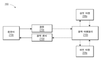
이제 도면을 참조하면, 도 1은 전자 부품 본딩 머신(100)의 사시도이다. 전자 부품 본딩 머신(100)은 지지 구조체(102)(예를 들어, 기판(104)(하부 타겟(104a)을 포함함)을 운반함), 본드 헤드 어셈블리(106)(가열된 본딩 툴일 수 있는 본딩 툴(108), 노즐, 등을 포함함)(본딩 툴(108)은 전자 부품(108a)을 운반하는 것으로 도시됨), 및 측정 시스템(110)을 포함한다. 측정 시스템(110)은 암 어셈블리(110a)(예를 들어, 도시된 바와 같이, 측정 시스템(110)의 특정 다른 요소를 운반하기 위함), 광학 어셈블리(110b), 광원(110c), 광학 센서(110d), 및 컴퓨터(110e)(예를 들어, 상부 타겟과 하부 타겟 사이의 거리를 결정하도록 반사된 광학 신호의 주파수 스펙트럼을 분석하는 컴퓨터)를 포함한다.Referring now to the drawings, FIG. 1 is a perspective view of an electronic
암 어셈블리(110a)(광학 어셈블리(110b), 광원(110c), 광학 센서(110d)를 운반할 수 있음)는 본드 헤드 어셈블리(106)와 함께, 또는 독립적으로 이동될 수 있다. 도 3에 도시된 바와 같이, 본드 헤드 어셈블리(106)(및 암 어셈블리(110a))는 아래에 기술되는 바와 같이, 복수의 거리를 측정하도록 전자 부품 본딩 머신(100)의 XY 평면 내에서 이동될 수 있다. 광원(110c)으로부터의 광학 신호는 광학 어셈블리(110b)로 들어간다. 이 광학 신호는 상부 광학 신호 부분(110b1)(본드 헤드 어셈블리(106)의 일부 및/또는 전자 부품(108a)과 같은 상부 타겟을 향하여 보내짐) 및 하부 광학 신호 부분(110b2)(지지 구조체(102)의 일부 또는 기판(104)과 같은 하부 타겟을 향하여 보내짐)으로 분할될 수 있다. 이러한 신호 부분은 해당 타겟에서 반사되어, 광학 어셈블리(110b)에서 재결합되고, 이에 의해 단일 복귀 광학 신호를 제공한다. 이 복귀 광학 신호는 컴퓨터(100e)와 연결되어 상부 타겟과 하부 타겟 사이의 거리를 결정하는 광학 센서(110d)에 의해 수신된다.
도 2는 측정 시스템(210)(즉, 도 1의 측정 시스템(110))의 블록도이다. 측정 시스템(210)은 광학 어셈블리(210b), 광원(210c), 광학 센서(210d), 및 컴퓨터(210e)를 포함한다. 도시된 바와 같이, 광학 어셈블리(210b)는 상부 타겟(208a) 및/또는 하부 타겟(204a)으로 광학 신호를 전송하고 및/또는 상부 타겟(208a) 및/또는 하부 타겟(204a)으로부터 반사된 광학 신호를 수신하도록 구성된다. 광학 어셈블리(210b)는 광원(210c)으로부터 광학 신호를 수신하도록 구성되고; 광학 어셈블리(210b)는 또한 광학 센서(210d)에 복귀 광학 신호를 제공하도록 구성된다. 컴퓨터(210e)(예를 들어, 상부 타겟과 하부 타겟 사이의 거리를 결정하도록 반사된 광학 신호의 주파수 스펙트럼을 분석하기 위한 컴퓨터)는 광원(210c) 및/또는 광학 센서(210d)와 통신하도록 구성된다.Figure 2 is a block diagram of measurement system 210 (i.e.,
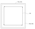
도 3은, 본 발명의 예시적인 실시예에 따른 전자 부품 본딩 머신 상의 XY 평면 내에서 측정 시스템의 일부를 이동시키기 위한 예시적인 스캔 패턴(300)을 도시한다. 예시의 목적으로, 상부 타겟(108a/208a)은 하부 타겟(104a/204a) 상에 오버레이된다. 물론, 다른 스캔 패턴도 본 발명의 범위 내에서 고려된다.3 shows an
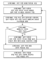
도 4 내지 도 11은: 거리를 측정하는 방법; 평행도에 관련된 프로파일을 결정하는 방법; 본딩 머신 상에 전자 부품을 본딩하는 방법과 같은 본 발명에 따른 예시적인 방법을 도시하는 흐름도이다(예를 들어, 도 1에서의 전자 부품 본딩 머신(100), 도 2에서의 전자 부품 본딩 머신(200)을 참조). 통상의 기술자에 의해 이해될 바와 같이, 흐름도에 포함되는 특정 단계는 생략될 수 있고; 특정 추가 단계가 추가될 수 있고; 단계의 순서는 도시된 순서로부터 변경될 수 있으며, 이는 보두 본 발명의 범위 내이다.4 to 11: Method for measuring distance; How to determine the profile related to parallelism; Flow diagram illustrating exemplary methods in accordance with the present invention, such as a method for bonding electronic components on a bonding machine (e.g., electronic
또한, 이러한 흐름도에 포함되는 다양한 단계가 서로 다른 시간에 발생할 수 있다는 것이 통상의 기술자에 의해 이해되어야 할 것이다. 예를 들어, 도 4 내지 도 11의 각각은 상부 타겟과 하부 타겟 사이의 평행도에 관련된 프로파일을 결정하는 것과 관련된 단계를 포함한다(도 4 내지 도 11의 각각에서 단계(404, 504, 604, 704, 804, 904, 1004, 및 1104) 참조). 이 단계 후에, 도 4 내지 도 11의 각각은 상부 타겟과 하부 타겟 사이의 각도를 조정하기 위하여 기울기 제어 메커니즘을 사용하는 단계를 포함한다(도 4의 단계(406) 참조). 프로파일은 하나의 단계(예를 들어, 도 4의 단계(404) 참조)에서 결정될 수 있고, 그런 다음 각도를 조정을 위해 후에 사용(예를 들어, 도 4의 단계(406) 참조)하기 위하여, 프로파일은 저장될 수 있다(그렇지 않다면 메모리에 저장될 수 있음).Additionally, it should be understood by those skilled in the art that various steps included in this flow chart may occur at different times. For example, each of FIGS. 4-11 includes steps associated with determining a profile related to the degree of parallelism between the upper and lower targets (steps 404, 504, 604, and 704 in each of FIGS. 4-11 , 804, 904, 1004, and 1104). After this step, each of FIGS. 4-11 includes using a tilt control mechanism to adjust the angle between the upper and lower targets (see step 406 in FIG. 4). The profile can be determined in one step (e.g., see step 404 in FIG. 4) and then used later to adjust the angle (e.g., see step 406 in FIG. 4). Profiles can be saved (otherwise stored in memory).
도 4 내지 도 11 각각은 상이한 예시적인 구성이다. 도 4에서, 상부 타겟은 전자 부품을 포함할 것이고, 하부 타겟은 기판을 포함할 것이다.4-11 each show a different example configuration. In Figure 4, the upper target will contain the electronic components and the lower target will contain the substrate.
도 4는, 전자 부품과 본딩 머신(예를 들어, 도 1의 본딩 머신(100), 도 2의 본딩 머신(200)) 상의 기판 사이의 평행도에 관련된 프로파일을 생성하고, 그런 다음 전자 부품을 기판에 본딩하도록 복수의 거리를 측정하는 방법을 도시하는 흐름도이다. 단계(400)에서, 상부 타겟 물질(예를 들어, 전자 부품) 및 하부 타겟 물질(예를 들어, 기판)은 전자 부품 본딩 머신으로 로딩된다. 단계(402)에서 광학 측정 시스템(예를 들어, 도 1의 측정 시스템(110), 및 도 2의 측정 시스템(210) 참조)을 사용하여 상부 타겟(예를 들어, 전자 부품)과 하부 타겟(예를 들어, 기판) 사이의 거리의 배열이 수집된다. 단계(404)에서, 본딩 머신 상의(또는 본딩 머신에 연결된) 컴퓨터를 사용하여, 상부 타겟과 하부 타겟 사이의 평행도에 관련된 프로파일이 복수의 거리를 사용하여 결정된다. 단계(406)에서, 상부 타겟과 하부 타겟 사이의 각도가 프로파일을 사용하여 (예를 들어, 기울기 제어 메커니즘을 사용하여) 조정된다. 단계(408)에서, 전자 부품을 본딩 머신 상의 기판에 본딩하는 본딩 작업이 시작된다.4 generates a profile related to the degree of parallelism between an electronic component and a substrate on a bonding machine (e.g.,
이제 도 5를 참조하면, 상부 타겟은 전자 부품을 포함할 것이나, 하부 타겟은 기판을 포함하지 않을 것이다(예를 들어, 하부 타겟은 지지 구조체의 일부를 포함할 것임). 도 5는 전자 부품과 본딩 머신(예를 들어, 도 1의 본딩 머신(100), 도 2의 본딩 머신(200)) 상의 지지 구조체 사이의 평행도에 관련된 프로파일을 생성하고, 그런 다음 전자 부품을 기판에 본딩하기 위해 복수의 거리를 측정하는 방법을 도시하는 흐름도이다. 단계(500)에서, 상부 타겟 물질(전자 부품)이 전자 부품 본딩 머신 상에 로딩된다. 단계(502)에서, 상부 타겟(예를 들어, 전자 부품)과 하부 타겟(예를 들어, 지지 구조체) 사이의 거리의 배열은 광학 측정 시스템(예를 들어, 도 1의 측정 시스템(110), 및 도 2의 측정 시스템(210) 참조)을 사용하여 수집된다. 단계(504)에서, 본딩 머신 상의(또는 본딩 머신에 연결된) 컴퓨터를 사용하여, 상부 타겟과 하부 타겟 사이의 평행도에 관련된 프로파일이 복수의 거리를 사용하여 결정된다. 단계(506)에서, 상부 타겟과 하부 타겟 사이의 각도는 프로파일을 사용하여 (예를 들어, 기울기 제어 메커니즘을 사용하여) 조정된다. 단계(508)에서 하부 타겟 물질(예를 들어, 기판)이 본딩 머신 상에 로딩된다. 단계(510)에서, 전자 부품을 기판에 본딩하는 접합 작업이 본딩 머신 상에서 시작된다.Referring now to Figure 5, the upper target will include electronic components, but the lower target will not include a substrate (eg, the lower target will include a portion of the support structure). 5 shows a profile related to the degree of parallelism between an electronic component and a support structure on a bonding machine (e.g.,
이제 도 6을 참조하면, 상부 타겟은 전자 부품을 포함하지 않을 것이고(예를 들어, 상부 타겟은 본드 헤드 어셈블리의 일부를 포함할 것임), 하부 타겟은 기판을 포함할 것이다. 도 6은, 본드 헤드 어셈블리와 본딩 머신(예를 들어, 도 1의 본딩 머신(100), 도 2의 본딩 머신(200)) 상의 기판 사이의 평행도에 관련된 프로파일을 생성하고, 그런 다음 전자 부품을 기판에 본딩하기 위해 복수의 거리를 측정하는 방법을 도시하는 흐름도이다. 단계(600)에서, 하부 타겟 물질(기판)이 본딩 머신 상에 로딩된다. 단계(602)에서, 상부 타겟(예를 들어, 본드 헤드 어셈블리의 일부)과 하부 타겟(예를 들어, 기판) 사이의 거리의 배열이 광학 측정 시스템(예를 들어, 도 1의 측정 시스템(110), 및 도 2의 측정 시스템(210))을 사용하여 수집된다. 단계(604)에서, 본딩 머신 상의(또는 본딩 머신에 연결된) 컴퓨터를 사용하여, 상부 타겟과 하부 타겟 사이의 평행도에 관련된 프로파일이 복수의 거리를 사용하여 결정된다. 단계(606)에서, 상부 타겟과 하부 타겟 사이의 각도는 프로파일을 사용하여 (예를 들어, 기울기 제어 메커니즘을 사용하여) 조정된다. 단계(608)에서 상부 타겟 물질(예를 들어, 전자 부품)이 본딩 머신 상에 로딩된다. 단계(610)에서, 전자 부품을 기판에 본딩하는 접합 작업이 본딩 머신 상에서 시작된다.Referring now to Figure 6, the upper target will not contain electronic components (eg, the upper target will contain part of the bond head assembly) and the lower target will contain the substrate. FIG. 6 generates a profile related to the degree of parallelism between a bond head assembly and a substrate on a bonding machine (e.g.,
이제 도 7을 참조하면, 상부 타겟은 전자 부품을 포함하지 않을 것이고(예를 들어, 상부 타겟은 본드 헤드 어셈블리의 일부를 포함할 것임), 하부 타겟은 기판을 포함하지 않을 것이다(예를 들어, 하부 타겟은 지지 구조체의 일부를 포함할 것임). 도 7은, 본드 헤드 어셈블리와 본딩 머신(예를 들어, 도 1의 본딩 머신(100), 도 2의 본딩 머신(200)) 상의 지지 구조체 사이의 평행도에 관련된 프로파일을 생성하고, 그런 다음 전자 부품을 기판에 본딩하기 위해 복수의 거리를 측정하는 방법을 도시하는 흐름도이다. 단계(702)에서, 상부 타겟(예를 들어, 본드 헤드 어셈블리의 일부)과 하부 타겟(예를 들어, 지지 구조체의 일부) 사이의 거리의 배열이 광학 측정 시스템(예를 들어, 도 1의 측정 시스템(110), 및 도 2의 측정 시스템(210))을 사용하여 수집된다. 단계(704)에서, 본딩 머신 상의(또는 본딩 머신에 연결된) 컴퓨터를 사용하여, 상부 타겟과 하부 타겟 사이의 평행도에 관련된 프로파일이 복수의 거리를 사용하여 결정된다. 단계(706)에서, 상부 타겟과 하부 타겟 사이의 각도는 프로파일을 사용하여 (예를 들어, 기울기 제어 메커니즘을 사용하여) 조정된다. 단계(708)에서, 상부 타겟 물질(전자 부품) 및 하부 타겟 물질(기판)이 본딩 머신 상에 로딩된다. 단계(710)에서, 전자 부품을 본딩 머신 상의 기판에 본딩하는 접합 작업이 시작된다.Referring now to Figure 7, the upper target will not include electronic components (e.g., the upper target will include part of the bond head assembly) and the lower target will not include the substrate (e.g., The lower target will contain part of the support structure). FIG. 7 generates a profile related to the degree of parallelism between the bond head assembly and the support structure on the bonding machine (e.g.,
본 발명의 실시예(도 4 내지 도 7에 도시된 방법 포함)의 각각은 하나 이상의 "피드백(feedback)" 단계를 포함할 수 있다. 예를 들어, 도 4 내지 도 7 각각은 상부 타겟과 하부 타겟 사이의 평행도에 관련된 프로파일을 결정하는 것을 포함한다(예를 들어, 도 4 내지 도 7 각각의 단계(404, 504, 604, 704) 참조). 방법은 미리 결정된 기준에 기초하여 평행도 수준이 허용 가능한지 여부에 대한 피드백을 포함할 수 있다. 도 8 내지 도 11 각각은 도 4 내지 도 7의 대응하는 것과 실질적으로 유사하나; 도 8 내지 도 11 각각은 평행도 수준이 허용 가능한지 여부를 결정하는 단계와, 평행도 수준이 허용 가능(또는 허용 불가능)한 경우 해당 프로세스 흐름을 포함한다.Each of the embodiments of the invention (including the methods shown in FIGS. 4-7) may include one or more “feedback” steps. For example, each of FIGS. 4-7 includes determining a profile related to the degree of parallelism between the upper target and the lower target (e.g., steps 404, 504, 604, and 704 of each of FIGS. 4-7 reference). The method may include feedback as to whether the level of parallelism is acceptable based on predetermined criteria. Each of Figures 8-11 is substantially similar to its counterpart in Figures 4-7; 8-11 each include steps for determining whether the level of parallelism is acceptable and a corresponding process flow if the level of parallelism is acceptable (or unacceptable).
도 8은 도 4와 유사한 흐름도이다. 단계(800)에서, 상부 타겟 물질(전자 부품) 및 하부 타겟 물질(기판)은 본딩 머신(예를 들어, 도 1의 본딩 머신(100), 도 2의 본딩 머신(200)) 상에 로딩된다. 단계(802)에서, 상부 타겟과 하부 타겟 사이의 거리의 배열이 광학 측정 시스템을 사용하여 수집된다. 단계(804)에서, 본딩 머신 상의(또는 본딩 머신에 연결된) 컴퓨터를 사용하여, 상부 타겟과 하부 타겟 사이의 평행도에 관련된 프로파일이 복수의 거리를 사용하여 결정된다. 단계(806)에서, 평행도의 수준이 허용 가능한지 여부의 결정이 이루어진다. 허용 불가한 경우("NO"), 상부 타겟과 하부 타겟 사이의 각도는 단계(808)에서 (예를 들어, 기울기 제어 메커니즘을 사용하여) 조정된다(그리고 프로세스는 반복되는 단계(802 내지 806)에서 계속됨). 허용 가능한 경우("YES"), 전자 부품을 본딩 머신 상의 기판에 본딩하는 본딩 작업이 단계(810)에서 시작된다.Figure 8 is a flow chart similar to Figure 4. In step 800, the top target material (electronic component) and bottom target material (substrate) are loaded onto a bonding machine (e.g.,
도 9는 도 5와 유사한 흐름도이다. 단계(900)에서, 상부 타겟 물질(전자 부품)이 본딩 머신(예를 들어, 도 1의 본딩 머신(100), 도 2의 본딩 머신(200)) 상에 로딩된다. 단계(902)에서, 상부 타겟과 하부 타겟 사이의 거리의 배열이 광학 측정 시스템을 사용하여 수집된다. 단계(904)에서, 본딩 머신 상의(또는 본딩 머신에 연결된) 컴퓨터를 사용하여, 상부 타겟과 하부 타겟 사이의 평행도에 관련된 프로파일이 복수의 거리를 사용하여 결정된다. 단계(906)에서, 평행도의 수준이 허용 가능한지 여부의 결정이 이루어진다. 허용 불가한 경우("NO"), 상부 타겟과 하부 타겟 사이의 각도는 단계(908)에서 (예를 들어, 기울기 제어 메커니즘을 사용하여) 조정된다(그리고 프로세스는 반복되는 단계(902 내지 906)에서 계속됨). 허용 가능한 경우("YES"), 단계(910)에서 하부 타겟 물질(기판)이 본딩 머신 상에 로딩된다. 단계(912)에서, 전자 부품을 본딩 머신 상의 기판에 본딩하는 본딩 작업이 시작된다.Figure 9 is a flow chart similar to Figure 5. At step 900, the top target material (electronic component) is loaded onto a bonding machine (e.g.,
도 10은 도 6과 유사한 흐름도이다. 단계(1000)에서, 하부 타겟 물질(기판)이 본딩 머신(예를 들어, 도 1의 본딩 머신(100), 도 2의 본딩 머신(200)) 상에 로딩된다. 단계(1002)에서, 상부 타겟과 하부 타겟 사이의 거리의 배열이 광학 측정 시스템을 사용하여 수집된다. 단계(1004)에서, 본딩 머신 상의(또는 본딩 머신에 연결된) 컴퓨터를 사용하여, 상부 타겟과 하부 타겟 사이의 평행도에 관련된 프로파일이 복수의 거리를 사용하여 결정된다. 단계(1006)에서, 평행도의 수준이 허용 가능한지 여부의 결정이 이루어진다. 허용 불가한 경우("NO"), 상부 타겟과 하부 타겟 사이의 각도는 단계(1008)에서 (예를 들어, 기울기 제어 메커니즘을 사용하여) 조정된다(그리고 프로세스는 반복되는 단계(1002 내지 1006)에서 계속됨). 허용 가능한 경우("YES"), 단계(1010)에서 상부 타겟 물질(전자 부품)이 본딩 머신 상에 로딩된다. 단계(1012)에서, 전자 부품을 본딩 머신 상의 기판에 본딩하는 본딩 작업이 시작된다.Figure 10 is a flow chart similar to Figure 6. At step 1000, the underlying target material (substrate) is loaded onto a bonding machine (e.g.,
도 11은 도 7과 유사한 흐름도이다. 단계(1102)에서, 상부 타겟과 하부 타겟 사이의 거리의 배열은 본딩 머신(예를 들어, 도 1의 본딩 머신(100), 도 2의 본딩 머신(200)) 상의 광학 측정 시스템을 사용하여 수집된다. 단계(1104)에서, 본딩 머신 상의(또는 본딩 머신에 연결된) 컴퓨터를 사용하여, 상부 타겟과 하부 타겟 사이의 평행도에 관련된 프로파일이 복수의 거리를 사용하여 결정된다. 단계(1106)에서, 평행도의 수준이 허용 가능한지 여부의 결정이 이루어진다. 허용 불가한 경우("NO"), 상부 타겟과 하부 타겟 사이의 각도는 단계(1108)에서 (예를 들어, 기울기 제어 메커니즘을 사용하여) 조정된다(그리고 프로세스는 반복되는 단계(1102 내지 1106)에서 계속됨). 허용 가능한 경우("YES"), 단계(1110)에서 상부 타겟 물질(전자 부품) 및 하부 타겟 물질(기판)은 본딩 머신 상에 로딩된다. 단계(1112)에서, 전자 부품을 본딩 머신 상의 기판에 본딩하는 본딩 작업이 시작된다.Figure 11 is a flow chart similar to Figure 7. In step 1102, an array of distances between the upper and lower targets is collected using an optical measurement system on a bonding machine (e.g.,
본 발명은 특정 실시예를 참조하여 여기서 도시 및 기술되었지만, 본 발명은 개시된 세부 사항에 제한되도록 의도되지 않는다. 오히려, 청구항의 균등의 범위 및 범주 내에서 본 발명을 벗어남이 없이 세부 사항에서 다양한 수정이 이루어질 수 있다.Although the invention has been shown and described herein with reference to specific embodiments, the invention is not intended to be limited to the details disclosed. Rather, various modifications may be made in the details without departing from the invention within the scope and scope of equivalence of the claims.
Claims (38)
기판을 지지하기 위한 지지 구조체;
전자 부품을 홀딩하고, 상기 전자 부품을 상기 기판에 본딩하기 위한 본드 헤드 어셈블리; 및
(i) 상기 전자 부품 본딩 머신 상의 상부 타겟과, (ii) 상기 전자 부품 본딩 머신 상의 하부 타겟 사이의 거리를 측정하기 위한 측정 시스템으로서, 상기 상부 타겟은 상기 본드 헤드 어셈블리의 일부 및 상기 전자 부품 중 적어도 하나를 포함하고, 상기 하부 타겟은 상기 지지 구조체의 일부 및 상기 기판 중 적어도 하나를 포함하는, 측정 시스템을 포함하고,
상기 측정 시스템은, 상기 상부 타겟 및 상기 하부 타겟 중 적어도 하나를 향하여 보내지는 광학 신호를 제공하기 위한 광원, 상기 하부 타겟 및 상기 상부 타겟 중 적어도 하나로부터 반사된 광학 신호를 수신하기 위한 광학 센서, 및 상기 광학 센서로부터의 정보를 사용하여 상기 거리를 결정하도록 상기 광학 센서와 통신하는 컴퓨터를 포함하는 전자 부품 본딩 머신.As an electronic component bonding machine,
a support structure for supporting the substrate;
a bond head assembly for holding electronic components and bonding the electronic components to the substrate; and
A measurement system for measuring the distance between (i) an upper target on the electronic component bonding machine and (ii) a lower target on the electronic component bonding machine, wherein the upper target is a portion of the bond head assembly and one of the electronic components. a measurement system comprising at least one, wherein the lower target includes at least one of a portion of the support structure and the substrate,
The measurement system includes a light source for providing an optical signal sent toward at least one of the upper target and the lower target, an optical sensor for receiving an optical signal reflected from at least one of the lower target and the upper target, and An electronic component bonding machine comprising a computer in communication with the optical sensor to determine the distance using information from the optical sensor.
상기 전자 부품은 반도체 칩인 전자 부품 본딩 머신.In claim 1,
An electronic component bonding machine where the electronic component is a semiconductor chip.
상기 기판은 반도체 웨이퍼인 전자 부품 본딩 머신.In claim 1,
An electronic component bonding machine where the substrate is a semiconductor wafer.
상기 상부 타겟은 상기 본드 헤드 어셈블리의 일부이고, 상기 하부 타겟은 상기 지지 구조체의 일부인 전자 부품 본딩 머신.In claim 1,
An electronic component bonding machine, wherein the upper target is part of the bond head assembly and the lower target is part of the support structure.
상기 상부 타겟은 상기 본드 헤드 어셈블리의 일부이고, 상기 하부 타겟은 기판인 전자 부품 본딩 머신.In claim 1,
An electronic component bonding machine wherein the upper target is part of the bond head assembly and the lower target is a substrate.
상기 상부 타겟은 상기 전자 부품이고, 상기 하부 타겟은 상기 지지 구조체의 일부인 전자 부품 본딩 머신.In claim 1,
An electronic component bonding machine wherein the upper target is the electronic component and the lower target is part of the support structure.
상기 상부 타겟은 상기 전자 부품이고, 상기 하부 타겟은 기판인 전자 부품 본딩 머신.In claim 1,
An electronic component bonding machine wherein the upper target is the electronic component and the lower target is a substrate.
상기 본드 헤드 어셈블리의 일부는, 상기 전자 부품을 홀딩하고, 상기 전자 부품을 상기 기판에 본딩하기 위한 본딩 툴인 전자 부품 본딩 머신.In claim 1,
A part of the bond head assembly is a bonding tool for holding the electronic component and bonding the electronic component to the substrate.
상기 본드 헤드 어셈블리의 일부는, 상기 전자 부품을 홀딩하고, 상기 전자 부품을 상기 기판에 본딩하기 위한 가열된 본딩 툴인 전자 부품 본딩 머신.In claim 1,
An electronic component bonding machine, wherein a portion of the bond head assembly holds the electronic component and is a heated bonding tool for bonding the electronic component to the substrate.
상기 광학 신호는 (a) 상기 상부 타겟을 향하여 보내지는 제1 부분 및 (b) 상기 하부 타겟을 향하여 보내지는 제2 부분으로 분할되는 전자 부품 본딩 머신.In claim 1,
The electronic component bonding machine wherein the optical signal is divided into (a) a first portion sent toward the upper target and (b) a second portion sent toward the lower target.
상기 하부 타겟 및 상기 상부 타겟으로부터 단일 반사된 광학 신호를 상기 광학 센서에 제공하기 위한 광학 어셈블리를 더 포함하는 전자 부품 본딩 머신.In claim 1,
An electronic component bonding machine further comprising an optical assembly for providing a single reflected optical signal from the lower target and the upper target to the optical sensor.
상기 컴퓨터는 상기 상부 타겟과 상기 하부 타겟 사이의 상기 거리를 결정하도록 상기 반사된 광학 신호의 주파수 스펙트럼을 분석하는 전자 부품 본딩 머신.In claim 1,
The electronic component bonding machine wherein the computer analyzes the frequency spectrum of the reflected optical signal to determine the distance between the upper target and the lower target.
상기 전자 부품 본딩 머신은 다이 부착 머신인 전자 부품 본딩 머신.In claim 1,
The electronic component bonding machine is a die attachment machine.
상기 전자 부품 본딩 머신은 플립 칩 본딩 머신인 전자 부품 본딩 머신.In claim 1,
The electronic component bonding machine is a flip chip bonding machine.
상기 전자 부품 본딩 머신은 열압착 본딩 머신인 전자 부품 본딩 머신.In claim 1,
The electronic component bonding machine is a thermal compression bonding machine.
상기 측정 시스템의 일부는, 상기 전자 부품 본딩 머신의 XY 평면 내에서 복수의 위치로 이동되어 상기 복수의 위치의 각각에서 상기 상부 타겟과 상기 하부 타겟 사이의 상기 거리를 측정하도록 구성되는 전자 부품 본딩 머신.In claim 1,
A portion of the measurement system is configured to be moved to a plurality of positions within an XY plane of the electronic component bonding machine and measure the distance between the upper target and the lower target at each of the plurality of locations. .
상기 복수의 위치에서 측정된 상기 거리는, 상기 상부 타겟과 상기 하부 타겟 사이의 평행도에 관련된 프로파일을 결정하도록 집합적으로 사용되는 전자 부품 본딩 머신.In claim 16,
The distances measured at the plurality of locations are collectively used to determine a profile related to the degree of parallelism between the upper target and the lower target.
기판을 지지하기 위한 지지 구조체;
전자 부품을 홀딩하고, 상기 전자 부품을 상기 기판에 본딩하기 위한 본드 헤드 어셈블리; 및
(i) 상기 전자 부품 본딩 머신 상의 상부 타겟과, (ii) 상기 전자 부품 본딩 머신 상의 하부 타겟 사이의 평행도에 관련된 프로파일을 측정하기 위한 측정 시스템으로서, 상기 상부 타겟은 상기 본드 헤드 어셈블리의 일부 및 상기 전자 부품 중 적어도 하나를 포함하고, 상기 하부 타겟은 상기 지지 구조체의 일부 및 상기 기판 중 적어도 하나를 포함하는, 측정 시스템을 포함하고,
상기 측정 시스템은, 상기 상부 타겟 및 상기 하부 타겟 중 적어도 하나를 향하여 보내지는 광학 신호를 제공하기 위한 광원, 상기 하부 타겟 및 상기 상부 타겟 중 적어도 하나로부터 반사된 광학 신호를 수신하기 위한 광학 센서, 및 상기 광학 센서로부터의 정보를 사용하여 상기 거리를 결정하도록 상기 광학 센서와 통신하는 컴퓨터를 포함하는 전자 부품 본딩 머신.As an electronic component bonding machine,
a support structure for supporting the substrate;
a bond head assembly for holding electronic components and bonding the electronic components to the substrate; and
A measurement system for measuring a profile related to the degree of parallelism between (i) an upper target on the electronic component bonding machine and (ii) a lower target on the electronic component bonding machine, wherein the upper target is a portion of the bond head assembly and the A measurement system comprising at least one of an electronic component, wherein the lower target includes at least one of a portion of the support structure and the substrate,
The measurement system includes a light source for providing an optical signal sent toward at least one of the upper target and the lower target, an optical sensor for receiving an optical signal reflected from at least one of the lower target and the upper target, and An electronic component bonding machine comprising a computer in communication with the optical sensor to determine the distance using information from the optical sensor.
상기 컴퓨터는 상기 전자 부품 본딩 머신의 복수의 XY 위치에서 반사된 광학 신호를 사용하여 측정된 복수의 거리를 사용하여 상기 프로파일을 결정하도록 구성되는 전자 부품 본딩 머신.In claim 18,
The computer is configured to determine the profile using a plurality of distances measured using reflected optical signals at a plurality of XY positions of the electronic component bonding machine.
상기 전자 부품은 반도체 칩인 전자 부품 본딩 머신.In claim 18,
An electronic component bonding machine where the electronic component is a semiconductor chip.
상기 기판은 반도체 웨이퍼인 전자 부품 본딩 머신.In claim 18,
An electronic component bonding machine where the substrate is a semiconductor wafer.
상기 상부 타겟은 상기 본드 헤드 어셈블리의 일부이고, 상기 하부 타겟은 상기 지지 구조체의 일부인 전자 부품 본딩 머신.In claim 18,
An electronic component bonding machine, wherein the upper target is part of the bond head assembly and the lower target is part of the support structure.
상기 상부 타겟은 상기 본드 헤드 어셈블리의 일부이고, 상기 하부 타겟은 기판인 전자 부품 본딩 머신.In claim 18,
An electronic component bonding machine wherein the upper target is a part of the bond head assembly and the lower target is a substrate.
상기 상부 타겟은 상기 전자 부품이고, 상기 하부 타겟은 상기 지지 구조체의 일부인 전자 부품 본딩 머신.In claim 18,
An electronic component bonding machine wherein the upper target is the electronic component and the lower target is part of the support structure.
상기 상부 타겟은 상기 전자 부품이고, 상기 하부 타겟은 기판인 전자 부품 본딩 머신.In claim 18,
An electronic component bonding machine wherein the upper target is the electronic component and the lower target is a substrate.
상기 본드 헤드 어셈블리의 일부는, 상기 전자 부품을 홀딩하고, 상기 전자 부품을 상기 기판에 본딩하기 위한 본딩 툴인 전자 부품 본딩 머신.In claim 18,
A part of the bond head assembly is a bonding tool for holding the electronic component and bonding the electronic component to the substrate.
상기 본드 헤드 어셈블리의 일부는, 상기 전자 부품을 홀딩하고, 상기 전자 부품을 상기 기판에 본딩하기 위한 가열된 본딩 툴인 전자 부품 본딩 머신.In claim 18,
An electronic component bonding machine, wherein a portion of the bond head assembly holds the electronic component and is a heated bonding tool for bonding the electronic component to the substrate.
상기 광학 신호는 (a) 상기 상부 타겟을 향하여 보내지는 제1 부분 및 (b) 상기 하부 타겟을 향하여 보내지는 제2 부분으로 분할되는 전자 부품 본딩 머신.In claim 18,
The electronic component bonding machine wherein the optical signal is divided into (a) a first portion sent toward the upper target and (b) a second portion sent toward the lower target.
상기 하부 타겟 및 상기 상부 타겟으로부터 단일 반사된 광학 신호를 상기 광학 센서에 제공하기 위한 광학 어셈블리를 더 포함하는 전자 부품 본딩 머신.In claim 18,
An electronic component bonding machine further comprising an optical assembly for providing a single reflected optical signal from the lower target and the upper target to the optical sensor.
상기 컴퓨터는 상기 상부 타겟과 상기 하부 타겟 사이의 거리를 결정하도록 상기 반사된 광학 신호의 주파수 스펙트럼을 분석하도록 구성되고, 상기 컴퓨터는 상기 전자 부품 본딩 머신의 복수의 XY 위치에서 결정된 상기 거리를 사용하여 상기 프로파일을 결정하는 전자 부품 본딩 머신.In claim 18,
The computer is configured to analyze the frequency spectrum of the reflected optical signal to determine a distance between the upper target and the lower target, the computer using the distance determined at a plurality of XY positions of the electronic component bonding machine. Electronic component bonding machine to determine the profile.
상기 전자 부품 본딩 머신은 다이 부착 머신인 전자 부품 본딩 머신.In claim 18,
The electronic component bonding machine is a die attachment machine.
상기 전자 부품 본딩 머신은 플립 칩 본딩 머신인 전자 부품 본딩 머신.In claim 18,
The electronic component bonding machine is a flip chip bonding machine.
상기 전자 부품 본딩 머신은 열압착 본딩 머신인 전자 부품 본딩 머신.In claim 18,
The electronic component bonding machine is a thermal compression bonding machine.
(a) 전자 부품 본딩 머신의 상부 타겟, 및 상기 전자 부품 본딩 머신의 하부 타겟 중 적어도 하나를 향하여 광학 신호를 보내는 단계로서, 상기 상부 타겟은 (i) 상기 전자 부품 본딩 머신의 본드 헤드 어셈블리의 일부, 및 (ii) 상기 본드 헤드 어셈블리에 의해 운반되는 전자 부품 중 적어도 하나를 포함하고, 상기 하부 타겟은 (i) 상기 전자 부품 본딩 머신의 지지 구조체의 일부, 및 (ii) 상기 지지 구조체에 의해 지지되는 기판 중 적어도 하나를 포함하는, 단계;
(b) 상기 상부 타겟 및 상기 하부 타겟 중 적어도 하나로부터 반사된 광학 신호를 광학 센서에서 수신하는 단계; 및
(c) 상기 상부 타겟 및 상기 하부 타겟 사이의 거리를 결정하도록 상기 반사된 광학 신호를 분석하는 단계를 포함하는 방법.A method for measuring distance on an electronic component bonding machine, said method comprising:
(a) sending an optical signal toward at least one of an upper target of an electronic component bonding machine and a lower target of the electronic component bonding machine, wherein the upper target is (i) a portion of a bond head assembly of the electronic component bonding machine , and (ii) an electronic component carried by the bond head assembly, wherein the lower target is (i) a portion of a support structure of the electronic component bonding machine, and (ii) supported by the support structure. comprising at least one of a substrate;
(b) receiving an optical signal reflected from at least one of the upper target and the lower target at an optical sensor; and
(c) analyzing the reflected optical signal to determine the distance between the upper target and the lower target.
(a) 전자 부품을 제공하는 단계;
(b) 지지 구조체로 기판을 지지하는 단계;
(c) 전자 부품 본딩 머신의 본드 헤드 어셈블리로 상기 전자 부품을 운반하는 단계;
(d) 상기 전자 부품 본딩 머신의 상부 타겟, 및 상기 전자 부품 본딩 머신의 하부 타겟 중 적어도 하나를 향하여 광학 신호를 보내는 단계로서, 상기 상부 타겟은 (i) 상기 전자 부품 본딩 머신의 상기 본드 헤드 어셈블리의 일부, 및 (ii) 상기 본드 헤드 어셈블리에 의해 운반되는 전자 부품 중 적어도 하나를 포함하고, 상기 하부 타겟은 (i) 상기 전자 부품 본딩 머신의 상기 지지 구조체의 일부, 및 (ii) 상기 지지 구조체에 의해 지지되는 기판 중 적어도 하나를 포함하는, 단계;
(e) 상기 상부 타겟 및 상기 하부 타겟 중 적어도 하나로부터 반사된 광학 신호를 광학 센서에서 수신하는 단계;
(f) 상기 상부 타겟 및 상기 하부 타겟 사이의 거리를 결정하도록 상기 반사된 광학 신호를 분석하는 단계; 및
(g) 상기 전자 부품을 상기 기판에 본딩하는 본딩 작업을 시작하는 단계를 포함하는 방법.As a bonding method,
(a) providing electronic components;
(b) supporting the substrate with a support structure;
(c) transporting the electronic component to a bond head assembly of an electronic component bonding machine;
(d) sending an optical signal toward at least one of an upper target of the electronic component bonding machine and a lower target of the electronic component bonding machine, wherein the upper target is (i) the bond head assembly of the electronic component bonding machine and (ii) at least one of an electronic component carried by the bond head assembly, wherein the lower target includes (i) a portion of the support structure of the electronic component bonding machine, and (ii) the support structure. comprising at least one of a substrate supported by;
(e) receiving an optical signal reflected from at least one of the upper target and the lower target at an optical sensor;
(f) analyzing the reflected optical signal to determine a distance between the upper target and the lower target; and
(g) starting a bonding operation to bond the electronic component to the substrate.
(h) 상기 상부 타겟과 상기 하부 타겟 사이의 각도를 조정하는 단계를 더 포함하는 방법.In claim 35,
(h) adjusting the angle between the upper target and the lower target.
(a) 전자 부품 본딩 머신으로 상부 타겟 물질과 하부 타겟 물질을 로딩하는 단계;
(b) 광학 측정 시스템을 사용하여 상부 타겟과 하부 타겟 사이의 거리 배열을 수집하는 단계;
(c) 상기 상부 타겟과 상기 하부 타겟 사이의 평행도에 관련된 프로파일을 결정하도록 상기 전자 부품 본딩 머신 상의 컴퓨터를 사용하는 단계;
(d) 상기 상부 타겟과 상기 하부 타겟 사이의 각도를 조정하는 단계; 및
(e) 상기 전자 부품을 기판에 본딩하는 본딩 작업을 시 작하는 단계를 포함하는 방법.As a bonding method,
(a) loading an upper target material and a lower target material into an electronic component bonding machine;
(b) collecting an array of distances between the upper and lower targets using an optical measurement system;
(c) using a computer on the electronic component bonding machine to determine a profile related to the degree of parallelism between the upper target and the lower target;
(d) adjusting the angle between the upper target and the lower target; and
(e) starting a bonding operation to bond the electronic component to the substrate.
(c1) 평행도에 관련된 프로파일이 허용 가능한 수준의 평행도를 제공하는 지 결정하는 단계를 더 포함하는 방법.In claim 37,
(c1) A method further comprising determining whether the profile related to parallelism provides an acceptable level of parallelism.
Applications Claiming Priority (3)
| Application Number | Priority Date | Filing Date | Title |
|---|---|---|---|
| US202163195705P | 2021-06-01 | 2021-06-01 | |
| US63/195,705 | 2021-06-01 | ||
| PCT/US2022/031622 WO2022256332A1 (en) | 2021-06-01 | 2022-05-31 | Electronic component bonding machines, and methods of measuring a distance on such machines |
Publications (1)
| Publication Number | Publication Date |
|---|---|
| KR20240015650A true KR20240015650A (en) | 2024-02-05 |
Family
ID=84194313
Family Applications (1)
| Application Number | Title | Priority Date | Filing Date |
|---|---|---|---|
| KR1020237042009A KR20240015650A (en) | 2021-06-01 | 2022-05-31 | Electronic component bonding machines and methods for measuring distances on such machines |
Country Status (6)
| Country | Link |
|---|---|
| US (1) | US20220384384A1 (en) |
| JP (1) | JP2024523149A (en) |
| KR (1) | KR20240015650A (en) |
| CN (1) | CN117355934A (en) |
| TW (1) | TW202312859A (en) |
| WO (1) | WO2022256332A1 (en) |
Family Cites Families (5)
| Publication number | Priority date | Publication date | Assignee | Title |
|---|---|---|---|---|
| CH694931A5 (en) * | 2000-03-17 | 2005-09-15 | Esec Trading Sa | Device for mounting semiconductor chips on a substrate especially a metallic lead-frame has a sensor for detecting a first longitudinal edge of the substrate enabling accurate chip positioning across the substrate |
| US6705507B2 (en) * | 2001-07-24 | 2004-03-16 | Kulicke & Soffa Investments, Inc. | Die attach system and process using cornercube offset tool |
| JP5894745B2 (en) * | 2011-05-31 | 2016-03-30 | 浜松ホトニクス株式会社 | Integrated circuit inspection equipment |
| US9136243B2 (en) * | 2013-12-03 | 2015-09-15 | Kulicke And Soffa Industries, Inc. | Systems and methods for determining and adjusting a level of parallelism related to bonding of semiconductor elements |
| US20150380379A1 (en) * | 2014-06-26 | 2015-12-31 | MRSI Systems, LLC | System and method for thermo-compression bonding of high bump count semiconductors |
-
2022
- 2022-05-31 KR KR1020237042009A patent/KR20240015650A/en unknown
- 2022-05-31 CN CN202280037236.5A patent/CN117355934A/en active Pending
- 2022-05-31 JP JP2023573325A patent/JP2024523149A/en active Pending
- 2022-05-31 US US17/828,966 patent/US20220384384A1/en active Pending
- 2022-05-31 WO PCT/US2022/031622 patent/WO2022256332A1/en active Application Filing
- 2022-06-01 TW TW111120469A patent/TW202312859A/en unknown
Also Published As
| Publication number | Publication date |
|---|---|
| WO2022256332A1 (en) | 2022-12-08 |
| JP2024523149A (en) | 2024-06-28 |
| TW202312859A (en) | 2023-03-16 |
| CN117355934A (en) | 2024-01-05 |
| US20220384384A1 (en) | 2022-12-01 |
Similar Documents
| Publication | Publication Date | Title |
|---|---|---|
| US9425163B2 (en) | Systems and methods for determining and adjusting a level of parallelism related to bonding of semiconductor elements | |
| KR102336344B1 (en) | Methods of operating bonding machines for bonding semiconductor elements, and bonding machines | |
| TWI467681B (en) | Method for manufacturing semiconductor device | |
| US6961994B2 (en) | Method of high-speed and accurate alignment using a chip mounting device | |
| US6146014A (en) | Method for laser scanning flip-chip integrated circuits | |
| KR102363436B1 (en) | Device and method of laser compression bonding for semiconductor chip | |
| CN114485450B (en) | PCB warp detection device, method and system | |
| JP2007157970A (en) | Bonding method and bonding device | |
| KR19980081827A (en) | Apparatus and method for mounting semiconductor chips on a substrate | |
| KR20240015650A (en) | Electronic component bonding machines and methods for measuring distances on such machines | |
| KR100672227B1 (en) | Bonding apparatus | |
| KR20060051417A (en) | Bonding apparatus | |
| US10784130B2 (en) | Bonding apparatus | |
| US20230326778A1 (en) | Methods of adjusting a tilt between a bonding tool assembly and a support structure assembly of a bonding system, and related bonding systems | |
| JP4932203B2 (en) | Paste coating apparatus and paste coating method | |
| CN114074236A (en) | Welding device and welding method | |
| KR20220084744A (en) | Bonding apparatus and calibration method thereof | |
| JP2021015917A (en) | Mounting device | |
| US20230392921A1 (en) | Measurement device, measurement method, and bonding system | |
| KR102525378B1 (en) | Noncontact cutting system and cutting method using the same | |
| JP3996101B2 (en) | Semiconductor device manufacturing apparatus and semiconductor device manufacturing method | |
| JPH09223717A (en) | Method and apparatus for bonding flip chip | |
| JPS63260143A (en) | Semiconductor wafer prober |