KR20230148733A - Non-metal incorporation into molybdenum on dielectric surfaces - Google Patents
Non-metal incorporation into molybdenum on dielectric surfaces Download PDFInfo
- Publication number
- KR20230148733A KR20230148733A KR1020227044687A KR20227044687A KR20230148733A KR 20230148733 A KR20230148733 A KR 20230148733A KR 1020227044687 A KR1020227044687 A KR 1020227044687A KR 20227044687 A KR20227044687 A KR 20227044687A KR 20230148733 A KR20230148733 A KR 20230148733A
- Authority
- KR
- South Korea
- Prior art keywords
- gas
- layer
- substrate
- chamber
- process chamber
- Prior art date
Links
- 229910052750 molybdenum Inorganic materials 0.000 title claims abstract description 81
- 239000011733 molybdenum Substances 0.000 title claims abstract description 76
- ZOKXTWBITQBERF-UHFFFAOYSA-N Molybdenum Chemical compound [Mo] ZOKXTWBITQBERF-UHFFFAOYSA-N 0.000 title claims abstract description 75
- 238000010348 incorporation Methods 0.000 title description 4
- 229910052755 nonmetal Inorganic materials 0.000 title 1
- 150000002843 nonmetals Chemical class 0.000 title 1
- 238000000034 method Methods 0.000 claims abstract description 257
- 230000008569 process Effects 0.000 claims abstract description 211
- 239000007789 gas Substances 0.000 claims description 284
- 238000000151 deposition Methods 0.000 claims description 158
- 239000000758 substrate Substances 0.000 claims description 143
- 230000008021 deposition Effects 0.000 claims description 123
- 239000002243 precursor Substances 0.000 claims description 115
- 238000000231 atomic layer deposition Methods 0.000 claims description 73
- QVGXLLKOCUKJST-UHFFFAOYSA-N atomic oxygen Chemical compound [O] QVGXLLKOCUKJST-UHFFFAOYSA-N 0.000 claims description 64
- 229910052760 oxygen Inorganic materials 0.000 claims description 64
- 239000001301 oxygen Substances 0.000 claims description 64
- 238000012545 processing Methods 0.000 claims description 50
- 239000000463 material Substances 0.000 claims description 45
- 239000003638 chemical reducing agent Substances 0.000 claims description 44
- IJGRMHOSHXDMSA-UHFFFAOYSA-N Atomic nitrogen Chemical compound N#N IJGRMHOSHXDMSA-UHFFFAOYSA-N 0.000 claims description 43
- 239000001257 hydrogen Substances 0.000 claims description 39
- 229910052739 hydrogen Inorganic materials 0.000 claims description 39
- UFHFLCQGNIYNRP-UHFFFAOYSA-N Hydrogen Chemical compound [H][H] UFHFLCQGNIYNRP-UHFFFAOYSA-N 0.000 claims description 37
- 229910052721 tungsten Inorganic materials 0.000 claims description 33
- 239000000460 chlorine Substances 0.000 claims description 30
- 229910052796 boron Inorganic materials 0.000 claims description 27
- 239000010937 tungsten Substances 0.000 claims description 27
- ZOXJGFHDIHLPTG-UHFFFAOYSA-N Boron Chemical compound [B] ZOXJGFHDIHLPTG-UHFFFAOYSA-N 0.000 claims description 26
- WFKWXMTUELFFGS-UHFFFAOYSA-N tungsten Chemical compound [W] WFKWXMTUELFFGS-UHFFFAOYSA-N 0.000 claims description 26
- 229910052731 fluorine Inorganic materials 0.000 claims description 24
- 238000002791 soaking Methods 0.000 claims description 23
- YCKRFDGAMUMZLT-UHFFFAOYSA-N Fluorine atom Chemical compound [F] YCKRFDGAMUMZLT-UHFFFAOYSA-N 0.000 claims description 21
- 239000011737 fluorine Substances 0.000 claims description 21
- 229910052757 nitrogen Inorganic materials 0.000 claims description 20
- ZAMOUSCENKQFHK-UHFFFAOYSA-N Chlorine atom Chemical compound [Cl] ZAMOUSCENKQFHK-UHFFFAOYSA-N 0.000 claims description 17
- 229910052801 chlorine Inorganic materials 0.000 claims description 17
- 230000009977 dual effect Effects 0.000 claims description 17
- QJGQUHMNIGDVPM-UHFFFAOYSA-N nitrogen group Chemical group [N] QJGQUHMNIGDVPM-UHFFFAOYSA-N 0.000 claims description 17
- 238000012546 transfer Methods 0.000 claims description 17
- 230000002829 reductive effect Effects 0.000 claims description 15
- 150000002431 hydrogen Chemical class 0.000 claims description 12
- 239000002923 metal particle Substances 0.000 claims description 2
- 229910052751 metal Inorganic materials 0.000 abstract description 145
- 239000002184 metal Substances 0.000 abstract description 145
- 238000010899 nucleation Methods 0.000 abstract description 125
- 230000006911 nucleation Effects 0.000 abstract description 125
- 239000004020 conductor Substances 0.000 abstract description 43
- 238000004519 manufacturing process Methods 0.000 abstract description 18
- 238000001465 metallisation Methods 0.000 abstract description 14
- 239000003989 dielectric material Substances 0.000 abstract description 7
- XKRFYHLGVUSROY-UHFFFAOYSA-N Argon Chemical compound [Ar] XKRFYHLGVUSROY-UHFFFAOYSA-N 0.000 description 103
- 229910052786 argon Inorganic materials 0.000 description 53
- 229910017840 NH 3 Inorganic materials 0.000 description 46
- 235000012431 wafers Nutrition 0.000 description 38
- 230000004888 barrier function Effects 0.000 description 34
- 239000012535 impurity Substances 0.000 description 32
- 239000004065 semiconductor Substances 0.000 description 29
- 238000010926 purge Methods 0.000 description 26
- NJPPVKZQTLUDBO-UHFFFAOYSA-N novaluron Chemical compound C1=C(Cl)C(OC(F)(F)C(OC(F)(F)F)F)=CC=C1NC(=O)NC(=O)C1=C(F)C=CC=C1F NJPPVKZQTLUDBO-UHFFFAOYSA-N 0.000 description 24
- 239000000376 reactant Substances 0.000 description 23
- 239000000203 mixture Substances 0.000 description 19
- 239000007788 liquid Substances 0.000 description 16
- 230000036961 partial effect Effects 0.000 description 16
- NRTOMJZYCJJWKI-UHFFFAOYSA-N Titanium nitride Chemical compound [Ti]#N NRTOMJZYCJJWKI-UHFFFAOYSA-N 0.000 description 15
- QGZKDVFQNNGYKY-UHFFFAOYSA-N Ammonia Chemical compound N QGZKDVFQNNGYKY-UHFFFAOYSA-N 0.000 description 14
- 230000001276 controlling effect Effects 0.000 description 14
- 238000006243 chemical reaction Methods 0.000 description 13
- 230000015572 biosynthetic process Effects 0.000 description 12
- 238000005229 chemical vapour deposition Methods 0.000 description 11
- 238000010586 diagram Methods 0.000 description 11
- 238000009826 distribution Methods 0.000 description 11
- 229910001510 metal chloride Inorganic materials 0.000 description 10
- 238000002156 mixing Methods 0.000 description 10
- 238000011282 treatment Methods 0.000 description 10
- 230000007547 defect Effects 0.000 description 9
- 238000011144 upstream manufacturing Methods 0.000 description 9
- 239000012159 carrier gas Substances 0.000 description 8
- 230000008859 change Effects 0.000 description 8
- 238000005137 deposition process Methods 0.000 description 8
- RCJVRSBWZCNNQT-UHFFFAOYSA-N dichloridooxygen Chemical compound ClOCl RCJVRSBWZCNNQT-UHFFFAOYSA-N 0.000 description 8
- 239000011261 inert gas Substances 0.000 description 8
- 229910052710 silicon Inorganic materials 0.000 description 8
- 239000010703 silicon Substances 0.000 description 8
- 238000009834 vaporization Methods 0.000 description 8
- 230000008016 vaporization Effects 0.000 description 8
- VYPSYNLAJGMNEJ-UHFFFAOYSA-N Silicium dioxide Chemical compound O=[Si]=O VYPSYNLAJGMNEJ-UHFFFAOYSA-N 0.000 description 7
- XUIMIQQOPSSXEZ-UHFFFAOYSA-N Silicon Chemical compound [Si] XUIMIQQOPSSXEZ-UHFFFAOYSA-N 0.000 description 7
- 229910021529 ammonia Inorganic materials 0.000 description 7
- 125000004429 atom Chemical group 0.000 description 7
- 150000002739 metals Chemical class 0.000 description 7
- 150000004767 nitrides Chemical class 0.000 description 7
- 229910052814 silicon oxide Inorganic materials 0.000 description 6
- 229910004298 SiO 2 Inorganic materials 0.000 description 5
- 239000006227 byproduct Substances 0.000 description 5
- -1 cobalt (Co) Chemical class 0.000 description 5
- 230000010354 integration Effects 0.000 description 5
- 239000002245 particle Substances 0.000 description 5
- NXHILIPIEUBEPD-UHFFFAOYSA-H tungsten hexafluoride Chemical compound F[W](F)(F)(F)(F)F NXHILIPIEUBEPD-UHFFFAOYSA-H 0.000 description 5
- 229910018072 Al 2 O 3 Inorganic materials 0.000 description 4
- VEXZGXHMUGYJMC-UHFFFAOYSA-N Hydrochloric acid Chemical compound Cl VEXZGXHMUGYJMC-UHFFFAOYSA-N 0.000 description 4
- PXHVJJICTQNCMI-UHFFFAOYSA-N Nickel Chemical compound [Ni] PXHVJJICTQNCMI-UHFFFAOYSA-N 0.000 description 4
- 229910052799 carbon Inorganic materials 0.000 description 4
- 150000001875 compounds Chemical class 0.000 description 4
- 238000009792 diffusion process Methods 0.000 description 4
- 230000000694 effects Effects 0.000 description 4
- 230000014759 maintenance of location Effects 0.000 description 4
- TWNQGVIAIRXVLR-UHFFFAOYSA-N oxo(oxoalumanyloxy)alumane Chemical compound O=[Al]O[Al]=O TWNQGVIAIRXVLR-UHFFFAOYSA-N 0.000 description 4
- 230000005641 tunneling Effects 0.000 description 4
- MYMOFIZGZYHOMD-UHFFFAOYSA-N Dioxygen Chemical compound O=O MYMOFIZGZYHOMD-UHFFFAOYSA-N 0.000 description 3
- 229910052581 Si3N4 Inorganic materials 0.000 description 3
- 239000000654 additive Substances 0.000 description 3
- 230000000996 additive effect Effects 0.000 description 3
- 238000013459 approach Methods 0.000 description 3
- 239000003990 capacitor Substances 0.000 description 3
- CNRRZWMERIANGJ-UHFFFAOYSA-N chloro hypochlorite;molybdenum Chemical class [Mo].ClOCl CNRRZWMERIANGJ-UHFFFAOYSA-N 0.000 description 3
- 230000001143 conditioned effect Effects 0.000 description 3
- ZOCHARZZJNPSEU-UHFFFAOYSA-N diboron Chemical compound B#B ZOCHARZZJNPSEU-UHFFFAOYSA-N 0.000 description 3
- 229910001873 dinitrogen Inorganic materials 0.000 description 3
- 229910001882 dioxygen Inorganic materials 0.000 description 3
- 230000006870 function Effects 0.000 description 3
- 230000003993 interaction Effects 0.000 description 3
- 230000000670 limiting effect Effects 0.000 description 3
- 229910001507 metal halide Inorganic materials 0.000 description 3
- 150000005309 metal halides Chemical class 0.000 description 3
- 229920002120 photoresistant polymer Polymers 0.000 description 3
- 230000009467 reduction Effects 0.000 description 3
- HQVNEWCFYHHQES-UHFFFAOYSA-N silicon nitride Chemical compound N12[Si]34N5[Si]62N3[Si]51N64 HQVNEWCFYHHQES-UHFFFAOYSA-N 0.000 description 3
- WIDQNNDDTXUPAN-UHFFFAOYSA-I tungsten(v) chloride Chemical compound Cl[W](Cl)(Cl)(Cl)Cl WIDQNNDDTXUPAN-UHFFFAOYSA-I 0.000 description 3
- NLXLAEXVIDQMFP-UHFFFAOYSA-N Ammonia chloride Chemical compound [NH4+].[Cl-] NLXLAEXVIDQMFP-UHFFFAOYSA-N 0.000 description 2
- KRHYYFGTRYWZRS-UHFFFAOYSA-N Fluorane Chemical compound F KRHYYFGTRYWZRS-UHFFFAOYSA-N 0.000 description 2
- OAKJQQAXSVQMHS-UHFFFAOYSA-N Hydrazine Chemical compound NN OAKJQQAXSVQMHS-UHFFFAOYSA-N 0.000 description 2
- WTEOIRVLGSZEPR-UHFFFAOYSA-N boron trifluoride Chemical compound FB(F)F WTEOIRVLGSZEPR-UHFFFAOYSA-N 0.000 description 2
- 238000004422 calculation algorithm Methods 0.000 description 2
- BWKCCRPHMILRGD-UHFFFAOYSA-N chloro hypochlorite;tungsten Chemical class [W].ClOCl BWKCCRPHMILRGD-UHFFFAOYSA-N 0.000 description 2
- 238000004891 communication Methods 0.000 description 2
- 238000004590 computer program Methods 0.000 description 2
- 230000007423 decrease Effects 0.000 description 2
- 230000001627 detrimental effect Effects 0.000 description 2
- ASLHVQCNFUOEEN-UHFFFAOYSA-N dioxomolybdenum;dihydrochloride Chemical compound Cl.Cl.O=[Mo]=O ASLHVQCNFUOEEN-UHFFFAOYSA-N 0.000 description 2
- 238000011049 filling Methods 0.000 description 2
- 238000010438 heat treatment Methods 0.000 description 2
- 238000001459 lithography Methods 0.000 description 2
- 239000012528 membrane Substances 0.000 description 2
- 239000005300 metallic glass Substances 0.000 description 2
- GICWIDZXWJGTCI-UHFFFAOYSA-I molybdenum pentachloride Chemical compound Cl[Mo](Cl)(Cl)(Cl)Cl GICWIDZXWJGTCI-UHFFFAOYSA-I 0.000 description 2
- 229910052759 nickel Inorganic materials 0.000 description 2
- 230000003647 oxidation Effects 0.000 description 2
- 238000007254 oxidation reaction Methods 0.000 description 2
- 238000005240 physical vapour deposition Methods 0.000 description 2
- 238000011160 research Methods 0.000 description 2
- 229920006395 saturated elastomer Polymers 0.000 description 2
- 239000000126 substance Substances 0.000 description 2
- 239000010936 titanium Substances 0.000 description 2
- KPGXUAIFQMJJFB-UHFFFAOYSA-H tungsten hexachloride Chemical compound Cl[W](Cl)(Cl)(Cl)(Cl)Cl KPGXUAIFQMJJFB-UHFFFAOYSA-H 0.000 description 2
- 239000006200 vaporizer Substances 0.000 description 2
- XLYOFNOQVPJJNP-UHFFFAOYSA-N water Substances O XLYOFNOQVPJJNP-UHFFFAOYSA-N 0.000 description 2
- OFEAOSSMQHGXMM-UHFFFAOYSA-N 12007-10-2 Chemical compound [W].[W]=[B] OFEAOSSMQHGXMM-UHFFFAOYSA-N 0.000 description 1
- WSWMGHRLUYADNA-UHFFFAOYSA-N 7-nitro-1,2,3,4-tetrahydroquinoline Chemical compound C1CCNC2=CC([N+](=O)[O-])=CC=C21 WSWMGHRLUYADNA-UHFFFAOYSA-N 0.000 description 1
- 229910015900 BF3 Inorganic materials 0.000 description 1
- 206010056740 Genital discharge Diseases 0.000 description 1
- YZCKVEUIGOORGS-UHFFFAOYSA-N Hydrogen atom Chemical compound [H] YZCKVEUIGOORGS-UHFFFAOYSA-N 0.000 description 1
- 229910015275 MoF 6 Inorganic materials 0.000 description 1
- MWUXSHHQAYIFBG-UHFFFAOYSA-N Nitric oxide Chemical compound O=[N] MWUXSHHQAYIFBG-UHFFFAOYSA-N 0.000 description 1
- ODUCDPQEXGNKDN-UHFFFAOYSA-N Nitrogen oxide(NO) Natural products O=N ODUCDPQEXGNKDN-UHFFFAOYSA-N 0.000 description 1
- KJTLSVCANCCWHF-UHFFFAOYSA-N Ruthenium Chemical compound [Ru] KJTLSVCANCCWHF-UHFFFAOYSA-N 0.000 description 1
- BLRPTPMANUNPDV-UHFFFAOYSA-N Silane Chemical compound [SiH4] BLRPTPMANUNPDV-UHFFFAOYSA-N 0.000 description 1
- RTAQQCXQSZGOHL-UHFFFAOYSA-N Titanium Chemical compound [Ti] RTAQQCXQSZGOHL-UHFFFAOYSA-N 0.000 description 1
- YOUIDGQAIILFBW-UHFFFAOYSA-J Tungsten(IV) chloride Inorganic materials Cl[W](Cl)(Cl)Cl YOUIDGQAIILFBW-UHFFFAOYSA-J 0.000 description 1
- 238000003848 UV Light-Curing Methods 0.000 description 1
- DDHXQDUQHLEATR-UHFFFAOYSA-N [O-2].[O-2].[O-2].[O-2].[Zr+4].[Mo+4] Chemical compound [O-2].[O-2].[O-2].[O-2].[Zr+4].[Mo+4] DDHXQDUQHLEATR-UHFFFAOYSA-N 0.000 description 1
- KUWFERPIOIZKRW-UHFFFAOYSA-N [Si]=O.[Mo] Chemical compound [Si]=O.[Mo] KUWFERPIOIZKRW-UHFFFAOYSA-N 0.000 description 1
- 239000000956 alloy Substances 0.000 description 1
- 229910045601 alloy Inorganic materials 0.000 description 1
- 229910052782 aluminium Inorganic materials 0.000 description 1
- XAGFODPZIPBFFR-UHFFFAOYSA-N aluminium Chemical compound [Al] XAGFODPZIPBFFR-UHFFFAOYSA-N 0.000 description 1
- HTIKCTPIJXASKS-UHFFFAOYSA-N aluminum molybdenum(4+) oxygen(2-) Chemical compound [O-2].[Al+3].[Mo+4] HTIKCTPIJXASKS-UHFFFAOYSA-N 0.000 description 1
- 235000019270 ammonium chloride Nutrition 0.000 description 1
- 238000003491 array Methods 0.000 description 1
- 230000001174 ascending effect Effects 0.000 description 1
- 238000000429 assembly Methods 0.000 description 1
- 230000000712 assembly Effects 0.000 description 1
- 230000003190 augmentative effect Effects 0.000 description 1
- IVHJCRXBQPGLOV-UHFFFAOYSA-N azanylidynetungsten Chemical compound [W]#N IVHJCRXBQPGLOV-UHFFFAOYSA-N 0.000 description 1
- 230000008901 benefit Effects 0.000 description 1
- UORVGPXVDQYIDP-UHFFFAOYSA-N borane Chemical compound B UORVGPXVDQYIDP-UHFFFAOYSA-N 0.000 description 1
- 229910010277 boron hydride Inorganic materials 0.000 description 1
- 238000004140 cleaning Methods 0.000 description 1
- 239000010941 cobalt Substances 0.000 description 1
- 229910017052 cobalt Inorganic materials 0.000 description 1
- GUTLYIVDDKVIGB-UHFFFAOYSA-N cobalt atom Chemical compound [Co] GUTLYIVDDKVIGB-UHFFFAOYSA-N 0.000 description 1
- 238000009833 condensation Methods 0.000 description 1
- 230000005494 condensation Effects 0.000 description 1
- 230000003750 conditioning effect Effects 0.000 description 1
- 238000011109 contamination Methods 0.000 description 1
- 238000001816 cooling Methods 0.000 description 1
- 239000000112 cooling gas Substances 0.000 description 1
- 238000001723 curing Methods 0.000 description 1
- 230000000593 degrading effect Effects 0.000 description 1
- 230000001419 dependent effect Effects 0.000 description 1
- UDJQAOMQLIIJIE-UHFFFAOYSA-L dichlorotungsten Chemical compound Cl[W]Cl UDJQAOMQLIIJIE-UHFFFAOYSA-L 0.000 description 1
- 238000010494 dissociation reaction Methods 0.000 description 1
- 230000005593 dissociations Effects 0.000 description 1
- 238000005516 engineering process Methods 0.000 description 1
- 238000005530 etching Methods 0.000 description 1
- 238000011156 evaluation Methods 0.000 description 1
- 238000002474 experimental method Methods 0.000 description 1
- 230000002349 favourable effect Effects 0.000 description 1
- 239000012530 fluid Substances 0.000 description 1
- 125000001153 fluoro group Chemical group F* 0.000 description 1
- 239000011521 glass Substances 0.000 description 1
- 150000004820 halides Chemical class 0.000 description 1
- 229910052736 halogen Inorganic materials 0.000 description 1
- 150000002367 halogens Chemical class 0.000 description 1
- IXCSERBJSXMMFS-UHFFFAOYSA-N hcl hcl Chemical compound Cl.Cl IXCSERBJSXMMFS-UHFFFAOYSA-N 0.000 description 1
- 239000001307 helium Substances 0.000 description 1
- 229910052734 helium Inorganic materials 0.000 description 1
- SWQJXJOGLNCZEY-UHFFFAOYSA-N helium atom Chemical compound [He] SWQJXJOGLNCZEY-UHFFFAOYSA-N 0.000 description 1
- DBGPLCIFYUHWKA-UHFFFAOYSA-H hexachloromolybdenum Chemical compound Cl[Mo](Cl)(Cl)(Cl)(Cl)Cl DBGPLCIFYUHWKA-UHFFFAOYSA-H 0.000 description 1
- 230000000977 initiatory effect Effects 0.000 description 1
- 238000002347 injection Methods 0.000 description 1
- 239000007924 injection Substances 0.000 description 1
- 238000005468 ion implantation Methods 0.000 description 1
- 239000010410 layer Substances 0.000 description 1
- 239000012705 liquid precursor Substances 0.000 description 1
- 238000005259 measurement Methods 0.000 description 1
- 230000007246 mechanism Effects 0.000 description 1
- 230000001404 mediated effect Effects 0.000 description 1
- 150000001247 metal acetylides Chemical class 0.000 description 1
- 229910001512 metal fluoride Inorganic materials 0.000 description 1
- 229910044991 metal oxide Inorganic materials 0.000 description 1
- 150000004706 metal oxides Chemical class 0.000 description 1
- 238000012986 modification Methods 0.000 description 1
- 230000004048 modification Effects 0.000 description 1
- NBJFDNVXVFBQDX-UHFFFAOYSA-I molybdenum pentafluoride Chemical compound F[Mo](F)(F)(F)F NBJFDNVXVFBQDX-UHFFFAOYSA-I 0.000 description 1
- 238000012544 monitoring process Methods 0.000 description 1
- 238000000465 moulding Methods 0.000 description 1
- QKCGXXHCELUCKW-UHFFFAOYSA-N n-[4-[4-(dinaphthalen-2-ylamino)phenyl]phenyl]-n-naphthalen-2-ylnaphthalen-2-amine Chemical compound C1=CC=CC2=CC(N(C=3C=CC(=CC=3)C=3C=CC(=CC=3)N(C=3C=C4C=CC=CC4=CC=3)C=3C=C4C=CC=CC4=CC=3)C3=CC4=CC=CC=C4C=C3)=CC=C21 QKCGXXHCELUCKW-UHFFFAOYSA-N 0.000 description 1
- QHIRVZBLPRTQQO-UHFFFAOYSA-I pentafluorotungsten Chemical compound F[W](F)(F)(F)F QHIRVZBLPRTQQO-UHFFFAOYSA-I 0.000 description 1
- 238000007747 plating Methods 0.000 description 1
- 238000011112 process operation Methods 0.000 description 1
- BGRYSGVIVVUJHH-UHFFFAOYSA-N prop-2-ynyl propanoate Chemical compound CCC(=O)OCC#C BGRYSGVIVVUJHH-UHFFFAOYSA-N 0.000 description 1
- 238000005086 pumping Methods 0.000 description 1
- 230000001105 regulatory effect Effects 0.000 description 1
- 230000004044 response Effects 0.000 description 1
- 230000000284 resting effect Effects 0.000 description 1
- 230000000717 retained effect Effects 0.000 description 1
- 229910052707 ruthenium Inorganic materials 0.000 description 1
- 238000012163 sequencing technique Methods 0.000 description 1
- 229910000077 silane Inorganic materials 0.000 description 1
- 229910010271 silicon carbide Inorganic materials 0.000 description 1
- HBMJWWWQQXIZIP-UHFFFAOYSA-N silicon carbide Chemical compound [Si+]#[C-] HBMJWWWQQXIZIP-UHFFFAOYSA-N 0.000 description 1
- 239000000377 silicon dioxide Substances 0.000 description 1
- 235000012239 silicon dioxide Nutrition 0.000 description 1
- LIVNPJMFVYWSIS-UHFFFAOYSA-N silicon monoxide Chemical class [Si-]#[O+] LIVNPJMFVYWSIS-UHFFFAOYSA-N 0.000 description 1
- ABTOQLMXBSRXSM-UHFFFAOYSA-N silicon tetrafluoride Chemical compound F[Si](F)(F)F ABTOQLMXBSRXSM-UHFFFAOYSA-N 0.000 description 1
- 239000007787 solid Substances 0.000 description 1
- 238000001179 sorption measurement Methods 0.000 description 1
- 238000010408 sweeping Methods 0.000 description 1
- 229910052719 titanium Inorganic materials 0.000 description 1
- XJDNKRIXUMDJCW-UHFFFAOYSA-J titanium tetrachloride Chemical compound Cl[Ti](Cl)(Cl)Cl XJDNKRIXUMDJCW-UHFFFAOYSA-J 0.000 description 1
- 239000011573 trace mineral Substances 0.000 description 1
- 235000013619 trace mineral Nutrition 0.000 description 1
- 238000013022 venting Methods 0.000 description 1
Images


Classifications
-
- H—ELECTRICITY
- H01—ELECTRIC ELEMENTS
- H01L—SEMICONDUCTOR DEVICES NOT COVERED BY CLASS H10
- H01L21/00—Processes or apparatus adapted for the manufacture or treatment of semiconductor or solid state devices or of parts thereof
- H01L21/02—Manufacture or treatment of semiconductor devices or of parts thereof
- H01L21/04—Manufacture or treatment of semiconductor devices or of parts thereof the devices having at least one potential-jump barrier or surface barrier, e.g. PN junction, depletion layer or carrier concentration layer
- H01L21/18—Manufacture or treatment of semiconductor devices or of parts thereof the devices having at least one potential-jump barrier or surface barrier, e.g. PN junction, depletion layer or carrier concentration layer the devices having semiconductor bodies comprising elements of Group IV of the Periodic System or AIIIBV compounds with or without impurities, e.g. doping materials
- H01L21/28—Manufacture of electrodes on semiconductor bodies using processes or apparatus not provided for in groups H01L21/20 - H01L21/268
- H01L21/283—Deposition of conductive or insulating materials for electrodes conducting electric current
- H01L21/285—Deposition of conductive or insulating materials for electrodes conducting electric current from a gas or vapour, e.g. condensation
- H01L21/28506—Deposition of conductive or insulating materials for electrodes conducting electric current from a gas or vapour, e.g. condensation of conductive layers
- H01L21/28512—Deposition of conductive or insulating materials for electrodes conducting electric current from a gas or vapour, e.g. condensation of conductive layers on semiconductor bodies comprising elements of Group IV of the Periodic System
- H01L21/28556—Deposition of conductive or insulating materials for electrodes conducting electric current from a gas or vapour, e.g. condensation of conductive layers on semiconductor bodies comprising elements of Group IV of the Periodic System by chemical means, e.g. CVD, LPCVD, PECVD, laser CVD
-
- C—CHEMISTRY; METALLURGY
- C23—COATING METALLIC MATERIAL; COATING MATERIAL WITH METALLIC MATERIAL; CHEMICAL SURFACE TREATMENT; DIFFUSION TREATMENT OF METALLIC MATERIAL; COATING BY VACUUM EVAPORATION, BY SPUTTERING, BY ION IMPLANTATION OR BY CHEMICAL VAPOUR DEPOSITION, IN GENERAL; INHIBITING CORROSION OF METALLIC MATERIAL OR INCRUSTATION IN GENERAL
- C23C—COATING METALLIC MATERIAL; COATING MATERIAL WITH METALLIC MATERIAL; SURFACE TREATMENT OF METALLIC MATERIAL BY DIFFUSION INTO THE SURFACE, BY CHEMICAL CONVERSION OR SUBSTITUTION; COATING BY VACUUM EVAPORATION, BY SPUTTERING, BY ION IMPLANTATION OR BY CHEMICAL VAPOUR DEPOSITION, IN GENERAL
- C23C16/00—Chemical coating by decomposition of gaseous compounds, without leaving reaction products of surface material in the coating, i.e. chemical vapour deposition [CVD] processes
- C23C16/02—Pretreatment of the material to be coated
- C23C16/0272—Deposition of sub-layers, e.g. to promote the adhesion of the main coating
-
- C—CHEMISTRY; METALLURGY
- C23—COATING METALLIC MATERIAL; COATING MATERIAL WITH METALLIC MATERIAL; CHEMICAL SURFACE TREATMENT; DIFFUSION TREATMENT OF METALLIC MATERIAL; COATING BY VACUUM EVAPORATION, BY SPUTTERING, BY ION IMPLANTATION OR BY CHEMICAL VAPOUR DEPOSITION, IN GENERAL; INHIBITING CORROSION OF METALLIC MATERIAL OR INCRUSTATION IN GENERAL
- C23C—COATING METALLIC MATERIAL; COATING MATERIAL WITH METALLIC MATERIAL; SURFACE TREATMENT OF METALLIC MATERIAL BY DIFFUSION INTO THE SURFACE, BY CHEMICAL CONVERSION OR SUBSTITUTION; COATING BY VACUUM EVAPORATION, BY SPUTTERING, BY ION IMPLANTATION OR BY CHEMICAL VAPOUR DEPOSITION, IN GENERAL
- C23C16/00—Chemical coating by decomposition of gaseous compounds, without leaving reaction products of surface material in the coating, i.e. chemical vapour deposition [CVD] processes
- C23C16/06—Chemical coating by decomposition of gaseous compounds, without leaving reaction products of surface material in the coating, i.e. chemical vapour deposition [CVD] processes characterised by the deposition of metallic material
- C23C16/08—Chemical coating by decomposition of gaseous compounds, without leaving reaction products of surface material in the coating, i.e. chemical vapour deposition [CVD] processes characterised by the deposition of metallic material from metal halides
- C23C16/14—Deposition of only one other metal element
-
- C—CHEMISTRY; METALLURGY
- C23—COATING METALLIC MATERIAL; COATING MATERIAL WITH METALLIC MATERIAL; CHEMICAL SURFACE TREATMENT; DIFFUSION TREATMENT OF METALLIC MATERIAL; COATING BY VACUUM EVAPORATION, BY SPUTTERING, BY ION IMPLANTATION OR BY CHEMICAL VAPOUR DEPOSITION, IN GENERAL; INHIBITING CORROSION OF METALLIC MATERIAL OR INCRUSTATION IN GENERAL
- C23C—COATING METALLIC MATERIAL; COATING MATERIAL WITH METALLIC MATERIAL; SURFACE TREATMENT OF METALLIC MATERIAL BY DIFFUSION INTO THE SURFACE, BY CHEMICAL CONVERSION OR SUBSTITUTION; COATING BY VACUUM EVAPORATION, BY SPUTTERING, BY ION IMPLANTATION OR BY CHEMICAL VAPOUR DEPOSITION, IN GENERAL
- C23C16/00—Chemical coating by decomposition of gaseous compounds, without leaving reaction products of surface material in the coating, i.e. chemical vapour deposition [CVD] processes
- C23C16/44—Chemical coating by decomposition of gaseous compounds, without leaving reaction products of surface material in the coating, i.e. chemical vapour deposition [CVD] processes characterised by the method of coating
- C23C16/455—Chemical coating by decomposition of gaseous compounds, without leaving reaction products of surface material in the coating, i.e. chemical vapour deposition [CVD] processes characterised by the method of coating characterised by the method used for introducing gases into reaction chamber or for modifying gas flows in reaction chamber
- C23C16/45523—Pulsed gas flow or change of composition over time
- C23C16/45525—Atomic layer deposition [ALD]
- C23C16/45527—Atomic layer deposition [ALD] characterized by the ALD cycle, e.g. different flows or temperatures during half-reactions, unusual pulsing sequence, use of precursor mixtures or auxiliary reactants or activations
-
- C—CHEMISTRY; METALLURGY
- C23—COATING METALLIC MATERIAL; COATING MATERIAL WITH METALLIC MATERIAL; CHEMICAL SURFACE TREATMENT; DIFFUSION TREATMENT OF METALLIC MATERIAL; COATING BY VACUUM EVAPORATION, BY SPUTTERING, BY ION IMPLANTATION OR BY CHEMICAL VAPOUR DEPOSITION, IN GENERAL; INHIBITING CORROSION OF METALLIC MATERIAL OR INCRUSTATION IN GENERAL
- C23C—COATING METALLIC MATERIAL; COATING MATERIAL WITH METALLIC MATERIAL; SURFACE TREATMENT OF METALLIC MATERIAL BY DIFFUSION INTO THE SURFACE, BY CHEMICAL CONVERSION OR SUBSTITUTION; COATING BY VACUUM EVAPORATION, BY SPUTTERING, BY ION IMPLANTATION OR BY CHEMICAL VAPOUR DEPOSITION, IN GENERAL
- C23C16/00—Chemical coating by decomposition of gaseous compounds, without leaving reaction products of surface material in the coating, i.e. chemical vapour deposition [CVD] processes
- C23C16/44—Chemical coating by decomposition of gaseous compounds, without leaving reaction products of surface material in the coating, i.e. chemical vapour deposition [CVD] processes characterised by the method of coating
- C23C16/455—Chemical coating by decomposition of gaseous compounds, without leaving reaction products of surface material in the coating, i.e. chemical vapour deposition [CVD] processes characterised by the method of coating characterised by the method used for introducing gases into reaction chamber or for modifying gas flows in reaction chamber
- C23C16/45523—Pulsed gas flow or change of composition over time
- C23C16/45525—Atomic layer deposition [ALD]
- C23C16/45544—Atomic layer deposition [ALD] characterized by the apparatus
-
- C—CHEMISTRY; METALLURGY
- C23—COATING METALLIC MATERIAL; COATING MATERIAL WITH METALLIC MATERIAL; CHEMICAL SURFACE TREATMENT; DIFFUSION TREATMENT OF METALLIC MATERIAL; COATING BY VACUUM EVAPORATION, BY SPUTTERING, BY ION IMPLANTATION OR BY CHEMICAL VAPOUR DEPOSITION, IN GENERAL; INHIBITING CORROSION OF METALLIC MATERIAL OR INCRUSTATION IN GENERAL
- C23C—COATING METALLIC MATERIAL; COATING MATERIAL WITH METALLIC MATERIAL; SURFACE TREATMENT OF METALLIC MATERIAL BY DIFFUSION INTO THE SURFACE, BY CHEMICAL CONVERSION OR SUBSTITUTION; COATING BY VACUUM EVAPORATION, BY SPUTTERING, BY ION IMPLANTATION OR BY CHEMICAL VAPOUR DEPOSITION, IN GENERAL
- C23C16/00—Chemical coating by decomposition of gaseous compounds, without leaving reaction products of surface material in the coating, i.e. chemical vapour deposition [CVD] processes
- C23C16/44—Chemical coating by decomposition of gaseous compounds, without leaving reaction products of surface material in the coating, i.e. chemical vapour deposition [CVD] processes characterised by the method of coating
- C23C16/46—Chemical coating by decomposition of gaseous compounds, without leaving reaction products of surface material in the coating, i.e. chemical vapour deposition [CVD] processes characterised by the method of coating characterised by the method used for heating the substrate
-
- C—CHEMISTRY; METALLURGY
- C23—COATING METALLIC MATERIAL; COATING MATERIAL WITH METALLIC MATERIAL; CHEMICAL SURFACE TREATMENT; DIFFUSION TREATMENT OF METALLIC MATERIAL; COATING BY VACUUM EVAPORATION, BY SPUTTERING, BY ION IMPLANTATION OR BY CHEMICAL VAPOUR DEPOSITION, IN GENERAL; INHIBITING CORROSION OF METALLIC MATERIAL OR INCRUSTATION IN GENERAL
- C23C—COATING METALLIC MATERIAL; COATING MATERIAL WITH METALLIC MATERIAL; SURFACE TREATMENT OF METALLIC MATERIAL BY DIFFUSION INTO THE SURFACE, BY CHEMICAL CONVERSION OR SUBSTITUTION; COATING BY VACUUM EVAPORATION, BY SPUTTERING, BY ION IMPLANTATION OR BY CHEMICAL VAPOUR DEPOSITION, IN GENERAL
- C23C16/00—Chemical coating by decomposition of gaseous compounds, without leaving reaction products of surface material in the coating, i.e. chemical vapour deposition [CVD] processes
- C23C16/44—Chemical coating by decomposition of gaseous compounds, without leaving reaction products of surface material in the coating, i.e. chemical vapour deposition [CVD] processes characterised by the method of coating
- C23C16/52—Controlling or regulating the coating process
-
- C—CHEMISTRY; METALLURGY
- C23—COATING METALLIC MATERIAL; COATING MATERIAL WITH METALLIC MATERIAL; CHEMICAL SURFACE TREATMENT; DIFFUSION TREATMENT OF METALLIC MATERIAL; COATING BY VACUUM EVAPORATION, BY SPUTTERING, BY ION IMPLANTATION OR BY CHEMICAL VAPOUR DEPOSITION, IN GENERAL; INHIBITING CORROSION OF METALLIC MATERIAL OR INCRUSTATION IN GENERAL
- C23C—COATING METALLIC MATERIAL; COATING MATERIAL WITH METALLIC MATERIAL; SURFACE TREATMENT OF METALLIC MATERIAL BY DIFFUSION INTO THE SURFACE, BY CHEMICAL CONVERSION OR SUBSTITUTION; COATING BY VACUUM EVAPORATION, BY SPUTTERING, BY ION IMPLANTATION OR BY CHEMICAL VAPOUR DEPOSITION, IN GENERAL
- C23C16/00—Chemical coating by decomposition of gaseous compounds, without leaving reaction products of surface material in the coating, i.e. chemical vapour deposition [CVD] processes
- C23C16/56—After-treatment
-
- H—ELECTRICITY
- H01—ELECTRIC ELEMENTS
- H01L—SEMICONDUCTOR DEVICES NOT COVERED BY CLASS H10
- H01L21/00—Processes or apparatus adapted for the manufacture or treatment of semiconductor or solid state devices or of parts thereof
- H01L21/02—Manufacture or treatment of semiconductor devices or of parts thereof
- H01L21/04—Manufacture or treatment of semiconductor devices or of parts thereof the devices having at least one potential-jump barrier or surface barrier, e.g. PN junction, depletion layer or carrier concentration layer
- H01L21/18—Manufacture or treatment of semiconductor devices or of parts thereof the devices having at least one potential-jump barrier or surface barrier, e.g. PN junction, depletion layer or carrier concentration layer the devices having semiconductor bodies comprising elements of Group IV of the Periodic System or AIIIBV compounds with or without impurities, e.g. doping materials
- H01L21/28—Manufacture of electrodes on semiconductor bodies using processes or apparatus not provided for in groups H01L21/20 - H01L21/268
- H01L21/283—Deposition of conductive or insulating materials for electrodes conducting electric current
- H01L21/285—Deposition of conductive or insulating materials for electrodes conducting electric current from a gas or vapour, e.g. condensation
- H01L21/28506—Deposition of conductive or insulating materials for electrodes conducting electric current from a gas or vapour, e.g. condensation of conductive layers
- H01L21/28512—Deposition of conductive or insulating materials for electrodes conducting electric current from a gas or vapour, e.g. condensation of conductive layers on semiconductor bodies comprising elements of Group IV of the Periodic System
- H01L21/28556—Deposition of conductive or insulating materials for electrodes conducting electric current from a gas or vapour, e.g. condensation of conductive layers on semiconductor bodies comprising elements of Group IV of the Periodic System by chemical means, e.g. CVD, LPCVD, PECVD, laser CVD
- H01L21/28562—Selective deposition
-
- H—ELECTRICITY
- H01—ELECTRIC ELEMENTS
- H01L—SEMICONDUCTOR DEVICES NOT COVERED BY CLASS H10
- H01L21/00—Processes or apparatus adapted for the manufacture or treatment of semiconductor or solid state devices or of parts thereof
- H01L21/02—Manufacture or treatment of semiconductor devices or of parts thereof
- H01L21/04—Manufacture or treatment of semiconductor devices or of parts thereof the devices having at least one potential-jump barrier or surface barrier, e.g. PN junction, depletion layer or carrier concentration layer
- H01L21/18—Manufacture or treatment of semiconductor devices or of parts thereof the devices having at least one potential-jump barrier or surface barrier, e.g. PN junction, depletion layer or carrier concentration layer the devices having semiconductor bodies comprising elements of Group IV of the Periodic System or AIIIBV compounds with or without impurities, e.g. doping materials
- H01L21/28—Manufacture of electrodes on semiconductor bodies using processes or apparatus not provided for in groups H01L21/20 - H01L21/268
- H01L21/283—Deposition of conductive or insulating materials for electrodes conducting electric current
- H01L21/285—Deposition of conductive or insulating materials for electrodes conducting electric current from a gas or vapour, e.g. condensation
- H01L21/28506—Deposition of conductive or insulating materials for electrodes conducting electric current from a gas or vapour, e.g. condensation of conductive layers
- H01L21/28512—Deposition of conductive or insulating materials for electrodes conducting electric current from a gas or vapour, e.g. condensation of conductive layers on semiconductor bodies comprising elements of Group IV of the Periodic System
- H01L21/28568—Deposition of conductive or insulating materials for electrodes conducting electric current from a gas or vapour, e.g. condensation of conductive layers on semiconductor bodies comprising elements of Group IV of the Periodic System the conductive layers comprising transition metals
-
- H—ELECTRICITY
- H01—ELECTRIC ELEMENTS
- H01L—SEMICONDUCTOR DEVICES NOT COVERED BY CLASS H10
- H01L21/00—Processes or apparatus adapted for the manufacture or treatment of semiconductor or solid state devices or of parts thereof
- H01L21/02—Manufacture or treatment of semiconductor devices or of parts thereof
- H01L21/04—Manufacture or treatment of semiconductor devices or of parts thereof the devices having at least one potential-jump barrier or surface barrier, e.g. PN junction, depletion layer or carrier concentration layer
- H01L21/18—Manufacture or treatment of semiconductor devices or of parts thereof the devices having at least one potential-jump barrier or surface barrier, e.g. PN junction, depletion layer or carrier concentration layer the devices having semiconductor bodies comprising elements of Group IV of the Periodic System or AIIIBV compounds with or without impurities, e.g. doping materials
- H01L21/30—Treatment of semiconductor bodies using processes or apparatus not provided for in groups H01L21/20 - H01L21/26
- H01L21/31—Treatment of semiconductor bodies using processes or apparatus not provided for in groups H01L21/20 - H01L21/26 to form insulating layers thereon, e.g. for masking or by using photolithographic techniques; After treatment of these layers; Selection of materials for these layers
- H01L21/3205—Deposition of non-insulating-, e.g. conductive- or resistive-, layers on insulating layers; After-treatment of these layers
- H01L21/32051—Deposition of metallic or metal-silicide layers
-
- H—ELECTRICITY
- H01—ELECTRIC ELEMENTS
- H01L—SEMICONDUCTOR DEVICES NOT COVERED BY CLASS H10
- H01L21/00—Processes or apparatus adapted for the manufacture or treatment of semiconductor or solid state devices or of parts thereof
- H01L21/70—Manufacture or treatment of devices consisting of a plurality of solid state components formed in or on a common substrate or of parts thereof; Manufacture of integrated circuit devices or of parts thereof
- H01L21/71—Manufacture of specific parts of devices defined in group H01L21/70
- H01L21/768—Applying interconnections to be used for carrying current between separate components within a device comprising conductors and dielectrics
- H01L21/76838—Applying interconnections to be used for carrying current between separate components within a device comprising conductors and dielectrics characterised by the formation and the after-treatment of the conductors
- H01L21/76841—Barrier, adhesion or liner layers
- H01L21/76871—Layers specifically deposited to enhance or enable the nucleation of further layers, i.e. seed layers
- H01L21/76876—Layers specifically deposited to enhance or enable the nucleation of further layers, i.e. seed layers for deposition from the gas phase, e.g. CVD
-
- H—ELECTRICITY
- H01—ELECTRIC ELEMENTS
- H01L—SEMICONDUCTOR DEVICES NOT COVERED BY CLASS H10
- H01L23/00—Details of semiconductor or other solid state devices
- H01L23/52—Arrangements for conducting electric current within the device in operation from one component to another, i.e. interconnections, e.g. wires, lead frames
- H01L23/522—Arrangements for conducting electric current within the device in operation from one component to another, i.e. interconnections, e.g. wires, lead frames including external interconnections consisting of a multilayer structure of conductive and insulating layers inseparably formed on the semiconductor body
- H01L23/532—Arrangements for conducting electric current within the device in operation from one component to another, i.e. interconnections, e.g. wires, lead frames including external interconnections consisting of a multilayer structure of conductive and insulating layers inseparably formed on the semiconductor body characterised by the materials
- H01L23/53204—Conductive materials
- H01L23/53209—Conductive materials based on metals, e.g. alloys, metal silicides
- H01L23/53257—Conductive materials based on metals, e.g. alloys, metal silicides the principal metal being a refractory metal
- H01L23/53266—Additional layers associated with refractory-metal layers, e.g. adhesion, barrier, cladding layers
-
- H—ELECTRICITY
- H01—ELECTRIC ELEMENTS
- H01L—SEMICONDUCTOR DEVICES NOT COVERED BY CLASS H10
- H01L29/00—Semiconductor devices adapted for rectifying, amplifying, oscillating or switching, or capacitors or resistors with at least one potential-jump barrier or surface barrier, e.g. PN junction depletion layer or carrier concentration layer; Details of semiconductor bodies or of electrodes thereof ; Multistep manufacturing processes therefor
- H01L29/40—Electrodes ; Multistep manufacturing processes therefor
- H01L29/401—Multistep manufacturing processes
- H01L29/4011—Multistep manufacturing processes for data storage electrodes
- H01L29/40114—Multistep manufacturing processes for data storage electrodes the electrodes comprising a conductor-insulator-conductor-insulator-semiconductor structure
-
- H—ELECTRICITY
- H01—ELECTRIC ELEMENTS
- H01L—SEMICONDUCTOR DEVICES NOT COVERED BY CLASS H10
- H01L29/00—Semiconductor devices adapted for rectifying, amplifying, oscillating or switching, or capacitors or resistors with at least one potential-jump barrier or surface barrier, e.g. PN junction depletion layer or carrier concentration layer; Details of semiconductor bodies or of electrodes thereof ; Multistep manufacturing processes therefor
- H01L29/40—Electrodes ; Multistep manufacturing processes therefor
- H01L29/401—Multistep manufacturing processes
- H01L29/4011—Multistep manufacturing processes for data storage electrodes
- H01L29/40117—Multistep manufacturing processes for data storage electrodes the electrodes comprising a charge-trapping insulator
-
- H—ELECTRICITY
- H10—SEMICONDUCTOR DEVICES; ELECTRIC SOLID-STATE DEVICES NOT OTHERWISE PROVIDED FOR
- H10B—ELECTRONIC MEMORY DEVICES
- H10B12/00—Dynamic random access memory [DRAM] devices
- H10B12/30—DRAM devices comprising one-transistor - one-capacitor [1T-1C] memory cells
- H10B12/48—Data lines or contacts therefor
- H10B12/488—Word lines
Abstract
3D NAND 애플리케이션들을 위한 저 저항 금속화 스택 구조체들 및 관련된 제조 방법들이 본 명세서에 제공된다. 일부 실시 예들에서, 박형 금속 옥시나이트라이드 핵생성 층들은 유전체 재료 상에 증착되고 이어서 옥시나이트라이드-유전체 계면에서 비-몰리브덴 컴포넌트 원소 (element) 함량을 증가시키는 프로세스 조건들을 사용하여 순수 금속 전도체가 증착된다. 이하에 기술된 방법들의 특정한 실시 예들은 모든 금속 옥시나이트라이드 핵생성 층보다 더 적은 금속 옥시나이트라이드 핵생성 층을 순수 금속 층으로 변환하여, 저항률을 더 낮춘다. Low-resistance metallization stack structures and related manufacturing methods for 3D NAND applications are provided herein. In some embodiments, thin metal oxynitride nucleation layers are deposited on the dielectric material and then a pure metal conductor is deposited using process conditions that increase the non-molybdenum component element content at the oxynitride-dielectric interface. do. Certain embodiments of the methods described below convert less than all of the metal oxynitride nucleation layers into pure metal layers, further lowering the resistivity.

Description
화학적 기상 증착 (chemical vapor deposition; CVD) 기법들을 사용한 텅스텐 (W) 막 증착은 반도체 제조 프로세스들의 필수적인 부분이다. 예를 들어, W 막들은 수평 상호 접속부들, 인접한 금속 층들 사이의 비아들, 및 제 1 금속 층과 실리콘 기판 상의 디바이스들 사이의 콘택트들의 형태의 저 저항률 전기적 접속부들로서 사용될 수도 있다. 텅스텐 막들은 또한 DRAM (dynamic random access memory) 을 위한 bWL (buried wordline) 아키텍처들의 형성, 3D NAND를 위한 워드라인들, 및 로직 애플리케이션들을 포함하는 다양한 메모리 애플리케이션들에서 사용될 수도 있다. 그러나, 피처 크기 및 막 두께의 계속된 감소는 더 박형의 막들에 대한 고 저항률을 포함하는 다양한 과제들을 야기한다. 몰리브덴 (Mo) 과 같은 다른 금속들이 W에 대한 저 저항률 대체물들로서 평가되고 있다. Tungsten (W) film deposition using chemical vapor deposition (CVD) techniques is an essential part of semiconductor manufacturing processes. For example, W films may be used as low resistivity electrical connections in the form of horizontal interconnects, vias between adjacent metal layers, and contacts between a first metal layer and devices on a silicon substrate. Tungsten films may also be used in a variety of memory applications, including forming buried wordline (bWL) architectures for dynamic random access memory (DRAM), wordlines for 3D NAND, and logic applications. However, the continued decline in feature size and film thickness poses a variety of challenges, including high resistivity for thinner films. Other metals such as molybdenum (Mo) are being evaluated as low resistivity substitutes for W.
본 명세서에 제공된 배경기술 기술 (description) 은 본 개시의 맥락을 일반적으로 제시하기 위한 것이다. 이 배경기술 섹션에 기술된 정도 (extent) 의 본 명세서에 명명된 발명자들의 업적, 뿐만 아니라 출원 시 종래 기술로서 달리 인증되지 않을 수도 있는 본 기술의 양태들은 본 개시에 대한 종래 기술로서 명시적으로나 암시적으로 인정되지 않는다. The background description provided herein is intended to generally present the context of the disclosure. The work of the inventors named herein to the extent described in this Background section, as well as aspects of the technology that may not otherwise be certified as prior art at the time of filing, are expressly or impliedly considered prior art to the present disclosure. Not recognized as an enemy.
참조로서 인용Cited as Reference
PCT 신청 양식이 본 출원의 일부로서 본 명세서와 동시에 제출되었다. 본 출원이 동시에 제출된 PCT 신청 양식에서 식별된 바와 같이 우선권 또는 이익을 주장하는 출원 각각은 전체가 모든 목적들을 위해 본 명세서에 참조로서 인용되었다. A PCT application form was filed concurrently with this specification as part of this application. Each of the applications claiming priority or interest as identified in the PCT application form filed concurrently with this application is incorporated herein by reference in its entirety for all purposes.
기판들을 프로세싱하기 위한 방법들 및 장치들이 본 명세서에 제공된다. 일 양태는 기판들을 프로세싱하기 위한 방법을 수반하고, 방법은 상부에 옥사이드 재료를 갖는 기판을 제공하는 단계; 제 1 세트의 프로세스 조건들을 사용하여 제 1 산소-함유 몰리브덴 전구체와 제 1 환원제의 교번하는 펄스들에 옥사이드 재료를 노출함으로써 제 1 원자 층 증착 (atomic layer deposition; ALD) 프로세스를 사용하여 옥사이드 재료 위에 원소 (elemental) 몰리브덴 층의 적어도 일부를 증착하는 단계; 및 원소 몰리브덴 층의 일부를 증착하는 단계 시 비-몰리브덴 함량을 증가시키도록 제 1 세트의 프로세스 조건들을 조절하는 단계를 포함한다. Methods and apparatuses for processing substrates are provided herein. One aspect involves a method for processing substrates, the method comprising providing a substrate with an oxide material thereon; on the oxide material using a first atomic layer deposition (ALD) process by exposing the oxide material to alternating pulses of a first oxygen-containing molybdenum precursor and a first reducing agent using a first set of process conditions. Depositing at least a portion of a layer of elemental molybdenum; and adjusting the first set of process conditions to increase the non-molybdenum content when depositing a portion of the elemental molybdenum layer.
다양한 실시 예들에서, 제 1 세트의 프로세스 조건들은 제 1 ALD 프로세스 동안 제 1 환원제의 적어도 약 1000 sccm의 플로우 레이트를 사용하는 것을 포함한다. In various embodiments, the first set of process conditions includes using a flow rate of at least about 1000 sccm of the first reducing agent during the first ALD process.
다양한 실시 예들에서, 제 1 세트의 프로세스 조건들은 제 1 ALD 프로세스의 사이클 동안 적어도 1 초 동안 기판을 제 1 환원제에 노출하는 것을 포함한다. In various embodiments, the first set of process conditions includes exposing the substrate to a first reducing agent for at least 1 second during a cycle of a first ALD process.
다양한 실시 예들에서, 방법은 또한 원소 몰리브덴 층의 일부를 증착하는 단계 전에, 붕소-함유 가스들, 텅스텐-함유 가스들, 불소-함유 가스들, 산소-함유 가스들, 염소-함유 가스들, 및 이들의 조합들과 같은 소킹 가스 (soak gas) 에 옥사이드 재료를 노출하는 단계를 포함한다. In various embodiments, the method also includes boron-containing gases, tungsten-containing gases, fluorine-containing gases, oxygen-containing gases, chlorine-containing gases, and and exposing the oxide material to a soak gas, such as combinations thereof.
다양한 실시 예들에서, 방법은 또한 원소 몰리브덴 층의 일부를 증착하는 단계 전에, 붕소-함유 가스와 텅스텐-함유 가스의 교번하는 펄스들에 옥사이드 재료를 노출하는 단계를 포함한다. 일부 실시 예들에서, 붕소-함유 가스는 디보란을 포함하고 그리고 텅스텐-함유 가스는 텅스텐 헥사플루오라이드를 포함한다. In various embodiments, the method also includes exposing the oxide material to alternating pulses of a boron-containing gas and a tungsten-containing gas prior to depositing a portion of the elemental molybdenum layer. In some embodiments, the boron-containing gas includes diborane and the tungsten-containing gas includes tungsten hexafluoride.
다양한 실시 예들에서, 방법은 또한 원소 몰리브덴 층의 일부를 증착하는 단계 전에, 제 2 세트의 프로세스 조건들 하의 옥사이드 재료 상에 제 2 ALD 프로세스를 사용하여 제 2 산소-함유 몰리브덴 전구체 및 제 2 환원제를 사용하여 옥사이드 재료 상에 제 1 층을 증착하는 동작을 포함한다. 일부 실시 예들에서, 제 2 환원제는 질소-함유 가스, 수소, 또는 이들의 조합들이다. In various embodiments, the method also includes forming a second oxygen-containing molybdenum precursor and a second reducing agent using a second ALD process on the oxide material under a second set of process conditions prior to depositing a portion of the elemental molybdenum layer. and depositing a first layer on the oxide material using. In some embodiments, the second reducing agent is a nitrogen-containing gas, hydrogen, or combinations thereof.
일부 실시 예들에서, 제 2 세트의 프로세스 조건들은 약 400 ℃ 미만의 기판 온도에서 적어도 원소 몰리브덴 층의 일부를 증착하는 것을 포함한다. 일부 실시 예들에서, 제 1 산소-함유 몰리브덴 전구체 및 제 2 산소-함유 몰리브덴 전구체 중 적어도 하나는 몰리브덴 옥시할라이드이다. 일부 실시 예들에서, 제 1 산소-함유 몰리브덴 전구체는 몰리브덴 옥시할라이드이고, 그리고 제 1 세트의 프로세스 조건들은 약 100:1 내지 약 10,000:1의 수소 대 몰리브덴 옥시할라이드 전구체를 사용하는 것을 포함한다. In some embodiments, the second set of process conditions includes depositing at least a portion of the elemental molybdenum layer at a substrate temperature of less than about 400 degrees Celsius. In some embodiments, at least one of the first oxygen-containing molybdenum precursor and the second oxygen-containing molybdenum precursor is a molybdenum oxyhalide. In some embodiments, the first oxygen-containing molybdenum precursor is molybdenum oxyhalide, and the first set of process conditions include using a ratio of about 100:1 to about 10,000:1 hydrogen to molybdenum oxyhalide precursor.
일부 실시 예들에서, 제 2 세트의 프로세스 조건들은 제 2 ALD 프로세스 동안 질소-함유 가스의 플로우를 증가시키는 것을 포함한다. In some embodiments, the second set of process conditions includes increasing the flow of nitrogen-containing gas during the second ALD process.
일부 실시 예들에서, 방법은 또한 제 1 층의 증착 동안 질소를 흘리는 단계를 포함한다. In some embodiments, the method also includes flowing nitrogen during deposition of the first layer.
일부 실시 예들에서, 방법은 또한 제 1 층을 증착하기 전에 소킹 가스로 상부에 옥사이드 재료를 갖는 기판을 소킹하는 단계를 포함한다. 소킹 가스는 산소, 암모니아, 또는 질소 중 임의의 하나 이상일 수도 있다. In some embodiments, the method also includes soaking the substrate with the oxide material thereon with a soaking gas prior to depositing the first layer. The soaking gas may be any one or more of oxygen, ammonia, or nitrogen.
일부 실시 예들에서, 방법은 또한 제 1 층을 증착한 후 소킹 가스로 상부에 옥사이드 재료를 갖는 기판을 소킹하는 단계를 포함한다. In some embodiments, the method also includes soaking the substrate with the oxide material thereon with a soaking gas after depositing the first layer.
일부 실시 예들에서, 제 1 층의 절반 미만이 제 1 ALD 프로세스 동안 또는 제 1 ALD 프로세스 전에 변환된 원소 몰리브덴 층으로 변환된다. 변환된 원소 몰리브덴 층은 1 (원자)% 초과의 불순물들을 함유할 수도 있다. 불순물들은 산소, 염소, 질소, 및 이들의 조합들 중 임의의 것일 수도 있다. In some embodiments, less than half of the first layer is converted to elemental molybdenum layer during or before the first ALD process. The converted elemental molybdenum layer may contain more than 1 (atomic) percent impurities. Impurities may be any of oxygen, chlorine, nitrogen, and combinations thereof.
다양한 실시 예들에서, 제 1 층은 결정질 (crystalline) 층이다. In various embodiments, the first layer is a crystalline layer.
다양한 실시 예들에서, 제 1 층은 비정질 (amorphous) 층이다. In various embodiments, the first layer is an amorphous layer.
다양한 실시 예들에서, 제 1 ALD 프로세스 및 제 2 ALD 프로세스는 공기에 대한 노출 없이 동일한 챔버에서 수행된다. In various embodiments, the first ALD process and the second ALD process are performed in the same chamber without exposure to air.
다양한 실시 예들에서, 제 1 층은 원소 몰리브덴 층에서 금속 입자 성장을 위한 템플릿이다. In various embodiments, the first layer is a template for metal particle growth in the elemental molybdenum layer.
다양한 실시 예들에서, 제 2 ALD 프로세스는 400 ℃ 미만의 온도에서 수행된다. 일부 실시 예들에서, 제 1 ALD 프로세스는 제 2 ALD 프로세스와 동일한 온도에서 수행된다. 일부 실시 예들에서, 원소 몰리브덴 층은 적어도 제 1 ALD 프로세스의 사이클들의 제 1 세트가 약 400 ℃ 미만의 온도에서 수행되고 그리고 적어도 제 1 ALD 프로세스의 사이클들의 마지막 세트가 400 ℃ 초과의 온도에서 수행되도록, 경사 막 (gradient film) 이다. In various embodiments, the second ALD process is performed at a temperature below 400°C. In some embodiments, the first ALD process is performed at the same temperature as the second ALD process. In some embodiments, the elemental molybdenum layer is such that at least a first set of cycles of the first ALD process are performed at a temperature below about 400 °C and at least the last set of cycles of the first ALD process are performed at a temperature above 400 °C. , It is a gradient film.
다양한 실시 예들에서, 제 1 층의 증착 및 원소 몰리브덴 층의 증착은 동일한 챔버에서 수행된다. 일부 실시 예들에서, 제 1 층의 증착 및 원소 몰리브덴 층의 증착은 동일한 챔버의 상이한 스테이션들에서 수행된다. In various embodiments, deposition of the first layer and deposition of the elemental molybdenum layer are performed in the same chamber. In some embodiments, deposition of the first layer and deposition of the elemental molybdenum layer are performed at different stations in the same chamber.
다양한 실시 예들에서, 제 1 층의 증착은 제 1 챔버에서 수행되고 그리고 원소 몰리브덴 층의 증착은 제 2 챔버에서 수행된다. In various embodiments, deposition of the first layer is performed in a first chamber and deposition of the elemental molybdenum layer is performed in a second chamber.
다양한 실시 예들에서, 방법은 또한 원소 몰리브덴 층의 증착 전에 제 1 층을 공기에 노출하는 단계를 포함한다. In various embodiments, the method also includes exposing the first layer to air prior to deposition of the elemental molybdenum layer.
다양한 실시 예들에서, 원소 몰리브덴 층은 결정질이다. In various embodiments, the elemental molybdenum layer is crystalline.
다양한 실시 예들에서, 원소 몰리브덴 층은 1 (원자)% 미만의 불순물들을 함유한다. In various embodiments, the elemental molybdenum layer contains less than 1 (atomic) percent impurities.
다양한 실시 예들에서, 원소 몰리브덴 층은 원소 몰리브덴이다. In various embodiments, the elemental molybdenum layer is elemental molybdenum.
또 다른 양태는 기판들을 프로세싱하기 위한 장치를 수반하고, 장치는: 기판을 하우징하도록 각각 구성된 제 1 프로세스 챔버 및 제 2 프로세스 챔버; 제 1 프로세스 챔버 및 제 2 프로세스 챔버 각각의 기판 지지부; 하나 이상의 단일 또는 듀얼 플레넘 샤워헤드들을 통해 제 1 프로세스 챔버 및 제 2 프로세스 챔버 각각 내로 가스를 지향시키도록 구성된 가스 유입구들; 프로세스 챔버 각각에서 기판 지지부를 가열하도록 구성된 히터; 및 프로그램 인스트럭션들을 포함하는 제어기를 포함하고, 프로그램 인스트럭션들은: (a) 기판이 제 1 프로세스 챔버 내에 하우징되는 동안 순차적으로 제 1 프로세스 챔버 내로 산소-함유 몰리브덴 전구체 및 질소-함유 가스의 유입을 유발하는 인스트럭션; (b) 인스트럭션 (a) 후에, 제 2 프로세스 챔버로의 기판의 이송을 유발하는 인스트럭션; (c) 인스트럭션 (b) 후에, 기판이 제 2 프로세스 챔버 내에 하우징되는 동안 순차적으로 제 2 프로세스 챔버 내로 산소-함유 몰리브덴 전구체 및 수소의 유입을 유발하는 인스트럭션; 및 (d) 기판이 제 1 프로세스 챔버 내에 하우징될 때 질소로 하여금 제 1 프로세스 챔버 내로 유입되게 하는 인스트럭션; 기판이 제 2 프로세스 챔버 내에 하우징되는 동안 제 2 프로세스 챔버 내의 기판 지지부의 온도가 2 개의 상이한 온도들이게 하는 인스트럭션; 순차적으로 산소-함유 몰리브덴 전구체 및 질소-함유 가스를 제 1 프로세스 챔버 내로 유입하기 전 또는 후에 제 1 프로세스 챔버로의 소킹 가스의 전달을 유발하는 인스트럭션, 및 기판이 제 2 프로세스 챔버 내에 하우징되는 동안 제 2 프로세스 챔버 내로의 수소의 감소된 플로우를 유발하는 인스트럭션으로 구성된 그룹으로부터 선택된 프로그램 인스트럭션들 중 하나 이상의 구현을 유발하는 인스트럭션이다. Another aspect involves an apparatus for processing substrates, the apparatus comprising: a first process chamber and a second process chamber each configured to house a substrate; a substrate support portion of each of the first process chamber and the second process chamber; gas inlets configured to direct gas into each of the first and second process chambers through one or more single or dual plenum showerheads; a heater configured to heat the substrate support in each of the process chambers; and a controller comprising program instructions, wherein the program instructions: (a) sequentially cause introduction of an oxygen-containing molybdenum precursor and a nitrogen-containing gas into the first process chamber while the substrate is housed within the first process chamber; instructions; (b) after instruction (a), an instruction causing transfer of the substrate to a second process chamber; (c) after instruction (b), instructions sequentially causing the introduction of an oxygen-containing molybdenum precursor and hydrogen into the second process chamber while the substrate is housed within the second process chamber; and (d) instructions for causing nitrogen to flow into the first process chamber when the substrate is housed within the first process chamber; Instructions for causing the temperature of the substrate support within the second process chamber to be at two different temperatures while the substrate is housed within the second process chamber; instructions causing delivery of a soaking gas to a first process chamber before or after sequentially introducing an oxygen-containing molybdenum precursor and a nitrogen-containing gas into the first process chamber, and 2 An instruction that causes the implementation of one or more of the program instructions selected from the group consisting of instructions that cause a reduced flow of hydrogen into the process chamber.
다양한 실시 예들에서, 하나 이상의 샤워헤드들 중 적어도 하나는 단일 플레넘 샤워헤드이다. In various embodiments, at least one of the one or more showerheads is a single plenum showerhead.
다양한 실시 예들에서, 하나 이상의 샤워헤드들 중 적어도 하나는 듀얼 플레넘 샤워헤드이다. In various embodiments, at least one of the one or more showerheads is a dual plenum showerhead.
다양한 실시 예들에서, 프로세스 챔버는 멀티-챔버 장치 내의 챔버이다. In various embodiments, the process chamber is a chamber within a multi-chamber device.
또 다른 양태는 기판들을 프로세싱하기 위한 장치를 수반하고, 장치는: 기판을 하우징하도록 구성된 프로세스 챔버; 프로세스 챔버들 내의 기판 지지부; 수소 가스를 담기 위한 가스 소스를 포함하는 제 1 가스 박스; 몰리브덴-함유 가스를 담기 위한 가스 소스를 포함하는 제 2 가스 박스; 붕소-함유 가스 또는 텅스텐-함유 가스를 담기 위한 가스 소스를 포함하는 제 3 가스 박스; 제 1 가스 박스, 제 2 가스 박스, 및 제 3 가스 박스 각각으로부터의 가스를 하나 이상의 샤워헤드들을 통해 프로세스 챔버 내로 지향시키도록 구성된 가스 유입구들; 및 프로세스 챔버 각각에서 기판 지지부를 가열하도록 구성된 히터를 포함한다. Another aspect involves an apparatus for processing substrates, the apparatus comprising: a process chamber configured to house a substrate; a substrate support within the process chambers; a first gas box containing a gas source for containing hydrogen gas; a second gas box containing a gas source for containing molybdenum-containing gas; a third gas box containing a gas source for containing boron-containing gas or tungsten-containing gas; gas inlets configured to direct gas from each of the first gas box, second gas box, and third gas box through one or more showerheads into the process chamber; and a heater configured to heat the substrate support in each of the process chambers.
다양한 실시 예들에서, 하나 이상의 샤워헤드들 중 적어도 하나는 단일 플레넘 샤워헤드이다. In various embodiments, at least one of the one or more showerheads is a single plenum showerhead.
다양한 실시 예들에서, 하나 이상의 샤워헤드들 중 적어도 하나는 듀얼 플레넘 샤워헤드이다. In various embodiments, at least one of the one or more showerheads is a dual plenum showerhead.
다양한 실시 예들에서, 프로세스 챔버는 멀티-챔버 장치 내의 챔버이다. In various embodiments, the process chamber is a chamber within a multi-chamber device.
이들 및 다른 양태들은 도면들을 참조하여 이하에 더 기술된다. These and other aspects are further described below with reference to the drawings.
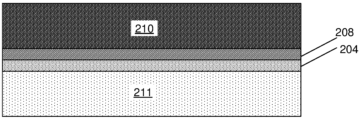
도 1a 및 도 1b는 금속 성장을 위한 템플릿으로서 핵생성 층을 포함하는 재료 스택들의 개략적인 예들이다.
도 2a 및 도 2b는 다양한 실시 예들에 따른 재료 스택들이 채용될 수도 있는 구조체들의 예들을 제공한다.
도 3a, 도 3b 및 도 3c는 다양한 실시 예들에 따른 전도성 재료를 증착하는 방법들의 동작들을 예시하는 프로세스 흐름도들이다.
도 4는 다양한 실시 예들에 따른 핵생성 층의 경사 조성 (gradient composition) 을 갖는 재료 스택의 일 예이다.
도 5는 개시된 실시 예들을 수행하기 위한 예시적인 프로세스 챔버의 개략도이다.
도 6 및 도 7a 내지 도 7c는 특정한 개시된 실시 예들을 수행하도록 사용될 수도 있는 장치들에 대한 예시적인 가스 흐름도들의 개략적인 예시들이다.
도 8은 본 명세서에 기술된 실시 예들에 따른 증착 프로세스들을 수행하기에 적합한 프로세싱 시스템의 블록도이다.
도 9는 특정한 개시된 실시 예들에 따라 증착된 스택들의 다양한 엘리먼트들의 원자 함량의 그래프들이다. 1A and 1B are schematic examples of material stacks containing a nucleation layer as a template for metal growth.
2A and 2B provide examples of structures in which material stacks according to various embodiments may be employed.
3A, 3B, and 3C are process flow diagrams illustrating the operations of methods for depositing conductive material according to various embodiments.
4 is an example of a material stack with a gradient composition of the nucleation layer according to various embodiments.
5 is a schematic diagram of an example process chamber for performing the disclosed embodiments.
6 and 7A-7C are schematic illustrations of example gas flow diagrams for devices that may be used to practice certain disclosed embodiments.
Figure 8 is a block diagram of a processing system suitable for performing deposition processes according to embodiments described herein.
9 is a graph of the atomic content of various elements of stacks deposited in accordance with certain disclosed embodiments.
이하의 기술 (description) 에서, 제시된 실시 예들의 완전한 이해를 제공하기 위해 수많은 구체적 상세들이 제시되었다. 개시된 실시 예들은 이들 구체적인 상세들 중 일부 또는 전부 없이 실시될 수도 있다. 다른 예들에서, 공지된 프로세스 동작들은 개시된 실시 예들을 불필요하게 모호하게 하지 않기 위해 상세히 기술되지 않았다. 개시된 실시 예들이 구체적인 실시 예들과 함께 기술될 것이지만, 이는 개시된 실시 예들을 제한하는 것으로 의도되지 않았다는 것이 이해될 것이다. In the following description, numerous specific details are set forth to provide a thorough understanding of the presented embodiments. The disclosed embodiments may be practiced without some or all of these specific details. In other instances, well-known process operations have not been described in detail so as not to unnecessarily obscure the disclosed embodiments. Although the disclosed embodiments will be described in conjunction with specific examples, it will be understood that they are not intended to be limiting.
반도체 제조 프로세스들은 3D NAND 디바이스들의 형성을 수반한다. 3D NAND 트랜지스터의 게이트 콘택트의 금속화는 특히 작은 피처들에서 매우 전도성이고 낮은 저항률을 갖는 금속의 증착을 수반한다. 텅스텐 (W) 은 3D NAND 디바이스들에서 금속화를 위해 사용되었고 그리고 게이트 콘택트들을 위한 W의 증착은 티타늄 나이트라이드 (TiN) 라이너 층, 이어서 W 핵생성 층 및 마지막으로 W 벌크 층의 형성을 수반한다. TiN 층은 고 품질 벌크 W의 형성을 용이하게 하기 위해 사용되는 W 핵생성 층의 효과적인 핵생성을 용이하게 하도록 배리어 층 및 접착 층 모두로서 사용된다. 핵생성 층은 종종 핵생성 층을 증착하기 위해 사용된 붕소-함유 반응 물질로부터 붕소를 포함하고, 그리고 벌크 W보다 더 높은 저항률을 갖는다. 많은 층들이 증착되기 때문에, 특히 디바이스들이 계속해서 축소됨에 따라, 고 품질, 저 저항의 벌크 W를 증착하기 위한 이용 가능한 공간은 적다. Semiconductor manufacturing processes involve the formation of 3D NAND devices. Metallization of the gate contact of a 3D NAND transistor involves the deposition of a highly conductive, low resistivity metal, especially in small features. Tungsten (W) has been used for metallization in 3D NAND devices and deposition of W for gate contacts involves the formation of a titanium nitride (TiN) liner layer, followed by a W nucleation layer and finally a W bulk layer. . The TiN layer is used as both a barrier layer and an adhesion layer to facilitate effective nucleation of the W nucleation layer used to facilitate the formation of high quality bulk W. The nucleation layer often contains boron from the boron-containing reactive material used to deposit the nucleation layer, and has a higher resistivity than bulk W. As many layers are deposited, there is less space available to deposit high quality, low resistivity bulk W, especially as devices continue to shrink.
몰리브덴 (Mo) 금속화는 대안적인 금속화 옵션이다. Mo 금속화 동안, 라이너 층이 증착되고 이어서 벌크 Mo 층이 증착된다. 벌크 Mo 층의 증착 동안, 프로세스 조건들은 라이너 층을 원소 (elemental) Mo로 거의 완전히 변환하도록 제어될 수 있고, 이에 따라 피처 내 더 많은 공간이 원소 Mo로 충진되게 할 수 있고, 이는 비-변환된 라이너 층과 벌크 Mo의 조합보다 더 낮은 저항률을 갖는다. 전반적으로, 이는 원소 Mo가 게이트 옥사이드와 콘택트하게 한다. Molybdenum (Mo) metallization is an alternative metallization option. During Mo metallization, a liner layer is deposited followed by the bulk Mo layer. During the deposition of the bulk Mo layer, process conditions can be controlled to almost completely convert the liner layer to elemental Mo, thereby allowing more space within the feature to be filled with elemental Mo, which can be converted to non-converted Mo. It has a lower resistivity than the combination of liner layer and bulk Mo. Overall, this brings the element Mo into contact with the gate oxide.
3D NAND 디바이스의 일 기능은 디바이스에 데이터를 유지하는 능력이다. 3D NAND 디바이스를 사용하는 일 장점은 비-휘발성이다. 데이터는 3D NAND 디바이스의 트랜지스터에 기록될 수도 있고 이어서 일정 기간 동안 전력이 공급되지 않은 채로 있을 수도 있고; 3D NAND 디바이스가 나중에 전력 공급될 때, 데이터는 여전히 트랜지스터에 기록되고 이에 따라 효과적인 3D NAND 디바이스로서 기능할 것으로 예상된다. 시간 기간이 경과된 후 데이터를 유지하는 트랜지스터의 능력은 데이터 유지 (data retention) (예를 들어, 데이터가 디바이스 내에 효과적으로 유지될 수 있는지 여부) 로서 지칭될 수도 있다. One function of 3D NAND devices is the ability to retain data on the device. One advantage of using 3D NAND devices is non-volatility. Data may be written to the transistors of a 3D NAND device and then left without power for a period of time; When the 3D NAND device is later powered on, it is expected that data will still be written to the transistor and thus function as an effective 3D NAND device. The ability of a transistor to retain data after a period of time may be referred to as data retention (e.g., whether data can be effectively retained within the device).
메모리 셀 트랜지스터들의 게이트 금속으로서 Mo를 사용하는 3D NAND 디바이스들의 데이터 유지는 라이너 층이 원소 Mo로 완전히 변환될 때 W-기반 3D NAND 디바이스들만큼 효과적이지 않았다. 스택의 전체 저항률은 더 낮을 수도 있는 한편, 데이터 유지는 효과적이지 않을 수도 있다. Data retention in 3D NAND devices using Mo as the gate metal of memory cell transistors was not as effective as W-based 3D NAND devices when the liner layer was fully converted to elemental Mo. The overall resistivity of the stack may be lower, while data retention may not be as effective.
특정한 이론에 얽매이지 않고, 산소 및 다른 비-몰리브덴 컴포넌트 원소들 (예컨대 알루미늄) 이 게이트 금속의 증착 동안 게이트 옥사이드 스택으로부터 스트립핑되어 (strip), 빈 공간 결함들 (vacancy defects) 을 발생시키고, 비-휘발성 트랩핑된 (trap) 전하의 더 높은 누설을 야기한다고 여겨진다. 이 트랩핑된 전하 누설은 감소된 데이터 유지를 야기한다: 데이터는 더 빨리 손실된다. 특정한 이론에 얽매이지 않고, 유전체-금속 계면에서 게이트 옥사이드 스택의 유전체 막의 결함들에 의해 유발된 양자 터널링이 증가된 데이터 손실에 기여한다고 여겨진다. 예를 들어, 유전체 막의 결함들이 전자 근처에 있다면, 전자는 에너지 배리어를 극복하고 유전체를 떠날 수 있다. 유전체 막에 더 많은 결함들이 있을수록, 유전체의 트랩핑 층에 원래 트랩핑된 전자들이 유전체를 떠나기 쉽고, 더 빠른 레이트로 데이터 손실을 발생시킨다. 스택 내의 산소는 스택으로부터 제거되고 양자 터널링을 허용하는 결함들의 형성을 유발하고, 이에 따라 증가된 데이터 손실에 기여한다고 여겨진다. Without wishing to be bound by a particular theory, it is believed that oxygen and other non-molybdenum component elements (such as aluminum) strip from the gate oxide stack during deposition of the gate metal, creating vacancy defects and -It is believed to result in higher leakage of volatile trapped charges. This trapped charge leakage results in reduced data retention: data is lost more quickly. Without being bound by a particular theory, it is believed that quantum tunneling caused by defects in the dielectric film of the gate oxide stack at the dielectric-metal interface contributes to the increased data loss. For example, if defects in a dielectric film are near electrons, the electrons can overcome the energy barrier and leave the dielectric. The more defects there are in the dielectric film, the easier it is for electrons originally trapped in the dielectric's trapping layer to leave the dielectric, causing data loss at a faster rate. It is believed that oxygen within the stack is removed from the stack and causes the formation of defects that allow quantum tunneling, thereby contributing to increased data loss.
산소 및 비-몰리브덴 컴포넌트 원소 손실을 감소시키기 위한 일 잠재적인 방식은 초기 게이트 금속 막에 과잉의 (an overabundance of) 산소 및 비-몰리브덴 컴포넌트 원소들을 공급하거나, 게이트 옥사이드 스택들에 사용되었던 TiN W 통합 스킴들과 유사한 조성을 갖도록 금속-유전체 계면을 제조하는 것이다. 이는 게이트 옥사이드 스택으로부터 산소 및 다른 비-몰리브덴 컴포넌트 원소들의 손실을 야기하는 구동력을 감소시킬 수도 있다. 핵생성 층 내에 산소 또는 다른 원소들을 유지하는 것은 산소 및 다른 원소들이 유전체로부터 제거되는 것을 방지할 수 있다고 또한 여겨진다. 예를 들어, 금속 층이 핵생성 층 상에 증착될 때, 금속 층을 증착하기 위한 프로세스 조건들은 산소가 유전체 층으로부터 제거되도록 핵생성 층과 유전체 층 사이의 상호 작용을 유발한다고 여겨지는 반면, 핵생성 층이 일부 산소 또는 다른 비-몰리브덴 컴포넌트 원소 불순물들을 유지할 때, 데이터 손실 레이트는 실질적으로 감소된다. One potential approach to reduce oxygen and non-molybdenum component loss is to supply an overabundance of oxygen and non-molybdenum component elements to the initial gate metal film, or to incorporate TiNW used in the gate oxide stacks. The metal-dielectric interface is manufactured to have a composition similar to that of the schemes. This may reduce the driving force causing loss of oxygen and other non-molybdenum component elements from the gate oxide stack. It is also believed that retaining oxygen or other elements within the nucleation layer can prevent oxygen and other elements from being removed from the dielectric. For example, when a metal layer is deposited on a nucleation layer, it is believed that the process conditions for depositing the metal layer cause interaction between the nucleation layer and the dielectric layer such that oxygen is removed from the dielectric layer, while the nucleation layer When the production layer retains some oxygen or other non-molybdenum component elemental impurities, the data loss rate is substantially reduced.
메모리 디바이스 전기적 성능은 또한 워드라인 (wordline) 금속들의 W에서 Mo 로의 변화로 인해 변화된다. 이전에, 텅스텐 통합은 TiN, 텅스텐 나이트라이드 (WN), 텅스텐 카보나이트라이드 (WCN), 등과 같은 배리어 금속을 수반하였다. TiN 배리어 층들의 증착은 고온들에서 암모니아 (NH3), 염소 (Cl2) 및 염산 (HCl) 을 포함하는 다양한 화학 물질들에 대한 노출을 발생시키지만, 전체 프로세스 스킴은 미량의 이들 원소들이 제어 게이트 유전체 또는 커패시터 유전체를 본질적으로 해치지 (harm) 않도록 이들 노출들에 적응된다 (adapt). 텅스텐 층들의 증착은 디보란 (B2H6), 실란 (SiH4), 수소 (H2), 텅스텐 헥사플루오라이드 (WF6) 및 이로 제한되는 것은 아니지만, 불소 (F2), 하이드로플루오릭산 (HF), 붕소 트리플루오라이드 (BF3), 실리콘 테트라플루오라이드 (SiF4), 등을 포함하는 반응 부산물들을 포함하는 다양한 다른 화학 물질들에 제어 게이트 및 커패시터 유전체들의 노출을 발생시킨다. 그러나, 프로세스 스킴들은 이들 노출들이 제어 게이트 또는 커패시터 유전체들을 본질적으로 해치지 않도록 개발되었다. Memory device electrical performance also changes due to the change from W to Mo in the wordline metals. Previously, tungsten incorporation involved barrier metals such as TiN, tungsten nitride (WN), tungsten carbonitride (WCN), etc. Deposition of TiN barrier layers results in exposure to a variety of chemicals including ammonia (NH 3 ), chlorine (Cl 2 ) and hydrochloric acid (HCl) at high temperatures, but the overall process scheme requires that trace amounts of these elements be released into the control gate. It adapts to these exposures so as not to essentially harm the dielectric or capacitor dielectric. Deposition of tungsten layers may include, but is not limited to, diborane (B 2 H 6 ), silane (SiH 4 ), hydrogen (H 2 ), tungsten hexafluoride (WF 6 ) and, but not limited to, fluorine (F 2 ), hydrofluoric acid. (HF), boron trifluoride (BF 3 ), silicon tetrafluoride (SiF 4 ), etc. However, process schemes have been developed such that these exposures do not inherently harm the control gate or capacitor dielectrics.
반도체 제조 프로세스들은 이전에 TiN 배리어 층들 증착 및/또는 텅스텐-함유 막 증착을 사용하는 것, 특히 WF6 가스 및 B2H6 가스를 사용하는 증착을 고려하여 수행되었다. 배리어 금속 층들은 NH3와 같은 질소-함유 반응 물질 및 티타늄 테트라클로라이드 (TiCl4) 와 같은 티타늄-함유 반응 물질, 및 H2를 사용하여 증착된 TiN 층들일 수도 있다. 이러한 증착은 디바이스 내에 미량의 불소, 붕소, 및 다른 비-몰리브덴 컴포넌트 원소들의 혼입을 발생시킬 수 있다. 금속화가 W 대신 Mo의 증착을 수반할 때에도, 일부 디바이스들은 여전히 디바이스 내의 이들 미량의 원소들을 사용하여 더 최적으로 수행할 수도 있다. 그러나, 일부 Mo 증착은 배리어 층들을 포함할 수도 있지만, 일부 통합 스킴들은 배리어 층들 없이 통합될 수도 있다. Semiconductor manufacturing processes have previously been carried out using deposition of TiN barrier layers and/or deposition of tungsten-containing films, especially deposition using WF 6 gas and B 2 H 6 gas. Barrier metal layers may be TiN layers deposited using nitrogen-containing reactive materials such as NH 3 and titanium-containing reactive materials such as titanium tetrachloride (TiCl 4 ), and H 2 . This deposition can result in the incorporation of trace amounts of fluorine, boron, and other non-molybdenum component elements into the device. Even when metallization involves deposition of Mo instead of W, some devices may still perform more optimally using these trace elements within the device. However, some Mo depositions may include barrier layers, while some integration schemes may be integrated without barrier layers.
특정한 이론에 얽매이지 않고, 금속화 스택의 유전체-금속 계면에서 미량의 비-몰리브덴 컴포넌트 원소들의 존재는 금속화를 위해 사용된 금속이 Mo인 개선된 디바이스 성능에 기여할 수도 있다고 여겨진다. Mo 증착은 NH3, H2, 및 HCl에 대한 노출을 수반할 수도 있지만, W 증착을 사용한 프로세스 스킴들이 또한 이러한 노출들을 수반하므로 이들 가스들이 반드시 유전체에 본질적으로 해로운 것이 아닐 수도 있다. 그러나, Mo의 증착은 또한 Mo-함유 전구체들, 물 (H2O) 및 질소 옥사이드 (NO) 와 같은 반응 부산물들, 및 Mo 옥사이드들 및 아산화물들 (suboxides), 뿐만 아니라 몰리브덴 옥시나이트라이드 (MoOxNy) 에 대한 노출을 포함한다. W 증착을 사용한 프로세스 스킴들은 통상적으로 Mo 증착에 사용되는 이들 가스들에 대한 노출을 수반하지 않는다. 이러한 노출들의 잠재적인 유해한 영향들을 완화시키기 위해, W 증착 동안 유전체들이 노출된 화합물들은 Mo 게이트 옥사이드 스택들에 대해 우수한 전기적 성능을 발생시키는 유전체-Mo 계면을 조절하도록 사용될 수 있다. Without wishing to be bound by a particular theory, it is believed that the presence of traces of non-molybdenum component elements at the dielectric-metal interface of the metallization stack may contribute to improved device performance where the metal used for metallization is Mo. Mo deposition may involve exposure to NH 3 , H 2 , and HCl, but these gases may not necessarily be inherently harmful to the dielectric since process schemes using W deposition also involve these exposures. However, the deposition of Mo also produces Mo-containing precursors, reaction by-products such as water (H 2 O) and nitrogen oxide (NO), and Mo oxides and suboxides, as well as molybdenum oxynitride ( Includes exposure to MoO x N y ). Process schemes using W deposition do not involve exposure to these gases typically used for Mo deposition. To mitigate the potentially detrimental effects of these exposures, the compounds to which the dielectrics are exposed during W deposition can be used to modulate the dielectric-Mo interface resulting in superior electrical performance for Mo gate oxide stacks.
특정한 개시된 실시 예들은, 배리어 금속을 사용하는 워드라인들의 3D NAND 제조, 배리어 금속을 사용하지 않는 워드라인들의 3D NAND 제조, 배리어 금속을 사용하는 DRAM 매립된 워드라인, 배리어 금속을 사용하지 않는 DRAM 매립된 워드라인 및 금속-옥사이드-반도체 커패시터 (metal-oxide-semiconductor capacitor; MOSCAP) 디바이스들을 포함하지만 이로 제한되지 않는 다양한 애플리케이션들에서 이들 문제들을 해결한다. Specific disclosed embodiments include 3D NAND fabrication of word lines using a barrier metal, 3D NAND fabrication of word lines without a barrier metal, DRAM embedded word lines using a barrier metal, and DRAM embedding without a barrier metal. It addresses these problems in a variety of applications, including but not limited to wordline and metal-oxide-semiconductor capacitor (MOSCAP) devices.
유전체-Mo 계면들이 일 예로서 본 명세서에 기술되었지만, 다양한 개시된 실시 예들이 또한 다른 유전체-금속 계면들을 조절하는 데 적합하다는 것이 이해될 것이다. 비-제한적인 예시적인 금속-유전체 계면들은 알루미늄 옥사이드-몰리브덴 (Al2O3-Mo) 계면들, 실리콘 옥사이드-몰리브덴 (SiO2-Mo) 계면들, 지르코늄 옥사이드-몰리브덴 (ZrO2-Mo) 계면들, 및 Mo와 같은 금속들과 인터페이싱된 다른 제어 게이트 유전체들을 포함한다. Although dielectric-Mo interfaces are described herein as an example, it will be understood that the various disclosed embodiments are also suitable for controlling other dielectric-metal interfaces. Non-limiting exemplary metal-dielectric interfaces include aluminum oxide-molybdenum (Al 2 O 3- Mo) interfaces, silicon oxide-molybdenum (SiO 2 -Mo) interfaces, and zirconium oxide-molybdenum (ZrO 2- Mo) interfaces. and other control gate dielectrics interfaced with metals such as Mo.
금속화 스택의 형성 동안 미량의 비-몰리브덴 컴포넌트 원소들을 혼입하는 Mo의 금속화 스택들을 형성하는 방법들이 본 명세서에 제공된다. 이러한 방법들은 유전체-금속 계면을 개질하기 위해 구체적으로 타깃팅될 수도 있다. 방법들은 이로 제한되는 것은 아니지만, 임의의 금속의 증착 전, 금속 옥시나이트라이드와 같은 금속 핵생성 층의 증착 전, (금속 옥시나이트라이드 및 벌크 금속을 포함하는) 일부 금속 증착 후, 핵생성 층의 일부의 증착 후 전체 핵생승 층의 증착 후 그리고 벌크 금속의 증착 전, 금속 핵생성 층의 증착 전반에 걸쳐 (throughout) 또는 금속 핵생성 층의 증착 동안, 또는 벌크 금속의 증착 전반에 걸쳐 또는 벌크 금속의 증착 동안, 또는 벌크 금속의 증착 후를 포함하는 금속 증착의 임의의 동작 동안 수행될 수도 있다. 실시 예들이 유전체 상에 배리어 층을 갖는 기판을 수반하면, 본 명세서에 기술된 방법들은 배리어 층을 증착하기 전, 배리어 층을 증착한 후, 또는 배리어 층의 증착 동안 유전체 상에서 수행될 수도 있다. 본 명세서에 기술된 방법들은 산소, 질소, 불소, 붕소, 염소, 및 텅스텐 중 하나 이상의 원소들을 혼입할 수도 있다. 다양한 실시 예들에서, 3D NAND 게이트 트랜지스터들은 특정한 개시된 실시 예들을 사용하여 제조된다. 개시된 다양한 실시 예들은 플라즈마-프리 (plasma-free) 증착 또는 플라즈마-리스 (plasma-less) 증착을 수반한다. 개시된 다양한 실시 예들은 열적 프로세스들이다. Provided herein are methods of forming metallization stacks of Mo that incorporate trace amounts of non-molybdenum component elements during formation of the metallization stack. These methods may be specifically targeted to modify the dielectric-metal interface. Methods include, but are not limited to, prior to deposition of any metal, prior to deposition of a metal nucleation layer, such as a metal oxynitride, and after deposition of some metal (including metal oxynitride and bulk metal), of the nucleation layer. After deposition of a portion After deposition of the entire nucleation layer and before deposition of the bulk metal, through or during the deposition of the metal nucleation layer, or throughout or through the deposition of the bulk metal. It may be performed during the deposition of, or during any operation of metal deposition, including after deposition of the bulk metal. If embodiments involve a substrate having a barrier layer on a dielectric, the methods described herein may be performed on the dielectric before depositing the barrier layer, after depositing the barrier layer, or during deposition of the barrier layer. The methods described herein may incorporate one or more of the following elements: oxygen, nitrogen, fluorine, boron, chlorine, and tungsten. In various embodiments, 3D NAND gate transistors are fabricated using certain disclosed embodiments. Various disclosed embodiments involve plasma-free or plasma-less deposition. Various disclosed embodiments are thermal processes.
특정한 개시된 실시 예들은 원소 타입 당 약 1 원자% (atomic %) 미만 내지 약 50 원자%의 범위일 수도 있는 붕소, 불소, 산소, 질소, 염소, 및 다른 비-몰리브덴 컴포넌트 원소들의 불순물 함량을 유지한다. 다양한 실시 예들에서, 유전체-금속 계면 근방의 불순물 함량이 벌크 금속에서보다 더 큰, 경사 조성 (gradient composition) 이 형성될 수도 있다. 고 불순물 함량은 유전체-Mo 계면에서 약 1 Å 내지 30 Å 범위 미만의 Mo-함유 재료에서 약 1 원자% 미만 내지 약 50 원자%일 수도 있다. Certain disclosed embodiments maintain impurity contents of boron, fluorine, oxygen, nitrogen, chlorine, and other non-molybdenum component elements, which may range from less than about 1 atomic percent to about 50 atomic percent per element type. . In various embodiments, a gradient composition may be formed, where the impurity content near the dielectric-metal interface is greater than in the bulk metal. The high impurity content may be from less than about 1 atomic percent to about 50 atomic percent in the Mo-containing material, ranging from about 1 Å to less than 30 Å at the dielectric-Mo interface.
일부 실시 예들에서, 방법들은 다음 동작들 중 하나 이상을 수반한다: 특정한 가스들을 사용하는 (유전체, 부분적인 또는 전체 배리어 층, 부분적인 또는 전체 금속 핵생성 층, 또는 부분적인 또는 전체 금속 층을 포함하는) 기판의 온도 및/또는 가스 처리; 및 초기 Mo 층들의 증착, 라이너 층과 벌크 Mo 층 사이의 계면의 처리, 및 벌크 Mo 층의 증착 중 적어도 하나가 라이너 층 내의 산소 및 다른 원소들의 함량을 증가시키거나 유지하도록 조절되는 증착. 예를 들어, 라이너 층의 증착은 금속 막 내에 산소를 유지하기 위해 Mo 전구체를 과소 반응시키는 (under-react) 것을 포함할 수도 있다. 본 명세서에 기술된 방법들은 CA, Fremont 소재의 Lam Research Corporation으로부터 입수 가능한 쿼드-스테이션 모듈과 같은 반도체 디바이스들을 제조하기 위한 멀티-스테이션 장치에서의 구현에 특히 유리하다. 쿼드-스테이션 모듈은 4 개의 스테이션들을 포함한다; 적어도 하나의 스테이션이 특정한 개시된 실시 예들에 따라 몰리브덴을 증착하도록 사용될 수도 있다. 일 예에서, 일 스테이션은 라이너를 증착하기 위한 것이고, 또 다른 스테이션은 선택 가능한 (optional) 개시 층을 증착하기 위한 것이고, 또 다른 스테이션은 벌크를 증착하기 위한 것이고, 그리고 또 다른 스테이션은 피처의 완전한 충진을 보장하기 위해 오버버든 (overburden) 을 증착하기 위한 것일 수 있다. 일부 실시 예들에서, 쿼드-스테이션 모듈은 2 개의 분리된 스테이션들에 라이너를 증착하고 벌크를 증착하는 것을 허용한다. 라이너 및/또는 벌크를 증착하기 위한 스테이션은 증착 온도를 감소시키도록 (또는 특정한 개시된 실시 예들에 대해 본 명세서에 기술된 임의의 다른 프로세스 조건을 조절하거나 수행하도록) 조절될 수 있는 한편, 다른 스테이션들로 하여금 더 높은 증착 온도들에서 증착하게 하거나 더 높은 모듈 쓰루풋 (throughput) 을 허용하기 위해 반응 레이트를 개선하는 다른 프로세스 조건들을 허용한다. In some embodiments, methods involve one or more of the following operations: using specific gases (including a dielectric, a partial or full barrier layer, a partial or full metal nucleation layer, or a partial or full metal layer) ) temperature and/or gas treatment of the substrate; and deposition, wherein at least one of the deposition of the initial Mo layers, the treatment of the interface between the liner layer and the bulk Mo layer, and the deposition of the bulk Mo layer is controlled to increase or maintain the content of oxygen and other elements in the liner layer. For example, deposition of the liner layer may include under-reacting the Mo precursor to retain oxygen within the metal film. The methods described herein are particularly advantageous for implementation in a multi-station apparatus for manufacturing semiconductor devices, such as the quad-station module available from Lam Research Corporation of Fremont, CA. The quad-station module contains 4 stations; At least one station may be used to deposit molybdenum according to certain disclosed embodiments. In one example, one station is for depositing the liner, another station is for depositing the optional initiation layer, another station is for depositing the bulk, and yet another station is for the complete completion of the feature. This may be to deposit overburden to ensure filling. In some embodiments, a quad-station module allows depositing liner and bulk at two separate stations. A station for depositing the liner and/or bulk may be adjusted to reduce the deposition temperature (or adjust or perform any other process conditions described herein for certain disclosed embodiments) while other stations allows for deposition at higher deposition temperatures or other process conditions that improve the reaction rate to allow for higher module throughput.
도 1a 및 도 1b는 금속 성장을 위한 템플릿으로서 핵생성 층을 포함하는 재료 스택들의 개략적인 예들이다. 도 1a 및 도 1b는 특정한 스택의 재료들의 순서를 예시하고, 도 3a 내지 도 3c 및 도 4에 대해 이하에 더 기술된 바와 같이, 임의의 적절한 아키텍처 및 애플리케이션과 함께 사용될 수도 있다. 도 1a의 예에서, 스택 (100) 은 유전체, 전도성 또는 반전도성 재료와 같은 재료의 하나 이상의 층들이 그 위에 증착된 웨이퍼들을 포함하는, 실리콘 또는 다른 반도체 웨이퍼, 예를 들어, 200-㎜ 웨이퍼, 300-㎜ 웨이퍼, 또는 450-㎜ 웨이퍼일 수도 있는 기판 (102) 을 포함한다. 방법들은 또한 유리, 플라스틱, 등과 같은 다른 기판들 상에 금속화 스택 구조체들을 형성하도록 적용될 수도 있다. 일부 실시 예들에서, 기판 (102) 은 실리콘을 포함한다. 1A and 1B are schematic examples of material stacks containing a nucleation layer as a template for metal growth. 1A and 1B illustrate the order of materials in a particular stack, and may be used with any suitable architecture and application, as described further below with respect to FIGS. 3A-3C and 4. In the example of FIG. 1A , stack 100 is a silicon or other semiconductor wafer, e.g., a 200-mm wafer, comprising wafers with one or more layers of material, such as a dielectric, conductive or semiconducting material, deposited thereon. and a
유전체 층 (104) 이 기판 (102) 상에 있다. 유전체 층 (104) 은 기판 (102) 의 반도체 표면 직상에 증착될 수도 있거나 임의의 수의 개재 (intervening) 층들이 있을 수도 있다. 유전체 층들의 예들은 도핑되고 도핑되지 않은 실리콘 옥사이드 (SiO2), 도핑되고 도핑되지 않은 실리콘 카바이드 (SiC), 실리콘 나이트라이드 (SiN), 및 알루미늄 옥사이드 (Al2O3) 층들을 포함하고, 구체적인 예들은 도핑되거나 도핑되지 않은 실리콘 옥사이드 (SiO2) 층 및 Al2O3 층을 포함한다. 또한, 또 다른 실시 예에서, 도 1b에서, 스택 (100) 은 핵생성 층 (108) 과 유전체 층 (104) 사이에 증착된 배리어 층 (106) 을 포함한다. 배리어 층 (106) 은 확산 배리어, 접착 배리어, 또는 둘 모두일 수도 있다. 배리어 층들의 예들은 TiN, Ti/TiN, WN, 및 WCN을 포함한다. 다양한 실시 예들에서, 배리어 층 (106) 은 약 10 Å 내지 약 40 Å 두께 또는 약 10 Å 내지 약 20 Å 두께이다. 도 1a에서, 핵생성 층 (108) 은 유전체 층 (104) 상에 증착되고 그리고 금속 층 (110) 은 핵생성 층 (108) 상에 증착된다. 도 1b에서, 핵생성 층 (108) 은 배리어 층 (106) 상에 증착되고 그리고 금속 층 (110) 은 핵생성 층 (108) 상에 증착된다. 도 1a 및 도 1b는 유전체-금속 계면, 즉, (112a) 및 (112b) 를 도시한다. 특정한 개시된 실시 예들은 핵생성 층 (108) 을 증착하기 전에 처리 동작을 수행하는 것, 핵생성 층 (108) 중 적어도 일부를 증착한 후 처리 동작을 수행하는 것, 모든 핵생성 층 (108) 을 증착한 후 처리 동작을 수행하는 것, 핵생성 층 (108) 의 증착 조건들을 조절하는 것, 금속 층 (110) 을 증착하기 전에 처리 동작을 수행하는 것, 금속 층 (110) 의 증착 동안 처리를 수행하는 것, 금속 층 (110) 중 적어도 일부를 증착할 때 증착 조건들을 조절하는 것, 금속 층 (110) 모두를 증착할 때 증착 조건들을 조절하는 것, 또는 이들의 조합들을 수반할 수도 있다. 금속 층 (110) 은 유전체-금속 계면 (112) 에서 핵생성 층 (108) 과 콘택트하도록 형성될 수 있다. A
핵생성 층 (108) 상에 증착된 금속 층 (110) 이 금속 성장을 위한 템플릿을 제공하는 핵생성 층 (108) 을 갖는 구조체의 주 전도체 (또한 벌크 전도체 또는 벌크 층으로 지칭됨) 이다. The
이하에 더 기술된 바와 같이, 핵생성 층 (108) 은 비정질 (amorphous) 막으로서 증착될 수도 있다. 비정질 막은 입자 구조를 갖지 않고 그리고 금속 성장을 위한 템플릿으로서, 입자 구조가 없고 그리고/또는 (작은 입자들과 반대로) 큰 입자들을 갖는 저 저항률 금속이 형성될 수 있다. 금속 층들의 예들은 Mo 층들을 포함한다. As described further below,
도 1a 및 도 1b의 예들에서, 증착된 핵생성 층 (108) 은 MoOxNy 층과 같은 금속 옥시나이트라이드 층이다. 1A and 1B, the deposited
특정한 개시된 실시 예들에서, 후속 프로세싱 동안, 특정한 실시 예들에서, 핵생성 층 (108) 중 일부는 순수 금속으로 변환될 수도 있는 한편, 핵생성 층 (108) 중 일부, 예컨대 핵생성 층 (108) 층 과 유전체 층 (104) 의 계면은, 붕소, 불소, 텅스텐, 산소, 질소, 및 염소와 같은 비-몰리브덴 컴포넌트 원소 불순물들을 유지할 수도 있고, 그리고 핵생성 층 (108) 중 일부는 순수 금속으로 변환되지 않을 수도 있다. 순수 금속은 약 1 % 미만의 비-몰리브덴 컴포넌트 원소 조성을 갖는 것으로 규정될 수도 있다. In certain disclosed embodiments, during subsequent processing, in certain embodiments, some of the
비-몰리브덴 컴포넌트 원소 불순물들은 데이터 손실을 유발할 수 있는 유전체로부터 옥사이드 확산의 기회들을 감소시킬 수 있는 유전체-금속 계면에서 또는 그 근방에서 핵생성 층 (108) 내에 의도적으로 유지된다. 따라서, 다양한 실시 예들에 따라, 핵생성 층 (108) 은 금속 층 (110) 과 동일한 조성일 수도 있고 아닐 수도 있다. 일부 실시 예들에서, 핵생성 층 (108) 은 복수의 층들을 포함하거나, 경사 층이거나, 또는 사이클 각각에서 동일한 전구체 플로우 및 반응 물질 플로우를 사용하여 적어도 하나의 원자 층 증착 (atomic layer deposition; ALD) 사이클을 반복함으로써 증착된 층이고, 그리고 금속 층 (110) 을 증착할 때, 핵생성 층 (108) 은 경사, 복수의 층들, 모폴로지 (morphology) 의 변화, 또는 핵생성 층의 불순물 조성의 변화를 발생시키도록 개질된다. 일부 실시 예들에서, 복수의 플레이어들 중 하나 이상은 경사 층들이다. 일부 실시 예들에서, 핵생성 층 (108) 은 비정질 특징을 특징으로 할 수도 있고, 금속 층 (110) 은 큰 입자 경계들의 결여를 특징으로 한다. Non-molybdenum component elemental impurities are intentionally maintained within the
일부 실시 예들에서, 금속 옥시나이트라이드 층의 금속은 순수 금속 전도체의 금속과 동일하고, 예를 들어, MoOxNy 층은 Mo 층의 증착 전에 핵생성 층으로서 증착될 수도 있다. 다른 실시 예들에서, 금속 옥시나이트라이드 층은 순수 전도체의 금속과 상이한 금속을 가질 수도 있고, 예를 들어, W 층이 Mo-함유 핵생성 층 상에 증착될 수도 있고, 또는 Mo 층이 W-함유 핵생성 층 상에 증착될 수도 있다. In some embodiments, the metal of the metal oxynitride layer is the same as the metal of the pure metal conductor, for example, the MoO x Ny layer may be deposited as a nucleation layer prior to deposition of the Mo layer. In other embodiments, the metal oxynitride layer may have a different metal than that of the pure conductor, for example, a W layer may be deposited on a Mo-containing nucleation layer, or a Mo layer may be deposited on a W-containing nucleation layer. It may also be deposited on a nucleation layer.
도 1a 및 도 1b는 금속화 스택들의 예들을 도시하지만, 방법들 및 발생되는 스택들은 그렇게 제한되지 않는다. 예를 들어, 일부 실시 예들에서, 금속 성장을 위한 템플릿으로서 핵생성 층은 SiO2, 실리콘 또는 다른 반도체 기판 직상에 증착될 수도 있다. 또한, 핵생성 층들 상의 W 또는 Mo 성장이 상기 기술되었지만, 핵생성 층들은 다른 금속들 예컨대, 코발트 (Co), 루테늄 (Ru), 니켈 (Ni), 및 MoW와 같은 이들 금속들을 포함하는 합금들의 저 저항률 성장을 위한 템플릿으로 역할할 (serve) 수도 있다. 또한, 핵생성 층은 MoOxNy, Mo 나이트라이드, 텅스텐 옥시나이트라이드, WN, 니켈 나이트라이드, 등을 포함하는, 임의의 적절한 금속 옥시나이트라이드 또는 금속 나이트라이드 층일 수도 있다. 1A and 1B show examples of metallization stacks, but the methods and resulting stacks are not so limited. For example, in some embodiments, a nucleation layer may be deposited directly on a SiO 2 , silicon or other semiconductor substrate as a template for metal growth. Additionally, although W or Mo growth on nucleation layers has been described above, the nucleation layers may be formed of other metals such as cobalt (Co), ruthenium (Ru), nickel (Ni), and alloys containing these metals such as MoW. It may also serve as a template for low-resistivity growth. Additionally, the nucleation layer may be any suitable metal oxynitride or metal nitride layer, including MoO x N y , Mo nitride, tungsten oxynitride, WN, nickel nitride, etc.
상기 및 이하에 더 기술된 재료 스택들은 다양한 구조체들로 구현될 수도 있다. 도 2a 및 도 2b는 스택들이 채용될 수도 있는 구조체들의 예들을 제공한다. 도 2a는 2D NAND 구조체 (223) 의 워드라인들 (210) 의 개략적인 예를 도시한다. 워드라인들 (210) 은 기판 (200) 상에 필라 자신들 사이에 갭들 (235) 을 갖는 필라들로서 옥사이드 층들 (211) 에 의해 분리된다. 도 2b에서, Al2O3 층 (204) 및 핵생성 층 (208) 을 포함하는, 워드라인 (210) 과 옥사이드 층 (211) 사이의 계면의 상세가 도시된다. 일부 실시 예들에서, 본 명세서에 기술된 바와 같이 핵생성 층 (208) 은 옥사이드 층 (211) 상에 또는 TiN (204) 또는 다른 배리어 층 직상에 증착될 수도 있다. 핵생성 층들은 예를 들어, 약 10 ㎚ 내지 100 ㎚ 두께 또는 약 5 ㎚ 두께 이하의 워드라인 (210) 의 증착을 위해 약 10 Å 내지 100 Å, 또는 10 Å 내지 50 Å일 수도 있다. The material stacks described above and further below may be implemented in various structures. 2A and 2B provide examples of structures in which stacks may be employed. FIG. 2A shows a schematic example of
도 3a는 특정한 개시된 실시 예들에 따른 전도성 재료를 증착하는 방법의 동작들을 예시하는 프로세스 흐름도이다. 동작 (301) 에서, 옥사이드 표면 및/또는 (옥사이드 표면 상에 있을 수도 있는) 배리어 층 표면을 갖는 기판이 제공된다. 동작 (301) 의 프로세스 조건들 및 특징들의 예들은 도 3b와 관련하여 이하에 더 제공된다. 동작 (360) 에서, 옥사이드-금속 계면은 옥사이드 내 결함들을 방지하도록 조절된다. 동작 (360) 을 수행하기 위한 예시적인 방법들은 도 3b 및 도 3c에 대해 이하에 기술된다. 동작 (370) 에서, 금속이 옥사이드 표면 또는 배리어 층 표면과 콘택트하는, 금속 층이 기판 위에 형성된다. 동작 (370) 을 수행하기 위한 예시적인 실시 예들은 도 3b 및 도 3c에 대해 이하에 더 기술된다. 3A is a process flow diagram illustrating the operations of a method for depositing a conductive material in accordance with certain disclosed embodiments. In operation 301, a substrate is provided having an oxide surface and/or a barrier layer surface (which may be on the oxide surface). Examples of process conditions and features of operation 301 are further provided below with respect to FIG. 3B. In operation 360, the oxide-metal interface is adjusted to prevent defects in the oxide. Exemplary methods for performing operation 360 are described below with respect to FIGS. 3B and 3C. In operation 370, a metal layer is formed on the substrate, where the metal contacts the oxide surface or barrier layer surface. Exemplary embodiments for performing operation 370 are further described below with respect to FIGS. 3B and 3C.
도 3a에서, 동작들 (360 및 370) 은 동시에; 또는 먼저 동작 (360) 에 이어서 동작 (370) 의 순서로; 또는 먼저 동작 (370) 에 이어서 동작 (360) 의 순서로; 또는 동작들 (360 및 370) 의 조합이 함께 (예를 들어, 대안적으로; 또는 동작 (370) 동안 수행된 동작 (360) 의 일부 동작들; 또는 동작 (360) 동안 수행된 동작 (370) 의 일부 동작들) 수행될 수도 있다. 동작들 (301, 360, 및 370) 각각은 동일한 챔버에서, 단일 챔버에서, 동일한 챔버의 하나 이상의 스테이션들에서, 또는 상이한 챔버들의 하나 이상의 스테이션들에서 수행될 수도 있다. In Figure 3A, operations 360 and 370 are simultaneous; or in that order, first operation 360 followed by operation 370; or in that order, first operation 370 followed by operation 360; or a combination of operations 360 and 370 together (e.g., alternatively; or some operations of operation 360 performed during operation 370; or operation 370 performed during operation 360 some operations) may be performed. Each of operations 301, 360, and 370 may be performed in the same chamber, in a single chamber, at one or more stations in the same chamber, or at one or more stations in different chambers.
도 3b는 전도성 재료를 증착하는 방법의 동작들을 예시하는 프로세스 흐름도이다. 동작들 (301, 303a, 305, 307, 및 309) 각각은 도 3b에서 다른 동작들 중 하나를 수행할 때와 같이 동일한 챔버에서 각각 수행될 수도 있거나 별개의 챔버들에서 수행될 수도 있거나 동일하고 상이한 챔버들의 조합을 사용하여 수행될 수도 있고, 그리고 동작들 (301, 303a, 305, 307, 및 309) 각각은 도 3b에서 다른 동작들 중 하나를 수행할 때와 같이 멀티-스테이션 챔버의 동일한 스테이션에서 수행될 수도 있거나 별개의 스테이션들에서 수행될 수도 있거나 동일하고 상이한 스테이션들의 조합을 사용하여 수행될 수도 있다는 것이 이해될 것이다. 3B is a process flow diagram illustrating the operations of a method for depositing a conductive material. Each of operations 301, 303a, 305, 307, and 309 may each be performed in the same chamber as when performing one of the other operations in Figure 3B, may be performed in separate chambers, or may be performed in the same and different chambers. It may be performed using a combination of chambers, and each of operations 301, 303a, 305, 307, and 309 is performed at the same station in the multi-station chamber as when performing one of the other operations in FIG. 3B. It will be appreciated that it may be performed on separate stations or using a combination of the same and different stations.
선택 가능한 동작으로 식별된 도 3b의 동작들 중 적어도 하나가 수행된다. 선택 가능한 동작들 각각은 도 3b의 다른 선택 가능한 동작들과 조합하여 사용될 수도 있고; 예를 들어, 동작 (303a) 의 처리는 동작 (305) 및 동작 (309) 의 프로세스 조건들을 조절하는 단계를 생략하고 동작 (307) 의 처리를 생략하는 동안 수행될 수도 있다. At least one of the operations in FIG. 3B identified as a selectable operation is performed. Each of the selectable operations may be used in combination with other selectable operations in Figure 3B; For example, the processing of operation 303a may be performed while omitting the step of adjusting the process conditions of operations 305 and 309 and omitting the processing of operation 307.
동작 (301) 에서, 옥사이드 표면을 갖는 기판이 제공된다. 이는 도 3a의 동작 (301) 과 동일할 수도 있다. 다양한 실시 예들에서, 기판은 상부에 옥사이드 표면을 포함하는 유전체 층을 갖는다. 다양한 실시 예들에서, 기판은 멀티-스테이션 챔버의 제 1 프로세스 스테이션에 제공된다. 기판은 유전체, 전도성 또는 반전도성 재료와 같은 재료의 하나 이상의 층들이 그 위에 증착된 웨이퍼들을 포함하는, 실리콘 웨이퍼, 예를 들어, 200 ㎜ 웨이퍼, 300 ㎜ 웨이퍼, 또는 450 ㎜ 웨이퍼일 수도 있다. 하부 층들의 비-제한적인 예들은 유전체 층들 및 전도성 층들, 예를 들어, 실리콘 옥사이드들, 실리콘 나이트라이드들, 실리콘 카바이드들, 금속 옥사이드들, 금속 나이트라이드들, 금속 카바이드들, 및 금속 층들을 포함한다. 일부 실시 예들에서, 기판은 도 1a 또는 도 1b의 기판 (102) 과 동일하다. In operation 301, a substrate having an oxide surface is provided. This may be the same as operation 301 of Figure 3A. In various embodiments, the substrate has a dielectric layer thereon that includes an oxide surface. In various embodiments, a substrate is provided to a first process station of a multi-station chamber. The substrate may be a silicon wafer, eg, a 200 mm wafer, a 300 mm wafer, or a 450 mm wafer, comprising wafers with one or more layers of material, such as a dielectric, conductive or semiconducting material, deposited thereon. Non-limiting examples of underlying layers include dielectric layers and conductive layers, such as silicon oxides, silicon nitrides, silicon carbides, metal oxides, metal nitrides, metal carbides, and metal layers. do. In some embodiments, the substrate is the same as
기판은 옥사이드 표면을 포함한다. 일부 실시 예들에서, 옥사이드 표면은 도 1a의 유전체 층 (104) 과 같은 유전체 층의 일부이다. 일부 실시 예들에서, 옥사이드 표면은 도 1b의 배리어 층 (106) 과 같은 배리어 층의 일부이다. 일부 실시 예들에서, 옥사이드 표면은 실리콘 옥사이드를 포함한다. 일부 실시 예들에서, 옥사이드 표면은 알루미늄 옥사이드를 포함한다. The substrate includes an oxide surface. In some embodiments, the oxide surface is part of a dielectric layer, such as
도 3b를 다시 참조하면, 동작 (303a) 에서 선택 가능한 소킹 처리가 수행된다. 선택 가능한 소킹 처리는 동작 (305) 전에 기판 상의 옥사이드 표면의 표면을 준비하도록 수행될 수도 있다. 소킹은 동작 (305) 에서 재료의 증착으로 하여금 옥사이드의 표면 상에 상이하게 증착되거나 상이한 조성을 형성하게 할 수도 있다. Referring back to Figure 3B, a selectable soaking process is performed in operation 303a. An optional soaking treatment may be performed to prepare the surface of the oxide surface on the substrate prior to operation 305. Soaking may cause the deposition of material in operation 305 to deposit differently or form a different composition on the surface of the oxide.
다양한 실시 예들에서, 동작 (303a) 은 디보란 (B2H6) 과 같은 붕소-함유 가스를 도입하는 것을 수반한다. 붕소-함유 가스에 대한 노출은 유전체 프로세스 이력을, 텅스텐 통합을 사용하는 TiN을 수반하는 이전 프로세스 이력들과 더 유사하게 할 수 있다. In various embodiments, operation 303a involves introducing a boron-containing gas, such as diborane (B 2 H 6 ). Exposure to boron-containing gases may make the dielectric process history more similar to previous process histories involving TiN using tungsten integration.
다양한 실시 예들에서, 동작 (303a) 은 텅스텐-함유 가스 또는 불소-함유 가스, 예컨대, 이로 제한되는 것은 아니지만, 텅스텐 헥사클로라이드, 텅스텐 펜타클로라이드, 텅스텐 펜타플루오라이드, 및 텅스텐 헥사플루오라이드 (WF6) 를 포함하는 텅스텐 할라이드들을 도입하는 것을 수반한다. 불소 노출은 유전체 프로세스 이력을, 텅스텐 통합을 사용하는 TiN을 갖는 프로세스 이력과 더 유사하게 할 수 있다. 그러나, 노출은 유전체를 너무 많은 불소에 노출시키지 않도록 제한될 수도 있고, 이는 디바이스 성능에 해로울 수 있지만, 트레이스 노출은 W 통합을 사용하는 TiN의 디바이스 성능을 매칭하는 데 유리할 수 있다. In various embodiments, operation 303a may be performed on a tungsten-containing gas or a fluorine-containing gas, such as, but not limited to, tungsten hexachloride, tungsten pentachloride, tungsten pentafluoride, and tungsten hexafluoride (WF 6 ). It involves introducing tungsten halides containing. Fluorine exposure can make the dielectric process history more similar to that with TiN using tungsten integration. However, exposure may be limited to avoid exposing the dielectric to too much fluorine, which may be detrimental to device performance, while trace exposure may be advantageous for matching device performance of TiN using W integration.
다양한 실시 예들에서, 동작 (303a) 은 가스 처리들의 2 개 이상의 시간적으로 분리된 펄스들로 수행된다. 예를 들어, 노출은 일부 실시 예들에서 B2H6과 WF6 사이에서 교번할 수도 있고, 예컨대 원자 층 증착에 의해 W 핵생성 층의 증착을 수행하도록 할 수도 있다. 이 동작은 유전체 프로세스 이력을 W 통합을 사용하는 TiN의 프로세스 이력과 더 유사하게 하도록 수행될 수도 있다. 동작 (303a) 을 수행함으로써 증착될 수도 있는 임의의 W 핵생성 층은 Mo 또는 후속하는 금속 전도체 층 저항률의 부정적인 영향을 방지하도록 최소화된다 (예를 들어, 1 내지 5 사이클들 또는 1 내지 10 사이클들과 같은 매우 적은 사이클들이 사용된다). Mo 증착 전에 ALD에 의해 증착된 초박형 (ultra-thin) W 핵생성 층은 다양한 실시 예들에서 큰 입자 또는 비정질 Mo 성장을 위한 템플릿을 제공한다면 Mo 저항률을 감소시킬 수도 있다. 다양한 실시 예들에서, 화학적 기상 증착 (chemical vapor deposition; CVD) 타입 프로세스와 유사하게, 붕소-함유 및 W-함유 또는 불소-함유 가스 노출들이 동시에 수행된다. ALD 프로세스 및 CVD 프로세스의 조합이 사용될 수도 있다. In various embodiments, operation 303a is performed with two or more temporally separated pulses of gas treatments. For example, the exposure may alternate between B 2 H 6 and WF 6 in some embodiments, allowing deposition of the W nucleation layer, such as by atomic layer deposition. This operation may be performed to make the dielectric process history more similar to that of TiN using W integration. Any W nucleation layer that may be deposited by performing operation 303a is minimized to avoid negative effects on the Mo or subsequent metal conductor layer resistivity (e.g., 1 to 5 cycles or 1 to 10 cycles very few cycles such as are used). An ultra-thin W nucleation layer deposited by ALD prior to Mo deposition may reduce Mo resistivity in various embodiments if it provides a template for large grain or amorphous Mo growth. In various embodiments, boron-containing and W-containing or fluorine-containing gas exposures are performed simultaneously, similar to a chemical vapor deposition (CVD) type process. A combination of ALD processes and CVD processes may also be used.
동작 (303a) 은 동작 (305) 전에 별개의 동작으로서 수행될 수도 있거나 일부 핵생성 층이 증착된 후와 같이 동작 (305) 동안 수행될 수도 있고, 이에 따라 동작 (303a) 및 동작 (305) 은 시간적으로 교번하는 동작들로 수행될 수도 있다. 일부 실시 예들에서, 동작 (303a) 은 도 3b에서 수행된 다른 동작들 전반에 걸쳐 주기적으로 수행된다. Operation 303a may be performed as a separate operation before operation 305 or may be performed during operation 305, such as after some nucleation layer has been deposited, such that operations 303a and 305 are It may also be performed as operations that alternate in time. In some embodiments, operation 303a is performed periodically throughout the other operations performed in Figure 3B.
일부 실시 예들에서, 소킹 처리 (soak treatment) 는 기판의 옥사이드로부터 옥사이드 밖으로 전자들의 터널링을 감소시키기 위해 옥사이드 표면과 이후에 (later) 증착된 재료 사이의 계면을 변화시킬 수 있는 산소-함유 가스, 질소-함유 가스, 또는 다른 적합한 가스와 같은 하나 이상의 가스들, 및 이들의 조합들에 옥사이드 표면을 노출하는 것들을 포함한다. 예시적인 산소-함유 가스들은 산소 가스를 포함한다. 예시적인 질소-함유 가스들은 NH3 가스 및 질소를 포함한다. In some embodiments, the soak treatment is an oxygen-containing gas, nitrogen, or oxygen that can change the interface between the oxide surface and the later deposited material to reduce tunneling of electrons from the oxide of the substrate to the oxide. - those that expose the oxide surface to one or more gases, such as an oxide gas, or other suitable gases, and combinations thereof. Exemplary oxygen-containing gases include oxygen gas. Exemplary nitrogen-containing gases include NH 3 gas and nitrogen.
동작 (303a) 은 임의의 적합한 온도에서 수행될 수도 있다. 예시적인 비-제한적인 온도들은 최대 약 650 ℃ 또는 약 350 ℃ 미만, 또는 약 250 ℃ 내지 약 350 ℃를 포함한다. 챔버 압력의 비-제한적인 예들은 최대 약 90 Torr, 또는 약 5 Torr 내지 약 50 Torr, 또는 약 5 Torr 내지 약 15 Torr, 또는 약 10 Torr일 수도 있다. Operation 303a may be performed at any suitable temperature. Exemplary non-limiting temperatures include up to about 650°C or less than about 350°C, or from about 250°C to about 350°C. Non-limiting examples of chamber pressure may be up to about 90 Torr, or about 5 Torr to about 50 Torr, or about 5 Torr to about 15 Torr, or about 10 Torr.
노출 시간들은 플로우 레이트들에 따라 가변할 수도 있다. 노출 시간들의 비-제한적인 예들은 가스 각각에 대해 약 0.1 초 내지 약 10 초, 또는 약 0.1 초 내지 약 20 초 범위이다. 처리들의 교번하는 펄스들에 대해, 펄스 각각은 상기 노출 시간들 중 임의의 시간을 가질 수도 있다. 동작 (303a) 의 전체 지속 기간은 약 0.1 초 내지 약 20 초, 또는 약 0.1 초 내지 약 15 초, 또는 약 0.1 초 내지 약 10 초의 범위일 수도 있다. Exposure times may vary depending on flow rates. Non-limiting examples of exposure times range from about 0.1 seconds to about 10 seconds, or from about 0.1 seconds to about 20 seconds for each gas. For alternating pulses of treatments, each pulse may have any of the exposure times above. The total duration of operation 303a may range from about 0.1 seconds to about 20 seconds, or from about 0.1 seconds to about 15 seconds, or from about 0.1 seconds to about 10 seconds.
B2H6 및 수소 가스 노출을 위한 노출 시간들은 약 0.1 초 내지 약 10 초일 수도 있다. 예를 들어, 일부 실시 예들에서, B2H6 및 수소는 약 0.1 초 내지 약 10 초 동안 기판으로 동시에 흐를 수도 있다. Exposure times for B 2 H 6 and hydrogen gas exposure may be from about 0.1 seconds to about 10 seconds. For example, in some embodiments, B 2 H 6 and hydrogen may flow simultaneously to the substrate for about 0.1 seconds to about 10 seconds.
WF6 가스 노출을 위한 노출 시간들은 약 0.1 초 내지 약 1 초일 수도 있다. 예를 들어, 일부 실시 예들에서, WF6는 약 0.1 초 내지 약 1 초 동안 기판으로 흐를 수도 있다. Exposure times for WF 6 gas exposure may be about 0.1 second to about 1 second. For example, in some embodiments, WF 6 may flow to the substrate for about 0.1 seconds to about 1 second.
교번하는 펄스들이 수행되는 경우, 퍼징 동작은 교번하는 펄스들 사이에서 수행될 수도 있다. 퍼징은 약 0.1 초 내지 약 1 초와 같은 특정한 지속 기간 동안 아르곤 가스 또는 또 다른 불활성 가스를 흘리는 것을 수반할 수도 있다. When alternating pulses are performed, a purging operation may be performed between alternating pulses. Purging may involve flowing argon gas or another inert gas for a specific duration, such as about 0.1 seconds to about 1 second.
동작 (303a) 에서 교번하는 펄스들이 수행되는 일 실시 예의 일 예에서, 펄스들의 일 사이클은: (1) 0.1 초 내지 10 초 동안 B2H6 및 수소 도즈, (2) 0.1 초 내지 1 초 동안 아르곤 가스를 사용하는 퍼징, (3) 0.1 초 내지 1 초 WF6 도즈, 및 (4) 0.1 초 내지 1 초 동안 아르곤 가스를 사용하는 퍼징을 수반할 수도 있다. In one example of an embodiment in which alternating pulses are performed in operation 303a, one cycle of pulses is: (1) B 2 H 6 and hydrogen dose for 0.1 to 10 seconds, (2) B 2 H 6 and hydrogen dose for 0.1 to 1 second. It may involve purging using argon gas, (3) WF 6 dose for 0.1 to 1 second, and (4) purging using argon gas for 0.1 to 1 second.
하나 이상의 가스들의 가스 플로우는 선택된 하나 이상의 가스들의 화학 물질, 옥사이드 표면 재료, 노출 지속 기간, 2 개 이상의 가스가 흐를 경우 가스들의 혼합물, 및 주어진 기판에 목표된 소킹 효과의 정도 (extent) 에 종속된다. 가스 노출의 지속 기간은 가스 플로우, 가스의 타입, 및 목표된 소킹 효과의 정도에 종속된다. The gas flow of one or more gases depends on the chemistry of the one or more gases selected, the oxide surface material, the duration of exposure, the mixture of gases if two or more gases are flowing, and the extent of soaking effect desired for a given substrate. . The duration of gas exposure depends on the gas flow, type of gas, and degree of soaking effect desired.
산소 가스를 흘리기 위한 비-제한적인 예시적인 가스 플로우들은 약 100 sccm 내지 약 10,000 sccm에서 가변할 수도 있다. 산소 가스 플로우들에 대한 예시적인 지속 기간들은 약 0.1 초 내지 약 30 초를 포함한다. Non-limiting example gas flows for flowing oxygen gas may vary from about 100 sccm to about 10,000 sccm. Exemplary durations for oxygen gas flows include from about 0.1 seconds to about 30 seconds.
NH3 가스를 흘리기 위한 비-제한적인 예시적인 가스 플로우들은 약 100 sccm 내지 약 10,000 sccm에서 가변할 수도 있다. NH3 가스 플로우들에 대한 예시적인 지속 기간들은 약 0.1 초 내지 약 30 초를 포함한다. Non-limiting example gas flows for flowing NH 3 gas may vary from about 100 sccm to about 10,000 sccm. Exemplary durations for NH 3 gas flows include from about 0.1 seconds to about 30 seconds.
질소 가스를 흘리기 위한 비-제한적인 예시적인 가스 플로우들은 약 100 sccm 내지 약 10,000 sccm에서 가변할 수도 있다. 질소 가스 플로우들에 대한 예시적인 지속 기간들은 약 0.1 초 내지 약 30 초를 포함한다. Non-limiting example gas flows for flowing nitrogen gas may vary from about 100 sccm to about 10,000 sccm. Exemplary durations for nitrogen gas flows include from about 0.1 seconds to about 30 seconds.
동작 (305) 에서, 컨포멀한 핵생성 층이 ALD에 의해 기판 상에 형성된다. 다양한 실시 예들에서, 컨포멀한 핵생성 층은 동작 (301) 에서 제공된 기판의 옥사이드 표면 상에 증착된다. 일부 실시 예들에서, 동작 (303a) 및 동작 (305) 은 동일한 챔버에서, 또는 별개의 챔버들의 동일한 툴에서, 또는 진공을 파괴하지 않고 수행된다. 일부 실시 예들에서, 동작 (303a) 후, 노출된 붕소 또는 불소 원자들이 표면 상에 있을 수도 있고 그리고 이들 원자들이 산화될 수도 있고 이에 따라 동작 (305) 전에 디바이스 내로 산소를 혼입할 수도 있기 때문에 유리할 수도 있는, 에어 브레이크 (air break) 는 동작 (303a) 후에 동작 (305) 전에 발생하고, 이는 혼입된 비-몰리브덴 컴포넌트 원소들이 옥사이드 손실 또는 확산 가능성을 감소시키는 것을 도울 수 있기 때문에 전체 막 스택의 감소된 저항률을 인에이블할 (enable) 수 있고 그리고/또는 데이터 손실을 감소시킬 수 있다. In operation 305, a conformal nucleation layer is formed on the substrate by ALD. In various embodiments, a conformal nucleation layer is deposited on the oxide surface of the provided substrate in operation 301. In some embodiments, operations 303a and 305 are performed in the same chamber, or in the same tool in separate chambers, or without breaking the vacuum. In some embodiments, it may be advantageous because, after operation 303a, there may be exposed boron or fluorine atoms on the surface and these atoms may be oxidized and thus incorporate oxygen into the device before operation 305. , an air break occurs after operation 303a but before operation 305, which results in reduced oxidation of the overall membrane stack since incorporated non-molybdenum component elements can help reduce the potential for oxide loss or diffusion. Resistivity may be enabled and/or data loss may be reduced.
동작 (305) 동안, 프로세스 조건들은 컨포멀한 핵생성 층의 조성을 수정하도록 조절될 수도 있다. 예를 들어, 프로세스 조건들은 컨포멀한 핵생성 층의 비-몰리브덴 컴포넌트 원소 함량, 예컨대 산소, 염소, 및/또는 질소 함량을 증가시키도록 조정될 수도 있다. 일부 실시 예들에서, 동작들 (303a 또는 307) 에서 선택 가능한 소킹 처리들이 수행된다면 그리고/또는 동작 (309) 의 프로세스 조건들이 조절된다면, 동작 (305) 의 프로세스 조건들은 조절되지 않을 수도 있다는 것이 이해될 것이다. 유사하게, 동작들 (303a 및 307) 의 소킹 처리들 중 적어도 하나를 수행하는 단계뿐만 아니라 동작 (309) 의 프로세스 조건들을 조절하는 단계 또는 본 명세서의 임의의 조합 동안 동작 (305) 의 프로세스 조건들을 조절하는 것이 또한 가능하다. During operation 305, process conditions may be adjusted to modify the composition of the conformal nucleation layer. For example, process conditions may be adjusted to increase the non-molybdenum component element content of the conformal nucleation layer, such as oxygen, chlorine, and/or nitrogen content. It will be appreciated that, in some embodiments, if selectable soaking processes are performed in operations 303a or 307 and/or if the process conditions of operation 309 are adjusted, the process conditions of operation 305 may not be adjusted. will be. Similarly, performing at least one of the soaking processes of operations 303a and 307 as well as adjusting the process conditions of operation 309 or any combination herein while the process conditions of operation 305 It is also possible to adjust.
ALD 프로세스에서, 기판은 기판이 먼저 적합한 금속-함유 전구체의 펄스에 노출되고, 이어서 전구체가 선택 가능하게 퍼징되고, 이어서 기판이 환원제의 펄스에 노출되고, 이어서 환원제가 선택 가능하게 퍼징되도록 사이클들로 노출될 수도 있고, 이러한 사이클들은 목표된 두께의 핵생성 층이 기판 상에 형성될 때까지 반복될 수도 있다. 전구체 및 환원제의 순서는 시퀀스가 환원제 도즈에 의해 개시되고 금속 함유 전구체 도즈가 이어질 수도 있도록 뒤바뀔 수도 있다는 것이 인식될 것이다. 퍼징은 아르곤과 같은 불활성 가스를 흘림으로써 수행될 수도 있다. 일부 실시 예들에서, 불활성 가스들은 또한 이로 제한되는 것은 아니지만, 소킹 가스들, 전구체 가스들, 및 반응 물질 가스들을 포함하는 하나 이상의 가스들을 기판에 전달하기 위해 캐리어 가스로서 사용될 수도 있다. In an ALD process, a substrate is first exposed to a pulse of a suitable metal-containing precursor, then the precursor is selectively purged, then the substrate is exposed to a pulse of a reducing agent, and then the reducing agent is selectively purged. may be exposed, and these cycles may be repeated until a nucleation layer of the desired thickness is formed on the substrate. It will be appreciated that the order of precursor and reducing agent may be reversed such that the sequence may be initiated by a reducing agent dose followed by a metal containing precursor dose. Purging may also be performed by flowing an inert gas such as argon. In some embodiments, inert gases may also be used as a carrier gas to deliver one or more gases, including but not limited to soaking gases, precursor gases, and reactant gases, to the substrate.
ALD는 순차적인 자기-제한 (self-limiting) 반응들을 사용하여 재료의 박층들을 증착하는 기법이다. 통상적으로, ALD 사이클은 기판 표면에 적어도 하나의 반응 물질을 전달하고 흡착시키는 동작, 및 이어서 부분적인 막 층을 형성하도록 흡착된 반응 물질을 하나 이상의 반응 물질과 반응시키는 동작을 포함한다. 일 예로서, MoOxNy 증착 사이클은 다음의 동작들: (i) Mo-함유 전구체의 전달/흡착, (ii) 챔버로부터 Mo 전구체의 퍼징, (iii) 질소-함유 반응 물질 또는 질소-함유 가스의 전달, 및 (iv) 챔버로부터 질소-함유 반응 물질의 퍼징을 포함할 수도 있다. ALD is a technique that deposits thin layers of material using sequential self-limiting reactions. Typically, an ALD cycle includes delivering and adsorbing at least one reactant to a substrate surface, and then reacting the adsorbed reactant with one or more reactants to form a partial film layer. As an example , the MoO delivery of gases, and (iv) purging of nitrogen-containing reactive material from the chamber.
CVD (chemical vapor deposition) 기법과 달리, ALD 프로세스들은 층 단위 (layer-by-layer) 기준으로 막들을 증착하도록 표면-매개 증착 반응들을 사용한다. ALD 프로세스의 일 예에서, 표면 활성 사이트들의 집단을 포함하는 기판 표면은 기판을 하우징하는 챔버에 제공된 도즈로 Mo-함유 전구체와 같은 제 1 전구체의 가스상 (gas phase) 분포에 노출된다. 제 1 전구체의 물리 흡착된 (physisorb) 분자들 및/또는 화학 흡착된 (chemisorb) 종을 포함하는, 이 제 1 전구체의 분자들은 기판 표면 상으로 흡착된다. 본 명세서에 기술된 바와 같이 화합물이 기판 표면 상에 흡착될 때, 흡착된 층은 화합물뿐만 아니라 화합물의 유도체들을 포함할 수도 있다는 것이 이해되어야 한다. 예를 들어, Mo-함유 전구체의 흡착된 층은 Mo-함유 전구체뿐만 아니라 Mo-함유 전구체의 유도체들도 포함할 수도 있다. 제 1 전구체 도즈 후, 대부분 또는 흡착된 종만이 남도록 가스상으로 남아 있는 제 1 전구체의 대부분 또는 전부를 제거하도록 이어서 챔버가 배기된다 (evacuate). 일부 구현 예들에서, 챔버는 완전히 배기되지 않을 수도 있다. 예를 들어, 챔버는 가스상의 제 1 전구체의 분압이 반응을 완화시키기에 충분히 낮도록 배기될 수도 있다. 제 2 반응 물질, 예컨대 질소-함유 반응 물질은 이들 분자들 중 일부가 표면 상에 흡착된 제 1 전구체와 반응하도록 챔버로 도입된다. 일부 프로세스들에서, 제 2 반응 물질은 흡착된 제 1 전구체와 즉시 반응한다. 이어서 챔버는 결합되지 않은 (unbound) 제 2 반응 물질 분자들을 제거하기 위해 다시 배기될 수도 있다. 상기 기술된 바와 같이, 일부 실시 예들에서 챔버는 완전히 배기되지 않을 수도 있다. 막 두께를 구축하기 위해 부가적인 ALD 사이클들이 사용될 수도 있다. Unlike chemical vapor deposition (CVD) techniques, ALD processes use surface-mediated deposition reactions to deposit films on a layer-by-layer basis. In one example of an ALD process, a substrate surface containing a population of surface active sites is exposed to a gas phase distribution of a first precursor, such as a Mo-containing precursor, at a dose provided to a chamber housing the substrate. Molecules of the first precursor, including physisorbed molecules and/or chemisorbed species, are adsorbed onto the substrate surface. It should be understood that when a compound is adsorbed onto a substrate surface as described herein, the adsorbed layer may include the compound as well as derivatives of the compound. For example, the adsorbed layer of the Mo-containing precursor may include not only the Mo-containing precursor but also derivatives of the Mo-containing precursor. After the first precursor dose, the chamber is then evacuated to remove most or all of the first precursor remaining in the gas phase such that most or only the adsorbed species remain. In some implementations, the chamber may not be completely evacuated. For example, the chamber may be evacuated so that the partial pressure of the first precursor in the gas phase is sufficiently low to moderate the reaction. A second reactant, such as a nitrogen-containing reactant, is introduced into the chamber such that some of these molecules react with the first precursor adsorbed on the surface. In some processes, the second reactant reacts immediately with the adsorbed first precursor. The chamber may then be evacuated again to remove unbound second reactant molecules. As described above, in some embodiments the chamber may not be completely evacuated. Additional ALD cycles may be used to build film thickness.
특정한 실시 예들에서, ALD 제 1 전구체 도즈는 기판 표면을 부분적으로 포화시킨다. 일부 실시 예들에서, ALD 사이클의 도즈 페이즈 (phase) 는 표면을 고르게 포화시키기 위해 전구체가 기판과 콘택트하기 전에 종료된다. 통상적으로, 전구체 플로우는 이 지점에서 턴 오프되거나 방향 전환되고, 퍼지 가스만이 흐른다. 이 아포화 레짐 (sub-saturation regime) 에서 동작함으로써, ALD 프로세스는 사이클 시간을 감소시키고 쓰루풋을 증가시킨다. 그러나, 전구체 흡착이 포화 제한되지 않기 때문에, 흡착된 전구체 농도는 기판 표면에 걸쳐 약간 가변할 수도 있다. 아포화 레짐에서 동작하는 ALD 프로세스들의 예들은 2013년 10월 23일 출원된, 명칭이 "SUB-SATURATED ATOMIC LAYER DEPOSITION AND CONFORMAL FILM DEPOSITION"인 미국 특허 출원 번호 제 14/061,587 호 (현재 미국 특허 번호 제 9,355,839 호) 에 제공되고, 이는 전체가 참조로서 본 명세서에 인용된다. ALD가 일 예로서 본 명세서에 기술되지만, 본 명세서에서 ALD에 의해 증착된 막들은 또한 CVD 또는 다른 기법들에 의해 증착될 수도 있다는 것이 이해될 것이다. In certain embodiments, the ALD first precursor dose partially saturates the substrate surface. In some embodiments, the dose phase of the ALD cycle is terminated before the precursor contacts the substrate to evenly saturate the surface. Typically, the precursor flow is turned off or diverted at this point and only the purge gas flows. By operating in this sub-saturation regime, the ALD process reduces cycle time and increases throughput. However, because precursor adsorption is not saturation limited, the adsorbed precursor concentration may vary slightly across the substrate surface. Examples of ALD processes operating in a saturation regime include U.S. Patent Application No. 14/061,587, entitled “SUB-SATURATED ATOMIC LAYER DEPOSITION AND CONFORMAL FILM DEPOSITION,” filed October 23, 2013 (currently U.S. Patent No. No. 9,355,839), which is incorporated herein by reference in its entirety. Although ALD is described herein as an example, it will be understood that films deposited by ALD herein may also be deposited by CVD or other techniques.
핵생성 층 증착을 위한 기판 온도는 예를 들어, 250 ℃ 내지 약 600 ℃ 또는 300 ℃ 내지 600 ℃ 또는 250 ℃ 내지 약 550 ℃의 범위일 수도 있다. 일부 실시 예들에서, 더 낮은 온도들이 사용될 수도 있다. 이러한 온도들은 500 ℃ 미만, 550 ℃ 미만, 450 ℃ 미만, 400 ℃ 미만, 또는 350 ℃ 미만일 수도 있다. 개선된 단차 커버리지를 위해 저온들이 사용될 수도 있다. 이에 더하여, 저온들은 핵생성 층 내의 불순물들의 양을 증가시킬 수도 있고, 비정질 특징을 증가시킬 수도 있고, 이는 결국 후속하여 증착된 전도체의 입자 사이즈를 증가시킬 수도 있다. 다양한 실시 예들에서, 저온들에서 핵생성 층을 증착하는 것이 유리할 수도 있다. 챔버 압력은 약 5 Torr 내지 약 90 Torr, 또는 약 5 Torr 내지 약 50 Torr, 또는 약 20 Torr 내지 약 40 Torr, 또는 약 30 Torr일 수도 있다. The substrate temperature for nucleation layer deposition may range, for example, from 250°C to about 600°C or from 300°C to 600°C or from 250°C to about 550°C. In some embodiments, lower temperatures may be used. These temperatures may be less than 500°C, less than 550°C, less than 450°C, less than 400°C, or less than 350°C. Lower temperatures may also be used for improved step coverage. Additionally, low temperatures may increase the amount of impurities in the nucleation layer and increase the amorphous character, which in turn may increase the grain size of the subsequently deposited conductor. In various embodiments, it may be advantageous to deposit the nucleation layer at low temperatures. The chamber pressure may be about 5 Torr to about 90 Torr, or about 5 Torr to about 50 Torr, or about 20 Torr to about 40 Torr, or about 30 Torr.
핵생성 층이 증착되는 표면은 특정한 애플리케이션에 종속된다. 일부 실시 예들에서, 핵생성 층은 (예를 들어, 실리콘 옥사이드, 알루미늄 옥사이드, 실리콘 나이트라이드, 등) 유전체 표면 직상에 증착된다. 일부 실시 예들에서, 핵생성 층은 배리어 층 상에 증착된다. 일부 실시 예들에서, 핵생성 층은 표면 상에 임의의 다른 금속을 증착하기 전에 증착된다. 일부 실시 예들에서, 핵생성 층은 처리된 유전체 상에 증착된다. 일부 실시 예들에서, 핵생성 층은 텅스텐 핵생성 층 상에 증착된다. 일부 실시 예들에서, 핵생성 층은 처리되지 않은 유전체 상에 증착된다. 일부 실시 예들에서, 핵생성 층은 처리된 배리어 층 상에 증착된다. 일부 실시 예들에서, 핵생성 층은 처리되지 않은 배리어 층 상에 증착된다. 일부 실시 예들에서, 핵생성 층은 TiN 또는 다른 표면 직상에 증착된다. 일부 실시 예들에서, 후속하는 원소 금속 증착은 임의의 표면 상에서 수행될 수도 있다. The surface on which the nucleation layer is deposited depends on the specific application. In some embodiments, a nucleation layer (eg, silicon oxide, aluminum oxide, silicon nitride, etc.) is deposited directly on the dielectric surface. In some embodiments, the nucleation layer is deposited on the barrier layer. In some embodiments, the nucleation layer is deposited prior to depositing any other metal on the surface. In some embodiments, a nucleation layer is deposited on the treated dielectric. In some embodiments, the nucleation layer is deposited on the tungsten nucleation layer. In some embodiments, the nucleation layer is deposited on the untreated dielectric. In some embodiments, the nucleation layer is deposited on the treated barrier layer. In some embodiments, the nucleation layer is deposited on the untreated barrier layer. In some embodiments, the nucleation layer is deposited directly on the TiN or other surface. In some embodiments, subsequent elemental metal deposition may be performed on any surface.
다양한 실시 예들에서, 동작 (305) 의 ALD 프로세스는 순차적으로 교번하는 펄스들 또는 도즈들로 산소 함유 Mo 전구체 및 환원제를 흘리는 것을 수반한다. 일부 실시 예들에서, 환원제는 암모니아 (NH3) 이거나 하이드라진 (N2H4) 과 같은 다른 질소-함유 가스 또는 질소-함유 환원제이다. 유전체들 상의 암모니아 화학 흡착은 핵생성 층에 대한 수소 (H2) 의 화학 흡착보다 더 유리하다. 일부 실시 예들에서, 환원제 및 전구체는 환원제 해리 없이 반응하도록 선택된다. 암모니아는 해리 없이 금속 옥시클로라이드들 및 금속 클로라이드들과 반응한다. 이는 예를 들어, 환원제로서 수소를 사용하는 금속 옥시클로라이드들로부터의 ALD와 대조적이다; 수소는 흡착된 원자 수소를 형성하도록 표면 상에서 해리되고, 이는 유전체 표면 상의 금속의 최초 핵생성 동안 매우 낮은 농도들의 반응성 종 및 낮은 표면 커버리지를 발생시킨다. NH3 및 금속 옥시클로라이드 전구체 또는 금속 클로라이드 전구체를 사용함으로써, 핵생성 지연은 동일한 금속 전구체들의 수소 환원에 의해 사용된 온도보다 최대 수백 도 더 낮은 증착 온도들에서 감소되거나 제거된다. In various embodiments, the ALD process of operation 305 involves flowing an oxygen-containing Mo precursor and reducing agent in sequential alternating pulses or doses. In some embodiments, the reducing agent is ammonia (NH 3 ) or another nitrogen-containing gas such as hydrazine (N 2 H 4 ) or a nitrogen-containing reducing agent. Ammonia chemisorption on dielectrics is more advantageous than hydrogen (H 2 ) chemisorption on the nucleation layer. In some embodiments, the reducing agent and precursor are selected to react without dissociating the reducing agent. Ammonia reacts with metal oxychlorides and metal chlorides without dissociation. This is in contrast to, for example, ALD from metal oxychlorides using hydrogen as reducing agent; Hydrogen dissociates on the surface to form adsorbed atomic hydrogen, which results in very low concentrations of reactive species and low surface coverage during initial nucleation of metal on the dielectric surface. By using NH 3 and a metal oxychloride precursor or a metal chloride precursor, the nucleation delay is reduced or eliminated at deposition temperatures up to hundreds of degrees lower than those used by hydrogen reduction of the same metal precursors.
일부 실시 예들에서, 환원제는 B2H6 또는 SiH4과 같은 붕소-함유 또는 실리콘-함유 환원제일 수도 있다. 이들 환원제들은 금속 클로라이드 전구체들과 함께 사용될 수도 있다; 그러나, 금속 옥시클로라이드들을 사용하면, B2H6 및 SiH4는 ALD 프로세스 동안 부산물로서 형성된 물과 반응할 것이고 그리고 절연성이고 막 내에 남아 있을 고체 B2O3 및 SiO2를 형성하여, 저항률을 상승시킬 것이다. NH3의 사용은 또한 Al2O3를 포함하는 특정한 표면들 상에서 B2H6 및 SiH4 ALD 프로세스들에 비해 더 큰 접착을 갖는다. In some embodiments, the reducing agent may be a boron-containing or silicon-containing reducing agent, such as B 2 H 6 or SiH 4 . These reducing agents may also be used with metal chloride precursors; However, using metal oxychlorides, B 2 H 6 and SiH 4 will react with water formed as a by-product during the ALD process and form solid B 2 O 3 and SiO 2 which are insulating and will remain in the film, raising the resistivity. I will do it. The use of NH 3 also has greater adhesion compared to B 2 H 6 and SiH 4 ALD processes on certain surfaces containing Al 2 O 3 .
금속 옥시클로라이드 전구체 및 금속 클로라이드 전구체의 예들은 몰리브덴 펜타클로라이드 (MoCl5), 몰리브덴 디클로라이드 다이옥사이드 (MoO2Cl2) 및 몰리브덴 옥시테트라클로라이드 (MoOCl4) 와 같은 몰리브덴 옥시클로라이드들, 텅스텐 펜타클로라이드 (WCl5), 텅스텐 헥사클로라이드 (WCl6), 텅스텐 테트라클로라이드 (WCl4), 텅스텐 디클로라이드 (WCl2), 및 텅스텐 옥시테트라클로라이드 (WOCl4) 와 같은 텅스텐 옥시클로라이드들 (WOxCly) 을 포함한다. Examples of metal oxychloride precursors and metal chloride precursors include molybdenum oxychlorides such as molybdenum pentachloride (MoCl 5 ), molybdenum dichloride dioxide (MoO 2 Cl 2 ) and molybdenum oxytetrachloride (MoOCl 4 ), tungsten pentachloride (WCl) 5 ) , tungsten oxychlorides ( WO do.
금속 클로라이드 및 금속 옥시클로라이드는 불소 혼입이 우려되는 실시 예들에서 유용할 수도 있다. 그러나, 일부 실시 예들에서, 질소 트리플루오라이드 (NF3) 와 같은 불소-함유 전구체들이 사용될 수도 있다. 이들은 WF6, 몰리브덴 헥사플루오라이드 (MoF6), 및 몰리브덴 펜타플루오라이드 (MoF5) 와 같은 금속 플루오라이드들을 포함한다. Metal chlorides and metal oxychlorides may be useful in embodiments where fluorine incorporation is a concern. However, in some embodiments, fluorine-containing precursors such as nitrogen trifluoride (NF 3 ) may be used. These include metal fluors such as WF 6 , molybdenum hexafluoride (MoF 6 ), and molybdenum pentafluoride (MoF 5 ).
발생되는 핵생성 층은 일반적으로 순수 원소 막이 아니라 금속 나이트라이드 또는 금속 옥시나이트라이드 막이다. 일부 실시 예들에서, 특히 증착이 저온들에서 수행된다면, 증착으로부터 잔류 염소 또는 불소가 있을 수도 있다. 일부 실시 예들에서, 단지 미량의 잔류 염소 또는 불소가 있다. 일부 실시 예들에서, 핵생성 층은 비정질 층이다. 막 내의 불순물들 (예를 들어, 산소, NH3, 염소 또는 다른 할로겐) 은 비정질 마이크로구조체의 성장을 용이하게 한다. 일부 실시 예들에서, 증착될 때 핵생성 층은 비정질 금속 옥시나이트라이드 층 또는 비정질 금속 나이트라이드 층이다. 비정질 특징은 후속하여 증착된 전도체에서 큰 입자 성장을 템플릿한다. 옥사이드 표면에 대한 나이트라이드 또는 옥시나이트라이드의 표면 에너지는 옥사이드 표면 상의 금속의 표면 에너지보다 훨씬 더 유리하고, 유전체 상에 연속적이고 평활한 막의 형성을 용이하게 한다. 이는 박형의 연속적인 층들의 형성을 허용한다. 핵생성 층의 예시적인 두께들은 증착될 때 5 Å 내지 30 Å의 범위이다. 온도에 따라, 이는 예를 들어 약 5 내지 50 ALD 사이클들일 수도 있다. The resulting nucleation layer is generally a metal nitride or metal oxynitride film rather than a purely elemental film. In some embodiments, there may be residual chlorine or fluorine from the deposition, especially if the deposition is performed at low temperatures. In some embodiments, there are only trace amounts of residual chlorine or fluorine. In some embodiments, the nucleation layer is an amorphous layer. Impurities in the film (eg, oxygen, NH 3 , chlorine or other halogens) facilitate the growth of amorphous microstructures. In some embodiments, the nucleation layer when deposited is an amorphous metal oxynitride layer or an amorphous metal nitride layer. The amorphous feature templates large grain growth in the subsequently deposited conductor. The surface energy of nitride or oxynitride on an oxide surface is much more favorable than that of a metal on an oxide surface and facilitates the formation of a continuous, smooth film on the dielectric. This allows the formation of thin, continuous layers. Exemplary thicknesses of the nucleation layer as deposited range from 5 Å to 30 Å. Depending on the temperature, this may for example be about 5 to 50 ALD cycles.
동작 (305) 동안, 증착 프로세스 조건들은 막의 비-몰리브덴 컴포넌트 원소들 또는 "불순물들"의 양을 증가시키거나 조절하도록 선택 가능하게 조절된다. 일 기법은 증착 프로세스 동안 노출 시간들 및/또는 노출 플로우들을 가변시키는 것이다. 예를 들어, ALD 방법에서, 기판은 먼저 적합한 금속-함유 전구체의 펄스에 노출되고, 이어서 환원제의 펄스에 노출된다. 다양한 실시 예들에서, 환원제의 플로우는 발생되는 금속 옥시나이트라이드 막에 금속-함유 전구체로부터 더 많은 불순물들을 유지하도록 개질된다. 환원제의 예시적인 플로우 레이트들은 약 100 sccm 내지 약 40,000 sccm을 포함한다. 환원제 펄스들 동안 플로우 레이트들이 사용된다. During operation 305, deposition process conditions are selectively adjusted to increase or adjust the amount of non-molybdenum component elements or “impurities” in the film. One technique is to vary exposure times and/or exposure flows during the deposition process. For example, in an ALD method, a substrate is first exposed to pulses of a suitable metal-containing precursor and then to pulses of a reducing agent. In various embodiments, the flow of reducing agent is modified to retain more impurities from the metal-containing precursor in the resulting metal oxynitride film. Exemplary flow rates of reducing agent include from about 100 sccm to about 40,000 sccm. Flow rates during reducing agent pulses are used.
일부 실시 예들에서, 전구체에 대한 노출 및 환원제에 대한 노출 중 적어도 하나 동안, 하나 이상의 첨가제 가스들이 흐른다. 첨가제 가스들은 산소-함유 가스들, 질소-함유 가스들, 또는 이들의 조합들을 포함할 수도 있다. 예시적인 산소-함유 가스들은 산소를 포함한다. 예시적인 질소-함유 가스들은 질소 및 NH3를 포함한다. 첨가제 가스들은 연속적으로 흐를 수도 있고, Mo 전구체만으로 흐를 수도 있고, 환원제만으로 흐를 수도 있고, 퍼지 가스로만 흐를 수도 있고, 또는 전구체 도즈들, 환원제 도즈들, 또는 퍼지 가스 동작들과 동기화되지 않고 주기적으로 흐를 수도 있다. In some embodiments, one or more additive gases are flowed during at least one of the exposure to the precursor and the exposure to the reducing agent. Additive gases may include oxygen-containing gases, nitrogen-containing gases, or combinations thereof. Exemplary oxygen-containing gases include oxygen. Exemplary nitrogen-containing gases include nitrogen and NH 3 . The additive gases may flow continuously, flow only with the Mo precursor, flow with only the reductant, flow with only the purge gas, or flow periodically without synchronization with the precursor doses, reductant doses, or purge gas operations. It may be possible.
단독으로 또는 상기 기법과 조합하여 수행될 수도 있는 또 다른 기법은 프로세스 조건들을 변화시키는 것이다. 예를 들어, 온도 또는 압력은 금속 옥시나이트라이드 층에 산소, 질소, 및 다른 컴포넌트 원소들을 유지하도록 조절될 수도 있다. 다양한 실시 예들에서, 동작 (305) 은 막에 불순물들을 유지하기 위해 최대 약 650 ℃ 또는 약 350 ℃ 미만, 또는 약 200 ℃ 내지 약 550 ℃ 또는 약 250 ℃ 내지 약 350 ℃의 온도에서 수행될 수도 있다. 일부 실시 예들에서, 챔버 압력은 약 5 내지 약 90일 수 있다. Another technique that may be performed alone or in combination with the above techniques is to vary the process conditions. For example, temperature or pressure may be adjusted to maintain oxygen, nitrogen, and other component elements in the metal oxynitride layer. In various embodiments, operation 305 may be performed at a temperature of up to about 650 °C or less than about 350 °C, or from about 200 °C to about 550 °C or from about 250 °C to about 350 °C to maintain impurities in the film. . In some embodiments, the chamber pressure can be from about 5 to about 90 degrees Celsius.
핵생성 층에 불순물 함량을 유지하기 위한 또 다른 기법은 막의 모폴로지를 변화시키는 것이다. 비정질 막들은 막으로부터 불순물들의 확산을 감소시킬 가능성이 더 크고 따라서 유전체로부터의 산소 또는 다른 원소들이 유전체로부터 확산될 가능성을 감소시키고, 이에 따라 트랩핑된 (trap) 전하가 유전체를 벗어나고 데이터 손실을 유발할 가능성들을 감소시킨다. 모폴로지는 막 증착 및 벌크 몰리브덴 증착 동안 기판의 온도를 감소시킴으로써 조절될 수도 있다. Another technique to maintain the impurity content in the nucleation layer is to change the morphology of the membrane. Amorphous films are more likely to reduce the diffusion of impurities from the film and thus reduce the likelihood of oxygen or other elements diffusing from the dielectric, thereby allowing trapped charges to escape the dielectric and cause data loss. reduce the possibilities. The morphology can also be controlled by reducing the temperature of the substrate during film deposition and bulk molybdenum deposition.
특정한 개시된 실시 예들이 동작 (305) 의 ALD의 처음 몇몇 사이클들을 조절하는 것을 수반할 수도 있지만, 일부 실시 예들에서, 동작 (305) 의 ALD의 대부분 또는 모든 사이클들이 조절될 수도 있다. 조절된 ALD 사이클들의 임의의 조합은, 쓰루풋을 개선하기 위해, 조절된 사이클들과 비-조절된 사이클들 사이를 교번하는 것, 예컨대 저온 ALD의 몇몇 사이클들에 이어서 고온 ALD의 몇몇 사이클들을 수행하는 것 및 이를 순차적으로 반복하는 것을 포함하여 수행될 수도 있다. Although certain disclosed embodiments may involve adjusting the first few cycles of the ALD of operation 305, in some embodiments most or all cycles of the ALD of operation 305 may be adjusted. Any combination of conditioned ALD cycles can be performed, such as alternating between conditioned and non-conditioned cycles to improve throughput, e.g., performing several cycles of low temperature ALD followed by several cycles of high temperature ALD. It may also be performed including sequentially repeating this.
핵생성 층을 증착하기 위해 사용된 가스들에 대한 노출 시간들은 플로우 레이트들에 따라 가변할 수도 있다. 노출 시간들의 비-제한적인 예들은 가스 각각에 대해 약 0.1 초 내지 약 10 초, 또는 약 0.1 초 내지 약 20 초 범위이다. 처리들의 교번하는 펄스들에 대해, 펄스 각각은 상기 노출 시간들 중 임의의 시간을 가질 수도 있다. Exposure times to the gases used to deposit the nucleation layer may vary depending on flow rates. Non-limiting examples of exposure times range from about 0.1 seconds to about 10 seconds, or from about 0.1 seconds to about 20 seconds for each gas. For alternating pulses of treatments, each pulse may have any of the exposure times above.
NH3 및 수소 가스 노출에 대한 노출 시간들은 특정한 애플리케이션에 종속되고 그리고 광범위할 수 있다. 일부 실시 예들에서, 수소 가스 노출은 적어도 약 30 초 이상일 수도 있다. 노출 시간들의 비-제한적인 예들은 약 0.1 초 내지 약 60 초, 약 0.1 초 내지 약 50 초, 및 적어도 약 30 초를 포함한다. 예를 들어, 일부 실시 예들에서, NH3 및 수소는 적어도 약 30 초 동안, 또는 약 0.1 초 내지 약 50 초 동안 기판으로 동시에 흐를 수도 있다. Exposure times for NH 3 and hydrogen gas exposure are dependent on the specific application and can vary widely. In some embodiments, hydrogen gas exposure may be at least about 30 seconds or longer. Non-limiting examples of exposure times include from about 0.1 seconds to about 60 seconds, from about 0.1 seconds to about 50 seconds, and at least about 30 seconds. For example, in some embodiments, NH 3 and hydrogen may flow simultaneously to the substrate for at least about 30 seconds, or from about 0.1 second to about 50 seconds.
산소-함유 Mo 전구체 (예컨대 MoOxCly 화학식을 갖는 전구체) 가스 노출을 위한 노출 시간들은 약 0.1 초 내지 약 10 초일 수도 있다. 예를 들어, 일부 실시 예들에서, 산소-함유 Mo 전구체는 약 0.1 초 내지 약 10 초 동안 기판으로 흐를 수도 있다. Exposure times for gas exposure of an oxygen-containing Mo precursor (e.g., a precursor having the formula MoO x Cl y ) may be from about 0.1 seconds to about 10 seconds. For example, in some embodiments, the oxygen-containing Mo precursor may flow to the substrate for about 0.1 seconds to about 10 seconds.
교번하는 펄스들이 수행되는 경우, 퍼징 동작은 교번하는 펄스들 사이에서 수행될 수도 있다. 퍼징은 약 0.1 초 내지 약 5 초와 같은 특정한 지속 기간 동안 아르곤 가스 또는 다른 불활성 가스를 흘리는 것을 수반할 수도 있다. When alternating pulses are performed, a purging operation may be performed between alternating pulses. Purging may involve flowing argon gas or another inert gas for a specific duration, such as about 0.1 seconds to about 5 seconds.
동작 (305) 에서 교번하는 펄스들이 수행되는 일 실시 예의 일 예에서, 펄스들의 일 사이클은: (1) 0.1 초 내지 10 초 동안 NH3 및 수소 도즈, (2) 0.1 초 내지 5 초 동안 아르곤 가스를 사용하는 퍼징, (3) 0.1 초 내지 10 초 MoOxCly 도즈, 및 (4) 0.1 초 내지 5 초 동안 아르곤 가스를 사용하는 퍼징을 수반할 수도 있다. In one example of an embodiment in which alternating pulses are performed in operation 305, one cycle of pulses includes: (1) NH 3 and hydrogen doses for 0.1 to 10 seconds, (2) argon gas for 0.1 to 5 seconds. (3) a MoO x Cl y dose for 0.1 seconds to 10 seconds, and (4) purging using argon gas for 0.1 seconds to 5 seconds.
도 3b를 다시 참조하면, 동작 (307) 에서, 소킹 처리가 선택 가능하게 수행된다. 일부 실시 예들에서, 이 소킹은 동작 (305) 의 프로세스 조건들을 조절하지 않고 또는 동작 (305) 의 프로세스 조건들을 조절하여 동작 (303) 에 더하여 또는 동작 (303) 대신 수행된다. 다양한 실시 예들에서, 수행된 소킹 처리는 동작 (303a) 에 대해 상기 기술된 기법들 중 임의의 하나 이상을 사용할 수 있다. Referring back to Figure 3B, at operation 307, a soaking process is optionally performed. In some embodiments, this soaking is performed in addition to or instead of operation 303 without adjusting the process conditions of operation 305 or by adjusting the process conditions of operation 305. In various embodiments, the soaking process performed may use any one or more of the techniques described above for operation 303a.
동작 (307) 은 동작 (305) 후에 별개의 동작으로서 수행될 수도 있거나 일부 핵생성 층이 증착된 후와 같이 동작 (305) 동안 수행될 수도 있고, 이에 따라 동작 (307) 및 동작 (305) 는 시간적으로 교번하는 동작들로 수행될 수도 있다. 일부 실시 예들에서, 동작 (307) 은 도 3b에서 수행된 다른 동작들 전반에 걸쳐 주기적으로 수행된다. 동작 (307) 은 동작 (309) 에서 일부 주 전도체 층 재료를 증착한 후, 또는 동작 (309) 에서 임의의 주 전도체 층 재료가 증착되기 전에 수행될 수도 있다. Operation 307 may be performed as a separate operation after operation 305 or may be performed during operation 305, such as after some nucleation layer has been deposited, such that operations 307 and 305 can be It may also be performed as operations that alternate in time. In some embodiments, operation 307 is performed periodically throughout the other operations performed in FIG. 3B. Operation 307 may be performed after depositing some main conductor layer material in operation 309, or before depositing any main conductor layer material in operation 309.
동작 (309) 에서, 주 전도체 층이 형성된다. 다양한 실시 예들에서, 주 전도체 층은 프로세스 조건들을 조절하는 동안 ALD에 의해 형성된다. 다양한 실시 예들에서, 증착은 핵생성 층 위에 (over), 핵생성 층 상에 또는 핵생성 층 직상에 수행된다. 주 전도체 층은 벌크 층 또는 금속 층으로 지칭될 수도 있다. 다양한 실시 예들에서, 주 전도체 층은 Mo 층이다. 다양한 실시 예들에서, 주 전도체 층은 원소 Mo 층이다. 다양한 실시 예들에서, 주 전도체 층의 불순물들의 양은 약 1 % 미만이다. In operation 309, a primary conductor layer is formed. In various embodiments, the main conductor layer is formed by ALD while controlling process conditions. In various embodiments, the deposition is performed over, on, or directly over the nucleation layer. The main conductor layer may also be referred to as the bulk layer or metal layer. In various embodiments, the main conductor layer is a Mo layer. In various embodiments, the main conductor layer is an elemental Mo layer. In various embodiments, the amount of impurities in the main conductor layer is less than about 1%.
주 전도체 층은 산소-함유 금속 전구체 (예컨대 금속 옥시할라이드) 및 환원제의 교번하는 펄스들을 사용하여 ALD에 의해 증착된다. 일부 실시 예들에서, 주 전도체 층은 환원제로서 산소 함유 Mo 전구체 및 수소를 사용하여 ALD에 의해 증착된다. 일부 실시 예들에서, 퍼지 가스가 사용될 수도 있고; 동작 (305) 에 대해 상기 기술된 임의의 퍼지 가스가 동작 (309) 에서 사용될 수도 있다. The main conductor layer is deposited by ALD using alternating pulses of an oxygen-containing metal precursor (such as a metal oxyhalide) and a reducing agent. In some embodiments, the main conductor layer is deposited by ALD using an oxygen-containing Mo precursor and hydrogen as a reducing agent. In some embodiments, a purge gas may be used; Any purge gas described above for operation 305 may be used in operation 309.
동작 (305) 에 대해 상기 기술된 임의의 Mo 전구체가 동작 (309) 에서 사용될 수도 있다. Mo 전구체는 몰리브덴 옥시할라이드일 수도 있다. 일부 실시 예들에서, 몰리브덴 옥시할라이드는 몰리브덴 옥시클로라이드 (MoOxCly) 이다. 동작 (305) 및 동작 (309) 에서 채용될 수도 있는 금속 옥시클로라이드 및 금속 클로라이드 전구체들의 예들은 몰리브덴 펜타클로라이드 (MoCl5) 및 몰리브덴 헥사클로라이드 (MoCl6), 몰리브덴 디클로라이드 다이옥사이드 (MoO2Cl2) 및 몰리브덴 옥시테트라클로라이드 (MoOCl4) 와 같은 몰리브덴 옥시클로라이드들, 텅스텐 펜타클로라이드 (WCl5), 텅스텐 헥사클로라이드 (WCl6), 텅스텐 테트라클로라이드 (WCl4), 텅스텐 디클로라이드 (WCl2), 및 텅스텐 옥시테트라클로라이드 (WOCl4) 와 같은 텅스텐 옥시클로라이드들 (WOxCly) 을 포함한다. Any of the Mo precursors described above for operation 305 may be used in operation 309. The Mo precursor may be molybdenum oxyhalide. In some embodiments, the molybdenum oxyhalide is molybdenum oxychloride (MoO x Cl y ). Examples of metal oxychloride and metal chloride precursors that may be employed in operations 305 and 309 include molybdenum pentachloride (MoCl 5 ) and molybdenum hexachloride (MoCl 6 ), molybdenum dichloride dioxide (MoO 2 Cl 2 ). and molybdenum oxychlorides such as molybdenum oxytetrachloride (MoOCl 4 ), tungsten pentachloride (WCl 5 ), tungsten hexachloride (WCl 6 ), tungsten tetrachloride (WCl 4 ), tungsten dichloride (WCl 2 ), and tungsten. and tungsten oxychlorides (WO x Cl y ) such as oxytetrachloride (WOCl 4 ).
특정한 이론에 얽매이지 않고, 주 전도체 층의 증착 동안, 핵생성 층으로부터 불순물들이 제거된다고 여겨진다. 핵생성 층이 산소-함유 금속 전구체 및 염소-함유 금속 전구체 및 질소-함유 반응 물질을 사용하여 증착되는 실시 예들에서, 존재하는 불순물들은 산소, 염소, 및 질소를 포함할 수도 있다. 더 높은 온도가 증착을 위해 사용될 때와 같이, 주 전도체 층의 증착 동안 먼저 핵생성 층으로부터 염소가 제거될 가능성이 높다고 여겨진다. 염소에 이어, 산소 및/또는 질소가 그 후 제거될 수도 있다. 특정한 이론에 얽매이지 않고, 주 전도체 층의 증착 레이트를 감소시키는 것은 핵생성 층을 떠나는 불순물들의 양을 감소시킨다고 여겨진다. Without wishing to be bound by any particular theory, it is believed that during deposition of the main conductor layer, impurities are removed from the nucleation layer. In embodiments in which the nucleation layer is deposited using an oxygen-containing metal precursor and a chlorine-containing metal precursor and a nitrogen-containing reactive material, the impurities present may include oxygen, chlorine, and nitrogen. It is believed that chlorine is likely to be removed from the nucleation layer first during deposition of the main conductor layer, such as when higher temperatures are used for deposition. Following the chlorine, oxygen and/or nitrogen may then be removed. Without wishing to be bound by any particular theory, it is believed that reducing the deposition rate of the main conductor layer reduces the amount of impurities leaving the nucleation layer.
동작 (309) 의 프로세스 조건들을 조절하는 것은 동작 (309) 동안 핵생성 층이 금속으로 완전히 또는 대부분 변환되지 않도록 동작 (307) 에서 증착된 핵생성 층의 불순물 함량을 유지하는 것을 돕는다. 동작 (309) 는 동작 (309) 후, 발생되는 핵생성 층 조성이 약 100:1 내지 약 1:4의 금속 대 불순물 원자비, 또는 약 100:1 내지 약 1:4의 Mo 대 산소 원자비이도록 하는 프로세스 조건들 하에서 수행된다. Controlling the process conditions of operation 309 helps maintain the impurity content of the nucleation layer deposited in operation 307 such that the nucleation layer is not completely or largely converted to metal during operation 309. Operation 309 may be performed such that after operation 309, the resulting nucleation layer composition has a metal to impurity atomic ratio of about 100:1 to about 1:4, or a Mo to oxygen atomic ratio of about 100:1 to about 1:4. It is carried out under process conditions that allow
프로세스 조건들을 조절하는 단계는 다양한 방식들로 수행될 수 있다. 일 방식은 증착의 처음 몇몇 사이클들이 전도체 층의 조성을 변화시키지 않도록 2 개 이상의 상이한 세트들의 ALD 사이클들을 수행하고, 이에 따라 동작 (307) 에서 핵생성 층의 증착 동안 혼입된 불순물들을 유지하는 것이다. 처음 몇몇 사이클들은 동작 (309) 에서 ALD의 첫 번째 내지 열 번째 사이클들 또는 첫 번째 내지 스무 번째 사이클들을 지칭할 수도 있다. 처음 몇몇 사이클들은 주 전도체 층 재료를 사용하여 피처의 30 %까지 증착하기에 충분한 사이클들을 지칭할 수도 있다. 이들 처음 몇몇 사이클들 동안 조건들은 불순물들이 핵생성 층을 벗어나는 (escape) 것을 방지하도록 조절될 수도 있다. 제 1 세트의 ALD 사이클들에서, 증착은 핵생성 층으로부터 제거된 불순물들의 양을 감소시키기 위해 더 낮은 온도에서 수행된다. 예시적인 온도들은 500 ℃ 미만, 550 ℃ 미만, 450 ℃ 미만, 400 ℃ 미만, 또는 350 ℃ 미만일 수도 있다. 더 낮은 온도는 핵생성 층 내 불순물 또는 비-몰리브덴 컴포넌트 원소들의 양이 유지되거나 약 1 % 초과 또는 적어도 0 % 초과이도록 원소 막으로 변환된 핵생성 층의 양을 감소시키도록 사용될 수도 있다. 이 동작에서, 환원제는 수소 (H2) 일 수도 있다. 온도는 일부 실시 예들에서 동작 (305) 에서 사용된 것과 동일한 온도일 수도 있다. 금속 전구체는 또한 동작 (305) 에서 채용된 것과 동일하거나 상이한 전구체일 수도 있다. 일부 실시 예들에서, 동일한 전구체가 사용되고, 환원제만 변경된다. 다양한 실시 예들에 따라, 동작 (309) 은 인식 가능한 양의 주 전도체의 막을 증착할 수도 있고 또는 증착하지 않을 수도 있다. 처음 몇몇 사이클들 후에, ALD 사이클들의 후속 세트들은 더 높은 온도들, 예컨대 약 350 ℃ 내지 약 700 ℃에서 수행될 수도 있다. 더 높은 온도들은 일부 Mo 전구체들이 더 높은 온도들에서 더 효율적이고 더 반응성일 수도 있기 때문에, 주 전도체 층, 특히 Mo의 상승된 증착 레이트를 허용한다. Adjusting process conditions can be performed in a variety of ways. One approach is to perform two or more different sets of ALD cycles such that the first few cycles of deposition do not change the composition of the conductor layer, thus retaining impurities incorporated during the deposition of the nucleation layer in operation 307. The first few cycles may refer to the first to tenth cycles or the first to twentieth cycles of the ALD in operation 309. The first few cycles may refer to cycles sufficient to deposit up to 30% of the feature using the main conductor layer material. Conditions during these first few cycles may be adjusted to prevent impurities from escaping the nucleation layer. In the first set of ALD cycles, deposition is performed at a lower temperature to reduce the amount of impurities removed from the nucleation layer. Exemplary temperatures may be less than 500°C, less than 550°C, less than 450°C, less than 400°C, or less than 350°C. Lower temperatures may be used to reduce the amount of the nucleation layer converted to an elemental film such that the amount of impurities or non-molybdenum component elements in the nucleation layer is maintained or greater than about 1% or at least greater than 0%. In this operation, the reducing agent may be hydrogen (H 2 ). The temperature may be the same temperature used in operation 305 in some embodiments. The metal precursor may also be the same or a different precursor than that employed in operation 305. In some embodiments, the same precursor is used and only the reducing agent is changed. Depending on various embodiments, operation 309 may or may not deposit an appreciable amount of the film of the primary conductor. After the first few cycles, subsequent sets of ALD cycles may be performed at higher temperatures, such as about 350 °C to about 700 °C. Higher temperatures allow for an elevated deposition rate of the main conductor layer, especially Mo, since some Mo precursors may be more efficient and more reactive at higher temperatures.
또 다른 기법은 주 전도체 층의 증착 레이트를 변화시키도록 전구체 플로우 및 환원제 플로우를 조절하는 것이다. 전구체 플로우들은 환원제 플로우가 흡착된 전구체를 변환하기에 불충분하도록 환원제 플로우들에 비해 증가될 수도 있고; 환원제 플로우들은 흡착된 전구체들을 금속으로 변환시키기에 불충분한 환원제가 있도록 전구체 플로우들을 일정하게 유지하는 동안 감소될 수도 있다. 전구체 플로우들이 증가될 때, 예시적인 전구체 대 환원제 플로우 비들은 약 1:1000 내지 약 1:10,000일 수도 있다. 수소 환원제 플로우가 감소될 때, 예시적인 환원제 대 전구체 플로우 비들은 약 1:10 내지 약 1:1000일 수도 있다. Another technique is to adjust the precursor flow and reductant flow to vary the deposition rate of the main conductor layer. Precursor flows may be increased relative to the reducing agent flows such that the reducing agent flow is insufficient to convert the adsorbed precursor; Reductant flows may be reduced while keeping precursor flows constant so that there is insufficient reductant to convert the adsorbed precursors to metal. When precursor flows are increased, exemplary precursor to reducing agent flow ratios may be from about 1:1000 to about 1:10,000. When the hydrogen reductant flow is reduced, exemplary reductant to precursor flow ratios may be from about 1:10 to about 1:1000.
일부 실시 예들에서, 유전체 층 또는 배리어 층 근방의 금속-함유 막의 불순물 레벨이 더 높은 한편 주 전도체 층에 증착된 금속의 마지막 몇몇 사이클들에 더 적은 불순물들이 있거나 불순물들이 없도록 유전체 층으로부터의 거리가 증가함에 따라 금속-함유 막에서 불순물 레벨이 감소하는 특정한 개시된 실시 예들을 사용하여 경사 막 (gradient film) 이 형성될 수도 있다. 경사 막들은 증착 동안 다양한 상이한 세트들의 ALD 사이클들을 사용함으로써 증착될 수도 있다. In some embodiments, the distance from the dielectric layer is increased such that the impurity level of the metal-containing film near the dielectric layer or barrier layer is higher while there are fewer or no impurities in the last few cycles of the metal deposited in the main conductor layer. A gradient film may be formed using certain disclosed embodiments in which impurity levels in the metal-containing film decrease as a result. Gradient films may be deposited by using various different sets of ALD cycles during deposition.
일부 실시 예들에서, ALD 사이클들은 변화하는 온도 및/또는 전구체 플로우들 및/또는 반응 물질 플로우들 대신에 또는 이에 더하여 챔버 압력을 변화시킴으로써 조절된다. 예를 들어, 챔버 압력은 핵생성 층의 원소 금속으로의 변환을 감소시키기 위해 주 전도체 층의 증착 레이트를 늦추도록 감소될 수도 있다. 예시적인 감소된 압력들은 핵생성 층의 증착을 위해 사용된 압력보다 약 5 내지 약 20 Torr 또는 적어도 약 30 내지 80 % 더 낮을 수도 있다. In some embodiments, ALD cycles are controlled by varying temperature and/or chamber pressure instead of or in addition to precursor flows and/or reactant flows. For example, the chamber pressure may be reduced to slow the deposition rate of the primary conductor layer to reduce conversion of the nucleation layer to elemental metal. Exemplary reduced pressures may be about 5 to about 20 Torr, or at least about 30 to 80% lower than the pressure used for deposition of the nucleation layer.
주 전도체 층을 증착하기 위해 사용된 가스들에 대한 노출 시간들은 플로우 레이트들에 따라 가변할 수도 있다. 노출 시간들의 비-제한적인 예들은 가스 각각에 대해 약 0.1 초 내지 약 10 초, 또는 약 0.1 초 내지 약 20 초 범위이다. 처리들의 교번하는 펄스들에 대해, 펄스 각각은 상기 노출 시간들 중 임의의 시간을 가질 수도 있다. Exposure times to the gases used to deposit the main conductor layer may vary depending on flow rates. Non-limiting examples of exposure times range from about 0.1 seconds to about 10 seconds, or from about 0.1 seconds to about 20 seconds for each gas. For alternating pulses of treatments, each pulse may have any of the exposure times above.
수소 가스 노출을 위한 노출 시간들은 약 0.1 초 내지 약 10 초일 수도 있다. 예를 들어, 일부 실시 예들에서, 수소는 약 0.1 초 내지 약 10 초 동안 기판으로 흐를 수도 있다. Exposure times for hydrogen gas exposure may be from about 0.1 seconds to about 10 seconds. For example, in some embodiments, hydrogen may flow to the substrate for about 0.1 seconds to about 10 seconds.
산소-함유 Mo 전구체 (예컨대 MoOxCly 화학식을 갖는 전구체) 가스 노출을 위한 노출 시간들은 약 0.1 초 내지 약 2 초일 수도 있다. 예를 들어, 일부 실시 예들에서, 산소-함유 Mo 전구체는 약 0.1 초 내지 약 2 초 동안 기판으로 흐를 수도 있다. Exposure times for gas exposure of an oxygen-containing Mo precursor (e.g., a precursor having the formula MoO x Cl y ) may be from about 0.1 seconds to about 2 seconds. For example, in some embodiments, the oxygen-containing Mo precursor may flow to the substrate for about 0.1 seconds to about 2 seconds.
교번하는 펄스들이 수행되는 경우, 퍼징 동작은 교번하는 펄스들 사이에서 수행될 수도 있다. 퍼징은 약 0.1 초 내지 약 5 초와 같은 특정한 지속 기간 동안 아르곤 가스 또는 또 다른 불활성 가스를 흘리는 것을 수반할 수도 있다. When alternating pulses are performed, a purging operation may be performed between alternating pulses. Purging may involve flowing argon gas or another inert gas for a specific duration, such as about 0.1 seconds to about 5 seconds.
동작 (309) 에서 교번하는 펄스들이 수행되는 일 실시 예의 일 예에서, 펄스들의 일 사이클은: (1) 0.1 초 내지 10 초 동안 수소 도즈, (2) 0.1 초 내지 5 초 동안 아르곤 가스를 사용하는 퍼징, (3) 0.1 초 내지 2 초 MoOxCly 도즈, 및 (4) 0.1 초 내지 5 초 동안 아르곤 가스를 사용하는 퍼징을 수반할 수도 있다. In one example of an embodiment in which alternating pulses are performed in operation 309, one cycle of pulses includes: (1) a hydrogen dose for 0.1 seconds to 10 seconds, (2) argon gas for 0.1 seconds to 5 seconds. It may involve purging, (3) MoO x Cl y dose for 0.1 to 2 seconds, and (4) purging using argon gas for 0.1 to 5 seconds.
도 3c는 특정한 개시된 실시 예들을 수행하기 위한 예시적인 프로세스 흐름도를 도시한다. 동작 (301) 은 도 3a 및 도 3b의 동작 (301) 과 동일할 수도 있다. 동작 (303b) 는 반도체 기판의 옥사이드 표면 상에서 처리를 수행하는 것을 수반한다. 이 옥사이드 표면은 일부 실시 예들에서 알루미늄 옥사이드 또는 실리콘 옥사이드일 수도 있고 그리고 동작 (303a) 에 대해 상기 기술된 임의의 기법들을 사용하여 수행될 수도 있다. 일부 실시 예들에서, 동작 (303b) 는 옥사이드 표면을 B2H6 및 WF6에 노출하는 것을 수반한다. 동작 (305) 에서, Mo의 컨포멀한 핵생성 층이 처리된 옥사이드 표면 상에 ALD에 의해 증착된다. 이는 도 3b에 대해 기술된 임의의 기법들을 사용하여 수행될 수도 있다. 일부 실시 예들에서, 동작 (305) 는 B2H6 및 WF6 처리된 옥사이드 표면 상에 ALD에 의해 MoOxNy 막을 증착하는 것을 수반한다. 동작 (319a) 에서, 부분적인 주 전도체 층이 ALD에 의해 저온에서 증착된다. 더 낮은 온도는 동작 (305) 에서 증착된 MoOxNy가 Mo 금속으로 완전히 변환되는 것을 방지한다. 저온은 약 500 ℃ 미만일 수도 있다. 동작 (319b) 에서, 주 전도체 층의 나머지는 ALD에 의해 고온에서 증착된다. 일부 실시 예들에서, 동작 (319b) 는 540 ℃ 초과의 온도들에서 산소-함유 Mo 전구체 및 수소를 사용함으로써 증착된 벌크 Mo 금속을 수반한다. 본 명세서에서 수행된 노출들에 대해, 붕소-함유 가스 도즈들은 약 1E16 원자들/㎠ 내지 약 1E21 원자들/㎠의 붕소의 노출을 발생시킬 수도 있다. 본 명세서에서 수행된 노출들에 대해, 불소-함유 가스 도즈들은 약 1E16 원자들/㎠ 내지 약 1E21 원자들/㎠의 불소의 노출을 발생시킬 수도 있다. 본 명세서에서 수행된 노출들에 대해, W 및/또는 Mo-함유 가스 도즈들은 각각 약 1E16 원자들/㎠ 내지 약 1E21 원자들/㎠의 W 또는 Mo의 노출을 발생시킬 수도 있다. FIG. 3C depicts an example process flow diagram for carrying out certain disclosed embodiments. Operation 301 may be identical to operation 301 of FIGS. 3A and 3B. Operation 303b involves performing processing on the oxide surface of the semiconductor substrate. This oxide surface may be aluminum oxide or silicon oxide in some embodiments and may be performed using any of the techniques described above for operation 303a. In some embodiments, operation 303b involves exposing the oxide surface to B 2 H 6 and WF 6 . In operation 305, a conformal nucleation layer of Mo is deposited by ALD on the treated oxide surface. This may be performed using any of the techniques described for FIG. 3B. In some embodiments, operation 305 involves depositing a MoO x N y film by ALD on a B 2 H 6 and WF 6 treated oxide surface. In operation 319a, a partial primary conductor layer is deposited at low temperature by ALD. The lower temperature prevents the MoO x N y deposited in operation 305 from fully converting to Mo metal. The low temperature may be less than about 500°C. In operation 319b, the remainder of the main conductor layer is deposited at elevated temperature by ALD. In some embodiments, operation 319b involves bulk Mo metal deposited by using an oxygen-containing Mo precursor and hydrogen at temperatures above 540°C. For the exposures performed herein, boron-containing gas doses may result in exposure of about 1E16 atoms/cm2 to about 1E21 atoms/cm2 of boron. For the exposures performed herein, fluorine-containing gas doses may result in exposure of about 1E16 atoms/cm2 to about 1E21 atoms/cm2 of fluorine. For the exposures performed herein, W and/or Mo-containing gas doses may result in exposure of W or Mo of about 1E16 atoms/cm2 to about 1E21 atoms/cm2, respectively.
도 4는 (도 1a의 기판 (102) 과 동일할 수도 있는) 기판 (102) 을 갖는 스택 (400) 의 확대된 개략적 예시의 일 예를 도시하고, 여기서 유전체-금속 계면 (112) 은 금속 층 (110) 증착 후 유전체 층 (104) 과 Mo 핵생성 층 (108) 사이이다. 유전체-금속 계면 (112) 은 도 1a의 유전체-금속 계면 (112) 와 동일하고; 유전체 층 (104) 은 도 1a 및 도 1b의 유전체 층 (104) 과 동일할 수도 있고; Mo 핵생성 층 (108) 은 도 1a 및 도 1b의 핵생성 층 (108) 과 동일할 수도 있고; 금속 층 (110) 은 도 1a 및 도 1b의 금속 층 (110) 과 동일할 수도 있다. 이 예에서, Mo 핵생성 층 (108) 은 Mo 핵생성 층 (108) 의 영역 (450) 이 증가된 양의 "불순물들" 또는 붕소, 텅스텐, 불소, 산소, 질소, 또는 염소와 같은 비-몰리브덴 컴포넌트 원소들을 갖는 한편, Mo 핵생성 층 (108) 의 나머지는 금속 층 (110) 이 증착될 때 Mo 금속으로 변환되도록 경사 (gradient) 를 포함한다. 특정한 이론에 얽매이지 않고, 이 영역 (450) 을 갖는 것은 Mo-기반 게이트 구조체들에서 양자 터널링 또는 데이터 손실을 유발할 수 있는 결함들이 유전체 층 (104) 내에 형성되는 것을 방지한다고 여겨진다. FIG. 4 shows an example of an enlarged schematic illustration of a stack 400 with a substrate 102 (which may be the same as the
장치Device
임의의 적합한 챔버가 개시된 실시 예들을 구현하는 데 사용될 수도 있다. 예시적인 증착 장치들은 다양한 시스템들, 예를 들어, California, Fremont 소재의 Lam Research Corp. 로부터 입수 가능한 ALTUS® 및 ALTUS® Max, 또는 임의의 다양한 다른 상업적으로 입수 가능한 프로세싱 시스템들을 포함한다. 프로세스는 복수의 증착 스테이션들 상에서 동시에 수행될 수 있다. Any suitable chamber may be used to implement the disclosed embodiments. Exemplary deposition devices are available from a variety of systems, such as those available from Lam Research Corp., Fremont, California. ALTUS ® and ALTUS ® Max available from , or any of a variety of other commercially available processing systems. The process can be performed simultaneously on multiple deposition stations.
일부 실시 예들에서, 핵생성 층 증착 프로세스가 단일 증착 챔버 내에 위치된 2 개, 5 개, 또는 훨씬 더 많은 증착 스테이션들 중 하나인 제 1 스테이션에서 수행된다. 예를 들어, 핵생성 층 증착은 제 1 스테이션에서 이어서 제 2 스테이션에서 금속 전구체의 더 낮은 온도 수소 환원, 이어서 제 3 스테이션에서 금속 전구체의 고온 수소 환원이 수행될 수도 있다. 스테이션 각각은 독립적인 온도 제어를 가질 수도 있다. 일부 실시 예들에서, 프로세스를 위한 다양한 단계들이 증착 챔버의 2 개의 상이한 스테이션들에서 수행된다. 예를 들어, 기판은 기판 표면에 국부화된 분위기를 생성하는 개별 가스 공급 시스템을 사용하여 제 1 스테이션에서 NH3에 노출될 수도 있고, 이어서 기판은 핵생성 층을 증착하기 위해 금속 할라이드, 금속 옥시할라이드, 금속 클로라이드, 금속 플루오라이드, 또는 금속 옥시클로라이드 전구체에 노출되도록 제 2 스테이션으로 이송될 수도 있다. 일부 실시 예들에서, 기판은 NH3의 두 번째 노출을 위해 제 1 스테이션으로 다시 이송될 수도 있다. 이어서 기판은 금속 전구체에 대한 노출을 위해 제 2 스테이션으로 이송될 수도 있다. 기판은 또한 제 1 금속 클로라이드 또는 금속 옥시클로라이드 증착에 이어 또 다른 스테이션에서 NH3에 노출될 수도 있다. 이는 핵생성 층 증착을 완료하고 동일하거나 상이한 스테이션들에서 벌크 층 증착을 진행하기 위해 필요에 따라 반복될 수도 있다. In some embodiments, the nucleation layer deposition process is performed at a first station, one of two, five, or even more deposition stations located within a single deposition chamber. For example, nucleation layer deposition may be performed at a first station, followed by lower temperature hydrogen reduction of the metal precursor at a second station, followed by higher temperature hydrogen reduction of the metal precursor at a third station. Each station may have independent temperature control. In some embodiments, the various steps for the process are performed at two different stations in the deposition chamber. For example, the substrate may be exposed to NH 3 at a first station using a separate gas supply system to create an atmosphere localized on the substrate surface, and then the substrate may be exposed to metal halide, metal oxygas to deposit a nucleation layer. It may be transferred to a second station to be exposed to a halide, metal chloride, metal fluoride, or metal oxychloride precursor. In some embodiments, the substrate may be transferred back to the first station for a second exposure of NH 3 . The substrate may then be transferred to a second station for exposure to a metal precursor. The substrate may also be exposed to NH 3 at another station following the first metal chloride or metal oxychloride deposition. This may be repeated as needed to complete nucleation layer deposition and proceed with bulk layer deposition at the same or different stations.
또 다른 예에서, 핵생성 층 증착 프로세스는 제 1 스테이션에서 수행되고 그리고 더 높은 온도 처리는 NH3가 처리를 위해 제 2 스테이션으로 배관되도록 (plumb) 제 2 스테이션에서 수행된다. 제 3 스테이션은 벌크를 증착하는 데 사용될 수도 있다. In another example, the nucleation layer deposition process is performed at a first station and the higher temperature treatment is performed at a second station such that NH 3 is plumbed to the second station for processing. A third station may be used to deposit the bulk.
일부 실시 예들에서, 복수의 챔버들이 본 명세서에 기술된 방법들을 수행하도록 사용된다. 예를 들어, 핵생성 층의 증착은 제 1 챔버에서 수행될 수도 있고, 벌크 금속 층의 증착은 제 2 챔버에서 수행될 수도 있다. 2 개의 챔버들은 기판이 노출 없이 이들 사이에서 이송될 수 있도록 공통 진공 챔버에 연결될 수도 있다. 대안적인 실시 예들에서, 챔버들은 진공 하에 연결되지 않고 기판은 이송 동안 공기에 노출된다. 임의의 산화는 상기 기술된 바와 같이 후속 프로세싱에서 환원될 수 있다. In some embodiments, multiple chambers are used to perform the methods described herein. For example, deposition of the nucleation layer may be performed in a first chamber and deposition of the bulk metal layer may be performed in a second chamber. The two chambers may be connected to a common vacuum chamber so that the substrate can be transferred between them without exposure. In alternative embodiments, the chambers are not connected under vacuum and the substrate is exposed to air during transfer. Any oxidation may be reduced in subsequent processing as described above.
도 5는 프로세스 챔버 바디 (502) 를 갖는 ALD 프로세스 스테이션 (500) 의 일 실시 예의 개략적인 예시를 도시한다. 복수의 프로세스 스테이션들 (500) 이 툴 분위기에 포함될 수도 있다. 예를 들어, 도 6은 시스템 (600) 의 일 실시 예를 도시한다. 일부 실시 예들에서, 이하에 상세히 논의된 것을 포함하는, 프로세스 스테이션 (500) 의 하나 이상의 하드웨어 파라미터들이 하나 이상의 컴퓨터 제어기들 (550) 에 의해 프로그램적으로 조정될 수도 있다는 것이 인식될 것이다. FIG. 5 shows a schematic illustration of one embodiment of an
프로세스 스테이션 (500) 은 분배 샤워헤드 (506) 로 프로세스 가스들을 전달하기 위해 반응 물질 전달 시스템 (501) 과 유체로 연통한다 (fluidly communicate). 반응 물질 전달 시스템 (501) 은 분배 샤워헤드 (506) 로의 전달을 위해 산소-함유 Mo 전구체 가스, 또는 NH3 및/또는 질소 가스와 같은 프로세스 가스들을 블렌딩 및/또는 컨디셔닝하기 위한 혼합 용기 (504) 를 포함한다. 하나 이상의 혼합 용기 유입구 밸브들 (520) 은 프로세스 가스들의 혼합 용기 (504) 로의 도입을 제어할 수도 있다. 가스들은 프로세스 챔버 바디 (502) 로 전달되고 그리고 프로세싱 영역 (507) 에서 반응할 수도 있다.
일 예로서, 도 5의 실시 예는 반응 물질들을 혼합 용기 (504) 로부터 프로세스 챔버 바디 (502) 로 지향시키는 밸브 (505) 와 함께 혼합 용기 (504) 로 공급될 액체 반응 물질을 기화하기 위한 기화 지점 (503) 을 포함한다. 일부 실시 예들에서, 기화 지점 (503) 은 가열된 기화기일 수도 있다. 이러한 기화기들로부터 생성된 포화된 반응 물질 증기가 다운스트림 (downstream) 전달 파이프에서 응결될 수도 있다. 응결된 반응 물질로의 양립할 수 없는 가스들의 노출은 작은 입자들을 생성할 수도 있다. 이들 작은 입자들은 파이프를 막고, 밸브 동작을 방해하고, 기판들을 오염시키는, 등을할 수도 있다. 이들 문제들을 해결하기 위한 일부 접근법들은 잔류 반응 물질을 제거하기 위해 전달 파이프를 퍼징 및/또는 배기하는 것을 수반한다. 그러나, 전달 파이프를 퍼징하는 것은 프로세스 스테이션 사이클 시간을 증가시킬 수도 있어, 프로세스 스테이션 쓰루풋을 열화시킨다. 따라서, 일부 실시 예들에서, 기화 지점 (503) 의 다운스트림 전달 파이핑은 열 추적될 수도 있다. 일부 예들에서, 혼합 용기 (504) 는 또한 열 추적될 수도 있다. 일 비-제한적인 예에서, 기화 지점 (503) 의 다운스트림 파이프는 혼합 용기 (504) 에서 대략 100 ℃로부터 대략 150 ℃로 연장하는, 상승하는 온도 프로파일을 갖는다. As an example, the embodiment of FIG. 5 includes a vaporizer to vaporize liquid reactant to be supplied to the mixing
일부 실시 예들에서, 액체 전구체 또는 액체 반응 물질은 액체 주입기에서 기화될 수도 있다. 예를 들어, 액체 주입기는 액체 반응 물질의 펄스들을 혼합 용기의 업스트림 (upstream) 의 캐리어 가스 스트림 (stream) 내로 주입할 수도 있다. 일 실시 예에서, 액체 주입기는 더 높은 압력으로부터 더 낮은 압력으로 액체를 플래싱 (flash) 함으로써 반응 물질을 기화할 수도 있다. 또 다른 예에서, 액체 주입기는 가열된 전달 파이프 내에서 나중에 기화되는 분산된 마이크로액적들 (microdroplets) 로 액체를 원자화할 (atomize) 수도 있다. 더 작은 액적들이 더 큰 액적들보다 더 빠르게 기화될 수도 있고, 액체 주입과 완전한 기화 사이의 지연을 감소시킨다. 더 빠른 기화는 기화 지점 (503) 으로부터 다운스트림 파이핑의 길이를 감소시킬 수도 있다. 일 시나리오에서, 액체 주입기는 혼합 용기 (504) 에 직접 장착될 수도 있다. 또 다른 시나리오에서, 액체 주입기는 분배 샤워헤드 (506) 에 직접 장착될 수도 있다. In some embodiments, the liquid precursor or liquid reactant may be vaporized in a liquid injector. For example, a liquid injector may inject pulses of liquid reactant into a carrier gas stream upstream of the mixing vessel. In one embodiment, the liquid injector may vaporize the reactant by flashing the liquid from a higher pressure to a lower pressure. In another example, a liquid injector may atomize the liquid into dispersed microdroplets that are later vaporized within a heated delivery pipe. Smaller droplets may vaporize more quickly than larger droplets, reducing the delay between liquid injection and complete vaporization. Faster vaporization may reduce the length of piping downstream from the
일부 실시 예들에서, 기화 지점 (503) 의 업스트림의 액체 플로우 제어기 (liquid flow controller; LFC) 가 기화 및 프로세스 스테이션 (500) 으로의 전달을 위해 액체의 대량 플로우를 제어하기 위해 제공될 수도 있다. 예를 들어, LFC는 LFC의 다운스트림에 위치된 열적 질량 유량계 (mass flow meter; MFM) 를 포함할 수도 있다. 이어서 LFC의 플런저 밸브가 MFM과 전기적으로 통신하는 PID (Proportional-Integral-Derivative) 제어기에 의해 제공된 피드백 제어 신호들에 응답하여 조정될 수도 있다. 그러나, 이는 피드백 제어를 사용하여 액체 플로우를 안정화시키기 위해 1 초 이상 소요될 수도 있다. 이는 액체 반응 물질을 도즈하기 (dose) 위한 시간을 연장할 수도 있다. 따라서, 일부 실시 예들에서, LFC는 피드백 제어 모드와 직접 제어 모드 사이에서 동적으로 스위칭될 수도 있다. 일부 실시 예들에서, 이는 LFC 및 PID 제어기의 센스 튜브를 디스에이블함으로써 (disable) 수행될 수도 있다. In some embodiments, a liquid flow controller (LFC) upstream of the
분배 샤워헤드 (506) 는 기판 (512) 을 향해 프로세스 가스들을 분배한다. 도 5에 도시된 실시 예에서, 기판 (512) 은 분배 샤워헤드 (506) 밑에 위치되고 페데스탈 (508) 상에 놓인 것으로 도시된다. 분배 샤워헤드 (506) 는 임의의 적합한 형상을 가질 수도 있고 그리고 기판 (512) 에 프로세스 가스들을 분배하기 위한 임의의 적합한 수 및 배열의 포트들을 가질 수도 있다.
일부 실시 예들에서, 페데스탈 (508) 은 기판 (512) 과 분배 샤워헤드 (506) 사이의 볼륨에 기판 (512) 을 노출시키도록 상승되거나 하강될 수도 있다. 일부 실시 예들에서, 페데스탈 높이는 적합한 컴퓨터 제어기 (550) 에 의해 프로그램적으로 조정될 수도 있다는 것이 인식될 것이다. In some embodiments,
일부 실시 예들에서, 페데스탈 (508) 은 히터 (510) 를 통해 온도 제어될 수도 있다. 일부 실시 예들에서, 페데스탈 (508) 은 전체 증착 프로세스에서 챔버 및 챔버의 기능에 따라, 50 ℃ 내지 700 ℃의 온도로 가열될 수도 있다. 예를 들어, 일부 챔버들은 핵생성 층의 증착 또는 주 전도체 층의 초기 ALD 사이클들을 위해, 250 ℃ 내지 약 400 ℃의 온도로 설정된 페데스탈 (508) 을 가질 수도 있고; 일부 챔버들은 특히 MoO2Cl2와 같은 산소-함유 Mo 전구체들을 사용하여 증착되는 주 전도체 층들의 일부 증착을 위해 약 350 ℃ 내지 약 700 ℃ 또는 약 400 ℃ 초과의 온도로 설정된 페데스탈 (508) 을 가질 수도 있다. In some embodiments,
또한, 일부 실시 예들에서, 프로세스 스테이션 (500) 에 대한 압력 제어가 버터플라이 밸브 (518) 에 의해 제공될 수도 있다. 도 5의 실시 예에 도시된 바와 같이, 버터플라이 밸브 (518) 는 다운스트림 진공 펌프 (미도시) 에 의해 제공된 진공을 쓰로틀한다 (throttle). 그러나, 일부 실시 예들에서, 프로세스 스테이션 (500) 의 압력 제어는 또한 프로세스 스테이션 (500) 으로 도입된 하나 이상의 가스들의 플로우 레이트를 가변시킴으로써 조정될 수도 있다. Additionally, in some embodiments, pressure control for
일부 실시 예들에서, 분배 샤워헤드 (506) 의 포지션은 기판 (512) 과 분배 샤워헤드 (506) 사이의 볼륨을 가변시키도록 페데스탈 (508) 에 대해 조정될 수도 있다. 또한, 페데스탈 (508) 및/또는 분배 샤워헤드 (506) 의 수직 포지션은 본 개시의 범위 내의 임의의 적합한 메커니즘에 의해 가변될 수도 있다는 것이 인식될 것이다. 일부 실시 예들에서, 페데스탈 (508) 은 기판 (512) 의 배향 (orientation) 을 회전시키기 위한 회전 축을 포함할 수도 있다. 일부 실시 예들에서, 이들 예시적인 조정들 중 하나 이상이 하나 이상의 적합한 컴퓨터 제어기들 (550) 에 의해 프로그램적으로 수행될 수도 있다는 것이 인식될 것이다. In some embodiments, the position of the
일부 실시 예들에서, 제어기 (550) 에 대한 인스트럭션들은 IOC (input/output control) 시퀀싱 인스트럭션들을 통해 제공될 수도 있다. 일 예에서, 프로세스 페이즈에 대한 조건들을 설정하기 위한 인스트럭션들은 프로세스 레시피의 대응하는 레시피 페이즈에 포함될 수도 있다. 일부 경우들에서, 프로세스 레시피 페이즈들은 프로세스 페이즈에 대한 모든 인스트럭션들이 그 프로세스 페이즈와 동시에 실행되도록 순차적으로 배열될 수도 있다. 일부 실시 예들에서, 하나 이상의 반응기 파라미터들을 설정하기 위한 인스트럭션들은 레시피 페이즈에 포함될 수도 있다. 예를 들어, 제 1 레시피 페이즈는 불활성 및/또는 NH3 및/또는 질소 반응 물질 가스의 플로우 레이트를 설정하기 위한 인스트럭션들, 캐리어 가스 (예컨대 아르곤) 의 플로우 레이트를 설정하기 위한 인스트럭션들, 플라즈마를 점화하기 위한 인스트럭션들, 및 제 1 레시피 페이즈에 대한 시간 지연 인스트럭션들을 포함할 수도 있다. 제 2 레시피 페이즈는 불활성 및/또는 금속 할라이드 또는 금속 옥시할라이드 전구체 가스의 플로우 레이트를 설정하기 위한 인스트럭션들, 캐리어 가스 (예컨대 아르곤) 의 플로우 레이트를 설정하기 위한 인스트럭션들, 및 제 2 레시피 페이즈에 대한 시간 지연 인스트럭션들을 포함할 수도 있다. 제 3, 후속하는 레시피 페이즈는 불활성 가스 및/또는 반응 물질 가스의 플로우 레이트를 조절하거나 중단하기 위한 인스트럭션들, 및 캐리어 가스 또는 퍼지 가스의 플로우 레이트를 설정하기 위한 인스트럭션들, 및 제 3 레시피 페이즈에 대한 시간 지연 인스트럭션들을 포함할 수도 있다. 제 4 레시피 페이즈는 환원제 가스의 플로우 레이트를 조절하기 위한 인스트럭션들, 캐리어 또는 퍼지 가스의 플로우 레이트를 조절하기 위한 인스트럭션들, 및 제 4 레시피 페이즈를 위한 시간 지연 인스트럭션들을 포함할 수도 있다. 제 5, 후속하는 레시피 페이즈는 불활성 가스 및/또는 제 2 금속 할라이드 또는 금속 옥시할라이드 반응 물질 가스의 플로우 레이트를 조절하거나 중단하기 위한 인스트럭션들, 및 캐리어 가스 또는 퍼지 가스의 플로우 레이트를 조절하기 위한 인스트럭션들, 및 제 5 레시피 페이즈에 대한 시간 지연 인스트럭션들을 포함할 수도 있다. 이들 레시피 페이즈들은 개시된 실시 예들의 범위 내에서 임의의 적합한 방식으로 더 세분되고 그리고/또는 반복될 수도 있다는 것이 인식될 것이다. 일부 실시 예들에서, 제어기 (550) 는 도 8의 시스템 제어기 (829) 에 대해 이하에 기술된 임의의 피처들을 포함할 수도 있다. In some embodiments, instructions to controller 550 may be provided through input/output control (IOC) sequencing instructions. In one example, instructions for setting conditions for a process phase may be included in the corresponding recipe phase of the process recipe. In some cases, process recipe phases may be arranged sequentially such that all instructions for a process phase are executed concurrently with that process phase. In some embodiments, instructions for setting one or more reactor parameters may be included in a recipe phase. For example, the first recipe phase may include instructions to set the flow rate of an inert and/or NH 3 and/or nitrogen reactant gas, instructions to set the flow rate of a carrier gas (e.g., argon), and a plasma. It may include instructions for ignition, and time delay instructions for the first recipe phase. The second recipe phase includes instructions for setting the flow rate of the inert and/or metal halide or metal oxyhalide precursor gas, instructions for setting the flow rate of the carrier gas (e.g., argon), and instructions for the second recipe phase. It may also contain time delay instructions. A third, subsequent recipe phase includes instructions for adjusting or stopping the flow rate of the inert gas and/or reactant gas, and instructions for setting the flow rate of the carrier gas or purge gas, and in the third recipe phase, It may also include time delay instructions. The fourth recipe phase may include instructions for controlling the flow rate of the reducing agent gas, instructions for controlling the flow rate of the carrier or purge gas, and time delay instructions for the fourth recipe phase. A fifth, subsequent recipe phase includes instructions for adjusting or stopping the flow rate of the inert gas and/or the second metal halide or metal oxyhalide reactant gas, and instructions for adjusting the flow rate of the carrier gas or purge gas. , and may include time delay instructions for the fifth recipe phase. It will be appreciated that these recipe phases may be further subdivided and/or repeated in any suitable manner within the scope of the disclosed embodiments. In some embodiments, controller 550 may include any of the features described below for
도 6은 특정한 개시된 실시 예들을 수행하기 적합한 장치의 단일 스테이션에 대한 가스 소스 및 라인 구성의 라인 다이어그램 (line diagram) 의 개략적인 예시를 도시한다. 일 스테이션만이 도시되지만, 장치는 기판들을 프로세싱하기 위해 이들 동일하거나, 유사하거나, 상이한 모듈들 중 하나 이상을 포함할 수도 있다는 것이 이해될 것이다. 단일 스테이션 챔버는 챔버 당 한번에 일 기판만을 프로세싱하도록 단일 스테이션과 함께 사용될 수도 있다. 일부 실시 예들에서, 단일 스테이션은 2 개 이상의 스테이션들, 예컨대 4 개의 스테이션들을 갖는 멀티-스테이션 챔버 내 일 스테이션이다. 단일 스테이션이 도시되지만, 일부 실시 예들에서, 가스 소스들이 특정한 가스들을 일부 스테이션들로 유입되게 하지만 다른 스테이션들로는 유입되지 않도록 구성된 복수의 스테이션들이 사용될 수도 있다. 6 shows a schematic illustration of a line diagram of gas source and line configuration for a single station of an apparatus suitable for carrying out certain disclosed embodiments. Although only one station is shown, it will be understood that the apparatus may include one or more of these same, similar, or different modules for processing substrates. A single station chamber may be used with a single station to process only one substrate at a time per chamber. In some embodiments, a single station is one station in a multi-station chamber with two or more stations, such as four stations. Although a single station is shown, in some embodiments, multiple stations may be used where gas sources are configured to allow certain gases to flow into some stations but not other stations.
도 6에 도시된 스테이션에서, 프로세스 챔버 (602) 는 샤워헤드 (606), 및 기판 (612) 을 홀딩하기 위한 이동식 페데스탈 (608) 을 포함한다. 프로세스 챔버 (602) 에 대한 압력 제어는 프로세스를 진공 하에 유지하도록 버터플라이 밸브 (618) 에 의해 제공될 수도 있다. 샤워헤드 (606) 와 이동식 페데스탈 (608) 사이에 생성된 마이크로볼륨 (607) 은 샤워헤드 (606) 와 이동식 페데스탈 (608) 사이의 공간을 좁히고 넓히도록 이동식 페데스탈 (608) 을 수직으로 이동시킴으로써 조절될 수도 있고, 이에 따라 마이크로볼륨 (607) 내 다양한 가스들의 분압을 변화시킨다. In the station shown in FIG. 6 , the
샤워헤드 (606) 는 라인들에서 가스들이 서로 상호 작용할 가능성을 감소시키도록 수행될 수도 있는, 가스 플로우들이 상이한 라인들을 사용하여 샤워헤드로 들어갈 수도 있고, 그리고 또한 상이한 라인들을 사용하여 샤워헤드를 나갈 수도 있다는 것을 도시하는, 2 개의 화살표들로 도시된 바와 같은 듀얼 플레넘 샤워헤드일 수도 있다. 즉, 일부 실시 예들에서, 동일한 라인에 도입되도록 선택된 가스들은 이들이 서로 상호 작용하지 않도록 선택될 수도 있고 따라서 기판 (612) 상의 결함들의 형성에 기여할 수도 있는, 라인들 내 과잉 부산물들 또는 증착된 재료들의 형성을 발생시킬 수 없다. 일부 실시 예들에서, 샤워헤드 (606) 는 가열될 수도 있다. 일부 실시 예들에서, 샤워헤드 (606) 는 모두 가열되고 듀얼-플레넘 샤워헤드이다.
샤워헤드 (606) 의 업스트림은 샤워헤드로의 전달 전에 가스들을 수집하도록 사용될 수도 있는 매니폴드 (686) 이다. 일부 실시 예들에서, 매니폴드는 상이한 라인들로부터의 가스들이 서로 상호 작용하지 않지만 샤워헤드 (606) 에 별도로 전달될 수 있고 또한 업스트림 밸브 및 다운스트림 밸브 (미도시) 로 제어될 수 있도록 구성된다. 샤워헤드 (606) 는 단일 플레넘 또는 멀티-플레넘 샤워헤드일 수도 있다. 멀티-플레넘 샤워헤드는 듀얼 플레넘 샤워헤드 또는 트리플 플레넘 샤워헤드일 수도 있다. 듀얼 플레넘 샤워헤드는 일 플레넘 내에서 W 함유 가스 및/또는 불소-함유 가스, Mo-함유 전구체, 및 수소의 플로우를 허용할 수도 있는 한편, 제 2 플레넘은 붕소-함유 가스들, 수소, NH3, 및 아르곤을 흘리도록 사용된다. 이러한 실시 예는 Mo 또는 W-함유 전구체와 NH3 및 붕소-함유 가스 사이의 업스트림 반응들을 방지하도록 사용될 수도 있다. 매니폴드 (686) 는 고압 가스를 마이크로볼륨 (607) 에 전달하기 위해 밸브가 해제되기 (release) 전에 고압 볼륨들의 가스들이 축적되게 하도록 샤워헤드 (606) 에 가까운 거리에 있게 구성될 수도 있다. Upstream of the
도 6에 도시된 구성은 이 예의 목적들을 위해 특정한 가스와 연관된 것으로 지칭될 복수의 가스 소스들을 포함한다. 그러나, 가스 소스들은 특정한 개시된 실시 예들을 수행하기 위한 전구체 또는 반응 물질로서 사용된 임의의 적합한 가스를 포함할 수도 있고, 그리고 구성은 일 라인으로 가스들을 전달하는 것이 다른 라인으로 전달된 가스 소스들과 혼합되는 경우보다 서로 상호 작용하거나 막의 증착을 야기할 가능성이 더 적고, 그 반대의 경우도 마찬가지이도록 선택될 수도 있다는 것이 이해될 것이다. 또한 3 개의 가스 소스들이 단일 라인으로 전달되는 것으로 도시되고, 2 개의 분리된 라인들만이 도시되지만, 하나 이상의 가스 소스들이 단일 라인으로 전달될 수도 있고, 그리고 2 개 이상의 분리된 라인들이 샤워헤드 (606) 로 도입되기 전에 매니폴드 (686) 로 모두 전달될 수도 있다는 것이 이해될 것이다. The configuration shown in FIG. 6 includes a plurality of gas sources, which for the purposes of this example will be referred to as associated with a particular gas. However, the gas sources may include any suitable gas used as a precursor or reactant for carrying out certain disclosed embodiments, and the arrangement may be such that delivery of the gases in one line combines with gas sources delivered in another line. It will be appreciated that they may be chosen so that they are less likely to interact with each other or cause film deposition than if they were mixed, and vice versa. Also, although three gas sources are shown delivered in a single line, and only two separate lines are shown, one or more gas sources may be delivered in a single line, and two or more separate lines are shown to the showerhead (606). ) It will be understood that it may all be passed to the manifold 686 before being introduced into .
아르곤 가스 소스 (621a), WF6 가스 소스 (631a), 및 Mo-함유 전구체 가스 소스 (641a) 는 상단 플레이트 (684) 로부터 분리된 가스 박스 (682) 내에 포함된다. 아르곤 가스 소스 (621a), WF6 가스 소스 (631a), 및 Mo-함유 전구체 가스 소스 (641a) 는 대응하는 라인을 통해 매니폴드 (686) 에 전달될 라인 (690) 으로 각각 전달된다.
디보란 (B2H6) 가스 소스 (651a), NH3 가스 소스 (661a), 및 아르곤 가스 소스 (671a) 가 또한 가스 박스 (682) 내에 제공된다. B2H6 가스 소스 (651a), NH3 가스 소스 (661a), 및 아르곤 가스 소스 (671a) 는 대응하는 라인을 통해 매니폴드 (686) 에 전달될 라인 (695) 으로 각각 전달된다. Diborane (B 2 H 6 )
아르곤 가스 소스 (621a) 로부터의 아르곤의 플로우는 아르곤이 샤워헤드 (606) 로의 전달 전에 아르곤 충전 볼륨 (621b) 에 축적될 수 있도록 아르곤 충전 볼륨 (621b) 으로의 전달 전에 아르곤 제어 밸브 (620a) 에 의해 제어된다; 즉, 가스 박스 (682) 가 프로세스 챔버 (602) 로부터 물리적으로 더 멀리 떨어져 있을 수도 있지만, 샤워헤드 (606) 에 더 가까운 부근에 아르곤 충전 볼륨 (621b) 을 갖고 아르곤 충전 볼륨 (621b) 으로부터 아르곤의 플로우를 제어하기 위해 아르곤 유출구 밸브 (620b) 를 갖는 것은 샤워헤드 (606) 에 전달될 수 있고, 따라서 기판 (612) 에 전달될 수 있는 아르곤의 상승된 압력 및 더 나은 제어를 허용한다. The flow of argon from the
유사하게, WF6 가스 소스 (631a) 로부터의 WF6의 플로우는 텅스텐이 샤워헤드 (606) 로의 전달 전에 WF6 충전 볼륨 (631b) 에 축적될 수 있도록 WF6 충전 볼륨 (631b) 으로의 전달 전에 WF6 제어 밸브 (630a) 에 의해 제어된다; 즉, 가스 박스 (682) 가 프로세스 챔버 (602) 로부터 물리적으로 더 멀리 떨어져 있을 수도 있지만, 샤워헤드 (606) 에 더 가까운 부근에 WF6 충전 볼륨 (631b) 을 갖고 WF6 충전 볼륨 (631b) 으로부터 WF6의 플로우를 제어하기 위해 WF6 유출구 밸브 (630b) 를 갖는 것은 샤워헤드 (606) 에 전달될 수 있고, 따라서 기판 (612) 에 전달될 수 있는 WF6의 상승된 압력 및 더 나은 제어를 허용한다. Similarly, the flow of WF 6 from WF 6 gas source 631a prior to delivery to WF 6 fill volume 631b such that tungsten can accumulate in WF 6 fill
Mo-함유 전구체 가스 소스 (641a) 로부터의 Mo-함유 전구체의 플로우는 전달 전에 Mo-함유 전구체 제어 밸브 (640a) 에 의해 제어된다. 일부 실시 예들에서, Mo-함유 전구체는 프로세스 챔버 (602) 로의 전달 전에 생성된 플라즈마를 통과할 수 있다. 일부 실시 예들에서, Mo-함유 전구체는 리모트 소스로부터 전달된다. 몰리브덴-함유 전구체 유출구 밸브 (640b) 는 Mo-함유 전구체가 샤워헤드 (606) 로 도입된 Mo-함유 전구체의 압력을 상승시키고 플로우를 조절하도록 샤워헤드를 향하여 라인을 통해 흐른 후 플로우를 제어하도록 사용될 수도 있다. The flow of Mo-containing precursor from Mo-containing
아르곤 가스, WF6, 및 Mo-함유 전구체의 플로우는 라인 (690) 을 통해 매니폴드 (686) 로 축적되고, 여기서 라인들에 텅스텐을 형성할 수 있는, 예를 들어, WF6와 B2H6 사이의 상호 작용들을 방지하도록 라인 (695) 을 통해 전달되는 가스들로부터 분리된 샤워헤드 (606) 로 전달된다. A flow of argon gas, WF 6 , and Mo-containing precursor accumulates through
B2H6 가스 소스 (651a) 로부터의 B2H6의 플로우는 B2H6가 샤워헤드 (606) 로의 전달 전에 B2H6 충전 볼륨 (651b) 에 축적될 수 있도록 B2H6의 B2H6 충전 볼륨 (651b) 로의 전달 전에 B2H6 제어 밸브 (650a) 에 의해 제어된다. 가스 박스 (682) 가 매니폴드 (686) 보다 프로세스 챔버 (602) 로부터 물리적으로 더 멀리 떨어져 있을 수도 있지만, 샤워헤드 (606) 에 더 가까운 부근에 B2H6 충전 볼륨 (651b) 을 갖고 B2H6 충전 볼륨 (651b) 으로부터 B2H6의 플로우를 제어하기 위해 B2H6 유출구 밸브 (650b) 를 갖는 것은 매니폴드 (686) 를 통해 샤워헤드 (606) 로 전달될 수 있는 B2H6의 상승된 압력 및 더 나은 제어를 허용한다. The flow of B 2 H 6 from the B 2 H 6 gas source 651a allows B 2 H 6 to accumulate in the B 2 H 6 fill volume 651b prior to delivery to the showerhead 606 . B 2 H 6 is controlled by the B 2 H 6 control valve 650a before delivery to the
NH3 가스 소스 (661a) 로부터의 NH3의 플로우는 샤워헤드 (606) 로의 전달 전에 NH3가 NH3 충전 볼륨 (661b) 에 축적될 수 있도록 NH3의 NH3 충전 볼륨 (661b) 으로의 전달 전에 NH3 제어 밸브 (660a) 에 의해 제어된다. 가스 박스 (682) 가 매니폴드 (686) 보다 프로세스 챔버 (602) 로부터 물리적으로 더 멀리 떨어져 있을 수도 있지만, 샤워헤드 (606) 에 더 가까운 부근에 NH3 충전 볼륨 (661b) 을 갖고 NH3 충전 볼륨 (661b) 으로부터 NH3의 플로우를 제어하기 위해 NH3 유출구 밸브 (660b) 를 갖는 것은 매니폴드 (686) 를 통해 샤워헤드 (606) 로 전달될 수 있는 NH3의 상승된 압력 및 더 나은 제어를 허용한다. The flow of NH 3 from the NH 3 gas source 661a transfers NH 3 to the NH 3 charge volume 661b such that the NH 3 accumulates in the NH 3 charge volume 661b prior to delivery to the
아르곤 가스 소스 (671a) 로부터의 아르곤의 플로우는 아르곤이 샤워헤드 (606) 로의 전달 전에 아르곤 충전 볼륨 (671b) 에 축적될 수 있도록 아르곤 충전 볼륨 (671b) 으로의 전달 전에 아르곤 제어 밸브 (670a) 에 의해 제어된다; 즉, 가스 박스 (682) 가 프로세스 챔버 (602) 로부터 물리적으로 더 멀리 떨어져 있을 수도 있지만, 샤워헤드 (606) 에 더 가까운 부근에 아르곤 충전 볼륨 (671b) 을 갖고 아르곤 충전 볼륨 (671b) 으로부터 아르곤의 플로우를 제어하기 위해 아르곤 유출구 밸브 (670b) 를 갖는 것은 샤워헤드 (606) 에 전달될 수 있고, 따라서 기판 (612) 에 전달될 수 있는 아르곤의 상승된 압력 및 더 나은 제어를 허용한다. The flow of argon from the
가스가 축적되고 충전 볼륨들에서 가압되고 유출구 밸브들을 통해 제어될 수 있으면, 매니폴드 (686) 로의 가스들의 플로우는 증가될 수 있고, 이에 따라 마이크로볼륨 (607) 에 도입된 가스들의 볼륨 및 압력을 상승시킨다. 이러한 실시 예들은 3D NAND 구조체들을 형성하기 위해 기판들을 프로세싱하는 데 특히 적합할 수도 있다. Once the gas has accumulated and can be pressurized in the fill volumes and controlled through the outlet valves, the flow of gases to the manifold 686 can be increased, thereby increasing the volume and pressure of the gases introduced into the
본 명세서에 개시된 장치들은 기판을 진공 하로 유지하기 위해, 약 760 Torr 미만, 또는 약 600 Torr 미만과 같은 대기압 미만의 (subatmospheric) 압력들로 설정될 수도 있다. 일부 가스들의 분압들은 300 ㎜ 웨이퍼에 대해 약 1500 Torr까지 기판에 전달될 수도 있다. Devices disclosed herein may be set to subatmospheric pressures, such as less than about 760 Torr, or less than about 600 Torr, to maintain the substrate under vacuum. Partial pressures of some gases may be delivered to the substrate up to approximately 1500 Torr for a 300 mm wafer.
충전 볼륨, 라인 및 매니폴드 구성과 결합된 이동식 페데스탈은 약 1 Torr 미만 내지 약 90 Torr 초과의 분압을 갖는 마이크로볼륨으로의 가스들의 도입을 집합적으로 유발할 수 있다. 예를 들어, 분압은 희석된 플로우를 갖는 3 Torr 챔버에 대해 1 Torr 미만일 수도 있고, 또는 분압은 (캐리어 가스가 없는) 순수 플로우를 갖는 90 Torr 챔버에 대해 90 Torr 초과일 수도 있다. The movable pedestal combined with the fill volume, lines and manifold configuration can collectively cause introduction of gases into the microvolume having a partial pressure of less than about 1 Torr and greater than about 90 Torr. For example, the partial pressure may be less than 1 Torr for a 3 Torr chamber with diluted flow, or the partial pressure may be greater than 90 Torr for a 90 Torr chamber with pure flow (without carrier gas).
도 7a는 특정한 개시된 실시 예들을 수행하기 적합한 장치의 단일 스테이션에 대한 가스 소스 및 라인 구성의 라인 다이어그램의 개략적인 예시를 도시한다. 본 명세서의 도면들에서 사용된 "CV"는 충전 볼륨들을 지칭한다. 일 스테이션만이 도시되지만, 장치는 기판들을 프로세싱하기 위해 이들 동일하거나, 유사하거나, 상이한 모듈들 중 하나 이상을 포함할 수도 있다는 것이 이해될 것이다. 단일 스테이션 챔버는 챔버 당 한번에 일 기판만을 프로세싱하도록 단일 스테이션과 함께 사용될 수도 있다. 일부 실시 예들에서, 단일 스테이션은 2 개 이상의 스테이션들, 예컨대 4 개의 스테이션들을 갖는 멀티-스테이션 챔버 내 일 스테이션이다. 단일 스테이션이 도시되지만, 일부 실시 예들에서, 가스 소스들이 특정한 가스들을 일부 스테이션들로 유입되게 하지만 다른 스테이션들로는 유입되지 않도록 구성된 복수의 스테이션들이 사용될 수도 있다. 7A shows a schematic illustration of a line diagram of gas source and line configurations for a single station of an apparatus suitable for practicing certain disclosed embodiments. As used in the drawings herein, “CV” refers to charge volumes. Although only one station is shown, it will be understood that the apparatus may include one or more of these same, similar, or different modules for processing substrates. A single station chamber may be used with a single station to process only one substrate at a time per chamber. In some embodiments, a single station is one station in a multi-station chamber with two or more stations, such as four stations. Although a single station is shown, in some embodiments, multiple stations may be used where gas sources are configured to allow certain gases to flow into some stations but not other stations.
도 7a에 도시된 스테이션에서, 프로세스 챔버 (702) 는 샤워헤드 (706), 및 기판 (712) 을 홀딩하기 위한 이동식 페데스탈 (708) 을 포함한다. 프로세스 챔버 (702) 에 대한 압력 제어는 프로세스를 진공 하에 유지하도록 버터플라이 밸브 (718) 에 의해 제공될 수도 있다. 샤워헤드 (706) 와 이동식 페데스탈 (708) 사이에 생성된 마이크로볼륨 (707) 은 샤워헤드 (706) 와 이동식 페데스탈 (708) 사이의 공간을 좁히고 넓히도록 이동식 페데스탈 (708) 을 수직으로 이동시킴으로써 조절될 수도 있고, 이에 따라 마이크로볼륨 (707) 내 다양한 가스들의 분압을 변화시킨다. In the station shown in FIG. 7A , the
샤워헤드 (706) 는 라인들에서 가스들이 서로 상호 작용할 가능성을 감소시키도록 수행될 수도 있는, 가스 플로우들이 상이한 라인들을 사용하여 샤워헤드로 들어갈 수도 있고, 그리고 또한 상이한 라인들을 사용하여 샤워헤드를 나갈 수도 있다는 것을 도시하는, 2 개의 화살표들로 도시된 바와 같은 듀얼 플레넘 샤워헤드일 수도 있다. 즉, 일부 실시 예들에서, 동일한 라인에 도입되도록 선택된 가스들은 이들이 서로 상호 작용하지 않도록 선택될 수도 있고 따라서 기판 (712) 상의 결함들의 형성에 기여할 수도 있는, 라인들 내 과잉 부산물들 또는 증착된 재료들의 형성을 발생시킬 수 없다. 일부 실시 예들에서, 샤워헤드 (706) 는 가열될 수도 있다. 일부 실시 예들에서, 샤워헤드 (706) 는 모두 가열되고 듀얼-플레넘 샤워헤드이다.
샤워헤드 (706) 의 업스트림은 샤워헤드로의 전달 전에 가스들을 수집하도록 사용될 수도 있는 매니폴드 (786) 이다. 일부 실시 예들에서, 매니폴드는 상이한 라인들로부터의 가스들이 서로 상호 작용하지 않지만 샤워헤드 (706) 로 별도로 전달될 수 있고 또한 업스트림 밸브 및 다운스트림 밸브 (미도시) 로 제어될 수 있도록 구성된다. 샤워헤드 (706) 는 단일 플레넘 또는 멀티-플레넘 샤워헤드일 수도 있다. 멀티-플레넘 샤워헤드는 듀얼 플레넘 샤워헤드 또는 트리플 플레넘 샤워헤드일 수도 있다. 듀얼 플레넘 샤워헤드는 일 플레넘 내에서 W-함유 가스 및/또는 불소-함유 가스, Mo-함유 전구체, 및 수소의 플로우를 허용할 수도 있는 한편, 제 2 플레넘은 붕소-함유 가스들, 수소, NH3, 및 아르곤을 흘리도록 사용된다. 이러한 실시 예는 Mo 또는 W-함유 전구체와 NH3 및 붕소-함유 가스 사이의 업스트림 반응들을 방지하도록 사용될 수도 있다. 매니폴드 (786) 는 고압 가스를 마이크로볼륨 (707) 에 전달하기 위해 밸브가 해제되기 전에 고압 볼륨들의 가스들이 축적되게 하도록 샤워헤드 (706) 에 가까운 거리에 있게 구성될 수도 있다. Upstream of the
도 7에 도시된 구성은 이 예의 목적들을 위해 특정한 가스와 연관된 것으로 지칭될 복수의 가스 소스들을 포함한다. 그러나, 가스 소스들은 특정한 개시된 실시 예들을 수행하기 위한 전구체 또는 반응 물질로서 사용된 임의의 적합한 가스를 포함할 수도 있고, 그리고 구성은 일 라인으로 가스들을 전달하는 것이 다른 라인으로 전달된 가스 소스들과 혼합되는 경우보다 서로 상호 작용하거나 막의 증착을 야기할 가능성이 더 적고, 그 반대의 경우도 마찬가지이도록 선택될 수도 있다는 것이 이해될 것이다. 3 개의 가스 소스들이 단일 라인으로 전달되는 것으로 도시되고, 그리고 2 개의 분리된 라인들만이 도시되지만, 하나 이상의 가스 소스들은 단일 라인으로 전달될 수도 있고, 그리고 2 개 이상의 분리된 라인들이 모두 샤워헤드 (706) 로 도입되기 전에 매니폴드 (786) 에 전달될 수도 있다는 것이 이해될 것이다. The configuration shown in FIG. 7 includes a plurality of gas sources, which for the purposes of this example will be referred to as associated with a particular gas. However, the gas sources may include any suitable gas used as a precursor or reactant for carrying out certain disclosed embodiments, and the arrangement may be such that delivery of the gases in one line combines with gas sources delivered in another line. It will be appreciated that they may be chosen so that they are less likely to interact with each other or cause film deposition than if they were mixed, and vice versa. Although three gas sources are shown delivered in a single line, and only two separate lines are shown, one or more gas sources may be delivered in a single line, and two or more separate lines are all connected to the showerhead ( It will be appreciated that it may be delivered to
아르곤 가스 소스들 및 선택 가능하게 수소 가스 소스들은 가스 박스 (782a) 내에 포함된다. 아르곤 가스 소스들 및 선택 가능하게 수소 가스 소스들은 매니폴드 (786) 에 전달될 대응하는 라인을 통해 아르곤 가스 및 선택 가능하게 수소 가스를 각각 전달한다. Argon gas sources and optionally hydrogen gas sources are contained within
몰리브덴 전구체 가스 소스는 가스 박스 (782b) 내에 포함된다. Mo-함유 전구체 가스는 매니폴드 (786) 에 전달될 대응하는 라인을 통해 전달된다. A molybdenum precursor gas source is contained within
암모니아 및 아르곤 가스 소스들은 가스 박스들 (782a 및 782b) 로부터 분리된 가스 박스 (782c) 내에 포함된다. 암모니아 및 아르곤은 매니폴드 (786) 에 전달될 대응하는 라인을 통해 이들 가스 소스들로부터 흐른다. Ammonia and argon gas sources are contained in
일부 실시 예들에서, 도 7b에 도시된 바와 같이 아르곤 가스 소스들이 사용되는 챔버 퍼지 상단 플레이트가 사용될 수도 있다. In some embodiments, a chamber purge top plate may be used where argon gas sources are used, as shown in FIG. 7B.
아르곤 가스 또는 선택 가능하게 수소, Mo-함유 전구체, 및 NH3의 플로우는 라인들에서 Mo를 형성할 수 있는, 예를 들어 Mo-함유 전구체와 수소 사이의 상호 작용들을 감소시키도록 분리된다. The flows of argon gas or optionally hydrogen, Mo-containing precursor, and NH 3 are separated to reduce interactions, for example between the Mo-containing precursor and hydrogen, that could form Mo in the lines.
가스가 축적되고 충전 볼륨들에서 가압되고 유출구 밸브들을 통해 제어될 수 있으면, 매니폴드 (786) 로의 가스들의 플로우는 증가될 수 있고, 이에 따라 마이크로볼륨 (707) 에 도입된 가스들의 볼륨 및 압력을 상승시킨다. 이러한 실시 예들은 3D NAND 구조체들을 형성하기 위해 기판들을 프로세싱하는 데 특히 적합할 수도 있다. Once the gas has accumulated and can be pressurized in the fill volumes and controlled through the outlet valves, the flow of gases to the manifold 786 can be increased, thereby increasing the volume and pressure of the gases introduced into the
본 명세서에 개시된 장치들은 기판을 진공 하로 유지하기 위해, 약 760 Torr 미만, 또는 약 600 Torr 미만과 같은 대기압 미만의 압력들로 설정될 수도 있다. 일부 가스들의 분압들은 300 ㎜ 웨이퍼에 대해 약 1500 Torr까지 기판에 전달될 수도 있다. Devices disclosed herein may be set to subatmospheric pressures, such as less than about 760 Torr, or less than about 600 Torr, to maintain the substrate under vacuum. Partial pressures of some gases may be delivered to the substrate up to approximately 1500 Torr for a 300 mm wafer.
충전 볼륨, 라인 및 매니폴드 구성과 결합된 이동식 페데스탈은 약 1 Torr 미만 내지 약 90 Torr 초과의 분압을 갖는 마이크로볼륨으로의 가스들의 도입을 집합적으로 유발할 수 있다. 예를 들어, 분압은 희석된 플로우를 갖는 3 Torr 챔버에 대해 1 Torr 미만일 수도 있고, 또는 분압은 (캐리어 가스가 없는) 순수 플로우를 갖는 90 Torr 챔버에 대해 90 Torr 초과일 수도 있다. The movable pedestal combined with the fill volume, lines and manifold configuration can collectively cause introduction of gases into the microvolume having a partial pressure of less than about 1 Torr and greater than about 90 Torr. For example, the partial pressure may be less than 1 Torr for a 3 Torr chamber with diluted flow, or the partial pressure may be greater than 90 Torr for a 90 Torr chamber with pure flow (without carrier gas).
도 7c는 특정한 개시된 실시 예들을 수행하기 적합한 장치의 단일 스테이션에 대한 가스 소스 및 라인 구성의 라인 다이어그램의 예시적인 개략적 예시를 도시한다. "Stn2", "Stn3" 및 "Stn4"는 도 5의 프로세스 챔버 바디 (502), 도 6의 프로세스 챔버 (602), 및 도 7a의 프로세스 챔버 (702) 와 같은 스테이션들을 지칭한다. 가스 박스 (792a) 는 아르곤 가스 소스 및 수소 가스 소스를 포함하고 그리고 가스 박스 (792b) 는 상이한 프로세스 조건들 하에서 각각 설정된 상이한 스테이션들에서 상이한 동작들의 수행을 허용하도록 대응하는 스테이션들의 매니폴드들 및 상이한 충전 볼륨들로 각각 전달되는, Mo-함유 가스 소스를 포함한다. FIG. 7C shows an exemplary schematic illustration of a line diagram of gas source and line configurations for a single station of an apparatus suitable for practicing certain disclosed embodiments. “Stn2,” “Stn3,” and “Stn4” refer to stations such as
상기 기술된 바와 같은 하드웨어는 MoOxNy와 같은 핵생성 층 및/또는 원소 Mo의 주 전도체 층의 증착 전에 붕소, 불소, 텅스텐-함유 종 및 다른 비-몰리브덴 컴포넌트 원소 소스들로 메모리 디바이스 워드라인 유전체 표면들의 처리를 구현하도록 사용될 수 있다. 이들 예시적인 챔버들 및 시스템들은 ALD 또는 CVD 모드에서 반도체 기판들로 B2H6, 수소, 및 아르곤을 전달하도록 사용될 수 있다. 일부 실시 예들에서, 가스 충전 볼륨(들)은 B2H6, 수소, 아르곤, 질소, 및 이들의 조합들을 갖는 가스 혼합물들의 펄스들을 ALD 모드의 반도체 웨이퍼들에 전달하도록 사용된다. 이는 웨이퍼 표면이 B2H6, 수소, 및 질소에 노출되게 할 수도 있고, 이는 웨이퍼 표면 상에 흡착된 붕소 하이드라이드 (BHx) 를 발생시킬 수 있다. 흡착된 BHx는 기판 내로 직접 확산되거나 더 반응할 수 있다. Hardware as described above may be used to form a memory device wordline with boron, fluorine, tungsten-containing species and other non-molybdenum component elements prior to the deposition of a nucleation layer such as MoO x N y and/or a primary conductor layer of elemental Mo. It can be used to implement processing of dielectric surfaces. These exemplary chambers and systems can be used to deliver B 2 H 6 , hydrogen, and argon to semiconductor substrates in ALD or CVD mode. In some embodiments, gas fill volume(s) are used to deliver pulses of gas mixtures having B 2 H 6 , hydrogen, argon, nitrogen, and combinations thereof to semiconductor wafers in ALD mode. This may expose the wafer surface to B 2 H 6 , hydrogen, and nitrogen, which can generate boron hydride (BH x ) adsorbed on the wafer surface. The adsorbed BH x can diffuse directly into the substrate or react further.
다양한 실시 예들에서, 상기 기술된 바와 같은 하드웨어는 ALD 또는 CVD 모드에서 반도체 기판으로 WF6-아르곤 (WF6-Ar) 을 전달하도록 사용될 수 있다. 일부 실시 예들에서, 가스 충전 볼륨(들)은 ALD 모드 (W 및 F 노출) 에서 반도체 웨이퍼들로 WF6-Ar 가스 혼합물들의 펄스들을 전달하도록 사용된다. 텅스텐 헥사플루오라이드 노출은 텅스텐 플루오라이드 (WFx) 가 웨이퍼 표면 상에 흡착되게 할 수 있다. 흡착된 WFx는 기판 내로 직접 확산하거나 더 반응할 수 있다. In various embodiments, hardware as described above may be used to deliver WF 6 -Argon (WF 6 -Ar) to a semiconductor substrate in ALD or CVD mode. In some embodiments, gas fill volume(s) are used to deliver pulses of WF 6 -Ar gas mixtures to semiconductor wafers in ALD mode (W and F exposure). Tungsten hexafluoride exposure can cause tungsten fluoride (WF x ) to adsorb on the wafer surface. The adsorbed WF x can diffuse directly into the substrate or react further.
다양한 실시 예들에서, 하드웨어는 (WF6-Ar) 의 펄스들과 교번적으로 (B2H6-H2-Ar-N2) 가스 혼합물들의 하나 이상의 ALD 펄스들을 전달하도록 구성된다. 일부 실시 예들에서, 이는 W 금속, 텅스텐 보라이드 (WBx), WFx 서브-플루오라이드들 및 흡착된 F, HF, 및 흡착된 수소의 형성을 발생시킬 수 있는 H2, B2H6, 또는 BHx와의 WF6 반응을 유발한다. B2H6/H2와의 WF6 반응 후, W 금속, WBx, WFx, F 및 HF가 반도체 표면 상에서 이용 가능하고 기판 내로 확산될 수 있다. In various embodiments, the hardware is configured to deliver one or more ALD pulses of (B 2 H 6 -H 2 -Ar-N 2 ) gas mixtures alternating with pulses of (WF 6 -Ar). In some embodiments, this may result in the formation of W metal, tungsten boride (WB x ), WF x sub-fluorides and adsorbed F, HF , and adsorbed hydrogen . or causes a WF 6 reaction with BH x . After WF 6 reaction with B 2 H 6 /H 2 , W metal, WB x , WF x , F and HF are available on the semiconductor surface and can diffuse into the substrate.
상기 주지된 바와 같이, 멀티-스테이션 챔버들이 본 명세서에 기술되었지만, 특정한 개시된 실시 예들은 단일-챔버 장치들에서 구현될 수 있다. 예를 들어, 단일-챔버 장치에서, 가스 전달 하드웨어는 독립적인 WF6-Ar 가스 충전 볼륨들, B2H6/H2/N2/Ar 가스 충전 볼륨들, 및 NH3/H2/Ar 가스 충전 볼륨들을 통해 WF6/Ar 및 B2H6/H2/NH3의 펄스들에 반도체 표면을 노출하여 웨이퍼 위의 샤워헤드 내로 피딩하기 (feed) 위해 사용될 수 있다. 다양한 실시 예들에서, 단일 플레넘 샤워헤드가 사용된다. 다양한 실시 예들에서, 듀얼 플레넘 샤워헤드가 사용된다. 예를 들어, 듀얼 플레넘 샤워헤드는 Mo 또는 W 전구체와 NH3 및 B2H6의 업스트림 반응을 방지하도록 사용될 수도 있는, 일 플레넘에 WF6/Ar + MoOxCly + H2 및 다른 플레넘에 B2H6/H2/NH3/Ar을 포함할 수도 있다. 다양한 실시 예들에서, 가스 충전 볼륨들은 연속적인 트리클 (trickle) 퍼지 스윕핑 (sweeping) 제어 밸브 유출구들과 함께 사용될 수 있다. As noted above, although multi-station chambers are described herein, certain disclosed embodiments may be implemented in single-chamber devices. For example, in a single-chamber device, the gas delivery hardware may include independent WF 6 -Ar gas charge volumes, B 2 H 6 /H 2 /N 2 /Ar gas charge volumes, and NH 3 /H 2 /Ar. It can be used to feed into a showerhead over a wafer by exposing the semiconductor surface to pulses of WF 6 /Ar and B 2 H 6 /H 2 /NH 3 through gas fill volumes. In various embodiments, a single plenum showerhead is used. In various embodiments, a dual plenum showerhead is used. For example, a dual plenum showerhead may be used to prevent upstream reactions of NH 3 and B 2 H 6 with Mo or W precursors, in one plenum WF 6 /Ar + MoO x Cl y + H 2 and the other. The plenum may also contain B 2 H 6 /H 2 /NH 3 /Ar. In various embodiments, gas fill volumes may be used with continuous trickle purge sweeping control valve outlets.
다양한 실시 예들에서, WF6/Ar, B2H6/H2/Ar/N2, 및 NH3/H2/Ar 가스 전달 하드웨어는 단일-웨이퍼 또는 멀티-스테이션 증착 챔버에서 사용될 수 있다. 다양한 실시 예들에서, WF6/Ar, B2H6/H2/Ar/N2, 및 NH3/H2/Ar 가스 전달 하드웨어는 멀티-스테이션 증착 챔버의 제 1 증착 스테이션에서 사용될 수 있다. In various embodiments, WF 6 /Ar, B 2 H 6 /H 2 /Ar/N 2 , and NH 3 /H 2 /Ar gas delivery hardware can be used in a single-wafer or multi-station deposition chamber. In various embodiments, WF 6 /Ar, B 2 H 6 /H 2 /Ar/N 2 , and NH 3 /H 2 /Ar gas delivery hardware may be used in a first deposition station of a multi-station deposition chamber.
다양한 개시된 실시 예들이 멀티-챔버 장치들에서 구현될 수도 있다. 예를 들어, 하나 이상의 챔버들은 반도체 기판들 상에 W-F-B 노출을 유발하도록 구성될 수 있다. 하나 이상의 챔버들은 반도체 기판들 상에 핵생성 층, MoOxNy, 또는 MoOxNy 증착을 유발하도록 구성될 수도 있다. 하나 이상의 챔버들이 반도체 기판들 상에 금속성 Mo 증착을 유발하도록 구성될 수도 있다. 하나 이상의 챔버들은 MoOxNy 및 금속성 Mo의 증착을 유발하도록 구성될 수도 있다. Various disclosed embodiments may be implemented in multi-chamber devices. For example, one or more chambers can be configured to cause WFB exposure on semiconductor substrates. One or more chambers may be configured to cause deposition of a nucleation layer, MoO x N y , or MoO x N y on semiconductor substrates. One or more chambers may be configured to cause metallic Mo deposition on semiconductor substrates. One or more chambers may be configured to cause deposition of MoO x N y and metallic Mo.
도 8은 본 명세서에 기술된 실시 예들에 따른 증착 프로세스들을 수행하기에 적합한 프로세싱 시스템의 블록도이다. 시스템 (800) 은 이송 모듈 (803) 을 포함한다. 이송 모듈 (803) 은 다양한 반응기 모듈들 사이에서 이동될 때 프로세싱될 기판들의 오염 위험을 최소화하도록 클린 (clean), 가압된 분위기를 제공한다. 이송 모듈 (803) 상에 본 명세서에 기술된 바와 같이 ALD 증착들을 수행할 수 있는 멀티-스테이션 반응기 (809) 가 장착된다. 멀티-스테이션 반응기 (809) 는 이들 동작들을 순차적으로 수행할 수도 있는 복수의 스테이션들 (811, 813, 815, 및 817) 을 포함할 수도 있다. 예를 들어, 멀티-스테이션 반응기 (809) 는 스테이션들 (811 및 813) 이 핵생성 증착을 수행하고, 스테이션들 (813 및 815) 은 벌크 층 증착을 수행하도록 구성될 수 있다. 증착 스테이션 각각은 가열된 웨이퍼 페데스탈 및 샤워헤드, 분산 플레이트 또는 다른 가스 유입구를 포함할 수도 있다. Figure 8 is a block diagram of a processing system suitable for performing deposition processes according to embodiments described herein.
또한 이송 모듈 (803) 상에 플라즈마 또는 화학적 (비-플라즈마) 사전 세정들을 수행할 수 있는 하나 이상의 단일 또는 멀티-스테이션 모듈들 (807) 이 장착될 수도 있다. 모듈은 또한 다양한 다른 처리들, 예를 들어, 환원제 소킹 (soaking) 을 위해 사용될 수도 있다. 시스템 (800) 은 또한 웨이퍼들이 프로세싱 전후에 저장되는, 하나 이상 (이 경우 2 개) 의 웨이퍼 소스 모듈들 (801) 을 포함한다. 대기 이송 챔버 (819) 의 대기 로봇 (미도시) 이 먼저 소스 모듈들 (801) 로부터 로드록들 (821) 로 웨이퍼들을 제거한다. 이송 모듈 (803) 의 웨이퍼 이송 디바이스 (일반적으로 로봇 암 (arm) 유닛) 가 로드록들 (821) 로부터 이송 모듈 (803) 상에 장착된 모듈들로 그리고 모듈들 사이에서 웨이퍼들을 이동시킨다. The
일부 실시 예들에서, 고온 샤워헤드가 채용된다. In some embodiments, a high temperature showerhead is employed.
이는 듀얼이 아니라 단일 플레넘 샤워헤드들이 사용되게 한다. 샤워헤드 내부의 습식 표면들을 150 ℃ 또는 200 ℃보다 더 높게 유지함으로써, NH3 및 금속 옥시클로라이드 또는 금속 클로라이드 전구체들은 암모늄 클로라이드 (NH4Cl) 응결 없이 단일 플레넘 샤워헤드에서 사용될 수 있다. 대안적으로, NH3가 일 플레넘을 통해 전달되고 금속 클로라이드 또는 옥시클로라이드 전구체들이 다른 플레넘을 통해 전달될 수 있는 듀얼 플레넘 샤워헤드들이 사용될 수도 있다. This allows single plenum showerheads to be used rather than dual. By maintaining wet surfaces inside the showerhead above 150°C or 200°C, NH 3 and metal oxychloride or metal chloride precursors can be used in a single plenum showerhead without ammonium chloride (NH 4 Cl) condensation. Alternatively, dual plenum showerheads may be used in which NH 3 may be delivered through one plenum and metal chloride or oxychloride precursors may be delivered through the other plenum.
상기 주지된 바와 같이, 일부 실시 예들에서, 단일 프로세스 챔버에서 금속 (나이트라이드) 핵생성 및 순수 금속 모두를 증착하는 것은 H2, 금속 (옥시클로라이드), 및 이들의 부산물들 (HCl, OClx, 금속-Clx, …) 과의 고온 반응에 의해 증착될 때 금속 + Ox + NHx + Clx 핵생성 막의 순수 금속으로의 변환을 용이하게 한다. 이는 상기 기술된 바와 같이 제 1 증착 스테이션에서 저온 및 후속하는 증착 스테이션에서 저온 또는 더 높은 온도의 멀티-스테이션 반응기에서 수행될 수도 있다. 일부 실시 예들에서, 멀티-스테이션 증착 반응기의 개별 증착 스테이션들은 페데스탈-업 (pedestal-up) 프로세스 포지션에서 2 개의 어셈블리들이 웨이퍼 위에 작은 프로세스 볼륨을 생성하고 주 챔버로부터 프로세스 볼륨을 격리하기 위해 매우 좁은 갭을 생성하도록, 샤워헤드들 및 페데스탈들을 성형함으로써 서로로부터 격리될 수 있다. 프로세스 볼륨의 에지에서의 좁은 갭은 가스가 주 챔버로부터 프로세스 볼륨 내로 확산하는 것을 어렵게 하도록 불활성 가스 퍼지 배리어로 증대될 (augment) 수 있다. 프로세스 볼륨의 에지에서의 좁은 갭은 또한 프로세스 가스가 주 챔버로 들어가는 것을 방지하도록 국부적인 펌핑 플레넘을 포함할 수 있다. 이는 주 챔버에서 증착 또는 입자 생성의 위험을 제거할 수 있다. 좁은 에지 갭은 그 자체로 주 챔버로부터의 가스가 웨이퍼 프로세싱 볼륨 내로 다시 확산될 위험을 제거할 수 있어서,As noted above, in some embodiments, metal (nitride) nucleation and deposition of both pure metal in a single process chamber combines H 2 , metal (oxychloride), and their by-products (HCl, OCl x , Facilitates the conversion of the metal + O x + NH x + Cl x nucleation film into pure metal when deposited by high temperature reaction with metal-Cl x ,...). This may be performed in a multi-station reactor with a lower temperature in the first deposition station and lower or higher temperatures in subsequent deposition stations as described above. In some embodiments, the individual deposition stations of a multi-station deposition reactor may have two assemblies in a pedestal-up process position to create a small process volume above the wafer and a very narrow gap to isolate the process volume from the main chamber. The showerheads and pedestals can be isolated from each other by molding them to create a . The narrow gap at the edge of the process volume can be augmented with an inert gas purge barrier to make it difficult for gases to diffuse from the main chamber into the process volume. The narrow gap at the edge of the process volume may also include a local pumping plenum to prevent process gases from entering the main chamber. This can eliminate the risk of deposition or particle generation in the main chamber. The narrow edge gap itself can eliminate the risk of gases from the main chamber diffusing back into the wafer processing volume,
스테이션 간 크로스토크 (cross talk) 가 없다. There is no cross talk between stations.
상기 주지된 바와 같이, 특정한 실시 예들에서, 시스템은 2 개의 상이한 증착 챔버들을 포함한다. 예를 들어, 도 8을 참조하면, 2 개의 증착 챔버들이 이송 모듈 (803) 상에 장착될 수도 있다. 이러한 실시 예들에서, 증착 챔버 각각은 단일 또는 멀티-스테이션 챔버일 수도 있다. 또한, 공통 진공 하에 있지 않은 2 개의 증착 챔버들이 채용될 수도 있다. As noted above, in certain embodiments, the system includes two different deposition chambers. For example, referring to Figure 8, two deposition chambers may be mounted on
특정한 실시 예들에서, 시스템 제어기 (829) 가 증착 동안 프로세스 조건들을 제어하도록 채용된다. 제어기는 통상적으로 하나 이상의 메모리 디바이스들 및 하나 이상의 프로세서들을 포함할 것이다. 프로세서는 CPU (central processing unit) 또는 컴퓨터, 아날로그 입력/출력 연결부들 및/또는 디지털 입력/출력 연결부들, 스텝퍼 (stepper) 모터 제어기 보드들, 등을 포함할 수도 있다. In certain embodiments, a
제어기는 증착 장치의 모든 액티비티들을 제어할 수도 있다. 시스템 제어기는 타이밍, 가스들의 혼합물, 챔버 압력, 챔버 온도, 웨이퍼 온도, 사용된다면 무선 주파수 (radio frequency; RF) 전력 레벨들, 웨이퍼 척 또는 페데스탈 위치, 및 특정한 프로세스의 다른 파라미터들을 제어하기 위한 인스트럭션들의 세트들을 포함하는, 시스템 제어 소프트웨어를 실행한다. 일부 실시 예들에서 제어기와 연관된 메모리 디바이스들 상에 저장된 다른 컴퓨터 프로그램들이 채용될 수도 있다. The controller may control all activities of the deposition apparatus. The system controller provides instructions for controlling timing, mixture of gases, chamber pressure, chamber temperature, wafer temperature, radio frequency (RF) power levels if used, wafer chuck or pedestal position, and other parameters of the particular process. Runs system control software, including sets. Other computer programs stored on memory devices associated with the controller may be employed in some embodiments.
통상적으로, 제어기와 연관된 사용자 인터페이스가 있을 것이다. 사용자 인터페이스는 디스플레이 스크린, 장치 및/또는 프로세스 조건들의 그래픽 소프트웨어 디스플레이들, 및 포인팅 디바이스들, 키보드들, 터치 스크린들, 마이크로폰들, 등과 같은 사용자 입력 디바이스들을 포함할 수도 있다. Typically, there will be a user interface associated with the controller. The user interface may include a display screen, graphical software displays of device and/or process conditions, and user input devices such as pointing devices, keyboards, touch screens, microphones, etc.
시스템 제어 로직은 임의의 적합한 방식으로 구성될 수도 있다. 일반적으로, 로직은 하드웨어 및/또는 소프트웨어로 구성되거나 설계될 수 있다. 구동 회로를 제어하기 위한 인스트럭션들은 하드 코딩될 (hard code) 수도 있고 또는 소프트웨어로서 제공될 수도 있다. 인스트럭션들은 "프로그래밍"에 의해 제공될 수도 있다. 이러한 프로그래밍은 디지털 신호 프로세서들 (Digital Signal Processors; DSPs), ASICs (Application-Specific Integrated Circuits), 및 하드웨어로서 구현된 특정한 알고리즘들을 갖는 다른 디바이스들에 하드코딩된 로직을 포함하는 임의의 형태의 로직을 포함하는 것으로 이해된다. 프로그래밍은 또한 범용 프로세서 상에서 실행될 수도 있는 소프트웨어 또는 펌웨어 인스트럭션들을 포함하는 것으로 이해된다. 시스템 제어 소프트웨어는 임의의 적합한 컴퓨터 판독가능 프로그램 언어로 코딩될 수도 있다. 대안적으로, 제어 로직은 제어기에 하드코딩될 수도 있다. ASIC들 (Applications Specific Integrated Circuits), PLD들 (Programmable Logic Devices) (예를 들어, field-programmable gate arrays, 또는 FPGA들) 등이 이들 목적들을 위해 사용될 수도 있다. 이하의 논의에서, "소프트웨어" 또는 "코드"가 사용될 때마다, 기능적으로 비슷한 하드코딩된 로직이 그 자리에 사용될 수도 있다. System control logic may be configured in any suitable manner. In general, logic may be constructed or designed as hardware and/or software. Instructions for controlling the driving circuit may be hard coded or provided as software. Instructions may also be provided by “programming”. This programming involves any form of logic, including logic hardcoded into Digital Signal Processors (DSPs), Application-Specific Integrated Circuits (ASICs), and other devices with specific algorithms implemented in hardware. It is understood to include. Programming is also understood to include software or firmware instructions that may be executed on a general-purpose processor. System control software may be coded in any suitable computer-readable program language. Alternatively, the control logic may be hardcoded into the controller. ASICs (Applications Specific Integrated Circuits), PLDs (Programmable Logic Devices) (e.g., field-programmable gate arrays, or FPGAs), etc. may be used for these purposes. In the discussion below, whenever “software” or “code” is used, functionally similar hard-coded logic may be used in its place.
프로세스 시퀀스에서 증착 및 다른 프로세스들을 제어하기 위한 컴퓨터 프로그램 코드는 임의의 종래의 컴퓨터 판독 가능 프로그래밍 언어: 예를 들어, 어셈블리 언어, C, C++, Pascal, Fortran 또는 다른 언어들로 작성될 수 있다. 컴파일링된 객체 코드 또는 스크립트가 프로그램에서 식별된 태스크들을 수행하도록 프로세서에 의해 실행된다. Computer program code for controlling deposition and other processes in the process sequence may be written in any conventional computer-readable programming language: for example, assembly language, C, C++, Pascal, Fortran, or other languages. The compiled object code or script is executed by the processor to perform the tasks identified in the program.
제어기 파라미터들은 예를 들어, 프로세스 가스 조성 및 플로우 레이트들, 온도, 압력, 냉각 가스 압력, 및 챔버 벽 온도와 같은, 프로세스 조건들에 관련된다. 이들 파라미터들은 사용자 인터페이스를 활용하여 입력될 수도 있고, 레시피의 형태로 사용자에게 제공된다. Controller parameters are related to process conditions, such as process gas composition and flow rates, temperature, pressure, cooling gas pressure, and chamber wall temperature. These parameters may be entered using a user interface and provided to the user in the form of a recipe.
프로세스를 모니터링하기 위한 신호들은 시스템 제어기의 아날로그 입력 연결부 및/또는 디지털 입력 연결부에 의해 제공될 수도 있다. 프로세스를 제어하기 위한 신호들은 증착 장치의 아날로그 출력 연결부들 및 디지털 출력 연결부들 상에 출력된다. Signals for monitoring the process may be provided by analog and/or digital input connections of the system controller. Signals for controlling the process are output on the analog output connections and digital output connections of the deposition apparatus.
시스템 소프트웨어는 많은 상이한 방식들로 설계되거나 구성될 수도 있다. 예를 들어, 다양한 챔버 컴포넌트 서브루틴들 또는 제어 객체들이 본 명세서에 기술된 증착 프로세스들을 수행하기 위해 필요한 챔버 컴포넌트들의 동작을 제어하도록 작성될 수도 있다. 이 목적을 위한 프로그램들 또는 프로그램들의 섹션들의 예들은 기판 포지셔닝 코드, 프로세스 가스 제어 코드, 압력 제어 코드, 및 히터 제어 코드를 포함한다. System software may be designed or configured in many different ways. For example, various chamber component subroutines or control objects may be written to control the operation of chamber components necessary to perform the deposition processes described herein. Examples of programs or sections of programs for this purpose include substrate positioning code, process gas control code, pressure control code, and heater control code.
일부 구현 예들에서, 제어기 (829) 는 상기 기술된 예들의 일부일 수도 있는 시스템의 일부이다. 이러한 시스템들은, 프로세싱 툴 또는 툴들, 챔버 또는 챔버들, 프로세싱용 플랫폼 또는 플랫폼들 및/또는 특정 프로세싱 컴포넌트들 (웨이퍼 페데스탈, 가스 플로우 시스템, 등) 을 포함하는, 반도체 프로세싱 장비를 포함할 수 있다. 이들 시스템들은 반도체 웨이퍼 또는 기판의 프로세싱 이전에, 프로세싱 동안에, 그리고 프로세싱 이후에 그들의 동작을 제어하기 위한 전자 장치들과 통합될 수도 있다. 전자장치들은 시스템 또는 시스템들의 다양한 컴포넌트들 또는 하위부분들을 제어할 수도 있는 "제어기"로서 지칭될 수도 있다. 제어기 (829) 는, 시스템의 프로세싱 요건들 및/또는 타입에 따라서, 프로세싱 가스들의 전달, 온도 설정들 (예를 들어, 가열 및/또는 냉각), 압력 설정들, 진공 설정들, 전력 설정들, 일부 시스템들에서 RF 생성기 설정들, RF 매칭 회로 설정들, 주파수 설정들, 플로우 레이트 설정들, 유체 전달 설정들, 위치 및 동작 설정들, 툴 및 다른 이송 툴들 및/또는 특정 시스템과 연결되거나 인터페이싱된 로드 록들 내외로의 웨이퍼 이송들을 포함하는, 본 명세서에 개시된 프로세스들 중 임의의 프로세스들을 제어하도록 프로그래밍될 수도 있다. In some implementations,
일반적으로 말하면, 제어기는 인스트럭션들을 수신하고, 인스트럭션들을 발행하고, 동작을 제어하고, 세정 동작들을 인에이블하고, 엔드포인트 측정들을 인에이블하는, 등을 하는 다양한 집적 회로들, 로직, 메모리 및/또는 소프트웨어를 갖는 전자장치들로서 규정될 수도 있다. 집적 회로들은 프로그램 인스트럭션들을 저장하는 펌웨어의 형태의 칩들, 디지털 신호 프로세서들 (DSPs), ASICs (application specific integrated circuits) 로서 규정되는 칩들 및/또는 프로그램 인스트럭션들 (예를 들어, 소프트웨어) 을 실행하는 하나 이상의 마이크로프로세서들, 또는 마이크로제어기들을 포함할 수도 있다. 프로그램 인스트럭션들은 반도체 웨이퍼 상에서 또는 반도체 웨이퍼에 대한 특정 프로세스를 수행하기 위한 동작 파라미터들을 규정하는, 다양한 개별 설정들 (또는 프로그램 파일들) 의 형태로 제어기와 통신하는 또는 시스템과 통신하는 인스트럭션들일 수도 있다. 일부 실시 예들에서, 동작 파라미터들은 하나 이상의 층들, 재료들, 금속들, 옥사이드들, 실리콘, 실리콘 다이옥사이드, 표면들, 회로들 및/또는 웨이퍼의 다이들의 제조 동안 하나 이상의 프로세싱 단계들을 달성하도록 프로세스 엔지니어들에 의해 규정된 레시피의 일부일 수도 있다. Generally speaking, a controller includes various integrated circuits, logic, memory, and/or components that receive instructions, issue instructions, control operations, enable cleaning operations, enable endpoint measurements, etc. It may also be defined as electronic devices with software. Integrated circuits are chips in the form of firmware that store program instructions, chips defined as digital signal processors (DSPs), application specific integrated circuits (ASICs), and/or one that executes program instructions (e.g., software). It may also include one or more microprocessors or microcontrollers. Program instructions may be instructions that communicate with a controller or with a system in the form of various individual settings (or program files) that specify operating parameters for performing a particular process on or for a semiconductor wafer. In some embodiments, operating parameters may be used by process engineers to achieve one or more processing steps during fabrication of dies of one or more layers, materials, metals, oxides, silicon, silicon dioxide, surfaces, circuits and/or wafers. It may be part of a recipe prescribed by .
제어기 (829) 는, 일부 구현 예들에서, 시스템에 포함되거나, 시스템에 커플링되거나, 이와 달리 시스템에 네트워킹되거나, 또는 이들의 조합으로 될 수 있는 컴퓨터에 커플링되거나 이의 일부일 수도 있다. 예를 들어, 제어기 (829) 는 웨이퍼 프로세싱의 원격 액세스를 인에이블할 수 있는 팹 (fab) 호스트 컴퓨터 시스템의 전부 또는 일부이거나 "클라우드" 내에 있을 수도 있다. 컴퓨터는 제조 동작들의 현재 진행을 모니터링하고, 과거 제조 동작들의 이력을 조사하고, 복수의 제조 동작들로부터 경향들 또는 성능 메트릭들을 조사하고, 현재 프로세싱의 파라미터들을 변경하고, 현재 프로세싱에 후속하는 프로세싱 단계들을 설정하고, 또는 새로운 프로세스를 시작하도록 시스템에 대한 원격 액세스를 인에이블할 수도 있다. 일부 예들에서, 원격 컴퓨터 (예를 들어, 서버) 는 로컬 네트워크 또는 인터넷을 포함할 수도 있는 네트워크를 통해서 프로세스 레시피들을 시스템에 제공할 수 있다. 원격 컴퓨터는 차후에 원격 컴퓨터로부터 시스템으로 전달될 파라미터들 및/또는 설정들의 입력 또는 프로그래밍을 인에이블하는 사용자 인터페이스를 포함할 수도 있다. 일부 예들에서, 제어기는 하나 이상의 동작들 동안 수행될 프로세싱 단계들 각각에 대한 파라미터들을 특정하는, 데이터의 형태의 인스트럭션들을 수신한다. 파라미터들은 제어기가 제어하거나 인터페이싱하도록 구성되는 툴의 타입 및 수행될 프로세스의 타입에 특정적일 수도 있다는 것이 이해되어야 한다. 따라서, 상기 기술된 바와 같이, 제어기는 예컨대 본 명세서에 기술된 프로세스들 및 제어들과 같은, 공동의 목적을 향해 함께 네트워킹되고 작동하는 하나 이상의 개별 제어기들을 포함함으로써 분산될 수도 있다. 이러한 목적들을 위한 분산형 제어기의 일 예는 챔버 상의 프로세스를 제어하도록 조합되는 (예컨대 플랫폼 레벨에서 또는 원격 컴퓨터의 일부로서) 원격으로 위치한 하나 이상의 집적 회로들과 통신하는 챔버 상의 하나 이상의 집적 회로들일 것이다.
비한정적으로, 예시적인 시스템들은 플라즈마 에칭 챔버 또는 모듈, 증착 챔버 또는 모듈, 스핀-린스 챔버 또는 모듈, 금속 도금 챔버 또는 모듈, 세정 챔버 또는 모듈, 베벨 에지 에칭 챔버 또는 모듈, 물리적 기상 증착 (physical vapor deposition; PVD) 챔버 또는 모듈, CVD 챔버 또는 모듈, ALD 챔버 또는 모듈, 원자 층 에칭 (atomic layer etch; ALE) 챔버 또는 모듈, 이온 주입 챔버 또는 모듈, 트랙 (track) 챔버 또는 모듈, 및 반도체 웨이퍼들의 제조 및/또는 제작 시에 사용되거나 연관될 수도 있는 임의의 다른 반도체 프로세싱 시스템들을 포함할 수도 있다. Without limitation, example systems include a plasma etch chamber or module, a deposition chamber or module, a spin-rinse chamber or module, a metal plating chamber or module, a clean chamber or module, a bevel edge etch chamber or module, and a physical vapor deposition chamber or module. deposition (PVD) chamber or module, CVD chamber or module, ALD chamber or module, atomic layer etch (ALE) chamber or module, ion implantation chamber or module, track chamber or module, and semiconductor wafers. It may also include any other semiconductor processing systems that may be used or associated with fabrication and/or fabrication.
상술한 바와 같이, 툴에 의해서 수행될 프로세스 단계 또는 단계들에 따라서, 제어기는, 반도체 제작 공장 내의 툴 위치들 및/또는 로드 포트들로부터/로드 포트들로 웨이퍼들의 컨테이너들을 이동시키는 재료 이송 시에 사용되는, 다른 툴 회로들 또는 모듈들, 다른 툴 컴포넌트들, 클러스터 툴들, 다른 툴 인터페이스들, 인접 툴들, 이웃하는 툴들, 공장 도처에 위치한 툴들, 주 컴퓨터, 또 다른 제어기, 또는 툴들 중 하나 이상과 통신할 수도 있다. As described above, depending on the process step or steps to be performed by the tool, the controller may perform material transfer operations that move containers of wafers to/from tool locations and/or load ports within the semiconductor fabrication plant. used with other tool circuits or modules, other tool components, cluster tools, other tool interfaces, adjacent tools, neighboring tools, tools located throughout the factory, a main computer, another controller, or one or more of the tools. You can also communicate.
제어기 (829) 는 다양한 프로그램들을 포함할 수도 있다. 기판 포지셔닝 프로그램은 기판을 페데스탈 또는 척 상으로 로딩하도록 그리고 기판과 가스 유입구 및/또는 타깃과 같은 챔버의 다른 부분들 사이의 간격을 제어하도록 사용되는 챔버 컴포넌트들을 제어하기 위한 프로그램 코드를 포함할 수도 있다. 프로세스 가스 제어 프로그램은 가스 조성 및 플로우 레이트들을 제어하기 위한 코드 및 선택 가능하게 챔버 내 압력을 안정화시키기 위해 증착 전에 챔버 내로 가스를 흘리기 위한 코드를 포함할 수도 있다. 압력 제어 프로그램은 예를 들어, 챔버의 배기 시스템 내의 쓰로틀 밸브를 조절함으로써 챔버 내의 압력을 제어하기 위한 코드를 포함할 수도 있다. 히터 제어 프로그램은 기판을 가열하도록 사용되는 가열 유닛으로 전류를 제어하기 위한 코드를 포함할 수도 있다. 대안적으로, 히터 제어 프로그램은 웨이퍼 척으로 헬륨과 같은 열 전달 가스의 전달을 제어할 수도 있다.
증착 동안 모니터링될 수도 있는 챔버 센서들의 예들은 질량 유량 제어기들, 마노미터들 (manometers) 과 같은 압력 센서들, 및 페데스탈 또는 척에 위치된 열전대들 (thermocouples) 을 포함한다. 적절하게 프로그래밍된 피드백 및 제어 알고리즘들은 목표된 프로세스 조건들을 유지하기 위해 이들 센서들로부터의 데이터와 함께 사용될 수도 있다. Examples of chamber sensors that may be monitored during deposition include mass flow controllers, pressure sensors such as manometers, and thermocouples located on the pedestal or chuck. Appropriately programmed feedback and control algorithms may be used with data from these sensors to maintain targeted process conditions.
전술한 바는 단일 또는 멀티-챔버 반도체 프로세싱 툴에서 본 개시의 실시 예들의 구현 예를 기술한다. The foregoing describes an example implementation of embodiments of the present disclosure in a single or multi-chamber semiconductor processing tool.
전술한 바는 단일 또는 멀티-챔버 반도체 프로세싱 툴의 개시된 실시 예들의 구현 예를 기술한다. 본 명세서에 기술된 장치 및 프로세스는 예를 들어, 반도체 디바이스들, 디스플레이들, LED들, 광전 패널들, 등의 제조 또는 제작을 위해 리소그래픽 (lithographic) 패터닝 툴들 또는 프로세스들과 함께 사용될 수도 있다. 통상적으로, 반드시 그러한 것은 아니지만, 이러한 툴들/프로세스들은 공통 제조 설비에서 함께 사용되거나 수행될 것이다. 막의 리소그래픽 패터닝은 통상적으로 단계 각각이 다수의 가능한 툴들과 함께 제공된, 이하의 단계들: (1) 스핀-온 (spin-on) 툴 또는 스프레이-온 (spray-on) 툴을 사용하여 워크피스 (workpiece), 즉, 기판 상에 포토레지스트의 도포; (2) 핫 플레이트 또는 퍼니스 (furnace) 또는 UV 경화 툴을 사용하여 포토레지스트를 경화하는 단계; (3) 웨이퍼 스텝퍼와 같은 툴을 사용하여 가시광선 또는 UV 또는 x-선 광에 포토레지스트를 노출시키는 단계; (4) 습식 벤치와 같은 툴을 사용하여 레지스트를 선택적으로 제거하고 이에 따라 레지스트를 패터닝하도록 레지스트를 현상하는 단계; (5) 건식 또는 플라즈마 보조 에칭 툴을 사용함으로써 하부 (underlying) 막 또는 워크피스 내로 레지스트 패턴을 전사하는 단계; 및 (6) RF 또는 마이크로파 플라즈마 레지스트 스트립퍼와 같은 툴을 사용하여 레지스트를 제거하는 단계 중 일부 또는 전부를 포함한다. The foregoing describes example implementations of the disclosed embodiments of a single or multi-chamber semiconductor processing tool. The apparatus and process described herein may be used in conjunction with lithographic patterning tools or processes for, for example, the fabrication or fabrication of semiconductor devices, displays, LEDs, photovoltaic panels, etc. Typically, although not necessarily, these tools/processes will be used or performed together in a common manufacturing facility. Lithographic patterning of a film typically involves the following steps, each step provided with a number of possible tools: (1) a workpiece using a spin-on tool or spray-on tool; (workpiece), i.e. application of photoresist on a substrate; (2) curing the photoresist using a hot plate or furnace or UV curing tool; (3) exposing the photoresist to visible or UV or x-ray light using a tool such as a wafer stepper; (4) developing the resist using a tool such as a wet bench to selectively remove the resist and thereby pattern the resist; (5) transferring the resist pattern into the underlying film or workpiece by using a dry or plasma assisted etching tool; and (6) removing the resist using a tool such as an RF or microwave plasma resist stripper.
상기 기술 및 청구항들에서, 수치적 범위들은 범위의 종점들을 포함한다. 예를 들어, "1 내지 5 ㎚의 두께"는 1 ㎚ 및 5 ㎚를 포함한다. 유사하게, "내지 (-)"로 나타낸 범위들은 범위들의 종점들을 포함한다. In the foregoing description and claims, numerical ranges include the endpoints of the range. For example, “a thickness of 1 to 5 nm” includes 1 nm and 5 nm. Similarly, ranges denoted “to (-)” include the endpoints of the ranges.
실험Experiment
상이한 Mo 스택 및 MoOxNy 스택을 갖는 3 개의 상이한 기판들의 원자 조성이 평가되었다. 도 9는 MoOxNy와 유전체 층 사이의 Mo-옥사이드 계면에서 평가로부터의 결과를 도시한다. (910, 920, 및 930) 각각에서, 수직 점선은 좌측의 MoOxNy 핵생성 층과 우측의 유전체 옥사이드 사이의 계면의 근사치를 도시한다. The atomic composition of three different substrates with different Mo stacks and MoO x N y stacks were evaluated. Figure 9 shows results from evaluation at the Mo-oxide interface between MoO x N y and the dielectric layer. In each of (910, 920, and 930), the vertical dashed line shows an approximation of the interface between the MoO x N y nucleation layer on the left and the dielectric oxide on the right.
(910) 에서, 주 전도체 층 Mo가 산소-함유 Mo 전구체 및 감소된 수소 도즈를 사용하여 MoOxNy 핵생성 층 상에 증착된다. 결과들은 Mo-옥사이드 계면에서 낮은 산소 함량을 도시한다. In (910), a main conductor layer Mo is deposited on the MoO x N y nucleation layer using an oxygen-containing Mo precursor and a reduced hydrogen dose. The results show low oxygen content at the Mo-oxide interface.
(920) 에서, 주 전도체 층 Mo는 산소-함유 Mo 전구체 및 훨씬 더 감소된 ((910) 보다 13 % 더 적은) 수소 도즈를 사용하여 MoOxNy 핵생성 층 상에 증착된다. 화살표 (922) 는 (910) 에서보다 더 큰 계면에서의 옥사이드 함량을 도시한다. In (920), the main conductor layer Mo is deposited on the MoO x N y nucleation layer using an oxygen-containing Mo precursor and a much reduced (13% less than (910)) hydrogen dose. Arrow 922 shows the oxide content at the interface being greater than at 910.
(930) 에서, 주 전도체 층 Mo는 산소-함유 Mo 전구체 및 훨씬 더 감소된 ((910) 보다 26 % 더 적은) 수소 도즈를 사용하여 MoOxNy 핵생성 층 상에 증착된다. 화살표 (931) 는 (910 또는 920) 에서보다 주 전도체 층 Mo에서 훨씬 더 큰 산소 함량을 도시한다. 유사하게, 화살표 (932) 는 또한 계면에서 더 많은 (하지만 아직도 적은 양의) 염소를 도시한다. In (930), the main conductor layer Mo is deposited on the MoO x N y nucleation layer using an oxygen-containing Mo precursor and a much reduced (26% less than (910)) hydrogen dose. Arrow 931 shows a much larger oxygen content in the main conductor layer Mo than in 910 or 920. Similarly, arrow 932 also shows more (but still less) chlorine at the interface.
이들 결과들은 수소 도즈 (예를 들어, 플로우 레이트 및/또는 노출 지속 기간) 가 Mo 옥사이드 계면에서 막의 조성에 영향을 줄 수 있다는 것을 도시한다. These results show that hydrogen dose (eg, flow rate and/or exposure duration) can affect the composition of the film at the Mo oxide interface.
결론conclusion
전술한 실시 예들이 이해의 명확성의 목적들을 위해 다소 상세히 기술되었지만, 특정한 변화들 및 수정들이 첨부된 청구항들의 범위 내에서 실시될 수도 있다는 것이 자명할 것이다. 본 실시 예들의 프로세스들, 시스템들 및 장치를 구현하는 많은 대안적인 방식들이 있다는 것을 주의해야 한다. 이에 따라, 본 실시 예들은 예시적이고, 제한적이지 않은 것으로 간주될 것이며, 실시 예들은 본 명세서에 주어진 상세들로 제한되지 않을 것이다. Although the foregoing embodiments have been described in some detail for purposes of clarity of understanding, it will be apparent that certain changes and modifications may be made within the scope of the appended claims. It should be noted that there are many alternative ways to implement the processes, systems and devices of the present embodiments. Accordingly, the present embodiments are to be regarded as illustrative and not restrictive, and the embodiments are not limited to the details given herein.
Claims (10)
상부에 옥사이드 재료를 갖는 기판을 제공하는 단계;
제 1 세트의 프로세스 조건들을 사용하여 제 1 산소-함유 몰리브덴 전구체와 제 1 환원제의 교번하는 펄스들에 상기 옥사이드 재료를 노출함으로써 제 1 원자 층 증착 (atomic layer deposition; ALD) 프로세스를 사용하여 상기 옥사이드 재료 위에 원소 (elemental) 몰리브덴 층의 적어도 일부를 증착하는 단계; 및
상기 원소 몰리브덴 층의 상기 일부를 증착하는 단계 시 비-몰리브덴 함량을 증가시키도록 상기 제 1 세트의 프로세스 조건들을 조절하는 단계를 포함하는, 기판 프로세싱 방법. In a method for processing substrates,
providing a substrate with an oxide material thereon;
The oxide material is formed using a first atomic layer deposition (ALD) process by exposing the oxide material to alternating pulses of a first oxygen-containing molybdenum precursor and a first reducing agent using a first set of process conditions. Depositing at least a portion of a layer of elemental molybdenum over the material; and
A method of processing a substrate, comprising adjusting the first set of process conditions to increase non-molybdenum content when depositing the portion of the elemental molybdenum layer.
상기 제 1 세트의 프로세스 조건들은 상기 제 1 ALD 프로세스 동안 상기 제 1 환원제의 적어도 약 1000 sccm의 플로우 레이트를 사용하는 것을 포함하는, 기판 프로세싱 방법. According to claim 1,
The first set of process conditions includes using a flow rate of at least about 1000 sccm of the first reducing agent during the first ALD process.
상기 제 1 세트의 프로세스 조건들은 상기 제 1 ALD 프로세스의 사이클 동안 적어도 1 초 동안 상기 기판을 상기 제 1 환원제에 노출하는 것을 포함하는, 기판 프로세싱 방법. According to claim 1,
The first set of process conditions includes exposing the substrate to the first reducing agent for at least 1 second during a cycle of the first ALD process.
상기 원소 몰리브덴 층의 상기 일부를 증착하는 단계 전에,
붕소-함유 가스들, 텅스텐-함유 가스들, 불소-함유 가스들, 산소-함유 가스들, 염소-함유 가스들, 및 이들의 조합들로 구성된 그룹으로부터 선택된 소킹 가스 (soak gas) 에 상기 옥사이드 재료를 노출하는 동작; 또는
붕소-함유 가스와 텅스텐-함유 가스의 교번하는 펄스들에 상기 옥사이드 재료를 노출하는 동작; 또는
제 2 세트의 프로세스 조건들 하의 옥사이드 재료 상에 제 2 ALD 프로세스를 사용하여 제 2 산소-함유 몰리브덴 전구체 및 제 2 환원제를 사용하여 상기 옥사이드 재료 상에 제 1 층을 증착하는 동작을 포함하는 동작들 중 하나를 수행하는 단계를 더 포함하는, 기판 프로세싱 방법. According to claim 1,
Prior to depositing said portion of said elemental molybdenum layer,
The oxide material in a soak gas selected from the group consisting of boron-containing gases, tungsten-containing gases, fluorine-containing gases, oxygen-containing gases, chlorine-containing gases, and combinations thereof. An action that exposes; or
exposing the oxide material to alternating pulses of boron-containing gas and tungsten-containing gas; or
Operations comprising depositing a first layer on the oxide material using a second oxygen-containing molybdenum precursor and a second reducing agent using a second ALD process on the oxide material under a second set of process conditions. A method of processing a substrate, further comprising performing one of the following:
적어도 상기 제 2 환원제는 질소-함유 가스, 수소, 또는 이들의 조합들이고; 또는 상기 제 1 산소-함유 몰리브덴 전구체 및 상기 제 2 산소-함유 몰리브덴 전구체 중 적어도 하나는 몰리브덴 옥시할라이드이고; 또는 상기 제 2 세트의 프로세스 조건들은 상기 제 2 ALD 프로세스 동안 질소-함유 가스의 플로우를 증가시키는 것을 포함하고; 또는 상기 제 1 층의 절반 미만은 상기 제 1 ALD 프로세스 동안 또는 상기 제 1 ALD 프로세스 전에 변환된 원소 몰리브덴 층으로 변환되는, 기판 프로세싱 방법. According to claim 4,
At least the second reducing agent is a nitrogen-containing gas, hydrogen, or combinations thereof; or at least one of the first oxygen-containing molybdenum precursor and the second oxygen-containing molybdenum precursor is a molybdenum oxyhalide; or the second set of process conditions includes increasing the flow of nitrogen-containing gas during the second ALD process; or less than half of the first layer is converted to a converted elemental molybdenum layer during or before the first ALD process.
상기 제 1 층의 증착 동안 질소를 흘리는 동작; 상기 제 1 층을 증착하기 전에 소킹 가스로 상부에 상기 옥사이드 재료를 갖는 상기 기판을 소킹하는 동작; 또는 상기 제 1 층을 증착한 후 소킹 가스로 상부에 상기 옥사이드 재료를 갖는 상기 기판을 소킹하는 동작 중 하나를 더 포함하는, 기판 프로세싱 방법. According to claim 4,
flowing nitrogen during deposition of the first layer; soaking the substrate with the oxide material thereon with a soaking gas prior to depositing the first layer; or soaking the substrate with the oxide material thereon with a soaking gas after depositing the first layer.
상기 제 1 층은 결정질 (crystalline) 층 또는 비정질 (amorphous) 층인, 기판 프로세싱 방법. The method according to any one of claims 1 to 6,
The method of processing a substrate, wherein the first layer is a crystalline layer or an amorphous layer.
상기 제 1 층은 상기 원소 몰리브덴 층에서 금속 입자 성장을 위한 템플릿인, 기판 프로세싱 방법. The method according to any one of claims 1 to 6,
Wherein the first layer is a template for metal particle growth in the elemental molybdenum layer.
기판을 하우징하도록 각각 구성된 제 1 프로세스 챔버 및 제 2 프로세스 챔버로서, 선택 가능하게 (optionally) 상기 제 1 프로세스 챔버 및 상기 제 2 프로세스 챔버는 멀티-챔버 장치 내의 챔버들인, 상기 제 1 프로세스 챔버 및 상기 제 2 프로세스 챔버;
상기 제 1 프로세스 챔버 및 상기 제 2 프로세스 챔버 각각의 기판 지지부;
하나 이상의 단일 또는 듀얼 플레넘 샤워헤드들을 통해 상기 제 1 프로세스 챔버 및 상기 제 2 프로세스 챔버 각각 내로 가스를 지향시키도록 구성된 가스 유입구들;
상기 프로세스 챔버 각각에서 상기 기판 지지부를 가열하도록 구성된 히터; 및
프로그램 인스트럭션들을 포함하는 제어기를 포함하고, 상기 프로그램 인스트럭션들은:
(a) 기판이 상기 제 1 프로세스 챔버 내에 하우징되는 동안 순차적으로 상기 제 1 프로세스 챔버 내로 산소-함유 몰리브덴 전구체 및 질소-함유 가스의 유입을 유발하는 인스트럭션;
(b) 상기 인스트럭션 (a) 후에, 상기 제 2 프로세스 챔버로의 상기 기판의 이송을 유발하는 인스트럭션;
(c) 상기 인스트럭션 (b) 후에, 상기 기판이 상기 제 2 프로세스 챔버 내에 하우징되는 동안 순차적으로 상기 제 2 프로세스 챔버 내로 산소-함유 몰리브덴 전구체 및 수소의 유입을 유발하는 인스트럭션; 및
(d) 상기 기판이 상기 제 1 프로세스 챔버 내에 하우징될 때 질소로 하여금 상기 제 1 프로세스 챔버 내로 유입되게 하는 인스트럭션;
상기 기판이 상기 제 2 프로세스 챔버 내에 하우징되는 동안 상기 제 2 프로세스 챔버 내의 상기 기판 지지부의 온도가 2 개의 상이한 온도들이게 하는 인스트럭션;
순차적으로 상기 산소-함유 몰리브덴 전구체 및 상기 질소-함유 가스를 상기 제 1 프로세스 챔버 내로 유입하기 전 또는 후에 상기 제 1 프로세스 챔버로의 소킹 가스의 전달을 유발하는 인스트럭션, 및
상기 기판이 상기 제 2 프로세스 챔버 내에 하우징되는 동안 상기 제 2 프로세스 챔버 내로의 수소의 감소된 플로우를 유발하는 인스트럭션으로 구성된 그룹으로부터 선택된 상기 프로그램 인스트럭션들 중 하나 이상의 구현을 유발하는 인스트럭션인, 기판 프로세싱 장치. In an apparatus for processing substrates,
a first process chamber and a second process chamber each configured to house a substrate, wherein optionally the first process chamber and the second process chamber are chambers in a multi-chamber device. a second process chamber;
a substrate support portion of each of the first process chamber and the second process chamber;
gas inlets configured to direct gas into each of the first and second process chambers through one or more single or dual plenum showerheads;
a heater configured to heat the substrate support in each of the process chambers; and
A controller comprising: a controller comprising program instructions, the program instructions being:
(a) instructions for sequentially causing introduction of an oxygen-containing molybdenum precursor and a nitrogen-containing gas into the first process chamber while a substrate is housed within the first process chamber;
(b) after the instruction (a), an instruction causing transfer of the substrate to the second process chamber;
(c) after the instruction (b), instructions for sequentially causing the introduction of an oxygen-containing molybdenum precursor and hydrogen into the second process chamber while the substrate is housed within the second process chamber; and
(d) instructions for causing nitrogen to flow into the first process chamber when the substrate is housed within the first process chamber;
instructions for causing the temperature of the substrate support within the second process chamber to be two different temperatures while the substrate is housed within the second process chamber;
instructions causing delivery of a soaking gas to the first process chamber before or after sequentially introducing the oxygen-containing molybdenum precursor and the nitrogen-containing gas into the first process chamber, and
an instruction that causes implementation of one or more of the program instructions selected from the group consisting of instructions that cause a reduced flow of hydrogen into the second process chamber while the substrate is housed in the second process chamber. .
기판을 하우징하도록 구성된 프로세스 챔버로서, 상기 프로세스 챔버는 선택 가능하게 멀티-챔버 장치 내의 챔버인, 상기 프로세스 챔버;
상기 프로세스 챔버들 내의 기판 지지부;
수소 가스를 담기 위한 가스 소스를 포함하는 제 1 가스 박스;
몰리브덴-함유 가스를 담기 위한 가스 소스를 포함하는 제 2 가스 박스;
붕소-함유 가스 또는 텅스텐-함유 가스를 담기 위한 가스 소스를 포함하는 제 3 가스 박스;
상기 제 1 가스 박스, 상기 제 2 가스 박스, 및 상기 제 3 가스 박스 각각으로부터의 가스를 하나 이상의 단일 또는 듀얼 플레넘 샤워헤드들을 통해 상기 프로세스 챔버 내로 지향시키도록 구성된 가스 유입구들; 및
상기 프로세스 챔버 각각에서 상기 기판 지지부를 가열하도록 구성된 히터를 포함하는, 기판 프로세싱 장치. In an apparatus for processing substrates,
a process chamber configured to house a substrate, wherein the process chamber is optionally a chamber in a multi-chamber device;
a substrate support within the process chambers;
a first gas box containing a gas source for containing hydrogen gas;
a second gas box containing a gas source for containing molybdenum-containing gas;
a third gas box containing a gas source for containing boron-containing gas or tungsten-containing gas;
gas inlets configured to direct gas from each of the first gas box, the second gas box, and the third gas box into the process chamber through one or more single or dual plenum showerheads; and
A substrate processing apparatus, comprising a heater configured to heat the substrate support in each of the process chambers.
Applications Claiming Priority (3)
| Application Number | Priority Date | Filing Date | Title |
|---|---|---|---|
| US202163200237P | 2021-02-23 | 2021-02-23 | |
| US63/200,237 | 2021-02-23 | ||
| PCT/US2022/017005 WO2022182590A1 (en) | 2021-02-23 | 2022-02-18 | Non-metal incorporation in molybdenum on dielectric surfaces |
Publications (1)
| Publication Number | Publication Date |
|---|---|
| KR20230148733A true KR20230148733A (en) | 2023-10-25 |
Family
ID=83049450
Family Applications (1)
| Application Number | Title | Priority Date | Filing Date |
|---|---|---|---|
| KR1020227044687A KR20230148733A (en) | 2021-02-23 | 2022-02-18 | Non-metal incorporation into molybdenum on dielectric surfaces |
Country Status (5)
| Country | Link |
|---|---|
| JP (1) | JP2024502503A (en) |
| KR (1) | KR20230148733A (en) |
| CN (1) | CN115769343A (en) |
| TW (1) | TW202302895A (en) |
| WO (1) | WO2022182590A1 (en) |
Family Cites Families (5)
| Publication number | Priority date | Publication date | Assignee | Title |
|---|---|---|---|---|
| US7964505B2 (en) * | 2005-01-19 | 2011-06-21 | Applied Materials, Inc. | Atomic layer deposition of tungsten materials |
| US11295980B2 (en) * | 2017-08-30 | 2022-04-05 | Asm Ip Holding B.V. | Methods for depositing a molybdenum metal film over a dielectric surface of a substrate by a cyclical deposition process and related semiconductor device structures |
| US11560625B2 (en) * | 2018-01-19 | 2023-01-24 | Entegris, Inc. | Vapor deposition of molybdenum using a bis(alkyl-arene) molybdenum precursor |
| KR20210027507A (en) * | 2018-07-26 | 2021-03-10 | 램 리써치 코포레이션 | Deposition of pure metal film |
| JP2022524041A (en) * | 2019-03-11 | 2022-04-27 | ラム リサーチ コーポレーション | Precursor for deposition of molybdenum-containing coatings |
-
2022
- 2022-02-18 WO PCT/US2022/017005 patent/WO2022182590A1/en active Application Filing
- 2022-02-18 JP JP2023547183A patent/JP2024502503A/en active Pending
- 2022-02-18 KR KR1020227044687A patent/KR20230148733A/en unknown
- 2022-02-18 CN CN202280005186.2A patent/CN115769343A/en active Pending
- 2022-02-21 TW TW111106158A patent/TW202302895A/en unknown
Also Published As
| Publication number | Publication date |
|---|---|
| JP2024502503A (en) | 2024-01-19 |
| TW202302895A (en) | 2023-01-16 |
| CN115769343A (en) | 2023-03-07 |
| WO2022182590A1 (en) | 2022-09-01 |
Similar Documents
| Publication | Publication Date | Title |
|---|---|---|
| US11549175B2 (en) | Method of depositing tungsten and other metals in 3D NAND structures | |
| US10529722B2 (en) | Tungsten for wordline applications | |
| KR102572271B1 (en) | Low resistivity films containing molybdenum | |
| KR102637938B1 (en) | Method for encapsulating a chalcogenide | |
| CN114667600A (en) | Molybdenum fill | |
| KR20210081436A (en) | Molybdenum Templates for Tungsten | |
| CN115362531A (en) | Feature filling with nucleation suppression | |
| CN113366144B (en) | Deposition of metal films | |
| KR20210092840A (en) | Atomic Layer Deposition on 3D NAND Structures | |
| US20240006180A1 (en) | Low resistance pulsed cvd tungsten | |
| KR20230148733A (en) | Non-metal incorporation into molybdenum on dielectric surfaces | |
| CN114600233A (en) | Reducing wire bowing during metal filling processes | |
| KR20200014939A (en) | Tungsten Nitride Barrier Layer Deposition | |
| KR20230169827A (en) | Deposition of molybdenum | |
| WO2023205184A1 (en) | Molybdenum integration and void-free fill | |
| KR20240011601A (en) | Tungsten word line fill in high aspect ratio 3-D NAND architecture | |
| KR20230104071A (en) | Low resistivity contacts and interconnects | |
| TW202338134A (en) | Gradient liner in metal fill | |
| TW202412178A (en) | Molybdenum integration and void-free fill | |
| TW202401671A (en) | Tungsten wordline fill in high aspect ratio 3d nand architecture |