KR20230120835A - Multilayer electronic component and method of manufacturing the same - Google Patents
Multilayer electronic component and method of manufacturing the same Download PDFInfo
- Publication number
- KR20230120835A KR20230120835A KR1020220017552A KR20220017552A KR20230120835A KR 20230120835 A KR20230120835 A KR 20230120835A KR 1020220017552 A KR1020220017552 A KR 1020220017552A KR 20220017552 A KR20220017552 A KR 20220017552A KR 20230120835 A KR20230120835 A KR 20230120835A
- Authority
- KR
- South Korea
- Prior art keywords
- disposed
- electronic components
- cover
- layer
- stacked electronic
- Prior art date
Links
- 238000004519 manufacturing process Methods 0.000 title claims description 14
- 238000007747 plating Methods 0.000 claims abstract description 237
- 229910052751 metal Inorganic materials 0.000 claims description 52
- 239000002184 metal Substances 0.000 claims description 52
- 238000000034 method Methods 0.000 claims description 46
- 239000011521 glass Substances 0.000 claims description 27
- 238000004381 surface treatment Methods 0.000 claims description 16
- 230000003746 surface roughness Effects 0.000 claims description 15
- 229910052759 nickel Inorganic materials 0.000 claims description 11
- XLYOFNOQVPJJNP-UHFFFAOYSA-N water Substances O XLYOFNOQVPJJNP-UHFFFAOYSA-N 0.000 claims description 11
- 229910044991 metal oxide Inorganic materials 0.000 claims description 10
- 150000004706 metal oxides Chemical class 0.000 claims description 10
- 238000009832 plasma treatment Methods 0.000 claims description 9
- 239000004925 Acrylic resin Substances 0.000 claims description 6
- 229920000178 Acrylic resin Polymers 0.000 claims description 6
- 239000001856 Ethyl cellulose Substances 0.000 claims description 6
- ZZSNKZQZMQGXPY-UHFFFAOYSA-N Ethyl cellulose Chemical compound CCOCC1OC(OC)C(OCC)C(OCC)C1OC1C(O)C(O)C(OC)C(CO)O1 ZZSNKZQZMQGXPY-UHFFFAOYSA-N 0.000 claims description 6
- 239000003822 epoxy resin Substances 0.000 claims description 6
- 229920001249 ethyl cellulose Polymers 0.000 claims description 6
- 235000019325 ethyl cellulose Nutrition 0.000 claims description 6
- 229920000647 polyepoxide Polymers 0.000 claims description 6
- 229910000990 Ni alloy Inorganic materials 0.000 claims description 5
- 238000013459 approach Methods 0.000 claims 2
- 239000010410 layer Substances 0.000 description 552
- 230000035515 penetration Effects 0.000 description 29
- PXHVJJICTQNCMI-UHFFFAOYSA-N Nickel Chemical compound [Ni] PXHVJJICTQNCMI-UHFFFAOYSA-N 0.000 description 28
- 239000000463 material Substances 0.000 description 25
- 239000010949 copper Substances 0.000 description 20
- 230000000694 effects Effects 0.000 description 18
- 239000011135 tin Substances 0.000 description 16
- 230000008569 process Effects 0.000 description 15
- 229910000679 solder Inorganic materials 0.000 description 13
- KDLHZDBZIXYQEI-UHFFFAOYSA-N Palladium Chemical compound [Pd] KDLHZDBZIXYQEI-UHFFFAOYSA-N 0.000 description 12
- 239000011347 resin Substances 0.000 description 11
- 229920005989 resin Polymers 0.000 description 11
- 239000000758 substrate Substances 0.000 description 10
- 229910045601 alloy Inorganic materials 0.000 description 9
- 239000000956 alloy Substances 0.000 description 9
- 230000032798 delamination Effects 0.000 description 9
- 238000010304 firing Methods 0.000 description 9
- 229910052709 silver Inorganic materials 0.000 description 9
- 239000000919 ceramic Substances 0.000 description 8
- 229910052802 copper Inorganic materials 0.000 description 8
- 229910052763 palladium Inorganic materials 0.000 description 8
- 239000000843 powder Substances 0.000 description 8
- 238000005728 strengthening Methods 0.000 description 8
- 229910052718 tin Inorganic materials 0.000 description 8
- 239000003985 ceramic capacitor Substances 0.000 description 7
- 230000006872 improvement Effects 0.000 description 7
- 239000010936 titanium Substances 0.000 description 7
- 238000007598 dipping method Methods 0.000 description 6
- 230000003628 erosive effect Effects 0.000 description 6
- 239000010931 gold Substances 0.000 description 6
- BASFCYQUMIYNBI-UHFFFAOYSA-N platinum Chemical compound [Pt] BASFCYQUMIYNBI-UHFFFAOYSA-N 0.000 description 6
- 239000011575 calcium Substances 0.000 description 5
- 238000005520 cutting process Methods 0.000 description 5
- 239000010944 silver (metal) Substances 0.000 description 5
- 238000012935 Averaging Methods 0.000 description 4
- BQCADISMDOOEFD-UHFFFAOYSA-N Silver Chemical compound [Ag] BQCADISMDOOEFD-UHFFFAOYSA-N 0.000 description 4
- JRPBQTZRNDNNOP-UHFFFAOYSA-N barium titanate Chemical compound [Ba+2].[Ba+2].[O-][Ti]([O-])([O-])[O-] JRPBQTZRNDNNOP-UHFFFAOYSA-N 0.000 description 4
- 229910002113 barium titanate Inorganic materials 0.000 description 4
- 229910052737 gold Inorganic materials 0.000 description 4
- 238000005498 polishing Methods 0.000 description 4
- 238000007789 sealing Methods 0.000 description 4
- 239000004332 silver Substances 0.000 description 4
- RYGMFSIKBFXOCR-UHFFFAOYSA-N Copper Chemical compound [Cu] RYGMFSIKBFXOCR-UHFFFAOYSA-N 0.000 description 3
- 230000015572 biosynthetic process Effects 0.000 description 3
- 229910052804 chromium Inorganic materials 0.000 description 3
- 239000011651 chromium Substances 0.000 description 3
- 230000014509 gene expression Effects 0.000 description 3
- ATJFFYVFTNAWJD-UHFFFAOYSA-N Tin Chemical compound [Sn] ATJFFYVFTNAWJD-UHFFFAOYSA-N 0.000 description 2
- RTAQQCXQSZGOHL-UHFFFAOYSA-N Titanium Chemical compound [Ti] RTAQQCXQSZGOHL-UHFFFAOYSA-N 0.000 description 2
- 239000000654 additive Substances 0.000 description 2
- 230000008901 benefit Effects 0.000 description 2
- 239000011230 binding agent Substances 0.000 description 2
- 239000003990 capacitor Substances 0.000 description 2
- 229910010293 ceramic material Inorganic materials 0.000 description 2
- 230000008094 contradictory effect Effects 0.000 description 2
- 230000007547 defect Effects 0.000 description 2
- PCHJSUWPFVWCPO-UHFFFAOYSA-N gold Chemical compound [Au] PCHJSUWPFVWCPO-UHFFFAOYSA-N 0.000 description 2
- 238000010438 heat treatment Methods 0.000 description 2
- 239000011810 insulating material Substances 0.000 description 2
- 239000007788 liquid Substances 0.000 description 2
- 238000005259 measurement Methods 0.000 description 2
- 150000002739 metals Chemical class 0.000 description 2
- -1 or the like Substances 0.000 description 2
- 239000004033 plastic Substances 0.000 description 2
- 229910052697 platinum Inorganic materials 0.000 description 2
- 230000002265 prevention Effects 0.000 description 2
- 238000007639 printing Methods 0.000 description 2
- 239000000126 substance Substances 0.000 description 2
- 229910052719 titanium Inorganic materials 0.000 description 2
- WFKWXMTUELFFGS-UHFFFAOYSA-N tungsten Chemical compound [W] WFKWXMTUELFFGS-UHFFFAOYSA-N 0.000 description 2
- 229910052721 tungsten Inorganic materials 0.000 description 2
- 239000010937 tungsten Substances 0.000 description 2
- 229910018072 Al 2 O 3 Inorganic materials 0.000 description 1
- OYPRJOBELJOOCE-UHFFFAOYSA-N Calcium Chemical compound [Ca] OYPRJOBELJOOCE-UHFFFAOYSA-N 0.000 description 1
- 229910004298 SiO 2 Inorganic materials 0.000 description 1
- 229910010413 TiO 2 Inorganic materials 0.000 description 1
- QCWXUUIWCKQGHC-UHFFFAOYSA-N Zirconium Chemical compound [Zr] QCWXUUIWCKQGHC-UHFFFAOYSA-N 0.000 description 1
- QVQLCTNNEUAWMS-UHFFFAOYSA-N barium oxide Inorganic materials [Ba]=O QVQLCTNNEUAWMS-UHFFFAOYSA-N 0.000 description 1
- 229910052791 calcium Inorganic materials 0.000 description 1
- 230000008859 change Effects 0.000 description 1
- 238000006243 chemical reaction Methods 0.000 description 1
- 239000002131 composite material Substances 0.000 description 1
- 230000006866 deterioration Effects 0.000 description 1
- 239000002270 dispersing agent Substances 0.000 description 1
- 230000005611 electricity Effects 0.000 description 1
- 238000007772 electroless plating Methods 0.000 description 1
- 238000009713 electroplating Methods 0.000 description 1
- 238000004299 exfoliation Methods 0.000 description 1
- 230000005484 gravity Effects 0.000 description 1
- 238000007646 gravure printing Methods 0.000 description 1
- 238000009616 inductively coupled plasma Methods 0.000 description 1
- 239000004973 liquid crystal related substance Substances 0.000 description 1
- 239000000203 mixture Substances 0.000 description 1
- 230000004048 modification Effects 0.000 description 1
- 238000012986 modification Methods 0.000 description 1
- 239000011368 organic material Substances 0.000 description 1
- 239000003960 organic solvent Substances 0.000 description 1
- 230000037361 pathway Effects 0.000 description 1
- 239000012466 permeate Substances 0.000 description 1
- 239000002952 polymeric resin Substances 0.000 description 1
- 238000012545 processing Methods 0.000 description 1
- 239000000047 product Substances 0.000 description 1
- 239000002994 raw material Substances 0.000 description 1
- 238000007650 screen-printing Methods 0.000 description 1
- 238000000926 separation method Methods 0.000 description 1
- VEALVRVVWBQVSL-UHFFFAOYSA-N strontium titanate Chemical compound [Sr+2].[O-][Ti]([O-])=O VEALVRVVWBQVSL-UHFFFAOYSA-N 0.000 description 1
- 238000006467 substitution reaction Methods 0.000 description 1
- 239000002344 surface layer Substances 0.000 description 1
- 229920003002 synthetic resin Polymers 0.000 description 1
- 229910052726 zirconium Inorganic materials 0.000 description 1
Images


Classifications
-
- H—ELECTRICITY
- H01—ELECTRIC ELEMENTS
- H01G—CAPACITORS; CAPACITORS, RECTIFIERS, DETECTORS, SWITCHING DEVICES, LIGHT-SENSITIVE OR TEMPERATURE-SENSITIVE DEVICES OF THE ELECTROLYTIC TYPE
- H01G4/00—Fixed capacitors; Processes of their manufacture
- H01G4/002—Details
- H01G4/018—Dielectrics
- H01G4/06—Solid dielectrics
- H01G4/08—Inorganic dielectrics
- H01G4/12—Ceramic dielectrics
-
- H—ELECTRICITY
- H01—ELECTRIC ELEMENTS
- H01G—CAPACITORS; CAPACITORS, RECTIFIERS, DETECTORS, SWITCHING DEVICES, LIGHT-SENSITIVE OR TEMPERATURE-SENSITIVE DEVICES OF THE ELECTROLYTIC TYPE
- H01G4/00—Fixed capacitors; Processes of their manufacture
- H01G4/30—Stacked capacitors
-
- H—ELECTRICITY
- H01—ELECTRIC ELEMENTS
- H01G—CAPACITORS; CAPACITORS, RECTIFIERS, DETECTORS, SWITCHING DEVICES, LIGHT-SENSITIVE OR TEMPERATURE-SENSITIVE DEVICES OF THE ELECTROLYTIC TYPE
- H01G4/00—Fixed capacitors; Processes of their manufacture
- H01G4/002—Details
- H01G4/005—Electrodes
-
- H—ELECTRICITY
- H01—ELECTRIC ELEMENTS
- H01G—CAPACITORS; CAPACITORS, RECTIFIERS, DETECTORS, SWITCHING DEVICES, LIGHT-SENSITIVE OR TEMPERATURE-SENSITIVE DEVICES OF THE ELECTROLYTIC TYPE
- H01G4/00—Fixed capacitors; Processes of their manufacture
- H01G4/002—Details
- H01G4/005—Electrodes
- H01G4/012—Form of non-self-supporting electrodes
-
- H—ELECTRICITY
- H01—ELECTRIC ELEMENTS
- H01G—CAPACITORS; CAPACITORS, RECTIFIERS, DETECTORS, SWITCHING DEVICES, LIGHT-SENSITIVE OR TEMPERATURE-SENSITIVE DEVICES OF THE ELECTROLYTIC TYPE
- H01G4/00—Fixed capacitors; Processes of their manufacture
- H01G4/002—Details
- H01G4/018—Dielectrics
- H01G4/06—Solid dielectrics
- H01G4/08—Inorganic dielectrics
- H01G4/12—Ceramic dielectrics
- H01G4/1209—Ceramic dielectrics characterised by the ceramic dielectric material
-
- H—ELECTRICITY
- H01—ELECTRIC ELEMENTS
- H01G—CAPACITORS; CAPACITORS, RECTIFIERS, DETECTORS, SWITCHING DEVICES, LIGHT-SENSITIVE OR TEMPERATURE-SENSITIVE DEVICES OF THE ELECTROLYTIC TYPE
- H01G4/00—Fixed capacitors; Processes of their manufacture
- H01G4/002—Details
- H01G4/224—Housing; Encapsulation
-
- H—ELECTRICITY
- H01—ELECTRIC ELEMENTS
- H01G—CAPACITORS; CAPACITORS, RECTIFIERS, DETECTORS, SWITCHING DEVICES, LIGHT-SENSITIVE OR TEMPERATURE-SENSITIVE DEVICES OF THE ELECTROLYTIC TYPE
- H01G4/00—Fixed capacitors; Processes of their manufacture
- H01G4/002—Details
- H01G4/228—Terminals
- H01G4/232—Terminals electrically connecting two or more layers of a stacked or rolled capacitor
- H01G4/2325—Terminals electrically connecting two or more layers of a stacked or rolled capacitor characterised by the material of the terminals
-
- H—ELECTRICITY
- H01—ELECTRIC ELEMENTS
- H01G—CAPACITORS; CAPACITORS, RECTIFIERS, DETECTORS, SWITCHING DEVICES, LIGHT-SENSITIVE OR TEMPERATURE-SENSITIVE DEVICES OF THE ELECTROLYTIC TYPE
- H01G4/00—Fixed capacitors; Processes of their manufacture
- H01G4/002—Details
- H01G4/018—Dielectrics
- H01G4/06—Solid dielectrics
- H01G4/08—Inorganic dielectrics
- H01G4/12—Ceramic dielectrics
- H01G4/1209—Ceramic dielectrics characterised by the ceramic dielectric material
- H01G4/1218—Ceramic dielectrics characterised by the ceramic dielectric material based on titanium oxides or titanates
- H01G4/1227—Ceramic dielectrics characterised by the ceramic dielectric material based on titanium oxides or titanates based on alkaline earth titanates
Landscapes
- Engineering & Computer Science (AREA)
- Power Engineering (AREA)
- Manufacturing & Machinery (AREA)
- Microelectronics & Electronic Packaging (AREA)
- Chemical & Material Sciences (AREA)
- Ceramic Engineering (AREA)
- Inorganic Chemistry (AREA)
- Fixed Capacitors And Capacitor Manufacturing Machines (AREA)
- Ceramic Capacitors (AREA)
Abstract
본 발명의 일 실시예에 따른 적층형 전자 부품은 유전체층 및 상기 유전체층을 사이에 두고 번갈아 배치되는 제1 및 제2 내부 전극을 포함하며, 제1 방향으로 대향하는 제1 및 제2 면, 상기 제1 및 제2 면과 연결되고 제2 방향으로 대향하는 제3 및 제4 면, 상기 제1 내지 제4 면과 연결되고 제3 방향으로 대향하는 제5 및 제6 면을 포함하는 바디; 상기 제3 면에 배치되는 제1 접속부, 상기 제1 접속부로부터 상기 제1 면의 일부까지 연장되는 제1 밴드부, 상기 제1 접속부로부터 상기 제2 면의 일부까지 연장되는 제3 밴드부를 포함하는 제1 외부 전극; 상기 제4 면에 배치되는 제2 접속부, 상기 제2 접속부로부터 상기 제1 면의 일부까지 연장되는 제2 밴드부, 및 상기 제2 접속부로부터 상기 제2 면의 일부까지 연장되는 제4 밴드부를 포함하는 제2 외부 전극; 상기 제1 및 제2 접속부 상에 배치되며, 상기 제2 면, 제3 및 제4 밴드부를 덮도록 배치되는 커버층; 상기 제1 밴드부 상에 배치되는 제1 도금층; 및 상기 제2 밴드부 상에 배치되는 제2 도금층; 을 포함하며, 상기 커버층은 친수성을 가지는 베이스층 및 상기 베이스층 상에 배치된 절연층을 포함할 수 있다.A multilayer electronic component according to an embodiment of the present invention includes a dielectric layer and first and second internal electrodes alternately disposed with the dielectric layer interposed therebetween, and includes first and second surfaces facing in a first direction, the first and second internal electrodes facing each other in a first direction. and third and fourth surfaces connected to the second surface and facing in a second direction, and fifth and sixth surfaces connected to the first to fourth surfaces and facing in a third direction; A first connection portion disposed on the third surface, a first band portion extending from the first connection portion to a portion of the first surface, and a third band portion extending from the first connection portion to a portion of the second surface. 1 external electrode; A second connection part disposed on the fourth surface, a second band part extending from the second connection part to a part of the first surface, and a fourth band part extending from the second connection part to a part of the second surface a second external electrode; a cover layer disposed on the first and second connection parts and disposed to cover the second surface and the third and fourth band parts; a first plating layer disposed on the first band portion; and a second plating layer disposed on the second band portion. Including, the cover layer may include a hydrophilic base layer and an insulating layer disposed on the base layer.
Description
본 발명은 적층형 전자 부품 및 그 제조방법에 관한 것이다.The present invention relates to a multilayer electronic component and a manufacturing method thereof.
적층형 전자 부품의 하나인 적층 세라믹 커패시터(MLCC: Multi-Layered Ceramic Capacitor)는 액정 표시 장치(LCD: Liquid Crystal Display) 및 플라즈마 표시 장치 패널(PDP: Plasma Display Panel) 등의 영상 기기, 컴퓨터, 스마트폰 및 휴대폰 등 여러 전자 제품의 인쇄회로기판에 장착되어 전기를 충전시키거나 또는 방전시키는 역할을 하는 칩 형태의 콘덴서이다.Multi-Layered Ceramic Capacitors (MLCCs), one of multilayer electronic components, are used in video devices such as Liquid Crystal Displays (LCDs) and Plasma Display Panels (PDPs), computers, and smartphones. and a chip-type capacitor that is mounted on printed circuit boards of various electronic products such as mobile phones and serves to charge or discharge electricity.
이러한 적층 세라믹 커패시터는 소형이면서 고용량이 보장되고 실장이 용이하다는 장점을 인하여 다양한 전자 장치의 부품으로 사용될 수 있다. 컴퓨터, 모바일 기기 등 각종 전자 기기가 소형화, 고출력화되면서 적층 세라믹 커패시터에 대한 소형화 및 고용량화의 요구가 증대되고 있다. Such a multilayer ceramic capacitor may be used as a component of various electronic devices due to its small size, high capacitance, and ease of mounting. As various electronic devices such as computers and mobile devices are miniaturized and high-output, demands for miniaturization and high capacity multilayer ceramic capacitors are increasing.
또한, 최근 자동차용 전장 부품에 대한 업계의 관심이 높아지면서 적층 세라믹 커패시터 역시 자동차 혹은 인포테인먼트 시스템에 사용되기 위하여 고신뢰성 특성이 요구되고 있다. In addition, as the industry's interest in electric components for automobiles has recently increased, multilayer ceramic capacitors are also required to have high reliability characteristics in order to be used in automobiles or infotainment systems.
적층 세라믹 커패시터의 소형화 및 고용량화를 위해서는 내부 전극 및 유전체층을 얇게 형성하여 적층 수를 증가시켜야 하며, 용량 형성에 영향을 미치지 않는 부분의 부피를 최소화시켜 용량구현에 필요한 유효 부피 분율을 증가시킬 필요가 있다. In order to miniaturize and increase the capacity of multilayer ceramic capacitors, it is necessary to increase the number of stacked layers by forming thin internal electrodes and dielectric layers, and to increase the effective volume fraction required to realize capacitance by minimizing the volume of parts that do not affect capacitance formation. .
또한, 제한된 기판의 면적 내에서 최대한 많은 수의 부품을 실장하기 위해서는 실장 공간을 최소화할 필요가 있다. In addition, in order to mount as many components as possible within a limited area of a board, it is necessary to minimize a mounting space.
또한, 적층 세라믹 커패시터의 소형화 및 고용량화에 따라 마진의 두께가 얇아짐에 따라 외부의 수분 침투 또는 도금액의 침투가 용이해질 수 있고, 이로 인해 신뢰성이 취약해질 수 있다. 따라서, 외부의 수분 침투 또는 도금액의 침투로부터 적층 세라믹 커패시터를 보호하기 위하여 외부 전극 상에 절연층을 배치하는 방안이 있다. 다만, 절연층이 연마, 도금 공정 등으로 인해 물리적 박리 및 손상이 발생할 수 있어 이를 방지할 수 방안이 요구된다.In addition, as the thickness of the margin becomes thinner as the multilayer ceramic capacitor is miniaturized and has a higher capacity, permeation of external moisture or plating solution may become easier, and thus reliability may be weakened. Therefore, there is a method of disposing an insulating layer on the external electrode to protect the multilayer ceramic capacitor from penetration of external moisture or penetration of a plating solution. However, since the insulating layer may be physically peeled off and damaged due to polishing, plating, etc., a method to prevent this is required.
본 발명의 여러 목적 중 하나는 단위 부피당 용량이 향상된 적층형 전자 부품을 제공하기 위함이다.One of the various objects of the present invention is to provide a multilayer electronic component with improved capacity per unit volume.
본 발명의 여러 목적 중 하나는 신뢰성이 향상된 적층형 전자 부품을 제공하기 위함이다.One of the various objects of the present invention is to provide a multilayer electronic component with improved reliability.
본 발명의 여러 목적 중 하나는 실장 공간을 최소화할 수 있는 적층형 전자 부품을 제공하기 위함이다.One of the various objects of the present invention is to provide a multilayer electronic component capable of minimizing a mounting space.
본 발명의 여러 목적 중 하나는 절연층을 포함한 커버층과 외부 전극 간의 결합력이 우수한 적층형 전자 부품을 제공하기 위함이다. One of the various objects of the present invention is to provide a multilayer electronic component having excellent bonding strength between a cover layer including an insulating layer and an external electrode.
다만, 본 발명의 목적은 상술한 내용에 한정되지 않으며, 본 발명의 구체적인 실시 형태를 설명하는 과정에서 보다 쉽게 이해될 수 있을 것이다.However, the object of the present invention is not limited to the above, and will be more easily understood in the process of describing specific embodiments of the present invention.
본 발명의 일 실시예에 따른 적층형 전자 부품은 유전체층 및 상기 유전체층을 사이에 두고 번갈아 배치되는 제1 및 제2 내부 전극을 포함하며, 제1 방향으로 대향하는 제1 및 제2 면, 상기 제1 및 제2 면과 연결되고 제2 방향으로 대향하는 제3 및 제4 면, 상기 제1 내지 제4 면과 연결되고 제3 방향으로 대향하는 제5 및 제6 면을 포함하는 바디; 상기 제3 면에 배치되는 제1 접속부, 상기 제1 접속부로부터 상기 제1 면의 일부까지 연장되는 제1 밴드부, 상기 제1 접속부로부터 상기 제2 면의 일부까지 연장되는 제3 밴드부를 포함하는 제1 외부 전극; 상기 제4 면에 배치되는 제2 접속부, 상기 제2 접속부로부터 상기 제1 면의 일부까지 연장되는 제2 밴드부, 및 상기 제2 접속부로부터 상기 제2 면의 일부까지 연장되는 제4 밴드부를 포함하는 제2 외부 전극; 상기 제1 및 제2 접속부 상에 배치되며, 상기 제2 면, 제3 및 제4 밴드부를 덮도록 배치되는 커버층; 상기 제1 밴드부 상에 배치되는 제1 도금층; 및 상기 제2 밴드부 상에 배치되는 제2 도금층; 을 포함하며, 상기 커버층은 친수성을 가지는 베이스층 및 상기 베이스층 상에 배치된 절연층을 포함할 수 있다.A multilayer electronic component according to an embodiment of the present invention includes a dielectric layer and first and second internal electrodes alternately disposed with the dielectric layer interposed therebetween, and includes first and second surfaces facing in a first direction, the first and second internal electrodes facing each other in a first direction. and third and fourth surfaces connected to the second surface and facing in a second direction, and fifth and sixth surfaces connected to the first to fourth surfaces and facing in a third direction; A first connection portion disposed on the third surface, a first band portion extending from the first connection portion to a portion of the first surface, and a third band portion extending from the first connection portion to a portion of the second surface. 1 external electrode; A second connection part disposed on the fourth surface, a second band part extending from the second connection part to a part of the first surface, and a fourth band part extending from the second connection part to a part of the second surface a second external electrode; a cover layer disposed on the first and second connection parts and disposed to cover the second surface and the third and fourth band parts; a first plating layer disposed on the first band portion; and a second plating layer disposed on the second band portion. Including, the cover layer may include a hydrophilic base layer and an insulating layer disposed on the base layer.
본 발명의 일 실시예에 따른 적층형 전자 부품은 유전체층 및 상기 유전체층을 사이에 두고 번갈아 배치되는 제1 및 제2 내부 전극을 포함하며, 제1 방향으로 대향하는 제1 및 제2 면, 상기 제1 및 제2 면과 연결되고 제2 방향으로 대향하는 제3 및 제4 면, 상기 제1 내지 제4 면과 연결되고 제3 방향으로 대향하는 제5 및 제6 면을 포함하는 바디; 상기 제3 면에 배치되는 제1 접속부, 상기 제1 접속부로부터 상기 제1 면의 일부까지 연장되는 제1 밴드부, 상기 제1 접속부로부터 상기 제2 면과 제3 면을 연결하는 코너로 연장되어 배치되는 제1 코너부를 포함하는 제1 외부 전극; 상기 제4 면에 배치되는 제2 접속부, 상기 제2 접속부로부터 상기 제1 면의 일부까지 연장되는 제2 밴드부, 및 상기 제2 접속부로부터 제2 면과 제4 면을 연결하는 코너로 연장되어 배치되는 제2 코너부를 포함하는 제2 외부 전극; 상기 제1 및 제2 접속부 상에 배치되며, 상기 제2 면, 제1 및 제2 코너부를 덮도록 배치되는 커버층; 상기 제1 밴드부 상에 배치되는 제1 도금층; 및 상기 제2 밴드부 상에 배치되는 제2 도금층; 을 포함하며, 상기 제3 면의 연장선으로부터 상기 제1 코너부의 끝단까지의 상기 제2 방향 평균 크기를 B3, 상기 제4 면의 연장선으로부터 상기 제2 코너부의 끝단 까지의 상기 제2 방향 평균 크기를 B4, 상기 제3 면과 상기 제2 내부 전극이 이격된 영역의 제2 방향 평균 크기를 G1, 상기 제4 면과 상기 제1 내부 전극이 이격된 영역의 제2 방향 평균 크기를 G2라 할 때, B3≤G1 및 B4≤G2를 만족하며, 상기 커버층은 친수성을 가지는 베이스층 및 상기 베이스층 상에 배치된 절연층을 포함할 수 있다.A multilayer electronic component according to an embodiment of the present invention includes a dielectric layer and first and second internal electrodes alternately disposed with the dielectric layer interposed therebetween, and includes first and second surfaces facing in a first direction, the first and second internal electrodes facing each other in a first direction. and third and fourth surfaces connected to the second surface and facing in a second direction, and fifth and sixth surfaces connected to the first to fourth surfaces and facing in a third direction; A first connection part disposed on the third surface, a first band part extending from the first connection part to a part of the first surface, and disposed extending from the first connection part to a corner connecting the second and third surfaces. a first external electrode including a first corner portion; A second connecting portion disposed on the fourth surface, a second band portion extending from the second connecting portion to a part of the first surface, and extending from the second connecting portion to a corner connecting the second and fourth surfaces. a second external electrode including a second corner portion; a cover layer disposed on the first and second connection portions and disposed to cover the second surface and the first and second corner portions; a first plating layer disposed on the first band portion; and a second plating layer disposed on the second band portion. Including, the average size in the second direction from the extension line of the third surface to the end of the first corner portion B3, the average size in the second direction from the extension line of the fourth surface to the end of the second corner portion B4, where G1 is the average size of the area where the third surface and the second internal electrode are spaced apart from each other, and G2 is the average size of the area where the fourth surface and the first internal electrode are spaced apart from each other in the second direction , B3≤G1 and B4≤G2 are satisfied, and the cover layer may include a hydrophilic base layer and an insulating layer disposed on the base layer.
본 발명의 일 실시예에 따른 적층형 전자 부품의 제조방법은 유전체층 및 내부 전극을 포함하는 바디를 형성하는 단계; 상기 바디 상에 외부 전극을 형성하는 단계; 상기 외부 전극의 외표면 및 상기 바디의 외표면 중 상기 외부 전극이 형성되지 않은 외표면을 플라즈마 처리하는 단계; 및 상기 외부 전극 상에 절연층을 형성하는 단계; 및 상기 외부 전극 중 절연층이 형성되지 않은 영역에 도금층을 형성하는 단계; 를 포함할 수 있다. A method of manufacturing a multilayer electronic component according to an embodiment of the present invention includes forming a body including a dielectric layer and internal electrodes; forming external electrodes on the body; Plasma-treating outer surfaces of the external electrodes and outer surfaces of the body on which the external electrodes are not formed; and forming an insulating layer on the external electrode; and forming a plating layer on a region of the external electrode where the insulating layer is not formed. can include
본 발명의 여러 효과 중 하나는 외부 전극의 접속부 상에는 커버층을 배치하고, 외부 전극의 밴드부 상에는 도금층을 배치함으로써, 적층형 전자 부품의 단위 부피당 용량을 향상시키면서도 신뢰성을 향상시킨 것이다.One of the various effects of the present invention is to improve reliability while improving capacity per unit volume of a multilayer electronic component by disposing a cover layer on the connection portion of the external electrode and disposing a plating layer on the band portion of the external electrode.
본 발명의 여러 효과 중 하나는 적층형 전자 부품의 실장 공간을 최소화한 것이다.One of the various effects of the present invention is to minimize the mounting space of the multilayer electronic component.
본 발명의 여러 효과 중 하나는 커버층이 친수성을 가지는 베이스층 및 상기 베이스층 상에 배치된 절연층을 포함함으로써, 외부 전극과 절연층 간의 결합력을 향상시킨 것이다. One of the various effects of the present invention is that the cover layer includes a hydrophilic base layer and an insulating layer disposed on the base layer, thereby improving the bonding force between the external electrode and the insulating layer.
본 발명의 여러 효과 중 하나는 커버층이 친수성을 가지는 베이스층 및 상기 베이스층 상에 배치된 절연층을 포함함으로써, 수분 및 도금액의 침투를 방지하여 내습 신뢰성을 향상시키고, 크랙 발생 및 전파를 억제한 것이다. One of the various effects of the present invention is that the cover layer includes a hydrophilic base layer and an insulating layer disposed on the base layer, thereby preventing penetration of moisture and plating solution to improve moisture resistance reliability and suppressing crack generation and propagation. it did
다만, 본 발명의 다양하면서도 유익한 장점과 효과는 상술한 내용에 한정되지 않으며, 본 발명의 구체적인 실시 형태를 설명하는 과정에서 보다 쉽게 이해될 수 있을 것이다.However, the various advantageous advantages and effects of the present invention are not limited to the above description, and will be more easily understood in the process of describing specific embodiments of the present invention.
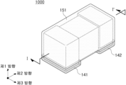
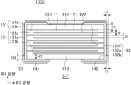
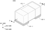
도 1은 본 발명의 일 실시예에 따른 적층형 전자 부품의 사시도를 개략적으로 도시한 것이다.
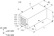
도 2는 도 1의 적층형 전자 부품의 바디의 사시도를 개략적으로 도시한 것이다.
도 3은 도 1의 I-I`에 따른 단면도이다.
도 4는 도 2의 바디를 분해하여 개략적으로 도시한 분해 사시도이다.
도 5는 도 1의 적층형 전자 부품이 실장된 기판의 사시도를 개략적으로 도시한 것이다.
도 6은 본 발명의 일 실시예에 따른 적층형 전자 부품의 사시도를 개략적으로 도시한 것이다. 도 7은 도 6의 II-II`에 따른 단면도이다.
도 8은 본 발명의 일 실시예에 따른 적층형 전자 부품의 사시도를 개략적으로 도시한 것이다. 도 9는 도 8의 III-III`에 따른 단면도이다.
도 10은 본 발명의 일 실시예에 따른 적층형 전자 부품의 사시도를 개략적으로 도시한 것이다. 도 11은 도 10의 IV-IV`에 따른 단면도이다.
도 12는 본 발명의 일 실시예에 따른 적층형 전자 부품의 사시도를 개략적으로 도시한 것이다. 도 13은 도 12의 V-V`에 따른 단면도이다.
도 14는 본 발명의 일 실시예에 따른 적층형 전자 부품의 사시도를 개략적으로 도시한 것이다. 도 15는 도 14의 VI-VI`에 따른 단면도이다. 도 16은 도 14의 변형예를 도시한 것이다.
도 17은 본 발명의 일 실시예에 따른 적층형 전자 부품의 사시도를 개략적으로 도시한 것이다. 도 18은 도 17의 VII-VII`에 따른 단면도이다.
도 19은 본 발명의 일 실시예에 따른 적층형 전자 부품의 사시도를 개략적으로 도시한 것이다. 도 20는 도 19의 VIII-VIII`에 따른 단면도이다. 도 21은 도 19의 변형예를 도시한 것이다.
도 22는 본 발명의 일 실시예에 따른 적층형 전자 부품의 사시도를 개략적으로 도시한 것이다. 도 23는 도 22의 IX-IX`에 따른 단면도이다. 도 25는 도 22의 변형예를 도시한 것이다.
도 25는 본 발명의 일 실시예에 따른 적층형 전자 부품의 사시도를 개략적으로 도시한 것이다. 도 26은 도 25의 X-X`에 따른 단면도이다. 도 27은 도 25의 변형예를 도시한 것이다.
도 28은 본 발명의 일 실시예에 따른 적층형 전자 부품의 사시도를 개략적으로 도시한 것이다. 도 29는 도 28의 XI-XI`에 따른 단면도이다. 도 30은 도 28의 변형예를 도시한 것이다.
도 31은 본 발명의 일 실시예에 따른 적층형 전자 부품의 사시도를 개략적으로 도시한 것이다. 도 32는 도 31의 XII-XII`에 따른 단면도이다.
도 33은 본 발명의 일 실시예에 따른 적층형 전자 부품의 사시도를 개략적으로 도시한 것이다. 도 34는 도 33의 XIII-XIII`에 따른 단면도이다. 도 35는 도 33의 변형예를 도시한 것이다.
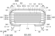
도 36은 본 발명의 일 실시예에 따른 적층형 전자 부품의 사시도를 개략적으로 도시한 것이다. 도 37은 도 36의 XIV-XIV`에 따른 단면도이다. 도 38은 도 36의 K1 영역을 확대한 확대도이다.1 schematically illustrates a perspective view of a multilayer electronic component according to an embodiment of the present invention.
FIG. 2 schematically illustrates a perspective view of a body of the multilayer electronic component of FIG. 1 .
3 is a cross-sectional view taken along line II′ of FIG. 1;
Figure 4 is an exploded perspective view schematically showing the disassembled body of Figure 2;
FIG. 5 schematically illustrates a perspective view of a substrate on which the multilayer electronic component of FIG. 1 is mounted.
6 schematically illustrates a perspective view of a multilayer electronic component according to an embodiment of the present invention. 7 is a cross-sectional view taken along line II-II′ of FIG. 6 .
8 schematically illustrates a perspective view of a multilayer electronic component according to an embodiment of the present invention. 9 is a cross-sectional view along line III-III′ of FIG. 8 .
10 schematically illustrates a perspective view of a multilayer electronic component according to an embodiment of the present invention. 11 is a cross-sectional view along IV-IV′ of FIG. 10;
12 schematically illustrates a perspective view of a multilayer electronic component according to an embodiment of the present invention. 13 is a cross-sectional view taken along VV′ of FIG. 12;
14 schematically illustrates a perspective view of a multilayer electronic component according to an embodiment of the present invention. 15 is a cross-sectional view taken along line VI-VI′ of FIG. 14; FIG. 16 shows a modified example of FIG. 14 .
17 schematically illustrates a perspective view of a multilayer electronic component according to an embodiment of the present invention. 18 is a cross-sectional view taken along VII-VII′ of FIG. 17;
19 schematically illustrates a perspective view of a multilayer electronic component according to an embodiment of the present invention. FIG. 20 is a cross-sectional view along line VIII-VIII′ in FIG. 19 . FIG. 21 shows a modified example of FIG. 19 .
22 schematically illustrates a perspective view of a multilayer electronic component according to an embodiment of the present invention. 23 is a cross-sectional view taken along IX-IX′ of FIG. 22; FIG. 25 shows a modified example of FIG. 22 .
25 schematically illustrates a perspective view of a multilayer electronic component according to an embodiment of the present invention. 26 is a cross-sectional view along XX′ in FIG. 25; FIG. 27 shows a modified example of FIG. 25 .
28 schematically illustrates a perspective view of a multilayer electronic component according to an embodiment of the present invention. Fig. 29 is a cross-sectional view taken along line XI-XI' in Fig. 28; FIG. 30 shows a modified example of FIG. 28 .
31 schematically illustrates a perspective view of a multilayer electronic component according to an embodiment of the present invention. 32 is a cross-sectional view taken along XII-XII′ of FIG. 31;
33 schematically illustrates a perspective view of a multilayer electronic component according to an embodiment of the present invention. 34 is a cross-sectional view taken along XIII-XIII′ in FIG. 33; FIG. 35 shows a modified example of FIG. 33 .
36 schematically illustrates a perspective view of a multilayer electronic component according to an embodiment of the present invention. 37 is a cross-sectional view taken along XIV-XIV′ of FIG. 36; FIG. 38 is an enlarged view of area K1 of FIG. 36 .
이하, 구체적인 실시형태 및 첨부된 도면을 참조하여 본 발명의 실시형태를 설명한다. 그러나, 본 발명의 실시형태는 여러 가지 다른 형태로 변형될 수 있으며, 본 발명의 범위가 이하 설명하는 실시형태로 한정되는 것은 아니다. 또한, 본 발명의 실시형태는 통상의 기술자에게 본 발명을 더욱 완전하게 설명하기 위해서 제공되는 것이다. 따라서, 도면에서의 요소들의 형상 및 크기 등은 보다 명확한 설명을 위해 과장될 수 있으며, 도면상의 동일한 부호로 표시되는 요소는 동일한 요소이다.Hereinafter, embodiments of the present invention will be described with reference to specific embodiments and accompanying drawings. However, the embodiments of the present invention can be modified in many different forms, and the scope of the present invention is not limited to the embodiments described below. In addition, the embodiments of the present invention are provided to more completely explain the present invention to those skilled in the art. Therefore, the shape and size of elements in the drawings may be exaggerated for clearer explanation, and elements indicated by the same reference numerals in the drawings are the same elements.
그리고 도면에서 본 발명을 명확하게 설명하기 위해서 설명과 관계없는 부분은 생략하고, 도면에서 나타난 각 구성의 크기 및 두께는 설명의 편의를 위해 임의로 나타내었으므로, 본 발명이 반드시 도시된 바에 한정되지 않는다. 또한, 동일한 사상의 범위 내의 기능이 동일한 구성요소는 동일한 참조부호를 사용하여 설명한다. 나아가, 명세서 전체에서, 어떤 부분이 어떤 구성요소를 "포함"한다고 할 때, 이는 특별히 반대되는 기재가 없는 한 다른 구성요소를 제외하는 것이 아니라 다른 구성요소를 더 포함할 수 있는 것을 의미한다.In addition, in order to clearly explain the present invention in the drawings, parts irrelevant to the description are omitted, and the size and thickness of each component shown in the drawings are arbitrarily shown for convenience of explanation, so the present invention is not necessarily limited to what is shown. . Also, components having the same function within the scope of the same concept are described using the same reference numerals. Furthermore, throughout the specification, when a certain component is said to "include", it means that it may further include other components without excluding other components unless otherwise stated.
도면에서, 제1 방향은 적층 방향 또는 두께(T) 방향, 제2 방향은 길이(L) 방향, 제3 방향은 폭(W) 방향으로 정의될 수 있다.In the drawing, the first direction may be defined as the stacking direction or the thickness (T) direction, the second direction may be defined as the length (L) direction, and the third direction may be defined as the width (W) direction.
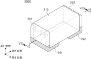
도 1은 본 발명의 일 실시예에 따른 적층형 전자 부품의 사시도를 개략적으로 도시한 것이다. 1 schematically illustrates a perspective view of a multilayer electronic component according to an embodiment of the present invention.
도 2는 도 1의 적층형 전자 부품의 바디의 사시도를 개략적으로 도시한 것이다. FIG. 2 schematically illustrates a perspective view of a body of the multilayer electronic component of FIG. 1 .
도 3은 도 1의 I-I`에 따른 단면도이다. 3 is a cross-sectional view taken along line II′ of FIG. 1 .
도 4는 도 2의 바디를 분해하여 개략적으로 도시한 분해 사시도이다.Figure 4 is an exploded perspective view schematically showing the disassembled body of Figure 2;
도 5는 도 1의 적층형 전자 부품이 실장된 기판의 사시도를 개략적으로 도시한 것이다. FIG. 5 schematically illustrates a perspective view of a substrate on which the multilayer electronic component of FIG. 1 is mounted.
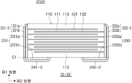
이하, 도 1 내지 도 5를 참조하여, 본 발명의 일 실시예에 따른 적층형 전자 부품(1000)에 대해 설명하도록 한다. Hereinafter, a multilayer
본 발명의 일 실시예에 따른 적층형 전자 부품(1000)은, 유전체층(111), 상기 유전체층을 사이에 두고 번갈아 배치되는 제1 및 제2 내부 전극(121, 122)을 포함하며, 제1 방향으로 대향하는 제1 및 제2 면(1, 2), 상기 제1 및 제2 면과 연결되고 제2 방향으로 대향하는 제3 및 제4 면(3, 4), 상기 제1 내지 제4 면과 연결되고 제3 방향으로 대향하는 제5 및 제6 면(5, 6)을 포함하는 바디(110); 상기 제3 면에 배치되는 제1 접속부(131a), 상기 제1 접속부로부터 상기 제1 면의 일부까지 연장되는 제1 밴드부(131b), 및 상기 제1 접속부로부터 상기 제2 면의 일부까지 연장되는 제3 밴드부(131c)를 포함하는 제1 외부 전극(131); 상기 제4 면에 배치되는 제2 접속부(132a), 상기 제2 접속부로부터 상기 제1 면의 일부까지 연장되는 제2 밴드부(132b), 및 상기 제2 접속부로부터 상기 제2 면의 일부까지 연장되는 제4 밴드부(132c)를 포함하는 제2 외부 전극(132); 상기 제1 및 제2 접속부 상에 배치되며, 상기 제2 면, 제3 및 제4 밴드부(131c, 132c)를 덮도록 배치되는 커버층(151); 상기 제1 밴드부(131b) 상에 배치되는 제1 도금층(141); 및 상기 제2 밴드부(132b)상에 배치되는 제2 도금층(142); 을 포함하며, 상기 커버층(151)은 친수성을 가지는 베이스층(151a) 및 상기 베이스층 상에 배치된 절연층(151b)을 포함할 수 있다.A multilayer
바디(110)는 유전체층(111) 및 내부 전극(121, 122)이 교대로 적층되어 있다.In the
바디(110)의 구체적인 형상에 특별히 제한은 없지만, 도시된 바와 같이 바디(110)는 육면체 형상이나 이와 유사한 형상으로 이루어질 수 있다. 소성 과정에서 바디(110)에 포함된 세라믹 분말의 수축으로 인하여, 바디(110)는 완전한 직선을 가진 육면체 형상은 아니지만 실질적으로 육면체 형상을 가질 수 있다.Although the specific shape of the
바디(110)는 제1 방향으로 서로 대향하는 제1 및 제2 면(1, 2), 상기 제1 및 제2 면(1, 2)과 연결되고 제2 방향으로 서로 대향하는 제3 및 제4 면(3, 4), 제1 및 제2 면(1, 2)과 연결되고 제3 및 제4 면(3, 4)과 연결되며 제3 방향으로 서로 대향하는 제5 및 제6 면(5, 6)을 가질 수 있다. The
일 실시예에서, 바디(110)는 제1 면과 제3 면을 연결하는 제1-3 코너, 상기 제1 면과 제4 면을 연결하는 제1-4 코너, 상기 제2 면과 제3 면을 연결하는 제2-3 코너, 상기 제2 면과 제4 면을 연결하는 제2-4 코너를 포함하며, 상기 제1-3 코너 및 제2-3 코너는 상기 제3 면에 가까워질수록 상기 바디의 제1 방향 중앙으로 수축된 형태를 가지고, 상기 제1-4 코너 및 제2-4 코너는 상기 제4 면에 가까워질수록 상기 바디의 제1 방향 중앙으로 수축된 형태를 가질 수 있다. In one embodiment, the
유전체층(111) 상에 내부 전극(121, 122)이 배치되지 않은 마진 영역이 중첩됨에 따라 내부 전극(121, 122) 두께에 의한 단차가 발생하여 제1 면과 제3 내지 제5 면을 연결하는 코너 및/또는 제2 면과 제3 내지 제5 면을 연결하는 코너는 제1 면 또는 제2 면을 기준으로 볼 때 바디(110)의 제1 방향 중앙 쪽으로 수축된 형태를 가질 수 있다. 또는, 바디의 소결 과정에서의 수축 거동에 의해 제1 면(1)과 제3 내지 제6 면(3, 4, 5, 6)을 연결하는 코너 및/또는 제2 면(2)과 제3 내지 제6 면(3, 4, 5, 6)을 연결하는 코너는 제1 면 또는 제2 면을 기준으로 볼 때 바디(110)의 제1 방향 중앙 쪽으로 수축된 형태를 가질 수 있다. 또는, 칩핑 불량 등을 방지하기 위하여 바디(110)의 각 면을 연결하는 모서리를 별도의 공정을 수행하여 라운드 처리함에 따라 제1 면과 제3 내지 제6 면을 연결하는 코너 및/또는 제2 면과 제3 내지 제6 면을 연결하는 코너는 라운드 형태를 가질 수 있다. As the margin area where the
상기 코너는 제1 면과 제3 면을 연결하는 제1-3 코너, 제1 면과 제4 면을 연결하는 제1-4 코너, 제2 면과 제3 면을 연결하는 제2-3 코너, 제2 면과 제4 면을 연결하는 제2-4 코너를 포함할 수 있다. 또한, 코너는 제1 면과 제5 면을 연결하는 제1-5 코너, 제1 면과 제6 면을 연결하는 제1-6 코너, 제2 면과 제5 면을 연결하는 제2-5 코너, 제2 면과 제6 면을 연결하는 제2-6 코너를 포함할 수 있다. 바디(110)의 제1 내지 제6 면은 대체로 평탄한 면일 수 있으며, 평탄하지 않은 영역을 코너로 볼 수 있다. 이하, 각 면의 연장선이란 각 면의 평탄한 부분을 기준으로 연장한 선을 의미할 수 있다. The corners include a 1-3 corner connecting the first surface and the third surface, a 1-4 corner connecting the first surface and the fourth surface, and a 2-3 corner connecting the second surface and the third surface. , may include a 2-4 corner connecting the second surface and the fourth surface. In addition, the corner is a 1-5 corner connecting the first surface and the fifth surface, a 1-6 corner connecting the first surface and the sixth surface, and a 2-5 corner connecting the second surface and the fifth surface. A corner, and 2-6 corners connecting the second surface and the sixth surface may be included. The first to sixth surfaces of the
이때, 외부 전극(131, 132) 중 바디(110)의 코너 상에 배치된 영역을 코너부, 바디(110)의 제3 및 제4 면 상에 배치된 영역을 접속부, 바디의 제1 및 제2 면 상에 배치된 영역을 밴드부라 할 수 있다. At this time, among the
한편, 내부 전극(121, 122)에 의한 단차를 억제하기 위하여, 적층 후 내부 전극이 바디의 제5 및 제6 면(5, 6)으로 노출되도록 절단한 후, 단일 유전체층 또는 2 개 이상의 유전체층을 용량 형성부(Ac)의 양측면에 제3 방향(폭 방향)으로 적층하여 마진부(114, 115)를 형성하는 경우에는 제1 면과 제5 및 제6 면을 연결하는 부분 및 제2 면과 제5 및 제6 면을 연결하는 부분이 수축된 형태를 가지지 않을 수 있다. On the other hand, in order to suppress the step difference caused by the
바디(110)를 형성하는 복수의 유전체층(111)은 소성된 상태로서, 인접하는 유전체층(111) 사이의 경계는 주사전자현미경(SEM: Scanning Electron Microscope)를 이용하지 않고 확인하기 곤란할 정도로 일체화될 수 있다. The plurality of
본 발명의 일 실시예에 따르면, 상기 유전체층(111)을 형성하는 원료는 충분한 정전 용량을 얻을 수 있는 한 특별히 제한되지 않는다. 예를 들어, 티탄산바륨계 재료, 납 복합 페로브스카이트계 재료 또는 티탄산스트론튬계 재료 등을 사용할 수 있다. 상기 티탄산바륨계 재료는 BaTiO3계 세라믹 분말을 포함할 수 있으며, 상기 세라믹 분말의 예시로, BaTiO3, BaTiO3에 Ca(칼슘), Zr(지르코늄) 등이 일부 고용된 (Ba1-xCax)TiO3 (0<x<1), Ba(Ti1-yCay)O3 (0<y<1), (Ba1-xCax)(Ti1-yZry)O3 (0<x<1, 0<y<1)또는 Ba(Ti1-yZry)O3 (0<y<1) 등을 들 수 있다. According to one embodiment of the present invention, a material for forming the
또한, 상기 유전체층(111)을 형성하는 원료는 티탄산바륨(BaTiO3) 등의 파우더에 본 발명의 목적에 따라 다양한 세라믹 첨가제, 유기용제, 결합제, 분산제 등이 첨가될 수 있다. In addition, various ceramic additives, organic solvents, binders, dispersants, etc. may be added to powder such as barium titanate (BaTiO 3 ) as a raw material forming the
한편, 유전체층(111)의 평균 두께(td)는 특별히 한정할 필요는 없다. On the other hand, the average thickness (td) of the
다만, 일반적으로 유전체층을 0.6μm 미만의 두께로 얇게 형성하는 경우, 특히 유전체층의 두께가 0.35μm 이하인 경우에는 신뢰성이 저하될 우려가 있었다. However, in general, when the dielectric layer is formed thinly with a thickness of less than 0.6 μm, in particular, when the thickness of the dielectric layer is 0.35 μm or less, there is a risk of deterioration in reliability.
본 발명의 일 실시예에 따르면, 커버층을 외부 전극의 접속부 상에 배치하고, 도금층을 외부 전극의 밴드부 상에 배치함으로써 외부의 수분 침투, 도금액의 침투 등을 방지하여 신뢰성을 향상시킬 수 있기 때문에, 유전체층(111)의 평균 두께가 0.35μm 이하인 경우에도 우수한 신뢰성을 확보할 수 있다. According to an embodiment of the present invention, by disposing the cover layer on the connecting portion of the external electrode and disposing the plating layer on the band portion of the external electrode, it is possible to prevent penetration of external moisture and penetration of a plating solution, thereby improving reliability. , Excellent reliability can be secured even when the average thickness of the
따라서, 유전체층(111)의 평균 두께가 0.35μm 이하인 경우에 본 발명에 따른 신뢰성 향상 효과가 보다 현저해질 수 있다. Therefore, when the average thickness of the
상기 유전체층(111)의 평균 두께(td)는 상기 제1 및 제2 내부 전극(121, 122) 사이에 배치되는 유전체층(111)의 평균 두께를 의미할 수 있다. The average thickness td of the
유전체층(111)의 평균 두께는 바디(110)의 길이 및 두께 방향(L-T) 단면을 1만 배율의 주사전자현미경(SEM, Scanning Electron Microscope)으로 이미지를 스캔하여 측정할 수 있다. 보다 구체적으로, 스캔된 이미지에서 하나의 유전체층을 길이 방향으로 등간격인 30개의 지점에서 그 두께를 측정하여 평균값을 측정할 수 있다. 상기 등간격인 30개의 지점은 용량 형성부(Ac)에서 지정될 수 있다. 또한, 이러한 평균값 측정을 10개의 유전체층으로 확장하여 평균값을 측정하면, 유전체층의 평균 두께를 더욱 일반화할 수 있다.The average thickness of the
바디(110)는 바디(110)의 내부에 배치되며, 유전체층(111)을 사이에 두고 서로 대향하도록 배치되는 제1 내부 전극(121) 및 제2 내부 전극(122)을 포함하여 용량이 형성되는 용량 형성부(Ac)와 상기 용량 형성부(Ac)의 제1 방향 상부 및 하부에 형성된 커버부(112, 113)를 포함할 수 있다. The
또한, 상기 용량 형성부(Ac)는 커패시터의 용량 형성에 기여하는 부분으로서, 유전체층(111)을 사이에 두고 복수의 제1 및 제2 내부 전극(121, 122)을 반복적으로 적층하여 형성될 수 있다. In addition, the capacitance forming portion (Ac), which contributes to forming the capacitance of the capacitor, may be formed by repeatedly stacking a plurality of first and second
커버부(112, 113)는 상기 용량 형성부(Ac)의 제1 방향 상부에 배치되는 상부 커버부(112) 및 상기 용량 형성부(Ac)의 제1 방향 하부에 배치되는 하부 커버부(113)를 포함할 수 있다. The
상기 상부 커버부(112) 및 하부 커버부(113)는 단일 유전체층 또는 2 개 이상의 유전체층을 용량 형성부(Ac)의 상하면에 각각 두께 방향으로 적층하여 형성할 수 있으며, 기본적으로 물리적 또는 화학적 스트레스에 의한 내부 전극의 손상을 방지하는 역할을 수행할 수 있다. The
상기 상부 커버부(112) 및 하부 커버부(113)는 내부 전극을 포함하지 않으며, 유전체층(111)과 동일한 재료를 포함할 수 있다. The
즉, 상기 상부 커버부(112) 및 하부 커버부(113)는 세라믹 재료를 포함할 수 있으며, 예를 들어 티탄산바륨(BaTiO3)계 세라믹 재료를 포함할 수 있다.That is, the
한편, 커버부(112, 113)의 평균 두께는 특별히 한정할 필요는 없다. 다만, 적층형 전자 부품의 소형화 및 고용량화를 보다 용이하게 달성하기 위하여 커버부(112, 113)의 평균 두께(tc)는 15μm 이하일 수 있다. 또한, 본 발명의 일 실시예에 따르면, 커버층을 외부 전극의 접속부 상에 배치하고, 도금층을 외부 전극의 밴드부 상에 배치함으로써 외부의 수분 침투, 도금액의 침투 등을 방지하여 신뢰성을 향상시킬 수 있기 때문에, 커버부(112, 113)의 평균 두께(tc)가 15μm 이하인 경우에도 우수한 신뢰성을 확보할 수 있다. On the other hand, the average thickness of the
커버부(112, 113)의 평균 두께(tc)는 제1 방향 크기를 의미할 수 있으며, 용량 형성부(Ac)의 상부 또는 하부에서 등간격의 5개 지점에서 측정한 커버부(112, 113)의 제1 방향 크기를 평균한 값일 수 있다. The average thickness (tc) of the
또한, 상기 용량 형성부(Ac)의 측면에는 마진부(114, 115)가 배치될 수 있다. In addition,
마진부(114, 115)는 바디(110)의 제5 면(5)에 배치된 제1 마진부(114)와 제6 면(6)에 배치된 제2 마진부(115)를 포함할 수 있다. 즉, 마진부(114, 115)는 상기 바디(110)의 폭 방향 양 단면(end surfaces)에 배치될 수 있다. The
마진부(114, 115)는 도 3에 도시된 바와 같이, 상기 바디(110)를 폭-두께(W-T) 방향으로 자른 단면(cross-section)에서 제1 및 제2 내부 전극(121, 122)의 양 끝단과 바디(110)의 경계면 사이의 영역을 의미할 수 있다. As shown in FIG. 3 , the
마진부(114, 115)는 기본적으로 물리적 또는 화학적 스트레스에 의한 내부 전극의 손상을 방지하는 역할을 수행할 수 있다. The
마진부(114, 115)는 세라믹 그린시트 상에 마진부가 형성될 곳을 제외하고 도전성 페이스트를 도포하여 내부 전극을 형성함으로써 형성된 것일 수 있다. The
또한, 내부 전극(121, 122)에 의한 단차를 억제하기 위하여, 적층 후 내부 전극이 바디의 제5 및 제6 면(5, 6)으로 노출되도록 절단한 후, 단일 유전체층 또는 2 개 이상의 유전체층을 용량 형성부(Ac)의 양측면에 제3 방향(폭 방향)으로 적층하여 마진부(114, 115)를 형성할 수도 있다.In addition, in order to suppress the step difference caused by the
한편, 마진부(114, 115)의 폭은 특별히 한정할 필요는 없다. 다만, 적층형 전자 부품의 소형화 및 고용량화를 보다 용이하게 달성하기 위하여 마진부(114, 115)의 평균 폭은 15μm 이하일 수 있다. 또한, 본 발명의 일 실시예에 따르면, 커버층을 외부 전극의 접속부 상에 배치하고, 도금층을 외부 전극의 밴드부 상에 배치함으로써 외부의 수분 침투, 도금액의 침투 등을 방지하여 신뢰성을 향상시킬 수 있기 때문에, 마진부(114, 115)의 평균 폭이 15μm 이하인 경우에도 우수한 신뢰성을 확보할 수 있다. On the other hand, the width of the
마진부(114, 115)의 평균 폭은 마진부(114, 115)의 제3 방향 평균 크기를 의미할 수 있으며, 용량 형성부(Ac)의 측면에서 등간격의 5개 지점에서 측정한 마진부(114, 115)의 제3 방향 크기를 평균한 값일 수 있다. The average width of the
내부 전극(121, 122)은 유전체층(111)과 교대로 적층된다. The
내부 전극(121, 122)은 제1 및 제2 내부 전극(121, 122)을 포함할 수 있다. 제1 및 제2 내부 전극(121, 122)은 바디(110)를 구성하는 유전체층(111)을 사이에 두고 서로 대향하도록 번갈아 배치되며, 바디(110)의 제3 및 제4 면(3, 4)으로 각각 노출될 수 있다. The
도 3을 참조하면, 제1 내부 전극(121)은 제4 면(4)과 이격되며 제3 면(3)을 통해 노출되고, 제2 내부 전극(122)은 제3 면(3)과 이격되며 제4 면(4)을 통해 노출될 수 있다. 바디의 제3 면(3)에는 제1 외부 전극(131)이 배치되어 제1 내부 전극(121)과 연결되고, 바디의 제4 면(4)에는 제2 외부 전극(132)이 배치되어 제2 내부 전극(122)과 연결될 수 있다. Referring to FIG. 3 , the first
즉, 제1 내부 전극(121)은 제2 외부 전극(132)과는 연결되지 않고 제1 외부 전극(131)과 연결되며, 제2 내부 전극(122)은 제1 외부 전극(131)과는 연결되지 않고 제2 외부 전극(132)과 연결된다. 따라서, 제1 내부 전극(121)은 제4 면(4)에서 일정거리 이격되어 형성되고, 제2 내부 전극(122)은 제3 면(3)에서 일정거리 이격되어 형성될 수 있다. That is, the first
이때, 제1 및 제2 내부 전극(121, 122)은 중간에 배치된 유전체층(111)에 의해 서로 전기적으로 분리될 수 있다. In this case, the first and second
바디(110)는 제1 내부 전극(121)이 인쇄된 세라믹 그린 시트와 제2 내부 전극(122)이 인쇄된 세라믹 그린 시트를 번갈아 적층한 후, 소성하여 형성할 수 있다.The
내부 전극(121, 122)을 형성하는 재료는 특별히 제한되지 않으며, 전기 전도성이 우수한 재료를 사용할 수 있다. 예를 들어, 내부 전극(121, 122)은 니켈(Ni), 구리(Cu), 팔라듐(Pd), 은(Ag), 금(Au), 백금(Pt), 주석(Sn), 텅스텐(W), 티타늄(Ti) 및 이들의 합금 중 하나 이상을 포함할 수 있다. Materials forming the
또한, 내부 전극(121, 122)은 니켈(Ni), 구리(Cu), 팔라듐(Pd), 은(Ag), 금(Au), 백금(Pt), 주석(Sn), 텅스텐(W), 티타늄(Ti) 및 이들의 합금 중 하나 이상을 포함하는 내부 전극용 도전성 페이스트를 세라믹 그린 시트에 인쇄하여 형성할 수 있다. 상기 내부 전극용 도전성 페이스트의 인쇄 방법은 스크린 인쇄법 또는 그라비아 인쇄법 등을 사용할 수 있으며, 본 발명이 이에 한정되는 것은 아니다.In addition, the
한편, 내부 전극(121, 122)의 평균 두께(te)는 특별히 한정할 필요는 없다. Meanwhile, the average thickness te of the
다만, 일반적으로 내부 전극을 0.6μm 미만의 두께로 얇게 형성하는 경우, 특히 내부 전극의 두께가 0.35μm 이하인 경우에는 신뢰성이 저하될 우려가 있었다. However, in general, when the thickness of the internal electrode is less than 0.6 μm, and particularly when the thickness of the internal electrode is 0.35 μm or less, reliability may be deteriorated.
본 발명의 일 실시예에 따르면, 커버층을 외부 전극의 접속부 상에 배치하고, 도금층을 외부 전극의 밴드부 상에 배치함으로써 외부의 수분 침투, 도금액의 침투 등을 방지하여 신뢰성을 향상시킬 수 있기 때문에, 내부 전극(121, 122)의 평균 두께가 0.35μm 이하인 경우에도 우수한 신뢰성을 확보할 수 있다. According to an embodiment of the present invention, by disposing the cover layer on the connecting portion of the external electrode and disposing the plating layer on the band portion of the external electrode, it is possible to prevent penetration of external moisture and penetration of a plating solution, thereby improving reliability. , Excellent reliability can be secured even when the average thickness of the
따라서, 내부 전극(121, 122)의 두께가 평균 0.35μm 이하인 경우에 본 발명에 따른 효과가 보다 현저해질 수 있으며, 적층형 전자 부품의 소형화 및 고용량화를 보다 용이하게 달성할 수 있다. Therefore, when the average thickness of the
상기 내부 전극(121, 122)의 평균 두께(te)는 내부 전극(121, 122)의 평균 두께를 의미할 수 있다. The average thickness te of the
내부 전극(121, 122)의 평균 두께는 바디(110)의 길이 및 두께 방향(L-T) 단면을 1만 배율의 주사전자현미경(SEM, Scanning Electron Microscope)으로 이미지를 스캔하여 측정할 수 있다. 보다 구체적으로, 스캔된 이미지에서 하나의 내부 전극을 길이 방향으로 등간격인 30개의 지점에서 그 두께를 측정하여 평균값을 측정할 수 있다. 상기 등간격인 30개의 지점은 용량 형성부(Ac)에서 지정될 수 있다. 또한, 이러한 평균값 측정을 10개의 내부 전극으로 확장하여 평균값을 측정하면, 내부 전극의 평균 두께를 더욱 일반화할 수 있다.The average thickness of the
외부 전극(131, 132)은 바디(110)의 제3 면(3) 및 제4 면(4)에 배치될 수 있다. 외부 전극(131, 132)은 바디(110)의 제3 및 제4 면(3, 4)에 각각 배치되어, 제1 및 제2 내부 전극(121, 122)과 각각 연결된 제1 및 제2 외부 전극(131, 132)을 포함할 수 있다. The
외부 전극(131, 132)은 제3 면에 배치되는 제1 접속부(131a) 및 상기 제1 접속부로부터 상기 제1 면의 일부까지 연장되는 제1 밴드부(131b)를 포함하는 제1 외부 전극(131), 제4 면에 배치되는 제2 접속부(132a) 및 상기 제2 접속부로부터 상기 제1 면의 일부까지 연장되는 제2 밴드부(132b)를 포함하는 제2 외부 전극(132)을 포함할 수 있다. 제1 접속부(131a)는 제1 내부 전극(121)과 제3 면에서 연결되고, 제2 접속부(132a)는 제2 내부 전극(122)과 제4 면에서 연결될 수 있다. The
또한, 제1 외부 전극(131)은 제1 접속부(131a)로부터 제2 면의 일부까지 연장되는 제3 밴드부(131c)를 포함할 수 있으며, 제2 외부 전극(132)은 제2 접속부(132a)로부터 제2 면의 일부까지 연장되는 제4 밴드부(132c)를 포함할 수 있다. 나아가, 제1 외부 전극(131)은 제1 접속부(131a)로부터 제5 및 제6 면의 일부까지 연장되는 제1 측면 밴드부를 포함할 수 있으며, 제2 외부 전극(132)은 제2 접속부(132a)로부터 제5 및 제6 면의 일부까지 연장되는 제2 측면 밴드부를 포함할 수 있다. In addition, the first
다만, 제3 밴드부, 제4 밴드부, 제1 측면 밴드부 및 제2 측면 밴드부는 본 발명에 필수 구성 요소가 아닐 수 있다. 제1 및 제2 외부 전극(131, 132)은 제2 면에는 배치되지 않을 수 있고, 제5 및 제6 면에도 배치되지 않을 수 있다. 제1 및 제2 외부 전극(131, 132)이 제2 면에 배치되지 않음에 따라, 제1 및 제2 외부 전극(131, 132)은 바디의 제2 면의 연장선 이하로 배치될 수 있다. 또한, 제1 및 제2 접속부(131a, 132a)는 제5 및 제6 면과 이격되어 배치될 수 있으며, 제1 및 제2 접속부(131a, 132a)는 제2 면과 이격되어 배치될 수 있다. 또한, 제1 및 제2 밴드부(131b, 132b)도 제5 및 제6 면과 이격되어 배치될 수 있다. However, the third band unit, the fourth band unit, the first side band unit, and the second side band unit may not be essential elements in the present invention. The first and second
한편, 제1 및 제2 외부 전극(131, 132)이 제3 및 제4 밴드부(131c, 132c)를 포함하는 경우, 제3 및 제4 밴드부(131c, 132c) 상에 커버층이 배치되는 것을 도시하고 있으나, 이에 제한되는 것은 아니며, 실장 편이성을 향상시키기 위하여 제3 및 제4 밴드부(131c, 132c) 상에 도금층을 배치할 수 있다. 또한, 제1 및 제2 외부 전극(131, 132)이 제3 및 제4 밴드부(131c, 132c)를 포함하되, 측면 밴드부는 포함하지 않는 형태일 수 있으며, 이 경우 제1, 제2 접속부(131a, 132a), 및 제1 내지 제4 밴드부(131a, 132b, 131c, 132c)가 제5 및 제6 면과 이격된 형태를 가질 수 있다. Meanwhile, when the first and second
본 실시 형태에서는 적층형 전자 부품(1000)이 2개의 외부 전극(131, 132)을 갖는 구조를 설명하고 있지만, 외부 전극(131, 132)의 개수나 형상 등은 내부 전극(121, 122)의 형태나 기타 다른 목적에 따라 바뀔 수 있을 것이다. In this embodiment, a structure in which the multilayer
한편, 외부 전극(131, 132)은 금속 등과 같이 전기 전도성을 갖는 것이라면 어떠한 물질을 사용하여 형성될 수 있고, 전기적 특성, 구조적 안정성 등을 고려하여 구체적인 물질이 결정될 수 있으며, 나아가 다층 구조를 가질 수 있다. Meanwhile, the
외부 전극(131, 132)은 도전성 금속 및 글라스를 포함한 소성(firing) 전극이거나, 도전성 금속 및 수지를 포함한 수지계 전극일 수 있다. The
또한, 외부 전극(131, 132)은 바디 상에 소성 전극 및 수지계 전극이 순차적으로 형성된 형태일 수 있다. 또한, 외부 전극(131, 132)은 바디 상에 도전성 금속을 포함한 시트를 전사하는 방식으로 형성되거나, 소성 전극 상에 도전성 금속을 포함한 시트를 전사하는 방식으로 형성된 것일 수 있다. In addition, the
외부 전극(131, 132)에 포함되는 도전성 금속으로 전기 전도성이 우수한 재료를 사용할 수 있으며 특별히 한정하지 않는다. 예를 들어, 도전성 금속은 Cu, Ni, Pd, Ag, Sn, Cr 및 그들의 합금 중 하나 이상일 수 있다. 바람직하게는 외부 전극(131, 132)은 Ni 및 Ni 합금 중 하나 이상을 포함할 수 있으며, 이에 따라, Ni을 포함하는 내부 전극(121, 122)과의 연결성을 보다 향상시킬 수 있다. A material having excellent electrical conductivity may be used as the conductive metal included in the
커버층(151)은 제1 및 제2 접속부(131a, 132a) 상에 배치될 수 있다. 커버층(151)은 친수성을 가지는 베이스층(151a) 및 상기 베이스층 상에 배치된 절연층(151b)을 포함할 수 있다. The
제1 및 제2 접속부(131a, 132a)는 내부 전극(121, 122)과 연결되는 부위이기 때문에, 도금 공정에서 도금액 침투 또는 실사용시 수분 침투의 경로가 될 수 있다. 본 발명에서는 접속부(131a, 132a) 상에 커버층(151)이 배치되기 때문에 외부의 수분 침투 또는 도금액의 침투를 방지할 수 있다. Since the first and
커버층(151)은 제1 및 제2 도금층(141, 142)과 접하도록 배치될 수 있다. 이때, 커버층(151)이 제1 및 제2 도금층(141, 142)의 끝단을 일부 덮는 형태로 접하거나, 제1 및 제2 도금층(141, 142)이 커버층(151)의 끝단을 일부 덮는 형태로 접할 수 있다. The
커버층(151)은 제1 및 제2 접속부(131a, 132a) 상에 배치되며, 제2 면, 제3 및 제4 밴드부(131c, 132c)를 덮도록 배치될 수 있다. 이때, 커버층(151)은 제2 면 중 제3 및 제4 밴드부(131c, 132c)가 배치되지 않은 영역, 제3 및 제4 밴드부(131c, 132c)를 덮도록 배치될 수 있다. 이에 따라, 커버층(151)이 제3 및 제4 밴드부(131c, 132c)의 끝단과 바디(110)가 접하는 영역을 커버하여 수분 침투 경로를 차단함으로써 내습 신뢰성을 보다 향상시킬 수 있다. The
커버층(151)은 제2 면 상에 배치되어 상기 제1 및 제2 접속부(131a, 132a) 로 연장되어 배치될 수 있다. 또한, 커버층은 외부 전극(131, 132)이 제2 면에 배치되지 않는 경우, 제2 면을 전부 덮도록 배치될 수 있다. 한편, 커버층(151)이 제2 면에 반드시 배치되어야 하는 것은 아니며, 커버층이 제2 면의 일부 또는 전부에 배치되지 않을 수 있고, 커버층이 2개로 분리되어 제1 및 제2 접속부(131a, 132a) 상에 각각 배치되는 형태를 가질 수도 있다. 커버층이 제2 면 전부에 배치되지 않는 경우, 제2 면의 연장선 이하로 배치될 수 있다. 또한, 커버층이 제2 면에는 배치되지 않으나, 제1 및 제2 접속부(131a, 132a) 상에서 제5 및 제6 면으로 연장되어 하나의 커버층을 이룰 수 있다.The
나아가, 커버층(151)은 제1 및 제2 측면 밴드부, 제5 면 및 제6 면의 일부를 덮도록 배치될 수 있다. 이때, 커버층(151)에 덮이지 않은 제5 면 및 제6 면의 일부는 외부로 노출될 수 있다. Furthermore, the
또한, 커버층(151)은 제1 및 제2 측면 밴드부, 제5 면 및 제 6 면을 모두 덮도록 배치될 수 있으며, 이 경우 제5 면 및 제6 면이 외부로 노출되지 않아 내습 신뢰성을 향상시킬 수 있으며, 접속부(131a, 132a) 또한 직접적으로 외부로 노출되지 않아 적층형 전자 부품(1000)의 신뢰성을 향상시킬 수 있다. 보다 상세하게는, 커버층이 제1 및 제2 측면 밴드부를 모두 덮고, 제5 및 제6 면 중 제1 및 제2 측면 밴드부가 형성된 영역을 제외한 영역을 모두 덮을 수 있다. In addition, the
커버층(151)은 커버층(151)이 배치된 외부 전극(131, 132) 상에 도금층(141, 142)이 형성되는 것을 방지하는 역할을 수행할 수 있으며, 실링 특성을 향상시켜 외부로부터 수분이나 도금액 등이 침투하는 것을 최소화하는 역할을 수행할 수 있다.The
커버층(151)은 친수성을 가지는 베이스층(151a) 및 상기 베이스층 상에 배치된 절연층(151b)을 포함할 수 있다.The
종래에는 일반적으로 친수성을 가지는 베이스층(151a) 없이 절연층을 외부 전극 상에 배치하였으나, 절연층과 외부 전극 간의 결합력이 약해 절연층이 연마, 도금 공정 등으로 인해 물리적 박리 및 손상이 발생할 수 있었다. 박리된 부분 및 손상이 발생한 부분으로 수분, 도금액 등이 침투할 수 있어 신뢰성이 저하될 우려가 있었다. In the prior art, the insulating layer was generally disposed on the external electrode without the
본 발명에서는 절연층(151b)이 배치될 영역에 친수성을 가지는 베이스층(151a)을 배치함으로써, 외부 전극(131, 132)과 절연층(151b) 간의 결합력을 향상시켜 종래의 절연층만 배치하는 경우 발생하는 문제점을 해결하고자 하였다. In the present invention, by disposing the
베이스층(151a)은 친수성을 가져 바디(110) 및 외부 전극(131, 132)과 절연층(151b) 간의 결합력을 향상시키는 역할을 수행할 수 있다. The
친수성(hydrophilicity)이란 물 분자와 쉽게 결합하는 성질을 의미할 수 있으며, 이와는 반대로 물 분자와 쉽게 결합하지 못하는 성질을 소수성(hydrophobicity)이라 할 수 있다. 물과의 접촉각을 측정함으로써 친수성과 소수성을 구별할 수 있으며, 본 발명에서 친수성이란 물(Water)과의 접촉각이 90도(degree) 미만인 것을 의미할 수 있다. 따라서, 일 실시예에서, 베이스층(151a)은 물(Water)과의 접촉각이 90도(degree) 미만일 수 있다. Hydrophilicity may refer to a property that easily binds to water molecules, and on the contrary, a property that does not easily bind to water molecules may be referred to as hydrophobicity . Hydrophilicity and hydrophobicity can be distinguished by measuring the contact angle with water, and in the present invention, hydrophilicity may mean that the contact angle with water is less than 90 degrees. Accordingly, in one embodiment, the contact angle of the
또한, 외부 전극(131, 132)과 절연층(151b) 간의 결합력을 보다 향상시키기 위해서는 베이스층(151a)은 물(Water)과의 접촉각이 60도(degree) 이하인 것이 보다 바람직할 수 있다. 베이스층(151a)이 물(Water)과의 접촉각이 60도(degree) 이하가 되도록 형성하는 방법은 특별히 한정할 필요는 없으나, 예를 들어 플라즈마 표면처리에 의해 물(Water)과의 접촉각이 60도(degree) 이하인 베이스층(151a)을 형성할 수 있다. In addition, in order to further improve bonding strength between the
상기 베이스층(151a)을 형성하는 방법은 특별히 한정할 필요는 없다. 예를 들어, 베이스층(151a)은 플라즈마 표면처리에 의해 형성될 수 있으며, 보다 구체적으로는 O2/Ar 플라즈마 표면처리에 의해 형성될 수 있다. 플라즈마 표면처리는 물리적, 화학적 반응이 물질의 전체적인 성질을 변화시키지 않고, 표면층에 국한되어 균일하게 일어나므로 표면을 안정하게 다룰 수 있으며 저온에서 안정한 물질을 처리 할 수 있는 장점이 있다. 여기서, O2/Ar 플라즈마 표면처리란 O2와 Ar의 혼합 가스를 주입하여 플라즈마를 발생시켜 대상물의 표면을 개질하는 것을 의미할 수 있다. O2와 Ar의 비율은 특별히 한정할 필요는 없으며, 얻고자 하는 특성을 고려하여 O2와 Ar의 비율을 결정할 수 있다. A method of forming the
O2/Ar 플라즈마 표면처리에 의해 외부 전극(131, 132) 표면 및 바디(110) 표면에 조도를 향상시키고, 표면 에너지를 증가시킬 수 있다. 또한, 외부 전극(131, 132) 표면 및 바디(110) 표면에 친수성을 부여할 수 있으며, O2/Ar 플라즈마 표면처리된 외부 전극(131, 132) 및 바디(110)의 표면을 베이스층(151a)으로 볼 수 있다. 이에 따라, 절연층(151b)과 외부 전극(131, 132) 간의 결합력을 향상시킬 수 있다.By the O 2 /Ar plasma surface treatment, roughness of the surfaces of the
플라즈마 표면처리 장치는 특별히 한정할 필요는 없으며, 예를 들어 고 진공에서 고밀도 플라즈마를 형성하는 유도 결합 플라즈마 (inductively coupled plasma) 장비를 이용할 수 있다. The plasma surface treatment device does not need to be particularly limited, and for example, an inductively coupled plasma device that forms high-density plasma in a high vacuum may be used.
일 실시예에서, 베이스층(151a)은 상기 절연층(151b)과의 계면에서 표면 조도를 가질 수 있다. 이에 따라, 절연층(151b)과 외부 전극(131, 132) 간의 결합력을 향상시킬 수 있다. 표면 조도를 부여하는 방법은 특별히 한정하지 않으나, 상술한 O2/Ar 플라즈마 표면처리에 의해 표면 조도를 부여할 수 있다. 이때, O2 및 Ar 가스의 비율을 조절함에 따라 표면 조도를 제어할 수 있다. 예를 들어, 베이스층(151a)은 상기 절연층(151b)과의 계면에서 가지는 중심선 평균 거칠기(Ra)가 50~100nm 일 수 있다. In one embodiment, the
일 실시예에서, 베이스층(151a)은 O2를 포함할 수 있다. 베이스층(151a)이 O2/Ar 플라즈마 표면처리에 의해 형성되는 경우 베이스층(151a)은 O2를 포함할 수 있다. In one embodiment, the
일 실시예에서, 베이스층(151a)은 상기 제1 및 제2 외부 전극(131, 132)과 접하는 영역에서 금속 산화물을 포함할 수 있다. 베이스층(151a)이 금속 산화물을 포함함에 따라 표면 조도가 부여될 수 있으며, 베이스층(151a)에 포함된 금속 산화물은 외부 전극(131, 132)에 포함된 도전성 금속이 O2/Ar 플라즈마 표면처리에 의해 산화됨에 따라 형성된 것일 수 있다. 따라서, 베이스층(151a)에 포함된 금속 산화물의 금속은 외부 전극(131, 132)에 포함된 도전성 금속과 동일한 종류일 수 있다. In one embodiment, the
특히, 외부 전극(131, 132)이 도전성 금속으로 Cu를 포함하는 경우, 베이스층(151a)은 금속 산화물로 Cu를 포함하는 산화물을 포함할 수 있다. 베이스층(151a)이 Cu를 포함하는 산화물을 포함하는 경우, 표면 조도가 보다 높아질 수 있기 때문에, 절연층(151b)과 외부 전극(131, 132) 간의 결합력을 보다 향상시킬 수 있다.In particular, when the
이때, Cu를 포함하는 산화물은 CuO 및 Cu2O 중 하나 이상일 수 있다. In this case, the oxide containing Cu may be one or more of CuO and Cu 2 O.
한편, 베이스층(151a)은 연속적인 층 형상을 가지지 않을 수 있으며, 주사전자현미경을 이용하더라도 외부 전극(131, 132)과 명확한 구별이 용이하지 않을 수 있다. 다만, 외부 전극(131, 132) 표면에 표면 조도가 형성된 경우나, 외부 전극 표면에 O2가 포함된 경우, 외부 전극 표면에 금속 산화물이 포함된 경우 등을 본 발명의 베이스층(151a)이 외부 전극(131, 132) 상에 배치된 것으로 볼 수 있다. Meanwhile, the
절연층(151b)은 커버층(151)이 배치된 외부 전극(131, 132) 상에 도금층(141, 142)이 형성되는 것을 방지하는 역할을 수행할 수 있으며, 실링 특성을 향상시켜 외부로부터 수분이나 도금액 등이 침투하는 것을 최소화하는 역할을 수행할 수 있다. The insulating
절연층(151b)을 구성하는 물질은 특별히 한정할 필요는 없으며, 절연층(151b)은 절연 물질을 포함하여 전기적으로 절연 특성을 가질 수 있다. 예를 들어, 절연층(151b)에 포함된 절연 물질은 에폭시 수지, 아크릴 수지, 에틸 셀룰로우스(Ethyl Cellulose) 등에서 선택된 1종 이상이거나, 글래스일 수 있다. 보다 구체적으로, 절연층(151b)을 구성하는 재료로는 도금액에 대한 내성이 뛰어난 글래스 재료로서, Si의 몰분율이 20mol% 이상 65mol% 이하인 글래스 재료가 바람직할 수 있다. The material constituting the insulating
한편, 절연층(151b)이 글래스를 포함하는 경우, 절연층이 연마, 도금 공정 등으로 인해 물리적 박리 및 손상이 발생할 가능성이 높을 수 있다. 다만, 본 발명의 일 실시예에 따르면 절연층과 외부 전극 사이에 베이스층을 배치함에 따라 절연층(151b)과 외부 전극(131, 132) 간의 결합력을 향상시킬 수 있으므로, 절연층(151b)이 글래스를 포함하더라도 효과적으로 물리적 박리 및 손상을 방지할 수 있다. 따라서, 절연층(151b)이 글래스를 포함하는 경우, 절연층(151b)의 물리적 박리 및 손상을 방지하는 본 발명의 효과가 보다 현저해질 수 있다. On the other hand, when the insulating
절연층(151b)을 형성하는 방법은 특별히 한정할 필요는 없다. 예를 들어, 바디(100)에 외부 전극(131, 132)을 형성하고, 베이스층(151a)을 형성한 후, 글래스 분말을 포함하는 페이스트를 도포하거나, 글래스를 포함하는 페이스트에 딥핑(dipping)한 후 열처리하여 절연층(151b)을 형성할 수 있다. The method of forming the insulating
일 실시예에서, 커버층(151)은 제1 및 제2 외부 전극(131, 132)과 직접 접하도록 배치되며, 제1 및 제2 외부 전극(131, 132)은 도전성 금속 및 글라스를 포함할 수 있다. 이에 따라, 제1 및 제2 외부 전극(131, 132)의 외표면 중 커버층(151)이 배치된 영역에는 도금층(141, 142)이 배치되지 않을 수 있기 때문에, 도금액에 의한 외부전극 침식 방지를 효과적으로 억제할 수 있다. In one embodiment, the
이때, 제1 도금층(141)은 커버층(151)의 제1 외부 전극(131) 상에 배치된 끝단을 덮도록 배치되며, 제2 도금층(142)은 커버층(151)의 제2 외부 전극(132) 상에 배치된 끝단을 덮도록 배치될 수 있다. 외부 전극(131, 132) 상에 도금층(141, 142)을 형성하기 전에 커버층(151)을 먼저 형성함으로써, 도금층 형성 과정에서의 도금액 침투를 보다 확실히 억제할 수 있다. 도금층보다 커버층을 먼저 형성함에 따라, 도금층(141, 142)이 커버층(151)의 끝단을 덮는 형태를 가질 수 있다. At this time, the
일 실시예에서, 커버층(151)은 제1 및 제2 외부 전극(131, 132)과 직접 접하도록 배치되며, 제1 및 제2 외부 전극(131, 132)은 도전성 금속 및 수지를 포함할 수 있다. 이에 따라, 제1 및 제2 외부 전극(131, 132)의 외표면 중 커버층(151)이 배치된 영역에는 도금층(141, 142)이 배치되지 않을 수 있기 때문에, 도금액에 의한 외부전극 침식 방지를 효과적으로 억제할 수 있다. In one embodiment, the
이때, 제1 도금층(141)은 커버층(151)의 제1 외부 전극(131) 상에 배치된 끝단을 덮도록 배치되며, 제2 도금층(142)은 커버층(151)의 제2 외부 전극(132) 상에 배치된 끝단을 덮도록 배치될 수 있다. 외부 전극(131, 132) 상에 도금층(141, 142)을 형성하기 전에 커버층(151)을 먼저 형성함으로써, 도금층 형성 과정에서의 도금액 침투를 보다 확실히 억제할 수 있다. 도금층보다 커버층을 먼저 형성함에 따라, 도금층(141, 142)이 커버층(151)의 끝단을 덮는 형태를 가질 수 있다. At this time, the
일 실시예에서, 커버층(151)의 평균 두께(t2)는 1μm 이상 20μm 이하일 수 있다. In one embodiment, the average thickness t2 of the
커버층(151)의 평균 두께(t2)가 1μm 미만인 경우에는 절연층에 의한 수분 또는 도금액 침투 방지 효과가 불충분할 수 있으며, 20μm 초과인 경우에는 단위 부피당 용량이 저하될 우려가 있다. When the average thickness (t2) of the
커버층(151)의 평균 두께(t2)는 제1 및 제2 접속부(131a, 132a) 상의 등간격의 5개 지점에서 측정한 두께를 평균한 값일 수 있다. 보다 구체적인 예를 들면, 제1 및 제2 접속부(131a, 132a)의 제1 방향 중앙 지점, 상기 제1 방향 중앙 지점을 기준으로 제1 방향으로 5μm 이격된 2개 지점, 제1 방향으로 10μm 이격된 2개 지점에서 측정한 커버층의 두께 값을 평균한 값일 수 있다. 한편, 베이스층(151a)은 매우 얇아 측정이 불가능할 수 있으며 커버층(151)의 평균 두께(t2)에 큰 영향을 미치지 않기 때문에, 절연층(151b)의 두께를 커버층(151)의 두께로 볼 수 있다. 따라서, 커버층(151)의 평균 두께(t2)는 절연층(151b)의 평균 두께를 의미할 수 있다. The average thickness t2 of the
제1 및 제2 도금층(141, 142)은 각각 제1 및 제2 밴드부(131b, 132b) 상에 배치될 수 있다. 도금층(141, 142)은 실장 특성을 향상시키는 역할을 수행할 수 있으며, 도금층(141, 142)이 밴드부(131b, 132b) 상에 배치됨에 따라 실장 공간을 최소화할 수 있고, 내부 전극으로 도금액이 침투하는 것을 최소화하여 신뢰성을 향상시킬 수 있다. 제1 및 제2 도금층(141, 142)의 일 끝단은 제1 면에 접할 수 있으며, 타 끝단은 커버층(151)에 접할 수 있다. The first and second plating layers 141 and 142 may be disposed on the first and
도금층(141, 142)의 종류는 특별히 한정하지 않으며, Cu, Ni, Sn, Ag, Au, Pd 및 이들의 합금 중 하나 이상을 포함하는 도금층일 수 있고, 복수의 층으로 형성될 수 있다. The type of the plating layers 141 and 142 is not particularly limited, and may be a plating layer containing at least one of Cu, Ni, Sn, Ag, Au, Pd, and an alloy thereof, and may be formed of a plurality of layers.
도금층(141, 142)에 대한 보다 구체적인 예를 들면, 도금층(141, 142)은 Ni 도금층 또는 Sn 도금층일 수 있으며, 제1 및 제2 밴드부(131b, 132b) 상에 Ni 도금층 및 Sn 도금층이 순차적으로 형성된 형태일 수 있다. For a more specific example of the plating layers 141 and 142, the plating layers 141 and 142 may be Ni plating layers or Sn plating layers, and the Ni plating layers and the Sn plating layers are sequentially formed on the first and
일 실시예에서, 제1 및 제2 도금층(141, 142)은 각각 제1 및 제2 접속부(131a, 132a)를 일부 덮도록 연장되어 배치될 수 있다. 제1 및 제2 내부 전극(121, 122) 중 제1 면(1)에 가장 가깝게 배치된 내부 전극까지의 제1 방향 평균 크기를 H1, 상기 제1 면(1)의 연장선으로부터 상기 제1 및 제2 접속부(131a, 132a) 상에 배치된 제1 및 제2 도금층(141, 142)의 끝단까지의 제1 방향 평균 크기를 H2라 할 때, H1>H2를 만족할 수 있다. 이에 따라, 도금 공정시 도금액이 내부 전극으로 침투하는 것을 억제하여 신뢰성을 향상시킬 수 있다. In one embodiment, the first and second plating layers 141 and 142 may be disposed to extend to partially cover the first and
H1 및 H2는 바디(110)를 제3 방향으로 등간격을 가지는 5개 지점에서 제1 및 제2 방향으로 절단한 단면(L-T 단면)에서 측정한 값들을 평균한 값일 수 있다. H1은 각 단면에서 제1 면(1)에 가장 가깝게 배치된 내부 전극이 외부 전극과 연결되는 지점에서 측정한 값들을 평균한 값일 수 있으며, H2는 외부 전극과 접하는 도금층의 끝단을 기준으로 측정한 값들을 평균한 값일 수 있고, H1 및 H2 측정시 기준이 되는 제1 면의 연장선은 동일할 수 있다.H1 and H2 may be an average value of values measured in cross sections (L-T cross sections) obtained by cutting the
일 실시예에서, 제1 도금층(141)은 커버층(151)의 제1 외부 전극(131) 상에 배치된 끝단을 덮도록 배치되며, 제2 도금층(142)은 커버층(151)의 제2 외부 전극(132) 상에 배치된 끝단을 덮도록 배치될 수 있다. 이에 따라, 커버층(151)과 도금층(141, 142)의 결합력을 강화하여 적층형 전자 부품(1000)의 신뢰성을 향상시킬 수 있다.In one embodiment, the
일 실시예에서, 커버층(151)은 제1 도금층(141)의 제1 외부 전극(131) 상에 배치된 끝단을 덮도록 배치되며, 커버층(151)은 제2 도금층(142)의 제2 외부 전극(132) 상에 배치된 끝단을 덮도록 배치될 수 있다. 이에 따라, 커버층(151)과 도금층(141, 142)의 결합력을 강화하여 적층형 전자 부품(1000)의 신뢰성을 향상시킬 수 있다.In one embodiment, the
일 실시예에서, 바디(110)의 제2 방향 평균 크기를 L, 상기 제3 면의 연장선으로부터 상기 제1 밴드부의 끝단까지의 상기 제2 방향 평균 크기를 B1, 상기 제4 면의 연장선으로부터 상기 제2 밴드부의 끝단까지의 상기 제2 방향 평균 크기를 B2라 할 때, 0.2≤B1/L≤0.4 및 0.2≤B2/L≤0.4를 만족할 수 있다. In one embodiment, the average size of the
B1/L 및 B2/L이 0.2 미만인 경우에는 충분한 고착 강도를 확보하기 어려울 수 있다. 반면에, B2/L이 0.4 초과인 경우에는 고압 전류 하에서 제1 밴드부(131b)와 제2 밴드부(132b) 사이에서 누설 전류가 방생할 우려가 있으며, 도금 공정시 도금 번짐 등에 의해 제1 밴드부(131b)와 제2 밴드부(132b)가 전기적으로 연결될 우려가 있다. When B1/L and B2/L are less than 0.2, it may be difficult to secure sufficient bonding strength. On the other hand, when B2 / L exceeds 0.4, there is a concern that leakage current may occur between the
B1, B2 및 L은 바디(110)를 제3 방향으로 등간격을 가지는 5개 지점에서 제1 및 제2 방향으로 절단한 단면(L-T 단면)에서 측정한 값들을 평균한 값일 수 있다.B1, B2, and L may be an average of values measured in cross sections (L-T cross sections) obtained by cutting the
적층형 전자 부품(1000)이 실장된 실장 기판(1100)을 도시한 도 5를 참조하면, 적층형 전자 부품(1000)의 도금층(141, 142)은 기판(180) 상에 배치된 전극 패드(181, 182)와 솔더(191, 192)에 의해 접합될 수 있다. Referring to FIG. 5 showing a mounting
한편, 내부 전극(121, 122)이 제1 방향으로 적층되어 있는 경우에는 내부 전극(121, 122)이 실장 면과 평행하도록 적층형 전자 부품(1000)을 기판(180)에 수평 실장할 수 있다. 다만 본 발명이 수평 실장인 경우에 한정되는 것은 아니며, 내부 전극(121, 122)을 제3 방향으로 적층하는 경우에는 내부 전극(121, 122)이 실장 면과 수직하도록 기판에 적층형 전자 부품을 수직 실장할 수 있다. Meanwhile, when the
적층형 전자 부품(1000)의 사이즈는 특별히 한정할 필요는 없다. The size of the multilayer
다만, 소형화 및 고용량화를 동시에 달성하기 위해서는 유전체층 및 내부 전극의 두께를 얇게 하여 적층수를 증가시켜야 하기 때문에, 1005 (길이Х폭, 1.0mmХ0.5mm) 이하의 사이즈를 가지는 적층형 전자 부품(1000)에서 본 발명에 따른 신뢰성 및 단위 부피당 용량 향상 효과가 보다 현저해질 수 있다. However, in order to simultaneously achieve miniaturization and high capacity, the thickness of the dielectric layer and internal electrodes must be thinned to increase the number of layers. The effect of improving reliability and capacity per unit volume according to the present invention can be more remarkable.
따라서, 제조 오차, 외부 전극 크기 등을 고려하면 적층형 전자 부품(1000)의 길이가 1.1mm 이하이고, 폭이 0.55mm 이하인 경우, 본 발명에 따른 신뢰성 향상 효과가 보다 현저해질 수 있다. 여기서, 적층형 전자 부품(1000)의 길이는 적층형 전자 부품(1000)의 제2 방향 최대 크기를 의미하며, 적층형 전자 부품(1000)의 폭은 적층형 전자 부품(1000)의 제3 방향 최대 크기를 의미할 수 있다. Accordingly, when the length of the multilayer
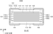
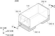
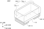
도 6은 본 발명의 일 실시예에 따른 적층형 전자 부품(1001)의 사시도를 개략적으로 도시한 것이며, 도 7은 도 6의 II-II`에 따른 단면도이다. FIG. 6 is a schematic perspective view of a multilayer
도 6 및 도 7을 참조하면, 본 발명의 일 실시예에 따른 적층형 전자 부품(1001)은 제1 및 제2 도금층(141-1, 142-1)이 제1 면의 연장선(E1) 이하로 배치될 수 있다. 이에 따라, 실장 시 솔더의 높이를 최소화할 수 있으며 실장 공간을 최소화할 수 있다. 6 and 7 , in the multilayer
또한, 커버층(151-1)은 제1 면의 연장선 이하까지 연장되어 제1 및 제2 도금층(141-1, 142-1)과 접하도록 배치될 수 있다. In addition, the cover layer 151-1 may be disposed to extend below the extension line of the first surface and contact the first and second plating layers 141-1 and 142-1.
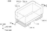
도 8을 본 발명의 일 실시예에 따른 적층형 전자 부품(1002)의 사시도를 개략적으로 도시한 것이며, 도 9는 도 8의 III-III`에 따른 단면도이다. FIG. 8 schematically illustrates a perspective view of a multilayer
도 8 및 도 9를 참조하면, 본 발명의 일 실시예에 따른 적층형 전자 부품(1002)은 제1 면(1) 상에 배치되며 제1 밴드부(131b)와 제2 밴드부(132b) 사이에 배치되는 추가 절연층(161)을 더 포함할 수 있다. 이에 따라, 고압 전류 하에서 제1 밴드부(131b)와 제2 밴드부(132b) 사이에서 발생할 수 있는 누설 전류 등을 방지할 수 있다. Referring to FIGS. 8 and 9 , the multilayer
추가 절연층(161)의 종류는 특별히 한정할 필요는 없다. 예를 들어, 추가 절연층(161)은 에폭시 수지, 아크릴 수지, 에틸 셀룰로우스(Ethyl Cellulose) 등에서 선택된 1종 이상을 포함하거나, 글래스를 포함할 수 있다. 또한, 추가 절연층(161)은 고분자 수지 이외에 TiO2, BaTiO3, Al2O3, SiO2, BaO 등에서 선택된 1종 이상을 첨가제로 포함할 수 있다. 이에 따라, 바디 또는 외부 전극과의 결합력을 향상시킬 수 있다. The type of the additional insulating
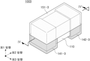
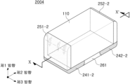
도 10은 본 발명의 일 실시예에 따른 적층형 전자 부품(1003)의 사시도를 개략적으로 도시한 것이며, 도 11은 도 10의 IV-IV`에 따른 단면도이다. 10 is a schematic perspective view of a multilayer
도 10 및 도 11을 참조하면, 일 실시예에 따른 적층형 전자 부품(1003)은 제1 면(1)으로부터 상기 제1 및 제2 내부 전극(121, 122) 중 상기 제1 면(1)에 가장 가깝게 배치된 내부 전극까지의 제1 방향 평균 크기를 H1, 상기 제1 면(1)의 연장선으로부터 상기 제1 및 제2 접속부(131a, 132a) 상에 배치된 도금층(141-3, 142-3)의 끝단까지의 제1 방향 평균 크기를 H2라 할 때, H1<H2를 만족할 수 있다. 이에 따라, 실장시 솔더와 접하는 면적을 증가시켜 고착 강도를 향상시킬 수 있다. Referring to FIGS. 10 and 11 , a multilayer
보다 바람직하게는 바디(110)의 제1 방향 평균 크기를 T라 할 때, H2<T/2를 만족할 수 있다. 즉, H1<H2<T/2를 만족할 수 있다. H2가 T/2 이상인 경우에는 커버층에 의한 내습 신뢰성 향상 효과가 저하될 우려가 있기 때문이다. More preferably, when T is the average size of the
H1, H2 및 T는 바디(110)를 제3 방향으로 등간격을 가지는 5개 지점에서 제1 및 제2 방향으로 절단한 단면(L-T 단면)에서 측정한 값들을 평균한 값일 수 있다. H1은 각 단면에서 제1 면(1)에 가장 가깝게 배치된 내부 전극이 외부 전극과 연결되는 지점에서 측정한 값들을 평균한 값일 수 있으며, H2는 각 단면에서 외부 전극과 접하는 도금층의 끝단을 기준으로 측정한 값들을 평균한 값일 수 있고, H1 및 H2 측정시 기준이 되는 제1 면의 연장선은 동일할 수 있다. 또한, T는 각 단면에서 바디(110)의 제1 방향 최대 크기를 측정한 후 평균한 값일 수 있다.H1, H2, and T may be an average of values measured in cross sections (L-T cross sections) obtained by cutting the
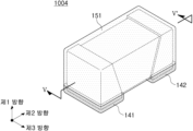
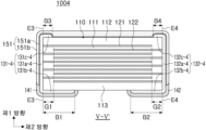
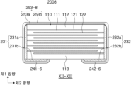
도 12는 본 발명의 일 실시예에 따른 적층형 전자 부품(1004)의 사시도를 개략적으로 도시한 것이며 도 13은 도 12의 V-V`에 따른 단면도이다. FIG. 12 schematically illustrates a perspective view of a multilayer
도 12 및 도 13을 참조하면, 본 발명의 일 실시예에 따른 적층형 전자 부품(1004)은 제1 밴드부(131b-4)의 평균 길이(B1)가 제3 밴드부(131c-4)의 평균 길이(B3)보다 길 수 있으며, 제2 밴드부(132b-4)의 평균 길이가 제4 밴드부(132c-4)의 평균 길이(B4)보다 길 수 있다. 이에 따라, 실장시 솔더와 접하는 면적을 증가시켜 고착 강도를 향상시킬 수 있다. 12 and 13, in the multilayer
보다 상세하게는 제3 면(3)의 연장선으로부터 상기 제1 밴드부(131b-4)의 끝단까지의 상기 제2 방향 평균 크기를 B1, 상기 제4 면(4)의 연장선으로부터 상기 제2 밴드부(132b-4)의 끝단까지의 상기 제2 방향 평균 크기를 B2, 상기 제3 면(3)의 연장선으로부터 상기 제3 밴드부(131c-4)의 끝단까지의 상기 제2 방향 평균 크기를 B3, 상기 제4 면(4)의 연장선으로부터 상기 제4 밴드부(132c-4)의 끝단까지의 상기 제2 방향 평균 크기를 B4라 할 때, B3<B1 및 B4<B2를 만족할 수 있다. More specifically, the average size in the second direction from the extension line of the
이 때, 바디(110)의 제2 방향 평균 크기를 L이라 할 때, 0.2≤B1/L≤0.4 및 0.2≤B2/L≤0.4를 만족할 수 있다. At this time, when L is the average size of the
B1, B2, B3, B4 및 L은 바디(110)를 제3 방향으로 등간격을 가지는 5개 지점에서 제1 및 제2 방향으로 절단한 단면(L-T 단면)에서 측정한 값들을 평균한 값일 수 있다.B1, B2, B3, B4, and L may be values obtained by averaging values measured in cross sections (L-T cross sections) obtained by cutting the
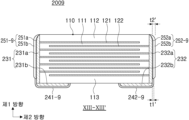
또한, 제1 외부 전극(131-4)은 제1 접속부(131a-4)로부터 제5 및 제6 면의 일부까지 연장되는 제1 측면 밴드부를 포함할 수 있으며, 제2 외부 전극(132-4)은 제2 접속부(132a-4)로부터 제5 및 제6 면의 일부까지 연장되는 제2 측면 밴드부를 포함할 수 있다. 이 때, 상기 제1 및 제2 측면 밴드부의 제2 방향 크기는 제1 면에 가까워질수록 점차 커질 수 있다. 즉, 상기 제1 및 제2 측면 밴드부는 테이퍼 형상 내지 사다리꼴 형상으로 배치될 수 있다.In addition, the first external electrode 131-4 may include a first side band portion extending from the
나아가, 상기 제3 면의 연장선으로부터 상기 제3 밴드부(131c-4)의 끝단까지의 상기 제2 방향 평균 크기를 B3, 상기 제4 면의 연장선으로부터 상기 제4 밴드부(132c-4)의 끝단까지의 상기 제2 방향 평균 크기를 B4, 상기 제3 면과 상기 제2 내부 전극(122)이 이격된 영역의 제2 방향 평균 크기를 G1, 상기 제4 면과 상기 제1 내부 전극(121)이 이격된 영역의 제2 방향 평균 크기를 G2라 할 때, B3≤G1 및 B4≤G2를 만족할 수 있다. 이에 따라, 외부 전극이 차지하는 부피를 최소화하여 적층형 전자 부품(1004)의 단위 부피당 용량을 증가시킬 수 있다.Furthermore, the average size in the second direction from the extension line of the third surface to the end of the
상기 G1 및 G2는 바디를 제3 방향 중앙에서 제1 및 제2 방향으로 절단한 단면에서, 제1 방향 중앙부에 위치한 임의의 5개의 제2 내부 전극에 대하여 측정한 제3 면까지 이격된 제2 방향 크기를 평균한 값은 G1으로 하고, 제1 방향 중앙부에 위치한 임의의 5개의 제1 내부 전극에 대하여 측정한 제4 면까지 이격된 영역의 제2 방향 크기를 평균한 값을 G2로 할 수 있다. The G1 and G2 are the second spaced apart from the cross section of the body in the first and second directions from the center in the third direction to the third surface measured with respect to five arbitrary second internal electrodes located at the center in the first direction. A value obtained by averaging the sizes in the 1st direction is G1, and a value obtained by averaging the sizes in the 2nd direction of the area spaced up to the 4th surface measured for any five first internal electrodes located at the center of the 1st direction is G2. there is.
나아가, 바디(110)를 제3 방향으로 등간격을 가지는 5개 지점에서 제1 및 제2 방향으로 절단한 단면(L-T 단면)에서 G1 및 G2를 구하고, 그들을 평균한 값을 G1 및 G2로 하여 더욱 일반화할 수 있다.Furthermore, G1 and G2 are obtained from cross sections (L-T cross sections) obtained by cutting the
다만, 본 발명을 B3≤G1 및 B4≤G2으로 한정하려는 의도는 아니며, B3≥G1 및 B4≥G2를 만족하는 경우도 본 발명의 일 실시예로 포함될 수 있다. 따라서, 일 실시예에서, 제3 면의 연장선으로부터 제3 밴드부의 끝단까지의 상기 제2 방향 평균 크기를 B3, 상기 제4 면의 연장선으로부터 상기 제4 밴드부의 끝단까지의 상기 제2 방향 평균 크기를 B4, 제3 면과 상기 제2 내부 전극이 이격된 영역의 제2 방향 평균 크기를 G1, 제4 면과 상기 제1 내부 전극이 이격된 영역의 제2 방향 평균 크기를 G2라 할 때, B3≥G1 및 B4≥G2를 만족할 수 있다. However, it is not intended to limit the present invention to B3≤G1 and B4≤G2, and cases satisfying B3≥G1 and B4≥G2 may also be included as an embodiment of the present invention. Therefore, in one embodiment, B3 is the average size in the second direction from the extension line of the third surface to the end of the third band portion, and the average size in the second direction from the extension line of the fourth surface to the end of the fourth band portion. When B4, the average size in the second direction of the area where the third surface and the second internal electrode are spaced apart is G1, and the average size in the second direction of the area where the fourth surface and the first inner electrode are spaced apart is G2, B3≥G1 and B4≥G2 can be satisfied.
일 실시예에서, 상기 제3 면(E3)의 연장선으로부터 상기 제1 밴드부의 끝단까지의 상기 제2 방향 평균 크기를 B1, 상기 제4 면의 연장선으로부터 상기 제2 밴드부의 끝단까지의 상기 제2 방향 평균 크기를 B2라 할 때, B1≥G1 및 B2≥G2를 만족할 수 있다. 이에 따라, 적층형 전자 부품(2009)의 기판(180)과의 고착 강도를 향상시킬 수 있다. In one embodiment, the average size in the second direction from the extension line of the third surface (E3) to the end of the first band part B1, the second from the extension line of the fourth surface to the end of the second band part Assuming that the direction average magnitude is B2, B1≥G1 and B2≥G2 may be satisfied. Accordingly, the bonding strength of the multilayer
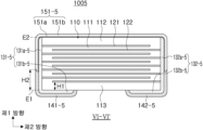
도 14는 본 발명의 일 실시예에 따른 적층형 전자 부품(1005)의 사시도를 개략적으로 도시한 것이며 도 15는 도 14의 VI-VI`에 따른 단면도이다. FIG. 14 schematically illustrates a perspective view of a multilayer
도 14 및 도 15를 참조하면, 본 발명의 일 실시예에 따른 적층형 전자 부품(1005)의 제1 및 제2 외부 전극(131-5, 132-5)은 제2 면상에는 배치되지 않고, 제3, 제4 및 제1 면에 배치되어 L자 형태를 가질 수 있다. 즉, 제1 및 제2 외부 전극(131-5, 132-5)은 제2 면의 연장선 이하에 배치될 수 있다. 14 and 15, the first and second external electrodes 131-5 and 132-5 of the multilayer
제1 외부 전극(131-5)은 제3 면(3)에 배치되는 제1 접속부(131a-5), 상기 제1 접속부(131a-5)로부터 상기 제1 면(1)의 일부까지 연장되는 제1 밴드부(131b-5)를 포함할 수 있으며, 제2 외부 전극(132-5)은 제4 면(4)에 배치되는 제2 접속부(132a-5), 상기 제2 접속부(132a-5)로부터 상기 제1 면(1)의 일부까지 연장되는 제2 밴드부(132b-5)를 포함할 수 있다. 제2 면(2) 상에는 외부 전극(131-5, 132-5)가 배치되지 않아, 커버층(151-5)이 제2 면(2)의 전부를 덮도록 배치될 수 있다. 이에 따라, 외부 전극(131-5, 132-5)이 차지하는 부피를 최소화할 수 있기 때문에 적층 전자 부품(1005)의 단위 부피당 용량을 보다 향상시킬 수 있다. 다만, 커버층(151-5)이 제2 면(2)의 전부를 덮는 형태로 한정할 필요는 없으며, 커버층이 제2 면(2)의 일부 또는 전부를 덮지 않고, 분리되어 제1 및 제2 접속부(131a-5, 132a-5)를 각각 덮고 있는 형태를 가질 수도 있다. The first external electrode 131-5 includes a
또한, 커버층(151-5)이 제5 면 및 제6 면의 일부를 덮도록 배치되어 신뢰성을 보다 향상시킬 수 있다. 이때, 커버층(151-5)에 덮이지 않은 제5 면 및 제6 면의 일부는 외부로 노출될 수 있다. In addition, since the cover layer 151 - 5 is disposed to cover portions of the fifth and sixth surfaces, reliability can be further improved. In this case, portions of the fifth and sixth surfaces not covered by the cover layer 151-5 may be exposed to the outside.
나아가, 커버층(151-5)은 제5 면 및 제6 면의 전체를 덮도록 배치될 수 있으며, 이 경우 제5 면 및 제6 면이 외부로 노출되지 않아 내습 신뢰성을 보다 더 향상시킬 수 있다.Furthermore, the cover layer 151-5 may be disposed to cover the entirety of the fifth and sixth surfaces. In this case, the fifth and sixth surfaces are not exposed to the outside, thereby further improving moisture resistance. there is.
제1 밴드부(131b-5) 상에는 제1 도금층(141-5), 제2 밴드부(132b-5) 상에는 제2 도금층(142-5)이 배치되며, 제1 및 제2 도금층(141-5, 142-5)은 제1 및 제2 접속부(132a-5. 132b-5) 상의 일부까지 연장되어 배치될 수 있다. A first plating layer 141-5 is disposed on the
이때, 제5 및 제6 면(5, 6) 상에도 외부 전극(131-5, 132-5)이 배치되지 않을 수 있다. 즉, 외부 전극(131-5, 132-5)이 제3, 제4 및 제1 면 상에만 배치되는 형태를 가질 수 있다. At this time, the external electrodes 131 - 5 and 132 - 5 may not be disposed on the fifth and
제1 면(1)으로부터 상기 제1 및 제2 내부 전극(121, 122) 중 상기 제1 면(1)에 가장 가깝게 배치된 내부 전극까지의 제1 방향 평균 크기를 H1, 상기 제1 면(1)의 연장선으로부터 상기 제1 및 제2 접속부(131a-5, 132a-5) 상에 배치된 도금층(141-5, 142-5)의 끝단까지의 제1 방향 평균 크기를 H2라 할 때, H1<H2를 만족할 수 있다. 이에 따라, 실장시 솔더와 접하는 면적을 증가시켜 고착 강도를 향상시킬 수 있으며, 외부 전극(131-5, 132-5)과 도금층(141-5, 142-5)이 접하는 면적을 증가시켜 ESR(Equivalent Series Resistance)가 증가되는 것을 억제할 수 있다. The average size in the first direction from the
보다 바람직하게는 바디(110)의 제1 방향 평균 크기를 T라 할 때, H2<T/2를 만족할 수 있다. 즉, H1<H2<T/2를 만족할 수 있다. H2가 T/2 이상인 경우에는 커버층에 의한 내습 신뢰성 향상 효과가 저하될 우려가 있기 때문이다. More preferably, when T is the average size of the
또한, 제1 및 제2 도금층(141-5, 142-5)은 제3 면 및 제4 면에서 커버층(151-1)의 일부를 덮도록 배치될 수 있다. 즉, 도금층(141-5, 142-5)이 제3 면 및 제4 면에서 커버층(151-5)의 끝단을 덮도록 배치될 수 있다. 이에 따라 커버층(151-5)과 도금층(141-5, 142-5)의 결합력을 강화하여 적층형 전자 부품(1005)의 신뢰성을 향상시킬 수 있다.Also, the first and second plating layers 141-5 and 142-5 may be disposed to cover portions of the cover layer 151-1 on the third and fourth surfaces. That is, the plating layers 141-5 and 142-5 may be disposed to cover the ends of the cover layer 151-5 on the third and fourth surfaces. Accordingly, the reliability of the multilayer
또한, 커버층(151-5)는 제3 면 및 제4 면에서 제1 및 제2 도금층(141-5, 142-5)의 일부를 덮도록 배치될 수 있다. 즉, 커버층(151-5)이 제3 면 및 제4 면에서 도금층(141-5, 142-5)의 끝단을 덮도록 배치될 수 있다. 이에 따라, 커버층(151-5)과 도금층(141-5, 142-5)의 결합력을 강화하여 적층형 전자 부품(1005)의 신뢰성을 향상시킬 수 있다.Also, the cover layer 151-5 may be disposed to cover portions of the first and second plating layers 141-5 and 142-5 on the third and fourth surfaces. That is, the cover layer 151-5 may be disposed to cover the ends of the plating layers 141-5 and 142-5 on the third and fourth surfaces. Accordingly, the reliability of the multilayer
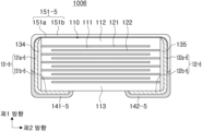
도 16은 도 14의 변형예를 도시한 것이다. 도 16을 참조하면, 본 발명의 일 실시예에 따른 적층형 전자 부품(1005)의 변형예(1006)는 제1 접속부(131a-6)와 제3 면 사이에는 제1 추가 전극층(134)이 배치될 수 있으며, 제2 접속부(132a-6)와 제4 면 사이에는 제2 추가 전극층(135)이 배치될 수 있다. 제1 추가 전극층(134)은 제3 면을 벗어나지 않는 범위에서 배치될 수 있으며, 제2 추가 전극층(135)은 제4 면을 벗어나지 않는 범위에서 배치될 수 있다. 제1 및 제2 추가 전극층(134, 135)은 내부 전극(121, 122)과 외부 전극(131-6, 132-6) 간의 전기적 연결성을 향상시킬 수 있으며, 외부 전극(131-6, 132-6)과의 결합력이 우수하여 외부 전극(131-6, 132-6)의 기계적 결합력을 보다 향상 시키는 역할을 수행할 수 있다. FIG. 16 shows a modified example of FIG. 14 . Referring to FIG. 16 , in a modified example 1006 of the multilayer
제1 및 제2 외부 전극(131-6, 132-6)은 제2 면 상에 제1 및 제2 외부 전극이 배치되지 않은 L자 형태를 가질 수 있다. The first and second external electrodes 131 - 6 and 132 - 6 may have an L shape in which the first and second external electrodes are not disposed on the second surface.
제1 외부 전극(131-6)은 제1 추가 전극층(134) 상에 배치되는 제1 접속부(131a-6), 상기 제1 접속부(131a-6)로부터 상기 제1 면(1)의 일부까지 연장되는 제1 밴드부(131b-6)를 포함할 수 있으며, 제2 외부 전극(132-6)은 제2 추가 전극층(135) 상에 배치되는 제2 접속부(132a-6), 상기 제2 접속부(132a-6)로부터 상기 제1 면(1)의 일부까지 연장되는 제2 밴드부(132b-6)를 포함할 수 있다. The first external electrode 131-6 extends from the
한편, 제1 및 제2 추가 전극층(131-6, 132-6)은 금속 등과 같이 전기 전도성을 갖는 것이라면 어떠한 물질을 사용하여 형성될 수 있고, 전기적 특성, 구조적 안정성 등을 고려하여 구체적인 물질이 결정될 수 있다. 또한, 제1 및 제2 추가 전극층(131-6, 132-6)은 도전성 금속 및 글라스를 포함한 소성(firing) 전극이거나, 도전성 금속 및 수지를 포함한 수지계 전극일 수 있다. 또한, 제1 및 제2 추가 전극층(131-6, 132-6)은 바디 상에 도전성 금속을 포함한 시트를 전사하는 방식으로 형성된 것일 수 있다. Meanwhile, the first and second additional electrode layers 131-6 and 132-6 may be formed using any material as long as they have electrical conductivity, such as metal, and specific materials may be determined in consideration of electrical characteristics, structural stability, and the like. can In addition, the first and second additional electrode layers 131-6 and 132-6 may be firing electrodes including conductive metal and glass or resin-based electrodes including conductive metal and resin. Also, the first and second additional electrode layers 131-6 and 132-6 may be formed by transferring a sheet including a conductive metal onto the body.
제1 및 제2 추가 전극층(131-6, 132-6)에 포함되는 도전성 금속으로 전기 전도성이 우수한 재료를 사용할 수 있으며 특별히 한정하지 않는다. 예를 들어, 도전성 금속은 Cu, Ni, Pd, Ag, Sn, Cr 및 그들의 합금 중 하나 이상일 수 있다. 바람직하게는 제1 및 제2 추가 전극층(131-6, 132-6)은 Ni 및 Ni 합금 중 하나 이상을 포함할 수 있으며, 이에 따라, Ni을 포함하는 내부 전극(121, 122)과의 연결성을 보다 향상시킬 수 있다. A material having excellent electrical conductivity may be used as the conductive metal included in the first and second additional electrode layers 131-6 and 132-6, and is not particularly limited. For example, the conductive metal may be one or more of Cu, Ni, Pd, Ag, Sn, Cr, and alloys thereof. Preferably, the first and second additional electrode layers 131-6 and 132-6 may include at least one of Ni and a Ni alloy, and thus, connectivity with the
도 17은 본 발명의 일 실시예에 따른 적층형 전자 부품(1007)의 사시도를 개략적으로 도시한 것이며 도 18은 도 17의 VII-VII`에 따른 단면도이다. FIG. 17 schematically illustrates a perspective view of a multilayer
도 17 및 도 18을 참조하면, 본 발명의 일 실시예에 따른 적층형 전자 부품(1007)의 제1 및 제2 도금층(141-6, 142-6)의 평균 두께(t1)은 커버층(151-6)의 평균 두께(t2)보다 얇은 형태일 수 있다. 17 and 18, the average thickness t1 of the first and second plating layers 141-6 and 142-6 of the multilayer
커버층(151-6)은 외부의 수분 침투 또는 도금액의 침투를 방지하는 역할을 하나, 도금층(141-6, 142-6)과의 연결성이 약해 도금층(141-6, 142-6)의 딜라미네이션(delamination)의 원인이 될 수 있다. 도금층이 딜라미네이션되는 경우 기판(180)과의 고착 강도가 저하될 수 있다. 여기서 도금층(141-6, 142-6)의 딜라미네이션이란 도금층이 일부 떨어지거나 외부 전극(131-5, 132-5)과 물리적으로 분리되는 것을 의미할 수 있다. 도금층과 커버층의 연결성이 약하기 때문에 커버층과 도금층의 계면의 틈이 벌어지거나 이물질이 침투할 가능성이 높아지고, 외부 충격 등에 취약하게 되어 딜라미네이션될 가능성이 높아질 수 있다. The cover layer 151-6 serves to prevent the permeation of external moisture or plating solution, but the connection with the plating layers 141-6 and 142-6 is weak, resulting in damage to the plating layers 141-6 and 142-6. It can cause delamination. When the plating layer is delaminated, adhesion strength with the
본 발명의 일 실시예에 따르면 도금층의 평균 두께(t1)를 커버층의 평균 두께(t2)보다 얇게하여 도금층과 커버층이 맞닿는 면적을 줄일 수 있으며, 이에 따라 딜라미네이션의 발생을 억제하여 적층형 전자 부품(1000)의 기판(180)과의 고착 강도를 향상시킬 수 있다. According to an embodiment of the present invention, by making the average thickness t1 of the plating layer thinner than the average thickness t2 of the cover layer, the contact area between the plating layer and the cover layer can be reduced, thereby suppressing the occurrence of delamination, thereby suppressing the multilayer electronic Adhesion strength of the
제1 및 제2 도금층(141-6, 142-6)의 평균 두께(t1)는 제1 및 제2 접속부(131a-5, 132a-5) 또는 제1 및 제2 밴드부(131b-5, 132b-5) 상의 등간격의 5개 지점에서 측정한 두께를 평균한 값일 수 있으며, 커버층(151-6)의 평균 두께(t2)는 제1 및 제2 접속부(131a-5, 132a-5) 상의 등간격의 5개 지점에서 측정한 두께를 평균한 값일 수 있다. The average thickness t1 of the first and second plating layers 141-6 and 142-6 is determined by the first and
도 19는 본 발명의 일 실시예에 따른 적층형 전자 부품(2000)의 사시도를 개략적으로 도시한 것이다. 도 20은 도 19의 VIII-VIII`에 따른 단면도이다. 19 is a schematic perspective view of a multilayer
이하, 도 19 및 도 20를 참조하여 본 발명의 일 실시예에 따른 적층형 전자 부품(2000)에 대하여 상세히 설명하도록 한다. 다만, 상술한 내용과 중복되는 내용은 중복된 설명을 피하기 위하여 생략될 수 있다. Hereinafter, the multilayer
본 발명의 일 실시예에 따른 적층형 전자 부품(2000)은, 유전체층(111), 상기 유전체층을 사이에 두고 번갈아 배치되는 제1 및 제2 내부 전극(121, 122)을 포함하며, 제1 방향으로 대향하는 제1 및 제2 면(1, 2), 상기 제1 및 제2 면과 연결되고 제2 방향으로 대향하는 제3 및 제4 면(3, 4), 상기 제1 내지 제4 면과 연결되고 제3 방향으로 대향하는 제5 및 제6 면(5, 6)을 포함하는 바디(110); 상기 제3 면에 배치되는 제1 연결 전극(231a) 및 상기 제1 면에 배치되어 상기 제1 연결 전극과 연결되는 제1 밴드 전극(231b)을 포함하는 제1 외부 전극(231); 상기 제4 면에 배치되는 제2 연결 전극(232a) 및 상기 제1 면에 배치되어 상기 제2 연결 전극과 연결되는 제2 밴드 전극(232b)을 포함하는 제2 외부 전극(232); 상기 제1 연결 전극 상에 배치되는 제1 커버층(251); 상기 제2 연결 전극 상에 배치되는 제2 커버층(252); 상기 제1 밴드 전극 상에 배치되는 제1 도금층(241); 및 상기 제2 밴드 전극 상에 배치되는 제2 도금층(242); 을 포함하며, 상기 제1 커버층(251)은 친수성을 가지는 제1 베이스층(251a) 및 상기 제1 베이스층(251a) 상에 배치된 제1 절연층(251b)를 포함하고, 제2 커버층(252)은 친수성을 가지는 제2 베이스층(252a) 및 상기 제2 베이스층(252a) 상에 배치된 제2 절연층(252b)를 포함할 수 있다. A multilayer
제1 연결 전극(231a)은 제3 면(3)에 배치되어 제1 내부 전극(121)과 연결되며, 제2 연결 전극(231b)은 제4 면(4)에 배치되어 제2 내부 전극(122)과 연결될 수 있다. 또한, 제1 연결 전극(231a`) 상에는 제1 커버층(251)이 배치되고, 제2 연결 전극(232a) 상에는 제2 커버층(252)이 배치될 수 있다. The
종래에는 외부 전극을 형성할 때 도전성 금속이 포함된 페이스트를 사용하여, 바디의 내부 전극이 노출된 면을 페이스트에 딥핑(dipping)하는 방법이 주로 사용되었다. 하지만 딥핑(dipping) 공법에 의하여 형성된 외부 전극은 두께 방향 중앙부에서의 외부 전극의 두께가 너무 두꺼울 수 있었다. 또한, 이러한 딥핑(dipping) 공법에 따른 외부 전극의 두께 불균형 문제가 아니더라도, 바디의 제3 및 제4 면으로 내부 전극이 노출되기 때문에 외부 전극을 통한 수분 및 도금액 침투를 억제하기 위해서 제3 및 제4 면에 배치된 외부 전극의 두께가 일정 이상이 되도록 형성하였다. Conventionally, when forming external electrodes, a method of dipping the surface of the body where internal electrodes are exposed using a paste containing a conductive metal has been mainly used. However, in the case of the external electrode formed by the dipping method, the thickness of the external electrode at the central portion in the thickness direction may be too thick. In addition, even if the thickness imbalance of the external electrodes according to the dipping method is not a problem, since the internal electrodes are exposed through the third and fourth surfaces of the body, in order to suppress penetration of moisture and plating solution through the external electrodes, the third and fourth electrodes are exposed. The external electrodes disposed on the four surfaces were formed to have a certain thickness or more.
반면에, 본 발명에서는 연결 전극(231a, 232a) 상에 커버층(251, 252)을 배치하기 때문에 내부 전극이 노출되는 제3 및 제4 면에서의 연결 전극(231a, 232a) 두께를 얇게 해도 충분한 신뢰성을 확보할 수 있다. On the other hand, in the present invention, since the cover layers 251 and 252 are disposed on the
제1 및 제2 연결 전극(231a, 232a)은 각각 제3 및 제4 면에 대응하는 형태일 수 있으며, 제1 및 제2 연결 전극(231a, 232a)에서 바디(110)를 향하는 면은 바디(110)의 제3 및 제4 면과 각각 동일한 면적을 가질 수 있다. 제1 및 제2 연결 전극(231a, 232a)은 각각 제3 및 제4 면(3, 4)을 벗어나지 않는 범위에서 배치될 수 있다. 연결 전극(231a, 232a)은 바디(110)의 제1, 제2, 제5 및 제6 면(1, 2, 5, 6)으로 연장되지 않도록 배치될 수 있다. 구체적으로, 일 실시예에서 제1 및 제2 연결 전극(231a, 232a)은 제5 및 제6 면과 이격되어 배치될 수 있다. 이에 따라 내부 전극(121, 122)과 외부 전극(231, 232) 간의 충분한 연결성을 확보하면서도 외부 전극이 차지하는 부피를 최소화 하여 적층형 전자 부품(2000)의 단위 부피당 용량을 증가시킬 수 있다.The first and
이런 관점에서, 상기 제1 및 제2 연결전극(231a, 232a)는 상기 제2 면(2)과 이격되어 배치될 수 있다. 즉, 외부 전극(231, 232)이 제2 면 상에는 배치되지 않음에 따라 외부 전극(231, 232)이 차지하는 부피를 더욱 최소화 하여 적층형 전자 부품(2000)의 단위 부피당 용량을 더욱 증가시킬 수 있다.In this respect, the first and
다만, 연결 전극(231a, 232a)은 바디(110)의 코너로 연장되어 코너 상에 배치된 코너부를 포함할 수 있다. 즉, 일 실시예에서, 제1 연결 전극은 상기 제1-3 코너 및 제2-3 코너 상으로 연장되어 배치되는 코너부를 포함하며, 상기 제2 연결 전극은 상기 제1-4 코너 및 제2-4 코너 상으로 연장되어 배치되는 코너부를 포함할 수 있다.However, the
또한, 연결 전극(231a, 232a)은 종래 딥핑 방식에 의해 형성된 외부 전극 대비 균일하고 얇은 두께를 가질 수 있다. In addition, the
연결 전극(231a, 232a)을 형성하는 방법은 특별히 제한할 필요는 없으나, 예를 들어, 도전성 금속, 바인더와 같은 유기물질 등을 포함하는 시트를 제3 및 제4 면에 전사하는 방식으로 형성할 수 있으나 이에 제한되는 것은 아니며, 도전성 금속을 제3 및 제4 면에 도금하여 형성할 수 있다. 즉, 연결 전극(231a, 232a)는 도전성 금속을 소성한 소성층 이거나 도금층일 수 있다.The method of forming the
연결 전극(231a, 232a)의 두께는 특별히 한정하지 않으나, 예를 들어 2~7μm일 수 있다. 여기서, 연결 전극(231a, 232a)의 두께란 최대 두께를 의미할 수 있으며, 연결 전극(231a, 232a)의 제2 방향 크기를 의미할 수 있다. The thickness of the
일 실시예에서, 제1 및 제2 연결 전극(231a, 232a)은 내부 전극(121, 122)에 포함된 금속과 동일한 금속 및 글라스를 포함할 수 있다. 제1 및 제2 연결 전극(231a, 232a)이 내부 전극(121, 122)에 포함된 금속과 동일한 금속을 포함함에 따라 내부 전극(121, 122)과의 전기적 연결성을 향상시킬 수 있으며, 제1 및 제2 연결 전극(231a, 232a)이 글라스를 포함함에 따라 바디(110) 및/또는 커버층(251, 252)과의 결합력을 향상시킬 수 있다. 이때, 내부 전극(121, 122)에 포함된 금속과 동일한 금속은 Ni일 수 있다. In one embodiment, the first and
제1 및 제2 커버층(251, 252)은 각각 제1 및 제2 연결 전극(231a, 232a) 상에 배치되어 제1 및 제2 연결 전극(231a, 232a) 상에 도금층이 형성되는 것을 방지하는 역할을 수행할 수 있다. 또한, 제1 및 제2 커버층(251, 252)은 실링 특성을 향상시켜 외부로부터 수분이나 도금액 등이 침투하는 것을 최소화하는 역할을 수행할 수 있다. The first and second cover layers 251 and 252 are disposed on the first and
제1 커버층(251)은 친수성을 가지는 제1 베이스층(251a) 및 상기 제1 베이스층(251a) 상에 배치된 제1 절연층(251b)를 포함하고, 제2 커버층(252)은 친수성을 가지는 제2 베이스층(252a) 및 상기 제2 베이스층(252a) 상에 배치된 제2 절연층(252b)를 포함할 수 있다. The
제1 및 제2 밴드 전극(231b, 232b)은 바디(110)의 제1 면(1)에 배치될 수 있다. 제1 및 제2 밴드 전극(231b, 232b)은 각각 제1 및 제2 연결 전극(231a, 232a)과 접촉함으로써, 제1 및 제2 내부 전극(121, 122)과 각각 전기적으로 연결될 수 있다. The first and
종래의 딥핑(dipping) 공법에 의하여 형성된 외부 전극은 제3 및 제4 면에서 두껍게 형성되고 제1, 제2, 제5 및 제6 면에도 일부 연장되어 형성됨에 따라 유효 부피율을 높게 확보하기 어려운 문제점이 있었다. External electrodes formed by the conventional dipping method are formed thickly on the third and fourth surfaces and partially extended to the first, second, fifth, and sixth surfaces, so it is difficult to secure a high effective volume ratio. There was a problem.
반면에, 본 발명의 일 실시예에 따르면, 내부 전극이 노출된 면에는 제1 및 제2 연결 전극(231a, 232a)을 배치하고, 기판에 실장되는 면에는 제1 및 제2 밴드 전극(231b, 232b)을 배치함에 따라 유효 부피율을 높게 확보할 수 있다. On the other hand, according to an embodiment of the present invention, the first and
한편, 내부 전극(121, 122)이 제1 방향으로 적층되어 있는 경우에는 내부 전극(121, 122)이 실장 면과 평행하도록 적층형 전자 부품(2000)을 기판에 수평 실장할 수 있다. 다만 본 발명이 수평 실장인 경우에 한정되는 것은 아니며, 내부 전극(121, 122)을 제3 방향으로 적층하는 경우에는 내부 전극(121, 122)이 실장 면과 수직하도록 기판에 적층형 전자 부품을 수직 실장할 수 있다. Meanwhile, when the
제1 및 제2 밴드 전극(231b, 232b)은 금속 등과 같이 전기 전도성을 갖는 것이라면 어떠한 물질을 사용하여 형성될 수 있고, 전기적 특성, 구조적 안정성 등을 고려하여 구체적인 물질이 결정될 수 있다. 예를 들어, 제1 및 제2 밴드 전극(231, 232b)은 도전성 금속 및 글라스를 포함한 소성(firing) 전극일 수 있으며, 바디의 제1 면에 도전성 금속 및 글라스를 포함하는 페이스트를 도포하는 방식을 이용하여 형성할 수 있으나, 이에 제한되는 것은 아니며, 도전성 금속을 바디의 제1 면에 도금한 도금층일 수 있다.The first and
제1 및 제2 밴드 전극(231b, 232b)에 포함되는 도전성 금속으로 전기 전도성이 우수한 재료를 사용할 수 있으며 특별히 한정하지 않는다. 예를 들어, 도전성 금속은 니켈(Ni), 구리(Cu) 및 그들의 합금 중 하나 이상일 수 있으며, 내부 전극(121, 122)에 포함된 금속과 동일한 금속을 포함할 수 있다. A material having excellent electrical conductivity may be used as the conductive metal included in the first and
한편, 일 실시예에서, 제1 외부 전극(231)은 상기 제2 면(2)에 배치되어 상기 제1 연결 전극(231a)과 연결되는 제3 밴드 전극(미도시)을 더 포함하며, 상기 제2 외부 전극(232)는 상기 제2 면(2)에 배치되어 상기 제2 연결전극(232a)과 연결되는 제4 밴드 전극(미도시)을 더 포함할 수 있다.Meanwhile, in one embodiment, the first
일 실시예에서, 상기 제3 면의 연장선(E3)으로부터 상기 제1 밴드 전극(231b)의 끝단까지의 거리를 B1, 상기 제4 면의 연장선(E4)으로부터 상기 제2 밴드 전극(232b)의 끝단까지의 거리를 B2, 상기 제3 면의 연장선으로부터 상기 제3 밴드 전극(미도시)의 끝단까지의 거리를 B3, 상기 제4 면의 연장선으로부터 상기 제4 밴드 전극(미도시)의 끝단까지의 거리를 B4, 상기 제3 면과 상기 제2 내부 전극(122)이 이격된 영역의 제2 방향 평균 크기를 G1, 상기 제4 면과 상기 제1 내부 전극(121)이 이격된 영역의 제2 방향 평균 크기를 G2라 할 때, B1≥G1, B3≤G1, B2≥G2 및 B4≤G2를 만족할 수 있다. 이에 따라, 외부 전극이 차지하는 부피를 최소화 하여 적층형 전자 부품(2000)의 단위 부피당 용량을 증가 시킴과 동시에 실장 시 솔더와 접하는 면적을 증가시켜 고착 강도를 향상시킬 수 있다.In one embodiment, the distance from the extension line E3 on the third surface to the end of the
다만, 본 발명을 B1≥G1, B3≤G1, B2≥G2 및 B4≤G2으로 한정하려는 의도는 아니며, B1≥G1, B3≥G1, B2≥G2 및 B4≥G2를 만족하는 경우도 본 발명의 일 실시예로 포함될 수 있다. 따라서, 일 실시예에서, 상기 제3 면의 연장선(E3)으로부터 상기 제1 밴드 전극(231b)의 끝단까지의 거리를 B1, 상기 제4 면의 연장선(E4)으로부터 상기 제2 밴드 전극(232b)의 끝단까지의 거리를 B2, 상기 제3 면의 연장선으로부터 상기 제3 밴드 전극(미도시)의 끝단까지의 거리를 B3, 상기 제4 면의 연장선으로부터 상기 제4 밴드 전극(미도시)의 끝단까지의 거리를 B4, 상기 제3 면과 상기 제2 내부 전극(122)이 이격된 영역의 제2 방향 평균 크기를 G1, 상기 제4 면과 상기 제1 내부 전극(121)이 이격된 영역의 제2 방향 평균 크기를 G2라 할 때, B1≥G1, B3≥G1, B2≥G2 및 B4≥G2를 만족할 수 있다. 이에 따라, 제1 및 제2 면 중 어느 한 면을 실장면으로 할 수 있어 실장 편이성을 향상시킬 수 있다. However, it is not intended to limit the present invention to B1≥G1, B3≤G1, B2≥G2 and B4≤G2, and the case of satisfying B1≥G1, B3≥G1, B2≥G2 and B4≥G2 is also the scope of the present invention. may be included in an embodiment. Therefore, in one embodiment, the distance from the extension line E3 on the third surface to the end of the
제1 및 제2 도금층(241, 242)은 제1 및 제2 밴드 전극(231b, 232b) 상에 배치될 수 있다. 제1 및 제2 도금층(241, 242)은 실장 특성을 향상시키는 역할을 수행한다. 제1 및 제2 도금층(241, 242)의 종류는 특별히 한정하지 않으며, Ni, Sn, Pd 및 이들의 합금 중 하나 이상을 포함하는 도금층일 수 있고, 복수의 층으로 형성될 수 있다. The first and second plating layers 241 and 242 may be disposed on the first and
제1 및 제2 도금층(241, 242)에 대한 보다 구체적인 예를 들면, 제1 및 제2 도금층(241, 242)은 Ni 도금층 또는 Sn 도금층일 수 있으며, 제1 및 제2 밴드 전극(231b, 232b) 상에 Ni 도금층 및 Sn 도금층이 순차적으로 형성된 형태일 수 있다. As a more specific example of the first and second plating layers 241 and 242, the first and second plating layers 241 and 242 may be Ni plating layers or Sn plating layers, and the first and
일 실시예에서, 제1 및 제2 도금층(241, 242)은 각각 제1 및 제2 연결 전극(231a, 232a)을 일부 덮도록 연장되어 배치될 수 있다. In one embodiment, the first and second plating layers 241 and 242 may be disposed to extend to partially cover the first and
제1 면(1)으로부터 제1 및 제2 내부 전극(121, 122) 중 제1 면(1)에 가장 가깝게 배치된 내부 전극까지의 제1 방향 평균 크기를 H1, 상기 제1 면(1)의 연장선으로부터 상기 제1 및 제2 연결 전극(231a, 232a) 상에 배치된 제1 및 제2 도금층(241, 242)의 끝단까지의 제1 방향 평균 크기를 H2라 할 때, H1>H2를 만족할 수 있다. 이에 따라, 도금 공정시 도금액이 내부 전극으로 침투하는 것을 억제하여 신뢰성을 향상시킬 수 있다. The average size in the first direction from the
일 실시예에서, 제1 및 제2 커버층(251, 252)은 제1 및 제2 연결 전극(231a, 232a)과 각각 직접 접하도록 배치되며, 제1 및 제2 연결 전극(231a, 232a)은 도전성 금속 및 글라스를 포함할 수 있다. 이에 따라, 제1 및 제2 연결 전극 (231a, 232a)의 외표면 중 커버층(251, 252)이 배치된 영역에는 도금층(241, 242)이 배치되지 않을 수 있기 때문에, 도금액에 의한 외부전극 침식 방지를 효과적으로 억제할 수 있다. In one embodiment, the first and second cover layers 251 and 252 are disposed to directly contact the first and
일 실시예에서, 제1 및 제2 커버층(251, 252)은 제1 및 제2 연결 전극(231a, 232a)과 각각 직접 접하도록 배치되며, 제1 및 제2 연결 전극(231a, 232a)은 도전성 금속 및 수지를 포함할 수 있다. 이에 따라, 제1 및 제2 연결 전극 (231a, 232a)의 외표면 중 커버층(251, 252)이 배치된 영역에는 도금층(241, 242)이 배치되지 않을 수 있기 때문에, 도금액에 의한 외부전극 침식 방지를 효과적으로 억제할 수 있다. In one embodiment, the first and second cover layers 251 and 252 are disposed to directly contact the first and
일 실시예에서, 제1 도금층(241)은 제1 커버층(251)의 제1 외부 전극(231) 상에 배치된 끝단을 덮도록 배치되며, 제2 도금층(242)은 제2 커버층(252)의 제2 외부 전극(232) 상에 배치된 끝단을 덮도록 배치될 수 있다. 이에 따라, 커버층(251, 252)과 도금층(241, 242)의 결합력을 강화하여 적층형 전자 부품(3000)의 신뢰성을 향상시킬 수 있다. 또한, 외부 전극(231, 232) 상에 도금층(241, 242)을 형성하기 전에 제1 및 제2 커버층(251, 252)을 먼저 형성함으로써, 도금층 형성 과정에서의 도금액 침투를 보다 확실히 억제할 수 있다. 도금층보다 커버층을 먼저 형성함에 따라, 도금층(241, 242)이 커버층(251, 252)의 끝단을 덮는 형태를 가질 수 있다. In one embodiment, the
일 실시예에서, 제1 커버층(251)은 제1 도금층(241)의 제1 외부 전극(231) 상에 배치된 끝단을 덮도록 배치되며, 제2 커버층(252)은 제2 도금층(342)의 제2 외부 전극(332) 상에 배치된 끝단을 덮도록 배치될 수 있다. 이에 따라, 커버층(351)과 도금층(341, 342)의 결합력을 강화하여 적층형 전자 부품(3000)의 신뢰성을 향상시킬 수 있다.In one embodiment, the
도 21은 도 19의 변형예를 도시한 것이다. 도 21을 참조하면, 본 발명의 일 실시예에 따른 적층형 전자 부품(2000)의 변형예(2001)는 제1 및 제2 커버층(251-1, 252-1)이 제5 및 제6 면(5, 6)으로 연장되어 서로 연결됨으로써 하나의 커버층(253-1)으로 연결될 수 있다. 이때, 연결된 제1 및 제2 커버층(253-1)이 제5 면 및 제6 면의 일부를 덮도록 배치될 수 있다. FIG. 21 shows a modified example of FIG. 19 . Referring to FIG. 21 , in a modified example 2001 of the multilayer
도 22는 본 발명의 일 실시예에 따른 적층형 전자 부품(2002)의 사시도를 개략적으로 도시한 것이다. 도 23는 도 22의 IX-IX`에 따른 단면도이다. 22 schematically illustrates a perspective view of a multilayer
도 22 및 도 23을 참조하면, 본 발명의 일 실시예에 따른 적층형 전자 부품(2002)은 제1 및 제2 도금층(241-2, 242-2)이 제1 면의 연장선 이하로 배치될 수 있다. 이에 따라, 실장 시 솔더의 높이를 최소화할 수 있으며 실장 공간을 최소화할 수 있다. 22 and 23 , in the multilayer
또한, 제1 및 제2 커버층(251-2, 252-2)은 제1 면의 연장선 이하까지 연장되어 제1 및 제2 도금층(241-2, 242-2)과 접하도록 배치될 수 있다. In addition, the first and second cover layers 251-2 and 252-2 may be disposed to extend below the extension line of the first surface and to contact the first and second plating layers 241-2 and 242-2. .
도 25는 도 22의 변형예를 도시한 것이다. 도 25를 참조하면, 본 발명의 일 실시예에 따른 적층형 전자 부품(2002)의 변형예(2003)는 제1 및 제2 커버층(251-3, 252-3)이 제5 및 제6 면(5, 6)으로 연장되어 서로 연결됨으로써 하나의 커버층(253-3)으로 연결될 수 있다. 이때, 연결된 제1 및 제2 커버층(253-3)이 제5 면 및 제6 면의 전부를 덮도록 배치될 수 있다.FIG. 25 shows a modified example of FIG. 22 . Referring to FIG. 25 , in a modified example 2003 of the multilayer
도 25는 본 발명의 일 실시예에 따른 적층형 전자 부품(2004)의 사시도를 개략적으로 도시한 것이다. 도 26은 도 25의 X-X`에 따른 단면도이다. 25 schematically illustrates a perspective view of a multilayer
도 25 및 도 26을 참조하면, 본 발명의 일 실시예에 따른 적층형 전자 부품(2004)은 제1 면(1) 상에 배치되며 제1 밴드 전극(231b)와 제2 밴드 전극(232b) 사이에 배치되는 추가 절연층(261)을 더 포함할 수 있다. 이에 따라, 고압 전류 하에서 제1 밴드 전극(231b)와 제2 밴드 전극(232b) 사이에서 발생할 수 있는 누설 전류 등을 방지할 수 있다. 25 and 26, the multilayer
추가 절연층(261)의 종류는 특별히 한정할 필요는 없다. 예를 들어, 추가 절연층(261)은 에폭시 수지, 아크릴 수지, 에틸 셀룰로우스(Ethyl Cellulose) 등에서 선택된 1종 이상을 포함하거나, 글래스를 포함할 수 있다. The type of the additional insulating
도 27는 도 25의 변형예를 도시한 것이다. 도 27을 참조하면, 본 발명의 일 실시예에 따른 적층형 전자 부품(2004)의 변형예(2005)는 제1 및 제2 커버층(251-5, 252-5)이 제5 및 제6 면(5, 6)으로 연장되어 서로 연결됨으로써 하나의 커버층(253-5)으로 연결될 수 있다. FIG. 27 shows a modified example of FIG. 25 . Referring to FIG. 27 , in a modified example 2005 of the multilayer
도 28은 본 발명의 일 실시예에 따른 적층형 전자 부품(2006)의 사시도를 개략적으로 도시한 것이다. 도 29는 도 28의 XI-XI`에 따른 단면도이다. 28 schematically illustrates a perspective view of a multilayer
도 28 및 도 29를 참조하면, 일 실시예에 따른 적층형 전자 부품(2006)은 제1 연결 전극(231a) 상에 배치되는 제1 커버층(251-6), 제2 연결 전극(232a) 상에 배치되는 제2 커버층(252-6)을 포함하며, 제1 면(1)으로부터 상기 제1 및 제2 내부 전극(121, 122) 중 상기 제1 면(1)에 가장 가깝게 배치된 내부 전극까지의 제1 방향 평균 크기를 H1, 상기 제1 면(1)의 연장선으로부터 상기 제1 및 제2 연결 전극(231a, 232a) 상에 배치된 제1 및 제2 도금층(241-6, 242-6)의 끝단까지의 제1 방향 평균 크기를 H2라 할 때, H1<H2를 만족할 수 있다. 이에 따라, 실장시 솔더와 접하는 면적을 증가시켜 고착 강도를 향상시킬 수 있다. Referring to FIGS. 28 and 29 , the multilayer
보다 바람직하게는 바디(110)의 제1 방향 평균 크기를 T라 할 때, H2<T/2를 만족할 수 있다. 즉, H1<H2<T/2를 만족할 수 있다. H2가 T/2 이상인 경우에는 커버층에 의한 내습 신뢰성 향상 효과가 저하될 우려가 있기 때문이다. More preferably, when T is the average size of the
도 30은 도 28의 변형예를 도시한 것이다. 도 30을 참조하면, 본 발명의 일 실시예에 따른 적층형 전자 부품(2006)의 변형예(2007)는 제1 및 제2 커버층(251-7, 252-7)이 제5 및 제6 면(5, 6)으로 연장되어 서로 연결됨으로써 하나의 커버층(253-7)으로 연결될 수 있다. FIG. 30 shows a modified example of FIG. 28 . Referring to FIG. 30 , in a modified example 2007 of the multilayer
도 31은 본 발명의 일 실시예에 따른 적층형 전자 부품(2008)의 사시도를 개략적으로 도시한 것이다. 도 32는 도 31의 XII-XII`에 따른 단면도이다.31 schematically illustrates a perspective view of a multilayer
도 31 및 도 32를 참조하면, 본 발명의 일 실시예에 따른 적층형 전자 부품(2008)은 제1 및 제2 커버층(251-8, 252-8)이 제2, 제5 및 제6 면(2, 5, 6)으로 연장되어 서로 연결됨으로써 하나의 커버층(253-8)으로 연결될 수 있다. 도 33에 도시된 바와 같이, 커버층(253-8)이 제2 면을 모두 덮고 있는 형태일 수 있으며, 제5 및 제6 면은 일부만 덮고 있는 형태일 수 있다. Referring to FIGS. 31 and 32 , in a multilayer
도 33은 본 발명의 일 실시예에 따른 적층형 전자 부품(2009)의 사시도를 개략적으로 도시한 것이다. 도 34는 도 33의 XIII-XIII`에 따른 단면도이다. 33 schematically illustrates a perspective view of a multilayer
도 35 및 도 36을 참조하면, 본 발명의 일 실시예에 따른 적층형 전자 부품(2009)의 제1 및 제2 도금층(241-9, 242-9)의 평균 두께(t1)은 제1 및 제2 커버층(251-9, 252-9)의 평균 두께(t2)보다 얇은 형태일 수 있다. 35 and 36, the average thickness t1 of the first and second plating layers 241-9 and 242-9 of the multilayer
본 발명의 일 실시예에 따르면 제1 및 제2 도금층(241-9, 242-9)의 평균 두께(t1)를 제1 및 제2 커버층(251-9, 252-9)의 평균 두께(t2)보다 얇게하여 도금층과 커버층이 맞닿는 면적을 줄일 수 있으며, 이에 따라 딜라미네이션의 발생을 억제하여 적층형 전자 부품(2009)의 기판(180)과의 고착 강도를 향상시킬 수 있다. According to an embodiment of the present invention, the average thickness t1 of the first and second plating layers 241-9 and 242-9 is defined as the average thickness of the first and second cover layers 251-9 and 252-9 ( By making the layer thinner than t2), the contact area between the plating layer and the cover layer can be reduced, thereby suppressing the occurrence of delamination and improving the bonding strength of the multilayer
제1 및 제2 도금층(241-9, 242-9)의 평균 두께(t1)는 제1 및 제2 연결 전극(231a, 232a) 또는 제1 및 제2 밴드 전극(231b, 232b) 상의 등간격의 5개 지점에서 측정한 두께를 평균한 값일 수 있으며, 커버층(251-9, 252-9)의 평균 두께(t2)는 제1 및 제2 연결 전극(231a, 232a) 상의 등간격의 5개 지점에서 측정한 두께를 평균한 값일 수 있다. The average thickness t1 of the first and second plating layers 241-9 and 242-9 is equally spaced on the first and
도 35는 도 33의 변형예를 도시한 것이다. 도 35를 참조하면, 본 발명의 일 실시예에 따른 적층형 전자 부품(2009)의 변형예(2010)는 제1 및 제2 커버층(251-10, 252-10)이 제5 및 제6 면(5, 6)으로 연장되어 서로 연결됨으로써 하나의 커버층(253-10)으로 연결될 수 있다. FIG. 35 shows a modified example of FIG. 33 . Referring to FIG. 35 , in a modified example 2010 of the multilayer
도 36은 본 발명의 일 실시예에 따른 적층형 전자 부품의(3000) 사시도를 개략적으로 도시한 것이다. 도 37은 도 36의 XIV-XIV`에 따른 단면도이다. 도 38은 도 36의 K1 영역을 확대한 확대도이다.36 schematically illustrates a
도 36 내지 42를 참조하면, 본 발명의 일 실시예에 따른 적층형 전자 부품(3000)은 유전체층(111) 및 상기 유전체층을 사이에 두고 번갈아 배치되는 제1 및 제2 내부 전극(121, 122)을 포함하며, 제1 방향으로 대향하는 제1 및 제2 면, 상기 제1 및 제2 면과 연결되고 제2 방향으로 대향하는 제3 및 제4 면, 상기 제1 내지 제4 면과 연결되고 제3 방향으로 대향하는 제5 및 제6 면을 포함하는 바디(110); 상기 바디의 제3 면에 배치되는 제1 접속부(331a), 상기 제1 접속부로부터 제1 면의 일부까지 연장되는 제1 밴드부(331b), 상기 제1 접속부로부터 바디의 제2 면과 제3 면을 연결하는 코너로 연장되어 배치되는 제1 코너부(331c)를 포함하는 제1 외부 전극(331); 상기 바디의 제4 면에 배치되는 제2 접속부(332a), 상기 제2 접속부로부터 제1 면의 일부까지 연장되는 제2 밴드부(332b), 상기 제2 접속부로부터 바디의 제2 면과 제4 면을 연결하는 코너로 연장되어 배치되는 제2 코너부(332c)를 포함하는 제2 외부 전극(332); 상기 제1 및 제2 접속부(331a, 332a) 상에 배치되며, 상기 제2 면, 제1 및 제2 코너부를 덮도록 배치되는 커버층(351); 상기 제1 밴드부 상에 배치되는 제1 도금층(341); 및 상기 제2 밴드부 상에 배치되는 제2 도금층(342);을 포함하며, 상기 커버층(351)은 친수성을 가지는 베이스층(351a) 및 상기 베이스층 상에 배치된 절연층(351b)을 포함할 수 있다.36 to 42, the multilayer
일 실시예에서, 상기 제3 면의 연장선으로부터 상기 제1 코너부(331c)의 끝단 까지의 상기 제2 방향 평균 크기를 B3, 상기 제4 면의 연장선으로부터 상기 제2 코너부(332c)의 끝단 까지의 상기 제2 방향 평균 크기를 B4, 상기 제3 면과 상기 제2 내부 전극이 이격된 영역의 제2 방향 평균 크기를 G1, 상기 제4 면과 상기 제1 내부 전극이 이격된 영역의 제2 방향 평균 크기를 G2라 할 때, B3≤G1 및 B4≤G2를 만족할 수 있다. 이에 따라 외부 전극(331, 332)이 차지하는 부피를 최소화하여 적층형 전자 부품(3000)의 단위 부피당 용량을 증가시킬 수 있다.In one embodiment, the average size in the second direction from the extension line of the third surface to the end of the
이때, 상기 제3 면의 연장선으로부터 상기 제1 밴드부(331b)의 끝단까지의 상기 제2 방향 평균 크기를 B1, 상기 제4 면의 연장선으로부터 상기 제2 밴드부(332b)의 끝단까지의 상기 제2 방향 평균 크기를 B2라 할 때, B1≥G1 및 B3≥G2를 만족할 수 있다. 이에 따라, 실장시 솔더와 접하는 면적을 증가시켜 고착 강도를 향상시킬 수 있다. At this time, the average size in the second direction from the extension line of the third surface to the end of the
일 실시예에 따른 적층형 전자 부품(3000)은 유전체층(111) 및 상기 유전체층을 사이에 두고 번갈아 배치되는 제1 및 제2 내부 전극(121, 122)을 포함하며, 제1 방향으로 대향하는 제1 및 제2 면, 상기 제1 및 제2 면과 연결되고 제2 방향으로 대향하는 제3 및 제4 면, 상기 제1 내지 제4 면과 연결되고 제3 방향으로 대향하는 제5 및 제6 면을 포함하는 바디(110)를 포함할 수 있다. 적층형 전자 부품(3000)의 바디(110)는 후술할 바와 같이 바디의 제1 면 또는 제2 면의 단부가 수축된 형태를 가지는 것을 제외하면 적층형 전자 부품(1000)의 바디(110)과 동일한 구성을 가질 수 있다.The multilayer
외부 전극(331, 332)은 바디(110)의 제3 면(3) 및 제4 면(4)에 배치될 수 있다. 외부 전극(331, 332)은 바디(110)의 제3 및 제4 면(3, 4)에 각각 배치되어, 제1 및 제2 내부 전극(121, 122)과 각각 연결된 제1 및 제2 외부 전극(331, 332)을 포함할 수 있다. The
외부 전극(331, 332)은 제3 면에 배치되는 제1 접속부(331a) 및 상기 제1 접속부로부터 상기 제1 면의 일부까지 연장되는 제1 밴드부(331b), 상기 제1 접속부로부터 상기 제2 면과 제3 면을 연결하는 코너로 연장되어 배치되는 제1 코너부(331c)를 포함하는 제1 외부 전극(331), 제4 면에 배치되는 제2 접속부(332a) 및 상기 제2 접속부로부터 상기 제1 면의 일부까지 연장되는 제2 밴드부(332b), 상기 제2 접속부로부터 제2 면과 제4 면을 연결하는 코너로 연장되어 배치되는 제2 코너부(332c)를 포함하는 제2 외부 전극(132)을 포함할 수 있다. 제1 접속부(331a)는 제1 내부 전극(121)과 제3 면에서 연결되고, 제2 접속부(332a)는 제2 내부 전극(122)과 제4 면에서 연결될 수 있다. The
일 실시에에서 상기 제1 및 제2 접속부(331a, 332a)는 상기 제5 및 제6 면과 이격되어 배치될 수 있다. 이에 따라 외부 전극(331, 332)가 차지하는 비중을 최소화 하여 적층형 전자 부품(3000)을 더욱 소형화 할 수 있다.In one embodiment, the first and
유전체층(111) 상에 내부 전극(121, 122)이 배치되지 않은 마진 영역이 중첩됨에 따라 내부 전극(121, 122) 두께에 의한 단차가 발생하여 제1 면과 제3 내지 제5 면을 연결하는 코너 및/또는 제2 면과 제3 내지 제5 면을 연결하는 코너는 제1 면 또는 제2 면을 기준으로 볼 때 바디(110)의 제1 방향 중앙 쪽으로 수축된 형태를 가질 수 있다. 또는, 바디의 소결 과정에서의 수축 거동에 의해 제1 면(1)과 제3 내지 제6 면(3, 4, 5, 6)을 연결하는 코너 및/또는 제2 면(2)과 제3 내지 제6 면(3, 4, 5, 6)을 연결하는 코너는 제1 면 또는 제2 면을 기준으로 볼 때 바디(110)의 제1 방향 중앙 쪽으로 수축된 형태를 가질 수 있다. 또는, 칩핑 불량 등을 방지하기 위하여 바디(110)의 각 면을 연결하는 모서리를 별도의 공정을 수행하여 라운드 처리함에 따라 제1 면과 제3 내지 제6 면을 연결하는 코너 및/또는 제2 면과 제3 내지 제6 면을 연결하는 코너는 라운드 형태를 가질 수 있다. As the margin area where the
상기 코너는 제1 면과 제3 면을 연결하는 제1-3 코너(c1-3), 제1 면과 제4 면을 연결하는 제1-4 코너(c1-4), 제2 면과 제3 면을 연결하는 제2-3 코너(c2-3), 제2 면과 제4 면을 연결하는 제2-4 코너(c2-4)를 포함할 수 있다. 또한, 코너는 제1 면과 제5 면을 연결하는 제1-5 코너, 제1 면과 제6 면을 연결하는 제1-6 코너, 제2 면과 제5 면을 연결하는 제2-5 코너, 제2 면과 제6 면을 연결하는 제2-6 코너를 포함할 수 있다. 다만, 내부 전극(121, 122)에 의한 단차를 억제하기 위하여, 적층 후 내부 전극이 바디의 제5 및 제6 면(5, 6)으로 노출되도록 절단한 후, 단일 유전체층 또는 2 개 이상의 유전체층을 용량 형성부(Ac)의 양측면에 제3 방향(폭 방향)으로 적층하여 마진부(114, 115)를 형성하는 경우에는 제1 면과 제5 및 제6 면을 연결하는 부분 및 제2 면과 제5 및 제6 면을 연결하는 부분이 수축된 형태를 가지지 않을 수 있다. The corners include a 1-3 corner (c1-3) connecting the first surface and the third surface, a 1-4 corner (c1-4) connecting the first surface and the fourth surface, and a second surface and a second corner (c1-4). A 2-3 corner c2-3 connecting the three surfaces and a 2-4 corner c2-4 connecting the second and fourth surfaces may be included. In addition, the corner is a 1-5 corner connecting the first surface and the fifth surface, a 1-6 corner connecting the first surface and the sixth surface, and a 2-5 corner connecting the second surface and the fifth surface. A corner, and 2-6 corners connecting the second surface and the sixth surface may be included. However, in order to suppress the step difference caused by the
한편, 바디(110)의 제1 내지 제6 면은 대체로 평탄한 면일 수 있으며, 평탄하지 않은 영역을 코너로 볼 수 있다. 또한, 외부 전극(131, 132) 중 코너 상에 배치되는 영역을 코너부로 볼 수 있다. Meanwhile, the first to sixth surfaces of the
이런 관점에서, 상기 제1 및 제2 코너부(331c, 332c)는 상기 제2 면의 연장선(E2) 이하에 배치될 수 있으며, 상기 제1 및 제2 코너부(331c, 332c)는 제2 면과 이격되어 배치될 수 있다. 즉, 외부 전극(331, 332)이 제2 면 상에는 배치되지 않음에 따라 외부 전극(331, 332)이 차지하는 부피를 더욱 최소화 하여 적층형 전자 부품(3000)의 단위 부피당 용량을 더욱 증가시킬 수 있다. 또한 제1 코너부(331c)는 제3 면과 제2 면을 연결하는 제2-3코너(C2-3)의 일부 상에 배치될 수 있으며, 제2 코너부(332c)는 제4 면과 제2 면을 연결하는 제2-4코너(C2-4)의 일부 상에 배치될 수 있다.From this point of view, the first and
제2 면의 연장선(E2)는 하기와 같이 정의될 수 있다.The extension line E2 of the second surface may be defined as follows.
적층형 전자 부품(3000)을 폭 방향 중앙에서 절단한 길이-두께 방향 단면(L-T 단면)에서, 제3 면에서 제4 면까지 길이 방향으로 균등한 간격을 가지는 두께 방향의 7개의 직선(P0, P1, P2. P3, P4, P5, P6, P7)을 그어 P2와 제2 면이 만나는 지점과 P4와 제2 면이 만나는 지점을 지나는 직선을 제2 면의 연장선(E2)으로 정의할 수 있다.In the length-thickness direction cross section (L-T cross section) of the multilayer
한편, 외부 전극(331, 332)은 금속 등과 같이 전기 전도성을 갖는 것이라면 어떠한 물질을 사용하여 형성될 수 있고, 전기적 특성, 구조적 안정성 등을 고려하여 구체적인 물질이 결정될 수 있으며, 나아가 다층 구조를 가질 수 있다. Meanwhile, the
외부 전극(331, 332)은 도전성 금속 및 글라스를 포함한 소성(firing) 전극이거나, 도전성 금속 및 수지를 포함한 수지계 전극일 수 있다. The
또한, 외부 전극(331, 332)은 바디 상에 소성 전극 및 수지계 전극이 순차적으로 형성된 형태일 수 있다. 또한, 외부 전극(331, 332)은 바디 상에 도전성 금속을 포함한 시트를 전사하는 방식으로 형성되거나, 소성 전극 상에 도전성 금속을 포함한 시트를 전사하는 방식으로 형성된 것일 수 있다. In addition, the
외부 전극(331, 332)에 포함되는 도전성 금속으로 전기 전도성이 우수한 재료를 사용할 수 있으며 특별히 한정하지 않는다. 예를 들어, 도전성 금속은 Cu, Ni, Pd, Ag, Sn, Cr 및 그들의 합금 중 하나 이상일 수 있다. 바람직하게는 외부 전극(331, 332)은 Ni 및 Ni 합금 중 하나 이상을 포함할 수 있으며, 이에 따라, Ni을 포함하는 내부 전극(121, 122)과의 연결성을 보다 향상시킬 수 있다.A material having excellent electrical conductivity may be used as the conductive metal included in the
커버층(351)은 제1 및 제2 접속부(331a, 332a) 상에 배치될 수 있다. The
제1 및 제2 접속부(331a, 332a)는 내부 전극(121, 122)과 연결되는 부위이기 때문에, 도금 공정에서 도금액 침투 또는 실사용시 수분 침투의 경로가 될 수 있다. 본 발명에서는 접속부(331a, 332a) 상에 커버층(351)이 배치되기 때문에 외부의 수분 침투 또는 도금액의 침투를 방지할 수 있다. Since the first and
커버층(351)은 제1 및 제2 도금층(341, 342)과 접하도록 배치될 수 있다. 이때, 커버층(351)이 제1 및 제2 도금층(341, 342)의 끝단을 일부 덮는 형태로 접하거나, 제1 및 제2 도금층(341, 342)이 커버층(351)의 끝단을 일부 덮는 형태로 접할 수 있다. The
커버층(353)은 제1 및 제2 접속부(331a, 332a) 상에 배치되며, 제2 면, 제1 및 제2 코너부(331c, 332c)를 덮도록 배치될 수 있다. 또한, 커버층(351)이 제1 및 제2 코너부(331c, 332c)의 끝단과 바디(110)가 접하는 영역을 커버하여 수분 침투 경로를 차단함으로써 내습 신뢰성을 보다 향상시킬 수 있다. The cover layer 353 may be disposed on the first and
커버층(351)은 제2 면 상에 배치되어 상기 제1 및 제2 접속부(331a, 332a) 로 연장되어 배치될 수 있다. 또한, 커버층은 외부 전극(331, 332)이 제2 면에 배치되지 않는 경우, 제2 면을 전부 덮도록 배치될 수 있다. 한편, 커버층(351)이 제2 면에 반드시 배치되어야 하는 것은 아니며, 커버층이 제2 면의 일부 또는 전부에 배치되지 않을 수 있고, 커버층이 2개로 분리되어 제1 및 제2 접속부(331a, 332a) 상에 각각 배치되는 형태를 가질 수도 있다. 그러나 이 경우에도 커버층은 제1 및 제2 코너부(331c 332c)를 전부 덮도록 배치될 수 있다. 커버층이 제2 면 전부에 배치되지 않는 경우, 제2 면의 연장선 이하로 배치될 수 있다. 또한, 커버층이 제2 면에는 배치되지 않으나, 제1 및 제2 접속부(331a, 332a) 상에서 제5 및 제6 면으로 연장되어 하나의 커버층을 이룰 수 있다.The
일 실시예에서, 상기 커버층(351)은 상기 제5 면 및 제6 면의 일부를 덮도록 배치되어 신뢰성을 향상시킬 수 있다. 이때, 상기 커버층에 덮이지 않은 상기 제5 면 및 제6 면의 일부는 외부로 노출될 수 있다.In one embodiment, the
나아가, 커버층(351)은 제5 면 및 제6 면의 전체를 덮도록 배치될 수 있으며, 이 경우 제5 면 및 제6 면이 외부로 노출되지 않아 내습 신뢰성을 보다 더 향상시킬 수 있다. Furthermore, the
커버층(351)은 커버층(351)이 배치된 외부 전극(331, 332) 상에 도금층(341, 342)이 형성되는 것을 방지하는 역할을 수행할 수 있으며, 실링 특성을 향상시켜 외부로부터 수분이나 도금액 등이 침투하는 것을 최소화하는 역할을 수행할 수 있다. 커버층(351)의 성분, 조성, 평균 두께 및 이에 따른 효과는 적층형 전자 부품(1000, 2000) 내지 이들의 다양한 실시예가 포함하는 커버층(151, 251, 252, 253)과 동일하므로 이에 대한 설명은 생략하도록 한다.The
제1 및 제2 도금층(341, 342)은 각각 제1 및 제2 밴드부(331b, 332b) 상에 배치될 수 있다. 도금층(341, 342)은 실장 특성을 향상시키는 역할을 수행할 수 있으며, 도금층(341, 342)이 밴드부(331b, 332b) 상에 배치됨에 따라 실장 공간을 최소화할 수 있고, 내부 전극으로 도금액이 침투하는 것을 최소화하여 신뢰성을 향상시킬 수 있다. 제1 및 제2 도금층(341, 342)의 일 끝단은 제1 면에 접할 수 있으며, 타 끝단은 커버층(351)에 접할 수 있다. The first and second plating layers 341 and 342 may be disposed on the first and
도금층(341, 342)의 종류는 특별히 한정하지 않으며, Cu, Ni, Sn, Ag, Au, Pd 및 이들의 합금 중 하나 이상을 포함하는 도금층일 수 있고, 복수의 층으로 형성될 수 있다. The type of the plating layers 341 and 342 is not particularly limited, and may be a plating layer containing at least one of Cu, Ni, Sn, Ag, Au, Pd, and an alloy thereof, and may be formed of a plurality of layers.
도금층(341, 342)에 대한 보다 구체적인 예를 들면, 도금층(341, 342)은 Ni 도금층 또는 Sn 도금층일 수 있으며, 제1 및 제2 밴드부(331b, 332b) 상에 Ni 도금층 및 Sn 도금층이 순차적으로 형성된 형태일 수 있다. For a more specific example of the plating layers 341 and 342, the plating layers 341 and 342 may be Ni plating layers or Sn plating layers, and the Ni plating layers and Sn plating layers are sequentially formed on the first and
일 실시예에서, 커버층(351)은 제1 및 제2 외부 전극(331, 332)과 직접 접하도록 배치되며, 제1 및 제2 외부 전극(331, 332)은 도전성 금속 및 글라스를 포함할 수 있다. 이에 따라, 제1 및 제2 외부 전극(331, 332)의 외표면 중 커버층(351)이 배치된 영역에는 도금층(341, 342)이 배치되지 않을 수 있기 때문에, 도금액에 의한 외부전극 침식 방지를 효과적으로 억제할 수 있다. In one embodiment, the
일 실시예에서, 커버층(351)은 제1 및 제2 외부 전극(331, 332)과 직접 접하도록 배치되며, 제1 및 제2 외부 전극(331, 332)은 도전성 금속 및 수지를 포함할 수 있다. 이에 따라, 제1 및 제2 외부 전극(331, 332)의 외표면 중 커버층(351)이 배치된 영역에는 도금층(341, 342)이 배치되지 않을 수 있기 때문에, 도금액에 의한 외부전극 침식 방지를 효과적으로 억제할 수 있다.In one embodiment, the
일 실시예에서, 제1 도금층(341)은 커버층(351)의 제1 외부 전극(331) 상에 배치된 끝단을 덮도록 배치되며, 제2 도금층(342)은 커버층(351)의 제2 외부 전극(332) 상에 배치된 끝단을 덮도록 배치될 수 있다. 이에 따라, 커버층(351)과 도금층(341, 342)의 결합력을 강화하여 적층형 전자 부품(3000)의 신뢰성을 향상시킬 수 있다. 또한, 외부 전극(331, 332) 상에 도금층(341, 342)을 형성하기 전에 커버층(351)을 먼저 형성함으로써, 도금층 형성 과정에서의 도금액 침투를 보다 확실히 억제할 수 있다. 도금층보다 커버층을 먼저 형성함에 따라, 도금층(341, 342)이 커버층(351)의 끝단을 덮는 형태를 가질 수 있다. In one embodiment, the
일 실시예에서, 커버층(351)은 제1 도금층(341)의 제1 외부 전극(331) 상에 배치된 끝단을 덮도록 배치되며, 커버층(351)은 제2 도금층(342)의 제2 외부 전극(332) 상에 배치된 끝단을 덮도록 배치될 수 있다. 이에 따라, 커버층(351)과 도금층(341, 342)의 결합력을 강화하여 적층형 전자 부품(3000)의 신뢰성을 향상시킬 수 있다.In one embodiment, the
일 실시예에서, 제1 및 제2 도금층(341, 342)은 각각 제1 및 제2 접속부(331a, 332a)를 일부 덮도록 연장되어 배치될 수 있다. 제1 및 제2 내부 전극(121, 122) 중 제1 면(1)에 가장 가깝게 배치된 내부 전극까지의 제1 방향 평균 크기를 H1, 상기 제1 면(1)의 연장선으로부터 상기 제1 및 제2 접속부(131a, 132a) 상에 배치된 제1 및 제2 도금층(141, 142)의 끝단까지의 제1 방향 평균 크기를 H2라 할 때, H1>H2를 만족할 수 있다. 이에 따라, 도금 공정시 도금액이 내부 전극으로 침투하는 것을 억제하여 신뢰성을 향상시킬 수 있다. In one embodiment, the first and second plating layers 341 and 342 may be disposed to extend to partially cover the first and
일 실시예에서, 상기 제1 면으로부터 상기 제1 및 제2 내부 전극(121, 122) 중 상기 제1 면에 가장 가깝게 배치된 내부 전극까지의 제1 방향 평균 크기를 H1, 상기 제1 면의 연장선으로부터 상기 제1 및 제2 접속부(331a, 332a) 상에 배치된 도금층(341, 342)의 끝단까지의 제1 방향 평균 크기를 H2라 할 때, H1<H2를 만족할 수 있다. 이에 따라, 실장시 솔더와 접하는 면적을 증가시켜 고착 강도를 향상시킬 수 있다. 보다 바람직하게는 바디(110)의 제1 방향 평균 크기를 T라 할 때, H2<T/2를 만족할 수 있다. 즉, H1<H2<T/2를 만족할 수 있다. H2가 T/2 이상인 경우에는 커버층에 의한 내습 신뢰성 향상 효과가 저하될 우려가 있기 때문이다. In one embodiment, an average size in a first direction from the first surface to an internal electrode disposed closest to the first surface among the first and second
일 실시예에서, 상기 제1 및 제2 도금층(341, 342)은 상기 제1 면의 연장선 이하로 배치될 수 있다. 이에 따라, 실장 시 솔더의 높이를 최소화할 수 있으며 실장 공간을 최소화할 수 있다. 또한, 커버층(351)은 제1 면의 연장선 이하까지 연장되어 제1 및 제2 도금층(341, 342)과 접하도록 배치될 수 있다. In one embodiment, the first and second plating layers 341 and 342 may be disposed below the extension line of the first surface. Accordingly, the height of the solder can be minimized during mounting and the mounting space can be minimized. In addition, the
일 실시예에서, 상기 바디의 제2 방향 평균 크기를 L, 상기 제3 면의 연장선으로부터 상기 제1 밴드부의 끝단까지의 상기 제2 방향 평균 크기를 B1, 상기 제4 면의 연장선으로부터 상기 제2 밴드부의 끝단까지의 상기 제2 방향 평균 크기를 B2라 할 때, 0.2≤B1/L≤0.4 및 0.2≤B2/L≤0.4를 만족할 수 있다.In one embodiment, the average size of the body in the second direction L, the average size in the second direction from the extension line of the third surface to the end of the first band portion B1, the second direction from the extension line of the fourth surface Assuming that the average size in the second direction up to the end of the band part is B2, 0.2≤B1/L≤0.4 and 0.2≤B2/L≤0.4 may be satisfied.
B1/L 및 B2/L이 0.2 미만인 경우에는 충분한 고착 강도를 확보하기 어려울 수 있다. 반면에, B2/L이 0.4 초과인 경우에는 고압 전류 하에서 제1 밴드부(331b)와 제2 밴드부(332b) 사이에서 누설 전류가 방생할 우려가 있으며, 도금 공정시 도금 번짐 등에 의해 제1 밴드부(331b)와 제2 밴드부(332b)가 전기적으로 연결될 우려가 있다. When B1/L and B2/L are less than 0.2, it may be difficult to secure sufficient bonding strength. On the other hand, when B2 / L is greater than 0.4, there is a concern that leakage current may occur between the
일 실시예에서, 상기 제1 면 상에 배치되며 상기 제1 밴드부(331b)와 상기 제2 밴드부(332b) 사이에 배치되는 추가 절연층을 더 포함할 수 있다. 이에 따라, 고압 전류 하에서 제1 밴드 전극(331b)와 제2 밴드 전극(332b) 사이에서 발생할 수 있는 누설 전류 등을 방지할 수 있다. In one embodiment, an additional insulating layer disposed on the first surface and disposed between the
추가 절연층의 종류는 특별히 한정할 필요는 없다. 예를 들어, 추가 절연층은 에폭시 수지, 아크릴 수지, 에틸 셀룰로우스(Ethyl Cellulose) 등에서 선택된 1종 이상을 포함하거나, 글래스를 포함할 수 있다. The type of the additional insulating layer does not need to be particularly limited. For example, the additional insulating layer may include one or more selected from epoxy resin, acrylic resin, ethyl cellulose, and the like, or may include glass.
일 실시예에서, 상기 제3 면의 연장선으로부터 상기 제1 밴드부의 끝단까지의 상기 제2 방향 평균 크기를 B1, 상기 제4 면의 연장선으로부터 상기 제2 밴드부의 끝단까지의 상기 제2 방향 평균 크기를 B2라 할 때, B3<B1 및 B4<B2를 만족할 수 있다. 제1 밴드부(331b)의 평균 길이(B1)가 제1 코너부 (331c)의 평균 길이(B3)보다 길 수 있으며, 제2 밴드부(332b)의 평균 길이가 제2 코너부(332)의 평균 길이(B4)보다 길 수 있다. 이에 따라, 실장시 솔더와 접하는 면적을 증가시켜 고착 강도를 향상시킬 수 있다. In one embodiment, the average size in the second direction from the extension line of the third surface to the end of the first band portion B1, the average size in the second direction from the extension line of the fourth surface to the end of the second band portion Assuming B2, B3<B1 and B4<B2 may be satisfied. The average length B1 of the
보다 상세하게는 제3 면(3)의 연장선으로부터 상기 제1 밴드부(331b)의 끝단까지의 상기 제2 방향 평균 크기를 B1, 상기 제4 면(4)의 연장선으로부터 상기 제2 밴드부(332b)의 끝단까지의 상기 제2 방향 평균 크기를 B2, 상기 제3 면(3)의 연장선으로부터 상기 제1 코너부(331c)의 끝단까지의 상기 제2 방향 평균 크기를 B3, 상기 제4 면(4)의 연장선으로부터 상기 제2 코너부(332c)의 끝단까지의 상기 제2 방향 평균 크기를 B4라 할 때, B3<B1 및 B4<B2를 만족할 수 있다.More specifically, B1 is the average size in the second direction from the extension line of the
일 실시예에서, 상기 제1 및 제2 도금층(341, 342)의 평균 두께는 상기 커버층(351)의 평균 두께보다 얇을 수 있다.In one embodiment, the average thickness of the first and second plating layers 341 and 342 may be smaller than the average thickness of the
커버층(351)은 외부의 수분 침투 또는 도금액의 침투를 방지하는 역할을 하나, 도금층(341, 342)과의 연결성이 약해 도금층의 딜라미네이션(delamination)의 원인이 될 수 있다. 도금층이 딜라미네이션되는 경우 기판과의 고착 강도가 저하될 수 있다. 여기서 도금층의 딜라미네이션이란 도금층이 일부 떨어지거나 외부 전극(331, 332)과 물리적으로 분리되는 것을 의미할 수 있다. 도금층과 커버층의 연결성이 약하기 때문에 커버층과 도금층의 계면의 틈이 벌어지거나 이물질이 침투할 가능성이 높아지고, 외부 충격 등에 취약하게 되어 딜라미네이션될 가능성이 높아질 수 있다. The
본 발명의 일 실시예에 따르면 도금층의 평균 두께를 커버층의 평균 두께보다 얇게하여 도금층과 커버층이 맞닿는 면적을 줄일 수 있으며, 이에 따라 딜라미네이션의 발생을 억제하여 적층형 전자 부품(3000)의 과의 고착 강도를 향상시킬 수 있다. According to an embodiment of the present invention, by making the average thickness of the plating layer thinner than the average thickness of the cover layer, the contact area between the plating layer and the cover layer can be reduced, thereby suppressing the occurrence of delamination, thereby reducing the cost of the multilayer
적층형 전자 부품(3000)의 사이즈는 특별히 한정할 필요는 없다. The size of the multilayer
다만, 소형화 및 고용량화를 동시에 달성하기 위해서는 유전체층 및 내부 전극의 두께를 얇게 하여 적층수를 증가시켜야 하기 때문에, 1005 (길이×폭, 1.0mm×0.5mm) 이하의 사이즈를 가지는 적층형 전자 부품(3000)에서 본 발명에 따른 신뢰성 및 단위 부피당 용량 향상 효과가 보다 현저해질 수 있다. However, in order to achieve miniaturization and high capacity at the same time, since the thickness of the dielectric layer and the internal electrode must be increased to increase the number of layers, the multilayer
따라서, 제조 오차, 외부 전극 크기 등을 고려하면 적층형 전자 부품(3000)의 길이가 1.1mm 이하이고, 폭이 0.55mm 이하인 경우, 본 발명에 따른 신뢰성 향상 효과가 보다 현저해질 수 있다. 여기서, 적층형 전자 부품(3000)의 길이는 적층형 전자 부품(3000)의 제2 방향 최대 크기를 의미하며, 적층형 전자 부품(3000)의 폭은 적층형 전자 부품(3000)의 제3 방향 최대 크기를 의미할 수 있다.Accordingly, when the length of the multilayer
이하, 상술한 적층형 전자 부품들을 제조하는 방법에 대하여 설명하도록 한다. 다만, 이에 제한되는 것은 아니며, 상술한 내용과 중복되는 내용은 중복된 설명을 피하기 위하여 생략될 수 있다.Hereinafter, a method of manufacturing the above-described multilayer electronic components will be described. However, it is not limited thereto, and content overlapping with the above may be omitted to avoid redundant description.
본 발명의 일실시예에 따른 적층형 전자 부품의 제조 방법은 유전체층 및 내부 전극을 포함하는 바디를 형성하는 단계; 상기 바디 상에 외부 전극을 형성하는 단계; 상기 외부 전극의 외표면 및 상기 바디의 외표면 중 상기 외부 전극이 형성되지 않은 외표면을 플라즈마 처리하는 단계; 및 상기 외부 전극 상에 절연층을 형성하는 단계; 및 상기 외부 전극 중 절연층이 형성되지 않은 영역에 도금층을 형성하는 단계; 를 포함할 수 있다. A method of manufacturing a multilayer electronic component according to an embodiment of the present invention includes forming a body including a dielectric layer and internal electrodes; forming external electrodes on the body; Plasma-treating outer surfaces of the external electrodes and outer surfaces of the body on which the external electrodes are not formed; and forming an insulating layer on the external electrode; and forming a plating layer on a region of the external electrode where the insulating layer is not formed. can include
바디(110)는 상술한 바와 같이, 제1 방향으로 서로 대향하는 제1 및 제2 면(1, 2), 상기 제1 및 제2 면(1, 2)과 연결되고 제2 방향으로 서로 대향하는 제3 및 제4 면(3, 4), 제1 및 제2 면(1, 2)과 연결되고 제3 및 제4 면(3, 4)과 연결되며 제3 방향으로 서로 대향하는 제5 및 제6 면(5, 6)을 가질 수 있다. 또한, 바디(110)는 제1 면과 제3 면을 연결하는 제1-3 코너, 상기 제1 면과 제4 면을 연결하는 제1-4 코너, 상기 제2 면과 제3 면을 연결하는 제2-3 코너, 상기 제2 면과 제4 면을 연결하는 제2-4 코너를 포함하며, 상기 제1-3 코너 및 제2-3 코너는 상기 제3 면에 가까워질수록 상기 바디의 제1 방향 중앙으로 수축된 형태를 가지고, 상기 제1-4 코너 및 제2-4 코너는 상기 제4 면에 가까워질수록 상기 바디의 제1 방향 중앙으로 수축된 형태를 가질 수 있다. As described above, the
또한, 외부 전극의 형상도 특별히 한정하지 않으며, 상술한 외부 전극의 형태들을 가질 수 있다. In addition, the shape of the external electrode is not particularly limited, and may have the above-described shapes of the external electrode.
외부 전극 및 바디의 외표면을 플라즈마 처리함에 따라, 절연층과 외부 전극 간의 결합력을 향상시킬 수 있으며, 절연층이 연마, 도금 공정 등으로 인해 물리적 박리 및 손상이 발생하는 것을 억제할 수 있다. 이때, 플라즈마 처리된 외부 전극(131, 132) 및 바디(110)의 표면을 상술한 베이스층(151a)으로 볼 수 있다.By plasma-treating the external electrode and the outer surface of the body, bonding strength between the insulating layer and the external electrode may be improved, and physical separation and damage of the insulating layer due to polishing and plating processes may be suppressed. At this time, the surface of the plasma-treated
이에 제한되는 것은 아니나, 도금층이 형성될 영역은 제외하고 플라즈마 처리를 행할 수 있다. 이에 따라, 도금층과 외부 전극 간의 전기적 연결성을 향상시킬 수 있다. Although not limited thereto, the plasma treatment may be performed except for a region where a plating layer is to be formed. Accordingly, electrical connectivity between the plating layer and the external electrode may be improved.
일 실시예에서, 상기 플라즈마 처리는 O2 및 Ar의 혼합가스를 이용하여 형성된 플라즈마를 이용하여 수행될 수 있다. 즉, 상기 플라즈마 처리는 O2/Ar 플라즈마 표면처리일 수 있다. In one embodiment, the plasma treatment may be performed using plasma formed using a mixed gas of O 2 and Ar. That is, the plasma treatment may be O 2 /Ar plasma surface treatment.
O2/Ar 플라즈마 표면처리에 의해 외부 전극(131, 132) 표면 및 바디(110) 표면에 조도를 향상시키고, 표면 에너지를 증가시킬 수 있다. 또한, 외부 전극(131, 132) 표면 및 바디(110) 표면에 친수성을 부여할 수 있다. 이에 따라, 절연층(151b)과 외부 전극(131, 132) 간의 결합력을 향상시킬 수 있다. By the O 2 /Ar plasma surface treatment, roughness of the surfaces of the
일 실시예에서, 상기 플라즈마 처리는 상기 외부 전극의 외표면이 산화되도록 수행될 수 있다. 외부 전극의 외표면이 산화됨에 따라 외부 전극의 외표면이 표면 조도를 가질 수 있으며, 절연층(151b)과 외부 전극(131, 132) 간의 결합력을 향상시킬 수 있다.In one embodiment, the plasma treatment may be performed such that an outer surface of the external electrode is oxidized. As the outer surface of the external electrode is oxidized, the outer surface of the external electrode may have a surface roughness, and bonding force between the insulating
일 실시예에서, 외부 전극(131, 132)은 도전성 금속으로 산화가 용이한 금속을 포함할 수 있다. 특히, 외부 전극(131, 132)이 도전성 금속으로 Cu를 포함하는 경우, 외부 전극(131, 132)의 표면에 Cu를 포함하는 산화물이 형성될 수 있어 외부 전극(131, 132)의 표면 조도가 보다 높아질 수 있기 때문에, 절연층(151b)과 외부 전극(131, 132) 간의 결합력을 보다 향상시킬 수 있다. 이때, Cu를 포함하는 산화물은 CuO 및 Cu2O 중 하나 이상일 수 있다.In one embodiment, the
일 실시예에서, 상기 플라즈마 처리는 상기 외부 전극 외표면의 표면 조도가 증가되도록 수행될 수 있다. 상술한 O2/Ar 플라즈마 표면처리에 의해 외부 전극 외표면의 표면 조도가 증가되도록 플라즈마 처리할 수 있으며, O2 및 Ar 가스의 비율을 조절함에 따라 표면 조도를 제어할 수 있다.In one embodiment, the plasma treatment may be performed to increase the surface roughness of the outer surface of the external electrode. The surface roughness of the outer surface of the external electrode may be increased by the above-described O 2 /Ar plasma surface treatment, and the surface roughness may be controlled by adjusting the ratio of O 2 and Ar gas.
이후, 외부 전극 상에 절연층을 형성할 수 있다. 절연층을 형성하는 방법은 특별히 한정할 필요는 없다. 예를 들어, 바디(100)에 외부 전극(131, 132)을 형성하고, 플라즈마 처리를 수행한 후, 글래스 분말을 포함하는 페이스트를 도포하거나, 글래스를 포함하는 페이스트에 딥핑(dipping)한 후 열처리하여 절연층(151b)을 형성할 수 있다. After that, an insulating layer may be formed on the external electrode. The method of forming the insulating layer does not need to be particularly limited. For example, after forming the
이후, 상기 외부 전극 중 절연층이 형성되지 않은 영역에 도금층을 형성할 수 있다. 도금층을 형성하는 방법은 특별히 한정할 필요는 없으며, 무전해 도금, 전해 도금 등의 방법을 이용하여 형설할 수 있다. Thereafter, a plating layer may be formed in a region of the external electrode on which the insulating layer is not formed. The method of forming the plating layer does not need to be particularly limited, and it can be formed using methods such as electroless plating and electrolytic plating.
이상에서 본 발명의 실시 형태에 대하여 상세하게 설명하였지만 본 발명은 상술한 실시형태 및 첨부된 도면에 의해 한정되는 것이 아니며, 첨부된 청구범위에 의해 한정하고자 한다. 따라서, 청구범위에 기재된 본 발명의 기술적 사상을 벗어나지 않는 범위 내에서 당 기술분야의 통상의 지식을 가진 자에 의해 다양한 형태의 치환, 변형 및 변경이 가능할 것이며, 이 또한 본 발명의 범위에 속한다고 할 것이다.Although the embodiments of the present invention have been described in detail above, the present invention is not limited by the above-described embodiments and the accompanying drawings, and is intended to be limited by the appended claims. Therefore, various forms of substitution, modification, and change will be possible by those skilled in the art within the scope of the technical spirit of the present invention described in the claims, which also falls within the scope of the present invention. something to do.
또한, 본 개시에서 사용된 '일 실시예'라는 표현은 서로 동일한 실시예를 의미하지 않으며, 각각 서로 다른 고유한 특징을 강조하여 설명하기 위해서 제공된 것이다. 그러나, 상기 제시된 일 실시예들은 다른 일 실시예의 특징과 결합되어 구현되는 것을 배제하지 않는다. 예를 들어, 특정한 일 실시예에서 설명된 사항이 다른 일 실시예에서 설명되어 있지 않더라도, 다른 일 실시예에서 그 사항과 반대되거나 모순되는 설명이 없는 한, 다른 일 실시예에 관련된 설명으로 이해될 수 있다. In addition, the expression 'one embodiment' used in the present disclosure does not mean the same embodiment, and is provided to emphasize and describe different unique characteristics. However, one embodiment presented above is not excluded from being implemented in combination with features of another embodiment. For example, even if a matter described in one specific embodiment is not described in another embodiment, it can be understood as a description related to another embodiment, unless there is a description contradicting or contradicting the matter in the other embodiment. can
본 개시에서 사용된 용어는 단지 일 실시예를 설명하기 위해 사용된 것으로, 본 개시를 한정하려는 의도가 아니다. 이때, 단수의 표현은 문맥상 명백하게 다르게 뜻하지 않는 한, 복수의 표현을 포함한다. Terms used in this disclosure are only used to describe one embodiment, and are not intended to limit the disclosure. In this case, singular expressions include plural expressions unless the context clearly indicates otherwise.
1000, 2000, 3000: 적층형 전자 부품
1100: 적층형 전자 부품의 실장 기판
110: 바디
111: 유전체층
112, 113: 커버부
114, 115: 마진부
121, 122: 내부 전극
131, 231, 331: 제1 외부 전극
132, 232, 332: 제2 외부 전극
134, 135: 추가 전극층
141, 142, 241, 242, 341, 342: 도금층
151, 251, 252, 253, 351: 커버층
151a, 251a, 252a, 253a, 351a: 베이스층
151b, 251b, 252b, 253b, 351b: 절연층
161, 261: 추가 절연층
180: 기판
181, 182: 전극 패드
191, 192: 솔더1000, 2000, 3000: stacked electronic components
1100: mounting board of laminated electronic components
110: body
111: dielectric layer
112, 113: cover part
114, 115: margin part
121, 122: internal electrode
131, 231, 331: first external electrode
132, 232, 332: second external electrode
134, 135: additional electrode layer
141, 142, 241, 242, 341, 342: plating layer
151, 251, 252, 253, 351: cover layer
151a, 251a, 252a, 253a, 351a: base layer
151b, 251b, 252b, 253b, 351b: insulating layer
161, 261: additional insulating layer
180: substrate
181, 182: electrode pad
191, 192: solder
Claims (67)
상기 제3 면에 배치되는 제1 접속부, 상기 제1 접속부로부터 상기 제1 면의 일부까지 연장되는 제1 밴드부, 상기 제1 접속부로부터 상기 제2 면의 일부까지 연장되는 제3 밴드부를 포함하는 제1 외부 전극;
상기 제4 면에 배치되는 제2 접속부, 상기 제2 접속부로부터 상기 제1 면의 일부까지 연장되는 제2 밴드부, 및 상기 제2 접속부로부터 상기 제2 면의 일부까지 연장되는 제4 밴드부를 포함하는 제2 외부 전극;
상기 제1 및 제2 접속부 상에 배치되며, 상기 제2 면, 제3 및 제4 밴드부를 덮도록 배치되는 커버층;
상기 제1 밴드부 상에 배치되는 제1 도금층; 및
상기 제2 밴드부 상에 배치되는 제2 도금층; 을 포함하며,
상기 커버층은 친수성을 가지는 베이스층 및 상기 베이스층 상에 배치된 절연층을 포함하는
적층형 전자 부품.
It includes a dielectric layer and first and second internal electrodes alternately disposed with the dielectric layer interposed therebetween, first and second surfaces facing in a first direction, connected to the first and second surfaces and facing in a second direction a body including third and fourth surfaces, fifth and sixth surfaces connected to the first to fourth surfaces and facing in a third direction;
A first connection portion disposed on the third surface, a first band portion extending from the first connection portion to a portion of the first surface, and a third band portion extending from the first connection portion to a portion of the second surface. 1 external electrode;
A second connection part disposed on the fourth surface, a second band part extending from the second connection part to a part of the first surface, and a fourth band part extending from the second connection part to a part of the second surface a second external electrode;
a cover layer disposed on the first and second connection parts and disposed to cover the second surface and the third and fourth band parts;
a first plating layer disposed on the first band portion; and
a second plating layer disposed on the second band portion; Including,
The cover layer includes a hydrophilic base layer and an insulating layer disposed on the base layer.
Stacked electronic components.
상기 베이스층은 물과의 접촉각이 60도(degree) 이하인
적층형 전자 부품.
According to claim 1,
The base layer has a contact angle with water of 60 degrees or less.
Stacked electronic components.
상기 베이스층은 O2/ Ar 플라즈마 표면처리에 의해 형성되는
적층형 전자 부품.
According to claim 1,
The base layer is formed by O 2 / Ar plasma surface treatment
Stacked electronic components.
상기 베이스층은 상기 커버층과의 계면에서 표면 조도를 가지는
적층형 전자 부품.
According to claim 1,
The base layer has a surface roughness at the interface with the cover layer
Stacked electronic components.
상기 베이스층은 O2를 포함하는
적층형 전자 부품.
According to claim 1,
The base layer contains O 2
Stacked electronic components.
상기 베이스층은 상기 제1 및 제2 외부 전극과 접하는 영역에서 금속 산화물을 포함하는
적층형 전자 부품.
According to claim 1,
The base layer includes a metal oxide in a region in contact with the first and second external electrodes.
Stacked electronic components.
상기 금속 산화물은 Cu를 포함하는 산화물인
적층형 전자 부품.
According to claim 6,
The metal oxide is an oxide containing Cu.
Stacked electronic components.
상기 절연층은 글라스를 포함하는
적층형 전자 부품.
According to claim 1,
The insulating layer includes glass
Stacked electronic components.
상기 제1 면으로부터 상기 제1 및 제2 내부 전극 중 상기 제1 면에 가장 가깝게 배치된 내부 전극까지의 제1 방향 평균 크기를 H1, 상기 제1 면의 연장선으로부터 상기 제1 및 제2 접속부 상에 배치된 도금층의 끝단까지의 제1 방향 평균 크기를 H2라 할 때, H1>H2를 만족하는
적층형 전자 부품.
According to claim 1,
An average size in the first direction from the first surface to the internal electrode disposed closest to the first surface among the first and second internal electrodes is H1, and H1 is determined from an extension line of the first surface to the first and second connection parts. When the average size in the first direction up to the end of the plating layer disposed on is H2, H1>H2 is satisfied.
Stacked electronic components.
상기 제1 면으로부터 상기 제1 및 제2 내부 전극 중 상기 제1 면에 가장 가깝게 배치된 내부 전극까지의 제1 방향 평균 크기를 H1, 상기 제1 면의 연장선으로부터 상기 제1 및 제2 접속부 상에 배치된 도금층의 끝단까지의 제1 방향 평균 크기를 H2라 할 때, H1<H2를 만족하는
적층형 전자 부품.
According to claim 1,
An average size in the first direction from the first surface to the internal electrode disposed closest to the first surface among the first and second internal electrodes is H1, and H1 is determined from an extension line of the first surface to the first and second connection parts. When the average size in the first direction to the end of the plating layer disposed on is H2, H1 < H2 is satisfied.
Stacked electronic components.
상기 바디의 제1 방향 평균 크기를 T라 할 때,
상기 H2 및 T는 H2<T/2를 만족하는
적층형 전자 부품.
According to claim 10,
When the average size of the body in the first direction is T,
H2 and T satisfy H2<T/2
Stacked electronic components.
상기 제1 및 제2 도금층은 상기 제1 면의 연장선 이하로 배치되는
적층형 전자 부품.
According to claim 1,
The first and second plating layers are disposed below the extension line of the first surface.
Stacked electronic components.
상기 바디의 제2 방향 평균 크기를 L, 상기 제3 면의 연장선으로부터 상기 제1 밴드부의 끝단까지의 상기 제2 방향 평균 크기를 B1, 상기 제4 면의 연장선으로부터 상기 제2 밴드부의 끝단까지의 상기 제2 방향 평균 크기를 B2라 할 때,
0.2≤B1/L≤0.4 및 0.2≤B2/L≤0.4를 만족하는
적층형 전자 부품.
According to claim 1,
The average size of the body in the second direction is L, the average size in the second direction from the extension line of the third surface to the end of the first band part is B1, and the average size of the body is from the extension line of the fourth surface to the end of the second band part. When the average size in the second direction is B2,
Satisfying 0.2≤B1/L≤0.4 and 0.2≤B2/L≤0.4
Stacked electronic components.
상기 제1 면 상에 배치되며 상기 제1 밴드부와 상기 제2 밴드부 사이에 배치되는 추가 절연층을 더 포함하는
적층형 전자 부품.
According to claim 1,
Disposed on the first surface and further comprising an additional insulating layer disposed between the first band portion and the second band portion
Stacked electronic components.
상기 추가 절연층은 에폭시 수지, 아크릴 수지, 에틸 셀룰로우스 및 글래스 중 하나 이상을 포함하는
적층형 전자 부품.
According to claim 14,
The additional insulating layer comprises at least one of epoxy resin, acrylic resin, ethyl cellulose and glass.
Stacked electronic components.
상기 제1 및 제2 외부 전극은 Ni 및 Ni 합금 중 하나 이상을 포함하는
적층형 전자 부품.
According to claim 1,
The first and second external electrodes include at least one of Ni and Ni alloys.
Stacked electronic components.
상기 제3 면의 연장선으로부터 상기 제1 밴드부의 끝단까지의 상기 제2 방향 평균 크기를 B1, 상기 제4 면의 연장선으로부터 상기 제2 밴드부의 끝단까지의 상기 제2 방향 평균 크기를 B2, 상기 제3 면의 연장선으로부터 상기 제3 밴드부의 끝단까지의 상기 제2 방향 평균 크기를 B3, 상기 제4 면의 연장선으로부터 상기 제4 밴드부의 끝단까지의 상기 제2 방향 평균 크기를 B4라 할 때,
B3<B1 및 B4<B2를 만족하는
적층형 전자 부품.
According to claim 1,
B1 is the average size in the second direction from the extension line of the third surface to the end of the first band portion, and B2 is the average size in the second direction from the extension line of the fourth surface to the end of the second band portion. When the average size in the second direction from the extension line of the three surfaces to the end of the third band portion is B3, and the average size in the second direction from the extension line of the fourth surface to the end of the fourth band portion is B4,
Satisfying B3<B1 and B4<B2
Stacked electronic components.
상기 적층형 전자 부품의 상기 제2 방향 최대 크기는 1.1mm 이하이고, 상기 제3 방향 최대 크기는 0.55mm 이하인
적층형 전자 부품.
According to claim 1,
The maximum size of the multilayer electronic component in the second direction is 1.1 mm or less, and the maximum size in the third direction is 0.55 mm or less.
Stacked electronic components.
상기 유전체층의 평균 두께는 0.35μm 이하인
적층형 전자 부품.
According to claim 1,
The average thickness of the dielectric layer is 0.35 μm or less
Stacked electronic components.
상기 제1 및 제2 내부 전극의 평균 두께는 0.35μm 이하인
적층형 전자 부품.
According to claim 1,
The average thickness of the first and second internal electrodes is 0.35 μm or less.
Stacked electronic components.
상기 바디는 상기 유전체층을 사이에 두고 번갈아 배치되는 제1 및 제2 내부 전극을 포함하는 용량 형성부 및 상기 용량 형성부의 제1 방향 양 단면 상에 배치되는 커버부를 포함하며,
상기 커버부의 제1 방향 평균 크기는 15μm 이하인
적층형 전자 부품.
According to claim 1,
The body includes a capacitance forming portion including first and second internal electrodes alternately disposed with the dielectric layer interposed therebetween, and a cover portion disposed on both end surfaces of the capacitance forming portion in a first direction;
The average size of the cover part in the first direction is 15 μm or less
Stacked electronic components.
상기 제1 및 제2 도금층의 평균 두께는 상기 커버층의 평균 두께보다 얇은
적층형 전자 부품.
According to claim 1,
The average thickness of the first and second plating layers is smaller than the average thickness of the cover layer.
Stacked electronic components.
상기 제1 도금층은 상기 커버층의 상기 제1 외부 전극 상에 배치된 끝단을 덮도록 배치되며, 상기 제2 도금층은 상기 커버층의 상기 제2 외부 전극 상에 배치된 끝단을 덮도록 배치되는
적층형 전자 부품.
According to claim 1,
The first plating layer is disposed to cover an end of the cover layer disposed on the first external electrode, and the second plating layer is disposed to cover an end of the cover layer disposed on the second external electrode.
Stacked electronic components.
상기 커버층은 상기 제1 도금층의 상기 제1 외부 전극 상에 배치된 끝단을 덮도록 배치되며, 상기 커버층은 상기 제2 도금층의 상기 제2 외부 전극 상에 배치된 끝단을 덮도록 배치되는
적층형 전자 부품.
According to claim 1,
The cover layer is disposed to cover an end of the first plating layer disposed on the first external electrode, and the cover layer is disposed to cover an end of the second plating layer disposed on the second external electrode.
Stacked electronic components.
상기 제1 외부 전극은 상기 제1 접속부로부터 상기 제5 및 제6 면의 일부까지 연장되는 제1 측면 밴드부를 포함하며,
상기 제2 외부 전극은 상기 제2 접속부로부터 상기 제5 및 제6면의 일부까지 연장되는 제2 측면 밴드부를 포함하고,
상기 제1 및 제2 측면 밴드부의 제2 방향 크기는 상기 제1 면에 가까워질수록 커지는
적층형 전자 부품.
According to claim 1,
The first external electrode includes a first side band portion extending from the first connection portion to portions of the fifth and sixth surfaces,
The second external electrode includes a second side band portion extending from the second connection portion to portions of the fifth and sixth surfaces,
The size of the first and second side band parts in the second direction increases as it approaches the first surface.
Stacked electronic components.
상기 제1 외부 전극은 상기 제1 접속부로부터 상기 제5 및 제6 면의 일부까지 연장되는 제1 측면 밴드부를 포함하며,
상기 제2 외부 전극은 상기 제2 접속부로부터 상기 제5 및 제6면의 일부까지 연장되는 제2 측면 밴드부를 포함하고,
상기 커버층은 상기 제1 및 제2 측면 밴드부, 상기 제5 면 및 제6 면의 일부를 덮도록 배치되는
적층형 전자 부품.
According to claim 1,
The first external electrode includes a first side band portion extending from the first connection portion to portions of the fifth and sixth surfaces,
The second external electrode includes a second side band portion extending from the second connection portion to portions of the fifth and sixth surfaces,
The cover layer is disposed to cover portions of the first and second side band parts and the fifth and sixth surfaces.
Stacked electronic components.
상기 제1 외부 전극은 상기 제1 접속부로부터 상기 제5 및 제6 면의 일부까지 연장되는 제1 측면 밴드부를 포함하고,
상기 제2 외부 전극은 상기 제2 접속부로부터 상기 제5 및 제6면의 일부까지 연장되는 제2 측면 밴드부를 포함하며,
상기 커버층은 상기 제1, 제2 측면 밴드부, 제5 및 제6 면을 모두 덮도록 배치되는
적층형 전자 부품.
According to claim 1,
The first external electrode includes a first side band portion extending from the first connection portion to portions of the fifth and sixth surfaces,
The second external electrode includes a second side band portion extending from the second connection portion to portions of the fifth and sixth surfaces,
The cover layer is disposed to cover all of the first and second side band parts, and the fifth and sixth surfaces.
Stacked electronic components.
상기 제3 면의 연장선으로부터 상기 제3 밴드부의 끝단까지의 상기 제2 방향 평균 크기를 B3, 상기 제4 면의 연장선으로부터 상기 제4 밴드부의 끝단까지의 상기 제2 방향 평균 크기를 B4,
상기 제3 면과 상기 제2 내부 전극이 이격된 영역의 제2 방향 평균 크기를 G1, 상기 제4 면과 상기 제1 내부 전극이 이격된 영역의 제2 방향 평균 크기를 G2라 할 때,
B3≥G1 및 B4≥G2를 만족하는
적층형 전자 부품.
According to claim 1,
The average size in the second direction from the extension line of the third surface to the end of the third band portion is B3, the average size in the second direction from the extension line of the fourth surface to the end of the fourth band portion is B4,
When the average size in the second direction of the area where the third surface and the second internal electrode are spaced apart is G1, and the average size in the second direction of the area where the fourth surface and the first inner electrode are spaced apart is G2,
Satisfying B3≥G1 and B4≥G2
Stacked electronic components.
상기 제3 면의 연장선으로부터 상기 제1 밴드부의 끝단까지의 상기 제2 방향 평균 크기를 B1, 상기 제4 면의 연장선으로부터 상기 제2 밴드부의 끝단까지의 상기 제2 방향 평균 크기를 B2라 할 때,
B1≥G1 및 B2≥G2를 만족하는
적층형 전자 부품.
According to claim 28,
When the average size in the second direction from the extension line of the third surface to the end of the first band part is B1, and the average size in the second direction from the extension line of the fourth surface to the end of the second band part is B2 ,
Satisfying B1≥G1 and B2≥G2
Stacked electronic components.
상기 바디는 상기 제1 면과 제3 면을 연결하는 제1-3 코너, 상기 제1 면과 제4 면을 연결하는 제1-4 코너, 상기 제2 면과 제3 면을 연결하는 제2-3 코너, 상기 제2 면과 제4 면을 연결하는 제2-4 코너를 포함하며,
상기 제1-3 코너 및 제2-3 코너는 상기 제3 면에 가까워질수록 상기 바디의 제1 방향 중앙으로 수축된 형태를 가지고, 상기 제1-4 코너 및 제2-4 코너는 상기 제4 면에 가까워질수록 상기 바디의 제1 방향 중앙으로 수축된 형태를 가지고,
상기 제1 외부 전극은 상기 제1-3 코너 및 제2-3 코너 상에 배치되는 코너부를 포함하며, 상기 제2 외부 전극은 상기 제1-4 코너 및 제2-4 코너 상에 배치되는 코너부를 포함하는
적층형 전자 부품.
According to claim 1,
The body includes a 1-3 corner connecting the first surface and a third surface, a 1-4 corner connecting the first surface and a fourth surface, and a second corner connecting the second surface and the third surface. -3 corner, including a 2-4 corner connecting the second surface and the fourth surface;
The 1-3 corner and the 2-3 corner have a shape that is contracted toward the center of the body in the first direction as they approach the third surface, and the 1-4 corner and the 2-4 corner are the first corner. As it gets closer to the 4th surface, it has a shape that is contracted toward the center of the first direction of the body,
The first external electrode includes a corner portion disposed on the 1-3 corner and the 2-3 corner, and the second external electrode includes a corner disposed on the 1-4 corner and the 2-4 corner. including wealth
Stacked electronic components.
상기 제3 면에 배치되는 제1 접속부, 상기 제1 접속부로부터 상기 제1 면의 일부까지 연장되는 제1 밴드부, 상기 제1 접속부로부터 상기 제2 면과 제3 면을 연결하는 코너로 연장되어 배치되는 제1 코너부를 포함하는 제1 외부 전극;
상기 제4 면에 배치되는 제2 접속부, 상기 제2 접속부로부터 상기 제1 면의 일부까지 연장되는 제2 밴드부, 상기 제2 접속부로부터 제2 면과 제4 면을 연결하는 코너로 연장되어 배치되는 제2 코너부를 포함하는 제2 외부 전극;
상기 제1 및 제2 접속부 상에 배치되며, 상기 제2 면, 제1 및 제2 코너부를 덮도록 배치되는 커버층;
상기 제1 밴드부 상에 배치되는 제1 도금층; 및
상기 제2 밴드부 상에 배치되는 제2 도금층; 을 포함하며,
상기 제3 면의 연장선으로부터 상기 제1 코너부의 끝단까지의 상기 제2 방향 평균 크기를 B3, 상기 제4 면의 연장선으로부터 상기 제2 코너부의 끝단까지의 상기 제2 방향 평균 크기를 B4, 상기 제3 면과 상기 제2 내부 전극이 이격된 영역의 제2 방향 평균 크기를 G1, 상기 제4 면과 상기 제1 내부 전극이 이격된 영역의 제2 방향 평균 크기를 G2라 할 때,
B3≤G1 및 B4≤G2를 만족하며,
상기 커버층은 친수성을 가지는 베이스층 및 상기 베이스층 상에 배치된 절연층을 포함하는
적층형 전자 부품.
It includes a dielectric layer and first and second internal electrodes alternately disposed with the dielectric layer interposed therebetween, first and second surfaces facing in a first direction, connected to the first and second surfaces and facing in a second direction a body including third and fourth surfaces, fifth and sixth surfaces connected to the first to fourth surfaces and facing in a third direction;
A first connection part disposed on the third surface, a first band part extending from the first connection part to a part of the first surface, and disposed extending from the first connection part to a corner connecting the second and third surfaces. a first external electrode including a first corner portion;
A second connection part disposed on the fourth surface, a second band part extending from the second connection part to a part of the first surface, and extending from the second connection part to a corner connecting the second surface and the fourth surface. a second external electrode including a second corner portion;
a cover layer disposed on the first and second connection portions and disposed to cover the second surface and the first and second corner portions;
a first plating layer disposed on the first band portion; and
a second plating layer disposed on the second band portion; Including,
The average size in the second direction from the extension line of the third surface to the end of the first corner portion is B3, and the average size in the second direction from the extension line of the fourth surface to the end of the second corner portion is B4. When the average size in the second direction of the area where the third surface and the second inner electrode are spaced apart is G1, and the average size of the area where the fourth surface and the first inner electrode are spaced apart is G2,
satisfies B3≤G1 and B4≤G2;
The cover layer includes a hydrophilic base layer and an insulating layer disposed on the base layer.
Stacked electronic components.
상기 제3 면의 연장선으로부터 상기 제1 밴드부의 끝단까지의 상기 제2 방향 평균 크기를 B1, 상기 제4 면의 연장선으로부터 상기 제2 밴드부의 끝단까지의 상기 제2 방향 평균 크기를 B2라 할 때,
B1≥G1 및 B2≥G2를 만족하는
적층형 전자 부품.
According to claim 31,
When the average size in the second direction from the extension line of the third surface to the end of the first band part is B1, and the average size in the second direction from the extension line of the fourth surface to the end of the second band part is B2 ,
Satisfying B1≥G1 and B2≥G2
Stacked electronic components.
상기 베이스층은 물과의 접촉각이 60도(degree) 이하인 적층형 전자 부품.
According to claim 31,
The base layer has a contact angle with water of 60 degrees or less.
상기 베이스층은 O2/ Ar 플라즈마 표면처리에 의해 형성되는 적층형 전자 부품.
According to claim 31,
The base layer is a layered electronic component formed by O 2 / Ar plasma surface treatment.
상기 베이스층은 상기 절연층과의 계면에서 표면 조도를 가지는 적층형 전자 부품.
According to claim 31,
Wherein the base layer has a surface roughness at an interface with the insulating layer.
상기 베이스층은 O2를 포함하는 적층형 전자 부품.
According to claim 31,
The base layer is a multilayer electronic component containing O 2 .
상기 베이스층은 상기 제1 및 제2 외부 전극과 접하는 영역에서 금속 산화물을 포함하는 적층형 전자 부품.
According to claim 31,
The base layer includes a metal oxide in a region in contact with the first and second external electrodes.
상기 금속 산화물은 Cu를 포함하는 산화물인 적층형 전자 부품.
38. The method of claim 37,
Wherein the metal oxide is an oxide containing Cu.
상기 절연층은 글라스를 포함하는 적층형 전자 부품.
38. The method of claim 37,
Wherein the insulating layer includes glass.
상기 제1 면으로부터 상기 제1 및 제2 내부 전극 중 상기 제1 면에 가장 가깝게 배치된 내부 전극까지의 제1 방향 평균 크기를 H1, 상기 제1 면의 연장선으로부터 상기 제1 및 제2 접속부 상에 배치된 도금층의 끝단까지의 제1 방향 평균 크기를 H2라 할 때, H1>H2를 만족하는
적층형 전자 부품.
According to claim 31,
An average size in the first direction from the first surface to the internal electrode disposed closest to the first surface among the first and second internal electrodes is H1, and H1 is determined from an extension line of the first surface to the first and second connection parts. When the average size in the first direction up to the end of the plating layer disposed on is H2, H1>H2 is satisfied.
Stacked electronic components.
상기 제1 면으로부터 상기 제1 및 제2 내부 전극 중 상기 제1 면에 가장 가깝게 배치된 내부 전극까지의 제1 방향 평균 크기를 H1, 상기 제1 면의 연장선으로부터 상기 제1 및 제2 접속부 상에 배치된 도금층의 끝단까지의 제1 방향 평균 크기를 H2라 할 때, H1<H2를 만족하는
적층형 전자 부품.
According to claim 31,
An average size in the first direction from the first surface to the internal electrode disposed closest to the first surface among the first and second internal electrodes is H1, and H1 is determined from an extension line of the first surface to the first and second connection parts. When the average size in the first direction to the end of the plating layer disposed on is H2, H1 < H2 is satisfied.
Stacked electronic components.
상기 바디의 제1 방향 평균 크기를 T라 할 때,
상기 H2 및 T는 H2<T/2를 만족하는
적층형 전자 부품.
The method of claim 41 ,
When the average size of the body in the first direction is T,
H2 and T satisfy H2<T/2
Stacked electronic components.
상기 제1 및 제2 도금층은 상기 제1 면의 연장선 이하로 배치되는
적층형 전자 부품.
According to claim 31,
The first and second plating layers are disposed below the extension line of the first surface.
Stacked electronic components.
상기 바디의 제2 방향 평균 크기를 L, 상기 제3 면의 연장선으로부터 상기 제1 밴드부의 끝단까지의 상기 제2 방향 평균 크기를 B1, 상기 제4 면의 연장선으로부터 상기 제2 밴드부의 끝단까지의 상기 제2 방향 평균 크기를 B2라 할 때,
0.2≤B1/L≤0.4 및 0.2≤B2/L≤0.4를 만족하는
적층형 전자 부품.
According to claim 31,
The average size of the body in the second direction is L, the average size in the second direction from the extension line of the third surface to the end of the first band part is B1, and the average size of the body is from the extension line of the fourth surface to the end of the second band part. When the average size in the second direction is B2,
Satisfying 0.2≤B1/L≤0.4 and 0.2≤B2/L≤0.4
Stacked electronic components.
상기 제1 면 상에 배치되며 상기 제1 밴드부와 상기 제2 밴드부 사이에 배치되는 추가 절연층을 더 포함하는
적층형 전자 부품.
According to claim 31,
Disposed on the first surface and further comprising an additional insulating layer disposed between the first band portion and the second band portion
Stacked electronic components.
상기 추가 절연층은 에폭시 수지, 아크릴 수지, 에틸 셀룰로우스 및 글래스 중 하나 이상을 포함하는
적층형 전자 부품.
The method of claim 45,
The additional insulating layer comprises at least one of epoxy resin, acrylic resin, ethyl cellulose and glass.
Stacked electronic components.
상기 제1 및 제2 외부 전극은 Ni 및 Ni 합금 중 하나 이상을 포함하는
적층형 전자 부품.
According to claim 31,
The first and second external electrodes include at least one of Ni and Ni alloys.
Stacked electronic components.
상기 제3 면의 연장선으로부터 상기 제1 밴드부의 끝단까지의 상기 제2 방향 평균 크기를 B1, 상기 제4 면의 연장선으로부터 상기 제2 밴드부의 끝단까지의 상기 제2 방향 평균 크기를 B2라 할 때,
B3<B1 및 B4<B2를 만족하는
적층형 전자 부품.
According to claim 31,
When the average size in the second direction from the extension line of the third surface to the end of the first band part is B1, and the average size in the second direction from the extension line of the fourth surface to the end of the second band part is B2 ,
Satisfying B3<B1 and B4<B2
Stacked electronic components.
상기 제1 및 제2 코너부는 상기 제2 면의 연장선 이하에 배치되는
적층형 전자 부품.
According to claim 31,
The first and second corner portions are disposed below the extension line of the second surface.
Stacked electronic components.
상기 제1 및 제2 접속부는 상기 제5 및 제6 면과 이격되어 배치되는
적층형 전자 부품.
According to claim 31,
The first and second connectors are disposed spaced apart from the fifth and sixth surfaces.
Stacked electronic components.
상기 제1 및 제2 코너부는 상기 제2 면과 이격되어 배치되는
적층형 전자 부품.
According to claim 31,
The first and second corner portions are disposed spaced apart from the second surface
Stacked electronic components.
상기 적층형 전자 부품의 상기 제2 방향 최대 크기는 1.1mm 이하이고, 상기 제3 방향 최대 크기는 0.55mm 이하인
적층형 전자 부품.
According to claim 31,
The maximum size of the multilayer electronic component in the second direction is 1.1 mm or less, and the maximum size in the third direction is 0.55 mm or less.
Stacked electronic components.
상기 유전체층의 평균 두께는 0.35μm 이하인
적층형 전자 부품.
According to claim 31,
The average thickness of the dielectric layer is 0.35 μm or less
Stacked electronic components.
상기 제1 및 제2 내부 전극의 평균 두께는 0.35μm 이하인
적층형 전자 부품.
According to claim 31,
The average thickness of the first and second internal electrodes is 0.35 μm or less.
Stacked electronic components.
상기 바디는 상기 유전체층을 사이에 두고 번갈아 배치되는 제1 및 제2 내부 전극을 포함하는 용량 형성부 및 상기 용량 형성부의 제1 방향 양 단면 상에 배치되는 커버부를 포함하며,
상기 커버부의 제1 방향 평균 크기는 15μm 이하인
적층형 전자 부품.
According to claim 31,
The body includes a capacitance forming portion including first and second internal electrodes alternately disposed with the dielectric layer interposed therebetween, and a cover portion disposed on both end surfaces of the capacitance forming portion in a first direction;
The average size of the cover part in the first direction is 15 μm or less
Stacked electronic components.
상기 제1 및 제2 도금층의 평균 두께는 상기 커버층의 평균 두께보다 얇은
적층형 전자 부품.
According to claim 31,
The average thickness of the first and second plating layers is smaller than the average thickness of the cover layer.
Stacked electronic components.
상기 제1 도금층은 상기 커버층의 상기 제1 외부 전극 상에 배치된 끝단을 덮도록 배치되며, 상기 제2 도금층은 상기 커버층의 상기 제2 외부 전극 상에 배치된 끝단을 덮도록 배치되는
적층형 전자 부품.
According to claim 31,
The first plating layer is disposed to cover an end of the cover layer disposed on the first external electrode, and the second plating layer is disposed to cover an end of the cover layer disposed on the second external electrode.
Stacked electronic components.
상기 커버층은 상기 제1 도금층의 상기 제1 외부 전극 상에 배치된 끝단을 덮도록 배치되며, 상기 커버층은 상기 제2 도금층의 상기 제2 외부 전극 상에 배치된 끝단을 덮도록 배치되는
적층형 전자 부품.
According to claim 31,
The cover layer is disposed to cover an end of the first plating layer disposed on the first external electrode, and the cover layer is disposed to cover an end of the second plating layer disposed on the second external electrode.
Stacked electronic components.
상기 커버층은 상기 제5 면 및 제6 면의 일부를 덮도록 배치되는
적층형 전자 부품.
According to claim 31,
The cover layer is disposed to cover portions of the fifth and sixth surfaces.
Stacked electronic components.
상기 커버층은 상기 제5 면 및 제6 면의 전부를 덮도록 배치되는
적층형 전자 부품.
According to claim 31,
The cover layer is disposed to cover all of the fifth and sixth surfaces.
Stacked electronic components.
상기 바디 상에 외부 전극을 형성하는 단계;
상기 외부 전극의 외표면 및 상기 바디의 외표면 중 상기 외부 전극이 형성되지 않은 외표면을 플라즈마 처리하는 단계;
상기 외부 전극 상에 절연층을 형성하는 단계; 및
상기 외부 전극 중 절연층이 형성되지 않은 영역에 도금층을 형성하는 단계; 를 포함하는
적층형 전자 부품의 제조방법.
forming a body including a dielectric layer and internal electrodes;
forming external electrodes on the body;
Plasma-treating outer surfaces of the external electrodes and outer surfaces of the body on which the external electrodes are not formed;
forming an insulating layer on the external electrode; and
forming a plating layer on a region of the external electrode where no insulating layer is formed; containing
A method for manufacturing a laminated electronic component.
상기 플라즈마 처리는 O2/Ar 플라즈마 표면처리인
적층형 전자 부품의 제조방법.
The method of claim 61 ,
The plasma treatment is O 2 /Ar plasma surface treatment
A method for manufacturing a laminated electronic component.
상기 플라즈마 처리는 상기 외부 전극의 외표면이 산화되도록 수행되는
적층형 전자 부품의 제조방법.
The method of claim 61 ,
The plasma treatment is performed so that the outer surface of the external electrode is oxidized.
A method for manufacturing a laminated electronic component.
상기 외부 전극은 도전성 금속으로 Cu를 포함하는
적층형 전자 부품의 제조방법.
The method of claim 61 ,
The external electrode includes Cu as a conductive metal.
A method for manufacturing a laminated electronic component.
상기 플라즈마 처리는 상기 외부 전극 외표면의 표면 조도가 증가되도록 수행되는
적층형 전자 부품의 제조 방법.
The method of claim 61 ,
The plasma treatment is performed to increase the surface roughness of the outer surface of the external electrode
A method for manufacturing a laminated electronic component.
상기 절연층은 글라스를 포함하는
적층형 전자 부품의 제조 방법.
The method of claim 61 ,
The insulating layer includes glass
A method for manufacturing a laminated electronic component.
상기 플라즈마 처리된 외부 전극 및 바디의 외표면은 물과의 접촉각이 60도(degree) 이하인
적층형 전자 부품의 제조 방법.
The method of claim 61 ,
The outer surface of the plasma-treated external electrode and body has a contact angle with water of 60 degrees or less.
A method for manufacturing a laminated electronic component.
Priority Applications (4)
| Application Number | Priority Date | Filing Date | Title |
|---|---|---|---|
| KR1020220017552A KR20230120835A (en) | 2022-02-10 | 2022-02-10 | Multilayer electronic component and method of manufacturing the same |
| US17/947,323 US20230253158A1 (en) | 2022-02-10 | 2022-09-19 | Multilayer electronic component and method of manufacturing the same |
| JP2022154484A JP2023117364A (en) | 2022-02-10 | 2022-09-28 | Multilayer electronic component and method of manufacturing the same |
| CN202211649987.0A CN116580968A (en) | 2022-02-10 | 2022-12-21 | Multilayer electronic component and method for manufacturing the same |
Applications Claiming Priority (1)
| Application Number | Priority Date | Filing Date | Title |
|---|---|---|---|
| KR1020220017552A KR20230120835A (en) | 2022-02-10 | 2022-02-10 | Multilayer electronic component and method of manufacturing the same |
Publications (1)
| Publication Number | Publication Date |
|---|---|
| KR20230120835A true KR20230120835A (en) | 2023-08-17 |
Family
ID=87520261
Family Applications (1)
| Application Number | Title | Priority Date | Filing Date |
|---|---|---|---|
| KR1020220017552A KR20230120835A (en) | 2022-02-10 | 2022-02-10 | Multilayer electronic component and method of manufacturing the same |
Country Status (4)
| Country | Link |
|---|---|
| US (1) | US20230253158A1 (en) |
| JP (1) | JP2023117364A (en) |
| KR (1) | KR20230120835A (en) |
| CN (1) | CN116580968A (en) |
-
2022
- 2022-02-10 KR KR1020220017552A patent/KR20230120835A/en unknown
- 2022-09-19 US US17/947,323 patent/US20230253158A1/en active Pending
- 2022-09-28 JP JP2022154484A patent/JP2023117364A/en active Pending
- 2022-12-21 CN CN202211649987.0A patent/CN116580968A/en active Pending
Also Published As
| Publication number | Publication date |
|---|---|
| JP2023117364A (en) | 2023-08-23 |
| US20230253158A1 (en) | 2023-08-10 |
| CN116580968A (en) | 2023-08-11 |
Similar Documents
| Publication | Publication Date | Title |
|---|---|---|
| KR20230103058A (en) | Mutilayer electronic component | |
| KR20230120835A (en) | Multilayer electronic component and method of manufacturing the same | |
| KR20230103351A (en) | Mutilayer electronic component | |
| KR20230103631A (en) | Multilayer electronic component | |
| KR20230107048A (en) | Mutilayer electronic component | |
| KR20230103056A (en) | Mutilayer electronic component | |
| KR20230103547A (en) | Multilayer electronic component | |
| KR20230103097A (en) | Mutilayer electronic component | |
| KR20230103059A (en) | Mutilayer electronic component | |
| KR20230103573A (en) | Multilayer electronic component | |
| KR20230103352A (en) | Multilayer electronic component | |
| KR20230103350A (en) | Multilayer electronic component | |
| KR20230114068A (en) | Multilayer electronic component | |
| KR20230103546A (en) | Multilayer electronic component | |
| KR20230103096A (en) | Mutilayer electronic component | |
| US20230253156A1 (en) | Multilayer electronic component | |
| KR20230103057A (en) | Multilayer electronic component | |
| KR20230100594A (en) | Mutilayer electronic component | |
| KR20210095540A (en) | Mutilayer electronic component |