KR20230047331A - Imaging devices and electronic devices - Google Patents
Imaging devices and electronic devices Download PDFInfo
- Publication number
- KR20230047331A KR20230047331A KR1020227045104A KR20227045104A KR20230047331A KR 20230047331 A KR20230047331 A KR 20230047331A KR 1020227045104 A KR1020227045104 A KR 1020227045104A KR 20227045104 A KR20227045104 A KR 20227045104A KR 20230047331 A KR20230047331 A KR 20230047331A
- Authority
- KR
- South Korea
- Prior art keywords
- layer
- circuit
- transistor
- circuits
- pixel
- Prior art date
Links
- 238000003384 imaging method Methods 0.000 title claims abstract description 89
- 238000004364 calculation method Methods 0.000 claims abstract description 34
- 230000010354 integration Effects 0.000 claims abstract description 12
- 229910052710 silicon Inorganic materials 0.000 claims description 28
- 239000010703 silicon Substances 0.000 claims description 28
- 238000003860 storage Methods 0.000 claims description 18
- 230000015572 biosynthetic process Effects 0.000 claims description 16
- 229910052782 aluminium Inorganic materials 0.000 claims description 12
- 229910052738 indium Inorganic materials 0.000 claims description 12
- 229910052733 gallium Inorganic materials 0.000 claims description 11
- 229910044991 metal oxide Inorganic materials 0.000 claims description 10
- 150000004706 metal oxides Chemical class 0.000 claims description 10
- 229910052725 zinc Inorganic materials 0.000 claims description 8
- 229910052735 hafnium Inorganic materials 0.000 claims description 7
- 229910052719 titanium Inorganic materials 0.000 claims description 7
- 229910052746 lanthanum Inorganic materials 0.000 claims description 6
- 229910052727 yttrium Inorganic materials 0.000 claims description 6
- 229910052726 zirconium Inorganic materials 0.000 claims description 6
- 229910052684 Cerium Inorganic materials 0.000 claims description 5
- 229910052779 Neodymium Inorganic materials 0.000 claims description 5
- 229910052732 germanium Inorganic materials 0.000 claims description 5
- 229910052718 tin Inorganic materials 0.000 claims description 4
- 230000006870 function Effects 0.000 abstract description 65
- 238000012545 processing Methods 0.000 abstract description 15
- 239000010410 layer Substances 0.000 description 498
- 239000004065 semiconductor Substances 0.000 description 102
- 238000006243 chemical reaction Methods 0.000 description 77
- 239000010408 film Substances 0.000 description 52
- 238000010586 diagram Methods 0.000 description 40
- 238000000034 method Methods 0.000 description 39
- 239000011701 zinc Substances 0.000 description 34
- XUIMIQQOPSSXEZ-UHFFFAOYSA-N Silicon Chemical compound [Si] XUIMIQQOPSSXEZ-UHFFFAOYSA-N 0.000 description 27
- 150000001875 compounds Chemical class 0.000 description 24
- 229910052751 metal Inorganic materials 0.000 description 23
- 239000000463 material Substances 0.000 description 21
- 239000000758 substrate Substances 0.000 description 20
- 230000000875 corresponding effect Effects 0.000 description 16
- 230000003287 optical effect Effects 0.000 description 16
- 239000002184 metal Substances 0.000 description 15
- XLOMVQKBTHCTTD-UHFFFAOYSA-N Zinc monoxide Chemical compound [Zn]=O XLOMVQKBTHCTTD-UHFFFAOYSA-N 0.000 description 14
- 125000004429 atom Chemical group 0.000 description 14
- 239000013078 crystal Substances 0.000 description 14
- BUGBHKTXTAQXES-UHFFFAOYSA-N Selenium Chemical compound [Se] BUGBHKTXTAQXES-UHFFFAOYSA-N 0.000 description 13
- 239000001257 hydrogen Substances 0.000 description 13
- 229910052739 hydrogen Inorganic materials 0.000 description 13
- 229910052711 selenium Inorganic materials 0.000 description 13
- 239000011669 selenium Substances 0.000 description 13
- UFHFLCQGNIYNRP-UHFFFAOYSA-N Hydrogen Chemical compound [H][H] UFHFLCQGNIYNRP-UHFFFAOYSA-N 0.000 description 12
- 230000008569 process Effects 0.000 description 12
- 229910052760 oxygen Inorganic materials 0.000 description 11
- 230000035945 sensitivity Effects 0.000 description 11
- IJGRMHOSHXDMSA-UHFFFAOYSA-N Atomic nitrogen Chemical compound N#N IJGRMHOSHXDMSA-UHFFFAOYSA-N 0.000 description 9
- QVGXLLKOCUKJST-UHFFFAOYSA-N atomic oxygen Chemical compound [O] QVGXLLKOCUKJST-UHFFFAOYSA-N 0.000 description 9
- 230000000903 blocking effect Effects 0.000 description 9
- 239000001301 oxygen Substances 0.000 description 9
- XAGFODPZIPBFFR-UHFFFAOYSA-N aluminium Chemical compound [Al] XAGFODPZIPBFFR-UHFFFAOYSA-N 0.000 description 8
- APFVFJFRJDLVQX-UHFFFAOYSA-N indium atom Chemical compound [In] APFVFJFRJDLVQX-UHFFFAOYSA-N 0.000 description 8
- 239000011787 zinc oxide Substances 0.000 description 8
- GYHNNYVSQQEPJS-UHFFFAOYSA-N Gallium Chemical compound [Ga] GYHNNYVSQQEPJS-UHFFFAOYSA-N 0.000 description 7
- 239000000969 carrier Substances 0.000 description 7
- 229910052802 copper Inorganic materials 0.000 description 7
- 239000010949 copper Substances 0.000 description 7
- 230000007547 defect Effects 0.000 description 7
- 229910052721 tungsten Inorganic materials 0.000 description 7
- PXHVJJICTQNCMI-UHFFFAOYSA-N Nickel Chemical compound [Ni] PXHVJJICTQNCMI-UHFFFAOYSA-N 0.000 description 6
- 239000011229 interlayer Substances 0.000 description 6
- 238000004519 manufacturing process Methods 0.000 description 6
- 239000000203 mixture Substances 0.000 description 6
- 230000001681 protective effect Effects 0.000 description 6
- 238000004544 sputter deposition Methods 0.000 description 6
- 239000010936 titanium Substances 0.000 description 6
- RYGMFSIKBFXOCR-UHFFFAOYSA-N Copper Chemical compound [Cu] RYGMFSIKBFXOCR-UHFFFAOYSA-N 0.000 description 5
- 229910052581 Si3N4 Inorganic materials 0.000 description 5
- VYPSYNLAJGMNEJ-UHFFFAOYSA-N Silicium dioxide Chemical compound O=[Si]=O VYPSYNLAJGMNEJ-UHFFFAOYSA-N 0.000 description 5
- RTAQQCXQSZGOHL-UHFFFAOYSA-N Titanium Chemical compound [Ti] RTAQQCXQSZGOHL-UHFFFAOYSA-N 0.000 description 5
- VBJZVLUMGGDVMO-UHFFFAOYSA-N hafnium atom Chemical compound [Hf] VBJZVLUMGGDVMO-UHFFFAOYSA-N 0.000 description 5
- HQVNEWCFYHHQES-UHFFFAOYSA-N silicon nitride Chemical compound N12[Si]34N5[Si]62N3[Si]51N64 HQVNEWCFYHHQES-UHFFFAOYSA-N 0.000 description 5
- 229910052814 silicon oxide Inorganic materials 0.000 description 5
- WFKWXMTUELFFGS-UHFFFAOYSA-N tungsten Chemical compound [W] WFKWXMTUELFFGS-UHFFFAOYSA-N 0.000 description 5
- 239000010937 tungsten Substances 0.000 description 5
- 101100341026 Caenorhabditis elegans inx-2 gene Proteins 0.000 description 4
- XEEYBQQBJWHFJM-UHFFFAOYSA-N Iron Chemical compound [Fe] XEEYBQQBJWHFJM-UHFFFAOYSA-N 0.000 description 4
- FYYHWMGAXLPEAU-UHFFFAOYSA-N Magnesium Chemical compound [Mg] FYYHWMGAXLPEAU-UHFFFAOYSA-N 0.000 description 4
- QCWXUUIWCKQGHC-UHFFFAOYSA-N Zirconium Chemical compound [Zr] QCWXUUIWCKQGHC-UHFFFAOYSA-N 0.000 description 4
- 239000004020 conductor Substances 0.000 description 4
- 230000001276 controlling effect Effects 0.000 description 4
- AJNVQOSZGJRYEI-UHFFFAOYSA-N digallium;oxygen(2-) Chemical compound [O-2].[O-2].[O-2].[Ga+3].[Ga+3] AJNVQOSZGJRYEI-UHFFFAOYSA-N 0.000 description 4
- 229910001195 gallium oxide Inorganic materials 0.000 description 4
- 239000010931 gold Substances 0.000 description 4
- 238000002955 isolation Methods 0.000 description 4
- FZLIPJUXYLNCLC-UHFFFAOYSA-N lanthanum atom Chemical compound [La] FZLIPJUXYLNCLC-UHFFFAOYSA-N 0.000 description 4
- 229910052749 magnesium Inorganic materials 0.000 description 4
- 239000011777 magnesium Substances 0.000 description 4
- 229910021421 monocrystalline silicon Inorganic materials 0.000 description 4
- 239000002105 nanoparticle Substances 0.000 description 4
- 229910052757 nitrogen Inorganic materials 0.000 description 4
- 238000011017 operating method Methods 0.000 description 4
- 230000005855 radiation Effects 0.000 description 4
- 238000001004 secondary ion mass spectrometry Methods 0.000 description 4
- 229910052715 tantalum Inorganic materials 0.000 description 4
- GUVRBAGPIYLISA-UHFFFAOYSA-N tantalum atom Chemical compound [Ta] GUVRBAGPIYLISA-UHFFFAOYSA-N 0.000 description 4
- 239000010409 thin film Substances 0.000 description 4
- VWQVUPCCIRVNHF-UHFFFAOYSA-N yttrium atom Chemical compound [Y] VWQVUPCCIRVNHF-UHFFFAOYSA-N 0.000 description 4
- OKTJSMMVPCPJKN-UHFFFAOYSA-N Carbon Chemical compound [C] OKTJSMMVPCPJKN-UHFFFAOYSA-N 0.000 description 3
- ZOKXTWBITQBERF-UHFFFAOYSA-N Molybdenum Chemical compound [Mo] ZOKXTWBITQBERF-UHFFFAOYSA-N 0.000 description 3
- HCHKCACWOHOZIP-UHFFFAOYSA-N Zinc Chemical compound [Zn] HCHKCACWOHOZIP-UHFFFAOYSA-N 0.000 description 3
- 229910052790 beryllium Inorganic materials 0.000 description 3
- ATBAMAFKBVZNFJ-UHFFFAOYSA-N beryllium atom Chemical compound [Be] ATBAMAFKBVZNFJ-UHFFFAOYSA-N 0.000 description 3
- ZMIGMASIKSOYAM-UHFFFAOYSA-N cerium Chemical compound [Ce][Ce][Ce][Ce][Ce][Ce][Ce][Ce][Ce][Ce][Ce][Ce][Ce][Ce][Ce][Ce][Ce][Ce][Ce][Ce][Ce][Ce][Ce][Ce][Ce][Ce][Ce][Ce][Ce][Ce][Ce][Ce][Ce][Ce][Ce][Ce][Ce][Ce] ZMIGMASIKSOYAM-UHFFFAOYSA-N 0.000 description 3
- 239000000470 constituent Substances 0.000 description 3
- 239000006059 cover glass Substances 0.000 description 3
- 238000010894 electron beam technology Methods 0.000 description 3
- 238000002149 energy-dispersive X-ray emission spectroscopy Methods 0.000 description 3
- 239000007789 gas Substances 0.000 description 3
- GNPVGFCGXDBREM-UHFFFAOYSA-N germanium atom Chemical compound [Ge] GNPVGFCGXDBREM-UHFFFAOYSA-N 0.000 description 3
- 239000012535 impurity Substances 0.000 description 3
- WPYVAWXEWQSOGY-UHFFFAOYSA-N indium antimonide Chemical compound [Sb]#[In] WPYVAWXEWQSOGY-UHFFFAOYSA-N 0.000 description 3
- 229910003437 indium oxide Inorganic materials 0.000 description 3
- PJXISJQVUVHSOJ-UHFFFAOYSA-N indium(iii) oxide Chemical compound [O-2].[O-2].[O-2].[In+3].[In+3] PJXISJQVUVHSOJ-UHFFFAOYSA-N 0.000 description 3
- 229910052750 molybdenum Inorganic materials 0.000 description 3
- 239000011733 molybdenum Substances 0.000 description 3
- QEFYFXOXNSNQGX-UHFFFAOYSA-N neodymium atom Chemical compound [Nd] QEFYFXOXNSNQGX-UHFFFAOYSA-N 0.000 description 3
- 229910052759 nickel Inorganic materials 0.000 description 3
- TWNQGVIAIRXVLR-UHFFFAOYSA-N oxo(oxoalumanyloxy)alumane Chemical compound O=[Al]O[Al]=O TWNQGVIAIRXVLR-UHFFFAOYSA-N 0.000 description 3
- 229910052698 phosphorus Inorganic materials 0.000 description 3
- 239000011574 phosphorus Substances 0.000 description 3
- BASFCYQUMIYNBI-UHFFFAOYSA-N platinum Chemical compound [Pt] BASFCYQUMIYNBI-UHFFFAOYSA-N 0.000 description 3
- 229910052709 silver Inorganic materials 0.000 description 3
- 238000005477 sputtering target Methods 0.000 description 3
- 229910052720 vanadium Inorganic materials 0.000 description 3
- GPPXJZIENCGNKB-UHFFFAOYSA-N vanadium Chemical compound [V]#[V] GPPXJZIENCGNKB-UHFFFAOYSA-N 0.000 description 3
- YBNMDCCMCLUHBL-UHFFFAOYSA-N (2,5-dioxopyrrolidin-1-yl) 4-pyren-1-ylbutanoate Chemical compound C=1C=C(C2=C34)C=CC3=CC=CC4=CC=C2C=1CCCC(=O)ON1C(=O)CCC1=O YBNMDCCMCLUHBL-UHFFFAOYSA-N 0.000 description 2
- VUFNLQXQSDUXKB-DOFZRALJSA-N 2-[4-[4-[bis(2-chloroethyl)amino]phenyl]butanoyloxy]ethyl (5z,8z,11z,14z)-icosa-5,8,11,14-tetraenoate Chemical group CCCCC\C=C/C\C=C/C\C=C/C\C=C/CCCC(=O)OCCOC(=O)CCCC1=CC=C(N(CCCl)CCCl)C=C1 VUFNLQXQSDUXKB-DOFZRALJSA-N 0.000 description 2
- 229920000178 Acrylic resin Polymers 0.000 description 2
- 239000004925 Acrylic resin Substances 0.000 description 2
- XKRFYHLGVUSROY-UHFFFAOYSA-N Argon Chemical compound [Ar] XKRFYHLGVUSROY-UHFFFAOYSA-N 0.000 description 2
- ZOXJGFHDIHLPTG-UHFFFAOYSA-N Boron Chemical compound [B] ZOXJGFHDIHLPTG-UHFFFAOYSA-N 0.000 description 2
- MYMOFIZGZYHOMD-UHFFFAOYSA-N Dioxygen Chemical compound O=O MYMOFIZGZYHOMD-UHFFFAOYSA-N 0.000 description 2
- 229910052688 Gadolinium Inorganic materials 0.000 description 2
- 229910000661 Mercury cadmium telluride Inorganic materials 0.000 description 2
- BQCADISMDOOEFD-UHFFFAOYSA-N Silver Chemical compound [Ag] BQCADISMDOOEFD-UHFFFAOYSA-N 0.000 description 2
- 238000002441 X-ray diffraction Methods 0.000 description 2
- 230000004913 activation Effects 0.000 description 2
- 239000000853 adhesive Substances 0.000 description 2
- 230000001070 adhesive effect Effects 0.000 description 2
- 229910052783 alkali metal Inorganic materials 0.000 description 2
- 150000001340 alkali metals Chemical class 0.000 description 2
- 229910052784 alkaline earth metal Inorganic materials 0.000 description 2
- 150000001342 alkaline earth metals Chemical class 0.000 description 2
- 229910045601 alloy Inorganic materials 0.000 description 2
- 239000000956 alloy Substances 0.000 description 2
- 230000003321 amplification Effects 0.000 description 2
- 238000013528 artificial neural network Methods 0.000 description 2
- 238000000231 atomic layer deposition Methods 0.000 description 2
- 229910052796 boron Inorganic materials 0.000 description 2
- 229910052799 carbon Inorganic materials 0.000 description 2
- 230000015556 catabolic process Effects 0.000 description 2
- 229910052798 chalcogen Inorganic materials 0.000 description 2
- 239000002131 composite material Substances 0.000 description 2
- 230000003247 decreasing effect Effects 0.000 description 2
- 238000009792 diffusion process Methods 0.000 description 2
- 229910001882 dioxygen Inorganic materials 0.000 description 2
- 230000005669 field effect Effects 0.000 description 2
- 239000011521 glass Substances 0.000 description 2
- 230000005525 hole transport Effects 0.000 description 2
- 239000011261 inert gas Substances 0.000 description 2
- 238000003331 infrared imaging Methods 0.000 description 2
- 238000007689 inspection Methods 0.000 description 2
- 239000011810 insulating material Substances 0.000 description 2
- 238000009413 insulation Methods 0.000 description 2
- 229910052742 iron Inorganic materials 0.000 description 2
- 238000005304 joining Methods 0.000 description 2
- 238000010030 laminating Methods 0.000 description 2
- 239000011159 matrix material Substances 0.000 description 2
- 239000007769 metal material Substances 0.000 description 2
- 238000002156 mixing Methods 0.000 description 2
- 239000002159 nanocrystal Substances 0.000 description 2
- 238000003199 nucleic acid amplification method Methods 0.000 description 2
- 229910052697 platinum Inorganic materials 0.000 description 2
- 238000005498 polishing Methods 0.000 description 2
- 238000007517 polishing process Methods 0.000 description 2
- 229920001721 polyimide Polymers 0.000 description 2
- 239000009719 polyimide resin Substances 0.000 description 2
- 238000011176 pooling Methods 0.000 description 2
- 230000009467 reduction Effects 0.000 description 2
- 239000011347 resin Substances 0.000 description 2
- 229920005989 resin Polymers 0.000 description 2
- 239000004332 silver Substances 0.000 description 2
- 239000002356 single layer Substances 0.000 description 2
- 239000002344 surface layer Substances 0.000 description 2
- XOLBLPGZBRYERU-UHFFFAOYSA-N tin dioxide Chemical compound O=[Sn]=O XOLBLPGZBRYERU-UHFFFAOYSA-N 0.000 description 2
- 229910001887 tin oxide Inorganic materials 0.000 description 2
- 238000002834 transmittance Methods 0.000 description 2
- 229910001233 yttria-stabilized zirconia Inorganic materials 0.000 description 2
- 229910016036 BaF 2 Inorganic materials 0.000 description 1
- XMWRBQBLMFGWIX-UHFFFAOYSA-N C60 fullerene Chemical class C12=C3C(C4=C56)=C7C8=C5C5=C9C%10=C6C6=C4C1=C1C4=C6C6=C%10C%10=C9C9=C%11C5=C8C5=C8C7=C3C3=C7C2=C1C1=C2C4=C6C4=C%10C6=C9C9=C%11C5=C5C8=C3C3=C7C1=C1C2=C4C6=C2C9=C5C3=C12 XMWRBQBLMFGWIX-UHFFFAOYSA-N 0.000 description 1
- 229910004261 CaF 2 Inorganic materials 0.000 description 1
- 229910020156 CeF Inorganic materials 0.000 description 1
- VYZAMTAEIAYCRO-UHFFFAOYSA-N Chromium Chemical compound [Cr] VYZAMTAEIAYCRO-UHFFFAOYSA-N 0.000 description 1
- 235000015842 Hesperis Nutrition 0.000 description 1
- 235000012633 Iberis amara Nutrition 0.000 description 1
- OAICVXFJPJFONN-UHFFFAOYSA-N Phosphorus Chemical compound [P] OAICVXFJPJFONN-UHFFFAOYSA-N 0.000 description 1
- 229910052777 Praseodymium Inorganic materials 0.000 description 1
- KJTLSVCANCCWHF-UHFFFAOYSA-N Ruthenium Chemical compound [Ru] KJTLSVCANCCWHF-UHFFFAOYSA-N 0.000 description 1
- NINIDFKCEFEMDL-UHFFFAOYSA-N Sulfur Chemical compound [S] NINIDFKCEFEMDL-UHFFFAOYSA-N 0.000 description 1
- 229910052771 Terbium Inorganic materials 0.000 description 1
- ATJFFYVFTNAWJD-UHFFFAOYSA-N Tin Chemical compound [Sn] ATJFFYVFTNAWJD-UHFFFAOYSA-N 0.000 description 1
- NRTOMJZYCJJWKI-UHFFFAOYSA-N Titanium nitride Chemical compound [Ti]#N NRTOMJZYCJJWKI-UHFFFAOYSA-N 0.000 description 1
- 238000009825 accumulation Methods 0.000 description 1
- 229910021417 amorphous silicon Inorganic materials 0.000 description 1
- 230000003064 anti-oxidating effect Effects 0.000 description 1
- 229910052787 antimony Inorganic materials 0.000 description 1
- WATWJIUSRGPENY-UHFFFAOYSA-N antimony atom Chemical compound [Sb] WATWJIUSRGPENY-UHFFFAOYSA-N 0.000 description 1
- 229910052786 argon Inorganic materials 0.000 description 1
- 229910052785 arsenic Inorganic materials 0.000 description 1
- RQNWIZPPADIBDY-UHFFFAOYSA-N arsenic atom Chemical compound [As] RQNWIZPPADIBDY-UHFFFAOYSA-N 0.000 description 1
- 238000013473 artificial intelligence Methods 0.000 description 1
- 230000005540 biological transmission Effects 0.000 description 1
- 229910052795 boron group element Inorganic materials 0.000 description 1
- 229910052793 cadmium Inorganic materials 0.000 description 1
- BDOSMKKIYDKNTQ-UHFFFAOYSA-N cadmium atom Chemical compound [Cd] BDOSMKKIYDKNTQ-UHFFFAOYSA-N 0.000 description 1
- XQPRBTXUXXVTKB-UHFFFAOYSA-M caesium iodide Inorganic materials [I-].[Cs+] XQPRBTXUXXVTKB-UHFFFAOYSA-M 0.000 description 1
- 239000003990 capacitor Substances 0.000 description 1
- 150000001720 carbohydrates Chemical class 0.000 description 1
- 229910052800 carbon group element Inorganic materials 0.000 description 1
- 239000000919 ceramic Substances 0.000 description 1
- 230000008859 change Effects 0.000 description 1
- 229910052804 chromium Inorganic materials 0.000 description 1
- 239000011651 chromium Substances 0.000 description 1
- 239000003086 colorant Substances 0.000 description 1
- 238000002485 combustion reaction Methods 0.000 description 1
- 238000004891 communication Methods 0.000 description 1
- 230000006835 compression Effects 0.000 description 1
- 238000007906 compression Methods 0.000 description 1
- 230000002596 correlated effect Effects 0.000 description 1
- 229910021419 crystalline silicon Inorganic materials 0.000 description 1
- 230000018044 dehydration Effects 0.000 description 1
- 238000006297 dehydration reaction Methods 0.000 description 1
- 230000001066 destructive effect Effects 0.000 description 1
- 238000001514 detection method Methods 0.000 description 1
- 229910001873 dinitrogen Inorganic materials 0.000 description 1
- 238000009826 distribution Methods 0.000 description 1
- 230000000694 effects Effects 0.000 description 1
- 230000005684 electric field Effects 0.000 description 1
- 230000005685 electric field effect Effects 0.000 description 1
- 238000002524 electron diffraction data Methods 0.000 description 1
- -1 etc. Substances 0.000 description 1
- 239000000284 extract Substances 0.000 description 1
- 238000000605 extraction Methods 0.000 description 1
- 229910003472 fullerene Inorganic materials 0.000 description 1
- PCHJSUWPFVWCPO-UHFFFAOYSA-N gold Chemical compound [Au] PCHJSUWPFVWCPO-UHFFFAOYSA-N 0.000 description 1
- 229910052737 gold Inorganic materials 0.000 description 1
- 229910021389 graphene Inorganic materials 0.000 description 1
- 229910001849 group 12 element Inorganic materials 0.000 description 1
- 229910000449 hafnium oxide Inorganic materials 0.000 description 1
- WIHZLLGSGQNAGK-UHFFFAOYSA-N hafnium(4+);oxygen(2-) Chemical compound [O-2].[O-2].[Hf+4] WIHZLLGSGQNAGK-UHFFFAOYSA-N 0.000 description 1
- 230000012447 hatching Effects 0.000 description 1
- 238000010438 heat treatment Methods 0.000 description 1
- 125000004435 hydrogen atom Chemical group [H]* 0.000 description 1
- 238000005286 illumination Methods 0.000 description 1
- 238000003702 image correction Methods 0.000 description 1
- RPQDHPTXJYYUPQ-UHFFFAOYSA-N indium arsenide Chemical compound [In]#[As] RPQDHPTXJYYUPQ-UHFFFAOYSA-N 0.000 description 1
- AMGQUBHHOARCQH-UHFFFAOYSA-N indium;oxotin Chemical compound [In].[Sn]=O AMGQUBHHOARCQH-UHFFFAOYSA-N 0.000 description 1
- 238000002347 injection Methods 0.000 description 1
- 239000007924 injection Substances 0.000 description 1
- 239000012212 insulator Substances 0.000 description 1
- 229910052741 iridium Inorganic materials 0.000 description 1
- GKOZUEZYRPOHIO-UHFFFAOYSA-N iridium atom Chemical compound [Ir] GKOZUEZYRPOHIO-UHFFFAOYSA-N 0.000 description 1
- 230000001678 irradiating effect Effects 0.000 description 1
- 238000003475 lamination Methods 0.000 description 1
- 230000031700 light absorption Effects 0.000 description 1
- 239000004973 liquid crystal related substance Substances 0.000 description 1
- WPBNNNQJVZRUHP-UHFFFAOYSA-L manganese(2+);methyl n-[[2-(methoxycarbonylcarbamothioylamino)phenyl]carbamothioyl]carbamate;n-[2-(sulfidocarbothioylamino)ethyl]carbamodithioate Chemical compound [Mn+2].[S-]C(=S)NCCNC([S-])=S.COC(=O)NC(=S)NC1=CC=CC=C1NC(=S)NC(=O)OC WPBNNNQJVZRUHP-UHFFFAOYSA-L 0.000 description 1
- 238000013507 mapping Methods 0.000 description 1
- 238000005259 measurement Methods 0.000 description 1
- 238000000691 measurement method Methods 0.000 description 1
- 230000007246 mechanism Effects 0.000 description 1
- 238000002558 medical inspection Methods 0.000 description 1
- QSHDDOUJBYECFT-UHFFFAOYSA-N mercury Chemical compound [Hg] QSHDDOUJBYECFT-UHFFFAOYSA-N 0.000 description 1
- 229910052753 mercury Inorganic materials 0.000 description 1
- 150000002739 metals Chemical class 0.000 description 1
- 239000013081 microcrystal Substances 0.000 description 1
- 229910021424 microcrystalline silicon Inorganic materials 0.000 description 1
- 230000004048 modification Effects 0.000 description 1
- 238000012986 modification Methods 0.000 description 1
- 229910000476 molybdenum oxide Inorganic materials 0.000 description 1
- 229910052758 niobium Inorganic materials 0.000 description 1
- 239000010955 niobium Substances 0.000 description 1
- GUCVJGMIXFAOAE-UHFFFAOYSA-N niobium atom Chemical compound [Nb] GUCVJGMIXFAOAE-UHFFFAOYSA-N 0.000 description 1
- 230000003647 oxidation Effects 0.000 description 1
- 238000007254 oxidation reaction Methods 0.000 description 1
- SIWVEOZUMHYXCS-UHFFFAOYSA-N oxo(oxoyttriooxy)yttrium Chemical compound O=[Y]O[Y]=O SIWVEOZUMHYXCS-UHFFFAOYSA-N 0.000 description 1
- PQQKPALAQIIWST-UHFFFAOYSA-N oxomolybdenum Chemical compound [Mo]=O PQQKPALAQIIWST-UHFFFAOYSA-N 0.000 description 1
- 125000004430 oxygen atom Chemical group O* 0.000 description 1
- 230000000149 penetrating effect Effects 0.000 description 1
- 230000002093 peripheral effect Effects 0.000 description 1
- 238000005424 photoluminescence Methods 0.000 description 1
- 229910052696 pnictogen Inorganic materials 0.000 description 1
- 229910021420 polycrystalline silicon Inorganic materials 0.000 description 1
- 229920005591 polysilicon Polymers 0.000 description 1
- 230000002265 prevention Effects 0.000 description 1
- 238000011084 recovery Methods 0.000 description 1
- 229910052707 ruthenium Inorganic materials 0.000 description 1
- 239000000523 sample Substances 0.000 description 1
- 238000005070 sampling Methods 0.000 description 1
- GGYFMLJDMAMTAB-UHFFFAOYSA-N selanylidenelead Chemical compound [Pb]=[Se] GGYFMLJDMAMTAB-UHFFFAOYSA-N 0.000 description 1
- 229940065287 selenium compound Drugs 0.000 description 1
- 239000010944 silver (metal) Substances 0.000 description 1
- FVAUCKIRQBBSSJ-UHFFFAOYSA-M sodium iodide Inorganic materials [Na+].[I-] FVAUCKIRQBBSSJ-UHFFFAOYSA-M 0.000 description 1
- 229910000679 solder Inorganic materials 0.000 description 1
- 230000003595 spectral effect Effects 0.000 description 1
- 229910052712 strontium Inorganic materials 0.000 description 1
- CIOAGBVUUVVLOB-UHFFFAOYSA-N strontium atom Chemical compound [Sr] CIOAGBVUUVVLOB-UHFFFAOYSA-N 0.000 description 1
- 229910052717 sulfur Inorganic materials 0.000 description 1
- 239000011593 sulfur Substances 0.000 description 1
- 229910052714 tellurium Inorganic materials 0.000 description 1
- PORWMNRCUJJQNO-UHFFFAOYSA-N tellurium atom Chemical compound [Te] PORWMNRCUJJQNO-UHFFFAOYSA-N 0.000 description 1
- 238000012546 transfer Methods 0.000 description 1
- 238000001771 vacuum deposition Methods 0.000 description 1
- 210000003462 vein Anatomy 0.000 description 1
- XLYOFNOQVPJJNP-UHFFFAOYSA-N water Substances O XLYOFNOQVPJJNP-UHFFFAOYSA-N 0.000 description 1
- 210000000707 wrist Anatomy 0.000 description 1
- YVTHLONGBIQYBO-UHFFFAOYSA-N zinc indium(3+) oxygen(2-) Chemical compound [O--].[Zn++].[In+3] YVTHLONGBIQYBO-UHFFFAOYSA-N 0.000 description 1
Images


Classifications
-
- H—ELECTRICITY
- H04—ELECTRIC COMMUNICATION TECHNIQUE
- H04N—PICTORIAL COMMUNICATION, e.g. TELEVISION
- H04N25/00—Circuitry of solid-state image sensors [SSIS]; Control thereof
- H04N25/70—SSIS architectures; Circuits associated therewith
- H04N25/79—Arrangements of circuitry being divided between different or multiple substrates, chips or circuit boards, e.g. stacked image sensors
-
- H—ELECTRICITY
- H04—ELECTRIC COMMUNICATION TECHNIQUE
- H04N—PICTORIAL COMMUNICATION, e.g. TELEVISION
- H04N25/00—Circuitry of solid-state image sensors [SSIS]; Control thereof
- H04N25/70—SSIS architectures; Circuits associated therewith
- H04N25/76—Addressed sensors, e.g. MOS or CMOS sensors
- H04N25/77—Pixel circuitry, e.g. memories, A/D converters, pixel amplifiers, shared circuits or shared components
-
- G—PHYSICS
- G06—COMPUTING; CALCULATING OR COUNTING
- G06F—ELECTRIC DIGITAL DATA PROCESSING
- G06F7/00—Methods or arrangements for processing data by operating upon the order or content of the data handled
- G06F7/38—Methods or arrangements for performing computations using exclusively denominational number representation, e.g. using binary, ternary, decimal representation
- G06F7/48—Methods or arrangements for performing computations using exclusively denominational number representation, e.g. using binary, ternary, decimal representation using non-contact-making devices, e.g. tube, solid state device; using unspecified devices
- G06F7/544—Methods or arrangements for performing computations using exclusively denominational number representation, e.g. using binary, ternary, decimal representation using non-contact-making devices, e.g. tube, solid state device; using unspecified devices for evaluating functions by calculation
- G06F7/5443—Sum of products
-
- H—ELECTRICITY
- H01—ELECTRIC ELEMENTS
- H01L—SEMICONDUCTOR DEVICES NOT COVERED BY CLASS H10
- H01L27/00—Devices consisting of a plurality of semiconductor or other solid-state components formed in or on a common substrate
- H01L27/14—Devices consisting of a plurality of semiconductor or other solid-state components formed in or on a common substrate including semiconductor components sensitive to infrared radiation, light, electromagnetic radiation of shorter wavelength or corpuscular radiation and specially adapted either for the conversion of the energy of such radiation into electrical energy or for the control of electrical energy by such radiation
- H01L27/144—Devices controlled by radiation
- H01L27/146—Imager structures
- H01L27/14601—Structural or functional details thereof
- H01L27/14609—Pixel-elements with integrated switching, control, storage or amplification elements
- H01L27/14612—Pixel-elements with integrated switching, control, storage or amplification elements involving a transistor
-
- H—ELECTRICITY
- H01—ELECTRIC ELEMENTS
- H01L—SEMICONDUCTOR DEVICES NOT COVERED BY CLASS H10
- H01L27/00—Devices consisting of a plurality of semiconductor or other solid-state components formed in or on a common substrate
- H01L27/14—Devices consisting of a plurality of semiconductor or other solid-state components formed in or on a common substrate including semiconductor components sensitive to infrared radiation, light, electromagnetic radiation of shorter wavelength or corpuscular radiation and specially adapted either for the conversion of the energy of such radiation into electrical energy or for the control of electrical energy by such radiation
- H01L27/144—Devices controlled by radiation
- H01L27/146—Imager structures
- H01L27/14601—Structural or functional details thereof
- H01L27/14634—Assemblies, i.e. Hybrid structures
-
- H—ELECTRICITY
- H01—ELECTRIC ELEMENTS
- H01L—SEMICONDUCTOR DEVICES NOT COVERED BY CLASS H10
- H01L27/00—Devices consisting of a plurality of semiconductor or other solid-state components formed in or on a common substrate
- H01L27/14—Devices consisting of a plurality of semiconductor or other solid-state components formed in or on a common substrate including semiconductor components sensitive to infrared radiation, light, electromagnetic radiation of shorter wavelength or corpuscular radiation and specially adapted either for the conversion of the energy of such radiation into electrical energy or for the control of electrical energy by such radiation
- H01L27/144—Devices controlled by radiation
- H01L27/146—Imager structures
- H01L27/14665—Imagers using a photoconductor layer
-
- H—ELECTRICITY
- H01—ELECTRIC ELEMENTS
- H01L—SEMICONDUCTOR DEVICES NOT COVERED BY CLASS H10
- H01L29/00—Semiconductor devices adapted for rectifying, amplifying, oscillating or switching, or capacitors or resistors with at least one potential-jump barrier or surface barrier, e.g. PN junction depletion layer or carrier concentration layer; Details of semiconductor bodies or of electrodes thereof ; Multistep manufacturing processes therefor
- H01L29/66—Types of semiconductor device ; Multistep manufacturing processes therefor
- H01L29/68—Types of semiconductor device ; Multistep manufacturing processes therefor controllable by only the electric current supplied, or only the electric potential applied, to an electrode which does not carry the current to be rectified, amplified or switched
- H01L29/76—Unipolar devices, e.g. field effect transistors
- H01L29/772—Field effect transistors
- H01L29/78—Field effect transistors with field effect produced by an insulated gate
- H01L29/786—Thin film transistors, i.e. transistors with a channel being at least partly a thin film
-
- H—ELECTRICITY
- H04—ELECTRIC COMMUNICATION TECHNIQUE
- H04N—PICTORIAL COMMUNICATION, e.g. TELEVISION
- H04N25/00—Circuitry of solid-state image sensors [SSIS]; Control thereof
- H04N25/70—SSIS architectures; Circuits associated therewith
- H04N25/76—Addressed sensors, e.g. MOS or CMOS sensors
- H04N25/78—Readout circuits for addressed sensors, e.g. output amplifiers or A/D converters
Abstract
화상 처리 기능을 가지고, 고속 동작이 가능한 촬상 장치를 제공한다. 화상 처리 등의 부가 기능을 가진 촬상 장치이고, 촬상 동작에서 취득한 화상 데이터를 화소부에서 이진화하고, 상기 이진화 데이터를 사용하여 적화 연산(product-sum operation)을 수행한다. 화소부에는 기억 회로가 제공되고, 적화 연산에 사용하는 가중 계수를 유지한다. 따라서, 가중 계수를 외부로부터, 매번 판독하지 않아도 연산을 수행할 수 있어, 소비 전력을 저감할 수 있다. 또한, 화소 회로 및 기억 회로 등과, 적화 연산 회로 등을 적층하여 형성함으로써, 회로 사이의 배선 길이를 짧게 할 수 있어, 저소비 전력 동작 및 고속 동작을 수행할 수 있다.An imaging device having an image processing function and capable of high-speed operation is provided. An imaging device having an additional function such as image processing, wherein image data acquired in an imaging operation is binarized in a pixel unit, and a product-sum operation is performed using the binarized data. A memory circuit is provided in the pixel portion to hold weighting coefficients used in multiplication calculations. Therefore, calculation can be performed without reading the weighting coefficients from the outside every time, and power consumption can be reduced. In addition, by stacking and forming the pixel circuit, the memory circuit, and the like, the integration circuit, etc., the wiring length between the circuits can be shortened, and low power consumption operation and high-speed operation can be performed.
Description
본 발명의 일 형태는 촬상 장치에 관한 것이다.One embodiment of the present invention relates to an imaging device.
또한, 본 발명의 일 형태는 상기 기술분야에 한정되지 않는다. 본 명세서 등에서 개시(開示)하는 발명의 일 형태가 속하는 기술분야는 물건, 방법, 또는 제조 방법에 관한 것이다. 또는, 본 발명의 일 형태는 공정(process), 기계(machine), 제품(manufacture), 또는 조성물(composition of matter)에 관한 것이다. 그러므로, 더 구체적으로 본 명세서에서 개시하는 본 발명의 일 형태의 기술분야로서는 반도체 장치, 표시 장치, 액정 표시 장치, 발광 장치, 조명 장치, 축전 장치, 기억 장치, 촬상 장치, 이들의 동작 방법, 또는 이들의 제조 방법을 일례로서 들 수 있다.In addition, one embodiment of the present invention is not limited to the above technical fields. The technical field to which one embodiment of the invention disclosed in this specification and the like belongs relates to an object, a method, or a manufacturing method. Alternatively, one form of the invention relates to a process, machine, manufacture, or composition of matter. Therefore, more specifically, as the technical field of one embodiment of the present invention disclosed herein, a semiconductor device, a display device, a liquid crystal display device, a light emitting device, a lighting device, a power storage device, a storage device, an image pickup device, an operation method thereof, or These manufacturing methods are mentioned as an example.
또한 본 명세서 등에서 반도체 장치란, 반도체 특성을 이용함으로써 기능할 수 있는 장치 전반을 가리킨다. 트랜지스터, 반도체 회로는 반도체 장치의 일 형태이다. 또한 기억 장치, 표시 장치, 촬상 장치, 전자 기기는 반도체 장치를 포함하는 경우가 있다.In this specification and the like, a semiconductor device refers to all devices that can function by utilizing semiconductor characteristics. Transistors and semiconductor circuits are one form of semiconductor devices. In addition, a memory device, a display device, an imaging device, and an electronic device may include a semiconductor device.
기판 위에 형성된 산화물 반도체 박막을 사용하여 트랜지스터를 구성하는 기술이 주목을 받고 있다. 예를 들어 산화물 반도체를 포함하고 오프 전류가 매우 낮은 트랜지스터를 화소 회로에 사용하는 구성의 촬상 장치가 특허문헌 1에 개시되어 있다.A technique of constructing a transistor using an oxide semiconductor thin film formed on a substrate is attracting attention.
또한 촬상 장치에 연산 기능을 부가하는 기술이 특허문헌 2에 개시되어 있다.Further, a technique for adding an arithmetic function to an imaging device is disclosed in
휴대 기기 등에 탑재되는 촬상 장치에서는, 고해상도의 화상을 취득할 수 있는 기능이 일반화되어 있다. 차세대의 촬상 장치에는 더 지적인 기능이 탑재되는 것이 요구되고 있다.BACKGROUND OF THE INVENTION [0002] In imaging devices mounted on mobile devices or the like, a function capable of acquiring high-resolution images is common. Next-generation imaging devices are required to be equipped with more intelligent functions.
촬상 장치로 취득된 화상 데이터(아날로그 데이터)는 디지털 데이터로 변환되고, 외부로 추출된 후에 필요에 따라 화상 처리가 수행된다. 상기 처리를 촬상 장치 내에서 수행할 수 있으면, 외부의 기기와의 연계가 더 빨라지고, 사용자의 편의성이 향상된다. 또한 주변 장치 등의 부하 및 소비 전력도 저감할 수 있다.Image data (analog data) acquired with the imaging device is converted into digital data, and after being extracted to the outside, image processing is performed as necessary. If the processing can be performed within the imaging device, linkage with external devices is faster, and user convenience is improved. In addition, the load and power consumption of peripheral devices and the like can be reduced.
또한 촬상 장치에 기능을 부가할 때, 추가될 회로 등의 요소는 적층하는 것이 바람직하다. 예를 들어 복수의 회로를 화소 회로와 중첩되도록 제공함으로써, 면적의 증대를 억제할 수 있으므로, 고기능이며 소형의 촬상 장치를 형성할 수 있다. 또한, 적층되는 회로 사이에서는 배선 길이를 짧게 할 수 있고, 고속 동작 및 저소비 전력 동작을 실현할 수 있다.Also, when adding a function to an imaging device, it is preferable to layer elements such as circuits to be added. For example, since an increase in area can be suppressed by providing a plurality of circuits so as to overlap with a pixel circuit, a highly functional and compact imaging device can be formed. In addition, the wiring length can be shortened between the stacked circuits, and high-speed operation and low-power consumption operation can be realized.
따라서 본 발명의 일 형태에서는, 화상 처리를 수행할 수 있는 촬상 장치를 제공하는 것을 목적 중 하나로 한다. 또는 고기능이며 소형의 촬상 장치를 제공하는 것을 목적 중 하나로 한다. 또는 고속 동작이 가능한 촬상 장치를 제공하는 것을 목적 중 하나로 한다. 또는 저소비 전력의 촬상 장치를 제공하는 것을 목적 중 하나로 한다. 또는 신뢰성이 높은 촬상 장치를 제공하는 것을 목적 중 하나로 한다. 또는 신규 촬상 장치 등을 제공하는 것을 목적 중 하나로 한다. 또는 상기 촬상 장치의 구동 방법을 제공하는 것을 목적 중 하나로 한다. 또는 신규 반도체 장치 등을 제공하는 것을 목적 중 하나로 한다.Therefore, in one aspect of the present invention, one of the objects is to provide an imaging device capable of performing image processing. Alternatively, one of the objects is to provide a highly functional and compact imaging device. Alternatively, one of the objects is to provide an imaging device capable of high-speed operation. Or, one of the objects is to provide an imaging device with low power consumption. Alternatively, one of the objects is to provide a highly reliable imaging device. Or, one of the objects is to provide a new imaging device or the like. Alternatively, one of the objects is to provide a method for driving the imaging device. Or, one of the purposes is to provide a novel semiconductor device or the like.
또한, 이들 과제의 기재는 다른 과제의 존재를 방해하는 것은 아니다. 또한, 본 발명의 일 형태는 이들 과제 모두를 해결할 필요는 없는 것으로 한다. 또한, 이들 이외의 과제는 명세서, 도면, 청구항 등의 기재로부터 저절로 명백해지는 것이며 명세서, 도면, 청구항 등의 기재로부터 이들 이외의 과제를 추출할 수 있다.In addition, the description of these subjects does not obstruct the existence of other subjects. In addition, one embodiment of the present invention assumes that it is not necessary to solve all of these problems. In addition, subjects other than these become clear spontaneously from descriptions, such as specifications, drawings, and claims, and subjects other than these can be extracted from descriptions, such as specifications, drawings, and claims.
본 발명의 일 형태는 화상 처리 기능을 가지며, 고속 동작이 가능한 촬상 장치에 관한 것이다.One embodiment of the present invention relates to an imaging device having an image processing function and capable of high-speed operation.
본 발명의 일 형태는 복수의 화소 블록을 가지는 촬상 장치이고, 화소 블록은 제 1 층과 제 2 층을 가지고, 제 1 층은 제 2 층과 중첩되는 영역을 가지고, 화소 블록은 제 1 층에 복수의 화소 회로와 복수의 제 1 기억 회로를 가지고, 제 2 층에 복수의 적화 연산(product-sum operation) 회로와, 복수의 제 1 이진화 회로와, 복수의 제 2 이진화 회로를 가지고, 화소 회로 및 제 1 기억 회로는 채널 형성 영역에 금속 산화물을 포함하는 트랜지스터를 가지는 촬상 장치이다.One aspect of the present invention is an imaging device having a plurality of pixel blocks, wherein the pixel blocks have a first layer and a second layer, the first layer has a region overlapping the second layer, and the pixel blocks are in the first layer. A plurality of pixel circuits and a plurality of first memory circuits, a plurality of product-sum operation circuits, a plurality of first binarization circuits, and a plurality of second binarization circuits in a second layer, a pixel circuit and the first memory circuit is an imaging device having a transistor containing a metal oxide in a channel formation region.
본 발명의 다른 일 형태는 복수의 화소 블록을 가지는 촬상 장치이고, 화소 블록은 제 1 층과, 제 2 층과, 제 3 층을 가지고, 제 1 층이 제 2 층과 제 3 층 사이, 또는 제 3 층이 제 1 층과 제 2 층 사이에 위치하고, 제 1 층 내지 제 3 층은 서로 중첩되는 영역을 가지고, 화소 블록은 제 1 층에 복수의 화소 회로를 가지고, 제 2 층에 복수의 적화 연산 회로와, 복수의 제 1 이진화 회로와, 복수의 제 2 이진화 회로를 가지고, 제 3 층에 복수의 제 1 기억 회로를 가지고, 화소 회로 및 제 1 기억 회로는 채널 형성 영역에 금속 산화물을 포함하는 트랜지스터를 가지는 촬상 장치이다.Another aspect of the present invention is an imaging device having a plurality of pixel blocks, the pixel blocks having a first layer, a second layer, and a third layer, the first layer being between the second layer and the third layer, or A third layer is located between the first layer and the second layer, the first to third layers have areas overlapping each other, and the pixel block has a plurality of pixel circuits in the first layer and a plurality of pixel circuits in the second layer. It has a multiplication operation circuit, a plurality of first binarization circuits, a plurality of second binarization circuits, a plurality of first memory circuits in a third layer, and the pixel circuit and the first memory circuits contain a metal oxide in a channel formation region. An imaging device having a transistor including:
적층 연산 회로, 제 1 이진화 회로, 및 제 2 이진화 회로는 채널 형성 영역에 실리콘을 포함하는 트랜지스터를 가지는 것이 바람직하다.It is preferable that the stacked arithmetic circuit, the first binarization circuit, and the second binarization circuit have transistors containing silicon in channel formation regions.
화소 회로와 제 1 이진화 회로는 개수가 같고, 화소 회로는 하나의 제 1 이진화 회로에 전기적으로 접속할 수 있다.The number of pixel circuits and the first binarization circuit is the same, and the pixel circuits may be electrically connected to one first binarization circuit.
하나의 제 1 이진화 회로는 복수의 적화 연산 회로에 전기적으로 접속할 수 있다.One first binarization circuit can be electrically connected to a plurality of multiplication operation circuits.
하나의 제 1 기억 회로는 복수의 적화 연산 회로에 전기적으로 접속할 수 있다.One first memory circuit can be electrically connected to a plurality of multiplication operation circuits.
적화 연산 회로와 제 2 이진화 회로는 개수가 같고, 하나의 적화 연산 회로는 하나의 제 2 이진화 회로에 전기적으로 접속할 수 있다.The multiplication operation circuit and the second binarization circuit have the same number, and one multiplication operation circuit may be electrically connected to one second binarization circuit.
화소 회로의 구동 회로 및 제 1 기억 회로의 구동 회로는 제 2 층에 제공할 수 있다.The driving circuit of the pixel circuit and the driving circuit of the first storage circuit may be provided in the second layer.
또한 제 2 기억 회로를 가지고, 제 2 기억 회로의 입력 단자는 복수의 제 2 이진화 회로에 전기적으로 접속되고, 제 2 기억 회로의 출력 단자는 복수의 적화 연산 회로에 전기적으로 접속되어도 좋다.It may also have a second memory circuit, and an input terminal of the second memory circuit may be electrically connected to a plurality of second binarization circuits, and an output terminal of the second memory circuit may be electrically connected to a plurality of multiplication circuits.
또한 제 3 기억 회로와 제 3 이진화 회로를 가지고, 제 3 기억 회로는 제 3 이진화 회로를 통하여 복수의 적화 연산 회로에 전기적으로 접속되어도 좋다.Further, it may have a third storage circuit and a third binarization circuit, and the third storage circuit may be electrically connected to a plurality of product calculation circuits via the third binarization circuit.
제 2 기억 회로, 제 3 기억 회로, 및 제 3 이진화 회로는 제 2 층에 제공할 수 있다.The second storage circuit, the third storage circuit, and the third binarization circuit can be provided in the second layer.
금속 산화물은 In과, Zn과, M(M은 Al, Ti, Ga, Ge, Sn, Y, Zr, La, Ce, Nd, 및 Hf 중 하나 또는 복수)을 포함하는 것이 바람직하다.The metal oxide preferably contains In, Zn, and M (M is one or more of Al, Ti, Ga, Ge, Sn, Y, Zr, La, Ce, Nd, and Hf).
발명의 일 형태를 사용함으로써, 화상 처리를 수행할 수 있는 촬상 장치를 제공할 수 있다. 또는 고기능이며 소형의 촬상 장치를 제공할 수 있다. 또는 고속 동작이 가능한 촬상 장치를 제공할 수 있다. 또는 저소비 전력의 촬상 장치를 제공할 수 있다. 또는 신뢰성이 높은 촬상 장치를 제공할 수 있다. 또는 신규 촬상 장치 등을 제공할 수 있다. 또는 상기 촬상 장치의 구동 방법을 제공할 수 있다. 또는 신규 반도체 장치 등을 제공할 수 있다.By using one aspect of the invention, it is possible to provide an imaging device capable of performing image processing. Alternatively, a highly functional and compact imaging device can be provided. Alternatively, an imaging device capable of high-speed operation may be provided. Alternatively, an imaging device with low power consumption can be provided. Alternatively, a highly reliable imaging device can be provided. Alternatively, a new imaging device or the like can be provided. Alternatively, a driving method of the imaging device may be provided. Alternatively, a novel semiconductor device or the like can be provided.
도 1은 촬상 장치를 설명하는 도면이다.
도 2의 (A) 내지 (C)는 화소부를 설명하는 도면이다.
도 3은 화소 블록을 설명하는 도면이다.
도 4는 화소 블록을 설명하는 도면이다.
도 5는 화소 블록을 설명하는 도면이다.
도 6의 (A)는 적화 연산 회로를 설명하는 도면이다. 도 6의 (B)는 이진화 회로를 설명하는 도면이다.
도 7은 화소 블록을 설명하는 도면이다.
도 8은 화소 블록 및 판독 회로를 설명하는 도면이다.
도 9는 판독 회로의 동작을 설명하는 타이밍 차트이다.
도 10의 (A) 내지 (C)는 화소 회로를 설명하는 도면이다.
도 11의 (A)는 기억 회로를 설명하는 도면이다. 도 11의 (B) 및 (C)는 메모리 셀을 설명하는 도면이다.
도 12의 (A), (B)는 화소 회로의 레이아웃을 설명하는 도면이다.
도 13은 화소 블록으로부터의 데이터의 판독 동작을 설명하는 도면이다.
도 14는 화소 블록으로의 데이터의 분배 동작을 설명하는 도면이다.
도 15의 (A)는 화소 블록으로부터의 데이터의 판독 동작을 설명하는 도면이다. 도 15의 (B)는 회로(25)를 설명하는 도면이다.
도 16의 (A)는 판독 회로를 설명하는 도면이다. 도 16의 (B)는 판독 회로의 동작을 설명하는 타이밍 차트이다.
도 17의 (A) 내지 (D)는 촬상 장치의 화소의 구성을 설명하는 도면이다.
도 18의 (A) 내지 (C)는 광전 변환 디바이스의 구성을 설명하는 도면이다.
도 19는 화소를 설명하는 단면도이다.
도 20의 (A) 내지 (C)는 Si 트랜지스터를 설명하는 도면이다.
도 21은 화소를 설명하는 단면도이다.
도 22는 화소를 설명하는 단면도이다.
도 23은 화소를 설명하는 단면도이다.
도 24의 (A) 내지 (D)는 OS 트랜지스터를 설명하는 도면이다.
도 25는 화소를 설명하는 단면도이다.
도 26은 화소를 설명하는 단면도이다.
도 27은 화소를 설명하는 단면도이다.
도 28의 (A) 내지 (C)는 화소를 설명하는 사시도(단면도)이다.
도 29의 (A)는 촬상 장치를 수납한 패키지를 설명하는 도면이다. 도 29의 (B)는 촬상 장치를 수납한 패키지를 설명하는 도면이다.
도 30의 (A) 내지 (F)는 전자 기기를 설명하는 도면이다
도 31의 (A), (B)는 이동체를 설명하는 도면이다.1 is a diagram illustrating an imaging device.
2(A) to (C) are diagrams for explaining a pixel unit.
3 is a diagram illustrating a pixel block.
4 is a diagram illustrating a pixel block.
5 is a diagram illustrating a pixel block.
Fig. 6(A) is a diagram for explaining the multiplication calculation circuit. 6(B) is a diagram for explaining a binarization circuit.
7 is a diagram illustrating a pixel block.
8 is a diagram for explaining a pixel block and a readout circuit.
9 is a timing chart explaining the operation of the reading circuit.
10(A) to (C) are diagrams for explaining the pixel circuit.
11(A) is a diagram for explaining a memory circuit. 11(B) and (C) are diagrams for explaining memory cells.
12(A) and (B) are diagrams for explaining the layout of the pixel circuit.
Fig. 13 is a diagram explaining an operation of reading data from a pixel block.
14 is a diagram explaining a data distribution operation to pixel blocks.
Fig. 15(A) is a diagram explaining an operation of reading data from a pixel block. 15(B) is a diagram for explaining the
Fig. 16(A) is a diagram for explaining the reading circuit. Fig. 16(B) is a timing chart explaining the operation of the reading circuit.
17(A) to (D) are diagrams for explaining the configuration of pixels of the imaging device.
18(A) to (C) are diagrams for explaining the configuration of the photoelectric conversion device.
19 is a cross-sectional view illustrating a pixel.
20(A) to (C) are diagrams for explaining Si transistors.
21 is a cross-sectional view illustrating a pixel.
22 is a cross-sectional view illustrating a pixel.
23 is a cross-sectional view illustrating a pixel.
24(A) to (D) are diagrams for explaining the OS transistor.
25 is a cross-sectional view illustrating a pixel.
26 is a cross-sectional view illustrating a pixel.
27 is a cross-sectional view illustrating a pixel.
28(A) to (C) are perspective views (sectional views) for explaining pixels.
29(A) is a diagram for explaining a package containing an imaging device. 29(B) is a diagram for explaining a package containing an imaging device.
30 (A) to (F) are diagrams for explaining electronic devices.
31 (A) and (B) are diagrams for explaining the moving body.
실시형태에 대하여 도면을 사용하여 자세히 설명한다. 다만, 본 발명은 이하의 설명에 한정되지 않으며, 본 발명의 취지 및 그 범위에서 벗어남이 없이 그 형태 및 자세한 사항을 다양하게 변경할 수 있는 것은 통상의 기술자라면 용이하게 이해할 수 있다. 따라서 본 발명은 아래에 기재된 실시형태의 내용에 한정하여 해석되는 것은 아니다. 또한 아래에서 설명하는 발명의 구성에서 동일 부분 또는 같은 기능을 가지는 부분에는 동일한 부호를 다른 도면 간에서 공통적으로 사용하고, 그 반복 설명은 생략하는 경우가 있다. 또한 도면을 구성하는 같은 요소의 해칭을 다른 도면 간에서 적절히 생략 또는 변경하는 경우도 있다.Embodiments will be described in detail using drawings. However, the present invention is not limited to the following description, and it can be easily understood by those skilled in the art that the form and details can be variously changed without departing from the spirit and scope of the present invention. Therefore, the present invention should not be construed as being limited to the contents of the embodiments described below. In addition, in the configuration of the invention described below, the same reference numerals are commonly used in different drawings for the same parts or parts having the same functions, and repeated explanations thereof may be omitted. In addition, hatching of the same elements constituting the drawings may be appropriately omitted or changed between different drawings.
또한 회로도상에서는 단일 요소로서 도시된 경우에도 기능적으로 문제가 없으면 상기 요소가 복수로 구성되어도 좋다. 예를 들어 스위치로서 동작하는 트랜지스터는 복수가 직렬 또는 병렬로 접속되어도 좋은 경우가 있다. 또한 용량 소자를 분할하여 복수의 위치에 배치하는 경우도 있다.In addition, even when shown as a single element on the circuit diagram, the element may be configured in plurality as long as there is no functional problem. For example, there are cases in which a plurality of transistors operating as switches may be connected in series or in parallel. In some cases, the capacitance elements are divided and arranged at a plurality of positions.
또한 하나의 도전체가 배선, 전극, 및 단자 등의 복수의 기능을 겸비하는 경우가 있고, 본 명세서에서는 동일 요소에 대하여 복수의 호칭을 사용하는 경우가 있다. 또한 회로도상에서 요소 간이 직접 접속되는 것처럼 도시되어 있는 경우에도, 실제로는 상기 요소 간이 하나 또는 복수의 도전체를 통하여 접속되어 있는 경우가 있고, 본 명세서에서는 이와 같은 구성도 직접 접속의 범주에 포함된다.In addition, there are cases where one conductor has a plurality of functions such as wiring, electrodes, and terminals, and in this specification, there are cases where a plurality of names are used for the same element. In addition, even when elements are shown as being directly connected on a circuit diagram, in reality, there are cases where the elements are connected through one or a plurality of conductors, and in this specification, such a configuration is also included in the category of direct connection.
(실시형태 1)(Embodiment 1)
본 실시형태에서는 본 발명의 일 형태인 촬상 장치에 대하여 도면을 참조하여 설명한다.In this embodiment, an imaging device of one embodiment of the present invention will be described with reference to the drawings.
본 발명의 일 형태는 화상 처리 등의 부가 기능을 가지는 촬상 장치이다. 상기 촬상 장치는 촬상 동작에서 취득한 아날로그 데이터(화상 데이터)를 화소부에서 이진화하고, 상기 이진화 데이터를 사용하여 적화 연산을 수행한다. 화소부에는 기억 회로가 제공되고, 적화 연산에 사용하는 가중 계수(가중치 데이터, 필터라고도 불림)가 유지된다. 따라서, 가중 계수를 외부로부터, 매번 판독하지 않아도 연산을 수행할 수 있어, 소비 전력을 저감할 수 있다.One embodiment of the present invention is an imaging device having additional functions such as image processing. The imaging device binarizes analog data (image data) acquired in an imaging operation in a pixel unit, and performs a multiplication operation using the binarized data. A storage circuit is provided in the pixel portion, and weight coefficients (weight data, also called a filter) used in product calculation are held. Therefore, calculation can be performed without reading the weighting coefficients from the outside every time, and power consumption can be reduced.
또한, 본 발명의 일 형태의 촬상 장치에서는, 화소 회로 및 기억 회로 등과 적화 연산 회로 등을 적층하여 형성함으로써 회로 사이의 배선 길이를 짧게 할 수 있어, 저소비 전력 동작 및 고속 동작을 수행할 수 있다. 또는 고기능이며 소형의 촬상 장치를 제공할 수 있다.Further, in the imaging device of one embodiment of the present invention, by laminating a pixel circuit, a memory circuit, and the like, and a multiplication operation circuit, the wiring length between circuits can be shortened, and low power consumption operation and high-speed operation can be performed. Alternatively, a highly functional and compact imaging device can be provided.
<촬상 장치><Imaging device>
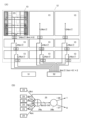
도 1은 본 발명의 일 형태의 촬상 장치를 설명하는 사시도이다. 촬상 장치는 층(10) 및 층(20)을 가진다. 층(10)은 층(20) 위에 제공할 수 있다. 촬상 장치는 화소 회로 및 기억 회로 등이 제공된 화소부(11)를 가진다. 화소부(11)는 층(10)에 제공된 요소 및 층(20)에 제공된 요소를 가진다.1 is a perspective view illustrating an imaging device of one embodiment of the present invention. The imaging device has a layer (10) and a layer (20).
층(10)에는 화소 회로 및 기억 회로를 제공할 수 있다. 층(20)에는 층(10)이 가지는 회로의 구동 회로, 층(10)이 가지는 회로가 취득한 데이터의 연산 회로, 데이터 변환 회로, 및 기억 회로 등을 제공할 수 있다. 예를 들어, 층(20)에는 연산부(21), 화소 회로를 구동하는 행 드라이버(31) 및 열 드라이버(32), 기억 회로를 구동하는 행 드라이버(33) 및 열 드라이버(34) 등을 제공할 수 있다. 또한, 층(20)에는 필요에 따라, 데이터의 선택 기능, 유지 기능, 변환 기능, 판독 기능 등을 가지는 회로(35), 회로(36) 등이 제공되어도 좋다.
층(10)이 가지는 회로와 층(20)이 가지는 회로는, 층(10)을 관통하는 전극 또는 배선 등에 의하여 전기적으로 접속될 수 있다. 또한, 상술한 일부의 회로는 상기 설명과는 반대의 층 또는 촬상 장치의 외부에 제공할 수도 있다.A circuit of the
도 2의 (A)는 화소부(11)의 자세한 사항을 설명하는 도면이다. 화소부(11)는 매트릭스상으로 배치된 복수의 화소 블록(12)을 가진다. 또한, 화소 블록(12)은 3×3으로 배치된 화소 블록(13)을 가진다. 또한, 화소 블록(13)은 3×3의 화소(14)를 가진다. 즉, 화소 블록(12)은 9×9의 화소(14)를 가진다. 화소(14)는 화소 회로(15) 및 기억 회로(16)를 가진다.2(A) is a diagram for explaining details of the
또한, 본 발명의 일 형태에서는, 화소 블록(13)이 3×3의 화소(14)를 가지는 구성을 전제로 하여 각종 연산 등을 수행하지만, 상술한 화소수에 한정되지 않고, 예를 들어 2×2, 4×4, 5×5, 25×25 등으로 할 수 있다. 또는 수평 방향과 수직 방향에서 화소(14)의 개수가 달라도 좋다. 또한 일부의 화소 블록(13)을 인접한 화소 블록(12)으로 공유할 수도 있다. 또한 일부의 화소(14)를 인접한 화소 블록(13)으로 공유할 수도 있다. 또한, 화소 블록(12)이 가지는 화소 블록(13)의 개수도 적절히 변경할 수 있다.In one embodiment of the present invention, various calculations and the like are performed on the premise that the
도 2의 (A)에 나타낸 화소(14)는 화소 회로(15) 및 기억 회로(16)가 층(10)에 나란히 제공되는 예이지만, 도 2의 (B)에 나타낸 바와 같이, 기억 회로(16) 위에 화소 회로(15)를 중첩하여 제공하여도 좋다. 또는, 도 2의 (C)에 나타낸 바와 같이, 화소 회로(15) 위에 기억 회로(16)를 중첩하여 제공하여도 좋다.The
도 3은 화소 블록(13)의 구성 요소를 설명하는 도면이다. 화소 블록(13)은 3×3의 화소(14)를 가진다. 따라서, 화소 블록(13)은 층(10)에 9개의 화소 회로(15) 및 9개의 기억 회로(16)를 가진다. 또한, 화소 회로(15) 또는 기억 회로(16)와 중첩되는 영역(층(20))에는, 연산부(21)로서 복수의 이진화 회로(22), 복수의 적화 연산 회로(23), 및 복수의 이진화 회로(24)가 제공된다.FIG. 3 is a diagram explaining the constituent elements of the
이진화 회로(22)는 화소 회로(15)와 같은 개수, 즉 9개 제공된다. 이진화 회로(22)는 화소 회로(15)와 중첩되는 영역을 가지는 위치에 제공된다. 도 4는 화소 회로(15)와 이진화 회로(22)의 접속 관계를 나타낸 도면이고, 하나의 화소 회로(15)는 중첩되는 영역을 가지는 하나의 이진화 회로(22)에 전기적으로 접속된다.
이진화 회로(22)는 화소 회로(15)에서 취득된 화상 데이터(아날로그 데이터)를 미리 설정된 문턱값으로 판정하여 이진화하는 회로이고, 예를 들어 콤퍼레이터를 사용할 수 있다.The
적화 연산 회로(23)는 하나의 화소 블록(13)에 복수 개 제공되고, 본 실시형태에서는 6개의 적화 연산 회로(23)를 제공한 예를 나타내었다. 또한, 적화 연산 회로(23)의 개수는 목적에 따라 적절히 증감할 수 있다. 적화 연산 회로(23)의 입력 단자는 기억 회로(16) 및 이진화 회로(22)에 전기적으로 접속된다.A plurality of
도 5는 적화 연산 회로(23), 기억 회로(16), 및 이진화 회로(22)의 접속 관계를 나타낸 도면이다. 또한, 상기 접속 관계를 명료하게 나타내기 위하여, 9개의 이진화 회로(22)를 발췌하여 도시하였다.FIG. 5 is a diagram showing the connection relationship among the
화소 블록(13)은 9개의 기억 회로(16)를 가지고, 그 각각은 복수의 메모리 셀을 가진다. 상기 복수의 메모리 셀의 각각에는 1bit의 가중 계수를 미리 기록할 수 있다. 9개의 기억 회로(16)의 각각은 6개의 적화 연산 회로(23)의 각각에 전기적으로 접속된다. 따라서, 적화 연산 회로(23)의 각각에는 9bit분의 가중 계수를 공급할 수 있다. 하나의 기억 회로(16)로부터 6개의 적화 연산 회로(23)에 가중 계수를 공급할 수 있기 때문에, 여기서는 하나의 기억 회로(16)에 적어도 1bit분의 가중 계수가 기록되어 있으면 상기 동작을 수행할 수 있다.The
이진화 회로(22)의 각각은 1bit로 변환된 화상 데이터를 출력할 수 있다. 9개의 이진화 회로(22)의 각각은 6개의 적화 연산 회로(23)의 각각에 전기적으로 접속된다. 하나의 이진화 회로(22)로부터 6개의 적화 연산 회로(23)에 화상 데이터를 공급할 수 있기 때문에, 적화 연산 회로(23)의 각각에는 9bit분의 화상 데이터가 공급된다.Each of the
도 6의 (A)는 적화 연산 회로(23)의 구성 및 연산 동작을 간략하게 설명하는 도면이다. 적화 연산 회로(23)는 예를 들어 승산기(23a)를 9개, 가산기(23b)를 하나 가지는 구성으로 할 수 있다. 각 승산기(23a)에는 이진화 회로(22)에서 1bit로 변환된 화상 데이터(X1 내지 X9)와 기억 회로(16)로부터 판독되는 1bit의 가중 계수(W1 내지 W9)가 입력되고, 승산 연산을 수행하여 1bit의 데이터를 가산기(23b)에 출력한다. 가산기(23b)에서는 각 승산기(23a)로부터 입력된 데이터를 가산하고, 이진화 회로(24)에 출력한다. 여기서, 가산기(23b)(적화 연산 회로(23))로부터 출력되는 데이터는 0 내지 9의 값을 취하기 때문에, 4bit의 데이터가 된다.6(A) is a diagram briefly explaining the configuration and calculation operation of the
이진화 회로(24)는 적화 연산 회로(23)와 같은 개수, 즉 6개 제공된다. 도 6의 (A), (B) 및 도 7에 나타낸 바와 같이, 하나의 이진화 회로(24)는 하나의 적화 연산 회로(23)에 전기적으로 접속된다. 도 6의 (A), (B)에 나타낸 바와 같이, 이진화 회로(24)에 입력되는 데이터는 0 내지 9에 상당하는 4bit의 디지털 데이터이다. 이진화 회로(24)는 입력 데이터를 5 이상이라고 판정한 경우에는 1을 출력하고, 4 이하라고 판정한 경우에는 0을 출력한다. 즉, 이진화 회로(24)는 4bit의 데이터를 1bit로 변환하는 기능을 가지는 회로이다.The
도 7에 나타낸 바와 같이, 하나의 화소 블록(13)으로부터는 6bit분의 연산 데이터를 출력할 수 있다. 도 8은 화소 블록(12)(화소 블록(13[1,1]) 내지 화소 블록(13[3,3]))으로부터의 연산 데이터의 판독을 설명하는 도면이다.As shown in FIG. 7 , 6 bits of operation data can be output from one
화소 블록(13)이 가지는 6개의 이진화 회로(24)는 각각 출력을 제어하는 선택 트랜지스터(24S)를 가진다. 6개의 선택 트랜지스터(24S)의 게이트는 배선(RSEL)(배선(RSEL[0]), 배선(RSEL[1]), 배선(RSEL[2]))에 전기적으로 접속된다. 배선(RSEL)은 행 방향으로 제공되는 화소 블록(13)으로 공유된다. 또한, 6개의 이진화 회로(24)가 전기적으로 접속되는 6개의 출력선(OUT)(OUT[0] 내지 OUT[5])은 열 방향으로 제공되는 화소 블록(13)으로 공유된다.Each of the six
6개의 출력선(OUT)에는 판독 회로(40)가 전기적으로 접속된다. 판독 회로(40)는 각 열의 6개의 출력선(OUT)에 각각 전기적으로 접속되는 스위치(40S), 스위치(41S), 및 스위치(42S)를 가진다.The
스위치(40S) 내지 스위치(42S)는 복수의 트랜지스터를 가진다. 스위치(40S)가 가지는 트랜지스터의 게이트는 배선(CSEL[0])에 전기적으로 접속된다. 스위치(42S)가 가지는 트랜지스터의 게이트는 배선(CSEL[1])에 전기적으로 접속된다. 스위치(42S)가 가지는 트랜지스터의 게이트는 배선(CSEL[2])에 전기적으로 접속된다.The
스위치(40S) 내지 스위치(42S)의 출력 측의 배선은 3개마다 하나의 출력선(OUT)에 전기적으로 접속된다. 상기 구성으로 함으로써, 화소 블록(13)마다의 데이터를 출력할 수 있다.The wirings on the output side of the
또한, 판독 회로(40)는 도 1에 나타낸 회로(35) 또는 회로(36)의 요소로서, 층(20)에 제공할 수 있다.Further, the
도 9는 화소 블록(12)(화소 블록(13[1,1] 내지 화소 블록(13[3,3]))으로부터의 연산 데이터의 판독을 설명하는 타이밍 차트이다. 또한, 시각 T1보다 전에 각 화소 블록(13)에서는 모든 연산이 종료되고, 이진화 회로(24)에 연산 데이터가 유지되어 있는 상태로 한다. 또한, 이하의 설명에서는, 트랜지스터를 도통 상태로 하는 전위(고전위)를 "H", 트랜지스터를 비도통 상태로 하는 전위(저전위)를 "L"이라고 표현한다.Fig. 9 is a timing chart for explaining the reading of operation data from the pixel block 12 (pixel block 13 [1,1] to pixel block 13 [3,3]). In the
시각 T1에 배선(RSEL[0])의 전위를 "H"로 하면, 0행째에 배치된 화소 블록(13)의 모든 이진화 회로(24)가 가지는 선택 트랜지스터(24S)가 도통되고, 연산 데이터가 판독 회로(40)에 출력된다.When the potential of the wiring (RSEL[0]) is set to "H" at time T1, the
또한, 시각 T1에 배선(CSEL[0])의 전위를 "H"로 하면, 배선(CSEL[0])에 게이트가 전기적으로 접속된 스위치(40S)가 도통되고, 출력선(OUT[0]) 내지 출력선(OUT[5])에 화소 블록(13[1,1])의 연산 데이터가 출력된다.Also, when the potential of the wiring CSEL[0] is set to "H" at time T1, the
시각 T2에 배선(CSEL[0])의 전위를 "L", 배선(CSEL[1])의 전위를 "H"로 하면, 스위치(40S)가 비도통이 되고, 배선(CSEL[1])에 게이트가 전기적으로 접속된 스위치(41S)가 도통되고, 출력선(OUT[0]) 내지 출력선(OUT[5])에 화소 블록(13[1,2])의 연산 데이터가 출력된다.At time T2, when the potential of the wiring CSEL[0] is set to "L" and the potential of the wiring CSEL[1] to "H", the
시각 T3에 배선(CSEL[1])의 전위를 "L", 배선(CSEL[2])의 전위를 "H"로 하면, 스위치(41S)가 비도통이 되고, 배선(CSEL[2])에 게이트가 전기적으로 접속된 스위치(42S)가 도통되고, 출력선(OUT[0]) 내지 출력선(OUT[5])에 화소 블록(13[1,3])의 연산 데이터가 출력된다.At time T3, when the potential of the wiring (CSEL[1]) is set to "L" and the potential of the wiring (CSEL[2]) is set to "H", the
시각 T4에 배선(RSEL[0])의 전위를 "L", 배선(CSEL[2])의 전위를 "L"로 하고, 0행째 화소 블록(13)(화소 블록(13[1,1]) 내지 화소 블록(13[1,3]))의 연산 데이터의 출력을 종료한다.At time T4, when the potential of the wiring RSEL[0] is set to "L" and the potential of the wiring CSEL[2] is set to "L", the 0th row pixel block 13 (pixel block 13[1,1] ) to the pixel block 13 [1, 3]).
시각 T4 내지 시각 T7에서는, 배선(RSEL[1])의 전위를 "H"로 하고, 상기와 같은 동작을 수행함으로써, 1행째 화소 블록(13)(화소 블록(13[2,1]) 내지 화소 블록(13[2,3]))의 연산 데이터의 출력을 수행한다.From time T4 to time T7, by setting the potential of the wiring RSEL[1] to "H" and performing the above operation, the pixel blocks 13 in the first row (pixel blocks 13[2,1] to Operation data of the pixel block 13[2,3] is output.
또한, 시각 T7 내지 시각 T10에서는, 배선(RSEL[2])의 전위를 "H"로 하고, 상기와 같은 동작을 수행함으로써, 2행째 화소 블록(13)(화소 블록(13[3,1]) 내지 화소 블록(13[3,3]))의 연산 데이터의 출력을 수행한다.Further, from time T7 to time T10, by setting the potential of the wiring RSEL[2] to "H" and performing the above operation, the second row pixel block 13 (pixel block 13[3,1] ) to the output of the operation data of the pixel block 13 [3, 3]).
여기서, 연산 동작을 1클록으로 완료하고, 하나의 화소 블록(13)의 판독 동작을 1클록으로 수행하면, 하나의 화소 블록(12)을 총 10클록으로 판독할 수 있다. 또한, 화소 블록(12)의 열과 같은 수의 판독 회로(40)를 제공함으로써, 1행분의 화소 블록(12)을 병렬로 판독할 수 있다.Here, if the arithmetic operation is completed with one clock and the read operation of one
<화소 회로><Pixel Circuit>
화소 회로(15)는 도 10의 (A)에 나타낸 바와 같이, 광전 변환 디바이스(101)와, 트랜지스터(102)와, 트랜지스터(103)와, 트랜지스터(104)와, 트랜지스터(105)와, 용량 소자(106)를 가질 수 있다.As shown in FIG.
광전 변환 디바이스(101)의 한쪽 전극은 트랜지스터(102)의 소스 및 드레인 중 한쪽에 전기적으로 접속된다. 트랜지스터(102)의 소스 및 드레인 중 다른 쪽은 트랜지스터(103)의 소스 및 드레인 중 한쪽, 용량 소자(106)의 한쪽 전극, 그리고 트랜지스터(104)의 게이트와 전기적으로 접속된다. 트랜지스터(104)의 소스 및 드레인 중 한쪽은 트랜지스터(105)의 소스 및 드레인 중 한쪽에 전기적으로 접속된다.One electrode of the
광전 변환 디바이스(101)의 다른 쪽 전극은 배선(111)에 전기적으로 접속된다. 트랜지스터(102)의 게이트는 배선(114)에 전기적으로 접속된다. 트랜지스터(103)의 소스 및 드레인 중 다른 쪽은 배선(112)에 전기적으로 접속된다. 트랜지스터(103)의 게이트는 배선(115)에 전기적으로 접속된다. 트랜지스터(104)의 소스 및 드레인 중 다른 쪽은 배선(113)에 전기적으로 접속된다. 트랜지스터(105)의 소스 및 드레인 중 다른 쪽은 배선(117)에 전기적으로 접속된다. 트랜지스터(105)의 게이트는 배선(116)에 전기적으로 접속된다.The other electrode of the
여기서, 트랜지스터(102)의 소스 및 드레인 중 다른 쪽과, 트랜지스터(103)의 소스 및 드레인 중 한쪽과, 용량 소자(106)의 한쪽 전극과, 트랜지스터(104)의 게이트의 전기적인 접속점(배선)을 노드(N)라고 한다.Here, the electrical connection point (wiring) of the other of the source and drain of the
배선(111, 112, 113)은 전원선으로서의 기능을 가질 수 있다. 예를 들어 배선(111)은 저전위 전원선으로서 기능하고, 배선(112) 및 배선(113)은 고전위 전원선으로서 기능할 수 있다. 또한 배선(112) 및 배선(113)은 전기적으로 접속되어도 좋다. 배선(114), 배선(115), 배선(116)은 각 트랜지스터의 도통을 제어하는 신호선으로서 기능시킬 수 있다. 배선(117)은 화소 회로(15)와 이진화 회로(22)를 전기적으로 접속하는 배선으로서 기능할 수 있다.The
광전 변환 디바이스(101)로서는 포토다이오드를 사용할 수 있다. 조도가 낮을 때의 광 검출 감도를 높이고자 하는 경우에는, 애벌란시 포토다이오드를 사용하는 것이 바람직하다.As the
트랜지스터(102)는 노드(N)의 전위를 제어하는 기능을 가질 수 있다. 트랜지스터(103)는 노드(N)의 전위를 초기화하는 기능을 가질 수 있다. 트랜지스터(104)는 노드(N)의 전위에 따라 전류를 흘리는 기능을 가질 수 있다. 트랜지스터(105)는 화소를 선택하는 기능을 가질 수 있다.The
또한 광전 변환 디바이스(101)에 포함되는 한 쌍의 전극의 접속 방향을 반대로 하여도 좋다. 이 경우, 배선(111)은 고전위 전원선으로서 기능하고, 배선(112) 및 배선(113)은 저전위 전원선으로서 기능하면 좋다.Further, the connection direction of a pair of electrodes included in the
트랜지스터(102, 103)로서는, 채널 형성 영역에 금속 산화물을 사용한 트랜지스터(OS 트랜지스터)를 사용하는 것이 바람직하다. OS 트랜지스터는 오프 전류가 매우 낮다는 특성을 가진다. 트랜지스터(102, 103)로서 OS 트랜지스터를 사용함으로써, 노드(N)에서 전하가 유지될 수 있는 기간을 매우 길게 할 수 있다. 또한 회로 구성 및 동작 방법을 복잡하게 하지 않고 모든 화소에서 동시에 전하의 축적 동작을 수행하는 글로벌 셔터 방식을 적용할 수 있다.As the
한편으로, 트랜지스터(104)는 증폭 특성이 우수한 것이 요구되는 경우가 있다. 또한 트랜지스터(105)로서는 고속 동작이 가능하고 이동도가 높은 트랜지스터를 사용하는 것이 바람직한 경우가 있다. 따라서, 트랜지스터(104, 105)에는 실리콘을 채널 형성 영역에 사용한 트랜지스터(Si 트랜지스터)를 적용하여도 좋다.On the other hand, there are cases in which the
또한 상술한 것에 한정되지 않고, OS 트랜지스터 및 Si 트랜지스터를 임의로 조합하여 적용하여도 좋다. 또한 모든 트랜지스터를 OS 트랜지스터로 하여도 좋다. 또는 모든 트랜지스터를 Si 트랜지스터로 하여도 좋다. Si 트랜지스터로서는 비정질 실리콘을 포함하는 트랜지스터, 결정성 실리콘(미결정 실리콘, 저온 폴리실리콘, 단결정 실리콘)을 포함하는 트랜지스터 등을 들 수 있다.Moreover, it is not limited to what was mentioned above, and an arbitrary combination of OS transistors and Si transistors may be applied. Also, all transistors may be OS transistors. Alternatively, all transistors may be Si transistors. Examples of Si transistors include transistors made of amorphous silicon, transistors made of crystalline silicon (microcrystalline silicon, low-temperature polysilicon, single crystal silicon), and the like.
또한 도 10의 (B)에 나타낸 바와 같이, 트랜지스터에 백 게이트(제 2 게이트)를 제공하는 구성으로 하여도 좋다. 상기 백 게이트를 프런트 게이트와 전기적으로 접속함으로써 트랜지스터의 온 전류를 증대할 수 있다. 또한 이 백 게이트에 적절한 정전위를 공급함으로써, 트랜지스터의 문턱 전압을 제어할 수 있다. 또한 트랜지스터에 백 게이트를 제공하는 구성은 본 명세서에서의 다른 회로에도 적용할 수 있다. 또한 백 게이트를 포함하는 트랜지스터와 백 게이트를 포함하지 않는 트랜지스터를 혼재시켜 회로를 구성하여도 좋다.Further, as shown in FIG. 10(B), it is good also as a structure in which a back gate (second gate) is provided to the transistor. By electrically connecting the back gate to the front gate, the on-state current of the transistor may be increased. In addition, by supplying an appropriate constant potential to the back gate, the threshold voltage of the transistor can be controlled. Also, the configuration of providing a back gate to the transistor can be applied to other circuits in this specification. Further, the circuit may be configured by mixing transistors with back gates and transistors without back gates.
또한, 도 10의 (C)에 나타낸 바와 같이, 도 10의 (A)의 구성에 트랜지스터(107) 및 트랜지스터(108)를 추가한 구성으로 하여도 좋다. 트랜지스터(107)의 게이트는 트랜지스터(104)의 게이트와 전기적으로 접속된다. 트랜지스터(107)의 소스 및 드레인 중 한쪽은 트랜지스터(108)의 소스 및 드레인 중 한쪽에 전기적으로 접속된다. 트랜지스터(107)의 소스 및 드레인 중 다른 쪽은 배선(113)에 전기적으로 접속된다. 트랜지스터(108)의 게이트는 배선(118)에 전기적으로 접속된다. 트랜지스터(108)의 소스 및 드레인 중 다른 쪽은 배선(119)에 전기적으로 접속된다.Alternatively, as shown in FIG. 10(C), a configuration in which
여기서, 배선(118)은 트랜지스터(108)의 도통을 제어하는 신호선으로서 기능할 수 있다. 또한 배선(119)은 회로(60)에 전기적으로 접속될 수 있다. 회로(60)는 화상 판독 회로이고, 예를 들어 CDS 회로(상관 이중 샘플링 회로) 등을 사용할 수 있다. 상기 구성을 사용함으로써, 화상 데이터를 배선(117) 및 배선(119)에 출력할 수 있다. 배선(117)에 출력된 화상 데이터는 이진화 회로(22)에 입력되고, 그 후 적화 연산이 수행된다. 배선(119)에 출력된 화상 데이터는 회로(60)를 통하여 외부로 판독된다. 이들의 동작을 병렬로 수행할 수 있다. 또한, 연산(화상 처리)만 또는 화상 데이터의 판독만을 수행할 수도 있다.Here, the
또한 회로(60)는 도 1에 나타낸 회로(35) 또는 회로(36)의 요소로서 층(20)에 제공할 수 있다.
<기억 회로><memory circuit>
도 2에 나타낸 바와 같이, 기억 회로(16)는 화소(14)에 제공된다. 또한, 기억 회로(16)는 복수의 메모리 셀을 가지고, 상기 메모리 셀에는 가중 계수에 상당하는 1bit의 데이터가 저장된다.As shown in FIG. 2 , the
도 11의 (A)는 메모리 셀(150), 행 드라이버(33), 및 열 드라이버(34)의 접속 관계를 나타낸 도면이다. 메모리 셀(150)을 구성하는 트랜지스터로서는 OS 트랜지스터를 사용하는 것이 바람직하다. 복수의 메모리 셀(150)은 기억 회로(16)로서 층(10)에 제공된다. 행 드라이버(33) 및 열 드라이버(34)는 메모리 셀(150)의 구동 회로이고, 층(20)에 제공될 수 있다.11(A) is a diagram showing the connection relationship between the
기억 회로(16)는 1열에 m(m은 1 이상의 정수)개와 1행에 n(n은 1 이상의 정수)개의 총 m×n개의 메모리 셀(150)을 가지고, 메모리 셀(150)은 매트릭스상으로 배치되어 있다.The
도 11의 (B), (C)는 메모리 셀(150)에 적용할 수 있는 메모리 셀(150a) 및 메모리 셀(150b)을 설명하는 도면이다. 또한 아래의 설명에서, 비트선 등은 열 드라이버(34)에 접속될 수 있다. 또한 워드선 등은 행 드라이버(33)에 접속될 수 있다. 또한 비트선 등은 적화 연산 회로(23)에도 전기적으로 접속되지만, 여기서는 도시하지 않았다.11 (B) and (C) are diagrams for explaining the
행 드라이버(33) 및 열 드라이버(34)에는, 예를 들어 디코더 또는 시프트 레지스터를 사용할 수 있다. 또한 행 드라이버(33) 및 열 드라이버(34)는 복수로 제공되어도 좋다.For the row driver 33 and
도 11의 (B)는 2개의 트랜지스터와 하나의 용량 소자를 가지는 게인 셀형("2Tr 1C형"이라고도 함) 메모리 셀(150a)의 회로 구성예를 나타낸 것이다. 메모리 셀(150a)은 트랜지스터(273)와, 트랜지스터(272)와, 용량 소자(274)를 가진다.Fig. 11(B) shows an example of a circuit configuration of a gain cell type (also referred to as "2Tr 1C type")
트랜지스터(273)의 소스 및 드레인 중 한쪽은 용량 소자(274)의 한쪽 전극에 접속되고, 트랜지스터(273)의 소스 및 드레인 중 다른 쪽은 배선(WBL)에 접속되고, 트랜지스터(273)의 게이트는 배선(WL)에 접속되고, 트랜지스터(273)의 백 게이트는 배선(BGL)에 접속되어 있다. 용량 소자(274)의 다른 쪽 전극은 배선(RL)에 접속되어 있다. 트랜지스터(272)의 소스 및 드레인 중 한쪽은 배선(RBL)에 접속되고, 트랜지스터(272)의 소스 및 드레인 중 다른 쪽은 배선(SL)에 접속되고, 트랜지스터(272)의 게이트는 용량 소자(274)의 한쪽 전극에 접속되어 있다.One of the source and drain of the
배선(WBL)은 기록 비트선으로서 기능한다. 배선(RBL)은 판독 비트선으로서 기능한다. 배선(WL)은 워드선으로서 기능한다. 배선(RL)은 용량 소자(274)의 다른 쪽 전극에 소정의 전위를 인가하기 위한 배선으로서 기능한다. 데이터를 기록할 때 및 데이터를 유지하는 도중에는, 배선(RL)에 기준 전위를 인가하는 것이 바람직하다.The wiring WBL functions as a write bit line. The wiring RBL functions as a read bit line. The wiring WL functions as a word line. The wiring RL functions as a wiring for applying a predetermined potential to the other electrode of the
배선(BGL)은 트랜지스터(273)의 백 게이트에 전위를 인가하기 위한 배선으로서 기능한다. 배선(BGL)에 임의의 전위를 인가함으로써, 트랜지스터(273)의 문턱 전압을 증감할 수 있다.The wiring BGL functions as a wiring for applying a potential to the back gate of the
데이터의 기록은, 배선(WL)에 고레벨 전위를 인가하여 트랜지스터(273)를 도통 상태로 하여, 배선(WBL)과 용량 소자(274)의 한쪽 전극을 전기적으로 접속함으로써 수행된다. 구체적으로는, 트랜지스터(273)가 도통 상태일 때, 기록하는 정보에 대응하는 전위를 배선(WBL)에 인가하여, 용량 소자(274)의 한쪽 전극 및 트랜지스터(272)의 게이트에 상기 전위를 기록한다. 그 후, 배선(WL)에 저레벨 전위를 인가하여 트랜지스터(273)를 비도통 상태로 함으로써, 용량 소자(274)의 한쪽 전극의 전위 및 트랜지스터(272)의 게이트의 전위가 유지된다.Data writing is performed by applying a high-level potential to the wiring WL to bring the
데이터의 판독은 배선(RL)과 배선(SL)에 소정의 전위를 인가함으로써 수행된다. 트랜지스터(272)의 소스-드레인 간을 흐르는 전류, 및 트랜지스터(273)의 소스 및 드레인 중 한쪽의 전위는 트랜지스터(272)의 게이트의 전위, 및 트랜지스터(273)의 소스 및 드레인 중 다른 쪽의 전위에 따라 정해지므로, 트랜지스터(272)의 소스 및 드레인 중 한쪽에 접속되는 배선(RBL)의 전위를 판독함으로써, 용량 소자(274)의 한쪽 전극(또는 트랜지스터(272)의 게이트)에 유지된 전위를 판독할 수 있다. 즉, 용량 소자(274)의 한쪽 전극(또는 트랜지스터(272)의 게이트)에 유지된 전위로부터, 이 메모리 셀에 기록된 정보를 판독할 수 있다. 또는 이 메모리 셀에 기록된 정보의 유무를 알 수 있다.Data reading is performed by applying a predetermined potential to the wirings RL and SL. The current flowing between the source and drain of the
또한 도 11의 (C)에 나타낸 바와 같이, 배선(WBL)과 배선(RBL)을 하나의 배선(BIL)으로서 합쳐도 좋다. 도 11의 (C)에 나타낸 메모리 셀(150b)에서는, 메모리 셀(150a)의 배선(WBL)과 배선(RBL)을 하나의 배선(BIL)으로 하고, 트랜지스터(273)의 소스 및 드레인 중 다른 쪽 및 트랜지스터(272)의 소스 및 드레인 중 한쪽이 배선(BIL)에 접속되어 있다. 즉 메모리 셀(150b)에서는, 기록 비트선과 판독 비트선이 하나의 배선(BIL)으로서 동작한다.Further, as shown in FIG. 11(C), the wiring WBL and the wiring RBL may be combined as one wiring BIL. In the
또한 메모리 셀(150a) 및 메모리 셀(150b)에서도 트랜지스터(273)로서 OS 트랜지스터를 사용하는 것이 바람직하다. 트랜지스터(273)로서 OS 트랜지스터를 사용하고, 메모리 셀(150a) 및 메모리 셀(150b)과 같은 2Tr 1C형 메모리 셀을 사용한 기억 장치를 NOSRAM(Non-volatile Oxide Semiconductor Random Access Memory)이라고 한다. 또한 메모리 셀은 회로의 구성을 적절히 변경할 수 있다.Also in the
<레이아웃><layout>
도 12의 (A), (B)는 본 발명의 일 형태의 화소 회로에 사용할 수 있는 레이아웃(상면도)의 예이다. 도 12의 (A), (B)는 도 10의 (B)에 나타낸 화소 회로의 레이아웃이고, 도 12의 (A)에는 백 게이트 배선(170), 금속 산화물층(175), 소스-드레인 배선(180)을 나타내었다. 여기서, 금속 산화물층(175)은 OS 트랜지스터의 채널 형성 영역이 형성되는 층이다.12(A) and (B) are examples of layouts (top view) usable for a pixel circuit of one embodiment of the present invention. 12(A) and (B) are layouts of the pixel circuit shown in FIG. 10(B), and in FIG. (180). Here, the
촬상 장치의 해상도 향상을 위해서는 화소 회로의 미세화가 필요하다. 미세화 공정에서는 근접하는 구조물이 서로 영향을 미치기 때문에, 구조물을 랜덤하게 배치하면 배선 폭 등에 편차가 생기는 것이 조장된다. 따라서, 도 12의 (A)에 나타낸 바와 같이, 수평 방향(X 방향) 및 수직 방향(Y 방향)에 등간격으로 구조물을 배치하는 것이 바람직하다.In order to improve the resolution of an imaging device, miniaturization of a pixel circuit is required. In the miniaturization process, since adjacent structures affect each other, randomly arranging the structures encourages variations in wiring width and the like. Therefore, as shown in FIG. 12(A), it is preferable to arrange structures at equal intervals in the horizontal direction (X direction) and the vertical direction (Y direction).
도 12의 (B)는 도 12의 (A)에 게이트 배선(185) 및 게이트 배선(185)에 전기적으로 접속되는 배선(190)을 추가한 구성을 나타낸 것이다. 이와 같이 각 요소를 중첩시킴으로써, 도 10의 (B)에 나타낸 트랜지스터(102), 트랜지스터(103), 트랜지스터(104), 및 트랜지스터(105)가 형성된다. 또한, 이 외에 트랜지스터(109)가 복수 개 형성된다. 트랜지스터(109)는 회로 동작에 관여하지 않는 더미 트랜지스터이지만, 이와 같은 구성으로 함으로써 배선 폭 등의 균일성을 향상시킬 수 있어, 트랜지스터 특성의 편차 등을 억제할 수 있다.FIG. 12(B) shows a configuration in which a
본 실시형태에서 설명한 본 발명의 일 형태에 의하여, 화상 처리 기능을 가지고, 고속 동작이 가능한 촬상 장치를 제공할 수 있다.According to one aspect of the present invention described in the present embodiment, an imaging device having an image processing function and capable of high-speed operation can be provided.
본 실시형태는 다른 실시형태의 기재와 적절히 조합할 수 있다.This embodiment can be suitably combined with descriptions of other embodiments.
(실시형태 2)(Embodiment 2)
본 실시형태에서는 실시형태 1과는 다른 구성을 가진 촬상 장치에 대하여 도면을 참조하여 설명한다. 실시형태 1에서 설명한 촬상 장치는 화상 데이터에 대하여 적화 연산을 한 번 수행하고 연산 데이터를 추출하는 구성이었지만, 본 실시형태에서 설명하는 촬상 장치는 화상 데이터에 대하여 적화 연산을 여러 번 수행하고 연산 데이터를 추출하는 구성을 가진다.In this embodiment, an imaging device having a configuration different from that of
화소(14) 및 화소 블록(화소 블록(12), 화소 블록(13))의 기본 구성은 실시형태 1과 공통되기 때문에, 자세한 설명은 생략한다.Since the basic configuration of the
촬상 장치는 적화 연산을 여러 번 수행하고, 연산 데이터를 추출하기 위한 요소로서 2개의 레지스터를 가진다. 도 13은 화소 블록(12)과, 2개의 레지스터(레지스터(51), 레지스터(52)) 중 하나인 레지스터(51)의 접속 관계를 설명하는 도면이다. 또한, 화소 블록(13)과 레지스터(51) 사이에 선택 회로를 제공하여, 배선 수를 줄일 수도 있다.The imaging device has two registers as elements for performing multiplication operations several times and extracting operation data. Fig. 13 is a diagram for explaining the connection relationship between the
도 13에 나타낸 화소 블록(12)은 도 8에 나타낸 화소 블록(12)을 간략화한 것이고, 이는 첫 번째 적화 연산 후에 각 화소 블록(13)으로부터 출력되는 연산 데이터가 6bit분(1bit×6)인 것을 나타낸다. 각 화소 블록(13)으로부터 출력되는 6bit분의 연산 데이터는 레지스터(51)에 입력되고, 저장된다. 여기서, 레지스터(51)에는 9개의 화소 블록(13)으로부터 출력되는 6bit분의 연산 데이터가 입력되기 때문에 총 54bit분(6bit분×9)의 연산 데이터가 저장된다.The
다음으로, 도 14에 나타낸 바와 같이, 레지스터(51)에 저장된 54bit분의 연산 데이터를 각 화소 블록(13)에 재분배한다. 각 화소 블록(13)에는 도 6의 (A)에 나타낸 9bit분의 데이터를 처리할 수 있는 적화 연산 회로(23)가 6개 제공되고, 각 적화 연산 회로(23)에 9bit분의 연산 데이터가 분배된다. 또한, 각 적화 연산 회로(23)에는 화소 블록(13)이 가지는 9개의 기억 회로(16)로부터 9bit분의 가중 계수가 공급된다. 따라서, 각 적화 연산 회로(23)에서는 2번째 적화 연산을 수행할 수 있다.Next, as shown in FIG. 14, the 54-bit operation data stored in the
다음으로, 도 15의 (A)에 나타낸 바와 같이, 각 적화 연산 회로(23)가 출력하는 4bit의 연산 데이터는 화소 블록(13)과 같은 수 제공된 회로(25)에 각각 입력된다. 여기서, 적화 연산 회로(23)는 6개이므로, 회로(25)에 입력되는 연산 데이터는 24bit분(4bit×6)이다.Next, as shown in FIG. 15(A), the 4-bit calculation data output from each
도 15의 (B)는 회로(25)를 설명하는 도면이다. 회로(25)는 가산 회로(26a) 및 이진화 회로(26b)를 가진다. 6개의 적화 연산 회로(23)로부터 가산 회로(26a)에 4bit(0 내지 9에 상당함)의 연산 데이터가 각각 입력되기 때문에 가산 회로(26a)의 출력은 6bit(0 내지 54에 상당함)의 연산 데이터이다. 6bit의 데이터는 이진화 회로(26b)에 입력된다. 이진화 회로(26b)는 입력된 데이터를 1bit로 변환할 수 있고, 데이터가 28 이상일 때 1을 출력하고, 27 이하일 때 0을 출력한다. 또한, 도 15에서는 회로(25)를 화소 블록(12) 내에 도시하였지만, 화소 블록(12) 외부에 제공하여도 좋다.15(B) is a diagram for explaining the
각 회로(25)가 출력하는 1bit의 연산 데이터(총 9bit분의 데이터)는 레지스터(52)에 입력되고, 저장된다. 여기서, 필요에 따라 9bit분의 연산 데이터를 판독할 수 있다. 또한, 회로(25)와 레지스터(52) 사이에 선택 회로를 제공하여, 배선 수를 줄일 수도 있다.1-bit operation data (data for a total of 9 bits) output from each
본 실시형태에서는, 이에 더하여 가중 계수를 바꾸면서 적화 연산을 반복하는 동작에 대하여 설명한다. 상기 동작 후, 화소 블록(13)이 가지는 적화 연산 회로(23)에는 레지스터(51)로부터 재분배된 54bit분의 연산 데이터가 유지되어 있고, 기억 회로(16)로부터 공급되는 가중 계수를 변경함으로써 다시 적화 연산을 수행하고, 다른 연산 데이터를 얻을 수 있다. 그리고, 상기 연산 데이터는 앞의 적화 연산으로 얻은 연산 데이터와 마찬가지로 레지스터(52)에 저장된다. 따라서, 레지스터(52)에는 총 18bit분의 연산 데이터가 저장된다.In the present embodiment, an operation of repeating the multiplication operation while changing the weighting coefficient will be described in addition to this. After the above operation, the
도 16의 (A)는 레지스터(52)의 출력 측에 접속되는 판독 회로(41)를 설명하는 도면이다. 레지스터(52)의 출력 측에는 6bit분마다 연산 데이터를 판독할 수 있도록 6개의 출력선이 복수 개 제공된다. 6개의 출력선에는 판독 회로(41)가 전기적으로 접속된다. 판독 회로(41)는 6개의 출력선에 각각 전기적으로 접속되는 스위치(43S), 스위치(44S), 및 스위치(45S)를 가진다.16(A) is a diagram for explaining the
스위치(43S) 내지 스위치(45S)는 복수의 트랜지스터를 가진다. 스위치(43S)가 가지는 트랜지스터의 게이트는 배선(CSEL[0])에 전기적으로 접속된다. 스위치(44S)가 가지는 트랜지스터의 게이트는 배선(CSEL[1])에 전기적으로 접속된다. 스위치(45S)가 가지는 트랜지스터의 게이트는 배선(CSEL[2])에 전기적으로 접속된다.The
스위치(43S) 내지 스위치(45S)의 출력 측의 배선은 3개마다 하나의 출력선(OUT)(OUT[0] 내지 OUT[5])에 전기적으로 접속된다. 상기 구성으로 함으로써, 6bit분마다 연산 데이터를 출력할 수 있다.Wirings on the output side of
또한, 레지스터(51), 레지스터(52), 및 판독 회로(41)는 도 1에 나타낸 회로(35) 또는 회로(36)의 요소로서 층(20)에 제공할 수 있다.Additionally, register 51, register 52, and read
도 16의 (B)는 레지스터(52)에 저장된 연산 데이터의 판독을 설명하는 타이밍 차트이다. 또한, 시각 T1보다 전에 레지스터(52)에 모든 연산 데이터(18bit분)가 유지되어 있는 상태로 한다. 또한, 이하의 설명에서는 트랜지스터를 도통 상태로 하는 전위(고전위)를 "H", 트랜지스터를 비도통 상태로 하는 전위(저전위)를 "L"이라고 표현한다.16(B) is a timing chart explaining reading of operation data stored in the
시각 T1에 배선(CSEL[0])의 전위를 "H"로 하면, 배선(CSEL[0])에 게이트가 전기적으로 접속된 스위치(43S)가 도통되고, 출력선(OUT[0]) 내지 출력선(OUT[5])에 첫 번째의 6bit분의 연산 데이터가 출력된다.When the potential of the wiring CSEL[0] is set to "H" at time T1, the
시각 T2에 배선(CSEL[0])의 전위를 "L", 배선(CSEL[1])의 전위를 "H"로 하면, 스위치(43S)가 비도통이 되고, 배선(CSEL[1])에 게이트가 전기적으로 접속된 스위치(44S)가 도통되고, 출력선(OUT[0]) 내지 출력선(OUT[5])에 첫 번째 데이터와는 다른 두 번째의 6bit분의 연산 데이터가 출력된다.At time T2, when the potential of the wiring (CSEL[0]) is set to "L" and the potential of the wiring (CSEL[1]) is set to "H", the
시각 T3에 배선(CSEL[1])의 전위를 "L", 배선(CSEL[2])의 전위를 "H"로 하면, 스위치(44S)가 비도통이 되고, 배선(CSEL[2])에 게이트가 전기적으로 접속된 스위치(45S)가 도통되고, 출력선(OUT[0]) 내지 출력선(OUT[5])에 첫 번째 및 두 번째 데이터와는 다른 세 번째의 6bit분의 연산 데이터가 출력된다.At time T3, when the potential of the wiring (CSEL[1]) is set to "L" and the potential of the wiring (CSEL[2]) is set to "H", the
여기서, 레지스터(51)에 54bit분의 연산 데이터를 저장하는 공정까지를 첫 번째 클록에서 수행하고, 레지스터(52)에 첫 번째의 9bit분의 연산 데이터를 저장하는 공정까지를 두 번째 클록에서 수행하고, 레지스터(52)에 두 번째의 9bit분의 연산 데이터를 저장하는 공정까지를 세 번째 클록에서 수행하는 것으로 한다. 그리고, 레지스터(52)로부터 첫 번째의 6bit분의 연산 데이터를 판독하는 공정을 네 번째 클록에서 수행하고, 두 번째의 6bit분의 연산 데이터의 판독을 다섯 번째 클록에서 수행하고, 세 번째의 6bit분의 연산 데이터의 판독을 여섯 번째 클록에서 수행하기로 하면, 모든 동작을 6클록으로 종료할 수 있다.Here, the process of storing 54 bits of operation data in the
첫 번째 클록 내지 세 번째 클록의 동작과 네 번째 클록 내지 여섯 번째 클록의 동작은 병렬로 동작할 수 있고, 도 16의 (B)에 나타낸 타이밍 차트의 시각 T1 내지 시각 T2 기간을 네 번째 클록에 대응시키고, 시각 T2 내지 시각 T3의 기간을 다섯 번째 클록에 대응시키고, 시각 T3 내지 시각 T4의 기간을 여섯 번째 클록에 대응시키면, 시각 T4 내지 시각 T7에서는 다음의 18bit분의 연산 데이터를 판독할 수 있다. 또한, 시각 T7 내지 시각 T10에서는, 그 다음의 18bit분의 연산 데이터를 판독할 수 있다.The operations of the first to third clocks and the fourth to sixth clocks can be operated in parallel, and the time T1 to time T2 period of the timing chart shown in FIG. 16 (B) corresponds to the fourth clock. Then, if the period from time T2 to time T3 corresponds to the fifth clock, and the period from time T3 to time T4 corresponds to the sixth clock, the next 18 bits of operation data can be read from time T4 to time T7. . In addition, from time T7 to time T10, calculation data for the next 18 bits can be read.
또한, 실시형태 1 및 본 실시형태에서의 화소 블록(12)으로부터의 연산 데이터의 판독 동작은 스트라이드 3의 동작에 상당하고, 풀링 처리를 생략하였지만, 풀링 처리를 수행하여, 연산 데이터를 더 압축하여도 좋다.Further, the operation of reading computational data from the
본 실시형태에서 설명한 본 발명의 일 형태에 의하여, 화상 처리 기능을 가지고, 고속 동작이 가능한 촬상 장치를 제공할 수 있다.According to one aspect of the present invention described in the present embodiment, an imaging device having an image processing function and capable of high-speed operation can be provided.
본 실시형태는 다른 실시형태의 기재와 적절히 조합할 수 있다.This embodiment can be suitably combined with descriptions of other embodiments.
(실시형태 3)(Embodiment 3)
본 실시형태에서는 본 발명의 일 형태의 촬상 장치의 구조예 등에 대하여 설명한다.In this embodiment, a structural example of an imaging device according to one embodiment of the present invention and the like will be described.
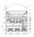
<구조예><Structure example>
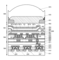
도 17의 (A)는 촬상 장치의 화소의 구조의 일례를 나타낸 도면이고, 층(561)과 층(563)의 적층 구조로 할 수 있다.17(A) is a diagram showing an example of a structure of a pixel of an imaging device, and a
층(561)은 광전 변환 디바이스(101)를 가진다. 광전 변환 디바이스(101)는, 도 18의 (A)에 나타낸 바와 같이, 층(565a)과 층(565b)을 가질 수 있다. 또한 경우에 따라서는 층을 영역이라고 바꿔 말하여도 좋다.
도 18의 (A)에 나타낸 광전 변환 디바이스(101)는 pn 접합형 포토다이오드이고, 예를 들어 층(565a)에 p형 반도체를 사용하고, 층(565b)에 n형 반도체를 사용할 수 있다. 또는 층(565a)에 n형 반도체, 층(565b)에 p형 반도체를 사용하여도 좋다.The
상기 pn접합형 포토다이오드는 대표적으로 단결정 실리콘을 사용하여 형성할 수 있다. 단결정 실리콘을 광전 변환층으로 한 포토다이오드는 자외광에서 근적외광까지 비교적 넓은 분광 감도 특성을 가지므로, 후술하는 광학 변환층과 조합됨으로써, 다양한 파장의 광을 검출할 수 있다.The pn junction photodiode may be typically formed using single crystal silicon. Since a photodiode using single crystal silicon as a photoelectric conversion layer has a relatively wide spectral sensitivity characteristic from ultraviolet light to near infrared light, light of various wavelengths can be detected by combining with an optical conversion layer described later.
이 외에는, pn접합형 포토다이오드의 광전 변환층으로서 화합물 반도체를 사용하여도 좋다. 상기 화합물 반도체로서는 예를 들어, 갈륨-비소-인 화합물(GaAsP), 갈륨-인 화합물(GaP), 인듐-갈륨-비소 화합물(InGaAs), 납-황 화합물(PbS), 납-셀레늄 화합물(PbSe), 인듐-비소 화합물(InAs), 인듐-안티모니 화합물(InSb), 수은-카드뮴-텔루륨 화합물(HgCdTe) 등을 사용할 수 있다.In addition to this, a compound semiconductor may be used as the photoelectric conversion layer of the pn junction photodiode. Examples of the compound semiconductor include gallium-arsenic-phosphorus compound (GaAsP), gallium-phosphorus compound (GaP), indium-gallium-arsenic compound (InGaAs), lead-sulfur compound (PbS), and lead-selenium compound (PbSe). ), an indium-arsenic compound (InAs), an indium-antimony compound (InSb), a mercury-cadmium-tellurium compound (HgCdTe), or the like can be used.
화합물 반도체로서는 13족 원소(알루미늄, 갈륨, 인듐 등) 및 15족 원소(질소, 인, 비소, 안티모니 등)를 포함하는 화합물 반도체(3-5족 화합물 반도체라고도 함), 또는 12족 원소(마그네슘, 아연, 카드뮴, 수은 등) 및 16족 원소(산소, 황, 셀레늄, 텔루륨 등)를 포함하는 화합물 반도체(2-6족 화합물 반도체라고도 함)가 바람직하다.As the compound semiconductor, a compound semiconductor containing a
화합물 반도체는 구성 원소의 조합 및 그 원자수비에 따라 밴드 갭을 변화시킬 수 있기 때문에, 자외광에서 적외광까지 다양한 파장 범위에 감도를 가지는 포토다이오드를 형성할 수 있다.Since the compound semiconductor can change its band gap depending on the combination of constituent elements and atomic number ratio thereof, it is possible to form a photodiode having sensitivity to a wide range of wavelengths from ultraviolet light to infrared light.
또한 일반적으로는, 자외광의 파장은 0.01μm 근방 내지 0.38μm 근방, 가시광의 파장은 0.38μm 근방 내지 0.75μm 근방, 근적외광의 파장은 0.75μm 근방 내지 2.5μm 근방, 중적외광의 파장은 2.5μm 근방 내지 4μm 근방, 원적외광의 파장은 4μm 근방 내지 1000μm 근방이라고 정의할 수 있다.In general, the wavelength of ultraviolet light is around 0.01 μm to around 0.38 μm, the wavelength of visible light is around 0.38 μm to around 0.75 μm, the wavelength of near infrared light is around 0.75 μm to around 2.5 μm, and the wavelength of mid-infrared light is 2.5 μm. Near to 4 μm, the wavelength of far-infrared light can be defined to be around 4 μm to around 1000 μm.
예를 들어 자외광에서 가시광까지의 광에 감도를 가지는 포토다이오드를 형성하기 위해서는, 광전 변환층에 GaP 등을 사용할 수 있다. 또한 자외광에서 근적외광까지의 광에 감도를 가지는 포토다이오드를 형성하기 위해서는, 광전 변환층에 실리콘 또는 GaAsP 등을 사용할 수 있다. 또한 가시광에서 중적외광까지의 광에 감도를 가지는 포토다이오드를 형성하기 위해서는, 광전 변환층에 InGaAs 등을 사용할 수 있다. 또한 근적외광에서 중적외광까지의 광에 감도를 가지는 포토다이오드를 형성하기 위해서는, 광전 변환층에 PbS 또는 InAs 등을 사용할 수 있다. 또한 중적외광에서 원적외광까지의 광에 감도를 가지는 포토다이오드를 형성하기 위해서는, 광전 변환층에 PbSe, InSb, 또는 HgCdTe 등을 사용할 수 있다.For example, in order to form a photodiode having sensitivity to light from ultraviolet light to visible light, GaP or the like can be used for the photoelectric conversion layer. Further, in order to form a photodiode having sensitivity to light from ultraviolet light to near infrared light, silicon or GaAsP or the like can be used for the photoelectric conversion layer. Further, in order to form a photodiode having sensitivity to light from visible light to mid-infrared light, InGaAs or the like can be used for the photoelectric conversion layer. Further, in order to form a photodiode having sensitivity to light from near infrared light to mid-infrared light, PbS or InAs can be used for the photoelectric conversion layer. In addition, in order to form a photodiode having sensitivity to light from mid-infrared to far-infrared light, PbSe, InSb, HgCdTe or the like can be used for the photoelectric conversion layer.
또한 상기 화합물 반도체를 사용한 포토다이오드는 pn접합뿐만 아니라, pin접합이어도 좋다. 또한 pn접합 및 pin접합은 동종접합(homojunction) 구조에 한정되지 않고, 이종접합(heterojunction) 구조이어도 좋다.In addition, a photodiode using the compound semiconductor may be a pin junction as well as a pn junction. Also, the pn junction and the pin junction are not limited to a homojunction structure, and may be a heterojunction structure.
예를 들어 이종접합에서는, pn접합 구조의 한쪽 층에 제 1 화합물 반도체를 사용하고, 다른 쪽 층에 제 1 화합물 반도체와는 다른 제 2 화합물 반도체를 사용할 수 있다. 또한 pin접합 구조 중 어느 1층 또는 2층에 제 1 화합물 반도체를 사용하고, 나머지 층에 제 1 화합물 반도체와는 다른 제 2 화합물 반도체를 사용할 수 있다. 또한 제 1 화합물 반도체 또는 제 2 화합물 반도체 중 한쪽은 실리콘 등 단체의 반도체이어도 좋다.For example, in a heterojunction, a first compound semiconductor can be used for one layer of a pn junction structure, and a second compound semiconductor different from the first compound semiconductor can be used for the other layer. In addition, a first compound semiconductor may be used for any first or second layer of the pin junction structure, and a second compound semiconductor different from the first compound semiconductor may be used for the remaining layers. In addition, one of the first compound semiconductor and the second compound semiconductor may be a simple semiconductor such as silicon.
또한 화소마다 다른 재료를 사용하고 포토다이오드의 광전 변환층을 형성하여도 좋다. 상기 구성을 사용함으로써, 자외광을 검출하는 화소, 가시광을 검출하는 화소, 적외광을 검출하는 화소 등 중 어느 2종류 또는 3종류를 가지는 촬상 장치를 형성할 수 있다.Alternatively, the photoelectric conversion layer of the photodiode may be formed using a different material for each pixel. By using the above structure, it is possible to form an imaging device having any two or three types of pixels detecting ultraviolet light, pixels detecting visible light, and pixels detecting infrared light.
또한 도 18의 (B)에 나타낸 바와 같이, 층(561)이 가지는 광전 변환 디바이스(101)는 층(566a)과, 층(566b)과, 층(566c)과, 층(566d)의 적층을 가져도 좋다. 도 18의 (B)에 나타낸 광전 변환 디바이스(101)는 애벌란시 포토다이오드의 일례이고, 층(566a), 층(566d)은 전극에 상당하고, 층(566b), 층(566c)은 광전 변환부에 상당한다.Further, as shown in (B) of FIG. 18 , the
층(566a)은 저저항의 금속층 등으로 하는 것이 바람직하다. 예를 들어 알루미늄, 타이타늄, 텅스텐, 탄탈럼, 은, 또는 이들의 적층을 사용할 수 있다.The
층(566d)으로서는 가시광에 대하여 높은 투광성을 가지는 도전층을 사용하는 것이 바람직하다. 예를 들어 인듐 산화물, 주석 산화물, 아연 산화물, 인듐-주석 산화물, 갈륨-아연 산화물, 인듐-갈륨-아연 산화물, 또는 그래핀 등을 사용할 수 있다. 또한 층(566d)을 생략하는 구성으로 할 수도 있다.As the
광전 변환부의 층(566b, 566c)은 예를 들어 셀레늄계 재료를 광전 변환층으로 한 pn접합형 포토다이오드의 구성으로 할 수 있다. 층(566b)으로서는 p형 반도체인 셀레늄계 재료를 사용하고, 층(566c)으로서는 n형 반도체인 갈륨 산화물 등을 사용하는 것이 바람직하다.The
셀레늄계 재료를 사용한 광전 변환 디바이스는 가시광에 대한 외부 양자 효율이 높다는 특성을 가진다. 상기 광전 변환 디바이스에서는, 애벌란시 증배를 이용함으로써, 입사하는 광의 양에 대한 전자의 증폭을 크게 할 수 있다. 또한 셀레늄계 재료는 광 흡수 계수가 높기 때문에, 광전 변환층을 박막으로 제작할 수 있다는 등의 생산상의 이점을 가진다. 셀레늄계 재료의 박막은 진공 증착법 또는 스퍼터링법 등을 사용하여 형성할 수 있다.A photoelectric conversion device using a selenium-based material has a high external quantum efficiency for visible light. In the photoelectric conversion device, by using avalanche multiplication, the amplification of electrons relative to the amount of incident light can be increased. In addition, since the selenium-based material has a high light absorption coefficient, it has advantages in terms of production, such as that the photoelectric conversion layer can be made into a thin film. The thin film of the selenium-based material may be formed using a vacuum deposition method or a sputtering method.
셀레늄계 재료로서는 결정성 셀레늄(단결정 셀레늄, 다결정 셀레늄), 비정질 셀레늄을 사용할 수 있다. 이들은 자외광에서 가시광까지의 광에 감도를 가진다. 또한 구리, 인듐, 셀레늄의 화합물(CIS), 또는 구리, 인듐, 갈륨, 셀레늄의 화합물(CIGS) 등을 사용할 수 있다. 이들은 자외광에서 근적외광까지의 광에 감도를 가진다.As the selenium-based material, crystalline selenium (single crystal selenium, polycrystalline selenium) and amorphous selenium can be used. They are sensitive to light ranging from ultraviolet light to visible light. In addition, a compound of copper, indium, and selenium (CIS) or a compound of copper, indium, gallium, and selenium (CIGS) may be used. These have sensitivity to light from ultraviolet light to near infrared light.
n형 반도체는 밴드 갭이 넓고 가시광에 대하여 투광성을 가지는 재료로 형성하는 것이 바람직하다. 예를 들어 아연 산화물, 갈륨 산화물, 인듐 산화물, 주석 산화물, 또는 이들이 혼재된 산화물 등을 사용할 수 있다. 또한 이들 재료는 정공 주입 저지층으로서의 기능도 가지고, 암전류를 작게 할 수도 있다.The n-type semiconductor is preferably formed of a material that has a wide band gap and transmits visible light. For example, zinc oxide, gallium oxide, indium oxide, tin oxide, or a mixed oxide thereof may be used. Further, these materials also have a function as a hole injection blocking layer, and dark current can be reduced.
또한 도 18의 (C)에 나타낸 바와 같이, 층(561)이 가지는 광전 변환 디바이스(101)는 층(567a)과, 층(567b)과, 층(567c)과, 층(567d)과, 층(567e)의 적층을 가져도 좋다. 도 18의 (C)에 나타낸 광전 변환 디바이스(101)는 유기광 도전막의 일례이고, 층(567a)은 하부 전극이고, 층(567e)은 투광성을 가지는 상부 전극이고, 층(567b, 567c, 567d)은 광전 변환부에 상당한다.18(C), the
광전 변환부의 층(567b, 567d) 중 어느 한쪽은 정공 수송층, 다른 쪽은 전자 수송층으로 할 수 있다. 또한 층(567c)은 광전 변환층으로 할 수 있다.One of the
정공 수송층으로서는 예를 들어 산화 몰리브데넘 등을 사용할 수 있다. 전자 수송층으로서는 예를 들어 C60, C70 등의 풀러렌, 또는 이들의 유도체 등을 사용할 수 있다.As the hole transport layer, for example, molybdenum oxide or the like can be used. As the electron transport layer, for example, fullerenes such as C 60 and C 70 or derivatives thereof can be used.
광전 변환층으로서는 n형 유기 반도체 및 p형 유기 반도체의 혼합층(벌크 이종접합 구조)을 사용할 수 있다. 유기 반도체에는 다양한 종류가 있으며, 목적하는 파장의 광에 감도를 가지는 재료를 광전 변환층으로서 선택하면 좋다.As the photoelectric conversion layer, a mixed layer of an n-type organic semiconductor and a p-type organic semiconductor (bulk heterojunction structure) can be used. There are various types of organic semiconductors, and a material having sensitivity to light of a desired wavelength may be selected as the photoelectric conversion layer.
도 17의 (A)에 나타낸 층(563)으로서는, 예를 들어 실리콘 기판을 사용할 수 있다. 상기 실리콘 기판은 Si 트랜지스터 등을 가진다. 상기 Si 트랜지스터를 사용하여, 화소 회로 외에, 상기 화소 회로를 구동하는 회로, 화상 신호의 판독 회로, 화상 처리 회로, 신경망, 통신 회로 등을 형성할 수 있다. 또한 DRAM(Dynamic Random Access Memory) 등의 기억 회로, CPU(Central Processing Unit), MCU(Micro Controller Unit) 등을 형성하여도 좋다. 또한 화소 회로를 제외한 상기 회로를 본 실시형태에서는 기능 회로라고 부른다.As the
예를 들어, 실시형태 1에서 설명한 층(20)에 제공하는 기능 회로(연산부(21), 행 드라이버(31), 열 드라이버(32), 행 드라이버(33), 열 드라이버(34), 회로(35), 회로(36) 등)가 가지는 트랜지스터에 있어서, 그 일부 또는 모두를 층(563)에 제공할 수 있다.For example, functional circuits (computing
또한 층(563)은 도 17의 (B)에 나타낸 바와 같이, 복수의 층의 적층이어도 좋다. 도 17의 (B)에서는 층(563a, 563b, 563c)의 3층을 예시하였지만, 2층이어도 좋다. 또는 층(563)은 4층 이상의 적층이어도 좋다. 이들 층은 예를 들어 접합 공정 등을 사용하여 적층할 수 있다. 상기 구성으로 함으로써, 화소 회로와 기능 회로를 복수의 층으로 분산시키고, 화소 회로와 기능 회로를 중첩하여 제공할 수 있기 때문에, 소형이며 고기능인 촬상 장치를 제작할 수 있다.Further, the
또한 화소는 도 17의 (C)에 나타낸 바와 같이 층(561), 층(562), 및 층(563)의 적층 구조를 가져도 좋다.Further, the pixel may have a stacked structure of a
층(562)은 실시형태 1에서 설명한 층(10)에 상당하고, OS 트랜지스터를 가질 수 있다. 상술한 기능 회로 중 하나 이상을 OS 트랜지스터로 형성하여도 좋다. 또는 층(563)이 가지는 Si 트랜지스터와 층(562)이 가지는 OS 트랜지스터를 사용하여 기능 회로 중 하나 이상을 형성하여도 좋다. 또는 층(563)을 유리 기판 등의 지지 기판으로 하고, 층(562)에 가지는 OS 트랜지스터로 화소 회로 및 기능 회로를 형성하여도 좋다.The
예를 들어, OS 트랜지스터 및 Si 트랜지스터를 사용하여, 노멀리 오프 CPU("NoffCPU(등록 상표)"라고도 함)를 실현할 수 있다. 또한 NoffCPU란, 게이트 전압이 0V이어도 비도통 상태(오프 상태라고도 함)인 노멀리 오프형 트랜지스터를 포함하는 집적 회로를 말한다.For example, a normally off CPU (also referred to as “NoffCPU (registered trademark)”) can be realized by using an OS transistor and an Si transistor. NoffCPU refers to an integrated circuit including a normally off type transistor that is in a non-conductive state (also referred to as an off state) even when the gate voltage is 0 V.
NoffCPU는, NoffCPU 내의 동작이 불필요한 회로에 대한 전력 공급을 정지하여, 상기 회로를 대기 상태로 할 수 있다. 전력 공급이 정지되어 대기 상태가 된 회로에서는 전력이 소비되지 않는다. 따라서 NoffCPU는 전력 사용량을 최소한으로 할 수 있다. 또한 NoffCPU는 전력 공급이 정지되어도 설정 조건 등의 동작에 필요한 정보를 장기간 유지할 수 있다. 대기 상태로부터 복귀하기 위해서는 상기 회로에 대한 전력 공급을 다시 시작하기만 하면 좋고, 설정 조건 등의 재기록은 불필요하다. 즉 대기 상태에서의 고속 복귀가 가능하다. 이와 같이, NoffCPU는 동작 속도를 크게 저하시키지 않고 소비 전력을 저감할 수 있다.The NoffCPU can stop supplying power to circuits in the NoffCPU that do not require operations to put the circuits in a standby state. No power is consumed in the circuit that is in a stand-by state due to the power supply being stopped. Therefore, NoffCPU can minimize power consumption. In addition, the NoffCPU can retain information necessary for operation such as setting conditions for a long period of time even if power supply is stopped. In order to return from the standby state, it is only necessary to restart the supply of power to the circuit, and rewriting of setting conditions and the like is unnecessary. That is, high-speed recovery in the standby state is possible. In this way, the NoffCPU can reduce power consumption without significantly lowering the operating speed.
또한 층(562)은 도 17의 (D)에 나타낸 바와 같이, 복수의 층의 적층이어도 좋다. 도 17의 (D)에서는 층(562a, 562b)의 2층을 예시하였지만, 3층 이상의 적층이어도 좋다. 이들 층은 예를 들어 층(563) 위에 적층되도록 형성할 수 있다. 또는 층(563) 위에 형성한 층과, 층(561) 위에 형성한 층을 접합하여 형성하여도 좋다.Further, as shown in FIG. 17(D), the
OS 트랜지스터에 사용하는 반도체 재료로서는 에너지 갭이 2eV 이상, 바람직하게는 2.5eV 이상, 더 바람직하게는 3eV 이상인 금속 산화물을 사용할 수 있다. 대표적으로는, 인듐을 포함하는 산화물 반도체 등이고, 예를 들어 후술하는 CAAC-OS 또는 CAC-OS 등을 사용할 수 있다. CAAC-OS는 결정을 구성하는 원자가 안정적이고, 신뢰성을 중시하는 트랜지스터 등에 적합하다. 또한 CAC-OS는 고이동도 특성을 나타내기 때문에, 고속 구동을 수행하는 트랜지스터 등에 적합하다.As a semiconductor material used for the OS transistor, a metal oxide having an energy gap of 2 eV or more, preferably 2.5 eV or more, and more preferably 3 eV or more can be used. Typically, it is an oxide semiconductor containing indium, and for example, CAAC-OS or CAC-OS described later can be used. CAAC-OS is suitable for transistors, etc., where the atoms constituting the crystal are stable and reliability is important. In addition, since the CAC-OS exhibits high mobility characteristics, it is suitable for transistors that perform high-speed driving.
OS 트랜지스터는 반도체층의 에너지 갭이 크기 때문에, 수yA/μm(채널 폭 1μm당 전류값)라는 매우 낮은 오프 전류 특성을 나타낸다. 또한 OS 트랜지스터는 임팩트 이온화, 애벌란시 항복, 및 단채널 효과 등이 일어나지 않는다는 등, Si 트랜지스터와는 상이한 특징을 가지고, 내압이 높고 신뢰성이 높은 회로를 형성할 수 있다. 또한 Si 트랜지스터에서 문제가 되는 결정성의 불균일성에 기인하는 전기 특성의 편차도 OS 트랜지스터에서는 일어나기 어렵다.Since the energy gap of the semiconductor layer is large, the OS transistor exhibits a very low off-current characteristic of several yA/μm (current value per 1 μm channel width). OS transistors also have characteristics different from those of Si transistors, such as that impact ionization, avalanche breakdown, and short-channel effects do not occur, and circuits with high breakdown voltage and high reliability can be formed. In addition, variations in electrical characteristics due to non-uniformity in crystallinity, which is a problem in Si transistors, are unlikely to occur in OS transistors.
OS 트랜지스터가 가지는 반도체층은 예를 들어 인듐, 아연, 및 M(알루미늄, 타이타늄, 갈륨, 저마늄, 이트륨, 지르코늄, 란타넘, 세륨, 주석, 네오디뮴, 및 하프늄 등의 금속 중에서 선택된 하나 또는 복수)을 포함하는 In-M-Zn계 산화물로 표기되는 막으로 할 수 있다. In-M-Zn계 산화물은 대표적으로는 스퍼터링법으로 형성할 수 있다. 또는 ALD(Atomic layer deposition)법을 사용하여 형성하여도 좋다.The semiconductor layer of the OS transistor is, for example, indium, zinc, and M (one or more selected from metals such as aluminum, titanium, gallium, germanium, yttrium, zirconium, lanthanum, cerium, tin, neodymium, and hafnium) It can be a film expressed as an In-M-Zn-based oxide containing An In-M-Zn-based oxide can be typically formed by a sputtering method. Alternatively, it may be formed using an atomic layer deposition (ALD) method.
In-M-Zn계 산화물을 스퍼터링법으로 형성하기 위하여 사용하는 스퍼터링 타깃의 금속 원소의 원자수비는 In≥M, Zn≥M을 만족시키는 것이 바람직하다. 이와 같은 스퍼터링 타깃의 금속 원소의 원자수비로서는 In:M:Zn=1:1:1, In:M:Zn=1:1:1.2, In:M:Zn=3:1:2, In:M:Zn=4:2:3, In:M:Zn=4:2:4.1, In:M:Zn=5:1:6, In:M:Zn=5:1:7, In:M:Zn=5:1:8 등이 바람직하다. 또한 성막되는 반도체층의 원자수비는 각각 상기 스퍼터링 타깃에 포함된 금속 원소의 원자수비의 ±40%의 변동을 포함한다.It is preferable that the number of atoms of metal elements in a sputtering target used to form an In-M-Zn-based oxide by the sputtering method satisfies In≥M and Zn≥M. As the atomic number ratio of metal elements of such a sputtering target, In:M:Zn = 1:1:1, In:M:Zn = 1:1:1.2, In:M:Zn = 3:1:2, In:M :Zn=4:2:3, In:M:Zn=4:2:4.1, In:M:Zn=5:1:6, In:M:Zn=5:1:7, In:M:Zn = 5:1:8 and the like are preferred. In addition, the atomic number ratio of the semiconductor layer to be formed includes a variation of ±40% of the atomic number ratio of the metal element included in the sputtering target.
반도체층으로서는 캐리어 밀도가 낮은 산화물 반도체를 사용한다. 예를 들어 반도체층에는 캐리어 밀도가 1×10¹⁷/cm3 이하, 바람직하게는 1×10¹⁵/cm3 이하, 더 바람직하게는 1×10¹³/cm3 이하, 더 바람직하게는 1×10¹¹/cm3 이하, 더 바람직하게는 1×10¹⁰/cm3 미만이고, 1×10⁻⁹/cm3 이상인 산화물 반도체를 사용할 수 있다. 이와 같은 산화물 반도체를 고순도 진성 또는 실질적으로 고순도 진성인 산화물 반도체라고 부른다. 상기 산화물 반도체는 결함 준위 밀도가 낮고, 안정된 특성을 가지는 산화물 반도체라고 할 수 있다.As the semiconductor layer, an oxide semiconductor having a low carrier density is used. For example, the semiconductor layer has a carrier density of 1×10 17 /cm 3 or less, preferably 1×10 15 /cm 3 or less, more preferably 1×10 13 /cm 3 or less, and even more preferably 1×10 An oxide semiconductor having 11 /cm 3 or less, more preferably less than 1×10 10 /cm 3 , and 1×10 -9 /cm 3 or more can be used. Such an oxide semiconductor is called a highly purified intrinsic or substantially highly purified intrinsic oxide semiconductor. The oxide semiconductor can be said to be an oxide semiconductor having a low density of defect states and stable characteristics.
또한 이들에 한정되지 않고, 필요로 하는 트랜지스터의 반도체 특성 및 전기 특성(전계 효과 이동도, 문턱 전압 등)에 따라 적절한 조성을 가지는 것을 사용하면 좋다. 또한 필요로 하는 트랜지스터의 반도체 특성을 얻기 위하여 반도체층의 캐리어 밀도, 불순물 농도, 결함 밀도, 금속 원소와 산소의 원자수비, 원자간 거리, 밀도 등을 적절한 것으로 하는 것이 바람직하다.In addition, it is not limited to these, and what is necessary is just to use what has an appropriate composition according to the semiconductor characteristics and electrical characteristics (field effect mobility, threshold voltage, etc.) of the transistor needed. In addition, in order to obtain required semiconductor characteristics of the transistor, it is desirable to set the carrier density, impurity concentration, defect density, metal element to oxygen atom number ratio, interatomic distance, density, and the like to be appropriate.
반도체층을 구성하는 산화물 반도체에 14족 원소의 하나인 실리콘 또는 탄소가 포함되면, 산소 결손이 증가되어 n형화된다. 그러므로 반도체층에서의 실리콘 또는 탄소의 농도(이차 이온 질량 분석법에 의하여 얻어지는 농도)를 2×10¹⁸atoms/cm3 이하, 바람직하게는 2×10¹⁷atoms/cm3 이하로 한다.When silicon or carbon, which is one of
또한 알칼리 금속 및 알칼리 토금속은 산화물 반도체와 결합되면, 캐리어를 생성하는 경우가 있어, 트랜지스터의 오프 전류가 증대되는 경우가 있다. 그러므로 반도체층에서의 알칼리 금속 또는 알칼리 토금속의 농도(이차 이온 질량 분석법에 의하여 얻어지는 농도)를 1×10¹⁸atoms/cm3 이하, 바람직하게는 2×10¹⁶atoms/cm3 이하로 한다.When alkali metals and alkaline earth metals are bonded to an oxide semiconductor, carriers may be generated in some cases, and the off-state current of the transistor may increase. Therefore, the concentration of alkali metal or alkaline earth metal (concentration obtained by secondary ion mass spectrometry) in the semiconductor layer is set to 1×10 18 atoms/cm 3 or less, preferably 2×10 16 atoms/cm 3 or less.
또한 반도체층을 구성하는 산화물 반도체에 질소가 포함되면, 캐리어인 전자가 발생하고 캐리어 밀도가 증가되어 n형화되기 쉽다. 결과적으로, 질소가 포함되는 산화물 반도체를 사용한 트랜지스터는 노멀리 온 특성이 되기 쉽다. 그러므로 반도체층에서의 질소 농도(이차 이온 질량 분석법에 의하여 얻어지는 농도)를 5×10¹⁸atoms/cm3 이하로 하는 것이 바람직하다.In addition, when nitrogen is included in the oxide semiconductor constituting the semiconductor layer, electrons as carriers are generated and the carrier density is increased to easily become n-type. As a result, a transistor using an oxide semiconductor containing nitrogen tends to have a normally-on characteristic. Therefore, it is preferable to set the nitrogen concentration (concentration obtained by secondary ion mass spectrometry) in the semiconductor layer to 5×10 18 atoms/cm 3 or less.
또한 반도체층을 구성하는 산화물 반도체에 수소가 포함되면 금속 원자와 결합되는 산소와 반응하여 물이 되기 때문에 산화물 반도체 내에 산소 결손을 형성하는 경우가 있다. 산화물 반도체 내의 채널 형성 영역에 산소 결손이 포함되면, 트랜지스터는 노멀리 온 특성이 되는 경우가 있다. 또한 산소 결손에 수소가 들어간 결함은 도너로서 기능하고, 캐리어인 전자가 생성되는 경우가 있다. 또한 수소의 일부가 금속 원자와 결합하는 산소와 결합하여, 캐리어인 전자가 생성되는 경우가 있다. 따라서 수소가 많이 포함되어 있는 산화물 반도체를 사용한 트랜지스터는 노멀리 온 특성이 되기 쉽다.In addition, when hydrogen is contained in the oxide semiconductor constituting the semiconductor layer, oxygen vacancies may be formed in the oxide semiconductor because it reacts with oxygen bonded to metal atoms to become water. When oxygen vacancies are included in the channel formation region in the oxide semiconductor, the transistor may have normally-on characteristics. In addition, defects in which hydrogen enters oxygen vacancies function as donors, and electrons serving as carriers may be generated. Also, in some cases, a part of hydrogen is bonded to oxygen bonded to a metal atom to generate electrons as carriers. Therefore, a transistor using an oxide semiconductor containing a lot of hydrogen tends to have a normally-on characteristic.
산소 결손에 수소가 들어간 결함은 산화물 반도체의 도너로서 기능할 수 있다. 그러나 상기 결함을 정량적으로 평가하는 것은 어렵다. 그러므로 산화물 반도체에서는 도너 농도가 아니라 캐리어 농도로 평가되는 경우가 있다. 따라서 본 명세서 등에서는 산화물 반도체의 파라미터로서 도너 농도가 아니라 전계가 인가되지 않는 상태를 상정한 캐리어 농도를 사용하는 경우가 있다. 즉 본 명세서 등에 기재된 "캐리어 농도"는 "도너 농도"라고 바꿔 말할 수 있는 경우가 있다.A defect in which hydrogen enters an oxygen vacancy can function as a donor of an oxide semiconductor. However, it is difficult to quantitatively evaluate these defects. Therefore, in some cases, oxide semiconductors are evaluated not by donor concentration but by carrier concentration. Therefore, in this specification and the like, in some cases, the carrier concentration assuming a state in which no electric field is applied is used as a parameter of the oxide semiconductor, rather than the donor concentration. That is, the "carrier concentration" described in this specification and the like may be referred to as "donor concentration" in some cases.
따라서 산화물 반도체 내의 수소는 가능한 한 저감되어 있는 것이 바람직하다. 구체적으로는 산화물 반도체에서 이차 이온 질량 분석법(SIMS: Secondary Ion Mass Spectrometry)으로 얻어지는 수소 농도를 1×10²⁰atoms/cm3 미만, 바람직하게는 1×10¹⁹atoms/cm3 미만, 더 바람직하게는 5×10¹⁸atoms/cm3 미만, 더 바람직하게는 1×10¹⁸atoms/cm3 미만으로 한다. 수소 등의 불순물이 충분히 저감된 산화물 반도체를 트랜지스터의 채널 형성 영역에 사용함으로써, 안정된 전기 특성을 부여할 수 있다.Therefore, it is desirable that hydrogen in the oxide semiconductor be reduced as much as possible. Specifically, the hydrogen concentration obtained by secondary ion mass spectrometry (SIMS) in an oxide semiconductor is less than 1×10 20 atoms/cm 3 , preferably less than 1×10 19 atoms/cm 3 , more preferably less than 1×10 19 atoms/
또한 반도체층은 예를 들어 비단결정 구조이어도 좋다. 비단결정 구조는 예를 들어 c축으로 배향된 결정을 가지는 CAAC-OS(C-Axis Aligned Crystalline Oxide Semiconductor), 다결정 구조, 미결정 구조, 또는 비정질 구조를 포함한다. 비단결정 구조에서 비정질 구조는 결함 준위 밀도가 가장 높고, CAAC-OS는 결함 준위 밀도가 가장 낮다.Also, the semiconductor layer may have, for example, a non-single crystal structure. The non-single-crystal structure includes, for example, a C-Axis Aligned Crystalline Oxide Semiconductor (CAAC-OS) having c-axis oriented crystals, a poly-crystal structure, a microcrystal structure, or an amorphous structure. In the non-single-crystal structure, the amorphous structure has the highest density of defect states, and the CAAC-OS has the lowest density of defect states.
비정질 구조의 산화물 반도체막은 예를 들어 원자 배열이 무질서하며 결정 성분을 가지지 않는다. 또는 비정질 구조의 산화물막은 예를 들어 완전한 비정질 구조이며 결정부를 가지지 않는다.An oxide semiconductor film having an amorphous structure, for example, has disordered atomic arrangement and does not have a crystalline component. Alternatively, an oxide film having an amorphous structure, for example, has a completely amorphous structure and has no crystal part.
또한 반도체층이 비정질 구조의 영역, 미결정 구조의 영역, 다결정 구조의 영역, CAAC-OS의 영역, 단결정 구조의 영역 중 2종류 이상을 포함하는 혼합막이어도 좋다. 혼합막은 예를 들어 상술한 영역 중 어느 2종류 이상의 영역을 포함한 단층 구조 또는 적층 구조를 가지는 경우가 있다.Further, the semiconductor layer may be a mixed film including two or more of an amorphous structure region, a microcrystalline structure region, a polycrystalline structure region, a CAAC-OS region, and a single crystal structure region. The mixed film may have, for example, a single-layer structure or a laminated structure including any two or more types of regions among the above-mentioned regions.
비단결정 반도체층의 일 형태인 CAC(Cloud-Aligned Composite)-OS의 구성에 대하여 아래에서 설명한다.The configuration of CAC (Cloud-Aligned Composite)-OS, which is one type of non-single crystal semiconductor layer, will be described below.
CAC-OS란 예를 들어 산화물 반도체를 구성하는 원소가 0.5nm 이상 10nm 이하, 바람직하게는 1nm 이상 2nm 이하, 또는 그 근방의 크기로 편재(偏在)한 재료의 하나의 구성이다. 또한 아래에서는 산화물 반도체에서 하나 또는 그 이상의 금속 원소가 편재하고, 상기 금속 원소를 포함한 영역이 0.5nm 이상 10nm 이하, 바람직하게는 1nm 이상 2nm 이하, 또는 그 근방의 크기로 혼합된 상태를 모자이크 패턴 또는 패치 패턴이라고도 한다.A CAC-OS is one configuration of a material in which elements constituting an oxide semiconductor are unevenly distributed in a size of, for example, 0.5 nm or more and 10 nm or less, preferably 1 nm or more and 2 nm or less, or in the vicinity thereof. In addition, below, one or more metal elements are unevenly distributed in the oxide semiconductor, and the region containing the metal elements is mixed in a size of 0.5 nm or more and 10 nm or less, preferably 1 nm or more and 2 nm or less, or in the vicinity thereof, in a mosaic pattern or Also called patch pattern.
또한 산화물 반도체는 적어도 인듐을 포함하는 것이 바람직하다. 특히 인듐 및 아연을 포함하는 것이 바람직하다. 또한 이들에 더하여, 알루미늄, 갈륨, 이트륨, 구리, 바나듐, 베릴륨, 붕소, 실리콘, 타이타늄, 철, 니켈, 저마늄, 지르코늄, 몰리브데넘, 란타넘, 세륨, 네오디뮴, 하프늄, 탄탈럼, 텅스텐, 및 마그네슘 등 중에서 선택된 1종류 또는 복수의 종류가 포함되어도 좋다.Also, the oxide semiconductor preferably contains at least indium. Particularly preferred are those containing indium and zinc. In addition to these, aluminum, gallium, yttrium, copper, vanadium, beryllium, boron, silicon, titanium, iron, nickel, germanium, zirconium, molybdenum, lanthanum, cerium, neodymium, hafnium, tantalum, tungsten, And one type or a plurality of types selected from magnesium and the like may be included.
예를 들어 In-Ga-Zn 산화물에서의 CAC-OS(CAC-OS 중에서도 In-Ga-Zn 산화물을 특히 CAC-IGZO라고 불러도 좋음)란, 인듐 산화물(이하 InOX1(X1은 0보다 큰 실수)로 함) 또는 인듐 아연 산화물(이하 InX2ZnY2OZ2(X2, Y2, 및 Z2는 0보다 큰 실수)로 함)와, 갈륨 산화물(이하 GaOX3(X3은 0보다 큰 실수)로 함) 또는 갈륨 아연 산화물(이하 GaX4ZnY4OZ4(X4, Y4, 및 Z4는 0보다 큰 실수)로 함) 등으로 재료가 분리됨으로써 모자이크 패턴이 되고, 모자이크 패턴의 InOX1 또는 InX2ZnY2OZ2가 막 내에 균일하게 분포된 구성(이하 클라우드상이라고도 함)이다.For example, CAC-OS from In-Ga-Zn oxide (Among CAC-OS, In-Ga-Zn oxide may be particularly referred to as CAC-IGZO), indium oxide (hereinafter InO X1 (X1 is a real number greater than 0)) ) or indium zinc oxide (hereinafter referred to as In X2 Zn Y2 O Z2 (X2, Y2, and Z2 are real numbers greater than 0)), and gallium oxide (hereinafter referred to as GaO X3 (X3 is a real number greater than 0)) or gallium zinc oxide (hereinafter referred to as Ga X4 Zn Y4 O Z4 (X4, Y4, and Z4 are real numbers greater than 0)) to form a mosaic pattern, and the mosaic pattern of InO X1 or In X2 Zn Y2 O It is a configuration in which Z2 is uniformly distributed in the film (hereinafter also referred to as a cloud phase).
즉 CAC-OS는 GaOX3이 주성분인 영역과, InX2ZnY2OZ2 또는 InOX1이 주성분인 영역이 혼합된 구성을 가지는 복합 산화물 반도체이다. 또한 본 명세서에서 예를 들어 제 1 영역의 원소 M에 대한 In의 원자수비가 제 2 영역의 원소 M에 대한 In의 원자수비보다 큰 것을 "제 1 영역은 제 2 영역과 비교하여 In의 농도가 높다"라고 한다.That is, the CAC-OS is a composite oxide semiconductor having a mixed configuration of a region mainly composed of GaO X3 and a region mainly composed of In X2 Zn Y2 O Z2 or InO X1 . In addition, in this specification, for example, the atomic number ratio of In to element M in the first region is greater than the atomic number ratio of In to element M in the second region, “the concentration of In in the first region is greater than that in the second region” high,” he says.
또한 IGZO는 통칭이며, In, Ga, Zn, 및 O로 이루어진 하나의 화합물을 뜻하는 경우가 있다. 대표예로서, InGaO3(ZnO)m1(m1은 자연수) 또는 In(1+x0)Ga(1-x0)O3(ZnO)m0(-1≤x0≤1, m0은 임의의 수)으로 나타내어지는 결정성 화합물을 들 수 있다.In addition, IGZO is a common name and may mean one compound composed of In, Ga, Zn, and O. As a representative example, represented by InGaO 3 (ZnO) m1 (m1 is a natural number) or In (1+x0) Ga (1-x0) O 3 (ZnO) m0 (-1≤x0≤1, m0 is an arbitrary number) A crystalline compound may be mentioned.
상기 결정성 화합물은 단결정 구조, 다결정 구조, 또는 CAAC 구조를 가진다. 또한 CAAC 구조란 복수의 IGZO의 나노 결정이 c축 배향을 가지고, 또한 a-b면에서는 배향되지 않고 연결된 결정 구조를 뜻한다.The crystalline compound has a single crystal structure, a polycrystal structure, or a CAAC structure. In addition, the CAAC structure means a crystal structure in which a plurality of IGZO nanocrystals have a c-axis orientation and are connected without being oriented in the a-b plane.
한편 CAC-OS는 산화물 반도체의 재료 구성에 관한 것이다. CAC-OS란, In, Ga, Zn, 및 O를 포함한 재료 구성에서, 일부에 Ga를 주성분으로 하는 나노 입자상으로 관찰되는 영역과, 일부에 In을 주성분으로 하는 나노 입자상으로 관찰되는 영역이 각각 모자이크 패턴으로 무작위로 분산되는 구성을 뜻한다. 따라서 CAC-OS에서 결정 구조는 부차적인 요소이다.On the other hand, CAC-OS is related to the material composition of an oxide semiconductor. In the CAC-OS, in a material composition including In, Ga, Zn, and O, a region partially observed as nanoparticles mainly composed of Ga and a region observed as nanoparticles mainly composed of In are mosaics, respectively. A configuration that is randomly distributed in a pattern. Therefore, in CAC-OS, crystal structure is a secondary factor.
또한 CAC-OS는 조성이 상이한 2종류 이상의 막의 적층 구조를 포함하지 않는 것으로 한다. 예를 들어 In을 주성분으로 하는 막과, Ga를 주성분으로 하는 막의 2층으로 이루어지는 구조를 포함하지 않는다.Further, the CAC-OS shall not contain a laminated structure of two or more types of films having different compositions. For example, a structure composed of two layers of a film containing In as a main component and a film containing Ga as a main component is not included.
또한 GaOX3이 주성분인 영역과, InX2ZnY2OZ2 또는 InOX1이 주성분인 영역의 경계는 명확히 관찰될 수 없는 경우가 있다.Further, the boundary between a region mainly composed of GaO X3 and a region containing In X2 Zn Y2 O Z2 or InO X1 may not be clearly observed in some cases.
또한 갈륨 대신에, 알루미늄, 이트륨, 구리, 바나듐, 베릴륨, 붕소, 실리콘, 타이타늄, 철, 니켈, 저마늄, 지르코늄, 몰리브데넘, 란타넘, 세륨, 네오디뮴, 하프늄, 탄탈럼, 텅스텐, 및 마그네슘 등 중에서 선택된 1종류 또는 복수 종류가 포함되어 있는 경우, CAC-OS란 상기 금속 원소를 주성분으로 하는 나노 입자상으로 관찰되는 영역이 일부에서 관찰되고, In을 주성분으로 하는 나노 입자상으로 관찰되는 영역이 일부에서 관찰되고, 각각이 모자이크 패턴으로 무작위로 분산된 구성을 말한다.Also, instead of gallium, aluminum, yttrium, copper, vanadium, beryllium, boron, silicon, titanium, iron, nickel, germanium, zirconium, molybdenum, lanthanum, cerium, neodymium, hafnium, tantalum, tungsten, and magnesium When one type or a plurality of types selected from the above are included, CAC-OS indicates that a part of the area observed in the form of nanoparticles containing the metal element as a main component is observed, and a part of the area observed in the form of nanoparticles containing In as a main component is observed. , and each refers to a randomly distributed composition in a mosaic pattern.
CAC-OS는 예를 들어 기판을 의도적으로 가열하지 않는 조건에서 스퍼터링법에 의하여 형성할 수 있다. 또한 CAC-OS를 스퍼터링법으로 형성하는 경우, 성막 가스로서 불활성 가스(대표적으로는 아르곤), 산소 가스, 및 질소 가스 중에서 선택된 어느 하나 또는 복수를 사용하면 좋다. 또한 성막 시의 성막 가스의 총유량에 대한 산소 가스의 유량비는 낮을수록 바람직하고, 예를 들어 산소 가스의 유량비를 0% 이상 30% 미만, 바람직하게는 0% 이상 10% 이하로 하는 것이 바람직하다.The CAC-OS can be formed, for example, by sputtering under the condition that the substrate is not intentionally heated. In the case of forming the CAC-OS by the sputtering method, one or more selected from inert gas (typically argon), oxygen gas, and nitrogen gas may be used as the film forming gas. In addition, the lower the flow rate ratio of the oxygen gas to the total flow rate of the film formation gas during film formation, the better. .
CAC-OS는 X선 회절(XRD: X-ray diffraction) 측정법의 하나인 Out-of-plane법에 의한 θ/2θ 스캔을 사용하여 측정하였을 때 명확한 피크가 관찰되지 않는다는 특징을 가진다. 즉 X선 회절 측정에서 측정 영역의 a-b면 방향 및 c축 방향의 배향은 보이지 않는 것을 알 수 있다.CAC-OS is characterized in that no clear peak is observed when measured using a θ/2θ scan by an out-of-plane method, which is one of the X-ray diffraction (XRD) measurement methods. That is, in the X-ray diffraction measurement, it can be seen that the orientation of the measurement area in the a-b plane direction and the c-axis direction is not visible.
또한 CAC-OS는 프로브 직경이 1nm인 전자선(나노 빔 전자선이라고도 함)을 조사함으로써 얻어지는 전자선 회절 패턴에서, 링 형상으로 휘도가 높은 영역(링 영역)이 관측되고, 이 링 영역에 복수의 휘점이 관측된다. 따라서 전자선 회절 패턴으로부터 CAC-OS의 결정 구조가 평면 방향 및 단면 방향에서 배향성을 가지지 않는 nc(nano-crystal) 구조를 가진다는 것을 알 수 있다.In the CAC-OS, in the electron beam diffraction pattern obtained by irradiating an electron beam with a probe diameter of 1 nm (also called nanobeam electron beam), a ring-shaped region with high luminance (ring region) is observed, and a plurality of bright spots are observed in this ring region. Observed. Therefore, it can be seen from the electron diffraction pattern that the crystal structure of the CAC-OS has a nc (nano-crystal) structure having no orientation in the planar and cross-sectional directions.
또한 예를 들어 In-Ga-Zn 산화물에서의 CAC-OS에서는, 에너지 분산형 X선 분광법(EDX: Energy Dispersive X-ray spectroscopy)을 사용하여 취득한 EDX 매핑에 의하여, GaOX3이 주성분인 영역과, InX2ZnY2OZ2 또는 InOX1이 주성분인 영역이 편재되고 혼합된 구조를 가지는 것을 확인할 수 있다.In addition, for example, in the CAC-OS in In—Ga—Zn oxide, by EDX mapping obtained using energy dispersive X-ray spectroscopy (EDX), a region in which GaO X3 is the main component; It can be seen that the region in which In X2 Zn Y2 O Z2 or InO X1 is the main component has a localized and mixed structure.
CAC-OS는 금속 원소가 균일하게 분포된 IGZO 화합물과 상이한 구조이고, IGZO 화합물과 상이한 성질을 가진다. 즉 CAC-OS는 GaOX3 등이 주성분인 영역과, InX2ZnY2OZ2 또는 InOX1이 주성분인 영역으로 서로 상(相)분리되어 각 원소를 주성분으로 하는 영역이 모자이크 패턴이 되는 구조를 가진다.The CAC-OS has a structure different from that of the IGZO compound in which metal elements are uniformly distributed, and has properties different from those of the IGZO compound. That is, the CAC-OS has a structure in which a region mainly composed of GaO X3 and a region mainly composed of In X2 Zn Y2 O Z2 or InO X1 are phase-separated from each other, and the region mainly composed of each element forms a mosaic pattern. .
여기서 InX2ZnY2OZ2 또는 InOX1이 주성분인 영역은 GaOX3 등이 주성분인 영역과 비교하여 도전성이 높은 영역이다. 즉 InX2ZnY2OZ2 또는 InOX1이 주성분인 영역을 캐리어가 흐름으로써, 산화물 반도체로서의 도전성이 나타난다. 따라서 InX2ZnY2OZ2 또는 InOX1이 주성분인 영역이 산화물 반도체 내에 클라우드상으로 분포됨으로써, 높은 전계 효과 이동도(μ)를 실현할 수 있다.Here, a region in which InX2 Zn Y2 O Z2 or InO X1 is the main component is a region having higher conductivity than a region in which GaO X3 or the like is the main component. That is, when carriers flow through a region in which InX2 Zn Y2 O Z2 or InO X1 is the main component, conductivity as an oxide semiconductor appears. Therefore, a high field effect mobility (μ) can be realized by distributing a region where InX2 Zn Y2 O Z2 or InO X1 as a main component is cloud-shaped in the oxide semiconductor.
한편, GaOX3 등이 주성분인 영역은 InX2ZnY2OZ2 또는 InOX1이 주성분인 영역과 비교하여 절연성이 높은 영역이다. 즉 GaOX3 등이 주성분인 영역이 산화물 반도체 내에 분포됨으로써 누설 전류가 억제되어 양호한 스위칭 동작을 실현할 수 있다.On the other hand, a region in which GaO X3 or the like is the main component is a region having higher insulation compared to a region in which InX2 Zn Y2 O Z2 or InO X1 is the main component. In other words, leakage current is suppressed by distributing a region in which GaO X3 or the like is the main component within the oxide semiconductor, and a good switching operation can be realized.
따라서 CAC-OS를 반도체 소자에 사용한 경우, GaOX3 등에 기인하는 절연성과, InX2ZnY2OZ2 또는 InOX1에 기인하는 도전성이 상보적으로 작용함으로써, 높은 온 전류(Ion) 및 높은 전계 효과 이동도(μ)를 실현할 수 있다.Therefore, when the CAC-OS is used in a semiconductor device, the insulation due to GaO X3 and the conductivity due to In X2 Zn Y2 O Z2 or InO X1 work complementaryly, resulting in high on-current (I on ) and high electric field effect. Mobility (μ) can be realized.
또한 CAC-OS를 사용한 반도체 소자는 신뢰성이 높다. 따라서 CAC-OS는 다양한 반도체 장치의 구성 재료로서 적합하다.In addition, semiconductor devices using CAC-OS have high reliability. Therefore, CAC-OS is suitable as a constituent material of various semiconductor devices.
<적층 구조 1><
다음으로 촬상 장치의 적층 구조에 대하여 단면도를 사용하여 설명한다. 또한 이하에 제시하는 절연층 및 도전층 등의 요소는 일례이고, 다른 요소가 더 포함되어도 좋다. 또는 이하에 제시하는 요소의 일부가 생략되어도 좋다. 또한 이하에 제시하는 적층 구조는 필요에 따라 접합 공정, 연마 공정 등을 사용하여 형성할 수 있다.Next, the laminated structure of the imaging device will be described using cross-sectional views. Elements such as an insulating layer and a conductive layer presented below are examples, and other elements may be further included. Alternatively, some of the elements presented below may be omitted. In addition, the laminated structure presented below can be formed using a bonding process, a polishing process, or the like, if necessary.
도 19는, 층(560), 층(561), 층(563)을 가지고, 층(563)을 구성하는 층(563a)과 층(563b) 사이에 접합면을 가지는 적층체의 단면도의 일례를 나타낸 것이다.19 shows an example of a cross-sectional view of a
<층(563b)><
층(563b)은 실리콘 기판(611)에 제공된 기능 회로를 포함할 수 있다. 여기서는, 기능 회로가 가지는 일부의 트랜지스터로서 트랜지스터(223), 트랜지스터(224), 트랜지스터(225)를 나타내었다. 또한, 트랜지스터(225)는 이진화 회로(22)가 가지는 트랜지스터로서 예시하였다.The
층(563b)에는 실리콘 기판(611), 절연층(612, 613, 614, 616, 617, 618)이 제공된다. 절연층(612)은 보호막으로서의 기능을 가진다. 절연층(613, 614, 616, 617)은 층간 절연막 및 평탄화막으로서의 기능을 가진다. 절연층(618) 및 도전층(619)은 접합층으로서의 기능을 가진다. 도전층(619)은 트랜지스터(225)의 게이트에 전기적으로 접속된다.A
보호막으로서는 예를 들어, 질화 실리콘막, 산화 실리콘막, 산화 알루미늄막 등을 사용할 수 있다. 층간 절연막 및 평탄화막으로서는 예를 들어, 산화 실리콘막 등의 무기 절연막, 아크릴 수지, 폴리이미드 수지 등의 유기 절연막을 사용할 수 있다. 용량 소자의 유전체층으로서는 질화 실리콘막, 산화 실리콘막, 산화 알루미늄막 등을 사용할 수 있다. 접합층에 대해서는 후술한다.As a protective film, a silicon nitride film, a silicon oxide film, an aluminum oxide film, etc. can be used, for example. As the interlayer insulating film and the planarization film, for example, an inorganic insulating film such as a silicon oxide film or an organic insulating film such as an acrylic resin or polyimide resin can be used. As the dielectric layer of the capacitive element, a silicon nitride film, a silicon oxide film, an aluminum oxide film, or the like can be used. The bonding layer will be described later.
또한 디바이스 간의 전기적인 접속에 사용되는 배선, 전극, 및 플러그로서 사용할 수 있는 도전체에는 알루미늄, 크로뮴, 구리, 은, 금, 백금, 탄탈럼, 니켈, 타이타늄, 몰리브데넘, 텅스텐, 하프늄, 바나듐, 나이오븀, 망가니즈, 마그네슘, 지르코늄, 베릴륨, 인듐, 루테늄, 이리듐, 스트론튬, 란타넘 등 중에서 선택된 금속 원소, 또는 상술한 금속 원소를 성분으로 하는 합금이나 상술한 금속 원소를 조합한 합금 등을 적절히 선택하여 사용하면 좋다. 상기 도전체는 단층에 한정되지 않고, 다른 재료로 구성된 복수의 층이어도 좋다.In addition, conductors that can be used as wires, electrodes, and plugs used for electrical connection between devices include aluminum, chromium, copper, silver, gold, platinum, tantalum, nickel, titanium, molybdenum, tungsten, hafnium, and vanadium. , a metal element selected from niobium, manganese, magnesium, zirconium, beryllium, indium, ruthenium, iridium, strontium, lanthanum, etc., or an alloy containing the above-mentioned metal elements as a component or an alloy combining the above-mentioned metal elements, etc. It is good if you choose and use it appropriately. The conductor is not limited to a single layer, but may be a plurality of layers composed of different materials.
<층(563a)><
층(563a)은 화소(14)의 요소를 포함한다. 또한 기능 회로의 요소를 포함하여도 좋다. 여기서는 화소(14)의 요소의 일부로서 화소 회로(15)가 가지는 트랜지스터(102) 및 트랜지스터(105)를 나타내었다. 도 19에 나타낸 단면도에서 이들의 전기적 접속은 도시하지 않았다.
층(563a)에는 실리콘 기판(632), 절연층(631, 633, 634, 635, 637, 638)이 제공된다. 또한 도전층(636, 639)이 제공된다.A
절연층(631) 및 도전층(639)은 접합층으로서의 기능을 가진다. 절연층(634, 635, 637)은 층간 절연막 및 평탄화막으로서의 기능을 가진다. 절연층(633)은 보호막으로서의 기능을 가진다. 절연층(638)은 실리콘 기판(632)과 도전층(639)을 절연하는 기능을 가진다. 절연층(638)은 다른 절연층과 같은 재료로 형성할 수 있다. 또한 절연층(638)은 절연층(631)과 같은 재료로 형성되어도 좋다.The insulating
도전층(639)은 트랜지스터(105)의 소스 및 드레인 중 다른 쪽 및 도전층(619)에 전기적으로 접속된다. 또한 도전층(636)은 배선(111)(도 10의 (A) 참조)에 전기적으로 접속된다.The
도 19에 나타낸 Si 트랜지스터는 실리콘 기판(실리콘 기판(611, 632))에 채널 형성 영역을 가지는 FIN형이다. 채널 폭 방향에서의 단면(도 19의 층(563a)에 나타낸 A1-A2 단면)을 도 20의 (A)에 나타내었다. 또한 Si 트랜지스터는 도 20의 (B)에 나타낸 바와 같이 플레이너형이어도 좋다.The Si transistor shown in Fig. 19 is of a FIN type having a channel formation region in a silicon substrate (
또는, 도 20의 (C)에 나타낸 바와 같이, 실리콘 박막의 반도체층(545)을 가지는 트랜지스터이어도 좋다. 반도체층(545)은 예를 들어 실리콘 기판(632) 위의 절연층(546) 위에 형성된 단결정 실리콘(SOI(Silicon on Insulator))으로 할 수 있다.Alternatively, as shown in FIG. 20(C), a transistor having a
<층(561)><Layer 561>
층(561)은 광전 변환 디바이스(101)를 가진다. 광전 변환 디바이스(101)는 층(563a) 위에 형성할 수 있다. 도 19에는, 광전 변환 디바이스(101)로서, 도 18의 (C)에 나타낸 유기광 도전막을 광전 변환층에 사용한 구성을 나타내었다. 또한 여기서는 층(567a)을 캐소드, 층(567e)을 애노드로 한다.
층(561)에는 절연층(651, 652, 653, 654) 및 도전층(655)이 제공된다.The
절연층(651, 653, 654)은 층간 절연막 및 평탄화막으로서의 기능을 가진다. 또한 절연층(654)은 광전 변환 디바이스(101)의 단부를 덮어 제공되고, 층(567e)과 층(567a)의 단락을 방지하는 기능도 가진다. 절연층(652)은 소자 분리층으로서의 기능을 가진다. 소자 분리층으로서는 유기 절연막 등을 사용하는 것이 바람직하다.The insulating
광전 변환 디바이스(101)의 캐소드에 상당하는 층(567a)은, 층(563a)이 가지는 트랜지스터(102)의 소스 및 드레인 중 한쪽에 전기적으로 접속된다. 광전 변환 디바이스(101)의 애노드에 상당하는 층(567e)은, 도전층(655)을 통하여, 층(563a)에 포함되는 도전층(636)에 전기적으로 접속된다.The
<층(560)><Layer 560>
층(560)은 층(561) 위에 형성된다. 층(560)은 차광층(671), 광학 변환층(672), 및 마이크로렌즈 어레이(673)를 가진다.
차광층(671)은 인접한 화소로의 광의 유입을 억제할 수 있다. 차광층(671)에는 알루미늄, 텅스텐 등의 금속층을 사용할 수 있다. 또한 상기 금속층과 반사 방지막으로서의 기능을 가지는 유전체막을 적층시켜도 좋다.The
광전 변환 디바이스(101)가 가시광에 감도를 가지는 경우, 광학 변환층(672)에 컬러 필터를 사용할 수 있다. R(적색), G(녹색), B(청색), Y(황색), C(시안), M(마젠타) 등의 색깔의 컬러 필터를 화소별로 할당함으로써, 컬러 화상을 얻을 수 있다. 예를 들어 도 28의 (A)의 사시도(단면을 포함함)에 나타낸 바와 같이, 컬러 필터(672R)(적색), 컬러 필터(672G)(녹색), 컬러 필터(672B)(청색)의 각각을 다른 화소에 할당할 수 있다.When the
또한 광전 변환 디바이스(101)와 광학 변환층(672)의 적절한 조합에서 광학 변환층(672)에 파장 컷 필터를 사용하면, 다양한 파장 영역에서의 화상을 얻을 수 있는 촬상 장치로 할 수 있다.In addition, when a wavelength cut filter is used for the
예를 들어 광학 변환층(672)에 가시광선의 파장 이하의 광을 차단하는 적외선 필터를 사용하면, 적외선 촬상 장치로 할 수 있다. 또한 광학 변환층(672)에 근적외선의 파장 이하의 광을 차단하는 필터를 사용하면, 원적외선 촬상 장치로 할 수 있다. 또한 광학 변환층(672)에 가시광선의 파장 이상의 광을 차단하는 자외선 필터를 사용하면, 자외선 촬상 장치로 할 수 있다.For example, if an infrared filter that blocks light below the wavelength of visible light is used for the
또한 하나의 촬상 장치 내에 다른 광학 변환층을 복수 배치하여도 좋다. 예를 들어 도 28의 (B)에 나타낸 바와 같이, 컬러 필터(672R)(적색), 컬러 필터(672G)(녹색), 컬러 필터(672B)(청색), 적외선 필터(672IR)의 각각을 다른 화소에 할당할 수 있다. 상기 구성에서는 가시광 화상 및 적외광 화상을 동시에 취득할 수 있다.In addition, a plurality of different optical conversion layers may be disposed in one imaging device. For example, as shown in (B) of FIG. 28, each of the
또는 도 28의 (C)에 나타낸 바와 같이, 컬러 필터(672R)(적색), 컬러 필터(672G)(녹색), 컬러 필터(672B)(청색), 자외선 필터(672UV)의 각각을 다른 화소에 할당할 수 있다. 상기 구성에서는 가시광 화상 및 자외광 화상을 동시에 취득할 수 있다.Alternatively, as shown in (C) of FIG. 28, each of the
또한 광학 변환층(672)으로서 신틸레이터를 사용하면, X선 촬상 장치 등에 사용하는 방사선의 강약을 가시화한 화상을 얻는 촬상 장치를 얻을 수 있다. 피사체를 투과한 X선 등의 방사선이 신틸레이터에 입사하면 포토루미네선스 현상에 의하여 가시광선 또는 자외광선 등의 광(형광)으로 변환된다. 그리고 상기 광을 광전 변환 디바이스(101)에 의하여 검지함으로써 화상 데이터를 취득한다. 또한 방사선 검출기 등에 이 구성의 촬상 장치를 사용하여도 좋다.Further, if a scintillator is used as the
신틸레이터는 X선 또는 감마선 등의 방사선이 조사되면, 그 에너지를 흡수하여 가시광 또는 자외광을 발하는 물질을 포함한다. 예를 들어 Gd2O2S:Tb, Gd2O2S:Pr, Gd2O2S:Eu, BaFCl:Eu, NaI, CsI, CaF2, BaF2, CeF3, LiF, LiI, ZnO 등을 수지 또는 세라믹에 분산시킨 것을 사용할 수 있다.The scintillator includes a material that emits visible light or ultraviolet light by absorbing the energy when radiation such as X-rays or gamma rays is irradiated. For example, Gd 2 O 2 S:Tb, Gd 2 O 2 S:Pr, Gd 2 O 2 S:Eu, BaFCl:Eu, NaI, CsI, CaF 2 , BaF 2 , CeF 3 , LiF, LiI, ZnO, etc. may be used dispersed in resin or ceramic.
적외광 또는 자외광에 의한 촬상을 수행함으로써 검사 기능, 보안 기능, 센서 기능 등을 촬상 장치에 부여할 수 있다. 예를 들어 적외광에 의한 촬상을 수행함으로써, 생산물의 비파괴 검사, 농산물의 선별(당도계 기능 등), 정맥 인증, 의료 검사 등을 수행할 수 있다. 또한 자외광에 의한 촬상을 수행함으로써, 광원 또는 화염으로부터 방출되는 자외광을 검출할 수 있어, 광원, 열원, 생산 장치 등의 관리 등을 수행할 수 있다.An inspection function, a security function, a sensor function, and the like can be provided to the imaging device by performing imaging using infrared light or ultraviolet light. For example, by performing imaging with infrared light, non-destructive inspection of products, sorting of agricultural products (saccharide meter function, etc.), vein authentication, medical inspection, etc. can be performed. In addition, by performing imaging with ultraviolet light, it is possible to detect ultraviolet light emitted from a light source or flame, and management of light sources, heat sources, production equipment, and the like can be performed.
광학 변환층(672) 위에는 마이크로렌즈 어레이(673)가 제공된다. 마이크로렌즈 어레이(673)의 각 렌즈를 통과하는 광이, 직하의 광학 변환층(672)을 통과하고, 광전 변환 디바이스(101)에 조사된다. 마이크로렌즈 어레이(673)를 제공함으로써, 집광한 광을 광전 변환 디바이스(101)에 입사시킬 수 있기 때문에, 광전 변환을 효율적으로 수행할 수 있다. 마이크로렌즈 어레이(673)는 목적하는 파장의 광에 대한 투광성이 높은 수지 또는 유리 등으로 형성되는 것이 바람직하다.A
<접합><junction>
다음으로 층(563b)과 층(563a)의 접합에 대하여 설명한다.Next, bonding between the
층(563b)에는 절연층(618) 및 도전층(619)이 제공된다. 도전층(619)은 절연층(618)에 매립된 영역을 가진다. 또한 절연층(618) 및 도전층(619)의 표면은 각각 높이가 일치하도록 평탄화되어 있다.An insulating
층(563a)에는 절연층(631) 및 도전층(639)이 제공된다. 도전층(639)은 절연층(631)에 매립된 영역을 가진다. 또한 절연층(631) 및 도전층(639)의 표면은 각각 높이가 일치하도록 평탄화되어 있다.An insulating
여기서 도전층(619) 및 도전층(639)은 주성분이 동일한 금속 원소인 것이 바람직하다. 또한 절연층(618) 및 절연층(631)은 동일한 성분으로 구성되어 있는 것이 바람직하다.Here, it is preferable that the
예를 들어 도전층(619, 639)에는 Cu, Al, Sn, Zn, W, Ag, Pt, 또는 Au 등을 사용할 수 있다. 접합의 용이성을 고려하여, 바람직하게는 Cu, Al, W, 또는 Au를 사용한다. 또한 절연층(618, 631)에는 산화 실리콘, 산화질화 실리콘, 질화산화 실리콘, 질화 실리콘, 질화 타이타늄 등을 사용할 수 있다.For example, Cu, Al, Sn, Zn, W, Ag, Pt, or Au can be used for the
즉 도전층(619) 및 도전층(639)의 각각에, 상술한 금속 재료 중에서 같은 재료를 사용하는 것이 바람직하다. 또한 절연층(618) 및 절연층(631)의 각각에, 상술한 절연 재료 중에서 같은 재료를 사용하는 것이 바람직하다. 상기 구성으로 함으로써, 층(563b)과 층(563a) 사이의 경계를 접합 위치로 하는 접합을 수행할 수 있다.That is, it is preferable to use the same material among the metal materials described above for each of the
또한 도전층(619) 및 도전층(639)은 복수의 층으로 이루어진 다층 구조를 가져도 좋고, 그 경우에는 표층(접합면)이 동일한 금속 재료로 형성되면 좋다. 또한 절연층(618) 및 절연층(631)도 복수의 층으로 이루어진 다층 구조를 가져도 좋고, 그 경우에는 표층(접합면)이 동일한 절연 재료로 형성되면 좋다.The
상기 접합에 의하여, 도전층(619) 및 도전층(639)의 전기적인 접속을 얻을 수 있다. 또한 절연층(618) 및 절연층(631)의 기계적인 강도를 가지는 접속을 얻을 수 있다.Through the bonding, electrical connection between the
금속층들의 접합에는, 표면의 산화막 및 불순물의 흡착층 등을 스퍼터링 처리 등에 의하여 제거하고, 청정화 및 활성화된 표면들을 접촉시켜 접합하는 표면 활성화 접합법을 사용할 수 있다. 또는 온도와 압력을 병용하여 표면들을 접합하는 확산 접합법 등을 사용할 수 있다. 어느 방법에서도 원자 레벨의 결합이 일어나기 때문에, 전기적뿐만 아니라 기계적으로도 우수한 접합을 얻을 수 있다.For bonding of the metal layers, a surface activation bonding method may be used in which an oxide film and an adsorbed layer of impurities on the surface are removed by sputtering or the like, and the cleaned and activated surfaces are brought into contact with each other to be bonded. Alternatively, a diffusion bonding method or the like in which surfaces are bonded by using a combination of temperature and pressure may be used. Since bonding occurs at the atomic level in either method, excellent bonding can be obtained not only electrically but also mechanically.
또한 절연층들의 접합에는, 연마 등에 의하여 높은 평탄성을 얻은 후, 산소 플라스마 등으로 친수성 처리를 수행한 표면들을 접촉시켜 일시적으로 접합하고, 열처리에 의한 탈수로 최종적인 접합을 하는 친수성 접합법 등을 사용할 수 있다. 친수성 접합법에서도 원자 레벨의 결합이 일어나기 때문에, 기계적으로 우수한 접합을 얻을 수 있다.In addition, for the bonding of the insulating layers, a hydrophilic bonding method in which high flatness is obtained by polishing, etc., and then surfaces subjected to hydrophilic treatment with oxygen plasma are brought into contact to temporarily bond, and final bonding is performed by dehydration by heat treatment can be used. there is. Since bonding occurs at the atomic level even in the hydrophilic bonding method, mechanically excellent bonding can be obtained.
층(563b)과 층(563a)을 접합하는 경우, 각각의 접합면에는 절연층과 금속층이 혼재하기 때문에, 예를 들어 표면 활성화 접합법 및 친수성 접합법을 조합하여 수행하면 좋다.When bonding the
예를 들어 연마 후에 표면을 청정화하고, 금속층의 표면에 산화 방지 처리를 수행한 후에, 친수성 처리를 수행하여 접합하는 방법 등을 사용할 수 있다. 또한 금속층의 표면을 Au 등의 난(難)산화성 금속으로 하고 친수성 처리를 수행하여도 좋다. 또한 상술한 방법 외의 접합 방법을 사용하여도 좋다.For example, a method in which the surface is cleaned after polishing, an anti-oxidation treatment is performed on the surface of the metal layer, and then a hydrophilic treatment is performed to bond the surface can be used. Alternatively, the surface of the metal layer may be made of a metal that is difficult to oxidize, such as Au, and subjected to hydrophilic treatment. In addition, you may use a joining method other than the method mentioned above.
상기 접합에 의하여, 층(563b)에 가지는 회로와 층(563a)에 포함되는 화소(14)의 요소를 전기적으로 접속할 수 있다.Through the bonding, the circuit of the
<적층 구조 1의 변형예><Modification of Laminated
도 21은 도 19에 나타낸 적층 구조의 변형예이고, 층(561)이 가지는 광전 변환 디바이스(101)의 구성 및 층(563a)의 일부의 구성이 상이하고, 층(561)과 층(563a) 사이에도 접합면을 가지는 구성이다.FIG. 21 is a modified example of the laminated structure shown in FIG. 19, and the
층(561)은 광전 변환 디바이스(101), 절연층(661, 662, 664, 665), 및 도전층(685, 686)을 가진다.The
광전 변환 디바이스(101)는 pn접합형 포토다이오드이고, p형 영역에 상당하는 층(565b) 및 n형 영역에 상당하는 층(565a)을 가진다. 또한 여기서는 pn접합형 포토다이오드가 실리콘 기판에 형성된 예를 나타내었다. 광전 변환 디바이스(101)는 매립형 포토다이오드이고, 층(565a)의 표면 측(전류 추출 측)에 제공된 얇은 p형 영역(층(565b)의 일부)에 의하여 암전류를 억제하여 노이즈를 저감할 수 있다.The
절연층(661), 도전층(685, 686)은 접합층으로서의 기능을 가진다. 절연층(662)은 층간 절연막 및 평탄화막으로서의 기능을 가진다. 절연층(664)은 소자 분리층으로서의 기능을 가진다.The insulating
실리콘 기판에는 화소를 분리하는 홈이 제공되고, 절연층(665)은 실리콘 기판 상면 및 상기 홈에 제공된다. 절연층(665)이 제공됨으로써, 광전 변환 디바이스(101) 내에서 발생한 캐리어가 인접한 화소에 유출되는 것을 억제할 수 있다. 또한 절연층(665)은 미광의 침입을 억제하는 기능도 가진다. 따라서 절연층(665)에 의하여 혼색을 억제할 수 있다. 또한 실리콘 기판의 상면과 절연층(665) 사이에 반사 방지막이 제공되어도 좋다.Grooves separating pixels are provided on the silicon substrate, and an insulating
절연층(664)은 LOCOS(LOCal Oxidation of Silicon)법을 사용하여 형성할 수 있다. 또는 STI(Shallow Trench Isolation)법 등을 사용하여 형성하여도 좋다. 절연층(665)으로서는 예를 들어, 산화 실리콘, 질화 실리콘 등의 무기 절연막, 폴리이미드 수지, 아크릴 수지 등의 유기 절연막을 사용할 수 있다. 또한 절연층(665)은 다층 구성이어도 좋다. 또한 절연층(665)의 일부에 공간을 제공하여도 좋다. 상기 공간은 공기 또는 불활성 가스 등의 기체를 가져도 좋다. 또한 상기 공간은 감압 상태이어도 좋다.The insulating
광전 변환 디바이스(101)의 층(565a)(n형 영역, 캐소드에 상당함)은 도전층(685)에 전기적으로 접속된다. 층(565b)(p형 영역, 애노드에 상당함)은 도전층(686)에 전기적으로 접속된다. 도전층(685, 686)은 절연층(661)에 매립된 영역을 가진다. 또한 절연층(661) 및 도전층(685, 686)의 표면은 각각 높이가 일치하도록 평탄화되어 있다.The
층(563a)에서, 절연층(637) 위에는 절연층(638)이 형성된다. 또한 트랜지스터(102)의 소스 및 드레인 중 한쪽에 전기적으로 접속되는 도전층(683), 및 도전층(636)에 전기적으로 접속되는 도전층(684)이 형성된다.In
절연층(638), 도전층(683, 684)은 접합층으로서의 기능을 가진다. 도전층(683, 684)은 절연층(638)에 매립된 영역을 가진다. 또한 절연층(638) 및 도전층(683, 684)의 표면은 각각 높이가 일치하도록 평탄화되어 있다.The insulating
여기서 도전층(683, 684, 685, 686)은 상술한 도전층(619, 639)과 같은 접합층이다. 또한 절연층(638, 661)은 상술한 절연층(618, 631)과 같은 접합층이다.Here, the
따라서 도전층(683)과 도전층(685)을 접합함으로써, 광전 변환 디바이스(101)의 층(565a)(n형 영역, 캐소드에 상당함)과 트랜지스터(102)의 소스 및 드레인 중 한쪽을 전기적으로 접속할 수 있다. 또한 도전층(684)과 도전층(686)을 접합함으로써, 광전 변환 디바이스(101)의 층(565b)(p형 영역, 애노드에 상당함)과 배선(111)(도 10의 (A) 참조)을 전기적으로 접속할 수 있다. 또한 절연층(638)과 절연층(661)을 접합함으로써, 층(561)과 층(563a)의 전기적인 접합 및 기계적인 접합을 수행할 수 있다.Therefore, by bonding the
또한 도 22는 상술한 것과는 다른 변형예를 나타낸 것이고, 트랜지스터(102)가 층(561)에 제공된 구성을 나타낸 것이다. 이 구성에서는, 트랜지스터(102)의 소스 및 드레인 중 한쪽은 광전 변환 디바이스(101)와 직결되고, 소스 및 드레인 중 다른 쪽은 노드(N)로서 기능한다. 이 구성에서는, 광전 변환 디바이스(101)에 축적된 전하의 완전 전송(轉送)이 가능하므로, 노이즈가 적은 촬상 장치로 할 수 있다.22 shows a modified example different from the above, and shows a configuration in which the
여기서, 층(561)이 가지는 트랜지스터(102)의 소스 및 드레인 중 다른 쪽은 도전층(692)에 전기적으로 접속된다. 또한 층(563)이 가지는 트랜지스터(104)의 게이트는 도전층(691)에 전기적으로 접속된다. 도전층(691, 692)은 상술한 도전층(619, 639)과 같은 접합층이다.Here, the other of the source and drain of the
<적층 구조 2><
도 23은, 층(560, 561, 562, 563)을 가지며, 접합면을 가지지 않는 적층체의 단면도의 일례를 나타낸 것이다. 층(563)에는 Si 트랜지스터가 제공된다. 층(562)에는 OS 트랜지스터가 제공된다. 또한 층(563), 층(561), 및 층(560)의 구성은 도 19에 나타낸 구성과 동일하므로 여기서는 설명을 생략한다.Fig. 23 shows an example of a cross-sectional view of a
<층(562)><Layer 562>
층(562)은 층(563) 위에 형성된다. 층(562)은 OS 트랜지스터를 가진다. 여기서는 트랜지스터(102) 및 트랜지스터(105)를 나타내었다. 도 23에 나타낸 단면도에서 이들의 전기적인 접속은 도시하지 않았다.
층(562)에는 절연층(621, 622, 623, 624, 625, 626, 628)이 제공된다. 또한 도전층(627)이 제공된다. 도전층(627)은 배선(111)(도 10의 (A) 참조)에 전기적으로 접속될 수 있다.
절연층(621)은 블로킹층으로서의 기능을 가진다. 절연층(622, 623, 625, 626, 628)은 층간 절연막 및 평탄화막으로서의 기능을 가진다. 절연층(624)은 보호막으로서의 기능을 가진다.The insulating
블로킹층으로서는 수소의 확산을 방지하는 기능을 가지는 막을 사용하는 것이 바람직하다. Si 디바이스에 있어서, 수소는 댕글링 본드를 종단하는 데 필요하지만, OS 트랜지스터 근방에 있는 수소는 산화물 반도체층 중에 캐리어를 생성하는 요인의 하나가 되어, 신뢰성을 저하시킨다. 따라서 Si 디바이스가 형성되는 층과 OS 트랜지스터가 형성되는 층 사이에는 수소의 블로킹막이 제공되는 것이 바람직하다.As the blocking layer, it is preferable to use a film having a function of preventing diffusion of hydrogen. In Si devices, hydrogen is required to terminate dangling bonds, but hydrogen in the vicinity of the OS transistor becomes one of the factors generating carriers in the oxide semiconductor layer, reducing reliability. Therefore, it is preferable to provide a hydrogen blocking film between the layer on which the Si device is formed and the layer on which the OS transistor is formed.
상기 블로킹막으로서는 예를 들어 산화 알루미늄, 산화질화 알루미늄, 산화 갈륨, 산화질화 갈륨, 산화 이트륨, 산화질화 이트륨, 산화 하프늄, 산화질화 하프늄, 이트리아 안정화 지르코니아(YSZ) 등을 사용할 수 있다.As the blocking film, for example, aluminum oxide, aluminum oxynitride, gallium oxide, gallium oxynitride, yttrium oxide, yttrium oxynitride, hafnium oxide, hafnium oxynitride, yttria stabilized zirconia (YSZ), or the like can be used.
트랜지스터(105)의 소스 및 드레인 중 다른 쪽은 플러그를 통하여 트랜지스터(225)의 게이트에 전기적으로 접속된다. 또한 도전층(627)은 배선(111)(도 10의 (A) 참조)에 전기적으로 접속된다.The other of the source and drain of
트랜지스터(102)의 소스 및 드레인 중 한쪽은 층(561)이 가지는 광전 변환 디바이스(101)의 캐소드에 전기적으로 접속된다. 도전층(627)은 층(561)이 가지는 광전 변환 디바이스(101)의 애노드에 전기적으로 접속된다.One of the source and drain of the
도 24의 (A)에 OS 트랜지스터의 자세한 사항을 도시하였다. 도 24의 (A)에 도시된 OS 트랜지스터는 산화물 반도체층과 도전층의 적층 위에 절연층을 제공하고, 상기 산화물 반도체층에 도달하는 개구부를 제공함으로써 소스 전극(705) 및 드레인 전극(706)을 형성하는 셀프 얼라인형 구성을 가진다.24(A) shows details of the OS transistor. In the OS transistor shown in FIG. 24(A), a
OS 트랜지스터는 산화물 반도체층에 형성되는 채널 형성 영역(708), 소스 영역(703), 및 드레인 영역(704) 외에, 게이트 전극(701), 게이트 절연막(702)을 가지는 구성으로 할 수 있다. 상기 개구부에는 적어도 게이트 절연막(702) 및 게이트 전극(701)이 제공된다. 상기 개구부에는 산화물 반도체층(707)이 더 제공되어도 좋다.The OS transistor can have a structure having a
OS 트랜지스터는 도 24의 (B)에 도시된 바와 같이, 게이트 전극(701)을 마스크로서 사용하여 반도체층에 소스 영역(703) 및 드레인 영역(704)을 형성하는 셀프 얼라인형 구성으로 하여도 좋다.As shown in FIG. 24(B), the OS transistor may have a self-aligned configuration in which a
또는, 도 24의 (C)에 도시된 바와 같이, 소스 전극(705) 또는 드레인 전극(706)과 게이트 전극(701)이 중첩되는 영역을 가지는 비셀프 얼라인형 톱 게이트형 트랜지스터이어도 좋다.Alternatively, as shown in FIG. 24(C), a non-self-aligned top-gate transistor may be used, which has a region where the
OS 트랜지스터가 백 게이트(735)를 가지는 구조를 나타내었지만, 백 게이트를 가지지 않는 구조이어도 좋다. 백 게이트(735)는, 도 24의 (D)에 도시된 트랜지스터의 채널 폭 방향에서의 단면도와 같이, 대향하여 제공되는 트랜지스터의 프런트 게이트와 전기적으로 접속되어도 좋다. 또한 도 24의 (D)에는 일례로서 도 24의 (A)의 트랜지스터의 B1-B2 단면을 나타내었지만, 그 외의 구조의 트랜지스터도 마찬가지이다. 또한 백 게이트(735)에 프런트 게이트와는 다른 고정 전위를 공급할 수 있는 구성이어도 좋다.Although the structure in which the OS transistor has a
<적층 구조 2의 변형예><Modified Example of
도 25는 도 23에 나타낸 적층 구조의 변형예를 나타낸 것이고, 층(561)이 가지는 광전 변환 디바이스(101)의 구성 및 층(562)의 일부 구성이 다르고, 층(561)과 층(562) 사이에 접합면을 가지는 구성이다.FIG. 25 shows a modified example of the laminated structure shown in FIG. 23 , wherein the
층(561)이 가지는 광전 변환 디바이스(101)는 pn접합형 포토다이오드이고, 도 21에 나타낸 구성과 같다.The
층(562)에서, 절연층(628) 위에는 절연층(648)이 형성된다. 또한 트랜지스터(102)의 소스 및 드레인 중 한쪽에 전기적으로 접속되는 도전층(688), 및 도전층(627)에 전기적으로 접속되는 도전층(689)이 형성된다.In
절연층(648), 도전층(688, 689)은 접합층으로서의 기능을 가진다. 도전층(688, 689)은 절연층(648)에 매립된 영역을 가진다. 또한 절연층(648) 및 도전층(688, 689)의 표면은 각각 높이가 일치하도록 평탄화되어 있다.The insulating
여기서 도전층(688, 689)은 상술한 도전층(619, 639)과 같은 접합층이다. 또한 절연층(648)은 상술한 절연층(618, 631)과 같은 접합층이다.Here, the
따라서 도전층(688)과 도전층(685)을 접합함으로써, 광전 변환 디바이스(101)의 층(565a)(n형 영역, 캐소드에 상당함)과 트랜지스터(102)의 소스 및 드레인 중 한쪽을 전기적으로 접속할 수 있다. 또한 도전층(689)과 도전층(686)을 접합함으로써, 광전 변환 디바이스(101)의 층(565b)(p형 영역, 애노드에 상당함)과 배선(111)(도 10의 (A) 참조)을 전기적으로 접속할 수 있다. 또한 절연층(648)과 절연층(661)을 접합함으로써, 층(561)과 층(562)의 전기적인 접합 및 기계적인 접합을 수행할 수 있다.Therefore, by bonding the
복수의 Si 디바이스를 적층하는 경우, 연마 공정 및 접합 공정을 복수 회 수행할 필요가 있다. 그러므로, 공정수가 많거나, 전용 장치가 필요하거나, 수율이 낮다는 등의 과제가 있고, 제조 비용도 높다. OS 트랜지스터는 디바이스가 형성된 반도체 기판 상에 적층하여 형성할 수 있어, 접합 공정을 삭감할 수 있다.In the case of laminating a plurality of Si devices, it is necessary to perform the polishing process and the bonding process a plurality of times. Therefore, there are problems such as a large number of steps, a special equipment required, and a low yield, and the manufacturing cost is also high. The OS transistor can be formed by stacking it on a semiconductor substrate on which a device is formed, and the bonding process can be reduced.
또한 상기 구성에는, 도 22에 나타낸, 층(561)에 트랜지스터(102)를 제공하는 구성을 적용하여도 좋다.In addition, a configuration in which the
또한 메모리 셀(150)은 예를 들어 층(562)에 제공할 수 있다. 도 26에서는, 화소 회로의 요소인 트랜지스터(102, 105) 등과 메모리 셀(150)의 요소인 트랜지스터(273) 등이 층(562)의 동일한 면 위에 제공되어 있다.
또한 도 27에서는, 층(562)에서 화소 회로의 요소인 트랜지스터(102, 104, 105) 등과 메모리 셀(150)의 요소인 트랜지스터(272, 273) 등이 중첩된 영역을 가지도록 적층되어 있다. 상기 구성으로 함으로써, 회로 면적을 작게 할 수 있고, 고기능이며 소형의 촬상 장치를 형성할 수 있다. 또한 적층되는 요소들을 전기적으로 접속하는 배선의 길이를 짧게 할 수 있으므로, 고속으로 그리고 저소비 전력으로 동작할 수 있게 된다.In FIG. 27 , in a
또한 도 26, 도 27에 나타낸 구성에는, 도 22에 나타낸, 층(561)에 트랜지스터(102)를 제공하는 구성을 적용하여도 좋다. 또한 도 23에 나타낸 광전 변환 디바이스(101)의 구성을 적용하여도 좋다.26 and 27, the configuration in which the
<패키지, 모듈><package, module>
도 29의 (A)는 이미지 센서 칩이 제공된 패키지의 외관 사시도이다. 상기 패키지는 CSP(Chip Size Package)이고, 이미지 센서의 베어 칩(450), 커버 유리(440), 및 이들을 접착하는 접착제(430) 등을 가진다.29(A) is an external perspective view of a package provided with an image sensor chip. The package is a CSP (Chip Size Package), and includes a
화소 어레이(455)의 외측에 제공된 전극 패드(425)는 관통 전극(420)을 통하여 이면 전극(415)에 전기적으로 접속된다. 전극 패드(425)는 이미지 센서를 구성하는 회로와 배선 또는 와이어에 의하여 전기적으로 접속된다. 또한, 베어 칩(450)은 다양한 기능을 가지는 회로와 적층된 적층 칩이어도 좋다.An
도 29에는 이면 전극(415)에 납땜 볼로 범프(410)를 형성하는 구성인 BGA(Ball Grid Array)를 예시하였다. 또한, BGA에 한정되지 않고, LGA(Land Grid Array) 또는 PGA(Pin Grid Array) 등이어도 좋다. 또는, 베어 칩(450)을 QFN(Quad Flat No-lead package), QFP(Quad Flat Package)에 실장한 패키지를 사용하여도 좋다.FIG. 29 illustrates a BGA (Ball Grid Array) configuration in which bumps 410 are formed on the
또한, 도 29의 (B)는 이미지 센서 칩과 렌즈를 조합한 카메라 모듈의 상면 측의 외관 사시도이다. 상기 카메라 모듈은 도 29의 (A)의 구성 위에 렌즈 커버(460) 및 복수의 렌즈(470) 등을 가진다. 또한, 렌즈(470)와 커버 유리(440) 사이에는 필요에 따라 특정의 파장의 광을 흡수하는 광학 필터(480)가 제공된다. 광학 필터(480)로서는, 예를 들어 가시광의 촬상을 주로 하는 이미지 센서의 경우에는 적외선 차단 필터 등을 사용할 수 있다.29(B) is an external perspective view of the upper side of the camera module in which the image sensor chip and the lens are combined. The camera module has a
상술한 바와 같은 형태의 패키지에 이미지 센서 칩을 내장함으로써, 프린트 기판 등으로의 실장이 용이하게 되어, 다양한 반도체 장치, 전자 기기에 이미지 센서 칩을 제공할 수 있다.By embedding the image sensor chip in the package as described above, mounting on a printed circuit board or the like becomes easy, and the image sensor chip can be provided in various semiconductor devices and electronic devices.
본 실시형태는 다른 실시형태의 기재와 적절히 조합할 수 있다.This embodiment can be suitably combined with descriptions of other embodiments.
(실시형태 4)(Embodiment 4)
본 발명의 일 형태에 따른 촬상 장치를 사용할 수 있는 전자 기기로서, 표시 기기, 퍼스널 컴퓨터, 기록 매체를 가진 화상 기억 장치 또는 화상 재생 장치, 휴대 전화, 휴대용을 포함하는 게임기, 휴대 정보 단말기, 전자책 단말기, 비디오 카메라, 디지털 스틸 카메라 등의 카메라, 고글형 디스플레이(헤드 마운트 디스플레이), 내비게이션 시스템, 음향 재생 장치(카 오디오, 디지털 오디오 플레이어 등), 복사기, 팩시밀리, 프린터, 프린터 복합기, 현금 자동 입출금기(ATM), 자동 판매기 등을 들 수 있다. 이들 전자 기기의 구체적인 예를 도 30의 (A) 내지 (F)에 나타내었다.Electronic devices that can use the imaging device according to one embodiment of the present invention include display devices, personal computers, image storage devices or image reproducing devices with recording media, mobile phones, game machines including portable devices, portable information terminals, and e-books. Terminals, video cameras, cameras such as digital still cameras, goggle-type displays (head-mounted displays), navigation systems, sound reproduction devices (car audio, digital audio players, etc.), copiers, facsimiles, printers, multi-printer machines, automatic teller machines ( ATM), and vending machines. Specific examples of these electronic devices are shown in FIGS. 30 (A) to (F).
도 30의 (A)는 휴대 전화기의 일례이고, 하우징(981), 표시부(982), 조작 버튼(983), 외부 접속 포트(984), 스피커(985), 마이크로폰(986), 카메라(987) 등을 가진다. 상기 휴대 전화기는 표시부(982)에 터치 센서를 가진다. 전화를 걸거나 또는 문자를 입력하는 등의 다양한 조작은 손가락 또는 스타일러스 등으로 표시부(982)를 터치함으로써 수행할 수 있다. 상기 휴대 전화기에 본 발명의 일 형태의 촬상 장치 및 그 동작 방법을 적용할 수 있다.30(A) is an example of a mobile phone, and includes a
도 30의 (B)는 휴대 정보 단말기이고, 하우징(911), 표시부(912), 스피커(913), 카메라(919) 등을 가진다. 표시부(912)가 가지는 터치 패널 기능에 의하여 정보의 입출력을 수행할 수 있다. 또한 카메라(919)로 취득한 화상의 문자 등을 인식하고, 스피커(913)로부터 이 문자를 음성으로 출력할 수 있다. 상기 휴대 정보 단말기에 본 발명의 일 형태의 촬상 장치 및 그 동작 방법을 적용할 수 있다.30(B) is a portable information terminal, and has a
도 30의 (C)는 감시 카메라이며, 지지대(951), 카메라 유닛(952), 보호 커버(953) 등을 가진다. 카메라 유닛(952)에는 회전 기구 등이 제공되고, 천장에 설치함으로써 모든 방향의 촬상이 가능하다. 상기 카메라 유닛에서의 화상 취득을 위한 요소에 본 발명의 일 형태의 촬상 장치 및 그 동작 방법을 적용할 수 있다. 또한 감시 카메라란 관용적인 명칭이고, 용도를 한정하는 것은 아니다. 예를 들어 감시 카메라로서의 기능을 가지는 기기는 카메라 또는 비디오 카메라라고도 불린다.30(C) is a surveillance camera, and has a
도 30의 (D)는 차량용 블랙박스이고, 프레임(941), 카메라(942), 조작 버튼(943), 장착 부품(944) 등을 가진다. 장착 부품(944)에 의하여 자동차의 앞유리 등에 설치함으로써, 주행 시의 앞쪽의 풍경을 녹화할 수 있다. 또한, 도시하지 않은 이면에는 녹화되는 화상을 표시하는 표시 패널이 제공된다. 카메라(942)에 본 발명의 일 형태의 촬상 장치 및 그 동작 방법을 적용할 수 있다.30(D) is a black box for a vehicle, and has a
도 30의 (E)는 디지털 카메라이며, 하우징(961), 셔터 버튼(962), 마이크로폰(963), 발광부(967), 렌즈(965) 등을 가진다. 상기 디지털 카메라에 본 발명의 일 형태의 촬상 장치 및 그 동작 방법을 적용할 수 있다.30(E) is a digital camera, and has a
도 30의 (F)는 손목시계형 정보 단말기이고, 표시부(932), 하우징 겸 리스트 밴드(933), 카메라(939) 등을 가진다. 표시부(932)는 정보 단말기를 조작하기 위한 터치 패널을 가진다. 표시부(932) 및 하우징 겸 리스트 밴드(933)는 가요성을 가지고 신체에 대한 장착성이 우수하다. 상기 정보 단말기에 본 발명의 일 형태의 촬상 장치 및 그 동작 방법을 적용할 수 있다.30(F) is a wrist watch type information terminal, and has a
도 31의 (A)는 이동체의 일례인 드론이고, 프레임(921), 암(922), 로터(923), 블레이드(924), 카메라(925), 및 배터리(926) 등을 가지고, 자율 비행 기능, 공중에서 멈추는 기능 등을 가진다. 카메라(925)에 본 발명의 일 형태의 촬상 장치 및 그 동작 방법을 적용할 수 있다.31 (A) is a drone that is an example of a mobile body, and has a
도 31의 (B)에는 이동체의 일례로서 자동차의 외관도를 도시하였다. 자동차(890)는 복수의 카메라(891) 등을 가지고, 자동차(890)의 전후좌우 및 위쪽의 정보를 취득할 수 있다. 카메라(891)에는 본 발명의 일 형태의 촬상 장치 및 그 동작 방법을 적용할 수 있다. 또한 자동차(890)는 적외선 레이더, 밀리파 레이더, 레이저 레이더 등 각종 센서(미도시) 등을 가진다. 자동차(890)는 복수의 촬상 방향(892)에 대하여 카메라(891)가 취득한 화상의 해석을 수행하여, 가드레일 또는 보행자의 유무 등, 주위의 교통 상황을 판단함으로써, 자동 운전을 수행할 수 있다. 또한 도로 안내, 위험 예측 등을 수행하는 시스템에 사용할 수 있다.31(B) shows an external view of an automobile as an example of a moving body. The
본 발명의 일 형태의 촬상 장치에서는, 얻어진 화상 데이터에 신경망 등의 연산 처리를 수행함으로써, 예를 들어 화상의 고해상도화, 화상 노이즈의 저감, 얼굴 인식(방범 목적 등), 물체 인식(자동 운전의 목적 등), 화상 압축, 화상 보정(광(廣)다이내믹 레인지화), 렌즈리스 이미지 센서의 화상 복원, 위치 결정, 문자 인식, 반사 비침의 저감 등의 처리를 수행할 수 있다.In the imaging device of one embodiment of the present invention, by performing arithmetic processing such as a neural network on obtained image data, for example, high-resolution images, reduction of image noise, face recognition (for crime prevention purposes, etc.), object recognition (for automatic driving) purpose), image compression, image correction (wide dynamic range), image restoration of a lensless image sensor, positioning, character recognition, reflection reflection reduction, and the like.
또한 상술한 바에 있어서 자동차는 내연 기관을 가지는 자동차, 전기 자동차, 수소 자동차 등 중 어느 것이어도 좋다. 또한 이동체는 자동차에 한정되지 않는다. 예를 들어 이동체로서는 전철, 모노레일, 선박, 비행체(헬리콥터, 무인 항공기, 비행기, 로켓) 등도 있고, 이들 이동체에 본 발명의 일 형태의 컴퓨터를 적용하여 인공 지능을 이용한 시스템을 부여할 수 있다.In the above description, the vehicle may be any of a vehicle having an internal combustion engine, an electric vehicle, and a hydrogen vehicle. Also, the mobile body is not limited to automobiles. For example, there are trains, monorails, ships, air vehicles (helicopters, unmanned aerial vehicles, airplanes, rockets), etc. as mobile vehicles, and systems using artificial intelligence can be provided by applying a computer of one embodiment of the present invention to these mobile vehicles.
10: 층, 11: 화소부, 12: 화소 블록, 13: 화소 블록, 14: 화소, 15: 화소 회로, 16: 기억 회로, 20: 층, 21: 연산부, 22: 이진화 회로, 23: 적화 연산 회로, 23a: 승산기, 23b: 가산기, 24: 이진화 회로, 24S: 선택 트랜지스터, 25: 회로, 26a: 가산 회로, 26b: 이진화 회로, 31: 행 드라이버, 32: 열 드라이버, 33: 행 드라이버, 34: 열 드라이버, 35: 회로, 36: 회로, 40: 회로, 40S: 스위치, 41: 회로, 41S: 스위치, 42S: 스위치, 43S: 스위치, 44S: 스위치, 45S: 스위치, 51: 레지스터, 52: 레지스터, 60: 회로, 101: 광전 변환 디바이스, 102: 트랜지스터, 103: 트랜지스터, 104: 트랜지스터, 105: 트랜지스터, 106: 용량 소자, 107: 트랜지스터, 108: 트랜지스터, 109: 트랜지스터, 111: 배선, 112: 배선, 113: 배선, 114: 배선, 115: 배선, 116: 배선, 117: 배선, 118: 배선, 119: 배선, 150: 메모리 셀, 150a: 메모리 셀, 150b: 메모리 셀, 170: 백 게이트 배선, 175: 금속 산화물층, 180: 소스-드레인 배선, 185: 게이트 배선, 190: 배선, 223: 트랜지스터, 224: 트랜지스터, 225: 트랜지스터, 272: 트랜지스터, 273: 트랜지스터, 274: 용량 소자, 410: 범프, 415: 이면 전극, 420: 관통 전극, 425: 전극 패드, 430: 접착제, 440: 커버 유리, 450: 베어 칩, 455: 화소 어레이, 460: 렌즈 커버, 470: 렌즈, 480: 광학 필터, 545: 반도체층, 546: 절연층, 560: 층, 561: 층, 562: 층, 562a: 층, 562b: 층, 563: 층, 563a: 층, 563b: 층, 563c: 층, 565a: 층, 565b: 층, 566a: 층, 566b: 층, 566c: 층, 566d: 층, 567a: 층, 567b: 층, 567c: 층, 567d: 층, 567e: 층, 611: 실리콘 기판, 612: 절연층, 613: 절연층, 614: 절연층, 616: 절연층, 617: 절연층, 618: 절연층, 619: 도전층, 621: 절연층, 622: 절연층, 623: 절연층, 624: 절연층, 625: 절연층, 626: 절연층, 627: 도전층, 628: 절연층, 631: 절연층, 632: 실리콘 기판, 633: 절연층, 634: 절연층, 635: 절연층, 636: 도전층, 637: 절연층, 638: 절연층, 639: 도전층, 648: 절연층, 651: 절연층, 652: 절연층, 653: 절연층, 654: 절연층, 655: 도전층, 661: 절연층, 662: 절연층, 664: 절연층, 665: 절연층, 671: 차광층, 672: 광학 변환층, 672B: 컬러 필터, 672G: 컬러 필터, 672IR: 적외선 필터, 672R: 컬러 필터, 672UV: 자외선 필터, 673: 마이크로렌즈 어레이, 683: 도전층, 684: 도전층, 685: 도전층, 686: 도전층, 688: 도전층, 689: 도전층, 691: 도전층, 692: 도전층, 701: 게이트 전극, 702: 게이트 절연막, 703: 소스 영역, 704: 드레인 영역, 705: 소스 전극, 706: 드레인 전극, 707: 산화물 반도체층, 708: 채널 형성 영역, 735: 백 게이트, 890: 자동차, 891: 카메라, 892: 촬상 방향, 911: 하우징, 912: 표시부, 913: 스피커, 919: 카메라, 921: 프레임, 922: 암, 923: 로터, 924: 블레이드, 925: 카메라, 926: 배터리, 932: 표시부, 933: 하우징 겸 리스트 밴드, 939: 카메라, 941: 프레임, 942: 카메라, 943: 조작 버튼, 944: 부품, 951: 지지대, 952: 카메라 유닛, 953: 보호 커버, 961: 하우징, 962: 셔터 버튼, 963: 마이크로폰, 965: 렌즈, 967: 발광부, 981: 하우징, 982: 표시부, 983: 조작 버튼, 984: 외부 접속 포트, 985: 스피커, 986: 마이크로폰, 987: 카메라DESCRIPTION OF SYMBOLS 10: layer, 11: pixel unit, 12: pixel block, 13: pixel block, 14: pixel, 15: pixel circuit, 16: memory circuit, 20: layer, 21: calculation unit, 22: binarization circuit, 23: multiplication operation circuit, 23a: multiplier, 23b: adder, 24: binarization circuit, 24S: select transistor, 25: circuit, 26a: adder circuit, 26b: binarization circuit, 31: row driver, 32: column driver, 33: row driver, 34 : column driver, 35: circuit, 36: circuit, 40: circuit, 40S: switch, 41: circuit, 41S: switch, 42S: switch, 43S: switch, 44S: switch, 45S: switch, 51: register, 52: 102: register, 60: circuit, 101: photoelectric conversion device, 102: transistor, 103: transistor, 104: transistor, 105: transistor, 106: capacitive element, 107: transistor, 108: transistor, 109: transistor, 111: wiring, 112 : wiring, 113: wiring, 114: wiring, 115: wiring, 116: wiring, 117: wiring, 118: wiring, 119: wiring, 150: memory cell, 150a: memory cell, 150b: memory cell, 170: back gate Wiring, 175: metal oxide layer, 180: source-drain wiring, 185: gate wiring, 190: wiring, 223: transistor, 224: transistor, 225: transistor, 272: transistor, 273: transistor, 274: capacitive element, 410 : bump, 415: back electrode, 420: through electrode, 425: electrode pad, 430: adhesive, 440: cover glass, 450: bare chip, 455: pixel array, 460: lens cover, 470: lens, 480: optical filter , 545: semiconductor layer, 546: insulating layer, 560: layer, 561: layer, 562: layer, 562a: layer, 562b: layer, 563: layer, 563a: layer, 563b: layer, 563c: layer, 565a: layer , 565b: layer, 566a: layer, 566b: layer, 566c: layer, 566d: layer, 567a: layer, 567b: layer, 567c: layer, 567d: layer, 567e: layer, 611: silicon substrate, 612: insulating layer , 613: insulating layer, 614: insulating layer, 616: insulating layer, 617: insulating layer, 618: insulating layer, 619: conductive layer, 621: insulating layer, 622: insulating layer, 623: insulating layer, 624: insulating layer , 625: insulating layer, 626: insulating layer, 627: conductive layer, 628: insulating layer, 631: insulating layer, 632: silicon substrate, 633: insulating layer, 634: insulating layer, 635: insulating layer, 636: conductive layer , 637: insulating layer, 638: insulating layer, 639: conductive layer, 648: insulating layer, 651: insulating layer, 652: insulating layer, 653: insulating layer, 654: insulating layer, 655: conductive layer, 661: insulating layer , 662: insulating layer, 664: insulating layer, 665: insulating layer, 671: light blocking layer, 672: optical conversion layer, 672B: color filter, 672G: color filter, 672IR: infrared filter, 672R: color filter, 672UV: ultraviolet light filter, 673: microlens array, 683: conductive layer, 684: conductive layer, 685: conductive layer, 686: conductive layer, 688: conductive layer, 689: conductive layer, 691: conductive layer, 692: conductive layer, 701: 702: gate insulating film, 703: source region, 704: drain region, 705: source electrode, 706: drain electrode, 707: oxide semiconductor layer, 708: channel formation region, 735: back gate, 890: automobile, 891 : camera, 892: imaging direction, 911: housing, 912: display, 913: speaker, 919: camera, 921: frame, 922: arm, 923: rotor, 924: blade, 925: camera, 926: battery, 932: 933: housing and wristband, 939: camera, 941: frame, 942: camera, 943: operation button, 944: parts, 951: support, 952: camera unit, 953: protective cover, 961: housing, 962:: 963: microphone, 965: lens, 967: light emitting part, 981: housing, 982: display part, 983: operation button, 984: external connection port, 985: speaker, 986: microphone, 987: camera
Claims (13)
상기 화소 블록은 제 1 층과 제 2 층을 가지고,
상기 제 1 층은 상기 제 2 층과 중첩되는 영역을 가지고,
상기 화소 블록은
상기 제 1 층에 복수의 화소 회로와 복수의 제 1 기억 회로를 가지고,
상기 제 2 층에 복수의 적화 연산(product-sum operation) 회로와, 복수의 제 1 이진화 회로와, 복수의 제 2 이진화 회로를 가지고,
상기 화소 회로 및 상기 제 1 기억 회로는 채널 형성 영역에 금속 산화물을 포함하는 트랜지스터를 가지는, 촬상 장치.
As an imaging device having a plurality of pixel blocks,
The pixel block has a first layer and a second layer,
The first layer has a region overlapping the second layer,
The pixel block is
a plurality of pixel circuits and a plurality of first memory circuits in the first layer;
a plurality of product-sum operation circuits, a plurality of first binarization circuits, and a plurality of second binarization circuits in the second layer;
wherein the pixel circuit and the first memory circuit have a transistor containing a metal oxide in a channel formation region.
상기 화소 블록은 제 1 층과, 제 2 층과, 제 3 층을 가지고,
상기 제 1 층이 상기 제 2 층과 상기 제 3 층 사이, 또는 상기 제 3 층이 상기 제 1 층과 상기 제 2 층 사이에 위치하고,
상기 제 1 층 내지 상기 제 3 층은 서로 중첩되는 영역을 가지고,
상기 화소 블록은
상기 제 1 층에 복수의 화소 회로를 가지고,
상기 제 2 층에 복수의 적화 연산 회로와, 복수의 제 1 이진화 회로와, 복수의 제 2 이진화 회로를 가지고,
상기 제 3 층에 복수의 제 1 기억 회로를 가지고,
상기 화소 회로 및 상기 제 1 기억 회로는 채널 형성 영역에 금속 산화물을 포함하는 트랜지스터를 가지는, 촬상 장치.
As an imaging device having a plurality of pixel blocks,
The pixel block has a first layer, a second layer, and a third layer,
the first layer is between the second layer and the third layer, or the third layer is between the first layer and the second layer;
The first layer to the third layer have areas overlapping each other,
The pixel block is
a plurality of pixel circuits in the first layer;
a plurality of multiplication operation circuits, a plurality of first binarization circuits, and a plurality of second binarization circuits in the second layer;
a plurality of first memory circuits in the third layer;
wherein the pixel circuit and the first memory circuit have a transistor containing a metal oxide in a channel formation region.
상기 적화 연산 회로, 상기 제 1 이진화 회로, 및 상기 제 2 이진화 회로는 채널 형성 영역에 실리콘을 포함하는 트랜지스터를 가지는, 촬상 장치.
According to claim 1 or 2,
The imaging device, wherein the multiplication operation circuit, the first binarization circuit, and the second binarization circuit have transistors containing silicon in channel formation regions.
상기 화소 회로와 상기 제 1 이진화 회로는 개수가 같고,
상기 화소 회로는 하나의 상기 제 1 이진화 회로에 전기적으로 접속되는, 촬상 장치.
According to any one of claims 1 to 3,
The pixel circuit and the first binarization circuit have the same number,
wherein the pixel circuit is electrically connected to one of the first binarization circuits.
하나의 상기 제 1 이진화 회로는 상기 복수의 적화 연산 회로에 전기적으로 접속되는, 촬상 장치.
According to any one of claims 1 to 4,
and one of the first binarization circuits is electrically connected to the plurality of multiplication operation circuits.
하나의 상기 제 1 기억 회로는 상기 복수의 적화 연산 회로에 전기적으로 접속되는, 촬상 장치.
According to any one of claims 1 to 5,
The imaging device, wherein one of the first storage circuits is electrically connected to the plurality of product operation circuits.
상기 적화 연산 회로와 상기 제 2 이진화 회로는 개수가 같고,
하나의 상기 적화 연산 회로는 하나의 상기 제 2 이진화 회로에 전기적으로 접속되는, 촬상 장치.
According to any one of claims 1 to 6,
The integration operation circuit and the second binarization circuit have the same number,
wherein one said multiplication operation circuit is electrically connected to one said second binarization circuit.
상기 화소 회로의 구동 회로 및 상기 제 1 기억 회로의 구동 회로는 상기 제 2 층에 제공되는, 촬상 장치.
According to any one of claims 1 to 7,
and the driving circuit of the pixel circuit and the driving circuit of the first storage circuit are provided in the second layer.
제 2 기억 회로를 가지고,
상기 제 2 기억 회로의 입력 단자는 복수의 상기 제 2 이진화 회로에 전기적으로 접속되고,
상기 제 2 기억 회로의 출력 단자는 상기 복수의 적화 연산 회로에 전기적으로 접속되는, 촬상 장치.
According to any one of claims 1 to 8,
With a second memory circuit,
An input terminal of the second memory circuit is electrically connected to a plurality of second binarization circuits;
An output terminal of the second memory circuit is electrically connected to the plurality of product calculation circuits.
제 3 기억 회로와 제 3 이진화 회로를 가지고,
상기 제 3 기억 회로는 상기 제 3 이진화 회로를 통하여 상기 복수의 적화 연산 회로에 전기적으로 접속되는, 촬상 장치.
According to claim 9,
With a third memory circuit and a third binarization circuit,
wherein the third storage circuit is electrically connected to the plurality of product calculation circuits via the third binarization circuit.
상기 제 2 기억 회로, 상기 제 3 기억 회로, 및 상기 제 3 이진화 회로는 상기 제 2 층에 제공되는, 촬상 장치.
According to claim 10,
wherein the second storage circuit, the third storage circuit, and the third binarization circuit are provided in the second layer.
상기 금속 산화물은 In과, Zn과, M(M은 Al, Ti, Ga, Ge, Sn, Y, Zr, La, Ce, Nd, 및 Hf 중 하나 또는 복수)을 포함하는, 촬상 장치.
According to any one of claims 1 to 11,
wherein the metal oxide includes In, Zn, and M (M is one or more of Al, Ti, Ga, Ge, Sn, Y, Zr, La, Ce, Nd, and Hf).
제 1 항 내지 제 12 항 중 어느 한 항에 기재된 촬상 장치와, 표시 장치를 가지는, 전자 기기.As an electronic device,
An electronic device comprising the imaging device according to any one of claims 1 to 12 and a display device.
Applications Claiming Priority (3)
| Application Number | Priority Date | Filing Date | Title |
|---|---|---|---|
| JPJP-P-2020-125984 | 2020-07-24 | ||
| JP2020125984 | 2020-07-24 | ||
| PCT/IB2021/056222 WO2022018561A1 (en) | 2020-07-24 | 2021-07-12 | Imaging device and electronic apparatus |
Publications (1)
| Publication Number | Publication Date |
|---|---|
| KR20230047331A true KR20230047331A (en) | 2023-04-07 |
Family
ID=79728640
Family Applications (1)
| Application Number | Title | Priority Date | Filing Date |
|---|---|---|---|
| KR1020227045104A KR20230047331A (en) | 2020-07-24 | 2021-07-12 | Imaging devices and electronic devices |
Country Status (7)
| Country | Link |
|---|---|
| US (1) | US20230179888A1 (en) |
| JP (1) | JPWO2022018561A1 (en) |
| KR (1) | KR20230047331A (en) |
| CN (1) | CN116018818A (en) |
| DE (1) | DE112021003951T5 (en) |
| TW (1) | TW202209659A (en) |
| WO (1) | WO2022018561A1 (en) |
Citations (2)
| Publication number | Priority date | Publication date | Assignee | Title |
|---|---|---|---|---|
| JP2011119711A (en) | 2009-11-06 | 2011-06-16 | Semiconductor Energy Lab Co Ltd | Semiconductor device |
| JP2016123087A (en) | 2014-12-10 | 2016-07-07 | 株式会社半導体エネルギー研究所 | Semiconductor device and electronic apparatus |
Family Cites Families (2)
| Publication number | Priority date | Publication date | Assignee | Title |
|---|---|---|---|---|
| US10020336B2 (en) * | 2015-12-28 | 2018-07-10 | Semiconductor Energy Laboratory Co., Ltd. | Imaging device and electronic device using three dimentional (3D) integration |
| JP6540886B2 (en) * | 2016-03-30 | 2019-07-10 | 株式会社ニコン | Feature extraction element, feature extraction system, and determination apparatus |
-
2021
- 2021-07-12 WO PCT/IB2021/056222 patent/WO2022018561A1/en active Application Filing
- 2021-07-12 KR KR1020227045104A patent/KR20230047331A/en unknown
- 2021-07-12 DE DE112021003951.2T patent/DE112021003951T5/en active Pending
- 2021-07-12 US US18/008,302 patent/US20230179888A1/en active Pending
- 2021-07-12 JP JP2022538486A patent/JPWO2022018561A1/ja active Pending
- 2021-07-12 CN CN202180043372.0A patent/CN116018818A/en active Pending
- 2021-07-16 TW TW110126178A patent/TW202209659A/en unknown
Patent Citations (2)
| Publication number | Priority date | Publication date | Assignee | Title |
|---|---|---|---|---|
| JP2011119711A (en) | 2009-11-06 | 2011-06-16 | Semiconductor Energy Lab Co Ltd | Semiconductor device |
| JP2016123087A (en) | 2014-12-10 | 2016-07-07 | 株式会社半導体エネルギー研究所 | Semiconductor device and electronic apparatus |
Also Published As
| Publication number | Publication date |
|---|---|
| CN116018818A (en) | 2023-04-25 |
| JPWO2022018561A1 (en) | 2022-01-27 |
| DE112021003951T5 (en) | 2023-06-07 |
| US20230179888A1 (en) | 2023-06-08 |
| TW202209659A (en) | 2022-03-01 |
| WO2022018561A1 (en) | 2022-01-27 |
Similar Documents
| Publication | Publication Date | Title |
|---|---|---|
| US11699068B2 (en) | Imaging device, imaging module, electronic device, and imaging system | |
| US20230109524A1 (en) | Imaging device and electronic device | |
| US20220359592A1 (en) | Imaging device and electronic device | |
| WO2022018561A1 (en) | Imaging device and electronic apparatus | |
| KR20220093138A (en) | Imaging device, operation method thereof, and electronic device | |
| WO2022064307A1 (en) | Imaging device and electronic apparatus | |
| US20230156376A1 (en) | Imaging device and electronic device | |
| WO2021214616A1 (en) | Imaging device | |
| US20230090488A1 (en) | Imaging device, electronic device, and moving object | |
| US20220415941A1 (en) | Imaging device and electronic device | |
| US11956570B2 (en) | Imaging system and electronic device | |
| US20230054986A1 (en) | Imaging device and electronic device | |
| WO2022263967A1 (en) | Imaging device and electronic device | |
| US20220238582A1 (en) | Imaging device and electronic device | |
| TW202105704A (en) | Imaging device and electronic equipment | |
| KR20220043138A (en) | imaging device or imaging system |