KR20230040885A - Organic compound, organic light-emitting element, display apparatus, photoelectric conversion apparatus, electronic equipment, lighting apparatus, moving body, and exposure light source - Google Patents
Organic compound, organic light-emitting element, display apparatus, photoelectric conversion apparatus, electronic equipment, lighting apparatus, moving body, and exposure light source Download PDFInfo
- Publication number
- KR20230040885A KR20230040885A KR1020220109569A KR20220109569A KR20230040885A KR 20230040885 A KR20230040885 A KR 20230040885A KR 1020220109569 A KR1020220109569 A KR 1020220109569A KR 20220109569 A KR20220109569 A KR 20220109569A KR 20230040885 A KR20230040885 A KR 20230040885A
- Authority
- KR
- South Korea
- Prior art keywords
- light emitting
- general formula
- organic
- organic compound
- group
- Prior art date
Links
- 150000002894 organic compounds Chemical class 0.000 title claims abstract description 212
- 238000006243 chemical reaction Methods 0.000 title claims description 26
- 239000003446 ligand Substances 0.000 claims abstract description 75
- 150000001875 compounds Chemical class 0.000 claims description 217
- 229910052799 carbon Inorganic materials 0.000 claims description 70
- 125000001424 substituent group Chemical group 0.000 claims description 69
- 125000004432 carbon atom Chemical group C* 0.000 claims description 42
- 238000003384 imaging method Methods 0.000 claims description 34
- 238000000034 method Methods 0.000 claims description 28
- 125000000623 heterocyclic group Chemical group 0.000 claims description 25
- 125000000217 alkyl group Chemical group 0.000 claims description 20
- 229910052757 nitrogen Inorganic materials 0.000 claims description 19
- 125000004430 oxygen atom Chemical group O* 0.000 claims description 18
- 125000002029 aromatic hydrocarbon group Chemical group 0.000 claims description 17
- 125000005843 halogen group Chemical group 0.000 claims description 16
- 125000004434 sulfur atom Chemical group 0.000 claims description 16
- JUJWROOIHBZHMG-UHFFFAOYSA-N Pyridine Chemical group C1=CC=NC=C1 JUJWROOIHBZHMG-UHFFFAOYSA-N 0.000 claims description 15
- 125000004433 nitrogen atom Chemical group N* 0.000 claims description 15
- 125000004093 cyano group Chemical group *C#N 0.000 claims description 14
- 229910052717 sulfur Inorganic materials 0.000 claims description 14
- OKTJSMMVPCPJKN-UHFFFAOYSA-N Carbon Chemical compound [C] OKTJSMMVPCPJKN-UHFFFAOYSA-N 0.000 claims description 13
- 125000000609 carbazolyl group Chemical group C1(=CC=CC=2C3=CC=CC=C3NC12)* 0.000 claims description 12
- 230000003287 optical effect Effects 0.000 claims description 12
- 125000001997 phenyl group Chemical group [H]C1=C([H])C([H])=C(*)C([H])=C1[H] 0.000 claims description 11
- 125000003277 amino group Chemical group 0.000 claims description 10
- IYYZUPMFVPLQIF-ALWQSETLSA-N dibenzothiophene Chemical group C1=CC=CC=2[34S]C3=C(C=21)C=CC=C3 IYYZUPMFVPLQIF-ALWQSETLSA-N 0.000 claims description 10
- 125000003545 alkoxy group Chemical group 0.000 claims description 9
- 125000004104 aryloxy group Chemical group 0.000 claims description 9
- 125000003808 silyl group Chemical group [H][Si]([H])([H])[*] 0.000 claims description 8
- TXCDCPKCNAJMEE-UHFFFAOYSA-N dibenzofuran Chemical group C1=CC=C2C3=CC=CC=C3OC2=C1 TXCDCPKCNAJMEE-UHFFFAOYSA-N 0.000 claims description 7
- 125000003914 fluoranthenyl group Chemical group C1(=CC=C2C=CC=C3C4=CC=CC=C4C1=C23)* 0.000 claims description 6
- 125000004435 hydrogen atom Chemical group [H]* 0.000 claims description 6
- 125000001624 naphthyl group Chemical group 0.000 claims description 6
- 125000005580 triphenylene group Chemical group 0.000 claims description 6
- YLQBMQCUIZJEEH-UHFFFAOYSA-N Furan Chemical group C=1C=COC=1 YLQBMQCUIZJEEH-UHFFFAOYSA-N 0.000 claims description 5
- YTPLMLYBLZKORZ-UHFFFAOYSA-N Thiophene Chemical group C=1C=CSC=1 YTPLMLYBLZKORZ-UHFFFAOYSA-N 0.000 claims description 5
- 125000005578 chrysene group Chemical group 0.000 claims description 5
- 238000004891 communication Methods 0.000 claims description 5
- 229910052805 deuterium Inorganic materials 0.000 claims description 5
- 125000004431 deuterium atom Chemical group 0.000 claims description 5
- 125000001792 phenanthrenyl group Chemical group C1(=CC=CC=2C3=CC=CC=C3C=CC12)* 0.000 claims description 5
- 229910052741 iridium Inorganic materials 0.000 claims description 4
- GKOZUEZYRPOHIO-UHFFFAOYSA-N iridium atom Chemical group [Ir] GKOZUEZYRPOHIO-UHFFFAOYSA-N 0.000 claims description 4
- RWCCWEUUXYIKHB-UHFFFAOYSA-N benzophenone Chemical group C=1C=CC=CC=1C(=O)C1=CC=CC=C1 RWCCWEUUXYIKHB-UHFFFAOYSA-N 0.000 claims description 2
- YRHRIQCWCFGUEQ-UHFFFAOYSA-N thioxanthen-9-one Chemical group C1=CC=C2C(=O)C3=CC=CC=C3SC2=C1 YRHRIQCWCFGUEQ-UHFFFAOYSA-N 0.000 claims description 2
- JNELGWHKGNBSMD-UHFFFAOYSA-N xanthone Chemical group C1=CC=C2C(=O)C3=CC=CC=C3OC2=C1 JNELGWHKGNBSMD-UHFFFAOYSA-N 0.000 claims description 2
- 239000010410 layer Substances 0.000 description 187
- 239000000463 material Substances 0.000 description 49
- 150000001721 carbon Chemical group 0.000 description 48
- 239000000758 substrate Substances 0.000 description 37
- HEDRZPFGACZZDS-UHFFFAOYSA-N Chloroform Chemical compound ClC(Cl)Cl HEDRZPFGACZZDS-UHFFFAOYSA-N 0.000 description 32
- -1 1-adamantyl Chemical group 0.000 description 30
- OKKJLVBELUTLKV-UHFFFAOYSA-N Methanol Chemical compound OC OKKJLVBELUTLKV-UHFFFAOYSA-N 0.000 description 30
- 230000015572 biosynthetic process Effects 0.000 description 28
- 238000000859 sublimation Methods 0.000 description 28
- 230000008022 sublimation Effects 0.000 description 28
- 229910052751 metal Inorganic materials 0.000 description 27
- 239000002184 metal Substances 0.000 description 27
- RIYPENPUNLHEBK-UHFFFAOYSA-N phenanthro[9,10-b]pyridine Chemical group C1=CC=C2C3=CC=CC=C3C3=CC=CC=C3C2=N1 RIYPENPUNLHEBK-UHFFFAOYSA-N 0.000 description 27
- 239000000047 product Substances 0.000 description 27
- 238000006862 quantum yield reaction Methods 0.000 description 27
- 238000003786 synthesis reaction Methods 0.000 description 27
- 230000005525 hole transport Effects 0.000 description 26
- 238000010586 diagram Methods 0.000 description 23
- 230000000052 comparative effect Effects 0.000 description 21
- YXFVVABEGXRONW-UHFFFAOYSA-N Toluene Chemical compound CC1=CC=CC=C1 YXFVVABEGXRONW-UHFFFAOYSA-N 0.000 description 18
- 238000002347 injection Methods 0.000 description 16
- 239000007924 injection Substances 0.000 description 16
- 239000000243 solution Substances 0.000 description 16
- 239000010408 film Substances 0.000 description 15
- 239000002904 solvent Substances 0.000 description 15
- 230000000903 blocking effect Effects 0.000 description 14
- 239000003153 chemical reaction reagent Substances 0.000 description 14
- 239000011241 protective layer Substances 0.000 description 14
- 239000007787 solid Substances 0.000 description 14
- 230000007704 transition Effects 0.000 description 14
- 238000004768 lowest unoccupied molecular orbital Methods 0.000 description 13
- 238000011084 recovery Methods 0.000 description 13
- 230000006870 function Effects 0.000 description 11
- 238000012546 transfer Methods 0.000 description 11
- XLYOFNOQVPJJNP-UHFFFAOYSA-N water Substances O XLYOFNOQVPJJNP-UHFFFAOYSA-N 0.000 description 11
- IJGRMHOSHXDMSA-UHFFFAOYSA-N Atomic nitrogen Chemical compound N#N IJGRMHOSHXDMSA-UHFFFAOYSA-N 0.000 description 10
- 125000003118 aryl group Chemical group 0.000 description 10
- 210000005252 bulbus oculi Anatomy 0.000 description 10
- 238000004770 highest occupied molecular orbital Methods 0.000 description 10
- 238000001840 matrix-assisted laser desorption--ionisation time-of-flight mass spectrometry Methods 0.000 description 10
- 238000004949 mass spectrometry Methods 0.000 description 9
- 238000005424 photoluminescence Methods 0.000 description 9
- CDBYLPFSWZWCQE-UHFFFAOYSA-L Sodium Carbonate Chemical compound [Na+].[Na+].[O-]C([O-])=O CDBYLPFSWZWCQE-UHFFFAOYSA-L 0.000 description 8
- 239000000470 constituent Substances 0.000 description 8
- 230000001965 increasing effect Effects 0.000 description 8
- 230000002776 aggregation Effects 0.000 description 7
- 238000004220 aggregation Methods 0.000 description 7
- 238000001816 cooling Methods 0.000 description 7
- 230000003993 interaction Effects 0.000 description 7
- 239000011347 resin Substances 0.000 description 7
- 229920005989 resin Polymers 0.000 description 7
- LFQSCWFLJHTTHZ-UHFFFAOYSA-N Ethanol Chemical compound CCO LFQSCWFLJHTTHZ-UHFFFAOYSA-N 0.000 description 6
- XEKOWRVHYACXOJ-UHFFFAOYSA-N Ethyl acetate Chemical compound CCOC(C)=O XEKOWRVHYACXOJ-UHFFFAOYSA-N 0.000 description 6
- PEDCQBHIVMGVHV-UHFFFAOYSA-N Glycerine Chemical compound OCC(O)CO PEDCQBHIVMGVHV-UHFFFAOYSA-N 0.000 description 6
- IMNFDUFMRHMDMM-UHFFFAOYSA-N N-Heptane Chemical compound CCCCCCC IMNFDUFMRHMDMM-UHFFFAOYSA-N 0.000 description 6
- BQCADISMDOOEFD-UHFFFAOYSA-N Silver Chemical compound [Ag] BQCADISMDOOEFD-UHFFFAOYSA-N 0.000 description 6
- 238000001514 detection method Methods 0.000 description 6
- 238000001035 drying Methods 0.000 description 6
- 239000011521 glass Substances 0.000 description 6
- 239000007788 liquid Substances 0.000 description 6
- 108091008695 photoreceptors Proteins 0.000 description 6
- 238000000926 separation method Methods 0.000 description 6
- 229910052709 silver Inorganic materials 0.000 description 6
- 239000004332 silver Substances 0.000 description 6
- 239000000126 substance Substances 0.000 description 6
- VQGHOUODWALEFC-UHFFFAOYSA-N 2-phenylpyridine Chemical compound C1=CC=CC=C1C1=CC=CC=N1 VQGHOUODWALEFC-UHFFFAOYSA-N 0.000 description 5
- KDLHZDBZIXYQEI-UHFFFAOYSA-N Palladium Chemical compound [Pd] KDLHZDBZIXYQEI-UHFFFAOYSA-N 0.000 description 5
- 125000004429 atom Chemical group 0.000 description 5
- 239000002585 base Substances 0.000 description 5
- 238000004440 column chromatography Methods 0.000 description 5
- 238000000354 decomposition reaction Methods 0.000 description 5
- 230000006866 deterioration Effects 0.000 description 5
- 230000010287 polarization Effects 0.000 description 5
- 230000008569 process Effects 0.000 description 5
- 238000010791 quenching Methods 0.000 description 5
- 230000000171 quenching effect Effects 0.000 description 5
- 239000002994 raw material Substances 0.000 description 5
- 238000001953 recrystallisation Methods 0.000 description 5
- 239000004065 semiconductor Substances 0.000 description 5
- 239000004984 smart glass Substances 0.000 description 5
- ZNQVEEAIQZEUHB-UHFFFAOYSA-N 2-ethoxyethanol Chemical compound CCOCCO ZNQVEEAIQZEUHB-UHFFFAOYSA-N 0.000 description 4
- 229940093475 2-ethoxyethanol Drugs 0.000 description 4
- XUIMIQQOPSSXEZ-UHFFFAOYSA-N Silicon Chemical compound [Si] XUIMIQQOPSSXEZ-UHFFFAOYSA-N 0.000 description 4
- XLOMVQKBTHCTTD-UHFFFAOYSA-N Zinc monoxide Chemical compound [Zn]=O XLOMVQKBTHCTTD-UHFFFAOYSA-N 0.000 description 4
- YRKCREAYFQTBPV-UHFFFAOYSA-N acetylacetone Chemical compound CC(=O)CC(C)=O YRKCREAYFQTBPV-UHFFFAOYSA-N 0.000 description 4
- 229910045601 alloy Inorganic materials 0.000 description 4
- 239000000956 alloy Substances 0.000 description 4
- 229910052782 aluminium Inorganic materials 0.000 description 4
- XAGFODPZIPBFFR-UHFFFAOYSA-N aluminium Chemical compound [Al] XAGFODPZIPBFFR-UHFFFAOYSA-N 0.000 description 4
- 238000005259 measurement Methods 0.000 description 4
- 125000002496 methyl group Chemical group [H]C([H])([H])* 0.000 description 4
- 239000000203 mixture Substances 0.000 description 4
- BWHMMNNQKKPAPP-UHFFFAOYSA-L potassium carbonate Chemical compound [K+].[K+].[O-]C([O-])=O BWHMMNNQKKPAPP-UHFFFAOYSA-L 0.000 description 4
- 230000005855 radiation Effects 0.000 description 4
- 229910052710 silicon Inorganic materials 0.000 description 4
- 239000010703 silicon Substances 0.000 description 4
- 229910000029 sodium carbonate Inorganic materials 0.000 description 4
- YMWUJEATGCHHMB-UHFFFAOYSA-N Dichloromethane Chemical compound ClCCl YMWUJEATGCHHMB-UHFFFAOYSA-N 0.000 description 3
- 229910052581 Si3N4 Inorganic materials 0.000 description 3
- 239000011230 binding agent Substances 0.000 description 3
- 238000005229 chemical vapour deposition Methods 0.000 description 3
- 239000003086 colorant Substances 0.000 description 3
- 238000000151 deposition Methods 0.000 description 3
- 230000005281 excited state Effects 0.000 description 3
- 239000000706 filtrate Substances 0.000 description 3
- 238000001914 filtration Methods 0.000 description 3
- 125000003983 fluorenyl group Chemical group C1(=CC=CC=2C3=CC=CC=C3CC12)* 0.000 description 3
- 230000007246 mechanism Effects 0.000 description 3
- 229910044991 metal oxide Inorganic materials 0.000 description 3
- 150000004706 metal oxides Chemical class 0.000 description 3
- 150000002739 metals Chemical class 0.000 description 3
- 229910021421 monocrystalline silicon Inorganic materials 0.000 description 3
- 239000004417 polycarbonate Substances 0.000 description 3
- 210000001747 pupil Anatomy 0.000 description 3
- 238000000746 purification Methods 0.000 description 3
- 125000002943 quinolinyl group Chemical group N1=C(C=CC2=CC=CC=C12)* 0.000 description 3
- 238000010898 silica gel chromatography Methods 0.000 description 3
- VYPSYNLAJGMNEJ-UHFFFAOYSA-N silicon dioxide Inorganic materials O=[Si]=O VYPSYNLAJGMNEJ-UHFFFAOYSA-N 0.000 description 3
- HQVNEWCFYHHQES-UHFFFAOYSA-N silicon nitride Chemical compound N12[Si]34N5[Si]62N3[Si]51N64 HQVNEWCFYHHQES-UHFFFAOYSA-N 0.000 description 3
- 239000002356 single layer Substances 0.000 description 3
- 239000010409 thin film Substances 0.000 description 3
- YVTHLONGBIQYBO-UHFFFAOYSA-N zinc indium(3+) oxygen(2-) Chemical compound [O--].[Zn++].[In+3] YVTHLONGBIQYBO-UHFFFAOYSA-N 0.000 description 3
- UJOBWOGCFQCDNV-UHFFFAOYSA-N 9H-carbazole Chemical compound C1=CC=C2C3=CC=CC=C3NC2=C1 UJOBWOGCFQCDNV-UHFFFAOYSA-N 0.000 description 2
- 239000004925 Acrylic resin Substances 0.000 description 2
- 229920000178 Acrylic resin Polymers 0.000 description 2
- WKBOTKDWSSQWDR-UHFFFAOYSA-N Bromine atom Chemical compound [Br] WKBOTKDWSSQWDR-UHFFFAOYSA-N 0.000 description 2
- ZAMOUSCENKQFHK-UHFFFAOYSA-N Chlorine atom Chemical compound [Cl] ZAMOUSCENKQFHK-UHFFFAOYSA-N 0.000 description 2
- VYZAMTAEIAYCRO-UHFFFAOYSA-N Chromium Chemical compound [Cr] VYZAMTAEIAYCRO-UHFFFAOYSA-N 0.000 description 2
- PXGOKWXKJXAPGV-UHFFFAOYSA-N Fluorine Chemical compound FF PXGOKWXKJXAPGV-UHFFFAOYSA-N 0.000 description 2
- PXHVJJICTQNCMI-UHFFFAOYSA-N Nickel Chemical compound [Ni] PXHVJJICTQNCMI-UHFFFAOYSA-N 0.000 description 2
- KYQCOXFCLRTKLS-UHFFFAOYSA-N Pyrazine Chemical group C1=CN=CC=N1 KYQCOXFCLRTKLS-UHFFFAOYSA-N 0.000 description 2
- RTAQQCXQSZGOHL-UHFFFAOYSA-N Titanium Chemical compound [Ti] RTAQQCXQSZGOHL-UHFFFAOYSA-N 0.000 description 2
- MWPLVEDNUUSJAV-UHFFFAOYSA-N anthracene Chemical class C1=CC=CC2=CC3=CC=CC=C3C=C21 MWPLVEDNUUSJAV-UHFFFAOYSA-N 0.000 description 2
- 239000007864 aqueous solution Substances 0.000 description 2
- 238000013473 artificial intelligence Methods 0.000 description 2
- 125000006267 biphenyl group Chemical group 0.000 description 2
- GDTBXPJZTBHREO-UHFFFAOYSA-N bromine Substances BrBr GDTBXPJZTBHREO-UHFFFAOYSA-N 0.000 description 2
- 229910052794 bromium Inorganic materials 0.000 description 2
- 239000000460 chlorine Substances 0.000 description 2
- 229910052801 chlorine Inorganic materials 0.000 description 2
- 239000011651 chromium Substances 0.000 description 2
- 229910052804 chromium Inorganic materials 0.000 description 2
- 238000000576 coating method Methods 0.000 description 2
- 229940125904 compound 1 Drugs 0.000 description 2
- 229920001940 conductive polymer Polymers 0.000 description 2
- 238000004132 cross linking Methods 0.000 description 2
- 230000009849 deactivation Effects 0.000 description 2
- 230000008021 deposition Effects 0.000 description 2
- 239000007772 electrode material Substances 0.000 description 2
- 230000002708 enhancing effect Effects 0.000 description 2
- 230000007613 environmental effect Effects 0.000 description 2
- 125000001301 ethoxy group Chemical group [H]C([H])([H])C([H])([H])O* 0.000 description 2
- 125000001495 ethyl group Chemical group [H]C([H])([H])C([H])([H])* 0.000 description 2
- 238000011156 evaluation Methods 0.000 description 2
- 229910052731 fluorine Inorganic materials 0.000 description 2
- 239000011737 fluorine Substances 0.000 description 2
- JVZRCNQLWOELDU-UHFFFAOYSA-N gamma-Phenylpyridine Natural products C1=CC=CC=C1C1=CC=NC=C1 JVZRCNQLWOELDU-UHFFFAOYSA-N 0.000 description 2
- 230000005283 ground state Effects 0.000 description 2
- 125000005842 heteroatom Chemical group 0.000 description 2
- 230000002209 hydrophobic effect Effects 0.000 description 2
- 238000005286 illumination Methods 0.000 description 2
- 229910052738 indium Inorganic materials 0.000 description 2
- APFVFJFRJDLVQX-UHFFFAOYSA-N indium atom Chemical compound [In] APFVFJFRJDLVQX-UHFFFAOYSA-N 0.000 description 2
- AMGQUBHHOARCQH-UHFFFAOYSA-N indium;oxotin Chemical compound [In].[Sn]=O AMGQUBHHOARCQH-UHFFFAOYSA-N 0.000 description 2
- 230000010365 information processing Effects 0.000 description 2
- 239000011229 interlayer Substances 0.000 description 2
- 125000001449 isopropyl group Chemical group [H]C([H])([H])C([H])(*)C([H])([H])[H] 0.000 description 2
- 239000004973 liquid crystal related substance Substances 0.000 description 2
- 125000000956 methoxy group Chemical group [H]C([H])([H])O* 0.000 description 2
- 125000000325 methylidene group Chemical group [H]C([H])=* 0.000 description 2
- 125000004108 n-butyl group Chemical group [H]C([H])([H])C([H])([H])C([H])([H])C([H])([H])* 0.000 description 2
- 125000004123 n-propyl group Chemical group [H]C([H])([H])C([H])([H])C([H])([H])* 0.000 description 2
- 150000002790 naphthalenes Chemical class 0.000 description 2
- 125000002370 organoaluminium group Chemical group 0.000 description 2
- 125000000951 phenoxy group Chemical group [H]C1=C([H])C([H])=C(O*)C([H])=C1[H] 0.000 description 2
- XHXFXVLFKHQFAL-UHFFFAOYSA-N phosphoryl trichloride Chemical compound ClP(Cl)(Cl)=O XHXFXVLFKHQFAL-UHFFFAOYSA-N 0.000 description 2
- 238000000206 photolithography Methods 0.000 description 2
- BASFCYQUMIYNBI-UHFFFAOYSA-N platinum Chemical compound [Pt] BASFCYQUMIYNBI-UHFFFAOYSA-N 0.000 description 2
- 229920003227 poly(N-vinyl carbazole) Polymers 0.000 description 2
- 229920000515 polycarbonate Polymers 0.000 description 2
- 229920001721 polyimide Polymers 0.000 description 2
- 229920000123 polythiophene Polymers 0.000 description 2
- 229910000027 potassium carbonate Inorganic materials 0.000 description 2
- 238000012545 processing Methods 0.000 description 2
- 125000002572 propoxy group Chemical group [*]OC([H])([H])C(C([H])([H])[H])([H])[H] 0.000 description 2
- 230000001681 protective effect Effects 0.000 description 2
- 125000004076 pyridyl group Chemical group 0.000 description 2
- 238000001028 reflection method Methods 0.000 description 2
- 238000010992 reflux Methods 0.000 description 2
- 230000004044 response Effects 0.000 description 2
- 229910052814 silicon oxide Inorganic materials 0.000 description 2
- 238000004544 sputter deposition Methods 0.000 description 2
- PJANXHGTPQOBST-UHFFFAOYSA-N stilbene Chemical class C=1C=CC=CC=1C=CC1=CC=CC=C1 PJANXHGTPQOBST-UHFFFAOYSA-N 0.000 description 2
- 238000003756 stirring Methods 0.000 description 2
- 230000002194 synthesizing effect Effects 0.000 description 2
- 125000000999 tert-butyl group Chemical group [H]C([H])([H])C(*)(C([H])([H])[H])C([H])([H])[H] 0.000 description 2
- 238000005979 thermal decomposition reaction Methods 0.000 description 2
- XOLBLPGZBRYERU-UHFFFAOYSA-N tin dioxide Chemical compound O=[Sn]=O XOLBLPGZBRYERU-UHFFFAOYSA-N 0.000 description 2
- 229910001887 tin oxide Inorganic materials 0.000 description 2
- 239000010936 titanium Substances 0.000 description 2
- 229910052719 titanium Inorganic materials 0.000 description 2
- 239000012780 transparent material Substances 0.000 description 2
- MJRFDVWKTFJAPF-UHFFFAOYSA-K trichloroiridium;hydrate Chemical compound O.Cl[Ir](Cl)Cl MJRFDVWKTFJAPF-UHFFFAOYSA-K 0.000 description 2
- 239000010937 tungsten Substances 0.000 description 2
- WFKWXMTUELFFGS-UHFFFAOYSA-N tungsten Chemical compound [W] WFKWXMTUELFFGS-UHFFFAOYSA-N 0.000 description 2
- 229910052721 tungsten Inorganic materials 0.000 description 2
- 238000001771 vacuum deposition Methods 0.000 description 2
- 238000007738 vacuum evaporation Methods 0.000 description 2
- 239000011787 zinc oxide Substances 0.000 description 2
- JYEUMXHLPRZUAT-UHFFFAOYSA-N 1,2,3-triazine Chemical group C1=CN=NN=C1 JYEUMXHLPRZUAT-UHFFFAOYSA-N 0.000 description 1
- YJTKZCDBKVTVBY-UHFFFAOYSA-N 1,3-Diphenylbenzene Chemical group C1=CC=CC=C1C1=CC=CC(C=2C=CC=CC=2)=C1 YJTKZCDBKVTVBY-UHFFFAOYSA-N 0.000 description 1
- ZPSJGADGUYYRKE-UHFFFAOYSA-N 2H-pyran-2-one Chemical class O=C1C=CC=CO1 ZPSJGADGUYYRKE-UHFFFAOYSA-N 0.000 description 1
- 229910001316 Ag alloy Inorganic materials 0.000 description 1
- 229910001148 Al-Li alloy Inorganic materials 0.000 description 1
- OYPRJOBELJOOCE-UHFFFAOYSA-N Calcium Chemical compound [Ca] OYPRJOBELJOOCE-UHFFFAOYSA-N 0.000 description 1
- RYGMFSIKBFXOCR-UHFFFAOYSA-N Copper Chemical compound [Cu] RYGMFSIKBFXOCR-UHFFFAOYSA-N 0.000 description 1
- 108091006149 Electron carriers Proteins 0.000 description 1
- VGGSQFUCUMXWEO-UHFFFAOYSA-N Ethene Chemical group C=C VGGSQFUCUMXWEO-UHFFFAOYSA-N 0.000 description 1
- 239000005977 Ethylene Substances 0.000 description 1
- GYHNNYVSQQEPJS-UHFFFAOYSA-N Gallium Chemical compound [Ga] GYHNNYVSQQEPJS-UHFFFAOYSA-N 0.000 description 1
- 101000777301 Homo sapiens Uteroglobin Proteins 0.000 description 1
- WHXSMMKQMYFTQS-UHFFFAOYSA-N Lithium Chemical compound [Li] WHXSMMKQMYFTQS-UHFFFAOYSA-N 0.000 description 1
- ZOKXTWBITQBERF-UHFFFAOYSA-N Molybdenum Chemical compound [Mo] ZOKXTWBITQBERF-UHFFFAOYSA-N 0.000 description 1
- PCNDJXKNXGMECE-UHFFFAOYSA-N Phenazine Chemical group C1=CC=CC2=NC3=CC=CC=C3N=C21 PCNDJXKNXGMECE-UHFFFAOYSA-N 0.000 description 1
- 239000004642 Polyimide Substances 0.000 description 1
- 229920000265 Polyparaphenylene Polymers 0.000 description 1
- CZPWVGJYEJSRLH-UHFFFAOYSA-N Pyrimidine Chemical group C1=CN=CN=C1 CZPWVGJYEJSRLH-UHFFFAOYSA-N 0.000 description 1
- NRCMAYZCPIVABH-UHFFFAOYSA-N Quinacridone Chemical class N1C2=CC=CC=C2C(=O)C2=C1C=C1C(=O)C3=CC=CC=C3NC1=C2 NRCMAYZCPIVABH-UHFFFAOYSA-N 0.000 description 1
- BUGBHKTXTAQXES-UHFFFAOYSA-N Selenium Chemical compound [Se] BUGBHKTXTAQXES-UHFFFAOYSA-N 0.000 description 1
- 239000007983 Tris buffer Substances 0.000 description 1
- 229920001807 Urea-formaldehyde Polymers 0.000 description 1
- 102100031083 Uteroglobin Human genes 0.000 description 1
- NEIHULKJZQTQKJ-UHFFFAOYSA-N [Cu].[Ag] Chemical compound [Cu].[Ag] NEIHULKJZQTQKJ-UHFFFAOYSA-N 0.000 description 1
- JFBZPFYRPYOZCQ-UHFFFAOYSA-N [Li].[Al] Chemical compound [Li].[Al] JFBZPFYRPYOZCQ-UHFFFAOYSA-N 0.000 description 1
- 239000002250 absorbent Substances 0.000 description 1
- 230000002745 absorbent Effects 0.000 description 1
- 239000006096 absorbing agent Substances 0.000 description 1
- 125000000641 acridinyl group Chemical group C1(=CC=CC2=NC3=CC=CC=C3C=C12)* 0.000 description 1
- 229920000122 acrylonitrile butadiene styrene Polymers 0.000 description 1
- 150000008360 acrylonitriles Chemical class 0.000 description 1
- 230000009471 action Effects 0.000 description 1
- 125000005073 adamantyl group Chemical group C12(CC3CC(CC(C1)C3)C2)* 0.000 description 1
- 239000000654 additive Substances 0.000 description 1
- 239000012790 adhesive layer Substances 0.000 description 1
- 229910052783 alkali metal Inorganic materials 0.000 description 1
- 150000001340 alkali metals Chemical class 0.000 description 1
- 229910052784 alkaline earth metal Inorganic materials 0.000 description 1
- 150000001342 alkaline earth metals Chemical class 0.000 description 1
- AZDRQVAHHNSJOQ-UHFFFAOYSA-N alumane Chemical class [AlH3] AZDRQVAHHNSJOQ-UHFFFAOYSA-N 0.000 description 1
- SNAAJJQQZSMGQD-UHFFFAOYSA-N aluminum magnesium Chemical compound [Mg].[Al] SNAAJJQQZSMGQD-UHFFFAOYSA-N 0.000 description 1
- 229910021417 amorphous silicon Inorganic materials 0.000 description 1
- 125000002490 anilino group Chemical group [H]N(*)C1=C([H])C([H])=C([H])C([H])=C1[H] 0.000 description 1
- 150000001454 anthracenes Chemical class 0.000 description 1
- 239000003963 antioxidant agent Substances 0.000 description 1
- 229940027991 antiseptic and disinfectant quinoline derivative Drugs 0.000 description 1
- 238000013459 approach Methods 0.000 description 1
- 150000004945 aromatic hydrocarbons Chemical class 0.000 description 1
- 230000008901 benefit Effects 0.000 description 1
- 125000004196 benzothienyl group Chemical group S1C(=CC2=C1C=CC=C2)* 0.000 description 1
- 125000000051 benzyloxy group Chemical group [H]C1=C([H])C([H])=C(C([H])=C1[H])C([H])([H])O* 0.000 description 1
- 150000001572 beryllium Chemical class 0.000 description 1
- 230000005540 biological transmission Effects 0.000 description 1
- QHIWVLPBUQWDMQ-UHFFFAOYSA-N butyl prop-2-enoate;methyl 2-methylprop-2-enoate;prop-2-enoic acid Chemical compound OC(=O)C=C.COC(=O)C(C)=C.CCCCOC(=O)C=C QHIWVLPBUQWDMQ-UHFFFAOYSA-N 0.000 description 1
- 239000011575 calcium Substances 0.000 description 1
- 229910052791 calcium Inorganic materials 0.000 description 1
- 150000001716 carbazoles Chemical class 0.000 description 1
- 238000005266 casting Methods 0.000 description 1
- 150000001787 chalcogens Chemical group 0.000 description 1
- 230000008859 change Effects 0.000 description 1
- 150000001846 chrysenes Chemical class 0.000 description 1
- 229910017052 cobalt Inorganic materials 0.000 description 1
- 239000010941 cobalt Substances 0.000 description 1
- GUTLYIVDDKVIGB-UHFFFAOYSA-N cobalt atom Chemical compound [Co] GUTLYIVDDKVIGB-UHFFFAOYSA-N 0.000 description 1
- 230000000295 complement effect Effects 0.000 description 1
- 229920001577 copolymer Polymers 0.000 description 1
- 150000001879 copper Chemical class 0.000 description 1
- 229910052802 copper Inorganic materials 0.000 description 1
- 239000010949 copper Substances 0.000 description 1
- 210000004087 cornea Anatomy 0.000 description 1
- 239000013078 crystal Substances 0.000 description 1
- 238000002425 crystallisation Methods 0.000 description 1
- 230000008025 crystallization Effects 0.000 description 1
- 125000000113 cyclohexyl group Chemical group [H]C1([H])C([H])([H])C([H])([H])C([H])(*)C([H])([H])C1([H])[H] 0.000 description 1
- 230000007547 defect Effects 0.000 description 1
- 150000004826 dibenzofurans Chemical class 0.000 description 1
- 125000001664 diethylamino group Chemical group [H]C([H])([H])C([H])([H])N(*)C([H])([H])C([H])([H])[H] 0.000 description 1
- 125000002147 dimethylamino group Chemical group [H]C([H])([H])N(*)C([H])([H])[H] 0.000 description 1
- IPZJQDSFZGZEOY-UHFFFAOYSA-N dimethylmethylene Chemical group C[C]C IPZJQDSFZGZEOY-UHFFFAOYSA-N 0.000 description 1
- 238000007598 dipping method Methods 0.000 description 1
- 230000000694 effects Effects 0.000 description 1
- 230000005674 electromagnetic induction Effects 0.000 description 1
- 239000003822 epoxy resin Substances 0.000 description 1
- 238000001704 evaporation Methods 0.000 description 1
- 230000008020 evaporation Effects 0.000 description 1
- 230000005284 excitation Effects 0.000 description 1
- 238000000605 extraction Methods 0.000 description 1
- DNXDYHALMANNEJ-UHFFFAOYSA-N furan-2,3-dicarboxylic acid Chemical class OC(=O)C=1C=COC=1C(O)=O DNXDYHALMANNEJ-UHFFFAOYSA-N 0.000 description 1
- 229910052733 gallium Inorganic materials 0.000 description 1
- 230000009477 glass transition Effects 0.000 description 1
- PCHJSUWPFVWCPO-UHFFFAOYSA-N gold Chemical compound [Au] PCHJSUWPFVWCPO-UHFFFAOYSA-N 0.000 description 1
- 229910052737 gold Inorganic materials 0.000 description 1
- 239000010931 gold Substances 0.000 description 1
- LNEPOXFFQSENCJ-UHFFFAOYSA-N haloperidol Chemical compound C1CC(O)(C=2C=CC(Cl)=CC=2)CCN1CCCC(=O)C1=CC=C(F)C=C1 LNEPOXFFQSENCJ-UHFFFAOYSA-N 0.000 description 1
- 230000017525 heat dissipation Effects 0.000 description 1
- 238000010438 heat treatment Methods 0.000 description 1
- 125000001072 heteroaryl group Chemical group 0.000 description 1
- 229920001519 homopolymer Polymers 0.000 description 1
- 230000006872 improvement Effects 0.000 description 1
- 125000003454 indenyl group Chemical group C1(C=CC2=CC=CC=C12)* 0.000 description 1
- 229910003437 indium oxide Inorganic materials 0.000 description 1
- PJXISJQVUVHSOJ-UHFFFAOYSA-N indium(iii) oxide Chemical compound [O-2].[O-2].[O-2].[In+3].[In+3] PJXISJQVUVHSOJ-UHFFFAOYSA-N 0.000 description 1
- 150000002484 inorganic compounds Chemical class 0.000 description 1
- 229910010272 inorganic material Inorganic materials 0.000 description 1
- 239000012212 insulator Substances 0.000 description 1
- 238000011835 investigation Methods 0.000 description 1
- PNDPGZBMCMUPRI-UHFFFAOYSA-N iodine Chemical compound II PNDPGZBMCMUPRI-UHFFFAOYSA-N 0.000 description 1
- 150000002503 iridium Chemical class 0.000 description 1
- 239000011133 lead Substances 0.000 description 1
- 229910052744 lithium Inorganic materials 0.000 description 1
- SJCKRGFTWFGHGZ-UHFFFAOYSA-N magnesium silver Chemical compound [Mg].[Ag] SJCKRGFTWFGHGZ-UHFFFAOYSA-N 0.000 description 1
- WPBNNNQJVZRUHP-UHFFFAOYSA-L manganese(2+);methyl n-[[2-(methoxycarbonylcarbamothioylamino)phenyl]carbamothioyl]carbamate;n-[2-(sulfidocarbothioylamino)ethyl]carbamodithioate Chemical compound [Mn+2].[S-]C(=S)NCCNC([S-])=S.COC(=O)NC(=S)NC1=CC=CC=C1NC(=S)NC(=O)OC WPBNNNQJVZRUHP-UHFFFAOYSA-L 0.000 description 1
- 238000004519 manufacturing process Methods 0.000 description 1
- 239000011159 matrix material Substances 0.000 description 1
- 125000000250 methylamino group Chemical group [H]N(*)C([H])([H])[H] 0.000 description 1
- 229910021424 microcrystalline silicon Inorganic materials 0.000 description 1
- 238000012986 modification Methods 0.000 description 1
- 230000004048 modification Effects 0.000 description 1
- 229910052750 molybdenum Inorganic materials 0.000 description 1
- 239000011733 molybdenum Substances 0.000 description 1
- 229910052759 nickel Inorganic materials 0.000 description 1
- 125000002347 octyl group Chemical group [H]C([*])([H])C([H])([H])C([H])([H])C([H])([H])C([H])([H])C([H])([H])C([H])([H])C([H])([H])[H] 0.000 description 1
- 239000013110 organic ligand Substances 0.000 description 1
- 125000002524 organometallic group Chemical group 0.000 description 1
- 150000004866 oxadiazoles Chemical class 0.000 description 1
- 125000001715 oxadiazolyl group Chemical group 0.000 description 1
- 150000007978 oxazole derivatives Chemical class 0.000 description 1
- 125000002971 oxazolyl group Chemical group 0.000 description 1
- 125000001820 oxy group Chemical group [*:1]O[*:2] 0.000 description 1
- 229910052763 palladium Inorganic materials 0.000 description 1
- 238000002161 passivation Methods 0.000 description 1
- 238000000059 patterning Methods 0.000 description 1
- 230000035515 penetration Effects 0.000 description 1
- 125000002080 perylenyl group Chemical group C1(=CC=C2C=CC=C3C4=CC=CC5=CC=CC(C1=C23)=C45)* 0.000 description 1
- 150000005041 phenanthrolines Chemical class 0.000 description 1
- 125000005561 phenanthryl group Chemical group 0.000 description 1
- 239000005011 phenolic resin Substances 0.000 description 1
- 150000004986 phenylenediamines Chemical class 0.000 description 1
- IEQIEDJGQAUEQZ-UHFFFAOYSA-N phthalocyanine Chemical class N1C(N=C2C3=CC=CC=C3C(N=C3C4=CC=CC=C4C(=N4)N3)=N2)=C(C=CC=C2)C2=C1N=C1C2=CC=CC=C2C4=N1 IEQIEDJGQAUEQZ-UHFFFAOYSA-N 0.000 description 1
- 239000004014 plasticizer Substances 0.000 description 1
- 150000003057 platinum Chemical class 0.000 description 1
- 229910052697 platinum Inorganic materials 0.000 description 1
- 229920000553 poly(phenylenevinylene) Chemical class 0.000 description 1
- 229920000767 polyaniline Polymers 0.000 description 1
- 229920005668 polycarbonate resin Polymers 0.000 description 1
- 239000004431 polycarbonate resin Substances 0.000 description 1
- 229910021420 polycrystalline silicon Inorganic materials 0.000 description 1
- 229920000647 polyepoxide Polymers 0.000 description 1
- 229920001225 polyester resin Polymers 0.000 description 1
- 239000004645 polyester resin Substances 0.000 description 1
- 229920002098 polyfluorene Polymers 0.000 description 1
- 239000009719 polyimide resin Substances 0.000 description 1
- 229920000642 polymer Polymers 0.000 description 1
- 229920000128 polypyrrole Polymers 0.000 description 1
- 229920005591 polysilicon Polymers 0.000 description 1
- 150000004033 porphyrin derivatives Chemical class 0.000 description 1
- 150000003216 pyrazines Chemical class 0.000 description 1
- 150000003220 pyrenes Chemical class 0.000 description 1
- UMJSCPRVCHMLSP-UHFFFAOYSA-N pyridine Natural products COC1=CC=CN=C1 UMJSCPRVCHMLSP-UHFFFAOYSA-N 0.000 description 1
- 125000000168 pyrrolyl group Chemical group 0.000 description 1
- 239000010453 quartz Substances 0.000 description 1
- 150000003252 quinoxalines Chemical class 0.000 description 1
- 230000006798 recombination Effects 0.000 description 1
- 238000005215 recombination Methods 0.000 description 1
- 230000009467 reduction Effects 0.000 description 1
- 238000009877 rendering Methods 0.000 description 1
- 150000003281 rhenium Chemical class 0.000 description 1
- YYMBJDOZVAITBP-UHFFFAOYSA-N rubrene Chemical compound C1=CC=CC=C1C(C1=C(C=2C=CC=CC=2)C2=CC=CC=C2C(C=2C=CC=CC=2)=C11)=C(C=CC=C2)C2=C1C1=CC=CC=C1 YYMBJDOZVAITBP-UHFFFAOYSA-N 0.000 description 1
- 150000003303 ruthenium Chemical class 0.000 description 1
- 125000002914 sec-butyl group Chemical group [H]C([H])([H])C([H])([H])C([H])(*)C([H])([H])[H] 0.000 description 1
- 229910052711 selenium Inorganic materials 0.000 description 1
- 239000011669 selenium Substances 0.000 description 1
- 238000004904 shortening Methods 0.000 description 1
- 229920002050 silicone resin Polymers 0.000 description 1
- QRUBYZBWAOOHSV-UHFFFAOYSA-M silver trifluoromethanesulfonate Chemical compound [Ag+].[O-]S(=O)(=O)C(F)(F)F QRUBYZBWAOOHSV-UHFFFAOYSA-M 0.000 description 1
- BSWGGJHLVUUXTL-UHFFFAOYSA-N silver zinc Chemical compound [Zn].[Ag] BSWGGJHLVUUXTL-UHFFFAOYSA-N 0.000 description 1
- 238000009751 slip forming Methods 0.000 description 1
- 238000004528 spin coating Methods 0.000 description 1
- 239000013589 supplement Substances 0.000 description 1
- 230000001502 supplementing effect Effects 0.000 description 1
- 238000001308 synthesis method Methods 0.000 description 1
- 229940042055 systemic antimycotics triazole derivative Drugs 0.000 description 1
- 238000012360 testing method Methods 0.000 description 1
- 150000003518 tetracenes Chemical class 0.000 description 1
- 125000001113 thiadiazolyl group Chemical group 0.000 description 1
- 125000000335 thiazolyl group Chemical group 0.000 description 1
- 125000005297 thienyloxy group Chemical group S1C(=CC=C1)O* 0.000 description 1
- TVIVIEFSHFOWTE-UHFFFAOYSA-K tri(quinolin-8-yloxy)alumane Chemical compound [Al+3].C1=CN=C2C([O-])=CC=CC2=C1.C1=CN=C2C([O-])=CC=CC2=C1.C1=CN=C2C([O-])=CC=CC2=C1 TVIVIEFSHFOWTE-UHFFFAOYSA-K 0.000 description 1
- 125000005259 triarylamine group Chemical group 0.000 description 1
- 150000003918 triazines Chemical class 0.000 description 1
- 125000000026 trimethylsilyl group Chemical group [H]C([H])([H])[Si]([*])(C([H])([H])[H])C([H])([H])[H] 0.000 description 1
- 125000003960 triphenylenyl group Chemical group C1(=CC=CC=2C3=CC=CC=C3C3=CC=CC=C3C12)* 0.000 description 1
- 229910052720 vanadium Inorganic materials 0.000 description 1
- GPPXJZIENCGNKB-UHFFFAOYSA-N vanadium Chemical compound [V]#[V] GPPXJZIENCGNKB-UHFFFAOYSA-N 0.000 description 1
- 238000007740 vapor deposition Methods 0.000 description 1
- 230000004580 weight loss Effects 0.000 description 1
Images


Classifications
-
- C—CHEMISTRY; METALLURGY
- C07—ORGANIC CHEMISTRY
- C07F—ACYCLIC, CARBOCYCLIC OR HETEROCYCLIC COMPOUNDS CONTAINING ELEMENTS OTHER THAN CARBON, HYDROGEN, HALOGEN, OXYGEN, NITROGEN, SULFUR, SELENIUM OR TELLURIUM
- C07F15/00—Compounds containing elements of Groups 8, 9, 10 or 18 of the Periodic System
- C07F15/0006—Compounds containing elements of Groups 8, 9, 10 or 18 of the Periodic System compounds of the platinum group
- C07F15/0033—Iridium compounds
-
- C—CHEMISTRY; METALLURGY
- C07—ORGANIC CHEMISTRY
- C07D—HETEROCYCLIC COMPOUNDS
- C07D221/00—Heterocyclic compounds containing six-membered rings having one nitrogen atom as the only ring hetero atom, not provided for by groups C07D211/00 - C07D219/00
- C07D221/02—Heterocyclic compounds containing six-membered rings having one nitrogen atom as the only ring hetero atom, not provided for by groups C07D211/00 - C07D219/00 condensed with carbocyclic rings or ring systems
- C07D221/04—Ortho- or peri-condensed ring systems
- C07D221/18—Ring systems of four or more rings
-
- C—CHEMISTRY; METALLURGY
- C07—ORGANIC CHEMISTRY
- C07D—HETEROCYCLIC COMPOUNDS
- C07D491/00—Heterocyclic compounds containing in the condensed ring system both one or more rings having oxygen atoms as the only ring hetero atoms and one or more rings having nitrogen atoms as the only ring hetero atoms, not provided for by groups C07D451/00 - C07D459/00, C07D463/00, C07D477/00 or C07D489/00
- C07D491/02—Heterocyclic compounds containing in the condensed ring system both one or more rings having oxygen atoms as the only ring hetero atoms and one or more rings having nitrogen atoms as the only ring hetero atoms, not provided for by groups C07D451/00 - C07D459/00, C07D463/00, C07D477/00 or C07D489/00 in which the condensed system contains two hetero rings
- C07D491/06—Peri-condensed systems
-
- C—CHEMISTRY; METALLURGY
- C07—ORGANIC CHEMISTRY
- C07D—HETEROCYCLIC COMPOUNDS
- C07D495/00—Heterocyclic compounds containing in the condensed system at least one hetero ring having sulfur atoms as the only ring hetero atoms
- C07D495/02—Heterocyclic compounds containing in the condensed system at least one hetero ring having sulfur atoms as the only ring hetero atoms in which the condensed system contains two hetero rings
- C07D495/06—Peri-condensed systems
-
- C—CHEMISTRY; METALLURGY
- C09—DYES; PAINTS; POLISHES; NATURAL RESINS; ADHESIVES; COMPOSITIONS NOT OTHERWISE PROVIDED FOR; APPLICATIONS OF MATERIALS NOT OTHERWISE PROVIDED FOR
- C09K—MATERIALS FOR MISCELLANEOUS APPLICATIONS, NOT PROVIDED FOR ELSEWHERE
- C09K11/00—Luminescent, e.g. electroluminescent, chemiluminescent materials
- C09K11/06—Luminescent, e.g. electroluminescent, chemiluminescent materials containing organic luminescent materials
-
- G—PHYSICS
- G02—OPTICS
- G02B—OPTICAL ELEMENTS, SYSTEMS OR APPARATUS
- G02B5/00—Optical elements other than lenses
- G02B5/20—Filters
- G02B5/201—Filters in the form of arrays
-
- H—ELECTRICITY
- H10—SEMICONDUCTOR DEVICES; ELECTRIC SOLID-STATE DEVICES NOT OTHERWISE PROVIDED FOR
- H10K—ORGANIC ELECTRIC SOLID-STATE DEVICES
- H10K30/00—Organic devices sensitive to infrared radiation, light, electromagnetic radiation of shorter wavelength or corpuscular radiation
- H10K30/80—Constructional details
-
- H—ELECTRICITY
- H10—SEMICONDUCTOR DEVICES; ELECTRIC SOLID-STATE DEVICES NOT OTHERWISE PROVIDED FOR
- H10K—ORGANIC ELECTRIC SOLID-STATE DEVICES
- H10K50/00—Organic light-emitting devices
- H10K50/10—OLEDs or polymer light-emitting diodes [PLED]
- H10K50/11—OLEDs or polymer light-emitting diodes [PLED] characterised by the electroluminescent [EL] layers
-
- H—ELECTRICITY
- H10—SEMICONDUCTOR DEVICES; ELECTRIC SOLID-STATE DEVICES NOT OTHERWISE PROVIDED FOR
- H10K—ORGANIC ELECTRIC SOLID-STATE DEVICES
- H10K85/00—Organic materials used in the body or electrodes of devices covered by this subclass
- H10K85/30—Coordination compounds
- H10K85/341—Transition metal complexes, e.g. Ru(II)polypyridine complexes
- H10K85/342—Transition metal complexes, e.g. Ru(II)polypyridine complexes comprising iridium
-
- H—ELECTRICITY
- H10—SEMICONDUCTOR DEVICES; ELECTRIC SOLID-STATE DEVICES NOT OTHERWISE PROVIDED FOR
- H10K—ORGANIC ELECTRIC SOLID-STATE DEVICES
- H10K85/00—Organic materials used in the body or electrodes of devices covered by this subclass
- H10K85/30—Coordination compounds
- H10K85/361—Polynuclear complexes, i.e. complexes comprising two or more metal centers
-
- H—ELECTRICITY
- H10—SEMICONDUCTOR DEVICES; ELECTRIC SOLID-STATE DEVICES NOT OTHERWISE PROVIDED FOR
- H10K—ORGANIC ELECTRIC SOLID-STATE DEVICES
- H10K85/00—Organic materials used in the body or electrodes of devices covered by this subclass
- H10K85/40—Organosilicon compounds, e.g. TIPS pentacene
-
- H—ELECTRICITY
- H10—SEMICONDUCTOR DEVICES; ELECTRIC SOLID-STATE DEVICES NOT OTHERWISE PROVIDED FOR
- H10K—ORGANIC ELECTRIC SOLID-STATE DEVICES
- H10K85/00—Organic materials used in the body or electrodes of devices covered by this subclass
- H10K85/60—Organic compounds having low molecular weight
- H10K85/615—Polycyclic condensed aromatic hydrocarbons, e.g. anthracene
- H10K85/622—Polycyclic condensed aromatic hydrocarbons, e.g. anthracene containing four rings, e.g. pyrene
-
- H—ELECTRICITY
- H10—SEMICONDUCTOR DEVICES; ELECTRIC SOLID-STATE DEVICES NOT OTHERWISE PROVIDED FOR
- H10K—ORGANIC ELECTRIC SOLID-STATE DEVICES
- H10K85/00—Organic materials used in the body or electrodes of devices covered by this subclass
- H10K85/60—Organic compounds having low molecular weight
- H10K85/615—Polycyclic condensed aromatic hydrocarbons, e.g. anthracene
- H10K85/624—Polycyclic condensed aromatic hydrocarbons, e.g. anthracene containing six or more rings
-
- H—ELECTRICITY
- H10—SEMICONDUCTOR DEVICES; ELECTRIC SOLID-STATE DEVICES NOT OTHERWISE PROVIDED FOR
- H10K—ORGANIC ELECTRIC SOLID-STATE DEVICES
- H10K85/00—Organic materials used in the body or electrodes of devices covered by this subclass
- H10K85/60—Organic compounds having low molecular weight
- H10K85/649—Aromatic compounds comprising a hetero atom
- H10K85/654—Aromatic compounds comprising a hetero atom comprising only nitrogen as heteroatom
-
- H—ELECTRICITY
- H10—SEMICONDUCTOR DEVICES; ELECTRIC SOLID-STATE DEVICES NOT OTHERWISE PROVIDED FOR
- H10K—ORGANIC ELECTRIC SOLID-STATE DEVICES
- H10K85/00—Organic materials used in the body or electrodes of devices covered by this subclass
- H10K85/60—Organic compounds having low molecular weight
- H10K85/649—Aromatic compounds comprising a hetero atom
- H10K85/657—Polycyclic condensed heteroaromatic hydrocarbons
- H10K85/6572—Polycyclic condensed heteroaromatic hydrocarbons comprising only nitrogen in the heteroaromatic polycondensed ring system, e.g. phenanthroline or carbazole
-
- H—ELECTRICITY
- H10—SEMICONDUCTOR DEVICES; ELECTRIC SOLID-STATE DEVICES NOT OTHERWISE PROVIDED FOR
- H10K—ORGANIC ELECTRIC SOLID-STATE DEVICES
- H10K85/00—Organic materials used in the body or electrodes of devices covered by this subclass
- H10K85/60—Organic compounds having low molecular weight
- H10K85/649—Aromatic compounds comprising a hetero atom
- H10K85/657—Polycyclic condensed heteroaromatic hydrocarbons
- H10K85/6574—Polycyclic condensed heteroaromatic hydrocarbons comprising only oxygen in the heteroaromatic polycondensed ring system, e.g. cumarine dyes
-
- H—ELECTRICITY
- H10—SEMICONDUCTOR DEVICES; ELECTRIC SOLID-STATE DEVICES NOT OTHERWISE PROVIDED FOR
- H10K—ORGANIC ELECTRIC SOLID-STATE DEVICES
- H10K85/00—Organic materials used in the body or electrodes of devices covered by this subclass
- H10K85/60—Organic compounds having low molecular weight
- H10K85/649—Aromatic compounds comprising a hetero atom
- H10K85/657—Polycyclic condensed heteroaromatic hydrocarbons
- H10K85/6576—Polycyclic condensed heteroaromatic hydrocarbons comprising only sulfur in the heteroaromatic polycondensed ring system, e.g. benzothiophene
-
- C—CHEMISTRY; METALLURGY
- C07—ORGANIC CHEMISTRY
- C07B—GENERAL METHODS OF ORGANIC CHEMISTRY; APPARATUS THEREFOR
- C07B2200/00—Indexing scheme relating to specific properties of organic compounds
- C07B2200/05—Isotopically modified compounds, e.g. labelled
-
- H—ELECTRICITY
- H10—SEMICONDUCTOR DEVICES; ELECTRIC SOLID-STATE DEVICES NOT OTHERWISE PROVIDED FOR
- H10K—ORGANIC ELECTRIC SOLID-STATE DEVICES
- H10K2101/00—Properties of the organic materials covered by group H10K85/00
- H10K2101/10—Triplet emission
-
- H—ELECTRICITY
- H10—SEMICONDUCTOR DEVICES; ELECTRIC SOLID-STATE DEVICES NOT OTHERWISE PROVIDED FOR
- H10K—ORGANIC ELECTRIC SOLID-STATE DEVICES
- H10K2101/00—Properties of the organic materials covered by group H10K85/00
- H10K2101/90—Multiple hosts in the emissive layer
-
- H—ELECTRICITY
- H10—SEMICONDUCTOR DEVICES; ELECTRIC SOLID-STATE DEVICES NOT OTHERWISE PROVIDED FOR
- H10K—ORGANIC ELECTRIC SOLID-STATE DEVICES
- H10K50/00—Organic light-emitting devices
- H10K50/10—OLEDs or polymer light-emitting diodes [PLED]
- H10K50/11—OLEDs or polymer light-emitting diodes [PLED] characterised by the electroluminescent [EL] layers
- H10K50/12—OLEDs or polymer light-emitting diodes [PLED] characterised by the electroluminescent [EL] layers comprising dopants
- H10K50/121—OLEDs or polymer light-emitting diodes [PLED] characterised by the electroluminescent [EL] layers comprising dopants for assisting energy transfer, e.g. sensitization
-
- Y—GENERAL TAGGING OF NEW TECHNOLOGICAL DEVELOPMENTS; GENERAL TAGGING OF CROSS-SECTIONAL TECHNOLOGIES SPANNING OVER SEVERAL SECTIONS OF THE IPC; TECHNICAL SUBJECTS COVERED BY FORMER USPC CROSS-REFERENCE ART COLLECTIONS [XRACs] AND DIGESTS
- Y02—TECHNOLOGIES OR APPLICATIONS FOR MITIGATION OR ADAPTATION AGAINST CLIMATE CHANGE
- Y02E—REDUCTION OF GREENHOUSE GAS [GHG] EMISSIONS, RELATED TO ENERGY GENERATION, TRANSMISSION OR DISTRIBUTION
- Y02E10/00—Energy generation through renewable energy sources
- Y02E10/50—Photovoltaic [PV] energy
- Y02E10/549—Organic PV cells
Abstract
Description
본 발명은, 유기 화합물, 유기 발광 소자, 표시장치, 광전 변환장치, 전자기기, 조명장치, 이동체, 및, 노광 광원에 관한 것이다. The present invention relates to an organic compound, an organic light emitting element, a display device, a photoelectric conversion device, an electronic device, a lighting device, a moving body, and an exposure light source.
유기 발광 소자(이하, "유기 일렉트로루미네센스 소자" 혹은 "유기 EL 소자"로 부르는 경우가 있다)는, 한쌍의 전극과 이들 전극 사이의 유기 화합물층을 갖는 전자소자다. 이들 한쌍의 전극으로부터 전자 및 정공을 주입함으로써, 유기 화합물층 중의 발광성 유기 화합물의 여기자를 생성한다. 이 여기자가 기저 상태로 되돌아올 때에, 유기 발광 소자가 빛을 방출한다. An organic light emitting element (hereinafter sometimes referred to as an "organic electroluminescent element" or an "organic EL element") is an electronic element having a pair of electrodes and an organic compound layer between the electrodes. By injecting electrons and holes from the pair of electrodes, excitons of the light-emitting organic compound in the organic compound layer are generated. When this exciton returns to the ground state, the organic light emitting element emits light.
유기 발광 소자의 최근의 현저한 진보에 따라, 그것의 특징으로서는, 낮은 구동전압, 다양한 발광 파장, 고속 응답성, 발광 디바이스의 박형화 및 경량화를 실현가능한 것을 들 수 있다. [0003] According to recent significant advances in organic light-emitting devices, their features include low driving voltage, various emission wavelengths, high-speed response, and being able to realize thinning and light-weighting of light-emitting devices.
발광성의 유기 화합물의 창출이 활발히 행해지고 있다. 이것은 고성능의 유기 발광 소자를 위해 발광 특성이 우수한 화합물의 창출이 중요하기 때문이다. Creation of luminescent organic compounds is being actively conducted. This is because it is important to create a compound with excellent light emitting properties for a high-performance organic light emitting device.
지금까지 창출된 화합물로서, 미국 특허출원 공개 제2010/0327736호 명세서(PTL1)에는 하기 화합물 1-a가 기재되어 있다. As a compound created so far, US Patent Application Publication No. 2010/0327736 specification (PTL1) describes the following compound 1-a.

PTL1에 기재되어 있는 화합물 1-a는, 발광 특성에 개선의 여지가 있는 것을 발견하였다. 발광 효율이 더 높은 유기 발광 소자가 요망된다. Compound 1-a described in PTL1 was found to have room for improvement in luminescent properties. An organic light emitting device with higher luminous efficiency is desired.
전술한 과제를 감안하여, 본 발명은 발광 특성이 우수한 유기 화합물을 제공한다. 또한, 본 발명은 발광 특성이 우수한 유기 발광 소자를 제공한다. In view of the foregoing problems, the present invention provides an organic compound having excellent light emitting properties. In addition, the present invention provides an organic light emitting device having excellent light emitting characteristics.
본 발명의 일측면에 따른 유기 화합물은 하기 일반식 [1]로 표시된다. An organic compound according to one aspect of the present invention is represented by the following general formula [1].

이때, Ir는 이리듐을 나타낸다. L 및 L'은 서로 다른 두자리 배위자를 나타낸다. m은 1 내지 3의 범위의 정수를 나타내고, m이 1일 때 n은 2이고, m이 2일 때 n은 1이고, m이 3일 때 n은 0이다. 부분 구조 IrL은 하기 일반식 [A-1] 또는 [A-2]로 표시되는 부분 구조를 나타내고, 부분 구조 IrL'은 하기 일반식 [B-1] 또는 [B-2]로 표시되는 부분 구조를 나타낸다. m이 2 이상일 때, L들은 같거나 달라도 된다. n이 2일 때, L'들은 같거나 달라도 된다. At this time, Ir represents iridium. L and L' represent different bidentate ligands. m represents an integer in the range of 1 to 3, n is 2 when m is 1, n is 1 when m is 2, and n is 0 when m is 3. The partial structure IrL represents a partial structure represented by the following general formula [A-1] or [A-2], and the partial structure IrL' represents a partial structure represented by the following general formula [B-1] or [B-2] indicates When m is 2 or more, L's may be the same or different. When n is 2, L's may be the same or different.


일반식 [A-1], [A-2] 및 [B-2]에 있어서 Y1 내지 Y24은 탄소 원자 또는 질소 원자로부터 독립적으로 선택된다. Y1 내지 Y24이 탄소 원자를 나타내는 경우, 이 탄소 원자는 수소 원자, 중수소 원자 또는 치환기 R을 갖는다. Y1 내지 Y24 중의 2개 이상이 치환기 R을 갖는 탄소 원자를 나타내는 경우, 치환기 R은 같거나 다른 구조를 가져도 된다.In general formulas [A-1], [A-2] and [B-2], Y 1 to Y 24 are independently selected from a carbon atom or a nitrogen atom. When Y 1 to Y 24 represent a carbon atom, the carbon atom has a hydrogen atom, a deuterium atom or a substituent R. When two or more of Y 1 to Y 24 represent carbon atoms having substituents R, substituents R may have the same or different structures.
상기 치환기 R은, 할로겐 원자, 치환 혹은 무치환의 알킬기, 치환 혹은 무치환의 알콕시기, 치환 혹은 무치환의 아미노기, 치환 혹은 무치환의 아릴옥시기, 치환 혹은 무치환의 실릴기, 시아노기, 치환 혹은 무치환의 방향족 탄화수소기, 및 치환 혹은 무치환의 헤테로 고리기로부터 독립적으로 선택되는 치환기를 나타낸다. The substituent R is a halogen atom, a substituted or unsubstituted alkyl group, a substituted or unsubstituted alkoxy group, a substituted or unsubstituted amino group, a substituted or unsubstituted aryloxy group, a substituted or unsubstituted silyl group, a cyano group, A substituent independently selected from a substituted or unsubstituted aromatic hydrocarbon group and a substituted or unsubstituted heterocyclic group is shown.
일반식 [A-1], [A-2] 및 [B-2]에 있어서 Y1 내지 Y24 중 어느 인접하는 2개가 동시에 탄소 원자를 나타내고, 또한 치환기 R을 갖는 경우, 치환기들 R이 서로 결합하여 고리를 형성해도 된다. 고리 구조는, 벤젠 고리, 나프탈렌 고리, 아진 고리, 티오펜 고리, 또는 푸란 고리이다.In general formulas [A-1], [A-2] and [B-2], when any two adjacent Y 1 to Y 24 simultaneously represent a carbon atom and also have a substituent R, the substituents R are mutually They may combine to form a ring. The ring structure is a benzene ring, a naphthalene ring, an azine ring, a thiophene ring or a furan ring.
일반식 [A-1] 및 [A-2]에 있어서, Z1 및 Z2는, 산소 원자, 유황 원자, SiR1R2, CR1R2, GeR1R2, NR1 및 CR1=CR2로부터 독립적으로 선택된다. R1 및 R2는 서로 결합해서 고리를 형성해도 된다.In general formulas [A-1] and [A-2], Z 1 and Z 2 are an oxygen atom, a sulfur atom, SiR 1 R 2 , CR 1 R 2 , GeR 1 R 2 , NR 1 and CR 1 = independently selected from CR 2 . R 1 and R 2 may be bonded to each other to form a ring.
일반식 [A-1], [A-2] 및 [B-1]에 있어서 R1 내지 R5는, 할로겐 원자, 치환 혹은 무치환의 알킬기, 시아노기, 치환 혹은 무치환의 방향족 탄화수소기, 및 치환 혹은 무치환의 헤테로 고리기로부터 독립적으로 선택된다.In general formulas [A-1], [A-2] and [B-1], R 1 to R 5 are a halogen atom, a substituted or unsubstituted alkyl group, a cyano group, a substituted or unsubstituted aromatic hydrocarbon group, and a substituted or unsubstituted heterocyclic group.
본 발명의 또 다른 특징은 첨부도면을 참조하는 이하의 실시형태의 설명으로부터 명백해질 것이다. Further features of the present invention will become apparent from the following description of the embodiments with reference to the accompanying drawings.
도1a는, 본 발명의 일 실시형태에 따른 표시장치의 화소의 일례를 나타내는 개략 단면도다.
도1b는, 본 발명의 일 실시형태에 따른 유기 발광 소자를 갖는 표시장치의 일례의 개략 단면도다.
도2는, 본 발명의 일 실시형태에 따른 표시장치의 일례를 나타내는 모식도다.
도3a는, 본 발명의 일 실시형태에 따른 촬상장치의 일례를 나타내는 모식도다.
도3b는, 본 발명의 일 실시형태에 따른 휴대 기기의 일례를 나타내는 모식도다.
도4a는, 본 발명의 일 실시형태에 따른 표시장치의 일례를 나타내는 모식도다.
도4b는, 본 발명의 일 실시형태에 따른 절곡 가능한 표시장치의 일례를 나타내는 모식도다.
도5a는, 본 발명의 일 실시형태에 따른 조명장치의 일례를 나타내는 모식도다.
도5b는, 본 발명의 일 실시형태에 따른 이동체의 일례인 자동차를 나타내는 모식도다.
도6a는, 본 발명의 일 실시형태에 따른 웨어러블 디바이스의 일례를 나타내는 모식도다.
도6b는, 촬상장치를 갖는 본 발명의 일 실시형태에 따른 웨어러블 디바이스의 일례를 나타내는 모식도다.
도7은, 본 발명의 일 실시형태에 따른 화상 형성장치의 일례를 나타내는 모식도다.
도8은, 본 발명의 일 실시형태에 따른 화상 형성장치의 노광 광원의 일례를 나타내는 모식도다.
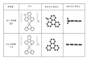
도9는, 예시 화합물 및 비교 화합물의 구조와, 배위자의 대칭성을 나타내는 모식도다.
도10은, 예시 화합물 및 비교 화합물의 구조와, 배위자의 대칭성을 나타내는 모식도다.
도11은, 예시 화합물 및 비교 화합물의 구조와, 배위자의 3차원 구조를 나타내는 모식도다.1A is a schematic cross-sectional view showing an example of a pixel of a display device according to an embodiment of the present invention.
1B is a schematic cross-sectional view of an example of a display device having an organic light emitting element according to an embodiment of the present invention.
2 is a schematic diagram showing an example of a display device according to an embodiment of the present invention.
Fig. 3A is a schematic diagram showing an example of an imaging device according to an embodiment of the present invention.
3B is a schematic diagram showing an example of a portable device according to an embodiment of the present invention.
4A is a schematic diagram showing an example of a display device according to an embodiment of the present invention.
4B is a schematic diagram showing an example of a bendable display device according to an embodiment of the present invention.
5A is a schematic diagram showing an example of a lighting device according to an embodiment of the present invention.
5B is a schematic diagram showing a car as an example of a moving body according to an embodiment of the present invention.
6A is a schematic diagram showing an example of a wearable device according to an embodiment of the present invention.
Fig. 6B is a schematic diagram showing an example of a wearable device having an imaging device according to an embodiment of the present invention.
Fig. 7 is a schematic diagram showing an example of an image forming apparatus according to an embodiment of the present invention.
Fig. 8 is a schematic diagram showing an example of an exposure light source of an image forming apparatus according to an embodiment of the present invention.
Fig. 9 is a schematic diagram showing the structure of exemplary compounds and comparative compounds and the symmetry of their ligands.
Fig. 10 is a schematic diagram showing the structure of exemplary compounds and comparative compounds and the symmetry of ligands.
Fig. 11 is a schematic diagram showing the structures of exemplary compounds and comparative compounds, and the three-dimensional structure of ligands.
<<유기 화합물>><<Organic Compounds>>
우선, 본 실시형태에 따른 유기 화합물에 대해 설명한다. First, the organic compound according to the present embodiment will be described.
본 실시형태에 따른 유기 화합물은, 하기 일반식 [1]로 표시되는 유기 화합물이다. 유기 배위자가 금속에 배위하고 있으므로, 유기 화합물은 유기 금속 착물로도 부를 수 있다. The organic compound according to the present embodiment is an organic compound represented by the following general formula [1]. Since the organic ligand is coordinated to the metal, the organic compound can also be called an organometallic complex.

일반식 [1]에 있어서, Ir는 이리듐을 나타낸다. L 및 L'은, 서로 다른 두자리 배위자를 나타낸다. m은 1 내지 3의 범위의 정수를 나타내고, m이 1일 때 n은 2이고, m이 2일 때 n은 1이고, m이 3일 때 n은 0이다. 부분 구조 IrL은 하기 일반식 [A-1] 또는 [A-2]로 표시되는 부분 구조를 나타내고, 부분 구조 IrL'은 하기 일반식 [B-1] 또는 [B-2]로 표시되는 부분 구조를 나타낸다. m이 2 이상일 때, L들은 같거나 달라도 된다. n이 2일 때, L'들은 같거나 달라도 된다. In general formula [1], Ir represents iridium. L and L' represent different bidentate ligands. m represents an integer in the range of 1 to 3, n is 2 when m is 1, n is 1 when m is 2, and n is 0 when m is 3. The partial structure IrL represents a partial structure represented by the following general formula [A-1] or [A-2], and the partial structure IrL' represents a partial structure represented by the following general formula [B-1] or [B-2] indicates When m is 2 or more, L's may be the same or different. When n is 2, L's may be the same or different.


일반식 [A-1], [A-2] 및 [B-2]에 있어서 Y1 내지 Y24는 탄소 원자 또는 질소 원자로부터 독립적으로 선택된다. Y1 내지 Y24가 탄소 원자를 나타내는 경우, 이 탄소 원자는 수소 원자, 중수소 원자 또는 치환기 R을 갖는다. Y1 내지 Y24 중의 2개 이상이 치환기 R을 갖는 탄소 원자를 나타내는 경우, 치환기 R은 같거나 다른 구조를 가져도 된다.In the general formulas [A-1], [A-2] and [B-2], Y 1 to Y 24 are independently selected from a carbon atom or a nitrogen atom. When Y 1 to Y 24 represent a carbon atom, the carbon atom has a hydrogen atom, a deuterium atom or a substituent R. When two or more of Y 1 to Y 24 represent carbon atoms having substituents R, substituents R may have the same or different structures.
상기 치환기 R은, 할로겐 원자, 치환 혹은 무치환의 알킬기, 치환 혹은 무치환의 알콕시기, 치환 혹은 무치환의 아미노기, 치환 혹은 무치환의 아릴옥시기, 치환 혹은 무치환의 실릴기, 시아노기, 치환 혹은 무치환의 방향족 탄화수소기, 및 치환 혹은 무치환의 헤테로 고리기로부터 독립적으로 선택되는 치환기를 나타낸다. The substituent R is a halogen atom, a substituted or unsubstituted alkyl group, a substituted or unsubstituted alkoxy group, a substituted or unsubstituted amino group, a substituted or unsubstituted aryloxy group, a substituted or unsubstituted silyl group, a cyano group, A substituent independently selected from a substituted or unsubstituted aromatic hydrocarbon group and a substituted or unsubstituted heterocyclic group is shown.
일반식 [A-1], [A-2] 및 [B-2]에 있어서 Y1 내지 Y24 중 어느 인접하는 2개가 동시에 탄소 원자를 나타내고, 또한 치환기 R을 갖는 경우, 치환기들 R이 서로 결합하여 고리를 형성해도 된다. 고리 구조는, 벤젠 고리, 나프탈렌 고리, 아진 고리, 티오펜 고리, 또는 푸란 고리이다.In general formulas [A-1], [A-2] and [B-2], when any two adjacent Y 1 to Y 24 simultaneously represent a carbon atom and also have a substituent R, the substituents R are mutually They may combine to form a ring. The ring structure is a benzene ring, a naphthalene ring, an azine ring, a thiophene ring or a furan ring.
일반식 [A-1] 및 [A-2]에 있어서, Z1 및 Z2는, 산소 원자, 유황 원자, SiR1R2, CR1R2, GeR1R2, NR1 및 CR1=CR2로부터 독립적으로 선택된다. R1 및 R2은 서로 결합해서 고리를 형성해도 된다.In general formulas [A-1] and [A-2], Z 1 and Z 2 are an oxygen atom, a sulfur atom, SiR 1 R 2 , CR 1 R 2 , GeR 1 R 2 , NR 1 and CR 1 = independently selected from CR 2 . R 1 and R 2 may be bonded to each other to form a ring.
일반식 [A-1], [A-2] 및 [B-1]에 있어서 R1 내지 R5는, 할로겐 원자, 치환 혹은 무치환의 알킬기, 시아노기, 치환 혹은 무치환의 방향족 탄화수소기, 및 치환 혹은 무치환의 헤테로 고리기로부터 독립적으로 선택된다.In general formulas [A-1], [A-2] and [B-1], R 1 to R 5 are a halogen atom, a substituted or unsubstituted alkyl group, a cyano group, a substituted or unsubstituted aromatic hydrocarbon group, and a substituted or unsubstituted heterocyclic group.
본 실시형태에 따른 유기 화합물에 있어서, 상기 일반식 [1]에 있어서 부분 구조 IrL이 하기 일반식 [A-11] 내지 [A-14]와 [A-21] 내지 [A-24] 중에서 한개로 표시되는 부분 구조일 수 있다. In the organic compound according to the present embodiment, in the general formula [1], the partial structure IrL is one of the following general formulas [A-11] to [A-14] and [A-21] to [A-24] It may be a partial structure represented by


일반식 [A-11] 내지 [A-14]와 [A-21] 내지 [A-24]에 있어서 X1 내지 X68은, 탄소 원자 또는 질소 원자로부터 독립적으로 선택된다. X1 내지 X68이 탄소 원자를 나타내는 경우, 이 탄소 원자는 수소 원자, 중수소 원자 또는 치환기 R을 갖는다. X1 내지 X68 중에서 2개 이상이 치환기 R을 갖는 탄소 원자를 나타내는 경우, 치환기들 R은 같거나 다른 구조를 가져도 된다.In general formulas [A-11] to [A-14] and [A-21] to [A-24], X 1 to X 68 are independently selected from a carbon atom or a nitrogen atom. When X 1 to X 68 represent a carbon atom, this carbon atom has a hydrogen atom, a deuterium atom or a substituent R. When two or more of X 1 to X 68 represent a carbon atom having a substituent R, the substituents R may have the same or different structures.
상기 치환기 R은, 할로겐 원자, 치환 혹은 무치환의 알킬기, 치환 혹은 무치환의 알콕시기, 치환 혹은 무치환의 아미노기, 치환 혹은 무치환의 아릴옥시기, 치환 혹은 무치환의 실릴기, 시아노기, 치환 혹은 무치환의 방향족 탄화수소기, 및 치환 혹은 무치환의 헤테로 고리기로부터 독립적으로 선택되는 치환기를 나타낸다. The substituent R is a halogen atom, a substituted or unsubstituted alkyl group, a substituted or unsubstituted alkoxy group, a substituted or unsubstituted amino group, a substituted or unsubstituted aryloxy group, a substituted or unsubstituted silyl group, a cyano group, A substituent independently selected from a substituted or unsubstituted aromatic hydrocarbon group and a substituted or unsubstituted heterocyclic group is shown.
일반식 [A-11] 내지 [A-14]와 [A-21] 내지 [A-24]에 있어서 X1 내지 X68 중 어느 인접하는 2개가 동시에 탄소 원자를 나타내고, 또한 치환기 R을 갖는 경우, 치환기들 R이 서로 결합하여 고리를 형성해도 된다. 고리 구조는, 벤젠 고리, 나프탈렌 고리, 아진 고리, 티오펜 고리, 또는 푸란 고리이다.In the general formulas [A-11] to [A-14] and [A-21] to [A-24], any two adjacent X 1 to X 68 represent carbon atoms at the same time and have a substituent R , Substituents R may combine with each other to form a ring. The ring structure is a benzene ring, a naphthalene ring, an azine ring, a thiophene ring or a furan ring.
일반식 [A-11] 및 [A-21]에 있어서 R6 내지 R9는, 할로겐 원자, 치환 혹은 무치환의 알킬기, 시아노기, 치환 혹은 무치환의 방향족 탄화수소기, 및 치환 혹은 무치환의 헤테로 고리기로부터 독립적으로 선택된다.In general formulas [A-11] and [A-21], R 6 to R 9 are a halogen atom, a substituted or unsubstituted alkyl group, a cyano group, a substituted or unsubstituted aromatic hydrocarbon group, and a substituted or unsubstituted independently selected from heterocyclic groups.
Y1 내지 Y24가 탄소 원자를 나타낼 때 탄소 원자의 옵션의 치환기 R, 및, X1 내지 X68이 탄소 원자를 나타낼 때 이 탄소 원자의 옵션의 치환기 R은, 할로겐 원자, 치환 혹은 무치환의 1 내지 10개의 탄소 원자를 갖는 알킬기, 치환 혹은 무치환의 1 내지 10개의 탄소 원자를 갖는 알콕시기, 치환 혹은 무치환의 1 내지 6개의 탄소 원자를 갖는 아미노기, 치환 혹은 무치환의 아릴옥시기, 치환 혹은 무치환의 실릴기, 시아노기, 치환 혹은 무치환의 6 내지 30개의 탄소 원자를 갖는 방향족 탄화수소기, 치환 혹은 무치환의 3 내지 27개의 탄소 원자를 갖는 헤테로 고리기로부터 독립적으로 선택되는 치환기를 나타낼 수 있다.Optional substituent R of a carbon atom when Y 1 to Y 24 represents a carbon atom, and optional substituent R of this carbon atom when X 1 to X 68 represent a carbon atom are halogen atoms, substituted or unsubstituted An alkyl group having 1 to 10 carbon atoms, a substituted or unsubstituted alkoxy group having 1 to 10 carbon atoms, a substituted or unsubstituted amino group having 1 to 6 carbon atoms, a substituted or unsubstituted aryloxy group, A substituent independently selected from a substituted or unsubstituted silyl group, a cyano group, a substituted or unsubstituted aromatic hydrocarbon group having 6 to 30 carbon atoms, and a substituted or unsubstituted heterocyclic group having 3 to 27 carbon atoms can represent
일반식 [A-1], [A-2] 및 [B-1]에 있어서 R1 내지 R5는, 할로겐 원자, 치환 혹은 무치환의 1 내지 10개의 탄소 원자를 갖는 알킬기, 시아노기, 치환 혹은 무치환의 방향족 탄화수소기, 치환 혹은 무치환의 헤테로 고리기로부터 독립적으로 선택될 수 있다.In general formulas [A-1], [A-2] and [B-1], R 1 to R 5 are a halogen atom, a substituted or unsubstituted alkyl group having 1 to 10 carbon atoms, a cyano group, or a substituted Or it may be independently selected from an unsubstituted aromatic hydrocarbon group and a substituted or unsubstituted heterocyclic group.
일반식 [A-11] 및 [A-21]에 있어서 R6 내지 R9는, 할로겐 원자, 치환 혹은 무치환의 1 내지 10개의 탄소 원자를 갖는 알킬기, 시아노기, 치환 혹은 무치환의 방향족 탄화수소기, 치환 혹은 무치환의 헤테로 고리기로부터 독립적으로 선택될 수 있다.In general formulas [A-11] and [A-21], R 6 to R 9 are a halogen atom, a substituted or unsubstituted alkyl group having 1 to 10 carbon atoms, a cyano group, or a substituted or unsubstituted aromatic hydrocarbon groups, substituted or unsubstituted heterocyclic groups.
Y1 내지 Y24가 탄소 원자를 나타낼 때 탄소 원자의 옵션의 치환기 R, 및, X1 내지 X68이 탄소 원자를 나타낼 때 이 탄소 원자의 옵션의 치환기 R인 옵션의 할로겐 원자, 및, R1 내지 R5의 할로겐 원자는, 불소, 염소, 브롬 또는 요오드이어도 되지만, 이것들에 한정되는 것은 아니다.an optional substituent R of a carbon atom when Y 1 to Y 24 represent a carbon atom, and an optional halogen atom which is an optional substituent R of this carbon atom when X 1 to X 68 represent a carbon atom, and R 1 The halogen atom of R 5 may be fluorine, chlorine, bromine or iodine, but is not limited thereto.
Y1 내지 Y24가 탄소 원자를 나타낼 때 이 탄소 원자의 옵션의 치환기 R, 및, X1 내지 X68이 탄소 원자를 나타낼 때 이 탄소 원자의 옵션의 치환기 R인 옵션의 알킬기, 및, R1 내지 R5의 알킬기는, 메틸기, 에틸기, n-프로필기, 이소프로필기, n-부틸기, t-부틸기, sec-부틸기, 옥틸기, 시클로헥실기, 1-아다만틸기 또는 2-아다만틸기일 수 있지만, 이것들에 한정되는 것은 아니다.an optional substituent R on this carbon atom when Y 1 to Y 24 represent a carbon atom, and an optional alkyl group which is an optional substituent R on this carbon atom when X 1 to X 68 represent a carbon atom, and R 1 The alkyl group of R 5 is methyl, ethyl, n-propyl, isopropyl, n-butyl, t-butyl, sec-butyl, octyl, cyclohexyl, 1-adamantyl or 2- Although it may be an adamantyl group, it is not limited to these.
Y1 내지 Y24가 탄소 원자를 나타낼 때 이 탄소 원자의 옵션의 치환기 R, 및, X1 내지 X68이 탄소 원자를 나타낼 때 이 탄소 원자의 옵션의 치환기 R인 옵션의 알콕시기는, 메톡시기, 에톡시기, 프로폭시기, 2-에틸-옥틸옥시기, 또는 벤질옥시기일 수 있지만, 이것들에 한정되는 것은 아니다.The optional substituent R of this carbon atom when Y 1 to Y 24 represents a carbon atom, and the optional alkoxy group which is the optional substituent R of this carbon atom when X 1 to X 68 represent a carbon atom are a methoxy group, It may be an ethoxy group, a propoxy group, a 2-ethyl-octyloxy group, or a benzyloxy group, but is not limited thereto.
Y1 내지 Y24가 탄소 원자를 나타낼 때 이 탄소 원자의 옵션의 치환기 R, 및, X1 내지 X68이 탄소 원자를 나타낼 때 이 탄소 원자의 옵션의 치환기 R인 옵션의 아미노기는, N-메틸아미노기, N-에틸아미노기, N,N-디메틸아미노기, N,N-디에틸아미노기, N-메틸-N-에틸아미노기, N-벤질아미노기, N-메틸-N-벤질아미노기, N,N-디벤질아미노기, 아닐리노기, N,N-디페닐아미노기, N,N-디나프틸아미노기, N,N-디플루오레닐아미노기, N-페닐-N-토릴아미노기, N,N-디토릴아미노기, N-메틸-N-페닐아미노기, N,N-디아니소릴아미노기, N-메시틸-N-페닐아미노기, N,N-디메시틸아미노기, N-페닐-N-(4-t-부틸페틸)아미노기, N-페닐-N-(4-트리플루오로메틸페닐)아미노기, 또는 N-피페리딜기일 수 있지만, 이것들에 한정되는 것은 아니다.Optional substituents R on carbon atoms when Y 1 to Y 24 represent carbon atoms, and optional amino groups which are optional substituents R on carbon atoms when X 1 to X 68 represent carbon atoms are N-methyl Amino group, N-ethylamino group, N,N-dimethylamino group, N,N-diethylamino group, N-methyl-N-ethylamino group, N-benzylamino group, N-methyl-N-benzylamino group, N,N-di Benzylamino group, anilino group, N,N-diphenylamino group, N,N-dinaphthylamino group, N,N-difluorenylamino group, N-phenyl-N-torylamino group, N,N-ditorylamino group , N-methyl-N-phenylamino group, N,N-dianisolylamino group, N-mesityl-N-phenylamino group, N,N-dimethylamino group, N-phenyl-N-(4-t-butyl methyl)amino group, N-phenyl-N-(4-trifluoromethylphenyl)amino group, or N-piperidyl group, but is not limited thereto.
Y1 내지 Y24가 탄소 원자를 나타낼 때 이 탄소 원자의 옵션의 치환기 R, 및, X1 내지 X68이 탄소 원자를 나타낼 때 이 탄소 원자의 옵션의 치환기 R인 옵션의 아릴옥시기 및 헤테로 아릴옥시기는, 페녹시기 또는 티에닐옥시기일 수 있지만, 이것들에 한정되는 것은 아니다.Optional aryloxy groups and heteroaryls which are optional substituents R on carbon atoms when Y 1 to Y 24 represent carbon atoms, and optional substituents R on carbon atoms when X 1 to X 68 represent carbon atoms; The oxy group may be a phenoxy group or a thienyloxy group, but is not limited thereto.
Y1 내지 Y24가 탄소 원자를 나타낼 때 이 탄소 원자의 옵션의 치환기 R, 및, X1 내지 X68이 탄소 원자를 나타낼 때 이 탄소 원자의 옵션의 치환기 R인 옵션의 실릴기는, 트리메틸실릴기, 또는 트리페닐실릴기일 수 있지만, 이것들에 한정되는 것은 아니다.When Y 1 to Y 24 represent a carbon atom, an optional substituent R on the carbon atom, and an optional silyl group, which is an optional substituent R on the carbon atom when X 1 to X 68 represent a carbon atom, is a trimethylsilyl group. , or a triphenylsilyl group, but is not limited thereto.
Y1 내지 Y24가 탄소 원자를 나타낼 때 이 탄소 원자의 옵션의 치환기 R, 및, X1 내지 X68이 탄소 원자를 나타낼 때 이 탄소 원자의 옵션의 치환기 R인 옵션의 방향족 탄화수소기, 및, R1 내지 R5의 방향족 탄화수소기는, 페닐기, 나프틸기, 인데닐기, 비페닐기, 테르페닐기, 플루오레닐기, 페난트릴기, 플루오란테닐기, 또는 트리페닐레닐기일 수 있지만, 이것들에 한정되는 것은 아니다.an optional aromatic hydrocarbon group which is an optional substituent R on this carbon atom when Y 1 to Y 24 represents a carbon atom, and an optional substituent R on this carbon atom when X 1 to X 68 represent a carbon atom; and, The aromatic hydrocarbon group represented by R 1 to R 5 may be a phenyl group, a naphthyl group, an indenyl group, a biphenyl group, a terphenyl group, a fluorenyl group, a phenanthryl group, a fluoranthenyl group, or a triphenylenyl group, but is not limited to these no.
Y1 내지 Y24가 탄소 원자를 나타낼 때 이 탄소 원자의 옵션의 치환기 R, 및, X1 내지 X68이 탄소 원자를 나타낼 때 이 탄소 원자의 옵션의 치환기 R인 옵션의 헤테로 고리기, 및, R1 내지 R5의 헤테로 고리기는, 피리딜기, 옥사졸릴기, 옥사디아졸릴기, 티아졸릴기, 티아디아졸릴기, 카바조릴기, 아크리디닐기, 페난트로릴기, 디벤조푸라닐기, 또는 디벤조티오페닐기일 수 있지만, 이것들에 한정되는 것은 아니다.an optional heterocyclic group which is an optional substituent R on this carbon atom when Y 1 to Y 24 represents a carbon atom, and an optional substituent R on this carbon atom when X 1 to X 68 represent a carbon atom, and, The heterocyclic group of R 1 to R 5 is a pyridyl group, an oxazolyl group, an oxadiazolyl group, a thiazolyl group, a thiadiazolyl group, a carbazolyl group, an acridinyl group, a phenanthroyl group, a dibenzofuranyl group, or a dibenzofuranyl group. Although it may be a benzothiophenyl group, it is not limited to these.
알킬기, 알콕시기, 아미노기, 아릴옥시기, 실릴기, 방향족 탄화수소기, 및 헤테로 고리기의 추가적인 옵션의 치환기는, 불소, 염소, 브롬, 또는 요오드 등의 할로겐 원자, 메틸기, 에틸기, n-프로필기, 이소프로필기, n-부틸기, t-부틸기 등의 알킬기, 메톡시기, 에톡시기, 또는 프로폭시기 등의 알콕시기, 디메틸아미노기, 디에틸아미노기, 디벤질아미노기, 디페닐아미노기, 또는 디토릴아미노기 등의 아미노기, 페녹시기 등의 아릴옥시기, 페닐기 또는 비페닐기 등의 방향족 탄화수소기, 피리딜기 또는 피롤릴기 등의 헤테로 고리기, 또는 시아노기일 수 있지만, 이것들에 한정되는 것은 아니다. Additional optional substituents of the alkyl group, alkoxy group, amino group, aryloxy group, silyl group, aromatic hydrocarbon group, and heterocyclic group are halogen atoms such as fluorine, chlorine, bromine, or iodine, methyl group, ethyl group, n-propyl group , Alkyl groups such as isopropyl group, n-butyl group and t-butyl group, alkoxy groups such as methoxy group, ethoxy group, or propoxy group, dimethylamino group, diethylamino group, dibenzylamino group, diphenylamino group, or dito It may be an amino group such as a lylamino group, an aryloxy group such as a phenoxy group, an aromatic hydrocarbon group such as a phenyl group or a biphenyl group, a heterocyclic group such as a pyridyl group or a pyrrolyl group, or a cyano group, but is not limited thereto.
유기 화합물의 합성 방법Methods for synthesizing organic compounds
다음에, 본 실시형태에 따른 유기 화합물의 합성 방법을 설명한다. 예를 들면, 본 실시형태에 따른 유기 화합물은 하기에 나타내는 반응 스킴에 따라 합성된다. Next, a method for synthesizing an organic compound according to the present embodiment will be described. For example, the organic compound according to the present embodiment is synthesized according to the reaction scheme shown below.


상기 (a), (b), (f), (h), (j), (k), (n), (p), (q) 및 (r)로 표시되는 화합물을 적절히 변경함으로써, 다양한 화합물을 얻을 수 있다. 본 발명은, 상기한 합성 스킴, 및 상기한 합성 스킴에 의해 합성된 화합물에 한정되는 것은 아니고, 다양한 합성 스킴 및 시약을 사용해도 된다. 합성 방법에 대해서는 실시예에서 상세하게 설명한다. By appropriately changing the compounds represented by (a), (b), (f), (h), (j), (k), (n), (p), (q) and (r), various compound can be obtained. The present invention is not limited to the above synthesis scheme and the compound synthesized by the above synthesis scheme, and various synthesis schemes and reagents may be used. The synthesis method is explained in detail in Examples.
본 실시형태에 따른 유기 화합물의 특징Characteristics of the organic compound according to the present embodiment
다음에, 본 실시형태에 따른 유기 화합물의 특징에 대해 설명한다. 본 실시형태에 따른 유기 화합물에서는, 부분 구조 IrL이 일반식 [A-1] 또는 [A-2]로 표시되는 부분 구조이다. 따라서, 배위자 L은, 디벤조[f,h]퀴놀린 골격을 갖고 있다고도 할 수 있다. Next, characteristics of the organic compound according to the present embodiment will be described. In the organic compound according to the present embodiment, the partial structure IrL is a partial structure represented by the general formula [A-1] or [A-2]. Therefore, it can also be said that the ligand L has a dibenzo[f,h]quinoline backbone.
본 실시형태에 따른 유기 화합물은, 이하와 같은 특징을 갖기 때문에, 양자 수율이 높다고 하는 특징을 갖는다. 본 실시형태에 따른 유기 화합물은 높은 승화성도 갖는다. 더구나, 이 유기 화합물을 사용함으로써, 발광 효율이 우수한 유기 발광 소자를 제공할 수도 있다. 또한, 이 유기 화합물을 사용함으로써, 소자 내구성이 우수한 유기 발광 소자를 제공할 수도 있다. Since the organic compound according to the present embodiment has the following characteristics, it has a high quantum yield. The organic compound according to the present embodiment also has high sublimability. Moreover, by using this organic compound, it is also possible to provide an organic light emitting element with excellent luminous efficiency. Further, by using this organic compound, an organic light emitting element having excellent element durability can be provided.
(1) 배위자가 디벤조[f,h]퀴놀린 골격이 Z1 또는 Z2에 의해 가교된 고리 구조를 갖기 때문에, 양자 수율이 높다.(1) Since the ligand has a ring structure in which the skeleton of dibenzo[f,h]quinoline is bridged by Z 1 or Z 2 , the quantum yield is high.
(2) 배위자가 디벤조[f,h]퀴놀린 골격이 Z1 또는 Z2에 의해 가교된 고리 구조를 갖기 때문에, 배위자의 대칭성이 저하하고 승화성이 높다.(2) Since the ligand has a ring structure in which the skeleton of dibenzo[f,h]quinoline is bridged by Z 1 or Z 2 , the symmetry of the ligand is lowered and the sublimation property is high.
이하, 이들 특징에 대해, 비교 화합물 1-b를 비교 대상으로 참조하여 설명한다. 비교 화합물 1-b는, PTL1에 기재된 화합물 1-a의 보조 배위자를 아세틸아세톤으로부터 페닐피리딘으로 변화시킨 화합물이다. Hereinafter, these characteristics are described with reference to Comparative Compound 1-b as a comparison object. Comparative compound 1-b is a compound in which the auxiliary ligand of compound 1-a described in PTL1 is changed from acetylacetone to phenylpyridine.
(1) 배위자가 디벤조[f,h]퀴놀린 골격이 Z1 또는 Z2에 의해 가교된 고리 구조를 갖기 때문에, 양자 수율이 높다.(1) Since the ligand has a ring structure in which the skeleton of dibenzo[f,h]quinoline is bridged by Z 1 or Z 2 , the quantum yield is high.
본 발명자들은, 본 발명의 유기 화합물을 발명함에 있어서, 유기 화합물의 배위자의 구조에 주목하였다. 더욱 구체적으로는, 디벤조[f,h]퀴놀린 골격을 갖는 배위자를 갖는 Ir 착물에 있어서, 배위자의 디벤조[f,h]퀴놀린 골격을 Z1 또는 Z2에 의해 가교해서 고리 구조를 형성함으로써 양자 수율을 향상시킨다.The present inventors paid attention to the structure of the ligand of the organic compound when inventing the organic compound of the present invention. More specifically, in an Ir complex having a ligand having a dibenzo[f,h]quinoline skeleton, by crosslinking the dibenzo[f,h]quinoline skeleton of the ligand with Z 1 or Z 2 to form a ring structure, improve the quantum yield.
표 1은, 본 실시형태에 따른 유기 화합물인 예시 화합물 A21과 비교 화합물 1-b의 발광 특성의 비교 결과를 나타낸다. 발광 파장은 히타치제 F-4500을 사용하여, 실온에서 여기 파장 350nm에 있어서의 희석 톨루엔 용액의 포토루미네센스(PL) 측정으로 측정을 행하였다. 양자 수율, 희석 톨루엔 용액의 절대 양자 수율을 하마마쯔포토닉스사제의 절대 PL 양자 수율 측정장치(C9920-02)를 사용해서 측정함으로써 결정하였다. 양자 수율은 예시 화합물 A21의 양자 수율을 1.0으로 설정하여 이것에 대한 상대값으로 나타낸다. Table 1 shows the comparison results of emission characteristics of Example Compound A21, which is an organic compound according to the present embodiment, and Comparative Compound 1-b. The emission wavelength was measured by photoluminescence (PL) measurement of a diluted toluene solution at an excitation wavelength of 350 nm at room temperature using F-4500 manufactured by Hitachi. The quantum yield and the absolute quantum yield of the diluted toluene solution were determined by measuring using an absolute PL quantum yield measuring device (C9920-02) manufactured by Hamamatsu Photonics. The quantum yield is expressed as a relative value with respect to the quantum yield of Exemplary Compound A21 set to 1.0.

표 1은, 비교 화합물 1-b보다도, 예시 화합물 A21 쪽이 양자 수율이 높고 발광 특성이 우수한 것을 나타낸다. 본 발명자들은 이것에 대해 아래와 같이 고찰을 행하였다. Table 1 shows that Exemplified Compound A21 has a higher quantum yield and superior emission characteristics than Comparative Compound 1-b. The present inventors conducted consideration about this as follows.
2가지 화합물의 구조상의 차이는, 배위자 중의 디벤조[f,h]퀴놀린 구조가 가교된 고리 구조를 형성하고 있는지 아닌지이다. 더욱 구체적으로는, 비교 화합물 1-b에서는, 배위자가 디벤조[f,h]퀴놀린 골격 중의 2개의 탄소 원자가 가교된 고리 구조를 형성하지 않고 있다. 이에 대해, 예시 화합물 A21은, 배위자 내부의 디벤조[f,h]퀴놀린 골격 중의 2개의 탄소 원자 사이가 디메틸메틸렌기에 의해 가교된 고리 구조를 갖는다. The structural difference between the two compounds is whether or not the dibenzo[f,h]quinoline structure in the ligand forms a bridged ring structure. More specifically, in Comparative Compound 1-b, the ligand does not form a ring structure in which two carbon atoms in the backbone of dibenzo[f,h]quinoline are bridged. In contrast, Exemplified Compound A21 has a ring structure in which two carbon atoms in a dibenzo[f,h]quinoline backbone inside the ligand are bridged by a dimethylmethylene group.
하기 식으로 표시되는 것과 같이, 포토루미네센스 양자 수율(PLQY)은, 여기상태로부터 기저상태로의 복사 천이(발광)와 무복사 천이(비발광)의 속도 상수로부터 구해진다. 하기 식에 있어서, kr는 복사 천이의 속도 상수(복사 감쇠 속도)를 나타내고, knr는 무복사 천이의 속도 상수(무복사 감쇠 속도)를 나타낸다. 복사 감쇠 속도(kr)는, 하기 식으로 표시되는 것과 같이, 천이 쌍극자 모멘트(transition dipole moment: TDM)의 제곱에 비례한다(Phys. Chem. Chem. Phys. 16, 1719-1758(2014)을 참조). As expressed by the following formula, the photoluminescence quantum yield (PLQY) is obtained from the rate constants of the radiative transition from the excited state to the ground state (light emission) and the non-radiative transition (non-emitting). In the following equation, kr represents a rate constant of radiative transition (radiative decay rate), and knr represents a rate constant of non-radiative transition (radiative decay rate). The radiation decay rate (kr) is proportional to the square of the transition dipole moment (TDM), as expressed by the following equation (see Phys. Chem. Chem. Phys. 16, 1719-1758 (2014)). ).

ΔE: T1과 S0의 에너지 차ΔE: energy difference between T 1 and S 0
h: 프랑크 상수h: Frank's constant
c: 광속c: speed of light
이 식은, 포토루미네센스 양자 수율 PLQY를 높이기 위해서는 복사 감쇠 속도(kr)를 크게 하는 것이 유효한 것을 나타낸다. 복사 감쇠 속도(kr)는 전술한 것과 같이 천이 쌍극자 모멘트의 제곱에 비례하기 때문에, 천이 쌍극자 모멘트를 크게 하는 것이 유효하다. This expression shows that it is effective to increase the radiation attenuation rate kr in order to increase the photoluminescence quantum yield PLQY. Since the radiation attenuation rate kr is proportional to the square of the transition dipole moment as described above, it is effective to increase the transition dipole moment.
Ir 착물에 있어서의 천이 쌍극자 모멘트는, 최고 점유 분자 오비탈(HOMO)과 최저 비점유 분자 오비탈(LUMO) 사이의 전하 이동성(charge transfer: CT)의 크기에 비례한다(J. Phys. Chem. 94, 239-243(1990)을 참조). Ir 착물에 있어서, HOMO는 Ir 금속과 σ결합하는 방향 고리에 분포하고, LUMO는 Ir 금속과 배위결합하는 헤테로 고리에 분포한다. 예를 들면, 대표적인 Ir 착물인 Ir(ppy)3에서는, HOMO가 벤젠 고리에 분포하고, LUMO가 피리딘 고리에 분포하는 것이 알려져 있다.The transition dipole moment in an Ir complex is proportional to the magnitude of the charge transfer (CT) between the highest occupied molecular orbital (HOMO) and the lowest unoccupied molecular orbital (LUMO) (J. Phys. Chem. 94, 239-243 (1990)). In the Ir complex, HOMO is distributed in an aromatic ring σ-bonded with Ir metal, and LUMO is distributed in a hetero ring coordinated with Ir metal. For example, in Ir(ppy) 3 , which is a typical Ir complex, it is known that HOMO is distributed on the benzene ring and LUMO is distributed on the pyridine ring.
본 발명자들은, 디벤조[f,h]퀴놀린 골격을 갖는 배위자를 갖는 Ir 착물에 있어서, 디벤조[f,h]퀴놀린 골격 중의 원자 사이를 가교해서 고리 구조를 형성함으로써, 방향 고리 부위와 헤테로 고리 부위 사이의 CT성을 향상시킬 수 있는 것을 발견하였다. 더욱 구체적으로는, 디벤조[f,h]퀴놀린 골격 중의 Ir 금속과 결합하는 원자를 포함하는 6개의 원자로 이루어진 방향 고리 또는 헤테로 고리에 있어서 Ir 금속에 대해 파라 위치에 해당하는 위치에 가교 구조를 가짐으로써 CT성을 향상시킬 수 있다는 것을 발견하였다. 더욱 구체적으로는, 디벤조[f,h]퀴놀린 골격의 9 위치 또는 4 위치에, 가교 구조를 가짐으로써 CT성을 향상시킬 수 있다는 것을 발견하였다. 이 결과, 천이 쌍극자 모멘트가 증가될 수 있고, 포토루미네센스 양자 수율 PLQY를 높일 수 있다. The inventors of the present invention, in an Ir complex having a ligand having a dibenzo[f,h]quinoline skeleton, form a ring structure by crosslinking atoms in the dibenzo[f,h]quinoline skeleton, thereby forming an aromatic ring moiety and a heterocyclic ring. It was found that CT properties between sites could be improved. More specifically, in the dibenzo[f,h]quinoline skeleton, an aromatic ring or heterocyclic ring composed of 6 atoms including an atom bonded to Ir metal has a bridge structure at a position corresponding to the para position with respect to the Ir metal. It was found that the CT properties could be improved by this. More specifically, it was found that CT properties can be improved by having a cross-linked structure at the 9-position or 4-position of the dibenzo[f,h]quinoline backbone. As a result, the transition dipole moment can be increased, and the photoluminescence quantum yield PLQY can be increased.
도9에 나타낸 것과 같이, 예시 화합물 A21에서는, Ir 금속과 σ결합하는 탄소 원자를 포함하는 6개의 원자로 이루어진 방향 고리가, Ir 금속에 대해 파라 위치에 해당하는 위치에 메틸렌 사슬(디메틸메틸렌기)을 거쳐 가교 구조를 갖는다. HOMO가 분포하는 방향 고리 내부의 전자 공여성 알킬기는 전자 공여성을 향상시켜, 전하의 분극을 일으켜, CT성을 향상시킨다. As shown in FIG. 9, in Exemplary Compound A21, an aromatic ring composed of 6 atoms including a carbon atom σ-bonded with Ir metal has a methylene chain (dimethylmethylene group) at a position corresponding to the para position with respect to Ir metal. has a cross-linked structure. The electron-donating alkyl group inside the aromatic ring in which HOMO is distributed improves the electron-donating ability, causes charge polarization, and improves the CT property.
예시 화합물 G1에서는, Ir 금속과 배위결합하는 질소 원자를 포함하는 6개의 원자로 이루어진 헤테로 고리가, Ir 금속에 대해 파라 위치에 해당하는 위치에 산소 원자를 거쳐 가교 구조를 갖는다. LUMO가 분포하는 헤테로 고리 내부의 전기음성도가 높은 산소 원자는, 전자 흡인성을 향상시켜, 전하의 분극을 일으켜, CT성을 향상시킨다. In Exemplary Compound G1, a six-membered hetero ring including a nitrogen atom coordinating with Ir metal has a cross-linked structure via an oxygen atom at a position corresponding to the para position with respect to Ir metal. Oxygen atoms with high electronegativity inside the heterocycle in which LUMO is distributed improve electron-attracting properties, cause charge polarization, and improve CT properties.
방향 고리가 전자 공여성의 치환기에 의해 가교된 구조, 및, 헤테로 고리가 전자 흡인성의 치환기에 의해 가교된 구조를 예시했지만, 본 발명은 이들 구조에 한정되지 않는다. 보다 구체적으로는, 가교 구조를 구성하는 치환기가 전자 공여성인지 또는 전자 흡인성인지에 무관하계, 상기 일반식 [A-1] 또는 [A-2]로 표시되는 부분 구조 IrL은 대칭성을 무너뜨려 방향 고리 또는 헤테로 고리에 전하의 분극을 생기게 할 수 있다. 이에 따라, CT성이 향상되고, 천이 쌍극자 모멘트가 높아져, 복사 감쇠 속도(kr)가 높아진다. 이 결과, 포토루미네센스 양자 수율(PLQY)이 향상된다고 생각된다. Structures in which aromatic rings are crosslinked by electron-donating substituents and structures in which heterocycles are crosslinked by electron-withdrawing substituents have been exemplified, but the present invention is not limited to these structures. More specifically, irrespective of whether the substituent constituting the cross-linked structure is electron-donating or electron-withdrawing, the partial structure IrL represented by the general formula [A-1] or [A-2] breaks symmetry and It is possible to create a polarization of charge in a ring or heterocyclic ring. Accordingly, the CT property is improved, the transition dipole moment is increased, and the radiation attenuation rate (kr) is increased. As a result, it is thought that the photoluminescence quantum yield (PLQY) is improved.
한편, 본 실시형태에 따른 유기 화합물과 비교하여, 비교 화합물 1-b에서의 디벤조[f,h]퀴놀린 골격을 갖는 배위자는 더 높은 대칭성을 갖고 전하의 분극이 적다. 그 때문에, CT성이 낮고, 천이 쌍극자 모멘트가 낮아, 양자 수율이 낮은 결과로 되었다고 생각된다. On the other hand, compared to the organic compound according to the present embodiment, the ligand having a dibenzo[f,h]quinoline skeleton in Comparative Compound 1-b has higher symmetry and less charge polarization. Therefore, it is considered that the CT property is low, the transition dipole moment is low, and the quantum yield is low.
상기 식은, 포토루미네센스 양자 수율(PLQY)을 높이기 위해서는, 무복사 감쇠 속도(knr)를 작게 하는 것도 유효하다는 것을 나타낸다. The above formula shows that in order to increase the photoluminescence quantum yield (PLQY), it is also effective to reduce the no-radiation decay rate (knr).
무복사 천이(무복사 실활)는, 분자의 여기상태의 에너지를 분자의 진동 모드로 변환함으로써 생기는 실활과정이다. 분자의 진동을 억제하면, 무복사 천이를 저감시킬 수 있다. 분자의 진동을 억제하기 위해서는, 분자의 강직성을 향상시키는 것이 유효하다. 이것은, 강직성이 높은 분자에서는, 분자를 형성하는 결합의 신축 진동, 회전 진동, 및 변각 진동이 더 작기 때문이다. Radiation-free transition (radiative-free deactivation) is a deactivation process that occurs by converting the energy of an excited state of a molecule into a vibrational mode of a molecule. If molecular vibration is suppressed, the non-radiative transition can be reduced. In order to suppress molecular vibration, it is effective to improve molecular rigidity. This is because, in a molecule with high rigidity, the stretching vibration, rotational vibration, and rotational vibration of the bonds forming the molecule are smaller.
본 실시형태에 따른 유기 화합물에서는, 배위자가, 디벤조[f,h]퀴놀린 골격 중의 원자가 가교된 구조를 갖는다. 이 때문에, 이 배위자는 가교 구조가 없는 단순한 디벤조[f,h]퀴놀린 배위자보다도 더 적은 진동을 가져 강직성이 향상된다. 이에 따라, 가교 구조가 없는 배위자에 비해 배위자가 더 작은 무복사 감쇠 속도(knr)와 더 높은 포토루미네센스 양자 수율(PLQY)을 갖는다고 생각된다. In the organic compound according to the present embodiment, the ligand has a structure in which atoms in the dibenzo[f,h]quinoline skeleton are bridged. Because of this, this ligand has less vibration than a simple dibenzo[f,h]quinoline ligand without a cross-linked structure, and the rigidity is improved. Accordingly, it is thought that the ligand has a smaller radiative decay rate (knr) and a higher photoluminescence quantum yield (PLQY) than a ligand without a cross-linked structure.
(2) 배위자가 디벤조[f,h]퀴놀린 골격이 Z1 또는 Z2에 의해 가교된 고리 구조를 갖기 때문에, 배위자의 대칭성이 저하하여, 승화성이 높다.(2) Since the ligand has a ring structure in which the skeleton of dibenzo[f,h]quinoline is crosslinked by Z 1 or Z 2 , the symmetry of the ligand is reduced and the sublimation property is high.
본 발명자들은, 본 발명에 따른 유기 화합물을 발명함에 있어서, 배위자의 구조의 대칭성에 주목하였다. 단순화해서 배위자의 구조의 대칭성을 논의하기 위해, 도10에 나타낸 것과 같이, 질소 원자를 탄소 원자로 가정하여, 배위자의 분자구조를 비교한다. 비교 화합물 1-b의 배위자는, 분자 평면에 대해 수직한 1개의 3회 회전축과 분자 평면에 대해 평행한 3개의 2회 회전축으로 인해(도10에 있어서 점선으로 도시) 높은 대칭성을 갖는다. 한편, 예시 화합물 A21은, 전술한 가교 구조와, 분자 평면에 대해 평행한 단지 1개의 2회 회전축(도10에 있어서 점선으로 도시)으로 인해 비교 화합물 1-b보다도 더 낮은 대칭성을 갖는다. The present inventors paid attention to the symmetry of the structure of the ligand when inventing the organic compound according to the present invention. In order to simplify and discuss the symmetry of the structure of the ligand, as shown in Fig. 10, nitrogen atoms are assumed to be carbon atoms, and molecular structures of the ligands are compared. The ligand of Comparative Compound 1-b has high symmetry due to one 3-fold axis of rotation perpendicular to the molecular plane and 3 2-fold axes of rotation parallel to the molecular plane (shown by dotted lines in FIG. 10). On the other hand, Exemplified Compound A21 has a lower symmetry than Comparative Compound 1-b due to the above-described cross-linked structure and only one double axis of rotation parallel to the molecular plane (shown by a dotted line in Fig. 10).
배위자의 대칭성을 저하시킴으로써 승화 온도를 저하시킬 수 있다. 이것은, 배위자의 대칭성이 낮은 경우, 유기 화합물이 응집하기 어려워지기 때문이다. 한편, 배위자의 대칭성이 높으면 유기 화합물이 응집하기 쉬워지기 때문에, 승화 온도가 높아진다. 승화 온도가 낮으면, 승화 온도와 열분해 온도 사이의 온도차를 크게 할 수 있고, 승화시의 열분해를 억제할 수 있어, 승화성을 높일 수 있다. The sublimation temperature can be lowered by lowering the symmetry of the ligand. This is because, when the symmetry of the ligand is low, the organic compound becomes difficult to aggregate. On the other hand, when the symmetry of the ligand is high, the organic compound tends to aggregate, so the sublimation temperature increases. When the sublimation temperature is low, the temperature difference between the sublimation temperature and the thermal decomposition temperature can be increased, thermal decomposition at the time of sublimation can be suppressed, and the sublimation property can be improved.
도10은, 본 실시형태에 따른 유기 화합물인 예시 화합물 A21과 비교 화합물 1-b의 승화성을 비교한 결과를 나타낸다. 승화성의 평가를 위해, 승화 온도와 분해 온도의 차이를 비교한다. 이 온도차가 클수록 승화성이 높다고 할 수 있다. 분해 온도는, TG/DTA 측정에서 중량 감소가 5%에 도달하는 온도이다. 승화 온도는, 1×10⁻¹Pa의 진공도에 있어서, Ar 플로우에서 서서히 승온하여, 승화 정제를 행하는 동안, 충분한 승화 속도에 도달했을 때의 온도이다.Fig. 10 shows the results of comparing the sublimation properties of Exemplary Compound A21, which is an organic compound according to the present embodiment, and Comparative Compound 1-b. For evaluation of sublimability, the difference between sublimation temperature and decomposition temperature is compared. It can be said that the sublimation property is high, so that this temperature difference is large. The decomposition temperature is the temperature at which the weight loss reaches 5% in TG/DTA measurements. The sublimation temperature is a temperature when a sufficient sublimation rate is reached during sublimation purification by gradually increasing the temperature with an Ar flow at a vacuum degree of 1×10 -1 Pa.
도10은, 본 실시형태에 따른 유기 화합물인 예시 화합물 A21은, 승화 온도와 분해 온도의 온도차가 커서, 승화성이 높은 재료인 것을 나타낸다. 또한, 높은 승화성으로 인해, 분해하지 않고 안정적으로 승화 정제할 수 있다. 이것은, 유기 발광 소자를 제작할 때의 증착 안정성이 높은 것도 나타내고 있다. 더욱 구체적으로는, 증착시에 분해하지 않고 고순도의 증착막을 형성할 수 있어, 장수명의 유기 발광 소자를 제공할 수 있다. Fig. 10 shows that Exemplified Compound A21, which is an organic compound according to the present embodiment, has a large temperature difference between sublimation temperature and decomposition temperature, and thus is a material with high sublimation properties. In addition, because of its high sublimability, it can be stably purified by sublimation without decomposition. This also shows that deposition stability at the time of manufacturing an organic light emitting element is high. More specifically, it is possible to form a high-purity deposited film without decomposition during deposition, thereby providing an organic light emitting device with a long lifespan.
대칭성이 낮은 것은 다음과 같은 장점도 제공한다. 비교 화합물 1-b는, π 공역계가 넓어진 디벤조[f,h]퀴놀린 구조의 배위자를 갖고 있다. 이 때문에, π-π 상호작용에 의해 유기 화합물이 응집하기 쉬워, 유기 발광 소자에서 농도 소광을 일으키기 쉽다. 한편, 본 실시형태에 따른 유기 화합물은, 배위자가 디벤조[f,h]퀴놀린 골격을 갖고 있지만, 전술한 가교 구조로 인해 대칭성이 저하하고 있다. 이 때문에, 가교 구조가 없는 화합물에 비해 π-π 상호작용이 억제되어, 유기 화합물의 응집을 억제할 수 있다. 이에 따라, 적은 농도 소광을 갖는 고효율의 유기 발광 소자를 제공할 수 있다. Low symmetry also provides the following advantages: Comparative Compound 1-b has a dibenzo[f,h]quinoline structure ligand with a widened π-conjugated system. For this reason, organic compounds tend to aggregate due to π-π interaction, and concentration quenching easily occurs in the organic light emitting element. On the other hand, in the organic compound according to the present embodiment, although the ligand has a dibenzo[f,h]quinoline skeleton, the symmetry is lowered due to the above-described crosslinked structure. For this reason, the π-π interaction is suppressed compared to a compound without a crosslinked structure, and aggregation of organic compounds can be suppressed. Accordingly, it is possible to provide a highly efficient organic light emitting device having low concentration quenching.
본 실시형태에 따른 유기 화합물의 특징 (1) 및 (2)의 평가는, 후술하는 실시예에서 더욱 상세하게 서술한다. Evaluation of the characteristics (1) and (2) of the organic compound according to the present embodiment will be described in more detail in Examples to be described later.
다음에, 부분 구조 IrL이 전술한 일반식 [A-11] 내지 [A-14]와 [A-21] 내지 [A-24] 중 어느 한 개로 표시되는 부분 구조인 유기 화합물의 다른 특징에 대해 설명한다. 이들 유기 화합물은 이하와 같은 특징을 갖기 때문에, 유기 발광 소자에 적합하게 사용할 수 있다. Next, about other characteristics of organic compounds in which the partial structure IrL is a partial structure represented by any one of the general formulas [A-11] to [A-14] and [A-21] to [A-24] described above. Explain. Since these organic compounds have the following characteristics, they can be suitably used for organic light emitting devices.
(3) 일반식 [A-1] 또는 [A-2]에 있어서 Z1 또는 Z2가 SiR1R2, CR1R2 및 GeR1R2 중 어느 한개인 경우, 디벤조[f,h]퀴놀린 구조의 면내 방향에 대해 수직한 방향으로 신장하는 치환기가 승화성을 더 향상시킨다.(3) In the general formula [A-1] or [A-2], when Z 1 or Z 2 is any one of SiR 1 R 2 , CR 1 R 2 and GeR 1 R 2 , dibenzo[f,h ] Substituents extending in a direction perpendicular to the in-plane direction of the quinoline structure further improve sublimation properties.
(4) 일반식 [A-1] 또는 [A-2]에 있어서 Z1 또는 Z2가 산소 원자 또는 유황 원자인 경우, 산소 원자 또는 유황 원자의 비공유 전자쌍이 CT성을 향상시켜, 양자 수율을 더 증진시킨다.(4) In general formula [A-1] or [A-2], when Z 1 or Z 2 is an oxygen atom or a sulfur atom, the non-shared electron pair of the oxygen atom or sulfur atom improves the CT property and increases the quantum yield. further promote
(5) 부분 구조 IrL이 일반식 [A-14] 또는 [A-24]로 표시되는 경우, 배위자의 기본 골격을 구성하는 탄소 원자가 sp2 탄소만으로 구성되기 때문에, 배위자가 더 높은 화학 안정성을 갖는다. (5) When the partial structure IrL is represented by the general formula [A-14] or [A-24], the ligand has higher chemical stability because the carbon atoms constituting the basic skeleton of the ligand are composed only of sp2 carbon.
이하, 이들 특징에 대해 설명한다. Hereinafter, these characteristics are demonstrated.
(3) 일반식 [A-1] 또는 [A-2]에 있어서 Z1 또는 Z2가 SiR1R2, CR1R2 및 GeR1R2 중 어느 한개인 경우, 디벤조[f,h]퀴놀린 구조의 면내 방향에 대해 수직한 방향으로 신장하는 치환기가 승화성을 더 향상시킨다.(3) In the general formula [A-1] or [A-2], when Z 1 or Z 2 is any one of SiR 1 R 2 , CR 1 R 2 and GeR 1 R 2 , dibenzo[f,h ] Substituents extending in a direction perpendicular to the in-plane direction of the quinoline structure further improve sublimation properties.
일반식 [A-1] 또는 [A-2]로 표시되는 것과 같이, 본 실시형태에 따른 유기 화합물은 디벤조[f,h]퀴놀린 골격을 기본 골격으로 갖고 π 공역계가 넓어진 평면성이 높은 배위자를 갖고 있다. 전술한 가교 구조는 배위자의 대칭성을 저하시켜, 배위자들의 스택킹을 억제한다. Z1 또는 Z2가 SiR1R2, CR1R2 및 GeR1R2 중 어느 한개인 경우에는, 치환기 R1 및 R2가 배위자의 평면성을 저하시킬 수 있어, 배위자들의 스택킹을 한층 더 억제할 수 있다.As represented by the general formula [A-1] or [A-2], the organic compound according to the present embodiment comprises a highly planar ligand having a dibenzo[f,h]quinoline skeleton as a basic skeleton and having a widened π-conjugated system. I have it. The aforementioned cross-linked structure lowers the symmetry of the ligands, thereby suppressing the stacking of the ligands. When Z 1 or Z 2 is any one of SiR 1 R 2 , CR 1 R 2 and GeR 1 R 2 , the substituents R 1 and R 2 can reduce the planarity of the ligand, further enhancing the stacking of the ligands. can be suppressed
예시 화합물 A21과 비교 화합물 1-b의 배위자들의 평면성을 비교한다. 도11에 나타낸 것과 같이, 예시 화합물 A21에서는, 배위자가 디메틸메틸렌기를 거쳐 가교된 구조를 갖고, 메틸렌 사슬에 결합하는 치환기(메틸기)가 배위자 면내에 대해 수직한 방향으로 신장한다. 이 때문에, 이 치환기의 입체장해 작용에 의해 배위자들이 응집하기 어려워지기 때문에, 유기 화합물들의 응집을 한층 더 억제할 수 있다. 이것은 승화 온도를 보다 저하시킬 수 있고, 승화성을 더욱 향상시킬 수 있다. 이 때문에, 유기 화합물은 농도 소광에 대한 더 높은 내성을 가질 수 있다. Planarity of the ligands of Exemplary Compound A21 and Comparative Compound 1-b is compared. As shown in Fig. 11, in Exemplified Compound A21, the ligand has a structure in which the ligand is crosslinked via a dimethylmethylene group, and the substituent (methyl group) bonded to the methylene chain extends in a direction perpendicular to the inside of the ligand plane. For this reason, since it becomes difficult for ligands to aggregate due to the steric hindering action of this substituent, aggregation of organic compounds can be further suppressed. This can further lower the sublimation temperature and further improve the sublimation properties. Because of this, organic compounds can have a higher resistance to concentration quenching.
특히, 일반식 [A-1] 또는 [A-2]에 있어서 Z1 또는 Z2는 CR1R2일 수 있다. 바꿔 말하면, 부분 구조 IrL이 일반식 [A-11] 또는 [A-21]로 표시될 수 있다.In particular, Z 1 or Z 2 in Formula [A-1] or [A-2] may be CR 1 R 2 . In other words, the partial structure IrL can be represented by the general formula [A-11] or [A-21].
(4) 일반식 [A-1] 또는 [A-2]에 있어서 Z1 또는 Z2가 산소 원자 또는 유황 원자인 경우, 산소 원자 또는 유황 원자의 비공유 전자쌍이 CT성을 향상시켜, 양자 수율을 더 증진시킨다.(4) In general formula [A-1] or [A-2], when Z 1 or Z 2 is an oxygen atom or a sulfur atom, the non-shared electron pair of the oxygen atom or sulfur atom improves the CT property and increases the quantum yield. further promote
일반식 [A-1] 또는 [A-2]에 있어서 Z1 또는 Z2가 산소 원자 또는 유황 원자인 경우, 본 실시형태에 따른 유기 화합물은, 디벤조[f,h]퀴놀린 골격 내의 산소 원자 또는 유황 원자에 의해 탄소 원자가 가교된 구조를 갖는다. 산소 원자는 높은 전기음성도와 풍부한 비공유 전자쌍을 갖고, 유황 원자는 풍부한 비공유 전자쌍을 갖는다. 이 때문에, Z1 또는 Z2의 산소 원자 또는 유황 원자가 배위자 내의 분극을 증진시켜, 전자밀도의 변화량을 증가시키고, 이에 따라 CT성을 보다 높일 수 있다. 그 결과, 표 2에 나타낸 것과 같이, 유기 화합물은 더 양자 수율을 갖는다. 양자 수율은 전술한 것과 같이 측정되며, 예시 화합물 A21의 양자 수율을 1.0으로 설정하여 이것에 대한 상대값에 의해 나타낸다.When Z 1 or Z 2 is an oxygen atom or a sulfur atom in the general formula [A-1] or [A-2], the organic compound according to the present embodiment is an oxygen atom in the dibenzo[f,h]quinoline skeleton. or a structure in which carbon atoms are cross-linked by sulfur atoms. Oxygen atoms have high electronegativity and an abundance of lone pairs, and sulfur atoms have an abundance of lone pairs. For this reason, the polarization of the oxygen atom or sulfur atom of Z 1 or Z 2 in the ligand is enhanced to increase the amount of change in electron density, thereby further enhancing CT properties. As a result, as shown in Table 2, organic compounds have higher quantum yields. The quantum yield is measured as described above, and the quantum yield of Exemplary Compound A21 is set to 1.0 and expressed by a relative value.

따라서, 양자 수율의 관점에서, 일반식 [A-1] 또는 [A-2]에 있어서 Z1 또는 Z2가 산소 원자 또는 유황 원자일 수 있다. 바꿔 말하면, 부분 구조 IrL이, 일반식 [A-12], [A-13], [A-22] 및 [A-23] 중 어느 한 개로 표시될 수 있다.Therefore, from the viewpoint of quantum yield, Z 1 or Z 2 in the general formula [A-1] or [A-2] may be an oxygen atom or a sulfur atom. In other words, the partial structure IrL can be represented by any one of general formulas [A-12], [A-13], [A-22] and [A-23].
(5) 부분 구조 IrL이 일반식 [A-14] 또는 [A-24]로 표시되는 경우, 배위자의 기본 골격을 구성하는 탄소 원자가 sp2 탄소만으로 구성되기 때문에, 배위자가 더 높은 화학 안정성을 갖는다. (5) When the partial structure IrL is represented by the general formula [A-14] or [A-24], the ligand has higher chemical stability because the carbon atoms constituting the basic skeleton of the ligand are composed only of sp2 carbon.
부분 구조 IrL이 일반식 [A-14] 또는 [A-24]로 표시되는 경우, 본 실시형태에 따른 유기 화합물은, 디벤조[f,h]퀴놀린 골격 내의 에틸렌 사슬에 의해 탄소 원자가 가교된 구조를 갖는다. 이러한 구조는, 유기 화합물의 배위자의 화학 안정성을 향상시킬 수 있다. 이것은, 배위자의 기본 골격을 구성하는 탄소 원자가 sp2 탄소 만으로 구성되기 때문이다. 바꿔 말하면, 배위자 L의 기본 골격을 구성하는 탄소 원자가 sp2 탄소 만으로 구성될 수 있다. 본 명세서에 있어서 배위자의 기본 골격은, 일반식 [A-1] 또는 [A-2]에 있어서 Y1 내지 Y16의 모두가 수소 원자를 갖는 탄소 원자인 구조를 가리킨다.When the partial structure IrL is represented by the general formula [A-14] or [A-24], the organic compound according to the present embodiment has a structure in which carbon atoms are bridged by ethylene chains in the dibenzo[f,h]quinoline skeleton have Such a structure can improve the chemical stability of the ligand of an organic compound. This is because the carbon atoms constituting the basic skeleton of the ligand are composed only of sp2 carbon. In other words, the carbon atoms constituting the basic skeleton of the ligand L may be composed only of sp2 carbon. In the present specification, the basic skeleton of the ligand refers to a structure in which all of Y 1 to Y 16 in general formula [A-1] or [A-2] are carbon atoms having hydrogen atoms.
유기 발광 소자에서는, 소자 구동중에 산화 환원이 반복하여 일어나고, 또한, 소자가 여기상태의 고에너지 분자를 갖는다. 그 때문에, 소자를 형성하는 분자는, 산화 환원에 대해 안정적이고, 고에너지 상태에 있어서도 쪼개지지 않는 결합 에너지가 높은 결합 만으로 이루어진 구조를 가질 수 있다. In an organic light emitting element, redox repeatedly occurs during driving of the element, and the element has high-energy molecules in an excited state. Therefore, the molecules forming the element can have a structure composed only of bonds with high bonding energy that are stable against redox and cannot be cleaved even in a high energy state.
부분 구조 IrL이 일반식 [A-14] 또는 [A-24]로 표시되는 경우, 배위자의 기본 골격을 구성하는 탄소 원자가 sp2 탄소 만으로 구성되다. 이 때문에, 이 유기 화합물을 유기 발광 소자에 사용한 경우에는, 유기 발광 소자는 특히 높은 구동 내구성을 가질 수 있다. 일반식 [A-14]에 있어서의 X25 내지 X34, 및 일반식 [A-24]에 있어서의 X59 내지 X68의 적어도 1개가 질소 원자인 경우에도, 탄소 원자와 마찬가지로, 배위자의 기본 골격을 구성하는 결합이 sp2 혼성 궤도 만으로 구성된다. 그 때문에, 배위자가 결합 에너지가 충분히 높은 결합으로 구성된 기본 골격을 가지므로, 높은 화학 안정성을 갖는다.When the partial structure IrL is represented by the general formula [A-14] or [A-24], the carbon atoms constituting the basic skeleton of the ligand are composed only of sp2 carbon. For this reason, when this organic compound is used for an organic light emitting element, the organic light emitting element can have particularly high driving durability. Even when at least one of X 25 to X 34 in the general formula [A-14] and X 59 to X 68 in the general formula [A-24] is a nitrogen atom, as in the case of a carbon atom, the base of the ligand The bonds constituting the backbone are composed of only sp2 hybrid orbitals. Therefore, since the ligand has a basic skeleton composed of bonds having sufficiently high binding energy, it has high chemical stability.
본 실시형태에 따른 유기 화합물의 예Examples of organic compounds according to the present embodiment
본 실시형태에 따른 유기 화합물의 구체예를 이하에 나타낸다. 그러나, 본 발명은 이들 예에 한정되는 것은 아니다. Specific examples of the organic compound according to the present embodiment are shown below. However, the present invention is not limited to these examples.


상기 예시 화합물 중, A군에 속하는 예시 화합물(A1 내지 A40)은, Z1이 CR1R2를 나타내는 일반식 [A-1]로 표시되는 유기 화합물이다. 바꿔 말하면, 유기 화합물의 부분 구조 IrL은 일반식 [A-11]로 표시된다. 이들 화합물은, 상기한 특징 (1), (2), (3)을 갖고, 상기 화합물 중에서도, 승화성이 보다 우수하다.Among the above exemplary compounds, the exemplary compounds (A1 to A40) belonging to Group A are organic compounds represented by the general formula [A-1] in which Z 1 represents CR 1 R 2 . In other words, the partial structure IrL of the organic compound is represented by the general formula [A-11]. These compounds have the above characteristics (1), (2) and (3), and are more excellent in sublimability among the above compounds.
상기 예시 화합물 중, B군에 속하는 예시 화합물(B1 내지 B40)은, Z1이 유황 원자를 나타내는 일반식 [A-1]로 표시되는 유기 화합물이다. 바꿔 말하면, 유기 화합물의 부분 구조 IrL이 일반식 [A-12]로 표시된다. 이들 화합물은, 상기한 특징 (1), (2), (4)를 갖고, 상기 예시 화합물 중에서도 발광 특성이 보다 우수하다.Among the above exemplary compounds, the exemplary compounds (B1 to B40) belonging to group B are organic compounds represented by the general formula [A-1] in which Z 1 represents a sulfur atom. In other words, the partial structure IrL of the organic compound is represented by the general formula [A-12]. These compounds have the characteristics (1), (2), and (4) described above, and are superior in emission characteristics among the above exemplary compounds.
상기 예시 화합물 중, C군에 속하는 예시 화합물(C1 내지 C40)은, Z1이 산소 원자를 나타내는 일반식 [A-1]로 표시되는 유기 화합물이다. 바꿔 말하면, 유기 화합물의 부분 구조 IrL이 일반식 [A-13]으로 표시된다. 이들 화합물은, 상기한 특징 (1), (2), (4)를 갖고, 상기 예시 화합물 중에서도, 발광 특성이 보다 우수하다.Among the above exemplary compounds, the exemplary compounds (C1 to C40) belonging to group C are organic compounds represented by the general formula [A-1] in which Z 1 represents an oxygen atom. In other words, the partial structure IrL of the organic compound is represented by the general formula [A-13]. These compounds have the above characteristics (1), (2), and (4), and are superior in light emission properties among the above exemplary compounds.
상기 예시 화합물 중, D군에 속하는 예시 화합물(D1 내지 D40)은, Z1이 CR1=CR2를 나타내는 일반식 [A-1]으로 표시되는 유기 화합물이다. 바꿔 말하면, 유기 화합물의 부분 구조 IrL이 일반식 [A-14]로 표시된다. 이들 화합물은, 상기한 특징 (1), (2), (5)를 갖고, 상기 예시 화합물 중에서도, 화학 안정성이 보다 우수하다.Among the above exemplary compounds, the exemplary compounds (D1 to D40) belonging to group D are organic compounds represented by the general formula [A-1] in which Z 1 represents CR 1 =CR 2 . In other words, the partial structure IrL of the organic compound is represented by the general formula [A-14]. These compounds have the above characteristics (1), (2) and (5), and are more excellent in chemical stability among the above exemplary compounds.
상기 예시 화합물 중, E군에 속하는 예시 화합물(E1 내지 E40)은, Z1이 CR1R2를 나타내는 일반식 [A-2]로 표시되는 유기 화합물이다. 바꿔 말하면, 유기 화합물의부분 구조 IrL이 일반식 [A-21]로 표시된다. 이들 화합물은, 상기한 특징 (1), (2), (3)을 갖고, 상기 화합물 중에서도, 승화성이 보다 우수하다.Among the above exemplary compounds, exemplary compounds (E1 to E40) belonging to group E are organic compounds represented by general formula [A-2] in which Z 1 represents CR 1 R 2 . In other words, the partial structure IrL of the organic compound is represented by the general formula [A-21]. These compounds have the above characteristics (1), (2) and (3), and are more excellent in sublimability among the above compounds.
상기 예시 화합물 중, F군에 속하는 예시 화합물(F1 내지 F40)은, Z1이 유황 원자를 나타내는 일반식 [A-2]로 표시되는 유기 화합물이다. 바꿔 말하면, 유기 화합물부분 구조 IrL이 일반식 [A-22]로 표시된다. 이들 화합물은, 상기한 특징 (1), (2), (4)를 갖고, 상기 예시 화합물 중에서도, 발광 특성이 보다 우수하다.Among the above exemplary compounds, exemplary compounds (F1 to F40) belonging to group F are organic compounds represented by the general formula [A-2] in which Z 1 represents a sulfur atom. In other words, the organic compound partial structure IrL is represented by the general formula [A-22]. These compounds have the above characteristics (1), (2), and (4), and are superior in light emission properties among the above exemplary compounds.
상기 예시 화합물 중, G군에 속하는 예시 화합물(G1 내지 G40)은, Z1이 산소 원자를 나타내는 일반식 [A-2]로 표시되는 유기 화합물이다. 바꿔 말하면, 유기 화합물의 부분 구조 IrL이 일반식 [A-23]으로 표시된다. 이들 화합물은, 상기한 특징 (1), (2), (4)를 갖고, 상기 예시 화합물 중에서도, 발광 특성이 보다 우수하다.Among the above exemplary compounds, exemplary compounds belonging to Group G (G1 to G40) are organic compounds represented by the general formula [A-2] in which Z 1 represents an oxygen atom. In other words, the partial structure IrL of the organic compound is represented by the general formula [A-23]. These compounds have the above characteristics (1), (2), and (4), and are superior in light emission properties among the above exemplary compounds.
상기 예시 화합물 중, H군에 속하는 예시 화합물(H1 내지 H40)은, Z1이 CR1=CR2를 나타내는 일반식 [A-2]로 표시되는 유기 화합물이다. 바꿔 말하면, 유기 화합물의 부분 구조 IrL이 일반식 [A-24]로 표시된다. 이들 화합물은, 상기한 특징 (1), (2), (5)를 갖고, 상기 예시 화합물 중에서도, 화학 안정성이 보다 우수하다.Among the above exemplary compounds, exemplary compounds belonging to Group H (H1 to H40) are organic compounds represented by the general formula [A-2] in which Z 1 represents CR 1 =CR 2 . In other words, the partial structure IrL of the organic compound is represented by the general formula [A-24]. These compounds have the above characteristics (1), (2) and (5), and are more excellent in chemical stability among the above exemplary compounds.
상기 예시 화합물 중, I군에 속하는 예시 화합물(I1 내지 I20)은, Z1이 SiR1R2를 나타내는 일반식 [A-1]로 표시되는 유기 화합물이다. J군에 속하는 예시 화합물(J1 내지 J20)은, Z1이 GeR1R2를 나타내는 일반식 [A-1]으로 표시되는 유기 화합물이다. 이들 화합물은, 상기한 특징 (1), (2), (3)을 갖고, 상기 화합물 중에서도, 승화성이 보다 우수하다.Among the above exemplary compounds, the exemplary compounds (I1 to I20) belonging to Group I are organic compounds represented by the general formula [A-1] in which Z 1 represents SiR 1 R 2 . Exemplary compounds belonging to group J (J1 to J20) are organic compounds represented by general formula [A-1] in which Z 1 represents GeR 1 R 2 . These compounds have the above characteristics (1), (2) and (3), and are more excellent in sublimability among the above compounds.
상기 예시 화합물 중, K군에 속하는 예시 화합물(K1 내지 K20)은, Z2가 NR1을 나타내는 일반식 [A-1]으로 표시되는 유기 화합물이다. 이들 화합물은, 디벤조[f,h]퀴놀린 골격 내의 질소 원자에 의해 탄소 원자가 가교된 구조를 갖는다. 질소 원자는, 산소 원자 및 유황 원자와 마찬가지로, 비공유 전자쌍을 가지며, 전술한 (4)와 같은 특성을 가져, CT성이 높고 양자 수율이 우수한 화합물을 제공한다. 또한, 질소 원자의 치환기(R1)가 벤젠 고리와 같은 부피가 큰 치환기인 경우에는, 입체장해 작용에 의해 치환기가 배위자의 응집을 더욱 효과적으로 억제할 수 있기 때문에, 화합물이 더 높은 승화성을 갖는다.Among the above exemplary compounds, the exemplary compounds (K1 to K20) belonging to group K are organic compounds represented by the general formula [A-1] in which Z 2 represents NR 1 . These compounds have a structure in which a carbon atom is bridged by a nitrogen atom in the skeleton of dibenzo[f,h]quinoline. A nitrogen atom, like an oxygen atom and a sulfur atom, has an unshared pair of electrons and has the same characteristics as in (4) above, providing a compound with high CT property and excellent quantum yield. In addition, when the substituent (R 1 ) of the nitrogen atom is a bulky substituent such as a benzene ring, the substituent can more effectively suppress the aggregation of the ligand due to steric hindrance, so that the compound has a higher sublimation property. .
상기 예시 화합물 중, L군에 속하는 예시 화합물(L1 내지 L20)은, Z2가 SiR1R2를 나타내는 일반식 [A-2]로 표시되는 유기 화합물이다. M군에 속하는 예시 화합물(M1 내지 M20)은, Z2가 GeR1R2를 나타내는 일반식 [A-2]로 표시되는 유기 화합물이다. 이들 화합물은, 상기한 특징 (1), (2), (3)을 갖고, 상기 화합물 중에서도, 승화성이 보다 우수하다.Among the above exemplary compounds, the exemplary compounds (L1 to L20) belonging to Group L are organic compounds represented by the general formula [A-2] in which Z 2 represents SiR 1 R 2 . Exemplary compounds belonging to group M (M1 to M20) are organic compounds represented by general formula [A-2] in which Z 2 represents GeR 1 R 2 . These compounds have the above characteristics (1), (2) and (3), and are more excellent in sublimability among the above compounds.
상기 예시 화합물 중, N군에 속하는 예시 화합물(N1 내지 N20)은, Z2가 NR1을 나타내는 일반식 [A-2]로 표시되는 유기 화합물이다. 이들 화합물은, 디벤조[f,h]퀴놀린 골격 내의 질소 원자에 의해 탄소 원자가 가교된 구조를 갖는다. 질소 원자는, 산소 원자 및 유황 원자와 마찬가지로, 비공유 전자쌍을 갖고, 전술한 (4)와 같은 특성을 가져, CT성이 높고 양자 수율이 우수한 화합물을 제공한다. 또한, 질소 원자의 치환기(R1)가 벤젠 고리와 같은 부피가 큰 치환기인 경우에는, 입체장해 작용에 의해 치환기가 배위자의 응집을 더욱 효과적으로 억제할 수 있기 때문에, 화합물이 더 높은 승화성을 갖는다.Among the above exemplary compounds, exemplary compounds belonging to group N (N1 to N20) are organic compounds represented by general formula [A-2] in which Z 2 represents NR 1 . These compounds have a structure in which a carbon atom is bridged by a nitrogen atom in the skeleton of dibenzo[f,h]quinoline. A nitrogen atom, like an oxygen atom and a sulfur atom, has an unshared electron pair and has the same characteristics as in (4) above, providing a compound with high CT property and excellent quantum yield. In addition, when the substituent (R 1 ) of the nitrogen atom is a bulky substituent such as a benzene ring, the substituent can more effectively suppress the aggregation of the ligand due to steric hindrance, so that the compound has a higher sublimation property. .
일반식 [1]에 있어서, m은 1 또는 2인 것이 바람직하고, m은 2인 것이 보다 바람직하다. 즉, Ir(L)(L')2로 표시될 수 있다. 본 실시형태에 있어서, 부분 구조 IrL은 일반식 [A-1] 또는 [A-2]로 표시되고, 배위자 L은 분자량이 크고, 평면성이 높은 구조를 갖는다. 그 때문에, 배위자 L을 갖는 유기 화합물은 유기 화합물끼리의 상호작용에 의해 회합이 생기기 쉽고, 더 높은 분자량을 갖는 경향이 있다. 그러나, m=1에서, 유기 화합물은 전체적으로 낮은 분자량을 가질 수 있고, 유기 화합물 사이의 상호작용을 억제할 수 있으므로, 승화 온도를 낮게 억제할 수 있다. 이 결과, 보다 낮은 온도에서, 승화 정제를 행할 수 있고, 보다 낮은 온도에서 진공증착에 의한 소자를 제작할 수 있다.In general formula [1], it is preferable that m is 1 or 2, and it is more preferable that m is 2. That is, it can be expressed as Ir(L)(L') 2 . In the present embodiment, the partial structure IrL is represented by the general formula [A-1] or [A-2], and the ligand L has a structure with high molecular weight and high planarity. Therefore, an organic compound having a ligand L tends to easily form an association due to an interaction between the organic compounds and has a higher molecular weight. However, at m=1, the organic compound may have a low molecular weight as a whole, and the interaction between the organic compounds may be suppressed, so that the sublimation temperature may be suppressed to a low level. As a result, sublimation purification can be performed at a lower temperature, and elements can be fabricated by vacuum deposition at a lower temperature.
일반식 [A-1] 또는 [A-2]에 있어서, Ir 금속과 σ결합하는 방향 고리에 있어서, Ir 금속과 σ결합하는 탄소 원자에 인접하는 탄소 원자가 메틸기를 가질 수 있다. 이에 따라, 배위자와 Ir 금속의 상호작용인 MLCT(metal to ligand charge transfer)성과, 배위자의 π-π*성 사이의 밸런스가 좋아진다. 일반식 [A-11] 내지 [A-14]와, [A-21] 내지 [A-24]에 있어서도 마찬가지이다. In the general formula [A-1] or [A-2], in the aromatic ring σ-bonded with Ir metal, a carbon atom adjacent to the carbon atom σ-bonded with Ir metal may have a methyl group. Accordingly, the balance between the metal to ligand charge transfer (MLCT) property, which is an interaction between the ligand and the Ir metal, and the π-π* property of the ligand is improved. The same applies to general formulas [A-11] to [A-14] and [A-21] to [A-24].
따라서, 일반식 [1]에 있어서, 부분 구조 IrL은, 하기 일반식 [C-1] 또는 [C-2]로 표시되는 부분 구조일 수 있다. Therefore, in the general formula [1], the partial structure IrL may be a partial structure represented by the following general formula [C-1] or [C-2].

더구나, 일반식 [1]에 있어서, 부분 구조 IrL은, 하기 일반식 [C-11] 내지 [C-14]와, 일반식 [C-21] 내지 [C-24] 중 어느 한 개로 표시되는 부분 구조일 수 있다. Further, in the general formula [1], the partial structure IrL is represented by any one of the following general formulas [C-11] to [C-14] and general formulas [C-21] to [C-24] It may be a partial structure.


일반식 [C-1] 및 [C-2]에 있어서의 Y2 내지 Y16은 일반식 [A-1] 및 [A-2]에 있어서의 Y2 내지 Y16과 같다. 또한, 일반식 [C-11] 내지 [C-14]와 [C-21] 내지 [C-24]에 있어서의 X2 내지 X68은, 일반식 [A-11] 내지 [A-14]와 [A-21] 내지 [A-24]에 있어서의 X2 내지 X68과 같다.Y 2 to
더구나, 일반식 [1]에 있어서, 3개의 배위자가 모두 다른 구조를 가질 수 있다. 3개의 배위자가 모두 다른 구조를 가지면, Ir 착물이 전체로서 낮은 대칭성을 가져, 승화성의 향상과 농도 소광에 대한 내성을 향상시킬 수 있다. 바꿔 말하면, 하기의 일반식 [2]로 표시되는 유기 화합물일 수 있다. Moreover, in general formula [1], all three ligands may have different structures. If all three ligands have different structures, the Ir complex as a whole has a low symmetry, so that sublimation properties and resistance to concentration quenching can be improved. In other words, it may be an organic compound represented by the following general formula [2].

상기 일반식 [2]에 있어서, Ir는 이리듐을 나타낸다. L 및 L' 및 L"은, 서로 다른 두자리 배위자를 나타낸다. 부분 구조 IrL은, 상기 일반식 [A-1] 또는 [A-2]로 표시되는 부분 구조를 나타내고, 부분 구조 IrL'은, 상기 일반식 [B-1] 또는 일반식 [B-2]로 표시되는 부분 구조를 나타낸다. 부분 구조 IrL"은, 상기 일반식 [A-1], [A-2], [B-1] 및 [B-2] 중 어느 한 개로 표시되는 부분 구조이다. 부분 구조 IrL"은, 상기 일반식 [B-1] 또는 [B-2]로 표시되는 부분 구조일 수 있다. In the above general formula [2], Ir represents iridium. L and L' and L" represent different bidentate ligands. The partial structure IrL represents the partial structure represented by the general formula [A-1] or [A-2], and the partial structure IrL' is Represents the partial structure represented by the general formula [B-1] or the general formula [B-2]. The partial structure IrL" is the general formula [A-1], [A-2], [B-1] It is a partial structure represented by any one of [B-2]. The partial structure IrL" may be a partial structure represented by the general formula [B-1] or [B-2].
<<유기 발광 소자>><<Organic light-emitting device>>
다음에, 본 실시형태에 따른 유기 발광 소자에 대해 설명한다. Next, the organic light emitting element according to the present embodiment will be described.
본 실시형태에 따른 유기 발광 소자의 구체적인 소자 구성은, 기판 위에, 하기 (1) 내지 (6)에 나타낸 전극층 및 유기 화합물층을 순차 적층한 다층형의 소자 구성이어도 된다. 더욱 구체적으로는, 본 실시형태의 유기 발광 소자는, 한쌍의 전극인 제1 전극 및 제2 전극과, 이들 전극 사이에 배치되는 유기 화합물층을 적어도 갖는다. 제1 전극은 양극이고, 제2 전극은 음극이어도 된다. 어느쪽의 소자 구성에 있어서도 유기 화합물층에는 발광 재료를 갖는 발광층이 반드시 포함된다. A specific device configuration of the organic light emitting device according to the present embodiment may be a multilayer device configuration in which electrode layers and organic compound layers shown in (1) to (6) below are sequentially laminated on a substrate. More specifically, the organic light emitting element of this embodiment has at least a pair of electrodes, a first electrode and a second electrode, and an organic compound layer disposed between these electrodes. The first electrode may be an anode and the second electrode may be a cathode. In either element configuration, the organic compound layer necessarily includes a light-emitting layer containing a light-emitting material.
(1) 양극/발광층/음극(1) anode/light emitting layer/cathode
(2) 양극/정공수송층/발광층/전자 수송층/음극(2) anode/hole transport layer/light emitting layer/electron transport layer/cathode
(3) 양극/정공수송층/발광층/전자 수송층/전자주입층/음극(3) anode/hole transport layer/light emitting layer/electron transport layer/electron injection layer/cathode
(4) 양극/정공 주입층/정공수송층/발광층/전자 수송층/음극(4) anode/hole injection layer/hole transport layer/light emitting layer/electron transport layer/cathode
(5) 양극/정공 주입층/정공수송층/발광층/전자 수송층/전자주입층/음극(5) anode/hole injection layer/hole transport layer/light emitting layer/electron transport layer/electron injection layer/cathode
(6) 양극/정공수송층/전자블로킹층/발광층/정공블로킹층/전자 수송층/음극(6) anode / hole transport layer / electron blocking layer / light emitting layer / hole blocking layer / electron transport layer / cathode
이들 소자 구성예는 어디까지나 기본적인 소자 구성이며, 본 발명의 유기 발광 소자의 소자 구성은 이들 소자 구성에 한정되는 것은 아니다. 예를 들면, 전극과 유기 화합물층의 계면에 절연성층, 접착층 혹은 간섭층을 설치해도 된다. 전자 수송층 혹은 정공수송층이 이온화포텐셜이 다른 2개의 층을 갖는 다층 구조를 가져도 된다. 발광층이 다른 발광 재료를 각각 포함하는 2개의 층을 갖는 다층 구조를 가져도 된다. 따라서, 양극과 음극 사이에, 제1 빛을 발생하는 제1 발광층과, 제2 빛을 발생하는 제2 발광층을 설치해도 된다. 백색광이 서로 다른 색의 제1 빛과 제2 빛으로 구성되는 백색광을 발생하는 유기 발광 소자를 제조할 수 있다. 이와 같은 구성 이외에도, 다양한 층 구성을 채용할 수 있다. These element configuration examples are only basic element configurations, and the element configuration of the organic light emitting element of the present invention is not limited to these element configurations. For example, an insulating layer, an adhesive layer, or an interference layer may be provided at the interface between the electrode and the organic compound layer. The electron transport layer or the hole transport layer may have a multilayer structure in which two layers having different ionization potentials are included. The light emitting layer may have a multilayer structure in which two layers each contain different light emitting materials. Therefore, a first light-emitting layer for generating the first light and a second light-emitting layer for generating the second light may be provided between the anode and the cathode. An organic light emitting device generating white light composed of first light and second light of different colors may be manufactured. In addition to such a configuration, various layer configurations can be employed.
본 실시형태에 있어서, 발광층으로부터 빛을 추출하는 방식(소자 형태)은, 기판측의 전극으로 빛을 추출하는 보텀 이미션 방식 또는 기판의 반대측으로부터 빛을 추출하는 톱 이미션 방식이어도 된다. 또한, 이 방식은, 기판측 및 기판의 반대측으로부터 빛을 추출하는 양면 추출 방식이어도 있다. In the present embodiment, the method (element type) for extracting light from the light emitting layer may be a bottom emission method in which light is extracted with an electrode on the substrate side or a top emission method in which light is extracted from the opposite side of the substrate. Also, this method may be a double-sided extraction method in which light is extracted from the side of the substrate and from the opposite side of the substrate.
상기 (1) 내지 (6)에 나타낸 소자 구성 중에서, (6)의 구성은, 전자 블로킹층(전자저지층) 및 정공 블로킹층(정공저지층)을 모두 갖고 있다. 이 때문에, (6)에서 전자 블로킹층 및 정공 블로킹층이 정공과 전자의 양쪽 캐리어를 발광층 내에 확실하게 가둘 수 있다. 따라서, 유기 발광 소자는 캐리어 누설이 없으며 높은 발광 효율을 갖는다. Among the element configurations shown in (1) to (6) above, the configuration (6) has both an electron blocking layer (electron blocking layer) and a hole blocking layer (hole blocking layer). For this reason, in (6), the electron-blocking layer and the hole-blocking layer can reliably confine both hole and electron carriers in the light emitting layer. Therefore, the organic light emitting device has no carrier leakage and has high luminous efficiency.
본 실시형태에 따른 유기 발광 소자는, 전술한 일반식 [1]로 표시되는 유기 화합물을 유기 화합물층에 포함한다. 본 실시형태에 따른 유기 발광 소자는, 전술한 일반식 [1]로 표시되는 유기 화합물을 발광층에 포함할 수 있다. 단, 본 발명은 이것에 한정되지 않고, 본 실시형태의 유기 발광 소자를 구성하는 발광층 이외의 유기 화합물층의 구성 재료로서 사용될 수 있다. 더욱 구체적으로는, 전자 수송층, 전자주입층, 전자 블로킹층, 정공수송층, 정공 주입층, 정공 블로킹층 등의 구성 재료로서 사용해도 된다. The organic light emitting device according to the present embodiment includes the organic compound represented by the above general formula [1] in the organic compound layer. The organic light emitting device according to the present embodiment may include the organic compound represented by the above-described general formula [1] in the light emitting layer. However, the present invention is not limited to this, and it can be used as a constituent material of organic compound layers other than the light emitting layer constituting the organic light emitting element of this embodiment. More specifically, you may use it as a constituent material of an electron transport layer, an electron injection layer, an electron blocking layer, a hole transport layer, a hole injection layer, a hole blocking layer, etc.
본 실시형태에 따른 유기 발광 소자에 있어서, 일반식 [1]로 표시되는 유기 화합물이 발광층에 포함되는 경우, 발광층은 일반식 [1]로 표시되는 유기 화합물 만으로 이루어진 층이어도 된다. 이와 달리, 발광층은, 일반식 [1]로 표시되는 유기 화합물과 다른 화합물로 이루어진 층이어도 된다. 일반식 [1]로 표시되는 유기 화합물이 게스트(이하, 게스트 재료라고도 칭한다)로서 사용되는 경우, 발광층은 제1 화합물을 갖고 있어도 된다. 발광층이 제2 화합물을 더 갖고 있어도 된다. 제1 화합물은 호스트(이하, 호스트 재료라고도 칭한다)이어도 된다. 제2 화합물은 어시스트(이하, 어시스트 재료라고도 칭한다)이어도 된다. 발광층이 일반식 [1]로 표시되는 유기 화합물과 다른 화합물로 이루어진 층인 경우, 본 실시형태에 따른 유기 화합물은 발광층의 호스트 또는 게스트로서 사용해도 된다. 또한 유기 화합물은 발광층에 포함될 수 있는 어시스트 재료로서 사용해도 된다. In the organic light emitting device according to the present embodiment, when the organic compound represented by the general formula [1] is included in the light emitting layer, the light emitting layer may be a layer composed only of the organic compound represented by the general formula [1]. Alternatively, the light emitting layer may be a layer composed of a compound different from the organic compound represented by the general formula [1]. When the organic compound represented by the general formula [1] is used as a guest (hereinafter also referred to as a guest material), the light emitting layer may have a first compound. The light emitting layer may further have a 2nd compound. The first compound may be a host (hereinafter also referred to as a host material). The second compound may be an assist (hereinafter also referred to as an assist material). When the light emitting layer is a layer made of a compound different from the organic compound represented by the general formula [1], the organic compound according to the present embodiment may be used as a host or a guest of the light emitting layer. Also, an organic compound may be used as an assist material that may be included in the light emitting layer.
호스트는 발광층을 구성하는 화합물 중에서 질량비가 가장 큰 화합물이다. 게스트는, 발광층을 구성하는 화합물 중에서 질량비가 호스트보다도 작고 주된 발광을 담당하는 화합물이다. 어시스트 재료는, 발광층을 구성하는 화합물 중에서 질량비가 호스트보다도 작고, 게스트의 발광을 보조하는 화합물이다. 어시스트 재료는 제2 호스트로도 불린다. The host is a compound having the highest mass ratio among compounds constituting the light emitting layer. Among the compounds constituting the light emitting layer, the guest is a compound whose mass ratio is smaller than that of the host and mainly takes charge of light emission. The assist material is a compound that assists the guest in emitting light with a mass ratio smaller than that of the host among the compounds constituting the light emitting layer. The assist material is also called a second host.
호스트는, 게스트보다도 LUMO가 높은 재료(LUMO가 진공 준위에 보다 가까운 재료)일 수 있다. 이에 따라, 발광층의 호스트에 공급되는 전자가 효율적으로 게스트에 전해지게 되어, 발광 효율이 향상된다. 더구나, 호스트 및 게스트 이외에 어시스트 재료를 사용하는 경우에는, 호스트는, 어시스트 재료보다도 LUMO가 높은 재료(LUMO가 진공준위에 보다 가까운 재료)일 수 있다. 이에 따라, 발광층의 호스트에 공급되는 전자가 효율적으로 어시스트 재료에 전해지게 되어, 어시스트 재료가 여기자 재결합을 담당할 수 있게 된다. 이 결과, 효율적으로 게스트에의 에너지 이동을 일으킬 수 있다. The host may be a material having a higher LUMO than the guest (a material whose LUMO is closer to the vacuum level). As a result, electrons supplied to the host of the light emitting layer are efficiently transferred to the guest, and the light emitting efficiency is improved. Furthermore, in the case of using an assist material other than the host and the guest, the host may be a material having a higher LUMO than the assist material (a material whose LUMO is closer to the vacuum level). Accordingly, electrons supplied to the host of the light emitting layer are efficiently transmitted to the assist material, so that the assist material can take charge of exciton recombination. As a result, it is possible to efficiently transfer energy to the guest.
호스트의 여기 단일항 상태(S1)의 에너지(단일항 에너지)를 Sh1으로 표시하고, 여기 삼중항 (T1)의 에너지(삼중항 에너지)를 Th1로 표시하고, 게스트의 S1의 에너지를 Sg1으로 표시하고, T1의 에너지를 Tg1으로 표시한다. 이때, Sh1>Sg1을 만족할 수 있다. 또한, Th1>Tg1을 만족할 수도 있다. 더구나, 어시스트 재료의 S1의 에너지를 Sa1, T1의 에너지를 Ta1은 Sa1>Sg1 및 Ta1>Tg1을 만족할 수 있다. 더구나, Sh1>Sa1>Sg1을 만족할 수 있고, Th1>Ta1>Tg1을 더 만족할 수 있다.The energy (singlet energy) of the excited singlet state (S 1 ) of the host is denoted by S h1 , the energy (triplet energy) of the excited triplet state (T 1 ) is denoted by T h1 , and the S 1 of the guest The energy is denoted by S g1 , and the energy of T 1 is denoted by T g1 . At this time, S h1 >S g1 may be satisfied. Also, T h1 >T g1 may be satisfied. Moreover, the energy of S 1 of the assist material S a1 , the energy of T 1 T a1 may satisfy S a1 >S g1 and T a1 >T g1 . Moreover, S h1 >S a1 >S g1 may be satisfied, and T h1 >T a1 >T g1 may be further satisfied.
본 발명자들은 다양한 검토를 행하여, 일반식 [1]로 표시되는 유기 화합물을 발광층의 호스트 또는 게스트로서, 특히, 발광층의 게스트로서 사용하면, 발광 효율과 내구 특성이 우수한 유기 발광 소자가 얻어질 수 있다는 것을 발견하였다. The inventors of the present invention conducted various investigations and found that an organic light emitting device having excellent luminous efficiency and durability can be obtained by using the organic compound represented by the general formula [1] as a host or a guest of the light emitting layer, particularly as a guest of the light emitting layer. found something
본 실시형태에 따른 유기 발광 소자가 일반식 [1]로 표시되는 유기 화합물을 발광층에 포함하는 경우에는, 발광층에 포함되는 화합물에 관해, 이하와 같은 조건을 만족한다. 2가지 이상의 하기 조건을 동시에 만족해도 된다. 전술한 것과 같이, 일반식 [1]로 표시되는 유기 화합물은 발광층의 게스트로서 사용될 수 있고, 하기의 각 조건에 있어서 제2 유기 화합물은 발광층의 호스트일 수 있다. When the organic light emitting device according to the present embodiment includes the organic compound represented by the general formula [1] in the light emitting layer, the following conditions are satisfied for the compound included in the light emitting layer. Two or more of the following conditions may be satisfied simultaneously. As described above, the organic compound represented by the general formula [1] can be used as a guest of the light emitting layer, and the second organic compound can be a host of the light emitting layer under each of the following conditions.
(7) 발광층은, 일반식 [1]로 표시되는 유기 화합물을 발광층 전체의 1질량% 내지 30질량%의 범위의 농도로 갖는다. (7) The light-emitting layer has an organic compound represented by the general formula [1] at a concentration in the range of 1% by mass to 30% by mass of the entire light-emitting layer.
(8) 발광층은, 일반식 [1]로 표시되는 유기 화합물과, 트리페닐렌 구조, 페난트렌 구조, 크리센 구조 및 플루오란텐 구조로 이루어진 군으로부터 선택되는 적어도 1개의 구조를 갖는 제2 유기 화합물을 포함한다. (8) The light emitting layer is a second organic compound having at least one structure selected from the group consisting of an organic compound represented by the general formula [1] and a triphenylene structure, a phenanthrene structure, a chrysene structure, and a fluoranthene structure. contains a compound
(9) 발광층은, 일반식 [1]로 표시되는 유기 화합물과, 카바졸 구조를 갖는 제2 유기 화합물을 포함한다. (9) The light emitting layer contains an organic compound represented by general formula [1] and a second organic compound having a carbazole structure.
(10) 발광층은, 일반식 [1]로 표시되는 유기 화합물과, 디벤조티오펜 구조 및 디벤조푸란 구조의 적어도 1개를 갖는 제2 유기 화합물을 포함한다. (10) The light-emitting layer contains an organic compound represented by the general formula [1] and a second organic compound having at least one of a dibenzothiophene structure and a dibenzofuran structure.
(11) 발광층은, 일반식 [1]로 표시되는 유기 화합물과, sp3 탄소를 갖지 않는 제2 유기 화합물을 포함한다. (11) The light-emitting layer contains an organic compound represented by the general formula [1] and a second organic compound having no sp3 carbon.
이하, 상기한 각 조건에 대해 설명한다. Hereinafter, each of the above conditions will be described.
(7) 발광층은, 일반식 [1]로 표시되는 유기 화합물을 발광층 전체의 1질량% 내지 30질량%의 범위의 농도로 갖는다. (7) The light-emitting layer has an organic compound represented by the general formula [1] at a concentration in the range of 1% by mass to 30% by mass of the entire light-emitting layer.
일반식 [1]로 표시되는 유기 화합물을 발광층에 사용할 때에는, 이 유기 화합물의 함유량은 발광층 전체의 1질량% 내지 30질량%의 범위를 갖는 것이 바람직하다. 더구나, 이 유기 화합물의 함유량은, 발광층 전체의 5질량% 내지 15질량%의 범위를 갖는 것이 보다 바람직하다. 일반식 [1]로 표시되는 유기 화합물은 발광층에 사용할 때에는, 저농도 쪽이 더 우수한 특성을 발현할 수 있다. 저농도는 고효율 및 고색순도를 갖는 발광 소자를 제공할 수 있다. When using the organic compound represented by general formula [1] for a light emitting layer, it is preferable that content of this organic compound has the range of 1 mass % - 30 mass % of the whole light emitting layer. Moreover, it is more preferable that the content of this organic compound has a range of 5% by mass to 15% by mass of the entire light emitting layer. When the organic compound represented by the general formula [1] is used for the light emitting layer, a lower concentration can express better characteristics. A low concentration can provide a light emitting device with high efficiency and high color purity.
이것은, 일반식 [1]로 표시되는 유기 화합물의 구조 상의 특징에 유래한다. 일반식 [1]로 표시되는 유기 화합물은, π 공역계가 확장된 배위자를 갖는다. 이 때문에, 일반식 [1]로 표시되는 유기 화합물을 발광층에 있어서 과잉으로 고농도로 혼합하면, 유기 화합물이 응집해서 농도 소광을 일으켜 발광 효율을 저하시킨다. 한편, 발광층 전체의 1질량% 내지 30질량% 범위의 비교적 저농도의 일반식 [1]로 표시되는 유기 화합물은, 응집이 발생이 억제되어 발광 효율을 높일 수 있다. This is derived from the structural characteristics of the organic compound represented by general formula [1]. The organic compound represented by the general formula [1] has a ligand with an extended π-conjugated system. For this reason, when the organic compound represented by the general formula [1] is mixed at an excessively high concentration in the light emitting layer, the organic compound aggregates to cause concentration quenching and lowers the luminous efficiency. On the other hand, the organic compound represented by the general formula [1] at a relatively low concentration in the range of 1% by mass to 30% by mass of the entire light emitting layer can suppress aggregation and increase luminous efficiency.
(8) 발광층은, 일반식 [1]로 표시되는 유기 화합물과, 트리페닐렌 구조, 페난트렌 구조, 크리센 구조 및 플루오란텐 구조로 이루어진 군으로부터 선택되는 적어도 1개의 구조를 갖는 제2 유기 화합물을 포함한다. (8) The light emitting layer is a second organic compound having at least one structure selected from the group consisting of an organic compound represented by the general formula [1] and a triphenylene structure, a phenanthrene structure, a chrysene structure, and a fluoranthene structure. contains a compound
일반식 [1]로 표시되는 유기 화합물에서, 배위자는 디벤조[f,h]퀴놀린 골격을 갖고, π 공역계가 확장된 평면성이 높은 구조를 갖는다. 이 때문에, 일반식 [1]로 표시되는 유기 화합물과 조합해서 사용되는 제2 유기 화합물은, 방향 고리를 갖고 평면성이 높은 구조를 가질 수 있다. 왜냐하면, 평면성이 높은 구조를 갖는 제2 유기 화합물의 평면성이 높은 부위가 일반식 [1]로 표시되는 유기 화합물의 평면성이 높은 부위와 상호작용하여 접근할 수 있기 때문이다. 더욱 구체적으로는, 일반식 [1]로 표시되는 유기 화합물의 배위자 L이 제2 유기 화합물의 평면성 부위가 접근하기 쉬워진다. 이 때문에, 일반식 [1]로 표시되는 유기 화합물과 제2 유기 화합물 사이의 분자간 거리가 짧아지는 것을 기대할 수 있다. In the organic compound represented by the general formula [1], the ligand has a dibenzo[f,h]quinoline skeleton and has a highly planar structure in which a π-conjugated system is extended. For this reason, the 2nd organic compound used in combination with the organic compound represented by General formula [1] can have an aromatic ring and a structure with high planarity. This is because the highly planar region of the second organic compound having the highly planar structure can interact with and approach the highly planar region of the organic compound represented by the general formula [1]. More specifically, the ligand L of the organic compound represented by the general formula [1] is easily accessible to the planar site of the second organic compound. For this reason, it can be expected that the intermolecular distance between the organic compound represented by general formula [1] and the 2nd organic compound becomes short.
유기 발광 소자에 있어서의 인광 발광에 사용되는 삼중항 에너지는 덱스터 기구에 의해 이동이 행해지는 것이 알려져 있다. 덱스터 기구는, 분자간 접촉에 의한 에너지 이동을 포함한다. 더욱 구체적으로는, 호스트와 게스트 사이의 분자간 거리가 짧아짐으로써, 효율적으로 호스트로부터 게스트로의 에너지 이동이 행해진다. It is known that the triplet energy used for phosphorescent light emission in an organic light emitting element is moved by a Dexter mechanism. The Dexter mechanism involves energy transfer by intermolecular contact. More specifically, by shortening the intermolecular distance between the host and the guest, energy transfer from the host to the guest is efficiently performed.
평면성이 높은 유기 화합물을 제2 유기 화합물에 사용하는 것은 일반식 [1]로 표시되는 유기 화합물과 제2 유기 화합물 사이의 분자간 거리를 짧게 하여, 2개의 화합물 사이에서의 덱스터 기구에 의한 에너지 이동이 보다 고효율로 일어난다. 더욱 구체적으로는, 제2 유기 화합물을 호스트로서 사용하는 것은, 제2 유기 화합물로부터 일반식 [1]로 표시되는 유기 화합물로의 에너지 이동의 효율을 향상시킨다. 그 결과, 고효율의 발광을 하는 유기 발광 소자를 제공할 수 있다. Using an organic compound with high planarity as the second organic compound shortens the intermolecular distance between the organic compound represented by the general formula [1] and the second organic compound, so that energy transfer by the Dexter mechanism between the two compounds occurs with higher efficiency. More specifically, using the second organic compound as a host improves the efficiency of energy transfer from the second organic compound to the organic compound represented by the general formula [1]. As a result, an organic light emitting device capable of emitting light with high efficiency can be provided.
평면성이 높은 구조는, 구체적으로는, 트리페닐렌 구조, 페난트렌 구조, 크리센 구조 또는 플루오란텐 구조를 가리킨다. 적어도 이들 구조 중 어느 한개를 갖는 화합물을 제2 유기 화합물로서 일반식 [1]로 표시되는 유기 화합물과 조합하여 사용함으로써, 보다 고효율의 발광 소자를 제공할 수 있다. A structure with high planarity specifically points out a triphenylene structure, a phenanthrene structure, a chrysene structure, or a fluoranthene structure. By using a compound having at least one of these structures in combination with the organic compound represented by the general formula [1] as the second organic compound, a more highly efficient light emitting element can be provided.
(9) 발광층은, 일반식 [1]로 표시되는 유기 화합물과, 카바졸 구조를 갖는 제2 유기 화합물을 포함한다. (9) The light emitting layer contains an organic compound represented by general formula [1] and a second organic compound having a carbazole structure.
하기 표 3에 나타낸 것과 같이, 일반식 [1]로 표시되는 유기 화합물은, Ir 금속과 방향 고리로 형성되는 HOMO 부위와, Ir 금속과 헤테로 고리로 형성되는 LUMO 부위를 갖는다. 하기의 표 3에 있어서, HOMO 부위와 LUMO 부위는 점선의 원으로 둘러싸여 있다. 표 3에 있어서, 점선의 정사각형으로 둘러싼 개소는 공궤도이다. 이와 같이, HOMO 부위가 Ir 금속과 Ir 금속에 결합된 벤젠 고리 근방에서 국재한 후 궤도가 존재하므로, 일반식 [1]로 표시되는 유기 화합물은 이 공궤도에 기인하여 낮은 홀 수송 능력을 갖기 쉽다. As shown in Table 3 below, the organic compound represented by the general formula [1] has a HOMO moiety formed by Ir metal and an aromatic ring, and a LUMO moiety formed by Ir metal and a heterocyclic ring. In Table 3 below, the HOMO site and the LUMO site are surrounded by dotted circles. In Table 3, a portion surrounded by a dotted square is an empty orbit. In this way, since the orbital exists after the HOMO site is localized in the vicinity of the Ir metal and the benzene ring bonded to the Ir metal, the organic compound represented by the general formula [1] tends to have a low hole transport ability due to this empty orbital .
따라서, 본 발명자들은, 일반식 [1]로 표시되는 유기 화합물을 카바졸 구조를 갖는 유기 화합물과 조합해서 사용할 수 있다는 것을 발견하였다. 카바졸 구조는, 홀 수송 능력이 우수한 헤테로 고리이다. 따라서, 카바졸 구조를 갖는 유기 화합물은 홀 수송 능력이 우수하다. 그 때문에, 카바졸 구조를 갖는 유기 화합물과 조합해서 사용하면, 일반식 [1]로 표시되는 유기 화합물에 의해 저하된 홀 수송 능력을 보충하여, 발광층의 홀 수송 능력이 향상될 것으로 기대할 수 있다. Accordingly, the present inventors have discovered that the organic compound represented by the general formula [1] can be used in combination with an organic compound having a carbazole structure. The carbazole structure is a heterocyclic ring having excellent hole transport ability. Therefore, organic compounds having a carbazole structure have excellent hole transport ability. Therefore, when used in combination with an organic compound having a carbazole structure, it can be expected that the hole transport capability of the light emitting layer is improved by supplementing the hole transport capability reduced by the organic compound represented by the general formula [1].
더구나, 일반식 [1]로 표시되는 유기 화합물을, 카바졸 구조 및 아진 고리를 갖는 제2 유기 화합물과 조합해서 사용할 수 있다. 피리딘, 피라진, 피리미딘, 트리아진 등의 아진 고리는, 전자 수송 능력이 우수한 헤테로 고리이다. 따라서, 카바졸 구조를 갖는 유기 화합물에 아진 고리를 더 도입함으로써, 홀 수송 능력 이외에 전자 수송 능력도 높일 수 있다. 이에 따라, 전자 수송 능력 및 홀 수송 능력의 양쪽을 개선한 발광층을 형성할 수 있으므로, 보다 바람직하다. Moreover, the organic compound represented by General formula [1] can be used in combination with the 2nd organic compound which has a carbazole structure and an azine ring. Azine rings such as pyridine, pyrazine, pyrimidine, and triazine are heterocyclic rings having excellent electron transport ability. Therefore, by further introducing an azine ring into an organic compound having a carbazole structure, electron transport capability as well as hole transport capability can be increased. This is more preferable because it is possible to form a light emitting layer having improved both electron transport capability and hole transport capability.

(10) 발광층은, 일반식 [1]로 표시되는 유기 화합물과, 디벤조티오펜 구조 및 디벤조푸란 구조의 적어도 1개를 갖는 제2 유기 화합물을 포함한다. (10) The light-emitting layer contains an organic compound represented by the general formula [1] and a second organic compound having at least one of a dibenzothiophene structure and a dibenzofuran structure.
일반적으로, Ir 착물은 홀 트랩성의 화합물인 것이 알려져 있다. 더구나, 상기한 것과 같이, 일반식 [1]로 표시되는 유기 화합물은 공궤도를 갖기 때문에, 특히 홀 수송 능력이 낮다. In general, it is known that Ir complexes are hole-trapping compounds. Moreover, as described above, since the organic compound represented by the general formula [1] has a vacant orbital, it has a particularly low hole transport capability.
이 홀 수송 능력을 보충하기 위해, 일반식 [1]로 표시되는 유기 화합물과 조합해서 사용되는 제2 유기 화합물은, 홀 수송 능력이 우수한 골격을 갖는 재료일 수 있다. 홀 수송 능력이 우수한 골격은, 비공유 전자쌍을 풍부하게 갖고, 전자공여성이 높은 골격이다. 구체적으로는, 상기 (9)에서 설명한 것 같이, 카바졸 등의 전자공여성의 질소 원자를 갖는 골격이나, 디벤조티오펜 구조나 디벤조푸란 구조와 같이, 비공유 전자쌍을 풍부하게 갖는 칼코젠 원자를 갖는 골격이다. In order to supplement this hole transport capability, the second organic compound used in combination with the organic compound represented by the general formula [1] may be a material having a skeleton with excellent hole transport capability. A skeleton having excellent hole transport ability is a skeleton having an abundance of unshared electron pairs and having a high electron donating ability. Specifically, as described in (9) above, a skeleton having an electron-donating nitrogen atom such as carbazole or a chalcogen atom having an abundance of unshared electron pairs such as a dibenzothiophene structure or a dibenzofuran structure It is a skeleton with
이들 중에서, 일반식 [1]로 표시되는 유기 화합물과 조합하여 적합하게 사용할 수 있는 제2 유기 화합물은, 디벤조티오펜 구조, 및 디벤조푸란 구조의 적어도 1개의 골격을 가질 수 있다. 디벤조티오펜 구조, 또는 디벤조푸란 구조를 갖는 골격은, 극단적으로 HOMO가 얕아지는 일이 적기 때문에, 홀과 전자 사이의 캐리어 밸런스를 조정할 수 있고, 또한, 일반식 [1]로 표시되는 유기 화합물의 홀 수송 능력을 보조하는 골격으로 적합하다. 특히, 제2 유기 화합물은 비공유 전자쌍이 풍부한 디벤조티오펜 구조를 가질 수 있다. Among these, the second organic compound that can be suitably used in combination with the organic compound represented by the general formula [1] can have at least one skeleton of a dibenzothiophene structure and a dibenzofuran structure. Skeletons having a dibenzothiophene structure or a dibenzofuran structure rarely have an extremely shallow HOMO, so the carrier balance between holes and electrons can be adjusted, and organic It is suitable as a skeleton that supports the hole transport ability of the compound. In particular, the second organic compound may have a dibenzothiophene structure rich in unshared electron pairs.
(11) 발광층은, 일반식 [1]로 표시되는 유기 화합물과, sp3 탄소를 갖지 않는 제2 유기 화합물을 포함한다. (11) The light-emitting layer contains an organic compound represented by the general formula [1] and a second organic compound having no sp3 carbon.
상기 (8)에서 서술한 것 같이, 일반식 [1]로 표시되는 유기 화합물과 제2 유기 화합물 사이의 분자간 거리를 짧게 하면, 유기 발광 소자의 발광 특성을 향상시킬 수 있다. 제2 유기 화합물로서 sp3 탄소를 갖지 않는 유기 화합물을 사용하면, 일반식 [1]로 표시되는 유기 화합물로부터의 분자간 거리를 보다 짧게 할 수 있다. As described in (8) above, if the intermolecular distance between the organic compound represented by the general formula [1] and the second organic compound is shortened, the emission characteristics of the organic light emitting device can be improved. When an organic compound having no sp3 carbon is used as the second organic compound, the intermolecular distance from the organic compound represented by the general formula [1] can be further shortened.
sp3 탄소를 갖는 경우에는, 알킬기의 소수성 상호작용과 입체장해에 의해, 일반식 [1]로 표시되는 유기 화합물과 제2 유기 화합물 사이의 분자간 거리가 증가한다. 한편, sp3 탄소가 없고, 그 결과 알킬기의 소수성 상호작용과 입체장해가 없으면, 분리간 거리의 증대 작용이 생기지 않아, 일반식 [1]로 표시되는 유기 화합물로부터의 분자간 거리를 짧게 할 수 있다. 이것은 유기 발광 소자의 발광 특성을 향상시킬 수 있다. When it has sp3 carbon, the intermolecular distance between the organic compound represented by the general formula [1] and the second organic compound increases due to the hydrophobic interaction and steric hindrance of the alkyl group. On the other hand, if there is no sp3 carbon and, as a result, there is no hydrophobic interaction and steric hindrance of the alkyl group, the effect of increasing the separation distance does not occur, and the intermolecular distance from the organic compound represented by the general formula [1] can be shortened. This can improve the light emitting characteristics of the organic light emitting device.
본 실시형태에 따른 제1 화합물의 구체예, 더 구체적으로는, 호스트 재료로서 적합한 화합물의 구체예를 이하에 나타낸다. 그러나, 본 발명은 이들 예에 한정되는 것은 아니다. Specific examples of the first compound according to the present embodiment, more specifically, specific examples of compounds suitable as host materials are shown below. However, the present invention is not limited to these examples.


이들 화합물 중, AA군에 속하는 예시 화합물(AA1 내지 AA21)은, 카바졸 구조를 갖는 화합물이다. 이 때문에, 이들 화합물은, 카바졸 구조로 인해 홀 수송 능력이 우수하다. 그 결과, 일반식 [1]로 표시되는 유기 화합물의 비교적 낮은 홀 수송 능력을 보충할 수 있다. 이 때문에, 홀 수송 능력에도 우수한 발광층을 형성할 수 있어, 유기 발광 소자가 높은 발광 효율을 가질 수 있다. Among these compounds, exemplary compounds (AA1 to AA21) belonging to group AA are compounds having a carbazole structure. For this reason, these compounds are excellent in hole transport ability due to the carbazole structure. As a result, the relatively low hole transport ability of the organic compound represented by the general formula [1] can be compensated for. For this reason, it is possible to form a light emitting layer excellent in hole transport capability, and the organic light emitting device can have high light emitting efficiency.
이들 화합물 중, BB군에 속하는 예시 화합물(BB1 내지 BB42)은, 트리페닐렌 구조, 페난트렌 구조, 크리센 구조, 및 플루오란텐 구조로 이루어진 군으로부터 선택되는 적어도 1개를 골격에 갖고, 또한, sp3 탄소를 갖지 않는 화합물이다. 이 때문에, 이들 화합물은 일반식 [1]로 표시되는 유기 화합물과 조합하여 층을 형성할 때에, 이들 사이의 분자간 거리를 짧게 할 수 있다. 그 결과, 분자간 에너지 이동을 효율적으로 할 수 있고, 더욱 구체적으로는, 제2 유기 화합물로부터 일반식 [1]로 표시되는 화합물로의 에너지 이동을 고효율로 행할 수 있어, 발광 효율을 향상시킬 수 있다. 이들 화합물 중에서도, 트리페닐렌 구조를 갖는 화합물, 더욱 구체적으로는, BB6 내지 BB8, BB10 내지 BB29와, BB34 내지 BB42가 특히 높은 평면성을 갖는다. Among these compounds, exemplary compounds belonging to the BB group (BB1 to BB42) have at least one selected from the group consisting of a triphenylene structure, a phenanthrene structure, a chrysene structure, and a fluoranthene structure in their backbone, and , is a compound that does not have an sp3 carbon. For this reason, when these compounds combine with the organic compound represented by General formula [1] to form a layer, the intermolecular distance between them can be shortened. As a result, intermolecular energy transfer can be performed efficiently, more specifically, energy transfer from the second organic compound to the compound represented by the general formula [1] can be performed with high efficiency, and the luminous efficiency can be improved. . Among these compounds, compounds having a triphenylene structure, more specifically, BB6 to BB8, BB10 to BB29, and BB34 to BB42 have particularly high planarity.
이들 화합물 중, CC군에 속하는 예시 화합물(CC1 내지 CC21)은, 디벤조티오펜 구조, 또는 디벤조푸란 구조를 골격에 갖고, sp3 탄소를 갖지 않는 화합물이다. 이 때문에, 이들 화합물은 일반식 [1]로 표시되는 유기 화합물과 결합하여 발광층을 형성할 때에, HOMO와 LUMO의 밸런스가 향상된다. 그 결과, 양호한 캐리어 밸런스를 제공하여, 발광 효율이 높은 유기 발광 소자를 제공한다. 이들 화합물 중에서도, 디벤조티오펜 구조를 갖는 화합물, 더욱 구체적으로는, CC2 내지 CC5, CC7, CC9, CC13 내지 CC16, CC18 내지 CC21이 양호한 캐리어 밸런스를 제공한다. Among these compounds, exemplary compounds belonging to the CC group (CC1 to CC21) are compounds having a dibenzothiophene structure or a dibenzofuran structure in their backbone and not having sp3 carbon. For this reason, when these compounds combine with the organic compound represented by General formula [1] to form a light emitting layer, the balance of HOMO and LUMO improves. As a result, a good carrier balance is provided and an organic light emitting device with high luminous efficiency is provided. Among these compounds, compounds having a dibenzothiophene structure, more specifically, CC2 to CC5, CC7, CC9, CC13 to CC16, and CC18 to CC21 provide a good carrier balance.
기타 화합물other compounds
이하, 본 실시형태에 따른 유기 발광 소자에 사용할 수 있는 그 밖의 화합물의 예를 설명한다. Hereinafter, examples of other compounds that can be used in the organic light emitting device according to the present embodiment will be described.
정공 주입층이나 정공수송층에 적합하게 사용되는 정공 주입/수송성 재료는, 양극으로부터의 정공의 주입을 용이하게 할 수 있고, 또한 주입된 정공을 발광층으로 수송할 수 있는, 정공이동도가 높은 재료일 수 있다. 또한, 발광 소자 중에 있어서 결정화 등의 막질의 열화를 억제하기 위해, 글래스 전이점 온도가 높은 재료를 사용할 수 있다. 정공 주입/수송 성능을 갖는 저분자 및 고분자계 재료의 예로는, 트리아릴아민 유도체, 아릴카바졸 유도체, 페닐렌디아민 유도체, 스틸벤 유도체, 프탈로시아닌 유도체, 포르피린 유도체, 폴리비닐카바졸, 폴리티오펜, 및 기타 도전성 고분자를 들 수 있다. 상기한 정공 주입/수송성 재료는, 전자 블로킹층에도 적합하게 사용된다. The hole injection/transport material suitably used for the hole injection layer or the hole transport layer is a material with high hole mobility that can facilitate injection of holes from the anode and transport the injected holes to the light emitting layer. can In addition, in order to suppress deterioration of film quality, such as crystallization, in a light emitting element, a material with a high glass transition point temperature can be used. Examples of low-molecular and high-molecular materials having hole injection/transport performance include triarylamine derivatives, arylcarbazole derivatives, phenylenediamine derivatives, stilbene derivatives, phthalocyanine derivatives, porphyrin derivatives, polyvinylcarbazole, polythiophene, and other conductive polymers. The hole injecting/transporting material described above is suitably used also in an electron blocking layer.
정공 주입/수송성 재료로서 사용될 수 있는 화합물의 구체예는 다음을 포함하지만, 이것들에 한정되는 것은 아니다. Specific examples of compounds that can be used as hole injection/transport materials include, but are not limited to, the following.

주로 발광 기능에 관련되는 발광 재료의 예로는, 일반식 [1]로 표시되는 유기 화합물 이외에, 접합 고리 화합물(예를 들면, 플루오렌 유도체, 나프탈렌 유도체, 피렌 유도체, 페릴렌 유도체, 테트라센 유도체, 안트라센 유도체, 루브렌 등), 퀴나크리돈 유도체, 쿠말린 유도체, 스틸벤 유도체, 트리스(8-퀴놀리노라토)알루미늄 등의 유기 알루미늄 착물, 이리듐 착물, 백금 착물, 레늄 착물, 구리 착물, 유로피엄 착물, 루테늄 착물, 및 폴리(페닐렌 비닐렌) 유도체, 폴리플루오렌 유도체, 및 폴리페닐렌 유도체 등의 고분자 유도체를 들 수 있다. Examples of the light emitting material mainly related to the light emitting function include, in addition to the organic compound represented by the general formula [1], fused ring compounds (e.g., fluorene derivatives, naphthalene derivatives, pyrene derivatives, perylene derivatives, tetracene derivatives, anthracene derivatives, rubrene, etc.), quinacridone derivatives, coumalin derivatives, stilbene derivatives, organoaluminium complexes such as tris(8-quinolinolato)aluminum, iridium complexes, platinum complexes, rhenium complexes, copper complexes, euros and polymer derivatives such as pyum complexes, ruthenium complexes, and poly(phenylene vinylene) derivatives, polyfluorene derivatives, and polyphenylene derivatives.
발광 재료로서 사용될 수 있는 화합물의 구체예는 다음을 포함하지만, 이것들에 한정되는 것은 아니다. Specific examples of compounds that can be used as the light emitting material include, but are not limited to, the following.


발광층 내부의 발광층 호스트 혹은 어시스트 재료의 예로는, AA군, BB군, 및 CC군의 재료 이외에도, 방향족 탄화수소 화합물 또는 그것의 유도체, 카바졸 유도체, 디벤조푸란 유도체, 디벤조티오펜 유도체, 트리스(8-퀴놀리노라토)알루미늄 등의 유기 알루미늄 착물 및 유기 베릴륨 착물을 들 수 있다. Examples of the light emitting layer host or assist material inside the light emitting layer include, in addition to materials of group AA, group BB, and group CC, aromatic hydrocarbon compounds or derivatives thereof, carbazole derivatives, dibenzofuran derivatives, dibenzothiophene derivatives, tris ( Organic aluminum complexes and organic beryllium complexes, such as 8-quinolinolato) aluminum, are mentioned.
어시스트 재료는, 아진 고리와 마찬가지로 깊은(진공 준위로부터 먼) LUMO를 갖는 잔톤 구조, 티오잔톤 구조, 및 벤조페논 구조로부터 선택되는 적어도 1개의 구조를 갖는 화합물일 수 있다. 더욱 구체적으로는, 하기의 EM28 내지 EM31이 사용될 수 있다. 어시스트 재료는, 아진 고리를 갖는 화합물일 수도 있다. The assist material may be a compound having at least one structure selected from a xanthone structure, a thioxanthone structure, and a benzophenone structure having a deep (distant from vacuum level) LUMO similarly to an azine ring. More specifically, the following EM28 to EM31 may be used. The assist material may be a compound having an azine ring.
발광층 내부의 호스트 혹은 어시스트 재료로서 사용될 수 있는 화합물의 구체예는 다음을 포함하지만, 이것들에 한정되는 것은 아니다. Specific examples of the compound that can be used as a host or assist material inside the light emitting layer include, but are not limited to, the following.

전자 수송성 재료는, 음극으로부터 주입된 전자를 발광층으로 수송할 수 있는 재료로부터 선택될 수 있고, 정공수송성 재료의 정공 이동도와의 밸런스 등을 고려해서 선택된다. 전자 수송 성능을 갖는 재료의 예로는, 옥사디아졸 유도체, 옥사졸 유도체, 피라진 유도체, 트리아졸 유도체, 트리아진 유도체, 퀴놀린 유도체, 퀸옥살린 유도체, 페난트롤린 유도체, 유기 알루미늄 착물 및 접합 고리 화합물(예를 들면, 플루오렌 유도체, 나프탈렌 유도체, 크리센 유도체 및 안트라센 유도체)을 들 수 있다. 더구나, 전자 수송성 재료는 정공 블로킹층에도 적합하게 사용된다. The electron-transporting material can be selected from materials capable of transporting electrons injected from the cathode to the light emitting layer, and is selected in consideration of the balance with the hole mobility of the hole-transporting material. Examples of materials having electron transport performance include oxadiazole derivatives, oxazole derivatives, pyrazine derivatives, triazole derivatives, triazine derivatives, quinoline derivatives, quinoxaline derivatives, phenanthroline derivatives, organoaluminium complexes, and fused ring compounds ( For example, fluorene derivatives, naphthalene derivatives, chrysene derivatives and anthracene derivatives). Moreover, the electron transporting material is suitably used also for the hole blocking layer.
전자 수송성 재료로서 사용될 수 있는 화합물의 구체예는 다음을 포함하지만, 이것들에 한정되는 것은 아니다. Specific examples of compounds that can be used as electron transporting materials include, but are not limited to, the following.

이하, 본 실시형태에 따른 유기 발광 소자를 구성하는 유기 화합물층 이외의 구성부재에 대해 설명한다. 유기 발광 소자는, 기판 위에, 제1전극, 유기 화합물층, 제2전극을 구비해도 된다. 제1전극 및 제2전극 중 한쪽이 양극이고 다른쪽이 음극이다. 제2전극 위에는, 보호층, 칼라필터 등을 설치해도 된다. 칼라필터를 설치하는 경우에는, 칼라필터와 보호층 사이에 평탄화층을 설치해도 된다. 평탄화층은 아크릴 수지 등으로 구성되어도 된다. Hereinafter, constituent members other than the organic compound layer constituting the organic light emitting device according to the present embodiment will be described. The organic light emitting element may include a first electrode, an organic compound layer, and a second electrode on a substrate. One of the first electrode and the second electrode is an anode and the other is a cathode. A protective layer, a color filter, or the like may be provided on the second electrode. In the case of providing a color filter, a flattening layer may be provided between the color filter and the protective layer. The flattening layer may be made of an acrylic resin or the like.
기판은, 석영, 글래스, 실리콘, 수지, 금속 등으로 형성된다. 기판은, 트랜지스터 등의 스위칭 소자와 배선을 구비하고, 그 위에 절연층을 구비해도 된다. 절연층은, 양극과 배선 사이의 도통을 확보하기 위해, 절연층이 콘택홀을 가질 수 있고, 또한, 미접속의 배선으로부터 절연될 수 있으면, 모든 재료로 형성되어도 된다. 예를 들면, 절연층은 폴리이미드 등의 수지, 산화 실리콘, 또는 질화 실리콘으로 형성되어도 된다. The substrate is made of quartz, glass, silicon, resin, metal or the like. The substrate may include switching elements such as transistors and wiring, and may include an insulating layer thereon. The insulating layer may be formed of any material as long as the insulating layer can have a contact hole to ensure conduction between the anode and the wiring and can be insulated from the unconnected wiring. For example, the insulating layer may be formed of resin such as polyimide, silicon oxide, or silicon nitride.
양극의 구성 재료는 일 함수가 가능한 한 클 수 있다. 구성 재료의 예로는, 금, 백금, 은, 구리, 니켈, 팔라듐, 코발트, 셀렌, 바나듐, 텅스텐 등의 금속 단체, 이것들의 혼합물, 또는 이것들의 합금, 산화 주석, 산화 아연, 산화 인듐, 산화 주석 인듐(ITO), 산화 아연 인듐 등의 금속 산화물을 들 수 있다. 또한, 폴리아닐린, 포리피롤 및 폴리티오펜 등의 도전성 폴리머를 사용해도 된다. 이들 전극 물질은 단독으로 또는 조합하여 사용해도 된다. 양극은 1층 또는 복수의 층으로 구성되어 있어도 된다. 반사 전극으로서 사용하는 경우에는, 예를 들면, 크롬, 알루미늄, 은, 티타늄, 텅스텐, 몰리브덴, 이것들의 합금, 또는 이것들을 적층한 것을 사용할 수 있다. 또한, 투명 전극으로서 사용하는 경우에는, 산화 인듐 주석(ITO), 산화 인듐 아연 등의 산화물 투명 도전층 등을 사용할 수 있다, 그러나, 본 발명이 이것들에 한정되는 것은 아니다. 양극은 포토리소그래피 기술을 사용하여 형성해도 된다. A constituent material of the anode may have a work function as large as possible. Examples of the constituent material include simple metals such as gold, platinum, silver, copper, nickel, palladium, cobalt, selenium, vanadium, and tungsten, mixtures thereof, or alloys thereof, tin oxide, zinc oxide, indium oxide, and tin oxide. and metal oxides such as indium (ITO) and indium zinc oxide. In addition, conductive polymers such as polyaniline, polypyrrole, and polythiophene may be used. These electrode materials may be used alone or in combination. The anode may be composed of one layer or a plurality of layers. When used as a reflective electrode, for example, chromium, aluminum, silver, titanium, tungsten, molybdenum, an alloy thereof, or a laminate thereof can be used. In the case of using as a transparent electrode, an oxide transparent conductive layer such as indium tin oxide (ITO) or indium zinc oxide can be used. However, the present invention is not limited thereto. The anode may be formed using a photolithography technique.
음극의 구성 재료는 일 함수가 작은 것이 재료일 수 있다. 예를 들면, 리튬 등의 알칼리 금속, 칼슘 등의 알칼리 토금속, 알루미늄, 티타늄, 망간, 은, 납, 크롬 등의 금속 단체 또는 이것들의 혼합물을 사용해도 된다. 이들 금속 단체의 합금도 사용할 수 있다. 예를 들면, 마그네슘-은, 알루미늄-리튬, 알루미늄-마그네슘, 은-구리, 또는 아연-은을 사용해도 된다. 산화 주석 인듐(ITO) 등의 금속 산화물의 이용도 가능하다. 이들 전극 물질은 단독으로 또는 조합하여 사용해도 된다. 음극은 1층 또는 다층이어도 된다. 이중에서도, 은을 사용할 수 있으며, 은의 응집을 억제하기 위해, 은 합금을 사용할 수 있다. 은의 응집을 억제할 수 있으면, 합금의 비율은 상관없다. 예를 들면, 1:1이어도 된다. The constituent material of the negative electrode may be a material having a low work function. For example, alkali metals such as lithium, alkaline earth metals such as calcium, simple metals such as aluminum, titanium, manganese, silver, lead, and chromium, or mixtures thereof may be used. Alloys of these simple metals can also be used. For example, magnesium-silver, aluminum-lithium, aluminum-magnesium, silver-copper, or zinc-silver may be used. The use of metal oxides such as indium tin oxide (ITO) is also possible. These electrode materials may be used alone or in combination. A single layer or multiple layers may be sufficient as a cathode. Among these, silver can be used, and a silver alloy can be used to suppress aggregation of silver. As long as the aggregation of silver can be suppressed, the ratio of the alloy is not limited. For example, it may be 1:1.
음극은, ITO 등의 산화 도전층을 사용해서 톱 이미션 소자로 해도 되고, 알루미늄(Al) 등의 반사 전극을 사용해서 보텀 이미션 소자로 해도 되지만, 특별하게 한정되지 않는다. 음극은 임의의 방법으로 형성되어도 된다. 직류 및 교류 스퍼터링법은 양호한 막의 커버리지를 달성하고 저항을 낮추기 쉽다. The cathode may be a top emission element using an oxide conductive layer such as ITO or a bottom emission element using a reflective electrode such as aluminum (Al), but is not particularly limited. The cathode may be formed by any method. DC and AC sputtering methods are easy to achieve good film coverage and low resistance.
음극을 형성한 후에, 보호층을 설치해도 된다. 예를 들면, 음극에 흡습제를 설치한 글래스 시이트를 접착함으로써, 유기 화합물층에 대한 물 등의 침입을 억제하여, 표시 불량의 발생을 억제할 수 있다. 다른 실시형태로서는, 음극 위에 질화 규소 등의 패시베이션 막을 설치하여, 유기 화합물층에 대한 물 등의 침입을 억제해도 된다. 예를 들면, 음극 형성후에, 진공을 깨지 않고 음극을 다른 챔버로 반송하여, 화학기상증착(CVD)법으로 두께 2㎛의 질화 규소막을 보호층으로 형성해도 된다. CVD법의 성막 후에 원자퇴적법(ALD법)을 사용하여 보호층을 형성해도 된다. After forming the cathode, a protective layer may be provided. For example, by adhering a glass sheet having a moisture absorbent attached to the cathode, intrusion of water or the like into the organic compound layer can be suppressed, and occurrence of display defects can be suppressed. As another embodiment, a passivation film of silicon nitride or the like may be provided on the cathode to suppress entry of water or the like into the organic compound layer. For example, after forming the cathode, the cathode may be transferred to another chamber without breaking the vacuum, and a silicon nitride film having a thickness of 2 mu m may be formed as a protective layer by chemical vapor deposition (CVD). You may form a protective layer using the atomic deposition method (ALD method) after film formation by the CVD method.
또한, 각 화소에 칼라필터를 설치해도 된다. 예를 들면, 화소의 사이즈에 맞춘 칼라필터를 다른 기판 위에 설치하고, 그것을 유기 발광 소자의 기판에 부착하거나, 산화 규소로 이루어진 보호층 위에 포토리소그래피 기술을 사용하여 칼라필터를 패터닝해도 된다. Further, a color filter may be provided in each pixel. For example, a color filter according to the size of a pixel may be installed on another substrate and attached to the organic light emitting element substrate, or a color filter may be patterned on a protective layer made of silicon oxide using photolithography.
본 실시형태에 따른 유기 발광 소자를 구성하는 유기 화합물층(정공 주입층, 정공수송층, 전자 블로킹층, 발광층, 정공 블로킹층, 전자 수송층, 전자주입층 등)은, 이하에 나타내는 방법에 의해 형성된다. 즉, 유기 화합물층을 진공증착법, 이온화 증착법, 스퍼터링 또는 플라즈마 등의 드라이 프로세스를 사용하여 형성해도 된다. 드라이 프로세스 대신에, 적절한 용매를 사용한 공지의 도포법(예를 들면, 스핀코팅, 디핑, 캐스트법, LB법, 잉크젯법 등)에 의해 층을 형성하는 웨트 프로세스를 사용해도 된다. 진공증착법, 용액도포법 등에 의해 형성된 층은 결정화 등이 일어나기 어려워 경시 안정성이 우수하다. 도포법으로 막형성하는 경우에는, 적당한 바인더 수지와 조합해서 막을 형성할 수도 있다. 바인더 수지의 에로는, 폴리비닐카바졸 수지, 폴리카보네이트 수지, 폴리에스테르 수지, ABS 수지, 아크릴 수지, 폴리이미드 수지, 페놀 수지, 에폭시 수지, 실리콘 수지 및 요소 수지를 들 수 있지만, 이것들에 한정되는 것은 아니다. 바인더 수지는, 호모 폴리머 또는 공중합체로서 단독으로 사용하거나, 조합하여 사용해도 된다. 필요에 따라, 공지의 가소제, 산화방지제, 및/또는 자외선 흡수제 등의 첨가제를 병용해도 된다. The organic compound layers (hole injection layer, hole transport layer, electron blocking layer, light emitting layer, hole blocking layer, electron transport layer, electron injection layer, etc.) constituting the organic light emitting device according to the present embodiment are formed by the method described below. That is, the organic compound layer may be formed using a dry process such as vacuum evaporation, ionization evaporation, sputtering or plasma. Instead of the dry process, a wet process for forming a layer by a known coating method using an appropriate solvent (for example, spin coating, dipping, casting method, LB method, inkjet method, etc.) may be used. A layer formed by a vacuum deposition method, a solution application method, or the like is difficult to crystallize and has excellent stability over time. When forming a film by a coating method, a film can also be formed in combination with an appropriate binder resin. Examples of binder resins include polyvinylcarbazole resins, polycarbonate resins, polyester resins, ABS resins, acrylic resins, polyimide resins, phenol resins, epoxy resins, silicone resins, and urea resins, but are limited to these. It is not. Binder resin may be used alone or in combination as a homopolymer or copolymer. If necessary, additives such as known plasticizers, antioxidants, and/or ultraviolet absorbers may be used in combination.
<<유기 발광 소자를 갖는 장치>><<device having an organic light-emitting element>>
본 실시형태에 따른 유기 발광 소자는, 표시장치나 조명장치의 구성부재로서 사용할 수 있다. 다른 용도로는, 전자사진 방식의 화상 형성장치의 노광 광원, 액정표시장치의 백라이트와, 백색 광원에 칼라필터를 갖는 발광장치를 들 수 있다. The organic light emitting element according to the present embodiment can be used as a constituent member of a display device or a lighting device. Other uses include an exposure light source of an electrophotographic image forming apparatus, a backlight of a liquid crystal display device, and a light emitting device having a color filter for a white light source.
표시장치는, 에어리어 CCD, 리니어 CCD, 메모리카드 등으로부터의 화상정보를 입력하는 화상입력부를 갖고, 입력된 정보를 처리하는 정보처리부를 갖고, 입력된 화상을 표시부에 표시하는 화상 정보 처리장치이어도 된다. 표시장치는, 복수의 화소를 갖고, 복수의 화소의 적어도 한개가, 본 실시형태의 유기 발광 소자와, 유기 발광 소자에 접속된 트랜지스터를 가져도 된다. 기판은 실리콘 등의 반도체 기판이어도 되고, 트랜지스터는 기판에 형성된 MOSFET이어도 된다. The display device may be an image information processing device that has an image input unit that inputs image information from an area CCD, linear CCD, memory card, or the like, has an information processing unit that processes the input information, and displays the input image on the display unit. . The display device may have a plurality of pixels, and at least one of the plurality of pixels may have the organic light emitting element of the present embodiment and a transistor connected to the organic light emitting element. The substrate may be a semiconductor substrate such as silicon, and the transistor may be a MOSFET formed on the substrate.
촬상장치나 잉크젯 프린터의 표시부는, 터치패널 기능을 갖고 있어도 된다. 이 터치패널 기능의 구동방식은, 적외선 방식, 정전 용량 방식, 저항막 방식, 또는 전자유도 방식이어도 되고, 특별하게 한정되지 않는다. 표시장치는 멀티펑션 프린터의 표시부에 사용되어도 된다. The display unit of the imaging device or inkjet printer may have a touch panel function. The driving method of this touch panel function may be an infrared method, a capacitance method, a resistive film method, or an electromagnetic induction method, and is not particularly limited. The display device may be used for a display unit of a multifunction printer.
다음에, 첨부도면을 참조하여 본 실시형태에 따른 표시장치에 대해 설명한다. Next, a display device according to the present embodiment will be described with reference to the accompanying drawings.
도1a 및 도1b는, 유기 발광 소자와 이 유기 발광 소자에 접속되는 트랜지스터를 갖는 표시장치의 예를 나타내는 단면 모식도다. 트랜지스터는 능동 소자의 일례다. 트랜지스터는 박막 트랜지스터(TFT)이어도 된다. 1A and 1B are cross-sectional schematic diagrams showing an example of a display device having an organic light emitting element and a transistor connected to the organic light emitting element. A transistor is an example of an active device. The transistor may be a thin film transistor (TFT).
도1a는, 본 실시형태에 따른 표시장치의 구성요소인 화소의 일례를 나타낸 것이다. 화소는 부화소(10)를 갖고 있다. 부화소는 서로 다른 발광색을 갖는 10R, 10G, 10B이다. 발광 색은, 발광층으로부터 발광되는 파장으로 구별되거나, 각각의 부화소로부터 출사되는 빛이 칼라필터 등에 의해 선택적 투과 또는 색 변환이 행해져도 된다. 각각의 부화소는, 층간절연층(1) 위에, 제1전극인 반사 전극(2), 반사 전극(2)의 끝을 덮는 절연층(3), 제1전극과 절연층을 덮는 유기 화합물층(4), 투명전극(5), 보호층(6) 및 칼라필터(7)를 갖고 있다.
1A shows an example of a pixel as a component of the display device according to the present embodiment. Each pixel has sub-pixels 10 . The subpixels are 10R, 10G, and 10B having different luminous colors. The emission color may be distinguished by the wavelength emitted from the emission layer, or selective transmission or color conversion of light emitted from each sub-pixel may be performed by a color filter or the like. Each sub-pixel has, on the
층간절연층(1)의 하층 또는 내부에 트랜지스터 및/또는 용량 소자가 배치되어도 된다. 트랜지스터는 콘택홀(미도시) 등을 거쳐 제1전극에 전기적으로 접속되어도 된다.
A transistor and/or a capacitance element may be disposed under or inside the
절연층(3)은, 뱅크 또는 화소 분리막으로도 불린다. 절연층(3)은 제1전극의 끝을 덮고 있고, 제1전극을 둘러싼다. 절연층으로 덮이지 않은 제1전극의 부분이, 유기 화합물층(4)과 접하고, 발광 영역으로 기능한다.
The insulating
유기 화합물층(4)은, 정공 주입층(41), 정공수송층(42), 제1발광층(43), 제2발광층(44) 및 전자 수송층(45)을 갖는다.
The
제2전극(5)은, 투명 전극, 반사 전극, 또는 반투과 전극이어도 된다.
The
보호층(6)은, 유기 화합물층에 수분이 침투하는 것을 저감한다. 보호층은, 단일 층으로 도시되어 있지만, 복수층이어도 된다. 보호층은 무기화합물층 및 유기 화합물층을 가져도 된다.
The
칼라필터(7)는, 그것의 색에 따라 7R, 7G, 7B로 나뉜다. 칼라필터는, 평탄화 막(미도시) 위에 형성되어도 된다. 또한, 칼라필터 위에 수지보호층(미도시)을 가져도 된다. 칼라필터는, 보호층(6) 위에 형성되어도 된다. 이와 달리, 칼라 필터가 글래스 기판 등의 대향 기판 위에 설치된 후에, 부착되어도 된다.
Color filters 7 are classified into 7R, 7G and 7B according to their color. The color filter may be formed on a flattening film (not shown). In addition, a resin protective layer (not shown) may be provided on the color filter. A color filter may be formed on the
도1b에 도시된 표시장치(100)는, 유기 발광 소자(26)와, 트랜지스터의 일례인 TFT(18)을 갖는다. 표시장치(100)는 글래스, 실리콘 등으로 이루어진 기판(11)과 기판(11) 위의 절연층(12)을 갖는다. 절연층(12) 위에는, TFT(18) 등의 능동소자와, 능동소자의 게이트 전극(13), 게이트 절연막(14)과, 반도체층(15)이 설치된다.
The
TFT(18)은, 반도체층(15), 드레인 전극(16)과 소스 전극(17)을 갖고 있다. TFT(18)는 절연막(19)으로 덮인다. 콘택홀(20)을 통해 유기 발광 소자(26)를 구성하는 양극(21)이 소스 전극(17)에 접속되어 있다.
The
유기 발광 소자(26)의 전극(양극(21) 및 음극(23))과 TFT의 전극(소스 전극(17) 및 드레인 전극(16))의 전기 접속은 도1b에 도시되는 것에 한정되는 것은 아니다. 더욱 구체적으로는, 양극(21) 또는 음극(23) 중 어느 한쪽을 TFT(18)의 소스 전극(17) 또는 드레인 전극(16)의 어느 한개에 전기 접속하고 있으면 된다.
The electrical connection between the electrodes (
도1b에 도시된 표시장치(100)에서는 유기 화합물층(22)이 단일 층이지만, 유기 화합물층(22)은 복수층으로 구성되어도 된다. 음극(23)은 유기 발광 소자의 열화를 억제하기 위한 제1 보호층(25)과 제2 보호층(24)으로 덮인다.
In the
도1b에 도시된 표시장치(100)에서 스위칭 소자로서 사용된 트랜지스터는 금속 절연체 금속(MIM) 소자 등의 다른 스위칭 소자로 교체되어도 된다.
The transistor used as a switching element in the
도1b의 표시장치(100)에 사용되는 트랜지스터는, 기판의 절연성 표면 위에 활성층을 갖는 박막 트랜지스터에 한정되지 않고, 단결정 실리콘 웨이퍼를 갖는 트랜지스터이어도 된다. 활성층은, 단결정 실리콘, 아모퍼스 실리콘 또는 미결정 실리콘 등의 비단결정 실리콘, 또는 인듐 아연 산화물 또는 인듐 갈륨 아연 산화물 등의 비단결정 산화물 반도체이어도 된다. 박막 트랜지스터는 TFT 소자로도 불린다.
The transistor used in the
도1b의 표시장치(100)에 포함되는 트랜지스터는, Si 기판 등의 기판 내에 형성되어 있어도 된다. "기판 내에 형성되는"이라는 어구는, Si 기판 등의 기판 자체를 가공해서 트랜지스터를 제작하는 것을 의미한다. 이 때문에, 기판 내의 트랜지스터는, 기판과 트랜지스터가 일체로 형성되어 있는 것으로 생각할 수 있다.
The transistor included in the
본 실시형태에 따른 유기 발광 소자에서는, 스위칭 소자의 일례인 TFT에 의해 발광 휘도가 제어된다. 유기 발광 소자를 복수면 내에 설치함으로써 각각의 발광 휘도에서 화상을 표시할 수 있다. 본 실시형태에 따른 스위칭 소자는, TFT에 한정되지 않고, 저온 폴리실리콘으로 형성되어 있는 트랜지스터, 또는 Si 기판 등의 기판 위에 형성된 액티브 매트릭스 드라이버이어도 된다. "기판 위"란, 그 "기판 내"라고 할 수도 있다. 기판 내에 트랜지스터를 설치할 것인지, TFT를 사용할 것인지는, 표시부의 크기에 의존한다. 예를 들면, 0.5인치 정도의 표시부에 대해서는, Si 기판 위에 유기 발광 소자를 설치할 수 있다. In the organic light emitting element according to the present embodiment, light emission luminance is controlled by a TFT as an example of a switching element. An image can be displayed at each light emission luminance by arranging the organic light emitting element on a plurality of surfaces. The switching element according to the present embodiment is not limited to a TFT, and may be a transistor formed of low-temperature polysilicon or an active matrix driver formed on a substrate such as a Si substrate. "On the substrate" can also be referred to as "in the substrate". Whether a transistor is provided in the substrate or a TFT is used depends on the size of the display unit. For example, for a display portion of about 0.5 inch, an organic light emitting element can be provided on a Si substrate.
도2는, 본 실시형태에 따른 표시장치의 일례를 나타내는 모식도다. 표시장치(1000)는, 상부 커버(1001)와 하부 커버(1009) 사이에, 터치패널(1003), 표시 패널(1005), 프레임(1006), 회로 기판(1007) 및 배터리(1008)를 가져도 된다. 터치패널(1003) 및 표시 패널(1005)은, 플렉시블 프린트 회로 FPC 1002 및 1004에 각각 접속되어 있다. 회로 기판(1007)에는 트랜지스터가 프린트되어 있다. 배터리(1008)는, 표시장치가 휴대 기기가 아니면, 설치하지 않아도 되고, 표시장치가 휴대 기기이어도, 다른 위치에 설치해도 된다.
Fig. 2 is a schematic diagram showing an example of the display device according to the present embodiment. The
본 실시형태에 따른 표시장치는, 복수의 렌즈를 갖는 광학부와, 이 광학부를 통과한 빛을 수광하는 촬상 소자를 갖는 촬상장치의 표시부에 사용되어도 된다. 촬상장치는, 촬상 소자가 취득한 정보를 표시하는 표시부를 가져도 된다. 표시부는, 촬상장치의 외부에 노출한 표시부이거나, 파인더 내에 배치된 표시부이어도 된다. 촬상장치는 디지털 카메라 또는 디지털 비디오 카메라이어도 된다. 촬상장치는 광전 변환장치로 불러도 된다. The display device according to this embodiment may be used for a display portion of an imaging device having an optical unit having a plurality of lenses and an imaging element that receives light passing through the optical unit. The imaging device may have a display unit that displays information acquired by the imaging element. The display unit may be a display unit exposed to the outside of the imaging device or a display unit disposed within the finder. The imaging device may be a digital camera or a digital video camera. The imaging device may be referred to as a photoelectric conversion device.
도3a는, 본 실시형태에 따른 촬상장치의 일례를 나타내는 모식도다. 촬상장치(1100)는, 뷰파인더(1101), 배면 디스플레이(1102), 조작부(1103) 및 하우징(1104)을 가져도 된다. 뷰파인더(1101)는, 본 실시형태에 따른 표시장치를 가져도 된다. 이 경우, 표시장치는, 촬상하는 화상 뿐만 아니라, 환경 정보, 촬상 지시 등을 표시해도 된다. 환경 정보는, 외광의 강도, 외광의 방향, 피사체가 움직이는 속도, 피사체가 차폐물에 의해 차폐될 가능성 등이어도 된다.
Fig. 3A is a schematic diagram showing an example of an imaging device according to the present embodiment. The
촬상에 적합한 타이밍은 짧은 시간이므로, 가능한한 조기에 정보를 표시하는 쪽이 좋다. 따라서, 본 실시형태의 유기 발광 소자를 갖는 표시장치를 사용할 수 있다. 이것은 유기 발광 소자가 응답 속도가 빠르기 때문이다. 유기 발광 소자를 갖는 표시장치는, 높은 표시 속도를 요구하는 이들 장치 및 액정 표시장치보다도 적합하게 사용할 수 있다. Since the timing suitable for imaging is short, it is better to display information as early as possible. Therefore, a display device having the organic light emitting element of this embodiment can be used. This is because the organic light emitting device has a fast response speed. A display device having an organic light emitting element can be used more suitably than those devices and liquid crystal display devices that require high display speed.
촬상장치(1100)는, 광학부(미도시)를 갖는다. 광학부는 복수의 렌즈를 갖고, 하우징(1104) 내의 촬상 소자에 결상한다. 복수의 렌즈의 초점은 그것의 상대 위치를 조정함으로써 조정할 수 있다. 이 조작을 자동으로 행할 수도 있다.
The
본 실시형태에 따른 표시장치는, 적색, 녹색, 청색의 칼라필터를 가져도 된다. 칼라필터에서는, 이 적색, 녹색, 청색이 델타 배열로 배치되어도 된다. The display device according to this embodiment may have red, green, and blue color filters. In the color filter, these red, green, and blue colors may be arranged in a delta arrangement.
본 실시형태에 따른 표시장치는, 휴대 단말 등의 전자기기의 표시부에 사용되어도 된다. 이와 같은 표시장치는 표시 기능과 조작 기능의 양쪽을 가져도 된다. 휴대 단말의 예로는, 스마트폰 등의 휴대전화, 태블릿, 및 헤드 마운트 디스플레이를 들 수 있다. The display device according to the present embodiment may be used for a display portion of an electronic device such as a portable terminal. Such a display device may have both a display function and an operation function. Examples of portable terminals include mobile phones such as smart phones, tablets, and head mounted displays.
도3b는, 본 실시형태에 따른 전자기기의 일례를 나타내는 모식도다. 전자기기(1200)는, 표시부(1201), 조작부(1202) 및 하우징(1203)을 갖는다. 하우징(1203)은, 회로, 이 회로를 갖는 프린트 기판, 배터리 및 통신부를 가져도 된다. 조작부(1202)는, 버튼이거나 터치패널 방식의 반응부이어도 된다. 조작부는, 지문을 인식해서 록을 해제하는 생체인식부이어도 된다. 통신부를 갖는 전자기기는 통신 기기라고도 부를 수 있다.
Fig. 3B is a schematic diagram showing an example of the electronic device according to the present embodiment. The
도4a 및 도4b는, 본 실시형태에 따른 표시장치의 일례를 나타내는 모식도다. 도4a는, 텔레비젼 모니터나 PC 모니터 등의 표시장치다. 표시장치(1300)는, 프레임(1301)과 표시부(1302)를 갖는다. 표시부(1302)에는, 본 실시형태에 따른 발광장치가 사용되어도 된다. 표시장치(1300)는, 프레임(1301)과 표시부(1302)를 지지하는 베이스(1303)를 갖고 있다. 베이스(1303)는 도4a에 도시된 구조에 한정되지 않는다. 프레임(1301)의 밑변이 베이스를 겸해도 된다. 프레임(1301) 및 표시부(1302)는, 표시부(1302)의 표시면이 만곡하도록, 구부러져 있어도 된다. 그것의 곡률반경은 5000mm 내지 6000mm의 범위를 가져도 된다.
4A and 4B are schematic diagrams showing an example of the display device according to the present embodiment. 4A is a display device such as a TV monitor or PC monitor. A
도4b는 본 실시형태에 따른 표시장치의 다른 예를 나타낸 모식도다. 도4b의 표시장치(1310)는, 절곡 가능하게 구성되어 있고, 소위 폴더블한 표시장치다. 표시장치(1310)는, 제1표시부(1311), 제2표시부(1312), 하우징(1313) 및 굴곡점(1314)을 갖는다. 제1표시부(1311)와 제2표시부(1312)는, 본 실시형태에 따른 발광 장치를 가져도 된다. 제1표시부(1311)와 제2표시부(1312)는, 이음매가 없는 1매의 표시장치이어도 된다. 제1표시부(1311)와 제2표시부(1312)는 굴곡점으로 나눌 수 있다. 제1표시부(1311) 및 제2표시부(1312)는, 각각 다른 화상 또는 1개의 화상을 표시해도 된다.
4B is a schematic diagram showing another example of the display device according to the present embodiment. The
도5a는, 본 실시형태에 따른 조명장치의 일례를 나타내는 모식도다. 조명장치(1400)는, 하우징(1401), 광원(1402), 회로기판(1403), 광원(1402)이 발생하는 빛을 투과하는 광학필터(1404)와, 광확산부(1405)를 가져도 된다. 광원(1402)은, 본 실시형태에 따른 유기 발광 소자를 가져도 된다. 광학필터는 광원의 연색성을 향상시키는 필터이어도 된다. 광확산부는, 광원의 빛을 효과적으로 확산하여, 조명으로서 빛을 넓은 범위에 걸쳐 분산할 수 있다. 광학필터 및 광확산부는, 조명의 광출사측에 설치되어도 된다. 필요에 따라, 최외부에 커버를 설치해도 된다.
Fig. 5A is a schematic diagram showing an example of the lighting device according to the present embodiment. The
예를 들면, 조명장치는 실내 조명장치다. 조명장치는 백색, 주백색, 기타 청색으로부터 적색의 어느 한 색을 발광하는 것이어도 된다. 조명장치는 이와 같은 빛을 조광하는 조광회로나 발광 색을 조색하는 조색회로를 가져도 된다. 조명장치는 본 실시형태의 유기 발광 소자와 그것에 접속되는 전원회로를 가져도 된다. 전원회로는, 교류전압을 직류전압으로 변환하는 회로다. 백색은 색온도가 4200K이고 주백색은 색온도가 5000K이다. 조명장치는 칼라필터를 가져도 된다. For example, the lighting device is an indoor lighting device. The lighting device may emit light of any one color from white, daylight white, and blue to red. The lighting device may have a light control circuit for controlling such light or a color control circuit for adjusting the color of light emitted. The lighting device may have the organic light emitting element of this embodiment and a power supply circuit connected thereto. The power supply circuit is a circuit that converts AC voltage to DC voltage. White has a color temperature of 4200K and daylight white has a color temperature of 5000K. The lighting device may have a color filter.
본 실시형태에 따른 조명장치는 방열부를 갖고 있어도 된다. 방열부는 장치 내의 열을 외부로 방출하는 것이며, 비열이 높은 금속이나 액체 실리콘이어도 된다. The lighting device according to this embodiment may have a heat dissipation unit. The heat radiating portion releases heat inside the device to the outside, and may be a metal or liquid silicon having a high specific heat.
도5b는, 본 실시형태에 따른 이동체의 일례인 자동차의 모식도다. 이 자동차는 램프의 일례인 미등을 갖는다. 자동차(1500)는, 미등(1501)을 갖고, 미등은 브레이크 조작 등을 행했을 때에 점등해도 된다.
Fig. 5B is a schematic diagram of an automobile as an example of a moving body according to the present embodiment. This automobile has a taillight that is an example of a lamp. The
미등(1501)은, 본 실시형태에 따른 유기 발광 소자를 가져도 된다. 미등(1501)은, 유기 EL 소자를 보호하는 보호부재를 가져도 된다. 보호부재는 적당히 높은 강도를 갖는 투명한 재료로 형성되며, 폴리카보네이트 등으로 구성될 수 있다. 폴리카보네이트는 푸란 디카르복실산 유도체, 아크릴로니트릴 유도체 등과 혼합해도 된다.
The
자동차(1500)는, 차체(1503)와 차체(1503) 위의 창문(1502)을 가져도 된다. 창문(1502)은, 자동차의 전후를 확인하기 위한 창문이 아니면, 투명한 디스플레이이어도 된다. 이 투명한 디스플레이는, 본 실시형태에 따른 유기 발광 소자를 가져도 된다. 이 경우, 유기 발광 소자의 전극 등의 구성 재료는 투명한 재료이다.
The
본 실시형태에 따른 이동체는, 선박, 항공기, 드론 등이어도 된다. 이동체는, 몸체와 이 몸체에 설치된 램프를 가져도 된다. 램프는 몸체의 위치를 알리기 위한 발광을 해도 된다. 램프는 본 실시형태에 따른 유기 발광 소자를 갖는다. The moving object according to the present embodiment may be a ship, an aircraft, a drone, or the like. The mobile body may have a body and a lamp attached to the body. The lamp may emit light for notifying the position of the body. The lamp has the organic light emitting element according to the present embodiment.
도6a 및 도6b를 참조하여, 전술한 각 실시형태에 따른 표시장치의 적용예에 대해 설명한다. 표시장치는, 스마트 글래스, 헤드 마운트 디스플레이(HMD), 스마트 콘택 렌즈 등의 웨어러블 디바이스로서 장착가능한 시스템에 적용할 수 있다. 이러한 적용 예에서 사용되는 촬상 표시장치는, 가시광선을 광전변환가능한 촬상장치와, 가시광선을 발광가능한 표시장치를 갖는다. Referring to FIGS. 6A and 6B , an application example of the display device according to each of the above-described embodiments will be described. The display device can be applied to wearable systems such as smart glasses, head mounted displays (HMDs), and smart contact lenses. The imaging display device used in this application example has an imaging device capable of photoelectric conversion of visible light and a display device capable of emitting visible light.
도6a는, 1개의 적용 예에 따른 안경(1600)(스마트 글래스)을 나타낸 것이다. 안경(1600)의 렌즈(1601)의 표면측에, 상보성 금속 산화물 반도체(CMOS) 센서나 단일 광자 애벌란시 포토다이오드(SPAD)와 같은 촬상장치(1602)가 설치된다. 렌즈(1601)의 이면측에는, 실시형태들 중 한 개에 따른 표시장치가 설치된다.
6A shows eyeglasses 1600 (smart glasses) according to one application example. On the surface side of the
안경(1600)은, 제어장치(1603)를 더 구비한다. 제어장치(1603)는, 촬상장치(1602)와 실시형태들 중 한 개에 따른 표시장치에 전력을 공급하는 전원으로서 기능한다. 제어장치(1603)는, 촬상장치(1602)와 표시장치의 동작을 제어한다. 렌즈(1601)는, 촬상장치(1602)에 빛을 집광하기 위한 광학계를 갖는다.
The
도6b는, 1개의 적용 예에 따른 안경(1610)(스마트 글래스)을 나타낸 것이다. 안경(1610)은, 제어장치(1612)를 갖고 있고, 제어장치는, 촬상장치(1602)에 해당하는 촬상장치와, 표시장치를 갖는다. 렌즈(1611)는, 제어장치(1612)의 촬상장치와, 표시장치로부터의 발광을 투영하기 위한 광학계를 갖고, 렌즈(1611)에는 화상이 투영된다. 제어장치(1612)는, 촬상장치 및 표시장치에 전력을 공급하는 전원으로서 기능하는 동시에, 촬상장치 및 표시장치의 동작을 제어한다. 제어장치는, 장착자의 시선을 검지하는 시선 검지부를 가져도 된다. 시선의 검지는 적외선을 사용해도 된다. 적외 발광부는, 표시 화상을 주시하고 있는 유저의 안구에 대해 적외광을 발생한다. 적외광의 안구로부터의 반사광을, 수광소자를 갖는 촬상부가 검출함으로써 안구의 촬상 화상이 얻어진다. 평면도에 있어서 적외 발광부로부터 표시부에의 빛을 저감하는 저감부를 설치하여 화상 품위의 저하를 저감한다.
6B shows eyeglasses 1610 (smart glasses) according to one application example. The
적외광의 촬영에 의해 얻어진 안구의 화상으로부터 표시 화상에 대한 유저의 시선을 검출한다. 안구의 촬상 화상을 사용한 시선 검출에는 임의의 공지의 수법을 적용할 수 있다. 일례로서, 각막에 의한 조사 광의 반사에 의해 얻어진 풀키니에 상에 근거한 시선 검출방법을 사용할 수 있다. A user's line of sight to a display image is detected from an image of the eyeball obtained by photographing infrared light. Arbitrary known methods can be applied to line-of-sight detection using the captured image of the eyeball. As an example, a line-of-sight detection method based on a Pulkini image obtained by reflection of irradiation light by the cornea can be used.
보다 구체적으로는, 동공 각막 반사법에 근거한 시선 검출 처리가 행해진다. 동공 각막 반사법을 사용하여, 안구의 촬상 화상에 포함되는 동공의 상과 풀키니에 상에 근거하여, 안구의 방향(회전 각도)을 나타내는 시선 벡터를 산출함으로써, 유저의 시선이 검출된다. More specifically, line-of-sight detection processing based on the pupil corneal reflection method is performed. The user's line of sight is detected by calculating a line of sight vector indicating the direction (rotational angle) of the eyeball based on the pupil image and the Pulkini image included in the captured image of the eyeball using the pupil corneal reflection method.
본 발명의 일 실시형태에 따른 표시장치는, 수광소자를 갖는 촬상장치를 갖고, 촬상장치로부터의 유저의 시선 정보에 근거하여 표시장치의 표시 화상을 제어해도 된다. A display device according to an embodiment of the present invention may have an imaging device having a light receiving element, and may control a displayed image of the display device based on user's line of sight information from the imaging device.
더욱 구체적으로는, 표시장치는, 시선 정보에 근거하여, 유저가 주시하는 제1 시야 영역과, 제1 시야 영역 이외의 제2 시야 영역을 결정한다. 제1 시야 영역과 제2 시야 영역은, 표시장치의 제어장치가 결정하거나, 외부의 제어장치로부터 수신해도 된다. 표시장치의 표시 영역에 있어서, 제1 시야 영역은 제2 시야 영역보다 높은 표시 해상도를 갖도록 제어해도 된다. 즉, 제2 시야 영역은 제1 시야 영역보다도 낮은 해상도를 가져도 된다. More specifically, the display device determines a first viewing area that the user gazes on and a second viewing area other than the first viewing area, based on the line of sight information. The first viewing area and the second viewing area may be determined by the control device of the display device or received from an external control device. In the display area of the display device, the first viewing area may be controlled to have a higher display resolution than the second viewing area. That is, the second viewing area may have a lower resolution than the first viewing area.
표시 영역은, 제1 표시 영역과, 제1 표시 영역과는 다른 제2 표시 영역을 갖고, 제1 표시 영역 및 제2 표시 영역의 우선도가 시선 정보에 의존한다. 제1 시야 영역 및 제2 시야 영역은, 표시장치의 제어장치가 결정하거나, 외부의 제어장치로부터 수신해도 된다. 우선도가 높은 영역이 다른 영역보다 높은 해상도를 갖도록 제어해도 된다. 즉 우선도가 낮은 영역이 더 낮은 해상도를 가져도 된다. The display area has a first display area and a second display area different from the first display area, and the priority of the first display area and the second display area depends on line-of-sight information. The first viewing area and the second viewing area may be determined by the control device of the display device or may be received from an external control device. You may control so that a region with a high priority has a higher resolution than other regions. That is, an area with a low priority may have a lower resolution.
제1 시야 영역이나 우선도가 높은 영역은 인공 지능(AI)에 의해 결정해도 된다. AI는, 안구의 화상과 이 화상의 안구가 실제로 보고 있었던 방향을 교사 데이터로 사용하여, 안구의 화상으로부터 시선의 각도 및 시선 앞의 목적물까지의 거리를 추정하도록 구성된 모델이어도 된다. AI 프로그램은, 표시장치, 촬상장치, 또는 외부장치에 기억되어도 된다. 외부장치에 기억된 AI 프로그램은 통신을 거쳐, 표시장치에 전해진다. The first viewing area or the area with high priority may be determined by artificial intelligence (AI). The AI may be a model configured to estimate the angle of the line of sight and the distance to the target in front of the line of sight from the image of the eyeball by using the eyeball image and the direction the eyeball was actually looking in the image as teacher data. The AI program may be stored in a display device, an imaging device, or an external device. The AI program stored in the external device is transmitted to the display device through communication.
시인 검지에 근거한 표시 제어에 대해, 외부를 촬상하는 촬상장치를 더 갖는 스마트 글래스에 본 발명을 적용할 수 있다. 스마트 글래스는, 촬상한 외부정보를 실시간으로 표시할 수 있다. The present invention can be applied to smart glasses that further have an imaging device that captures an image of the outside for display control based on the viewer detection. Smart glasses can display captured external information in real time.
도7은, 본 실시형태에 따른 화상 형성장치의 일례를 나타내는 모식도다. 화상 형성장치(40)는 전자사진 방식의 화상 형성장치이며, 감광체(27), 노광 광원(28), 대전부(30), 현상부(31), 전사기(32), 반송 롤러(33) 및 정착기(35)를 갖는다. 노광 광원(28)이 빛(29)을 발생하고, 감광체(27)의 표면에 정전 잠상이 형성된다. 이 노광 광원(28)이 본 실시형태에 따른 유기 발광 소자를 갖는다. 현상부(31)는 토너 등을 갖는다. 대전부(30)는 감광체(27)를 대전시킨다. 전사기(32)는 현상된 화상을 기록 매체(34)에 전사한다. 반송 롤러(33)는 기록 매체(34)를 반송한다. 기록 매체(34)는 예를 들면 종이다. 정착기(35)는 기록 매체(34)에 형성된 화상을 정착시킨다.
Fig. 7 is a schematic diagram showing an example of the image forming apparatus according to the present embodiment. The
도8a 및 도8b는, 노광 광원(28)의 모식도이며, 복수의 발광부(36)가 길다란 기판 위에 배치된다. 화살표 37은 유기 발광 소자가 배열되어 있는 길이 방향을 나타낸다. 이 길이 방향은, 감광체(27)의 회전축의 방향과 같다. 이 방향은 감광체(27)의 장축 방향으로 부를 수도 있다. 도8a에서, 발광부(36)는 감광체(27)의 장축 방향으로 배치된다. 도8b에서는, 도8a와는 달리, 발광부(36)가 제1 열과 제2 열에 있어서 길이 방향으로 교대로 배치된다. 제1 열과 제2 열은 횡 방향으로 다른 위치에 배치되어 있다. 제1 열에서는, 복수의 발광부(36)가 간격을 두어 배치되어 있다. 제2 열에서는, 복수의 발광부(36)가 제1 열의 발광부(36)들 사이의 간격에 대응하는 위치에 배치된다. 이 때문에, 횡 방향으로도, 복수의 발광부(36)가 간격을 두어 배치되어 있다. 도8b의 배치는, 예를 들면, 격자 형상 패턴, 엇갈린 패턴, 혹은 체커 패턴으로 부를 수 있다.
8A and 8B are schematic views of the
이상 설명한 것과 같이, 본 실시형태에 따른 유기 발광 소자를 갖는 장치를 사용함으로써, 양호한 화질의 화상을 장시간 안정적으로 표시할 수 있다. As described above, by using the device having the organic light emitting element according to the present embodiment, it is possible to stably display an image of good quality for a long time.
실시예Example
이하, 실시예에 의해 본 발명을 설명한다. 단 본 발명은 이들 실시예에 한정되는 것은 아니다. Hereinafter, the present invention will be described by examples. However, the present invention is not limited to these examples.
[실시예 1(예시 화합물 A25 및 A35의 합성)][Example 1 (Synthesis of Exemplary Compounds A25 and A35)]
예시 화합물 A25 및 A35를, 하기의 합성 스킴으로 합성하였다. Exemplary compounds A25 and A35 were synthesized according to the following synthesis scheme.

(1) 화합물 m-3의 합성(1) Synthesis of compound m-3
200ml의 리커버리 플라스크에 이하에 나타내는 시약 및 용매를 투입하였다. The reagents and solvents shown below were put into a 200 ml recovery flask.
화합물 m-1: 4.0g(16.8mmol)Compound m-1: 4.0 g (16.8 mmol)
화합물 m-2: 3.2g(18.5mmol)Compound m-2: 3.2 g (18.5 mmol)
Pd(PPh3)4: 0.19gPd(PPh 3 ) 4 : 0.19g
톨루엔: 20mlToluene: 20ml
에탄올: 10mlEthanol: 10ml
2M 탄산나트륨 수용액: 20ml2M sodium carbonate aqueous solution: 20ml
반응 용액을, 질소 기류하에서 6시간 동안 가열 환류 교반하였다. 반응 종료후, 생성물에 물을 가하여, 분액을 행하였다. 그후, 그 결과 얻어진 생성물을 클로로포름에 용해하고, 이것을 컬럼 크로마토그래피(클로로포름)로 정제하였다. 클로로포름/메탄올로 재결정을 행함으로써, 옅은 황색 고체의 화합물 m-3을 3.7g(수율: 76%) 얻었다. The reaction solution was heated under reflux and stirred for 6 hours under a nitrogen stream. After completion of the reaction, water was added to the product to perform liquid separation. Thereafter, the resulting product was dissolved in chloroform and purified by column chromatography (chloroform). Recrystallization was performed with chloroform/methanol to obtain 3.7 g (yield: 76%) of compound m-3 as a pale yellow solid.
(2) 화합물 m-4의 합성(2) Synthesis of compound m-4
200ml의 리커버리 플라스크에, 이하에 나타내는 시약 및 용매를 투입하였다. To a 200 ml recovery flask, reagents and solvents shown below were charged.
화합물 m-3: 3.5g(12.2mmol)Compound m-3: 3.5 g (12.2 mmol)
옥시염화 인: 105mlPhosphorus oxychloride: 105ml
다음에, 반응 용액을 질소 기류하에서 130℃로 가열하고, 3일간 교반을 행하였다. 반응 종료후, 생성물에 물을 가하여 분액을 행하였다. 그후, 그 결과 얻어진 생성물을 클로로포름에 용해하고, 이것을 컬럼 크로마토그래피(클로로포름)로 정제하였다. 클로로포름/메탄올로 재결정을 행함으로써, 옅은 황색 고체의 화합물 m-4를 2.0g(수율: 55%) 얻었다. Next, the reaction solution was heated at 130°C under a nitrogen stream, and stirred for 3 days. After completion of the reaction, water was added to the product for liquid separation. Thereafter, the resulting product was dissolved in chloroform and purified by column chromatography (chloroform). Recrystallization was performed with chloroform/methanol to obtain 2.0 g (yield: 55%) of compound m-4 as a pale yellow solid.
(3) 화합물 m-5의 합성(3) Synthesis of compound m-5
200ml의 리커버리 플라스크에, 이하에 나타내는 시약 및 용매를 투입하였다. To a 200 ml recovery flask, reagents and solvents shown below were charged.
화합물 m-4: 2.0g(6.5mmol)Compound m-4: 2.0 g (6.5 mmol)
Pd(dba)2: 0.23gPd(dba) 2 : 0.23g
P(Cy)3-HBF4: 0.29gP(Cy) 3 -HBF 4 : 0.29g
DMAc: 20mlDMAc: 20ml
탄산 칼륨: 2.7g(19.6mmol)Potassium carbonate: 2.7 g (19.6 mmol)
다음에, 반응 용액을, 질소 기류하에서 150℃로 가열하고, 6시간 동안 교반을 행하였다. 반응 종료후, 생성물에 물을 가하여 분액을 행하였다. 그후, 그 결과 얻어진 생성물을 클로로포름에 용해하고, 이것을 컬럼 크로마토그래피(클로로포름)로 정제하였다. 클로로포름/메탄올로 재결정을 행함으로써, 옅은 황색 고체의 화합물 m-5를 0.49g(수율: 28%) 얻었다. Next, the reaction solution was heated to 150°C under a nitrogen stream and stirred for 6 hours. After completion of the reaction, water was added to the product for liquid separation. Thereafter, the resulting product was dissolved in chloroform and purified by column chromatography (chloroform). Recrystallization was performed with chloroform/methanol to obtain 0.49 g (yield: 28%) of compound m-5 as a pale yellow solid.
(4) 화합물 m-6의 합성(4) Synthesis of compound m-6
200ml의 리커버리 플라스크에, 이하에 나타내는 시약 및 용매를 투입하였다. To a 200 ml recovery flask, reagents and solvents shown below were charged.
2-에톡시에탄올: 12ml2-Ethoxyethanol: 12ml
염화 이리듐(III) 수화물: 0.19gIridium(III) chloride hydrate: 0.19 g
화합물 m-5: 0.4g(1.5mmol)Compound m-5: 0.4 g (1.5 mmol)
다음에, 반응 용액을, 120℃로 가열해서 6시간 동안 교반을 행하였다. 냉각후, 생성물에 물을 가하고, 생성물을 여과해서 물로 세정하였다. 이 생성물을 건조함으로써, 황색 고체의 화합물 m-6을 0.5g(수율: 90%)를 얻었다. Next, the reaction solution was heated to 120°C and stirred for 6 hours. After cooling, water was added to the product, and the product was filtered and washed with water. By drying this product, 0.5 g (yield: 90%) of compound m-6 was obtained as a yellow solid.
(5) 예시 화합물 A25의 합성(5) Synthesis of Exemplary Compound A25
200ml의 리커버리 플라스크에, 이하에 나타내는 시약 및 용매를 투입하였다. To a 200 ml recovery flask, reagents and solvents shown below were charged.
2-에톡시에탄올: 30ml2-Ethoxyethanol: 30ml
화합물 m-6: 0.5g(0.3mmol)Compound m-6: 0.5 g (0.3 mmol)
화합물 m-7: 0.13g(1.3mmol)Compound m-7: 0.13 g (1.3 mmol)
탄산 나트륨: 0.3g(3.3mmol)Sodium Carbonate: 0.3 g (3.3 mmol)
다음에, 반응 용액을, 100℃로 가열해서 6시간 동안 교반을 행하였다. 냉각후, 생성물에 메탄올을 가하고, 생성물을 여과해서 메탄올로 세정하였다. 이 생성물을 건조함으로써, 황색 고체의 예시 화합물 A25를 0.3g(수율: 63%)를 얻었다. Next, the reaction solution was heated to 100°C and stirred for 6 hours. After cooling, methanol was added to the product, and the product was filtered and washed with methanol. By drying this product, 0.3 g (yield: 63%) of exemplary compound A25 as a yellow solid was obtained.
예시 화합물 A25를, MALDI-TOF-MS(Bruker사제 Autoflex LRF)을 사용해서 질량분석을 행하였다. Exemplary compound A25 was subjected to mass spectrometry using MALDI-TOF-MS (Autoflex LRF manufactured by Bruker).
[MALDI-TOF-MS] [MALDI-TOF-MS]
실측값: m/z=828 계산값: C45H35IrN2O2=828Found value: m/z=828 Calculated value: C 45 H 35 IrN 2 O 2 =828
(6) 예시 화합물 A35의 합성(6) Synthesis of Exemplary Compound A35
50ml의 리커버리 플라스크에, 이하에 나타내는 시약 및 용매를 투입하였다. To a 50 ml recovery flask, reagents and solvents shown below were charged.
예시 화합물 A25: 0.2g(0.2mmol)Exemplary compound A25: 0.2 g (0.2 mmol)
화합물 m-5: 0.7g(2.4mmol)Compound m-5: 0.7 g (2.4 mmol)
글리세롤: 15mlGlycerol: 15ml
다음에, 반응 용액을, 230℃로 가열해서 3시간 교반을 행하였다. 100℃까지 냉각한 후, 생성물에 톨루엔 2mL을 가하고, 실온이 될 때까지 교반하면서 냉각하였다. 그후 생성물에 헵탄을 가해서 여과를 행하였다. 여과물을 실리카겔 컬럼 크로마토그래피(초산 에틸)로 정제하여, 짙은 황색 고체의 예시 화합물 A35를 0.06g(수율: 24%)를 얻었다. Next, the reaction solution was heated to 230°C and stirred for 3 hours. After cooling to 100 degreeC, 2 mL of toluene was added to the product, and it cooled while stirring until it reached room temperature. Thereafter, heptane was added to the product and filtration was performed. The filtrate was purified by silica gel column chromatography (ethyl acetate) to obtain 0.06 g (yield: 24%) of Example Compound A35 as a dark yellow solid.
예시 화합물 A35를, MALDI-TOF-MS(Bruker사제 Autoflex LRF)을 사용해서 질량분석을 행하였다. Exemplary compound A35 was subjected to mass spectrometry using MALDI-TOF-MS (Autoflex LRF manufactured by Bruker).
[MALDI-TOF-MS] [MALDI-TOF-MS]
실측값: m/z=997 계산값: C60H42IrN3=997Actual value: m/z=997 Calculated value: C 60 H 42 IrN 3 =997
[실시예 2 내지 7(예시 화합물의 합성)][Examples 2 to 7 (synthesis of exemplary compounds)]
표 4에 나타낸 것과 같이, 실시예 2 내지 7의 예시 화합물을, 실시예 1의 원료 m-1, m-2, m-7을 변경한 것 이외는 실시예 1과 동일하게 하여 합성하였다. 실시예 1과 동일하게 하여 질량분석에 의해 측정한 실측값 m/z를 나타내었다. As shown in Table 4, exemplary compounds of Examples 2 to 7 were synthesized in the same manner as in Example 1 except for changing the raw materials m-1, m-2, and m-7 of Example 1. In the same manner as in Example 1, the actual value m/z measured by mass spectrometry is shown.

[실시예 8(예시 화합물 E29 및 E33의 합성)][Example 8 (synthesis of exemplary compounds E29 and E33)]
예시 화합물 E29 및 E33을, 하기의 합성 스킴으로 합성하였다. Exemplary compounds E29 and E33 were synthesized according to the following synthesis scheme.

(1) 화합물 n-3의 합성(1) Synthesis of compound n-3
200ml의 리커버리 플라스크에, 이하에 나타내는 시약 및 용매를 투입하였다. To a 200 ml recovery flask, reagents and solvents shown below were charged.
화합물 n-1: 4.0g(16.7mmol)Compound n-1: 4.0 g (16.7 mmol)
화합물 n-2: 3.5g(18.4mmol)Compound n-2: 3.5 g (18.4 mmol)
Pd(PPh3)4: 0.19gPd(PPh 3 ) 4 : 0.19g
톨루엔: 20mlToluene: 20ml
에탄올: 10mlEthanol: 10ml
2M 탄산 나트륨 수용액: 20ml2M sodium carbonate aqueous solution: 20ml
다음에, 반응 용액을, 질소 기류하에서 6시간 동안 가열 환류 교반하였다. 반응 종료후, 생성물에 물을 가하여 분액을 행하였다. 그후, 그 결과 얻어진 생성물을 클로로포름에 용해하고, 이것을 컬럼 크로마토그래피(클로로포름)로 정제하였다. 클로로포름/메탄올로 재결정을 행함으로써, 옅은 황색 고체의 화합물 n-3을 3.3g(수율: 64%) 얻었다. Next, the reaction solution was heated under reflux and stirred for 6 hours under a nitrogen stream. After completion of the reaction, water was added to the product for liquid separation. Thereafter, the resulting product was dissolved in chloroform and purified by column chromatography (chloroform). Recrystallization was performed with chloroform/methanol to obtain 3.3 g (yield: 64%) of compound n-3 as a pale yellow solid.
(3) 화합물 m-4의 합성(3) Synthesis of compound m-4
200ml의 리커버리 플라스크에, 이하에 나타내는 시약 및 용매를 투입하였다. To a 200 ml recovery flask, reagents and solvents shown below were charged.
화합물 n-3: 3.0g(9.8mmol)Compound n-3: 3.0 g (9.8 mmol)
P(dba)2: 0.34gP(dba) 2 : 0.34g
P(Cy)3-HBF4: 0.43gP(Cy) 3 -HBF 4 : 0.43g
DMAc: 30mlDMAc: 30ml
탄산 칼륨: 4.1g(29.4mmol)Potassium carbonate: 4.1 g (29.4 mmol)
다음에, 반응 용액을, 질소 기류하에서 150℃로 가열하고, 6시간 교반을 행하였다. 반응 종료후, 생성물에 물을 가하여 분액을 행하였다. 그후, 그 결과 얻어진 생성물을 클로로포름에 용해한 후, 이것을 컬럼 크로마토그래피(클로로포름)로 정제하였다. 클로로포름/메탄올로 재결정을 행함으로써, 옅은 황색 고체의 화합물 n-4를 0.8g(수율: 29%) 얻었다. Next, the reaction solution was heated at 150°C under a nitrogen stream and stirred for 6 hours. After completion of the reaction, water was added to the product for liquid separation. Thereafter, the resulting product was dissolved in chloroform and purified by column chromatography (chloroform). Recrystallization was performed with chloroform/methanol to obtain 0.8 g (yield: 29%) of compound n-4 as a pale yellow solid.
(4) 화합물 n-5의 합성(4) Synthesis of compound n-5
200ml의 리커버리 플라스크에, 이하에 나타내는 시약 및 용매를 투입하였다. To a 200 ml recovery flask, reagents and solvents shown below were charged.
2-에톡시에탄올: 24ml2-Ethoxyethanol: 24ml
염화 이리듐(III) 수화물: 0.32gIridium(III) chloride hydrate: 0.32 g
화합물 n-4: 0.7g(2.6mmol)Compound n-4: 0.7 g (2.6 mmol)
다음에, 반응 용액을, 120℃로 가열해서 6시간 교반을 행하였다. 냉각후, 생성물에 물을 가하고, 생성물을 여과해서 물로 세정하였다. 생성물을 건조함으로써, 황색 고체의 화합물 n-5를 0.9g(수율: 89%)를 얻었다. Next, the reaction solution was heated at 120°C and stirred for 6 hours. After cooling, water was added to the product, and the product was filtered and washed with water. By drying the product, 0.9 g (yield: 89%) of compound n-5 was obtained as a yellow solid.
(5) 예시 화합물 E29의 합성(5) Synthesis of Exemplary Compound E29
200ml의 리커버리 플라스크에, 이하에 나타내는 시약 및 용매를 투입하였다. To a 200 ml recovery flask, reagents and solvents shown below were charged.
2-에톡시에탄올: 30ml2-Ethoxyethanol: 30ml
화합물 n-5: 0.8g(0.6mmol)Compound n-5: 0.8 g (0.6 mmol)
화합물 n-6: 0.2g(2.5mmol)Compound n-6: 0.2 g (2.5 mmol)
탄산 나트륨: 0.6g(6.3mmol)Sodium carbonate: 0.6 g (6.3 mmol)
다음에, 반응 용액을, 100℃로 가열해서 6시간 교반을 행하였다. 냉각후, 생성물에 메탄올을 가하고, 생성물을 여과해서 메탄올로 세정하였다. 생성물을 건조함으로써, 황색 고체의 예시 화합물 E29를 0.5g(수율: 61%) 얻었다. Next, the reaction solution was heated at 100°C and stirred for 6 hours. After cooling, methanol was added to the product, and the product was filtered and washed with methanol. By drying the product, 0.5 g (yield: 61%) of Example Compound E29 was obtained as a yellow solid.
예시 화합물 E29를, MALDI-TOF-MS(Bruker사제 Autoflex LRF)을 사용해서 질량분석을 행하였다. Exemplary compound E29 was subjected to mass spectrometry using MALDI-TOF-MS (Autoflex LRF manufactured by Bruker).
[MALDI-TOF-MS] [MALDI-TOF-MS]
실측값: m/z=828 계산값: C45H35IrN2O2=828Found value: m/z=828 Calculated value: C 45 H 35 IrN 2 O 2 =828
(6) 예시 화합물 E33의 합성(6) Synthesis of Exemplary Compound E33
50ml의 리커버리 플라스크에, 이하에 나타내는 시약 및 용매를 투입하였다. To a 50 ml recovery flask, reagents and solvents shown below were charged.
예시 화합물 E29: 0.5g(0.5mmol)Exemplary compound E29: 0.5 g (0.5 mmol)
화합물 n-4: 1.6g(6.0mmol)Compound n-4: 1.6 g (6.0 mmol)
글리세롤: 15mlGlycerol: 15ml
다음에, 반응 용액을, 230℃로 가열해서 3시간 교반을 행하였다. 100℃까지 냉각후, 생성물에 톨루엔 2mL을 가하고, 실온이 될 때까지 교반하면서 냉각시켰다. 그후, 생성물에 헵탄을 가하고 여과를 행하였다. 여과물을 실리카겔 컬럼 크로마토그래피(초산 에틸)로 정제하여, 짙은 황색 고체 E33을 0.1g(수율: 22%) 얻었다. Next, the reaction solution was heated to 230°C and stirred for 3 hours. After cooling to 100°C, 2 mL of toluene was added to the product, and the product was cooled while stirring until it reached room temperature. Thereafter, heptane was added to the product and filtration was performed. The filtrate was purified by silica gel column chromatography (ethyl acetate) to obtain 0.1 g (yield: 22%) of dark yellow solid E33.
예시 화합물 E33을, MALDI-TOF-MS(Bruker사제 Autoflex LRF)을 사용해서 질량분석을 행하였다. Exemplary compound E33 was subjected to mass spectrometry using MALDI-TOF-MS (Autoflex LRF manufactured by Bruker).
[MALDI-TOF-MS] [MALDI-TOF-MS]
실측값: m/z=997 계산값: C60H42IrN3=997Actual value: m/z=997 Calculated value: C 60 H 42 IrN 3 =997
[실시예 9 내지 16(예시 화합물의 합성)][Examples 9 to 16 (synthesis of exemplary compounds)]
표 5로 나타낸 것과 같이, 실시예 9 내지 16의 예시 화합물을, 실시예 8의 원료 n-1, n-2, n-6을 변경한 것 이외는 실시예 8과 동일하게 하여 합성하였다. 실시예 8과 동일하게 하여 질량분석에 의해 측정한 실측값 m/z도 나타내었다. As shown in Table 5, the exemplary compounds of Examples 9 to 16 were synthesized in the same manner as in Example 8 except for changing the raw materials n-1, n-2, and n-6 of Example 8. In the same manner as in Example 8, the actual value m/z measured by mass spectrometry is also shown.

[실시예 17 내지 25(예시 화합물의 합성)][Examples 17 to 25 (synthesis of exemplary compounds)]
표 6에 나타낸 것과 같이, 실시예 17 내지 21의 예시 화합물을, 실시예 1의 원료 m-1, m-2, m-5를 변경한 것 이외는 실시예 1과 동일하게 하여 성하였다. 표 6에 나타낸 것과 같이, 실시예 22 내지 25의 예시 화합물을, 실시예 8의 원료 n-1, n-2, n-4를 변경한 것 이외는 실시예 8과 동일하게 하여 합성하였다. 실시예 1 및 8과 동일하게 하여 질량분석에 의해 측정한 실측값 m/z도 나타내었다. As shown in Table 6, exemplary compounds of Examples 17 to 21 were formed in the same manner as in Example 1 except for changing the raw materials m-1, m-2, and m-5 in Example 1. As shown in Table 6, the exemplary compounds of Examples 22 to 25 were synthesized in the same manner as in Example 8 except for changing the raw materials n-1, n-2, and n-4 of Example 8. The measured value m/z measured by mass spectrometry in the same manner as in Examples 1 and 8 is also shown.

[실시예 26(예시 화합물 A1의 합성)][Example 26 (Synthesis of Exemplary Compound A1)]
예시 화합물 A1을 하기의 합성 스킴으로 합성하였다. Exemplary Compound A1 was synthesized by the following synthesis scheme.

화합물의 k-2의 합성은 실시예 1의 (4) 화합물 m-6의 합성과 같기 때문에, 설명을 생략한다. Since the synthesis of compound k-2 is the same as the synthesis of compound m-6 in (4) of Example 1, description is omitted.
(2) 예시 화합물 A1의 합성(2) Synthesis of Example Compound A1
200ml의 리커버리 플라스크에, 이하에 나타내는 시약 및 용매를 투입하였다. To a 200 ml recovery flask, reagents and solvents shown below were charged.
화합물 k-2: 1.0g(0.9mmol)Compound k-2: 1.0 g (0.9 mmol)
AgOTf: 0.5g(1.9mmol)AgOTf: 0.5 g (1.9 mmol)
디클로로메탄: 50mlDichloromethane: 50ml
메탄올: 2mlMethanol: 2ml
다음에, 반응 용액을, 실온하에서 6시간 교반을 행하였다. 그후, 용매를 감압 증류 제거하여, 황색 고체를 얻었다. Next, the reaction solution was stirred at room temperature for 6 hours. Thereafter, the solvent was distilled off under reduced pressure to obtain a yellow solid.
200ml의 리커버리 플라스크에, 이 황색 고체와 이하에 나타내는 시약 및 용매를 투입하였다. Into a 200 ml recovery flask, this yellow solid and the reagents and solvents shown below were charged.
에탄올: 30mlEthanol: 30ml
화합물 k-3: 0.4g(1.9mmol)Compound k-3: 0.4 g (1.9 mmol)
다음에, 반응 용액을, 85℃로 가열해서 3시간 교반을 행하였다. 냉각후, 여과를 행하였다. 여과물을 실리카겔 컬럼 크로마토그래피(클로로포름:헵탄=1:1)로 정제하여, 짙은 황색 고체 A1을 0.7g(수율: 52%)를 얻었다. Next, the reaction solution was heated to 85°C and stirred for 3 hours. After cooling, filtration was performed. The filtrate was purified by silica gel column chromatography (chloroform:heptane = 1:1) to obtain 0.7 g (yield: 52%) of dark yellow solid A1.
예시 화합물 A1을, MALDI-TOF-MS(Bruker사제 Autoflex LRF)을 사용해서 질량분석을 행하였다. Exemplary compound A1 was subjected to mass spectrometry using MALDI-TOF-MS (Autoflex LRF manufactured by Bruker).
[MALDI-TOF-MS] [MALDI-TOF-MS]
실측값: m/z=769 계산값: C42H30IrN3=769Found value: m/z=769 Calculated value: C 42 H 30 IrN 3 =769
[실시예 27 내지 43(예시 화합물의 합성)][Examples 27 to 43 (synthesis of exemplary compounds)]
표 7 및 8에 나타낸 것과 같이, 실시예 27 내지 43에 나타내는 예시 화합물을, 실시예 26의 원료 k-1 및 k-3을 변경한 것 이외는 실시예 26과 동일하게 하여 합성하였다. 실시예 26과 동일하게 하여 질량분석에 의해 측정한 실측값 m/z도 나타내었다. As shown in Tables 7 and 8, the exemplary compounds shown in Examples 27 to 43 were synthesized in the same manner as in Example 26 except for changing the raw materials k-1 and k-3 of Example 26. In the same manner as in Example 26, the actual value m/z measured by mass spectrometry is also shown.


[실시예 44][Example 44]
보텀 이미션형 구조의 유기 발광 소자를 제작하였다. 유기 발광 소자는, 기판 위에 양극, 정공 주입층, 정공수송층, 전자 블로킹층, 발광층, 정공 블로킹층, 전자 수송층, 전자주입층 및 음극을 포함하였다. An organic light emitting device having a bottom emission structure was manufactured. The organic light emitting device includes an anode, a hole injection layer, a hole transport layer, an electron blocking layer, a light emitting layer, a hole blocking layer, an electron transport layer, an electron injection layer, and a cathode on a substrate.
우선, 글래스 기판 위에 ITO를 막형성하고, 원하는 패터닝 가공을 실시함으로써 ITO 전극(양극)을 형성하였다. ITO 전극은 막 두께 100nm를 가졌다. 이하의 공정에서 ITO 전극이 형성된 기판을 ITO 기판으로 사용하였다. 다음에, 1.33×10⁻⁴Pa의 진공 챔버 내에 있어서의 저항가열에 의한 진공증착을 행하여, 상기 ITO 기판 위에, 표 9에 나타내는 유기 화합물층 및 전극층을 연속 막형성하였다. 대향하는 전극(금속 전극층, 음극)은 3㎟의 전극 면적을 가졌다.First, an ITO electrode (anode) was formed by forming an ITO film on a glass substrate and performing a desired patterning process. The ITO electrode had a film thickness of 100 nm. In the following process, the substrate on which the ITO electrode was formed was used as an ITO substrate. Next, vacuum evaporation by resistance heating was performed in a vacuum chamber of 1.33×10 -4 Pa to continuously form an organic compound layer and an electrode layer shown in Table 9 on the ITO substrate. The opposing electrode (metal electrode layer, cathode) had an electrode area of 3

소자의 특성을 측정 및 평가하였다. 발광 소자는 최대 발광 파장 522nm와 최대 외부 양자 효율(E.Q.E.) 12%를 가졌다. 전류밀도 100mA/㎠에서의 연속 구동시험을 행하여, 휘도 열화율이 5%에 도달했을 때의 시간(LT95)을 측정하였다. 비교예 1의 휘도 열화율이 5%에 도달했을 때의 시간(LT95)을 1.0으로 가정하면, 본 실시예의 LT95(상대값)는 1.4이었다.
The characteristics of the device were measured and evaluated. The light emitting device had a maximum emission wavelength of 522 nm and a maximum external quantum efficiency (E.Q.E.) of 12%. A continuous driving test was conducted at a current density of 100 mA/
본 실시예에 있어서, 측정 장치에 대해, 더욱 구체적으로는, 전류 전압 특성을 휴렛패커드사제의 미소전류계 4140B로 측정하고, 발광 휘도는 탑콘사제 BM7로 측정하였다. In this Example, more specifically, with respect to the measuring device, current-voltage characteristics were measured with a microammeter 4140B manufactured by Hewlett-Packard, and emission luminance was measured with a BM7 manufactured by Topcon.
[실시예 45 내지 68, 비교예 1 및 2][Examples 45 to 68, Comparative Examples 1 and 2]
각 층을 형성하는 재료를 표 10에 표시되는 화합물로 적절히 변경하는 것 이외는, 실시예 44와 같은 방법에 의해 유기 발광 소자를 제작하였다. 표 10에 기재되어 있지 않은 층은 실시예 44와 동일한 구성을 가졌다. 실시예 44와 마찬가지로 소자의 특성을 측정 및 평가하였다. 표10은 실시예 44의 결과와 함께 측정 결과를 나타낸다. An organic light emitting device was produced in the same manner as in Example 44, except that the materials forming each layer were appropriately changed to the compounds shown in Table 10. Layers not listed in Table 10 had the same composition as Example 44. As in Example 44, the characteristics of the device were measured and evaluated. Table 10 shows the measurement results together with the results of Example 44.

표 10은, 비교예 1 및 2가 8% 내지 9% 범위의 최대 외부 양자 효율(E.Q.E.)을 갖고, 실시예 44 내지 68이 10% 내지 15% 범위의 최대 외부 양자 효율을 가진 것을 나타낸다. 따라서, 실시예 44 내지 68의 유기 발광 소자가 더 높은 발광 효율을 가졌다. 이것은 아마도, 실시예 44 내지 68의 유기 발광 소자에서 발광층 내부에 게스트로서 포함되는 각 유기 화합물이, 비교예 1 및 2의 유기 발광 소자에서 발광층 내부에 게스트로서 포함되는 유기 화합물(비교 화합물1)보다도 양자 수율이 높기 때문이다. 비교 화합물 1은, PTL 1에 기재된 화합물 1-b의 보조 배위자를 아세틸아세톤으로부터 페닐피리딘으로 변경한 화합물이다. 실시예 44 내지 68의 유기 발광 소자에서 발광층 내부에 게스트로서 포함되는 각 유기 화합물은, 디벤조[f,h]퀴놀린 골격을 구성하는 탄소 원자가 가교된 고리 구조를 갖는다. 이 때문에, 양호한 CT성과 천이 쌍극자 모멘트로 인해 복사 감쇠 속도가 크고, 높은 강직성으로 인해 무복사 감쇠 속도가 작다. 이 결과, 각 유기 화합물의 양자 수율이 높다. 이에 따라, 실시예 44 내지 68의 유기 발광 소자는 높은 발광 효율을 나타내는 것으로 생각된다.
Table 10 shows that Comparative Examples 1 and 2 have maximum external quantum efficiencies (E.Q.E.) in the range of 8% to 9%, and Examples 44 to 68 have maximum external quantum efficiencies in the range of 10% to 15%. Accordingly, the organic light emitting devices of Examples 44 to 68 had higher luminous efficiency. This is probably because, in the organic light emitting devices of Examples 44 to 68, each organic compound included as a guest in the light emitting layer is higher than the organic compound (Comparative Compound 1) included as a guest in the light emitting layer in the organic light emitting devices of Comparative Examples 1 and 2. This is because the quantum yield is high.
표 10은, 일반식 [C-1] 또는 [C-2]로 표시되는 부분 구조를 갖는 유기 화합물을 게스트로서 발광층에 포함하는 실시예(실시예 45, 51 내지 53, 58, 60, 64, 65)는 더 높은 최대 외부 양자 효율을 가진 것을 나타낸다. 이것은 아마, Ir 금속과 σ결합하는 방향 고리에 있어서, Ir 금속과 σ결합하는 탄소 원자에 인접하는 탄소 원자가 메틸기를 가짐으로써, MLCT성과, 배위자의 π-π*성의 밸런스를 향상시켰기 때문이다. Table 10 shows examples (Examples 45, 51 to 53, 58, 60, 64, 65) indicates one with a higher maximum external quantum efficiency. This is probably because, in the aromatic ring σ-bonded with Ir metal, the carbon atom adjacent to the carbon atom σ-bonded with Ir metal has a methyl group, thereby improving the balance between the MLCT property and the π-π* property of the ligand.
또한, 표 10은, 실시예 44 내지 68이 비교예 1 및 2의 유기 발광 소자 더 긴 LT95와 더 긴 수명(더 높은 내구 특성)을 가졌다는 것을 나타낸다. 이것은 아마, 실시예 44 내지 68의 유기 발광 소자가 발광층에 게스트로서 포함하는 각 유기 화합물이 디벤조[f,h]퀴놀린 골격을 구성하는 탄소 원자가 가교된 고리 구조를 갖기 때문에, 배위자가 더 낮은 대칭성과 높은 승화를 갖기 때문이다. 이 때문에, 각 유기 화합물은 승화 정제시 혹은 증착시의 안정성이 높아, 고순도의 증착막을 제작할 수 있었다. 따라서, 유기 발광 소자가 장수명을 가졌다. Table 10 also shows that Examples 44 to 68 had longer LT95 and longer lifetime (higher endurance properties) than the organic light emitting devices of Comparative Examples 1 and 2. This is probably because each organic compound included as a guest in the light emitting layer of the organic light emitting devices of Examples 44 to 68 has a ring structure in which carbon atoms constituting the dibenzo[f,h]quinoline backbone are bridged, so that the ligand has lower symmetry. and has high sublimation. For this reason, each organic compound had high stability at the time of sublimation purification or vapor deposition, and it was possible to produce a high-purity vapor-deposited film. Therefore, the organic light emitting device had a long lifespan.
[실시예 69][Example 69]
표 11에 나타낸 유기 화합물층 및 전극층을 연속 제막한 것 이외는, 실시예 44와 같은 방법에 의해 유기 발광 소자를 제작하였다. An organic light emitting device was produced in the same manner as in Example 44, except that the organic compound layer and the electrode layer shown in Table 11 were continuously formed.

소자의 특성을 측정 및 평가하였다. 발광 소자의 발광 색은 녹색이었으며, 최대 외부 양자 효율(E.Q.E.)은 19%이었다. The characteristics of the device were measured and evaluated. The emission color of the light emitting device was green, and the maximum external quantum efficiency (E.Q.E.) was 19%.
[실시예 70 내지 100][Examples 70 to 100]
각 층을 형성하는 재료를 표 12에 표시되는 화합물로 적절히 변경하는 것 이외는, 실시예 69와 같은 방법에 의해 유기 발광 소자를 제작하였다. 표 12에 기재되어 있지 않은 층은 실시예 69와 동일한 구성을 가졌다. 실시예 69와 마찬가지로 소자의 특성을 측정 및 평가하였다. 표 12는 실시예 69의 결과와 함께 측정 결과를 나타낸다. An organic light emitting device was produced in the same manner as in Example 69, except that the materials forming each layer were appropriately changed to the compounds shown in Table 12. Layers not listed in Table 12 had the same composition as Example 69. As in Example 69, the characteristics of the device were measured and evaluated. Table 12 shows the measurement results together with the results of Example 69.

이상과 같이, 일반식 [1]로 표시되는 유기 화합물을 발광층의 게스트로서 사용하면, 최대 외부 양자 효율이 높고 발광 효율이 높은 유기 발광 소자를 실현할 수 있다. As described above, when the organic compound represented by the general formula [1] is used as a guest in the light emitting layer, an organic light emitting element having high maximum external quantum efficiency and high light emitting efficiency can be realized.
본 발명은 발광 특성이 우수한 유기 화합물을 제공할 수 있다. The present invention can provide an organic compound with excellent light emitting properties.
예시적인 실시형태들을 참조하여 본 발명을 설명하였지만, 본 발명이 이러한 실시형태에 한정되지 않는다는 것은 자명하다. 이하의 청구범위의 보호범위는 가장 넓게 해석되어 모든 변형, 동등물 구조 및 기능을 포괄하여야 한다. Although the present invention has been described with reference to exemplary embodiments, it is apparent that the present invention is not limited to these embodiments. The scope of protection of the following claims is to be interpreted most broadly to encompass all modifications and equivalent structures and functions.
Claims (32)

이때, Ir는 이리듐을 나타낸다. L 및 L'은 서로 다른 두자리 배위자를 나타내고, m은 1 내지 3의 범위의 정수를 나타내고, m이 1일 때 n은 2이고, m이 2일 때 n은 1이고, m이 3일 때 n은 0이고, 부분 구조 IrL은 하기 일반식 [A-1] 또는 [A-2]로 표시되는 부분 구조를 나타내고, 부분 구조 IrL'은 하기 일반식 [B-1] 또는 [B-2]로 표시되는 부분 구조를 나타내고, m이 2 이상일 때, L들은 같거나 달라도 되고, n이 2일 때, L'들은 같거나 달라도 되고,


일반식 [A-1], [A-2] 및 [B-2]에 있어서 Y1 내지 Y24는 탄소 원자 및 질소 원자로부터 독립적으로 선택되고, Y1 내지 Y24가 탄소 원자를 나타내는 경우, 이 탄소 원자는 수소 원자, 중수소 원자 또는 치환기 R을 갖고, Y1 내지 Y24 중의 2개 이상이 치환기 R을 갖는 탄소 원자를 나타내는 경우, 치환기들 R은 같거나 다른 구조를 가져도 되고,
상기 치환기 R은, 할로겐 원자, 치환 혹은 무치환의 알킬기, 치환 혹은 무치환의 알콕시기, 치환 혹은 무치환의 아미노기, 치환 혹은 무치환의 아릴옥시기, 치환 혹은 무치환의 실릴기, 시아노기, 치환 혹은 무치환의 방향족 탄화수소기, 및 치환 혹은 무치환의 헤테로 고리기로부터 독립적으로 선택되는 치환기를 나타내고,
일반식 [A-1], [A-2] 및 [B-2]에 있어서 Y1 내지 Y24 중 어느 인접하는 2개가 동시에 탄소 원자를 나타내고, 또한 치환기 R을 갖는 경우, 치환기들 R이 서로 결합하여 고리를 형성해도 되고, 고리 구조는, 벤젠 고리, 나프탈렌 고리, 아진 고리, 티오펜 고리, 또는 푸란 고리이고,
일반식 [A-1] 및 [A-2]에 있어서, Z1 및 Z2는, 산소 원자, 유황 원자, SiR1R2, CR1R2, GeR1R2, NR1 및 CR1=CR2로부터 독립적으로 선택되고, R1 및 R2는 서로 결합해서 고리를 형성해도 되고,
일반식 [A-1], [A-2] 및 [B-1]에 있어서 R1 내지 R5는, 할로겐 원자, 치환 혹은 무치환의 알킬기, 시아노기, 치환 혹은 무치환의 방향족 탄화수소기, 및 치환 혹은 무치환의 헤테로 고리기로부터 독립적으로 선택된다.
An organic compound represented by the following general formula [1]:
At this time, Ir represents iridium. L and L' represent different bidentate ligands, m represents an integer in the range of 1 to 3, when m is 1, n is 2, when m is 2, n is 1, and when m is 3, n is is 0, the partial structure IrL represents a partial structure represented by the following general formula [A-1] or [A-2], and the partial structure IrL' is represented by the following general formula [B-1] or [B-2] Represents the displayed partial structure, when m is 2 or more, L may be the same or different, when n is 2, L' may be the same or different,
In the general formulas [A-1], [A-2] and [B-2], Y 1 to Y 24 are independently selected from a carbon atom and a nitrogen atom, and when Y 1 to Y 24 represent a carbon atom, This carbon atom has a hydrogen atom, a deuterium atom or a substituent R, and when two or more of Y 1 to Y 24 represent a carbon atom having a substituent R, the substituents R may have the same or different structures;
The substituent R is a halogen atom, a substituted or unsubstituted alkyl group, a substituted or unsubstituted alkoxy group, a substituted or unsubstituted amino group, a substituted or unsubstituted aryloxy group, a substituted or unsubstituted silyl group, a cyano group, represents a substituent independently selected from a substituted or unsubstituted aromatic hydrocarbon group and a substituted or unsubstituted heterocyclic group;
In general formulas [A-1], [A-2] and [B-2], when any two adjacent Y 1 to Y 24 simultaneously represent a carbon atom and also have a substituent R, the substituents R are mutually may be bonded to form a ring, and the ring structure is a benzene ring, a naphthalene ring, an azine ring, a thiophene ring, or a furan ring;
In general formulas [A-1] and [A-2], Z 1 and Z 2 are an oxygen atom, a sulfur atom, SiR 1 R 2 , CR 1 R 2 , GeR 1 R 2 , NR 1 and CR 1 = independently selected from CR 2 , and R 1 and R 2 may combine with each other to form a ring;
In general formulas [A-1], [A-2] and [B-1], R 1 to R 5 are a halogen atom, a substituted or unsubstituted alkyl group, a cyano group, a substituted or unsubstituted aromatic hydrocarbon group, and a substituted or unsubstituted heterocyclic group.
상기 일반식 [A-1]은 하기 일반식 [A-11] 내지 [A-14]로부터 독립적으로 선택되고, 상기 일반식 [A-2]는 하기 일반식 [A-21] 내지 [A24]로부터 독립적으로 선택되는 유기 화합물:


일반식 [A-11] 내지 [A-14]와 [A-21] 내지 [A-24]에 있어서 X1 내지 X68은, 탄소 원자 또는 질소 원자로부터 독립적으로 선택되고, X1 내지 X68이 탄소 원자를 나타내는 경우, 이 탄소 원자는 수소 원자, 중수소 원자 또는 치환기 R을 갖고, X1 내지 X68 중에서 2개 이상이 치환기 R을 갖는 탄소 원자를 나타내는 경우, 치환기들 R은 같거나 다른 구조를 가져도 되고,
상기 치환기 R은, 할로겐 원자, 치환 혹은 무치환의 알킬기, 치환 혹은 무치환의 알콕시기, 치환 혹은 무치환의 아미노기, 치환 혹은 무치환의 아릴옥시기, 치환 혹은 무치환의 실릴기, 시아노기, 치환 혹은 무치환의 방향족 탄화수소기, 및 치환 혹은 무치환의 헤테로 고리기로부터 독립적으로 선택되는 치환기를 나타내고,
일반식 [A-11] 내지 [A-14]와 [A-21] 내지 [A-24]에 있어서 X1 내지 X68 중 어느 인접하는 2개가 동시에 탄소 원자를 나타내고, 또한 치환기 R을 갖는 경우, 치환기들 R이 서로 결합하여 고리를 형성해도 되고, 고리 구조는, 벤젠 고리, 나프탈렌 고리, 아진 고리, 티오펜 고리, 또는 푸란 고리이고,
일반식 [A-11] 및 [A-21]에 있어서 R6 내지 R9는, 할로겐 원자, 치환 혹은 무치환의 알킬기, 시아노기, 치환 혹은 무치환의 방향족 탄화수소기, 및 치환 혹은 무치환의 헤테로 고리기로부터 독립적으로 선택된다.
According to claim 1,
The general formula [A-1] is independently selected from the following general formulas [A-11] to [A-14], and the general formula [A-2] is the following general formula [A-21] to [A24] Organic compounds independently selected from:
In the general formulas [A-11] to [A-14] and [A-21] to [A-24], X 1 to X 68 are independently selected from a carbon atom or a nitrogen atom, and X 1 to X 68 When representing this carbon atom, this carbon atom has a hydrogen atom, a deuterium atom or a substituent R, and when two or more of X 1 to X 68 represent a carbon atom having a substituent R, the substituents R have the same or different structures. can have,
The substituent R is a halogen atom, a substituted or unsubstituted alkyl group, a substituted or unsubstituted alkoxy group, a substituted or unsubstituted amino group, a substituted or unsubstituted aryloxy group, a substituted or unsubstituted silyl group, a cyano group, represents a substituent independently selected from a substituted or unsubstituted aromatic hydrocarbon group and a substituted or unsubstituted heterocyclic group;
In the general formulas [A-11] to [A-14] and [A-21] to [A-24], any two adjacent X 1 to X 68 represent carbon atoms at the same time and have a substituent R , The substituents R may combine with each other to form a ring, and the ring structure is a benzene ring, a naphthalene ring, an azine ring, a thiophene ring, or a furan ring,
In general formulas [A-11] and [A-21], R 6 to R 9 are a halogen atom, a substituted or unsubstituted alkyl group, a cyano group, a substituted or unsubstituted aromatic hydrocarbon group, and a substituted or unsubstituted independently selected from heterocyclic groups.
상기 일반식 [1]에 있어서 부분 구조 IrL은 상기 일반식 [A-11]로 표시되는 유기 화합물.
According to claim 2,
In the above general formula [1], the partial structure IrL is an organic compound represented by the above general formula [A-11].
상기 일반식 [1]에 있어서 부분 구조 IrL은 상기 일반식 [A-12]로 표시되는 유기 화합물.
According to claim 2,
In the above general formula [1], the partial structure IrL is an organic compound represented by the above general formula [A-12].
상기 일반식 [1]에 있어서 부분 구조 IrL은 상기 일반식 [A-13]으로 표시되는 유기 화합물.
According to claim 2,
In the above general formula [1], the partial structure IrL is an organic compound represented by the above general formula [A-13].
상기 일반식 [1]에 있어서 부분 구조 IrL은 상기 일반식 [A-14]로 표시되는 유기 화합물.
According to claim 2,
In the above general formula [1], the partial structure IrL is an organic compound represented by the above general formula [A-14].
상기 일반식 [1]에 있어서 부분 구조 IrL은 상기 일반식 [A-21]로 표시되는 유기 화합물.
According to claim 2,
In the above general formula [1], the partial structure IrL is an organic compound represented by the above general formula [A-21].
상기 일반식 [1]에 있어서 부분 구조 IrL은 상기 일반식 [A-22]로 표시되는 유기 화합물.
According to claim 2,
In the above general formula [1], the partial structure IrL is an organic compound represented by the above general formula [A-22].
상기 일반식 [1]에 있어서 부분 구조 IrL은 상기 일반식 [A-23]으로 표시되는 유기 화합물.
According to claim 2,
In the above general formula [1], the partial structure IrL is an organic compound represented by the above general formula [A-23].
상기 일반식 [1]에 있어서 부분 구조 IrL은 상기 일반식 [A-24]로 표시되는 유기 화합물.
According to claim 2,
In the above general formula [1], the partial structure IrL is an organic compound represented by the above general formula [A-24].
X1 내지 X68은 탄소 원자를 나타내는 유기 화합물.
According to claim 2,
An organic compound in which X 1 to X 68 represent carbon atoms.
제2 전극과,
상기 제1 전극과 상기 제2 전극 사이에 배치되고, 발광층을 적어도 갖는 유기 화합물층을 구비하고,
상기 유기 화합물층은 청구항 1에 기재된 유기 화합물을 포함하는 유기 발광 소자.
a first electrode;
a second electrode;
an organic compound layer disposed between the first electrode and the second electrode and having at least a light emitting layer;
The organic compound layer comprises an organic compound according to claim 1 organic light emitting device.
상기 발광층은 상기 유기 화합물을 포함하는 유기 발광 소자.
According to claim 12,
The light emitting layer is an organic light emitting device including the organic compound.
상기 발광층은 상기 유기 화합물과는 다른 제1 화합물을 포함하는 유기 발광 소자.
According to claim 13,
The organic light emitting layer includes a first compound different from the organic compound.
상기 발광층에 있어서의 상기 유기 화합물의 함유량은 1질량% 내지 30질량%의 범위를 갖는 유기 발광 소자.
According to claim 14,
The organic light emitting element having a range of 1% by mass to 30% by mass of the content of the organic compound in the light emitting layer.
상기 제1 화합물은 카바졸 구조를 갖는 유기 발광 소자.
According to claim 14,
The organic light emitting device wherein the first compound has a carbazole structure.
상기 제1 화합물은 아진 고리를 더 갖는 유기 발광 소자.
According to claim 16,
The organic light emitting device wherein the first compound further has an azine ring.
상기 제1 화합물은, 트리페닐렌 구조, 페난트렌 구조, 크리센 구조 및 플루오란텐 구조로부터 선택되는 적어도 1개의 구조를 갖는 유기 발광 소자.
According to claim 14,
The organic light-emitting element wherein the first compound has at least one structure selected from a triphenylene structure, a phenanthrene structure, a chrysene structure, and a fluoranthene structure.
상기 제1 화합물은, 디벤조티오펜 구조 및 디벤조푸란 구조로부터 선택되는 적어도 1개의 구조를 갖는 유기 발광 소자.
According to claim 14,
The organic light emitting element in which the first compound has at least one structure selected from a dibenzothiophene structure and a dibenzofuran structure.
상기 제1 화합물은 sp3 탄소를 갖지 않는 유기 발광 소자.
According to claim 14,
The organic light emitting device of claim 1, wherein the first compound does not have sp3 carbon.
상기 발광층은, 상기 유기 화합물 및 상기 제1 화합물과 다른 제2 화합물을 더 포함하는 유기 발광 소자.
According to claim 14,
The light emitting layer further includes the organic compound and a second compound different from the first compound.
상기 제2 화합물은 아진 고리를 갖는 유기 발광 소자.
According to claim 21,
The second compound is an organic light emitting device having an azine ring.
상기 제2 화합물은, 잔톤 구조, 티오잔톤 구조 및 벤조페논 구조로부터 선택되는 적어도 1개의 구조를 갖는 유기 발광 소자.
According to claim 21,
The organic light-emitting device wherein the second compound has at least one structure selected from a xanthone structure, a thioxanthone structure, and a benzophenone structure.
상기 발광층은 제1 발광층이고,
상기 유기 발광 소자는, 상기 제1 발광층과 상기 제1 전극 사이, 또는 상기 제1 발광층과 상기 제2 전극 사이에 배치된, 상기 제1 발광층과 다른 제2 발광층을 더 갖고,
상기 제2 발광층은 상기 제1 발광층이 발생한 빛과는 다른 색의 빛을 발생하는 유기 발광 소자.
According to claim 12,
The light emitting layer is a first light emitting layer,
The organic light emitting element further has a second light emitting layer different from the first light emitting layer disposed between the first light emitting layer and the first electrode or between the first light emitting layer and the second electrode,
The second light emitting layer generates light of a different color from light generated by the first light emitting layer.
상기 유기 발광 소자는 백색 발광하는 유기 발광 소자.
25. The method of claim 24,
The organic light emitting diode emits white light.
상기 복수의 화소의 적어도 1개가, 청구항 12 내지 25 중 어느 한 항에 기재된 유기 발광 소자와, 상기 유기 발광 소자에 접속된 능동 소자를 갖는 표시장치.
have multiple pixels,
A display device in which at least one of the plurality of pixels includes the organic light emitting element according to any one of claims 12 to 25 and an active element connected to the organic light emitting element.
칼라필터를 더 갖는 표시장치.
27. The method of claim 26,
A display device further comprising a color filter.
상기 광학부를 통과한 빛을 수광하도록 구성된 촬상 소자와,
상기 촬상 소자가 촬상한 화상을 표시하도록 구성된 표시부를 갖고,
상기 표시부는 청구항 12 내지 25 중 어느 한 항에 기재된 유기 발광 소자를 갖는 광전 변환장치.
An optical unit having a plurality of lenses;
an imaging device configured to receive light passing through the optical unit;
a display unit configured to display an image captured by the imaging device;
The photoelectric conversion device in which the display portion has the organic light emitting device according to any one of claims 12 to 25.
외부와 통신하도록 구성된 통신부와,
표시부를 갖고,
상기 표시부는 청구항 12 내지 25 중 어느 한 항에 기재된 유기 발광 소자를 갖는 전자기기.
housing department,
A communication unit configured to communicate with the outside;
have a display,
The display unit is an electronic device having the organic light emitting device according to any one of claims 12 to 25.
광확산부 또는 광학 필터를 갖고,
상기 광원은 청구항 12 내지 25 중 어느 한 항에 기재된 유기 발광 소자를 갖는 조명장치.
light source,
a light diffusing unit or an optical filter;
The light source is a lighting device having an organic light emitting device according to any one of claims 12 to 25.
상기 몸체에 설치된 램프를 갖고,
상기 램프는 청구항 12 내지 25 중 어느 한 항에 기재된 유기 발광 소자를 갖는 이동체.
body and
With a lamp installed in the body,
A mobile body in which the lamp has the organic light emitting device according to any one of claims 12 to 25.
Applications Claiming Priority (2)
| Application Number | Priority Date | Filing Date | Title |
|---|---|---|---|
| JP2021151163A JP2023043496A (en) | 2021-09-16 | 2021-09-16 | Organic compound, organic light-emitting element, display device, photoelectric conversion device, electronic equipment, illumination device, movable body, and exposure light source |
| JPJP-P-2021-151163 | 2021-09-16 |
Publications (1)
| Publication Number | Publication Date |
|---|---|
| KR20230040885A true KR20230040885A (en) | 2023-03-23 |
Family
ID=85284900
Family Applications (1)
| Application Number | Title | Priority Date | Filing Date |
|---|---|---|---|
| KR1020220109569A KR20230040885A (en) | 2021-09-16 | 2022-08-31 | Organic compound, organic light-emitting element, display apparatus, photoelectric conversion apparatus, electronic equipment, lighting apparatus, moving body, and exposure light source |
Country Status (5)
| Country | Link |
|---|---|
| US (1) | US20230135868A1 (en) |
| JP (1) | JP2023043496A (en) |
| KR (1) | KR20230040885A (en) |
| CN (1) | CN115819464A (en) |
| DE (1) | DE102022123418A1 (en) |
Family Cites Families (1)
| Publication number | Priority date | Publication date | Assignee | Title |
|---|---|---|---|---|
| US8753756B2 (en) | 2009-06-30 | 2014-06-17 | Chien-Hong Cheng | Green phosphorescent iridium complexes, fabrication method thereof and organic light-emitting diodes comprising the same |
-
2021
- 2021-09-16 JP JP2021151163A patent/JP2023043496A/en active Pending
-
2022
- 2022-08-31 KR KR1020220109569A patent/KR20230040885A/en unknown
- 2022-09-14 US US17/932,148 patent/US20230135868A1/en active Pending
- 2022-09-14 DE DE102022123418.5A patent/DE102022123418A1/en active Pending
- 2022-09-16 CN CN202211126390.8A patent/CN115819464A/en active Pending
Also Published As
| Publication number | Publication date |
|---|---|
| US20230135868A1 (en) | 2023-05-04 |
| JP2023043496A (en) | 2023-03-29 |
| DE102022123418A1 (en) | 2023-03-16 |
| CN115819464A (en) | 2023-03-21 |
Similar Documents
| Publication | Publication Date | Title |
|---|---|---|
| CN112441949A (en) | Organic compound, organic light-emitting element, display device, photoelectric conversion device, electronic device, illumination device, and exposure light source | |
| CN113517408A (en) | Composition, organic light-emitting device including the same, display apparatus, image pickup apparatus, electronic apparatus, lighting apparatus, and moving object | |
| WO2022065178A1 (en) | Organic compound and organic light emitting element | |
| KR20230040885A (en) | Organic compound, organic light-emitting element, display apparatus, photoelectric conversion apparatus, electronic equipment, lighting apparatus, moving body, and exposure light source | |
| WO2023085123A1 (en) | Organic compound and organic light-emitting element | |
| WO2023120315A1 (en) | Organic compound and organic light-emitting element | |
| WO2022264759A1 (en) | Organic compound and organic light-emitting element | |
| WO2023063112A1 (en) | Organic compound and organic light-emitting element | |
| WO2023238629A1 (en) | Organic compound and organic light-emitting device | |
| EP4350794A1 (en) | Organic light emitting element, organic compound, display device, photoelectric conversion device, electronic device, lighting device, moving body and exposure light source | |
| WO2023095543A1 (en) | Organic compound and organic light-emitting element | |
| US20230095563A1 (en) | Organic compound, organic light-emitting element, display apparatus, photoelectric conversion apparatus, electronic apparatus, illumination apparatus, moving object, and exposure light source | |
| EP3995497B1 (en) | Organic compound and organic light-emitting device | |
| WO2023085046A1 (en) | Organic compound, organic light emitting element, display device, photoelectric conversion device, electronic apparatus, illumination device, movable body, and exposure light source | |
| WO2023127495A1 (en) | Organic compound and organic light-emitting element | |
| WO2023085047A1 (en) | Organic light emitting element | |
| WO2024063116A1 (en) | Organic light-emitting element | |
| KR20240052790A (en) | Organic compounds and organic light-emitting devices | |
| JP2023048750A (en) | Organic compound and organic light-emitting device | |
| JP2023015701A (en) | Organic light-emitting device and organic compound | |
| KR20230018325A (en) | Organic light-emitting element, display apparatus, photoelectric conversion apparatus, electronic equipment, lighting apparatus, moving body, and exposure light source | |
| JP2023180700A (en) | Organic compound and organic light-emitting element | |
| JP2023156118A (en) | Organic compound and organic light-emitting element | |
| JP2023090310A (en) | Organic compound and organic light-emitting element | |
| KR20240031885A (en) | Organic compound and organic light-emitting element |