KR20230023620A - Semiconductor devices and electronic devices - Google Patents
Semiconductor devices and electronic devices Download PDFInfo
- Publication number
- KR20230023620A KR20230023620A KR1020227039827A KR20227039827A KR20230023620A KR 20230023620 A KR20230023620 A KR 20230023620A KR 1020227039827 A KR1020227039827 A KR 1020227039827A KR 20227039827 A KR20227039827 A KR 20227039827A KR 20230023620 A KR20230023620 A KR 20230023620A
- Authority
- KR
- South Korea
- Prior art keywords
- cell
- terminal
- wiring
- transistor
- electrically connected
- Prior art date
Links
- 239000004065 semiconductor Substances 0.000 title claims abstract description 317
- 239000000463 material Substances 0.000 claims description 97
- 229910044991 metal oxide Inorganic materials 0.000 claims description 64
- 150000004706 metal oxides Chemical class 0.000 claims description 64
- 238000000034 method Methods 0.000 claims description 55
- 230000015572 biosynthetic process Effects 0.000 claims description 48
- 238000006243 chemical reaction Methods 0.000 claims description 29
- 230000005621 ferroelectricity Effects 0.000 claims description 27
- -1 PbTiO X Chemical compound 0.000 claims description 22
- 229910000449 hafnium oxide Inorganic materials 0.000 claims description 20
- WIHZLLGSGQNAGK-UHFFFAOYSA-N hafnium(4+);oxygen(2-) Chemical compound [O-2].[O-2].[Hf+4] WIHZLLGSGQNAGK-UHFFFAOYSA-N 0.000 claims description 20
- RTAQQCXQSZGOHL-UHFFFAOYSA-N Titanium Chemical compound [Ti] RTAQQCXQSZGOHL-UHFFFAOYSA-N 0.000 claims description 13
- 229910052451 lead zirconate titanate Inorganic materials 0.000 claims description 12
- 229910052715 tantalum Inorganic materials 0.000 claims description 12
- GUVRBAGPIYLISA-UHFFFAOYSA-N tantalum atom Chemical compound [Ta] GUVRBAGPIYLISA-UHFFFAOYSA-N 0.000 claims description 12
- RVTZCBVAJQQJTK-UHFFFAOYSA-N oxygen(2-);zirconium(4+) Chemical compound [O-2].[O-2].[Zr+4] RVTZCBVAJQQJTK-UHFFFAOYSA-N 0.000 claims description 11
- 229910001928 zirconium oxide Inorganic materials 0.000 claims description 11
- 229910052454 barium strontium titanate Inorganic materials 0.000 claims description 9
- HFGPZNIAWCZYJU-UHFFFAOYSA-N lead zirconate titanate Chemical compound [O-2].[O-2].[O-2].[O-2].[O-2].[Ti+4].[Zr+4].[Pb+2] HFGPZNIAWCZYJU-UHFFFAOYSA-N 0.000 claims description 8
- 229910001233 yttria-stabilized zirconia Inorganic materials 0.000 claims description 8
- VEALVRVVWBQVSL-UHFFFAOYSA-N strontium titanate Chemical compound [Sr+2].[O-][Ti]([O-])=O VEALVRVVWBQVSL-UHFFFAOYSA-N 0.000 claims description 7
- JRPBQTZRNDNNOP-UHFFFAOYSA-N barium titanate Chemical compound [Ba+2].[Ba+2].[O-][Ti]([O-])([O-])[O-] JRPBQTZRNDNNOP-UHFFFAOYSA-N 0.000 claims description 6
- 229910002113 barium titanate Inorganic materials 0.000 claims description 6
- 229910052712 strontium Inorganic materials 0.000 claims description 6
- CIOAGBVUUVVLOB-UHFFFAOYSA-N strontium atom Chemical compound [Sr] CIOAGBVUUVVLOB-UHFFFAOYSA-N 0.000 claims description 6
- 229910052797 bismuth Inorganic materials 0.000 claims description 4
- JCXGWMGPZLAOME-UHFFFAOYSA-N bismuth atom Chemical compound [Bi] JCXGWMGPZLAOME-UHFFFAOYSA-N 0.000 claims description 4
- DFRJXBODDKCODB-UHFFFAOYSA-N strontium tantalum Chemical compound [Sr][Ta] DFRJXBODDKCODB-UHFFFAOYSA-N 0.000 claims description 4
- 229910000859 α-Fe Inorganic materials 0.000 claims description 4
- 210000004027 cell Anatomy 0.000 description 1704
- 230000015654 memory Effects 0.000 description 1260
- 239000012212 insulator Substances 0.000 description 640
- 239000004020 conductor Substances 0.000 description 343
- 230000006870 function Effects 0.000 description 323
- 239000010410 layer Substances 0.000 description 157
- 229910052760 oxygen Inorganic materials 0.000 description 139
- 239000001301 oxygen Substances 0.000 description 137
- 239000010408 film Substances 0.000 description 136
- QVGXLLKOCUKJST-UHFFFAOYSA-N atomic oxygen Chemical compound [O] QVGXLLKOCUKJST-UHFFFAOYSA-N 0.000 description 135
- 229910052739 hydrogen Inorganic materials 0.000 description 108
- 239000001257 hydrogen Substances 0.000 description 108
- UFHFLCQGNIYNRP-UHFFFAOYSA-N Hydrogen Chemical compound [H][H] UFHFLCQGNIYNRP-UHFFFAOYSA-N 0.000 description 93
- 210000002569 neuron Anatomy 0.000 description 91
- 238000004364 calculation method Methods 0.000 description 85
- 239000012535 impurity Substances 0.000 description 71
- 239000000758 substrate Substances 0.000 description 56
- XUIMIQQOPSSXEZ-UHFFFAOYSA-N Silicon Chemical compound [Si] XUIMIQQOPSSXEZ-UHFFFAOYSA-N 0.000 description 55
- 229910052710 silicon Inorganic materials 0.000 description 55
- 239000010703 silicon Substances 0.000 description 55
- IJGRMHOSHXDMSA-UHFFFAOYSA-N Atomic nitrogen Chemical compound N#N IJGRMHOSHXDMSA-UHFFFAOYSA-N 0.000 description 51
- 239000013078 crystal Substances 0.000 description 48
- 238000010586 diagram Methods 0.000 description 48
- 238000009792 diffusion process Methods 0.000 description 47
- 230000004888 barrier function Effects 0.000 description 43
- 230000014509 gene expression Effects 0.000 description 39
- 238000013528 artificial neural network Methods 0.000 description 35
- 230000008878 coupling Effects 0.000 description 34
- 238000010168 coupling process Methods 0.000 description 34
- 238000005859 coupling reaction Methods 0.000 description 34
- 239000011701 zinc Substances 0.000 description 32
- 101100059544 Arabidopsis thaliana CDC5 gene Proteins 0.000 description 31
- 101150115300 MAC1 gene Proteins 0.000 description 31
- 229910052782 aluminium Inorganic materials 0.000 description 31
- XAGFODPZIPBFFR-UHFFFAOYSA-N aluminium Chemical compound [Al] XAGFODPZIPBFFR-UHFFFAOYSA-N 0.000 description 31
- 239000000047 product Substances 0.000 description 31
- 238000013473 artificial intelligence Methods 0.000 description 28
- 229910052735 hafnium Inorganic materials 0.000 description 28
- 229910052581 Si3N4 Inorganic materials 0.000 description 27
- 230000008859 change Effects 0.000 description 27
- HQVNEWCFYHHQES-UHFFFAOYSA-N silicon nitride Chemical compound N12[Si]34N5[Si]62N3[Si]51N64 HQVNEWCFYHHQES-UHFFFAOYSA-N 0.000 description 27
- XLYOFNOQVPJJNP-UHFFFAOYSA-N water Substances O XLYOFNOQVPJJNP-UHFFFAOYSA-N 0.000 description 27
- 229910001868 water Inorganic materials 0.000 description 27
- TWNQGVIAIRXVLR-UHFFFAOYSA-N oxo(oxoalumanyloxy)alumane Chemical compound O=[Al]O[Al]=O TWNQGVIAIRXVLR-UHFFFAOYSA-N 0.000 description 26
- 229910052757 nitrogen Inorganic materials 0.000 description 25
- VYPSYNLAJGMNEJ-UHFFFAOYSA-N silicon dioxide Inorganic materials O=[Si]=O VYPSYNLAJGMNEJ-UHFFFAOYSA-N 0.000 description 25
- 239000003990 capacitor Substances 0.000 description 24
- 229910052814 silicon oxide Inorganic materials 0.000 description 24
- 239000000203 mixture Substances 0.000 description 23
- VBJZVLUMGGDVMO-UHFFFAOYSA-N hafnium atom Chemical compound [Hf] VBJZVLUMGGDVMO-UHFFFAOYSA-N 0.000 description 22
- 230000004913 activation Effects 0.000 description 21
- 125000004429 atom Chemical group 0.000 description 21
- 229910052751 metal Inorganic materials 0.000 description 21
- 238000003491 array Methods 0.000 description 20
- 230000010354 integration Effects 0.000 description 20
- 229910052721 tungsten Inorganic materials 0.000 description 20
- 239000010937 tungsten Substances 0.000 description 20
- WFKWXMTUELFFGS-UHFFFAOYSA-N tungsten Chemical compound [W] WFKWXMTUELFFGS-UHFFFAOYSA-N 0.000 description 19
- 230000007547 defect Effects 0.000 description 18
- 238000010438 heat treatment Methods 0.000 description 17
- 150000002431 hydrogen Chemical class 0.000 description 16
- 101150112388 cms1 gene Proteins 0.000 description 15
- 150000004767 nitrides Chemical class 0.000 description 15
- 230000008569 process Effects 0.000 description 15
- 239000002356 single layer Substances 0.000 description 15
- 230000000694 effects Effects 0.000 description 14
- 238000007667 floating Methods 0.000 description 14
- 238000004519 manufacturing process Methods 0.000 description 14
- 239000002184 metal Substances 0.000 description 14
- 229910052738 indium Inorganic materials 0.000 description 13
- 230000003071 parasitic effect Effects 0.000 description 13
- RYGMFSIKBFXOCR-UHFFFAOYSA-N Copper Chemical compound [Cu] RYGMFSIKBFXOCR-UHFFFAOYSA-N 0.000 description 12
- 238000000231 atomic layer deposition Methods 0.000 description 12
- 239000000969 carrier Substances 0.000 description 12
- 229910052719 titanium Inorganic materials 0.000 description 12
- 239000010936 titanium Substances 0.000 description 12
- OKTJSMMVPCPJKN-UHFFFAOYSA-N Carbon Chemical compound [C] OKTJSMMVPCPJKN-UHFFFAOYSA-N 0.000 description 11
- 238000002441 X-ray diffraction Methods 0.000 description 11
- APFVFJFRJDLVQX-UHFFFAOYSA-N indium atom Chemical compound [In] APFVFJFRJDLVQX-UHFFFAOYSA-N 0.000 description 11
- 238000012545 processing Methods 0.000 description 11
- 101100244969 Arabidopsis thaliana PRL1 gene Proteins 0.000 description 10
- 102100039558 Galectin-3 Human genes 0.000 description 10
- 101100454448 Homo sapiens LGALS3 gene Proteins 0.000 description 10
- 101150051246 MAC2 gene Proteins 0.000 description 10
- PXHVJJICTQNCMI-UHFFFAOYSA-N Nickel Chemical compound [Ni] PXHVJJICTQNCMI-UHFFFAOYSA-N 0.000 description 10
- 229910052799 carbon Inorganic materials 0.000 description 10
- 239000010949 copper Substances 0.000 description 10
- 229910052733 gallium Inorganic materials 0.000 description 10
- MWUXSHHQAYIFBG-UHFFFAOYSA-N Nitric oxide Chemical compound O=[N] MWUXSHHQAYIFBG-UHFFFAOYSA-N 0.000 description 9
- 229910052802 copper Inorganic materials 0.000 description 9
- 230000005669 field effect Effects 0.000 description 9
- 230000003647 oxidation Effects 0.000 description 9
- 238000007254 oxidation reaction Methods 0.000 description 9
- 101150111117 BBP1 gene Proteins 0.000 description 8
- GYHNNYVSQQEPJS-UHFFFAOYSA-N Gallium Chemical compound [Ga] GYHNNYVSQQEPJS-UHFFFAOYSA-N 0.000 description 8
- XEEYBQQBJWHFJM-UHFFFAOYSA-N Iron Chemical compound [Fe] XEEYBQQBJWHFJM-UHFFFAOYSA-N 0.000 description 8
- NRTOMJZYCJJWKI-UHFFFAOYSA-N Titanium nitride Chemical compound [Ti]#N NRTOMJZYCJJWKI-UHFFFAOYSA-N 0.000 description 8
- 230000005684 electric field Effects 0.000 description 8
- MZLGASXMSKOWSE-UHFFFAOYSA-N tantalum nitride Chemical compound [Ta]#N MZLGASXMSKOWSE-UHFFFAOYSA-N 0.000 description 8
- ZOKXTWBITQBERF-UHFFFAOYSA-N Molybdenum Chemical compound [Mo] ZOKXTWBITQBERF-UHFFFAOYSA-N 0.000 description 7
- 239000011229 interlayer Substances 0.000 description 7
- 239000011159 matrix material Substances 0.000 description 7
- 229910052750 molybdenum Inorganic materials 0.000 description 7
- 239000011733 molybdenum Substances 0.000 description 7
- 125000004430 oxygen atom Chemical group O* 0.000 description 7
- 238000001228 spectrum Methods 0.000 description 7
- 238000004544 sputter deposition Methods 0.000 description 7
- 238000003860 storage Methods 0.000 description 7
- 229910052727 yttrium Inorganic materials 0.000 description 7
- VWQVUPCCIRVNHF-UHFFFAOYSA-N yttrium atom Chemical compound [Y] VWQVUPCCIRVNHF-UHFFFAOYSA-N 0.000 description 7
- 229910052725 zinc Inorganic materials 0.000 description 7
- ZOXJGFHDIHLPTG-UHFFFAOYSA-N Boron Chemical compound [B] ZOXJGFHDIHLPTG-UHFFFAOYSA-N 0.000 description 6
- 230000009471 action Effects 0.000 description 6
- 229910021417 amorphous silicon Inorganic materials 0.000 description 6
- 229910052796 boron Inorganic materials 0.000 description 6
- 238000002003 electron diffraction Methods 0.000 description 6
- 229910003437 indium oxide Inorganic materials 0.000 description 6
- PJXISJQVUVHSOJ-UHFFFAOYSA-N indium(iii) oxide Chemical compound [O-2].[O-2].[O-2].[In+3].[In+3] PJXISJQVUVHSOJ-UHFFFAOYSA-N 0.000 description 6
- CPLXHLVBOLITMK-UHFFFAOYSA-N magnesium oxide Inorganic materials [Mg]=O CPLXHLVBOLITMK-UHFFFAOYSA-N 0.000 description 6
- HCHKCACWOHOZIP-UHFFFAOYSA-N Zinc Chemical compound [Zn] HCHKCACWOHOZIP-UHFFFAOYSA-N 0.000 description 5
- 238000005229 chemical vapour deposition Methods 0.000 description 5
- 238000010894 electron beam technology Methods 0.000 description 5
- 238000002955 isolation Methods 0.000 description 5
- 229910052746 lanthanum Inorganic materials 0.000 description 5
- FZLIPJUXYLNCLC-UHFFFAOYSA-N lanthanum atom Chemical compound [La] FZLIPJUXYLNCLC-UHFFFAOYSA-N 0.000 description 5
- 230000033001 locomotion Effects 0.000 description 5
- 239000000395 magnesium oxide Substances 0.000 description 5
- 239000007769 metal material Substances 0.000 description 5
- 229910052759 nickel Inorganic materials 0.000 description 5
- 229910052707 ruthenium Inorganic materials 0.000 description 5
- 238000001004 secondary ion mass spectrometry Methods 0.000 description 5
- JBRZTFJDHDCESZ-UHFFFAOYSA-N AsGa Chemical compound [As]#[Ga] JBRZTFJDHDCESZ-UHFFFAOYSA-N 0.000 description 4
- 229910001218 Gallium arsenide Inorganic materials 0.000 description 4
- 229910052779 Neodymium Inorganic materials 0.000 description 4
- KJTLSVCANCCWHF-UHFFFAOYSA-N Ruthenium Chemical compound [Ru] KJTLSVCANCCWHF-UHFFFAOYSA-N 0.000 description 4
- 101150075681 SCL1 gene Proteins 0.000 description 4
- ATJFFYVFTNAWJD-UHFFFAOYSA-N Tin Chemical group [Sn] ATJFFYVFTNAWJD-UHFFFAOYSA-N 0.000 description 4
- XLOMVQKBTHCTTD-UHFFFAOYSA-N Zinc monoxide Chemical compound [Zn]=O XLOMVQKBTHCTTD-UHFFFAOYSA-N 0.000 description 4
- QCWXUUIWCKQGHC-UHFFFAOYSA-N Zirconium Chemical compound [Zr] QCWXUUIWCKQGHC-UHFFFAOYSA-N 0.000 description 4
- 229910052783 alkali metal Inorganic materials 0.000 description 4
- 150000001340 alkali metals Chemical class 0.000 description 4
- 229910052784 alkaline earth metal Inorganic materials 0.000 description 4
- 150000001342 alkaline earth metals Chemical class 0.000 description 4
- 210000004556 brain Anatomy 0.000 description 4
- PMHQVHHXPFUNSP-UHFFFAOYSA-M copper(1+);methylsulfanylmethane;bromide Chemical compound Br[Cu].CSC PMHQVHHXPFUNSP-UHFFFAOYSA-M 0.000 description 4
- 238000013461 design Methods 0.000 description 4
- AJNVQOSZGJRYEI-UHFFFAOYSA-N digallium;oxygen(2-) Chemical compound [O-2].[O-2].[O-2].[Ga+3].[Ga+3] AJNVQOSZGJRYEI-UHFFFAOYSA-N 0.000 description 4
- 238000007599 discharging Methods 0.000 description 4
- 229910001195 gallium oxide Inorganic materials 0.000 description 4
- 239000007789 gas Substances 0.000 description 4
- 229910052732 germanium Inorganic materials 0.000 description 4
- GNPVGFCGXDBREM-UHFFFAOYSA-N germanium atom Chemical compound [Ge] GNPVGFCGXDBREM-UHFFFAOYSA-N 0.000 description 4
- 239000011521 glass Substances 0.000 description 4
- 238000001341 grazing-angle X-ray diffraction Methods 0.000 description 4
- 125000004435 hydrogen atom Chemical group [H]* 0.000 description 4
- 238000003384 imaging method Methods 0.000 description 4
- 239000011810 insulating material Substances 0.000 description 4
- 229910052742 iron Inorganic materials 0.000 description 4
- AXZKOIWUVFPNLO-UHFFFAOYSA-N magnesium;oxygen(2-) Chemical compound [O-2].[Mg+2] AXZKOIWUVFPNLO-UHFFFAOYSA-N 0.000 description 4
- 238000005259 measurement Methods 0.000 description 4
- 229910021421 monocrystalline silicon Inorganic materials 0.000 description 4
- 239000002159 nanocrystal Substances 0.000 description 4
- QEFYFXOXNSNQGX-UHFFFAOYSA-N neodymium atom Chemical compound [Nd] QEFYFXOXNSNQGX-UHFFFAOYSA-N 0.000 description 4
- BPUBBGLMJRNUCC-UHFFFAOYSA-N oxygen(2-);tantalum(5+) Chemical compound [O-2].[O-2].[O-2].[O-2].[O-2].[Ta+5].[Ta+5] BPUBBGLMJRNUCC-UHFFFAOYSA-N 0.000 description 4
- 230000010287 polarization Effects 0.000 description 4
- 229910001925 ruthenium oxide Inorganic materials 0.000 description 4
- WOCIAKWEIIZHES-UHFFFAOYSA-N ruthenium(iv) oxide Chemical compound O=[Ru]=O WOCIAKWEIIZHES-UHFFFAOYSA-N 0.000 description 4
- 239000000523 sample Substances 0.000 description 4
- 239000000126 substance Substances 0.000 description 4
- 210000000225 synapse Anatomy 0.000 description 4
- 229910001936 tantalum oxide Inorganic materials 0.000 description 4
- 239000010409 thin film Substances 0.000 description 4
- 229910052718 tin Inorganic materials 0.000 description 4
- 229910052726 zirconium Inorganic materials 0.000 description 4
- 229910052684 Cerium Inorganic materials 0.000 description 3
- 229910002601 GaN Inorganic materials 0.000 description 3
- JMASRVWKEDWRBT-UHFFFAOYSA-N Gallium nitride Chemical compound [Ga]#N JMASRVWKEDWRBT-UHFFFAOYSA-N 0.000 description 3
- FYYHWMGAXLPEAU-UHFFFAOYSA-N Magnesium Chemical compound [Mg] FYYHWMGAXLPEAU-UHFFFAOYSA-N 0.000 description 3
- OAICVXFJPJFONN-UHFFFAOYSA-N Phosphorus Chemical compound [P] OAICVXFJPJFONN-UHFFFAOYSA-N 0.000 description 3
- 229910000577 Silicon-germanium Inorganic materials 0.000 description 3
- GWEVSGVZZGPLCZ-UHFFFAOYSA-N Titan oxide Chemical compound O=[Ti]=O GWEVSGVZZGPLCZ-UHFFFAOYSA-N 0.000 description 3
- 239000000956 alloy Substances 0.000 description 3
- 230000005540 biological transmission Effects 0.000 description 3
- 230000015556 catabolic process Effects 0.000 description 3
- 239000000919 ceramic Substances 0.000 description 3
- ZMIGMASIKSOYAM-UHFFFAOYSA-N cerium Chemical compound [Ce][Ce][Ce][Ce][Ce][Ce][Ce][Ce][Ce][Ce][Ce][Ce][Ce][Ce][Ce][Ce][Ce][Ce][Ce][Ce][Ce][Ce][Ce][Ce][Ce][Ce][Ce][Ce][Ce][Ce][Ce][Ce][Ce][Ce][Ce][Ce][Ce][Ce] ZMIGMASIKSOYAM-UHFFFAOYSA-N 0.000 description 3
- 229910001873 dinitrogen Inorganic materials 0.000 description 3
- 238000002524 electron diffraction data Methods 0.000 description 3
- 238000002149 energy-dispersive X-ray emission spectroscopy Methods 0.000 description 3
- 238000000605 extraction Methods 0.000 description 3
- 239000011261 inert gas Substances 0.000 description 3
- 239000004615 ingredient Substances 0.000 description 3
- 229910052749 magnesium Inorganic materials 0.000 description 3
- 239000011777 magnesium Substances 0.000 description 3
- 229910021424 microcrystalline silicon Inorganic materials 0.000 description 3
- 125000004433 nitrogen atom Chemical group N* 0.000 description 3
- QGLKJKCYBOYXKC-UHFFFAOYSA-N nonaoxidotritungsten Chemical compound O=[W]1(=O)O[W](=O)(=O)O[W](=O)(=O)O1 QGLKJKCYBOYXKC-UHFFFAOYSA-N 0.000 description 3
- 230000001151 other effect Effects 0.000 description 3
- 230000001590 oxidative effect Effects 0.000 description 3
- 238000003909 pattern recognition Methods 0.000 description 3
- 229910052698 phosphorus Inorganic materials 0.000 description 3
- 239000011574 phosphorus Substances 0.000 description 3
- 239000004033 plastic Substances 0.000 description 3
- 229920003023 plastic Polymers 0.000 description 3
- 229910021420 polycrystalline silicon Inorganic materials 0.000 description 3
- 239000011148 porous material Substances 0.000 description 3
- OGIDPMRJRNCKJF-UHFFFAOYSA-N titanium oxide Inorganic materials [Ti]=O OGIDPMRJRNCKJF-UHFFFAOYSA-N 0.000 description 3
- 229910001930 tungsten oxide Inorganic materials 0.000 description 3
- 229910052720 vanadium Inorganic materials 0.000 description 3
- YVTHLONGBIQYBO-UHFFFAOYSA-N zinc indium(3+) oxygen(2-) Chemical compound [O--].[Zn++].[In+3] YVTHLONGBIQYBO-UHFFFAOYSA-N 0.000 description 3
- 229910019311 (Ba,Sr)TiO Inorganic materials 0.000 description 2
- PXGOKWXKJXAPGV-UHFFFAOYSA-N Fluorine Chemical compound FF PXGOKWXKJXAPGV-UHFFFAOYSA-N 0.000 description 2
- 229910052688 Gadolinium Inorganic materials 0.000 description 2
- BPQQTUXANYXVAA-UHFFFAOYSA-N Orthosilicate Chemical compound [O-][Si]([O-])([O-])[O-] BPQQTUXANYXVAA-UHFFFAOYSA-N 0.000 description 2
- 241000209094 Oryza Species 0.000 description 2
- 235000007164 Oryza sativa Nutrition 0.000 description 2
- 238000004833 X-ray photoelectron spectroscopy Methods 0.000 description 2
- 230000003321 amplification Effects 0.000 description 2
- 229910052785 arsenic Inorganic materials 0.000 description 2
- RQNWIZPPADIBDY-UHFFFAOYSA-N arsenic atom Chemical compound [As] RQNWIZPPADIBDY-UHFFFAOYSA-N 0.000 description 2
- 229910052788 barium Inorganic materials 0.000 description 2
- DSAJWYNOEDNPEQ-UHFFFAOYSA-N barium atom Chemical compound [Ba] DSAJWYNOEDNPEQ-UHFFFAOYSA-N 0.000 description 2
- 239000002585 base Substances 0.000 description 2
- 230000006399 behavior Effects 0.000 description 2
- 229910052790 beryllium Inorganic materials 0.000 description 2
- ATBAMAFKBVZNFJ-UHFFFAOYSA-N beryllium atom Chemical compound [Be] ATBAMAFKBVZNFJ-UHFFFAOYSA-N 0.000 description 2
- 229910052795 boron group element Inorganic materials 0.000 description 2
- 229910052800 carbon group element Inorganic materials 0.000 description 2
- 239000002131 composite material Substances 0.000 description 2
- 150000001875 compounds Chemical class 0.000 description 2
- 239000000470 constituent Substances 0.000 description 2
- 238000001816 cooling Methods 0.000 description 2
- 239000011737 fluorine Substances 0.000 description 2
- 229910052731 fluorine Inorganic materials 0.000 description 2
- 239000011888 foil Substances 0.000 description 2
- UIWYJDYFSGRHKR-UHFFFAOYSA-N gadolinium atom Chemical compound [Gd] UIWYJDYFSGRHKR-UHFFFAOYSA-N 0.000 description 2
- AMGQUBHHOARCQH-UHFFFAOYSA-N indium;oxotin Chemical compound [In].[Sn]=O AMGQUBHHOARCQH-UHFFFAOYSA-N 0.000 description 2
- 150000002500 ions Chemical class 0.000 description 2
- 238000010030 laminating Methods 0.000 description 2
- 238000003754 machining Methods 0.000 description 2
- 238000002844 melting Methods 0.000 description 2
- 238000002156 mixing Methods 0.000 description 2
- 230000004048 modification Effects 0.000 description 2
- 238000012986 modification Methods 0.000 description 2
- 238000003199 nucleic acid amplification method Methods 0.000 description 2
- 230000002093 peripheral effect Effects 0.000 description 2
- 230000000704 physical effect Effects 0.000 description 2
- 229910052696 pnictogen Inorganic materials 0.000 description 2
- 229920000139 polyethylene terephthalate Polymers 0.000 description 2
- 239000005020 polyethylene terephthalate Substances 0.000 description 2
- 229920001343 polytetrafluoroethylene Polymers 0.000 description 2
- 239000004810 polytetrafluoroethylene Substances 0.000 description 2
- 239000002243 precursor Substances 0.000 description 2
- 238000004549 pulsed laser deposition Methods 0.000 description 2
- 239000000376 reactant Substances 0.000 description 2
- 229920005989 resin Polymers 0.000 description 2
- 239000011347 resin Substances 0.000 description 2
- 235000009566 rice Nutrition 0.000 description 2
- 230000008054 signal transmission Effects 0.000 description 2
- 229910000679 solder Inorganic materials 0.000 description 2
- 239000010935 stainless steel Substances 0.000 description 2
- 229910001220 stainless steel Inorganic materials 0.000 description 2
- 238000012916 structural analysis Methods 0.000 description 2
- GPPXJZIENCGNKB-UHFFFAOYSA-N vanadium Chemical compound [V]#[V] GPPXJZIENCGNKB-UHFFFAOYSA-N 0.000 description 2
- 239000011787 zinc oxide Substances 0.000 description 2
- RXURNZNTOOHOJY-UHFFFAOYSA-N 6-ethenyl-n,n-diethyl-2-methylsulfonylpyrimidin-4-amine Chemical compound CCN(CC)C1=CC(C=C)=NC(S(C)(=O)=O)=N1 RXURNZNTOOHOJY-UHFFFAOYSA-N 0.000 description 1
- VYZAMTAEIAYCRO-UHFFFAOYSA-N Chromium Chemical compound [Cr] VYZAMTAEIAYCRO-UHFFFAOYSA-N 0.000 description 1
- MYMOFIZGZYHOMD-UHFFFAOYSA-N Dioxygen Chemical compound O=O MYMOFIZGZYHOMD-UHFFFAOYSA-N 0.000 description 1
- 239000004593 Epoxy Substances 0.000 description 1
- 235000015842 Hesperis Nutrition 0.000 description 1
- 235000012633 Iberis amara Nutrition 0.000 description 1
- DGAQECJNVWCQMB-PUAWFVPOSA-M Ilexoside XXIX Chemical compound C[C@@H]1CC[C@@]2(CC[C@@]3(C(=CC[C@H]4[C@]3(CC[C@@H]5[C@@]4(CC[C@@H](C5(C)C)OS(=O)(=O)[O-])C)C)[C@@H]2[C@]1(C)O)C)C(=O)O[C@H]6[C@@H]([C@H]([C@@H]([C@H](O6)CO)O)O)O.[Na+] DGAQECJNVWCQMB-PUAWFVPOSA-M 0.000 description 1
- GPXJNWSHGFTCBW-UHFFFAOYSA-N Indium phosphide Chemical compound [In]#P GPXJNWSHGFTCBW-UHFFFAOYSA-N 0.000 description 1
- WHXSMMKQMYFTQS-UHFFFAOYSA-N Lithium Chemical compound [Li] WHXSMMKQMYFTQS-UHFFFAOYSA-N 0.000 description 1
- 241001465754 Metazoa Species 0.000 description 1
- 229920012266 Poly(ether sulfone) PES Polymers 0.000 description 1
- 239000004952 Polyamide Substances 0.000 description 1
- 239000004642 Polyimide Substances 0.000 description 1
- 239000004743 Polypropylene Substances 0.000 description 1
- BQCADISMDOOEFD-UHFFFAOYSA-N Silver Chemical compound [Ag] BQCADISMDOOEFD-UHFFFAOYSA-N 0.000 description 1
- LEVVHYCKPQWKOP-UHFFFAOYSA-N [Si].[Ge] Chemical compound [Si].[Ge] LEVVHYCKPQWKOP-UHFFFAOYSA-N 0.000 description 1
- MDPILPRLPQYEEN-UHFFFAOYSA-N aluminium arsenide Chemical compound [As]#[Al] MDPILPRLPQYEEN-UHFFFAOYSA-N 0.000 description 1
- 239000005407 aluminoborosilicate glass Substances 0.000 description 1
- 238000004458 analytical method Methods 0.000 description 1
- 150000001450 anions Chemical class 0.000 description 1
- 239000004760 aramid Substances 0.000 description 1
- 229920003235 aromatic polyamide Polymers 0.000 description 1
- GPBUGPUPKAGMDK-UHFFFAOYSA-N azanylidynemolybdenum Chemical compound [Mo]#N GPBUGPUPKAGMDK-UHFFFAOYSA-N 0.000 description 1
- 229910000416 bismuth oxide Inorganic materials 0.000 description 1
- 230000000903 blocking effect Effects 0.000 description 1
- 239000005388 borosilicate glass Substances 0.000 description 1
- 230000008309 brain mechanism Effects 0.000 description 1
- 239000002041 carbon nanotube Substances 0.000 description 1
- 229910021393 carbon nanotube Inorganic materials 0.000 description 1
- 150000001768 cations Chemical class 0.000 description 1
- 229910052804 chromium Inorganic materials 0.000 description 1
- 239000011651 chromium Substances 0.000 description 1
- 239000011248 coating agent Substances 0.000 description 1
- 238000000576 coating method Methods 0.000 description 1
- 229910017052 cobalt Inorganic materials 0.000 description 1
- 239000010941 cobalt Substances 0.000 description 1
- GUTLYIVDDKVIGB-UHFFFAOYSA-N cobalt atom Chemical compound [Co] GUTLYIVDDKVIGB-UHFFFAOYSA-N 0.000 description 1
- 238000007906 compression Methods 0.000 description 1
- 230000006835 compression Effects 0.000 description 1
- 238000011109 contamination Methods 0.000 description 1
- 238000012937 correction Methods 0.000 description 1
- 238000005520 cutting process Methods 0.000 description 1
- 238000013144 data compression Methods 0.000 description 1
- 238000013135 deep learning Methods 0.000 description 1
- 238000006731 degradation reaction Methods 0.000 description 1
- 238000011161 development Methods 0.000 description 1
- TYIXMATWDRGMPF-UHFFFAOYSA-N dibismuth;oxygen(2-) Chemical compound [O-2].[O-2].[O-2].[Bi+3].[Bi+3] TYIXMATWDRGMPF-UHFFFAOYSA-N 0.000 description 1
- 239000003989 dielectric material Substances 0.000 description 1
- 238000002050 diffraction method Methods 0.000 description 1
- 229910001882 dioxygen Inorganic materials 0.000 description 1
- IVUXZQJWTQMSQN-UHFFFAOYSA-N distrontium;oxygen(2-);tantalum(5+) Chemical compound [O-2].[O-2].[O-2].[O-2].[O-2].[O-2].[O-2].[Sr+2].[Sr+2].[Ta+5].[Ta+5] IVUXZQJWTQMSQN-UHFFFAOYSA-N 0.000 description 1
- 230000005611 electricity Effects 0.000 description 1
- 239000003792 electrolyte Substances 0.000 description 1
- 238000005516 engineering process Methods 0.000 description 1
- 239000003822 epoxy resin Substances 0.000 description 1
- 230000001747 exhibiting effect Effects 0.000 description 1
- 239000002657 fibrous material Substances 0.000 description 1
- 230000008014 freezing Effects 0.000 description 1
- 238000007710 freezing Methods 0.000 description 1
- 239000000446 fuel Substances 0.000 description 1
- 238000004868 gas analysis Methods 0.000 description 1
- YBMRDBCBODYGJE-UHFFFAOYSA-N germanium oxide Inorganic materials O=[Ge]=O YBMRDBCBODYGJE-UHFFFAOYSA-N 0.000 description 1
- 238000005247 gettering Methods 0.000 description 1
- 125000005843 halogen group Chemical group 0.000 description 1
- 230000036541 health Effects 0.000 description 1
- 238000002173 high-resolution transmission electron microscopy Methods 0.000 description 1
- RHZWSUVWRRXEJF-UHFFFAOYSA-N indium tin Chemical compound [In].[Sn] RHZWSUVWRRXEJF-UHFFFAOYSA-N 0.000 description 1
- 230000006698 induction Effects 0.000 description 1
- 230000010365 information processing Effects 0.000 description 1
- 238000002347 injection Methods 0.000 description 1
- 239000007924 injection Substances 0.000 description 1
- 238000007689 inspection Methods 0.000 description 1
- 238000009413 insulation Methods 0.000 description 1
- 239000004973 liquid crystal related substance Substances 0.000 description 1
- 229910052744 lithium Inorganic materials 0.000 description 1
- 238000010801 machine learning Methods 0.000 description 1
- 238000013507 mapping Methods 0.000 description 1
- 230000007246 mechanism Effects 0.000 description 1
- 230000008018 melting Effects 0.000 description 1
- 239000012528 membrane Substances 0.000 description 1
- 239000013081 microcrystal Substances 0.000 description 1
- 238000001451 molecular beam epitaxy Methods 0.000 description 1
- 238000003062 neural network model Methods 0.000 description 1
- 229910000484 niobium oxide Inorganic materials 0.000 description 1
- URLJKFSTXLNXLG-UHFFFAOYSA-N niobium(5+);oxygen(2-) Chemical compound [O-2].[O-2].[O-2].[O-2].[O-2].[Nb+5].[Nb+5] URLJKFSTXLNXLG-UHFFFAOYSA-N 0.000 description 1
- 230000003287 optical effect Effects 0.000 description 1
- SIWVEOZUMHYXCS-UHFFFAOYSA-N oxo(oxoyttriooxy)yttrium Chemical compound O=[Y]O[Y]=O SIWVEOZUMHYXCS-UHFFFAOYSA-N 0.000 description 1
- PVADDRMAFCOOPC-UHFFFAOYSA-N oxogermanium Chemical compound [Ge]=O PVADDRMAFCOOPC-UHFFFAOYSA-N 0.000 description 1
- 238000006213 oxygenation reaction Methods 0.000 description 1
- 230000035699 permeability Effects 0.000 description 1
- 239000012466 permeate Substances 0.000 description 1
- 239000011295 pitch Substances 0.000 description 1
- 238000005498 polishing Methods 0.000 description 1
- 229920002647 polyamide Polymers 0.000 description 1
- 229920000647 polyepoxide Polymers 0.000 description 1
- 229920000728 polyester Polymers 0.000 description 1
- 239000011112 polyethylene naphthalate Substances 0.000 description 1
- 229920001721 polyimide Polymers 0.000 description 1
- 229920001155 polypropylene Polymers 0.000 description 1
- 239000004800 polyvinyl chloride Substances 0.000 description 1
- 229920000915 polyvinyl chloride Polymers 0.000 description 1
- 229920002620 polyvinyl fluoride Polymers 0.000 description 1
- 230000002250 progressing effect Effects 0.000 description 1
- 230000001681 protective effect Effects 0.000 description 1
- 108090000623 proteins and genes Proteins 0.000 description 1
- 238000011002 quantification Methods 0.000 description 1
- 239000010453 quartz Substances 0.000 description 1
- 230000006798 recombination Effects 0.000 description 1
- 230000009467 reduction Effects 0.000 description 1
- 230000003252 repetitive effect Effects 0.000 description 1
- 230000000630 rising effect Effects 0.000 description 1
- 229910052594 sapphire Inorganic materials 0.000 description 1
- 239000010980 sapphire Substances 0.000 description 1
- 229920006395 saturated elastomer Polymers 0.000 description 1
- 229910052706 scandium Inorganic materials 0.000 description 1
- SIXSYDAISGFNSX-UHFFFAOYSA-N scandium atom Chemical compound [Sc] SIXSYDAISGFNSX-UHFFFAOYSA-N 0.000 description 1
- SBIBMFFZSBJNJF-UHFFFAOYSA-N selenium;zinc Chemical compound [Se]=[Zn] SBIBMFFZSBJNJF-UHFFFAOYSA-N 0.000 description 1
- 230000001568 sexual effect Effects 0.000 description 1
- 229910052709 silver Inorganic materials 0.000 description 1
- 239000004332 silver Substances 0.000 description 1
- 239000005361 soda-lime glass Substances 0.000 description 1
- 229910052708 sodium Inorganic materials 0.000 description 1
- 239000011734 sodium Substances 0.000 description 1
- 238000005477 sputtering target Methods 0.000 description 1
- 238000006467 substitution reaction Methods 0.000 description 1
- 230000000946 synaptic effect Effects 0.000 description 1
- 229920003002 synthetic resin Polymers 0.000 description 1
- 239000000057 synthetic resin Substances 0.000 description 1
- JBQYATWDVHIOAR-UHFFFAOYSA-N tellanylidenegermanium Chemical compound [Te]=[Ge] JBQYATWDVHIOAR-UHFFFAOYSA-N 0.000 description 1
- LLZRNZOLAXHGLL-UHFFFAOYSA-J titanic acid Chemical compound O[Ti](O)(O)O LLZRNZOLAXHGLL-UHFFFAOYSA-J 0.000 description 1
- 229910052723 transition metal Inorganic materials 0.000 description 1
- 150000003624 transition metals Chemical class 0.000 description 1
- 238000007740 vapor deposition Methods 0.000 description 1
- 210000003462 vein Anatomy 0.000 description 1
- 230000000007 visual effect Effects 0.000 description 1
- 238000005406 washing Methods 0.000 description 1
Images


Classifications
-
- G—PHYSICS
- G11—INFORMATION STORAGE
- G11C—STATIC STORES
- G11C5/00—Details of stores covered by group G11C11/00
- G11C5/06—Arrangements for interconnecting storage elements electrically, e.g. by wiring
- G11C5/10—Arrangements for interconnecting storage elements electrically, e.g. by wiring for interconnecting capacitors
-
- G—PHYSICS
- G11—INFORMATION STORAGE
- G11C—STATIC STORES
- G11C11/00—Digital stores characterised by the use of particular electric or magnetic storage elements; Storage elements therefor
- G11C11/54—Digital stores characterised by the use of particular electric or magnetic storage elements; Storage elements therefor using elements simulating biological cells, e.g. neuron
-
- H—ELECTRICITY
- H10—SEMICONDUCTOR DEVICES; ELECTRIC SOLID-STATE DEVICES NOT OTHERWISE PROVIDED FOR
- H10B—ELECTRONIC MEMORY DEVICES
- H10B53/00—Ferroelectric RAM [FeRAM] devices comprising ferroelectric memory capacitors
- H10B53/30—Ferroelectric RAM [FeRAM] devices comprising ferroelectric memory capacitors characterised by the memory core region
-
- G—PHYSICS
- G06—COMPUTING; CALCULATING OR COUNTING
- G06G—ANALOGUE COMPUTERS
- G06G7/00—Devices in which the computing operation is performed by varying electric or magnetic quantities
- G06G7/12—Arrangements for performing computing operations, e.g. operational amplifiers
- G06G7/16—Arrangements for performing computing operations, e.g. operational amplifiers for multiplication or division
-
- G—PHYSICS
- G06—COMPUTING; CALCULATING OR COUNTING
- G06G—ANALOGUE COMPUTERS
- G06G7/00—Devices in which the computing operation is performed by varying electric or magnetic quantities
- G06G7/48—Analogue computers for specific processes, systems or devices, e.g. simulators
- G06G7/60—Analogue computers for specific processes, systems or devices, e.g. simulators for living beings, e.g. their nervous systems ; for problems in the medical field
-
- G—PHYSICS
- G06—COMPUTING; CALCULATING OR COUNTING
- G06N—COMPUTING ARRANGEMENTS BASED ON SPECIFIC COMPUTATIONAL MODELS
- G06N3/00—Computing arrangements based on biological models
- G06N3/02—Neural networks
- G06N3/06—Physical realisation, i.e. hardware implementation of neural networks, neurons or parts of neurons
- G06N3/063—Physical realisation, i.e. hardware implementation of neural networks, neurons or parts of neurons using electronic means
-
- G—PHYSICS
- G11—INFORMATION STORAGE
- G11C—STATIC STORES
- G11C11/00—Digital stores characterised by the use of particular electric or magnetic storage elements; Storage elements therefor
- G11C11/21—Digital stores characterised by the use of particular electric or magnetic storage elements; Storage elements therefor using electric elements
- G11C11/22—Digital stores characterised by the use of particular electric or magnetic storage elements; Storage elements therefor using electric elements using ferroelectric elements
- G11C11/221—Digital stores characterised by the use of particular electric or magnetic storage elements; Storage elements therefor using electric elements using ferroelectric elements using ferroelectric capacitors
-
- G—PHYSICS
- G11—INFORMATION STORAGE
- G11C—STATIC STORES
- G11C11/00—Digital stores characterised by the use of particular electric or magnetic storage elements; Storage elements therefor
- G11C11/21—Digital stores characterised by the use of particular electric or magnetic storage elements; Storage elements therefor using electric elements
- G11C11/22—Digital stores characterised by the use of particular electric or magnetic storage elements; Storage elements therefor using electric elements using ferroelectric elements
- G11C11/225—Auxiliary circuits
- G11C11/2273—Reading or sensing circuits or methods
-
- G—PHYSICS
- G11—INFORMATION STORAGE
- G11C—STATIC STORES
- G11C11/00—Digital stores characterised by the use of particular electric or magnetic storage elements; Storage elements therefor
- G11C11/21—Digital stores characterised by the use of particular electric or magnetic storage elements; Storage elements therefor using electric elements
- G11C11/22—Digital stores characterised by the use of particular electric or magnetic storage elements; Storage elements therefor using electric elements using ferroelectric elements
- G11C11/225—Auxiliary circuits
- G11C11/2293—Timing circuits or methods
-
- H—ELECTRICITY
- H01—ELECTRIC ELEMENTS
- H01L—SEMICONDUCTOR DEVICES NOT COVERED BY CLASS H10
- H01L29/00—Semiconductor devices adapted for rectifying, amplifying, oscillating or switching, or capacitors or resistors with at least one potential-jump barrier or surface barrier, e.g. PN junction depletion layer or carrier concentration layer; Details of semiconductor bodies or of electrodes thereof ; Multistep manufacturing processes therefor
- H01L29/66—Types of semiconductor device ; Multistep manufacturing processes therefor
- H01L29/66007—Multistep manufacturing processes
- H01L29/66075—Multistep manufacturing processes of devices having semiconductor bodies comprising group 14 or group 13/15 materials
- H01L29/66227—Multistep manufacturing processes of devices having semiconductor bodies comprising group 14 or group 13/15 materials the devices being controllable only by the electric current supplied or the electric potential applied, to an electrode which does not carry the current to be rectified, amplified or switched, e.g. three-terminal devices
- H01L29/66409—Unipolar field-effect transistors
- H01L29/66477—Unipolar field-effect transistors with an insulated gate, i.e. MISFET
- H01L29/6684—Unipolar field-effect transistors with an insulated gate, i.e. MISFET with a ferroelectric gate insulator
-
- H—ELECTRICITY
- H01—ELECTRIC ELEMENTS
- H01L—SEMICONDUCTOR DEVICES NOT COVERED BY CLASS H10
- H01L29/00—Semiconductor devices adapted for rectifying, amplifying, oscillating or switching, or capacitors or resistors with at least one potential-jump barrier or surface barrier, e.g. PN junction depletion layer or carrier concentration layer; Details of semiconductor bodies or of electrodes thereof ; Multistep manufacturing processes therefor
- H01L29/66—Types of semiconductor device ; Multistep manufacturing processes therefor
- H01L29/68—Types of semiconductor device ; Multistep manufacturing processes therefor controllable by only the electric current supplied, or only the electric potential applied, to an electrode which does not carry the current to be rectified, amplified or switched
- H01L29/76—Unipolar devices, e.g. field effect transistors
- H01L29/772—Field effect transistors
- H01L29/78—Field effect transistors with field effect produced by an insulated gate
- H01L29/78391—Field effect transistors with field effect produced by an insulated gate the gate comprising a layer which is used for its ferroelectric properties
-
- H—ELECTRICITY
- H10—SEMICONDUCTOR DEVICES; ELECTRIC SOLID-STATE DEVICES NOT OTHERWISE PROVIDED FOR
- H10B—ELECTRONIC MEMORY DEVICES
- H10B53/00—Ferroelectric RAM [FeRAM] devices comprising ferroelectric memory capacitors
- H10B53/40—Ferroelectric RAM [FeRAM] devices comprising ferroelectric memory capacitors characterised by the peripheral circuit region
-
- H—ELECTRICITY
- H10—SEMICONDUCTOR DEVICES; ELECTRIC SOLID-STATE DEVICES NOT OTHERWISE PROVIDED FOR
- H10B—ELECTRONIC MEMORY DEVICES
- H10B53/00—Ferroelectric RAM [FeRAM] devices comprising ferroelectric memory capacitors
- H10B53/50—Ferroelectric RAM [FeRAM] devices comprising ferroelectric memory capacitors characterised by the boundary region between the core and peripheral circuit regions
-
- H—ELECTRICITY
- H01—ELECTRIC ELEMENTS
- H01L—SEMICONDUCTOR DEVICES NOT COVERED BY CLASS H10
- H01L29/00—Semiconductor devices adapted for rectifying, amplifying, oscillating or switching, or capacitors or resistors with at least one potential-jump barrier or surface barrier, e.g. PN junction depletion layer or carrier concentration layer; Details of semiconductor bodies or of electrodes thereof ; Multistep manufacturing processes therefor
- H01L29/66—Types of semiconductor device ; Multistep manufacturing processes therefor
- H01L29/68—Types of semiconductor device ; Multistep manufacturing processes therefor controllable by only the electric current supplied, or only the electric potential applied, to an electrode which does not carry the current to be rectified, amplified or switched
- H01L29/76—Unipolar devices, e.g. field effect transistors
- H01L29/772—Field effect transistors
- H01L29/78—Field effect transistors with field effect produced by an insulated gate
- H01L29/786—Thin film transistors, i.e. transistors with a channel being at least partly a thin film
- H01L29/78645—Thin film transistors, i.e. transistors with a channel being at least partly a thin film with multiple gate
-
- H—ELECTRICITY
- H01—ELECTRIC ELEMENTS
- H01L—SEMICONDUCTOR DEVICES NOT COVERED BY CLASS H10
- H01L29/00—Semiconductor devices adapted for rectifying, amplifying, oscillating or switching, or capacitors or resistors with at least one potential-jump barrier or surface barrier, e.g. PN junction depletion layer or carrier concentration layer; Details of semiconductor bodies or of electrodes thereof ; Multistep manufacturing processes therefor
- H01L29/66—Types of semiconductor device ; Multistep manufacturing processes therefor
- H01L29/68—Types of semiconductor device ; Multistep manufacturing processes therefor controllable by only the electric current supplied, or only the electric potential applied, to an electrode which does not carry the current to be rectified, amplified or switched
- H01L29/76—Unipolar devices, e.g. field effect transistors
- H01L29/772—Field effect transistors
- H01L29/78—Field effect transistors with field effect produced by an insulated gate
- H01L29/786—Thin film transistors, i.e. transistors with a channel being at least partly a thin film
- H01L29/7869—Thin film transistors, i.e. transistors with a channel being at least partly a thin film having a semiconductor body comprising an oxide semiconductor material, e.g. zinc oxide, copper aluminium oxide, cadmium stannate
-
- H—ELECTRICITY
- H01—ELECTRIC ELEMENTS
- H01L—SEMICONDUCTOR DEVICES NOT COVERED BY CLASS H10
- H01L29/00—Semiconductor devices adapted for rectifying, amplifying, oscillating or switching, or capacitors or resistors with at least one potential-jump barrier or surface barrier, e.g. PN junction depletion layer or carrier concentration layer; Details of semiconductor bodies or of electrodes thereof ; Multistep manufacturing processes therefor
- H01L29/66—Types of semiconductor device ; Multistep manufacturing processes therefor
- H01L29/68—Types of semiconductor device ; Multistep manufacturing processes therefor controllable by only the electric current supplied, or only the electric potential applied, to an electrode which does not carry the current to be rectified, amplified or switched
- H01L29/76—Unipolar devices, e.g. field effect transistors
- H01L29/772—Field effect transistors
- H01L29/78—Field effect transistors with field effect produced by an insulated gate
- H01L29/786—Thin film transistors, i.e. transistors with a channel being at least partly a thin film
- H01L29/78696—Thin film transistors, i.e. transistors with a channel being at least partly a thin film characterised by the structure of the channel, e.g. multichannel, transverse or longitudinal shape, length or width, doping structure, or the overlap or alignment between the channel and the gate, the source or the drain, or the contacting structure of the channel
Abstract
회로 면적이 작고 소비 전력이 낮은 반도체 장치를 제공한다. 제 1 셀 내지 제 4 셀과, 커런트 미러 회로와, 제 1 배선 내지 제 4 배선을 가지는 반도체 장치이고, 제 1 셀 내지 제 4 셀은 각각 제 1 트랜지스터와, 제 2 트랜지스터와, 용량 소자를 가진다. 제 1 셀 내지 제 4 셀 각각에서, 제 1 트랜지스터의 제 1 단자는 용량 소자의 제 1 단자와 제 2 트랜지스터의 게이트에 전기적으로 접속된다. 제 1 배선은 제 1 셀 및 제 2 셀의 제 2 트랜지스터의 제 1 단자에 전기적으로 접속되고, 제 2 배선은 제 3 셀 및 제 4 셀의 제 2 트랜지스터의 제 1 단자에 전기적으로 접속되고, 제 3 배선은 제 1 셀 및 제 3 셀의 용량 소자의 제 2 단자에 전기적으로 접속되고, 제 4 배선은 제 2 셀 및 제 4 셀의 용량 소자의 제 2 단자에 전기적으로 접속된다. 커런트 미러 회로는 제 1 배선과 제 2 배선에 전기적으로 접속된다.A semiconductor device having a small circuit area and low power consumption is provided. A semiconductor device having first to fourth cells, a current mirror circuit, and first to fourth wirings, wherein the first to fourth cells each have a first transistor, a second transistor, and a capacitance element. . In each of the first to fourth cells, the first terminal of the first transistor is electrically connected to the first terminal of the capacitive element and the gate of the second transistor. The first wiring is electrically connected to the first terminals of the second transistors of the first and second cells, the second wiring is electrically connected to the first terminals of the second transistors of the third and fourth cells, The third wiring is electrically connected to the second terminals of the capacitive elements of the first and third cells, and the fourth wiring is electrically connected to the second terminals of the capacitive elements of the second and fourth cells. The current mirror circuit is electrically connected to the first wiring and the second wiring.
Description
본 발명의 일 형태는 반도체 장치 및 전자 기기에 관한 것이다.One embodiment of the present invention relates to a semiconductor device and an electronic device.
또한 본 발명의 일 형태는 상기 기술분야에 한정되지 않는다. 본 명세서 등에서 개시(開示)하는 발명의 기술분야는 물건, 동작 방법, 또는 제조 방법에 관한 것이다. 또는 본 발명의 일 형태는 공정(process), 기계(machine), 제품(manufacture), 또는 조성물(composition of matter)에 관한 것이다. 그러므로, 더 구체적으로 본 명세서에서 개시하는 본 발명의 일 형태의 기술분야로서는 반도체 장치, 표시 장치, 액정 표시 장치, 발광 장치, 축전 장치, 촬상 장치, 기억 장치, 신호 처리 장치, 센서, 프로세서, 전자 기기, 시스템, 이들의 구동 방법, 이들의 제조 방법, 또는 이들의 검사 방법을 일례로서 들 수 있다.Also, one embodiment of the present invention is not limited to the above technical fields. The technical field of the invention disclosed in this specification and the like relates to an object, an operation method, or a manufacturing method. Alternatively, one aspect of the invention relates to a process, machine, manufacture, or composition of matter. Therefore, more specifically, as the technical field of one embodiment of the present invention disclosed herein, a semiconductor device, a display device, a liquid crystal display device, a light emitting device, a power storage device, an image pickup device, a memory device, a signal processing device, a sensor, a processor, and an electronic device Devices, systems, their driving methods, their manufacturing methods, and their inspection methods can be cited as examples.
현재, 인간의 뇌의 메커니즘을 모방한 집적 회로의 개발이 활발히 진행되고 있다. 상기 집적 회로에는 뇌의 메커니즘이 전자 회로로서 제공되어 있고, 인간의 뇌의 '뉴런'과 '시냅스'에 상당하는 회로를 가진다. 그러므로, 이와 같은 집적 회로를 '뉴로모픽', '브레인 모픽(brain morphic)', '브레인 인스파이어(brain inspire)'라고 부르는 경우도 있다. 상기 집적 회로는 비노이만형 아키텍처를 가지고, 처리 속도의 증가에 따라 소비 전력이 높아지는 노이만형 아키텍처와 비교하여 매우 낮은 소비 전력으로 병렬 처리를 수행할 수 있는 것으로 기대된다.Currently, the development of integrated circuits that imitate the mechanism of the human brain is actively progressing. The integrated circuit is provided with brain mechanisms as electronic circuits, and has circuits corresponding to 'neurons' and 'synapses' of the human brain. Therefore, such integrated circuits are sometimes called 'neuromorphic', 'brain morphic', or 'brain inspire'. The integrated circuit has a non-Neumann architecture and is expected to be able to perform parallel processing with very low power consumption compared to a Neumann architecture in which power consumption increases with an increase in processing speed.
'뉴런'과 '시냅스'를 가지는 신경 회로망을 모방한 정보 처리 모델은 인공 신경망(ANN)이라고 불린다. 인공 신경망을 사용함으로써, 인간 레벨 또는 인간을 초월하는 정밀도로 추론할 수도 있다. 인공 신경망에서는 뉴런 출력의 가중 합 연산, 즉 적화 연산(product-sum operation)이 주된 연산이다.An information processing model imitating a neural network having 'neurons' and 'synapses' is called an artificial neural network (ANN). By using an artificial neural network, it is also possible to infer with human level or transhuman precision. In an artificial neural network, a weighted sum operation of neuron outputs, that is, a product-sum operation, is the main operation.
예를 들어 특허문헌 1에, 적화 연산을 실행하는 회로로서, OS 트랜지스터(산화물 반도체 트랜지스터라고 부르는 경우가 있음)가 사용된 메모리 셀을 이용하는 발명이 개시되어 있다. OS 트랜지스터는 채널 형성 영역에 금속 산화물 반도체를 가지는 트랜지스터이고, 오프 전류가 매우 작다는 것이 보고되어 있다(예를 들어 비특허문헌 1 및 비특허문헌 2). 또한 OS 트랜지스터가 사용된 다양한 반도체 장치가 제작되어 있다(예를 들어 비특허문헌 3 및 비특허문헌 4). OS 트랜지스터의 제조 프로세스는 종래의 Si 트랜지스터(Si가 채널 형성 영역에 포함되는 트랜지스터)의 CMOS 프로세스에 포함시킬 수 있고, OS 트랜지스터는 Si 트랜지스터 위에 적층하는 것이 가능하다(예를 들어 비특허문헌 4).For example,
적화 연산을 디지털 회로로 실행하는 경우, 승수인 디지털 데이터(승수 데이터)와 피승수인 디지털 데이터(피승수 데이터)의 승산을 디지털 승산 회로로 실행한다. 그 후, 상기 승산으로 얻어진 디지털 데이터(곱 데이터)의 가산을 디지털 가산 회로로 실행하고, 상기 적화 연산의 결과로서 디지털 데이터(적화 데이터)를 취득한다. 디지털 승산 회로 및 디지털 가산 회로는 멀티 비트의 연산을 취급할 수 있는 사양인 것이 바람직하다. 그러나 이 경우에는, 디지털 승산 회로 및 디지털 가산 회로 각각의 회로 규모가 커질 경우가 있어, 연산 회로 전체의 회로 면적의 증대와 소비 전력의 증대에 이어질 우려가 있다.When the multiplication operation is performed by the digital circuit, the multiplication of digital data (multiplier data) that is a multiplier and digital data (multiplicand data) that is a multiplicand is performed by a digital multiplier circuit. After that, addition of the digital data (product data) obtained by the multiplication is performed by a digital addition circuit, and digital data (product data) is obtained as a result of the product operation. It is desirable that the digital multiplication circuit and the digital addition circuit have specifications capable of handling multi-bit operations. However, in this case, the circuit scale of each of the digital multiplication circuit and the digital addition circuit may increase, which may lead to an increase in circuit area and power consumption of the entire arithmetic circuit.
또한 인공 신경망에서는, 적화 연산 외에 활성화 함수의 연산이 수행된다. 활성화 함수의 연산을 디지털 회로로 실행하는 사양으로 한 경우, 상술한 바와 같이 연산 회로 전체의 회로 면적의 증대와 소비 전력의 증대에 이어질 우려가 있다. 또한 적화 연산을 디지털 승산 회로 및 디지털 가산 회로가 아니라 아날로그 회로로 실행한 경우, 상기 아날로그 회로에 의하여 출력된 연산 결과는 아날로그 신호가 되기 때문에, 상기 연산 결과를 활성화 함수의 연산을 수행하는 디지털 회로에 입력하기 위해서는 아날로그 신호로부터 디지털 신호로 한번 변환할 필요가 있다. 또한 상기 디지털 회로는 활성화 함수의 연산 결과를 디지털 신호로서 출력하기 때문에, 상기 연산 결과를 사용하여 다시 적화 연산을 수행하기 위해서는 상기 연산 결과의 디지털 신호를 상기 아날로그 회로에 입력하기 위하여 아날로그 신호로 변환할 필요가 있다. 특히 인공 신경망에서는, 적화 연산과 활성화 함수의 연산이 반복적으로 수행되기 때문에 아날로그 회로와 디지털 회로가 혼재된 회로에서는 디지털 신호와 아날로그 신호 간의 변환도 빈번히 수행된다. 그러므로 디지털 신호와 아날로그 신호 간의 변환을 수행하는 회로의 소비 전력도 증대되는 경우가 있다.Also, in the artificial neural network, an activation function operation is performed in addition to integration operation. When the activation function calculation is performed by a digital circuit, as described above, there is a risk of increasing the circuit area and power consumption of the entire arithmetic circuit. In addition, when the multiplication operation is performed with an analog circuit instead of a digital multiplication circuit and a digital addition circuit, since the operation result output by the analog circuit becomes an analog signal, the operation result is transferred to the digital circuit that performs the operation of the activation function For input, it is necessary to convert the analog signal into a digital signal once. In addition, since the digital circuit outputs the operation result of the activation function as a digital signal, in order to perform multiplication operation again using the operation result, the digital signal of the operation result must be converted into an analog signal to be input to the analog circuit. There is a need. In particular, in an artificial neural network, since integration calculation and activation function calculation are repeatedly performed, conversion between digital signals and analog signals is frequently performed in circuits in which analog circuits and digital circuits are mixed. Therefore, power consumption of a circuit that performs conversion between a digital signal and an analog signal may also increase.
본 발명의 일 형태는 적화 연산 및/또는 활성화 함수의 연산이 가능한 반도체 장치를 제공하는 것을 과제의 하나로 한다. 또는 본 발명의 일 형태는 소비 전력이 낮은 반도체 장치를 제공하는 것을 과제의 하나로 한다.An object of one embodiment of the present invention is to provide a semiconductor device capable of performing integration calculation and/or activation function calculation. Alternatively, one aspect of the present invention makes it one of the subjects to provide a semiconductor device with low power consumption.
또는 본 발명의 일 형태는 신규 반도체 장치 등을 제공하는 것을 과제의 하나로 한다. 또는 본 발명의 일 형태는 상기 반도체 장치를 가지는 전자 기기를 제공하는 것을 과제의 하나로 한다.Alternatively, one aspect of the present invention makes it one of the subjects to provide a novel semiconductor device or the like. Alternatively, one aspect of the present invention makes it one of the subjects to provide an electronic device having the above semiconductor device.
또한 본 발명의 일 형태의 과제는 위에서 열거한 과제에 한정되지 않는다. 위에서 열거한 과제는 다른 과제의 존재를 방해하는 것이 아니다. 또한 다른 과제는 이하에 기재되고 본 항목에서는 언급되지 않은 과제이다. 본 항목에서 언급되지 않은 과제는 통상의 기술자라면 명세서 또는 도면 등의 기재로부터 도출할 수 있는 것이고, 이들 기재로부터 적절히 추출할 수 있다. 또한 본 발명의 일 형태는 위에서 열거한 과제 및 다른 과제 중 적어도 하나의 과제를 해결하는 것이다. 또한 본 발명의 일 형태는 위에서 열거한 과제 및 다른 과제 모두를 해결할 필요는 없다.In addition, the subject of one embodiment of the present invention is not limited to the subject listed above. The tasks listed above do not prevent the existence of other tasks. Further, other tasks are tasks described below and not mentioned in this section. Subjects not mentioned in this section can be derived from descriptions such as specifications or drawings by those skilled in the art, and can be appropriately extracted from these descriptions. Furthermore, one aspect of the present invention is to solve at least one of the problems listed above and other problems. In addition, one embodiment of the present invention need not solve all of the problems listed above and other problems.
(1)(One)
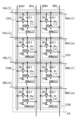
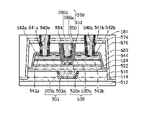
본 발명의 일 형태는 제 1 셀과, 제 2 셀과, 제 3 셀과, 제 4 셀과, 커런트 미러 회로와, 제 1 배선과, 제 2 배선과, 제 3 배선과, 제 4 배선을 가지는 반도체 장치이다. 제 1 셀과, 제 2 셀과, 제 3 셀과, 제 4 셀은 각각 제 1 트랜지스터와, 제 2 트랜지스터와, 용량 소자를 가진다. 제 1 셀과, 제 2 셀과, 제 3 셀과, 제 4 셀 각각에서 제 1 트랜지스터의 제 1 단자는 용량 소자의 제 1 단자와 제 2 트랜지스터의 게이트에 전기적으로 접속된다. 제 1 셀의 제 2 트랜지스터의 제 1 단자는 제 1 배선에 전기적으로 접속되고, 제 1 셀의 용량 소자의 제 2 단자는 제 3 배선에 전기적으로 접속된다. 제 2 셀의 제 2 트랜지스터의 제 1 단자는 제 1 배선에 전기적으로 접속되고, 제 2 셀의 용량 소자의 제 2 단자는 제 4 배선에 전기적으로 접속된다. 제 3 셀의 제 2 트랜지스터의 제 1 단자는 제 2 배선에 전기적으로 접속되고, 제 3 셀의 용량 소자의 제 2 단자는 제 3 배선에 전기적으로 접속된다. 제 4 셀의 제 2 트랜지스터의 제 1 단자는 제 2 배선에 전기적으로 접속되고, 제 4 셀의 용량 소자의 제 2 단자는 제 4 배선에 전기적으로 접속된다. 커런트 미러 회로는 제 1 배선과 제 2 배선에 전기적으로 접속되고, 커런트 미러 회로는 제 1 배선의 전위에 대응한 전류를 제 2 배선에 흘리는 기능을 가진다. 제 1 데이터는 제 1 전위와 제 2 전위의 차분에 따라 결정되는 것으로 하고, 제 2 데이터는 제 3 전위와 제 4 전위의 차분에 따라 결정되는 것으로 한다. 제 1 셀은 제 1 셀의 용량 소자의 제 1 단자에 제 1 전위를 유지하는 기능을 가지고, 제 2 셀은 제 2 셀의 용량 소자의 제 1 단자에 제 2 전위를 유지하는 기능을 가지고, 제 3 셀은 제 3 셀의 용량 소자의 제 1 단자에 제 2 전위를 유지하는 기능을 가지고, 제 4 셀은 제 4 셀의 용량 소자의 제 1 단자에 제 1 전위를 유지하는 기능을 가진다. 제 3 배선에 제 3 전위가 입력되며 제 4 배선에 제 4 전위가 입력됨으로써, 커런트 미러 회로로부터 제 2 배선에 흐르는 전류의 양에서, 제 2 배선으로부터 제 3 셀의 제 2 트랜지스터의 제 1 단자에 흐르는 전류의 양과 제 2 배선으로부터 제 4 셀의 제 2 트랜지스터의 제 1 단자에 흐르는 전류의 양을 뺀 전류의 양은 제 1 데이터와 제 2 데이터의 곱에 대응한 양이 된다.One embodiment of the present invention provides a first cell, a second cell, a third cell, a fourth cell, a current mirror circuit, a first wiring, a second wiring, a third wiring, and a fourth wiring. branch is a semiconductor device. The first cell, the second cell, the third cell, and the fourth cell each have a first transistor, a second transistor, and a capacitance element. In each of the first cell, the second cell, the third cell, and the fourth cell, the first terminal of the first transistor is electrically connected to the first terminal of the capacitance element and the gate of the second transistor. A first terminal of the second transistor of the first cell is electrically connected to the first wiring, and a second terminal of the capacitive element of the first cell is electrically connected to the third wiring. The first terminal of the second transistor of the second cell is electrically connected to the first wiring, and the second terminal of the capacitive element of the second cell is electrically connected to the fourth wiring. The first terminal of the second transistor of the third cell is electrically connected to the second wiring, and the second terminal of the capacitive element of the third cell is electrically connected to the third wiring. The first terminal of the second transistor of the fourth cell is electrically connected to the second wiring, and the second terminal of the capacitive element of the fourth cell is electrically connected to the fourth wiring. The current mirror circuit is electrically connected to the first wiring and the second wiring, and the current mirror circuit has a function of passing a current corresponding to the potential of the first wiring to the second wiring. It is assumed that the first data is determined according to the difference between the first potential and the second potential, and the second data is determined according to the difference between the third potential and the fourth potential. The first cell has a function of holding a first potential at the first terminal of the capacitive element of the first cell, and the second cell has a function of holding a second potential at the first terminal of the capacitive element of the second cell; The third cell has a function of holding the second potential to the first terminal of the capacitive element of the third cell, and the fourth cell has a function of holding the first potential to the first terminal of the capacitive element of the fourth cell. When the third potential is input to the third wiring and the fourth potential is input to the fourth wiring, the amount of current flowing from the current mirror circuit to the second wiring is reduced from the second wiring to the first terminal of the second transistor of the third cell. The amount of current obtained by subtracting the amount of current flowing through the second wiring to the first terminal of the second transistor of the fourth cell is an amount corresponding to the product of the first data and the second data.
(2)(2)
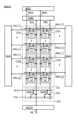
또는 본 발명의 일 형태는 m개(m은 1 이상의 정수임)의 제 1 셀과, m개의 제 2 셀과, m개의 제 3 셀과, m개의 제 4 셀과, 커런트 미러 회로와, 제 1 배선과, 제 2 배선과, m개의 제 3 배선과, m개의 제 4 배선을 가지는 반도체 장치이다. m개의 제 1 셀과, m개의 제 2 셀과, m개의 제 3 셀과, m개의 제 4 셀은 각각 제 1 트랜지스터와, 제 2 트랜지스터와, 용량 소자를 가진다. m개의 제 1 셀과, m개의 제 2 셀과, m개의 제 3 셀과, m개의 제 4 셀 각각에서 제 1 트랜지스터의 제 1 단자는 용량 소자의 제 1 단자와 제 2 트랜지스터의 게이트에 전기적으로 접속된다. m개의 제 1 셀 각각의 제 2 트랜지스터의 제 1 단자는 제 1 배선에 전기적으로 접속되고, i번째(i는 1 이상 m 이하의 정수임) 제 1 셀의 용량 소자의 제 2 단자는 i번째 제 3 배선에 전기적으로 접속된다. m개의 제 2 셀 각각의 제 2 트랜지스터의 제 1 단자는 제 1 배선에 전기적으로 접속되고, i번째 제 2 셀의 용량 소자의 제 2 단자는 i번째 제 4 배선에 전기적으로 접속된다. m개의 제 3 셀 각각의 제 2 트랜지스터의 제 1 단자는 제 2 배선에 전기적으로 접속되고, i번째 제 3 셀의 용량 소자의 제 2 단자는 i번째 제 3 배선에 전기적으로 접속된다. m개의 제 4 셀 각각의 제 2 트랜지스터의 제 1 단자는 제 2 배선에 전기적으로 접속되고, i번째 제 4 셀의 용량 소자의 제 2 단자는 i번째 제 4 배선에 전기적으로 접속된다. 커런트 미러 회로는 제 1 배선과 제 2 배선에 전기적으로 접속되고, 커런트 미러 회로는 제 1 배선의 전위에 대응한 전류를 제 2 배선에 흘리는 기능을 가진다. i번째 제 3 배선에 전기적으로 접속되는 제 1 셀과 제 3 셀 각각에서, 제 1 셀은 제 1 셀의 용량 소자의 제 1 단자에 VWα[i]의 전위를 유지하는 기능을 가지고, 제 3 셀은 제 3 셀의 용량 소자의 제 1 단자에 VWβ[i]의 전위를 유지하는 기능을 가진다. 또한 i번째 제 4 배선에 전기적으로 접속되는 제 2 셀과 제 4 셀 각각에서, 제 2 셀은 제 2 셀의 용량 소자의 제 1 단자에 VWβ[i]의 전위를 유지하는 기능을 가지고, 제 4 셀은 제 4 셀의 용량 소자의 제 1 단자에 VWα[i]의 전위를 유지하는 기능을 가진다. i번째 제 3 배선에 VXα[i]의 전위가 입력되고, i번째 제 4 배선에 VXβ[i]의 전위가 입력됨으로써, 커런트 미러 회로로부터 제 2 배선에 흐르는 전류의 양에서, 제 2 배선으로부터 m개의 제 3 셀 각각의 제 2 트랜지스터의 제 1 단자에 흐르는 전류의 양의 합 및 제 2 배선으로부터 m개의 제 4 셀 각각의 제 2 트랜지스터의 제 1 단자에 흐르는 전류의 양의 합을 뺀 전류의 양은 식(A1)의 값에 대응한 양이 된다.Alternatively, in one embodiment of the present invention, m number of first cells (m is an integer of 1 or greater), m number of second cells, m number of third cells, m number of fourth cells, a current mirror circuit, a first A semiconductor device having wirings, second wirings, m third wirings, and m fourth wirings. The m number of first cells, m number of second cells, m number of third cells, and m number of fourth cells each have a first transistor, a second transistor, and a capacitor element. In each of the m number of first cells, m number of second cells, m number of third cells, and m number of fourth cells, the first terminal of the first transistor is electrically connected to the first terminal of the capacitive element and the gate of the second transistor. connected to The first terminal of the second transistor of each of the m number of first cells is electrically connected to the first wiring, and the second terminal of the capacitance element of the ith (i is an integer equal to or greater than 1 and equal to or less than m) first cell is electrically connected to the first wiring. 3 Electrically connected to wiring. The first terminal of the second transistor of each of the m second cells is electrically connected to the first wiring, and the second terminal of the capacitive element of the i-th second cell is electrically connected to the i-th fourth wiring. A first terminal of a second transistor of each of the m third cells is electrically connected to a second wiring, and a second terminal of a capacitive element of an i-th third cell is electrically connected to an i-th third wiring. A first terminal of a second transistor of each of the m fourth cells is electrically connected to a second wire, and a second terminal of a capacitive element of an i-th fourth cell is electrically connected to an i-th fourth wire. The current mirror circuit is electrically connected to the first wiring and the second wiring, and the current mirror circuit has a function of passing a current corresponding to the potential of the first wiring to the second wiring. In each of the first cell and the third cell electrically connected to the i-th third wire, the first cell has a function of holding a potential of V Wα [i] at the first terminal of the capacitive element of the first cell, The three cells have a function of holding the potential of V Wβ [i] to the first terminal of the capacitance element of the third cell. Further, in each of the second cell and the fourth cell electrically connected to the i-th fourth wire, the second cell has a function of holding a potential of V Wβ [i] at the first terminal of the capacitance element of the second cell, The fourth cell has a function of holding a potential of V Wα [i] to the first terminal of the capacitance element of the fourth cell. When a potential of V Xα [i] is input to the i-th third wire and a potential of V Xβ [i] is input to the i-th fourth wire, in the amount of current flowing from the current mirror circuit to the second wire, the second The sum of the amounts of current flowing from the wiring to the first terminal of the second transistor of each of the m number of third cells and the sum of the amount of current flowing from the second wiring to the first terminal of the second transistor of each of the m number of fourth cells The amount of the subtracted current is an amount corresponding to the value of equation (A1).
[수학식 1][Equation 1]

(3)(3)
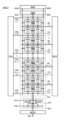
또는 본 발명의 일 형태는 제 1 셀과, 제 2 셀과, 제 3 셀과, 제 4 셀과, 제 1 전류원과, 제 2 전류원과, 감산 회로와, 제 1 배선과, 제 2 배선과, 제 3 배선과, 제 4 배선을 가지는 반도체 장치이다. 제 1 셀과, 제 2 셀과, 제 3 셀과, 제 4 셀은 각각 제 1 트랜지스터와, 제 2 트랜지스터와, 용량 소자를 가진다. 제 1 셀과, 제 2 셀과, 제 3 셀과, 제 4 셀 각각에서 제 1 트랜지스터의 제 1 단자는 용량 소자의 제 1 단자와 제 2 트랜지스터의 게이트에 전기적으로 접속된다. 제 1 셀의 제 2 트랜지스터의 제 1 단자는 제 1 배선에 전기적으로 접속되고, 제 1 셀의 용량 소자의 제 2 단자는 제 3 배선에 전기적으로 접속된다. 제 2 셀의 제 2 트랜지스터의 제 1 단자는 제 1 배선에 전기적으로 접속되고, 제 2 셀의 용량 소자의 제 2 단자는 제 4 배선에 전기적으로 접속된다. 제 3 셀의 제 2 트랜지스터의 제 1 단자는 제 2 배선에 전기적으로 접속되고, 제 3 셀의 용량 소자의 제 2 단자는 제 3 배선에 전기적으로 접속된다. 제 4 셀의 제 2 트랜지스터의 제 1 단자는 제 2 배선에 전기적으로 접속되고, 제 4 셀의 용량 소자의 제 2 단자는 제 4 배선에 전기적으로 접속된다. 제 1 전류원은 제 1 배선에 전기적으로 접속되고, 제 2 전류원은 제 2 배선에 전기적으로 접속된다. 또한 제 1 전류원이 제 1 배선에 흘리는 전류의 양은 제 2 전류원이 제 2 배선에 흘리는 전류의 양의 0.9배 이상 1.1배 이하이다. 또한 감산 회로의 제 1 입력 단자는 제 1 배선에 전기적으로 접속되고, 감산 회로의 제 2 입력 단자는 제 2 배선에 전기적으로 접속된다. 제 1 데이터는 제 1 전위와 제 2 전위의 차분에 따라 결정되는 것으로 하고, 제 2 데이터는 제 3 전위와 제 4 전위의 차분에 따라 결정되는 것으로 한다. 제 1 셀은 제 1 셀의 용량 소자의 제 1 단자에 제 1 전위를 유지하는 기능을 가지고, 제 2 셀은 제 2 셀의 용량 소자의 제 1 단자에 제 2 전위를 유지하는 기능을 가지고, 제 3 셀은 제 3 셀의 용량 소자의 제 1 단자에 제 2 전위를 유지하는 기능을 가지고, 제 4 셀은 제 4 셀의 용량 소자의 제 1 단자에 제 1 전위를 유지하는 기능을 가진다. 제 3 배선에 제 3 전위가 입력되고 제 4 배선에 제 4 전위가 입력됨으로써, 제 1 전류원으로부터 제 1 배선에 흐르는 전류의 양에서, 제 1 배선으로부터 제 1 셀 및 제 2 셀 각각의 제 2 트랜지스터의 제 1 단자에 흐르는 전류의 양의 합을 뺀 양의 전류가 감산 회로의 제 1 입력 단자에 입력되며, 제 2 전류원으로부터 제 2 배선에 흐르는 전류의 양에서, 제 2 배선으로부터 제 3 셀 및 제 4 셀 각각의 제 2 트랜지스터의 제 1 단자에 흐르는 전류의 양의 합을 뺀 양의 전류가 감산 회로의 제 2 입력 단자에 입력된다. 이에 의하여, 감산 회로의 출력 단자로부터 제 1 데이터와 제 2 데이터의 곱에 대응한 전압이 출력된다.Alternatively, one embodiment of the present invention is a first cell, a second cell, a third cell, a fourth cell, a first current source, a second current source, a subtraction circuit, a first wiring, a second wiring, , a semiconductor device having a third wiring and a fourth wiring. The first cell, the second cell, the third cell, and the fourth cell each have a first transistor, a second transistor, and a capacitance element. In each of the first cell, the second cell, the third cell, and the fourth cell, the first terminal of the first transistor is electrically connected to the first terminal of the capacitance element and the gate of the second transistor. A first terminal of the second transistor of the first cell is electrically connected to the first wiring, and a second terminal of the capacitive element of the first cell is electrically connected to the third wiring. The first terminal of the second transistor of the second cell is electrically connected to the first wiring, and the second terminal of the capacitive element of the second cell is electrically connected to the fourth wiring. The first terminal of the second transistor of the third cell is electrically connected to the second wiring, and the second terminal of the capacitive element of the third cell is electrically connected to the third wiring. The first terminal of the second transistor of the fourth cell is electrically connected to the second wiring, and the second terminal of the capacitive element of the fourth cell is electrically connected to the fourth wiring. The first current source is electrically connected to the first wire, and the second current source is electrically connected to the second wire. In addition, the amount of current that the first current source passes through the first wiring is 0.9 times or more and less than or equal to 1.1 times the amount of current that the second current source passes through the second wiring. Also, the first input terminal of the subtraction circuit is electrically connected to the first wiring, and the second input terminal of the subtraction circuit is electrically connected to the second wiring. It is assumed that the first data is determined according to the difference between the first potential and the second potential, and the second data is determined according to the difference between the third potential and the fourth potential. The first cell has a function of holding a first potential at the first terminal of the capacitive element of the first cell, and the second cell has a function of holding a second potential at the first terminal of the capacitive element of the second cell; The third cell has a function of holding the second potential to the first terminal of the capacitive element of the third cell, and the fourth cell has a function of holding the first potential to the first terminal of the capacitive element of the fourth cell. By inputting the third potential to the third wiring and the input of the fourth potential to the fourth wiring, the amount of current flowing from the first current source to the first wiring, the second of each of the first cell and the second cell from the first wiring An amount of current obtained by subtracting the sum of the amounts of current flowing through the first terminal of the transistor is input to the first input terminal of the subtraction circuit, and from the amount of current flowing from the second current source to the second wiring, from the second wiring to the third cell and a positive current obtained by subtracting the sum of the positive currents flowing through the first terminal of the second transistor of each of the fourth cells is input to the second input terminal of the subtraction circuit. As a result, a voltage corresponding to the product of the first data and the second data is output from the output terminal of the subtraction circuit.
(4)(4)
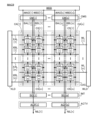
본 발명의 일 형태는 m개(m은 1 이상의 정수임)의 제 1 셀과, m개의 제 2 셀과, m개의 제 3 셀과, m개의 제 4 셀과, 제 1 전류원과, 제 2 전류원과, 감산 회로와, 제 1 배선과, 제 2 배선과, m개의 제 3 배선과, m개의 제 4 배선을 가지는 반도체 장치이다. m개의 제 1 셀과, m개의 제 2 셀과, m개의 제 3 셀과, m개의 제 4 셀은 각각 제 1 트랜지스터와, 제 2 트랜지스터와, 용량 소자를 가진다. 개의 제 1 셀과, m개의 제 2 셀과, m개의 제 3 셀과, m개의 제 4 셀 각각에서 제 1 트랜지스터의 제 1 단자는 용량 소자의 제 1 단자와 제 2 트랜지스터의 게이트에 전기적으로 접속된다. m개의 제 1 셀 각각의 제 2 트랜지스터의 제 1 단자는 제 1 배선에 전기적으로 접속되고, i번째(i는 1 이상 m 이하의 정수임) 제 1 셀의 용량 소자의 제 2 단자는 i번째 제 3 배선에 전기적으로 접속된다. m개의 제 2 셀 각각의 제 2 트랜지스터의 제 1 단자는 제 1 배선에 전기적으로 접속되고, i번째 제 2 셀의 용량 소자의 제 2 단자는 i번째 제 4 배선에 전기적으로 접속된다. m개의 제 3 셀 각각의 제 2 트랜지스터의 제 1 단자는 제 2 배선에 전기적으로 접속되고, i번째 제 3 셀의 용량 소자의 제 2 단자는 i번째 제 3 배선에 전기적으로 접속된다. m개의 제 4 셀 각각의 제 2 트랜지스터의 제 1 단자는 제 2 배선에 전기적으로 접속되고, i번째 제 4 셀의 용량 소자의 제 2 단자는 i번째 제 4 배선에 전기적으로 접속된다. 제 1 전류원은 제 1 배선에 전기적으로 접속되고, 제 2 전류원은 제 2 배선에 전기적으로 접속된다. 또한 제 1 전류원이 제 1 배선에 흘리는 전류의 양은 제 2 전류원이 제 2 배선에 흘리는 전류의 양의 0.9배 이상 1.1배 이하이다. 감산 회로의 제 1 입력 단자는 제 1 배선에 전기적으로 접속되고, 감산 회로의 제 2 입력 단자는 제 2 배선에 전기적으로 접속된다. i번째 제 3 배선에 전기적으로 접속되는 제 1 셀과 제 3 셀 각각에서, 제 1 셀은 제 1 셀의 용량 소자의 제 1 단자에 VWα[i]의 전위를 유지하는 기능을 가지고, 제 3 셀은 제 3 셀의 용량 소자의 제 1 단자에 VWβ[i]의 전위를 유지하는 기능을 가진다. i번째 제 4 배선에 전기적으로 접속되는 제 2 셀과 제 4 셀 각각에서, 제 2 셀은 제 2 셀의 용량 소자의 제 1 단자에 VWβ[i]의 전위를 유지하는 기능을 가지고, 제 4 셀은 제 4 셀의 용량 소자의 제 1 단자에 VWα[i]의 전위를 유지하는 기능을 가진다. i번째 제 3 배선에 VXα[i]의 전위가 입력되고 i번째 제 4 배선에 VXβ[i]의 전위가 입력됨으로써, 제 1 전류원으로부터 제 1 배선에 흐르는 전류의 양에서, 제 1 배선으로부터 m개의 제 1 셀 및 제 2 셀 각각의 제 2 트랜지스터의 제 1 단자에 흐르는 전류의 양의 합을 뺀 양의 전류가 감산 회로의 제 1 입력 단자에 입력되고, 제 2 전류원으로부터 제 2 배선에 흐르는 전류의 양에서, 제 2 배선으로부터 m개의 제 3 셀 및 제 4 셀 각각의 제 2 트랜지스터의 제 1 단자에 흐르는 전류의 양의 합을 뺀 양의 전류가 감산 회로의 제 2 입력 단자에 입력된다. 이에 의하여, 감산 회로의 출력 단자에는 식(A2)의 값에 대응한 전압이 출력된다.One embodiment of the present invention comprises m first cells (where m is an integer of 1 or greater), m second cells, m third cells, m fourth cells, a first current source, and a second current source. and a subtraction circuit, first wirings, second wirings, m third wirings, and m fourth wirings. The m number of first cells, m number of second cells, m number of third cells, and m number of fourth cells each have a first transistor, a second transistor, and a capacitor element. In each of the number of first cells, m number of second cells, m number of third cells, and m number of fourth cells, the first terminal of the first transistor is electrically connected to the first terminal of the capacitive element and the gate of the second transistor. connected The first terminal of the second transistor of each of the m number of first cells is electrically connected to the first wiring, and the second terminal of the capacitance element of the ith (i is an integer equal to or greater than 1 and equal to or less than m) first cell is electrically connected to the first wiring. 3 Electrically connected to wiring. The first terminal of the second transistor of each of the m second cells is electrically connected to the first wiring, and the second terminal of the capacitive element of the i-th second cell is electrically connected to the i-th fourth wiring. A first terminal of a second transistor of each of the m third cells is electrically connected to a second wiring, and a second terminal of a capacitive element of an i-th third cell is electrically connected to an i-th third wiring. A first terminal of a second transistor of each of the m fourth cells is electrically connected to a second wire, and a second terminal of a capacitive element of an i-th fourth cell is electrically connected to an i-th fourth wire. The first current source is electrically connected to the first wire, and the second current source is electrically connected to the second wire. In addition, the amount of current that the first current source passes through the first wiring is 0.9 times or more and less than or equal to 1.1 times the amount of current that the second current source passes through the second wiring. A first input terminal of the subtraction circuit is electrically connected to the first wire, and a second input terminal of the subtraction circuit is electrically connected to the second wire. In each of the first cell and the third cell electrically connected to the i-th third wire, the first cell has a function of holding a potential of V Wα [i] at the first terminal of the capacitive element of the first cell, The three cells have a function of holding the potential of V Wβ [i] to the first terminal of the capacitance element of the third cell. In each of the second cell and the fourth cell electrically connected to the i-th fourth wiring, the second cell has a function of holding a potential of V Wβ [i] to the first terminal of the capacitance element of the second cell, The 4 cells have a function of holding a potential of V Wα [i] to the first terminal of the capacitance element of the 4th cell. When a potential of V Xα [i] is input to the i-th third wiring and a potential of V Xβ [i] is input to the i-th fourth wiring, the amount of current flowing from the first current source to the first wiring A current of an amount obtained by subtracting the sum of the amounts of currents flowing through the first terminals of the second transistors of each of the m number of first cells and second cells is input to the first input terminal of the subtraction circuit, and is input to the second wire from the second current source The amount of current flowing through the second wiring is obtained by subtracting the sum of the currents flowing through the first terminal of the second transistor of m number of third cells and m number of fourth cells, respectively, from the second wiring to the second input terminal of the subtraction circuit. is entered As a result, a voltage corresponding to the value of formula (A2) is output to the output terminal of the subtraction circuit.
[수학식 2][Equation 2]

(5)(5)
또는 본 발명의 일 형태는 제 1 셀과, 제 2 셀과, 제 3 셀과, 제 4 셀과, 제 1 배선과, 제 2 배선과, 제 3 배선을 가지는 반도체 장치이다. 제 1 셀과, 제 2 셀과, 제 3 셀과, 제 4 셀은 각각 제 1 트랜지스터와, 제 2 트랜지스터와, 용량 소자를 가진다. 또한 제 1 셀과, 제 2 셀과, 제 3 셀과, 제 4 셀 각각에서 제 1 트랜지스터의 제 1 단자는 용량 소자의 제 1 단자와 제 2 트랜지스터의 게이트에 전기적으로 접속되고, 제 1 트랜지스터의 게이트는 제 1 배선에 전기적으로 접속된다. 또한 제 2 배선은 제 1 셀의 제 1 트랜지스터의 제 2 단자와 제 4 셀의 제 1 트랜지스터의 제 2 단자에 전기적으로 접속되고, 제 3 배선은 제 2 셀의 제 1 트랜지스터의 제 2 단자와 제 3 셀의 제 1 트랜지스터의 제 2 단자에 전기적으로 접속된다.Alternatively, one embodiment of the present invention is a semiconductor device having a first cell, a second cell, a third cell, a fourth cell, a first wiring, a second wiring, and a third wiring. The first cell, the second cell, the third cell, and the fourth cell each have a first transistor, a second transistor, and a capacitance element. Further, in each of the first cell, the second cell, the third cell, and the fourth cell, the first terminal of the first transistor is electrically connected to the first terminal of the capacitance element and the gate of the second transistor, and the first transistor A gate of is electrically connected to the first wire. Also, the second wiring is electrically connected to the second terminal of the first transistor of the first cell and the second terminal of the first transistor of the fourth cell, and the third wiring is electrically connected to the second terminal of the first transistor of the second cell. It is electrically connected to the second terminal of the first transistor of the third cell.
(6)(6)
또는 본 발명의 일 형태는 제 1 셀과, 제 2 셀과, 제 3 셀과, 제 4 셀과, 제 1 배선과, 제 2 배선과, 제 3 배선과, 제 4 배선과, 제 5 배선과, 제 6 배선과, 제 7 배선을 가지는 반도체 장치이다. 또한 제 1 셀과, 제 2 셀과, 제 3 셀과, 제 4 셀은 각각 제 1 트랜지스터와, 제 2 트랜지스터와, 용량 소자를 가진다. 제 1 셀과, 제 2 셀과, 제 3 셀과, 제 4 셀 각각에서 제 1 트랜지스터의 제 1 단자는 용량 소자의 제 1 단자와 제 2 트랜지스터의 게이트에 전기적으로 접속된다. 제 1 셀의 제 2 트랜지스터의 제 1 단자는 제 4 배선에 전기적으로 접속되고, 제 1 셀의 용량 소자의 제 2 단자는 제 6 배선에 전기적으로 접속되고, 제 1 셀의 제 1 트랜지스터의 제 2 단자는 제 2 배선에 전기적으로 접속되고, 제 1 셀의 제 1 트랜지스터의 게이트는 제 1 배선에 전기적으로 접속된다. 제 2 셀의 제 2 트랜지스터의 제 1 단자는 제 4 배선에 전기적으로 접속되고, 제 2 셀의 용량 소자의 제 2 단자는 제 7 배선에 전기적으로 접속되고, 제 2 셀의 제 1 트랜지스터의 제 2 단자는 제 3 배선에 전기적으로 접속되고, 제 2 셀의 제 1 트랜지스터의 게이트는 제 1 배선에 전기적으로 접속된다. 제 3 셀의 제 2 트랜지스터의 제 1 단자는 제 5 배선에 전기적으로 접속되고, 제 3 셀의 용량 소자의 제 2 단자는 제 6 배선에 전기적으로 접속되고, 제 3 셀의 제 1 트랜지스터의 제 2 단자는 제 3 배선에 전기적으로 접속되고, 제 3 셀의 제 1 트랜지스터의 게이트는 제 1 배선에 전기적으로 접속된다. 제 4 셀의 제 2 트랜지스터의 제 1 단자는 제 5 배선에 전기적으로 접속되고, 제 4 셀의 용량 소자의 제 2 단자는 제 7 배선에 전기적으로 접속되고, 제 4 셀의 제 1 트랜지스터의 제 2 단자는 제 2 배선에 전기적으로 접속되고, 제 4 셀의 제 1 트랜지스터의 게이트는 제 1 배선에 전기적으로 접속된다.Alternatively, one embodiment of the present invention is a first cell, a second cell, a third cell, a fourth cell, a first wiring, a second wiring, a third wiring, a fourth wiring, and a fifth wiring. , a sixth wiring, and a seventh wiring. In addition, the first cell, the second cell, the third cell, and the fourth cell each have a first transistor, a second transistor, and a capacitance element. In each of the first cell, the second cell, the third cell, and the fourth cell, the first terminal of the first transistor is electrically connected to the first terminal of the capacitance element and the gate of the second transistor. The first terminal of the second transistor of the first cell is electrically connected to the fourth wiring, the second terminal of the capacitive element of the first cell is electrically connected to the sixth wiring, and the first terminal of the first transistor of the first cell is electrically connected. The two terminals are electrically connected to the second wiring, and the gate of the first transistor of the first cell is electrically connected to the first wiring. The first terminal of the second transistor of the second cell is electrically connected to the fourth wiring, the second terminal of the capacitive element of the second cell is electrically connected to the seventh wiring, and the first terminal of the first transistor of the second cell is electrically connected. The second terminal is electrically connected to the third wire, and the gate of the first transistor of the second cell is electrically connected to the first wire. The first terminal of the second transistor of the third cell is electrically connected to the fifth wiring, the second terminal of the capacitive element of the third cell is electrically connected to the sixth wiring, and the first terminal of the first transistor of the third cell is electrically connected. The second terminal is electrically connected to the third wire, and the gate of the first transistor of the third cell is electrically connected to the first wire. The first terminal of the second transistor of the fourth cell is electrically connected to the fifth wiring, the second terminal of the capacitive element of the fourth cell is electrically connected to the seventh wiring, and the first terminal of the first transistor of the fourth cell is electrically connected. The two terminals are electrically connected to the second wiring, and the gate of the first transistor of the fourth cell is electrically connected to the first wiring.
(7)(7)
또는 본 발명의 일 형태는 상기 (6)에 있어서, 커런트 미러 회로를 가지는 구성으로 하는 것이 바람직하다. 또한 커런트 미러 회로는 제 4 배선과 제 5 배선에 전기적으로 접속되는 것이 바람직하다. 또한 커런트 미러 회로는 제 4 배선의 전위에 대응한 전류를 제 5 배선에 흘리는 기능을 가진다.Alternatively, in one embodiment of the present invention, in the above (6), it is preferable to have a configuration including a current mirror circuit. Also, the current mirror circuit is preferably electrically connected to the fourth wiring and the fifth wiring. Also, the current mirror circuit has a function of passing a current corresponding to the potential of the fourth wiring to the fifth wiring.
(8)(8)
또는 본 발명의 일 형태는 상기 (7)에 있어서, 제 1 데이터와 제 2 데이터의 곱셈을 하는 구성으로 하는 것이 바람직하다. 또한 제 1 데이터는 제 1 전위와 제 2 전위의 차분에 따라 결정되는 것으로 하고, 제 2 데이터는 제 3 전위와 제 4 전위의 차분에 따라 결정되는 것으로 한다. 또한 제 1 셀은 제 1 셀의 용량 소자의 제 1 단자에 제 1 전위를 유지하는 기능을 가지고, 제 2 셀은 제 2 셀의 용량 소자의 제 1 단자에 제 2 전위를 유지하는 기능을 가지고, 제 3 셀은 제 3 셀의 용량 소자의 제 1 단자에 제 2 전위를 유지하는 기능을 가지고, 제 4 셀은 제 4 셀의 용량 소자의 제 1 단자에 제 1 전위를 유지하는 기능을 가진다. 제 6 배선에 제 3 전위가 입력되며 제 7 배선에 제 4 전위가 입력됨으로써, 커런트 미러 회로로부터 제 5 배선에 흐르는 전류의 양에서, 제 5 배선으로부터 제 3 셀의 제 2 트랜지스터의 제 1 단자에 흐르는 전류의 양과 제 5 배선으로부터 제 4 셀의 제 2 트랜지스터의 제 1 단자에 흐르는 전류의 양을 뺀 전류의 양은 제 1 데이터와 제 2 데이터의 곱에 대응한 양이 된다.Alternatively, in one embodiment of the present invention, in the above (7), the first data and the second data are preferably multiplied. It is assumed that the first data is determined according to the difference between the first potential and the second potential, and the second data is determined according to the difference between the third potential and the fourth potential. In addition, the first cell has a function of holding a first potential at the first terminal of the capacitive element of the first cell, and the second cell has a function of holding the second potential at the first terminal of the capacitive element of the second cell. , The third cell has a function of holding the second potential to the first terminal of the capacitive element of the third cell, and the fourth cell has a function of holding the first potential to the first terminal of the capacitance element of the fourth cell. . When the third potential is input to the sixth wiring and the fourth potential is input to the seventh wiring, the amount of current flowing from the current mirror circuit to the fifth wiring is reduced from the fifth wiring to the first terminal of the second transistor of the third cell. The amount of current obtained by subtracting the amount of current flowing through the fifth wiring to the first terminal of the second transistor of the fourth cell is an amount corresponding to the product of the first data and the second data.
(9)(9)
또는 본 발명의 일 형태는 상기 (6)에 있어서, 제 1 전류원과, 제 2 전류원과, 감산 회로를 가지는 구성으로 하는 것이 바람직하다. 또한 제 1 전류원은 제 4 배선에 전기적으로 접속되고, 제 2 전류원은 제 5 배선에 전기적으로 접속되는 것이 바람직하다. 또한 감산 회로의 제 1 입력 단자는 제 4 배선에 전기적으로 접속되고, 감산 회로의 제 2 입력 단자는 제 5 배선에 전기적으로 접속되는 것이 바람직하다. 또한 제 1 전류원이 제 4 배선에 흘리는 전류의 양은 제 2 전류원이 제 5 배선에 흘리는 전류의 양의 0.9배 이상 1.1배 이하인 것이 바람직하다.Alternatively, one embodiment of the present invention is preferably configured to include a first current source, a second current source, and a subtraction circuit in the above (6). Also, it is preferable that the first current source is electrically connected to the fourth wiring, and the second current source is electrically connected to the fifth wiring. Further, it is preferable that the first input terminal of the subtraction circuit is electrically connected to the fourth wiring, and the second input terminal of the subtraction circuit is electrically connected to the fifth wiring. Further, it is preferable that the amount of current passed through the fourth wire by the first current source is not less than 0.9 times and not more than 1.1 times the amount of current passed through the fifth wire by the second current source.
(10)(10)
또는 본 발명의 일 형태는 상기 (9)에 있어서, 제 1 데이터와 제 2 데이터의 곱셈을 하는 구성으로 하는 것이 바람직하다. 또한 제 1 데이터는 제 1 전위와 제 2 전위의 차분에 따라 결정되는 것으로 하고, 제 2 데이터는 제 3 전위와 제 4 전위의 차분에 따라 결정되는 것으로 한다. 또한 제 1 셀은 제 1 셀의 용량 소자의 제 1 단자에 제 1 전위를 유지하는 기능을 가지고, 제 2 셀은 제 2 셀의 용량 소자의 제 1 단자에 제 2 전위를 유지하는 기능을 가지고, 제 3 셀은 제 3 셀의 용량 소자의 제 1 단자에 제 2 전위를 유지하는 기능을 가지고, 제 4 셀은 제 4 셀의 용량 소자의 제 1 단자에 제 1 전위를 유지하는 기능을 가진다. 제 6 배선에 제 3 전위가 입력되고 제 7 배선에 제 4 전위가 입력됨으로써, 제 1 전류원으로부터 제 4 배선에 흐르는 전류의 양에서, 제 4 배선으로부터 제 1 셀 및 제 2 셀 각각의 제 2 트랜지스터의 제 1 단자에 흐르는 전류의 양의 합을 뺀 양의 전류가 감산 회로의 제 1 입력 단자에 입력되며, 제 2 전류원으로부터 제 5 배선에 흐르는 전류의 양에서, 제 5 배선으로부터 제 3 셀 및 제 4 셀 각각의 제 2 트랜지스터의 제 1 단자에 흐르는 전류의 양의 합을 뺀 양의 전류가 감산 회로의 제 2 입력 단자에 입력된다. 이에 의하여, 감산 회로의 출력 단자로부터 제 1 데이터와 제 2 데이터의 곱에 대응한 전압이 출력된다.Alternatively, in one embodiment of the present invention, in the above (9), the first data and the second data are preferably multiplied. It is assumed that the first data is determined according to the difference between the first potential and the second potential, and the second data is determined according to the difference between the third potential and the fourth potential. In addition, the first cell has a function of holding a first potential at the first terminal of the capacitive element of the first cell, and the second cell has a function of holding the second potential at the first terminal of the capacitive element of the second cell. , The third cell has a function of holding the second potential to the first terminal of the capacitive element of the third cell, and the fourth cell has a function of holding the first potential to the first terminal of the capacitance element of the fourth cell. . By inputting the third potential to the sixth wiring and inputting the fourth potential to the seventh wiring, the amount of current flowing from the first current source to the fourth wiring, the second of each of the first cell and the second cell from the fourth wiring An amount of current minus the sum of the amounts of current flowing through the first terminal of the transistor is input to the first input terminal of the subtraction circuit, and from the amount of current flowing from the second current source to the fifth wiring, from the fifth wiring to the third cell and a current amount obtained by subtracting the sum of the amounts of the currents flowing through the first terminal of the second transistor of each of the fourth cells is input to the second input terminal of the subtraction circuit. As a result, a voltage corresponding to the product of the first data and the second data is output from the output terminal of the subtraction circuit.
(11)(11)
또는 본 발명의 일 형태는 m개(m은 1 이상의 정수임)의 제 1 셀과, m개의 제 2 셀과, m개의 제 3 셀과, m개의 제 4 셀과, 커런트 미러 회로와, m개의 제 1 배선과, 제 2 배선과, 제 3 배선과, 제 4 배선과, 제 5 배선과, m개의 제 6 배선과, m개의 제 7 배선을 가지는 반도체 장치이다. 또한 m개의 제 1 셀과, m개의 제 2 셀과, m개의 제 3 셀과, m개의 제 4 셀은 각각 제 1 트랜지스터와, 제 2 트랜지스터와, 용량 소자를 가진다. m개의 제 1 셀과, m개의 제 2 셀과, m개의 제 3 셀과, m개의 제 4 셀 각각에서 제 1 트랜지스터의 제 1 단자는 용량 소자의 제 1 단자와 제 2 트랜지스터의 게이트에 전기적으로 접속된다. m개의 제 1 셀 각각의 제 2 트랜지스터의 제 1 단자는 제 4 배선에 전기적으로 접속되고, i번째(i는 1 이상 m 이하의 정수임) 제 1 셀의 용량 소자의 제 2 단자는 i번째 제 6 배선에 전기적으로 접속되고, m개의 제 1 셀 각각의 제 1 트랜지스터의 제 2 단자는 제 2 배선에 전기적으로 접속되고, i번째 제 1 셀의 제 1 트랜지스터의 게이트는 i번째 제 1 배선에 전기적으로 접속된다. m개의 제 2 셀 각각의 제 2 트랜지스터의 제 1 단자는 제 4 배선에 전기적으로 접속되고, i번째 제 2 셀의 용량 소자의 제 2 단자는 i번째 제 7 배선에 전기적으로 접속되고, m개의 제 2 셀 각각의 제 1 트랜지스터의 제 2 단자는 제 3 배선에 전기적으로 접속되고, i번째 제 2 셀의 제 1 트랜지스터의 게이트는 i번째 제 1 배선에 전기적으로 접속된다. m개의 제 3 셀 각각의 제 2 트랜지스터의 제 1 단자는 제 5 배선에 전기적으로 접속되고, i번째 제 3 셀의 용량 소자의 제 2 단자는 i번째 제 6 배선에 전기적으로 접속되고, m개의 제 3 셀 각각의 제 1 트랜지스터의 제 2 단자는 제 3 배선에 전기적으로 접속되고, i번째 제 3 셀의 제 1 트랜지스터의 게이트는 i번째 제 1 배선에 전기적으로 접속된다. m개의 제 4 셀 각각의 제 2 트랜지스터의 제 1 단자는 제 5 배선에 전기적으로 접속되고, i번째 제 4 셀의 용량 소자의 제 2 단자는 i번째 제 7 배선에 전기적으로 접속되고, m개의 제 4 셀 각각의 제 1 트랜지스터의 제 2 단자는 제 2 배선에 전기적으로 접속되고, i번째 제 4 셀의 제 1 트랜지스터의 게이트는 i번째 제 1 배선에 전기적으로 접속된다. 또한 커런트 미러 회로는 제 4 배선과 제 5 배선에 전기적으로 접속된다. 또한 커런트 미러 회로는 제 4 배선의 전위에 대응한 전류를 제 5 배선에 흘리는 기능을 가진다. 또한 i번째 제 6 배선에 전기적으로 접속되는 제 1 셀과 제 3 셀 각각에서, 제 1 셀은 제 1 셀의 용량 소자의 제 1 단자에 VWα[i]의 전위를 유지하는 기능을 가지고, 제 3 셀은 제 3 셀의 용량 소자의 제 1 단자에 VWβ[i]의 전위를 유지하는 기능을 가진다. 또한 i번째 제 7 배선에 전기적으로 접속되는 제 2 셀과 제 4 셀 각각에서, 제 2 셀은 제 2 셀의 용량 소자의 제 1 단자에 VWβ[i]의 전위를 유지하는 기능을 가지고, 제 4 셀은 제 4 셀의 용량 소자의 제 1 단자에 VWα[i]의 전위를 유지하는 기능을 가진다. i번째 제 6 배선에 VXα[i]의 전위가 입력되고, i번째 제 7 배선에 VXβ[i]의 전위가 입력됨으로써, 커런트 미러 회로로부터 제 5 배선에 흐르는 전류의 양에서, 제 5 배선으로부터 m개의 제 3 셀 각각의 제 2 트랜지스터의 제 1 단자에 흐르는 전류의 양의 합 및 제 5 배선으로부터 m개의 제 4 셀 각각의 제 2 트랜지스터의 제 1 단자에 흐르는 전류의 양의 합을 뺀 전류의 양은 식(A3)의 값에 대응한 양이 된다.Alternatively, in one embodiment of the present invention, m number of first cells (m is an integer of 1 or more), m number of second cells, m number of third cells, m number of fourth cells, a current mirror circuit, and m number of second cells A semiconductor device having a first wire, a second wire, a third wire, a fourth wire, a fifth wire, m number of sixth wire, and m number of seventh wire. Further, the m number of first cells, m number of second cells, m number of third cells, and m number of fourth cells each have a first transistor, a second transistor, and a capacitance element. In each of the m number of first cells, m number of second cells, m number of third cells, and m number of fourth cells, the first terminal of the first transistor is electrically connected to the first terminal of the capacitive element and the gate of the second transistor. connected to A first terminal of a second transistor of each of the m number of first cells is electrically connected to a fourth wiring, and a second terminal of a capacitance element of the i-th (i is an integer equal to or greater than 1 and equal to or less than m) first cell is electrically connected to a fourth wire. 6 wirings, the second terminal of the first transistor of each of the m number of first cells is electrically connected to the second wiring, and the gate of the first transistor of the i-th first cell is connected to the i-th first wiring. electrically connected. A first terminal of a second transistor of each of the m second cells is electrically connected to a fourth wiring, a second terminal of a capacitive element of an i-th second cell is electrically connected to an i-th seventh wiring, and The second terminal of the first transistor of each second cell is electrically connected to the third wiring, and the gate of the first transistor of the i-th second cell is electrically connected to the i-th first wiring. A first terminal of a second transistor of each of the m third cells is electrically connected to a fifth wiring, a second terminal of a capacitive element of an i-th third cell is electrically connected to an i-th sixth wiring, and The second terminal of the first transistor of each of the third cells is electrically connected to the third wiring, and the gate of the first transistor of the i-th third cell is electrically connected to the i-th first wiring. A first terminal of a second transistor of each of the m fourth cells is electrically connected to a fifth wiring, a second terminal of a capacitive element of an i-th fourth cell is electrically connected to an i-th seventh wiring, and The second terminal of the first transistor of each fourth cell is electrically connected to the second wiring, and the gate of the first transistor of the i-th fourth cell is electrically connected to the i-th first wiring. Also, the current mirror circuit is electrically connected to the fourth wiring and the fifth wiring. Also, the current mirror circuit has a function of passing a current corresponding to the potential of the fourth wiring to the fifth wiring. Further, in each of the first cell and the third cell electrically connected to the i-th sixth wiring, the first cell has a function of holding a potential of V Wα [i] at the first terminal of the capacitance element of the first cell, The third cell has a function of holding a potential of V Wβ [i] to the first terminal of the capacitance element of the third cell. Further, in each of the second cell and the fourth cell electrically connected to the i-th seventh wire, the second cell has a function of holding a potential of V Wβ [i] at the first terminal of the capacitance element of the second cell, The fourth cell has a function of holding a potential of V Wα [i] to the first terminal of the capacitance element of the fourth cell. When a potential of V Xα [i] is input to the i-th 6th wiring and a potential of V Xβ [i] is input to the i-th 7th wiring, the amount of current flowing from the current mirror circuit to the 5th wiring The sum of the amounts of current flowing from the wiring to the first terminal of the second transistor of each of the m number of third cells and the sum of the amount of current flowing from the fifth wiring to the first terminal of the second transistor of each of the m number of fourth cells The amount of the subtracted current is an amount corresponding to the value of equation (A3).
[수학식 3][Equation 3]

(12)(12)
또는 본 발명의 일 형태는 m개(m은 1 이상의 정수임)의 제 1 셀과, m개의 제 2 셀과, m개의 제 3 셀과, m개의 제 4 셀과, 제 1 전류원과, 제 2 전류원과, 감산 회로와, m개의 제 1 배선과, 제 2 배선과, 제 3 배선과, 제 4 배선과, 제 5 배선과, m개의 제 6 배선과, m개의 제 7 배선을 가지는 반도체 장치이다. 또한 m개의 제 1 셀과, m개의 제 2 셀과, m개의 제 3 셀과, m개의 제 4 셀은 각각 제 1 트랜지스터와, 제 2 트랜지스터와, 용량 소자를 가진다. m개의 제 1 셀과, m개의 제 2 셀과, m개의 제 3 셀과, m개의 제 4 셀 각각에서 제 1 트랜지스터의 제 1 단자는 용량 소자의 제 1 단자와 제 2 트랜지스터의 게이트에 전기적으로 접속된다. m개의 제 1 셀 각각의 제 2 트랜지스터의 제 1 단자는 제 4 배선에 전기적으로 접속되고, i번째(i는 1 이상 m 이하의 정수임) 제 1 셀의 용량 소자의 제 2 단자는 i번째 제 6 배선에 전기적으로 접속되고, m개의 제 1 셀 각각의 제 1 트랜지스터의 제 2 단자는 제 2 배선에 전기적으로 접속되고, i번째 제 1 셀의 제 1 트랜지스터의 게이트는 i번째 제 1 배선에 전기적으로 접속된다. m개의 제 2 셀 각각의 제 2 트랜지스터의 제 1 단자는 제 4 배선에 전기적으로 접속되고, i번째 제 2 셀의 용량 소자의 제 2 단자는 i번째 제 7 배선에 전기적으로 접속되고, m개의 제 2 셀 각각의 제 1 트랜지스터의 제 2 단자는 제 3 배선에 전기적으로 접속되고, i번째 제 2 셀의 제 1 트랜지스터의 게이트는 i번째 제 1 배선에 전기적으로 접속된다. m개의 제 3 셀 각각의 제 2 트랜지스터의 제 1 단자는 제 5 배선에 전기적으로 접속되고, i번째 제 3 셀의 용량 소자의 제 2 단자는 i번째 제 6 배선에 전기적으로 접속되고, m개의 제 3 셀 각각의 제 1 트랜지스터의 제 2 단자는 제 3 배선에 전기적으로 접속되고, i번째 제 3 셀의 제 1 트랜지스터의 게이트는 i번째 제 1 배선에 전기적으로 접속된다. m개의 제 4 셀 각각의 제 2 트랜지스터의 제 1 단자는 제 5 배선에 전기적으로 접속되고, i번째 제 4 셀의 용량 소자의 제 2 단자는 i번째 제 7 배선에 전기적으로 접속되고, m개의 제 4 셀 각각의 제 1 트랜지스터의 제 2 단자는 제 2 배선에 전기적으로 접속되고, i번째 제 4 셀의 제 1 트랜지스터의 게이트는 i번째 제 1 배선에 전기적으로 접속된다. 또한 제 1 전류원은 제 4 배선에 전기적으로 접속되고, 제 2 전류원은 제 5 배선에 전기적으로 접속된다. 또한 제 1 전류원이 제 4 배선에 흘리는 전류의 양은 제 2 전류원이 제 5 배선에 흘리는 전류의 양의 0.9배 이상 1.1배 이하이다. 또한 감산 회로의 제 1 입력 단자는 제 4 배선에 전기적으로 접속되고, 감산 회로의 제 2 입력 단자는 제 5 배선에 전기적으로 접속된다. i번째 제 6 배선에 전기적으로 접속되는 제 1 셀과 제 3 셀 각각에서, 제 1 셀은 제 1 셀의 용량 소자의 제 1 단자에 VWα[i]의 전위를 유지하는 기능을 가지고, 제 3 셀은 제 3 셀의 용량 소자의 제 1 단자에 VWβ[i]의 전위를 유지하는 기능을 가진다. 또한 i번째 제 7 배선에 전기적으로 접속되는 제 2 셀과 제 4 셀 각각에서, 제 2 셀은 제 2 셀의 용량 소자의 제 1 단자에 VWβ[i]의 전위를 유지하는 기능을 가지고, 제 4 셀은 제 4 셀의 용량 소자의 제 1 단자에 VWα[i]의 전위를 유지하는 기능을 가진다. i번째 제 6 배선에 VXα[i]의 전위가 입력되고 i번째 제 7 배선에 VXβ[i]의 전위가 입력됨으로써, 제 1 전류원으로부터 제 4 배선에 흐르는 전류의 양에서, 제 4 배선으로부터 m개의 제 1 셀 및 제 2 셀 각각의 제 2 트랜지스터의 제 1 단자에 흐르는 전류의 양의 합을 뺀 양의 전류가 감산 회로의 제 1 입력 단자에 입력되고, 제 2 전류원으로부터 제 5 배선에 흐르는 전류의 양에서, 제 5 배선으로부터 m개의 제 3 셀 및 제 4 셀 각각의 제 2 트랜지스터의 제 1 단자에 흐르는 전류의 양의 합을 뺀 양의 전류가 감산 회로의 제 2 입력 단자에 입력된다. 이에 의하여, 감산 회로의 출력 단자로부터 식(A4)의 값에 대응한 전압이 출력된다.Alternatively, in one embodiment of the present invention, m (m is an integer of 1 or more) first cells, m second cells, m third cells, m fourth cells, a first current source, and a second A semiconductor device having a current source, a subtraction circuit, m first wires, second wires, third wires, fourth wires, fifth wires, m sixth wires, and m seventh wires am. Further, the m number of first cells, m number of second cells, m number of third cells, and m number of fourth cells each have a first transistor, a second transistor, and a capacitance element. In each of the m number of first cells, m number of second cells, m number of third cells, and m number of fourth cells, the first terminal of the first transistor is electrically connected to the first terminal of the capacitive element and the gate of the second transistor. connected to A first terminal of a second transistor of each of the m number of first cells is electrically connected to a fourth wiring, and a second terminal of a capacitance element of the i-th (i is an integer equal to or greater than 1 and equal to or less than m) first cell is electrically connected to a fourth wire. 6 wirings, the second terminal of the first transistor of each of the m number of first cells is electrically connected to the second wiring, and the gate of the first transistor of the i-th first cell is connected to the i-th first wiring. electrically connected. A first terminal of a second transistor of each of the m second cells is electrically connected to a fourth wiring, a second terminal of a capacitive element of an i-th second cell is electrically connected to an i-th seventh wiring, and The second terminal of the first transistor of each second cell is electrically connected to the third wiring, and the gate of the first transistor of the i-th second cell is electrically connected to the i-th first wiring. A first terminal of a second transistor of each of the m third cells is electrically connected to a fifth wiring, a second terminal of a capacitive element of an i-th third cell is electrically connected to an i-th sixth wiring, and The second terminal of the first transistor of each of the third cells is electrically connected to the third wiring, and the gate of the first transistor of the i-th third cell is electrically connected to the i-th first wiring. A first terminal of a second transistor of each of the m fourth cells is electrically connected to a fifth wiring, a second terminal of a capacitive element of an i-th fourth cell is electrically connected to an i-th seventh wiring, and The second terminal of the first transistor of each fourth cell is electrically connected to the second wiring, and the gate of the first transistor of the i-th fourth cell is electrically connected to the i-th first wiring. Also, the first current source is electrically connected to the fourth wire, and the second current source is electrically connected to the fifth wire. Further, the amount of current passed through the fourth wire by the first current source is 0.9 times or more and less than or equal to 1.1 times the amount of current passed through the fifth wire by the second current source. Also, the first input terminal of the subtraction circuit is electrically connected to the fourth wire, and the second input terminal of the subtraction circuit is electrically connected to the fifth wire. In each of the first cell and the third cell electrically connected to the i-th sixth wiring, the first cell has a function of holding a potential of V Wα [i] at the first terminal of the capacitive element of the first cell, The three cells have a function of holding the potential of V Wβ [i] to the first terminal of the capacitance element of the third cell. Further, in each of the second cell and the fourth cell electrically connected to the i-th seventh wire, the second cell has a function of holding a potential of V Wβ [i] at the first terminal of the capacitance element of the second cell, The fourth cell has a function of holding a potential of V Wα [i] to the first terminal of the capacitance element of the fourth cell. By inputting a potential of V Xα [i] to the i-th sixth wiring and inputting a potential of V Xβ [i] to the i-th seventh wiring, the amount of current flowing from the first current source to the fourth wiring A current of an amount obtained by subtracting the sum of the amounts of currents flowing through the first terminals of the second transistors of each of the m number of first cells and second cells is input to the first input terminal of the subtraction circuit, and is input to the fifth wiring from the second current source. A positive current obtained by subtracting the sum of the amounts of the currents flowing through the first terminal of the second transistor of each of the m number of third and fourth cells from the fifth wiring, from the amount of current flowing through the is entered As a result, a voltage corresponding to the value of expression (A4) is output from the output terminal of the subtraction circuit.
[수학식 4][Equation 4]

(13)(13)
또는 본 발명의 일 형태는 제 1 셀과, 제 2 셀과, 제 3 셀과, 제 4 셀과, 제 1 커런트 미러 회로와, 제 2 커런트 미러 회로와, 제 3 커런트 미러 회로를 가지는 반도체 장치이다. 또한 제 1 셀과, 제 2 셀과, 제 3 셀과, 제 4 셀은 각각 제 1 트랜지스터와, 제 2 트랜지스터와, 용량 소자를 가진다. 제 1 셀과, 제 2 셀과, 제 3 셀과, 제 4 셀 각각에서 제 1 트랜지스터의 제 1 단자는 용량 소자의 제 1 단자와 제 2 트랜지스터의 게이트에 전기적으로 접속된다. 또한 제 1 셀의 제 1 트랜지스터의 게이트는 제 2 셀의 제 1 트랜지스터의 게이트와, 제 3 셀의 제 1 트랜지스터의 게이트와, 제 4 셀의 제 1 트랜지스터의 게이트에 전기적으로 접속된다. 제 1 커런트 미러 회로의 제 1 단자는 제 1 셀의 제 2 트랜지스터의 제 1 단자에 전기적으로 접속되고, 제 1 커런트 미러 회로의 제 2 단자는 제 4 셀의 제 2 트랜지스터의 제 1 단자에 전기적으로 접속된다. 제 2 커런트 미러 회로의 제 1 단자는 제 3 셀의 제 2 트랜지스터의 제 1 단자에 전기적으로 접속되고, 제 2 커런트 미러 회로의 제 2 단자는 제 2 셀의 제 2 트랜지스터의 제 1 단자에 전기적으로 접속된다. 제 3 커런트 미러 회로의 제 1 단자는 제 2 셀의 제 2 트랜지스터의 제 1 단자에 전기적으로 접속되고, 제 3 커런트 미러 회로의 제 2 단자는 제 4 셀의 제 2 트랜지스터의 제 1 단자에 전기적으로 접속된다. 또한 제 1 커런트 미러 회로는 제 1 커런트 미러 회로의 제 1 단자의 전위에 대응한 전류를 제 1 커런트 미러 회로의 제 1 단자 및 제 2 단자로부터 외부에 흘리는 기능을 가진다. 또한 제 2 커런트 미러 회로는 제 2 커런트 미러 회로의 제 1 단자의 전위에 대응한 전류를 제 2 커런트 미러 회로의 제 1 단자 및 제 2 단자로부터 외부에 흘리는 기능을 가진다. 또한 제 3 커런트 미러 회로는 제 3 커런트 미러 회로의 제 1 단자의 전위에 대응한 전류를 제 3 커런트 미러 회로의 제 1 단자 및 제 2 단자로부터 내부에 흘리는 기능을 가진다.Alternatively, one embodiment of the present invention is a semiconductor device having a first cell, a second cell, a third cell, a fourth cell, a first current mirror circuit, a second current mirror circuit, and a third current mirror circuit. am. In addition, the first cell, the second cell, the third cell, and the fourth cell each have a first transistor, a second transistor, and a capacitance element. In each of the first cell, the second cell, the third cell, and the fourth cell, the first terminal of the first transistor is electrically connected to the first terminal of the capacitance element and the gate of the second transistor. Also, the gate of the first transistor of the first cell is electrically connected to the gate of the first transistor of the second cell, the gate of the first transistor of the third cell, and the gate of the first transistor of the fourth cell. A first terminal of the first current mirror circuit is electrically connected to a first terminal of a second transistor of a first cell, and a second terminal of the first current mirror circuit is electrically connected to a first terminal of a second transistor of a fourth cell. connected to The first terminal of the second current mirror circuit is electrically connected to the first terminal of the second transistor of the third cell, and the second terminal of the second current mirror circuit is electrically connected to the first terminal of the second transistor of the second cell. connected to The first terminal of the third current mirror circuit is electrically connected to the first terminal of the second transistor of the second cell, and the second terminal of the third current mirror circuit is electrically connected to the first terminal of the second transistor of the fourth cell. connected to Also, the first current mirror circuit has a function of passing a current corresponding to the potential of the first terminal of the first current mirror circuit to the outside from the first terminal and the second terminal of the first current mirror circuit. Also, the second current mirror circuit has a function of passing a current corresponding to the potential of the first terminal of the second current mirror circuit to the outside from the first terminal and the second terminal of the second current mirror circuit. Also, the third current mirror circuit has a function of passing a current corresponding to the potential of the first terminal of the third current mirror circuit from the first terminal and the second terminal of the third current mirror circuit to the inside.
(14)(14)
또는 본 발명의 일 형태는 상기 (13)에 있어서, 제 1 셀의 용량 소자의 제 2 단자가 제 3 셀의 용량 소자의 제 2 단자에 전기적으로 접속되고, 제 1 셀의 제 1 트랜지스터의 제 2 단자가 제 4 셀의 제 1 트랜지스터의 제 2 단자에 전기적으로 접속되고, 제 2 셀의 용량 소자의 제 2 단자가 제 4 셀의 용량 소자의 제 2 단자에 전기적으로 접속되고, 제 2 셀의 제 1 트랜지스터의 제 2 단자가 제 3 셀의 제 1 트랜지스터의 제 2 단자에 전기적으로 접속되는 구성으로 하는 것이 바람직하다.Alternatively, one embodiment of the present invention is described in (13) above, wherein the second terminal of the capacitance element of the first cell is electrically connected to the second terminal of the capacitance element of the third cell, and the second terminal of the first transistor of the first cell is electrically connected. two terminals are electrically connected to the second terminal of the first transistor of the fourth cell, the second terminal of the capacitive element of the second cell is electrically connected to the second terminal of the capacitance element of the fourth cell, and Preferably, the second terminal of the first transistor of the third cell is electrically connected to the second terminal of the first transistor of the third cell.
(15)(15)
또는 본 발명의 일 형태는 상기 (14)에 있어서, 제 1 데이터와 제 2 데이터의 곱셈을 하는 구성으로 하는 것이 바람직하다. 또한 제 1 데이터는 제 1 전위와 제 2 전위의 차분에 따라 결정되는 것으로 하고, 제 2 데이터는 제 3 전위와 제 4 전위의 차분에 따라 결정되는 것으로 한다. 또한 제 1 셀은 제 1 셀의 용량 소자의 제 1 단자에 제 1 전위를 유지하는 기능을 가지고, 제 2 셀은 제 2 셀의 용량 소자의 제 1 단자에 제 2 전위를 유지하는 기능을 가지고, 제 3 셀은 제 3 셀의 용량 소자의 제 1 단자에 제 2 전위를 유지하는 기능을 가지고, 제 4 셀은 제 4 셀의 용량 소자의 제 1 단자에 제 1 전위를 유지하는 기능을 가진다. 제 1 셀의 용량 소자의 제 2 단자 및 제 3 셀의 용량 소자의 제 2 단자 각각에 제 3 전위가 입력되고, 제 2 셀의 용량 소자의 제 2 단자 및 제 4 셀의 용량 소자의 제 2 단자 각각에 제 4 전위가 입력됨으로써, 제 1 커런트 미러 회로의 제 2 단자로부터 흐르는 전류의 양에서, 제 4 셀의 제 2 트랜지스터의 제 1 단자에 흐르는 전류의 양과 제 3 커런트 미러 회로의 제 3 단자에 흐르는 전류의 양을 뺀 전류의 양은 제 1 데이터와 제 2 데이터의 곱에 대응한 양이 된다.Alternatively, in one embodiment of the present invention, in the above (14), the first data and the second data are preferably multiplied. It is assumed that the first data is determined according to the difference between the first potential and the second potential, and the second data is determined according to the difference between the third potential and the fourth potential. In addition, the first cell has a function of holding a first potential at the first terminal of the capacitive element of the first cell, and the second cell has a function of holding the second potential at the first terminal of the capacitive element of the second cell. , The third cell has a function of holding the second potential to the first terminal of the capacitive element of the third cell, and the fourth cell has a function of holding the first potential to the first terminal of the capacitance element of the fourth cell. . A third potential is input to the second terminal of the capacitance element of the first cell and the second terminal of the capacitance element of the third cell, respectively, and the second terminal of the capacitance element of the second cell and the second terminal of the capacitance element of the fourth cell are input. By inputting the fourth potential to each of the terminals, the amount of current flowing through the first terminal of the second transistor of the fourth cell and the amount of current flowing from the second terminal of the first current mirror circuit to the third current mirror circuit The amount of current obtained by subtracting the amount of current flowing through the terminal becomes an amount corresponding to the product of the first data and the second data.
(16)(16)
또는 본 발명의 일 형태는 제 1 셀과, 제 2 셀과, 제 3 셀과, 제 4 셀과, 제 1 커런트 미러 회로와, 제 2 커런트 미러 회로와, 제 3 커런트 미러 회로와, 제 4 커런트 미러 회로를 가지는 반도체 장치이다. 또한 제 1 셀과, 제 2 셀과, 제 3 셀과, 제 4 셀은 각각 제 1 트랜지스터와, 제 2 트랜지스터와, 용량 소자를 가진다. 제 1 셀과, 제 2 셀과, 제 3 셀과, 제 4 셀 각각에서 제 1 트랜지스터의 제 1 단자는 용량 소자의 제 1 단자와 제 2 트랜지스터의 게이트에 전기적으로 접속된다. 또한 제 1 셀의 제 1 트랜지스터의 게이트는 제 2 셀의 제 1 트랜지스터의 게이트와, 제 3 셀의 제 1 트랜지스터의 게이트와, 제 4 셀의 제 1 트랜지스터의 게이트에 전기적으로 접속된다. 제 1 커런트 미러 회로의 제 1 단자는 제 1 셀의 제 2 트랜지스터의 제 1 단자에 전기적으로 접속되고, 제 1 커런트 미러 회로의 제 2 단자는 제 4 셀의 제 2 트랜지스터의 제 1 단자에 전기적으로 접속된다. 제 2 커런트 미러 회로의 제 1 단자는 제 3 셀의 제 2 트랜지스터의 제 1 단자에 전기적으로 접속되고, 제 2 커런트 미러 회로의 제 2 단자는 제 3 커런트 미러 회로의 제 1 단자에 전기적으로 접속된다. 제 3 커런트 미러 회로의 제 2 단자는 제 4 셀의 제 2 트랜지스터의 제 1 단자에 전기적으로 접속된다. 제 4 커런트 미러 회로의 제 1 단자는 제 2 셀의 제 2 트랜지스터의 제 1 단자에 전기적으로 접속되고, 제 4 커런트 미러 회로의 제 2 단자는 제 4 셀의 제 2 트랜지스터의 제 1 단자에 전기적으로 접속된다. 제 1 커런트 미러 회로는 제 1 커런트 미러 회로의 제 1 단자의 전위에 대응한 전류를 제 1 커런트 미러 회로의 제 1 단자 및 제 2 단자로부터 외부에 흘리는 기능을 가진다. 또한 제 2 커런트 미러 회로는 제 2 커런트 미러 회로의 제 1 단자의 전위에 대응한 전류를 제 2 커런트 미러 회로의 제 1 단자 및 제 2 단자로부터 외부에 흘리는 기능을 가진다. 또한 제 3 커런트 미러 회로는 제 3 커런트 미러 회로의 제 1 단자의 전위에 대응한 전류를 제 3 커런트 미러 회로의 제 1 단자 및 제 2 단자로부터 내부에 흘리는 기능을 가진다. 또한 제 4 커런트 미러 회로는 제 4 커런트 미러 회로의 제 1 단자의 전위에 대응한 전류를 제 4 커런트 미러 회로의 제 1 단자 및 제 2 단자로부터 외부에 흘리는 기능을 가진다.Alternatively, one embodiment of the present invention is a first cell, a second cell, a third cell, a fourth cell, a first current mirror circuit, a second current mirror circuit, a third current mirror circuit, and a fourth A semiconductor device having a current mirror circuit. In addition, the first cell, the second cell, the third cell, and the fourth cell each have a first transistor, a second transistor, and a capacitance element. In each of the first cell, the second cell, the third cell, and the fourth cell, the first terminal of the first transistor is electrically connected to the first terminal of the capacitance element and the gate of the second transistor. Also, the gate of the first transistor of the first cell is electrically connected to the gate of the first transistor of the second cell, the gate of the first transistor of the third cell, and the gate of the first transistor of the fourth cell. A first terminal of the first current mirror circuit is electrically connected to a first terminal of a second transistor of a first cell, and a second terminal of the first current mirror circuit is electrically connected to a first terminal of a second transistor of a fourth cell. connected to The first terminal of the second current mirror circuit is electrically connected to the first terminal of the second transistor of the third cell, and the second terminal of the second current mirror circuit is electrically connected to the first terminal of the third current mirror circuit. do. The second terminal of the third current mirror circuit is electrically connected to the first terminal of the second transistor of the fourth cell. The first terminal of the fourth current mirror circuit is electrically connected to the first terminal of the second transistor of the second cell, and the second terminal of the fourth current mirror circuit is electrically connected to the first terminal of the second transistor of the fourth cell. connected to The first current mirror circuit has a function of passing a current corresponding to the potential of the first terminal of the first current mirror circuit from the first terminal and the second terminal of the first current mirror circuit to the outside. Also, the second current mirror circuit has a function of passing a current corresponding to the potential of the first terminal of the second current mirror circuit to the outside from the first terminal and the second terminal of the second current mirror circuit. Also, the third current mirror circuit has a function of passing a current corresponding to the potential of the first terminal of the third current mirror circuit from the first terminal and the second terminal of the third current mirror circuit to the inside. Also, the fourth current mirror circuit has a function of passing a current corresponding to the potential of the first terminal of the fourth current mirror circuit from the first terminal and the second terminal of the fourth current mirror circuit to the outside.
(17)(17)
또는 본 발명의 일 형태는 상기 (16)에 있어서, 제 1 셀의 용량 소자의 제 2 단자가 제 3 셀의 용량 소자의 제 2 단자에 전기적으로 접속되고, 제 1 셀의 제 1 트랜지스터의 제 2 단자가 제 4 셀의 제 1 트랜지스터의 제 2 단자에 전기적으로 접속되고, 제 2 셀의 용량 소자의 제 2 단자가 제 4 셀의 용량 소자의 제 2 단자에 전기적으로 접속되고, 제 2 셀의 제 1 트랜지스터의 제 2 단자가 제 3 셀의 제 1 트랜지스터의 제 2 단자에 전기적으로 접속되는 구성으로 하는 것이 바람직하다.Alternatively, in one embodiment of the present invention, in the above (16), the second terminal of the capacitive element of the first cell is electrically connected to the second terminal of the capacitance element of the third cell, and the second terminal of the first transistor of the first cell is electrically connected. two terminals are electrically connected to the second terminal of the first transistor of the fourth cell, the second terminal of the capacitive element of the second cell is electrically connected to the second terminal of the capacitance element of the fourth cell, and Preferably, the second terminal of the first transistor of the third cell is electrically connected to the second terminal of the first transistor of the third cell.
(18)(18)
또는 본 발명의 일 형태는 상기 (17)에 있어서, 제 1 데이터와 제 2 데이터의 곱셈을 하는 구성으로 하는 것이 바람직하다. 또한 제 1 데이터는 제 1 전위와 제 2 전위의 차분에 따라 결정되는 것으로 하고, 제 2 데이터는 제 3 전위와 제 4 전위의 차분에 따라 결정되는 것으로 한다. 또한 제 1 셀은 제 1 셀의 용량 소자의 제 1 단자에 제 1 전위를 유지하는 기능을 가지고, 제 2 셀은 제 2 셀의 용량 소자의 제 1 단자에 제 2 전위를 유지하는 기능을 가지고, 제 3 셀은 제 3 셀의 용량 소자의 제 1 단자에 제 2 전위를 유지하는 기능을 가지고, 제 4 셀은 제 4 셀의 용량 소자의 제 1 단자에 제 1 전위를 유지하는 기능을 가진다. 제 1 셀의 용량 소자의 제 2 단자 및 제 3 셀의 용량 소자의 제 2 단자 각각에 제 3 전위가 입력되고, 제 2 셀의 용량 소자의 제 2 단자 및 제 4 셀의 용량 소자의 제 2 단자 각각에 제 4 전위가 입력됨으로써, 제 1 커런트 미러 회로의 제 2 단자로부터 흐르는 전류의 양과 제 4 커런트 미러 회로의 제 2 단자로부터 흐르는 전류의 양의 합에서, 제 4 셀의 제 2 트랜지스터의 제 1 단자에 흐르는 전류의 양과 제 3 커런트 미러 회로의 제 3 단자에 흐르는 전류의 양을 뺀 전류의 양은 제 1 데이터와 제 2 데이터의 곱에 대응한 양이 된다.Alternatively, in one embodiment of the present invention, in the above (17), the first data and the second data are preferably multiplied. It is assumed that the first data is determined according to the difference between the first potential and the second potential, and the second data is determined according to the difference between the third potential and the fourth potential. In addition, the first cell has a function of holding a first potential at the first terminal of the capacitive element of the first cell, and the second cell has a function of holding the second potential at the first terminal of the capacitive element of the second cell. , The third cell has a function of holding the second potential to the first terminal of the capacitive element of the third cell, and the fourth cell has a function of holding the first potential to the first terminal of the capacitance element of the fourth cell. . A third potential is input to the second terminal of the capacitance element of the first cell and the second terminal of the capacitance element of the third cell, respectively, and the second terminal of the capacitance element of the second cell and the second terminal of the capacitance element of the fourth cell are input. When the fourth potential is input to each of the terminals, the sum of the amount of current flowing from the second terminal of the first current mirror circuit and the amount of current flowing from the second terminal of the fourth current mirror circuit generates the second transistor of the fourth cell. The amount of current obtained by subtracting the amount of current flowing through the first terminal and the amount of current flowing through the third terminal of the third current mirror circuit becomes an amount corresponding to the product of the first data and the second data.
(19)(19)
또는 본 발명의 일 형태는 제 1 셀과, 제 2 셀과, 제 3 셀과, 제 4 셀과, 제 1 배선과, 제 2 배선과, 제 3 배선을 가지는 반도체 장치이다. 제 1 셀과, 제 2 셀과, 제 3 셀과, 제 4 셀은 각각 제 1 트랜지스터와, 제 2 트랜지스터와, 용량 소자를 가진다. 특히 제 2 셀과 제 3 셀이 가지는 용량 소자는 강유전성을 가질 수 있는 재료를 가진다. 제 1 셀과, 제 2 셀과, 제 3 셀과, 제 4 셀 각각에서 제 1 트랜지스터의 제 1 단자는 용량 소자의 제 1 단자와 제 2 트랜지스터의 게이트에 전기적으로 접속되고, 제 1 트랜지스터의 게이트는 제 1 배선에 전기적으로 접속된다. 또한 제 2 배선은 제 1 셀의 제 1 트랜지스터의 제 2 단자와 제 4 셀의 제 1 트랜지스터의 제 2 단자에 전기적으로 접속되고, 제 3 배선은 제 2 셀의 제 1 트랜지스터의 제 2 단자와 제 3 셀의 제 1 트랜지스터의 제 2 단자에 전기적으로 접속된다.Alternatively, one embodiment of the present invention is a semiconductor device having a first cell, a second cell, a third cell, a fourth cell, a first wiring, a second wiring, and a third wiring. The first cell, the second cell, the third cell, and the fourth cell each have a first transistor, a second transistor, and a capacitance element. In particular, the capacitive elements of the second cell and the third cell include a material capable of ferroelectricity. In each of the first cell, the second cell, the third cell, and the fourth cell, the first terminal of the first transistor is electrically connected to the first terminal of the capacitance element and the gate of the second transistor, and the first terminal of the first transistor The gate is electrically connected to the first wire. Also, the second wiring is electrically connected to the second terminal of the first transistor of the first cell and the second terminal of the first transistor of the fourth cell, and the third wiring is electrically connected to the second terminal of the first transistor of the second cell. It is electrically connected to the second terminal of the first transistor of the third cell.
(20)(20)
또는 본 발명의 일 형태는 상기 (19)에 있어서, 강유전성을 가질 수 있는 재료가 산화 하프늄, 산화 지르코늄, HfZrOX(X를 0보다 큰 실수(實數)로 함), 이트리아 안정화 지르코니아, 타이타늄산 바륨, PbTiOX, 타이타늄산 지르콘산 연, 타이타늄산 바륨 스트론튬, 타이타늄산 스트론튬, 탄탈럼산 비스무트산 스트론튬에서 선택된 하나 또는 복수의 재료를 가지는 구성으로 하는 것이 바람직하다.Alternatively, in one embodiment of the present invention, in the above (19), the material capable of having ferroelectricity is hafnium oxide, zirconium oxide, HfZrO X (where X is a real number greater than 0), yttria stabilized zirconia, and titanic acid. It is preferable to use one or more materials selected from barium, PbTiOx , lead zirconate titanate, barium strontium titanate, strontium titanate, and strontium tantalum bismuthate.
(21)(21)
또는 본 발명의 일 형태는 제 1 셀과, 제 2 셀과, 제 3 셀과, 제 4 셀과, 제 1 배선과, 제 2 배선과, 제 3 배선과, 제 4 배선과, 제 5 배선과, 제 6 배선과, 제 7 배선을 가지는 반도체 장치이다. 제 1 셀과, 제 2 셀과, 제 3 셀과, 제 4 셀은 각각 제 1 트랜지스터와, 제 2 트랜지스터와, 용량 소자를 가진다. 특히 제 2 셀과 제 3 셀이 가지는 용량 소자는 강유전성을 가질 수 있는 재료를 가진다. 제 1 셀과, 제 2 셀과, 제 3 셀과, 제 4 셀 각각에서 제 1 트랜지스터의 제 1 단자는 용량 소자의 제 1 단자와 제 2 트랜지스터의 게이트에 전기적으로 접속되고, 제 1 셀의 제 1 트랜지스터의 제 2 단자는 제 2 배선에 전기적으로 접속된다. 또한 제 1 셀의 용량 소자의 제 2 단자는 제 6 배선에 전기적으로 접속되고, 제 1 셀의 제 2 트랜지스터의 제 1 단자는 제 4 배선에 전기적으로 접속되고, 제 1 셀의 제 1 트랜지스터의 게이트는 제 1 배선에 전기적으로 접속된다. 또한 제 2 셀의 제 1 트랜지스터의 제 2 단자는 제 3 배선에 전기적으로 접속되고, 제 2 셀의 용량 소자의 제 2 단자는 제 7 배선에 전기적으로 접속되고, 제 2 셀의 제 2 트랜지스터의 제 1 단자는 제 4 배선에 전기적으로 접속되고, 제 2 셀의 제 1 트랜지스터의 게이트는 제 1 배선에 전기적으로 접속된다. 또한 제 3 셀의 제 1 트랜지스터의 제 2 단자는 제 3 배선에 전기적으로 접속되고, 제 3 셀의 용량 소자의 제 2 단자는 제 6 배선에 전기적으로 접속되고, 제 3 셀의 제 2 트랜지스터의 제 1 단자는 제 5 배선에 전기적으로 접속되고, 제 3 셀의 제 1 트랜지스터의 게이트는 제 1 배선에 전기적으로 접속된다. 또한 제 4 셀의 제 1 트랜지스터의 제 2 단자는 제 2 배선에 전기적으로 접속되고, 제 4 셀의 용량 소자의 제 2 단자는 제 7 배선에 전기적으로 접속되고, 제 4 셀의 제 2 트랜지스터의 제 1 단자는 제 5 배선에 전기적으로 접속되고, 제 4 셀의 제 1 트랜지스터의 게이트는 제 1 배선에 전기적으로 접속된다.Alternatively, one embodiment of the present invention is a first cell, a second cell, a third cell, a fourth cell, a first wiring, a second wiring, a third wiring, a fourth wiring, and a fifth wiring. , a sixth wiring, and a seventh wiring. The first cell, the second cell, the third cell, and the fourth cell each have a first transistor, a second transistor, and a capacitance element. In particular, the capacitive elements of the second cell and the third cell include a material capable of ferroelectricity. In each of the first cell, the second cell, the third cell, and the fourth cell, the first terminal of the first transistor is electrically connected to the first terminal of the capacitance element and the gate of the second transistor, and A second terminal of the first transistor is electrically connected to the second wire. In addition, the second terminal of the capacitance element of the first cell is electrically connected to the sixth wiring, the first terminal of the second transistor of the first cell is electrically connected to the fourth wiring, and the first transistor of the first cell is electrically connected. The gate is electrically connected to the first wire. Further, the second terminal of the first transistor of the second cell is electrically connected to the third wiring, the second terminal of the capacitive element of the second cell is electrically connected to the seventh wiring, and the second terminal of the second transistor of the second cell is electrically connected. The first terminal is electrically connected to the fourth wiring, and the gate of the first transistor of the second cell is electrically connected to the first wiring. Further, the second terminal of the first transistor of the third cell is electrically connected to the third wiring, the second terminal of the capacitance element of the third cell is electrically connected to the sixth wiring, and the second terminal of the second transistor of the third cell is electrically connected. The first terminal is electrically connected to the fifth wiring, and the gate of the first transistor of the third cell is electrically connected to the first wiring. Further, the second terminal of the first transistor of the fourth cell is electrically connected to the second wiring, the second terminal of the capacitance element of the fourth cell is electrically connected to the seventh wiring, and the second terminal of the fourth cell is electrically connected to the second wiring. The first terminal is electrically connected to the fifth wiring, and the gate of the first transistor of the fourth cell is electrically connected to the first wiring.
(22)(22)
또는 본 발명의 일 형태는 상기 (21)에 있어서, 강유전성을 가질 수 있는 재료가 산화 하프늄, 산화 지르코늄, HfZrOX(X를 0보다 큰 실수로 함), 이트리아 안정화 지르코니아, 타이타늄산 바륨, PbTiOX, 타이타늄산 지르콘산 연, 타이타늄산 바륨 스트론튬, 타이타늄산 스트론튬, 탄탈럼산 비스무트산 스트론튬에서 선택된 하나 또는 복수의 재료를 가지는 구성으로 하는 것이 바람직하다.Alternatively, in one embodiment of the present invention, in the above (21), the material capable of having ferroelectricity is hafnium oxide, zirconium oxide, HfZrO X (where X is a real number greater than 0), yttria stabilized zirconia, barium titanate, and PbTiO It is preferable to have a structure including one or a plurality of materials selected from X , lead zirconate titanate, barium strontium titanate, strontium titanate, and strontium tantalate bismuthate.
(23)(23)
또는 본 발명의 일 형태는 상기 (21) 또는 (22)에 있어서, 제 1 회로와 제 2 회로를 가지는 구성으로 하는 것이 바람직하다. 특히 상기 구성은 제 2 배선이 제 1 회로에 전기적으로 접속되고, 제 3 배선이 제 2 회로에 전기적으로 접속되고, 제 1 회로가 아날로그 디지털 변환 회로를 가지고, 제 2 회로가 전압원을 가지는 구성으로 하는 것이 바람직하다.Alternatively, one embodiment of the present invention is preferably configured to have a first circuit and a second circuit in the above (21) or (22). In particular, the configuration is such that the second wire is electrically connected to the first circuit, the third wire is electrically connected to the second circuit, the first circuit has an analog-to-digital conversion circuit, and the second circuit has a voltage source. It is desirable to do
(24)(24)
또는 본 발명의 일 형태는 상기 (21) 내지 (23) 중 어느 하나에 있어서, 커런트 미러 회로를 가지는 구성으로 하는 것이 바람직하다. 특히 상기 구성은 커런트 미러 회로가 제 4 배선과 제 5 배선에 전기적으로 접속되고, 커런트 미러 회로가 제 4 배선의 전위에 대응한 전류를 제 5 배선에 흘리는 기능을 가지는 구성으로 하는 것이 바람직하다.Alternatively, in one embodiment of the present invention, any one of (21) to (23) above is preferably configured to include a current mirror circuit. In particular, the above configuration is preferably such that the current mirror circuit is electrically connected to the fourth wiring and the fifth wiring, and the current mirror circuit has a function of passing a current corresponding to the potential of the fourth wiring to the fifth wiring.
(25)(25)
또는 본 발명의 일 형태는 상기 (24)에 있어서, 제 1 데이터와 제 2 데이터의 곱셈을 하는 구성으로 하는 것이 바람직하다. 또한 제 1 데이터는 제 1 전위와 제 2 전위의 차분에 따라 결정되는 것으로 하고, 제 2 데이터는 제 3 전위와 제 4 전위의 차분에 따라 결정되는 것으로 한다. 또한 제 1 셀은 제 1 셀의 용량 소자의 제 1 단자에 제 1 전위를 유지하는 기능을 가지고, 제 2 셀은 제 2 셀의 용량 소자의 제 1 단자에 제 2 전위를 유지하는 기능을 가지고, 제 3 셀은 제 3 셀의 용량 소자의 제 1 단자에 제 2 전위를 유지하는 기능을 가지고, 제 4 셀은 제 4 셀의 용량 소자의 제 1 단자에 제 1 전위를 유지하는 기능을 가진다. 제 6 배선에 제 3 전위가 입력되며 제 7 배선에 제 4 전위가 입력됨으로써, 커런트 미러 회로로부터 제 5 배선에 흐르는 전류의 양에서, 제 5 배선으로부터 제 3 셀의 제 2 트랜지스터의 제 1 단자에 흐르는 전류의 양과 제 5 배선으로부터 제 4 셀의 제 2 트랜지스터의 제 1 단자에 흐르는 전류의 양을 뺀 전류의 양은 제 1 데이터와 제 2 데이터의 곱에 대응한 양이 된다.Alternatively, in one embodiment of the present invention, in the above (24), the first data and the second data are preferably multiplied. It is assumed that the first data is determined according to the difference between the first potential and the second potential, and the second data is determined according to the difference between the third potential and the fourth potential. In addition, the first cell has a function of holding a first potential at the first terminal of the capacitive element of the first cell, and the second cell has a function of holding the second potential at the first terminal of the capacitive element of the second cell. , The third cell has a function of holding the second potential to the first terminal of the capacitive element of the third cell, and the fourth cell has a function of holding the first potential to the first terminal of the capacitance element of the fourth cell. . When the third potential is input to the sixth wiring and the fourth potential is input to the seventh wiring, the amount of current flowing from the current mirror circuit to the fifth wiring is reduced from the fifth wiring to the first terminal of the second transistor of the third cell. The amount of current obtained by subtracting the amount of current flowing through the fifth wiring to the first terminal of the second transistor of the fourth cell is an amount corresponding to the product of the first data and the second data.
(26)(26)
또는 본 발명의 일 형태는 상기 (21) 또는 (22)에 있어서, 제 1 전류원과, 제 2 전류원과, 감산 회로를 가지는 구성으로 하는 것이 바람직하다. 또한 제 1 전류원은 제 4 배선에 전기적으로 접속되고, 제 2 전류원은 제 5 배선에 전기적으로 접속되는 것이 바람직하다. 또한 감산 회로의 제 1 입력 단자는 제 4 배선에 전기적으로 접속되고, 감산 회로의 제 2 입력 단자는 제 5 배선에 전기적으로 접속되는 것이 바람직하다. 또한 제 1 전류원이 제 4 배선에 흘리는 전류의 양은 제 2 전류원이 제 5 배선에 흘리는 전류의 양의 0.9배 이상 1.1배 이하인 것이 바람직하다.Alternatively, one embodiment of the present invention is preferably configured to include a first current source, a second current source, and a subtraction circuit in the above (21) or (22). Also, it is preferable that the first current source is electrically connected to the fourth wiring, and the second current source is electrically connected to the fifth wiring. Further, it is preferable that the first input terminal of the subtraction circuit is electrically connected to the fourth wiring, and the second input terminal of the subtraction circuit is electrically connected to the fifth wiring. Further, it is preferable that the amount of current passed through the fourth wire by the first current source is not less than 0.9 times and not more than 1.1 times the amount of current passed through the fifth wire by the second current source.
(27)(27)
또는 본 발명의 일 형태는 상기 (26)에 있어서, 제 1 데이터와 제 2 데이터의 곱셈을 하는 구성으로 하는 것이 바람직하다. 또한 제 1 데이터는 제 1 전위와 제 2 전위의 차분에 따라 결정되는 것으로 하고, 제 2 데이터는 제 3 전위와 제 4 전위의 차분에 따라 결정되는 것으로 한다. 또한 제 1 셀은 제 1 셀의 용량 소자의 제 1 단자에 제 1 전위를 유지하는 기능을 가지고, 제 2 셀은 제 2 셀의 용량 소자의 제 1 단자에 제 2 전위를 유지하는 기능을 가지고, 제 3 셀은 제 3 셀의 용량 소자의 제 1 단자에 제 2 전위를 유지하는 기능을 가지고, 제 4 셀은 제 4 셀의 용량 소자의 제 1 단자에 제 1 전위를 유지하는 기능을 가진다. 제 6 배선에 제 3 전위가 입력되고 제 7 배선에 제 4 전위가 입력됨으로써, 제 1 전류원으로부터 제 4 배선에 흐르는 전류의 양에서, 제 4 배선으로부터 제 1 셀 및 제 2 셀 각각의 제 2 트랜지스터의 제 1 단자에 흐르는 전류의 양의 합을 뺀 양의 전류가 감산 회로의 제 1 입력 단자에 입력되며, 제 2 전류원으로부터 제 5 배선에 흐르는 전류의 양에서, 제 5 배선으로부터 제 3 셀 및 제 4 셀 각각의 제 2 트랜지스터의 제 1 단자에 흐르는 전류의 양의 합을 뺀 양의 전류가 감산 회로의 제 2 입력 단자에 입력된다. 이에 의하여, 감산 회로의 출력 단자로부터 제 1 데이터와 제 2 데이터의 곱에 대응한 전압이 출력된다.Alternatively, in one embodiment of the present invention, in the above (26), the first data and the second data are preferably multiplied. It is assumed that the first data is determined according to the difference between the first potential and the second potential, and the second data is determined according to the difference between the third potential and the fourth potential. In addition, the first cell has a function of holding a first potential at the first terminal of the capacitive element of the first cell, and the second cell has a function of holding the second potential at the first terminal of the capacitive element of the second cell. , The third cell has a function of holding the second potential to the first terminal of the capacitive element of the third cell, and the fourth cell has a function of holding the first potential to the first terminal of the capacitance element of the fourth cell. . By inputting the third potential to the sixth wiring and inputting the fourth potential to the seventh wiring, the amount of current flowing from the first current source to the fourth wiring, the second of each of the first cell and the second cell from the fourth wiring An amount of current minus the sum of the amounts of current flowing through the first terminal of the transistor is input to the first input terminal of the subtraction circuit, and from the amount of current flowing from the second current source to the fifth wiring, from the fifth wiring to the third cell and a current amount obtained by subtracting the sum of the amounts of the currents flowing through the first terminal of the second transistor of each of the fourth cells is input to the second input terminal of the subtraction circuit. As a result, a voltage corresponding to the product of the first data and the second data is output from the output terminal of the subtraction circuit.
(28)(28)
또는 본 발명의 일 형태는 상기 (1) 내지 (27) 중 어느 하나에 있어서, 제 1 셀과, 제 2 셀과, 제 3 셀과, 제 4 셀에서 제 1 트랜지스터 및 제 2 트랜지스터 각각이 채널 형성 영역에 금속 산화물을 가지는 구성으로 하는 것이 바람직하다.Alternatively, one embodiment of the present invention according to any one of the above (1) to (27), wherein each of the first transistor and the second transistor in the first cell, the second cell, the third cell, and the fourth cell is a channel It is preferable to set it as the structure which has a metal oxide in a formation area.
(29)(29)
또는 본 발명의 일 형태는 상기 (1) 내지 (28) 중 어느 하나의 반도체 장치와, 하우징을 가지는 전자 기기이다.Alternatively, one embodiment of the present invention is an electronic device having the semiconductor device according to any one of (1) to (28) above and a housing.
또한 본 명세서 등에서 반도체 장치란, 반도체 특성을 이용한 장치이고 반도체 소자(트랜지스터, 다이오드, 포토다이오드 등)를 포함하는 회로, 이 회로를 가지는 장치 등을 말한다. 또한 반도체 특성을 이용함으로써 기능할 수 있는 장치 전반을 말한다. 예를 들어 집적 회로, 집적 회로를 가진 칩, 패키지에 칩을 수납한 전자 부품 등은 반도체 장치의 일례이다. 또한 기억 장치, 표시 장치, 발광 장치, 조명 장치, 및 전자 기기 등은 그 자체가 반도체 장치인 경우가 있고, 반도체 장치를 가지는 경우가 있다.In this specification and the like, a semiconductor device is a device using semiconductor characteristics and refers to a circuit including a semiconductor element (transistor, diode, photodiode, etc.), a device having the circuit, and the like. In addition, it refers to the overall device that can function by using semiconductor characteristics. For example, an integrated circuit, a chip having an integrated circuit, an electronic component containing a chip in a package, and the like are examples of semiconductor devices. In addition, a memory device, a display device, a light emitting device, a lighting device, and an electronic device may be a semiconductor device itself, or may have a semiconductor device.
또한 본 명세서 등에 X와 Y가 접속된다고 기재되는 경우에는 X와 Y가 전기적으로 접속되는 경우와, X와 Y가 기능적으로 접속되는 경우와, X와 Y가 직접 접속되는 경우가 본 명세서 등에 기재되어 있는 것으로 한다. 따라서 소정의 접속 관계, 예를 들어 도면 또는 문장에 나타낸 접속 관계에 한정되지 않고, 도면 또는 문장에 나타낸 접속 관계 외의 것도 도면 또는 문장에 기재되어 있는 것으로 한다. X, Y는 대상물(예를 들어 장치, 소자, 회로, 배선, 전극, 단자, 도전막, 층 등)인 것으로 한다.In addition, when it is described that X and Y are connected in this specification, etc., the case where X and Y are electrically connected, the case where X and Y are functionally connected, and the case where X and Y are directly connected are described in this specification, etc. do as there is Therefore, it is not limited to a predetermined connection relationship, for example, a connection relationship shown in a drawing or text, and it is assumed that connection relationships other than those shown in the drawing or text are also described in the drawing or text. It is assumed that X and Y are objects (for example, devices, elements, circuits, wirings, electrodes, terminals, conductive films, layers, etc.).
X와 Y가 전기적으로 접속되는 경우의 일례로서는 X와 Y의 전기적인 접속을 가능하게 하는 소자(예를 들어 스위치, 트랜지스터, 용량 소자, 인덕터, 저항 소자, 다이오드, 표시 디바이스, 발광 디바이스, 부하 등)가 X와 Y 사이에 하나 이상 접속될 수 있다. 또한 스위치는 온, 오프가 제어되는 기능을 가진다. 즉, 스위치는 도통 상태(온 상태) 또는 비도통 상태(오프 상태)가 되어, 전류를 흘릴지 여부를 제어하는 기능을 가진다.As an example of the case where X and Y are electrically connected, an element enabling electrical connection between X and Y (eg, switch, transistor, capacitance element, inductor, resistance element, diode, display device, light emitting device, load, etc. ) may be connected between X and Y one or more. In addition, the switch has a function of controlling on and off. That is, the switch has a function of controlling whether or not to flow current by being in a conducting state (on state) or a non-conducting state (off state).
X와 Y가 기능적으로 접속되는 경우의 일례로서는 X와 Y의 기능적인 접속을 가능하게 하는 회로(예를 들어 논리 회로(인버터, NAND 회로, NOR 회로 등), 신호 변환 회로(디지털 아날로그 변환 회로, 아날로그 디지털 변환 회로, 감마 보정 회로 등), 전위 레벨 변환 회로(전원 회로(승압 회로, 강압 회로 등), 신호의 전위 레벨을 변경하는 레벨 시프터 회로 등), 전압원, 전류원, 전환 회로, 증폭 회로(신호 진폭 또는 전류량 등을 크게 할 수 있는 회로, 연산 증폭기, 차동 증폭 회로, 소스 폴로어 회로, 버퍼 회로 등), 신호 생성 회로, 기억 회로, 제어 회로 등)가 X와 Y 사이에 하나 이상 접속될 수 있다. 또한 일례로서 X와 Y 사이에 다른 회로를 끼워도 X로부터 출력된 신호가 Y로 전달되는 경우에는 X와 Y는 기능적으로 접속되는 것으로 한다.As an example of the case where X and Y are functionally connected, a circuit that enables functional connection of X and Y (e.g., a logic circuit (inverter, NAND circuit, NOR circuit, etc.), a signal conversion circuit (digital-to-analog conversion circuit, Analog-to-digital conversion circuits, gamma correction circuits, etc.), potential level conversion circuits (power supply circuits (step-up circuits, step-down circuits, etc.), level shifter circuits that change the potential level of signals, etc.), voltage sources, current sources, conversion circuits, amplifier circuits ( One or more circuits capable of increasing signal amplitude or current, operational amplifiers, differential amplification circuits, source follower circuits, buffer circuits, signal generator circuits, memory circuits, control circuits, etc.) are connected between X and Y. can As an example, even if another circuit is interposed between X and Y, if a signal output from X is transmitted to Y, X and Y are assumed to be functionally connected.
또한 X와 Y가 전기적으로 접속된다고 명시적으로 기재하는 경우에는 X와 Y가 전기적으로 접속되는 경우(즉, X와 Y 사이에 다른 소자 또는 다른 회로를 끼워 접속되는 경우)와, X와 Y가 직접 접속되는 경우(즉, X와 Y 사이에 다른 소자 또는 다른 회로를 끼우지 않고 접속되는 경우)를 포함하는 것으로 한다.In addition, when it is explicitly stated that X and Y are electrically connected, X and Y are electrically connected (ie, connected by inserting another element or other circuit between X and Y), and X and Y The case of being directly connected (that is, the case of being connected without interposing another element or other circuit between X and Y) shall be included.
또한 예를 들어 "X와, Y와, 트랜지스터의 소스(또는 제 1 단자 등)와, 드레인(또는 제 2 단자 등)은 서로 전기적으로 접속되고, X, 트랜지스터의 소스(또는 제 1 단자 등), 트랜지스터의 드레인(또는 제 2 단자 등), Y의 순서로 전기적으로 접속된다"라고 표현할 수 있다. 또는 "트랜지스터의 소스(또는 제 1 단자 등)는 X에 전기적으로 접속되고, 트랜지스터의 드레인(또는 제 2 단자 등)은 Y에 전기적으로 접속되고, X, 트랜지스터의 소스(또는 제 1 단자 등), 트랜지스터의 드레인(또는 제 2 단자 등), Y는 이 순서대로 전기적으로 접속된다"라고 표현할 수 있다. 또는 "X는 트랜지스터의 소스(또는 제 1 단자 등)와 드레인(또는 제 2 단자 등)을 통하여 Y에 전기적으로 접속되고, X, 트랜지스터의 소스(또는 제 1 단자 등), 트랜지스터의 드레인(또는 제 2 단자 등), Y는 이 접속 순서로 제공된다"라고 표현할 수 있다. 이들 예와 같은 표현 방법을 사용하여 회로 구성에서의 접속 순서에 대하여 규정함으로써, 트랜지스터의 소스(또는 제 1 단자 등)와 드레인(또는 제 2 단자 등)을 구별하여 기술적 범위를 결정할 수 있다. 또한 이들 표현 방법은 일례이고, 이들 표현 방법에 한정되지 않는다. 여기서 X, Y는 대상물(예를 들어 장치, 소자, 회로, 배선, 전극, 단자, 도전막, 층 등)인 것으로 한다.Further, for example, "X, Y, the source (or first terminal, etc.) of the transistor, and the drain (or second terminal, etc.) are electrically connected to each other, and X, the source (or first terminal, etc.) of the transistor are , the drain of the transistor (or the second terminal, etc.), and Y are electrically connected in that order." or "the source (or first terminal, etc.) of the transistor is electrically connected to X, the drain (or second terminal, etc.) of the transistor is electrically connected to Y, and X, the source (or first terminal, etc.) of the transistor , the drain of the transistor (or the second terminal, etc.), and Y are electrically connected in this order." or "X is electrically connected to Y through the source (or first terminal, etc.) and drain (or second terminal, etc.) of the transistor, and X, the source (or first terminal, etc.) of the transistor, the drain (or second terminal, etc.), Y is provided in this connection sequence." By specifying the connection order in the circuit configuration using expression methods such as these examples, the technical scope can be determined by distinguishing the source (or first terminal, etc.) and drain (or second terminal, etc.) of the transistor. Note that these expression methods are examples, and are not limited to these expression methods. Here, X and Y are assumed to be objects (for example, devices, elements, circuits, wires, electrodes, terminals, conductive films, layers, etc.).
또한 회로도 상 독립된 구성 요소들이 전기적으로 접속되는 것처럼 도시되어 있는 경우에도, 하나의 구성 요소가 복수의 구성 요소의 기능을 겸비하는 경우도 있다. 예를 들어 배선의 일부가 전극으로서도 기능하는 경우에는 하나의 도전막이 배선의 기능 및 전극의 기능의 양쪽 모두의 구성 요소의 기능을 겸비한다. 따라서, 본 명세서에서의 전기적인 접속이란, 이와 같이 하나의 도전막이 복수의 구성 요소의 기능을 겸비하는 경우도 그 범주에 포함한다.Also, even when independent components are shown as being electrically connected on a circuit diagram, one component may have the functions of a plurality of components. For example, in the case where a part of the wiring also functions as an electrode, one conductive film serves as both a wiring function and an electrode function as constituent elements. Therefore, electrical connection in this specification also includes in its category the case where one conductive film combines the functions of a plurality of constituent elements in this way.
또한 본 명세서 등에서 '저항 소자'란, 예를 들어 0Ω보다 저항값이 높은 회로 소자, 배선 등으로 할 수 있다. 따라서 본 명세서 등에서 '저항 소자'는 저항값을 가지는 배선, 소스와 드레인 간을 전류가 흐르는 트랜지스터, 다이오드, 코일 등을 포함하는 것으로 한다. 그러므로 '저항 소자'라는 용어는 '저항', '부하', '저항값을 가지는 영역' 등의 용어로 바꿔 말할 수 있고, 반대로 '저항', '부하', '저항값을 가지는 영역'이라는 용어는 '저항 소자' 등의 용어로 바꿔 말할 수 있다. 저항값은 예를 들어 바람직하게는 1mΩ 이상 10Ω 이하, 더 바람직하게는 5mΩ 이상 5Ω 이하, 더욱 바람직하게는 10mΩ 이상 1Ω 이하로 할 수 있다. 또한 예를 들어 1Ω 이상 1×10⁹Ω 이하로 할 수 있다.In this specification and the like, a 'resistor element' may be, for example, a circuit element or wiring having a resistance value higher than 0Ω. Therefore, in this specification and the like, a 'resistor element' shall include a wiring having a resistance value, a transistor, a diode, a coil, etc. in which a current flows between a source and a drain. Therefore, the term 'resistive element' can be replaced with terms such as 'resistance', 'load', and 'region having a resistance value', and conversely, the terms 'resistance', 'load', and 'region having a resistance value' can be rephrased with terms such as 'resistive element'. The resistance value can be, for example, preferably 1 mΩ or more and 10 Ω or less, more preferably 5 mΩ or more and 5 Ω or less, and still more preferably 10 mΩ or more and 1 Ω or less. Further, for example, it can be 1 Ω or more and 1×10 9 Ω or less.
또한 본 명세서 등에서, '용량 소자'란, 예를 들어 0F보다 높은 정전 용량의 값을 가지는 회로 소자, 0F보다 높은 정전 용량의 값을 가지는 배선의 영역, 기생 용량, 트랜지스터의 게이트 용량 등으로 할 수 있다. 그러므로 본 명세서 등에서 '용량 소자', '기생 용량', '게이트 용량' 등이라는 용어는 '용량' 등의 용어로 바꿔 말할 수 있는 경우가 있다. 반대로 '용량'이라는 용어는 '용량 소자', '기생 용량', '게이트 용량' 등의 용어로 바꿔 말할 수 있는 경우가 있다. 또한 '용량'의 '한 쌍의 전극'이라는 용어는 '한 쌍의 도전체', '한 쌍의 도전 영역', '한 쌍의 영역' 등으로 바꿔 말할 수 있다. 또한 정전 용량의 값은 예를 들어 0.05fF 이상 10pF 이하로 할 수 있다. 또한 예를 들어 1pF 이상 10μF 이하로 할 수 있다.In addition, in this specification and the like, a 'capacitance element' may be, for example, a circuit element having a capacitance value higher than 0F, a wiring region having a capacitance value higher than 0F, a parasitic capacitance, a gate capacitance of a transistor, and the like. there is. Therefore, in this specification and the like, terms such as 'capacitance element', 'parasitic capacitance', and 'gate capacitance' may be interchanged with terms such as 'capacitance'. Conversely, the term 'capacitance' may be interchanged with terms such as 'capacitance element', 'parasitic capacitance', and 'gate capacitance'. In addition, the term 'a pair of electrodes' in 'capacitance' can be interchanged with 'a pair of conductors', 'a pair of conductive regions', and 'a pair of regions'. In addition, the capacitance value can be, for example, 0.05 fF or more and 10 pF or less. Further, for example, it can be 1 pF or more and 10 μF or less.
또한 본 명세서 등에서 트랜지스터는 게이트, 소스, 및 드레인이라고 불리는 3개의 단자를 가진다. 게이트는 트랜지스터의 도통 상태를 제어하는 제어 단자이다. 소스 또는 드레인으로서 기능하는 2개의 단자는 트랜지스터의 입출력 단자이다. 2개의 입출력 단자는 트랜지스터의 도전형(n채널형, p채널형) 및 트랜지스터의 3개의 단자에 인가되는 전위의 높낮이에 따라, 한쪽이 소스가 되고 다른 쪽이 드레인이 된다. 그러므로 본 명세서 등에서는 소스 및 드레인이라는 용어는 서로 바꿔 말할 수 있는 경우가 있다. 또한 본 명세서 등에서는 트랜지스터의 접속 관계를 설명하는 경우, '소스 및 드레인 중 한쪽'(또는 제 1 전극 또는 제 1 단자), '소스 및 드레인 중 다른 쪽'(또는 제 2 전극 또는 제 2 단자)이라는 표기를 사용한다. 또한 트랜지스터의 구조에 따라서는 상술한 3개의 단자에 더하여 백 게이트를 가지는 경우가 있다. 이 경우, 본 명세서 등에서 트랜지스터의 게이트 및 백 게이트 중 한쪽을 제 1 게이트라고 부르고, 트랜지스터의 게이트 및 백 게이트 중 다른 쪽을 제 2 게이트라고 부르는 경우가 있다. 또한 같은 트랜지스터에서 '게이트'와 '백 게이트'라는 용어는 서로 바꿀 수 있는 경우가 있다. 또한 트랜지스터가 3개 이상의 게이트를 가지는 경우, 본 명세서 등에서는 각 게이트를 제 1 게이트, 제 2 게이트, 제 3 게이트 등이라고 부를 수 있다.Also, in this specification and the like, a transistor has three terminals called a gate, a source, and a drain. The gate is a control terminal that controls the conduction state of the transistor. The two terminals serving as sources or drains are the input/output terminals of the transistor. As for the two input/output terminals, one becomes the source and the other becomes the drain according to the conductivity type of the transistor (n-channel type or p-channel type) and the level of the potential applied to the three terminals of the transistor. Therefore, in this specification and the like, the terms source and drain may be used interchangeably. In addition, in this specification and the like, when describing the connection relationship of transistors, 'one of the source and the drain' (or the first electrode or the first terminal), 'the other of the source and the drain' (or the second electrode or the second terminal) use the notation Depending on the structure of the transistor, in addition to the three terminals described above, there may be a back gate. In this case, in this specification and the like, one of the gate and the back gate of the transistor is sometimes referred to as a first gate, and the other of the gate and the back gate of the transistor is referred to as a second gate. Also, in some cases the terms 'gate' and 'back gate' are interchangeable for the same transistor. Also, when a transistor has three or more gates, each gate may be referred to as a first gate, a second gate, a third gate, and the like in this specification and the like.
예를 들어 본 명세서 등에서, 트랜지스터의 일례로서는 게이트 전극을 2개 이상 가지는 멀티 게이트 구조의 트랜지스터를 사용할 수 있다. 멀티 게이트 구조로 하면 채널 형성 영역이 직렬로 접속되기 때문에 복수의 트랜지스터가 직렬로 접속된 구조가 된다. 따라서 멀티 게이트 구조에 의하여 오프 전류의 저감, 트랜지스터의 내압 향상(신뢰성의 향상)을 도모할 수 있다. 또는 멀티 게이트 구조에 의하여, 포화 영역에서 동작할 때 드레인과 소스 사이의 전압이 변화되어도, 드레인과 소스 사이의 전류가 그다지 변화되지 않아 기울기가 평탄한 전압 전류 특성을 얻을 수 있다. 기울기가 평탄한 전압 전류 특성을 이용하면, 이상적인 전류원 회로 또는 매우 높은 저항값을 가지는 능동 부하를 실현할 수 있다. 그 결과, 특성이 양호한 차동 회로 또는 커런트 미러 회로 등을 실현할 수 있다.For example, in this specification and the like, as an example of the transistor, a transistor having a multi-gate structure having two or more gate electrodes can be used. When the multi-gate structure is used, since the channel formation regions are connected in series, a structure in which a plurality of transistors are connected in series is obtained. Therefore, the off-state current can be reduced and the breakdown voltage of the transistor can be improved (reliability improved) by the multi-gate structure. Alternatively, due to the multi-gate structure, even if the voltage between the drain and the source changes during operation in the saturation region, the current between the drain and the source does not change much, so that voltage current characteristics with a flat slope can be obtained. An ideal current source circuit or an active load having a very high resistance value can be realized by using voltage-current characteristics with a flat slope. As a result, a differential circuit or a current mirror circuit or the like with good characteristics can be realized.
또한 회로도 상에서는 단일의 회로 소자가 도시되어 있는 경우에도 상기 회로 소자가 복수의 회로 소자를 가지는 경우가 있다. 예를 들어 회로도 상에서 하나의 저항 소자가 도시되어 있는 경우에는 2개 이상의 저항 소자가 직렬로 전기적으로 접속되어 있는 경우를 포함하는 것으로 한다. 또한 예를 들어 회로도 상에서 하나의 용량 소자가 도시되어 있는 경우에는 2개 이상의 용량 소자가 병렬로 전기적으로 접속되어 있는 경우를 포함하는 것으로 한다. 또한 예를 들어 회로도 상에서 하나의 트랜지스터가 도시되어 있는 경우에는 2개 이상의 트랜지스터가 직렬로 전기적으로 접속되며, 각 트랜지스터의 게이트가 서로 전기적으로 접속되어 있는 경우를 포함하는 것으로 한다. 또한 마찬가지로, 예를 들어 회로도 상에서 하나의 스위치가 도시되어 있는 경우에는 상기 스위치가 2개 이상의 트랜지스터를 가지고, 2개 이상의 트랜지스터가 직렬 또는 병렬로 전기적으로 접속되고, 각 트랜지스터의 게이트가 서로 전기적으로 접속되어 있는 경우를 포함하는 것으로 한다.Also, even when a single circuit element is shown on the circuit diagram, the circuit element may have a plurality of circuit elements. For example, when one resistance element is shown on the circuit diagram, it is assumed that two or more resistance elements are electrically connected in series. Further, for example, when one capacitive element is shown on the circuit diagram, it is assumed that two or more capacitive elements are electrically connected in parallel. Also, for example, when one transistor is shown on the circuit diagram, it is assumed that two or more transistors are electrically connected in series and the gates of each transistor are electrically connected to each other. Similarly, for example, when one switch is shown on the circuit diagram, the switch has two or more transistors, the two or more transistors are electrically connected in series or parallel, and the gates of each transistor are electrically connected to each other. It shall include cases where it is.
또한 본 명세서 등에서 노드는 회로 구성, 디바이스 구조 등에 따라 단자, 배선, 전극, 도전층, 도전체, 불순물 영역 등으로 바꿔 말할 수 있다. 또한 단자, 배선 등을 노드로 바꿔 말할 수 있다.Also, in this specification and the like, a node may be referred to as a terminal, a wire, an electrode, a conductive layer, a conductor, an impurity region, and the like depending on circuit configuration and device structure. Terminals, wires, etc. can also be referred to as nodes.
또한 본 명세서 등에서 '전압'과 '전위'는 적절히 바꿔 말할 수 있다. '전압'은 기준이 되는 전위와의 전위차를 말하고, 예를 들어 기준이 되는 전위를 그라운드 전위(접지 전위)로 하면 '전압'을 '전위'로 바꿔 말할 수 있다. 또한 그라운드 전위는 반드시 0V를 의미하는 것은 아니다. 또한 전위는 상대적인 것이고, 기준이 되는 전위가 변화됨으로써, 배선에 공급되는 전위, 회로 등에 인가되는 전위, 회로 등으로부터 출력되는 전위 등도 변화된다.In this specification and the like, 'voltage' and 'potential' may be appropriately interchanged. 'Voltage' refers to a potential difference from a potential that becomes a reference. For example, if the potential that becomes a reference is ground potential (ground potential), 'voltage' can be replaced with 'potential'. Also, the ground potential does not necessarily mean 0V. Further, the potential is relative, and as the reference potential changes, the potential supplied to the wiring, the potential applied to the circuit, etc., the potential output from the circuit, etc. also change.
또한 본 명세서 등에서, '고레벨 전위', '저레벨 전위'라는 용어는 특정의 전위를 의미하는 것이 아니다. 예를 들어 2개의 배선에 있어서, 양쪽이 "고레벨 전위를 인가하는 배선으로서 기능한다"라고 기재되어 있는 경우, 양쪽 배선이 인가하는 각 고레벨 전위는 서로 동일하지 않아도 된다. 또한 마찬가지로, 2개의 배선에 있어서, 양쪽이 "저레벨 전위를 인가하는 배선으로서 기능한다"라고 기재되어 있는 경우, 양쪽 배선이 인가하는 각 저레벨 전위는 서로 동일하지 않아도 된다.Also, in this specification and the like, the terms 'high-level potential' and 'low-level potential' do not mean a specific potential. For example, in two wirings, when it is described that both of them "function as wirings that apply high-level potentials", the respective high-level potentials applied by both wirings do not have to be the same. Similarly, in two wirings, when it is described that both of them "function as wirings that apply low-level potentials", the low-level potentials applied by both wirings do not have to be the same.
'전류'란 전하의 이동 현상(전기 전도)을 말하고, 예를 들어 "양의 하전체(荷電體)의 전기 전도가 발생하고 있다"라는 기재는 "그 반대 방향으로 음의 하전체의 전기 전도가 발생하고 있다"로 바꿔 말할 수 있다. 그러므로 본 명세서 등에서 '전류'란 특별히 언급하지 않는 한, 캐리어의 이동에 따른 전하의 이동 현상(전기 전도)을 말하는 것으로 한다. 여기서 캐리어란 전자, 정공, 음이온, 양이온, 착이온 등이 있고, 전류가 흐르는 시스템(예를 들어 반도체, 금속, 전해액, 진공 중 등)에 따라 캐리어가 상이하다. 또한 배선 등에서의 '전류의 방향'은 양전하가 되는 캐리어가 이동하는 방향이고, 양의 전류량으로 표현된다. 바꿔 말하면, 음전하가 되는 캐리어가 이동하는 방향은 전류의 방향과 반대 방향이고, 음의 전류량으로 표현된다. 따라서 본 명세서 등에서 전류의 양과 음(또는 전류의 방향)에 대하여 언급하지 않는 경우, "소자(A)로부터 소자(B)로 전류가 흐른다" 등의 기재는 "소자(B)로부터 소자(A)로 전류가 흐른다" 등으로 바꿔 말할 수 있는 것으로 한다. 또한 "소자(A)에 전류가 입력된다" 등의 기재는 "소자(A)로부터 전류가 출력된다" 등으로 바꿔 말할 수 있는 것으로 한다.'Current' refers to the movement of electric charge (electric conduction), and for example, the statement "electric conduction of a positively charged body is occurring" means "electrical conduction of a negatively charged body in the opposite direction." is occurring". Therefore, 'current' in this specification and the like shall refer to the movement of charges (electrical conduction) according to the movement of carriers unless otherwise specified. Here, the carrier includes electrons, holes, anions, cations, complex ions, and the like, and the carriers are different depending on the system in which current flows (eg, semiconductor, metal, electrolyte, vacuum, etc.). In addition, the 'direction of current' in a wiring or the like is a direction in which carriers that become positive charges move, and is expressed as a positive amount of current. In other words, the direction in which negatively charged carriers move is opposite to the direction of current, and is expressed as a negative amount of current. Therefore, when the positive and negative current (or direction of current) is not mentioned in this specification, etc., descriptions such as “current flows from element A to element B” refer to “from element B to element A”. Let the current flow as "and so on." In addition, descriptions such as "a current is input to the element A" can be replaced with "a current is output from the element A" or the like.
또한 본 명세서 등에서 '제 1', '제 2', '제 3'이라는 서수사는 구성 요소의 혼동을 피하기 위하여 붙인 것이다. 따라서 구성 요소의 수를 한정하는 것이 아니다. 또한 구성 요소의 순서를 한정하는 것이 아니다. 예를 들어 본 명세서 등의 실시형태 중 하나에서 '제 1'로 언급된 구성 요소가 다른 실시형태 또는 청구범위에서 '제 2'로 언급된 구성 요소가 될 수도 있다. 또한 예를 들어 본 명세서 등의 실시형태 중 하나에서 '제 1'로 언급된 구성 요소가 다른 실시형태 또는 청구범위에서는 생략될 수도 있다.In addition, in this specification and the like, ordinal numbers such as 'first', 'second', and 'third' are added to avoid confusion between components. Therefore, the number of components is not limited. Also, the order of components is not limited. For example, a component referred to as 'first' in one embodiment such as this specification may be a component referred to as 'second' in another embodiment or claims. Also, for example, a component referred to as 'first' in one of the embodiments such as this specification may be omitted in other embodiments or claims.
또한 본 명세서 등에서 '위에', '아래에' 등의 배치를 나타내는 용어는 구성끼리의 위치 관계를 도면을 참조하여 설명하기 위하여 편의상 사용하고 있는 경우가 있다. 또한 구성끼리의 위치 관계는 각 구성을 묘사하는 방향에 따라 적절히 변화된다. 따라서, 명세서 등에서 설명한 용어에 한정되지 않고, 상황에 따라 적절히 바꿔 말할 수 있다. 예를 들어 '도전체의 상면에 위치하는 절연체'라는 표현은, 나타낸 도면의 방향을 180° 회전시킴으로써 '도전체의 하면에 위치하는 절연체'로 바꿔 말할 수 있다.Also, in this specification and the like, terms indicating arrangement such as 'above' and 'below' are sometimes used for convenience in order to describe the positional relationship between components with reference to drawings. In addition, the positional relationship between the components changes appropriately according to the direction in which each component is described. Therefore, it is not limited to the terminology explained in the specification or the like, and may be appropriately rephrased depending on the situation. For example, the expression 'insulator located on the upper surface of the conductor' can be changed to 'insulator located on the lower surface of the conductor' by rotating the direction of the drawing shown by 180°.
또한 '위' 및 '아래'라는 용어는 구성 요소의 위치 관계가 바로 위 또는 바로 아래이며 직접 접촉하는 것에 한정되지 않는다. 예를 들어 '절연층(A) 위의 전극(B)'이라는 표현이면, 절연층(A) 위에 전극(B)이 직접 접촉되어 형성될 필요는 없고, 절연층(A)과 전극(B) 사이에 다른 구성 요소를 포함하는 것을 제외하지 않는다.In addition, the terms 'above' and 'below' are directly above or below the positional relationship of the components, and are not limited to direct contact. For example, if the expression 'electrode (B) on insulating layer (A)' is used, it is not necessary that electrode (B) is directly contacted and formed on insulating layer (A), and the insulating layer (A) and electrode (B) It is not excluded to include other components in between.
또한 본 명세서 등에서 '막', '층' 등이라는 용어는 상황에 따라 서로 바꿀 수 있다. 예를 들어 '도전층'이라는 용어를 '도전막'이라는 용어로 변경할 수 있는 경우가 있다. 또는 예를 들어 '절연막'이라는 용어를 '절연층'이라는 용어로 변경할 수 있는 경우가 있다. 또는 경우 또는 상황에 따라 '막', '층' 등의 용어를 사용하지 않고, 다른 용어로 바꿀 수 있다. 예를 들어 '도전층' 또는 '도전막'이라는 용어를 '도전체'라는 용어로 변경할 수 있는 경우가 있다. 또는 예를 들어 '절연층', '절연막'이라는 용어를 '절연체'라는 용어로 변경할 수 있는 경우가 있다.Also, terms such as 'film' and 'layer' in this specification and the like may be interchanged depending on circumstances. For example, there are cases where the term 'conductive layer' can be changed to the term 'conductive film'. Alternatively, for example, there is a case where the term 'insulating film' can be changed to the term 'insulating layer'. Alternatively, terms such as 'film' and 'layer' may not be used and may be replaced with other terms depending on circumstances. For example, there are cases in which the term 'conductive layer' or 'conductive film' can be changed to the term 'conductor'. Alternatively, for example, there is a case where the terms 'insulating layer' and 'insulating film' can be changed to the term 'insulator'.
또한 본 명세서 등에서 '전극', '배선', '단자' 등이라는 용어는 이들 구성 요소를 기능적으로 한정하는 것이 아니다. 예를 들어 '전극'은 '배선'의 일부로서 사용되는 경우가 있고, 그 반대도 마찬가지이다. 또한 '전극' 또는 '배선'이라는 용어는 복수의 '전극', '배선' 등이 일체가 되어 형성되어 있는 경우 등도 포함한다. 또한 예를 들어 '단자'는 '배선', '전극' 등의 일부로서 사용되는 경우가 있고, 그 반대도 마찬가지이다. 또한 '단자'라는 용어는 복수의 '전극', '배선', '단자' 등이 일체가 되어 형성되어 있는 경우 등도 포함한다. 그러므로 예를 들어 '전극'은 '배선' 또는 '단자'의 일부가 될 수 있고, 예를 들어 '단자'는 '배선' 또는 '전극'의 일부가 될 수 있다. 또한 '전극', '배선', '단자' 등이라는 용어는 경우에 따라 '영역' 등의 용어로 바꿔 말하는 경우가 있다.Also, terms such as 'electrode', 'wiring', and 'terminal' in this specification and the like do not functionally limit these components. For example, 'electrode' is sometimes used as part of 'wiring', and vice versa. In addition, the term 'electrode' or 'wiring' includes a case where a plurality of 'electrodes', 'wiring', etc. are integrally formed. Also, for example, 'terminal' is sometimes used as a part of 'wiring', 'electrode', etc., and vice versa. In addition, the term 'terminal' includes a case where a plurality of 'electrodes', 'wiring', 'terminals', etc. are integrally formed. Therefore, for example, 'electrode' may be a part of 'wiring' or 'terminal', and for example, 'terminal' may be a part of 'wiring' or 'electrode'. In addition, terms such as 'electrode', 'wiring', and 'terminal' are sometimes replaced with terms such as 'region'.
또한 본 명세서 등에서 '배선', '신호선', '전원선' 등이라는 용어는 경우 또는 상황에 따라 서로 바꿀 수 있다. 예를 들어 '배선'이라는 용어를 '신호선'이라는 용어로 변경할 수 있는 경우가 있다. 또한 예를 들어 '배선'이라는 용어를 '전원선' 등이라는 용어로 변경할 수 있는 경우가 있다. 또한 그 반대도 마찬가지로, '신호선', '전원선' 등의 용어를 '배선'이라는 용어로 변경할 수 있는 경우가 있다. '전원선' 등이라는 용어는 '신호선' 등이라는 용어로 변경할 수 있는 경우가 있다. 또한 그 반대도 마찬가지로, '신호선' 등이라는 용어는 '전원선' 등이라는 용어로 변경할 수 있는 경우가 있다. 또한 배선에 인가되는 '전위'라는 용어를 경우 또는 상황에 따라 '신호' 등이라는 용어로 변경할 수 있는 경우가 있다. 또한 그 반대도 마찬가지로, '신호' 등이라는 용어는 '전위'라는 용어로 변경할 수 있는 경우가 있다.In addition, terms such as 'wiring', 'signal line', and 'power line' in this specification and the like may be interchanged depending on the case or situation. For example, there are cases where the term 'wiring' can be changed to the term 'signal line'. Also, for example, there are cases where the term 'wiring' can be changed to a term such as 'power line'. Also, conversely, there are cases where terms such as 'signal line' and 'power line' can be changed to the term 'wiring'. In some cases, terms such as 'power line' may be changed to terms such as 'signal line'. Also, conversely, there are cases in which the term 'signal line' or the like can be changed to the term 'power line' or the like. Also, in some cases, the term 'potential' applied to the wire may be changed to a term such as 'signal' depending on circumstances. Conversely, in some cases, the term 'signal' or the like can be changed to the term 'potential'.
본 명세서 등에서 반도체의 불순물이란, 예를 들어 반도체층을 구성하는 주성분 외의 것을 말한다. 예를 들어 농도가 0.1atomic% 미만인 원소는 불순물이다. 불순물이 포함됨으로써, 예를 들어 반도체의 결함 준위 밀도가 높아지거나, 캐리어 이동도가 저하하거나, 결정성이 저하하는 것 등이 일어나는 경우가 있다. 반도체가 산화물 반도체인 경우, 반도체의 특성을 변화시키는 불순물로서는, 예를 들어 1족 원소, 2족 원소, 13족 원소, 14족 원소, 15족 원소, 주성분 외의 전이 금속 등이 있고, 특히, 예를 들어 수소(물에도 포함됨), 리튬, 소듐, 실리콘, 붕소, 인, 탄소, 질소 등이 있다. 구체적으로는, 반도체가 실리콘층인 경우, 반도체의 특성을 변화시키는 불순물로서는 예를 들어 1족 원소, 2족 원소, 13족 원소, 15족 원소 등(다만, 산소, 수소는 포함되지 않음)이 있다.In this specification and the like, the impurity of a semiconductor refers to, for example, things other than the main components constituting the semiconductor layer. For example, an element with a concentration less than 0.1 atomic % is an impurity. The inclusion of impurities may cause, for example, an increase in the density of defect states in the semiconductor, a decrease in carrier mobility, or a decrease in crystallinity. When the semiconductor is an oxide semiconductor, the impurity that changes the characteristics of the semiconductor includes, for example, a
본 명세서 등에서 스위치란, 도통 상태(온 상태) 또는 비도통 상태(오프 상태)가 되어 전류를 흘릴지 여부를 제어하는 기능을 가지는 것을 말한다. 또는 스위치란, 전류를 흘리는 경로를 선택하고 전환하는 기능을 가지는 것을 말한다. 일례로서는 전기적 스위치, 기계적 스위치 등을 사용할 수 있다. 즉, 스위치는 전류를 제어할 수 있는 것이면 좋고, 특정의 것에 한정되지 않는다.In this specification and the like, a switch refers to a device having a function of controlling whether current flows in a conducting state (on state) or a non-conducting state (off state). Alternatively, a switch refers to a device having a function of selecting and converting a path through which current flows. As an example, an electrical switch, a mechanical switch, and the like can be used. That is, as long as the switch can control the current, it is not limited to a specific one.
전기적 스위치의 일례로서는 트랜지스터(예를 들어 바이폴라 트랜지스터, MOS 트랜지스터 등), 다이오드(예를 들어 PN 다이오드, PIN 다이오드, 쇼트키 다이오드, MIM(Metal Insulator Metal) 다이오드, MIS(Metal Insulator Semiconductor) 다이오드, 다이오드 접속의 트랜지스터 등), 또는 이들을 조합한 논리 회로 등이 있다. 또한 스위치로서 트랜지스터를 사용하는 경우, 트랜지스터의 '도통 상태'란 예를 들어 트랜지스터의 소스 전극과 드레인 전극이 전기적으로 단락되어 있다고 간주할 수 있는 상태, 소스 전극과 드레인 전극 사이에 전류를 흘릴 수 있는 상태 등을 말한다. 또한 트랜지스터의 '비도통 상태'란 트랜지스터의 소스 전극과 드레인 전극이 전기적으로 차단되어 있다고 간주할 수 있는 상태를 말한다. 또한 트랜지스터를 단순히 스위치로서 동작시키는 경우에는 트랜지스터의 극성(도전형)은 특별히 한정되지 않는다.Examples of electrical switches include transistors (e.g. bipolar transistors, MOS transistors, etc.), diodes (e.g. PN diodes, PIN diodes, Schottky diodes, MIM (Metal Insulator Metal) diodes, MIS (Metal Insulator Semiconductor) diodes, diodes connected transistors, etc.), or logic circuits combining them. In the case of using a transistor as a switch, the "conductive state" of the transistor means, for example, a state in which the source electrode and drain electrode of the transistor can be regarded as being electrically short-circuited, and a current can flow between the source and drain electrodes. state, etc. Also, the 'non-conductive state' of a transistor refers to a state in which the source electrode and drain electrode of the transistor can be considered to be electrically cut off. Also, when the transistor is simply operated as a switch, the polarity (conductive type) of the transistor is not particularly limited.
기계적 스위치의 일례로서는 MEMS(micro electro mechanical systems) 기술을 사용한 스위치가 있다. 그 스위치는 기계적으로 동작시킬 수 있는 전극을 가지고, 그 전극의 움직임에 따라 도통과 비도통을 제어하여 동작한다.An example of a mechanical switch is a switch using micro electro mechanical systems (MEMS) technology. The switch has electrodes that can be operated mechanically, and operates by controlling conduction and non-conduction according to the movement of the electrodes.
본 명세서에서 '평행'이란 2개의 직선이 -10° 이상 10° 이하의 각도로 배치된 상태를 말한다. 따라서 -5° 이상 5° 이하의 경우도 포함된다. 또한 '실질적으로 평행' 또는 '대략 평행'이란 2개의 직선이 -30° 이상 30° 이하의 각도로 배치된 상태를 말한다. 또한 '수직'이란 2개의 직선이 80° 이상 100° 이하의 각도로 배치된 상태를 말한다. 따라서 85° 이상 95° 이하의 경우도 포함된다. 또한 '실질적으로 수직' 또는 '대략 수직'이란 2개의 직선이 60° 이상 120° 이하의 각도로 배치된 상태를 말한다.In this specification, 'parallel' refers to a state in which two straight lines are arranged at an angle of -10° or more and 10° or less. Therefore, the case of -5° or more and 5° or less is included. In addition, 'substantially parallel' or 'substantially parallel' refers to a state in which two straight lines are arranged at an angle of -30° or more and 30° or less. In addition, 'perpendicular' refers to a state in which two straight lines are arranged at an angle of 80° or more and 100° or less. Therefore, cases of 85° or more and 95° or less are included. In addition, 'substantially vertical' or 'substantially vertical' refers to a state in which two straight lines are arranged at an angle of 60° or more and 120° or less.
본 발명의 일 형태에 의하여 적화 연산 및/또는 활성화 함수의 연산이 가능한 반도체 장치를 제공할 수 있다. 또는 본 발명의 일 형태에 의하여 소비 전력이 낮은 반도체 장치를 제공할 수 있다.According to one embodiment of the present invention, a semiconductor device capable of multiplication calculation and/or activation function calculation can be provided. Alternatively, according to one embodiment of the present invention, a semiconductor device with low power consumption can be provided.
또는 본 발명의 일 형태에 의하여 신규 반도체 장치 등을 제공할 수 있다. 또는 본 발명의 일 형태에 의하여 상기 반도체 장치를 가지는 전자 기기를 제공할 수 있다.Alternatively, a novel semiconductor device or the like can be provided according to one embodiment of the present invention. Alternatively, an electronic device having the above semiconductor device can be provided according to one embodiment of the present invention.
또한 본 발명의 일 형태의 효과는 위에서 열거한 효과에 한정되지 않는다. 위에서 열거한 효과는 다른 효과의 존재를 방해하는 것이 아니다. 또한 다른 효과는 이하에 기재되고 본 항목에서는 언급되지 않은 효과이다. 본 항목에서 언급되지 않은 효과는 통상의 기술자라면 명세서 또는 도면 등의 기재로부터 도출할 수 있는 것이고, 이들 기재로부터 적절히 추출할 수 있다. 또한 본 발명의 일 형태는 위에서 열거한 효과 및 다른 효과 중 적어도 하나의 효과를 가지는 것이다. 따라서 본 발명의 일 형태는 경우에 따라서는 위에서 열거한 효과를 가지지 않는 경우도 있다.In addition, the effects of one embodiment of the present invention are not limited to the effects listed above. The effects listed above do not prevent the existence of other effects. Also, other effects are effects described below and not mentioned in this section. Effects not mentioned in this section can be derived from descriptions such as specifications or drawings by those skilled in the art, and can be appropriately extracted from these descriptions. Also, one embodiment of the present invention has at least one effect among the above-listed effects and other effects. Therefore, one embodiment of the present invention may not have the above-listed effects depending on the case.
도 1은 반도체 장치의 일례를 나타낸 블록도이다.
도 2는 반도체 장치에 포함되는 회로의 구성예를 나타낸 회로도이다.
도 3의 (A) 및 (B)는 반도체 장치에 포함되는 회로의 구성예를 나타낸 회로도이다.
도 4의 (A) 내지 (C)는 반도체 장치에 포함되는 회로의 구성예를 나타낸 회로도이다.
도 5의 (A) 내지 (C)는 반도체 장치에 포함되는 회로의 구성예를 나타낸 회로도이다.
도 6은 반도체 장치의 일례를 나타낸 회로도이다.
도 7은 반도체 장치의 동작예를 나타낸 타이밍 차트이다.
도 8은 반도체 장치의 일례를 나타낸 블록도이다.
도 9는 반도체 장치에 포함되는 회로의 구성예를 나타낸 블록도이다.
도 10은 반도체 장치의 일례를 나타낸 블록도이다.
도 11은 반도체 장치의 일례를 나타낸 블록도이다.
도 12는 반도체 장치의 일례를 나타낸 블록도이다.
도 13은 반도체 장치에 포함되는 회로의 구성예를 나타낸 회로도이다.
도 14는 반도체 장치의 일례를 나타낸 회로도이다.
도 15는 반도체 장치의 동작예를 나타낸 타이밍 차트이다.
도 16은 반도체 장치의 일례를 나타낸 블록도이다.
도 17은 반도체 장치의 일례를 나타낸 블록도이다.
도 18은 반도체 장치의 일례를 나타낸 블록도이다.
도 19는 반도체 장치의 일례를 나타낸 블록도이다.
도 20은 반도체 장치의 일례를 나타낸 블록도이다.
도 21은 반도체 장치에 포함되는 회로의 구성예를 나타낸 회로도이다.
도 22는 반도체 장치에 포함되는 회로의 구성예를 나타낸 회로도이다.
도 23은 반도체 장치에 포함되는 회로의 구성예를 나타낸 블록도이다.
도 24는 반도체 장치의 동작예를 나타낸 타이밍 차트이다.
도 25는 반도체 장치의 동작예를 나타낸 타이밍 차트이다.
도 26은 반도체 장치에 포함되는 회로의 구성예를 나타낸 회로도이다.
도 27은 반도체 장치에 포함되는 회로의 구성예를 나타낸 회로도이다.
도 28은 반도체 장치에 포함되는 회로의 구성예를 나타낸 회로도이다.
도 29는 반도체 장치에 포함되는 회로의 구성예를 나타낸 회로도이다.
도 30은 반도체 장치에 포함되는 회로의 구성예를 나타낸 회로도이다.
도 31의 (A) 및 (B)는 계층형 신경망을 설명하는 도면이다.
도 32는 반도체 장치의 구성예를 나타낸 블록도이다.
도 33은 반도체 장치의 구성예를 나타낸 블록도이다.
도 34는 반도체 장치의 구성예를 나타낸 단면 모식도이다.
도 35의 (A) 내지 (C)는 트랜지스터의 구성예를 나타낸 단면 모식도이다.
도 36은 반도체 장치의 구성예를 나타낸 단면 모식도이다.
도 37의 (A) 및 (B)는 트랜지스터의 구성예를 나타낸 단면 모식도이다.
도 38은 트랜지스터의 구성예를 나타낸 단면 모식도이다.
도 39의 (A)는 IGZO의 결정 구조의 분류를 설명하는 도면이고, 도 39의 (B)는 결정성 IGZO의 XRD 스펙트럼을 설명하는 도면이고, 도 39의 (C)는 결정성 IGZO의 극미 전자선 회절 패턴을 설명하는 도면이다.
도 40의 (A)는 반도체 웨이퍼의 일례를 나타낸 사시도이고, 도 40의 (B)는 칩의 일례를 나타낸 사시도이고, 도 40의 (C) 및 (D)는 전자 부품의 일례를 나타낸 사시도이다.
도 41은 전자 기기의 일례를 나타낸 개략도이다.
도 42의 (A) 내지 (C)는 전자 기기의 일례를 나타낸 개략도이다.1 is a block diagram showing an example of a semiconductor device.
2 is a circuit diagram showing a configuration example of a circuit included in a semiconductor device.
3(A) and (B) are circuit diagrams showing configuration examples of circuits included in the semiconductor device.
4(A) to (C) are circuit diagrams showing configuration examples of circuits included in the semiconductor device.
5(A) to (C) are circuit diagrams showing configuration examples of circuits included in the semiconductor device.
6 is a circuit diagram showing an example of a semiconductor device.
7 is a timing chart showing an operation example of the semiconductor device.
8 is a block diagram showing an example of a semiconductor device.
9 is a block diagram showing a configuration example of a circuit included in a semiconductor device.
10 is a block diagram showing an example of a semiconductor device.
11 is a block diagram showing an example of a semiconductor device.
12 is a block diagram showing an example of a semiconductor device.
13 is a circuit diagram showing a configuration example of a circuit included in a semiconductor device.
14 is a circuit diagram showing an example of a semiconductor device.
15 is a timing chart showing an operation example of the semiconductor device.
16 is a block diagram showing an example of a semiconductor device.
17 is a block diagram showing an example of a semiconductor device.
18 is a block diagram showing an example of a semiconductor device.
19 is a block diagram showing an example of a semiconductor device.
20 is a block diagram showing an example of a semiconductor device.
21 is a circuit diagram showing a configuration example of a circuit included in a semiconductor device.
22 is a circuit diagram showing a configuration example of a circuit included in a semiconductor device.
23 is a block diagram showing a configuration example of a circuit included in a semiconductor device.
24 is a timing chart showing an operation example of the semiconductor device.
25 is a timing chart showing an operation example of the semiconductor device.
26 is a circuit diagram showing a configuration example of a circuit included in a semiconductor device.
27 is a circuit diagram showing a configuration example of a circuit included in a semiconductor device.
28 is a circuit diagram showing a configuration example of a circuit included in a semiconductor device.
29 is a circuit diagram showing a configuration example of a circuit included in a semiconductor device.
30 is a circuit diagram showing a configuration example of a circuit included in a semiconductor device.
31 (A) and (B) are diagrams for explaining a hierarchical neural network.
32 is a block diagram showing a configuration example of a semiconductor device.
33 is a block diagram showing a configuration example of a semiconductor device.
34 is a cross-sectional schematic diagram showing a configuration example of a semiconductor device.
35(A) to (C) are cross-sectional schematic diagrams showing configuration examples of transistors.
36 is a cross-sectional schematic diagram showing a configuration example of a semiconductor device.
37(A) and (B) are cross-sectional schematic diagrams showing configuration examples of transistors.
Fig. 38 is a cross-sectional schematic diagram showing a configuration example of a transistor.
Figure 39 (A) is a diagram explaining the classification of the crystal structure of IGZO, Figure 39 (B) is a diagram explaining the XRD spectrum of crystalline IGZO, Figure 39 (C) is a microscopic view of crystalline IGZO It is a drawing explaining an electron beam diffraction pattern.
40(A) is a perspective view showing an example of a semiconductor wafer, FIG. 40(B) is a perspective view showing an example of a chip, and FIGS. 40(C) and (D) are perspective views showing an example of an electronic component. .
41 is a schematic diagram showing an example of an electronic device.
42(A) to (C) are schematic diagrams showing an example of an electronic device.
인공 신경망(이하, 신경망이라고 부름)에서, 시냅스의 결합 강도는 신경망에 기존의 정보를 공급함으로써 변화될 수 있다. 이와 같이, 신경망에 기존의 정보를 공급하여 결합 강도를 결정하는 처리를 '학습'이라고 부르는 경우가 있다.In an artificial neural network (hereinafter referred to as a neural network), synaptic coupling strength can be changed by supplying existing information to the neural network. In this way, the process of supplying the existing information to the neural network to determine the coupling strength is sometimes referred to as "learning".
또한 '학습'을 수행한(결합 강도를 결정한) 신경망에 대하여 어떠한 정보를 공급함으로써, 그 결합 강도에 기초하여 새로운 정보를 출력할 수 있다. 이와 같이 신경망에서, 공급된 정보와 결합 강도에 기초하여 새로운 정보를 출력하는 처리를 '추론' 또는 '인지'라고 부르는 경우가 있다.In addition, by supplying some information to the neural network that has performed 'learning' (determining the coupling strength), new information can be output based on the coupling strength. In this way, in a neural network, the process of outputting new information based on supplied information and coupling strength is sometimes referred to as 'reasoning' or 'recognition'.
신경망 모델로서는, 예를 들어 홉필드형, 계층형 등이 있다. 특히, 다층 구조로 한 신경망을 '심층 신경망'(DNN)이라고 부르고, 심층 신경망에 의한 기계 학습을 '심층 학습'이라고 부르는 경우가 있다.As a neural network model, there exist a hop field type, a hierarchical type, etc., for example. In particular, a multi-layered neural network is called a 'deep neural network' (DNN), and machine learning using a deep neural network is sometimes called 'deep learning'.
본 명세서 등에서 금속 산화물(metal oxide)이란, 넓은 의미로의 금속의 산화물이다. 금속 산화물은 산화물 절연체, 산화물 도전체(투명 산화물 도전체를 포함함), 산화물 반도체(Oxide Semiconductor 또는 단순히 OS라고도 함) 등으로 분류된다. 예를 들어 트랜지스터의 채널 형성 영역에 금속 산화물이 포함되는 경우, 상기 금속 산화물을 산화물 반도체라고 부르는 경우가 있다. 즉, 금속 산화물이 증폭 작용, 정류 작용, 및 스위칭 작용 중 적어도 하나를 가지는 트랜지스터의 채널 형성 영역을 구성할 수 있는 경우, 상기 금속 산화물을 금속 산화물 반도체(metal oxide semiconductor)라고 부를 수 있다. 또한 OS 트랜지스터라고 기재하는 경우에는 금속 산화물 또는 산화물 반도체를 가지는 트랜지스터로 바꿔 말할 수 있다.In this specification and the like, a metal oxide is a metal oxide in a broad sense. Metal oxides are classified into oxide insulators, oxide conductors (including transparent oxide conductors), oxide semiconductors (also referred to as oxide semiconductors or simply OSs), and the like. For example, when a metal oxide is included in a channel formation region of a transistor, the metal oxide is sometimes referred to as an oxide semiconductor. That is, when the metal oxide can constitute a channel formation region of a transistor having at least one of an amplification action, a rectification action, and a switching action, the metal oxide may be referred to as a metal oxide semiconductor. In addition, in the case of describing as an OS transistor, it can be rephrased as a transistor having a metal oxide or an oxide semiconductor.
또한 본 명세서 등에서, 질소를 포함하는 금속 산화물도 금속 산화물(metal oxide)이라고 총칭하는 경우가 있다. 또한 질소를 포함하는 금속 산화물을 금속 산질화물(metal oxynitride)이라고 부를 수 있다.Also, in this specification and the like, metal oxides containing nitrogen may also be collectively referred to as metal oxides. Also, a metal oxide containing nitrogen may be referred to as a metal oxynitride.
또한 본 명세서 등에서 각 실시형태에 기재된 구성은 다른 실시형태에 기재된 구성과 적절히 조합하여 본 발명의 일 형태로 할 수 있다. 또한 하나의 실시형태에 복수의 구성예가 기재되는 경우에는 구성예를 서로 적절히 조합할 수 있다.In addition, the configuration described in each embodiment in this specification and the like can be appropriately combined with the configuration described in other embodiments to form one embodiment of the present invention. Further, when a plurality of structural examples are described in one embodiment, the structural examples can be appropriately combined with each other.
또한 어떤 하나의 실시형태에서 설명하는 내용(일부 내용이어도 좋음)은, 그 실시형태에서 설명하는 다른 내용(일부 내용이어도 좋음)과, 하나 또는 복수의 다른 실시형태에서 설명하는 내용(일부 내용이어도 좋음) 중 적어도 하나의 내용에 대하여 적용, 조합, 또는 치환 등을 할 수 있다.In addition, the content described in a certain embodiment (may be partial content) is different from the other content (may be partial content) described in that embodiment, and the content described in one or more other embodiments (partial content may be sufficient). ) can be applied, combined, or substituted with respect to at least one of the contents.
또한 실시형태에서 설명하는 내용이란, 각 실시형태(또는 실시예)에서 다양한 도면을 사용하여 설명하는 내용 또는 명세서에 기재되는 문장을 사용하여 설명하는 내용을 말한다.The content described in the embodiments refers to content described using various drawings or content described using sentences described in the specification in each embodiment (or example).
또한 어떤 하나의 실시형태에서 제시하는 도면(일부이어도 좋음)은 그 도면의 다른 부분, 그 실시형태에서 제시하는 다른 도면(일부이어도 좋음), 하나 또는 복수의 다른 실시형태에서 제시하는 도면(일부이어도 좋음) 중 적어도 하나의 도면과 조합함으로써 더 많은 도면을 구성할 수 있다.In addition, a drawing presented in one embodiment (which may be a part) is another part of the drawing, another drawing presented in the embodiment (which may be a part), a drawing presented in one or a plurality of other embodiments (even a part thereof) More drawings can be configured by combining with at least one of the drawings.
본 명세서에 기재되는 실시형태에 대해서는 도면을 참조하면서 설명한다. 다만 실시형태는 많은 상이한 형태로 실시할 수 있고, 취지 및 그 범위에서 벗어남이 없이 그 형태 및 자세한 사항을 다양하게 변경할 수 있다는 것은 통상의 기술자라면 용이하게 이해할 수 있다. 따라서 본 발명은 실시형태의 기재 내용에 한정하여 해석되는 것은 아니다. 또한 실시형태의 발명의 구성에서 동일한 부분 또는 같은 기능을 가지는 부분에는 동일한 부호를 상이한 도면 사이에서 공통적으로 사용하고, 이의 반복적인 설명은 생략하는 경우가 있다. 또한 사시도 등에서 도면의 명확성을 위하여 일부 구성 요소의 기재를 생략하는 경우가 있다.Embodiments described in this specification will be described with reference to the drawings. However, those skilled in the art can easily understand that the embodiment can be implemented in many different forms, and that the form and details can be changed in various ways without departing from the spirit and scope thereof. Therefore, the present invention is not construed as being limited to the description of the embodiments. In the configuration of the invention of the embodiment, the same reference numerals are commonly used in different drawings for the same parts or parts having the same functions, and repetitive explanations thereof are omitted in some cases. In addition, in a perspective view, description of some components may be omitted for clarity of the drawing.
본 명세서 등에서, 복수의 요소에 같은 부호를 사용하는 경우, 특히 이들을 구별할 필요가 있는 경우에는 부호에 "_1", "[n]", "[m,n]" 등의 식별용 부호를 부기하여 기재하는 경우가 있다. 또한 도면 등에서 부호에 "_1", "[n]", "[m,n]" 등의 식별용 부호를 부기하는 경우에도, 본 명세서 등에서 이들을 구별할 필요가 없으면 식별용 부호를 기재하지 않는 경우가 있다.In this specification, etc., when the same code is used for a plurality of elements, in particular, when it is necessary to distinguish them, an identification code such as "_1", "[n]", or "[m,n]" is added to the code. There are cases in which it is written. In addition, even when identification codes such as "_1", "[n]", and "[m,n]" are added to the codes in the drawings, etc., identification codes are not described unless it is necessary to distinguish them in this specification, etc. there is
또한 본 명세서의 도면에서 크기, 층의 두께, 또는 영역은 명료화를 위하여 과장되어 있는 경우가 있다. 따라서, 반드시 그 스케일에 한정되는 것은 아니다. 또한 도면은 이상적인 예를 모식적으로 나타낸 것이고, 도면에 나타낸 형상 또는 값 등에 한정되지 않는다. 예를 들어 노이즈에 기인한 신호, 전압, 또는 전류의 편차, 혹은 타이밍의 어긋남으로 인한 신호, 전압, 또는 전류의 편차 등을 포함할 수 있다.In addition, in the drawings of this specification, the size, layer thickness, or region may be exaggerated for clarity. Therefore, it is not necessarily limited to that scale. In addition, the drawing schematically shows an ideal example, and is not limited to the shape or value shown in the drawing. For example, it may include deviations in signals, voltages, or currents due to noise, or deviations in signals, voltages, or currents due to timing discrepancies.
(실시형태 1)(Embodiment 1)
본 실시형태에서는 본 발명의 일 형태의 반도체 장치인, 적화 연산과 함수의 연산이 가능한 연산 회로의 일례에 대하여 설명한다.In this embodiment, an example of an arithmetic circuit capable of multiplication calculation and function calculation, which is a semiconductor device of one embodiment of the present invention, will be described.
<반도체 장치의 구성예 1><Configuration Example 1 of Semiconductor Device>
도 1은 복수의 제 1 데이터와 복수의 제 2 데이터의 적화 연산이 가능한 반도체 장치의 구성예를 나타낸 것이다.1 shows an example of a configuration of a semiconductor device capable of multiplication operation of a plurality of first data and a plurality of second data.
도 1에 나타낸 연산 회로(MAC1)는 적화 연산 및 함수의 연산이 가능한 연산 회로의 구성예를 나타낸 것이다. 연산 회로(MAC1)는 후술하는 복수의 메모리 셀에 유지된 복수의 제 1 데이터와 입력된 복수의 제 2 데이터의 적화 연산을 수행하며, 상기 적화 연산의 결과를 사용하여 활성화 함수의 연산을 수행하는 회로이다. 또한 복수의 제 1 데이터 및 복수의 제 2 데이터는, 일례로서 아날로그 데이터 또는 멀티레벨의 데이터(이산적인 데이터)로 할 수 있다. 또한 복수의 제 1 데이터를 통틀어 제 1 그룹의 제 1 데이터 등이라고 부르는 경우가 있다. 마찬가지로, 복수의 제 2 데이터를 통틀어 제 2 그룹의 제 2 데이터 등이라고 부르는 경우가 있다.An arithmetic circuit MAC1 shown in FIG. 1 shows an example of the configuration of an arithmetic circuit capable of multiplication calculation and function calculation. The arithmetic circuit MAC1 performs a multiplication operation between a plurality of first data held in a plurality of memory cells and a plurality of second data input, which will be described later, and performs an activation function operation using a result of the multiplication operation. it is a circuit Also, the plurality of first data and the plurality of second data can be, for example, analog data or multilevel data (discrete data). In addition, there are cases in which a plurality of pieces of first data are collectively referred to as first data of a first group or the like. Similarly, in some cases, a plurality of second data collectively is referred to as the second data of the second group or the like.
연산 회로(MAC1)는 일례로서 메모리 셀 어레이(CA)와, 회로(CMS)와, 회로(WDD)와, 회로(XLD)와, 회로(WLD)와, 회로(INT)와, 회로(ACTV)를 가진다.The arithmetic circuit MAC1 includes, for example, a memory cell array CA, a circuit CMS, a circuit WDD, a circuit XLD, a circuit WLD, a circuit INT, and a circuit ACTV. have
메모리 셀 어레이(CA)는 메모리 셀(AMx[1]) 내지 메모리 셀(AMx[m])(m은 1 이상의 정수임)과, 메모리 셀(AMw[1]) 내지 메모리 셀(AMw[m])과, 메모리 셀(AMu[1]) 내지 메모리 셀(AMu[m])과, 메모리 셀(AMr[1]) 내지 메모리 셀(AMr[m])을 가진다.The memory cell array CA includes memory cells AMx[1] to memory cells AMx[m] (where m is an integer greater than or equal to 1), and memory cells AMw[1] to AMw[m]. , memory cells AMu[1] to memory cells AMu[m], and memory cells AMr[1] to AMr[m].
또한 본 명세서 등에서 메모리 셀(AMx[1]) 내지 메모리 셀(AMx[m])은 회로(CSX)에 포함되고, 메모리 셀(AMu[1]) 내지 메모리 셀(AMu[m])은 회로(CSU)에 포함되고, 메모리 셀(AMw[1]) 내지 메모리 셀(AMw[m])은 회로(CSW)에 포함되고, 메모리 셀(AMr[1]) 내지 메모리 셀(AMr[m])은 회로(CSR)에 포함되는 것으로 하여 설명하는 경우가 있다.In addition, in this specification and the like, the memory cells AMx[1] to AMx[m] are included in the circuit CSX, and the memory cells AMu[1] to AMu[m] are included in the circuit ( CSU), the memory cells AMw[1] to the memory cells AMw[m] are included in the circuit CSW, and the memory cells AMr[1] to the memory cells AMr[m] are included in the circuit CSW. In some cases, it is described as being included in the circuit CSR.
메모리 셀 어레이(CA)에서 각 메모리 셀은 2m행 2열의 매트릭스상으로 배치된다. 특히 메모리 셀(AMx[1]) 내지 메모리 셀(AMx[m])은 메모리 셀 어레이(CA)의 1행 1열부터 m행 1열까지의 어드레스에 배치되고, 메모리 셀(AMw[1]) 내지 메모리 셀(AMw[m])은 메모리 셀 어레이(CA)의 m+1행 1열부터 2m행 1열까지의 어드레스에 배치되고, 메모리 셀(AMu[1]) 내지 메모리 셀(AMu[m])은 메모리 셀 어레이(CA)의 1행 2열부터 m행 2열까지의 어드레스에 배치되고, 메모리 셀(AMr[1]) 내지 메모리 셀(AMr[m])은 메모리 셀 어레이(CA)의 m+1행 2열부터 2m행 2열까지의 어드레스에 배치된다.In the memory cell array CA, each memory cell is arranged in a matrix of 2 m rows and 2 columns. In particular, memory cells AMx[1] to memory cells AMx[m] are arranged at addresses from
메모리 셀(AMx), 메모리 셀(AMw), 메모리 셀(AMu), 및 메모리 셀(AMr)은 각각 제 1 데이터에 대응한 전압을 유지하는 기능을 가진다. 또한 제 1 데이터에 대응한 전압이란, 예를 들어 메모리 셀(AMu[i]) 및 메모리 셀(AMw[i])에 유지되는 전압과, 메모리 셀(AMx[i]) 및 메모리 셀(AMr[i])에 유지되는 전압의 차분으로 할 수 있다.Each of the memory cells AMx, AMw, AMu, and AMr has a function of maintaining a voltage corresponding to the first data. In addition, the voltage corresponding to the first data means, for example, the voltage held in the memory cell AMu[i] and the memory cell AMw[i], and the memory cell AMx[i] and the memory cell AMr[ i])).
메모리 셀(AMx[1])은 배선(WAD)과, 배선(BAL)과, 배선(WAL[1])과, 배선(XAL[1])에 전기적으로 접속된다. 또한 메모리 셀(AMx[m])은 배선(WAD)과, 배선(BAL)과, 배선(WAL[m])과, 배선(XAL[m])에 전기적으로 접속된다. 또한 메모리 셀(AMw[1])은 배선(WAD)과, 배선(BAL)과, 배선(WBL[1])과, 배선(XBL[1])에 전기적으로 접속된다. 또한 메모리 셀(AMw[m])은 배선(WAD)과, 배선(BAL)과, 배선(WBL[m])과, 배선(XBL[m])에 전기적으로 접속된다. 또한 메모리 셀(AMu[1])은 배선(WBD)과, 배선(BBL)과, 배선(WAL[1])과, 배선(XAL[1])에 전기적으로 접속된다. 또한 메모리 셀(AMu[m])은 배선(WBD)과, 배선(BBL)과, 배선(WAL[m])과, 배선(XAL[m])에 전기적으로 접속된다. 또한 메모리 셀(AMr[1])은 배선(WBD)과, 배선(BBL)과, 배선(WBL[1])과, 배선(XBL[1])에 전기적으로 접속된다. 또한 메모리 셀(AMr[m])은 배선(WBD)과, 배선(BBL)과, 배선(WBL[m])과, 배선(XBL[m])에 전기적으로 접속된다.The memory cell AMx[1] is electrically connected to the wiring WAD, the wiring BAL, the wiring WAL[1], and the wiring XAL[1]. Further, the memory cell AMx[m] is electrically connected to the wiring WAD, the wiring BAL, the wiring WAL[m], and the wiring XAL[m]. Also, the memory cell AMw[1] is electrically connected to the wiring WAD, the wiring BAL, the wiring WBL[1], and the wiring XBL[1]. Also, the memory cell AMw[m] is electrically connected to the wiring WAD, the wiring BAL, the wiring WBL[m], and the wiring XBL[m]. Also, the memory cell AMu[1] is electrically connected to the wiring WBD, the wiring BBL, the wiring WAL[1], and the wiring XAL[1]. Also, the memory cell AMu[m] is electrically connected to the wiring WBD, the wiring BBL, the wiring WAL[m], and the wiring XAL[m]. Also, the memory cell AMr[1] is electrically connected to the wiring WBD, the wiring BBL, the wiring WBL[1], and the wiring XBL[1]. Also, the memory cell AMr[m] is electrically connected to the wiring WBD, the wiring BBL, the wiring WBL[m], and the wiring XBL[m].
메모리 셀(AMx[1]) 내지 메모리 셀(AMx[m])과, 메모리 셀(AMw[1]) 내지 메모리 셀(AMw[m])과, 메모리 셀(AMu[1]) 내지 메모리 셀(AMu[m])과, 메모리 셀(AMr[1]) 내지 메모리 셀(AMr[m]) 각각의 자세한 회로 구성의 예에 대해서는 후술한다.Memory cells AMx[1] to memory cells AMx[m], memory cells AMw[1] to memory cells AMw[m], and memory cells AMu[1] to memory cells ( AMu[m]) and an example of a detailed circuit configuration of each of the memory cells AMr[1] to AMr[m] will be described later.
회로(CMS)는 일례로서 배선(BAL)과 배선(BBL)에 전기적으로 접속된다. 회로(CMS)는 배선(BAL)으로부터 메모리 셀(AMx[1]) 내지 메모리 셀(AMx[m]) 및 메모리 셀(AMw[1]) 내지 메모리 셀(AMw[m]) 각각에 전류를 공급하는 기능과, 배선(BBL)으로부터 메모리 셀(AMu[1]) 내지 메모리 셀(AMu[m]) 및 메모리 셀(AMr[1]) 내지 메모리 셀(AMr[m]) 각각에 전류를 공급하는 기능을 가진다. 또한 회로(CMS)에 의하여 배선(BAL)에 흐르는 전류의 양과 배선(BBL)에 흐르는 전류의 양은 같은 것이 바람직하다. 구체적으로는 배선(BAL)에 흐르는 전류의 양은 배선(BBL)에 흐르는 전류의 양의 0.85배 이상, 0.9배 이상, 또는 0.95배 이상인 것이 바람직하며, 1.05배 이하, 1.1배 이하, 또는 1.15배 이하인 것이 바람직하다. 또한 상술한 하한값 및 상한값은 각각 조합할 수 있는 것으로 한다.The circuit CMS is electrically connected to the wiring BAL and the wiring BBL as an example. The circuit CMS supplies current to the memory cells AMx[1] to memory cells AMx[m] and the memory cells AMw[1] to AMw[m], respectively, from the wiring BAL. and supplying current from the wiring BBL to the memory cells AMu[1] to memory cells AMu[m] and the memory cells AMr[1] to AMr[m], respectively. has a function In addition, it is preferable that the amount of current flowing through the wiring BAL by the circuit CMS and the amount of current flowing through the wiring BBL are the same. Specifically, the amount of current flowing through the wiring BAL is preferably 0.85 times or more, 0.9 times or more, or 0.95 times or more, and 1.05 times or less, 1.1 times or less, or 1.15 times or less of the amount of current flowing through the wiring BBL. it is desirable In addition, it is assumed that the lower limit value and the upper limit value mentioned above can be combined, respectively.
또한 회로(CMS)의 구체적인 구성예에 대해서는 후술한다.A specific configuration example of the circuit CMS will be described later.
회로(WDD)는 일례로서 배선(WAD)과 배선(WBD)에 전기적으로 접속된다. 회로(WDD)는 메모리 셀 어레이(CA)가 가지는 각 메모리 셀에 저장하기 위한 데이터를 송신하는 기능을 가진다. 예를 들어 회로(WDD)는 배선(WAD) 및 배선(WBD) 각각에 상기 데이터로서 제 1 데이터 또는 참조 데이터를 송신할 수 있다.The circuit WDD is electrically connected to the wiring WAD and the wiring WBD as an example. The circuit WDD has a function of transmitting data to be stored in each memory cell of the memory cell array CA. For example, the circuit WDD may transmit first data or reference data as the data to each of the wires WAD and WBD.
회로(WLD)는 일례로서 배선(WAL[1]) 내지 배선(WAL[m]) 및 배선(WBL[1]) 내지 배선(WBL[m])에 전기적으로 접속된다. 회로(WLD)는 메모리 셀 어레이(CA)가 가지는 메모리 셀에 데이터를 기록할 때, 데이터의 기록처가 되는 메모리 셀을 선택하는 기능을 가진다. 구체적으로는, 예를 들어 메모리 셀 어레이(CA)의 메모리 셀(AMx[i])(i는 1 이상 m 이하의 정수임) 및 메모리 셀(AMu[i])에 데이터를 기록할 때, 회로(WLD)는 배선(WAL[i])에 고레벨 전위를 인가하고, 배선(WAL[i]) 외의 배선(WAL[1]) 내지 배선(WAL[m]) 및 배선(WBL[1]) 내지 배선(WBL[m])에 저레벨 전위를 인가함으로써, 데이터의 기록처가 되는 메모리 셀(AMx[i]) 내지 메모리 셀(AMu[i])을 선택할 수 있다. 또한 예를 들어 메모리 셀 어레이(CA)의 메모리 셀(AMw[i]) 및 메모리 셀(AMr[i])에 데이터를 기록할 때, 회로(WLD)는 배선(WBL[i])에 고레벨 전위를 인가하고, 배선(WAL[1]) 내지 배선(WAL[m]) 및 배선(WBL[i]) 외의 배선(WBL[1]) 내지 배선(WBL[m])에 저레벨 전위를 인가함으로써, 데이터의 기록처가 되는 메모리 셀(AMw[i]) 및 메모리 셀(AMr[i])을 선택할 수 있다.The circuit WLD is electrically connected to wiring WAL[1] to wiring WAL[m] and wiring WBL[1] to wiring WBL[m] as an example. The circuit WLD has a function of selecting a memory cell to be a writing destination of data when data is written to a memory cell included in the memory cell array CA. Specifically, for example, when writing data into the memory cells AMx[i] (where i is an integer equal to or greater than 1 and equal to or less than m) and the memory cells AMu[i] of the memory cell array CA, the circuit ( WLD) applies a high-level potential to the wiring WAL[i], and the wiring WAL[1] other than the wiring WAL[i] to the wiring WAL[m] and the wiring WBL[1] to the wiring By applying a low-level potential to (WBL[m]), memory cells AMx[i] to memory cells AMu[i] to be written to can be selected. Further, for example, when data is written to the memory cells AMw[i] and memory cells AMr[i] of the memory cell array CA, the circuit WLD applies a high-level potential to the wiring WBL[i]. by applying a low-level potential to wirings WAL[1] to wirings WAL[m] and wirings WBL[1] other than wirings WBL[i] to wirings WBL[m], The memory cell AMw[i] and the memory cell AMr[i] to which data are written can be selected.
회로(XLD)는 일례로서 배선(XAL[1]) 내지 배선(XAL[m]) 및 배선(XBL[1]) 내지 배선(XBL[m])에 전기적으로 접속된다. 회로(XLD)는 제 1 데이터의 승산을 수행하기 위한 제 2 데이터를, 메모리 셀 어레이(CA)가 가지는 각 메모리 셀에 송신하는 기능을 가진다. 구체적으로, 예를 들어 회로(XLD)는 배선(XAL[1]) 내지 배선(XAL[m]) 및 배선(XBL[1]) 내지 배선(XBL[m])에 제 2 데이터에 대응한 전위를 인가할 수 있다.The circuit XLD is electrically connected to wirings XAL[1] to XAL[m] and wirings XBL[1] to XBL[m] as an example. The circuit XLD has a function of transmitting second data for performing multiplication of the first data to each memory cell included in the memory cell array CA. Specifically, for example, the circuit XLD has wirings XAL[1] to XAL[m] and potentials corresponding to the second data on wirings XBL[1] to XBL[m]. can be authorized.
회로(INT)는 일례로서 배선(BAL)과 배선(BBL)에 전기적으로 접속된다. 회로(INT)는 예를 들어 배선(BAL)과 배선(BBL)에 소정의 전압을 입력하는 기능을 가진다. 또한 상기 전압으로서는 예를 들어 저레벨 전위, 접지 전위로 할 수 있다.Circuit INT is electrically connected to wiring BAL and wiring BBL as an example. The circuit INT has a function of inputting a predetermined voltage to the wirings BAL and BBL, for example. As the voltage, for example, a low-level potential or a ground potential can be used.
구체적인 구성예로서 회로(INT)는 회로(SCI)를 가지고, 회로(SCI)는 스위치(SW5A)와 스위치(SW5B)를 가진다. 스위치(SW5A)의 제 1 단자는 배선(BAL)에 전기적으로 접속되고, 스위치(SW5A)의 제 2 단자는 배선(VSL)에 전기적으로 접속되어 있다. 또한 스위치(SW5B)의 제 1 단자는 배선(BBL)에 전기적으로 접속되고, 스위치(SW5B)의 제 2 단자는 배선(VSL)에 전기적으로 접속되어 있다. 또한 스위치(SW5A) 및 스위치(SW5B) 각각의 제어 단자는 배선(SL5)에 전기적으로 접속된다.As a specific configuration example, the circuit INT has a circuit SCI, and the circuit SCI has a switch SW5A and a switch SW5B. A first terminal of the switch SW5A is electrically connected to the wiring BAL, and a second terminal of the switch SW5A is electrically connected to the wiring VSL. Also, a first terminal of the switch SW5B is electrically connected to the wiring BBL, and a second terminal of the switch SW5B is electrically connected to the wiring VSL. Also, the control terminals of the switches SW5A and SW5B are electrically connected to the wiring SL5.
스위치(SW5A) 및 스위치(SW5B)로서는, 예를 들어 아날로그 스위치, 트랜지스터 등의 전기적 스위치를 적용할 수 있다. 또는 스위치(SW5A) 및 스위치(SW5B)로서는, 예를 들어 기계적 스위치를 적용하여도 좋다. 또한 스위치(SW5A) 및 스위치(SW5B)에 트랜지스터를 적용하는 경우, 상기 트랜지스터는 OS 트랜지스터 또는 Si를 채널 형성 영역에 포함하는 트랜지스터(이하, Si 트랜지스터라고 부름)로 할 수 있다.As the switches SW5A and SW5B, electrical switches such as analog switches and transistors can be used, for example. Alternatively, as the switch SW5A and the switch SW5B, for example, a mechanical switch may be applied. Further, when transistors are applied to the switches SW5A and SW5B, the transistors can be OS transistors or transistors containing Si in a channel formation region (hereinafter referred to as Si transistors).
또한 본 실시형태에서 스위치(SW5A) 및 스위치(SW5B)는 각각 제어 단자에 고레벨 전위가 입력되었을 때 온 상태가 되고, 저레벨 전위가 입력되었을 때 오프 상태가 되는 것으로 한다.In this embodiment, the switch SW5A and the switch SW5B are assumed to be in an on state when a high level potential is input to the control terminal, and to be in an off state when a low level potential is input to the control terminal.
배선(SL5)은 일례로서 스위치(SW5A) 및 스위치(SW5B)의 도통 상태와 비도통 상태를 전환하기 위한 전압을 공급하는 배선으로서 기능한다. 그러므로 상기 전압으로서는 예를 들어 고레벨 전위 또는 저레벨 전위로 할 수 있다.The wiring SL5 functions as a wiring for supplying a voltage for switching between a conducting state and a non-conducting state of the switches SW5A and SW5B, for example. Therefore, the voltage may be, for example, a high level potential or a low level potential.
또한 배선(VSL)은 일례로서 정전압을 공급하는 배선으로서 기능한다. 상기 정전압으로서는 예를 들어 저레벨 전위, 접지 전위 등으로 할 수 있다.In addition, the wiring VSL functions as a wiring supplying a constant voltage, for example. As the constant voltage, for example, a low-level potential, a ground potential, or the like can be used.
회로(ACTV)는 일례로서 배선(BAL)과 배선(NIL)에 전기적으로 접속된다. 회로(ACTV)는 예를 들어 배선(BAL)으로부터 회로(ACTV)에 흐르는 전류의 양에 대응한 전압을 출력하는 기능과, 상기 전압을 사용하여, 미리 정의된 함수계에 따른 연산을 수행하는 기능과, 상기 함수의 연산 결과를 배선(NIL)에 출력하는 기능을 가진다.The circuit ACTV is electrically connected to the wiring BAL and the wiring NIL as an example. The circuit ACTV has, for example, a function of outputting a voltage corresponding to the amount of current flowing from the wiring BAL to the circuit ACTV, and a function of performing an operation according to a predefined function system using the voltage. and a function of outputting the calculation result of the function to the wire NIL.
특히 회로(ACTV)에서의 상기 함수계로서는, 예를 들어 시그모이드 함수, tanh 함수, 소프트맥스(softmax) 함수, ReLU 함수(램프 함수), 문턱값 함수 등을 사용할 수 있다. 또한 이들 함수는 예를 들어 신경망에서의 활성화 함수로서 적용할 수 있다.In particular, as the function system in the circuit ACTV, for example, a sigmoid function, a tanh function, a softmax function, a ReLU function (ramp function), a threshold function, or the like can be used. In addition, these functions can be applied as activation functions in neural networks, for example.
<<메모리 셀 어레이(CA)의 구성예>><<Configuration Example of Memory Cell Array (CA)>>
다음으로 메모리 셀 어레이(CA)에 포함되는 메모리 셀(AMx[1]) 내지 메모리 셀(AMx[m]), 메모리 셀(AMu[1]) 내지 메모리 셀(AMu[m]), 메모리 셀(AMw[1]) 내지 메모리 셀(AMw[m]), 및 메모리 셀(AMr[1]) 내지 메모리 셀(AMr[m])의 구성예에 대하여 설명한다.Next, memory cells AMx[1] to memory cells AMx[m], memory cells AMu[1] to memory cells AMu[m], and memory cells (AMu[m]) included in the memory cell array CA. Configuration examples of AMw[1]) to memory cells AMw[m] and memory cells AMr[1] to AMr[m] will be described.
도 2는 메모리 셀 어레이(CA)의 구성예를 나타낸 회로도이다. 메모리 셀 어레이(CA)는 복수의 제 1 데이터와 복수의 제 2 데이터의 적화 연산을 수행하는 기능을 가진다.2 is a circuit diagram showing a configuration example of the memory cell array CA. The memory cell array CA has a function of performing an integration operation of a plurality of first data and a plurality of second data.
도 2에 나타낸 메모리 셀 어레이(CA)에서 메모리 셀(AMx), 메모리 셀(AMu), 메모리 셀(AMw), 및 메모리 셀(AMr) 각각은 트랜지스터(M1)와, 트랜지스터(M2)와, 용량 소자(C1)를 가진다.In the memory cell array CA shown in FIG. 2, the memory cells AMx, memory cells AMu, memory cells AMw, and memory cells AMr each have a transistor M1, a transistor M2, and a capacitance. It has element C1.
또한 메모리 셀(AMx), 메모리 셀(AMu), 메모리 셀(AMw), 및 메모리 셀(AMr) 각각에 포함되는 트랜지스터(M1)의 크기는 서로 같은 것이 바람직하다. 또한 메모리 셀(AMx), 메모리 셀(AMu), 메모리 셀(AMw), 및 메모리 셀(AMr) 각각에 포함되는 트랜지스터(M2)의 크기는 서로 같은 것이 바람직하다.In addition, it is preferable that the transistors M1 included in each of the memory cells AMx, AMu, memory cells AMw, and AMr have the same size. In addition, it is preferable that the size of the transistors M2 included in each of the memory cells AMx, AMu, memory cells AMw, and AMr is the same.
트랜지스터의 크기를 서로 같게 함으로써, 각 트랜지스터의 전기 특성을 거의 같게 할 수 있다. 그러므로 메모리 셀(AMx), 메모리 셀(AMu), 메모리 셀(AMw), 및 메모리 셀(AMr) 각각에 포함되는 트랜지스터(M1)를 같은 크기로 하고, 메모리 셀(AMx), 메모리 셀(AMu), 메모리 셀(AMw), 및 메모리 셀(AMr) 각각에 포함되는 트랜지스터(M2)를 같은 크기로 함으로써, 메모리 셀(AMx), 메모리 셀(AMu), 메모리 셀(AMw), 및 메모리 셀(AMr) 각각은 서로 동일한 조건인 경우에 거의 같은 동작을 할 수 있다. 여기서 동일한 조건이란, 예를 들어 트랜지스터(M1)의 소스, 드레인, 게이트 등의 전위, 트랜지스터(M2)의 소스, 드레인, 게이트 등의 전위, 메모리 셀(AMx), 메모리 셀(AMu), 메모리 셀(AMw), 및 메모리 셀(AMr) 각각에 입력된 전압 등을 가리킨다.By making the sizes of the transistors the same, the electrical characteristics of the respective transistors can be made substantially the same. Therefore, the transistors M1 included in each of the memory cells AMx, AMu, memory cells AMw, and memory cells AMr have the same size, and the memory cells AMx and AMu are formed. , the memory cell AMw, and the memory cell AMr by making the transistors M2 included in each of the memory cells AMx the same size, the memory cell AMx, the memory cell AMu, the memory cell AMw, and the memory cell AMr. ) can perform almost the same operation under the same conditions. Here, the same condition means, for example, the potential of the source, drain, gate, etc. of the transistor M1, the potential of the source, drain, gate, etc. of the transistor M2, the memory cells AMx, the memory cells AMu, and the memory cells (AMw), and the voltage input to each of the memory cells (AMr).
또한 트랜지스터(M1)는 특별히 언급하지 않는 한, 스위칭 소자로서 기능하는 경우를 포함하는 것으로 한다. 즉, 트랜지스터(M1)의 게이트, 소스, 및 드레인에는 트랜지스터(M1)가 스위칭 소자로서 동작하는 범위의 전압이 적절히 입력되어 있는 경우를 포함하는 것으로 한다. 다만, 본 발명의 일 형태는 이에 한정되지 않는다. 예를 들어 트랜지스터(M1)는 온 상태일 때는 포화 영역 또는 선형 영역에서 동작할 수 있다. 또는 트랜지스터(M1)에 흐르는 전류의 양을 줄이기 위하여 트랜지스터(M1)는 서브스레숄드 영역에서 동작할 수 있다. 또는 트랜지스터(M1)는 선형 영역에서 동작하는 경우와, 포화 영역에서 동작하는 경우와, 서브스레숄드 영역에서 동작하는 경우가 혼재할 수 있다. 또는 트랜지스터(M1)는 선형 영역에서 동작하는 경우와 포화 영역에서 동작하는 경우가 혼재하거나, 포화 영역에서 동작하는 경우와 서브스레숄드 영역에서 동작하는 경우가 혼재하거나, 선형 영역에서 동작하는 경우와 서브스레숄드 영역에서 동작하는 경우가 혼재할 수 있다.In addition, the case where the transistor M1 functions as a switching element is included unless otherwise specified. That is, it is assumed that the case where a voltage within a range in which the transistor M1 operates as a switching element is properly input to the gate, source, and drain of the transistor M1. However, one embodiment of the present invention is not limited thereto. For example, transistor M1 may operate in a saturation region or a linear region when in an on state. Alternatively, to reduce the amount of current flowing through the transistor M1, the transistor M1 may operate in a subthreshold region. Alternatively, the transistor M1 may operate in a linear region, in a saturation region, or in a subthreshold region. Alternatively, the transistor M1 may operate in a linear region and in a saturation region, or operate in a saturation region and a subthreshold region, or operate in a linear region and a subthreshold region. Cases operating in the domain may coexist.
또한 본 명세서 등에서 서브스레숄드 영역이란, 트랜지스터의 게이트 전압(Vg)-드레인 전류(Id) 특성을 나타내는 그래프에서 게이트 전압이 문턱 전압보다 낮은 영역을 말한다. 또는 서브스레숄드 영역이란, 경사형 채널 근사(gradual channel approximation)(드리프트 전류밖에 고려하지 않는 모델)에서 벗어난, 캐리어의 확산에 의한 전류가 흐르는 영역을 말한다. 또는 서브스레숄드 영역이란, 게이트 전압의 증가에 대하여 드레인 전류가 지수 함수적으로 증대되는 영역을 말한다. 또는 서브스레숄드 영역은 상기에서 설명한 영역으로 간주할 수 있는 영역을 포함하는 것으로 한다.Also, in this specification and the like, the subthreshold region refers to a region in which the gate voltage is lower than the threshold voltage in a graph showing the gate voltage (Vg)-drain current (Id) characteristics of a transistor. Alternatively, the subthreshold region refers to a region in which a current due to diffusion of carriers flows, out of a gradual channel approximation (a model that considers only drift current). Alternatively, the subthreshold region refers to a region in which a drain current increases exponentially with respect to an increase in gate voltage. Alternatively, it is assumed that the subthreshold area includes an area that can be regarded as the above-described area.
또한 트랜지스터가 서브스레숄드 영역에서 동작하는 경우의 드레인 전류를 서브스레숄드 전류라고 한다. 서브스레숄드 전류는 드레인 전압과 상관없이 게이트 전압에 대하여 지수 함수적으로 증대된다. 서브스레숄드 전류를 사용한 회로 동작에서는 드레인 전압의 편차의 영향을 줄일 수 있다.In addition, the drain current when the transistor operates in the subthreshold region is referred to as the subthreshold current. The subthreshold current increases exponentially with respect to the gate voltage regardless of the drain voltage. In the circuit operation using the subthreshold current, the influence of the drain voltage variation can be reduced.
또한 트랜지스터(M2)는 특별히 언급하지 않는 한, 온 상태일 때 포화 영역에서 동작하는 경우를 포함하는 것으로 한다. 즉, 상술한 각 트랜지스터의 게이트, 소스, 및 드레인에는 포화 영역에서 동작하는 범위의 전압이 적절히 입력되어 있는 경우를 포함하는 것으로 한다. 다만, 본 발명의 일 형태는 이에 한정되지 않는다. 공급되는 전압의 진폭값을 작게 하기 위하여, 트랜지스터(M2)는 선형 영역에서 동작할 수 있다. 또는 트랜지스터(M2)에 흐르는 전류의 양을 줄이기 위하여 트랜지스터(M2)는 서브스레숄드 영역에서 동작할 수 있다. 또는 트랜지스터(M2)는 선형 영역에서 동작하는 경우와, 포화 영역에서 동작하는 경우와, 서브스레숄드 영역에서 동작하는 경우가 혼재할 수 있다. 또는 트랜지스터(M2)는 선형 영역에서 동작하는 경우와 포화 영역에서 동작하는 경우가 혼재할 수 있다. 또는 트랜지스터(M2)는 포화 영역에서 동작하는 경우와 서브스레숄드 영역에서 동작하는 경우가 혼재할 수 있다.In addition, the case where the transistor M2 operates in a saturation region when in an on state is included unless otherwise specified. That is, it is assumed that the case where the gate, source, and drain of each of the aforementioned transistors are appropriately inputted with a voltage within a range operating in the saturation region. However, one embodiment of the present invention is not limited thereto. In order to reduce the amplitude value of the supplied voltage, the transistor M2 may operate in a linear region. Alternatively, to reduce the amount of current flowing through the transistor M2, the transistor M2 may operate in a subthreshold region. Alternatively, the transistor M2 may operate in a linear region, in a saturation region, or in a subthreshold region. Alternatively, the case in which the transistor M2 operates in the linear region and the case in which it operates in the saturation region may coexist. Alternatively, the case in which the transistor M2 operates in the saturation region and the case in which it operates in the subthreshold region may coexist.
또한 트랜지스터(M1)는 OS 트랜지스터인 것이 바람직하다. 이에 더하여, 트랜지스터(M1)의 채널 형성 영역에는 인듐, 갈륨, 아연 중 적어도 하나를 포함하는 산화물이 포함되는 것이 더 바람직하다. 또는 트랜지스터(M1)의 채널 형성 영역은 인듐, 원소 M(원소 M으로서는, 예를 들어 알루미늄, 이트륨, 구리, 바나듐, 베릴륨, 붕소, 타이타늄, 철, 니켈, 저마늄, 지르코늄, 몰리브데넘, 란타넘, 세륨, 네오디뮴, 하프늄, 탄탈럼, 텅스텐, 및 마그네슘 등에서 선택된 1종류 또는 복수 종류 등이 있음), 아연 중 적어도 하나를 포함하는 산화물이어도 좋다. 또한 트랜지스터(M1)는 실시형태 5에 기재하는 트랜지스터의 구조인 것이 더 바람직하다.Also, the transistor M1 is preferably an OS transistor. In addition, it is more preferable that an oxide containing at least one of indium, gallium, and zinc is included in the channel formation region of the transistor M1. Alternatively, the channel formation region of the transistor M1 may include indium, element M (as the element M, for example, aluminum, yttrium, copper, vanadium, beryllium, boron, titanium, iron, nickel, germanium, zirconium, molybdenum, or lanta It may be an oxide containing at least one of num, cerium, neodymium, hafnium, tantalum, tungsten, magnesium, etc.) and zinc. It is more preferable that the transistor M1 has the structure of the transistor described in
트랜지스터(M1)로서 OS 트랜지스터를 사용함으로써 트랜지스터(M1)의 누설 전류를 억제할 수 있기 때문에, 계산 정밀도가 높은 적화 연산 회로를 실현할 수 있는 경우가 있다. 또한 트랜지스터(M1)로서 OS 트랜지스터를 사용함으로써 트랜지스터(M1)가 비도통 상태일 때의 유지 노드(예를 들어 후술하는 노드(Nx[1]), 노드(Nx[m]), 노드(Nu[1]), 노드(Nu[m]), 노드(Nw[1]), 노드(Nw[m]), 노드(Nr[1]), 노드(Nr[m]) 등)로부터 기록 워드선(예를 들어 배선(WAD), 배선(WBD))으로의 누설 전류를 매우 작게 할 수 있다. 즉, 유지 노드의 전위의 리프레시 동작을 줄일 수 있기 때문에 적화 연산 회로의 소비 전력을 저감할 수 있다.Since the leakage current of the transistor M1 can be suppressed by using the OS transistor as the transistor M1, a multiplication calculation circuit with high calculation accuracy can be realized in some cases. In addition, by using the OS transistor as the transistor M1, the holding node when the transistor M1 is in a non-conductive state (for example, a node Nx[1] described later), a node Nx[m], a node Nu[ 1]), node (Nu [m]), node (Nw [1]), node (Nw [m]), node (Nr [1]), node (Nr [m]), etc.) For example, leakage current to the wirings WAD and WBD can be made very small. That is, since the refreshing operation of the potential of the sustain node can be reduced, the power consumption of the integration calculation circuit can be reduced.
또한 트랜지스터(M2)에도 OS 트랜지스터를 사용함으로써 트랜지스터(M1)와 동시에 제작할 수 있기 때문에, 적화 연산 회로의 제작 공정을 단축할 수 있는 경우가 있다. 또한 트랜지스터(M2)는 OS 트랜지스터가 아니라 Si 트랜지스터로 하여도 좋다. 실리콘으로서는, 예를 들어 비정질 실리콘(수소화 비정질 실리콘이라고 부르는 경우가 있음), 미결정 실리콘, 다결정 실리콘, 단결정 실리콘 등으로 할 수 있다.In addition, since the transistor M2 can also be fabricated at the same time as the transistor M1 by using the OS transistor, the manufacturing process of the multiplication arithmetic circuit can be shortened in some cases. Also, the transistor M2 may be a Si transistor instead of an OS transistor. As silicon, it can be set as amorphous silicon (sometimes called hydrogenated amorphous silicon), microcrystalline silicon, polycrystalline silicon, single crystal silicon, etc., for example.
또한 OS 트랜지스터에서는, 게이트 전압이 트랜지스터의 문턱 전압보다 작은 경우, 채널 폭 1μm당 1×10-20A 미만, 1×10-22A 미만, 또는 1×10-24A 미만의 드레인 전류가 흐른다. 또한 OS 트랜지스터에서는, 게이트 전압이 트랜지스터의 문턱 전압인 경우, 채널 폭 1μm당 1.0×10⁻⁸A 이하, 1.0×10⁻¹²A 이하, 또는 1.0×10⁻¹⁵A 이하의 드레인 전류가 흐른다. 즉, OS 트랜지스터는 서브스레숄드 영역에서 동작하는 게이트 전압의 범위를 넓게 할 수 있다. 구체적으로는 OS 트랜지스터의 문턱 전압을 Vth로 한 경우, 서브스레숄드 영역에서는 (Vth-1.0V) 이상 Vth 이하, 또는 (Vth-0.5V) 이상 Vth 이하의 전압 범위의 게이트 전압을 사용한 회로 동작을 할 수 있다.Further, in the OS transistor, when the gate voltage is smaller than the threshold voltage of the transistor, a drain current of less than 1×10 −20 A, less than 1×10 −22 A, or less than 1×10 −24 A flows per μm of channel width. In the OS transistor, when the gate voltage is the threshold voltage of the transistor, a drain current of 1.0 × 10 -8 A or less, 1.0 × 10 -12 A or less, or 1.0 × 10 -15 A or less per 1 μm of channel width flows. That is, the OS transistor can widen the range of gate voltage operating in the subthreshold region. Specifically, when the threshold voltage of the OS transistor is set to V th , the gate voltage in the voltage range of (V th -1.0V) to V th or less, or (V th -0.5V) to V th or less in the subthreshold region You can operate the circuit you used.
한편, Si 트랜지스터에서는 오프 전류가 크고, 서브스레숄드 영역에서 동작하는 게이트 전압의 범위가 좁다. 서브스레숄드 전류를 이용하는 경우, OS 트랜지스터는 Si 트랜지스터보다 넓은 게이트 전압의 범위에서 회로 동작을 할 수 있다.On the other hand, the Si transistor has a large off-state current and a narrow gate voltage range operating in the subthreshold region. In the case of using a subthreshold current, the OS transistor can operate a circuit in a wider gate voltage range than the Si transistor.
도 2에서, 트랜지스터(M1) 및 트랜지스터(M2)에는 백 게이트가 도시되고 상기 백 게이트의 접속 구성에 대해서는 도시되지 않았지만, 상기 백 게이트의 전기적인 접속처는 설계 단계에서 결정할 수 있다. 예를 들어 백 게이트를 가지는 트랜지스터에서 그 트랜지스터의 온 전류를 높이기 위하여, 게이트와 백 게이트를 전기적으로 접속하여도 좋다. 즉, 예를 들어 트랜지스터(M1)의 게이트와 백 게이트를 전기적으로 접속하여도 좋고, 트랜지스터(M2)의 게이트와 백 게이트를 전기적으로 접속하여도 좋다. 또한 예를 들어 백 게이트를 가지는 트랜지스터에서 그 트랜지스터의 문턱 전압을 변동시키기 위하여, 또는 그 트랜지스터의 오프 전류를 작게 하기 위하여, 그 트랜지스터의 백 게이트와 외부 회로 등을 전기적으로 접속하기 위한 배선을 제공하고, 상기 외부 회로 등에 의하여 그 트랜지스터의 백 게이트에 전위를 인가하는 구성으로 하여도 좋다.In FIG. 2 , back gates are shown in the transistors M1 and M2 , and although the connection structure of the back gates is not shown, the electrical connection of the back gates can be determined in the design stage. For example, in a transistor having a back gate, the gate may be electrically connected to the back gate in order to increase the on-state current of the transistor. That is, for example, the gate and back gate of the transistor M1 may be electrically connected, or the gate and back gate of the transistor M2 may be electrically connected. In addition, for example, in a transistor having a back gate, in order to change the threshold voltage of the transistor or to reduce the off-state current of the transistor, wiring is provided to electrically connect the back gate of the transistor to an external circuit, etc. , a potential may be applied to the back gate of the transistor by the external circuit or the like.
또한 도 2에 도시된 트랜지스터(M1) 및 트랜지스터(M2)는 백 게이트를 가지지만, 본 발명의 일 형태의 반도체 장치는 이에 한정되지 않는다. 예를 들어 도 2에 도시된 트랜지스터(M1) 및 트랜지스터(M2)는 백 게이트를 가지지 않는 구성, 즉 싱글 게이트 구조의 트랜지스터로 하여도 좋다. 또한 일부의 트랜지스터는 백 게이트를 가지는 구성이고, 다른 일부의 트랜지스터는 백 게이트를 가지지 않는 구성이어도 좋다.Also, although the transistors M1 and M2 shown in FIG. 2 have back gates, the semiconductor device of one embodiment of the present invention is not limited to this. For example, the transistors M1 and M2 shown in FIG. 2 may be configured without a back gate, that is, transistors of a single gate structure. Also, some of the transistors may have a configuration with a back gate, and some of the transistors may have a configuration without a back gate.
또한 도 2에 도시된 트랜지스터(M1) 및 트랜지스터(M2)는 n채널형 트랜지스터로 하였지만, 본 발명의 일 형태의 반도체 장치는 이에 한정되지 않는다. 예를 들어 트랜지스터(M1) 및 트랜지스터(M2)의 일부 또는 전체를 p채널형 트랜지스터로 변경하여도 좋다.Also, although the transistors M1 and M2 shown in FIG. 2 are n-channel transistors, the semiconductor device of one embodiment of the present invention is not limited to this. For example, some or all of the transistors M1 and M2 may be replaced with p-channel transistors.
또한 상기 트랜지스터의 구조, 극성에 관한 변경예는 트랜지스터(M1) 및 트랜지스터(M2)에 한정되지 않는다. 예를 들어 후술하는 트랜지스터(M3A), 트랜지스터(M3B), 그리고 명세서의 다른 부분에 기재된 트랜지스터, 스위치, 회로 등에 포함되는 트랜지스터, 다른 도면에 도시된 트랜지스터 등에 대해서도 마찬가지이다.Further, examples of modifications regarding the structure and polarity of the transistors are not limited to the transistors M1 and M2. The same applies to, for example, transistors M3A and M3B described later, transistors included in transistors, switches, circuits, etc. described in other parts of the specification, and transistors shown in other drawings.
메모리 셀(AMx), 메모리 셀(AMu), 메모리 셀(AMw), 및 메모리 셀(AMr) 각각에서, 트랜지스터(M1)의 제 1 단자는 트랜지스터(M2)의 게이트에 전기적으로 접속된다. 트랜지스터(M2)의 제 1 단자는 배선(VR)에 전기적으로 접속된다. 용량 소자(C1)의 제 1 단자는 트랜지스터(M2)의 게이트에 전기적으로 접속된다.In each of memory cell AMx, memory cell AMu, memory cell AMw, and memory cell AMr, a first terminal of transistor M1 is electrically connected to a gate of transistor M2. A first terminal of the transistor M2 is electrically connected to the wiring VR. A first terminal of the capacitive element C1 is electrically connected to the gate of the transistor M2.
메모리 셀(AMx[1]) 내지 메모리 셀(AMx[m]) 각각에서 트랜지스터(M1)의 제 2 단자는 배선(WAD)에 전기적으로 접속되고, 트랜지스터(M2)의 제 2 단자는 배선(BAL)에 전기적으로 접속된다. 또한 메모리 셀(AMx[i])에서 트랜지스터(M1)의 게이트는 배선(WAL[i])에 전기적으로 접속되고, 용량 소자(C1)의 제 2 단자는 배선(XAL[i])에 전기적으로 접속된다. 또한 메모리 셀(AMx[1])에서 트랜지스터(M1)의 제 1 단자와, 트랜지스터(M2)의 게이트와, 용량 소자(C1)의 제 1 단자의 전기적인 접속 부분을 노드(Nx[1])로 하고, 메모리 셀(AMx[m])에서 트랜지스터(M1)의 제 1 단자와, 트랜지스터(M2)의 게이트와, 용량 소자(C1)의 제 1 단자의 전기적인 접속 부분을 노드(Nx[m])로 하였다.In each of the memory cells AMx[1] to AMx[m], the second terminal of the transistor M1 is electrically connected to the wiring WAD, and the second terminal of the transistor M2 is electrically connected to the wiring BAL. ) is electrically connected to Also, in the memory cell AMx[i], the gate of the transistor M1 is electrically connected to the wiring WAL[i], and the second terminal of the capacitance element C1 is electrically connected to the wiring XAL[i]. connected Further, in the memory cell AMx[1], an electrical connection between the first terminal of the transistor M1, the gate of the transistor M2, and the first terminal of the capacitance element C1 is connected to the node Nx[1]. , and the electrical connection between the first terminal of the transistor M1, the gate of the transistor M2, and the first terminal of the capacitance element C1 in the memory cell AMx[m] is a node Nx[m]. ]).
메모리 셀(AMu[1]) 내지 메모리 셀(AMu[m]) 각각에서 트랜지스터(M1)의 제 2 단자는 배선(WBD)에 전기적으로 접속되고, 트랜지스터(M2)의 제 2 단자는 배선(BBL)에 전기적으로 접속된다. 또한 메모리 셀(AMu[i])에서 트랜지스터(M1)의 게이트는 배선(WAL[i])에 전기적으로 접속되고, 용량 소자(C1)의 제 2 단자는 배선(XAL[i])에 전기적으로 접속된다. 또한 메모리 셀(AMu[1])에서 트랜지스터(M1)의 제 1 단자와, 트랜지스터(M2)의 게이트와, 용량 소자(C1)의 제 1 단자의 전기적인 접속 부분을 노드(Nu[1])로 하고, 메모리 셀(AMu[m])에서 트랜지스터(M1)의 제 1 단자와, 트랜지스터(M2)의 게이트와, 용량 소자(C1)의 제 1 단자의 전기적인 접속 부분을 노드(Nu[m])로 하였다.In each of the memory cells AMu[1] to AMu[m], the second terminal of the transistor M1 is electrically connected to the wiring WBD, and the second terminal of the transistor M2 is electrically connected to the wiring BBL. ) is electrically connected to Also, in the memory cell AMu[i], the gate of the transistor M1 is electrically connected to the wiring WAL[i], and the second terminal of the capacitance element C1 is electrically connected to the wiring XAL[i]. connected Further, in the memory cell AMu[1], an electrical connection between the first terminal of the transistor M1, the gate of the transistor M2, and the first terminal of the capacitance element C1 is connected to the node Nu[1]. , and the electrical connection between the first terminal of the transistor M1, the gate of the transistor M2, and the first terminal of the capacitive element C1 in the memory cell AMu[m] is a node Nu[m]. ]).
메모리 셀(AMw[1]) 내지 메모리 셀(AMw[m]) 각각에서 트랜지스터(M1)의 제 2 단자는 배선(WAD)에 전기적으로 접속되고, 트랜지스터(M2)의 제 2 단자는 배선(BAL)에 전기적으로 접속된다. 또한 메모리 셀(AMw[i])에서 트랜지스터(M1)의 게이트는 배선(WBL[i])에 전기적으로 접속되고, 용량 소자(C1)의 제 2 단자는 배선(XBL[i])에 전기적으로 접속된다. 또한 메모리 셀(AMw[1])에서 트랜지스터(M1)의 제 1 단자와, 트랜지스터(M2)의 게이트와, 용량 소자(C1)의 제 1 단자의 전기적인 접속 부분을 노드(Nw[1])로 하고, 메모리 셀(AMw[m])에서 트랜지스터(M1)의 제 1 단자와, 트랜지스터(M2)의 게이트와, 용량 소자(C1)의 제 1 단자의 전기적인 접속 부분을 노드(Nw[m])로 하였다.In each of the memory cells AMw[1] to AMw[m], the second terminal of the transistor M1 is electrically connected to the wiring WAD, and the second terminal of the transistor M2 is electrically connected to the wiring BAL. ) is electrically connected to Also, in the memory cell AMw[i], the gate of the transistor M1 is electrically connected to the wiring WBL[i], and the second terminal of the capacitance element C1 is electrically connected to the wiring XBL[i]. connected Further, in the memory cell AMw[1], an electrical connection between the first terminal of the transistor M1, the gate of the transistor M2, and the first terminal of the capacitance element C1 is connected to the node Nw[1]. , and the electrical connection between the first terminal of the transistor M1, the gate of the transistor M2, and the first terminal of the capacitance element C1 in the memory cell AMw[m] is a node Nw[m]. ]).
메모리 셀(AMr[1]) 내지 메모리 셀(AMr[m]) 각각에서 트랜지스터(M1)의 제 2 단자는 배선(WBD)에 전기적으로 접속되고, 트랜지스터(M2)의 제 2 단자는 배선(BBL)에 전기적으로 접속된다. 또한 메모리 셀(AMr[i])에서 트랜지스터(M1)의 게이트는 배선(WBL[i])에 전기적으로 접속되고, 용량 소자(C1)의 제 2 단자는 배선(XBL[i])에 전기적으로 접속된다. 또한 메모리 셀(AMr[1])에서 트랜지스터(M1)의 제 1 단자와, 트랜지스터(M2)의 게이트와, 용량 소자(C1)의 제 1 단자의 전기적인 접속 부분을 노드(Nr[1])로 하고, 메모리 셀(AMr[m])에서 트랜지스터(M1)의 제 1 단자와, 트랜지스터(M2)의 게이트와, 용량 소자(C1)의 제 1 단자의 전기적인 접속 부분을 노드(Nr[m])로 하였다.In each of the memory cells AMr[1] to AMr[m], the second terminal of the transistor M1 is electrically connected to the wiring WBD, and the second terminal of the transistor M2 is electrically connected to the wiring BBL. ) is electrically connected to Also, in the memory cell AMr[i], the gate of the transistor M1 is electrically connected to the wiring WBL[i], and the second terminal of the capacitance element C1 is electrically connected to the wiring XBL[i]. connected Further, in the memory cell AMr[1], an electrical connection between the first terminal of the transistor M1, the gate of the transistor M2, and the first terminal of the capacitance element C1 is connected to the node Nr[1]. , and the electrical connection between the first terminal of the transistor M1, the gate of the transistor M2, and the first terminal of the capacitance element C1 in the memory cell AMr[m] is a node Nr[m]. ]).
상술한 노드(Nx[1]), 노드(Nx[m]), 노드(Nu[1]), 노드(Nu[m]), 노드(Nw[1]), 노드(Nw[m]), 노드(Nr[1]), 및 노드(Nr[m])는 각 메모리 셀의 유지 노드로서 기능한다.The aforementioned node (Nx[1]), node (Nx[m]), node (Nu[1]), node (Nu[m]), node (Nw[1]), node (Nw[m]), The node Nr[1] and the node Nr[m] function as a holding node of each memory cell.
배선(VR)은 메모리 셀(AMx), 메모리 셀(AMu), 메모리 셀(AMw), 및 메모리 셀(AMr) 각각의 트랜지스터(M2)의 제 1 단자-제 2 단자 간에 전류를 흘리기 위한 배선이다. 그러므로 배선(VR)은 소정의 전위를 인가하기 위한 배선으로서 기능한다. 또한 본 실시형태에서는 배선(VR)이 인가하는 전위는 예를 들어 저레벨 전위, 접지 전위, 또는 접지 전위보다 낮은 전위로 할 수 있다. 또한 도 2에 도시된 복수의 배선(VR) 각각은 서로 동일한 배선으로 할 수 있고, 또는 서로 다른 배선으로 할 수 있다. 또는 도 2에 도시된 복수의 배선(VR)의 일부를 동일한 배선으로 하고, 나머지를 상이한 배선으로 할 수 있다. 특히 복수의 배선(VR) 모두 또는 일부가 상이한 배선인 경우, 상이한 배선에 각각 다른 전위를 인가할 수 있다. 바꿔 말하면, 도 13에 도시된 복수의 배선(VR) 각각에는 동일한 전위를 인가할 수 있고, 또는 상이한 전위를 인가할 수 있다.The wiring VR is a wiring for passing a current between a first terminal and a second terminal of the transistor M2 of each of the memory cells AMx, AMu, memory cells AMw, and AMr. . Therefore, the wiring VR functions as a wiring for applying a predetermined potential. In this embodiment, the potential applied by the wiring VR can be, for example, a low-level potential, a ground potential, or a potential lower than the ground potential. In addition, each of the plurality of wires VR shown in FIG. 2 may be identical to each other or different from each other. Alternatively, some of the plurality of wires VR shown in FIG. 2 may be the same wire and the rest may be different wires. In particular, when all or some of the plurality of wires VR are different wires, different potentials may be applied to the different wires. In other words, the same potential or different potentials may be applied to each of the plurality of wires VR shown in FIG. 13 .
<<회로(CMS)의 구성예>><<Configuration Example of Circuit (CMS)>>
다음으로 회로(CMS)의 구성예에 대하여 설명한다.Next, a configuration example of the circuit CMS will be described.
도 3의 (A)는 도 1의 회로(CMS)에 적용할 수 있는 회로 구성의 예를 나타낸 것이고, 도 3의 (A)의 회로(CMS)는 회로(CM)를 가진다. 또한 회로(CM)는 p채널형 트랜지스터인 트랜지스터(M3A) 및 트랜지스터(M3B)와, 스위치(SW7A)와, 스위치(SW7B)를 가진다.3(A) shows an example of a circuit configuration applicable to the circuit CMS of FIG. 1, and the circuit CMS of FIG. 3(A) has a circuit CM. The circuit CM also includes transistors M3A and M3B, which are p-channel transistors, and a switch SW7A and a switch SW7B.
트랜지스터(M3A)의 제 1 단자는 스위치(SW7A)의 제 1 단자에 전기적으로 접속되고, 트랜지스터(M3A)의 제 2 단자는 배선(VHE)에 전기적으로 접속된다. 스위치(SW7A)의 제 2 단자는 배선(BAL)에 전기적으로 접속된다. 또한 트랜지스터(M3B)의 제 1 단자는 스위치(SW7B)의 제 1 단자와, 트랜지스터(M3A)의 게이트와, 트랜지스터(M3B)의 게이트에 전기적으로 접속되고, 트랜지스터(M3B)의 제 2 단자는 배선(VHE)에 전기적으로 접속된다. 스위치(SW7B)의 제 2 단자는 배선(BBL)에 전기적으로 접속된다. 또한 스위치(SW7A) 및 스위치(SW7B) 각각의 제어 단자는 배선(SL7)에 전기적으로 접속된다.A first terminal of the transistor M3A is electrically connected to a first terminal of the switch SW7A, and a second terminal of the transistor M3A is electrically connected to the wire VHE. A second terminal of the switch SW7A is electrically connected to the wire BAL. Also, the first terminal of the transistor M3B is electrically connected to the first terminal of the switch SW7B, the gate of the transistor M3A, and the gate of the transistor M3B, and the second terminal of the transistor M3B is wired. (VHE) electrically connected. A second terminal of the switch SW7B is electrically connected to the wiring BBL. Also, the control terminals of the switches SW7A and SW7B are electrically connected to the wiring SL7.
또한 트랜지스터(M3A) 및 트랜지스터(M3B)는 각각 채널 형성 영역에 실리콘을 포함하는 트랜지스터(이하, Si 트랜지스터라고 부름)인 것이 바람직하다. 또한 채널 형성 영역에 포함되는 실리콘으로서는, 예를 들어 비정질 실리콘(수소화 비정질 실리콘이라고 부르는 경우가 있음), 미결정 실리콘, 다결정 실리콘, 단결정 실리콘 등으로 할 수 있다.It is also preferable that the transistors M3A and M3B each contain silicon in a channel formation region (hereinafter referred to as a Si transistor). Silicon included in the channel formation region may be, for example, amorphous silicon (sometimes referred to as hydrogenated amorphous silicon), microcrystalline silicon, polycrystalline silicon, single crystal silicon, or the like.
또한 트랜지스터(M3A) 및 트랜지스터(M3B)는 각각, 특별히 언급하지 않는 한, 온 상태일 때 포화 영역에서 동작하는 경우를 포함하는 것으로 한다. 즉, 상술한 각 트랜지스터의 게이트, 소스, 및 드레인에는 포화 영역에서 동작하는 범위의 전압이 적절히 입력되어 있는 경우를 포함하는 것으로 한다. 다만, 본 발명의 일 형태는 이에 한정되지 않는다. 공급되는 전압의 진폭값을 작게 하기 위하여, 트랜지스터(M3A) 및 트랜지스터(M3B)는 선형 영역에서 동작할 수 있다. 또는 트랜지스터(M3A) 및 트랜지스터(M3B)에 흐르는 전류의 양을 줄이기 위하여 트랜지스터(M3A) 및 트랜지스터(M3B)는 서브스레숄드 영역에서 동작할 수 있다. 또는 트랜지스터(M3A) 및 트랜지스터(M3B)는 선형 영역에서 동작하는 경우와, 포화 영역에서 동작하는 경우와, 서브스레숄드 영역에서 동작하는 경우가 혼재하거나, 선형 영역에서 동작하는 경우와 포화 영역에서 동작하는 경우가 혼재하거나, 포화 영역에서 동작하는 경우와 서브스레숄드 영역에서 동작하는 경우가 혼재하거나, 선형 영역에서 동작하는 경우와 서브스레숄드 영역에서 동작하는 경우가 혼재할 수 있다.In addition, the case where the transistors M3A and M3B each operate in a saturation region when in an on state is assumed to be included unless otherwise specified. That is, it is assumed that the case where the gate, source, and drain of each of the aforementioned transistors are appropriately inputted with a voltage within a range operating in the saturation region. However, one embodiment of the present invention is not limited thereto. In order to reduce the amplitude value of the supplied voltage, the transistors M3A and M3B may operate in a linear region. Alternatively, to reduce the amount of current flowing through the transistors M3A and MB3B, the transistors M3A and MB may operate in a subthreshold region. Alternatively, the transistors M3A and M3B may operate in a linear region, in a saturation region, or in a subthreshold region, or operate in a linear region and a saturation region. The case of operating in the saturated region and the case of operating in the subthreshold region may be mixed, or the case of operating in the linear region and the case of operating in the subthreshold region may be mixed.
또한 스위치(SW7A) 및 스위치(SW7B)로서는 예를 들어 스위치(SW5A) 및 스위치(SW5B)에 적용할 수 있는 스위치를 사용할 수 있다. 또한 본 실시형태에서 스위치(SW7A) 및 스위치(SW7B)는 각각 제어 단자에 고레벨 전위가 입력되었을 때 온 상태가 되고, 저레벨 전위가 입력되었을 때 오프 상태가 되는 것으로 한다.Further, as the switches SW7A and SW7B, for example, switches applicable to the switches SW5A and SW5B can be used. In the present embodiment, the switch SW7A and the switch SW7B are assumed to be in an on state when a high level potential is input to the control terminal, and to be in an off state when a low level potential is input to the control terminal, respectively.
배선(VHE)은 일례로서 정전압을 공급하는 배선으로서 기능한다. 상기 정전압으로서는, 예를 들어 고레벨 전위로 하는 것이 바람직하다.The wiring VHE functions as a wiring supplying a constant voltage as an example. As the constant voltage, it is preferable to set it as a high-level potential, for example.
또한 배선(SL7)은 일례로서 스위치(SW7A) 및 스위치(SW7B)의 도통 상태와 비도통 상태를 전환하기 위한 전압을 공급하는 배선으로서 기능한다. 그러므로 상기 전압으로서는 예를 들어 고레벨 전위 또는 저레벨 전위로 할 수 있다.Further, the wiring SL7 functions as a wiring supplying a voltage for switching between the conducting state and the non-conducting state of the switches SW7A and SW7B, for example. Therefore, the voltage may be, for example, a high level potential or a low level potential.
도 3의 (A)에 나타낸 회로(CM)는 상술한 구성이기 때문에 커런트 미러 회로로서 기능한다. 구체적으로, 도 3의 (A)의 회로(CM)는 트랜지스터(M3B)의 제 1 단자(배선(BBL))의 전위를 참조하여, 상기 전위에 대응한 전류를 트랜지스터(M3A) 및 트랜지스터(M3B) 각각의 소스-드레인 간에 흘리는 기능을 가진다. 바꿔 말하면, 회로(CMS)는 트랜지스터(M3B)의 소스-드레인 간에 흐르는 전류와 거의 같은 양의 전류를 트랜지스터(M3A)의 소스-드레인 간에 흘리는 기능을 가진다.The circuit CM shown in Fig. 3(A) functions as a current mirror circuit because of the above configuration. Specifically, the circuit CM of FIG. 3 (A) refers to the potential of the first terminal (line BBL) of the transistor M3B, and converts the current corresponding to the potential to the transistor M3A and the transistor M3B. ) has a function of flowing between each source-drain. In other words, the circuit CMS has a function of flowing between the source and drain of the transistor M3A an amount of current substantially equal to the current flowing between the source and drain of the transistor M3B.
또한 회로(CMS)의 구성은 도 3의 (A)에 나타낸 구성에 한정되지 않는다. 회로(CMS)의 구성은 예를 들어 도 3의 (B)에 나타낸 회로(CMS)와 같이, 트랜지스터(M3A)와 트랜지스터(M4A)를 캐스코드 접속하고, 트랜지스터(M3B)와 트랜지스터(M4B)를 캐스코드 접속한 구성으로 하여도 좋다. 구체적으로 트랜지스터(M3A)의 제 1 단자는 트랜지스터(M4A)의 제 1 단자에 전기적으로 접속되고, 트랜지스터(M3A)의 제 2 단자는 배선(VHE)에 전기적으로 접속된다. 또한 트랜지스터(M3B)의 제 1 단자는 트랜지스터(M4B)의 제 1 단자와, 트랜지스터(M3A)의 게이트와, 트랜지스터(M3B)의 게이트에 전기적으로 접속되고, 트랜지스터(M3B)의 제 2 단자는 배선(VHE)에 전기적으로 접속된다. 트랜지스터(M4A)의 제 2 단자는 배선(BAL)에 전기적으로 접속된다. 트랜지스터(M4B)의 제 2 단자는 배선(BBL)과, 트랜지스터(M4A)의 게이트와, 트랜지스터(M4B)의 게이트에 전기적으로 접속된다. 도 3의 (B)에 나타낸 회로(CMS)와 같이, 회로(CM)에 포함되는 트랜지스터를 캐스코드 접속함으로써, 회로(CM)에 의한 커런트 미러 회로의 동작을 더 안정화시킬 수 있다.Note that the configuration of the circuit CMS is not limited to the configuration shown in Fig. 3(A). The configuration of the circuit CMS is, for example, as in the circuit CMS shown in FIG. A configuration in which a cascode is connected may be used. Specifically, the first terminal of the transistor M3A is electrically connected to the first terminal of the transistor M4A, and the second terminal of the transistor M3A is electrically connected to the wire VHE. Also, the first terminal of the transistor M3B is electrically connected to the first terminal of the transistor M4B, the gate of the transistor M3A, and the gate of the transistor M3B, and the second terminal of the transistor M3B is wired. (VHE) electrically connected. A second terminal of the transistor M4A is electrically connected to the wiring BAL. A second terminal of the transistor M4B is electrically connected to the wiring BBL, the gate of the transistor M4A, and the gate of the transistor M4B. Like the circuit CMS shown in FIG. 3(B), the operation of the current mirror circuit by the circuit CM can be further stabilized by cascode-connecting the transistors included in the circuit CM.
또한 도 3의 (A)의 회로(CMS)는 트랜지스터(M3A)의 제 1 단자가 스위치(SW7A)를 통하여 배선(BAL)에 전기적으로 접속되고, 트랜지스터(M3B)의 제 1 단자가 스위치(SW7B)를 통하여 배선(BBL)에 전기적으로 접속되는 구성을 가지지만, 스위치(SW7A)와 스위치(SW7B)의 전기적인 접속 위치는 이에 한정되지 않는다. 예를 들어 도 3의 (A)의 회로(CMS)는 트랜지스터(M3A)의 제 2 단자가 스위치(SW7A)를 통하여 배선(VHE)에 전기적으로 접속되는 구성(도시하지 않았음), 및/또는 트랜지스터(M3B)의 제 2 단자가 스위치(SW7B)를 통하여 배선(VHE)에 전기적으로 접속되는 구성(도시하지 않았음)으로 할 수 있다. 또한 도 3의 (B)의 회로(CMS)는 트랜지스터(M4A)의 제 2 단자가 스위치(SW7A)를 통하여 배선(BAL)에 전기적으로 접속되고, 트랜지스터(M4B)의 제 2 단자가 스위치(SW7B)를 통하여 배선(BBL)에 전기적으로 접속되는 구성을 가지지만, 스위치(SW7A)와 스위치(SW7B)의 전기적인 접속 위치는 이에 한정되지 않는다. 예를 들어 도 3의 (B)의 회로(CMS)는 트랜지스터(M3A)의 제 2 단자가 스위치(SW7A)를 통하여 배선(VHE)에 전기적으로 접속되는 구성, 또는 트랜지스터(M3A)의 제 1 단자가 스위치(SW7A)를 통하여 트랜지스터(M4A)의 제 1 단자에 전기적으로 접속되는 구성으로 할 수 있다. 또한 예를 들어 도 3의 (B)의 회로(CMS)는 트랜지스터(M3B)의 제 2 단자가 스위치(SW7B)를 통하여 배선(VHE)에 전기적으로 접속되는 구성, 또는 트랜지스터(M3B)의 제 1 단자가 스위치(SW7B)를 통하여 트랜지스터(M4B)의 제 1 단자에 전기적으로 접속되는 구성으로 할 수 있다. 상술한 바와 같이, 도 3의 (A) 및 (B)에서 스위치(SW7A), 스위치(SW7B)의 전기적인 접속 위치는 설계 단계에서 자유롭게 결정할 수 있다. 그러므로 본 발명의 일 형태에서 스위치(SW7A), 스위치(SW7B)의 전기적인 접속 위치는 특별히 한정되지 않는다.In the circuit CMS of FIG. 3(A), the first terminal of the transistor M3A is electrically connected to the wire BAL through the switch SW7A, and the first terminal of the transistor M3B is connected to the switch SW7B. ) through the wire BBL, but the electrical connection positions of the switches SW7A and SW7B are not limited thereto. For example, in the circuit CMS of FIG. 3(A), the second terminal of the transistor M3A is electrically connected to the wiring VHE via the switch SW7A (not shown), and/or The second terminal of the transistor M3B may be electrically connected to the wiring VHE via the switch SW7B (not shown). In the circuit CMS of FIG. 3(B), the second terminal of the transistor M4A is electrically connected to the wiring BAL through the switch SW7A, and the second terminal of the transistor M4B is connected to the switch SW7B. ) through the wire BBL, but the electrical connection positions of the switches SW7A and SW7B are not limited thereto. For example, in the circuit CMS of FIG. 3(B), the second terminal of the transistor M3A is electrically connected to the wiring VHE through the switch SW7A, or the first terminal of the transistor M3A may be configured to be electrically connected to the first terminal of the transistor M4A via the switch SW7A. Further, for example, the circuit CMS of FIG. 3(B) has a configuration in which the second terminal of the transistor M3B is electrically connected to the wiring VHE via the switch SW7B, or the first terminal of the transistor M3B The terminal may be electrically connected to the first terminal of the transistor M4B via the switch SW7B. As described above, the electrical connection positions of the switches SW7A and SW7B in (A) and (B) of FIG. 3 can be freely determined in the design stage. Therefore, in one embodiment of the present invention, the electrical connection positions of the switches SW7A and SW7B are not particularly limited.
<<회로(ACTV)의 구성예>><<Configuration example of circuit (ACTV)>>
다음으로 연산 회로(MAC1)에 적용할 수 있는 회로(ACTV)의 구성예에 대하여 설명한다.Next, a configuration example of the circuit ACTV applicable to the arithmetic circuit MAC1 will be described.
도 4의 (A)는 회로(ACTV)의 구성예를 나타낸 회로도이다. 회로(ACTV)는 일례로서 회로(ACP)를 가지고, 회로(ACP)는 회로(IVC)와, 회로(ACF)와, 스위치(SW4A)를 가진다.4(A) is a circuit diagram showing a configuration example of the circuit ACTV. The circuit ACTV has a circuit ACP as an example, and the circuit ACP has a circuit IVC, a circuit ACF, and a switch SW4A.
스위치(SW4A)의 제 1 단자는 배선(BAL)에 전기적으로 접속되고, 스위치(SW4A)의 제 2 단자는 회로(IVC)의 제 1 단자에 전기적으로 접속되고, 회로(IVC)의 제 2 단자는 회로(ACF)의 제 1 단자에 전기적으로 접속된다. 회로(ACF)의 제 2 단자는 배선(NIL)에 전기적으로 접속된다. 또한 스위치(SW4A)의 제어 단자는 배선(SL4)에 전기적으로 접속된다. 또한 후술하는 실시형태 2에서는 배선(BAL)을 배선(BAN)으로 변경하여 설명한다.A first terminal of the switch SW4A is electrically connected to the wire BAL, a second terminal of the switch SW4A is electrically connected to a first terminal of the circuit IVC, and a second terminal of the circuit IVC. is electrically connected to a first terminal of the circuit ACF. A second terminal of the circuit ACF is electrically connected to the wiring NIL. Also, the control terminal of the switch SW4A is electrically connected to the wiring SL4. In
회로(IVC)는 제 1 단자에 입력된 전류의 양에 대응한 전압을 제 2 단자에 출력하는 기능을 가진다. 즉, 회로(IVC)는 전류 전압 변환 회로로서의 기능을 가진다.The circuit IVC has a function of outputting a voltage corresponding to the amount of current input to the first terminal to the second terminal. That is, the circuit IVC has a function as a current-to-voltage conversion circuit.
회로(ACF)는 제 1 단자에 입력된 전압에 따라, 정의된 함수계에 따른 연산을 수행하는 기능과, 상기 함수계의 연산 결과를 회로(ACF)의 제 2 단자(배선(NIL))에 출력하는 기능을 가진다. 상기 함수계로서는, 예를 들어 시그모이드 함수, tanh 함수, 소프트맥스 함수, ReLU 함수(램프 함수), 문턱값 함수 등이 있다.The circuit ACF has a function of performing an operation according to a defined function system according to a voltage input to a first terminal, and an operation result of the function system is transmitted to a second terminal (wire NIL) of the circuit ACF. It has an output function. Examples of the function system include a sigmoid function, a tanh function, a softmax function, a ReLU function (ramp function), and a threshold function.
스위치(SW4A)로서는 예를 들어 스위치(SW5A) 및 스위치(SW5B)에 적용할 수 있는 스위치를 사용할 수 있다.As the switch SW4A, for example, a switch applicable to the switch SW5A and the switch SW5B can be used.
배선(SL4)은 일례로서 스위치(SW4A)의 도통 상태와 비도통 상태를 전환하기 위한 전압을 공급하는 배선으로서 기능한다. 그러므로 상기 전압으로서는 예를 들어 고레벨 전위 또는 저레벨 전위로 할 수 있다.The wiring SL4 functions as a wiring supplying a voltage for switching between the conducting state and the non-conducting state of the switch SW4A, for example. Therefore, the voltage may be, for example, a high level potential or a low level potential.
다음으로 회로(IVC)의 구체적인 구성예에 대하여 설명한다. 도 4의 (B)에 나타낸 회로(ACTV)는 도 4의 (A)의 회로(ACTV)에 적용할 수 있는 회로 구성을 가지고, 도 4의 (B)에는 회로(IVC)의 구체적인 구성예를 나타내었다. 도 4의 (B)에서 회로(IVC)는 연산 증폭기(OP)와 부하(LEA)를 가진다. 연산 증폭기(OP)의 반전 입력 단자는 회로(IVC)의 제 1 단자와 부하(LEA)의 제 1 단자에 전기적으로 접속되고, 연산 증폭기(OP)의 출력 단자는 부하(LEA)의 제 2 단자와 회로(IVC)의 제 2 단자에 전기적으로 접속된다. 또한 연산 증폭기(OP)의 비반전 입력 단자는 배선(VRPL)에 전기적으로 접속된다. 또한 연산 증폭기(OP)의 비반전 입력 단자와 배선(VRPL) 사이에는 회로(IVC)의 제 3 단자를 가진다.Next, a specific configuration example of the circuit IVC will be described. The circuit ACTV shown in FIG. 4(B) has a circuit configuration applicable to the circuit ACTV in FIG. 4(A), and a specific example of the circuit IVC is shown in FIG. 4(B). showed up In (B) of FIG. 4, the circuit IVC has an operational amplifier OP and a load LEA. An inverting input terminal of the operational amplifier OP is electrically connected to a first terminal of the circuit IVC and a first terminal of the load LEA, and an output terminal of the operational amplifier OP is electrically connected to a second terminal of the load LEA. and electrically connected to the second terminal of the circuit IVC. Also, the non-inverting input terminal of the operational amplifier OP is electrically connected to the wiring VRPL. In addition, a third terminal of the circuit IVC is provided between the non-inverting input terminal of the operational amplifier OP and the wiring VRPL.
부하(LEA)로서는 예를 들어 저항 소자, 다이오드, 트랜지스터 등을 사용할 수 있다.As the load LEA, for example, a resistance element, a diode, a transistor, or the like can be used.
배선(VRPL)은 일례로서 정전압을 공급하는 배선으로서 기능한다. 상기 정전압으로서는 예를 들어 접지 전위, 저레벨 전위 등으로 할 수 있다.The wiring VRPL functions as a wiring supplying a constant voltage as an example. As the constant voltage, for example, a ground potential, a low-level potential, or the like can be used.
특히 배선(VRPL)이 인가하는 전위를 접지 전위로 함으로써, 연산 증폭기(OP)의 비반전 입력 단자에는 접지 전위가 입력된다. 또한 연산 증폭기(OP)의 반전 입력 단자는 부하(LEA)를 통하여 연산 증폭기(OP)의 출력 단자에 전기적으로 접속되기 때문에(부귀환의 접속 구성을 가지기 때문에), 연산 증폭기(OP)의 반전 입력 단자의 전위는 가상 접지로 간주할 수 있다.In particular, by setting the potential applied by the wiring VRPL as the ground potential, the ground potential is input to the non-inverting input terminal of the operational amplifier OP. In addition, since the inverting input terminal of the operational amplifier (OP) is electrically connected to the output terminal of the operational amplifier (OP) through the load (LEA) (because it has a negative feedback connection configuration), the inverting input terminal of the operational amplifier (OP) The potential of the terminal can be regarded as a virtual ground.
또한 도 4의 (A)의 회로(ACTV)에 적용할 수 있는 회로 구성으로서는, 도 4의 (B)의 회로 구성 외에 도 4의 (C)의 회로(ACTV)의 회로 구성이 있다. 또한 도 4의 (C)에 나타낸 회로(ACP)는 회로(IVC)와 회로(ACF) 외에 전류원(CCS)을 가진다. 도 4의 (C)에서 회로(IVC)는 연산 증폭기(OP)와, 부하(LEA)와, 부하(LEB)를 가진다. 연산 증폭기(OP)의 반전 입력 단자는 회로(IVC)의 제 1 단자와 부하(LEA)의 제 1 단자에 전기적으로 접속되고, 연산 증폭기(OP)의 출력 단자는 부하(LEA)의 제 2 단자와 회로(IVC)의 제 2 단자에 전기적으로 접속된다. 또한 연산 증폭기(OP)의 비반전 입력 단자는 전류원(CCS)의 출력 단자와 부하(LEB)의 제 1 단자에 전기적으로 접속되고, 전류원(CCS)의 입력 단자는 배선(VDL)에 전기적으로 접속되고, 부하(LEB)의 제 2 단자는 배선(VSSL)에 전기적으로 접속된다. 또한 연산 증폭기(OP)의 비반전 입력 단자와 전류원(CCS)의 출력 단자 사이에는 회로(IVC)의 제 3 단자를 가진다.As a circuit configuration applicable to the circuit ACTV of FIG. 4(A), there is a circuit configuration of the circuit ACTV of FIG. 4(C) in addition to the circuit configuration of FIG. 4(B). The circuit ACP shown in FIG. 4(C) has a current source CCS in addition to the circuit IVC and the circuit ACF. In (C) of FIG. 4, the circuit IVC has an operational amplifier OP, a load LEA, and a load LEB. An inverting input terminal of the operational amplifier OP is electrically connected to a first terminal of the circuit IVC and a first terminal of the load LEA, and an output terminal of the operational amplifier OP is electrically connected to a second terminal of the load LEA. and electrically connected to the second terminal of the circuit IVC. In addition, the non-inverting input terminal of the operational amplifier (OP) is electrically connected to the output terminal of the current source (CCS) and the first terminal of the load (LEB), and the input terminal of the current source (CCS) is electrically connected to the line (VDL). and the second terminal of the load LEB is electrically connected to the wiring VSSL. In addition, a third terminal of the circuit IVC is provided between the non-inverting input terminal of the operational amplifier OP and the output terminal of the current source CCS.
부하(LEB)에는 예를 들어 부하(LEA)와 같은 회로 소자를 사용하는 것이 바람직하다.It is preferable to use circuit elements such as, for example, the load LEA for the load LEB.
배선(VDL)은 일례로서 정전압을 공급하는 배선으로서 기능한다. 상기 정전압으로서는 예를 들어 고레벨 전위 등으로 할 수 있다.The wiring VDL functions as a wiring supplying a constant voltage as an example. As the constant voltage, for example, a high-level potential or the like can be used.
배선(VSSL)은 일례로서 정전압을 공급하는 배선으로서 기능한다. 상기 정전압으로서는 예를 들어 접지 전위, 저레벨 전위 등으로 할 수 있다.The wiring VSSL functions as a wiring supplying a constant voltage as an example. As the constant voltage, for example, a ground potential, a low-level potential, or the like can be used.
도 4의 (C)에 나타낸 회로(IVC)는 감산 회로로서 기능한다. 구체적으로는, 배선(BAL)으로부터 회로(IVC)의 제 1 단자에 흐르는 전류의 양과, 전류원(CCS)의 출력 단자로부터 회로(IVC)의 제 3 단자에 흐르는 전류의 양의 차분에 대응한 전압을 회로(IVC)의 제 2 단자에 출력할 수 있다. 또한 회로(IVC)가 감산 회로로서 기능하는 경우, 회로(IVC)에 포함되는 부하(LEA) 및 부하(LEB)는 서로 같은 저항값을 가지는 것이 바람직하다.The circuit IVC shown in Fig. 4(C) functions as a subtraction circuit. Specifically, the voltage corresponding to the difference between the amount of current flowing from the wiring BAL to the first terminal of the circuit IVC and the amount of current flowing from the output terminal of the current source CCS to the third terminal of the circuit IVC. may be output to the second terminal of the circuit IVC. Also, when the circuit IVC functions as a subtraction circuit, it is preferable that the load LEA and the load LEB included in the circuit IVC have the same resistance value.
또한 전류원(CCS)의 출력 단자로부터 회로(IVC)의 제 3 단자에 흐르는 전류를 0A(전류가 흐르지 않는다고 할 수 있음)로 하고, 회로(IVC)의 제 3 단자의 전위가 도 4의 (B)의 배선(VRPL)이 인가하는 전위와 같은 경우, 도 4의 (C)의 회로(ACTV)는 도 4의 (B)의 회로(ACTV)와 등가이다.In addition, when the current flowing from the output terminal of the current source CCS to the third terminal of the circuit IVC is 0 A (it can be said that no current flows), the potential of the third terminal of the circuit IVC is (B of FIG. 4). ), the circuit ACTV of FIG. 4(C) is equivalent to the circuit ACTV of FIG. 4(B).
다음으로 회로(ACF)의 구체적인 구성예에 대하여 설명한다. 도 5의 (A)는 도 4의 (A)의 회로(ACTV)에 적용할 수 있는 회로 구성을 가지고, 도 5의 (A)에는 회로(ACF)의 구체적인 구성예를 나타내었다. 도 5의 (A)에서 회로(ACF)는 p채널형 트랜지스터인 트랜지스터(M5)와 스위치(SW4F)를 가진다. 트랜지스터(M5)의 제 1 단자는 회로(ACF)의 제 1 단자에 전기적으로 접속되고, 트랜지스터(M5)의 제 2 단자는 스위치(SW4F)의 제 1 단자에 전기적으로 접속되고, 스위치(SW4F)의 제 2 단자는 회로(ACF)의 제 2 단자에 전기적으로 접속된다. 또한 트랜지스터(M5)의 게이트는 배선(VBA)에 전기적으로 접속되고, 스위치(SW4F)의 제어 단자는 배선(SL4)에 전기적으로 접속된다.Next, a specific configuration example of the circuit ACF will be described. FIG. 5(A) has a circuit configuration applicable to the circuit ACTV of FIG. 4(A), and FIG. 5(A) shows a specific configuration example of the circuit ACF. In FIG. 5(A), the circuit ACF has a transistor M5 which is a p-channel transistor and a switch SW4F. A first terminal of transistor M5 is electrically connected to a first terminal of circuit ACF, a second terminal of transistor M5 is electrically connected to a first terminal of switch SW4F, and a switch SW4F The second terminal of is electrically connected to the second terminal of the circuit ACF. Also, the gate of the transistor M5 is electrically connected to the wiring VBA, and the control terminal of the switch SW4F is electrically connected to the wiring SL4.
배선(VBA)은 일례로서 임의의 정전압을 공급하는 배선으로서 기능한다.As an example, the wiring VBA functions as a wiring supplying an arbitrary constant voltage.
스위치(SW4F)로서는 예를 들어 스위치(SW5A) 및 스위치(SW5B)에 적용할 수 있는 스위치를 사용할 수 있다. 또한 스위치(SW4F)의 제어 단자는 배선(SL4)에 전기적으로 접속되기 때문에, 스위치(SW4F)가 스위치(SW4A)와 동기하여 온 상태와 오프 상태를 전환할 수 있다.As the switch SW4F, for example, a switch applicable to the switches SW5A and SW5B can be used. Also, since the control terminal of the switch SW4F is electrically connected to the wire SL4, the switch SW4F can switch between an on state and an off state in synchronization with the switch SW4A.
트랜지스터(M5)는 배선(BAL)과 배선(NIL) 사이에서의 패스 트랜지스터로서 기능한다. 또한 트랜지스터(M5)의 제 2 단자로부터 출력되는 전압은 트랜지스터(M5)의 제 1 단자에 입력되는 전압과, 트랜지스터(M5)의 게이트에 공급되는 전압에 따라 결정된다. 여기서 트랜지스터(M5)의 제 1 단자의 전압을 VA로 하고, 트랜지스터(M5)의 게이트에 공급되는 전압(배선(VBA)이 공급하는 전압)을 VBIAS로 하고, 트랜지스터(M5)의 문턱 전압을 Vth로 한 경우에 대하여 생각한다. 여기서 VA가 VBIAS+Vth 이상일 때, 트랜지스터(M5)는 제 2 단자에 대략 VA를 출력한다. 또한 VA가 VBIAS+Vth 미만일 때, 트랜지스터(M5)는 제 2 단자에 대략 VBIAS+Vth를 출력한다. 즉, 트랜지스터(M5)의 제 2 단자에 출력되는 전압은 트랜지스터(M5)의 제 1 단자의 전압을 입력값으로 한 ReLU 함수(램프 함수)의 연산 결과로 간주할 수 있다.The transistor M5 functions as a pass transistor between the wiring BAL and the wiring NIL. Also, the voltage output from the second terminal of the transistor M5 is determined according to the voltage input to the first terminal of the transistor M5 and the voltage supplied to the gate of the transistor M5. Here, the voltage of the first terminal of the transistor M5 is V A , the voltage supplied to the gate of the transistor M5 (the voltage supplied by the wiring VBA) is V BIAS , and the threshold voltage of the transistor M5 is Consider the case where V th is used. Here, when V A is greater than or equal to V BIAS +V th , the transistor M5 outputs approximately V A to the second terminal. Also, when V A is less than V BIAS +V th , the transistor M5 outputs approximately V BIAS +V th to the second terminal. That is, the voltage output to the second terminal of the transistor M5 can be regarded as an operation result of a ReLU function (ramp function) with the voltage of the first terminal of the transistor M5 as an input value.
또한 도 4의 (A)의 회로(ACTV)의 회로(ACF)에 적용할 수 있는 다른 회로 구성으로서는, 예를 들어 도 5의 (B)에 나타낸 회로(ACTV)의 회로(ACF)의 회로 구성으로 할 수 있다. 또한 도 5의 (B)에 나타낸 회로(ACF)는 콤퍼레이터(CMP)를 가진다. 구체적으로는 콤퍼레이터(CMP)의 제 1 단자는 회로(ACF)의 제 1 단자에 전기적으로 접속되고, 콤퍼레이터(CMP)의 제 2 단자는 배선(VBA)에 전기적으로 접속되고, 콤퍼레이터(CMP)의 출력 단자는 회로(ACF)의 제 2 단자에 전기적으로 접속된다.As another circuit configuration applicable to the circuit ACF of the circuit ACTV of FIG. 4(A), for example, the circuit configuration of the circuit ACF of the circuit ACTV shown in FIG. 5(B) can be done with Further, the circuit ACF shown in Fig. 5(B) has a comparator CMP. Specifically, the first terminal of the comparator CMP is electrically connected to the first terminal of the circuit ACF, the second terminal of the comparator CMP is electrically connected to the wiring VBA, and the The output terminal is electrically connected to the second terminal of the circuit ACF.
여기서 배선(VBA)은 콤퍼레이터(CMP)의 제 1 단자의 전위와 비교하기 위한 전압을 공급하는 배선으로서 기능한다. 그러므로 상기 전압은 임의의 정전압으로 할 수 있다.Here, the wiring VBA functions as a wiring supplying a voltage for comparison with the potential of the first terminal of the comparator CMP. Therefore, the voltage can be any constant voltage.
연산 회로(MAC1)의 회로(ACTV)에 도 5의 (B)의 회로(ACTV)를 적용함으로써, 도 5의 (B)의 회로(ACF)는 회로(IVC)로부터 공급되는 전압과 배선(VBA)이 공급하는 전압의 크기에 따라, 배선(NIL)에 저레벨 전위 또는 고레벨 전위(2치의 디지털 신호)를 출력할 수 있다. 즉, 도 5의 (B)의 회로(ACF)에서 회로(ACF)의 제 2 단자에 출력되는 전압은 회로(ACF)의 제 1 단자의 전압을 입력값으로 한 계단 함수(램프 함수)의 연산 결과로 간주할 수 있다.By applying the circuit ACTV of FIG. 5(B) to the circuit ACTV of the arithmetic circuit MAC1, the circuit ACF of FIG. ), a low-level potential or a high-level potential (binary digital signal) can be output to the wire NIL. That is, the voltage output to the second terminal of the circuit ACF in the circuit ACF of FIG. can be regarded as a result.
또한 도 4의 (A)의 회로(ACTV)의 회로(ACF)에 적용할 수 있는 다른 회로 구성으로서는, 예를 들어 도 5의 (C)에 나타낸 회로(ACTV)의 회로(ACF)의 회로 구성으로 할 수 있다. 또한 도 5의 (C)에 나타낸 회로(ACF)는 아날로그 디지털 변환 회로(ADC)를 가진다. 구체적으로 아날로그 디지털 변환 회로(ADC)의 입력 단자는 회로(ACF)의 제 1 단자에 전기적으로 접속되고, 아날로그 디지털 변환 회로(ADC)의 출력 단자는 회로(ACF)의 제 2 단자에 전기적으로 접속된다. 즉, 도 5의 (C)의 회로(ACF)는 회로(ACF)의 제 1 단자의 아날로그 전압을 디지털값으로 변환하여, 회로(ACF)의 제 2 단자에 출력하는 구성을 가진다. 또한 도 5의 (C)의 회로(ACTV)를 도 4의 (A)의 회로(ACTV)에 적용한 경우, 회로(ACTV)에 전기적으로 접속되는 배선(NIL)은 비트 수에 대응한 개수로 제공되는 것이 바람직하다.As another circuit configuration applicable to the circuit ACF of the circuit ACTV of FIG. 4(A), for example, the circuit configuration of the circuit ACF of the circuit ACTV shown in FIG. 5(C) can be done with Further, the circuit ACF shown in Fig. 5(C) has an analog-to-digital conversion circuit ADC. Specifically, the input terminal of the analog-to-digital conversion circuit (ADC) is electrically connected to the first terminal of the circuit (ACF), and the output terminal of the analog-to-digital conversion circuit (ADC) is electrically connected to the second terminal of the circuit (ACF). do. That is, the circuit ACF of FIG. 5(C) has a configuration in which the analog voltage of the first terminal of the circuit ACF is converted into a digital value and output to the second terminal of the circuit ACF. In addition, when the circuit ACTV of FIG. 5(C) is applied to the circuit ACTV of FIG. 4(A), the number of wires NIL electrically connected to the circuit ACTV is provided corresponding to the number of bits. it is desirable to be
<연산 회로의 동작예><Operating example of arithmetic circuit>
다음으로 연산 회로(MAC1)의 동작예에 대하여 설명한다.Next, an operation example of the arithmetic circuit MAC1 will be described.
또한 여기서 연산 회로(MAC1)는 도 6에 나타낸 바와 같이 메모리 셀 어레이(CA)로서 도 2의 메모리 셀 어레이(CA)를 적용하고, 회로(CMS)로서 도 3의 (A)의 회로(CMS)를 적용한 연산 회로(MAC1A)로 한다. 또한 도 6에 나타낸 연산 회로(MAC1A)는 주로 메모리 셀 어레이(CA)와, 회로(CMS)와, 회로(XLD)와, 회로(WLD)와, 회로(INT)를 발췌하여 나타낸 것이다. 또한 도시하지 않았지만 도 6의 연산 회로(MAC1A)의 회로(ACTV)로서는 도 4의 (A)의 회로(ACTV)를 적용한 것으로 한다.As shown in FIG. 6, the arithmetic circuit MAC1 applies the memory cell array CA of FIG. 2 as the memory cell array CA, and uses the circuit CMS of (A) of FIG. 3 as the circuit CMS. It is assumed to be an arithmetic circuit (MAC1A) to which is applied. The arithmetic circuit MAC1A shown in Fig. 6 mainly includes a memory cell array CA, a circuit CMS, a circuit XLD, a circuit WLD, and a circuit INT. Although not shown, it is assumed that the circuit ACTV of FIG. 4(A) is applied as the circuit ACTV of the arithmetic circuit MAC1A in FIG. 6 .
도 7에 연산 회로(MAC1A)의 동작예의 타이밍 차트를 나타내었다. 도 7의 타이밍 차트는 시각 T01 내지 시각 T13 또는 그 근방에서의 배선(WAL[1]), 배선(WAL[m]), 배선(WBL[1]), 배선(WBL[m]), 배선(SL4), 배선(SL5), 배선(SL7), 배선(WAD), 배선(WBD), 배선(XAL[1]), 배선(XAL[m]), 배선(XBL[1]), 배선(XBL[m]), 노드(Nx[1]), 노드(Nx[m]), 노드(Nu[1]), 노드(Nu[m]), 노드(Nw[1]), 노드(Nw[m]), 노드(Nr[1]), 및 노드(Nr[m])의 전위의 변동을 나타낸 것이다. 또한 도 7에서는 고레벨 전위를 High로 표기하고, 저레벨 전위를 Low로 표기하였다.7 shows a timing chart of an operation example of the arithmetic circuit MAC1A. The timing chart in FIG. 7 shows wiring (WAL[1]), wiring (WAL[m]), wiring (WBL[1]), wiring (WBL[m]), wiring ( SL4), wiring (SL5), wiring (SL7), wiring (WAD), wiring (WBD), wiring (XAL[1]), wiring (XAL[m]), wiring (XBL[1]), wiring (XBL [m]), Node(Nx[1]), Node(Nx[m]), Node(Nu[1]), Node(Nu[m]), Node(Nw[1]), Node(Nw[m] ]), the change in the potential of the node Nr[1], and the node Nr[m]. In addition, in FIG. 7, a high-level potential is marked as High, and a low-level potential is marked as Low.
또한 본 동작예에서 배선(VR)이 공급하는 전압을 접지 전위로 한다.Also, in this operation example, the voltage supplied by the wiring VR is set as the ground potential.
<<시각 T01 전>><<before time T01>>
시각 T01 전의 시각에서는 노드(Nx[1]) 내지 노드(Nx[m]), 노드(Nu[1]) 내지 노드(Nu[m]), 노드(Nw[1]) 내지 노드(Nw[m]), 및 노드(Nr[1]) 내지 노드(Nr[m]) 각각의 전위가 접지 전위인 것으로 한다. 또한 도 15에서는 접지 전위를 GND로 표기하였다.At a time before time T01, node (Nx[1]) to node (Nx[m]), node (Nu[1]) to node (Nu[m]), node (Nw[1]) to node (Nw[m]) ]), and the potential of each of the nodes Nr[1] to Nr[m] is assumed to be a ground potential. Also, in FIG. 15, the ground potential is expressed as GND.
또한 회로(WDD)(도 6에는 도시하지 않았음)에 의하여, 배선(WAD) 및 배선(WBD) 각각에 저레벨 전위가 입력된다.In addition, a low-level potential is input to each of the wirings WAD and WBD by a circuit WDD (not shown in FIG. 6).
또한 회로(XLD)에 의하여, 배선(XAL[1]) 내지 배선(XAL[m]) 및 배선(XBL[1]) 내지 배선(XBL[m]) 각각에 기준 전위(VRFP)가 입력된다. 또한 VRFP는 접지 전위보다 높아도 좋고 낮아도 좋다.Further, by the circuit XLD, a reference potential V RFP is input to each of the wirings XAL[1] to XAL[m] and the wirings XBL[1] to XBL[m]. . Also, V RFP may be higher or lower than the ground potential.
또한 회로(WLD)에 의하여, 배선(WAL[1]) 내지 배선(WAL[m]) 및 배선(WBL[1]) 내지 배선(WBL[m]) 각각에 저레벨 전위가 입력된다. 그러므로 메모리 셀 어레이(CA)의 모든 메모리 셀(AMx), 메모리 셀(AMu), 메모리 셀(AMw), 및 메모리 셀(AMr)에 포함되는 각 트랜지스터(M1)는 오프 상태이다.Also, by the circuit WLD, a low-level potential is input to each of the wirings WAL[1] to WAL[m] and the wirings WBL[1] to WBL[m]. Therefore, each transistor M1 included in all memory cells AMx, memory cells AMu, memory cells AMw, and memory cells AMr of the memory cell array CA is in an off state.
또한 배선(SL4), 배선(SL5), 및 배선(SL7) 각각에는 저레벨 전위가 입력된다. 그러므로 스위치(SW4A), 스위치(SW5A), 스위치(SW5B), 스위치(SW7A), 및 스위치(SW7B)는 각각 오프 상태가 된다.In addition, a low-level potential is input to each of the wirings SL4, SL5, and SL7. Therefore, the switch SW4A, the switch SW5A, the switch SW5B, the switch SW7A, and the switch SW7B are each turned off.
<<시각 T01부터 시각 T02까지>><<From time T01 to time T02>>
시각 T01부터 시각 T02까지의 사이에서, 배선(SL5)에는 고레벨 전위가 입력된다. 이에 의하여, 회로(INT)에 포함되는 스위치(SW5A) 및 스위치(SW5B)가 각각 온 상태가 된다.Between time T01 and time T02, a high-level potential is input to the wiring SL5. As a result, the switches SW5A and SW5B included in the circuit INT are turned on, respectively.
스위치(SW5A) 및 스위치(SW5B)가 각각 온 상태가 됨으로써, 배선(BAL) 및 배선(BBL) 각각과 배선(VSL) 사이가 도통 상태가 되어 배선(BAL) 및 배선(BBL) 각각에는 배선(VSL)으로부터의 전위가 인가된다. 또한 본 동작예에서 배선(VSL)을 배선(BAL) 및 배선(BBL) 각각에 초기화용 전위를 인가하는 배선으로 하고, 초기화용 전위를 접지 전위로 한다. 그러므로 시각 T01부터 시각 T02까지의 사이에서 배선(BAL) 및 배선(BBL) 각각의 전위는 접지 전위이다.When the switches SW5A and SW5B are turned on, a conduction state is established between each of the wirings BAL and BBL and the wiring VSL, and each of the wirings BAL and BBL has a wiring ( VSL) is applied. Further, in this operation example, the wiring VSL is used as a wiring for applying an initialization potential to each of the wirings BAL and BBL, and the initialization potential is set as a ground potential. Therefore, between the time T01 and the time T02, the potential of each of the wirings BAL and BBL is the ground potential.
또한 메모리 셀 어레이(CA)의 모든 메모리 셀(AMx), 메모리 셀(AMu), 메모리 셀(AMw), 및 메모리 셀(AMr)에 포함되는 각 트랜지스터(M2)의 제 1 단자에는 배선(VR)으로부터 접지 전위가 인가되기 때문에 각 트랜지스터(M2)의 제 1 단자-제 2 단자 간의 전압은 0V가 된다. 또한 노드(Nx[1]) 내지 노드(Nx[m]), 노드(Nu[1]) 내지 노드(Nu[m]), 노드(Nw[1]) 내지 노드(Nw[m]), 및 노드(Nr[1]) 내지 노드(Nr[m]) 각각의 전위가 접지 전위이기 때문에, 각 트랜지스터(M2)는 오프 상태가 된다.In addition, a wiring VR is provided at the first terminal of each transistor M2 included in all memory cells AMx, memory cells AMu, memory cells AMw, and memory cells AMr of the memory cell array CA. Since the ground potential is applied from M2, the voltage between the first terminal and the second terminal of each transistor M2 becomes 0V. In addition, nodes (Nx[1]) to nodes (Nx[m]), nodes (Nu[1]) to nodes (Nu[m]), nodes (Nw[1]) to nodes (Nw[m]), and Since the potential of each of the nodes Nr[1] to Nr[m] is the ground potential, each transistor M2 is turned off.
<<시각 T02부터 시각 T03까지>><<From time T02 to time T03>>
시각 T02부터 시각 T03까지의 사이에서, 배선(WAL[1])에는 고레벨 전위가 입력된다. 이에 의하여, 메모리 셀 어레이(CA)에서 메모리 셀(AMx[1]) 및 메모리 셀(AMu[1]) 각각에 포함되는 트랜지스터(M1)의 게이트에 고레벨 전위가 인가되어 각 트랜지스터(M1)가 온 상태가 된다.From time T02 to time T03, a high-level potential is input to the wiring WAL[1]. Accordingly, a high-level potential is applied to the gate of the transistor M1 included in each of the memory cells AMx[1] and AMu[1] in the memory cell array CA, so that each transistor M1 is turned on. become a state
또한 시각 T02부터 시각 T03까지의 사이에서, 배선(WAD)에는 접지 전위보다 VWβ[1]만큼 큰 전위가 입력된다. 이때, 메모리 셀(AMx[1])의 트랜지스터(M1)는 온 상태이기 때문에 배선(WAD)과 노드(Nx[1]) 사이가 도통 상태가 되어, 메모리 셀(AMx[1])의 용량 소자(C1)의 제 1 단자(노드(Nx[1]))에는 접지 전위보다 VWβ[1]만큼 큰 전위가 입력된다.Further, from time T02 to time T03, a potential higher than the ground potential by V Wβ [1] is input to the wiring WAD. At this time, since the transistor M1 of the memory cell AMx[1] is in an on state, a conduction state is established between the wire WAD and the node Nx[1], and the capacitance element of the memory cell AMx[1] A potential higher than the ground potential by V Wβ [1] is input to the first terminal (node Nx[1]) of (C1).
또한 시각 T02부터 시각 T03까지의 사이에서, 배선(WBD)에는 접지 전위보다 VWα[1]만큼 큰 전위가 입력된다. 이때, 메모리 셀(AMu[1])의 트랜지스터(M1)는 온 상태이기 때문에 배선(WBD)과 노드(Nu[1]) 사이가 도통 상태가 되어, 메모리 셀(AMu[1])의 용량 소자(C1)의 제 1 단자(노드(Nu[1]))에는 접지 전위보다 VWα[1]만큼 큰 전위가 입력된다.Further, from time T02 to time T03, a potential higher than the ground potential by V Wα [1] is input to the wiring WBD. At this time, since the transistor M1 of the memory cell AMu[1] is in an on state, a conduction state is established between the wiring WBD and the node Nu[1], and the capacitance element of the memory cell AMu[1] is turned on. A potential higher than the ground potential by V Wα [1] is input to the first terminal (node Nu[1]) of (C1).
여기서 아래의 식과 같이 VW[1]를 정의한다.Here, V W [1] is defined as the following formula.
[수학식 5][Equation 5]

VW[1]는 m개의 제 1 데이터 중 첫 번째 제 1 데이터에 대응한 전압으로 한다. 즉, VWα[1] 및 VWβ[1]도 각각, m개의 제 1 데이터 중 첫 번째 제 1 데이터에 대응한 전압이라고 할 수 있다. 또한 식(1.1)을 만족한다면 VWα[1] 및 VWβ[1]의 전압의 조합은 임의로 결정할 수 있다. 예를 들어 VWα[1]는 VWβ[1]보다 높아도 좋고, VWβ[1]보다 낮아도 좋고, 또는 VWβ[1]와 같은 전압이어도 좋다. 즉, VW[1]는 양의 전압, 0, 또는 음의 전압으로 하여도 좋다.V W [1] is a voltage corresponding to the first first data among the m pieces of first data. That is, V Wα [1] and V Wβ [1] may also be regarded as voltages corresponding to the first first data among the m pieces of first data. Also, if equation (1.1) is satisfied, the combination of voltages of V Wα [1] and V Wβ [1] can be arbitrarily determined. For example, V Wα [1] may be higher than V Wβ [1], lower than V Wβ [1], or may be the same voltage as V Wβ [1]. That is, V W [1] may be a positive voltage, 0, or a negative voltage.
또한 스위치(SW5A)가 온 상태이기 때문에 배선(BAL)에는 접지 전위가 입력된다. 또한 메모리 셀(AMx[1])에서, 트랜지스터(M2)의 제 1 단자에는 배선(VR)으로부터의 접지 전위가 입력되기 때문에 트랜지스터(M2)의 제 1 단자-제 2 단자 간의 전압은 거의 0V가 된다. 그러므로 메모리 셀(AMx[1])의 트랜지스터(M2)의 제 1 단자-제 2 단자 간에 전류는 흐르지 않는다.Also, since the switch SW5A is in an on state, a ground potential is input to the wiring BAL. Also, in the memory cell AMx[1], since the ground potential from the wiring VR is input to the first terminal of the transistor M2, the voltage between the first terminal and the second terminal of the transistor M2 is approximately 0V. do. Therefore, no current flows between the first terminal and the second terminal of the transistor M2 of the memory cell AMx[1].
또한 마찬가지로, 스위치(SW5B)가 온 상태이기 때문에 배선(BBL)에는 접지 전위가 입력된다. 또한 메모리 셀(AMu[1])에서, 트랜지스터(M2)의 제 1 단자에는 배선(VR)으로부터의 접지 전위가 입력되기 때문에 트랜지스터(M2)의 제 1 단자-제 2 단자 간의 전압도 거의 0V가 된다. 그러므로 메모리 셀(AMu[1])의 트랜지스터(M2)의 제 1 단자-제 2 단자 간에도 전류는 흐르지 않는다.Similarly, since the switch SW5B is in an on state, a ground potential is input to the wiring BBL. Also, in the memory cell AMu[1], since the ground potential from the wiring VR is input to the first terminal of the transistor M2, the voltage between the first terminal and the second terminal of the transistor M2 is also approximately 0V. do. Therefore, no current flows between the first terminal and the second terminal of the transistor M2 of the memory cell AMu[1] either.
또한 시각 T02부터 시각 T03까지의 사이에서, 배선(WAL[2]) 내지 배선(WAL[m]) 및 배선(WBL[1]) 내지 배선(WBL[m])에는 시각 T02 이전부터 계속하여 저레벨 전위가 입력된다. 그러므로 메모리 셀 어레이(CA)에서, 두 번째 행부터 m번째 행까지에 배치되는 메모리 셀(AMx[2]) 내지 메모리 셀(AMx[m]) 및 메모리 셀(AMu[2]) 내지 메모리 셀(AMu[m]), m+1번째 행부터 2m번째 행까지에 배치되는 메모리 셀(AMw[1]) 내지 메모리 셀(AMw[m]) 및 메모리 셀(AMr[1]) 내지 메모리 셀(AMr[m]) 각각에 포함되는 트랜지스터(M1)의 게이트에 저레벨 전위가 인가되기 때문에 각 트랜지스터(M1)는 오프 상태이다. 이에 의하여 배선(WAD), 배선(WBD) 각각에 입력된 데이터는 노드(Nx[2]) 내지 노드(Nx[m]), 노드(Nu[2]) 내지 노드(Nu[m]), 노드(Nw[1]) 내지 노드(Nw[m]), 및 노드(Nr[1]) 내지 노드(Nr[m])에 기록되지 않는다.Also, between time T02 and time T03, the wiring WAL[2] to wiring WAL[m] and the wiring WBL[1] to wiring WBL[m] continue to have a low level from before time T02. Potential is entered. Therefore, in the memory cell array CA, memory cells AMx[2] to memory cells AMx[m] and memory cells AMu[2] to memory cells disposed from the second row to the m-th row ( AMu[m]), memory cells AMw[1] to memory cells AMw[m], and memory cells AMr[1] to memory cells AMr arranged from the m+1th row to the 2mth row. [m]) Since a low-level potential is applied to the gate of each transistor M1 included in each transistor M1, each transistor M1 is in an off state. As a result, the data input to each of the wiring WAD and the wiring WBD are nodes Nx[2] to Nx[m], nodes Nu[2] to Node Nu[m], and nodes It is not recorded in (Nw[1]) to node (Nw[m]), and node (Nr[1]) to node (Nr[m]).
<<시각 T03부터 시각 T04까지>><<From time T03 to time T04>>
시각 T03부터 시각 T04까지의 사이에서, 배선(WAL[1])에는 저레벨 전위가 입력된다. 이에 의하여, 메모리 셀 어레이(CA)에서 메모리 셀(AMx[1]) 및 메모리 셀(AMu[1]) 각각에 포함되는 트랜지스터(M1)의 게이트에 저레벨 전위가 인가되어 각 트랜지스터(M1)가 오프 상태가 된다.From time T03 to time T04, a low-level potential is input to the wiring WAL[1]. Accordingly, the low-level potential is applied to the gates of the transistors M1 included in each of the memory cells AMx[1] and AMu[1] in the memory cell array CA, so that each transistor M1 is turned off. become a state
메모리 셀(AMx[1])에서 트랜지스터(M1)가 오프 상태가 됨으로써 메모리 셀(AMx[1])의 용량 소자(C1)의 제 1 단자(노드(Nx[1]))에 접지 전위보다 VWβ[1]만큼 큰 전위가 유지된다. 또한 메모리 셀(AMu[1])에서 트랜지스터(M1)가 오프 상태가 됨으로써 메모리 셀(AMu[1])의 용량 소자(C1)의 제 1 단자(노드(Nu[1]))에 접지 전위보다 VWα[1]만큼 큰 전위가 유지된다.When the transistor M1 in the memory cell AMx[1] is turned off, the first terminal (node Nx[1]) of the capacitive element C1 of the memory cell AMx[1] has a potential of V lower than the ground. A potential as large as Wβ [1] is maintained. Also, as the transistor M1 in the memory cell AMu[1] is turned off, the first terminal (node Nu[1]) of the capacitance element C1 of the memory cell AMu[1] has a potential lower than the ground potential. A potential as large as V Wα [1] is maintained.
또한 시각 T03부터 시각 T04까지의 사이에서는 시각 T02부터 시각 T03까지의 사이에서의 메모리 셀(AMx[1])에 대한 전압(VWβ[1])의 기록 동작과 마찬가지로, 메모리 셀 어레이(CA)의 두 번째 행부터 m-1번째 행까지의 사이에 배치되는 메모리 셀(AMx[2]) 내지 메모리 셀(AMx[m-1]) 각각에 대하여 전압(VWβ[2]) 내지 전압(VWβ[m-1])이 순차적으로 기록되는 것으로 한다. 또한 메모리 셀(AMx[2]) 내지 메모리 셀(AMx[m-1]) 각각에 대한 전압의 기록 동작과 동시에, 메모리 셀 어레이(CA)의 두 번째 행부터 m-1번째 행까지의 사이에 배치되는 메모리 셀(AMu[2]) 내지 메모리 셀(AMu[m-1]) 각각에 대하여 전압(VWα[2]) 내지 전압(VWα[m-1])이 기록되는 것으로 한다.Also, between time T03 and time T04, similar to the write operation of the voltage (V Wβ [1]) to the memory cell (AMx[1]) between time T02 and time T03, the memory cell array CA The voltage (V Wβ [2]) to the voltage (V It is assumed that Wβ [m-1]) is recorded sequentially. In addition, simultaneously with the write operation of the voltage for each of the memory cells AMx[2] to AMx[m−1], between the second row to the m−1 row of the memory cell array CA It is assumed that the voltage (V Wα [2]) to the voltage (V Wα [m-1]) are written for each of the arranged memory cells AMu[2] to AMu[m-1].
이때, p번째 행(p는 2 이상 m-1 이하의 정수)에 위치하는 메모리 셀(AMx[p])에는 전압(VWβ[p])이 유지되고, 메모리 셀(AMu[p])에는 전압(VWα[p])이 유지된다. 여기서 식(1.1)과 마찬가지로, m개의 제 1 데이터 중 p번째 제 1 데이터에 대응한 전압(VW[p])을 아래의 식과 같이 정의한다.At this time, the voltage (V Wβ [p]) is maintained in the memory cell AMx[p] located in the p-th row (p is an integer of 2 or more and m-1 or less), and the memory cell AMu[p] is The voltage V Wα [p] is maintained. Here, as in Equation (1.1), the voltage (V W [p]) corresponding to the p-th first data among the m first data is defined as the following equation.
[수학식 6][Equation 6]

VW[p]는 m개의 제 1 데이터 중 p번째 제 1 데이터에 대응한 전압으로 한다. 즉, VWα[p] 및 VWβ[p]도 각각, m개의 제 1 데이터 중 p번째 제 1 데이터에 대응한 전압이라고 할 수 있다. 또한 식(1.2)을 만족한다면 VWα[p] 및 VWβ[p]의 전압의 조합은 임의로 결정할 수 있다. 예를 들어 VWα[p]는 VWβ[p]보다 높아도 좋고, VWβ[p]보다 낮아도 좋고, 또는 VWβ[p]와 같은 전압이어도 좋다. 즉, VW[p]는 양의 전압, 0, 또는 음의 전압으로 하여도 좋다.V W [p] is a voltage corresponding to p-th first data among m pieces of first data. That is, V Wα [p] and V Wβ [p] may also be regarded as voltages corresponding to p-th first data among m pieces of first data. Also, if equation (1.2) is satisfied, the combination of voltages of V Wα [p] and V Wβ [p] can be arbitrarily determined. For example, V Wα [p] may be higher than V Wβ [p], lower than V Wβ [p], or may be the same voltage as V Wβ [p]. That is, V W [p] may be a positive voltage, 0, or a negative voltage.
<<시각 T04부터 시각 T05까지>><<From time T04 to time T05>>
시각 T04부터 시각 T05까지의 사이에서, 배선(WAL[m])에는 고레벨 전위가 입력된다. 이에 의하여, 메모리 셀 어레이(CA)에서 메모리 셀(AMx[m]) 및 메모리 셀(AMu[m]) 각각에 포함되는 트랜지스터(M1)의 게이트에 고레벨 전위가 인가되어 각 트랜지스터(M1)가 온 상태가 된다.From time T04 to time T05, a high-level potential is input to the wiring WAL[m]. Accordingly, a high-level potential is applied to the gates of the transistors M1 included in each of the memory cells AMx[m] and AMu[m] in the memory cell array CA, so that each transistor M1 is turned on. become a state
또한 시각 T04부터 시각 T05까지의 사이에서, 배선(WAD)에는 접지 전위보다 VWβ[m]만큼 큰 전위가 입력된다. 이때, 메모리 셀(AMx[m])의 트랜지스터(M1)는 온 상태이기 때문에 배선(WAD)과 노드(Nx[m]) 사이가 도통 상태가 되어, 메모리 셀(AMx[m])의 용량 소자(C1)의 제 1 단자(노드(Nx[m]))에는 접지 전위보다 VWβ[m]만큼 큰 전위가 입력된다.Further, from time T04 to time T05, a potential higher than the ground potential by V Wβ [m] is input to the wiring WAD. At this time, since the transistor M1 of the memory cell AMx[m] is in an on state, a conduction state is established between the wire WAD and the node Nx[m], and the capacitance element of the memory cell AMx[m] is turned on. A potential higher than the ground potential by V Wβ [m] is input to the first terminal (node Nx [m]) of (C1).
또한 시각 T04부터 시각 T05까지의 사이에서, 배선(WBD)에는 접지 전위보다 VWα[m]만큼 큰 전위가 입력된다. 이때, 메모리 셀(AMu[m])의 트랜지스터(M1)는 온 상태이기 때문에 배선(WBD)과 노드(Nu[m]) 사이가 도통 상태가 되어, 메모리 셀(AMu[m])의 용량 소자(C1)의 제 1 단자(노드(Nu[m]))에는 접지 전위보다 VWα[m]만큼 큰 전위가 입력된다.Further, from time T04 to time T05, a potential higher than the ground potential by V Wα [m] is input to the wiring WBD. At this time, since the transistor M1 of the memory cell AMu[m] is in an on state, a conduction state is established between the wire WBD and the node Nu[m], and the capacitance element of the memory cell AMu[m] is turned on. A potential higher than the ground potential by V Wα [m] is input to the first terminal (node Nu[m]) of (C1).
여기서 아래의 식과 같이 VW[m]를 정의한다.Here, V W [m] is defined as in the formula below.
[수학식 7][Equation 7]
![]()
![]()
VW[m]는 m개의 제 1 데이터 중 m번째 제 1 데이터에 대응한 전압으로 한다. 즉, VWα[m] 및 VWβ[m]도 각각, m개의 제 1 데이터 중 m번째 제 1 데이터에 대응한 전압이라고 할 수 있다. 또한 식(1.3)을 만족한다면 VWα[m] 및 VWβ[m]의 전압의 조합은 임의로 결정할 수 있다. 예를 들어 VWα[m]는 VWβ[m]보다 높아도 좋고, VWβ[m]보다 낮아도 좋고, 또는 VWβ[m]와 같은 전압이어도 좋다. 즉, VW[m]는 양의 전압, 0, 또는 음의 전압으로 하여도 좋다.V W [m] is a voltage corresponding to m-th first data among m pieces of first data. That is, V Wα [m] and V Wβ [m] may also be regarded as voltages corresponding to m-th first data among m pieces of first data. Also, if equation (1.3) is satisfied, the combination of voltages of V Wα [m] and V Wβ [m] can be arbitrarily determined. For example, V Wα [m] may be higher than V Wβ [m], lower than V Wβ [m], or may be the same voltage as V Wβ [m]. That is, V W [m] may be a positive voltage, 0, or a negative voltage.
또한 스위치(SW5A)가 온 상태이기 때문에 배선(BAL)에는 접지 전위가 입력된다. 또한 메모리 셀(AMx[m])에서, 트랜지스터(M2)의 제 1 단자에는 배선(VR)으로부터의 접지 전위가 입력되기 때문에 트랜지스터(M2)의 제 1 단자-제 2 단자 간의 전압은 거의 0V가 된다. 그러므로 메모리 셀(AMx[m])의 트랜지스터(M2)의 제 1 단자-제 2 단자 간에 전류는 흐르지 않는다.Also, since the switch SW5A is in an on state, a ground potential is input to the wiring BAL. Also, in the memory cell AMx[m], since the ground potential from the wiring VR is input to the first terminal of the transistor M2, the voltage between the first terminal and the second terminal of the transistor M2 is approximately 0V. do. Therefore, no current flows between the first terminal and the second terminal of the transistor M2 of the memory cell AMx[m].
또한 마찬가지로, 스위치(SW5B)가 온 상태이기 때문에 배선(BBL)에는 접지 전위가 입력된다. 또한 메모리 셀(AMu[m])에서, 트랜지스터(M2)의 제 1 단자에는 배선(VR)으로부터의 접지 전위가 입력되기 때문에 트랜지스터(M2)의 제 1 단자-제 2 단자 간의 전압도 거의 0V가 된다. 그러므로 메모리 셀(AMu[m])의 트랜지스터(M2)의 제 1 단자-제 2 단자 간에도 전류는 흐르지 않는다.Similarly, since the switch SW5B is in an on state, a ground potential is input to the wiring BBL. Also, in the memory cell AMu[m], since the ground potential from the wiring VR is input to the first terminal of the transistor M2, the voltage between the first terminal and the second terminal of the transistor M2 is also approximately 0V. do. Therefore, no current flows between the first terminal and the second terminal of the transistor M2 of the memory cell AMu[m] either.
또한 시각 T04부터 시각 T05까지의 사이에서, 배선(WAL[1]) 내지 배선(WAL[m-1]) 및 배선(WBL[1]) 내지 배선(WBL[m])에는 시각 T04 이전부터 계속하여 저레벨 전위가 입력된다. 그러므로 메모리 셀 어레이(CA)에서, 첫 번째 행부터 m-1번째 행까지에 배치되는 메모리 셀(AMx[1]) 내지 메모리 셀(AMx[m-1]) 및 메모리 셀(AMu[1]) 내지 메모리 셀(AMu[m-1]), m+1번째 행부터 2m번째 행까지에 배치되는 메모리 셀(AMw[1]) 내지 메모리 셀(AMw[m]) 및 메모리 셀(AMr[1]) 내지 메모리 셀(AMr[m]) 각각에 포함되는 트랜지스터(M1)의 게이트에 저레벨 전위가 인가되기 때문에 각 트랜지스터(M1)는 오프 상태이다. 이에 의하여 배선(WAD), 배선(WBD) 각각에 입력된 데이터는 노드(Nx[1]) 내지 노드(Nx[m-1]), 노드(Nu[1]) 내지 노드(Nu[m-1]), 노드(Nw[1]) 내지 노드(Nw[m]), 및 노드(Nr[1]) 내지 노드(Nr[m])에 기록되지 않는다.In addition, from time T04 to time T05, wiring WAL[1] to wiring WAL[m-1] and wiring WBL[1] to wiring WBL[m] continue from before time T04. Thus, a low-level potential is input. Therefore, in the memory cell array CA, memory cells AMx[1] to memory cells AMx[m-1] and memory cells AMu[1] arranged from the first row to the m−1 th row. to memory cells AMu[m−1], memory cells AMw[1] to memory cells AMw[m], and memory cells AMr[1] disposed in the m+1th row to the 2mth row. ) to the memory cell AMr[m], each transistor M1 is in an off state because a low-level potential is applied to the gate of the transistor M1 included in each of the memory cells AMr[m]. As a result, the data input to each of the wiring WAD and the wiring WBD are nodes (Nx[1]) to (Nx[m-1]), and nodes (Nu[1]) to (Nu[m-1]). ]), nodes Nw[1] to Nw[m], and nodes Nr[1] to Nr[m].
<<시각 T05부터 시각 T06까지>><<From time T05 to time T06>>
시각 T05부터 시각 T06까지의 사이에서, 배선(WAL[m])에는 저레벨 전위가 입력된다. 이에 의하여, 메모리 셀 어레이(CA)에서 메모리 셀(AMx[m]) 및 메모리 셀(AMu[m]) 각각에 포함되는 트랜지스터(M1)의 게이트에 저레벨 전위가 인가되어 각 트랜지스터(M1)가 오프 상태가 된다.Between time T05 and time T06, a low-level potential is input to the wiring WAL[m]. Accordingly, the low-level potential is applied to the gate of the transistor M1 included in each of the memory cells AMx[m] and AMu[m] in the memory cell array CA, so that each transistor M1 is turned off. become a state
메모리 셀(AMx[m])에서 트랜지스터(M1)가 오프 상태가 됨으로써 메모리 셀(AMx[m])의 용량 소자(C1)의 제 1 단자(노드(Nx[m]))에 접지 전위보다 VWβ[m]만큼 큰 전위가 유지된다. 또한 메모리 셀(AMu[m])에서 트랜지스터(M1)가 오프 상태가 됨으로써 메모리 셀(AMu[m])의 용량 소자(C1)의 제 1 단자(노드(Nu[1]))에 접지 전위보다 VWα[m]만큼 큰 전위가 유지된다.When the transistor M1 in the memory cell AMx[m] is turned off, the first terminal (node Nx[m]) of the capacitive element C1 of the memory cell AMx[m] has a potential of V lower than the ground. A potential as large as Wβ [m] is maintained. In addition, when the transistor M1 in the memory cell AMu[m] is turned off, the first terminal (node Nu[1]) of the capacitance element C1 of the memory cell AMu[m] has a potential lower than the ground potential. A potential as large as V Wα [m] is maintained.
<<시각 T06부터 시각 T07까지>><<From time T06 to time T07>>
시각 T06부터 시각 T07까지의 사이에서, 배선(WBL[1])에는 고레벨 전위가 입력된다. 이에 의하여, 메모리 셀 어레이(CA)에서 메모리 셀(AMw[1]) 및 메모리 셀(AMr[1]) 각각에 포함되는 트랜지스터(M1)의 게이트에 고레벨 전위가 인가되어 각 트랜지스터(M1)가 온 상태가 된다.Between time T06 and time T07, a high-level potential is input to the wiring WBL[1]. Accordingly, a high-level potential is applied to the gates of the transistors M1 included in each of the memory cells AMw[1] and AMr[1] in the memory cell array CA, so that each transistor M1 is turned on. become a state
또한 시각 T06부터 시각 T07까지의 사이에서, 배선(WAD)에는 접지 전위보다 VWα[1]만큼 큰 전위가 입력된다. 이때, 메모리 셀(AMw[1])의 트랜지스터(M1)는 온 상태이기 때문에 배선(WAD)과 노드(Nw[1]) 사이가 도통 상태가 되어, 메모리 셀(AMw[1])의 용량 소자(C1)의 제 1 단자(노드(Nw[1]))에는 접지 전위보다 VWα[1]만큼 큰 전위가 입력된다.Further, from time T06 to time T07, a potential higher than the ground potential by V Wα [1] is input to the wiring WAD. At this time, since the transistor M1 of the memory cell AMw[1] is in an on state, a conduction state is established between the wiring WAD and the node Nw[1], and the capacitance element of the memory cell AMw[1] is turned on. A potential higher than the ground potential by V Wα [1] is input to the first terminal (node Nw[1]) of (C1).
또한 시각 T06부터 시각 T07까지의 사이에서, 배선(WBD)에는 접지 전위보다 VWβ[1]만큼 큰 전위가 입력된다. 이때, 메모리 셀(AMr[1])의 트랜지스터(M1)는 온 상태이기 때문에 배선(WBD)과 노드(Nr[1]) 사이가 도통 상태가 되어, 메모리 셀(AMr[1])의 용량 소자(C1)의 제 1 단자(노드(Nr[1]))에는 접지 전위보다 VWβ[1]만큼 큰 전위가 입력된다.Further, from time T06 to time T07, a potential higher than the ground potential by V Wβ [1] is input to the wiring WBD. At this time, since the transistor M1 of the memory cell AMr[1] is in an on state, a conduction state is established between the wire WBD and the node Nr[1], and the capacitance element of the memory cell AMr[1] A potential higher than the ground potential by V Wβ [1] is input to the first terminal (node Nr[1]) of (C1).
또한 스위치(SW5A)가 온 상태이기 때문에 배선(BAL)에는 접지 전위가 입력된다. 또한 메모리 셀(AMw[1])에서, 트랜지스터(M2)의 제 1 단자에는 배선(VR)으로부터의 접지 전위가 입력되기 때문에 트랜지스터(M2)의 제 1 단자-제 2 단자 간의 전압은 거의 0V가 된다. 그러므로 메모리 셀(AMw[1])의 트랜지스터(M2)의 제 1 단자-제 2 단자 간에 전류는 흐르지 않는다.Also, since the switch SW5A is in an on state, a ground potential is input to the wiring BAL. Also, in the memory cell AMw[1], since the ground potential from the wiring VR is input to the first terminal of the transistor M2, the voltage between the first terminal and the second terminal of the transistor M2 is approximately 0V. do. Therefore, no current flows between the first terminal and the second terminal of the transistor M2 of the memory cell AMw[1].
또한 마찬가지로, 스위치(SW5B)가 온 상태이기 때문에 배선(BBL)에는 접지 전위가 입력된다. 또한 메모리 셀(AMr[1])에서, 트랜지스터(M2)의 제 1 단자에는 배선(VR)으로부터의 접지 전위가 입력되기 때문에 트랜지스터(M2)의 제 1 단자-제 2 단자 간의 전압도 거의 0V가 된다. 그러므로 메모리 셀(AMr[1])의 트랜지스터(M2)의 제 1 단자-제 2 단자 간에도 전류는 흐르지 않는다.Similarly, since the switch SW5B is in an on state, a ground potential is input to the wiring BBL. Also, in the memory cell AMr[1], since the ground potential from the wiring VR is input to the first terminal of the transistor M2, the voltage between the first terminal and the second terminal of the transistor M2 is also approximately 0V. do. Therefore, no current flows between the first terminal and the second terminal of the transistor M2 of the memory cell AMr[1] either.
또한 시각 T06부터 시각 T07까지의 사이에서, 배선(WAL[1]) 내지 배선(WAL[m]) 및 배선(WBL[2]) 내지 배선(WBL[m])에는 시각 T06 이전부터 계속하여 저레벨 전위가 입력된다. 그러므로 메모리 셀 어레이(CA)에서, 첫 번째 행부터 m번째 행까지에 배치되는 메모리 셀(AMx[1]) 내지 메모리 셀(AMx[m]) 및 메모리 셀(AMu[1]) 내지 메모리 셀(AMu[m]), m+2번째 행부터 2m번째 행까지에 배치되는 메모리 셀(AMw[2]) 내지 메모리 셀(AMw[m]) 및 메모리 셀(AMr[2]) 내지 메모리 셀(AMr[m]) 각각에 포함되는 트랜지스터(M1)의 게이트에 저레벨 전위가 인가되기 때문에 각 트랜지스터(M1)는 오프 상태이다. 이에 의하여 배선(WAD), 배선(WBD) 각각에 입력된 데이터는 노드(Nx[1]) 내지 노드(Nx[m]), 노드(Nu[1]) 내지 노드(Nu[m]), 노드(Nw[2]) 내지 노드(Nw[m]), 및 노드(Nr[2]) 내지 노드(Nr[m])에 기록되지 않는다.Also, between time T06 and time T07, the wiring WAL[1] to wiring WAL[m] and wiring WBL[2] to wiring WBL[m] continue to have a low level from before time T06. Potential is entered. Therefore, in the memory cell array CA, memory cells AMx[1] to memory cells AMx[m] and memory cells AMu[1] to memory cells disposed from the first row to the m-th row ( AMu[m]), memory cells AMw[2] to memory cells AMw[m] and memory cells AMr[2] to memory cells AMr arranged from the m+2th row to the 2mth row. [m]) Since a low-level potential is applied to the gate of each transistor M1 included in each transistor M1, each transistor M1 is in an off state. Accordingly, the data input to each of the wiring WAD and the wiring WBD are nodes Nx[1] to Nx[m], nodes Nu[1] to Node Nu[m], and nodes It is not recorded in (Nw[2]) to node (Nw[m]), and node (Nr[2]) to node (Nr[m]).
<<시각 T07부터 시각 T08까지>><<From time T07 to time T08>>
시각 T07부터 시각 T08까지의 사이에서, 배선(WBL[1])에는 저레벨 전위가 입력된다. 이에 의하여, 메모리 셀 어레이(CA)에서 메모리 셀(AMw[1]) 및 메모리 셀(AMr[1]) 각각에 포함되는 트랜지스터(M1)의 게이트에 저레벨 전위가 인가되어 각 트랜지스터(M1)가 오프 상태가 된다.Between time T07 and time T08, a low-level potential is input to the wiring WBL[1]. Accordingly, the low-level potential is applied to the gate of the transistor M1 included in each of the memory cells AMw[1] and AMr[1] in the memory cell array CA, so that each transistor M1 is turned off. become a state
메모리 셀(AMw[1])에서 트랜지스터(M1)가 오프 상태가 됨으로써 메모리 셀(AMw[1])의 용량 소자(C1)의 제 1 단자(노드(Nw[1]))에 접지 전위보다 VWα[1]만큼 큰 전위가 유지된다. 또한 메모리 셀(AMr[1])에서 트랜지스터(M1)가 오프 상태가 됨으로써 메모리 셀(AMr[1])의 용량 소자(C1)의 제 1 단자(노드(Nr[1]))에 접지 전위보다 VWβ[1]만큼 큰 전위가 유지된다.When the transistor M1 in the memory cell AMw[1] is turned off, the first terminal (node Nw[1]) of the capacitance element C1 of the memory cell AMw[1] has a potential of V lower than the ground potential. A potential as large as Wα [1] is maintained. In addition, when the transistor M1 in the memory cell AMr[1] is turned off, the first terminal (node Nr[1]) of the capacitance element C1 of the memory cell AMr[1] has a potential lower than the ground potential. A potential as large as V Wβ [1] is maintained.
또한 시각 T07부터 시각 T08까지의 사이에서는 시각 T06부터 시각 T07까지의 사이에서의 메모리 셀(AMw[1])에 대한 전압(VWα[1])의 기록 동작과 마찬가지로, 메모리 셀 어레이(CA)의 m+2번째 행부터 2m-1번째 행까지의 사이에 배치되는 메모리 셀(AMw[2]) 내지 메모리 셀(AMw[m-1]) 각각에 대하여 전압(VWα[2]) 내지 전압(VWα[m-1])이 순차적으로 기록되는 것으로 한다. 또한 메모리 셀(AMw[2]) 내지 메모리 셀(AMw[m-1]) 각각에 대한 전압의 기록 동작과 동시에, 메모리 셀 어레이(CA)의 2m+2번째 행부터 2m-1번째 행까지의 사이에 배치되는 메모리 셀(AMr[2]) 내지 메모리 셀(AMr[m-1]) 각각에 대하여 전압(VWβ[2]) 내지 전압(VWβ[m-1])이 기록되는 것으로 한다.Also, from time T07 to time T08, similarly to the writing operation of the voltage V Wα [1] to the memory cell AMw[1] between time T06 and time T07, the memory cell array CA Voltage (V Wα [2]) to voltage for each of the memory cells (AMw[2]) to memory cells (AMw[m-1]) arranged between the m+2th row and the 2m -1th row of It is assumed that (V Wα [m-1]) is sequentially recorded. In addition, simultaneously with the write operation of the voltage for each of the memory cells AMw[2] to AMw[m-1], the 2m+2nd row to the 2m-1st row of the memory cell array CA It is assumed that the voltage (V Wβ [2]) to the voltage (V Wβ [m-1]) are written for each of the memory cells (AMr[2]) to ( AMr [m-1]) disposed therebetween. .
<<시각 T08부터 시각 T09까지>><<From time T08 to time T09>>
시각 T08부터 시각 T09까지의 사이에서, 배선(WBL[m])에는 고레벨 전위가 입력된다. 이에 의하여, 메모리 셀 어레이(CA)에서 메모리 셀(AMw[m]) 및 메모리 셀(AMr[m]) 각각에 포함되는 트랜지스터(M1)의 게이트에 고레벨 전위가 인가되어 각 트랜지스터(M1)가 온 상태가 된다.Between time T08 and time T09, a high-level potential is input to the wiring WBL[m]. Accordingly, a high-level potential is applied to the gates of the transistors M1 included in each of the memory cells AMw[m] and AMr[m] in the memory cell array CA, so that each transistor M1 is turned on. become a state
또한 시각 T08부터 시각 T09까지의 사이에서, 배선(WAD)에는 접지 전위보다 VWα[m]만큼 큰 전위가 입력된다. 이때, 메모리 셀(AMw[m])의 트랜지스터(M1)는 온 상태이기 때문에 배선(WAD)과 노드(Nw[m]) 사이가 도통 상태가 되어, 메모리 셀(AMw[m])의 용량 소자(C1)의 제 1 단자(노드(Nw[m]))에는 접지 전위보다 VWα[m]만큼 큰 전위가 입력된다.Further, from time T08 to time T09, a potential higher than the ground potential by V Wα [m] is input to the wiring WAD. At this time, since the transistor M1 of the memory cell AMw[m] is in an on state, a conduction state is established between the wire WAD and the node Nw[m], and the capacitance element of the memory cell AMw[m] is turned on. A potential higher than the ground potential by V Wα [m] is input to the first terminal (node Nw [m]) of (C1).
또한 시각 T08부터 시각 T09까지의 사이에서, 배선(WBD)에는 접지 전위보다 VWβ[m]만큼 큰 전위가 입력된다. 이때, 메모리 셀(AMr[m])의 트랜지스터(M1)는 온 상태이기 때문에 배선(WBD)과 노드(Nr[m]) 사이가 도통 상태가 되어, 메모리 셀(AMr[m])의 용량 소자(C1)의 제 1 단자(노드(Nr[m]))에는 접지 전위보다 VWβ[m]만큼 큰 전위가 입력된다.Further, from time T08 to time T09, a potential higher than the ground potential by V Wβ [m] is input to the wiring WBD. At this time, since the transistor M1 of the memory cell AMr[m] is in an on state, a conduction state is established between the wiring WBD and the node Nr[m], and the capacitance element of the memory cell AMr[m] is turned on. A potential higher than the ground potential by V Wβ [m] is input to the first terminal (node Nr[m]) of (C1).
또한 스위치(SW5A)가 온 상태이기 때문에 배선(BAL)에는 접지 전위가 입력된다. 또한 메모리 셀(AMw[m])에서, 트랜지스터(M2)의 제 1 단자에는 배선(VR)으로부터의 접지 전위가 입력되기 때문에 트랜지스터(M2)의 제 1 단자-제 2 단자 간의 전압은 거의 0V가 된다. 그러므로 메모리 셀(AMw[m])의 트랜지스터(M2)의 제 1 단자-제 2 단자 간에 전류는 흐르지 않는다.Also, since the switch SW5A is in an on state, a ground potential is input to the wiring BAL. Also, in the memory cell AMw[m], since the ground potential from the wiring VR is input to the first terminal of the transistor M2, the voltage between the first terminal and the second terminal of the transistor M2 is approximately 0V. do. Therefore, no current flows between the first terminal and the second terminal of the transistor M2 of the memory cell AMw[m].
또한 마찬가지로, 스위치(SW5B)가 온 상태이기 때문에 배선(BBL)에는 접지 전위가 입력된다. 또한 메모리 셀(AMr[m])에서, 트랜지스터(M2)의 제 1 단자에는 배선(VR)으로부터의 접지 전위가 입력되기 때문에 트랜지스터(M2)의 제 1 단자-제 2 단자 간의 전압도 거의 0V가 된다. 그러므로 메모리 셀(AMr[m])의 트랜지스터(M2)의 제 1 단자-제 2 단자 간에도 전류는 흐르지 않는다.Similarly, since the switch SW5B is in an on state, a ground potential is input to the wiring BBL. Also, in the memory cell AMr[m], since the ground potential from the wiring VR is input to the first terminal of the transistor M2, the voltage between the first terminal and the second terminal of the transistor M2 is also approximately 0V. do. Therefore, no current flows either between the first terminal and the second terminal of the transistor M2 of the memory cell AMr[m].
또한 시각 T08부터 시각 T09까지의 사이에서, 배선(WAL[1]) 내지 배선(WAL[m]) 및 배선(WBL[1]) 내지 배선(WBL[m-1])에는 시각 T08 이전부터 계속하여 저레벨 전위가 입력된다. 그러므로 메모리 셀 어레이(CA)에서, 첫 번째 행부터 m번째 행까지에 배치되는 메모리 셀(AMx[1]) 내지 메모리 셀(AMx[m]) 및 메모리 셀(AMu[1]) 내지 메모리 셀(AMu[m]), m+1번째 행부터 2m-1번째 행까지에 배치되는 메모리 셀(AMw[1]) 내지 메모리 셀(AMw[m-1]) 및 메모리 셀(AMr[1]) 내지 메모리 셀(AMr[m-1]) 각각에 포함되는 트랜지스터(M1)의 게이트에 저레벨 전위가 인가되기 때문에 각 트랜지스터(M1)는 오프 상태이다. 이에 의하여 배선(WAD), 배선(WBD) 각각에 입력된 데이터는 노드(Nx[1]) 내지 노드(Nx[m]), 노드(Nu[1]) 내지 노드(Nu[m]), 노드(Nw[1]) 내지 노드(Nw[m-1]), 및 노드(Nr[1]) 내지 노드(Nr[m-1])에 기록되지 않는다.Also, from time T08 to time T09, wiring WAL[1] to wiring WAL[m] and wiring WBL[1] to wiring WBL[m-1] continue from before time T08. Thus, a low-level potential is input. Therefore, in the memory cell array CA, memory cells AMx[1] to memory cells AMx[m] and memory cells AMu[1] to memory cells disposed from the first row to the m-th row ( AMu[m]), memory cells AMw[1] to memory cells AMw[m-1] and memory cells AMr[1] to Since a low-level potential is applied to the gate of the transistor M1 included in each memory cell AMr[m-1], each transistor M1 is in an off state. Accordingly, the data input to each of the wiring WAD and the wiring WBD are nodes Nx[1] to Nx[m], nodes Nu[1] to Node Nu[m], and nodes It is not recorded in (Nw[1]) to node (Nw[m-1]), and node (Nr[1]) to node (Nr[m-1]).
<<시각 T09부터 시각 T10까지>><<From time T09 to time T10>>
시각 T09부터 시각 T10까지의 사이에서, 배선(WBL[m])에는 저레벨 전위가 입력된다. 이에 의하여, 메모리 셀 어레이(CA)에서 메모리 셀(AMw[m]) 및 메모리 셀(AMr[m]) 각각에 포함되는 트랜지스터(M1)의 게이트에 저레벨 전위가 인가되어 각 트랜지스터(M1)가 오프 상태가 된다.Between time T09 and time T10, a low-level potential is input to the wiring WBL[m]. Accordingly, the low-level potential is applied to the gates of the transistors M1 included in each of the memory cells AMw[m] and AMr[m] in the memory cell array CA, so that each transistor M1 is turned off. become a state
메모리 셀(AMw[m])에서 트랜지스터(M1)가 오프 상태가 됨으로써 메모리 셀(AMw[m])의 용량 소자(C1)의 제 1 단자(노드(Nw[m]))에 접지 전위보다 VWα[m]만큼 큰 전위가 유지된다. 또한 메모리 셀(AMr[m])에서 트랜지스터(M1)가 오프 상태가 됨으로써 메모리 셀(AMr[m])의 용량 소자(C1)의 제 1 단자(노드(Nr[m]))에 접지 전위보다 VWβ[m]만큼 큰 전위가 유지된다.When the transistor M1 in the memory cell AMw[m] is turned off, the first terminal (node Nw[m]) of the capacitance element C1 of the memory cell AMw[m] has a potential of V lower than the ground potential. A potential as large as Wα [m] is maintained. In addition, when the transistor M1 in the memory cell AMr[m] is turned off, the first terminal (node Nr[m]) of the capacitive element C1 of the memory cell AMr[m] has a potential lower than the ground potential. A potential as large as V Wβ [m] is maintained.
시각 T01부터 시각 T10까지의 사이의 동작에 의하여, 메모리 셀 어레이(CA)에 포함되는 메모리 셀(AMx), 메모리 셀(AMu), 메모리 셀(AMw), 및 메모리 셀(AMr) 각각에 제 1 데이터에 대응한 전압을 기록할 수 있다.By the operation from time T01 to time T10, each of the memory cells AMx, memory cells AMu, memory cells AMw, and memory cells AMr included in the memory cell array CA receives a first charge. The voltage corresponding to the data can be recorded.
<<시각 T10부터 시각 T11까지>><<From time T10 to time T11>>
시각 T10부터 시각 T11까지의 사이에서, 배선(SL5)에는 저레벨 전위가 입력된다. 이에 의하여, 회로(INT)에서 스위치(SW5A) 및 스위치(SW5B)가 각각 오프 상태가 된다.Between time T10 and time T11, a low-level potential is input to the wiring SL5. As a result, the switches SW5A and SW5B in the circuit INT are each turned off.
<<시각 T11부터 시각 T12까지>><<From time T11 to time T12>>
시각 T11부터 시각 T12까지의 사이에서, 배선(XAL[1]) 내지 배선(XAL[m]) 각각에는 m개의 제 2 데이터에 대응한 전위가 입력된다. 여기서 예를 들어 회로(XLD)로부터 배선(XAL[1])에 입력되는 전위를 접지 전위보다 VXα[1] 높은 전위로 하고, 회로(XLD)로부터 배선(XAL[p])에 입력되는 전위를 접지 전위보다 VXα[p] 높은 전위로 하고, 회로(XLD)로부터 배선(XAL[m])에 입력되는 전위를 접지 전위보다 VXα[m] 높은 전위로 한다.Between the time T11 and the time T12, potentials corresponding to the m pieces of second data are input to each of the wirings XAL[1] to XAL[m]. Here, for example, the potential input from the circuit XLD to the wiring XAL[1] is set to a potential higher than the ground potential by V Xα [1], and the potential input from the circuit XLD to the wiring XAL[p] is set to a potential higher than the ground potential by V Xα [p], and a potential input from the circuit XLD to the wiring XAL [m] is set to a potential higher than the ground potential by V Xα [m].
배선(XAL[1])의 전위는 접지 전위에서 VXα[1]로 상승되기 때문에 메모리 셀(AMx[1]) 및 메모리 셀(AMu[1]) 각각의 용량 소자(C1)의 제 2 단자에는 VXα[1]가 인가된다. 이때 노드(Nx[1]) 및 노드(Nu[1])는 각각 전기적으로 부유 상태에 있기 때문에 용량 소자(C1)의 용량 결합에 의하여 노드(Nx[1]) 및 노드(Nu[1]) 각각의 전위가 변화된다.Since the potential of the wiring XAL[1] rises from the ground potential to V Xα [1], the second terminal of the capacitance element C1 of each of the memory cells AMx[1] and AMu[1] V Xα [1] is applied to At this time, since the node (Nx[1]) and the node (Nu[1]) are in an electrically floating state, respectively, the node (Nx[1]) and the node (Nu[1]) are separated by the capacitive coupling of the capacitive element (C1). Each potential is changed.
메모리 셀(AMx[1]) 및 메모리 셀(AMu[1]) 각각에서 트랜지스터(M2)의 게이트의 전위의 증가량은 메모리 셀의 구성에 따라 결정되는 용량 결합 계수를 배선(XAL[1])의 전위 변화에 곱한 전위이다. 상기 용량 결합 계수는 용량 소자(C1)의 용량, 트랜지스터(M2)의 게이트 용량, 기생 용량 등에 기초하여 산출된다. 본 동작예에서, 메모리 셀(AMx) 및 메모리 셀(AMu) 각각의 용량 결합 계수를 h로 한다.The amount of increase in the potential of the gate of the transistor M2 in each of the memory cells AMx[1] and the memory cells AMu[1] is the capacitive coupling coefficient determined according to the configuration of the memory cell of the wiring XAL[1]. It is the potential multiplied by the potential change. The capacitive coupling coefficient is calculated based on the capacitance of the capacitive element C1, the gate capacitance of the transistor M2, the parasitic capacitance, and the like. In this operation example, the capacitive coupling coefficient of each of the memory cells AMx and AMu is h.
그러므로 배선(XAL[1])의 전위 변화가 VXα[1]인 경우, 노드(Nx[1]) 및 노드(Nu[1]) 각각의 전위 변화는 hVXα[1]이다. 즉, 노드(Nx[1])의 전위는 VWβ[1]+hVXα[1]가 되고, 노드(Nu[1])의 전위는 VWα[1]+hVXα[1]가 된다.Therefore, when the potential change of the wiring XAL[1] is V Xα [1], the potential change of each of the node Nx[1] and the node Nu[1] is hV Xα [1]. That is, the potential of the node Nx[1] becomes V Wβ [1]+hV Xα [1], and the potential of the node Nu[1] becomes V Wα [1]+hV Xα [1].
또한 본 동작예에서는 메모리 셀 어레이(CA)에 포함되는 메모리 셀(AMx[1]) 및 메모리 셀(AMu[1]) 외의 메모리 셀에 대해서도 각 용량 결합 계수를 h로 하여 설명한다.In addition, in this operation example, each capacitive coupling coefficient of memory cells other than the memory cells AMx[1] and memory cells AMu[1] included in the memory cell array CA will be described as h.
그러므로 배선(XAL[p])의 전위는 접지 전위에서 VXα[p]로 상승되기 때문에 메모리 셀(AMx[p]) 및 메모리 셀(AMu[p]) 각각의 용량 소자(C1)의 제 2 단자에는 VXα[p]가 인가된다. 이때 노드(Nx[p]) 및 노드(Nu[p])는 각각 전기적으로 부유 상태에 있기 때문에 용량 소자(C1)의 용량 결합에 의하여 노드(Nx[p]) 및 노드(Nu[p]) 각각의 전위가 변화된다. 구체적으로, 노드(Nx[p])의 전위는 VWβ[p]+hVXα[p]가 되고, 노드(Nu[p])의 전위는 VWα[p]+hVXα[p]가 된다.Therefore, since the potential of the wiring XAL[p] rises from the ground potential to V Xα [p], the second voltage of the capacitance element C1 of each of the memory cells AMx[p] and AMu[p] V Xα [p] is applied to the terminal. At this time, since the node Nx[p] and the node Nu[p] are in an electrically floating state, respectively, the node Nx[p] and the node Nu[p] are formed by the capacitive coupling of the capacitive element C1. Each potential is changed. Specifically, the potential of the node Nx[p] becomes V Wβ [p]+hV Xα [p], and the potential of the node Nu[p] becomes V Wα [p]+hV Xα [p]. .
또한 배선(XAL[m])의 전위는 접지 전위에서 VXα[m]로 상승되기 때문에 메모리 셀(AMx[m]) 및 메모리 셀(AMu[m]) 각각의 용량 소자(C1)의 제 2 단자에는 VXα[m]가 인가된다. 이때 노드(Nx[m]) 및 노드(Nu[m])는 각각 전기적으로 부유 상태에 있기 때문에 용량 소자(C1)의 용량 결합에 의하여 노드(Nx[m]) 및 노드(Nu[m]) 각각의 전위가 변화된다. 구체적으로, 노드(Nx[m])의 전위는 VWβ[m]+hVXα[m]가 되고, 노드(Nu[m])의 전위는 VWα[m]+hVXα[m]가 된다.In addition, since the potential of the wiring XAL[m] rises from the ground potential to V Xα [m], the second voltage of the capacitance element C1 of each of the memory cells AMx[m] and AMu[m] V Xα [m] is applied to the terminal. At this time, since the node Nx[m] and the node Nu[m] are in an electrically floating state, respectively, the node Nx[m] and the node Nu[m] are separated by the capacitive coupling of the capacitive element C1. Each potential is changed. Specifically, the potential of the node Nx[m] becomes V Wβ [m]+hV Xα [m], and the potential of the node Nu[m] becomes V Wα [m]+hV Xα [m]. .
또한 시각 T11부터 시각 T12까지의 사이에서, 배선(XBL[1]) 내지 배선(XBL[m]) 각각에는 m개의 제 2 데이터에 대응한 전위가 입력된다. 여기서 예를 들어 회로(XLD)로부터 배선(XBL[1])에 입력되는 전위를 접지 전위보다 VXβ[1] 높은 전위로 하고, 회로(XLD)로부터 배선(XBL[p])에 입력되는 전위를 접지 전위보다 VXβ[p] 높은 전위로 하고, 회로(XLD)로부터 배선(XBL[m])에 입력되는 전위를 접지 전위보다 VXβ[m] 높은 전위로 한다.Further, between the time T11 and the time T12, potentials corresponding to the m pieces of second data are input to each of the wirings XBL[1] to XBL[m]. Here, for example, the potential input from the circuit XLD to the wiring XBL[1] is set to a potential higher than the ground potential by V Xβ [1], and the potential input from the circuit XLD to the wiring XBL[p] is set to a potential higher than the ground potential by V Xβ [p], and a potential input from the circuit XLD to the wiring XBL [m] is set to a potential higher than the ground potential by V Xβ [m].
배선(XBL[1])의 전위는 접지 전위에서 VXβ[1]로 상승되기 때문에 메모리 셀(AMw[1]) 및 메모리 셀(AMr[1]) 각각의 용량 소자(C1)의 제 2 단자에는 VXβ[1]가 인가된다. 이때 노드(Nw[1]) 및 노드(Nr[1])는 각각 전기적으로 부유 상태에 있기 때문에 용량 소자(C1)의 용량 결합에 의하여 노드(Nw[1]) 및 노드(Nr[1]) 각각의 전위가 변화된다.Since the potential of the wiring XBL[1] rises from the ground potential to V Xβ [1], the second terminal of the capacitance element C1 of each of the memory cells AMw[1] and AMr[1] V Xβ [1] is applied to At this time, since the node Nw[1] and the node Nr[1] are in an electrically floating state, respectively, the node Nw[1] and the node Nr[1] are separated by the capacitive coupling of the capacitive element C1. Each potential is changed.
또한 본 동작예에서는, 메모리 셀 어레이(CA)에 포함되는 메모리 셀(AMw) 및 메모리 셀(AMr) 각각의 용량 결합 계수를 메모리 셀(AMx) 및 메모리 셀(AMu)과 마찬가지로 h로 하여 설명한다.In this operation example, the capacitive coupling coefficient of each of the memory cells AMw and AMr included in the memory cell array CA is assumed to be h, similar to that of the memory cells AMx and AMu. .
그러므로 배선(XBL[1])의 전위 변화가 VXβ[1]인 경우, 노드(Nw[1]) 및 노드(Nr[1]) 각각의 전위 변화는 hVXβ[1]이다. 즉, 노드(Nw[1])의 전위는 VWα[1]+hVXβ[1]가 되고, 노드(Nr[1])의 전위는 VWβ[1]+hVXβ[1]가 된다.Therefore, when the potential change of the wiring XBL[1] is V Xβ [1], the potential change of each of the node Nw[1] and the node Nr[1] is hV Xβ [1]. That is, the potential of the node Nw[1] becomes V Wα [1] + hV Xβ [1], and the potential of the node Nr [1] becomes V Wβ [1] + hV Xβ [1].
또한 배선(XBL[p])의 전위는 접지 전위에서 VXβ[p]로 상승되기 때문에 메모리 셀(AMw[p]) 및 메모리 셀(AMr[p]) 각각의 용량 소자(C1)의 제 2 단자에는 VXβ[p]가 인가된다. 이때 노드(Nw[p]) 및 노드(Nr[p])는 각각 전기적으로 부유 상태에 있기 때문에 용량 소자(C1)의 용량 결합에 의하여 노드(Nw[p]) 및 노드(Nr[p]) 각각의 전위가 변화된다. 구체적으로, 노드(Nw[p])의 전위는 VWα[p]+hVXβ[p]가 되고, 노드(Nr[p])의 전위는 VWβ[p]+hVXβ[p]가 된다.In addition, since the potential of the wiring XBL[p] rises from the ground potential to V Xβ [p], the second voltage of the capacitance element C1 of each of the memory cells AMw[p] and AMr[p] V Xβ [p] is applied to the terminal. At this time, since the node Nw[p] and the node Nr[p] are in an electrically floating state, respectively, the capacitive coupling of the capacitive element C1 causes the node Nw[p] and the node Nr[p] to Each potential is changed. Specifically, the potential of the node Nw[p] becomes V Wα [p] + hV Xβ [p], and the potential of the node Nr [p] becomes V Wβ [p] + hV Xβ [p]. .
또한 배선(XBL[m])의 전위는 접지 전위에서 VXβ[m]로 상승되기 때문에 메모리 셀(AMw[m]) 및 메모리 셀(AMr[m]) 각각의 용량 소자(C1)의 제 2 단자에는 VXβ[m]가 인가된다. 이때 노드(Nw[m]) 및 노드(Nr[m])는 각각 전기적으로 부유 상태에 있기 때문에 용량 소자(C1)의 용량 결합에 의하여 노드(Nw[m]) 및 노드(Nr[m]) 각각의 전위가 변화된다. 구체적으로, 노드(Nw[m])의 전위는 VWα[m]+hVXβ[m]가 되고, 노드(Nu[m])의 전위는 VWβ[m]+hVXβ[m]가 된다.Also, since the potential of the wiring XBL[m] rises from the ground potential to V Xβ [m], the second voltage of the capacitance element C1 of each of the memory cells AMw[m] and AMr[m] V Xβ [m] is applied to the terminal. At this time, since the node Nw[m] and the node Nr[m] are in an electrically floating state, respectively, the node Nw[m] and the node Nr[m] are separated by the capacitive coupling of the capacitive element C1. Each potential is changed. Specifically, the potential of the node Nw[m] becomes V Wα [m]+hV Xβ [m], and the potential of the node Nu[m] becomes V Wβ [m]+hV Xβ [m]. .
여기서 아래의 식과 같이, VX[1], VX[p], 및 VX[m]를 정의한다.Here, V X [1], V X [p], and V X [m] are defined as in the equation below.
[수학식 8][Equation 8]

VX[1] 내지 VX[m]는 각각 제 2 데이터에 대응한 전압으로 한다. 즉, VXα[1] 내지 VXα[m] 및 VXβ[1] 내지 VXβ[m]도 각각, 제 2 데이터에 대응한 전압이라고 할 수 있다. 또한 식(1.4) 내지 식(1.6)을 만족한다면 VXα[i] 및 VXβ[i]의 전압의 조합은 임의로 결정할 수 있다. 예를 들어 VXα[i]는 VXβ[i]보다 높아도 좋고, VXβ[i]보다 낮아도 좋고, 또는 VXβ[i]와 같은 전압이어도 좋다. 즉, VX[i]는 양의 전압, 0, 또는 음의 전압으로 하여도 좋다.V X [1] to V X [m] are voltages respectively corresponding to the second data. That is, V Xα [1] to V Xα [m] and V Xβ [1] to V Xβ [m] can also be regarded as voltages corresponding to the second data, respectively. Also, as long as Expressions (1.4) to (1.6) are satisfied, the combination of voltages of V Xα [i] and V Xβ [i] can be arbitrarily determined. For example, V Xα [i] may be higher than V Xβ [i], lower than V Xβ [i], or may be the same voltage as V Xβ [i]. That is, V X [i] may be a positive voltage, 0, or a negative voltage.
<<시각 T12부터 시각 T13까지>><<From time T12 to time T13>>
시각 T12부터 시각 T13까지의 사이에서, 배선(SL4) 및 배선(SL7)에는 고레벨 전위가 입력된다. 이에 의하여, 회로(CMS)에서의 스위치(SW7A) 및 스위치(SW7B)와, 회로(ACTV)에서의 스위치(SW4A)가 각각 온 상태가 된다.Between the time T12 and the time T13, a high-level potential is input to the wirings SL4 and SL7. As a result, the switches SW7A and SW7B in the circuit CMS and the switch SW4A in the circuit ACTV are turned on, respectively.
이때, 메모리 셀(AMx[1]) 내지 메모리 셀(AMx[m]) 및 메모리 셀(AMw[1]) 내지 메모리 셀(AMw[m]) 각각에 포함되는 트랜지스터(M2)의 제 2 단자는 배선(BAL)을 통하여, 회로(CM)에 포함되는 트랜지스터(M3A)의 제 1 단자와 도통 상태가 된다. 또한 메모리 셀(AMx[1]) 내지 메모리 셀(AMx[m]) 및 메모리 셀(AMw[1]) 내지 메모리 셀(AMw[m]) 각각에 포함되는 트랜지스터(M2)의 제 2 단자는 배선(BAL)을 통하여, 회로(ACTV)에 포함되는 회로(IVC)의 제 1 단자와 도통 상태가 된다. 또한 메모리 셀(AMu[1]) 내지 메모리 셀(AMu[m]) 및 메모리 셀(AMr[1]) 내지 메모리 셀(AMr[m]) 각각에 포함되는 트랜지스터(M2)의 제 2 단자는 배선(BBL)을 통하여, 회로(CM)에 포함되는 트랜지스터(M3B)의 제 1 단자와 도통 상태가 된다.At this time, the second terminal of the transistor M2 included in each of the memory cells AMx[1] to AMx[m] and the memory cells AMw[1] to AMw[m] is Through the wiring BAL, it is in a conductive state with the first terminal of the transistor M3A included in the circuit CM. In addition, the second terminal of the transistor M2 included in each of the memory cells AMx[1] to AMx[m] and the memory cells AMw[1] to AMw[m] is wired. Through (BAL), it is in a conductive state with the first terminal of the circuit IVC included in the circuit ACTV. In addition, the second terminal of the transistor M2 included in each of the memory cells AMu[1] to AMu[m] and the memory cells AMr[1] to AMr[m] is wired. Through (BBL), it is in a conductive state with the first terminal of the transistor M3B included in the circuit CM.
여기서 메모리 셀(AMx), 메모리 셀(AMu), 메모리 셀(AMw), 및 메모리 셀(AMr) 각각의 트랜지스터(M2)의 제 2 단자로부터 제 1 단자에 흐르는 전류에 대하여 생각한다.Here, the current flowing from the second terminal to the first terminal of the transistor M2 of each of the memory cells AMx, AMu, memory cells AMw, and AMr will be considered.
배선(BAL)으로부터 메모리 셀(AMx[1])의 트랜지스터(M2)의 제 2 단자를 통하여 제 1 단자에 흐르는 전류를 IAMx[1]로 하였을 때, IAMx[1]는 아래의 식으로 나타낼 수 있다.When the current flowing from the wiring BAL through the second terminal of the transistor M2 of the memory cell AMx[1] to the first terminal is I AMx[1] , I AMx[1] is obtained by the following formula. can indicate
[수학식 9][Equation 9]

k는 트랜지스터(M2)의 채널 길이, 채널 폭, 이동도, 및 게이트 절연막의 용량 등에 의하여 결정되는 상수이다. 또한 Vth는 트랜지스터(M2)의 문턱 전압이다. 또한 상수 k는 메모리 셀(AMx)뿐만 아니라 메모리 셀(AMu), 메모리 셀(AMw), 및 메모리 셀(AMr)에도 적용할 수 있는 것으로 한다. 또한 메모리 셀(AMx)뿐만 아니라 메모리 셀(AMu), 메모리 셀(AMw), 및 메모리 셀(AMr)이 가지는 트랜지스터(M2)의 문턱 전압도 Vth로 한다.k is a constant determined by the channel length, channel width, mobility, and capacitance of the gate insulating film of the transistor M2. Also, V th is the threshold voltage of the transistor M2. In addition, it is assumed that the constant k is applicable not only to the memory cell AMx, but also to the memory cell AMu, the memory cell AMw, and the memory cell AMr. Also, the threshold voltage of the transistor M2 of not only the memory cell AMx but also the memory cell AMu, the memory cell AMw, and the memory cell AMr is set to V th .
또한 배선(BAL)으로부터 메모리 셀(AMx[m])의 트랜지스터(M2)의 제 2 단자를 통하여 제 1 단자에 흐르는 전류를 IAMx[m]로 하였을 때, IAMx[m]는 아래의 식으로 나타낼 수 있다.Also, when the current flowing from the wiring BAL through the second terminal of the transistor M2 of the memory cell AMx[m] to the first terminal is I AMx[m] , I AMx[m] is obtained by the following equation can be expressed as
[수학식 10][Equation 10]

즉, 배선(BAL)으로부터 메모리 셀(AMx[1]) 내지 메모리 셀(AMx[m]) 각각의 트랜지스터(M2)의 제 2 단자에 흐르는 전류의 양의 총합을 Ix로 하였을 때, Ix는 식(1.7) 및 식(1.8)에 따르면 아래의 식으로 나타낼 수 있다.That is, when the total amount of the current flowing from the wiring BAL to the second terminal of the transistor M2 of each of the memory cells AMx[1] to AMx[m] is I x , I x can be expressed by the following equation according to equations (1.7) and (1.8).
[수학식 11][Equation 11]

마찬가지로, 배선(BAL)으로부터 메모리 셀(AMw[1])의 트랜지스터(M2)의 제 2 단자를 통하여 제 1 단자에 흐르는 전류를 IAMw[1]로 하고, 배선(BAL)으로부터 메모리 셀(AMw[m])의 트랜지스터(M2)의 제 2 단자를 통하여 제 1 단자에 흐르는 전류를 IAMw[m]로 하였을 때, IAMw[1] 및 IAMw[m]는 아래의 식으로 나타낼 수 있다.Similarly, the current flowing from the wiring BAL through the second terminal of the transistor M2 of the memory cell AMw[1] to the first terminal is I AMw[1] , and the current flowing from the wiring BAL to the memory cell AMw When the current flowing through the second terminal of the transistor M2 of [m]) to the first terminal is I AMw[m] , I AMw[1] and I AMw[m] can be expressed by the following equations .
[수학식 12][Equation 12]

즉, 배선(BAL)으로부터 메모리 셀(AMw[1]) 내지 메모리 셀(AMw[m]) 각각의 트랜지스터(M2)의 제 2 단자에 흐르는 전류의 양의 총합을 Iw로 하였을 때, Iw는 식(1.10) 및 식(1.11)에 따르면 아래의 식으로 나타낼 수 있다.That is, when the total amount of the current flowing from the wiring BAL to the second terminal of the transistor M2 of each of the memory cells AMw[1] to AMw[m] is I w , I w can be expressed as the following equation according to equations (1.10) and (1.11).
[수학식 13][Equation 13]

마찬가지로, 배선(BBL)으로부터 메모리 셀(AMu[1])의 트랜지스터(M2)의 제 2 단자를 통하여 제 1 단자에 흐르는 전류를 IAMu[1]로 하고, 배선(BBL)으로부터 메모리 셀(AMu[m])의 트랜지스터(M2)의 제 2 단자를 통하여 제 1 단자에 흐르는 전류를 IAMu[m]로 하였을 때, IAMu[1] 및 IAMu[m]는 아래의 식으로 나타낼 수 있다.Similarly, the current flowing from the wiring BBL to the first terminal through the second terminal of the transistor M2 of the memory cell AMu[1] is I AMu[1] , and the current flowing from the wiring BBL to the memory cell AMu[1] When the current flowing through the second terminal of the transistor M2 of [m]) to the first terminal is I AMu[m] , I AMu[1] and I AMu[m] can be expressed by the following equations .
[수학식 14][Equation 14]

즉, 배선(BBL)으로부터 메모리 셀(AMu[1]) 내지 메모리 셀(AMu[m]) 각각의 트랜지스터(M2)의 제 2 단자에 흐르는 전류의 양의 총합을 Iu로 하였을 때, Iu는 식(1.13) 및 식(1.14)에 따르면 아래의 식으로 나타낼 수 있다.That is, when the sum of the currents flowing from the wiring BBL to the second terminal of the transistor M2 of each of the memory cells AMu[1] to AMu[m] is I u , I u can be expressed as the following equation according to equations (1.13) and (1.14).
[수학식 15][Equation 15]

마찬가지로, 배선(BBL)으로부터 메모리 셀(AMr[1])의 트랜지스터(M2)의 제 2 단자를 통하여 제 1 단자에 흐르는 전류를 IAMr[1]로 하고, 배선(BBL)으로부터 메모리 셀(AMr[m])의 트랜지스터(M2)의 제 2 단자를 통하여 제 1 단자에 흐르는 전류를 IAMr[m]로 하였을 때, IAMr[1] 및 IAMr[m]는 아래의 식으로 나타낼 수 있다.Similarly, the current flowing from the wiring BBL to the first terminal through the second terminal of the transistor M2 of the memory cell AMr[1] is I AMr[1] , and the current flowing from the wiring BBL to the memory cell AMr When the current flowing through the second terminal of the transistor M2 of [m]) to the first terminal is I AMr[m] , I AMr[1] and I AMr[m] can be expressed by the following equations .
[수학식 16][Equation 16]

즉, 배선(BBL)으로부터 메모리 셀(AMr[1]) 내지 메모리 셀(AMr[m]) 각각의 트랜지스터(M2)의 제 2 단자에 흐르는 전류의 양의 총합을 Ir로 하였을 때, Ir는 식(1.16) 및 식(1.17)에 따르면 아래의 식으로 나타낼 수 있다.That is, when the total amount of the current flowing from the wiring BBL to the second terminal of the transistor M2 of each of the memory cells AMr[1] to AMr[m] is I r , I r can be expressed as the following equation according to equations (1.16) and (1.17).
[수학식 17][Equation 17]

시각 T12부터 시각 T13까지의 사이에서, 회로(CMS)에 포함되는 스위치(SW7B)는 온 상태이며, 회로(INT)에 포함되는 스위치(SW5B)는 오프 상태이기 때문에, 배선(BBL)을 통하여 메모리 셀(AMu[1]) 내지 메모리 셀(AMu[m]) 및 메모리 셀(AMr[1]) 내지 메모리 셀(AMr[m])에 흐르는 전류의 총합 Iu+Ir는 트랜지스터(M3B)의 제 1 단자를 통하여 배선(VHE)으로부터 흐른다. 이때, 트랜지스터(M3B)의 제 1 단자(게이트)의 전압은 전류량 Iu+Ir에 대응한 전압이 된다.Between the time T12 and the time T13, since the switch SW7B included in the circuit CMS is in an on state and the switch SW5B included in the circuit INT is in an off state, the memory is passed through the wiring BBL. The sum I u +I r of the current flowing through the cells AMu[1] to memory cells AMu[m] and the memory cells AMr[1] to memory cells AMr[m] is It flows from the wire (VHE) through the first terminal. At this time, the voltage of the first terminal (gate) of the transistor M3B becomes a voltage corresponding to the amount of current I u +I r .
또한 회로(CM)는 커런트 미러 회로이기 때문에, 트랜지스터(M3B)의 제 1 단자-제 2 단자 간에 흐르는 전류의 양은 트랜지스터(M3A)의 제 1 단자-제 2 단자 간에 흐르는 전류의 양과 거의 같다. 시각 T12부터 시각 T13까지의 사이에서, 회로(CMS)에 포함되는 스위치(SW7A)는 온 상태이기 때문에 배선(VHE)으로부터 트랜지스터(M3B)를 통하여 배선(BAL)에 흐르는 전류의 양은 Iu+Ir가 된다.Also, since the circuit CM is a current mirror circuit, the amount of current flowing between the first terminal and the second terminal of the transistor M3B is almost equal to the amount of current flowing between the first terminal and the second terminal of the transistor M3A. Between the time T12 and the time T13, since the switch SW7A included in the circuit CMS is in an on state, the amount of current flowing from the wiring VHE to the wiring BAL through the transistor M3B is I u +I becomes r .
그리고 회로(INT)에 포함되는 스위치(SW5B)는 오프 상태이고, 회로(ACTV)에 포함되는 스위치(SW4A)는 온 상태이기 때문에, 배선(BAL)으로부터 스위치(SW4A)를 통하여 회로(ACTV)에 포함되는 회로(IVC)의 제 1 단자에 전류가 흐른다. 상기 전류량을 IEV로 하였을 때, IEV는 아래의 식으로 나타낼 수 있다.Since the switch SW5B included in the circuit INT is in an OFF state and the switch SW4A included in the circuit ACTV is in an ON state, the circuit ACTV is connected from the wiring BAL through the switch SW4A. A current flows in the first terminal of the included circuit IVC. When the amount of current is referred to as I EV , I EV can be expressed by the following equation.
[수학식 18][Equation 18]

식(1.19)은 식(1.1) 내지 식(1.6), 식(1.9), 식(1.12), 식(1.15), 및 식(1.18)을 사용함으로써 아래의 식과 같이 기술할 수 있다.Equation (1.19) can be expressed as the following equation by using equations (1.1) to (1.6), (1.9), (1.12), (1.15), and (1.18).
[수학식 19][Equation 19]

식(1.20)에 따르면, 배선(BAL)으로부터 회로(ACTV)에 입력되는 전류의 양 IEV는 제 1 데이터에 대응한 전위(VW[1]) 내지 전위(VW[m])와, 제 2 데이터에 대응한 전위(VX[1]) 내지 전위(VX[m])의 적화에 비례한다. 즉, 제 1 데이터와 제 2 데이터의 적화는 전류의 양 IEV로서 나타낼 수 있다.According to Equation (1.20), the amount of current I EV input from the wiring BAL to the circuit ACTV is the potential (V W [1]) to the potential (V W [m]) corresponding to the first data, It is proportional to the product of the potential (V X [1]) to the potential (V X [m]) corresponding to the second data. That is, the product of the first data and the second data can be expressed as the amount of current I EV .
회로(ACTV)에 포함되는 회로(IVC)의 제 1 단자에 IEV의 전류가 흐름으로써, 회로(IVC)의 제 3 단자에는 IEV에 대응한 전압이 출력된다. 그 후, 상기 전압은 회로(ACF)의 제 1 단자에 입력되고, 상기 전압을 사용하여, 회로(ACF)에 의하여 미리 정의된 함수계의 연산이 수행됨으로써, 연산 결과가 전압(또는 전류 등)으로서 배선(NIL)으로부터 출력된다.When a current of I EV flows in the first terminal of the circuit IVC included in the circuit ACTV, a voltage corresponding to I EV is output to the third terminal of the circuit IVC. Thereafter, the voltage is input to the first terminal of the circuit ACF, and an operation of a function system predefined by the circuit ACF is performed using the voltage, so that the operation result is a voltage (or current, etc.) is output from the wire (NIL) as
또한 식(1.1) 내지 식(1.3)은 각각, VWα[i]=VWβ[i]+VW[i]로 변형시킬 수 있다. 즉, 메모리 셀(AMu[i]) 및 메모리 셀(AMw[i])에는 VWβ[i]+VW[i]가 유지된다. VWβ[i]는 임의의 전압으로 할 수 있기 때문에 VWβ[1] 내지 VWβ[m] 각각을 모두 같은 전압으로 하여도 좋다. 예를 들어 VWβ[1] 내지 VWβ[m] 각각을 VPR로 하였을 때, 메모리 셀(AMx[i])에는 VPR가 유지되고, 메모리 셀(AMu[i])에는 VPR+VW[i]가 유지되고, 메모리 셀(AMw[i])에는 VPR+VW[i]가 유지되고, 메모리 셀(AMr[i])에는 VPR가 유지된다. 이와 같이, VWβ[1] 내지 VWβ[m] 각각을 모두 VPR로 함으로써 VPR를 기준 전압으로 하고, 기준 전압에 제 1 데이터에 대응한 전압을 가한 전압을 메모리 셀(AMu) 및 메모리 셀(AMw)에 유지하고, 메모리 셀(AMx) 및 메모리 셀(AMr)에 기준 전압을 유지함으로써도 상기와 마찬가지로 식(1.20)의 연산을 수행할 수 있다.Expressions (1.1) to (1.3) can be transformed into V Wα [i] = V Wβ [i] + V W [i], respectively. That is, V Wβ [i] + V W [i] is maintained in the memory cell AMu[i] and the memory cell AMw[i]. Since V Wβ [i] can be set to an arbitrary voltage, each of V Wβ [1] to V Wβ [m] may be set to the same voltage. For example, when each of V Wβ [1] to V Wβ [m] is set as V PR , V PR is maintained in the memory cell AMx[i], and V PR +V in the memory cell AMu[i]. W [i] is maintained, V PR +V W [i] is maintained in the memory cell AMw[i], and V PR is maintained in the memory cell AMr[i]. In this way, by setting all of V Wβ [1] to V Wβ [m] as V PR , V PR is used as the reference voltage, and the voltage obtained by adding the voltage corresponding to the first data to the reference voltage is used to generate the memory cell AMu and the memory cell AMu. The calculation of Equation (1.20) can be performed in the same manner as above by maintaining the reference voltage in the cell AMw and maintaining the reference voltage in the memory cell AMx and the memory cell AMr.
또한 식(1.4) 내지 식(1.6)은 각각, VXα[i]=VXβ[i]+VX[i]로 변형시킬 수 있다. 즉, 시각 T11부터 시각 T12까지의 사이에서, 배선(XAL[i])에는 VXβ[i]+VX[i]가 입력된다. VXβ[i]는 임의의 전압으로 할 수 있기 때문에 VXβ[1] 내지 VXβ[m] 각각을 모두 같은 전압으로 하여도 좋다. 예를 들어 VXβ[1] 내지 VXβ[m] 각각을 VRFP로 하였을 때, 배선(XAL[i])에는 VRFP+VX[i]가 입력되고, 배선(XBL[i])에는 VRFP가 입력된다. 이와 같이, VXβ[1] 내지 VXβ[m] 각각을 모두 VRFP로 함으로써 VRFP를 기준 전압으로 하고, 기준 전압에 제 2 데이터에 대응한 전압을 가한 전압을 배선(XAL)에 입력하고, 배선(XBL)에 기준 전압을 입력함으로써도 상기와 마찬가지로 식(1.20)의 연산을 수행할 수 있다.Expressions (1.4) to (1.6) can be transformed into V Xα [i] = V X β [i] + V X [i], respectively. That is, from time T11 to time T12, V Xβ [i] + V X [i] is input to the wiring XAL[i]. Since V Xβ [i] can be set to any voltage, each of VXβ [1] to VXβ [m] may be set to the same voltage. For example, when each of V Xβ [1] to V Xβ [m] is set as V RFP , V RFP +V X [i] is input to the wiring XAL[i], and to the wiring XBL[i] V RFP is entered. In this way, by making V RFP each of V Xβ [1] to V Xβ [m], V RFP is used as a reference voltage, and a voltage obtained by adding a voltage corresponding to the second data to the reference voltage is input to the wiring XAL, , The calculation of Equation (1.20) can be performed in the same way as above by inputting a reference voltage to the wiring (XBL).
<반도체 장치의 구성예 2><Configuration Example 2 of Semiconductor Device>
여기서는 도 1의 연산 회로(MAC1)와 상이한, 복수의 제 1 데이터와 복수의 제 2 데이터의 적화 연산이 가능한 반도체 장치에 대하여 설명한다.Here, a semiconductor device capable of multiplication calculation of a plurality of first data and a plurality of second data, which is different from the arithmetic circuit MAC1 of FIG. 1, will be described.
도 8의 연산 회로(MAC2)는 도 1의 연산 회로(MAC1)와 마찬가지로, 복수의 제 1 데이터와 복수의 제 2 데이터의 적화 연산이 가능한 반도체 장치의 일례를 나타낸 것이다. 또한 연산 회로(MAC2)는 회로(CMS)의 회로 구성에 관한 점과, 배선(BBL)이 회로(ACTV)에 전기적으로 접속되는 점에서 연산 회로(MAC1)와 상이하다.An arithmetic circuit MAC2 of FIG. 8 shows an example of a semiconductor device capable of multiplication calculation of a plurality of first data and a plurality of second data, similarly to the arithmetic circuit MAC1 of FIG. 1 . The arithmetic circuit MAC2 differs from the arithmetic circuit MAC1 in the circuit structure of the circuit CMS and in that the wiring BBL is electrically connected to the circuit ACTV.
연산 회로(MAC2)에 포함되는 회로(CMS)는 전류원(CSA)과 전류원(CSB)을 가진다. 전류원(CSA)의 입력 단자는 배선(VHE)에 전기적으로 접속되고, 전류원(CSA)의 출력 단자는 배선(BAL)에 전기적으로 접속된다. 전류원(CSB)의 입력 단자는 배선(VHE)에 전기적으로 접속되고, 전류원(CSB)의 출력 단자는 배선(BBL)에 전기적으로 접속된다.The circuit CMS included in the arithmetic circuit MAC2 has a current source CSA and a current source CSB. An input terminal of the current source CSA is electrically connected to the wiring VHE, and an output terminal of the current source CSA is electrically connected to the wiring BAL. An input terminal of the current source CSB is electrically connected to the wiring VHE, and an output terminal of the current source CSB is electrically connected to the wiring BBL.
또한 연산 회로(MAC2)에 포함되는 회로(CMS)는 상술한 회로 구성이기 때문에 도 3의 (A) 및 (B)에 나타낸 커런트 미러 회로로서의 기능을 가지지 않는다.Also, since the circuit CMS included in the arithmetic circuit MAC2 has the circuit configuration described above, it does not function as a current mirror circuit shown in Figs. 3(A) and (B).
도 3의 (A) 및 (B)의 회로(CMS)에 대하여 설명한 내용과 마찬가지로, 배선(VHE)은 일례로서 정전압을 공급하는 배선으로 할 수 있다. 상기 정전압으로서는, 예를 들어 고레벨 전위로 하는 것이 바람직하다.As in the description of the circuits CMS in (A) and (B) of FIG. 3 , the wiring VHE can be, for example, a wiring supplying a constant voltage. As the constant voltage, it is preferable to set it as a high-level potential, for example.
전류원(CSA) 및 전류원(CSB)은 각각, 입력 단자에 전원 전위가 입력됨으로써 정전류를 출력 단자에 출력하는 기능을 가진다. 또한 전류원(CSA) 및 전류원(CSB)이 각각 출력 단자에 출력하는 전류의 양은 서로 같은 것이 바람직하다. 구체적으로 전류원(CSA)의 출력 단자로부터 배선(BAL)에 흐르는 전류의 양은 전류원(CSB)의 출력 단자로부터 배선(BBL)에 흐르는 전류의 양의 0.85배 이상, 0.9배 이상, 또는 0.95배 이상인 것이 바람직하며, 1.05배 이하, 1.1배 이하, 또는 1.15배 이하인 것이 바람직하다. 또한 상술한 하한값 및 상한값은 각각 조합할 수 있는 것으로 한다.Current source CSA and current source CSB each have a function of outputting a constant current to an output terminal when a power source potential is input to an input terminal. In addition, it is preferable that the amount of current output to the output terminal of the current source CSA and the current source CSB is equal to each other. Specifically, the amount of current flowing from the output terminal of the current source CSA to the wiring BAL is 0.85 times or more, 0.9 times or more, or 0.95 times or more of the amount of current flowing from the output terminal of the current source CSB to the wiring BBL. Preferably, it is 1.05 times or less, 1.1 times or less, or 1.15 times or less. In addition, it is assumed that the lower limit value and the upper limit value mentioned above can be combined, respectively.
또한 상술한 바와 같이, 배선(BBL)은 회로(ACTV)에 전기적으로 접속된다. 도 8에서의 회로(ACTV)는 예를 들어 배선(BAL)으로부터 회로(ACTV)에 흐르는 전류와, 배선(BBL)으로부터 회로(ACTV)에 흐르는 전류의 차분의 전류량에 대응한 전압을 출력하는 기능과, 상기 전압을 사용하여, 미리 정의된 함수계에 따른 연산을 수행하는 기능과, 상기 함수의 연산 결과를 배선(NIL)에 출력하는 기능을 가지는 구성으로 하는 것이 바람직하다.Also, as described above, the wiring BBL is electrically connected to the circuit ACTV. The circuit ACTV in FIG. 8 has, for example, a function of outputting a voltage corresponding to the amount of current of the difference between the current flowing from the wiring BAL to the circuit ACTV and the current flowing from the wiring BBL to the circuit ACTV. and a function of performing an operation according to a predefined function system using the voltage, and a function of outputting an operation result of the function to a wire (NIL).
구체적으로, 도 8의 연산 회로(MAC2)에 포함되는 회로(ACTV)로서는 예를 들어 도 9에 나타낸 회로(ACTV)가 있다. 도 9에 나타낸 회로(ACTV)는 회로(ACP)를 가지고, 회로(ACP)는 스위치(SW4A)와, 스위치(SW4B)와, 회로(IVC)와, 회로(ACF)를 가진다.Specifically, as the circuit ACTV included in the arithmetic circuit MAC2 of FIG. 8, there is a circuit ACTV shown in FIG. 9, for example. The circuit ACTV shown in Fig. 9 has a circuit ACP, and the circuit ACP has a switch SW4A, a switch SW4B, a circuit IVC, and a circuit ACF.
도 9의 회로(IVC)는 연산 증폭기(OP)와, 부하(LEA)와, 부하(LEB)를 가지고, 도 4의 (C)의 회로(ACTV)에 포함되는 회로(IVC)와 같은 회로 구성을 가진다. 그러므로 도 9의 회로(IVC)를 설명할 때, 도 4의 (C)의 회로(IVC)에 대한 기재를 참작한다.The circuit IVC of FIG. 9 has an operational amplifier OP, a load LEA, and a load LEB, and has the same circuit configuration as the circuit IVC included in the circuit ACTV of FIG. 4 (C). have Therefore, when explaining the circuit IVC of FIG. 9, the description of the circuit IVC of FIG. 4(C) is taken into account.
또한 도 9의 회로(ACF)는 예를 들어 도 4의 (A) 내지 (C)를 사용하여 설명한 회로(ACTV)에 포함되는 회로(ACF)와 같은 회로로 할 수 있다. 그러므로 도 9의 회로(ACF)는 도 4의 (A) 내지 (C)의 회로(ACF)와 마찬가지로, 제 1 단자에 입력된 전압에 따라, 정의된 함수계에 따른 연산을 수행하는 기능과, 상기 함수계의 연산 결과를 회로(ACF)의 제 2 단자(배선(NIL))에 출력하는 기능을 가지는 구성으로 할 수 있다.Further, the circuit ACF of FIG. 9 can be the same circuit as the circuit ACF included in the circuit ACTV described using (A) to (C) of FIG. 4 , for example. Therefore, the circuit ACF of FIG. 9, like the circuits ACF of FIGS. 4 (A) to (C), has a function of performing an operation according to a defined function system according to the voltage input to the first terminal, It may be configured to have a function of outputting the calculation result of the function system to the second terminal (wire NIL) of the circuit ACF.
스위치(SW4A)의 제 1 단자는 배선(BAL)에 전기적으로 접속되고, 스위치(SW4A)의 제 2 단자는 회로(IVC)의 제 1 단자를 통하여 연산 증폭기(OP)의 반전 입력 단자와 부하(LEA)의 제 1 단자에 전기적으로 접속된다. 회로(ACF)의 제 1 단자는 회로(IVC)의 제 2 단자를 통하여 연산 증폭기(OP)의 출력 단자와 부하(LEA)의 제 2 단자에 전기적으로 접속된다. 스위치(SW4B)의 제 1 단자는 배선(BBL)에 전기적으로 접속되고, 스위치(SW4B)의 제 2 단자는 회로(IVC)의 제 3 단자를 통하여 연산 증폭기(OP)의 비반전 입력 단자와 부하(LEB)의 제 1 단자에 전기적으로 접속된다. 또한 스위치(SW4A) 및 스위치(SW4B) 각각의 제어 단자는 배선(SL4)에 전기적으로 접속된다.A first terminal of the switch SW4A is electrically connected to the wiring BAL, and a second terminal of the switch SW4A is connected to the inverting input terminal of the operational amplifier OP through the first terminal of the circuit IVC and the load ( LEA) is electrically connected to the first terminal. A first terminal of circuit ACF is electrically connected to an output terminal of operational amplifier OP and a second terminal of load LEA through a second terminal of circuit IVC. The first terminal of the switch SW4B is electrically connected to the wire BBL, and the second terminal of the switch SW4B is connected to the non-inverting input terminal of the operational amplifier OP through the third terminal of the circuit IVC and the load. It is electrically connected to the first terminal of (LEB). Also, the control terminals of the switches SW4A and SW4B are electrically connected to the wiring SL4.
또한 스위치(SW4B)로서는 예를 들어 스위치(SW4A), 스위치(SW5A), 및 스위치(SW5B)에 적용할 수 있는 스위치를 사용할 수 있다.Further, as the switch SW4B, for example, a switch applicable to the switch SW4A, the switch SW5A, and the switch SW5B can be used.
도 9의 회로(ACTV)는 예를 들어 배선(SL4)에 고레벨 전위를 입력하여 스위치(SW4A) 및 스위치(SW4B)를 각각 온 상태로 함으로써, 배선(BAL)으로부터의 전류를 회로(IVC)의 제 1 단자에 흘릴 수 있고, 배선(BBL)으로부터의 전류를 회로(IVC)의 제 3 단자에 흘릴 수 있다.In the circuit ACTV of FIG. 9, for example, by inputting a high-level potential to the wiring SL4 to turn on the switches SW4A and SW4B, respectively, the current from the wiring BAL is transferred to the circuit IVC. A current can flow through the first terminal, and a current from the wiring BBL can flow through the third terminal of the circuit IVC.
예를 들어 도 8의 연산 회로(MAC2)에서 전류원(CSA) 및 전류원(CSB) 각각이 배선(BAL) 및 배선(BBL)에 흘리는 전류의 양을 ICS로 하고, 배선(BAL)으로부터 메모리 셀(AMx[1]) 내지 메모리 셀(AMx[m])에 흐르는 전류의 양의 총합을 Ix로 하고, 배선(BAL)으로부터 메모리 셀(AMw[1]) 내지 메모리 셀(AMw[m])에 흐르는 전류의 양의 총합을 Iw로 하면, 배선(BAL)으로부터 회로(IVC)의 제 1 단자에 흐르는 전류의 양은 ICS-Ix-Iw가 된다. 또한 배선(BBL)으로부터 메모리 셀(AMu[1]) 내지 메모리 셀(AMu[m])에 흐르는 전류의 양의 총합을 Iu로 하고, 배선(BBL)으로부터 메모리 셀(AMr[1]) 내지 메모리 셀(AMr[m])에 흐르는 전류의 양의 총합을 Ir로 하면, 배선(BBL)으로부터 회로(IVC)의 제 3 단자에 흐르는 전류의 양은 ICS-Iu-Ir가 된다.For example, in the arithmetic circuit MAC2 of FIG. 8, the amount of current that the current source CSA and CSB respectively flow through the wiring BAL and BBL is set to I CS , and the wiring BAL passes through the memory cell. Let I x be the total amount of current flowing through (AMx[1]) to memory cell (AMx[m]), and from wiring BAL to memory cell (AMw[1]) to memory cell (AMw[m]). If the total amount of current flowing through is I w , the amount of current flowing from the wiring BAL to the first terminal of the circuit IVC is I CS -I x -I w . In addition, the total sum of the currents flowing from the wiring BBL to the memory cells AMu[1] to the memory cells AMu[m] is I u , and from the wiring BBL to the memory cells AMr[1] to AMr[1]. If the total amount of current flowing through the memory cell AMr[m] is I r , the amount of current flowing from the wiring BBL to the third terminal of the circuit IVC is I CS -I u -I r .
도 9의 회로(IVC)를 감산 회로로 하는 경우(예를 들어 부하(LEA) 및 부하(LEB)를 저항 소자로 하는 경우), 회로(IVC)의 제 2 단자는 회로(IVC)의 제 1 단자에 입력된 전류의 양과, 회로(IVC)의 제 3 단자에 입력된 전류의 양의 차분(-Iu-Ir+Ix+Iw)에 대응한 전압을 출력한다. 이 차분의 전류량은 식(1.19), 식(1.20)에 따르면, 복수의 제 1 데이터와 복수의 제 2 데이터의 적화에 따라 결정되기 때문에 회로(IVC)의 제 2 단자로부터 출력되는 전압은 복수의 제 1 데이터와 복수의 제 2 데이터의 적화의 결과에 대응한 전압이라고 할 수 있다.When the circuit IVC of FIG. 9 is used as a subtraction circuit (for example, when the load LEA and the load LEB are used as resistive elements), the second terminal of the circuit IVC is the first terminal of the circuit IVC. A voltage corresponding to the difference between the amount of current input to the terminal and the amount of current input to the third terminal of the circuit IVC (-I u -I r +I x +I w ) is output. Since the amount of current of this difference is determined according to the product of the plurality of first data and the plurality of second data according to Expressions (1.19) and (1.20), the voltage output from the second terminal of the circuit IVC is a plurality of It can be said to be a voltage corresponding to the result of productization of the first data and the plurality of second data.
그 후, 상기 전압은 회로(ACF)의 제 1 단자에 입력되고, 상기 전압을 사용하여, 회로(ACF)에 의하여 미리 정의된 함수계의 연산이 수행됨으로써, 연산 결과가 전압(또는 전류 등)으로서 배선(NIL)으로부터 출력된다.Thereafter, the voltage is input to the first terminal of the circuit ACF, and an operation of a function system predefined by the circuit ACF is performed using the voltage, so that the operation result is a voltage (or current, etc.) is output from the wire (NIL) as
<반도체 장치의 구성예 3><Configuration Example 3 of Semiconductor Device>
다음으로 도 1의 연산 회로(MAC1) 및 도 8의 연산 회로(MAC2)와 상이한, 복수의 제 1 데이터와 복수의 제 2 데이터의 적화 연산이 가능한 반도체 장치에 대하여 설명한다.Next, a semiconductor device that is different from the arithmetic circuit MAC1 of FIG. 1 and the arithmetic circuit MAC2 of FIG. 8 and is capable of multiplication operation of a plurality of first data and a plurality of second data will be described.
도 10의 연산 회로(MAC3)는 연산 회로(MAC1) 및 연산 회로(MAC2)와 마찬가지로, 복수의 제 1 데이터와 복수의 제 2 데이터의 적화 연산이 가능한 반도체 장치의 일례를 나타낸 것이다. 연산 회로(MAC3)는 연산 회로(MAC1)의 변형예이고, 회로(CSW)에 포함되는 메모리 셀(AMw) 및 회로(CSR)에 포함되는 메모리 셀(AMr)의 개수가 연산 회로(MAC1)와 상이하다.An arithmetic circuit MAC3 in FIG. 10 shows an example of a semiconductor device capable of multiplication of a plurality of first data and a plurality of second data, similarly to the arithmetic circuit MAC1 and the arithmetic circuit MAC2. The arithmetic circuit MAC3 is a modification of the arithmetic circuit MAC1, and the number of memory cells AMw included in the circuit CSW and memory cells AMr included in the circuit CSR is equal to that of the arithmetic circuit MAC1. It is different.
예를 들어 연산 회로(MAC3)에서 회로(CSW)에 포함되는 메모리 셀(AMw)의 개수를 g개(g는 m이 아니며 1 이상의 정수임)로 하고, 회로(CSR)에 포함되는 메모리 셀(AMr)의 개수를 g개로 할 수 있다. 그러므로 배선(XBL) 및 배선(WBL)의 개수를 각각 g개로 하였다.For example, in the arithmetic circuit MAC3, the number of memory cells AMw included in the circuit CSW is g (g is not m and is an integer greater than or equal to 1), and the memory cells AMr included in the circuit CSR ) can be g. Therefore, the number of wires (XBL) and wires (WBL) is set to g, respectively.
우선, g가 1 이상 m 미만인 경우에 대하여 설명한다.First, the case where g is greater than or equal to 1 and less than m will be described.
복수의 제 1 데이터에 대응한 전압을 VW[1] 내지 VW[m]로 하고, 식(1.1) 내지 식(1.3)을 만족하도록 VWα[1] 내지 VWα[m] 및 VWβ[1] 내지 VWβ[m]를 정의한다. 또한 메모리 셀(AMw[1]) 내지 메모리 셀(AMw[m]), 메모리 셀(AMu[1]) 내지 메모리 셀(AMu[m]) 각각에는 전압(VWα[1]) 내지 전압(VWα[m])이 유지되고, 메모리 셀(AMx[1]) 내지 메모리 셀(AMx[m]), 메모리 셀(AMr[1]) 내지 메모리 셀(AMr[m])에 VWβ[1] 내지 VWβ[m]가 유지되어 있는 것으로 한다.Let the voltages corresponding to the plurality of first data be V W [1] to V W [m], and V Wα [1] to V Wα [m] and V Wβ so as to satisfy Expressions (1.1) to (1.3). Define [1] to V Wβ [m]. In addition, voltages (V Wα [1]) to voltages (V Wα [m]) is maintained, and memory cells AMx[1] to memory cells AMx[m] and memory cells AMr[1] to memory cells AMr[m] are V Wβ [1]. to V Wβ [m] are maintained.
이때, 도 7의 타이밍 차트의 시각 T11부터 시각 T12까지의 사이에서 배선(XBL[1]) 내지 배선(XBL[m])의 전위의 변화량이 작은 경우, 예를 들어 VXβ[1] 내지 VXβ[m]를 각각 0V로 한 경우에 대하여 생각한다. 여기서 예를 들어 배선(BAL)으로부터 메모리 셀(AMw[i])에 흐르는 전류 IAMw[i]는 식(1.10) 및 식(1.11)에 따르면, IAMw[i]=k(VWα[i]-Vth)2가 되고, 배선(BBL)으로부터 메모리 셀(AMr[i])에 흐르는 전류 IAMr[i]는 식(1.16) 및 식(1.17)에 따르면, IAMr[i]=k(VWβ[i]-Vth)2가 된다. 이때 VW[i]=VWα[i]-VWβ[i]가 0에 가까운 경우, IAMw[i]와 IAMr[i]는 거의 같은 전류량인 것으로 간주할 수 있다. 그러므로 배선(BBL)에 흐르는 전류의 일부인 IAMr[i]는 회로(CMS)가 배선(BAL)에 흘리는 전류의 일부이기도 하기 때문에, 배선(BAL)에서 회로(CMS)가 흘리는 전류의 일부인 IAMr[i]와 메모리 셀(AMw[i])에 흐르는 IAMw[i]는 취소된다.At this time, when the amount of change in the potential of the wiring (XBL[1]) to wiring (XBL[m]) between time T11 and time T12 in the timing chart of FIG. 7 is small, for example, V Xβ [1] to V Consider the case where Xβ [m] is set to 0 V, respectively. Here, for example, the current I AMw [i] flowing from the wiring BAL to the memory cell AMw[i] is, according to equations (1.10) and (1.11), I AMw [i] = k(V Wα [i] ]-V th ) 2 , and the current I AMr [i] flowing from the wiring BBL to the memory cell AMr [i] is I AMr [i]=k according to equations (1.16) and (1.17). (V Wβ [i] - V th ) 2 . At this time, when V W [i]=V Wα [i]-V Wβ [i] is close to 0, I AMw [i] and I AMr [i] can be regarded as having almost the same amount of current. Therefore, since I AMr [i], which is a part of the current flowing through the wiring BBL, is also a part of the current that the circuit CMS flows through the wiring BAL, I AMr [i], which is a part of the current flowing by the circuit CMS in the wiring BAL, [i] and I AMw [i] flowing to the memory cell AMw[i] are canceled.
반대로, 메모리 셀(AMw[i]), 메모리 셀(AMr[i]) 각각에 기록되는 전압(VWα[i])과 전압(VWβ[i])의 차이가 0에 가까운 것을 미리 알고 있는 경우에는 메모리 셀(AMw[i]) 및 메모리 셀(AMr[i]) 각각에 VWα[i]와 VWβ[i]를 기록하지 않아도 된다. 이로써, 회로(CSW)에 포함되는 메모리 셀(AMw)의 개수 및 회로(CSR)에 포함되는 메모리 셀(AMr)의 개수를 줄일 수 있어, 회로(CSW)에 포함되는 메모리 셀(AMw), 회로(CSR)에 포함되는 메모리 셀(AMr)에 필요한 소비 전력을 저감할 수 있다.Conversely, it is known in advance that the difference between the voltage (V Wα [i]) and the voltage (V Wβ [i]) written to each of the memory cells AMw[i] and AMr[i] is close to zero. In this case, it is not necessary to write V Wα [i] and V Wβ [i] in each of the memory cell AMw[i] and the memory cell AMr[i]. Accordingly, the number of memory cells AMw included in the circuit CSW and the number of memory cells AMr included in the circuit CSR can be reduced, so that the memory cells AMw included in the circuit CSW, the circuit It is possible to reduce the power consumption required for the memory cell AMr included in (CSR).
또한 도 7의 타이밍 차트의 시각 T11부터 시각 T12까지의 사이에서, 배선(XAL[i])의 전위의 변화량을 VXα[i](=VX[i])로 하였을 때, 배선(BAL)으로부터 메모리 셀(AMx[i])에 흐르는 전류의 양은 IAMx[i]=k(VWβ[i]+hVXα[i]-Vth)2가 되고, 배선(BBL)으로부터 메모리 셀(AMu[i])에 흐르는 전류의 양은 IAMu[i]=k(VWα[i]+hVXα[i]-Vth)2가 된다. VXα[i]가 커질수록 IAMx[i]와 IAMu[i]의 전류량의 차이가 커지는 경우가 있기 때문에 메모리 셀(AMx[i]) 및 메모리 셀(AMu[i]) 각각에는 메모리 셀(AMw[i]) 및 메모리 셀(AMr[i])과 달리, 제 1 데이터에 대응한 전압을 기록하는 것이 바람직하다.Further, when the amount of change in the potential of the wiring XAL[i] between the time T11 and the time T12 in the timing chart of FIG. 7 is V Xα [i] (= V X [i]), the wiring BAL The amount of current flowing from I AMx [i] to the memory cell AMx[i] is I AMx [i]=k(V Wβ [i]+hV Xα [i]-V th ) 2 , and the wiring BBL to the memory cell AMu The amount of current flowing through [i]) becomes I AMu [i]=k(V Wα [i]+hV Xα [i]-V th ) 2 . Since the difference between the amount of current between I AMx [i] and I AMu [i] increases in some cases as V Xα [i] increases, each of the memory cell AMx[i] and the memory cell AMu[i] has a memory cell. Unlike (AMw[i]) and the memory cell (AMr[i]), it is preferable to write the voltage corresponding to the first data.
다음으로 g가 m을 초과하는 경우, 예를 들어 g=m+1에 대하여 설명한다.Next, when g exceeds m, for example, g = m + 1 will be described.
복수의 제 1 데이터에 대응한 전압을 VW[1] 내지 VW[m]로 하고, 식(1.1) 내지 식(1.3)을 만족하도록 VWα[1] 내지 VWα[m] 및 VWβ[1] 내지 VWβ[m]를 정의한다. 또한 메모리 셀(AMw[1]) 내지 메모리 셀(AMw[m]), 메모리 셀(AMu[1]) 내지 메모리 셀(AMu[m]) 각각에는 전압(VWα[1]) 내지 전압(VWα[m])이 유지되고, 메모리 셀(AMx[1]) 내지 메모리 셀(AMx[m]), 메모리 셀(AMr[1]) 내지 메모리 셀(AMr[m])에 VWβ[1] 내지 VWβ[m]가 유지되어 있는 것으로 한다.Let the voltages corresponding to the plurality of first data be V W [1] to V W [m], and V Wα [1] to V Wα [m] and V Wβ so as to satisfy Expressions (1.1) to (1.3). Define [1] to V Wβ [m]. In addition, voltages (V Wα [1]) to voltages (V Wα [m]) is maintained, and memory cells AMx[1] to memory cells AMx[m] and memory cells AMr[1] to memory cells AMr[m] are V Wβ [1]. to V Wβ [m] are maintained.
또한 메모리 셀(AMr[m+1])에는 임의의 전압(Vb)이 기록되고, 메모리 셀(AMw[m+1])에는 접지 전위가 기록된다. 또한 도 7의 타이밍 차트의 시각 T11부터 시각 T12까지의 사이에서 배선(XBL[m+1])의 전압은 변화하지 않는다. 이 경우, 도 15의 타이밍 차트의 시각 T12부터 시각 T13까지의 사이에서 배선(BBL)으로부터 메모리 셀(AMr[m+1])에 흐르는 전류를 Ib로 하였을 때, Ib, 및 배선(BAL)으로부터 회로(ACTV)에 흐르는 전류의 양 IEV는 각각, 아래의 식과 같다.In addition, an arbitrary voltage V b is written to the memory cell AMr[m+1], and a ground potential is written to the memory cell AMw[m+1]. Further, the voltage of the wiring XBL[m+1] does not change between time T11 and time T12 in the timing chart of FIG. 7 . In this case, when I b is the current flowing from the wiring BBL to the memory cell AMr[m+1] between time T12 and time T13 in the timing chart of FIG. 15 , I b and wiring BAL The amount of current I EV flowing from ) to the circuit ACTV is as follows.
[수학식 20][Equation 20]

식(1.22)은 적화의 결과에 임의의 값을 가하는 식에 상당한다. 이는, 예를 들어 계층형 신경망에서의 연산에서 가중 계수와 뉴런의 신호의 적화 연산의 결과에 임의의 값으로서 바이어스를 가하는 계산 등에서 사용될 수 있다.Equation (1.22) corresponds to an equation that adds an arbitrary value to the result of integration. This can be used, for example, in a calculation in which a bias is applied as an arbitrary value to a result of an integration calculation of a weight coefficient and a signal of a neuron in an operation in a hierarchical neural network.
또한 상기에서는, 메모리 셀(AMr[m+1])에 임의의 전압(Vb)을 기록하고, 메모리 셀(AMw[m+1])에 접지 전위를 기록한 경우에 대하여 설명하였지만, 메모리 셀(AMr[m+1])에 접지 전위를 기록하고, 메모리 셀(AMw[m+1])에 임의의 전압(Vb)을 기록하여도 좋다. 이 경우, 배선(BAL)으로부터 메모리 셀(AMw[m+1])에 전류량이 Ib인 전류가 흐르기 때문에, 배선(BAL)으로부터 회로(ACTV)에 흐르는 전류의 양 IEV는 식(1.21)의 Ib가 -Ib로 바뀐 값이 된다. 즉, 적화의 결과에 가해지는 임의의 값은 음의 값으로 할 수도 있다.In the above, the case where an arbitrary voltage (V b ) is written to the memory cell AMr[m+1] and a ground potential is written to the memory cell AMw[m+1] has been described, but the memory cell ( A ground potential may be written to AMr[m+1]) and an arbitrary voltage V b may be written to memory cell AMw[m+1]. In this case, since a current having an amount of I b flows from the wiring BAL to the memory cell AMw[m+1], the amount of current I EV flowing from the wiring BAL to the circuit ACTV is expressed by equation (1.21) I b of is the value changed to -I b . That is, an arbitrary value applied to the result of integration may be a negative value.
또한 상술한, 차이가 0에 가까운 전압(VWα[i])과 전압(VWβ[i])의 기록 생략과, 적화 연산의 결과에 대한 임의의 값의 가산은 동시에 수행할 수 있다. 또한 이때, 메모리 셀 어레이(CA)의 행의 수인 g의 값은 1 이상 m 미만으로 하여도 좋고, g가 m을 초과하여도 좋다.In addition, the above-described skipping of writing the voltage (V Wα [i]) and the voltage (V Wβ [i]) whose difference is close to zero and the addition of an arbitrary value to the result of the multiplication operation can be performed simultaneously. At this time, the value of g, which is the number of rows of the memory cell array CA, may be greater than or equal to 1 and less than m, or g may exceed m.
또한 g의 값은 m으로 하여도 좋다. 이 경우, 예를 들어 도 1의 연산 회로(MAC1)에서 메모리 셀(AMw[i]), 메모리 셀(AMr[i]) 각각에 기록되는 전압(VWα[i])과 전압(VWβ[i])의 차이가 0에 가까운 것을 미리 알고 있는 경우에는, 예를 들어 메모리 셀(AMw[i]) 및 메모리 셀(AMr[i]) 각각에 VWα[i]와 VWβ[i]를 기록하지 않고, 그 대신에 메모리 셀(AMw[i]) 및 메모리 셀(AMr[i]) 중 한쪽에 임의의 전압(Vb)을 기록하고, 메모리 셀(AMw[i]) 및 메모리 셀(AMr[i]) 중 다른 쪽에 접지 전위를 기록함으로써, 차이가 0에 가까운 전압(VWα[i])과 전압(VWβ[i])의 기록 생략과, 적화 연산의 결과에 대한 임의의 값의 가산을 동시에 수행할 수 있다.Also, the value of g may be set to m. In this case, for example, the voltage (V Wα [i]) and the voltage (V Wβ [ i]) is known in advance to be close to 0, for example, V Wα [i] and V Wβ [i] are respectively applied to the memory cell AMw[i] and the memory cell AMr[i]. Instead of writing, an arbitrary voltage (V b ) is written to one of the memory cell AMw[i] and the memory cell AMr[i], and the memory cell AMw[i] and the memory cell ( By recording the ground potential on the other side of AMr[i]), the voltage (V Wα [i]) and the voltage (V Wβ [i]) whose difference is close to zero are omitted, and an arbitrary value for the result of the summation operation The addition of can be performed simultaneously.
또한 본 발명의 일 형태의 반도체 장치는 본 실시형태에서 설명한 연산 회로(MAC1) 내지 연산 회로(MAC3) 등에 한정되지 않는다. 예를 들어 복수의 같은 제 2 데이터를 사용하여 복수의 적화 연산을 동시에 수행하는 경우에는, 도 11에 나타낸 연산 회로(MAC4)를 사용하면 좋다. 연산 회로(MAC4)는 도 1의 연산 회로(MAC1)의 메모리 셀 어레이(CA)를 n개씩(n은 1 이상의 정수임) 열마다 배치한 구성을 가진다.Note that the semiconductor device of one embodiment of the present invention is not limited to the arithmetic circuit MAC1 to MAC3 described in this embodiment. For example, when a plurality of multiplication operations are performed simultaneously using a plurality of identical second data, the operation circuit MAC4 shown in FIG. 11 may be used. The arithmetic circuit MAC4 has a configuration in which n memory cell arrays CA of the arithmetic circuit MAC1 of FIG. 1 are arranged in rows by n units (n is an integer greater than or equal to 1).
도 11에는 메모리 셀 어레이(CA[1]) 내지 메모리 셀 어레이(CA[n])를 도시하였고, 메모리 셀 어레이(CA[1]) 내지 메모리 셀 어레이(CA[n])를 묶어서 메모리 셀 어레이(CAS)로 하였다. 또한 연산 회로(MAC4)는 n개의 메모리 셀 어레이(CA)를 가지기 때문에, 도 11에서 회로(CMS)는 n개의 회로(CM)로서 회로(CM[1]) 내지 회로(CM[n])를 가지고, 회로(INT)는 n개의 회로(SCI)로서 회로(SCI[1]) 내지 회로(SCI[n])를 가지고, 회로(ACTV)는 n개의 회로(ACP)로서 회로(ACP[1]) 내지 회로(ACP[n])를 가진다. 또한 연산 회로(MAC4)는 연산 회로(MAC1)의 배선(BAL)에 상당하는 배선(BAL[1]) 내지 배선(BAL[n])과, 연산 회로(MAC1)의 배선(BBL)에 상당하는 배선(BBL[1]) 내지 배선(BBL[n])과, 연산 회로(MAC1)의 배선(WAD)에 상당하는 배선(WAD[1]) 내지 배선(WAD[n])과, 연산 회로(MAC1)의 배선(WBD)에 상당하는 배선(WBD[1]) 내지 배선(WBD[n])과, 연산 회로(MAC1)의 배선(NIL)에 상당하는 배선(NIL[1]) 내지 배선(NIL[n])을 가진다.11 illustrates memory cell arrays CA[1] to memory cell arrays CA[n], and the memory cell arrays CA[1] to memory cell arrays CA[n] are grouped together to form a memory cell array. (CAS). Also, since the arithmetic circuit MAC4 has n memory cell arrays CA, the circuit CMS in FIG. 11 includes circuits CM[1] to CM[n] as n circuits CM. The circuit INT has circuit SCI[1] to circuit SCI[n] as n circuits SCI, and the circuit ACTV has n circuits ACP as circuit ACP[1] ) to circuit ACP[n]. Further, the arithmetic circuit MAC4 includes wiring BAL[1] to wiring BAL[n] corresponding to the wiring BAL of the arithmetic circuit MAC1, and wiring BBL corresponding to the wiring BBL of the arithmetic circuit MAC1. Wirings BBL[1] to BBL[n], wirings WAD[1] to wirings WAD[n] corresponding to the wirings WAD of the arithmetic circuit MAC1, and arithmetic circuits ( The wiring WBD[1] to the wiring WBD[n] corresponding to the wiring WBD of the MAC1) and the wiring NIL[1] to the wiring NIL[1] corresponding to the wiring NIL of the arithmetic circuit MAC1 to the wiring ( NIL[n]).
메모리 셀 어레이(CA[1])는 배선(BAL[1])과, 배선(BBL[1])과, 배선(WAD[1])과, 배선(WBD[1])과, 배선(XAL[1]) 내지 배선(XAL[m])과, 배선(XBL[1]) 내지 배선(XBL[m])과, 배선(WAL[1]) 내지 배선(WAL[m])과, 배선(WBL[1]) 내지 배선(WBL[m])에 전기적으로 접속된다. 회로(WDD)는 배선(WAD[1])과 배선(WBD[1])에 전기적으로 접속된다. 또한 회로(CMS)의 회로(CM[1])는 배선(BAL[1])과 배선(BBL[1])에 전기적으로 접속되고, 회로(INT)의 회로(SCI[1])는 배선(BAL[1])과, 배선(BBL[1])과, 회로(ACTV)의 회로(ACP[1])에 전기적으로 접속된다. 회로(ACP[1])는 배선(NIL[1])에 전기적으로 접속된다.The memory cell array CA[1] includes a wiring BAL[1], a wiring BBL[1], a wiring WAD[1], a wiring WBD[1], and a wiring XAL[ 1]) to wiring (XAL[m]), wiring (XBL[1]) to wiring (XBL[m]), wiring (WAL[1]) to wiring (WAL[m]), and wiring (WBL [1]) to the wiring WBL[m]. The circuit WDD is electrically connected to the wiring WAD[1] and the wiring WBD[1]. Further, the circuit CM[1] of the circuit CMS is electrically connected to the wiring BAL[1] and the wiring BBL[1], and the circuit SCI[1] of the circuit INT is connected to the wiring ( BAL[1]), the wiring BBL[1], and the circuit ACP[1] of the circuit ACTV. The circuit ACP[1] is electrically connected to the wiring NIL[1].
마찬가지로, 메모리 셀 어레이(CA[n])는 배선(BAL[n])과, 배선(BBL[n])과, 배선(WAD[n])과, 배선(WBD[n])과, 배선(XAL[1]) 내지 배선(XAL[m])과, 배선(XBL[1]) 내지 배선(XBL[m])과, 배선(WAL[1]) 내지 배선(WAL[m])과, 배선(WBL[1]) 내지 배선(WBL[m])에 전기적으로 접속된다. 회로(WDD)는 배선(WAD[n])과 배선(WBD[n])에 전기적으로 접속된다. 또한 회로(CMS)의 회로(CM[n])는 배선(BAL[n])과 배선(BBL[n])에 전기적으로 접속되고, 회로(INT)의 회로(SCI[n])는 배선(BAL[n])과, 배선(BBL[n])과, 회로(ACTV)의 회로(ACP[n])에 전기적으로 접속된다. 회로(ACP[n])는 배선(NIL[n])에 전기적으로 접속된다.Similarly, the memory cell array CA[n] includes the wiring BAL[n], the wiring BBL[n], the wiring WAD[n], the wiring WBD[n], and the wiring ( XAL[1]) to wiring (XAL[m]), wiring (XBL[1]) to wiring (XBL[m]), wiring (WAL[1]) to wiring (WAL[m]), and wiring (WBL[1]) to wiring WBL[m]. The circuit WDD is electrically connected to the wiring WAD[n] and the wiring WBD[n]. Further, the circuit CM[n] of the circuit CMS is electrically connected to the wiring BAL[n] and the wiring BBL[n], and the circuit SCI[n] of the circuit INT is connected to the wiring ( BAL[n]), the wiring BBL[n], and the circuit ACP[n] of the circuit ACTV. The circuit ACP[n] is electrically connected to the wiring NIL[n].
도 11의 연산 회로(MAC4)는 도 7의 타이밍 차트의 동작과 마찬가지로, 메모리 셀 어레이(CA[1]) 내지 메모리 셀 어레이(CA[n]) 각각에 제 1 그룹 내지 제 n 그룹의 제 1 데이터에 대응한 전압을 기록한 후, 배선(XAL[1]) 내지 배선(XAL[m]) 및 배선(XBL[1]) 내지 배선(XBL[m])에 제 2 데이터에 대응한 전압을 입력함으로써, 제 1 그룹 내지 제 n 그룹 각각의 제 1 데이터와 제 2 데이터의 적화 연산을 배선(NIL[1]) 내지 배선(NIL[n])에 동시에 출력할 수 있다.Similar to the operation of the timing chart of FIG. 7 , the arithmetic circuit MAC4 of FIG. 11 processes the first to nth groups of the first to nth groups in each of the memory cell arrays CA[1] to CA[n]. After recording the voltage corresponding to the data, the voltage corresponding to the second data is input to the wiring (XAL[1]) to the wiring (XAL[m]) and the wiring (XBL[1]) to the wiring (XBL[m]). Accordingly, the product operation of the first data and the second data of each of the first to nth groups can be simultaneously output to the wires NIL[1] to the wires NIL[n].
<반도체 장치의 구성예 4><Configuration Example 4 of Semiconductor Device>
여기서는 상술한 연산 회로(MAC1), 연산 회로(MAC1A), 연산 회로(MAC2), 연산 회로(MAC3)와 상이한, 복수의 제 1 데이터와 복수의 제 2 데이터의 적화 연산이 가능한 반도체 장치에 대하여 설명한다.Here, a description is made of a semiconductor device that is different from the above-described arithmetic circuit MAC1, arithmetic circuit MAC1A, arithmetic circuit MAC2, and arithmetic circuit MAC3 and is capable of multiplication calculation of a plurality of first data and a plurality of second data. do.
도 12에 나타낸 연산 회로(MAC5)는 상술한 연산 회로(MAC1) 등과 마찬가지로, 적화 연산 및 함수의 연산이 가능한 연산 회로의 구성예를 나타낸 것이다. 연산 회로(MAC5)는 후술하는 복수의 메모리 셀에 유지된 복수의 제 1 데이터와 입력된 복수의 제 2 데이터의 적화 연산을 수행하며, 상기 적화 연산의 결과를 사용하여 함수의 연산을 수행하는 회로이다.An arithmetic circuit MAC5 shown in FIG. 12 shows an example of the configuration of an arithmetic circuit capable of multiplication calculation and function calculation, similarly to the aforementioned arithmetic circuit MAC1 and the like. An arithmetic circuit MAC5 performs a multiplication operation between a plurality of first data held in a plurality of memory cells and a plurality of second data input, which will be described later, and performs a function operation using the result of the multiplication operation. am.
연산 회로(MAC5)는 일례로서 메모리 셀 어레이(CA)와, 회로(CMS)와, 회로(WDD)와, 회로(XLD)와, 회로(WLD)와, 회로(INT)와, 회로(ACTV)를 가진다.The arithmetic circuit MAC5 includes, for example, a memory cell array CA, a circuit CMS, a circuit WDD, a circuit XLD, a circuit WLD, a circuit INT, and a circuit ACTV. have
메모리 셀 어레이(CA)는 회로(CS[1]) 내지 회로(CS[m])(여기서 m은 1 이상의 정수임)를 가진다. 또한 회로(CS[1]) 내지 회로(CS[m])는 각각, 메모리 셀(AMu)과, 메모리 셀(AMx)과, 메모리 셀(AMw)과, 메모리 셀(AMr)을 가진다. 또한 도 12에는 도시하지 않았지만, 본 명세서 등에서 회로(CS[i])(i는 1 이상 m 이하의 정수임)에 포함되는 메모리 셀(AMu), 메모리 셀(AMx), 메모리 셀(AMw), 메모리 셀(AMr)은 각각, 메모리 셀(AMu[i]), 메모리 셀(AMx[i]), 메모리 셀(AMw[i]), 메모리 셀(AMr[i])이라고 기재하는 경우가 있다.The memory cell array CA has circuits CS[1] to circuits CS[m] (where m is an integer greater than or equal to 1). Further, the circuits CS[1] to CS[m] have memory cells AMu, memory cells AMx, memory cells AMw, and memory cells AMr, respectively. Also, although not shown in FIG. 12 , memory cells AMu, memory cells AMx, memory cells AMw, memory cells included in the circuit CS[i] (where i is an integer equal to or greater than 1 and equal to or less than m) in this specification and the like. The cells AMr may be referred to as memory cells AMu[i], memory cells AMx[i], memory cells AMw[i], and memory cells AMr[i], respectively.
메모리 셀 어레이(CA)에서 각 메모리 셀은 2m행 2열의 매트릭스상으로 배치된다. 도 12에서는 일례로서 메모리 셀(AMu[i])이 2i-1행 1열의 어드레스에 배치되고, 메모리 셀(AMw[i])이 2i행 1열의 어드레스에 배치되고, 메모리 셀(AMx[i])이 2i-1행 2열의 어드레스에 배치되고, 메모리 셀(AMr[i])이 2i행 2열의 어드레스에 배치된다.In the memory cell array CA, each memory cell is arranged in a matrix of 2 m rows and 2 columns. 12, as an example, the memory cell AMu[i] is arranged at the address of row 2i-1,
메모리 셀(AMx), 메모리 셀(AMw), 메모리 셀(AMu), 및 메모리 셀(AMr)은 각각 제 1 데이터에 대응한 전압을 유지하는 기능을 가진다. 또한 제 1 데이터에 대응한 전압이란, 예를 들어 메모리 셀(AMu[i]) 및 메모리 셀(AMw[i])에 유지되는 전압과, 메모리 셀(AMx[i]) 및 메모리 셀(AMr[i])에 유지되는 전압의 차분으로 할 수 있다.Each of the memory cells AMx, AMw, AMu, and AMr has a function of maintaining a voltage corresponding to the first data. In addition, the voltage corresponding to the first data means, for example, the voltage held in the memory cell AMu[i] and the memory cell AMw[i], and the memory cell AMx[i] and the memory cell AMr[ i])).
메모리 셀(AMu[1])은 배선(WAD)과, 배선(BBL)과, 배선(WL[1])과, 배선(XAL[1])에 전기적으로 접속된다. 또한 메모리 셀(AMw[1])은 배선(WAD)과, 배선(BAL)과, 배선(WL[1])과, 배선(XBL[1])에 전기적으로 접속된다. 또한 메모리 셀(AMx[1])은 배선(WBD)과, 배선(BAL)과, 배선(WL[1])과, 배선(XAL[1])에 전기적으로 접속된다. 또한 메모리 셀(AMr[1])은 배선(WBD)과, 배선(BBL)과, 배선(WL[1])과, 배선(XBL[1])에 전기적으로 접속된다. 또한 메모리 셀(AMu[m])은 배선(WAD)과, 배선(BBL)과, 배선(WL[m])과, 배선(XAL[m])에 전기적으로 접속된다. 또한 메모리 셀(AMw[m])은 배선(WAD)과, 배선(BAL)과, 배선(WL[m])과, 배선(XBL[m])에 전기적으로 접속된다. 또한 메모리 셀(AMx[m])은 배선(WBD)과, 배선(BAL)과, 배선(WL[m])과, 배선(XAL[m])에 전기적으로 접속된다. 또한 메모리 셀(AMr[m])은 배선(WBD)과, 배선(BBL)과, 배선(WL[m])과, 배선(XBL[m])에 전기적으로 접속된다.The memory cell AMu[1] is electrically connected to the wiring WAD, the wiring BBL, the wiring WL[1], and the wiring XAL[1]. Also, the memory cell AMw[1] is electrically connected to the wiring WAD, the wiring BAL, the wiring WL[1], and the wiring XBL[1]. Also, the memory cell AMx[1] is electrically connected to the wiring WBD, the wiring BAL, the wiring WL[1], and the wiring XAL[1]. Also, the memory cell AMr[1] is electrically connected to the wiring WBD, the wiring BBL, the wiring WL[1], and the wiring XBL[1]. Also, the memory cell AMu[m] is electrically connected to the wiring WAD, the wiring BBL, the wiring WL[m], and the wiring XAL[m]. Also, the memory cell AMw[m] is electrically connected to the wiring WAD, the wiring BAL, the wiring WL[m], and the wiring XBL[m]. Also, the memory cell AMx[m] is electrically connected to the wiring WBD, the wiring BAL, the wiring WL[m], and the wiring XAL[m]. Also, the memory cell AMr[m] is electrically connected to the wiring WBD, the wiring BBL, the wiring WL[m], and the wiring XBL[m].
회로(CS[1]) 내지 회로(CS[m]) 각각에 포함되는 메모리 셀(AMu)과, 메모리 셀(AMw)과, 메모리 셀(AMx)과, 메모리 셀(AMr) 각각의 자세한 회로 구성의 예에 대해서는 후술한다.Detailed circuit configuration of the memory cells AMu, the memory cells AMw, the memory cells AMx, and the memory cells AMr included in each of the circuits CS[1] to CS[m]. An example of will be described later.
회로(CMS)는 일례로서 배선(BAL)과 배선(BBL)에 전기적으로 접속된다. 회로(CMS)는 배선(BAL)을 통하여 메모리 셀(AMx[1]) 내지 메모리 셀(AMx[m]) 및 메모리 셀(AMw[1]) 내지 메모리 셀(AMw[m]) 각각에 전류를 공급하는 기능과, 배선(BBL)을 통하여 메모리 셀(AMu[1]) 내지 메모리 셀(AMu[m]) 및 메모리 셀(AMr[1]) 내지 메모리 셀(AMr[m]) 각각에 전류를 공급하는 기능을 가진다. 또한 회로(CMS)에 의하여 배선(BAL)에 흐르는 전류의 양과 배선(BBL)에 흐르는 전류의 양은 같은 것이 바람직하다.The circuit CMS is electrically connected to the wiring BAL and the wiring BBL as an example. The circuit CMS supplies current to each of the memory cells AMx[1] to memory cells AMx[m] and the memory cells AMw[1] to memory cells AMw[m] through the wiring BAL. function to supply current to each of the memory cells AMu[1] to memory cells AMu[m] and the memory cells AMr[1] to memory cells AMr[m] through the wiring BBL. It has a supply function. In addition, it is preferable that the amount of current flowing through the wiring BAL by the circuit CMS and the amount of current flowing through the wiring BBL are the same.
또한 회로(CMS)의 구체적인 구성예에 대해서는 상술한 연산 회로(MAC1)에 적용할 수 있는 회로(CMS)에 대한 설명을 참작한다.For a specific configuration example of the circuit CMS, the description of the circuit CMS applicable to the above-described arithmetic circuit MAC1 will be considered.
회로(WDD)에 대해서는 일례로서 상술한 연산 회로(MAC1)에 적용할 수 있는 회로(WDD)에 대한 설명을 참작한다.Regarding the circuit WDD, as an example, the description of the circuit WDD applicable to the above-described arithmetic circuit MAC1 will be considered.
회로(WLD)는 일례로서 배선(WL[1]) 내지 배선(WL[m])에 전기적으로 접속된다. 회로(WLD)는 메모리 셀 어레이(CA)가 가지는 메모리 셀에 데이터를 기록할 때, 데이터의 기록처가 되는 메모리 셀을 선택하는 기능을 가진다. 구체적으로, 예를 들어 배선(WL[i])은 회로(CS[i])에 포함되는 메모리 셀(AMu[i]), 메모리 셀(AMw[i]), 메모리 셀(AMx[i]), 및 메모리 셀(AMr[i])에 전기적으로 접속되기 때문에 회로(WLD)가 메모리 셀 어레이(CA)에 포함되는 회로(CS[1]) 내지 회로(CS[m]) 중 어느 하나를 선택함으로써, 선택된 회로(CS)에 포함되는 메모리 셀(AMu), 메모리 셀(AMw), 메모리 셀(AMx), 및 메모리 셀(AMr)이 데이터의 기록처인 메모리 셀이 된다.The circuit WLD is electrically connected to wiring WL[1] to wiring WL[m] as an example. The circuit WLD has a function of selecting a memory cell to be a writing destination of data when data is written to a memory cell included in the memory cell array CA. Specifically, for example, the wiring WL[i] includes memory cells AMu[i], memory cells AMw[i], and memory cells AMx[i] included in the circuit CS[i]. , and since the circuit WLD is electrically connected to the memory cell AMr[i], the circuit WLD selects one of the circuits CS[1] to CS[m] included in the memory cell array CA. As a result, the memory cells AMu, memory cells AMw, memory cells AMx, and memory cells AMr included in the selected circuit CS become memory cells where data is written.
예를 들어 메모리 셀 어레이(CA)의 회로(CS[i])에 포함되는 각 메모리 셀에 데이터를 기록할 때, 회로(WLD)는 배선(WL[i])에 고레벨 전위를 인가하고, 배선(WL[i]) 외의 배선(WL[1]) 내지 배선(WL[m])에 저레벨 전위를 인가함으로써, 회로(CS[i])에 포함되는 메모리 셀(AMu[i]), 메모리 셀(AMw[i]), 메모리 셀(AMx[i]), 및 메모리 셀(AMr[i])을 데이터의 기록처로서 선택할 수 있다.For example, when writing data into each memory cell included in the circuit CS[i] of the memory cell array CA, the circuit WLD applies a high-level potential to the wiring WL[i], By applying a low-level potential to wirings WL[1] to wirings WL[m] other than (WL[i]), memory cells AMu[i] included in circuit CS[i], memory cells (AMw[i]), the memory cell (AMx[i]), and the memory cell (AMr[i]) can be selected as data recording destinations.
회로(XLD)에 대해서는 일례로서 상술한 연산 회로(MAC1)에 적용할 수 있는 회로(XLD)에 대한 설명을 참작한다.Regarding the circuit XLD, as an example, the description of the circuit XLD applicable to the above-described arithmetic circuit MAC1 will be considered.
회로(INT)에 대해서는 일례로서 상술한 연산 회로(MAC1)에 적용할 수 있는 회로(INT)에 대한 설명을 참작한다.Regarding the circuit INT, as an example, the description of the circuit INT applicable to the above-described arithmetic circuit MAC1 will be considered.
회로(ACTV)에 대해서는 일례로서 상술한 연산 회로(MAC1)에 적용할 수 있는 회로(ACTV)에 대한 설명을 참작한다.Regarding the circuit ACTV, as an example, the description of the circuit ACTV applicable to the above-described arithmetic circuit MAC1 will be considered.
<<메모리 셀 어레이(CA)의 구성예>><<Configuration Example of Memory Cell Array (CA)>>
다음으로 메모리 셀 어레이(CA)의 회로(CS[1]) 내지 회로(CS[m]) 각각에 포함되는 메모리 셀(AMu), 메모리 셀(AMw), 메모리 셀(AMx), 및 메모리 셀(AMr)의 구성예에 대하여 설명한다.Next, memory cells AMu, memory cells AMw, memory cells AMx, and memory cells included in each of the circuits CS[1] to CS[m] of the memory cell array CA ( A configuration example of AMr) will be described.
도 13은 메모리 셀 어레이(CA)의 구성예를 나타낸 회로도이다. 메모리 셀 어레이(CA)는 복수의 제 1 데이터와 복수의 제 2 데이터의 적화 연산을 수행하는 기능을 가진다.Fig. 13 is a circuit diagram showing a configuration example of the memory cell array CA. The memory cell array CA has a function of performing an integration operation of a plurality of first data and a plurality of second data.
도 13에 나타낸 메모리 셀 어레이(CA)에서 메모리 셀(AMx), 메모리 셀(AMu), 메모리 셀(AMw), 및 메모리 셀(AMr) 각각은 트랜지스터(M1)와, 트랜지스터(M2)와, 용량 소자(C1)를 가진다.In the memory cell array CA shown in FIG. 13, each of the memory cells AMx, AMu, AMw, and AMr has a transistor M1, a transistor M2, and a capacitor. It has element C1.
또한 메모리 셀(AMx), 메모리 셀(AMu), 메모리 셀(AMw), 및 메모리 셀(AMr) 각각에 포함되는 트랜지스터(M1) 및 트랜지스터(M2)에 대해서는 상술한 연산 회로(MAC1)의 메모리 셀(AMx), 메모리 셀(AMu), 메모리 셀(AMw), 및 메모리 셀(AMr) 각각에 포함되는 트랜지스터(M1) 및 트랜지스터(M2)에 대한 설명을 참작한다.Also, the transistors M1 and M2 included in each of the memory cells AMx, AMu, memory cells AMw, and AMr are memory cells of the above-described arithmetic circuit MAC1. The description of the transistors M1 and M2 included in each of the memory cell AMx, the memory cell AMu, the memory cell AMw, and the memory cell AMr will be considered.
메모리 셀(AMx), 메모리 셀(AMu), 메모리 셀(AMw), 및 메모리 셀(AMr) 각각에서, 트랜지스터(M1)의 제 1 단자는 트랜지스터(M2)의 게이트에 전기적으로 접속된다. 트랜지스터(M2)의 제 1 단자는 배선(VR)에 전기적으로 접속된다. 용량 소자(C1)의 제 1 단자는 트랜지스터(M2)의 게이트에 전기적으로 접속된다.In each of memory cell AMx, memory cell AMu, memory cell AMw, and memory cell AMr, a first terminal of transistor M1 is electrically connected to a gate of transistor M2. A first terminal of the transistor M2 is electrically connected to the wiring VR. A first terminal of the capacitive element C1 is electrically connected to the gate of the transistor M2.
메모리 셀(AMu[1]) 내지 메모리 셀(AMu[m]) 각각에서 트랜지스터(M1)의 제 2 단자는 배선(WAD)에 전기적으로 접속되고, 트랜지스터(M2)의 제 2 단자는 배선(BBL)에 전기적으로 접속된다. 또한 메모리 셀(AMu[i])에서 트랜지스터(M1)의 게이트는 배선(WL[i])에 전기적으로 접속되고, 용량 소자(C1)의 제 2 단자는 배선(XAL[i])에 전기적으로 접속된다. 또한 메모리 셀(AMu[1])에서 트랜지스터(M1)의 제 1 단자와, 트랜지스터(M2)의 게이트와, 용량 소자(C1)의 제 1 단자의 전기적인 접속 부분을 노드(Nu[1])로 하고, 메모리 셀(AMu[m])에서 트랜지스터(M1)의 제 1 단자와, 트랜지스터(M2)의 게이트와, 용량 소자(C1)의 제 1 단자의 전기적인 접속 부분을 노드(Nu[m])로 하였다.In each of the memory cells AMu[1] to AMu[m], the second terminal of the transistor M1 is electrically connected to the wiring WAD, and the second terminal of the transistor M2 is electrically connected to the wiring BBL. ) is electrically connected to Also, in the memory cell AMu[i], the gate of the transistor M1 is electrically connected to the wiring WL[i], and the second terminal of the capacitance element C1 is electrically connected to the wiring XAL[i]. connected Further, in the memory cell AMu[1], an electrical connection between the first terminal of the transistor M1, the gate of the transistor M2, and the first terminal of the capacitance element C1 is connected to the node Nu[1]. , and the electrical connection between the first terminal of the transistor M1, the gate of the transistor M2, and the first terminal of the capacitive element C1 in the memory cell AMu[m] is a node Nu[m]. ]).
메모리 셀(AMw[1]) 내지 메모리 셀(AMw[m]) 각각에서 트랜지스터(M1)의 제 2 단자는 배선(WAD)에 전기적으로 접속되고, 트랜지스터(M2)의 제 2 단자는 배선(BAL)에 전기적으로 접속된다. 또한 메모리 셀(AMw[i])에서 트랜지스터(M1)의 게이트는 배선(WL[i])에 전기적으로 접속되고, 용량 소자(C1)의 제 2 단자는 배선(XBL[i])에 전기적으로 접속된다. 또한 메모리 셀(AMw[1])에서 트랜지스터(M1)의 제 1 단자와, 트랜지스터(M2)의 게이트와, 용량 소자(C1)의 제 1 단자의 전기적인 접속 부분을 노드(Nw[1])로 하고, 메모리 셀(AMw[m])에서 트랜지스터(M1)의 제 1 단자와, 트랜지스터(M2)의 게이트와, 용량 소자(C1)의 제 1 단자의 전기적인 접속 부분을 노드(Nw[m])로 하였다.In each of the memory cells AMw[1] to AMw[m], the second terminal of the transistor M1 is electrically connected to the wiring WAD, and the second terminal of the transistor M2 is electrically connected to the wiring BAL. ) is electrically connected to Also, in the memory cell AMw[i], the gate of the transistor M1 is electrically connected to the wiring WL[i], and the second terminal of the capacitance element C1 is electrically connected to the wiring XBL[i]. connected Further, in the memory cell AMw[1], an electrical connection between the first terminal of the transistor M1, the gate of the transistor M2, and the first terminal of the capacitance element C1 is connected to the node Nw[1]. , and the electrical connection between the first terminal of the transistor M1, the gate of the transistor M2, and the first terminal of the capacitance element C1 in the memory cell AMw[m] is a node Nw[m]. ]).
메모리 셀(AMx[1]) 내지 메모리 셀(AMx[m]) 각각에서 트랜지스터(M1)의 제 2 단자는 배선(WBD)에 전기적으로 접속되고, 트랜지스터(M2)의 제 2 단자는 배선(BAL)에 전기적으로 접속된다. 또한 메모리 셀(AMx[i])에서 트랜지스터(M1)의 게이트는 배선(WL[i])에 전기적으로 접속되고, 용량 소자(C1)의 제 2 단자는 배선(XAL[i])에 전기적으로 접속된다. 또한 메모리 셀(AMx[1])에서 트랜지스터(M1)의 제 1 단자와, 트랜지스터(M2)의 게이트와, 용량 소자(C1)의 제 1 단자의 전기적인 접속 부분을 노드(Nx[1])로 하고, 메모리 셀(AMx[m])에서 트랜지스터(M1)의 제 1 단자와, 트랜지스터(M2)의 게이트와, 용량 소자(C1)의 제 1 단자의 전기적인 접속 부분을 노드(Nx[m])로 하였다.In each of the memory cells AMx[1] to AMx[m], the second terminal of the transistor M1 is electrically connected to the wiring WBD, and the second terminal of the transistor M2 is electrically connected to the wiring BAL. ) is electrically connected to Also, in the memory cell AMx[i], the gate of the transistor M1 is electrically connected to the wiring WL[i], and the second terminal of the capacitance element C1 is electrically connected to the wiring XAL[i]. connected Further, in the memory cell AMx[1], an electrical connection between the first terminal of the transistor M1, the gate of the transistor M2, and the first terminal of the capacitance element C1 is connected to the node Nx[1]. , and the electrical connection between the first terminal of the transistor M1, the gate of the transistor M2, and the first terminal of the capacitance element C1 in the memory cell AMx[m] is a node Nx[m]. ]).
메모리 셀(AMr[1]) 내지 메모리 셀(AMr[m]) 각각에서 트랜지스터(M1)의 제 2 단자는 배선(WBD)에 전기적으로 접속되고, 트랜지스터(M2)의 제 2 단자는 배선(BBL)에 전기적으로 접속된다. 또한 메모리 셀(AMr[i])에서 트랜지스터(M1)의 게이트는 배선(WL[i])에 전기적으로 접속되고, 용량 소자(C1)의 제 2 단자는 배선(XBL[i])에 전기적으로 접속된다. 또한 메모리 셀(AMr[1])에서 트랜지스터(M1)의 제 1 단자와, 트랜지스터(M2)의 게이트와, 용량 소자(C1)의 제 1 단자의 전기적인 접속 부분을 노드(Nr[1])로 하고, 메모리 셀(AMr[m])에서 트랜지스터(M1)의 제 1 단자와, 트랜지스터(M2)의 게이트와, 용량 소자(C1)의 제 1 단자의 전기적인 접속 부분을 노드(Nr[m])로 하였다.In each of the memory cells AMr[1] to AMr[m], the second terminal of the transistor M1 is electrically connected to the wiring WBD, and the second terminal of the transistor M2 is electrically connected to the wiring BBL. ) is electrically connected to Also, in the memory cell AMr[i], the gate of the transistor M1 is electrically connected to the wiring WL[i], and the second terminal of the capacitance element C1 is electrically connected to the wiring XBL[i]. connected Further, in the memory cell AMr[1], an electrical connection between the first terminal of the transistor M1, the gate of the transistor M2, and the first terminal of the capacitance element C1 is connected to the node Nr[1]. , and the electrical connection between the first terminal of the transistor M1, the gate of the transistor M2, and the first terminal of the capacitance element C1 in the memory cell AMr[m] is a node Nr[m]. ]).
상술한 노드(Nx[1]), 노드(Nx[m]), 노드(Nu[1]), 노드(Nu[m]), 노드(Nw[1]), 노드(Nw[m]), 노드(Nr[1]), 및 노드(Nr[m])는 각 메모리 셀의 유지 노드로서 기능한다.The aforementioned node (Nx[1]), node (Nx[m]), node (Nu[1]), node (Nu[m]), node (Nw[1]), node (Nw[m]), The node Nr[1] and the node Nr[m] function as a holding node of each memory cell.
배선(VR)에 대해서는 상술한 연산 회로(MAC1)에 포함되는 배선(VR)에 대한 설명을 참작한다.Regarding the wiring VR, the description of the wiring VR included in the above-described arithmetic circuit MAC1 will be considered.
<연산 회로의 동작예><Operating example of arithmetic circuit>
다음으로 연산 회로(MAC5)의 동작예에 대하여 설명한다.Next, an operation example of the arithmetic circuit MAC5 will be described.
또한 여기서 연산 회로(MAC5)는 도 14에 나타낸 바와 같이 메모리 셀 어레이(CA)로서 도 13의 메모리 셀 어레이(CA)를 적용하고, 회로(CMS)로서 도 3의 (A)의 회로(CMS)를 적용한 연산 회로(MAC5A)로 한다. 또한 도 14에 나타낸 연산 회로(MAC5A)는 주로 메모리 셀 어레이(CA)와, 회로(CMS)와, 회로(XLD)와, 회로(WLD)와, 회로(INT)를 발췌하여 나타낸 것이다. 또한 도시하지 않았지만 도 14의 연산 회로(MAC5A)의 회로(ACTV)로서는 도 4의 (A)의 회로(ACTV)를 적용한 것으로 한다.As shown in FIG. 14, the arithmetic circuit MAC5 applies the memory cell array CA of FIG. 13 as the memory cell array CA, and the circuit CMS of FIG. It is assumed to be an arithmetic circuit (MAC5A) to which is applied. In addition, the arithmetic circuit MAC5A shown in FIG. 14 mainly shows a memory cell array CA, circuit CMS, circuit XLD, circuit WLD, and circuit INT extracted. Although not shown, it is assumed that the circuit ACTV of FIG. 4A is applied as the circuit ACTV of the arithmetic circuit MAC5A in FIG. 14 .
도 15에 연산 회로(MAC5A)의 동작예의 타이밍 차트를 나타내었다. 도 15의 타이밍 차트는 시각 T21 내지 시각 T29 또는 그 근방에서의 배선(WL[1]), 배선(WL[m]), 배선(SL4), 배선(SL5), 배선(SL7), 배선(WAD), 배선(WBD), 배선(XAL[1]), 배선(XAL[m]), 배선(XBL[1]), 배선(XBL[m]), 노드(Nx[1]), 노드(Nx[m]), 노드(Nu[1]), 노드(Nu[m]), 노드(Nw[1]), 노드(Nw[m]), 노드(Nr[1]), 및 노드(Nr[m])의 전위의 변동을 나타낸 것이다. 또한 도 15에서는 고레벨 전위를 High로 표기하고, 저레벨 전위를 Low로 표기하였다.Fig. 15 shows a timing chart of an operation example of the arithmetic circuit MAC5A. The timing chart in FIG. 15 is the wiring WL[1], wiring WL[m], wiring SL4, wiring SL5, wiring SL7, and wiring WAD at or near time T21 to time T29. ), Wiring(WBD), Wiring(XAL[1]), Wiring(XAL[m]), Wiring(XBL[1]), Wiring(XBL[m]), Node(Nx[1]), Node(Nx [m]), Node(Nu[1]), Node(Nu[m]), Node(Nw[1]), Node(Nw[m]), Node(Nr[1]), and Node(Nr[ m]). In addition, in FIG. 15, a high level potential is marked as High, and a low level potential is marked as Low.
또한 본 동작예에서 배선(VR)이 공급하는 전압을 접지 전위로 한다.Also, in this operation example, the voltage supplied by the wiring VR is set as the ground potential.
<<시각 T21 전>><<before time T21>>
시각 T21 전의 시각에서는 노드(Nu[1]) 내지 노드(Nu[m]), 노드(Nw[1]) 내지 노드(Nw[m]), 노드(Nx[1]) 내지 노드(Nx[m]), 및 노드(Nr[1]) 내지 노드(Nr[m]) 각각의 전위가 접지 전위인 것으로 한다. 또한 도 15에서는 접지 전위를 GND로 표기하였다.At a time before time T21, node (Nu[1]) to node (Nu[m]), node (Nw[1]) to node (Nw[m]), node (Nx[1]) to node (Nx[m]) ]), and the potential of each of the nodes Nr[1] to Nr[m] is assumed to be a ground potential. Also, in FIG. 15, the ground potential is expressed as GND.
또한 회로(WDD)(도 14에는 도시하지 않았음)에 의하여, 배선(WAD) 및 배선(WBD) 각각에 저레벨 전위가 입력된다.In addition, a low-level potential is input to each of the wirings WAD and WBD by a circuit WDD (not shown in Fig. 14).
또한 회로(XLD)에 의하여, 배선(XAL[1]) 내지 배선(XAL[m]) 및 배선(XBL[1]) 내지 배선(XBL[m]) 각각에 기준 전위(VRFP)가 입력된다. 또한 VRFP는 접지 전위보다 높은 전위, 또는 접지 전위보다 낮은 전위로 할 수 있다.Further, by the circuit XLD, a reference potential V RFP is input to each of the wirings XAL[1] to XAL[m] and the wirings XBL[1] to XBL[m]. . Further, V RFP can be set to a potential higher than the ground potential or a potential lower than the ground potential.
또한 회로(WLD)에 의하여, 배선(WL[1]) 내지 배선(WL[m]) 각각에 저레벨 전위가 입력된다. 그러므로 메모리 셀 어레이(CA)의 모든 메모리 셀(AMx), 메모리 셀(AMu), 메모리 셀(AMw), 및 메모리 셀(AMr)에 포함되는 각 트랜지스터(M1)는 오프 상태이다.Further, a low-level potential is input to each of the wirings WL[1] to WL[m] by the circuit WLD. Therefore, each transistor M1 included in all memory cells AMx, memory cells AMu, memory cells AMw, and memory cells AMr of the memory cell array CA is in an off state.
또한 배선(SL4), 배선(SL5), 및 배선(SL7) 각각에는 저레벨 전위가 입력된다. 그러므로 스위치(SW4A), 스위치(SW5A), 스위치(SW5B), 스위치(SW7A), 및 스위치(SW7B)는 각각 오프 상태가 된다.In addition, a low-level potential is input to each of the wirings SL4, SL5, and SL7. Therefore, the switch SW4A, the switch SW5A, the switch SW5B, the switch SW7A, and the switch SW7B are each turned off.
<<시각 T21부터 시각 T22까지>><<From time T21 to time T22>>
시각 T21부터 시각 T22까지의 사이에서, 배선(SL5)에는 고레벨 전위가 입력된다. 이에 의하여, 회로(INT)에 포함되는 스위치(SW5A) 및 스위치(SW5B)가 각각 온 상태가 된다.Between time T21 and time T22, a high-level potential is input to the wiring SL5. As a result, the switches SW5A and SW5B included in the circuit INT are turned on, respectively.
스위치(SW5A) 및 스위치(SW5B)가 각각 온 상태가 됨으로써, 배선(BAL) 및 배선(BBL) 각각과 배선(VSL) 사이가 도통 상태가 되어 배선(BAL) 및 배선(BBL) 각각에는 배선(VSL)으로부터의 전위가 인가된다. 또한 본 동작예에서 배선(VSL)을 배선(BAL) 및 배선(BBL) 각각에 초기화용 전위를 인가하는 배선으로 하고, 초기화용 전위를 접지 전위로 한다. 그러므로 시각 T21부터 시각 T22까지의 사이에서 배선(BAL) 및 배선(BBL) 각각의 전위는 접지 전위이다.When the switches SW5A and SW5B are turned on, a conduction state is established between each of the wirings BAL and BBL and the wiring VSL, and each of the wirings BAL and BBL has a wiring ( VSL) is applied. Further, in this operation example, the wiring VSL is used as a wiring for applying an initialization potential to each of the wirings BAL and BBL, and the initialization potential is set as a ground potential. Therefore, between the time T21 and the time T22, the potential of each of the wirings BAL and BBL is the ground potential.
또한 메모리 셀 어레이(CA)의 모든 메모리 셀(AMx), 메모리 셀(AMu), 메모리 셀(AMw), 및 메모리 셀(AMr)에 포함되는 각 트랜지스터(M2)의 제 1 단자에는 배선(VR)으로부터 접지 전위가 인가되기 때문에 각 트랜지스터(M2)의 제 1 단자-제 2 단자 간의 전압은 0V가 된다. 또한 노드(Nx[1]) 내지 노드(Nx[m]), 노드(Nu[1]) 내지 노드(Nu[m]), 노드(Nw[1]) 내지 노드(Nw[m]), 및 노드(Nr[1]) 내지 노드(Nr[m]) 각각의 전위가 접지 전위이기 때문에, 각 트랜지스터(M2)는 오프 상태가 된다.In addition, a wiring VR is provided at the first terminal of each transistor M2 included in all memory cells AMx, memory cells AMu, memory cells AMw, and memory cells AMr of the memory cell array CA. Since the ground potential is applied from M2, the voltage between the first terminal and the second terminal of each transistor M2 becomes 0V. In addition, nodes (Nx[1]) to nodes (Nx[m]), nodes (Nu[1]) to nodes (Nu[m]), nodes (Nw[1]) to nodes (Nw[m]), and Since the potential of each of the nodes Nr[1] to Nr[m] is the ground potential, each transistor M2 is turned off.
<<시각 T22부터 시각 T23까지>><<From time T22 to time T23>>
시각 T22부터 시각 T23까지의 사이에서, 배선(WL[1])에는 고레벨 전위가 입력된다. 이에 의하여, 메모리 셀 어레이(CA)에서 메모리 셀(AMu[1]), 메모리 셀(AMw[1]), 메모리 셀(AMx[1]), 및 메모리 셀(AMr[1]) 각각에 포함되는 트랜지스터(M1)의 게이트에 고레벨 전위가 인가되어 각 트랜지스터(M1)가 온 상태가 된다.Between time T22 and time T23, a high-level potential is input to the wiring WL[1]. Accordingly, each of the memory cells AMu[1], memory cells AMw[1], memory cells AMx[1], and memory cells AMr[1] in the memory cell array CA A high-level potential is applied to the gate of the transistor M1 to turn each transistor M1 into an on state.
또한 시각 T22부터 시각 T23까지의 사이에서, 배선(WAD)에는 접지 전위보다 VWα[1]만큼 큰 전위가 입력된다. 이때, 메모리 셀(AMu[1]) 및 메모리 셀(AMw[1]) 각각의 트랜지스터(M1)는 온 상태이기 때문에 배선(WAD)과 노드(Nu[1]) 사이가 도통 상태가 되며, 배선(WAD)과 노드(Nw[1]) 사이가 도통 상태가 된다. 그러므로 메모리 셀(AMu[1])의 용량 소자(C1)의 제 1 단자(노드(Nu[1])) 및 메모리 셀(AMw[1])의 용량 소자(C1)의 제 1 단자(노드(Nw[1])) 각각에는 접지 전위보다 VWα[1]만큼 큰 전위가 입력된다.Further, from time T22 to time T23, a potential higher than the ground potential by V Wα [1] is input to the wiring WAD. At this time, since the transistor M1 of each of the memory cell AMu[1] and the memory cell AMw[1] is in an on state, a conduction state is established between the wiring WAD and the node Nu[1], and the wiring A conduction state is established between (WAD) and the node (Nw[1]). Therefore, the first terminal (node Nu[1]) of the capacitance element C1 of the memory cell AMu[1] and the first terminal (node (node (node)) of the capacitance element C1 of the memory cell AMw[1] A potential higher than the ground potential by V Wα [1] is input to each of Nw[1])).
또한 시각 T22부터 시각 T23까지의 사이에서, 배선(WBD)에는 접지 전위보다 VWβ[1]만큼 큰 전위가 입력된다. 이때, 메모리 셀(AMx[1]) 및 메모리 셀(AMr[1]) 각각의 트랜지스터(M1)는 온 상태이기 때문에 배선(WBD)과 노드(Nx[1]) 사이가 도통 상태가 되며, 배선(WBD)과 노드(Nr[1]) 사이가 도통 상태가 된다. 그러므로 메모리 셀(AMx[1])의 용량 소자(C1)의 제 1 단자(노드(Nx[1])) 및 메모리 셀(AMr[1])의 용량 소자(C1)의 제 1 단자(노드(Nr[1])) 각각에는 접지 전위보다 VWβ[1]만큼 큰 전위가 입력된다.Further, from time T22 to time T23, a potential higher than the ground potential by V Wβ [1] is input to the wiring WBD. At this time, since the transistor M1 of each of the memory cell AMx[1] and the memory cell AMr[1] is in an on state, a conduction state is established between the wiring WBD and the node Nx[1], and the wiring A conduction state is established between WBD and the node Nr[1]. Therefore, the first terminal (node Nx[1]) of the capacitive element C1 of the memory cell AMx[1] and the first terminal (node (node A potential higher than the ground potential by V Wβ [1] is input to each Nr[1])).
여기서 VW[1]를 본 실시형태에서 설명한 식(1.1)과 같이 정의한다.Here, V W [1] is defined as Equation (1.1) described in the present embodiment.
식(1.1)에서 VW[1]는 m개의 제 1 데이터 중 첫 번째 제 1 데이터에 대응한 전압으로 한다. 즉, VWα[1] 및 VWβ[1]도 각각, m개의 제 1 데이터 중 첫 번째 제 1 데이터에 대응한 전압이라고 할 수 있다. 또한 식(1.1)을 만족한다면 VWα[1] 및 VWβ[1]의 전압의 조합은 임의로 결정할 수 있다. 예를 들어 VWα[1]는 VWβ[1]보다 높은 전압, VWβ[1]보다 낮은 전압, 또는 VWβ[1]와 같은 전압으로 할 수 있다. 즉, VW[1]는 양의 전압, 0, 또는 음의 전압으로 하여도 좋다.In Equation (1.1), V W [1] is a voltage corresponding to the first first data among m pieces of first data. That is, V Wα [1] and V Wβ [1] may also be regarded as voltages corresponding to the first first data among the m pieces of first data. Also, if equation (1.1) is satisfied, the combination of voltages of V Wα [1] and V Wβ [1] can be arbitrarily determined. For example, V Wα [1] can be a voltage higher than V Wβ [1], a voltage lower than V Wβ [1], or a voltage equal to V Wβ [1]. That is, V W [1] may be a positive voltage, 0, or a negative voltage.
또한 스위치(SW5A)가 온 상태이기 때문에 배선(BAL)에는 접지 전위가 입력된다. 또한 메모리 셀(AMu[1]) 및 메모리 셀(AMw[1]) 각각에서, 트랜지스터(M2)의 제 1 단자에는 배선(VR)으로부터의 접지 전위가 입력되기 때문에 트랜지스터(M2)의 제 1 단자-제 2 단자 간의 전압은 거의 0V가 된다. 그러므로 메모리 셀(AMu[1]) 및 메모리 셀(AMw[1]) 각각의 트랜지스터(M2)의 제 1 단자-제 2 단자 간에 전류는 흐르지 않는다.Also, since the switch SW5A is in an on state, a ground potential is input to the wiring BAL. Further, in each of the memory cell AMu[1] and the memory cell AMw[1], since the ground potential from the wiring VR is input to the first terminal of the transistor M2, the first terminal of the transistor M2 -The voltage between the second terminals becomes almost 0V. Therefore, no current flows between the first terminal and the second terminal of the transistor M2 of each of the memory cells AMu[1] and AMw[1].
또한 마찬가지로, 스위치(SW5B)가 온 상태이기 때문에 배선(BBL)에는 접지 전위가 입력된다. 또한 메모리 셀(AMx[1]) 및 메모리 셀(AMr[1]) 각각에서, 트랜지스터(M2)의 제 1 단자에는 배선(VR)으로부터의 접지 전위가 입력되기 때문에 트랜지스터(M2)의 제 1 단자-제 2 단자 간의 전압도 거의 0V가 된다. 그러므로 메모리 셀(AMx[1]) 및 메모리 셀(AMr[1]) 각각의 트랜지스터(M2)의 제 1 단자-제 2 단자 간에도 전류는 흐르지 않는다.Similarly, since the switch SW5B is in an on state, a ground potential is input to the wiring BBL. Further, in each of the memory cells AMx[1] and the memory cells AMr[1], since the ground potential from the wiring VR is input to the first terminal of the transistor M2, the first terminal of the transistor M2 - The voltage between the second terminals also becomes almost 0V. Therefore, no current flows between the first terminal and the second terminal of the transistor M2 of each of the memory cells AMx[1] and AMr[1].
또한 시각 T22부터 시각 T23까지의 사이에서, 배선(WL[2]) 내지 배선(WL[m]) 각각에는 시각 T22 이전부터 계속하여 저레벨 전위가 입력된다. 그러므로 메모리 셀 어레이(CA)의 회로(CS[2]) 내지 회로(CS[m])에서 메모리 셀(AMu), 메모리 셀(AMw), 메모리 셀(AMx), 및 메모리 셀(AMr) 각각에 포함되는 트랜지스터(M1)의 게이트에 저레벨 전위가 인가되기 때문에, 각 트랜지스터(M1)는 오프 상태이다. 이에 의하여 배선(WAD), 배선(WBD) 각각에 입력된 데이터는 노드(Nu[2]) 내지 노드(Nu[m]), 노드(Nw[2]) 내지 노드(Nw[m]), 노드(Nx[2]) 내지 노드(Nx[m]), 및 노드(Nr[2]) 내지 노드(Nr[m])에 기록되지 않는다.In the period from time T22 to time T23, a low-level potential is continuously input to each of the wirings WL[2] to WL[m] from before time T22. Therefore, in the circuits CS[2] to CS[m] of the memory cell array CA, memory cells AMu, memory cells AMw, memory cells AMx, and memory cells AMr are respectively Since a low-level potential is applied to the gate of the included transistors M1, each transistor M1 is in an off state. As a result, the data input to each of the wiring WAD and WBD is the node Nu[2] to the node Nu[m], the node Nw[2] to the node Nw[m], and the node It is not recorded in (Nx[2]) to node (Nx[m]), and node (Nr[2]) to node (Nr[m]).
<<시각 T23부터 시각 T24까지>><<From time T23 to time T24>>
시각 T23부터 시각 T24까지의 사이에서, 배선(WL[1])에는 저레벨 전위가 입력된다. 이에 의하여, 메모리 셀 어레이(CA)에서 메모리 셀(AMu[1]), 메모리 셀(AMw[1]), 메모리 셀(AMx[1]), 및 메모리 셀(AMr[1]) 각각에 포함되는 트랜지스터(M1)의 게이트에 저레벨 전위가 인가되어 각 트랜지스터(M1)가 오프 상태가 된다.Between time T23 and time T24, a low-level potential is input to the wiring WL[1]. Accordingly, each of the memory cells AMu[1], memory cells AMw[1], memory cells AMx[1], and memory cells AMr[1] in the memory cell array CA A low-level potential is applied to the gate of the transistor M1, and each transistor M1 is turned off.
메모리 셀(AMu[1]) 및 메모리 셀(AMw[1]) 각각에서 트랜지스터(M1)가 오프 상태가 됨으로써, 메모리 셀(AMu[1])의 용량 소자(C1)의 제 1 단자(노드(Nu[1])) 및 메모리 셀(AMw[1])의 용량 소자(C1)의 제 1 단자(노드(Nw[1])) 각각에 접지 전위보다 VWα[1]만큼 큰 전위가 유지된다. 또한 메모리 셀(AMx[1]) 및 메모리 셀(AMr[1]) 각각에서 트랜지스터(M1)가 오프 상태가 됨으로써, 메모리 셀(AMx[1])의 용량 소자(C1)의 제 1 단자(노드(Nx[1])) 및 메모리 셀(AMr[1])의 용량 소자(C1)의 제 1 단자(노드(Nr[1])) 각각에 접지 전위보다 VWβ[1]만큼 큰 전위가 유지된다.When the transistor M1 is turned off in each of the memory cell AMu[1] and the memory cell AMw[1], the first terminal (node ( Nu[1]) and the first terminal (node Nw[1]) of the capacitive element C1 of the memory cell AMw[1], respectively, a potential higher than the ground potential by V Wα [1] is maintained. . In addition, as the transistor M1 is turned off in each of the memory cell AMx[1] and the memory cell AMr[1], the first terminal (node) of the capacitance element C1 of the memory cell AMx[1] (Nx[1])) and the first terminal (node Nr[1]) of the capacitive element C1 of the memory cell AMr[1], respectively, a potential greater than the ground potential by V Wβ [1] is maintained. do.
또한 시각 T23부터 시각 T24까지의 사이에서는, 시각 T22부터 시각 T23까지의 사이에서의 회로(CS[1])의 메모리 셀(AMu[1]), 메모리 셀(AMw[1]), 메모리 셀(AMx[1]), 및 메모리 셀(AMr[1]) 각각에 대한 전위의 기록 동작과 마찬가지로, 회로(CS[2]) 내지 회로(CS[m-1])의 메모리 셀(AMu), 메모리 셀(AMw), 메모리 셀(AMx), 및 메모리 셀(AMr) 각각에 대한 전위의 기록 동작이 순차적으로 수행된다. 구체적으로는 예를 들어 일정 기간 고레벨 전위가 되는 신호를 배선(WL[2]) 내지 배선(WL[m-1])에 순차적으로 입력하고, 상기 신호에 맞추어 배선(WAD) 및 배선(WBD) 각각의 전위를 변화시킴으로써, 회로(CS[2]) 내지 회로(CS[m-1]) 각각의 메모리 셀(AMu), 메모리 셀(AMw), 메모리 셀(AMx), 및 메모리 셀(AMr)에 소정의 전위를 기록할 수 있다. 여기서는 메모리 셀(AMu[2]) 내지 메모리 셀(AMu[m-1]), 메모리 셀(AMw[2]) 내지 메모리 셀(AMw[m-1])에는 VWα[2] 내지 VWα[m-1]가 순차적으로 기록되는 것으로 한다. 또한 메모리 셀(AMu[2]) 내지 메모리 셀(AMu[m-1]), 메모리 셀(AMw[2]) 내지 메모리 셀(AMw[m-1]) 각각에 대한 전압의 기록 동작과 병행하여, 메모리 셀(AMx[2]) 내지 메모리 셀(AMx[m-1]), 메모리 셀(AMr[2]) 내지 메모리 셀(AMr[m-1])에는 VWβ[2] 내지 VWβ[m-1]가 순차적으로 기록되는 것으로 한다.Further, from time T23 to time T24, memory cell AMu[1], memory cell AMw[1], memory cell ( AMx[1]) and memory cell AMr[1], respectively, similarly to the write operation of the potential, the memory cell AMu, the memory of the circuits CS[2] to CS[m-1]. A write operation of the potential for each of the cell AMw, memory cell AMx, and memory cell AMr is sequentially performed. Specifically, for example, a signal that becomes a high level potential for a certain period of time is sequentially input to the wirings WL[2] to WL[m-1], and the wirings WAD and WBD are connected in accordance with the signals. By changing each potential, the memory cells AMu, memory cells AMw, memory cells AMx, and memory cells AMr of each of the circuits CS[2] to CS[m-1] A predetermined potential can be recorded. Here, V Wα [2] to V Wα [ m-1] are recorded sequentially. In addition, in parallel with the write operation of the voltage for each of the memory cells AMu[2] to memory cells AMu[m-1] and memory cells AMw[2] to memory cells AMw[m-1]. , V Wβ [2] to V Wβ [ m-1] are recorded sequentially.
이때, p번째 행(p는 2 이상 m-1 이하의 정수)에 위치하는 메모리 셀(AMx[p])에는 전압(VWβ[p])이 유지되고, 메모리 셀(AMu[p])에는 전압(VWα[p])이 유지된다. 여기서 식(1.1)과 마찬가지로, m개의 제 1 데이터 중 p번째 제 1 데이터에 대응한 전압(VW[p])을 본 실시형태에서 설명한 식(1.2)과 같이 정의한다.At this time, the voltage (V Wβ [p]) is maintained in the memory cell AMx[p] located in the p-th row (p is an integer of 2 or more and m-1 or less), and the memory cell AMu[p] is The voltage V Wα [p] is maintained. Here, as in Equation (1.1), the voltage (V W [p]) corresponding to the p-th first data among the m pieces of first data is defined as in Equation (1.2) described in the present embodiment.
식(1.2)에서 VW[p]는 m개의 제 1 데이터 중 p번째 제 1 데이터에 대응한 전압으로 한다. 즉, VWα[p] 및 VWβ[p]도 각각, m개의 제 1 데이터 중 p번째 제 1 데이터에 대응한 전압이라고 할 수 있다. 또한 식(1.2)을 만족한다면 VWα[p] 및 VWβ[p]의 전압의 조합은 임의로 결정할 수 있다. 예를 들어 VWα[p]는 VWβ[p]보다 높은 전압, VWβ[p]보다 낮은 전압, 또는 VWβ[p]와 같은 전압으로 할 수 있다. 즉, VW[p]는 양의 전압, 0, 또는 음의 전압으로 하여도 좋다.In Equation (1.2), V W [p] is a voltage corresponding to p-th first data among m pieces of first data. That is, V Wα [p] and V Wβ [p] may also be regarded as voltages corresponding to p-th first data among m pieces of first data. Also, if equation (1.2) is satisfied, the combination of voltages of V Wα [p] and V Wβ [p] can be arbitrarily determined. For example, V Wα [p] may be a voltage higher than V Wβ [p], a voltage lower than V Wβ [p], or a voltage equal to V Wβ [p]. That is, V W [p] may be a positive voltage, 0, or a negative voltage.
<<시각 T24부터 시각 T25까지>><<From time T24 to time T25>>
시각 T24부터 시각 T25까지의 사이에서, 배선(WL[m])에는 고레벨 전위가 입력된다. 이에 의하여, 메모리 셀 어레이(CA)에서 메모리 셀(AMu[m]), 메모리 셀(AMw[m]), 메모리 셀(AMx[m]), 및 메모리 셀(AMu[m]) 각각에 포함되는 트랜지스터(M1)의 게이트에 고레벨 전위가 인가되어 각 트랜지스터(M1)가 온 상태가 된다.Between time T24 and time T25, a high-level potential is input to the wiring WL[m]. Accordingly, each of the memory cells AMu[m], memory cells AMw[m], memory cells AMx[m], and memory cells AMu[m] in the memory cell array CA A high-level potential is applied to the gate of the transistor M1 to turn each transistor M1 into an on state.
또한 시각 T24부터 시각 T25까지의 사이에서, 배선(WAD)에는 접지 전위보다 VWα[m]만큼 큰 전위가 입력된다. 이때, 메모리 셀(AMu[m]) 및 메모리 셀(AMw[m]) 각각의 트랜지스터(M1)는 온 상태이기 때문에 배선(WAD)과 노드(Nu[m]) 사이가 도통 상태가 되며, 배선(WAD)과 노드(Nw[m]) 사이가 도통 상태가 된다. 그러므로 메모리 셀(AMu[m])의 용량 소자(C1)의 제 1 단자(노드(Nu[m])) 및 메모리 셀(AMw[m])의 용량 소자(C1)의 제 1 단자(노드(Nw[m])) 각각에는 접지 전위보다 VWα[m]만큼 큰 전위가 입력된다.Further, from time T24 to time T25, a potential higher than the ground potential by V Wα [m] is input to the wiring WAD. At this time, since the transistor M1 of each of the memory cell AMu[m] and the memory cell AMw[m] is in an on state, a conduction state is established between the wiring WAD and the node Nu[m], and the wiring A conduction state is established between (WAD) and the node (Nw[m]). Therefore, the first terminal (node Nu[m]) of the capacitance element C1 of the memory cell AMu[m] and the first terminal (node (node( A potential higher than the ground potential by V Wα [m] is input to each of Nw[m])).
또한 시각 T24부터 시각 T25까지의 사이에서, 배선(WBD)에는 접지 전위보다 VWβ[m]만큼 큰 전위가 입력된다. 이때, 메모리 셀(AMx[m]) 및 메모리 셀(AMr[m]) 각각의 트랜지스터(M1)는 온 상태이기 때문에 배선(WBD)과 노드(Nx[m]) 사이가 도통 상태가 되며, 배선(WBD)과 노드(Nr[m]) 사이가 도통 상태가 된다. 그러므로 메모리 셀(AMx[m])의 용량 소자(C1)의 제 1 단자(노드(Nx[m])) 및 메모리 셀(AMr[m])의 용량 소자(C1)의 제 1 단자(노드(Nr[m])) 각각에는 접지 전위보다 VWβ[m]만큼 큰 전위가 입력된다.Further, from time T24 to time T25, a potential higher than the ground potential by V Wβ [m] is input to the wiring WBD. At this time, since the transistor M1 of each of the memory cell AMx[m] and the memory cell AMr[m] is in an on state, a conduction state is established between the wiring WBD and the node Nx[m], and the wiring A conduction state is established between (WBD) and the node (Nr[m]). Therefore, the first terminal (node Nx[m]) of the capacitance element C1 of the memory cell AMx[m] and the first terminal (node (node(Nx[m])) of the capacitive element C1 of the memory cell AMr[m]) A potential higher than the ground potential by V Wβ [m] is input to each Nr [m])).
여기서 VW[m]를 본 실시형태에서 설명한 식(1.3)과 같이 정의한다.Here, V W [m] is defined as Equation (1.3) described in the present embodiment.
식(1.3)에서 VW[m]는 m개의 제 1 데이터 중 m번째 제 1 데이터에 대응한 전압으로 한다. 즉, VWα[m] 및 VWβ[m]도 각각, m개의 제 1 데이터 중 m번째 제 1 데이터에 대응한 전압이라고 할 수 있다. 또한 식(1.3)을 만족한다면 VWα[m] 및 VWβ[m]의 전압의 조합은 임의로 결정할 수 있다. 예를 들어 VWα[m]는 VWβ[m]보다 높은 전압, VWβ[m]보다 낮은 전압, 또는 VWβ[m]와 같은 전압으로 할 수 있다. 즉, VW[m]는 양의 전압, 0, 또는 음의 전압으로 하여도 좋다.In Equation (1.3), V W [m] is a voltage corresponding to m-th first data among m pieces of first data. That is, V Wα [m] and V Wβ [m] may also be regarded as voltages corresponding to m-th first data among m pieces of first data. Also, if equation (1.3) is satisfied, the combination of voltages of V Wα [m] and V Wβ [m] can be arbitrarily determined. For example, V Wα [m] can be a voltage higher than V Wβ [m], a voltage lower than V Wβ [m], or a voltage equal to V Wβ [m]. That is, V W [m] may be a positive voltage, 0, or a negative voltage.
또한 스위치(SW5A)가 온 상태이기 때문에 배선(BAL)에는 접지 전위가 입력된다. 또한 메모리 셀(AMu[m]) 및 메모리 셀(AMw[m])에서, 트랜지스터(M2)의 제 1 단자에는 배선(VR)으로부터의 접지 전위가 입력되기 때문에 트랜지스터(M2)의 제 1 단자-제 2 단자 간의 전압은 거의 0V가 된다. 그러므로 메모리 셀(AMu[m]) 및 메모리 셀(AMw[m]) 각각의 트랜지스터(M2)의 제 1 단자-제 2 단자 간에 전류는 흐르지 않는다.Also, since the switch SW5A is in an on state, a ground potential is input to the wiring BAL. Also, in the memory cell AMu[m] and the memory cell AMw[m], since the ground potential from the wiring VR is input to the first terminal of the transistor M2, the first terminal of the transistor M2- The voltage between the second terminals becomes almost 0V. Therefore, no current flows between the first terminal and the second terminal of the transistor M2 of each of the memory cells AMu[m] and AMw[m].
또한 마찬가지로, 스위치(SW5B)가 온 상태이기 때문에 배선(BBL)에는 접지 전위가 입력된다. 또한 메모리 셀(AMx[m]) 및 메모리 셀(AMr[m]) 각각에서, 트랜지스터(M2)의 제 1 단자에는 배선(VR)으로부터의 접지 전위가 입력되기 때문에 트랜지스터(M2)의 제 1 단자-제 2 단자 간의 전압도 거의 0V가 된다. 그러므로 메모리 셀(AMx[m]) 및 메모리 셀(AMr[m]) 각각의 트랜지스터(M2)의 제 1 단자-제 2 단자 간에도 전류는 흐르지 않는다.Similarly, since the switch SW5B is in an on state, a ground potential is input to the wiring BBL. Further, in each of the memory cells AMx[m] and the memory cells AMr[m], since the ground potential from the wiring VR is input to the first terminal of the transistor M2, the first terminal of the transistor M2 - The voltage between the second terminals also becomes almost 0V. Therefore, no current flows between the first terminal and the second terminal of the transistor M2 of each of the memory cells AMx[m] and AMr[m].
또한 시각 T24부터 시각 T25까지의 사이에서, 배선(WL[1]) 내지 배선(WL[m-1]) 각각에는 시각 T04 이전부터 계속하여 저레벨 전위가 입력된다. 그러므로 메모리 셀 어레이(CA)의 회로(CS[1]) 내지 회로(CS[m-1])에서 메모리 셀(AMu), 메모리 셀(AMw), 메모리 셀(AMx), 및 메모리 셀(AMr) 각각에 포함되는 트랜지스터(M1)의 게이트에 저레벨 전위가 인가되기 때문에, 각 트랜지스터(M1)는 오프 상태이다. 이에 의하여 배선(WAD), 배선(WBD) 각각에 입력된 데이터는 노드(Nu[1]) 내지 노드(Nu[m-1]), 노드(Nw[1]) 내지 노드(Nw[m-1]), 노드(Nx[1]) 내지 노드(Nx[m-1]), 및 노드(Nr[1]) 내지 노드(Nr[m-1])에 기록되지 않는다.In the period from time T24 to time T25, a low-level potential is continuously input to each of the wirings WL[1] to WL[m-1] from before time T04. Therefore, memory cells AMu, memory cells AMw, memory cells AMx, and memory cells AMr in the circuits CS[1] to CS[m-1] of the memory cell array CA. Since a low-level potential is applied to the gates of the transistors M1 included in each, each transistor M1 is in an off state. As a result, the data input to each of the wiring WAD and WBD is the node Nu[1] to the node Nu[m-1], and the node Nw[1] to the node Nw[m-1]. ]), nodes (Nx[1]) to (Nx[m-1]), and nodes (Nr[1]) to (Nr[m-1]).
<<시각 T25부터 시각 T26까지>><<From time T25 to time T26>>
시각 T25부터 시각 T26까지의 사이에서, 배선(WL[m])에는 저레벨 전위가 입력된다. 이에 의하여, 메모리 셀 어레이(CA)에서 메모리 셀(AMu[m]), 메모리 셀(AMw[m]), 메모리 셀(AMx[m]), 및 메모리 셀(AMr[m]) 각각에 포함되는 트랜지스터(M1)의 게이트에 저레벨 전위가 인가되어 각 트랜지스터(M1)가 오프 상태가 된다.Between time T25 and time T26, a low-level potential is input to the wiring WL[m]. Accordingly, each of the memory cells AMu[m], memory cells AMw[m], memory cells AMx[m], and memory cells AMr[m] is included in the memory cell array CA. A low-level potential is applied to the gate of the transistor M1, and each transistor M1 is turned off.
메모리 셀(AMu[m]) 및 메모리 셀(AMw[m]) 각각에서 트랜지스터(M1)가 오프 상태가 됨으로써, 메모리 셀(AMu[m])의 용량 소자(C1)의 제 1 단자(노드(Nu[m])) 및 메모리 셀(AMw[m])의 용량 소자(C1)의 제 1 단자(노드(Nw[m])) 각각에 접지 전위보다 VWα[m]만큼 큰 전위가 유지된다. 또한 메모리 셀(AMx[m]) 및 메모리 셀(AMr[m]) 각각에서 트랜지스터(M1)가 오프 상태가 됨으로써, 메모리 셀(AMx[m])의 용량 소자(C1)의 제 1 단자(노드(Nx[m])) 및 메모리 셀(AMr[m])의 용량 소자(C1)의 제 1 단자(노드(Nr[m])) 각각에 접지 전위보다 VWβ[m]만큼 큰 전위가 유지된다.When the transistor M1 is turned off in each of the memory cell AMu[m] and the memory cell AMw[m], the first terminal (node ( Nu [m]) and the first terminal (node Nw [m]) of the capacitance element C1 of the memory cell AMw [m], respectively, a potential higher than the ground potential by V Wα [m] is maintained. . Also, as the transistor M1 is turned off in each of the memory cells AMx[m] and the memory cells AMr[m], the first terminal (node) of the capacitive element C1 of the memory cell AMx[m] (Nx[m])) and the first terminal (node Nr[m]) of the capacitive element C1 of the memory cell AMr[m], respectively, a potential higher than the ground potential by V Wβ [m] is maintained. do.
시각 T21부터 시각 T26까지의 사이의 동작에 의하여, 메모리 셀 어레이(CA)에 포함되는 메모리 셀(AMx), 메모리 셀(AMu), 메모리 셀(AMw), 및 메모리 셀(AMr) 각각에 제 1 데이터에 대응한 전압을 기록할 수 있다.By the operation from time T21 to time T26, each of the memory cells AMx, memory cells AMu, memory cells AMw, and memory cells AMr included in the memory cell array CA receives a first charge. The voltage corresponding to the data can be recorded.
<<시각 T26부터 시각 T27까지>><<From time T26 to time T27>>
시각 T26부터 시각 T27까지의 사이에서, 배선(SL5)에는 저레벨 전위가 입력된다. 이에 의하여, 회로(INT)에서 스위치(SW5A) 및 스위치(SW5B)가 각각 오프 상태가 된다.Between time T26 and time T27, a low-level potential is input to the wiring SL5. As a result, the switches SW5A and SW5B in the circuit INT are each turned off.
<<시각 T27부터 시각 T28까지>><<From time T27 to time T28>>
시각 T27부터 시각 T28까지의 사이에서, 배선(XAL[1]) 내지 배선(XAL[m]) 각각에는 m개의 제 2 데이터에 대응한 전위가 입력된다. 여기서 예를 들어 회로(XLD)로부터 배선(XAL[1])에 입력되는 전위를 접지 전위보다 VXα[1] 높은 전위로 하고, 회로(XLD)로부터 배선(XAL[p])에 입력되는 전위를 접지 전위보다 VXα[p] 높은 전위로 하고, 회로(XLD)로부터 배선(XAL[m])에 입력되는 전위를 접지 전위보다 VXα[m] 높은 전위로 한다.Between the time T27 and the time T28, potentials corresponding to the m pieces of second data are input to each of the wirings XAL[1] to XAL[m]. Here, for example, the potential input from the circuit XLD to the wiring XAL[1] is set to a potential higher than the ground potential by V Xα [1], and the potential input from the circuit XLD to the wiring XAL[p] is set to a potential higher than the ground potential by V Xα [p], and a potential input from the circuit XLD to the wiring XAL [m] is set to a potential higher than the ground potential by V Xα [m].
배선(XAL[1])의 전위는 접지 전위에서 VXα[1]로 상승되기 때문에 메모리 셀(AMu[1]) 및 메모리 셀(AMx[1]) 각각의 용량 소자(C1)의 제 2 단자에는 VXα[1]가 인가된다. 이때 노드(Nu[1]) 및 노드(Nx[1])는 각각 전기적으로 부유 상태에 있기 때문에 용량 소자(C1)의 용량 결합에 의하여 노드(Nu[1]) 및 노드(Nx[1]) 각각의 전위가 변화된다.Since the potential of the wiring XAL[1] rises from the ground potential to V Xα [1], the second terminal of the capacitance element C1 of each of the memory cells AMu[1] and AMx[1] V Xα [1] is applied to At this time, since the node Nu[1] and the node Nx[1] are in an electrically floating state, respectively, the node Nu[1] and the node Nx[1] are separated by the capacitive coupling of the capacitive element C1. Each potential is changed.
메모리 셀(AMu[1]) 및 메모리 셀(AMx[1]) 각각에서 트랜지스터(M2)의 게이트의 전위의 증가량은 메모리 셀의 구성에 따라 결정되는 용량 결합 계수를 배선(XAL[1])의 전위 변화에 곱한 전위이다. 상기 용량 결합 계수는 용량 소자(C1)의 용량, 트랜지스터(M2)의 게이트 용량, 기생 용량 등에 기초하여 산출된다. 본 동작예에서, 메모리 셀(AMu) 및 메모리 셀(AMx) 각각의 용량 결합 계수를 h로 한다.The amount of increase in the potential of the gate of the transistor M2 in each of the memory cells AMu[1] and memory cells AMx[1] corresponds to the capacitive coupling coefficient determined according to the configuration of the memory cell of the wiring XAL[1]. It is the potential multiplied by the potential change. The capacitive coupling coefficient is calculated based on the capacitance of the capacitive element C1, the gate capacitance of the transistor M2, the parasitic capacitance, and the like. In this operation example, the capacitive coupling coefficient of each of the memory cells AMu and AMx is h.
그러므로 배선(XAL[1])의 전위 변화가 VXα[1]인 경우, 노드(Nu[1]) 및 노드(Nx[1]) 각각의 전위 변화는 hVXα[1]이다. 즉, 노드(Nu[1])의 전위는 VWα[1]+hVXα[1]가 되고, 노드(Nx[1])의 전위는 VWβ[1]+hVXα[1]가 된다.Therefore, when the potential change of the wiring XAL[1] is V Xα [1], the potential change of each of the node Nu[1] and the node Nx[1] is hV Xα [1]. That is, the potential of the node Nu[1] becomes V Wα [1] + hV Xα [1], and the potential of the node Nx [1] becomes V Wβ [1] + hV Xα [1].
또한 본 동작예에서는 메모리 셀 어레이(CA)에 포함되는 메모리 셀(AMu[1]) 및 메모리 셀(AMx[1]) 외의 메모리 셀에 대해서도 각 용량 결합 계수를 h로 하여 설명한다.Also, in this operation example, each capacitive coupling coefficient of memory cells other than the memory cells AMu[1] and memory cells AMx[1] included in the memory cell array CA will be described as h.
그러므로 배선(XAL[p])의 전위는 접지 전위에서 VXα[p]로 상승되기 때문에 메모리 셀(AMu[p]) 및 메모리 셀(AMx[p]) 각각의 용량 소자(C1)의 제 2 단자에는 VXα[p]가 인가된다. 이때 노드(Nu[p]) 및 노드(Nx[p])는 각각 전기적으로 부유 상태에 있기 때문에 용량 소자(C1)의 용량 결합에 의하여 노드(Nu[p]) 및 노드(Nx[p]) 각각의 전위가 변화된다. 구체적으로, 노드(Nu[p])의 전위는 VWα[p]+hVXα[p]가 되고, 노드(Nx[p])의 전위는 VWβ[p]+hVXα[p]가 된다.Therefore, since the potential of the wiring XAL[p] rises from the ground potential to V Xα [p], the second voltage of the capacitive element C1 of each of the memory cells AMu[p] and AMx[p] V Xα [p] is applied to the terminal. At this time, since the node Nu[p] and the node Nx[p] are in an electrically floating state, respectively, the node Nu[p] and the node Nx[p] are separated by the capacitive coupling of the capacitive element C1. Each potential is changed. Specifically, the potential of the node Nu[p] becomes V Wα [p]+hV Xα [p], and the potential of the node Nx[p] becomes V Wβ [p]+hV Xα [p]. .
또한 배선(XAL[m])의 전위는 접지 전위에서 VXα[m]로 상승되기 때문에 메모리 셀(AMu[m]) 및 메모리 셀(AMx[m]) 각각의 용량 소자(C1)의 제 2 단자에는 VXα[m]가 인가된다. 이때 노드(Nu[m]) 및 노드(Nx[m])는 각각 전기적으로 부유 상태에 있기 때문에 용량 소자(C1)의 용량 결합에 의하여 노드(Nu[m]) 및 노드(Nx[m]) 각각의 전위가 변화된다. 구체적으로, 노드(Nu[m])의 전위는 VWα[m]+hVXα[m]가 되고, 노드(Nx[m])의 전위는 VWβ[m]+hVXα[m]가 된다.In addition, since the potential of the wiring XAL[m] rises from the ground potential to V Xα [m], the second voltage of the capacitance element C1 of each of the memory cells AMu[m] and AMx[m] V Xα [m] is applied to the terminal. At this time, since the node Nu[m] and the node Nx[m] are in an electrically floating state, respectively, the node Nu[m] and the node Nx[m] are separated by the capacitive coupling of the capacitive element C1. Each potential is changed. Specifically, the potential of the node Nu[m] becomes V Wα [m]+hV Xα [m], and the potential of the node Nx[m] becomes V Wβ [m]+hV Xα [m]. .
또한 시각 T27부터 시각 T28까지의 사이에서, 배선(XBL[1]) 내지 배선(XBL[m]) 각각에는 m개의 제 2 데이터에 대응한 전위가 입력된다. 여기서 예를 들어 회로(XLD)로부터 배선(XBL[1])에 입력되는 전위를 접지 전위보다 VXβ[1] 높은 전위로 하고, 회로(XLD)로부터 배선(XBL[p])에 입력되는 전위를 접지 전위보다 VXβ[p] 높은 전위로 하고, 회로(XLD)로부터 배선(XBL[m])에 입력되는 전위를 접지 전위보다 VXβ[m] 높은 전위로 한다.Further, from time T27 to time T28, potentials corresponding to m pieces of second data are input to each of the wirings XBL[1] to XBL[m]. Here, for example, the potential input from the circuit XLD to the wiring XBL[1] is set to a potential higher than the ground potential by V Xβ [1], and the potential input from the circuit XLD to the wiring XBL[p] is set to a potential higher than the ground potential by V Xβ [p], and a potential input from the circuit XLD to the wiring XBL [m] is set to a potential higher than the ground potential by V Xβ [m].
배선(XBL[1])의 전위는 접지 전위에서 VXβ[1]로 상승되기 때문에 메모리 셀(AMw[1]) 및 메모리 셀(AMr[1]) 각각의 용량 소자(C1)의 제 2 단자에는 VXβ[1]가 인가된다. 이때 노드(Nw[1]) 및 노드(Nr[1])는 각각 전기적으로 부유 상태에 있기 때문에 용량 소자(C1)의 용량 결합에 의하여 노드(Nw[1]) 및 노드(Nr[1]) 각각의 전위가 변화된다.Since the potential of the wiring XBL[1] rises from the ground potential to V Xβ [1], the second terminal of the capacitance element C1 of each of the memory cells AMw[1] and AMr[1] V Xβ [1] is applied to At this time, since the node Nw[1] and the node Nr[1] are in an electrically floating state, respectively, the node Nw[1] and the node Nr[1] are separated by the capacitive coupling of the capacitive element C1. Each potential is changed.
또한 본 동작예에서는, 메모리 셀 어레이(CA)에 포함되는 메모리 셀(AMw) 및 메모리 셀(AMr) 각각의 용량 결합 계수를 메모리 셀(AMx) 및 메모리 셀(AMu)과 마찬가지로 h로 하여 설명한다.In this operation example, the capacitive coupling coefficient of each of the memory cells AMw and AMr included in the memory cell array CA is assumed to be h, similar to that of the memory cells AMx and AMu. .
그러므로 배선(XBL[1])의 전위 변화가 VXβ[1]인 경우, 노드(Nw[1]) 및 노드(Nr[1]) 각각의 전위 변화는 hVXβ[1]이다. 즉, 노드(Nw[1])의 전위는 VWα[1]+hVXβ[1]가 되고, 노드(Nr[1])의 전위는 VWβ[1]+hVXβ[1]가 된다.Therefore, when the potential change of the wiring XBL[1] is V Xβ [1], the potential change of each of the node Nw[1] and the node Nr[1] is hV Xβ [1]. That is, the potential of the node Nw[1] becomes V Wα [1] + hV Xβ [1], and the potential of the node Nr [1] becomes V Wβ [1] + hV Xβ [1].
또한 배선(XBL[p])의 전위는 접지 전위에서 VXβ[p]로 상승되기 때문에 메모리 셀(AMw[p]) 및 메모리 셀(AMr[p]) 각각의 용량 소자(C1)의 제 2 단자에는 VXβ[p]가 인가된다. 이때 노드(Nw[p]) 및 노드(Nr[p])는 각각 전기적으로 부유 상태에 있기 때문에 용량 소자(C1)의 용량 결합에 의하여 노드(Nw[p]) 및 노드(Nr[p]) 각각의 전위가 변화된다. 구체적으로, 노드(Nw[p])의 전위는 VWα[p]+hVXβ[p]가 되고, 노드(Nr[p])의 전위는 VWβ[p]+hVXβ[p]가 된다.In addition, since the potential of the wiring XBL[p] rises from the ground potential to V Xβ [p], the second voltage of the capacitance element C1 of each of the memory cells AMw[p] and AMr[p] V Xβ [p] is applied to the terminal. At this time, since the node Nw[p] and the node Nr[p] are in an electrically floating state, respectively, the capacitive coupling of the capacitive element C1 causes the node Nw[p] and the node Nr[p] to Each potential is changed. Specifically, the potential of the node Nw[p] becomes V Wα [p] + hV Xβ [p], and the potential of the node Nr [p] becomes V Wβ [p] + hV Xβ [p]. .
또한 배선(XBL[m])의 전위는 접지 전위에서 VXβ[m]로 상승되기 때문에 메모리 셀(AMw[m]) 및 메모리 셀(AMr[m]) 각각의 용량 소자(C1)의 제 2 단자에는 VXβ[m]가 인가된다. 이때 노드(Nw[m]) 및 노드(Nr[m])는 각각 전기적으로 부유 상태에 있기 때문에 용량 소자(C1)의 용량 결합에 의하여 노드(Nw[m]) 및 노드(Nr[m]) 각각의 전위가 변화된다. 구체적으로, 노드(Nw[m])의 전위는 VWα[m]+hVXβ[m]가 되고, 노드(Nu[m])의 전위는 VWβ[m]+hVXβ[m]가 된다.Also, since the potential of the wiring XBL[m] rises from the ground potential to V Xβ [m], the second voltage of the capacitance element C1 of each of the memory cells AMw[m] and AMr[m] V Xβ [m] is applied to the terminal. At this time, since the node Nw[m] and the node Nr[m] are in an electrically floating state, respectively, the node Nw[m] and the node Nr[m] are separated by the capacitive coupling of the capacitive element C1. Each potential is changed. Specifically, the potential of the node Nw[m] becomes V Wα [m]+hV Xβ [m], and the potential of the node Nu[m] becomes V Wβ [m]+hV Xβ [m]. .
여기서 VX[1], VX[p], 및 VX[m] 각각을 본 실시형태에서 설명한 식(1.4) 내지 식(1.6)과 같이 정의한다.Here, each of V X [1], V X [p], and V X [m] is defined as in Expressions (1.4) to (1.6) described in the present embodiment.
식(1.4) 내지 식(1.6) 각각에서, VX[1] 내지 VX[m]는 각각 제 2 데이터에 대응한 전압으로 한다. 즉, VXα[1] 내지 VXα[m] 및 VXβ[1] 내지 VXβ[m]도 각각, 제 2 데이터에 대응한 전압이라고 할 수 있다. 또한 식(1.4) 내지 식(1.6)을 만족한다면 VXα[i] 및 VXβ[i]의 전압의 조합은 임의로 결정할 수 있다. 예를 들어 VXα[i]는 VXβ[i]보다 높은 전압, VXβ[i]보다 낮은 전압, 또는 VXβ[i]와 같은 전압으로 할 수 있다. 즉, VX[i]는 양의 전압, 0, 또는 음의 전압으로 하여도 좋다.In each of Expressions (1.4) to (1.6), V X [1] to V X [m] are respectively voltages corresponding to the second data. That is, V Xα [1] to V Xα [m] and V Xβ [1] to V Xβ [m] can also be regarded as voltages corresponding to the second data, respectively. Also, as long as Expressions (1.4) to (1.6) are satisfied, the combination of voltages of V Xα [i] and V Xβ [i] can be arbitrarily determined. For example, V Xα [i] may be a voltage higher than V Xβ [i], a voltage lower than V Xβ [i], or the same voltage as V Xβ [i]. That is, V X [i] may be a positive voltage, 0, or a negative voltage.
<<시각 T28부터 시각 T29까지>><<From time T28 to time T29>>
시각 T28부터 시각 T29까지의 사이에서, 배선(SL4) 및 배선(SL7)에는 고레벨 전위가 입력된다. 이에 의하여, 회로(CMS)에서의 스위치(SW7A) 및 스위치(SW7B)와, 회로(ACTV)에서의 스위치(SW4A)가 각각 온 상태가 된다.Between the time T28 and the time T29, a high-level potential is input to the wirings SL4 and SL7. As a result, the switches SW7A and SW7B in the circuit CMS and the switch SW4A in the circuit ACTV are turned on, respectively.
이때, 메모리 셀(AMx[1]) 내지 메모리 셀(AMx[m]) 및 메모리 셀(AMw[1]) 내지 메모리 셀(AMw[m]) 각각에 포함되는 트랜지스터(M2)의 제 2 단자는 배선(BAL)을 통하여, 회로(CM)에 포함되는 트랜지스터(M3A)의 제 1 단자와 도통 상태가 된다. 또한 메모리 셀(AMx[1]) 내지 메모리 셀(AMx[m]) 및 메모리 셀(AMw[1]) 내지 메모리 셀(AMw[m]) 각각에 포함되는 트랜지스터(M2)의 제 2 단자는 배선(BAL)을 통하여, 회로(ACTV)에 포함되는 회로(IVC)의 제 1 단자와 도통 상태가 된다. 또한 메모리 셀(AMu[1]) 내지 메모리 셀(AMu[m]) 및 메모리 셀(AMr[1]) 내지 메모리 셀(AMr[m]) 각각에 포함되는 트랜지스터(M2)의 제 2 단자는 배선(BBL)을 통하여, 회로(CM)에 포함되는 트랜지스터(M3B)의 제 1 단자와 도통 상태가 된다.At this time, the second terminal of the transistor M2 included in each of the memory cells AMx[1] to AMx[m] and the memory cells AMw[1] to AMw[m] is Through the wiring BAL, it is in a conductive state with the first terminal of the transistor M3A included in the circuit CM. In addition, the second terminal of the transistor M2 included in each of the memory cells AMx[1] to AMx[m] and the memory cells AMw[1] to AMw[m] is wired. Through (BAL), it is in a conductive state with the first terminal of the circuit IVC included in the circuit ACTV. In addition, the second terminal of the transistor M2 included in each of the memory cells AMu[1] to AMu[m] and the memory cells AMr[1] to AMr[m] is wired. Through (BBL), it is in a conductive state with the first terminal of the transistor M3B included in the circuit CM.
여기서 메모리 셀(AMx), 메모리 셀(AMu), 메모리 셀(AMw), 및 메모리 셀(AMr) 각각의 트랜지스터(M2)의 제 2 단자로부터 제 1 단자에 흐르는 전류에 대하여 생각한다.Here, the current flowing from the second terminal to the first terminal of the transistor M2 of each of the memory cells AMx, AMu, memory cells AMw, and AMr will be considered.
배선(BAL)으로부터 메모리 셀(AMx[1])의 트랜지스터(M2)의 제 2 단자를 통하여 제 1 단자에 흐르는 전류를 IAMx[1]로 하였을 때, IAMx[1]는 본 실시형태에서 설명한 식(1.7)과 마찬가지로 나타낼 수 있다.When the current flowing from the wiring BAL through the second terminal of the transistor M2 of the memory cell AMx[1] to the first terminal is I AMx[1] , I AMx[1] is It can be expressed in the same way as in Expression (1.7) described above.
식(1.7)에서, k는 트랜지스터(M2)의 채널 길이, 채널 폭, 이동도, 및 게이트 절연막의 용량 등에 의하여 결정되는 상수이다. 또한 Vth는 트랜지스터(M2)의 문턱 전압이다. 또한 상수 k는 메모리 셀(AMx)뿐만 아니라 메모리 셀(AMu), 메모리 셀(AMw), 및 메모리 셀(AMr)에도 적용할 수 있는 것으로 한다. 또한 메모리 셀(AMx)뿐만 아니라 메모리 셀(AMu), 메모리 셀(AMw), 및 메모리 셀(AMr)이 가지는 트랜지스터(M2)의 문턱 전압도 Vth로 한다.In Equation (1.7), k is a constant determined by the channel length, channel width, mobility, and capacitance of the gate insulating film of the transistor M2. Also, V th is the threshold voltage of the transistor M2. In addition, it is assumed that the constant k is applicable not only to the memory cell AMx, but also to the memory cell AMu, the memory cell AMw, and the memory cell AMr. Also, the threshold voltage of the transistor M2 of not only the memory cell AMx but also the memory cell AMu, the memory cell AMw, and the memory cell AMr is set to V th .
또한 배선(BAL)으로부터 메모리 셀(AMx[m])의 트랜지스터(M2)의 제 2 단자를 통하여 제 1 단자에 흐르는 전류를 IAMx[m]로 하였을 때, IAMx[m]는 본 실시형태에서 설명한 식(1.7)과 마찬가지로 나타낼 수 있다.Further, when the current flowing from the wiring BAL through the second terminal of the transistor M2 of the memory cell AMx[m] to the first terminal is I AMx[m] , I AMx[m] is It can be expressed in the same way as Equation (1.7) described above.
즉, 배선(BAL)으로부터 메모리 셀(AMx[1]) 내지 메모리 셀(AMx[m]) 각각의 트랜지스터(M2)의 제 2 단자에 흐르는 전류의 양의 총합을 Ix로 하였을 때, Ix는 식(1.7) 및 식(1.8)을 사용하여, 본 실시형태에서 설명한 식(1.9)과 마찬가지로 나타낼 수 있다.That is, when the total amount of the current flowing from the wiring BAL to the second terminal of the transistor M2 of each of the memory cells AMx[1] to AMx[m] is I x , I x can be expressed similarly to Expression (1.9) described in the present embodiment using Expressions (1.7) and Expression (1.8).
마찬가지로, 배선(BAL)으로부터 메모리 셀(AMw[1])의 트랜지스터(M2)의 제 2 단자를 통하여 제 1 단자에 흐르는 전류를 IAMw[1]로 하고, 배선(BAL)으로부터 메모리 셀(AMw[m])의 트랜지스터(M2)의 제 2 단자를 통하여 제 1 단자에 흐르는 전류를 IAMw[m]로 하였을 때, IAMw[1] 및 IAMw[m]는 각각 본 실시형태에서 설명한 식(1.10) 및 식(1.11)과 마찬가지로 나타낼 수 있다.Similarly, the current flowing from the wiring BAL through the second terminal of the transistor M2 of the memory cell AMw[1] to the first terminal is I AMw[1] , and the current flowing from the wiring BAL to the memory cell AMw When the current flowing through the second terminal of the transistor M2 of [m]) to the first terminal is I AMw[m] , I AMw[1] and I AMw[m] are respectively expressed by the equations described in the present embodiment. (1.10) and (1.11) can be expressed similarly.
즉, 배선(BAL)으로부터 메모리 셀(AMw[1]) 내지 메모리 셀(AMw[m]) 각각의 트랜지스터(M2)의 제 2 단자에 흐르는 전류의 양의 총합을 Iw로 하였을 때, Iw는 식(1.10) 및 식(1.11)을 사용하여, 본 실시형태에서 설명한 식(1.12)과 마찬가지로 나타낼 수 있다.That is, when the total amount of the current flowing from the wiring BAL to the second terminal of the transistor M2 of each of the memory cells AMw[1] to AMw[m] is I w , I w can be expressed similarly to Expression (1.12) described in the present embodiment using Expressions (1.10) and Expression (1.11).
마찬가지로, 배선(BBL)으로부터 메모리 셀(AMu[1])의 트랜지스터(M2)의 제 2 단자를 통하여 제 1 단자에 흐르는 전류를 IAMu[1]로 하고, 배선(BBL)으로부터 메모리 셀(AMu[m])의 트랜지스터(M2)의 제 2 단자를 통하여 제 1 단자에 흐르는 전류를 IAMu[m]로 하였을 때, IAMu[1] 및 IAMu[m]는 각각 본 실시형태에서 설명한 식(1.13) 및 식(1.14)과 마찬가지로 나타낼 수 있다.Similarly, the current flowing from the wiring BBL to the first terminal through the second terminal of the transistor M2 of the memory cell AMu[1] is I AMu[1] , and the current flowing from the wiring BBL to the memory cell AMu[1] When the current flowing to the first terminal through the second terminal of the transistor M2 of [m]) is I AMu[m] , I AMu[1] and I AMu[m] are respectively expressed by the equations described in the present embodiment. (1.13) and Equation (1.14) can be expressed similarly.
즉, 배선(BBL)으로부터 메모리 셀(AMu[1]) 내지 메모리 셀(AMu[m]) 각각의 트랜지스터(M2)의 제 2 단자에 흐르는 전류의 양의 총합을 Iu로 하였을 때, Iu는 식(1.13) 및 식(1.14)을 사용하여, 본 실시형태에서 설명한 식(1.15)과 마찬가지로 나타낼 수 있다.That is, when the sum of the currents flowing from the wiring BBL to the second terminal of the transistor M2 of each of the memory cells AMu[1] to AMu[m] is I u , I u can be expressed similarly to Expression (1.15) described in the present embodiment using Expressions (1.13) and Expression (1.14).
마찬가지로, 배선(BBL)으로부터 메모리 셀(AMr[1])의 트랜지스터(M2)의 제 2 단자를 통하여 제 1 단자에 흐르는 전류를 IAMr[1]로 하고, 배선(BBL)으로부터 메모리 셀(AMr[m])의 트랜지스터(M2)의 제 2 단자를 통하여 제 1 단자에 흐르는 전류를 IAMr[m]로 하였을 때, IAMr[1] 및 IAMr[m]는 각각 본 실시형태에서 설명한 식(1.16) 및 식(1.17)과 마찬가지로 아래의 식으로 나타낼 수 있다.Similarly, the current flowing from the wiring BBL to the first terminal through the second terminal of the transistor M2 of the memory cell AMr[1] is I AMr[1] , and the current flowing from the wiring BBL to the memory cell AMr When the current flowing to the first terminal through the second terminal of the transistor M2 of [m]) is I AMr[m] , I AMr[1] and I AMr[m] are respectively expressed by the expressions described in the present embodiment. Like (1.16) and (1.17), it can be expressed by the following equation.
즉, 배선(BBL)으로부터 메모리 셀(AMr[1]) 내지 메모리 셀(AMr[m]) 각각의 트랜지스터(M2)의 제 2 단자에 흐르는 전류의 양의 총합을 Ir로 하였을 때, Ir는 식(1.16) 및 식(1.17)을 사용하여, 본 실시형태에서 설명한 식(1.18)과 마찬가지로 나타낼 수 있다.That is, when the total amount of the current flowing from the wiring BBL to the second terminal of the transistor M2 of each of the memory cells AMr[1] to AMr[m] is I r , I r can be expressed similarly to Expression (1.18) described in the present embodiment using Expressions (1.16) and Expression (1.17).
시각 T28부터 시각 T29까지의 사이에서, 회로(CMS)에 포함되는 스위치(SW7B)는 온 상태이며, 회로(INT)에 포함되는 스위치(SW5B)는 오프 상태이기 때문에, 배선(BBL)을 통하여 메모리 셀(AMu[1]) 내지 메모리 셀(AMu[m]) 및 메모리 셀(AMr[1]) 내지 메모리 셀(AMr[m])에 흐르는 전류의 총합 Iu+Ir는 트랜지스터(M3B)의 제 1 단자를 통하여 배선(VHE)으로부터 흐른다. 이때, 트랜지스터(M3B)의 제 1 단자(게이트)의 전압은 전류량 Iu+Ir에 대응한 전압이 된다.Between the time T28 and the time T29, since the switch SW7B included in the circuit CMS is in an on state and the switch SW5B included in the circuit INT is in an off state, the memory is passed through the wiring BBL. The sum I u +I r of the current flowing through the cells AMu[1] to memory cells AMu[m] and the memory cells AMr[1] to memory cells AMr[m] is It flows from the wire (VHE) through the first terminal. At this time, the voltage of the first terminal (gate) of the transistor M3B becomes a voltage corresponding to the amount of current I u +I r .
또한 회로(CM)는 커런트 미러 회로이기 때문에, 트랜지스터(M3B)의 제 1 단자-제 2 단자 간에 흐르는 전류의 양은 트랜지스터(M3A)의 제 1 단자-제 2 단자 간에 흐르는 전류의 양과 거의 같다. 시각 T12부터 시각 T13까지의 사이에서, 회로(CMS)에 포함되는 스위치(SW7A)는 온 상태이기 때문에 배선(VHE)으로부터 트랜지스터(M3A)를 통하여 배선(BAL)에 흐르는 전류의 양은 Iu+Ir가 된다.Also, since the circuit CM is a current mirror circuit, the amount of current flowing between the first terminal and the second terminal of the transistor M3B is almost equal to the amount of current flowing between the first terminal and the second terminal of the transistor M3A. Between the time T12 and the time T13, since the switch SW7A included in the circuit CMS is in an on state, the amount of current flowing from the wiring VHE to the wiring BAL through the transistor M3A is I u +I becomes r .
또한 배선(BAL)에는 메모리 셀(AMx[1]) 내지 메모리 셀(AMx[m]) 및 메모리 셀(AMw[1]) 내지 메모리 셀(AMw[m])이 전기적으로 접속되기 때문에 배선(BAL)으로부터 메모리 셀(AMx[1]) 내지 메모리 셀(AMx[m])에 전류량이 Ix인 전류가 흐르며, 배선(BAL)으로부터 메모리 셀(AMw[1]) 내지 메모리 셀(AMw[m])에 전류량이 Iw인 전류가 흐른다.Further, since memory cells AMx[1] to memory cells AMx[m] and memory cells AMw[1] to memory cells AMw[m] are electrically connected to the wiring BAL, the wiring BAL ) flows from the memory cell AMx[1] to the memory cell AMx[m], and a current having an amount of I x flows from the wiring BAL to the memory cell AMw[1] to the memory cell AMw[m]. ), a current of I w flows.
그리고 회로(INT)에 포함되는 스위치(SW5A) 및 스위치(SW5B)는 오프 상태이고, 회로(ACTV)에 포함되는 스위치(SW4A)는 온 상태이기 때문에, 배선(BAL)으로부터 스위치(SW4A)를 통하여 회로(ACTV)에 포함되는 회로(IVC)의 제 1 단자에 전류가 흐른다. 상기 전류량을 IEV로 하였을 때, IEV는 본 실시형태에서 설명한 식(1.19)과 마찬가지로 나타낼 수 있다.Since the switches SW5A and SW5B included in the circuit INT are in an OFF state and the switch SW4A included in the circuit ACTV is in an ON state, the wiring BAL passes through the switch SW4A. A current flows through the first terminal of the circuit IVC included in the circuit ACTV. When the amount of current is referred to as I EV , I EV can be expressed similarly to Equation (1.19) described in the present embodiment.
따라서 식(1.19)은 식(1.1) 내지 식(1.6), 식(1.9), 식(1.12), 식(1.15), 및 식(1.18)을 사용함으로써 식(1.20)과 마찬가지로 아래의 식과 같이 기술할 수 있다.Therefore, Equation (1.19) is described as the following equation similarly to Equation (1.20) by using Equation (1.1) to Equation (1.6), Equation (1.9), Equation (1.12), Equation (1.15), and Equation (1.18). can do.
[수학식 21][Equation 21]

식(1.23)에 따르면, 배선(BAL)으로부터 회로(ACTV)에 입력되는 전류의 양 IEV는 제 1 데이터에 대응한 전위(VW[1]) 내지 전위(VW[m])와, 제 2 데이터에 대응한 전위(VX[1]) 내지 전위(VX[m])의 적화에 비례한다. 즉, 제 1 데이터와 제 2 데이터의 적화는 전류의 양 IEV로서 나타낼 수 있다.According to Equation (1.23), the amount of current I EV input from the wiring BAL to the circuit ACTV is the potential (V W [1]) to the potential (V W [m]) corresponding to the first data; It is proportional to the product of the potential (V X [1]) to the potential (V X [m]) corresponding to the second data. That is, the product of the first data and the second data can be expressed as the amount of current I EV .
회로(ACTV)에 포함되는 회로(IVC)의 제 1 단자에 IEV의 전류가 흐름으로써, 회로(IVC)의 제 3 단자에는 IEV에 대응한 전압이 출력된다. 그 후, 상기 전압은 회로(ACF)의 제 1 단자에 입력되고, 상기 전압을 사용하여, 회로(ACF)에 의하여 미리 정의된 함수계의 연산이 수행됨으로써, 연산 결과가 전압(또는 전류 등)으로서 배선(NIL)으로부터 출력된다.When a current of I EV flows in the first terminal of the circuit IVC included in the circuit ACTV, a voltage corresponding to I EV is output to the third terminal of the circuit IVC. Thereafter, the voltage is input to the first terminal of the circuit ACF, and an operation of a function system predefined by the circuit ACF is performed using the voltage, so that the operation result is a voltage (or current, etc.) is output from the wire (NIL) as
또한 식(1.1) 내지 식(1.3)은 각각, VWα[i]=VWβ[i]+VW[i]로 변형시킬 수 있다. 즉, 메모리 셀(AMu[i]) 및 메모리 셀(AMw[i])에는 VWβ[i]+VW[i]가 유지된다. VWβ[i]는 임의의 전압으로 할 수 있기 때문에 VWβ[1] 내지 VWβ[m] 각각을 모두 같은 전압으로 하여도 좋다. 예를 들어 VWβ[1] 내지 VWβ[m] 각각을 VPR로 하였을 때, 메모리 셀(AMu[i]) 및 메모리 셀(AMw[i]) 각각에는 VPR+VW[i]가 유지되고, 메모리 셀(AMx[i]) 및 메모리 셀(AMr[i]) 각각에는 VPR가 유지된다. 이와 같이, VWβ[1] 내지 VWβ[m] 각각을 모두 VPR로 함으로써 VPR를 기준 전압으로 하고, 기준 전압에 제 1 데이터에 대응한 전압을 가한 전압을 메모리 셀(AMu) 및 메모리 셀(AMw)에 유지하고, 메모리 셀(AMx) 및 메모리 셀(AMr)에 기준 전압을 유지함으로써도 상기와 마찬가지로 식(1.23)의 연산을 수행할 수 있다.Expressions (1.1) to (1.3) can be transformed into V Wα [i] = V Wβ [i] + V W [i], respectively. That is, V Wβ [i] + V W [i] is maintained in the memory cell AMu[i] and the memory cell AMw[i]. Since V Wβ [i] can be set to an arbitrary voltage, each of V Wβ [1] to V Wβ [m] may be set to the same voltage. For example, when each of V Wβ [1] to V Wβ [m] is regarded as V PR , each of the memory cell AMu[i] and the memory cell AMw[i] has V PR +V W [i] is maintained, and V PR is maintained in each of the memory cell AMx[i] and the memory cell AMr[i]. In this way, by setting all of V Wβ [1] to V Wβ [m] as V PR , V PR is used as the reference voltage, and the voltage obtained by adding the voltage corresponding to the first data to the reference voltage is used to generate the memory cell AMu and the memory cell AMu. The calculation of Equation (1.23) can be performed in the same manner as above by holding the reference voltage in the cell AMw and holding the reference voltage in the memory cell AMx and the memory cell AMr.
또한 식(1.4) 내지 식(1.6)은 각각, VXα[i]=VXβ[i]+VX[i]로 변형시킬 수 있다. 즉, 시각 T11부터 시각 T12까지의 사이에서, 배선(XAL[i])에는 VXβ[i]+VX[i]가 입력된다. VXβ[i]는 임의의 전압으로 할 수 있기 때문에 VXβ[1] 내지 VXβ[m] 각각을 모두 같은 전압으로 하여도 좋다. 예를 들어 VXβ[1] 내지 VXβ[m] 각각을 VRFP로 하였을 때, 배선(XAL[i])에는 VRFP+VX[i]가 입력되고, 배선(XBL[i])에는 VRFP가 입력된다. 이와 같이, VXβ[1] 내지 VXβ[m] 각각을 모두 VRFP로 함으로써 VRFP를 기준 전압으로 하고, 기준 전압에 제 2 데이터에 대응한 전압을 가한 전압을 배선(XAL)에 입력하고, 배선(XBL)에 기준 전압을 입력함으로써도 상기와 마찬가지로 식(1.23)의 연산을 수행할 수 있다.Expressions (1.4) to (1.6) can be transformed into V Xα [i] = V X β [i] + V X [i], respectively. That is, from time T11 to time T12, V Xβ [i] + V X [i] is input to the wiring XAL[i]. Since V Xβ [i] can be set to any voltage, each of VXβ [1] to VXβ [m] may be set to the same voltage. For example, when each of V Xβ [1] to V Xβ [m] is set as V RFP , V RFP +V X [i] is input to the wiring XAL[i], and to the wiring XBL[i] V RFP is entered. In this way, by making V RFP each of V Xβ [1] to V Xβ [m], V RFP is used as a reference voltage, and a voltage obtained by adding a voltage corresponding to the second data to the reference voltage is input to the wiring XAL, , The calculation of Equation (1.23) can be performed in the same way as above by inputting a reference voltage to the wiring (XBL).
<반도체 장치의 구성예 5><Configuration Example 5 of Semiconductor Device>
여기서는 도 12의 연산 회로(MAC5)와 상이한, 복수의 제 1 데이터와 복수의 제 2 데이터의 적화 연산이 가능한 반도체 장치에 대하여 설명한다.Here, a semiconductor device capable of multiplication calculation of a plurality of first data and a plurality of second data, which is different from the calculation circuit MAC5 of FIG. 12, will be described.
도 16의 연산 회로(MAC6)는 도 12의 연산 회로(MAC5)와 마찬가지로, 복수의 제 1 데이터와 복수의 제 2 데이터의 적화 연산이 가능한 반도체 장치의 일례를 나타낸 것이다. 또한 연산 회로(MAC6)는 회로(CMS)의 회로 구성에 관한 점과, 배선(BBL)이 회로(ACTV)에 전기적으로 접속되는 점에서 연산 회로(MAC5)와 상이하다.Like the arithmetic circuit MAC5 of FIG. 12, the arithmetic circuit MAC6 of FIG. 16 shows an example of a semiconductor device capable of multiplication of a plurality of first data and a plurality of second data. The arithmetic circuit MAC6 differs from the arithmetic circuit MAC5 in the circuit structure of the circuit CMS and in that the wiring BBL is electrically connected to the circuit ACTV.
연산 회로(MAC6)에 포함되는 회로(CMS)는 전류원(CSA)과 전류원(CSB)을 가진다. 전류원(CSA)의 입력 단자는 배선(VHE)에 전기적으로 접속되고, 전류원(CSA)의 출력 단자는 배선(BAL)에 전기적으로 접속된다. 전류원(CSB)의 입력 단자는 배선(VHE)에 전기적으로 접속되고, 전류원(CSB)의 출력 단자는 배선(BBL)에 전기적으로 접속된다.The circuit CMS included in the arithmetic circuit MAC6 has a current source CSA and a current source CSB. An input terminal of the current source CSA is electrically connected to the wiring VHE, and an output terminal of the current source CSA is electrically connected to the wiring BAL. An input terminal of the current source CSB is electrically connected to the wiring VHE, and an output terminal of the current source CSB is electrically connected to the wiring BBL.
또한 연산 회로(MAC6)에 포함되는 회로(CMS)는 상술한 회로 구성이기 때문에 도 3의 (A) 및 (B)에 나타낸 커런트 미러 회로로서의 기능을 가지지 않는다.Also, since the circuit CMS included in the arithmetic circuit MAC6 has the circuit configuration described above, it does not function as a current mirror circuit shown in Figs. 3(A) and (B).
도 3의 (A) 및 (B)의 회로(CMS)에 대하여 설명한 내용과 마찬가지로, 배선(VHE)은 일례로서 정전압을 공급하는 배선으로 할 수 있다. 상기 정전압으로서는, 예를 들어 고레벨 전위로 하는 것이 바람직하다.As in the description of the circuits CMS in (A) and (B) of FIG. 3 , the wiring VHE can be, for example, a wiring supplying a constant voltage. As the constant voltage, it is preferable to set it as a high-level potential, for example.
전류원(CSA) 및 전류원(CSB)은 각각, 입력 단자에 전원 전위가 입력됨으로써 정전류를 출력 단자에 출력하는 기능을 가진다. 또한 전류원(CSA) 및 전류원(CSB)이 각각 출력 단자에 출력하는 전류의 양은 서로 같은 것이 바람직하다. 구체적으로 전류원(CSA)의 출력 단자로부터 배선(BAL)에 흐르는 전류의 양은 전류원(CSB)의 출력 단자로부터 배선(BBL)에 흐르는 전류의 양의 0.85배 이상, 0.9배 이상, 또는 0.95배 이상인 것이 바람직하며, 1.05배 이하, 1.1배 이하, 또는 1.15배 이하인 것이 바람직하다. 또한 상술한 하한값 및 상한값은 각각 조합할 수 있는 것으로 한다.Current source CSA and current source CSB each have a function of outputting a constant current to an output terminal when a power source potential is input to an input terminal. In addition, it is preferable that the amount of current output to the output terminal of the current source CSA and the current source CSB is equal to each other. Specifically, the amount of current flowing from the output terminal of the current source CSA to the wiring BAL is 0.85 times or more, 0.9 times or more, or 0.95 times or more of the amount of current flowing from the output terminal of the current source CSB to the wiring BBL. Preferably, it is 1.05 times or less, 1.1 times or less, or 1.15 times or less. In addition, it is assumed that the lower limit value and the upper limit value mentioned above can be combined, respectively.
또한 상술한 바와 같이, 배선(BBL)은 회로(ACTV)에 전기적으로 접속된다. 도 16에서의 회로(ACTV)는 예를 들어 배선(BAL)으로부터 회로(ACTV)에 흐르는 전류와, 배선(BBL)으로부터 회로(ACTV)에 흐르는 전류의 차분의 전류량에 대응한 전압을 출력하는 기능과, 상기 전압을 사용하여, 미리 정의된 함수계에 따른 연산을 수행하는 기능과, 상기 함수의 연산 결과를 배선(NIL)에 출력하는 기능을 가지는 구성으로 하는 것이 바람직하다.Also, as described above, the wiring BBL is electrically connected to the circuit ACTV. The circuit ACTV in FIG. 16 outputs a voltage corresponding to the current amount of the difference between the current flowing from the wiring BAL to the circuit ACTV and the current flowing from the wiring BBL to the circuit ACTV, for example. and a function of performing an operation according to a predefined function system using the voltage, and a function of outputting an operation result of the function to a wire (NIL).
구체적으로, 도 16의 연산 회로(MAC6)에 포함되는 회로(ACTV)로서는 예를 들어 도 9에 나타낸 회로(ACTV)가 있다.Specifically, as the circuit ACTV included in the arithmetic circuit MAC6 of FIG. 16, there is a circuit ACTV shown in FIG. 9, for example.
도 9의 회로(ACTV)는 예를 들어 배선(SL4)에 고레벨 전위를 입력하여 스위치(SW4A) 및 스위치(SW4B)를 각각 온 상태로 함으로써, 배선(BAL)으로부터의 전류를 회로(IVC)의 제 1 단자에 흘릴 수 있고, 배선(BBL)으로부터의 전류를 회로(IVC)의 제 3 단자에 흘릴 수 있다.In the circuit ACTV of FIG. 9, for example, by inputting a high-level potential to the wiring SL4 to turn on the switches SW4A and SW4B, respectively, the current from the wiring BAL is transferred to the circuit IVC. A current can flow through the first terminal, and a current from the wiring BBL can flow through the third terminal of the circuit IVC.
예를 들어 도 16의 연산 회로(MAC6)에서 전류원(CSA) 및 전류원(CSB) 각각이 배선(BAL) 및 배선(BBL)에 흘리는 전류의 양을 ICS로 하고, 배선(BAL)으로부터 메모리 셀(AMx[1]) 내지 메모리 셀(AMx[m])에 흐르는 전류의 양의 총합을 Ix로 하고, 배선(BAL)으로부터 메모리 셀(AMw[1]) 내지 메모리 셀(AMw[m])에 흐르는 전류의 양의 총합을 Iw로 하면, 배선(BAL)으로부터 회로(IVC)의 제 1 단자에 흐르는 전류의 양은 ICS-Ix-Iw가 된다. 또한 배선(BBL)으로부터 메모리 셀(AMu[1]) 내지 메모리 셀(AMu[m])에 흐르는 전류의 양의 총합을 Iu로 하고, 배선(BBL)으로부터 메모리 셀(AMr[1]) 내지 메모리 셀(AMr[m])에 흐르는 전류의 양의 총합을 Ir로 하면, 배선(BBL)으로부터 회로(IVC)의 제 3 단자에 흐르는 전류의 양은 ICS-Iu-Ir가 된다.For example, in the arithmetic circuit MAC6 of FIG. 16, the amount of current flowing through the wirings BAL and BBL from the current source CSA and CSB, respectively, is set to I CS , and the wiring BAL passes through the memory cell. Let I x be the total amount of current flowing through (AMx[1]) to memory cell (AMx[m]), and from wiring BAL to memory cell (AMw[1]) to memory cell (AMw[m]). If the total amount of current flowing through is I w , the amount of current flowing from the wiring BAL to the first terminal of the circuit IVC is I CS -I x -I w . In addition, the total sum of the currents flowing from the wiring BBL to the memory cells AMu[1] to the memory cells AMu[m] is I u , and from the wiring BBL to the memory cells AMr[1] to AMr[1]. If the total amount of current flowing through the memory cell AMr[m] is I r , the amount of current flowing from the wiring BBL to the third terminal of the circuit IVC is I CS -I u -I r .
도 9의 회로(IVC)를 감산 회로로 하는 경우(예를 들어 부하(LEA) 및 부하(LEB)를 저항 소자로 하는 경우), 회로(IVC)의 제 2 단자는 회로(IVC)의 제 1 단자에 입력된 전류의 양과, 회로(IVC)의 제 3 단자에 입력된 전류의 양의 차분(-Iu-Ir+Ix+Iw)에 대응한 전압을 출력한다. 이 차분의 전류량은 식(1.19), 식(1.20)에 따르면, 복수의 제 1 데이터와 복수의 제 2 데이터의 적화에 따라 결정되기 때문에 회로(IVC)의 제 2 단자로부터 출력되는 전압은 복수의 제 1 데이터와 복수의 제 2 데이터의 적화의 결과에 대응한 전압이라고 할 수 있다.When the circuit IVC of FIG. 9 is used as a subtraction circuit (for example, when the load LEA and the load LEB are used as resistive elements), the second terminal of the circuit IVC is the first terminal of the circuit IVC. A voltage corresponding to the difference between the amount of current input to the terminal and the amount of current input to the third terminal of the circuit IVC (-I u -I r +I x +I w ) is output. Since the amount of current of this difference is determined according to the product of the plurality of first data and the plurality of second data according to Expressions (1.19) and (1.20), the voltage output from the second terminal of the circuit IVC is a plurality of It can be said to be a voltage corresponding to the result of productization of the first data and the plurality of second data.
그 후, 상기 전압은 회로(ACF)의 제 1 단자에 입력되고, 상기 전압을 사용하여, 회로(ACF)에 의하여 미리 정의된 함수계의 연산이 수행됨으로써, 연산 결과가 전압(또는 전류 등)으로서 배선(NIL)으로부터 출력된다.Thereafter, the voltage is input to the first terminal of the circuit ACF, and an operation of a function system predefined by the circuit ACF is performed using the voltage, so that the operation result is a voltage (or current, etc.) is output from the wire (NIL) as
<반도체 장치의 구성예 6><Configuration Example 6 of Semiconductor Device>
다음으로 도 12의 연산 회로(MAC5) 및 도 16의 연산 회로(MAC6)와 상이한, 복수의 제 1 데이터와 복수의 제 2 데이터의 적화 연산이 가능한 반도체 장치에 대하여 설명한다.Next, a semiconductor device that is different from the arithmetic circuit MAC5 of FIG. 12 and the arithmetic circuit MAC6 of FIG. 16 and is capable of multiplication calculation of a plurality of first data and a plurality of second data will be described.
도 17의 연산 회로(MAC7)는 연산 회로(MAC5) 및 연산 회로(MAC6)와 마찬가지로, 복수의 제 1 데이터와 복수의 제 2 데이터의 적화 연산이 가능한 반도체 장치의 일례를 나타낸 것이다. 연산 회로(MAC7)는 연산 회로(MAC5)의 변형예이고, 연산 회로(MAC5)에서의 배선(XBL[1])과 배선(XBL[2])을 하나의 배선(XBL[1,2])으로 하며, 연산 회로(MAC5)에서의 배선(XBL[m-1])과 배선(XBL[m])을 하나의 배선(XBL[m-1,m])으로 한 점에서 연산 회로(MAC5)와 상이하다. 즉, 도 17의 연산 회로(MAC7)의 배선(XBL)의 개수는 m/2개이다. 다만, 도 17의 연산 회로(MAC7)에서 m은 2 이상의 짝수로 하였다.An arithmetic circuit MAC7 in FIG. 17 shows an example of a semiconductor device capable of multiplication of a plurality of first data and a plurality of second data, similarly to the arithmetic circuit MAC5 and MAC6. The arithmetic circuit MAC7 is a modified example of the arithmetic circuit MAC5, and the wiring XBL[1] and the wiring XBL[2] in the arithmetic circuit MAC5 are combined into one wiring (XBL[1,2]). , and the calculation circuit (MAC5) at a point where the wiring (XBL[m-1]) and the wiring (XBL[m]) in the calculation circuit (MAC5) are made into one wiring (XBL[m-1,m]) different from That is, the number of wires XBL in the arithmetic circuit MAC7 of FIG. 17 is m/2. However, in the arithmetic circuit MAC7 of FIG. 17, m is an even number of 2 or more.
그러므로 도 17에 나타낸 연산 회로(MAC7)는 메모리 셀(AMw[1])과, 메모리 셀(AMr[1])과, 메모리 셀(AMw[2])과, 메모리 셀(AMr[2])이 배선(XBL[1,2])에 전기적으로 접속되고, 메모리 셀(AMw[m-1])과, 메모리 셀(AMr[m-1])과, 메모리 셀(AMw[m])과, 메모리 셀(AMr[m])이 배선(XBL[m-1,m])에 전기적으로 접속되는 구성을 가진다.Therefore, the arithmetic circuit MAC7 shown in FIG. 17 includes memory cells AMw[1], memory cells AMr[1], memory cells AMw[2], and memory cells AMr[2]. Electrically connected to the wiring XBL[1,2], the memory cell AMw[m-1], the memory cell AMr[m-1], the memory cell AMw[m], and the memory cell AMw[m-1]. The cell AMr[m] has a configuration electrically connected to the wiring XBL[m-1,m].
또한 도 17의 메모리 셀 어레이(CA)에서 각 메모리 셀은 연산 회로(MAC5)와 마찬가지로, 2m행 2열의 매트릭스상으로 배치된다. 도 17에서는, 일례로서 메모리 셀(AMu[i])이 2i-1행 1열의 어드레스에 배치되고, 메모리 셀(AMw[i])이 2i행 1열의 어드레스에 배치되고, 메모리 셀(AMx[i])이 2i-1행 2열의 어드레스에 배치되고, 메모리 셀(AMr[i])이 2i행 2열의 어드레스에 배치되고, 메모리 셀(AMu[i+1])이 2i+2행 1열의 어드레스에 배치되고, 메모리 셀(AMw[i+1])이 2i+1행 1열의 어드레스에 배치되고, 메모리 셀(AMx[i+1])이 2i+2행 2열의 어드레스에 배치되고, 메모리 셀(AMr[i+1])이 2i+1행 2열의 어드레스에 배치된다. 또한 도 17의 연산 회로(MAC7)에서 i는 1 이상 m 이하의 홀수이다.Also, in the memory cell array CA of FIG. 17, each memory cell is arranged in a matrix of 2 m rows and 2 columns, similarly to the arithmetic circuit MAC5. In Fig. 17, as an example, the memory cell AMu[i] is disposed at the address of row 2i-1,
그러므로 도 17에는 도시하지 않았지만, 메모리 셀(AMw[i])과, 메모리 셀(AMr[i])과, 메모리 셀(AMw[i+1])과, 메모리 셀(AMr[i+1])은 배선(XBL[i,i+1])에 전기적으로 접속된다.Therefore, although not shown in FIG. 17, the memory cell AMw[i], the memory cell AMr[i], the memory cell AMw[i+1], and the memory cell AMr[i+1] is electrically connected to the silver wiring XBL[i,i+1].
다음으로 도 17의 연산 회로(MAC7)의 동작예에 대하여 설명한다. 또한 연산 회로(MAC7)의 동작예에 대해서는 도 15의 타이밍 차트의 동작예를 참작하고, 상기 타이밍 차트에 기재되지 않은 부분에 대하여 주로 설명한다.Next, an operation example of the arithmetic circuit MAC7 in Fig. 17 will be described. Regarding an operation example of the arithmetic circuit MAC7, the operation example of the timing chart in Fig. 15 is referred to, and portions not described in the above timing chart are mainly explained.
복수의 제 1 데이터에 대응한 전압을 VW[1] 내지 VW[m]로 하고, 식(1.1) 내지 식(1.3)을 만족하도록 VWα[1] 내지 VWα[m] 및 VWβ[1] 내지 VWβ[m]를 정의한다. 또한 메모리 셀(AMw[1]) 내지 메모리 셀(AMw[m]), 메모리 셀(AMu[1]) 내지 메모리 셀(AMu[m]) 각각에는 전압(VWα[1]) 내지 전압(VWα[m])이 유지되고, 메모리 셀(AMx[1]) 내지 메모리 셀(AMx[m]), 메모리 셀(AMr[1]) 내지 메모리 셀(AMr[m])에 VWβ[1] 내지 VWβ[m]가 유지되어 있는 것으로 한다.Let the voltages corresponding to the plurality of first data be V W [1] to V W [m], and V Wα [1] to V Wα [m] and V Wβ so as to satisfy Expressions (1.1) to (1.3). Define [1] to V Wβ [m]. In addition, voltages (V Wα [1]) to voltages (V Wα [m]) is maintained, and memory cells AMx[1] to memory cells AMx[m] and memory cells AMr[1] to memory cells AMr[m] are V Wβ [1]. to V Wβ [m] are maintained.
또한 복수의 제 2 데이터에 대응한 전압을 VX[1] 내지 VX[m]로 하고, 식(1.4) 내지 식(1.6)을 만족하도록 VXα[1] 내지 VXα[m] 및 VXβ[1] 내지 VXβ[m]를 정의한다. 다만, VXβ[i]와 VXβ[i+1]는 같은 전압인 것으로 하고, VXβ[i]=VXβ[i+1]=VXβ[i,i+1]로 한다. 이와 같이, 복수의 제 2 데이터에 대응한 전압(VX[1]) 내지 전압(VX[m])을 정의함으로써 연산 회로(MAC7)에서 배선(XAL[1]) 내지 배선(XAL[m]) 각각에 전압(VXα[1]) 내지 전압(VXα[m])을 입력할 수 있고, 배선(XBL[1,2]) 내지 배선(XBL[m-1,m]) 각각에 VXβ[1,2] 내지 VXβ[m-1,m]를 입력할 수 있다.In addition, voltages corresponding to the plurality of second data are V X [1] to V X [m], and V Xα [1] to V Xα [m] and V to satisfy Expressions (1.4) to (1.6). Xβ [1] to V Xβ [m] are defined. However, it is assumed that V Xβ [i] and V Xβ [i+1] are the same voltage, and V Xβ [i]=V Xβ [i+1]=V Xβ [i,i+1]. In this way, by defining the voltages (V X [1]) to (V X [m]) corresponding to the plurality of second data, in the arithmetic circuit MAC7, the wiring XAL[1] to the wiring XAL[m] ]) to each voltage (V Xα [1]) to voltage (V Xα [m]) can be input, and to each of the wirings (XBL[1,2]) to (XBL[m-1,m]) V Xβ [1,2] to V Xβ [m-1,m] can be input.
시각 T27부터 시각 T28까지의 사이에서는, 연산 회로(MAC7)에서 배선(XAL[1]) 내지 배선(XAL[m]) 각각에 전압(VXα[1]) 내지 전압(VXα[m])을 입력하고, 배선(XBL[1,2]) 내지 배선(XBL[m-1,m]) 각각에 VXβ[1,2] 내지 VXβ[m-1,m]를 입력함으로써, 연산 회로(MAC5)와 마찬가지로 복수의 제 1 데이터와 복수의 제 2 데이터의 적화 연산 및 함수의 연산을 수행할 수 있다.Between time T27 and time T28, the voltage (V Xα [1]) to the voltage (V Xα [m]) are applied to each of the wirings (XAL[1]) to ( XAL [m]) in the arithmetic circuit (MAC7). , and by inputting V Xβ [1,2] to V Xβ [m-1, m] to each of the wiring (XBL[1,2]) to the wiring ( XBL [m-1,m]), the calculation circuit Similarly to (MAC5), product calculation of a plurality of first data and a plurality of second data and function operation can be performed.
연산 회로(MAC7)는 연산 회로(MAC5)보다 배선(XBL)의 개수가 적은 구성이기 때문에, 연산 회로(MAC7)의 회로 면적은 연산 회로(MAC5)보다 작게 할 수 있다. 또한 연산 회로(MAC7)의 배선(XBL)에 입력하는 전압 신호의 수가 연산 회로(MAC5)보다 적기 때문에, 연산 회로(MAC7)의 소비 전력을 연산 회로(MAC5)보다 낮출 수 있다.Since the arithmetic circuit MAC7 has a structure with fewer wires XBL than the arithmetic circuit MAC5, the circuit area of the arithmetic circuit MAC7 can be made smaller than that of the arithmetic circuit MAC5. Also, since the number of voltage signals input to the wiring XBL of the arithmetic circuit MAC7 is smaller than that of the arithmetic circuit MAC5, the power consumption of the arithmetic circuit MAC7 can be lower than that of the arithmetic circuit MAC5.
또한 상기에서 VXβ[i]와 VXβ[i+1]는 같은 전압인 것으로 하였지만, 연산 회로(MAC5)의 동작예에서 설명한 바와 마찬가지로, VXβ[1] 내지 VXβ[m] 각각이 모두 같은 전압(예를 들어 VRFP)이 되도록 하여도 좋다.Also, although it is assumed that V Xβ [i] and V Xβ [i+1] have the same voltage in the above, as described in the operation example of the arithmetic circuit MAC5, each of V Xβ [1] to V Xβ [m] is all It may be the same voltage (for example, V RFP ).
<반도체 장치의 구성예 7><Configuration Example 7 of Semiconductor Device>
다음으로 도 12의 연산 회로(MAC5), 도 16의 연산 회로(MAC6), 및 도 17의 연산 회로(MAC7)와 상이한, 복수의 제 1 데이터와 복수의 제 2 데이터의 적화 연산이 가능한 반도체 장치에 대하여 설명한다.Next, a semiconductor device that is different from the calculation circuit MAC5 of FIG. 12, the calculation circuit MAC6 of FIG. 16, and the calculation circuit MAC7 of FIG. explain about.
도 18의 연산 회로(MAC8)는 연산 회로(MAC5), 연산 회로(MAC6), 및 연산 회로(MAC7)와 마찬가지로, 복수의 제 1 데이터와 복수의 제 2 데이터의 적화 연산이 가능한 반도체 장치의 일례를 나타낸 것이다. 연산 회로(MAC8)는 연산 회로(MAC5)의 변형예이고, 메모리 셀 어레이(CA)에 회로(CSb)를 제공하는 점에서 연산 회로(MAC5)와 상이하다.The arithmetic circuit MAC8 of FIG. 18 is an example of a semiconductor device capable of multiplication calculation of a plurality of first data and a plurality of second data, similarly to the arithmetic circuit MAC5, the arithmetic circuit MAC6, and the arithmetic circuit MAC7. is shown. The arithmetic circuit MAC8 is a modified example of the arithmetic circuit MAC5, and differs from the arithmetic circuit MAC5 in providing the circuit CSb to the memory cell array CA.
도 18에 나타낸 연산 회로(MAC8)에서 회로(CSb)는 메모리 셀(AMub), 메모리 셀(AMwb), 메모리 셀(AMxb), 메모리 셀(AMrb)을 가진다. 또한 메모리 셀(AMub)은 회로(CS[1]) 내지 회로(CS[m]) 각각에서의 메모리 셀(AMu)에 상당하고, 메모리 셀(AMwb)은 회로(CS[1]) 내지 회로(CS[m]) 각각에서의 메모리 셀(AMw)에 상당하고, 메모리 셀(AMxb)은 회로(CS[1]) 내지 회로(CS[m]) 각각에서의 메모리 셀(AMx)에 상당하고, 메모리 셀(AMrb)은 회로(CS[1]) 내지 회로(CS[m]) 각각에서의 메모리 셀(AMr)에 상당한다.In the arithmetic circuit MAC8 shown in Fig. 18, the circuit CSb has memory cells AMub, memory cells AMwb, memory cells AMxb, and memory cells AMrb. Further, the memory cell AMub corresponds to the memory cell AMu in each of the circuits CS[1] to circuit CS[m], and the memory cell AMwb corresponds to the circuit CS[1] to the circuit (CS[m]). CS[m]) corresponds to the memory cell AMw, and the memory cell AMxb corresponds to the memory cell AMx in each of the circuits CS[1] to CS[m]; The memory cell AMrb corresponds to the memory cell AMr in each of the circuits CS[1] to CS[m].
다음으로 연산 회로(MAC8)의 동작예에 대하여 설명한다. 또한 연산 회로(MAC8)의 동작예에 대해서는 도 15의 타이밍 차트의 동작예를 참작하고, 상기 타이밍 차트에 기재되지 않은 부분에 대하여 주로 설명한다.Next, an operation example of the arithmetic circuit MAC8 will be described. Regarding an operation example of the arithmetic circuit MAC8, the operation example of the timing chart in Fig. 15 is referred to, and parts not described in the above timing chart are mainly explained.
복수의 제 1 데이터에 대응한 전압을 VW[1] 내지 VW[m]로 하고, 식(1.1) 내지 식(1.3)을 만족하도록 VWα[1] 내지 VWα[m] 및 VWβ[1] 내지 VWβ[m]를 정의한다. 또한 메모리 셀(AMw[1]) 내지 메모리 셀(AMw[m]), 메모리 셀(AMu[1]) 내지 메모리 셀(AMu[m]) 각각에는 전압(VWα[1]) 내지 전압(VWα[m])이 유지되고, 메모리 셀(AMx[1]) 내지 메모리 셀(AMx[m]), 메모리 셀(AMr[1]) 내지 메모리 셀(AMr[m])에 VWβ[1] 내지 VWβ[m]가 유지되어 있는 것으로 한다.Let the voltages corresponding to the plurality of first data be V W [1] to V W [m], and V Wα [1] to V Wα [m] and V Wβ so as to satisfy Expressions (1.1) to (1.3). Define [1] to V Wβ [m]. In addition, voltages (V Wα [1]) to voltages (V Wα [m]) is maintained, and memory cells AMx[1] to memory cells AMx[m] and memory cells AMr[1] to memory cells AMr[m] are V Wβ [1]. to V Wβ [m] are maintained.
또한 예를 들어 도 15의 타이밍 차트의 시각 T25부터 시각 T26까지의 사이에서, 메모리 셀(AMub) 및 메모리 셀(AMwb)은 전압(VWbα)을 유지하고, 메모리 셀(AMxb) 및 메모리 셀(AMrb)은 전압(VWbβ)을 유지하는 것으로 한다. 또한 VWb=VWbα-VWbβ를 만족하는 전압(VWb)을 정의한다.Further, for example, from time T25 to time T26 in the timing chart of FIG. 15 , the memory cell AMub and the memory cell AMwb hold the voltage V Wbα , and the memory cell AMxb and the memory cell ( AMrb) is assumed to hold the voltage (V Wbβ ). Also, a voltage (V Wb ) that satisfies V Wb =V Wbα -V Wbβ is defined.
또한 예를 들어 도 15의 타이밍 차트의 시각 T27부터 시각 T28까지의 사이에서, 배선(XALb)에는 전압(VXbα)이 입력되고, 배선(XBLb)에는 전압(VXbβ)이 입력되어 있는 것으로 한다. 또한 VXb=VXbα-VXbβ를 만족하는 전압(VXb)을 정의한다.Further, for example, it is assumed that from time T27 to time T28 in the timing chart of FIG. 15 , voltage V Xbα is input to the wiring XALb and voltage V Xbβ is input to the wiring XBLb. . Also, a voltage (V Xb ) that satisfies V Xb =V Xbα -V Xbβ is defined.
이때, 도 15의 타이밍 차트의 시각 T28부터 시각 T29까지의 사이에서, 메모리 셀(AMwb) 및 메모리 셀(AMxb) 각각이 배선(BAL)에 흐르는 전류의 양을 IAMwb, IAMxb로 하였을 때, IAMwb 및 IAMxb는 각각 IAMwb=k(VWbα+VXbβ-Vth)2, IAMxb=k(VWbβ+VXbα-Vth)2로 나타낼 수 있다. 또한 메모리 셀(AMub) 및 메모리 셀(AMrb) 각각이 배선(BBL)에 흐르는 전류의 양을 IAMub, IAMrb로 하였을 때, IAMub 및 IAMrb는 각각 IAMub=k(VWbα+VXbα-Vth)2, IAMrb=k(VWbβ+VXbβ-Vth)2로 나타낼 수 있다.At this time, between time T28 and time T29 in the timing chart of FIG. 15 , when the amount of current flowing through the wiring BAL of each memory cell AMwb and memory cell AMxb is I AMwb and I AMxb , I AMwb and I AMxb can be expressed as I AMwb =k(V Wbα +V Xbβ -V th ) 2 and I AMxb =k(V Wbβ +V Xbα -V th ) 2 , respectively. Also, when I AMub and I AMrb are the amounts of current flowing through the memory cell AMub and the memory cell AMrb through the wire BBL, I AMub and I AMrb are respectively I AMub =k(V Wbα +V Xbα -V th ) 2 , and I AMrb =k(V Wbβ +V Xbβ -V th ) 2 .
또한 도 15의 타이밍 차트의 시각 T28부터 시각 T29까지의 사이에서, 배선(BAL)으로부터 회로(ACTV)에 흐르는 전류의 양 IEV는 아래의 식과 같다. 또한 여기서는 Ib=IAMub+IAMrb+IAMxb+IAMwb로 하였다.Further, the amount of current I EV flowing from the wiring BAL to the circuit ACTV from time T28 to time T29 in the timing chart of FIG. 15 is as follows. Also, here, I b = I AMub + I AMrb + I AMxb + I AMwb .
[수학식 22][Equation 22]

식(1.24)은 식(1.22)과 마찬가지로, 적화의 결과에 임의의 값을 가하는 식에 상당한다. 이는, 예를 들어 계층형 신경망에서의 연산에서 가중 계수와 뉴런의 신호의 적화 연산의 결과에 임의의 값으로서 바이어스를 가하는 계산 등에서 사용될 수 있다.Equation (1.24), like equation (1.22), corresponds to an equation that adds an arbitrary value to the result of integration. This can be used, for example, in a calculation in which a bias is applied as an arbitrary value to a result of an integration calculation of a weight coefficient and a signal of a neuron in an operation in a hierarchical neural network.
또한 예를 들어 배선(BBL)으로부터 메모리 셀(AMub) 및 메모리 셀(AMrb)에 흐르는 전류의 합 IAMub+IAMrb보다 배선(BAL)으로부터 메모리 셀(AMxb) 및 메모리 셀(AMwb)에 흐르는 전류의 합 IAMxb+IAMwb를 크게 함으로써 식(1.24)의 Ib를 0보다 작은 값으로 할 수 있다. 즉, 적화의 결과에 가해지는 임의의 값은 음의 값으로 할 수도 있다.Further, for example, the current flowing from the wiring BAL to the memory cell AMxb and the memory cell AMwb is greater than the sum of the currents I AMub +I AMrb flowing from the wiring BBL to the memory cell AMub and the memory cell AMrb. By increasing the sum of I AMxb + I AMwb , I b in Equation (1.24) can be made smaller than zero. That is, an arbitrary value applied to the result of integration may be a negative value.
또한 메모리 셀(AMub), 메모리 셀(AMwb), 메모리 셀(AMxb), 및 메모리 셀(AMrb) 중 적어도 하나에서 트랜지스터(M2)의 제 1 단자-제 2 단자 간에 흐르는 전류의 양을 0으로 하여도 좋다. 예를 들어 메모리 셀(AMwb), 메모리 셀(AMxb), 및 메모리 셀(AMrb) 각각의 트랜지스터(M2)의 제 1 단자-제 2 단자 간에 흐르는 전류의 양을 0으로 함으로써, 식(1.24)의 전류량 Ib를 Ib=IAMub로 바꿀 수 있다. 또한 메모리 셀(AMub), 메모리 셀(AMxb), 및 메모리 셀(AMrb) 각각의 트랜지스터(M2)의 제 1 단자-제 2 단자 간에 흐르는 전류의 양을 0으로 함으로써, 식(1.24)의 전류량 Ib를 Ib=IAMwb로 바꿀 수 있다. 즉, 적화 연산의 결과에 부여되는 임의의 값을 설정할 때, 메모리 셀(AMub), 메모리 셀(AMwb), 메모리 셀(AMxb), 및 메모리 셀(AMrb) 각각의 트랜지스터(M2)의 제 1 단자-제 2 단자 간에 흐르는 전류를 모두 사용할 필요는 없다. 그러므로 연산 회로(MAC8)는 회로(CSb)에서 메모리 셀(AMub), 메모리 셀(AMwb), 메모리 셀(AMxb), 및 메모리 셀(AMrb) 중 적어도 하나가 제공되지 않은 구성으로 하여도 좋다. 예를 들어 회로(CSb)는 메모리 셀(AMub) 및 메모리 셀(AMxb)만을 가지는 회로로 하거나, 메모리 셀(AMwb) 및 메모리 셀(AMrb)만을 가지는 회로로 하거나, 메모리 셀(AMub) 및 메모리 셀(AMwb)만을 가지는 회로로 하거나, 메모리 셀(AMxb) 및 메모리 셀(AMrb)만을 가지는 회로로 할 수 있다. 또한 예를 들어 회로(CSb)는 메모리 셀(AMub), 메모리 셀(AMwb), 메모리 셀(AMxb), 및 메모리 셀(AMrb) 중 어느 하나를 가지는 구성으로 할 수 있고, 메모리 셀(AMub), 메모리 셀(AMwb), 메모리 셀(AMxb), 및 메모리 셀(AMrb)에서 선택된 하나의 메모리 셀만 제공되지 않은 구성으로 할 수 있다.In addition, the amount of current flowing between the first terminal and the second terminal of the transistor M2 in at least one of the memory cells AMub, AMwb, memory cells AMxb, and memory cells AMrb is set to zero. also good For example, by setting the amount of current flowing between the first terminal and the second terminal of the transistor M2 of each of the memory cells AMwb, AMxb, and AMrb to be zero, the expression (1.24) is The amount of current I b can be converted to I b =I AMub . In addition, by setting the amount of current flowing between the first terminal and the second terminal of the transistor M2 of each of the memory cells AMub, AMxb, and AMrb to be zero, the amount of current I in Equation (1.24) b can be replaced by I b = I AMwb . That is, when setting an arbitrary value given to the result of the multiplication operation, the first terminal of the transistor M2 of each of the memory cells AMub, AMwb, AMxb, and AMrb - It is not necessary to use all of the current flowing between the second terminals. Therefore, the arithmetic circuit MAC8 may have a configuration in which at least one of the memory cells AMub, memory cells AMwb, memory cells AMxb, and memory cells AMrb is not provided in the circuit CSb. For example, the circuit CSb may be a circuit having only the memory cell AMub and the memory cell AMxb, or a circuit having only the memory cell AMwb and the memory cell AMrb, or the memory cell AMub and the memory cell AMrb. It can be a circuit having only (AMwb) or a circuit having only memory cells (AMxb) and memory cells (AMrb). Further, for example, the circuit CSb may have a configuration including any one of the memory cells AMub, the memory cells AMwb, the memory cells AMxb, and the memory cells AMrb. The memory cells AMub, Only one memory cell selected from the memory cell AMwb, memory cell AMxb, and memory cell AMrb may not be provided.
또한 본 발명의 일 형태의 반도체 장치는 본 실시형태에서 설명한 연산 회로(MAC5) 내지 연산 회로(MAC8) 등에 한정되지 않는다. 예를 들어 복수의 같은 제 2 데이터를 사용하여 복수의 적화 연산을 동시에 수행하는 경우에는, 도 19에 나타낸 연산 회로(MAC9)를 사용하면 좋다. 연산 회로(MAC9)는 도 12의 연산 회로(MAC5)의 메모리 셀 어레이(CA)를 n개씩(n은 1 이상의 정수임) 열마다 배치한 구성을 가진다.Note that the semiconductor device of one embodiment of the present invention is not limited to the arithmetic circuit MAC5 to MAC8 described in this embodiment. For example, when a plurality of multiplication operations are performed simultaneously using a plurality of identical second data, the operation circuit MAC9 shown in FIG. 19 may be used. The arithmetic circuit MAC9 has a configuration in which n memory cell arrays CA of the arithmetic circuit MAC5 of Fig. 12 are arranged in rows of n units (n is an integer greater than or equal to 1).
도 19에는 메모리 셀 어레이(CA[1]) 내지 메모리 셀 어레이(CA[n])를 도시하였고, 메모리 셀 어레이(CA[1]) 내지 메모리 셀 어레이(CA[n])를 묶어서 메모리 셀 어레이(CAS)로 하였다. 또한 연산 회로(MAC9)는 n개의 메모리 셀 어레이(CA)를 가지기 때문에, 도 19에서 회로(CMS)는 n개의 회로(CM)로서 회로(CM[1]) 내지 회로(CM[n])를 가지고, 회로(INT)는 n개의 회로(SCI)로서 회로(SCI[1]) 내지 회로(SCI[n])를 가지고, 회로(ACTV)는 n개의 회로(ACP)로서 회로(ACP[1]) 내지 회로(ACP[n])를 가진다. 또한 연산 회로(MAC9)는 연산 회로(MAC5)의 배선(BAL)에 상당하는 배선(BAL[1]) 내지 배선(BAL[n])과, 연산 회로(MAC5)의 배선(BBL)에 상당하는 배선(BBL[1]) 내지 배선(BBL[n])과, 연산 회로(MAC5)의 배선(WAD)에 상당하는 배선(WAD[1]) 내지 배선(WAD[n])과, 연산 회로(MAC5)의 배선(WBD)에 상당하는 배선(WBD[1]) 내지 배선(WBD[n])과, 연산 회로(MAC5)의 배선(NIL)에 상당하는 배선(NIL[1]) 내지 배선(NIL[n])을 가진다.19 illustrates memory cell arrays CA[1] to memory cell arrays CA[n], and the memory cell arrays CA[1] to memory cell arrays CA[n] are grouped together to form a memory cell array. (CAS). Also, since the arithmetic circuit MAC9 has n memory cell arrays CA, the circuit CMS in FIG. 19 includes circuits CM[1] to CM[n] as n circuits CM. The circuit INT has circuit SCI[1] to circuit SCI[n] as n circuits SCI, and the circuit ACTV has n circuits ACP as circuit ACP[1] ) to circuit ACP[n]. Further, the arithmetic circuit MAC9 includes wiring BAL[1] to wiring BAL[n] corresponding to the wiring BAL of the arithmetic circuit MAC5, and wiring BBL corresponding to the wiring BBL of the arithmetic circuit MAC5. Wirings BBL[1] to BBL[n], wirings WAD[1] to wirings WAD[n] corresponding to the wirings WAD of the arithmetic circuit MAC5, and arithmetic circuits ( The wiring WBD[1] to wiring WBD[n] corresponding to the wiring WBD of the MAC5, and the wiring NIL[1] to the wiring NIL[1] corresponding to the wiring NIL of the arithmetic circuit MAC5. NIL[n]).
메모리 셀 어레이(CA[1])는 배선(BAL[1])과, 배선(BBL[1])과, 배선(WAD[1])과, 배선(WBD[1])과, 배선(XAL[1]) 내지 배선(XAL[m])과, 배선(XBL[1]) 내지 배선(XBL[m])과, 배선(WL[1]) 내지 배선(WL[m])에 전기적으로 접속된다. 회로(WDD)는 배선(WAD[1])과 배선(WBD[1])에 전기적으로 접속된다. 또한 회로(CMS)의 회로(CM[1])는 배선(BAL[1])과 배선(BBL[1])에 전기적으로 접속되고, 회로(INT)의 회로(SCI[1])는 배선(BAL[1])과, 배선(BBL[1])과, 회로(ACTV)의 회로(ACP[1])에 전기적으로 접속된다. 회로(ACP[1])는 배선(NIL[1])에 전기적으로 접속된다.The memory cell array CA[1] includes a wiring BAL[1], a wiring BBL[1], a wiring WAD[1], a wiring WBD[1], and a wiring XAL[ 1]) to wiring XAL[m], wiring XBL[1] to wiring XBL[m], and wiring WL[1] to wiring WL[m]. . The circuit WDD is electrically connected to the wiring WAD[1] and the wiring WBD[1]. Further, the circuit CM[1] of the circuit CMS is electrically connected to the wiring BAL[1] and the wiring BBL[1], and the circuit SCI[1] of the circuit INT is connected to the wiring ( BAL[1]), the wiring BBL[1], and the circuit ACP[1] of the circuit ACTV. The circuit ACP[1] is electrically connected to the wiring NIL[1].
마찬가지로, 메모리 셀 어레이(CA[n])는 배선(BAL[n])과, 배선(BBL[n])과, 배선(WAD[n])과, 배선(WBD[n])과, 배선(XAL[1]) 내지 배선(XAL[m])과, 배선(XBL[1]) 내지 배선(XBL[m])과, 배선(WL[1]) 내지 배선(WL[m])에 전기적으로 접속된다. 회로(WDD)는 배선(WAD[n])과 배선(WBD[n])에 전기적으로 접속된다. 또한 회로(CMS)의 회로(CM[n])는 배선(BAL[n])과 배선(BBL[n])에 전기적으로 접속되고, 회로(INT)의 회로(SCI[n])는 배선(BAL[n])과, 배선(BBL[n])과, 회로(ACTV)의 회로(ACP[n])에 전기적으로 접속된다. 회로(ACP[n])는 배선(NIL[n])에 전기적으로 접속된다.Similarly, the memory cell array CA[n] includes the wiring BAL[n], the wiring BBL[n], the wiring WAD[n], the wiring WBD[n], and the wiring ( XAL[1]) to wiring XAL[m], wiring XBL[1] to wiring XBL[m], and wiring WL[1] to wiring WL[m] electrically connected The circuit WDD is electrically connected to the wiring WAD[n] and the wiring WBD[n]. Further, the circuit CM[n] of the circuit CMS is electrically connected to the wiring BAL[n] and the wiring BBL[n], and the circuit SCI[n] of the circuit INT is connected to the wiring ( BAL[n]), the wiring BBL[n], and the circuit ACP[n] of the circuit ACTV. The circuit ACP[n] is electrically connected to the wiring NIL[n].
도 19의 연산 회로(MAC9)는 도 15의 타이밍 차트의 동작과 마찬가지로, 메모리 셀 어레이(CA[1]) 내지 메모리 셀 어레이(CA[n]) 각각에 제 1 그룹 내지 제 n 그룹에 포함되는 복수의 제 1 데이터에 대응한 전압을 기록한 후, 배선(XAL[1]) 내지 배선(XAL[m]) 및 배선(XBL[1]) 내지 배선(XBL[m])에 제 2 데이터에 대응한 전압을 입력함으로써, 제 1 그룹 내지 제 n 그룹 각각의 복수의 제 1 데이터와 복수의 제 2 데이터의 적화 연산을 배선(NIL[1]) 내지 배선(NIL[n])에 동시에 출력할 수 있다.Similar to the operation of the timing chart of FIG. 15, the arithmetic circuit MAC9 of FIG. 19 is included in the first to nth groups of each of the memory cell arrays CA[1] to CA[n]. After recording the voltages corresponding to the plurality of first data, corresponding to the second data in the wirings XAL[1] to XAL[m] and the wirings XBL[1] to XBL[m]. By inputting one voltage, the multiplication operation of the plurality of first data and the plurality of second data of each of the first to nth groups can be simultaneously output to the wiring NIL[1] to the wiring NIL[n]. there is.
또한 본 실시형태에서는 연산 회로(MAC5) 내지 연산 회로(MAC9)에 포함되어 있는 트랜지스터를 OS 트랜지스터 또는 Si 트랜지스터로 한 경우에 대하여 설명하였지만, 본 발명의 일 형태는 이에 한정되지 않는다. 연산 회로(MAC5) 내지 연산 회로(MAC9)에 포함되어 있는 트랜지스터로서는, 예를 들어 Ge 등이 채널 형성 영역에 포함되는 트랜지스터, ZnSe, CdS, GaAs, InP, GaN, SiGe 등의 화합물 반도체가 채널 형성 영역에 포함되는 트랜지스터, 카본 나노 튜브가 채널 형성 영역에 포함되는 트랜지스터, 유기 반도체가 채널 형성 영역에 포함되는 트랜지스터 등을 사용할 수 있다.In this embodiment, the case where the transistors included in the arithmetic circuits MAC5 to MAC9 are OS transistors or Si transistors has been described, but one embodiment of the present invention is not limited to this. As the transistor included in the arithmetic circuit MAC5 to MAC9, for example, a transistor in which Ge or the like is included in the channel formation region, or a compound semiconductor such as ZnSe, CdS, GaAs, InP, GaN, SiGe, or the like forms a channel. A transistor included in the region, a transistor in which a carbon nanotube is included in a channel formation region, a transistor in which an organic semiconductor is included in a channel formation region, and the like can be used.
또한 본 실시형태는 본 명세서에서 나타내는 다른 실시형태와 적절히 조합할 수 있다.In addition, this embodiment can be suitably combined with other embodiments shown in this specification.
(실시형태 2)(Embodiment 2)
본 실시형태에서는 본 발명의 일 형태의 반도체 장치인, 복수의 적화 연산을 동시에 수행할 수 있는 연산 회로의 일례에 대하여 설명한다.In this embodiment, an example of an arithmetic circuit capable of simultaneously performing a plurality of multiplication calculations, which is a semiconductor device of one embodiment of the present invention, will be described.
<반도체 장치의 구성예 1><Configuration Example 1 of Semiconductor Device>
도 20은 복수의 제 1 데이터와 복수의 제 2 데이터의 적화 연산이 가능한 반도체 장치의 구성예를 나타낸 것이다. 또한 도 20에 나타낸 반도체 장치는 예를 들어 복수의 적화 연산을 동시에 수행할 수 있다. 또한 도 20의 반도체 장치는 상기 적화 연산의 결과를 입력값으로 한 함수의 연산을 수행할 수 있다. 또한 도 20의 반도체 장치는 복수의 함수의 연산을 동시에 수행할 수 있다.Fig. 20 shows an example of a configuration of a semiconductor device capable of multiplication operation of a plurality of first data and a plurality of second data. Also, the semiconductor device shown in FIG. 20 can simultaneously perform a plurality of multiplication operations, for example. Also, the semiconductor device of FIG. 20 may perform a function operation using the result of the multiplication operation as an input value. Also, the semiconductor device of FIG. 20 can simultaneously perform calculations of a plurality of functions.
도 20의 연산 회로(MAC10)는 상기 실시형태에서 설명한 연산 회로(MAC5)와 마찬가지로, 복수의 메모리 셀에 유지된 복수의 제 1 데이터와 입력된 복수의 제 2 데이터의 적화 연산을 수행하며, 상기 적화 연산의 결과를 사용하여 함수의 연산을 수행하는 회로이다. 또한 복수의 제 1 데이터 및 복수의 제 2 데이터는, 일례로서 아날로그 데이터 또는 멀티레벨의 데이터(이산적인 데이터)로 할 수 있다.An arithmetic circuit MAC10 of FIG. 20 performs a multiplication operation between a plurality of first data held in a plurality of memory cells and a plurality of input second data, similarly to the arithmetic circuit MAC5 described in the above embodiment. It is a circuit that performs function operation using the result of integration operation. Also, the plurality of first data and the plurality of second data can be, for example, analog data or multilevel data (discrete data).
연산 회로(MAC10)는 일례로서 메모리 셀 어레이(CA)와, 회로(CMS1)와, 회로(CMS2)와, 회로(WDD)와, 회로(XLD)와, 회로(WLD)와, 회로(INT)와, 회로(ACTV)를 가진다.The arithmetic circuit MAC10 includes, for example, a memory cell array CA, a circuit CMS1, a circuit CMS2, a circuit WDD, a circuit XLD, a circuit WLD, and a circuit INT. and has a circuit (ACTV).
메모리 셀 어레이(CA)는 회로(CUW[1,1]) 내지 회로(CUW[m,n])(여기서 m, n은 각각 1 이상의 정수임)와, 회로(CXR[1]) 내지 회로(CXR[m])를 가진다. 또한 회로(CUW[1,1]) 내지 회로(CUW[m,n])는 각각 메모리 셀(AMu)과 메모리 셀(AMw)을 가지고, 회로(CXR[1]) 내지 회로(CXR[m])는 각각 메모리 셀(AMx)과 메모리 셀(AMr)을 가진다. 또한 도 20에는 도시하지 않았지만, 본 명세서 등에서는 회로(CUW[i,j])(여기서 i는 1 이상 m 이하의 정수이고, j는 1 이상 n 이하의 정수임)에 포함되는 메모리 셀(AMu), 메모리 셀(AMw)을 각각 메모리 셀(AMu[i,j]), 메모리 셀(AMw[i,j])이라고 기재하는 경우가 있다. 또한 본 명세서 등에서는 회로(CXR[i])에 포함되는 메모리 셀(AMx), 메모리 셀(AMr)을 각각 메모리 셀(AMx[j]), 메모리 셀(AMr[j])이라고 기재하는 경우가 있다.The memory cell array CA includes circuits CUW[1,1] to circuit CUW[m,n] (where m and n are integers greater than or equal to 1), and circuits CXR[1] to CXR [m]). Further, the circuits CUW[1,1] to circuit CUW[m,n] each have a memory cell AMu and a memory cell AMw, and circuit CXR[1] to circuit CXR[m] ) has a memory cell AMx and a memory cell AMr, respectively. In addition, although not shown in FIG. 20, in this specification and the like, the memory cell AMu included in the circuit CUW[i,j] (where i is an integer equal to or greater than 1 and equal to or smaller than m, and j is an integer equal to or greater than 1 and equal to or smaller than n) , the memory cell AMw may be referred to as a memory cell AMu[i,j] and a memory cell AMw[i,j], respectively. Note that in this specification and the like, memory cells AMx and memory cells AMr included in the circuit CXR[i] are sometimes referred to as memory cells AMx[j] and memory cells AMr[j], respectively. there is.
메모리 셀 어레이(CA)에서 각 메모리 셀은 2m행 n+1열의 매트릭스상으로 배치된다. 도 20에서는 일례로서 메모리 셀(AMu[i,j])이 2i-1행 j열의 어드레스에 배치되고, 메모리 셀(AMw[i,j])이 2i행 j열의 어드레스에 배치되고, 메모리 셀(AMx[i])이 2i-1행 n+1열의 어드레스에 배치되고, 메모리 셀(AMr[i])이 2i행 n+1열의 어드레스에 배치된다.In the memory cell array CA, each memory cell is arranged in a matrix of 2m rows and n+1 columns. 20, as an example, the memory cell AMu[i,j] is arranged at the address of row 2i-1, column j, the memory cell AMw[i,j] is arranged at the address of row 2i, column j, and the memory cell ( AMx[i]) is disposed at the address of row 2i-1, column n+1, and the memory cell AMr[i] is disposed at the address of column n+1, row 2i.
메모리 셀(AMx), 메모리 셀(AMw), 메모리 셀(AMu), 및 메모리 셀(AMr)은 각각 제 1 데이터에 대응한 전압을 유지하는 기능을 가진다. 또한 제 1 데이터에 대응한 전압이란, 예를 들어 메모리 셀(AMu[i,j]) 및 메모리 셀(AMw[i,j])에 유지되는 전압과, 메모리 셀(AMx[i]) 및 메모리 셀(AMr[i])에 유지되는 전압의 차분으로 할 수 있다.Each of the memory cells AMx, AMw, AMu, and AMr has a function of maintaining a voltage corresponding to the first data. In addition, the voltage corresponding to the first data means, for example, the voltage held in the memory cell AMu[i,j] and the memory cell AMw[i,j], and the memory cell AMx[i] and the memory cell AMx[i]. It can be set as the difference between the voltages held in the cell AMr[i].
특히 메모리 셀 어레이(CA)의 첫 번째 내지 n번째 열의 메모리 셀 각각에는 제 1 그룹 내지 제 n 그룹의 복수의 제 1 데이터에 대응한 전압이 유지된다. 구체적으로 예를 들어 제 1 그룹에 포함되는 복수의 제 1 데이터에 대응한 전압은 각각 첫 번째 열에 위치하는 메모리 셀(AMu[1,1]) 내지 메모리 셀(AMu[m,1]) 및 메모리 셀(AMw[1,1]) 내지 메모리 셀(AMw[m,1])에 유지되는 것으로 하고, 제 n 그룹에 포함되는 복수의 제 1 데이터에 대응한 전압은 각각 n번째 열에 위치하는 메모리 셀(AMu[1,n]) 내지 메모리 셀(AMu[m,n]) 및 메모리 셀(AMw[1,n]) 내지 메모리 셀(AMw[m,n])에 유지되는 것으로 한다. 이와 같이 제 j 그룹에 포함되는 복수의 제 1 데이터에 대응한 전압은 각각 j번째 열에 위치하는 메모리 셀(AMu[1,j]) 내지 메모리 셀(AMu[m,j]) 및 메모리 셀(AMw[1,j]) 내지 메모리 셀(AMw[m,j])에 유지되는 것으로 한다.In particular, voltages corresponding to the plurality of pieces of first data of the first to nth groups are maintained in each of the memory cells of the first to nth columns of the memory cell array CA. Specifically, for example, the voltages corresponding to the plurality of first data included in the first group are the memory cells (AMu[1,1]) to the memory cells (AMu[m,1]) and the memory cells located in the first column, respectively. It is assumed that the cells AMw[1,1] to the memory cells AMw[m,1] are held, and the voltages corresponding to the plurality of first data included in the nth group are memory cells located in the nth column, respectively. (AMu[1,n]) to memory cells AMu[m,n] and memory cells AMw[1,n] to memory cells AMw[m,n]. As such, the voltages corresponding to the plurality of first data included in the jth group are the memory cells AMu[1,j] to the memory cells AMu[m,j] and the memory cells AMw located in the jth column, respectively. [1,j]) to memory cells AMw[m,j].
메모리 셀(AMu[1,1])은 배선(WAD[1])과, 배선(BAP[1])과, 배선(WL[1])과, 배선(XAL[1])에 전기적으로 접속된다. 또한 메모리 셀(AMw[1,1])은 배선(WAD[1])과, 배선(BAN[1])과, 배선(WL[1])과, 배선(XBL[1])에 전기적으로 접속된다. 메모리 셀(AMu[1,n])은 배선(WAD[n])과, 배선(BAP[n])과, 배선(WL[1])과, 배선(XAL[1])에 전기적으로 접속된다. 또한 메모리 셀(AMw[1,n])은 배선(WAD[n])과, 배선(BAN[n])과, 배선(WL[1])과, 배선(XBL[1])에 전기적으로 접속된다. 메모리 셀(AMx[1])은 배선(WBD)과, 배선(BBP)과, 배선(WL[1])과, 배선(XAL[1])에 전기적으로 접속된다. 또한 메모리 셀(AMr[1])은 배선(WBD)과, 배선(BBN)과, 배선(WL[1])과, 배선(XBL[1])에 전기적으로 접속된다. 메모리 셀(AMu[m,1])은 배선(WAD[1])과, 배선(BAP[1])과, 배선(WL[m])과, 배선(XAL[m])에 전기적으로 접속된다. 또한 메모리 셀(AMw[m,1])은 배선(WAD[1])과, 배선(BAN[1])과, 배선(WL[m])과, 배선(XBL[m])에 전기적으로 접속된다. 메모리 셀(AMu[m,n])은 배선(WAD[n])과, 배선(BAP[n])과, 배선(WL[m])과, 배선(XAL[m])에 전기적으로 접속된다. 또한 메모리 셀(AMw[m,n])은 배선(WAD[n])과, 배선(BAN[n])과, 배선(WL[m])과, 배선(XBL[m])에 전기적으로 접속된다. 메모리 셀(AMx[m])은 배선(WBD)과, 배선(BBP)과, 배선(WL[m])과, 배선(XAL[m])에 전기적으로 접속된다. 또한 메모리 셀(AMr[m])은 배선(WBD)과, 배선(BBN)과, 배선(WL[m])과, 배선(XBL[m])에 전기적으로 접속된다.The memory cell AMu[1,1] is electrically connected to wiring WAD[1], wiring BAP[1], wiring WL[1], and wiring XAL[1]. . Also, the memory cell AMw[1,1] is electrically connected to the wiring WAD[1], the wiring BAN[1], the wiring WL[1], and the wiring XBL[1]. do. The memory cell AMu[1,n] is electrically connected to the wiring WAD[n], the wiring BAP[n], the wiring WL[1], and the wiring XAL[1]. . Further, the memory cell AMw[1,n] is electrically connected to the wiring WAD[n], the wiring BAN[n], the wiring WL[1], and the wiring XBL[1]. do. The memory cell AMx[1] is electrically connected to a wiring WBD, a wiring BBP, a wiring WL[1], and a wiring XAL[1]. Also, the memory cell AMr[1] is electrically connected to the wiring WBD, the wiring BBN, the wiring WL[1], and the wiring XBL[1]. The memory cell AMu[m,1] is electrically connected to wiring WAD[1], wiring BAP[1], wiring WL[m], and wiring XAL[m]. . Further, the memory cell AMw[m,1] is electrically connected to the wiring WAD[1], the wiring BAN[1], the wiring WL[m], and the wiring XBL[m]. do. The memory cell AMu[m,n] is electrically connected to the wiring WAD[n], the wiring BAP[n], the wiring WL[m], and the wiring XAL[m]. . Further, the memory cell AMw[m,n] is electrically connected to the wiring WAD[n], the wiring BAN[n], the wiring WL[m], and the wiring XBL[m]. do. The memory cell AMx[m] is electrically connected to a wiring WBD, a wiring BBP, a wiring WL[m], and a wiring XAL[m]. Also, the memory cell AMr[m] is electrically connected to the wiring WBD, the wiring BBN, the wiring WL[m], and the wiring XBL[m].
회로(CUW[1,1]) 내지 회로(CUW[m,n]) 각각에 포함되는 메모리 셀(AMu) 및 메모리 셀(AMw)과, 회로(CXR[1]) 내지 회로(CXR[m]) 각각에 포함되는 메모리 셀(AMx) 및 메모리 셀(AMr) 각각의 자세한 회로 구성은, 예를 들어 상기 실시형태에서 설명한 연산 회로(MAC5)에 적용할 수 있는 메모리 셀(AMu), 메모리 셀(AMw), 메모리 셀(AMx), 및 메모리 셀(AMr)과 같은 구성으로 할 수 있다.Memory cells AMu and memory cells AMw included in each of circuits CUW[1,1] to circuit CUW[m,n], and circuits CXR[1] to CXR[m] ) The detailed circuit configuration of each of the memory cells AMx and AMr included in each of the memory cells AMu and the memory cells (which can be applied to, for example, the arithmetic circuit MAC5 described in the above embodiment) AMw), memory cells AMx, and memory cells AMr.
회로(CMS1)는 일례로서, 회로(CMA[1]) 내지 회로(CMA[n])와 회로(CMB)를 가진다. 회로(CMA[1])는 배선(BAN[1])과 배선(BAP[1])에 전기적으로 접속되고, 회로(CMA[n])는 배선(BAN[n])과 배선(BAP[n])에 전기적으로 접속되고, 회로(CMB)는 배선(BBN)과 배선(BBP)에 전기적으로 접속된다.As an example, the circuit CMS1 includes circuits CMA[1] to CMA[n] and a circuit CMB. The circuit CMA[1] is electrically connected to the wiring BAN[1] and the wiring BAP[1], and the circuit CMA[n] is connected to the wiring BAN[n] and the wiring BAP[n]. ]), and the circuit CMB is electrically connected to the wiring BBN and the wiring BBP.
회로(CMA[j])는 예를 들어 배선(BAP[j])을 통하여 메모리 셀(AMu[1,j]) 내지 메모리 셀(AMu[m,j])에 전류를 공급하는 기능과, 배선(BAN[j])을 통하여 메모리 셀(AMw[1,j]) 내지 메모리 셀(AMw[m,j])에 전류를 공급하는 기능을 가진다. 또한 회로(CMA[j])에 의하여 배선(BAP[j])에 흐르는 전류의 양과 배선(BAN[j])에 흐르는 전류의 양은 같은 것이 바람직하다. 구체적으로는 예를 들어 회로(CMA[j])로부터 배선(BAP[j])에 흐르는 전류의 양은 회로(CMA[j])로부터 배선(BAN[j])에 흐르는 전류의 양의 0.85배 이상, 0.9배 이상, 또는 0.95배 이상인 것이 바람직하며, 1.05배 이하, 1.1배 이하, 또는 1.15배 이하인 것이 바람직하다. 또한 상술한 하한값 및 상한값은 각각 조합할 수 있는 것으로 한다.The circuit CMA[j] has, for example, a function of supplying current to the memory cells AMu[1,j] through the wiring BAP[j] to the memory cells AMu[m,j], and the wiring It has a function of supplying current to the memory cells AMw[1,j] or the memory cells AMw[m,j] through (BAN[j]). In addition, it is preferable that the amount of current flowing through the wiring BAP[j] by the circuit CMA[j] and the amount of current flowing through the wiring BAN[j] are the same. Specifically, for example, the amount of current flowing from the circuit CMA[j] to the wiring BAP[j] is 0.85 times or more of the amount of current flowing from the circuit CMA[j] to the wiring BAN[j]. , preferably 0.9 times or more, or 0.95 times or more, and preferably 1.05 times or less, 1.1 times or less, or 1.15 times or less. In addition, it is assumed that the lower limit value and the upper limit value mentioned above can be combined, respectively.
또한 회로(CMB)는 예를 들어 배선(BBP)을 통하여 메모리 셀(AMx[1]) 내지 메모리 셀(AMx[m])에 전류를 공급하는 기능과, 배선(BBN)을 통하여 메모리 셀(AMr[1]) 내지 메모리 셀(AMr[m])에 전류를 공급하는 기능을 가진다. 또한 회로(CMB)에 의하여 배선(BBP)에 흐르는 전류의 양과 배선(BBN)에 흐르는 전류의 양은 같은 것이 바람직하다. 구체적으로는 회로(CMB)로부터 배선(BBP)에 흐르는 전류의 양은 회로(CMB)로부터 배선(BBN)에 흐르는 전류의 양의 0.85배 이상, 0.9배 이상, 또는 0.95배 이상인 것이 바람직하며, 1.05배 이하, 1.1배 이하, 또는 1.15배 이하인 것이 바람직하다. 또한 상술한 하한값 및 상한값은 각각 조합할 수 있는 것으로 한다.In addition, the circuit CMB has, for example, a function of supplying current to the memory cells AMx[1] to memory cells AMx[m] through the wiring BBP, and the memory cell AMr through the wiring BBN. [1]) to the memory cell AMr[m]. Further, it is preferable that the amount of current flowing through the wiring BBP by the circuit CMB and the amount of current flowing through the wiring BBN are the same. Specifically, the amount of current flowing from the circuit CMB to the wiring BBP is preferably 0.85 times or more, 0.9 times or more, or 0.95 times or more, and 1.05 times the amount of current flowing from the circuit CMB to the wiring BBN. Below, it is preferable that it is 1.1 times or less, or 1.15 times or less. In addition, it is assumed that the lower limit value and the upper limit value mentioned above can be combined, respectively.
또한 회로(CMS1)의 구체적인 구성예에 대해서는 후술한다.A specific configuration example of the circuit CMS1 will be described later.
회로(WDD)는 일례로서 배선(WAD[1]) 내지 배선(WAD[n])과 배선(WBD)에 전기적으로 접속된다. 회로(WDD)는 메모리 셀 어레이(CA)가 가지는 각 메모리 셀에 저장하기 위한 데이터를 송신하는 기능을 가진다. 또한 배선(WDD)에 대해서는, 상기 실시형태 1에서 설명한 연산 회로(MAC5)에 포함되는 회로(WDD)에 대한 설명을 참작한다.The circuit WDD is electrically connected to the wiring WAD[1] to WAD[n] and the wiring WBD as an example. The circuit WDD has a function of transmitting data to be stored in each memory cell of the memory cell array CA. Regarding the wiring WDD, the description of the circuit WDD included in the arithmetic circuit MAC5 described in the first embodiment will be considered.
배선(WLD)에 대해서는, 상기 실시형태 1에서 설명한 연산 회로(MAC5)에 포함되는 회로(WLD)에 대한 설명을 참작한다.Regarding the wiring WLD, the description of the circuit WLD included in the arithmetic circuit MAC5 described in the first embodiment will be considered.
배선(XLD)에 대해서는, 상기 실시형태 1에서 설명한 연산 회로(MAC5)에 포함되는 회로(XLD)에 대한 설명을 참작한다.Regarding the wiring XLD, the description of the circuit XLD included in the arithmetic circuit MAC5 described in the first embodiment will be considered.
회로(INT)는 일례로서, 배선(BAP[1]) 내지 배선(BAP[n])과, 배선(BAN[1]) 내지 배선(BAN[n])과, 배선(BBP)과, 배선(BBN)에 전기적으로 접속된다. 회로(INT)는 예를 들어 배선(BAP[1]) 내지 배선(BAP[n])과, 배선(BAN[1]) 내지 배선(BAN[n])과, 배선(BBP)과, 배선(BBN) 각각에 소정의 전압을 입력하는 기능을 가진다. 또한 상기 전압으로서는 예를 들어 저레벨 전위, 접지 전위 등으로 할 수 있다.As an example, the circuit INT includes wiring BAP[1] to BAP[n], wiring BAN[1] to BAN[n], wiring BBP, wiring ( BBN) is electrically connected. The circuit INT includes, for example, wiring BAP[1] to BAP[n], wiring BAN[1] to BAN[n], wiring BBP, and wiring ( BBN) has a function of inputting a predetermined voltage to each. In addition, as the voltage, for example, a low-level potential, a ground potential, or the like can be used.
구체적인 구성예로서, 회로(INT)는 회로(SCIA[1]) 내지 회로(SCIA[n])과 회로(SCIB)를 가진다. 또한 회로(SCIA[1]) 내지 회로(SCIA[n])와 회로(SCIB)는 각각 연산 회로(MAC5)의 회로(INT)에 포함되는 회로(SCI)와 같은 구성으로 할 수 있다. 구체적으로, 회로(INT)는 도 20에서 회로(SCIA[1]) 내지 회로(SCIA[n])와 회로(SCIB)가 각각 스위치(SW5A)와 스위치(SW5B)를 가지는 구성을 가진다. 또한 회로(SCIA[j])에서 스위치(SW5A)의 제 1 단자는 배선(BAN[j])에 전기적으로 접속되고, 스위치(SW5A)의 제 2 단자는 배선(VSL)에 전기적으로 접속되고, 스위치(SW5B)의 제 1 단자는 배선(BAP[j])에 전기적으로 접속되고, 스위치(SW5B)의 제 2 단자는 배선(VSL)에 전기적으로 접속된다. 또한 스위치(SW5A) 및 스위치(SW5B) 각각의 제어 단자는 배선(SL5)에 전기적으로 접속된다. 마찬가지로, 회로(SCIB)에서 스위치(SW5A)의 제 1 단자는 배선(BBN)에 전기적으로 접속되고, 스위치(SW5A)의 제 2 단자는 배선(VSL)에 전기적으로 접속되고, 스위치(SW5B)의 제 1 단자는 배선(BBP)에 전기적으로 접속되고, 스위치(SW5B)의 제 2 단자는 배선(VSL)에 전기적으로 접속된다. 또한 스위치(SW5A) 및 스위치(SW5B) 각각의 제어 단자는 배선(SL5)에 전기적으로 접속된다.As a specific configuration example, the circuit INT includes a circuit SCIA[1] to a circuit SCIA[n] and a circuit SCIB. Further, the circuit SCIA[1] to circuit SCIA[n] and the circuit SCIB can each have the same configuration as the circuit SCI included in the circuit INT of the arithmetic circuit MAC5. Specifically, the circuit INT has a configuration in which circuits SCIA[1] to SCIA[n] and circuit SCIB in FIG. 20 each have a switch SW5A and a switch SW5B. Further, in the circuit SCIA[j], the first terminal of the switch SW5A is electrically connected to the wiring BAN[j], and the second terminal of the switch SW5A is electrically connected to the wiring VSL, A first terminal of the switch SW5B is electrically connected to the wiring BAP[j], and a second terminal of the switch SW5B is electrically connected to the wiring VSL. Also, the control terminals of the switches SW5A and SW5B are electrically connected to the wiring SL5. Similarly, in the circuit SCIB, the first terminal of the switch SW5A is electrically connected to the wiring BBN, the second terminal of the switch SW5A is electrically connected to the wiring VSL, and the The first terminal is electrically connected to the wiring BBP, and the second terminal of the switch SW5B is electrically connected to the wiring VSL. Also, the control terminals of the switches SW5A and SW5B are electrically connected to the wiring SL5.
또한 본 실시형태에서는 스위치(SW5A) 및 스위치(SW5B)는 각각 제어 단자에 고레벨 전위가 입력되었을 때 온 상태가 되고, 저레벨 전위가 입력되었을 때 오프 상태가 되는 것으로 한다.In this embodiment, it is assumed that the switches SW5A and SW5B are turned on when a high-level potential is input to their control terminals, and turned off when a low-level potential is input to their respective control terminals.
배선(SL5)은 일례로서 스위치(SW5A) 및 스위치(SW5B)의 도통 상태와 비도통 상태를 전환하기 위한 전압을 공급하는 배선으로서 기능한다. 그러므로 상기 전압으로서는 예를 들어 고레벨 전위 또는 저레벨 전위로 할 수 있다.The wiring SL5 functions as a wiring for supplying a voltage for switching between a conducting state and a non-conducting state of the switches SW5A and SW5B, for example. Therefore, the voltage may be, for example, a high level potential or a low level potential.
또한 배선(VSL)은 일례로서 정전압을 공급하는 배선으로서 기능한다. 상기 정전압으로서는 예를 들어 저레벨 전위, 접지 전위 등으로 할 수 있다.In addition, the wiring VSL functions as a wiring supplying a constant voltage, for example. As the constant voltage, for example, a low-level potential, a ground potential, or the like can be used.
회로(CMS2)는 일례로서 배선(BAN[1]) 내지 배선(BAN[n])과 배선(BBN)에 전기적으로 접속된다. 회로(CMS2)는 예를 들어 배선(BBN)에 흐르는 전류를 배출하는 기능과, 배선(BAN[1]) 내지 배선(BAN[n]) 각각에 흐르는 전류를 배출하는 기능을 가진다. 또한 회로(CMS2)에 의하여 배선(BBN)으로부터 배출되는 전류의 양은 배선(BAN[1]) 내지 배선(BAN[n])으로부터 배출되는 전류의 양 각각과 같은 것이 바람직하다. 구체적으로, 예를 들어 배선(BBN)으로부터 회로(CMS2)에 흐르는 전류의 양은 배선(BAN[j])으로부터 회로(CMS2)에 흐르는 전류의 양의 0.85배 이상, 0.9배 이상, 또는 0.95배 이상인 것이 바람직하며, 1.05배 이하, 1.1배 이하, 또는 1.15배 이하인 것이 바람직하다. 또한 상술한 하한값 및 상한값은 각각 조합할 수 있는 것으로 한다.The circuit CMS2 is electrically connected to wiring BAN[1] to wiring BAN[n] and wiring BBN as an example. The circuit CMS2 has, for example, a function of discharging the current flowing in the wiring BBN and a function of discharging the current flowing in each of the wirings BAN[1] to BAN[n]. Further, it is preferable that the amount of current discharged from the wiring BBN by the circuit CMS2 is equal to each of the amounts of the current discharged from the wirings BAN[1] to BAN[n]. Specifically, for example, the amount of current flowing from the wiring BBN to the circuit CMS2 is 0.85 times or more, 0.9 times or more, or 0.95 times or more of the amount of current flowing from the wiring BAN[j] to the circuit CMS2. It is preferable, and it is preferable that it is 1.05 times or less, 1.1 times or less, or 1.15 times or less. In addition, it is assumed that the lower limit value and the upper limit value mentioned above can be combined, respectively.
회로(ACTV)는 일례로서 회로(ACP[1]) 내지 회로(ACP[n])를 가진다. 회로(ACP[1])는 배선(BAN[1])과 배선(NIL[1])에 전기적으로 접속되고, 회로(ACP[n])는 배선(BAN[n])과 배선(NIL[n])에 전기적으로 접속된다. 회로(ACP[1]) 내지 회로(ACP[n])로서는, 예를 들어 상기 실시형태 1에서 설명한 연산 회로(MAC5)의 회로(ACTV)에 포함되는 회로(ACP)와 같은 구성으로 할 수 있다. 또한 도 4의 (A) 내지 (C), 도 5의 (A) 내지 (C) 각각에는 스위치(SW4A)의 제 1 단자가 배선(BAL)에 전기적으로 접속되는 구성을 도시하였지만, 본 실시형태에서는 도 4의 (A) 내지 (C), 도 5의 (A) 내지 (C)에 도시된 배선(BAL)을 배선(BAN)으로 바꿔 설명하는 것으로 한다.The circuit ACTV has circuits ACP[1] to circuits ACP[n] as an example. The circuit ACP[1] is electrically connected to the wiring BAN[1] and the wiring NIL[1], and the circuit ACP[n] is connected to the wiring BAN[n] and the wiring NIL[n]. ]) is electrically connected to The circuits ACP[1] to circuit ACP[n] can have the same configuration as the circuit ACP included in the circuit ACTV of the arithmetic circuit MAC5 described in the first embodiment, for example. . 4 (A) to (C) and FIG. 5 (A) to (C) each show a configuration in which the first terminal of the switch SW4A is electrically connected to the wire BAL, but in this embodiment In , the wiring BAL shown in (A) to (C) of FIGS. 4 and (A) to (C) of FIG. 5 will be replaced with a wiring (BAN) for description.
<<메모리 셀 어레이(CA)의 구성예>><<Configuration Example of Memory Cell Array (CA)>>
다음으로 메모리 셀 어레이(CA)의 회로(CUW[1,1]) 내지 회로(CUW[m,n]) 각각에 포함되는 메모리 셀(AMu) 및 메모리 셀(AMw), 회로(CXR[1]) 내지 회로(CXR[m]) 각각에 포함되는 메모리 셀(AMx) 및 메모리 셀(AMr)의 구성예에 대하여 설명한다.Next, memory cells AMu, memory cells AMw, and circuit CXR[1] included in each of the circuits CUW[1,1] to CUW[m,n] of the memory cell array CA. ) to circuit CXR[m], examples of configurations of the memory cells AMx and the memory cells AMr included in each of the circuits CXR[m] will be described.
도 21은 메모리 셀 어레이(CA)의 구성예를 나타낸 회로도이다. 메모리 셀 어레이(CA)는 상기 실시형태에서 설명한 연산 회로(MAC5)와 마찬가지로, 복수의 제 1 데이터와 복수의 제 2 데이터의 적화 연산을 수행하는 기능을 가진다.Fig. 21 is a circuit diagram showing a configuration example of the memory cell array CA. The memory cell array CA has a function of performing a multiplication operation of a plurality of first data and a plurality of second data, similarly to the calculation circuit MAC5 described in the above embodiment.
또한 도 21에 나타낸 메모리 셀(AMu), 메모리 셀(AMw), 메모리 셀(AMx), 및 메모리 셀(AMr)의 구성은 도 13에 나타낸 메모리 셀(AMu), 메모리 셀(AMw), 메모리 셀(AMx), 및 메모리 셀(AMr)의 구성과 같다. 그러므로 메모리 셀(AMw), 메모리 셀(AMx), 및 메모리 셀(AMr)에 포함되는 회로 소자에 관한 설명은 상기 실시형태에서 설명한 메모리 셀(AMu), 메모리 셀(AMw), 메모리 셀(AMx), 및 메모리 셀(AMr) 각각의 내용을 참작한다.Further, the configurations of the memory cells AMu, the memory cells AMw, the memory cells AMx, and the memory cells AMr shown in FIG. 21 are the memory cells AMu, the memory cells AMw, and the memory cells shown in FIG. 13. (AMx), and the configuration of the memory cell (AMr). Therefore, the description of circuit elements included in the memory cells AMw, AMx, and memory cells AMr is based on the memory cells AMu, the memory cells AMw, and the memory cells AMx described in the above embodiment. , and the contents of each of the memory cells AMr are considered.
메모리 셀(AMu[i,1]) 내지 메모리 셀(AMu[i,n]) 각각에서 트랜지스터(M1)의 게이트는 배선(WL[i])에 전기적으로 접속되고, 용량 소자(C1)의 제 2 단자는 배선(XAL[i])에 전기적으로 접속된다. 또한 메모리 셀(AMu[i,1])에서 트랜지스터(M1)의 제 2 단자는 배선(WAD[1])에 전기적으로 접속되고, 트랜지스터(M2)의 제 2 단자는 배선(BAP[1])에 전기적으로 접속된다. 또한 메모리 셀(AMu[i,n])에서 트랜지스터(M1)의 제 2 단자는 배선(WAD[n])에 전기적으로 접속되고, 트랜지스터(M2)의 제 2 단자는 배선(BAP[n])에 전기적으로 접속된다. 또한 도 21에는 도시하지 않았지만, 메모리 셀(AMu[i,j])에서 트랜지스터(M1)의 제 2 단자는 배선(WAD[j])에 전기적으로 접속되고, 트랜지스터(M2)의 제 2 단자는 배선(BAP[j])에 전기적으로 접속되어 있는 것으로 한다. 또한 메모리 셀(AMu[i,j])에서 트랜지스터(M1)의 제 1 단자와, 트랜지스터(M2)의 게이트와, 용량 소자(C1)의 제 1 단자의 전기적인 접속 부분을 노드(Nu[i,j])로 하였다.In each of the memory cells AMu[i,1] to AMu[i,n], the gate of the transistor M1 is electrically connected to the wiring WL[i], and the capacitor element C1 The two terminals are electrically connected to the wiring XAL[i]. Also, in the memory cell AMu[i,1], the second terminal of the transistor M1 is electrically connected to the wiring WAD[1], and the second terminal of the transistor M2 is connected to the wiring BAP[1]. is electrically connected to Also, in the memory cell AMu[i,n], the second terminal of the transistor M1 is electrically connected to the wiring WAD[n], and the second terminal of the transistor M2 is connected to the wiring BAP[n]. is electrically connected to Also, although not shown in FIG. 21, in the memory cell AMu[i,j], the second terminal of the transistor M1 is electrically connected to the wiring WAD[j], and the second terminal of the transistor M2 is Assume that it is electrically connected to the wiring BAP[j]. Further, in the memory cell AMu[i,j], an electrical connection between the first terminal of the transistor M1, the gate of the transistor M2, and the first terminal of the capacitance element C1 is connected to a node Nu[i ,j]).
메모리 셀(AMw[i,1]) 내지 메모리 셀(AMw[i,n]) 각각에서 트랜지스터(M1)의 게이트는 배선(WL[i])에 전기적으로 접속되고, 용량 소자(C1)의 제 2 단자는 배선(XBL[i])에 전기적으로 접속된다. 또한 메모리 셀(AMw[i,1])에서 트랜지스터(M1)의 제 2 단자는 배선(WAD[1])에 전기적으로 접속되고, 트랜지스터(M2)의 제 2 단자는 배선(BAN[1])에 전기적으로 접속된다. 또한 메모리 셀(AMw[i,n])에서 트랜지스터(M1)의 제 2 단자는 배선(WAD[n])에 전기적으로 접속되고, 트랜지스터(M2)의 제 2 단자는 배선(BAN[n])에 전기적으로 접속된다. 또한 도 21에는 도시하지 않았지만, 메모리 셀(AMw[i,j])에서 트랜지스터(M1)의 제 2 단자는 배선(WAD[j])에 전기적으로 접속되고, 트랜지스터(M2)의 제 2 단자는 배선(BAN[j])에 전기적으로 접속되어 있는 것으로 한다. 또한 메모리 셀(AMw[i,j])에서 트랜지스터(M1)의 제 1 단자와, 트랜지스터(M2)의 게이트와, 용량 소자(C1)의 제 1 단자의 전기적인 접속 부분을 노드(Nw[i,j])로 하였다.In each of the memory cells AMw[i,1] to AMw[i,n], the gate of the transistor M1 is electrically connected to the wiring WL[i], and the capacitor element C1 The two terminals are electrically connected to the wiring XBL[i]. Also, in the memory cell AMw[i,1], the second terminal of the transistor M1 is electrically connected to the wiring WAD[1], and the second terminal of the transistor M2 is connected to the wiring BAN[1]. is electrically connected to Also, in the memory cell AMw[i,n], the second terminal of the transistor M1 is electrically connected to the wiring WAD[n], and the second terminal of the transistor M2 is connected to the wiring BAN[n]. is electrically connected to Also, although not shown in FIG. 21, in the memory cell AMw[i,j], the second terminal of the transistor M1 is electrically connected to the wiring WAD[j], and the second terminal of the transistor M2 is Assume that it is electrically connected to the wiring BAN[j]. Also, in the memory cell AMw[i,j], an electrical connection between the first terminal of the transistor M1, the gate of the transistor M2, and the first terminal of the capacitance element C1 is connected to a node Nw[i ,j]).
메모리 셀(AMx[i])에서 트랜지스터(M1)의 게이트는 배선(WL[i])에 전기적으로 접속되고, 용량 소자(C1)의 제 2 단자는 배선(XAL[i])에 전기적으로 접속되고, 트랜지스터(M1)의 제 2 단자는 배선(WBD)에 전기적으로 접속되고, 트랜지스터(M2)의 제 2 단자는 배선(BBP)에 전기적으로 접속된다. 또한 메모리 셀(AMx[i])에서 트랜지스터(M1)의 제 1 단자와, 트랜지스터(M2)의 게이트와, 용량 소자(C1)의 제 1 단자의 전기적인 접속 부분을 노드(Nx[i])로 하였다.In the memory cell AMx[i], the gate of the transistor M1 is electrically connected to the wiring WL[i], and the second terminal of the capacitance element C1 is electrically connected to the wiring XAL[i]. The second terminal of the transistor M1 is electrically connected to the wiring WBD, and the second terminal of the transistor M2 is electrically connected to the wiring BBP. Further, in the memory cell AMx[i], an electrical connection between the first terminal of the transistor M1, the gate of the transistor M2, and the first terminal of the capacitance element C1 is connected to the node Nx[i]. was made
메모리 셀(AMr[i])에서 트랜지스터(M1)의 게이트는 배선(WL[i])에 전기적으로 접속되고, 용량 소자(C1)의 제 2 단자는 배선(XBL[i])에 전기적으로 접속되고, 트랜지스터(M1)의 제 2 단자는 배선(WBD)에 전기적으로 접속되고, 트랜지스터(M2)의 제 2 단자는 배선(BBN)에 전기적으로 접속된다. 또한 메모리 셀(AMr[i])에서 트랜지스터(M1)의 제 1 단자와, 트랜지스터(M2)의 게이트와, 용량 소자(C1)의 제 1 단자의 전기적인 접속 부분을 노드(Nr[i])로 하였다.In the memory cell AMr[i], the gate of the transistor M1 is electrically connected to the wiring WL[i], and the second terminal of the capacitance element C1 is electrically connected to the wiring XBL[i]. The second terminal of the transistor M1 is electrically connected to the wiring WBD, and the second terminal of the transistor M2 is electrically connected to the wiring BBN. Further, in the memory cell AMr[i], an electrical connection between the first terminal of the transistor M1, the gate of the transistor M2, and the first terminal of the capacitive element C1 is connected to a node Nr[i]. was made
<<회로(CMS1)의 구성예>><<Configuration Example of Circuit (CMS1)>>
다음으로 도 20의 회로(CMS1)에 포함되는 회로(CMA[1]) 내지 회로(CMA[n]) 및 회로(CMB)에 적용할 수 있는 회로 구성의 예에 대하여 설명한다.Next, an example of a circuit configuration applicable to the circuit CMA[1] to circuit CMA[n] and the circuit CMB included in the circuit CMS1 of FIG. 20 will be described.
도 21의 회로(CMS1)는 회로(CMA[1]) 내지 회로(CMA[n]) 및 회로(CMB)에 적용할 수 있는 회로 구성의 예를 도시한 것이다. 구체적으로, 도 21에 나타낸 회로(CMA[1]) 내지 회로(CMA[n]) 및 회로(CMB)에는 도 3의 (A)의 회로(CM)의 구성을 적용하였다. 그러므로 도 21에 나타낸 회로(CMA[1]) 내지 회로(CMA[n]) 및 회로(CMB)의 회로 구성, 그리고 이들에 포함되는 회로 소자 등에 대해서는 상기 실시형태에서 설명한 회로(CM)의 기재를 참작한다.A circuit CMS1 in FIG. 21 shows an example of a circuit configuration applicable to the circuits CMA[1] to CMA[n] and the circuit CMB. Specifically, the configuration of the circuit CM of FIG. 3(A) is applied to the circuits CMA[1] to CMA[n] and the circuit CMB shown in FIG. 21 . Therefore, the description of the circuit CM described in the above embodiment for the circuit configurations of the circuit CMA[1] to the circuit CMA[n] and the circuit CMB shown in FIG. 21, and the circuit elements included in them, take into account
회로(CMA[1])에서 스위치(SW7A)의 제 2 단자는 배선(BAN[1])에 전기적으로 접속되고, 스위치(SW7B)의 제 2 단자는 배선(BAP[1])에 전기적으로 접속된다. 또한 회로(CMA[n])에서 스위치(SW7A)의 제 2 단자는 배선(BAN[n])에 전기적으로 접속되고, 스위치(SW7B)의 제 2 단자는 배선(BAP[n])에 전기적으로 접속된다. 또한 도 21에는 도시하지 않았지만, 회로(CMA[j])에서 스위치(SW7A)의 제 2 단자는 배선(BAN[j])에 전기적으로 접속되고, 스위치(SW7B)의 제 2 단자는 배선(BAP[j])에 전기적으로 접속되어 있는 것으로 한다. 또한 회로(CMB)에서 스위치(SW7A)의 제 2 단자는 배선(BBN)에 전기적으로 접속되고, 스위치(SW7B)의 제 2 단자는 배선(BBP)에 전기적으로 접속된다.In the circuit CMA[1], the second terminal of the switch SW7A is electrically connected to the wire BAN[1], and the second terminal of the switch SW7B is electrically connected to the wire BAP[1]. do. Also, in the circuit CMA[n], the second terminal of the switch SW7A is electrically connected to the wiring BAN[n], and the second terminal of the switch SW7B is electrically connected to the wiring BAP[n]. connected Also, although not shown in FIG. 21, in the circuit CMA[j], the second terminal of the switch SW7A is electrically connected to the wire BAN[j], and the second terminal of the switch SW7B is the wire BAP It is assumed that it is electrically connected to [j]). Further, in the circuit CMB, the second terminal of the switch SW7A is electrically connected to the wiring BBN, and the second terminal of the switch SW7B is electrically connected to the wiring BBP.
<<회로(CMS2)의 구성예>><<Configuration Example of Circuit (CMS2)>>
다음으로 도 20의 회로(CMS2)의 회로 구성의 예에 대하여 설명한다.Next, an example of the circuit configuration of the circuit CMS2 in Fig. 20 will be described.
도 20의 회로(CMS2)에는, 예를 들어 도 21에 나타낸 회로(CMS2)의 회로 구성을 적용할 수 있다. 도 21의 회로(CMS2)는 일례로서 스위치(SW8A[1]) 내지 스위치(SW8A[n])와, 스위치(SW8B)와, 트랜지스터(M6A[1]) 내지 트랜지스터(M6A[n])와, 트랜지스터(M6B)를 가진다.The circuit configuration of the circuit CMS2 shown in FIG. 21 can be applied to the circuit CMS2 of FIG. 20, for example. The circuit CMS2 in FIG. 21 includes, for example, switches SW8A[1] to SW8A[n], switches SW8B, transistors M6A[1] to transistors M6A[n], It has a transistor M6B.
스위치(SW8A[1])의 제 1 단자는 배선(BAN[1])과 회로(ACP[1])(도 20에 도시되고, 도 21에는 도시되지 않았음)에 전기적으로 접속되고, 스위치(SW8A[1])의 제 2 단자는 트랜지스터(M6A[1])의 제 1 단자에 전기적으로 접속된다. 트랜지스터(M6A[1])의 제 2 단자는 배선(VLL)에 전기적으로 접속된다. 스위치(SW8A[n])의 제 1 단자는 배선(BAN[n])과 회로(ACP[n])(도 20에 도시되고, 도 21에는 도시되지 않았음)에 전기적으로 접속되고, 스위치(SW8A[n])의 제 2 단자는 트랜지스터(M6A[n])의 제 1 단자에 전기적으로 접속된다. 트랜지스터(M6A[n])의 제 2 단자는 배선(VLL)에 전기적으로 접속된다. 스위치(SW8B)의 제 1 단자는 배선(BBN)에 전기적으로 접속되고, 스위치(SW8B)의 제 2 단자는 트랜지스터(M6B)의 제 1 단자에 전기적으로 접속된다. 트랜지스터(M6B)의 제 2 단자는 배선(VLL)에 전기적으로 접속된다. 또한 트랜지스터(M6B)의 게이트는 스위치(SW8B)의 제 2 단자와, 트랜지스터(M6B)의 제 1 단자와, 트랜지스터(M6A[1]) 내지 트랜지스터(M6A[n]) 각각의 게이트에 전기적으로 접속된다. 또한 스위치(SW8A[1]) 내지 스위치(SW8A[n])와 스위치(SW8B) 각각의 제어 단자에는 배선(SL8)이 전기적으로 접속된다.A first terminal of the switch SW8A[1] is electrically connected to a wire BAN[1] and a circuit ACP[1] (shown in FIG. 20, not shown in FIG. 21), and the switch ( The second terminal of SW8A[1] is electrically connected to the first terminal of transistor M6A[1]. A second terminal of the transistor M6A[1] is electrically connected to the wiring VLL. A first terminal of the switch SW8A[n] is electrically connected to a wiring BAN[n] and a circuit ACP[n] (shown in FIG. 20, not shown in FIG. 21), and the switch ( The second terminal of SW8A[n]) is electrically connected to the first terminal of transistor M6A[n]. A second terminal of the transistor M6A[n] is electrically connected to the wiring VLL. A first terminal of the switch SW8B is electrically connected to the wire BBN, and a second terminal of the switch SW8B is electrically connected to the first terminal of the transistor M6B. A second terminal of transistor M6B is electrically connected to wiring VLL. Also, the gate of the transistor M6B is electrically connected to the second terminal of the switch SW8B, the first terminal of the transistor M6B, and the gates of each of the transistors M6A[1] to M6A[n]. do. In addition, a wire SL8 is electrically connected to the control terminal of each of the switches SW8A[1] to SW8A[n] and SW8B.
또한 스위치(SW8A[1]) 내지 스위치(SW8A[n]) 및 스위치(SW8B)로서는 예를 들어 스위치(SW5A) 및 스위치(SW5B)에 적용할 수 있는 스위치를 사용할 수 있다. 또한 본 실시형태에서 스위치(SW8A) 및 스위치(SW8B)는 각각 제어 단자에 고레벨 전위가 입력되었을 때 온 상태가 되고, 저레벨 전위가 입력되었을 때 오프 상태가 되는 것으로 한다.Further, as the switches SW8A[1] to SW8A[n] and the switch SW8B, for example, switches applicable to the switches SW5A and SW5B can be used. In this embodiment, it is assumed that the switches SW8A and SW8B are turned on when a high-level potential is input to their control terminals, and turned off when a low-level potential is input to their respective control terminals.
배선(SL8)은 일례로서 스위치(SW8A[1]) 내지 스위치(SW8A[n]) 및 스위치(SW8B)의 도통 상태와 비도통 상태를 전환하기 위한 전압을 공급하는 배선으로서 기능한다. 그러므로 상기 전압으로서는 예를 들어 고레벨 전위 또는 저레벨 전위로 할 수 있다.The wiring SL8 functions as wiring for supplying a voltage for switching between the conducting state and the non-conducting state of the switches SW8A[1] to SW8A[n] and the switch SW8B, for example. Therefore, the voltage may be, for example, a high level potential or a low level potential.
배선(VLL)은 일례로서 정전압을 공급하는 배선으로서 기능한다. 상기 정전압으로서는 예를 들어 저레벨 전위, 접지 전위 등으로 하는 것이 바람직하다.The wiring VLL functions as a wiring supplying a constant voltage as an example. As the constant voltage, it is preferable to use, for example, a low-level potential, a ground potential, or the like.
또한 트랜지스터(M6A[1]) 내지 트랜지스터(M6A[n]) 및 트랜지스터(M6B)는 각각, 예를 들어 n채널형 트랜지스터인 것이 바람직하다. 또한 트랜지스터(M6A[1]) 내지 트랜지스터(M6A[n]) 및 트랜지스터(M6B)에는 각각, 예를 들어 OS 트랜지스터 또는 Si 트랜지스터 등을 적용할 수 있다. 또한 OS 트랜지스터로서는 트랜지스터(M1) 또는 트랜지스터(M2)에 적용할 수 있는 트랜지스터를 사용할 수 있다. 또한 트랜지스터(M6A[1]) 내지 트랜지스터(M6A[n]) 및 트랜지스터(M6B)에 Si 트랜지스터를 적용하는 경우, 상기 Si 트랜지스터의 채널 형성 영역에 포함되는 실리콘은 예를 들어 비정질 실리콘(수소화 비정질 실리콘이라고 부르는 경우가 있음), 미결정 실리콘, 다결정 실리콘, 단결정 실리콘 등으로 할 수 있다.In addition, each of the transistors M6A[1] to M6A[n] and transistor M6B is preferably an n-channel transistor, for example. For the transistors M6A[1] to M6A[n] and transistor M6B, for example, OS transistors or Si transistors can be applied. Also, as the OS transistor, a transistor applicable to the transistor M1 or the transistor M2 can be used. Further, when Si transistors are applied to the transistors M6A[1] to M6A[n] and the transistor M6B, silicon included in the channel formation region of the Si transistor is, for example, amorphous silicon (hydrogenated amorphous silicon). may be referred to as), microcrystalline silicon, polycrystalline silicon, single crystal silicon, and the like.
또한 트랜지스터(M6A[1]) 내지 트랜지스터(M6A[n]) 및 트랜지스터(M6B)는 각각, 특별히 언급하지 않는 한, 온 상태일 때 포화 영역에서 동작하는 경우를 포함하는 것으로 한다. 즉, 상술한 각 트랜지스터의 게이트, 소스, 및 드레인에는 포화 영역에서 동작하는 범위의 전압이 적절히 입력되어 있는 경우를 포함하는 것으로 한다. 다만, 본 발명의 일 형태는 이에 한정되지 않는다. 공급되는 전압의 진폭값을 작게 하기 위하여, 트랜지스터(M6A[1]) 내지 트랜지스터(M6A[n]) 및 트랜지스터(M6B)는 선형 영역에서 동작할 수 있다. 또는 트랜지스터(M6A[1]) 내지 트랜지스터(M6A[n]) 및 트랜지스터(M6B)에 흐르는 전류의 양을 줄이기 위하여 트랜지스터(M6A[1]) 내지 트랜지스터(M6A[n]) 및 트랜지스터(M6B)는 서브스레숄드 영역에서 동작할 수 있다. 또는 트랜지스터(M6A[1]) 내지 트랜지스터(M6A[n]) 및 트랜지스터(M6B)는 선형 영역에서 동작하는 경우와, 포화 영역에서 동작하는 경우와, 서브스레숄드 영역에서 동작하는 경우가 혼재하거나, 선형 영역에서 동작하는 경우와 포화 영역에서 동작하는 경우가 혼재하거나, 포화 영역에서 동작하는 경우와 서브스레숄드 영역에서 동작하는 경우가 혼재하거나, 선형 영역에서 동작하는 경우와 서브스레숄드 영역에서 동작하는 경우가 혼재할 수 있다.Further, unless otherwise specified, the transistors M6A[1] to M6A[n] and transistor M6B each operate in a saturation region when in an on state. That is, it is assumed that the case where the gate, source, and drain of each of the aforementioned transistors are appropriately inputted with a voltage within a range operating in the saturation region. However, one embodiment of the present invention is not limited thereto. In order to reduce the amplitude value of the supplied voltage, transistors M6A[1] to M6A[n] and transistor M6B can operate in a linear region. Alternatively, to reduce the amount of current flowing through the transistors M6A[1] to M6A[n] and the transistor M6B, the transistors M6A[1] to M6A[n] and the transistor M6B are It can operate in the sub-threshold area. Alternatively, the transistors M6A[1] to M6A[n] and transistor M6B may operate in a linear region, in a saturation region, or in a subthreshold region, or may be operated in a linear region. The case of operating in the domain and the case of operating in the saturation region are mixed, the case of operating in the saturation region and the case of operating in the subthreshold region are mixed, or the case of operating in the linear region and the case of operating in the subthreshold region are mixed can do.
도 21에 나타낸 회로(CMS2)는 상술한 구성이기 때문에 커런트 미러 회로로서 기능한다. 구체적으로, 도 21의 회로(CMS2)는 트랜지스터(M6B)의 제 1 단자(배선(BBN))의 전위를 참조하여, 상기 전위에 대응한 전류를 트랜지스터(M6A[1]) 내지 트랜지스터(M6A[n]) 및 트랜지스터(M6B) 각각의 소스-드레인 간에 흘리는 기능을 가진다. 바꿔 말하면, 회로(CMS2)는 트랜지스터(M6B)의 소스-드레인 간에 흐르는 전류와 거의 같은 양의 전류를 트랜지스터(M6A[1]) 내지 트랜지스터(M6A[n]) 각각의 소스-드레인 간에 흘리는 기능을 가진다.The circuit CMS2 shown in Fig. 21 functions as a current mirror circuit because of the configuration described above. Specifically, the circuit CMS2 of FIG. 21 refers to the potential of the first terminal (wire BBN) of the transistor M6B, and generates a current corresponding to the potential from the transistors M6A[1] to the transistors M6A[ n]) and a function of flowing between the source and drain of each of the transistors M6B. In other words, the circuit CMS2 has a function of flowing between the source and drain of each of the transistors M6A[1] to M6A[n] a current of approximately the same amount as the current flowing between the source and drain of the transistor M6B. have
또한 회로(CMS2)의 구성은 도 21에 나타낸 구성에 한정되지 않는다. 회로(CMS2)의 구성은 예를 들어 도 22에 나타낸 회로(CMS2)와 같이, 트랜지스터(M6A[1]) 내지 트랜지스터(M6A[n]) 각각과 트랜지스터(M7A[1]) 내지 트랜지스터(M7A[n]) 각각을 캐스코드 접속하고, 트랜지스터(M6B)와 트랜지스터(M7B)를 캐스코드 접속한 구성으로 하여도 좋다. 구체적으로 트랜지스터(M6A[1])의 제 2 단자는 트랜지스터(M7A[1])의 제 1 단자에 전기적으로 접속되고, 트랜지스터(M7A[1])의 제 2 단자는 배선(VLL)에 전기적으로 접속된다. 또한 트랜지스터(M6A[n])의 제 2 단자는 트랜지스터(M7A[n])의 제 1 단자에 전기적으로 접속되고, 트랜지스터(M7A[n])의 제 2 단자는 배선(VLL)에 전기적으로 접속된다. 또한 트랜지스터(M6B)의 제 2 단자는 트랜지스터(M7B)의 제 1 단자와, 트랜지스터(M7A[1]) 내지 트랜지스터(M7A[n]) 각각의 게이트와, 트랜지스터(M7B)의 게이트에 전기적으로 접속되고, 트랜지스터(M7B)의 제 2 단자는 배선(VLL)에 전기적으로 접속된다. 도 22에 나타낸 회로(CMS2)와 같이, 회로(CMS2)에 포함되는 트랜지스터를 캐스코드 접속함으로써, 회로(CMS2)에 의한 커런트 미러 회로의 동작을 더 안정화시킬 수 있다.Also, the configuration of the circuit CMS2 is not limited to the configuration shown in FIG. 21 . The configuration of the circuit CMS2 is, for example, as in the circuit CMS2 shown in FIG. n]) may be cascode-connected, and the transistors M6B and M7B may be cascode-connected. Specifically, the second terminal of the transistor M6A[1] is electrically connected to the first terminal of the transistor M7A[1], and the second terminal of the transistor M7A[1] is electrically connected to the wiring VLL. connected Also, the second terminal of the transistor M6A[n] is electrically connected to the first terminal of the transistor M7A[n], and the second terminal of the transistor M7A[n] is electrically connected to the wiring VLL. do. Also, the second terminal of the transistor M6B is electrically connected to the first terminal of the transistor M7B, the gate of each of the transistors M7A[1] to M7A[n], and the gate of the transistor M7B. and the second terminal of the transistor M7B is electrically connected to the wiring VLL. As in the circuit CMS2 shown in Fig. 22, by cascode-connecting the transistors included in the circuit CMS2, the operation of the current mirror circuit by the circuit CMS2 can be further stabilized.
또한 회로(CMS2)의 구성에서는, 예를 들어 도 23에 나타낸 회로(CMS2)와 같이 스위치(SW8A[1]) 내지 스위치(SW8A[n])의 전기적인 접속 부분을 변경하여도 좋다. 또한 도 23에는 회로(CMS2)뿐만 아니라, 일례로서 도 4의 (A)의 회로(ACTV)도 도시하였다. 또한 도 23의 회로(ACTV)는 n개의 회로(ACP)를 가지는 것으로 한다. 도 23의 회로(CMS2)에서, 스위치(SW8A[1])의 제 1 단자는 배선(BAN[1])에 전기적으로 접속되고, 스위치(SW8A[1])의 제 2 단자는 회로(ACP[1])와 트랜지스터(M6A[1])의 제 1 단자에 전기적으로 접속된다. 또한 스위치(SW8A[n])의 제 1 단자는 배선(BAN[n])에 전기적으로 접속되고, 스위치(SW8A[n])의 제 2 단자는 회로(ACP[n])와 트랜지스터(M6A[n])의 제 1 단자에 전기적으로 접속된다. 연산 회로(MAC10)의 회로(CMS2)에 도 23의 회로(CMS2)를 적용함으로써, 도 4의 (A)의 회로(ACTV)의 회로(ACP[1]) 내지 회로(ACP[n])를 스위치(SW4A)를 포함하지 않는 구성으로 할 수 있다. 즉, 도 23의 회로(CMS2)에 포함되는 스위치(SW8A[1]) 내지 스위치(SW8A[n])를 도 4의 (A)의 회로(ACTV)의 회로(ACP[1]) 내지 회로(ACP[n])에 포함되는 각 스위치(SW4A)로서 기능시킬 수 있다. 그러므로 연산 회로(MAC10)의 회로(CMS2)에 도 23의 회로(CMS2)를 적용함으로써 회로 소자의 개수를 줄일 수 있기 때문에, 연산 회로(MAC10)의 회로 면적의 축소 및/또는 연산 회로(MAC10)의 소비 전력의 저감을 도모할 수 있다. 또한 도 23에서는 도 4의 (A)의 회로(ACF)를 도시하였지만, 도 23에 나타낸 회로(ACF)는 도 4의 (B), (C), 도 5의 (A) 내지 (C) 등의 회로(ACF)로 하여도 좋다.Further, in the configuration of the circuit CMS2, electrical connection portions of the switches SW8A[1] to SW8A[n] may be changed as in the circuit CMS2 shown in FIG. 23, for example. 23 shows not only the circuit CMS2, but also the circuit ACTV of FIG. 4(A) as an example. It is assumed that the circuit ACTV in Fig. 23 has n circuits ACP. In the circuit CMS2 of Fig. 23, the first terminal of the switch SW8A[1] is electrically connected to the wiring BAN[1], and the second terminal of the switch SW8A[1] is the circuit ACP[ 1]) and the first terminal of the transistor M6A[1]. Also, a first terminal of the switch SW8A[n] is electrically connected to the wiring BAN[n], and a second terminal of the switch SW8A[n] is electrically connected to the circuit ACP[n] and the transistor M6A[ n]) is electrically connected to the first terminal. By applying the circuit CMS2 of FIG. 23 to the circuit CMS2 of the arithmetic circuit MAC10, the circuits ACP[1] to circuit ACP[n] of the circuit ACTV of FIG. It can be set as the structure which does not include the switch (SW4A). That is, switch (SW8A[1]) to switch (SW8A[n]) included in circuit (CMS2) of FIG. 23 are converted to circuit (ACP[1]) to circuit ( It can function as each switch (SW4A) included in ACP[n]). Therefore, since the number of circuit elements can be reduced by applying the circuit CMS2 of FIG. 23 to the circuit CMS2 of the calculation circuit MAC10, the circuit area of the calculation circuit MAC10 can be reduced and/or the calculation circuit MAC10 of power consumption can be reduced. 23 shows the circuit ACF of FIG. 4(A), but the circuit ACF shown in FIG. 23 is shown in FIGS. may be used as a circuit (ACF).
<연산 회로의 동작예><Operating example of arithmetic circuit>
다음으로 연산 회로(MAC10)의 동작예에 대하여 설명한다.Next, an operation example of the arithmetic circuit MAC10 will be described.
또한 여기서 연산 회로(MAC10)에서는, 메모리 셀 어레이(CA)와, 회로(CMS1)와, 회로(INT)와, 회로(CMS2) 각각으로서, 도 21에 도시된 메모리 셀 어레이(CA)와, 회로(CMS1)와, 회로(INT)와, 회로(CMS2)를 적용하는 것으로 한다. 또한 도시하지 않았지만 도 20의 연산 회로(MAC10)의 회로(ACTV)로서는 도 4의 (A)의 회로(ACTV)를 적용한 것으로 한다.In addition, here, in the arithmetic circuit MAC10, the memory cell array CA, the circuit CMS1, the circuit INT, and the circuit CMS2, respectively, the memory cell array CA shown in FIG. 21 and the circuit It is assumed that (CMS1), circuit (INT), and circuit (CMS2) are applied. Although not shown, it is assumed that the circuit ACTV of FIG. 4(A) is applied as the circuit ACTV of the arithmetic circuit MAC10 in FIG. 20 .
도 24 및 도 25에 연산 회로(MAC10)의 동작예의 타이밍 차트를 나타내었다. 도 24의 타이밍 차트는 시각 T31 내지 시각 T39 및 그 근방에서의 배선(WL[1]), 배선(WL[m]), 배선(SL4), 배선(SL5), 배선(SL7), 및 배선(SL8)의 전위의 변동을 나타낸 것이고, 도 25의 타이밍 차트는 시각 T31 내지 시각 T39 및 그 근방에서의 배선(WAD[1]), 배선(WAD[n]), 배선(WBD), 배선(XAL[1]), 배선(XAL[m]), 배선(XBL[1]), 배선(XBL[m]), 노드(Nu[1,1]), 노드(Nw[1,1]), 노드(Nu[1,n]), 노드(Nw[1,n]), 노드(Nx[1]), 노드(Nr[1]), 노드(Nu[m,1]), 노드(Nw[m,1]), 노드(Nu[m,n]), 노드(Nw[m,n]), 노드(Nx[m]), 및 노드(Nr[m])의 전위의 변동을 나타낸 것이다. 또한 도 24에서는 고레벨 전위를 High로 표기하고, 저레벨 전위를 Low로 표기하였다. 또한 도 25에서는 접지 전위를 GND로 표기하였다.24 and 25 show timing charts of operation examples of the arithmetic circuit MAC10. The timing chart in FIG. 24 is the wiring (WL[1]), wiring (WL[m]), wiring (SL4), wiring (SL5), wiring (SL7), and wiring ( SL8), and the timing chart in FIG. 25 shows the wiring (WAD[1]), wiring (WAD[n]), wiring (WBD), wiring (XAL) at and around time T31 to time T39 [1]), wiring(XAL[m]), wiring(XBL[1]), wiring(XBL[m]), node(Nu[1,1]), node(Nw[1,1]), node (Nu[1,n]), Node(Nw[1,n]), Node(Nx[1]), Node(Nr[1]), Node(Nu[m,1]), Node(Nw[m ,1]), node Nu[m,n], node Nw[m,n], node Nx[m], and node Nr[m]. In addition, in FIG. 24, a high-level potential is indicated as High, and a low-level potential is indicated as Low. Also, in FIG. 25, the ground potential is expressed as GND.
또한 본 동작예에서 배선(VR)이 공급하는 전압을 접지 전위로 한다. 또한 배선(VHE)이 공급하는 전압을 고레벨 전위로 하고, 배선(VLL)이 공급하는 전압을 접지 전위로 한다.Also, in this operation example, the voltage supplied by the wiring VR is set as the ground potential. Further, the voltage supplied by the wiring VHE is set to a high level potential, and the voltage supplied by the wiring VLL is set to a ground potential.
우선, 동작예에서, 연산 회로(MAC10)에 유지되는 복수의 제 1 데이터와 연산 회로(MAC10)에 입력되는 복수의 제 2 데이터에 대하여 설명한다.First, in an operation example, a plurality of first data held in the arithmetic circuit MAC10 and a plurality of second data input to the arithmetic circuit MAC10 will be described.
본 동작예에서는, 예를 들어 연산 회로(MAC10)에서 메모리 셀 어레이(CA)의 j번째 열에 위치하는 회로(CUW[1,j]) 내지 회로(CUW[m,j])에 포함되는 메모리 셀(AMu) 및 메모리 셀(AMw) 각각에, 제 j 그룹에 포함되는 m개의 제 1 데이터에 대응한 전압이 유지되는 것으로 한다.In this operation example, for example, memory cells included in the circuits CUW[1,j] to circuit CUW[m,j] located in the j-th column of the memory cell array CA in the arithmetic circuit MAC10. It is assumed that each of AMu and memory cell AMw holds a voltage corresponding to m pieces of first data included in the jth group.
여기서 제 j 그룹의 m개의 제 1 데이터에 대응한 전압으로서, VW[1,j] 내지 VW[m,j]를 정의한다. 또한 아래의 식을 만족하도록 VWα[i,j]를 정의한다. 또한 VWβ는 임의의 기준 전압으로 할 수 있다.Here, V W [1, j] to V W [m, j] are defined as voltages corresponding to m pieces of first data in the j group. Also, V Wα [i, j] is defined to satisfy the following equation. Also, V Wβ can be set to an arbitrary reference voltage.
[수학식 23][Equation 23]

VW[i,j]는 제 j 그룹에 포함되는 m개의 제 1 데이터 중 i번째 제 1 데이터에 대응한 전압으로 한다. 즉, VWα[i,j]도 제 j 그룹에 포함되는 m개의 제 1 데이터 중 i번째 제 1 데이터에 대응한 전압이라고 할 수 있다.V W [i,j] is a voltage corresponding to the i-th first data among the m pieces of first data included in the j-th group. That is, V Wα [i,j] may also be regarded as a voltage corresponding to the i-th first data among the m pieces of first data included in the j-th group.
자세히는 후술하지만, 메모리 셀 어레이(CA)의 j번째 열에 위치하는 회로(CUW[1,j]) 내지 회로(CUW[m,j])에 포함되는 메모리 셀(AMu) 및 메모리 셀(AMw) 각각에는, 제 j 그룹에 포함되는 m개의 제 1 데이터로서 VWα[1,j] 내지 VWα[m,j]가 유지된다. 또한 메모리 셀 어레이(CA)의 n+1번째 열에 위치하는 회로(CXR[1]) 내지 회로(CXR[m])에 포함되는 메모리 셀(AMx) 및 메모리 셀(AMr) 각각에는 VWβ가 유지된다.Although described in detail later, memory cells AMu and memory cells AMw included in the circuits CUW[1,j] to circuit CUW[m,j] located in the j-th column of the memory cell array CA. In each, V Wα [1,j] to V Wα [m,j] are maintained as m pieces of first data included in the j group. In addition, V Wβ is maintained in each of the memory cells AMx and AMr included in the circuit CXR[1] to circuit CXR[m] located in the n+1th column of the memory cell array CA. do.
다음으로 m개의 제 2 데이터에 대응한 전압으로서 VX[1] 내지 VX[m]를 정의한다. 구체적으로, 아래의 식을 만족하도록 VXα[i]를 정의한다. 또한 VXβ는 임의의 기준 전압으로 할 수 있다.Next, V X [1] to V X [m] are defined as voltages corresponding to m pieces of second data. Specifically, V Xα [i] is defined to satisfy the following equation. Also, V Xβ can be an arbitrary reference voltage.
[수학식 24][Equation 24]

VX[i]는 m개의 제 2 데이터 중 i번째 제 2 데이터에 대응한 전압으로 한다. 즉, VXα[i]도 m개의 제 2 데이터 중 i번째 제 2 데이터에 대응한 전압이라고 할 수 있다.V X [i] is a voltage corresponding to i-th second data among m pieces of second data. That is, V Xα [i] can also be said to be a voltage corresponding to the i-th second data among the m pieces of second data.
자세히는 후술하지만, 메모리 셀 어레이(CA)에 m개의 제 2 데이터를 입력할 때, 배선(XAL[1]) 내지 배선(XAL[m]) 각각에 VXα[1] 내지 VXα[m]를 입력하고, 배선(XBL[1]) 내지 배선(XBL[m]) 각각에 VXβ를 입력하는 것으로 한다.Although described in detail later, when m pieces of second data are input to the memory cell array CA, V Xα [1] to V Xα [m] are assigned to each of the wirings XAL [1] to XAL [m]. is input, and V Xβ is input to each of the wires (XBL[1]) to (XBL[m]).
<<시각 T31 전>><<before time T31>>
시각 T31 전의 시각에서는 노드(Nu[1,1]) 내지 노드(Nu[m,n]), 노드(Nw[1,1]) 내지 노드(Nw[m,n]), 노드(Nx[1]) 내지 노드(Nx[m]), 및 노드(Nr[1]) 내지 노드(Nr[m]) 각각의 전위가 접지 전위인 것으로 한다.At a time before time T31, node (Nu[1,1]) to node (Nu[m,n]), node (Nw[1,1]) to node (Nw[m,n]), node (Nx[1] ]) to the node Nx[m], and the potential of each of the nodes Nr[1] to the node Nr[m] is assumed to be a ground potential.
또한 회로(WDD)(도 21에는 도시하지 않았음)에 의하여, 배선(WAD[1]) 내지 배선(WAD[n]) 및 배선(WBD) 각각에 저레벨 전위가 입력된다.Further, a low-level potential is input to each of the wirings WAD[1] to WAD[n] and the wiring WBD by a circuit WDD (not shown in FIG. 21).
또한 회로(XLD)(도 21에는 도시하지 않았음)에 의하여, 배선(XAL[1]) 내지 배선(XAL[m]) 및 배선(XBL[1]) 내지 배선(XBL[m]) 각각에 기준 전위(VRFP)가 입력된다. 또한 VRFP는 접지 전위보다 높은 전위, 또는 접지 전위보다 낮은 전위로 할 수 있다.Further, by the circuit XLD (not shown in FIG. 21 ), each of the wirings XAL[1] to XAL[m] and wirings XBL[1] to XBL[m] The reference potential (V RFP ) is input. Further, V RFP can be set to a potential higher than the ground potential or a potential lower than the ground potential.
또한 회로(WLD)(도 21에는 도시하지 않았음)에 의하여, 배선(WL[1]) 내지 배선(WL[m]) 각각에 저레벨 전위가 입력된다. 그러므로 메모리 셀 어레이(CA)의 모든 메모리 셀(AMx), 메모리 셀(AMu), 메모리 셀(AMw), 및 메모리 셀(AMr)에 포함되는 각 트랜지스터(M1)는 오프 상태이다.Further, a low-level potential is input to each of the wirings WL[1] to WL[m] by a circuit WLD (not shown in FIG. 21). Therefore, each transistor M1 included in all memory cells AMx, memory cells AMu, memory cells AMw, and memory cells AMr of the memory cell array CA is in an off state.
또한 배선(SL4), 배선(SL5), 배선(SL7), 및 배선(SL8) 각각에는 저레벨 전위가 입력된다. 그러므로 스위치(SW4A), 스위치(SW5A), 스위치(SW5B), 스위치(SW7A), 스위치(SW7B), 스위치(SW8A[1]) 내지 스위치(SW8A[n]), 및 스위치(SW8B)는 각각 오프 상태가 된다.Further, a low-level potential is input to each of the wiring SL4, the wiring SL5, the wiring SL7, and the wiring SL8. Therefore, switches SW4A, SW5A, SW5B, SW7A, SW7B, SW8A[1] to SW8A[n], and SW8B are OFF, respectively. become a state
<<시각 T31부터 시각 T32까지>><<From time T31 to time T32>>
시각 T31부터 시각 T32까지의 사이에서, 배선(SL5)에는 고레벨 전위가 입력된다. 이에 의하여, 회로(INT)에 포함되는 스위치(SW5A) 및 스위치(SW5B)가 각각 온 상태가 된다.Between time T31 and time T32, a high-level potential is input to the wiring SL5. As a result, the switches SW5A and SW5B included in the circuit INT are turned on, respectively.
스위치(SW5A) 및 스위치(SW5B)가 각각 온 상태가 됨으로써, 배선(BAN[1]) 내지 배선(BAN[n]), 배선(BAP[1]) 내지 배선(BAP[n]), 배선(BBN), 및 배선(BBP) 각각과 배선(VSL) 사이가 도통 상태가 되어, 배선(BAN[1]) 내지 배선(BAN[n]), 배선(BAP[1]) 내지 배선(BAP[n]), 배선(BBN), 및 배선(BBP) 각각에는 배선(VSL)으로부터의 전위가 인가된다. 또한 본 동작예에서, 배선(VSL)은 배선(BAN[1]) 내지 배선(BAN[n]), 배선(BAP[1]) 내지 배선(BAP[n]), 배선(BBN), 및 배선(BBP) 각각에 초기화용 전위를 인가하는 배선으로 하고, 초기화용 전위를 접지 전위로 한다. 그러므로 시각 T31부터 시각 T32까지의 사이에서, 배선(BAN[1]) 내지 배선(BAN[n]), 배선(BAP[1]) 내지 배선(BAP[n]), 배선(BBN), 및 배선(BBP) 각각의 전위는 접지 전위이다.When the switches SW5A and SW5B are turned on, respectively, the wirings BAN[1] to wiring BAN[n], wiring BAP[1] to wiring BAP[n], wiring ( BBN) and the wiring BBP and between the wirings VSL are in a conductive state, and the wirings BAN[1] to BAN[n], and wirings BAP[1] to BAP[n] ]), a potential from the wiring VSL is applied to each of the wiring BBN and BBP. Further, in this operation example, the wiring VSL is the wiring BAN[1] to the wiring BAN[n], the wiring BAP[1] to the wiring BAP[n], the wiring BBN, and the wiring (BBP) is a wiring for applying an initialization potential to each, and the initialization potential is set as a ground potential. Therefore, from time T31 to time T32, wiring (BAN[1]) to wiring (BAN[n]), wiring (BAP[1]) to wiring (BAP[n]), wiring (BBN), and wiring (BBP) Each potential is a ground potential.
또한 메모리 셀 어레이(CA)의 모든 메모리 셀(AMx), 메모리 셀(AMu), 메모리 셀(AMw), 및 메모리 셀(AMr)에 포함되는 각 트랜지스터(M2)의 제 1 단자에는 배선(VR)으로부터 접지 전위가 인가되기 때문에 각 트랜지스터(M2)의 제 1 단자-제 2 단자 간의 전압은 0V가 된다. 또한 노드(Nu[1,1]) 내지 노드(Nu[m,n]), 노드(Nw[1,1]) 내지 노드(Nw[m,n]), 노드(Nx[1]) 내지 노드(Nx[m]), 및 노드(Nr[1]) 내지 노드(Nr[m]) 각각의 전위가 접지 전위이기 때문에, 각 트랜지스터(M2)는 오프 상태가 된다.In addition, a wiring VR is provided at the first terminal of each transistor M2 included in all memory cells AMx, memory cells AMu, memory cells AMw, and memory cells AMr of the memory cell array CA. Since the ground potential is applied from M2, the voltage between the first terminal and the second terminal of each transistor M2 becomes 0V. In addition, nodes (Nu[1,1]) to nodes (Nu[m,n]), nodes (Nw[1,1]) to nodes (Nw[m,n]), and nodes (Nx[1]) to nodes Since (Nx[m]) and the potential of each of the nodes Nr[1] to Nr[m] are ground potentials, each transistor M2 is turned off.
<<시각 T32부터 시각 T33까지>><<From time T32 to time T33>>
시각 T32부터 시각 T33까지의 사이에서, 배선(WL[1])에는 고레벨 전위가 입력된다. 이에 의하여, 메모리 셀 어레이(CA)에서 메모리 셀(AMu[1,1]) 내지 메모리 셀(AMu[1,n]), 메모리 셀(AMw[1,1]) 내지 메모리 셀(AMw[1,n]), 메모리 셀(AMx[1]), 및 메모리 셀(AMr[1]) 각각에 포함되는 트랜지스터(M1)의 게이트에 고레벨 전위가 인가되어 각 트랜지스터(M1)가 온 상태가 된다.Between the time T32 and the time T33, a high-level potential is input to the wiring WL[1]. Accordingly, in the memory cell array CA, memory cells AMu[1,1] to memory cells AMu[1,n], memory cells AMw[1,1] to memory cells AMw[1, n]), a high-level potential is applied to the gates of transistors M1 included in each of the memory cells AMx[1], and memory cells AMr[1], so that each transistor M1 is turned on.
또한 시각 T32부터 시각 T33까지의 사이에서, 배선(WAD[1]) 내지 배선(WAD[n]) 각각에는 VWα[1,1] 내지 VWα[1,n]의 전위가 입력된다. 여기서 메모리 셀 어레이(CA)의 j번째 열에 착안하면, 메모리 셀(AMu[1,j]) 및 메모리 셀(AMw[1,j]) 각각의 트랜지스터(M1)는 온 상태이기 때문에, 배선(WAD[j])과 노드(Nu[m,j]) 사이가 도통 상태가 되며 배선(WAD[j])과 노드(Nw[1,j]) 사이가 도통 상태가 된다. 그러므로 메모리 셀(AMu[1,j])의 용량 소자(C1)의 제 1 단자(노드(Nu[1,j])) 및 메모리 셀(AMw[1,j])의 용량 소자(C1)의 제 1 단자(노드(Nw[1,j])) 각각에는 VWα[1,j]의 전위가 입력된다. 예를 들어 j=1일 때, 메모리 셀(AMu[1,1])의 용량 소자(C1)의 제 1 단자(노드(Nu[1,1])) 및 메모리 셀(AMw[1,1])의 용량 소자(C1)의 제 1 단자(노드(Nw[1,1])) 각각에 VWα[1,1]의 전위가 입력되고, 예를 들어 j=n일 때, 메모리 셀(AMu[1,n])의 용량 소자(C1)의 제 1 단자(노드(Nu[1,n])) 및 메모리 셀(AMw[1,n])의 용량 소자(C1)의 제 1 단자(노드(Nw[1,n])) 각각에 VWα[1,n]의 전위가 입력된다.Further, from time T32 to time T33, potentials of V Wα [1, 1] to V W α [1, n] are input to the wirings WAD[1] to WAD[n], respectively. Here, focusing on the j-th column of the memory cell array CA, since the transistor M1 of each of the memory cell AMu[1,j] and the memory cell AMw[1,j] is in an on state, the wiring WAD [j]) and the node Nu[m,j] are in a conduction state, and between the wiring WAD[j] and the node Nw[1,j] are in a conduction state. Therefore, the first terminal (node Nu[1,j]) of the capacitance element C1 of the memory cell AMu[1,j] and the capacitance element C1 of the memory cell AMw[1,j] A potential of V Wα [1, j] is input to each of the first terminals (nodes Nw [1, j]). For example, when j = 1, the first terminal (node Nu[1,1]) of the capacitive element C1 of the memory cell AMu[1,1] and the memory cell AMw[1,1] ), a potential of V Wα [1,1] is input to each of the first terminals (nodes Nw[1,1]) of the capacitance element C1, and for example, when j = n, the memory cell AMu [1,n]) of the first terminal (node Nu[1,n]) of the capacitive element C1 and the first terminal of the capacitance element C1 of the memory cell AMw[1,n] (node (node Nu[1,n])). (Nw[1,n])) A potential of V Wα [1,n] is input to each.
또한 시각 T32부터 시각 T33까지의 사이에서, 배선(WBD)에는 VWβ의 전위가 입력된다. 이때, 메모리 셀(AMx[1]) 및 메모리 셀(AMr[1]) 각각의 트랜지스터(M1)는 온 상태이기 때문에 배선(WBD)과 노드(Nx[1]) 사이가 도통 상태가 되며, 배선(WBD)과 노드(Nr[1]) 사이가 도통 상태가 된다. 그러므로 메모리 셀(AMx[1])의 용량 소자(C1)의 제 1 단자(노드(Nx[1])) 및 메모리 셀(AMr[1])의 용량 소자(C1)의 제 1 단자(노드(Nr[1])) 각각에는 VWβ의 전위가 입력된다.Further, from the time T32 to the time T33, the potential of V Wβ is input to the wiring WBD. At this time, since the transistor M1 of each of the memory cell AMx[1] and the memory cell AMr[1] is in an on state, a conduction state is established between the wiring WBD and the node Nx[1], and the wiring A conduction state is established between WBD and the node Nr[1]. Therefore, the first terminal (node Nx[1]) of the capacitive element C1 of the memory cell AMx[1] and the first terminal (node (node The potential of V Wβ is input to each Nr[1])).
또한 시각 T32부터 시각 T33까지의 사이에서, 배선(WL[2]) 내지 배선(WL[m]) 각각에는 시각 T22 이전부터 계속하여 저레벨 전위가 입력된다. 그러므로 메모리 셀 어레이(CA)의 회로(CUW[2]) 내지 회로(CUW[m]) 및 회로(CXR[2]) 내지 회로(CXR[m])에서 메모리 셀(AMu), 메모리 셀(AMw), 메모리 셀(AMx), 및 메모리 셀(AMr) 각각에 포함되는 트랜지스터(M1)의 게이트에 저레벨 전위가 인가되기 때문에, 각 트랜지스터(M1)는 오프 상태이다. 이에 의하여, 배선(WAD[1]) 내지 배선(WAD[n]), 배선(WBD) 각각에 입력되는 데이터는 회로(CUW[2]) 내지 회로(CUW[m]) 및 회로(CXR[2]) 내지 회로(CXR[m]) 각각에 포함되는 메모리 셀의 유지 노드에 기록되지 않는다.In the period from time T32 to time T33, a low-level potential is continuously input to each of the wirings WL[2] to WL[m] from before time T22. Therefore, in circuits CUW[2] to circuit CUW[m] and circuits CXR[2] to circuit CXR[m] of memory cell array CA, memory cells AMu and memory cells AMw ), the memory cell AMx, and the memory cell AMr, since the low-level potential is applied to the gate of the transistor M1, each transistor M1 is in an off state. Accordingly, the data input to each of the wiring WAD[1] to wiring WAD[n] and wiring WBD is the circuit CUW[2] to circuit CUW[m] and the circuit CXR[2]. ]) to the circuit CXR[m].
<<시각 T33부터 시각 T34까지>><<From time T33 to time T34>>
시각 T33부터 시각 T34까지의 사이에서, 배선(WL[1])에는 저레벨 전위가 입력된다. 이에 의하여, 메모리 셀 어레이(CA)에서 메모리 셀(AMu[1,1]) 내지 메모리 셀(AMu[1,n]), 메모리 셀(AMw[1,1]) 내지 메모리 셀(AMw[1,n]), 메모리 셀(AMx[1]), 및 메모리 셀(AMr[1]) 각각에 포함되는 트랜지스터(M1)의 게이트에 저레벨 전위가 인가되어 각 트랜지스터(M1)가 오프 상태가 된다.Between time T33 and time T34, a low-level potential is input to the wiring WL[1]. Accordingly, in the memory cell array CA, memory cells AMu[1,1] to memory cells AMu[1,n], memory cells AMw[1,1] to memory cells AMw[1, n]), the memory cell AMx[1], and the memory cell AMr[1], respectively, a low-level potential is applied to the gate of the transistor M1, so that each transistor M1 is turned off.
메모리 셀 어레이(CA)의 j번째 열에 착안하면, 메모리 셀(AMu[1,j]) 및 메모리 셀(AMw[1,j]) 각각에서 트랜지스터(M1)가 오프 상태가 됨으로써, 메모리 셀(AMu[1,j])의 용량 소자(C1)의 제 1 단자(노드(Nu[1,j])) 및 메모리 셀(AMw[1,j])의 용량 소자(C1)의 제 1 단자(노드(Nw[1,j])) 각각에 VWα[1,j]의 전위가 유지된다. 예를 들어 j=1일 때, 메모리 셀(AMu[1,1])의 용량 소자(C1)의 제 1 단자(노드(Nu[1,1])) 및 메모리 셀(AMw[1,1])의 용량 소자(C1)의 제 1 단자(노드(Nw[1,1])) 각각에 VWα[1,1]의 전위가 유지된다. 또한 예를 들어 j=n일 때, 메모리 셀(AMu[1,n])의 용량 소자(C1)의 제 1 단자(노드(Nu[1,n])) 및 메모리 셀(AMw[1,n])의 용량 소자(C1)의 제 1 단자(노드(Nw[1,n])) 각각에 VWα[1,n]의 전위가 유지된다. 또한 메모리 셀(AMx[1]) 및 메모리 셀(AMr[1]) 각각에서 트랜지스터(M1)가 오프 상태가 됨으로써, 메모리 셀(AMx[1])의 용량 소자(C1)의 제 1 단자(노드(Nx[1])) 및 메모리 셀(AMr[1])의 용량 소자(C1)의 제 1 단자(노드(Nr[1])) 각각에 VWβ의 전위가 유지된다.Focusing on the j-th column of the memory cell array CA, the transistor M1 is turned off in each of the memory cell AMu[1,j] and the memory cell AMw[1,j], thereby causing the memory cell AMu The first terminal (node Nu[1,j]) of the capacitive element C1 of [1,j]) and the first terminal (node) of the capacitance element C1 of the memory cell AMw[1,j] (Nw[1,j])) The potential of V Wα [1,j] is maintained at each. For example, when j = 1, the first terminal (node Nu[1,1]) of the capacitive element C1 of the memory cell AMu[1,1] and the memory cell AMw[1,1] A potential of V Wα [1,1] is maintained at each of the first terminals (nodes Nw[1,1]) of the capacitance element C1 of ). Also, for example, when j = n, the first terminal (node Nu[1,n]) of the capacitance element C1 of the memory cell AMu[1,n] and the memory cell AMw[1,n] ]), a potential of V Wα [1,n] is maintained at each of the first terminals (nodes Nw[1,n]) of the capacitance element C1. In addition, as the transistor M1 is turned off in each of the memory cell AMx[1] and the memory cell AMr[1], the first terminal (node) of the capacitance element C1 of the memory cell AMx[1] (Nx[1])) and the first terminal (node Nr[1]) of the capacitance element C1 of the memory cell AMr[1], respectively, the potential of V Wβ is maintained.
또한 시각 T33부터 시각 T34까지의 사이에서는, 시각 T32부터 시각 T33까지의 사이에서의 회로(CUW[1,1]) 내지 회로(CUW[1,n])의 메모리 셀(AMu) 및 메모리 셀(AMw)과, 회로(CXR[1])의 메모리 셀(AMx) 및 메모리 셀(AMr) 각각에 대한 전위의 기록 동작과 마찬가지로, 회로(CUW[2,1]) 내지 회로(CUW[m-1,n]), 회로(CXR[2]) 내지 회로(CXR[m-1])의 메모리 셀(AMu), 메모리 셀(AMw), 메모리 셀(AMx), 및 메모리 셀(AMr) 각각에 대한 전위의 기록 동작이 순차적으로 수행된다. 구체적으로는 예를 들어 일정 기간 고레벨 전위가 되는 신호를 배선(WL[2]) 내지 배선(WL[m-1])에 순차적으로 입력하고, 상기 신호에 맞추어 배선(WAD[1]) 내지 배선(WAD[n]) 및 배선(WBD) 각각의 전위를 변화시킴으로써, 회로(CUW[2,1]) 내지 회로(CUW[m-1,n]) 각각의 메모리 셀(AMu), 메모리 셀(AMw), 및 회로(CXR[2]) 내지 회로(CXR[m-1]) 각각의 메모리 셀(AMx), 메모리 셀(AMr)에 소정의 전위를 기록할 수 있다. 여기서는 메모리 셀(AMu[2,1]) 내지 메모리 셀(AMu[m-1,n]), 메모리 셀(AMw[2,1]) 내지 메모리 셀(AMw[m-1,n])에는 VWα[2,1] 내지 VWα[m-1,n]가 순차적으로 기록되는 것으로 한다. 또한 메모리 셀(AMu[2,1]) 내지 메모리 셀(AMu[m-1,n]), 메모리 셀(AMw[2,1]) 내지 메모리 셀(AMw[m-1,n]) 각각에 대한 전압의 기록 동작과 병행하여, 메모리 셀(AMx[2]) 내지 메모리 셀(AMx[m-1]), 메모리 셀(AMr[2]) 내지 메모리 셀(AMr[m-1]) 각각에는 VWβ가 순차적으로 기록되는 것으로 한다.Further, between time T33 and time T34, memory cells AMu and memory cells ( AMw) and the memory cells AMx and AMr of the circuit CXR[1], similarly to the write operation of the potential, from the circuit CUW[2,1] to the circuit CUW[m-1]. ,n]), memory cells AMu, memory cells AMw, memory cells AMx, and memory cells AMr of circuits CXR[2] to CXR[m−1], respectively. The writing operation of the potential is performed sequentially. Specifically, for example, a signal that becomes a high level potential for a certain period of time is sequentially input to the wiring WL[2] to the wiring WL[m-1], and in accordance with the signal, the wiring WAD[1] to the wiring By changing the potential of each of (WAD[n]) and wiring WBD, memory cells AMu and memory cells ( AMw), and the memory cells AMx and AMr of the circuits CXR[2] to CXR[m-1], respectively, can be written with a predetermined potential. Here, memory cells AMu[2,1] to memory cells AMu[m-1,n] and memory cells AMw[2,1] to memory cells AMw[m-1,n] are V It is assumed that Wα [2,1] to V Wα [m-1,n] are sequentially recorded. In addition, memory cells AMu[2,1] to memory cells AMu[m-1,n], and memory cells AMw[2,1] to memory cells AMw[m-1,n], respectively. In parallel with the write operation of the voltage for the memory cells AMx[2] to memory cells AMx[m-1], memory cells AMr[2] to memory cells AMr[m-1], respectively. It is assumed that V Wβ is recorded sequentially.
<<시각 T34부터 시각 T35까지>><<From time T34 to time T35>>
시각 T34부터 시각 T35까지의 사이에서, 배선(WL[m])에는 고레벨 전위가 입력된다. 이에 의하여, 메모리 셀 어레이(CA)에서 메모리 셀(AMu[m,1]) 내지 메모리 셀(AMu[m,n]), 메모리 셀(AMw[m,1]) 내지 메모리 셀(AMw[m,n]), 메모리 셀(AMx[m]), 및 메모리 셀(AMr[m]) 각각에 포함되는 트랜지스터(M1)의 게이트에 고레벨 전위가 인가되어 각 트랜지스터(M1)가 온 상태가 된다.Between time T34 and time T35, a high-level potential is input to the wiring WL[m]. Accordingly, in the memory cell array CA, memory cells AMu[m,1] to memory cells AMu[m,n], memory cells AMw[m,1] to memory cells AMw[m, n]), the memory cell AMx[m], and the memory cell AMr[m], respectively, a high-level potential is applied to the gate of the transistor M1, and each transistor M1 is turned on.
또한 시각 T34부터 시각 T35까지의 사이에서, 배선(WAD[1]) 내지 배선(WAD[n]) 각각에는 VWα[m,1] 내지 VWα[m,n]의 전위가 입력된다. 여기서 메모리 셀 어레이(CA)의 j번째 열에 착안하면, 메모리 셀(AMu[m,j]) 및 메모리 셀(AMw[m,j]) 각각의 트랜지스터(M1)는 온 상태이기 때문에, 배선(WAD[j])과 노드(Nu[m,j]) 사이가 도통 상태가 되며 배선(WAD[j])과 노드(Nw[m,j]) 사이가 도통 상태가 된다. 그러므로 메모리 셀(AMu[m,j])의 용량 소자(C1)의 제 1 단자(노드(Nu[m,j])) 및 메모리 셀(AMw[m,j])의 용량 소자(C1)의 제 1 단자(노드(Nw[m,j])) 각각에는 VWα[m,j]의 전위가 입력된다. 예를 들어 j=1일 때, 메모리 셀(AMu[m,1])의 용량 소자(C1)의 제 1 단자(노드(Nu[m,1])) 및 메모리 셀(AMw[m,1])의 용량 소자(C1)의 제 1 단자(노드(Nw[m,1])) 각각에 VWα[m,1]의 전위가 입력되고, 예를 들어 j=n일 때, 메모리 셀(AMu[m,n])의 용량 소자(C1)의 제 1 단자(노드(Nu[m,n])) 및 메모리 셀(AMw[m,n])의 용량 소자(C1)의 제 1 단자(노드(Nw[m,n])) 각각에 VWα[m,n]의 전위가 입력된다.Further, from time T34 to time T35, potentials of V Wα [m, 1] to V Wα [m, n] are input to the wirings WAD[1] to WAD[n], respectively. Here, focusing on the jth column of the memory cell array CA, since the transistor M1 of each of the memory cells AMu [m, j] and memory cells AMw [m, j] is in an on state, the wiring WAD [j]) and the node Nu[m,j] are in a conduction state, and between the wiring WAD[j] and the node Nw[m,j] are in a conduction state. Therefore, the first terminal (node Nu[m,j]) of the capacitance element C1 of the memory cell AMu[m,j] and the capacitance element C1 of the memory cell AMw[m,j] A potential of V Wα [m, j] is input to each of the first terminals (nodes Nw [m, j]). For example, when j = 1, the first terminal (node Nu[m,1]) of the capacitance element C1 of the memory cell AMu[m,1] and the memory cell AMw[m,1] ), a potential of V Wα [m, 1] is input to each of the first terminals (nodes (Nw [m, 1])) of the capacitance element C1, and for example, when j = n, the memory cell AMu [m,n]) of the first terminal (node Nu[m,n]) of the capacitive element C1 and the first terminal of the capacitance element C1 of the memory cell AMw[m,n] (node (Nw[m,n])) A potential of V Wα [m,n] is input to each.
또한 시각 T34부터 시각 T35까지의 사이에서, 배선(WBD)에는 VWβ의 전위가 입력된다. 이때, 메모리 셀(AMx[m]) 및 메모리 셀(AMr[m]) 각각의 트랜지스터(M1)는 온 상태이기 때문에 배선(WBD)과 노드(Nx[m]) 사이가 도통 상태가 되며, 배선(WBD)과 노드(Nr[m]) 사이가 도통 상태가 된다. 그러므로 메모리 셀(AMx[m])의 용량 소자(C1)의 제 1 단자(노드(Nx[m])) 및 메모리 셀(AMr[m])의 용량 소자(C1)의 제 1 단자(노드(Nr[m])) 각각에는 VWβ의 전위가 입력된다.Further, from the time T34 to the time T35, the potential of V Wβ is input to the wiring WBD. At this time, since the transistor M1 of each of the memory cell AMx[m] and the memory cell AMr[m] is in an on state, a conduction state is established between the wiring WBD and the node Nx[m], and the wiring A conduction state is established between (WBD) and the node (Nr[m]). Therefore, the first terminal (node Nx[m]) of the capacitance element C1 of the memory cell AMx[m] and the first terminal (node (node(Nx[m])) of the capacitive element C1 of the memory cell AMr[m]) The potential of V Wβ is input to each Nr[m])).
또한 시각 T34부터 시각 T35까지의 사이에서, 배선(WL[1]) 내지 배선(WL[m-1]) 각각에는 시각 T34 이전부터 계속하여 저레벨 전위가 입력된다. 그러므로 메모리 셀 어레이(CA)의 회로(CUW[1]) 내지 회로(CUW[m-1]) 및 회로(CXR[1]) 내지 회로(CXR[m-1])에서 메모리 셀(AMu), 메모리 셀(AMw), 메모리 셀(AMx), 및 메모리 셀(AMr) 각각에 포함되는 트랜지스터(M1)의 게이트에 저레벨 전위가 인가되기 때문에, 각 트랜지스터(M1)는 오프 상태이다. 이에 의하여, 배선(WAD[1]) 내지 배선(WAD[n]), 배선(WBD) 각각에 입력되는 데이터는 회로(CUW[1]) 내지 회로(CUW[m-1]) 및 회로(CXR[1]) 내지 회로(CXR[m-1]) 각각에 포함되는 메모리 셀의 유지 노드에 기록되지 않는다.In the period from time T34 to time T35, a low-level potential is continuously input to each of the wirings WL[1] to WL[m-1] from before time T34. Therefore, memory cells AMu in circuits CUW[1] to circuit CUW[m-1] and circuit CXR[1] to circuit CXR[m-1] of memory cell array CA, Since the low-level potential is applied to the gate of the transistor M1 included in each of the memory cells AMw, AMx, and AMr, each transistor M1 is in an off state. Accordingly, data input to each of the wiring WAD[1] to wiring WAD[n] and wiring WBD is the circuit CUW[1] to circuit CUW[m-1] and the circuit CXR [1]) to the circuit CXR[m-1] are not written to the holding node of the memory cell included in each.
<<시각 T35부터 시각 T36까지>><<From time T35 to time T36>>
시각 T35부터 시각 T36까지의 사이에서, 배선(WL[m])에는 저레벨 전위가 입력된다. 이에 의하여, 메모리 셀 어레이(CA)에서 메모리 셀(AMu[m,1]) 내지 메모리 셀(AMu[m,n]), 메모리 셀(AMw[m,1]) 내지 메모리 셀(AMw[m,n]), 메모리 셀(AMx[m]), 및 메모리 셀(AMr[m]) 각각에 포함되는 트랜지스터(M1)의 게이트에 저레벨 전위가 인가되어 각 트랜지스터(M1)가 오프 상태가 된다.Between time T35 and time T36, a low-level potential is input to the wiring WL[m]. Accordingly, in the memory cell array CA, memory cells AMu[m,1] to memory cells AMu[m,n], memory cells AMw[m,1] to memory cells AMw[m, n]), the memory cell AMx[m], and the memory cell AMr[m], respectively, a low-level potential is applied to the gate of the transistor M1, so that each transistor M1 is turned off.
메모리 셀 어레이(CA)의 j번째 열에 착안하면, 메모리 셀(AMu[m,j]) 및 메모리 셀(AMw[m,j]) 각각에서 트랜지스터(M1)가 오프 상태가 됨으로써, 메모리 셀(AMu[m,j])의 용량 소자(C1)의 제 1 단자(노드(Nu[m,j])) 및 메모리 셀(AMw[m,j])의 용량 소자(C1)의 제 1 단자(노드(Nw[m,j])) 각각에 VWα[m,j]의 전위가 유지된다. 예를 들어 j=1일 때, 메모리 셀(AMu[m,1])의 용량 소자(C1)의 제 1 단자(노드(Nu[m,1])) 및 메모리 셀(AMw[m,1])의 용량 소자(C1)의 제 1 단자(노드(Nw[m,1])) 각각에 VWα[m,1]의 전위가 유지된다. 또한 예를 들어 j=n일 때, 메모리 셀(AMu[m,n])의 용량 소자(C1)의 제 1 단자(노드(Nu[m,n])) 및 메모리 셀(AMw[m,n])의 용량 소자(C1)의 제 1 단자(노드(Nw[m,n])) 각각에 VWα[m,n]의 전위가 유지된다. 또한 메모리 셀(AMx[m]) 및 메모리 셀(AMr[m]) 각각에서 트랜지스터(M1)가 오프 상태가 됨으로써, 메모리 셀(AMx[m])의 용량 소자(C1)의 제 1 단자(노드(Nx[m])) 및 메모리 셀(AMr[m])의 용량 소자(C1)의 제 1 단자(노드(Nr[m])) 각각에 VWβ[m]의 전위가 유지된다.Focusing on the j-th column of the memory cell array CA, the transistor M1 is turned off in each of the memory cells AMu [m, j] and memory cells AMw [m, j], thereby causing the memory cell AMu [m,j]) of the first terminal (node Nu[m,j]) of the capacitive element C1 and the first terminal of the capacitance element C1 of the memory cell AMw[m,j] (node) (Nw[m,j])) A potential of V Wα [m,j] is maintained at each. For example, when j = 1, the first terminal (node Nu[m,1]) of the capacitance element C1 of the memory cell AMu[m,1] and the memory cell AMw[m,1] A potential of V Wα [m, 1] is maintained at each of the first terminals (nodes Nw [m, 1]) of the capacitance element C1 of ). Also, for example, when j = n, the first terminal (node Nu[m,n]) of the capacitance element C1 of the memory cell AMu[m,n] and the memory cell AMw[m,n] ]), a potential of V Wα [m, n] is maintained at each of the first terminals (nodes Nw [m, n]) of the capacitance element C1. Also, as the transistor M1 is turned off in each of the memory cells AMx[m] and the memory cells AMr[m], the first terminal (node) of the capacitive element C1 of the memory cell AMx[m] (Nx[m])) and the first terminal (node Nr[m]) of the capacitance element C1 of the memory cell AMr[m], respectively, a potential of V Wβ [m] is maintained.
시각 T31부터 시각 T36까지의 사이의 동작에 의하여, 메모리 셀 어레이(CA)에 포함되는 메모리 셀(AMx), 메모리 셀(AMu), 메모리 셀(AMw), 및 메모리 셀(AMr) 각각에 제 1 데이터에 대응한 전압을 기록할 수 있다.As a result of the operation from time T31 to time T36, each of the memory cells AMx, memory cells AMu, memory cells AMw, and memory cells AMr included in the memory cell array CA receives a first charge. The voltage corresponding to the data can be recorded.
<<시각 T36부터 시각 T37까지>><<From time T36 to time T37>>
시각 T36부터 시각 T37까지의 사이에서, 배선(SL5)에는 저레벨 전위가 입력된다. 이에 의하여, 회로(INT)에서 스위치(SW5A) 및 스위치(SW5B)가 각각 오프 상태가 된다.Between time T36 and time T37, a low-level potential is input to the wiring SL5. As a result, the switches SW5A and SW5B in the circuit INT are each turned off.
<<시각 T37부터 시각 T38까지>><<From time T37 to time T38>>
시각 T37부터 시각 T38까지의 사이에서, 배선(XAL[1]) 내지 배선(XAL[m]) 각각에는 m개의 제 2 데이터에 대응한 전위로서 VXα[1] 내지 VXα[m]가 입력된다. 예를 들어 메모리 셀 어레이(CA)의 i번째 행에 착안하면, 배선(XAL[i])에는 회로(XLD)로부터 VXα[i]의 전위가 입력된다.From time T37 to time T38, V Xα [1] to V Xα [m] are input as potentials corresponding to m pieces of second data to each of the wirings XAL[1] to XAL [m]. do. For example, focusing on the i-th row of the memory cell array CA, a potential of V Xα [i] is input to the wiring XAL[i] from the circuit XLD.
배선(XAL[i])의 전위는 접지 전위에서 VXα[i]로 상승되기 때문에 메모리 셀(AMu[i,1]) 내지 메모리 셀(AMu[i,n]) 및 메모리 셀(AMx[i]) 각각의 용량 소자(C1)의 제 2 단자에는 VXα[i]가 인가된다. 이때 노드(Nu[i,1]) 내지 노드(Nu[i,n]) 및 노드(Nx[i])는 각각 전기적으로 부유 상태에 있기 때문에 용량 소자(C1)의 용량 결합에 의하여 노드(Nu[i,1]) 내지 노드(Nu[i,n]) 및 노드(Nx[i]) 각각의 전위가 변화된다.Since the potential of the wiring XAL[i] rises from the ground potential to V Xα [i], the memory cells AMu[i,1] to the memory cells AMu[i,n] and the memory cells AMx[i] ]) V Xα [i] is applied to the second terminal of each capacitance element C1. At this time, since the node (Nu[i,1]) to the node (Nu[i,n]) and the node (Nx[i]) are in an electrically floating state, the capacitive coupling of the capacitive element (C1) causes the node (Nu [i,1]) to the node (Nu[i,n]) and the potential of each node (Nx[i]) is changed.
메모리 셀(AMu[i,1]) 내지 메모리 셀(AMu[i,n]) 및 메모리 셀(AMx[i]) 각각에서 트랜지스터(M2)의 게이트의 전위의 증가량은 메모리 셀의 구성에 따라 결정되는 용량 결합 계수를 배선(XAL[i])의 전위 변화에 곱한 전위이다. 상기 용량 결합 계수는 용량 소자(C1)의 용량, 트랜지스터(M2)의 게이트 용량, 기생 용량 등에 기초하여 산출된다. 본 동작예에서, 메모리 셀(AMu) 및 메모리 셀(AMx) 각각의 용량 결합 계수를 h로 한다.The amount of increase in the potential of the gate of the transistor M2 in each of the memory cells AMu[i,1] to AMu[i,n] and the memory cells AMx[i] is determined according to the configuration of the memory cell. It is the potential obtained by multiplying the change in the potential of the wiring XAL[i] by the capacitive coupling coefficient. The capacitive coupling coefficient is calculated based on the capacitance of the capacitive element C1, the gate capacitance of the transistor M2, the parasitic capacitance, and the like. In this operation example, the capacitive coupling coefficient of each of the memory cells AMu and AMx is h.
그러므로 배선(XAL[i])의 전위 변화가 VXα[i]인 경우, 노드(Nu[i,1]) 내지 노드(Nu[i,n]) 및 노드(Nx[i]) 각각의 전위 변화는 hVXα[i]이다. 이때, 노드(Nu[i,j])의 전위는 VWα[i,j]+hVXα[i]가 되고, 노드(Nx[i])의 전위는 VWβ+hVXα[i]가 된다.Therefore, when the potential change of the wiring XAL[i] is V Xα [i], the potentials of each of the nodes Nu[i,1] to the node Nu[i,n] and the node Nx[i] The change is hV Xα [i]. At this time, the potential of the node Nu[i,j] becomes V Wα [i,j]+hV Xα [i], and the potential of the node Nx[i] becomes V Wβ +hV Xα [i]. .
예를 들어 i=1 및 j=1로 하였을 때, 노드(Nu[1,1])의 전위는 VWα[1,1]+hVXα[1]가 되고, i=1 및 j=n으로 하였을 때, 노드(Nu[1,n])의 전위는 VWα[1,n]+hVXα[1]가 되고, i=m 및 j=1로 하였을 때, 노드(Nu[m,1])의 전위는 VWα[m,1]+hVXα[m]가 되고, i=m 및 j=n으로 하였을 때, 노드(Nu[m,n])의 전위는 VWα[m,n]+hVXα[m]가 된다. 또한 예를 들어 i=1일 때, 노드(Nx[1])의 전위는 VWβ+hVXα[1]가 되고, i=m일 때, 노드(Nx[n])의 전위는 VWβ+hVXα[n]가 된다.For example, when i = 1 and j = 1, the potential of the node (Nu[1,1]) becomes V Wα [1,1] + hV Xα [1], and i = 1 and j = n When i = m and j = 1, the potential of the node (Nu[1,n]) becomes V Wα [1,n] + hV Xα [1], and when i = m and j = 1, the node (Nu [m, 1] ) becomes V Wα [m,1]+hV Xα [m], and when i=m and j=n, the potential of the node (Nu[m,n]) is V Wα [m,n] +hV Xα [m]. Also, for example, when i = 1, the potential of the node (Nx[1]) becomes V Wβ +hV Xα [1], and when i = m, the potential of the node (Nx[n]) becomes V Wβ + hV Xα [n].
또한 본 동작예에서는 메모리 셀 어레이(CA)에 포함되는 메모리 셀(AMu) 및 메모리 셀(AMx)뿐만 아니라, 메모리 셀(AMw) 및 메모리 셀(AMr)에 대해서도 각 용량 결합 계수를 h로 하여 설명한다.In addition, in this operation example, not only the memory cells AMu and AMx included in the memory cell array CA, but also the memory cells AMw and AMr are described with the capacitive coupling coefficient as h. do.
또한 시각 T37부터 시각 T38까지의 사이에서, 배선(XBL[1]) 내지 배선(XBL[m]) 각각에는 전위로서 VXβ가 입력된다. 여기서 i를 1 이상 m 이하의 정수로 하였을 때, 배선(XBL[i])에는 회로(XLD)로부터 VXβ의 전위가 입력된다.Further, from time T37 to time T38, V Xβ is input as a potential to each of the wirings XBL[1] to XBL[m]. Here, when i is an integer greater than or equal to 1 and less than or equal to m, a potential of V Xβ is input to the wiring XBL[i] from the circuit XLD.
배선(XBL[i])의 전위는 접지 전위에서 VXβ[i]로 상승되기 때문에 메모리 셀(AMw[i,1]) 내지 메모리 셀(AMw[i,n]) 및 메모리 셀(AMr[i]) 각각의 용량 소자(C1)의 제 2 단자에는 VXβ가 인가된다. 이때 노드(Nw[i,1]) 내지 노드(Nw[i,n]) 및 노드(Nr[i])는 각각 전기적으로 부유 상태에 있기 때문에 용량 소자(C1)의 용량 결합에 의하여 노드(Nw[i,1]) 내지 노드(Nw[i,n]) 및 노드(Nr[i]) 각각의 전위가 변화된다.Since the potential of the wiring XBL[i] rises from the ground potential to V Xβ [i], the memory cells AMw[i,1] to the memory cells AMw[i,n] and the memory cells AMr[i] ]) V Xβ is applied to the second terminal of each capacitance element C1. At this time, since the node Nw[i,1] to the node Nw[i,n] and the node Nr[i] are each in an electrically floating state, the capacitive coupling of the capacitive element C1 causes the node Nw [i,1]) to the node Nw[i,n], and the potential of each node Nr[i] is changed.
그러므로 배선(XBL[i])의 전위 변화가 VXβ인 경우, 노드(Nw[i,1]) 내지 노드(Nw[i,n]) 및 노드(Nr[i]) 각각의 전위 변화는 hVXβ이다. 이때, 노드(Nw[i,j])의 전위는 VWα[i,j]+hVXβ가 되고, 노드(Nr[i])의 전위는 VWβ+hVXβ가 된다.Therefore, when the potential change of the wiring XBL[i] is V Xβ , the potential change of each of the nodes Nw[i,1] to the node Nw[i,n] and the node Nr[i] is hV is Xβ . At this time, the potential of the node Nw[i,j] becomes V Wα [i,j]+hV Xβ , and the potential of the node Nr[i] becomes V Wβ +hV Xβ .
예를 들어 i=1 및 j=1로 하였을 때, 노드(Nw[1,1])의 전위는 VWα[1,1]+hVXβ가 되고, i=1 및 j=n으로 하였을 때, 노드(Nw[1,n])의 전위는 VWα[1,n]+hVXβ가 되고, i=m 및 j=1로 하였을 때, 노드(Nw[m,1])의 전위는 VWα[m,1]+hVXβ가 되고, i=m 및 j=n으로 하였을 때, 노드(Nw[m,n])의 전위는 VWα[m,n]+hVXβ가 된다. 또한 예를 들어 i=1일 때, 노드(Nr[1])의 전위는 VWβ+hVXβ가 되고, i=m일 때, 노드(Nr[n])의 전위도 VWβ+hVXβ가 된다.For example, when i = 1 and j = 1, the potential of the node (Nw[1,1]) becomes V Wα [1,1] + hV Xβ , and when i = 1 and j = n, The potential of the node Nw[1,n] is V Wα [1,n]+hV Xβ , and when i=m and j=1, the potential of the node Nw[m,1] is V Wα [m,1]+hV Xβ , and when i=m and j=n, the potential of the node Nw[m,n] becomes V Wα [m,n]+hV Xβ . Also, for example, when i = 1, the potential of the node (Nr[1]) becomes V Wβ +hV Xβ , and when i = m, the potential of the node (Nr[n]) also becomes V Wβ +hV Xβ do.
<<시각 T38부터 시각 T39까지>><<From time T38 to time T39>>
시각 T38부터 시각 T39까지의 사이에서, 배선(SL4), 배선(SL7), 및 배선(SL8)에는 고레벨 전위가 입력된다. 이에 의하여, 회로(CMS1)에서의 스위치(SW7A) 및 스위치(SW7B)와, 회로(ACTV)에서의 스위치(SW4A)와, 회로(CMS2)에서의 스위치(SW8A[1]) 내지 스위치(SW8A[n]) 및 스위치(SW8B)가 각각 온 상태가 된다.Between the time T38 and the time T39, a high-level potential is input to the wiring SL4, the wiring SL7, and the wiring SL8. Accordingly, the switches SW7A and SW7B in the circuit CMS1, the switch SW4A in the circuit ACTV, and the switches SW8A[1] to switches SW8A[ n]) and the switch SW8B are turned on, respectively.
이때, 메모리 셀(AMx[1]) 내지 메모리 셀(AMx[m]) 각각에 포함되는 트랜지스터(M2)의 제 2 단자는 배선(BBP)을 통하여, 회로(CMB)에 포함되는 트랜지스터(M3B)의 제 1 단자와 도통 상태가 된다. 또한 메모리 셀(AMr[1]) 내지 메모리 셀(AMr[m]) 각각에 포함되는 트랜지스터(M2)의 제 2 단자는 배선(BBN)을 통하여, 회로(CMB)에 포함되는 트랜지스터(M3A)의 제 1 단자 및 회로(CMS2)의 트랜지스터(M6B)의 제 1 단자와 도통 상태가 된다.At this time, the second terminal of the transistor M2 included in each of the memory cells AMx[1] to AMx[m] is connected to the transistor M3B included in the circuit CMB through the wiring BBP. is in a conductive state with the first terminal of Also, the second terminal of the transistor M2 included in each of the memory cells AMr[1] to AMr[m] is connected to the transistor M3A included in the circuit CMB via the wiring BBN. The first terminal and the first terminal of the transistor M6B of the circuit CMS2 are in a conductive state.
그러므로 배선(BBP)으로부터 메모리 셀(AMx[1]) 내지 메모리 셀(AMx[m]) 각각의 트랜지스터(M2)의 제 2 단자에 흐르는 전류의 양의 총합 Ix는 식(1.9)에 따르면 아래의 식으로 나타낼 수 있다.Therefore, the total amount of current I x flowing from the wiring BBP to the second terminal of the transistor M2 of each of the memory cells AMx[1] to memory cells AMx[m] is as follows according to Equation (1.9): can be expressed in the form of
[수학식 25][Equation 25]

또한 배선(BBN)으로부터 메모리 셀(AMr[1]) 내지 메모리 셀(AMr[m]) 각각의 트랜지스터(M2)의 제 2 단자에 흐르는 전류의 양의 총합 Ir는 식(1.18)에 따르면 아래의 식으로 나타낼 수 있다.In addition, the total amount of current I r flowing from the wiring BBN to the second terminal of the transistor M2 of each of the memory cells AMr[1] to memory cells AMr[m] is as follows according to Equation (1.18): can be expressed in the form of
[수학식 26][Equation 26]

배선(BBP)은 회로(CMB)의 트랜지스터(M3B)의 제 1 단자와 도통 상태이기 때문에, 회로(CMB)는 메모리 셀(AMx[1]) 내지 메모리 셀(AMx[m]) 각각의 트랜지스터(M2)의 제 2 단자에 흐르는 전류의 총합으로서 배선(BBP)에 전류량이 Ix인 전류를 흘린다. 또한 회로(CMB)는 커런트 미러 회로의 구성을 가지기 때문에 배선(BBN)에 전류량이 Ix인 전류를 흘린다.Since the wiring BBP is in a conductive state with the first terminal of the transistor M3B of the circuit CMB, the circuit CMB has a transistor ( As the total sum of the currents flowing through the second terminal of M2), a current having an amount of I x is passed through the wiring BBP. Also, since the circuit CMB has a configuration of a current mirror circuit, a current having an amount of I x flows through the wiring BBN.
이때, 배선(BBN)과 회로(CMS2)의 트랜지스터(M6B)의 제 1 단자 사이가 도통 상태이기 때문에 배선(BBN)으로부터 회로(CMS2)의 트랜지스터(M6B)의 제 1 단자에 전류량이 Ix-Ir인 전류가 흐른다. 또한 여기서는 Ix-Ir는 0 이상의 값으로 한다.At this time, since the connection between the wiring BBN and the first terminal of the transistor M6B of the circuit CMS2 is in a conducting state, the amount of current from the wiring BBN to the first terminal of the transistor M6B of the circuit CMS2 is I x - A current of I r flows. Also, here, I x -I r is set to a value greater than or equal to 0.
또한 여기서 메모리 셀 어레이(CA)의 j번째 열의 메모리 셀에 착안한다. 시각 T38부터 시각 T39까지의 사이에서, 메모리 셀(AMu[1,j]) 내지 메모리 셀(AMu[m,j]) 각각에 포함되는 트랜지스터(M2)의 제 2 단자는 배선(BAP[j])을 통하여, 회로(CMA[j])에 포함되는 트랜지스터(M3B)의 제 1 단자와 도통 상태가 된다. 또한 메모리 셀(AMw[1,j]) 내지 메모리 셀(AMw[m,j]) 각각에 포함되는 트랜지스터(M2)의 제 2 단자는 배선(BAN[j])을 통하여, 회로(CMA[j])에 포함되는 트랜지스터(M3A)의 제 1 단자 및 회로(CMS2)에 포함되는 트랜지스터(M6A[j])의 제 1 단자와 도통 상태가 된다.Also, attention is paid to the memory cell of the j-th column of the memory cell array CA. From time T38 to time T39, the second terminal of the transistor M2 included in each of the memory cells AMu[1,j] to memory cells AMu[m,j] is connected to the wiring BAP[j] ), it is in a conductive state with the first terminal of the transistor M3B included in the circuit CMA[j]. In addition, the second terminal of the transistor M2 included in each of the memory cells AMw[1,j] to AMw[m,j] is connected to the circuit CMA[j] through the wiring BAN[j]. ]) and the first terminal of the transistor M6A[j] included in the circuit CMS2.
그러므로 배선(BAP[j])으로부터 메모리 셀(AMu[1,j]) 내지 메모리 셀(AMx[m,j]) 각각의 트랜지스터(M2)의 제 2 단자에 흐르는 전류의 양의 총합을 Iu[j]로 하였을 때, Iu[j]는 식(1.15)에 따르면 아래의 식으로 나타낼 수 있다.Therefore, the total amount of current flowing from the wiring BAP[j] to the second terminal of the transistor M2 of each of the memory cells AMu[1,j] to memory cells AMx[m,j] is I u When [j], I u [j] can be expressed as the following equation according to Equation (1.15).
[수학식 27][Equation 27]

또한 배선(BAN[j])으로부터 메모리 셀(AMw[1,j]) 내지 메모리 셀(AMw[m,j]) 각각의 트랜지스터(M2)의 제 2 단자에 흐르는 전류의 양의 총합을 Iw[j]로 하였을 때, Iw[j]는 식(1.12)에 따르면 아래의 식으로 나타낼 수 있다.In addition, the total amount of current flowing from the wiring BAN[j] to the second terminal of the transistor M2 of each of the memory cells AMw[1,j] to memory cells AMw[m,j] is I w When [j], I w [j] can be expressed by the following equation according to Equation (1.12).
[수학식 28][Equation 28]

배선(BAP[j])은 회로(CMA[j])의 트랜지스터(M3B)의 제 1 단자와 도통 상태이기 때문에, 회로(CMA[j])는 메모리 셀(AMu[1,j]) 내지 메모리 셀(AMu[m,j]) 각각의 트랜지스터(M2)의 제 2 단자에 흐르는 전류의 총합으로서 배선(BAP[j])에 전류량이 Iu[j]인 전류를 흘린다. 또한 회로(CMA[j])는 커런트 미러 회로의 구성을 가지기 때문에 배선(BAN[j])에 전류량이 Iu[j]인 전류를 흘린다.Since the wiring BAP[j] is in a conductive state with the first terminal of the transistor M3B of the circuit CMA[j], the circuit CMA[j] connects the memory cells AMu[1,j] to the memory cells. As the total sum of the currents flowing through the second terminals of the transistors M2 of each of the cells AMu[m,j], a current having an amount of I u [j] is passed through the wiring BAP[j]. Also, since the circuit CMA[j] has a configuration of a current mirror circuit, a current having an amount of I u [j] flows through the wiring BAN[j].
또한 배선(BAN[j])과 회로(CMS2)의 트랜지스터(M6A[j])의 제 1 단자 사이는 도통 상태이다. 회로(CMS2)는 커런트 미러 회로의 구성을 가지기 때문에 배선(BAN[j])으로부터 회로(CMS2)에 전류량이 Ix-Ir인 전류가 흐른다.Further, a conduction state is established between the wiring BAN[j] and the first terminal of the transistor M6A[j] of the circuit CMS2. Since the circuit CMS2 has a configuration of a current mirror circuit, a current having an amount of I x -I r flows through the circuit CMS2 from the wiring BAN[j].
이때, 배선(BAN[j])으로부터 회로(ACP[j])에 흐르는 전류의 양을 IEV[j]로 하였을 때, IEV[j]는 식(2.1) 내지 식(2.6)을 사용하여 아래의 식으로 나타낼 수 있다.At this time, when I EV [j] is the amount of current flowing from the wire BAN [j] to the circuit ACP [j], I EV [j] is obtained by using Equations (2.1) to (2.6) It can be expressed in the following formula.
[수학식 29][Equation 29]

식(2.7)에 따르면, 배선(BAN[j])으로부터 회로(ACTV)의 회로(ACP[j])에 입력되는 전류의 양 IEV[j]는 제 j 그룹의 복수의 제 1 데이터 각각에 대응한 전위(VW[1]) 내지 전위(VW[m])와, 제 2 데이터에 대응한 전위(VX[1]) 내지 전위(VX[m])의 적화에 비례한다. 즉, 제 j 그룹의 복수의 제 1 데이터와 복수의 제 2 데이터의 적화는 전류의 양 IEV[j]로서 나타낼 수 있다.According to Equation (2.7), the amount of current I EV [j] input from the wiring BAN[j] to the circuit ACP[j] of the circuit ACTV is It is proportional to the product of the corresponding potential (V W [1]) to (V W [m]) and the potential (V X [1]) to (V X [m]) corresponding to the second data. That is, the product of the plurality of first data and the plurality of second data of the j group can be expressed as the amount of current I EV [j].
회로(ACTV)에 포함되는 회로(IVC)의 제 1 단자에 IEV의 전류가 흐름으로써, 회로(IVC)의 제 3 단자에는 IEV에 대응한 전압이 출력된다. 그 후, 상기 전압은 회로(ACF)의 제 1 단자에 입력되고, 상기 전압을 사용하여, 회로(ACF)에 의하여 미리 정의된 함수계의 연산이 수행됨으로써, 연산 결과가 전압(또는 전류 등)으로서 배선(NIL[j])으로부터 출력된다.When a current of I EV flows in the first terminal of the circuit IVC included in the circuit ACTV, a voltage corresponding to I EV is output to the third terminal of the circuit IVC. Thereafter, the voltage is input to the first terminal of the circuit ACF, and an operation of a function system predefined by the circuit ACF is performed using the voltage, so that the operation result is a voltage (or current, etc.) is output from the wire (NIL[j]) as
상기에서는 메모리 셀 어레이(CA)의 j번째 열에 착안하여 제 j 그룹의 복수의 제 1 데이터와 복수의 제 2 데이터의 적화 연산과 상기 적화 연산의 결과를 사용한 함수계의 연산에 대하여 설명하였지만, 도 20의 연산 회로(MAC10)는 배선(SL4), 배선(SL5), 배선(SL7), 배선(SL8) 등이 각 열의 스위치 등의 회로 소자에 전기적으로 접속되기 때문에 첫 번째 내지 n번째 열에서의 적화 연산 및 상기 적화 연산의 결과를 사용한 함수계의 연산을 각 열에서 동시에 수행할 수 있다. 즉, 연산 회로(MAC10)는 제 1 그룹 내지 제 n 그룹 각각에 포함되는 복수의 제 1 데이터와 복수의 제 2 데이터의 적화 연산을 동시에 실행할 수 있고, 배선(BAN[1]) 내지 배선(BAN[n]) 각각에 적화 연산의 결과인 IEV[1] 내지 IEV[n]의 전류를 동시에 흘릴 수 있다. 또한 IEV[1] 내지 IEV[n]의 전류가 각각 회로(ACP[1]) 내지 회로(ACP[n])에 흐름으로써, 배선(NIL[1]) 내지 배선(NIL[n])으로부터 상기 적화 연산의 결과(IEV[1] 내지 IEV[n])에 대응한 전압(또는 전류 등)을 출력할 수 있다.In the above, the multiplication operation of the plurality of first data and the plurality of second data of the j group with attention to the j-th column of the memory cell array CA and the calculation of the function system using the result of the multiplication operation have been described. In the arithmetic circuit MAC10 of 20, since wiring SL4, wiring SL5, wiring SL7, wiring SL8, etc. are electrically connected to circuit elements such as switches in each column, the first to nth columns The multiplication operation and the operation of the function system using the result of the multiplication operation can be simultaneously performed in each column. That is, the arithmetic circuit MAC10 can simultaneously execute a multiplication operation of a plurality of first data and a plurality of second data included in each of the first to nth groups, and the wiring BAN[1] to the wiring BAN [n]), currents of I EV [1] to I EV [n], which are the results of the integration operation, can flow simultaneously. In addition, as the currents of I EV [1] to I EV [n] flow through circuits ACP[1] to circuit ACP[n], respectively, wirings NIL[1] to wirings NIL[n] From , voltages (or currents, etc.) corresponding to the results of the integration operation (I EV [1] to I EV [n]) can be output.
<반도체 장치의 구성예 2><Configuration Example 2 of Semiconductor Device>
또한 도 20, 도 21에 나타낸 연산 회로(MAC10)의 구성에 있어서, n+1번째 열에서 배선(BBP)으로부터 메모리 셀(AMx[1]) 내지 메모리 셀(AMx[m]) 각각의 트랜지스터(M2)의 제 2 단자에 흐르는 전류의 총합보다 배선(BBN)으로부터 메모리 셀(AMr[1]) 내지 메모리 셀(AMr[m]) 각각의 트랜지스터(M2)의 제 2 단자에 흐르는 전류의 총합이 큰 경우, 바꿔 말하면 회로(CMB)로부터 배선(BBN)에 공급되는 전류의 양 Ix와, 배선(BBN)으로부터 메모리 셀(AMr[1]) 내지 메모리 셀(AMr[m]) 각각의 트랜지스터(M2)의 제 2 단자에 흐르는 전류의 총합 Ir의 관계가 Ix-Ir<0인 경우에는, 회로(CMS2)에서 트랜지스터(M6B)의 제 1 단자-제 2 단자 간에는 전류가 흐르지 않는다. 그러므로 회로(CMS2)에 의한 배선(BAN[1]) 내지 배선(BAN[n]) 각각으로부터의 전류 추출이 수행되지 않는다. 따라서 적화 연산에서 Ix-Ir<0인 경우, 도 20, 도 21에 나타낸 연산 회로(MAC10)의 회로 구성을 변경할 필요가 있다.20 and 21, in the configuration of the arithmetic circuit MAC10, each transistor ( The sum of the currents flowing from the wiring BBN to the second terminals of the transistors M2 of each of the memory cells AMr[1] to memory cells AMr[m] is greater than the sum of the currents flowing through the second terminals of the M2). If large, in other words, the amount of current I x supplied from the circuit CMB to the wiring BBN and the transistors of each of the memory cells AMr[1] to memory cells AMr[m] from the wiring BBN ( When the relation of the total sum I r of the current flowing through the second terminal of M2) is I x -I r <0, current does not flow between the first terminal and the second terminal of the transistor MB6B in the circuit CMS2. Therefore, current extraction from each of the wirings BAN[1] to wirings BAN[n] by the circuit CMS2 is not performed. Therefore, when I x -I r < 0 in the multiplication calculation, it is necessary to change the circuit configuration of the calculation circuit MAC10 shown in FIGS. 20 and 21 .
도 26의 연산 회로(MAC11)는, Ix-Ir<0인 경우에도 적화 연산을 수행할 수 있는 회로 구성의 일례를 나타낸 것이다. 또한 연산 회로(MAC11)는 연산 회로(MAC10)의 변경예이기도 하기 때문에, 연산 회로(MAC11)와 연산 회로(MAC10)에서 중복되는 부분에 대해서는 설명을 생략하는 경우가 있다.An arithmetic circuit MAC11 in FIG. 26 shows an example of a circuit configuration capable of performing multiplication calculation even when I x -I r < 0. In addition, since the arithmetic circuit MAC11 is also a modified example of the arithmetic circuit MAC10, the description of overlapping parts between the arithmetic circuit MAC11 and the arithmetic circuit MAC10 may be omitted in some cases.
도 26의 연산 회로(MAC11)에서, 회로(CMS1)는 회로(CMA[1]) 내지 회로(CMA[n])와 회로(CMB)에 더하여 회로(CMC)를 가진다. 회로(CMC)는 일례로서 배선(BAN[1]) 내지 배선(BAN[n])과 배선(BBN)에 전기적으로 접속된다. 회로(CMC)는 예를 들어 배선(BBN)을 통하여 메모리 셀(AMr[1]) 내지 메모리 셀(AMr[m])에 전류를 공급하는 기능과, 배선(BAN[1]) 내지 배선(BAN[n]) 각각에 전류를 공급하는 기능을 가진다. 또한 회로(CMC)에 의하여 배선(BBN)에 흐르는 전류의 양과 배선(BAN[1]) 내지 배선(BAN[n]) 각각에 흐르는 전류의 양은 같은 것이 바람직하다. 구체적으로는 회로(CMC)로부터 배선(BBN)에 흐르는 전류의 양은 회로(CMC)로부터 배선(BAN[j])(j는 1 이상 n 이하의 정수임)에 흐르는 전류의 양의 0.85배 이상, 0.9배 이상, 또는 0.95배 이상인 것이 바람직하며, 1.05배 이하, 1.1배 이하, 또는 1.15배 이하인 것이 바람직하다. 또한 상술한 하한값 및 상한값은 각각 조합할 수 있는 것으로 한다.In the arithmetic circuit MAC11 of Fig. 26, the circuit CMS1 has circuits CMA[1] to CMA[n] and a circuit CMC in addition to the circuit CMB. The circuit CMC is electrically connected to wiring BAN[1] to wiring BAN[n] and wiring BBN as an example. The circuit CMC has, for example, a function of supplying current to the memory cells AMr[1] to memory cells AMr[m] through the wiring BBN, and the wiring BAN[1] to the wiring BAN [n]) has a function of supplying current to each. Further, it is preferable that the amount of current flowing through the wiring BBN by the circuit CMC and the amount of current flowing through each of the wirings BAN[1] to BAN[n] are the same. Specifically, the amount of current flowing from the circuit CMC to the wiring BBN is 0.85 times or more, 0.9 times the amount of current flowing from the circuit CMC to the wiring BAN[j] (where j is an integer equal to or greater than 1 and equal to or smaller than n). It is preferably 1.05 times or less, 1.1 times or less, or 1.15 times or less. In addition, it is assumed that the lower limit value and the upper limit value mentioned above can be combined, respectively.
또한 도 26의 연산 회로(MAC11)에서 회로(CMB)는 배선(BBP1)과 배선(BBP2)에 전기적으로 접속된다. 회로(CMB)는 예를 들어 배선(BBP1)을 통하여 메모리 셀(AMx[1]) 내지 메모리 셀(AMx[m])에 전류를 공급하는 기능과 배선(BBP2)에 전류를 공급하는 기능을 가진다. 또한 회로(CMB)에 의하여 배선(BBP1)에 흐르는 전류의 양과 배선(BBP2)에 흐르는 전류의 양은 같은 것이 바람직하다. 구체적으로는 회로(CMB)로부터 배선(BBP1)에 흐르는 전류의 양은 회로(CMB)로부터 배선(BBP2)에 흐르는 전류의 양의 0.85배 이상, 0.9배 이상, 또는 0.95배 이상인 것이 바람직하며, 1.05배 이하, 1.1배 이하, 또는 1.15배 이하인 것이 바람직하다. 또한 상술한 하한값 및 상한값은 각각 조합할 수 있는 것으로 한다.Also, in the arithmetic circuit MAC11 of Fig. 26, the circuit CMB is electrically connected to the wiring BBP1 and the wiring BBP2. Circuit CMB has, for example, a function of supplying current to memory cells AMx[1] to memory cells AMx[m] via wiring BBP1 and a function of supplying current to wiring BBP2. . In addition, it is preferable that the amount of current flowing through the wiring BBP1 and the amount of current flowing through the wiring BBP2 by the circuit CMB are the same. Specifically, the amount of current flowing from the circuit CMB to the wiring BBP1 is preferably 0.85 times or more, 0.9 times or more, or 0.95 times or more, and 1.05 times the amount of current flowing from the circuit CMB to the wiring BBP2. Below, it is preferable that it is 1.1 times or less, or 1.15 times or less. In addition, it is assumed that the lower limit value and the upper limit value mentioned above can be combined, respectively.
또한 도 26의 연산 회로(MAC11)에서 회로(CMS2)는 일례로서 배선(BAN[1]) 내지 배선(BAN[n])과 배선(BBP2)에 전기적으로 접속된다. 또한 도 26의 연산 회로(MAC11)는 연산 회로(MAC10)와 달리, 배선(BBN)으로부터 회로(CMS2)에 전류가 직접 흐르는 구성을 가지지 않는다. 회로(CMS2)는 예를 들어 배선(BBP2)에 흐르는 전류를 배출하는 기능과, 배선(BAN[1]) 내지 배선(BAN[n]) 각각에 흐르는 전류를 배출하는 기능을 가진다. 또한 회로(CMS2)에 의하여 배선(BBP2)으로부터 배출되는 전류의 양은 배선(BAN[1]) 내지 배선(BAN[n]) 각각으로부터 배출되는 전류의 양과 같은 것이 바람직하다. 구체적으로, 배선(BBP2)으로부터 회로(CMS2)에 흐르는 전류의 양은 배선(BAN[j])(j는 1 이상 n 이하의 정수임)으로부터 회로(CMS2)에 흐르는 전류의 양의 0.85배 이상, 0.9배 이상, 또는 0.95배 이상인 것이 바람직하며, 1.05배 이하, 1.1배 이하, 또는 1.15배 이하인 것이 바람직하다. 또한 상술한 하한값 및 상한값은 각각 조합할 수 있는 것으로 한다.Further, in the arithmetic circuit MAC11 of Fig. 26, the circuit CMS2 is electrically connected to the wirings BAN[1] to BAN[n] and the wiring BBP2 as an example. Unlike the arithmetic circuit MAC10, the arithmetic circuit MAC11 in FIG. 26 does not have a configuration in which a current directly flows from the wiring BBN to the circuit CMS2. The circuit CMS2 has, for example, a function of discharging the current flowing through the wiring BBP2 and a function of discharging the current flowing through each of the wirings BAN[1] to BAN[n]. Further, it is preferable that the amount of current discharged from the wiring BBP2 by the circuit CMS2 is the same as the amount of current discharged from each of the wirings BAN[1] to BAN[n]. Specifically, the amount of current flowing from the wiring BBP2 to the circuit CMS2 is 0.85 times or more, 0.9 It is preferably 1.05 times or less, 1.1 times or less, or 1.15 times or less. In addition, it is assumed that the lower limit value and the upper limit value mentioned above can be combined, respectively.
도 27에는 도 26의 연산 회로(MAC11)의 회로(CMS1) 및 회로(CMS2)에 적용할 수 있는 회로의 구성예를 도시하였다. 또한 메모리 셀(AMu[i,1]) 내지 메모리 셀(AMu[i,n]), 메모리 셀(AMw[i,1]) 내지 메모리 셀(AMw[i,n]), 메모리 셀(AMx[i]), 및 메모리 셀(AMr[i]) 각각의 구성에 대해서는, 도 21의 메모리 셀(AMu[i,1]) 내지 메모리 셀(AMu[i,n]), 메모리 셀(AMw[i,1]) 내지 메모리 셀(AMw[i,n]), 메모리 셀(AMx[i]), 및 메모리 셀(AMr[i])의 구성을 참작한다.FIG. 27 shows an example of a circuit configuration applicable to the circuits CMS1 and CMS2 of the arithmetic circuit MAC11 in FIG. 26 . In addition, memory cells AMu[i,1] to memory cells AMu[i,n], memory cells AMw[i,1] to memory cells AMw[i,n], memory cells AMx[ i]) and the memory cells AMr[i], the memory cells AMu[i,1] to the memory cells AMu[i,n], and the memory cells AMw[i] in FIG. 21 . ,1]) to memory cells AMw[i,n], memory cells AMx[i], and memory cells AMr[i].
도 27의 회로(CMS1)에서의 회로(CMA[1]) 내지 회로(CMA[n]) 및 회로(CMB) 각각에는, 도 21의 회로(CMA[1]) 내지 회로(CMA[n]) 및 회로(CMB)의 구성을 적용하였다. 그러므로 도 27에 나타낸 회로(CMA[1]) 내지 회로(CMA[n]) 및 회로(CMB)의 회로 구성, 그리고 이들에 포함되는 회로 소자 등에 대해서는 상기에서 설명한 연산 회로(MAC10)에 포함되는 회로(CMA[1]) 내지 회로(CMA[n]) 및 회로(CMB)의 기재를 참작한다.Each of the circuits CMA[1] to circuit CMA[n] and circuit CMB in the circuit CMS1 of FIG. 27 includes circuits CMA[1] to circuit CMA[n] of FIG. and the configuration of the circuit (CMB) was applied. Therefore, for the circuit configurations of the circuit CMA[1] to circuit CMA[n] and circuit CMB shown in FIG. 27, and the circuit elements included in them, the circuit included in the arithmetic circuit MAC10 described above. Consider the description of (CMA[1]) to circuit (CMA[n]) and circuit (CMB).
또한 도 27의 회로(CMS1)에서의 회로(CMC)는 일례로서 스위치(SW7C[1]) 내지 스위치(SW7C[n])와, 스위치(SW7D)와, 트랜지스터(M8A[1]) 내지 트랜지스터(M8A[n])와, 트랜지스터(M8B)를 가진다. 트랜지스터(M8A[1])의 제 1 단자는 배선(VHE)에 전기적으로 접속되고, 트랜지스터(M8A[1])의 제 2 단자는 스위치(SW7C[1])의 제 1 단자에 전기적으로 접속되고, 스위치(SW7C[1])의 제 2 단자는 배선(BAN[1])에 전기적으로 접속된다. 또한 트랜지스터(M8A[n])의 제 1 단자는 배선(VHE)에 전기적으로 접속되고, 트랜지스터(M8A[n])의 제 2 단자는 스위치(SW7C[n])의 제 1 단자에 전기적으로 접속되고, 스위치(SW7C[n])의 제 2 단자는 배선(BAN[n])에 전기적으로 접속된다. 또한 트랜지스터(M8B)의 제 1 단자는 배선(VHE)에 전기적으로 접속되고, 트랜지스터(M8B)의 제 2 단자는 트랜지스터(M8A[1]) 내지 트랜지스터(M8A[n]) 각각의 게이트와, 트랜지스터(M8B)의 게이트와, 스위치(SW7D)의 제 1 단자에 전기적으로 접속되고, 스위치(SW7D)의 제 2 단자는 배선(BBN)에 전기적으로 접속된다. 또한 스위치(SW7C[1]) 내지 스위치(SW7C[n])와 스위치(SW7D) 각각의 제어 단자에는 배선(SL7)이 전기적으로 접속된다.In addition, the circuit CMC in the circuit CMS1 of FIG. 27 is, as an example, switches SW7C[1] to SW7C[n], switches SW7D, and transistors M8A[1] to transistors ( M8A[n]) and a transistor M8B. A first terminal of the transistor M8A[1] is electrically connected to the wiring VHE, a second terminal of the transistor M8A[1] is electrically connected to the first terminal of the switch SW7C[1], , the second terminal of the switch SW7C[1] is electrically connected to the wiring BAN[1]. Also, the first terminal of the transistor M8A[n] is electrically connected to the wiring VHE, and the second terminal of the transistor M8A[n] is electrically connected to the first terminal of the switch SW7C[n]. and the second terminal of the switch SW7C[n] is electrically connected to the wire BAN[n]. Also, a first terminal of the transistor M8B is electrically connected to the wiring VHE, and a second terminal of the transistor M8B is connected to the gate of each of the transistors M8A[1] to M8A[n], and the transistor The gate of M8B is electrically connected to the first terminal of the switch SW7D, and the second terminal of the switch SW7D is electrically connected to the wire BBN. In addition, a wire SL7 is electrically connected to the control terminal of each of the switches SW7C[1] to SW7C[n] and the switch SW7D.
또한 도 27에는 도시하지 않았지만, 회로(CMC)에서 트랜지스터(M8A[j])의 제 1 단자는 배선(VHE)에 전기적으로 접속되고, 트랜지스터(M8A[j])의 제 2 단자는 스위치(SW7C[j])의 제 1 단자에 전기적으로 접속되고, 스위치(SW7C[j])의 제 2 단자는 배선(BAN[j])에 전기적으로 접속된다. 또한 트랜지스터(M8A[j])의 게이트는 트랜지스터(M8B)의 게이트에 전기적으로 접속된다. 또한 스위치(SW7C[j])의 제어 단자에는 배선(SL7)이 전기적으로 접속된다.Although not shown in FIG. 27, in the circuit CMC, the first terminal of the transistor M8A[j] is electrically connected to the wiring VHE, and the second terminal of the transistor M8A[j] is the switch SW7C. [j]) and the second terminal of the switch SW7C[j] is electrically connected to the wire BAN[j]. Also, the gate of the transistor M8A[j] is electrically connected to the gate of the transistor M8B. Further, a wiring SL7 is electrically connected to the control terminal of the switch SW7C[j].
또한 트랜지스터(M8A[1]) 내지 트랜지스터(M8A[n]) 및 트랜지스터(M8B)는 예를 들어 p채널형 트랜지스터인 것이 바람직하다. 또한 트랜지스터(M8A[1]) 내지 트랜지스터(M8A[n]) 및 트랜지스터(M8B)로서는 예를 들어 트랜지스터(M3A) 및 트랜지스터(M3B)에 적용할 수 있는 트랜지스터를 사용할 수 있다.In addition, it is preferable that transistors M8A[1] to M8A[n] and transistor M8B are p-channel transistors, for example. As the transistors M8A[1] to M8A[n] and the transistor M8B, for example, transistors applicable to the transistors M3A and M3B can be used.
또한 스위치(SW7C[1]) 내지 스위치(SW7C[n]) 및 스위치(SW7D)로서는 예를 들어 스위치(SW7A) 또는 스위치(SW7B)에 적용할 수 있는 스위치를 사용할 수 있다.Further, as the switches SW7C[1] to SW7C[n] and the switch SW7D, for example, switches applicable to the switch SW7A or the switch SW7B can be used.
또한 스위치(SW7C[1]) 내지 스위치(SW7C[n]) 및 스위치(SW7D) 각각의 제어 단자에는 배선(SL7)이 전기적으로 접속되기 때문에, 스위치(SW7C[1]) 내지 스위치(SW7C[n]) 및 스위치(SW7D) 각각의 온 상태와 오프 상태의 전환은 회로(CMA[1]) 내지 회로(CMA[n]) 및 회로(CMB) 각각에 포함되는 스위치(SW7A) 및 스위치(SW7B)의 온 상태와 오프 상태의 전환과 동기한다. 그러므로 스위치(SW7A) 및 스위치(SW7B)가 온 상태 및 오프 상태 중 한쪽인 경우, 스위치(SW7C[1]) 내지 스위치(SW7C[n]) 및 스위치(SW7D)는 각각 온 상태 및 오프 상태 중 한쪽의 상태가 된다.Further, since the wiring SL7 is electrically connected to the control terminals of the switches SW7C[1] to SW7C[n] and the switch SW7D, the switches SW7C[1] to SW7C[n] ]) and switch SW7D, switching between the on-state and off-state of each of the switches SW7A and SW7B included in the circuits CMA[1] to CMA[n] and circuit CMB, respectively. Synchronizes with the on-state and off-state switching of Therefore, when switches SW7A and SW7B are in one of ON and OFF states, switches SW7C[1] through SW7C[n] and SW7D are in ON and OFF states, respectively. becomes the state of
또한 도 27의 회로(CMS2)에서 스위치(SW8B)의 제 1 단자는 배선(BBP2)에 전기적으로 접속된다. 즉, 도 27의 연산 회로(MAC11)는 도 21의 연산 회로(MAC10)와 달리, 배선(BBN)으로부터가 아니라 배선(BBP2)으로부터 회로(CMS2)에 전류가 흐르는 구성을 가진다.Also, in the circuit CMS2 of Fig. 27, the first terminal of the switch SW8B is electrically connected to the wire BBP2. That is, unlike the calculating circuit MAC10 of FIG. 21, the calculating circuit MAC11 of FIG. 27 has a configuration in which a current flows from the wiring BBP2 to the circuit CMS2 instead of from the wiring BBN.
여기서 메모리 셀 어레이(CA)의 메모리 셀(AMu), 메모리 셀(AMw), 메모리 셀(AMx), 및 메모리 셀(AMr) 각각에 제 1 데이터에 대응한 전위가 유지되며, 배선(XAL[1]) 내지 배선(XAL[m]) 및 배선(XBL[1]) 내지 배선(XBL[m]) 각각에 제 2 데이터가 입력되었을 때의 동작에 대하여 생각한다.Here, a potential corresponding to the first data is maintained in each of the memory cells AMu, AMw, AMx, and AMr of the memory cell array CA, and the wiring XAL[1 ]) to the wiring (XAL[m]) and the wiring (XBL[1]) to the wiring (XBL[m]), respectively, consider an operation when the second data is input.
구체적으로, 도 24 및 도 25의 타이밍 차트의 시각 T31부터 시각 T39까지의 사이의 동작이 도 26 및 도 27의 연산 회로(MAC11)에서도 수행되는 것으로 한다. 그러므로 연산 회로(MAC11)에서는 시각 T31부터 시각 T36까지의 사이에서, 메모리 셀(AMu[i,j]) 및 메모리 셀(AMw[i,j]) 각각에는 VWα[i,j]가 유지되고, 메모리 셀(AMx[i]) 및 메모리 셀(AMr[i]) 각각에는 VWβ[i]가 유지된다. 또한 연산 회로(MAC11)에서는 시각 T37부터 시각 T38까지의 사이에서, 배선(XAL[1]) 내지 배선(XAL[m]) 각각에 VXα[1] 내지 VXα[m]가 입력되고, 배선(XBL[1]) 내지 배선(XBL[m]) 각각에 VXβ가 입력된다.Specifically, it is assumed that the operation from time T31 to time T39 in the timing charts in FIGS. 24 and 25 is also performed by the arithmetic circuit MAC11 in FIGS. 26 and 27 . Therefore, in the arithmetic circuit MAC11, V Wα [i, j] is maintained in each of the memory cells AMu[i,j] and memory cells AMw[i,j] from time T31 to time T36. , V Wβ [i] is maintained in each of the memory cell AMx[i] and the memory cell AMr[i]. Further, in the arithmetic circuit MAC11, from time T37 to time T38, V Xα [1] to V Xα[m] are input to each of the wirings XAL[1] to XAL [m], and the wirings V Xβ is input to each of (XBL[1]) to wiring (XBL[m]).
또한 그 후에 시각 T38부터 시각 T39까지의 사이의 동작이 수행됨으로써, 연산 회로(MAC11)에서는 배선(NIL[1]) 내지 배선(NIL[n])으로부터, 제 1 그룹 내지 제 n 그룹 각각의 m개의 제 1 데이터와 m개의 제 2 데이터의 적화 연산의 결과에 대응한 전류가 출력된다.In addition, since the operation from time T38 to time T39 is performed thereafter, in the arithmetic circuit MAC11, from the wiring NIL[1] to the wiring NIL[n], m of each of the first group to the nth group A current corresponding to a result of the multiplication operation of m first data and m second data is output.
구체적으로, 회로(CMS1)에 포함되는 복수의 스위치(SW7A), 복수의 스위치(SW7B), 스위치(SW7C[1]) 내지 스위치(SW7C[n]) 및 스위치(SW7D), 스위치(SW8A[1]) 내지 스위치(SW8A[n]) 및 스위치(SW8B) 각각을 온 상태로 하고, 회로(INT)에 포함되는 복수의 스위치(SW5A) 및 복수의 스위치(SW5B) 각각을 오프 상태로 함으로써, 메모리 셀 어레이(CA)에 포함되는 각 메모리 셀과, 회로(CMA[1]) 내지 회로(CMA[n])와, 회로(CMB)와, 회로(CMC)와, 회로(CMS2)에 의하여, 배선(BAN[1]) 내지 배선(BAN[n]), 배선(BAP[1]) 내지 배선(BAP[n]), 배선(BBN), 배선(BBP1), 및 배선(BBP2) 각각에 전류가 흐른다. 이하에서 그 자세한 사항에 대하여 설명한다.Specifically, a plurality of switches (SW7A), a plurality of switches (SW7B), a switch (SW7C[1]) to a switch (SW7C[n]) and a switch (SW7D), a switch (SW8A[1]) included in the circuit (CMS1) ]) to switches SW8A[n] and switches SW8B are turned on, and each of the plurality of switches SW5A and SW5B included in the circuit INT is turned off, so that the memory Each memory cell included in the cell array CA, the circuit CMA[1] to the circuit CMA[n], the circuit CMB, the circuit CMC, and the circuit CMS2 provides wiring A current is applied to each of (BAN[1]) to wiring (BAN[n]), wiring (BAP[1]) to wiring (BAP[n]), wiring (BBN), wiring (BBP1), and wiring (BBP2). flows Details thereof are described below.
도 27에 나타낸 회로(CMB)는 상술한 구성이기 때문에 커런트 미러 회로로서 기능한다. 구체적으로, 도 27의 회로(CMB)는 배선(BBP1)의 전위를 참조하여 트랜지스터(M3B)의 소스-드레인 간에 흐르는 전류와 거의 같은 양의 전류를 트랜지스터(M3A)의 소스-드레인 간에 흘리는 기능을 가진다.The circuit CMB shown in Fig. 27 functions as a current mirror circuit because of the configuration described above. Specifically, the circuit CMB of FIG. 27 has a function of passing a current substantially equal to the current flowing between the source and drain of the transistor M3B between the source and drain of the transistor M3A with reference to the potential of the wiring BBP1. have
그러므로 n+1번째 열에 위치하는 메모리 셀(AMx[1]) 내지 메모리 셀(AMx[m]) 각각의 트랜지스터(M2)의 제 2 단자에 흐르는 전류의 총합 Ix는 회로(CMB)로부터 배선(BBP1)을 통하여 공급된다. 또한 배선(BBP2)에는 회로(CMB)로부터 전류량이 Ix인 전류가 공급된다.Therefore, the sum of the currents I x flowing through the second terminal of the transistor M2 of each of the memory cells AMx[1] to AMx[m] located in the n+1th column is the wiring ( It is supplied through BBP1). Further, a current having an amount of I x is supplied from the circuit CMB to the wiring BBP2.
또한 도 27에 나타낸 회로(CMS2)도 상술한 구성이기 때문에 커런트 미러 회로로서 기능한다. 구체적으로, 도 27의 회로(CMS2)는 배선(BBP2)의 전위를 참조하여 트랜지스터(M6B)의 소스-드레인 간에 흐르는 전류와 거의 같은 양의 전류를 트랜지스터(M6A[1]) 내지 트랜지스터(M6A[n])의 소스-드레인 간에 흘리는 기능을 가진다.The circuit CMS2 shown in Fig. 27 also functions as a current mirror circuit because of the above-described configuration. Specifically, the circuit CMS2 of FIG. 27 refers to the potential of the wiring BBP2 and applies a current substantially equal to the current flowing between the source and drain of the transistor M6B from the transistors M6A[1] to the transistors M6A[ n]) has a function of flowing between the source and drain.
회로(CMS2)의 트랜지스터(M6B)의 제 2 단자에는 배선(BBP2)으로부터 전류량이 Ix인 전류가 흐르기 때문에, 트랜지스터(M6A[1]) 내지 트랜지스터(M6A[n]) 각각의 소스-드레인 간에는 전류량이 Ix인 전류가 흐른다. 따라서 배선(BAN[1]) 내지 배선(BAN[n]) 각각으로부터 회로(CMS2)에 전류량이 Ix인 전류가 흐른다.Since a current having an amount of I x flows from the wiring BBP2 to the second terminal of the transistor M6B of the circuit CMS2, there is no connection between the source and drain of each of the transistors M6A[1] to M6A[n]. A current of I x amount flows. Accordingly, a current having an amount of I x flows through the circuit CMS2 from each of the wirings BAN[1] to BAN[n].
또한 도 27에 나타낸 회로(CMC)는 상술한 구성이기 때문에 커런트 미러 회로로서 기능한다. 구체적으로, 도 27의 회로(CMC)는 트랜지스터(M7D)의 제 2 단자(배선(BBN))의 전위를 참조하여, 상기 전위에 대응한 전류를 트랜지스터(M8A[1]) 내지 트랜지스터(M8A[n]) 및 트랜지스터(M8B) 각각의 소스-드레인 간에 흘리는 기능을 가진다. 바꿔 말하면, 회로(CMC)는 트랜지스터(M8B)의 소스-드레인 간에 흐르는 전류와 거의 같은 양의 전류를 트랜지스터(M7A[1]) 내지 트랜지스터(M7A[n]) 각각의 소스-드레인 간에 흘리는 기능을 가진다.Also, the circuit CMC shown in Fig. 27 functions as a current mirror circuit because of the above-described configuration. Specifically, the circuit CMC of FIG. 27 refers to the potential of the second terminal (wire BBN) of the transistor M7D, and generates a current corresponding to the potential from the transistors M8A[1] to the transistors M8A[ n]) and a function of flowing between the source and drain of each of the transistors M8B. In other words, the circuit CMC has a function of flowing between the source and drain of each of the transistors M7A[1] to M7A[n] a current approximately equal to the current flowing between the source and drain of the transistor M8B. have
n+1번째 열에 위치하는 메모리 셀(AMr[1]) 내지 메모리 셀(AMr[m]) 각각의 트랜지스터(M2)의 제 2 단자에 흐르는 전류의 총합 Ir는 회로(CMC)로부터 배선(BBN)을 통하여 공급된다. 그러므로 배선(BAN[1]) 내지 배선(BAN[n]) 각각에는 회로(CMC)로부터 전류량이 Ir인 전류가 공급된다.The total sum of the currents I r flowing through the second terminal of the transistor M2 of each of the memory cells AMr[1] to AMr[m] located in the n+1th column is the wiring BBN from the circuit CMC. ) is supplied through Therefore, a current having an amount of I r is supplied from the circuit CMC to each of the wirings BAN[1] to BAN[n].
또한 도 27에 나타낸 회로(CMA[1]) 내지 회로(CMA[n])도 상술한 구성이기 때문에 커런트 미러 회로로서 기능한다. 예를 들어 j번째 열에 착안하면, 회로(CMA[j])는 배선(BAP[j])의 전위를 참조하여 트랜지스터(M3B)의 소스-드레인 간에 흐르는 전류와 거의 같은 양의 전류를 트랜지스터(M3)의 소스-드레인 간에 흘리는 기능을 가진다.The circuits CMA[1] to CMA[n] shown in Fig. 27 also function as a current mirror circuit because of the above-described configuration. For example, focusing on the jth column, the circuit CMA[j] refers to the potential of the wiring BAP[j] and applies a current of approximately the same amount as the current flowing between the source and drain of the transistor M3B. ) has a function of flowing between the source and drain.
j번째 열에 위치하는 메모리 셀(AMu[1,j]) 내지 메모리 셀(AMu[m,j]) 각각의 트랜지스터(M2)의 제 2 단자에 흐르는 전류의 총합 Iu[j]는 회로(CMA[j])로부터 배선(BAP[j])을 통하여 공급된다. 그러므로 배선(BAN[j])에는 회로(CMA[j])로부터 전류량이 Iu[j]인 전류가 공급된다.The sum of the currents I u [ j] flowing through the second terminal of each transistor M2 of the memory cells AMu[1,j] to AMu[m,j] located in the j-th column is the circuit CMA [j]) is supplied through the wiring BAP[j]. Therefore, a current having an amount of I u [j] is supplied from the circuit CMA[j] to the wiring BAN[j].
또한 j번째 열에서 배선(BAN[j])으로부터 메모리 셀(AMw[1,j]) 내지 메모리 셀(AMw[m,j]) 각각의 트랜지스터(M2)의 제 2 단자에 흐르는 전류의 총합을 Iw[j]로 하였을 때, 배선(BAN[j])에 흐르는 전류의 양 IEV[j]는 식(2.7)과 동일한 식으로 나타낼 수 있다.In addition, the sum of the currents flowing from the wiring BAN[j] to the second terminal of the transistor M2 of each of the memory cells AMw[1,j] to AMw[m,j] in the jth column is When I w [j], the amount of current flowing through the wiring BAN [j], I EV [j], can be expressed by the same equation as Equation (2.7).
연산 회로(MAC11)는 연산 회로(MAC10)와 달리, 회로(CMC)를 사용하여 Ir의 전류를 배선(BAN[1]) 내지 배선(BAN[n])에 공급하는 구성이기 때문에 Ix와 Ir의 관계가 Ix-Ir<0이어도 적화 연산을 수행할 수 있다.Unlike the calculation circuit MAC10, the calculation circuit MAC11 uses the circuit CMC to supply the current of I r to the wirings BAN[1] to BAN[n], so I x and Even if the relation of I r is I x -I r < 0, integration operation can be performed.
또한 회로(CMC)의 구성은 도 27에 나타낸 구성에 한정되지 않는다. 회로(CMC)는 예를 들어 도 3의 (B)의 회로(CMS), 도 22의 회로(CMS2) 등과 마찬가지로, 트랜지스터(M8A[1]) 내지 트랜지스터(M8A[n]) 및 트랜지스터(M8B) 각각을 캐스코드 접속하기 위한 트랜지스터를 가지는 구성이어도 좋다(도시하지 않았음). 트랜지스터(M8A[1]) 내지 트랜지스터(M8A[n]) 및 트랜지스터(M8B) 각각을 캐스코드 접속함으로써, 회로(CMC)에 의한 커런트 미러 회로의 동작을 더 안정화시킬 수 있다.Also, the configuration of the circuit CMC is not limited to the configuration shown in FIG. 27 . Circuit CMC includes, for example, transistors M8A[1] to M8A[n] and transistor M8B, similarly to circuit CMS of FIG. 3(B), circuit CMS2 of FIG. 22, and the like. It may be a configuration having transistors for cascode-connecting each one (not shown). By cascode-connecting each of the transistors M8A[1] to M8A[n] and transistor M8B, the operation of the current mirror circuit by the circuit CMC can be further stabilized.
<반도체 장치의 구성예 3><Configuration Example 3 of Semiconductor Device>
또한 본 발명의 일 형태의 반도체 장치는 도 20, 도 21에 나타낸 연산 회로(MAC10), 또는 도 26, 도 27에 나타낸 연산 회로(MAC11)에 한정되지 않는다. 예를 들어 본 발명의 일 형태의 반도체 장치는 상술한 연산 회로(MAC10) 또는 연산 회로(MAC11)의 회로 구성을 변경한 것으로 하여도 좋다.Note that the semiconductor device of one embodiment of the present invention is not limited to the arithmetic circuit MAC10 shown in FIGS. 20 and 21 or the arithmetic circuit MAC11 shown in FIGS. 26 and 27 . For example, in the semiconductor device of one embodiment of the present invention, the circuit configuration of the arithmetic circuit MAC10 or MAC11 described above may be changed.
도 28에 나타낸 연산 회로(MAC12)는 도 20에 나타낸 연산 회로(MAC10)의 변경예이고, 도 17에 나타낸 연산 회로(MAC7)와 마찬가지로, 배선(XBL[1])과 배선(XBL[2])을 하나의 배선(XBL[1,2])으로 하고, 배선(XBL[m-1])과 배선(XBL[m])을 하나의 배선(XBL[m-1,m])으로 한 구성을 가진다. 즉, 도 28의 연산 회로(MAC12)의 배선(XBL)의 개수는 m/2개이다. 다만, 도 28의 연산 회로(MAC12)에서 m은 2 이상의 짝수로 하였다.The arithmetic circuit MAC12 shown in FIG. 28 is a modified example of the arithmetic circuit MAC10 shown in FIG. 20 , and like the arithmetic circuit MAC7 shown in FIG. 17 , wiring XBL[1] and wiring XBL[2] ) as one wire (XBL[1,2]) and the wire (XBL[m-1]) and the wire (XBL[m]) as one wire (XBL[m-1,m]) have That is, the number of wires XBL in the arithmetic circuit MAC12 in FIG. 28 is m/2. However, in the arithmetic circuit MAC12 of FIG. 28, m is an even number of 2 or more.
그러므로 도 28에 나타낸 연산 회로(MAC12)는 메모리 셀(AMw[1,1]) 내지 메모리 셀(AMw[1,n])과, 메모리 셀(AMr[1])과, 메모리 셀(AMw[2,1]) 내지 메모리 셀(AMw[2,n])과, 메모리 셀(AMr[2])이 배선(XBL[1,2])에 전기적으로 접속되고, 메모리 셀(AMw[m-1,1]) 내지 메모리 셀(AMw[m-1,n])과, 메모리 셀(AMr[m-1])과, 메모리 셀(AMw[m,1]) 내지 메모리 셀(AMw[m,n])과, 메모리 셀(AMr[m])이 배선(XBL[m-1,m])에 전기적으로 접속되는 구성을 가진다.Therefore, the arithmetic circuit MAC12 shown in FIG. 28 includes memory cells AMw[1,1] to memory cells AMw[1,n], memory cells AMr[1], and memory cells AMw[2]. ,1]) to the memory cells AMw[2,n], the memory cells AMr[2] are electrically connected to the wires XBL[1,2], and the memory cells AMw[m-1, 1] to memory cells AMw[m-1,n], memory cells AMr[m-1], and memory cells AMw[m,1] to memory cells AMw[m,n] ), and the memory cell AMr[m] is electrically connected to the wiring XBL[m-1,m].
또한 도 28의 메모리 셀 어레이(CA)에서 각 메모리 셀은 연산 회로(MAC10)와 마찬가지로, 2m행 2열의 매트릭스상으로 배치된다. 도 28에서는, 일례로서 메모리 셀(AMu[i,j])이 2i-1행 j열의 어드레스에 배치되고, 메모리 셀(AMw[i,j])이 2i행 j열의 어드레스에 배치되고, 메모리 셀(AMx[i])이 2i-1행 n+1열의 어드레스에 배치되고, 메모리 셀(AMr[i])이 2i행 n+1열의 어드레스에 배치되고, 메모리 셀(AMu[i+1,j])이 2i+2행 j열의 어드레스에 배치되고, 메모리 셀(AMw[i+1,j])이 2i+1행 j열의 어드레스에 배치되고, 메모리 셀(AMx[i+1])이 2i+2행 n+1열의 어드레스에 배치되고, 메모리 셀(AMr[i+1])이 2i+1행 n+1열의 어드레스에 배치된다. 또한 도 28의 연산 회로(MAC12)에서 i는 1 이상 m 이하의 홀수이다.Also, in the memory cell array CA of FIG. 28, each memory cell is arranged in a matrix of 2m rows and 2 columns, similarly to the arithmetic circuit MAC10. 28, as an example, the memory cell AMu[i,j] is arranged at the address of row 2i-1, column j, the memory cell AMw[i,j] is arranged at the address of row 2i, column j, and the memory cell (AMx[i]) is disposed at the address of column n+1 of row 2i−1, memory cell AMr[i] is disposed at the address of column n+1 of row 2i, and memory cell AMu[i+1,j ]) is located at the address of row 2i+2, column j, the memory cell AMw[i+1,j] is located at the address of row 2i+1, column j, and the memory cell AMx[i+1] is located at the address of 2i +2 row and n+1 column address, and the memory cell AMr[i+1] is located at the 2i+1 row n+1 column address. Also, in the arithmetic circuit MAC12 of Fig. 28, i is an odd number equal to or greater than 1 and equal to or less than m.
그러므로 도 28에는 도시하지 않았지만, 메모리 셀(AMw[i,1]) 내지 메모리 셀(AMw[i,n])과, 메모리 셀(AMr[i])과, 메모리 셀(AMw[i+1,1]) 내지 메모리 셀(AMw[i+1,n])과, 메모리 셀(AMr[i+1])은 배선(XBL[i,i+1])에 전기적으로 접속된다.Therefore, although not shown in FIG. 28, memory cells AMw[i,1] to memory cells AMw[i,n], memory cells AMr[i], and memory cells AMw[i+1, 1]) to the memory cell AMw[i+1,n], and the memory cell AMr[i+1] are electrically connected to the wiring XBL[i,i+1].
또한 본 실시형태는 본 명세서에서 나타내는 다른 실시형태와 적절히 조합할 수 있다.In addition, this embodiment can be suitably combined with other embodiments shown in this specification.
(실시형태 3)(Embodiment 3)
본 실시형태에서는, 강유전성을 가질 수 있는 재료를 사용한 용량 소자를 상기 실시형태에서 설명한 연산 회로에 적용한 구성예에 대하여 설명한다.In this embodiment, a configuration example in which a capacitance element using a material capable of ferroelectricity is applied to the arithmetic circuit described in the above embodiment will be described.
강유전성을 가질 수 있는 재료로서는 산화 하프늄, 산화 지르코늄, HfZrOX(X는 0보다 큰 실수임), 산화 하프늄에 원소 J(여기서 원소 J는 실리콘(Si), 알루미늄(Al), 가돌리늄(Gd), 이트륨(Y), 란타넘(La), 스트론튬(Sr) 등)를 첨가한 재료, 이트리아 안정화 지르코니아(YSZ), PbTiOX, 타이타늄산 바륨 스트론튬(BST), 타이타늄산 스트론튬, 타이타늄산 지르콘산 연(PZT), 탄탈럼산 비스무트산 스트론튬(SBT), 비스무트 페라이트(BFO), 타이타늄산 바륨 등을 들 수 있다. 또한 상기 재료로서는, 페로브스카이트 구조를 가지는 압전성 세라믹을 사용하여도 좋다. 또한 상기 재료로서는, 예를 들어 상기에서 열거한 재료에서 선택된 복수의 재료, 또는 상기에서 열거한 재료에서 선택된 복수의 재료로 이루어지는 적층 구조로 할 수 있다. 또한 산화 하프늄은 성막 조건뿐만 아니라 상하의 막 구성, 프로세스 등에 따라서도 결정 구조(특성)가 바뀔 수 있기 때문에, 본 명세서 등에서는 강유전성을 나타내는 재료를 강유전체라고 부를 뿐만 아니라, 강유전성을 가질 수 있는 재료 또는 강유전성을 가지게 하는 재료라고도 부른다.Materials that can have ferroelectricity include hafnium oxide, zirconium oxide, HfZrO X (X is a real number greater than 0), hafnium oxide and element J (where element J is silicon (Si), aluminum (Al), gadolinium (Gd), Yttrium (Y), lanthanum (La), strontium (Sr), etc.) added materials, yttria stabilized zirconia (YSZ), PbTiO X , barium titanate strontium (BST), strontium titanate, lead zirconate titanate (PZT), strontium tantalum bismuthate (SBT), bismuth ferrite (BFO), barium titanate, and the like. Further, as the material, a piezoelectric ceramic having a perovskite structure may be used. In addition, as the material, for example, a plurality of materials selected from the materials listed above or a laminated structure composed of a plurality of materials selected from the materials listed above can be used. In addition, since the crystal structure (characteristics) of hafnium oxide can change not only depending on the film formation conditions but also on the upper and lower film configurations, processes, etc., in this specification and the like, not only materials exhibiting ferroelectricity are called ferroelectrics, but also materials that can have ferroelectricity or ferroelectricity. It is also called a material that has
강유전성을 가질 수 있는 재료는 절연체이고, 외부로부터 전기장을 인가함으로써 내부에서 분극이 발생하고, 상기 전기장을 0으로 하여도 분극이 남는 성질을 가지기 때문에, 비휘발성 기억 소자로서 응용할 수 있다. 그러므로 상기 재료를 용량 소자의 한 쌍의 전극에 끼워지는 유전체로서 사용함으로써, 상기 용량 소자를 '강유전성을 가질 수 있는 커패시터'로 할 수 있다. 또한 본 명세서 등에서, 강유전성을 가질 수 있는 커패시터는 상기 커패시터의 제 1 단자와 제 2 단자 사이에 가진다고 하는 경우가 있다. 또한 강유전성을 가질 수 있는 커패시터를 사용한 기억 회로는 FeRAM(Ferroelectric Random Access Memory), 강유전체 메모리 등이라고 불리는 경우가 있다.A material that can have ferroelectricity is an insulator, and polarization occurs internally when an electric field is applied from the outside, and polarization remains even when the electric field is set to 0. Therefore, it can be applied as a non-volatile memory element. Therefore, by using the material as a dielectric sandwiched between a pair of electrodes of the capacitive element, the capacitance element can be made into a 'capacitor capable of ferroelectricity'. Also, in this specification and the like, there are cases where a capacitor capable of having ferroelectricity is said to have between the first terminal and the second terminal of the capacitor. In addition, a memory circuit using a capacitor capable of ferroelectricity is sometimes called FeRAM (Ferroelectric Random Access Memory), ferroelectric memory, or the like.
FeRAM(강유전체 메모리)에서, 강유전성을 가질 수 있는 커패시터 내의 분극의 방향(극성)에 따라 데이터의 값이 결정된다. 예를 들어 극성이 양(플러스)일 때, 값을 "1"로 하고, 극성이 음(마이너스)일 때, 값을 "0"으로 할 수 있다. 또한 예를 들어 극성이 양(플러스)일 때, 값을 "0"으로 하고, 극성이 음(마이너스)일 때, 값을 "1"로 하여도 좋다. 또한 본 실시형태에서 설명하는 강유전성을 가질 수 있는 커패시터는 상기와 같이 2치를 유지하거나, 또는 아날로그 값을 유지하는 것으로 한다.In FeRAM (ferroelectric memory), the value of data is determined according to the direction (polarity) of polarization in a capacitor that may have ferroelectricity. For example, when the polarity is positive (plus), the value can be “1”, and when the polarity is negative (minus), the value can be “0”. Further, for example, when the polarity is positive (positive), the value may be "0", and when the polarity is negative (minus), the value may be "1". In addition, the capacitor capable of having ferroelectricity described in this embodiment is supposed to hold a binary value or an analog value as described above.
강유전성을 가질 수 있는 커패시터는 데이터가 기록되면 분극을 오래 유지할 수 있다. 그러므로 상기 커패시터의 한 쌍의 전극 사이의 전위를 오래 유지할 수 있다. 또한 종래의 용량 소자보다 커패시터의 면적을 축소시킬 수 있기 때문에, 강유전성을 가질 수 있는 커패시터를 메모리 셀에 적용함으로써 상기 메모리 셀의 면적을 축소시킬 수 있어 연산 회로의 집적도를 높일 수 있다.Capacitors that can have ferroelectricity can maintain polarization for a long time when data is written. Therefore, the potential between the pair of electrodes of the capacitor can be maintained for a long time. In addition, since the area of the capacitor can be reduced compared to the conventional capacitive element, the area of the memory cell can be reduced by applying a capacitor having ferroelectricity to the memory cell, thereby increasing the degree of integration of the arithmetic circuit.
또한 강유전성을 가질 수 있는 커패시터에 데이터를 기록하기 위해서는(강유전성을 가질 수 있는 재료를 분극시키기 위해서는), 한 쌍의 전극 사이에 고전압을 인가할 필요가 있다. 그러므로 강유전성을 가질 수 있는 커패시터를 포함하는 메모리 셀에 데이터를 기록하기 위해서는, 고전압의 공급이 가능한 구동 회로를 제공할 필요가 있다.In addition, in order to write data into a capacitor that may have ferroelectricity (to polarize a material that may have ferroelectricity), it is necessary to apply a high voltage between a pair of electrodes. Therefore, in order to write data in a memory cell including a capacitor that may have ferroelectricity, it is necessary to provide a driving circuit capable of supplying a high voltage.
여기서 상기 실시형태에서 설명한 연산 회로의 메모리 셀에서, 유전성을 가지는 커패시터를 적용한 경우의 회로 구성에 대하여 설명한다. 도 29는 메모리 셀 어레이(CA)와 회로(WDD)의 구성을 나타낸 것이고, 도 13의 메모리 셀 어레이(CA)와, 도 12, 도 16, 또는 도 17 내지 도 19의 회로(WDD)의 변경예이다.Here, a circuit configuration in the case where a dielectric capacitor is applied to the memory cell of the arithmetic circuit described in the above embodiment will be described. 29 shows configurations of the memory cell array CA and the circuit WDD, and changes in the memory cell array CA of FIG. 13 and the circuit WDD of FIGS. 12, 16, or 17 to 19 Yes.
메모리 셀 어레이(CA)는 메모리 셀(AMu), 메모리 셀(AMw), 메모리 셀(AMx), 및 메모리 셀(AMr)을 가진다. 도 29에 나타낸 메모리 셀(AMu) 및 메모리 셀(AMw)은 도 13의 메모리 셀 어레이(CA)에 포함되는 메모리 셀(AMu), 메모리 셀(AMw)과 같은 구성으로 할 수 있다. 또한 도 29에 나타낸 메모리 셀(AMx) 및 메모리 셀(AMr)은 용량 소자(C1)가 용량 소자(FC)로 바뀐 점에서 도 13의 메모리 셀(AMx) 및 메모리 셀(AMr)과 상이하다. 본 실시형태에서 용량 소자(FC)는 상술한 강유전성을 가질 수 있는 커패시터로 한다.The memory cell array CA includes memory cells AMu, memory cells AMw, memory cells AMx, and memory cells AMr. The memory cells AMu and AMw shown in FIG. 29 may have the same configuration as the memory cells AMu and AMw included in the memory cell array CA of FIG. 13 . 29 is different from the memory cell AMx and AMr of FIG. 13 in that the capacitance element C1 is replaced with the capacitance element FC. In this embodiment, the capacitance element FC is a capacitor capable of having the above-described ferroelectricity.
또한 도 29에 나타낸 회로(WDD)는 회로(WDa)와 회로(WDb)를 가진다. 회로(WDD)는 도 12, 도 16, 또는 도 17 내지 도 19의 회로(WDD)와 마찬가지로, 메모리 셀 어레이(CA)가 가지는 각 메모리 셀에 저장하기 위한 데이터를 송신하는 기능을 가진다. 특히 회로(WDa)는 메모리 셀 어레이(CA)의 메모리 셀(AMu[1]) 내지 메모리 셀(AMu[m]), 메모리 셀(AMw[1]) 내지 메모리 셀(AMw[m])에 데이터를 송신하는 기능을 가지고, 회로(WDb)는 메모리 셀 어레이(CA)의 메모리 셀(AMx[1]) 내지 메모리 셀(AMx[m]), 메모리 셀(AMr[1]) 내지 메모리 셀(AMr[m])에 데이터를 송신하는 기능을 가진다.Further, the circuit WDD shown in Fig. 29 includes a circuit WDa and a circuit WDb. Like the circuit WDD of FIGS. 12, 16, or 17 to 19, the circuit WDD has a function of transmitting data to be stored in each memory cell of the memory cell array CA. In particular, the circuit WDa stores data in memory cells AMu[1] to memory cells AMu[m] and memory cells AMw[1] to memory cells AMw[m] of the memory cell array CA. , and the circuit WDb includes memory cells AMx[1] to memory cells AMx[m], memory cells AMr[1] to memory cells AMr of the memory cell array CA. It has the function of sending data to [m]).
또한 회로(WDD)는 예를 들어 외부로부터 송신된 디지털 데이터를 아날로그 데이터로 변환하여 배선(WAD) 및 배선(WBD)에 송신하는 디지털 아날로그 변환 회로(DAC)를 가져도 좋다. 또한 회로(WDD)가 디지털 아날로그 변환 회로를 가질 수 있는 점에 대해서는, 상기 실시형태에서 설명한 연산 회로에 포함되는 회로(WDD)에 대해서도 마찬가지로 생각할 수 있다.Further, the circuit WDD may have, for example, a digital-to-analog conversion circuit DAC that converts digital data transmitted from the outside into analog data and transmits the converted analog data to the wiring WAD and the wiring WBD. As for the fact that the circuit WDD can have a digital-to-analog conversion circuit, the same can be considered for the circuit WDD included in the arithmetic circuit described in the above embodiment.
그러므로 회로(WDa), 회로(WDb)는 디지털 아날로그 변환 회로를 가져도 좋다. 특히 메모리 셀(AMx[1]) 내지 메모리 셀(AMx[m]) 및 메모리 셀(AMr[1]) 내지 메모리 셀(AMr[m]) 각각에 포함되는 용량 소자(FC)에 데이터를 기록하기 위해서는(용량 소자(FC)에 포함되는 강유전성을 가질 수 있는 재료를 분극시키기 위해서는), 용량 소자(C1)에 기록되는 데이터의 전압보다 높은 전압(또는 낮은 전압)의 데이터를 입력할 필요가 있기 때문에, 회로(WDb)가 가지는 디지털 아날로그 변환 회로는 회로(WDa)보다 높은 전압 또는 낮은 전압(예를 들어 접지 전압, 음의 전압 등)의 공급이 가능한 구성으로 하는 것이 바람직하다. 한편, 메모리 셀(AMu[1]) 내지 메모리 셀(AMu[m]) 및 메모리 셀(AMw[1]) 내지 메모리 셀(AMw[m]) 각각에 포함되는 용량 소자(C1)에 데이터를 기록하는 경우, 메모리 셀(AMx[1]) 내지 메모리 셀(AMx[m]) 및 메모리 셀(AMr[1]) 내지 메모리 셀(AMr[m]) 각각에 포함되는 용량 소자(FC)에 데이터를 기록할 때와 비교하여, 고전압 또는 저전압을 공급할 필요는 없기 때문에, 회로(WDa)가 가지는 디지털 아날로그 변환 회로는 회로(WDb)가 가지는 고전압 또는 저전압의 공급이 가능한 디지털 아날로그 변환 회로로 할 필요가 없다. 또한 회로(WDa)는 회로(WDb)가 가지는 고전압 또는 저전압의 공급이 가능한 디지털 아날로그 변환 회로로 할 필요가 없기 때문에, 회로(WDa)의 면적을 회로(WDb)보다 축소시킬 수 있어, 그 결과, 연산 회로 전체의 면적을 축소시킬 수 있다.Therefore, the circuits WDa and WDb may have digital-to-analog conversion circuits. In particular, writing data to the memory cells AMx[1] to memory cells AMx[m] and the capacitive elements FC included in each of the memory cells AMr[1] to AMr[m]. In order to polarize the material that may have ferroelectricity included in the capacitance element FC), it is necessary to input data of a higher voltage (or lower voltage) than the voltage of the data written to the capacitance element C1. , It is preferable that the digital-to-analog conversion circuit of the circuit WDb has a configuration capable of supplying a voltage higher or lower than that of the circuit WDa (for example, ground voltage, negative voltage, etc.). Meanwhile, data is written to the memory cells AMu[1] through AMu[m] and the capacitance element C1 included in each of the memory cells AMw[1] through AMw[m]. In this case, data is stored in the capacitance element FC included in each of the memory cells AMx[1] to AMx[m] and the memory cells AMr[1] to AMr[m]. Compared to the case of recording, since there is no need to supply high or low voltage, the digital-to-analog conversion circuit of the circuit WDa does not need to be a digital-to-analog conversion circuit capable of supplying high or low voltage to the circuit WDb. . Further, since the circuit WDa does not need to be a digital-to-analog conversion circuit capable of supplying the high voltage or low voltage of the circuit WDb, the area of the circuit WDa can be reduced compared to that of the circuit WDb. As a result, The area of the entire arithmetic circuit can be reduced.
상기와 같이, 메모리 셀(AMx[1]) 내지 메모리 셀(AMx[m]) 및 메모리 셀(AMr[1]) 내지 메모리 셀(AMr[m]) 각각에 포함되는 용량 소자(FC)에, 메모리 셀(AMu[1]) 내지 메모리 셀(AMu[m]) 및 메모리 셀(AMw[1]) 내지 메모리 셀(AMw[m]) 각각에 포함되는 용량 소자(C1)보다 높은 강유전성을 가질 수 있는 재료를 사용함으로써 메모리 셀 어레이(CA)와 회로(WDD)의 면적을 축소시킬 수 있다.As described above, in the capacitance element FC included in each of the memory cells AMx[1] to AMx[m] and the memory cells AMr[1] to AMr[m], It may have higher ferroelectricity than the capacitance element C1 included in each of the memory cells AMu[1] to AMu[m] and the memory cells AMw[1] to AMw[m]. Areas of the memory cell array CA and the circuit WDD can be reduced by using a material having an existing material.
또한 상기 실시형태에서 설명한 바와 같이, 메모리 셀(AMu[i])(여기서 i는 1 이상 m 이하의 정수임) 및 메모리 셀(AMw[i])의 용량 소자(C1)에 기록하는 전압을 VWα[i]=VWβ[i]+VW[i]로 하고, 메모리 셀(AMx[i]) 및 메모리 셀(AMr[i])의 용량 소자(FC)에 기록하는 전압을 VWβ[i]로 할 수 있다. 또한 상기 실시형태에서 설명한 바와 같이, VWβ[i]는 임의의 전압으로 할 수 있기 때문에 VWβ[1] 내지 VWβ[m] 각각을 모두 같은 전압으로 할 수 있다. 즉, 메모리 셀(AMu[i]) 및 메모리 셀(AMw[i])의 용량 소자(C1)에 기록하는 전압은 VWα[i]=VWβ+VW[i]가 되고, 메모리 셀(AMx[i]) 및 메모리 셀(AMr[i])의 용량 소자(FC)에 기록하는 전압은 VWβ가 된다.Further, as described in the above embodiment, the voltage to be written into the memory cell AMu[i] (where i is an integer equal to or greater than 1 and equal to or less than m) and the capacitance element C1 of the memory cell AMw[i] is V Wα [i] = V Wβ [i] + V W [i], and the voltage to be written to the capacitance element FC of the memory cell AMx[i] and the memory cell AMr[i] is V Wβ [i] ]. Also, as described in the above embodiment, since V Wβ [i] can be set to any voltage, each of V Wβ [1] to V Wβ [m] can be set to the same voltage. That is, the voltage to be written to the capacitance element C1 of the memory cell AMu[i] and the memory cell AMw[i] is V Wα [i] = V Wβ + V W [i], and the memory cell ( AMx[i]) and the voltage to be written to the capacitance element FC of the memory cell AMr[i] become V Wβ .
이 경우, 메모리 셀(AMx[1]) 내지 메모리 셀(AMx[m]) 및 메모리 셀(AMr[1]) 내지 메모리 셀(AMr[m]) 각각에 포함되는 용량 소자(FC)에는 모두 같은 전압(VWβ)이 기록되기 때문에, 회로(WDb)는 디지털 아날로그 변환 회로가 아니라 임의의 전압으로서 VWβ를 공급하는 전압원을 가질 수 있다. 전압원을 가지는 회로(WDb)는 디지털 아날로그 변환 회로를 가지는 회로(WDb)보다 회로 면적을 축소시킬 수 있기 때문에 회로(WDD)의 면적을 더 축소시킬 수 있다.In this case, all of the capacitance elements FC included in the memory cells AMx[1] to AMx[m] and the memory cells AMr[1] to AMr[m] are all the same. Since the voltage V Wβ is written, the circuit WDb can have a voltage source supplying V Wβ as an arbitrary voltage rather than a digital-to-analog conversion circuit. Since the circuit WDb having the voltage source can have a smaller circuit area than the circuit WDb having the digital-to-analog conversion circuit, the area of the circuit WDD can be further reduced.
또한 도 29의 메모리 셀 어레이(CA)와 회로(WDD)의 구성은 도 13에 나타낸 메모리 셀 어레이(CA)와, 도 12, 도 16, 또는 도 17 내지 도 19의 회로(WDD)의 변경예로서, 즉 연산 회로(MAC5) 내지 연산 회로(MAC9)의 변경예로서 설명하였지만, 본 발명의 일 형태는 이들에 한정되지 않는다. 예를 들어 도 20 내지 도 22 및 도 26 내지 도 28에 나타낸 메모리 셀 어레이(CA)와, 도 20, 도 26, 및 도 28에 나타낸 회로(WDD)의 구성에 대해서도, 상기와 마찬가지로 변경할 수 있다.The configuration of the memory cell array CA and circuit WDD of FIG. 29 is a modified example of the memory cell array CA shown in FIG. 13 and the circuit WDD of FIGS. 12, 16, or 17 to 19 , namely, as a modified example of the arithmetic circuit MAC5 to MAC9, one embodiment of the present invention is not limited to these. For example, the configurations of the memory cell array CA shown in Figs. 20 to 22 and 26 to 28 and the circuit WDD shown in Figs. 20, 26 and 28 can be changed in the same manner as above. .
도 30은 메모리 셀 어레이(CA)와 회로(WDD)의 구성을 나타낸 것이고, 도 21의 메모리 셀 어레이(CA)와, 도 20, 도 26, 및 도 28의 회로(WDD)의 변경예이다. 또한 도 30에는 편의상, 회로(INT)와 회로(CMS2)도 나타내었다.FIG. 30 shows the configuration of the memory cell array CA and the circuit WDD, and is a modified example of the memory cell array CA of FIG. 21 and the circuit WDD of FIGS. 20, 26, and 28 . 30 also shows a circuit INT and a circuit CMS2 for convenience.
메모리 셀 어레이(CA)는 메모리 셀(AMu), 메모리 셀(AMw), 메모리 셀(AMx), 및 메모리 셀(AMr)을 가진다. 도 30에 나타낸 메모리 셀(AMu[i,1]) 내지 메모리 셀(AMu[i,n]) 및 메모리 셀(AMw[i,1]) 내지 메모리 셀(AMw[i,n])은 도 13의 메모리 셀 어레이(CA)에 포함되는 메모리 셀(AMu), 메모리 셀(AMw)과 같은 구성으로 할 수 있다. 또한 도 30에 나타낸 메모리 셀(AMx[i]) 및 메모리 셀(AMr[i])은 도 29와 마찬가지로, 용량 소자(C1)가 아니라 용량 소자(FC)를 가진다.The memory cell array CA includes memory cells AMu, memory cells AMw, memory cells AMx, and memory cells AMr. The memory cells AMu[i,1] to memory cells AMu[i,n] and the memory cells AMw[i,1] to AMw[i,n] shown in FIG. 30 are shown in FIG. The memory cell AMu and the memory cell AMw included in the memory cell array CA of can have the same configuration. Also, the memory cells AMx[i] and the memory cells AMr[i] shown in FIG. 30 have a capacitance element FC instead of a capacitance element C1 as in FIG. 29 .
또한 도 30의 회로(WDD)는 회로(WDa[1]) 내지 회로(WDa[n])와 회로(WDb)를 가진다. 회로(WDa[1]) 내지 회로(WDa[n])에 대해서는 도 29의 회로(WDa)에 대한 설명을 참작하고, 회로(WDb)에 대해서는 도 29의 회로(WDb)에 대한 설명을 참작한다.Further, the circuit WDD in Fig. 30 includes circuits (WDa[1]) to (WDa[n]) and a circuit (WDb). For circuits WDa[1] to WDa[n], the description of the circuit WDa in FIG. 29 is taken into account, and for the circuit WDb, the description of the circuit WDb in FIG. 29 is taken into account. .
도 21에 나타낸 메모리 셀 어레이(CA)와, 도 20, 도 26, 및 도 28에 나타낸 회로(WDD)를 도 30에 나타낸 메모리 셀 어레이(CA)와 회로(WDD)로 변경함으로써, 메모리 셀 어레이(CA)와 회로(WDD)의 면적을 축소시킬 수 있다. 또한 그 결과, 연산 회로 전체의 회로 면적을 축소시킬 수 있다.By changing the memory cell array CA shown in FIG. 21 and the circuit WDD shown in FIGS. 20, 26 and 28 into the memory cell array CA and circuit WDD shown in FIG. 30, the memory cell array Areas of (CA) and circuit (WDD) can be reduced. As a result, the circuit area of the entire arithmetic circuit can be reduced.
또한 상기에서는 도 20의 메모리 셀(CA)과 회로(WDD)의 변경예로서 도 30의 구성에 대하여 설명하였지만, 도 26 또는 도 28의 메모리 셀(CA)과 회로(WDD)를 도 30의 구성과 마찬가지로 변경할 수 있다.In the above, the configuration of FIG. 30 has been described as a modified example of the memory cell CA and circuit WDD of FIG. 20, but the configuration of FIG. can be changed as well.
또한 도 29 및 도 30 각각에서 설명한 용량 소자(FC)에 데이터를 기록할 때, 경우에 따라서는 배선(XAL) 및 배선(XBL)에도 소정의 전압을 공급할 필요가 있다. 이 경우, 배선(XAL) 및 배선(XBL)은 제 2 데이터를 입력하는 배선으로서 기능할 뿐만 아니라 용량 소자(FC)에 데이터를 기록하기 위한 플레이트선으로서도 기능한다.Also, when data is written to the capacitance element FC described in FIGS. 29 and 30 respectively, a predetermined voltage needs to be supplied to the wiring XAL and XBL in some cases. In this case, the wiring XAL and the wiring XBL function not only as wirings for inputting the second data, but also as plate lines for writing data into the capacitive element FC.
또한 본 실시형태는 본 명세서에서 나타내는 다른 실시형태와 적절히 조합할 수 있다.In addition, this embodiment can be suitably combined with other embodiments shown in this specification.
(실시형태 4)(Embodiment 4)
본 실시형태에서는 계층형 신경망에 대하여 설명한다. 또한 계층형 신경망의 연산은 상기 실시형태에서 설명한 반도체 장치를 사용함으로써 수행할 수 있다.In this embodiment, a hierarchical neural network will be described. Also, calculation of the hierarchical neural network can be performed by using the semiconductor device described in the above embodiment.
<계층형 신경망><Layered Neural Network>
계층형 신경망은, 일례로서 하나의 입력층과, 하나 또는 복수의 중간층(은닉층)과, 하나의 출력층을 가지고, 총 3개 이상의 층으로 구성된다. 도 31의 (A)에 나타낸 계층형 신경망(100)은 이의 일례를 나타낸 것이고, 신경망(100)은 제 1 층 내지 제 R 층(여기서 R는 4 이상의 정수로 할 수 있음)을 가진다. 특히, 제 1 층은 입력층에 상당하고, 제 R 층은 출력층에 상당하고, 이들 외의 층은 중간층에 상당한다. 또한 도 31의 (A)에는 중간층으로서 제 (k-1) 층, 제 k 층(여기서 k는 3 이상 R-1 이하의 정수로 함)를 도시하고, 이 외의 중간층에 대해서는 도시를 생략하였다.A layered neural network is composed of a total of three or more layers, including, for example, one input layer, one or a plurality of intermediate layers (hidden layers), and one output layer. The hierarchical
신경망(100)의 각 층은 하나 또는 복수의 뉴런을 가진다. 도 31의 (A)에서, 제 1 층은 뉴런(N1 (1)) 내지 뉴런(Np (1))(여기서 p는 1 이상의 정수임)을 가지고, 제 (k-1) 층은 뉴런(N1 (k-1)) 내지 뉴런(Nm (k-1))(여기서 m은 1 이상의 정수임)을 가지고, 제 k 층은 뉴런(N1 (k)) 내지 뉴런(Nn (k))(여기서 n은 1 이상의 정수임)을 가지고, 제 R 층은 뉴런(N1 (R)) 내지 뉴런(Nq (R))(여기서 q는 1 이상의 정수임)을 가진다.Each layer of the
또한 도 31의 (A)에는 뉴런(N1 (1)), 뉴런(Np (1)), 뉴런(N1 (k-1)), 뉴런(Nm (k-1)), 뉴런(N1 (k)), 뉴런(Nn (k)), 뉴런(N1 (R)), 뉴런(Nq (R))에 더하여 제 (k-1) 층의 뉴런(Ni (k-1))(여기서 i는 1 이상 m 이하의 정수임), 제 k 층의 뉴런(Nj (k))(여기서 j는 1 이상 n 이하의 정수임)을 발췌하여 도시하였다.In addition, in (A) of FIG. 31, neurons (N 1 (1) ), neurons (N p (1) ), neurons (N 1 (k-1) ), neurons (N m (k-1) ), neurons ( In addition to N 1 (k) ), neurons (N n (k) ), neurons (N 1 (R) ), and neurons (N q (R) ), neurons (N i (k- 1) ) (where i is an integer greater than or equal to 1 and less than or equal to m), and neurons of the kth layer (N j (k) ) (where j is an integer greater than or equal to 1 and less than or equal to n) are extracted and shown.
다음으로, 앞의 층의 뉴런으로부터 다음의 층의 뉴런으로의 신호의 전달, 및 각 뉴런에서 입출력되는 신호에 대하여 설명한다. 또한 본 설명에서는 제 k 층의 뉴런(Nj (k))에 착안한다.Next, transmission of signals from neurons in the previous layer to neurons in the next layer and signals input and output from each neuron will be described. In addition, this description focuses on the k-th layer neuron (N j (k) ).
도 31의 (B)에는 제 k 층의 뉴런(Nj (k))과 뉴런(Nj (k))에 입력되는 신호와 뉴런(Nj (k))으로부터 출력되는 신호를 나타내었다.31(B) shows a signal input to the neuron N j (k) and the neuron N j (k) of the kth layer, and a signal output from the neuron N j (k) .
구체적으로, 제 (k-1) 층의 뉴런(N1 (k-1)) 내지 뉴런(Nm (k-1))의 각 출력 신호인 z1 (k-1) 내지 zm (k-1)이, 뉴런(Nj (k))으로 출력된다. 그리고 뉴런(Nj (k))은 z1 (k-1) 내지 zm (k-1)에 따라 zj (k)를 생성하고, zj (k)를 출력 신호로서 제 (k+1) 층(도시하지 않았음)의 각 뉴런으로 출력한다.Specifically, each of the output signals z 1 (k-1) to z m (k-1) of the (k-1)th layer neurons N 1 (k-1 ) to neurons N m (k - 1) 1) is output to the neuron N j (k) . And the neuron N j (k) generates z j (k ) according to z 1 (k-1) to z m (k-1) , and z j ( k) is the second (k+1) output signal. ) output to each neuron of the layer (not shown).
앞의 층의 뉴런으로부터 다음의 층의 뉴런에 입력되는 신호는 그 뉴런들을 접속하는 시냅스의 결합 강도(이하, 가중치 계수라고 부름)에 따라 신호 전달의 정도가 결정된다. 신경망(100)에서는 앞의 층의 뉴런으로부터 출력된 신호에, 대응하는 가중치 계수를 곱하여 다음의 층의 뉴런에 입력한다. i를 1 이상 m 이하의 정수로 하고, 제 (k-1) 층의 뉴런(Ni (k-1))과 제 k 층의 뉴런(Nj (k)) 사이의 시냅스의 가중치 계수를 wi (k-1) j (k)로 하였을 때, 제 k 층의 뉴런(Nj (k))에 입력되는 신호는 식(4.1)으로 나타낼 수 있다.The degree of signal transmission of a signal input from a neuron of a previous layer to a neuron of a next layer is determined according to the coupling strength of a synapse connecting the neurons (hereinafter referred to as a weight coefficient). In the
[수학식 30][Equation 30]

즉, 제 (k-1) 층의 뉴런(N1 (k-1)) 내지 뉴런(Nm (k-1)) 각각으로부터, 제 k 층의 뉴런(Nj (k))에 신호가 전달될 때, 상기 신호인 z1 (k-1) 내지 zm (k-1)에는 각 신호에 대응하는 가중치 계수(w1 (k-1) j (k) 내지 wm (k-1) j (k))를 곱한다. 그리고 제 k 층의 뉴런(Nj (k))에는 w1 (k-1) j (k)·z1 (k-1) 내지 wm (k-1) j (k)·zm (k-1)이 입력된다. 이때, 제 k 층의 뉴런(Nj (k))에 입력되는 신호의 총합 uj (k)는 식(4.2)이 된다.That is, signals are transmitted from each of the neurons N 1 (k-1) to neurons N m (k-1) of the (k-1)th layer to the neuron N j (k) of the kth layer. , the signals z 1 (k-1) to z m (k-1) have weight coefficients (w 1 (k-1) j (k) to w m (k-1) j corresponding to each signal. (k) ) multiplied by And in the k-layer neurons N j (k), w 1 (k-1) j (k) z 1 (k-1) to w m (k-1) j (k) z m (k -1) is entered. At this time, the sum u j (k) of the signals input to the neurons N j (k) of the k-th layer becomes Equation (4.2).
[수학식 31][Equation 31]

또한 가중치 계수(w1 (k-1) j (k) 내지 wm (k-1) j (k))와 뉴런의 신호(z1 (k-1) 내지 zm (k-1))의 적화 결과에는 바이어스를 가하여도 좋다. 바이어스를 b로 하였을 때, 식(4.2)은 아래의 식으로 변형할 수 있다.In addition, the weight coefficients (w 1 (k-1) j (k) to w m (k-1) j (k) ) and the signals of neurons (z 1 (k-1) to z m (k-1) ) A bias may be applied to the integration result. When the bias is b, equation (4.2) can be transformed into the following equation.
[수학식 32][Equation 32]

뉴런(Nj (k))은 uj (k)에 따라 출력 신호(zj (k))를 생성한다. 여기서 뉴런(Nj (k))으로부터의 출력 신호(zj (k))를 아래의 식으로 정의한다.A neuron N j (k) generates an output signal z j (k) according to u j (k) . Here, the output signal z j (k) from the neuron N j (k) is defined by the following equation.
[수학식 33][Equation 33]

함수 f(uj (k))는 계층형 신경망에서의 활성화 함수이고, 시그모이드 함수, tanh 함수, 소프트맥스 함수, ReLU 함수(램프 함수), 문턱값 함수 등을 사용할 수 있다. 또한 활성화 함수는 모든 뉴런에서 동일한 함수를 적용하거나, 또는 상이한 함수를 적용할 수 있다. 그리고 뉴런의 활성화 함수로서는 층마다 동일한 함수를 적용하거나, 또는 상이한 함수를 적용할 수 있다.The function f(u j (k) ) is an activation function in a hierarchical neural network, and a sigmoid function, a tanh function, a softmax function, a ReLU function (ramp function), a threshold function, and the like can be used. In addition, the activation function may apply the same function or a different function to all neurons. In addition, as the activation function of neurons, the same function or a different function may be applied for each layer.
또한 각 층의 뉴런이 출력하는 신호, 가중치 계수(w), 또는 바이어스(b)는 아날로그값으로 하거나, 또는 디지털값으로 할 수 있다. 디지털값으로서는, 예를 들어 2치 또는 3치 이상의 비트 수의 값으로 할 수 있다. 더 큰 비트 수의 값이어도 좋다. 일례로서, 아날로그값의 경우, 활성화 함수로서, 예를 들어 선형 램프 함수, 시그모이드 함수 등을 사용하면 좋다. 디지털값의 2치의 경우, 예를 들어 출력을 -1 또는 1, 혹은 0 또는 1로 하는 계단 함수를 사용하면 좋다. 또한 각 층의 뉴런이 출력하는 신호는 3치 이상으로 할 수 있고, 이 경우 활성화 함수는 3치, 예를 들어 출력을 -1, 0, 또는 1로 하는 계단 함수 또는 0, 1, 또는 2로 하는 계단 함수 등을 사용하면 좋다. 또한 예를 들어 5치를 출력하는 활성화 함수로서 -2, -1, 0, 1, 또는 2로 하는 계단 함수 등을 사용하여도 좋다. 각 층의 뉴런이 출력하는 신호, 가중치 계수(w), 및 바이어스(b) 중 적어도 하나에 대하여 디지털값을 사용함으로써, 회로 규모를 작게 하는 것, 소비 전력을 저감하는 것, 또는 연산 속도를 향상시키는 것 등을 할 수 있다. 또한 각 층의 뉴런이 출력하는 신호, 가중치 계수(w), 및 바이어스(b) 중 적어도 하나에 대하여 아날로그값을 사용함으로써 연산의 정밀도를 향상시킬 수 있다.Signals, weight coefficients (w), and biases (b) output by neurons of each layer can be analog values or digital values. As a digital value, it can be set as the value of the number of bits of 2 or 3 values or more, for example. A value of a larger number of bits may be used. As an example, in the case of an analog value, as an activation function, for example, a linear ramp function, a sigmoid function, or the like may be used. In the case of binary digital values, for example, a step function that sets the output to -1 or 1, or 0 or 1 may be used. In addition, the signals output by the neurons of each layer can be 3 or more, and in this case, the activation function is 3 values, for example, a step function that outputs -1, 0, or 1, or 0, 1, or 2. It is good to use a step function that does Further, for example, a step function having -2, -1, 0, 1, or 2 as an activation function for outputting 5 values may be used. By using a digital value for at least one of the signals output by the neurons of each layer, the weighting coefficient (w), and the bias (b), the circuit scale can be reduced, power consumption can be reduced, or calculation speed can be improved. can do, etc. In addition, by using an analog value for at least one of the signals output by neurons of each layer, the weight coefficient w, and the bias b, the accuracy of calculation can be improved.
신경망(100)은 제 1 층(입력층)에 입력 신호가 입력됨으로써, 제 1 층(입력층)으로부터 마지막 층(출력층)까지의 각 층에 있어서 순차적으로, 앞의 층으로부터 입력된 신호를 바탕으로, 식(4.1), 식(4.2)(또는 식(4.3)), 식(4.4)을 사용하여 출력 신호를 생성함으로써, 상기 출력 신호를 다음의 층으로 출력하는 동작을 수행한다. 마지막 층(출력층)으로부터 출력된 신호가 신경망(100)에 의하여 계산된 결과에 상당한다.The
실시형태 1에서 설명한 연산 회로(MAC5)를 상술한 은닉층으로서 적용하는 경우, 가중치 계수(ws[k-1] (k-1) s[k] (k))(s[k-1]은 1 이상 m 이하의 정수로 하고, s[k]는 1 이상 n 이하의 정수로 함)를 제 1 데이터로 하고, 제 1 데이터에 대응한 전압을 메모리 셀(AMx), 메모리 셀(AMu), 메모리 셀(AMw), 및 메모리 셀(AMr)에 기억시키고, 제 (k-1) 층의 뉴런(Ns[k-1] (k-1))으로부터의 출력 신호(zs[k-1] (k-1))를 제 2 데이터로 하고, 제 2 데이터에 대응한 양의 전류를 회로(XLD)로부터 복수의 배선(XAL), 복수의 배선(XBL)에 흘림으로써, 회로(ACTV)에 흐르는 전류의 양 IEV로부터 제 1 데이터와 제 2 데이터의 적화를 구할 수 있다. 그리고 회로(ACTV)의 회로(ACP)에 의하여, 상기 적화의 값을 사용하여 활성화 함수의 값을 구함으로써, 활성화 함수의 값을 신호로 하고 제 k 층의 뉴런(Ns[k] (k))의 출력 신호(zs[k] (k))로 할 수 있다.When the arithmetic circuit MAC5 described in
또한 실시형태 1에서 설명한 연산 회로(MAC5)를 상술한 출력층으로서 적용하는 경우, 가중치 계수(ws[R-1] (R-1) s[R] (R))(s[R-1]은 1 이상의 정수로 하고, s[R]는 1 이상 q 이하의 정수로 함)를 제 1 데이터로 하고, 제 1 데이터에 대응한 전압을 메모리 셀(AMx), 메모리 셀(AMu), 메모리 셀(AMw), 및 메모리 셀(AMr)에 기억시키고, 제 (R-1) 층의 뉴런(Ns[R-1] (R-1))으로부터의 출력 신호(zs[R-1] (R-1))를 제 2 데이터로 하고, 제 2 데이터에 대응한 양의 전류를 회로(XLD)로부터 복수의 배선(XAL), 복수의 배선(XBL)에 흘림으로써, 회로(ACTV)에 흐르는 전류의 양 IEV로부터 제 1 데이터와 제 2 데이터의 적화를 구할 수 있다. 그리고 회로(ACTV)의 회로(ACP)에 의하여, 상기 적화의 값을 사용하여 활성화 함수의 값을 구함으로써, 활성화 함수의 값을 신호로 하고 제 R 층의 뉴런(Ns[R] (R))의 출력 신호(zs[R] (R))로 할 수 있다.Further, when the arithmetic circuit MAC5 described in
또한 본 실시형태에서 설명한 입력층은 입력 신호를 제 2 층으로 출력하는 버퍼 회로로서 기능하여도 좋다.Also, the input layer described in this embodiment may function as a buffer circuit that outputs an input signal to the second layer.
또한 예를 들어 실시형태 1에서 설명한 연산 회로(MAC4)를 상술한 은닉층으로서 적용하는 경우, 가중치 계수(ws[k-1] (k-1) s[k] (k))를 제 1 데이터로 하고, 제 1 데이터에 대응한 전압을 메모리 셀(AMx), 메모리 셀(AMu), 메모리 셀(AMw), 및 메모리 셀(AMr)에 기억시키고, 제 (k-1) 층의 뉴런(Ns[k-1] (k-1))으로부터의 출력 신호(zs[k-1] (k-1))를 제 2 데이터로 하고, 제 2 데이터에 대응한 양의 전류를 회로(XLD)로부터 복수의 배선(XAL), 복수의 배선(XBL)에 입력함으로써, 회로(ACTV)에 입력되는 전류의 양 IEV로부터 제 1 데이터와 제 2 데이터의 적화에 대응한 활성화 함수의 값을 산출할 수 있다. 즉, 상기 값을 신호로 하고 제 k 층의 뉴런(Ns[k] (k))의 출력 신호(zs[k] (k))로 할 수 있다. 또한 예를 들어 회로(ACTV)를 상기 값에 대응한 전압을 출력하는 구성으로 한 경우, 제 (k+1) 층의 복수의 뉴런에 입력되는 제 k 층의 뉴런(Ns[k] (k))의 출력 신호(zs[k] (k))는 상기 전압으로 할 수 있다. 즉, 제 (k+1) 층의 은닉층으로서 연산 회로(MAC4)를 적용하는 경우, 연산 회로(MAC1)의 배선(XAL) 및 배선(XBL)에 입력되는 제 k 층의 뉴런(Ns[k] (k))의 출력 신호(zs[k] (k))는 회로(XLD)에 의하여 생성되지 않고, 제 k 층의 은닉층의 연산 회로(MAC4)의 회로(ACTV)로부터 출력된 상기 전압으로 할 수 있다.In addition, for example, when the arithmetic circuit MAC4 described in
구체적으로는, 도 32에 나타낸 연산 회로를 사용함으로써, 상술한 계층형 신경망의 연산을 수행할 수 있다. 도 32의 연산 회로는, 일례로서 도 18의 연산 회로(MAC4)와 같은 구성의 연산 회로(MAC4-1)와 도 18의 연산 회로(MAC4)에서 회로(XLD)를 제공하지 않은 구성인 연산 회로(MAC4-2)를 가진다. 또한 연산 회로(MAC4-1)의 메모리 셀 어레이(CAS)는 메모리 셀 어레이(CA[1]) 내지 메모리 셀 어레이(CA[n])를 가지고, 각 메모리 셀 어레이(CA)는 m개의 메모리 셀(AMx)과, 메모리 셀(AMu)과, 메모리 셀(AMw)과, 메모리 셀(AMr)을 가진다. 즉, 연산 회로(MAC4-1)의 메모리 셀 어레이(CAS)는 총 2m×2n개의 메모리 셀을 가진다. 또한 연산 회로(MAC4-2)의 메모리 셀 어레이(CAS)는 메모리 셀 어레이(CA[1]) 내지 메모리 셀 어레이(CA[t])(t는 1 이상의 정수임)를 가지고, 각 메모리 셀 어레이(CA)는 n개의 메모리 셀(AMx)과, 메모리 셀(AMu)과, 메모리 셀(AMw)과, 메모리 셀(AMr)을 가진다. 즉, 연산 회로(MAC4-2)의 메모리 셀 어레이(CAS)는 총 2n×2t개의 메모리 셀을 가진다. 또한 연산 회로(MAC4-1)의 배선(NIL[1]) 내지 배선(NIL[n]) 각각은 연산 회로(MAC4-2)의 배선(XAL[1]) 내지 배선(XAL[n])에 전기적으로 접속되어 있다.Specifically, the calculation of the hierarchical neural network described above can be performed by using the calculation circuit shown in FIG. 32 . The arithmetic circuit in FIG. 32 is, for example, an arithmetic circuit MAC4-1 with the same configuration as the arithmetic circuit MAC4 in FIG. 18 and an arithmetic circuit with a configuration in which the circuit XLD is not provided in the arithmetic circuit MAC4 in FIG. (MAC4-2). Also, the memory cell array CAS of the arithmetic circuit MAC4-1 has memory cell arrays CA[1] to memory cell arrays CA[n], and each memory cell array CA has m memory cells. (AMx), memory cells (AMu), memory cells (AMw), and memory cells (AMr). That is, the memory cell array CAS of the arithmetic circuit MAC4-1 has a total of 2m×2n memory cells. In addition, the memory cell array CAS of the arithmetic circuit MAC4-2 includes a memory cell array CA[1] to a memory cell array CA[t] (t is an integer greater than or equal to 1), and each memory cell array ( CA) has n memory cells AMx, memory cells AMu, memory cells AMw, and memory cells AMr. That is, the memory cell array CAS of the arithmetic circuit MAC4-2 has a total of 2n×2t memory cells. In addition, each of the wirings NIL[1] to wiring NIL[n] of the arithmetic circuit MAC4-1 is connected to the wiring XAL[1] to XAL[n] of the arithmetic circuit MAC4-2. are electrically connected.
예를 들어 도 32의 연산 회로(MAC4-1)에서 제 (k-1) 층의 뉴런과 제 k 층의 뉴런 사이의 가중치 계수를 제 1 데이터로 하고, 메모리 셀 어레이(CA[1]) 내지 메모리 셀 어레이(CA[n])에 유지하고, 제 (k-1) 층의 뉴런(Ns[k-1] (k-1))으로부터의 출력 신호(zs[k-1] (k-1))를 제 2 데이터로 하고, 제 2 데이터에 대응한 전압을 회로(XLD)로부터 복수의 배선(XAL) 및 배선(XBL)에 입력함으로써, 배선(NIL[1]) 내지 배선(NIL[n]) 각각으로부터 제 k 층의 뉴런(N1 (k)) 내지 뉴런(Nn (k))의 출력 신호(z1 (k) 내지 zn (k))를 출력할 수 있다. 또한 출력 신호(z1 (k) 내지 zn (k)) 각각의 값은 회로(ACTV)로부터 출력되는 전압으로서 나타낼 수 있다.For example, in the calculation circuit MAC4-1 of FIG. 32, a weight coefficient between neurons of the (k-1)th layer and neurons of the kth layer is set as first data, and the memory cell array CA[1] to held in the memory cell array CA[n], and the output signal z s[ k-1] ( k -1) ) is used as second data, and a voltage corresponding to the second data is input from the circuit XLD to a plurality of wirings XAL and XBL, thereby wiring NIL[1] to NIL. [n]), output signals z 1 (k) to z n (k) of neurons N 1 ( k) to neurons N n (k) of the kth layer may be output. In addition, each value of the output signals z 1 (k) to z n (k) can be expressed as a voltage output from the circuit ACTV.
여기서 도 32의 연산 회로(MAC4-2)에서 제 k 층의 뉴런과 제 (k+1) 층의 뉴런 사이의 가중치 계수를 제 1 데이터로 하고, 메모리 셀 어레이(CA[1]) 내지 메모리 셀 어레이(CA[n])에 유지하고, 복수의 배선(XAL)에 입력되는 전압, 즉 제 k 층의 뉴런(N1 (k)) 내지 뉴런(Nn (k))의 출력 신호(z1 (k) 내지 zn (k))를 제 2 데이터로 함으로써, 배선(NIL[s[k+1]])(여기서 s[k+1]은 1 이상 t 이하의 정수로 함)으로부터 제 (k+1) 층의 뉴런(Ns[k+1] (k+1))의 출력 신호(zs[k+1] (k+1))를 출력할 수 있다. 또한 복수의 배선(XBL)에는, 메모리 셀 어레이(CA[1]) 내지 메모리 셀 어레이(CA[n])에 제 1 데이터를 유지하기 전부터 정전위(접지 전위)가 상시 입력되어 있는 것으로 한다.Here, in the calculation circuit MAC4-2 of FIG. 32, a weight coefficient between neurons of the k-th layer and neurons of the (k+1)-th layer is set as first data, and the memory cell array CA[1] to the memory cells The voltage maintained in the array CA[n] and input to the plurality of wirings XAL, that is, the output signal z 1 of the neurons N 1 (k) to neurons N n (k) of the kth layer. (k) to z n (k) ) as the second data, the second ( An output signal (z s[k+1] (k+1) ) of a neuron (N s [k+1] (k+1) ) of layer k+1) may be output. It is assumed that a constant potential (ground potential) is constantly input to the plurality of wirings XBL even before the first data is stored in the memory cell array CA[1] to memory cell array CA[n].
상술한 바와 같이, 도 32에 나타낸 연산 회로를 구성함으로써, 연산 회로(MAC4-1)에서 출력한 뉴런의 출력 신호의 값(전압)을 그대로 연산 회로(MAC4-2)에 입력할 수 있기 때문에, 계층형 신경망의 연산을 일례로서 제 1 층으로부터 연속적으로 수행할 수 있다. 또한 연산 회로(MAC4-1)의 배선(NIL[1]) 내지 배선(NIL[n])으로부터 출력된 출력 신호를 외부 회로 등에 의하여 일시적으로 기억할 필요가 없기 때문에, 일시 기억에 필요한 기억 장치를 별도로 제공하지 않아도 된다. 즉, 도 32의 연산 회로를 구성함으로써, 회로 면적을 축소할 수 있고, 일시 기억을 위한 데이터 송신에 필요한 전력을 저감할 수 있다.As described above, by configuring the arithmetic circuit shown in FIG. 32, the value (voltage) of the neuron output signal output from the arithmetic circuit MAC4-1 can be directly input to the arithmetic circuit MAC4-2. The computation of a layered neural network can be performed continuously from the first layer as an example. In addition, since there is no need to temporarily store the output signals output from the wiring (NIL[1]) to the wiring (NIL[n]) of the arithmetic circuit (MAC4-1) by an external circuit or the like, a storage device necessary for temporary storage is provided separately. do not have to provide That is, by configuring the arithmetic circuit in Fig. 32, the circuit area can be reduced, and the power required for data transmission for temporary storage can be reduced.
또한 예를 들어 실시형태 1에서 설명한 연산 회로(MAC9)를 상술한 은닉층으로서 적용하는 경우, 가중치 계수(ws[k-1] (k-1) s[k] (k))를 제 1 데이터로 하고, 제 1 데이터에 대응한 전압을 메모리 셀(AMx), 메모리 셀(AMu), 메모리 셀(AMw), 및 메모리 셀(AMr)에 기억시키고, 제 (k-1) 층의 뉴런(Ns[k-1] (k-1))으로부터의 출력 신호(zs[k-1] (k-1))를 제 2 데이터로 하고, 제 2 데이터에 대응한 양의 전류를 회로(XLD)로부터 복수의 배선(XAL), 복수의 배선(XBL)에 입력함으로써, 회로(ACTV)에 입력되는 전류의 양 IEV로부터 제 1 데이터와 제 2 데이터의 적화에 대응한 활성화 함수의 값을 산출할 수 있다. 즉, 상기 값을 신호로 하고 제 k 층의 뉴런(Ns[k] (k))의 출력 신호(zs[k] (k))로 할 수 있다. 또한 예를 들어 회로(ACTV)를 상기 값에 대응한 전압을 출력하는 구성으로 한 경우, 제 (k+1) 층의 복수의 뉴런에 입력되는 제 k 층의 뉴런(Ns[k] (k))의 출력 신호(zs[k] (k))는 상기 전압으로 할 수 있다. 즉, 제 (k+1) 층의 은닉층으로서 연산 회로(MAC9)를 적용하는 경우, 연산 회로(MAC9)의 배선(XAL) 및 배선(XBL)에 입력되는 제 k 층의 뉴런(Ns[k] (k))의 출력 신호(zs[k] (k))는 회로(XLD)에 의하여 생성되지 않고, 제 k 층의 은닉층의 연산 회로(MAC9)의 회로(ACTV)로부터 출력된 상기 전압으로 할 수 있다.Further, for example, when the arithmetic circuit MAC9 described in
구체적으로는, 도 33에 나타낸 연산 회로를 사용함으로써, 상술한 계층형 신경망의 연산을 수행할 수 있다. 도 33의 연산 회로는, 일례로서 도 19의 연산 회로(MAC9)와 같은 구성의 연산 회로(MAC9-1)와 도 19의 연산 회로(MAC9)에서 회로(XLD)를 제공하지 않은 구성인 연산 회로(MAC9-2)를 가진다. 또한 연산 회로(MAC9-1)의 메모리 셀 어레이(CAS)는 메모리 셀 어레이(CA[1]) 내지 메모리 셀 어레이(CA[n])를 가지고, 각 메모리 셀 어레이(CA)는 m개의 메모리 셀(AMx)과, 메모리 셀(AMu)과, 메모리 셀(AMw)과, 메모리 셀(AMr)을 가진다. 즉, 연산 회로(MAC9-1)의 메모리 셀 어레이(CAS)는 총 2m×2n개의 메모리 셀을 가진다. 또한 연산 회로(MAC9-2)의 메모리 셀 어레이(CAS)는 메모리 셀 어레이(CA[1]) 내지 메모리 셀 어레이(CA[t])(t는 1 이상의 정수임)를 가지고, 각 메모리 셀 어레이(CA)는 n개의 메모리 셀(AMx)과, 메모리 셀(AMu)과, 메모리 셀(AMw)과, 메모리 셀(AMr)을 가진다. 즉, 연산 회로(MAC9-2)의 메모리 셀 어레이(CAS)는 총 2n×2t개의 메모리 셀을 가진다. 또한 연산 회로(MAC9-1)의 배선(NIL[1]) 내지 배선(NIL[n]) 각각은 연산 회로(MAC9-2)의 배선(XAL[1]) 내지 배선(XAL[n])에 전기적으로 접속되어 있다.Specifically, the calculation of the hierarchical neural network described above can be performed by using the calculation circuit shown in FIG. 33 . The arithmetic circuit in FIG. 33 is, as an example, an arithmetic circuit MAC9-1 with the same configuration as the arithmetic circuit MAC9 in FIG. 19 and an arithmetic circuit with a configuration in which the circuit XLD is not provided in the arithmetic circuit MAC9 in FIG. (MAC9-2). Also, the memory cell array CAS of the arithmetic circuit MAC9-1 has memory cell arrays CA[1] to memory cell arrays CA[n], and each memory cell array CA has m memory cells. (AMx), memory cells (AMu), memory cells (AMw), and memory cells (AMr). That is, the memory cell array CAS of the arithmetic circuit MAC9-1 has a total of 2m×2n memory cells. Also, the memory cell array CAS of the arithmetic circuit MAC9-2 includes memory cell arrays CA[1] to memory cell arrays CA[t] (t is an integer greater than or equal to 1), and each memory cell array ( CA) has n memory cells AMx, memory cells AMu, memory cells AMw, and memory cells AMr. That is, the memory cell array CAS of the arithmetic circuit MAC9-2 has a total of 2n×2t memory cells. In addition, each of the wirings NIL[1] to wiring NIL[n] of the arithmetic circuit MAC9-1 is connected to the wiring XAL[1] to XAL[n] of the arithmetic circuit MAC9-2. are electrically connected.
예를 들어 도 33의 연산 회로(MAC9-1)에서 제 (k-1) 층의 뉴런과 제 k 층의 뉴런 사이의 가중치 계수를 제 1 데이터로 하고, 메모리 셀 어레이(CA[1]) 내지 메모리 셀 어레이(CA[n])에 유지하고, 제 (k-1) 층의 뉴런(Ns[k-1] (k-1))으로부터의 출력 신호(zs[k-1] (k-1))를 제 2 데이터로 하고, 제 2 데이터에 대응한 전압을 회로(XLD)로부터 복수의 배선(XAL) 및 배선(XBL)에 입력함으로써, 배선(NIL[1]) 내지 배선(NIL[n]) 각각으로부터 제 k 층의 뉴런(N1 (k)) 내지 뉴런(Nn (k))의 출력 신호(z1 (k) 내지 zn (k))를 출력할 수 있다. 또한 출력 신호(z1 (k) 내지 zn (k)) 각각의 값은 회로(ACTV)로부터 출력되는 전압으로서 나타낼 수 있다.For example, in the arithmetic circuit MAC9-1 of FIG. 33, a weight coefficient between a neuron of the (k-1)th layer and a neuron of the kth layer is set as first data, and the memory cell array CA[1] to held in the memory cell array CA[n], and the output signal z s[ k-1] ( k -1) ) is used as second data, and a voltage corresponding to the second data is input from the circuit XLD to a plurality of wirings XAL and XBL, thereby wiring NIL[1] to NIL. [n]), output signals z 1 (k) to z n (k) of neurons N 1 ( k) to neurons N n (k) of the kth layer may be output. In addition, each value of the output signals z 1 (k) to z n (k) can be expressed as a voltage output from the circuit ACTV.
여기서 도 33의 연산 회로(MAC9-2)에서 제 k 층의 뉴런과 제 (k+1) 층의 뉴런 사이의 가중치 계수를 제 1 데이터로 하고, 메모리 셀 어레이(CA[1]) 내지 메모리 셀 어레이(CA[n])에 유지하고, 복수의 배선(XAL)에 입력되는 전압, 즉 제 k 층의 뉴런(N1 (k)) 내지 뉴런(Nn (k))의 출력 신호(z1 (k) 내지 zn (k))를 제 2 데이터로 함으로써, 배선(NIL[s[k+1]])(여기서 s[k+1]은 1 이상 t 이하의 정수로 함)으로부터 제 (k+1) 층의 뉴런(Ns[k+1] (k+1))의 출력 신호(zs[k+1] (k+1))를 출력할 수 있다. 또한 복수의 배선(XBL)에는, 메모리 셀 어레이(CA[1]) 내지 메모리 셀 어레이(CA[n])에 제 1 데이터를 유지하기 전부터 정전위(예를 들어 접지 전위 등)가 상시 입력되어 있는 것으로 한다.Here, in the calculation circuit MAC9-2 of FIG. 33, a weight coefficient between neurons of the k-th layer and neurons of the (k+1)-th layer is set as first data, and the memory cell array CA[1] to the memory cells The voltage maintained in the array CA[n] and input to the plurality of wirings XAL, that is, the output signal z 1 of the neurons N 1 (k) to neurons N n (k) of the kth layer. (k) to z n (k) ) as the second data, the second ( An output signal (z s[k+1] (k+1) ) of a neuron (N s [k+1] (k+1) ) of layer k+1) may be output. In addition, a constant potential (for example, ground potential, etc.) is always input to the plurality of wirings XBL even before the first data is stored in the memory cell array CA[1] to memory cell array CA[n]. do as there is
상술한 바와 같이, 도 33에 나타낸 연산 회로를 구성함으로써, 연산 회로(MAC9-1)에서 출력한 뉴런의 출력 신호의 값(전압)을 그대로 연산 회로(MAC9-2)에 입력할 수 있기 때문에, 계층형 신경망의 연산을 일례로서 제 1 층으로부터 연속적으로 수행할 수 있다. 또한 연산 회로(MAC9-1)의 배선(NIL[1]) 내지 배선(NIL[n])으로부터 출력된 출력 신호를 외부 회로 등에 의하여 일시적으로 기억할 필요가 없기 때문에, 일시 기억에 필요한 기억 장치를 별도로 제공하지 않아도 된다. 즉, 도 33의 연산 회로를 구성함으로써, 회로 면적을 축소할 수 있고, 일시 기억을 위한 데이터 송신에 필요한 전력을 저감할 수 있다.As described above, by configuring the arithmetic circuit shown in Fig. 33, the value (voltage) of the neuron output signal output from the arithmetic circuit MAC9-1 can be directly input to the arithmetic circuit MAC9-2. The computation of a layered neural network can be performed continuously from the first layer as an example. In addition, since there is no need to temporarily store the output signals output from the wiring (NIL[1]) to the wiring (NIL[n]) of the arithmetic circuit (MAC9-1) by an external circuit or the like, a storage device necessary for temporary storage is separately provided. do not have to provide That is, by configuring the arithmetic circuit in Fig. 33, the circuit area can be reduced, and the power required for data transmission for temporary storage can be reduced.
또한 본 실시형태는 본 명세서에서 나타내는 다른 실시형태와 적절히 조합할 수 있다.In addition, this embodiment can be suitably combined with other embodiments shown in this specification.
(실시형태 5)(Embodiment 5)
본 실시형태에서는 상기 실시형태에서 설명한 반도체 장치의 구성예 및 상기 실시형태에서 설명한 반도체 장치에 적용할 수 있는 트랜지스터의 구성예에 대하여 설명한다.In this embodiment, a configuration example of the semiconductor device described in the above embodiment and a configuration example of a transistor applicable to the semiconductor device described in the above embodiment will be described.
<반도체 장치의 구성예><Configuration Example of Semiconductor Device>
도 34는 일례로서 상기 실시형태에서 설명한 반도체 장치를 나타낸 것이고, 상기 반도체 장치는 트랜지스터(300)와, 트랜지스터(500)와, 용량 소자(600)를 가진다. 또한 도 35의 (A)는 트랜지스터(500)의 채널 길이 방향의 단면도이고, 도 35의 (B)는 트랜지스터(500)의 채널 폭 방향의 단면도이고, 도 35의 (C)는 트랜지스터(300)의 채널 폭 방향의 단면도이다.34 shows the semiconductor device described in the above embodiment as an example, and the semiconductor device has a
트랜지스터(500)는 채널 형성 영역에 금속 산화물을 가지는 트랜지스터(OS 트랜지스터)이다. 트랜지스터(500)는 오프 전류가 작고, 고온에서도 전계 효과 이동도가 변화되기 어렵다는 특성을 가진다. 트랜지스터(500)를 반도체 장치, 예를 들어 상기 실시형태에서 설명한 연산 회로(MAC5), 연산 회로(MAC5A), 연산 회로(MAC6), 연산 회로(MAC7), 연산 회로(MAC8), 연산 회로(MAC9), 연산 회로(MAC10), 연산 회로(MAC11) 등에 포함되는 트랜지스터에 적용함으로써, 고온에서도 동작 능력이 저하되기 어려운 반도체 장치를 실현할 수 있다. 특히, 오프 전류가 작다는 특성을 이용하여 트랜지스터(500)를 트랜지스터(M1)에 적용함으로써, 메모리 셀(AMx), 메모리 셀(AMu), 메모리 셀(AMw), 및 메모리 셀(AMr) 등에 기록된 전위가 장시간 유지될 수 있다.The
트랜지스터(500)는, 예를 들어 트랜지스터(300) 위쪽에 제공되고, 용량 소자(600)는, 예를 들어 트랜지스터(300) 및 트랜지스터(500) 위쪽에 제공된다. 또한 용량 소자(600)는 상기 실시형태에서 설명한 연산 회로(MAC5), 연산 회로(MAC5A), 연산 회로(MAC6), 연산 회로(MAC7), 연산 회로(MAC8), 연산 회로(MAC9), 연산 회로(MAC10), 연산 회로(MAC11) 등에 포함되는 용량 소자 등으로 할 수 있다. 또한 회로 구성에 따라서는 도 34에 나타낸 용량 소자(600)는 반드시 제공하지 않아도 된다.The
트랜지스터(300)는 기판(310) 위에 제공되고, 소자 분리층(312), 도전체(316), 절연체(315), 기판(310)의 일부로 이루어지는 반도체 영역(313), 소스 영역 또는 드레인 영역으로서 기능하는 저저항 영역(314a) 및 저저항 영역(314b)을 가진다. 또한 트랜지스터(300)는, 예를 들어 상기 실시형태에서 설명한 연산 회로(MAC5), 연산 회로(MAC5A), 연산 회로(MAC6), 연산 회로(MAC7), 연산 회로(MAC8), 연산 회로(MAC9), 연산 회로(MAC10), 연산 회로(MAC11) 등에 포함되는 트랜지스터 등에 적용할 수 있다. 구체적으로는, 예를 들어 도 4의 (A) 내지 (C)에 나타낸 회로(ACTV)가 가지는 연산 증폭기(OP), 회로(ACF) 등에 포함되는 트랜지스터로 할 수 있다. 또한 예를 들어 트랜지스터(300)는 각 메모리 셀에 포함되는 트랜지스터(M2)로 할 수 있다. 또한 도 34에서는 트랜지스터(300)의 게이트가 용량 소자(600)의 한 쌍의 전극을 통하여 트랜지스터(500)의 소스 및 드레인 중 한쪽에 전기적으로 접속되는 구성을 나타내었지만, 연산 회로(MAC5), 연산 회로(MAC5A), 연산 회로(MAC6), 연산 회로(MAC7), 연산 회로(MAC8), 연산 회로(MAC9), 연산 회로(MAC10), 연산 회로(MAC11) 등의 구성에 따라서는 트랜지스터(300)의 소스 및 드레인 중 한쪽이 용량 소자(600)의 한 쌍의 전극을 통하여 트랜지스터(500)의 소스 및 드레인 중 한쪽에 전기적으로 접속되는 구성으로 할 수 있고, 트랜지스터(300)의 소스 및 드레인 중 한쪽이 용량 소자(600)의 한 쌍의 전극을 통하여 트랜지스터(500)의 게이트에 전기적으로 접속되는 구성으로 할 수 있고, 트랜지스터(300)의 각 단자가 트랜지스터(500)의 각 단자, 용량 소자(600)의 각 단자에 전기적으로 접속되지 않는 구성으로 할 수 있다.The
또한 기판(310)으로서는 반도체 기판(예를 들어 단결정 기판 또는 실리콘 기판)을 사용하는 것이 바람직하다.As the
트랜지스터(300)는, 도 35의 (C)에 나타낸 바와 같이 반도체 영역(313)의 상면 및 채널 폭 방향의 측면이 절연체(315)를 개재(介在)하여 도전체(316)로 덮여 있다. 이와 같이, 트랜지스터(300)를 Fin형으로 함으로써 실효적인 채널 폭이 증대하여 트랜지스터(300)의 온 특성을 향상시킬 수 있다. 또한 게이트 전극의 전계의 기여를 높일 수 있기 때문에, 트랜지스터(300)의 오프 특성을 향상시킬 수 있다.As shown in FIG. 35(C) , in the
또한 트랜지스터(300)는 p채널형 및 n채널형 중 어느 것이어도 좋다.Also, the
반도체 영역(313)에서 채널이 형성되는 영역, 그 근방의 영역, 소스 영역 또는 드레인 영역이 되는 저저항 영역(314a) 및 저저항 영역(314b) 등에서 실리콘계 반도체 등의 반도체를 포함하는 것이 바람직하고, 단결정 실리콘을 포함하는 것이 바람직하다. 또는 Ge(저마늄), SiGe(실리콘 저마늄), GaAs(갈륨 비소), GaAlAs(갈륨 알루미늄 비소), GaN(질화 갈륨) 등을 가지는 재료로 형성하여도 좋다. 결정 격자에 응력을 가하여 격자 간격을 변화시킴으로써 유효 질량을 제어한 실리콘을 사용한 구성으로 하여도 좋다. 또는 GaAs와 GaAlAs 등을 사용함으로써, 트랜지스터(300)를 HEMT(High Electron Mobility Transistor)로 하여도 좋다.In the
저저항 영역(314a) 및 저저항 영역(314b)은 반도체 영역(313)에 적용되는 반도체 재료에 더하여 비소, 인 등의 n형 도전성을 부여하는 원소 또는 붕소 등의 p형 도전성을 부여하는 원소를 포함한다.In addition to the semiconductor material applied to the
게이트 전극으로서 기능하는 도전체(316)에는 비소, 인 등의 n형 도전성을 부여하는 원소, 또는 붕소 등의 p형 도전성을 부여하는 원소를 포함하는 실리콘 등의 반도체 재료, 금속 재료, 합금 재료, 또는 금속 산화물 재료 등의 도전성 재료를 사용할 수 있다.The
또한 도전체의 재료에 따라 일함수가 결정되기 때문에, 상기 도전체의 재료를 선택함으로써 트랜지스터의 문턱 전압을 조정할 수 있다. 구체적으로는, 도전체에 질화 타이타늄, 질화 탄탈럼 등의 재료를 사용하는 것이 바람직하다. 또한 도전성과 매립성을 양립하기 위하여 도전체에 텅스텐, 알루미늄 등의 금속 재료를 적층하여 사용하는 것이 바람직하고, 특히 텅스텐을 사용하는 것이 내열성의 관점에서 바람직하다.Also, since the work function is determined according to the material of the conductor, the threshold voltage of the transistor can be adjusted by selecting the material of the conductor. Specifically, it is preferable to use materials such as titanium nitride and tantalum nitride for the conductor. Further, in order to achieve both conductivity and embeddability, it is preferable to laminate a metal material such as tungsten or aluminum on the conductor, and in particular, it is preferable to use tungsten from the viewpoint of heat resistance.
소자 분리층(312)은 기판(310) 위에 형성되는 복수의 트랜지스터를 서로 분리하기 위하여 제공된다. 소자 분리층은 예를 들어 LOCOS(Local Oxidation of Silicon)법, STI(Shallow Trench Isolation)법, 메사 분리법 등을 사용하여 형성할 수 있다.The
또한 도 34에 나타낸 트랜지스터(300)는 일례이고, 이 구조에 한정되지 않고 회로 구성, 구동 방법에 따라 적절한 트랜지스터를 사용하면 좋다. 예를 들어 트랜지스터(300)는 도 35의 (C)에 나타낸 FIN형이 아니라 플레이너형 구조로 하여도 좋다. 또한 예를 들어 반도체 장치를 OS 트랜지스터만의 단극성 회로로 하는 경우, 도 36에 나타낸 바와 같이 트랜지스터(300)의 구성을 산화물 반도체를 사용하는 트랜지스터(500)와 같은 구성으로 하면 좋다. 또한 이 경우, 트랜지스터(300)와 트랜지스터(500)는 서로 같은 OS 트랜지스터가 되지만, 트랜지스터(300)와 트랜지스터(500)는 서로 중첩되지 않도록(동일한 제작 공정에서 제작되도록) 구성하여도 좋다. 또한 트랜지스터(500)의 자세한 사항에 대해서는 후술한다.The
또한 본 명세서 등에 기재된 단극성 회로란, n채널형 트랜지스터 및 p채널형 트랜지스터 중 한쪽을 포함하지 않고, n채널형 트랜지스터 및 p채널형 트랜지스터 중 다른 쪽을 포함하는 회로를 말한다. 그러므로 OS 트랜지스터만을 포함하는 단극성 회로란, n채널형 및 p채널형 중 어느 한쪽의 OS 트랜지스터를 포함하는 회로를 말한다.Note that the unipolar circuit described in this specification and the like refers to a circuit that does not include either an n-channel transistor or a p-channel transistor, but includes the other of an n-channel transistor or a p-channel transistor. Therefore, a unipolar circuit including only an OS transistor refers to a circuit including either an n-channel type or a p-channel type OS transistor.
또한 도 36에서 트랜지스터(300)는 기판(310A) 위에 제공되어 있지만, 이 경우, 기판(310A)으로서는 도 34의 반도체 장치의 기판(310)과 마찬가지로 반도체 기판을 사용하여도 좋다. 또한 기판(310A)으로서는, 예를 들어 SOI 기판, 유리 기판, 석영 기판, 플라스틱 기판, 사파이어 유리 기판, 금속 기판, 스테인리스강 기판, 스테인리스강 포일을 가지는 기판, 텅스텐 기판, 텅스텐 포일을 가지는 기판, 가요성 기판, 접합 필름, 섬유상의 재료를 포함하는 종이, 또는 기재 필름 등을 사용할 수 있다. 유리 기판의 일례로서는 바륨 보로실리케이트 유리, 알루미노보로실리케이트 유리, 또는 소다 석회 유리 등이 있다. 가요성 기판, 접합 필름, 기재 필름 등의 일례로서는 이하의 것을 들 수 있다. 예를 들어 폴리에틸렌 테레프탈레이트(PET), 폴리에틸렌 나프탈레이트(PEN), 폴리에터 설폰(PES), 폴리테트라플루오로에틸렌(PTFE)으로 대표되는 플라스틱이 있다. 또는 일례로서는 아크릴 등의 합성 수지 등이 있다. 또는 일례로서는 폴리프로필렌, 폴리에스터, 폴리플루오린화 바이닐, 또는 폴리염화 바이닐 등이 있다. 또는 일례로서는 폴리아마이드, 폴리이미드, 아라미드, 에폭시 수지, 무기 증착 필름, 또는 종이류 등이 있다.In FIG. 36 , the
도 34에 나타낸 트랜지스터(300)에는 절연체(320), 절연체(322), 절연체(324), 절연체(326)가 기판(310) 측으로부터 이 순서대로 적층되어 제공된다.The
절연체(320), 절연체(322), 절연체(324), 및 절연체(326)로서 예를 들어 산화 실리콘, 산화질화 실리콘, 질화산화 실리콘, 질화 실리콘, 산화 알루미늄, 산화질화 알루미늄, 질화산화 알루미늄, 질화 알루미늄 등을 사용하면 좋다.Examples of the
또한 본 명세서에서 산화질화 실리콘이란 그 조성에서 질소보다 산소의 함유량이 많은 재료를 가리키고, 질화산화 실리콘이란 그 조성에서 산소보다 질소의 함유량이 많은 재료를 가리킨다. 또한 본 명세서에서 산화질화 알루미늄이란 그 조성에서 질소보다 산소의 함유량이 많은 재료를 가리키고, 질화산화 알루미늄이란 그 조성에서 산소보다 질소의 함유량이 많은 재료를 가리킨다.Further, in this specification, silicon oxynitride refers to a material containing more oxygen than nitrogen in its composition, and silicon nitride oxide refers to a material containing more nitrogen than oxygen in its composition. Further, in the present specification, aluminum oxynitride refers to a material containing more oxygen than nitrogen in its composition, and aluminum nitride oxide refers to a material containing more nitrogen than oxygen in its composition.
절연체(322)는 절연체(320) 및 절연체(322)로 덮인 트랜지스터(300) 등에 의하여 생기는 단차를 평탄화하는 평탄화막으로서의 기능을 가져도 좋다. 예를 들어 절연체(322)의 상면은 평탄성을 높이기 위하여 화학 기계 연마(CMP: Chemichal Mechanical Polishing)법 등을 사용한 평탄화 처리에 의하여 평탄화되어도 좋다.The
또한 절연체(324)에는 기판(310) 또는 트랜지스터(300) 등으로부터 트랜지스터(500)가 제공되는 영역으로 수소, 불순물 등이 확산되지 않도록 하는 배리어성을 가지는 막을 사용하는 것이 바람직하다.In addition, it is preferable to use a barrier film for the
수소에 대한 배리어성을 가지는 막의 일례로서 예를 들어 CVD법으로 형성한 질화 실리콘을 사용할 수 있다. 여기서, 트랜지스터(500) 등의 산화물 반도체를 가지는 반도체 소자로 수소가 확산됨으로써 상기 반도체 소자의 특성이 저하하는 경우가 있다. 따라서, 트랜지스터(500)와 트랜지스터(300) 사이에 수소의 확산을 억제하는 막을 사용하는 것이 바람직하다. 수소의 확산을 억제하는 막이란, 구체적으로는 수소의 이탈량이 적은 막이다.As an example of a film having barrier properties against hydrogen, silicon nitride formed by, for example, a CVD method can be used. Here, when hydrogen is diffused into a semiconductor element having an oxide semiconductor, such as the
수소의 이탈량은, 예를 들어 승온 이탈 가스 분석법(TDS) 등을 사용하여 분석할 수 있다. 예를 들어 절연체(324)의 수소의 이탈량은 TDS 분석에서 막의 표면 온도가 50℃ 내지 500℃인 범위에서 수소 원자로 환산한 이탈량이 절연체(324)의 면적당으로 환산하여, 10×1015atoms/cm2 이하, 바람직하게는 5×10¹⁵atoms/cm2 이하이면 좋다.The release amount of hydrogen can be analyzed using, for example, temperature rising release gas analysis (TDS) or the like. For example, the release amount of hydrogen from the
또한 절연체(326)는 절연체(324)보다 유전율이 낮은 것이 바람직하다. 예를 들어 절연체(326)의 비유전율은 4 미만이 바람직하고, 3 미만이 더 바람직하다. 또한 예를 들어 절연체(326)의 비유전율은 절연체(324)의 비유전율의 0.7배 이하가 바람직하고, 0.6배 이하가 더 바람직하다. 유전율이 낮은 재료를 층간막으로 함으로써, 배선 사이에 생기는 기생 용량을 저감할 수 있다.In addition, the dielectric constant of the
또한 절연체(320), 절연체(322), 절연체(324), 및 절연체(326)에는 용량 소자(600) 또는 트랜지스터(500)에 접속되는 도전체(328) 및 도전체(330) 등이 매립되어 있다. 또한 도전체(328) 및 도전체(330)는 플러그 또는 배선으로서의 기능을 가진다. 또한 플러그 또는 배선으로서의 기능을 가지는 도전체에는 복수의 구조를 하나로 묶어 동일한 부호를 부여하는 경우가 있다. 또한 본 명세서 등에서 배선과, 배선에 접속되는 플러그가 일체물이어도 좋다. 즉, 도전체의 일부가 배선으로서 기능하는 경우 및 도전체의 일부가 플러그로서 기능하는 경우도 있다.In addition, the
각 플러그 및 배선(도전체(328), 도전체(330) 등)의 재료로서는 금속 재료, 합금 재료, 금속 질화물 재료, 또는 금속 산화물 재료 등의 도전성 재료를 단층으로 또는 적층하여 사용할 수 있다. 내열성과 도전성을 양립하는 텅스텐, 몰리브데넘 등의 고융점 재료를 사용하는 것이 바람직하고, 텅스텐을 사용하는 것이 바람직하다. 또는 알루미늄, 구리 등의 저저항 도전성 재료로 형성하는 것이 바람직하다. 저저항 도전성 재료를 사용함으로써 배선 저항을 낮출 수 있다.As a material for each plug and wiring (
절연체(326) 및 도전체(330) 위에 배선층을 제공하여도 좋다. 예를 들어 도 34에서 절연체(350), 절연체(352), 및 절연체(354)가 절연체(326) 및 도전체(330) 위쪽에 이 순서대로 적층되어 제공되어 있다. 또한 절연체(350), 절연체(352), 및 절연체(354)에는 도전체(356)가 형성된다. 도전체(356)는 트랜지스터(300)에 접속되는 플러그 또는 배선으로서의 기능을 가진다. 또한 도전체(356)는 도전체(328) 및 도전체(330)와 같은 재료를 사용하여 제공할 수 있다.A wiring layer may be provided over the
또한 예를 들어 절연체(350)에는 절연체(324)와 마찬가지로 수소, 물 등의 불순물에 대한 배리어성을 가지는 절연체를 사용하는 것이 바람직하다. 또한 절연체(352) 및 절연체(354)로서, 절연체(326)와 마찬가지로 배선 사이에 생기는 기생 용량을 저감하기 위하여, 비유전율이 비교적 낮은 절연체를 사용하는 것이 바람직하다. 또한 도전체(356)는 수소, 물 등의 불순물에 대한 배리어성을 가지는 도전체를 포함하는 것이 바람직하다. 특히, 수소에 대한 배리어성을 가지는 절연체(350)가 가지는 개구부에 수소에 대한 배리어성을 가지는 도전체가 형성된다. 상기 구성으로 함으로써, 트랜지스터(300)와 트랜지스터(500)는 배리어층에 의하여 분리할 수 있어, 트랜지스터(300)로부터 트랜지스터(500)로 수소가 확산되는 것을 억제할 수 있다.In addition, for example, it is preferable to use an insulator having barrier properties against impurities such as hydrogen and water as in the case of the
또한 수소에 대한 배리어성을 가지는 도전체로서는, 예를 들어 질화 탄탈럼 등을 사용하는 것이 좋다. 또한 질화 탄탈럼과 도전성이 높은 텅스텐을 적층함으로써, 배선으로서의 도전성을 유지한 채, 트랜지스터(300)로부터의 수소의 확산을 억제할 수 있다. 이 경우, 수소에 대한 배리어성을 가지는 질화 탄탈럼층이, 수소에 대한 배리어성을 가지는 절연체(350)와 접하는 구조인 것이 바람직하다.As the conductor having barrier properties to hydrogen, for example, tantalum nitride or the like is preferably used. Further, by laminating tantalum nitride and highly conductive tungsten, diffusion of hydrogen from the
또한 절연체(354) 및 도전체(356) 위에는 절연체(360)와, 절연체(362)와, 절연체(364)가 이 순서대로 적층된다.Further, on the
절연체(360)로서는 절연체(324) 등과 마찬가지로 물, 수소 등의 불순물에 대한 배리어성을 가지는 절연체를 사용하는 것이 바람직하다. 그러므로 절연체(360)에는, 예를 들어 절연체(324) 등에 적용할 수 있는 재료를 사용할 수 있다.As the
절연체(362) 및 절연체(364)로서는 층간 절연막 및 평탄화막으로서의 기능을 가진다. 또한 절연체(362) 및 절연체(364)로서는 절연체(324)와 마찬가지로 물, 수소 등의 불순물에 대한 배리어성을 가지는 절연체를 사용하는 것이 바람직하다. 그러므로 절연체(362) 및/또는 절연체(364)에는 절연체(324)에 적용할 수 있는 재료를 사용할 수 있다.The
또한 절연체(360), 절연체(362), 및 절연체(364) 각각에서, 일부의 도전체(356)와 중첩되는 영역에 개구부가 형성되고, 상기 개구부를 매립하도록 도전체(366)가 제공된다. 또한 도전체(366)는 절연체(362) 위에도 형성된다. 도전체(366)는 일례로서 트랜지스터(300)에 접속되는 플러그 또는 배선으로서의 기능을 가진다. 또한 도전체(366)는 도전체(328) 및 도전체(330)와 같은 재료를 사용하여 제공할 수 있다.Further, in each of the
절연체(364) 및 도전체(366) 위에는 절연체(510), 절연체(512), 절연체(514), 및 절연체(516)가 이 순서대로 적층되어 제공된다. 절연체(510), 절연체(512), 절연체(514), 및 절연체(516) 중 어느 것에는 산소, 수소 등에 대하여 배리어성을 가지는 물질을 사용하는 것이 바람직하다.On the
예를 들어 절연체(510) 및 절연체(514)에는, 예를 들어 기판(310) 또는 트랜지스터(300)가 제공되는 영역 등으로부터 트랜지스터(500)가 제공되는 영역으로 수소, 불순물 등이 확산되지 않도록 하는 배리어성을 가지는 막을 사용하는 것이 바람직하다. 따라서, 절연체(324)와 같은 재료를 사용할 수 있다.For example, the
수소에 대한 배리어성을 가지는 막의 일례로서 CVD법으로 형성한 질화 실리콘을 사용할 수 있다. 여기서, 트랜지스터(500) 등의 산화물 반도체를 가지는 반도체 소자로 수소가 확산됨으로써 상기 반도체 소자의 특성이 저하하는 경우가 있다. 따라서, 트랜지스터(500)와 트랜지스터(300) 사이에 수소의 확산을 억제하는 막을 사용하는 것이 바람직하다. 수소의 확산을 억제하는 막이란, 구체적으로는 수소의 이탈량이 적은 막이다.As an example of a film having hydrogen barrier properties, silicon nitride formed by a CVD method can be used. Here, when hydrogen is diffused into a semiconductor element having an oxide semiconductor, such as the
또한 수소에 대한 배리어성을 가지는 막으로서, 예를 들어 절연체(510) 및 절연체(514)에는 산화 알루미늄, 산화 하프늄, 산화 탄탈럼 등의 금속 산화물을 사용하는 것이 바람직하다.In addition, it is preferable to use a metal oxide such as aluminum oxide, hafnium oxide, or tantalum oxide for the
특히, 산화 알루미늄은 산소와, 트랜지스터의 전기 특성의 변동 요인이 되는 수소, 수분 등의 불순물의 양쪽에 대하여 막을 투과시키지 않도록 하는 차단 효과가 높다. 따라서, 산화 알루미늄은 트랜지스터의 제작 공정 중 및 제작 후에서 수소, 수분 등의 불순물이 트랜지스터(500)에 혼입되는 것을 방지할 수 있다. 또한 트랜지스터(500)를 구성하는 산화물로부터의 산소의 방출을 억제할 수 있다. 그러므로 트랜지스터(500)에 대한 보호막으로서 사용하는 데 적합하다.In particular, aluminum oxide has a high blocking effect of preventing the film from permeating both oxygen and impurities such as hydrogen and moisture, which are factors that change the electrical characteristics of the transistor. Therefore, aluminum oxide can prevent impurities such as hydrogen and moisture from entering the
또한 예를 들어 절연체(512) 및 절연체(516)에는 절연체(320)와 같은 재료를 사용할 수 있다. 또한 이들 절연체에 유전율이 비교적 낮은 재료를 적용함으로써, 배선 사이에 생기는 기생 용량을 저감할 수 있다. 예를 들어 절연체(512) 및 절연체(516)로서 산화 실리콘막, 산화질화 실리콘막 등을 사용할 수 있다.In addition, for example, the same material as the
또한 절연체(510), 절연체(512), 절연체(514), 및 절연체(516)에는 도전체(518) 및 트랜지스터(500)를 구성하는 도전체(예를 들어 도 35의 (A) 및 (B)에 나타낸 도전체(503)) 등이 매립되어 있다. 또한 도전체(518)는 용량 소자(600) 또는 트랜지스터(300)에 접속되는 플러그 또는 배선으로서의 기능을 가진다. 도전체(518)는 도전체(328) 및 도전체(330)와 같은 재료를 사용하여 제공할 수 있다.In addition, the
특히 절연체(510) 및 절연체(514)와 접하는 영역의 도전체(518)는 산소, 수소, 및 물에 대한 배리어성을 가지는 도전체인 것이 바람직하다. 상기 구성으로 함으로써, 트랜지스터(300)와 트랜지스터(500)는 산소, 수소, 및 물에 대한 배리어성을 가지는 층에 의하여 분리할 수 있어, 트랜지스터(300)로부터 트랜지스터(500)로 수소가 확산되는 것을 억제할 수 있다.In particular, it is preferable that the
절연체(516) 위쪽에는 트랜지스터(500)가 제공된다.A
도 35의 (A) 및 (B)에 나타낸 바와 같이, 트랜지스터(500)는 절연체(514) 위의 절연체(516)와, 절연체(514) 또는 절연체(516)에 매립되도록 배치된 도전체(503)(도전체(503a) 및 도전체(503b))와, 절연체(516) 위 및 도전체(503) 위의 절연체(522)와, 절연체(522) 위의 절연체(524)와, 절연체(524) 위의 산화물(530a)과, 산화물(530a) 위의 산화물(530b)과, 산화물(530b) 위의 도전체(542a)와, 도전체(542a) 위의 절연체(571a)와, 산화물(530b) 위의 도전체(542b)와, 도전체(542b) 위의 절연체(571b)와, 산화물(530b) 위의 절연체(552)와, 절연체(552) 위의 절연체(550)와, 절연체(550) 위의 절연체(554)와, 절연체(554) 위에 위치하고 산화물(530b)의 일부와 중첩되는 도전체(560)(도전체(560a) 및 도전체(560b))와, 절연체(522), 절연체(524), 산화물(530a), 산화물(530b), 도전체(542a), 도전체(542b), 절연체(571a), 및 절연체(571b) 위에 배치되는 절연체(544)를 가진다. 여기서 도 35의 (A) 및 (B)에 나타낸 바와 같이, 절연체(552)는 절연체(522)의 상면, 절연체(524)의 측면, 산화물(530a)의 측면, 산화물(530b)의 측면 및 상면, 도전체(542)의 측면, 절연체(571)의 측면, 절연체(544)의 측면, 절연체(580)의 측면, 및 절연체(550)의 하면에 접한다. 또한 도전체(560)의 상면은 절연체(554)의 상부, 절연체(550)의 상부, 절연체(552)의 상부, 및 절연체(580)의 상면과 높이가 실질적으로 일치하도록 배치된다. 또한 절연체(574)는 도전체(560)의 상면, 절연체(552)의 상부, 절연체(550)의 상부, 절연체(554)의 상부, 및 절연체(580)의 상면 중 적어도 어느 것의 일부에 접한다.35(A) and (B), the
절연체(580) 및 절연체(544)에는 산화물(530b)에 도달하는 개구가 제공된다. 상기 개구 내에 절연체(552), 절연체(550), 절연체(554), 및 도전체(560)가 배치되어 있다. 또한 트랜지스터(500)의 채널 길이 방향에서, 절연체(571a) 및 도전체(542a)와, 절연체(571b) 및 도전체(542b) 사이에 도전체(560), 절연체(552), 절연체(550), 및 절연체(554)가 제공된다. 절연체(554)는 도전체(560)의 측면과 접하는 영역과, 도전체(560)의 밑면과 접하는 영역을 가진다.
산화물(530)은 절연체(524) 위에 배치된 산화물(530a)과 산화물(530a) 위에 배치된 산화물(530b)을 가지는 것이 바람직하다. 산화물(530b) 아래에 산화물(530a)을 가짐으로써, 산화물(530a)보다 아래쪽에 형성된 구조물로부터 산화물(530b)로의 불순물의 확산을 억제할 수 있다.The
또한 트랜지스터(500)에서는 산화물(530)을 산화물(530a)과 산화물(530b)의 2층이 적층된 구성으로 나타내었지만, 본 발명은 이에 한정되지 않는다. 예를 들어 트랜지스터(500)는 산화물(530b)의 단층 또는 3층 이상의 적층 구조를 가지는 구성으로 할 수 있다. 또는 산화물(530a) 및 산화물(530b)이 각각 적층 구조를 가지는 구성으로 할 수 있다.Also, in the
도전체(560)는 제 1 게이트(톱 게이트라고도 함) 전극으로서 기능하고, 도전체(503)는 제 2 게이트(백 게이트라고도 함) 전극으로서 기능한다. 또한 절연체(552), 절연체(550), 및 절연체(554)는 제 1 게이트 절연체로서 기능하고, 절연체(522) 및 절연체(524)는 제 2 게이트 절연체로서 기능한다. 또한 게이트 절연체를 게이트 절연층 또는 게이트 절연막이라고 부르는 경우도 있다. 또한 도전체(542a)는 소스 및 드레인 중 한쪽으로서 기능하고, 도전체(542b)는 소스 및 드레인 중 다른 쪽으로서 기능한다. 또한 산화물(530)에서 도전체(560)와 중첩되는 영역의 적어도 일부는 채널 형성 영역으로서 기능한다.The
여기서, 도 35의 (A)에서의 채널 형성 영역 근방의 확대도를 도 37의 (A)에 나타내었다. 산화물(530b)에 산소가 공급됨으로써, 도전체(542a)와 도전체(542b) 사이의 영역에 채널 형성 영역이 형성된다. 따라서 도 37의 (A)에 나타낸 바와 같이, 산화물(530b)은 트랜지스터(500)의 채널 형성 영역으로서 기능하는 영역(530bc)과, 영역(530bc)을 사이에 두고 제공되며 소스 영역 또는 드레인 영역으로서 기능하는 영역(530ba) 및 영역(530bb)을 가진다. 영역(530bc)은 적어도 일부가 도전체(560)와 중첩된다. 바꿔 말하면, 영역(530bc)은 도전체(542a)와 도전체(542b) 사이의 영역에 제공된다. 영역(530ba)은 도전체(542a)와 중첩하여 제공되어 있고, 영역(530bb)은 도전체(542b)와 중첩하여 제공되어 있다.Here, an enlarged view of the vicinity of the channel formation region in FIG. 35(A) is shown in FIG. 37(A). By supplying oxygen to the
채널 형성 영역으로서 기능하는 영역(530bc)은 영역(530ba) 및 영역(530bb)보다 산소 결손(본 명세서 등에서 금속 산화물 내의 산소 결손을 VO(oxygen vacancy)라고 부르는 경우가 있음)이 적거나, 또는 불순물 농도가 낮기 때문에 캐리어 농도가 낮은 고저항 영역이다. 따라서, 영역(530bc)은 i형(진성) 또는 실질적으로 i형이라고 할 수 있다.The region 530bc functioning as a channel formation region has fewer oxygen vacancies (oxygen vacancies in metal oxide are sometimes referred to as VO (oxygen vacancy) in this specification and the like) than regions 530ba and 530bb, or Since the impurity concentration is low, it is a high-resistance region with a low carrier concentration. Accordingly, region 530bc may be referred to as i-type (intrinsic) or substantially i-type.
금속 산화물을 사용한 트랜지스터는 금속 산화물 내의 채널이 형성되는 영역에 불순물 또는 산소 결손(VO)이 존재하면 전기 특성이 변동되기 쉬워 신뢰성이 저하하는 경우가 있다. 또한 산소 결손(VO) 근방의 수소가, 산소 결손(VO)에 수소가 들어간 결함(이하, VOH라고 부르는 경우가 있음)을 형성하여 캐리어가 되는 전자를 생성하는 경우가 있다. 그러므로 산화물 반도체 내의 채널이 형성되는 영역에 산소 결손이 포함되어 있으면, 트랜지스터는 노멀리 온 특성(게이트 전극에 전압을 인가하지 않아도 채널이 존재하고, 트랜지스터에 전류가 흐르는 특성)을 가지기 쉽다. 따라서, 산화물 반도체 내의 채널이 형성되는 영역에서는, 불순물, 산소 결손, 및 VOH는 가능한 한 저감되어 있는 것이 바람직하다.In a transistor using a metal oxide, when impurities or oxygen vacancies (V O ) exist in a region in which a channel is formed in the metal oxide, electrical characteristics tend to fluctuate and reliability may deteriorate. In some cases, hydrogen near the oxygen vacancies ( VO ) forms defects in which hydrogen enters the oxygen vacancies ( VO ) (hereinafter sometimes referred to as VO H ) to generate electrons serving as carriers. Therefore, if oxygen vacancies are included in the region where the channel is formed in the oxide semiconductor, the transistor tends to have a normally-on characteristic (a characteristic that the channel exists even when no voltage is applied to the gate electrode and current flows through the transistor). Therefore, in the region where the channel is formed in the oxide semiconductor, impurities, oxygen vacancies, and V O H are preferably reduced as much as possible.
또한 소스 영역 또는 드레인 영역으로서 기능하는 영역(530ba) 및 영역(530bb)은 산소 결손(VO)이 많거나, 또는 수소, 질소, 금속 원소 등의 불순물의 농도가 높기 때문에, 캐리어 농도가 증가하여 저저항화된 영역이다. 즉, 영역(530ba) 및 영역(530bb)은 영역(530bc)과 비교하여 캐리어 농도가 높고 저항이 낮은 n형 영역이다.In addition, since the regions 530ba and 530bb functioning as source regions or drain regions have many oxygen vacancies (V O ) or high concentrations of impurities such as hydrogen, nitrogen, and metal elements, the carrier concentration increases. This is a low-resistance area. That is, regions 530ba and 530bb are n-type regions having higher carrier concentration and lower resistance than region 530bc.
여기서 채널 형성 영역으로서 기능하는 영역(530bc)의 캐리어 농도는 1×1018cm-3 이하인 것이 바람직하고, 1×1017cm-3 미만인 것이 더 바람직하고, 1×1016cm-3 미만인 것이 더욱 바람직하고, 1×1013cm-3 미만인 것이 더욱더 바람직하고, 1×1012cm-3 미만인 것이 나아가 더욱더 바람직하다. 또한 채널 형성 영역으로서 기능하는 영역(530bc)의 캐리어 농도의 하한값은 특별히 한정되지 않지만, 예를 들어 1×10⁻⁹cm-3로 할 수 있다.Here, the carrier concentration of the region 530bc serving as the channel formation region is preferably 1×10 18 cm -3 or less, more preferably less than 1×10 17 cm -3 , and even more preferably less than 1×10 16 cm -3 Preferably, less than 1×10 13 cm -3 is even more preferable, and less than 1×10 12 cm -3 is even more preferable. The lower limit of the carrier concentration in the region 530bc serving as the channel formation region is not particularly limited, but can be, for example, 1×10 -9 cm -3 .
또한 캐리어 농도가 영역(530ba) 및 영역(530bb)의 캐리어 농도와 동등하거나, 또는 이보다 낮으며, 영역(530bc)의 캐리어 농도와 동등하거나, 또는 이보다 높은 영역이 영역(530bc)과, 영역(530ba) 또는 영역(530bb) 사이에 형성되어도 좋다. 즉, 상기 영역은 영역(530bc)과, 영역(530ba) 또는 영역(530bb)의 접합 영역으로서 기능한다. 상기 접합 영역은 수소 농도가 영역(530ba) 및 영역(530bb)의 수소 농도와 동등하거나, 또는 이보다 낮으며, 영역(530bc)의 수소 농도와 동등하거나, 또는 이보다 높은 경우가 있다. 또한 상기 접합 영역은 산소 결손이 영역(530ba) 및 영역(530bb)의 산소 결손과 동등하거나, 또는 이보다 적으며, 영역(530bc)의 산소 결손과 동등하거나, 또는 이보다 많은 경우가 있다.In addition, a carrier concentration equal to or lower than that of the regions 530ba and 530bb and equal to or higher than that of the region 530bc is the region 530bc and the region 530ba. ) or may be formed between the regions 530bb. That is, the region functions as a junction region between the region 530bc and the region 530ba or region 530bb. The junction region may have a hydrogen concentration equal to or lower than that of the regions 530ba and 530bb, and equal to or higher than the hydrogen concentration of the region 530bc. Also, in the junction region, oxygen vacancies are equal to or less than those of the regions 530ba and 530bb, and may be equal to or greater than those of the region 530bc.
또한 도 37의 (A)에서 영역(530ba), 영역(530bb), 및 영역(530bc)이 산화물(530b)에 형성되는 예에 대하여 나타내었지만, 본 발명은 이에 한정되지 않는다. 예를 들어 상기 각 영역이 산화물(530b)뿐만 아니라 산화물(530a)에도 형성되어도 좋다.In addition, in FIG. 37(A), an example in which the regions 530ba, 530bb, and 530bc are formed on the
또한 산화물(530)에서, 각 영역의 경계를 명확히 검출하기가 어려운 경우가 있다. 각 영역 내에서 검출되는 금속 원소, 그리고 수소 및 질소 등의 불순물 원소의 농도는 영역마다 단계적으로 변화되는 것에 한정되지 않고, 각 영역 내에서도 연속적으로 변화되어도 좋다. 즉, 채널 형성 영역에 가까운 영역일수록 금속 원소, 그리고 수소 및 질소 등의 불순물 원소의 농도가 감소되면 좋다.Also, in the
트랜지스터(500)에서는, 채널 형성 영역을 포함하는 산화물(530)(산화물(530a) 및 산화물(530b))로서, 반도체로서 기능하는 금속 산화물(이하, 산화물 반도체라고도 함)을 사용하는 것이 바람직하다.In the
또한 반도체로서 기능하는 금속 산화물로서는, 밴드 갭이 2eV 이상, 바람직하게는 2.5eV 이상인 것을 사용하는 것이 바람직하다. 이와 같이, 밴드 갭이 큰 금속 산화물을 사용함으로써, 트랜지스터의 오프 전류를 저감할 수 있다.As the metal oxide functioning as a semiconductor, it is preferable to use a metal oxide having a band gap of 2 eV or more, preferably 2.5 eV or more. In this way, by using a metal oxide having a large band gap, the off current of the transistor can be reduced.
산화물(530)로서 예를 들어 인듐, 원소 M, 및 아연을 포함하는 In-M-Zn 산화물(원소 M은 알루미늄, 갈륨, 이트륨, 주석, 구리, 바나듐, 베릴륨, 붕소, 타이타늄, 철, 니켈, 저마늄, 지르코늄, 몰리브데넘, 란타넘, 세륨, 네오디뮴, 하프늄, 탄탈럼, 텅스텐, 및 마그네슘 등 중에서 선택된 1종류 또는 복수 종류) 등의 금속 산화물을 사용하는 것이 좋다. 또한 산화물(530)로서 In-Ga 산화물, In-Zn 산화물, 인듐 산화물을 사용하여도 좋다.As the
여기서 산화물(530b)에 사용하는 금속 산화물에서의 원소 M에 대한 In의 원자수비가 산화물(530a)에 사용하는 금속 산화물에서의 원소 M에 대한 In의 원자수비보다 큰 것이 바람직하다.Here, it is preferable that the atomic ratio of In to element M in the metal oxide used for the
이와 같이, 산화물(530b) 아래에 산화물(530a)을 배치함으로써, 산화물(530a)보다 아래쪽에 형성된 구조물로부터 산화물(530b)로의 불순물 및 산소의 확산을 억제할 수 있다.In this way, by disposing the
또한 산화물(530a) 및 산화물(530b)이 산소 외에 공통된 원소를 가짐으로써(주성분으로 함으로써), 산화물(530a)과 산화물(530b)의 계면에서의 결함 준위 밀도를 낮출 수 있다. 산화물(530a)과 산화물(530b)의 계면에서의 결함 준위 밀도를 낮출 수 있기 때문에 계면 산란으로 인한 캐리어 전도에 대한 영향이 작아 큰 온 전류를 얻을 수 있다.In addition, since the
산화물(530b)은 결정성을 가지는 것이 바람직하다. 특히 산화물(530b)로서 CAAC-OS(c-axis aligned crystalline oxide semiconductor)를 사용하는 것이 바람직하다.The
CAAC-OS는 결정성이 높고 치밀한 구조를 가지고, 불순물 및 결함(예를 들어 산소 결손(VO) 등)이 적은 금속 산화물이다. 특히 금속 산화물의 형성 후에, 금속 산화물이 다결정화되지 않을 정도의 온도(예를 들어 400℃ 이상 600℃ 이하)에서 가열 처리함으로써, CAAC-OS를 결정성이 더 높고 치밀한 구조로 할 수 있다. 이와 같이, CAAC-OS의 밀도를 더 높임으로써, 상기 CAAC-OS 내의 불순물 또는 산소의 확산을 더 저감할 수 있다.The CAAC-OS is a metal oxide having a highly crystalline and dense structure and having few impurities and defects (eg, oxygen vacancies ( VO )). In particular, after formation of the metal oxide, the CAAC-OS can be made into a denser structure with higher crystallinity by heat treatment at a temperature at which the metal oxide does not polycrystallize (for example, 400° C. or more and 600° C. or less). In this way, by further increasing the density of the CAAC-OS, diffusion of impurities or oxygen in the CAAC-OS can be further reduced.
한편, CAAC-OS에서는 명확한 결정립계를 확인하기 어렵기 때문에, 결정립계에 기인하는 전자 이동도의 저하가 일어나기 어렵다고 할 수 있다. 따라서 CAAC-OS를 가지는 금속 산화물은 물리적 성질이 안정된다. 그러므로 CAAC-OS를 가지는 금속 산화물은 열에 강하고 신뢰성이 높다.On the other hand, since it is difficult to confirm clear grain boundaries in CAAC-OS, it can be said that the decrease in electron mobility due to grain boundaries is unlikely to occur. Therefore, metal oxides having CAAC-OS have stable physical properties. Therefore, metal oxides with CAAC-OS are resistant to heat and have high reliability.
산화물 반도체를 사용한 트랜지스터는 산화물 반도체 내의 채널이 형성되는 영역에 불순물 및 산소 결손이 존재하면 전기 특성이 변동되기 쉬워 신뢰성이 저하하는 경우가 있다. 또한 산소 결손 근방의 수소가, 산소 결손에 수소가 들어간 결함(이하, VOH라고 부르는 경우가 있음)을 형성하여 캐리어가 되는 전자를 생성하는 경우가 있다. 그러므로 산화물 반도체 내의 채널이 형성되는 영역에 산소 결손이 포함되어 있으면, 트랜지스터는 노멀리 온 특성(게이트 전극에 전압을 인가하지 않아도 채널이 존재하고, 트랜지스터에 전류가 흐르는 특성)을 가지기 쉽다. 따라서, 산화물 반도체 내의 채널이 형성되는 영역에서는, 불순물, 산소 결손, 및 VOH는 가능한 한 저감되어 있는 것이 바람직하다. 바꿔 말하면, 산화물 반도체 내의 채널이 형성되는 영역은 캐리어 농도가 저감되고, i형(진성화) 또는 실질적으로 i형인 것이 바람직하다.In a transistor using an oxide semiconductor, when impurities and oxygen vacancies exist in a region in which a channel is formed in the oxide semiconductor, electrical characteristics tend to fluctuate and reliability may deteriorate. In addition, hydrogen in the vicinity of oxygen vacancies may form defects in which hydrogen enters oxygen vacancies (hereinafter sometimes referred to as V O H ) to generate electrons serving as carriers. Therefore, if oxygen vacancies are included in the region where the channel is formed in the oxide semiconductor, the transistor tends to have a normally-on characteristic (a characteristic that the channel exists even when no voltage is applied to the gate electrode and current flows through the transistor). Therefore, in the region where the channel is formed in the oxide semiconductor, impurities, oxygen vacancies, and V O H are preferably reduced as much as possible. In other words, the region in which the channel is formed in the oxide semiconductor is preferably i-type (intrinsic) or substantially i-type in which the carrier concentration is reduced.
한편, 가열에 의하여 이탈되는 산소(이하, 과잉 산소라고 부르는 경우가 있음)를 포함하는 절연체를 산화물 반도체의 근방에 제공하고 열처리를 수행함으로써, 상기 절연체로부터 산화물 반도체에 산소를 공급하여 산소 결손 및 VOH를 저감할 수 있다. 다만, 소스 영역 또는 드레인 영역에 과잉량의 산소가 공급되면, 트랜지스터(500)의 온 전류의 저하 또는 전계 효과 이동도의 저하가 일어날 우려가 있다. 또한 소스 영역 또는 드레인 영역에 공급되는 산소가 기판 면 내에서 편재함으로써, 트랜지스터를 가지는 반도체 장치의 특성에 편차가 생긴다.On the other hand, by providing an insulator containing oxygen released by heating (hereinafter, sometimes referred to as excess oxygen) near the oxide semiconductor and performing a heat treatment, oxygen is supplied from the insulator to the oxide semiconductor so that oxygen vacancies and V O H can be reduced. However, if an excessive amount of oxygen is supplied to the source region or the drain region, there is a possibility that the on-current or field effect mobility of the
따라서, 산화물 반도체 내에서 채널 형성 영역으로서 기능하는 영역(530bc)은 캐리어 농도가 저감되고, i형 또는 실질적으로 i형인 것이 바람직하지만, 소스 영역 또는 드레인 영역으로서 기능하는 영역(530ba) 및 영역(530bb)은 캐리어 농도가 높고, n형인 것이 바람직하다. 즉, 산화물 반도체의 영역(530bc)의 산소 결손 및 VOH를 저감하고, 영역(530ba) 및 영역(530bb)에 과잉량의 산소가 공급되지 않도록 하는 것이 바람직하다.Therefore, the region 530bc functioning as a channel formation region in the oxide semiconductor has a reduced carrier concentration and is preferably i-type or substantially i-type, but the region 530ba and region 530bb functioning as a source or drain region ) has a high carrier concentration and is preferably n-type. That is, it is desirable to reduce oxygen vacancies and V O H in the region 530bc of the oxide semiconductor, and to prevent an excessive amount of oxygen from being supplied to the regions 530ba and 530bb.
그러므로 본 실시형태에서는 산화물(530b) 위에 도전체(542a) 및 도전체(542b)를 제공한 상태로, 산소를 포함하는 분위기에서 마이크로파 처리를 수행하여, 영역(530bc)의 산소 결손 및 VOH를 저감한다. 여기서 마이크로파 처리란, 예를 들어 마이크로파를 사용하여 고밀도 플라스마를 발생시키는 전원을 가지는 장치를 사용한 처리를 말한다.Therefore, in the present embodiment, microwave treatment is performed in an oxygen-containing atmosphere with the
산소를 포함하는 분위기에서 마이크로파 처리를 수행함으로써, 마이크로파 또는 RF 등의 고주파를 사용하여 산소 가스를 플라스마화하고, 상기 산소 플라스마를 작용시킬 수 있다. 이때, 마이크로파 또는 RF 등의 고주파를 영역(530bc)에 조사할 수도 있다. 플라스마, 마이크로파 등의 작용에 의하여, 영역(530bc)의 VOH를 분단하고, 수소 H를 영역(530bc)에서 제거하고, 산소 결손 VO를 산소로 보전할 수 있다. 즉, 영역(530bc)에서 'VOH→H+VO'라는 반응이 일어나, 영역(530bc)의 수소 농도를 저감할 수 있다. 따라서, 영역(530bc) 내의 산소 결손 및 VOH를 저감하여 캐리어 농도를 저하시킬 수 있다.By performing the microwave treatment in an atmosphere containing oxygen, the oxygen gas can be converted into a plasma using a high frequency such as microwave or RF, and the oxygen plasma can be acted upon. At this time, a high frequency such as microwave or RF may be irradiated to the region 530bc. By the action of plasma, microwave, etc., V O H in the region 530bc is split, hydrogen H is removed from the region 530bc, and oxygen vacancies VO can be filled with oxygen. That is, a reaction of ' VO H→H+ VO ' occurs in the region 530bc, and the hydrogen concentration in the region 530bc can be reduced. Accordingly, the carrier concentration can be reduced by reducing oxygen vacancies and V O H in the region 530bc.
또한 산소를 포함하는 분위기에서 마이크로파 처리를 수행할 때, 마이크로파 또는 RF 등의 고주파, 산소 플라스마 등의 작용은 도전체(542a) 및 도전체(542b)에 의하여 차폐되므로, 영역(530ba) 및 영역(530bb)에는 미치지 않는다. 또한 산소 플라스마의 작용은 산화물(530b) 및 도전체(542)를 덮어 제공된 절연체(571) 및 절연체(580)에 의하여 저감할 수 있다. 이에 의하여, 마이크로파 처리를 할 때, 영역(530ba) 및 영역(530bb)에서 VOH의 저감 및 과잉량의 산소의 공급이 발생하지 않기 때문에, 캐리어 농도의 저하를 방지할 수 있다.In addition, when microwave treatment is performed in an atmosphere containing oxygen, the action of high frequency such as microwave or RF, oxygen plasma, etc. is shielded by the
또한 절연체(552)가 되는 절연막의 성막 후, 또는 절연체(550)가 되는 절연막의 성막 후에, 산소를 포함하는 분위기에서 마이크로파 처리를 수행하는 것이 바람직하다. 이와 같이 절연체(552) 또는 절연체(550)를 통하여 산소를 포함하는 분위기에서 마이크로파 처리를 수행함으로써, 영역(530bc) 내에 산소를 효율적으로 주입할 수 있다. 또한 절연체(552)를 도전체(542)의 측면 및 영역(530bc)의 표면과 접하도록 배치함으로써, 영역(530bc)에 필요 이상의 양의 산소가 주입되는 것을 억제하여, 도전체(542)의 측면이 산화되는 것을 억제할 수 있다. 또한 절연체(550)가 되는 절연막의 성막 시에 도전체(542)의 측면이 산화되는 것을 억제할 수 있다.Further, after forming the insulating film to be the
또한 영역(530bc) 내에 주입되는 산소로서는 산소 원자, 산소 분자, 산소 라디칼(O 라디칼이라고도 함, 홀전자(unpaired electron)를 가지는 원자 또는 분자, 혹은 이온) 등, 다양한 형태가 있다. 또한 영역(530bc) 내에 주입되는 산소는 상술한 형태 중 어느 하나 또는 복수인 것이 바람직하고, 특히 산소 라디칼인 것이 적합하다. 또한 절연체(552) 및 절연체(550)의 막질을 향상시킬 수 있기 때문에, 트랜지스터(500)의 신뢰성이 향상된다.In addition, oxygen injected into the region 530bc includes various forms such as oxygen atoms, oxygen molecules, oxygen radicals (also referred to as O radicals, atoms, molecules, or ions having unpaired electrons). In addition, oxygen injected into the region 530bc is preferably one or more of the above types, and oxygen radicals are particularly suitable. Further, since the film quality of the
이와 같이 하여, 산화물 반도체의 영역(530bc)에서 선택적으로 산소 결손 및 VOH를 제거하여, 영역(530bc)을 i형 또는 실질적으로 i형으로 할 수 있다. 또한 소스 영역 또는 드레인 영역으로서 기능하는 영역(530ba) 및 영역(530bb)에 과잉량의 산소가 공급되는 것을 억제하고, n형을 유지할 수 있다. 이로써, 트랜지스터(500)의 전기 특성의 변동을 억제하여 기판 면 내에서의 트랜지스터(500)의 전기 특성의 편차를 줄일 수 있다.In this way, by selectively removing oxygen vacancies and V O H from the oxide semiconductor region 530bc, the region 530bc can be made i-type or substantially i-type. In addition, supply of excess oxygen to the regions 530ba and 530bb serving as source or drain regions can be suppressed, and the n-type state can be maintained. In this way, variations in the electrical characteristics of the
상술한 바와 같은 구성으로 함으로써, 트랜지스터 특성의 편차가 적은 반도체 장치를 제공할 수 있다. 또한 신뢰성이 양호한 반도체 장치를 제공할 수 있다. 또한 양호한 전기 특성을 가지는 반도체 장치를 제공할 수 있다.By adopting the structure as described above, it is possible to provide a semiconductor device with less variations in transistor characteristics. Furthermore, a semiconductor device with good reliability can be provided. In addition, a semiconductor device having good electrical characteristics can be provided.
또한 도 35의 (B)에 나타낸 바와 같이, 트랜지스터(500)의 채널 폭 방향의 단면에서 보았을 때, 산화물(530b)의 측면과 산화물(530b)의 상면 사이에 만곡면을 가져도 좋다. 즉, 상기 측면의 단부와 상기 상면의 단부는 만곡되어도 좋다(이하, 라운드 형상이라고도 함).Further, as shown in (B) of FIG. 35 , a curved surface may be provided between the side surface of the
상기 만곡면에서의 곡률 반경은 0nm보다 크고, 도전체(542)와 중첩되는 영역의 산화물(530b)의 막 두께보다 작거나, 또는 상기 만곡면을 가지지 않는 영역의 길이의 절반보다 작은 것이 바람직하다. 상기 만곡면에서의 곡률 반경은, 구체적으로는 0nm보다 크고 20nm 이하, 바람직하게는 1nm 이상 15nm 이하, 더 바람직하게는 2nm 이상 10nm 이하로 한다. 이와 같은 형상으로 함으로써, 산화물(530b)에 대한 절연체(552), 절연체(550), 절연체(554), 및 도전체(560)의 피복성을 높일 수 있다.The radius of curvature on the curved surface is preferably greater than 0 nm and smaller than the film thickness of the
산화물(530)은 화학 조성이 상이한 복수의 산화물층의 적층 구조를 가지는 것이 바람직하다. 구체적으로는 산화물(530a)에 사용하는 금속 산화물에서 주성분인 금속 원소에 대한 원소 M의 원자수비가 산화물(530b)에 사용하는 금속 산화물에서의 주성분인 금속 원소에 대한 원소 M의 원자수비보다 큰 것이 바람직하다. 또한 산화물(530a)에 사용하는 금속 산화물에서 In에 대한 원소 M의 원자수비가 산화물(530b)에 사용하는 금속 산화물에서의 In에 대한 원소 M의 원자수비보다 큰 것이 바람직하다. 또한 산화물(530b)에 사용하는 금속 산화물에서 원소 M에 대한 In의 원자수비가 산화물(530a)에 사용하는 금속 산화물에서의 원소 M에 대한 In의 원자수비보다 큰 것이 바람직하다.The
또한 산화물(530b)은 CAAC-OS 등 결정성을 가지는 산화물인 것이 바람직하다. CAAC-OS 등 결정성을 가지는 산화물은 불순물 및 결함(산소 결손 등)이 적고 결정성이 높으며 치밀한 구조를 가진다. 따라서 소스 전극 또는 드레인 전극에 의한 산화물(530b)로부터의 산소 추출을 억제할 수 있다. 이에 의하여, 열처리를 수행한 경우에도 산화물(530b)로부터 산소가 추출되는 것을 저감할 수 있기 때문에, 트랜지스터(500)는 제조 공정에서의 높은 온도(소위 thermal budget)에 대하여 안정적이다.Also, the
여기서, 산화물(530a)과 산화물(530b)의 접합부에서 전도대 하단은 완만하게 변화된다. 바꿔 말하면, 산화물(530a)과 산화물(530b)의 접합부에서의 전도대 하단은 연속적으로 변화 또는 연속 접합한다고도 할 수 있다. 이와 같이 하기 위해서는, 산화물(530a)과 산화물(530b)의 계면에 형성되는 혼합층의 결함 준위 밀도를 낮추는 것이 좋다.Here, the lower end of the conduction band at the junction of the
구체적으로는, 산화물(530a)과 산화물(530b)이 산소 외에 공통된 원소를 주성분으로서 가짐으로써, 결함 준위 밀도가 낮은 혼합층을 형성할 수 있다. 예를 들어 산화물(530b)이 In-M-Zn 산화물인 경우, 산화물(530a)로서 In-M-Zn 산화물, M-Zn 산화물, 원소 M의 산화물, In-Zn 산화물, 인듐 산화물 등을 사용하여도 좋다.Specifically, when the
구체적으로는 산화물(530a)로서, In:M:Zn=1:3:4[원자수비] 또는 그 근방의 조성, 혹은 In:M:Zn=1:1:0.5[원자수비] 또는 그 근방의 조성의 금속 산화물을 사용하면 좋다. 또한 산화물(530b)로서, In:M:Zn=1:1:1[원자수비] 또는 그 근방의 조성, 혹은 In:M:Zn=4:2:3[원자수비] 또는 그 근방의 조성의 금속 산화물을 사용하면 좋다. 또한 근방의 조성이란, 원하는 원자수비의 ±30%의 범위를 포함한 것이다. 또한 원소 M으로서 갈륨을 사용하는 것이 바람직하다.Specifically, as the
또한 금속 산화물을 스퍼터링법에 의하여 성막하는 경우, 상기 원자수비는 성막된 금속 산화물의 원자수비에 한정되지 않고, 금속 산화물의 성막에 사용하는 스퍼터링 타깃의 원자수비이어도 좋다.In addition, when forming a film of a metal oxide by the sputtering method, the said atomic number ratio is not limited to the atomic number ratio of the metal oxide formed into a film, It may be the atomic number ratio of the sputtering target used for film formation of a metal oxide.
또한 도 35의 (A) 등에 나타낸 바와 같이, 산화물(530)의 상면 및 측면에 접하여, 산화 알루미늄 등으로 형성되는 절연체(552)를 제공함으로써, 산화물(530)과 절연체(552)의 계면 및 그 근방에 산화물(530)에 포함되는 인듐이 편재되는 경우가 있다. 이에 의하여, 산화물(530)의 표면 근방이 인듐 산화물에 가까운 원자수비, 또는 In-Zn 산화물에 가까운 원자수비가 된다. 이와 같이 산화물(530), 특히 산화물(530b)의 표면 근방의 인듐의 원자수비가 커짐으로써, 트랜지스터(500)의 전계 효과 이동도를 향상시킬 수 있다.35(A) and the like, by providing an
산화물(530a) 및 산화물(530b)을 상술한 구성으로 함으로써, 산화물(530a)과 산화물(530b)의 계면에서의 결함 준위 밀도를 낮출 수 있다. 그러므로 계면 산란으로 인한 캐리어 전도에 대한 영향이 작아지고, 트랜지스터(500)는 큰 온 전류 및 높은 주파수 특성을 얻을 수 있다.By configuring the
절연체(512), 절연체(514), 절연체(544), 절연체(571), 절연체(574), 절연체(576), 및 절연체(581) 중 적어도 하나는 물, 수소 등의 불순물이 기판 측으로부터, 또는 트랜지스터(500)의 위쪽으로부터 트랜지스터(500)로 확산되는 것을 억제하는 배리어 절연막으로서 기능하는 것이 바람직하다. 따라서 절연체(512), 절연체(514), 절연체(544), 절연체(571), 절연체(574), 절연체(576), 및 절연체(581) 중 적어도 하나는 수소 원자, 수소 분자, 물 분자, 질소 원자, 질소 분자, 산화 질소 분자(N2O, NO, NO2 등), 구리 원자 등의 불순물의 확산을 억제하는 기능을 가지는(상기 불순물이 투과하기 어려운) 절연성 재료를 사용하는 것이 바람직하다. 또는 산소(예를 들어 산소 원자, 산소 분자 등 중 적어도 하나)의 확산을 억제하는 기능을 가지는(상기 산소가 투과하기 어려운) 절연성 재료를 사용하는 것이 바람직하다.At least one of the
또한 본 명세서에서 배리어 절연막이란, 배리어성을 가지는 절연막을 가리킨다. 본 명세서에서 배리어성이란, 대응하는 물질의 확산을 억제하는 기능(투과성이 낮다고도 함)을 말한다. 또는 대응하는 물질을 포획 및 고착하는(게터링이라고도 함) 기능을 말한다.In this specification, a barrier insulating film refers to an insulating film having barrier properties. In this specification, barrier property refers to a function of suppressing diffusion of a corresponding substance (also referred to as low permeability). Or, it refers to the function of trapping and fixing (also called gettering) a corresponding substance.
절연체(512), 절연체(514), 절연체(544), 절연체(571), 절연체(574), 절연체(576), 및 절연체(581)에는 물, 수소 등의 불순물 및 산소의 확산을 억제하는 기능을 가지는 절연체를 사용하는 것이 바람직하고, 예를 들어 산화 알루미늄, 산화 마그네슘, 산화 하프늄, 산화 갈륨, 인듐 갈륨 아연 산화물, 질화 실리콘, 또는 질화산화 실리콘 등을 사용할 수 있다. 예를 들어 절연체(512), 절연체(544), 및 절연체(576)에, 보다 수소 배리어성이 높은 질화 실리콘 등을 사용하는 것이 바람직하다. 또한 예를 들어 절연체(514), 절연체(571), 절연체(574), 및 절연체(581)에, 수소를 포획 및 고착하는 기능이 높은 산화 알루미늄 또는 산화 마그네슘 등을 사용하는 것이 바람직하다. 이로써, 물, 수소 등의 불순물이 절연체(512) 및 절연체(514)를 통하여 기판 측으로부터 트랜지스터(500) 측으로 확산되는 것을 억제할 수 있다. 또는 물, 수소 등의 불순물이 절연체(581)보다 외측에 배치되는 층간 절연막 등으로부터 트랜지스터(500) 측으로 확산되는 것을 억제할 수 있다. 또는 절연체(524) 등에 포함되는 산소가 절연체(512) 및 절연체(514)를 통하여 기판 측으로 확산되는 것을 억제할 수 있다. 또는 절연체(580) 등에 포함되는 산소가 절연체(574) 등을 통하여 트랜지스터(500)보다 위쪽으로 확산되는 것을 억제할 수 있다. 이와 같이, 트랜지스터(500)를 물, 수소 등의 불순물 및 산소의 확산을 억제하는 기능을 가지는 절연체(512), 절연체(514), 절연체(571), 절연체(544), 절연체(574), 절연체(576), 및 절연체(581)로 둘러싸는 구조로 하는 것이 바람직하다.The
여기서 절연체(512), 절연체(514), 절연체(544), 절연체(571), 절연체(574), 절연체(576), 및 절연체(581)에 비정질 구조를 가지는 산화물을 사용하는 것이 바람직하다. 예를 들어 AlOx(x는 0보다 큰 임의의 수) 또는 MgOy(y는 0보다 큰 임의의 수) 등의 금속 산화물을 사용하는 것이 바람직하다. 이와 같은 비정질 구조를 가지는 금속 산화물에서는, 산소 원자가 댕글링 본드(dangling bond)를 가지고, 상기 댕글링 본드로 수소를 포획 또는 고착하는 성질을 가지는 경우가 있다. 이와 같은 비정질 구조를 가지는 금속 산화물을 트랜지스터(500)의 구성 요소로서 사용하거나 트랜지스터(500)의 주위에 제공함으로써, 트랜지스터(500)에 포함되는 수소, 또는 트랜지스터(500)의 주위에 존재하는 수소를 포획 또는 고착할 수 있다. 특히 트랜지스터(500)의 채널 형성 영역에 포함되는 수소를 포획 또는 고착하는 것이 바람직하다. 비정질 구조를 가지는 금속 산화물을 트랜지스터(500)의 구성 요소로서 사용하거나 트랜지스터(500)의 주위에 제공함으로써, 양호한 특성을 가지고 신뢰성이 높은 트랜지스터(500) 및 반도체 장치를 제작할 수 있다.Here, it is preferable to use an oxide having an amorphous structure for the
또한 절연체(512), 절연체(514), 절연체(544), 절연체(571), 절연체(574), 절연체(576), 및 절연체(581)는 비정질 구조인 것이 바람직하지만, 일부에 다결정 구조의 영역이 형성되어 있어도 좋다. 또한 절연체(512), 절연체(514), 절연체(544), 절연체(571), 절연체(574), 절연체(576), 및 절연체(581)는 비정질 구조의 층과 다결정 구조의 층이 적층된 다층 구조이어도 좋다. 예를 들어 비정질 구조의 층 위에 다결정 구조의 층이 형성된 적층 구조이어도 좋다.The
절연체(512), 절연체(514), 절연체(544), 절연체(571), 절연체(574), 절연체(576), 및 절연체(581)의 성막은 예를 들어 스퍼터링법을 사용하여 수행하면 좋다. 스퍼터링법은 성막 가스에 수소를 포함하는 분자를 사용하지 않아도 되기 때문에 절연체(512), 절연체(514), 절연체(544), 절연체(571), 절연체(574), 절연체(576), 및 절연체(581)의 수소 농도를 저감할 수 있다. 또한 성막 방법은 스퍼터링법에 한정되지 않고, 화학 기상 성장(CVD: Chemical Vapor Deposition)법, 분자선 에피택시(MBE: Molecular Beam Epitaxy)법, 펄스 레이저 퇴적(PLD: Pulsed Laser Deposition)법, 원자층 퇴적(ALD: Atomic Layer Deposition)법 등을 적절히 사용하여도 좋다.The
또한 절연체(512), 절연체(544), 및 절연체(576)의 저항률을 낮추는 것이 바람직한 경우가 있다. 예를 들어 절연체(512), 절연체(544), 및 절연체(576)의 저항률을 실질적으로 1×10¹³Ωcm로 함으로써, 반도체 장치 제작 공정의 플라스마 등을 사용하는 처리에서 절연체(512), 절연체(544), 및 절연체(576)가 도전체(503), 도전체(542), 도전체(560) 등의 차지 업을 완화할 수 있는 경우가 있다. 절연체(512), 절연체(544), 및 절연체(576)의 저항률은, 바람직하게는 1×10¹⁰Ωcm 이상 1×10¹⁵Ωcm 이하로 한다.There are also cases where it is desirable to lower the resistivities of the
또한 절연체(516), 절연체(574), 절연체(580), 및 절연체(581)는 절연체(514)보다 유전율이 낮은 것이 바람직하다. 유전율이 낮은 재료를 층간막으로 함으로써, 배선 사이에 생기는 기생 용량을 저감할 수 있다. 예를 들어 절연체(516), 절연체(580), 및 절연체(581)로서, 산화 실리콘, 산화질화 실리콘, 플루오린을 첨가한 산화 실리콘, 탄소를 첨가한 산화 실리콘, 탄소 및 질소를 첨가한 산화 실리콘, 공공(空孔)을 가지는 산화 실리콘 등을 적절히 사용하면 좋다.The
또한 절연체(581)는 일례로서 층간막, 평탄화막 등으로서 기능하는 절연체로 하는 것이 바람직하다.The
도전체(503)는 산화물(530) 및 도전체(560)와 중첩되도록 배치된다. 여기서 도전체(503)는 절연체(516)에 형성된 개구에 매립되어 제공되는 것이 바람직하다. 또한 도전체(503)의 일부가 절연체(514)에 매립되는 경우가 있다.The
도전체(503)는 도전체(503a) 및 도전체(503b)를 가진다. 도전체(503a)는 상기 개구의 밑면 및 측벽과 접하여 제공된다. 도전체(503b)는 도전체(503a)에 형성된 오목부에 매립되도록 제공된다. 여기서 도전체(503b)의 상부의 높이는 도전체(503a)의 상부의 높이 및 절연체(516)의 상부의 높이와 실질적으로 일치한다.The
여기서 도전체(503a)에는 수소 원자, 수소 분자, 물 분자, 질소 원자, 질소 분자, 산화 질소 분자(N2O, NO, NO2 등), 구리 원자 등의 불순물의 확산을 억제하는 기능을 가지는 도전성 재료를 사용하는 것이 바람직하다. 또는 산소(예를 들어 산소 원자, 산소 분자 등 중 적어도 하나)의 확산을 억제하는 기능을 가지는 도전성 재료를 사용하는 것이 바람직하다.Here, the
도전체(503a)에, 수소의 확산을 저감하는 기능을 가지는 도전성 재료를 사용함으로써, 도전체(503b)에 포함되는 수소 등의 불순물이 절연체(524) 등을 통하여 산화물(530)로 확산되는 것을 방지할 수 있다. 또한 도전체(503a)에 산소의 확산을 억제하는 기능을 가지는 도전성 재료를 사용함으로써, 도전체(503b)가 산화되어 도전율이 저하되는 것을 억제할 수 있다. 산소의 확산을 억제하는 기능을 가지는 도전성 재료로서는, 예를 들어 타이타늄, 질화 타이타늄, 탄탈럼, 질화 탄탈럼, 루테늄, 산화 루테늄 등을 사용하는 것이 바람직하다. 따라서 도전체(503a)는 상기 도전성 재료의 단층 또는 적층으로 하면 좋다. 예를 들어 도전체(503a)에는 질화 타이타늄을 사용하면 좋다.By using a conductive material having a function of reducing diffusion of hydrogen for the
또한 도전체(503b)에는 텅스텐, 구리, 또는 알루미늄을 주성분으로 하는 도전성 재료를 사용하는 것이 바람직하다. 예를 들어 도전체(503b)에는 텅스텐을 사용하면 좋다.In addition, it is preferable to use a conductive material containing tungsten, copper, or aluminum as a main component for the
도전체(503)는 제 2 게이트 전극으로서 기능하는 경우가 있다. 이 경우, 도전체(503)에 인가하는 전위를 도전체(560)에 인가하는 전위와 연동시키지 않고 독립적으로 변화시킴으로써, 트랜지스터(500)의 문턱 전압(Vth)을 제어할 수 있다. 특히 도전체(503)에 음의 전위를 인가함으로써, 트랜지스터(500)의 Vth를 더 크게 하여 오프 전류를 저감할 수 있다. 따라서, 도전체(503)에 음의 전위를 인가하는 것이, 인가하지 않은 경우보다 도전체(560)에 인가하는 전위가 0V일 때의 드레인 전류를 작게 할 수 있다.The
또한 도전체(503)의 전기 저항률은 상기 도전체(503)에 인가하는 전위를 고려하여 설계되고, 도전체(503)의 막 두께는 상기 전기 저항률에 맞추어 설정된다. 또한 절연체(516)의 막 두께는 도전체(503)와 거의 같다. 여기서 도전체(503)의 설계상 허용되는 범위에서 도전체(503) 및 절연체(516)의 막 두께를 얇게 하는 것이 바람직하다. 절연체(516)의 막 두께를 얇게 함으로써, 절연체(516) 내에 포함되는 수소 등의 불순물의 절대량을 저감할 수 있기 때문에 상기 불순물이 산화물(530)로 확산되는 것을 저감할 수 있다.In addition, the electrical resistivity of the
또한 도전체(503)는 상면에서 보았을 때, 산화물(530)에서 도전체(542a) 및 도전체(542b)와 중첩되지 않는 영역의 크기보다 크게 제공되는 것이 좋다. 특히 도 35의 (B)에 나타낸 바와 같이, 도전체(503)는 산화물(530a) 및 산화물(530b)의 채널 폭 방향의 단부보다 외측의 영역에서도 연장되어 있는 것이 바람직하다. 즉, 산화물(530)의 채널 폭 방향에서의 측면의 외측에서 도전체(503)와 도전체(560)는 절연체를 개재하여 중첩되어 있는 것이 바람직하다. 상기 구성을 가짐으로써, 제 1 게이트 전극으로서 기능하는 도전체(560)의 전계와 제 2 게이트 전극으로서 기능하는 도전체(503)의 전계에 의하여, 산화물(530)의 채널 형성 영역을 전기적으로 둘러쌀 수 있다. 본 명세서에서 제 1 게이트 및 제 2 게이트의 전계에 의하여 채널 형성 영역을 전기적으로 둘러싸는 트랜지스터의 구조를 surrounded channel(S-channel) 구조라고 부른다.Also, when viewed from the top, the
또한 본 명세서 등에서 S-channel 구조의 트랜지스터란, 한 쌍의 게이트 전극 중 한쪽 및 다른 쪽의 전계에 의하여 채널 형성 영역을 전기적으로 둘러싸는 트랜지스터의 구조를 말한다. 또한 본 명세서 등에서 개시하는 S-channel 구조는 Fin형 구조 및 플레이너형 구조와는 상이하다. S-channel 구조를 채용함으로써, 단채널 효과에 대한 내성을 높일 수 있고, 바꿔 말하면 단채널 효과가 발생하기 어려운 트랜지스터로 할 수 있다.Also, in this specification and the like, an S-channel structure transistor refers to a transistor structure in which a channel formation region is electrically surrounded by an electric field of one and the other of a pair of gate electrodes. In addition, the S-channel structure disclosed in this specification and the like is different from the Fin-type structure and the planar-type structure. By adopting the S-channel structure, resistance to the short-channel effect can be increased, in other words, a transistor in which the short-channel effect is less likely to occur can be obtained.
또한 도 35의 (B)에 나타낸 바와 같이, 도전체(503)는 연장되어 배선으로서도 기능한다. 다만, 이에 한정되지 않고, 도전체(503) 아래에 배선으로서 기능하는 도전체를 제공하는 구성으로 하여도 좋다. 또한 도전체(503)는 반드시 각 트랜지스터에 하나씩 제공될 필요는 없다. 예를 들어 도전체(503)를 복수의 트랜지스터로 공유하는 구성으로 하여도 좋다.As shown in FIG. 35(B), the
또한 트랜지스터(500)에서는 도전체(503)를 도전체(503a) 및 도전체(503b)가 적층된 구성으로 나타내었지만, 본 발명은 이에 한정되지 않는다. 예를 들어 도전체(503)를 단층 또는 3층 이상의 적층 구조로서 제공하는 구성으로 하여도 좋다.Also, in the
절연체(522) 및 절연체(524)는 게이트 절연체로서 기능한다.
절연체(522)는 수소(예를 들어 수소 원자, 수소 분자 등 중 적어도 하나)의 확산을 억제하는 기능을 가지는 것이 바람직하다. 또한 절연체(522)는 산소(예를 들어 산소 원자, 산소 분자 등 중 적어도 하나)의 확산을 억제하는 기능을 가지는 것이 바람직하다. 예를 들어 절연체(522)는 절연체(524)보다 수소 및 산소 중 한쪽 또는 양쪽의 확산을 억제하는 기능을 가지는 것이 바람직하다.The
절연체(522)로서는 절연성 재료인 알루미늄 및 하프늄 중 한쪽 또는 양쪽의 산화물을 포함한 절연체를 사용하는 것이 좋다. 상기 절연체로서 산화 알루미늄, 산화 하프늄, 알루미늄 및 하프늄을 포함한 산화물(하프늄 알루미네이트) 등을 사용하는 것이 바람직하다. 이와 같은 재료를 사용하여 절연체(522)를 형성한 경우, 절연체(522)는 산화물(530)로부터 기판 측으로의 산소의 방출이나, 트랜지스터(500)의 주변부로부터 산화물(530)로의 수소 등의 불순물의 확산을 억제하는 층으로서 기능한다. 따라서 절연체(522)를 제공함으로써, 수소 등의 불순물이 트랜지스터(500)의 내측으로 확산되는 것을 억제하고, 산화물(530) 내에 산소 결손이 생성되는 것을 억제할 수 있다. 또한 절연체(524), 산화물(530) 등이 가지는 산소와 도전체(503)가 반응하는 것을 억제할 수 있다.As the
또는 상기 절연체에, 예를 들어 산화 알루미늄, 산화 비스무트, 산화 저마늄, 산화 나이오븀, 산화 실리콘, 산화 타이타늄, 산화 텅스텐, 산화 이트륨, 산화 지르코늄을 첨가하여도 좋다. 또는 이들 절연체를 질화 처리하여도 좋다. 또한 절연체(522)로서는 이들 절연체에 산화 실리콘, 산화질화 실리콘, 또는 질화 실리콘을 적층시킨 것을 사용하여도 좋다.Alternatively, for example, aluminum oxide, bismuth oxide, germanium oxide, niobium oxide, silicon oxide, titanium oxide, tungsten oxide, yttrium oxide, or zirconium oxide may be added to the insulator. Alternatively, these insulators may be nitrided. In addition, as the
또한 절연체(522)에는 예를 들어 산화 알루미늄, 산화 하프늄, 산화 탄탈럼, 산화 지르코늄 등의 소위 high-k 재료를 포함한 절연체를 단층 또는 적층으로 사용하여도 좋다. 트랜지스터의 미세화 및 고집적화가 진행되면, 게이트 절연체가 박막화됨으로써 누설 전류 등의 문제가 발생하는 경우가 있다. 게이트 절연체로서 기능하는 절연체에 high-k 재료를 사용함으로써, 물리적 막 두께를 유지하면서 트랜지스터 동작 시의 게이트 전위를 저감할 수 있게 된다. 또한 절연체(522)로서, 타이타늄산 지르콘산 연(PZT), 타이타늄산 스트론튬(SrTiO3), (Ba,Sr)TiO3(BST) 등, 유전율이 높은 물질을 사용할 수 있는 경우도 있다.For the
산화물(530)과 접하는 절연체(524)에는, 예를 들어 산화 실리콘, 산화질화 실리콘 등을 적절히 사용하면 좋다.For the
또한 트랜지스터(500)의 제작 공정 중에서, 산화물(530)의 표면이 노출된 상태에서 가열 처리를 수행하는 것이 적합하다. 상기 가열 처리는 예를 들어 100℃ 이상 600℃ 이하, 바람직하게는 350℃ 이상 550℃ 이하에서 수행하면 좋다. 또한 가열 처리는 질소 가스 또는 불활성 가스 분위기, 혹은 산화성 가스를 10ppm 이상, 1% 이상, 또는 10% 이상 포함하는 분위기에서 수행한다. 예를 들어 가열 처리는 산소 분위기에서 수행하는 것이 바람직하다. 이로써, 산화물(530)에 산소가 공급되므로 산소 결손(VO)을 저감할 수 있다. 또한 가열 처리는 감압 상태에서 수행하여도 좋다. 또는 가열 처리는 질소 가스 또는 불활성 가스 분위기에서 가열 처리를 수행한 후에, 이탈된 산소를 보충하기 위하여 산화성 가스를 10ppm 이상, 1% 이상, 또는 10% 이상 포함하는 분위기에서 수행하여도 좋다. 또는 산화성 가스를 10ppm 이상, 1% 이상, 또는 10% 이상 포함하는 분위기에서 가열 처리를 수행한 후에, 연속하여 질소 가스 또는 불활성 가스 분위기에서 가열 처리를 수행하여도 좋다.Also, during the fabrication process of the
또한 산화물(530)에 가산소화 처리를 수행함으로써, 공급된 산소에 의하여 산화물(530) 내의 산소 결손을 수복(修復)하는 반응, 바꿔 말하면 'VO+O→null'이라는 반응을 촉진시킬 수 있다. 또한 산화물(530) 내에 잔존한 수소와 공급된 산소가 반응함으로써, 상기 수소를 H2O로서 제거(탈수화)할 수 있다. 이에 의하여, 산화물(530) 내에 잔존한 수소가 산소 결손과 재결합되어 VOH가 형성되는 것을 억제할 수 있다.In addition, by performing additional oxygenation treatment on the
또한 절연체(522) 및 절연체(524)가 2층 이상의 적층 구조를 가져도 좋다. 이 경우, 같은 재료로 이루어지는 적층 구조에 한정되지 않고, 상이한 재료로 이루어지는 적층 구조이어도 좋다. 또한 절연체(524)는 산화물(530a)과 중첩하여 섬 형상으로 형성되어도 좋다. 이 경우, 절연체(544)가 절연체(524)의 측면 및 절연체(522)의 상면과 접하는 구성이 된다.In addition, the
도전체(542a) 및 도전체(542b)는 산화물(530b)의 상면에 접하여 제공된다. 도전체(542a) 및 도전체(542b)는 각각 트랜지스터(500)의 소스 전극 또는 드레인 전극으로서 기능한다.The
도전체(542)(도전체(542a) 및 도전체(542b))에는, 예를 들어 탄탈럼을 포함한 질화물, 타이타늄을 포함한 질화물, 몰리브데넘을 포함한 질화물, 텅스텐을 포함한 질화물, 탄탈럼 및 알루미늄을 포함한 질화물, 타이타늄 및 알루미늄을 포함한 질화물 등을 사용하는 것이 바람직하다. 본 발명의 일 형태에서는 탄탈럼을 포함한 질화물이 특히 바람직하다. 또한 예를 들어 산화 루테늄, 질화 루테늄, 스트론튬과 루테늄을 포함한 산화물, 란타넘과 니켈을 포함한 산화물 등을 사용하여도 좋다. 이들 재료는 산화되기 어려운 도전성 재료 또는 산소를 흡수하여도 도전성을 유지하는 재료이기 때문에 바람직하다.The conductor 542 (
또한 산화물(530b) 등에 포함되는 수소가 도전체(542a) 또는 도전체(542b)로 확산되는 경우가 있다. 특히 도전체(542a) 및 도전체(542b)에 탄탈럼을 포함하는 질화물을 사용함으로써, 산화물(530b) 등에 포함되는 수소는 도전체(542a) 또는 도전체(542b)로 확산되기 쉽고, 확산된 수소는 도전체(542a) 또는 도전체(542b)가 가지는 질소와 결합되는 경우가 있다. 즉, 산화물(530b) 등에 포함되는 수소는 도전체(542a) 또는 도전체(542b)에 흡수되는 경우가 있다.Also, hydrogen contained in the
또한 도전체(542)의 측면과 도전체(542)의 상면 사이에 만곡면이 형성되지 않는 것이 바람직하다. 상기 만곡면이 형성되지 않는 도전체(542)로 함으로써, 채널 폭 방향의 단면에서의 도전체(542)의 단면적을 크게 할 수 있다. 이로써, 도전체(542)의 도전율을 크게 하여, 트랜지스터(500)의 온 전류를 크게 할 수 있다.In addition, it is preferable that no curved surface is formed between the side surface of the conductor 542 and the top surface of the conductor 542 . By using the conductor 542 without the curved surface, the cross-sectional area of the conductor 542 in the cross section in the channel width direction can be increased. In this way, the conductivity of the conductor 542 can be increased, and the on-state current of the
절연체(571a)는 도전체(542a)의 상면에 접하여 제공되고, 절연체(571b)는 도전체(542b)의 상면에 접하여 제공된다. 절연체(571)는 적어도 산소에 대한 배리어 절연막으로서 기능하는 것이 바람직하다. 따라서, 절연체(571)는 산소의 확산을 억제하는 기능을 가지는 것이 바람직하다. 예를 들어 절연체(571)는 절연체(580)보다 산소의 확산을 억제하는 기능을 가지는 것이 바람직하다. 절연체(571)에는 예를 들어 질화 실리콘 등의 실리콘을 포함하는 질화물을 사용하면 좋다. 또한 절연체(571)는 수소 등의 불순물을 포획하는 기능을 가지는 것이 바람직하다. 그 경우, 절연체(571)로서는 비정질 구조를 가지는 금속 산화물, 예를 들어 산화 알루미늄 또는 산화 마그네슘 등의 절연체를 사용하면 좋다. 특히 절연체(571)에 비정질 구조를 가지는 산화 알루미늄 또는 비정질 구조의 산화 알루미늄을 사용함으로써, 더 효과적으로 수소를 포획 또는 고착할 수 있는 경우가 있기 때문에 바람직하다. 이에 의하여, 양호한 특성을 가지고 신뢰성이 높은 트랜지스터(500) 및 반도체 장치를 제작할 수 있다.The
절연체(544)는 절연체(524), 산화물(530a), 산화물(530b), 도전체(542), 및 절연체(571)를 덮도록 제공된다. 절연체(544)로서 수소를 포획 및 고착하는 기능을 가지는 것이 바람직하다. 그 경우, 절연체(544)로서는 질화 실리콘 또는 비정질 구조를 가지는 금속 산화물, 예를 들어 산화 알루미늄 또는 산화 마그네슘 등의 절연체를 포함하는 것이 바람직하다. 또한 예를 들어 절연체(544)로서 산화 알루미늄과, 상기 산화 알루미늄 위의 질화 실리콘의 적층막을 사용하여도 좋다.An
상술한 바와 같은 절연체(571) 및 절연체(544)를 제공함으로써, 산소에 대한 배리어성을 가지는 절연체로 도전체(542)를 감쌀 수 있다. 즉, 절연체(524) 및 절연체(580)에 포함되는 산소가 도전체(542)로 확산되는 것을 방지할 수 있다. 이로써, 절연체(524) 및 절연체(580)에 포함되는 산소에 의하여 도전체(542)가 직접 산화되어 저항률이 증대되고 온 전류가 저감되는 것을 억제할 수 있다.By providing the insulator 571 and the
절연체(552)는 게이트 절연체의 일부로서 기능한다. 절연체(552)로서는 산소에 대한 배리어 절연막을 사용하는 것이 바람직하다. 절연체(552)에는 상술한 절연체(574)에 사용할 수 있는 절연체를 사용하면 좋다. 절연체(552)로서, 알루미늄 및 하프늄 중 한쪽 또는 양쪽의 산화물을 포함한 절연체를 사용하는 것이 좋다. 상기 절연체에는 산화 알루미늄, 산화 하프늄, 알루미늄 및 하프늄을 포함한 산화물(하프늄 알루미네이트), 하프늄 및 실리콘을 포함한 산화물(하프늄 실리케이트) 등을 사용할 수 있다. 본 실시형태에서는 절연체(552)로서 산화 알루미늄을 사용한다. 이 경우, 절연체(552)는 적어도 산소와 알루미늄을 가지는 절연체이다.
도 35의 (B)에 나타낸 바와 같이, 절연체(552)는 산화물(530b)의 상면 및 측면, 산화물(530a)의 측면, 절연체(524)의 측면, 및 절연체(522)의 상면에 접하여 제공된다. 즉, 산화물(530a), 산화물(530b), 및 절연체(524)에서 도전체(560)와 중첩되는 영역은 채널 폭 방향의 단면에서 절연체(552)로 덮인다. 이에 의하여, 열처리 등을 수행한 경우에 산화물(530a) 및 산화물(530b)에서 산소가 이탈되는 것을 산소에 대한 배리어성을 가지는 절연체(552)로 차단할 수 있다. 따라서 산화물(530a) 및 산화물(530b)에서의 산소 결손(Vo)의 형성을 저감할 수 있다. 이에 의하여, 영역(530bc)에 형성되는 산소 결손(Vo) 및 VOH를 저감할 수 있다. 따라서 트랜지스터(500)의 전기 특성을 양호하게 하고 신뢰성을 향상시킬 수 있다.As shown in FIG. 35(B) , the
또한 반대로, 절연체(580) 및 절연체(550) 등에 과잉량의 산소가 포함되어도 상기 산소가 산화물(530a) 및 산화물(530b)에 과잉으로 공급되는 것을 억제할 수 있다. 따라서 영역(530bc)을 통하여 영역(530ba) 및 영역(530bb)이 과잉으로 산화되어 트랜지스터(500)의 온 전류의 저하 또는 전계 효과 이동도의 저하를 일으키는 것을 억제할 수 있다.Conversely, even if an excessive amount of oxygen is included in the
또한 도 35의 (A)에 나타낸 바와 같이, 절연체(552)는 도전체(542), 절연체(571), 절연체(544), 및 절연체(580) 각각의 측면에 접하여 제공된다. 따라서 도전체(542)의 측면이 산화되어 상기 측면에 산화막이 형성되는 것을 저감할 수 있다. 이에 의하여 트랜지스터(500)의 온 전류의 저하 또는 전계 효과 이동도의 저하를 일으키는 것을 억제할 수 있다.As shown in FIG. 35(A), the
또한 절연체(552)는 절연체(554), 절연체(550), 및 도전체(560)와 함께, 절연체(580) 등에 형성된 개구에 제공될 필요가 있다. 트랜지스터(500)의 미세화를 도모할 때 절연체(552)의 막 두께는 얇은 것이 바람직하다. 절연체(552)의 막 두께는 0.1nm 이상, 0.5nm 이상, 또는 1.0nm 이상으로 하는 것이 바람직하며, 1.0nm 이하, 3.0nm 이하, 또는 5.0nm 이하로 하는 것이 바람직하다. 또한 상술한 하한값 및 상한값은 각각 조합할 수 있는 것으로 한다. 이 경우, 절연체(552)는 적어도 일부에서 상기와 같은 막 두께의 영역을 가지면 좋다. 또한 절연체(552)의 막 두께는 절연체(550)의 막 두께보다 얇은 것이 바람직하다. 이 경우, 절연체(552)는 적어도 일부에서 절연체(550)보다 막 두께가 얇은 영역을 가지면 좋다.In addition, the
절연체(552)의 막 두께를 상기와 같이 얇게 성막하기 위해서는 ALD법을 사용하여 성막하는 것이 바람직하다. ALD법으로서는, 전구체 및 반응제의 반응을 열 에너지만으로 수행하는 열 ALD(Thermal ALD)법, 플라스마 여기된 반응제를 사용하는 PEALD(Plasma Enhanced ALD)법 등이 있다. PEALD법에서는 플라스마를 이용하면, 더 낮은 온도에서 성막할 수 있기 때문에 바람직한 경우가 있다.In order to form a thin film of the
ALD법에서는 원자의 성질인 자기 제어성을 이용하여 한 층씩 원자를 퇴적할 수 있기 때문에, 매우 얇게 성막할 수 있고, 종횡비가 높은 구조에 대한 성막이 가능하고, 핀홀 등의 결함이 적은 성막이 가능하고, 피복성이 우수한 성막이 가능하고, 저온에서의 성막이 가능하다는 등의 효과가 있다. 따라서 절연체(552)를 절연체(580) 등에 형성된 개구의 측면 등에 높은 피복성으로, 상기와 같이 얇은 막 두께로 성막할 수 있다.In the ALD method, since atoms can be deposited layer by layer using self-regulation, which is a property of atoms, very thin films can be formed, films with high aspect ratio structures can be formed, and films with few defects such as pinholes can be formed. There are effects such as being able to form a film with excellent coating properties and being able to form a film at a low temperature. Therefore, the
또한 ALD법에서 사용하는 전구체에는 탄소 등이 포함되는 경우가 있다. 그러므로 ALD법에 의하여 제공된 막은, 다른 성막법에 의하여 제공된 막과 비교하여 탄소 등의 불순물을 많이 포함하는 경우가 있다. 또한 불순물의 정량은 이차 이온 질량 분석법(SIMS: Secondary Ion Mass Spectrometry) 또는 X선 광전자 분광법(XPS: X-ray Photoelectron Spectroscopy)을 사용하여 수행할 수 있다.In addition, the precursor used in the ALD method may contain carbon or the like. Therefore, a film formed by the ALD method may contain more impurities such as carbon than films formed by other film formation methods. In addition, the quantification of impurities can be performed using secondary ion mass spectrometry (SIMS) or X-ray photoelectron spectroscopy (XPS).
절연체(550)는 게이트 절연체의 일부로서 기능한다. 절연체(550)는 절연체(552)의 상면과 접하여 배치되는 것이 바람직하다. 절연체(550)에는 산화 실리콘, 산화질화 실리콘, 질화산화 실리콘, 질화 실리콘, 플루오린을 첨가한 산화 실리콘, 탄소를 첨가한 산화 실리콘, 탄소 및 질소를 첨가한 산화 실리콘, 공공을 가지는 산화 실리콘 등을 사용할 수 있다. 특히 산화 실리콘 및 산화질화 실리콘은 열에 대하여 안정적이므로 바람직하다. 이 경우, 절연체(550)는 적어도 산소와 실리콘을 가지는 절연체이다.
절연체(550)는 절연체(524)와 마찬가지로, 절연체(550) 내의 물, 수소 등의 불순물의 농도가 저감되어 있는 것이 바람직하다. 절연체(550)의 막 두께는 1nm 이상 또는 0.5nm 이상으로 하는 것이 바람직하며, 15.0nm 이하 또는 20nm 이하로 하는 것이 바람직하다. 또한 상술한 하한값 및 상한값은 각각 조합할 수 있는 것으로 한다. 이 경우, 절연체(550)는 적어도 일부에서 상기와 같은 막 두께의 영역을 가지면 좋다.In the
도 35의 (A) 및 (B) 등에서는 절연체(550)를 단층으로 하는 구성에 대하여 나타내었지만, 본 발명은 이에 한정되지 않고 2층 이상의 적층 구조로 하여도 좋다. 예를 들어 도 37의 (B)에 나타낸 바와 같이, 절연체(550)를 절연체(550a)와, 절연체(550a) 위의 절연체(550b)의 2층의 적층 구조로 하여도 좋다.In FIG. 35 (A) and (B), a configuration in which the
도 37의 (B)에 나타낸 바와 같이, 절연체(550)를 2층의 적층 구조로 하는 경우, 아래층인 절연체(550a)는 산소를 투과시키기 쉬운 절연체를 사용하여 형성되고, 위층인 절연체(550b)는 산소의 확산을 억제하는 기능을 가지는 절연체를 사용하여 형성되는 것이 바람직하다. 이와 같은 구성으로 함으로써, 절연체(550a)에 포함되는 산소가 도전체(560)로 확산되는 것을 억제할 수 있다. 즉, 산화물(530)에 공급하는 산소량의 감소를 억제할 수 있다. 또한 절연체(550a)에 포함되는 산소로 인한 도전체(560)의 산화를 억제할 수 있다. 예를 들어 절연체(550a)는 상술한 절연체(550)에 사용할 수 있는 재료를 사용하여 제공되고, 절연체(550b)에는 알루미늄 및 하프늄 중 한쪽 또는 양쪽의 산화물을 포함하는 절연체를 사용하는 것이 좋다. 상기 절연체에는 산화 알루미늄, 산화 하프늄, 알루미늄 및 하프늄을 포함한 산화물(하프늄 알루미네이트), 하프늄 및 실리콘을 포함한 산화물(하프늄 실리케이트) 등을 사용할 수 있다. 본 실시형태에서는 절연체(550b)로서 산화 하프늄을 사용한다. 이 경우, 절연체(550b)는 적어도 산소와 하프늄을 가지는 절연체이다. 또한 절연체(550b)의 막 두께는 0.5nm 이상 또는 1.0nm 이상으로 하는 것이 바람직하며, 3.0nm 이하 또는 5.0nm 이하로 하는 것이 바람직하다. 또한 상술한 하한값 및 상한값은 각각 조합할 수 있는 것으로 한다. 이 경우, 절연체(550b)는 적어도 일부에서 상기와 같은 막 두께의 영역을 가지면 좋다.As shown in (B) of FIG. 37, when the
또한 절연체(550a)에 산화 실리콘, 산화질화 실리콘 등을 사용하는 경우, 절연체(550b)에는 비유전율이 높은 high-k 재료인 절연성 재료를 사용하여도 좋다. 게이트 절연체를 절연체(550a)와 절연체(550b)의 적층 구조로 함으로써, 열에 대하여 안정적이며 비유전율이 높은 적층 구조로 할 수 있다. 따라서 게이트 절연체의 물리적 막 두께를 유지하면서 트랜지스터 동작 시에 인가되는 게이트 전위를 저감할 수 있다. 또한 게이트 절연체로서 기능하는 절연체의 등가 산화막 두께(EOT)를 저감할 수 있다. 따라서 절연체(550)의 절연 내압을 높일 수 있다.Further, when silicon oxide, silicon oxynitride, or the like is used for the
절연체(554)는 게이트 절연체의 일부로서 기능한다. 절연체(554)로서는 수소에 대한 배리어 절연막을 사용하는 것이 바람직하다. 이에 의하여, 도전체(560)에 포함되는 수소 등의 불순물이 절연체(550) 및 산화물(530b)로 확산되는 것을 방지할 수 있다. 절연체(554)에는 상술한 절연체(522) 또는 절연체(524)에 사용할 수 있는 절연체를 사용하면 좋다. 예를 들어 절연체(554)로서 PEALD법으로 성막한 질화 실리콘을 사용하면 좋다. 이 경우, 절연체(554)는 적어도 질소와 실리콘을 가지는 절연체이다.
또한 절연체(554)가 산소에 대한 배리어성을 더 가져도 좋다. 이에 의하여, 절연체(550)에 포함되는 산소가 도전체(560)로 확산되는 것을 억제할 수 있다.In addition, the
또한 절연체(554)는 절연체(552), 절연체(550), 및 도전체(560)와 함께, 절연체(580) 등에 형성된 개구에 제공될 필요가 있다. 트랜지스터(500)의 미세화를 도모할 때 절연체(554)의 막 두께는 얇은 것이 바람직하다. 절연체(554)의 막 두께는 0.1nm 이상, 0.5nm 이상, 또는 1.0nm 이상으로 하는 것이 바람직하며, 3.0nm 이하 또는 5.0nm 이하로 하는 것이 바람직하다. 또한 상술한 하한값 및 상한값은 각각 조합할 수 있는 것으로 한다. 이 경우, 절연체(554)는 적어도 일부에서 상기와 같은 막 두께의 영역을 가지면 좋다. 또한 절연체(554)의 막 두께는 절연체(550)의 막 두께보다 얇은 것이 바람직하다. 이 경우, 절연체(554)는 적어도 일부에서 절연체(550)보다 막 두께가 얇은 영역을 가지면 좋다.Further, the
도전체(560)는 트랜지스터(500)의 제 1 게이트 전극으로서 기능한다. 도전체(560)는 도전체(560a)와, 도전체(560a) 위에 배치된 도전체(560b)를 가지는 것이 바람직하다. 예를 들어 도전체(560a)는 도전체(560b)의 밑면 및 측면을 감싸도록 배치되는 것이 바람직하다. 또한 도 35의 (A) 및 (B)에 나타낸 바와 같이, 도전체(560)의 상부의 높이의 위치는 절연체(550)의 상부의 높이의 위치와 실질적으로 일치한다. 또한 도 35의 (A) 및 (B)에서 도전체(560)는 도전체(560a)와 도전체(560b)의 2층 구조로 나타내었지만, 도전체(560)는 상기 2층 구조 외에는 단층 구조 또는 3층 이상의 적층 구조로 할 수 있다.
도전체(560a)에는 수소 원자, 수소 분자, 물 분자, 질소 원자, 질소 분자, 산화 질소 분자, 구리 원자 등의 불순물의 확산을 억제하는 기능을 가지는 도전성 재료를 사용하는 것이 바람직하다. 또는 산소(예를 들어 산소 원자, 산소 분자 등 중 적어도 하나)의 확산을 억제하는 기능을 가지는 도전성 재료를 사용하는 것이 바람직하다.It is preferable to use a conductive material having a function of suppressing diffusion of impurities such as hydrogen atoms, hydrogen molecules, water molecules, nitrogen atoms, nitrogen molecules, nitrogen oxide molecules, and copper atoms for the
또한 도전체(560a)가 산소의 확산을 억제하는 기능을 가짐으로써, 절연체(550)에 포함되는 산소로 인하여 도전체(560b)가 산화되어 도전율이 저하하는 것을 억제할 수 있다. 산소의 확산을 억제하는 기능을 가지는 도전성 재료로서는, 예를 들어 타이타늄, 질화 타이타늄, 탄탈럼, 질화 탄탈럼, 루테늄, 산화 루테늄 등을 사용하는 것이 바람직하다.In addition, since the
또한 도전체(560)는 배선으로서도 기능하기 때문에, 도전성이 높은 도전체를 사용하는 것이 바람직하다. 예를 들어 도전체(560b)에는 텅스텐, 구리, 또는 알루미늄을 주성분으로 하는 도전성 재료를 사용할 수 있다. 또한 도전체(560b)는 적층 구조로 할 수 있다. 구체적으로, 예를 들어 도전체(560b)는 타이타늄 또는 질화 타이타늄과 상기 도전성 재료의 적층 구조로 할 수 있다.In addition, since the
또한 트랜지스터(500)에서는 도전체(560)가 절연체(580) 등에 형성된 개구를 매립하도록 자기 정합(self-aligned)적으로 형성된다. 도전체(560)를 이와 같이 형성함으로써, 도전체(542a)와 도전체(542b) 사이의 영역에 도전체(560)를 위치 맞춤 없이 확실하게 배치할 수 있다.Also, in the
또한 도 35의 (B)에 나타낸 바와 같이, 트랜지스터(500)의 채널 폭 방향에서 절연체(522)의 밑면을 기준으로 하였을 때, 도전체(560)에서 도전체(560)와 산화물(530b)이 중첩되지 않는 영역의 밑면의 높이는 산화물(530b)의 밑면의 높이보다 낮은 것이 바람직하다. 게이트 전극으로서 기능하는 도전체(560)가 절연체(550) 등을 개재하여 산화물(530b)의 채널 형성 영역의 측면 및 상면을 덮는 구성으로 함으로써, 도전체(560)의 전계를 산화물(530b)의 채널 형성 영역 전체에 작용시키기 쉬워진다. 따라서 트랜지스터(500)의 온 전류를 증대시키고 주파수 특성을 향상시킬 수 있다. 절연체(522)의 밑면을 기준으로 하였을 때, 산화물(530a) 및 산화물(530b)과 도전체(560)가 중첩되지 않는 영역에서의 도전체(560)의 밑면의 높이와 산화물(530b)의 밑면의 높이의 차이는 0nm 이상, 3nm 이상, 또는 5nm 이상으로 하는 것이 바람직하며, 20nm 이하, 50nm 이하, 또는 100nm 이하로 하는 것이 바람직하다. 또한 상술한 하한값 및 상한값은 각각 조합할 수 있는 것으로 한다.35(B), when the bottom surface of the
절연체(580)는 절연체(544) 위에 제공되고, 절연체(550) 및 도전체(560)가 제공되는 영역에 개구가 형성되어 있다. 또한 절연체(580)의 상면은 평탄화되어도 좋다.An
층간막으로서 기능하는 절연체(580)는 유전율이 낮은 것이 바람직하다. 유전율이 낮은 재료를 층간막으로 함으로써, 배선 사이에 생기는 기생 용량을 저감할 수 있다. 절연체(580)는 예를 들어 절연체(516)와 같은 재료를 사용하여 제공되는 것이 바람직하다. 특히 산화 실리콘 및 산화질화 실리콘은 열적으로 안정적이므로 바람직하다. 특히 산화 실리콘, 산화질화 실리콘, 공공을 가지는 산화 실리콘 등의 재료는 가열에 의하여 이탈되는 산소를 포함한 영역을 용이하게 형성할 수 있기 때문에 바람직하다.The
절연체(580)는 절연체(580) 내의 물, 수소 등의 불순물의 농도가 저감되어 있는 것이 바람직하다. 예를 들어 절연체(580)에는 산화 실리콘, 산화질화 실리콘 등의 실리콘을 포함하는 산화물을 적절히 사용하면 좋다.In the
절연체(574)는 물, 수소 등의 불순물이 위쪽으로부터 절연체(580)로 확산되는 것을 억제하는 배리어 절연막으로서 기능하는 것이 바람직하고, 수소 등의 불순물을 포획하는 기능을 가지는 것이 바람직하다. 또한 절연체(574)는 산소의 투과를 억제하는 배리어 절연막으로서 기능하는 것이 바람직하다. 절연체(574)로서는 비정질 구조를 가지는 금속 산화물, 예를 들어 산화 알루미늄 등의 절연체를 사용하면 좋다. 이 경우, 절연체(574)는 적어도 산소와 알루미늄을 가지는 절연체이다. 절연체(512)와 절연체(581)에 끼워진 영역 내에서, 절연체(580)와 접하여, 수소 등의 불순물을 포획하는 기능을 가지는 절연체(574)를 제공함으로써, 절연체(580) 등에 포함되는 수소 등의 불순물을 포획하고, 상기 영역 내에서의 수소의 양을 일정한 값으로 할 수 있다. 특히 절연체(574)에 비정질 구조를 가지는 산화 알루미늄을 사용함으로써, 더 효과적으로 수소를 포획 또는 고착할 수 있는 경우가 있기 때문에 바람직하다. 이에 의하여, 양호한 특성을 가지고 신뢰성이 높은 트랜지스터(500) 및 반도체 장치를 제작할 수 있다.The
절연체(576)는 물, 수소 등의 불순물이 위쪽으로부터 절연체(580)로 확산되는 것을 억제하는 배리어 절연막으로서 기능한다. 절연체(576)는 절연체(574) 위에 배치된다. 절연체(576)에는 질화 실리콘 또는 질화산화 실리콘 등의 실리콘을 포함하는 질화물을 사용하는 것이 바람직하다. 예를 들어 절연체(576)로서 스퍼터링법으로 성막된 질화 실리콘을 사용하면 좋다. 절연체(576)를 스퍼터링법으로 성막함으로써, 밀도가 높은 질화 실리콘막을 형성할 수 있다. 또한 절연체(576)로서, 스퍼터링법으로 성막된 질화 실리콘 위에 PEALD법 또는 CVD법으로 성막된 질화 실리콘을 더 적층하여도 좋다.The
또한 트랜지스터(500)의 제 1 단자 및 제 2 단자 중 한쪽은 플러그로서 기능하는 도전체(540a)에 전기적으로 접속되고, 트랜지스터(500)의 제 1 단자 및 제 2 단자 중 다른 쪽은 도전체(540b)에 전기적으로 접속된다. 또한 본 명세서 등에서는 도전체(540a) 및 도전체(540b)를 통틀어 도전체(540)라고 부르기로 한다.In addition, one of the first terminal and the second terminal of the
도전체(540a)는 일례로서 도전체(542a)와 중첩되는 영역에 제공된다. 구체적으로, 도전체(542a)와 중첩되는 영역에서 도 35의 (A)에 나타낸 절연체(571), 절연체(544), 절연체(580), 절연체(574), 절연체(576), 및 절연체(581), 그리고 도 34에 나타낸 절연체(582) 및 절연체(586)에는 개구부가 형성되고, 도전체(540a)는 상기 개구부의 내측에 제공된다. 또한 도전체(540b)는 일례로서 도전체(542b)와 중첩되는 영역에 제공된다. 구체적으로, 도전체(542b)와 중첩되는 영역에서 도 35의 (A)에 나타낸 절연체(571), 절연체(544), 절연체(580), 절연체(574), 절연체(576), 및 절연체(581), 그리고 도 34에 나타낸 절연체(582) 및 절연체(586)에는 개구부가 형성되고, 도전체(540b)는 상기 개구부의 내측에 제공된다. 또한 절연체(582) 및 절연체(586)에 대해서는 후술한다.The
또한 도 35의 (A)에 나타낸 바와 같이, 도전체(542a)와 중첩되는 영역의 개구부의 측면과 도전체(540a) 사이에는 불순물에 대하여 배리어성을 가지는 절연체로서 절연체(541a)를 제공하여도 좋다. 마찬가지로 도전체(542b)와 중첩되는 영역의 개구부의 측면과 도전체(540b) 사이에는 불순물에 대하여 배리어성을 가지는 절연체로서 절연체(541b)를 제공하여도 좋다. 또한 본 명세서 등에서는 절연체(541a) 및 절연체(541b)를 통틀어 절연체(541)라고 부르기로 한다.As shown in FIG. 35(A), an
도전체(540a) 및 도전체(540b)에는 텅스텐, 구리, 또는 알루미늄을 주성분으로 하는 도전성 재료를 사용하는 것이 바람직하다. 또한 도전체(540a) 및 도전체(540b)는 적층 구조로 하여도 좋다.It is preferable to use a conductive material containing tungsten, copper, or aluminum as a main component for the
또한 도전체(540)를 적층 구조로 하는 경우, 절연체(574), 절연체(576), 절연체(581), 절연체(580), 절연체(544), 및 절연체(571) 근방에 배치되는 제 1 도전체에는 물, 수소 등의 불순물의 투과를 억제하는 기능을 가지는 도전성 재료를 사용하는 것이 바람직하다. 예를 들어 탄탈럼, 질화 탄탈럼, 타이타늄, 질화 타이타늄, 루테늄, 산화 루테늄 등을 사용하는 것이 바람직하다. 또한 물, 수소 등의 불순물의 투과를 억제하는 기능을 가지는 도전성 재료를 단층 또는 적층으로 사용하여도 좋다. 또한 절연체(576)보다 위층에 포함되는 물, 수소 등의 불순물이 도전체(540a) 및 도전체(540b)를 통하여 산화물(530)에 혼입되는 것을 억제할 수 있다.Further, when the conductor 540 has a multilayer structure, the first conductor disposed near the
절연체(541a) 및 절연체(541b)로서는 절연체(544) 등에 사용할 수 있는 배리어 절연막을 사용하면 좋다. 예를 들어 절연체(541a) 및 절연체(541b)로서는 질화 실리콘, 산화 알루미늄, 질화산화 실리콘 등의 절연체를 사용하면 좋다. 절연체(541a) 및 절연체(541b)는 절연체(574), 절연체(576), 및 절연체(571)와 접하여 제공되기 때문에, 절연체(580) 등에 포함되는 물, 수소 등의 불순물이 도전체(540a) 및 도전체(540b)를 통하여 산화물(530)에 혼입되는 것을 억제할 수 있다. 특히, 질화 실리콘은 수소에 대한 차단성이 높기 때문에 적합하다. 또한 절연체(580)에 포함되는 산소가 도전체(540a) 및 도전체(540b)에 흡수되는 것을 방지할 수 있다.As the
절연체(541a) 및 절연체(541b)를 도 35의 (A)에 나타낸 바와 같이 적층 구조로 하는 경우, 절연체(580) 등의 개구의 내벽에 접하는 제 1 절연체와, 그 내측의 제 2 절연체로서는 산소에 대한 배리어 절연막과, 수소에 대한 배리어 절연막을 조합한 것을 사용하는 것이 바람직하다.When the
예를 들어 제 1 절연체로서 ALD법으로 성막된 산화 알루미늄을 사용하고, 제 2 절연체로서 PEALD법으로 성막된 질화 실리콘을 사용하면 좋다. 이와 같은 구성으로 함으로써, 도전체(540)의 산화를 억제하고, 도전체(540)에 수소가 혼입되는 것을 저감할 수 있다.For example, aluminum oxide formed by the ALD method may be used as the first insulator, and silicon nitride formed by the PEALD method may be used as the second insulator. With such a configuration, oxidation of the conductor 540 can be suppressed and mixing of hydrogen into the conductor 540 can be reduced.
또한 트랜지스터(500)에서는 절연체(541)의 제 1 절연체와 절연체(541)의 제 2 도전체가 적층된 구성을 나타내었지만, 본 발명은 이에 한정되지 않는다. 예를 들어 절연체(541)를 단층 또는 3층 이상의 적층 구조로서 제공하는 구성으로 하여도 좋다. 또한 트랜지스터(500)에서는 도전체(540)의 제 1 도전체와 도전체(540)의 제 2 도전체가 적층된 구성을 나타내었지만, 본 발명은 이에 한정되지 않는다. 예를 들어 도전체(540)를 단층 또는 3층 이상의 적층 구조로서 제공하는 구성으로 하여도 좋다.In the
또한 도 34에 나타낸 바와 같이, 도전체(540a)의 상부 및 도전체(540b)의 상부에 접하여, 배선으로서 기능하는 도전체(610), 도전체(612) 등을 배치하여도 좋다. 도전체(610), 도전체(612)에는 텅스텐, 구리, 또는 알루미늄을 주성분으로 하는 도전성 재료를 사용하는 것이 바람직하다. 또한 상기 도전체는 적층 구조로 할 수도 있다. 구체적으로, 예를 들어 상기 도전체는 타이타늄 또는 질화 타이타늄과 상기 도전성 재료의 적층으로 하여도 좋다. 또한 상기 도전체는 절연체에 제공된 개구에 매립되도록 형성하여도 좋다.Further, as shown in Fig. 34,
또한 본 발명의 일 형태의 반도체 장치에 포함되는 트랜지스터의 구조는 도 34, 도 35의 (A), (B), 및 도 36에 나타낸 트랜지스터(500)에 한정되지 않는다. 본 발명의 일 형태의 반도체 장치에 포함되는 트랜지스터의 구조는 상황에 따라 변경하여도 좋다.The structure of the transistor included in the semiconductor device of one embodiment of the present invention is not limited to the
예를 들어 도 34, 도 35의 (A), (B), 및 도 36에 나타낸 트랜지스터(500)는 도 38에 나타낸 구성으로 하여도 좋다. 도 38의 트랜지스터는 산화물(543a) 및 산화물(543b)을 가지는 점에서 도 34, 도 35의 (A), (B), 및 도 36에 나타낸 트랜지스터(500)와 상이하다. 또한 본 명세서 등에서는 산화물(543a) 및 산화물(543b)을 통틀어 산화물(543)이라고 부르기로 한다. 또한 도 38의 트랜지스터의 채널 폭 방향의 단면의 구성에 대해서는 도 35의 (B)에 나타낸 트랜지스터(500)의 단면과 같은 구성으로 할 수 있다.For example, the
산화물(543a)은 산화물(530b)과 도전체(542a) 사이에 제공되고, 산화물(543b)은 산화물(530b)과 도전체(542b) 사이에 제공된다. 여기서 산화물(543a)은 산화물(530b)의 상면 및 도전체(542a)의 하면에 접하는 것이 바람직하다. 또한 산화물(543b)은 산화물(530b)의 상면 및 도전체(542b)의 하면에 접하는 것이 바람직하다.
산화물(543)은 산소의 투과를 억제하는 기능을 가지는 것이 바람직하다. 소스 전극 또는 드레인 전극으로서 기능하는 도전체(542)와 산화물(530b) 사이에 산소의 투과를 억제하는 기능을 가지는 산화물(543)을 배치함으로써, 도전체(542)와 산화물(530b) 사이의 전기 저항이 저감되기 때문에 바람직하다. 이와 같은 구성으로 함으로써, 트랜지스터(500)의 전기 특성, 전계 효과 이동도, 및 신뢰성을 향상시킬 수 있는 경우가 있다.The oxide 543 preferably has a function of suppressing oxygen permeation. By disposing an oxide 543 having a function of suppressing oxygen permeation between the conductor 542 serving as a source electrode or drain electrode and the
또한 산화물(543)로서 원소 M을 가지는 금속 산화물을 사용하여도 좋다. 특히, 원소 M은 알루미늄, 갈륨, 이트륨, 또는 주석을 사용하면 좋다. 또한 산화물(543)은 산화물(530b)보다 원소 M의 농도가 높은 것이 바람직하다. 또한 산화물(543)로서, 산화 갈륨을 사용하여도 좋다. 또한 산화물(543)로서, In-M-Zn 산화물 등의 금속 산화물을 사용하여도 좋다. 구체적으로는 산화물에 사용하는 금속 산화물에서 In에 대한 원소 M의 원자수비가 산화물(530b)에 사용하는 금속 산화물에서의 In에 대한 원소 M의 원자수비보다 큰 것이 바람직하다. 또한 산화물(543)의 막 두께는 0.5nm 이상 또는 1nm 이상인 것이 바람직하고, 2nm 이하, 3nm 이하, 또는 5nm 이하인 것이 바람직하다. 또한 상술한 하한값 및 상한값은 각각 조합할 수 있는 것으로 한다. 또한 산화물(543)은 결정성을 가지는 것이 바람직하다. 산화물(543)이 결정성을 가지는 경우, 산화물(530) 내의 산소의 방출을 적합하게 억제할 수 있다. 예를 들어 산화물(543)이 육방정 등의 결정 구조를 가지면, 산화물(530) 내의 산소가 방출되는 것을 억제할 수 있는 경우가 있다.Alternatively, as the oxide 543, a metal oxide containing element M may be used. In particular, aluminum, gallium, yttrium, or tin may be used as the element M. In addition, the oxide 543 preferably has a higher concentration of element M than the
절연체(581) 위에는 절연체(582)가 제공되고, 절연체(582) 위에는 절연체(586)가 제공된다.An
절연체(582)에는 산소, 수소 등에 대하여 배리어성이 있는 물질을 사용하는 것이 바람직하다. 따라서, 절연체(582)에는 절연체(514)와 같은 재료를 사용할 수 있다. 예를 들어 절연체(582)에는 산화 알루미늄, 산화 하프늄, 산화 탄탈럼 등의 금속 산화물을 사용하는 것이 바람직하다.It is preferable to use a material having barrier properties against oxygen, hydrogen, and the like for the
또한 절연체(586)에는 절연체(320)와 같은 재료를 사용할 수 있다. 또한 이들 절연체에 유전율이 비교적 낮은 재료를 적용함으로써, 배선 사이에 생기는 기생 용량을 저감할 수 있다. 예를 들어 절연체(586)로서 산화 실리콘막, 산화질화 실리콘막 등을 사용할 수 있다.In addition, the same material as the
이어서 도 34 및 도 36에 나타낸 반도체 장치에 포함되는 용량 소자(600), 및 그 주변의 배선 또는 플러그에 대하여 설명한다. 또한 도 34 및 도 36에 나타낸 트랜지스터(500)의 위쪽에는 용량 소자(600)와, 배선 및/또는 플러그가 제공된다.Next, the
용량 소자(600)는 일례로서 도전체(610)와, 도전체(620)와, 절연체(630)를 가진다.The
도전체(540a) 및 도전체(540b) 중 한쪽, 도전체(546), 및 절연체(586) 위에는 도전체(610)가 제공된다. 도전체(610)는 용량 소자(600)의 한 쌍의 전극 중 한쪽으로서의 기능을 가진다.A
또한 도전체(540a) 및 도전체(540b) 중 다른 쪽, 그리고 절연체(586) 위에는 도전체(612)가 제공된다. 도전체(612)는 트랜지스터(500)에 전기적으로 접속되는 플러그, 배선, 단자 등으로서의 기능을 가진다. 구체적으로, 예를 들어 도전체(612)는 실시형태 1에서 설명하는 연산 회로(MAC5)에서의 배선(WAD) 또는 배선(WBD)으로 할 수 있다.In addition, a
또한 도전체(612) 및 도전체(610)는 동시에 형성하여도 좋다.In addition, the
도전체(612) 및 도전체(610)에는 몰리브데넘, 타이타늄, 탄탈럼, 텅스텐, 알루미늄, 구리, 크로뮴, 네오디뮴, 스칸듐에서 선택된 원소를 포함하는 금속막, 또는 상술한 원소를 성분으로 하는 금속 질화물막(질화 탄탈럼막, 질화 타이타늄막, 질화 몰리브데넘막, 질화 텅스텐막) 등을 사용할 수 있다. 또는 인듐 주석 산화물, 산화 텅스텐을 포함하는 인듐 산화물, 산화 텅스텐을 포함하는 인듐 아연 산화물, 산화 타이타늄을 포함하는 인듐 산화물, 산화 타이타늄을 포함하는 인듐 주석 산화물, 인듐 아연 산화물, 산화 실리콘을 첨가한 인듐 주석 산화물 등의 도전성 재료를 적용할 수도 있다.The
도 34에서는 도전체(612) 및 도전체(610)는 단층 구조로 나타내었지만, 상기 구성에 한정되지 않고 2층 이상의 적층 구조이어도 좋다. 예를 들어 배리어성을 가지는 도전체와 도전성이 높은 도전체 사이에, 배리어성을 가지는 도전체 및 도전성이 높은 도전체에 대하여 밀착성이 높은 도전체를 형성하여도 좋다.In Fig. 34, the
절연체(586), 도전체(610) 위에는 절연체(630)가 제공된다. 절연체(630)는 용량 소자(600)에서 한 쌍의 전극 사이에 끼워지는 유전체로서 기능한다.An
절연체(630)로서는, 예를 들어 산화 실리콘, 산화질화 실리콘, 질화산화 실리콘, 질화 실리콘, 산화 알루미늄, 산화질화 알루미늄, 질화산화 알루미늄, 질화 알루미늄, 산화 하프늄, 산화질화 하프늄, 질화산화 하프늄, 질화 하프늄, 산화 지르코늄 등을 사용할 수 있다. 또한 절연체(630)는 상술한 재료를 사용하여 적층 또는 단층으로 제공할 수 있다.Examples of the
또한 본 명세서에서 산화질화 하프늄이란 그 조성에서 질소보다 산소의 함유량이 많은 재료를 가리키고, 질화산화 하프늄이란 그 조성에서 산소보다 질소의 함유량이 많은 재료를 가리킨다.In addition, in this specification, hafnium oxynitride refers to a material containing more oxygen than nitrogen in its composition, and hafnium nitride oxide refers to a material containing more nitrogen than oxygen in its composition.
또한 예를 들어 절연체(630)에는 산화질화 실리콘 등의 절연 내력이 큰 재료와 고유전율(high-k) 재료의 적층 구조를 사용하여도 좋다. 상기 구성으로 하면, 용량 소자(600)는 고유전율(high-k)의 절연체를 가짐으로써 충분한 용량을 확보할 수 있으며, 절연 내력이 큰 절연체를 가짐으로써 절연 내력이 향상되어 용량 소자(600)의 정전 파괴를 억제할 수 있다.For example, for the
또한 고유전율(high-k) 재료(비유전율이 높은 재료)의 절연체로서는 산화 갈륨, 산화 하프늄, 산화 지르코늄, 알루미늄 및 하프늄을 가지는 산화물, 알루미늄 및 하프늄을 가지는 산화 질화물, 실리콘 및 하프늄을 가지는 산화물, 실리콘 및 하프늄을 가지는 산화 질화물, 또는 실리콘 및 하프늄을 가지는 질화물 등이 있다.In addition, as insulators of high-k materials (materials with high relative permittivity), gallium oxide, hafnium oxide, zirconium oxide, oxides of aluminum and hafnium, oxynitrides of aluminum and hafnium, oxides of silicon and hafnium, an oxynitride having silicon and hafnium, or a nitride having silicon and hafnium, and the like.
또는 절연체(630)에는, 예를 들어 산화 알루미늄, 산화 하프늄, 산화 탄탈럼, 산화 지르코늄, 타이타늄산 지르콘산 연(PZT), 타이타늄산 스트론튬(SrTiO3), 또는 (Ba,Sr)TiO3(BST) 등의 high-k 재료를 포함한 절연체를 단층으로 또는 적층하여 사용하여도 좋다. 또한 절연체(630)로서는 하프늄과 지르코늄이 포함되는 화합물 등을 사용하여도 좋다. 반도체 장치의 미세화 및 고집적화가 진행되면, 게이트 절연체 및 용량 소자에 사용하는 유전체의 박막화로 인하여 트랜지스터 및/또는 용량 소자의 누설 전류 등의 문제가 발생하는 경우가 있다. 게이트 절연체 및 용량 소자에 사용하는 유전체로서 기능하는 절연체에 high-k 재료를 사용함으로써, 물리적 막 두께를 유지하면서 트랜지스터 동작 시의 게이트 전위의 저감, 및 용량 소자의 용량의 확보가 가능해진다. 또는 절연체(630)로서는 강유전성을 가지는 재료를 사용하여도 좋다. 강유전성을 가지는 재료로서는 예를 들어 산화 하프늄과 산화 지르코늄의 혼정('HZO'라고도 함), 또는 산화 하프늄에 원소 J(원소 J는 실리콘(Si), 알루미늄(Al), 가돌리늄(Gd), 이트륨(Y), 란타넘(La), 스트론튬(Sr) 등)를 첨가한 재료를 사용할 수 있다. 또한 절연체(630)로서는 페로브스카이트 구조를 가지는 압전성 세라믹을 사용하여도 좋다. 예를 들어 타이타늄산 지르콘산 연(PZT), 탄탈럼산 비스무트산 스트론튬(SBT), 비스무트 페라이트(BFO), 또는 타이타늄산 바륨을 사용하여도 좋다. 또는 절연체(630)로서는 이트리아 안정화 지르코니아(YSZ), PbTiOX, 타이타늄산 바륨 스트론튬(BST), 타이타늄산 스트론튬 등을 사용하여도 좋다.Alternatively, the
절연체(630)를 개재하여 도전체(610)와 중첩되도록 도전체(620)를 제공한다. 도전체(610)는 용량 소자(600)의 한 쌍의 전극 중 한쪽으로서의 기능을 가진다. 또한 예를 들어 도전체(620)는 실시형태 1에서 설명하는 연산 회로(MAC5)에서의 배선(XAL) 또는 배선(XBL)으로 할 수 있다.The
또한 도전체(620)에는 금속 재료, 합금 재료, 또는 금속 산화물 재료 등의 도전성 재료를 사용할 수 있다. 내열성과 도전성을 양립하는 텅스텐, 몰리브데넘 등의 고융점 재료를 사용하는 것이 바람직하고, 특히 텅스텐을 사용하는 것이 바람직하다. 또한 도전체 등의 다른 구조와 동시에 형성하는 경우에는 저저항 금속 재료인 Cu(구리), Al(알루미늄) 등을 사용하면 좋다. 또한 예를 들어 도전체(620)에는, 도전체(610)에 적용할 수 있는 재료를 사용할 수 있다. 또한 도전체(620)는 단층 구조가 아니라 2층 이상의 적층 구조로 하여도 좋다.In addition, a conductive material such as a metal material, an alloy material, or a metal oxide material can be used for the
도전체(620) 및 절연체(630) 위에는 절연체(640)가 제공되어 있다. 절연체(640)로서는, 예를 들어 트랜지스터(500)가 제공되는 영역에 수소, 불순물 등이 확산되지 않도록 하는 배리어성을 가지는 막을 사용하는 것이 바람직하다. 따라서, 절연체(324)와 같은 재료를 사용할 수 있다.An
절연체(640) 위에는 절연체(650)가 제공된다. 절연체(650)는 절연체(320)와 같은 재료를 사용하여 제공할 수 있다. 또한 절연체(650)는 그 아래쪽의 요철 형상을 피복하는 평탄화막으로서 기능하여도 좋다. 그러므로 절연체(650)에는, 예를 들어 절연체(324)에 적용할 수 있는 재료를 사용할 수 있다.An
또한 도 34 및 도 36에 나타낸 용량 소자(600)는 플레이너형으로 하였지만, 용량 소자의 형상은 이에 한정되지 않는다. 용량 소자(600)는 플레이너형이 아니라, 예를 들어 실린더형으로 하여도 좋다.The
또한 용량 소자(600)의 위쪽에는 배선층을 제공하여도 좋다. 예를 들어 도 34에서, 절연체(411), 절연체(412), 절연체(413), 및 절연체(414)가 절연체(650)의 위쪽에 이 순서대로 제공된다. 또한 절연체(411), 절연체(412), 및 절연체(413)에 플러그 또는 배선으로서 기능하는 도전체(416)가 제공되는 구성을 나타내었다. 또한 도전체(416)는 일례로서 후술하는 도전체(660)와 중첩되는 영역에 제공될 수 있다.Further, a wiring layer may be provided above the
또한 절연체(630), 절연체(640), 및 절연체(650)에는 도전체(612)와 중첩되는 영역에 개구부가 제공되고, 상기 개구부를 매립하도록 도전체(660)가 제공된다. 도전체(660)는 상술한 배선층에 포함되는 도전체(416)에 전기적으로 접속되는 플러그, 배선으로서 기능한다.In addition, openings are provided in regions overlapping the
절연체(411) 및 절연체(414)로서는, 예를 들어 절연체(324) 등과 마찬가지로 물, 수소 등의 불순물에 대한 배리어성을 가지는 절연체를 사용하는 것이 바람직하다. 그러므로 절연체(411) 및 절연체(414)에는, 예를 들어 절연체(324) 등에 적용할 수 있는 재료를 사용할 수 있다.As the
절연체(412) 및 절연체(413)로서, 예를 들어 절연체(326)와 마찬가지로 배선 사이에 생기는 기생 용량을 저감하기 위하여, 비유전율이 비교적 낮은 절연체를 사용하는 것이 바람직하다.As the
또한 도전체(612) 및 도전체(416)는 예를 들어 도전체(328) 및 도전체(330)와 같은 재료를 사용하여 제공할 수 있다.Also, the
산화물 반도체를 가지는 트랜지스터를 사용한 반도체 장치로서, 본 실시형태에서 설명한 본 구조를 적용함으로써, 상기 트랜지스터의 전기 특성의 변동을 억제하면서 신뢰성을 향상시킬 수 있다. 또는 산화물 반도체를 가지는 트랜지스터를 사용한 반도체 장치에서 미세화 또는 고집적화를 도모할 수 있다.By applying the present structure described in the present embodiment to a semiconductor device using a transistor having an oxide semiconductor, reliability can be improved while suppressing fluctuations in electrical characteristics of the transistor. Alternatively, miniaturization or high integration may be achieved in a semiconductor device using a transistor having an oxide semiconductor.
또한 본 실시형태는 본 명세서에서 나타내는 다른 실시형태와 적절히 조합할 수 있다.In addition, this embodiment can be suitably combined with other embodiments shown in this specification.
(실시형태 6)(Embodiment 6)
본 실시형태에서는 상기 실시형태에서 설명한 OS 트랜지스터에 사용할 수 있는 금속 산화물(이하, 산화물 반도체라고도 함)에 대하여 설명한다.In this embodiment, a metal oxide (hereinafter also referred to as an oxide semiconductor) usable for the OS transistor described in the above embodiment will be described.
금속 산화물은 적어도 인듐 또는 아연을 포함하는 것이 바람직하다. 특히 인듐 및 아연을 포함하는 것이 바람직하다. 또한 이들에 더하여 알루미늄, 갈륨, 이트륨, 주석 등이 포함되는 것이 바람직하다. 또한 붕소, 실리콘, 타이타늄, 철, 니켈, 저마늄, 지르코늄, 몰리브데넘, 란타넘, 세륨, 네오디뮴, 하프늄, 탄탈럼, 텅스텐, 마그네슘, 코발트 등에서 선택된 1종류 또는 복수 종류가 포함되어도 좋다.The metal oxide preferably contains at least indium or zinc. Particularly preferred are those containing indium and zinc. In addition to these, aluminum, gallium, yttrium, tin, etc. are preferably contained. Further, one or more selected from boron, silicon, titanium, iron, nickel, germanium, zirconium, molybdenum, lanthanum, cerium, neodymium, hafnium, tantalum, tungsten, magnesium, cobalt, and the like may be contained.
<결정 구조의 분류><Classification of crystal structure>
우선, 산화물 반도체에서의 결정 구조의 분류에 대하여 도 39의 (A)를 사용하여 설명한다. 도 39의 (A)는 산화물 반도체, 대표적으로는 IGZO(In과, Ga와, Zn을 포함하는 금속 산화물)의 결정 구조의 분류를 설명하는 도면이다.First, classification of crystal structures in oxide semiconductors will be described using FIG. 39(A). Fig. 39(A) is a view explaining the classification of the crystal structure of an oxide semiconductor, typically IGZO (metal oxide containing In, Ga, and Zn).
도 39의 (A)에 나타낸 바와 같이, 산화물 반도체는 'Amorphous(무정형)'와, 'Crystalline(결정성)'과, 'Crystal(결정)'로 크게 분류된다. 또한 'Amorphous'의 범주에는 completely amorphous가 포함된다. 또한 'Crystalline'의 범주에는 CAAC(c-axis-aligned crystalline), nc(nanocrystalline), 및 CAC(Cloud-Aligned Composite)가 포함된다(excluding single crystal and poly crystal). 또한 'Crystalline'의 분류에서는 single crystal, poly crystal, 및 completely amorphous는 제외된다. 또한 'Crystal'의 범주에는 single crystal 및 poly crystal이 포함된다.As shown in (A) of FIG. 39, oxide semiconductors are roughly classified into 'Amorphous', 'Crystalline', and 'Crystal'. Also, the category of 'Amorphous' includes completely amorphous. Also, the category of 'Crystalline' includes CAAC (c-axis-aligned crystalline), nc (nanocrystalline), and CAC (Cloud-Aligned Composite) (excluding single crystal and poly crystal). Also, in the classification of 'Crystalline', single crystal, poly crystal, and completely amorphous are excluded. Also, the category of 'Crystal' includes single crystal and poly crystal.
또한 도 39의 (A)에 나타낸 굵은 테두리 내의 구조는 'Amorphous(무정형)'와 'Crystal(결정)'의 중간 상태이고, 새로운 경계 영역(New crystalline phase)에 속하는 구조이다. 즉, 상기 구조는 에너지적으로 불안정한 'Amorphous(무정형)', 'Crystal(결정)'과는 전혀 다른 구조라고 할 수 있다.Also, the structure within the thick frame shown in FIG. 39(A) is an intermediate state between 'Amorphous' and 'Crystal', and is a structure belonging to a new boundary region (New crystalline phase). That is, the above structure can be said to be a completely different structure from 'Amorphous' and 'Crystal' which are energetically unstable.
또한 막 또는 기판의 결정 구조는 X선 회절(XRD: X-Ray Diffraction) 스펙트럼을 사용하여 평가할 수 있다. 여기서, ' Crystalline'으로 분류되는 CAAC-IGZO막의 GIXD(Grazing-Incidence XRD) 측정으로 얻어지는 XRD 스펙트럼을 도 39의 (B)에 나타내었다(세로축은 강도(Intensity)를 임의 단위(a.u.)로 나타냄). 또한 GIXD법은 박막법 또는 Seemann-Bohlin법이라고도 한다. 이하에서는, 도 39의 (B)에 나타낸 GIXD 측정으로 얻어지는 XRD 스펙트럼을 단순히 XRD 스펙트럼이라고 기재한다. 또한 도 39의 (B)에 나타낸 CAAC-IGZO막의 조성은 In:Ga:Zn=4:2:3[원자수비] 근방이다. 또한 도 39의 (B)에 나타낸 CAAC-IGZO막의 두께는 500nm이다.In addition, the crystal structure of the film or substrate can be evaluated using an X-ray diffraction (XRD) spectrum. Here, the XRD spectrum obtained by the Grazing-Incidence XRD (GIXD) measurement of the CAAC-IGZO film classified as 'Crystalline' is shown in FIG. 39 (B) (the vertical axis represents intensity in arbitrary units (a.u.)). . The GIXD method is also called the thin film method or the Seemann-Bohlin method. Hereinafter, the XRD spectrum obtained by the GIXD measurement shown in FIG. 39(B) is simply referred to as an XRD spectrum. The composition of the CAAC-IGZO film shown in FIG. 39(B) is around In:Ga:Zn=4:2:3 [atomic number ratio]. In addition, the thickness of the CAAC-IGZO film shown in FIG. 39(B) is 500 nm.
도 39의 (B)에 나타낸 바와 같이, CAAC-IGZO막의 XRD 스펙트럼에서는 명확한 결정성을 나타내는 피크가 검출된다. 구체적으로는, CAAC-IGZO막의 XRD 스펙트럼에서는 2θ=31° 근방에 c축 배향을 나타내는 피크가 검출된다. 또한 도 39의 (B)에 나타낸 바와 같이, 2θ=31° 근방의 피크는 피크 강도가 검출된 각도를 축으로 좌우 비대칭이다.As shown in (B) of FIG. 39, a peak showing clear crystallinity is detected in the XRD spectrum of the CAAC-IGZO film. Specifically, in the XRD spectrum of the CAAC-IGZO film, a peak showing c-axis orientation is detected near 2θ = 31°. Further, as shown in (B) of FIG. 39, the peak around 2θ = 31° is asymmetrical about the angle at which the peak intensity is detected.
또한 막 또는 기판의 결정 구조는 극미 전자선 회절법(NBED: Nano Beam Electron Diffraction)에 의하여 관찰되는 회절 패턴(극미 전자선 회절 패턴이라고도 함)으로 평가할 수 있다. CAAC-IGZO막의 회절 패턴을 도 39의 (C)에 나타내었다. 도 39의 (C)는 전자선을 기판에 대하여 평행하게 입사시키는 NBED에 의하여 관찰되는 회절 패턴이다. 또한 도 39의 (C)에 나타낸 CAAC-IGZO막의 조성은 In:Ga:Zn=4:2:3[원자수비] 근방이다. 또한 극미 전자선 회절법에서는 프로브 직경을 1nm로 하여 전자선 회절이 수행된다.In addition, the crystal structure of the film or substrate can be evaluated by a diffraction pattern (also referred to as a nanobeam electron diffraction pattern) observed by NBED (Nano Beam Electron Diffraction). The diffraction pattern of the CAAC-IGZO film is shown in FIG. 39(C). 39(C) is a diffraction pattern observed by NBED in which electron beams are incident in parallel to a substrate. The composition of the CAAC-IGZO film shown in Fig. 39(C) is around In:Ga:Zn = 4:2:3 [atomic number ratio]. Also, in the microelectron diffraction method, electron diffraction is performed with a probe diameter of 1 nm.
도 39의 (C)에 나타낸 바와 같이, CAAC-IGZO막의 회절 패턴에서는 c축 배향을 나타내는 복수의 스폿이 관찰된다.As shown in (C) of FIG. 39 , a plurality of spots showing c-axis orientation are observed in the diffraction pattern of the CAAC-IGZO film.
<<산화물 반도체의 구조>><<Structure of Oxide Semiconductor>>
또한 산화물 반도체는 결정 구조에 착안한 경우, 도 39의 (A)와는 다른 식으로 분류되는 경우가 있다. 예를 들어 산화물 반도체는 단결정 산화물 반도체와 그 외의 비단결정 산화물 반도체로 나누어진다. 비단결정 산화물 반도체로서는, 예를 들어 상술한 CAAC-OS 및 nc-OS가 있다. 또한 비단결정 산화물 반도체에는 다결정 산화물 반도체, a-like OS(amorphous-like oxide semiconductor), 비정질 산화물 반도체 등이 포함된다.Oxide semiconductors may be classified in a different way from FIG. 39(A) when attention is paid to the crystal structure. For example, oxide semiconductors are divided into single crystal oxide semiconductors and other non-single crystal oxide semiconductors. Examples of the non-single crystal oxide semiconductor include the above-mentioned CAAC-OS and nc-OS. Further, non-single-crystal oxide semiconductors include polycrystal oxide semiconductors, a-like OS (amorphous-like oxide semiconductors), amorphous oxide semiconductors, and the like.
여기서, 상술한 CAAC-OS, nc-OS, 및 a-like OS에 대하여 자세히 설명한다.Here, the aforementioned CAAC-OS, nc-OS, and a-like OS will be described in detail.
[CAAC-OS][CAAC-OS]
CAAC-OS는 복수의 결정 영역을 가지고, 상기 복수의 결정 영역은 c축이 특정 방향으로 배향되는 산화물 반도체이다. 또한 특정 방향이란, CAAC-OS막의 두께 방향, CAAC-OS막의 피형성면의 법선 방향, 또는 CAAC-OS막의 표면의 법선 방향을 말한다. 또한 결정 영역이란, 원자 배열에 주기성을 가지는 영역이다. 또한 원자 배열을 격자 배열로 간주하면, 결정 영역은 격자 배열이 정렬된 영역이기도 하다. 또한 CAAC-OS는 a-b면 방향에서 복수의 결정 영역이 연결되는 영역을 가지고, 상기 영역은 변형을 가지는 경우가 있다. 또한 변형이란 복수의 결정 영역이 연결되는 영역에서, 격자 배열이 정렬된 영역과 격자 배열이 정렬된 다른 영역 사이에서 격자 배열의 방향이 변화되는 부분을 가리킨다. 즉, CAAC-OS는 c축 배향을 가지고, a-b면 방향으로는 명확한 배향을 가지지 않는 산화물 반도체이다.The CAAC-OS has a plurality of crystal regions, and the plurality of crystal regions are oxide semiconductors in which the c-axis is oriented in a specific direction. Further, the specific direction refers to the thickness direction of the CAAC-OS film, the normal direction of the formed surface of the CAAC-OS film, or the normal direction of the surface of the CAAC-OS film. The crystal region is a region having periodicity in atomic arrangement. In addition, if the atomic arrangement is regarded as a lattice arrangement, the crystal region is also a region in which the lattice arrangement is arranged. Also, the CAAC-OS has a region in which a plurality of crystal regions are connected in the a-b plane direction, and the region may have deformation. Also, deformation refers to a portion in which a direction of a lattice array is changed between an area where a lattice array is aligned and another area where a lattice array is aligned in a region where a plurality of crystal regions are connected. That is, the CAAC-OS is an oxide semiconductor having a c-axis orientation and no clear orientation in the a-b plane direction.
또한 상기 복수의 결정 영역 각각은 하나 또는 복수의 미소한 결정(최대 직경이 10nm 미만인 결정)으로 구성된다. 결정 영역이 하나의 미소한 결정으로 구성되는 경우, 상기 결정 영역의 최대 직경은 10nm 미만이 된다. 또한 결정 영역이 다수의 미소한 결정으로 구성되는 경우, 상기 결정 영역의 크기는 수십nm 정도가 되는 경우가 있다.Further, each of the plurality of crystal regions is composed of one or a plurality of fine crystals (crystals having a maximum diameter of less than 10 nm). When the crystal region is composed of one microscopic crystal, the maximum diameter of the crystal region becomes less than 10 nm. Further, when the crystal region is composed of many fine crystals, the size of the crystal region may be on the order of several tens of nm.
또한 In-M-Zn 산화물(원소 M은 알루미늄, 갈륨, 이트륨, 주석, 타이타늄 등에서 선택된 1종류 또는 복수 종류)에서, CAAC-OS는 인듐(In) 및 산소를 가지는 층(이하, In층)과, 원소 M, 아연(Zn), 및 산소를 가지는 층(이하, (M,Zn)층)이 적층된 층상의 결정 구조(층상 구조라고도 함)를 가지는 경향이 있다. 또한 인듐과 원소 M은 서로 치환될 수 있다. 따라서 (M,Zn)층에는 인듐이 포함되는 경우가 있다. 또한 In층에는 원소 M이 포함되는 경우가 있다. 또한 In층에는 Zn이 포함되는 경우도 있다. 상기 층상 구조는 예를 들어 고분해능 TEM 이미지에서 격자상(格子像)으로 관찰된다.In addition, in an In—M—Zn oxide (element M is one or more types selected from aluminum, gallium, yttrium, tin, titanium, etc.), the CAAC-OS is a layer containing indium (In) and oxygen (hereinafter referred to as an In layer) and , element M, zinc (Zn), and oxygen (hereinafter referred to as (M, Zn) layer) are stacked to have a layered crystal structure (also referred to as a layered structure). In addition, indium and element M may be substituted for each other. Therefore, the (M, Zn) layer may contain indium. In addition, element M may be contained in the In layer. In addition, Zn may be contained in the In layer. The layered structure is observed, for example, in a lattice form in a high-resolution TEM image.
예를 들어 XRD 장치를 사용하여 CAAC-OS막의 구조 해석을 수행할 때, θ/2θ 스캔을 사용한 Out-of-plane XRD 측정에서는 c축 배향을 나타내는 피크가 2θ=31° 또는 그 근방에서 검출된다. 또한 c축 배향을 나타내는 피크의 위치(2θ의 값)는 CAAC-OS를 구성하는 금속 원소의 종류, 조성 등에 따라 변동되는 경우가 있다.For example, when performing structural analysis of a CAAC-OS film using an XRD device, in out-of-plane XRD measurement using θ/2θ scans, a peak representing the c-axis orientation is detected at or near 2θ = 31°. . In addition, the position of the peak (2θ value) representing the c-axis orientation may vary depending on the type and composition of metal elements constituting the CAAC-OS.
또한 예를 들어 CAAC-OS막의 전자선 회절 패턴에서 복수의 휘점(스폿)이 관측된다. 또한 어떤 스폿과 다른 스폿은 시료를 투과한 입사 전자선의 스폿(다이렉트 스폿이라고도 함)을 대칭 중심으로 하여 점대칭의 위치에서 관측된다.Also, a plurality of bright spots (spots) are observed in the electron diffraction pattern of the CAAC-OS film, for example. Also, a spot different from a certain spot is observed at a point-symmetric position with the spot of the incident electron beam passing through the sample (also referred to as a direct spot) as the center of symmetry.
상기 특정 방향에서 결정 영역을 관찰한 경우, 상기 결정 영역 내의 격자 배열은 기본적으로 육방 격자이지만, 단위 격자는 정육각형에 한정되지 않고 비정육각형인 경우가 있다. 또한 상기 변형에서 오각형, 칠각형 등의 격자 배열을 가지는 경우가 있다. 또한 CAAC-OS에서는 변형 근방에서도 명확한 결정립계(그레인 바운더리)를 확인할 수 없다. 즉, 격자 배열의 변형에 의하여 결정립계의 형성이 억제되어 있는 것을 알 수 있다. 이는 CAAC-OS가 a-b면 방향에서 산소 원자의 배열이 조밀하지 않거나, 금속 원자가 치환됨으로써 원자 사이의 결합 거리가 변화되는 것 등에 의하여 변형을 허용할 수 있기 때문이라고 생각된다.When the crystal region is observed from the specific direction, the lattice arrangement in the crystal region is basically a hexagonal lattice, but the unit lattice is not limited to a regular hexagon and may be a non-regular hexagon. In addition, in the above variant, there is a case of having a grid arrangement such as a pentagon or heptagon. Also, in CAAC-OS, clear grain boundaries (grain boundaries) cannot be confirmed even in the vicinity of deformation. That is, it can be seen that the formation of grain boundaries is suppressed by the deformation of the lattice arrangement. This is considered to be because the CAAC-OS can allow deformation due to a non-dense arrangement of oxygen atoms in the a-b plane direction or a change in interatomic bond distance due to substitution of metal atoms.
또한 명확한 결정립계가 확인되는 결정 구조는 소위 다결정(polycrystal)이다. 결정립계는 재결합 중심이 되고, 캐리어가 포획되어 트랜지스터의 온 전류의 저하, 전계 효과 이동도의 저하 등을 일으킬 가능성이 높다. 따라서 명확한 결정립계가 확인되지 않는 CAAC-OS는 트랜지스터의 반도체층에 적합한 결정 구조를 가지는 결정성 산화물의 하나이다. 또한 CAAC-OS를 구성하기 위해서는 Zn을 포함하는 구성이 바람직하다. 예를 들어 In-Zn 산화물 및 In-Ga-Zn 산화물은 In 산화물보다 결정립계의 발생을 억제할 수 있기 때문에 적합하다.Also, a crystal structure in which clear grain boundaries are identified is a so-called polycrystal. The grain boundary becomes a recombination center, and carriers are captured, which is highly likely to cause a decrease in on-current and field effect mobility of the transistor. Therefore, CAAC-OS, in which no clear grain boundary is identified, is one of the crystalline oxides having a crystal structure suitable for a semiconductor layer of a transistor. In addition, in order to configure the CAAC-OS, a configuration including Zn is preferable. For example, In—Zn oxide and In—Ga—Zn oxide are more suitable because they can suppress generation of crystal grain boundaries than In oxide.
CAAC-OS는 결정성이 높고, 명확한 결정립계가 확인되지 않는 산화물 반도체이다. 따라서 CAAC-OS는 결정립계에 기인하는 전자 이동도의 저하가 일어나기 어렵다고 할 수 있다. 또한 산화물 반도체의 결정성은 불순물의 혼입, 결함의 생성 등으로 인하여 저하하는 경우가 있기 때문에, CAAC-OS는 불순물, 결함(산소 결손 등) 등이 적은 산화물 반도체라고도 할 수 있다. 따라서 CAAC-OS를 가지는 산화물 반도체는 물리적 성질이 안정된다. 그러므로 CAAC-OS를 가지는 산화물 반도체는 열에 강하고 신뢰성이 높다. 또한 CAAC-OS는 제조 공정에서의 높은 온도(소위 thermal budget)에 대해서도 안정적이다. 따라서 OS 트랜지스터에 CAAC-OS를 사용하면, 제조 공정의 자유도를 넓힐 수 있다.CAAC-OS is an oxide semiconductor with high crystallinity and no clear grain boundaries. Therefore, it can be said that CAAC-OS is less prone to decrease in electron mobility due to grain boundaries. In addition, since the crystallinity of an oxide semiconductor may deteriorate due to contamination of impurities or generation of defects, CAAC-OS can be said to be an oxide semiconductor with few impurities and defects (oxygen vacancies, etc.). Therefore, the oxide semiconductor having the CAAC-OS has stable physical properties. Therefore, an oxide semiconductor having a CAAC-OS is resistant to heat and has high reliability. CAAC-OS is also stable against high temperatures in the manufacturing process (so-called thermal budget). Therefore, if the CAAC-OS is used for the OS transistor, the degree of freedom in the manufacturing process can be widened.
[nc-OS][nc-OS]
nc-OS는 미소한 영역(예를 들어 1nm 이상 10nm 이하의 영역, 특히 1nm 이상 3nm 이하의 영역)에서 원자 배열에 주기성을 가진다. 바꿔 말하면, nc-OS는 미소한 결정을 가진다. 또한 상기 미소한 결정은 크기가 예를 들어 1nm 이상 10nm 이하, 특히 1nm 이상 3nm 이하이기 때문에 나노 결정이라고도 한다. 또한 nc-OS는 상이한 나노 결정 사이에서 결정 방위에 규칙성이 보이지 않는다. 따라서 막 전체에서 배향성이 보이지 않는다. 그러므로 nc-OS는 분석 방법에 따라서는 a-like OS 및 비정질 산화물 반도체와 구별할 수 없는 경우가 있다. 예를 들어 XRD 장치를 사용하여 nc-OS막의 구조 해석을 수행할 때, θ/2θ 스캔을 사용한 Out-of-plane XRD 측정에서는 결정성을 나타내는 피크가 검출되지 않는다. 또한 나노 결정보다 큰 프로브 직경(예를 들어 50nm 이상)의 전자선을 사용하는 전자선 회절(제한 시야 전자선 회절이라고도 함)을 nc-OS막에 대하여 수행하면 헤일로 패턴과 같은 회절 패턴이 관측된다. 한편, nc-OS막에 대하여 나노 결정의 크기와 가깝거나 나노 결정보다 작은 프로브 직경(예를 들어 1nm 이상 30nm 이하)의 전자선을 사용하는 전자선 회절(나노빔 전자선 회절이라고도 함)을 수행하면, 다이렉트 스폿을 중심으로 하는 링 형상의 영역 내에 복수의 스폿이 관측되는 전자선 회절 패턴이 취득되는 경우가 있다.The nc-OS has periodicity in atomic arrangement in a minute region (for example, a region of 1 nm or more and 10 nm or less, particularly a region of 1 nm or more and 3 nm or less). In other words, the nc-OS has micro-decisions. In addition, the microcrystals are also referred to as nanocrystals because the size is, for example, 1 nm or more and 10 nm or less, particularly 1 nm or more and 3 nm or less. In the nc-OS, there is no regularity in crystal orientation between different nanocrystals. Therefore, orientation is not seen in the entire film. Therefore, the nc-OS may be indistinguishable from a-like OS and amorphous oxide semiconductors depending on the analysis method. For example, when structural analysis of the nc-OS film is performed using an XRD device, no peak indicating crystallinity is detected in out-of-plane XRD measurement using θ/2θ scans. In addition, when electron diffraction (also referred to as limited field electron diffraction) is performed on the nc-OS film using an electron beam having a probe diameter larger than that of the nanocrystal (eg, 50 nm or more), a diffraction pattern like a halo pattern is observed. On the other hand, when electron diffraction (also called nanobeam electron diffraction) is performed on the nc-OS film using an electron beam having a probe diameter close to or smaller than the size of the nanocrystal (for example, 1 nm or more and 30 nm or less), direct In some cases, an electron diffraction pattern in which a plurality of spots are observed in a ring-shaped area centered on the spot is acquired.
[a-like OS][a-like OS]
a-like OS는 nc-OS와 비정질 산화물 반도체의 중간의 구조를 가지는 산화물 반도체이다. a-like OS는 공동(void) 또는 저밀도 영역을 가진다. 즉, a-like OS는 nc-OS 및 CAAC-OS에 비하여 결정성이 낮다. 또한 a-like OS는 nc-OS 및 CAAC-OS에 비하여 막 내의 수소 농도가 높다.The a-like OS is an oxide semiconductor having an intermediate structure between an nc-OS and an amorphous oxide semiconductor. The a-like OS has voids or low-density areas. That is, the a-like OS has lower crystallinity than the nc-OS and CAAC-OS. In addition, a-like OS has a higher hydrogen concentration in the membrane than nc-OS and CAAC-OS.
<<산화물 반도체의 구성>><<Configuration of Oxide Semiconductor>>
다음으로 상술한 CAC-OS에 대하여 자세히 설명한다. 또한 CAC-OS는 재료 구성에 관한 것이다.Next, the above-described CAC-OS will be described in detail. CAC-OS is also about material composition.
[CAC-OS][CAC-OS]
CAC-OS란, 예를 들어 금속 산화물을 구성하는 원소가 0.5nm 이상 10nm 이하, 바람직하게는 1nm 이상 3nm 이하, 또는 그 근방의 크기로 편재한 재료의 한 구성이다. 또한 이하에서는 금속 산화물에 하나 또는 복수의 금속 원소가 편재하고, 상기 금속 원소를 가지는 영역이 0.5nm 이상 10nm 이하, 바람직하게는 1nm 이상 3nm 이하, 또는 그 근방의 크기로 혼합된 상태를 모자이크 패턴 또는 패치 패턴이라고도 한다.A CAC-OS is a configuration of a material in which elements constituting a metal oxide are unevenly distributed in a size of, for example, 0.5 nm or more and 10 nm or less, preferably 1 nm or more and 3 nm or less, or in the vicinity thereof. In addition, below, one or a plurality of metal elements are unevenly distributed in a metal oxide, and a region having the metal elements is 0.5 nm or more and 10 nm or less, preferably 1 nm or more and 3 nm or less, or a state in which a mixed state is formed in a mosaic pattern or Also called patch pattern.
또한 CAC-OS란, 재료가 제 1 영역과 제 2 영역으로 분리하여 모자이크 패턴을 형성하고, 상기 제 1 영역이 막 내에 분포된 구성(이하, 클라우드상이라고도 함)이다. 즉, CAC-OS는 상기 제 1 영역과 상기 제 2 영역이 혼합된 구성을 가지는 복합 금속 산화물이다.In CAC-OS, a material is separated into a first region and a second region to form a mosaic pattern, and the first region is distributed in a film (hereinafter also referred to as a cloud shape). That is, the CAC-OS is a composite metal oxide having a mixture of the first region and the second region.
여기서, In-Ga-Zn 산화물에서의 CAC-OS를 구성하는 금속 원소에 대한 In, Ga, 및 Zn의 원자수비 각각을 [In], [Ga], 및 [Zn]으로 표기한다. 예를 들어 In-Ga-Zn 산화물에서의 CAC-OS에 있어서, 제 1 영역은 [In]이 CAC-OS막의 조성에서의 [In]보다 큰 영역이다. 또한 제 2 영역은 [Ga]가 CAC-OS막의 조성에서의 [Ga]보다 큰 영역이다. 또는 예를 들어 제 1 영역은 [In]이 제 2 영역에서의 [In]보다 크고, [Ga]가 제 2 영역에서의 [Ga]보다 작은 영역이다. 또한 제 2 영역은 [Ga]가 제 1 영역에서의 [Ga]보다 크고, [In]이 제 1 영역에서의 [In]보다 작은 영역이다.Here, atomic number ratios of In, Ga, and Zn to metal elements constituting the CAC-OS in the In—Ga—Zn oxide are denoted as [In], [Ga], and [Zn], respectively. In the CAC-OS on In—Ga—Zn oxide, for example, the first region is a region where [In] is larger than [In] in the composition of the CAC-OS film. Also, the second region is a region in which [Ga] is greater than [Ga] in the composition of the CAC-OS film. Alternatively, for example, the first region is a region in which [In] is greater than [In] in the second region and [Ga] is smaller than [Ga] in the second region. Also, the second region is a region in which [Ga] is greater than [Ga] in the first region and [In] is smaller than [In] in the first region.
구체적으로는, 상기 제 1 영역은 인듐 산화물, 인듐 아연 산화물 등이 주성분인 영역이다. 또한 상기 제 2 영역은 갈륨 산화물, 갈륨 아연 산화물 등이 주성분인 영역이다. 즉, 상기 제 1 영역을 In을 주성분으로 하는 영역이라고 바꿔 말할 수 있다. 또한 상기 제 2 영역을 Ga를 주성분으로 하는 영역이라고 바꿔 말할 수 있다.Specifically, the first region is a region mainly composed of indium oxide, indium zinc oxide, and the like. In addition, the second region is a region mainly composed of gallium oxide, gallium zinc oxide, and the like. That is, the first region may be referred to as a region containing In as a main component. The second region can also be referred to as a region containing Ga as a main component.
또한 상기 제 1 영역과 상기 제 2 영역 사이에서 명확한 경계를 관찰할 수 없는 경우가 있다.Also, there are cases in which a clear boundary cannot be observed between the first region and the second region.
예를 들어 In-Ga-Zn 산화물에서의 CAC-OS에서는 에너지 분산형 X선 분광법(EDX: Energy Dispersive X-ray spectroscopy)을 사용하여 취득한 EDX 매핑으로부터, In을 주성분으로 하는 영역(제 1 영역)과, Ga를 주성분으로 하는 영역(제 2 영역)이 편재되고 혼합된 구조를 가지는 것을 확인할 수 있다.For example, in CAC-OS in In—Ga—Zn oxide, from EDX mapping obtained using energy dispersive X-ray spectroscopy (EDX), a region (first region) containing In as the main component It can be confirmed that and a region (second region) containing Ga as a main component are unevenly distributed and have a mixed structure.
CAC-OS를 트랜지스터에 사용하는 경우에는 제 1 영역에 기인하는 도전성과 제 2 영역에 기인하는 절연성이 상보적으로 작용함으로써, 스위칭 기능(On/Off 기능)을 CAC-OS에 부여할 수 있다. 즉, CAC-OS는 재료의 일부에서는 도전성 기능을 가지고, 재료의 다른 일부에서는 절연성 기능을 가지고, 재료의 전체로서는 반도체로서의 기능을 가진다. 도전성 기능과 절연성 기능을 분리함으로써, 양쪽의 기능을 최대한 높일 수 있다. 따라서 CAC-OS를 트랜지스터에 사용함으로써, 큰 온 전류(Ion), 높은 전계 효과 이동도(μ), 및 양호한 스위칭 동작을 실현할 수 있다.When the CAC-OS is used for a transistor, the conductivity due to the first region and the insulation due to the second region act complementaryly, so that a switching function (On/Off function) can be given to the CAC-OS. That is, the CAC-OS has a conductive function in part of the material, an insulating function in another part of the material, and a semiconductor function as a whole. By separating the conductive function and the insulating function, both functions can be maximized. Therefore, by using the CAC-OS for the transistor, a large on-current (I on ), high field-effect mobility (μ), and good switching operation can be realized.
산화물 반도체는 다양한 구조를 가지고, 각각이 상이한 특성을 가진다. 본 발명의 일 형태의 산화물 반도체는 비정질 산화물 반도체, 다결정 산화물 반도체, a-like OS, CAC-OS, nc-OS, CAAC-OS 중 2종류 이상을 가져도 좋다.Oxide semiconductors have various structures, and each has different characteristics. The oxide semiconductor of one embodiment of the present invention may have two or more types of amorphous oxide semiconductor, polycrystalline oxide semiconductor, a-like OS, CAC-OS, nc-OS, and CAAC-OS.
<산화물 반도체를 가지는 트랜지스터><Transistor having an oxide semiconductor>
이어서, 상기 산화물 반도체를 트랜지스터에 사용하는 경우에 대하여 설명한다.Next, a case of using the oxide semiconductor for a transistor will be described.
상기 산화물 반도체를 트랜지스터에 사용함으로써, 전계 효과 이동도가 높은 트랜지스터를 실현할 수 있다. 또한 신뢰성이 높은 트랜지스터를 실현할 수 있다.By using the oxide semiconductor for a transistor, a transistor with high field effect mobility can be realized. Also, a highly reliable transistor can be realized.
트랜지스터에는 캐리어 농도가 낮은 산화물 반도체를 사용하는 것이 바람직하다. 예를 들어 산화물 반도체의 캐리어 농도는 1×1017cm-3 이하, 바람직하게는 1×1015cm-3 이하, 더 바람직하게는 1×1013cm-3 이하, 더욱 바람직하게는 1×1011cm-3 이하, 더욱더 바람직하게는 1×1010cm-3 미만이고, 1×10⁻⁹cm-3 이상이다. 또한 산화물 반도체막의 캐리어 농도를 낮추는 경우에는 산화물 반도체막 내의 불순물 농도를 낮추고, 결함 준위 밀도를 낮추면 좋다. 본 명세서 등에서 불순물 농도가 낮고, 결함 준위 밀도가 낮은 것을 고순도 진성 또는 실질적으로 고순도 진성이라고 한다. 또한 캐리어 농도가 낮은 산화물 반도체를 고순도 진성 또는 실질적으로 고순도 진성인 산화물 반도체라고 부르는 경우가 있다.It is preferable to use an oxide semiconductor having a low carrier concentration for the transistor. For example, the carrier concentration of the oxide semiconductor is 1×10 17 cm -3 or less, preferably 1×10 15 cm -3 or less, more preferably 1×10 13 cm -3 or less, and even more preferably 1×10 11 cm -3 or less, more preferably less than 1×10 10 cm -3 , and 1×10 -9 cm -3 or more. In addition, when the carrier concentration of the oxide semiconductor film is lowered, the impurity concentration in the oxide semiconductor film may be lowered and the density of defect states lowered. In this specification and the like, a state in which the impurity concentration is low and the density of defect states is low is referred to as highly purified intrinsic or substantially highly purified intrinsic. In some cases, an oxide semiconductor having a low carrier concentration is referred to as a highly purified intrinsic or substantially highly purified intrinsic oxide semiconductor.
또한 고순도 진성 또는 실질적으로 고순도 진성인 산화물 반도체막은 결함 준위 밀도가 낮기 때문에 트랩 준위 밀도도 낮아지는 경우가 있다.Further, since a highly purified intrinsic or substantially highly purified intrinsic oxide semiconductor film has a low density of defect states, the density of trap states may also be low.
또한 산화물 반도체의 트랩 준위에 포획된 전하는 소실되는 데 걸리는 시간이 길어, 마치 고정 전하처럼 작용하는 경우가 있다. 그러므로 트랩 준위 밀도가 높은 산화물 반도체에 채널 형성 영역이 형성되는 트랜지스터는 전기 특성이 불안정해지는 경우가 있다.In addition, there are cases in which the charge trapped in the trap level of the oxide semiconductor takes a long time to dissipate and acts like a fixed charge. Therefore, a transistor in which a channel formation region is formed in an oxide semiconductor having a high density of trap states may have unstable electrical characteristics.
따라서 트랜지스터의 전기 특성을 안정시키기 위해서는 산화물 반도체 내의 불순물 농도를 저감하는 것이 유효하다. 또한 산화물 반도체 내의 불순물 농도를 저감하기 위해서는 근접한 막 내의 불순물 농도도 저감하는 것이 바람직하다. 불순물로서는 수소, 질소, 알칼리 금속, 알칼리 토금속, 철, 니켈, 실리콘 등이 있다.Therefore, it is effective to reduce the impurity concentration in the oxide semiconductor in order to stabilize the electrical characteristics of the transistor. In addition, in order to reduce the impurity concentration in the oxide semiconductor, it is preferable to also reduce the impurity concentration in adjacent films. Examples of impurities include hydrogen, nitrogen, alkali metals, alkaline earth metals, iron, nickel, and silicon.
<불순물><impurities>
여기서, 산화물 반도체 내에서의 각 불순물의 영향에 대하여 설명한다.Here, the influence of each impurity in the oxide semiconductor will be described.
산화물 반도체에 14족 원소 중 하나인 실리콘, 탄소 등이 포함되면, 산화물 반도체에서 결함 준위가 형성된다. 그러므로 산화물 반도체에서의 실리콘, 탄소 등의 농도와, 산화물 반도체와의 계면 근방의 실리콘, 탄소 등의 농도(이차 이온 질량 분석법(SIMS: Secondary Ion Mass Spectrometry)에 의하여 얻어지는 농도)를 2×10¹⁸atoms/cm3 이하, 바람직하게는 2×10¹⁷atoms/cm3 이하로 한다.When silicon, carbon, etc., which are one of group 14 elements, is included in the oxide semiconductor, a defect level is formed in the oxide semiconductor. Therefore, the concentration of silicon, carbon, etc. in the oxide semiconductor and the concentration of silicon, carbon, etc. near the interface with the oxide semiconductor (concentration obtained by secondary ion mass spectrometry (SIMS)) are 2×10 18 atoms /cm 3 or less, preferably 2×10 17 atoms/cm 3 or less.
또한 산화물 반도체에 알칼리 금속 또는 알칼리 토금속이 포함되면, 결함 준위를 형성하고 캐리어를 생성하는 경우가 있다. 따라서 알칼리 금속 또는 알칼리 토금속이 포함되는 산화물 반도체를 사용한 트랜지스터는 노멀리 온 특성을 가지기 쉽다. 그러므로 SIMS에 의하여 얻어지는 산화물 반도체 내의 알칼리 금속 또는 알칼리 토금속의 농도를 1×10¹⁸atoms/cm3 이하, 바람직하게는 2×10¹⁶atoms/cm3 이하로 한다.Further, when an alkali metal or an alkaline earth metal is contained in the oxide semiconductor, a defect level may be formed and carriers may be generated. Therefore, a transistor using an oxide semiconductor containing an alkali metal or an alkaline earth metal tends to have a normally-on characteristic. Therefore, the concentration of alkali metal or alkaline earth metal in the oxide semiconductor obtained by SIMS is 1×10 18 atoms/cm 3 or less, preferably 2×10 16 atoms/cm 3 or less.
또한 산화물 반도체에 질소가 포함되면, 캐리어인 전자가 발생하고 캐리어 농도가 증가되어 n형화되기 쉽다. 그러므로 질소가 포함되는 산화물 반도체를 반도체에 사용한 트랜지스터는 노멀리 온 특성을 가지기 쉽다. 또는 산화물 반도체에 질소가 포함되면, 트랩 준위가 형성되는 경우가 있다. 이 결과, 트랜지스터의 전기 특성이 불안정해지는 경우가 있다. 그러므로 SIMS에 의하여 얻어지는 산화물 반도체 내의 질소 농도를 5×10¹⁹atoms/cm3 미만, 바람직하게는 5×10¹⁸atoms/cm3 이하, 더 바람직하게는 1×10¹⁸atoms/cm3 이하, 더욱 바람직하게는 5×10¹⁷atoms/cm3 이하로 한다.In addition, when nitrogen is included in the oxide semiconductor, electrons as carriers are generated and the carrier concentration is increased to easily become n-type. Therefore, a transistor using an oxide semiconductor containing nitrogen as a semiconductor tends to have a normally-on characteristic. Alternatively, when nitrogen is contained in the oxide semiconductor, a trap state may be formed. As a result, the electrical characteristics of the transistor may become unstable. Therefore, the nitrogen concentration in the oxide semiconductor obtained by SIMS is less than 5×10 19 atoms/cm 3 , preferably 5×10 18 atoms/cm 3 or less, more preferably 1×10 18 atoms/cm 3 or less, still more preferably. Preferably, it is 5×10 17 atoms/cm 3 or less.
또한 산화물 반도체에 포함되는 수소는 금속 원자와 결합하는 산소와 반응하여 물이 되기 때문에, 산소 결손을 형성하는 경우가 있다. 상기 산소 결손에 수소가 들어감으로써, 캐리어인 전자가 생성되는 경우가 있다. 또한 수소의 일부가 금속 원자와 결합하는 산소와 결합하여, 캐리어인 전자를 생성하는 경우가 있다. 따라서 수소가 포함되는 산화물 반도체를 사용한 트랜지스터는 노멀리 온 특성을 가지기 쉽다. 그러므로 산화물 반도체 내의 수소는 가능한 한 저감되어 있는 것이 바람직하다. 구체적으로는, 산화물 반도체에서 SIMS에 의하여 얻어지는 수소 농도를 1×10²⁰atoms/cm3 미만, 바람직하게는 1×10¹⁹atoms/cm3 미만, 더 바람직하게는 5×10¹⁸atoms/cm3 미만, 더욱 바람직하게는 1×10¹⁸atoms/cm3 미만으로 한다.Also, since hydrogen contained in the oxide semiconductor reacts with oxygen bonded to a metal atom to become water, oxygen vacancies may be formed. When hydrogen enters the oxygen vacancies, electrons serving as carriers may be generated. Also, in some cases, a part of hydrogen is combined with oxygen bonded to a metal atom to generate electrons as carriers. Therefore, a transistor using an oxide semiconductor containing hydrogen tends to have a normally-on characteristic. Therefore, it is desirable that hydrogen in the oxide semiconductor be reduced as much as possible. Specifically, the hydrogen concentration obtained by SIMS in the oxide semiconductor is less than 1×10 20 atoms/cm 3 , preferably less than 1×10 19 atoms/cm 3 , and more preferably less than 5×10 18 atoms/cm 3 . , more preferably less than 1×10 18 atoms/cm 3 .
불순물이 충분히 저감된 산화물 반도체를 트랜지스터의 채널 형성 영역에 사용함으로써, 안정된 전기 특성을 부여할 수 있다.Stable electrical characteristics can be imparted by using an oxide semiconductor in which impurities are sufficiently reduced in the channel formation region of the transistor.
또한 본 실시형태는 본 명세서에서 나타내는 다른 실시형태와 적절히 조합할 수 있다.In addition, this embodiment can be suitably combined with other embodiments shown in this specification.
(실시형태 7)(Embodiment 7)
본 실시형태에서는 상기 실시형태에서 설명한 반도체 장치 등이 형성된 반도체 웨이퍼, 및 상기 반도체 장치를 포함한 전자 부품의 일례에 대하여 설명한다.In this embodiment, an example of a semiconductor wafer on which the semiconductor device or the like described in the above embodiment is formed and an electronic component including the semiconductor device will be described.
<반도체 웨이퍼><Semiconductor Wafer>
우선, 반도체 장치 등이 형성된 반도체 웨이퍼의 예를 도 40의 (A)를 사용하여 설명한다.First, an example of a semiconductor wafer on which a semiconductor device or the like is formed will be described using FIG. 40(A).
도 40의 (A)에 나타낸 반도체 웨이퍼(4800)는 웨이퍼(4801)와, 웨이퍼(4801)의 상면에 제공된 복수의 회로부(4802)를 가진다. 또한 웨이퍼(4801)의 상면에서 회로부(4802)가 없는 부분은 공간(spacing)(4803)이고 다이싱용 영역이다.A
반도체 웨이퍼(4800)는 전공정에 의하여 웨이퍼(4801)의 표면에 복수의 회로부(4802)를 형성함으로써 제작할 수 있다. 또한 그 후에, 웨이퍼(4801)에서 복수의 회로부(4802)가 형성된 면의 반대 측의 면을 연삭하여 웨이퍼(4801)를 얇게 하여도 좋다. 이 공정을 통하여, 웨이퍼(4801)의 휨 등을 저감하고 부품의 크기를 작게 할 수 있다.The
다음으로 다이싱 공정이 수행된다. 다이싱은 일점쇄선으로 나타낸 스크라이브 라인(SCL1) 및 스크라이브 라인(SCL2)(다이싱 라인 또는 절단 라인이라고 부르는 경우가 있음)을 따라 수행된다. 또한 공간(4803)은 다이싱 공정을 용이하게 수행하기 위하여 복수의 스크라이브 라인(SCL1)이 평행이 되도록 제공되고, 복수의 스크라이브 라인(SCL2)이 평행이 되도록 제공되고, 스크라이브 라인(SCL1)과 스크라이브 라인(SCL2)이 수직이 되도록 제공되는 것이 바람직하다.Next, a dicing process is performed. Dicing is performed along the scribe line SCL1 and the scribe line SCL2 (sometimes referred to as dicing lines or cutting lines) indicated by dashed-dotted lines. In addition, the
다이싱 공정을 수행함으로써, 도 40의 (B)에 나타낸 칩(4800a)을 반도체 웨이퍼(4800)로부터 잘라 낼 수 있다. 칩(4800a)은 웨이퍼(4801a)와, 회로부(4802)와, 공간(4803a)을 가진다. 또한 공간(4803a)은 가능한 한 작게 하는 것이 바람직하다. 이 경우, 인접한 회로부(4802)들 사이의 공간(4803)의 폭이, 스크라이브 라인(SCL1)의 가공 여유 또는 스크라이브 라인(SCL2)의 가공 여유의 폭과 거의 같으면 좋다.By performing the dicing process, the
또한 본 발명의 일 형태의 소자 기판의 형상은 도 40의 (A)에 도시된 반도체 웨이퍼(4800)의 형상에 한정되지 않는다. 예를 들어 직사각형 반도체 웨이퍼이어도 좋다. 소자 기판의 형상은 소자의 제작 공정 및 소자를 제작하기 위한 장치에 따라 적절히 변경할 수 있다.In addition, the shape of the element substrate of one embodiment of the present invention is not limited to the shape of the
<전자 부품><Electronic Components>
도 40의 (C)에 전자 부품(4700) 및 전자 부품(4700)이 실장된 기판(실장 기판(4704))의 사시도를 나타내었다. 도 40의 (C)에 나타낸 전자 부품(4700)은 몰드(4711) 내에 칩(4800a)을 가진다. 또한 도 40의 (C)에 나타낸 바와 같이, 칩(4800a)은 회로부(4802)가 적층된 구성으로 하여도 좋다. 도 40의 (C)에서는 전자 부품(4700)의 내부를 나타내기 위하여 일부를 생략하였다. 전자 부품(4700)은 몰드(4711)의 외측에 랜드(4712)를 가진다. 랜드(4712)는 전극 패드(4713)에 전기적으로 접속되고, 전극 패드(4713)는 와이어(4714)에 의하여 칩(4800a)에 전기적으로 접속된다. 전자 부품(4700)은 예를 들어 인쇄 기판(4702)에 실장된다. 이와 같은 전자 부품이 복수로 조합되고 각각이 인쇄 기판(4702) 위에서 전기적으로 접속됨으로써, 실장 기판(4704)이 완성된다.40(C) shows a perspective view of an
도 40의 (D)에 전자 부품(4730)의 사시도를 나타내었다. 전자 부품(4730)은 SiP(System in package) 또는 MCM(Multi Chip Module)의 일례이다. 전자 부품(4730)에서는 패키지 기판(4732)(인쇄 기판) 위에 인터포저(4731)가 제공되고, 인터포저(4731) 위에 반도체 장치(4735) 및 복수의 반도체 장치(4710)가 제공된다.A perspective view of the
전자 부품(4730)은 반도체 장치(4710)를 가진다. 반도체 장치(4710)로서는 예를 들어 상기 실시형태에서 설명한 반도체 장치, 광대역 메모리(HBM: High Bandwidth Memory) 등으로 할 수 있다. 또한 반도체 장치(4735)로서는 CPU, GPU, FPGA, 기억 장치 등의 집적 회로(반도체 장치)를 사용할 수 있다.The
패키지 기판(4732)으로서는 세라믹 기판, 플라스틱 기판, 또는 유리 에폭시 기판 등을 사용할 수 있다. 인터포저(4731)로서는 실리콘 인터포저, 수지 인터포저 등을 사용할 수 있다.As the
인터포저(4731)는 복수의 배선을 가지고, 단자 피치가 다른 복수의 집적 회로를 전기적으로 접속하는 기능을 가진다. 복수의 배선은 단층 또는 다층으로 제공된다. 또한 인터포저(4731)는 인터포저(4731) 위에 제공된 집적 회로를 패키지 기판(4732)에 제공된 전극과 전기적으로 접속하는 기능을 가진다. 그러므로 인터포저를 '재배선 기판' 또는 '중간 기판'이라고 부르는 경우가 있다. 또한 인터포저(4731)에 관통 전극을 제공하고, 상기 관통 전극을 사용하여 집적 회로와 패키지 기판(4732)을 전기적으로 접속하는 경우도 있다. 또한 실리콘 인터포저에서는 관통 전극으로서 TSV(Through Silicon Via)를 사용할 수도 있다.The
인터포저(4731)로서 실리콘 인터포저를 사용하는 것이 바람직하다. 실리콘 인터포저에서는 능동 소자를 제공할 필요가 없기 때문에, 집적 회로보다 낮은 비용으로 제작할 수 있다. 또한 실리콘 인터포저의 배선은 반도체 프로세스로 형성할 수 있으므로, 수지 인터포저로는 어려운 미세 배선의 형성이 용이하다.As the
HBM에서는 넓은 메모리 밴드 폭을 실현하기 위하여 많은 배선을 접속할 필요가 있다. 그러므로 HBM을 실장하는 인터포저에는 미세하고 밀도가 높은 배선의 형성이 요구된다. 따라서 HBM을 실장하는 인터포저로서는 실리콘 인터포저를 사용하는 것이 바람직하다.In HBM, it is necessary to connect many wires to realize a wide memory band width. Therefore, the formation of fine and high-density wiring is required in the interposer on which the HBM is mounted. Therefore, it is preferable to use a silicon interposer as an interposer for mounting the HBM.
또한 실리콘 인터포저를 사용한 SiP, MCM 등에서는 집적 회로와 인터포저 사이의 팽창 계수의 차이로 인한 신뢰성 저하가 발생하기 어렵다. 또한 실리콘 인터포저는 표면의 평탄성이 높으므로 실리콘 인터포저 위에 제공되는 집적 회로와 실리콘 인터포저 사이의 접속 불량이 발생하기 어렵다. 특히, 인터포저 위에 복수의 집적 회로를 나란히 배치하는 2.5D 패키지(2.5차원 실장)에서는 실리콘 인터포저를 사용하는 것이 바람직하다.In addition, in SiP, MCM, etc. using a silicon interposer, reliability degradation due to a difference in expansion coefficient between an integrated circuit and an interposer is difficult to occur. In addition, since the surface of the silicon interposer has a high flatness, it is difficult to cause connection failure between the integrated circuit provided on the silicon interposer and the silicon interposer. In particular, it is preferable to use a silicon interposer in a 2.5D package (2.5-dimensional mounting) in which a plurality of integrated circuits are arranged side by side on an interposer.
또한 전자 부품(4730)과 중첩시켜 히트 싱크(방열판)를 제공하여도 좋다. 히트 싱크를 제공하는 경우에는 인터포저(4731) 위에 제공하는 집적 회로의 높이를 일치시키는 것이 바람직하다. 예를 들어 본 실시형태에 나타내는 전자 부품(4730)에서는 반도체 장치(4710)와 반도체 장치(4735)의 높이를 일치시키는 것이 바람직하다.Alternatively, a heat sink (radiating plate) may be provided by overlapping with the
전자 부품(4730)을 다른 기판에 실장하기 위하여, 패키지 기판(4732)의 바닥 부분에 전극(4733)을 제공하여도 좋다. 도 40의 (D)에서는 전극(4733)을 땜납 볼로 형성하는 예를 나타내었다. 패키지 기판(4732)의 바닥 부분에 땜납 볼을 매트릭스상으로 제공함으로써 BGA(Ball Grid Array) 실장을 실현할 수 있다. 또한 전극(4733)을 도전성의 핀으로 형성하여도 좋다. 패키지 기판(4732)의 바닥 부분에 도전성의 핀을 매트릭스상으로 제공함으로써 PGA(Pin Grid Array) 실장을 실현할 수 있다.In order to mount the
전자 부품(4730)은 BGA 및 PGA에 한정되지 않고, 다양한 실장 방법을 사용하여 다른 기판에 실장할 수 있다. 예를 들어 SPGA(Staggered Pin Grid Array), LGA(Land Grid Array), QFP(Quad Flat Package), QFJ(Quad Flat J-leaded package), 또는 QFN(Quad Flat Non-leaded package) 등의 실장 방법을 사용할 수 있다.The
또한 본 실시형태는 본 명세서에서 나타내는 다른 실시형태와 적절히 조합할 수 있다.In addition, this embodiment can be suitably combined with other embodiments shown in this specification.
(실시형태 8)(Embodiment 8)
본 실시형태에서는 상기 실시형태에서 설명한 반도체 장치를 가지는 전자 기기의 일례에 대하여 설명한다. 또한 도 41에는 상기 반도체 장치를 가지는 전자 부품(4700)이 각 전자 기기에 포함되어 있는 상태를 도시하였다.In this embodiment, an example of an electronic device having the semiconductor device described in the above embodiment will be described. 41 shows a state in which the
[휴대 전화][Cell Phone]
도 41에 나타낸 정보 단말기(5500)는 정보 단말기의 일종인 휴대 전화(스마트폰)이다. 정보 단말기(5500)는 하우징(5510)과 표시부(5511)를 가지고, 입력용 인터페이스로서 터치 패널이 표시부(5511)에 제공되고, 버튼이 하우징(5510)에 제공된다.An
정보 단말기(5500)는 상기 실시형태에서 설명한 반도체 장치가 적용됨으로써, 인공 지능을 이용한 애플리케이션을 실행할 수 있다. 인공 지능을 이용한 애플리케이션으로서는, 예를 들어 회화를 인식하고 그 회화 내용을 표시부(5511)에 표시하는 애플리케이션, 표시부(5511)에 제공된 터치 패널에 사용자가 입력한 문자, 도형 등을 인식하고 표시부(5511)에 표시하는 애플리케이션, 지문, 성문 등의 생체 인증을 수행하는 애플리케이션 등이 있다.The
[웨어러블 단말기][Wearable terminal]
또한 도 41에는 웨어러블 단말기의 일례로서 손목시계형 정보 단말기(5900)가 도시되어 있다. 정보 단말기(5900)는 하우징(5901), 표시부(5902), 조작 버튼(5903), 조작자(操作子)(5904), 및 밴드(5905) 등을 가진다.41 shows a wristwatch
웨어러블 단말기는 상술한 정보 단말기(5500)와 마찬가지로, 상기 실시형태에서 설명한 반도체 장치가 적용됨으로써, 인공 지능을 이용한 애플리케이션을 실행할 수 있다. 인공 지능을 이용한 애플리케이션으로서는, 예를 들어 웨어러블 단말기를 장착한 사람의 건강 상태를 관리하는 애플리케이션, 목적지를 입력하면 최적의 경로를 선택하여 유도하는 내비게이션 시스템 등이 있다.Similar to the
[정보 단말기][Information Terminal]
또한 도 41에는 데스크톱형 정보 단말기(5300)가 도시되어 있다. 데스크톱형 정보 단말기(5300)는 정보 단말기의 본체(5301)와, 디스플레이(5302)와, 키보드(5303)를 가진다.Also, a desktop
데스크톱형 정보 단말기(5300)는 상술한 정보 단말기(5500)와 마찬가지로, 상기 실시형태에서 설명한 반도체 장치가 적용됨으로써, 인공 지능을 이용한 애플리케이션을 실행할 수 있다. 인공 지능을 이용한 애플리케이션으로서는, 예를 들어 설계 지원 소프트웨어, 문장 첨삭 소프트웨어, 식단 자동 생성 소프트웨어 등이 있다. 또한 데스크톱형 정보 단말기(5300)를 사용함으로써 신규 인공 지능을 개발할 수 있다.Similar to the
또한 위에서는 전자 기기로서 스마트폰, 데스크톱용 정보 단말기, 웨어러블 단말기를 예로 들어 각각 도 41에 도시하였지만, 스마트폰, 데스크톱용 정보 단말기, 웨어러블 단말기 외의 정보 단말기를 적용할 수 있다. 스마트폰, 데스크톱용 정보 단말기, 웨어러블 단말기 외의 정보 단말기로서는, 예를 들어 PDA(Personal Digital Assistant), 노트북형 정보 단말기, 워크 스테이션 등이 있다.In addition, although a smartphone, a desktop information terminal, and a wearable terminal are each illustrated in FIG. 41 as electronic devices as examples, information terminals other than a smartphone, a desktop information terminal, and a wearable terminal may be applied. Examples of information terminals other than smart phones, desktop information terminals, and wearable terminals include personal digital assistants (PDAs), notebook-type information terminals, and workstations.
[전자 제품][Electronic products]
또한 도 41에는 전자 제품의 일례로서 전기 냉동 냉장고(5800)가 도시되어 있다. 전기 냉동 냉장고(5800)는 하우징(5801), 냉장실용 문(5802), 냉동실용 문(5803) 등을 가진다.41 shows an electric freezer/
전기 냉동 냉장고(5800)에 상기 실시형태에서 설명한 반도체 장치가 적용됨으로써, 인공 지능을 가지는 전기 냉동 냉장고(5800)를 실현할 수 있다. 인공 지능을 이용함으로써, 전기 냉동 냉장고(5800)는 전기 냉동 냉장고(5800)에 저장되어 있는 식재료, 그 식재료의 소비 기한 등을 바탕으로 식단을 자동 생성하는 기능, 전기 냉동 냉장고(5800)에 저장되어 있는 식재료에 적합한 온도로 자동으로 조절하는 기능 등을 가질 수 있다.By applying the semiconductor device described in the above embodiment to the electric freezer-
본 일례에서는 전자 제품으로서 전기 냉동 냉장고에 대하여 설명하였지만, 그 외의 전자 제품으로서는, 예를 들어 청소기, 전자 레인지, 전기 오븐, 전기밥솥, 온수기, IH(Induction Heating) 조리기, 생수기, 에어컨디셔너를 포함한 냉난방 기구, 세탁기, 건조기, 오디오 비주얼 기기(audio visual appliance) 등이 있다.In this example, an electric refrigerator was described as an electronic product, but other electronic products include, for example, a vacuum cleaner, a microwave oven, an electric oven, an electric rice cooker, a water heater, an IH (Induction Heating) cooker, a water dispenser, and a cooling/heating appliance including an air conditioner. , washing machines, dryers, and audio visual appliances.
[게임기][game machine]
또한 도 41에는 게임기의 일례인 휴대용 게임기(5200)가 도시되어 있다. 휴대용 게임기(5200)는 하우징(5201), 표시부(5202), 버튼(5203) 등을 가진다.41 shows a
또한 도 41에는 게임기의 일례인 거치형 게임기(7500)가 도시되어 있다. 거치형 게임기(7500)는 본체(7520)와 컨트롤러(7522)를 가진다. 또한 본체(7520)에는 무선 또는 유선으로 컨트롤러(7522)를 접속할 수 있다. 또한 도 41에 나타내지 않았지만, 컨트롤러(7522)는 게임의 화상을 표시하는 표시부, 버튼 외의 입력 인터페이스로서 기능하는 터치 패널, 스틱, 회전식 손잡이, 슬라이드식 손잡이 등을 가질 수 있다. 또한 컨트롤러(7522)는 도 41에 나타낸 형상에 한정되지 않고, 게임의 장르에 따라 컨트롤러(7522)의 형상을 다양하게 변경하여도 좋다. 예를 들어 FPS(First Person Shooter) 등의 슈팅 게임에서는 버튼을 트리거로 하고 총의 형상을 가지는 컨트롤러를 사용할 수 있다. 또한 예를 들어 음악 게임 등에서는 악기, 음악 기기 등의 형상을 가지는 컨트롤러를 사용할 수 있다. 또한 거치형 게임기는 컨트롤러를 사용하는 대신에 카메라, 심도 센서, 마이크로폰 등을 가지고, 게임 플레이어의 제스처 및/또는 음성으로 조작하는 형식이어도 좋다.41 shows a
또한 상술한 게임기의 영상은 텔레비전 장치, 퍼스널 컴퓨터용 디스플레이, 게임용 디스플레이, 헤드 마운트 디스플레이 등의 표시 장치에 의하여 출력할 수 있다.In addition, the above-described video of the game machine can be output by a display device such as a television device, a personal computer display, a game display, or a head mounted display.
휴대용 게임기(5200)에 상기 실시형태에서 설명한 반도체 장치가 적용됨으로써, 소비 전력이 낮은 휴대용 게임기(5200)를 실현할 수 있다. 또한 소비 전력이 낮아 회로로부터의 발열을 저감시킬 수 있기 때문에, 발열로 인한 그 회로 자체, 주변 회로, 및 모듈에 대한 영향을 줄일 수 있다.By applying the semiconductor device described in the above embodiment to the
또한 휴대용 게임기(5200)에 상기 실시형태에서 설명한 반도체 장치가 적용됨으로써, 인공 지능을 가지는 휴대용 게임기(5200)를 실현할 수 있다.In addition, by applying the semiconductor device described in the above embodiment to the
원래, 게임의 진행, 게임에 등장하는 생물의 언동, 게임에서 발생하는 현상 등의 표현은 그 게임이 가지는 프로그램에 의하여 정해져 있지만, 휴대용 게임기(5200)에 인공 지능을 적용함으로써 게임의 프로그램에 한정되지 않는 표현이 가능해진다. 예를 들어 플레이어가 질문하는 내용, 게임의 진행 상황, 시각, 게임에 등장하는 인물의 언동이 변화되는 등의 표현이 가능해진다.Originally, expressions such as the progress of the game, the behavior of creatures appearing in the game, and the phenomena occurring in the game are determined by the game's program, but by applying artificial intelligence to the
또한 휴대용 게임기(5200)로 복수의 플레이어가 필요한 게임을 하는 경우, 인공 지능에 의하여 의인적으로 게임 플레이어를 구성할 수 있기 때문에, 대전 상대를 인공 지능에 의한 게임 플레이어로 함으로써 혼자서도 게임을 할 수 있다.Also, when playing a game requiring multiple players with the
도 41에서는 게임기의 일례로서 휴대용 게임기를 도시하였지만, 본 발명의 일 형태의 전자 기기는 이에 한정되지 않는다. 본 발명의 일 형태의 전자 기기로서는, 예를 들어 가정용 거치형 게임기, 오락 시설(오락실, 놀이공원 등)에 설치되는 아케이드 게임기, 스포츠 시설에 설치되는 배팅 연습용 투구 머신 등이 있다.41 shows a portable game machine as an example of a game machine, but the electronic device of one embodiment of the present invention is not limited thereto. Examples of electronic devices of one embodiment of the present invention include stationary game machines for home use, arcade game machines installed in amusement facilities (game arcades, amusement parks, etc.), pitching machines for batting practice installed in sports facilities, and the like.
[이동체][moving body]
상기 실시형태에서 설명한 반도체 장치는 이동체인 자동차 및 자동차의 운전석 주변에 적용할 수 있다.The semiconductor devices described in the above embodiments can be applied to automobiles, which are mobile vehicles, and around the driver's seat of automobiles.
도 41에는 이동체의 일례인 자동차(5700)가 도시되어 있다.41 shows an
자동차(5700)의 운전석 주변에는 속도계, 회전 속도계, 주행 거리, 연료계, 기어 상태, 에어컨디셔너의 설정 등을 표시할 수 있는 계기판이 제공된다. 또한 운전석 주변에는 이들 정보를 표시하는 표시 장치가 제공되어도 좋다.An instrument panel capable of displaying a speedometer, a tachometer, a mileage, a fuel gauge, a gear condition, an air conditioner setting, and the like is provided around a driver's seat of the
특히 상기 표시 장치는 자동차(5700)에 제공된 촬상 장치(도시하지 않았음)로부터의 영상이 표시됨으로써, 필러 등에 가려진 시계, 운전석의 사각 등을 보완할 수 있어 안전성을 높일 수 있다. 즉, 자동차(5700) 외측에 제공된 촬상 장치로부터의 화상을 표시함으로써 사각을 보완하여 안전성을 높일 수 있다.In particular, the display device displays an image from an imaging device (not shown) provided in the
상기 실시형태에서 설명한 반도체 장치는 인공 지능의 구성 요소로서 적용할 수 있기 때문에, 예를 들어 상기 반도체 장치를 자동차(5700)의 자동 운전 시스템에 사용할 수 있다. 또한 상기 반도체 장치를 도로 안내, 위험 예측 등을 수행하는 시스템에 사용할 수 있다. 상기 표시 장치에 도로 안내, 위험 예측 등의 정보를 표시하는 구성으로 하여도 좋다.Since the semiconductor device described in the above embodiment can be applied as a component of artificial intelligence, the semiconductor device can be used, for example, in an automatic driving system of the
또한 위에서는 이동체의 일례로서 자동차에 대하여 설명하였지만, 이동체는 자동차에 한정되지 않는다. 예를 들어 이동체로서는 전철, 모노레일, 선박, 비행체(헬리콥터, 무인 항공기(드론), 비행기, 로켓) 등도 있고, 이들 이동체에 본 발명의 일 형태의 반도체 장치를 적용하여, 인공 지능을 이용한 시스템을 부여할 수 있다.In addition, although the automobile has been described above as an example of the mobile body, the mobile body is not limited to the automobile. For example, there are trains, monorails, ships, air vehicles (helicopters, unmanned aerial vehicles (drones), airplanes, rockets) as mobile vehicles, and the semiconductor device of one embodiment of the present invention is applied to these mobile vehicles to provide a system using artificial intelligence. can do.
[카메라][camera]
상기 실시형태에서 설명한 반도체 장치는 카메라에 적용할 수 있다.The semiconductor device described in the above embodiment can be applied to a camera.
도 41에는 촬상 장치의 일례인 디지털 카메라(6240)가 도시되어 있다. 디지털 카메라(6240)는 하우징(6241), 표시부(6242), 조작 버튼(6243), 셔터 버튼(6244) 등을 가지고, 디지털 카메라(6240)에는 탈착 가능한 렌즈(6246)가 장착되어 있다. 또한 여기서는 디지털 카메라(6240)를, 하우징(6241)에서 렌즈(6246)를 떼어 교환할 수 있는 구성으로 하였지만, 렌즈(6246)와 하우징(6241)은 일체가 되어 있어도 좋다. 또한 디지털 카메라(6240)를, 스트로보 장치나 뷰파인더 등을 별도로 장착할 수 있는 구성으로 하여도 좋다.41 shows a
디지털 카메라(6240)에 상기 실시형태에서 설명한 반도체 장치가 적용됨으로써, 소비 전력이 낮은 디지털 카메라(6240)를 실현할 수 있다. 또한 소비 전력이 낮아 회로로부터의 발열을 저감시킬 수 있기 때문에, 발열로 인한 그 회로 자체, 주변 회로, 및 모듈에 대한 영향을 줄일 수 있다.By applying the semiconductor device described in the above embodiment to the
또한 디지털 카메라(6240)에 상기 실시형태에서 설명한 반도체 장치가 적용됨으로써, 인공 지능을 가지는 디지털 카메라(6240)를 실현할 수 있다. 인공 지능을 이용함으로써, 디지털 카메라(6240)는 얼굴, 물체 등 피사체를 자동으로 인식하는 기능, 상기 피사체에 맞춘 초점 조절, 환경에 맞추어 자동으로 플래시를 터뜨리는 기능, 또는 촬상한 화상을 조색하는 기능 등을 가질 수 있다.Furthermore, by applying the semiconductor device described in the above embodiment to the
[비디오 카메라][Video Camera]
상기 실시형태에서 설명한 반도체 장치는 비디오 카메라에 적용할 수 있다.The semiconductor device described in the above embodiment can be applied to a video camera.
도 41에는 촬상 장치의 일례인 비디오 카메라(6300)가 도시되어 있다. 비디오 카메라(6300)는 제 1 하우징(6301), 제 2 하우징(6302), 표시부(6303), 조작 키(6304), 렌즈(6305), 접속부(6306) 등을 가진다. 조작 키(6304) 및 렌즈(6305)는 제 1 하우징(6301)에 제공되고, 표시부(6303)는 제 2 하우징(6302)에 제공된다. 그리고 제 1 하우징(6301)과 제 2 하우징(6302)은 접속부(6306)에 의하여 접속되고, 제 1 하우징(6301)과 제 2 하우징(6302) 사이의 각도는 접속부(6306)에 의하여 변경할 수 있다. 표시부(6303)에 표시되는 영상을 접속부(6306)에서의 제 1 하우징(6301)과 제 2 하우징(6302) 사이의 각도에 따라 전환하는 구성으로 하여도 좋다.41 shows a
비디오 카메라(6300)로 촬영한 영상을 기록하는 경우, 데이터의 기록 형식에 따른 인코드를 수행할 필요가 있다. 인공 지능을 이용함으로써, 비디오 카메라(6300)는 인코드 시에 인공 지능에 의한 패턴 인식을 할 수 있다. 이 패턴 인식에 의하여, 연속하는 촬상 화상 데이터에 포함되는 인물, 동물, 물체 등의 차분 데이터를 산출하여 데이터의 압축을 수행할 수 있다.When recording an image taken by the
[PC용 확장 디바이스][Expansion device for PC]
상기 실시형태에서 설명한 반도체 장치는 PC(Personal Computer) 등의 계산기, 정보 단말기용 확장 디바이스에 적용할 수 있다.The semiconductor devices described in the above embodiments can be applied to calculators such as PCs (Personal Computers) and expansion devices for information terminals.
도 42의 (A)는 상기 확장 디바이스의 일례로서 들고 다닐 수 있고 연산 처리가 가능한 칩이 탑재된 PC 외장용 확장 디바이스(6100)를 나타낸 것이다. 확장 디바이스(6100)는 예를 들어 USB(Universal Serial Bus) 등에 의하여 PC에 접속되면, 상기 칩으로 연산 처리를 할 수 있다. 또한 도 42의 (A)에는 들고 다닐 수 있는 형태의 확장 디바이스(6100)를 도시하였지만, 본 발명의 일 형태에 따른 확장 디바이스는 이에 한정되지 않고, 예를 들어 냉각용 팬 등을 탑재한 비교적 큰 형태의 확장 디바이스로 하여도 좋다.FIG. 42(A) shows an
확장 디바이스(6100)는 하우징(6101), 캡(6102), USB 커넥터(6103), 및 기판(6104)을 가진다. 기판(6104)은 하우징(6101)에 수납된다. 기판(6104)에는 상기 실시형태에서 설명한 반도체 장치 등을 구동하는 회로가 제공된다. 예를 들어 기판(6104)에는 칩(6105)(예를 들어 상기 실시형태에서 설명한 반도체 장치, 전자 부품(4700), 메모리 칩 등), 컨트롤러 칩(6106)이 장착되어 있다. USB 커넥터(6103)는 외부 장치와 접속하기 위한 인터페이스로서 기능한다.The
확장 디바이스(6100)를 PC 등에 사용함으로써, 상기 PC의 연산 처리 능력을 높일 수 있다. 이에 의하여, 처리 능력이 부족한 PC에서도, 예를 들어 인공 지능, 동영상 처리 등의 연산을 할 수 있다.By using the
[방송 시스템][Broadcast system]
상기 실시형태에서 설명한 반도체 장치는 방송 시스템에 적용할 수 있다.The semiconductor device described in the above embodiment can be applied to a broadcasting system.
도 42의 (B)는 방송 시스템에서의 데이터 전송(傳送)을 모식적으로 나타낸 것이다. 구체적으로는, 도 42의 (B)는 방송국(5680)으로부터 송신된 전파(방송 신호)가, 각 가정의 텔레비전 수신 장치(TV)(5600)에 도달할 때까지의 경로를 나타낸 것이다. TV(5600)는 수신 장치(도시하지 않았음)를 가지고, 안테나(5650)로 수신된 방송 신호는 상기 수신 장치를 통하여 TV(5600)에 송신된다.42(B) schematically shows data transmission in the broadcasting system. Specifically, (B) of FIG. 42 shows the path of radio waves (broadcast signals) transmitted from the
도 42의 (B)에서는 안테나(5650)로서 UHF(Ultra High Frequency) 안테나를 도시하였지만, 안테나(5650)로서는 BS·110° CS 안테나, CS 안테나 등도 적용할 수 있다.In (B) of FIG. 42, a UHF (Ultra High Frequency) antenna is shown as the
전파(5675A), 전파(5675B)는 지상파 방송용의 방송 신호이고, 전파탑(5670)은 수신한 전파(5675A)를 증폭시키고 전파(5675B)의 송신을 수행한다. 각 가정에서는 안테나(5650)로 전파(5675B)를 수신함으로써 TV(5600)로 지상파 방송을 시청할 수 있다. 또한 방송 시스템은 도 42의 (B)에 나타낸 지상파 방송에 한정되지 않고, 인공위성을 사용한 위성 방송, 광 회선에 의한 데이터 방송 등으로 하여도 좋다.The
상술한 방송 시스템은, 상기 실시형태에서 설명한 반도체 장치가 적용되고 인공 지능을 이용한 방송 시스템이어도 좋다. 방송국(5680)에서 각 가정의 TV(5600)로 방송 데이터를 송신할 때, 인코더에 의하여 방송 데이터의 압축이 수행되고, 안테나(5650)가 상기 방송 데이터를 수신하였을 때, TV(5600)에 포함되는 수신 장치의 디코더에 의하여 상기 방송 데이터의 복원이 수행된다. 인공 지능을 이용함으로써 예를 들어 인코더의 압축 방법 중 하나인 움직임 보상 예측에서, 표시 화상에 포함되는 표시 패턴의 인식을 수행할 수 있다. 또한 인공 지능을 이용한 프레임 내 예측 등을 할 수도 있다. 또한 예를 들어 해상도가 낮은 방송 데이터를 수신하고, 해상도가 높은 TV(5600)에서 상기 방송 데이터를 표시하는 경우에는 디코더에 의하여 방송 데이터를 복원할 때, 업 컨버트 등의 화상 보간 처리를 수행할 수 있다.The broadcasting system described above may be a broadcasting system using artificial intelligence to which the semiconductor device described in the above embodiment is applied. When the
상술한 인공 지능을 이용한 방송 시스템은 방송 데이터의 양이 증대되는 초고정세(超高精細) 텔레비전(UHDTV: 4K, 8K) 방송에 적합하다.The above-described broadcasting system using artificial intelligence is suitable for ultra-high-definition television (UHDTV: 4K, 8K) broadcasting in which the amount of broadcasting data increases.
또한 TV(5600)에 대한 인공 지능의 응용으로서는 예를 들어 TV(5600)에 인공 지능을 가지는 녹화 장치를 제공하여도 좋다. 이와 같은 구성으로 하여 상기 녹화 장치의 인공 지능에 사용자의 취향을 학습시킴으로써, 사용자의 취향에 맞춘 프로그램을 자동으로 녹화할 수 있다.As an application of artificial intelligence to the
[인증 시스템][Authentication System]
상기 실시형태에서 설명한 반도체 장치는 인증 시스템에 적용할 수 있다.The semiconductor device described in the above embodiment can be applied to an authentication system.
도 42의 (C)는 장문 인증 장치를 나타낸 것이고, 하우징(6431), 표시부(6432), 장문 판독부(6433), 배선(6434)을 가진다.42(C) shows a palm print authentication device, and includes a
도 42의 (C)에는 장문 인증 장치가 손(6435)의 장문을 취득하는 상황을 나타내었다. 취득한 장문에는 인공 지능을 이용한 패턴 인식 처리가 수행되어, 상기 장문이 본인 것인지를 판별할 수 있다. 이에 의하여, 보안성이 높은 인증을 수행하는 시스템을 구축할 수 있다. 또한 본 발명의 일 형태의 인증 시스템은 장문 인증 장치에 한정되지 않고, 지문, 정맥, 얼굴, 홍채, 성문, 유전자, 체격 등의 생체 정보를 취득하여 생체 인증을 수행하는 장치이어도 좋다.42(C) shows a situation in which the palm print authentication device acquires the palm print of the
또한 본 실시형태는 본 명세서에서 나타내는 다른 실시형태와 적절히 조합할 수 있다.In addition, this embodiment can be suitably combined with other embodiments shown in this specification.
MAC1: 연산 회로, MAC1A: 연산 회로, MAC2: 연산 회로, MAC3: 연산 회로, MAC4: 연산 회로, MAC4-1: 연산 회로, MAC4-2: 연산 회로, MAC5: 연산 회로, MAC5A: 연산 회로, MAC6: 연산 회로, MAC7: 연산 회로, MAC8: 연산 회로, MAC9: 연산 회로, MAC9-1: 연산 회로, MAC9-2: 연산 회로, MAC10: 연산 회로, MAC11: 연산 회로, MAC12: 연산 회로, CA: 메모리 셀 어레이, CA[1]: 메모리 셀 어레이, CA[n]: 메모리 셀 어레이, CA[t]: 메모리 셀 어레이, CAS: 메모리 셀 어레이, WDD: 회로, WDa: 회로, WDb: 회로, CMS: 회로, XLD: 회로, WLD: 회로, INT: 회로, ACTV: 회로, CSX: 회로, CSU: 회로, CSW: 회로, CSR: 회로, AMx[1]: 메모리 셀, AMx[m]: 메모리 셀, AMu[1]: 메모리 셀, AMu[m]: 메모리 셀, AMw[1]: 메모리 셀, AMw[m]: 메모리 셀, AMr[1]: 메모리 셀, AMr[m]: 메모리 셀, AMxb: 메모리 셀, AMub: 메모리 셀, AMwb: 메모리 셀, AMrb: 메모리 셀, CS[1]: 회로, CS[m]: 회로, CSb: 회로, CUW[1,1]: 회로, CUW[1,n]: 회로, CUW[2,1]: 회로, CUW[2,n]: 회로, CUW[i,1]: 회로, CUW[i,n]: 회로, CUW[m-1,1]: 회로, CUW[m-1,n]: 회로, CUW[m,1]: 회로, CUW[m,n]: 회로, CXR[1]: 회로, CXR[2]: 회로, CXR[i]: 회로, CXR[m-1]: 회로, CXR[m]: 회로, CM: 회로, CM[1]: 회로, CM[n]: 회로, CMS1: 회로, CMS2: 회로, CMA[1]: 회로, CMA[n]: 회로, CMB: 회로, CMC: 회로, SCI: 회로, SCI[1]: 회로, SCI[n]: 회로, SCIA[1]: 회로, SCIA[n]: 회로, SCIB: 회로, ACP: 회로, ACP[1]: 회로, ACP[n]: 회로, IVC: 회로, ACF: 회로, XAL[1]: 배선, XAL[m]: 배선, XAL[n]: 배선, XBL[1]: 배선, XBL[m]: 배선, XBL[n]: 배선, XALb: 배선, XBLb: 배선, WAL[1]: 배선, WAL[m]: 배선, WAL[n]: 배선, WBL[1]: 배선, WBL[m]: 배선, WBL[n]: 배선, WL[1]: 배선, WL[m]: 배선, WL[n]: 배선, WAD: 배선, WAD[1]: 배선, WAD[n]: 배선, WAD[t]: 배선, WBD: 배선, WBD[1]: 배선, WBD[n]: 배선, WBD[t]: 배선, BAL: 배선, BAL[1]: 배선, BAL[n]: 배선, BBL: 배선, BBL[1]: 배선, BBL[n]: 배선, BAP[1]: 배선, BAP[n]: 배선, BAN[1]: 배선, BAN[n]: 배선, BBN: 배선, BBP: 배선, BBP1: 배선, BBP2: 배선, NIL: 배선, NIL[1]: 배선, NIL[n]: 배선, NIL[t]: 배선, SL4: 배선, SL5: 배선, SL7: 배선, SL8: 배선, VDL: 배선, VHE: 배선, VSL: 배선, VSSL: 배선, VLL: 배선, VR: 배선, VRPL: 배선, VBA: 배선, CCS: 전류원, CSA: 전류원, CSB: 전류원, M1: 트랜지스터, M2: 트랜지스터, M3A: 트랜지스터, M3B: 트랜지스터, M4A: 트랜지스터, M4B: 트랜지스터, M5: 트랜지스터, M6A[1]: 트랜지스터, M6A[n]: 트랜지스터, M6B: 트랜지스터, M7A[1]: 트랜지스터, M7A[n]: 트랜지스터, M7B: 트랜지스터, C1: 용량 소자, FC: 용량 소자, LEA: 부하, LEB: 부하, SW4A: 스위치, SW4B: 스위치, SW4F: 스위치, SW5A: 스위치, SW5B: 스위치, SW7A: 스위치, SW7B: 스위치, SW7C: 스위치, SW7D: 스위치, SW8A[1]: 스위치, SW8A[n]: 스위치, SW8B: 스위치, OP: 연산 증폭기, CMP: 콤퍼레이터, ADC: 아날로그 디지털 변환 회로, Nx[1]: 노드, Nx[m]: 노드, Nu[1]: 노드, Nu[m]: 노드, Nw[1]: 노드, Nw[m]: 노드, Nr[1]: 노드, Nr[m]: 노드, 300: 트랜지스터, 310: 기판, 310A: 기판, 312: 소자 분리층, 313: 반도체 영역, 314a: 저저항 영역, 314b: 저저항 영역, 315: 절연체, 316: 도전체, 320: 절연체, 322: 절연체, 324: 절연체, 326: 절연체, 328: 도전체, 330: 도전체, 350: 절연체, 352: 절연체, 354: 절연체, 356: 도전체, 360: 절연체, 362: 절연체, 364: 절연체, 366: 도전체, 411: 절연체, 412: 절연체, 413: 절연체, 414: 절연체, 416: 도전체, 500: 트랜지스터, 503: 도전체, 503a: 도전체, 503b: 도전체, 510: 절연체, 512: 절연체, 514: 절연체, 516: 절연체, 518: 도전체, 522: 절연체, 524: 절연체, 530: 산화물, 530a: 산화물, 530b: 산화물, 530ba: 영역, 530bb: 영역, 530bc: 영역, 540a: 도전체, 540b: 도전체, 541a: 절연체, 541b: 절연체, 542a: 도전체, 542b: 도전체, 543a: 산화물, 543b: 산화물, 544: 절연체, 546: 도전체, 550: 절연체, 550a: 절연체, 550b: 절연체, 552: 절연체, 554: 절연체, 560: 도전체, 560a: 도전체, 560b: 도전체, 571a: 절연체, 571b: 절연체, 574: 절연체, 576: 절연체, 580: 절연체, 581: 절연체, 582: 절연체, 586: 절연체, 600: 용량 소자, 610: 도전체, 612: 도전체, 620: 도전체, 630: 절연체, 640: 절연체, 650: 절연체, 660: 도전체, 4700: 전자 부품, 4702: 인쇄 기판, 4704: 실장 기판, 4710: 반도체 장치, 4711: 몰드, 4712: 랜드, 4713: 전극 패드, 4714: 와이어, 4730: 전자 부품, 4731: 인터포저, 4732: 패키지 기판, 4733: 전극, 4735: 반도체 장치, 4800: 반도체 웨이퍼, 4800a: 칩, 4801: 웨이퍼, 4801a: 웨이퍼, 4802: 회로부, 4803: 공간, 4803a: 공간, 5200: 휴대용 게임기, 5201: 하우징, 5202: 표시부, 5203: 버튼, 5300: 데스크톱형 정보 단말기, 5301: 본체, 5302: 디스플레이, 5303: 키보드, 5500: 정보 단말기, 5510: 하우징, 5511: 표시부, 5600: TV, 5650: 안테나, 5670: 전파탑, 5675A: 전파, 5675B: 전파, 5680: 방송국, 5700: 자동차, 5800: 전기 냉동 냉장고, 5801: 하우징, 5802: 냉장실용 문, 5803: 냉동실용 문, 5900: 정보 단말기, 5901: 하우징, 5902: 표시부, 5903: 조작 버튼, 5904: 조작자, 5905: 밴드, 6100: 확장 디바이스, 6101: 하우징, 6102: 캡, 6103: USB 커넥터, 6104: 기판, 6105: 칩, 6106: 컨트롤러 칩, 6240: 디지털 카메라, 6241: 하우징, 6242: 표시부, 6243: 조작 버튼, 6244: 셔터 버튼, 6246: 렌즈, 6300: 비디오 카메라, 6301: 제 1 하우징, 6302: 제 2 하우징, 6303: 표시부, 6304: 조작 키, 6305: 렌즈, 6306: 접속부, 6431: 하우징, 6432: 표시부, 6433: 장문 판독부, 6434: 배선, 6435: 손, 7500: 거치형 게임기, 7520: 본체, 7522: 컨트롤러MAC1: calculation circuit, MAC1A: calculation circuit, MAC2: calculation circuit, MAC3: calculation circuit, MAC4: calculation circuit, MAC4-1: calculation circuit, MAC4-2: calculation circuit, MAC5: calculation circuit, MAC5A: calculation circuit, MAC6 : calculation circuit, MAC7: calculation circuit, MAC8: calculation circuit, MAC9: calculation circuit, MAC9-1: calculation circuit, MAC9-2: calculation circuit, MAC10: calculation circuit, MAC11: calculation circuit, MAC12: calculation circuit, CA: Memory cell array, CA[1]: memory cell array, CA[n]: memory cell array, CA[t]: memory cell array, CAS: memory cell array, WDD: circuit, WDa: circuit, WDb: circuit, CMS : Circuit, XLD: Circuit, WLD: Circuit, INT: Circuit, ACTV: Circuit, CSX: Circuit, CSU: Circuit, CSW: Circuit, CSR: Circuit, AMx[1]: Memory Cell, AMx[m]: Memory Cell , AMu[1]: memory cell, AMu[m]: memory cell, AMw[1]: memory cell, AMw[m]: memory cell, AMr[1]: memory cell, AMr[m]: memory cell, AMxb : memory cell, AMub: memory cell, AMwb: memory cell, AMrb: memory cell, CS[1]: circuit, CS[m]: circuit, CSb: circuit, CUW[1,1]: circuit, CUW[1, n]: circuit, CUW[2,1]: circuit, CUW[2,n]: circuit, CUW[i,1]: circuit, CUW[i,n]: circuit, CUW[m-1,1]: Circuit, CUW[m-1,n]: Circuit, CUW[m,1]: Circuit, CUW[m,n]: Circuit, CXR[1]: Circuit, CXR[2]: Circuit, CXR[i]: Circuit, CXR[m-1]: Circuit, CXR[m]: Circuit, CM: Circuit, CM[1]: Circuit, CM[n]: Circuit, CMS1: Circuit, CMS2: Circuit, CMA[1]: Circuit , CMA[n]: circuit, CMB: circuit, CMC: circuit, SCI: circuit, SCI[1]: circuit, SCI[n]: circuit, SCIA[1]: circuit, SCIA[n]: circuit, SCIB: circuit, ACP: circuit, ACP[1]: circuit, ACP[n]: circuit, IVC: circuit, ACF: circuit, XAL[1]: wire, XAL[m]: wire, XAL[n]: wire , XBL[1]: wire, XBL[m]: wire, XBL[n]: wire, XALb: wire, XBLb: wire, WAL[1]: wire, WAL[m]: wire, WAL[n]: wire , WBL[1]: wiring, WBL[m]: wiring, WBL[n]: wiring, WL[1]: wiring, WL[m]: wiring, WL[n]: wiring, WAD: wiring, WAD[1] ]: wiring, WAD[n]: wiring, WAD[t]: wiring, WBD: wiring, WBD[1]: wiring, WBD[n]: wiring, WBD[t]: wiring, BAL: wiring, BAL[1] ]: wiring, BAL[n]: wiring, BBL: wiring, BBL[1]: wiring, BBL[n]: wiring, BAP[1]: wiring, BAP[n]: wiring, BAN[1]: wiring, BAN[n]: wire, BBN: wire, BBP: wire, BBP1: wire, BBP2: wire, NIL: wire, NIL[1]: wire, NIL[n]: wire, NIL[t]: wire, SL4: Wiring, SL5: Wiring, SL7: Wiring, SL8: Wiring, VDL: Wiring, VHE: Wiring, VSL: Wiring, VSSL: Wiring, VLL: Wiring, VR: Wiring, VRPL: Wiring, VBA: Wiring, CCS: Current Source, CSA: current source, CSB: current source, M1: transistor, M2: transistor, M3A: transistor, M3B: transistor, M4A: transistor, M4B: transistor, M5: transistor, M6A[1]: transistor, M6A[n]: transistor, M6B: Transistor, M7A[1]: Transistor, M7A[n]: Transistor, M7B: Transistor, C1: Capacitive element, FC: Capacitive element, LEA: Load, LEB: Load, SW4A: Switch, SW4B: Switch, SW4F: Switch, SW5A: Switch, SW5B: Switch, SW7A: Switch, SW7B: Switch, SW7C: Switch, SW7D: Switch, SW8A[1]: Switch value, SW8A[n]: switch, SW8B: switch, OP: operational amplifier, CMP: comparator, ADC: analog-to-digital conversion circuit, Nx[1]: node, Nx[m]: node, Nu[1]: node, Nu[m]: node, Nw[1]: node, Nw[m]: node, Nr[1]: node, Nr[m]: node, 300: transistor, 310: substrate, 310A: substrate, 312: element 313: semiconductor region, 314a: low resistance region, 314b: low resistance region, 315: insulator, 316: conductor, 320: insulator, 322: insulator, 324: insulator, 326: insulator, 328: conductor, 330: conductor, 350: insulator, 352: insulator, 354: insulator, 356: conductor, 360: insulator, 362: insulator, 364: insulator, 366: conductor, 411: insulator, 412: insulator, 413: insulator , 414: insulator, 416: conductor, 500: transistor, 503: conductor, 503a: conductor, 503b: conductor, 510: insulator, 512: insulator, 514: insulator, 516: insulator, 518: conductor, 522: insulator, 524: insulator, 530: oxide, 530a: oxide, 530b: oxide, 530ba: region, 530bb: region, 530bc: region, 540a: conductor, 540b: conductor, 541a: insulator, 541b: insulator, 542a: conductor, 542b: conductor, 543a: oxide, 543b: oxide, 544: insulator, 546: conductor, 550: insulator, 550a: insulator, 550b: insulator, 552: insulator, 554: insulator, 560: conductive body, 560a: conductor, 560b: conductor, 571a: insulator, 571b: insulator, 574: insulator, 576: insulator, 580: insulator, 581: insulator, 582: insulator, 586: insulator, 600: capacitive element, 610 : conductor, 612: conductor, 620: conductor, 630: insulator, 640: insulator, 650: insulator, 660: conductor, 4700: electron 4702: printed board, 4704: mounting board, 4710: semiconductor device, 4711: mold, 4712: land, 4713: electrode pad, 4714: wire, 4730: electronic component, 4731: interposer, 4732: package board, 4733 : electrode, 4735: semiconductor device, 4800: semiconductor wafer, 4800a: chip, 4801: wafer, 4801a: wafer, 4802: circuit part, 4803: space, 4803a: space, 5200: portable game machine, 5201: housing, 5202: display part, 5203: button, 5300: desktop type information terminal, 5301: body, 5302: display, 5303: keyboard, 5500: information terminal, 5510: housing, 5511: display unit, 5600: TV, 5650: antenna, 5670: radio tower, 5675A: Radio wave, 5675B: radio wave, 5680: broadcasting station, 5700: automobile, 5800: electric refrigerator, 5801: housing, 5802: refrigerator door, 5803: freezer door, 5900: information terminal, 5901: housing, 5902: display unit, 5903 : operation button, 5904: operator, 5905: band, 6100: extension device, 6101: housing, 6102: cap, 6103: USB connector, 6104: board, 6105: chip, 6106: controller chip, 6240: digital camera, 6241:: 6242: display part, 6243: operation button, 6244: shutter button, 6246: lens, 6300: video camera, 6301: first housing, 6302: second housing, 6303: display part, 6304: operation key, 6305: lens, 6306: connection part, 6431: housing, 6432: display part, 6433: palm print reader, 6434: wiring, 6435: hand, 7500: stationary game machine, 7520: main body, 7522: controller
Claims (29)
제 1 셀과, 제 2 셀과, 제 3 셀과, 제 4 셀과, 커런트 미러 회로와, 제 1 배선과, 제 2 배선과, 제 3 배선과, 제 4 배선을 가지고,
상기 제 1 셀과, 상기 제 2 셀과, 상기 제 3 셀과, 상기 제 4 셀은 각각 제 1 트랜지스터와, 제 2 트랜지스터와, 용량 소자를 가지고,
상기 제 1 셀과, 상기 제 2 셀과, 상기 제 3 셀과, 상기 제 4 셀 각각에서 상기 제 1 트랜지스터의 제 1 단자는 상기 용량 소자의 제 1 단자와 상기 제 2 트랜지스터의 게이트에 전기적으로 접속되고,
상기 제 1 셀의 상기 제 2 트랜지스터의 제 1 단자는 상기 제 1 배선에 전기적으로 접속되고,
상기 제 1 셀의 상기 용량 소자의 제 2 단자는 상기 제 3 배선에 전기적으로 접속되고,
상기 제 2 셀의 상기 제 2 트랜지스터의 제 1 단자는 상기 제 1 배선에 전기적으로 접속되고,
상기 제 2 셀의 상기 용량 소자의 제 2 단자는 상기 제 4 배선에 전기적으로 접속되고,
상기 제 3 셀의 상기 제 2 트랜지스터의 제 1 단자는 상기 제 2 배선에 전기적으로 접속되고,
상기 제 3 셀의 상기 용량 소자의 제 2 단자는 상기 제 3 배선에 전기적으로 접속되고,
상기 제 4 셀의 상기 제 2 트랜지스터의 제 1 단자는 상기 제 2 배선에 전기적으로 접속되고,
상기 제 4 셀의 상기 용량 소자의 제 2 단자는 상기 제 4 배선에 전기적으로 접속되고,
상기 커런트 미러 회로는 상기 제 1 배선과 상기 제 2 배선에 전기적으로 접속되고,
상기 커런트 미러 회로는 상기 제 1 배선의 전위에 대응한 전류를 상기 제 2 배선에 흘리는 기능을 가지고,
제 1 데이터는 제 1 전위와 제 2 전위의 차분에 따라 결정되고,
상기 제 1 셀은 상기 제 1 셀의 상기 용량 소자의 제 1 단자에 상기 제 1 전위를 유지하는 기능을 가지고,
상기 제 2 셀은 상기 제 2 셀의 상기 용량 소자의 제 1 단자에 상기 제 2 전위를 유지하는 기능을 가지고,
상기 제 3 셀은 상기 제 3 셀의 상기 용량 소자의 제 1 단자에 상기 제 2 전위를 유지하는 기능을 가지고,
상기 제 4 셀은 상기 제 4 셀의 상기 용량 소자의 제 1 단자에 상기 제 1 전위를 유지하는 기능을 가지고,
제 2 데이터는 제 3 전위와 제 4 전위의 차분에 따라 결정되고,
상기 제 3 배선에 상기 제 3 전위가 입력되며 상기 제 4 배선에 상기 제 4 전위가 입력됨으로써, 상기 커런트 미러 회로로부터 상기 제 2 배선에 흐르는 전류의 양에서, 상기 제 2 배선으로부터 상기 제 3 셀의 상기 제 2 트랜지스터의 제 1 단자에 흐르는 전류의 양과 상기 제 2 배선으로부터 상기 제 4 셀의 상기 제 2 트랜지스터의 제 1 단자에 흐르는 전류의 양을 뺀 전류의 양은 상기 제 1 데이터와 상기 제 2 데이터의 곱에 대응한 양이 되는, 반도체 장치.
As a semiconductor device,
a first cell, a second cell, a third cell, a fourth cell, a current mirror circuit, a first wiring, a second wiring, a third wiring, and a fourth wiring;
The first cell, the second cell, the third cell, and the fourth cell each have a first transistor, a second transistor, and a capacitance element;
In each of the first cell, the second cell, the third cell, and the fourth cell, the first terminal of the first transistor is electrically connected to the first terminal of the capacitance element and the gate of the second transistor. being connected,
a first terminal of the second transistor of the first cell is electrically connected to the first wiring;
a second terminal of the capacitive element of the first cell is electrically connected to the third wiring;
a first terminal of the second transistor of the second cell is electrically connected to the first wiring;
a second terminal of the capacitive element of the second cell is electrically connected to the fourth wiring;
a first terminal of the second transistor of the third cell is electrically connected to the second wiring;
a second terminal of the capacitive element of the third cell is electrically connected to the third wiring;
a first terminal of the second transistor of the fourth cell is electrically connected to the second wiring;
a second terminal of the capacitance element of the fourth cell is electrically connected to the fourth wiring;
the current mirror circuit is electrically connected to the first wiring and the second wiring;
the current mirror circuit has a function of passing a current corresponding to the potential of the first wiring to the second wiring;
The first data is determined according to the difference between the first potential and the second potential,
the first cell has a function of holding the first potential at a first terminal of the capacitive element of the first cell;
the second cell has a function of holding the second potential at the first terminal of the capacitive element of the second cell;
the third cell has a function of holding the second potential at the first terminal of the capacitive element of the third cell;
the fourth cell has a function of holding the first potential at a first terminal of the capacitive element of the fourth cell;
The second data is determined according to the difference between the third potential and the fourth potential,
When the third potential is input to the third wiring and the fourth potential is input to the fourth wiring, the amount of current flowing from the current mirror circuit to the second wiring is reduced from the second wiring to the third cell. The amount of current obtained by subtracting the amount of current flowing through the first terminal of the second transistor of the second wiring and the amount of current flowing through the first terminal of the second transistor of the fourth cell from the second wiring is the first data and the second A semiconductor device that becomes a quantity corresponding to the product of data.
m개(m은 1 이상의 정수임)의 제 1 셀과, m개의 제 2 셀과, m개의 제 3 셀과, m개의 제 4 셀과, 커런트 미러 회로와, 제 1 배선과, 제 2 배선과, m개의 제 3 배선과, m개의 제 4 배선을 가지고,
m개의 상기 제 1 셀과, m개의 상기 제 2 셀과, m개의 상기 제 3 셀과, m개의 상기 제 4 셀은 각각 제 1 트랜지스터와, 제 2 트랜지스터와, 용량 소자를 가지고,
m개의 상기 제 1 셀과, m개의 상기 제 2 셀과, m개의 상기 제 3 셀과, m개의 상기 제 4 셀 각각에서 상기 제 1 트랜지스터의 제 1 단자는 상기 용량 소자의 제 1 단자와 상기 제 2 트랜지스터의 게이트에 전기적으로 접속되고,
m개의 상기 제 1 셀 각각의 상기 제 2 트랜지스터의 제 1 단자는 상기 제 1 배선에 전기적으로 접속되고,
i번째(i는 1 이상 m 이하의 정수임) 상기 제 1 셀의 상기 용량 소자의 제 2 단자는 i번째 상기 제 3 배선에 전기적으로 접속되고,
m개의 상기 제 2 셀 각각의 상기 제 2 트랜지스터의 제 1 단자는 상기 제 1 배선에 전기적으로 접속되고,
i번째 상기 제 2 셀의 상기 용량 소자의 제 2 단자는 i번째 상기 제 4 배선에 전기적으로 접속되고,
m개의 상기 제 3 셀 각각의 상기 제 2 트랜지스터의 제 1 단자는 상기 제 2 배선에 전기적으로 접속되고,
i번째 상기 제 3 셀의 상기 용량 소자의 제 2 단자는 i번째 상기 제 3 배선에 전기적으로 접속되고,
m개의 상기 제 4 셀 각각의 상기 제 2 트랜지스터의 제 1 단자는 상기 제 2 배선에 전기적으로 접속되고,
i번째 상기 제 4 셀의 상기 용량 소자의 제 2 단자는 i번째 상기 제 4 배선에 전기적으로 접속되고,
상기 커런트 미러 회로는 상기 제 1 배선과 상기 제 2 배선에 전기적으로 접속되고,
상기 커런트 미러 회로는 상기 제 1 배선의 전위에 대응한 전류를 상기 제 2 배선에 흘리는 기능을 가지고,
i번째 상기 제 3 배선에 전기적으로 접속되는 상기 제 1 셀과 상기 제 3 셀 각각에서, 상기 제 1 셀은 상기 제 1 셀의 상기 용량 소자의 제 1 단자에 VWα[i]의 전위를 유지하는 기능을 가지고, 상기 제 3 셀은 상기 제 3 셀의 상기 용량 소자의 제 1 단자에 VWβ[i]의 전위를 유지하는 기능을 가지고,
i번째 상기 제 4 배선에 전기적으로 접속되는 상기 제 2 셀과 상기 제 4 셀 각각에서, 상기 제 2 셀은 상기 제 2 셀의 상기 용량 소자의 제 1 단자에 VWβ[i]의 전위를 유지하는 기능을 가지고, 상기 제 4 셀은 상기 제 4 셀의 상기 용량 소자의 제 1 단자에 VWα[i]의 전위를 유지하는 기능을 가지고,
i번째 상기 제 3 배선에 VXα[i]의 전위가 입력되고, i번째 상기 제 4 배선에 VXβ[i]의 전위가 입력됨으로써, 상기 커런트 미러 회로로부터 상기 제 2 배선에 흐르는 전류의 양에서, 상기 제 2 배선으로부터 m개의 상기 제 3 셀 각각의 상기 제 2 트랜지스터의 제 1 단자에 흐르는 전류의 양의 합 및 상기 제 2 배선으로부터 m개의 상기 제 4 셀 각각의 상기 제 2 트랜지스터의 제 1 단자에 흐르는 전류의 양의 합을 뺀 전류의 양은 식(A1)의 값에 대응한 양이 되는, 반도체 장치.
[수학식 1]

As a semiconductor device,
m number of first cells (m is an integer greater than or equal to 1), m number of second cells, m number of third cells, m number of fourth cells, current mirror circuit, first wiring, second wiring , having m third wires and m fourth wires,
m of the first cells, m of the second cells, m of the third cells, and m of the fourth cells each have a first transistor, a second transistor, and a capacitance element;
In each of the m number of the first cells, the m number of the second cells, the m number of the third cells, and the m number of the fourth cells, the first terminal of the first transistor connects to the first terminal of the capacitance element and the first terminal of the capacitance element. electrically connected to the gate of the second transistor;
a first terminal of the second transistor of each of the m first cells is electrically connected to the first wiring;
the i-th (i is an integer from 1 to m) the second terminal of the capacitance element of the first cell is electrically connected to the i-th third wire;
a first terminal of the second transistor of each of the m second cells is electrically connected to the first wiring;
a second terminal of the capacitance element of the i-th second cell is electrically connected to the i-th fourth wire;
a first terminal of the second transistor of each of the m third cells is electrically connected to the second wiring;
a second terminal of the capacitance element of the i-th third cell is electrically connected to the i-th third wiring;
a first terminal of the second transistor of each of the m number of the fourth cells is electrically connected to the second wiring;
a second terminal of the capacitance element of the i-th fourth cell is electrically connected to the i-th fourth wiring;
the current mirror circuit is electrically connected to the first wiring and the second wiring;
the current mirror circuit has a function of passing a current corresponding to the potential of the first wiring to the second wiring;
In each of the first cell and the third cell electrically connected to the ith third wire, the first cell maintains a potential of V Wα [i] at the first terminal of the capacitive element of the first cell. The third cell has a function of holding a potential of V Wβ [i] at the first terminal of the capacitance element of the third cell,
In each of the second cell and the fourth cell electrically connected to the ith fourth wire, the second cell maintains a potential of V Wβ [i] at the first terminal of the capacitance element of the second cell. The fourth cell has a function of maintaining a potential of V Wα [i] at the first terminal of the capacitance element of the fourth cell,
The amount of current flowing from the current mirror circuit to the second wiring when a potential of V Xα [i] is input to the i-th third wiring and a potential of V Xβ [i] is input to the i-th fourth wiring. In, the sum of the amounts of the currents flowing from the second wiring to the first terminals of the second transistors of each of the m third cells from the second wiring and the second transistor of each of the m fourth cells from the second wiring. A semiconductor device, wherein the amount of current obtained by subtracting the sum of the amounts of current flowing through one terminal is an amount corresponding to the value of equation (A1).
[Equation 1]
제 1 셀과, 제 2 셀과, 제 3 셀과, 제 4 셀과, 제 1 전류원과, 제 2 전류원과, 감산 회로와, 제 1 배선과, 제 2 배선과, 제 3 배선과, 제 4 배선을 가지고,
상기 제 1 셀과, 상기 제 2 셀과, 상기 제 3 셀과, 상기 제 4 셀은 각각 제 1 트랜지스터와, 제 2 트랜지스터와, 용량 소자를 가지고,
상기 제 1 셀과, 상기 제 2 셀과, 상기 제 3 셀과, 상기 제 4 셀 각각에서 상기 제 1 트랜지스터의 제 1 단자는 상기 용량 소자의 제 1 단자와 상기 제 2 트랜지스터의 게이트에 전기적으로 접속되고,
상기 제 1 셀의 상기 제 2 트랜지스터의 제 1 단자는 상기 제 1 배선에 전기적으로 접속되고,
상기 제 1 셀의 상기 용량 소자의 제 2 단자는 상기 제 3 배선에 전기적으로 접속되고,
상기 제 2 셀의 상기 제 2 트랜지스터의 제 1 단자는 상기 제 1 배선에 전기적으로 접속되고,
상기 제 2 셀의 상기 용량 소자의 제 2 단자는 상기 제 4 배선에 전기적으로 접속되고,
상기 제 3 셀의 상기 제 2 트랜지스터의 제 1 단자는 상기 제 2 배선에 전기적으로 접속되고,
상기 제 3 셀의 상기 용량 소자의 제 2 단자는 상기 제 3 배선에 전기적으로 접속되고,
상기 제 4 셀의 상기 제 2 트랜지스터의 제 1 단자는 상기 제 2 배선에 전기적으로 접속되고,
상기 제 4 셀의 상기 용량 소자의 제 2 단자는 상기 제 4 배선에 전기적으로 접속되고,
상기 제 1 전류원은 상기 제 1 배선에 전기적으로 접속되고,
상기 제 2 전류원은 상기 제 2 배선에 전기적으로 접속되고,
상기 제 1 전류원이 상기 제 1 배선에 흘리는 전류의 양은 상기 제 2 전류원이 상기 제 2 배선에 흘리는 전류의 양의 0.9배 이상 1.1배 이하이고,
상기 감산 회로의 제 1 입력 단자는 상기 제 1 배선에 전기적으로 접속되고,
상기 감산 회로의 제 2 입력 단자는 상기 제 2 배선에 전기적으로 접속되고,
제 1 데이터는 제 1 전위와 제 2 전위의 차분에 따라 결정되고,
상기 제 1 셀은 상기 제 1 셀의 상기 용량 소자의 제 1 단자에 상기 제 1 전위를 유지하는 기능을 가지고,
상기 제 2 셀은 상기 제 2 셀의 상기 용량 소자의 제 1 단자에 상기 제 2 전위를 유지하는 기능을 가지고,
상기 제 3 셀은 상기 제 3 셀의 상기 용량 소자의 제 1 단자에 상기 제 2 전위를 유지하는 기능을 가지고,
상기 제 4 셀은 상기 제 4 셀의 상기 용량 소자의 제 1 단자에 상기 제 1 전위를 유지하는 기능을 가지고,
제 2 데이터는 제 3 전위와 제 4 전위의 차분에 따라 결정되고,
상기 제 3 배선에 상기 제 3 전위가 입력되고 상기 제 4 배선에 상기 제 4 전위가 입력됨으로써,
상기 제 1 전류원으로부터 상기 제 1 배선에 흐르는 전류의 양에서, 상기 제 1 배선으로부터 상기 제 1 셀 및 상기 제 2 셀 각각의 상기 제 2 트랜지스터의 제 1 단자에 흐르는 전류의 양의 합을 뺀 양의 전류가 상기 감산 회로의 제 1 입력 단자에 입력되고,
상기 제 2 전류원으로부터 상기 제 2 배선에 흐르는 전류의 양에서, 상기 제 2 배선으로부터 상기 제 3 셀 및 상기 제 4 셀 각각의 상기 제 2 트랜지스터의 제 1 단자에 흐르는 전류의 양의 합을 뺀 양의 전류가 상기 감산 회로의 제 2 입력 단자에 입력되고,
상기 감산 회로의 출력 단자로부터 상기 제 1 데이터와 상기 제 2 데이터의 곱에 대응한 전압을 출력하는 기능을 가지는, 반도체 장치.
As a semiconductor device,
The first cell, the second cell, the third cell, the fourth cell, the first current source, the second current source, the subtraction circuit, the first wiring, the second wiring, the third wiring, have 4 wires,
The first cell, the second cell, the third cell, and the fourth cell each have a first transistor, a second transistor, and a capacitance element;
In each of the first cell, the second cell, the third cell, and the fourth cell, the first terminal of the first transistor is electrically connected to the first terminal of the capacitance element and the gate of the second transistor. being connected,
a first terminal of the second transistor of the first cell is electrically connected to the first wiring;
a second terminal of the capacitive element of the first cell is electrically connected to the third wiring;
a first terminal of the second transistor of the second cell is electrically connected to the first wiring;
a second terminal of the capacitive element of the second cell is electrically connected to the fourth wiring;
a first terminal of the second transistor of the third cell is electrically connected to the second wiring;
a second terminal of the capacitive element of the third cell is electrically connected to the third wiring;
a first terminal of the second transistor of the fourth cell is electrically connected to the second wiring;
a second terminal of the capacitance element of the fourth cell is electrically connected to the fourth wiring;
the first current source is electrically connected to the first wiring;
the second current source is electrically connected to the second wiring;
The amount of current through which the first current source passes through the first wiring is 0.9 times or more and less than or equal to 1.1 times the amount of current through which the second current source flows through the second wiring;
a first input terminal of the subtraction circuit is electrically connected to the first wiring;
a second input terminal of the subtraction circuit is electrically connected to the second wiring;
The first data is determined according to the difference between the first potential and the second potential,
the first cell has a function of holding the first potential at a first terminal of the capacitive element of the first cell;
the second cell has a function of holding the second potential at the first terminal of the capacitive element of the second cell;
the third cell has a function of holding the second potential at the first terminal of the capacitive element of the third cell;
the fourth cell has a function of holding the first potential at a first terminal of the capacitive element of the fourth cell;
The second data is determined according to the difference between the third potential and the fourth potential,
By inputting the third potential to the third wiring and inputting the fourth potential to the fourth wiring,
The amount obtained by subtracting the sum of the amounts of current flowing from the first wiring to the first terminal of the second transistor of each of the first cell and the second cell from the amount of current flowing from the first current source to the first wiring. A current of is input to the first input terminal of the subtraction circuit,
The amount obtained by subtracting the sum of the amounts of currents flowing from the second wiring to the first terminal of the second transistor of each of the third cell and the fourth cell from the amount of current flowing from the second current source to the second wiring. A current of is input to the second input terminal of the subtraction circuit,
The semiconductor device having a function of outputting a voltage corresponding to a product of the first data and the second data from an output terminal of the subtraction circuit.
m개(m은 1 이상의 정수임)의 제 1 셀과, m개의 제 2 셀과, m개의 제 3 셀과, m개의 제 4 셀과, 제 1 전류원과, 제 2 전류원과, 감산 회로와, 제 1 배선과, 제 2 배선과, m개의 제 3 배선과, m개의 제 4 배선을 가지고,
m개의 상기 제 1 셀과, m개의 상기 제 2 셀과, m개의 상기 제 3 셀과, m개의 상기 제 4 셀은 각각 제 1 트랜지스터와, 제 2 트랜지스터와, 용량 소자를 가지고,
m개의 상기 제 1 셀과, m개의 상기 제 2 셀과, m개의 상기 제 3 셀과, m개의 상기 제 4 셀 각각에서 상기 제 1 트랜지스터의 제 1 단자는 상기 용량 소자의 제 1 단자와 상기 제 2 트랜지스터의 게이트에 전기적으로 접속되고,
m개의 상기 제 1 셀 각각의 상기 제 2 트랜지스터의 제 1 단자는 상기 제 1 배선에 전기적으로 접속되고,
i번째(i는 1 이상 m 이하의 정수임) 상기 제 1 셀의 상기 용량 소자의 제 2 단자는 i번째 상기 제 3 배선에 전기적으로 접속되고,
m개의 상기 제 2 셀 각각의 상기 제 2 트랜지스터의 제 1 단자는 상기 제 1 배선에 전기적으로 접속되고,
i번째 상기 제 2 셀의 상기 용량 소자의 제 2 단자는 i번째 상기 제 4 배선에 전기적으로 접속되고,
m개의 상기 제 3 셀 각각의 상기 제 2 트랜지스터의 제 1 단자는 상기 제 2 배선에 전기적으로 접속되고,
i번째 상기 제 3 셀의 상기 용량 소자의 제 2 단자는 i번째 상기 제 3 배선에 전기적으로 접속되고,
m개의 상기 제 4 셀 각각의 상기 제 2 트랜지스터의 제 1 단자는 상기 제 2 배선에 전기적으로 접속되고,
i번째 상기 제 4 셀의 상기 용량 소자의 제 2 단자는 i번째 상기 제 4 배선에 전기적으로 접속되고,
상기 제 1 전류원은 상기 제 1 배선에 전기적으로 접속되고,
상기 제 2 전류원은 상기 제 2 배선에 전기적으로 접속되고,
상기 제 1 전류원이 상기 제 1 배선에 흘리는 전류의 양은 상기 제 2 전류원이 상기 제 2 배선에 흘리는 전류의 양의 0.9배 이상 1.1배 이하이고,
상기 감산 회로의 제 1 입력 단자는 상기 제 1 배선에 전기적으로 접속되고,
상기 감산 회로의 제 2 입력 단자는 상기 제 2 배선에 전기적으로 접속되고,
i번째 상기 제 3 배선에 전기적으로 접속되는 상기 제 1 셀과 상기 제 3 셀 각각에서, 상기 제 1 셀은 상기 제 1 셀의 상기 용량 소자의 제 1 단자에 VWα[i]의 전위를 유지하는 기능을 가지고, 상기 제 3 셀은 상기 제 3 셀의 상기 용량 소자의 제 1 단자에 VWβ[i]의 전위를 유지하는 기능을 가지고,
i번째 상기 제 4 배선에 전기적으로 접속되는 상기 제 2 셀과 상기 제 4 셀 각각에서, 상기 제 2 셀은 상기 제 2 셀의 상기 용량 소자의 제 1 단자에 VWβ[i]의 전위를 유지하는 기능을 가지고, 상기 제 4 셀은 상기 제 4 셀의 상기 용량 소자의 제 1 단자에 VWα[i]의 전위를 유지하는 기능을 가지고,
i번째 상기 제 3 배선에 VXα[i]의 전위가 입력되고 i번째 상기 제 4 배선에 VXβ[i]의 전위가 입력됨으로써,
상기 제 1 전류원으로부터 상기 제 1 배선에 흐르는 전류의 양에서, 상기 제 1 배선으로부터 m개의 상기 제 1 셀 및 상기 제 2 셀 각각의 상기 제 2 트랜지스터의 제 1 단자에 흐르는 전류의 양의 합을 뺀 양의 전류가 상기 감산 회로의 제 1 입력 단자에 입력되고,
상기 제 2 전류원으로부터 상기 제 2 배선에 흐르는 전류의 양에서, 상기 제 2 배선으로부터 m개의 상기 제 3 셀 및 상기 제 4 셀 각각의 상기 제 2 트랜지스터의 제 1 단자에 흐르는 전류의 양의 합을 뺀 양의 전류가 상기 감산 회로의 제 2 입력 단자에 입력되고,
상기 감산 회로의 출력 단자에는 식(A2)의 값에 대응한 전압이 출력되는, 반도체 장치.
[수학식 2]

As a semiconductor device,
m first cells (m is an integer greater than or equal to 1), m second cells, m third cells, m fourth cells, a first current source, a second current source, a subtraction circuit; having a first wire, a second wire, m third wires, and m fourth wires;
m of the first cells, m of the second cells, m of the third cells, and m of the fourth cells each have a first transistor, a second transistor, and a capacitance element;
In each of the m number of the first cells, the m number of the second cells, the m number of the third cells, and the m number of the fourth cells, the first terminal of the first transistor connects to the first terminal of the capacitance element and the first terminal of the capacitance element. electrically connected to the gate of the second transistor;
a first terminal of the second transistor of each of the m first cells is electrically connected to the first wiring;
the i-th (i is an integer from 1 to m) the second terminal of the capacitance element of the first cell is electrically connected to the i-th third wire;
a first terminal of the second transistor of each of the m second cells is electrically connected to the first wiring;
a second terminal of the capacitance element of the i-th second cell is electrically connected to the i-th fourth wire;
a first terminal of the second transistor of each of the m third cells is electrically connected to the second wiring;
a second terminal of the capacitance element of the i-th third cell is electrically connected to the i-th third wiring;
a first terminal of the second transistor of each of the m number of the fourth cells is electrically connected to the second wiring;
a second terminal of the capacitance element of the i-th fourth cell is electrically connected to the i-th fourth wiring;
the first current source is electrically connected to the first wiring;
the second current source is electrically connected to the second wiring;
The amount of current through which the first current source passes through the first wiring is 0.9 times or more and less than or equal to 1.1 times the amount of current through which the second current source flows through the second wiring;
a first input terminal of the subtraction circuit is electrically connected to the first wiring;
a second input terminal of the subtraction circuit is electrically connected to the second wiring;
In each of the first cell and the third cell electrically connected to the ith third wire, the first cell maintains a potential of V Wα [i] at the first terminal of the capacitive element of the first cell. The third cell has a function of holding a potential of V Wβ [i] at the first terminal of the capacitance element of the third cell,
In each of the second cell and the fourth cell electrically connected to the ith fourth wire, the second cell maintains a potential of V Wβ [i] at the first terminal of the capacitance element of the second cell. The fourth cell has a function of maintaining a potential of V Wα [i] at the first terminal of the capacitance element of the fourth cell,
When a potential of V Xα [i] is input to the i-th third wire and a potential of V Xβ [i] is input to the i-th fourth wire,
From the amount of current flowing from the first current source to the first wire, the sum of the amount of current flowing from the first wire to the first terminal of the second transistor of m number of the first cells and m of the second cells, respectively A subtracted amount of current is input to a first input terminal of the subtraction circuit;
From the amount of current flowing from the second current source to the second wire, the sum of the amount of current flowing from the second wire to the first terminal of the second transistor of m of the third and fourth cells, respectively The subtracted amount of current is input to the second input terminal of the subtraction circuit;
A voltage corresponding to the value of formula (A2) is output to an output terminal of the subtraction circuit.
[Equation 2]
제 1 셀과, 제 2 셀과, 제 3 셀과, 제 4 셀과, 제 1 배선과, 제 2 배선과, 제 3 배선을 가지고,
상기 제 1 셀과, 상기 제 2 셀과, 상기 제 3 셀과, 상기 제 4 셀은 각각 제 1 트랜지스터와, 제 2 트랜지스터와, 용량 소자를 가지고,
상기 제 1 셀과, 상기 제 2 셀과, 상기 제 3 셀과, 상기 제 4 셀 각각에서,
상기 제 1 트랜지스터의 제 1 단자는 상기 용량 소자의 제 1 단자와 상기 제 2 트랜지스터의 게이트에 전기적으로 접속되고,
상기 제 1 트랜지스터의 게이트는 상기 제 1 배선에 전기적으로 접속되고,
상기 제 2 배선은 상기 제 1 셀의 상기 제 1 트랜지스터의 제 2 단자와 상기 제 4 셀의 상기 제 1 트랜지스터의 제 2 단자에 전기적으로 접속되고,
상기 제 3 배선은 상기 제 2 셀의 상기 제 1 트랜지스터의 제 2 단자와 상기 제 3 셀의 상기 제 1 트랜지스터의 제 2 단자에 전기적으로 접속되는, 반도체 장치.
As a semiconductor device,
a first cell, a second cell, a third cell, a fourth cell, a first wiring, a second wiring, and a third wiring;
The first cell, the second cell, the third cell, and the fourth cell each have a first transistor, a second transistor, and a capacitance element;
In each of the first cell, the second cell, the third cell, and the fourth cell,
A first terminal of the first transistor is electrically connected to a first terminal of the capacitive element and a gate of the second transistor;
A gate of the first transistor is electrically connected to the first wiring;
the second wiring is electrically connected to a second terminal of the first transistor of the first cell and a second terminal of the first transistor of the fourth cell;
wherein the third wiring is electrically connected to a second terminal of the first transistor of the second cell and a second terminal of the first transistor of the third cell.
제 1 셀과, 제 2 셀과, 제 3 셀과, 제 4 셀과, 제 1 배선과, 제 2 배선과, 제 3 배선과, 제 4 배선과, 제 5 배선과, 제 6 배선과, 제 7 배선을 가지고,
상기 제 1 셀과, 상기 제 2 셀과, 상기 제 3 셀과, 상기 제 4 셀은 각각 제 1 트랜지스터와, 제 2 트랜지스터와, 용량 소자를 가지고,
상기 제 1 셀과, 상기 제 2 셀과, 상기 제 3 셀과, 상기 제 4 셀 각각에서 상기 제 1 트랜지스터의 제 1 단자는 상기 용량 소자의 제 1 단자와 상기 제 2 트랜지스터의 게이트에 전기적으로 접속되고,
상기 제 1 셀의 상기 제 2 트랜지스터의 제 1 단자는 상기 제 4 배선에 전기적으로 접속되고,
상기 제 1 셀의 상기 용량 소자의 제 2 단자는 상기 제 6 배선에 전기적으로 접속되고,
상기 제 1 셀의 상기 제 1 트랜지스터의 제 2 단자는 상기 제 2 배선에 전기적으로 접속되고,
상기 제 1 셀의 상기 제 1 트랜지스터의 게이트는 상기 제 1 배선에 전기적으로 접속되고,
상기 제 2 셀의 상기 제 2 트랜지스터의 제 1 단자는 상기 제 4 배선에 전기적으로 접속되고,
상기 제 2 셀의 상기 용량 소자의 제 2 단자는 상기 제 7 배선에 전기적으로 접속되고,
상기 제 2 셀의 상기 제 1 트랜지스터의 제 2 단자는 상기 제 3 배선에 전기적으로 접속되고,
상기 제 2 셀의 상기 제 1 트랜지스터의 게이트는 상기 제 1 배선에 전기적으로 접속되고,
상기 제 3 셀의 상기 제 2 트랜지스터의 제 1 단자는 상기 제 5 배선에 전기적으로 접속되고,
상기 제 3 셀의 상기 용량 소자의 제 2 단자는 상기 제 6 배선에 전기적으로 접속되고,
상기 제 3 셀의 상기 제 1 트랜지스터의 제 2 단자는 상기 제 3 배선에 전기적으로 접속되고,
상기 제 3 셀의 상기 제 1 트랜지스터의 게이트는 상기 제 1 배선에 전기적으로 접속되고,
상기 제 4 셀의 상기 제 2 트랜지스터의 제 1 단자는 상기 제 5 배선에 전기적으로 접속되고,
상기 제 4 셀의 상기 용량 소자의 제 2 단자는 상기 제 7 배선에 전기적으로 접속되고,
상기 제 4 셀의 상기 제 1 트랜지스터의 제 2 단자는 상기 제 2 배선에 전기적으로 접속되고,
상기 제 4 셀의 상기 제 1 트랜지스터의 게이트는 상기 제 1 배선에 전기적으로 접속되는, 반도체 장치.
As a semiconductor device,
A first cell, a second cell, a third cell, a fourth cell, a first wire, a second wire, a third wire, a fourth wire, a fifth wire, a sixth wire, With the 7th wire,
The first cell, the second cell, the third cell, and the fourth cell each have a first transistor, a second transistor, and a capacitance element;
In each of the first cell, the second cell, the third cell, and the fourth cell, the first terminal of the first transistor is electrically connected to the first terminal of the capacitance element and the gate of the second transistor. being connected,
a first terminal of the second transistor of the first cell is electrically connected to the fourth wiring;
a second terminal of the capacitive element of the first cell is electrically connected to the sixth wiring;
a second terminal of the first transistor of the first cell is electrically connected to the second wiring;
a gate of the first transistor of the first cell is electrically connected to the first wiring;
a first terminal of the second transistor of the second cell is electrically connected to the fourth wiring;
a second terminal of the capacitance element of the second cell is electrically connected to the seventh wiring;
a second terminal of the first transistor of the second cell is electrically connected to the third wiring;
a gate of the first transistor of the second cell is electrically connected to the first wiring;
a first terminal of the second transistor of the third cell is electrically connected to the fifth wiring;
a second terminal of the capacitance element of the third cell is electrically connected to the sixth wiring;
a second terminal of the first transistor of the third cell is electrically connected to the third wiring;
a gate of the first transistor of the third cell is electrically connected to the first wiring;
a first terminal of the second transistor of the fourth cell is electrically connected to the fifth wiring;
a second terminal of the capacitance element of the fourth cell is electrically connected to the seventh wiring;
a second terminal of the first transistor of the fourth cell is electrically connected to the second wiring;
and a gate of the first transistor of the fourth cell is electrically connected to the first wiring.
커런트 미러 회로를 가지고,
상기 커런트 미러 회로는 상기 제 4 배선과 상기 제 5 배선에 전기적으로 접속되고,
상기 커런트 미러 회로는 상기 제 4 배선의 전위에 대응한 전류를 상기 제 5 배선에 흘리는 기능을 가지는, 반도체 장치.
According to claim 6,
With a current mirror circuit,
the current mirror circuit is electrically connected to the fourth wiring and the fifth wiring;
The semiconductor device according to claim 1 , wherein the current mirror circuit has a function of passing a current corresponding to a potential of the fourth wiring to the fifth wiring.
제 1 데이터는 제 1 전위와 제 2 전위의 차분에 따라 결정되고,
상기 제 1 셀은 상기 제 1 셀의 상기 용량 소자의 제 1 단자에 상기 제 1 전위를 유지하는 기능을 가지고,
상기 제 2 셀은 상기 제 2 셀의 상기 용량 소자의 제 1 단자에 상기 제 2 전위를 유지하는 기능을 가지고,
상기 제 3 셀은 상기 제 3 셀의 상기 용량 소자의 제 1 단자에 상기 제 2 전위를 유지하는 기능을 가지고,
상기 제 4 셀은 상기 제 4 셀의 상기 용량 소자의 제 1 단자에 상기 제 1 전위를 유지하는 기능을 가지고,
제 2 데이터는 제 3 전위와 제 4 전위의 차분에 따라 결정되고,
상기 제 6 배선에 상기 제 3 전위가 입력되며 상기 제 7 배선에 상기 제 4 전위가 입력됨으로써, 상기 커런트 미러 회로로부터 상기 제 5 배선에 흐르는 전류의 양에서, 상기 제 5 배선으로부터 상기 제 3 셀의 상기 제 2 트랜지스터의 제 1 단자에 흐르는 전류의 양과 상기 제 5 배선으로부터 상기 제 4 셀의 상기 제 2 트랜지스터의 제 1 단자에 흐르는 전류의 양을 뺀 전류의 양은 상기 제 1 데이터와 상기 제 2 데이터의 곱에 대응한 양이 되는, 반도체 장치.
According to claim 7,
The first data is determined according to the difference between the first potential and the second potential,
the first cell has a function of holding the first potential at a first terminal of the capacitive element of the first cell;
the second cell has a function of holding the second potential at the first terminal of the capacitive element of the second cell;
the third cell has a function of holding the second potential at the first terminal of the capacitive element of the third cell;
the fourth cell has a function of holding the first potential at a first terminal of the capacitive element of the fourth cell;
The second data is determined according to the difference between the third potential and the fourth potential,
When the third potential is input to the sixth wiring and the fourth potential is input to the seventh wiring, the amount of current flowing from the current mirror circuit to the fifth wiring is reduced from the fifth wiring to the third cell. The amount of current obtained by subtracting the amount of current flowing through the first terminal of the second transistor of the fifth wire and the amount of current flowing through the first terminal of the second transistor of the fourth cell from the fifth wire is the first data and the second A semiconductor device that becomes a quantity corresponding to the product of data.
제 1 전류원과, 제 2 전류원과, 감산 회로를 가지고,
상기 제 1 전류원은 상기 제 4 배선에 전기적으로 접속되고,
상기 제 2 전류원은 상기 제 5 배선에 전기적으로 접속되고,
상기 제 1 전류원이 상기 제 4 배선에 흘리는 전류의 양은 상기 제 2 전류원이 상기 제 5 배선에 흘리는 전류의 양의 0.9배 이상 1.1배 이하이고,
상기 감산 회로의 제 1 입력 단자는 상기 제 4 배선에 전기적으로 접속되고,
상기 감산 회로의 제 2 입력 단자는 상기 제 5 배선에 전기적으로 접속되는, 반도체 장치.
According to claim 6,
A first current source, a second current source, and a subtraction circuit,
the first current source is electrically connected to the fourth wiring;
the second current source is electrically connected to the fifth wiring;
The amount of current through which the first current source passes through the fourth wiring is 0.9 times or more and less than or equal to 1.1 times the amount of current through which the second current source passes through the fifth wiring;
a first input terminal of the subtraction circuit is electrically connected to the fourth wiring;
and a second input terminal of the subtraction circuit is electrically connected to the fifth wire.
제 1 데이터는 제 1 전위와 제 2 전위의 차분에 따라 결정되고,
상기 제 1 셀은 상기 제 1 셀의 상기 용량 소자의 제 1 단자에 상기 제 1 전위를 유지하는 기능을 가지고,
상기 제 2 셀은 상기 제 2 셀의 상기 용량 소자의 제 1 단자에 상기 제 2 전위를 유지하는 기능을 가지고,
상기 제 3 셀은 상기 제 3 셀의 상기 용량 소자의 제 1 단자에 상기 제 2 전위를 유지하는 기능을 가지고,
상기 제 4 셀은 상기 제 4 셀의 상기 용량 소자의 제 1 단자에 상기 제 1 전위를 유지하는 기능을 가지고,
제 2 데이터는 제 3 전위와 제 4 전위의 차분에 따라 결정되고,
상기 제 6 배선에 상기 제 3 전위가 입력되고 상기 제 7 배선에 상기 제 4 전위가 입력됨으로써,
상기 제 1 전류원으로부터 상기 제 4 배선에 흐르는 전류의 양에서, 상기 제 4 배선으로부터 상기 제 1 셀 및 상기 제 2 셀 각각의 상기 제 2 트랜지스터의 제 1 단자에 흐르는 전류의 양의 합을 뺀 양의 전류가 상기 감산 회로의 제 1 입력 단자에 입력되고,
상기 제 2 전류원으로부터 상기 제 5 배선에 흐르는 전류의 양에서, 상기 제 5 배선으로부터 상기 제 3 셀 및 상기 제 4 셀 각각의 상기 제 2 트랜지스터의 제 1 단자에 흐르는 전류의 양의 합을 뺀 양의 전류가 상기 감산 회로의 제 2 입력 단자에 입력되고,
상기 감산 회로의 출력 단자로부터 상기 제 1 데이터와 상기 제 2 데이터의 곱에 대응한 전압을 출력하는 기능을 가지는, 반도체 장치.
According to claim 9,
The first data is determined according to the difference between the first potential and the second potential,
the first cell has a function of holding the first potential at a first terminal of the capacitive element of the first cell;
the second cell has a function of holding the second potential at the first terminal of the capacitive element of the second cell;
the third cell has a function of holding the second potential at the first terminal of the capacitive element of the third cell;
the fourth cell has a function of holding the first potential at a first terminal of the capacitive element of the fourth cell;
The second data is determined according to the difference between the third potential and the fourth potential,
When the third potential is input to the sixth wire and the fourth potential is input to the seventh wire,
The amount obtained by subtracting the sum of the amounts of currents flowing from the fourth wiring to the first terminal of the second transistor of each of the first cell and the second cell from the amount of current flowing from the first current source to the fourth wiring. A current of is input to the first input terminal of the subtraction circuit,
The amount obtained by subtracting the sum of the currents flowing from the fifth wiring to the first terminal of the second transistor of each of the third cell and the fourth cell from the amount of current flowing from the second current source to the fifth wiring. A current of is input to the second input terminal of the subtraction circuit,
The semiconductor device having a function of outputting a voltage corresponding to a product of the first data and the second data from an output terminal of the subtraction circuit.
m개(m은 1 이상의 정수임)의 제 1 셀과, m개의 제 2 셀과, m개의 제 3 셀과, m개의 제 4 셀과, 커런트 미러 회로와, m개의 제 1 배선과, 제 2 배선과, 제 3 배선과, 제 4 배선과, 제 5 배선과, m개의 제 6 배선과, m개의 제 7 배선을 가지고,
m개의 상기 제 1 셀과, m개의 상기 제 2 셀과, m개의 상기 제 3 셀과, m개의 상기 제 4 셀은 각각 제 1 트랜지스터와, 제 2 트랜지스터와, 용량 소자를 가지고,
m개의 상기 제 1 셀과, m개의 상기 제 2 셀과, m개의 상기 제 3 셀과, m개의 상기 제 4 셀 각각에서 상기 제 1 트랜지스터의 제 1 단자는 상기 용량 소자의 제 1 단자와 상기 제 2 트랜지스터의 게이트에 전기적으로 접속되고,
m개의 상기 제 1 셀 각각의 상기 제 2 트랜지스터의 제 1 단자는 상기 제 4 배선에 전기적으로 접속되고,
i번째(i는 1 이상 m 이하의 정수임) 상기 제 1 셀의 상기 용량 소자의 제 2 단자는 i번째 상기 제 6 배선에 전기적으로 접속되고,
m개의 상기 제 1 셀 각각의 상기 제 1 트랜지스터의 제 2 단자는 상기 제 2 배선에 전기적으로 접속되고,
i번째 상기 제 1 셀의 상기 제 1 트랜지스터의 게이트는 i번째 상기 제 1 배선에 전기적으로 접속되고,
m개의 상기 제 2 셀 각각의 상기 제 2 트랜지스터의 제 1 단자는 상기 제 4 배선에 전기적으로 접속되고,
i번째 상기 제 2 셀의 상기 용량 소자의 제 2 단자는 i번째 상기 제 7 배선에 전기적으로 접속되고,
m개의 상기 제 2 셀 각각의 상기 제 1 트랜지스터의 제 2 단자는 상기 제 3 배선에 전기적으로 접속되고,
i번째 상기 제 2 셀의 상기 제 1 트랜지스터의 게이트는 i번째 상기 제 1 배선에 전기적으로 접속되고,
m개의 상기 제 3 셀 각각의 상기 제 2 트랜지스터의 제 1 단자는 상기 제 5 배선에 전기적으로 접속되고,
i번째 상기 제 3 셀의 상기 용량 소자의 제 2 단자는 i번째 상기 제 6 배선에 전기적으로 접속되고,
m개의 상기 제 3 셀 각각의 상기 제 1 트랜지스터의 제 2 단자는 상기 제 3 배선에 전기적으로 접속되고,
i번째 상기 제 3 셀의 상기 제 1 트랜지스터의 게이트는 i번째 상기 제 1 배선에 전기적으로 접속되고,
m개의 상기 제 4 셀 각각의 상기 제 2 트랜지스터의 제 1 단자는 상기 제 5 배선에 전기적으로 접속되고,
i번째 상기 제 4 셀의 상기 용량 소자의 제 2 단자는 i번째 상기 제 7 배선에 전기적으로 접속되고,
m개의 상기 제 4 셀 각각의 상기 제 1 트랜지스터의 제 2 단자는 상기 제 2 배선에 전기적으로 접속되고,
i번째 상기 제 4 셀의 상기 제 1 트랜지스터의 게이트는 i번째 상기 제 1 배선에 전기적으로 접속되고,
상기 커런트 미러 회로는 상기 제 4 배선과 상기 제 5 배선에 전기적으로 접속되고,
상기 커런트 미러 회로는 상기 제 4 배선의 전위에 대응한 전류를 상기 제 5 배선에 흘리는 기능을 가지고,
i번째 상기 제 6 배선에 전기적으로 접속되는 상기 제 1 셀과 상기 제 3 셀 각각에서, 상기 제 1 셀은 상기 제 1 셀의 상기 용량 소자의 제 1 단자에 VWα[i]의 전위를 유지하는 기능을 가지고, 상기 제 3 셀은 상기 제 3 셀의 상기 용량 소자의 제 1 단자에 VWβ[i]의 전위를 유지하는 기능을 가지고,
i번째 상기 제 7 배선에 전기적으로 접속되는 상기 제 2 셀과 상기 제 4 셀 각각에서, 상기 제 2 셀은 상기 제 2 셀의 상기 용량 소자의 제 1 단자에 VWβ[i]의 전위를 유지하는 기능을 가지고, 상기 제 4 셀은 상기 제 4 셀의 상기 용량 소자의 제 1 단자에 VWα[i]의 전위를 유지하는 기능을 가지고,
i번째 상기 제 6 배선에 VXα[i]의 전위가 입력되고, i번째 상기 제 7 배선에 VXβ[i]의 전위가 입력됨으로써, 상기 커런트 미러 회로로부터 상기 제 5 배선에 흐르는 전류의 양에서, 상기 제 5 배선으로부터 m개의 상기 제 3 셀 각각의 상기 제 2 트랜지스터의 제 1 단자에 흐르는 전류의 양의 합 및 상기 제 5 배선으로부터 m개의 상기 제 4 셀 각각의 상기 제 2 트랜지스터의 제 1 단자에 흐르는 전류의 양의 합을 뺀 전류의 양은 식(A3)의 값에 대응한 양이 되는, 반도체 장치.
[수학식 3]

As a semiconductor device,
m number of first cells (m is an integer greater than or equal to 1), m number of second cells, m number of third cells, m number of fourth cells, current mirror circuits, m number of first wirings, and second a third wire, a fourth wire, a fifth wire, m number of sixth wire, and m number of seventh wire;
m of the first cells, m of the second cells, m of the third cells, and m of the fourth cells each have a first transistor, a second transistor, and a capacitance element;
In each of the m number of the first cells, the m number of the second cells, the m number of the third cells, and the m number of the fourth cells, the first terminal of the first transistor connects to the first terminal of the capacitance element and the first terminal of the capacitance element. electrically connected to the gate of the second transistor;
a first terminal of the second transistor of each of the m first cells is electrically connected to the fourth wiring;
the i-th (i is an integer of 1 or more and m or less) a second terminal of the capacitance element of the first cell is electrically connected to the i-th sixth wire;
a second terminal of the first transistor of each of the m first cells is electrically connected to the second wiring;
a gate of the first transistor of the i-th first cell is electrically connected to the i-th first wiring;
a first terminal of the second transistor of each of the m second cells is electrically connected to the fourth wiring;
a second terminal of the capacitance element of the i-th second cell is electrically connected to the i-th seventh wire;
a second terminal of the first transistor of each of the m second cells is electrically connected to the third wiring;
a gate of the first transistor of the i-th second cell is electrically connected to the i-th first wiring;
a first terminal of the second transistor of each of the m third cells is electrically connected to the fifth wiring;
a second terminal of the capacitance element of the i-th third cell is electrically connected to the i-th sixth wiring;
a second terminal of the first transistor of each of the m third cells is electrically connected to the third wiring;
a gate of the first transistor of the i-th third cell is electrically connected to the i-th first wiring;
a first terminal of the second transistor of each of the m fourth cells is electrically connected to the fifth wiring;
a second terminal of the capacitance element of the i-th fourth cell is electrically connected to the i-th seventh wiring;
a second terminal of the first transistor of each of the m number of the fourth cells is electrically connected to the second wiring;
a gate of the first transistor of the i-th fourth cell is electrically connected to the i-th first wiring;
the current mirror circuit is electrically connected to the fourth wiring and the fifth wiring;
the current mirror circuit has a function of passing a current corresponding to the potential of the fourth wiring through the fifth wiring;
In each of the first cell and the third cell electrically connected to the i-th sixth wiring, the first cell maintains a potential of V Wα [i] at the first terminal of the capacitive element of the first cell. The third cell has a function of holding a potential of V Wβ [i] at the first terminal of the capacitance element of the third cell,
In each of the second cell and the fourth cell electrically connected to the i-th seventh wiring, the second cell maintains a potential of V Wβ [i] at the first terminal of the capacitance element of the second cell. The fourth cell has a function of maintaining a potential of V Wα [i] at the first terminal of the capacitance element of the fourth cell,
The amount of current flowing from the current mirror circuit to the fifth wiring by inputting a potential of V Xα [i] to the i-th sixth wiring and inputting a potential of V Xβ [i] to the i-th seventh wiring. In, the sum of the amounts of currents flowing from the fifth wiring to the first terminal of the second transistor of each of the m third cells from the fifth wiring and the second transistor of each of the m fourth cells from the fifth wiring. A semiconductor device in which the amount of current obtained by subtracting the sum of the amounts of current flowing through one terminal is an amount corresponding to the value of equation (A3).
[Equation 3]
m개(m은 1 이상의 정수임)의 제 1 셀과, m개의 제 2 셀과, m개의 제 3 셀과, m개의 제 4 셀과, 제 1 전류원과, 제 2 전류원과, 감산 회로와, 제 4 배선과, 제 5 배선과, m개의 제 6 배선과, m개의 제 7 배선과, 제 2 배선과, 제 3 배선과, m개의 제 1 배선을 가지고,
m개의 상기 제 1 셀과, m개의 상기 제 2 셀과, m개의 상기 제 3 셀과, m개의 상기 제 4 셀은 각각 제 1 트랜지스터와, 제 2 트랜지스터와, 용량 소자를 가지고,
m개의 상기 제 1 셀과, m개의 상기 제 2 셀과, m개의 상기 제 3 셀과, m개의 상기 제 4 셀 각각에서 상기 제 1 트랜지스터의 제 1 단자는 상기 용량 소자의 제 1 단자와 상기 제 2 트랜지스터의 게이트에 전기적으로 접속되고,
m개의 상기 제 1 셀 각각의 상기 제 2 트랜지스터의 제 1 단자는 상기 제 4 배선에 전기적으로 접속되고,
i번째(i는 1 이상 m 이하의 정수임) 상기 제 1 셀의 상기 용량 소자의 제 2 단자는 i번째 상기 제 6 배선에 전기적으로 접속되고,
m개의 상기 제 1 셀 각각의 상기 제 1 트랜지스터의 제 2 단자는 상기 제 2 배선에 전기적으로 접속되고,
i번째 상기 제 1 셀의 상기 제 1 트랜지스터의 게이트는 i번째 상기 제 1 배선에 전기적으로 접속되고,
m개의 상기 제 2 셀 각각의 상기 제 2 트랜지스터의 제 1 단자는 상기 제 4 배선에 전기적으로 접속되고,
i번째 상기 제 2 셀의 상기 용량 소자의 제 2 단자는 i번째 상기 제 7 배선에 전기적으로 접속되고,
m개의 상기 제 2 셀 각각의 상기 제 1 트랜지스터의 제 2 단자는 상기 제 3 배선에 전기적으로 접속되고,
i번째 상기 제 2 셀의 상기 제 1 트랜지스터의 게이트는 i번째 상기 제 1 배선에 전기적으로 접속되고,
m개의 상기 제 3 셀 각각의 상기 제 2 트랜지스터의 제 1 단자는 상기 제 5 배선에 전기적으로 접속되고,
i번째 상기 제 3 셀의 상기 용량 소자의 제 2 단자는 i번째 상기 제 6 배선에 전기적으로 접속되고,
m개의 상기 제 3 셀 각각의 상기 제 1 트랜지스터의 제 2 단자는 상기 제 3 배선에 전기적으로 접속되고,
i번째 상기 제 3 셀의 상기 제 1 트랜지스터의 게이트는 i번째 상기 제 1 배선에 전기적으로 접속되고,
m개의 상기 제 4 셀 각각의 상기 제 2 트랜지스터의 제 1 단자는 상기 제 5 배선에 전기적으로 접속되고,
i번째 상기 제 4 셀의 상기 용량 소자의 제 2 단자는 i번째 상기 제 7 배선에 전기적으로 접속되고,
m개의 상기 제 4 셀 각각의 상기 제 1 트랜지스터의 제 2 단자는 상기 제 2 배선에 전기적으로 접속되고,
i번째 상기 제 4 셀의 상기 제 1 트랜지스터의 게이트는 i번째 상기 제 1 배선에 전기적으로 접속되고,
상기 제 1 전류원은 상기 제 4 배선에 전기적으로 접속되고,
상기 제 2 전류원은 상기 제 5 배선에 전기적으로 접속되고,
상기 제 1 전류원이 상기 제 4 배선에 흘리는 전류의 양은 상기 제 2 전류원이 상기 제 5 배선에 흘리는 전류의 양의 0.9배 이상 1.1배 이하이고,
상기 감산 회로의 제 1 입력 단자는 상기 제 4 배선에 전기적으로 접속되고,
상기 감산 회로의 제 2 입력 단자는 상기 제 5 배선에 전기적으로 접속되고,
i번째 상기 제 6 배선에 전기적으로 접속되는 상기 제 1 셀과 상기 제 3 셀 각각에서, 상기 제 1 셀은 상기 제 1 셀의 상기 용량 소자의 제 1 단자에 VWα[i]의 전위를 유지하는 기능을 가지고, 상기 제 3 셀은 상기 제 3 셀의 상기 용량 소자의 제 1 단자에 VWβ[i]의 전위를 유지하는 기능을 가지고,
i번째 상기 제 7 배선에 전기적으로 접속되는 상기 제 2 셀과 상기 제 4 셀 각각에서, 상기 제 2 셀은 상기 제 2 셀의 상기 용량 소자의 제 1 단자에 VWβ[i]의 전위를 유지하는 기능을 가지고, 상기 제 4 셀은 상기 제 4 셀의 상기 용량 소자의 제 1 단자에 VWα[i]의 전위를 유지하는 기능을 가지고,
i번째 상기 제 6 배선에 VXα[i]의 전위가 입력되고 i번째 상기 제 7 배선에 VXβ[i]의 전위가 입력됨으로써,
상기 제 1 전류원으로부터 상기 제 4 배선에 흐르는 전류의 양에서, 상기 제 4 배선으로부터 m개의 상기 제 1 셀 및 상기 제 2 셀 각각의 상기 제 2 트랜지스터의 제 1 단자에 흐르는 전류의 양의 합을 뺀 양의 전류가 상기 감산 회로의 제 1 입력 단자에 입력되고,
상기 제 2 전류원으로부터 상기 제 5 배선에 흐르는 전류의 양에서, 상기 제 5 배선으로부터 m개의 상기 제 3 셀 및 상기 제 4 셀 각각의 상기 제 2 트랜지스터의 제 1 단자에 흐르는 전류의 양의 합을 뺀 양의 전류가 상기 감산 회로의 제 2 입력 단자에 입력되고,
상기 감산 회로의 출력 단자에는 식(A4)의 값에 대응한 전압이 출력되는, 반도체 장치.
[수학식 4]

As a semiconductor device,
m first cells (m is an integer greater than or equal to 1), m second cells, m third cells, m fourth cells, a first current source, a second current source, a subtraction circuit; 4th wiring, 5th wiring, m 6th wiring, m 7th wiring, 2nd wiring, 3rd wiring, and m 1st wiring;
m of the first cells, m of the second cells, m of the third cells, and m of the fourth cells each have a first transistor, a second transistor, and a capacitance element;
In each of the m number of the first cells, the m number of the second cells, the m number of the third cells, and the m number of the fourth cells, the first terminal of the first transistor connects to the first terminal of the capacitance element and the first terminal of the capacitance element. electrically connected to the gate of the second transistor;
a first terminal of the second transistor of each of the m first cells is electrically connected to the fourth wiring;
the i-th (i is an integer of 1 or more and m or less) a second terminal of the capacitance element of the first cell is electrically connected to the i-th sixth wire;
a second terminal of the first transistor of each of the m first cells is electrically connected to the second wiring;
a gate of the first transistor of the i-th first cell is electrically connected to the i-th first wiring;
a first terminal of the second transistor of each of the m second cells is electrically connected to the fourth wiring;
a second terminal of the capacitance element of the i-th second cell is electrically connected to the i-th seventh wire;
a second terminal of the first transistor of each of the m second cells is electrically connected to the third wiring;
a gate of the first transistor of the i-th second cell is electrically connected to the i-th first wiring;
a first terminal of the second transistor of each of the m third cells is electrically connected to the fifth wiring;
a second terminal of the capacitance element of the i-th third cell is electrically connected to the i-th sixth wiring;
a second terminal of the first transistor of each of the m third cells is electrically connected to the third wiring;
a gate of the first transistor of the i-th third cell is electrically connected to the i-th first wiring;
a first terminal of the second transistor of each of the m fourth cells is electrically connected to the fifth wiring;
a second terminal of the capacitance element of the i-th fourth cell is electrically connected to the i-th seventh wiring;
a second terminal of the first transistor of each of the m number of the fourth cells is electrically connected to the second wiring;
a gate of the first transistor of the i-th fourth cell is electrically connected to the i-th first wiring;
the first current source is electrically connected to the fourth wiring;
the second current source is electrically connected to the fifth wiring;
The amount of current through which the first current source passes through the fourth wiring is 0.9 times or more and less than or equal to 1.1 times the amount of current through which the second current source passes through the fifth wiring;
a first input terminal of the subtraction circuit is electrically connected to the fourth wiring;
a second input terminal of the subtraction circuit is electrically connected to the fifth wiring;
In each of the first cell and the third cell electrically connected to the i-th sixth wiring, the first cell maintains a potential of V Wα [i] at the first terminal of the capacitive element of the first cell. The third cell has a function of holding a potential of V Wβ [i] at the first terminal of the capacitance element of the third cell,
In each of the second cell and the fourth cell electrically connected to the i-th seventh wiring, the second cell maintains a potential of V Wβ [i] at the first terminal of the capacitance element of the second cell. The fourth cell has a function of maintaining a potential of V Wα [i] at the first terminal of the capacitance element of the fourth cell,
When a potential of V Xα [i] is input to the i-th sixth wire and a potential of V Xβ [i] is input to the i-th seventh wire,
From the amount of current flowing from the first current source to the fourth wire, the sum of the amount of current flowing from the fourth wire to the first terminal of the second transistor of m number of the first cells and m of the second cells, respectively A subtracted amount of current is input to a first input terminal of the subtraction circuit;
From the amount of current flowing from the second current source to the fifth wire, the sum of the amount of current flowing from the fifth wire to the first terminal of the second transistor of m of the third cells and the fourth cell, respectively The subtracted amount of current is input to the second input terminal of the subtraction circuit;
A voltage corresponding to the value of equation (A4) is output to an output terminal of the subtraction circuit.
[Equation 4]
제 1 셀과, 제 2 셀과, 제 3 셀과, 제 4 셀과, 제 1 커런트 미러 회로와, 제 2 커런트 미러 회로와, 제 3 커런트 미러 회로를 가지고,
상기 제 1 셀과, 상기 제 2 셀과, 상기 제 3 셀과, 상기 제 4 셀은 각각 제 1 트랜지스터와, 제 2 트랜지스터와, 용량 소자를 가지고,
상기 제 1 셀과, 상기 제 2 셀과, 상기 제 3 셀과, 상기 제 4 셀 각각에서 상기 제 1 트랜지스터의 제 1 단자는 상기 용량 소자의 제 1 단자와 상기 제 2 트랜지스터의 게이트에 전기적으로 접속되고,
상기 제 1 셀의 상기 제 1 트랜지스터의 게이트는 상기 제 2 셀의 상기 제 1 트랜지스터의 게이트와, 상기 제 3 셀의 상기 제 1 트랜지스터의 게이트와, 상기 제 4 셀의 상기 제 1 트랜지스터의 게이트에 전기적으로 접속되고,
상기 제 1 커런트 미러 회로의 제 1 단자는 상기 제 1 셀의 상기 제 2 트랜지스터의 제 1 단자에 전기적으로 접속되고,
상기 제 1 커런트 미러 회로의 제 2 단자는 상기 제 4 셀의 상기 제 2 트랜지스터의 제 1 단자에 전기적으로 접속되고,
상기 제 2 커런트 미러 회로의 제 1 단자는 상기 제 3 셀의 상기 제 2 트랜지스터의 제 1 단자에 전기적으로 접속되고,
상기 제 2 커런트 미러 회로의 제 2 단자는 상기 제 2 셀의 상기 제 2 트랜지스터의 제 1 단자에 전기적으로 접속되고,
상기 제 3 커런트 미러 회로의 제 1 단자는 상기 제 2 셀의 상기 제 2 트랜지스터의 제 1 단자에 전기적으로 접속되고,
상기 제 3 커런트 미러 회로의 제 2 단자는 상기 제 4 셀의 상기 제 2 트랜지스터의 제 1 단자에 전기적으로 접속되고,
상기 제 1 커런트 미러 회로는 상기 제 1 커런트 미러 회로의 제 1 단자의 전위에 대응한 전류를 상기 제 1 커런트 미러 회로의 제 1 단자 및 제 2 단자로부터 외부에 흘리는 기능을 가지고,
상기 제 2 커런트 미러 회로는 상기 제 2 커런트 미러 회로의 제 1 단자의 전위에 대응한 전류를 상기 제 2 커런트 미러 회로의 제 1 단자 및 제 2 단자로부터 외부에 흘리는 기능을 가지고,
상기 제 3 커런트 미러 회로는 상기 제 3 커런트 미러 회로의 제 1 단자의 전위에 대응한 전류를 상기 제 3 커런트 미러 회로의 제 1 단자 및 제 2 단자로부터 내부에 흘리는 기능을 가지는, 반도체 장치.
As a semiconductor device,
a first cell, a second cell, a third cell, a fourth cell, a first current mirror circuit, a second current mirror circuit, and a third current mirror circuit;
The first cell, the second cell, the third cell, and the fourth cell each have a first transistor, a second transistor, and a capacitance element;
In each of the first cell, the second cell, the third cell, and the fourth cell, the first terminal of the first transistor is electrically connected to the first terminal of the capacitance element and the gate of the second transistor. being connected,
The gate of the first transistor of the first cell is connected to the gate of the first transistor of the second cell, the gate of the first transistor of the third cell, and the gate of the first transistor of the fourth cell. electrically connected,
a first terminal of the first current mirror circuit is electrically connected to a first terminal of the second transistor of the first cell;
a second terminal of the first current mirror circuit is electrically connected to a first terminal of the second transistor of the fourth cell;
a first terminal of the second current mirror circuit is electrically connected to a first terminal of the second transistor of the third cell;
a second terminal of the second current mirror circuit is electrically connected to a first terminal of the second transistor of the second cell;
a first terminal of the third current mirror circuit is electrically connected to a first terminal of the second transistor of the second cell;
a second terminal of the third current mirror circuit is electrically connected to a first terminal of the second transistor of the fourth cell;
the first current mirror circuit has a function of passing a current corresponding to the potential of the first terminal of the first current mirror circuit to the outside from the first terminal and the second terminal of the first current mirror circuit;
the second current mirror circuit has a function of passing a current corresponding to the potential of the first terminal of the second current mirror circuit to the outside from the first terminal and the second terminal of the second current mirror circuit;
wherein the third current mirror circuit has a function of internally passing a current corresponding to a potential of a first terminal of the third current mirror circuit from the first terminal and the second terminal of the third current mirror circuit.
상기 제 1 셀의 상기 용량 소자의 제 2 단자는 상기 제 3 셀의 상기 용량 소자의 제 2 단자에 전기적으로 접속되고,
상기 제 1 셀의 상기 제 1 트랜지스터의 제 2 단자는 상기 제 4 셀의 상기 제 1 트랜지스터의 제 2 단자에 전기적으로 접속되고,
상기 제 2 셀의 상기 용량 소자의 제 2 단자는 상기 제 4 셀의 상기 용량 소자의 제 2 단자에 전기적으로 접속되고,
상기 제 2 셀의 상기 제 1 트랜지스터의 제 2 단자는 상기 제 3 셀의 상기 제 1 트랜지스터의 제 2 단자에 전기적으로 접속되는, 반도체 장치.
According to claim 13,
a second terminal of the capacitive element of the first cell is electrically connected to a second terminal of the capacitance element of the third cell;
a second terminal of the first transistor of the first cell is electrically connected to a second terminal of the first transistor of the fourth cell;
a second terminal of the capacitive element of the second cell is electrically connected to a second terminal of the capacitance element of the fourth cell;
and a second terminal of the first transistor of the second cell is electrically connected to a second terminal of the first transistor of the third cell.
제 1 데이터는 제 1 전위와 제 2 전위의 차분에 따라 결정되고,
상기 제 1 셀은 상기 제 1 셀의 상기 용량 소자의 제 1 단자에 상기 제 1 전위를 유지하는 기능을 가지고,
상기 제 2 셀은 상기 제 2 셀의 상기 용량 소자의 제 1 단자에 상기 제 2 전위를 유지하는 기능을 가지고,
상기 제 3 셀은 상기 제 3 셀의 상기 용량 소자의 제 1 단자에 상기 제 2 전위를 유지하는 기능을 가지고,
상기 제 4 셀은 상기 제 4 셀의 상기 용량 소자의 제 1 단자에 상기 제 1 전위를 유지하는 기능을 가지고,
제 2 데이터는 제 3 전위와 제 4 전위의 차분에 따라 결정되고,
상기 제 1 셀의 상기 용량 소자의 제 2 단자 및 상기 제 3 셀의 상기 용량 소자의 제 2 단자 각각에 상기 제 3 전위가 입력되고, 상기 제 2 셀의 상기 용량 소자의 제 2 단자 및 상기 제 4 셀의 상기 용량 소자의 제 2 단자 각각에 상기 제 4 전위가 입력됨으로써, 상기 제 1 커런트 미러 회로의 제 2 단자로부터 흐르는 전류의 양에서, 상기 제 4 셀의 상기 제 2 트랜지스터의 제 1 단자에 흐르는 전류의 양과 상기 제 3 커런트 미러 회로의 제 3 단자에 흐르는 전류의 양을 뺀 전류의 양은 상기 제 1 데이터와 상기 제 2 데이터의 곱에 대응한 양이 되는, 반도체 장치.
15. The method of claim 14,
The first data is determined according to the difference between the first potential and the second potential,
the first cell has a function of holding the first potential at a first terminal of the capacitive element of the first cell;
the second cell has a function of holding the second potential at the first terminal of the capacitive element of the second cell;
the third cell has a function of holding the second potential at the first terminal of the capacitive element of the third cell;
the fourth cell has a function of holding the first potential at a first terminal of the capacitive element of the fourth cell;
The second data is determined according to the difference between the third potential and the fourth potential,
The third potential is input to the second terminal of the capacitance element of the first cell and the second terminal of the capacitance element of the third cell, respectively, and the second terminal of the capacitance element of the second cell and the second terminal of the capacitance element of the third cell When the fourth potential is input to each of the second terminals of the capacitance elements of the four cells, the amount of current flowing from the second terminal of the first current mirror circuit is reduced by the first terminal of the second transistor of the fourth cell. wherein an amount of current obtained by subtracting an amount of current flowing through the third current mirror circuit from an amount of current flowing through a third terminal of the third current mirror circuit is an amount corresponding to a product of the first data and the second data.
제 1 셀과, 제 2 셀과, 제 3 셀과, 제 4 셀과, 제 1 커런트 미러 회로와, 제 2 커런트 미러 회로와, 제 3 커런트 미러 회로와, 제 4 커런트 미러 회로를 가지고,
상기 제 1 셀과, 상기 제 2 셀과, 상기 제 3 셀과, 상기 제 4 셀은 각각 제 1 트랜지스터와, 제 2 트랜지스터와, 용량 소자를 가지고,
상기 제 1 셀과, 상기 제 2 셀과, 상기 제 3 셀과, 상기 제 4 셀 각각에서 상기 제 1 트랜지스터의 제 1 단자는 상기 용량 소자의 제 1 단자와 상기 제 2 트랜지스터의 게이트에 전기적으로 접속되고,
상기 제 1 셀의 상기 제 1 트랜지스터의 게이트는 상기 제 2 셀의 상기 제 1 트랜지스터의 게이트와, 상기 제 3 셀의 상기 제 1 트랜지스터의 게이트와, 상기 제 4 셀의 상기 제 1 트랜지스터의 게이트에 전기적으로 접속되고,
상기 제 1 커런트 미러 회로의 제 1 단자는 상기 제 1 셀의 상기 제 2 트랜지스터의 제 1 단자에 전기적으로 접속되고,
상기 제 1 커런트 미러 회로의 제 2 단자는 상기 제 4 셀의 상기 제 2 트랜지스터의 제 1 단자에 전기적으로 접속되고,
상기 제 2 커런트 미러 회로의 제 1 단자는 상기 제 3 셀의 상기 제 2 트랜지스터의 제 1 단자에 전기적으로 접속되고,
상기 제 2 커런트 미러 회로의 제 2 단자는 상기 제 3 커런트 미러 회로의 제 1 단자에 전기적으로 접속되고,
상기 제 3 커런트 미러 회로의 제 2 단자는 상기 제 4 셀의 상기 제 2 트랜지스터의 제 1 단자에 전기적으로 접속되고,
상기 제 4 커런트 미러 회로의 제 1 단자는 상기 제 2 셀의 상기 제 2 트랜지스터의 제 1 단자에 전기적으로 접속되고,
상기 제 4 커런트 미러 회로의 제 2 단자는 상기 제 4 셀의 상기 제 2 트랜지스터의 제 1 단자에 전기적으로 접속되고,
상기 제 1 커런트 미러 회로는 상기 제 1 커런트 미러 회로의 제 1 단자의 전위에 대응한 전류를 상기 제 1 커런트 미러 회로의 제 1 단자 및 제 2 단자로부터 외부에 흘리는 기능을 가지고,
상기 제 2 커런트 미러 회로는 상기 제 2 커런트 미러 회로의 제 1 단자의 전위에 대응한 전류를 상기 제 2 커런트 미러 회로의 제 1 단자 및 제 2 단자로부터 외부에 흘리는 기능을 가지고,
상기 제 3 커런트 미러 회로는 상기 제 3 커런트 미러 회로의 제 1 단자의 전위에 대응한 전류를 상기 제 3 커런트 미러 회로의 제 1 단자 및 제 2 단자로부터 내부에 흘리는 기능을 가지고,
상기 제 4 커런트 미러 회로는 상기 제 4 커런트 미러 회로의 제 1 단자의 전위에 대응한 전류를 상기 제 4 커런트 미러 회로의 제 1 단자 및 제 2 단자로부터 외부에 흘리는 기능을 가지는, 반도체 장치.
As a semiconductor device,
a first cell, a second cell, a third cell, a fourth cell, a first current mirror circuit, a second current mirror circuit, a third current mirror circuit, and a fourth current mirror circuit;
The first cell, the second cell, the third cell, and the fourth cell each have a first transistor, a second transistor, and a capacitance element;
In each of the first cell, the second cell, the third cell, and the fourth cell, the first terminal of the first transistor is electrically connected to the first terminal of the capacitance element and the gate of the second transistor. being connected,
The gate of the first transistor of the first cell is connected to the gate of the first transistor of the second cell, the gate of the first transistor of the third cell, and the gate of the first transistor of the fourth cell. electrically connected,
a first terminal of the first current mirror circuit is electrically connected to a first terminal of the second transistor of the first cell;
a second terminal of the first current mirror circuit is electrically connected to a first terminal of the second transistor of the fourth cell;
a first terminal of the second current mirror circuit is electrically connected to a first terminal of the second transistor of the third cell;
a second terminal of the second current mirror circuit is electrically connected to a first terminal of the third current mirror circuit;
a second terminal of the third current mirror circuit is electrically connected to a first terminal of the second transistor of the fourth cell;
a first terminal of the fourth current mirror circuit is electrically connected to a first terminal of the second transistor of the second cell;
a second terminal of the fourth current mirror circuit is electrically connected to a first terminal of the second transistor of the fourth cell;
the first current mirror circuit has a function of passing a current corresponding to the potential of the first terminal of the first current mirror circuit to the outside from the first terminal and the second terminal of the first current mirror circuit;
the second current mirror circuit has a function of passing a current corresponding to the potential of the first terminal of the second current mirror circuit to the outside from the first terminal and the second terminal of the second current mirror circuit;
the third current mirror circuit has a function of passing a current corresponding to the potential of the first terminal of the third current mirror circuit from the first terminal and the second terminal of the third current mirror circuit to the inside;
wherein the fourth current mirror circuit has a function of passing a current corresponding to a potential of a first terminal of the fourth current mirror circuit to the outside from the first terminal and the second terminal of the fourth current mirror circuit.
상기 제 1 셀의 상기 용량 소자의 제 2 단자는 상기 제 3 셀의 상기 용량 소자의 제 2 단자에 전기적으로 접속되고,
상기 제 1 셀의 상기 제 1 트랜지스터의 제 2 단자는 상기 제 4 셀의 상기 제 1 트랜지스터의 제 2 단자에 전기적으로 접속되고,
상기 제 2 셀의 상기 용량 소자의 제 2 단자는 상기 제 4 셀의 상기 용량 소자의 제 2 단자에 전기적으로 접속되고,
상기 제 2 셀의 상기 제 1 트랜지스터의 제 2 단자는 상기 제 3 셀의 상기 제 1 트랜지스터의 제 2 단자에 전기적으로 접속되는, 반도체 장치.
17. The method of claim 16,
a second terminal of the capacitive element of the first cell is electrically connected to a second terminal of the capacitance element of the third cell;
a second terminal of the first transistor of the first cell is electrically connected to a second terminal of the first transistor of the fourth cell;
a second terminal of the capacitive element of the second cell is electrically connected to a second terminal of the capacitance element of the fourth cell;
and a second terminal of the first transistor of the second cell is electrically connected to a second terminal of the first transistor of the third cell.
제 1 데이터는 제 1 전위와 제 2 전위의 차분에 따라 결정되고,
상기 제 1 셀은 상기 제 1 셀의 상기 용량 소자의 제 1 단자에 상기 제 1 전위를 유지하는 기능을 가지고,
상기 제 2 셀은 상기 제 2 셀의 상기 용량 소자의 제 1 단자에 상기 제 2 전위를 유지하는 기능을 가지고,
상기 제 3 셀은 상기 제 3 셀의 상기 용량 소자의 제 1 단자에 상기 제 2 전위를 유지하는 기능을 가지고,
상기 제 4 셀은 상기 제 4 셀의 상기 용량 소자의 제 1 단자에 상기 제 1 전위를 유지하는 기능을 가지고,
제 2 데이터는 제 3 전위와 제 4 전위의 차분에 따라 결정되고,
상기 제 1 셀의 상기 용량 소자의 제 2 단자 및 상기 제 3 셀의 상기 용량 소자의 제 2 단자 각각에 상기 제 3 전위가 입력되고, 상기 제 2 셀의 상기 용량 소자의 제 2 단자 및 상기 제 4 셀의 상기 용량 소자의 제 2 단자 각각에 상기 제 4 전위가 입력됨으로써, 상기 제 1 커런트 미러 회로의 제 2 단자로부터 흐르는 전류의 양과 상기 제 4 커런트 미러 회로의 제 2 단자로부터 흐르는 전류의 양의 합에서, 상기 제 4 셀의 상기 제 2 트랜지스터의 제 1 단자에 흐르는 전류의 양과 상기 제 3 커런트 미러 회로의 제 3 단자에 흐르는 전류의 양을 뺀 전류의 양은 상기 제 1 데이터와 상기 제 2 데이터의 곱에 대응한 양이 되는, 반도체 장치.
18. The method of claim 17,
The first data is determined according to the difference between the first potential and the second potential,
the first cell has a function of holding the first potential at a first terminal of the capacitive element of the first cell;
the second cell has a function of holding the second potential at the first terminal of the capacitive element of the second cell;
the third cell has a function of holding the second potential at the first terminal of the capacitive element of the third cell;
the fourth cell has a function of holding the first potential at a first terminal of the capacitive element of the fourth cell;
The second data is determined according to the difference between the third potential and the fourth potential,
The third potential is input to the second terminal of the capacitance element of the first cell and the second terminal of the capacitance element of the third cell, respectively, and the second terminal of the capacitance element of the second cell and the second terminal of the capacitance element of the third cell The amount of current flowing from the second terminal of the first current mirror circuit and the amount of current flowing from the second terminal of the fourth current mirror circuit by inputting the fourth potential to the second terminal of each of the capacitance elements in four cells. The amount of current obtained by subtracting the amount of current flowing through the first terminal of the second transistor of the fourth cell and the amount of current flowing through the third terminal of the third current mirror circuit is the sum of the first data and the second terminal. A semiconductor device that becomes a quantity corresponding to the product of data.
제 1 셀과, 제 2 셀과, 제 3 셀과, 제 4 셀과, 제 1 배선과, 제 2 배선과, 제 3 배선을 가지고,
상기 제 1 셀과, 상기 제 2 셀과, 상기 제 3 셀과, 상기 제 4 셀은 각각 제 1 트랜지스터와, 제 2 트랜지스터와, 용량 소자를 가지고,
상기 제 2 셀과 상기 제 3 셀 각각이 가지는 용량 소자는 제 1 단자와 제 2 단자 사이에 강유전성을 가질 수 있는 재료를 가지고,
상기 제 1 셀과, 상기 제 2 셀과, 상기 제 3 셀과, 상기 제 4 셀 각각에서,
상기 제 1 트랜지스터의 제 1 단자는 상기 용량 소자의 제 1 단자와 상기 제 2 트랜지스터의 게이트에 전기적으로 접속되고,
상기 제 1 트랜지스터의 게이트는 상기 제 1 배선에 전기적으로 접속되고,
상기 제 2 배선은 상기 제 1 셀의 상기 제 1 트랜지스터의 제 2 단자와 상기 제 4 셀의 상기 제 1 트랜지스터의 제 2 단자에 전기적으로 접속되고,
상기 제 3 배선은 상기 제 2 셀의 상기 제 1 트랜지스터의 제 2 단자와 상기 제 3 셀의 상기 제 1 트랜지스터의 제 2 단자에 전기적으로 접속되는, 반도체 장치.
As a semiconductor device,
a first cell, a second cell, a third cell, a fourth cell, a first wiring, a second wiring, and a third wiring;
The first cell, the second cell, the third cell, and the fourth cell each have a first transistor, a second transistor, and a capacitance element;
The capacitance element of each of the second cell and the third cell has a material capable of having ferroelectricity between a first terminal and a second terminal,
In each of the first cell, the second cell, the third cell, and the fourth cell,
A first terminal of the first transistor is electrically connected to a first terminal of the capacitive element and a gate of the second transistor;
A gate of the first transistor is electrically connected to the first wiring;
the second wiring is electrically connected to a second terminal of the first transistor of the first cell and a second terminal of the first transistor of the fourth cell;
wherein the third wiring is electrically connected to a second terminal of the first transistor of the second cell and a second terminal of the first transistor of the third cell.
상기 재료는 산화 하프늄, 산화 지르코늄, HfZrOX(X를 0보다 큰 실수(實數)로 함), 이트리아 안정화 지르코니아, 타이타늄산 바륨, PbTiOX, 타이타늄산 지르콘산 연, 타이타늄산 바륨 스트론튬, 타이타늄산 스트론튬, 탄탈럼산 비스무트산 스트론튬, 비스무트 페라이트에서 선택된 하나 또는 복수의 재료를 가지는, 반도체 장치.
According to claim 19,
The materials are hafnium oxide, zirconium oxide, HfZrO X (where X is a real number greater than 0), yttria stabilized zirconia, barium titanate, PbTiO X , lead zirconate titanate, barium strontium titanate, titanate A semiconductor device comprising one or a plurality of materials selected from strontium, strontium tantalum bismuthate, and bismuth ferrite.
제 1 셀과, 제 2 셀과, 제 3 셀과, 제 4 셀과, 제 1 배선과, 제 2 배선과, 제 3 배선과, 제 4 배선과, 제 5 배선과, 제 6 배선과, 제 7 배선을 가지고,
상기 제 1 셀과, 상기 제 2 셀과, 상기 제 3 셀과, 상기 제 4 셀은 각각 제 1 트랜지스터와, 제 2 트랜지스터와, 용량 소자를 가지고,
상기 제 2 셀과 상기 제 3 셀 각각이 가지는 용량 소자는 제 1 단자와 제 2 단자 사이에 강유전성을 가질 수 있는 재료를 가지고,
상기 제 1 셀과, 상기 제 2 셀과, 상기 제 3 셀과, 상기 제 4 셀 각각에서 상기 제 1 트랜지스터의 제 1 단자는 상기 용량 소자의 제 1 단자와 상기 제 2 트랜지스터의 게이트에 전기적으로 접속되고,
상기 제 1 셀의 상기 제 1 트랜지스터의 제 2 단자는 상기 제 2 배선에 전기적으로 접속되고,
상기 제 1 셀의 상기 용량 소자의 제 2 단자는 상기 제 6 배선에 전기적으로 접속되고,
상기 제 1 셀의 상기 제 2 트랜지스터의 제 1 단자는 상기 제 4 배선에 전기적으로 접속되고,
상기 제 1 셀의 상기 제 1 트랜지스터의 게이트는 상기 제 1 배선에 전기적으로 접속되고,
상기 제 2 셀의 상기 제 1 트랜지스터의 제 2 단자는 상기 제 3 배선에 전기적으로 접속되고,
상기 제 2 셀의 상기 용량 소자의 제 2 단자는 상기 제 7 배선에 전기적으로 접속되고,
상기 제 2 셀의 상기 제 2 트랜지스터의 제 1 단자는 상기 제 4 배선에 전기적으로 접속되고,
상기 제 2 셀의 상기 제 1 트랜지스터의 게이트는 상기 제 1 배선에 전기적으로 접속되고,
상기 제 3 셀의 상기 제 1 트랜지스터의 제 2 단자는 상기 제 3 배선에 전기적으로 접속되고,
상기 제 3 셀의 상기 용량 소자의 제 2 단자는 상기 제 6 배선에 전기적으로 접속되고,
상기 제 3 셀의 상기 제 2 트랜지스터의 제 1 단자는 상기 제 5 배선에 전기적으로 접속되고,
상기 제 3 셀의 상기 제 1 트랜지스터의 게이트는 상기 제 1 배선에 전기적으로 접속되고,
상기 제 4 셀의 상기 제 1 트랜지스터의 제 2 단자는 상기 제 2 배선에 전기적으로 접속되고,
상기 제 4 셀의 상기 용량 소자의 제 2 단자는 상기 제 7 배선에 전기적으로 접속되고,
상기 제 4 셀의 상기 제 2 트랜지스터의 제 1 단자는 상기 제 5 배선에 전기적으로 접속되고,
상기 제 4 셀의 상기 제 1 트랜지스터의 게이트는 상기 제 1 배선에 전기적으로 접속되는, 반도체 장치.
As a semiconductor device,
A first cell, a second cell, a third cell, a fourth cell, a first wire, a second wire, a third wire, a fourth wire, a fifth wire, a sixth wire, With the 7th wire,
The first cell, the second cell, the third cell, and the fourth cell each have a first transistor, a second transistor, and a capacitance element;
The capacitance element of each of the second cell and the third cell has a material capable of having ferroelectricity between a first terminal and a second terminal,
In each of the first cell, the second cell, the third cell, and the fourth cell, the first terminal of the first transistor is electrically connected to the first terminal of the capacitance element and the gate of the second transistor. being connected,
a second terminal of the first transistor of the first cell is electrically connected to the second wiring;
a second terminal of the capacitive element of the first cell is electrically connected to the sixth wiring;
a first terminal of the second transistor of the first cell is electrically connected to the fourth wiring;
a gate of the first transistor of the first cell is electrically connected to the first wiring;
a second terminal of the first transistor of the second cell is electrically connected to the third wiring;
a second terminal of the capacitance element of the second cell is electrically connected to the seventh wiring;
a first terminal of the second transistor of the second cell is electrically connected to the fourth wiring;
a gate of the first transistor of the second cell is electrically connected to the first wiring;
a second terminal of the first transistor of the third cell is electrically connected to the third wiring;
a second terminal of the capacitance element of the third cell is electrically connected to the sixth wiring;
a first terminal of the second transistor of the third cell is electrically connected to the fifth wiring;
a gate of the first transistor of the third cell is electrically connected to the first wiring;
a second terminal of the first transistor of the fourth cell is electrically connected to the second wiring;
a second terminal of the capacitance element of the fourth cell is electrically connected to the seventh wiring;
a first terminal of the second transistor of the fourth cell is electrically connected to the fifth wiring;
and a gate of the first transistor of the fourth cell is electrically connected to the first wiring.
상기 재료는 산화 하프늄, 산화 지르코늄, HfZrOX(X를 0보다 큰 실수로 함), 이트리아 안정화 지르코니아, 타이타늄산 바륨, PbTiOX, 타이타늄산 지르콘산 연, 타이타늄산 바륨 스트론튬, 타이타늄산 스트론튬, 탄탈럼산 비스무트산 스트론튬, 비스무트 페라이트에서 선택된 하나 또는 복수의 재료를 가지는, 반도체 장치.
According to claim 21,
The materials are hafnium oxide, zirconium oxide, HfZrOx (with X being a real number greater than zero), yttria stabilized zirconia, barium titanate, PbTiOx , lead zirconate titanate, barium strontium titanate, strontium titanate, tantalum A semiconductor device comprising one or a plurality of materials selected from strontium ruminate bismuthate and bismuth ferrite.
제 1 회로와 제 2 회로를 가지고,
상기 제 2 배선은 상기 제 1 회로에 전기적으로 접속되고,
상기 제 3 배선은 상기 제 2 회로에 전기적으로 접속되고,
상기 제 1 회로는 아날로그 디지털 변환 회로를 가지고,
상기 제 2 회로는 전압원을 가지는, 반도체 장치.
According to claim 21 or 22,
With a first circuit and a second circuit,
the second wiring is electrically connected to the first circuit;
the third wiring is electrically connected to the second circuit;
The first circuit has an analog-to-digital conversion circuit,
The semiconductor device, wherein the second circuit has a voltage source.
커런트 미러 회로를 가지고,
상기 커런트 미러 회로는 상기 제 4 배선과 상기 제 5 배선에 전기적으로 접속되고,
상기 커런트 미러 회로는 상기 제 4 배선의 전위에 대응한 전류를 상기 제 5 배선에 흘리는 기능을 가지는, 반도체 장치.
According to any one of claims 21 to 23,
With a current mirror circuit,
the current mirror circuit is electrically connected to the fourth wiring and the fifth wiring;
The semiconductor device according to claim 1 , wherein the current mirror circuit has a function of passing a current corresponding to a potential of the fourth wiring to the fifth wiring.
제 1 데이터는 제 1 전위와 제 2 전위의 차분에 따라 결정되고,
상기 제 1 셀은 상기 제 1 셀의 상기 용량 소자의 제 1 단자에 상기 제 1 전위를 유지하는 기능을 가지고,
상기 제 2 셀은 상기 제 2 셀의 상기 용량 소자의 제 1 단자에 상기 제 2 전위를 유지하는 기능을 가지고,
상기 제 3 셀은 상기 제 3 셀의 상기 용량 소자의 제 1 단자에 상기 제 2 전위를 유지하는 기능을 가지고,
상기 제 4 셀은 상기 제 4 셀의 상기 용량 소자의 제 1 단자에 상기 제 1 전위를 유지하는 기능을 가지고,
제 2 데이터는 제 3 전위와 제 4 전위의 차분에 따라 결정되고,
상기 제 6 배선에 상기 제 3 전위가 입력되며 상기 제 7 배선에 상기 제 4 전위가 입력됨으로써, 상기 커런트 미러 회로로부터 상기 제 5 배선에 흐르는 전류의 양에서, 상기 제 5 배선으로부터 상기 제 3 셀의 상기 제 2 트랜지스터의 제 1 단자에 흐르는 전류의 양과 상기 제 5 배선으로부터 상기 제 4 셀의 상기 제 2 트랜지스터의 제 1 단자에 흐르는 전류의 양을 뺀 전류의 양은 상기 제 1 데이터와 상기 제 2 데이터의 곱에 대응한 양이 되는, 반도체 장치.
25. The method of claim 24,
The first data is determined according to the difference between the first potential and the second potential,
the first cell has a function of holding the first potential at a first terminal of the capacitive element of the first cell;
the second cell has a function of holding the second potential at the first terminal of the capacitive element of the second cell;
the third cell has a function of holding the second potential at the first terminal of the capacitive element of the third cell;
the fourth cell has a function of holding the first potential at a first terminal of the capacitive element of the fourth cell;
The second data is determined according to the difference between the third potential and the fourth potential,
When the third potential is input to the sixth wiring and the fourth potential is input to the seventh wiring, the amount of current flowing from the current mirror circuit to the fifth wiring is reduced from the fifth wiring to the third cell. The amount of current obtained by subtracting the amount of current flowing through the first terminal of the second transistor of the fifth wire and the amount of current flowing through the first terminal of the second transistor of the fourth cell from the fifth wire is the first data and the second A semiconductor device that becomes a quantity corresponding to the product of data.
제 1 전류원과, 제 2 전류원과, 감산 회로를 가지고,
상기 제 1 전류원은 상기 제 4 배선에 전기적으로 접속되고,
상기 제 2 전류원은 상기 제 5 배선에 전기적으로 접속되고,
상기 제 1 전류원이 상기 제 4 배선에 흘리는 전류의 양은 상기 제 2 전류원이 상기 제 5 배선에 흘리는 전류의 양의 0.9배 이상 1.1배 이하이고,
상기 감산 회로의 제 1 입력 단자는 상기 제 4 배선에 전기적으로 접속되고,
상기 감산 회로의 제 2 입력 단자는 상기 제 5 배선에 전기적으로 접속되는, 반도체 장치.
According to claim 21 or 22,
A first current source, a second current source, and a subtraction circuit,
the first current source is electrically connected to the fourth wiring;
the second current source is electrically connected to the fifth wiring;
The amount of current through which the first current source passes through the fourth wiring is 0.9 times or more and less than or equal to 1.1 times the amount of current through which the second current source passes through the fifth wiring;
a first input terminal of the subtraction circuit is electrically connected to the fourth wiring;
and a second input terminal of the subtraction circuit is electrically connected to the fifth wire.
제 1 데이터는 제 1 전위와 제 2 전위의 차분에 따라 결정되고,
상기 제 1 셀은 상기 제 1 셀의 상기 용량 소자의 제 1 단자에 상기 제 1 전위를 유지하는 기능을 가지고,
상기 제 2 셀은 상기 제 2 셀의 상기 용량 소자의 제 1 단자에 상기 제 2 전위를 유지하는 기능을 가지고,
상기 제 3 셀은 상기 제 3 셀의 상기 용량 소자의 제 1 단자에 상기 제 2 전위를 유지하는 기능을 가지고,
상기 제 4 셀은 상기 제 4 셀의 상기 용량 소자의 제 1 단자에 상기 제 1 전위를 유지하는 기능을 가지고,
제 2 데이터는 제 3 전위와 제 4 전위의 차분에 따라 결정되고,
상기 제 6 배선에 상기 제 3 전위가 입력되고 상기 제 7 배선에 상기 제 4 전위가 입력됨으로써,
상기 제 1 전류원으로부터 상기 제 4 배선에 흐르는 전류의 양에서, 상기 제 4 배선으로부터 상기 제 1 셀 및 상기 제 2 셀 각각의 상기 제 2 트랜지스터의 제 1 단자에 흐르는 전류의 양의 합을 뺀 양의 전류가 상기 감산 회로의 제 1 입력 단자에 입력되고,
상기 제 2 전류원으로부터 상기 제 5 배선에 흐르는 전류의 양에서, 상기 제 5 배선으로부터 상기 제 3 셀 및 상기 제 4 셀 각각의 상기 제 2 트랜지스터의 제 1 단자에 흐르는 전류의 양의 합을 뺀 양의 전류가 상기 감산 회로의 제 2 입력 단자에 입력되고,
상기 감산 회로의 출력 단자로부터 상기 제 1 데이터와 상기 제 2 데이터의 곱에 대응한 전압을 출력하는 기능을 가지는, 반도체 장치.
27. The method of claim 26,
The first data is determined according to the difference between the first potential and the second potential,
the first cell has a function of holding the first potential at a first terminal of the capacitive element of the first cell;
the second cell has a function of holding the second potential at the first terminal of the capacitive element of the second cell;
the third cell has a function of holding the second potential at the first terminal of the capacitive element of the third cell;
the fourth cell has a function of holding the first potential at a first terminal of the capacitive element of the fourth cell;
The second data is determined according to the difference between the third potential and the fourth potential,
When the third potential is input to the sixth wire and the fourth potential is input to the seventh wire,
The amount obtained by subtracting the sum of the amounts of currents flowing from the fourth wiring to the first terminal of the second transistor of each of the first cell and the second cell from the amount of current flowing from the first current source to the fourth wiring. A current of is input to the first input terminal of the subtraction circuit,
The amount obtained by subtracting the sum of the currents flowing from the fifth wiring to the first terminal of the second transistor of each of the third cell and the fourth cell from the amount of current flowing from the second current source to the fifth wiring. A current of is input to the second input terminal of the subtraction circuit,
The semiconductor device having a function of outputting a voltage corresponding to a product of the first data and the second data from an output terminal of the subtraction circuit.
상기 제 1 트랜지스터 및 상기 제 2 트랜지스터 각각은 채널 형성 영역에 금속 산화물을 가지는, 반도체 장치.
28. The method of any one of claims 1 to 27,
The semiconductor device of claim 1 , wherein each of the first transistor and the second transistor has a metal oxide in a channel formation region.
제 1 항 내지 제 28 항 중 어느 한 항에 따른 반도체 장치와, 하우징을 가지는, 전자 기기.As an electronic device,
An electronic device comprising the semiconductor device according to any one of claims 1 to 28 and a housing.
Applications Claiming Priority (11)
| Application Number | Priority Date | Filing Date | Title |
|---|---|---|---|
| JP2020085737 | 2020-05-15 | ||
| JPJP-P-2020-085737 | 2020-05-15 | ||
| JPJP-P-2020-129929 | 2020-07-31 | ||
| JP2020129885 | 2020-07-31 | ||
| JPJP-P-2020-129885 | 2020-07-31 | ||
| JP2020129929 | 2020-07-31 | ||
| JPJP-P-2020-131822 | 2020-08-03 | ||
| JP2020131822 | 2020-08-03 | ||
| JP2021023247 | 2021-02-17 | ||
| JPJP-P-2021-023247 | 2021-02-17 | ||
| PCT/IB2021/053819 WO2021229373A1 (en) | 2020-05-15 | 2021-05-06 | Semiconductor device and electronic apparatus |
Publications (1)
| Publication Number | Publication Date |
|---|---|
| KR20230023620A true KR20230023620A (en) | 2023-02-17 |
Family
ID=78525448
Family Applications (1)
| Application Number | Title | Priority Date | Filing Date |
|---|---|---|---|
| KR1020227039827A KR20230023620A (en) | 2020-05-15 | 2021-05-06 | Semiconductor devices and electronic devices |
Country Status (6)
| Country | Link |
|---|---|
| US (1) | US20230326491A1 (en) |
| JP (1) | JPWO2021229373A1 (en) |
| KR (1) | KR20230023620A (en) |
| CN (1) | CN115552408A (en) |
| TW (1) | TW202145080A (en) |
| WO (1) | WO2021229373A1 (en) |
Families Citing this family (1)
| Publication number | Priority date | Publication date | Assignee | Title |
|---|---|---|---|---|
| WO2023161757A1 (en) * | 2022-02-25 | 2023-08-31 | 株式会社半導体エネルギー研究所 | Semiconductor device |
Citations (1)
| Publication number | Priority date | Publication date | Assignee | Title |
|---|---|---|---|---|
| JP2017168099A (en) | 2016-03-10 | 2017-09-21 | 株式会社半導体エネルギー研究所 | Semiconductor device |
Family Cites Families (11)
| Publication number | Priority date | Publication date | Assignee | Title |
|---|---|---|---|---|
| KR102505695B1 (en) * | 2016-03-18 | 2023-03-02 | 가부시키가이샤 한도오따이 에네루기 켄큐쇼 | Semiconductor device and system using the same |
| US9934826B2 (en) * | 2016-04-14 | 2018-04-03 | Semiconductor Energy Laboratory Co., Ltd. | Semiconductor device |
| CN110832592A (en) * | 2017-07-28 | 2020-02-21 | 英特尔公司 | Non-imprint write driver for ferroelectric memory |
| WO2019048979A1 (en) * | 2017-09-06 | 2019-03-14 | 株式会社半導体エネルギー研究所 | Electronic equipment |
| EP3506265A1 (en) * | 2017-12-29 | 2019-07-03 | IMEC vzw | A memory device |
| WO2019207404A1 (en) * | 2018-04-26 | 2019-10-31 | 株式会社半導体エネルギー研究所 | Semiconductor device |
| KR20220024015A (en) * | 2019-06-21 | 2022-03-03 | 가부시키가이샤 한도오따이 에네루기 켄큐쇼 | Semiconductor devices and electronic devices |
| US10916288B1 (en) * | 2019-07-18 | 2021-02-09 | Micron Technology, Inc. | Sensing techniques for a memory cell |
| KR20220123243A (en) * | 2019-12-27 | 2022-09-06 | 가부시키가이샤 한도오따이 에네루기 켄큐쇼 | Semiconductor devices and electronic devices |
| US11387254B2 (en) * | 2020-10-30 | 2022-07-12 | Ferroelectric Memory Gmbh | Memory cell and methods thereof |
| US20230062313A1 (en) * | 2021-08-24 | 2023-03-02 | International Business Machines Corporation | Generating 2d mapping using 3d data |
-
2021
- 2021-05-04 TW TW110116070A patent/TW202145080A/en unknown
- 2021-05-06 JP JP2022522079A patent/JPWO2021229373A1/ja active Pending
- 2021-05-06 US US17/922,659 patent/US20230326491A1/en active Pending
- 2021-05-06 CN CN202180034710.4A patent/CN115552408A/en active Pending
- 2021-05-06 KR KR1020227039827A patent/KR20230023620A/en unknown
- 2021-05-06 WO PCT/IB2021/053819 patent/WO2021229373A1/en active Application Filing
Patent Citations (1)
| Publication number | Priority date | Publication date | Assignee | Title |
|---|---|---|---|---|
| JP2017168099A (en) | 2016-03-10 | 2017-09-21 | 株式会社半導体エネルギー研究所 | Semiconductor device |
Non-Patent Citations (4)
| Title |
|---|
| K. Kato et al., "Evaluation of Off-State Current Characteristics of Transistor Using Oxide Semiconductor Material, Indium-Gallium-Zinc Oxide," Jpn. J. Appl. Phys., vol. 51, 021201(2012). |
| S. Amano et al., "Low Power LC Display Using In-Ga-Zn-Oxide TFTs Based on Variable Frame Frequency," SID Symp. Dig. Papers, vol. 41, pp. 626-629(2010). |
| S. Yamazaki et al., "Properties of crystalline In-Ga-Zn-oxide semiconductor and its transistor characteristics," Jpn. J. Appl. Phys., vol. 53, 04ED18(2014). |
| T. Ishizu et al., "Embedded Oxide Semiconductor Memories: A Key Enabler for Low-Power ULSI," ECS Tran., vol. 79, pp. 149-156(2017). |
Also Published As
| Publication number | Publication date |
|---|---|
| US20230326491A1 (en) | 2023-10-12 |
| TW202145080A (en) | 2021-12-01 |
| WO2021229373A1 (en) | 2021-11-18 |
| JPWO2021229373A1 (en) | 2021-11-18 |
| CN115552408A (en) | 2022-12-30 |
Similar Documents
| Publication | Publication Date | Title |
|---|---|---|
| JP7441175B2 (en) | Semiconductor devices and electronic equipment | |
| KR20220024015A (en) | Semiconductor devices and electronic devices | |
| US11515873B2 (en) | Semiconductor device and electronic device | |
| KR20210080381A (en) | Semiconductor devices and electronic devices | |
| KR20230039668A (en) | Semiconductor devices and electronic devices | |
| KR20230023620A (en) | Semiconductor devices and electronic devices | |
| KR20210125004A (en) | Semiconductor devices and electronic devices | |
| US20230132059A1 (en) | Semiconductor device and electronic device | |
| KR20230058645A (en) | Semiconductor devices and electronic devices | |
| KR20220123243A (en) | Semiconductor devices and electronic devices | |
| KR20220008291A (en) | Semiconductor devices and electronic devices | |
| WO2019239246A1 (en) | Semiconductor device and electronic apparatus | |
| KR20230047392A (en) | Semiconductor devices and electronic devices | |
| US20230386544A1 (en) | Semiconductor device and electronic device | |
| KR20220144838A (en) | Semiconductor devices and electronic devices | |
| KR20220131274A (en) | Semiconductor devices and electronic devices | |
| KR20230041718A (en) | Semiconductor devices and electronic devices | |
| KR20230047117A (en) | semiconductor device | |
| KR20230071139A (en) | Semiconductor devices and electronic devices | |
| KR20230071154A (en) | Semiconductor devices and electronic devices | |
| KR20230070233A (en) | Semiconductor devices and electronic devices | |
| KR20230088692A (en) | Semiconductor devices and electronic devices | |
| JP2023010639A (en) | Semiconductor device | |
| KR20230043924A (en) | Method of driving a semiconductor device | |
| KR20230041967A (en) | semiconductor device |