KR20220162086A - Plasma processing apparatus - Google Patents
Plasma processing apparatus Download PDFInfo
- Publication number
- KR20220162086A KR20220162086A KR1020220066436A KR20220066436A KR20220162086A KR 20220162086 A KR20220162086 A KR 20220162086A KR 1020220066436 A KR1020220066436 A KR 1020220066436A KR 20220066436 A KR20220066436 A KR 20220066436A KR 20220162086 A KR20220162086 A KR 20220162086A
- Authority
- KR
- South Korea
- Prior art keywords
- bias
- power supply
- electrode
- power
- period
- Prior art date
Links
- 239000000758 substrate Substances 0.000 claims abstract description 216
- 238000000034 method Methods 0.000 claims abstract description 12
- 230000001360 synchronised effect Effects 0.000 claims abstract description 9
- 239000007789 gas Substances 0.000 description 32
- 238000010586 diagram Methods 0.000 description 26
- 239000013256 coordination polymer Substances 0.000 description 9
- 239000004020 conductor Substances 0.000 description 8
- XAGFODPZIPBFFR-UHFFFAOYSA-N aluminium Chemical compound [Al] XAGFODPZIPBFFR-UHFFFAOYSA-N 0.000 description 5
- 229910052782 aluminium Inorganic materials 0.000 description 5
- 238000003672 processing method Methods 0.000 description 5
- 239000003990 capacitor Substances 0.000 description 4
- 229910052710 silicon Inorganic materials 0.000 description 4
- 239000010703 silicon Substances 0.000 description 4
- 230000000903 blocking effect Effects 0.000 description 3
- 239000000919 ceramic Substances 0.000 description 3
- 238000009792 diffusion process Methods 0.000 description 3
- SIWVEOZUMHYXCS-UHFFFAOYSA-N oxo(oxoyttriooxy)yttrium Chemical compound O=[Y]O[Y]=O SIWVEOZUMHYXCS-UHFFFAOYSA-N 0.000 description 3
- HBMJWWWQQXIZIP-UHFFFAOYSA-N silicon carbide Chemical compound [Si+]#[C-] HBMJWWWQQXIZIP-UHFFFAOYSA-N 0.000 description 3
- 229910010271 silicon carbide Inorganic materials 0.000 description 3
- PXHVJJICTQNCMI-UHFFFAOYSA-N Nickel Chemical compound [Ni] PXHVJJICTQNCMI-UHFFFAOYSA-N 0.000 description 2
- 150000002500 ions Chemical class 0.000 description 2
- 230000003647 oxidation Effects 0.000 description 2
- 238000007254 oxidation reaction Methods 0.000 description 2
- TWNQGVIAIRXVLR-UHFFFAOYSA-N oxo(oxoalumanyloxy)alumane Chemical compound O=[Al]O[Al]=O TWNQGVIAIRXVLR-UHFFFAOYSA-N 0.000 description 2
- 238000009832 plasma treatment Methods 0.000 description 2
- 239000010453 quartz Substances 0.000 description 2
- VYPSYNLAJGMNEJ-UHFFFAOYSA-N silicon dioxide Inorganic materials O=[Si]=O VYPSYNLAJGMNEJ-UHFFFAOYSA-N 0.000 description 2
- XUIMIQQOPSSXEZ-UHFFFAOYSA-N Silicon Chemical compound [Si] XUIMIQQOPSSXEZ-UHFFFAOYSA-N 0.000 description 1
- 238000007792 addition Methods 0.000 description 1
- 239000000853 adhesive Substances 0.000 description 1
- 230000001070 adhesive effect Effects 0.000 description 1
- 239000013626 chemical specie Substances 0.000 description 1
- 239000011248 coating agent Substances 0.000 description 1
- 238000000576 coating method Methods 0.000 description 1
- PMHQVHHXPFUNSP-UHFFFAOYSA-M copper(1+);methylsulfanylmethane;bromide Chemical compound Br[Cu].CSC PMHQVHHXPFUNSP-UHFFFAOYSA-M 0.000 description 1
- 230000008878 coupling Effects 0.000 description 1
- 238000010168 coupling process Methods 0.000 description 1
- 238000005859 coupling reaction Methods 0.000 description 1
- 239000003989 dielectric material Substances 0.000 description 1
- 238000005530 etching Methods 0.000 description 1
- 229910000856 hastalloy Inorganic materials 0.000 description 1
- 239000000463 material Substances 0.000 description 1
- 229910052759 nickel Inorganic materials 0.000 description 1
- 238000005192 partition Methods 0.000 description 1
- 239000003507 refrigerant Substances 0.000 description 1
- 238000000638 solvent extraction Methods 0.000 description 1
- 238000006467 substitution reaction Methods 0.000 description 1
Images


Classifications
-
- H—ELECTRICITY
- H01—ELECTRIC ELEMENTS
- H01J—ELECTRIC DISCHARGE TUBES OR DISCHARGE LAMPS
- H01J37/00—Discharge tubes with provision for introducing objects or material to be exposed to the discharge, e.g. for the purpose of examination or processing thereof
- H01J37/32—Gas-filled discharge tubes
- H01J37/32009—Arrangements for generation of plasma specially adapted for examination or treatment of objects, e.g. plasma sources
- H01J37/32082—Radio frequency generated discharge
- H01J37/32137—Radio frequency generated discharge controlling of the discharge by modulation of energy
-
- H—ELECTRICITY
- H01—ELECTRIC ELEMENTS
- H01J—ELECTRIC DISCHARGE TUBES OR DISCHARGE LAMPS
- H01J37/00—Discharge tubes with provision for introducing objects or material to be exposed to the discharge, e.g. for the purpose of examination or processing thereof
- H01J37/32—Gas-filled discharge tubes
- H01J37/32009—Arrangements for generation of plasma specially adapted for examination or treatment of objects, e.g. plasma sources
- H01J37/32082—Radio frequency generated discharge
- H01J37/32174—Circuits specially adapted for controlling the RF discharge
-
- H—ELECTRICITY
- H01—ELECTRIC ELEMENTS
- H01J—ELECTRIC DISCHARGE TUBES OR DISCHARGE LAMPS
- H01J37/00—Discharge tubes with provision for introducing objects or material to be exposed to the discharge, e.g. for the purpose of examination or processing thereof
- H01J37/32—Gas-filled discharge tubes
- H01J37/32431—Constructional details of the reactor
- H01J37/32623—Mechanical discharge control means
- H01J37/32642—Focus rings
-
- H—ELECTRICITY
- H01—ELECTRIC ELEMENTS
- H01J—ELECTRIC DISCHARGE TUBES OR DISCHARGE LAMPS
- H01J37/00—Discharge tubes with provision for introducing objects or material to be exposed to the discharge, e.g. for the purpose of examination or processing thereof
- H01J37/32—Gas-filled discharge tubes
- H01J37/32009—Arrangements for generation of plasma specially adapted for examination or treatment of objects, e.g. plasma sources
- H01J37/32082—Radio frequency generated discharge
- H01J37/32091—Radio frequency generated discharge the radio frequency energy being capacitively coupled to the plasma
-
- H—ELECTRICITY
- H01—ELECTRIC ELEMENTS
- H01J—ELECTRIC DISCHARGE TUBES OR DISCHARGE LAMPS
- H01J37/00—Discharge tubes with provision for introducing objects or material to be exposed to the discharge, e.g. for the purpose of examination or processing thereof
- H01J37/32—Gas-filled discharge tubes
- H01J37/32009—Arrangements for generation of plasma specially adapted for examination or treatment of objects, e.g. plasma sources
- H01J37/32082—Radio frequency generated discharge
- H01J37/32137—Radio frequency generated discharge controlling of the discharge by modulation of energy
- H01J37/32146—Amplitude modulation, includes pulsing
-
- H—ELECTRICITY
- H01—ELECTRIC ELEMENTS
- H01J—ELECTRIC DISCHARGE TUBES OR DISCHARGE LAMPS
- H01J37/00—Discharge tubes with provision for introducing objects or material to be exposed to the discharge, e.g. for the purpose of examination or processing thereof
- H01J37/32—Gas-filled discharge tubes
- H01J37/32009—Arrangements for generation of plasma specially adapted for examination or treatment of objects, e.g. plasma sources
- H01J37/32082—Radio frequency generated discharge
- H01J37/32174—Circuits specially adapted for controlling the RF discharge
- H01J37/32183—Matching circuits
-
- H—ELECTRICITY
- H01—ELECTRIC ELEMENTS
- H01J—ELECTRIC DISCHARGE TUBES OR DISCHARGE LAMPS
- H01J37/00—Discharge tubes with provision for introducing objects or material to be exposed to the discharge, e.g. for the purpose of examination or processing thereof
- H01J37/32—Gas-filled discharge tubes
- H01J37/32431—Constructional details of the reactor
- H01J37/32532—Electrodes
- H01J37/32541—Shape
-
- H—ELECTRICITY
- H01—ELECTRIC ELEMENTS
- H01J—ELECTRIC DISCHARGE TUBES OR DISCHARGE LAMPS
- H01J37/00—Discharge tubes with provision for introducing objects or material to be exposed to the discharge, e.g. for the purpose of examination or processing thereof
- H01J37/32—Gas-filled discharge tubes
- H01J37/32431—Constructional details of the reactor
- H01J37/32532—Electrodes
- H01J37/32568—Relative arrangement or disposition of electrodes; moving means
-
- H—ELECTRICITY
- H01—ELECTRIC ELEMENTS
- H01J—ELECTRIC DISCHARGE TUBES OR DISCHARGE LAMPS
- H01J37/00—Discharge tubes with provision for introducing objects or material to be exposed to the discharge, e.g. for the purpose of examination or processing thereof
- H01J37/32—Gas-filled discharge tubes
- H01J37/32431—Constructional details of the reactor
- H01J37/32715—Workpiece holder
Abstract
Description
본 개시의 예시적 실시 형태는, 플라스마 처리 장치 및 플라스마 처리 방법에 관한 것이다.An exemplary embodiment of the present disclosure relates to a plasma processing device and a plasma processing method.
플라스마 처리 장치가, 기판에 대한 플라스마 처리를 위해서 이용되고 있다. 플라스마 처리 장치는, 챔버, 정전 척, 및 하부 전극을 구비한다. 정전 척 및 하부 전극은, 챔버 내에 마련되어 있다. 정전 척은, 하부 전극 상에 마련되어 있다. 정전 척은, 그 위에 탑재되는 에지 링을 지지한다. 에지 링은, 포커스 링이라 불리는 경우가 있다. 정전 척은, 에지 링에 의해 둘러싸인 영역 내에 배치되는 기판을 지지한다. 플라스마 처리 장치에서 플라스마 처리가 행해질 때는, 가스가 챔버 내에 공급된다. 또, 고주파 전력이 하부 전극에 공급된다. 플라스마가, 챔버 내의 가스로부터 형성된다. 기판은, 플라스마로부터의 이온, 래디칼과 같은 화학종에 의해 처리된다.A plasma processing device is used for plasma processing of a substrate. A plasma processing device includes a chamber, an electrostatic chuck, and a lower electrode. An electrostatic chuck and a lower electrode are provided in the chamber. An electrostatic chuck is provided on the lower electrode. The electrostatic chuck supports an edge ring mounted thereon. The edge ring is sometimes called a focus ring. An electrostatic chuck supports a substrate disposed in an area surrounded by an edge ring. When plasma processing is performed in the plasma processing device, gas is supplied into the chamber. Also, high-frequency power is supplied to the lower electrode. Plasma is formed from the gas in the chamber. The substrate is treated with chemical species such as ions and radicals from plasma.
플라스마 처리가 실행되면, 에지 링은 소모하고, 에지 링의 두께가 작아진다. 에지 링의 두께가 작아지면, 에지 링의 위쪽에서의 플라스마 시스(이하, 「시스」라고 한다)의 상단의 위치가 낮아진다. 에지 링의 위쪽에서의 시스의 상단의 연직 방향에 있어서의 위치와 기판의 위쪽에서의 시스의 상단의 연직 방향에 있어서의 위치는 동일하게 있어야 하는 것이다. 일본 특개 2008-227063호 공보(이하, 「특허 문헌 1」이라고 한다)는, 에지 링의 위쪽에서의 시스의 상단의 연직 방향에 있어서의 위치를 조정하는 것을 가능하게 한 플라스마 처리 장치를 개시하고 있다. 특허 문헌 1에 기재된 플라스마 처리 장치는, 직류 전압을 에지 링에 인가하도록 구성되어 있다. 또, 특허 문헌 1에 기재된 플라스마 처리 장치는, 직류 전압을 에지 링에 인가하고 있을 때, 하부 전극에 공급되는 고주파 전력의 파워 레벨을 조정하도록 구성되어 있다.When the plasma treatment is performed, the edge ring is consumed, and the thickness of the edge ring is reduced. When the thickness of the edge ring is reduced, the position of the upper end of the plasma sheath (hereinafter referred to as "sheath") above the edge ring is lowered. The position in the vertical direction of the top of the sheath above the edge ring and the position in the vertical direction of the top of the sheath above the substrate should be the same. Japanese Unexamined Patent Publication No. 2008-227063 (hereinafter referred to as "Patent Document 1") discloses a plasma processing device capable of adjusting the position in the vertical direction of the upper end of the sheath above the edge ring. . The plasma processing device described in Patent Literature 1 is configured to apply a DC voltage to the edge ring. Further, the plasma processing device described in Patent Literature 1 is configured to adjust the power level of the high-frequency power supplied to the lower electrode when a DC voltage is applied to the edge ring.
본 개시는, 플라스마 처리 장치의 기판 지지기의 바이어스 전극에 공급되는 전기 바이어스 에너지의 주기 내에서의 플라스마의 지름 방향에 있어서의 퍼짐의 변동을 억제하는 기술을 제공한다.The present disclosure provides a technique for suppressing variation in spread of plasma in a radial direction within a cycle of electric bias energy supplied to a bias electrode of a substrate support of a plasma processing apparatus.
하나의 예시적 실시 형태에 있어서, 플라스마 처리 장치가 제공된다. 플라스마 처리 장치는, 플라스마 처리 챔버, 기판 지지기, RF 전원, 에지 링, 링 전극, 제 1 바이어스 RF 전원, 및 제 2 바이어스 RF 전원을 구비한다. 기판 지지기는, 플라스마 처리 챔버 내에 배치되고, 바이어스 전극을 포함한다. RF 전원은, 챔버 내에서 플라스마를 생성하기 위해서 RF 전력을 발생하도록 구성되어 있다. 에지 링은, 기판 지지기 상의 기판을 둘러싸도록 배치되어 있다. 링 전극은, 에지 링을 둘러싸도록 배치되어 있다. 제 1 바이어스 RF 전원은, 바이어스 전극에 제 1 바이어스 RF 전력을 공급하도록 구성되어 있다. 제 1 바이어스 RF 전력은, 제 1 주파수 및 제 1 전력 레벨을 가진다. 제 2 바이어스 RF 전원은, 링 전극에 제 2 바이어스 RF 전력을 공급하도록 구성되어 있다. 제 2 바이어스 RF 전력은, 제 1 주파수 및 제 2 전력 레벨을 가진다. 제 2 바이어스 RF 전력은, 제 1 바이어스 RF 전력과 동기하고 있다.In one exemplary embodiment, a plasma processing device is provided. A plasma processing apparatus includes a plasma processing chamber, a substrate support, an RF power source, an edge ring, a ring electrode, a first bias RF power source, and a second bias RF power source. A substrate support is disposed within the plasma processing chamber and includes a bias electrode. The RF power source is configured to generate RF power to generate plasma within the chamber. The edge ring is arranged to surround the substrate on the substrate support. The ring electrode is arranged so as to surround the edge ring. The first bias RF power supply is configured to supply the first bias RF power to the bias electrode. The first bias RF power has a first frequency and a first power level. The second bias RF power supply is configured to supply the second bias RF power to the ring electrode. The second bias RF power has a first frequency and a second power level. The second bias RF power is synchronized with the first bias RF power.
하나의 예시적 실시 형태에 의하면, 플라스마 처리 장치의 기판 지지기의 바이어스 전극에 공급되는 전기 바이어스 에너지의 주기 내에서의 플라스마의 지름 방향에 있어서의 퍼짐의 변동을 억제하는 것이 가능해진다.According to one exemplary embodiment, it is possible to suppress fluctuations in the spread of the plasma in the radial direction within the period of electric bias energy supplied to the bias electrode of the substrate support of the plasma processing device.
도 1은 하나의 예시적 실시 형태에 따른 플라스마 처리 장치를 개략적으로 나타내는 도면이다.
도 2는 하나의 예시적 실시 형태에 따른 플라스마 처리 장치에 있어서의 기판 지지기 및 복수의 전원을 나타내는 도면이다.
도 3(a) 및 도 3(b)의 각각은, 바이어스 전극에 공급되는 전기 바이어스 에너지 및 링 전극에 공급되는 전기 바이어스 에너지의 예를 나타내는 도면이다.
도 4는 다른 예시적 실시 형태에 따른 기판 지지기 및 복수의 전원을 나타내는 도면이다.
도 5는 또 다른 예시적 실시 형태에 따른 기판 지지기 및 복수의 전원을 나타내는 도면이다.
도 6은 또 다른 예시적 실시 형태에 따른 기판 지지기 및 복수의 전원을 나타내는 도면이다.
도 7은 또 다른 예시적 실시 형태에 따른 기판 지지기 및 복수의 전원을 나타내는 도면이다.
도 8은 또 다른 예시적 실시 형태에 따른 기판 지지기 및 복수의 전원을 나타내는 도면이다.
도 9는 또 다른 예시적 실시 형태에 따른 기판 지지기 및 복수의 전원을 나타내는 도면이다.
도 10은 또 다른 예시적 실시 형태에 따른 기판 지지기 및 복수의 전원을 나타내는 도면이다.
도 11은 또 다른 예시적 실시 형태에 따른 기판 지지기 및 복수의 전원을 나타내는 도면이다.
도 12는 또 다른 예시적 실시 형태에 따른 기판 지지기 및 복수의 전원을 나타내는 도면이다.
도 13은 또 다른 예시적 실시 형태에 따른 기판 지지기 및 복수의 전원을 나타내는 도면이다.
도 14는 하나의 예시적 실시 형태에 따른 플라스마 처리 방법의 흐름도이다.1 is a diagram schematically illustrating a plasma processing device according to one exemplary embodiment.
2 is a diagram illustrating a substrate support and a plurality of power sources in a plasma processing apparatus according to one exemplary embodiment.
3(a) and 3(b) are diagrams showing examples of electric bias energy supplied to the bias electrode and electric bias energy supplied to the ring electrode, respectively.
4 is a diagram illustrating a substrate supporter and a plurality of power sources according to another exemplary embodiment.
5 is a diagram illustrating a substrate supporter and a plurality of power sources according to another exemplary embodiment.
6 is a diagram illustrating a substrate supporter and a plurality of power sources according to another exemplary embodiment.
7 is a diagram illustrating a substrate supporter and a plurality of power sources according to another exemplary embodiment.
8 is a diagram illustrating a substrate supporter and a plurality of power sources according to another exemplary embodiment.
9 is a diagram illustrating a substrate supporter and a plurality of power sources according to another exemplary embodiment.
10 is a diagram illustrating a substrate supporter and a plurality of power sources according to another exemplary embodiment.
11 is a diagram illustrating a substrate supporter and a plurality of power sources according to another exemplary embodiment.
12 is a diagram illustrating a substrate supporter and a plurality of power sources according to another exemplary embodiment.
13 is a diagram illustrating a substrate supporter and a plurality of power sources according to another exemplary embodiment.
14 is a flow chart of a plasma processing method according to one exemplary embodiment.
이하, 도면을 참초하여 여러 가지의 예시적 실시 형태에 대해 상세하게 설명한다. 또한, 각 도면에 있어서 동일 또는 상당한 부분에 대해서는 동일한 부호를 부여하는 것으로 한다.Hereinafter, various exemplary embodiments will be described in detail with reference to the drawings. In addition, the same code|symbol shall be attached|subjected to the same or equivalent part in each drawing.
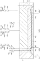
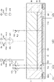
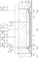
도 1은, 하나의 예시적 실시 형태에 따른 플라스마 처리 장치를 개략적으로 나타내는 도면이다. 도 2는, 하나의 예시적 실시 형태에 따른 플라스마 처리 장치의 기판 지지기 및 복수의 전원을 나타내는 도면이다. 도 1에 나타내는 플라스마 처리 장치(1)는, 용량 결합형의 플라스마 처리 장치이다. 플라스마 처리 장치(1)는, 챔버(10)(플라스마 처리 챔버)를 구비하고 있다. 챔버(10)는, 그 안에 내부 공간(10s)을 제공하고 있다. 내부 공간(10s)의 중심축선은, 연직 방향으로 연장되는 축선 AX이다. 1 is a diagram schematically illustrating a plasma processing device according to one exemplary embodiment. 2 is a diagram illustrating a substrate support and a plurality of power sources of a plasma processing apparatus according to one exemplary embodiment. The plasma processing device 1 shown in FIG. 1 is a capacitive coupling type plasma processing device. The plasma processing device 1 includes a chamber 10 (plasma processing chamber). The
일 실시 형태에 있어서, 챔버(10)는, 챔버 본체(12)를 포함하고 있어도 좋다. 챔버 본체(12)는, 대략 원통 형상을 갖고 있다. 내부 공간(10s)은, 챔버 본체(12) 안에 제공되어 있다. 챔버 본체(12)는, 예를 들면 알루미늄으로 구성되어 있다. 챔버 본체(12)는 전기적으로 접지되어 있다. 챔버 본체(12)의 내벽면, 즉 내부 공간(10s)을 구획하는 벽면에는, 내플라스마성을 갖는 막이 형성되어 있다. 이 막은, 양극 산화 처리에 의해 형성된 막 또는 산화 이트륨으로 형성된 막과 같은 세라믹제의 막일 수 있다.In one embodiment, the
챔버 본체(12)의 측벽은, 통로(12p)를 제공하고 있다. 기판 W는, 내부 공간(10s)과 챔버(10)의 외부 사이에서 반송될 때, 통로(12p)를 통과한다. 이 통로(12p)의 개폐를 위해서, 게이트 밸브(12g)가 챔버 본체(12)의 측벽을 따라 마련되어 있다.A side wall of the
도 1 및 도 2에 나타내는 바와 같이, 플라스마 처리 장치(1)는, 기판 지지기(16)를 더 구비하고 있다. 기판 지지기(16)는, 유전체부(17)에 의해 둘러싸여 있다. 유전체부(17)는, 축선 AX에 대해서 지름 방향에 있어서 기판 지지기(16)의 외측에서 둘레 방향으로 연장되어 있다. 유전체부(17)는, 석영과 같은 유전체로 형성되어 있다. 유전체부(17)는, 기판 지지기(16)를 지지하고 있어도 좋다.As shown in FIGS. 1 and 2 , the plasma processing device 1 further includes a
기판 지지기(16)는, 챔버(10) 안에서, 그 위에 탑재된 기판 W를 지지하도록 구성되어 있다. 기판 W는, 대략 원반 형상을 가진다. 기판 W는, 그 중심이 축선 AX 상에 위치하도록 기판 지지기(16) 상에 탑재된다. 기판 지지기(16)는, 에지 링 ER을 더 지지하도록 구성되어 있다. 에지 링 ER은, 고리 형상을 갖고 있다. 에지 링 ER은, 플라스마 처리 장치(1)에 있어서 행해지는 플라스마 처리에 따라 선택된 재료로 형성된다. 에지 링 ER은, 예를 들면 실리콘 또는 탄화 규소로 형성된다. 에지 링 ER은, 축선 AX에 그 중심축선이 일치하도록, 기판 지지기(16) 상에 탑재된다. 기판 W는, 기판 지지기(16) 상, 또한, 에지 링 ER에 의해 둘러싸인 영역 내에 배치된다. 즉, 에지 링 ER은, 기판 W을 둘러싸도록 배치된다. 또한, 에지 링 ER의 외연 부분은, 유전체부(17) 상에 탑재되어 있어도 좋다.The
기판 지지기(16)는, 기대(18) 및 정전 척(20)을 포함하고 있어도 좋다. 기대(18) 및 정전 척(20)은, 챔버(10) 안에 마련되어 있다. 기대(18)는, 알루미늄과 같은 도전성 재료로 형성되어 있고, 대략 원반 형상을 갖고 있다. 기대(18)의 중심축선은, 축선 AX이다.The
기대(18)는, 그 안에 유로(18f)를 제공하고 있다. 유로(18f)는, 열 교환 매체용의 유로이다. 열 교환 매체는, 예를 들면 냉매이다. 유로(18f)는, 열 교환 매체의 공급 장치(22)에 접속되어 있다. 공급 장치(22)는, 챔버(10)의 외부에 마련되어 있다. 유로(18f)는, 공급 장치(22)로부터 공급되는 열 교환 매체를 받는다. 유로(18f)에 공급된 열 교환 매체는, 공급 장치(22)에 되돌려진다.The
정전 척(20)은, 기대(18) 상에 마련되어 있다. 정전 척(20)은, 접착제 등의 접합 부재(19)를 통하여 기대(18)에 고정되어 있어도 좋다. 정전 척(20)은, 제 1 영역(20R1) 및 제 2 영역(20R2)을 포함하고 있다. 제 1 영역(20R1)은, 그 위에 탑재되는 기판 W를 유지하는 영역이며, 대략 원반 형상을 가진다. 제 1 영역(20R1)의 중심축선은, 축선 AX에 대략 일치하고 있다. 제 2 영역(20R2)은, 그 위에 탑재되는 에지 링 ER을 유지하는 영역이다. 제 2 영역(20R2)은, 평면에서 보아서는 대략 고리 형상을 갖고 있고, 제 1 영역(20R1)에 대해서 지름 방향 외측에서 둘레 방향으로 연장되어 있다. 또한, 제 1 영역(20R1)의 상면은, 높이 방향에 있어서 제 2 영역(20R2)의 상면의 높이 방향의 위치보다 높은 위치에서 연장되어 있다.The
정전 척(20)은, 본체(20m) 및 척 전극(20a)을 갖고 있다. 본체(20m)는, 산화 알루미늄 또는 질화 알루미늄과 같은 유전체로 형성되어 있다. 본체(20m)는, 대략 원반 형상을 갖고 있다. 정전 척(20) 및 본체(20m)의 중심축선은, 축선 AX이다. 척 전극(20a)은, 제 1 영역(20R1)에 있어서 본체(20m) 안에 마련되어 있다. 척 전극(20a)은, 도전성 재료로 형성된 막이다. 척 전극(20a)은, 대략 원형의 평면 형상을 가질 수 있다. 척 전극(20a)의 중심은, 축선 AX 상에 위치하고 있어도 좋다. 척 전극(20a)은, 스위치(50s)를 통하여 직류 전원(50p)에 전기적으로 접속되어 있다. 직류 전원(50p)으로부터의 전압이 척 전극(20a)에 인가되면, 정전 척(20)과 기판 W 사이에서 정전 인력이 발생한다. 발생한 정전 인력에 의해, 기판 W는 정전 척(20)에 끌어당겨지고, 정전 척(20)에 의해 유지된다.The
정전 척(20)은, 척 전극(20b) 및 (20c)을 더 갖고 있어도 좋다. 척 전극(20b) 및 (20c)은, 제 2 영역(20R2)에 있어서 본체(20m) 안에 마련되어 있다. 척 전극(20b) 및 (20c)의 각각은, 도전성 재료로 형성된 막이다. 척 전극(20b) 및 (20c)은, 축선 AX의 주위에서 둘레 방향으로 연장되어 있다. 척 전극(20c)은, 척 전극(20b)에 대해서 지름 방향 외측에서 연장되어 있다. 척 전극(20b) 및 (20c)의 각각은, 고리 형상을 갖고 있어도 좋다. 척 전극(20b)은, 스위치(51s)를 통하여 직류 전원(51p)에 전기적으로 접속되어 있다. 척 전극(20c)은, 스위치(52s)를 통하여 직류 전원(52p)에 전기적으로 접속되어 있다. 직류 전원(51p)으로부터의 전압, 직류 전원(52p)으로부터의 전압이 각각, 척 전극(20b), (20c)에 인가되면, 정전 척(20)과 에지 링 ER 사이에서 정전 인력이 발생한다. 발생한 정전 인력에 의해, 에지 링 ER은 정전 척(20)에 끌어당겨지고, 정전 척(20)에 의해 유지된다.The
플라스마 처리 장치(1)는, 링 전극 DR을 더 구비하고 있다. 링 전극 DR은, 에지 링 ER에 대해서 지름 방향 외측에서 연장되어 있다. 링 전극 DR은, 평면에서 보아서는 대략 고리 형상을 가질 수 있다. 도 2의 실시 형태에서는, 링 전극 DR은, 에지 링 ER을 둘러싸도록 연장되어 있다. 링 전극 DR은, 유전체부(17) 상에 배치될 수 있다. 도 2의 실시 형태에서는, 링 전극 DR은, 실리콘, 탄화 규소, 니켈, 하스텔로이 등과 같은 도전성 재료로 형성되어 있다.The plasma processing device 1 further includes a ring electrode DR. The ring electrode DR extends outward in the radial direction with respect to the edge ring ER. The ring electrode DR may have a substantially annular shape in plan view. In the embodiment of FIG. 2 , the ring electrode DR extends so as to surround the edge ring ER. The ring electrode DR may be disposed on the
도 1에 나타내는 바와 같이, 플라스마 처리 장치(1)는, 가스 공급 라인(24)을 제공하고 있어도 좋다. 가스 공급 라인(24)은, 가스 공급 기구로부터의 전열 가스, 예를 들면 He 가스를, 정전 척(20)의 상면과 기판 W의 이면(하면) 사이의 간극에 공급한다.As shown in FIG. 1 , the plasma processing device 1 may provide a
플라스마 처리 장치(1)는, 상부 전극(30)을 더 구비하고 있다. 상부 전극(30)은, 기판 지지기(16)의 위쪽에 마련되어 있다. 상부 전극(30)은, 부재(32)와 함께 챔버 본체(12)의 상부 개구를 닫고 있다. 부재(32)는, 절연성을 갖고 있다. 상부 전극(30)은, 부재(32)를 개재하여 챔버 본체(12)의 상부에 지지되어 있다.The plasma processing device 1 further includes an
상부 전극(30)은, 천판(34) 및 지지체(36)를 포함하고 있어도 좋다. 천판(34)의 하면은, 내부 공간(10s)을 구획하고 있다. 천판(34)은, 복수의 가스 구멍(34a)을 제공하고 있다. 복수의 가스 구멍(34a)의 각각은, 천판(34)을 그 판 두께 방향(연직 방향)으로 관통하고 있다. 천판(34)은, 예를 들면 실리콘으로 형성되어 있다. 혹은, 천판(34)은, 알루미늄제의 부재의 표면에 내플라스마성의 막을 마련한 구조를 가질 수 있다. 이 막은, 양극 산화 처리에 의해 형성된 막 또는 산화 이트륨으로 형성된 막과 같은 세라믹제의 막일 수 있다.The
지지체(36)는, 천판(34)을 착탈 자재로 지지하고 있다. 지지체(36)는, 예를 들면 알루미늄과 같은 도전성 재료로 형성되어 있다. 지지체(36)는, 그 안에 가스 확산실(36a)을 제공하고 있다. 지지체(36)는, 복수의 가스 구멍(36b)을 더 제공하고 있다. 복수의 가스 구멍(36b)은, 가스 확산실(36a)로부터 아래쪽으로 연장되어, 복수의 가스 구멍(34a)에 각각 연통하고 있다. 지지체(36)는, 가스 도입 포트(36c)를 더 제공하고 있다. 가스 도입 포트(36c)는, 가스 확산실(36a)에 접속하고 있다. 가스 도입 포트(36c)에는, 가스 공급관(38)이 접속되어 있다.The
가스 공급관(38)에는, 가스 소스군(40)이, 밸브군(41), 유량 제어기군(42), 및 밸브군(43)을 통하여 접속되어 있다. 가스 소스군(40), 밸브군(41), 유량 제어기군(42), 및 밸브군(43)은, 가스 공급부를 구성하고 있다. 가스 소스군(40)은, 복수의 가스 소스를 포함하고 있다. 밸브군(41) 및 밸브군(43)의 각각은, 복수의 밸브(예를 들면 개폐 밸브)를 포함하고 있다. 유량 제어기군(42)는, 복수의 유량 제어기를 포함하고 있다. 유량 제어기군(42)의 복수의 유량 제어기의 각각은, 매스 플로우 콘트롤러 또는 압력 제어식의 유량 제어기이다. 가스 소스군(40)의 복수의 가스 소스의 각각은, 밸브군(41)의 대응하는 밸브, 유량 제어기군(42)의 대응하는 유량 제어기, 및 밸브군(43)의 대응하는 밸브를 통하여, 가스 공급관(38)에 접속되어 있다. 플라스마 처리 장치(1)는, 가스 소스군(40)의 복수의 가스 중 선택된 1개 이상의 가스 소스로부터의 가스를, 개별적으로 조정된 유량으로, 내부 공간(10s)에 공급하는 것이 가능하다.A
플라스마 처리 장치(1)는, 배플 부재(48)를 더 구비하고 있어도 좋다. 배플 부재(48)는, 유전체부(17)와 챔버 본체(12)의 측벽 사이에서 연장되어 있다. 배플 부재(48)는, 예를 들면, 알루미늄제의 부재에 산화 이트륨 등의 세라믹을 피복하는 것에 의해 구성될 수 있다. 배플 부재(48)는, 복수의 관통 구멍을 제공하고 있다. 배플 부재(48)의 위쪽의 공간과 배플 부재(48)의 아래쪽의 공간은, 배플 부재(48)의 복수의 관통 구멍을 통하여 접속된다.The plasma processing device 1 may further include a
플라스마 처리 장치(1)는, 배기 장치(50)를 더 구비할 수 있다. 배기 장치(50)는, 배플 부재(48)의 아래쪽에서 챔버 본체(12)의 저부에 배기관(52)을 통하여 접속된다. 배기 장치(50)는, 자동 압력 제어 밸브와 같은 압력 제어기, 및, 터보 분자 펌프 등의 진공 펌프를 갖고 있고, 내부 공간(10s)의 압력을 감압할 수가 있다.The plasma processing device 1 may further include an exhaust device 50 . The exhaust device 50 is connected to the bottom of the
도 1 및 도 2에 나타내는 바와 같이, 플라스마 처리 장치(1)는, 고주파 전원(61)(RF 전원)을 더 구비하고 있다. 고주파 전원(61)은, 기판 지지기(16)의 위쪽에서 플라스마를 생성하기 위해서 고주파 전극에 공급되는 고주파 전력 RF(RF 전력를 발생한다. 고주파 전력 RF는, 27~100MHz의 범위 내의 주파수, 예를 들면 40MHz 또는 60MHz의 주파수를 가진다. 일 실시 형태에 있어서, 고주파 전극은, 기대(18)이다. 즉, 일 실시 형태에 있어서, 기대(18)는, 고주파 전극인 하부 전극을 제공하고 있다.As shown in FIGS. 1 and 2 , the plasma processing device 1 further includes a high frequency power supply 61 (RF power supply). The high-
고주파 전원(61)은, 정합기(61m)를 통하여 기대(18)에 접속되어 있다. 정합기(61m)는, 고주파 전원(61)의 부하 측(기대(18) 측)의 임피던스를, 고주파 전원(61)의 출력 임피던스에 정합시키도록 구성된 정합 회로를 갖고 있다. 일 실시 형태에 있어서, 고주파 전원(61)은, 정합기(61m) 및 필터(61f)를 통하여 기대(18)에 접속되어 있어도 좋다. 필터(61f)는, 고주파 전력 RF를 선택적으로 통과시키는 주파수 특성을 갖는 필터이며, 후술하는 전기 바이어스 에너지를 차단하거나 저감시키는 특성을 가진다. 또한, 고주파 전원(61)은, 기판 지지기(16)의 고주파 전극이 아니라, 상부 전극(30)에 전기적으로 접속되어 있어도 좋다. 즉, 다른 실시 형태에 있어서, 고주파 전극은, 상부 전극(30)이어도 좋다.The high
플라스마 처리 장치(1)는, 바이어스 전원(62)(제 1 바이어스 전원)을 더 구비하고 있다. 바이어스 전원(62)은, 기판 지지기(16)의 바이어스 전극에 전기적으로 결합되어 있고, 기판 지지기(16)의 바이어스 전극에 주어지는 전기 바이어스 에너지 BE를 발생하도록 구성되어 있다. 도 2의 실시 형태에서는, 기판 지지기(16)의 바이어스 전극은, 기대(18)이다. 전기 바이어스 에너지 BE는, 기판 W에 이온을 끌어 들이기 위해서 이용된다. 전기 바이어스 에너지 BE는, 바이어스 주파수를 가진다. 바이어스 주파수는, 고주파 전력 RF의 주파수와 달라도 좋고, 동일해도 좋다. 바이어스 주파수는, 고주파 전력 RF의 주파수보다 낮아도 좋다. 일 실시 형태에 있어서, 바이어스 주파수는, 50kHz~27MHz의 범위 내의 주파수이며, 예를 들면 400kHz이다.The plasma processing device 1 further includes a bias power supply 62 (first bias power supply). The
이하, 도 1 및 도 2와 함께 도 3(a) 및 도 3(b)를 참조한다. 도 3(a) 및 도 3(b)의 각각은, 바이어스 전극에 공급되는 전기 바이어스 에너지 및 링 전극에 공급되는 전기 바이어스 에너지의 예를 나타내는 도면이다.Hereinafter, reference is made to FIGS. 3(a) and 3(b) together with FIGS. 1 and 2 . 3(a) and 3(b) are diagrams showing examples of electric bias energy supplied to the bias electrode and electric bias energy supplied to the ring electrode, respectively.
일 실시 형태에 있어서, 바이어스 전원(62)(제 1 바이어스 전원 또는 제 1 바이어스 RF 전원)은, 도 3(a)에 나타내는 바와 같이, 전기 바이어스 에너지 BE로서, 고주파 전력, 즉 고주파 바이어스 전력(제 1 바이어스 RF 전력)을 발생해도 좋다. 전기 바이어스 에너지 BE로서의 고주파 바이어스 전력(및 그 전압 파형)은, 바이어스 주파수를 갖는 정현파이다. 바이어스 주파수의 역수는, 주기 CP(반복 기간)의 시간 길이다.In one embodiment, the bias power supply 62 (first bias power supply or first bias RF power supply), as shown in FIG. 1 bias RF power) may be generated. The high-frequency bias power (and its voltage waveform) as the electrical bias energy BE is a sinusoidal wave having a bias frequency. The reciprocal of the bias frequency is the time length of the cycle CP (repetition period).
바이어스 전원(62)(제 1 바이어스 전원 또는 제 1 바이어스 RF 전원)은, 고주파 바이어스 전력을 바이어스 전극에 공급하기 위해서, 정합기(62m) 및 필터(62f)를 통하여 바이어스 전극(도 2의 실시 형태에서는 기대(18))에 접속되어 있다. 정합기(62m)는, 바이어스 전원(62)의 부하 측의 임피던스를, 바이어스 전원(62)의 출력 임피던스에 정합시키도록 구성된 정합 회로를 갖고 있다. 필터(62f)는, 전기 바이어스 에너지 BE를 선택적으로 통과시키는 주파수 특성을 갖고 있고, 고주파 전력 RF를 차단하거나 저감시키는 특성을 가진다.The bias power supply 62 (first bias power supply or first bias RF power supply) is configured to supply high-frequency bias power to the bias electrode through a
다른 실시 형태에 있어서, 바이어스 전원(62)(제 1 바이어스 전원 또는 제 1 전압 펄스 전원)은, 도 3(b)에 나타내는 바와 같이, 전기 바이어스 에너지 BE로서 전압의 펄스를 주기적으로 바이어스 전극(도 2의 실시 형태에서는 기대(18))에 인가하도록 구성되어 있어도 좋다. 즉, 전기 바이어스 에너지 BE는, 제 1 DC 펄스 신호 또는 DC 전압 펄스의 시퀀스이어도 좋다. 전압의 펄스는, 바이어스 주파수의 역수인 시간 간격(즉 주기 CP)으로, 바이어스 전극(도 2의 실시 형태에서는 기대(18))에 인가된다. 전압의 펄스는, 음의 전압의 펄스이어도 좋고, 음의 직류 전압의 펄스이어도 좋다. 전압의 펄스는, 삼각파, 구형파 등과 같은 임의의 파형을 갖고 있어도 좋다.In another embodiment, the bias power supply 62 (first bias power supply or first voltage pulse power supply) periodically sends pulses of voltage as electric bias energy BE to the bias electrode (Fig. In Embodiment 2, it may be comprised so that it may be applied to the
플라스마 처리 장치(1)는, 고주파 전원(63)(RF 전원)을 더 구비하고 있어도 좋다. 고주파 전원(63)은, 기판 지지기(16)의 위쪽에서 플라스마를 생성하기 위해서 고주파 전력 RF2(RF 전력)를 발생한다. 고주파 전력 RF2는, 고주파 전력 RF의 주파수와 같은 주파수를 가질 수 있다. 고주파 전원(63)은, 정합기(63m) 및 필터(63f)를 통하여 링 전극 DR에 전기적으로 접속되어 있다. 정합기(63m)는, 고주파 전원(63)의 부하측의 임피던스를, 고주파 전원(63)의 출력 임피던스에 정합시키도록 구성된 정합 회로를 갖고 있다. 필터(63f)는, 고주파 전력 RF2를 선택적으로 통과시키는 특성을 갖고 있고, 후술하는 전기 바이어스 에너지 BE2를 차단하거나 저감시키는 특성을 가진다.The plasma processing device 1 may further include a high frequency power supply 63 (RF power supply). The high
플라스마 처리 장치(1)는, 바이어스 전원(64)(제 2 바이어스 전원)를 더 구비하고 있다. 바이어스 전원(64)은, 링 전극 DR에 전기적으로 결합되어 있다. 링 전극 DR에 주어지는 전기 바이어스 에너지 BE2를 발생하도록 구성되어 있다. 전기 바이어스 에너지 BE2는, 전기 바이어스 에너지 BE의 바이어스 주파수와 같은 바이어스 주파수를 가진다.The plasma processing device 1 further includes a bias power supply 64 (second bias power supply). The
도 3(a)에 나타내는 바와 같이, 전기 바이어스 에너지 BE2는, 전기 바이어스 에너지 BE와 마찬가지로, 고주파 바이어스 전력(제 2 바이어스 RF 전력)이어도 좋다. 이 경우에는, 바이어스 전원(64)(제 2 바이어스 전원 또는 제 2 바이어스 RF 전원)은, 정합기(64m) 및 필터(64f)를 통하여 링 전극 DR에 접속된다. 정합기(64m)는, 바이어스 전원(64)의 부하 측의 임피던스를, 바이어스 전원(64)의 출력 임피던스에 정합시키도록 구성된 정합 회로를 갖고 있다. 필터(64f)는, 전기 바이어스 에너지 BE2를 선택적으로 통과시키는 주파수 특성을 갖고 있고, 고주파 전력 RF2를 차단하거나 저감시키는 특성을 가진다.As shown in Fig. 3(a), the electric bias energy BE2 may be high frequency bias power (second bias RF power) similarly to the electric bias energy BE. In this case, the bias power supply 64 (second bias power supply or second bias RF power supply) is connected to the ring electrode DR via a
도 3(b)에 나타내는 바와 같이, 전기 바이어스 에너지 BE2는, 전기 바이어스 에너지 BE와 마찬가지로 전압의 펄스의 시퀀스이어도 좋다. 즉, 바이어스 전원(64)(제 2 바이어스 전원 또는 제 2 전압 펄스 전원)에 의해 발생되는 전기 바이어스 에너지 BE2는, 제 2 DC 펄스 신호 또는 DC 전압 펄스의 시퀀스이어도 좋다. 전기 바이어스 에너지 BE2의 전압의 펄스는, 바이어스 주파수의 역수인 시간 간격(즉 주기 CP)으로, 주기적으로 링 전극 DR에 인가된다. 전압의 펄스는, 음의 전압의 펄스이어도 좋고, 음의 직류 전압의 펄스이어도 좋다. 전압의 펄스는, 삼각파, 구형파 등과 같은 임의의 파형을 갖고 있어도 좋다.As shown in Fig. 3(b), the electrical bias energy BE2 may be a sequence of voltage pulses similarly to the electrical bias energy BE. That is, the electric bias energy BE2 generated by the bias power supply 64 (second bias power supply or second voltage pulse power supply) may be a second DC pulse signal or a sequence of DC voltage pulses. Pulses of the voltage of the electrical bias energy BE2 are applied to the ring electrode DR periodically at time intervals that are reciprocal of the bias frequency (i.e. period CP). The voltage pulse may be a negative voltage pulse or a negative DC voltage pulse. The voltage pulse may have an arbitrary waveform such as a triangular wave or a square wave.
도 3(a) 및 도 3(b)에 나타내는 바와 같이, 전기 바이어스 에너지 BE의 1주기(주기 CP 또는 반복 주기)는, 정위상 기간 PP(제 2 기간) 및 부위상 기간 PN(제 1 기간)으로 구성된다. 또, 전기 바이어스 에너지 BE2의 1주기(주기 CP 또는 반복 주기)는, 정위상 기간 PP(제 4 기간) 및 부위상 기간 PN(제 3 기간)으로 구성된다. 부위상 기간 PN에 있어서, 전기 바이어스 에너지 BE 및 BE2의 각각은, 1주기(주기 CP) 내에서의 그 평균 전압보다 낮은 전압을 가진다. 정위상 기간 PP에 있어서, 전기 바이어스 에너지 BE 및 BE2의 각각은, 1주기(주기 CP) 내에서의 그 평균 전압 이상의 전압을 가진다.As shown in Fig. 3(a) and Fig. 3(b), one cycle (cycle CP or repetition cycle) of the electric bias energy BE has a normal phase period PP (second period) and a partial phase period PN (first period) ) is composed of In addition, one cycle (cycle CP or repetition cycle) of the electric bias energy BE2 is composed of a regular phase period PP (fourth period) and a partial phase period PN (third period). In the partial phase period PN, each of the electric bias energies BE and BE2 has a voltage lower than its average voltage within one period (period CP). In the constant phase period PP, each of the electric bias energies BE and BE2 has a voltage equal to or higher than its average voltage within one period (period CP).
바이어스 전원(64)에 의해 발생되는 전기 바이어스 에너지 BE2의 부위상 기간 PN은, 바이어스 전원(62)에 의해 발생되는 전기 바이어스 에너지 BE의 부위상 기간 PN과 적어도 부분적으로 중복한다. 도 3(a) 및 도 3(b)에 나타내는 바와 같이, 전기 바이어스 에너지 BE2의 부위상 기간 PN은, 전기 바이어스 에너지 BE의 부위상 기간 PN과 일치하고 있어도 좋다. 즉, 전기 바이어스 에너지 BE2의 위상은, 전기 바이어스 에너지 BE의 위상과 동기하고 있어도 좋다.The part phase period PN of the electrical bias energy BE2 generated by the
또한, 전기 바이어스 에너지 BE 및 BE2가 각각 제 1 및 제 2 바이어스 RF 전력인 경우에는, 제 1 및 제 2 바이어스 RF 전력 각각의 제 1 및 제 2 전력 레벨은, 서로 동일해도 좋고, 서로 달라도 좋다. 제 2 전력 레벨은, 제 1 전력 레벨보다 커도, 작아도 좋다.Further, when the electric bias energies BE and BE2 are first and second bias RF powers, respectively, the first and second power levels of the first and second bias RF powers may be the same or different. The second power level may be larger or smaller than the first power level.
전기 바이어스 에너지 BE가 제 1 전압 펄스 신호인 경우에는, 제 1 전압 펄스 신호는, 제 1 기간에 있어서 제 1 전압 레벨을 갖고, 제 2 기간에 있어서 제 2 전압 레벨을 가진다. 제 1 전압 레벨의 절대치는, 제 2 전압 레벨의 절대치보다 크다. 또한, 전기 바이어스 에너지 BE2가 제 2 전압 펄스 신호인 경우에는, 제 2 전압 펄스 신호는 제 3 기간에 있어서 제 3 전압 레벨을 갖고, 제 4 기간에 있어서 제 4 전압 레벨을 가진다. 제 3 전압 레벨의 절대치는 제 4 전압 레벨의 절대값보다 크다. 제 1 전압 레벨 및 제 3 전압 레벨은 음의 레벨이어도 좋다. 제 3 전압 레벨은 제 1 전압 레벨과 같아도 좋고, 제 4 전압 레벨은 제 2 전압 레벨과 같아도 좋다. 혹은, 제 3 전압 레벨은 제 1 전압 레벨과 달라도 좋다. When the electric bias energy BE is a first voltage pulse signal, the first voltage pulse signal has a first voltage level in the first period and a second voltage level in the second period. The absolute value of the first voltage level is greater than the absolute value of the second voltage level. Further, when the electric bias energy BE2 is the second voltage pulse signal, the second voltage pulse signal has a third voltage level in the third period and a fourth voltage level in the fourth period. An absolute value of the third voltage level is greater than an absolute value of the fourth voltage level. The first voltage level and the third voltage level may be negative levels. The third voltage level may be equal to the first voltage level, and the fourth voltage level may be equal to the second voltage level. Alternatively, the third voltage level may be different from the first voltage level.
전기 바이어스 에너지 BE 및 BE2가 각각 제 1 및 제 2 전압 펄스 신호인 경우에는, 제 1 기간은 제 2 기간의 길이와 간은 길이를 가지고 있어도 좋다. 혹은, 제 1 기간은 제 2 기간의 길이와 다른 길이를 가지고 있어도 좋다. 제 1 기간의 길이는 제 2 기간의 길이보다 길어도 좋고, 짧아도 좋다.When the electric bias energies BE and BE2 are the first and second voltage pulse signals, respectively, the first period may have a length between the length of the second period. Alternatively, the first period may have a length different from that of the second period. The length of the first period may be longer or shorter than the length of the second period.
일 실시 형태에 있어서, 플라스마 처리 장치(1)는, 제어부 MC를 더 구비할 수 있다. 제어부 MC는, 프로세서, 기억 장치, 입력 장치, 표시 장치 등을 구비하는 컴퓨터이며, 플라스마 처리 장치(1)의 각 부를 제어한다. 구체적으로, 제어부 MC는, 기억 장치에 기억되어 있는 제어 프로그램을 실행하고, 해당 기억 장치에 기억되어 있는 레시피 데이터에 근거하여 플라스마 처리 장치(1)의 각 부를 제어한다. 제어부 MC에 의한 제어에 의해, 레시피 데이터에 의해 지정된 프로세스가 플라스마 처리 장치(1)에 있어서 실행된다.In one embodiment, the plasma processing device 1 may further include a controller MC. The controller MC is a computer including a processor, a storage device, an input device, a display device, and the like, and controls each part of the plasma processing device 1. Specifically, the control unit MC executes a control program stored in the storage device and controls each unit of the plasma processing device 1 based on recipe data stored in the storage device. Under the control of the controller MC, the process designated by the recipe data is executed in the plasma processing device 1 .
상술한 정위상 기간 PP에서는, 기판 W 상의 시스의 두께는 작고, 기판 W와 플라스마 사이의 임피던스가 작기 때문에, 비교적 많은 고주파 전력 RF가 기판 W의 위쪽에서 플라스마에 결합된다. 한편, 부위상 기간 PN에서는, 기판 W 상의 시스의 두께는 크고, 기판 W와 플라스마 사이의 임피던스는 크다. 플라스마 처리 장치(1)에서는, 부위상 기간 PN에 있어서 기판 W의 에지의 지름 방향 외측에서의 시스의 두께를 크게 하여 링 전극 DR과 플라스마 사이의 임피던스를 높게 하기 위해서, 전기 바이어스 에너지 BE2가 링 전극 DR에 공급된다. 따라서, 부위상 기간 PN에 있어서 링 전극 DR의 위쪽에 있어서 플라스마에 결합하는 고주파 전력 RF가 억제된다. 그 결과, 바이어스 전극에 공급되는 전기 바이어스 에너지 BE의 주기 CP 내에서의 플라스마의 지름 방향에 있어서의 퍼짐의 변동이 억제된다. 또, 에칭에 의해 기판 W의 에지 및 그 근방에 형성되는 형상의 이상을 억제하는 것이 가능해진다.In the above-described constant phase period PP, since the thickness of the sheath on the substrate W is small and the impedance between the substrate W and the plasma is small, a relatively large amount of high-frequency power RF is coupled to the plasma above the substrate W. On the other hand, in the partial phase period PN, the thickness of the sheath on the substrate W is large, and the impedance between the substrate W and the plasma is large. In the plasma processing device 1, in order to increase the impedance between the ring electrode DR and the plasma by increasing the thickness of the sheath on the outer side in the radial direction of the edge of the substrate W in the partial phase period PN, the electric bias energy BE2 is applied to the ring electrode supplied to the DR. Therefore, in the partial phase period PN, the high-frequency electric power RF coupled to the plasma above the ring electrode DR is suppressed. As a result, fluctuations in the spread of the plasma in the radial direction within the period CP of the electric bias energy BE supplied to the bias electrode are suppressed. In addition, it becomes possible to suppress irregularities in the shape formed on the edge of the substrate W and its vicinity by etching.
이하, 도 4를 참조한다. 도 4는, 다른 예시적 실시 형태에 따른 기판 지지기 및 복수의 전원을 나타내는 도면이다. 이하, 도 2의 실시 형태에 대한 도 4의 실시 형태의 차이점에 대해 설명한다.Hereinafter, reference is made to FIG. 4 . 4 is a diagram illustrating a substrate supporter and a plurality of power sources according to another exemplary embodiment. Hereinafter, differences between the embodiment of FIG. 4 and the embodiment of FIG. 2 will be described.
도 4의 실시 형태의 기판 지지기(16B)는, 플라스마 처리 장치(1)의 기판 지지기로서 채용 가능하다. 도 4의 실시 형태에서는, 링 전극 DRB가, 에지 링 ER에 대해서 지름 방향 외측에서 연장되어 있다. 링 전극 DRB는, 평면에서 보아서는 대략 고리 형상을 가질 수 있다. 링 전극 DRB는, 에지 링 ER을 둘러싸도록 연장되어 있고, 유전체부(17) 상에 배치되어 있다. 링 전극 DRB는, 실리콘, 탄화 규소와 같은 도전성 재료로 형성되어 있다.The
기판 지지기(16B)에서는, 보조 전극(71)이 링 전극 DRB의 아래쪽에서 유전체부(17) 안에 마련되어 있다. 보조 전극(71)은, 고리 형상을 갖고, 축선 AX의 주위에서 둘레 방향으로 연장되어 있어도 좋다. 기판 지지기(16B)의 다른 구성은, 도 2에 나타내는 기판 지지기(16)의 대응하는 구성과 동일하다. 도 4의 실시 형태에서는, 고주파 전원(63) 및 바이어스 전원(64)은, 보조 전극(71)에 전기적으로 접속되어 있고, 보조 전극(71)을 통하여 링 전극 DRB에 용량적으로 결합되어 있다.In the
이하, 도 5를 참조한다. 도 5는, 또 다른 예시적 실시 형태에 따른 기판 지지기 및 복수의 전원을 나타내는 도면이다. 이하, 도 2의 실시 형태에 대한 도 5의 실시 형태의 차이점에 대해 설명한다.Hereinafter, reference is made to FIG. 5 . 5 is a diagram illustrating a substrate supporter and a plurality of power sources according to still another exemplary embodiment. Hereinafter, differences between the embodiment of FIG. 5 and the embodiment of FIG. 2 will be described.
도 5의 실시 형태의 기판 지지기(16C)는, 플라스마 처리 장치(1)의 기판 지지기로서 채용 가능하다. 도 5의 실시 형태에서는, 링 부재(72)가, 에지 링 ER에 대해서 지름 방향 외측에서 연장되어 있다. 링 부재(72)는, 평면에서 보아서는 대략 고리 형상을 가질 수 있다. 링 부재(72)는, 에지 링 ER을 둘러싸도록 연장되어 있고, 유전체부(17) 상에 배치되어 있다. 링 부재(72)는, 석영 또는 산화 알루미늄과 같은 유전체로 형성되어 있다.The
기판 지지기(16C)에서는, 링 전극 DRC가 링 부재(72) 안에 마련되어 있다. 링 전극 DRC는, 고리 형상을 갖고, 축선 AX의 주위에서 둘레 방향으로 연장되어 있어도 좋다. 기판 지지기(16C)의 다른 구성은, 기판 지지기(16B)의 대응하는 구성과 동일하다. 도 5의 실시 형태에서는, 고주파 전원(63) 및 바이어스 전원(64)은, 링 전극 DRC에 전기적으로 접속되어 있다. 또한, 링 전극 DRC는, 링 부재(72)로부터 떨어진 영역, 예를 들면 유전체부(17) 안에 마련되어 있어도 좋다.In the
이하, 도 6을 참조한다. 도 6은, 또 다른 예시적 실시 형태에 따른 기판 지지기 및 복수의 전원을 나타내는 도면이다. 이하, 도 2의 실시 형태에 대한 도 6의 실시 형태의 차이점에 대해 설명한다.Hereinafter, reference is made to FIG. 6 . 6 is a diagram illustrating a substrate supporter and a plurality of power sources according to still another exemplary embodiment. Hereinafter, differences between the embodiment of FIG. 6 and the embodiment of FIG. 2 will be described.
도 6의 실시 형태에 있어서, 플라스마 처리 장치(1)는, 바이어스 전원(66)을 더 구비하고 있다. 바이어스 전원(66)은, 에지 링 ER에 전기적으로 결합되어 있다. 에지 링 ER에 주어지는 전기 바이어스 에너지 BE3를 발생하도록 구성되어 있다. 전기 바이어스 에너지 BE3는, 전기 바이어스 에너지 BE의 바이어스 주파수와 같은 바이어스 주파수를 갖고 있어도 좋다.In the embodiment of FIG. 6 , the plasma processing device 1 further includes a
전기 바이어스 에너지 BE3는, 전기 바이어스 에너지 BE와 마찬가지로, 고주파 바이어스 전력(제 3 바이어스 RF 전력)이어도 좋다. 이 경우에는, 바이어스 전원(66)은, 정합기(66m) 및 필터(66f)를 통하여 에지 링 ER에 접속된다. 정합기(66m)는, 바이어스 전원(66)의 부하 측의 임피던스를, 바이어스 전원(66)(제 3 바이어스 RF 전원)의 출력 임피던스에 정합시키도록 구성된 정합 회로를 갖고 있다. 필터(66f)는, 전기 바이어스 에너지 BE3를 선택적으로 통과시키는 주파수 특성을 갖고 있고, 고주파 전력 RF를 차단하거나 저감시키는 특성을 가진다.The electric bias energy BE3 may be high-frequency bias power (third bias RF power) similarly to the electric bias energy BE. In this case, the
혹은, 전기 바이어스 에너지 BE3는, 전기 바이어스 에너지 BE와 마찬가지로 전압의 펄스의 시퀀스 또는 제 3 전압 펄스 신호이어도 좋다. 전기 바이어스 에너지 BE3의 전압의 펄스는, 바이어스 주파수의 역수인 시간 간격(즉 주기 CP)으로, 주기적으로 링 전극 DR에 인가된다.Alternatively, the electrical bias energy BE3 may be a sequence of voltage pulses or a third voltage pulse signal similarly to the electrical bias energy BE. Pulses of the voltage of the electric bias energy BE3 are applied to the ring electrode DR periodically at time intervals that are reciprocal of the bias frequency (i.e. period CP).
도 6의 실시 형태에 의하면, 에지 링 ER에 주어지는 전기 바이어스 에너지를 독립적으로 제어하여, 에지 링 ER 상의 시스의 두께를 독립적으로 제어하는 것이 가능하다. 또한, 기판 지지기(16B) 및 기판 지지기(16C)의 각각에 있어서도, 바이어스 전원(66)이 에지 링 ER에 전기적으로 결합되어 있어도 좋다.According to the embodiment of FIG. 6 , it is possible to independently control the thickness of the sheath on the edge ring ER by independently controlling the electrical bias energy applied to the edge ring ER. Also in each of the
이하, 도 7을 참조한다. 도 7은, 또 다른 예시적 실시 형태에 따른 기판 지지기 및 복수의 전원을 나타내는 도면이다. 이하, 도 6의 실시 형태에 대한 도 7의 실시 형태의 차이점에 대해 설명한다.Hereinafter, reference is made to FIG. 7 . 7 is a diagram illustrating a substrate supporter and a plurality of power sources according to still another exemplary embodiment. Hereinafter, differences between the embodiment of FIG. 7 and the embodiment of FIG. 6 will be described.
도 7에 나타내는 기판 지지기(16D)는, 플라스마 처리 장치(1)의 기판 지지기로서 채용 가능하다. 기판 지지기(16D)의 정전 척(20D)은, 전극(20e)을 더 포함하고 있다. 기판 지지기(16D)의 다른 구성은, 도 6에 나타내는 기판 지지기(16)의 대응하는 구성과 동일하다. 전극(20e)은, 도전성 재료로 형성된 막이며, 제 2 영역(20R2)에 있어서 본체(20m) 안에 마련되어 있다. 전극(20e)은, 고리 형상을 갖고 있어도 좋고, 축선 AX의 주위에서 둘레 방향으로 연장되어 있어도 좋다. 도 7의 실시 형태에서는, 바이어스 전원(66)은, 전극(20e)에 전기적으로 접속되어 있고, 전극(20e)을 통하여 에지 링 ER에 용량적으로 결합되어 있다.The substrate support 16D shown in FIG. 7 can be employed as a substrate support for the plasma processing apparatus 1 . The
또한, 기판 지지기(16B) 및 기판 지지기(16C)의 각각에 있어서도, 바이어스 전원(66)이 전극(20e)을 통하여 에지 링 ER에 전기적으로 결합되어 있어도 좋다. 또, 바이어스 전원(66)은, 척 전극(20b) 및 척 전극(20c)에 전기적으로 접속되어 있어도 좋다. 이 경우에는, 기판 지지기는, 전극(20e)을 포함하지 않아도 좋다.Also in each of the
이하, 도 8을 참조한다. 도 8은, 또 다른 예시적 실시 형태에 따른 기판 지지기 및 복수의 전원을 나타내는 도면이다. 이하, 도 7의 실시 형태에 대한 도 8의 실시 형태의 차이점에 대해 설명한다.Hereinafter, reference is made to FIG. 8 . 8 is a diagram illustrating a substrate supporter and a plurality of power sources according to another exemplary embodiment. Hereinafter, differences between the embodiment of FIG. 8 and the embodiment of FIG. 7 will be described.
도 8에 나타내는 기판 지지기(16E)는, 플라스마 처리 장치(1)의 기판 지지기로서 채용 가능하다. 기판 지지기(16E)의 정전 척(20E)은, 전극(20f)을 더 포함하고 있다. 기판 지지기(16E)의 다른 구성은, 기판 지지기(16D)의 대응하는 구성과 동일하다. 전극(20f)은, 도전성 재료로 형성된 막이며, 제 1 영역(20R1)에 있어서 본체(20m) 안에 마련되어 있다. 전극(20f)은, 대략 원 형상을 갖고 있어도 좋고, 그 중심은 축선 AX 상에 위치하고 있어도 좋다. 도 8의 실시 형태에서는, 바이어스 전원(62)은, 전극(20f)에 전기적으로 접속되어 있다. 즉, 전극(20f)은, 기판 지지기(16E)에 있어서 바이어스 전극을 구성하고 있다.The
또한, 기판 지지기(16B) 및 기판 지지기(16C)의 각각에 있어서도, 바이어스 전원(62)이 전극(20f)에 전기적으로 접속되어 있어도 좋다. 또, 바이어스 전원(62)은, 척 전극(20a)에 전기적으로 접속되어 있어도 좋다. 이 경우에는, 척 전극(20a)이 바이어스 전극을 구성한다. 이 경우에는, 기판 지지기는, 전극(20f)을 포함하지 않아도 좋다.Also in each of the
이하, 도 9를 참조한다. 도 9는, 또 다른 예시적 실시 형태에 따른 기판 지지기 및 복수의 전원을 나타내는 도면이다. 이하, 도 8의 실시 형태에 대한 도 9의 실시 형태의 차이점에 대해 설명한다.Hereinafter, reference is made to FIG. 9 . 9 is a diagram illustrating a substrate supporter and a plurality of power sources according to another exemplary embodiment. Hereinafter, differences between the embodiment of FIG. 9 and the embodiment of FIG. 8 will be described.
도 9의 실시 형태에서는, 고주파 전원(61) 및 바이어스 전원(62)은, 전극(20f)에 전기적으로 접속되어 있다. 즉, 전극(20f)은, 기판 지지기(16E)에 있어서, 고주파 전극 및 바이어스 전극을 구성하고 있다.In the embodiment of Fig. 9, the high
또, 도 9의 실시 형태에서는, 플라스마 처리 장치(1)는, 고주파 전원(65)을 더 구비하고 있다. 고주파 전원(65)은, 기판 지지기(16)의 위쪽에서 플라스마를 생성하기 위해서 고주파 전력 RF3(RF 전력)을 발생한다. 고주파 전력 RF3은, 고주파 전력 RF의 주파수와 같은 주파수를 가질 수 있다. 고주파 전원(65)은, 정합기(65m) 및 필터(65f)를 통하여 전극(20e)에 전기적으로 접속되어 있다. 정합기(65m)는, 고주파 전원(65)의 부하 측의 임피던스를, 고주파 전원(65)의 출력 임피던스에 정합시키도록 구성된 정합 회로를 갖고 있다. 필터(65f)는, 고주파 전력 RF3을 선택적으로 통과시키는 특성을 갖고 있고, 전기 바이어스 에너지 BE3를 차단하거나 저감시키는 특성을 가진다.Moreover, in the embodiment of FIG. 9 , the plasma processing device 1 further includes a high
또한, 기판 지지기(16B) 및 기판 지지기(16C)의 각각에 있어서도, 고주파 전원(61) 및 바이어스 전원(62)이, 전극(20f)에 전기적으로 접속되어 있어도 좋다. 또, 기판 지지기(16B) 및 기판 지지기(16C)의 각각에 있어서도, 고주파 전원(65) 및 바이어스 전원(66)이, 전극(20e)에 전기적으로 접속되어 있어도 좋다.Also in each of the
이하, 도 10을 참조한다. 도 10은, 또 다른 예시적 실시 형태에 따른 기판 지지기 및 복수의 전원을 나타내는 도면이다. 이하, 도 2의 실시 형태에 대한 도 10의 실시 형태의 차이점에 대해 설명한다.Hereinafter, reference is made to FIG. 10 . 10 is a diagram illustrating a substrate supporter and a plurality of power sources according to another exemplary embodiment. Hereinafter, differences between the embodiment of FIG. 10 and the embodiment of FIG. 2 will be described.
도 10의 실시 형태에 있어서, 플라스마 처리 장치(1)는, 고주파 전원(63) 및 바이어스 전원(64)을 구비하지 않는다. 도 10의 실시 형태에서는, 고주파 전원(61)은, 기판 지지기(16)의 고주파 전극(도 10의 실시 형태에서는 기대(18))에 더하여, 링 전극 DR에 전기적으로 접속되어 있다. 도 10의 실시 형태에서는, 고주파 전력 RF가, 기판 지지기(16)의 고주파 전극과 링 전극 DR에 분배된다. 기판 지지기(16)의 고주파 전극과 링 전극 DR 사이에서의 고주파 전력 RF의 분배 비율은, 임피던스 조정기(61i)에 의해 조정된다. 임피던스 조정기(61i)는, 고주파 전원(61)과 기판 지지기(16)의 고주파 전극을 접속하는 전기적 패스 상의 노드와 링 전극 DR 사이에서 접속되어 있다. 임피던스 조정기(61i)는, 가변 임피던스를 가진다. 임피던스 조정기(61i)는, 예를 들면 가변 용량 콘덴서를 포함하고 있어도 좋다.In the embodiment of FIG. 10 , the plasma processing device 1 does not include a high
또, 도 10의 실시 형태에서는, 바이어스 전원(62)은, 기판 지지기(16)의 바이어스 전극(도 10의 실시 형태에서는 기대(18))에 더하여, 링 전극 DR에 전기적으로 접속되어 있다. 즉, 도 10의 실시 형태에서는, 단일의 바이어스 전원(62)이, 제 1 바이어스 RF 전원 및 제 2 바이어스 RF 전원을 겸하고 있다. 도 10의 실시 형태에서는, 전기 바이어스 에너지 BE가, 기판 지지기(16)의 바이어스 전극과 링 전극 DR에 분배된다. 기판 지지기(16)의 바이어스 전극과 링 전극 DR 사이에서의 전기 바이어스 에너지 BE의 분배 비율은, 임피던스 조정기(62i)에 의해 조정된다. 임피던스 조정기(62i)는, 바이어스 전원(62)과 기판 지지기(16)의 바이어스 전극을 접속하는 전기적 패스 상의 노드와 링 전극 DR 사이에서 접속되어 있다. 임피던스 조정기(62i)는, 가변 임피던스를 가진다. 임피던스 조정기(62i)는, 예를 들면 가변 용량 콘덴서를 포함하고 있어도 좋다.In the embodiment of FIG. 10 , the
도 10의 실시 형태에서는, 단일의 바이어스 전원(62)로부터의 전기 바이어스 에너지 BE가 기판 지지기(16)의 바이어스 전극과 링 전극 DR에 분배된다. 따라서, 기판 지지기(16)의 바이어스 전극에 주어지는 전기 바이어스 에너지 위상과 링 전극 DR에 주어지는 전기 바이어스 에너지의 위상은 서로 동기하고 있다. 따라서, 부위상 기간 PN에 있어서 링 전극 DR의 위쪽에 있어서 플라스마에 결합하는 고주파 전력 RF가 억제된다. 그 결과, 기판 지지기(16)의 바이어스 전극에 공급되는 전기 바이어스 에너지 BE의 주기 내에서의 플라스마의 지름 방향에 있어서의 퍼짐의 변동이 억제된다.In the embodiment of FIG. 10 , electrical bias energy BE from a single
또한, 도 10의 실시 형태와 마찬가지로, 기판 지지기(16B)에 있어서도, 고주파 전원(61)으로부터의 고주파 전력 RF가, 기판 지지기(16)의 고주파 전극과 링 전극 DRB에 분배되어도 좋다. 또, 도 10의 실시 형태와 마찬가지로, 기판 지지기(16B)에 있어서도, 바이어스 전원(62)로부터의 전기 바이어스 에너지 BE가, 기판 지지기(16)의 바이어스 전극과 링 전극 DRB에 분배되어도 좋다. 또, 도 10의 실시 형태와 마찬가지로, 기판 지지기(16C)에 있어서도, 고주파 전원(61)으로부터의 고주파 전력 RF가, 기판 지지기(16)의 고주파 전극과 링 전극 DRC에 분배되어도 좋다. 또, 도 10의 실시 형태와 마찬가지로, 기판 지지기(16C)에 있어서도, 바이어스 전원(62)로부터의 전기 바이어스 에너지 BE가, 기판 지지기(16)의 바이어스 전극과 링 전극 DRC에 분배되어도 좋다.10, also in the
이하, 도 11을 참조한다. 도 11은, 또 다른 예시적 실시 형태에 따른 기판 지지기 및 복수의 전원을 나타내는 도면이다. 이하, 도 10의 실시 형태에 대한 도 11의 실시 형태의 차이점에 대해 설명한다.Hereinafter, reference is made to FIG. 11 . 11 is a diagram illustrating a substrate supporter and a plurality of power sources according to still another exemplary embodiment. Hereinafter, differences between the embodiment of FIG. 11 and the embodiment of FIG. 10 will be described.
도 11에 나타내는 실시 형태에 있어서, 플라스마 처리 장치(1)는, 기판 지지기(16D)를 구비하고 있다. 기판 지지기(16D)는, 도 7에 나타내는 기판 지지기(16D)와 동일하다. 도 11에 나타내는 실시 형태에 있어서, 바이어스 전원(62)은, 또한 전극(20e)에 전기적으로 접속되어 있다. 도 11의 실시 형태에서는, 전기 바이어스 에너지 BE가, 기판 지지기(16)의 바이어스 전극, 링 전극 DR, 및 전극(20e)에 분배된다. 기판 지지기(16)의 바이어스 전극, 링 전극 DR, 및 전극(20e)에 대한 전기 바이어스 에너지 BE의 분배 비율은, 임피던스 조정기(62i) 및 임피던스 조정기(62j)에 의해 조정된다. 임피던스 조정기(62j)는, 바이어스 전원(62)과 기판 지지기(16)의 바이어스 전극을 접속하는 전기적 패스 상의 노드와 전극(20e) 사이에서 접속되어 있다. 임피던스 조정기(62j)는, 가변 임피던스를 가진다. 임피던스 조정기(62j)는, 예를 들면 가변 용량 콘덴서를 포함하고 있어도 좋다.In the embodiment shown in FIG. 11 , the plasma processing device 1 includes a substrate support 16D. The substrate supporter 16D is the same as the substrate supporter 16D shown in FIG. 7 . In the embodiment shown in Fig. 11, the
또한, 도 11의 실시 형태와 마찬가지로, 기판 지지기(16B)에 있어서도, 고주파 전원(61)으로부터의 고주파 전력 RF가, 기판 지지기(16)의 고주파 전극과 링 전극 DRB에 분배되어도 좋다. 또, 도 11의 실시 형태와 마찬가지로, 기판 지지기(16B)에 있어서도, 바이어스 전원(62)로부터의 전기 바이어스 에너지 BE가, 기판 지지기(16)의 바이어스 전극, 링 전극 DRB, 및 전극(20e)에 분배되어도 좋다. 또, 도 11의 실시 형태와 마찬가지로, 기판 지지기(16C)에 있어서도, 고주파 전원(61)으로부터의 고주파 전력 RF가, 기판 지지기(16)의 고주파 전극과 링 전극 DRC에 분배되어도 좋다. 또, 도 11의 실시 형태와 마찬가지로, 기판 지지기(16C)에 있어서도, 바이어스 전원(62)로부터의 전기 바이어스 에너지 BE가, 기판 지지기(16)의 바이어스 전극, 링 전극 DRC, 및 전극(20e)에 분배되어도 좋다.11, also in the
이하, 도 12를 참조한다. 도 12는, 또 다른 예시적 실시 형태에 따른 기판 지지기 및 복수의 전원을 나타내는 도면이다. 이하, 도 11의 실시 형태에 대한 도 12의 실시 형태의 차이점에 대해 설명한다.Hereinafter, reference is made to FIG. 12 . 12 is a diagram illustrating a substrate supporter and a plurality of power sources according to another exemplary embodiment. Hereinafter, differences between the embodiment of FIG. 12 and the embodiment of FIG. 11 will be described.
도 12에 나타내는 실시 형태에 있어서, 플라스마 처리 장치(1)는, 기판 지지기(16E)를 구비하고 있다. 기판 지지기(16E)는, 도 8에 나타내는 기판 지지기(16E)와 동일하다. 도 12에 나타내는 실시 형태에 있어서, 바이어스 전원(62)은, 전극(20f)에 전기적으로 접속되어 있다.In the embodiment shown in FIG. 12 , the plasma processing device 1 includes a
또한, 도 12의 실시 형태와 마찬가지로, 기판 지지기(16B)에 있어서도, 고주파 전원(61)으로부터의 고주파 전력 RF가, 기판 지지기(16)의 고주파 전극과 링 전극 DRB에 분배되어도 좋다. 또, 도 12의 실시 형태와 마찬가지로, 기판 지지기(16B)에 있어서도, 바이어스 전원(62)로부터의 전기 바이어스 에너지 BE가, 전극(20f), 링 전극 DRB, 및 전극(20e)에 분배되어도 좋다. 또, 도 12의 실시 형태와 마찬가지로, 기판 지지기(16C)에 있어서도, 고주파 전원(61)으로부터의 고주파 전력 RF가, 기판 지지기(16)의 고주파 전극과 링 전극 DRC에 분배되어도 좋다. 또, 도 11의 실시 형태와 마찬가지로, 기판 지지기(16C)에 있어서도, 바이어스 전원(62)로부터의 전기 바이어스 에너지 BE가, 전극(20f), 링 전극 DRC, 및 전극(20e)에 분배되어도 좋다.12, also in the
이하, 도 13을 참조한다. 도 13은, 또 다른 예시적 실시 형태에 따른 기판 지지기 및 복수의 전원을 나타내는 도면이다. 이하, 도 12의 실시 형태에 대한 도 13의 실시 형태의 차이점에 대해 설명한다.Hereinafter, reference is made to FIG. 13 . 13 is a diagram illustrating a substrate supporter and a plurality of power sources according to another exemplary embodiment. Hereinafter, differences between the embodiment of FIG. 13 and the embodiment of FIG. 12 will be described.
도 13에 나타내는 실시 형태에 있어서, 고주파 전원(61)은, 전극(20f)에 전기적으로 접속되어 있고, 또한 전극(20e)에 전기적으로 접속되어 있다. 도 13의 실시 형태에서는, 고주파 전력 RF가, 전극(20f), 링 전극 DR, 및 전극(20e)에 분배된다. 전극(20f), 링 전극 DR, 및 전극(20e)에 대한 고주파 전력 RF의 분배 비율은, 임피던스 조정기(61i) 및 임피던스 조정기(61j)에 의해 조정된다. 임피던스 조정기(61j)는, 고주파 전원(61)과 전극(20f)을 접속하는 전기적 패스 상의 노드와 전극(20e) 사이에서 접속되어 있다. 임피던스 조정기(61j)는, 가변 임피던스를 가진다. 임피던스 조정기(61j)는, 예를 들면 가변 용량 콘덴서를 포함하고 있어도 좋다.In the embodiment shown in Fig. 13, the high
또한, 도 13의 실시 형태와 마찬가지로, 기판 지지기(16B)에 있어서도, 고주파 전원(61)으로부터의 고주파 전력 RF가, 전극(20f), 링 전극 DRB, 및 전극(20e)에 분배되어도 좋다. 또, 도 13의 실시 형태와 마찬가지로, 기판 지지기(16B)에 있어서도, 바이어스 전원(62)로부터의 전기 바이어스 에너지 BE가, 전극(20f), 링 전극 DRB, 및 전극(20e)에 분배되어도 좋다. 또, 도 13의 실시 형태와 마찬가지로, 기판 지지기(16C)에 있어서도, 고주파 전원(61)으로부터의 고주파 전력 RF가, 전극(20f), 링 전극 DRC, 및 전극(20e)에 분배되어도 좋다. 또, 도 13의 실시 형태와 마찬가지로, 기판 지지기(16C)에 있어서도, 바이어스 전원(62)로부터의 전기 바이어스 에너지 BE가, 전극(20f), 링 전극 DRC, 및 전극(20e)에 분배되어도 좋다.13, also in the
이하, 도 14를 참조한다. 도 14는, 하나의 예시적 실시 형태에 따른 플라스마 처리 방법의 흐름도이다. 도 14에 나타내는 플라스마 처리 방법(이하, 「방법 MT」라고 한다)은, 상술한 여러 가지의 플라스마 처리 장치 중 어느 하나를 이용하여 실행될 수 있다.Hereinafter, reference is made to FIG. 14 . 14 is a flowchart of a plasma processing method according to one exemplary embodiment. The plasma processing method shown in FIG. 14 (hereinafter referred to as “Method MT”) can be executed using any one of the various plasma processing devices described above.
방법 MT는, 공정 STa에서 개시한다. 공정 STa에서는, 기판 W가, 플라스마 처리 장치(1)의 기판 지지기 상에 탑재된다. 공정 STa에 있어서, 기판 W는, 에지 링 ER에 의해 둘러싸인 영역 내에 배치된다. 방법 MT는, 공정 STb~STd를 더 포함한다. 공정 STb~STd는, 기판 W가 기판 지지기 상에 탑재된 상태에서 행해진다.Method MT starts at step STa. In step STa, the substrate W is mounted on the substrate support of the plasma processing device 1 . In step STa, the substrate W is placed in a region surrounded by the edge ring ER. Method MT further includes steps STb to STd. Steps STb to STd are performed in a state where the substrate W is mounted on the substrate support.
공정 STb에서는, 고주파 전력 RF가, 기판 지지기의 위쪽에서 플라스마를 생성하기 위해서 공급된다. 또한, 고주파 전원(63)을 구비하는 플라스마 처리 장치(1)에서는, 고주파 전력 RF2가 더 공급되어도 좋다. 또, 고주파 전원(65)을 구비하는 플라스마 처리 장치(1)에서는, 고주파 전력 RF3이 더 공급되어도 좋다. 방법 MT에서는, 공정 STc 및 공정 STd는, 공정 STb가 행해지고 있는 기간, 즉 챔버(10) 내에서 플라스마가 생성되고 있는 기간에서 행해진다.In step STb, high-frequency electric power RF is supplied to generate plasma above the substrate support. In addition, in the plasma processing apparatus 1 provided with the high
공정 STc에서는, 기판 지지기의 바이어스 전극(기대(18), 전극(20f), 또는 척 전극(20a))에 전기 바이어스 에너지 BE가 공급된다. 공정 STd에서는, 링 전극(DR, DRB, 또는 DRC)에 전기 바이어스 에너지(BE 또는 BE2)가 공급된다.In step STc, electric bias energy BE is supplied to the bias electrode (
일 실시 형태의 공정 STd에서는, 전기 바이어스 에너지 BE2가 링 전극에 공급된다. 전기 바이어스 에너지 BE2의 부위상 기간 PN은, 기판 지지기의 바이어스 전극에 공급되는 전기 바이어스 에너지 BE의 부위상 기간 PN과 적어도 부분적으로 중복한다. 전기 바이어스 에너지 BE2의 부위상 기간 PN은, 기판 지지기의 바이어스 전극에 공급되는 전기 바이어스 에너지 BE의 부위상 기간 PN과 일치하고 있어도 좋다. 전기 바이어스 에너지 BE2의 위상은, 기판 지지기의 바이어스 전극에 공급되는 전기 바이어스 에너지 BE의 위상과 동기하고 있어서 좋다.In step STd of one embodiment, electric bias energy BE2 is supplied to the ring electrode. The part phase period PN of the electrical bias energy BE2 at least partially overlaps the part phase period PN of the electrical bias energy BE supplied to the bias electrode of the substrate support. The part phase period PN of the electric bias energy BE2 may coincide with the part phase period PN of the electric bias energy BE supplied to the bias electrode of the substrate support. The phase of the electric bias energy BE2 may be synchronized with the phase of the electric bias energy BE supplied to the bias electrode of the substrate supporter.
다른 실시 형태의 공정 STc 및 STd에서는, 단일의 바이어스 전원(62)로부터의 전기 바이어스 에너지 BE가, 기판 지지기의 바이어스 전극과 링 전극에 분배된다. 따라서, 링 전극에 공급되는 전기 바이어스 에너지의 부위상 기간 PN은, 기판 지지기의 바이어스 전극에 공급되는 전기 바이어스 에너지의 부위상 기간 PN과 일치하고 있다. 즉, 링 전극에 공급되는 전기 바이어스 에너지의 위상은, 기판 지지기의 바이어스 전극에 공급되는 전기 바이어스 에너지의 위상과 일치하고 있다.In steps STc and STd of another embodiment, electric bias energy BE from a single
여기서, 본 개시에 포함되는 여러 가지의 예시적 실시 형태를, 이하의[E1]~[E12]및[F1]~[F19]에 기재한다.Here, various exemplary embodiments included in the present disclosure are described in the following [E1] to [E12] and [F1] to [F19].
[E1][E1]
챔버와,chamber,
상기 챔버 내에 마련되어 있고, 그 위에 탑재되는 기판 및 그 기판을 둘러싸도록 그 위에 탑재되는 에지 링을 지지하도록 구성되어 있고, 바이어스 전극을 포함하는 기판 지지기와,a substrate support provided in the chamber and configured to support a substrate mounted thereon and an edge ring mounted thereon so as to surround the substrate, the substrate support including a bias electrode;
상기 기판 지지기의 위쪽에서 플라스마를 생성하기 위해서 고주파 전력을 발생하도록 구성된 고주파 전원과,a high-frequency power source configured to generate high-frequency power to generate a plasma above the substrate support;
상기 에지 링에 대해서 지름 방향 외측에서 연장되는 링 전극과,A ring electrode extending outward in a radial direction with respect to the edge ring;
상기 바이어스 전극에 전기적으로 결합된 제 1 바이어스 전원과,a first bias power supply electrically coupled to the bias electrode;
상기 링 전극에 전기적으로 결합된 제 2 바이어스 전원a second bias power supply electrically coupled to the ring electrode
을 구비하고,to provide,
상기 제 1 바이어스 전원 및 상기 제 2 바이어스 전원의 각각은, 바이어스 주파수를 갖는 전기 바이어스 에너지를 발생하도록 구성되어 있고,each of the first bias power supply and the second bias power supply is configured to generate electrical bias energy having a bias frequency;
상기 바이어스 주파수의 역수인 시간 길이를 갖는 상기 전기 바이어스 에너지의 1주기는, 그 전기 바이어스 에너지가 그 1주기 내에서의 그 평균 전압보다 낮은 전압을 갖는 부위상 기간을 포함하고,one period of the electrical bias energy having a time length that is the reciprocal of the bias frequency includes a partial phase period in which the electrical bias energy has a voltage lower than the average voltage within the one period;
상기 제 2 바이어스 전원에 의해 발생되는 상기 전기 바이어스 에너지의 상기 부위상 기간은, 상기 제 1 바이어스 전원에 의해 발생되는 상기 전기 바이어스 에너지의 상기 부위상 기간과 적어도 부분적으로 중복하는wherein the partial phase period of the electrical bias energy generated by the second bias power supply at least partially overlaps the partial phase period of the electrical bias energy generated by the first bias power supply.
플라스마 처리 장치.Plasma processing unit.
전기 바이어스 에너지의 1주기는, 상술의 부위상 기간과 정위상 기간을 포함한다. 정위상 기간에 있어서, 전기 바이어스 에너지는, 1주기 내에서의 그 평균 전압 이상의 전압을 가진다. 정위상 기간에서는, 기판 상의 시스의 두께는 작고, 기판과 플라스마 사이의 임피던스가 작기 때문에, 비교적 많은 고주파 전력이 기판의 위쪽에서 플라스마에 결합된다. 한편, 부위상 기간에서는, 기판 상의 시스의 두께는 크고, 기판과 플라스마 사이의 임피던스는 크다. 상기 실시 형태에서는, 부위상 기간에 있어서 기판의 에지의 지름 방향 외측에서의 시스의 두께를 크게 하여 링 전극과 플라스마 사이의 임피던스를 높게 하기 위하여, 제 2 바이어스 전원에 의해 발생되는 전기 바이어스 에너지가 링 전극에 공급된다. 따라서, 부위상 기간에 있어서 링 전극의 위쪽에 있어서 플라스마에 결합하는 고주파 전력이 억제된다. 그 결과, 상기 실시 형태에 의하면, 바이어스 전극에 공급되는 전기 바이어스 에너지의 주기 내에서의 플라스마의 지름 방향에 있어서의 퍼짐의 변동이 억제된다.One cycle of the electric bias energy includes the above-described partial phase period and constant phase period. In the steady phase period, the electric bias energy has a voltage equal to or higher than its average voltage within one period. In the steady phase period, since the thickness of the sheath on the substrate is small and the impedance between the substrate and the plasma is small, a relatively large amount of high-frequency power is coupled to the plasma above the substrate. On the other hand, in the partial phase period, the thickness of the sheath on the substrate is large, and the impedance between the substrate and the plasma is large. In the above embodiment, in order to increase the impedance between the ring electrode and the plasma by increasing the thickness of the sheath on the outer side in the radial direction of the edge of the substrate in the partial phase period, the electric bias energy generated by the second bias power supply is applied to the ring. supplied to the electrode. Therefore, in the partial phase period, the high-frequency power coupled to the plasma above the ring electrode is suppressed. As a result, according to the above embodiment, variation in the spread of the plasma in the radial direction within the cycle of the electric bias energy supplied to the bias electrode is suppressed.
[E2][E2]
상기 제 2 바이어스 전원에 의해 발생되는 상기 전기 바이어스 에너지의 위상은, 상기 제 1 바이어스 전원에 의해 발생되는 상기 전기 바이어스 에너지의 위상과 동기하고 있는[E1]에 기재된 플라스마 처리 장치.The plasma processing device according to [E1], wherein a phase of the electric bias energy generated by the second bias power supply is synchronized with a phase of the electric bias energy generated by the first bias power supply.
[E3][E3]
상기 제 1 바이어스 전원 및 상기 제 2 바이어스 전원의 각각에 의해 발생되는 상기 전기 바이어스 에너지는, 상기 바이어스 주파수를 갖는 고주파 전력이거나, 상기 바이어스 주파수의 역수인 시간 간격으로 주기적으로 발생되는 전압의 펄스인[E1]또는[E2]에 기재된 플라스마 처리 장치.The electric bias energy generated by each of the first bias power supply and the second bias power supply is high-frequency power having the bias frequency, or a voltage pulse periodically generated at a time interval that is a reciprocal of the bias frequency [ The plasma processing device described in E1] or [E2].
[E4][E4]
상기 제 1 바이어스 전원, 상기 제 2 바이어스 전원, 또는 상기 바이어스 주파수를 갖는 전기 바이어스 에너지를 발생하는 다른 바이어스 전원이, 상기 에지 링에 전기적으로 결합되어 있는[E1]~[E3]중 어느 한 항에 기재된 플라스마 처리 장치.In any one of [E1] to [E3], wherein the first bias power supply, the second bias power supply, or another bias power supply generating electrical bias energy having the bias frequency is electrically coupled to the edge ring. Plasma processing device described.
[E5][E5]
챔버와,chamber,
상기 챔버 내에 마련되어 있고, 그 위에 탑재되는 기판 및 그 기판을 둘러싸도록 그 위에 탑재되는 에지 링을 지지하도록 구성되어 있고, 바이어스 전극을 포함하는 기판 지지기와,a substrate support provided in the chamber and configured to support a substrate mounted thereon and an edge ring mounted thereon so as to surround the substrate, the substrate support including a bias electrode;
상기 기판 지지기의 위쪽에서 플라스마를 생성하기 위해서 고주파 전력을 발생하도록 구성된 고주파 전원과,a high-frequency power source configured to generate high-frequency power to generate a plasma above the substrate support;
상기 에지 링에 대해서 지름 방향 외측에서 연장되는 링 전극과,A ring electrode extending outward in a radial direction with respect to the edge ring;
바이어스 주파수를 갖는 전기 바이어스 에너지를 발생하고, 그 전기 바이어스 에너지를 상기 바이어스 전극과 상기 링 전극에 분배하도록 상기 바이어스 전극 및 상기 링 전극에 전기적으로 결합된 바이어스 전원A bias power source electrically coupled to the bias electrode and the ring electrode to generate electrical bias energy having a bias frequency and distribute the electrical bias energy to the bias electrode and the ring electrode.
을 구비하는 플라스마 처리 장치.Plasma processing device having a.
상기 실시 형태에서는, 단일의 바이어스 전원으로부터의 전기 바이어스 에너지가 기판 지지기의 바이어스 전극과 링 전극에 분배된다. 따라서, 기판 지지기의 바이어스 전극에 주어지는 전기 바이어스 에너지 위상과 링 전극에 주어지는 전기 바이어스 에너지의 위상은 서로 동기하고 있다. 따라서, 부위상 기간에 있어서 링 전극의 위쪽에 있어서 플라스마에 결합하는 고주파 전력이 억제된다. 그 결과, 상기 실시 형태에 의하면, 바이어스 전극에 공급되는 전기 바이어스 에너지의 주기 내에서의 플라스마의 지름 방향에 있어서의 퍼짐의 변동이 억제된다.In the above embodiment, electrical bias energy from a single bias power supply is distributed to the bias electrode and the ring electrode of the substrate support. Therefore, the phase of the electric bias energy given to the bias electrode of the substrate support and the phase of the electric bias energy given to the ring electrode are synchronized with each other. Therefore, in the partial phase period, the high-frequency power coupled to the plasma above the ring electrode is suppressed. As a result, according to the above embodiment, variation in the spread of the plasma in the radial direction within the cycle of the electric bias energy supplied to the bias electrode is suppressed.
[E6][E6]
상기 전기 바이어스 에너지는, 상기 바이어스 주파수를 갖는 고주파 전력이거나, 상기 바이어스 주파수의 역수인 시간 간격으로 주기적으로 발생되는 전압의 펄스인[E5]에 기재된 플라스마 처리 장치.The plasma processing device according to [E5], wherein the electric bias energy is high-frequency power having the bias frequency or a pulse of voltage periodically generated at time intervals that are inverse numbers of the bias frequency.
[E7][E7]
상기 바이어스 전원 또는 상기 바이어스 주파수를 갖는 전기 바이어스 에너지를 발생하는 다른 바이어스 전원이, 상기 에지 링에 전기적으로 결합되어 있는[E5]또는[E6]에 기재된 플라스마 처리 장치.The plasma processing device according to [E5] or [E6], wherein the bias power supply or another bias power supply generating electric bias energy having the bias frequency is electrically coupled to the edge ring.
[E8][E8]
상기 고주파 전원은, 상기 바이어스 전극 또는 상기 기판 지지기 내에 마련된 다른 전극에 전기적으로 접속되어 있고, 상기 고주파 전력을 상기 바이어스 전극 또는 상기 다른 전극에 공급하도록 구성되어 있는[E1]~[E7] 중 어느 한 항에 기재된 플라스마 처리 장치.The high-frequency power supply is electrically connected to the bias electrode or another electrode provided in the substrate supporter, and is configured to supply the high-frequency power to the bias electrode or the other electrode, and any one of [E1] to [E7] The plasma processing device according to claim 1.
[E9][E9]
상기 고주파 전원 또는 상기 기판 지지기의 위쪽에서 플라스마를 생성하기 위해서 고주파 전력을 발생하도록 구성된 다른 고주파 전원이 상기 링 전극에 전기적으로 결합되어 있는,[E1]~[E8] 중 어느 한 항에 기재된 플라스마 처리 장치.The plasma according to any one of [E1] to [E8], wherein the high frequency power supply or another high frequency power supply configured to generate a high frequency power to generate plasma above the substrate supporter is electrically coupled to the ring electrode. processing unit.
[E10][E10]
상기 링 전극은, 상기 에지 링을 둘러싸도록 연장되어 있는[E1]~[E9]중 어느 한 항에 기재된 플라스마 처리 장치.The plasma processing device according to any one of [E1] to [E9], wherein the ring electrode extends to surround the edge ring.
[E11][E11]
(a) 플라스마 처리 장치의 챔버 내에 마련된 기판 지지기 상에 기판을 탑재하는 공정으로, 그 기판 지지기는 바이어스 전극을 포함하고, 상기 기판은, 상기 기판 지지기 상에 배치된 에지 링에 의해 둘러싸인 영역 내에 배치되는, 그 공정과,(a) a step of mounting a substrate on a substrate support provided in a chamber of a plasma processing apparatus, the substrate support including a bias electrode, and the substrate having an area surrounded by an edge ring disposed on the substrate support; disposed within the process,
(b) 상기 기판 지지기의 위쪽에서 플라스마를 생성하기 위해서 고주파 전력을 공급하는 공정과,(b) supplying high-frequency power to generate plasma above the substrate support;
(c) 제 1 바이어스 전원으로부터 상기 바이어스 전극에 전기 바이어스 에너지를 공급하는 공정과,(c) supplying electrical bias energy from a first bias power source to the bias electrode;
(d) 제 2 바이어스 전원으로부터 링 전극에 전기 바이어스 에너지를 공급하는 공정으로, 그 링 전극은 상기 에지 링의 지름 방향 외측에서 연장되는 그 공정(d) a step of supplying electric bias energy from a second bias power source to a ring electrode, the step of which the ring electrode extends outside the edge ring in the radial direction;
을 포함하고,including,
상기 제 1 바이어스 전원 및 상기 제 2 바이어스 전원의 각각에 의해 발생되는 전기 바이어스 에너지는, 바이어스 주파수를 갖고,electrical bias energy generated by each of the first bias power supply and the second bias power supply has a bias frequency;
상기 제 1 바이어스 전원 및 상기 제 2 바이어스 전원의 각각에 의해 발생되는 상기 전기 바이어스 에너지의 1주기는, 상기 바이어스 주파수의 역수인 시간 길이를 갖고, 그 전기 바이어스 에너지가 그 1주기 내에서의 그 평균 전압보다 낮은 전압을 갖는 부위상 기간을 포함하고,One cycle of the electric bias energy generated by each of the first bias power supply and the second bias power supply has a time length that is a reciprocal of the bias frequency, and the electric bias energy is an average of the electric bias energy within the one cycle. including a phase phase period having a voltage lower than the voltage;
상기 제 2 바이어스 전원에 의해 발생되는 상기 전기 바이어스 에너지의 상기 부위상 기간은, 상기 제 1 바이어스 전원에 의해 발생되는 상기 전기 바이어스 에너지의 상기 부위상 기간과 적어도 부분적으로 중복하는wherein the partial phase period of the electrical bias energy generated by the second bias power supply at least partially overlaps the partial phase period of the electrical bias energy generated by the first bias power supply.
플라스마 처리 방법.Plasma treatment method.
[E12][E12]
(a) 플라스마 처리 장치의 챔버 내에 마련된 기판 지지기 상에 기판을 탑재하는 공정으로, 그 기판 지지기는 바이어스 전극을 포함하고, 상기 기판은, 상기 기판 지지기 상에 배치된 에지 링에 의해 둘러싸인 영역 내에 배치되는, 그 공정과,(a) a step of mounting a substrate on a substrate support provided in a chamber of a plasma processing apparatus, the substrate support including a bias electrode, and the substrate having an area surrounded by an edge ring disposed on the substrate support; disposed within the process,
(b) 상기 기판 지지기의 위쪽에서 플라스마를 생성하기 위해서 고주파 전력을 공급하는 공정과,(b) supplying high-frequency power to generate plasma above the substrate support;
(c) 상기 바이어스 전극에 전기 바이어스 에너지를 공급하는 공정과,(c) supplying electric bias energy to the bias electrode;
(d) 링 전극에 전기 바이어스 에너지를 공급하는 공정으로, 그 링 전극은 상기 에지 링의 지름 방향 외측에서 연장되는, 그 공정(d) a step of supplying electric bias energy to a ring electrode, wherein the ring electrode extends outside the edge ring in a radial direction;
을 포함하고,including,
상기 (c) 및 상기 (d)에 있어서, 단일의 바이어스 전원에 의해 발생되는 전기 바이어스 에너지가 상기 바이어스 전극 및 상기 링 전극에 분배되는 플라스마 처리 방법.The plasma processing method according to (c) and (d) above, wherein electric bias energy generated by a single bias power supply is distributed to the bias electrode and the ring electrode.
[F1][F1]
플라스마 처리 챔버와,a plasma processing chamber;
상기 플라스마 처리 챔버 내에 배치되고, 바이어스 전극을 포함하는 기판 지지기와,a substrate support disposed within the plasma processing chamber and including a bias electrode;
상기 챔버 내에서 플라스마를 생성하기 위해서 RF 전력을 발생하도록 구성된 RF 전원과,an RF power source configured to generate RF power to generate plasma within the chamber;
상기 기판 지지기 상의 기판을 둘러싸도록 배치된 에지 링과,an edge ring disposed to surround a substrate on the substrate support;
상기 에지 링을 둘러싸도록 배치된 링 전극과,A ring electrode disposed to surround the edge ring;
상기 바이어스 전극에 제 1 바이어스 RF 전력을 공급하도록 구성된 제 1 바이어스 RF 전원으로, 상기 제 1 바이어스 RF 전력은, 제 1 주파수 및 제 1 전력 레벨을 갖는, 그 제 1 바이어스 RF 전원과,a first bias RF power supply configured to supply a first bias RF power to the bias electrode, the first bias RF power having a first frequency and a first power level;
상기 링 전극에 제 2 바이어스 RF 전력을 공급하도록 구성된 제 2 바이어스 RF 전원으로, 상기 제 2 바이어스 RF 전력은, 상기 제 1 주파수 및 제 2 전력 레벨을 갖고, 상기 제 2 바이어스 RF 전력은, 상기 제 1 바이어스 RF 전력과 동기하고 있는, 그 제 2 바이어스 RF 전원A second bias RF power supply configured to supply a second bias RF power to the ring electrode, the second bias RF power having the first frequency and a second power level, the second bias RF power comprising: 1, the second bias RF power supply synchronizing with the bias RF power
을 구비하는 플라스마 처리 장치.Plasma processing device having a.
[F2][F2]
상기 제 2 전력 레벨은, 상기 제 1 전력 레벨과 같은[F1]에 기재된 플라스마 처리 장치.The plasma processing device described in [F1], wherein the second power level is the same as the first power level.
[F3][F3]
상기 제 2 전력 레벨은, 상기 제 1 전력 레벨과는 다른[F1]에 기재된 플라스마 처리 장치.The plasma processing device according to [F1], wherein the second power level is different from the first power level.
[F4][F4]
상기 제 2 전력 레벨은, 상기 제 1 전력 레벨보다 큰[F3]에 기재된 플라스마 처리 장치.The plasma processing device according to [F3], wherein the second power level is greater than the first power level.
[F5][F5]
상기 제 2 전력 레벨은, 상기 제 1 전력 레벨보다 작은[F3]에 기재된 플라스마 처리 장치.The plasma processing device according to [F3], wherein the second power level is smaller than the first power level.
[F6][F6]
단일의 바이어스 RF 전원이, 상기 제 1 바이어스 RF 전원과 상기 제 2 바이어스 RF 전원을 겸하는[F1]~[F5]중 어느 한 항에 기재된 플라스마 처리 장치.The plasma processing device according to any one of [F1] to [F5], wherein a single bias RF power supply serves as both the first bias RF power supply and the second bias RF power supply.
[F7][F7]
플라스마 처리 챔버와,a plasma processing chamber;
상기 플라스마 처리 챔버 내에 배치되고, 바이어스 전극을 포함하는 기판 지지기와,a substrate support disposed within the plasma processing chamber and including a bias electrode;
상기 챔버 내에서 플라스마를 생성하기 위해서 RF 전력을 발생하도록 구성된 RF 전원과,an RF power source configured to generate RF power to generate plasma within the chamber;
상기 기판 지지기 상의 기판을 둘러싸도록 배치된 에지 링과,an edge ring disposed to surround a substrate on the substrate support;
상기 에지 링을 둘러싸도록 배치된 링 전극과,A ring electrode disposed to surround the edge ring;
상기 바이어스 전극에 제 1 전압 펄스 신호를 인가하도록 구성된 제 1 전압 펄스 전원으로, 상기 제 1 전압 펄스 신호는, 반복 기간 내의 제 1 기간에 있어서 그 반복 기간 내의 그 제 1 전압 펄스 신호의 제 1 평균 전압보다 낮은 제 1 전압 레벨을 갖고, 상기 반복 기간 내의 제 2 기간에 있어서 상기 제 1 평균 전압보다 높은 제 2 전압 레벨을 갖고, 상기 제 1 전압 레벨의 절대치는, 상기 제 2 전압 레벨의 절대치보다 큰, 그 제 1 전압 펄스 전원과,a first voltage pulse power source configured to apply a first voltage pulse signal to the bias electrode, wherein the first voltage pulse signal comprises, for a first period within a repetition period, a first average of the first voltage pulse signal within the repetition period; voltage, and has a second voltage level higher than the first average voltage in a second period within the repetition period, wherein an absolute value of the first voltage level is greater than an absolute value of the second voltage level. large, the first voltage pulse power supply;
상기 링 전극에 제 2 전압 펄스 신호를 인가하도록 구성된 제 2 전압 펄스 전원으로, 상기 제 2 전압 펄스 신호는, 상기 제 1 기간에 있어서 그 제 2 전압 펄스 신호의 제 2 평균 전압보다 낮은 제 3 전압 레벨을 갖고, 상기 제 2 기간에 있어서 그 제 2 평균 전압보다 높은 제 4 전압 레벨을 갖고, 상기 제 3 전압 레벨의 절대치는, 상기 제 4 전압 레벨의 절대치보다 큰, 그 제 2 전압 펄스 전원a second voltage pulse power source configured to apply a second voltage pulse signal to the ring electrode, wherein the second voltage pulse signal has a third voltage lower than a second average voltage of the second voltage pulse signal in the first period; level, and has a fourth voltage level higher than the second average voltage in the second period, wherein an absolute value of the third voltage level is greater than an absolute value of the fourth voltage level.
을 구비하는 플라스마 처리 장치.Plasma processing device having a.
[F8][F8]
상기 제 1 전압 레벨 및 상기 제 3 전압 레벨은, 음극성을 갖는[F7]에 기재된 플라스마 처리 장치.The plasma processing device according to [F7], wherein the first voltage level and the third voltage level have a negative polarity.
[F9][F9]
상기 제 3 전압 레벨은, 상기 제 1 전압 레벨과 같고, 상기 제 4 전압 레벨은, 상기 제 2 전압 레벨과 같은[F7]또는[F8]에 기재된 플라스마 처리 장치.The plasma processing device according to [F7] or [F8], wherein the third voltage level is the same as the first voltage level, and the fourth voltage level is the same as the second voltage level.
[F10][F10]
단일의 전압 펄스 전원이, 상기 제 1 전압 펄스 전원과 상기 제 2 전압 펄스 전원을 겸하는[F9]에 기재된 플라스마 처리 장치.The plasma processing device according to [F9], wherein a single voltage pulse power supply serves as both the first voltage pulse power supply and the second voltage pulse power supply.
[F11][F11]
상기 제 3 전압 레벨은, 상기 제 1 전압 레벨과는 다른[F7]또는[F8]에 기재된 플라스마 처리 장치.The plasma processing device according to [F7] or [F8], wherein the third voltage level is different from the first voltage level.
[F12][F12]
상기 제 1 기간은, 상기 제 2 기간의 길이와 같은 길이를 갖는[F7]~[F11] 중 의 어느 한 항에 기재된 플라스마 처리 장치.The plasma processing device according to any one of [F7] to [F11], wherein the first period has the same length as the second period.
[F13][F13]
상기 제 1 기간은, 상기 제 2 기간의 길이와는 다른 길이를 갖는[F7]~[F11] 중 어느 한 항에 기재된 플라스마 처리 장치.The plasma processing device according to any one of [F7] to [F11], wherein the first period has a length different from that of the second period.
[F14][F14]
상기 제 1 기간은, 상기 제 2 기간의 길이보다 긴[F7]~[F11] 중 어느 한 항에 기재된 플라스마 처리 장치.The plasma processing device according to any one of [F7] to [F11], wherein the first period is longer than the length of the second period.
[F15][F15]
상기 제 1 기간은, 상기 제 2 기간의 길이보다 짧은[F7]~[F11] 중 어느 한 항에 기재된 플라스마 처리 장치.The plasma processing device according to any one of [F7] to [F11], wherein the first period is shorter than the length of the second period.
[F16][F16]
챔버와,chamber,
상기 챔버 내에 배치되고, 바이어스 전극을 포함하는 기판 지지기와,a substrate support disposed in the chamber and including a bias electrode;
상기 챔버 내에서 플라스마를 생성하기 위해서 RF 전력을 발생하도록 구성된 RF 전원과,an RF power source configured to generate RF power to generate plasma within the chamber;
상기 기판 지지기 상의 기판을 둘러싸도록 배치된 에지 링과,an edge ring disposed to surround a substrate on the substrate support;
상기 에지 링을 둘러싸도록 배치된 링 전극과,A ring electrode disposed to surround the edge ring;
상기 바이어스 전극에 전기적으로 접속된 제 1 바이어스 전원과,a first bias power supply electrically connected to the bias electrode;
상기 링 전극에 전기적으로 접속된 제 2 바이어스 전원A second bias power supply electrically connected to the ring electrode
을 구비하고,to provide,
상기 제 1 바이어스 전원 및 상기 제 2 바이어스 전원의 각각은, 바이어스 주파수를 갖는 전기 바이어스 에너지를 발생하도록 구성되어 있고, each of the first bias power supply and the second bias power supply is configured to generate electrical bias energy having a bias frequency;
상기 바이어스 주파수의 역수인 시간 길이를 갖는 상기 전기 바이어스 에너지의 1주기는, 그 전기 바이어스 에너지가 그 1주기 내에서의 그 평균 전압보다 낮은 전압을 갖는 부위상 기간을 포함하고,one period of the electrical bias energy having a time length that is the reciprocal of the bias frequency includes a partial phase period in which the electrical bias energy has a voltage lower than the average voltage within the one period;
상기 제 2 바이어스 전원에 의해 발생되는 상기 전기 바이어스 에너지의 상기 부위상 기간은, 상기 제 1 바이어스 전원에 의해 발생되는 상기 전기 바이어스 에너지의 상기 부위상 기간과 적어도 부분적으로 중복하는wherein the partial phase period of the electrical bias energy generated by the second bias power supply at least partially overlaps the partial phase period of the electrical bias energy generated by the first bias power supply.
플라스마 처리 장치.Plasma processing unit.
[F17][F17]
상기 제 2 바이어스 전원에 의해 발생되는 상기 전기 바이어스 에너지의 위상은, 상기 제 1 바이어스 전원에 의해 발생되는 상기 전기 바이어스 에너지의 위상과 동기하고 있는[F16]에 기재된 플라스마 처리 장치.The plasma processing device according to [F16], wherein a phase of the electric bias energy generated by the second bias power supply is synchronized with a phase of the electric bias energy generated by the first bias power supply.
[F18][F18]
상기 제 1 바이어스 전원 및 상기 제 2 바이어스 전원의 각각에 의해 발생되는 상기 전기 바이어스 에너지는, 상기 바이어스 주파수를 갖는 RF 전력이거나, 상기 바이어스 주파수의 역수인 시간 간격으로 주기적으로 발생되는 DC 전압 펄스의 시퀀스인[F16]또는[F17]에 기재된 플라스마 처리 장치.The electrical bias energy generated by each of the first bias power supply and the second bias power supply is RF power having the bias frequency, or a sequence of DC voltage pulses periodically generated at time intervals that are reciprocal of the bias frequency. The plasma processing device according to [F16] or [F17].
[F19][F19]
상기 제 1 바이어스 전원, 상기 제 2 바이어스 전원, 또는 상기 바이어스 주파수를 갖는 전기 바이어스 에너지를 발생하도록 구성된 다른 바이어스 전원이, 상기 에지 링에 결합되어 있는[F16]~[F18]중 어느 한 항에 기재된 플라스마 처리 장치.according to any one of [F16] to [F18], wherein the first bias power supply, the second bias power supply, or another bias power supply configured to generate electrical bias energy having the bias frequency is coupled to the edge ring. Plasma processing unit.
이상, 여러 가지의 예시적 실시 형태에 대해 설명해 왔지만, 상술한 예시적 실시 형태로 한정되는 일 없이, 여러 가지 추가, 생략, 치환, 및 변경이 이루어져도 좋다. 또, 다른 실시 형태에 있어서의 요소를 조합하여 다른 실시 형태를 형성하는 것이 가능하다.As mentioned above, although various exemplary embodiments have been described, various additions, omissions, substitutions, and changes may be made without being limited to the exemplary embodiments described above. Further, it is possible to form other embodiments by combining elements in other embodiments.
이상의 설명으로부터, 본 개시의 여러 가지의 실시 형태는, 설명의 목적으로 본 명세서에서 설명되어 있고, 본 개시의 범위 및 주지로부터 일탈하는 일 없이 여러 가지의 변경을 할 수 있는 것이, 이해될 것이다. 따라서, 본 명세서에 개시한 여러 가지의 실시 형태는 한정하는 것을 의도하고 있지 않고, 진정한 범위와 주지는, 첨부의 특허 청구의 범위에 의해 나타난다.From the above description, it will be understood that various embodiments of the present disclosure have been described herein for explanatory purposes, and various changes can be made without departing from the scope and general knowledge of the present disclosure. Therefore, the various embodiments disclosed in this specification are not intended to be limiting, and the true scope and note are shown by the appended claims.
1…플라스마 처리 장치, 10…챔버, 16…기판 지지기, 18…기대, 20…정전 척, 61, 63…고주파 전원, 62, 64…바이어스 전원, W…기판, ER…에지 링, DR…링 전극.One… plasma processing unit, 10 . . . chamber, 16 . . . substrate supporter, 18 . . . Expect, 20... electrostatic chuck, 61, 63... High frequency power supply, 62, 64... Bias power, W… Substrate, ER... Edge ring, DR... ring electrode.
Claims (19)
상기 플라스마 처리 챔버 내에 배치되고, 바이어스 전극을 포함하는 기판 지지기와,
상기 챔버 내에서 플라스마를 생성하기 위해서 RF 전력을 발생하도록 구성된 RF 전원과,
상기 기판 지지기 상의 기판을 둘러싸도록 배치된 에지 링과,
상기 에지 링을 둘러싸도록 배치된 링 전극과,
상기 바이어스 전극에 제 1 바이어스 RF 전력을 공급하도록 구성된 제 1 바이어스 RF 전원으로, 상기 제 1 바이어스 RF 전력은, 제 1 주파수 및 제 1 전력 레벨을 갖는, 그 제 1 바이어스 RF 전원과,
상기 링 전극에 제 2 바이어스 RF 전력을 공급하도록 구성된 제 2 바이어스 RF 전원으로, 상기 제 2 바이어스 RF 전력은, 상기 제 1 주파수 및 제 2 전력 레벨을 갖고, 상기 제 2 바이어스 RF 전력은, 상기 제 1 바이어스 RF 전력과 동기하고 있는, 그 제 2 바이어스 RF 전원
을 구비하는 플라스마 처리 장치.a plasma processing chamber;
a substrate support disposed within the plasma processing chamber and including a bias electrode;
an RF power source configured to generate RF power to generate plasma within the chamber;
an edge ring disposed to surround a substrate on the substrate support;
A ring electrode disposed to surround the edge ring;
a first bias RF power supply configured to supply a first bias RF power to the bias electrode, the first bias RF power having a first frequency and a first power level;
A second bias RF power supply configured to supply a second bias RF power to the ring electrode, the second bias RF power having the first frequency and a second power level, the second bias RF power comprising: 1, the second bias RF power supply synchronizing with the bias RF power
Plasma processing device having a.
상기 제 2 전력 레벨은, 상기 제 1 전력 레벨과 같은 플라스마 처리 장치.According to claim 1,
The second power level is the same as the first power level.
단일의 바이어스 RF 전원이, 상기 제 1 바이어스 RF 전원과 상기 제 2 바이어스 RF 전원을 겸하는 플라스마 처리 장치.According to claim 2,
A plasma processing device in which a single bias RF power supply serves as both the first bias RF power supply and the second bias RF power supply.
상기 제 2 전력 레벨은, 상기 제 1 전력 레벨과는 다른 플라스마 처리 장치.According to claim 1,
The second power level is different from the first power level.
상기 제 2 전력 레벨은, 상기 제 1 전력 레벨보다 큰 플라스마 처리 장치.According to claim 4,
The second power level is greater than the first power level.
상기 제 2 전력 레벨은, 상기 제 1 전력 레벨보다 작은 플라스마 처리 장치.According to claim 4,
The second power level is lower than the first power level.
상기 플라스마 처리 챔버 내에 배치되고, 바이어스 전극을 포함하는 기판 지지기와,
상기 챔버 내에서 플라스마를 생성하기 위해서 RF 전력을 발생하도록 구성된 RF 전원과,
상기 기판 지지기 상의 기판을 둘러싸도록 배치된 에지 링과,
상기 에지 링을 둘러싸도록 배치된 링 전극과,
상기 바이어스 전극에 제 1 전압 펄스 신호를 인가하도록 구성된 제 1 전압 펄스 전원으로, 상기 제 1 전압 펄스 신호는, 반복 기간 내의 제 1 기간에 있어서 그 반복 기간 내의 그 제 1 전압 펄스 신호의 제 1 평균 전압보다 낮은 제 1 전압 레벨을 갖고, 상기 반복 기간 내의 제 2 기간에 있어서 상기 제 1 평균 전압보다 높은 제 2 전압 레벨을 갖고, 상기 제 1 전압 레벨의 절대치는, 상기 제 2 전압 레벨의 절대치보다 큰, 그 제 1 전압 펄스 전원과,
상기 링 전극에 제 2 전압 펄스 신호를 인가하도록 구성된 제 2 전압 펄스 전원으로, 상기 제 2 전압 펄스 신호는, 상기 제 1 기간에 있어서 그 제 2 전압 펄스 신호의 제 2 평균 전압보다 낮은 제 3 전압 레벨을 갖고, 상기 제 2 기간에 있어서 그 제 2 평균 전압보다 높은 제 4 전압 레벨을 갖고, 상기 제 3 전압 레벨의 절대치는, 상기 제 4 전압 레벨의 절대치보다 큰, 그 제 2 전압 펄스 전원
을 구비하는 플라스마 처리 장치.a plasma processing chamber;
a substrate support disposed within the plasma processing chamber and including a bias electrode;
an RF power source configured to generate RF power to generate plasma within the chamber;
an edge ring disposed to surround a substrate on the substrate support;
A ring electrode disposed to surround the edge ring;
a first voltage pulse power source configured to apply a first voltage pulse signal to the bias electrode, wherein the first voltage pulse signal comprises, for a first period within a repetition period, a first average of the first voltage pulse signal within the repetition period; voltage, and has a second voltage level higher than the first average voltage in a second period within the repetition period, wherein an absolute value of the first voltage level is greater than an absolute value of the second voltage level. large, the first voltage pulse power supply;
a second voltage pulse power source configured to apply a second voltage pulse signal to the ring electrode, wherein the second voltage pulse signal has a third voltage lower than a second average voltage of the second voltage pulse signal in the first period; level, and has a fourth voltage level higher than the second average voltage in the second period, wherein an absolute value of the third voltage level is greater than an absolute value of the fourth voltage level.
Plasma processing device having a.
상기 제 1 전압 레벨 및 상기 제 3 전압 레벨은, 부극성을 갖는 플라스마 처리 장치.According to claim 7,
The first voltage level and the third voltage level have a negative polarity.
상기 제 3 전압 레벨은, 상기 제 1 전압 레벨과 같고, 상기 제 4 전압 레벨은, 상기 제 2 전압 레벨과 같은 플라스마 처리 장치.According to claim 8,
The third voltage level is equal to the first voltage level, and the fourth voltage level is equal to the second voltage level.
단일의 전압 펄스 전원이, 상기 제 1 전압 펄스 전원과 상기 제 2 전압 펄스 전원을 겸하는 플라스마 처리 장치.According to claim 9,
A plasma processing device in which a single voltage pulse power supply serves as both the first voltage pulse power supply and the second voltage pulse power supply.
상기 제 1 기간은, 상기 제 2 기간의 길이와 같은 길이를 갖는 플라스마 처리 장치.According to claim 7,
The first period has a length equal to the length of the second period.
상기 제 1 기간은, 상기 제 2 기간의 길이와는 다른 길이를 갖는 플라스마 처리 장치.According to claim 7,
The first period has a length different from that of the second period.
상기 제 1 기간은, 상기 제 2 기간의 길이보다 긴 플라스마 처리 장치.According to claim 7,
Wherein the first period is longer than the length of the second period.
상기 제 1 기간은, 상기 제 2 기간의 길이보다 짧은 플라스마 처리 장치.According to claim 7,
The first period is shorter than the length of the second period.
상기 제 3 전압 레벨은, 상기 제 1 전압 레벨과는 다른 플라스마 처리 장치.According to claim 7,
The third voltage level is different from the first voltage level.
상기 챔버 내에 배치되고, 바이어스 전극을 포함하는 기판 지지기와,
상기 챔버 내에서 플라스마를 생성하기 위해서 RF 전력을 발생하도록 구성된 RF 전원과,
상기 기판 지지기 상의 기판을 둘러싸도록 배치된 에지 링과,
상기 에지 링을 둘러싸도록 배치된 링 전극과,
상기 바이어스 전극에 전기적으로 접속된 제 1 바이어스 전원과,
상기 링 전극에 전기적으로 접속된 제 2 바이어스 전원
을 구비하고,
상기 제 1 바이어스 전원 및 상기 제 2 바이어스 전원의 각각은, 바이어스 주파수를 갖는 전기 바이어스 에너지를 발생하도록 구성되어 있고,
상기 바이어스 주파수의 역수인 시간 길이를 갖는 상기 전기 바이어스 에너지의 1주기는, 그 전기 바이어스 에너지가 그 1주기 내에서의 그 평균 전압보다 낮은 전압을 갖는 부위상 기간을 포함하고,
상기 제 2 바이어스 전원에 의해 발생되는 상기 전기 바이어스 에너지의 상기 부위상 기간은, 상기 제 1 바이어스 전원에 의해 발생되는 상기 전기 바이어스 에너지의 상기 부위상 기간과 적어도 부분적으로 중복하는
플라스마 처리 장치.with the chamber.
a substrate support disposed in the chamber and including a bias electrode;
an RF power source configured to generate RF power to generate plasma within the chamber;
an edge ring disposed to surround a substrate on the substrate support;
A ring electrode disposed to surround the edge ring;
a first bias power supply electrically connected to the bias electrode;
A second bias power supply electrically connected to the ring electrode
to provide,
each of the first bias power supply and the second bias power supply is configured to generate electrical bias energy having a bias frequency;
one period of the electrical bias energy having a time length that is the reciprocal of the bias frequency includes a partial phase period in which the electrical bias energy has a voltage lower than the average voltage within the one period;
wherein the partial phase period of the electrical bias energy generated by the second bias power supply at least partially overlaps the partial phase period of the electrical bias energy generated by the first bias power supply.
Plasma processing unit.
상기 제 2 바이어스 전원에 의해 발생되는 상기 전기 바이어스 에너지의 위상은, 상기 제 1 바이어스 전원에 의해 발생되는 상기 전기 바이어스 에너지의 위상과 동기하고 있는 플라스마 처리 장치.17. The method of claim 16,
A phase of the electrical bias energy generated by the second bias power supply is synchronized with a phase of the electrical bias energy generated by the first bias power supply.
상기 제 1 바이어스 전원 및 상기 제 2 바이어스 전원의 각각에 의해 발생되는 상기 전기 바이어스 에너지는, 상기 바이어스 주파수를 갖는 RF 전력이거나, 상기 바이어스 주파수의 역수인 시간 간격으로 주기적으로 발생되는 DC 전압 펄스의 시퀀스인 플라스마 처리 장치.According to claim 16 or 17,
The electrical bias energy generated by each of the first bias power supply and the second bias power supply is RF power having the bias frequency, or a sequence of DC voltage pulses periodically generated at time intervals that are reciprocal of the bias frequency. In-plasma processing unit.
상기 제 1 바이어스 전원, 상기 제 2 바이어스 전원, 또는 상기 바이어스 주파수를 갖는 전기 바이어스 에너지를 발생하도록 구성된 다른 바이어스 전원이, 상기 에지 링에 결합되어 있는 플라스마 처리 장치.According to claim 16 or 17,
wherein the first bias power supply, the second bias power supply, or another bias power supply configured to generate electrical bias energy having the bias frequency is coupled to the edge ring.
Applications Claiming Priority (4)
| Application Number | Priority Date | Filing Date | Title |
|---|---|---|---|
| JP2021091015 | 2021-05-31 | ||
| JPJP-P-2021-091015 | 2021-05-31 | ||
| JP2022086242A JP2022184788A (en) | 2021-05-31 | 2022-05-26 | Plasma processing apparatus |
| JPJP-P-2022-086242 | 2022-05-26 |
Publications (1)
| Publication Number | Publication Date |
|---|---|
| KR20220162086A true KR20220162086A (en) | 2022-12-07 |
Family
ID=84193329
Family Applications (1)
| Application Number | Title | Priority Date | Filing Date |
|---|---|---|---|
| KR1020220066436A KR20220162086A (en) | 2021-05-31 | 2022-05-31 | Plasma processing apparatus |
Country Status (4)
| Country | Link |
|---|---|
| US (1) | US20220384150A1 (en) |
| KR (1) | KR20220162086A (en) |
| CN (1) | CN115483083A (en) |
| TW (1) | TW202306441A (en) |
Families Citing this family (2)
| Publication number | Priority date | Publication date | Assignee | Title |
|---|---|---|---|---|
| JP7344821B2 (en) * | 2020-03-17 | 2023-09-14 | 東京エレクトロン株式会社 | plasma processing equipment |
| JP7450427B2 (en) | 2020-03-25 | 2024-03-15 | 東京エレクトロン株式会社 | Substrate support and plasma processing equipment |
Citations (1)
| Publication number | Priority date | Publication date | Assignee | Title |
|---|---|---|---|---|
| JP2008227063A (en) | 2007-03-12 | 2008-09-25 | Tokyo Electron Ltd | Plasma treatment equipment and plasma distribution correcting method |
-
2022
- 2022-05-30 CN CN202210600062.0A patent/CN115483083A/en active Pending
- 2022-05-31 TW TW111120148A patent/TW202306441A/en unknown
- 2022-05-31 US US17/828,103 patent/US20220384150A1/en active Pending
- 2022-05-31 KR KR1020220066436A patent/KR20220162086A/en unknown
Patent Citations (1)
| Publication number | Priority date | Publication date | Assignee | Title |
|---|---|---|---|---|
| JP2008227063A (en) | 2007-03-12 | 2008-09-25 | Tokyo Electron Ltd | Plasma treatment equipment and plasma distribution correcting method |
Also Published As
| Publication number | Publication date |
|---|---|
| CN115483083A (en) | 2022-12-16 |
| US20220384150A1 (en) | 2022-12-01 |
| TW202306441A (en) | 2023-02-01 |
Similar Documents
| Publication | Publication Date | Title |
|---|---|---|
| JP7297795B2 (en) | Plasma processing apparatus and plasma processing method | |
| KR20190019853A (en) | Plasma processing method and plasma processing apparatus | |
| KR20220162086A (en) | Plasma processing apparatus | |
| JP7458287B2 (en) | Plasma processing equipment and plasma processing method | |
| US20200185193A1 (en) | Plasma processing apparatus and etching method | |
| US20220037129A1 (en) | Plasma processing apparatus and plasma processing method | |
| JP2021158134A (en) | Substrate support and plasma processing device | |
| KR20210077597A (en) | Plasma processing apparatus and plasma processing method | |
| KR20230023571A (en) | Plasma processing apparatus and plasma processing method | |
| US20210296093A1 (en) | Plasma processing apparatus | |
| US11532456B2 (en) | Inspection method, inspection apparatus, and plasma processing apparatus | |
| KR20210045927A (en) | Plasma processing apparatus and plasma processing method | |
| KR20210097027A (en) | Plasma processing apparatus and plasma processing method | |
| JP2022184788A (en) | Plasma processing apparatus | |
| JP7336608B2 (en) | Plasma processing apparatus and plasma processing method | |
| WO2023176555A1 (en) | Plasma treatment device and plasma treatment method | |
| WO2024062804A1 (en) | Plasma processing device and plasma processing method | |
| US11742180B2 (en) | Plasma processing method and plasma processing apparatus | |
| US20230178338A1 (en) | Plasma processing apparatus | |
| JP2022027459A (en) | Plasma processing apparatus and plasma processing method | |
| TW202331780A (en) | Plasma processing apparatus and plasma processing method |