KR20220145425A - Capacitive sensor and method for determining a touch input stimulus - Google Patents
Capacitive sensor and method for determining a touch input stimulus Download PDFInfo
- Publication number
- KR20220145425A KR20220145425A KR1020227036281A KR20227036281A KR20220145425A KR 20220145425 A KR20220145425 A KR 20220145425A KR 1020227036281 A KR1020227036281 A KR 1020227036281A KR 20227036281 A KR20227036281 A KR 20227036281A KR 20220145425 A KR20220145425 A KR 20220145425A
- Authority
- KR
- South Korea
- Prior art keywords
- electrode
- touch
- sensor
- stimulus
- capacitive
- Prior art date
Links
Images


Classifications
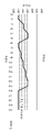
-
- G—PHYSICS
- G06—COMPUTING; CALCULATING OR COUNTING
- G06F—ELECTRIC DIGITAL DATA PROCESSING
- G06F3/00—Input arrangements for transferring data to be processed into a form capable of being handled by the computer; Output arrangements for transferring data from processing unit to output unit, e.g. interface arrangements
- G06F3/01—Input arrangements or combined input and output arrangements for interaction between user and computer
- G06F3/03—Arrangements for converting the position or the displacement of a member into a coded form
- G06F3/041—Digitisers, e.g. for touch screens or touch pads, characterised by the transducing means
- G06F3/044—Digitisers, e.g. for touch screens or touch pads, characterised by the transducing means by capacitive means
-
- G—PHYSICS
- G06—COMPUTING; CALCULATING OR COUNTING
- G06F—ELECTRIC DIGITAL DATA PROCESSING
- G06F3/00—Input arrangements for transferring data to be processed into a form capable of being handled by the computer; Output arrangements for transferring data from processing unit to output unit, e.g. interface arrangements
- G06F3/01—Input arrangements or combined input and output arrangements for interaction between user and computer
- G06F3/03—Arrangements for converting the position or the displacement of a member into a coded form
- G06F3/041—Digitisers, e.g. for touch screens or touch pads, characterised by the transducing means
- G06F3/0412—Digitisers structurally integrated in a display
-
- G—PHYSICS
- G06—COMPUTING; CALCULATING OR COUNTING
- G06F—ELECTRIC DIGITAL DATA PROCESSING
- G06F3/00—Input arrangements for transferring data to be processed into a form capable of being handled by the computer; Output arrangements for transferring data from processing unit to output unit, e.g. interface arrangements
- G06F3/01—Input arrangements or combined input and output arrangements for interaction between user and computer
- G06F3/03—Arrangements for converting the position or the displacement of a member into a coded form
- G06F3/041—Digitisers, e.g. for touch screens or touch pads, characterised by the transducing means
- G06F3/0416—Control or interface arrangements specially adapted for digitisers
- G06F3/0418—Control or interface arrangements specially adapted for digitisers for error correction or compensation, e.g. based on parallax, calibration or alignment
-
- G—PHYSICS
- G06—COMPUTING; CALCULATING OR COUNTING
- G06F—ELECTRIC DIGITAL DATA PROCESSING
- G06F3/00—Input arrangements for transferring data to be processed into a form capable of being handled by the computer; Output arrangements for transferring data from processing unit to output unit, e.g. interface arrangements
- G06F3/01—Input arrangements or combined input and output arrangements for interaction between user and computer
- G06F3/03—Arrangements for converting the position or the displacement of a member into a coded form
- G06F3/041—Digitisers, e.g. for touch screens or touch pads, characterised by the transducing means
- G06F3/044—Digitisers, e.g. for touch screens or touch pads, characterised by the transducing means by capacitive means
- G06F3/0446—Digitisers, e.g. for touch screens or touch pads, characterised by the transducing means by capacitive means using a grid-like structure of electrodes in at least two directions, e.g. using row and column electrodes
-
- G—PHYSICS
- G06—COMPUTING; CALCULATING OR COUNTING
- G06F—ELECTRIC DIGITAL DATA PROCESSING
- G06F2203/00—Indexing scheme relating to G06F3/00 - G06F3/048
- G06F2203/041—Indexing scheme relating to G06F3/041 - G06F3/045
- G06F2203/04101—2.5D-digitiser, i.e. digitiser detecting the X/Y position of the input means, finger or stylus, also when it does not touch, but is proximate to the digitiser's interaction surface and also measures the distance of the input means within a short range in the Z direction, possibly with a separate measurement setup
-
- G—PHYSICS
- G06—COMPUTING; CALCULATING OR COUNTING
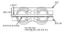
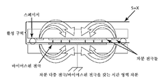
- G06F—ELECTRIC DIGITAL DATA PROCESSING
- G06F2203/00—Indexing scheme relating to G06F3/00 - G06F3/048
- G06F2203/041—Indexing scheme relating to G06F3/041 - G06F3/045
- G06F2203/04103—Manufacturing, i.e. details related to manufacturing processes specially suited for touch sensitive devices
-
- G—PHYSICS
- G06—COMPUTING; CALCULATING OR COUNTING
- G06F—ELECTRIC DIGITAL DATA PROCESSING
- G06F2203/00—Indexing scheme relating to G06F3/00 - G06F3/048
- G06F2203/041—Indexing scheme relating to G06F3/041 - G06F3/045
- G06F2203/04104—Multi-touch detection in digitiser, i.e. details about the simultaneous detection of a plurality of touching locations, e.g. multiple fingers or pen and finger
Abstract
자극을 검출하는 정전용량 센서. 정전용량 센서는 용량성 결합을 정의하는 제1 전극 및 제2 전극, 및 제1 전극 및 제2 전극에 전기적으로 결합되어 있고 용량성 결합의 변화율에 기초하여 자극의 존재를 결정하는 처리 유닛을 포함한다. 기판은 제1 전극 및 제2 전극에 인접하여 배치되고, 자극은 기판과 맞닿은 물체의 배치에 대응한다. 처리 유닛은 용량성 결합의 연속적인 측정들에 기초하여 그리고 용량성 결합이 미리정해진 기준값을 초과한 것에 응답하여 시간 변화율을 결정하는 동작을 한다.A capacitive sensor that detects stimuli. The capacitive sensor includes first and second electrodes defining a capacitive coupling, and a processing unit electrically coupled to the first and second electrodes and determining the presence of a stimulus based on a rate of change of the capacitive coupling do. A substrate is disposed adjacent to the first electrode and the second electrode, and the stimulus corresponds to the placement of the object abutting the substrate. The processing unit is operative to determine a rate of change in time based on successive measurements of the capacitive coupling and in response to the capacitive coupling exceeding a predetermined reference value.
Description
본 발명은 자극을 검출하는 장치 및 방법에 관한 것으로서, 보다 상세하게는, 터치 입력 및 스타일러스 입력을 검출하는 장치 및 방법에 관한 것이다.The present invention relates to an apparatus and method for detecting a stimulus, and more particularly, to an apparatus and method for detecting a touch input and a stylus input.
오늘날 사람의 터치의 존재를 감지하도록 설계된 수많은 사람 기계 인터페이스(Human Machine Interface)(HMI) 디바이스가 존재한다. 어떤 경우들에서, 이 HMI 인터페이스들은 사람으로부터의 입력을 기계 인터페이스에 제공하는 데 사용되는 스타일러스를 포함한다. 스타일러스는 직접 사람 인터페이스(direct human interface)를 완전히 대체할 수 있거나 사람 인터페이스를 보완할 수 있다. 이 HMI 디바이스들은 광, 소리, 전자-기계적 (스위치들) 자기장, 전기장, 전자기장, 또는 이 자극들의 조합을 사용할 수 있다.There are numerous Human Machine Interface (HMI) devices designed to detect the presence of a human touch today. In some cases, these HMI interfaces include a stylus used to provide input from a human to the machine interface. A stylus can completely replace a direct human interface, or it can complement a human interface. These HMI devices can use light, sound, electro-mechanical (switches) magnetic fields, electric fields, electromagnetic fields, or a combination of these stimuli.
오늘날 존재하는 그리고 전기장을 사용하는 3개의 이전의 및 현재의 터치 기술들은 흔히 투사 정전용량(projected capacitance), 정전용량(capacitive), 차분 감지(differential sensing)라고 한다. 투사 정전용량은 대략 동일한 크기의 디스플레이들과 관련하여 사용되는 그리고 디스플레이로부터의 광이 투사 정전용량 터치 스크린 감지 요소들의 감지 요소들을 통과할 수 있게 하는 방식으로 이러한 디스플레이들과 함께 조립되는 투명 터치 스크린들과 흔히 연관되어 있다. 투사 정전용량은 터치의 영역의 선택이 손가락의 실제 크기보다 훨씬 더 작을 수 있는 경우 보통 고분해능 능력으로 구현된다. 투사 정전용량은 휴대폰, PDA(personal digital assistant), 스마트폰, 노트북, 랩톱 컴퓨터, 랩톱 모니터, 및 디스플레이를 가지는 다른 사용자 디바이스와 같은 개인용 전자 디바이스들에서 널리 사용된다. 정전용량 감지는, 투사 정전용량과 달리, 버튼 또는 저분해능 슬라이더와 같은 투사 정전용량보다 훨씬 더 낮은 분해능에 일반적으로 응답하는 단일 입력들이 처리되는 응용들에서 보통 적용된다. 이러한 저분해능 입력 감지 응용들은 손가락 크기의 입력에 응답하도록 설계되어 있는 전극 구조들을 사용한다. 그럼에도 불구하고, 정전용량 감지가 투사 정전용량 대신에 사용될 수 있고, 원칙적으로 투사 정전용량은 일반적으로 부분 정전용량 구현(subset implementation of capacitance)이다. 차분 감지 기술은 전기장, 저임피던스 감지 기술들, 및 특정의 전자 감지 회로들과 함께 소프트웨어의 사용 없이 사람 터치의 정확하고 안정적인 감지를 가능하게 하는 독자적인 감지 전극들을 사용한다.The three previous and current touch technologies that exist today and that use electric fields are often referred to as projected capacitance, capacitive, and differential sensing. Transparent touch screens used in connection with approximately equal sized displays and assembled with such displays in such a way as to allow light from the display to pass through the sensing elements of the projected capacitive touch screen sensing elements. is often associated with Projection capacitance is usually implemented with high resolution capabilities when the selection of the area of touch can be much smaller than the actual size of the finger. Projected capacitance is widely used in personal electronic devices such as cell phones, personal digital assistants (PDAs), smart phones, notebook computers, laptop computers, laptop monitors, and other user devices with displays. Capacitive sensing, unlike projected capacitance, is commonly applied in applications where single inputs are processed that typically respond to a much lower resolution than projected capacitance, such as a button or low-resolution slider. These low-resolution input sensing applications use electrode structures designed to respond to finger-sized input. Nevertheless, capacitive sensing can be used instead of projected capacitance, which in principle is usually a subset implementation of capacitance. Differential sensing technology uses electric field, low impedance sensing techniques, and proprietary sensing electrodes that together with special electronic sensing circuits enable accurate and reliable sensing of human touch without the use of software.
정전용량, 투사 정전용량, 및 차분 감지는 적어도 2개의 공통 속성들을 가진다: 1) 이들 모두는 사람 기계 상호작용을 측정하기 위한 자극으로서 전기장을 사용하고, 2) 이들은 사람 기계 상호작용으로 인해 특정의 자극 변화가 일어났을 때 터치에 대응하는, 엔지니어에 의해 결정되는 미리정해진 임계치에 의존한다.Capacitance, projected capacitance, and differential sensing have at least two common properties: 1) they all use an electric field as a stimulus to measure human-machine interaction, and 2) they have specific properties due to human-machine interaction. It relies on a predetermined threshold determined by the engineer, which corresponds to a touch when a stimulus change occurs.
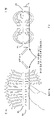
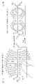
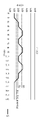
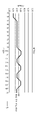
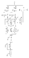
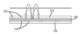
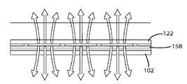
도 1 및 도 2는 다중 전극 및 단일 전극 정전용량 감지를 사용하기 위한 기본적인 단일 입력 센서 구성들을 나타낸 것이다. 도 2는 유전체 기판(102)을 통해 감지하기 위한 단일 전극(100)을 갖는 간단한 정전용량 센서를 나타낸 것이다. 터치 자극들은 단일 전극(100)이 위치해 있는 것과 반대쪽에 있는 유전체(102)의 측면에서 삽입될 것이다. 도 1은 유전체 기판(102) 및 적어도 2개의 전극들(100, 104)을 가지는 다중 전극 정전용량 센서를 나타낸 것이다. 도 2와 유사하게, 터치 자극들은 다수의 전극들(100, 104)이 위치해 있는 것과 반대쪽에 있는 유전체(102)의 측면에서 삽입될 것이다. 상기 도 1 및 도 2에서의 구조들에 관련된 이 정전용량 감지 기법들은, 자극 신호가 처리된 후에, 손가락 또는 스타일러스가 감지 전극(들)에 접근할 때 변하게 될 출력 신호가 있도록 하는 방식으로, 단일의 전극 또는 다수의 전극들로부터의 정전용량의 변화들을 감지한다. 특정의 값(미리정해진 임계치)에 도달될 때, 터치 응답이 일어나도록 하는 방식으로 출력 신호가 처리된다. 이 미리정해진 임계치는 터치 표면 위쪽의 터치 구역에 위치된 터치 위치에 대응할 것이다. 변화들 - 제조 허용 오차, 유전 상수, 유전체 두께, 전극 면적, 및 전자 감지 회로 변동에 의해 영향을 받음 - 이 센서 전극(들) 위쪽에서의 실제 터치 위치를 또한 변화시킬 것이다.1 and 2 show basic single input sensor configurations for using multi-electrode and single-electrode capacitive sensing. 2 shows a simple capacitive sensor with a
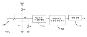
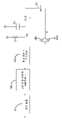
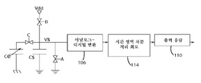
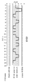
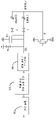
도 3 내지 도 7을 참조한다. 도 3은 도 2에 예시된 단일 전극 정전용량 센서의 전기 배선도 및 블록도를 나타낸 것이고, 타이밍도들은 도 4 내지 도 7에 예시되어 있으며, 단일 전극을 이용하여 터치 입력을 검출하고 처리하는 기본적인 기법이다. 도 2에 예시된 Ce는 단일 전극 감지 요소의 유효 순 정전용량(effective net capacitance)을 나타낸다. Ce는 존재하는 정전용량에 따라 변할 것이다 - 즉, "터치 없음"의 경우, Ce는 "터치"가 존재할 때(이 경우에, Ce가 더 높은 정전용량 값을 가질 것임)보다 더 낮은 정전용량 값을 가질 것이다 -. Cs는 아날로그-디지털 변환기(106), 미리정해진 임계치 회로(108), 및 출력 응답(110)에 대한 샘플링 커패시터를 나타낸다. 제어 디바이스들(A, B 및 C)은 턴온될 때 최소 저항 모드(이상적으로는, 0 오옴)에 있게 되고 오프일 때 고저항 모드(이상적으로는, 무한 저항)에 있는 전자 스위치들을 나타낸다.Reference is made to FIGS. 3 to 7 . 3 shows an electrical wiring diagram and a block diagram of the single electrode capacitive sensor illustrated in FIG. 2 , the timing diagrams are illustrated in FIGS. 4 to 7 , a basic technique for detecting and processing a touch input using a single electrode to be. Ce illustrated in FIG. 2 represents the effective net capacitance of a single electrode sensing element. Ce will change depending on the capacitance present - i.e., for "no touch", Ce will have a lower capacitance value than when "touch" is present (in this case, Ce will have a higher capacitance value). will have -. Cs represents the analog-to-
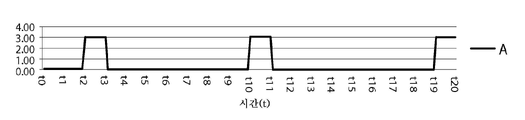
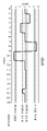
도 4, 도 5, 도 6 및 도 7은 단일 전극(Ce)을 사용하여 터치 입력을 감지하는 감지 기법의 기본 동작을 기술하는 데 사용되는 타이밍도들이다. 도 4는 제어 디바이스(A)에 대한 제어 신호에 대한 타이밍도를 나타낸 것이다. 제어 신호가 3.00의 값에 있을 때, 제어 디바이스는 온이고, 제어 신호가 0.00의 값에 있을 때, 제어 디바이스는 오프이다. 도 5 및 도 6에서의 제어 디바이스들(B 및 C)에 대한 제어 신호들에 대해서도 마찬가지이다. 도 6에서의 시각 t1에서, 제어 신호(C)는 하이(high)로 되고, 제어 디바이스를 턴온시켜 Ce를 Cs에 연결시킨다. 또한 시각 t1에서, 제어 신호들(A 및 B)은 나타낸 바와 같이 로우(low)이고, 제어 디바이스들(A 및 B)을 턴오프시킨다. 시각 t2에서, 제어 디바이스(A)는 턴온되어, 도 7에서 전압(Vs)이 1.00의 전압 값으로부터 0.00으로 떨어지는 것으로 나타낸 바와 같이 Ce 및 Cs에 존재하는 임의의 전하를 접지로 방전시킨다. 시각 t3에서, 제어 디바이스(A)가 턴오프된다. 시각 t4에서, 제어 디바이스(C)가 턴오프되어, Ce를 Cs로부터 분리시킨다. 시각 t5에서, 제어 디바이스(B)가 턴온되어, 샘플링 커패시터(Cs)를 Vdd로 충전시킨다. 도 7은 전압(Vs)이 0.00의 값으로부터 3.00의 Vdd 값으로 충전되는 것을 나타내고 있다. 시각 t7에서, 제어 디바이스(C)가 턴온되어, Cs를 Ce에 연결시키며, Cs 상의 전하를 Cs 및 Ce 둘 다로 재분배시키고, 따라서 전압(Vs)을 Ce의 정전용량의 양에 비례하여 강하시킨다. Cs의 정전용량은 일정하다. 이하의 식에 따라 하부 전압(lower voltage)이 강하할 것이다:4, 5, 6, and 7 are timing diagrams used to describe a basic operation of a sensing technique for sensing a touch input using a single electrode Ce. Fig. 4 shows a timing diagram for a control signal to the control device (A). When the control signal is at the value of 3.00, the control device is on, and when the control signal is at the value of 0.00, the control device is off. The same is true for the control signals for the control devices B and C in FIGS. 5 and 6 . At time t1 in FIG. 6 , the control signal C goes high and turns on the control device to connect Ce to Cs. Also at time t1, control signals A and B are low as shown, turning off control devices A and B. At time t2, the control device A is turned on, discharging any charge present in Ce and Cs to ground as shown in FIG. 7 as the voltage Vs drops from a voltage value of 1.00 to 0.00. At time t3, the control device A is turned off. At time t4, the control device C is turned off, separating Ce from Cs. At time t5, the control device B is turned on, charging the sampling capacitor Cs to Vdd. Figure 7 shows that the voltage Vs is charged from a value of 0.00 to a value of Vdd of 3.00. At time t7, the control device C is turned on, coupling Cs to Ce, redistributing the charge on Cs to both Cs and Ce, thus dropping the voltage Vs proportional to the amount of capacitance of Ce. The capacitance of Cs is constant. The lower voltage will drop according to the following equation:
Vs=Vdd*(Cs/(Cs+Ce))Vs=Vdd*(Cs/(Cs+Ce))
시각 t7에서, 1.00의 "터치 없음" 값이 도 7에 예시되어 있다. 터치 이벤트가 있는 경우, 정전용량(Ce)이 "터치 없음" 정전용량 값보다 더 높은 값에 있을 것이다. 앞서 언급한 식에 기초하여, Vs는 도 7에서 0.500의 낮은 값으로서 나타내어져 있다. 시각 t8에서, 제어 디바이스(C)가 턴오프되어, 센서 커패시터(Ce)를 샘플 커패시터(Cs)로부터 분리시킨다. Vs의 값은 터치 조건에 비례하는 샘플링된 값, "터치 없음" 조건에 대한 높은 값, 및 "터치" 조건에 대한 낮은 값에 유지될 것이다.At time t7, a “no touch” value of 1.00 is illustrated in FIG. 7 . If there is a touch event, the capacitance Ce will be at a higher value than the “no touch” capacitance value. Based on the above-mentioned equation, Vs is shown as a low value of 0.500 in FIG. 7 . At time t8, the control device C is turned off, disconnecting the sensor capacitor Ce from the sample capacitor Cs. The value of Vs will be held at a sampled value proportional to the touch condition, a high value for the “no touch” condition, and a low value for the “touch” condition.
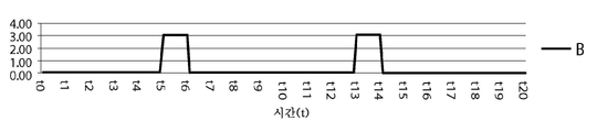
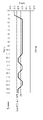
다수의 전극들을 이용하는 대안의 정전용량 검출 기법이 여기서 기술된다. 도 1, 도 8 내지 도 12를 참조한다. 도 8은 도 1에 예시된 다중 전극 정전용량 센서의 전기 배선도 및 블록도를 나타낸 것이고, 타이밍도들은 도 9 내지 도 12에 예시되어 있으며, 다수의 전극들을 이용하여 터치 입력을 검출하고 처리하는 기본적인 기법이다. 도 1에 예시된 Ce는 다중(2) 전극 감지 요소의 유효 순 정전용량을 나타낸다. Ce는 존재하는 정전용량에 따라 변할 것이다 - 즉, "터치 없음"의 경우, Ce는 높은 정전용량 값을 가질 것이고, "터치"가 존재할 때, Ce는 낮은 정전용량 값을 가질 것이다 -. Cs는 아날로그-디지털 변환기에 대한 샘플링 커패시터를 나타낸다. 제어 디바이스들(A 및 C)은 턴온될 때 최소 저항 모드(이상적으로는, 0 오옴)에 있게 되고 오프일 때 고저항 모드(이상적으로는, 무한 저항)에 있는 전자 스위치들을 나타낸다. 제어 디바이스(B)는 제어 디바이스(B)의 출력 상에 구동 신호를 발생시키는 MOSFet 회로로서 나타내어져 있다. 도 9, 도 10, 도 11 및 도 12는 다중 전극 정전용량 센서(Ce)를 사용하여 터치 입력을 감지하는 감지 기법의 기본 동작을 기술하는 데 사용되는 타이밍도들이다. 도 11은 제어 디바이스(C)에 대한 제어 신호에 대한 타이밍도를 나타낸 것이다. 제어 신호가 3.00의 값에 있을 때, 제어 디바이스는 온이고, 제어 신호가 0.00의 값에 있을 때, 제어 디바이스는 오프이다. 도 9에서의 제어 디바이스(A)에 대한 제어 신호에 대해서도 마찬가지이다. 도 10은 0.00의 값으로부터 3.00의 값까지 변하는 출력 구동 신호(B)에 대한 타이밍도를 나타낸 것이다.An alternative capacitive detection technique using multiple electrodes is described herein. Reference is made to Figs. 1 and 8 to 12 . 8 shows an electrical wiring diagram and a block diagram of the multi-electrode capacitive sensor illustrated in FIG. 1 , the timing diagrams are illustrated in FIGS. 9 to 12 , and the basic method of detecting and processing a touch input using a plurality of electrodes. is a technique Ce illustrated in FIG. 1 represents the effective net capacitance of a multi(2) electrode sensing element. Ce will change depending on the capacitance present - ie, in the case of "no touch", Ce will have a high capacitance value, and when "touch" is present, Ce will have a low capacitance value. Cs represents the sampling capacitor for the analog-to-digital converter. Control devices A and C represent electronic switches that are in minimum resistance mode (ideally, 0 ohms) when turned on and are in high resistance mode (ideally, infinite resistance) when off. The control device B is shown as a MOSFet circuit that generates a drive signal on the output of the control device B. 9, 10, 11 and 12 are timing diagrams used to describe a basic operation of a sensing technique for sensing a touch input using a multi-electrode capacitive sensor Ce. 11 shows a timing diagram for the control signal to the control device (C). When the control signal is at the value of 3.00, the control device is on, and when the control signal is at the value of 0.00, the control device is off. The same is true for the control signal to the control device A in FIG. 9 . 10 shows a timing diagram for the output driving signal B varying from a value of 0.00 to a value of 3.00.
도 11에서의 시각 t1에서, 제어 신호(C)는 하이로 되고, 제어 디바이스(C)를 턴온시켜 Ce를 Cs에 연결시킨다. 또한 시각 t1에서, 제어 신호(A)는 로우이고, 제어 디바이스(A)를 턴오프시키며, 출력(B)은 로우이고, 이들 상태 둘 다가, 각각, 도 11 및 도 10에 도시되어 있다. 시각 t2에서, 제어 디바이스(A)는 턴온되어, 도 12에서 전압(Vs)이 1.00의 전압 값으로부터 0.00으로 떨어지는 것으로 나타낸 바와 같이 Ce 및 Cs에 저장되어 있을 수 있는 임의의 전하를 접지로 방전시킨다. 시각 t3에서, 제어 디바이스(A)가 턴오프된다. 시각 t4에서, 출력 디바이스(B)는 턴온되어, 센서 전극 구조에 인가되는 전압을 0.00의 값으로부터 3.00으로 되게 한다. 전압 자극은, 전압이 0.00으로부터 "터치 없음" 조건에 대한 1.00의 값으로 상승하는 것으로 나타낸 바와 같이, Vs의 값을 Ce의 정전용량에 비례하는 값으로 상승시킬 것이다. 손가락/부속 기관(appendage) 또는 다른 터치 입력 디바이스가 터치 표면에 접근하거나 그와 접촉하게 될 때, Ce의 정전용량은 "터치 조건"에 대해 낮은 유효 정전용량에 있고, Vs에서의 전압을 "터치 조건"에서의 0.500의 값으로 나타낸 바와 같이 낮은 값에 안정되게 할 것이다. 이 조건들 둘 다는 도 12에 나타내어져 있다. 시각 t5에서, 제어 디바이스(C)가 턴오프되어, Ce를 Cs로부터 분리시킨다. 시각 t6에서, 출력 디바이스(B)는 로우로 되어, 전극 구조(Ce)로부터 자극을 제거한다. Cs의 정전용량은 일정하다. 이하의 식에 따라 하부 전압이 강하할 것이다:At time t1 in Fig. 11, the control signal C goes high and turns on the control device C, coupling Ce to Cs. Also at time t1, control signal A is low, turns control device A off, and output B is low, both of these states are shown in FIGS. 11 and 10 , respectively. At time t2, control device A is turned on, discharging to ground any charge that may have been stored in Ce and Cs as shown in Figure 12 where voltage Vs drops from a voltage value of 1.00 to 0.00. . At time t3, the control device A is turned off. At time t4, the output device B is turned on, causing the voltage applied to the sensor electrode structure to go from a value of 0.00 to 3.00. The voltage stimulus will raise the value of Vs to a value proportional to the capacitance of Ce, as shown by the voltage rising from 0.00 to a value of 1.00 for the "no touch" condition. When a finger/appendage or other touch input device approaches or comes into contact with the touch surface, the capacitance of Ce is at a low effective capacitance for the “touch condition” and changes the voltage at Vs to “touch”. It will stabilize at low values as indicated by a value of 0.500 in "Conditions". Both of these conditions are shown in FIG. 12 . At time t5, the control device C is turned off, separating Ce from Cs. At time t6, the output device B goes low, removing the stimulus from the electrode structure Ce. The capacitance of Cs is constant. The lower voltage will drop according to the following equation:
Vs=Vdd*(Ce/(Cs+Ce )).Vs=Vdd*(Ce/(Cs+Ce)).
시각 t6에서, 1.00의 "터치 없음" 값이 도 12에 예시되어 있다. 터치 이벤트가 있는 경우, 정전용량(Ce)이 "터치 없음" 정전용량 값보다 더 높은 값에 있을 것이다. 앞서 언급한 식에 기초하여, Vs는 도 12에서 0.500의 낮은 값으로서 나타내어져 있다. 커패시터(Ce)를 샘플 커패시터(Cs)로부터. Vs의 값은 터치 조건에 비례하는 Vs 값, "터치 없음" 조건에 대한 높은 값, 및 "터치" 조건에 대한 낮은 값에 유지될 것이다. 이 듀얼 전극 감지 기법의 하나의 유용한 속성은, 터치 센서 구조의 터치 표면 상에 물이 있는 경우, Ce가 본질적으로 값이 올라갈 것이고, 이어서 Vs의 값을 증가시킬 것이라는 것이다. 이것은 Vs가 보통의 터치 이벤트와 비교하여 물에 대해 반대 방향으로 움직인다는 점에서 유용하다. 이 정보는 터치 표면 상에 있는 물로 인한 잘못된 터치 이벤트들을 본질적으로 구분하는 데 아주 유용하다.At time t6, a “no touch” value of 1.00 is illustrated in FIG. 12 . If there is a touch event, the capacitance Ce will be at a higher value than the “no touch” capacitance value. Based on the above-mentioned equation, Vs is shown as a low value of 0.500 in FIG. 12 . Capacitor (Ce) from sample capacitor (Cs). The value of Vs will be held at a Vs value proportional to the touch condition, a high value for the “no touch” condition, and a low value for the “touch” condition. One useful property of this dual-electrode sensing technique is that if there is water on the touch surface of the touch sensor structure, Ce will intrinsically rise in value, which in turn will increase the value of Vs. This is useful in that Vs moves in the opposite direction to water compared to normal touch events. This information is very useful in essentially distinguishing false touch events caused by water on the touch surface.
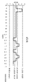
이상의 경우들 둘 다에서, 단일 전극이든 듀얼 전극이든 간에, 아날로그-디지털 변환기(106)는 Vs의 값을 미리정해진 임계치 처리 회로(108)에 의해 처리될 수 있는 디지털 값으로 변환할 것이다. 미리정해진 임계치 값이 어떻게 결정되는지에 대한 2가지 예들은 다음과 같을 수 있다: 1) 미리정해진 임계치 값은 전압 값으로서, Vs가 상기 전압 값 이하일 때, 유효한 터치 이벤트가 있음 - 즉, V(샘플) <= Vp(미리정해진 임계치 값)일 때 유효한 터치 이벤트가 존재함 -, 또는 2) 미리정해진 임계치 값은 전압 값으로서, "터치 없음" Vs 값과 Vs 사이의 차가 상기 전압 값 이상일 때, 유효한 터치 이벤트가 있음 - [("터치 없음" 전압의 값) - (Vs)] >= V(미리정해진 임계치 값)일 때 유효한 터치 이벤트가 존재함 -. 임계치 처리 회로(108)는 Vs의 디지털 표현을 취할 것이며, 임계치 처리 회로(108)는 이어서, 앞서 기술한 것과 유사한 미리정해진 임계치 값 프로세스들을 사용하여, 처리하고, 외부 세계와의 적절한 인터페이스를 위해 출력 응답 회로(110)에 의해 처리될 유효한 터치 이벤트가 있는지를 결정할 것이다. 미리정해진 임계치 값에 대한 값은 정전용량 또는 전계 효과 센서의 응용의 설계자에 의해 결정되어야만 한다. 미리정해진 임계치 값은 나중에 터치 이벤트로서 해석되는 터치 자극에 비례하는 샘플링된 값과 궁극적으로 비교되는 값이다. 미리정해진 임계치 값을 사용하는 이 방법을 사용하는 개발된 수많은 기법들이 있다. 심지어 다수의 감지 전극들을 사용하는 차분 감지 기법들은 하나의 전극들의 세트에서 감지된 값이 다른 전극들의 세트들에 대해 어떤 값을 가질 것을 필요로 한다 - 예컨대, 한 예로서, 차분 2 전극 감지 구조에서, 터치 이벤트가 있기 위해 양 전극이 서로 같을 필요가 있을 수 있고, 터치 이벤트가 없기 위해(논리적으로 터치하지 않음) 전극들 중 하나가 다른 전극 미만일 필요가 있을 수 있다 -. 기법에 관계없이, 미리정해진 임계치 기법들을 사용할 때, "터치 없음" 이벤트 또는 "터치" 이벤트 이외에, 도 7 및 도 12에서의 Vs와 같은 샘플링된 전압들의 값에 궁극적으로 영향을 미칠 수 있는 다른 변수들이 있다. 터치 기판의 유전 상수의 변화, 센서 패드 영역의 유효 변동, 센서 구조에 대한 손가락 결합 면적의 변동, 유리 기판의 허용 오차에 기초한 변동, 샘플링 회로에서의 변동, 온도, 습기, 기타 모두가 잘못된 또는 과소/과잉 감응 터치 감지 응답을 가져올 수 있다. 도 1 및 도 2는 터치 감도 또는 "터치감(touch feel)"에 영향을 미칠 수 있는 다른 인자들의 변동성을 고려하는 등을 위해 미리정해진 임계치 값에 대응하는 터치 표면 위쪽의 위치를 나타내고 있다. 설계자가 손가락/부속 기관 또는 다른 터치 입력 디바이스에 끼워져 있는 장갑의 사용을 고려해야만 하는 경우, 미리정해진 임계치 값에 대응하는 터치 표면 위쪽의 위치는 장갑 절연의 두께를 수용하기 위해 더 큰 거리이어야만 할 것이다. 물론, 손가락/부속 기관 또는 다른 터치 입력 디바이스가 터치 표면에 접근할 때, 미리정해진 임계치 처리 회로(108)는, 손가락/부속 기관 또는 다른 터치 입력 디바이스가 터치 표면을 실제로 터치하지 않더라도, 유효한 터치 이벤트를 등록할 것이다. 미리정해진 임계치 값의 대응하는 위치는 바로 터치 표면에 있을 수 있다. 이 경우에, 설계자는 터치 표면에의 초기 접촉 이후의 손가락/부속 기관의 평탄화(flattening)로 인한 신호 기여분의 양을 고려할 것이다. 손가락과 유리 간의 용량성 결합이 증가함에 따라 - 이는 도 3에서의 정전용량 Ce를 증가시키고 도 8에서의 정전용량 Ce를 감소시킴 - 자극 신호가 계속하여 증가한다. 설계자는 미리정해진 임계치 값이 무엇이어야 하는지에 영향을 미치는 모든 변수들을 고려해야만 한다. 손가락/부속 기관 또는 다른 터치 입력 디바이스를 터치 표면 쪽으로 가져갈 때, 유효한 터치 이벤트가 인식되지 않도록, 이 변수들 모두를 고려한 후에, 미리정해진 임계치 값이 이러한 값으로 설정되지 않는 것이 아주 중요할 것이다. 이와 달리, 미리정해진 임계치 값이 잘못된 작동들을 야기하도록 설정되어서는 안된다. 미리정해진 임계치 값을 설정하기 위한 적절한 절충을 결정하기 위해 환경 조건들을 비롯한 상기 변수들 모두가 고려될 필요가 있다.In both of the above cases, whether single electrode or dual electrode, the analog-to-
정전용량 센서가 제공된다. 하나의 실시예에서, 정전용량 센서는 용량성 결합을 정의하는 제1 전극 및 제2 전극, 및 제1 전극 및 제2 전극에 전기적으로 결합되어 있고 용량성 결합의 변화율에 기초하여 자극의 존재를 결정하는 처리 유닛을 포함한다. 처리 유닛은 용량성 결합이 미리정해진 임계치 초과인 것에 응답하여 시간 변화율을 결정하는 동작을 한다. 기판은 제1 전극 및 제2 전극에 인접하여 배치되고, 자극은 기판과 맞닿은(against) 물체의 배치에 대응한다.A capacitive sensor is provided. In one embodiment, the capacitive sensor is electrically coupled to first and second electrodes defining a capacitive coupling and to the first and second electrodes and detects the presence of a stimulus based on a rate of change of the capacitive coupling. and a processing unit for determining. The processing unit is operative to determine a rate of change of time in response to the capacitive coupling being above a predetermined threshold. A substrate is disposed adjacent the first electrode and the second electrode, and the stimulus corresponds to the placement of the object against the substrate.
다른 실시예에서, 정전용량 센서는 내부 전극 및 외부 전극을 포함한다. 내부 전극 및 외부 전극은 실질적으로 동일 평면에 있고, 외부 전극은 내부 전극을 실질적으로 포함하고, 내부 전극으로부터 떨어져 있다. 내부 전극은 선택적으로 일정 간격으로 있는 세그먼트들을 정의하고, 외부 전극은 선택적으로 내부 전극의 일정 간격으로 있는 세그먼트들 사이에 개재되어 있다. 처리 유닛은 자극(예컨대, 정전용량 센서에 근접한 물체)에 응답하여 내부 전극과 외부 전극 사이의 용량성 결합의 변화율을 결정하는 동작을 한다.In another embodiment, the capacitive sensor includes an inner electrode and an outer electrode. The inner electrode and the outer electrode are substantially coplanar, the outer electrode substantially including the inner electrode, and spaced apart from the inner electrode. The inner electrode optionally defines spaced segments, and the outer electrode is optionally interposed between spaced segments of the inner electrode. The processing unit is operative to determine a rate of change in capacitive coupling between the inner and outer electrodes in response to a stimulus (eg, an object proximate to the capacitive sensor).
또 다른 실시예에서, 정전용량 센서는 동일 평면에 있는 제1 전극 및 제2 전극을 그 위에 지지하는 경성 기판을 포함하고, 복수의 스페이서들에 의해 제1 전극 및 제2 전극 위쪽에 지지되는 연성 기판을 포함한다. 연성 기판은 제1 전극 및 제2 전극으로부터 원단쪽에서 연성 기판의 일부분 상에서의 터치 입력에 응답하여 내부 전극 및 외부 전극 쪽으로 하향 굴곡가능(flexible downwardly)하다. 처리 유닛은 연성 기판과 맞닿은 터치 입력에 응답하여 제1 전극과 제2 전극 사이의 용량성 결합의 변화율을 결정하는 동작을 한다.In another embodiment, a capacitive sensor includes a rigid substrate supporting coplanar first and second electrodes thereon, and a flexible substrate supported over the first and second electrodes by a plurality of spacers. includes a substrate. The flexible substrate is flexible downwardly toward the inner electrode and the outer electrode in response to a touch input on a portion of the flexible substrate from the distal side from the first electrode and the second electrode. The processing unit is operative to determine a rate of change of capacitive coupling between the first electrode and the second electrode in response to a touch input abutting the flexible substrate.
또 다른 실시예에서, 정전용량 센서는 제1 전극 및 제2 전극으로부터 떨어져 있는 스트로브 전극(strobe electrode)을 포함한다. 스트로브 전극은 일반적으로 평면이고, 제1 용량성 결합 및 제2 용량성 결합을 정의하기 위해, 각각, 제1 전극 및 제2 전극과 동일 공간에 걸쳐 있다. 경성 기판이 스트로브 전극과 제1 전극 및 제2 전극 사이에 개재되어 있다. 처리 유닛은, 선택적으로 제1 용량성 결합 및 제2 용량성 결합이 미리정해진 임계치 값을 초과한 것에 응답하여, 터치 입력을 나타내기 위해 제1 용량성 결합 및 제2 용량성 결합의 변화율을 결정하는 동작을 한다.In another embodiment, the capacitive sensor includes a strobe electrode spaced apart from the first electrode and the second electrode. The strobe electrode is generally planar and coextensive with the first and second electrodes, respectively, to define the first and second capacitive couplings. A rigid substrate is interposed between the strobe electrode and the first and second electrodes. The processing unit, optionally in response to the first capacitive coupling and the second capacitive coupling exceeding a predetermined threshold value, determines a rate of change of the first capacitive coupling and the second capacitive coupling to indicate a touch input. do the action
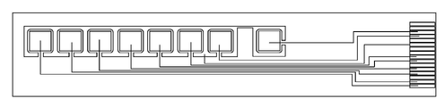
또 다른 실시예에서, 정전용량 센서는 제1 방향으로 뻗어 있는 복수의 전극 행들(electrode rows)을 포함하고, 제1 방향에 대해 횡단하는 제2 방향으로 뻗어 있는 복수의 전극 열들(electrode columns)을 포함한다. 복수의 전극 행들 및 복수의 전극 열들은 실질적으로 비중첩하는 배열(non-overlapping alignment)로 되어 있다. 다른 실시예들에서, 전극 열들은 전극 행들과 중첩하는 배열로 되어 있다. 처리 유닛은 2차원으로 자극의 존재를 나타내기 위해 복수의 전극 행들의 정전용량의 변화율 및 복수의 전극 열들의 정전용량의 변화율을 결정하는 동작을 한다. 인접한 전극 행들은 선택적으로 용량성 결합을 형성하고, 처리 유닛은 용량성 결합의 변화율을 측정하도록 추가로 구성되어 있다. 그에 부가하여, 인접한 전극 열들은 선택적으로 용량성 결합을 형성하고, 처리 유닛은 용량성 결합의 변화율을 측정하도록 추가로 구성되어 있다.In yet another embodiment, the capacitive sensor comprises a plurality of electrode rows extending in a first direction and comprising a plurality of electrode columns extending in a second direction transverse to the first direction. include The plurality of electrode rows and the plurality of electrode columns are in a substantially non-overlapping alignment. In other embodiments, the electrode columns are in an overlapping arrangement with the electrode rows. The processing unit is operative to determine a rate of change of capacitance of the plurality of electrode rows and a rate of change of capacitance of the plurality of electrode columns to indicate the presence of a stimulus in two dimensions. Adjacent electrode rows selectively form a capacitive coupling, and the processing unit is further configured to measure a rate of change of the capacitive coupling. In addition, adjacent electrode rows selectively form a capacitive coupling, and the processing unit is further configured to measure a rate of change of the capacitive coupling.
본원에 따르면, 정전용량 센서는 기판으로서 그 위에서 터치 입력을 수신하는 기판을 포함할 수 있다. 상기 센서는 상기 터치 입력에 응답하여 변하도록 구성된 정전용량을 포함하고 상기 기판 아래에 있는 전극을 포함한다. 처리 유닛은 상기 전극에 결합되어 있고 상기 전극 정전용량에 기초하여 상기 터치 입력의 서명을 결정하도록 구성된다. 상기 서명은 상기 기판에 일반적으로 수직이고 상기 기판과 맞닿은 터치 입력의 움직임에 대응하는 상기 전극 정전용량의 변동들을 포함한다.In accordance with the present disclosure, a capacitive sensor may include a substrate that receives touch input thereon as a substrate. The sensor includes an electrode under the substrate and comprising a capacitance configured to change in response to the touch input. A processing unit is coupled to the electrode and configured to determine a signature of the touch input based on the electrode capacitance. The signature is generally perpendicular to the substrate and includes variations in the electrode capacitance corresponding to movement of a touch input against the substrate.
본원에 따르면, 정전용량 센서는 기판으로서 그 위에서 터치 입력을 수신하는 기판을 포함할 수 있다. 상기 센서는 상기 터치 입력에 응답하여 변하도록 구성된 정전용량을 포함하고 상기 기판 아래에 있는 전극을 포함한다. 처리 유닛은 상기 전극에 결합되어 있고 상기 전극 정전용량에 기초하여 상기 터치 입력의 서명을 결정하도록 구성된다. 상기 서명은 상기 기판에 일반적으로 수직이고 상기 기판과 맞닿은 터치 입력의 움직임에 대응하는 상기 전극 정전용량의 변동들을 포함한다. 상기 터치 서명은 상기 정전용량 센서 쪽으로의 물체의 매끄러운 움직임(fluid movement)을 포함한다.In accordance with the present disclosure, a capacitive sensor may include a substrate that receives touch input thereon as a substrate. The sensor includes an electrode under the substrate and comprising a capacitance configured to change in response to the touch input. A processing unit is coupled to the electrode and configured to determine a signature of the touch input based on the electrode capacitance. The signature is generally perpendicular to the substrate and includes variations in the electrode capacitance corresponding to movement of a touch input against the substrate. The touch signature includes a fluid movement of an object towards the capacitive sensor.
본원에 따르면, 정전용량 센서는 기판으로서 그 위에서 터치 입력을 수신하는 기판을 포함할 수 있다. 상기 센서는 상기 터치 입력에 응답하여 변하도록 구성된 정전용량을 포함하고 상기 기판 아래에 있는 전극을 포함한다. 처리 유닛은 상기 전극에 결합되어 있고 상기 전극 정전용량에 기초하여 상기 터치 입력의 서명을 결정하도록 구성된다. 상기 서명은 상기 기판에 일반적으로 수직이고 상기 기판과 맞닿은 터치 입력의 움직임에 대응하는 상기 전극 정전용량의 변동들을 포함한다. 상기 터치 서명은 상기 정전용량 센서 쪽으로의 물체의 지그재그 움직임(staggered movement)을 포함할 수 있다.In accordance with the present disclosure, a capacitive sensor may include a substrate that receives touch input thereon as a substrate. The sensor includes an electrode under the substrate and comprising a capacitance configured to change in response to the touch input. A processing unit is coupled to the electrode and configured to determine a signature of the touch input based on the electrode capacitance. The signature is generally perpendicular to the substrate and includes variations in the electrode capacitance corresponding to movement of a touch input against the substrate. The touch signature may include a staggered movement of the object towards the capacitive sensor.
본원에 따르면, 정전용량 센서는 기판으로서 그 위에서 터치 입력을 수신하는 기판을 포함할 수 있다. 상기 센서는 상기 터치 입력에 응답하여 변하도록 구성된 정전용량을 포함하고 상기 기판 아래에 있는 전극을 포함한다. 처리 유닛은 상기 전극에 결합되어 있고 상기 전극 정전용량에 기초하여 상기 터치 입력의 서명을 결정하도록 구성된다. 상기 서명은 상기 기판에 일반적으로 수직이고 상기 기판과 맞닿은 터치 입력의 움직임에 대응하는 상기 전극 정전용량의 변동들을 포함한다. 상기 터치 서명은 상기 정전용량 센서 쪽으로 갔다가 그로부터 멀어지는 물체의 매끄러운 움직임을 포함할 수 있다.In accordance with the present disclosure, a capacitive sensor may include a substrate that receives touch input thereon as a substrate. The sensor includes an electrode under the substrate and comprising a capacitance configured to change in response to the touch input. A processing unit is coupled to the electrode and configured to determine a signature of the touch input based on the electrode capacitance. The signature is generally perpendicular to the substrate and includes variations in the electrode capacitance corresponding to movement of a touch input against the substrate. The touch signature may include smooth movement of an object toward and away from the capacitive sensor.
본원에 따르면, 정전용량 센서는 기판으로서 그 위에서 터치 입력을 수신하는 기판을 포함할 수 있다. 상기 센서는 상기 터치 입력에 응답하여 변하도록 구성된 정전용량을 포함하고 상기 기판 아래에 있는 전극을 포함한다. 처리 유닛은 상기 전극에 결합되어 있고 상기 전극 정전용량에 기초하여 상기 터치 입력의 서명을 결정하도록 구성된다. 상기 서명은 상기 기판에 일반적으로 수직이고 상기 기판과 맞닿은 터치 입력의 움직임에 대응하는 상기 전극 정전용량의 변동들을 포함한다. 상기 터치 서명은 상기 정전용량 센서 쪽으로 갔다가 그로부터 멀어지는 물체의 지그재그 움직임을 포함할 수 있다.In accordance with the present disclosure, a capacitive sensor may include a substrate that receives touch input thereon as a substrate. The sensor includes an electrode under the substrate and comprising a capacitance configured to change in response to the touch input. A processing unit is coupled to the electrode and configured to determine a signature of the touch input based on the electrode capacitance. The signature is generally perpendicular to the substrate and includes variations in the electrode capacitance corresponding to movement of a touch input against the substrate. The touch signature may include a zigzag movement of an object toward and away from the capacitive sensor.
본 발명의 이들 및 기타 특징들 및 장점들이, 첨부 도면들 및 첨부된 청구항들에 따라 볼 때, 본 발명의 이하의 설명으로부터 명백하게 될 것이다.These and other features and advantages of the present invention will become apparent from the following description of the invention when taken in accordance with the accompanying drawings and appended claims.
본 발명의 실시예들이 상세히 설명되기 전에, 본 발명이 동작의 상세들 또는 구성의 상세들 및 이하의 설명에 기재되거나 도면들에 예시되어 있는 구성요소들의 배열로 제한되지 않는다는 것을 잘 알 것이다. 본 발명은 다양한 다른 실시예들로 구현될 수 있고 본 명세서에 명확히 개시되어 있지 않은 대안의 방식들로 실시되거나 수행될 수 있다. 또한, 본 명세서에서 사용되는 어구 및 전문 용어가 설명을 위한 것이고 제한하는 것으로 보아서는 안된다는 것을 잘 알 것이다. "포함하는" 및 "구비하는" 그리고 이들의 변형들을 사용하는 것은 그 이후에 열거되는 항목들 및 그의 등가물들은 물론 부가의 항목들 및 그의 등가물들을 포괄하기 위한 것이다. 게다가, 다양한 실시예들의 설명에서 열거가 사용될 수 있다. 달리 명백히 언급되지 않는 한, 열거의 사용이 본 발명을 구성요소들의 임의의 특정의 순서 또는 수로 제한하는 것으로 해석되어서는 안된다. 열거의 사용이 열거된 단계들 또는 구성요소들과 결합되거나 그 내에 결합될 수 있는 임의의 부가의 단계들 또는 구성요소들을 본 발명의 범주로부터 제외시키는 것으로 해석되어서도 안된다.Before embodiments of the present invention are described in detail, it is to be understood that the present invention is not limited to the details of operation or construction and the arrangement of components described in the following description or illustrated in the drawings. The invention is capable of being embodied in various other embodiments and of being practiced or of being carried out in alternative ways not expressly disclosed herein. It will also be understood that the phraseology and terminology used herein is for the purpose of description and should not be viewed as limiting. The use of “comprising” and “comprising” and variations thereof is intended to encompass the items recited thereafter and equivalents thereof, as well as additional items and equivalents thereof. In addition, enumeration may be used in the description of various embodiments. Unless expressly stated otherwise, the use of enumeration should not be construed as limiting the invention to any particular order or number of elements. The use of a list is not to be construed as excluding from the scope of the invention any additional steps or elements that may be combined with or may be combined with the listed steps or elements.
도 1은 차분 감지 기법들에 대한 다수의 전극들을 포함하는 터치 센서를 나타낸 도면.
도 2는 용량성 감지 기법들에 대한 단일의 전극을 포함하는 터치 센서를 나타낸 도면.
도 3은 도 2에 예시된 단일 전극 터치 센서에 대응하는 회로도.
도 4는 도 3의 회로에 대한 제1 타이밍도.
도 5는 도 3의 회로에 대한 제2 타이밍도.
도 6은 도 3의 회로에 대한 제3 타이밍도.
도 7은 도 3의 회로에 대한 제4 타이밍도.
도 8은 도 1에 예시된 다중 전극 터치 센서에 대응하는 회로도.
도 9는 도 8의 회로에 대한 제1 타이밍도.
도 10은 도 8의 회로에 대한 제2 타이밍도.
도 11은 도 8의 회로에 대한 제3 타이밍도.
도 12는 도 8의 회로에 대한 제4 타이밍도.
도 13은 단일 전극에 대한 근접성을 결정하기 위한 활성 구역을 포함하는 터치 센서를 나타낸 도면.
도 14는 시간 영역 차분 감지를 위한 다수의 전극들을 포함하는 터치 센서를 나타낸 도면.
도 15는 시간 영역 차분 감지를 위한 단일의 전극을 포함하는 터치 센서를 나타낸 도면.
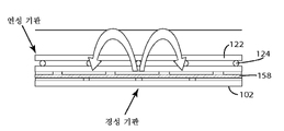
도 16은 단일 전극 및 활성화 구역을 포함하는 터치 센서에 접근하는 손가락을 나타낸 도면.
도 17은 도 16에 예시된 터치 센서에 대한 전압 대 시간을 나타낸 제1 그래프.
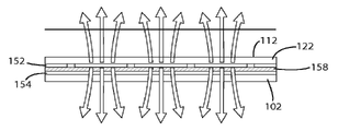
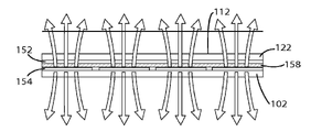
도 18은 도 16에 예시된 터치 센서에 대한 전압 대 시간을 나타낸 제2 그래프.
도 19는 도 16에 예시된 터치 센서에 대한 전압 대 시간을 나타낸 제3 그래프.
도 20은 도 16에 예시된 터치 센서의 동작을 나타낸 플로우차트.
도 21은 도 16에 예시된 터치 센서에 대한 타이밍 인터페이스 회로를 나타낸 블록도.
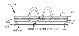
도 22는 자극(S)이 근접성 임계치(X)를 초과하는지를 결정하기 위한 활성 구역(active zone)을 포함하는 터치 센서를 나타낸 도면.
도 23은 다수의 전극들 및 시간 영역 차분 감지 회로를 포함하는 터치 센서의 회로도.
도 24는 도 23에 예시된 터치 센서에 대한 자극 대 시간을 나타낸 그래프.
도 25는 도 23에 예시된 터치 센서에 대한 자극의 변화율 대 시간을 나타낸 그래프.
도 26은 4개의 전극들 및 시간 영역 차분 서명 처리 회로를 포함하는 터치 센서의 회로도.
도 27은 도 26에 예시된 터치 센서에서 사용하기 위한 4개의 원형 전극들을 나타낸 도면.
도 28은 도 27에 도시된 4개의 원형 전극들 및 도 26에 예시된 터치 센서에서 사용하기 위한 접지 평면을 나타낸 도면.
도 29는 단일의 전극을 포함하는 터치 센서 상에 멈추게 되는 손가락의 제1 예시를 나타낸 도면.
도 30은 단일의 전극을 포함하는 터치 센서 상에 멈추게 되는 손가락의 제2 예시를 나타낸 도면.
도 31은 도 26에 예시된 터치 센서에 대한 자극 대 시간을 나타낸 그래프.
도 32는 도 26에 예시된 터치 센서에 대한 자극의 변화율 대 시간을 나타낸 그래프.
도 33은 도 26에 예시된 터치 센서에서 사용하기 위한 4개의 비원형 전극들을 나타낸 도면.
도 34는 도 33에 도시된 4개의 비원형 전극들 및 도 26에 예시된 터치 센서에서 사용하기 위한 접지 평면을 나타낸 도면.
도 35는 시간 영역 차분 논리에서 사용하기 위한 활성 구역 및 다수의 전극들을 포함하는 터치 센서를 나타낸 도면.
도 36은 시간 영역 차분 처리 회로를 포함하는 다중 전극 터치 센서의 회로도.
도 37은 8개의 단일 전극 또는 듀얼 전극 및 시간 영역 차분 처리 회로를 포함하는 터치 센서의 회로도.
도 38은 도 37에 예시된 터치 센서에서 사용하기 위한 8개의 단일 전극들을 나타낸 도면.
도 39는 도 37에 예시된 터치 센서에서 사용하기 위한 8개의 듀얼 전극들을 나타낸 도면.
도 40은 도 37에 예시된 터치 센서에서 사용하기 위한 12개의 듀얼 전극들을 나타낸 도면.
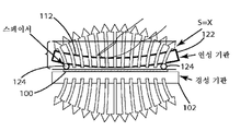
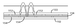
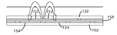
도 41은 연성 기판과 경성 기판 사이에 개재된 단일의 전극을 포함하는 터치 센서를 나타낸 도면.
도 42는 손가락이 도 41에 예시된 터치 센서에 접근하는 것을 나타낸 도면.
도 43은 손가락이 도 41에 예시된 터치 센서와 연관된 연성 기판을 편향시키는 것을 나타낸 도면.
도 44는 도 41 내지 도 43에 예시된 터치 센서에 대한 자극 대 시간을 나타낸 그래프.
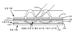
도 45는 도 41 내지 도 43에 예시된 터치 센서에 대한 자극의 변화율 대 시간을 나타낸 그래프.
도 46은 2개의 경성 기판들 사이에 개재된 단일의 전극을 포함하는 터치 센서를 나타낸 도면.
도 47은 손가락이 도 46에 예시된 터치 센서에 접근하는 것을 나타낸 도면.
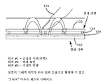
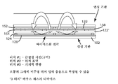
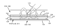
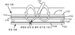
도 48은 상부 경성 기판과 하부 경성 기판 사이에 개재된 센서 전극 및 바이어스된 전극을 포함하는 터치 센서를 나타낸 도면.
도 49는 상부 경성 기판과 하부 경성 기판 사이에 개재된 다수의 전극들을 포함하는 터치 센서를 나타낸 도면.
도 50은 상부 경성 기판과 하부 경성 기판 사이에 개재된 다수의 전극들 및 바이어스된 전극을 포함하는 터치 센서를 나타낸 도면.
도 51은 도 49 및 도 50의 터치 센서에 대한 자극 대 시간을 나타낸 제1 그래프.
도 52는 도 49 및 도 50의 터치 센서에 대한 자극의 변화율 대 시간을 나타낸 제1 그래프.
도 53은 도 49 및 도 50의 터치 센서에 대한 자극 대 시간을 나타낸 제2 그래프.
도 54는 도 49 및 도 50의 터치 센서에 대한 자극의 변화율 대 시간을 나타낸 제2 그래프.
도 55는 도 49 및 도 50의 터치 센서에 대한 자극 대 시간을 나타낸 제3 그래프.
도 56은 도 49 및 도 50의 터치 센서에 대한 자극의 변화율 대 시간을 나타낸 제3 그래프.
도 57은 도 49 및 도 50의 터치 센서에 대한 자극 대 시간을 나타낸 제4 그래프.
도 58은 도 49 및 도 50의 터치 센서에 대한 자극의 변화율 대 시간을 나타낸 제4 그래프.
도 59는 필터 기능 및 시간 영역 차분 서명 인식을 포함하는 단일 전극 터치 센서의 회로도.
도 60은 필터 기능 및 시간 영역 차분 서명 인식을 포함하는 다중 전극 터치 센서의 회로도.
도 61은 내부 전극 및 외부 전극을 포함하는 듀얼 전극 터치 센서를 나타낸 도면.
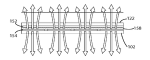
도 62는 순 전기장(net electric field)을 포함하는 도 61의 듀얼 전극 터치 센서를 나타낸 도면.
도 63은 도 61에 예시된 듀얼 전극 터치 센서의 제1 회로도.
도 64는 도 61에 예시된 듀얼 전극 터치 센서의 제2 회로도.
도 65는 일정 간격으로 있는 상부 경성 기판 및 하부 경성 기판을 포함하는 듀얼 전극 터치 센서를 나타낸 도면.
도 66은 일정 간격으로 있는 상부 경성 기판 및 하부 경성 기판과 바이어스된 하부 전극을 포함하는 듀얼 전극 터치 센서를 나타낸 도면.
도 67은 본 발명의 차분 감지 기법들을 이용하는 8-전극 터치 센서를 나타낸 도면.
도 68은 본 발명의 차분 감지 기법들을 이용하는 12-전극 터치 센서를 나타낸 도면.
도 69는 내부 전극 및 외부 전극과 스트로브 전극을 포함하는 터치 센서를 나타낸 도면.
도 70은 시간 차분 처리 회로를 포함하는, 도 69에 예시된 터치 센서의 회로도.
도 71은 내부 버퍼와 제1 자극 및 제2 자극 및 검출 회로를 포함하는, 도 69에 예시된 터치 센서의 회로도.
도 72는 순 전기장을 포함하는 도 69의 터치 센서를 나타낸 도면.
도 73은 위에 있는 기판이 스페이서들에 의해 지지되는 도 69의 터치 센서를 나타낸 도면.
도 74는 순 전기장을 포함하는 도 73의 터치 센서를 나타낸 도면.
도 75는 내부 전극 및 외부 전극을 포함하는 제1 12-전극 센서를 나타낸 도면.
도 76은 도 75의 12-전극 센서에서 사용하기 위한 하부 스트로브 전극을 나타낸 도면.
도 77은 내부 전극 및 외부 전극을 포함하는 제2 12-전극 센서를 나타낸 도면.
도 78은 도 77의 12-전극 센서에서 사용하기 위한 하부 스트로브 전극을 나타낸 도면.
도 79는 중첩하는 전극 행들 및 전극 열들을 포함하는 터치 센서의 제1 측면도.
도 80은 중첩하는 전극 행들 및 전극 열들을 포함하는 터치 센서의 제2 측면도.
도 81은 전극 열들을 포함하는 도 79 및 도 80의 터치 센서의 상면도.
도 82는 전극 행들을 포함하는 도 79 및 도 80의 터치 센서의 상면도.
도 83은 전극 열들 및 전극 행들을 포함하는 도 79 및 도 80의 터치 센서의 상면도.
도 84는 시간 영역 차분 서명 처리 회로를 포함하는 도 83의 터치 센서의 회로도.
도 85는 열이 본 발명의 일 실시예에 따라 구동되고 판독되는 것을 나타낸 도 83의 터치 센서의 상면도.
도 86은 행이 본 발명의 일 실시예에 따라 구동되고 판독되는 것을 나타낸 도 83의 터치 센서의 상면도.
도 87은 열 및 행이 본 발명의 일 실시예에 따라 구동되고 판독되는 것을 나타낸 도 83의 터치 센서의 상면도.
도 88은 다수의 열들이 본 발명의 일 실시예에 따라 구동되고 판독되는 것을 나타낸 도 83의 터치 센서의 상면도.
도 89는 다수의 행들이 본 발명의 일 실시예에 따라 구동되고 판독되는 것을 나타낸 도 83의 터치 센서의 상면도.
도 90은 다수의 열들 및 다수의 행들이 본 발명의 일 실시예에 따라 구동되고 판독되는 것을 나타낸 도 83의 터치 센서의 상면도.
도 91은 본 발명의 일 실시예에 따른 도 83의 터치 센서의 동작을 나타낸 제1 플로우차트.
도 92는 도 91의 플로우차트로부터 계속되는 플로우차트.
도 93은 본 발명의 일 실시예에 따른 도 83의 터치 센서의 동작을 나타낸 제2 플로우차트.
도 94는 도 93의 플로우차트로부터 계속되는 플로우차트.
도 95는 필터 기능 및 시간 영역 차분 서명 처리 회로를 포함하는 도 83의 터치 센서의 회로도.
도 96은 순 전기장을 예시한 도 83의 터치 센서의 제1 측면도.
도 97은 순 전기장을 예시한 도 83의 터치 센서의 제2 측면도.
도 98은 열 전극들을 스트로브하고 행 전극들을 판독하도록 구성된 회로의 회로도.
도 99는 행 또는 열로부터의 응답을 응답 검출 회로로 라우팅하기 위해 자극 선택 회로를 포함하도록 수정된 도 98의 회로도.
도 100은 단일의 행의 스트로브 및 2개의 열들의 판독을 나타낸 도 83의 터치 센서의 상면도.
도 101은 단일의 열의 스트로브 및 2개의 행들의 판독을 나타낸 도 83의 터치 센서의 상면도.
도 102는 다수의 행들의 스트로브 및 다수의 열들의 판독 그리고 그 반대를 나타낸 도 83의 터치 센서의 상면도.
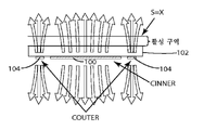
도 103은 인접한 전극 행들에 결합된 전극 열을 포함하는 터치 센서의 측면도.
도 104는 인접한 전극 열들에 결합된 전극 행을 포함하는 터치 센서의 측면도.
도 105는 시간 영역 차분 처리 회로를 포함하는 도 103 및 도 104의 터치 센서들의 회로도.
도 106은 행 또는 열로부터의 응답을 2개의 검출 회로들 중 하나로 라우팅하기 위해 자극 선택 회로들을 포함하도록 수정된 도 105의 회로도.
도 107은 단일의 열의 스트로브 및 다수의 행들의 판독을 나타낸 도 103 및 도 104의 터치 센서의 상면도.
도 108은 단일의 행의 스트로브 및 다수의 열들의 판독을 나타낸 도 103 및 도 104의 터치 센서의 상면도.
도 109는 다수의 행들의 스트로브 및 다수의 열들의 판독 그리고 그 반대를 나타낸 도 103 및 도 104의 터치 센서의 상면도.
도 110은 전극 열들 및 전극 행들을 포함하는 터치 센서의 제1 측면도.
도 111은 연성 기판을 포함하도록 수정된 도 110의 터치 센서를 나타낸 도면.
도 112는 전극 열들 및 전극 행들을 포함하는 터치 센서의 제2 측면도.
도 113은 연성 기판을 포함하도록 수정된 도 112의 터치 센서를 나타낸 도면.
도 114는 전극 열들 및 전극 행들을 포함하고 순 전기장을 예시한 터치 센서의 제1 측면도.
도 115는 전극 열들 및 전극 행들을 포함하고 순 전기장을 예시한 터치 센서의 제2 측면도.
도 116은 전극 열들, 전극 행들, 및 바이어스된 전극을 포함하는 터치 센서의 제1 측면도.
도 117은 순 전기장을 예시한 도 116의 터치 센서를 나타낸 도면.
도 118은 전극 열들, 전극 행들, 및 바이어스된 전극을 포함하는 터치 센서의 제2 측면도.
도 119는 순 전기장을 예시한 도 118의 터치 센서를 나타낸 도면.
도 120은 손가락이 도 116 내지 도 119의 터치 센서와 맞닿아 멈추게 되는 것을 나타낸 도면.
도 121은 스타일러스가 도 116 내지 도 119의 터치 센서와 맞닿아 멈추게 되는 것을 나타낸 도면.
도 122는 터치 입력이 없는 경우 다수의 전극 열들을 포함하는 터치 센서에 대한 순 전기장을 나타낸 도면.
도 123은 터치 입력이 없는 경우 다수의 전극 열들 및 다수의 전극 행들을 포함하는 터치 센서에 대한 순 전기장을 나타낸 도면.
도 124는 터치 입력이 없는 경우 다수의 전극 행들을 포함하는 터치 센서에 대한 순 전기장을 나타낸 도면.
도 125는 제1 측면도로부터의 다수의 전극 열들 및 다수의 전극 행들을 포함하는 터치 센서에 대한 순 전기장을 나타낸 도면.
도 126은 도 123 및 도 125의 터치 센서가 스타일러스에 의해 접촉된 것을 나타낸 도면.
도 127은 도 123 및 도 125의 터치 센서가 스타일러스에 의해 하향 편향된 것을 나타낸 도면.
도 128은 도 123 및 도 125의 터치 센서가 손가락에 의해 접촉된 것을 나타낸 도면.
도 129는 도 123 및 도 125의 터치 센서가 손가락에 의해 하향 편향된 것을 나타낸 도면.
도 130은 본 발명의 실시예들에 따른 터치 패드 위쪽에서의 물체의 위치를 결정하는 광 센서 어레이를 나타낸 도면.
도 131은 본 발명의 실시예들에 따른 터치 센서 위쪽에서의 물체의 위치를 결정하는 광 센서 매트릭스를 나타낸 도면.
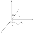
도 132는 도 131의 터치 센서와 관련하여 손가락 끝의 위치를 3차원으로 나타낸 도면.1 shows a touch sensor comprising multiple electrodes for differential sensing techniques;
2 shows a touch sensor comprising a single electrode for capacitive sensing techniques;
3 is a circuit diagram corresponding to the single electrode touch sensor illustrated in FIG. 2 .
Fig. 4 is a first timing diagram for the circuit of Fig. 3;
Fig. 5 is a second timing diagram for the circuit of Fig. 3;
Fig. 6 is a third timing diagram for the circuit of Fig. 3;
Fig. 7 is a fourth timing diagram for the circuit of Fig. 3;
8 is a circuit diagram corresponding to the multi-electrode touch sensor illustrated in FIG. 1 .
Fig. 9 is a first timing diagram for the circuit of Fig. 8;
Fig. 10 is a second timing diagram for the circuit of Fig. 8;
Fig. 11 is a third timing diagram for the circuit of Fig. 8;
Fig. 12 is a fourth timing diagram for the circuit of Fig. 8;
13 shows a touch sensor including an active zone for determining proximity to a single electrode.
14 is a diagram illustrating a touch sensor including a plurality of electrodes for time-domain difference sensing;
15 is a diagram illustrating a touch sensor including a single electrode for time-domain difference sensing;
16 shows a finger approaching a touch sensor comprising a single electrode and an activation zone;
17 is a first graph illustrating voltage versus time for the touch sensor illustrated in FIG. 16 ;
18 is a second graph illustrating voltage versus time for the touch sensor illustrated in FIG. 16 ;
19 is a third graph illustrating voltage versus time for the touch sensor illustrated in FIG. 16 ;
Fig. 20 is a flowchart showing the operation of the touch sensor illustrated in Fig. 16;
Fig. 21 is a block diagram illustrating a timing interface circuit for the touch sensor illustrated in Fig. 16;
Fig. 22 shows a touch sensor including an active zone for determining whether a stimulus S exceeds a proximity threshold X;
23 is a circuit diagram of a touch sensor including a plurality of electrodes and a time domain difference sensing circuit;
24 is a graph illustrating stimulation versus time for the touch sensor illustrated in FIG. 23 .
25 is a graph illustrating rate of change of stimulus versus time for the touch sensor illustrated in FIG. 23 .
26 is a circuit diagram of a touch sensor including four electrodes and a time domain differential signature processing circuit;
Fig. 27 shows four circular electrodes for use in the touch sensor illustrated in Fig. 26;
Fig. 28 shows the four circular electrodes shown in Fig. 27 and a ground plane for use in the touch sensor illustrated in Fig. 26;
Fig. 29 shows a first example of a finger resting on a touch sensor comprising a single electrode;
Fig. 30 shows a second example of a finger resting on a touch sensor comprising a single electrode;
31 is a graph illustrating stimulation versus time for the touch sensor illustrated in FIG. 26 .
32 is a graph illustrating rate of change of stimulus versus time for the touch sensor illustrated in FIG. 26 .
Fig. 33 shows four non-circular electrodes for use in the touch sensor illustrated in Fig. 26;
Fig. 34 shows the four non-circular electrodes shown in Fig. 33 and a ground plane for use in the touch sensor illustrated in Fig. 26;
Fig. 35 shows a touch sensor including an active region and multiple electrodes for use in time domain difference logic;
36 is a circuit diagram of a multi-electrode touch sensor including time domain difference processing circuitry;
37 is a circuit diagram of a touch sensor including eight single or dual electrodes and a time domain difference processing circuit;
38 shows eight single electrodes for use in the touch sensor illustrated in FIG. 37 ;
Fig. 39 shows eight dual electrodes for use in the touch sensor illustrated in Fig. 37;
FIG. 40 shows twelve dual electrodes for use in the touch sensor illustrated in FIG. 37 ;
41 is a view illustrating a touch sensor including a single electrode interposed between a flexible substrate and a rigid substrate;
FIG. 42 depicts a finger approaching the touch sensor illustrated in FIG. 41 ;
FIG. 43 depicts a finger deflecting a flexible substrate associated with the touch sensor illustrated in FIG. 41 ;
44 is a graph illustrating stimulation versus time for the touch sensor illustrated in FIGS. 41-43;
45 is a graph illustrating rate of change of stimulus versus time for the touch sensor illustrated in FIGS. 41-43;
46 illustrates a touch sensor including a single electrode interposed between two rigid substrates;
FIG. 47 depicts a finger approaching the touch sensor illustrated in FIG. 46 ;
48 is a view showing a touch sensor including a biased electrode and a sensor electrode interposed between the upper rigid substrate and the lower rigid substrate.
49 is a view illustrating a touch sensor including a plurality of electrodes interposed between an upper rigid substrate and a lower rigid substrate;
50 is a view illustrating a touch sensor including a plurality of electrodes and a biased electrode interposed between an upper rigid substrate and a lower rigid substrate;
FIG. 51 is a first graph illustrating stimulation versus time for the touch sensor of FIGS. 49 and 50 .
FIG. 52 is a first graph illustrating rate of change of stimulus versus time for the touch sensor of FIGS. 49 and 50;
53 is a second graph illustrating stimulation versus time for the touch sensor of FIGS. 49 and 50;
54 is a second graph illustrating rate of change of stimulus versus time for the touch sensor of FIGS. 49 and 50;
FIG. 55 is a third graph illustrating stimulation versus time for the touch sensor of FIGS. 49 and 50;
56 is a third graph illustrating rate of change of stimulus versus time for the touch sensor of FIGS. 49 and 50;
FIG. 57 is a fourth graph illustrating stimulation versus time for the touch sensor of FIGS. 49 and 50 .
58 is a fourth graph illustrating rate of change of stimulus versus time for the touch sensor of FIGS. 49 and 50;
59 is a circuit diagram of a single electrode touch sensor including filter function and time domain differential signature recognition.
60 is a circuit diagram of a multi-electrode touch sensor including filter function and time domain differential signature recognition.
61 is a view showing a dual electrode touch sensor including an inner electrode and an outer electrode.
FIG. 62 illustrates the dual electrode touch sensor of FIG. 61 including a net electric field;
63 is a first circuit diagram of the dual electrode touch sensor illustrated in FIG. 61 ;
FIG. 64 is a second circuit diagram of the dual electrode touch sensor illustrated in FIG. 61 ;
65 is a view showing a dual electrode touch sensor including an upper rigid substrate and a lower rigid substrate spaced at regular intervals.
66 is a diagram illustrating a dual-electrode touch sensor including an upper rigid substrate and a lower rigid substrate spaced apart from each other and a biased lower electrode;
67 shows an 8-electrode touch sensor using the differential sensing techniques of the present invention.
68 illustrates a 12-electrode touch sensor employing the differential sensing techniques of the present invention.
69 is a view showing a touch sensor including an internal electrode, an external electrode, and a strobe electrode;
70 is a circuit diagram of the touch sensor illustrated in FIG. 69, including temporal difference processing circuitry;
71 is a circuit diagram of the touch sensor illustrated in FIG. 69 including an internal buffer and first and second stimulation and detection circuitry;
FIG. 72 illustrates the touch sensor of FIG. 69 including a net electric field;
73 shows the touch sensor of FIG. 69 with an overlying substrate supported by spacers;
74 illustrates the touch sensor of FIG. 73 including a net electric field;
Fig. 75 shows a first 12-electrode sensor comprising an inner electrode and an outer electrode;
76 shows a lower strobe electrode for use in the 12-electrode sensor of FIG. 75;
77 shows a second 12-electrode sensor comprising an inner electrode and an outer electrode;
78 shows a lower strobe electrode for use in the 12-electrode sensor of FIG. 77;
79 is a first side view of a touch sensor including overlapping electrode rows and electrode columns;
80 is a second side view of a touch sensor including overlapping electrode rows and electrode columns;
81 is a top view of the touch sensor of FIGS. 79 and 80 including electrode rows;
82 is a top view of the touch sensor of FIGS. 79 and 80 including electrode rows;
83 is a top view of the touch sensor of FIGS. 79 and 80 including electrode columns and electrode rows;
84 is a circuit diagram of the touch sensor of FIG. 83 including time domain differential signature processing circuitry;
85 is a top view of the touch sensor of FIG. 83 showing heat being driven and read in accordance with an embodiment of the present invention;
86 is a top view of the touch sensor of FIG. 83 showing rows being driven and read in accordance with an embodiment of the present invention;
87 is a top view of the touch sensor of FIG. 83 showing columns and rows being driven and read in accordance with an embodiment of the present invention;
88 is a top view of the touch sensor of FIG. 83 showing multiple columns being driven and read in accordance with an embodiment of the present invention;
89 is a top view of the touch sensor of FIG. 83 showing multiple rows being driven and read in accordance with an embodiment of the present invention;
FIG. 90 is a top view of the touch sensor of FIG. 83 showing multiple columns and multiple rows being driven and read in accordance with an embodiment of the present invention;
91 is a first flowchart illustrating an operation of the touch sensor of FIG. 83 according to an embodiment of the present invention;
Fig. 92 is a flowchart continuing from the flowchart of Fig. 91;
93 is a second flowchart illustrating an operation of the touch sensor of FIG. 83 according to an embodiment of the present invention;
Fig. 94 is a flowchart continuing from the flowchart of Fig. 93;
Fig. 95 is a circuit diagram of the touch sensor of Fig. 83 including a filter function and a time domain differential signature processing circuit;
96 is a first side view of the touch sensor of FIG. 83 illustrating a net electric field;
97 is a second side view of the touch sensor of FIG. 83 illustrating a net electric field;
98 is a circuit diagram of a circuit configured to strobe column electrodes and read row electrodes;
FIG. 99 is the circuit diagram of FIG. 98 modified to include stimulus selection circuitry for routing responses from a row or column to response detection circuitry;
FIG. 100 is a top view of the touch sensor of FIG. 83 showing a single row of strobes and readings of two columns;
FIG. 101 is a top view of the touch sensor of FIG. 83 showing a single column of strobes and a readout of two rows;
FIG. 102 is a top view of the touch sensor of FIG. 83 showing a strobe of multiple rows and a readout of multiple columns, and vice versa.
103 is a side view of a touch sensor including electrode columns coupled to adjacent electrode rows;
104 is a side view of a touch sensor including a row of electrodes coupled to adjacent electrode columns;
105 is a circuit diagram of the touch sensors of FIGS. 103 and 104 including time domain difference processing circuitry;
106 is the circuit diagram of FIG. 105 modified to include stimulus selection circuits for routing a response from a row or column to one of two detection circuits;
107 is a top view of the touch sensor of FIGS. 103 and 104 showing a single column of strobes and multiple rows of readings;
108 is a top view of the touch sensor of FIGS. 103 and 104 showing a single row of strobes and a readout of multiple columns;
109 is a top view of the touch sensor of FIGS. 103 and 104 illustrating a strobe of multiple rows and a readout of multiple columns, and vice versa.
110 is a first side view of a touch sensor including electrode columns and electrode rows;
111 illustrates the touch sensor of FIG. 110 modified to include a flexible substrate;
112 is a second side view of a touch sensor including electrode columns and electrode rows;
113 illustrates the touch sensor of FIG. 112 modified to include a flexible substrate;
114 is a first side view of a touch sensor including electrode columns and electrode rows and illustrating a net electric field;
115 is a second side view of a touch sensor including electrode columns and electrode rows and illustrating a net electric field;
116 is a first side view of a touch sensor including electrode columns, electrode rows, and a biased electrode;
117 shows the touch sensor of FIG. 116 illustrating a net electric field;
118 is a second side view of a touch sensor including electrode columns, electrode rows, and a biased electrode;
119 shows the touch sensor of FIG. 118 illustrating a net electric field;
FIG. 120 is a view showing that a finger stops in contact with the touch sensor of FIGS. 116 to 119;
121 is a view showing that the stylus stops in contact with the touch sensor of FIGS. 116 to 119 .
122 is a diagram illustrating a net electric field for a touch sensor including a plurality of electrode columns in the absence of a touch input.
123 is a diagram illustrating a net electric field for a touch sensor including a plurality of electrode columns and a plurality of electrode rows in the absence of a touch input;
124 illustrates a net electric field for a touch sensor including multiple electrode rows in the absence of touch input.
125 illustrates a net electric field for a touch sensor including multiple electrode columns and multiple electrode rows from a first side view;
FIG. 126 is a view showing that the touch sensor of FIGS. 123 and 125 is contacted by a stylus;
FIG. 127 is a view showing the touch sensor of FIGS. 123 and 125 being downwardly deflected by the stylus;
FIG. 128 is a view illustrating that the touch sensor of FIGS. 123 and 125 is touched by a finger;
FIG. 129 is a view showing the touch sensor of FIGS. 123 and 125 being downwardly deflected by a finger;
130 is a diagram illustrating an optical sensor array for determining a position of an object above a touch pad according to embodiments of the present invention;
131 is a diagram illustrating an optical sensor matrix for determining a position of an object above a touch sensor according to embodiments of the present invention;
FIG. 132 is a view showing the position of a fingertip in three dimensions in relation to the touch sensor of FIG. 131;
본 발명은, 본 명세서에서 상정되고 개시된 바와 같이, 하나 이상의 터치 입력들을 검출하는 시스템들 및 방법들을 포함한다. 시스템들 및 방법들은 물체가 기판과 맞닿아 멈추게 될 때를 결정하기 위해 정전용량의 변화율을 모니터링하는 것을 포함한다. 파트 I는 시간 영역 차분 감지 기법들의 개요를 포함한다. 파트 II는 시간 영역 차분 감지 기법들을 이용하는 단일 전극 터치 센서 및 다중 전극 터치 센서에 관한 것이다. 파트 III은 시간 영역 차분 감지 기법들을 이용하는 매트릭스 전극 터치 센서들에 관한 것이다. 마지막으로, 파트 IV는, 선택적으로 파트 II 및 파트 III에서 논의된 터치 센서들과 관련하여 사용하기 위한, 광 센서들에서의 시간 영역 차분 감지에 관한 것이다.The present invention includes systems and methods for detecting one or more touch inputs, as contemplated and disclosed herein. Systems and methods include monitoring a rate of change of capacitance to determine when an object comes to rest against a substrate. Part I contains an overview of time domain difference sensing techniques. Part II relates to single-electrode touch sensors and multi-electrode touch sensors using time domain differential sensing techniques. Part III relates to matrix electrode touch sensors that use time domain differential sensing techniques. Finally, Part IV relates to time-domain differential sensing in optical sensors, optionally for use in connection with the touch sensors discussed in Part II and Part III.
I. 시간 영역 차분 감지의 개요 I. Overview of Time Domain Differential Detection
2010년 3월 24일자로 출원된 Caldwell 등의 국제 특허 출원 WO2010/111362(그 개시 내용은 참조 문헌으로서 그 전체가 포함됨)는 투사 정전용량, 용량성, 및 차분 감지와 연관된 많은 결점들 및 한계들은 물론, 이러한 결점들 및 한계들을 극복하는 기법들을 기술하고 있다. 바로 이 기법들은, 적절히 적용될 때, 미리정해진 임계치 값들에만 기초하는 기존의 정전용량 및 전계 효과 감지 기법들로부터 달성될 수 있는 것보다 더 높은 성능 및 부가의 특징들에 대한 보다 많은 기회들을 제공할 수 있다.International patent application WO2010/111362 to Caldwell et al., filed March 24, 2010, the disclosure of which is incorporated by reference in its entirety, discloses that many of the drawbacks and limitations associated with projected capacitance, capacitive, and differential sensing are Of course, techniques are described that overcome these drawbacks and limitations. These very techniques, when properly applied, can provide more opportunities for higher performance and additional features than can be achieved from existing capacitive and field effect sensing techniques that are based only on predetermined threshold values. have.
상세하게는, 국제 특허 출원 WO2010/111362는 "터치의 서명"을 실제로 감지하는 것에 의해 보다 신뢰성있는 터치 감지를 달성하기 위해 단일 전극 및 "시간 영역 차분" 감지 기법들을 사용하는 것을 기술하고 있다. 시간 영역 차분 감지 기법들은 먼저 도 3에서 터치 신호(Vs)(그리고 그 문제에 대해, 다중 전극 센서를 사용할 때, 도 8에서의 Vs)를 검출하기 위해 기술된 것과 동일한 기법들을 사용할 수 있다. 사람에 의한 터치에 대해 기본적으로 설명하면, 손가락을 멈추게 하는 주어진 단일 전극 위쪽의 표면 쪽으로 이동하고 따라서 손가락 접근을 감지 전극으로 물리적으로 제한하며 따라서 감지 전극에 의해 감지될 수 있는 자극의 양을 제한한다. 이어서, 사람의 손가락에 의해 야기되는 터치 이벤트의 서명이 손가락이 자극(s)이 느슨하게 설정된 값 x를 초과하게 되는 도 13에 도시된 활성 구역에 접근함으로써 감지 전극에 근접해 있는지를 먼저 결정하는 것에 의해 정의된다. 손가락이 감지 전극에 근접해 있고 s>x로 나타낸 바와 같이 활성 구역 내에 있는 것으로 결정되면, 시간에 대한 자극의 변화율(ds/dt)이 결정되고 분석된다. 자극의 변화율은 시간에 대한 대응하는 감지 전극 또는 전극들 상부의 터치 표면/페시아(fascia)에 접근하는 사람의 손가락에 의해 야기되는 자극 변화로서 기술된다.Specifically, international patent application WO2010/111362 describes the use of single electrode and "time domain differential" sensing techniques to achieve more reliable touch sensing by actually sensing the "signature of touch". Time domain differential sensing techniques may first use the same techniques described for detecting the touch signal Vs in FIG. 3 (and, for that matter, Vs in FIG. 8 when using a multi-electrode sensor). A basic description of touch by a human is that it moves towards the surface above a given single electrode that stops the finger, thus physically restricting finger access to the sensing electrode and thus limiting the amount of stimulus that can be sensed by the sensing electrode. . Then, by first determining whether the signature of a touch event caused by the human finger is in proximity to the sensing electrode by approaching the active region shown in Figure 13 where the stimulus (s) exceeds a loosely set value x. Defined. If the finger is determined to be in proximity to the sensing electrode and to be within the active zone as indicated by s>x, the rate of change of stimulus over time (ds/dt) is determined and analyzed. The rate of change of stimulus is described as the change in stimulus caused by a person's finger approaching the touch surface/fascia on top of the corresponding sensing electrode or electrodes over time.
단일의 전극을 포함하는 자기 정전용량 기법들 및 2개 이상의 전극들을 포함하는 상호 정전용량 기법들 둘 다를 비롯한 앞서 기술한 것과 같은 터치를 검출하는 데 사용되는 자극을 발생시키고 감지하는 수많은 기법들이 있다. 자극을 발생시키고 검출하기 위해 사용되는 기법에 따라, 터치 입력이 터치 표면에 접근함에 따라 터치 입력이 자극을 증가시키거나 감소시킬 수 있지만, 단일 전극 센서이든 다중 전극 센서이든 간에, 손가락 또는 다른 부속 기관/디바이스가 터치 표면 인터페이스에 접근함에 따라 자극이 증가하는 것으로 가정하자(감지 기법에 기초하여, 이것이 자연스러울 수 있거나, 반대로 구성될 수 있는 등). 따라서, 아날로그/디지털 하드웨어 또는 소프트웨어, 또는 이 둘의 조합에 의해 처리되는 터치 서명의 기본 정의는 다음과 같은 이벤트들의 기본 논리 시퀀스에 의해 정의될 것이다: 1) 자극(s)이 변하고 검출되며, 감지 전극에 아주 근접해 있는 손가락/부속 기관 또는 다른 터치 입력 디바이스에 기초하여, 어떤 값보다 큰 경우(s>x), 뒤이어서; 2) 시간에 대한 자극 변화율(ds/dt)이, 손가락이 터치 감지 전극 쪽으로 이동하는 것에 기초하여, 0보다 큰 경우(ds/dt >0), 뒤이어서; 3) 손가락이 감지 전극 위쪽에서 멈추고 표면 페시아(surface fascia)에 의해 멈춰지게 되는 것에 의해 야기되는 시간에 따른 자극 변화율이 (손가락이 움직이고 있을 때의 ds/dt에 대해) ds/dt=0이거나 0에 아주 가까운 경우, 조건들이 이벤트 1이 참이고, 이벤트 2가 참이며, 이벤트 3이 참이도록 되어 있으면, 프로세스는 터치 자극이 있다는 것을 나타낼 것이다.There are numerous techniques for generating and sensing a stimulus used to detect a touch, such as those described above, including both self-capacitance techniques involving a single electrode and mutual capacitance techniques involving two or more electrodes. Depending on the technique used to generate and detect the stimulus, touch input may increase or decrease the stimulus as it approaches the touch surface, but whether it is a single electrode sensor or a multi-electrode sensor, a finger or other appendage. Assume that the stimulus increases as the device approaches the touch surface interface (based on the sensing technique, this may be natural, or vice versa). Thus, the basic definition of a touch signature processed by analog/digital hardware or software, or a combination of the two, will be defined by a basic logical sequence of events as follows: 1) the stimulus(s) changes, is detected, and senses based on a finger/appendage or other touch input device in close proximity to the electrode, if greater than some value (s>x), then; 2) the rate of change of stimulus over time (ds/dt) is greater than zero (ds/dt >0), followed by movement of the finger towards the touch sensitive electrode; 3) the rate of change of stimulus over time caused by the finger stopping above the sensing electrode and being stopped by the surface fascia (for ds/dt when the finger is moving) ds/dt=0 or 0 If the conditions are such that
주목할 점은, 터치를 평가하는 프로세스에 대해 미리정해진 어떤 절대값들도 없다는 것이다. 따라서, 한 예로서, 손가락에 장갑이 착용되어, 손가락이 터치 표면을 실제로 터치하지 못하게 하는 부가의 두께 층들을 추가하여 거리(장갑의 두께에 일반적으로 기초하는 거리)를 본질적으로 증가시키는 경우, 자극이 감지 전극들 위쪽에 근접해 있는 한(상기 조건 1인 s > x) 그리고 상기 조건 2) 및 조건 3)이 충족될 때, 장갑을 끼지 않은 손가락/부속 기관이 사용될 때처럼 터치가 검출될 것이다. 이상의 논리적 조건들을 구현한 결과, 장갑을 끼거나 장갑을 끼지 않은 조건들을 사용하는 터치의 일관성있는 "터치감" 감지가 얻어진다. 그에 부가하여, 기판 유전체, 기판 두께, 또는 다른 제조 허용 오차들이 유효 자극 강도를 변화시키는 경우, 터치 입력을 검출하기 위해 상기 논리 시퀀스를 사용하는 것은 종래의 정전용량 및 차분 감지 기법들에서 사용되는 바와 같이 미리정해진 임계치를 사용하는 것 - 이들 둘 다는 자극 응답 및 터치 신호 응답에 대응하는 미리정해진 임계치를 사용함 - 과 비교하여 터치 응답의 일관성있는 "감지(feel)"를 가능하게 한다.Note that there are no absolute values predetermined for the process of evaluating a touch. Thus, as an example, when a glove is worn on a finger, adding additional layers of thickness that prevents the finger from actually touching the touch surface, essentially increasing the distance (a distance that is usually based on the thickness of the glove), stimulation As long as there is close proximity above these sensing electrodes (s > x in the above condition 1) and when conditions 2) and 3) above are met, a touch will be detected as when an ungloved finger/appendage is used. As a result of implementing the above logical conditions, a consistent "touch feeling" sensing of a touch using the gloved and gloved conditions is obtained. In addition, using the logic sequence to detect touch input when substrate dielectric, substrate thickness, or other manufacturing tolerances change the effective stimulus intensity is different from that used in conventional capacitive and differential sensing techniques. It allows for a consistent "feel" of the touch response as compared to using predetermined thresholds as such - both of which use predetermined thresholds corresponding to the stimulus response and the touch signal response.
II. 단일 전극 터치 센서 및 다중 전극 터치 센서 II. Single-electrode touch sensor and multi-electrode touch sensor
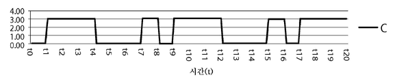
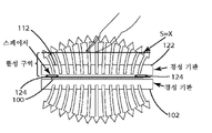
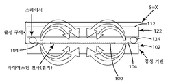
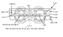
시간 영역 차분 감지 기법들은 단일 전극 터치 센서 및 다중 전극 터치 센서에 의해 구현될 수 있다. 이 기법들은 s, ds, S, dS, t, dt, T, dT, ds/dt, ds/dT, dS/dt, dS/dT에 기초하여 단일의 전극 또는 다수의 전극들을 사용하여 터치 서명을 결정하는 데 사용될 수 있고, 여기서 s (또는 s<<S인 경우 S)는 전극 정전용량의 절대값을 나타내고, t 및 T는 시간 영역들이다(단, t << T임). 이 기법들은 또한 2개의 전극들을 사용하여 터치 서명을 결정하는 데 사용될 수 있다. 도 14는 다중 전극 감지 구조를 나타낸 것이고, 도 13 및 도 15는 단일 전극 구조를 나타낸 것이다. 감지 기법에 상관없이, 손가락/부속 기관 또는 다른 터치 입력 디바이스가 터치 표면에 접근하는 것에 대한 자극 응답이 앞서 기술한 원리들에 따라 분석될 수 있다. 도 16은 손가락이 단일의 전극에 접근할 때의 손가락 형태의 터치 입력을 나타내는 국제 특허 출원 WO2010/111362로부터의 도면이고, 도 17은, 자극이 손가락이 단일의 전극에 접근하는 것에 대응하는 것일 때, 자극은 물론 그 자극의 변화율을 나타낸 것이다. 도 17에서의 응답은 또한 다중 전극 센서 및 검출 회로의 응답을 나타낼 수 있다. 마찬가지로, 도 18, 도 19, 도 20, 및 도 21은 다중 전극 응답에 적용될 수 있다.Time-domain differential sensing techniques can be implemented by single-electrode touch sensors and multi-electrode touch sensors. These techniques use a single electrode or multiple electrodes to generate a touch signature based on s, ds, S, dS, t, dt, T, dT, ds/dt, ds/dT, dS/dt, dS/dT. can be used to determine, where s (or S if s<<S) represents the absolute value of the electrode capacitance, and t and T are time domains (provided that t << T). These techniques can also be used to determine a touch signature using two electrodes. 14 shows a multi-electrode sensing structure, and FIGS. 13 and 15 show a single electrode structure. Regardless of the sensing technique, the stimulus response to the approach of a finger/appendage or other touch input device to the touch surface may be analyzed according to the principles described above. 16 is a view from international patent application WO2010/111362 indicating a finger-type touch input when a finger approaches a single electrode, and FIG. , which shows the rate of change of the stimulus as well as the stimulus. The response in FIG. 17 may also represent the response of the multi-electrode sensor and detection circuitry. Likewise, FIGS. 18 , 19 , 20 , and 21 may be applied to a multi-electrode response.
도 13을 다시 참조한다. 손가락이 기판 상부 표면(112)에 접근할 때 터치의 자극 감지 방법이 증가하는 것으로 가정한다. 터치를 검출하는 논리는 사람의 손가락이 단일의 전극(100) 또는 다수의 전극들(100, 104) 위쪽에 있는 정의된 터치 표면(112)에 접근할 때 근접성 및 시간에 대한 자극의 변화율에 기초한 이벤트들의 시퀀스에 의해 정의된다. 이 정의는 동일한 응답을 간단한 스위치로서 모의(mimic)하지만 터치 감지에 적용되도록 구현된다. 실제로, 터치에 대한 서명이 재정의될 수 있을 것이다. 예를 들면, 간단한 예는 제4 조건에 뒤이어서 마이너스 ds/dt가 뒤따를 필요가 있는 새로운 조건의 부가에 의해 이상과 같이 정의되는 서명일 것이다. 처음 3개의 시퀀스들이 충족되는 경우, 조건 ds/dt < 0은 종료 조건(terminating condition)일 것이다(언젠가 손가락이 제거될 필요가 있고, 이것은 ds/dt < 0로 귀결될 것임).Reference is again made to FIG. 13 . It is assumed that the stimulus sensing method of the touch increases as the finger approaches the substrate
손가락이 터치 표면(112) 쪽으로 이동함에 따라 s가 증가하고 s가 터치 자극을 나타내는 것으로 가정하면, "종래의 터치"에 대해, 터치를 처리하는 시퀀스는 앞서 기술한 바와 같을 것이다:Assuming that s increases as the finger moves towards the
1) s > x(근접성 임계치)이고1) s > x (proximity threshold) and
그리고and
2) ds/dt > 0이며, 뒤이어서2) ds/dt > 0, followed by
3) ds/dt = 0이면,3) If ds/dt = 0,
4) 터치가 검출된다.4) A touch is detected.
터치가 검출되기 위해, ds/dt < 0인 새로운 조건을 추가하는 것이 필요하고 - 이를 "터치 온 릴리스(touch on release)"라고 할 수 있음 -, 그러면 후속 시퀀스는 다음과 같을 것이다:For a touch to be detected, it is necessary to add a new condition where ds/dt < 0 - this can be called "touch on release" - then the subsequent sequence would be:
1) s > x(근접성 임계치)이고1) s > x (proximity threshold) and
그리고and
2) ds/dt > 0이며, 뒤이어서2) ds/dt > 0, followed by
3) ds/dt = 0이고, 뒤이어서3) ds/dt = 0, followed by
4) ds/dt < 0이면,4) If ds/dt < 0, then
5) 터치가 검출된다.5) A touch is detected.
자극 검출 기법에 따라, 상기 첫번째 단계가 필요하지 않을 수 있다. 앞서 기술한 조건들의 논리적 시퀀스에서, 첫번째 단계는 터치의 인식에 대한 게이트키퍼(gatekeeper)로서 역할한다. 단계 2 내지 단계 5를 완료하기 위해 덜 안정적인 감지 기법들을 사용할 때, 자극들은 유효하기 위해 어떤 신호 강도 레벨을 충족시킬 필요가 있다. 이것은 유효한 터치 자극이 아닐 수 있는 신호들 및 잡음의 처리를 배제한다. 유효한 자극 강도 및 존재를 구분하기 위해 다른 수단들이 사용될 수 있다. 하나의 예는 공통 모드 잡음(common mode noise)을 감소시키거나 제거하는 경향이 있는 차분 감지를 위한 다중 전극 구조들 및 연관된 자극 감지 기법들을 사용하는 것이다. 잡음 서명을 제거하거나 감소시키는 것은 앞서 기술한 논리 시퀀스들 둘 다에서 단계 1의 제거를 가능하게 한다.Depending on the stimulus detection technique, this first step may not be necessary. In the logical sequence of conditions described above, the first step acts as a gatekeeper for the recognition of a touch. When using less stable sensing techniques to complete steps 2-5, the stimuli need to meet a certain signal strength level to be valid. This precludes processing of signals and noise that may not be a valid touch stimulus. Other means may be used to differentiate between effective stimulus intensity and presence. One example is the use of multi-electrode structures and associated stimulus sensing techniques for differential sensing, which tends to reduce or eliminate common mode noise. Reducing or reducing the noise signature enables the elimination of
유의할 점은, 단일 전극 패드 설계를 사용하든 다중 전극 패드 설계를 사용하든 관계없이, 터치 서명의 정의만을 변경하는 것에 의해(단계 조건 4를 추가하는 것에 의해), 터치 응답이 달라진다는 것이다. 또한 유의할 점은, 상기 단계 4를 추가하는 것이 미리정해진 임계치를 변경하는 것을 수반하지 않는다는 것이다. 또한 유의할 점은, 터치 응답을 결정하는 논리가 터치 감지의 정의에 본질적으로 내재되어 있다는 것이다. 기존의 정전용량, 투사 정전용량, 및 차분 감지 기법들에서, 제1 응답은 ds/dt 및 관련 시퀀스들에 관계없이 터치 응답으로서의 s > x의 검출일 것이다. 터치 응답이 미리정해진 임계치에 의존하는 경우에, 결과는 상기 예들에서 제1 단계인 근접성 효과로서 간주될 것이다. 감지에 대한 효과의 한 예로서, 특히 "종래의 터치"에 대해, s > x이면 맨 손가락 및 장갑을 낀 손가락이 똑같이 반응할 것이다. 종래의 정전용량, 투사 정전용량, 및 차분 감지 기법들을 사용한 "터치 온 릴리스"는 "s > 0" 단계에 부가의 단계를 추가하는 것에 의해 구현될 것이고, 여기서 손가락에 의해 삽입되는 자극은 어떤 값 미만으로 떨어질 것이다(s < x2 또는 s < x). 물론, s > x일 때의 조건과 유사하게, 종래의 정전용량, 투사 정전용량 및 차분 감지 기법들을 사용하는 "터치 온 릴리스"는 손가락이 센서 표면으로부터 이동되는 어느 경우에서와 같이 장갑을 낀 손가락과 비교하여 맨 손가락에 관해 유사한 응답을 가질 것이다. 정전용량, 투사 정전용량, 및 차분 감지 기법들에 대한 비교 시퀀스들은 다음과 같을 수 있다.It should be noted that by changing only the definition of the touch signature (by adding step condition 4), the touch response is different, whether a single electrode pad design or a multi-electrode pad design is used. It should also be noted that adding
손가락이 터치 표면 쪽으로 이동함에 따라 s가 증가하고 s가 터치 자극을 나타내는 것으로 가정하면, "종래의 터치"에 대해, 종래의 정전용량, 투사 정전용량, 및 차분 감지 기법들을 사용하는 것은 일반적으로 앞서 기술한 바와 같을 것이다:Assuming that s increases as the finger moves towards the touch surface and that s represents a touch stimulus, for "conventional touch", using conventional capacitive, projected capacitive, and differential sensing techniques has generally been It would be as described:
1) s > x(근접성 임계치)이면,1) If s > x (proximity threshold), then
2) 터치가 검출된다.2) A touch is detected.
정전용량, 투사 정전용량, 및 차분 감지 기법들을 사용하여 터치가 검출되기 위해 s < x인 새로운 조건을 추가하는 것이 필요하고 - 이를 "터치 온 릴리스"라고 할 수 있음 -, 그러면 시퀀스는 다음과 같을 것이다:Using capacitive, projected capacitance, and differential sensing techniques, it is necessary to add a new condition where s < x for a touch to be detected - this can be called "touch on release" - then the sequence would be will be:
1) s > x(근접성 임계치)이고, 뒤이어서1) s > x (proximity threshold), followed by
2) s < x(또는 x2)이면,2) If s < x (or x2), then
3) 터치가 검출된다.3) A touch is detected.
앞서 기술한 시퀀스들에서 또한 유의할 점은, ds/dt의 사용에 의존하는 조건이 없다는 것이다.It should also be noted that in the sequences described above, there is no condition dependent on the use of ds/dt.
종래의 정전용량 시스템들과 비교하여 시간 영역 차분 감지의 하나의 잠재적인 부가의 차이점은 시간 영역 차분이 종래의 정전용량과 비교하여 더 빠른 샘플 레이트들을 사용할 수 있다는 것이다. 정전용량 측정 기법들은 본질적으로 시간에 의존하지 않는다. 자극이 미리정해진 임계치 레벨을 초과하고(s > x) 감지 인터페이스가 자극의 이 변화를 측정할 수 있는 한, 원칙적으로, 인터페이스는 단지 2개의 샘플들만 취하면 된다. 한 예로서, 터치 시스템이 즉각 응답하는 것으로 사용자에게 인지시키기 위해, 터치 인터페이스 시스템은 약 30 밀리초 정도에서 응답할 필요가 있을 것이다. 샘플링 이론에 기초하여, 시스템은 요구되는 응답의 2배의 주파수로 샘플링해야만 할 것이고, 이는 감지 인터페이스가 터치 자극에 대해 15 밀리초 내에 응답해야만 한다는 것을 의미한다. 종래의 정전용량 시스템은 자극 또는 자극의 변화를 측정하고, 그 자극 또는 자극의 변화(따라서 s = 자극 또는 자극의 변화)를 임계치 값과 비교해야만 하고(손가락이 터치 표면 쪽으로 이동함에 따라 s가 증가하는 것으로 가정하면, s > x), x와의 이 비교가 15 밀리초 내에 참인 경우, 응답은 오직 15 밀리초 내에 하나의 샘플을 그리고 30 밀리초 내에 최대 2개의 샘플을 필요로 할 것이다. 이것은 다양한 방식으로 행할 수 있다.One potential additional difference of time domain differential sensing compared to conventional capacitive systems is that time domain differential can use faster sample rates compared to conventional capacitive systems. Capacitance measurement techniques are inherently time-independent. As long as the stimulus exceeds a predetermined threshold level (s > x) and the sensing interface is able to measure this change in the stimulus, in principle, the interface only needs to take two samples. As an example, for the user to perceive the touch system as responding immediately, the touch interface system would need to respond in about 30 milliseconds. Based on sampling theory, the system would have to sample at twice the frequency of the desired response, meaning that the sensing interface must respond to a touch stimulus within 15 milliseconds. Conventional capacitive systems measure a stimulus or change in stimulus, and must compare that stimulus or change in stimulus (hence s = stimulus or change in stimulus) to a threshold value (s increases as the finger moves towards the touch surface) s > x), if this comparison with x is true within 15 milliseconds, the response will only require one sample in 15 milliseconds and up to two samples in 30 milliseconds. This can be done in a variety of ways.
비교에서, 시간 영역 차분 감지 기법들은 터치 검출을 정의하는 적절한 시퀀스를 분석하기 위해 필요에 따라 ds/dt 값들의 수를 계산하기 위해 15 ms의 동일한 시간 영역에서 다수의 측정들을 사용한다. 시간 영역 차분 감지는 조건들 ds/dt > 0, ds/dt = 0, ds/dt >0 등을 포착하기 위해 동일한 시간 영역(30 밀리초, 도 18 참조)에서 자극(s)을 여러번 측정하는 것을 필요로 할 수 있다. 따라서, 시간 영역 차분은 전형적으로 더 높은 샘플링 레이트들을 사용할 것이지만, 항상 그러한 것은 아니다. 이 부가의 처리 속도는, 전형적인 정전용량 터치 센서와 비교하여, 부가의 전자 회로 또는 마이크로프로세서에서의 더 높은 처리 속도 또는 둘 다를 필요로 할 수 있다. 다시 말하지만, 시간 영역 차분 감지는, 주로 미리정해진 임계치 값에 관한 결정을 하는 정전용량 또는 차분과 달리, 터치를 검출하기 위해 정밀한 미리정해진 임계치 값에 의존하지 않고 터치가 존재하는지 여부를 결정하는 결정 프로세스의 일부로서 ds/dt의 평가에 의존한다.In comparison, time domain differential sensing techniques use multiple measurements in the same time domain of 15 ms to calculate the number of ds/dt values as needed to analyze the appropriate sequence defining touch detection. Time domain differential sensing involves measuring the stimulus (s) multiple times in the same time domain (30 milliseconds, see Figure 18) to capture the conditions ds/dt > 0, ds/dt = 0, ds/dt > 0, etc. you may need Thus, time domain differential will typically use higher sampling rates, but not always. This additional processing speed may require a higher processing speed in additional electronic circuitry or microprocessor, or both, as compared to a typical capacitive touch sensor. Again, time domain differential sensing is a decision process that determines whether a touch is present without relying on a precise predetermined threshold value to detect a touch, as opposed to capacitance or differential, which primarily makes decisions about a predetermined threshold value. As part of the relies on the evaluation of ds/dt.
시간 영역 차분 감지 기법들은 먼저 정전용량, 투사 정전용량, 및 차분 감지 기법들과 동일한 파라미터들(시간을 포함함)을 측정한다. 시간 영역 차분 감지 기법들 및 이용가능한 다른 파라미터들(s 및 시간 등)을 사용함으로써, 종래의 정전용량 감지 인터페이스를 사용할 때 그렇지 않았으면 이용가능하지 않았을 새로운 감지 특징들이 이용가능하게 된다. 이 다른 파라미터들은 시간 영역 차분 인터페이스가 터치가 있는지를 결정하고 이어서 이 파라미터들을 사용할 때 아주 유용하게 된다. 터치가 검출된 후에 시간 영역 차분 인터페이스가 s 및 시간의 값들을 평가할 수 있는 흥미로운 가능한 경우들이 있다. 단일의 터치 표면 상에서의 다수의 터치점들 또는 제스처들의 가능한 경우들이 시간 영역 차분 인터페이스를 이용하여 가능하게 된다. 한 예로서, 이하의 시퀀스가 터치 입력의 물리적 구조를 변경하는 것에 의해 충족될 수 있는 경우, 적어도 2개의 터치 조건들이 있을 수 있다:Time domain differential sensing techniques first measure capacitance, projected capacitance, and the same parameters (including time) as differential sensing techniques. By using time domain differential sensing techniques and other available parameters (such as s and time), new sensing features that would not otherwise be available when using a conventional capacitive sensing interface are made available. These other parameters become very useful when the time domain difference interface determines if there is a touch and then uses these parameters. There are interesting possible cases where the time domain differential interface can evaluate the values of s and time after a touch has been detected. Possible instances of multiple touch points or gestures on a single touch surface are enabled using a time domain differential interface. As an example, if the following sequence can be satisfied by changing the physical structure of the touch input, there can be at least two touch conditions:
1) s > x(근접성 임계치)이고1) s > x (proximity threshold) and
그리고and
2) ds/dt > 0이며, 뒤이어서2) ds/dt > 0, followed by
3) ds/dt = 0이면,3) If ds/dt = 0,
5) 터치 #1이 검출되고,5)
뒤이어서followed by
6) ds/dt > 0이고, 뒤이어서6) ds/dt > 0, followed by
7) ds/dt = 0이면,7) If ds/dt = 0, then
8) 터치 #2가 검출된다.8)
도 13은 간단한 스위치 기능이 대체될 수 있는 기본적인 시간 영역 차분 논리가 적용될 수 있는 활성 구역을 갖는 기본적인 단일 전극 터치 센서를 나타낸 것이다. 도 23은 미리정해진 임계치 처리 회로(108)가 시간 영역 차분 처리 회로(114)로 대체되어 있는 것을 제외하고는 도 3의 검출 회로와 동일할 것인 터치 검출 회로를 나타낸 것이며, 검출 요소들(Cs, Ce), 제어 디바이스들(A, B, C), 및 아날로그-디지털 변환기(106)를 갖고, 상기 아날로그-디지털 변환기의 출력은 자극(S)이라고 하며 시간 영역 차분 처리 회로(114)로 출력된다. 시간 영역 차분 처리 회로(114)는, 선택적으로 실질적으로 국제 특허 출원 WO2010/111362에 기재된 바와 같이, 아날로그, 디지털, 또는 소프트웨어 처리일 수 있다. 도 24 및 도 25는 S 및 dS/dt가 시간 영역 차분 처리 시퀀스와 관련되어 있을 때 이들에 대한 타이밍 차트들이다. 터치 자극이 적용될 때(즉, 손가락/부속 기관 또는 다른 터치 입력 디바이스가 터치 표면에 접근할 때) 자극(S)의 값이 증가하는 것으로 구성되는 것으로 가정한다. t0에서의 자극(S)은 손가락/부속 기관 자극이 터치 표면으로부터 멀리 떨어져 있을 때의 "터치 없음" 조건에서 1.00의 베이스 레벨로서 표현되어 있다. t0에서의 시간에 대한 S의 변화율(dS/dt)은 앞서 기술한 동일한 "터치 없음" 조건에서 3.00의 베이스 레벨로서 표현되어 있다. 시각 t1에서, 자극(S)은 증가하는 것으로서 검출된다. 시각 t1에서, dS/dt가 시간에 대한 S의 변화율에 비례하는 값(이 경우에, 4.00의 값)으로 검출된다. 5.00의 HI ds/dt 기준값 및 1.00의 LO ds/dt 기준값이 필터로서 사용된다. 터치 입력 자극이 전기 잡음(터치 자극보다 훨씬 더 빠름) 또는 온도(터치 자극보다 훨씬 더 느림)와 같은 다른 인자들에 의해 영향을 받는 경우, 하드웨어로 구현되거나 소프트웨어로 처리되거나 이 둘의 조합일 수 있는 처리 회로는 터치 서명의 응답 시간에 기초하여 터치일 수 없는 이 다른 인자들을 차별할 수 있다. 한 예로서, 전기 잡음이 자극을 터치 입력일 수 없는 레이트로 증가시키는 경우, 처리 회로는 플러스 하이 dS/dt 또는 마이너스 하이 ds/dt 값 - 이들 둘 다는 사람이 아마도 달성할 수 없는 자극 삽입 또는 추출의 레이트를 나타낼 수 있음 - 을 발생시키는 것에 의해 이것을 검출할 것이다. 이 경우에, 처리 회로 또는 소프트웨어는 dS/dt 및/또는 S를 무시, 감쇠, 보간할 수 있다. 모든 경우들에서, 처리 회로는 터치 조건을 잘못 나타내지 않을 것이다. 이와 유사하게, 자극 삽입(S)의 변화율이 너무 느린 경우, 처리 및/또는 소프트웨어는 dS/dt 및/또는 S를 무시, 감쇠, 보간할 것이다. 손가락이 터치 표면에 보통 접근하는 것보다 훨씬 더 느린 레이트로 손가락이 접근하는 경우, 또는 온도가 훨씬 더 느린 레이트의 자극 변화를 야기하는 경우, 처리 회로 및/또는 소프트웨어 논리는 dS/dt 및/또는 S를 무시, 외삽하는 등을 할 것이다. 이들 경우 둘 다에서, 터치 처리 회로는 유효한 터치 입력을 보간하지 않을 것이다.Fig. 13 shows a basic single electrode touch sensor with an active zone to which a basic time domain difference logic can be applied in which a simple switch function can be replaced. 23 shows a touch detection circuit that will be identical to the detection circuit of FIG. 3 except that the predetermined
도 24 및 도 25를 다시 참조하면, 유효한 터치에 대해 이용가능한 정보를 쉽게 알 수 있다. 시각 t0에서, 자극(S)는 자극 없음에 대응하는 1.00의 베이스 값에 있다. 또한 시각 t0에서, dS/dt는 시간(t)에 대한 자극(S)의 변화율 없음에 대응하는 3.00의 베이스 값에 있다. 시각 t1에서, 자극(S)은 도 24에 도시된 바와 같이 증가하기 시작하고, 이와 동시에 시간(t)에 대한 자극(S)의 변화율(dS/dt)은 4.00의 값이다(3.00의 베이스 값에 1.00의 dS/dt 변화율이 가산되어 4.00의 순 값(net value)을 생성함). 손가락/부속 기관이 시각 t3에서 표면과 접촉하고, 접근을, 따라서 자극 삽입을 중단할 때까지 자극은 계속하여 증가한다. 손가락/부속 기관이, 터치 표면을 터치할 때, 즉각 터치 표면으로부터 멀어지는 쪽으로 움직이기 시작하는 경우, 자극(S)의 양이 감소하기 시작할 것이다. 따라서, 이와 동시에 시각 t3에서, dS/dt는 즉각 마이너스 값으로 될 것이다. 이것은 2.00의 값으로 나타내어져 있다(3.00의 베이스에 -1.00의 변화율이 가산되어 2.00의 순 값을 생성함). S=3.00의 "조건 없음" 및 dS/dt=3.00의 "조건 없음"이 시각 t5에서 충족되도록 손가락/부속 기관이 센서 전극으로부터 충분히 멀리 떨어질 때까지 손가락/부속 기관이 터치 표면(따라서 감지 전극)으로부터 더 멀리 이동함에 따라 자극(S)은 계속하여 감소할 것이다. 시각 t3에서 손가락/부속 기관이 표면 상에 놓여 있는 경우, S의 자극 값은 3.00에 머물러 있지만, 시각 t3에서의 dS/dt 값은 0으로 될 것이다. 물론, 시각 t1부터 시각 t3까지, 자극(S)은 시각 t1과 시각 t2 사이에서 1.50의 활성 구역 설정점을 초과할 것이다. 간단한 터치에 대한 논리는 따라서 다음과 같을 수 있다:Referring back to FIGS. 24 and 25 , it is easy to see the available information for a valid touch. At time t0, stimulus S is at a base value of 1.00, corresponding to no stimulus. Also at time t0, dS/dt is at a base value of 3.00, which corresponds to no rate of change of stimulus S with respect to time t. At time t1, the stimulus S begins to increase as shown in Figure 24, and at the same time the rate of change (dS/dt) of the stimulus S with respect to time t is at a value of 4.00 (base value of 3.00). A dS/dt rate of change of 1.00 is added to produce a net value of 4.00). The stimulus continues to increase until the finger/appendage contacts the surface at time t3 and stops approaching and thus inserting the stimulus. If the finger/appendage, when touching the touch surface, immediately begins to move away from the touch surface, the amount of stimulus S will begin to decrease. Accordingly, at the same time t3, dS/dt will immediately become negative. This is shown as a value of 2.00 (base of 3.00 plus a rate of change of -1.00 produces a net value of 2.00). The finger/appendage is moved away from the touch surface (hence the sensing electrode) until the finger/appendage is sufficiently far away from the sensor electrode such that "no condition" of S=3.00 and "no condition" of dS/dt=3.00 are satisfied at time t5. As it moves further from the stimulus S will continue to decrease. If at time t3 the finger/appendage rests on the surface, the stimulus value of S will remain at 3.00, but the value of dS/dt at time t3 will be zero. Of course, from time t1 to time t3, stimulus S will exceed the active zone setpoint of 1.50 between time t1 and time t2. The logic for a simple touch could thus be:
1) S > x (1.50)이고(활성 구역 설정점 = x (1.50) )1) S > x (1.50) (active zone setpoint = x (1.50) )
그리고and
2) dS/dt > +Lo dS/dt (3.50)이고 dS/dt< +Hi dS/dt (4.50)이며, 뒤이어서2) dS/dt > +Lo dS/dt (3.50) and dS/dt< +Hi dS/dt (4.50) followed by
3) ds/dt <= 0이면,3) If ds/dt <= 0, then
4) 터치가 검출된다(따라서 시각 t3에서).4) A touch is detected (thus at time t3).
이것의 유효 결과는 터치가 유효로 간주되기 전에 (장갑을 착용하고 있는지 여부 등에 관계없이) 손가락/부속 기관이 터치 표면과 접촉하기만 하면 된다는 것이다. 대안적으로, 간단한 터치에 대해, 유효한 터치에 대한 논리는 다음과 같을 수 있다:The valid result of this is that the finger/appendage only needs to be in contact with the touch surface (regardless of whether a glove is being worn, etc.) before the touch is considered valid. Alternatively, for a simple touch, the logic for a valid touch could be:
1) S > x (1.50)이고(활성 구역 설정점 = x (1.50) )1) S > x (1.50) (active zone setpoint = x (1.50) )
그리고and
2) dS/dt > +Lo dS/dt (3.50)이고 dS/dt< +Hi dS/dt (4.50)이며, 뒤이어서2) dS/dt > +Lo dS/dt (3.50) and dS/dt< +Hi dS/dt (4.50) followed by
3) S < x(1.50)이면,3) If S < x(1.50), then
4) 터치가 검출된다(따라서 시각 t4.5에서).4) A touch is detected (thus at time t4.5).
이것의 유효 결과는 유효로 간주되기 위해 손가락/부속 기관이 활성 구역을 벗어나게 충분히 멀리 끌려 가야 한다는 것이다. 유효 터치 논리에 대한 또 다른 대안은 다음과 같을 수 있다:The valid result of this is that the finger/appendage must be dragged far enough to leave the active area to be considered valid. Another alternative to valid touch logic could be:
1) S > x (1.50)이고(활성 구역 설정점 = x (1.50) )1) S > x (1.50) (active zone setpoint = x (1.50) )
그리고and
2) dS/dt > +Lo dS/dt (3.50)이고 dS/dt< +Hi dS/dt (4.50)이며, 뒤이어서2) dS/dt > +Lo dS/dt (3.50) and dS/dt< +Hi dS/dt (4.50) followed by
3) ds/dt < x(1.50)이면,3) If ds/dt < x(1.50), then
4) 터치가 검출된다(따라서 시각 t4.5에서).4) A touch is detected (thus at time t4.5).
이것의 유효 결과는 터치가 유효로 간주되기 전에 손가락/부속 기관이 터치 표면으로부터 멀리 끌려 가야 한다는 것이다.The valid result of this is that the finger/appendage must be pulled away from the touch surface before the touch is considered valid.
도 26, 도 27, 및 도 28을 참조한다. 도 26은 단독의 단일 센서를 측정하는 개념을 다수의 단일 센서들로 확장한다. Ce1, Ce2, Ce3, 및 Ce4 - 각각은 각각의 단일 센서를 샘플링 커패시터(Cs)에 연결시키는 제어 디바이스(제어 디바이스들(1, 2, 3 및 4))를 가짐 - 로서 도시되어 있는 총 4개의 단일 센서들이 도 26에 도시되어 있다. 각각의 센서에 대한 시퀀스는 앞서 기술한 것과 동일하거나 그렇지 않을 수 있다. 도 27 및 도 28은 도 26에 도시된 처리 회로와 함께 동작하게 될 4-센서 레이아웃을 나타낸 것이다. 선택적인 유전체 층이 도 27의 전극들(100)과 도 28의 접지 평면 사이에 개재될 수 있다.Reference is made to FIGS. 26 , 27 , and 28 . 26 extends the concept of measuring a single single sensor to multiple single sensors. Ce1, Ce2, Ce3, and Ce4 - each having a control device (
다른 특징들이 정의 및 가능한 전극 구조를 변경하는 것에 의해 시간 영역 차분 터치 감지의 기법들을 사용하여 구현될 수 있다. 도 26, 도 29, 도 30, 도 31, 및 도 32를 참조한다. 도 29 및 도 30은 기술된 것과 유사한 단일 전극 센서 및 손가락이 터치 표면에 접근하여(손가락은 다른 부속 기관 또는 터치 입력 디바이스일 수 있음) 터치 표면의 표면에서 멈추게 되는 것을 나타낸 것이다. 이 시퀀스는 도 26의 검출 및 처리 회로에 의해 검출되고, 자극(S) 및 dS/dt는 도 31 및 도 32에서 시각 t1부터 시각 t3까지 나타내어져 있고, 간단한 터치에 대한 시퀀스를 나타낸다. 손가락을 평탄화하여 손가락과 터치 기판의 하부 표면 상의 센서 전극 간의 더 많은 표면적 결합을 야기하기 위해 시각 t2에서 손가락이 "굴려지는" 경우, 자극(S)은 더 높은 레벨까지 계속 증가하는 것은 물론 손가락이 움직이는 동안 dS/dt의 점프를 야기할 것이다. 이동 후에, 손가락이 다시 멈추게 된다. 이 시퀀스는 시각 t3부터 t5까지에서 보인다. 이것은 제2 상태를 나타낼 것이다. 각각의 시퀀스들의 세트는 개별적인 터치 이벤트로서 취급될 수 있거나, 이 시퀀스들의 임의의 조합 모두가 터치 이벤트로서 해석될 수 있다. 이 상이한 조합들은 "터치 서명"이라고 할 수 있다. 이상의 시퀀스는 다음과 같이 기술될 수 있다:Other features can be implemented using techniques of time domain differential touch sensing by changing the definition and possible electrode structure. Reference is made to FIGS. 26 , 29 , 30 , 31 , and 32 . 29 and 30 show a single electrode sensor similar to that described and a finger approaching the touch surface (the finger could be another appendage or a touch input device) and stopping at the surface of the touch surface. This sequence is detected by the detection and processing circuit of Fig. 26, and the stimulus S and dS/dt are shown from time t1 to time t3 in Figs. 31 and 32, indicating a sequence for a simple touch. When the finger is “rolled” at time t2 to flatten the finger and cause more surface area engagement between the finger and the sensor electrode on the lower surface of the touch substrate, the stimulus S continues to increase to a higher level as well as the finger It will cause a jump of dS/dt while moving. After moving, the finger stops again. This sequence is visible from time t3 to time t5. This will represent the second state. Each set of sequences may be treated as an individual touch event, or any combination of these sequences may all be interpreted as a touch event. These different combinations may be referred to as “touch signatures”. The above sequence can be described as follows:
1) S > x (1.50)이고(활성 구역 설정점 = x (1.50) )1) S > x (1.50) (active zone setpoint = x (1.50) )
그리고and
2) dS/dt > +Lo dS/dt (3.50)이고 dS/dt< +Hi dS/dt (4.50)이며, 뒤이어서2) dS/dt > +Lo dS/dt (3.50) and dS/dt< +Hi dS/dt (4.50) followed by
3) dS/dt가 0으로 복귀하면,3) When dS/dt returns to zero,
4) 터치 #1이 검출된다(시각 t2에서)4)
5) 터치 #1이 리셋되지 않으면(다시 "터치 없음" 상태로 되지 않음)5) unless
6) dS/dt > +Lo dS/dt (3.50)이고 dS/dt< +Hi dS/dt (4.50)이며, 뒤이어서6) dS/dt > +Lo dS/dt (3.50) and dS/dt< +Hi dS/dt (4.50) followed by
7) dS/dt가 0으로 복귀하면,7) When dS/dt returns to zero,
8) 터치 #2가 검출된다(시각 t4에서)8)
도 33 및 도 34는 앞서 기술한 시퀀스를 사용할 수 있는 다중 터치 입력 레이아웃을 나타낸 것이다. 유의할 점은, 각각의 터치 센서(116)가 2개의 교차하는 원들(118, 120)을 포함하는 전극을 포함한다는 것이다. 각각의 원(118, 120)은 평탄화된 손가락의 크기와 비슷한 크기이다. 이것은 손가락이 보통의 터치 동안 유리 표면을 터치할 때 센서에의 손가락 결합의 양을 최적화하고 제한할 것이다. 사람이 배선 연결로부터 가장 먼 곳으로부터 원("상부 원") 위쪽을 터치하는 경우, 이것은 터치 #1로서 등록될 것이다. 손가락이 굴려지는 경우(dS/dt가 0으로 복귀하는 단계 3에 의해 분리됨), 하부 원은 손가락이 센서에의 그의 용량성 결합을 증가시킬 수 있게 하여, 터치 2의 검출을 가능하게 한다. 불규칙적인 또는 불연속적인 외측 주변부들을 가지는 다른 전극 구성들이 또한 가능하다. 이것은 "터치 서명" 응답을 향상시키기 위해 터치 전극 설계가 수정될 수 있다는 것을 나타낸다. 원하지 않는 자극(S)을 필터링 제거하는 데 도움을 주기 위해 전극 구조가 향상될 수 있다.33 and 34 show a multi-touch input layout that can use the above-described sequence. It should be noted that each
도 35는 도 1에서와 같이 정전용량 센서에서 사용되는 것과 같은 활성 구역을 갖는 다중 전극 터치 센서를 나타낸 것이다. 간단한 스위치 기능이 대체될 수 있는 기본적인 시간 영역 차분 논리가 적용될 수 있다. 도 36은 미리정해진 임계치 처리 회로(108)가 시간 영역 차분 처리 회로(114)로 대체되어 있는 것을 제외하고는 도 8의 검출 회로와 동일할 것인 터치 검출 회로를 나타낸 것이며, 검출 요소들(Cs, Ce), 제어 디바이스들(A 및 C), 출력 드라이브(B) 및 아날로그-디지털 변환기(106)를 갖고, 상기 아날로그-디지털 변환기(106)의 출력은 자극(S)이라고 하며 시간 영역 차분 처리 회로(114)로 출력된다. 그의 연관된 듀얼 전극 접근 방법을 갖는 이 유형의 검출 회로는 터치 자극(S)과 반대 방향으로 가는 자극(S)을 무시하는 것에 의해 더 물 내성이 있을 수 있다. 자극(S)은 듀얼 전극 센서 영역 위쪽의 터치 표면 상에 있는 물에 대해 반대 방향으로 가는 경향이 있다. 자극(S) 및 시간에 대한 자극의 변화율(dS/dt)의 처리에서 기술된 기법들 전부가 도 35 및 도 36과 연관된 출력을 처리하는 데 사용될 수 있다. 또한, 공통의 처리 회로를 갖는 다수의 듀얼 전극 센서들의 응답을 측정하는 개념이 적용될 수 있다. 하나의 특정의 구성은 도 37에 도시된 것이다. 도 37은 도 35 및 도 36에 기술된 바와 같은 듀얼 전극 센서들을 8개 갖는 다중 입력 구성을 나타낸 것이다. 각각의 센서는 Ce1, Ce2, Ce3, Ce4, Ce5, Ce6, Ce7, Ce8의 순 효과 정전용량으로 나타내어져 있고, 각각은 샘플링 커패시터(Cs) 및 연관된 처리 회로에 연결시키고/그로부터 분리시키는 제어 디바이스(1 내지 8)를 가진다. 이 예에서, Ce1 내지 Ce2가 모든 센서들이 하나의 공통 구동 라인을 통해 출력 드라이브(Output Drive) B에 의해 그리고 제2 공통 구동 라인을 통해 출력 드라이브 D에 의해 구동되는 것으로 도시되어 있다. 도 38은 구체적으로는 도 37에 적용될 것이다. 유사한 기법들을 사용하여 가능한 다른 구성들이 도 39 및 도 40에서의 레이아웃들을 통해 도시되어 있다. 도 40의 레이아웃이 각각의 센서 위치에서 외부 전극(104)과 내부 전극(100) 간의 결합을 향상시키는 것에 의해 내성에 대해 최적화된다. 향상된 결합은 각각의 외측 및 내측 전도성 패드(100, 104)의 외측 주변부의 선형 길이를 증가시키는 것에 의해 달성되고, 여기서 이들은 외측 패드로부터 내측 패드로의 물을 통한 결합을 증가시키기 위해 패드 영역의 양을 최대화하면서 서로 인접해 있다. 이것은 특정의 감지 전극 구조 위쪽의 터치 표면(112) 상에 물이 있는 경우 자극의 크기를 최대화할 것이고, 더 큰 자극(S)을 가능하게 한다. (터치 자극의 반대 방향으로) 물에 의해 야기된 더 큰 자극은 처리 회로가 물과 터치 자극을 더 쉽게 구별할 수 있게 한다.Fig. 35 shows a multi-electrode touch sensor having an active area as used in a capacitive sensor as in Fig. 1; A basic time domain differential logic can be applied in which a simple switch function can be substituted. FIG. 36 shows a touch detection circuit that will be identical to the detection circuit of FIG. 8 except that the predetermined
도 41을 참조하면, 경성 기판 형태의 제1 유전체 기판(102)에 의해 분리되어 있는 연성 기판 형태의 추가 유전체 층(122)이 부가되어 있는 것에 유의한다. 이 분리는 다양한 방식으로 구현되고 유지될 수 있으며, 유전체 연성 기판(122)과 경성 기판(102) 사이의 물질은 공기를 포함하는 각종의 구성들일 수 있다. 도 42는 스페이서들(124)에 의한 연성 기판(122)과 경성 기판(102) 간의 분리 및 지지를 나타내고 있다. 스페이서들(124)의 목적은 연성 기판(122)과 경성 기판(102) 간의 공극 간격을 지지하고 유지하는 것이다. 부가의 유전체 물질 및 연관된 공극이 활성 구역에 위치해 있다는 것에 유의한다. 도 41 내지 도 43은 시간 영역 차분 감지 기법을 사용하는 3차원 센서의 구조의 기능을 나타내고 있다. 도 42는 손가락/부속 기관이 유전체 연성 기판(122)의 터치 표면(112)과 접촉해 있는 것을 나타내고 있다. 이것은 제1 "터치 이벤트"를 생성할 것이다. 도 43은 손가락/부속 기관이 유전체 연성 기판(122)의 터치 표면(112)과 접촉해 있는 것을 나타내고 있으며, 손가락/부속 기관은, 유전체 연성 기판(122)의 상부 측면을 터치하는 손가락/부속 기관과 경성 기판(102)의 상부 또는 하부 측면 상의 센서 전극(100) 사이의 거리를 감소시키고 유전 상수를 증가시키기 위해, 유전체 연성 기판(122)을 눌러 굴곡시키기에 충분한 물리적 압력을 가하고 있다.Referring to FIG. 41 , it is noted that an additional
도 44 및 도 45는 도 42 및 도 43에서의 센서 구조의 동작에 대한 타이밍도를 나타낸 것이다. 센서 구조의 하나의 기본적인 구현은 다음과 같을 수 있다: 시각 t0부터 t1까지 자극(S) 및 시간에 대한 S의 변화율(dS/dt) 둘 다는 "터치 없음" 조건(S에 대한 1.00의 베이스 값 및 dS/dt에 대한 3.00의 베이스 값)에 있다. t1부터 t2까지, 도 42에 도시된 바와 같이, 손가락/부속 기관이 연성 표면의 상부 측면 상의 터치 표면에 접근함에 따라, t2(2.00의 값)에서 손가락이 터치 표면에 의해 제한될 때까지 S가 증가한다. 그에 따라, t1부터 t2까지, 시간에 대한 S의 변화율을 나타내는 dS/dt는 4.00의 값에 있다. t2에서, 손가락/부속 기관이 터치 표면에서 멈출 때, dS/dt는 3.00의 베이스 값으로 복귀한다. 이러한 이벤트들의 시퀀스는 유효한 터치 이벤트로서 처리될 수 있다. t2부터 t3까지, 손가락/부속 기관은 터치 표면과 접촉하고 있고, 자극(S)은 2.00의 값에 있다. 이와 동시에, 시간에 대한 자극의 변화가 없고, 따라서 dS/dt는 3.00의 베이스 값(변화 없음)에 있다. t3부터 t4까지, 손가락/부속 기관은 압력을 가하여, 연성 기판을 굴곡시키고, 손가락/부속 기관과 경성 기판의 하부 측면 상의 센서 전극 사이의 거리를 감소시키며 (공기를 연성 기판 물질로 대체하는 것에 의해) 유전 상수를 증가시킨다. 이 동작은 자극(S)을 증가시킬 것이다. 이것은 도 44에서 자극(S)이 t3부터 t4까지 2.00의 값으로부터 3.00으로 증가하는 것으로서 도시되어 있다. 이와 동시에, 도 45에 도시된 바와 같이 dS/dt에 점프가 있을 것이다. dS/dt의 값은 t3부터 t4까지 4.00의 값으로서 도시되어 있다. t4에서, 손가락/부속 기관이 연성 기판의 편향을 증가시키는 것을 중단할 때, 자극(S)은 증가하는 것을 멈추고, 도 44에서 3.00의 값에서 멈추는 것으로 도시되어 있다. 이와 동시에 t4에서, dS/dt는 3.00의 베이스 값에 나타내어져 있는 것과 같이 "변화 없음"으로 복귀한다. 이러한 이벤트들의 시퀀스는 터치 이벤트로서 처리될 수 있다. t4부터 t5까지, 손가락/부속 기관에 의한 자극 삽입의 변화가 없고, 도 44 및 도 45는 앞서 기술한 바와 같이 이 상태를 나타낸다. t5부터 t6까지, 손가락/부속 기관이 활성 구역 밖에서 터치 표면으로부터 제거될 것이다. 자극(S)은 "터치 없음" 상태로 떨어지고, 그와 동시에 마이너스(-dS/dt)되어 1.00의 값을 갖는다(3.00의 베이스 값 + (-2.00) =1.00). t6에서, 센서는 "터치 없음" 상태에 있고, S 및 dS/dt는, 각각, 1.00 및 3.00의 그들의 베이스 "터치 없음" 상태들로 복귀한다.44 and 45 show timing diagrams for the operation of the sensor structure in FIGS. 42 and 43 . One basic implementation of the sensor structure may be as follows: the stimulus (S) from time t0 to t1 and the rate of change of S with respect to time (dS/dt) are both the "no touch" condition (base value of 1.00 for S) and a base value of 3.00 for dS/dt). From t1 to t2, as the finger/appendage approaches the touch surface on the upper side of the soft surface, as shown in FIG. increases Accordingly, from t1 to t2, dS/dt, representing the rate of change of S with respect to time, is at a value of 4.00. At t2, when the finger/appendage stops at the touch surface, dS/dt returns to the base value of 3.00. This sequence of events may be treated as a valid touch event. From t2 to t3, the finger/appendage is in contact with the touch surface and the stimulus S is at a value of 2.00. At the same time, there is no change in the stimulus over time, so dS/dt is at a base value of 3.00 (no change). From t3 to t4, the finger/appendage applies pressure to flex the flexible substrate, decrease the distance between the finger/appendage and the sensor electrode on the lower side of the rigid substrate (by replacing air with the flexible substrate material). ) increase the dielectric constant. This action will increase the stimulus S. This is shown in FIG. 44 as stimulus S increasing from a value of 2.00 to 3.00 from t3 to t4. At the same time, there will be a jump in dS/dt as shown in FIG. 45 . The value of dS/dt is shown as a value of 4.00 from t3 to t4. At t4, when the finger/appendage stops increasing the deflection of the flexible substrate, the stimulus S stops increasing and is shown in FIG. 44 stopping at the value of 3.00. Simultaneously at t4, dS/dt returns to “no change” as indicated by the base value of 3.00. This sequence of events may be treated as a touch event. From t4 to t5, there is no change in stimulation insertion by the fingers/appendages, and FIGS. 44 and 45 show this state as previously described. From t5 to t6, the finger/appendage will be removed from the touch surface outside the active area. Stimulus S falls to the "no touch" state and at the same time minus (-dS/dt) has a value of 1.00 (base value of 3.00 + (-2.00) = 1.00). At t6, the sensor is in the “no touch” state, and S and dS/dt return to their base “no touch” states of 1.00 and 3.00, respectively.
도 42 및 도 43에 도시된 터치 센서의 구조는, 앞서 기술한 시간 영역 차분 감지 기법들과 결합하여, 미리정해진 임계치를 이용하는 종래의 정전용량 및 차분 감지 기법들을 통상적으로 괴롭히게 될, 유입될 수 있는 많은 변수들에도 불구하고 적절한 "터치감"의 일관성을 유지하면서 새로운 특징들을 생성할 수 있다. 이 구조는, 터치 표면 상의 주어진 터치 위치에 대해 적어도 하나 그리고 이어서 2개의 응답들이 있을 수 있기 때문에, 기본적인 3차원 터치 센서로 간주될 수 있다. 도 41 내지 도 45를 참조하면, 다시 말하지만 논리적 단계들의 시퀀스가 다음과 같을 수 있다.The structure of the touch sensor shown in FIGS. 42 and 43, in combination with the time domain differential sensing techniques described above, can be introduced, which would typically plague conventional capacitive and differential sensing techniques using a predetermined threshold. Despite the many variables present, new features can be created while maintaining an appropriate "touch feel" consistency. This structure can be considered a basic three-dimensional touch sensor, as there can be at least one and then two responses for a given touch location on the touch surface. 41 to 45 , again, the sequence of logical steps may be as follows.
1) S > x (1.50)이고(활성 구역 설정점 = x (1.50) )1) S > x (1.50) (active zone setpoint = x (1.50) )
그리고and
2) dS/dt > +Lo dS/dt (3.50)이고 dS/dt< +Hi dS/dt (4.50)이며, 뒤이어서2) dS/dt > +Lo dS/dt (3.50) and dS/dt< +Hi dS/dt (4.50) followed by
3) dS/dt가 0으로 복귀하면,3) When dS/dt returns to zero,
4) 터치 #1이 검출된다(시각 t2에서)4)
5) 터치 #1이 리셋되지 않으면(다시 "터치 없음" 상태로 되지 않음)5) unless
6) dS/dt > +Lo dS/dt (3.50)이고 dS/dt< +Hi dS/dt (4.50)이며, 뒤이어서6) dS/dt > +Lo dS/dt (3.50) and dS/dt< +Hi dS/dt (4.50) followed by
7) dS/dt가 0으로 복귀하면,7) When dS/dt returns to zero,
8) 터치 #2가 검출된다(시각 t4에서)8)
이것의 유효 결과는 2개의 구별되는 터치들의 순차적인 검출일 것이다. 또한, 이상은 활성 구역에 대한 느슨하게 정의된 설정점 이외의 미리정해진 임계치 레벨에 의존하지 않았다. 대안적으로, 그리고 도 41 내지 도 45를 참조하면, 이하의 조건들의 논리적 시퀀스는 이전의 예와 동일하지만 처리 회로에 이용가능한 데이터로부터 부가의 조건들을 추가하는 것에 기초하여 얼마간 더 높은 신뢰성을 갖는 결과를 산출할 것이다.A valid result of this would be the sequential detection of two distinct touches. Moreover, the anomaly did not depend on a predefined threshold level other than a loosely defined setpoint for the active zone. Alternatively, and with reference to Figures 41-45, the following logical sequence of conditions is the same as in the previous example, but with somewhat higher reliability based on adding additional conditions from data available to the processing circuitry. will yield
1) S > x (1.50)이고(활성 구역 설정점 = x (1.50) )1) S > x (1.50) (active zone setpoint = x (1.50) )
그리고and
2) dS/dt > +Lo dS/dt (3.50)이고 dS/dt< +Hi dS/dt (4.50)이며, 뒤이어서2) dS/dt > +Lo dS/dt (3.50) and dS/dt< +Hi dS/dt (4.50) followed by
3) dS/dt가 0으로 복귀하면,3) When dS/dt returns to zero,
4) 터치 #1이 검출되고(시각 t2에서); S의 값을 기억시킨다(S1=S)4)
5) 터치 #1이 리셋되지 않으면(다시 "터치 없음" 상태로 되지 않음)5) unless
6) dS/dt > +Lo dS/dt (3.50)이고 dS/dt< +Hi dS/dt (4.50)이며, 뒤이어서6) dS/dt > +Lo dS/dt (3.50) and dS/dt< +Hi dS/dt (4.50) followed by
7) dS/dt가 0으로 복귀하고 (S>2.75)이면7) if dS/dt returns to zero (S>2.75)
8) S>S1이면8) If S>S1
9) 터치 #2가 검출된다(시각 t4에서)9)
이것의 유효 결과는 2개의 구별되는 터치들의 순차적인 검출일 것이다. 또한, 처리 회로가 자극(S)을 평가하더라도, 여전히 미리정해진 임계치가 사용되지 않고 S의 2개의 변수 값들이 획득되며 서로 비교된다.A valid result of this would be the sequential detection of two distinct touches. Further, even if the processing circuit evaluates the stimulus S, still no predetermined threshold is used and two variable values of S are obtained and compared with each other.
또 다른 대안은 동일하지만 처리 회로에 이용가능한 정보에 기초하여 아마도 더 높은 신뢰성을 갖는 결과를 산출할 수 있는 이하의 조건들의 논리적 시퀀스일 것이다.Another alternative would be a logical sequence of the following conditions that would produce the same but possibly more reliable result based on the information available to the processing circuitry.
1) S > x (1.50)이고(활성 구역 설정점 = x (1.50) )1) S > x (1.50) (active zone setpoint = x (1.50) )
그리고and
2) dS/dt > +Lo dS/dt (3.50)이고 dS/dt< +Hi dS/dt (4.50)이며, 뒤이어서2) dS/dt > +Lo dS/dt (3.50) and dS/dt< +Hi dS/dt (4.50) followed by
3) dS/dt가 0으로 복귀하고 (S>1.75이고 S<2.25)이면3) if dS/dt returns to zero (S>1.75 and S<2.25) then
4) 터치 #1이 검출된다(시각 t8에서)4)
5) 터치 #1이 리셋되지 않으면(다시 "터치 없음" 상태로 되지 않음)5) unless
6) dS/dt > +Lo dS/dt (3.50)이고 dS/dt< +Hi dS/dt (4.50)이며, 뒤이어서6) dS/dt > +Lo dS/dt (3.50) and dS/dt< +Hi dS/dt (4.50) followed by
7) dS/dt가 0으로 복귀하고 (S>2.75)이면7) if dS/dt returns to zero (S>2.75)
8) 터치 #2가 검출된다(시각 t4에서)8)
이것의 유효 결과는 2개의 구별되는 터치들의 순차적인 검출일 것이다. 또한, 처리 회로가 자극(S)을 평가하더라도, 여전히 미리정해진 임계치가 사용되지 않는다(그러나 2개의 개별적인 범위들이 평가된다).A valid result of this would be the sequential detection of two distinct touches. Also, even if the processing circuit evaluates the stimulus S, still no predefined threshold is used (but two separate ranges are evaluated).
도 42 및 도 43 그리고 구체적으로 도 44 및 도 45를 참조한다. 시각 t7부터 t14까지는 연성 기판의 상부 표면에 대한 손가락/부속 기관에 의한 증가하는 압력으로부터의 증가하는 편향에 기초한 선형 감지를 보여주는 방식을 나타내고 있다. 도 44는 손가락/부속 기관을 연성 기판의 상부 표면에 갖다대고 이어서 증가하는 압력을 가하는 것, 따라서 연성 기판의 편향에 의해 자극(S)이 일련의 스텝들로 증가되는 것을 나타내고 있다. 도 45는 증가된 압력, 따라서 편향의 시퀀스를 dS/dt의 4개의 교번하는 펄스들에 의해 이산적 스텝들로 나타내고 있다. 이벤트들의 시퀀스의 처리의 한 예는 다음과 같을 수 있다:42 and 43 and specifically to FIGS. 44 and 45 . Time t7 to t14 show a way to show linear sensing based on increasing deflection from increasing pressure by the finger/appendage against the upper surface of the flexible substrate. Figure 44 shows the application of increasing pressure by placing a finger/appendage against the upper surface of the flexible substrate, thus increasing the stimulus S in a series of steps by deflection of the flexible substrate. Figure 45 shows the sequence of increased pressure and thus deflection in discrete steps with four alternating pulses of dS/dt. An example of processing a sequence of events may be as follows:
1) S > x (1.50)이고(활성 구역 설정점 = x (1.50) )1) S > x (1.50) (active zone setpoint = x (1.50) )
그리고and
2) dS/dt > +Lo dS/dt (3.50)이고 dS/dt< +Hi dS/dt (4.50)이며, 뒤이어서2) dS/dt > +Lo dS/dt (3.50) and dS/dt< +Hi dS/dt (4.50) followed by
3) dS/dt가 0으로 복귀하면,3) When dS/dt returns to zero,
4) 터치 #1이 검출된다(시각 t8에서). S의 값을 기억시킨다(S1=S)4)
5) 터치 #1이 리셋되지 않으면(다시 "터치 없음" 상태로 되지 않음)5) unless
6) dS/dt > +Lo dS/dt (3.50)이고 dS/dt< +Hi dS/dt (4.50)이며, 뒤이어서6) dS/dt > +Lo dS/dt (3.50) and dS/dt< +Hi dS/dt (4.50) followed by
7) dS/dt가 0으로 복귀하고 (S>S1)이면7) If dS/dt returns to 0 and (S>S1)
8) 터치 #2가 검출된다(시각 t10에서). S의 값을 기억시킨다(S1=S)8)
9) 터치 #1이 리셋되지 않으면(다시 "터치 없음" 상태로 되지 않음)9) unless
10) dS/dt > +Lo dS/dt (3.50)이고 dS/dt< +Hi dS/dt (4.50)이며, 뒤이어서10) dS/dt > +Lo dS/dt (3.50) and dS/dt< +Hi dS/dt (4.50) followed by
11) dS/dt가 0으로 복귀하고 (S>S1)이면11) If dS/dt returns to 0 and (S>S1)
12) 터치 #3이 검출된다(시각 t12에서). S의 값을 기억시킨다(S1=S)12)
13) 터치 #1이 리셋되지 않으면(다시 "터치 없음" 상태로 되지 않음)13) unless
14) dS/dt > +Lo dS/dt (3.50)이고 dS/dt< +Hi dS/dt (4.50)이며, 뒤이어서14) dS/dt > +Lo dS/dt (3.50) and dS/dt< +Hi dS/dt (4.50) followed by
15) dS/dt가 0으로 복귀하고 (S>S1)이면15) If dS/dt returns to 0 and (S>S1)
16) 터치 #4가 검출된다(시각 t14에서). S의 값을 기억시킨다(S1=S)16)
도 46 및 도 47은 도 42 및 도 43의 것에 대한 대안의 구조를 나타낸 것이다. 도 46 및 도 47은 상부 경성 기판(122)의 상부 터치 표면(112) 상의 손가락/부속 기관과 하부 경성 기판(102)의 상부 또는 하부 측면 상의 센서 전극(100) 사이의 거리를 감소시키는 것/평균 유전 상수를 증가시키는 것을 가능하게 하는 접이식 스페이서들(124)에 의해 분리되어 있는 2개의 경성 기판들(102, 122)의 구조를 나타낸 것이다. 도 48은 다음과 같은 2가지를 제외하고는 도 41의 센서의 구조와 유사하다: 1) 센서 전극(100)이 상부 연성 기판(122)의 하부 측면(126) 상에 위치하고 부착되어 있는 것 및 2) 부가의 전극(128)이 하부 경성 기판(102)의 상부 측면(130) 상에 위치해 있는 것. 부가의 전극(128)은 접지 전위에 바이어스되어 있고, 또한 상부 경성 기판(122)의 하부 측면 상에 위치해 있을 수 있다. 접지는 연성 기판이 접지된 바이어스된 전극(128) 쪽으로 움직일 때(그렇지만 터치하지 않음) 손가락/부속 기관을 에뮬레이트한다는 점에서 자극의 변화를 가능하게 한다. 앞서 기술한 시간 영역 차분 기법들이 도 41, 도 42, 도 43, 도 44, 도 47 및 도 48에 예시된 구조들 모두에서 구현될 수 있다.Figures 46 and 47 show an alternative structure to that of Figures 42 and 43; 46 and 47 show reducing the distance between the finger/appendage on the
도 49 및 도 50은 도 41 내지 도 48에 도시된 것들과 유사하지만 지금까지 기술한 다중 전극 구조들 및 다른 유사한 구조들을 갖는 유사한 구성들을 나타낸 것이다. 상부 터치 표면(112)이 위치해 있는 상부 기판(122)은, 도 41 내지 도 48의 물리적 구성 및 동작에 기술된 기법들이 적용되는 한, 다시 말하지만 다중 전극 기법들이 이용된다는 것을 제외하고는, 연성 기판 또는 경성 기판으로 이루어져 있을 수 있다. 시간 영역 차분 검출 및 처리 기법들을 이용하는 검출 및 처리 기법들 모두가 도 49 및 도 50의 구조들은 물론 그들의 파생물들에도 적용될 수 있다. 그에 부가하여, 감지 전극(100)은 상부 경성 기판(122)의 아래쪽에 배치되어 있는 것으로 도시되어 있는 반면, 바이어스된 전극(128)은 하부 경성 기판(102)의 위쪽에 배치되어 있는 것으로 도시되어 있다. 그렇지만, 다른 실시예들에서, 감지 전극(100)은 하부 경성 기판(102)의 위쪽에 배치되어 있고, 바이어스된 전극(128)은 상부 경성 기판(122)의 아래쪽에 배치되어 있다.49 and 50 show similar configurations similar to those shown in FIGS. 41-48, but with the multi-electrode structures described so far and other similar structures. The
앞서 기술한 바와 같이 S 및 dS/dt를 검출하는 기법들을 이용하는 상이한 시퀀스들을 결합하는 것이 다른 사용자 입력 특징들을 생성하는 데 사용될 수 있다. 이 사용자 특징들은 터치 입력 기능의 실용적 기능을 향상시킬 수 있다. 도 51/도 52, 도 53/도 54, 도 55/도 56, 및 도 57/도 58은 각종의 특정의 출력 기능들에 해당하게 될, 이용될 수 있는 각종의 시퀀스들 중 일부를 나타내고 있다. 예로서,Combining different sequences using techniques for detecting S and dS/dt as described above can be used to generate other user input characteristics. These user features can enhance the practical function of the touch input function. Figures 51/52, 53/54, 55/56, and 57/58 illustrate some of the various sequences that may be used, which will correspond to various specific output functions. . For example,
도 51/도 52는 터치 입력 자극이 누르는 일 없이 표면에 다가갈 때, 이어서 추가적으로 누르고, 뒤이어서 가볍게 터치하고, 이어서 누르고, 이어서 가볍게 터치하고, 이어서 최종적으로 누르는 것이 기능을 나타낼 수 있다는 것을 기본적으로 의미하는 이벤트들의 시퀀스를 나타낸 것이다. 마찬가지로, 가볍게 누르고, 뒤이어서 누르는 것이 특정의 기능을 선택할 수 있는 반면, 그 다음에 누르는 것은 서브기능을 선택할 수 있고, 뒤이어서 가볍게 터치하고 그 다음에 누르는 것은 제2 서브기능일 것이다.51/52 basically means that when a touch input stimulus approaches a surface without pressing, then further pressing, followed by a light touch, followed by a press, then a light touch, and finally a press may indicate a function. It represents a sequence of events. Likewise, a light press, followed by a press may select a particular function, whereas a subsequent press may select a sub-function, followed by a light touch and subsequent press would be the second sub-function.
도 53/도 54는, 도 51/도 52와 동일한 터치 입력 위치에서, 터치 자극이 터치하고 즉각 터치 입력을 누르며 어쩌면 x2의 S 값을 초과하는 경우(dS/dt가 S 값 > x2를 수반함), 가벼운 터치에 뒤이어서 두번째 누름이 있을 때 기능이 상이한 기능 및 그에 뒤이은 서브기능 값이라는 것을 나타내고 있다.Figure 53/Figure 54 shows that at the same touch input location as Figure 51/52, when the touch stimulus touches and immediately depresses the touch input and possibly exceeds an S value of x2 (dS/dt involves an S value > x2) ), indicating that when there is a second press followed by a light touch, the function is a different function followed by a subfunction value.
도 55/도 56은 도 51/도 52 및 도 53/도 54에 기술된 것과 동일한 터치점에 있지만 상이한 조건들의 세트를 나타낸 것이다. 이 시퀀스들의 세트에서, 최초의 누름 및 제1 동작(dS/Dt가 S 값 > x2를 수반함)에 뒤이어서 어떤 기간 후에, 이어서 가벼운 터치/누름 시퀀스들에 기초한 2개의 서브기능 선택들이 있다(상기와 유사함).55/56 show a different set of conditions, but at the same touch point as described in FIGS. 51/52 and 53/54. In this set of sequences, there are two sub-function selections based on the first press and first action (dS/Dt involves an S value > x2) followed by a period of time, followed by light touch/press sequences (see above). similar to).
마지막으로, 도 55/도 56과 유사하게, 시퀀스들은 다시 말하지만 맨 처음의 가벼운 터치 후에, 서브기능들이 누름들에 뒤이은 가벼운 터치에 의해 선택되는 일련의 서브기능들(이 경우에, 3개)이 있는 것을 제외하고는 시간이 사용되는 기술된 것과 유사한 "서명"을 나타내고 있다.Finally, similar to Fig. 55/56, the sequences are again but after the first light touch, a series of sub-functions (in this case, three) whose sub-functions are selected by presses followed by a light touch. Time is used to indicate a "signature" similar to that described, except that there is.
이상의 설명에 기초하여, 터치의 1차적 검출을 위해 미리정해진 임계치에 의존하지 않고 상이한 입력 시퀀스들을 정의하기 위해 사용될 수 있는 수많은 시퀀스들이 있다는 것이 당업자에게는 명백하다. 살펴본 바와 같이, 시간 영역 차분 처리에 관계된 시퀀스 도면들 중 임의의 것은 적어도 첫번째 터치를 검출하기 위해 절대값에 의존한다. 물론, 앞서 살펴본 바와 같이, dS/dt를 검출하는 기법과 관련하여 미리정해진 임계치를 사용할지라도, 간단한 터치 응답들에 신뢰성 및 새로운 특징들이 부가될 수 있다. 또한, 이상의 시퀀스들이 앞서 기술한 바와 같이 센서들의 구조에서의 범위들을 주의깊게 제어하는 것에 의해 미리정해진 임계치 기법들을 사용하여 얼마간 성공적으로 사용될 수 있을 것이다(즉, 시간 및 시퀀스들의 수와 함께 2개의 임계치 값들에 기초한 2개의 터치점들). 본 명세서에 기술된 시간 영역 차분 처리 기법들과 비교하여 미리정해진 임계치 기법들의 제한들이 여전히 적용될 것이다.Based on the above description, it will be apparent to a person skilled in the art that there are numerous sequences that can be used to define different input sequences without relying on a predetermined threshold for the primary detection of a touch. As can be seen, any of the sequence diagrams related to time-domain differential processing rely on absolute values to detect at least the first touch. Of course, as noted above, even using a predetermined threshold with respect to a technique for detecting dS/dt, reliability and new features can be added to simple touch responses. Also, the above sequences may be used with some success using predetermined thresholding techniques by carefully controlling the ranges in the structure of the sensors as described above (i.e. two thresholds with time and number of sequences) two touch points based on values). The limitations of the predetermined threshold techniques compared to the time domain difference processing techniques described herein will still apply.
앞서 기술한 바와 같이, 터치 입력들을 감지하기 위한 시간 영역 차분 감지 기법들은 터치를 검출하는 등을 위해 최소한 dS/dt의 상승 및 하강을 검출하기에 충분히 빠른 레이트로 샘플링할 필요가 있다. 그렇다 하더라도, 사람이 터치 입력 감지 디바이스를 터치할 수 있는 레이트가 전기 잡음 및 다른 환경 조건들의 레이트에 비해 느리다. 마찬가지로, 터치 자극 변화의 변화율이 온도, 습기, 얼음 등과 같은 다른 인자들보다 훨씬 더 빠르고 환경에서 전혀 변하지 않는(dS/dt=0) 유전체 기판 두께, 유전 상수, 및 다른 것들과 같은 정적 오프셋들보다는 확실히 그렇다. 도 59/도 60은 전자적으로 이용될 수 있는 필터(132), 소프트웨어, 또는 이 둘의 조합의 적용 및 사용을 나타낸 것이다. 필터(132)는 사람에 의해 아마도 수행될 수 있는 것보다 더 높은 레이트로 자극에 영향을 미칠 수 있는 변화들을 필터링 제거하는 등을 위해 저역 통과 필터로서 구성될 수 있다. 마찬가지로, 필터가 또한 보다 느린 신호들을 필터링 제거하기 위해 고역 통과 필터 형태로 사용될 수 있을 것이다. 대역 통과 필터를 형성하기 위해 저역 통과 필터 및 고역 통과 필터의 조합 또는 이 둘의 통합 형태가 또한 이용될 수 있을 것이다. 자극 및 검출 회로(134)는 필요에 따라 그리고 터치 자극을 감지하는 기법들 및 센서 전극 구조(단일 전극 센서인지 다중 전극 센서인지)에 기초하여 자극을 가할 것이다. 필터(132)는 터치에 관계된 것이 아닐 수 있는 그 주파수들을 필터링 제거할 것이고, 이어서 시간 영역 차분 처리 회로(114)는, 시퀀스들 S 및 dS/dt에 의해, 유효한 출력 기능들에 관련된 "서명들"을 식별할 것이다. 별도의 필터를 이용하는 것은 시간 영역 차분 처리 회로(114)의 신호 처리 속도 요구사항들을 감소시킬 것이다. 또한, 필터 기능을 "서명" 인식 기능으로부터 분리시키는 것에 의해, 필터 블록(132)은 최신의 집적 회로 설계들을 사용함으로써 더 낮은 비용으로 더 엄격한 필터 설계로 조정될 수 있다. 도 59는 단일 전극 구조의 사용을 나타낸 것이고, 도 60은 다중 센서 입력 응용들에서 필터(132)가 어떻게 사용될 수 있는지를 나타낸 것이다.As described above, time-domain differential sensing techniques for detecting touch inputs need to sample at a rate fast enough to detect a rise and fall of at least dS/dt, for example, to detect a touch. Even so, the rate at which a human can touch the touch input sensing device is slow compared to the rate of electrical noise and other environmental conditions. Likewise, the rate of change of touch stimulus change is much faster than other factors such as temperature, moisture, ice, etc. and is not changing at all in the environment (dS/dt=0) rather than static offsets such as dielectric substrate thickness, dielectric constant, and others. It certainly is. 59/60 illustrate the application and use of an electronically
도 61을 참조한다. 도 61은 터치 입력을 검출하기 위한 듀얼 전극 구조를 나타낸 것이고, 듀얼 전극 구조는 제1 전극(100) 및 제1 전극(100)에 근접하여 배치된 제2 전극(104)을 가진다. 차분 측정 회로는 공통 모드 신호들(예컨대, 전기 잡음, 간섭, 및 온도 변동)을 차단할 수 있다. 얻어진 차분 신호들은, 미리정해진 임계치 기법들을 사용하는 대신에, 시간 영역 차분 기법들을 사용하여 출력 처리될 수 있고, 지금까지 기술된 바와 같이, 터치 입력들의 개선된 검출을 가능하게 하는 것은 물론 향상된 특징들의 개발을 가능하게 한다. 도 61은 "내부" 전극(100) 및 "외부" 전극(104) - 각각이 Cinner 및 Couter로서 표시되어 있음 - 의 사용을 나타내고 있다. 각각의 전극(100, 104)이 자극되고, Cinner 전극 및 Couter 전극 각각의 위쪽에 및 아래쪽에 뻗어 있는 화살표들로 나타낸 바와 같이 전기장을 생성한다. Cinner 전기장과 Couter 전기장의 차이에 기초한 순 전기장은 원칙적으로 도 62에 나타내어져 있다. 도 61에서의 전기장들은, 시간상 분리되어, 발생되고 측정될 수 있고, 이어서 도 26에서 앞서 기술된 것과 유사한 처리 회로에 의해 비교될 수 있다.See FIG. 61 . FIG. 61 shows a dual electrode structure for detecting a touch input, and the dual electrode structure includes a
도 63은 Cinner 및 Couter가 자극 및 검출 회로(134)에 결합되어 있는 것을 나타낸 것이고, 여기서 각각의 전극의 신호는 시간 영역 차분 서명 처리 회로(114)에 의해 필터링되고 처리된다. 블록들(110, 114, 132, 134) 모두는 적어도 본 개시 내용에 기술된 바와 같이 동작한다. 자극 및 검출 회로(134)는, 제어 디바이스(1)를 턴온시키고 이어서 턴오프시키는 것에 의해, 먼저 Cinner 전극을 자극하고 이어서 측정한다. 자극 및 검출 회로(134)는 이어서 Couter에 대해 제어 디바이스(2)를 사용하여 이 사이클을 반복한다. 이들 전극 둘 다의 얻어진 출력들의 차이가 이어서, 시간 영역 차분 처리 회로(114)에 의해 나중에 사용될 수 있는 전극과 연관된 다른 파라미터들과 함께, 출력된다. 다른 가능한 파라미터들은 Cinner 및 Couter 전극의 비차분 신호 값, 공통 모드 전압 값 등 각각일 수 있다. 자극 및 검출 회로(134)의 출력 또는 출력들은 이어서 선택적으로 필터 기능(132)에 결합되고, 필터 기능(132)의 출력은 차례로 시간 영역 차분 서명 처리 회로(114)에 결합되며, 여기서 시퀀스에 의해 정의되는 터치 이벤트 또는 일련의 터치 이벤트들은 본 명세서에 기술된 바와 같이 시간 영역 차분 회로 블록(114)에서 정합된다. 시간 영역 차분 회로(114)의 출력은 이어서 출력 응답 회로(110)에 결합된다.63 shows Cinner and Couter coupled to stimulus and
대안적으로, 도 64에 도시된 바와 같이, Cinner 및 Couter 각각은 자극되고, 제1 및 제2 자극 및 검출 회로들(136, 138)은 Cinner 및 Couter 상의 전기장들을 동시에 검출할 것이다. Cinner 및 Couter 전극들에 대한 전기 응답이 내부 버퍼(140), 외부 버퍼(142), 및 차분 버퍼/증폭기(144)에 의해 동시에 처리될 것이다. Cinner 및 Couter의 차분 값의 동시적인 처리는 Cinner 값 및 Couter 값의 실시간 잡음 결합에 기초하여 공통 모드 잡음 내성을 크게 향상시킬 것이다. 내부 버퍼(140), 외부 버퍼(142), 및 차분 버퍼/증폭기(144)의 출력은 이전에 기술된 바와 그리고 도 64에 도시된 바와 유사하게 처리하기 위해 필터 기능(132) 및 나머지 블록들에 결합될 것이다. 다시 말하지만, 더 효과적으로, 차분 측정 기법들에 의해 전기 잡음이 방사된 전자기 간섭을 통해 억압되거나, 전도된 전자기 간섭을 통해 결합된다. 이전의 예들에서, 자극(S) 및 dS/dt를 처리하는 제1 단계는 신호가 dS/dt 이벤트를 처리하기에 충분히 강했는지를 검증하기 위해 S의 값이 느슨한 근접성 설정치 x를 초과했는지를 검출하는 것이었다. 도 22, 도 23, 도 24 및 도 25로부터의 간단한 터치 예를 인식하기 위한 시퀀스는 다음과 같았다:Alternatively, as shown in FIG. 64 , each of Cinner and Couter is stimulated, and the first and second stimulation and
1) s > x(근접성 임계치)이고1) s > x (proximity threshold) and
그리고and
2) ds/dt > 0이고, 뒤이어서2) ds/dt > 0, followed by
3) ds/dt = 0이면, 터치 이벤트3) If ds/dt = 0, touch event
차분 출력 신호가 터치에 비례하지만 전기 잡음을 감쇠시킬 수 있는 차분 감지 기법들을 사용하여, 시퀀스의 제1 단계가 다음과 같이 제거될 수 있다:Using differential sensing techniques where the differential output signal is proportional to touch but can attenuate electrical noise, the first step in the sequence can be eliminated as follows:
1) ds/dt > 0이고, 뒤이어서1) ds/dt > 0, followed by
2) ds/dt = 0이면, 터치 이벤트2) If ds/dt = 0, touch event
여기서 s= S(Cinner) - S(Couter)이고, ds/dt는 도 64에서의 Cinner와 Couter의 차분 출력에 기초하고 있다.Here, s = S(Cinner) - S(Couter), and ds/dt is based on the difference output between Cinner and Couter in FIG. 64 .
이것은 특정의 응용에 따라 아마도 필터 기능 없이 달성될 수 있다. 필터 기능을 제거하는 것의 장점은 단순화가 가능하다는 것이고 아마도 더 빠른 응답 시간일 것이다. 필터 기능은 응답 시간을 감소시키는 경향이 있다. 또한, 차분 감지 기법들 및 심지어 필터 기능을 도입하는 것에 의해, 시간 영역 차분 처리의 처리 요구사항들을 감소시킬 수 있다. 다른 경우들에서, 차분 감지 기법들과 관련하여, 소프트웨어 디지털 필터링 기법들을 사용하여 필터 기능을 구현하는 것이 유익할 수 있다.Depending on the particular application this can possibly be achieved without a filter function. The advantage of removing the filter function is that it allows for simplification and probably a faster response time. The filter function tends to reduce the response time. Also, by introducing difference sensing techniques and even a filter function, it is possible to reduce the processing requirements of time domain difference processing. In other cases, with respect to differential sensing techniques, it may be beneficial to implement the filter function using software digital filtering techniques.
차분 감지 기법들은 또한 앞서 논의된 것과 같은 3차원 감지 기법들을 구현할 수 있다. 차분 처리가 대체로 전자 처리 회로에서 구현되기 때문에, 많은 방식들로, 이전에 논의된 구조들 및 레이아웃들 중 다수가 사용될 수 있다. 도 65 내지 도 68은 시간 영역 차분 처리에 의한 차분 전극 감지에서 사용될 수 있는 이전에 논의된 구조들 및 레이아웃들을 나타내고 있다. 도 65/도 66은 차분 감지 전극 구조들을 사용하는 앞서 논의된 3차원의 예들이다. 각각의 전극 구조의 상부 기판은 연성 또는 경성일 수 있고, 동작은 이전의 예들을 따른다.Differential sensing techniques may also implement three-dimensional sensing techniques such as those discussed above. Because differential processing is generally implemented in electronic processing circuitry, many of the previously discussed structures and layouts may be used in many ways. 65 to 68 show previously discussed structures and layouts that can be used in differential electrode sensing by time-domain differential processing. 65/66 are three-dimensional examples discussed above using differential sensing electrode structures. The upper substrate of each electrode structure may be flexible or rigid, and operation follows the previous examples.
도 35 내지 도 40에 기술된 감지 기법들 및 차분 전극 감지 기법들의 이점들을 겸비하는 전극 구조가 도 69에 도시되어 있다. 도 70 및 도 71은 도 63 및 도 64와 비슷한 감지 기법들을 나타낸 것이다. 상세하게는, 도 69는 부가의 전극(146)의 사용을 나타내고 있다. 이 부가의 전극(146)은 도 35 내지 도 40과 관련하여 기술된 것과 유사하게 전기장을 감지 전극(100)에 결합시키기 위해 스트로브 전극으로서 사용된다. 도 35 내지 도 40과 달리, 도 69는 2개의 개별적인 전극들 Cinner(100) 및 Couter(104)에 공통이고 그에 동시에 결합하기 위한 스트로브 전극(146)을 나타내고 있다. 스트로브 전극(146)은 Cinner(100) 및 Couter(104)가 위치해 있는 기판(148)의 반대쪽에서 Cinner(100) 및 Couter(104) 아래에 위치해 있다. 이 기본 구조는 스트로브 전극(146)과 감지 전극(이 경우에, 2개의 감지 전극들을 동시에) 간의 결합에 의해 부가의 물 내성을 가능하게 한다. 도 70은 스트로브 전극이 Cinner(100) 및 Couter(104)에 결합되어 있는 것을 나타내고 있다. 처리 회로는 다중화 측정 기법들을 사용한 처리를 보여준다. 도 63에 기술된 것과 유사하게, Cinner(100) 및 Couter(104)를 시간상 분리되어 측정함으로써 차분 감지가 계산된다. 도 71은, 다시 말하지만 공통 스트로브 전극(146) 및 자극 회로(150)에 의해, Cinner(100) 및 Couter(104) 차분 감지를 동시에 측정하는 도 64에 도시된 것과 유사한 기법을 나타낸 것이다. 앞서 기술된 바와 같은 공통 모드 제거, 물 내성, 및 시간 영역 차분 감지 기법들의 이점들의 조합 모두가 도 69 및 도 71에서의 기본 전극 구조를 구현하는 데 통합되고 이용될 수 있다.An electrode structure that combines the advantages of the sensing techniques described in FIGS. 35-40 and the differential electrode sensing techniques is shown in FIG. 69 . 70 and 71 show sensing techniques similar to those of FIGS. 63 and 64 . Specifically, FIG. 69 illustrates the use of an
도 72는 도 69에 결합되어 도시된 Cinner(100)와 Couter(104) 사이의 전위차에 기초한 순 전기장을 나타내고 있다. 도 73 및 도 74는, 앞서 기술된 바와 같이, 시간 영역 차분 감지가 제공할 수 있는 특징들을 향상시킬 수 있는 3차원 전극들과 연관된 구조들을 다시 나타낸 것이다. 도 75 및 도 76은 도 69 내지 도 74와 관련하여 논의된 3개의 전극 구조들의 어레이를 나타낸 것이다. 도 75는 Cinner 및 Couter에 대한 전극들의 어레이를 나타내고 있고, 도 76은 스트로브 전극에 대한 전극들의 어레이를 나타내고 있다. 도 77 및 도 78은 3개의 전극 구조들에 관련된 도 75 및 도 76에 도시된 것에 대한 대안의 예에 대한 것이다. 도 77은 Cinner(100) 및 Couter(104)에 대한 전극들의 어레이를 나타내고 있고, 도 78은 스트로브 전극(146)에 대한 전극들의 어레이를 나타내고 있다. 도 77 및 도 78에 도시된 전극 구조들은, 물과 사람 터치를 구별하는 데 도움을 주는 스트로브 전극들(146)과 Cinner(100) 및 Couter(104) 간의 증가된 결합에 기초하여, 도 75 및 도 76에 도시된 것보다 더 물 내성이 있는 것으로 간주된다.FIG. 72 shows the net electric field based on the potential difference between
부가의 실시예들은 앞서 논의된 차분 감지 기법들을 포함할 수 있다. 예를 들어, 정전용량 센서는 서로 전기적으로 분리되어 있는 복수의 용량성 스위치들을 포함할 수 있고, 각각의 용량성 스위치는 제1 전극 및 제2 전극을 가지는 전극 쌍을 포함한다. 정전용량 센서는 복수의 용량성 스위치들 각각에 전기적으로 결합된 차분 측정 회로를 추가로 포함할 수 있고, 차분 측정 회로는, 관련 용량성 스위치에 근접한 자극의 검출에 도움을 주기 위해, 제1 전극의 자기 정전용량을 제2 전극의 자기 정전용량과 동시에 또는 순차적으로 비교하도록 구성되어 있다. 차분 측정은 또한 제1 전극의 자기 정전용량의 변화율을 제2 전극의 자기 정전용량의 변화율과 비교하도록 구성되어 있을 수 있다. 이 예에서, 전극 정전용량의 변화율은, 도 37 내지 도 40과 관련하여 앞서 논의된 바와 같이, 실질적으로 시간 영역 차분 처리 회로(114)에 의해 결정될 수 있다. 게다가, 예로서, 시간 영역 차분 처리 회로(114)는 상대 정전용량(relative capacitance)의 변화율을 결정하도록 구성될 수 있고, 여기서 상대 정전용량은 제1 전극의 자기 정전용량과 제2 전극의 자기 정전용량 간의 차를 포함한다. 또한, 예로서, 시간 영역 차분 처리 회로(114)는 제1 전극과 제2 전극 간의 상호 정전용량의 변화율을 측정하도록 구성될 수 있다. 관련 방법은 a) 각각이 내부 전극 및 외부 전극을 포함하는 복수의 전극 쌍들을 제공하는단계, b) 복수의 전극 쌍들에서의 각각의 전극의 자기 정전용량을 측정하는 단계, 및 c) 선택적으로 단일의 차분 감지 회로를 사용하여, 전극 쌍에 근접한 자극의 존재를 결정하기 위해 각각의 내부 전극의 자기 정전용량을 쌍을 이룬 외부 전극과 비교하는 단계를 포함할 수 있다. 이 방법은 각각의 전극 쌍에 대해 내부 전극의 정전용량의 변화율을 외부 전극의 정전용량의 변화율과 비교하는 단계를 추가로 포함할 수 있다. 이 방법은 또한 상대 정전용량을 정의하기 위해 내부 전극의 정전용량을 외부 전극의 정전용량과 비교하는 단계, 및 시간의 경과에 따른 상대 정전용량의 변화를 결정하는 단계를 추가로 포함할 수 있다.Additional embodiments may include the differential sensing techniques discussed above. For example, the capacitive sensor may include a plurality of capacitive switches that are electrically isolated from each other, each capacitive switch comprising an electrode pair having a first electrode and a second electrode. The capacitive sensor may further include a differential measurement circuit electrically coupled to each of the plurality of capacitive switches, the differential measurement circuit configured to assist in detection of a stimulus proximate to the associated capacitive switch, the first electrode and compare the self-capacitance of the second electrode simultaneously or sequentially with the self-capacitance of the second electrode. The differential measurement may also be configured to compare a rate of change of self capacitance of the first electrode with a rate of change of self capacitance of the second electrode. In this example, the rate of change of the electrode capacitance may be determined substantially by the time domain
다른 실시예는 차분 측정 회로에 전기적으로 결합된 전극 행들 및 전극 열들을 포함하는 터치 패드 또는 터치 스크린을 포함한다. 이 실시예에서, 차분 측정 회로는 터치 스크린 디스플레이 상에서의 자극의 존재 또는 부재를 결정하기 위해, 하나 이상의 전극 행들의 자기 정전용량을 하나 이상의 전극 열들의 자기 정전용량과 동시에 또는 순차적으로 비교하도록 구성되어 있다. 차분 측정은 또한 전극 행의 자기 정전용량의 변화율을 다른 전극 행의 자기 정전용량의 변화율과 비교하도록 구성될 수 있다. 이 예에서, 전극 정전용량의 변화율은, 도 37 내지 도 40과 관련하여 앞서 논의된 바와 같이, 실질적으로 시간 영역 차분 처리 회로(114)에 의해 결정될 수 있다. 게다가, 예로서, 시간 영역 차분 처리 회로(114)는 상대 정전용량의 변화율을 결정하도록 구성될 수 있고, 여기서 상대 정전용량은 하나의 행 또는 열의 자기 정전용량과 다른 행 또는 열의 자기 정전용량 간의 차를 포함한다. 또한, 예로서, 시간 영역 차분 처리 회로(114)는 2개의 행들, 2개의 열들, 또는 하나의 행과 하나의 열 간의 상호 정전용량의 변화율을 측정하도록 구성될 수 있다. 관련 방법은 a) 전극 행들 및 전극 열들을 포함하는 복수의 전극들을 제공하는 단계, b) 각각의 전극 행 및 각각의 전극 열의 자기 정전용량을 측정하는 단계, 및 c) 선택적으로 단일의 차분 감지 회로를 사용하여, 터치 스크린 디스플레이 상에서의 터치 입력의 2차원 위치를 결정하기 위해 복수의 전극들 중 적어도 2개의 전극들의 자기 정전용량을 비교하는 단계를 포함할 수 있다. 이 방법은 행 전극의 정전용량의 변화율을 열 전극의 다른 행 전극의 정전용량의 변화율과 비교하는 단계를 추가로 포함할 수 있다. 이 방법은 또한 상대 정전용량을 정의하기 위해 임의의 2개의 전극들의 정전용량을 비교하는 단계, 및 시간의 경과에 따른 상대 정전용량의 변화를 결정하는 단계를 추가로 포함할 수 있다.Another embodiment includes a touch pad or touch screen comprising electrode rows and electrode columns electrically coupled to a difference measurement circuit. In this embodiment, the differential measurement circuit is configured to simultaneously or sequentially compare the self-capacitance of one or more electrode rows with the self-capacitance of one or more electrode columns to determine the presence or absence of a stimulus on the touch screen display; have. The differential measurement may also be configured to compare the rate of change of self-capacitance of one electrode row with the rate of change of self-capacitance of another electrode row. In this example, the rate of change of the electrode capacitance may be determined substantially by the time domain
III. 매트릭스 전극 터치 센서 III. matrix electrode touch sensor
도 79 내지 도 85는 앞서 논의된 바와 같은 시간 영역 차분 기법들을 사용하여 다수의 지점들을 검출하기 위해 매트릭스(156)를 형성하도록 배열될 수 있는 일련의 전극 열들(152) 및 전극 행들(154)을 나타내고 있다. 전극들(152, 154)의 매트릭스는 불투명, 반투명, 또는 투명일 수 있고, 스크린 인쇄, 무전해, 전해 도금, 또는 캐리어 기판(carrier substrate) 상에 또는 그 내에 와이어들 또는 다른 서브어셈블리 구성요소들을 임베딩(embedding) 또는 어셈블링(assembling)하는 것을 비롯한 다른 기법들을 사용하여 도체들, 반도체, 또는 저항 물질들로 이루어져 있을 수 있다. 매트릭스(156)의 구성은 전극 열들(152)과 전극 행들(154) 사이에 개재된 유전체(158)를 포함할 수 있다. 예를 들어, 매트릭스(156)는 폴리에스테르 또는 폴리카보네이트 필름 또는 유리 상의 인쇄된 은 에폭시, 유리 또는 인쇄 회로 보드 상의 구리, 폴리에스테르 또는 폴리카보네이트 필름 또는 유리 상의 ITO(indium tin oxide), 또는 필름 또는 유리 상에 증착된 탄소 나노 물질과 같은 전도성 물질을 포함할 수 있다. 도 79 및 도 80은 전기장이 본 명세서에 기술된 것을 비롯한 정전용량 변화를 검출하는 데 사용되는 기법들 중 임의의 것에 의해 어떻게 열들 및 행들로부터 발생되는지를 나타낸 측면도이다. 도 79 및 도 80의 측면도에 도시된 열들은 도 81에 상면도로 도시되어 있고, 마찬가지로, 도 79 및 도 80의 측면도에 도시된 행들은 도 82에 상면도로 도시되어 있다. 도 83은 열들 및 행들의 결합된 도면을 상면도로 나타낸 것이다.79-85 show a series of
도 84는 도 59 및 도 60에서 앞서 기술한 바와 같은 개념들을 이용하지만 도 79 내지 도 85에서의 열/행 매트릭스에 적용되는 기본 감지 회로(170)를 나타낸 것이다. 이 회로(170)는 각각의 열(152) 그리고 이어서 각각의 행(154)을 샘플링하고, 이어서 이전에 기술된 바와 같은 파라미터들을 사용하는 시간 영역 차분 감지를 사용하여, 원하는 출력 응답에 대한 적절한 터치 서명을 결정할 것이다. 도 85는 도 84에서의 회로 샘플링 기법을 사용하여 구동되고 판독되는 열을 나타내고 있다. 각각의 열 전극이 자극될 때, 도 79에 도시된 것과 유사한 전기장들이 발생될 것이다. 이와 유사하게, 도 86은 도 84에서의 회로 샘플링 기법을 사용하여 구동되고 판독되는 행을 나타내고 있다. 각각의 행 전극이 자극될 때, 도 80에 도시된 것과 유사한 전기장들이 발생될 것이다. 도 60 내지 도 63과 관련하여 기술된 바와 같이, 차분 전극 감지 시간 영역 차분 감지 기법들이 또한 사용될 수 있다. 도 88 내지 도 90은 "가상" 내부 및 외부 전극 구조가 어떻게 3개의 열 전극들 및 3개의 행 전극들을 분석하는 것에 의해 이루어질 수 있는지를 나타내고 있다. 도 88은 도 84에 도시된 회로를 사용하여 3개의 전극 열들을 각각 개별적으로 감지하는 것을 나타낸 것이다. 도 89는 도 84에 도시된 회로를 사용하여 3개의 전극 행들을 각각 개별적으로 감지하는 것을 나타낸 것이다. 가장 바깥쪽 전극 열들 및 가장 바깥쪽 전극 행들을 통합하여, 가상 외부 전극이 생성된다. 가장 안쪽 열 전극 및 가장 안쪽 행 전극을 통합하여, 가상 내부 전극이 생성된다. 가상 내부 전극과 가상 외부 전극의 차이가 도 61 및 도 62에 도시된 차분 전극 구조의 기본 속성들을 생성한다. 측정들을 할 때 열들 및 행들에 대한 전극들의 주소를 아는 것에 의해 매트릭스에서의 가상 전극의 위치를 알게 된다. 이것은 도 90에서 열 전극들과 행 전극들의 교차 부분에서의 음영된 영역에 예시되어 있다.84 shows a
도 91 및 도 92는 도 20에 도시된 것과 동작이 유사한 플로우차트를 나타낸 것이다. 터치 서명이 검출된 후에 부가의 기준들은 전극 열들과 전극 행들 사이에 위치한 입력의 위치를 보간한다. 도 91 및 도 92의 플로우차트는 기본 터치 입력의 서명을 나타내고 있다. 터치 서명이 인식될 때까지 터치 위치의 보간이 수행되지 않는다. 터치를 결정하기 위해 미리정해진 임계치 값을 사용하고 그 결과 앞서 기술된 단점들을 갖는 단일 버튼들에 대한 종래의 정전용량 센서들과 유사하게, 터치를 결정하기 위해 미리정해진 임계치 값들을 사용하는 투사 정전용량 터치 스크린들도 역시 유사한 문제점들을 가진다. 본 명세서에 기술된 바와 같이 시간 영역 차분 기법들을 사용하는 것에 의해, 터치 스크린, 마우스 패드, 및 다른 고분해능/고 입력 디바이스들의 성능을 개선시키기 위해 단일 입력 터치 전극들의 이점들이 사용될 수 있다. 도 90에 도시된 매트릭스 터치 입력 디바이스는 적어도 209개의 단일 입력들을 가질 것이다. 보간을 갖는 매트릭스는 전형적인 정전용량 터치 스크린의 것과 동일한 분해능에 접근할 것이지만, 장갑을 끼지 않은 맨 손가락 또는 장갑을 낀 손가락에 의한 정확한 터치 입력이라는 부가의 이점은 물론, 이어서 위치의 보간을 트리거하게 될 터치에 대한 독자적인 서명 정의와 같은 다른 특징들을 갖는다. 도 91 및 도 92의 플로우차트는 다양한 방식으로 수정될 수 있다. 예를 들면, 전극들 모두에 대한 데이터 모두가 샘플링되고 저장되며, 이어서 터치 서명이 있는지 분석될 수 있을 것이고, 유효한 터치 서명 일치가 있는 경우, 보간 및 제스처 인식이 행해진다. 도 91 및 도 92는 유효한 터치 입력이 있는지 한번에 하나의 전극을 샘플링하는 것을 나타내고, 있는 경우, 보간 및 제스처 인식이 복호화된다. 도 93 및 도 94는 터치 서명의 일치는 물론 비터치 서명에 대한 일치를 찾는 개념을 나타내고 있다. 이 개념은, 본 명세서에 기술된 파라미터들 및 기법들을 사용하는 바로 그 터치 서명의 어떤 경우들에서, 시간 영역 차분 감지 기법들이 터치 복호화 레벨에서 제스처하는 데 기본적인 것으로 간주될 수 있다는 것을 나타낸다.91 and 92 are flowcharts similar in operation to that shown in FIG. 20 . After the touch signature is detected, additional criteria interpolate the position of the input located between the electrode columns and the electrode rows. The flowcharts of FIGS. 91 and 92 show the signature of the basic touch input. Interpolation of the touch position is not performed until the touch signature is recognized. Projected capacitance using predetermined threshold values to determine touch, similar to conventional capacitive sensors for single buttons that use a predetermined threshold value to determine touch and consequently have the disadvantages described above Touch screens also have similar problems. By using time domain differential techniques as described herein, the advantages of single input touch electrodes can be used to improve the performance of touch screens, mouse pads, and other high resolution/high input devices. The matrix touch input device shown in FIG. 90 will have at least 209 single inputs. A matrix with interpolation will approach the same resolution as that of a typical capacitive touch screen, but with the added benefit of accurate touch input by an ungloved bare or gloved finger, which will then trigger the interpolation of position. It has other features such as a unique signature definition for touch. The flowchart of FIGS. 91 and 92 may be modified in various ways. For example, all of the data for both electrodes may be sampled and stored, then analyzed for touch signatures, and if there is a valid touch signature match, interpolation and gesture recognition are done. 91 and 92 show sampling one electrode at a time whether there is a valid touch input, and if there is, interpolation and gesture recognition are decoded. 93 and 94 illustrate the concept of finding a match for a touch signature as well as a match for a non-touch signature. This concept indicates that in some cases of the very touch signature using the parameters and techniques described herein, time domain differential sensing techniques can be considered fundamental to gesturing at the touch decryption level.
도 95는 열들 및 행들에 대해 한번에 3개의 전극들을 동시에 자극하기 위한 도 84에 도시된 회로의 수정된 버전을 나타낸 것이다. 예를 들면, 스위치들(13B 및 15B)은 열들(2 및 4)을 외부에 대한 자극 및 검출 회로(Stimulus and Detection Circuit for Outer) 회로 블록(138)으로 라우팅하도록 선택될 것이고, 14A는 열(3)을 내부에 대한 자극 및 검출 회로(Stimulus and Detection Circuit for Inner) 회로 블록(136)으로 라우팅하도록 선택될 것이다. 절대값 및 차분 신호가 처리되고 필터 블록(132) 및 시간 영역 차분 서명 처리 회로(114)로 송신될 것이다. 전극들을 동시에 측정하는 것의 이점들은 도 64와 관련하여 이전에 기술된 것과 유사한 방식으로 유익할 것이다. 마찬가지로 그리고 이와 유사하게, 행들(3, 4 및 5)에 대해 스위치들(각각, 3B, 5B 및 4A)을 선택하는 것에 의해 행들(3, 4 및 5)이 측정될 수 있다. 다시 말하지만, 열들 및 행들의 어드레싱은 매트릭스 센서(170)에 대한 가상 터치 구역을 결정할 것이다.FIG. 95 shows a modified version of the circuit shown in FIG. 84 for simultaneously stimulating three electrodes at a time for columns and rows. For example, switches 13B and 15B would be selected to route
도 96 및 도 97은, 열 및 행 매트릭스에서 적용되는 것을 제외하고는, 도 35 내지 도 40에 기술된 것과 유사한 매트릭스 터치 센서(170)의 측면도들을 나타낸 것이다. 도 96은 행 전극(154)을 스트로브하고 이어서 열들(152)에서 응답들을 찾는 것에 의한 행 전극(154)으로부터 열 전극(152)으로의 결합을 나타낸 것이다. 이와 달리, 도 97은 열 전극(152)을 스트로브하고 이어서 행 전극들(154)에서 응답들을 찾는 것에 의한 열 전극(152)으로부터 행 전극들(154)로의 결합을 나타낸 것이다. 도 98은 열을 자극하고 이어서 행(R1)에서 응답들을 판독하는 회로이다. 열들만을 스트로브하고 행들을 판독할 수 있거나, 행들만을 스트로브하고 열들을 판독할 수 있지만, 안정성을 증가시키기 위해, 둘 다를 행하는 것이 안정성을 증가시킬 수 있다. 도 99는 자극을 행들 또는 열들 중 임의의 것으로 개별적으로 라우팅하기 위한 자극 선택 회로(160, 162)가 추가로 제공되어 있는 도 98의 회로를 나타낸 것이다. 마찬가지로, 도 99는 행들 또는 열들 중 임의의 것으로부터의 응답을 응답 검출 회로(164)로 라우팅하기 위한 선택 회로가 추가로 제공되어 있는 도 98의 기본 회로를 나타내고 있다. 도 91 내지 도 94에 도시된 플로우차트들은 개시하는 터치 서명 이벤트, 보간, 및 제스처 인식이 있는지를 결정하기 위해 앞서 기술한 바와 같이 적용될 것이고, 열/행 및/또는 행/열 선택이 매트릭스에서의 터치의 위치를 결정할 수 있다.96 and 97 show side views of a
도 100은 2개의 열들의 스트로브 및 판독을 위한 행의 개별적인 선택을 나타내고 있다. 모든 열들이 하나의 스트로브로 동시에 판독될 수 있을 것이지만, 더 비용 효율적인 방법은 동일한 행을 스트로브하면서 이어서 개별적으로 선택된 열을 측정하는 것일 것이다. 이 프로세스는, 처리 시간을 대가로 하여, 열들 및 그들의 응답들 모두가 측정될 때까지 반복될 것이다. 유의할 점은, 개별적인 열들을 따라 2개의 개별적인 터치 응답들을 검출하기 위해 하나의 행 자극이 사용될 수 있다는 것이다. 도 101은 이와 달리 열을 스트로브하면서 행들의 응답들을 개별적으로 선택하고 판독하는 것을 나타내고 있다. 다시 유의할 점은 하나의 열을 한번 스트로브하는 자극으로 2개의 상이한 행들로부터의 2개의 응답들이 있을 수 있다는 것이다. 도 102는 도 100 및 도 101에서 행들을 스트로브하고 열 응답들을 판독하는 것 및 열들을 스트로브하고 행 응답들을 판독하는 것 둘 다에 공통인 터치 입력의 공통의 교차 부분을 나타내고 있다. 또한, 이 샘플링 기법에서, 각각의 열/행 및/또는 행/열 조합이 개별적으로 샘플링된다. 샘플링이 개별적으로 선택하여 행해지더라도, 차분 감지 기법들이 앞서 기술된 것과 유사하게 사용될 수 있다.Figure 100 shows the strobe of the two columns and the individual selection of a row for reading. Although all columns could be read simultaneously with one strobe, a more cost-effective way would be to strobe the same row and then measure individually selected columns. This process will be repeated until all of the columns and their responses have been measured, at the expense of processing time. Note that one row stimulus can be used to detect two separate touch responses along separate columns. Figure 101 alternatively shows individually selecting and reading the responses of the rows while strobing the column. Note again that there can be two responses from two different rows to a stimulus that strobes one column once. 102 illustrates a common intersection of touch input common to both strobing rows and reading column responses and strobing columns and reading row responses in FIGS. 100 and 101 . Also, in this sampling technique, each column/row and/or row/column combination is sampled individually. Although sampling is done individually and selectively, differential sensing techniques may be used similarly to those described above.
부가의 차분 감지 기법이 도 103 내지 도 109에 기술된 바와 같이 구현될 수 있다. 선택된 개별적인 열들(152) 및/또는 행들(154)로부터 응답들을 판독하는 대신에, 3개의 선택된 열들 및/또는 행들의 그룹들이 동시에 만들어지고 이어서 도 105 및 도 106에 따라 처리되는 것을 제외하고는, 도 96 내지 도 102에 기술된 바와 같은 기본 스트로브/감지 기법이 사용된다. 도 105는 도 36 및 도 37 그리고 도 69 내지 도 71에 관련된 것과 같은 기법을 나타낸 것이다. 응답들을 위해 임의의 3개의 열들 또는 임의의 3개의 행들을 선택할 때, 가장 바깥쪽 열들 또는 가장 바깥쪽 행들이 동시에 선택되고 외부 검출 회로(138)로 라우팅되며, 여기서 출력은 시간 영역 차분 처리 회로(144)에 의한 나중의 처리를 위해 외부 버퍼(142) 및 차분 버퍼/증폭기(144)로 송신된다. 그에 부가하여, 가장 안쪽 행들 또는 가장 안쪽 열들이 선택되고 내부 검출 회로(137)로 라우팅되며, 여기서 출력은 시간 영역 차분 처리 회로(144)에 의한 나중의 처리를 위해 내부 버퍼(140) 및 차분 버퍼/증폭기(144)로 송신된다.Additional differential sensing techniques may be implemented as described in FIGS. 103-109 . Except instead of reading responses from selected
도 107 내지 도 109는, 응답들을 판독하기 위해 개별적인 행들 및 열들을 선택하는 대신에, 3개의 행들 및 열들을 동시에 선택하는 것을 제외하고는, 열들의 스트로브 및 행들로부터의 응답들의 판독 그리고 이와 달리 행들의 스트로브 및 열들로부터의 응답들의 판독이 있다는 점에서, 도 100 내지 도 102와 유사하다. 다시 유의할 점은, 도 107에서는, 열 스트로브에 대해 행들에 2개 이상의 응답들이 있을 수 있다는 것과 이와 유사하게 도 108에서는 행 스트로브에 대해 열들에 2개 이상의 응답들이 있을 수 있다는 것이다. 도 109는 도 107 및 도 108에서 열들을 스트로브하고 행 응답들을 판독하는 것 및 행들을 스트로브하고 열 응답들을 판독하는 것 둘 다에 공통인 터치 입력의 공통의 교차 부분을 나타내고 있다. 다시 말하지만, 도 91 내지 도 94에서의 플로우차트들이 사용될 것이고, 시간 영역 차분 서명 인식 처리를 사용하여 차분 전극들에 대해 기술된 기법들 및 이점들이 적용될 것이다.107-109 illustrate a strobe of columns and reading of responses from rows and otherwise row, except that instead of selecting individual rows and columns to read responses, three rows and columns are simultaneously selected. Similar to FIGS. 100-102 in that there is a readout of responses from the strobe and columns of Note again that in FIG. 107 there may be more than one response in the rows for a column strobe, and similarly in FIG. 108 there may be more than one response in the columns for a row strobe. 109 illustrates a common intersection of touch input common to both strobing columns and reading row responses and strobing rows and reading column responses in FIGS. 107 and 108 . Again, the flowcharts in FIGS. 91-94 will be used, and the techniques and advantages described for differential electrodes using a time domain differential signature recognition process will be applied.
도 110 내지 도 129는 3차원 터치 센서들을 사용한 시간 영역 차분 터치 서명 처리의 다른 잠재적인 사용들을 나타낸 것이다. 도 110 내지 도 113은 도 81 내지 도 83, 도 85 내지 도 87, 도 88 내지 도 90, 도 100 내지 도 102, 및 도 107 내지 도 109에 도시된 기본 구조들 중 임의의 것에 연성 기판(122)을 부가한 것을 나타내고 있다. 연성 기판(122)은 도 41 내지 도 43, 도 65, 도 73, 도 74를 기술하는 데 사용되는 기법들과 유사하게 사용될 것이다. 도 110 및 도 112는 도 81 내지 도 83 및 도 85 내지 도 90에 도시된 바와 같이 열들 및 행들이 자극될 때 그 열들 및 행들에 의해 형성된 전기장들의 측면도들을 나타낸 것이다. 도 111 및 도 113은 도 100 내지 도 102 및 도 107 내지 도 109에 도시된 바와 같이 열들 및 행들이 자극될 때 그 열들 및 행들에 의해 형성된 전기장들의 측면도들을 나타낸 것이다. 도 114는 스타일러스(172)가 어떻게 사용될 수 있는지를 나타낸 것이고, 도 115는 손가락(174)의 사용을 나타내고 있다. 스타일러스 선단이 전도성 물질에 연결되는 경우, 그리고 이 전도성 물질이 사람의 손에 결합되는 경우, 도 115에 도시된 손가락과 유사한 구조에서 스타일러스가 사용될 수 있다. 더 작고 더 고분해능의 입력 자극이라는 부가된 이점이 사용될 수 있다. 도 116 내지 도 119는 열/행 매트릭스 구성을 사용하는 3차원 전극 구조의 다른 변형을 나타낸 것이다. 3차원 전극 구조는 전극 행들과 전극 열들 사이에 간극(선택적으로 공극)을 포함할 수 있다. 3차원 전극 구조는, 시간 영역 차분 감지에 부가하여, 종래의 정전용량 감지 및 차분 감지에도 적용될 수 있다. 이 변형은 손가락(174) 또는 스타일러스(172)가 열/행 매트릭스를 바이어스된 전극(128) 쪽으로 움직일 때 자극의 변화에 영향을 주기 위해 열/행 매트릭스의 바이어스된 전극(접지 등)(128) 쪽으로의 굴곡을 가능하게 한다. 바이어스된 전극(128)은 임의의 DC 전위, 펄스형 AC 전위 또는 스트로브를 포함할 수 있고, 상부 기판(122)에 인접하여 배치될 수 있다. 감지 전극과 바이어스된 전극 사이에 상대적 이동이 있기만 한다면, 다른 구성들이 또한 가능하다. 손가락 또는 스타일러스 중 어느 하나가 터치 기판(122) 표면(112)에 접근할 때 손가락 또는 스타일러스는 자극의 증가를 야기할 것이다. 스타일러스 또는 손가락이 연성 열/행 매트릭스(국소화되어 있음)를 바이어스된 전극(128) 쪽으로 이동시킬 때 증가하는 자극이 삽입될 것이다. 도 120 및 도 121은 손가락(174) 및 스타일러스(172)의 사용을 나타내고 있다.110-129 illustrate other potential uses of time-domain differential touch signature processing using three-dimensional touch sensors. 110-113 show a
도 122 내지 도 129는 압축가능한 스페이서들(124)에 의해 분리되어 있는 2개의 경성 물질들(102 및 122)로 이루어져 있는 3차원 시간 영역 차분 전극 구조의 사용을 나타내고 있다. 도 122 및 도 124는 경성 기판(122)으로 구성된 상부 경성 센서 어셈블리의 측면도들을 나타낸 것이다. 도시된 구성은 또한 구체적으로는 매트릭스 유형 터치 입력 디바이스(170)에 적용될 것이다. 상부 경성 센서 기판(122)는 손가락(174) 또는 스타일러스(172)에 의해 눌러질 때 상부 경성 기판(122)의 많은 편향 없이 2개의 경성 기판(102 및 122)이 서로 더 가까워지게 이동할 수 있게 하기 위해 압축될 수 있는 스페이서 물질(124)에 의해 직접적으로 또는 간접적으로 지지될 것이다. 스타일러스(172) 또는 손가락(174)이 상부 경성 센서 기판(112) 쪽으로 이동하여 그를 터치할 때, 터치 입력의 일치를 결정하고 이어서 보간 및 제스처 인식을 하기 위해 시간 영역 차분 터치 서명 기법들이 사용될 것이다. 경성 상부 센서 어셈블리를 지지하고 있는 스페이서들(124)을 압축시켜 센서 전극들(152, 154)이 바이어스된 전극(128) 쪽으로 이동할 수 있게 하는 등을 위해 스타일러스(172) 및 손가락(174)이 터치 조건 후에 압력을 가하는 경우, 시간 영역 차분 처리 기법들을 사용하는 것은 3차원 입력에 기초하여 부가의 특징들이 추가될 수 있게 할 것이다. 이 추가된 특징들은 도 46, 도 47, 도 48, 도 50, 및 도 66에 기술된 것과 유사하다. 도 126 및 도 128은 스페이서들(124)을 압축시키는 일 없이 터치 조건을 검출하기 위해 스타일러스 및 손가락을 사용하는 것을 나타내고 있다. 도 127 및 도 129는 경성 상부 터치 표면(122)을 하부 경성 기판(102) 쪽으로 이동시키는 것에 의한 2개의 경성 기판들(122 및 102)의 이동 및 그들 사이의 공간의 감소(바이어스된 전극으로 인한 자극의 증가)를 나타내고 있다.122-129 illustrate the use of a three-dimensional time domain differential electrode structure consisting of two
그에 부가하여, 전도성 행들 및 열들과 하부 전도성 바이어스된 전극을 햅틱 구동기와 공유하는 것에 의해, 동일한 구성이 3차원 터치 감지를 발생시키기 위해 사용될 수 있고, 또한 햅틱 응답을 발생시키기 위해 사용될 수 있다. 터치 입력이 행해질 때, 사용자 디바이스에 의해 터치가 해석되었다는 것을 나타내는 조정가능 진동 자극을 손가락에 야기하는 것은 물론 터치 서명의 유형 또는 터치 서명/제스처가 제공되었는지에 따라 상이한 진동 응답을 제공하는 것에 의해, 사용자 경험이 향상되기 때문에, 햅틱 피드백이 점점 더 보편화되고 있다. 시간 영역 차분은 특히 햅틱에서 유용한데, 그 이유는 햅틱 피드백을 발생시키기 위해 차례로 사용될 수 있는 실제의 터치 순간이 결정되기 때문이다. 이것이 터치 입력이 잘못 또는 너무 일찍 해석되어 햅틱 응답을 빨리 또는 느리게 트리거시킬 수 있는 미리정해진 임계치 기법들을 사용하는 시스템들에서는 정반대일 것이다. 본 명세서에 기술된 바와 같이 시간 영역 차분 감지를 사용하는 것의 장점은 임의의 햅틱 응용에서도 유효할 것이다. 도 122 내지 도 129에 도시된 통합된 햅틱/시간 영역 차분 서명 전극 구조(상부 경성 기판 및 하부 경성 기판 상의 전극들이 공유될 때)는 모바일 및 다른 디바이스들에서 감소된 패키지 프로파일을 제공할 수 있다. 예를 들어, 정전용량 센서는 그 위에서의 터치 입력을 수신하기 위한 상부 기판(122), 상부 기판(122)에 의해 지지되는 상부 전극(152), 상부 전극(152)으로부터 떨어져 있는 하부 전극(154), 및 하부 전극(152)을 지지하는 하부 기판(122')을 포함할 수 있다. 집적 회로, 마이크로컨트롤러, 또는 FGPA는, 예를 들어, 터치 입력을 검출하는 처리 유닛, 및 그 위에서의 터치 입력에 응답하여 상부 기판(112)을 진동시키기 위해 일정 간격으로 있는 제1 전극(152)과 제2 전극(154) 사이에 정전기력을 유도하는 햅틱 구동기 둘 다를 포함할 수 있다. 처리 유닛 및 햅틱 구동기를 단일의 집적 회로로 결합시키는 것에 의해, 예를 들어, 햅틱 응답 지연시간이 어쩌면 감소된다. 그에 부가하여, 처리 유닛은 실질적으로 앞서 기재한 바와 같이 시간 영역 차분 감지 회로 및/또는 차분 감지 회로를 포함할 수 있다. 그렇지만, 다른 실시예들에서, 상부 기판(112)의 진동은 전용 햅틱 제어기에 의해 수행될 수 있다. 이들 및 기타 실시예들에서, 햅틱 구동기 및 터치 감지의 제어가 인터리빙될 수 있다. 게다가 선택적으로, 도 81 및 도 82와 관련하여 실질적으로 앞서 기재된 바와 같이, 상부 전극(152)은 복수의 전극 행들을 포함할 수 있고 하부 전극은 복수의 전극 열들을 포함할 수 있다.In addition, by sharing the conductive rows and columns and the lower conductive biased electrode with the haptic driver, the same configuration can be used to generate three-dimensional touch sensing and also to generate a haptic response. when a touch input is made, by causing the finger an adjustable vibrating stimulus to indicate that the touch has been interpreted by the user device as well as providing a different vibratory response depending on the type of touch signature or whether a touch signature/gesture has been provided; As the user experience improves, haptic feedback is becoming more and more common. Time domain differential is particularly useful in haptics because it determines the actual moment of touch that can in turn be used to generate haptic feedback. This would be the opposite in systems that use predefined threshold techniques where touch input can be interpreted erroneously or too early to trigger a haptic response quickly or slowly. The advantages of using time domain differential sensing as described herein will be valid for any haptic application. The integrated haptic/time domain differential signature electrode structure shown in FIGS. 122-129 (when electrodes on the upper and lower rigid substrates are shared) can provide a reduced package profile in mobile and other devices. For example, the capacitive sensor includes an
IV. 광 센서에서의 시간 영역 차분 감지 IV. Time-domain differential detection in optical sensors
시간 영역 차분 감지 기법들이 광 등의 다른 파라미터들의 감지에 적용될 수 있다. 도 130은 표면(202) 상의 물체의 서명을 결정하기 위해 LED 조명 및 광 센서들(200)을 사용하는 것을 나타내고 있다. 도 130은 LED 개구부들(A1 및 A2) 아래에 위치해 있는 LED들(L1 및 L2)에 의해 방출되는 광의 투사를 가능하게 하기 위해 개구부들을 갖는 센서 패드들(204)의 단일의 행 어레이를 나타내고 있다. 2개의 LED들 및 개구부들이 있고, 하나의 LED 및 개구부는 센서 스트립의 한쪽 단부에 있고, 다른 LED 및 개구부는 반대쪽 단부에 있다. 물체들이 터치 표면 쪽으로 이동할 때, LED들(L1 및 L2)로부터의 물체들의 반사된 광을 감지하기 위해 스트립의 중간에 위치해 있는 하나의 센서(S1)가 있다. 개구부 크기 및 기하 형태는 물체가 센서 스트립의 상부에서 이동됨에 따라 광의 세기가 변하도록 하는 크기로 되어 있을 것이다. 물체가 좌측으로부터 우측으로 이동할 때, 광의 세기는 sin(h2) 및 sin(h1)에 대체로 비례하여 변할 것이다. 물체가 좌측으로부터 우측으로 이동할 때 각도 h2가 감소할 것이고, 개구부(A1)로부터의 광은 물체에 의해 센서(S1)로 반사되고 세기가 각도 h2에 비례하여 감소할 것이다. 이와 동시에, 개구부(A2)로부터 방출되고 물체에 의해 센서(S1)로 반사된 광은 세기가 sin(h1)에 대체로 비례하여 변할 것이다. LED들(L1 및 L2)은 구동 회로에 의해 교번하여 자극될 것이다. 환언하면, L1은 턴온될 것이고 센서(S1)는 반사 광의 세기를 측정하고, 처리하거나 나중에 처리하기 위해 저장할 것이다. L1은 턴오프될 것이고 L2는 턴온될 것이며, 물체에서 반사된 반사 광 세기는 S1에 의해 측정되고 처리되거나 나중에 처리하기 위해 저장될 것이다. 물체가 센서 스트립 위쪽에 고정된 채로 있지만 표면 쪽으로 수직으로 이동하는 경우, LED들(L1 및 L2)로부터 반사된 광의 세기 둘 다가 동시에 감소할 것이다. 이와 달리, 물체가 센서 스트립 위쪽에 고정된 채로 있지만 센서 스트립 표면으로부터 멀어지는 쪽으로 이동하는 경우, 그 물체로부터 반사된 광의 반사 세기가 증가할 것이다. 전기장의 자극의 변화를 측정하는 대신에 광 세기의 이러한 자극 변화를 측정하는 것에 의해, 물체가 센서 스트립(200) 위쪽에서 위로, 아래로, 좌측으로 및 우측으로 추적되어, 터치 센서 패드들(204) 위쪽에 3차원을 부가할 수 있을 것이다. 손가락 또는 스타일러스가 표면(202) 위쪽에서 이동할 때, 본 명세서에서 앞서 기술된 바와 같이 터치 표면(202)에서의 터치 서명의 상호작용성을 보완하기 위해 상이한 손가락/손 서명들이 포착될 수 있다.Time domain differential sensing techniques may be applied to sensing other parameters, such as light. 130 illustrates the use of LED lighting and
터치 전극들의 행들 및 열들과 관련하여 광을 사용하는 개념은 개별적인 버튼들 또는 고분해능 터치 매트릭스들로서 구현될 수 있다. 도 131은 마우스 패드 또는 터치 스크린(210)과 같은 XY 매트릭스 응용에서 시간 영역 차분 감지를 확장하는 하나의 가능한 경우를 나타내고 있다. 도 132는 (터치 스크린, 터치 패드, 또는 키보드일) 평면 위쪽의 3차원 공간에서 위치를 결정하기 위해 간단한 해석 삼각법에 관련되어 있는 변수들을 나타내고 있다. 터치 패드 또는 터치 스크린은 도 122 내지 도 129와 관련하여 실질적으로 앞서 기재된 바와 같은 통합된 햅틱을 포함할 수 있다. 광 세기가 하기에 비례하여 변하는 식들이 일반적으로 적용된다.The concept of using light in conjunction with rows and columns of touch electrodes can be implemented as individual buttons or high resolution touch matrices. 131 illustrates one possible case of extending time domain differential sensing in an XY matrix application such as a mouse pad or
x=r*sin(각도 r)*cos(각도 y)x=r*sin(angle r)*cos(angle y)
y=r*sin(각도 r)*sin(각도 y)y=r*sin(angle r)*sin(angle y)
z=r*cos(각도 r)z=r*cos(angle r)
r=![]()
![]()
각도 y = inv tan(x/y)angle y = inv tan(x/y)
각도 r= inv cos ( z/![]()
![]()
여기서 광 개구부들로부터의 세기는 각도(r)에 따라 변한다.Here the intensity from the light openings varies with the angle r.
이 용어가 본 명세서에서 사용되는 바와 같이, "정전용량 감지 회로"는 물체(예를 들어, 손가락, 장갑 또는 스타일러스)의 존재에 응답하여 변하는 정전용량을 가지는 하나 이상의 전극들을 포함하는 임의의 회로이다. 정전용량 감지 회로는, 예를 들어, 단일의 전극, 전극 쌍, 다수의 전극 쌍들, 샘플 앤 홀드 커패시터, 다수의 샘플 앤 홀드 커패시터들, 전극 행, 다수의 전극 행들, 전극 열, 다수의 전극 열들, 멀티플렉서, 및 이들의 조합들(현재 공지된 것이든 이후에 개발되는 것이든 관계없음)을 포함할 수 있다. 이 용어가 본 명세서에서 사용되는 바와 같이, "정전용량 센서"는 자극을 유발하는 출력을 제공하기 위해 하나 이상의 처리 유닛들과 관련하여 정전용량 감지 회로(예컨대, 적어도 단일의 전극)를 포함한다. 예시적인 처리 유닛들은, 도 16 내지 도 129와 관련하여 선택적으로 기재된 바와 같이, 아날로그 필터, 아날로그-디지털 변환기, 디지털 필터, 차분 처리 유닛, 시간 영역 차분 처리 유닛, 시간 영역 차분 서명 처리 유닛, 자극 검출 유닛, 제스처 인식 유닛, 햅틱 구동기, 및 이들의 조합들을 포함할 수 있다. 처리 유닛(들)은 아날로그 또는 디지털일 수 있고, 예를 들어, 하나 이상의 집적 회로들, 마이크로컨트롤러들, 및 FPGA들을 포함할 수 있다. 본 발명의 정전용량 센서들이 터치 센서, 터치 스크린, 터치 패널, 및 다른 제어 인터페이스(현재 공지된 것이든 이후에 개발되는 것이든 관계없음)를 비롯한 자극의 검출이 요망되는 일정 범위의 응용들에 걸쳐 사용될 수 있다.As this term is used herein, a "capacitive sensing circuit" is any circuit that includes one or more electrodes having a capacitance that changes in response to the presence of an object (eg, a finger, glove, or stylus). . A capacitive sensing circuit may be, for example, a single electrode, an electrode pair, a plurality of electrode pairs, a sample and hold capacitor, a plurality of sample and hold capacitors, an electrode row, a plurality of electrode rows, an electrode column, a plurality of electrode columns , multiplexers, and combinations thereof, whether now known or later developed. As this term is used herein, “capacitive sensor” includes capacitive sensing circuitry (eg, at least a single electrode) in association with one or more processing units to provide an output that elicits a stimulus. Exemplary processing units include analog filter, analog-to-digital converter, digital filter, difference processing unit, time domain difference processing unit, time domain difference signature processing unit, stimulus detection, as optionally described in connection with FIGS. 16-129 . unit, a gesture recognition unit, a haptic driver, and combinations thereof. The processing unit(s) may be analog or digital and may include, for example, one or more integrated circuits, microcontrollers, and FPGAs. The capacitive sensors of the present invention span a range of applications where detection of a stimulus is desired, including touch sensors, touch screens, touch panels, and other control interfaces, whether presently known or later developed. can be used
이상의 설명은 현재 실시예들에 대한 것이다. 균등론을 비롯한 특허법의 원리들에 따라 해석되어야만 하는, 첨부된 청구항들에 한정되어 있는 바와 같은 본 발명의 사상 및 광의의 측면을 벗어남이 없이 다양한 수정 및 변경이 행해질 수 있다. 이 개시 내용은 예시를 위해 제시되어 있으며, 본 발명의 모든 실시예들에 대한 전수적인 설명으로서 또는 청구항의 범주를 이들 실시예와 관련하여 예시되거나 기술된 특정의 요소들로 제한하는 것으로 해석되어서는 안된다. 예를 들어, 기술된 발명의 임의의 개별 요소(들)가 실질적으로 유사한 기능을 제공하거나 다른 방식으로 적당한 동작을 제공하는 대안의 요소들로 대체될 수 있지만, 이들로 제한되지 않는다. 이것은, 예를 들어, 기술 분야의 당업자에게 현재 공지되어 있을 수 있는 것들과 같은 현재 공지된 대안의 요소들, 및 기술 분야의 당업자가, 개발 시에, 대안으로서 인식할 수 있는 것들과 같은 장래에 개발될 수 있는 대안의 요소들을 포함한다. 게다가, 개시된 실시예들은 일제히 기술되어 있는 그리고 협력하여 일단의 이점들을 제공할 수 있는 복수의 특징들을 포함한다. 본 발명은, 청구된 청구항들에서 달리 명확히 언급되어 있는 범위를 제외하고는, 이들 특징 모두를 포함하는 또는 언급된 이점들 모두를 제공하는 그 실시예들만으로 제한되지 않는다. 청구항 요소들을, 예를 들어, 관형사 "한", "이", "그", 또는 "상기"를 사용하여, 단수로 말하고 있는 것이 그 요소를 단수로 제한하는 것으로 해석되어서는 안된다. 청구항 요소들을 "X, Y 및 Z 중 적어도 하나"라고 말하는 것은 X, Y 또는 Z 중 임의의 것을 단독으로, 그리고 X, Y 및 Z의 임의의 조합(예를 들어, X, Y, Z; X, Y; X, Z; 및 Y, Z)을 포함하는 것을 의미한다.The above description is for the present embodiments. Various modifications and changes may be made without departing from the spirit and broad aspect of the present invention as defined in the appended claims, which should be construed in accordance with the principles of patent law, including the doctrine of equivalents. This disclosure has been presented for purposes of illustration and should not be construed as an exhaustive description of all embodiments of the invention or as limiting the scope of the claims to the specific elements illustrated or described in connection with these embodiments. Can not be done. For example, but not limited to, any individual element(s) of the disclosed subject matter may be replaced with alternative elements that provide substantially similar functionality or otherwise provide suitable operation. This includes, for example, presently known alternative elements, such as those that may be presently known to one of ordinary skill in the art, and in the future, such as those skilled in the art, in development, may recognize as alternatives. Includes elements of alternatives that may be developed. Moreover, the disclosed embodiments include a plurality of features that are described together and that may cooperate to provide a set of advantages. The invention is not limited to only those embodiments which contain all of these features or which provide all of the recited advantages, except to the extent expressly stated otherwise in the appended claims. Reference to claim elements in the singular, eg, using the adjectives "a", "the", "the", or "the", shall not be construed as limiting the element to the singular. Reference to claim elements "at least one of X, Y and Z" means any of X, Y or Z alone, and any combination of X, Y and Z (e.g., X, Y, Z; X , Y; X, Z; and Y, Z).
본 출원의 원출원의 최초 청구범위는 아래와 같다.The original claims of the original application of the present application are as follows.
청구항 1
정전용량 센서로서,A capacitive sensor comprising:
출력을 정의하는 정전용량 감지 회로;a capacitive sensing circuit defining an output;
물체를 그 위에 수납하기 위한 상기 정전용량 감지 회로 위에 있는 기판; 및a substrate over the capacitive sensing circuit for receiving an object thereon; and
상기 정전용량 감지 회로에 전기적으로 결합되어 있고 상기 정전용량 감지 회로 출력의 변화율에 기초하여 상기 기판에 대한 상기 물체의 배치를 검출하도록 구성되어 있는 처리 유닛을 포함하는, 정전용량 센서.and a processing unit electrically coupled to the capacitive sensing circuit and configured to detect placement of the object relative to the substrate based on a rate of change of the output of the capacitive sensing circuit.
청구항 2
제1항에 있어서, 상기 정전용량 감지 회로는 단일 전극을 포함하고, 상기 정전용량 감지 회로 출력은 상기 단일 전극의 자기 정전용량(self-capacitance)에 기초하는, 정전용량 센서.The capacitive sensor of
청구항 3
제1항에 있어서, 상기 정전용량 감지 회로는 복수의 전극들을 포함하고, 상기 정전용량 감지 회로 출력은 상기 복수의 전극들 중 적어도 2개의 전극들의 상호 정전용량(mutual capacitance)에 기초하는, 정전용량 센서.The capacitance of
청구항 4
제1항에 있어서, 상기 정전용량 감지 회로는 복수의 전극들을 포함하고, 상기 정전용량 감지 회로 출력은 상기 복수의 전극들 중 적어도 2개의 전극들의 자기 정전용량에 기초하는, 정전용량 센서.The capacitive sensor of
청구항 5
제1항에 있어서, 상기 정전용량 감지 회로는 상기 처리 유닛에 전기적으로 결합된 샘플링 커패시터를 포함하는, 정전용량 센서.2. The capacitive sensor of
청구항 6
제1항에 있어서, 상기 정전용량 감지 회로는 감지 전극 및 상기 감지 전극으로부터 떨어져 있는 바이어스 전극을 포함하는, 정전용량 센서.2. The capacitive sensor of
청구항 7
제1항에 있어서, 상기 정전용량 감지 회로는 감지 전극 및 상기 감지 전극으로부터 떨어져 있는 스트로브 전극을 포함하는, 정전용량 센서.The capacitive sensor of
청구항 8
제1항에 있어서, 상기 처리 유닛은 상기 정전용량 감지 회로 출력의 변화율을 결정하도록 구성된 시간 영역 차분 처리 회로(time domain differential processing circuit)인, 정전용량 센서.2. The capacitive sensor of
청구항 9
제6항에 있어서, 상기 시간 영역 차분 처리 회로는 상기 정전용량 센서 회로 출력의 변화율과 정전용량 값 및 시간 영역(time domain) 중 적어도 하나에 기초하여 터치 서명(touch signature)을 결정하도록 구성되어 있는, 정전용량 센서.7. The time domain difference processing circuit of
청구항 10
정전용량 센서로서,A capacitive sensor comprising:
그 위에서 터치 입력을 수신하는 기판;a substrate receiving a touch input thereon;
상기 기판 아래에 있고 상기 터치 입력에 응답하여 변하도록 구성된 정전용량을 포함하는 전극; 및an electrode under the substrate and comprising a capacitance configured to change in response to the touch input; and
상기 전극에 결합되어 있고 상기 전극 정전용량에 기초하여 상기 터치 입력의 서명을 결정하도록 구성된 처리 유닛을 포함하고, 상기 서명은 상기 기판에 일반적으로 수직이고 상기 기판과 맞닿은(against) 터치 입력의 움직임에 대응하는 상기 전극 정전용량의 변동들을 포함하는, 정전용량 센서.a processing unit coupled to the electrode and configured to determine a signature of the touch input based on the electrode capacitance, the signature being sensitive to movement of the touch input generally perpendicular to the substrate and against the substrate; and corresponding variations in the electrode capacitance.
청구항 11
제10항에 있어서, 상기 처리 유닛은 상기 터치 입력의 서명을 결정하기 위해 제1 시간 영역에 걸쳐 상기 전극 정전용량의 변화율을 측정하도록 구성되어 있는, 정전용량 센서.The capacitive sensor of
청구항 12
제11항에 있어서, 상기 처리 유닛은 상기 터치 입력의 서명을 결정하기 위해 제2 시간 영역에 걸쳐 상기 전극 정전용량의 변화율을 측정하도록 구성되어 있고, 상기 제2 시간 영역은 상기 제1 시간 영역보다 더 큰, 정전용량 센서.12. The method of
청구항 13
제10항에 있어서, 상기 처리 유닛은 접지에 대한 상기 전극 정전용량의 변화를 측정하도록 구성되어 있는, 정전용량 센서.The capacitive sensor of
청구항 14
제10항에 있어서, 상기 터치 서명은 상기 정전용량 센서 쪽으로의 물체의 매끄러운 움직임(fluid movement)을 포함하는, 정전용량 센서.11. The capacitive sensor of
청구항 15
제10항에 있어서, 상기 터치 서명은 상기 정전용량 센서 쪽으로의 물체의 지그재그 움직임(staggered movement)을 포함하는, 정전용량 센서.11. The capacitive sensor of
청구항 16
제10항에 있어서, 상기 터치 서명은 상기 정전용량 센서 쪽으로 갔다가 그로부터 멀어지는 물체의 매끄러운 움직임을 포함하는, 정전용량 센서.The capacitive sensor of
청구항 1717.
제10항에 있어서, 상기 터치 서명은 상기 정전용량 센서 쪽으로 갔다가 그로부터 멀어지는 물체의 지그재그 움직임을 포함하는, 정전용량 센서.The capacitive sensor of
청구항 1818.
제10항에 있어서, 상기 터치 서명은 상기 기판과 맞닿은 상기 터치 입력의 평탄화(flattening)를 포함하는, 정전용량 센서.11. The capacitive sensor of
청구항 1919.
제10항에 있어서, 상기 전극은 길쭉하고 길이를 정의하며, 상기 길쭉한 전극은, 터치 입력이 상기 전극의 길이를 따라 이동될 때, 변하는 정전용량을 제공하도록 상기 길이에 따라 변하는 폭을 포함하는, 정전용량 센서.11. The method of
청구항 20
정전용량 센서로서,A capacitive sensor comprising:
그들 사이에 용량성 결합을 정의하는 제1 전극 및 제2 전극; 및a first electrode and a second electrode defining a capacitive coupling therebetween; and
상기 제1 전극 및 상기 제2 전극 중 적어도 하나에 전기적으로 결합되어 있고 자극의 존재를 나타내기 위해 상기 용량성 결합의 변화율을 결정하도록 구성되어 있는 처리 유닛을 포함하는, 정전용량 센서.and a processing unit electrically coupled to at least one of the first electrode and the second electrode and configured to determine a rate of change of the capacitive coupling to indicate the presence of a stimulus.
청구항 2121.
제20항에 있어서, 상기 용량성 결합의 변화율을 결정하는 것은 상기 용량성 결합이 미리정해진 기준을 달성한 것에 응답한 것인, 정전용량 센서.21. The capacitive sensor of
청구항 2222.
제20항에 있어서, 상기 처리 유닛은 상기 제1 전극의 자기 정전용량을 상기 제2 전극의 자기 정전용량과 비교하도록 더 구성되어 있는, 정전용량 센서.21. The capacitive sensor of
청구항 2323.
제22항에 있어서, 상기 용량성 결합의 변화율을 결정하는 것은 상기 제1 전극의 자기 정전용량이 상기 제2 전극의 자기 정전용량과 실질적으로 상이한 것에 응답한 것인, 정전용량 센서.23. The capacitive sensor of
청구항 2424.
제22항에 있어서, 상기 처리 유닛은 상기 제1 전극 및 상기 제2 전극의 자기 정전용량을 동시에 측정하도록 구성되어 있는, 정전용량 센서.23. The capacitive sensor of
청구항 2525.
제22항에 있어서, 상기 처리 유닛은 상기 제1 전극 및 상기 제2 전극의 자기 정전용량을 순차적으로 측정하도록 구성되어 있는, 정전용량 센서.23. The capacitive sensor of
청구항 2626.
제20항에 있어서, 상기 제1 전극은 내부 전극이고;21. The method of
상기 제2 전극은 상기 내부 전극의 상당 부분을 둘러싸고 있는 외부 전극이며, 상기 내부 전극 및 상기 외부 전극은 실질적으로 동일 평면에 있는, 정전용량 센서.and the second electrode is an outer electrode surrounding a substantial portion of the inner electrode, the inner electrode and the outer electrode being substantially coplanar.
청구항 2727.
제26항에 있어서, 상기 내부 전극은 일정 간격으로 있는 세그먼트들을 정의하는 외측 주변부를 포함하고;27. The method of
상기 외부 전극의 일부분은 상기 일정 간격으로 있는 세그먼트들 사이에 개재되어 있는, 정전용량 센서.a portion of the outer electrode is interposed between the spaced segments.
청구항 2828.
제20항에 있어서, 상기 제1 전극 및 상기 제2 전극 위에 있는 제1 기판과 상기 제1 전극 및 상기 제2 전극 아래에 있는 제2 기판을 더 포함하고, 상기 제1 기판은 상기 제1 전극 및 상기 제2 전극에 대해 이동가능한, 정전용량 센서.21. The method of
청구항 2929.
제28항에 있어서, 상기 제1 기판과 상기 제2 기판 사이에 개재된 복수의 실질적으로 비압축가능한 스페이서들을 더 포함하고, 상기 제1 기판은 상기 제1 기판의 하향 편향(downward deflection)에 응답하여 상기 제2 기판 쪽으로 연성(flexible)인, 정전용량 센서.29. The method of
청구항 3030.
제28항에 있어서, 상기 제1 기판 및 상기 제2 기판은 실질적으로 경성(rigid)이고, 상기 제1 기판과 상기 제2 기판 사이에 개재된 복수의 접이식 스페이서들(collapsible spacers)을 더 포함하며, 상기 제1 기판은 상기 제1 기판의 하향 편향에 응답하여 상기 제2 기판 쪽으로 이동가능한, 정전용량 센서.29. The method of
청구항 3131.
자극을 검출하는 방법으로서,A method of detecting a stimulus comprising:
용량성 결합을 정의하는 제1 전극 및 제2 전극을 제공하는 단계;providing a first electrode and a second electrode defining capacitive coupling;
상기 용량성 결합의 변화율을 측정하는 단계; 및measuring the rate of change of the capacitive coupling; and
상기 용량성 결합의 측정된 변화율에 기초하여 자극의 존재를 결정하는 단계를 포함하는 방법.determining the presence of a stimulus based on the measured rate of change of capacitive coupling.
청구항 3232.
제31항에 있어서, 상기 자극은 상기 제1 전극 및 상기 제2 전극에 근접한 물체에 대응하는 방법.32. The method of claim 31, wherein the stimulus corresponds to an object proximate to the first electrode and the second electrode.
청구항 3333.
제31항에 있어서, 상기 용량성 결합이 미리정해진 기준을 달성한 것에 응답하여 상기 제1 전극 및 상기 제2 전극에 근접한 물체를 검출하는 단계를 더 포함하는 방법.32. The method of claim 31, further comprising detecting an object proximate to the first electrode and the second electrode in response to the capacitive coupling achieving a predetermined criterion.
청구항 3434.
제31항에 있어서, 상기 제1 전극 및 상기 제2 전극은 내부 전극 및 상기 내부 전극의 상당 부분을 둘러싸고 있는 외부 전극을 포함하고, 상기 내부 전극 및 상기 외부 전극은 실질적으로 동일 평면에 있는 방법.32. The method of claim 31, wherein the first electrode and the second electrode comprise an inner electrode and an outer electrode surrounding a substantial portion of the inner electrode, the inner electrode and the outer electrode being substantially coplanar.
청구항 3535.
제34항에 있어서, 동일 평면에 있는 상기 제1 전극 및 상기 제2 전극으로부터 떨어져 있는 바이어스 전극을 제공하는 단계를 더 포함하는 방법.35. The method of claim 34, further comprising providing a bias electrode spaced apart from the first electrode and the second electrode that are coplanar.
청구항 3636.
제31항에 있어서, 상기 제1 전극 및 상기 제2 전극 위에 있고 복수의 스페이서들에 의해 지지되는 연성 기판을 제공하는 단계를 더 포함하고, 상기 연성 기판은 상기 내부 전극 및 상기 외부 전극 쪽으로 편향가능한 방법.32. The method of claim 31, further comprising the step of providing a flexible substrate over the first electrode and the second electrode and supported by a plurality of spacers, the flexible substrate being deflectable toward the inner electrode and the outer electrode. Way.
청구항 3737.
제31항에 있어서, 상기 제1 전극 및 상기 제2 전극 위에 있고 복수의 접이식 스페이서들에 의해 지지되는 실질적으로 경성인 기판을 제공하는 단계를 더 포함하고, 상기 실질적으로 경성인 기판은 상기 내부 전극 및 상기 외부 전극 중 적어도 하나 쪽으로 편향가능한 방법.32. The method of claim 31, further comprising the step of providing a substantially rigid substrate over the first and second electrodes and supported by a plurality of collapsible spacers, wherein the substantially rigid substrate comprises the inner electrode. and deflectable toward at least one of the external electrodes.
청구항 3838.
정전용량 센서로서,A capacitive sensor comprising:
동일 평면에 있는 제1 전극 및 제2 전극;a first electrode and a second electrode coplanar;
상기 제1 전극 및 상기 제2 전극으로부터 떨어져 있는 제3 전극 - 상기 제3 전극은 상기 제1 전극과 제1 용량성 결합을 정의하고 상기 제2 전극과 제2 용량성 결합을 정의함 -; 및a third electrode remote from the first electrode and the second electrode, the third electrode defining a first capacitive coupling with the first electrode and a second capacitive coupling with the second electrode; and
상기 제1 전극, 상기 제2 전극 및 상기 제3 전극 중 적어도 하나에 전기적으로 결합되어 있고 자극의 존재를 나타내기 위해 상기 제1 용량성 결합 및 상기 제2 용량성 결합의 변화율을 결정하도록 구성되어 있는 처리 유닛을 포함하는, 정전용량 센서.electrically coupled to at least one of the first electrode, the second electrode and the third electrode and configured to determine a rate of change of the first capacitive coupling and the second capacitive coupling to indicate the presence of a stimulus A capacitive sensor comprising a processing unit with
청구항 3939.
제38항에 있어서, 상기 처리 유닛은 상기 제1 용량성 결합 및 상기 제2 용량성 결합을 동시에 측정하도록 구성되어 있는, 정전용량 센서.39. The capacitive sensor of
청구항 4040
제38항에 있어서, 상기 처리 유닛은 상기 제1 용량성 결합 및 상기 제2 용량성 결합을 순차적으로 측정하도록 구성되어 있는, 정전용량 센서.39. The capacitive sensor of
청구항 4141.
제38항에 있어서, 상기 제2 전극은 상기 제1 전극의 상당 부분을 둘러싸고 있는, 정전용량 센서.39. The capacitive sensor of
청구항 4242.
제42항에 있어서, 상기 제3 전극은 상기 제1 전극 및 상기 제2 전극과 동일 공간에 걸쳐 있는, 정전용량 센서.43. The capacitive sensor of claim 42, wherein the third electrode is coextensive with the first electrode and the second electrode.
청구항 4343.
제38항에 있어서, 상기 처리 유닛은, 상기 제1 용량성 결합 및 상기 제2 용량성 결합이 임계 정전용량을 초과한 것에 응답하여, 상기 제1 용량성 결합 및 상기 제2 용량성 결합의 변화율을 결정하도록 구성되어 있는, 정전용량 센서.39. The method of
청구항 4444.
정전용량 센서로서,A capacitive sensor comprising:
스트로브 전극;strobe electrode;
상기 스트로브 전극으로부터 떨어져 있는 제1 감지 전극 및 제2 감지 전극; 및a first sensing electrode and a second sensing electrode spaced apart from the strobe electrode; and
상기 제1 감지 전극 및 상기 제2 감지 전극에 전기적으로 결합되어 있고 상기 제1 감지 전극 및 상기 제2 감지 전극의 정전용량에 기초하여 자극의 존재를 결정하도록 구성되어 있는 처리 유닛을 포함하는, 정전용량 센서.a processing unit electrically coupled to the first and second sensing electrodes and configured to determine the presence of a stimulus based on capacitances of the first and second sensing electrodes; capacitive sensor.
청구항 4545.
제44항에 있어서, 상기 스트로브 전극 및 상기 제1 감지 전극은 제1 상호 정전용량을 정의하고;45. The method of claim 44, wherein: the strobe electrode and the first sense electrode define a first mutual capacitance;
상기 스트로브 전극 및 상기 제2 감지 전극은 제2 상호 정전용량을 정의하며;the strobe electrode and the second sensing electrode define a second mutual capacitance;
상기 처리 유닛은 상기 제1 상호 정전용량에 기초하여 그리고 상기 제2 상호 정전용량에 기초하여 자극의 존재를 결정하도록 구성되어 있는, 정전용량 센서.and the processing unit is configured to determine the presence of a stimulus based on the first mutual capacitance and based on the second mutual capacitance.
청구항 4646.
제45항에 있어서, 상기 처리 유닛은 상기 제1 상호 정전용량 및 상기 제2 상호 정전용량을 동시에 측정하도록 구성되어 있는, 정전용량 센서.46. The capacitive sensor of
청구항 4747.
제45항에 있어서, 상기 처리 유닛은 상기 제1 상호 정전용량 및 상기 제2 상호 정전용량을 순차적으로 측정하도록 구성되어 있는, 정전용량 센서.46. The capacitive sensor of
청구항 4848.
제45항에 있어서, 상기 처리 유닛은 상기 제1 상호 정전용량 및 상기 제2 상호 정전용량의 변화율을 결정하도록 구성된 시간 영역 차분 감지 회로(time domain differential sensing circuit)를 포함하는, 정전용량 센서.46. The capacitive sensor of
청구항 4949.
제45항에 있어서, 상기 제1 감지 전극은 내부 전극이고;46. The method of
상기 제2 감지 전극은 상기 내부 전극의 상당 부분을 둘러싸고 있는 외부 전극이며, 상기 내부 전극 및 상기 외부 전극은 실질적으로 동일 평면에 있는, 정전용량 센서.wherein the second sensing electrode is an outer electrode surrounding a substantial portion of the inner electrode, the inner electrode and the outer electrode being substantially coplanar.
청구항 5050.
제45항에 있어서, 그 위에서의 터치 입력을 수신하기 위한 상기 스트로브 전극 위에 있는 제1 유전체 기판을 더 포함하는, 정전용량 센서.46. The capacitive sensor of
청구항 5151.
제50항에 있어서, 상기 스트로브 전극 아래에 있고 상기 스트로브 전극과 상기 제1 감지 전극 및 상기 제2 감지 전극 사이에 개재되어 있는 제2 유전체 기판을 더 포함하는, 정전용량 센서.51. The capacitive sensor of
청구항 5252.
제51항에 있어서, 상기 유전체 기판들 사이에 개재된 복수의 스페이서들을 더 포함하고, 상기 제1 유전체 기판은 상기 제2 유전체 기판 쪽으로 하향 굴곡(flex downwardly)되도록 구성되어 있는, 정전용량 센서.The capacitive sensor of claim 51 , further comprising a plurality of spacers interposed between the dielectric substrates, wherein the first dielectric substrate is configured to flex downwardly toward the second dielectric substrate.
청구항 5353.
제51항에 있어서, 상기 유전체 기판들 사이에 개재된 복수의 접이식 스페이서들을 더 포함하고, 상기 제1 유전체 기판은 상기 제2 유전체 기판 쪽으로 하향 이동(translate downwardly)하도록 구성되어 있는, 정전용량 센서.52. The capacitive sensor of claim 51, further comprising a plurality of collapsible spacers interposed between the dielectric substrates, wherein the first dielectric substrate is configured to translate downwardly toward the second dielectric substrate.
청구항 5454.
제45항에 있어서, 그 위에서의 터치 입력을 수신하기 위한 상기 제1 감지 전극 및 상기 제2 감지 전극 위에 있는 제1 유전체 기판을 더 포함하는, 정전용량 센서.46. The capacitive sensor of
청구항 5555.
제54항에 있어서, 상기 제1 감지 전극 및 상기 제2 감지 전극 아래에 있고 상기 스트로브 전극 위에 있는 제2 유전체 기판을 더 포함하는, 정전용량 센서.55. The capacitive sensor of claim 54, further comprising a second dielectric substrate below the first and second sensing electrodes and above the strobe electrode.
청구항 5656.
제55항에 있어서, 상기 제1 유전체 기판과 상기 제2 유전체 기판 사이에 개재된 복수의 경성 스페이서들을 더 포함하고, 상기 제1 유전체 기판은 상기 제2 유전체 기판 쪽으로 하향 굴곡되도록 구성되어 있는, 정전용량 센서.56. The electrostatic capacity of
청구항 5757.
제55항에 있어서, 상기 유전체 기판들 사이에 개재된 복수의 접이식 스페이서들을 더 포함하고, 상기 제1 유전체 기판은 상기 제2 유전체 기판 쪽으로 하향 이동하도록 구성되어 있는, 정전용량 센서.56. The capacitive sensor of
청구항 5858.
정전용량 센서로서,A capacitive sensor comprising:
제1 방향으로 뻗어 있는 복수의 전극 행들(electrode rows);a plurality of electrode rows extending in a first direction;
상기 제1 방향에 대해 횡단하는 제2 방향으로 뻗어 있는 복수의 전극 열들(electrode columns); 및a plurality of electrode columns extending in a second direction transverse to the first direction; and
상기 복수의 전극 행들 및 상기 복수의 전극 열들 각각에 전기적으로 결합된 처리 유닛을 포함하고, 상기 처리 유닛은 2차원으로 자극의 존재를 나타내기 위해 상기 복수의 전극 행들 및 상기 복수의 전극 열들의 정전용량의 변화율을 결정하도록 구성되어 있는, 정전용량 센서.a processing unit electrically coupled to each of the plurality of electrode rows and the plurality of electrode columns, wherein the processing unit electrostatically energizes the plurality of electrode rows and the plurality of electrode columns to indicate the presence of a stimulus in two dimensions. A capacitive sensor, configured to determine a rate of change of capacitance.
청구항 5959.
제58항에 있어서, 인접한 전극 행들로부터의 전극들은 용량성 결합을 형성하고, 상기 처리 유닛은 자극의 존재를 검출하기 위해 상기 용량성 결합의 변화율을 측정하도록 더 구성되어 있는, 정전용량 센서.59. The capacitive sensor of claim 58, wherein electrodes from adjacent electrode rows form a capacitive coupling, and wherein the processing unit is further configured to measure a rate of change of the capacitive coupling to detect the presence of a stimulus.
청구항 6060
제58항에 있어서, 인접한 전극 열들로부터의 전극들은 용량성 결합을 형성하고, 상기 처리 유닛은 자극의 존재를 검출하기 위해 상기 용량성 결합의 변화율을 측정하도록 더 구성되어 있는, 정전용량 센서.59. The capacitive sensor of claim 58, wherein electrodes from adjacent electrode rows form a capacitive coupling, and wherein the processing unit is further configured to measure a rate of change of the capacitive coupling to detect the presence of a stimulus.
청구항 6161.
제58항에 있어서, 상기 복수의 전극 행들 중 하나 및 상기 복수의 전극 열들 중 하나는 용량성 결합을 형성하고, 상기 처리 유닛은 자극의 존재를 검출하기 위해 상기 용량성 결합의 변화율을 측정하도록 더 구성되어 있는, 정전용량 센서.59. The method of claim 58, wherein one of the plurality of electrode rows and one of the plurality of electrode columns form a capacitive coupling, and the processing unit is further configured to measure a rate of change of the capacitive coupling to detect the presence of a stimulus. Consisting of a capacitive sensor.
청구항 6262.
제58항에 있어서, 상기 복수의 전극 행들과 상기 복수의 전극 열들 사이에 개재된 비전도성 기판을 더 포함하는, 정전용량 센서.59. The capacitive sensor of claim 58, further comprising a non-conductive substrate interposed between the plurality of electrode rows and the plurality of electrode columns.
청구항 6363.
제58항에 있어서, 상기 복수의 전극 행들 및 상기 복수의 전극 열들은 실질적으로 비중첩하는 배열(non-overlapping alignment)로 되어 있는, 정전용량 센서.59. The capacitive sensor of claim 58, wherein the plurality of electrode rows and the plurality of electrode columns are in a substantially non-overlapping alignment.
청구항 6464.
정전용량 센서로서,A capacitive sensor comprising:
그 위에서 터치 입력을 수신하는 기판;a substrate receiving a touch input thereon;
상기 기판의 아래에 있는 복수의 전극 행들 및 전극 열들 - 각각은 터치 입력에 응답하여 변하도록 구성된 전극 정전용량을 포함함 -; 및a plurality of electrode rows and electrode columns underlying the substrate, each comprising an electrode capacitance configured to change in response to a touch input; and
상기 복수의 전극 행들 및 전극 열들에 결합되어 있고 적어도 하나의 전극 정전용량에 기초하여 터치 입력의 서명을 결정하도록 구성된 처리 유닛을 포함하고, 상기 서명은 상기 기판과 접촉한 채로 있으면서 상기 기판에 일반적으로 수직인 터치 입력의 움직임에 대응하는 적어도 하나의 전극 정전용량의 변동들을 포함하는, 정전용량 센서.a processing unit coupled to the plurality of electrode rows and electrode columns and configured to determine a signature of a touch input based on at least one electrode capacitance, the signature being generally applied to the substrate while remaining in contact with the substrate; A capacitive sensor comprising variations in capacitance of at least one electrode corresponding to movement of a vertical touch input.
청구항 6565.
제64항에 있어서, 상기 처리 유닛은 상기 터치 입력의 서명을 결정하기 위해 제1 시간 영역에 대해 전극 정전용량의 변화율을 측정하도록 구성되어 있는, 정전용량 센서.65. The capacitive sensor of claim 64, wherein the processing unit is configured to measure a rate of change in electrode capacitance over a first time region to determine a signature of the touch input.
청구항 6666.
제65항에 있어서, 상기 처리 유닛은 상기 터치 입력의 서명을 결정하기 위해 제2 시간 영역에 대해 전극 정전용량의 변화율을 측정하도록 구성되어 있는, 정전용량 센서.66. The capacitive sensor of claim 65, wherein the processing unit is configured to measure a rate of change in electrode capacitance over a second time region to determine a signature of the touch input.
청구항 6767.
제64항에 있어서, 상기 처리 유닛은 접지에 대한 전극 정전용량의 변화를 측정하도록 구성되어 있는, 정전용량 센서.65. The capacitive sensor of claim 64, wherein the processing unit is configured to measure a change in electrode capacitance with respect to ground.
청구항 6868.
제64항에 있어서, 상기 서명은 상기 복수의 전극 행들 및 전극 열들 쪽으로 갔다가 그로부터 멀어지는 물체의 움직임을 포함하는, 정전용량 센서.65. The capacitive sensor of claim 64, wherein the signature comprises movement of an object toward and away from the plurality of electrode rows and electrode columns.
청구항 6969.
제64항에 있어서, 상기 서명은 상기 기판과 맞닿은 상기 터치 입력의 평탄화를 포함하는, 정전용량 센서.65. The capacitive sensor of claim 64, wherein the signature comprises planarization of the touch input abutting the substrate.
청구항 7070
제64항에 있어서, 상기 서명은 상기 터치 입력에 응답한 상기 기판의 편향을 포함하는, 정전용량 센서.65. The capacitive sensor of claim 64, wherein the signature comprises a deflection of the substrate in response to the touch input.
청구항 7171
전극 행들 및 전극 열들을 포함하는 복수의 전극들을 제공하는 단계;providing a plurality of electrodes comprising electrode rows and electrode columns;
상기 복수의 전극들 중 적어도 하나의 전극의 정전용량의 변화율을 측정하는 단계; 및measuring a rate of change in capacitance of at least one of the plurality of electrodes; and
상기 측정된 변화율에 기초하여 자극의 존재를 결정하는 단계를 포함하는 방법.determining the presence of a stimulus based on the measured rate of change.
청구항 7272.
제71항에 있어서, 상기 측정하는 단계는72. The method of claim 71, wherein the measuring comprises:
상기 전극 행들 중 하나를 스트로브(strobe)하는 단계; 및strobe one of the electrode rows; and
인접한 전극 행의 전압을 샘플링하는 단계를 포함하는 방법.A method comprising sampling a voltage of an adjacent row of electrodes.
청구항 7373.
제75항에 있어서, 상기 측정하는 단계는76. The method of claim 75, wherein the measuring comprises:
상기 전극 열들 중 하나를 스트로브하는 단계; 및strobing one of the electrode columns; and
인접한 전극 열의 전압을 샘플링하는 단계를 포함하는 방법.A method comprising sampling a voltage of an adjacent electrode column.
청구항 7474.
제71항에 있어서, 상기 측정하는 단계는72. The method of claim 71, wherein the measuring comprises:
상기 전극 행들 중 하나를 스트로브하는 단계; 및strobing one of the electrode rows; and
상기 전극 열들 중 적어도 하나의 전극 열의 전압을 샘플링하는 단계를 포함하는 방법.and sampling the voltage of at least one of the electrode columns.
청구항 7575.
제74항에 있어서, 상기 측정하는 단계는75. The method of claim 74, wherein the measuring comprises:
상기 전극 열들 중 하나를 스트로브하는 단계; 및strobing one of the electrode columns; and
상기 전극 행들 중 적어도 하나의 전극 행의 전압을 샘플링하는 단계를 포함하는 방법.and sampling the voltage of at least one of the electrode rows.
청구항 7676.
제71항에 있어서, 상기 전극 행들 중 적어도 2개는 제1 상호 정전용량을 정의하고, 상기 방법은 상기 제1 상호 정전용량의 변화율을 측정하는 단계를 더 포함하는 방법.72. The method of claim 71, wherein at least two of the electrode rows define a first mutual capacitance, the method further comprising measuring a rate of change of the first mutual capacitance.
청구항 7777
제76항에 있어서, 상기 전극 열들 중 적어도 2개는 제2 상호 정전용량을 정의하고, 상기 방법은 상기 제2 상호 정전용량의 변화율을 측정하는 단계를 더 포함하는 방법.77. The method of claim 76, wherein at least two of the electrode columns define a second mutual capacitance, the method further comprising measuring a rate of change of the second mutual capacitance.
청구항 7878.
제71항에 있어서, 그의 제1 측면에서 상기 복수의 전극 행들을 지지하는 경성 기판을 제공하는 단계를 더 포함하는 방법.72. The method of claim 71, further comprising providing a rigid substrate supporting the plurality of electrode rows on a first side thereof.
청구항 7979.
제71항에 있어서, 상기 전극 행들과 상기 전극 열들 사이에 유전체 물질을 제공하는 단계를 더 포함하는 방법.72. The method of claim 71, further comprising providing a dielectric material between the electrode rows and the electrode columns.
청구항 8080.
제71항에 있어서, 상기 전극 행들 및 상기 전극 열들이 가시광에 실질적으로 투명한 방법.72. The method of claim 71, wherein said electrode rows and said electrode columns are substantially transparent to visible light.
청구항 8181
제71항에 있어서, 상기 전극 행들 및 상기 전극 열들이 가시광에 실질적으로 반투명인 방법.72. The method of claim 71, wherein said electrode rows and said electrode columns are substantially translucent to visible light.
청구항 8282
제71항에 있어서, 상기 전극 행들 및 상기 전극 열들이 실질적으로 불투명인 방법.72. The method of claim 71, wherein the electrode rows and the electrode columns are substantially opaque.
청구항 8383
자극을 검출하는 방법으로서,A method of detecting a stimulus comprising:
출력을 가지는 정전용량 감지 회로를 제공하는 단계;providing a capacitive sensing circuit having an output;
상기 정전용량 감지 회로 출력의 변화율을 측정하는 단계;measuring a rate of change of the output of the capacitive sensing circuit;
상기 측정된 변화율을 전자기 잡음에 기인하는 미리정해진 변화율과 비교하는 단계; 및comparing the measured rate of change with a predetermined rate of change due to electromagnetic noise; and
상기 측정된 변화율이 상기 미리정해진 변화율 미만인 것에 응답하여, 자극의 존재를 결정하는 단계를 포함하는 방법.in response to the measured rate of change being less than the predetermined rate of change, determining the presence of a stimulus.
청구항 8484.
제83항에 있어서, 상기 정전용량 감지 회로 출력은 단일 전극의 정전용량에 기초하는 방법.84. The method of claim 83, wherein the capacitance sensing circuit output is based on the capacitance of a single electrode.
청구항 8585.
제83항에 있어서, 상기 정전용량 감지 회로 출력은 제1 전극과 제2 전극 사이의 용량성 결합에 기초하는 방법.84. The method of claim 83, wherein the capacitive sensing circuit output is based on capacitive coupling between a first electrode and a second electrode.
청구항 8686.
자극을 검출하는 방법으로서,A method of detecting a stimulus comprising:
정전용량 감지 회로를 제공하는 단계 - 정전용량 센서는 출력을 가짐 -;providing a capacitive sensing circuit, the capacitive sensor having an output;
상기 정전용량 감지 회로 출력의 변화율을 측정하는 단계;measuring a rate of change of the output of the capacitive sensing circuit;
상기 측정된 변화율을 환경 변동들에 기인하는 미리정해진 변화율과 비교하는 단계; 및comparing the measured rate of change with a predetermined rate of change due to environmental fluctuations; and
상기 측정된 변화율이 상기 미리정해진 변화율 초과인 것에 응답하여, 자극의 존재를 결정하는 단계를 포함하는 방법.in response to the measured rate of change being greater than the predetermined rate of change, determining the presence of a stimulus.
청구항 8787.
제86항에 있어서, 상기 정전용량 감지 회로 출력은 단일 전극의 정전용량에 기초하는 방법.87. The method of claim 86, wherein the capacitance sensing circuit output is based on the capacitance of a single electrode.
청구항 8888
제86항에 있어서, 상기 정전용량 감지 회로 출력은 제1 전극과 제2 전극 사이의 용량성 결합에 기초하는 방법.87. The method of claim 86, wherein the capacitive sensing circuit output is based on capacitive coupling between a first electrode and a second electrode.
청구항 8989.
자극을 검출하는 방법으로서,A method of detecting a stimulus comprising:
출력을 가지는 정전용량 감지 회로를 제공하는 단계;providing a capacitive sensing circuit having an output;
상기 정전용량 감지 회로 출력의 변화율을 측정하는 단계;measuring a rate of change of the output of the capacitive sensing circuit;
상기 측정된 변화율을 미리정해진 최소 변화율과 그리고 미리정해진 최대 변화율과 비교하는 단계; 및comparing the measured rate of change with a predetermined minimum rate of change and with a predetermined maximum rate of change; and
상기 측정된 변화율이 상기 미리정해진 최소값과 상기 미리정해진 최대값 사이에 있는 것에 응답하여, 자극의 존재를 결정하는 단계를 포함하는 방법.in response to the measured rate of change being between the predetermined minimum value and the predetermined maximum value, determining the presence of a stimulus.
청구항 9090
제89항에 있어서, 상기 정전용량 감지 회로 출력은 단일 전극의 정전용량에 기초하는 방법.91. The method of
청구항 9191
제89항에 있어서, 상기 정전용량 감지 회로 출력은 제1 전극과 제2 전극 사이의 용량성 결합에 기초하는 방법.91. The method of
청구항 9292
자극을 검출하는 방법으로서,A method of detecting a stimulus comprising:
출력을 정의하는 정전용량 감지 회로를 제공하는 단계;providing a capacitive sensing circuit defining an output;
상기 정전용량 감지 회로 출력의 변화율을 측정하는 단계; 및measuring a rate of change of the output of the capacitive sensing circuit; and
상기 정전용량 감지 회로 출력의 측정된 변화율의 증가에 응답하여 자극의 존재를 결정하는 단계를 포함하는 방법.and determining the presence of a stimulus in response to an increase in the measured rate of change of the capacitive sensing circuit output.
청구항 9393.
제92항에 있어서, 상기 자극은 상기 측정된 변화율이 하한 임계치 값 미만으로부터 상한 임계치 값 초과로 천이하는 것에 대응하는 방법.93. The method of claim 92, wherein the stimulus corresponds to a transition of the measured rate of change from below a lower threshold value to above an upper threshold value.
청구항 9494.
자극을 검출하는 방법으로서,A method of detecting a stimulus comprising:
출력을 정의하는 정전용량 감지 회로를 제공하는 단계;providing a capacitive sensing circuit defining an output;
상기 정전용량 감지 회로 출력의 변화율을 측정하는 단계; 및measuring a rate of change of the output of the capacitive sensing circuit; and
상기 정전용량 감지 회로 출력의 측정된 변화율의 감소에 응답하여 자극의 존재를 결정하는 단계를 포함하는 방법.and determining the presence of a stimulus in response to a decrease in the measured rate of change of the capacitive sensing circuit output.
청구항 9595.
제94항에 있어서, 상기 자극은 상기 측정된 변화율이 상한 임계치 값 초과로부터 하한 임계치 값 미만으로 천이하는 것에 대응하는 방법.95. The method of claim 94, wherein the stimulus corresponds to a transition of the measured rate of change from above an upper threshold value to below a lower threshold value.
청구항 9696.
자극을 검출하는 방법으로서,A method of detecting a stimulus comprising:
출력을 정의하는 정전용량 감지 회로를 제공하는 단계;providing a capacitive sensing circuit defining an output;
상기 정전용량 감지 회로 출력의 변화율을 측정하는 단계; 및measuring a rate of change of the output of the capacitive sensing circuit; and
상기 정전용량 감지 회로 출력의 측정된 변화율의 순차적인 증가 및 감소에 응답하여 자극의 존재를 결정하는 단계를 포함하는 방법.and determining the presence of a stimulus in response to sequential increases and decreases in the measured rate of change of the capacitive sensing circuit output.
청구항 9797
제96항에 있어서, 상기 정전용량 감지 회로는 샘플링 커패시터와 단일 전극 및 전극 쌍(electrode pairing) 중 적어도 하나를 포함하는 방법.97. The method of claim 96, wherein the capacitive sensing circuit comprises a sampling capacitor and at least one of a single electrode and electrode pairing.
청구항 9898.
출력을 가지는 정전용량 감지 회로를 제공하는 단계;providing a capacitive sensing circuit having an output;
상기 정전용량 감지 회로 출력의 변화율을 결정하기 위해 연속적인 구간들에 걸쳐 상기 정전용량 감지 회로 출력을 측정하는 단계; 및measuring the capacitive sensing circuit output over successive intervals to determine a rate of change of the capacitive sensing circuit output; and
상기 정전용량 감지 회로 출력의 변화율에 기초하여 터치 서명을 결정하는 단계를 포함하는 방법.and determining a touch signature based on a rate of change of the capacitive sensing circuit output.
청구항 9999.
제98항에 있어서, 상기 정전용량 감지 회로는 단일 전극 및 전극 쌍 중 적어도 하나에 결합된 샘플링 커패시터를 포함하는 방법.99. The method of claim 98, wherein the capacitive sensing circuit comprises a sampling capacitor coupled to at least one of a single electrode and an electrode pair.
청구항 100
제98항에 있어서, 상기 터치 서명은 상기 정전용량 감지 회로에 근접하여 물체를 배치하는 것에 대응하는 방법.99. The method of claim 98, wherein the touch signature corresponds to placing an object in proximity to the capacitive sensing circuitry.
청구항 101101.
제98항에 있어서, 상기 터치 서명은 상기 정전용량 감지 회로 쪽으로의 물체의 매끄러운 움직임에 대응하는 방법.99. The method of claim 98, wherein the touch signature corresponds to smooth movement of an object toward the capacitive sensing circuitry.
청구항 102102.
제98항에 있어서, 상기 터치 서명은 상기 정전용량 감지 회로 쪽으로의 물체의 지그재그 움직임에 대응하는 방법.99. The method of claim 98, wherein the touch signature corresponds to a zigzag movement of the object toward the capacitive sensing circuit.
청구항 103103.
제98항에 있어서, 상기 터치 서명은 상기 정전용량 감지 회로 쪽으로 갔다가 그로부터 멀어지는 물체의 매끄러운 움직임에 대응하는 방법.99. The method of claim 98, wherein the touch signature corresponds to smooth movement of an object to and from the capacitive sensing circuitry.
청구항 104104.
제98항에 있어서, 상기 터치 서명은 상기 정전용량 감지 회로 쪽으로 갔다가 그로부터 멀어지는 물체의 지그재그 움직임에 대응하는 방법.99. The method of claim 98, wherein the touch signature corresponds to a zigzag motion of an object to and from the capacitive sensing circuitry.
청구항 105105.
제98항에 있어서, 상기 정전용량 센서는 제1 전극 및 제2 전극을 포함하고, 상기 결정하는 단계는99. The method of claim 98, wherein the capacitive sensor comprises a first electrode and a second electrode, and wherein the determining comprises:
상기 제1 전극의 정전용량을 상기 제2 전극의 정전용량과 비교하는 단계를 포함하는 방법.and comparing the capacitance of the first electrode to the capacitance of the second electrode.
청구항 106106.
제98항에 있어서, 상기 정전용량 감지 회로는 제1 전극 및 제2 전극을 포함하고, 상기 결정하는 단계는99. The method of claim 98, wherein the capacitive sensing circuit comprises a first electrode and a second electrode, and wherein the determining comprises:
상기 제1 전극의 정전용량의 변화율을 상기 제2 전극의 정전용량의 변화율과 비교하는 단계를 포함하는 방법.and comparing the rate of change of the capacitance of the first electrode with the rate of change of the capacitance of the second electrode.
청구항 107107.
정전용량 센서로서,A capacitive sensor comprising:
그 위에서 터치 입력을 수신하도록 구성된 터치 기판;a touch substrate configured to receive a touch input thereon;
상기 터치 기판 아래에 있는 감지 전극; 및a sensing electrode under the touch substrate; and
상기 감지 전극에 전기적으로 결합되어 있고 상기 터치 기판 상에서의 터치 입력에 응답하여 상기 기판의 편향을 검출하도록 구성된 처리 유닛을 포함하는, 정전용량 센서.and a processing unit electrically coupled to the sensing electrode and configured to detect a deflection of the substrate in response to a touch input on the touch substrate.
청구항 108108
제107항에 있어서, 상기 터치 기판으로부터 떨어져 있는 경성 기판을 더 포함하는, 정전용량 센서.108. The capacitive sensor of claim 107, further comprising a rigid substrate remote from the touch substrate.
청구항 109109
제107항에 있어서, 상기 터치 기판과 상기 경성 기판 사이에 개재된 접이식 스페이서를 더 포함하는, 정전용량 센서.108. The capacitive sensor of claim 107, further comprising a foldable spacer interposed between the touch substrate and the rigid substrate.
청구항 110110
제107항에 있어서, 상기 터치 기판과 상기 경성 기판 사이에 개재된 실질적으로 경성인 스페이서를 더 포함하는, 정전용량 센서.108. The capacitive sensor of claim 107, further comprising a substantially rigid spacer interposed between the touch substrate and the rigid substrate.
청구항 111111
제107항에 있어서, 상기 터치 기판은 상기 경성 기판 쪽으로 하향 굴곡되도록 구성되어 있는, 정전용량 센서.108. The capacitive sensor of claim 107, wherein the touch substrate is configured to bend downward toward the rigid substrate.
청구항 112112
제107항에 있어서, 상기 감지 전극은 상기 터치 기판에 결합되어 있는, 정전용량 센서.108. The capacitive sensor of claim 107, wherein the sensing electrode is coupled to the touch substrate.
청구항 113113
제107항에 있어서, 상기 감지 전극은 상기 경성 기판에 결합되어 있는, 정전용량 센서.108. The capacitive sensor of claim 107, wherein the sensing electrode is coupled to the rigid substrate.
청구항 114114
제107항에 있어서, 상기 터치 기판과 상기 경성 기판 사이에 공극(air gap)을 더 포함하는, 정전용량 센서.108. The capacitive sensor of claim 107, further comprising an air gap between the touch substrate and the rigid substrate.
청구항 115115
제107항에 있어서, 상기 감지 전극은 외부 전극을 포함하는 전극 쌍에서의 내부 전극인, 정전용량 센서.108. The capacitive sensor of claim 107, wherein the sensing electrode is an inner electrode in an electrode pair comprising an outer electrode.
청구항 116116
제107항에 있어서, 상기 감지 전극은 2차원 전극 매트릭스(electrode matrix)에서의 열 전극인, 정전용량 센서.108. The capacitive sensor of claim 107, wherein the sensing electrode is a column electrode in a two-dimensional electrode matrix.
청구항 117117
제107항에 있어서, 상기 감지 전극은 2차원 전극 매트릭스에서의 행 전극인, 정전용량 센서.108. The capacitive sensor of claim 107, wherein the sensing electrode is a row electrode in a two-dimensional electrode matrix.
청구항 118118
정전용량 센서로서,A capacitive sensor comprising:
그 위에서의 터치 입력을 수신하기 위한 상부 기판;a top substrate for receiving touch input thereon;
상기 상부 기판 아래에 있는, 일정 간격으로 있는 제1 전극 및 제2 전극;a first electrode and a second electrode spaced apart from each other under the upper substrate;
상기 제1 전극 및 상기 제2 전극에 전기적으로 결합되어 있고 상기 제1 전극 및 상기 제2 전극의 정전용량에 기초하여 터치 입력을 검출하도록 구성되어 있는 처리 유닛; 및a processing unit electrically coupled to the first and second electrodes and configured to detect a touch input based on capacitances of the first and second electrodes; and
상기 제1 전극 및 상기 제2 전극에 결합된 햅틱 구동기(haptics driver) - 상기 햅틱 구동기는 상기 처리 유닛에 의해 검출된 터치 입력에 응답하여 상기 상부 기판을 진동시키기 위해 상기 제1 전극과 상기 제2 전극 사이에 정전기력을 유발시키는 동작을 함 - 를 포함하는, 정전용량 센서.a haptics driver coupled to the first electrode and the second electrode, the haptic driver configured to vibrate the upper substrate in response to a touch input detected by the processing unit to vibrate the first electrode and the second electrode operative to induce an electrostatic force between the electrodes.
청구항 119119
제118항에 있어서, 상기 처리 유닛 및 상기 햅틱 구동기는 단일 집적 회로를 포함하는, 정전용량 센서.119. The capacitive sensor of
청구항 120120
제118항에 있어서, 상기 처리 유닛 및 상기 햅틱 구동기는 단일 마이크로컨트롤러를 포함하는, 정전용량 센서.119. The capacitive sensor of
청구항 121121
제118항에 있어서, 그 위에 상기 제2 전극을 지지하는 하부 기판을 더 포함하는, 정전용량 센서.119. The capacitive sensor of
청구항 122122
제121항에 있어서, 상기 상부 기판 및 상기 하부 기판은 실질적으로 경성인, 정전용량 센서.122. The capacitive sensor of claim 121, wherein the upper substrate and the lower substrate are substantially rigid.
청구항 123123
제118항에 있어서, 상기 제1 전극은 복수의 전극 행들을 포함하고;119. The method of
상기 제2 전극은 복수의 전극 열들을 포함하는, 정전용량 센서.wherein the second electrode comprises a plurality of electrode columns.
청구항 124124
제118항에 있어서, 상기 처리 유닛은 시간 영역 차분 감지 회로를 포함하는, 정전용량 센서.119. The capacitive sensor of
청구항 125125
출력을 가지는 광 센서; 및an optical sensor having an output; and
상기 광 센서에 전기적으로 결합된 처리 유닛 - 상기 처리 유닛은 상기 광 센서에 근접해 있는 물체의 존재를 나타내기 위해 상기 광 센서 출력의 변화율을 결정하도록 구성되어 있음 - 을 포함하는 장치.a processing unit electrically coupled to the optical sensor, the processing unit configured to determine a rate of change of the optical sensor output to indicate the presence of an object proximate to the optical sensor.
청구항 126126
제125항에 있어서, 상기 광 센서에 근접해 있는 물체를 조명하는 동작을 하는 제1 발광 다이오드를 더 포함하는 장치.126. The apparatus of claim 125, further comprising a first light emitting diode operative to illuminate an object proximate to the light sensor.
청구항 127127
제126항에 있어서, 상기 광 센서에 근접해 있는 물체를 조명하는 동작을 하는 제2 발광 다이오드를 더 포함하는 장치.127. The apparatus of claim 126, further comprising a second light emitting diode operative to illuminate an object proximate to the light sensor.
청구항 128128.
제127항에 있어서, 상기 제1 발광 다이오드 및 상기 제2 발광 다이오드는 상기 광 센서에 대해 고정되어 있는 장치.128. The apparatus of claim 127, wherein the first light emitting diode and the second light emitting diode are fixed relative to the optical sensor.
청구항 129129
제125항에 있어서, 상기 광 센서 출력의 변화율을 결정하는 것은 상기 광 센서 출력이 미리정해진 기준을 달성한 것에 응답한 것인 장치.126. The apparatus of claim 125, wherein determining the rate of change of the optical sensor output is in response to the optical sensor output achieving a predetermined criterion.
청구항 130130
제125항에 있어서, 상기 처리 유닛은 상기 광 센서 출력의 측정된 변화율이 실질적으로 영인 것에 응답하여 상기 물체가 상기 광 센서에 대해 정지되어 있는 것으로 결정하도록 더 구성되어 있는 장치.126. The apparatus of claim 125, wherein the processing unit is further configured to determine that the object is stationary relative to the light sensor in response to the measured rate of change of the light sensor output being substantially zero.
청구항 131131
제125항에 있어서, 상기 처리 유닛은 상기 광 센서 출력의 측정된 변화율이 실질적으로 영이 아닌 것에 응답하여 상기 물체가 상기 광 센서에 대해 움직이고 있는 것으로 결정하도록 더 구성되어 있는 장치.126. The apparatus of claim 125, wherein the processing unit is further configured to determine that the object is moving relative to the optical sensor in response to the measured rate of change of the optical sensor output being substantially non-zero.
청구항 132132
제125항에 있어서, 그 위에서의 터치 입력을 수신하기 위해 상기 광 센서에 대해 고정된 용량성 터치 부재를 더 포함하는 장치.126. The apparatus of claim 125, further comprising a capacitive touch member fixed relative to the optical sensor for receiving touch input thereon.
Claims (1)
Applications Claiming Priority (4)
| Application Number | Priority Date | Filing Date | Title |
|---|---|---|---|
| US201261639373P | 2012-04-27 | 2012-04-27 | |
| US61/639,373 | 2012-04-27 | ||
| KR1020217016968A KR20210068626A (en) | 2012-04-27 | 2013-04-26 | Capacitive sensor and method for determining a touch input stimulus |
| PCT/US2013/038323 WO2013163496A2 (en) | 2012-04-27 | 2013-04-26 | Apparatus and method for determining a stimulus, including a touch input and a stylus input |
Related Parent Applications (1)
| Application Number | Title | Priority Date | Filing Date |
|---|---|---|---|
| KR1020217016968A Division KR20210068626A (en) | 2012-04-27 | 2013-04-26 | Capacitive sensor and method for determining a touch input stimulus |
Publications (1)
| Publication Number | Publication Date |
|---|---|
| KR20220145425A true KR20220145425A (en) | 2022-10-28 |
Family
ID=49484036
Family Applications (3)
| Application Number | Title | Priority Date | Filing Date |
|---|---|---|---|
| KR1020227036281A KR20220145425A (en) | 2012-04-27 | 2013-04-26 | Capacitive sensor and method for determining a touch input stimulus |
| KR1020147033227A KR102262597B1 (en) | 2012-04-27 | 2013-04-26 | Capacitive sensor and method for determining a touch input stimulus |
| KR1020217016968A KR20210068626A (en) | 2012-04-27 | 2013-04-26 | Capacitive sensor and method for determining a touch input stimulus |
Family Applications After (2)
| Application Number | Title | Priority Date | Filing Date |
|---|---|---|---|
| KR1020147033227A KR102262597B1 (en) | 2012-04-27 | 2013-04-26 | Capacitive sensor and method for determining a touch input stimulus |
| KR1020217016968A KR20210068626A (en) | 2012-04-27 | 2013-04-26 | Capacitive sensor and method for determining a touch input stimulus |
Country Status (9)
| Country | Link |
|---|---|
| US (2) | US10248264B2 (en) |
| EP (1) | EP2842020A4 (en) |
| JP (3) | JP2015518218A (en) |
| KR (3) | KR20220145425A (en) |
| CN (2) | CN108646937B (en) |
| AU (3) | AU2013251459A1 (en) |
| CA (1) | CA2871246A1 (en) |
| SG (1) | SG11201406896WA (en) |
| WO (1) | WO2013163496A2 (en) |
Families Citing this family (22)
| Publication number | Priority date | Publication date | Assignee | Title |
|---|---|---|---|---|
| US9110543B1 (en) * | 2012-01-06 | 2015-08-18 | Steve Dabell | Method and apparatus for emulating touch and gesture events on a capacitive touch sensor |
| US9142363B2 (en) * | 2013-02-27 | 2015-09-22 | Microchip Technology Germany Gmbh | Method for forming a sensor electrode for a capacitive sensor device |
| US10955973B2 (en) * | 2013-04-16 | 2021-03-23 | Atmel Corporation | Differential sensing for touch sensors |
| US10589049B2 (en) | 2013-12-18 | 2020-03-17 | Koninklijke Philips N.V. | Fluid connector with exhaust valve |
| CN103699262B (en) * | 2013-12-20 | 2016-08-17 | 合肥京东方光电科技有限公司 | A kind of touch screen and preparation method thereof, display device |
| EP3114549A4 (en) | 2014-03-04 | 2018-01-24 | Alsentis, LLC | Simultaneous time domain differential sensing and electric field sensing |
| CN105183202B (en) * | 2014-05-30 | 2018-05-04 | 宸鸿光电科技股份有限公司 | Touch-control module and its manufacture method |
| JP2016208342A (en) * | 2015-04-24 | 2016-12-08 | 信越ポリマー株式会社 | Capacitive input device |
| CN105068690B (en) * | 2015-07-28 | 2018-10-26 | 李睿 | A kind of false-touch prevention method and system for touch screen |
| US10394393B2 (en) * | 2015-10-09 | 2019-08-27 | Synaptics Incorporated | Compensating force baseline artifacts in a capacitive sensor |
| TWI593943B (en) * | 2015-10-19 | 2017-08-01 | 國立清華大學 | A tunable sensing device |
| CN110139730B (en) * | 2016-10-03 | 2022-09-16 | 卡耐基梅隆大学 | Touch sensing system |
| DE102016124485A1 (en) * | 2016-12-15 | 2018-06-21 | Valeo Schalter Und Sensoren Gmbh | Operating device with a first and a second capacitive measuring unit, motor vehicle, and method for operating an operating device |
| US10288658B2 (en) * | 2017-02-02 | 2019-05-14 | Texas Instruments Incorporated | Enhancing sensitivity and robustness of mechanical rotation and position detection with capacitive sensors |
| US10572087B2 (en) * | 2017-07-27 | 2020-02-25 | Cirque Corporation | Self-capacitence sensor and sensor array sensitivity calibration method using secondary mutual capacitence measurements |
| US10725549B2 (en) * | 2018-03-29 | 2020-07-28 | Cirrus Logic, Inc. | Efficient detection of human machine interface interaction using a resonant phase sensing system |
| US20190354815A1 (en) * | 2018-05-15 | 2019-11-21 | Palo Alto Investors LP | Homeostatic Capacity Evaluation of Artificial Intelligence Systems |
| US11237665B2 (en) * | 2019-08-27 | 2022-02-01 | Lutron Technology Company Llc | Load control device having a capacitive touch surface |
| KR102325726B1 (en) * | 2020-02-27 | 2021-11-12 | 주식회사 카프마이크로 | Sensing apparatus for close object using detection of changes in electric field and sensor unit for the same |
| CN111399645B (en) * | 2020-03-13 | 2023-07-25 | Oppo广东移动通信有限公司 | Wearable device, tactile feedback method, device and storage medium |
| WO2021247602A1 (en) | 2020-06-02 | 2021-12-09 | Microchip Technology Incorporated | Capacitive sensing utilizing a differential value indication |
| KR102534265B1 (en) * | 2021-01-27 | 2023-05-17 | 고려대학교 산학협력단 | Capacitive type sensor |
Family Cites Families (43)
| Publication number | Priority date | Publication date | Assignee | Title |
|---|---|---|---|---|
| US4766368A (en) | 1986-09-30 | 1988-08-23 | Cox Harold A | Capacitive sensor |
| US5543588A (en) * | 1992-06-08 | 1996-08-06 | Synaptics, Incorporated | Touch pad driven handheld computing device |
| GB9422911D0 (en) * | 1994-11-14 | 1995-01-04 | Moonstone Technology Ltd | Capacitive touch detectors |
| EP1456739A2 (en) * | 2001-12-14 | 2004-09-15 | Infineon Technologies AG | Keypad integrated into textile items comprising a capacitive readout circuit |
| US7009663B2 (en) * | 2003-12-17 | 2006-03-07 | Planar Systems, Inc. | Integrated optical light sensitive active matrix liquid crystal display |
| JP2005030901A (en) * | 2003-07-11 | 2005-02-03 | Alps Electric Co Ltd | Capacitive sensor |
| JP4651355B2 (en) * | 2004-10-27 | 2011-03-16 | 京セラ株式会社 | Variable capacitor |
| US7567240B2 (en) * | 2005-05-31 | 2009-07-28 | 3M Innovative Properties Company | Detection of and compensation for stray capacitance in capacitive touch sensors |
| TWI269214B (en) * | 2005-06-08 | 2006-12-21 | Elan Microelectronics Corp | Object-detecting method of capacitive touch panel |
| US8111243B2 (en) * | 2006-03-30 | 2012-02-07 | Cypress Semiconductor Corporation | Apparatus and method for recognizing a tap gesture on a touch sensing device |
| US8040142B1 (en) * | 2006-03-31 | 2011-10-18 | Cypress Semiconductor Corporation | Touch detection techniques for capacitive touch sense systems |
| CN104484066B (en) * | 2006-06-09 | 2017-08-08 | 苹果公司 | Touch screen LCD |
| US20080238448A1 (en) * | 2007-03-30 | 2008-10-02 | Cypress Semiconductor Corporation | Capacitance sensing for percussion instruments and methods therefor |
| US7920134B2 (en) | 2007-06-13 | 2011-04-05 | Apple Inc. | Periodic sensor autocalibration and emulation by varying stimulus level |
| US8587541B2 (en) * | 2010-04-19 | 2013-11-19 | Tactus Technology, Inc. | Method for actuating a tactile interface layer |
| JP5158493B2 (en) * | 2008-03-26 | 2013-03-06 | Toto株式会社 | Touch switch detection device and water supply device using the same |
| EP2300899A4 (en) * | 2008-05-14 | 2012-11-07 | 3M Innovative Properties Co | Systems and methods for assessing locations of multiple touch inputs |
| US9927924B2 (en) * | 2008-09-26 | 2018-03-27 | Apple Inc. | Differential sensing for a touch panel |
| TWI385567B (en) * | 2008-12-30 | 2013-02-11 | Univ Nat Chiao Tung | Capacitive touch panel |
| JP5281551B2 (en) * | 2009-02-20 | 2013-09-04 | アルプス電気株式会社 | Capacitive input device |
| SG173847A1 (en) * | 2009-03-25 | 2011-09-29 | Alsentis Llc | Apparatus and method for determining a touch input |
| US20100295813A1 (en) | 2009-05-22 | 2010-11-25 | Tyco Electronics Corporation | System and method for a projected capacitive touchscreen having grouped electrodes |
| CN101907922B (en) | 2009-06-04 | 2015-02-04 | 新励科技(深圳)有限公司 | Touch and touch control system |
| US9323398B2 (en) * | 2009-07-10 | 2016-04-26 | Apple Inc. | Touch and hover sensing |
| CN101958090B (en) * | 2009-07-21 | 2013-01-09 | 上海天马微电子有限公司 | Touch detection circuit and method |
| US9069405B2 (en) * | 2009-07-28 | 2015-06-30 | Cypress Semiconductor Corporation | Dynamic mode switching for fast touch response |
| TWI506486B (en) * | 2009-10-09 | 2015-11-01 | Egalax Empia Technology Inc | Method and device for analyzing positions |
| US8773366B2 (en) | 2009-11-16 | 2014-07-08 | 3M Innovative Properties Company | Touch sensitive device using threshold voltage signal |
| JP5123370B2 (en) * | 2010-01-28 | 2013-01-23 | 富士フイルム株式会社 | Conductive sheet, method of using conductive sheet, and capacitive touch panel |
| JP5264800B2 (en) * | 2010-02-23 | 2013-08-14 | パナソニック株式会社 | Touch panel device |
| JP5427648B2 (en) * | 2010-03-02 | 2014-02-26 | 株式会社ジャパンディスプレイ | Coordinate input device and display device including the same |
| JP5540797B2 (en) * | 2010-03-19 | 2014-07-02 | ソニー株式会社 | Sensor device and display device |
| US8933907B2 (en) | 2010-04-30 | 2015-01-13 | Microchip Technology Incorporated | Capacitive touch system using both self and mutual capacitance |
| JP5396333B2 (en) | 2010-05-17 | 2014-01-22 | パナソニック株式会社 | Touch panel device |
| KR20120010795A (en) * | 2010-07-27 | 2012-02-06 | 삼성전기주식회사 | Electronic paper associated with touch panel |
| US8717331B2 (en) * | 2010-08-24 | 2014-05-06 | Cypress Semiconductor Corporation | Reducing water influence on a touch-sensing device |
| JP5768347B2 (en) * | 2010-09-07 | 2015-08-26 | ソニー株式会社 | Information processing apparatus, information processing method, and computer program |
| US10013058B2 (en) * | 2010-09-21 | 2018-07-03 | Apple Inc. | Touch-based user interface with haptic feedback |
| JP5606242B2 (en) * | 2010-09-24 | 2014-10-15 | 株式会社ジャパンディスプレイ | Display device |
| JP5667824B2 (en) | 2010-09-24 | 2015-02-12 | 株式会社ジャパンディスプレイ | Touch detection device and driving method thereof, display device with touch detection function, and electronic device |
| JP5839173B2 (en) * | 2010-10-14 | 2016-01-06 | Nltテクノロジー株式会社 | Touch sensor device and electronic device |
| US8743082B2 (en) | 2010-10-18 | 2014-06-03 | Qualcomm Mems Technologies, Inc. | Controller architecture for combination touch, handwriting and fingerprint sensor |
| US8907867B2 (en) * | 2012-03-21 | 2014-12-09 | Google Inc. | Don and doff sensing using capacitive sensors |
-
2013
- 2013-04-26 CN CN201810058790.7A patent/CN108646937B/en active Active
- 2013-04-26 CA CA2871246A patent/CA2871246A1/en not_active Abandoned
- 2013-04-26 US US14/396,794 patent/US10248264B2/en active Active
- 2013-04-26 JP JP2015509162A patent/JP2015518218A/en not_active Withdrawn
- 2013-04-26 CN CN201380033387.4A patent/CN104603729B/en not_active Expired - Fee Related
- 2013-04-26 EP EP13780865.5A patent/EP2842020A4/en active Pending
- 2013-04-26 KR KR1020227036281A patent/KR20220145425A/en not_active Application Discontinuation
- 2013-04-26 AU AU2013251459A patent/AU2013251459A1/en not_active Abandoned
- 2013-04-26 WO PCT/US2013/038323 patent/WO2013163496A2/en active Application Filing
- 2013-04-26 KR KR1020147033227A patent/KR102262597B1/en active IP Right Grant
- 2013-04-26 KR KR1020217016968A patent/KR20210068626A/en active Application Filing
- 2013-04-26 SG SG11201406896WA patent/SG11201406896WA/en unknown
-
2018
- 2018-05-16 JP JP2018094686A patent/JP2018139146A/en not_active Withdrawn
- 2018-08-13 AU AU2018217209A patent/AU2018217209A1/en not_active Abandoned
-
2019
- 2019-04-01 US US16/372,134 patent/US20190369771A1/en not_active Abandoned
-
2020
- 2020-08-28 AU AU2020223778A patent/AU2020223778A1/en not_active Abandoned
- 2020-10-09 JP JP2020171395A patent/JP2021009722A/en active Pending
Also Published As
| Publication number | Publication date |
|---|---|
| CA2871246A1 (en) | 2013-10-31 |
| KR20210068626A (en) | 2021-06-09 |
| KR102262597B1 (en) | 2021-06-09 |
| CN104603729B (en) | 2018-02-02 |
| SG11201406896WA (en) | 2014-11-27 |
| AU2020223778A1 (en) | 2020-09-17 |
| AU2013251459A1 (en) | 2014-11-20 |
| WO2013163496A2 (en) | 2013-10-31 |
| CN108646937B (en) | 2021-07-30 |
| EP2842020A4 (en) | 2016-10-12 |
| US10248264B2 (en) | 2019-04-02 |
| US20190369771A1 (en) | 2019-12-05 |
| AU2018217209A1 (en) | 2018-08-30 |
| JP2015518218A (en) | 2015-06-25 |
| CN108646937A (en) | 2018-10-12 |
| JP2018139146A (en) | 2018-09-06 |
| US20150301646A1 (en) | 2015-10-22 |
| CN104603729A (en) | 2015-05-06 |
| JP2021009722A (en) | 2021-01-28 |
| WO2013163496A3 (en) | 2013-12-19 |
| KR20150023303A (en) | 2015-03-05 |
| EP2842020A2 (en) | 2015-03-04 |
Similar Documents
| Publication | Publication Date | Title |
|---|---|---|
| KR102262597B1 (en) | Capacitive sensor and method for determining a touch input stimulus | |
| US20220365613A1 (en) | Active stylus and capacitive position detection system | |
| US9489061B2 (en) | Method and system for power conservation in a multi-zone input device | |
| US8546705B2 (en) | Device and method for preventing the influence of conducting material from point detection of projected capacitive touch panel | |
| US9182867B2 (en) | Apparatus and method for detecting adjacent object and method of driving electronic device | |
| TW201023012A (en) | Capacitive touch sensors | |
| TW201301110A (en) | Display device | |
| US20200348778A1 (en) | Excitation Voltages for Touch Sensors | |
| US7683892B2 (en) | Touch sensing apparatus using varying signal delay input to a flip-flop | |
| KR101609796B1 (en) | Touch input device | |
| KR20160040504A (en) | Touch input device | |
| JP6431610B2 (en) | Capacitive input device | |
| CN105373270B (en) | Touch control device | |
| CN106445220B (en) | Touch detection method and capacitive sensing device | |
| CN107315450B (en) | Touch screen controller for determining a relationship between a user's hand and a housing of an electronic device | |
| US7667693B2 (en) | Touch sensing apparatus using varying signal delay input to a flip-flop |
Legal Events
| Date | Code | Title | Description |
|---|---|---|---|
| A107 | Divisional application of patent | ||
| E902 | Notification of reason for refusal |