KR20220132855A - Gene amplification chip, apparatus for gene amplification, and method for manufacturing gene amplification chip - Google Patents
Gene amplification chip, apparatus for gene amplification, and method for manufacturing gene amplification chip Download PDFInfo
- Publication number
- KR20220132855A KR20220132855A KR1020210037923A KR20210037923A KR20220132855A KR 20220132855 A KR20220132855 A KR 20220132855A KR 1020210037923 A KR1020210037923 A KR 1020210037923A KR 20210037923 A KR20210037923 A KR 20210037923A KR 20220132855 A KR20220132855 A KR 20220132855A
- Authority
- KR
- South Korea
- Prior art keywords
- gene amplification
- light
- amplification chip
- hole
- substrate
- Prior art date
Links
- 230000004544 DNA amplification Effects 0.000 title claims abstract description 122
- 238000000034 method Methods 0.000 title claims description 52
- 238000004519 manufacturing process Methods 0.000 title claims description 9
- 239000000758 substrate Substances 0.000 claims abstract description 52
- 238000006243 chemical reaction Methods 0.000 claims abstract description 15
- 230000008569 process Effects 0.000 claims description 26
- 108090000623 proteins and genes Proteins 0.000 claims description 19
- VYPSYNLAJGMNEJ-UHFFFAOYSA-N Silicium dioxide Chemical compound O=[Si]=O VYPSYNLAJGMNEJ-UHFFFAOYSA-N 0.000 claims description 13
- 238000010438 heat treatment Methods 0.000 claims description 11
- 239000002313 adhesive film Substances 0.000 claims description 10
- 230000004888 barrier function Effects 0.000 claims description 10
- 238000005520 cutting process Methods 0.000 claims description 9
- 238000000151 deposition Methods 0.000 claims description 8
- 238000005530 etching Methods 0.000 claims description 8
- 229910052751 metal Inorganic materials 0.000 claims description 8
- 239000002184 metal Substances 0.000 claims description 8
- 229920000642 polymer Polymers 0.000 claims description 7
- 235000012239 silicon dioxide Nutrition 0.000 claims description 7
- NQKXFODBPINZFK-UHFFFAOYSA-N dioxotantalum Chemical compound O=[Ta]=O NQKXFODBPINZFK-UHFFFAOYSA-N 0.000 claims description 6
- 238000007599 discharging Methods 0.000 claims description 6
- 239000000377 silicon dioxide Substances 0.000 claims description 6
- 230000009471 action Effects 0.000 claims description 5
- 239000011521 glass Substances 0.000 claims description 5
- XUIMIQQOPSSXEZ-UHFFFAOYSA-N Silicon Chemical compound [Si] XUIMIQQOPSSXEZ-UHFFFAOYSA-N 0.000 claims description 4
- 229910052710 silicon Inorganic materials 0.000 claims description 4
- 239000010703 silicon Substances 0.000 claims description 4
- GWEVSGVZZGPLCZ-UHFFFAOYSA-N Titan oxide Chemical compound O=[Ti]=O GWEVSGVZZGPLCZ-UHFFFAOYSA-N 0.000 claims description 3
- 239000002105 nanoparticle Substances 0.000 claims description 3
- 239000002073 nanorod Substances 0.000 claims description 3
- 238000001816 cooling Methods 0.000 claims description 2
- 239000002107 nanodisc Substances 0.000 claims description 2
- 230000001678 irradiating effect Effects 0.000 claims 1
- 239000000243 solution Substances 0.000 description 89
- 238000004891 communication Methods 0.000 description 20
- 230000003287 optical effect Effects 0.000 description 18
- 239000000463 material Substances 0.000 description 13
- 239000000523 sample Substances 0.000 description 10
- 239000003921 oil Substances 0.000 description 9
- 238000003860 storage Methods 0.000 description 7
- 239000002609 medium Substances 0.000 description 6
- -1 polypropylene Polymers 0.000 description 6
- 239000010410 layer Substances 0.000 description 5
- 230000035945 sensitivity Effects 0.000 description 5
- 108091034117 Oligonucleotide Proteins 0.000 description 4
- 238000010521 absorption reaction Methods 0.000 description 4
- 238000005229 chemical vapour deposition Methods 0.000 description 4
- 238000000708 deep reactive-ion etching Methods 0.000 description 4
- 238000010586 diagram Methods 0.000 description 4
- 239000000975 dye Substances 0.000 description 4
- 230000000694 effects Effects 0.000 description 4
- 239000002086 nanomaterial Substances 0.000 description 4
- 108020004707 nucleic acids Proteins 0.000 description 4
- 102000039446 nucleic acids Human genes 0.000 description 4
- 150000007523 nucleic acids Chemical class 0.000 description 4
- 238000005240 physical vapour deposition Methods 0.000 description 4
- 229920000139 polyethylene terephthalate Polymers 0.000 description 4
- 238000007781 pre-processing Methods 0.000 description 4
- 239000000126 substance Substances 0.000 description 4
- 108020004414 DNA Proteins 0.000 description 3
- 102000053602 DNA Human genes 0.000 description 3
- 239000004743 Polypropylene Substances 0.000 description 3
- 230000002745 absorbent Effects 0.000 description 3
- 239000002250 absorbent Substances 0.000 description 3
- 230000003321 amplification Effects 0.000 description 3
- 238000000231 atomic layer deposition Methods 0.000 description 3
- 239000011324 bead Substances 0.000 description 3
- 238000001514 detection method Methods 0.000 description 3
- 238000007847 digital PCR Methods 0.000 description 3
- 238000005485 electric heating Methods 0.000 description 3
- 238000001704 evaporation Methods 0.000 description 3
- 230000008020 evaporation Effects 0.000 description 3
- 239000012530 fluid Substances 0.000 description 3
- 238000002347 injection Methods 0.000 description 3
- 239000007924 injection Substances 0.000 description 3
- 238000003199 nucleic acid amplification method Methods 0.000 description 3
- 239000004417 polycarbonate Substances 0.000 description 3
- 229920000515 polycarbonate Polymers 0.000 description 3
- 229920001155 polypropylene Polymers 0.000 description 3
- 239000000376 reactant Substances 0.000 description 3
- 238000004544 sputter deposition Methods 0.000 description 3
- OKTJSMMVPCPJKN-UHFFFAOYSA-N Carbon Chemical compound [C] OKTJSMMVPCPJKN-UHFFFAOYSA-N 0.000 description 2
- 102100034343 Integrase Human genes 0.000 description 2
- 239000004677 Nylon Substances 0.000 description 2
- 239000002033 PVDF binder Substances 0.000 description 2
- 108091093037 Peptide nucleic acid Proteins 0.000 description 2
- 108010092799 RNA-directed DNA polymerase Proteins 0.000 description 2
- 239000000853 adhesive Substances 0.000 description 2
- 230000001070 adhesive effect Effects 0.000 description 2
- 238000004458 analytical method Methods 0.000 description 2
- 239000012620 biological material Substances 0.000 description 2
- 210000001124 body fluid Anatomy 0.000 description 2
- 239000010839 body fluid Substances 0.000 description 2
- 229920002678 cellulose Polymers 0.000 description 2
- 238000003745 diagnosis Methods 0.000 description 2
- 238000005516 engineering process Methods 0.000 description 2
- 230000006870 function Effects 0.000 description 2
- 239000003365 glass fiber Substances 0.000 description 2
- 239000010439 graphite Substances 0.000 description 2
- 229910002804 graphite Inorganic materials 0.000 description 2
- 230000002401 inhibitory effect Effects 0.000 description 2
- 238000002414 normal-phase solid-phase extraction Methods 0.000 description 2
- 229920001778 nylon Polymers 0.000 description 2
- 229940080469 phosphocellulose Drugs 0.000 description 2
- 238000001020 plasma etching Methods 0.000 description 2
- 238000005498 polishing Methods 0.000 description 2
- 239000005020 polyethylene terephthalate Substances 0.000 description 2
- 238000003752 polymerase chain reaction Methods 0.000 description 2
- 229920001343 polytetrafluoroethylene Polymers 0.000 description 2
- 239000004810 polytetrafluoroethylene Substances 0.000 description 2
- 239000004800 polyvinyl chloride Substances 0.000 description 2
- 229920000915 polyvinyl chloride Polymers 0.000 description 2
- 229920002981 polyvinylidene fluoride Polymers 0.000 description 2
- 229920002477 rna polymer Polymers 0.000 description 2
- 238000002198 surface plasmon resonance spectroscopy Methods 0.000 description 2
- 230000000007 visual effect Effects 0.000 description 2
- JVIPLYCGEZUBIO-UHFFFAOYSA-N 2-(4-fluorophenyl)-1,3-dioxoisoindole-5-carboxylic acid Chemical compound O=C1C2=CC(C(=O)O)=CC=C2C(=O)N1C1=CC=C(F)C=C1 JVIPLYCGEZUBIO-UHFFFAOYSA-N 0.000 description 1
- BFSVOASYOCHEOV-UHFFFAOYSA-N 2-diethylaminoethanol Chemical compound CCN(CC)CCO BFSVOASYOCHEOV-UHFFFAOYSA-N 0.000 description 1
- 208000035473 Communicable disease Diseases 0.000 description 1
- 229920001425 Diethylaminoethyl cellulose Polymers 0.000 description 1
- LFQSCWFLJHTTHZ-UHFFFAOYSA-N Ethanol Chemical compound CCO LFQSCWFLJHTTHZ-UHFFFAOYSA-N 0.000 description 1
- 102000003960 Ligases Human genes 0.000 description 1
- 108090000364 Ligases Proteins 0.000 description 1
- 206010028980 Neoplasm Diseases 0.000 description 1
- 102000003992 Peroxidases Human genes 0.000 description 1
- 239000004695 Polyether sulfone Substances 0.000 description 1
- 239000004793 Polystyrene Substances 0.000 description 1
- 239000013614 RNA sample Substances 0.000 description 1
- FAPWRFPIFSIZLT-UHFFFAOYSA-M Sodium chloride Chemical compound [Na+].[Cl-] FAPWRFPIFSIZLT-UHFFFAOYSA-M 0.000 description 1
- 239000011358 absorbing material Substances 0.000 description 1
- NIXOWILDQLNWCW-UHFFFAOYSA-N acrylic acid group Chemical group C(C=C)(=O)O NIXOWILDQLNWCW-UHFFFAOYSA-N 0.000 description 1
- 238000000889 atomisation Methods 0.000 description 1
- 239000012472 biological sample Substances 0.000 description 1
- 239000008280 blood Substances 0.000 description 1
- 210000004369 blood Anatomy 0.000 description 1
- 201000011510 cancer Diseases 0.000 description 1
- 239000006229 carbon black Substances 0.000 description 1
- 239000001913 cellulose Substances 0.000 description 1
- 239000000919 ceramic Substances 0.000 description 1
- 239000003638 chemical reducing agent Substances 0.000 description 1
- 230000000295 complement effect Effects 0.000 description 1
- 238000013500 data storage Methods 0.000 description 1
- 230000001419 dependent effect Effects 0.000 description 1
- 238000011161 development Methods 0.000 description 1
- 238000002405 diagnostic procedure Methods 0.000 description 1
- LOKCTEFSRHRXRJ-UHFFFAOYSA-I dipotassium trisodium dihydrogen phosphate hydrogen phosphate dichloride Chemical compound P(=O)(O)(O)[O-].[K+].P(=O)(O)([O-])[O-].[Na+].[Na+].[Cl-].[K+].[Cl-].[Na+] LOKCTEFSRHRXRJ-UHFFFAOYSA-I 0.000 description 1
- 238000009826 distribution Methods 0.000 description 1
- 238000009509 drug development Methods 0.000 description 1
- 238000001312 dry etching Methods 0.000 description 1
- 230000007613 environmental effect Effects 0.000 description 1
- 230000005669 field effect Effects 0.000 description 1
- 239000010419 fine particle Substances 0.000 description 1
- 239000007850 fluorescent dye Substances 0.000 description 1
- 238000000227 grinding Methods 0.000 description 1
- 230000020169 heat generation Effects 0.000 description 1
- 238000006460 hydrolysis reaction Methods 0.000 description 1
- 229910010272 inorganic material Inorganic materials 0.000 description 1
- 239000011147 inorganic material Substances 0.000 description 1
- 230000002452 interceptive effect Effects 0.000 description 1
- 230000001788 irregular Effects 0.000 description 1
- 238000011901 isothermal amplification Methods 0.000 description 1
- 150000002736 metal compounds Chemical class 0.000 description 1
- 229910044991 metal oxide Inorganic materials 0.000 description 1
- 150000004706 metal oxides Chemical class 0.000 description 1
- 229910052752 metalloid Inorganic materials 0.000 description 1
- 150000002738 metalloids Chemical class 0.000 description 1
- 239000011859 microparticle Substances 0.000 description 1
- 238000012544 monitoring process Methods 0.000 description 1
- 239000002547 new drug Substances 0.000 description 1
- QGLKJKCYBOYXKC-UHFFFAOYSA-N nonaoxidotritungsten Chemical compound O=[W]1(=O)O[W](=O)(=O)O[W](=O)(=O)O1 QGLKJKCYBOYXKC-UHFFFAOYSA-N 0.000 description 1
- 229910052755 nonmetal Inorganic materials 0.000 description 1
- 238000005192 partition Methods 0.000 description 1
- 108040007629 peroxidase activity proteins Proteins 0.000 description 1
- 230000002974 pharmacogenomic effect Effects 0.000 description 1
- 239000002953 phosphate buffered saline Substances 0.000 description 1
- 239000000049 pigment Substances 0.000 description 1
- 229920006393 polyether sulfone Polymers 0.000 description 1
- 229920001296 polysiloxane Polymers 0.000 description 1
- 229920002223 polystyrene Polymers 0.000 description 1
- 239000011148 porous material Substances 0.000 description 1
- 238000002203 pretreatment Methods 0.000 description 1
- 238000012545 processing Methods 0.000 description 1
- 238000011002 quantification Methods 0.000 description 1
- 239000010453 quartz Substances 0.000 description 1
- 230000005855 radiation Effects 0.000 description 1
- 238000006479 redox reaction Methods 0.000 description 1
- 230000010076 replication Effects 0.000 description 1
- 230000000241 respiratory effect Effects 0.000 description 1
- 210000002345 respiratory system Anatomy 0.000 description 1
- 238000010839 reverse transcription Methods 0.000 description 1
- 210000003296 saliva Anatomy 0.000 description 1
- 230000028327 secretion Effects 0.000 description 1
- 239000004065 semiconductor Substances 0.000 description 1
- 239000002356 single layer Substances 0.000 description 1
- 239000011780 sodium chloride Substances 0.000 description 1
- 230000003068 static effect Effects 0.000 description 1
- 210000004243 sweat Anatomy 0.000 description 1
- 210000001138 tear Anatomy 0.000 description 1
- 238000005382 thermal cycling Methods 0.000 description 1
- 238000012546 transfer Methods 0.000 description 1
- 239000006163 transport media Substances 0.000 description 1
- 229910001930 tungsten oxide Inorganic materials 0.000 description 1
- 210000002700 urine Anatomy 0.000 description 1
- 230000003612 virological effect Effects 0.000 description 1
- 239000011800 void material Substances 0.000 description 1
- 238000005406 washing Methods 0.000 description 1
- XLYOFNOQVPJJNP-UHFFFAOYSA-N water Substances O XLYOFNOQVPJJNP-UHFFFAOYSA-N 0.000 description 1
- 238000001039 wet etching Methods 0.000 description 1
- 238000009736 wetting Methods 0.000 description 1
Images


Classifications
-
- B—PERFORMING OPERATIONS; TRANSPORTING
- B01—PHYSICAL OR CHEMICAL PROCESSES OR APPARATUS IN GENERAL
- B01L—CHEMICAL OR PHYSICAL LABORATORY APPARATUS FOR GENERAL USE
- B01L7/00—Heating or cooling apparatus; Heat insulating devices
- B01L7/52—Heating or cooling apparatus; Heat insulating devices with provision for submitting samples to a predetermined sequence of different temperatures, e.g. for treating nucleic acid samples
-
- B—PERFORMING OPERATIONS; TRANSPORTING
- B01—PHYSICAL OR CHEMICAL PROCESSES OR APPARATUS IN GENERAL
- B01L—CHEMICAL OR PHYSICAL LABORATORY APPARATUS FOR GENERAL USE
- B01L3/00—Containers or dishes for laboratory use, e.g. laboratory glassware; Droppers
- B01L3/50—Containers for the purpose of retaining a material to be analysed, e.g. test tubes
- B01L3/502—Containers for the purpose of retaining a material to be analysed, e.g. test tubes with fluid transport, e.g. in multi-compartment structures
- B01L3/5027—Containers for the purpose of retaining a material to be analysed, e.g. test tubes with fluid transport, e.g. in multi-compartment structures by integrated microfluidic structures, i.e. dimensions of channels and chambers are such that surface tension forces are important, e.g. lab-on-a-chip
- B01L3/502715—Containers for the purpose of retaining a material to be analysed, e.g. test tubes with fluid transport, e.g. in multi-compartment structures by integrated microfluidic structures, i.e. dimensions of channels and chambers are such that surface tension forces are important, e.g. lab-on-a-chip characterised by interfacing components, e.g. fluidic, electrical, optical or mechanical interfaces
-
- C—CHEMISTRY; METALLURGY
- C12—BIOCHEMISTRY; BEER; SPIRITS; WINE; VINEGAR; MICROBIOLOGY; ENZYMOLOGY; MUTATION OR GENETIC ENGINEERING
- C12Q—MEASURING OR TESTING PROCESSES INVOLVING ENZYMES, NUCLEIC ACIDS OR MICROORGANISMS; COMPOSITIONS OR TEST PAPERS THEREFOR; PROCESSES OF PREPARING SUCH COMPOSITIONS; CONDITION-RESPONSIVE CONTROL IN MICROBIOLOGICAL OR ENZYMOLOGICAL PROCESSES
- C12Q1/00—Measuring or testing processes involving enzymes, nucleic acids or microorganisms; Compositions therefor; Processes of preparing such compositions
- C12Q1/68—Measuring or testing processes involving enzymes, nucleic acids or microorganisms; Compositions therefor; Processes of preparing such compositions involving nucleic acids
- C12Q1/6806—Preparing nucleic acids for analysis, e.g. for polymerase chain reaction [PCR] assay
-
- B—PERFORMING OPERATIONS; TRANSPORTING
- B01—PHYSICAL OR CHEMICAL PROCESSES OR APPARATUS IN GENERAL
- B01L—CHEMICAL OR PHYSICAL LABORATORY APPARATUS FOR GENERAL USE
- B01L3/00—Containers or dishes for laboratory use, e.g. laboratory glassware; Droppers
- B01L3/50—Containers for the purpose of retaining a material to be analysed, e.g. test tubes
- B01L3/508—Containers for the purpose of retaining a material to be analysed, e.g. test tubes rigid containers not provided for above
- B01L3/5085—Containers for the purpose of retaining a material to be analysed, e.g. test tubes rigid containers not provided for above for multiple samples, e.g. microtitration plates
- B01L3/50851—Containers for the purpose of retaining a material to be analysed, e.g. test tubes rigid containers not provided for above for multiple samples, e.g. microtitration plates specially adapted for heating or cooling samples
-
- C—CHEMISTRY; METALLURGY
- C12—BIOCHEMISTRY; BEER; SPIRITS; WINE; VINEGAR; MICROBIOLOGY; ENZYMOLOGY; MUTATION OR GENETIC ENGINEERING
- C12Q—MEASURING OR TESTING PROCESSES INVOLVING ENZYMES, NUCLEIC ACIDS OR MICROORGANISMS; COMPOSITIONS OR TEST PAPERS THEREFOR; PROCESSES OF PREPARING SUCH COMPOSITIONS; CONDITION-RESPONSIVE CONTROL IN MICROBIOLOGICAL OR ENZYMOLOGICAL PROCESSES
- C12Q1/00—Measuring or testing processes involving enzymes, nucleic acids or microorganisms; Compositions therefor; Processes of preparing such compositions
- C12Q1/68—Measuring or testing processes involving enzymes, nucleic acids or microorganisms; Compositions therefor; Processes of preparing such compositions involving nucleic acids
- C12Q1/6844—Nucleic acid amplification reactions
- C12Q1/6846—Common amplification features
-
- G—PHYSICS
- G01—MEASURING; TESTING
- G01N—INVESTIGATING OR ANALYSING MATERIALS BY DETERMINING THEIR CHEMICAL OR PHYSICAL PROPERTIES
- G01N1/00—Sampling; Preparing specimens for investigation
- G01N1/28—Preparing specimens for investigation including physical details of (bio-)chemical methods covered elsewhere, e.g. G01N33/50, C12Q
-
- B—PERFORMING OPERATIONS; TRANSPORTING
- B01—PHYSICAL OR CHEMICAL PROCESSES OR APPARATUS IN GENERAL
- B01L—CHEMICAL OR PHYSICAL LABORATORY APPARATUS FOR GENERAL USE
- B01L2200/00—Solutions for specific problems relating to chemical or physical laboratory apparatus
- B01L2200/06—Fluid handling related problems
- B01L2200/0647—Handling flowable solids, e.g. microscopic beads, cells, particles
- B01L2200/0663—Stretching or orienting elongated molecules or particles
-
- B—PERFORMING OPERATIONS; TRANSPORTING
- B01—PHYSICAL OR CHEMICAL PROCESSES OR APPARATUS IN GENERAL
- B01L—CHEMICAL OR PHYSICAL LABORATORY APPARATUS FOR GENERAL USE
- B01L2300/00—Additional constructional details
- B01L2300/08—Geometry, shape and general structure
- B01L2300/0809—Geometry, shape and general structure rectangular shaped
- B01L2300/0816—Cards, e.g. flat sample carriers usually with flow in two horizontal directions
-
- B—PERFORMING OPERATIONS; TRANSPORTING
- B01—PHYSICAL OR CHEMICAL PROCESSES OR APPARATUS IN GENERAL
- B01L—CHEMICAL OR PHYSICAL LABORATORY APPARATUS FOR GENERAL USE
- B01L2300/00—Additional constructional details
- B01L2300/08—Geometry, shape and general structure
- B01L2300/0809—Geometry, shape and general structure rectangular shaped
- B01L2300/0829—Multi-well plates; Microtitration plates
-
- B—PERFORMING OPERATIONS; TRANSPORTING
- B01—PHYSICAL OR CHEMICAL PROCESSES OR APPARATUS IN GENERAL
- B01L—CHEMICAL OR PHYSICAL LABORATORY APPARATUS FOR GENERAL USE
- B01L2300/00—Additional constructional details
- B01L2300/08—Geometry, shape and general structure
- B01L2300/0848—Specific forms of parts of containers
- B01L2300/0851—Bottom walls
-
- B—PERFORMING OPERATIONS; TRANSPORTING
- B01—PHYSICAL OR CHEMICAL PROCESSES OR APPARATUS IN GENERAL
- B01L—CHEMICAL OR PHYSICAL LABORATORY APPARATUS FOR GENERAL USE
- B01L2300/00—Additional constructional details
- B01L2300/08—Geometry, shape and general structure
- B01L2300/0861—Configuration of multiple channels and/or chambers in a single devices
- B01L2300/0864—Configuration of multiple channels and/or chambers in a single devices comprising only one inlet and multiple receiving wells, e.g. for separation, splitting
-
- B—PERFORMING OPERATIONS; TRANSPORTING
- B01—PHYSICAL OR CHEMICAL PROCESSES OR APPARATUS IN GENERAL
- B01L—CHEMICAL OR PHYSICAL LABORATORY APPARATUS FOR GENERAL USE
- B01L2300/00—Additional constructional details
- B01L2300/08—Geometry, shape and general structure
- B01L2300/0861—Configuration of multiple channels and/or chambers in a single devices
- B01L2300/0874—Three dimensional network
-
- B—PERFORMING OPERATIONS; TRANSPORTING
- B01—PHYSICAL OR CHEMICAL PROCESSES OR APPARATUS IN GENERAL
- B01L—CHEMICAL OR PHYSICAL LABORATORY APPARATUS FOR GENERAL USE
- B01L2300/00—Additional constructional details
- B01L2300/08—Geometry, shape and general structure
- B01L2300/0887—Laminated structure
-
- B—PERFORMING OPERATIONS; TRANSPORTING
- B01—PHYSICAL OR CHEMICAL PROCESSES OR APPARATUS IN GENERAL
- B01L—CHEMICAL OR PHYSICAL LABORATORY APPARATUS FOR GENERAL USE
- B01L2300/00—Additional constructional details
- B01L2300/12—Specific details about materials
-
- B—PERFORMING OPERATIONS; TRANSPORTING
- B01—PHYSICAL OR CHEMICAL PROCESSES OR APPARATUS IN GENERAL
- B01L—CHEMICAL OR PHYSICAL LABORATORY APPARATUS FOR GENERAL USE
- B01L2300/00—Additional constructional details
- B01L2300/16—Surface properties and coatings
-
- B—PERFORMING OPERATIONS; TRANSPORTING
- B01—PHYSICAL OR CHEMICAL PROCESSES OR APPARATUS IN GENERAL
- B01L—CHEMICAL OR PHYSICAL LABORATORY APPARATUS FOR GENERAL USE
- B01L2300/00—Additional constructional details
- B01L2300/16—Surface properties and coatings
- B01L2300/168—Specific optical properties, e.g. reflective coatings
-
- B—PERFORMING OPERATIONS; TRANSPORTING
- B01—PHYSICAL OR CHEMICAL PROCESSES OR APPARATUS IN GENERAL
- B01L—CHEMICAL OR PHYSICAL LABORATORY APPARATUS FOR GENERAL USE
- B01L2300/00—Additional constructional details
- B01L2300/18—Means for temperature control
- B01L2300/1805—Conductive heating, heat from thermostatted solids is conducted to receptacles, e.g. heating plates, blocks
- B01L2300/1822—Conductive heating, heat from thermostatted solids is conducted to receptacles, e.g. heating plates, blocks using Peltier elements
-
- B—PERFORMING OPERATIONS; TRANSPORTING
- B01—PHYSICAL OR CHEMICAL PROCESSES OR APPARATUS IN GENERAL
- B01L—CHEMICAL OR PHYSICAL LABORATORY APPARATUS FOR GENERAL USE
- B01L2300/00—Additional constructional details
- B01L2300/18—Means for temperature control
- B01L2300/1861—Means for temperature control using radiation
-
- B—PERFORMING OPERATIONS; TRANSPORTING
- B82—NANOTECHNOLOGY
- B82Y—SPECIFIC USES OR APPLICATIONS OF NANOSTRUCTURES; MEASUREMENT OR ANALYSIS OF NANOSTRUCTURES; MANUFACTURE OR TREATMENT OF NANOSTRUCTURES
- B82Y30/00—Nanotechnology for materials or surface science, e.g. nanocomposites
-
- B—PERFORMING OPERATIONS; TRANSPORTING
- B82—NANOTECHNOLOGY
- B82Y—SPECIFIC USES OR APPLICATIONS OF NANOSTRUCTURES; MEASUREMENT OR ANALYSIS OF NANOSTRUCTURES; MANUFACTURE OR TREATMENT OF NANOSTRUCTURES
- B82Y35/00—Methods or apparatus for measurement or analysis of nanostructures
-
- B—PERFORMING OPERATIONS; TRANSPORTING
- B82—NANOTECHNOLOGY
- B82Y—SPECIFIC USES OR APPLICATIONS OF NANOSTRUCTURES; MEASUREMENT OR ANALYSIS OF NANOSTRUCTURES; MANUFACTURE OR TREATMENT OF NANOSTRUCTURES
- B82Y40/00—Manufacture or treatment of nanostructures
-
- B—PERFORMING OPERATIONS; TRANSPORTING
- B82—NANOTECHNOLOGY
- B82Y—SPECIFIC USES OR APPLICATIONS OF NANOSTRUCTURES; MEASUREMENT OR ANALYSIS OF NANOSTRUCTURES; MANUFACTURE OR TREATMENT OF NANOSTRUCTURES
- B82Y5/00—Nanobiotechnology or nanomedicine, e.g. protein engineering or drug delivery
-
- C—CHEMISTRY; METALLURGY
- C12—BIOCHEMISTRY; BEER; SPIRITS; WINE; VINEGAR; MICROBIOLOGY; ENZYMOLOGY; MUTATION OR GENETIC ENGINEERING
- C12Q—MEASURING OR TESTING PROCESSES INVOLVING ENZYMES, NUCLEIC ACIDS OR MICROORGANISMS; COMPOSITIONS OR TEST PAPERS THEREFOR; PROCESSES OF PREPARING SUCH COMPOSITIONS; CONDITION-RESPONSIVE CONTROL IN MICROBIOLOGICAL OR ENZYMOLOGICAL PROCESSES
- C12Q1/00—Measuring or testing processes involving enzymes, nucleic acids or microorganisms; Compositions therefor; Processes of preparing such compositions
- C12Q1/68—Measuring or testing processes involving enzymes, nucleic acids or microorganisms; Compositions therefor; Processes of preparing such compositions involving nucleic acids
- C12Q1/6844—Nucleic acid amplification reactions
-
- C—CHEMISTRY; METALLURGY
- C12—BIOCHEMISTRY; BEER; SPIRITS; WINE; VINEGAR; MICROBIOLOGY; ENZYMOLOGY; MUTATION OR GENETIC ENGINEERING
- C12Q—MEASURING OR TESTING PROCESSES INVOLVING ENZYMES, NUCLEIC ACIDS OR MICROORGANISMS; COMPOSITIONS OR TEST PAPERS THEREFOR; PROCESSES OF PREPARING SUCH COMPOSITIONS; CONDITION-RESPONSIVE CONTROL IN MICROBIOLOGICAL OR ENZYMOLOGICAL PROCESSES
- C12Q2563/00—Nucleic acid detection characterized by the use of physical, structural and functional properties
- C12Q2563/107—Nucleic acid detection characterized by the use of physical, structural and functional properties fluorescence
-
- G—PHYSICS
- G01—MEASURING; TESTING
- G01N—INVESTIGATING OR ANALYSING MATERIALS BY DETERMINING THEIR CHEMICAL OR PHYSICAL PROPERTIES
- G01N21/00—Investigating or analysing materials by the use of optical means, i.e. using sub-millimetre waves, infrared, visible or ultraviolet light
- G01N21/62—Systems in which the material investigated is excited whereby it emits light or causes a change in wavelength of the incident light
- G01N21/63—Systems in which the material investigated is excited whereby it emits light or causes a change in wavelength of the incident light optically excited
- G01N21/64—Fluorescence; Phosphorescence
- G01N21/645—Specially adapted constructive features of fluorimeters
- G01N2021/6482—Sample cells, cuvettes
-
- G—PHYSICS
- G01—MEASURING; TESTING
- G01N—INVESTIGATING OR ANALYSING MATERIALS BY DETERMINING THEIR CHEMICAL OR PHYSICAL PROPERTIES
- G01N21/00—Investigating or analysing materials by the use of optical means, i.e. using sub-millimetre waves, infrared, visible or ultraviolet light
- G01N21/62—Systems in which the material investigated is excited whereby it emits light or causes a change in wavelength of the incident light
- G01N21/63—Systems in which the material investigated is excited whereby it emits light or causes a change in wavelength of the incident light optically excited
- G01N21/64—Fluorescence; Phosphorescence
- G01N21/645—Specially adapted constructive features of fluorimeters
- G01N21/6452—Individual samples arranged in a regular 2D-array, e.g. multiwell plates
Abstract
Description
유전자 증폭 칩 및 장치와 관련된다.Gene amplification chips and devices.
임상 혹은 환경과 관련된 시료의 분석은 일련의 생화학적, 화학적, 기계적 처리과정을 통하여 이루어진다. 최근 에는 생물학적인 시료의 진단이나 모니터링을 위한 기술개발이 상당한 관심을 끌고 있다. 최근 핵산을 기반으로 한 분자진단 방법은 그 정확도 및 민감도가 우수하여 감염성 질환이나 암진단, 약물유전체학, 신약 개발 등에서 활용도가 상당히 증가하고 있다. 이러한 다양한 목적에 따라 시료를 간편하고 정밀하게 분석하기 위하여 미세 유체 소자가 널리 사용되고 있다.Analysis of clinical or environmental samples is performed through a series of biochemical, chemical, and mechanical processing processes. Recently, technology development for the diagnosis or monitoring of biological samples has attracted considerable attention. Recently, molecular diagnostic methods based on nucleic acids have excellent accuracy and sensitivity, and thus their applications are significantly increasing in infectious diseases and cancer diagnosis, pharmacogenomics, and new drug development. For these various purposes, microfluidic devices are widely used to analyze samples simply and precisely.
유전자 증폭 칩과, 유전자 증폭 칩을 이용한 유전자 증폭 장치, 및 유전자 증폭 칩의 제조방법이 제시된다. A gene amplification chip, a gene amplification device using the gene amplification chip, and a method for manufacturing the gene amplification chip are provided.
일 양상에 따르면, 유전자 증폭 칩은 기판, 기판의 상부면에서 하부면 방향으로 관통되도록 형성되고, 내부에서 유전자 증폭반응이 발생하는 관통 홀을 포함하는 관통 홀 어레이, 및 기판의 상부면 및 하부면 중 적어도 하나의 면에 증착되며, 광을 이용해 열을 발생시키는 광-열 필름을 포함할 수 있다. According to an aspect, the gene amplification chip includes a substrate, a through-hole array formed so as to penetrate from an upper surface of the substrate to a lower surface, and including through-holes in which a gene amplification reaction occurs, and upper and lower surfaces of the substrate. It is deposited on at least one surface of the light-heating film that generates heat using light.
기판은, 실리콘(Si), 유리(Glass), 고분자(polymer), 및 금속(metal) 중 어느 하나로 구성될 수 있다. The substrate may be made of any one of silicon (Si), glass, polymer, and metal.
기판의 두께는 1mm 이하일 수 있다. The thickness of the substrate may be 1 mm or less.
관통 홀 각각의 부피는 1nL 이하일 수 있다. The volume of each of the through holes may be 1 nL or less.
관통 홀의 개수는 적어도 2만개 이상일 수 있다. The number of through holes may be at least 20,000 or more.
관통 홀의 형태는, 원통, 또는 다각기둥일 수 있다. The shape of the through hole may be a cylinder or a polygonal prism.
이때, 관통 홀의 형태가 육각기둥 인 경우, 관통 홀의 단면적의 빗 거리(diagonal distance)는 100μm 이하일 수 있다. In this case, when the shape of the through hole is a hexagonal column, a diagonal distance of the cross-sectional area of the through hole may be 100 μm or less.
광-열 필름의 두께는 10μm 이하일 수 있다. The thickness of the light-thermal film may be 10 μm or less.
광-열 필름은, 관통 홀 각각의 격벽에 더 증착될 수 있다. A light-thermal film may be further deposited on the barrier ribs of each of the through holes.
광-열 필름은 금속층(metal layer)으로 형성될 수 있다. light-thermal film It may be formed of a metal layer.
광-열 필름은 나노 입자, 나노 막대, 나노 디스크, 및 나노 섬 중 적어도 어느 하나로 형성될 수 있다. The light-thermal film may be formed of at least one of nanoparticles, nanorods, nanodisks, and nanoislands.
일 양상에 따른 유전자 증폭 칩은 광-열 필름에 부착되는 보조 필름을 더 포함할 수 있다. The gene amplification chip according to an aspect may further include an auxiliary film attached to the light-thermal film.
이때, 보조 필름은, 이산화 규소(SiO2), 이산화 타이타늄(TiO2), 이산화 탄탈(TaO2), SiN, 및 폴리머(polymer) 중 어느 하나로 형성될 수 있다. In this case, the auxiliary film may be formed of any one of silicon dioxide (SiO2), titanium dioxide (TiO2), tantalum dioxide (TaO2), SiN, and a polymer.
일 양상에 따른 유전자 증폭 칩은, 기판과 광-열 필름 사이에 배치되어 광-열 필름의 접착력을 향상시키는 접착 막을 더 포함할 수 있다. The gene amplification chip according to an aspect may further include an adhesive film disposed between the substrate and the light-thermal film to improve adhesion of the light-thermal film.
일 양상에 따른 유전자 증폭 장치는, 본체, 유전자 증폭 칩, 본체의 일면에 배치되며, 유전자 증폭 칩이 삽입되도록 형성되고, 용액 주입구 및 용액 배출구와 유관을 통해 연결된 챔버, 유전자 증폭 칩에 광을 조사하는 광원, 및 증폭된 유전자로부터 방출된 형광을 검출하는 디텍터를 포함하되, 유전자 증폭 칩은, 기판, 기판의 상부면에서 하부면 방향으로 관통되도록 형성되고, 내부에서 유전자 증폭반응이 발생하는 관통 홀을 포함하는 관통 홀 어레이, 및 기판의 상부면 및 하부면 중 적어도 하나의 면에 증착되며, 광을 이용해 열을 발생시키는 광-열 필름을 포함할 수 있다. A gene amplification apparatus according to an aspect includes a main body, a gene amplification chip, disposed on one surface of the main body, formed to be inserted into the gene amplification chip, and irradiated with light to a chamber connected to a solution inlet and a solution outlet through a tube, and the gene amplification chip a light source, and a detector for detecting fluorescence emitted from the amplified gene, wherein the gene amplification chip is formed to penetrate from the upper surface of the substrate to the lower surface of the substrate, and a through hole in which the gene amplification reaction occurs and a photo-thermal film deposited on at least one of the upper and lower surfaces of the substrate and generating heat using light.
챔버는, 상부면 및 하부면을 포함하고, 유전자 증폭 칩은, 상부면 및 하부면 사이에 삽입될 수 있다. The chamber includes an upper surface and a lower surface, and the gene amplification chip includes: It can be inserted between the upper surface and the lower surface.
용액 주입구를 통해 용액이 로딩되어 유관을 따라 챔버 내로 유입되면, 용액은 모세관 현상에 의하여 관통 홀 내부로 주입될 수 있다. When the solution is loaded through the solution inlet and introduced into the chamber along the duct, the solution may be injected into the through hole by capillary action.
일 양상에 따른 유전자 증폭 장치는, 용액 주입구를 통해 로딩된 용액이 관통 홀 내부로 주입된 후, 관통홀의 내부를 제외한 챔버 내에 남아있는 용액을 용액 배출구로 배출시키는 커팅부를 더 포함할 수 있다. The gene amplification apparatus according to an aspect may further include a cutting unit for discharging the solution remaining in the chamber except for the inside of the through hole to the solution outlet after the solution loaded through the solution inlet is injected into the through hole.
일 양상에 따른 유전자 증폭 장치는, 광원을 온 오프 방식으로 구동시켜 광-열 필름을 가열 및 냉각 시키는 광원 제어부를 더 포함할 수 있다. The gene amplification apparatus according to an aspect may further include a light source controller for heating and cooling the light-thermal film by driving the light source in an on-off manner.
광-열 필름은, 관통홀 내부에서 증폭된 유전자로부터 방출된 형광을 디텍터 방향으로 반사시킬 수 있다. The light-thermal film can reflect the fluorescence emitted from the gene amplified inside the through hole toward the detector.
일 양상에 따른 유전자 증폭 칩의 제조방법은, 기판의 상부면에서 하부면 방향으로 관통 홀이 형성되도록 에칭(Etching)하는 단계, 기판의 하부면을 평탄화시키는, CMP공정을 포함하는 시닝(Thinning) 단계, 기판의 상부면 및 하부면 중 적어도 어느 하나의 면에 광-열 필름을 증착시키는 단계를 포함할 수 있다. A method of manufacturing a gene amplification chip according to an aspect includes: etching to form a through hole in a direction from an upper surface to a lower surface of a substrate; and planarizing the lower surface of the substrate; and a CMP process. Thinning step, and depositing a photo-thermal film on at least one of an upper surface and a lower surface of the substrate.
이때, 유전자 증폭 칩의 제조방법은, 광-열 필름을 관통 홀 각각의 격벽에 증착시키는 단계를 더 포함할 수 있다. In this case, the method of manufacturing the gene amplification chip may further include depositing a light-thermal film on each partition wall of the through hole.
복수 개의 관통 홀, 및 광열 필름을 이용하여 포토닉(Photonic), 및 디지털(Digital) PCR을 구현함으로써 유전자 증폭시간을 단축하고, 민감도와 정확성을 향상시킬 수 있다.By implementing photonic and digital PCR using a plurality of through-holes and a photothermal film, gene amplification time can be shortened, and sensitivity and accuracy can be improved.
도 1은 일 실시예에 따른 유전자 증폭 칩을 도시한 것이다.
도 2는 광열 필름이 증착된 유전자 증폭 칩의 측면을 도시한 것이다.
도 3은 다른 실시예에 따른 유전자 증폭 칩을 도시한 것이다.
도 4는 일 실시예에 따른 유전자 증폭 장치를 도시한 것이다.
도 5는 도 4의 챔버의 측면을 도시한 것이다.
도 6a 내지 6e는 용액이 관통 홀에 주입되는 과정을 도시한 것이다.
도 6f 내지 6k는 커팅부에 의해 관통홀의 내부를 제외한 챔버 내에 남아있는 용액을 용액 배출구로 배출시키는 과정을 도시한 것이다.
도 7은 일 실시예에 따른 유전자 증폭장치의 블록도이다.
도 8은 다른 실시예에 따른 유전자 증폭장치의 블록도이다.
도 9는 일 실시예에 따른 유전자 증폭 칩의 제조방법의 흐름도이다. 1 shows a gene amplification chip according to an embodiment.
2 shows a side view of a gene amplification chip on which a photothermal film is deposited.
3 shows a gene amplification chip according to another embodiment.
4 shows a gene amplification apparatus according to an embodiment.
Figure 5 shows a side view of the chamber of Figure 4;
6A to 6E illustrate a process in which a solution is injected into the through hole.
6F to 6K illustrate a process of discharging the solution remaining in the chamber except for the inside of the through hole through the solution outlet by the cutting part.
7 is a block diagram of a gene amplification apparatus according to an embodiment.
8 is a block diagram of a gene amplification apparatus according to another embodiment.
9 is a flowchart of a method of manufacturing a gene amplification chip according to an embodiment.
기타 실시예들의 구체적인 사항들은 상세한 설명 및 도면들에 포함되어 있다. 기재된 기술의 이점 및 특징, 그리고 그것들을 달성하는 방법은 도면과 함께 상세하게 후술되어 있는 실시예들을 참조하면 명확해질 것이다. 명세서 전체에 걸쳐 동일 참조 부호는 동일 구성 요소를 지칭한다.The details of other embodiments are included in the detailed description and drawings. Advantages and features of the described technology, and how to achieve them, will become apparent with reference to the embodiments described below in detail in conjunction with the drawings. Like reference numerals refer to like elements throughout.
제1, 제2 등의 용어는 다양한 구성요소들을 설명하는데 사용될 수 있지만, 구성요소들은 용어들에 의해 한정되어서는 안 된다. 용어들은 하나의 구성요소를 다른 구성요소로부터 구별하는 목적으로만 사용된다. 단수의 표현은 문맥상 명백하게 다르게 뜻하지 않는 한, 복수의 표현을 포함한다. 또한 어떤 부분이 어떤 구성요소를 "포함"한다고 할 때, 이는 특별히 반대되는 기재가 없는 한 다른 구성요소를 제외하는 것이 아니라 다른 구성요소를 더 포함할 수 있는 것을 의미한다. 또한, 명세서에 기재된 "…부", "모듈" 등의 용어는 적어도 하나의 기능이나 동작을 처리하는 단위를 의미하며, 이는 하드웨어 또는 소프트웨어로 구현되거나 하드웨어와 소프트웨어의 결합으로 구현될 수 있다.Terms such as first, second, etc. may be used to describe various elements, but the elements should not be limited by the terms. The terms are used only for the purpose of distinguishing one component from another. The singular expression includes the plural expression unless the context clearly dictates otherwise. Also, when a part "includes" a certain component, it means that other components may be further included, rather than excluding other components, unless otherwise stated. In addition, terms such as “…unit” and “module” described in the specification mean a unit that processes at least one function or operation, which may be implemented as hardware or software, or may be implemented as a combination of hardware and software.
이하, 유전자 증폭 칩, 유전자 증폭 장치 및 유전자 증폭 칩의 제조방법의 다양한 실시예들을 도면들을 참고하여 자세히 설명한다.Hereinafter, various embodiments of a gene amplification chip, a gene amplification device, and a method of manufacturing the gene amplification chip will be described in detail with reference to the drawings.
도 1은 일 실시예에 따른 유전자 증폭 칩을 도시한 것이다.1 shows a gene amplification chip according to an embodiment.
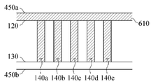
도 1을 참조하면, 유전자 증폭 칩(100)은 기판(110), 기판의 상부면(120), 기판의 하부면(130), 및 관통 홀(140) 어레이를 포함한다. Referring to FIG. 1 , a
기판(110)은 실리콘(Si), 유리(Glass), 고분자(polymer), 금속(metal), 세라믹, 그래파이트(graphite) 등의 무기물, 아크릴계, PET(PolyEthylene Terephtalate), 폴리카보네이트(polycarbonate), 폴리스틸렌(polystylene), 폴리프로필렌(polypropylene) 중 어느 하나로 구성될 수 있으나 이에 제한되는 것은 아니다. 기판의 두께, 즉 기판(110)의 상부면(120)에서부터 하부면(130)까지의 길이는 1mm 이하일 수 있으나, 이에 제한되는 것은 아니고 자유로이 변형이 가능하다.The
관통 홀(140)은 도시된 바와 같이 기판(110)의 상부면(120)에서 하부면(130)방향으로 관통되도록 형성될 수 있다. 관통 홀(140)을 형성할 때, 심도 반응성-이온 에칭(DRIE)을 포함하는 에칭, CMP 공정을 포함하는 시닝이 수행될 수 있다. 관통 홀의 형성방법과 관련하여서는 도 9에서 자세히 설명한다. The through
관통 홀(140)의 부피는 1nL이하일 수 있으며, 관통 홀(140)의 개수는 적어도 2만개 이상일 수 있다. 관통 홀(140)은 원통 또는 육각 기둥일 수 있으나, 이에 제한되지 않고 기타 다각기둥 등 다양한 형태로 형성될 수 있다. 관통 홀(140)의 형태가 육각기둥인 경우, 관통 홀(140)의 단면적의 빗 거리(diagonal distance)는 100μm 이하일 수 있다. 다만 이러한 관통 홀(140)의 개수, 형태, 또는 부피와 같은 특성은 이에 제한되는 것이 아니고, 자유로이 변형이 가능하다.The volume of the through-
관통 홀(140) 내부에서는 유전자 증폭반응이 일어난다. 이때, 각 관통 홀(140)에서 RNA 샘플을 역전사 효소를 이용하여 역전사하는 과정이 수행될 수도 있다. 유전자 증폭반응은 예컨대 PCR(polymerase chain reaction) 증폭 및 등온 증폭 중의 적어도 하나를 포함하는 핵산 증폭 반응, 산화-환원 반응 및 가수분해 반응 등을 포함할 수 있다. 이때 유전자는 RNA(ribonucleic acid), DNA(deoxyribonucleic acid), PNA(peptide nucleic acid), LNA(locked nucleic acid) 중의 하나 또는 둘 이상의 복합체(duplex)등을 포함할 수 있다. 다만, 이에 제한되는 것은 아니다.A gene amplification reaction occurs inside the
유전자 증폭 칩(100)은 광-열 필름(도 2, 220)을 포함할 수 있다. 광-열 필름이 증착된 유전자 증폭 칩(100)의 형태를 도 2를 참조하여 설명한다. The
도 2는 광열 필름이 증착된 유전자 증폭 칩의 측면을 도시한 것이다.2 shows a side view of a gene amplification chip on which a photothermal film is deposited.
도 2를 참조하면, 유전자 증폭 칩은 전술한 기판(110), 기판의 상부면(120), 기판의 하부면(130), 및 관통 홀(140) 어레이 외에, 광-열 필름(220)을 더 포함할 수 있다. 도 2는 기판의 상부면(120), 기판의 하부면(130), 및 관통 홀의 격벽(210)에 광-열 필름(220)이 증착된 상태를 도시하였다. 이때 광-열 필름(220)은 패턴으로 증착될 수 있다. Referring to FIG. 2 , the gene amplification chip includes a light-
도 2에 도시된 바와 달리, 기판의 상부면(120), 기판의 하부면(130), 및 관통 홀의 격벽(210) 중 어느 하나에만 광-열 필름(220)이 증착될 수 있고, 기판의 상부면(120), 및 기판의 하부면(130)에만 광-열 필름(220)이 증착될 수도 있다. 이때, 기판의 상부면(120), 기판의 하부면(130), 및 관통 홀의 격벽(210)에 모두 광-열 필름(220)이 증착된 경우보다, 공정 복잡도 또는 제조비용 측면에서 유리할 수 있다. 2 , the photo-
광-열 필름(220)의 두께는 10μm 이하일 수 있으나 이에 제한되지 않는다. 또한 광-열 필름(220)은 금속층(metal layer)으로 형성될 수 있으나, 이에 제한되지 않고 광-열 필름(220)은 금속을 산화시킨 물질, 준금속, 및 비금속으로 구성될 수도 있다. 예를 들어 광-열 필름(220)은 적외선 흡수능이 우수하여 레이저 조사시 광열변환 효과가 우수한 산화 텅스텐계 물질로 구성될 수도 있다. The thickness of the light-
광-열 필름(220)은 나노 구조로 형성될 수 있다. 예를 들어, 광-열 필름(220)은 지름 50nm 이하, 두께 50nm이하의 나노 입자, 나노 막대(nanorod), 나노 디스크(nanodisc), 또는 나노 섬(nanoisland)으로 형성될 수 있으나, 이에 제한되는 것은 아니고 이외에도 다양한 나노 구조로 형성되는 것이 가능하다.The light-
또한 광-열 필름(220)은 도 2에 도시되지는 않았지만, 카본블랙, 가시광선 염료, 자외선 염료, 적외선 염료, 형광 염료, 방사선 편광 염료, 안료, 금속 화합물, 및 다른 적합한 흡수 재료를 광-열 변환 물질로 추가적으로 포함할 수도 있다. In addition, although not shown in FIG. 2 , the light-to-
광-열 필름(220)은 예컨대 도 4의 광원(460)으로부터 광을 수신하고, 수신된 광을 통해 열을 발생(photonic heating)시킬 수 있다. 이때 광-열 필름(220)이 유전자 증폭 칩(100)의 복수의 위치에 증착 됨으로써, 온도를 균일하게 제어하는 것이 가능하고, 열 발생 효율이 증가한다. The photo-
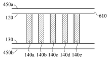
도 3은 다른 실시예에 따른 유전자 증폭 칩을 도시한 것이다.3 shows a gene amplification chip according to another embodiment.
도 3을 참조하면, 유전자 증폭 칩은 기판(110)과 광-열 필름(220) 사이에 배치되어 광-열 필름(220)의 접착력을 향상시키는 접착 막(310)을 더 포함할 수 있다. 접착 막(310)의 성분에는 제한이 없으며, 접착 막(310)에는 접착제가 도포될 수 있다. 또한 접착제를 보호하기 위한 이형지가 부착될 수도 있다. 또한, 접착 막(310)은 광-열 필름(220)과 기판(110) 사이의 접착력을 향상시키는 별도의 구성(미도시)을 추가적으로 포함할 수도 있다.Referring to FIG. 3 , the gene amplification chip may further include an
유전자 증폭 칩(100)은 보조 필름(320)을 더 포함할 수 있다. The
보조 필름(320)은 광-열 필름(220)이 관통 홀 내부에서의 유전자 증폭과정을 방해하는 것을 방지하여, 유전자 증폭과정을 보호할 수 있다. 광-열 필름(220)에 전하가 대전될 경우, 유전자 증폭과정에 사용되는 바이오 물질(미도시)이 광-열 필름(220)쪽으로 당겨질 수 있고, 그에 따라 전체적인 유전자 증폭과정이 저해될 수 있다. 보조 필름(320)은 바이오 물질(미도시)이 광-열 필름(220)의 방향으로 당겨지는 것을 방지하여 유전자 증폭과정을 보호할 수 있다. The
또한 보조 필름(320)은 광-열 필름(220)의 광열효과를 증폭시키기 위한 물질을 포함할 수도 있다. 이때, 보조 필름(320)은 광열 효과를 증폭시키기 위한 다양한 물질을 포함한 복수의 필름이 다층 구조로 적층 형성될 수 있다. 보조 필름(320)은 광-열 필름(220)이 관통 홀 내부에서의 유전자 증폭과정을 저해하지 못하게 함과 동시에, 광열효과를 증폭시킬 수도 있다. In addition, the
보조 필름(320)은 도시된 바와 같이, 광-열 필름(220)을 감싸도록 부착될 수 있으나, 이에 제한되는 것은 아니다. 예를 들어 보조 필름(320)은 기판(110)의 상부면(120), 및/또는 하부면(130)에 배치된 광-열 필름(220)에는 부착되지 않고, 관통 홀(140)의 격벽(210)에 배치된 광-열 필름(220)에만 부착될 수 있다.
보조 필름(320)은, 이산화 규소(SiO2), 이산화 타이타늄(TiO2), 이산화 탄탈(TaO2), SiN, 및 폴리머(polymer) 중 어느 하나로 형성될 수 있으나, 이에 제한됨이 없이 자유로이 변형이 가능하다.The
이때 접착 막(310), 및 보조 필름(320)은 광-열 필름(220)이 기판의 상부면(120)등에 증착된 방식과 마찬가지로 화학적 증기 증착법(CVD), 물리적 기상 증착법(PVD), 원자층 증착법(ALD), 스퍼터링(sputtering), 및 증발 탈수법(evaporation) 등을 이용하여 각각 관통 홀과 광-열 필름(220) 사이 또는 광-열 필름을 감싸도록 배치될 수 있으나, 이에 제한되는 것은 아니다. At this time, the
도 3에는 접착 막(310), 및 보조 필름(320)이 함께 도시되어 있으나, 유전자 증폭 칩(100)은 접착 막(310), 및 보조 필름(320) 중 어느 하나 만을 포함할 수 있다. Although the
도 4는 일 실시예에 따른 유전자 증폭 장치를 도시한 것이다.4 shows a gene amplification apparatus according to an embodiment.
도 4를 참조할 때. 유전자 증폭장치(400)는 본체(410), 용액 주입구(420), 용액 배출구(430), 본체의 일면에 배치되며 용액 주입구(420) 및 용액 배출구(430)와 유관(440a, 440b)을 통해 연결된 챔버(450), 및 챔버(450) 내에 삽입된 유전자 증폭 칩(100)을 포함할 수 있다. 본체(410)는 챔버(450)가 삽입될 수 있는 홈(미도시)을 포함할 수 있다 When referring to FIG. 4 . The gene amplification device 400 is disposed on the
유전자 증폭반응에 이용되는 용액은 용액 주입구(420)를 통해 로딩된다. 이때, 용액은 호흡기 분비물, 혈액, 소변, 땀, 눈물, 침 중의 적어도 하나를 포함하는 체액(bio-fluid), 폐결핵(upper respiratory tract)의 스왑(swab) 샘플, 또는 이러한 체액이나 스왑 샘플 등을 다른 매질에 분산시킨 용액을 포함할 수 있다. 이때, 다른 매질은 물, 식염수, 알코올, 인산 완충 식염수, 바이러스 전달 매체(vital transport media) 등을 포함하며 이에 한정되는 것은 아니다. 이때, 샘플의 부피는 1~ 1000 μL일 수 있으며, 예컨대 20 μL일 수 있다.The solution used for the gene amplification reaction is loaded through the
용액 주입구(420)에서 로딩된 용액은 챔버(450)로 유입되기 전에 전처리 될 수 있다. 예를 들어, 가열, 화학적 처리, 마그네틱 비드(magnet beads)를 이용한 처리, 고상 추출(solid phase extraction), 초음파를 이용한 처리 등의 전처리를 수행할 수 있다. 용액 주입구(420) 내부 또는 외부에 이러한 전처리를 위한 물질이나 구조물(미도시) 등이 형성될 수 있다. The solution loaded from the
또한, 용액 주입구(420)는 전계 효과 트랜지스터(field effect transistor, FET), 실리콘(Si) 포토닉스(photonics) 구조물, 2D 마이크로/나노 소재/구조 등을 포함할 수 있다. 또한, 용액 주입구(420)는 샘플의 온도를 조절하기 위한 광학(optical) 또는 전기적(electrical) 발열 특성을 갖는 구조물을 포함할 수 있다. 예컨대, 용액 주입구(420)는 예컨대 LED(light emitted diode), 레이저(laser), VCSEL(Vertical-cavity surface-emitting laser) 등과 같은 광원에 대하여 반응하는 광학적 발열 소재/구조 또는, 펠티어(peltier) 소자 등의 전기적 발열 소자 등을 포함할 수 있다.In addition, the
유전자 증폭장치(400)는 증폭하고자 하는 유전자 별로 반응물을 포함하고 있는 저장소(미도시)를 더 포함할 수 있다. 이때, 유전자별 반응물은 동결 건조되어 저장소(미도시)에 고정될 수 있다. 이때, 유전자에 대한 반응물은 역전사 효소, 중합 효소, 리가아제(ligase), 페록시다아제(peroxidase), 프라이머(primer) 및 프로브(probe) 등을 포함할 수 있으나 이에 제한되지 않는다. 프라이머는 올리고뉴클레오타이드(oligonucleotide) 예컨대, 대상 특정 단일 가닥 올리고뉴클레오타이드(target specific single strand oligonucleotide)로 구성될 수 있다. 또한, 프로브는 올리고뉴클레오타이드(oligonucleotide) 예컨대, 대상 특정 단일 가닥 올리고뉴클레오타이드(oligonucleotide), 형광 물질 및 활성 감소제(quencher) 등을 포함할 수 있다. 프로브는 여러 다른 종류의 물질들이 용해된 용액 상에서 특정 표적 분자와 상호 작용하여 특징적인 형광 신호를 나타낼 수 있다. 이러한 특징적인 신호는 유전자 증폭장치(400)의 디텍터(470) 및/또는 프로세서(미도시)에 의해 소정 시간 동안 추적, 검출 및 처리되어 유전자 검출에 활용될 수 있다.The gene amplification apparatus 400 may further include a storage (not shown) containing reactants for each gene to be amplified. In this case, the reactants for each gene may be freeze-dried and fixed in a storage (not shown). In this case, the reactant for the gene may include, but is not limited to, a reverse transcriptase, a polymerase, a ligase, a peroxidase, a primer, and a probe. The primer may be composed of an oligonucleotide, for example, a target specific single strand oligonucleotide. In addition, the probe may include an oligonucleotide, such as a target-specific single-stranded oligonucleotide, a fluorescent material, and an activity-reducing agent (quencher). The probe may exhibit a characteristic fluorescence signal by interacting with a specific target molecule in a solution in which different kinds of substances are dissolved. Such characteristic signals may be tracked, detected, and processed for a predetermined time by the detector 470 and/or the processor (not shown) of the gene amplification apparatus 400 to be utilized for gene detection.
도 4에는 용액 주입구(420)가 원형 인 것으로 도시되어 있으나, 용액 주입구(420)의 크기, 형태, 개수 등은 제한 없이 자유로이 변형될 수 있다.Although the
용액 주입구(420)를 통해 로딩된 용액은 유관(440a)을 따라 챔버(450)내로 유입될 수 있다. The solution loaded through the
이때, 유관(440a, 440b)은 용액의 흐름을 제어하는 밸브(미도시)를 포함할 수 있다. 이때 밸브(미도시)는 유관(440a, 440b)을 개폐하는 다양한 방식의 마이크로 밸브 일 수 있다. 예컨대, 공압/열공압식(pneumatic/thermopneumatic actuated), 정전기식(electrostatically actuated), 압전식(piezoelectrically actuated), 전자기식(electromagnetically actuated) 등의 능동형(active microvalve) 밸브, 또는, 인위적인 외부의 동작 없이 시스템이 유체 흐름의 방향이나 계면장력의 차 등에 의하는 개폐하는 수동형(passive microvalve) 방식의 마이크로밸브를 포함할 수 있으며 특별히 제한되지 않는다.In this case, the
유관(440a)은 용액 주입구(420)에 로딩되어 전처리된 샘플에서 미세입자를 차단하고 유체만을 통과시키는 필터(미도시)를 더 포함할 수 있다. 필터(미도시)는 미세 구멍을 갖는 일층 또는 다층의 막 형상의 필터일 수 있으며, 구멍의 크기에 따라 원하는 크기의 미세입자를 차단할 수 있다. 필터(미도시)는 예컨대, 실리콘(Silicon), PVDF(polyvinylidene fluoride), 폴리에테르술폰(Polyethersulfone), 폴리카보네이트(Polycarbonate), 유리섬유(Glass Fiber), 폴리프로필렌(Polypropylene), 셀룰로스(Cellulose), 혼합 셀룰로스 에스테르(Mixed cellulose esters), PTFE(Polytetrafluoroethylene), 폴리에틸렌 테레프타레이트(Polyethylene Terephthalate), PVC(Polyvinyl chloride), 나일론(Nylon), 포스포셀룰로스(Phosphocellulose), DEAE(Diethylaminoethyl cellulose) 등의 재료로 제조될 수 있으나 이에 제한되지 않는다. 구멍의 모양은 예컨대 원형, 사각형, 슬릿 형상, 글래스 파이버에 의한 불규칙한 형상 등 다양한 모양일 수 있다. The
도 4에는 유관(440a, 440b)이 직선의 형태로 챔버(450)의 좌우에 각각 하나씩 도시되어 있으나, 이에 제한되지 않는다. 예를 들어, 유관(440a, 440b)은 직선의 형태가 아닌 다양한 곡선의 형태일 수 있으며, 복수의 채널(미도시)을 포함할 수도 있다.In FIG. 4 , each of the
용액 주입구(420)를 통해 로딩된 용액은 모세관 현상에 의해 유관(440a)을 따라 챔버(450)내로 유입될 수 있다. 다만 이와 달리, 유전자 증폭장치(400)는 능동/수동 구동 장치, 전기습윤(electro-wetting) 등 용액을 이동시키기 위한 구조물(미도시)을 더 포함할 수 있다. 이때, 능동(active)/수동(passive) 구동 장치는 수동 진공 펌프(passive vacuum void pump), 시린지 펌프(syringe pump), 진공 펌프(vacuum pump), 공기 펌프(pneumatic pump) 등을 포함할 수 있으나 이에 제한되는 것은 아니다.The solution loaded through the
챔버(450)는 상부면 및 하부면을 포함하고, 상부면 및 하부면 사이에 유전자 증폭 칩(100)이 삽입될 수 있다. 이하 도 5를 통해 유전자 증폭 칩(100)이 챔버(450)내에 삽입된 형태를 살펴본다. The
도 5는 도 4의 챔버의 측면을 도시한 것이다. 상부면(450a), 및 하부면(450b) 사이에 유전자 증폭 칩(100)이 삽입되어 있다. 이때, 상부면(450a), 및 하부면(450b)은 유리(glass) 층일 수 있으나, 이에 제한되지 않고 다양한 성분으로 구성될 수 있다. Figure 5 shows a side view of the chamber of Figure 4; The
설명의 편의를 위해 도 5에는 도시하지 않았으나, 도 2에서 설명한 바와 같이 유전자 증폭 칩(100)의 상부면(120), 하부면(130), 및 관통 홀(140)의 격벽(210)에는 광-열 필름(220)이 증착될 수 있고, 도 3에서 설명한 바와 같은 접착 막(310), 및/또는 보조 필름(320)이 증착될 수도 있다.Although not shown in FIG. 5 for convenience of explanation, as described in FIG. 2 , the
도 6a 내지 6e를 통해 챔버(450)내로 용액이 유입되는 과정을 설명한다. 도 6a 내지 6e는 용액이 관통 홀에 주입되는 과정을 도시한 것이다.A process of introducing a solution into the
용액 주입구를 통해 로딩된 용액이 유관(440a)을 따라 챔버 내로 유입되면, 용액은 챔버의 상부면(450a)과 유전자 증폭 칩의 상부면(120) 사이의 통로(610)를 따라 이동하게 된다. When the solution loaded through the solution inlet flows into the chamber along the
통로(610)에 유입된 용액은 모세관 현상에 의하여 각 관통 홀(140a, 140b, 140c, 140d, 140e)에 주입될 수 있다. 도 6a는 통로(610)에 용액이 유입되어, 첫번째 관통 홀(140a)에 용액이 주입된 상태로 도시되어 있다. 그후 시간이 지남에 따라 모세관 현상에 의해 두번째 관통홀(140b), 세번째 관통홀(140c), 네번째 관통 홀(140d), 다섯번째 관통 홀(140e)에 용액이 차례대로 주입되고, 도 6b 내지 6e에 이러한 과정이 도시되어 있다.The solution introduced into the
또는 이와 달리, 유전자 증폭장치(400)은 통로(610)에 유입된 용액이 각 관통 홀(140a, 140b, 140c, 140d, 140e)로 주입될 수 있도록, 슬라이딩(sliding), 원심분리(centrifuge) 또는 스탬핑(stamping) 등을 수행하기 위한 기기(미도시)를 포함할 수도 있다. Alternatively, the gene amplification device 400 slides, centrifuges, so that the solution introduced into the
각 관통 홀(140a, 140b, 140c, 140d, 140e)에 용액이 모두 주입되고 나면, 통로(610)에 남아있는 용액은 용액 배출구로 배출 될 수 있다. 도 6f 내지 6k는 관통홀의 내부를 제외한 챔버 내에 남아있는 용액을 용액 배출구로 배출시키는 과정을 도시한 것이다. After all the solutions are injected into each of the through
각 관통 홀(140a, 140b, 140c, 140d, 140e)에 주입되고 나면 챔버(450)내부는 도 6e와 같은 상태가 된다. 이때, 통로(610)에 남아있는 용액이 제거되는 과정이 도 6f 내지 6k에 도시되어 있다. After being injected into each of the through
일 예로, 유전자 증폭장치(400)는 용액이 각 관통 홀(140a, 140b, 140c, 140d, 140e)에 주입되고 난 후, 관통홀의 내부를 제외한 챔버 내, 예컨대 통로(610)에 남아있는 용액을 용액 배출구로 배출시키는 커팅부(도 7, 730)를 더 포함할 수 있다. 이때 커팅부(도 7, 730)는 오일(oil), 또는 공기(air)를 이용하여 통로(610)에 남아있는 용액을 유관(440b)을 통해 용액 배출구(430)로 배출 시킬 수 있다. 또는 이와 달리, 용액 배출구(430)에 포함될 수 있는 흡수패드(미도시)에 의한 모세관 현상을 통해 통로(610)의 용액이 배출될 수도 있다. As an example, the gene amplification device 400 removes the solution remaining in the chamber except for the inside of the through-hole, for example, in the
통로(610)에 남아있는 용액이 배출되어도 각 관통 홀(140a, 140b, 140c, 140d, 140e)에 주입된 용액은 모세관 현상에 의해 관통 홀(140a, 140b, 140c, 140d, 140e)외부로 이탈되지 않는다. 이때, 통로(610)에 남아있는 용액이 배출됨으로써, 각 관통 홀(140a, 140b, 140c, 140d, 140e)은 더 이상 용액으로 연결되지 않기 때문에 디지털 PCR의 구현이 가능하고, 그에 따라 유전자 증폭의 민감도와 정확도가 향상될 수 있다. Even when the solution remaining in the
다시 도 4를 참조하면, 챔버(450)의 통로(610)에 남아있던 용액은 유관(440b)을 따라 용액 배출구(430)로 배출된다. Referring back to FIG. 4 , the solution remaining in the
이때 용액 배출구(430)는 흡수패드(미도시)를 포함할 수 있다. 흡수패드(미도시)는 모세관 현상을 이용하여 용액의 이동 및 드레인(drain)을 수행할 수 있다. 흡수패드(미도시)를 포함함으로써 용액의 이송 속도를 용이하게 제어할 수 있다. 다만, 이에 제한되지 않으며 흡수패드(미도시)의 위치, 크기 및 종류를 다르게 함으로서 챔버(450)을 통과하는 용액의 유속과 유량을 제어할 수 있고, 일례로서 효소 반응시에는 샘플을 느리게 이동시키고, 세척시에는 빠르게 이동시켜서 반응감도를 향상시킬 수 있다.In this case, the
도 7은 일 실시예에 따른 유전자 증폭장치의 블록도이다.7 is a block diagram of a gene amplification apparatus according to an embodiment.
유전자 증폭장치(700)는 유전자 증폭 칩(100), 광학부(710), 프로세서(720), 및 커팅부(730)를 포함할 수 있다. The
유전자 증폭 칩(100)은 관통 홀(140)을 포함하며, 관통 홀(140)내부에서 유전자 증폭반응이 발생한다. 유전자 증폭 칩(100)에 대해서는 위에서 상세히 설명한 바와 같으므로 여기서는 생략한다. The
광학부(710)는 유전자 증폭 칩(100)의 각 관통 홀(140) 내부에서 유전자 증폭 반응이 수행되는 동안 광학적 신호를 측정한다. 이때, 광학적 신호는 형광, 인광, 흡광, 표면 플라즈몬 공명 등을 포함한다. 광학부(710)는 광원(711), 및 디텍터(712)를 포함할 수 있다.The
광원(711)은 유전자 증폭 칩(100)의 광-열 필름(220)에 광을 조사할 수 있다. 광원은 LED, 레이저(laser), VCSEL(Vertical-cavity surface-emitting laser) 등을 포함할 수 있으나 이에 한정되지 않는다. 또한 광원(711)이 조사하는 광은 다양한 영역대의 파장을 포함할 수 있다. 예컨대 광원(711)은 자외선(UV) 내지 적외선(IR) 영역대의 파장을 갖는 광을 조사할 수 있으나, 이에 제한되는 것은 아니다. The
디텍터(712)는 증폭된 타겟 유전자로부터 방출된 광학적 신호를 검출할 수 있다. 디텍터(712)는 광전자 증폭관(photomultiplier tube), 포토 디텍터(photo detector), 광전자증 폭관(photomultiplier tube) 어레이, 포토 디텍터(photo detector) 어레이, CMOS 이미지 센서(complementary metal-oxide semiconductor) 등을 포함할 수 있으나 이에 제한되지 않는다. The
이때, 디텍터(712)는 증폭된 유전자로부터 방출된 형광을 검출할 때, 광-열 필름의 형광 반사를 이용할 수 있다. 예를 들어, 유전자 증폭 칩(100)의 관통 홀의 격벽에 반사도가 높은 구성물질로 이루어진 광-열 필름이 증착되는 경우, 광-열 필름은 관통 홀 내부에서 증폭된 유전자로부터 방출된 형광을 디텍터 방향으로 반사시킬 수 있다. 이때 디텍터(712)는 광-열 필름으로부터 반사된 형광을 검출할 수 있다. In this case, the
또한, 광학부(710)는 특정 파장을 통과시키기 위한 필터, 타겟 유전자 로부터 방출되는 형광을 검출기 방향으로 향하도록 조절하는 미러(mirror), 타겟 유전자로부터 방출되는 형광을 집광하는 렌즈(lens) 등을 더 포함할 수 있다.In addition, the
유전자 증폭 칩(100)의 각 관통 홀(140)에서 유전자 증폭 반응이 수행되는 동안, 유전자 증폭장치(700)의 광원(711), 디텍터(712) 및/또는 프로세서(720)에 의해 광학적 신호가 측정되며, 측정된 광학적 신호를 기초로 증폭된 유전자가 검출될 수 있다. 이때, 광학적 신호는 형광, 인광, 흡광, 표면 플라즈몬 공명 등을 포함할 수 있다. 이와 같이 유전자 증폭장치(700)는 중합 효소의 복제 과정 중에 표적 DNA 주형의 유무 및 정량 정보 등을 감지하는데 활용될 수 있다.While the gene amplification reaction is performed in each through
프로세서(720)는 광학부(710)와 전기적으로 연결될 수 있으며 디텍터(712) 로부터 광학적 신호를 수신하여 광학적 신호를 분석할 수 있다. 예를 들어, 프로세서(720)는 검출기에 의해 검출된 디지털 핵산 증폭 결과를 푸아송 분포(Poisson distribution)를 기반으로 유전자의 정량을 분석할 수 있다.The
프로세서(720)는 광원 제어부(721)를 포함할 수 있다. The
광원 제어부(721)는 광원(711)의 구동 여부, 및 구동 조건 등을 제어할 수 있다. 이때 광원 제어부(721)는 온 오프 방식으로 구동시켜 광-열 필름을 가열 및 냉각 시킬 수 있다. 광-열 필름이 가열 및 냉각됨에 따라 서머 사이클링(thermal cycling)이 발생하고, 그에 따라 타켓 유전자가 증폭될 수 있다. 또한 광원 제어부(721)는 광원(711)의 광의 종류, 파장, 전류세기, 지속 시간, 온 오프 의 간격 중 적어도 하나를 제어할 수 있다. The light
프로세서(720)는 전처리부(722), 및/또는 온도 제어부(723)를 더 포함할 수 있다. The
전처리부(722)는 예컨대 용액 주입구에 로딩된 샘플을 가열하거나, 화학적 처리, 마그네틱 비드(magnet beads)를 이용한 처리, 고상 추출(solid phase extraction), 초음파를 이용한 처리 등의 전처리를 수행할 수 있다. 이를 위해, 전처리부(722)는 용액 주입구 내부 및/또는 외부에 배치된 마그네틱 비드, 초음파 장치, 광학적/전기적 가열 장치 등의 전처리를 위한 다양한 물질이나 구조물 등을 포함할 수 있으며, 이러한 물질이나 구조물 등을 제어할 수 있다. 전처리부(722)의 적어도 일부 기능은 프로세서(720)에 통합될 수 있다. The
온도 제어부(723)는 용액 주입구, 또는 도 4의 유관(440a)에 존재하는 용액의 온도를 조절할 수 있다. 예를 들어, 온도 제어부(723)는 용액 주입구에 용액이 로딩되면 샘플의 온도가 95![]()
![]()
온도 제어부(723)는 유전자 증폭장치(700)의 용액 주입구, 또는 유관의 내부 또는 외부에 온도를 조절하기 위한 물질이나 구조물을 포함할 수 있다. 예를 들어, 용액 주입구, 또는 유관의 내부에 용액의 전기적인 가열을 위한 전기적 가열부(미도시)가 형성될 수 있다. 전기적 가열부는 예컨대 발열 소자 및/또는 펠티에 소자 등을 포함할 수 있다. 또한, 온도 제어부(723)는 유전자 증폭장치(700) 내부 또는 외부에 배치되어 용액 주입구, 또는 유관에 존재하는 용액의 온도를 측정하는 온도 센서를 포함할 수 있다. 이때, 온도 센서는 온도의존성 전동기력(EMF)을 생성하는 바이메탈 접합을 갖는 서모커플, 온도 비례의 전기 저항을 갖는 재료를 포함하는 저항성 서모미터, 서미스터(thermistors), IC 온도센서, IR 온도센서, IR 카메라, 콰르츠(quartz) 서모미터 등을 사용할 수 있다.The
커팅부(730)는 도 6f 내지 6k에서 설명한 바와 같이, 관통 홀 각각에 용액이 주입된 후, 관통홀의 내부를 제외한 챔버 내에 남아있는 용액을 용액 배출구로 배출시킬 수 있다. 이때 챔버 내 공간 중, 관통 홀의 내부를 제외한 곳은 도 6a 내지 6k의 통로(도 6, 610)일 수 있다.As described with reference to FIGS. 6F to 6K , after the solution is injected into each of the through-holes, the
이때, 커팅부(730)는 용액 배출시, 오일(oil), 또는 공기(air)를 이용하여 통로(도 6, 610)에 남아있는 용액을 유관을 통해 용액 배출구로 배출 시킬 수 있다. 이때, 통로(도 6, 610)에 남아있는 용액이 배출됨으로써, 각 관통 홀은 더 이상 용액으로 연결되지 않기 때문에 디지털 PCR의 구현이 가능하고, 그에 따라 유전자 증폭의 민감도와 정확도가 향상될 수 있다At this time, the
도 8은 다른 실시예에 따른 유전자 증폭장치의 블록도이다. 도 8을 참조하면, 본 실시예의 유전자 증폭장치(800)는 도 7의 실시예의 유전자 증폭장치(700)의 구성에 저장부(810), 출력부(820), 및 통신부(830)를 더 포함할 수 있다. 8 is a block diagram of a gene amplification apparatus according to another embodiment. Referring to FIG. 8 , the
저장부(810)는 예를 들어 유전자 증폭을 위한 각종 기준 정보 및/또는 유전자 증폭결과 등을 출력할 수 있다. 저장부(810)는 플래시 메모리 타입(flash memory type), 하드 디스크 타입(hard disk type), 멀티미디어 카드 마이크로 타입(multimedia card micro type), 카드 타입의 메모리(예컨대, SD 또는 XD 메모리 등), 램(Random Access Memory, RAM), SRAM(Static Random Access Memory), 롬(Read Only Memory, ROM), EEPROM(Electrically Erasable Programmable Read Only Memory), PROM(Programmable Read Only Memory), 자기 메모리, 자기 디스크, 광디스크 등 적어도 하나의 타입의 저장매체를 포함할 수 있다. The
출력부(820)는 예를 들어 유전자 증폭 과정, 유전자 증폭, 분석 결과등을 출력할 수 있다. 출력부(820)는 시각적 출력 모듈(예: 디스플레이), 음성 출력 모듈(예: 스피커), 햅틱 모듈 등을 이용하여 시각적, 청각적 및 촉각적 방법 등으로 사용자에게 정보를 제공할 수 있다. The
통신부(830)는 외부 장치와 통신을 수행할 수 있다. 예컨대, 통신부(830)는 유전자 증폭장치(700, 800)에서 생성된 데이터, 예컨대 유전자 검출 결과 등을 외부 장치로 전송할 수 있으며, 외부 장치로부터 유전자 검출에 필요한 데이터를 수신할 수 있다. 이때, 외부 장치는 의료 장비, 결과물을 출력하기 위한 프린트 또는 디스플레이 장치일 수 있다. 이외에도 외부 장치는 디지털 TV, 데스크탑 컴퓨터, 휴대폰, 스마트 폰, 태블릿, 노트북, PDA(Personal Digital Assistants), PMP(Portable Multimedia Player), 네비게이션, MP3 플레이어, 디지털 카메라, 웨어러블 디바이스 등일 수 있으나, 이에 제한되지 않는다.The
통신부(830)는 블루투스(bluetooth) 통신, BLE(Bluetooth Low Energy) 통신, 근거리 무선 통신(Near Field Communication, NFC), WLAN 통신, 지그비(Zigbee) 통신, 적외선(Infrared Data Association, IrDA) 통신, WFD(Wi-Fi Direct) 통신, UWB(ultra-wideband) 통신, Ant+ 통신, WIFI 통신, RFID(Radio Frequency Identification) 통신, 3G 통신, 4G 통신 및 5G 통신 등을 이용하여 외부 장치와 통신할 수 있다. 그러나, 이는 일 예에 불과할 뿐이며, 이에 한정되는 것은 아니다.
도 9는 일 실시예에 따른 도 1의 유전자 증폭 칩(100)의 제조방법의 흐름도이다. 기판(도 1, 110)상에 관통 홀(도 1, 140) 형성하고, 광-열 필름(도 2, 220)을 증착하는 과정을 도 9를 참조하여 설명한다.9 is a flowchart of a method of manufacturing the
우선, 기판의 상부면에서 하부면 방향으로 관통 홀이 형성되도록 에칭(Etching)할 수 있다(910). 이때 상부면 에서부터 에칭하여 하부면으로 관통홀이 형성될 수 있다. 에칭의 구체적인 방식으로는 심도 반응성-이온 에칭(DRIE) 또는 반응성-이온 에칭(RIE)이 이용될 수 있다. 다만 이에 제한되지 않고 에칭의 종류와 방식은 다양하게 변형될 수 있다. 예를 들어 (Wet) 에칭, 드라이(dry) 에칭, 및 가스(gas) 에칭을 이용할 수 있다.First, etching may be performed to form a through hole in a direction from the upper surface of the substrate to the lower surface ( 910 ). At this time, a through hole may be formed from the upper surface to the lower surface by etching. As a specific method of etching, deep reactive-ion etching (DRIE) or reactive-ion etching (RIE) may be used. However, it is not limited thereto, and the type and method of etching may be variously modified. For example, wet etching, dry etching, and gas etching can be used.
다음, 기판의 하부면을 평탄화시키는 시닝(Thining)을 수행할 수 있다(920). 이때 시닝은 CMP공정을 포함할 수 있으며, CMP공정의 평탄도, 균일성, 및 연마속도 등은 자유로이 정의될 수 있다. 다만, 시닝은 CMP공정에 제한되지 않고 그라인딩(Grinding), 및 기타 폴리싱(Polishing) 이 이용될 수도 있다. Next, thinning for planarizing the lower surface of the substrate may be performed ( 920 ). In this case, the thinning may include a CMP process, and the flatness, uniformity, and polishing rate of the CMP process may be freely defined. However, the thinning is not limited to the CMP process, and grinding and other polishing may be used.
다음, 위 단계(910), 및 단계(920)을 거쳐 관통 홀이 형성되면, 기판의 상부면 및 하부면 중 적어도 어느 하나의 면에 광-열 필름을 증착할 수 있다(930). 이때, 광-열 필름을 관통 홀의 격벽에 더 증착시키는 단계를 포함할 수도 있다. 또한, 광-열 필름은 패턴으로 증착될 수 있다. Next, when the through hole is formed through the
광-열 필름의 구체적인 증착 방식으로는 화학적 증기 증착법(CVD), 물리적 기상 증착법(PVD), 원자층 증착법(ALD), 스퍼터링(sputtering), 및 증발 탈수법(evaporation) 등이 사용될 수 있으나, 이에 제한되지 않는다. As a specific deposition method of the light-thermal film, chemical vapor deposition (CVD), physical vapor deposition (PVD), atomic layer deposition (ALD), sputtering, and evaporation, etc. may be used, but in this not limited
한편, 본 실시 예들은 컴퓨터로 읽을 수 있는 기록 매체에 컴퓨터가 읽을 수 있는 코드로 구현하는 것이 가능하다. 컴퓨터가 읽을 수 있는 기록 매체는 컴퓨터 시스템에 의하여 읽혀질 수 있는 데이터가 저장되는 모든 종류의 기록 장치를 포함한다.Meanwhile, the present embodiments can be implemented as computer-readable codes on a computer-readable recording medium. The computer-readable recording medium includes all types of recording devices in which data readable by a computer system is stored.
컴퓨터가 읽을 수 있는 기록 매체의 예로는 ROM, RAM, CD-ROM, 자기 테이프, 플로피디스크, 광 데이터 저장장치 등이 있으며, 또한 캐리어 웨이브(예를 들어 인터넷을 통한 전송)의 형태로 구현하는 것을 포함한다. 또한, 컴퓨터가 읽을 수 있는 기록 매체는 네트워크로 연결된 컴퓨터 시스템에 분산되어, 분산 방식으로 컴퓨터가 읽을 수 있는 코드가 저장되고 실행될 수 있다. 그리고 본 실시예들을 구현하기 위한 기능적인(functional) 프로그램, 코드 및 코드 세그먼트들은 본 발명이 속하는 기술 분야의 프로그래머들에 의하여 용이하게 추론될 수 있다.Examples of computer-readable recording media include ROM, RAM, CD-ROM, magnetic tape, floppy disk, optical data storage, etc. include In addition, the computer-readable recording medium may be distributed in a network-connected computer system, and the computer-readable code may be stored and executed in a distributed manner. In addition, functional programs, codes, and code segments for implementing the present embodiments can be easily inferred by programmers in the technical field to which the present invention pertains.
본 개시가 속하는 기술분야의 통상의 지식을 가진 자는 개시된 기술적 사상이나 필수적인 특징을 변경하지 않고서 다른 구체적인 형태로 실시될 수 있다는 것을 이해할 수 있을 것이다. 그러므로 이상에서 기술한 실시예들은 모든 면에서 예시적인 것이며 한정적이 아닌 것으로 이해해야만 한다.Those of ordinary skill in the art to which the present disclosure pertains will understand that the disclosed technical spirit or essential features may be embodied in other specific forms without changing. Therefore, it should be understood that the embodiments described above are illustrative in all respects and not restrictive.
100: 유전자 증폭 칩
110: 기판
140: 관통 홀
220: 광-열 필름
400, 700, 800: 유전자 증폭장치
450: 챔버
710: 광학부
711: 광원
712: 디텍터
720: 프로세서
721: 광원 제어부
722: 전처리부
723: 온도 제어부
730: 커팅부
810: 저장부
820: 출력부
830: 통신부 100: gene amplification chip
110: substrate 140: through hole
220: light-
450: chamber 710: optics
711: light source 712: detector
720: processor 721: light source control unit
722: pre-processing unit 723: temperature control unit 730: cutting unit 810: storage unit
820: output unit 830: communication unit
Claims (22)
상기 기판의 상부면에서 하부면 방향으로 관통되도록 형성되고, 내부에서 유전자 증폭반응이 발생하는 관통 홀을 포함하는 관통 홀 어레이; 및
상기 기판의 상부면 및 하부면 중 적어도 하나의 면에 증착되며, 광을 이용해 열을 발생시키는 광-열 필름을 포함하는 유전자 증폭 칩.
Board;
a through-hole array formed so as to penetrate from the upper surface of the substrate toward the lower surface, the through-hole array including through-holes in which a gene amplification reaction occurs; and
and a light-thermal film deposited on at least one of the upper and lower surfaces of the substrate and generating heat using light.
상기 기판은,
실리콘(Si), 유리(Glass), 고분자(polymer), 및 금속(metal) 중 어느 하나로 구성되는 유전자 증폭 칩.
2. The method of claim 1
The substrate is
A gene amplification chip composed of any one of silicon (Si), glass, polymer, and metal.
상기 기판의 두께는 1mm 이하인 유전자 증폭 칩.
The method of claim 1,
The thickness of the substrate is less than 1mm gene amplification chip.
상기 관통 홀 각각의 부피는 1nL 이하인 유전자 증폭 칩.
The method of claim 1,
The volume of each of the through holes is 1 nL or less of the gene amplification chip.
상기 관통 홀의 개수는 적어도 2만개 이상인 유전자 증폭 칩.
The method of claim 1,
The number of the through-holes is at least 20,000 or more gene amplification chip.
상기 관통 홀의 형태는,
원통, 또는 다각기둥인 유전자 증폭 칩.
The method of claim 1,
The shape of the through hole is
Cylindrical or polygonal gene amplification chip.
상기 관통 홀의 형태가 육각기둥 인 경우,
상기 관통 홀의 단면적의 빗 거리(diagonal distance)는 100μm 이하인 유전자 증폭 칩.
7. The method of claim 6,
When the shape of the through hole is a hexagonal column,
A gene amplification chip, wherein a diagonal distance of the cross-sectional area of the through hole is 100 μm or less.
상기 광-열 필름의 두께는 10μm 이하인 유전자 증폭 칩.
The method of claim 1,
The thickness of the light-thermal film is 10 μm or less gene amplification chip.
상기 광-열 필름은,
상기 관통 홀 각각의 격벽에 더 증착된 유전자 증폭 칩.
The method of claim 1,
The light-thermal film,
A gene amplification chip further deposited on the barrier ribs of each of the through holes.
상기 광-열 필름은,
금속층(metal layer)으로 형성되는 유전자 증폭 칩.
The method of claim 1,
The light-thermal film,
A gene amplification chip formed of a metal layer.
상기 광-열 필름은,
나노 입자, 나노 막대, 나노 디스크, 및 나노 섬 중 적어도 어느 하나로 형성되는 유전자 증폭 칩.
The method of claim 1,
The light-thermal film,
A gene amplification chip formed of at least one of nanoparticles, nanorods, nanodiscs, and nanoislands.
상기 광-열 필름에 부착되는 보조 필름을 더 포함하는 유전자 증폭 칩.
The method of claim 1,
The gene amplification chip further comprising an auxiliary film attached to the light-thermal film.
상기 보조 필름은,
이산화 규소(SiO2), 이산화 타이타늄(TiO2), 이산화 탄탈(TaO2), SiN, 및 폴리머(polymer) 중 어느 하나로 형성되는 유전자 증폭 칩.
13. The method of claim 12,
The auxiliary film is
A gene amplification chip formed of any one of silicon dioxide (SiO2), titanium dioxide (TiO2), tantalum dioxide (TaO2), SiN, and a polymer.
상기 기판과 상기 광-열 필름 사이에 배치되어 광-열 필름의 접착력을 향상시키는 접착 막을 더 포함하는 유전자 증폭 칩.
The method of claim 1,
The gene amplification chip further comprising an adhesive film disposed between the substrate and the light-thermal film to improve adhesion of the light-thermal film.
유전자 증폭 칩;
상기 본체의 일면에 배치되며, 유전자 증폭 칩이 삽입되도록 형성되고, 용액 주입구 및 용액 배출구와 유관을 통해 연결된 챔버;
유전자 증폭 칩에 광을 조사하는 광원; 및
증폭된 유전자로부터 방출된 형광을 검출하는 디텍터를 포함하되,
상기 유전자 증폭 칩은,
기판;
상기 기판의 상부면에서 하부면 방향으로 관통되도록 형성되고, 내부에서 유전자 증폭반응이 발생하는 관통 홀을 포함하는 관통 홀 어레이; 및
상기 기판의 상부면 및 하부면 중 적어도 하나의 면에 증착되며, 광을 이용해 열을 발생시키는 광-열 필름을 포함하는 유전자 증폭장치.
main body;
gene amplification chip;
a chamber disposed on one surface of the main body, formed so that a gene amplification chip is inserted, and connected to a solution inlet and a solution outlet through a pipe;
a light source irradiating light to the gene amplification chip; and
A detector for detecting fluorescence emitted from the amplified gene,
The gene amplification chip,
Board;
a through-hole array formed so as to penetrate from the upper surface of the substrate toward the lower surface, the through-hole array including through-holes in which a gene amplification reaction occurs; and
and a light-thermal film deposited on at least one of the upper and lower surfaces of the substrate and generating heat using light.
상기 챔버는,
상부면 및 하부면을 포함하고,
상기 유전자 증폭 칩은,
상기 상부면 및 하부면 사이에 삽입되는 유전자 증폭장치.
16. The method of claim 15,
The chamber is
comprising an upper surface and a lower surface;
The gene amplification chip,
A gene amplification device inserted between the upper and lower surfaces.
상기 용액 주입구를 통해 용액이 로딩되어 상기 유관을 따라 챔버 내로 유입되면, 상기 용액은 모세관 현상에 의하여 상기 관통 홀 내부로 주입되는 유전자 증폭장치.
16. The method of claim 15,
When a solution is loaded through the solution inlet and introduced into the chamber along the duct, the solution is injected into the through hole by capillary action.
상기 용액 주입구를 통해 로딩된 용액이 상기 관통 홀 내부로 주입된 후, 상기 관통홀의 내부를 제외한 챔버 내에 남아있는 용액을 용액 배출구로 배출시키는 커팅부를 더 포함하는 유전자 증폭장치.
16. The method of claim 15,
After the solution loaded through the solution inlet is injected into the through hole, the gene amplification apparatus further comprising a cutting unit for discharging the solution remaining in the chamber except for the inside of the through hole to the solution outlet.
광원을 온 오프 방식으로 구동시켜 상기 광-열 필름을 가열 및 냉각 시키는 광원 제어부를 더 포함하는 유전자 증폭장치.
16. The method of claim 15,
Gene amplification apparatus further comprising a light source control unit for heating and cooling the light-thermal film by driving the light source in an on-off manner.
상기 광-열 필름은,
관통홀 내부에서 증폭된 유전자로부터 방출된 형광을 상기 디텍터 방향으로 반사시키는 유전자 증폭장치.
16. The method of claim 15,
The light-thermal film,
A gene amplification device for reflecting fluorescence emitted from the gene amplified inside the through hole in the direction of the detector.
상기 기판의 하부면을 평탄화시키는, CMP공정을 포함하는 시닝(Thinning) 단계;
상기 기판의 상부면 및 하부면 중 적어도 어느 하나의 면에 광-열 필름을 증착시키는 단계를 포함하는 유전자 증폭 칩 제조방법.
etching the substrate to form a through hole in a direction from the upper surface of the substrate to the lower surface;
a thinning step including a CMP process for planarizing the lower surface of the substrate;
and depositing a light-thermal film on at least one of an upper surface and a lower surface of the substrate.
상기 광-열 필름을 관통 홀 각각의 격벽에 증착시키는 단계를 더 포함하는 유전자 증폭 칩 제조방법
22. The method of claim 21,
Gene amplification chip manufacturing method further comprising the step of depositing the light-thermal film on each barrier rib of the through hole
Priority Applications (2)
| Application Number | Priority Date | Filing Date | Title |
|---|---|---|---|
| KR1020210037923A KR20220132855A (en) | 2021-03-24 | 2021-03-24 | Gene amplification chip, apparatus for gene amplification, and method for manufacturing gene amplification chip |
| US17/356,126 US20220307068A1 (en) | 2021-03-24 | 2021-06-23 | Gene amplification chip, apparatus for gene amplification, and method of manufacturing gene amplification chip |
Applications Claiming Priority (1)
| Application Number | Priority Date | Filing Date | Title |
|---|---|---|---|
| KR1020210037923A KR20220132855A (en) | 2021-03-24 | 2021-03-24 | Gene amplification chip, apparatus for gene amplification, and method for manufacturing gene amplification chip |
Publications (1)
| Publication Number | Publication Date |
|---|---|
| KR20220132855A true KR20220132855A (en) | 2022-10-04 |
Family
ID=83363050
Family Applications (1)
| Application Number | Title | Priority Date | Filing Date |
|---|---|---|---|
| KR1020210037923A KR20220132855A (en) | 2021-03-24 | 2021-03-24 | Gene amplification chip, apparatus for gene amplification, and method for manufacturing gene amplification chip |
Country Status (2)
| Country | Link |
|---|---|
| US (1) | US20220307068A1 (en) |
| KR (1) | KR20220132855A (en) |
Families Citing this family (1)
| Publication number | Priority date | Publication date | Assignee | Title |
|---|---|---|---|---|
| WO2024065665A1 (en) * | 2022-09-30 | 2024-04-04 | 深圳华大智造科技股份有限公司 | Gene sequencing chip, slide and processing method therefor, and gene sequencing method |
Family Cites Families (6)
| Publication number | Priority date | Publication date | Assignee | Title |
|---|---|---|---|---|
| US20100261159A1 (en) * | 2000-10-10 | 2010-10-14 | Robert Hess | Apparatus for assay, synthesis and storage, and methods of manufacture, use, and manipulation thereof |
| US20060094108A1 (en) * | 2002-12-20 | 2006-05-04 | Karl Yoder | Thermal cycler for microfluidic array assays |
| US8470164B2 (en) * | 2008-06-25 | 2013-06-25 | Life Technologies Corporation | Methods and apparatus for measuring analytes using large scale FET arrays |
| WO2016115542A1 (en) * | 2015-01-16 | 2016-07-21 | The Regents Of The University Of California | Led driven plasmonic heating apparatus for nucleic acids amplification |
| WO2017019768A1 (en) * | 2015-07-30 | 2017-02-02 | The Regents Of The University Of California | Optical cavity pcr |
| KR20210006337A (en) * | 2018-03-15 | 2021-01-18 | 크립토스 바이오테크놀로지스, 인코포레이티드 | Methods and systems for performing heat assisted biochemical reactions |
-
2021
- 2021-03-24 KR KR1020210037923A patent/KR20220132855A/en active Search and Examination
- 2021-06-23 US US17/356,126 patent/US20220307068A1/en active Pending
Also Published As
| Publication number | Publication date |
|---|---|
| US20220307068A1 (en) | 2022-09-29 |
Similar Documents
| Publication | Publication Date | Title |
|---|---|---|
| US20220186325A1 (en) | Systems for sample analysis | |
| US11396015B2 (en) | Implementing barriers for controlled environments during sample processing and detection | |
| TWI683106B (en) | Methods of forming a sensor apparatus for a microfluidic device | |
| US20170029871A1 (en) | Microfluidic device | |
| US10406528B1 (en) | Non-contact temperature control system for microfluidic devices | |
| US20200276582A1 (en) | Methods and systems for automated sample processing | |
| CN111542394A (en) | Quantum plasma resonance energy transfer and ultrafast photon PCR | |
| KR20220132855A (en) | Gene amplification chip, apparatus for gene amplification, and method for manufacturing gene amplification chip | |
| KR20220002071A (en) | Microfluidic chip, apparatus and method for detecting biomolecule | |
| WO2019118343A2 (en) | Portable devices and methods for analyzing samples | |
| US10981174B1 (en) | Protein and nucleic acid detection for microfluidic devices | |
| CA3131142A1 (en) | Multi-function analytic devices | |
| US20230044621A1 (en) | Apparatus and method for gene amplification | |
| US20230145041A1 (en) | Apparatus and method for gene amplification | |
| KR20230021541A (en) | Apparatus and method for gene amplification | |
| US20230381772A1 (en) | Gene amplification chip, apparatus for gene amplification, and apparatus for bio-particle analysis | |
| EP3932556A1 (en) | Microfluidic chip, and apparatus and method for detecting biomolecules | |
| US20240091767A1 (en) | Gene amplification chip, apparatus for gene amplification, and apparatus for bio-particle analysis | |
| US20230302447A1 (en) | Apparatus and method for bio-particle detection | |
| Mohammadyousef et al. | Ultrafast VCSEL-based plasmonic polymerase chain reaction with real-time label-free amplicon detection for point-of-care diagnostics | |
| Hung et al. | Laser-induced heating integrated with a microfluidic platform for real-time DNA replication and detection | |
| US20230285977A1 (en) | Nucleic acid amplification device, nucleic acid amplification method, and sample solution position control method | |
| Spotts | Development of Scalable Optical Architectures for Microelectromechanical Systems | |
| WO2022250685A1 (en) | Fluorescence detection via light guide | |
| Lien | Microfluidic-photonic integration for on-chip flow cytometry |
Legal Events
| Date | Code | Title | Description |
|---|---|---|---|
| A201 | Request for examination |