KR20220131245A - Light emitting device including capping layer and manufacturing method thereof - Google Patents
Light emitting device including capping layer and manufacturing method thereof Download PDFInfo
- Publication number
- KR20220131245A KR20220131245A KR1020227025610A KR20227025610A KR20220131245A KR 20220131245 A KR20220131245 A KR 20220131245A KR 1020227025610 A KR1020227025610 A KR 1020227025610A KR 20227025610 A KR20227025610 A KR 20227025610A KR 20220131245 A KR20220131245 A KR 20220131245A
- Authority
- KR
- South Korea
- Prior art keywords
- wavelength
- cpl
- limiting examples
- optoelectronic device
- electrode
- Prior art date
Links
- 238000004519 manufacturing process Methods 0.000 title description 32
- 239000000463 material Substances 0.000 claims abstract description 522
- 238000001228 spectrum Methods 0.000 claims abstract description 96
- 238000010521 absorption reaction Methods 0.000 claims abstract description 75
- 238000000576 coating method Methods 0.000 claims description 1092
- 239000011248 coating agent Substances 0.000 claims description 1038
- 239000011777 magnesium Substances 0.000 claims description 173
- 229910052751 metal Inorganic materials 0.000 claims description 144
- 239000002184 metal Substances 0.000 claims description 131
- 238000000034 method Methods 0.000 claims description 126
- 230000008033 biological extinction Effects 0.000 claims description 108
- 230000005693 optoelectronics Effects 0.000 claims description 99
- 229910052709 silver Inorganic materials 0.000 claims description 94
- 239000004065 semiconductor Substances 0.000 claims description 92
- 229910052749 magnesium Inorganic materials 0.000 claims description 73
- 229910045601 alloy Inorganic materials 0.000 claims description 62
- 239000000956 alloy Substances 0.000 claims description 62
- 230000006911 nucleation Effects 0.000 claims description 61
- 238000010899 nucleation Methods 0.000 claims description 61
- 239000000203 mixture Substances 0.000 claims description 50
- 239000010949 copper Substances 0.000 claims description 48
- 239000011135 tin Substances 0.000 claims description 35
- 229910052769 Ytterbium Inorganic materials 0.000 claims description 34
- 239000010931 gold Substances 0.000 claims description 33
- 238000000059 patterning Methods 0.000 claims description 33
- PXHVJJICTQNCMI-UHFFFAOYSA-N Nickel Chemical compound [Ni] PXHVJJICTQNCMI-UHFFFAOYSA-N 0.000 claims description 28
- KDLHZDBZIXYQEI-UHFFFAOYSA-N Palladium Chemical compound [Pd] KDLHZDBZIXYQEI-UHFFFAOYSA-N 0.000 claims description 28
- BASFCYQUMIYNBI-UHFFFAOYSA-N platinum Chemical compound [Pt] BASFCYQUMIYNBI-UHFFFAOYSA-N 0.000 claims description 28
- 229910052802 copper Inorganic materials 0.000 claims description 27
- 230000002401 inhibitory effect Effects 0.000 claims description 25
- 150000004706 metal oxides Chemical class 0.000 claims description 25
- 229910044991 metal oxide Inorganic materials 0.000 claims description 24
- BQCADISMDOOEFD-UHFFFAOYSA-N Silver Chemical compound [Ag] BQCADISMDOOEFD-UHFFFAOYSA-N 0.000 claims description 23
- 239000004332 silver Substances 0.000 claims description 23
- 229910052718 tin Inorganic materials 0.000 claims description 23
- 239000011651 chromium Substances 0.000 claims description 22
- 239000010955 niobium Substances 0.000 claims description 22
- 239000010936 titanium Substances 0.000 claims description 22
- 229910052782 aluminium Inorganic materials 0.000 claims description 21
- XLOMVQKBTHCTTD-UHFFFAOYSA-N Zinc monoxide Chemical compound [Zn]=O XLOMVQKBTHCTTD-UHFFFAOYSA-N 0.000 claims description 20
- 229910052737 gold Inorganic materials 0.000 claims description 20
- 238000001429 visible spectrum Methods 0.000 claims description 20
- 229910052750 molybdenum Inorganic materials 0.000 claims description 17
- XEEYBQQBJWHFJM-UHFFFAOYSA-N Iron Chemical compound [Fe] XEEYBQQBJWHFJM-UHFFFAOYSA-N 0.000 claims description 16
- 229910052793 cadmium Inorganic materials 0.000 claims description 16
- 229910052804 chromium Inorganic materials 0.000 claims description 16
- 229910052741 iridium Inorganic materials 0.000 claims description 16
- 229910052759 nickel Inorganic materials 0.000 claims description 16
- 229910052758 niobium Inorganic materials 0.000 claims description 16
- 229910052760 oxygen Inorganic materials 0.000 claims description 16
- 229910052763 palladium Inorganic materials 0.000 claims description 16
- 229910052697 platinum Inorganic materials 0.000 claims description 16
- 239000011734 sodium Substances 0.000 claims description 16
- 229910052719 titanium Inorganic materials 0.000 claims description 16
- FYYHWMGAXLPEAU-UHFFFAOYSA-N Magnesium Chemical compound [Mg] FYYHWMGAXLPEAU-UHFFFAOYSA-N 0.000 claims description 15
- 239000011701 zinc Substances 0.000 claims description 15
- 229910052744 lithium Inorganic materials 0.000 claims description 14
- 229910052715 tantalum Inorganic materials 0.000 claims description 14
- 238000010494 dissociation reaction Methods 0.000 claims description 13
- 230000005593 dissociations Effects 0.000 claims description 13
- 239000010944 silver (metal) Substances 0.000 claims description 13
- IJGRMHOSHXDMSA-UHFFFAOYSA-N Atomic nitrogen Chemical compound N#N IJGRMHOSHXDMSA-UHFFFAOYSA-N 0.000 claims description 12
- ATJFFYVFTNAWJD-UHFFFAOYSA-N Tin Chemical compound [Sn] ATJFFYVFTNAWJD-UHFFFAOYSA-N 0.000 claims description 12
- 229910052799 carbon Inorganic materials 0.000 claims description 12
- XAGFODPZIPBFFR-UHFFFAOYSA-N aluminium Chemical compound [Al] XAGFODPZIPBFFR-UHFFFAOYSA-N 0.000 claims description 11
- QVGXLLKOCUKJST-UHFFFAOYSA-N atomic oxygen Chemical compound [O] QVGXLLKOCUKJST-UHFFFAOYSA-N 0.000 claims description 11
- 239000001301 oxygen Substances 0.000 claims description 11
- 229910052725 zinc Inorganic materials 0.000 claims description 11
- OKTJSMMVPCPJKN-UHFFFAOYSA-N Carbon Chemical compound [C] OKTJSMMVPCPJKN-UHFFFAOYSA-N 0.000 claims description 10
- 229910052742 iron Inorganic materials 0.000 claims description 10
- 229910052762 osmium Inorganic materials 0.000 claims description 10
- 229910052700 potassium Inorganic materials 0.000 claims description 10
- 229910052708 sodium Inorganic materials 0.000 claims description 10
- 229910052721 tungsten Inorganic materials 0.000 claims description 10
- 229910052720 vanadium Inorganic materials 0.000 claims description 10
- 229910052726 zirconium Inorganic materials 0.000 claims description 10
- RYGMFSIKBFXOCR-UHFFFAOYSA-N Copper Chemical compound [Cu] RYGMFSIKBFXOCR-UHFFFAOYSA-N 0.000 claims description 9
- GYHNNYVSQQEPJS-UHFFFAOYSA-N Gallium Chemical compound [Ga] GYHNNYVSQQEPJS-UHFFFAOYSA-N 0.000 claims description 9
- 229910052733 gallium Inorganic materials 0.000 claims description 9
- 229910052738 indium Inorganic materials 0.000 claims description 9
- APFVFJFRJDLVQX-UHFFFAOYSA-N indium atom Chemical compound [In] APFVFJFRJDLVQX-UHFFFAOYSA-N 0.000 claims description 9
- JBQYATWDVHIOAR-UHFFFAOYSA-N tellanylidenegermanium Chemical compound [Te]=[Ge] JBQYATWDVHIOAR-UHFFFAOYSA-N 0.000 claims description 9
- NAWDYIZEMPQZHO-UHFFFAOYSA-N ytterbium Chemical compound [Yb] NAWDYIZEMPQZHO-UHFFFAOYSA-N 0.000 claims description 9
- 239000011787 zinc oxide Substances 0.000 claims description 9
- PCHJSUWPFVWCPO-UHFFFAOYSA-N gold Chemical compound [Au] PCHJSUWPFVWCPO-UHFFFAOYSA-N 0.000 claims description 8
- ZOKXTWBITQBERF-UHFFFAOYSA-N Molybdenum Chemical compound [Mo] ZOKXTWBITQBERF-UHFFFAOYSA-N 0.000 claims description 7
- 229910052788 barium Inorganic materials 0.000 claims description 7
- DSAJWYNOEDNPEQ-UHFFFAOYSA-N barium atom Chemical compound [Ba] DSAJWYNOEDNPEQ-UHFFFAOYSA-N 0.000 claims description 7
- BDOSMKKIYDKNTQ-UHFFFAOYSA-N cadmium atom Chemical compound [Cd] BDOSMKKIYDKNTQ-UHFFFAOYSA-N 0.000 claims description 7
- 239000011733 molybdenum Substances 0.000 claims description 7
- VYZAMTAEIAYCRO-UHFFFAOYSA-N Chromium Chemical compound [Cr] VYZAMTAEIAYCRO-UHFFFAOYSA-N 0.000 claims description 6
- DGAQECJNVWCQMB-PUAWFVPOSA-M Ilexoside XXIX Chemical compound C[C@@H]1CC[C@@]2(CC[C@@]3(C(=CC[C@H]4[C@]3(CC[C@@H]5[C@@]4(CC[C@@H](C5(C)C)OS(=O)(=O)[O-])C)C)[C@@H]2[C@]1(C)O)C)C(=O)O[C@H]6[C@@H]([C@H]([C@@H]([C@H](O6)CO)O)O)O.[Na+] DGAQECJNVWCQMB-PUAWFVPOSA-M 0.000 claims description 6
- WHXSMMKQMYFTQS-UHFFFAOYSA-N Lithium Chemical compound [Li] WHXSMMKQMYFTQS-UHFFFAOYSA-N 0.000 claims description 6
- ZLMJMSJWJFRBEC-UHFFFAOYSA-N Potassium Chemical compound [K] ZLMJMSJWJFRBEC-UHFFFAOYSA-N 0.000 claims description 6
- NINIDFKCEFEMDL-UHFFFAOYSA-N Sulfur Chemical compound [S] NINIDFKCEFEMDL-UHFFFAOYSA-N 0.000 claims description 6
- RTAQQCXQSZGOHL-UHFFFAOYSA-N Titanium Chemical compound [Ti] RTAQQCXQSZGOHL-UHFFFAOYSA-N 0.000 claims description 6
- 229910052792 caesium Inorganic materials 0.000 claims description 6
- TVFDJXOCXUVLDH-UHFFFAOYSA-N caesium atom Chemical compound [Cs] TVFDJXOCXUVLDH-UHFFFAOYSA-N 0.000 claims description 6
- 229910017052 cobalt Inorganic materials 0.000 claims description 6
- 239000010941 cobalt Substances 0.000 claims description 6
- GUTLYIVDDKVIGB-UHFFFAOYSA-N cobalt atom Chemical compound [Co] GUTLYIVDDKVIGB-UHFFFAOYSA-N 0.000 claims description 6
- GKOZUEZYRPOHIO-UHFFFAOYSA-N iridium atom Chemical compound [Ir] GKOZUEZYRPOHIO-UHFFFAOYSA-N 0.000 claims description 6
- GUCVJGMIXFAOAE-UHFFFAOYSA-N niobium atom Chemical compound [Nb] GUCVJGMIXFAOAE-UHFFFAOYSA-N 0.000 claims description 6
- 229910052757 nitrogen Inorganic materials 0.000 claims description 6
- SYQBFIAQOQZEGI-UHFFFAOYSA-N osmium atom Chemical compound [Os] SYQBFIAQOQZEGI-UHFFFAOYSA-N 0.000 claims description 6
- 239000011591 potassium Substances 0.000 claims description 6
- VSZWPYCFIRKVQL-UHFFFAOYSA-N selanylidenegallium;selenium Chemical compound [Se].[Se]=[Ga].[Se]=[Ga] VSZWPYCFIRKVQL-UHFFFAOYSA-N 0.000 claims description 6
- 229910052717 sulfur Inorganic materials 0.000 claims description 6
- 239000011593 sulfur Substances 0.000 claims description 6
- GUVRBAGPIYLISA-UHFFFAOYSA-N tantalum atom Chemical compound [Ta] GUVRBAGPIYLISA-UHFFFAOYSA-N 0.000 claims description 6
- WFKWXMTUELFFGS-UHFFFAOYSA-N tungsten Chemical compound [W] WFKWXMTUELFFGS-UHFFFAOYSA-N 0.000 claims description 6
- 239000010937 tungsten Substances 0.000 claims description 6
- LEONUFNNVUYDNQ-UHFFFAOYSA-N vanadium atom Chemical compound [V] LEONUFNNVUYDNQ-UHFFFAOYSA-N 0.000 claims description 6
- YVTHLONGBIQYBO-UHFFFAOYSA-N zinc indium(3+) oxygen(2-) Chemical compound [O--].[Zn++].[In+3] YVTHLONGBIQYBO-UHFFFAOYSA-N 0.000 claims description 5
- 229910052787 antimony Inorganic materials 0.000 claims description 4
- WATWJIUSRGPENY-UHFFFAOYSA-N antimony atom Chemical compound [Sb] WATWJIUSRGPENY-UHFFFAOYSA-N 0.000 claims description 4
- BDVZHDCXCXJPSO-UHFFFAOYSA-N indium(3+) oxygen(2-) titanium(4+) Chemical compound [O-2].[Ti+4].[In+3] BDVZHDCXCXJPSO-UHFFFAOYSA-N 0.000 claims description 4
- SJCKRGFTWFGHGZ-UHFFFAOYSA-N magnesium silver Chemical compound [Mg].[Ag] SJCKRGFTWFGHGZ-UHFFFAOYSA-N 0.000 claims description 4
- 229910052755 nonmetal Inorganic materials 0.000 claims description 4
- 229910052727 yttrium Inorganic materials 0.000 claims description 3
- VWQVUPCCIRVNHF-UHFFFAOYSA-N yttrium atom Chemical compound [Y] VWQVUPCCIRVNHF-UHFFFAOYSA-N 0.000 claims description 3
- 230000000670 limiting effect Effects 0.000 description 1405
- 239000010410 layer Substances 0.000 description 648
- 238000000151 deposition Methods 0.000 description 243
- 230000008021 deposition Effects 0.000 description 171
- 239000000758 substrate Substances 0.000 description 144
- 239000010408 film Substances 0.000 description 74
- 230000003287 optical effect Effects 0.000 description 74
- 230000008569 process Effects 0.000 description 65
- 239000010409 thin film Substances 0.000 description 62
- 238000005137 deposition process Methods 0.000 description 61
- 238000010586 diagram Methods 0.000 description 58
- 238000000295 emission spectrum Methods 0.000 description 42
- 125000004429 atom Chemical group 0.000 description 35
- 239000007772 electrode material Substances 0.000 description 35
- 230000004888 barrier function Effects 0.000 description 32
- 230000000694 effects Effects 0.000 description 28
- 239000000178 monomer Substances 0.000 description 26
- 230000007246 mechanism Effects 0.000 description 25
- 238000007639 printing Methods 0.000 description 24
- 238000001704 evaporation Methods 0.000 description 22
- 230000008020 evaporation Effects 0.000 description 21
- 230000004907 flux Effects 0.000 description 20
- 150000002739 metals Chemical class 0.000 description 20
- 230000015572 biosynthetic process Effects 0.000 description 19
- 239000011368 organic material Substances 0.000 description 19
- 238000002834 transmittance Methods 0.000 description 19
- 230000002093 peripheral effect Effects 0.000 description 18
- 230000001737 promoting effect Effects 0.000 description 17
- 239000003463 adsorbent Substances 0.000 description 16
- 239000002585 base Substances 0.000 description 15
- -1 but not limited to Substances 0.000 description 15
- 238000001152 differential interference contrast microscopy Methods 0.000 description 15
- 230000002829 reductive effect Effects 0.000 description 15
- 239000012808 vapor phase Substances 0.000 description 15
- XMWRBQBLMFGWIX-UHFFFAOYSA-N C60 fullerene Chemical class C12=C3C(C4=C56)=C7C8=C5C5=C9C%10=C6C6=C4C1=C1C4=C6C6=C%10C%10=C9C9=C%11C5=C8C5=C8C7=C3C3=C7C2=C1C1=C2C4=C6C4=C%10C6=C9C9=C%11C5=C5C8=C3C3=C7C1=C1C2=C4C6=C2C9=C5C3=C12 XMWRBQBLMFGWIX-UHFFFAOYSA-N 0.000 description 13
- 229910003472 fullerene Inorganic materials 0.000 description 13
- 230000008859 change Effects 0.000 description 11
- 239000002356 single layer Substances 0.000 description 11
- 230000006870 function Effects 0.000 description 10
- 229910010272 inorganic material Inorganic materials 0.000 description 10
- 229920000740 poly(D-lysine) polymer Polymers 0.000 description 10
- 229920001621 AMOLED Polymers 0.000 description 9
- 229910001316 Ag alloy Inorganic materials 0.000 description 9
- 230000005540 biological transmission Effects 0.000 description 9
- 239000004020 conductor Substances 0.000 description 9
- 230000001965 increasing effect Effects 0.000 description 9
- 239000011147 inorganic material Substances 0.000 description 9
- 238000005240 physical vapour deposition Methods 0.000 description 9
- 238000000623 plasma-assisted chemical vapour deposition Methods 0.000 description 9
- 229910000821 Yb alloy Inorganic materials 0.000 description 8
- 230000004913 activation Effects 0.000 description 8
- 230000007423 decrease Effects 0.000 description 8
- 238000009792 diffusion process Methods 0.000 description 8
- 238000004680 force modulation microscopy Methods 0.000 description 8
- 238000002347 injection Methods 0.000 description 8
- 239000007924 injection Substances 0.000 description 8
- 238000000206 photolithography Methods 0.000 description 8
- 238000013459 approach Methods 0.000 description 7
- 238000000231 atomic layer deposition Methods 0.000 description 7
- 239000003990 capacitor Substances 0.000 description 7
- 238000003795 desorption Methods 0.000 description 7
- 238000003618 dip coating Methods 0.000 description 7
- 238000005566 electron beam evaporation Methods 0.000 description 7
- 230000001747 exhibiting effect Effects 0.000 description 7
- 238000005224 laser annealing Methods 0.000 description 7
- 238000004528 spin coating Methods 0.000 description 7
- 238000005507 spraying Methods 0.000 description 7
- 238000004544 sputter deposition Methods 0.000 description 7
- 238000002207 thermal evaporation Methods 0.000 description 7
- 238000010023 transfer printing Methods 0.000 description 7
- 230000006399 behavior Effects 0.000 description 6
- XJHCXCQVJFPJIK-UHFFFAOYSA-M caesium fluoride Chemical compound [F-].[Cs+] XJHCXCQVJFPJIK-UHFFFAOYSA-M 0.000 description 6
- 210000005155 neural progenitor cell Anatomy 0.000 description 6
- 229920002120 photoresistant polymer Polymers 0.000 description 6
- 229910002056 binary alloy Inorganic materials 0.000 description 5
- 150000001875 compounds Chemical class 0.000 description 5
- 238000005538 encapsulation Methods 0.000 description 5
- 239000011521 glass Substances 0.000 description 5
- 229910001092 metal group alloy Inorganic materials 0.000 description 5
- 239000007769 metal material Substances 0.000 description 5
- 239000002096 quantum dot Substances 0.000 description 5
- 238000003860 storage Methods 0.000 description 5
- 238000011282 treatment Methods 0.000 description 5
- 238000007740 vapor deposition Methods 0.000 description 5
- 229910052784 alkaline earth metal Inorganic materials 0.000 description 4
- 150000001342 alkaline earth metals Chemical class 0.000 description 4
- 230000008901 benefit Effects 0.000 description 4
- 239000003086 colorant Substances 0.000 description 4
- 239000000356 contaminant Substances 0.000 description 4
- 229910003460 diamond Inorganic materials 0.000 description 4
- 239000010432 diamond Substances 0.000 description 4
- 238000005516 engineering process Methods 0.000 description 4
- 238000004020 luminiscence type Methods 0.000 description 4
- 238000000926 separation method Methods 0.000 description 4
- 239000000126 substance Substances 0.000 description 4
- 229910000861 Mg alloy Inorganic materials 0.000 description 3
- 238000002835 absorbance Methods 0.000 description 3
- 229910052783 alkali metal Inorganic materials 0.000 description 3
- 150000001340 alkali metals Chemical class 0.000 description 3
- 230000015556 catabolic process Effects 0.000 description 3
- 230000007547 defect Effects 0.000 description 3
- 238000006731 degradation reaction Methods 0.000 description 3
- 238000013461 design Methods 0.000 description 3
- 238000009826 distribution Methods 0.000 description 3
- 125000000524 functional group Chemical group 0.000 description 3
- 238000010438 heat treatment Methods 0.000 description 3
- 239000012535 impurity Substances 0.000 description 3
- 239000011229 interlayer Substances 0.000 description 3
- 230000004048 modification Effects 0.000 description 3
- 238000012986 modification Methods 0.000 description 3
- 238000013086 organic photovoltaic Methods 0.000 description 3
- 229920000620 organic polymer Polymers 0.000 description 3
- 229920000642 polymer Polymers 0.000 description 3
- 230000006798 recombination Effects 0.000 description 3
- 238000005215 recombination Methods 0.000 description 3
- 238000000859 sublimation Methods 0.000 description 3
- 229910001111 Fine metal Inorganic materials 0.000 description 2
- OAICVXFJPJFONN-UHFFFAOYSA-N Phosphorus Chemical compound [P] OAICVXFJPJFONN-UHFFFAOYSA-N 0.000 description 2
- 238000000862 absorption spectrum Methods 0.000 description 2
- 239000000853 adhesive Substances 0.000 description 2
- 230000001070 adhesive effect Effects 0.000 description 2
- 230000002411 adverse Effects 0.000 description 2
- 229910021417 amorphous silicon Inorganic materials 0.000 description 2
- 229910000410 antimony oxide Inorganic materials 0.000 description 2
- 238000004630 atomic force microscopy Methods 0.000 description 2
- 230000000903 blocking effect Effects 0.000 description 2
- 239000011575 calcium Substances 0.000 description 2
- 125000004432 carbon atom Chemical group C* 0.000 description 2
- 238000005229 chemical vapour deposition Methods 0.000 description 2
- 238000004140 cleaning Methods 0.000 description 2
- 238000003776 cleavage reaction Methods 0.000 description 2
- 238000004581 coalescence Methods 0.000 description 2
- 239000000306 component Substances 0.000 description 2
- 239000000470 constituent Substances 0.000 description 2
- 238000011109 contamination Methods 0.000 description 2
- 239000013078 crystal Substances 0.000 description 2
- 230000003247 decreasing effect Effects 0.000 description 2
- 210000001787 dendrite Anatomy 0.000 description 2
- AJNVQOSZGJRYEI-UHFFFAOYSA-N digallium;oxygen(2-) Chemical compound [O-2].[O-2].[O-2].[Ga+3].[Ga+3] AJNVQOSZGJRYEI-UHFFFAOYSA-N 0.000 description 2
- 229910001195 gallium oxide Inorganic materials 0.000 description 2
- 239000007789 gas Substances 0.000 description 2
- 238000004770 highest occupied molecular orbital Methods 0.000 description 2
- 230000005525 hole transport Effects 0.000 description 2
- 229910003437 indium oxide Inorganic materials 0.000 description 2
- PJXISJQVUVHSOJ-UHFFFAOYSA-N indium(iii) oxide Chemical compound [O-2].[O-2].[O-2].[In+3].[In+3] PJXISJQVUVHSOJ-UHFFFAOYSA-N 0.000 description 2
- 230000005764 inhibitory process Effects 0.000 description 2
- 230000003993 interaction Effects 0.000 description 2
- 238000004768 lowest unoccupied molecular orbital Methods 0.000 description 2
- 230000000873 masking effect Effects 0.000 description 2
- 239000011159 matrix material Substances 0.000 description 2
- VTRUBDSFZJNXHI-UHFFFAOYSA-N oxoantimony Chemical compound [Sb]=O VTRUBDSFZJNXHI-UHFFFAOYSA-N 0.000 description 2
- 230000036961 partial effect Effects 0.000 description 2
- 239000012071 phase Substances 0.000 description 2
- 229910052698 phosphorus Inorganic materials 0.000 description 2
- 239000011574 phosphorus Substances 0.000 description 2
- 238000012545 processing Methods 0.000 description 2
- 230000007017 scission Effects 0.000 description 2
- 150000003384 small molecules Chemical class 0.000 description 2
- 239000007787 solid Substances 0.000 description 2
- 239000002904 solvent Substances 0.000 description 2
- 238000001179 sorption measurement Methods 0.000 description 2
- 230000003595 spectral effect Effects 0.000 description 2
- 230000008022 sublimation Effects 0.000 description 2
- 238000006467 substitution reaction Methods 0.000 description 2
- 239000013589 supplement Substances 0.000 description 2
- XOLBLPGZBRYERU-UHFFFAOYSA-N tin dioxide Chemical compound O=[Sn]=O XOLBLPGZBRYERU-UHFFFAOYSA-N 0.000 description 2
- 229910001887 tin oxide Inorganic materials 0.000 description 2
- 238000012876 topography Methods 0.000 description 2
- 239000012780 transparent material Substances 0.000 description 2
- 229910014033 C-OH Inorganic materials 0.000 description 1
- OYPRJOBELJOOCE-UHFFFAOYSA-N Calcium Chemical compound [Ca] OYPRJOBELJOOCE-UHFFFAOYSA-N 0.000 description 1
- 229910014570 C—OH Inorganic materials 0.000 description 1
- 208000012868 Overgrowth Diseases 0.000 description 1
- CBENFWSGALASAD-UHFFFAOYSA-N Ozone Chemical compound [O-][O+]=O CBENFWSGALASAD-UHFFFAOYSA-N 0.000 description 1
- 239000004642 Polyimide Substances 0.000 description 1
- XUIMIQQOPSSXEZ-UHFFFAOYSA-N Silicon Chemical compound [Si] XUIMIQQOPSSXEZ-UHFFFAOYSA-N 0.000 description 1
- 229910052771 Terbium Inorganic materials 0.000 description 1
- NPNMHHNXCILFEF-UHFFFAOYSA-N [F].[Sn]=O Chemical compound [F].[Sn]=O NPNMHHNXCILFEF-UHFFFAOYSA-N 0.000 description 1
- 230000002745 absorbent Effects 0.000 description 1
- 239000002250 absorbent Substances 0.000 description 1
- 238000007792 addition Methods 0.000 description 1
- 230000004075 alteration Effects 0.000 description 1
- 239000006117 anti-reflective coating Substances 0.000 description 1
- 230000002238 attenuated effect Effects 0.000 description 1
- 229910052791 calcium Inorganic materials 0.000 description 1
- 210000004027 cell Anatomy 0.000 description 1
- 239000002800 charge carrier Substances 0.000 description 1
- 238000006243 chemical reaction Methods 0.000 description 1
- 210000001072 colon Anatomy 0.000 description 1
- 230000008878 coupling Effects 0.000 description 1
- 238000010168 coupling process Methods 0.000 description 1
- 238000005859 coupling reaction Methods 0.000 description 1
- 239000002178 crystalline material Substances 0.000 description 1
- 230000003111 delayed effect Effects 0.000 description 1
- 239000002274 desiccant Substances 0.000 description 1
- 230000006866 deterioration Effects 0.000 description 1
- 238000005553 drilling Methods 0.000 description 1
- 230000005611 electricity Effects 0.000 description 1
- 238000001194 electroluminescence spectrum Methods 0.000 description 1
- 230000005670 electromagnetic radiation Effects 0.000 description 1
- 238000010894 electron beam technology Methods 0.000 description 1
- 238000000572 ellipsometry Methods 0.000 description 1
- 230000002708 enhancing effect Effects 0.000 description 1
- 238000009501 film coating Methods 0.000 description 1
- 238000009408 flooring Methods 0.000 description 1
- 150000004673 fluoride salts Chemical class 0.000 description 1
- 239000011888 foil Substances 0.000 description 1
- 239000012634 fragment Substances 0.000 description 1
- 229910052736 halogen Inorganic materials 0.000 description 1
- 150000002367 halogens Chemical group 0.000 description 1
- 125000005842 heteroatom Chemical group 0.000 description 1
- 238000003384 imaging method Methods 0.000 description 1
- AMGQUBHHOARCQH-UHFFFAOYSA-N indium;oxotin Chemical compound [In].[Sn]=O AMGQUBHHOARCQH-UHFFFAOYSA-N 0.000 description 1
- 230000006698 induction Effects 0.000 description 1
- 230000000977 initiatory effect Effects 0.000 description 1
- 238000007641 inkjet printing Methods 0.000 description 1
- 150000002484 inorganic compounds Chemical class 0.000 description 1
- 229910052500 inorganic mineral Inorganic materials 0.000 description 1
- 238000003780 insertion Methods 0.000 description 1
- 230000037431 insertion Effects 0.000 description 1
- 239000011810 insulating material Substances 0.000 description 1
- 230000002452 interceptive effect Effects 0.000 description 1
- 238000011835 investigation Methods 0.000 description 1
- 238000010030 laminating Methods 0.000 description 1
- ORUIBWPALBXDOA-UHFFFAOYSA-L magnesium fluoride Chemical compound [F-].[F-].[Mg+2] ORUIBWPALBXDOA-UHFFFAOYSA-L 0.000 description 1
- 238000005259 measurement Methods 0.000 description 1
- 238000001465 metallisation Methods 0.000 description 1
- 230000003278 mimic effect Effects 0.000 description 1
- 239000011707 mineral Substances 0.000 description 1
- 239000002052 molecular layer Substances 0.000 description 1
- 239000002048 multi walled nanotube Substances 0.000 description 1
- QJGQUHMNIGDVPM-UHFFFAOYSA-N nitrogen group Chemical group [N] QJGQUHMNIGDVPM-UHFFFAOYSA-N 0.000 description 1
- 239000012044 organic layer Substances 0.000 description 1
- 125000002524 organometallic group Chemical group 0.000 description 1
- 238000005192 partition Methods 0.000 description 1
- 229910021420 polycrystalline silicon Inorganic materials 0.000 description 1
- 229920001721 polyimide Polymers 0.000 description 1
- 229920001296 polysiloxane Polymers 0.000 description 1
- 229910001848 post-transition metal Inorganic materials 0.000 description 1
- 230000001681 protective effect Effects 0.000 description 1
- 239000010453 quartz Substances 0.000 description 1
- 230000005855 radiation Effects 0.000 description 1
- 239000012925 reference material Substances 0.000 description 1
- 230000002441 reversible effect Effects 0.000 description 1
- 229910052594 sapphire Inorganic materials 0.000 description 1
- 239000010980 sapphire Substances 0.000 description 1
- 238000004626 scanning electron microscopy Methods 0.000 description 1
- 229910052710 silicon Inorganic materials 0.000 description 1
- 239000010703 silicon Substances 0.000 description 1
- VYPSYNLAJGMNEJ-UHFFFAOYSA-N silicon dioxide Inorganic materials O=[Si]=O VYPSYNLAJGMNEJ-UHFFFAOYSA-N 0.000 description 1
- 239000002109 single walled nanotube Substances 0.000 description 1
- 238000010129 solution processing Methods 0.000 description 1
- 238000001931 thermography Methods 0.000 description 1
- 238000012546 transfer Methods 0.000 description 1
- 230000007704 transition Effects 0.000 description 1
- 229910052723 transition metal Inorganic materials 0.000 description 1
- 229910021561 transition metal fluoride Inorganic materials 0.000 description 1
- 229910000314 transition metal oxide Inorganic materials 0.000 description 1
- 150000003624 transition metals Chemical class 0.000 description 1
- 238000004627 transmission electron microscopy Methods 0.000 description 1
- 238000005019 vapor deposition process Methods 0.000 description 1
- 238000005406 washing Methods 0.000 description 1
- XASAPYQVQBKMIN-UHFFFAOYSA-K ytterbium(iii) fluoride Chemical compound F[Yb](F)F XASAPYQVQBKMIN-UHFFFAOYSA-K 0.000 description 1
Images


Classifications
-
- H—ELECTRICITY
- H10—SEMICONDUCTOR DEVICES; ELECTRIC SOLID-STATE DEVICES NOT OTHERWISE PROVIDED FOR
- H10K—ORGANIC ELECTRIC SOLID-STATE DEVICES
- H10K50/00—Organic light-emitting devices
- H10K50/10—OLEDs or polymer light-emitting diodes [PLED]
- H10K50/11—OLEDs or polymer light-emitting diodes [PLED] characterised by the electroluminescent [EL] layers
- H10K50/125—OLEDs or polymer light-emitting diodes [PLED] characterised by the electroluminescent [EL] layers specially adapted for multicolour light emission, e.g. for emitting white light
- H10K50/13—OLEDs or polymer light-emitting diodes [PLED] characterised by the electroluminescent [EL] layers specially adapted for multicolour light emission, e.g. for emitting white light comprising stacked EL layers within one EL unit
-
- H01L51/5253—
-
- H—ELECTRICITY
- H10—SEMICONDUCTOR DEVICES; ELECTRIC SOLID-STATE DEVICES NOT OTHERWISE PROVIDED FOR
- H10K—ORGANIC ELECTRIC SOLID-STATE DEVICES
- H10K50/00—Organic light-emitting devices
- H10K50/80—Constructional details
- H10K50/84—Passivation; Containers; Encapsulations
- H10K50/844—Encapsulations
-
- H—ELECTRICITY
- H01—ELECTRIC ELEMENTS
- H01L—SEMICONDUCTOR DEVICES NOT COVERED BY CLASS H10
- H01L33/00—Semiconductor devices with at least one potential-jump barrier or surface barrier specially adapted for light emission; Processes or apparatus specially adapted for the manufacture or treatment thereof or of parts thereof; Details thereof
- H01L33/44—Semiconductor devices with at least one potential-jump barrier or surface barrier specially adapted for light emission; Processes or apparatus specially adapted for the manufacture or treatment thereof or of parts thereof; Details thereof characterised by the coatings, e.g. passivation layer or anti-reflective coating
-
- H01L27/3211—
-
- H—ELECTRICITY
- H01—ELECTRIC ELEMENTS
- H01L—SEMICONDUCTOR DEVICES NOT COVERED BY CLASS H10
- H01L33/00—Semiconductor devices with at least one potential-jump barrier or surface barrier specially adapted for light emission; Processes or apparatus specially adapted for the manufacture or treatment thereof or of parts thereof; Details thereof
- H01L33/48—Semiconductor devices with at least one potential-jump barrier or surface barrier specially adapted for light emission; Processes or apparatus specially adapted for the manufacture or treatment thereof or of parts thereof; Details thereof characterised by the semiconductor body packages
- H01L33/58—Optical field-shaping elements
-
- H01L51/5203—
-
- H—ELECTRICITY
- H10—SEMICONDUCTOR DEVICES; ELECTRIC SOLID-STATE DEVICES NOT OTHERWISE PROVIDED FOR
- H10K—ORGANIC ELECTRIC SOLID-STATE DEVICES
- H10K50/00—Organic light-emitting devices
- H10K50/80—Constructional details
- H10K50/805—Electrodes
-
- H—ELECTRICITY
- H10—SEMICONDUCTOR DEVICES; ELECTRIC SOLID-STATE DEVICES NOT OTHERWISE PROVIDED FOR
- H10K—ORGANIC ELECTRIC SOLID-STATE DEVICES
- H10K50/00—Organic light-emitting devices
- H10K50/80—Constructional details
- H10K50/85—Arrangements for extracting light from the devices
- H10K50/858—Arrangements for extracting light from the devices comprising refractive means, e.g. lenses
-
- H—ELECTRICITY
- H10—SEMICONDUCTOR DEVICES; ELECTRIC SOLID-STATE DEVICES NOT OTHERWISE PROVIDED FOR
- H10K—ORGANIC ELECTRIC SOLID-STATE DEVICES
- H10K59/00—Integrated devices, or assemblies of multiple devices, comprising at least one organic light-emitting element covered by group H10K50/00
- H10K59/10—OLED displays
- H10K59/12—Active-matrix OLED [AMOLED] displays
-
- H—ELECTRICITY
- H10—SEMICONDUCTOR DEVICES; ELECTRIC SOLID-STATE DEVICES NOT OTHERWISE PROVIDED FOR
- H10K—ORGANIC ELECTRIC SOLID-STATE DEVICES
- H10K59/00—Integrated devices, or assemblies of multiple devices, comprising at least one organic light-emitting element covered by group H10K50/00
- H10K59/30—Devices specially adapted for multicolour light emission
- H10K59/35—Devices specially adapted for multicolour light emission comprising red-green-blue [RGB] subpixels
-
- H—ELECTRICITY
- H10—SEMICONDUCTOR DEVICES; ELECTRIC SOLID-STATE DEVICES NOT OTHERWISE PROVIDED FOR
- H10K—ORGANIC ELECTRIC SOLID-STATE DEVICES
- H10K59/00—Integrated devices, or assemblies of multiple devices, comprising at least one organic light-emitting element covered by group H10K50/00
- H10K59/30—Devices specially adapted for multicolour light emission
- H10K59/38—Devices specially adapted for multicolour light emission comprising colour filters or colour changing media [CCM]
-
- H—ELECTRICITY
- H10—SEMICONDUCTOR DEVICES; ELECTRIC SOLID-STATE DEVICES NOT OTHERWISE PROVIDED FOR
- H10K—ORGANIC ELECTRIC SOLID-STATE DEVICES
- H10K71/00—Manufacture or treatment specially adapted for the organic devices covered by this subclass
- H10K71/10—Deposition of organic active material
- H10K71/16—Deposition of organic active material using physical vapour deposition [PVD], e.g. vacuum deposition or sputtering
- H10K71/166—Deposition of organic active material using physical vapour deposition [PVD], e.g. vacuum deposition or sputtering using selective deposition, e.g. using a mask
Abstract
복수의 층으로서: 제1 캡핑 층(CPL) 물질을 포함하고 제1 발광 영역에 배치된 제1 캡핑 층(CPL: capping layer)을 포함하는 제1 캡핑 층(CPL)으로서, 상기 제1 발광 영역은 제1 개시 파장을 특징으로 하는 제1 파장 스펙트럼을 갖는 광자를 방출하도록 구성되는 제1 캡핑 층(CPL); 및 제2 CPL 물질을 포함하고 제2 발광 영역에 배치된 제2 CPL로서, 상기 제2 발광 영역은 제2 개시 파장을 특징으로 하는 제2 파장 스펙트럼을 갖는 광자를 방출하도록 구성되는 제2 CPL을 포함하는 복수의 층을 갖고, 여기서 상기 제1 CPL 및 상기 제1 CPL 물질(CPL(m)1) 중 적어도 하나는 제1 개시 파장(onset wavelength)보다 짧은 제1 흡수 에지 파장(absorption edge wavelength)에서 제1 흡수 에지(absorption edge)를 나타내고; 상기 제2 CPL 및 상기 제2 CPL 물질(CPL(m)2) 중 적어도 하나는 제2 개시 파장보다 짧은 제2 흡수 에지 파장에서 제2 흡수 에지를 나타내는 광전자 디바이스(opto-electronic device).A plurality of layers: a first capping layer (CPL) comprising a first capping layer (CPL) material and comprising a first capping layer (CPL) disposed in a first emissive region, the first emissive region a first capping layer (CPL) configured to emit photons having a first wavelength spectrum characterized by a first onset wavelength; and a second CPL comprising a second CPL material and disposed in a second emissive region, wherein the second emissive region is configured to emit photons having a second wavelength spectrum characterized by a second onset wavelength; wherein at least one of the first CPL and the first CPL material (CPL(m)1) has a first absorption edge wavelength that is shorter than a first onset wavelength; represents a first absorption edge in ; at least one of said second CPL and said second CPL material (CPL(m)2) exhibits a second absorption edge at a second absorption edge wavelength shorter than a second onset wavelength.

Description
관련 출원Related applications
본 특허출원은 2019년 12월 24일자로 출원된 미국 임시 특허출원 제62/953,442호에 대한 우선권의 이익을 주장하며, 그의 내용은 그 전체가 본원에서 참고로 포함된다.This patent application claims the benefit of priority to U.S. Provisional Patent Application No. 62/953,442, filed December 24, 2019, the contents of which are incorporated herein by reference in their entirety.
기술분야technical field
본 개시내용은 광전자 디바이스에 관한 것으로, 특히 각각 반도체 층에 의해 분리된 제1 및 제2 전극을 포함하고 발광 영역(emissive region)에 의해 생성된 발광 스펙트럼 파장(emission spectrum wavelength) 범위로 조정된(tuned to) 광학 특성을 갖는 캡핑 층(capping layer)을 갖는 다중 발광 영역을 갖는 광전자 디바이스(opto-electronic device)에 관한 것이다.The present disclosure relates to optoelectronic devices, in particular comprising first and second electrodes each separated by a semiconductor layer and tuned to a range of emission spectrum wavelengths generated by an emissive region ( An opto-electronic device having multiple light emitting regions having a capping layer with tuned to optical properties.
유기 발광 다이오드(OLED: organic light emitting diode)와 같은 광전자 디바이스에서, 적어도 하나의 반도체 층은 애노드 및 캐소드와 같은 한 쌍의 전극 사이에 배치된다. 애노드 및 캐소드는 전원에 전기적으로 결합되고 적어도 하나의 반도체 층을 통해 서로를 향해 이동하는 정공 및 전자를 각각 생성한다. 한 쌍의 정공과 전자가 결합하면, 광자가 방출될 수 있다.In optoelectronic devices, such as organic light emitting diodes (OLEDs), at least one semiconductor layer is disposed between a pair of electrodes, such as an anode and a cathode. The anode and cathode are electrically coupled to a power source and generate holes and electrons, respectively, that travel towards each other through the at least one semiconductor layer. When a pair of holes and electrons combine, a photon can be emitted.
OLED 디스플레이 패널은 복수의 (서브) 픽셀을 포함할 수 있으며, 이들 각각의 픽셀은 연관된 전극 쌍을 갖는다. 이러한 패널의 다양한 층 및 코팅은 전형적으로는 진공 기반 증착 기술에 의해 형성된다.An OLED display panel may include a plurality of (sub) pixels, each pixel having an associated electrode pair. The various layers and coatings of these panels are typically formed by vacuum-based deposition techniques.
일부 적용에서, 전도성 코팅 및/또는 전극 코팅은 OLED 제조 공정 동안 전도성 코팅의 선택적 증착에 의해 전극 및/또는 거기에 전기적으로 결합되는 전도성 요소와 같은 디바이스 피쳐(device feature)를 제한 없이 형성함으로써 패널의 각각의 (하위) 픽셀을 패널의 측면 및 단면 양태 중 하나 또는 둘 모두에 걸쳐 패턴으로 제공하는 것이 바람직할 수 있다.In some applications, conductive coatings and/or electrode coatings are applied to the panel by forming, without limitation, device features, such as electrodes and/or conductive elements electrically coupled thereto, by selective deposition of conductive coatings during the OLED manufacturing process. It may be desirable to provide each (sub)pixel in a pattern across one or both of the side and cross-sectional aspects of the panel.
일부 비제한적인 적용에서, 그렇게 하기 위한 한 가지 방법은 전극 물질 및/또는 거기에 전기적으로 결합되는 전도성 요소의 증착 동안 미세 금속 마스크(FMM: fine metal mask)의 삽입을 포함한다. 그러나, 전형적으로 전극으로 사용되는 물질은 비교적 높은 증발 온도를 갖고, 이는 FMM을 재사용하는 능력 및/또는 달성할 수 있는 패턴의 정밀도에 영향을 미쳐 그에 수반되는 비용, 노력 및 복잡성이 증가한다.In some non-limiting applications, one method for doing so includes insertion of a fine metal mask (FMM) during deposition of the electrode material and/or conductive element electrically coupled thereto. However, materials typically used as electrodes have relatively high evaporation temperatures, which affect the ability to reuse the FMM and/or the precision of the achievable patterns, increasing the cost, effort and complexity involved.
일부 비제한적인 예에서, 그렇게 하기 위한 한 가지 방법은 전극 물질을 증착한 후 예를 들어 레이저 드릴링 공정을 사용하여 전극 물질의 원하지 않는 영역을 제거함으로써 패턴을 형성하는 것을 포함한다. 그러나, 이러한 제거 공정은 종종 제조 공정의 수율에 영향을 미칠 수 있는 파편의 생성 및/또는 존재를 포함한다.In some non-limiting examples, one method for doing so includes depositing the electrode material and then forming a pattern by removing unwanted areas of the electrode material using, for example, a laser drilling process. However, these removal processes often involve the creation and/or presence of debris that can affect the yield of the manufacturing process.
또한, 이러한 방법은 일부 적용에서 및/또는 특정 지형적 특징을 가진 일부 디바이스와 함께 사용하기에 적합하지 않을 수 있다.In addition, these methods may not be suitable for use in some applications and/or with some devices having certain topographical characteristics.
일부 적용에서, 발광 영역에 의해 방출되는 파장 스펙트럼에 동조된 광학 특성을 각각 갖는 다중 발광 영역을 갖는 광전자 디바이스를 제공하는 것이 바람직할 수 있다.In some applications, it may be desirable to provide an optoelectronic device having multiple light emitting regions, each having optical properties tuned to the wavelength spectrum emitted by the light emitting region.
[도면의 간단한 설명][Brief Description of Drawings]
이하, 본 개시내용의 예들을 이제 하기 도면을 참조하여 설명할 것이고, 상이한 도면에서 동일한 참조 부호는 동일하고/하거나, 일부 비제한적인 예에서는, 유사하고/하거나 상응하는 요소를 나타내며, 여기서:DETAILED DESCRIPTION OF THE PREFERRED EMBODIMENTS Examples of the present disclosure will now be described with reference to the drawings in which the same reference signs in different drawings indicate identical and/or, in some non-limiting examples, similar and/or corresponding elements, wherein:
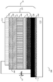
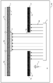
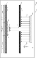
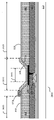
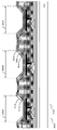
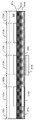
도 1은 본 개시내용의 일례에 따른 예시적인 전자 발광 디바이스(electro-luminescent device)의 단면 양태의 블록도이고; 1 is a block diagram of a cross-sectional aspect of an exemplary electro-luminescent device in accordance with an example of the present disclosure;
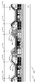
도 2는 도 1의 디바이스의 기판의 예시적인 백플레인(backplane) 층의 단면도로서, 그 안에 구현된 박막 트랜지스터(TFT: thin film transistor)를 도시하고; FIG. 2 is a cross-sectional view of an exemplary backplane layer of a substrate of the device of FIG. 1 , showing a thin film transistor (TFT) implemented therein;
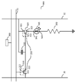
도 3은 도 2의 백플레인 층에 도시된 하나 이상의 TFT에 의해 제공될 수 있는 것과 같은 예시적인 회로에 대한 회로도이고; 3 is a circuit diagram for an exemplary circuit, such as may be provided by one or more TFTs shown in the backplane layer of FIG. 2 ;
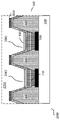
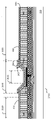
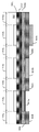
도 4는 도 1의 디바이스의 단면도이고; 4 is a cross-sectional view of the device of FIG . 1 ;
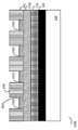
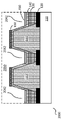
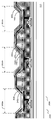
도 5는 도 1의 디바이스의 예시적인 버전의 단면도로서, 디바이스의 적어도 하나의 제2 전극의 증착을 지지하는 적어도 하나의 예시적인 픽셀 정의 층(PDL: pixel definition layer)을 도시하고; 5 is a cross-sectional view of an exemplary version of the device of FIG. 1 , showing at least one exemplary pixel definition layer (PDL) supporting deposition of at least one second electrode of the device;
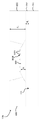
도 6은 본 개시내용의 일례에 따른 표면 상에 흡수된 흡착원자(adatom)의 상대적 에너지 상태를 나타내는 예시적인 에너지 프로파일이고; 6 is an exemplary energy profile showing the relative energy states of adsorbed adatoms on a surface according to an example of the present disclosure;
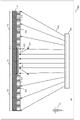
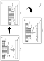
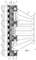
도 7은 본 개시내용의 일례에 따른 도 1의 디바이스의 예시적인 버전에서 하부 물질의 노출된 층 표면 상에 선택적 코팅을 패턴으로 증착하기 위한 예시적인 공정을 도시하는 개략도이고; 7 is a schematic diagram illustrating an exemplary process for depositing a selective coating in a pattern on an exposed layer surface of an underlying material in an exemplary version of the device of FIG. 1 according to an example of the present disclosure;
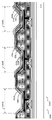
도 8은 도 7의 선택적 코팅의 증착된 패턴을 포함하는 노출된 층 표면 상에 전도성 코팅을 제1 패턴으로 증착하기 위한 예시적인 공정을 도시하는 개략도이며, 여기서 선택적 코팅은 핵 생성 억제 코팅(NIC: nucleation-inhibiting coating)이고; 8 is a schematic diagram illustrating an exemplary process for depositing a conductive coating in a first pattern on an exposed layer surface comprising the deposited pattern of the selective coating of FIG. 7 , wherein the optional coating is a nucleation inhibiting coating (NIC); : nucleation-inhibiting coating);
도 9a 내지 도 9d는 본 개시내용의 일례에 따른 내부에 개구를 갖는 도 7의 공정과 함께 사용하기에 적합한 예시적인 오픈 마스크(open mask)를 도시하는 개략도이고; 9A-9D are schematic diagrams illustrating an exemplary open mask suitable for use with the process of FIG. 7 having an opening therein in accordance with an example of the present disclosure;
도 10a는 본 개시내용의 일례에 따른 추가의 예시적인 증착 단계를 갖는 도 1의 디바이스의 예시적인 버전이고; 10A is an exemplary version of the device of FIG. 1 with an additional exemplary deposition step according to an example of the present disclosure;
도 10b는 제1 부분이 불연속 코팅을 포함하는 도 10a의 디바이스의 예시적인 버전이고; 10B is an exemplary version of the device of FIG. 10A in which a first portion includes a discontinuous coating;
도 10c는 도 10b의 디바이스의 제1 부분의 평면도이고; 10C is a top view of a first portion of the device of FIG. 10B ;
도 10d는 제3 부분을 추가로 포함하는 도 10a의 디바이스의 예시적인 버전이고; 10D is an exemplary version of the device of FIG. 10A further including a third portion;
도 10e는 도 10d의 디바이스의 부분의 평면도이고; 10E is a top view of a portion of the device of FIG. 10D ;
도 11a는 도 9의 선택적 코팅의 증착된 패턴을 포함하는 노출된 층 표면 상에 핵 생성 촉진 코팅(NPC: nucleation-promoting coating)인 선택적 코팅을 패턴으로 증착하기 위한 예시적인 공정을 도시하는 개략도이고; 11A is a schematic diagram illustrating an exemplary process for depositing in a pattern a selective coating, a nucleation-promoting coating (NPC), on an exposed layer surface comprising the deposited pattern of the selective coating of FIG. 9 ; ;
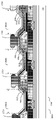
도 11b는 도 11a의 NPC의 증착된 패턴을 포함하는 노출된 층 표면 상에 전도성 코팅을 패턴으로 증착하기 위한 예시적인 공정을 도시하는 개략도이고; 11B is a schematic diagram illustrating an exemplary process for depositing a conductive coating in a pattern on an exposed layer surface comprising the deposited pattern of NPC of FIG. 11A ;
도 12a는 본 개시내용의 일례에 따른 도 1의 디바이스의 예시적인 버전에서 하부 물질의 노출된 층 표면 상에 NPC를 패턴으로 증착하기 위한 예시적인 공정을 도시하는 개략도이고; 12A is a schematic diagram illustrating an exemplary process for depositing NPCs in a pattern on an exposed layer surface of an underlying material in an exemplary version of the device of FIG. 1 according to an example of the present disclosure;
도 12b는 도 12a의 NPC의 증착된 패턴을 포함하는 노출된 층 표면 상에 NIC를 패턴으로 증착하는 예시적인 공정을 도시하는 개략도이고; 12B is a schematic diagram illustrating an exemplary process for depositing a NIC in a pattern on an exposed layer surface comprising the deposited pattern of NPC of FIG. 12A ;
도 12c는 도 12b의 NIC의 증착된 패턴을 포함하는 노출된 층 표면 상에 전도성 코팅을 패턴으로 증착하기 위한 예시적인 공정을 도시하는 개략도이고; 12C is a schematic diagram illustrating an exemplary process for depositing a conductive coating in a pattern on an exposed layer surface comprising the deposited pattern of the NIC of FIG. 12B ;
도 13a 내지 도 13c는 본 개시내용의 일례에 따른 도 1의 디바이스의 예시적인 버전에서 노출된 층 표면 상에 선택적 코팅을 패턴으로 증착하기 위한 예시적인 인쇄 공정의 예시적인 단계들을 도시하는 개략도이고; 13A-13C are schematic diagrams illustrating exemplary steps of an exemplary printing process for depositing a selective coating in a pattern on an exposed layer surface in an exemplary version of the device of FIG. 1 according to an example of the present disclosure;
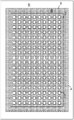
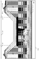
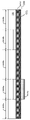
도 14는 본 개시내용의 일례에 따른 도 1의 디바이스의 하나의 버전에서 사용하기에 적합한 예시적인 패턴화된 전극을 평면도로 예시하는 개략도이고; 14 is a schematic diagram illustrating in top view an exemplary patterned electrode suitable for use in one version of the device of FIG. 1 according to an example of the present disclosure;
도 15는 라인 15-15를 따라 절취한 도 14의 디바이스의 예시적인 단면도를 예시하는 개략도이고; 15 is a schematic diagram illustrating an exemplary cross-sectional view of the device of FIG. 14 taken along line 15-15;
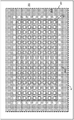
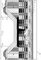
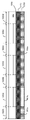
도 16a는 본 개시내용의 일례에 따른 도 1의 디바이스의 예시적인 버전에서 사용하기에 적합한 복수의 예시적인 전극 패턴을 평면도로 예시하는 개략도이고; 16A is a schematic diagram illustrating in top view a plurality of exemplary electrode patterns suitable for use in an exemplary version of the device of FIG. 1 according to an example of the present disclosure;
도 16b는 라인 16B-16B를 따라 절취한 도 16a의 디바이스의 중간 단계에서의 예시적인 단면도를 예시하는 개략도이고; 16B is a schematic diagram illustrating an exemplary cross-sectional view at an intermediate stage of the device of FIG. 16A taken along
도 16c는 라인 16C-16C를 따라 절취한 도 16a의 디바이스의 예시적인 단면도를 예시하는 개략도이고; 16C is a schematic diagram illustrating an exemplary cross-sectional view of the device of FIG. 16A taken along
도 17은 본 개시내용의 일례에 따른 하나의 예시적인 패턴화된 보조 전극을 갖는 도 1의 디바이스의 예시적인 버전의 단면도를 예시하는 개략도이고; 17 is a schematic diagram illustrating a cross-sectional view of an exemplary version of the device of FIG. 1 with one exemplary patterned auxiliary electrode according to an example of the present disclosure;
도 18a는 본 개시내용의 일례에 따른 도 1의 디바이스의 예시적인 버전에서 발광 영역(들) 및/또는 비-발광 영역(들)의 예시적인 배열을 평면도로 예시하는 개략도이고; 18A is a schematic diagram illustrating in top view an example arrangement of light emitting region(s) and/or non-emissive region(s) in an exemplary version of the device of FIG. 1 according to an example of the present disclosure;
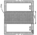
도 18b 내지 도 18d는 본 개시내용의 일례에 따른 비-발광 영역을 오버레이하는 예시적인 보조 전극을 도시하는 도 18a의 한 부분의 세그먼트를 각각 예시하는 개략도이고; 18B-18D are schematic diagrams each illustrating a segment of a portion of FIG. 18A showing an exemplary auxiliary electrode overlaying a non-emissive region according to an example of the present disclosure;
도 19는 본 개시내용의 일례에 따른 적어도 하나의 발광 영역 및 적어도 하나의 비-발광 영역을 오버레이하는 보조 전극의 예시적인 패턴을 평면도로 예시하는 개략도이고; 19 is a schematic diagram illustrating, in top view, an example pattern of an auxiliary electrode overlying at least one light emitting area and at least one non-emissive area according to an example of the present disclosure;
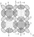
도 20a는 본 개시내용의 일례에 따른 다이아몬드 구성의 복수의 발광 영역의 그룹을 갖는 도 1의 디바이스의 예시적인 버전의 예시적인 패턴을 평면도로 예시하는 개략도이고; 20A is a schematic diagram illustrating, in top view, an exemplary pattern of an exemplary version of the device of FIG. 1 having groups of a plurality of light emitting regions of diamond configuration according to an example of the present disclosure;
도 20b는 라인 20B-20B를 따라 절취한 도 20a의 디바이스의 예시적인 단면도를 예시하는 개략도이고; 20B is a schematic diagram illustrating an exemplary cross-sectional view of the device of FIG. 20A taken along
도 20c는 라인 20C-20C를 따라 절취한 도 20a의 디바이스의 예시적인 단면도를 예시하는 개략도이고; 20C is a schematic diagram illustrating an exemplary cross-sectional view of the device of FIG. 20A taken along
도 21은 본 개시내용의 일례에 따른 추가의 예시적인 증착 단계를 갖는 도 4의 디바이스의 하나의 예시적인 버전의 예시적인 단면도를 예시하는 개략도이고; 21 is a schematic diagram illustrating an exemplary cross-sectional view of one exemplary version of the device of FIG. 4 with an additional exemplary deposition step in accordance with an example of the present disclosure;
도 22는 본 개시내용의 일례에 따른 추가의 예시적인 증착 단계를 갖는 도 4의 디바이스의 하나의 예시적인 버전의 예시적인 단면도를 예시하는 개략도이고; 22 is a schematic diagram illustrating an exemplary cross-sectional view of one exemplary version of the device of FIG. 4 with an additional exemplary deposition step in accordance with an example of the present disclosure;
도 23은 본 개시내용의 일례에 따른 추가의 예시적인 증착 단계를 갖는 도 4의 디바이스의 하나의 예시적인 버전의 예시적인 단면도를 예시하는 개략도이고; 23 is a schematic diagram illustrating an exemplary cross-sectional view of one exemplary version of the device of FIG. 4 with an additional exemplary deposition step in accordance with an example of the present disclosure;
도 24는 본 개시내용의 일례에 따른 추가의 예시적인 증착 단계를 갖는 도 4의 디바이스의 하나의 예시적인 버전의 예시적인 단면도를 예시하는 개략도이고; 24 is a schematic diagram illustrating an exemplary cross-sectional view of one exemplary version of the device of FIG. 4 with an additional exemplary deposition step in accordance with an example of the present disclosure;
도 25a 내지 도 25c는, 선택적 증착 및 후속 제거 공정에 의해, 본 개시내용의 일례에 따른 도 1의 디바이스의 예시적인 버전의 노출된 층 표면 상에 전도성 코팅을 패턴으로 증착하기 위한 예시적인 공정의 예시적인 단계들을 도시하는 개략도이고; 25A-25C illustrate an exemplary process for depositing a conductive coating in a pattern on an exposed layer surface of an exemplary version of the device of FIG. 1 according to an example of the present disclosure, by a selective deposition and subsequent removal process; It is a schematic diagram illustrating exemplary steps;
도 26a는 본 개시내용의 일례에 따른 적어도 하나의 보조 전극을 갖는, 적어도 하나의 예시적인 픽셀 영역 및 적어도 하나의 예시적인 투광 영역(light-transmissive region)을 포함하는 도 1의 디바이스의 투명 버전의 일례를 평면도로 예시하는 개략도이고; 26A is a transparent version of the device of FIG. 1 including at least one exemplary pixel region and at least one exemplary light-transmissive region, with at least one auxiliary electrode in accordance with an example of the present disclosure; It is a schematic diagram illustrating an example in a plan view;
도 26b는 라인 26B-26B를 따라 절취한 도 26a의 디바이스의 예시적인 단면도를 예시하는 개략도이고; 26B is a schematic diagram illustrating an exemplary cross-sectional view of the device of FIG. 26A taken along
도 27a는 본 개시내용의 일례에 따른 적어도 하나의 예시적인 픽셀 영역 및 적어도 하나의 예시적인 투광 영역을 포함하는 도 1의 디바이스의 투명 버전의 일례를 평면도로 예시하는 개략도이고; 27A is a schematic diagram illustrating in top view an example of a transparent version of the device of FIG. 1 including at least one exemplary pixel area and at least one exemplary light-transmissive area in accordance with an example of the present disclosure;
도 27b는 라인 27B-27B를 따라 절취한 도 27a의 디바이스의 예시적인 단면도를 예시하는 개략도이고; 27B is a schematic diagram illustrating an exemplary cross-sectional view of the device of FIG. 27A taken along
도 27c는 라인 27B-27B를 따라 절취한 도 27a의 디바이스의 또 다른 예시적인 단면도를 예시하는 개략도이고; 27C is a schematic diagram illustrating another exemplary cross-sectional view of the device of FIG. 27A taken along
도 28a 내지 도 28d는 본 개시내용의 일례에 따른 상이한 두께의 제2 전극을 각각 갖는 2개의 발광 영역을 제공하기 위해 도 1의 디바이스의 예시적인 버전을 제조하기 위한 예시적인 공정의 예시적인 단계들을 도시하는 개략도이고; 28A-28D illustrate exemplary steps of an exemplary process for manufacturing an exemplary version of the device of FIG. 1 to provide two light emitting regions each having a second electrode of a different thickness in accordance with an example of the present disclosure; It is a schematic diagram showing;
도 29a 내지 도 29d는 본 개시내용의 일례에 따른 상이한 두께의 제2 전극을 갖는 서브-픽셀 영역을 갖는 도 1의 디바이스의 예시적인 버전을 제조하기 위한 예시적인 공정의 예시적인 단계들을 도시하는 개략도이고; 29A-29D are schematic diagrams illustrating exemplary steps of an exemplary process for manufacturing an exemplary version of the device of FIG. 1 having a sub-pixel area having a second electrode of a different thickness according to an example of the present disclosure; ego;
도 30은 제2 전극이 본 개시내용의 일례에 따른 보조 전극에 결합된 도 1의 디바이스의 예시적인 버전의 예시적인 단면도를 예시하는 개략도이고; 30 is a schematic diagram illustrating an exemplary cross-sectional view of an exemplary version of the device of FIG. 1 with a second electrode coupled to an auxiliary electrode according to an example of the present disclosure;
도 31a 내지 도 31i는 본 개시내용의 다양한 예에 따른 도 1의 디바이스의 예시적인 버전에서 전도성 코팅을 갖는 증착 계면에서의 NIC의 다양한 잠재적 거동을 도시하는 개략도이고; 31A-31I are schematic diagrams illustrating various potential behaviors of a NIC at a deposition interface with a conductive coating in an exemplary version of the device of FIG. 1 according to various examples of the present disclosure;
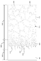
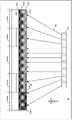
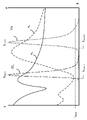
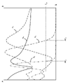
도 32는 본 개시내용의 다양한 예에 따른, 한 쌍의 예시적인 발광 영역에 대한 예시적인 발광 스펙트럼과 발광 영역 위에 놓이는 개개의 캡핑 층의 예시적인 굴절률의 플롯 사이의 관계를 정성적 형태로 예시하는 개략도이고; 32 illustrates in qualitative form the relationship between exemplary emission spectra for a pair of exemplary emissive regions and plots of exemplary refractive indices of individual capping layers overlying the emissive regions, in accordance with various examples of the present disclosure; is a schematic diagram;
도 33은 본 개시내용의 다양한 예에 따른, 도 32의 예시적인 굴절률의 플롯과 도 32의 개개의 캡핑 층의 예시적인 소광 계수(extinction coefficient)의 개개의 플롯 사이의 관계를 정성적 형태로 예시하는 개략도이고; FIG. 3 3 illustrates in a qualitative form the relationship between the exemplary plot of refractive index of FIG. 32 and individual plots of exemplary extinction coefficients of individual capping layers of FIG . 32 , in accordance with various examples of the present disclosure; It is a schematic diagram illustrating;
도 34는 본 개시내용의 다양한 예에 따른, 도 32의 예시적인 발광 스펙트럼과 도 33의 예시적인 소광 계수의 개개의 플롯 사이의 관계를 정성적 형태로 예시하는 개략도이고; FIG. 3 4 is a schematic diagram illustrating in qualitative form the relationship between the exemplary emission spectrum of FIG . 32 and individual plots of the exemplary extinction coefficient of FIG. 33 , in accordance with various examples of the present disclosure;
도 35는 본 개시내용의 일례에 따른 NIC 및/또는 전도성 코팅 하부에 있는 금속성 코팅을 예시하는 개략도이고; 35 is a schematic diagram illustrating a metallic coating underlying a NIC and/or a conductive coating according to an example of the present disclosure;
도 36a 및 도 36b는 도 28a 및 도 28b의 단계에 후속하는 도 1의 디바이스의 예시적인 버전을 제조하기 위한 예시적인 공정의 예시적인 단계들을 도시하는 개략도이고; 36A and 36B are schematic diagrams illustrating exemplary steps of an exemplary process for manufacturing an exemplary version of the device of FIG. 1 that follows the steps of FIGS. 28A and 28B ;
도 37a 내지 도 37e는 본 개시내용의 일례에 따른 상이한 두께의 제2 전극을 각각 갖는 3개의 발광 영역을 제공하기 위해 도 1의 디바이스의 예시적인 버전을 제조하기 위한 예시적인 공정의 예시적인 단계들을 도시하는 개략도이고; 37A -E show exemplary steps of an exemplary process for manufacturing an exemplary version of the device of FIG. 1 to provide three light emitting regions each having a second electrode of a different thickness according to an example of the present disclosure; It is a schematic diagram showing;
도 38a 내지 도 38f는 본 개시내용의 일례에 따른 상이한 두께의 제2 전극을 갖는 서브-픽셀 영역을 갖는 도 1의 디바이스의 예시적인 버전을 제조하기 위한 예시적인 공정의 예시적인 단계들을 도시하는 개략도이고; 38A-F are schematic diagrams illustrating exemplary steps of an exemplary process for manufacturing an exemplary version of the device of FIG. 1 having sub-pixel regions having a second electrode of a different thickness in accordance with an example of the present disclosure; ego;
도 39a 내지 도 39c는 본 개시내용의 일례에 따른 도 1의 디바이스의 예시적인 버전을 도시하는 개략도이며; 39A-39C are schematic diagrams illustrating an example version of the device of FIG. 1 according to an example of the present disclosure;
도 40은 본 개시내용의 일례에 따른 필름 핵의 형성을 예시하는 개략도이다. 40 is a schematic diagram illustrating the formation of a film nucleus according to an example of the present disclosure.
본 개시내용에서, 제한이 아닌 설명의 목적으로, 특정 아키텍처, 인터페이스 및/또는 기술을 포함하지만 이에 제한되지 않는 본 개시내용의 완전한 이해를 제공하기 위해 특정 세부사항을 기술한다. 일부 경우에는, 잘 알려진 시스템, 기술, 구성요소, 디바이스, 회로, 방법 및 응용 분야에 대한 상세한 설명은 불필요한 세부사항으로 인해 본 개시내용의 설명이 모호하게 되지 않도록 생략한다.In this disclosure, for purposes of explanation and not limitation, specific details are set forth in order to provide a thorough understanding of the disclosure including, but not limited to, specific architectures, interfaces, and/or techniques. In some instances, detailed descriptions of well-known systems, techniques, components, devices, circuits, methods, and applications are omitted so as not to obscure the description of the present disclosure in unnecessary detail.
또한, 본원에서 재현되는 블록도들은 기술의 원리를 구현하는 예시적인 구성요소의 개념적인 견해를 나타낼 수 있다는 것을 이해할 것이다.It will also be understood that the block diagrams reproduced herein may represent conceptual views of illustrative components embodying the principles of the technology.
따라서, 시스템 및 방법 구성요소는 경우에 따라서는 도면에서 통상적인 부호로 표현되었으며, 본 개시내용의 실례들을 이해하는 데 적절한 특정 세부사항만을 나타내어 본 개시내용이 본 명세서의 설명에 이점을 가진 당업자가 용이하게 인지할 수 있는 세부사항으로 모호하게 되지 않도록 하였다.Accordingly, system and method components have been represented by conventional numerals in the drawings, where appropriate, showing only specific details suitable for understanding the examples of the present disclosure so that those skilled in the art having the benefit of this disclosure will find out. It is not obscured by easily recognizable details.
본원에서 제공되는 모든 도면은 축척에 맞게 도시되지 않을 수 있으며 어떠한 방식으로든 본 개시내용을 제한하는 것으로 간주되지 않을 수 있다.All drawings provided herein may not be drawn to scale and should not be considered as limiting the disclosure in any way.
파선으로 도시된 특징 또는 기능은 일부 예에서 선택 사항으로 간주될 수 있다.Features or functions depicted in dashed lines may be considered optional in some examples.
본 개시내용의 목적은 종래 기술의 적어도 하나의 단점을 제거하거나 완화하는 것이다.It is an object of the present disclosure to obviate or alleviate at least one disadvantage of the prior art.
본 개시내용은 복수의 층을 갖는 광전자 디바이스(opto-electronic device)를 개시한다. 제1 캡핑 층(CPL: capping layer)은 제1 CPL 물질을 포함하고 제1 발광 영역에 배치된다. 제2 CPL은 제2 CPL 물질을 포함하고 제2 발광 영역에 배치된다. 제1 발광 영역은 제1 개시 파장(onset wavelength)을 특징으로 하는 제1 파장 스펙트럼을 갖는 광자를 방출하도록 구성된다. 제2 발광 영역은 제2 개시 파장을 특징으로 하는 제2 파장 스펙트럼을 갖는 광자를 방출하도록 구성된다. 제1 CPL 및 제1 CPL 물질(집합적으로 "CPL(m)1") 중 적어도 하나는 제1 개시 파장보다 짧은 제1 흡수 에지 파장에서 제1 흡수 에지(absorption edge)를 나타낸다. 제2 CPL 및 제2 CPL 물질(집합적으로 "CPL(m)2") 중 적어도 하나는 제2 개시 파장보다 짧은 제2 흡수 에지 파장에서 제2 흡수 에지를 나타낸다.The present disclosure discloses an opto-electronic device having a plurality of layers. A first capping layer (CPL) includes a first CPL material and is disposed in the first light emitting region. The second CPL includes a second CPL material and is disposed in the second light emitting region. The first emissive region is configured to emit photons having a first wavelength spectrum characterized by a first onset wavelength. The second light emitting region is configured to emit photons having a second wavelength spectrum characterized by a second onset wavelength. At least one of the first CPL and the first CPL material (collectively “CPL(m)1”) exhibits a first absorption edge at a first absorption edge wavelength that is shorter than the first onset wavelength. At least one of the second CPL and the second CPL material (collectively “CPL(m)2”) exhibits a second absorption edge at a second absorption edge wavelength shorter than the second onset wavelength.
본 개시내용의 넓은 양태에 따르면, 복수의 층으로서: 제1 캡핑 층(CPL) 물질을 포함하고 제1 발광 영역에 배치된 제1 캡핑 층(CPL)을 포함하는 제1 캡핑 층(CPL)으로서, 상기 제1 발광 영역은 제1 개시 파장을 특징으로 하는 제1 파장 스펙트럼을 갖는 광자를 방출하도록 구성되는 제1 캡핑 층(CPL); 및 제2 CPL 물질을 포함하고 제2 발광 영역에 배치된 제2 CPL로서, 상기 제2 발광 영역은 제2 개시 파장을 특징으로 하는 제2 파장 스펙트럼을 갖는 광자를 방출하도록 구성되는 제2 CPL을 포함하는 복수의 층을 갖고, 여기서 상기 제1 CPL 및 상기 제1 CPL 물질(CPL(m)1) 중 적어도 하나는 제1 개시 파장(onset wavelength)보다 짧은 제1 흡수 에지 파장(absorption edge wavelength)에서 제1 흡수 에지(absorption edge)를 나타내고; 상기 제2 CPL 및 상기 제2 CPL 물질(CPL(m)2) 중 적어도 하나는 제2 개시 파장보다 짧은 제2 흡수 에지 파장에서 제2 흡수 에지를 나타내는 광전자 디바이스가 개시된다.According to a broad aspect of the present disclosure, as a plurality of layers: a first capping layer (CPL) comprising a first capping layer (CPL) material and comprising a first capping layer (CPL) disposed in a first emissive region. , wherein the first light emitting region comprises: a first capping layer (CPL) configured to emit photons having a first wavelength spectrum characterized by a first onset wavelength; and a second CPL comprising a second CPL material and disposed in a second emissive region, wherein the second emissive region is configured to emit photons having a second wavelength spectrum characterized by a second onset wavelength; wherein at least one of the first CPL and the first CPL material (CPL(m)1) has a first absorption edge wavelength that is shorter than a first onset wavelength; represents a first absorption edge in ; at least one of the second CPL and the second CPL material (CPL(m)2) exhibits a second absorption edge at a second absorption edge wavelength shorter than the second onset wavelength.
일부 비제한적인 예에서, 제1 개시 파장은 제2 개시 파장보다 더 짧을 수 있다. 일부 비제한적인 예에서, 제1 흡수 에지 파장은 제2 흡수 에지 파장보다 더 짧을 수 있다.In some non-limiting examples, the first onset wavelength can be shorter than the second onset wavelength. In some non-limiting examples, the first absorption edge wavelength can be shorter than the second absorption edge wavelength.
일부 비제한적인 예에서, 제1 흡수 에지는 CPL(m)1의 소광 계수 k가 임계값과 동일한 제1 소광 파장을 특징으로 할 수 있으며, 제2 흡수 에지는 CPL(m)2의 소광 계수가 임계값과 동일한 제2 소광 파장을 특징으로 할 수 있다.In some non-limiting examples, the first absorption edge may be characterized by a first extinction wavelength at which an extinction coefficient k of CPL(m)1 is equal to a threshold, and the second absorption edge has an extinction coefficient of CPL(m)2 may be characterized by a second extinction wavelength equal to the threshold value.
일부 비제한적인 예에서, 제1 개시 파장은 제1 흡수 에지 파장보다 약 50 nm, 약 40 nm, 약 35 nm, 약 30 nm, 약 25 nm, 약 20 nm, 약 15 nm, 약 10 nm, 약 5 nm, 및 약 3 nm 중 적어도 하나의 미만 만큼 더 길 수 있다. 일부 비제한적인 예에서, 제1 소광 파장은 CPL(m)1의 소광 계수가 임계값과 동일한 적어도 하나의 파장 중 가장 긴 것일 수 있다. 일부 비제한적인 예에서, 파장의 함수로서의 CPL(m)의 소광 계수의 1차 도함수는 제1 소광 파장에서 음(-)의 값일 수 있다. 일부 비제한적인 예에서, 제1 소광 파장보다 긴 파장에서의 CPL(m)1의 소광 계수는 임계값 미만일 수 있다. 일부 비제한적인 예에서, 제1 소광 파장보다 긴 모든 파장에서의 CPL(m)1의 소광 계수는 임계값 미만일 수 있다. 일부 비제한적인 예에서, 제1 개시 파장보다 긴 임의의 파장에서의 CPL(m)1의 소광 계수는 약 0.1, 약 0.09, 약 0.08, 약 0.06, 약 0.05, 약 0.03, 약 0.01, 약 0.005, 및 약 0.0001 중 적어도 하나 미만일 수 있다. 일부 비제한적인 예에서, 제1 흡수 에지 파장보다 짧은 파장에서의 CPL(m)1의 소광 계수는 약 0.1, 약 0.12, 약 0.13, 약 0.15, 약 0.18, 약 0.2, 약 0.25, 약 0.3, 약 0.5, 약 0.7, 약 0.75, 약 0.8, 약 0.9, 및 약 1.0 중 적어도 하나를 초과할 수 있다.In some non-limiting examples, the first onset wavelength is about 50 nm, about 40 nm, about 35 nm, about 30 nm, about 25 nm, about 20 nm, about 15 nm, about 10 nm, longer by less than at least one of about 5 nm, and about 3 nm. In some non-limiting examples, the first extinction wavelength may be the longest of at least one wavelength in which an extinction coefficient of CPL(m)1 is equal to a threshold value. In some non-limiting examples, the first derivative of the extinction coefficient of CPL(m) as a function of wavelength may be negative at the first extinction wavelength. In some non-limiting examples, the extinction coefficient of CPL(m)1 at a wavelength longer than the first extinction wavelength may be less than a threshold value. In some non-limiting examples, the extinction coefficient of CPL(m)1 at all wavelengths longer than the first extinction wavelength may be less than a threshold value. In some non-limiting examples, the extinction coefficient of CPL(m)1 at any wavelength longer than the first onset wavelength is about 0.1, about 0.09, about 0.08, about 0.06, about 0.05, about 0.03, about 0.01, about 0.005 , and about 0.0001. In some non-limiting examples, the extinction coefficient of CPL(m)1 at wavelengths shorter than the first absorption edge wavelength is about 0.1, about 0.12, about 0.13, about 0.15, about 0.18, about 0.2, about 0.25, about 0.3, at least one of about 0.5, about 0.7, about 0.75, about 0.8, about 0.9, and about 1.0.
일부 비제한적인 예에서, 제1 흡수 에지 파장보다 긴 적어도 하나의 파장에 대한 CPL(m)1의 굴절률은 제1 흡수 파장보다 짧은 적어도 하나의 파장에 대한 CPL(m)1의 굴절률을 초과할 수 있다. 일부 비제한적인 예에서, 제1 파장 스펙트럼의 적어도 하나의 파장에서 CPL(m)의 굴절률은 약 1.8, 약 1.9, 약 1.95, 약 2, 약 2.05, 약 2.1, 약 2.2, 약 2.3, 및 약 2.5 중 적어도 하나를 초과할 수 있다.In some non-limiting examples, the index of refraction of CPL(m)1 for at least one wavelength longer than the first absorption edge wavelength may exceed the index of refraction of CPL(m)1 for at least one wavelength shorter than the first absorption wavelength. can In some non-limiting examples, the refractive index of CPL(m) at at least one wavelength of the first wavelength spectrum is about 1.8, about 1.9, about 1.95, about 2, about 2.05, about 2.1, about 2.2, about 2.3, and about may exceed at least one of 2.5.
일부 비제한적인 예에서, 제2 개시 파장은 제2 흡수 에지 파장보다 약 200 nm, 약 150 nm, 약 130 nm, 약 100 nm, 약 80 nm, 약 70 nm, 약 60 nm, 약 50 nm, 약 40 nm, 약 35 nm, 약 25 nm, 약 20 nm, 약 15 nm, 및 약 10 nm 중 적어도 하나의 미만 만큼 더 길 수 있다. 일부 비제한적인 예에서, 제2 소광 파장은 CPL(m)2의 소광 계수가 임계값과 동일한 적어도 하나의 파장 중 가장 긴 것일 수 있다. 일부 비제한적인 예에서, 파장의 함수로서의 CPL(m)2의 소광 계수의 1차 도함수는 제2 소광 파장에서 음(-)의 값일 수 있다. 일부 비제한적인 예에서, 제2 소광 파장보다 긴 파장에서의 CPL(m)2의 소광 계수는 임계값 미만일 수 있다. 일부 비제한적인 예에서, 제2 소광 파장보다 긴 모든 파장에서의 CPL(m)2의 소광 계수는 임계값 미만일 수 있다. 일부 비제한적인 예에서, 제2 개시 파장보다 긴 임의의 파장에서의 CPL(m)2의 소광 계수는 약 0.1, 약 0.09, 약 0.08, 약 0.06, 약 0.05, 약 0.03, 약 0.01, 약 0.005, 및 약 0.0001 중 적어도 하나 미만일 수 있다. 일부 비제한적인 예에서, 제2 흡수 에지 파장보다 짧은 파장에서의 CPL(m)2의 소광 계수는 약 0.1, 약 0.12, 약 0.13, 약 0.15, 약 0.18, 약 0.2, 약 0.25, 약 0.3, 약 0.5, 약 0.7, 약 0.75, 약 0.8, 약 0.9, 및 약 1.0 중 적어도 하나를 초과할 수 있다.In some non-limiting examples, the second onset wavelength is about 200 nm, about 150 nm, about 130 nm, about 100 nm, about 80 nm, about 70 nm, about 60 nm, about 50 nm, greater than the second absorption edge wavelength. longer by less than at least one of about 40 nm, about 35 nm, about 25 nm, about 20 nm, about 15 nm, and about 10 nm. In some non-limiting examples, the second extinction wavelength may be the longest of at least one wavelength in which an extinction coefficient of CPL(m)2 is equal to a threshold value. In some non-limiting examples, the first derivative of the extinction coefficient of CPL(m)2 as a function of wavelength may be negative at the second extinction wavelength. In some non-limiting examples, the extinction coefficient of CPL(m)2 at a wavelength longer than the second extinction wavelength may be less than a threshold value. In some non-limiting examples, the extinction coefficient of CPL(m)2 at all wavelengths longer than the second extinction wavelength may be less than a threshold value. In some non-limiting examples, the extinction coefficient of CPL(m)2 at any wavelength longer than the second onset wavelength is about 0.1, about 0.09, about 0.08, about 0.06, about 0.05, about 0.03, about 0.01, about 0.005 , and about 0.0001. In some non-limiting examples, the extinction coefficient of CPL(m)2 at a wavelength shorter than the second absorption edge wavelength is about 0.1, about 0.12, about 0.13, about 0.15, about 0.18, about 0.2, about 0.25, about 0.3, at least one of about 0.5, about 0.7, about 0.75, about 0.8, about 0.9, and about 1.0.
일부 비제한적인 예에서, 제2 흡수 에지 파장보다 긴 적어도 하나의 파장에 대한 CPL(m)2의 굴절률은 제2 흡수 에지 파장보다 짧은 적어도 하나의 파장에 대한 CPL(m)2의 굴절률을 초과할 수 있다. 일부 비제한적인 예에서, 제2 파장 스펙트럼의 적어도 하나의 파장에서 CPL(m)2의 굴절률은 약 1.8, 약 1.9, 약 1.95, 약 2, 약 2.05, 약 2.1, 약 2.2, 약 2.3, 및 약 2.5 중 적어도 하나를 초과할 수 있다.In some non-limiting examples, the refractive index of CPL(m)2 for at least one wavelength longer than the second absorption edge wavelength exceeds the refractive index of CPL(m)2 for at least one wavelength shorter than the second absorption edge wavelength. can do. In some non-limiting examples, the refractive index of CPL(m)2 at at least one wavelength of the second wavelength spectrum is about 1.8, about 1.9, about 1.95, about 2, about 2.05, about 2.1, about 2.2, about 2.3, and greater than at least one of about 2.5.
일부 비제한적인 예에서, CPL(m)1의 소광 계수는 제2 개시 파장에서의 임계값 미만일 수 있다. 일부 비제한적인 예에서, CPL(m)1의 소광 계수는 제2 파장 스펙트럼의 모든 파장에서의 임계값 미만일 수 있다. 일부 비제한적인 예에서, 제2 파장 스펙트럼의 임의의 파장에서의 CPL(m)1의 소광 계수는 약 0.1, 약 0.09, 약 0.08, 약 0.05, 약 0.05, 약 0.03, 약 0.01, 약 0.005, 및 약 0.001 중 적어도 하나 미만일 수 있다.In some non-limiting examples, the extinction coefficient of CPL(m)1 may be less than a threshold value at the second onset wavelength. In some non-limiting examples, the extinction coefficient of CPL(m)1 may be less than a threshold value at all wavelengths of the second wavelength spectrum. In some non-limiting examples, the extinction coefficient of CPL(m)1 at any wavelength in the second wavelength spectrum is about 0.1, about 0.09, about 0.08, about 0.05, about 0.05, about 0.03, about 0.01, about 0.005, and about 0.001.
일부 비제한적인 예에서, 제1 파장 스펙트럼의 적어도 하나의 파장에 대한 CPL(m)1의 굴절률은 제2 파장 스펙트럼의 적어도 하나의 파장에 대한 CPL(m)1의 굴절률을 초과할 수 있다. 일부 비제한적인 예에서, 제2 파장 스펙트럼의 적어도 하나의 파장에 대한 CPL(m)2의 굴절률은 제1 파장 스펙트럼의 적어도 하나의 파장에 대한 CPL(m)2의 굴절률을 초과할 수 있다. 일부 비제한적인 예에서, 제2 파장 스펙트럼의 적어도 하나의 파장에 대한 CPL(m)1의 굴절률은 약 1.8, 약 1.7, 약 1.65, 약 1.6, 약 1.5, 약 1.45, 약 1.4, 및 약 1.3 중 적어도 하나 미만일 수 있다. 일부 비제한적인 예에서, 제1 파장 스펙트럼의 적어도 하나의 파장에서의 CPL(m)2의 굴절률은 약 1.8, 약 1.7, 약 1.65, 약 1.6, 약 1.5, 약 1.45, 약 1.4, 및 약 1.3 중 적어도 하나 미만일 수 있다.In some non-limiting examples, the refractive index of CPL(m)1 for at least one wavelength in the first wavelength spectrum may exceed the refractive index of CPL(m)1 for at least one wavelength in the second wavelength spectrum. In some non-limiting examples, an index of refraction of CPL(m)2 for at least one wavelength of the second wavelength spectrum may exceed an index of refraction of CPL(m)2 for at least one wavelength of the first wavelength spectrum. In some non-limiting examples, the refractive index of CPL(m)1 for at least one wavelength of the second wavelength spectrum is about 1.8, about 1.7, about 1.65, about 1.6, about 1.5, about 1.45, about 1.4, and about 1.3. may be less than at least one of In some non-limiting examples, the refractive index of CPL(m)2 at at least one wavelength of the first wavelength spectrum is about 1.8, about 1.7, about 1.65, about 1.6, about 1.5, about 1.45, about 1.4, and about 1.3. may be less than at least one of
일부 비제한적인 예에서, CPL(m)2의 소광 계수는 제1 파장 스펙트럼의 적어도 하나의 파장에 대한 CPL(m)1의 소광 계수를 초과할 수 있다. 일부 비제한적인 예에서, CPL(m)2의 소광 계수는 제1 파장 스펙트럼의 모든 파장에 대한 CPL(m)1의 소광 계수를 초과할 수 있다.In some non-limiting examples, the extinction coefficient of CPL(m)2 may exceed the extinction coefficient of CPL(m)1 for at least one wavelength of the first wavelength spectrum. In some non-limiting examples, the extinction coefficient of CPL(m)2 may exceed the extinction coefficient of CPL(m)1 for all wavelengths of the first wavelength spectrum.
일부 비제한적인 예에서, 임계값은 0.1, 0.09, 0.08, 0.06, 0.05, 0.03, 0.01, 0.005, 및 0.001 중 적어도 하나일 수 있다.In some non-limiting examples, the threshold can be at least one of 0.1, 0.09, 0.08, 0.06, 0.05, 0.03, 0.01, 0.005, and 0.001.
일부 비제한적인 예에서, 제1 발광 영역 및 제2 발광 영역은 측면 양태에서 디바이스의 상이한 영역을 차지할 수 있다.In some non-limiting examples, the first emissive region and the second emissive region can occupy different areas of the device in a side aspect.
일부 비제한적인 예에서, 제1 파장 스펙트럼 및 제2 파장 스펙트럼은 가시 스펙트럼 내에 있다. 일부 비제한적인 예에서, 제1 파장 스펙트럼은 제1 피크 파장을 가질 수 있으며, 제2 파장 스펙트럼은 제1 피크 파장보다 더 긴 제2 피크 파장을 가질 수 있다.In some non-limiting examples, the first wavelength spectrum and the second wavelength spectrum are within the visible spectrum. In some non-limiting examples, the first wavelength spectrum can have a first peak wavelength, and the second wavelength spectrum can have a second peak wavelength that is longer than the first peak wavelength.
일부 비제한적인 예에서, 제1 개시 파장은 제1 파장 스펙트럼의 강도가 제1 피크 파장에서의 강도의 약 20%, 약 15%, 약 10%, 약 5%, 약 3%, 약 1%, 및 약 0.01% 중 적어도 하나일 수 있는 적어도 하나의 파장 중 가장 짧은 파장일 수 있다. 일부 비제한적인 예에서, 제2 개시 파장은 제2 파장 스펙트럼의 강도가 제2 피크 파장에서의 강도의 약 20%, 약 15%, 약 10%, 약 5%, 약 3%, 약 1%, 및 약 0.01% 중 적어도 하나일 수 있는 적어도 하나의 파장 중 가장 짧은 파장일 수 있다.In some non-limiting examples, the first onset wavelength is such that the intensity of the first wavelength spectrum is about 20%, about 15%, about 10%, about 5%, about 3%, about 1% of the intensity at the first peak wavelength. , and at least one wavelength, which may be at least one of about 0.01%. In some non-limiting examples, the second initiation wavelength is such that the intensity of the second wavelength spectrum is about 20%, about 15%, about 10%, about 5%, about 3%, about 1% of the intensity at the second peak wavelength. , and at least one wavelength, which may be at least one of about 0.01%.
일부 비제한적인 예에서, 제1 파장 스펙트럼은 청색(B) 및 녹색(G) 중 적어도 하나인 색상에 상응할 수 있다. 일부 비제한적인 예에서, 제2 파장 스펙트럼은 적색(R) 및 녹색(G) 중 적어도 하나인 색상에 상응할 수 있다. 일부 비제한적인 예에서, 제1 파장 스펙트럼은 청색(B)인 색상에 상응할 수 있으며, 제2 파장 스펙트럼은 녹색(G) 및 적색(R) 중 적어도 하나인 색상에 상응할 수 있다. 일부 비제한적인 예에서, 제1 파장 스펙트럼은 녹색(G)인 색상에 상응할 수 있으며, 제2 파장 스펙트럼은 적색(R)인 색상에 상응할 수 있다.In some non-limiting examples, the first wavelength spectrum may correspond to a color that is at least one of blue (B) and green (G). In some non-limiting examples, the second wavelength spectrum may correspond to a color that is at least one of red (R) and green (G). In some non-limiting examples, the first wavelength spectrum may correspond to a color that is blue (B) and the second wavelength spectrum may correspond to a color that is at least one of green (G) and red (R). In some non-limiting examples, a first wavelength spectrum may correspond to a color that is green (G), and a second wavelength spectrum may correspond to a color that is red (R).
일부 비제한적인 예에서, 제1 CPL 물질은 제2 CPL 물질과 상이한 조성을 가질 수 있다.In some non-limiting examples, the first CPL material can have a different composition than the second CPL material.
일부 비제한적인 예에서, 제1 CPL의 두께는 제2 CPL의 두께와 동일할 수 있다. 일부 비제한적인 예에서, 제1 CPL의 두께는 제2 CPL의 두께와 상이할 수 있다.In some non-limiting examples, the thickness of the first CPL may be the same as the thickness of the second CPL. In some non-limiting examples, the thickness of the first CPL may be different from the thickness of the second CPL.
일부 비제한적인 예에서, 제1 CPL의 두께는 약 5 내지 약 120 nm의 범위일 수 있다. 일부 비제한적인 예에서, 제1 CPL의 두께는 약 10 nm, 약 15 nm, 약 20 nm, 약 25 nm, 약 30 nm, 및 약 40 nm 중 적어도 하나를 초과할 수 있다. 일부 비제한적인 예에서, 제1 CPL의 두께는 약 100 nm, 약 90 nm, 약 80 nm, 및 약 70 nm 중 적어도 하나 미만일 수 있다.In some non-limiting examples, the thickness of the first CPL can range from about 5 to about 120 nm. In some non-limiting examples, the thickness of the first CPL can be greater than at least one of about 10 nm, about 15 nm, about 20 nm, about 25 nm, about 30 nm, and about 40 nm. In some non-limiting examples, the thickness of the first CPL can be less than at least one of about 100 nm, about 90 nm, about 80 nm, and about 70 nm.
일부 비제한적인 예에서, 제2 CPL의 두께는 약 5 nm 내지 약 120 nm의 범위일 수 있다. 일부 비제한적인 예에서, 제2 CPL의 두께는 약 10 nm, 약 15 nm, 약 20 nm, 약 25 nm, 약 30 nm, 및 약 40 nm 중 적어도 하나를 초과할 수 있다. 일부 비제한적인 예에서, 제2 CPL의 두께는 약 100 nm, 약 90 nm, 약 80 nm, 및 약 70 nm 미만일 수 있다.In some non-limiting examples, the thickness of the second CPL can range from about 5 nm to about 120 nm. In some non-limiting examples, the thickness of the second CPL can be greater than at least one of about 10 nm, about 15 nm, about 20 nm, about 25 nm, about 30 nm, and about 40 nm. In some non-limiting examples, the thickness of the second CPL can be less than about 100 nm, about 90 nm, about 80 nm, and about 70 nm.
일부 비제한적인 예에서, 디바이스는 제1 발광 영역 및 제2 발광 영역에서 적어도 하나의 전극 코팅을 추가로 포함할 수 있다. 일부 비제한적인 예에서, 제1 CPL은 적어도 하나의 전극 코팅의 노출된 층 표면 상에 배치될 수 있다. 일부 비제한적인 예에서, 제2 CPL은 적어도 하나의 전극 코팅의 노출된 층 표면 상에 배치될 수 있다. 일부 비제한적인 예에서, 적어도 하나의 전극 코팅은 제1 발광 영역에서 제1 전극 두께를 가질 수 있다. 일부 비제한적인 예에서, 적어도 하나의 전극 코팅은 제2 발광 영역에서 제2 전극 두께를 가질 수 있다.In some non-limiting examples, the device can further include at least one electrode coating in the first emissive region and in the second emissive region. In some non-limiting examples, the first CPL may be disposed on an exposed layer surface of the at least one electrode coating. In some non-limiting examples, the second CPL may be disposed on an exposed layer surface of the at least one electrode coating. In some non-limiting examples, the at least one electrode coating can have a first electrode thickness in the first light emitting region. In some non-limiting examples, the at least one electrode coating can have a second electrode thickness in the second light emitting region.
일부 비제한적인 예에서, 제1 전극 두께는 제2 전극 두께 미만일 수 있다. 일부 비제한적인 예에서, 제1 전극 두께를 제2 전극 두께로 나눈 몫은 약 0.9, 약 0.8, 약 0.7, 약 0.6, 약 0.5, 약 0.4, 약 0.3, 및 약 0.2 중 적어도 하나 미만일 수 있다. 일부 비제한적인 예에서, 제1 전극 두께는 약 5 nm 내지 약 100 nm, 약 5 nm 내지 약 50 nm, 약 5 nm 내지 약 25 nm, 약 5 nm 내지 약 20 nm, 약 5 nm 내지 약 15 nm, 약 8 nm 내지 약 15 nm, 약 8 nm 내지 약 12 nm, 및 약 8 nm 내지 약 10 nm 중 적어도 하나의 범위 내에 있을 수 있다. 일부 비제한적인 예에서, 제2 전극 두께는 약 10 nm 내지 약 60 nm, 약 10 nm 내지 약 50 nm, 약 15 nm 내지 약 40 nm, 약 15 nm 내지 약 35 nm, 및 약 20 nm 내지 약 35 nm 중 적어도 하나의 범위 내에 있을 수 있다.In some non-limiting examples, the first electrode thickness can be less than the second electrode thickness. In some non-limiting examples, the quotient of the first electrode thickness divided by the second electrode thickness may be less than at least one of about 0.9, about 0.8, about 0.7, about 0.6, about 0.5, about 0.4, about 0.3, and about 0.2. . In some non-limiting examples, the first electrode thickness is between about 5 nm and about 100 nm, between about 5 nm and about 50 nm, between about 5 nm and about 25 nm, between about 5 nm and about 20 nm, between about 5 nm and about 15 nm. nm, from about 8 nm to about 15 nm, from about 8 nm to about 12 nm, and from about 8 nm to about 10 nm. In some non-limiting examples, the second electrode thickness is from about 10 nm to about 60 nm, from about 10 nm to about 50 nm, from about 15 nm to about 40 nm, from about 15 nm to about 35 nm, and from about 20 nm to about at least one of 35 nm.
일부 비제한적인 예에서, 제2 전극 두께는 제1 전극 두께 미만일 수 있다. 일부 비제한적인 예에서, 제2 전극 두께를 제1 전극 두께로 나눈 몫은 약 0.9, 약 0.8, 약 0.7, 약 0.6, 약 0.5, 약 0.4, 약 0.3, 및 약 0.2 중 적어도 하나 미만일 수 있다. 일부 비제한적인 예에서, 제1 전극 두께는 약 10 nm 내지 약 60 nm, 약 10 nm 내지 약 50 nm, 약 15 nm 내지 약 40 nm, 약 15 nm 내지 약 35 nm, 및 약 20 nm 내지 약 35 nm 중 적어도 하나의 범위 내에 있을 수 있다. 일부 비제한적인 예에서, 제2 전극 두께는 약 t nm 내지 약 100 nm, 약 5 nm 내지 약 50 nm, 약 5 nm 내지 약 25 nm, 약 5 nm 내지 약 20 nm, 약 5 nm 내지 약 15 nm, 약 8 nm 내지 약 15 nm, 약 8 nm 내지 약 12 nm, 및 약 8 nm 내지 약 10 nm 중 적어도 하나의 범위 내에 있을 수 있다.In some non-limiting examples, the second electrode thickness can be less than the first electrode thickness. In some non-limiting examples, the quotient of the second electrode thickness divided by the first electrode thickness may be less than at least one of about 0.9, about 0.8, about 0.7, about 0.6, about 0.5, about 0.4, about 0.3, and about 0.2. . In some non-limiting examples, the first electrode thickness is from about 10 nm to about 60 nm, from about 10 nm to about 50 nm, from about 15 nm to about 40 nm, from about 15 nm to about 35 nm, and from about 20 nm to about at least one of 35 nm. In some non-limiting examples, the second electrode thickness is between about t nm and about 100 nm, between about 5 nm and about 50 nm, between about 5 nm and about 25 nm, between about 5 nm and about 20 nm, between about 5 nm and about 15 nm. nm, from about 8 nm to about 15 nm, from about 8 nm to about 12 nm, and from about 8 nm to about 10 nm.
일부 비제한적인 예에서, 적어도 하나의 전극 코팅은 금속 코팅 및 금속 코팅의 노출된 층 표면 상에 배치된 전도성 코팅을 포함할 수 있다. 일부 비제한적인 예에서, 전도성 코팅은 제2 발광 영역에서 금속 코팅과 제2 CPL 사이에서 연장할 수 있다. 일부 비제한적인 예에서, 제1 CPL은 제1 발광 영역의 금속 코팅의 노출된 층 표면 상에 배치될 수 있다. 일부 비제한적인 예에서, 전도성 코팅은 제1 발광 영역에서 금속 코팅과 제1 CPL 사이에서 연장할 수 있다.In some non-limiting examples, the at least one electrode coating can include a metal coating and a conductive coating disposed on an exposed layer surface of the metal coating. In some non-limiting examples, the conductive coating can extend between the metallic coating and the second CPL in the second light emitting region. In some non-limiting examples, the first CPL may be disposed on an exposed layer surface of the metallic coating of the first light emitting region. In some non-limiting examples, the conductive coating can extend between the metallic coating and the first CPL in the first light emitting region.
일부 비제한적인 예에서, 금속 코팅은 금속 코팅 물질로 구성될 수 있다. 일부 비제한적인 예에서, 금속 코팅 물질은 이원자 분자 중 298K에서 적어도 10 kJ/mol, 적어도 50 kJ/mol, 적어도 100 kJ/mol, 적어도 150 kJ/mol, 적어도 180 kJ/mol, 및 적어도 200 kJ/mol 중 적어도 하나의 결합 해리 에너지를 갖는 금속을 포함할 수 있다. 일부 비제한적인 예에서, 금속 코팅 물질은 약 1.4, 약 1.3, 및 약 1.2 중 적어도 하나 보다 작은 전기음성도를 갖는 원소를 포함할 수 있다.In some non-limiting examples, the metallic coating may be comprised of a metallic coating material. In some non-limiting examples, the metal coating material is at least 10 kJ/mol, at least 50 kJ/mol, at least 100 kJ/mol, at least 150 kJ/mol, at least 180 kJ/mol, and at least 200 kJ at 298K in a diatomic molecule. It may include a metal having a bond dissociation energy of at least one of /mol. In some non-limiting examples, the metallic coating material can include an element having an electronegativity of less than at least one of about 1.4, about 1.3, and about 1.2.
일부 비제한적인 예에서, 금속 코팅 물질은 칼륨(K), 나트륨(Na), 리튬(Li), 바륨(Ba), 세슘(Cs), 이테르븀(Yb), 은(Ag), 금(Au), 구리(Cu), 알루미늄(Al), 마그네슘(Mg), 아연(Zn), 카드뮴(Cd), 주석(Sn), 니켈(Ni), 티타늄(Ti), 팔라듐(Pd), 크롬(Cr), 철(Fe), 코발트(Co), 지르코늄(Zr), 백금(Pt), 바나듐(V), 니오븀(Nb), 이리듐(Ir), 오스뮴(Os), 탄탈륨(Ta), 몰리브덴(Mo), 텅스텐(W) 및 이들 중 임의의 것들의 임의의 조합으로부터 선택되는 원소를 포함할 수 있다. 일부 비제한적인 예에서, 원소는 Cu, Ag, Au, 및 이들 중 임의의 것들의 임의의 조합으로부터 선택될 수 있다. 일부 비제한적인 예에서, 원소는 Cu일 수 있다. 일부 비제한적인 예에서, 원소는 Al일 수 있다. 일부 비제한적인 예에서, 원소는 Mg, Zn, Cd, Yb, 및 이들 중 임의의 것들의 임의의 조합으로부터 선택될 수 있다. 일부 비제한적인 예에서, 원소는 Sn, Ni, Ti, Pd, Cr, Fe, Co, 및 이들 중 임의의 것들의 임의의 조합으로부터 선택될 수 있다. 일부 비제한적인 예에서, 원소는 Zr, Pt, V, Nb, Ir, Os, 및 이들 중 임의의 것들의 임의의 조합으로부터 선택될 수 있다. 일부 비제한적인 예에서, 원소는 Ta, Mo, W, 및 이들 중 임의의 것들의 임의의 조합으로부터 선택될 수 있다. 일부 비제한적인 예에서, 원소는 Mg, Ag, Al, Yb, Li, 및 이들 중 임의의 것들의 임의의 조합으로부터 선택될 수 있다. 일부 비제한적인 예에서, 원소는 Mg, Ag, Al, Yb, 및 이들 중 임의의 것들의 임의의 조합으로부터 선택될 수 있다. 일부 비제한적인 예에서, 원소는 Mg, Ag, Yb, 및 이들 중 임의의 것들의 임의의 조합으로부터 선택될 수 있다. 일부 비제한적인 예에서, 원소는 Mg, Ag, 및 이들 중 임의의 것들의 임의의 조합으로부터 선택될 수 있다. 일부 비제한적인 예에서, 원소는 Ag일 수 있다.In some non-limiting examples, the metal coating material is potassium (K), sodium (Na), lithium (Li), barium (Ba), cesium (Cs), ytterbium (Yb), silver (Ag), gold (Au) , copper (Cu), aluminum (Al), magnesium (Mg), zinc (Zn), cadmium (Cd), tin (Sn), nickel (Ni), titanium (Ti), palladium (Pd), chromium (Cr) , iron (Fe), cobalt (Co), zirconium (Zr), platinum (Pt), vanadium (V), niobium (Nb), iridium (Ir), osmium (Os), tantalum (Ta), molybdenum (Mo) , tungsten (W), and any combination of any of these. In some non-limiting examples, the element may be selected from Cu, Ag, Au, and any combination of any of these. In some non-limiting examples, the element can be Cu. In some non-limiting examples, the element can be Al. In some non-limiting examples, the element may be selected from Mg, Zn, Cd, Yb, and any combination of any of these. In some non-limiting examples, the element may be selected from Sn, Ni, Ti, Pd, Cr, Fe, Co, and any combination of any of these. In some non-limiting examples, the element can be selected from Zr, Pt, V, Nb, Ir, Os, and any combination of any of these. In some non-limiting examples, the element may be selected from Ta, Mo, W, and any combination of any of these. In some non-limiting examples, the element may be selected from Mg, Ag, Al, Yb, Li, and any combination of any of these. In some non-limiting examples, the element may be selected from Mg, Ag, Al, Yb, and any combination of any of these. In some non-limiting examples, the element may be selected from Mg, Ag, Yb, and any combination of any of these. In some non-limiting examples, the element may be selected from Mg, Ag, and any combination of any of these. In some non-limiting examples, the element can be Ag.
일부 비제한적인 예에서, 금속 코팅 물질은 순수한 금속을 포함할 수 있다. 일부 비제한적인 예에서, 순수한 금속은 순수한 은(Ag) 및 실질적으로 순수한 Ag 중 적어도 하나일 수 있다. 일부 비제한적인 예에서, 순수한 금속은 순수한 마그네슘(Mg) 및 실질적으로 순수한 Mg 중 적어도 하나일 수 있다. 일부 비제한적인 예에서, 순수한 금속은 순수한 알루미늄(Al) 및 실질적으로 순수한 Al 중 적어도 하나일 수 있다.In some non-limiting examples, the metal coating material may comprise pure metal. In some non-limiting examples, the pure metal can be at least one of pure silver (Ag) and substantially pure Ag. In some non-limiting examples, the pure metal can be at least one of pure magnesium (Mg) and substantially pure Mg. In some non-limiting examples, the pure metal can be at least one of pure aluminum (Al) and substantially pure Al.
일부 비제한적인 예에서, 금속 코팅 물질은 합금을 포함할 수 있다. 일부 비제한적인 예에서, 합금은 은(Ag) 함유 합금 및 은-마그네슘(AgMg) 함유 합금 중 적어도 하나일 수 있다.In some non-limiting examples, the metal coating material may include an alloy. In some non-limiting examples, the alloy may be at least one of a silver (Ag) containing alloy and a silver-magnesium (AgMg) containing alloy.
일부 비제한적인 예에서, 금속 코팅은 산소(O)를 포함할 수 있다. 일부 비제한적인 예에서, 금속 코팅은 O 및 적어도 하나의 금속을 포함할 수 있다. 일부 비제한적인 예에서, 금속 코팅은 금속 산화물을 포함할 수 있다. 일부 비제한적인 예에서, 금속 산화물은 아연(Zn), 인듐(I), 주석(Sn), 안티몬(Sb), 갈륨(Ga), 및 이들 중 임의의 것들의 임의의 조합으로부터 선택될 수 있다. 일부 비제한적인 예에서, 금속 산화물은 투명 전도성 산화물(TCO)일 수 있다. 일부 비제한적인 예에서, TCO는 인듐 티타늄 산화물(ITO), 산화아연(ZnO), 인듐 아연 산화물(IZO), 인듐 갈륨 아연 산화물(IGZO), 및 이들 중 임의의 것들의 임의의 조합 중 적어도 하나일 수 있다.In some non-limiting examples, the metallic coating may include oxygen (O). In some non-limiting examples, the metallic coating may include O and at least one metal. In some non-limiting examples, the metal coating may include a metal oxide. In some non-limiting examples, the metal oxide may be selected from zinc (Zn), indium (I), tin (Sn), antimony (Sb), gallium (Ga), and any combination of any of these. . In some non-limiting examples, the metal oxide can be a transparent conductive oxide (TCO). In some non-limiting examples, the TCO is at least one of indium titanium oxide (ITO), zinc oxide (ZnO), indium zinc oxide (IZO), indium gallium zinc oxide (IGZO), and any combination of any of these can be
일부 비제한적인 예에서, 금속 코팅은 금속 코팅 물질의 복수의 층을 포함할 수 있다. 일부 비제한적인 예에서, 복수의 층 중 제1 층의 금속 코팅 물질은 복수의 층 중 제2 층의 금속 코팅 물질과 상이할 수 있다. 일부 비제한적인 예에서, 복수의 층 중 적어도 하나의 금속 코팅 물질은 이테르븀(Yb)을 포함할 수 있다. 일부 비제한적인 예에서, 복수의 층 중 다른 하나의 금속 코팅 물질은 은(Ag) 함유 합금 및 은-마그네슘(AgMg) 함유 합금 중 적어도 하나를 포함할 수 있다. 일부 비제한적인 예에서, 복수의 층 중 다른 하나의 금속 코팅 물질은 순수한 은(Ag), 실질적으로 순수한 Ag, 순수한 마그네슘(Mg), 실질적으로 순수한 Mg, 및 이들 중 임의의 것들의 임의의 조합 중 적어도 하나를 포함할 수 있다. 일부 비제한적인 예에서, NIC에 근접한 복수의 층 중 하나의 금속 코팅 물질은 은(Ag), 금(Au), 구리(Cu), 알루미늄(Al), 주석(Sn), 니켈(Ni), 티타늄(Ti), 팔라듐(Pd), 크롬(Cr), 철(Fe), 코발트(Co), 지르코늄(Zr), 백금(Pt), 바나듐(V), 니오븀(Nb), 이리듐(Ir), 오스뮴(Os), 탄탈륨(Ta), 몰리브덴(Mo), 텅스텐(W) 및 이들 중 임의의 것들의 임의의 조합으로부터 선택되는 원소를 포함한다. 일부 비제한적인 예에서, 원소는 Cu, Ag, Au, 및 이들 중 임의의 것들의 임의의 조합을 포함할 수 있다. 일부 비제한적인 예에서, 원소는 Cu일 수 있다. 일부 비제한적인 예에서, 원소는 Al일 수 있다. 일부 비제한적인 예에서, 원소는 Sn, Ti, Pd, Cr, Fe, Co, 및 이들 중 임의의 것들의 임의의 조합을 포함할 수 있다. 일부 비제한적인 예에서, 원소는 Ni, Zr, Pt, V, Nb, Ir, Os, 및 이들 중 임의의 것들의 임의의 조합을 포함할 수 있다. 일부 비제한적인 예에서, 원소는 Ta, Mo, W, 및 이들 중 임의의 것들의 임의의 조합을 포함할 수 있다. 일부 비제한적인 예에서, 원소는 Mg, Ag, Al, 및 이들 중 임의의 것들의 임의의 조합을 포함할 수 있다. 일부 비제한적인 예에서, 원소는 Mg, Ag, 및 이들 중 임의의 것들의 임의의 조합을 포함할 수 있다. 일부 비제한적인 예에서, 원소는 Ag일 수 있다. 일부 비제한적인 예에서, 복수의 층 중 적어도 하나는 약 4 eV 미만인 일함수를 갖는 금속을 포함할 수 있다.In some non-limiting examples, the metallic coating can include a plurality of layers of metallic coating material. In some non-limiting examples, the metal coating material of the first layer of the plurality of layers may be different from the metal coating material of the second layer of the plurality of layers. In some non-limiting examples, the metal coating material of at least one of the plurality of layers may include ytterbium (Yb). In some non-limiting examples, the metal coating material of the other of the plurality of layers may include at least one of a silver (Ag) containing alloy and a silver-magnesium (AgMg) containing alloy. In some non-limiting examples, the metal coating material of the other of the plurality of layers is pure silver (Ag), substantially pure Ag, pure magnesium (Mg), substantially pure Mg, and any combination of any of these. may include at least one of In some non-limiting examples, the metal coating material of one of the plurality of layers proximate to the NIC is silver (Ag), gold (Au), copper (Cu), aluminum (Al), tin (Sn), nickel (Ni), Titanium (Ti), palladium (Pd), chromium (Cr), iron (Fe), cobalt (Co), zirconium (Zr), platinum (Pt), vanadium (V), niobium (Nb), iridium (Ir), osmium (Os), tantalum (Ta), molybdenum (Mo), tungsten (W), and any combination of any of these. In some non-limiting examples, the element may include Cu, Ag, Au, and any combination of any of these. In some non-limiting examples, the element can be Cu. In some non-limiting examples, the element can be Al. In some non-limiting examples, the elements may include Sn, Ti, Pd, Cr, Fe, Co, and any combination of any of these. In some non-limiting examples, the elements may include Ni, Zr, Pt, V, Nb, Ir, Os, and any combination of any of these. In some non-limiting examples, the elements can include Ta, Mo, W, and any combination of any of these. In some non-limiting examples, the element can include Mg, Ag, Al, and any combination of any of these. In some non-limiting examples, the element may include Mg, Ag, and any combination of any of these. In some non-limiting examples, the element can be Ag. In some non-limiting examples, at least one of the plurality of layers can include a metal having a workfunction that is less than about 4 eV.
일부 비제한적인 예에서, 전도성 코팅은 전도성 코팅 물질로 구성될 수 있다. 일부 비제한적인 예에서, 전도성 코팅 물질은 이원자 분자 중 298K에서 300 kJ/mol 미만, 200 kJ/mol 미만, 165 kJ/mol 미만, 150 kJ/mol 미만, 100 kJ/mol 미만, 50 kJ/mol 미만, 및 20 kJ/mol 미만의 결합 해리 에너지를 갖는 금속을 포함할 수 있다.In some non-limiting examples, the conductive coating may be comprised of a conductive coating material. In some non-limiting examples, the conductive coating material is less than 300 kJ/mol, less than 200 kJ/mol, less than 165 kJ/mol, less than 150 kJ/mol, less than 100 kJ/mol, 50 kJ/mol at 298K in a diatomic molecule. and metals having a bond dissociation energy of less than 20 kJ/mol.
일부 비제한적인 예에서, 전도성 코팅 물질은 칼륨(K), 나트륨(Na), 리튬(Li), 바륨(Ba), 세슘(Cs), 이테르븀(Yb), 은(Ag), 금(Au), 구리(Cu), 알루미늄(Al), 마그네슘(Mg), 아연(Zn), 카드뮴(Cd), 주석(Sn), 이트륨(Y) 및 이들 중 임의의 것들의 임의의 조합으로부터 선택되는 원소를 포함할 수 있다. 일부 비제한적인 예에서, 원소는 K, Na, Li, Ba, Cs, Yb, Ag, Au, Cu, Al, Mg, 및 이들 중 임의의 것들의 임의의 조합으로부터 선택될 수 있다. 일부 비제한적인 예에서, 원소는 Cu, Ag, Au, 및 이들의 임의의 조합으로부터 선택될 수 있다. 일부 비제한적인 예에서, 원소는 Cu일 수 있다. 일부 비제한적인 예에서, 원소는 Al일 수 있다. 일부 비제한적인 예에서, 원소는 Mg, Zn, Cd, Yb, 및 이들 중 임의의 것들의 임의의 조합으로부터 선택될 수 있다. 일부 비제한적인 예에서, 원소는 Mg, Ag, Al, Yb, Li, 및 이들 중 임의의 것들의 임의의 조합으로부터 선택될 수 있다. 일부 비제한적인 예에서, 원소는 Mg, Ag, Yb, 및 이들 중 임의의 것들의 임의의 조합으로부터 선택될 수 있다. 일부 비제한적인 예에서, 원소는 Mg, Ag, 및 이들 중 임의의 것들의 임의의 조합으로부터 선택될 수 있다. 일부 비제한적인 예에서, 원소는 Ag일 수 있다.In some non-limiting examples, the conductive coating material is potassium (K), sodium (Na), lithium (Li), barium (Ba), cesium (Cs), ytterbium (Yb), silver (Ag), gold (Au) , copper (Cu), aluminum (Al), magnesium (Mg), zinc (Zn), cadmium (Cd), tin (Sn), yttrium (Y), and any combination of any of these may include In some non-limiting examples, the element may be selected from K, Na, Li, Ba, Cs, Yb, Ag, Au, Cu, Al, Mg, and any combination of any of these. In some non-limiting examples, the element may be selected from Cu, Ag, Au, and any combination thereof. In some non-limiting examples, the element can be Cu. In some non-limiting examples, the element can be Al. In some non-limiting examples, the element may be selected from Mg, Zn, Cd, Yb, and any combination of any of these. In some non-limiting examples, the element may be selected from Mg, Ag, Al, Yb, Li, and any combination of any of these. In some non-limiting examples, the element may be selected from Mg, Ag, Yb, and any combination of any of these. In some non-limiting examples, the element may be selected from Mg, Ag, and any combination of any of these. In some non-limiting examples, the element can be Ag.
일부 비제한적인 예에서, 전도성 코팅 물질은 순수한 금속을 포함할 수 있다. 일부 비제한적인 예에서, 순수한 금속은 순수한 은(Ag), 및 실질적으로 순수한 Ag 중 적어도 하나일 수 있다. 일부 비제한적인 예에서, 실질적으로 순수한 Ag는 적어도 약 95%, 적어도 약 98%, 적어도 약 99%, 적어도 약 99.9%, 적어도 약 99.99%, 적어도 약 99.999%, 및 적어도 약 99.9995% 중 적어도 하나의 순도를 가질 수 있다. 일부 비제한적인 예에서, 순수한 금속은 순수한 마그네슘(Mg), 및 실질적으로 순수한 Mg 중 적어도 하나일 수 있다. 일부 비제한적인 예에서, 실질적으로 순수한 Mg는 적어도 약 95%, 적어도 약 98%, 적어도 약 99%, 적어도 약 99.9%, 적어도 약 99.99%, 적어도 약 99.999%, 및 적어도 약 99.9995% 중 적어도 하나의 순도를 가질 수 있다.In some non-limiting examples, the conductive coating material may comprise pure metal. In some non-limiting examples, the pure metal can be at least one of pure silver (Ag), and substantially pure Ag. In some non-limiting examples, the substantially pure Ag is at least one of at least about 95%, at least about 98%, at least about 99%, at least about 99.9%, at least about 99.99%, at least about 99.999%, and at least about 99.9995%. may have a purity of In some non-limiting examples, the pure metal can be at least one of pure magnesium (Mg), and substantially pure Mg. In some non-limiting examples, substantially pure Mg is at least one of at least about 95%, at least about 98%, at least about 99%, at least about 99.9%, at least about 99.99%, at least about 99.999%, and at least about 99.9995%. may have a purity of
일부 비제한적인 예에서, 전도성 코팅은 합금을 포함할 수 있다. 일부 비제한적인 예에서, 합금은 은(Ag) 함유 합금, 마그네슘(Mg) 함유 합금, 및 AgMg 함유 합금 중 적어도 하나일 수 있다.In some non-limiting examples, the conductive coating may include an alloy. In some non-limiting examples, the alloy may be at least one of a silver (Ag) containing alloy, a magnesium (Mg) containing alloy, and an AgMg containing alloy.
일부 비제한적인 예에서, 전도성 코팅은 비-금속 원소를 포함할 수 있다. 일부 비제한적인 예에서, 비-금속 원소는 산소(O), 황(S), 질소(N), 탄소(C), 및 이들 중 임의의 것들의 임의의 조합 중 적어도 하나로부터 선택될 수 있다. 일부 비제한적인 예에서, 전도성 코팅 물질의 비-금속 원소의 농도는 약 1%, 약 0.1%, 약 0.01%, 약 0.001%, 약 0.0001%, 약 0.00001%, 약 0.000001%, 및 약 0.0000001% 중 적어도 하나 미만일 수 있다.In some non-limiting examples, the conductive coating may include a non-metallic element. In some non-limiting examples, the non-metal element can be selected from at least one of oxygen (O), sulfur (S), nitrogen (N), carbon (C), and any combination of any of these. . In some non-limiting examples, the concentration of the non-metallic element in the conductive coating material is about 1%, about 0.1%, about 0.01%, about 0.001%, about 0.0001%, about 0.00001%, about 0.000001%, and about 0.0000001%. may be less than at least one of
일부 비제한적인 예에서, 디바이스는 반도체 층을 추가로 포함할 수 있으며, 여기서 적어도 하나의 전극 코팅은 제1 발광 영역에서 반도체 층과 제1 CPL 사이 및 제2 발광 영역에서 반도체 층과 제2 CPL 사이에서 연장한다. 일부 비제한적인 예에서, 제1 CPL 및 제2 CPL 중 적어도 하나는 전도성 코팅을 패터닝하기 위한 핵 생성 억제 코팅(NIC: nucleation inhibiting coating)을 포함할 수 있다.In some non-limiting examples, the device can further include a semiconductor layer, wherein the at least one electrode coating is between the semiconductor layer and the first CPL in the first light emitting region and the semiconductor layer and the second CPL in the second light emitting region. extend between In some non-limiting examples, at least one of the first CPL and the second CPL may include a nucleation inhibiting coating (NIC) for patterning the conductive coating.
일부 비제한적인 예에서, 제2 CPL은 제1 발광 영역 내에 배치될 수 있다. 일부 비제한적인 예에서, 제1 CPL은 제1 발광 영역에서 적어도 하나의 전극 코팅과 제2 CPL 사이에서 연장할 수 있다. 일부 비제한적인 예에서, 제2 CPL은 제1 발광 영역에서 적어도 하나의 전극 코팅과 제1 CPL 사이에서 연장할 수 있다.In some non-limiting examples, the second CPL may be disposed within the first light emitting region. In some non-limiting examples, the first CPL may extend between the at least one electrode coating and the second CPL in the first emissive region. In some non-limiting examples, the second CPL may extend between the first CPL and at least one electrode coating in the first light emitting region.
일부 비제한적인 예에서, 제1 CPL은 제2 발광 영역 내에 배치될 수 있다. 일부 비제한적인 예에서, 제1 CPL은 제2 발광 영역에서 적어도 하나의 전극 코팅과 제2 CPL 사이에서 연장할 수 있다. 일부 비제한적인 예에서, 제2 CPL은 제2 발광 영역에서 적어도 하나의 전극 코팅과 제1 CPL 사이에서 연장할 수 있다.In some non-limiting examples, the first CPL may be disposed within the second light emitting region. In some non-limiting examples, the first CPL may extend between the second CPL and the at least one electrode coating in the second light emitting region. In some non-limiting examples, the second CPL may extend between the first CPL and the at least one electrode coating in the second light emitting region.
일부 비제한적인 예에서, 디바이스는 제3 개시 파장을 특징으로 하는 제3 파장 스펙트럼을 갖는 광자를 방출하도록 구성된 제3 발광 영역을 추가로 포함할 수 있다. 일부 비제한적인 예에서, 제3 파장 스펙트럼은 제2 파장 스펙트럼의 제2 피크 파장보다 짧고 제1 파장 스펙트럼의 제1 피크 파장보다 긴 제3 피크 파장을 가질 수 있다. 일부 비제한적인 예에서, 제1 파장 스펙트럼은 청색(B)인 색상에 상응할 수 있고, 제2 파장 스펙트럼은 녹색(G)인 색상에 상응할 수 있으며, 제3 파장 스펙트럼은 적색(R)인 색상에 상응할 수 있다.In some non-limiting examples, the device can further include a third emissive region configured to emit photons having a third wavelength spectrum characterized by a third onset wavelength. In some non-limiting examples, the third wavelength spectrum can have a third peak wavelength that is shorter than the second peak wavelength of the second wavelength spectrum and longer than the first peak wavelength of the first wavelength spectrum. In some non-limiting examples, a first wavelength spectrum may correspond to a color that is blue (B), a second wavelength spectrum may correspond to a color that is green (G), and a third wavelength spectrum may correspond to a color that is red (R). It may correspond to the phosphorus color.
일부 비제한적인 예에서, 제1 CPL 및 제2 CPL 중 적어도 하나는 제3 발광 영역 내에 배치될 수 있다. 일부 비제한적인 예에서, 제3 CPL은 제3 발광 영역 내에 배치될 수 있다. 일부 비제한적인 예에서, 제3 CPL 및 제3 CPL 물질(CPL(m)3) 중 적어도 하나는 제3 개시 파장보다 짧은 제3 흡수 에지 파장에서 제3 흡수 에지를 나타낼 수 있다.In some non-limiting examples, at least one of the first CPL and the second CPL may be disposed within the third light emitting region. In some non-limiting examples, the third CPL may be disposed within the third light emitting region. In some non-limiting examples, at least one of the third CPL and the third CPL material (CPL(m)3 ) may exhibit a third absorption edge at a third absorption edge wavelength that is shorter than the third onset wavelength.
일부 비제한적인 예에서, 제3 흡수 에지는 CPL(m)3의 소광 계수가 임계값과 동일한 제3 소광 파장을 특징으로 할 수 있다.In some non-limiting examples, the third absorption edge can be characterized by a third extinction wavelength at which the extinction coefficient of CPL(m)3 is equal to a threshold value.
일부 비제한적인 예에서, 제3 개시 파장은 흡수 에지 파장보다 약 200 nm, 약 150 nm, 약 130 nm, 약 100 nm, 약 80 nm, 약 70 nm, 약 60 nm, 약 50 nm, 약 40 nm, 약 35 nm, 약 25 nm, 약 20 nm, 약 15 nm, 및 약 10 nm 중 적어도 하나의 미만 만큼 더 길 수 있다. 일부 비제한적인 예에서, 제3 소광 파장은 CPL(m)3의 소광 계수가 임계값과 동일한 적어도 하나의 파장 중 가장 긴 것이다. 일부 비제한적인 예에서, 파장의 함수로서의 CPL(m)3의 소광 계수의 1차 도함수는 제3 소광 파장에서 음(-)의 값일 수 있다. 일부 비제한적인 예에서, 제3 소광 파장보다 긴 파장에서의 CPL(m)3의 소광 계수는 임계값 미만일 수 있다. 일부 비제한적인 예에서, 제3 소광 파장보다 긴 모든 파장에서의 CPL(m)3의 소광 계수는 임계값 미만일 수 있다. 일부 비제한적인 예에서, 제3 개시 파장보다 긴 임의의 파장에서의 CPL(m)3의 소광 계수는 약 0.1, 약 0.09, 약 0.08, 약 0.06, 약 0.05, 약 0.03, 약 0.01, 약 0.005, 및 약 0.0001 중 적어도 하나 미만일 수 있다. 일부 비제한적인 예에서, 제1 흡수 에지 파장보다 짧은 파장에서의 CPL(m)3의 소광 계수는 약 0.1, 약 0.12, 약 0.13, 약 0.15, 약 0.18, 약 0.2, 약 0.25, 약 0.3, 약 0.5, 약 0.7, 약 0.75, 약 0.8, 약 0.9, 및 약 1.0 중 적어도 하나를 초과할 수 있다.In some non-limiting examples, the third onset wavelength is about 200 nm, about 150 nm, about 130 nm, about 100 nm, about 80 nm, about 70 nm, about 60 nm, about 50 nm, about 40 less than the absorption edge wavelength. longer by less than at least one of nm, about 35 nm, about 25 nm, about 20 nm, about 15 nm, and about 10 nm. In some non-limiting examples, the third extinction wavelength is the longest of the at least one wavelength for which the extinction coefficient of CPL(m)3 is equal to the threshold value. In some non-limiting examples, the first derivative of the extinction coefficient of CPL(m)3 as a function of wavelength may be negative at the third extinction wavelength. In some non-limiting examples, the extinction coefficient of CPL(m)3 at a wavelength longer than the third extinction wavelength may be less than a threshold value. In some non-limiting examples, the extinction coefficient of CPL(m)3 at all wavelengths longer than the third extinction wavelength may be less than a threshold value. In some non-limiting examples, the extinction coefficient of CPL(m)3 at any wavelength longer than the third onset wavelength is about 0.1, about 0.09, about 0.08, about 0.06, about 0.05, about 0.03, about 0.01, about 0.005 , and about 0.0001. In some non-limiting examples, the extinction coefficient of CPL(m)3 at wavelengths shorter than the first absorption edge wavelength is about 0.1, about 0.12, about 0.13, about 0.15, about 0.18, about 0.2, about 0.25, about 0.3, at least one of about 0.5, about 0.7, about 0.75, about 0.8, about 0.9, and about 1.0.
일부 비제한적인 예에서, 제3 흡수 에지 파장보다 긴 적어도 하나의 파장에 대한 CPL(m)3의 굴절률은 제1 흡수 에지 파장보다 짧은 적어도 하나의 파장에 대한 CPL(m)3의 굴절률을 초과할 수 있다. 일부 비제한적인 예에서, 제3 파장 스펙트럼의 적어도 하나의 파장에서 CPL(m)3의 굴절률은 약 1.8, 약 1.9, 약 1.95, 약 2, 약 2.05, 약 2.1, 약 2.2, 약 2.3, 및 약 2.5 중 적어도 하나를 초과할 수 있다.In some non-limiting examples, the index of refraction of CPL(m)3 for at least one wavelength longer than the third absorption edge wavelength exceeds the index of refraction of CPL(m)3 for at least one wavelength shorter than the first absorption edge wavelength. can do. In some non-limiting examples, the refractive index of CPL(m)3 at at least one wavelength of the third wavelength spectrum is about 1.8, about 1.9, about 1.95, about 2, about 2.05, about 2.1, about 2.2, about 2.3, and greater than at least one of about 2.5.
일부 비제한적인 예에서, 제3 발광 영역에는 제1 CPL 및 제2 CPL 중 적어도 하나가 실질적으로 없을 수 있다.In some non-limiting examples, the third light emitting region may be substantially free of at least one of the first CPL and the second CPL.
실례들은 그들을 구현할 수 있는 본 개시내용의 양태들과 함께 상기에서 설명하였다. 당업자는 이러한 실례들이 그들을 설명하는 양태와 함께 구현될 수 있지만, 그의 다른 예 또는 다른 양태와 함께 구현될 수도 있음을 이해할 것이다. 이러한 실례들이 상호간에 서로 배타적이거나 달리는 서로 양립할 수 없는 경우, 이는 관련 기술 분야에서 통상의 지식을 가진 자에게 자명할 것이다. 일부 예는 하나의 양태와 관련하여 설명될 수 있지만, 관련 기술 분야의 통상의 지식을 가진 자에게 자명한 바와 같이 다른 양태에도 또한 적용될 수 있다.Examples are described above in conjunction with aspects of the present disclosure in which they may be implemented. Those skilled in the art will appreciate that these examples may be implemented in conjunction with the aspects that describe them, but may also be implemented with other examples or other aspects thereof. When these examples are mutually exclusive or otherwise incompatible with each other, it will be apparent to a person skilled in the art. While some examples may be described with respect to one aspect, they may also apply to other aspects, as will be apparent to those of ordinary skill in the relevant art.
본 개시내용의 일부 양태 또는 예는 그의 광학 특성이 하부 발광 영역의 적어도 하나의 미세공동 효과를 수정하도록 선택될 수 있는 개개의 캡핑층(CPL)이 증착된 개개의 발광 스펙트럼을 갖는 제1 및 제2 발광 영역을 갖는 광전자 디바이스를 제공할 수 있다. CPL은 하부 표면 상에 전도성 코팅을 형성하기 위한 초기 접착 확률(initial sticking probability)보다 실질적으로 더 작은 표면 상에 전도성 코팅을 형성하기 위한 초기 접착 확률을 갖는 패터닝 코팅을 포함할 수 있으므로, CPL에는 후속적으로 증착되는 전도성 코팅이 실질적으로 없다.Some aspects or examples of the present disclosure include first and second luminescence spectra having respective capping layers (CPLs) deposited thereon whose optical properties can be selected to modify at least one microcavity effect of the underlying emissive region. It is possible to provide an optoelectronic device having two light emitting regions. Since CPL may include a patterned coating having an initial sticking probability for forming a conductive coating on a surface that is substantially less than an initial sticking probability for forming a conductive coating on an underlying surface, the CPL includes subsequent There is substantially no conductive coating deposited on the substrate.
광전자 디바이스Optoelectronic devices
본 개시내용은 일반적으로는 전자 디바이스에 관한 것으로, 보다 구체적으로는 광전자 디바이스에 관한 것이다. 광전자 디바이스는 일반적으로 전기 신호를 광자로 또는 그 반대로 변환하는 임의의 디바이스를 포함한다.BACKGROUND The present disclosure relates generally to electronic devices, and more particularly to optoelectronic devices. Optoelectronic devices generally include any device that converts electrical signals into photons and vice versa.
본 개시내용에서, 용어 "광자(photon)" 및 "광(light)"은 유사한 개념을 지칭하기 위해 상호교환적으로 사용될 수 있다. 본 개시내용에서, 광자는 가시광선 스펙트럼, 적외선(IR) 및/또는 자외선(UV) 영역 내의 파장을 가질 수 있다.In this disclosure, the terms “photon” and “light” may be used interchangeably to refer to similar concepts. In the present disclosure, photons may have wavelengths in the visible spectrum, infrared (IR) and/or ultraviolet (UV) regions.
본 개시내용에서, 본원에서 사용되는 용어 "가시광선 스펙트럼"은 일반적으로는 전자기 스펙트럼의 가시 부분 내의 적어도 하나의 파장을 지칭한다. 일부 비제한적인 예에서, 가시광선 스펙트럼은 약 380 nm 내지 약 750 nm의 파장 범위에 상응할 수 있다.In this disclosure, the term “visible light spectrum” as used herein generally refers to at least one wavelength within the visible portion of the electromagnetic spectrum. In some non-limiting examples, the visible spectrum may correspond to a wavelength range from about 380 nm to about 750 nm.
본 개시내용에서, 본원에서 사용되고 파장(λ)의 함수로서의 강도(I)의 플롯으로서 도 32에서 비제한적인 예로서 도시되는 용어 "발광 스펙트럼"(ES: emission spectrum)은 일반적으로는 광전자 디바이스에 의해 방출되는 광의 전자 발광 스펙트럼(electroluminescence spectrum)을 지칭한다. 비제한적인 예로서, 발광 스펙트럼(ES)은 광학 기기, 예를 들어, 비제한적인 예로서, 파장 범위 전체에 걸쳐 전자기 복사선의 강도(I)를 측정하는 분광 광도계를 사용하여 검출할 수 있다.In the present disclosure, the term “emission spectrum” (ES) as used herein and shown as a non-limiting example in FIG. 32 as a plot of intensity (I) as a function of wavelength (λ) is generally used in optoelectronic devices. Refers to the electroluminescence spectrum of the light emitted by the As a non-limiting example, the emission spectrum (ES) can be detected using an optical instrument, such as a non-limiting example, a spectrophotometer that measures the intensity (I) of electromagnetic radiation over a range of wavelengths.
본 개시내용에서, 본원에서 사용되고 도 32에서 비제한적인 예로서 도시되는 용어 "개시 파장"(λonset)은 일반적으로는 발광 스펙트럼 내에서 발광이 검출되는 가장 짧은 파장을 지칭한다.In this disclosure, the term “onset wavelength” (λ onset ) as used herein and shown as a non-limiting example in FIG. 32 generally refers to the shortest wavelength within the emission spectrum at which emission is detected.
본 개시내용에서, 본원에서 사용되고 도 32에서 비제한적인 예로서 도시되는 용어 "피크 파장"(λmax)은 일반적으로는 발광 스펙트럼 내에서 최대 발광이 검출되는 파장을 지칭한다. 당업자는 휘도가 칸델라(cd)(제곱 면적당 광도(luminous intensity)의 측정치) 단위, cd/m2 또는 니트(nit) 단위로 측정될 수 있다는 것을 이해할 것이다. 발광 스펙트럼이 시야각(즉, 발광 스펙트럼이 측정되는 각도)에 따라 변하는 광전자 디바이스의 일부 비제한적인 예에서, 디바이스의 평면에 대해 법선 각도에서 취한 발광 스펙트럼이 최대 휘도 및/또는 그의 피크 파장 λmax를 제한 없이 포함하는 발광의 다양한 특성을 측정하는 데 사용될 수 있다.In the present disclosure, the term “peak wavelength” (λ max ), used herein and shown as a non-limiting example in FIG. 32 , generally refers to the wavelength at which the maximum emission is detected within the emission spectrum. Those skilled in the art will understand that luminance can be measured in candela (cd) (a measure of luminous intensity per square area), cd/m 2 , or nits. In some non-limiting examples of optoelectronic devices in which the emission spectrum varies with the viewing angle (i.e., the angle at which the emission spectrum is measured), the emission spectrum taken at an angle normal to the plane of the device has a maximum luminance and/or its peak wavelength λ max . It can be used to measure various properties of luminescence, including without limitation.
일반적으로, 개시 파장 λonset은 피크 파장 λmax보다 짧은 파장에서 발생한다. 일부 비제한적인 예에서, 개시 파장 λonset은, 도 32에 비제한적인 예로서 일반적으로 도시되어 있는 바와 같이, 휘도가 임계 강도(Ionset)에 있는 발광 스펙트럼 내의 파장에 대응할 수 있으며, 이는, 일부 비제한적 예에서, 피크 파장 λmax에서의 휘도의 약 10%, 약 5%, 약 3%, 약 1%, 약 0.5%, 약 0.1%, 또는 약 0.01%에 있을 수 있다.In general, the onset wavelength λ onset occurs at a wavelength shorter than the peak wavelength λ max . In some non-limiting examples, the onset wavelength λ onset may correspond to a wavelength in the emission spectrum at which luminance is at a critical intensity I onset , as shown generally by way of non-limiting example in FIG. 32 , which is: In some non-limiting examples, it can be at about 10%, about 5%, about 3%, about 1%, about 0.5%, about 0.1%, or about 0.01% of the luminance at the peak wavelength λ max .
일반적으로, 전자 발광 디바이스는 약 425 nm 내지 약 725 nm 범위의 파장을 갖는 광, 보다 구체적으로, 일부 비제한적인 예에서는, 각각 청색(B)(2543), 녹색(G)(2542), 및 적색(R)(2541) 서브-픽셀(sub-pixel)에 대응하는 456 nm, 528 nm, 및 624 nm의 피크 방출 파장을 갖는 광을 방출 및/또는 투과하도록 구성된다. 따라서, 이러한 전자 발광 디바이스의 맥락에서, 발광 스펙트럼은 임의의 파장 또는 약 425 nm 내지 약 725 nm, 또는 약 456 nm 내지 약 624 nm 범위의 파장일 수 있다. 가시광선 스펙트럼 내의 파장을 갖는 광자는, 일부 비제한적인 예에서는, 또한 본원에서는 "가시광선"으로 지칭될 수도 있다.In general, an electroluminescent device comprises light having a wavelength in the range of about 425 nm to about 725 nm, more specifically, in some non-limiting examples, blue (B) 2543, green (G) 2542, and, respectively, and emit and/or transmit light having peak emission wavelengths of 456 nm, 528 nm, and 624 nm corresponding to the red (R) 2541 sub-pixel. Thus, in the context of such an electroluminescent device, the emission spectrum can be any wavelength or wavelength in the range from about 425 nm to about 725 nm, or from about 456 nm to about 624 nm. Photons having a wavelength within the visible spectrum, in some non-limiting examples, may also be referred to herein as “visible light”.
일부 비제한적인 예에서, 가시광선 스펙트럼의 R(적색) 부분에 있는 발광 스펙트럼은 600 nm 내지 약 640 nm의 파장 범위에 있을 수 있는 피크 파장(λmax)을 특징으로 할 수 있으며, 일부 비제한적인 예에서는 실질적으로 약 620 nm일 수 있다. 대응하는 개시 파장(λonset)은 약 500 nm 내지 약 610 nm, 약 575 nm 내지 약 600 nm, 약 570 nm 내지 약 580 nm, 또는 약 580 nm 내지 약 590 nm의 파장 범위에 있을 수 있다.In some non-limiting examples, the emission spectrum in the R (red) portion of the visible spectrum may be characterized by a peak wavelength (λ max ), which may be in a wavelength range from 600 nm to about 640 nm, some non-limiting examples. In a typical example, it may be substantially about 620 nm. The corresponding onset wavelength (λ onset ) may be in a wavelength range from about 500 nm to about 610 nm, from about 575 nm to about 600 nm, from about 570 nm to about 580 nm, or from about 580 nm to about 590 nm.
일부 비제한적인 예에서, 가시광선 스펙트럼의 G(녹색) 부분에 있는 발광 스펙트럼은 510 nm 내지 약 540 nm의 파장 범위에 있을 수 있는 피크 파장(λmax)을 특징으로 할 수 있으며, 일부 비제한적인 예에서는 실질적으로 약 530 nm일 수 있다. 대응하는 개시 파장(λonset)은 약 470 nm 내지 약 520 nm, 약 480 nm 내지 약 510 nm, 약 480 nm 내지 약 490 nm, 또는 약 490 nm 내지 약 500 nm의 파장 범위에 있을 수 있다.In some non-limiting examples, the emission spectrum in the G (green) portion of the visible spectrum may be characterized by a peak wavelength (λ max ), which may be in a wavelength range from 510 nm to about 540 nm, some non-limiting examples. In a typical example, it may be substantially about 530 nm. The corresponding onset wavelength (λ onset ) may be in a wavelength range from about 470 nm to about 520 nm, from about 480 nm to about 510 nm, from about 480 nm to about 490 nm, or from about 490 nm to about 500 nm.
일부 비제한적인 예에서, 가시광선 스펙트럼의 B(청색) 부분에 있는 발광 스펙트럼은 450 nm 내지 약 460 nm의 파장 범위에 있을 수 있는 피크 파장(λmax)을 특징으로 할 수 있으며, 일부 비제한적인 예에서는 실질적으로 약 455 nm일 수 있다. 대응하는 개시 파장(λonset)은 약 420 nm 내지 약 450 nm, 약 425 nm 내지 약 440 nm, 약 420 nm 내지 약 430 nm, 또는 약 430 nm 내지 약 440 nm의 파장 범위에 있을 수 있다.In some non-limiting examples, the emission spectrum in the B (blue) portion of the visible spectrum may be characterized by a peak wavelength (λ max ), which may be in a wavelength range from 450 nm to about 460 nm, some non-limiting examples. In a typical example, it may be substantially about 455 nm. The corresponding onset wavelength (λ onset ) may be in a wavelength range from about 420 nm to about 450 nm, from about 425 nm to about 440 nm, from about 420 nm to about 430 nm, or from about 430 nm to about 440 nm.
본 개시내용에서, 본원에서 사용되는 용어 "IR 신호"는 일반적으로 EM 스펙트럼의 IR 부분 내의 파장을 갖는 EM 방사선을 지칭한다. 일부 비제한적인 예에서, IR 신호는 그의 근적외선(NIR: near-infrared) 서브세트에 대응하는 파장을 가질 수 있다. 비제한적인 예로서, NIR 신호는 약 750 nm 내지 약 1400 nm, 약 750 nm 내지 약 1300 nm, 약 800 nm 내지 약 1300 nm, 약 800 nm 내지 약 1200 nm, 약 850 nm 내지 약 1100 nm, 및/또는 약 900 nm 내지 약 1000 nm의 파장을 가질 수 있다.In this disclosure, the term “IR signal” as used herein generally refers to EM radiation having a wavelength within the IR portion of the EM spectrum. In some non-limiting examples, an IR signal may have a wavelength corresponding to a near-infrared (NIR) subset thereof. As a non-limiting example, the NIR signal may be from about 750 nm to about 1400 nm, from about 750 nm to about 1300 nm, from about 800 nm to about 1300 nm, from about 800 nm to about 1200 nm, from about 850 nm to about 1100 nm, and and/or have a wavelength between about 900 nm and about 1000 nm.
본 개시내용에서, 본원에서 사용되는 용어 "흡수 스펙트럼"은 일반적으로 흡수가 일어나는 EM 스펙트럼의 파장(서브-)범위를 지칭한다.In the present disclosure, the term “absorption spectrum” as used herein generally refers to the wavelength (sub-)range of the EM spectrum in which absorption occurs.
본 개시내용에서, 본원에서 사용되고 도 33에서 비제한적인 예로서 일반적으로 도시되어 있는 바와 같은 용어 "소광 계수"(k)는 물질을 통해 전파될 때 전자기 계수가 감쇠되는 정도를 지칭한다. 일부 비제한적인 예에서, 소광 계수는 복소 굴절률(N)의 허수 성분(k)에 대응하는 것으로 이해될 수 있다. 일부 비제한적인 예에서, 물질의 소광 계수는 타원 측정법(ellipsometry)을 포함하는 다양한 방법으로 측정할 수 있지만, 이에 국한되지 않는다.In this disclosure, the term “extinction coefficient” ( k ) as used herein and generally shown as a non-limiting example in FIG. 33 refers to the degree to which an electromagnetic coefficient is attenuated as it propagates through a material. In some non-limiting examples, the extinction coefficient can be understood to correspond to the imaginary component ( k ) of the complex refractive index ( N ). In some non-limiting examples, the extinction coefficient of a material can be measured by a variety of methods including, but not limited to, ellipsometry.
본 개시내용에서, 매질을 설명하기 위해 본원에서 사용되고 도 32에서 비제한적인 예로서 일반적으로 도시되어 있는 바와 같은 용어 "굴절률"(n) 및/또는 "인덱스"는 진공에서의 광선의 속도에 대한 이러한 매질에서의 광선의 속도의 비로부터 계산되는 값을 지칭한다. 본 개시내용에서, 특히 박막 필름 층 및/또는 코팅을 포함하나 이에 국한되지 않는 실질적으로 투명한 물질의 특성을 설명하기 위해 사용되는 경우, 상기 용어는 식 N = n + ik에서 실수부 n에 대응할 수 있으며, 상기 식에서 N은 복소 굴절률을 나타내고 k는 소광 계수를 나타낸다.In this disclosure, the terms “index of refraction” ( n ) and/or “index” as used herein to describe a medium and shown generally as a non-limiting example in FIG. Refers to a value calculated from the ratio of the velocities of light rays in this medium. In this disclosure, particularly when used to describe the properties of substantially transparent materials, including but not limited to thin film layers and/or coatings, the term may correspond to the real part n in the formula N = n + ik In the above formula, N represents the complex refractive index and k represents the extinction coefficient.
당업자가 이해하고 있는 바와 같이, 박막 필름 층 및/또는 코팅을 포함하나 이에 국한되지 않는 실질적으로 투명한 물질은 일반적으로 가시광선 스펙트럼에서 상대적으로 낮은 k 값을 나타내고, 따라서 식의 허수 성분의 복소 굴절률(N)에 대한 기여는 무시할 수 있다. 반면에, 예를 들어 금속 박막 필름으로 형성된 투광성 전극은 가시광선 스펙트럼에서 상대적으로 낮은 n값 및 상대적으로 높은 k값을 나타낼 수 있다. 따라서, 이러한 박막 필름의 복소 굴절률(N)은 주로 그의 허수 성분에 의해 결정될 수 있다.As will be appreciated by those skilled in the art, substantially transparent materials, including, but not limited to, thin film layers and/or coatings, generally exhibit relatively low values of k in the visible spectrum, and thus the complex refractive index of the imaginary component of the equation ( The contribution to N) is negligible. On the other hand, for example, a light-transmitting electrode formed of a metal thin film may exhibit a relatively low n value and a relatively high k value in a visible light spectrum. Therefore, the complex refractive index ( N ) of such a thin film can be mainly determined by its imaginary component.
본 개시내용에서, 문맥상 달리 지시하지 않는 한, 굴절률에 대한 특이성이 없는 언급은 복소 굴절률(N)의 실수부(n)에 대한 언급으로 간주한다.In the present disclosure, unless the context dictates otherwise, a reference without specificity to the refractive index is regarded as a reference to the real part ( n ) of the complex refractive index ( N ).
본 개시내용에서, 본원에서 사용되고 도 33에서 비제한적인 예로서 도시되어 있는 바와 같은 용어 "흡수 에지"(AE: absorption edge), "흡수 불연속(absorption discontinuity)" 및/또는 "흡수 한계(absorption limit)"는 일반적으로 코팅, 층, 및/또는 물질의 소광 계수(k) 및/또는 흡수 스펙트럼의 급격한 감소를 지칭한다. 본 개시내용에서, 예를 들어, 캡핑 층(CPL)(3610)과 관련하여 기술된 바와 같은 "흡수 에지"는, 예를 들어, 가시 스펙트럼 내에서 CPL(3610)의 소광 계수(k)의 급격한 감소가 관찰되는 가장 긴 파장을 지칭한다. 일부 비제한적인 예에서, 특히 가시 스펙트럼에서 CPL(3610)의 소광 계수(k)는 0을 향해 감소할 수 있고 가시 스펙트럼의 나머지 부분 전체에 걸쳐 낮게 유지할 수 있다. 이러한 비제한적인 예에서, CPL(3610)의 흡수 에지는, 도 33에서 비제한적인 예로서 일반적으로 도시되어 있는 바와 같이, 소광 계수(k)가 0을 향해 감소함에 따라 임계값(TAE)을 통과하는 파장 또는 가장 긴 파장에 대응할 수 있다. 일부 비제한적인 예에서, CPL(3610)의 흡수 에지는 소광 계수(k)가 음수 값을 갖는 파장(λ)의 함수로서 소광 계수(k)의 1차 도함수를 갖는 임계값(TAE)를 통과하는 파장 또는 가장 긴 파장에 대응할 수 있다.In the present disclosure, the terms “absorption edge” (AE), “absorption discontinuity” and/or “absorption limit” as used herein and shown by way of non-limiting example in FIG. 33 . )" generally refers to a sharp decrease in the extinction coefficient ( k ) and/or absorption spectrum of a coating, layer, and/or material. In this disclosure, for example, an “absorption edge” as described with respect to a capping layer (CPL) 3610 is, for example, an abrupt change in the extinction coefficient ( k ) of the CPL 3610 within the visible spectrum. Refers to the longest wavelength at which a decrease is observed. In some non-limiting examples, the extinction coefficient k of CPL 3610, particularly in the visible spectrum, may decrease towards zero and remain low throughout the remainder of the visible spectrum. In this non-limiting example, the absorption edge of CPL 3610 is at a threshold value (T AE ) as the extinction coefficient ( k ) decreases towards zero, as shown generally by way of non-limiting example in FIG. 33 . It may correspond to the wavelength passing through or the longest wavelength. In some non-limiting examples, the absorption edge of CPL 3610 has a threshold value (T AE ) with the first derivative of extinction coefficient ( k ) as a function of wavelength (λ) at which extinction coefficient ( k ) has a negative value. It may correspond to the passing wavelength or the longest wavelength.
일부 비제한적인 예에서, 굴절률(n)과 투과율 사이에 일반적으로 양의 상관관계가 있을 수 있거나, 또는 다시 말해 흡수 에지에서 또는 그 근처에서 굴절률(n)과 흡광도 사이에 일반적으로 음의 상관관계가 있을 수 있다. 일부 비제한적인 예에서, 물질의 흡수 에지는 소광 계수(k)가 0에 가까운 임계값에 접근하는 파장에 대응할 수 있다.In some non-limiting examples, there may be a generally positive correlation between the refractive index ( n ) and the transmittance, or in other words a generally negative correlation between the refractive index ( n ) and absorbance at or near the absorption edge. there may be In some non-limiting examples, the absorption edge of the material may correspond to a wavelength at which the extinction coefficient k approaches a threshold value close to zero.
유기 광전자 디바이스는 상기 디바이스의 하나 이상의 활성층 및/또는 지층(strata)이 주로 유기(탄소-함유) 물질, 보다 구체적으로는 유기 반도체 물질로 형성되는 임의의 광전자 디바이스를 포함할 수 있다.An organic optoelectronic device may comprise any optoelectronic device in which one or more active layers and/or strata of the device are formed primarily of an organic (carbon-containing) material, more particularly an organic semiconductor material.
본 개시내용에서, 당업자는 유기 물질이 광범위한 유기 분자, 및/또는 유기 중합체를 제한없이 포함할 수 있다는 것을 이해할 것이다. 또한, 당업자는 원소 및/또는 무기 화합물을 제한 없이 포함하는 다양한 무기 물질로 도핑된 유기 물질이 여전히 유기 물질로 간주될 수 있다는 것을 이해할 것이다. 또한, 당업자는 다양한 유기 물질이 사용될 수 있고, 본원에서 기술되는 공정이 일반적으로 그러한 유기 물질의 전체 범위에 적용될 수 있다는 것을 이해할 것이다. 또한, 당업자는 금속 및/또는 다른 무기 원소를 함유하는 유기 물질이 여전히 유기 물질로 간주될 수 있다는 것을 이해할 것이다. 또한, 당업자는 다양한 유기 물질이 분자, 올리고머, 및/또는 중합체일 수 있다는 것을 이해할 것이다.In the present disclosure, those skilled in the art will understand that organic materials can include, without limitation, a wide variety of organic molecules, and/or organic polymers. In addition, those skilled in the art will understand that organic materials doped with various inorganic materials, including without limitation elements and/or inorganic compounds, may still be considered organic materials. In addition, those skilled in the art will appreciate that a variety of organic materials may be used, and that the processes described herein are generally applicable to the full range of such organic materials. In addition, those skilled in the art will understand that organic materials containing metals and/or other inorganic elements may still be considered organic materials. In addition, those skilled in the art will appreciate that the various organic materials can be molecules, oligomers, and/or polymers.
본 개시내용에서, 무기물은 무기 물질을 주로 포함하는 물질을 의미할 수 있다. 본 개시내용에서, 무기 물질은 금속, 유리 및/또는 미네랄을 제한 없이 포함하는, 유기 물질로 간주되지 않는 임의의 물질을 포함할 수 있다.In the present disclosure, an inorganic material may mean a material mainly containing an inorganic material. In the present disclosure, inorganic materials may include any material that is not considered an organic material, including without limitation metals, glasses, and/or minerals.
광전자 디바이스가 발광 공정을 통해 광자를 방출하는 경우, 이러한 디바이스는 전자 발광 디바이스로 간주될 수 있다. 일부 비제한적인 예에서, 전자 발광 디바이스는 유기 발광 다이오드(OLED: organic light-emitting diode) 디바이스일 수 있다. 일부 비제한적인 예에서, 전자 발광 디바이스는 전자 디바이스의 일부일 수 있다. 비제한적인 예로서, 전자 발광 디바이스는 OLED 조명 패널 또는 모듈, 및/또는 스마트폰, 태블릿, 랩탑, e-리더와 같은 컴퓨팅 디바이스, 및/또는 모니터 및/또는 텔레비전 세트(집합적으로 "사용자 디바이스")와 같은 일부 다른 전자 디바이스의 OLED 디스플레이 또는 모듈일 수 있다.When an optoelectronic device emits photons through a light emitting process, such a device can be considered an electroluminescent device. In some non-limiting examples, the electroluminescent device may be an organic light-emitting diode (OLED) device. In some non-limiting examples, the electroluminescent device can be part of an electronic device. By way of non-limiting example, an electroluminescent device may be an OLED lighting panel or module, and/or a computing device such as a smartphone, tablet, laptop, e-reader, and/or monitor and/or television set (collectively “user device”). ") of some other electronic device, such as an OLED display or module.
일부 비제한적인 예에서, 광전자 디바이스는 광자를 전기로 변환하는 유기 광전지(OPV: organic photo-voltaic) 디바이스일 수 있다. 일부 비제한적인 예에서, 광전자 디바이스는 전자 발광 양자점(electro-luminescent quantum dot) 디바이스일 수 있다. 본 개시내용에서, 특별히 달리 명시되지 않는 한, 이러한 개시내용을, 일부 예에서는, 당업자에게 명백한 방식으로 OPV 및/또는 양자점 디바이스를 제한 없이 포함하는 다른 광전자 디바이스에 동등하게 적용할 수 있다는 이해 하에 OLED 디바이스에 대해 언급될 것이다.In some non-limiting examples, the optoelectronic device can be an organic photo-voltaic (OPV) device that converts photons into electricity. In some non-limiting examples, the optoelectronic device can be an electro-luminescent quantum dot device. In the present disclosure, unless specifically indicated otherwise, it is understood that this disclosure is equally applicable to other optoelectronic devices including, without limitation, OPVs and/or quantum dot devices, in some instances in a manner apparent to those skilled in the art, to OLEDs. Reference will be made to devices.
이러한 디바이스의 구조는 두 가지 양태 각각에서, 즉 단면 양태 및/또는 측면(평면도) 양태에서 설명될 것이다.The structure of such a device will be described in each of two aspects, namely in a cross-sectional aspect and/or in a side (top view) aspect.
본 개시내용에서, 용어 "층(layer)" 및 "지층(strata)"은 유사한 개념을 지칭하기 위해 상호교환적으로 사용될 수 있다.In this disclosure, the terms “layer” and “strata” may be used interchangeably to refer to similar concepts.
아래에서 단면 양태를 도입하는 맥락에서, 이러한 디바이스의 구성요소는 실질적으로 평면인 측면 지층으로 도시된다. 당업자는 이러한 실질적으로 평면적인 표현이 단지 예시를 위한 것이며, 이러한 디바이스의 측면 범위를 가로질러, 일부에서 비제한적인 예에서는, 층, 및/또는 비평면 전이 영역(측면 갭 및 불연속면 포함)에 의해 분리된 층(들)의 실질적으로 완전한 부재를 포함하여 상이한 두께 및 치수를 갖는 국소화된 실질적으로 평면인 지층이 있을 수 있다는 것을 이해할 것이다. 따라서, 예시적인 목적을 위해, 디바이스가 실질적으로 계층화된 구조로서 그의 단면 양태에서 아래에서 도시되지만, 아래에서 논의되는 평면도 양태에서, 그러한 장치는 특징을 정의하기 위해 다양한 지형을 예시할 수 있으며, 각각의 특징은 단면 양태에서 논의된 계층화된 프로파일을 실질적으로 나타낼 수 있다.In the context of introducing a cross-sectional aspect below, the components of such a device are shown as substantially planar lateral strata. Those of ordinary skill in the art will appreciate that this substantially planar representation is for illustrative purposes only, and can span the lateral extents of such devices, in some non-limiting examples, by layers, and/or non-planar transition regions (including lateral gaps and discontinuities). It will be appreciated that there may be localized substantially planar strata having different thicknesses and dimensions, including substantially complete absence of separate layer(s). Thus, while, for illustrative purposes, the device is shown below in cross-sectional aspects thereof as a substantially layered structure, in the plan view aspects discussed below, such an apparatus may illustrate various topography to define features, each The characteristics of may substantially represent the layered profile discussed in the cross-sectional aspect.
단면 양태cross-section
도 1은 본 개시내용에 따른 예시적인 전자 발광 디바이스의 단면 양태의 단순화된 블록도이다. 일반적으로 100으로 도시되는 전자 발광 디바이스는 기판(110)을 제한 없이 포함하는 복수의 층을 포함하고, 그 위에 복수의 층, 즉 제1 전극(120), 적어도 하나의 반도체 층(130), 및 제2 전극(140)을 각각 포함하는 프런트플레인(frontplane)(10)이 배치된다. 일부 비제한적인 예에서, 프런트플레인(10)은 광자 방출 및/또는 방출된 광자의 조작을 위한 메커니즘을 제공할 수 있다. 일부 비제한적인 예에서, 층(120, 130, 140) 및/또는 그 위에 배치된 기판(110)을 둘러싸고/싸거나 캡슐화하기 위해 배리어 코팅(1650)(도 16c)이 제공될 수 있다. 1 is a simplified block diagram of a cross-sectional aspect of an exemplary electroluminescent device in accordance with the present disclosure; An electroluminescent device, shown generally at 100 , includes a plurality of layers including, without limitation, a
예시의 목적으로, 하부 물질의 노출된 층 표면은 111로 지칭된다. 도 1에서, 노출된 층 표면(111)은 제2 전극(140)인 것으로 도시되어 있다. 당업자는, 비제한적인 예로서, 제1 전극(120)의 증착 시에, 노출된 층 표면(111)은 기판(110)의 111a로 도시되었을 것이라는 사실을 이해할 것이다.For illustrative purposes, the exposed layer surface of the underlying material is referred to as 111 . In FIG. 1 , the exposed
당업자는, 구성요소, 층, 영역 및/또는 이들의 일부분이 또 다른 하부 물질, 구성요소, 층, 영역 및/또는 부분 상에 또는 위에 "형성", "배치" 및/또는 "증착"되는 것으로 언급되는 경우, 이러한 형성, 배치 및/또는 증착은 이러한 하부 물질, 구성요소, 층, 영역 및/또는 부분, 및 그들 사이에 개재될 가능성이 있는 물질(들), 구성요소(들), 층(들), 영역(들) 및/또는 부분(들)의 노출된 층 표면(111)(이러한 형성, 배치 및/또는 증착 시에) 상에서 직접적으로 및/또는 간접적으로 수행될 수 있다는 것을 이해할 것이다.Those skilled in the art will recognize that a component, layer, region and/or portion thereof is “formed,” “disposed,” and/or “deposited” on or over another underlying material, component, layer, region and/or portion. When referred to, such formation, arrangement and/or deposition may refer to such underlying materials, components, layers, regions and/or portions, and potentially intervening material(s), component(s), layers ( ), region(s) and/or portion(s) of the exposed layer surface 111 (in such formation, placement and/or deposition) directly and/or indirectly.
본 개시내용에서, 기판(110)이 디바이스(100)의 "바닥(bottom)"로 간주되고 층(120, 130, 140)이 기판(11)의 "상부(top)"에 배치되는 전술된 측면 양태에 대해 실질적으로 법선 방향으로 연장되는 방향 규칙(directional convention)을 따른다. 이러한 규칙에 따라, 제2 전극(140)은 도시된 디바이스(100)의 상부에 위치하고, 비록 (제조 공정 동안을 포함하지만 이에 제한되지 않는 일부 예에서는 하나 이상의 층(120, 130, 140)이 기상 증착 공정에 의해 도입될 수 있는) 경우에 조차도, 기판(110)은 층(120, 130, 140) 중 하나, 예를 들어, 이에 제한되는 것은 아니지만, 제1 전극(120)이 배치될 상부 표면이 물리적으로 기판(110) 아래에 놓이도록 물리적으로 반전됨으로써, 증착 물질(도시되지 않음)이 위쪽으로 이동하여 그의 상부 표면 상에 박막으로 증착된다.In the present disclosure, the above-described side wherein the
일부 비제한적인 예에서, 디바이스(100)는 전원(15)에 전기적으로 결합될 수 있다. 이렇게 결합되었을 때, 디바이스(100)는 본원에서 기술되는 바와 같이 광자를 방출할 수 있다.In some non-limiting examples,
일부 비제한적인 예에서, 디바이스(100)는 그로부터 생성되는 광자의 방출 방향에 따라 분류될 수 있다. 일부 비제한적인 예에서, 생성된 광자가 디바이스(100)의 바닥에서 기판(100)을 향해 이를 통과하고, 기판(110)의 상부에 배치된 층(120, 130, 140)으로부터 멀어지는 방향으로 방출되는 경우 디바이스(100)는 배면발광 디바이스(bottom-emission device)인 것으로 간주될 수 있다. 일부 비제한적인 예에서, 광자가 디바이스(100)의 바닥에서 기판(110)으로부터 멀어지는 방향으로 및 기판(110)의 상부에 중간층(120, 130)과 함께 배치된 상부 층(140)을 향하여 및/또는 이를 통해 방출되는 경우 디바이스(100)는 전면발광 디바이스(top-emission device)인 것으로 간주될 수 있다. 일부 비제한적인 예에서, 디바이스가 바닥(기판(110)을 향하여 및 이를 통해) 및 상부(상부 층(140)을 향하여 및 이를 통해) 모두에서 광자를 방출하도록 구성되는 경우 디바이스(100)는 양면발광 디바이스(double-sided emission device)인 것으로 간주될 수 있다.In some non-limiting examples,
박막 필름 형성thin film formation
프런트플레인(10) 층들(120, 130, 140)은, 일부 비제한적인 예에서는, 때때로 박막 필름으로서 기판(110) 및 개재되는 하부층(120, 130, 140)일 수 있는 하부 물질의 타겟 노출된 층 표면(111)(및/또는, 이로 제한되는 것은 아니지만 본원에서 개시되는 선택적 증착의 경우를 포함하는 일부 비제한적인 예에서는, 이러한 표면의 적어도 하나의 타겟 영역 또는 부분) 상에 차례로 배치될 수 있다. 일부 비제한적인 예에서, 전극(120, 140, 1750, 4150)은 전도성 코팅(830)(도 8)의 적어도 하나의 전도성 박막 필름 층으로 형성될 수 있다. 당업자는 이러한 전도성 코팅(830)이 디바이스(100)의 복수의 층들 중 (적어도) 하나일 수 있다는 것을 이해할 것이다. 전도성 코팅(830)은 전도성 코팅 물질(831)로 구성될 수 있다. 당업자는 전도성 코팅(830) 및 이를 포함하는 전도성 코팅 물질(831)은, 특히 필름으로서 및 전도성 코팅(830)을 증착하는 데 사용되는 것과 실질적으로 유사한 조건 하에 및/또는 메커니즘에 의해 배치될 때, 대체로 유사한 광학 및/또는 기타 특성을 나타낼 수 있다는 것을 이해할 것이다.The
도 1 및 도면 전체에 걸쳐 도시된, 층(120, 130, 140)을 제한 없이 포함하는 각각의 층 및 기판(110)의 두께는 단지 예시적일 뿐이며 반드시 다른 층(120, 130, 140)(및/또는 기판(110)의)에 대한 두께를 나타내는 것은 아니다.The thickness of each layer and
본 개시내용에서, 설명의 단순성을 위해, 본원에서 사용되는 용어 "코팅 필름", "폐쇄된 코팅", 및/또는 "폐쇄된 필름"(4530)은, 일부 비제한적인 예에서는, 전도성 코팅(830)에 사용되는 전도성 코팅 물질(831)의 박막 필름 구조물 및/또는 코팅을 지칭하며, 여기서 표면의 관련 부분이 그에 의해 실질적으로 코팅되고, 따라서 이러한 표면은 그 위에 증착된 폐쇄된 필름(4530)에 의해 또는 폐쇄된 필름(4530)을 통해 실질적으로 노출되지 않는다.In this disclosure, for simplicity of explanation, the terms “coated film”, “closed coating”, and/or “closed film” 4530 as used herein, in some non-limiting examples, include conductive coatings ( refers to a thin film structure and/or coating of a
본 개시내용에서, 문맥상 달리 지시하지 않는 한, 박막 필름에 대한 특이성이 없는 언급은 실질적으로 폐쇄된 필름(4530)에 대한 언급으로 간주한다.In this disclosure, unless the context dictates otherwise, a non-specific reference to a thin film is considered a reference to the substantially closed film 4530 .
일부 비제한적인 예에서, 폐쇄된 필름(4530), 일부 비제한적인 예에서는, 전도성 코팅 물질(831)의 폐쇄된 필름(4530)은 하부 표면의 일부를 덮도록 배치될 수 있으며, 따라서 이러한 부분 내에서, 약 20% 미만, 약 15% 미만, 약 10% 미만, 약 5% 미만, 약 3% 미만, 또는 약 1% 미만의 하부 표면은 폐쇄된 필름(4530)에 의해 또는 폐쇄된 필름(4530)을 통해 노출된다.In some non-limiting examples, closed film 4530, and in some non-limiting examples, closed film 4530 of
당업자는 폐쇄된 필름(4530)을 본원에서 기술되는 것들을 포함하지만 이에 국한되지 않는 다양한 기술 및 공정을 이용하여 패턴화함으로써, 폐쇄된 필름(4530)의 증착 후에 노출될 하부 표면의 노출된 층 표면(111)의 일부를 의도적으로 남겨둘 수 있다는 것을 이해할 것이다. 본 개시내용에서, 이러한 패터화된 필름은 그럼에도 불구하고, 비제한적인 예로서, 증착되는 박막 필름 및/또는 코팅이, 이러한 패터닝의 맥락 내에서, 그리고 하부 표면의 노출된 층 표면(111)의 이러한 의도적으로 노출된 부분 사이에서 그 자체가 실질적으로 폐쇄된 필름(4530)을 포함하는 경우에 폐쇄된 필름(4530)을 구성하는 것으로 간주될 수 있다.Those skilled in the art can pattern the occluded film 4530 using a variety of techniques and processes, including but not limited to those described herein, by patterning the exposed layer surface of the underlying surface to be exposed after deposition of the occluded film 4530 ( 111) may be intentionally left out. In the present disclosure, such a patterned film may nevertheless be, as a non-limiting example, a deposited thin film and/or coating, within the context of such patterning, and of the exposed
당업자는, 증착 공정에서의 고유한 가변성 및, 일부 비제한적인 예에서는, 증착된 물질, 일부 비제한적인 예에서는, 전도성 코팅 물질(831), 및 하부 물질의 노출된 층 표면(111) 중 어느 하나 또는 둘 모두에서의 불순물의 존재로 인하여, 본원에서 기술되는 것들을 제한 없이 포함하는 다양한 기술 및 공정을 이용하여 박막 필름을 증착하는 것은 그럼에도 불구하고 그 안에서 핀-홀, 인열, 및/또는 균열을 제한 없이 포함하는 작은 개구의 형성을 초래할 수 있다는 것을 이해할 것이다. 본 개시내용에서, 이러한 박막 필름은 그럼에도 불구하고, 비제한적인 예로서, 증착되는 박막 필름 및/또는 코팅이 이러한 개구의 존재에도 불구하고 실질적으로 폐쇄된 필름(4530)을 포함하고 상기에서 명시된 백분율 적용 기준을 충족하는 경우에 폐쇄된 필름(4530)을 구성하는 것으로 간주될 수 있다.One of ordinary skill in the art will appreciate the inherent variability in the deposition process and, in some non-limiting examples, the deposited material, in some non-limiting examples, the
단량체(일부 비제한적인 예에서는 증기 형태의 증착된 물질의 분자 및/또는 원자일 수 있음)를 지속적으로 증착하면, 궁극적으로는 실질적으로 폐쇄된 필름(4530)이 하부 물질의 노출된 층 표면(111) 상에 증착될 수 있다. 이러한 폐쇄된 필름(4530)의 이와 같이 야기되는 광학 효과를 포함하는 거동은 일반적으로는 비교적 일관되고 놀랍지 않다.Continuous deposition of monomers (which in some non-limiting examples may be molecules and/or atoms of the deposited material in vapor form) ultimately results in a substantially occluded film 4530 forming the surface of an exposed layer of the underlying material ( 111) may be deposited. The behavior, including the resulting optical effects, of such closed film 4530 is generally relatively consistent and unsurprising.
일부 비제한적인 예에서, 적어도 하나의 폐쇄된 필름(4530)을 포함하는 박막 필름의 그의 광학 효과를 포함하는 거동은 일반적으로 비교적 균일하다.In some non-limiting examples, the behavior of a thin film comprising at least one closed film 4530, including its optical effect, is generally relatively uniform.
본 개시내용은, 적어도 하나의 층 또는 코팅과 관련하여, 기상 증착의 관점에서 박막 필름 형성을 논의하지만, 당업자는, 일부 비제한적인 예에서, 전자 발광 디바이스의 다양한 구성요소(100)는, 이에 제한되는 것은 아니지만, 증발(열 증발 및/또는 전자빔 증발을 포함하지만 이에 제한되지 않음), 포토리소그래피, 프린팅(잉크 젯 및/또는 증기 젯 프린팅, 릴-투-릴 프린팅(reel-to-reel printing) 및/또는 마이크로-접촉 전사 프린팅(micro-contact transfer printing)을 포함하지만 이에 제한되지 않음), 물리적 기상 증착(PVD: physical vapor deposition)(스퍼터링을 포함하지만 이에 제한되지 않음), 화학적 기상 증착(CVD: chemical vapor deposition)(플라즈마 강화 CVD(PECVD) 및/또는 유기 기상 증착(OVPD)을 포함하지만 이에 제한되지 않음), 레이저 어닐링, 레이저 유도 열화상(LITI: laser-induced thermal imaging) 패터닝, 원자층 증착(ALD), 코팅(스핀 코팅, 딥 코팅, 라인 코팅 및/또는 스프레이 코팅을 포함하지만 이에 제한되지 않음), 및/또는 이들의 조합을 포함하는 매우 다양한 기술을 사용하여 선택적으로 증착시킬 수 있다는 것을 이해할 수 있을 것이다. 일부 공정은, 일부 비제한적인 예에서는, 노출된 하부 물질의 표면의 특정 부분 상에 증착되는 물질의 증착을 마스킹 및/또는 방지함으로써 다양한 패턴을 달성하기 위해 임의의 다양한 층 및/또는 코팅을 증착하는 동안 개방형 마스크 및/또는 미세 금속 마스크(FMM)일 수 있는 섀도우 마스크와 함께 사용될 수 있다.While this disclosure discusses thin film formation in terms of vapor deposition, with respect to at least one layer or coating, one of ordinary skill in the art will recognize that, in some non-limiting examples, the
본 개시내용에서, 용어 "증발" 및/또는 "승화"는 일반적으로는 소스 물질을, 이에 제한되는 것은 아니지만, 가열에 의해 증기로 전환시켜 타겟 표면 상에, 이에 제한되는 것은 아니지만, 고체 상태로 증착시키는 증착 공정을 지칭하는 데 상호교환적으로 사용될 수 있다. 이해하고 있는 바와 같이, 증발 공정은 하나 이상의 소스 물질들을 저압(진공을 포함하지만 이에 제한되지 않음) 환경 하에 증발 및/또는 승화시켜 증기상 단량체를 형성하고 하나 이상의 증발된 소스 물질들의 탈승화 작용(de-sublimation)을 통해 타겟 표면 상에 증착시키는 PVD 공정의 한 유형이다. 다양한 종류의 상이한 증발 소스들이 소스 물질을 가열하는 데 사용될 수 있으며, 그 자체로 소스 물질이 다양한 방식으로 가열될 수 있다는 것을 당업자는 이해할 것이다. 비제한적인 예로서, 소스 물질은 전기 필라멘트, 전자 빔, 유도 가열, 및/또는 저항 가열에 의해 가열될 수 있다. 일부 비제한적인 예에서, 소스 물질은 가열된 도가니, 가열된 보트, 크누센 셀(Knudsen cell)(유출 증발기 소스일 수 있음) 및/또는 임의의 다른 유형의 증발 소스에 로딩될 수 있다.In the present disclosure, the terms “evaporation” and/or “sublimation” generally refer to, but are not limited to, converting a source material into a vapor by heating to a solid state on, but not limited to, a target surface. It can be used interchangeably to refer to a deposition process that deposits. As will be appreciated, the evaporation process is the evaporation and/or sublimation of one or more source materials under a low pressure (including but not limited to, vacuum) environment to form vapor phase monomers and the desublimation of one or more evaporated source materials ( It is a type of PVD process that deposits on the target surface through de-sublimation. It will be appreciated by those skilled in the art that a wide variety of different evaporation sources may be used to heat the source material, and as such the source material may be heated in a variety of ways. As a non-limiting example, the source material may be heated by an electric filament, an electron beam, induction heating, and/or resistance heating. In some non-limiting examples, the source material may be loaded into a heated crucible, a heated boat, a Knudsen cell (which may be an outlet evaporator source) and/or any other type of evaporation source.
일부 비제한적인 예에서, 증착 소스 물질은 혼합물일 수 있다. 일부 비제한적인 예에서, 증착 소스 물질의 혼합물의 적어도 하나의 성분은 증착 공정 동안 증착되지 않을 수 있다(또는, 일부 비제한적인 예에서, 증착 소스 물질의 혼합물의 적어도 하나의 성분은 이러한 혼합물의 다른 성분들에 비해 비교적 소량으로 증착될 수 있다).In some non-limiting examples, the deposition source material may be a mixture. In some non-limiting examples, at least one component of the mixture of deposition source materials may not be deposited during the deposition process (or, in some non-limiting examples, at least one component of the mixture of deposition source materials is a component of the mixture). can be deposited in relatively small amounts compared to other components).
본 개시내용에서, 물질의 층 두께에 대한 언급은, 그의 증착 메커니즘과는 관계없이, 타겟 노출된 층 표면(111) 상에 증착되는 물질의 양을 지칭하며, 이는 언급된 층 두께를 갖는 물질의 균일한 두께의 층으로 타겟 표면을 덮기 위한 물질의 양에 해당한다. 비제한적인 예로서, 10 nm의 물질의 층 두께를 증착하는 것은 표면 상에 증착된 물질의 양이 10 nm 두께인 물질의 균일한 두께의 층을 형성하기 위한 물질의 양에 상응한다는 것을 나타낸다. 상기에서 논의된 박막 필름이 형성되는 메커니즘과 관련하여, 비제한적인 예로서, 단량체(일부 비제한적인 예에서는 분자 및/또는 원자일 수 있음)의 가능한 적층 또는 클러스터링으로 인하여 증착된 물질의 실제 두께가 불균일할 수 있다는 것이 이해될 것이다. 비제한적인 예로서, 10 nm의 층 두께를 증착하는 것은 10 nm 초과의 실제 두께를 갖는 증착된 물질의 일부 부분, 또는 10 nm 미만의 실제 두께를 갖는 증착된 물질의 다른 부분을 생성할 수 있다. 따라서, 표면 상에 증착된 물질의 특정의 층 두께는, 일부 비제한적인 예에서, 폐쇄된 필름(4530)을 제한 없이 포함하는 타겟 표면 전체에 걸쳐 증착된 물질의 평균 두께에 대응할 수 있다.In this disclosure, reference to a layer thickness of a material refers to the amount of material deposited on the target exposed
본 개시내용에서, 기준 층 두께에 대한 언급은 높은 초기 고착 확률(initial sticking probability) 또는 초기 고착 계수 S 0를 나타내는 기준 표면(즉, 약 1 및/또는 이에 근접한 초기 고착 확률 S 0를 갖는 표면) 상에 증착된, 본원에서는 또한 전도성 코팅 물질(831)로도 지칭되는 전도성 코팅(830)의 층 두께를 지칭한다. 기준 층 두께는 타겟 표면(예를 들어, 이에 제한되는 것은 아니지만, 핵 생성 억제 코팅(NIC)(810)의 표면) 상에 증착된 전도성 코팅 물질(831)의 실제 두께를 나타내지 않는다.In this disclosure, reference to a reference layer thickness refers to a reference surface that exhibits a high initial sticking probability or initial sticking coefficient S 0 (ie, a surface having an initial sticking probability S 0 of about 1 and/or close to it). Refers to the layer thickness of
당업자는 이러한 NIC(810)가 디바이스(100)의 복수의 층들 중 (적어도) 하나일 수 있다는 것을 이해할 것이다. NIC(810)는 NIC 물질로 구성될 수 있다. 당업자는 NIC(810) 및 이를 포함하는 NIC 물질은, 특히 필름으로서 및 NIC(810)을 증착하는 데 사용되는 것과 실질적으로 유사한 조건 하에 및/또는 메커니즘에 의해 배치될 때, 대체로 유사한 광학 및/또는 기타 특성을 나타낼 수 있다는 것을 이해할 것이다.Those skilled in the art will understand that such a
오히려, 기준 층 두께는 동일한 증착 기간 동안 전도성 코팅 물질(831)의 동일한 증기 플럭스를 타겟 표면 및 기준 표면에 적용할 때 기준 표면, 일부 비제한적인 예에서는, 증착 속도 및 기준 층 두께를 모니터링하기 위해 증착 챔버 내측에 위치되는 석영 결정의 표면 상에 증착되는 전도성 코팅 물질(831)의 층 두께를 지칭한다. 당업자는 타겟 표면 및 기준 표면이 증착 동안 동일한 증기 플럭스로 동시에 처리되지 않는 경우, 적절한 툴링 인자(tooling factor)를 사용하여 기준 층 두께를 결정 및/또는 모니터링할 수 있다는 것을 이해할 것이다.Rather, the reference layer thickness is used to monitor the reference surface, in some non-limiting examples, the deposition rate and reference layer thickness, when applying the same vapor flux of
본 개시내용에서, 다수의 X개의 물질의 단층(monolayer)을 증착하는 것에 대한 언급은 물질의 구성 단량체의 X개의 단일 층(single layer)(들)로 노출된 층 표면(111)의 원하는 영역을 덮는 양의 물질을 폐쇄된 필름(4530)에서와 같이 제한 없이 증착하는 것을 지칭한다.In this disclosure, reference to depositing a monolayer of multiple X materials refers to the desired area of the
하부 물질의 노출된 층 표면(111) 상에 기상 증착하는 동안 박막을 형성하는 것은 핵 생성 및 성장 과정을 포함한다. 막 형성의 초기 단계 동안, 충분한 수의 증기 단량체(vapor monomer)(일부 비제한적인 예에서는 분자 및/또는 원자일 수 있음)는 전형적으로 증기상으로부터 응축되어 기판(110)(또는 개재된 하부 층(120, 130, 140))에 나타나 있는 노출된 층 표면(111) 상에 초기 핵을 형성한다. 증기 단량체가 이러한 표면에 계속 충돌함에 따라 이러한 초기 핵의 크기와 밀도가 증가하여 작은 클러스터 또는 섬(island)을 형성한다. 포화 섬 밀도에 도달한 후, 인접한 섬들은 전형적으로는 유착(coalesce)되기 시작하여 평균 섬 크기는 증가하고 동시에 섬 밀도는 감소하기 시작할 것이다. 인접한 섬들의 유착은 실질적으로 폐쇄된 필름(4530)이 형성될 때까지 계속될 수 있다.Forming the thin film during vapor deposition on the exposed
그러나, 실질적으로 폐쇄된 필름(4530)의 형성 이전에, 증기상 단량체를 증착하면 하나 이상의 다양한 특성을 나타내는 동시에 광학 효과를 제한 없이 포함하는 다양한 거동을 나타낼 수 있는 본원에서 기술되는 박막 필름 구조를 생성할 수 있다.However, deposition of the vapor phase monomer prior to formation of the substantially closed film 4530 produces the thin film structures described herein that can exhibit one or more of a variety of properties while exhibiting a variety of behaviors including, without limitation, optical effects. can do.
본 개시내용에서, 물질의 0.X 분율의 단층을 증착하는 것에 대한 언급은 물질의 구성 단량체의 단일 층으로 표면의 0.X 분율의 원하는 영역을 덮는 양의 물질을 증착하는 것을 지칭한다. 당업자는, 비제한적인 예로서, 단량체의 가능한 적층 및/또는 클러스터링으로 인하여 표면의 원하는 영역 전체에 걸쳐 증착된 물질의 실제 국부 두께가 불균일할 수 있다는 것을 이해할 것이다. 비제한적인 예로서, 물질의 1개의 단층을 증착하면 표면의 원하는 영역의 일부 국부 영역은 물질에 의해 덮이지 않을 수 있는 반면, 표면의 원하는 영역의 다른 국부 영역은 그 위에 증착된 다중 원자 및/또는 분자 층을 가질 수 있다.In this disclosure, reference to depositing a monolayer of 0. X fraction of material refers to depositing an amount of material covering a desired area of 0. X fraction of a surface with a single layer of constituent monomers of the material. One of ordinary skill in the art will appreciate that, as a non-limiting example, the actual local thickness of the deposited material may be non-uniform over a desired area of the surface due to possible deposition and/or clustering of monomers. As a non-limiting example, depositing one monolayer of material may result in some localized areas of a desired area of the surface not being covered by the material, while other localized areas of the desired area of the surface may contain multiple atoms and/or deposited thereon. or a molecular layer.
본 개시내용에서, 타겟 표면(및/또는 그의 타겟 영역(들))은 임의의 적절한 측정 메커니즘으로 측정하였을 때 타겟 표면 상에 실질적으로 물질이 부재하는 경우에 물질이 "실질적으로 결여된(substantially devoid of)", "실질적으로 없는(substantially free of)" 및/또는 "실질적으로 덮이지 않은(substantially uncovered by)" 것으로 간주될 수 있다.In the present disclosure, a target surface (and/or target area(s) thereof) is "substantially devoid of material if it is substantially free of material on the target surface, as measured by any suitable measurement mechanism." of)", "substantially free of" and/or "substantially uncovered by".
본 개시내용에서, 설명의 단순화를 위해, (아직) 폐쇄된 필름(4530)이 형성되는 단계에 도달하지 않은 하부 물질의 노출된 층 표면(111) 상에 증기상 단량체를 증착한 결과는 "클러스터링 층"으로 지칭될 것이다. 일부 비제한적인 예에서, 이러한 클러스터링 층은 증착 공정이 완결되지 않았음을 반영할 수 있으며, 여기서 이러한 클러스터링 층은 폐쇄된 필름(4530) 형성의 중간 단계로 간주될 수 있다. 일부 비제한적인 예에서, 클러스터링 층은 완결된 증착 공정의 결과일 수 있으며, 따라서 그 자체로 최종 형성 단계를 구성할 수 있다.In the present disclosure, for simplicity of explanation, the result of depositing a vapor phase monomer on the exposed
본 개시내용에서, 설명의 단순성을 위해, 본원에서 사용되는 용어 "불연속 코팅"(1050)은 클러스터링 층을 지칭하며, 여기서 증착 공정에 의해 코팅된 하부 물질의 노출된 층 표면(111)의 관련 부분은 이러한 물질이 실질적으로 결여되지도 않았고 또한 그의 폐쇄된 필름(4530)을 실질적으로 형성하지도 않는다. 일부 비제한적인 예에서, 전도성 코팅 물질(831)의 불연속 코팅(1050)은 이러한 표면 상에 증착된 복수의 개별 섬으로 나타날 수 있다.In this disclosure, for simplicity of explanation, the term “discontinuous coating” 1050 as used herein refers to a clustering layer, wherein the relevant portion of the exposed
본 개시내용에서, 설명의 단순성을 위해, 전도성 코팅(830)을 제한 없이 포함하는 코팅과 관련하여 용어 "수지상(dendritic)"은 측면 양태에서 바라 보았을 때 분지형 구조와 유사한 특징(들)을 지칭한다. 일부 비제한적인 예에서, 전도성 코팅(830)은 수지상 돌출부(1021) 및/또는 수지상 리세스(1022)를 포함할 수 있다. 일부 비제한적인 예에서, 수지상 돌출부(1021)는 물리적으로 연결되고 실질적으로 외측 방향으로 연장하는 복수의 짧은 돌출부를 포함하는 분지형 구조를 나타내는 전도성 코팅(830)의 일부에 대응할 수 있다. 일부 비제한적인 예에서, 수지상 리세스(1022)는 물리적으로 연결되고 실질적으로 외측 방향으로 연장하는 전도성 코팅(830)의 갭, 개구, 및/또는 덮이지 않은 부분의 분지형 구조에 대응할 수 있다. 일부 비제한적인 예에서, 수지상 리세스(1022)는 거울상 및/또는 역 패턴을 제한 없이 포함하는 수지상 돌출부(1021)의 패턴에 대응할 수 있다. 일부 비제한적인 예에서, 수지상 돌출부(1021) 및/또는 수지상 리세스(1022)는 프랙탈 패턴, 메쉬 구조, 웹 구조 및/또는 인터디지테이티드 구조(interdigitated structure)를 나타내고/내거나 모방하는 구성을 가질 수 있다.In this disclosure, for simplicity of explanation, the term “dendritic” in the context of coatings, including, without limitation,
일부 비제한적인 예에서, 불연속 코팅(1050)의 형성을 넘어서지만 폐쇄된 필름(4530)의 형성 이전에 증기상 단량체의 증착 시에 중간 단계를 반영하는 클러스터링 층이 있을 수 있으며, 여기서 클러스터 및/또는 섬(5001, 5002)의 연속 유착은 잔류하는 클러스터 및/또는 섬(5001, 5002)의 수가 0에 접근할 때까지 계속된다. 이러한 중간 단계 클러스터링 층에 도달하는 경우, 증착된 단량체는 일부 비제한적인 예에서 단일의 모노층의 분획 0.X를 포함할 수 있는 중간 단계 박막 필름을 형성할 수 있으므로, 이는 하나 이상의 수지상 돌출부(1021), 및/또는 하나 이상의 수지상 리세스(1022)를 제한 없이 포함하는 필름 커버리지에 개구 및/또는 갭이 있을 수 있지만 실질적으로 전도성을 유지한다는 점에서 폐쇄된 필름(4530)이 아니다.In some non-limiting examples, there may be a clustering layer that reflects an intermediate step in the deposition of vapor phase monomer beyond the formation of the
박막 필름의 형성을 위한 하기의 적어도 세 가지 기본 성장 모드가 있을 수 있으며, 초기에는 클러스터링 층이 되고, 일부 비제한적인 예에서는, 결국 폐쇄된 필름(4530)이 된다: 1) 섬(Volmer-Weber), 2) 계층형(layer-by-layer)(Frank-van der Merwe), 3) Stranski-Krastanov.There may be at least three basic growth modes for the formation of thin films, initially as a clustering layer, and in some non-limiting examples, eventually into a closed film 4530: 1) an island (Volmer-Weber) ), 2) layer-by-layer (Frank-van der Merwe), 3) Stranski-Krastanov.
본 개시내용에서, 용어 "섬(island)" 및 "클러스터(cluster)"는 상호교환적으로 사용되어 유사한 개념을 지칭할 수 있다.In this disclosure, the terms “island” and “cluster” may be used interchangeably to refer to similar concepts.
섬 성장은 전형적으로는 단량체의 스테일 클러스터(stale cluster)가 표면에서 핵을 형성하고 성장하여 별개의 섬을 형성할 때 발생한다. 이러한 성장 모드는 단량체 사이의 상호 작용이 단량체와 표면 사이의 상호 작용보다 강할 때 발생한다.Islet growth typically occurs when stale clusters of monomers nucleate at the surface and grow to form discrete islands. This growth mode occurs when the interaction between the monomers is stronger than the interaction between the monomer and the surface.
핵 생성 속도는 단위 시간당 표면 상에 얼마나 많은 수의 소정 크기(자유 에너지가 이러한 핵의 클러스터가 성장하거나 축소하도록 영향을 미치지 않는 경우)의 핵("임계 핵")을 형성하는지를 말한다. 필름 형성의 초기 단계 동안, 핵의 밀도가 낮고 따라서 핵이 표면의 비교적 작은 부분을 덮기 때문에(예를 들어, 이웃하는 핵 사이에 큰 간격/공간이 있음) 표면 상에 단량체가 직접 충돌하여 핵이 성장할 가능성은 낮다. 따라서, 임계 핵이 성장하는 속도는 전형적으로는 표면 상의 흡착원자(예를 들어, 흡착된 단량체)가 이동하여 인접한 핵에 부착되는 속도에 따라 달라진다.The nucleation rate refers to how many nuclei (“critical nuclei”) form on a surface per unit time of a given size (if free energy does not affect clusters of such nuclei to grow or shrink). During the initial stage of film formation, the monomers directly impinge on the surface, causing the nuclei to strike because the density of nuclei is low and thus the nuclei cover a relatively small portion of the surface (e.g., there are large gaps/spaces between neighboring nuclei). Growth potential is low. Thus, the rate at which critical nuclei grow typically depends on the rate at which adsorbed atoms (eg, adsorbed monomers) on the surface migrate and attach to adjacent nuclei.
하부 물질(도면에서, 기판(110))의 노출된 층 표면(111) 상에 흡착된 흡착원자의 에너지 프로파일의 예가 도 6에 도시되어 있다. 구체적으로, 도 6은 다음에 대응하는 예시적인 정성적 에너지 프로파일을 도시한다: 국소 저에너지 부위로부터 탈출하는 흡착원자(610); 노출된 층 표면(111) 상의 흡착원자의 확산(620); 및 흡착원자의 탈착(630).An example of the energy profile of adsorbed atoms adsorbed on the exposed
610에서, 국소 저에너지 부위는 흡착원자가 더 낮은 에너지에 있을 하부 물질의 노출된 층 표면(111) 상의 임의의 부위일 수 있다. 전형적으로, 핵 생성 부위는 단차 에지, 화학적 불순물, 결합 부위 및/또는 꼬임을 제한 없이 포함하는 노출된 층 표면(111) 상의 결함 및/또는 이상(anomaly)을 포함할 수 있다. 흡착원자가 국소 저에너지 부위에 갇히면, 일부 비제한적인 예에서는, 전형적으로 표면 확산이 일어나기 전에 에너지 장벽이 있을 수 있다. 이러한 에너지 장벽은 도 6에서 ΔE 611로 표시된다. 일부 비제한적인 예에서, 국소 저에너지 부위를 탈출하기 위한 에너지 장벽 ΔE 611이 충분히 크면, 상기 부위가 핵 생성 부위로 작용할 수 있다.At 610 , the local low energy site may be any site on the exposed
620에서, 흡착원자는 노출된 층 표면(111) 상에서 확산될 수 있다. 비제한적인 예로서, 국소화된 흡수물의 경우, 흡착원자는 최소 표면 전위 근처에서 진동하고 흡착원자가 탈착되고/되거나 성장하는 필름 및/또는 흡착원자의 클러스터(5001, 5002)에 의해 형성된 성장하는 섬에 포함될 때까지 다양한 이웃하는 부위로 이동하는 경향이 있다. 도 6에서, 흡착원자의 표면 확산과 연관된 활성화 에너지는 E s 621로 표시된다.At 620 , adsorbent atoms may diffuse over the exposed
630에서, 흡착원자가 표면으로부터 탈착되는 것과 연관된 활성화 에너지는 E des 631로 표시된다. 당업자는 탈착되지 않은 임의의 흡착원자는 노출된 층 표면(111)에 남아 있을 수 있다는 것을 이해할 것이다. 비제한적인 예로서, 이러한 흡착원자는 노출된 층 표면(111) 상에서 확산되거나 성장하는 필름 및/또는 코팅의 일부로 포함되고/되거나 노출된 층 표면(111) 상에서 섬을 형성하는 흡착원자의 클러스터(5001, 5002)의 일부가 될 수 있다.At 630 , the activation energy associated with the desorption of the adsorbed atom from the surface is denoted by
흡착원자가 표면 상에 흡착된 후, 흡착원자는 표면으로부터 탈착되거나, 또는 탈착되어 다른 흡착원자와 상호 작용하여 작은 클러스터를 형성하거나 또는 성장하는 핵에 부착되기 전에 표면 상에서 일정 거리를 이동할 수 있다. 초기 흡착 후에 흡착원자가 표면 상에 체류하는 평균 시간은 하기 수학식으로 주어진다:After adsorbed atoms are adsorbed onto a surface, adsorbents may be desorbed from the surface, or may be desorbed and interact with other adsorbents to form small clusters or travel a certain distance on the surface before attaching to growing nuclei. The average time the adsorbed atoms stay on the surface after initial adsorption is given by the following equation:
![]()
![]()
상기 수학식에서, v는 표면 상에 있는 흡착원자의 진동 주파수이고, k는 볼츠만(Boltzmann) 상수이고, T는 온도이며, E des 631은 표면으로부터 흡착원자를 탈착시키는 데 관련된 에너지이다. 이러한 방정식으로부터, E des 631의 값이 낮을수록 흡착원자가 표면으로부터 탈착되기가 더 쉬우므로, 흡착원자가 표면 상에 체류하는 시간이 더 짧아지게 된다는 사실에 유의한다. 흡착원자가 확산할 수 있는 평균 거리는 하기 수학식으로 주어진다:In the above equation, v is the vibrational frequency of the adsorbed atom on the surface, k is the Boltzmann constant, T is the temperature, and
![]()
![]()
상기 수학식에서, a 0는 격자 상수이며, E s 621은 표면 확산을 위한 활성화 에너지이다. 낮은 값의 E des 631 및/또는 높은 값의 E s 621의 경우, 흡착원자는 탈착 전에 더 짧은 거리를 확산하므로 성장하는 핵에 부착되거나 다른 흡착원자 또는 흡착원자의 클러스터와 상호 작용할 가능성이 적다.In the above equation, a 0 is a lattice constant, and
막 형성의 초기 단계 동안, 흡착된 흡착원자는 상호 작용하여 클러스터를 형성할 수 있으며, 단위 면적당 클러스터의 임계 농도는 하기 수학식으로 주어진다:During the initial stage of film formation, adsorbed adsorbent atoms can interact to form clusters, and the critical concentration of clusters per unit area is given by the following equation:
![]()
![]()
상기 수학식에서, E i 는 i개의 흡착원자를 함유하는 임계 클러스터를 별개 흡착원자로 해리하는 데 관련된 에너지이고, n 0은 흡착 부위의 총 밀도이며, N 1은 하기 수학식으로 주어지는 단량체 밀도이다:where E i is the energy involved in dissociating a critical cluster containing i adsorbent atoms into distinct adsorbent atoms, n 0 is the total density of adsorption sites, and N 1 is the monomer density given by the equation:
![]()
![]()
상기 수학식에서, ![]()
![]()
성장하는 클러스터에 대한 임계 단량체 공급 속도는 증기 충돌 속도 및 탈착 전에 흡착원자가 확산될 수 있는 평균 면적에 의해 제공된다:The critical monomer feed rate for the growing cluster is given by the vapor impact rate and the average area through which the adsorbed atoms can diffuse prior to desorption:
![]()
![]()
따라서, 임계 핵 생성 속도는 상기 수학식들의 조합으로 주어진다:Thus, the critical nucleation rate is given by the combination of the above equations:

상기 수학식으로부터, 흡착된 흡착원자에 대하여 낮은 탈착 에너지를 갖거나 흡착원자의 확산을 위한 높은 활성화 에너지를 갖고, 고온에 있고/있거나 또는 증기 충돌 속도에 노출된 표면에 대해서는 임계 핵 형성 속도가 억제될 것이라는 사실에 유의한다.From the above equation, it can be seen that the critical nucleation rate is suppressed for surfaces that have a low desorption energy for adsorbed adsorbent atoms or a high activation energy for diffusion of adsorbed atoms, are at high temperatures and/or are exposed to vapor impact rates. Note that there will be
결함부, 돌출부(ledge) 또는 단차 모서리와 같은 기판 불균질성의 부위는 E des 631를 증가시켜 이러한 부위에서 관찰되는 핵 밀도가 높아질 수 있다. 또한, 표면 상의 불순물이나 오염이 또한 E des 631를 증가시켜 핵의 밀도가 높아질 수 있다. 고진공 조건 하에 수행되는 기상 증착 공정의 경우, 표면 상의 오염 물질의 유형과 밀도는 진공 압력과 이러한 압력을 구성하는 잔류 가스의 조성에 의해 영향을 받는다.Areas of substrate inhomogeneity, such as defects, ledges, or stepped edges, may increase
고진공 조건 하에서, 표면 상에 충돌하는 분자의 플럭스(cm2-sec당)는 하기 수학식으로 주어진다:Under high vacuum conditions, the flux (per cm 2 -sec) of molecules impinging on the surface is given by the following equation:
![]()
![]()
상기 수학식에서, P는 압력이며, M은 분자량이다. 따라서, H2O와 같은 반응성 가스의 분압이 높을수록 기상 증착 도중에 표면 상의 오염 밀도가 높아지고, 이는 E des 631의 증가를 초래하여 핵의 밀도가 높아질 수 있다.In the above formula, P is pressure and M is molecular weight. Therefore, the higher the partial pressure of a reactive gas such as H 2 O, the higher the contamination density on the surface during vapor deposition, which may lead to an increase in
일부 비제한적인 예에서, 표면 상의 물질의 양에 대한 한 가지 척도는 그러한 물질에 의한 표면의 백분율 커버리지(percentage coverage)이다. 일부 비제한적인 예에서, 표면 커버리지는 투과 전자 현미경법(TEM: transmission electron microscopy), 원자력 현미경법(AFM: atomic force microscopy) 및/또는 주사 전자 현미경법(SEM: scanning electron microscopy)을 포함하는 다양한 이미징 기술을 사용하여 평가할 수 있지만, 이에 제한되지 않는다.In some non-limiting examples, one measure of the amount of material on a surface is the percentage coverage of the surface by such material. In some non-limiting examples, the surface coverage can be determined using a variety of methods including transmission electron microscopy (TEM), atomic force microscopy (AFM), and/or scanning electron microscopy (SEM). Imaging techniques can be used to evaluate, but are not limited to.
일부 비제한적인 예에서, 표면 상의 전기 전도성 재료의 양에 대한 한 가지 척도는 (광) 투과율인데, 그 이유는, 일부 비제한적인 예에서, 금속, 예를 들어 이에 제한되는 것은 아니지만 은(Ag), 마그네슘(Mg), 및/또는 이테르븀(Yb)을 제한 없이 포함하는 전기 전도성 물질이 광자를 감쇠 및/또는 흡수하기 때문이다.In some non-limiting examples, one measure of the amount of electrically conductive material on a surface is (light) transmittance because, in some non-limiting examples, a metal such as, but not limited to, silver (Ag) ), magnesium (Mg), and/or ytterbium (Yb), because electrically conductive materials attenuate and/or absorb photons.
따라서, 일부 비제한적인 예에서, 물질의 표면을 통한 투과율이, 일부 비제한적인 예에서, 전자기 스펙트럼의 가시 영역 부분에서 유사한 조성 및 치수를 갖는 기준 물질의 투과율의 90% 초과, 92% 초과, 95% 초과, 및/또는 98% 초과인 경우 이러한 물질의 표면에는 전기 전도성 물질이 실질적으로 없는 것으로 간주될 수 있다.Thus, in some non-limiting examples, the transmittance through the surface of the material may, in some non-limiting examples, be greater than 90%, greater than 92% of the transmittance of a reference material having a similar composition and dimensions in the visible region portion of the electromagnetic spectrum; If greater than 95%, and/or greater than 98%, the surface of such material may be considered substantially free of electrically conductive material.
본 개시내용에서, 예시의 단순성을 위해, 이에 제한되는 것은 아니지만, 층(들)의 두께 프로파일 및/또는 에지 프로파일을 포함하는 증착된 물질의 세부사항은 생략되었다. NIC(810)와 전도성 코팅(830) 사이의 계면에서의 다양한 가능한 에지 프로파일은 본원에서 논의된다.In the present disclosure, for simplicity of illustration, details of the deposited material including, but not limited to, the thickness profile and/or edge profile of the layer(s) have been omitted. Various possible edge profiles at the interface between the
기판Board
일부 예에서, 기판(110)은 베이스 기판(112)을 포함할 수 있다. 일부 예에서, 베이스 기판(112)은 실리콘(Si), 유리, 금속(금속 호일을 포함하지만 이에 제한되지 않음), 사파이어, 및/또는 다른 무기 물질을 포함하지만 이에 제한되지는 않는 무기 물질, 및/또는 폴리이미드 및/또는 실리콘-기반 중합체를 포함하지만 이에 제한되지 않는 중합체를 포함하는 유기 물질로부터 선택되는, 사용하기에 적합한 물질로 형성될 수 있지만, 이에 제한되지 않는다. 일부 예에서, 베이스 기판(112)은 경질이거나 또는 가요성일 수 있다. 일부 예에서, 기판(112)은 적어도 하나의 평평한 표면에 의해 정의될 수 있다. 기판(110)은 제1 전극(120), 적어도 하나의 반도체 층(130) 및/또는 제2 전극(140)을 포함하지만 이에 제한되지 않는 디바이스(100)의 나머지 전방 평면(10) 구성요소를 지지하는 적어도 하나의 표면을 갖는다.In some examples, the
일부 비제한적인 예에서, 이러한 표면은 유기 표면 및/또는 무기 표면일 수 있다.In some non-limiting examples, such a surface may be an organic surface and/or an inorganic surface.
일부 예에서, 기판(110)은, 베이스 기판(112) 이외에도, 베이스 기판(112)의 노출된 층 표면(111) 상에 지지된 하나 이상의 추가의 유기 및/또는 무기 층(본원에서 도시되거나 구체적으로 기술되지 않음)을 포함할 수 있다.In some examples, the
일부 비제한적인 예에서, 이러한 추가의 층은 적어도 하나의 반도체 층(130)들 중 하나 이상을 포함, 대체 및/또는 보충할 수 있는 하나 이상의 유기 층을 포함하고/하거나 형성할 수 있다.In some non-limiting examples, such additional layers may include and/or form one or more organic layers that may include, replace, and/or supplement one or more of the at least one semiconductor layers 130 .
일부 비제한적인 예에서, 이러한 추가의 층은, 일부 비제한적인 예에서, 제1 전극(120) 및/또는 제2 전극(140)을 포함, 대체 및/또는 보충할 수 있는 하나 이상의 전극을 포함하고/하거나 형성할 수 있는 하나 이상의 무기 층을 포함할 수 있다.In some non-limiting examples, this additional layer comprises, in some non-limiting examples, one or more electrodes that may include, replace, and/or supplement the
일부 비제한적인 예에서, 이러한 추가의 층은 반도체 물질의 백플레인 층(20)(도 2)을 포함하고/하거나 그로 및/또는 그로서 형성될 수 있다. 일부 비제한적인 예에서, 백플레인 층(20)은 전자 TFT 구조(들) 및/또는 구성요소(들)(200)(도 2)을 포함하지만 이에 제한되지 않는 디바이스(100)를 구동하기 위한 전력 회로 및/또는 스위칭 소자를 포함하며, 이는 포토리소그래피 공정에 의해 형성될 수 있고, 저압(진공을 포함하지만 이에 제한되지 않음) 환경 하에 제공되지 않을 수 있고/있거나 저압의 도입 전에 선행할 수 있다.In some non-limiting examples, this additional layer may include and/or be formed from and/or formed from the backplane layer 20 ( FIG. 2 ) of semiconductor material. In some non-limiting examples, the
본 개시내용에서, 반도체 물질은 일반적으로 밴드갭을 나타내는 물질로 설명될 수 있다. 일부 비제한적인 예에서, 이러한 밴드갭은 최고준위 점유 분자 궤도(HOMO: highest occupied molecular orbital)와 최저준위 점유 분자 궤도(LUMO: lowest unoccupied molecular orbital) 사이에서 형성될 수 있다. 따라서, 반도체 물질은 일반적으로 전도성 물질(금속을 포함하지만 이에 제한되지 않음)보다는 작지만 절연성 물질(유리를 포함하지만 이에 제한되지 않음)보다는 큰 전기 전도도를 나타낸다. 일부 비제한적인 예에서, 반도체 물질은 유기 반도체 물질을 포함할 수 있다. 일부 비제한적인 예에서, 반도체 물질은 무기 반도체 물질을 포함할 수 있다.In this disclosure, a semiconductor material may be generally described as a material exhibiting a bandgap. In some non-limiting examples, such a bandgap may be formed between the highest occupied molecular orbital (HOMO) and the lowest unoccupied molecular orbital (LUMO). Accordingly, semiconductor materials generally exhibit electrical conductivity that is smaller than conductive materials (including but not limited to metals) but greater than those of insulating materials (including but not limited to glass). In some non-limiting examples, the semiconducting material may include an organic semiconducting material. In some non-limiting examples, the semiconductor material may include an inorganic semiconductor material.
백플레인 및 그 안에 구현된 TFT 구조(들)Backplane and TFT structure(s) implemented therein
도 2는 백플레인 층(20)을 포함하는 디바이스(100)의 기판(110)의 예의 단순화된 단면도이다. 일부 비제한적인 예에서, 기판(110)의 백플레인(20)은 예를 들어 능동 매트릭스 및/또는 수동 매트릭스 디바이스로서 작동하는 디바이스(100)를 지원할 수 있는 트랜지스터, 레지스터 및/또는 커패시터를 제한 없이 포함하는 하나 이상의 전자 및/또는 광전자 구성요소를 포함할 수 있다. 일부 비제한적인 예에서, 이러한 구조는 예를 들어 200으로 도시된 박막 트랜지스터(TFT) 구조일 수 있다. 일부 비제한적인 예에서, TFT 구조(200)는 베이스 기판(112) 위에 기판(110)의 다양한 층(210, 220, 230, 240, 250, 270, 270, 280) 및/또는 백플레인 층(20)의 부분을 형성하기 위해 유기 및/또는 무기 물질을 사용하여 제조될 수 있다. 도 2에서, 도시된 TFT 구조(200)는 탑-게이트(top-gate) TFT이다. 일부 비제한적인 예에서, TFT 기술 및/또는 하나 이상의 층(210, 220, 230, 240, 250, 270, 270, 280)을 제한 없이 포함하는 구조를 사용하여 레지스터 및/또는 커패시터를 제한 없이 포함하는 비-트랜지스터 구성요소를 구현할 수 있다. 2 is a simplified cross-sectional view of an example of a
일부 비제한적인 예에서, 백플레인(20)은 TFT 구조(200)의 구성요소를 지지하기 위해 베이스 기판(112)의 노출된 층 표면(111) 상에 증착된 버퍼층(210)을 포함할 수 있다. 일부 비제한적인 예에서, TFT 구조(200)는 반도체 활성 영역(220), 게이트 절연층(230), TFT 게이트 전극(240), 층간 절연층(250), TFT 소스 전극(260), TFT 드레인 전극(270) 및/또는 TFT 절연층(280)을 포함할 수 있다. 일부 비제한적인 예에서, 반도체 활성 영역(220)은 버퍼층(210)의 부분 위에 형성되고, 게이트 절연층(230)은 반도체 활성 영역(220)을 실질적으로 덮도록 증착된다. 일부 비제한적인 예에서, 게이트 전극(240)은 게이트 절연층(230)의 상부에 형성되고 층간 절연층(250)이 그 위에 증착된다. TFT 소스 전극(270) 및 TFT 드레인 전극(270)은 그들이 층간 절연층(250) 및 게이트 절연층(230)을 통해 형성된 개구부를 통해 연장되어 그들이 반도체 활성 영역(220)과 전기적으로 결합되도록 형성된다. 그 다음, TFT 절연층(280)이 TFT 구조(200) 위에 형성된다.In some non-limiting examples, the
일부 비제한적인 예에서, 백플레인(20)의 층들(210, 220, 230, 240, 250, 270, 270, 280) 중 하나 이상은 하부 디바이스 층을 덮는 포토레지스트의 선택적 부분을 UV 광에 노출시키기 위해 포토마스크를 사용하는 포토리소그래피를 사용하여 패턴화할 수 있다. 사용된 포토레지스트의 유형에 따라, 포토마스크의 노출된 부분 또는 노출되지 않은 부분을 제거하여 하부 디바이스 층의 원하는 부분이 드러나도록 할 수 있다. 일부 예에서, 포토레지스트는 포지티브 포토레지스트이며, 여기서 UV 광에 노출된 그의 선택적인 부분은 이후에 실질적으로 제거 가능하지 않은 반면, 그렇게 노출되지 않은 나머지 부분은 이후에 실질적으로 제거 가능하다. 일부 비제한적인 예에서, 포토레지스트는 네거티브 포토레지스트이며, 여기서 UV 광에 노출된 그의 선택적인 부분은 이후에 실질적으로 제거 가능한 반면, 그렇게 노출되지 않은 나머지 부분은 이후에 실질적으로 제거 가능하지 않다. 따라서, 패턴화된 표면은 이러한 층들(210, 220, 230, 240, 250, 260, 270, 280)의 노출된 부분을 효과적으로 제거하기 위해 화학적 및/또는 물리적으로 에칭하고/하거나, 세척하고/하거나 세척하여 제거할 수 있지만 이에 제한되지 않는다.In some non-limiting examples, one or more of the
또한, 탑-게이트 TFT 구조(200)가 도 2에 도시되어 있지만, 당업자는 바텀-게이트(bottom-gate) TFT 구조를 제한 없이 포함하는 다른 TFT 구조가 본 개시내용의 범위를 벗어나지 않고서도 백플레인(20) 내에 형성될 수 있다는 것을 이해할 것이다.Also, although a
일부 비제한적인 예에서, TFT 구조(200)는 n-형 TFT 및/또는 p-형 TFT일 수 있다. 일부 비제한적인 예에서, TFT 구조(200)는 비정질 Si(a-Si), 인듐 갈륨 아연(Zn) 산화물(IGZO) 및/또는 저온 다결정 Si(LTPS) 중 임의의 하나 이상을 포함할 수 있다.In some non-limiting examples,
제1 전극first electrode
제1 전극(120)은 기판(110) 위에 증착된다. 일부 비제한적인 예에서, 제1 전극(120)은 전원(15)의 단자 및/또는 접지에 전기적으로 결합된다. 일부 비제한적인 예에서, 제1 전극(120)은 적어도 하나의 구동 회로(300)(도 3)를 통해 결합되며, 일부 비제한적인 예에서는 기판(110)의 백플레인(20)에 적어도 하나의 TFT 구조(200)를 포함할 수 있다.The
일부 비제한적인 예에서, 제1 전극(120)은 애노드(341)(도 3) 및/또는 캐소드(342)(도 3)를 포함할 수 있다. 일부 비제한적인 예에서, 제1 전극(120)은 애노드(341)이다.In some non-limiting examples, the
일부 비제한적인 예에서, 제1 전극(120)은 기판(110)(이의 일부) 위에 적어도 하나의 전도성 박막 필름을 증착시킴으로써 형성될 수 있다. 일부 비제한적인 예에서, 기판(110)의 측면 양태에 걸쳐 공간적 배열로 배치된 복수의 제1 전극(120)이 있을 수 있다. 일부 비제한적인 예에서, 이러한 적어도 하나의 제1 전극(120) 중 하나 이상은 측면 양태에 공간 배열로 배치된 TFT 절연층(280)(절연층의 일부) 위에 증착될 수 있다. 그런 경우, 일부 비제한적인 예에서, 이러한 적어도 하나의 제1 전극(120) 중 적어도 하나는 도 4에 도시된 바와 같이 대응하는 TFT 절연층(280)의 개구를 통해 연장되어 백플레인(20) 내의 TFT 구조(200)의 전극(240, 260, 270)에 전기적으로 결합될 수 있다. 도 4에서, 적어도 하나의 제1 전극(120)의 부분은 TFT 드레인 전극(270)에 결합된 것으로 도시되어 있다.In some non-limiting examples, the
일부 비제한적인 예에서, 적어도 하나의 제1 전극(120) 및/또는 이의 적어도 하나의 박막은 임의의 하나 이상의 층이 제한 없이 박막일 수 있는 적어도 하나의 층에서 Mg, 알루미늄(Al), 칼슘(Ca), Zn, Ag, 카드뮴(Cd), 바륨(Ba) 및/또는 Yb을 제한 없이 포함하는 하나 이상의 금속 물질, 및/또는 임의의 이러한 물질을 함유하는 합금을 제한 없이 포함하는 이러한 물질 중의 임의의 둘 이상의 조합, 비제한적으로 불소 주석 산화물(FTO), 인듐 아연 산화물(IZO), 및/또는 인듐 주석 산화물(ITO)과 같은 삼원 조성물, 및/또는 이들 중 임의의 둘 이상 및/또는 다양한 비율의 조합을 제한 없이 포함하는 투명 전도성 산화물(TCO)을 제한 없이 포함하는 하나 이상의 금속 산화물, 및/또는 이들 중 임의의 둘 이상의 조합을 제한 없이 포함하는 다양한 물질을 포함할 수 있다.In some non-limiting examples, the at least one
일부 비제한적인 예에서, 제1 전극(120)을 포함하는 얇은 전도성 필름은 증발(열 증발 및/또는 전자빔 증발을 포함하지만 이에 제한되지 않음), 포토리소그래피, 프린팅(잉크 젯 및/또는 증기 젯 프린팅, 릴-투-릴 프린팅 및/또는 마이크로-접촉 전사 프린팅을 포함하지만 이에 제한되지 않음), PVD(스퍼터링을 포함하지만 이에 제한되지 않음), CVD(PECVD 및/또는 OVPD를 포함하지만 이에 제한되지 않음), 레이저 어닐링, LITI 패터닝, ALD, 코팅(스핀 코팅, 딥 코팅, 라인 코팅 및/또는 스프레이 코팅을 포함하지만 이에 제한되지 않음), 및/또는 이들 중 임의의 둘 이상의 조합을 제한 없이 포함하는 매우 다양한 기술을 사용하여 선택적으로 증착, 증착 및/또는 처리될 수 있다.In some non-limiting examples, the thin conductive film comprising the
제2 전극second electrode
제2 전극(140)은 적어도 하나의 반도체 층(130) 위에 증착된다. 일부 비제한적인 예에서, 제2 전극(140)은 전원(15)의 단자 및/또는 접지에 전기적으로 결합된다. 일부 비제한적인 예에서, 제2 전극(140)은 적어도 하나의 구동 회로(300)를 통해 결합되며, 일부 비제한적인 예에서는 기판(110)의 백플레인(20)에 적어도 하나의 TFT 구조(200)를 포함할 수 있다.The
일부 비제한적인 예에서, 제2 전극(140)은 애노드(341) 및/또는 캐소드(342)를 포함할 수 있다. 일부 비제한적인 예에서, 제2 전극(130)은 캐소드(342)이다.In some non-limiting examples, the
일부 비제한적인 예에서, 제2 전극(140)은 적어도 하나의 반도체 층(130)의 (이의 일부) 위에 전도성 코팅(830)을, 일부 비제한적인 예에서는, 적어도 하나의 박막 필름으로서 증착시킴으로써 형성될 수 있다. 일부 비제한적인 예에서, 적어도 하나의 반도체 층(130)의 측면 양태에 걸쳐 공간적 배열로 배치된 복수의 제2 전극(140)이 있을 수 있다.In some non-limiting examples, the
일부 비제한적인 예에서, 시트 저항은 구성요소, 층 및/또는 부품을 관통하는 전류의 특성을 변경할 수 있는 이러한 구성요소, 층 및/또는 부품의 특성이다. 일부 비제한적인 예에서, 제2 전극(140)의 시트 저항(R1)은 일반적으로 디바이스(100)의 다른 구성요소, 층, 및/또는 부품과 분리되어 측정된 제2 전극(140)의 시트 저항에 대응할 수 있다. 일부 비제한적인 예에서, 제2 전극(140)은 박막 필름으로서 형성될 수 있다. 따라서, 일부 비제한적인 예에서, 제2 전극(140)에 대한 시트 저항(R1)은 이러한 박막 필름의 조성, 두께, 및/또는 모폴로지에 기초하여 결정 및/또는 계산될 수 있다. 일부 비제한적인 예에서, 시트 저항(R1)은 약 0.1 내지 1,000 Ω/sqr, 약 1 내지 100 Ω/sqr, 약 2 내지 50 Ω/sqr, 약 3 내지 30 Ω/sqr, 약 4 내지 20 Ω/sqr, 약 5 내지 15 Ω/sqr, 및/또는 약 10 내지 12 Ω/sqr일 수 있다.In some non-limiting examples, sheet resistance is a property of a component, layer, and/or component that can change the characteristic of the current passing through the component, layer, and/or component. In some non-limiting examples, the sheet resistance R1 of the
일부 비제한적인 예에서, 제2 전극(140)은 제2 전극 물질로 구성될 수 있다.In some non-limiting examples, the
일부 비제한적인 예에서, 금속의 결합 해리 에너지는 금속의 2개의 동일한 원자에 의해 형성된 이원자 분자의 결합의 절단으로부터 298 K에서 측정된 표준 상태 엔탈피 변화에 대응할 수 있다. 결합 해리 에너지는, 비제한적인 예로서, 공지된 문헌[Luo, Yu-ran, "Bond dissociation energies" (2010)]에 기초하여 측정할 수 있지만, 이에 국한되지 않는다. 일부 비제한적인 예에서, 제2 전극 물질은 적어도 10 kJ/mol, 적어도 50 kJ/mol, 적어도 100 kJ/mol, 적어도 150 kJ/mol, 적어도 180 kJ/mol, 및/또는 적어도 200 kJ/mol의 결합 해리 에너지를 갖는 금속을 포함할 수 있다.In some non-limiting examples, the bond dissociation energy of a metal may correspond to a change in standard enthalpy of state measured at 298 K from cleavage of a bond in a diatomic molecule formed by two identical atoms of the metal. Binding dissociation energies can be determined based on, but not limited to, the known literature [Luo, Yu-ran, "Bond dissociation energies" (2010)], as a non-limiting example. In some non-limiting examples, the second electrode material is at least 10 kJ/mol, at least 50 kJ/mol, at least 100 kJ/mol, at least 150 kJ/mol, at least 180 kJ/mol, and/or at least 200 kJ/mol It may include a metal having a bond dissociation energy of
일부 비제한적인 예에서, 제2 전극 물질은 약 1.4, 약 1.3, 및/또는 약 1.2 미만의 전기음성도를 갖는 금속을 포함할 수 있다.In some non-limiting examples, the second electrode material can include a metal having an electronegativity of less than about 1.4, about 1.3, and/or about 1.2.
일부 비제한적인 예에서, 제2 전극 물질은 칼륨(K), 나트륨(Na), 리튬(Li), 바륨(Ba), 세슘(Cs), 이테르븀(Yb), 은(Ag), 금(Au), 구리(Cu), 알루미늄(Al), 마그네슘(Mg), 아연(Zn), 카드뮴(Cd), 주석(Sn), 니켈(Ni), 티타늄(Ti), 팔라듐(Pd), 크롬(Cr), 철(Fe), 코발트(Co), 지르코늄(Zr), 백금(Pt), 바나듐(V), 니오븀(Nb), 이리듐(Ir), 오스뮴(Os), 탄탈륨(Ta), 몰리브덴(Mo), 및/또는 텅스텐(W)으로부터 선택되는 원소를 포함할 수 있다. 일부 비제한적인 예에서, 원소는 Cu, Ag, 및/또는 Au를 포함할 수 있다. 일부 비제한적인 예에서, 원소는 Cu일 수 있다. 일부 비제한적인 예에서, 원소는 Al일 수 있다. 일부 비제한적인 예에서, 원소는 Mg, Zn, Cd, 및/또는 Yb를 포함할 수 있다. 일부 비제한적인 예에서, 원소는 Sn, Ni, Ti, Pd, Cr, Fe, 및/또는 Co를 포함할 수 있다. 일부 비제한적인 예에서, 원소는 Zr, Pt, V, Nb, Ir, 및/또는 Os를 포함할 수 있다. 일부 비제한적인 예에서, 원소는 Ta, Mo, 및/또는 W를 포함할 수 있다. 일부 비제한적인 예에서, 원소는 Mg, Ag, Al, Yb, 및/또는 Li를 포함할 수 있다. 일부 비제한적인 예에서, 원소는 Mg, Ag, 및/또는 Yb를 포함할 수 있다. 일부 비제한적인 예에서, 원소는 Mg, 및/또는 Ag를 포함할 수 있다. 일부 비제한적인 예에서, 원소는 Ag일 수 있다.In some non-limiting examples, the second electrode material is potassium (K), sodium (Na), lithium (Li), barium (Ba), cesium (Cs), ytterbium (Yb), silver (Ag), gold (Au) ), copper (Cu), aluminum (Al), magnesium (Mg), zinc (Zn), cadmium (Cd), tin (Sn), nickel (Ni), titanium (Ti), palladium (Pd), chromium (Cr) ), iron (Fe), cobalt (Co), zirconium (Zr), platinum (Pt), vanadium (V), niobium (Nb), iridium (Ir), osmium (Os), tantalum (Ta), molybdenum (Mo) ), and/or an element selected from tungsten (W). In some non-limiting examples, the elements may include Cu, Ag, and/or Au. In some non-limiting examples, the element can be Cu. In some non-limiting examples, the element can be Al. In some non-limiting examples, the elements may include Mg, Zn, Cd, and/or Yb. In some non-limiting examples, the elements may include Sn, Ni, Ti, Pd, Cr, Fe, and/or Co. In some non-limiting examples, elements can include Zr, Pt, V, Nb, Ir, and/or Os. In some non-limiting examples, the elements may include Ta, Mo, and/or W. In some non-limiting examples, the elements may include Mg, Ag, Al, Yb, and/or Li. In some non-limiting examples, the elements may include Mg, Ag, and/or Yb. In some non-limiting examples, the element may include Mg, and/or Ag. In some non-limiting examples, the element can be Ag.
일부 비제한적인 예에서, 제2 전극 물질은 순수한 금속을 포함할 수 있다. 일부 비제한적인 예에서, 제2 전극 물질은 순수한 금속이다. 일부 비제한적인 예에서, 제2 전극 물질은 순수한 Ag 또는 실질적으로 순수한 Ag이다. 일부 비제한적인 예에서, 제2 전극 물질은 순수한 Mg 또는 실질적으로 순수한 Mg이다. 일부 비제한적인 예에서, 제2 전극 물질은 순수한 Al 또는 실질적으로 순수한 Al이다.In some non-limiting examples, the second electrode material may comprise pure metal. In some non-limiting examples, the second electrode material is pure metal. In some non-limiting examples, the second electrode material is pure Ag or substantially pure Ag. In some non-limiting examples, the second electrode material is pure Mg or substantially pure Mg. In some non-limiting examples, the second electrode material is pure Al or substantially pure Al.
일부 비제한적인 예에서, 제2 전극 물질은 합금을 포함할 수 있다. 일부 비제한적인 예에서, 합금은 Ag 함유 합금, 및/또는 AgMg 함유 합금일 수 있다.In some non-limiting examples, the second electrode material may include an alloy. In some non-limiting examples, the alloy may be an Ag containing alloy, and/or an AgMg containing alloy.
일부 비제한적인 예에서, 제2 전극 물질은 Ag 대신에 및/또는 Ag와 조합으로 다른 금속을 포함할 수 있다. 일부 비제한적인 예에서, 제2 전극 물질은 Ag와 적어도 하나의 다른 금속과의 합금을 포함할 수 있다. 일부 비제한적인 예에서, 제2 전극 물질은 Ag와 Mg, 및/또는 Yb와의 합금을 포함할 수 있다. 일부 비제한적인 예에서, 이러한 합금은 약 5 부피%의 Ag 내지 약 95 부피%의 Ag 범위의 조성을 갖는 이원 합금일 수 있으며, 나머지는 다른 금속일 수 있다. 일부 비제한적인 예에서, 제2 전극 물질은 Ag 및 Mg를 포함한다. 일부 비제한적인 예에서, 제2 전극 물질은 부피 기준으로 약 1:10 내지 약 10:1 범위의 조성을 갖는 Ag:Mg 합금을 포함한다. 일부 비제한적인 예에서, 제2 전극 물질은 Ag 및 Yb를 포함한다. 일부 비제한적인 예에서, 제2 전극 물질은 부피 기준으로 약 1:20 내지 약 1-10:1 범위의 조성을 갖는 Yb:Ag 합금을 포함한다. 일부 비제한적인 예에서, 제2 전극 물질은 Mg 및 Yb를 포함한다. 일부 비제한적인 예에서, 제2 전극 물질은 Mg:Yb 합금을 포함한다. 일부 비제한적인 예에서, 제2 전극 물질은 Ag, Mg, 및 Yb를 포함한다. 일부 비제한적인 예에서, 제2 전극 물질은 Ag:Mg:Yb 합금을 포함한다.In some non-limiting examples, the second electrode material may include other metals in place of and/or in combination with Ag. In some non-limiting examples, the second electrode material may include an alloy of Ag with at least one other metal. In some non-limiting examples, the second electrode material may include an alloy of Ag and Mg, and/or Yb. In some non-limiting examples, such an alloy may be a binary alloy having a composition ranging from about 5 vol % Ag to about 95 vol % Ag, with the balance being other metals. In some non-limiting examples, the second electrode material includes Ag and Mg. In some non-limiting examples, the second electrode material comprises an Ag:Mg alloy having a composition ranging from about 1:10 to about 10:1 by volume. In some non-limiting examples, the second electrode material includes Ag and Yb. In some non-limiting examples, the second electrode material comprises a Yb:Ag alloy having a composition ranging from about 1:20 to about 1-10:1 by volume. In some non-limiting examples, the second electrode material includes Mg and Yb. In some non-limiting examples, the second electrode material comprises an Mg:Yb alloy. In some non-limiting examples, the second electrode material includes Ag, Mg, and Yb. In some non-limiting examples, the second electrode material comprises an Ag:Mg:Yb alloy.
일부 비제한적인 예에서, 제2 전극 물질은 산소(O)를 포함할 수 있다. 일부 비제한적인 예에서, 제2 전극 물질은 적어도 하나의 금속 및 O를 포함할 수 있다. 일부 비제한적인 예에서, 제2 전극 물질은 금속 산화물을 포함할 수 있다. 일부 비제한적인 예에서, 금속 산화물은 Zn, 인듐(I), 주석(Sn), 안티몬(Sb), 및/또는 갈륨(Ga)을 포함한다. 일부 비제한적인 예에서, 금속 산화물은 투명 전도성 산화물(TCO)일 수 있다. 일부 비제한적인 예에서, TCO는 인듐 산화물, 주석 산화물, 안티몬 산화물, 및/또는 갈륨 산화물을 포함할 수 있다. 일부 비제한적인 예에서, TCO는 인듐 티타늄 산화물(ITO), ZnO, 인듐 아연 산화물(IZO), 및/또는 인듐 갈륨 아연 산화물(IGZO)을 포함할 수 있다. 일부 비제한적인 예에서, TCO는 다른 원소로 전기적으로 도핑될 수 있다.In some non-limiting examples, the second electrode material may include oxygen (O). In some non-limiting examples, the second electrode material may include at least one metal and O. In some non-limiting examples, the second electrode material may include a metal oxide. In some non-limiting examples, metal oxides include Zn, indium (I), tin (Sn), antimony (Sb), and/or gallium (Ga). In some non-limiting examples, the metal oxide can be a transparent conductive oxide (TCO). In some non-limiting examples, the TCO may include indium oxide, tin oxide, antimony oxide, and/or gallium oxide. In some non-limiting examples, the TCO may include indium titanium oxide (ITO), ZnO, indium zinc oxide (IZO), and/or indium gallium zinc oxide (IGZO). In some non-limiting examples, the TCO may be electrically doped with other elements.
일부 비제한적인 예에서, 제2 전극(140)은 금속 및/또는 금속 합금으로 형성될 수 있다.In some non-limiting examples, the
일부 비제한적인 예에서, 제2 전극(140)은 적어도 하나의 금속 또는 금속 합금 및 적어도 하나의 금속 산화물을 포함할 수 있다.In some non-limiting examples, the
일부 비제한적인 예에서, 제2 전극(140)은 제2 전극 물질의 복수의 층을 포함할 수 있다. 일부 비제한적인 예에서, 복수의 층 중 제1 층의 제2 전극 물질은 복수의 층 중 제2 층의 제2 전극 물질과 상이할 수 있다. 일부 비제한적인 예에서, 복수의 층 중 제1 층의 제2 전극 물질은 금속을 포함할 수 있고 복수의 층 중 제2 층의 제2 전극 물질은 금속 산화물을 포함할 수 있다.In some non-limiting examples,
일부 비제한적인 예에서, 복수의 층 중 적어도 하나의 제2 전극 물질은 Yb를 포함할 수 있다. 일부 비제한적인 예에서, 복수의 층 중 하나의 제2 전극 물질은 Ag 함유 합금 및/또는 AgMg 함유 합금, 및/또는 순수한 Ag, 실질적으로 순수한 Ag, 순수한 Mg, 및/또는 실질적으로 순수한 Mg를 포함할 수 있다. 일부 비제한적인 예에서, 제2 전극(140)은 이중층 Yb/AgMg 코팅이다.In some non-limiting examples, the second electrode material of at least one of the plurality of layers may include Yb. In some non-limiting examples, the second electrode material of one of the plurality of layers comprises an Ag containing alloy and/or an AgMg containing alloy, and/or pure Ag, substantially pure Ag, pure Mg, and/or substantially pure Mg. may include In some non-limiting examples, the
일부 비제한적인 예에서, NIC(810)(최상위 층)에 근접한 복수의 층 중 제1 층은 Ag, Au, Cu, Al, Sn, Ni, Ti, Pd, Cr, Fe, Co, Zr, Pt, V, Nb, Ir, Os, Ta, Mo, 및/또는 W로부터 선택되는 원소를 포함할 수 있다. 일부 비제한적인 예에서, 원소는 Cu, Ag, 및/또는 Au를 포함할 수 있다. 일부 비제한적인 예에서, 원소는 Cu일 수 있다. 일부 비제한적인 예에서, 원소는 Al일 수 있다. 일부 비제한적인 예에서, 원소는 Sn, Ti, Pd, Cr, Fe, 및/또는 Co를 포함할 수 있다. 일부 비제한적인 예에서, 원소는 Ni, Zr, Pt, V, Nb, Ir, 및/또는 Os를 포함할 수 있다. 일부 비제한적인 예에서, 원소는 Ta, Mo, 및/또는 W를 포함할 수 있다. 일부 비제한적인 예에서, 원소는 Mg, Ag, 및/또는 Al을 포함할 수 있다. 일부 비제한적인 예에서, 원소는 Mg, 및/또는 Ag를 포함할 수 있다. 일부 비제한적인 예에서, 원소는 Ag일 수 있다.In some non-limiting examples, a first of the plurality of layers proximate to NIC 810 (top layer) is Ag, Au, Cu, Al, Sn, Ni, Ti, Pd, Cr, Fe, Co, Zr, Pt , V, Nb, Ir, Os, Ta, Mo, and/or W. In some non-limiting examples, the elements may include Cu, Ag, and/or Au. In some non-limiting examples, the element can be Cu. In some non-limiting examples, the element can be Al. In some non-limiting examples, the elements may include Sn, Ti, Pd, Cr, Fe, and/or Co. In some non-limiting examples, elements may include Ni, Zr, Pt, V, Nb, Ir, and/or Os. In some non-limiting examples, the elements may include Ta, Mo, and/or W. In some non-limiting examples, the elements may include Mg, Ag, and/or Al. In some non-limiting examples, the element may include Mg, and/or Ag. In some non-limiting examples, the element can be Ag.
일부 비제한적인 예에서, 제2 전극(140)은 적어도 하나의 추가의 원소를 포함할 수 있다. 일부 비제한적인 예에서, 이러한 추가의 원소는 비-금속 원소일 수 있다. 일부 비제한적인 예에서, 비-금속 물질은 산소(O), 황(S), 질소(N), 및/또는 탄소 C일 수 있다. 당업자는, 일부 비제한적인 예에서, 이러한 추가의 원소(들)가 소스 물질, 증착에 사용되는 장비, 및/또는 진공 챔버 환경에서 이러한 추가의 원소(들)의 존재로 인한 오염 물질로서 제2 전극(140) 내로 혼입될 수 있다는 사실을 이해하고 있을 것이다. 일부 비제한적인 예에서, 이러한 추가 원소(들)의 농도는 임계 농도 미만으로 제한될 수 있다. 일부 비제한적인 예에서, 이러한 추가의 원소(들)는 제2 전극(140)의 다른 원소(들)과 함께 화합물을 형성할 수 있다. 일부 비제한적인 예에서, 전도성 코팅 물질 중의 비-금속 원소의 농도는 약 1%, 약 0.1%, 약 0.001%, 약 0.0001%, 약 0.00001%, 약 0.000001%, 및/또는 약 0.0000001% 미만일 수 있다. 일부 비제한적인 예에서, 전도성 코팅(830)은 그 안의 O 및 C의 조합된 양이 약 10%, 약 5%, 약 1%, 약 0.1%, 약 0.001%, 약 0.0001%, 약 0.00001%, 약 0.000001%, 및/또는 약 0.0000001% 미만인 조성을 갖는다. 일부 비제한적인 예에서, 제2 전극(140)은 폐쇄된 코팅(4530)을 포함할 수 있다. 일부 비제한적인 예에서, 제2 전극(140)은 불연속 코팅(1050)을 포함할 수 있다.In some non-limiting examples, the
일부 비제한적인 예에서, 제2 전극(140)은 제1 부분(115)의 제1 층 표면 상의 제2 전극(140)의 폐쇄된 코팅(4530)이 실질적으로 없는 내부의 적어도 하나의 영역에 의해 정의될 수 있는 패턴으로 배치될 수 있다. 일부 비제한적인 예에서, 적어도 하나의 영역은 그 위에 배치된 금속 패터닝 NIC(810)를 갖는다. 일부 비제한적인 예에서, 적어도 하나의 영역은 제2 전극(140)을 그의 복수의 개별 단편으로 분리할 수 있다. 일부 비제한적인 예에서, 제2 전극(140)의 이러한 복수의 개별 단편 중 적어도 2개는 전기적으로 결합될 수 있다. 일부 비제한적인 예에서, 제2 전극(140)의 이러한 복수의 개별 단편 중 적어도 2개는 전도성 코팅(830)을 제한 없이 포함하는 공통 전도성 층 또는 코팅에 각각 전기적으로 결합되어 그들 사이에서 전류의 흐름을 허용할 수 있다. 일부 비제한적인 예에서, 제2 전극(140)의 이러한 복수의 개별 단편 중 적어도 2개는 서로 전기적으로 절연될 수 있다.In some non-limiting examples, the
일부 비제한적인 예에서, 제2 전극(140)을 포함하는 얇은 전도성 필름은 증발(열 증발 및/또는 전자빔 증발을 포함하지만 이에 제한되지 않음), 포토리소그래피, 프린팅(잉크 젯 및/또는 증기 젯 프린팅, 릴-투-릴 프린팅 및/또는 마이크로-접촉 전사 프린팅을 포함하지만 이에 제한되지 않음), PVD(스퍼터링을 포함하지만 이에 제한되지 않음), CVD(PECVD 및/또는 OVPD를 포함하지만 이에 제한되지 않음), 레이저 어닐링, LITI 패터닝, ALD, 코팅(스핀 코팅, 딥 코팅, 라인 코팅 및/또는 스프레이 코팅을 포함하지만 이에 제한되지 않음), 및/또는 이들 중 임의의 둘 이상의 조합을 제한 없이 포함하는 매우 다양한 기술을 사용하여 선택적으로 적용, 증착 및/또는 처리될 수 있다.In some non-limiting examples, the thin conductive film comprising the
설명의 단순성을 위해, 본 개시내용에서, 단일 층에서 복수의 요소의 조합은 2개의 이러한 요소를 콜론 ":"에 의해 분리하여 표시하는 반면, 다층 코팅에서 복수의 층을 포함하는 복수의 요소(의 조합(들))는 2개의 이러한 층을 슬래시 "/"에 의해 분리하여 표시한다. 일부 비제한적인 예에서, 슬래시 이후의 층은 슬래시 이전의 층 상에 증착될 수 있다.For simplicity of explanation, in the present disclosure, a combination of a plurality of elements in a single layer is denoted by two such elements separated by a colon ":", whereas a plurality of elements comprising a plurality of layers in a multilayer coating ( The combination(s) of ) indicate two such layers separated by a slash "/". In some non-limiting examples, the layer after the slash may be deposited on the layer before the slash.
일부 비제한적인 예에서, Mg:Ag 합금의 경우, 이러한 합금 조성은 부피 기준으로 약 1:10 내지 약 10:1의 범위일 수 있다.In some non-limiting examples, for Mg:Ag alloys, such alloy compositions can range from about 1:10 to about 10:1 by volume.
일부 비제한적인 예에서, 제2 전극(140)의 증착은 오픈 마스크 및/또는 마스크 없는 증착 공정을 사용하여 수행될 수 있다.In some non-limiting examples, the deposition of the
구동 회로drive circuit
본 개시내용에서, 서브-픽셀(2641-2643)(도 26)의 개념은 본원에서는 단지 설명의 단순성을 위해 서브-픽셀(264x)로서 지칭될 수 있다. 유사하게, 본 개시내용에서, 픽셀(340)(도 3)의 개념은 그의 적어도 하나의 서브-픽셀(264x)의 개념과 함께 논의될 수 있다. 설명의 단순성을 위해, 이러한 복합 개념은, 문맥상 달리 지시하지 않는 한, 본원에서는 "(서브-) 픽셀 340/264x"로서 지칭되며 이러한 용어는 픽셀(340) 및/또는 적어도 하나의 서브 픽셀(264x) 중 어느 하나 또는 둘 다를 제안하는 것으로 이해한다.In this disclosure, the concept of sub-pixels 2641-2643 ( FIG. 26 ) may be referred to herein as sub-pixels 264x only for simplicity of description. Similarly, in this disclosure, the concept of pixel 340 ( FIG. 3 ) may be discussed along with the concept of at least one sub-pixel 264x thereof. For simplicity of explanation, this compound concept is referred to herein as “(sub-)
도 3은 예를 들어 백플레인(20)에 도시된 하나 이상의 TFT 구조(200)에 의해 제공될 수 있는 예시적인 구동 회로에 대한 회로도이다. 도시된 예에서, 일반적으로 300으로 도시되는 회로는 예를 들어 제1 전극(120) 및 제2 전극(140)에 전류를 공급하고, 디바이스(100)(및 /또는 (서브-) 픽셀 340/264x)로부터 광자의 방출을 제어하기 위한 능동-매트릭스 OLED(AMOLED) 디바이스(100)(및/또는 그의 (서브-) 픽셀 340/264x)용의 구동 회로이다. 도시된 회로(300)는 복수의 p-형 탑-게이트 박막 TFT 구조(200)를 포함하지만, 회로(300)는 하나 또는 복수의 박막 층으로서 형성되든 그렇지 않든 간에 하나 이상의 p-형 바텀-게이트 TFT 구조(200), 하나 이상의 n-형 탑-게이트 TFT 구조(200), 하나 이상의 n-형 바텀-게이트 TFT 구조(200), 하나 이상의 다른 TFT 구조들(200), 및/또는 이들의 임의의 조합을 동등하게 포함할 수 있다. 회로(300)는, 일부 비제한적인 예에서, 스위칭 TFT(310), 구동 TFT(320) 및 스토리지 커패시터(330)를 포함한다. 3 is a circuit diagram for an exemplary driver circuit that may be provided by, for example, one or
OLED 디스플레이(100)의 (서브-) 픽셀(340/264x)은 다이오드(340)로 표시된다. 스위칭 TFT(310)의 소스(311)는 데이터(또는, 일부 비제한적인 예에서는, 열(column) 선택) 라인(30)에 결합된다. 스위칭 TFT(310)의 게이트(312)는 게이트(또는, 일부 비제한적인 예에서는, 행(row) 선택) 라인(31)에 결합된다. 스위칭 TFT(310)의 드레인(313)은 구동 TFT(320)의 게이트(322)에 결합된다.The (sub-)
구동 TFT(320)의 소스(321)는 전원(15)의 양극(또는 음극) 단자에 결합된다. 전원(15)의 (양극) 단자는 전원 공급 라인(VDD)(32)으로 표시된다.The
구동 TFT(320)의 드레인(323)은 구동 TFT(320) 및 다이오드(340)(및/또는 OLED 디스플레이(100)의 (서브-) 픽셀(340/264x))가 전원 공급 라인(VDD)(32)과 접지 사이에서 직렬로 결합되도록 다이오드(340)(OLED 디스플레이(100)의 (서브-) 픽셀(340/264x)을 나타냄)의 애노드(341)(일부 비제한적인 예에서, 제1 전극(120)일 수 있음)에 결합된다.The
다이오드(340)(OLED 디스플레이(100)의 (서브-) 픽셀(340/264x)을 나타냄)의 캐소드(342)(일부 비제한적인 예에서, 제2 전극(140)일 수 있음)는 회로(300)에서 레지스터(350)로 표시된다.The cathode 342 (which, in some non-limiting examples, may be the
스토리지 커패시터(330)는 그의 각각의 단부에서 구동 TFT(320)의 소스(321) 및 게이트(322)에 결합된다. 구동 TFT(320)는 스토리지 커패시터(330)에 저장된 전하의 전압에 따라 다이오드(340)(OLED 디스플레이(100)의 (서브-) 픽셀(340/264x)을 나타냄)를 통해 흐르는 전류를 조절하여 다이오드(340)가 원하는 휘도를 출력하도록 한다. 스토리지 커패시터(330)의 전압은 스위칭 TFT(310)에 의해 설정되어 데이터 라인(30)에 결합된다.A
일부 비제한적인 예에서, 시간 경과에 따른 스위칭 TFT(310) 및/또는 구동 TFT(320)의 제조 공정 및/또는 열화 동안의 변동으로부터 트랜지스터 특성의 임의의 편차를 보상하기 위해 보상 회로(370)가 제공된다.In some non-limiting examples, a compensation circuit 370 is used to compensate for any deviation in transistor characteristics from variations during the manufacturing process and/or deterioration of the switching
반도체 층semiconductor layer
일부 비제한적인 예에서, 적어도 하나의 반도체 층(130)은 복수의 층(131, 133, 135, 137, 139)을 포함할 수 있으며, 이들 중 임의의 것은, 일부 비제한적인 예에서, 정공 주입층(HIL: hole injection layer)(131), 정공 수송층(HTL: hole transport layer)(133), 발광층(EML: emissive layer)(135), 전자 수송층(ETL: electron transport layer)(137) 및/또는 전자 주입층(EIL: electron injection layer)(139) 중의 하나 이상을 비제한적으로 포함할 수 있는 박막 필름 형태의 스택 구성으로 배치될 수 있다. 본 개시내용에서, 용어 "반도체 층(들)"은 OLED 디바이스(100)의 층들(131, 133, 135, 137, 139)이 일부 비제한적인 예에서는 유기 반도체 물질을 포함할 수 있기 때문에 "유기 층(들)"과 상호 교환적으로 사용될 수 있다.In some non-limiting examples, the at least one
일부 비제한적인 예에서, 적어도 하나의 반도체 층(130)은 복수의 EMLs(135)을 포함하는 "탠덤(tandem)" 구조를 형성할 수 있다. 일부 비제한적인 예에서, 이러한 탠덤 구조는 또한 적어도 하나의 전하 생성 층(CGL: charge generation layer)을 포함할 수 있다.In some non-limiting examples, the at least one
일부 비제한적인 예에서, 적어도 하나의 반도체 층(130)을 구성하는 스택의 층(131, 133, 135, 137, 139)을 포함하는 박막 필름은 증발(열 증발 및/또는 전자빔 증발을 포함하지만 이에 제한되지 않음), 포토리소그래피, 프린팅(잉크 젯 및/또는 증기 젯 프린팅, 릴-투-릴 프린팅 및/또는 마이크로-접촉 전사 프린팅을 포함하지만 이에 제한되지 않음), PVD(스퍼터링을 포함하지만 이에 제한되지 않음), CVD(PECVD 및/또는 OVPD를 포함하지만 이에 제한되지 않음), 레이저 어닐링, LITI 패터닝, ALD, 코팅(스핀 코팅, 딥 코팅, 라인 코팅 및/또는 스프레이 코팅을 포함하지만 이에 제한되지 않음), 및/또는 이들 중 임의의 둘 이상의 조합을 제한 없이 포함하는 매우 다양한 기술을 사용하여 선택적으로 적용, 증착 및/또는 처리될 수 있다.In some non-limiting examples, a thin
당업자는 반도체 층(131, 133, 135, 137, 139) 중 하나 이상을 생략하고/하거나 결합함으로써 디바이스(100)의 구조를 변경할 수 있다는 것을 쉽게 이해할 것이다.Those skilled in the art will readily appreciate that the structure of the
또한, 적어도 하나의 반도체 층(130)의 층들(131, 133, 135, 137, 139) 중 임의의 층은 임의의 수의 서브-층을 포함할 수 있다. 또한, 이러한 층들(131, 133, 135, 137, 139) 및/또는 그의 서브-층(들) 중 임의의 층은 다양한 혼합물(들) 및/또는 조성 구배(들)를 포함할 수 있다. 또한, 당업자는 디바이스(100)가 무기 및/또는 유기금속 물질을 함유하는 하나 이상의 층을 포함할 수 있으며 유기 물질 단독으로만 구성된 디바이스로 반드시 제한되지 않는다는 것을 이해할 것이다. 비제한적인 예로서, 디바이스(100)는 하나 이상의 양자점을 포함할 수 있다.Further, any of the
일부 비제한적인 예에서, HIL(131)은 애노드(341)에 의한 정공의 주입을 용이하게 할 수 있는 정공 주입 물질을 사용하여 형성될 수 있다.In some non-limiting examples,
일부 비제한적 예에서, HTL(133)은, 일부 비제한적 예에서, 높은 정공 이동성을 나타낼 수 있는 정공 수송 물질을 사용하여 형성될 수 있다.In some non-limiting examples,
일부 비제한적 예에서, ETL(137)은, 일부 비제한적 예에서, 높은 전자 이동성을 나타낼 수 있는 전자 수송 물질을 사용하여 형성될 수 있다.In some non-limiting examples,
일부 비제한적인 예에서, EIL(139)은 캐소드(342)에 의한 전자의 주입을 용이하게 할 수 있는 전자 주입 물질을 사용하여 형성될 수 있다.In some non-limiting examples,
일부 비제한적 예에서, EML(135)은, 비제한적 예로서, 호스트 물질을 적어도 하나의 이미터 물질로 도핑함으로써 형성될 수 있다. 일부 비제한적인 예에서, 이미터 물질은 형광 이미터, 인광 이미터, 열적으로 활성화된 지연 형광(TADF: thermally activated delayed fluorescence) 이미터 및/또는 이들의 복수의 임의의 조합일 수 있다.In some non-limiting examples,
일부 비제한적인 예에서, 디바이스(100)는 OLED일 수 있으며, 여기서 적어도 하나의 반도체 층(130)은 전도성 박막 필름 전극들(120, 140) 사이에 개재된 적어도 하나의 EML(135)을 포함하고, 이에 의해 이들 사이에 전위차가 인가될 때, 정공은 애노드(341)를 통하여 적어도 하나의 반도체 층(130)으로 주입되고 전자는 캐소드(342)를 통하여 적어도 하나의 반도체층(130)으로 주입된다.In some non-limiting examples,
주입된 정공 및 전자는 그들이 서로 도달하여 만날 때까지 다양한 층들(131, 133, 135, 137, 139)을 통해 이동하는 경향이 있다. 정공 및 전자가 아주 근접하여 있을 경우, 그들은 쿨롱 힘(Coulomb force)으로 인하여 서로 끌어당기는 경향이 있으며, 일부 예에서는, 결합하여 엑시톤(exciton)이라 지칭되는 결합 상태의 전자-정공 쌍을 형성할 수 있다. 특히 엑시톤이 EML(135)에서 형성되는 경우, 엑시톤은 방사 재결합 과정(radiative recombination process)을 통해 붕괴될 수 있으며, 여기서 광자가 방출된다. 방사 재결합 과정의 유형은 엑시톤의 스핀 상태에 따라 달라질 수 있다. 일부 예에서, 엑시톤은 단일항 또는 삼중항 스핀 상태를 갖는 것을 특징으로 할 수 있다. 일부 비제한적인 예에서, 단일항 엑시톤의 방사 붕괴는 형광을 생성할 수 있다. 일부 비제한적인 예에서, 삼중항 엑시톤의 방사 붕괴는 인광을 생성할 수 있다.The injected holes and electrons tend to migrate through the
보다 최근에는, TADF를 제한 없이 포함하는 OLED용의 다른 광자 방출 메커니즘이 제안되고 연구되고 있다. 일부 비제한적인 예에서, TADF 방출은 열 에너지의 도움으로 시스템간 역방향 교차 과정(reverse inter-system crossing process)을 통해 삼중항 엑시톤을 단일항 엑시톤으로 변환한 다음 단일항 엑시톤의 방사 붕괴를 통해 발생된다.More recently, other photon emission mechanisms for OLEDs, including without limitation TADF, have been proposed and studied. In some non-limiting examples, TADF emission occurs through the conversion of triplet excitons to singlet excitons via a reverse inter-system crossing process with the aid of thermal energy followed by radiative decay of singlet excitons. do.
일부 비제한적인 예에서, 특히 엑시톤이 EML(135)에서 형성되지 않는 경우, 엑시톤은 비-방사 과정을 통해 붕괴될 수 있으며, 여기서 광자는 전혀 방출되지 않는다.In some non-limiting examples, particularly where excitons are not formed in
본 개시내용에서, OLED 디바이스(100)의 "내부 양자 효율"(IQE: internal quantum efficiency)이라는 용어는 디바이스(100)에서 생성되는 모든 전자-정공 쌍들 중 방사 재결합 과정을 통해 붕괴되어 광자를 방출하는 비율을 지칭한다.In the present disclosure, the term “internal quantum efficiency” (IQE) of the
본 개시내용에서, OLED 디바이스(100)의 "외부 양자 효율"(EQE: external quantum efficiency)이라는 용어는 디바이스(100)에 의해 방출된 광자의 수에 대한 디바이스(100)에 전달된 전하 캐리어의 비율을 지칭한다. 일부 비제한적인 예에서, 100%의 EQE는 디바이스(100) 내로 주입되는 각각의 전자에 대해 하나의 광자가 방출되는 것을 나타낸다.In this disclosure, the term “external quantum efficiency” (EQE) of the
당업자는 디바이스(100)의 EQE가, 일부 비제한적인 예에서는, 동일한 디바이스(100)의 IQE보다 실질적으로 더 낮을 수 있다는 것을 이해할 것이다. 소정의 디바이스(100)의 EQE와 IQE 간의 차이는 일부 비제한적인 예에서는 디바이스(100)의 다양한 구성요소에 의해 야기되는 광자의 흡착율 및 반사율을 제한 없이 포함하는 다수의 인자에 기인할 수 있다.Those skilled in the art will appreciate that the EQE of the
일부 비제한적인 예에서, 디바이스(100)는 적어도 하나의 반도체 층(130)이 적어도 하나의 양자점을 포함하는 활성층을 포함하는 전자 발광 양자점 디바이스일 수 있다. 전류가 전원(15)에 의해 제1 전극(120) 및 제2 전극(140)에 제공될 때, 그들 사이에 적어도 하나의 반도체 층(130)을 포함하는 활성층으로부터 광자가 방출된다.In some non-limiting examples,
당업자는 디바이스(100)의 구조가 하나의 반도체 층(130) 스택 내의 적절한 위치(들)에 정공 차단층(도시되지 않음), 전자 차단층(도시되지 않음), 추가의 전하 수송층(도시되지 않음) 및/또는 추가의 전하 주입층(도시되지 않음)을 제한 없이 포함하는 하나 이상의 추가의 층(도시되지 않음)을 도입함으로써 변경될 수 있다는 것을 쉽게 이해할 것이다.One of ordinary skill in the art will recognize that the structure of
배리어 코팅barrier coating
일부 비제한적인 예에서, 배리어 코팅(1650)은 제1 전극(120), 제2 전극(140), 및 적어도 하나의 반도체 층(130) 및/또는 그 위에 디바이스(100)가 배치되는 기판(110)의 다양한 층을 둘러싸고/싸거나 캡슐화하기 위해 제공될 수 있다.In some non-limiting examples, the
일부 비제한적인 예에서, 배리어 코팅(1650)은 적어도 하나의 반도체 층(130) 및/또는 캐소드(342)를 포함한 디바이스(100)의 다양한 층들(120, 130, 140)이 습기 및/또는 주변 공기에 노출되는 것을 방지하기 위해 제공될 수 있는데, 그 이유는 이러한 층들(120, 130, 140)이 쉽게 산화될 수 있기 때문이다.In some non-limiting examples, the
일부 비제한적인 예에서, 매우 불균일한 표면에 배리어 코팅(1650)을 적용하면 그러한 표면에 대한 배리어 코팅(1650)의 불량한 접착 가능성을 증가시킬 수 있다.In some non-limiting examples, application of
일부 비제한적인 예에서, 배리어 코팅(1650)의 부재 및/또는 제대로 적용되지 않은 배리어 코팅(1650)은 디바이스(100)의 결함 및/또는 부분적 및/또는 전체적인 고장을 야기하고/하거나 기여할 수 있다. 일부 비제한적인 예에서, 제대로 적용되지 않은 배리어 코팅(1650)은 디바이스(100)에 대한 배리어 코팅(1650)의 접착력을 감소시킬 수 있다. 일부 비제한적인 예에서, 배리어 코팅(1650)의 불량한 접착력은 특히 디바이스(100)가 굴곡되거나 구부러진 경우 배리어 코팅(1650)이 디바이스(100)에서 전체적으로 또는 부분적으로 박리될 가능성을 증가시킬 수 있다. 일부 비제한적인 예에서, 제대로 적용되지 않은 배리어 코팅(1650)은 배리어 코팅(1650)의 도포 동안 배리어 코팅(1650)과 배리어 코팅(1650)이 적용된 디바이스(100)의 하부 표면 사이에 에어 포켓이 포획되는 것을 허용할 수 있다.In some non-limiting examples, the absence of
일부 비제한적인 예에서, 배리어 코팅(1650)은 박막 캡슐화(TFE: thin film encapsulation) 층(2050)(도 20b)일 수 있으며, 증발(열 증발 및/또는 전자빔 증발을 포함하지만 이에 제한되지 않음), 포토리소그래피, 프린팅(잉크 젯 및/또는 증기 젯 프린팅, 릴-투-릴 프린팅 및/또는 마이크로-접촉 전사 프린팅을 포함하지만 이에 제한되지 않음), PVD(스퍼터링을 포함하지만 이에 제한되지 않음), CVD(PECVD 및/또는 OVPD를 포함하지만 이에 제한되지 않음), 레이저 어닐링, LITI 패터닝, ALD, 코팅(스핀 코팅, 딥 코팅, 라인 코팅 및/또는 스프레이 코팅을 포함하지만 이에 제한되지 않음), 및/또는 이들 중 임의의 둘 이상의 조합을 제한 없이 포함하는 매우 다양한 기술을 사용하여 선택적으로 적용, 증착 및/또는 처리될 수 있다.In some non-limiting examples, the
일부 비제한적인 예에서, 배리어 코팅(1650)은 디바이스(100) 상에 미리 형성된 배리어 필름을 라미네이팅함으로써 제공될 수 있다. 일부 비제한적인 예에서, 배리어 코팅(1650)은 유기 물질, 무기 물질 및/또는 이들의 임의의 조합 중 적어도 하나를 포함하는 다중층 코팅을 포함할 수 있다. 일부 비제한적인 예에서, 배리어 코팅(1550)은 게터 물질 및/또는 건조제를 추가로 포함할 수 있다.In some non-limiting examples,
측면 양태side aspect
일부 비제한적인 예에서, 예를 들어 OLED 디바이스(100)가 조명 패널을 포함하는 경우, 디바이스(100)의 전체 측면 양태는 단일 조명 요소에 대응할 수 있다. 이와 같이, 도 1에 도시된 실질적으로 평면인 단면 프로파일은 실질적으로 디바이스(100)의 전체 측면 양태를 따라 연장될 수 있어서, 광자는 실질적으로 디바이스(100)의 전체 측면 범위를 따라 디바이스(100)로부터 방출된다. 일부 비제한적인 예에서, 이러한 단일 조명 요소는 디바이스(100)의 단일 구동 회로(300)에 의해 구동될 수 있다.In some non-limiting examples, for example, where
일부 비제한적인 예에서, 예를 들어 OLED 디바이스(100)가 디스플레이 모듈을 포함하는 경우, 디바이스(100)의 측면 양태는 디바이스(100)의 복수의 발광 영역(1910)으로 세분될 수 있으며, 여기서 디바이스 구조(100)의 단면 양태는 도 1에서 제한 없이 도시된 각각의 발광 영역(들)(1910) 내에서 동력을 공급하였을 때 그로부터 광자의 방출을 야기한다.In some non-limiting examples, for example where
발광 영역luminous area
일부 비제한적인 예에서, 디바이스(100)의 개별 발광 영역(1910)은 측면 패턴으로 레이아웃될 수 있다. 일부 비제한적인 예에서, 패턴은 제1 측면 방향을 따라 연장될 수 있다. 일부 비제한적인 예에서, 패턴은 또한, 일부 비제한적인 예에서, 제1 측면 방향에 대해 실질적으로 법선 방향일 수 있는 제2 측면 방향을 따라 연장될 수도 있다. 일부 비제한적인 예에서, 패턴은 이러한 패턴의 다수의 요소를 가질 수 있으며, 이들 각각의 요소는 그의 발광 영역(1910)에 의해 방출된 광의 파장, 이러한 발광 영역(1910)의 형상, (제1 및/또는 제2 측면 방향(들) 중 어느 하나 또는 둘 모두에 따른) 치수, (제1 및/또는 제2 측면 방향(들) 중 어느 하나 및/또는 둘 모두에 대한) 배향 및/또는 패턴의 이전 요소로부터의 (제1 및/또는 제2 측면 방향(들) 중 어느 하나 또는 둘 모두에 대한) 간격을 제한 없이 포함하는 그들의 하나 이상의 특징을 특징으로 한다. 일부 비제한적인 예에서, 패턴은 제1 및/또는 제2 측면 방향(들) 중 어느 하나 또는 둘 모두에서 반복될 수 있다.In some non-limiting examples, individual
일부 비제한적인 예에서, 디바이스(100)의 각각의 개별 발광 영역(1910)은 디바이스(100)의 백플레인(20) 내의 대응하는 구동 회로(300)와 연관되고 그에 의해 구동되며, 여기서 다이오드(340)는 연관된 발광 영역(1910)을 위한 OLED 구조에 대응한다. 발광 영역(1910)이 제1(행) 측면 방향 및 제2(열) 측면 방향 모두로 연장되는 규칙적인 패턴으로 레이아웃되는 경우를 제한 없이 포함하는 일부 비제한적인 예에서, 제1 측면 방향으로 연장되는 발광 영역(1910)의 각각의 행에 대응하는 게이트(또는 행 선택) 라인(31)일 수 있는 백플레인(20) 내의 신호 라인(30, 31) 및, 일부 비제한적인 예에서, 제2 측면 방향으로 연장되는 발광 영역(1910)의 각각의 열에 대응하는 데이터(또는 열 선택) 라인(30)일 수 있는 신호 라인(30, 31)이 있을 수 있다. 이러한 비제한적인 구성에서, 행 선택 라인(31) 상의 신호는 거기에 전기적으로 결합된 스위칭 TFT(들)(310)의 개개의 게이트(312)에 동력을 공급할 수 있고 데이터 라인(30) 상의 신호는 거기에 전기적으로 결합된 스위칭 TFT(들)(310)의 개개의 소스에 동력을 공급할 수 있으므로, 행 선택 라인(31)/데이터 라인(30) 쌍 상의 신호는 전기적으로 결합되고 전원(15)의 양극 단자(전원 공급 라인 VDD(32)로 표시됨)에 의해 이러한 쌍과 연관된 발광 영역(1910)의 OLED 구조의 애노드(341)에 동력을 공급하여 그로부터 광자의 방출을 야기하고 그의 캐소드(342)는 전원(15)의 음극 단자에 전기적으로 결합될 것이다.In some non-limiting examples, each individual
일부 비제한적인 예에서, 디바이스(100)의 각각의 발광 영역(1910)은 단일 디스플레이 픽셀(340)에 대응한다. 일부 비제한적인 예에서, 각각의 픽셀(340)은 소정의 파장 스펙트럼에서 광을 방출한다. 일부 비제한적인 예에서, 파장 스펙트럼은 가시광선 스펙트럼의 색상에 대응하지만, 이로 제한되지 않는다.In some non-limiting examples, each
일부 비제한적인 예에서, 디바이스(100)의 각각의 발광 영역(1910)은 디스플레이 픽셀(340)의 서브-픽셀(264x)에 대응한다. 일부 비제한적인 예에서, 복수의 서브-픽셀(264x)을 조합하여 단일 디스플레이 픽셀(340)을 형성하거나 또는 나타낼 수 있다.In some non-limiting examples, each
일부 비제한적인 예에서, 단일 디스플레이 픽셀(340)은 3개의 서브-픽셀(2641-2643)로 나타낼 수 있다. 일부 비제한적인 예에서, 3개의 서브-픽셀(2641-2643)은 각각 R(적색) 서브-픽셀(2641), G(녹색) 서브-픽셀(2642) 및/또는 B(청색) 서브-픽셀(2643)로 표시될 수 있다. 일부 비제한적인 예에서, 단일 디스플레이 픽셀(340)은 4개의 서브-픽셀(264x)로 나타낼 수 있으며, 여기서 이러한 서브-픽셀(264x) 중 3개는 R, G 및 B 서브-픽셀(2641-2643)로 표시될 수 있으며 제4 서브-픽셀(264x)은 화이트(W) 서브-픽셀(264x)로 표시될 수 있다. 일부 비제한적인 예에서, 소정의 서브-픽셀(264x)에 의해 방출된 광의 방출 스펙트럼은 서브-픽셀(264x)에 의해 표시되는 색상에 대응한다. 일부 비제한적인 예에서, 광의 파장은 이러한 색상에 대응하는 것이 아니라 당업자에게 명백한 방식으로 추가 처리를 수행하여 파장을 그에 대응하는 색상으로 변환시킨다.In some non-limiting examples, a
상이한 색상의 서브-픽셀(264x)의 파장은 상이할 수 있기 때문에, 이러한 서브-픽셀(264x)의 광학 특성은 특히 실질적으로 균일한 두께 프로파일을 갖는 공통 전극(120, 140)이 상이한 색상의 서브-픽셀(264x)에 사용되는 경우에 서로 다를 수 있다.Since the wavelengths of the sub-pixels 264x of different colors can be different, the optical properties of these sub-pixels 264x are particularly important when the
실질적으로 균일한 두께를 갖는 공통 전극(120, 140)이 디바이스(100)에서 제2 전극(140)으로 제공되는 경우, 디바이스(100)의 광학적 성능은 각각의 (서브-)픽셀(340/264x)과 연관된 방출 스펙트럼에 따라 용이하게 미세 조정되지 않을 수 있다. 이러한 OLED 디바이스(100)에 사용되는 제2 전극(140)은, 일부 비제한적인 예에서, 복수의 (서브-)픽셀(340/264x)을 코팅하는 공통 전극(120, 140)일 수 있다. 비제한적인 예로서, 이러한 공통 전극(120, 140)은 디바이스(100) 전체에 걸쳐 실질적으로 균일한 두께를 갖는 비교적 얇은 전도성 필름일 수 있다. 일부 비제한적인 예에서, 상이한 (서브-)픽셀(들)(340/264x) 내에 배치된 유기층의 두께를 변화시킴으로써 각각의 (서브-)픽셀(340/264x) 색상과 연관된 광학 미세공동 효과(optical microcavity effect)들을 조정하려는 노력을 하여 왔지만, 이러한 접근 방식은, 일부 비제한적인 예에서는, 적어도 일부 경우에 상당한 정도의 광학 미세공동 효과의 조정을 제공할 수 있다. 또한, 일부 비제한적인 예에서, 이러한 접근 방식은 OLED 디스플레이 생산 환경에서 구현하기 어려울 수 있다.When the
결과적으로, 일부 비제한적인 예에서 OLED 디바이스(100)를 제한 없이 포함하는 광전자 디바이스를 구성하는 데 사용될 수 있는 상이한 굴절률을 갖는 많은 박막 층 및 코팅에 의해 생성되는 광학 계면의 존재는 상이한 색상의 서브-픽셀(264x)에 대한 상이한 광학 미세공동 효과를 생성할 수 있다.Consequently, in some non-limiting examples the presence of an optical interface created by many thin film layers and coatings having different refractive indices that can be used to construct optoelectronic devices including, without limitation,
디바이스(100)에서 관찰된 미세공동 효과에 영향을 미칠 수 있는 일부 인자는 전체 경로 길이(일부 비제한적인 예에서는 디바이스(100)로부터 방출된 광자가 통과하여 외부-결합되기 전에 이동할 상기 디바이스의 전체 두께에 해당할 수 있음) 및 다양한 층 및 코팅의 굴절률을 포함하지만, 이에 제한되지 않는다.Some factors that may affect the microcavity effect observed in
일부 비제한적인 예에서, (서브-) 픽셀(340/264x)의 발광 영역(들)(1910)의 측면 양태(410) 내에서 및 전체에 걸쳐 전극(120, 140)의 두께를 조절하면 관찰 가능한 미세공동 효과에 영향을 미칠 수 있다. 일부 비제한적인 예에서, 이러한 영향은 전체 광로 길이의 변화에 기인할 수 있다.In some non-limiting examples, adjusting the thickness of
일부 비제한적인 예에서, 이는 특히 전극(120, 140)이 적어도 하나의 전도성 코팅(830)으로 형성되는 경우일 수 있다. 일부 비제한적 예에서, 총 광 경로 길이, 및 동시에 관찰 가능한 광학 미세공동 효과는 또한 소정의 발광 영역(1910)에 배치된 NIC(810), NPC(1120), 및/또는 캡핑 층(CPL)(3610)(도 36a)을 제한 없이 포함하는 임의의 층의 두께 변화에 의해 변조될 수 있다.In some non-limiting examples, this may be the case in particular when
일부 비제한적인 예에서, 적어도 하나의 광학 미세공동 효과를 조절함으로써 변경될 수 있는 디바이스(100)의 광학 특성, 및/또는, 일부 비제한적인 예에서는, (서브-) 픽셀(340/264x)의 발광 영역(들)(1910)의 측면 양태(410) 전체에 걸친 광학 특성은 방출 스펙트럼, 강도(광도를 포함하지만 이에 제한되지 않음) 및/또는 휘도의 각도 의존성 및/또는 방출된 광의 색상 이동을 제한 없이 포함하는 방출된 광의 각도 분포를 포함한다.In some non-limiting examples, optical properties of
일부 비제한적인 예에서, 서브-픽셀(264x)은 제1 디스플레이 픽셀(340)을 나타내기 위해 다른 서브-픽셀(264x)의 제1 세트와 연관되고 또한 제2 디스플레이 픽셀(340)을 나타내기 위해 다른 서브-픽셀(264x)의 제2 세트와 연관되므로, 제1 및 제2 디스플레이 픽셀(340)은 그들과 연관된 동일한 서브-픽셀(들)(264x)을 가질 수 있다.In some non-limiting examples, sub-pixel 264x is associated with a first set of other sub-pixels 264x to represent
서브-픽셀(264x)에서 디스플레이 픽셀(340)로의 패턴 및/또는 조직은 계속 발전하고 있다. 현재 및 미래의 모든 패턴 및/또는 조직은 본 개시내용의 범위에 속하는 것으로 간주된다.The pattern and/or texture from sub-pixels 264x to display
비발광 영역non-luminous area
일부 비제한적인 예에서, 디바이스(100)의 다양한 발광 영역(1910)은 적어도 하나의 측면 방향으로 하나 이상의 비-발광 영역(1920)에 의해 실질적으로 둘러싸이고 분리되며, 여기서 도 1에 비제한적으로 도시된 디바이스 구조(100)의 단면 양태에 따른 구조 및/또는 구성은 그로부터 광자가 방출되는 것을 실질적으로 억제하도록 변경된다. 일부 비제한적인 예에서, 비발광 영역(1920)은 측면 양태에서 발광 영역(1910)이 실질적으로 없는 영역을 포함한다.In some non-limiting examples, various
따라서, 도 4의 단면도에 도시된 바와 같이, 적어도 하나의 반도체 층(130)의 다양한 층들의 측면 토폴로지는 적어도 하나의 비-발광 영역(1920)에 의해 (적어도 하나의 측면 방향으로) 둘러싸인 적어도 하나의 발광 영역(1910)을 정의하도록 변경될 수 있다.Accordingly, as shown in the cross-sectional view of FIG . 4 , the lateral topology of the various layers of the at least one
일부 비제한적인 예에서, 단일 디스플레이 (서브-) 픽셀(340/264x)에 대응하는 발광 영역(1910)은 측면 양태(420)를 갖는 적어도 하나의 비-발광 영역(1920)에 의해 적어도 하나의 측면 방향으로 둘러싸인 측면 양태(410)를 갖는 것으로 이해될 수 있다.In some non-limiting examples, a
이하, OLED 디스플레이(100)의 단일 디스플레이 (서브-) 픽셀(340/264x)에 대응하는 발광 영역(1910)에 적용된 디바이스(100)의 단면 양태의 구현의 비제한적인 예가 기술될 것이다. 이러한 구현의 특징이 발광 영역(1910)에 특이적인 것으로 도시되어 있지만, 당업자는, 일부 비제한적인 예에서, 하나를 초과하는 발광 영역(1910)이 공통적인 특징들을 포함할 수 있다는 것을 이해할 것이다.Hereinafter, a non-limiting example of implementation of a cross-sectional aspect of the
일부 비제한적인 예에서, 제1 전극(120)은 디바이스(100)의 노출된 층 표면(111) 위에 배치될 수 있으며, 일부 비제한적인 예에서는, 적어도 발광 영역(1910)의 측면 양태(410)의 일부 내에 배치될 수 있다. 일부 비제한적인 예에서, 적어도 (서브-) 픽셀(들)(340/264x)의 발광 영역(1910)의 측면 양태(410) 내에서, 노출된 층 표면(111)은, 제1 전극(120)의 증착 시에, 단일 디스플레이 (서브-) 픽셀(340/264x)에 대응하는 발광 영역(1910)을 위한 구동 회로(300)를 구성하는 다양한 TFT 구조(200)의 TFT 절연층(280)을 포함할 수 있다.In some non-limiting examples, the
일부 비제한적인 예에서, TFT 절연층(280)은 제1 전극(120)이 도 4에 도시된 바와 같이 TFT 드레인 전극(270)을 비제한적으로 포함하는 TFT 전극(240, 260, 270) 중 하나에 전기적으로 결합될 수 있도록 그들을 관통하여 연장되는 개구(430)와 함께 형성될 수 있다.In some non-limiting examples, the
당업자는 구동 회로(300)가 스위칭 TFT(310), 구동 TFT(320) 및/또는 스토리지 커패시터(330)를 제한 없이 포함하는 복수의 TFT 구조(200)를 포함한다는 것을 이해할 것이다. 도 4에서, 예시의 단순성을 위해, 단지 하나의 TFT 구조(200)만이 도시되어 있지만, 당업자는 이러한 TFT 구조(200)가 구동 회로(300)를 포함하는 그러한 복수의 것들을 대표한다는 것을 이해할 것이다.Those skilled in the art will understand that the driving
단면 양태에서, 각각의 발광 영역(1910)의 구성은, 일부 비제한적인 예에서는, 실질적으로 주변 비발광 영역(들)(1920)의 측면 양태(420) 전체에 걸쳐 적어도 하나의 픽셀 획정 층(PDL)(440)을 도입함으로써 획정될 수 있다. 일부 비제한적인 예에서, PDL(440)은 절연성 유기 및/또는 무기 물질을 포함할 수 있다.In a cross-sectional aspect, the configuration of each
일부 비제한적인 예에서, PDL(440)은 실질적으로 TFT 절연층(280) 위에 증착되지만, 도시된 바와 같이, 일부 비제한적인 예에서, PDL(440)은 또한 적어도 증착된 제1 전극(120) 및/또는 그의 외부 에지의 일부 위에 연장할 수 있다.In some non-limiting examples, the
일부 비제한적인 예에서, 도 4에 도시된 바와 같이, PDL(440)의 단면 두께 및/또는 프로파일은 (서브-) 픽셀(340/264x)에 대응하는 둘러싸인 발광 영역(1910)의 측면 양태(410)와 함께 주변 비-발광 영역(1920)의 측면 양태(420)의 경계를 따라 증가된 두께의 영역에 의해 각각의 (서브-) 픽셀(340/264x)의 발광 영역(1910)에 실질적으로 계곡 형상(valley-shaped)의 구성을 제공할 수 있다.In some non-limiting examples, as shown in FIG . 4 , the cross-sectional thickness and/or profile of the
일부 비제한적인 예에서, PDL(440)의 프로파일은 주변 비발광 영역(1920)의 측면 양태(420)와, 일부 비제한적인 예에서, 이러한 비발광 영역(1920)의 측면 양태(420) 내에 실질적으로 잘 맞는 둘러싸인 발광 영역(1910)의 측면 양태(410) 사이의 경계로부터 멀어지는 것을 제한 없이 포함하는 이러한 계곡 형상 구성을 초과하여 감소된 두께를 가질 수 있다.In some non-limiting examples, the profile of
PDL(들)(440)이 일반적으로는 그에 의해 둘러싸인 발광 영역(들)(1910)을 정의하는 계곡 형상 구성을 형성하기 위해 선형으로 경사진 표면을 갖는 것으로 예시되었지만, 당업자는, 일부 비제한적인 예에서, 이러한 PDL(들)(440)의 형상, 종횡비, 두께, 폭 및/또는 구성 중 적어도 하나는 변경될 수 있다는 것을 이해할 것이다. 비제한적인 예로서, PDL(440)은 더 가파르거나 더 완만하게 경사진 부분으로 형성될 수 있다. 일부 비제한적인 예에서, 이러한 PDL(들)(440)은 제1 전극(120)의 하나 이상의 에지를 덮는, 그것이 증착되는 표면으로부터 실질적으로는 법선 방향으로 멀리 연장되도록 구성될 수 있다. 일부 비제한적인 예에서, 이러한 PDL(들)(440)은 잉크젯 프린팅을 제한 없이 포함하는 프린팅을 제한 없이 포함하는 용액-처리 기술에 의해 그 위에 적어도 하나의 반도체 층(130)이 증착되도록 구성될 수 있다.Although the PDL(s) 440 have been illustrated as having a linearly sloping surface to form a valley-shaped configuration that generally defines the emissive region(s) 1910 surrounded by it, one of ordinary skill in the art will recognize that some non-limiting In an example, it will be appreciated that at least one of the shape, aspect ratio, thickness, width and/or configuration of such PDL(s) 440 may be varied. As a non-limiting example, the
일부 비제한적인 예에서, 적어도 하나의 반도체 층(130)은 적어도 (서브-) 픽셀(들)(340/264x)의 이러한 발광 영역(1910)의 측면 양태(410)의 부분을 포함하는 디바이스(100)의 노출된 층 표면(111) 위에 증착될 수 있다. 일부 비제한적인 예에서, 적어도 (서브-) 픽셀(들)(340/264x)의 발광 영역(1910)의 측면 양태(410) 내에서, 이러한 노출된 층 표면(111)은, 적어도 하나의 반도체 층(130)(및/또는 그의 층들(131, 133, 135, 137, 139))의 증착 시에, 제1 전극(120)을 포함할 수 있다.In some non-limiting examples, the at least one
일부 비제한적인 예에서, 적어도 하나의 반도체 층(130)은 또한 (서브-) 픽셀(들)(340/264x)의 발광 영역(1910)의 측면 양태(410)을 넘어 적어도 부분적으로는 주변 비-발광 영역(들)(1920)의 측면 양태(420) 내에서 연장될 수 있다. 일부 비제한적인 예에서, 이러한 주변 비-발광 영역(들)(1920)의 이러한 노출된 층 표면(111)은, 적어도 하나의 반도체 층(130)의 증착 시에, PDL(들)(440)을 포함할 수 있다.In some non-limiting examples, the at least one
일부 비제한적인 예에서, 제2 전극(140)은 적어도 (서브-) 픽셀(들)(340/264x)의 발광 영역(1910)의 측면 양태(410)의 부분을 포함하는 디바이스(100)의 노출된 층 표면(111) 위에 배치될 수 있다. 일부 비제한적인 예에서, 적어도 (서브-) 픽셀(들)(340/264x)의 발광 영역(1910)의 측면 양태(410) 내에서, 이러한 노출된 층 표면(111)은, 제2 전극(130)의 증착 시에, 적어도 하나의 반도체 층(130)을 포함할 수 있다.In some non-limiting examples, the
일부 비제한적인 예에서, 제2 전극(140)은 또한 (서브-) 픽셀(들)(340/264x)의 발광 영역(1910)의 측면 양태(410)을 넘어 적어도 부분적으로는 주변 비-발광 영역(들)(1920)의 측면 양태(420) 내에서 연장될 수 있다. 일부 비제한적인 예에서, 이러한 주변 비발광 영역(들)(1920)의 이러한 노출된 층 표면(111)은, 제2 전극(140)의 증착 시에, PDL(들)(440)을 포함할 수 있다.In some non-limiting examples,
일부 비제한적인 예에서, 제2 전극(140)은 주변 비발광 영역(들)(1920)의 측면 양태(420)의 실질적으로 모든 부분 또는 상당한 부분에 걸쳐 연장될 수 있다.In some non-limiting examples, the
투과율transmittance
OLED 디바이스(100)는 제1 전극(120)(배면발광 및/또는 양면발광 디바이스의 경우)뿐만 아니라 기판(110) 및/또는 제2 전극(140)(전면발광 및/또는 양면발광 디바이스의 경우) 중 어느 하나 또는 둘 모두를 통해 광자를 방출하기 때문에, 제1 전극(120) 및/또는 제2 전극(140) 중 어느 하나 또는 둘 모두를, 일부 비제한적인 예에서, 적어도 디바이스(100)의 발광 영역(들)(1910)의 측면 양태(410)의 상당한 부분에 걸쳐 실질적으로 광자(또는 광) 투과성("투과성")으로 만드는 것이 바람직할 수 있다. 본 개시내용에서, 전극(120, 140)을 비제한적으로 포함하는 이러한 투과성 요소, 이러한 요소가 형성되는 물질, 및/또는 이들의 특성은, 일부 비제한적인 예에서, 적어도 하나의 파장 범위에서 실질적으로 투과성("투명"), 및/또는, 일부 비제한적인 예에서는, 부분적으로 투과성("반투명")인 요소, 물질 및/또는 그들의 특성을 포함할 수 있다.The
디바이스의 발광 영역(들)(1910)의 측면 양태(410)의 적어도 상당한 부분에 걸쳐 디바이스(100)에 투과성 특성을 부여하기 위해 다양한 메커니즘이 채택되어 왔다.Various mechanisms have been employed to impart transmissive properties to the
디바이스(100)가 배면발광 디바이스 및/또는 양면발광 디바이스인 경우를 제한 없이 포함하는 일부 비제한적인 예에서, 주변 기판(110)의 투과율을 적어도 부분적으로 감소시킬 수 있는 (서브-) 픽셀(340/264x)의 발광 영역(1910)과 연관된 구동 회로(300)의 TFT 구조(들)(200)은 발광 영역(1910)의 측면 양태(410) 내에서 기판(110)의 투과성 특성에 영향을 미치는 것을 피하기 위해 주변 비-발광 영역(들)(1920)의 측면 양태(420) 내에 위치할 수 있다.In some non-limiting examples, including without limitation when
디바이스(100)가 양면발광 디바이스인 일부 비제한적인 예에서, (서브-) 픽셀(340/264x)의 발광 영역(1910)의 측면 양태(410)와 관련하여, 전극(120, 140) 중 첫 번째 것은 이웃하고/하거나 인접한 (서브-) 픽셀(들)(340/264x)의 측면 양태(410)와 관련하여 본원에서 개시되는 메커니즘 중 적어도 하나에 의해 실질적으로 투과성으로 제조될 수 있지만 이에 제한되는 것은 아니며, 전극(120, 140) 중 두 번째 것은 본원에서 개시되는 메커니즘 중 적어도 하나에 의해 실질적으로 투과성으로 제조될 수 있지만 이에 제한되는 것은 아니다. 따라서, (서브-) 픽셀(340/264x)의 제1 발광 영역(1910)의 측면 양태(410)는 실질적으로 전면발광형으로 제조될 수 있는 반면 이웃하는 (서브-) 픽셀(340/264x)의 제2 발광 영역(1910)의 측면 양태(410)는 실질적으로 배면발광형으로 제조될 수 있으므로, 교대하는 (서브-) 픽셀(340/264x) 순서로 (서브-) 픽셀(340/264x) 중 하나의 서브세트는 실질적으로 전면발광형이고 (서브-) 픽셀(340/264x) 중 하나의 서브세트는 실질적으로 배면발광형인 반면, 단지 각각의 (서브-) 픽셀(340/264x)의 단일 전극(120, 140)만이 실질적으로 투과성으로 제조될 수 있다.In some non-limiting examples where
일부 비제한적인 예에서, 투과성인 전극(120, 140), 즉 배면발광 디바이스 및/또는 양면발광 디바이스의 경우에는 제1 전극(120)을, 및/또는 전면발광 디바이스 및/또는 양면발광 디바이스의 경우에는 제2 전극(140)을 제조하는 메커니즘은 투과성 박막 필름의 이러한 전극(120, 140)을 형성하는 것이다.In some non-limiting examples, the
일부 비제한적인 예에서, 전도성 코팅(830)의 시트 저항(R2)은 일반적으로 디바이스(100)의 다른 구성요소, 층, 및/또는 부품과 분리되어 측정된 전도성 코팅(380)의 시트 저항에 대응할 수 있다. 일부 비제한적인 예에서, 전도성 코팅(830)은 박막 필름으로서 형성될 수 있다. 따라서, 일부 비제한적인 예에서, 전도성 코팅(830)에 대한 시트 저항(R3)은 이러한 박막 필름의 조성, 두께, 및/또는 모폴로지에 기초하여 결정 및/또는 계산될 수 있다. 일부 비제한적인 예에서, 시트 저항(R3)은 약 10 Ω/sqr 미만, 약 5 Ω/sqr 미만, 약 1 Ω/sqr 미만, 약 0.5 Ω/sqr 미만, 0.2 Ω/sqr 미만, 및/또는 약 0.1 Ω/sqr 미만일 수 있다.In some non-limiting examples, the sheet resistance (R2) of the conductive coating (830) is generally related to the sheet resistance of the conductive coating (380) measured separately from other components, layers, and/or components of the device (100). can respond. In some non-limiting examples,
일부 비제한적인 예에서, 전도성 코팅(830)은 전도성 코팅 물질(831)을 포함할 수 있다.In some non-limiting examples,
일부 비제한적인 예에서, 전도성 코팅 물질(831)은 300 kJ/mol 미만, 200 kJ/mol 미만, 165 kJ/mol 미만, 150 kJ/mol 미만, 100 kJ/mol 미만, 50 kJ/mol 미만, 및/또는 20 kJ/mol 미만의 전도성 코팅 물질(831)의 결합 해리 에너지를 갖는 금속을 포함할 수 있다.In some non-limiting examples, the
일부 비제한적인 예에서, 전도성 코팅 물질(831)은 K, Na, Li, Ba, Cs, Yb, Ag, Au, Cu, Al, Mg, Zn, Cd, Sn, 및/또는 이트륨(Y)으로부터 선택된 원소를 포함할 수 있다. 일부 비제한적인 예에서, 원소는 K, Na, Li, Ba, Cs, Tb, Ag, Au, Cu, Al, 및/또는 Mg를 포함할 수 있다. 일부 비제한적인 예에서, 원소는 Cu, Ag, 및/또는 Au를 포함할 수 있다. 일부 비제한적인 예에서, 원소는 Cu일 수 있다. 일부 비제한적인 예에서, 원소는 Al일 수 있다. 일부 비제한적인 예에서, 원소는 Mg, Zn, Cd, 및/또는 Yb를 포함할 수 있다. 일부 비제한적인 예에서, 원소는 Mg, Ag, Al, Yb, 및/또는 Li를 포함할 수 있다. 일부 비제한적인 예에서, 원소는 Mg, Ag, 및/또는 Yb를 포함할 수 있다. 일부 비제한적인 예에서, 원소는 Mg, 및/또는 Ag를 포함할 수 있다. 일부 비제한적인 예에서, 원소는 Ag일 수 있다.In some non-limiting examples, the
일부 비제한적인 예에서, 전도성 코팅 물질(831)은 순수한 금속을 포함할 수 있다. 일부 비제한적인 예에서, 전도성 코팅(830)은 순수한 금속이다. 일부 비제한적인 예에서, 전도성 코팅(830)은 순수한 Ag 또는 실질적으로 순수한 Ag이다. 일부 비제한적인 예에서, 실질적으로 순수한 Ag는 적어도 약 95%, 적어도 약 99%, 적어도 약 99.9%, 적어도 약 99.99%, 적어도 약 99.999%, 및 적어도 약 99.9995%의 순도를 가질 수 있다. 일부 비제한적인 예에서, 전도성 코팅(830)은 순수한 Mg 또는 실질적으로 순수한 Mg이다. 일부 비제한적인 예에서, 실질적으로 순수한 Mg는 적어도 약 95%, 적어도 약 99%, 적어도 약 99.9%, 적어도 약 99.99%, 적어도 약 99.999%, 및 적어도 약 99.9995%의 순도를 가질 수 있다.In some non-limiting examples,
일부 비제한적인 예에서, 전도성 코팅(830)은 합금을 포함할 수 있다. 일부 비제한적인 예에서, 합금은 Ag 함유 합금, Mg 함유 합금, 및/또는 AgMg 함유 합금일 수 있다. 일부 비제한적인 예에서, Mg:Ag 합금은 부피 기준으로 1:10(Ag:Mg) 내지 약 10:1의 범위일 수 있는 합금 조성을 가질 수 있다.In some non-limiting examples,
일부 비제한적인 예에서, 전도성 코팅 물질(831)은 Ag 대신에 및/또는 Ag와 조합으로 다른 금속을 포함할 수 있다. 일부 비제한적인 예에서, 전도성 코팅 물질(831)은 Ag와 적어도 하나의 다른 금속과의 합금을 포함할 수 있다. 일부 비제한적인 예에서, 전도성 코팅 물질(831)은 Ag와 Mg, 및/또는 Yb와의 합금을 포함할 수 있다. 일부 비제한적인 예에서, 이러한 합금은 약 5 부피%의 Ag 내지 약 95 부피%의 Ag 범위의 조성을 갖는 이원 합금일 수 있으며, 나머지는 다른 금속일 수 있다. 일부 비제한적인 예에서, 전도성 코팅 물질(831)은 Ag 및 Mg를 포함한다. 일부 비제한적인 예에서, 전도성 코팅 물질(831)은 부피 기준으로 약 1:10 내지 약 10:1 범위의 조성을 갖는 Ag:Mg 합금을 포함한다. 일부 비제한적인 예에서, 전도성 코팅 물질(831)은 Ag 및 Yb를 포함한다. 일부 비제한적인 예에서, 전도성 코팅 물질(831)은 부피 기준으로 약 1:20 내지 약 1-10:1 범위의 조성을 갖는 Yb:Ag 합금을 포함한다. 일부 비제한적인 예에서, 전도성 코팅 물질(831)은 Mg 및 Yb를 포함한다. 일부 비제한적인 예에서, 전도성 코팅 물질(831)은 Mg:Yb 합금을 포함한다. 일부 비제한적인 예에서, 전도성 코팅 물질(831)은 Ag, Mg, 및 Yb를 포함한다. 일부 비제한적인 예에서, 전도성 코팅 물질(831)은 Ag:Mg:Yb 합금을 포함한다.In some non-limiting examples,
일부 비제한적인 예에서, 전도성 코팅(830)은 적어도 하나의 추가의 원소를 포함할 수 있다. 일부 비제한적인 예에서, 이러한 추가의 원소는 비-금속 원소일 수 있다. 일부 비제한적인 예에서, 비-금속 물질은 산소(O), 황(S), 질소(N), 및/또는 탄소(C)일 수 있다. 당업자는, 일부 비제한적인 예에서, 이러한 추가의 원소(들)가 소스 물질, 증착에 사용되는 장비, 및/또는 진공 챔버 환경에서 이러한 추가의 원소(들)의 존재로 인한 오염 물질로서 전도성 코팅(830) 내로 혼입될 수 있다는 사실을 이해하고 있을 것이다. 일부 비제한적인 예에서, 이러한 추가 원소(들)의 농도는 임계 농도 미만으로 제한될 수 있다. 일부 비제한적인 예에서, 이러한 추가의 원소(들)는 전도성 코팅(830)의 다른 원소(들)과 함께 화합물을 형성할 수 있다. 일부 비제한적인 예에서, 전도성 코팅 물질(831) 중의 비-금속 원소의 농도는 약 1%, 약 0.1%, 약 0.001%, 약 0.0001%, 약 0.00001%, 약 0.000001%, 및/또는 약 0.0000001% 미만일 수 있다. 일부 비제한적인 예에서, 전도성 코팅(830)은 그 안의 O 및 C의 조합된 양이 약 10%, 약 5%, 약 1%, 약 0.1%, 약 0.001%, 약 0.0001%, 약 0.00001%, 약 0.000001%, 및/또는 약 0.0000001% 미만인 조성을 갖는다.In some non-limiting examples,
다소 놀랍게도, 현재에 이르러 전도성 코팅(830)에서 특정 비-금속 원소의 농도를 감소시키면 전도성 코팅(830)의 선택된 증착을 촉진할 수 있는 것으로 밝혀졌다. 임의의 특정 이론에 얽매이려는 것은 아니지만, 비제한적인 예로서, O 및/또는 C와 같은 특정 비-금속 원소는, 전도성 코팅(830)의 증기 플럭스 중에 존재하고/하거나 증착 챔버 및/또는 환경에서 존재하는 경우, NIC(810)의 표면 상에 증착되어 전도성 코팅(830)의 금속 원소(들)에 대한 핵 생성 부위로서 작용할 수 있는 것으로 가정할 수 있다. 핵 생성 부위로서 작용할 수 있는 이러한 비-금속 원소의 농도를 감소시키는 것은 NIC(810)의 노출된 층 표면(111) 상에 증착되는 전도성 코팅 물질(831)의 양을 감소시키는 것을 촉진할 수 있다고 가정할 수 있다.Somewhat surprisingly, it has now been found that reducing the concentration of certain non-metallic elements in the
일부 비제한적인 예에서, 전도성 코팅(830) 및 금속 코팅(138)은 공통 금속을 포함할 수 있다. 일부 비제한적인 예에서, 전도성 코팅 물질(831) 및 금속 코팅 물질은 동일한 조성을 갖는다.In some non-limiting examples,
일부 비제한적인 예에서, 전도성 코팅(830)은 전도성 코팅 물질(831)의 복수의 층을 포함할 수 있다. 일부 비제한적인 예에서, 복수의 층 중 제1 층의 전도성 코팅 물질(831)은 복수의 층 중 제2 층의 전도성 코팅 물질(831)과 상이할 수 있다. 일부 비제한적인 예에서, 전도성 코팅(830)은 다층 코팅을 포함할 수 있다. 일부 비제한적인 예에서, 이러한 다층 코팅은 Yb/Ag, Yb/Mg, Yb/Mg:Ag, Yb/Yb:Ag, Yb/Ag/Mg, 및/또는 Yb/Mg/Ag를 포함할 수 있다.In some non-limiting examples,
일부 비제한적인 예에서, 특히 이러한 박막 전도성 필름의 경우, 상대적으로 얇은 층 두께는 OLED 디바이스(100)에서 사용하기 위한 향상된 투과 품질뿐만 아니라 유리한 광학 특성(감소된 미세공동 효과를 포함하지만, 이에 제한되지 않음)에 기여하기 위해 실질적으로 수십 nm 이하일 수 있다.In some non-limiting examples, particularly for such thin conductive films, the relatively thin layer thicknesses result in improved transmission quality for use in
일부 비제한적인 예에서, 이러한 박막 전도성 필름은 중간 단계 박막 필름을 포함할 수 있다.In some non-limiting examples, such thin conductive films may include intermediate thin film films.
일부 비제한적인 예에서, 투과 품질을 촉진하기 위한 전극(120, 140)의 두께 감소는 전극(120, 140)의 시트 저항의 증가를 수반할 수 있다.In some non-limiting examples, reducing the thickness of the
일부 비제한적인 예에서, 높은 시트 저항을 가진 적어도 하나의 전극(120, 140)을 갖는 디바이스(100)는 작동 중에 전원(15)에 결합될 때 큰 전류 저항(IR) 강하를 야기한다. 일부 비제한적인 예에서, 그러한 IR 강하는 전원(15)의 레벨(VDD)을 증가시킴으로써 어느 정도는 보상받을 수 있다. 그러나, 일부 비제한적인 예에서, 적어도 하나의 (서브-) 픽셀(340/264x)에 대해 높은 시트 저항으로 인한 IR 강하를 보상하기 위해 전원(15)의 레벨을 증가시키는 것은 디바이스(100)의 효과적인 작동을 유지하기 위해 다른 구성요소에 공급되는 전압의 레벨을 증가시킬 것을 요구할 수 있다.In some non-limiting examples,
일부 비제한적인 예에서, (TCO, 박막 금속 필름 및/또는 박막 금속 합금 필름의 임의의 조합의 적어도 하나의 박막 필름 층을 사용함으로써) 전극(120, 140)을 실질적으로 투과성으로 만드는 능력에 상당한 영향을 미치지 않으면서 디바이스(100)에 대한 전력 공급 수요를 줄이기 위해, 보조 전극(1750) 및/또는 버스바 구조(4150)를 디바이스(100) 상에 형성시켜 전류가 디바이스(100)의 다양한 발광 영역(들)에 보다 효과적으로 전달되도록 하는 동시에, 투과성 전극(120, 140)의 시트 저항 및 그와 연관된 IR 강하를 감소시킬 수 있다.In some non-limiting examples, the ability to make
일부 비제한적인 예에서, AMOLED 디스플레이 디바이스(100)의 공통 전극(120, 140)에 대한 시트 저항 사양은 디바이스(100)의 (패널) 크기 및/또는 디바이스(100) 전체에 걸친 전압 변동에 대한 허용 오차를 제한 없이 포함하는 다수의 파라미터에 따라 달라질 수 있다. 일부 비제한적인 예에서, 시트 저항 사양은 패널 크기가 증가함에 따라 증가할 수 있다(즉, 더 낮은 시트 저항이 지정됨). 일부 비제한적인 예에서, 시트 저항 사양은 전압 변동에 대한 허용 오차가 감소함에 따라 증가할 수 있다.In some non-limiting examples, the sheet resistance specifications for the
일부 비제한적인 예에서, 시트 저항 사양은 다양한 패널 크기에 대한 이러한 사양을 준수하기 위해 보조 전극(1750) 및/또는 버스바(4150)의 예시적인 두께를 추론하는 데 사용될 수 있다. 하나의 비제한적인 예에서, 모든 디스플레이 패널 크기에 대해 0.64의 개구 비율을 가정하였으며, 다양한 예시적인 패널 크기에 대한 보조 전극(1750)의 두께는 예를 들어 아래 표 1에서 0.1 V 및 0.2 V의 전압 허용 오차에 대해 계산하였다.In some non-limiting examples, sheet resistance specifications may be used to infer exemplary thicknesses of

비제한적인 예로서, 전면발광 소자의 경우, 제2 전극(140)은 투과형으로 제조될 수 있다. 다른 한편으로, 일부 비제한적인 예에서, 이러한 보조 전극(1750) 및/또는 버스바(4150)는 실질적으로 투과형이 아닐 수 있으며, 이들 사이에 전도성 코팅(830)을 증착시킴으로써 제2 전극(140)에 전기적으로 결합시켜 제2 전극(140)의 유효 시트 저항을 감소시킬 수 있지만, 이에 제한되지 않는다.As a non-limiting example, in the case of a top light emitting device, the
일부 비제한적인 예에서, 이러한 보조 전극(1750)은 (서브-) 픽셀(340/264x)의 발광 영역(1910)의 측면 양태(410)로부터 광자의 방출을 방해하지 않도록 측면 양태 및/또는 단면 양태 중 어느 하나 또는 둘 모두에 위치되고/되거나 형상화될 수 있다.In some non-limiting examples, this
일부 비제한적인 예에서, 제1 전극(120), 및/또는 제2 전극(140)을 제조하는 메커니즘은 이러한 전극(120, 140)을 그의 발광 영역(들)(1910)의 측면 양태(410)의 적어도 일부에 걸쳐 및/또는, 일부 비제한적인 예에서는, 적어도 그들을 둘러싸는 비발광 영역(들)(1920)의 측면 양태(420)의 부분에 걸쳐 패턴으로 형성하는 것이다. 일부 비제한적인 예에서, 이러한 메커니즘은 상기에서 논의된 바와 같이 (서브-) 픽셀(340/264x)의 발광 영역(1910)의 측면 양태(410)로부터 광자의 방출을 방해하지 않도록 측면 양태 및/또는 단면 양태 중 어느 하나 또는 둘 모두의 위치에서 및/또는 형상으로 보조 전극(1750) 및/또는 버스바(4150)를 형성하는 데 사용될 수 있다.In some non-limiting examples, the mechanism for fabricating the
일부 비제한적인 예에서, 디바이스(100)는 디바이스(100)에 의해 방출된 광자의 광로 내에 전도성 산화물 물질이 실질적으로 없도록 구성될 수 있다. 비제한적인 예로서, (서브-) 픽셀(340/264x)에 대응하는 적어도 하나의 발광 영역(1910)의 측면 양태(410)에서, 제2 전극(140), NIC(810) 및/또는 그 위에 증착된 임의의 다른 층 및/또는 코팅을 제한 없이 적어도 하나의 반도체 층(130) 이후에 증착된 층들 및/또는 코팅들 중 적어도 하나는 임의의 전도성 산화물 물질이 실질적으로 없을 수 있다. 일부 비제한적인 예에서, 임의의 전도성 산화물 물질이 실질적으로 없는 것이 디바이스(100)에 의해 방출된 광의 흡수 및/또는 반사를 감소시킬 수 있다. 비제한적인 예로서, ITO 및/또는 IZO를 제한 없이 포함하는 전도성 산화물 물질은 적어도 가시 스펙트럼의 적어도 B(청색) 영역에서 빛을 흡수할 수 있으며, 이는 일반적으로 디바이스(100)의 효율 및/또는 성능을 감소시킬 수 있다.In some non-limiting examples,
일부 비제한적인 예에서, 이들 및/또는 다른 메커니즘의 조합이 사용될 수 있다.In some non-limiting examples, combinations of these and/or other mechanisms may be used.
또한, 일부 비제한적인 예에서, 제1 전극(120), 제2 전극(140), 보조 전극(1750) 및/또는 버스바(4150) 중 하나 이상을 광자가 실질적으로 그의 측면 양태(410) 전체에 걸쳐 방출되도록 하기 위해 디바이스(100)의 (서브-) 픽셀(들)(340/264x)에 대응하는 발광 영역(1910)의 측면 양태(410)의 적어도 상당 부분에 걸쳐 실질적으로 투과성으로 만드는 것 이외에도, 디바이스(100)가 그의 외부 표면 상의 입사광에 대해 실질적으로 투과성을 갖도록 하기 위해 본원에서 개시되는 바와 같이 디바이스(100) 내부에서 생성된 광자의 방출(전면발광, 배면발광 및/또는 양면발광에서) 이외에도 그러한 외부 입사광의 상당 부분이 디바이스(100)를 통해 투과될 수 있도록 디바이스(100)의 주변 비-발광 영역(들)(1920)의 측면 양태(들)(420) 중 적어도 하나를 바닥 및 상단 방향 모두에서 실질적으로 투과성으로 만드는 것이 바람직할 수 있다.Further, in some non-limiting examples, photons substantially affect one or more of the
전도성 코팅conductive coating
본 개시내용에서, 용어 "전도성 코팅" 및 "전극 코팅"은 유사한 개념을 지칭하기 위해 상호교환적으로 사용될 수 있으며, 본원에서 전도성 코팅(830)에 대한 언급은, NIC(810) 및/또는 NPC(1120)의 선택적 증착에 의해 패턴화되는 맥락에서, 일부 비제한적인 예에서는, 패턴화 코팅(810, 1120)의 선택적 증착에 의해 패턴화되는 맥락에서 전극 코팅(830)에 적용할 수 있다. 일부 비제한적인 예에서, 전극 코팅(830)에 대한 언급은 본원에서 기술되는 바와 같은 특정 조성을 갖는 코팅을 의미할 수 있다. 유사하게, 본 개시내용에서, 용어 "전도성 코팅 물질" 및 "전극 코팅 물질"은 본원에서 전도성 코팅 물질(831)에 대한 유사한 개념 및 참조를 지칭하기 위해 상호교환적으로 사용될 수 있다.In this disclosure, the terms "conductive coating" and "electrode coating" may be used interchangeably to refer to similar concepts, and reference herein to
일부 비제한적인 예에서, 전도성 코팅(830)을 하부 물질의 노출된 층 표면(111) 상에 증착하는 데 사용되는 전도성 코팅 물질(831)(도 9)은 실질적으로 순수한 원소일 수 있다. 일부 추가의 비제한적인 예에서, 전도성 코팅(830)은 실질적으로 순수한 원소를 포함한다. 일부 다른 비제한적인 예에서, 전도성 코팅(830)은 예를 들어 합금 또는 혼합물로서 제공될 수 있는 2개 이상의 원소를 포함한다.In some non-limiting examples, the conductive coating material 831 ( FIG. 9 ) used to deposit the
일부 비제한적인 예에서, 이러한 혼합물의 적어도 하나의 성분은 이러한 표면 상에 증착되지 않거나, 증착 동안 이러한 노출된 층 표면(111) 상에 증착되지 않을 수 있고/있거나 이러한 노출된 층 표면(111) 상에 증착되는 이러한 혼합물의 나머지 성분(들)의 양에 소량으로 증착될 수 있다.In some non-limiting examples, at least one component of such a mixture may not be deposited on such surface, or may not be deposited on such exposed
일부 비제한적인 예에서, 이러한 혼합물의 이러한 적어도 하나의 성분은 실질적으로 나머지 성분(들)만을 선택적으로 증착시키기 위해 나머지 성분(들)에 대한 특성을 가질 수 있다. 일부 비제한적인 예에서, 특성은 증기압일 수 있다.In some non-limiting examples, such at least one component of such a mixture may have properties relative to the remaining component(s) to selectively deposit substantially only the remaining component(s). In some non-limiting examples, the characteristic may be vapor pressure.
일부 비제한적인 예에서, 이러한 혼합물의 이러한 적어도 하나의 성분은 나머지 성분에 비해 더 낮은 증기압을 가질 수 있다.In some non-limiting examples, such at least one component of such a mixture may have a lower vapor pressure than the other components.
일부 비제한적인 예에서, 전도성 코팅 물질(831)은 구리(Cu)-마그네슘(Cu-Mg) 혼합물일 수 있으며, 여기서 Cu는 Mg보다 더 낮은 증기압을 갖는다.In some non-limiting examples, the
일부 비제한적인 예에서, 전도성 코팅(830)을 노출된 층 표면(111) 상에 증착하는 데 사용되는 전도성 코팅 물질(831)은 실질적으로 순수할 수 있다.In some non-limiting examples, the
일부 비제한적인 예에서, Mg를 증착하는 데 사용되는 전도성 코팅 물질(831)은 일부 비제한적인 예에서 실질적으로 순수한 Mg를 포함한다. 일부 비제한적인 예에서, 실질적으로 순수한 Mg는 순수한 Mg에 비해 실질적으로 유사한 특성을 나타낼 수 있다. 일부 비제한적인 예에서, Mg의 순도는 약 95% 이상, 약 98% 이상, 약 99% 이상, 약 99.9% 이상 및/또는 약 99.99% 이상일 수 있다.In some non-limiting examples, the
일부 비제한적인 예에서, 다양한 예에 따른 광전자 디바이스의 전도성 코팅(830)은 Mg를 포함한다. 일부 비제한적인 예에서, 전도성 코팅(830)은 실질적으로 순수한 Mg를 포함한다. 일부 비제한적인 예에서, 전도성 코팅(830)은 Mg 대신에 및/또는 Mg와 조합으로 다른 금속을 포함한다. 일부 비제한적인 예에서, 전도성 코팅(830)은 Mg와 하나 이상의 다른 금속의 합금을 포함한다. 일부 비제한적인 예에서, 전도성 코팅(830)은 Mg와 Yb, Cd, Zn, 및/또는 Ag의 합금을 포함한다. 일부 비제한적인 예에서, 이러한 합금은 약 5 부피%의 Mg 내지 약 95 부피%의 Mg 범위의 조성을 갖는 이원 합금일 수 있으며, 나머지는 다른 금속이다. 일부 비제한적인 예에서, 전도성 코팅(830)은 부피 기준으로 약 1:10 내지 약 10:1 범위의 조성을 갖는 Mg:Ag 합금을 포함한다.In some non-limiting examples, the
일부 비제한적인 예에서, 다양한 예에 따른 광전자 디바이스의 전도성 코팅(830) 및/또는 전도성 코팅 물질(831)은 Ag를 포함한다. 일부 비제한적인 예에서, 전도성 코팅(830) 및/또는 전도성 코팅 물질(831)은 실질적으로 순수한 Ag를 포함한다. 일부 비제한적인 예에서, 전도성 코팅(830) 및/또는 전도성 코팅 물질(831)은 Ag 대신에 및/또는 Ag와 조합으로 다른 금속을 포함한다. 일부 비제한적인 예에서, 전도성 코팅(830) 및/또는 전도성 코팅 물질(831)은 Ag와 하나 이상의 다른 금속의 합금을 포함한다. 일부 비제한적인 예에서, 전도성 코팅(830) 및/또는 전도성 코팅 물질(831)은 Ag와 Mg, Yb, 및/또는 Zn의 합금을 포함한다. 일부 비제한적인 예에서, 이러한 합금은 약 5 부피%의 Ag 내지 약 95 부피%의 Ag 범위의 조성을 갖는 이원 합금일 수 있으며, 나머지는 다른 금속일 수 있다. 일부 비제한적인 예에서, 전도성 코팅(830) 및/또는 전도성 코팅 물질(831)은 Ag 및 Mg를 포함한다. 이러한 전도성 코팅(830) 및/또는 전도성 코팅 물질(831)의 비제한적인 예는 부피 기준으로 약 1:10 내지 약 10:1의 조성을 갖는 Mg:Ag 합금을 포함한다. 일부 비제한적인 예에서, 전도성 코팅(830) 및/또는 전도성 코팅 물질(831)은 Ag 및 Yb를 포함한다. 이러한 전도성 코팅(830)의 비제한적인 예는 부피 기준으로 약 1:20 내지 약 10:1의 조성을 갖는 Yb:Ag 합금을 포함한다. 일부 비제한적인 예에서, 전도성 코팅(830)은 Mg 및 Yb를 예를 들어 Mg:Yb 합금으로서 포함한다. 일부 비제한적인 예에서, 전도성 코팅(830) 및/또는 전도성 코팅 물질(831)은 Ag, Mg, 및 Yb를 예를 들어 Ag:Mg:Yb 합금으로서 포함한다.In some non-limiting examples, the
일부 비제한적인 예에서, 전도성 코팅(830)은 서로 상이한 조성을 갖는 2개 이상의 층을 포함한다. 일부 비제한적인 예에서, 전도성 코팅(830)의 2개 이상의 층은 서로 상이한 원소를 포함한다. 이러한 전도성 코팅(830)의 비제한적인 예는 Yb/Ag, Yb/Mg, Yb/Mg:Ag, Mg/Ag, Yb/Yb:Ag, Yb/Ag/Mg, 및/또는 Yb/Mg/Ag에 의해 형성된 다층 코팅을 포함한다.In some non-limiting examples,
패터닝patterning
전술한 결과로서, (서브-) 픽셀(340/264x)의 발광 영역(1910)의 측면 양태(410) 및/또는 발광 영역(1910)을 둘러싸는 비-발광 영역(들)(1920)의 측면 양태(420) 전체에 걸쳐, 제1 전극(120), 제2 전극(140), 보조 전극(1750) 및/또는 버스바(4150) 중의 적어도 하나 및/또는 여기에 전기적으로 결합되는 전도성 요소를 제한 없이 포함하는 디바이스 피처를 디바이스(100)의 전면(10) 층의 노출된 층 표면(111) 상에 패턴으로 선택적으로 증착하는 것이 바람직할 수 있다. 일부 비제한적인 예에서, 제1 전극(120), 제2 전극(140), 보조 전극(1750) 및/또는 버스바(4150)는 복수의 전도성 코팅(830) 중 적어도 하나에서 증착될 수 있다.As a result of the foregoing, a
그러나, 일부 비제한적인 예에서, 수십 미크론 이하의 피처 크기를 갖는 비교적 작은 피처를 형성하는 데 사용될 수 있는 FMM과 같은 섀도우 마스크를 사용하여 전도성 코팅(830)의 이러한 패터닝을 달성하는 것은 실현 가능하지 않을 수 있으며, 그 이유는, 일부 비제한적인 예에서, 아래와 같다:However, in some non-limiting examples, it is not feasible to achieve such patterning of the
· FMM은 증착 공정 동안, 특히 얇은 전도성 필름의 증착에 사용될 수 있는 것과 같은 고온에서 변형될 수 있다;· FMMs can be deformed during the deposition process, especially at high temperatures, such as can be used for the deposition of thin conductive films;
· 특히 고온 증착 공정에서의 FMM의 기계적 강도(인장강도를 포함하지만 이에 제한되지 않음) 및/또는 섀도우 효과에 대한 제한은 이러한 FMM을 사용하여 달성할 수 있는 피쳐의 종횡비에 대한 제약을 부여할 수 있다;Limitations on the mechanical strength (including but not limited to tensile strength) and/or shadow effects of FMMs, particularly in high temperature deposition processes, may impose constraints on the aspect ratio of features that can be achieved using such FMMs. have;
· 비제한적인 예로서, FMM의 각각의 부분이 물리적으로 지지되어, 일부 비제한적인 예에서, 일부 패턴은 패턴이 단리된 피쳐를 지정하는 경우를 비제한적인 예로서 포함하는 단일 처리 단계에서 달성할 수 없을 것이기 때문에 이러한 FMM을 사용하여 달성할 수 있는 패턴의 유형 및 수가 제한될 수 있다;By way of non-limiting example, each portion of the FMM is physically supported so that, in some non-limiting examples, some patterns are achieved in a single processing step, including, but not limited to, instances where the patterns designate isolated features. This may limit the type and number of patterns that can be achieved using these FMMs;
· FMM은 고온 증착 공정 동안 휘어지는 경향을 나타낼 수 있으며, 이는, 일부 비제한적인 예에서, 그 안의 개구의 형상과 위치를 왜곡할 수 있고, 이로 인하여 선택적 증착 패턴이 변경되어 성능 및/또는 수율의 저하를 야기할 수 있다;FMMs may exhibit a tendency to warp during high temperature deposition processes, which, in some non-limiting examples, may distort the shape and location of openings therein, which may alter the selective deposition pattern, resulting in performance and/or yield degradation. may cause degradation;
· 디바이스(100)의 전체 표면에 걸쳐 확산하는 반복 구조를 생성하는 데 사용될 수 있는 FMM은 FMM 내에 형성될 다수의 개구를 요구할 수 있으며, 이는 FMM의 구조적 무결성을 손상시킬 수 있다;• FMMs that may be used to create repeating structures that diffuse over the entire surface of
· 연속적인 증착, 특히 금속 증착 공정에서 FMM을 반복적으로 사용하면 증착된 물질이 그에 부착되어 FMM의 피쳐가 모호해질 수 있으며 선택적 증착 패턴이 변경되어 성능 및/또는 수율의 저하를 야기할 수 있다;· Repeated use of FMMs in continuous deposition, particularly in metal deposition processes, may cause deposited material to adhere thereto, obscuring the features of the FMM and altering selective deposition patterns, resulting in performance and/or yield degradation;
· FMM을 주기적으로 클리닝하여 부착된 비금속 물질을 제거할 수 있지만, 이러한 클리닝 절차는 부착된 금속과 함께 사용하기에 적합하지 않을 수 있으며, 또한 일부 비제한적인 예에서는, 시간 소모적이고 및/또는 비용이 많이 들 수 있다; 그리고Although the FMM can be cleaned periodically to remove deposited non-metallic material, such cleaning procedures may not be suitable for use with deposited metal and, in some non-limiting examples, is time consuming and/or costly This can cost a lot; and
· 임의의 이러한 클리닝 공정과 상관없이, 특히 고온 증착 공정에서 이러한 FMM을 계속 사용하면 원하는 패터닝을 생성하는 데 효과적이지 않게 될 수 있으며, 그 시점에 그들은 복잡하고 값비싼 공정에서 폐기 및/또는 교체될 수 있다.Irrespective of any such cleaning process, continued use of these FMMs, especially in high temperature deposition processes, may become ineffective in producing the desired patterning, at which point they will be discarded and/or replaced in complex and expensive processes. can
도 5는 디바이스(100)와 실질적으로 유사하지만, (서브-) 픽셀(들)(340/264x)에 대응하는 발광 영역(들)(1910)의 측면 양태(들)(410)을 비-발광 영역(1920)의 측면 양태(들)(420)의 전체에 걸쳐 복수의 융기된 PDL(440)을 추가로 포함하는 디바이스(500)의 예시적인 단면도를 도시한다. 5 is substantially similar to
전도성 코팅(830)이, 일부 비제한적인 예에서, 오픈 마스크 및/또는 마스크 없는 증착 공정을 사용하여 증착될 때, 전도성 코팅(830)은 (서브-) 픽셀(들)(340/264x)에 대응하는 발광 영역(들)(1910)의 측면 양태(들)(410)의 전체에 걸쳐 증착되어 그 위에 제2 전극(140)을 형성하고(도면에서), 또한 그들을 둘러싸는 비-발광 영역(1920)의 측면 양태(들)(420)의 전체에 걸쳐 증착되어 PDL(440) 상부에 전도성 코팅(830)의 영역을 형성한다. 제2 전극(140)의 각각의 (세그먼트)가 임의의 적어도 하나의 전도성 영역(들)(830)에 전기적으로 결합되지 않는 것을 보장하기 위해, PDL(들)(440)의 두께는 제2 전극(들)(140)의 두께보다 더 두껍다. 일부 비제한적인 예에서, PDL(들)(440)은, 도면에 도시된 바와 같이, 언더컷 프로파일과 함께 제공되어 제2 전극(들)(140)의 임의의 (세그먼트)가 임의의 적어도 하나의 전도성 영역(들)(830)에 전기적으로 결합될 가능성을 추가로 감소시킬 수 있다.When the
일부 비제한적인 예에서, 디바이스(500) 위에 배리어 코팅(1650)을 적용하면 디바이스(500)의 매우 불균일한 표면 토포그래피와 관련하여 디바이스(500)에 대한 배리어 코팅(1650)의 불량한 접착을 초래할 수 있다.In some non-limiting examples, applying the
일부 비제한적인 예에서, 다른 색상의 서브-픽셀(들)(264x)에 대응하는 발광 영역(들)(1910)의 측면 양태(410)에 대한 하나의 색상의 서브-픽셀(들)(264x)에 대응하는 발광 영역(들)(1910)의 측면 양태(410)의 전체에 걸쳐 적어도 하나의 반도체 층(130)(및/또는 그의 층)의 두께를 변화시킴으로써 상이한 색상(및/또는 파장)의 서브-픽셀(들)(264x)과 연관된 광학 미세공동 효과를 조정하는 것이 바람직할 수 있다. 일부 비제한적인 예에서, 패터닝을 수행하기 위해 FMM을 사용하면 적어도 일부 경우에 및/또는, 일부 비제한적인 예에서는, OLED 디스플레이(100)를 위한 생산 환경에서 이러한 광학 미세공동 조정 효과를 제공하는 데 요구되는 정밀도를 제공하지 않을 수 있다.In some non-limiting examples, sub-pixel(s) 264x of one color relative to
핵 생성 억제 및/또는 촉진 물질 특성Nucleation inhibiting and/or promoting material properties
일부 비제한적인 예에서, 제1 전극(120), 제1 전극(140), 보조 전극(1750) 및/또는 버스바(4150) 중 적어도 하나 및/또는 거기에 전기적으로 결합된 전도성 요소를 제한 없이 포함하는 디바이스 피쳐를 형성하기 위해 얇은 전도성 필름의 복수의 층으로서 또는 적어도 하나의 층으로서 사용될 수 있는 전도성 코팅(830)은 하부 물질의 노출된 층 표면(111) 상에 증착되는 것에 대해 상대적으로 낮은 친화도를 나타낼 수 있으므로, 전도성 코팅(830)의 증착이 억제된다.In some non-limiting examples, limit at least one of and/or a conductive element electrically coupled thereto of
전도성 코팅(830)이 위에 증착되는 것에 대한 물질 및/또는 그의 특성의 상대적 친화도 또는 그의 결여는 각각 "핵 생성 촉진" 또는 "핵 생성 억제"로 지칭될 수 있다.The relative affinity or lack thereof of a material and/or properties thereof for which the
본 개시내용에서, "핵 생성 억제"는 전도성 코팅(830)(그의 증착)에 대해 상대적으로 낮은 친화도를 나타내는 표면을 가짐으로써 이러한 표면 상의 전도성 코팅(830)의 증착이 억제되는 코팅, 물질 및/또는 그의 층을 지칭한다.In the present disclosure, “nucleation inhibition” refers to coatings, materials and materials that have a surface that exhibits a relatively low affinity for the conductive coating 830 (deposition thereof), whereby deposition of the
본 개시내용에서, "핵 생성 촉진"은 전도성 코팅(830)(그의 증착)에 대해 상대적으로 높은 친화도를 나타내는 표면을 가짐으로써 이러한 표면 상의 전도성 코팅(830)의 증착이 촉진되는 코팅, 물질 및/또는 그의 층을 지칭한다.In the present disclosure, “promoting nucleation” refers to coatings, materials, and materials that have a surface that exhibits a relatively high affinity for the conductive coating 830 (deposition thereof), thereby facilitating deposition of the
이들 용어에서 용어 "핵 생성"은 기상의 단량체가 표면 상에 응축되어 핵을 형성하는 박막 형성 공정의 핵 생성 단계를 지칭한다.The term “nucleation” in these terms refers to the nucleation step of a thin film formation process in which vapor phase monomers are condensed on a surface to form nuclei.
특정 이론에 얽매이려는 것은 아니지만, 이러한 핵의 형상과 크기, 및 이러한 핵이 섬으로 그리고 그 후에 박막으로 순차적으로 성장하는 것은 증기, 표면 및/또는 응축된 필름 핵 사이의 계면 장력을 제한 없이 포함하는 다수의 인자에 따라 달라질 수 있다고 가정된다.While not wishing to be bound by any particular theory, the shape and size of these nuclei, and the sequential growth of these nuclei into islands and then into thin films, includes, without limitation, interfacial tension between vapor, surface and/or condensed film nuclei. It is assumed that this may depend on a number of factors.
본 개시내용에서, 이러한 친화도는 다수의 방식으로 측정될 수 있다.In the present disclosure, such affinity can be measured in a number of ways.
표면의 핵 생성 억제 및/또는 핵 생성 촉진 특성의 한 가지 척도는 Mg를 제한 없이 포함하는 소정의 전기 전도성 물질에 대한 표면의 초기 고착 확률(S 0)이다. 본 개시내용에서, 용어 "고착 확률" 및 "고착 계수"는 상호교환적으로 사용될 수 있다.One measure of the nucleation inhibiting and/or nucleation promoting properties of a surface is the initial adhesion probability ( S 0 ) of the surface to a given electrically conductive material, including but not limited to Mg. In this disclosure, the terms “stickiness probability” and “stickiness coefficient” may be used interchangeably.
일부 비제한적인 예에서, 고착 확률 S는 하기 수학식으로 주어질 수 있다:In some non-limiting examples, the sticking probability S can be given by the following equation:
![]()
![]()
상기 수학식에서, N ads 는 노출된 층 표면(111) 상에 남아 있는(즉, 필름 내에 포함된) 흡착된 단량체("흡착원자")의 수이며, N total 은 표면 상에 충돌하는 단량체의 총 수이다. 1과 같은 고착 확률 S는 표면에 충돌하는 모든 단량체가 흡착된 후 이어서 성장하는 필름에 포함됨을 나타낸다. 0과 같은 고착 확률 S는 표면에 충돌하는 모든 단량체가 탈착된 후 이어서 필름이 표면 상에 형성되지 않음을 나타낸다. 다양한 표면 상의 금속의 고착 확률 S는 문헌[Walker et al., J. Phys. Chem. C 2007, 111, 765 (2006)]에 기재된 바와 같은 이중 수정 결정 마이크로밸런스(QCM) 기법을 제한 없이 포함하는 고착 확률 S를 측정하는 다양한 기법을 사용하여 평가될 수 있다.where N ads is the number of adsorbed monomers (“adsorbed atoms”) remaining on the exposed layer surface 111 (ie contained within the film), and N total is the total number of monomers impinging on the surface. is the number A sticking probability S equal to 1 indicates that all monomers impinging on the surface are adsorbed and subsequently incorporated into the growing film. A sticking probability S equal to zero indicates that no film is subsequently formed on the surface after all monomers impinging on the surface are desorbed. The sticking probability S of metals on various surfaces is described in Walker et al. , J. Phys.
섬의 밀도가 증가(예를 들어, 평균 필름 두께 증가)함에 따라 고착 확률 S가 변할 수 있다. 비제한적인 예로서, 낮은 초기 고착 확률 S 0은 평균 필름 두께가 증가함에 따라 증가할 수 있다. 이는 섬이 없는 표면의 영역, 비제한적인 예로서, 베어 기판(110)과 높은 섬 밀도를 갖는 영역 사이의 고착 확률 S의 차이에 기초하여 이해될 수 있다. 비제한적인 예로서, 섬의 표면에 충돌하는 단량체는 1에 근접하는 고착 확률 S를 가질 수 있다.As the density of the islands increases (eg, the average film thickness increases), the sticking probability S may change. As a non-limiting example, the low initial probability of sticking S 0 may increase as the average film thickness increases. This can be understood based on the difference in the sticking probability S between the area of the surface without islands, as a non-limiting example, between the
따라서, 초기 고착 확률 S 0은 임의의 상당한 수의 임계 핵이 형성되기 전에 표면의 고착 확률 S로 지정될 수 있다. 초기 고착 확률 S 0의 하나의 척도는 물질의 증착의 초기 단계 동안 상기 물질에 대한 표면의 고착 확률 S를 포함할 수 있으며, 여기서 상기 표면 전체에 걸쳐 증착된 물질의 평균 두께는 임계값 이하이다. 일부 비제한적인 예의 설명에서, 초기 고착 확률 S 0에 대한 임계값은, 비제한적인 예로서, 1 nm로 지정될 수 있다. 평균 고착 확률 ![]()
![]()
![]()
![]()
상기 수학식에서, S nuc 는 섬에 의해 덮인 부분의 고착 확률 S이며, A nuc 는 섬에 의해 덮여진 기판 표면의 영역의 백분율이다.In the above equation, S nuc is the sticking probability S of the portion covered by the islands, and A nuc is the percentage of the area of the substrate surface covered by the islands.
도 6에 도시된 에너지 프로파일(610, 620, 630)에 기초하여, 탈착을 위한 상대적으로 낮은 활성화 에너지(E des 631) 및/또는 표면 확산을 위한 상대적으로 높은 활성화 에너지(E s 631)를 나타내는 NIC(810) 물질이 다양한 용도에서 사용하기에 특히 유리할 수 있다고 가정될 수 있다.Based on the
표면의 핵 생성 억제 및/또는 핵 생성 촉진 특성의 하나의 척도는 기준 표면 상에 전도성 물질의 초기 증착 속도에 대한 표면상의 Mg를 제한 없이 포함하는 전기 전도성 물질의 초기 증착 속도이며, 여기서 양쪽 표면은 전도성 물질의 증발 플럭스로 처리되고/되거나 증발 플럭스에 노출된다.One measure of the nucleation inhibiting and/or nucleation promoting properties of a surface is the initial deposition rate of an electrically conductive material including, without limitation, Mg on the surface relative to the initial deposition rate of the conductive material on the reference surface, wherein both surfaces are The conductive material is treated with and/or exposed to an evaporating flux.
핵 생성 억제 및/또는 촉진 물질 특성에 영향을 미치는 선택적 코팅Selective coatings affecting nucleation inhibition and/or promoting material properties
일부 비제한적인 예에서, 하나 이상의 선택적 코팅(710)(도 7)은 그 위의 박막 필름 전도성 코팅(830)의 증착을 위해 제공될 하부 물질의 노출된 층 표면(111)의 적어도 제1 부분(701)(도 7) 상에 선택적으로 증착될 수 있다. 이러한 선택적 코팅(들)(710)은 하부 물질의 노출된 층 표면(111)의 것과 상이한 전도성 코팅(830)에 대한 핵 생성 억제 특성(및/또는 역으로 핵 생성 촉진 특성)을 갖는다. 일부 비제한적인 예에서, 이러한 선택적 코팅(들)(710)이 증착되지 않은 하부 물질의 노출된 층 표면(111)의 제2 부분(702)(도 7)이 있을 수 있다.In some non-limiting examples, the one or more optional coatings 710 ( FIG. 7 ) are at least a first portion of the exposed
이러한 선택적 코팅(710)은 NIC(810) 및/또는 핵 생성 촉진 코팅(NPC(1120)(도 11))일 수 있다.This
일부 비제한적인 예에서, NIC(810)는 도 35에 비제한적 예로서 도시된 바와 같이 하부 금속 코팅(138)의 노출된 층 표면(111) 상에 배치될 수 있다. 당업자는 이러한 금속 코팅(138)이 디바이스(100)의 복수의 층들 중 (적어도) 하나일 수 있다는 것을 이해할 것이다. 금속 코팅(138)은 금속 코팅 물질로 구성될 수 있다. 당업자는 금속 코팅(138) 및 이를 포함하는 금속 코팅 물질은, 특히 필름으로서 및 제2 전극 물질(140)을 증착하는 데 사용되는 것과 실질적으로 유사한 조건 하에 및/또는 메커니즘에 의해 배치될 때, 대체로 유사한 광학 및/또는 기타 특성을 나타낼 수 있다는 것을 이해할 것이다.In some non-limiting examples, the
일부 비제한적인 예에서, 시트 저항은 구성요소, 층 및/또는 부품을 관통하는 전류의 특성을 변경할 수 있는 이러한 구성요소, 층 및/또는 부품의 특성이다. 일부 비제한적인 예에서, 금속 코팅(138)의 시트 저항(R1)은 일반적으로 디바이스(100)의 다른 구성요소, 층, 및/또는 부품과 분리되어 측정된 금속 코팅(138)의 시트 저항에 대응할 수 있다. 일부 비제한적인 예에서, 금속 코팅(138)은 박막 필름으로서 형성될 수 있다. 따라서, 일부 비제한적인 예에서, 금속 코팅(138)에 대한 시트 저항(R1)은 이러한 박막 필름의 조성, 두께, 및/또는 모폴로지에 기초하여 결정 및/또는 계산될 수 있다. 일부 비제한적인 예에서, 시트 저항(R1)은 약 0.1 내지 1,000 Ω/sqr, 약 1 내지 100 Ω/sqr, 약 2 내지 50 Ω/sqr, 약 3 내지 30 Ω/sqr, 약 4 내지 20 Ω/sqr, 약 5 내지 15 Ω/sqr, 및/또는 약 10 내지 12 Ω/sqr일 수 있다.In some non-limiting examples, sheet resistance is a property of a component, layer, and/or component that can change the characteristic of the current passing through the component, layer, and/or component. In some non-limiting examples, the sheet resistance R1 of the
일부 비제한적인 예에서, 금속의 결합 해리 에너지는 금속의 2개의 동일한 원자에 의해 형성된 이원자 분자의 결합의 절단으로부터 298 K에서 측정된 표준 상태 엔탈피 변화에 대응할 수 있다. 결합 해리 에너지는, 비제한적인 예로서, 공지된 문헌[Luo, Yu-ran, "Bond dissociation energies" (2010)]에 기초하여 측정할 수 있지만, 이에 국한되지 않는다. 일부 비제한적인 예에서, 금속 코팅 물질은 적어도 10 kJ/mol, 적어도 50 kJ/mol, 적어도 100 kJ/mol, 적어도 150 kJ/mol, 적어도 180 kJ/mol, 및/또는 적어도 200 kJ/mol의 결합 해리 에너지를 갖는 금속을 포함할 수 있다.In some non-limiting examples, the bond dissociation energy of a metal may correspond to a change in standard enthalpy of state measured at 298 K from cleavage of a bond in a diatomic molecule formed by two identical atoms of the metal. Binding dissociation energies can be determined based on, but not limited to, the known literature [Luo, Yu-ran, "Bond dissociation energies" (2010)], as a non-limiting example. In some non-limiting examples, the metal coating material is at least 10 kJ/mol, at least 50 kJ/mol, at least 100 kJ/mol, at least 150 kJ/mol, at least 180 kJ/mol, and/or at least 200 kJ/mol. It may include a metal having a bond dissociation energy.
일부 비제한적인 예에서, 금속 코팅 물질은 약 1.4, 약 1.3, 및/또는 약 1.2 미만의 전기음성도를 갖는 금속을 포함할 수 있다.In some non-limiting examples, the metal coating material can include a metal having an electronegativity of less than about 1.4, about 1.3, and/or about 1.2.
일부 비제한적인 예에서, 금속 코팅 물질은 칼륨(K), 나트륨(Na), 리튬(Li), 바륨(Ba), 세슘(Cs), 이테르븀(Yb), 은(Ag), 금(Au), 구리(Cu), 알루미늄(Al), 마그네슘(Mg), 아연(Zn), 카드뮴(Cd), 주석(Sn), 니켈(Ni), 티타늄(Ti), 팔라듐(Pd), 크롬(Cr), 철(Fe), 코발트(Co), 지르코늄(Zr), 백금(Pt), 바나듐(V), 니오븀(Nb), 이리듐(Ir), 오스뮴(Os), 탄탈륨(Ta), 몰리브덴(Mo), 및/또는 텅스텐(W)으로부터 선택되는 원소를 포함할 수 있다. 일부 비제한적인 예에서, 원소는 Cu, Ag, 및/또는 Au를 포함할 수 있다. 일부 비제한적인 예에서, 원소는 Cu일 수 있다. 일부 비제한적인 예에서, 원소는 Al일 수 있다. 일부 비제한적인 예에서, 원소는 Mg, Zn, Cd, 및/또는 Yb를 포함할 수 있다. 일부 비제한적인 예에서, 원소는 Sn, Ni, Ti, Pd, Cr, Fe, 및/또는 Co를 포함할 수 있다. 일부 비제한적인 예에서, 원소는 Zr, Pt, V, Nb, Ir, 및/또는 Os를 포함할 수 있다. 일부 비제한적인 예에서, 원소는 Ta, Mo, 및/또는 W를 포함할 수 있다. 일부 비제한적인 예에서, 원소는 Mg, Ag, Al, Yb, 및/또는 Li를 포함할 수 있다. 일부 비제한적인 예에서, 원소는 Mg, Ag, 및/또는 Yb를 포함할 수 있다. 일부 비제한적인 예에서, 원소는 Mg, 및/또는 Ag를 포함할 수 있다. 일부 비제한적인 예에서, 원소는 Ag일 수 있다.In some non-limiting examples, the metal coating material is potassium (K), sodium (Na), lithium (Li), barium (Ba), cesium (Cs), ytterbium (Yb), silver (Ag), gold (Au) , copper (Cu), aluminum (Al), magnesium (Mg), zinc (Zn), cadmium (Cd), tin (Sn), nickel (Ni), titanium (Ti), palladium (Pd), chromium (Cr) , iron (Fe), cobalt (Co), zirconium (Zr), platinum (Pt), vanadium (V), niobium (Nb), iridium (Ir), osmium (Os), tantalum (Ta), molybdenum (Mo) , and/or an element selected from tungsten (W). In some non-limiting examples, the elements may include Cu, Ag, and/or Au. In some non-limiting examples, the element can be Cu. In some non-limiting examples, the element can be Al. In some non-limiting examples, the elements may include Mg, Zn, Cd, and/or Yb. In some non-limiting examples, the elements may include Sn, Ni, Ti, Pd, Cr, Fe, and/or Co. In some non-limiting examples, elements can include Zr, Pt, V, Nb, Ir, and/or Os. In some non-limiting examples, the elements may include Ta, Mo, and/or W. In some non-limiting examples, the elements may include Mg, Ag, Al, Yb, and/or Li. In some non-limiting examples, the elements may include Mg, Ag, and/or Yb. In some non-limiting examples, the element may include Mg, and/or Ag. In some non-limiting examples, the element can be Ag.
일부 비제한적인 예에서, 금속 코팅 물질은 순수한 금속을 포함할 수 있다. 일부 비제한적인 예에서, 금속 코팅 물질은 순수한 금속이다. 일부 비제한적인 예에서, 금속 코팅 물질은 순수한 Ag 또는 실질적으로 순수한 Ag이다. 일부 비제한적인 예에서, 금속 코팅 물질은 순수한 Mg 또는 실질적으로 순수한 Mg이다. 일부 비제한적인 예에서, 금속 코팅 물질은 순수한 Al 또는 실질적으로 순수한 Al이다.In some non-limiting examples, the metal coating material may comprise pure metal. In some non-limiting examples, the metal coating material is pure metal. In some non-limiting examples, the metal coating material is pure Ag or substantially pure Ag. In some non-limiting examples, the metal coating material is pure Mg or substantially pure Mg. In some non-limiting examples, the metal coating material is pure Al or substantially pure Al.
일부 비제한적인 예에서, 금속 코팅 물질은 합금을 포함할 수 있다. 일부 비제한적인 예에서, 합금은 Ag 함유 합금, 및/또는 AgMg 함유 합금일 수 있다.In some non-limiting examples, the metal coating material may include an alloy. In some non-limiting examples, the alloy may be an Ag containing alloy, and/or an AgMg containing alloy.
일부 비제한적인 예에서, 금속 코팅 물질은 Ag 대신에 및/또는 Ag와 조합으로 다른 금속을 포함할 수 있다. 일부 비제한적인 예에서, 금속 코팅 물질은 Ag와 적어도 하나의 다른 금속과의 합금을 포함할 수 있다. 일부 비제한적인 예에서, 금속 코팅 물질은 Ag와 Mg, 및/또는 Yb와의 합금을 포함할 수 있다. 일부 비제한적인 예에서, 이러한 합금은 약 5 부피%의 Ag 내지 약 95 부피%의 Ag 범위의 조성을 갖는 이원 합금일 수 있으며, 나머지는 다른 금속일 수 있다. 일부 비제한적인 예에서, 금속 코팅 물질은 Ag 및 Mg를 포함한다. 일부 비제한적인 예에서, 금속 코팅 물질은 부피 기준으로 약 1:10 내지 약 10:1 범위의 조성을 갖는 Ag:Mg 합금을 포함한다. 일부 비제한적인 예에서, 금속 코팅 물질은 Ag 및 Yb를 포함한다. 일부 비제한적인 예에서, 금속 코팅 물질은 부피 기준으로 약 1:20 내지 약 1-10:1 범위의 조성을 갖는 Yb:Ag 합금을 포함한다. 일부 비제한적인 예에서, 금속 코팅 물질은 Mg 및 Yb를 포함한다. 일부 비제한적인 예에서, 금속 코팅 물질은 Mg:Yb 합금을 포함한다. 일부 비제한적인 예에서, 금속 코팅 물질은 Ag, Mg, 및 Yb를 포함한다. 일부 비제한적인 예에서, 금속 코팅 물질은 Ag:Mg:Yb 합금을 포함한다.In some non-limiting examples, the metal coating material may include other metals in place of and/or in combination with Ag. In some non-limiting examples, the metal coating material may include an alloy of Ag with at least one other metal. In some non-limiting examples, the metal coating material may include an alloy of Ag with Mg, and/or Yb. In some non-limiting examples, such an alloy may be a binary alloy having a composition ranging from about 5 vol % Ag to about 95 vol % Ag, with the balance being other metals. In some non-limiting examples, the metal coating material includes Ag and Mg. In some non-limiting examples, the metal coating material comprises an Ag:Mg alloy having a composition ranging from about 1:10 to about 10:1 by volume. In some non-limiting examples, the metal coating material includes Ag and Yb. In some non-limiting examples, the metallic coating material comprises a Yb:Ag alloy having a composition ranging from about 1:20 to about 1-10:1 by volume. In some non-limiting examples, the metal coating material includes Mg and Yb. In some non-limiting examples, the metal coating material comprises a Mg:Yb alloy. In some non-limiting examples, the metal coating material includes Ag, Mg, and Yb. In some non-limiting examples, the metal coating material comprises an Ag:Mg:Yb alloy.
일부 비제한적인 예에서, 금속 코팅 물질은 산소(O)를 포함할 수 있다. 일부 비제한적인 예에서, 금속 코팅 물질은 적어도 하나의 금속 및 O를 포함할 수 있다. 일부 비제한적인 예에서, 금속 코팅 물질은 금속 산화물을 포함할 수 있다. 일부 비제한적인 예에서, 금속 산화물은 Zn, 인듐(I), 주석(Sn), 안티몬(Sb), 및/또는 갈륨(Ga)을 포함한다. 일부 비제한적인 예에서, 금속 산화물은 투명 전도성 산화물(TCO)일 수 있다. 일부 비제한적인 예에서, TCO는 인듐 산화물, 주석 산화물, 안티몬 산화물, 및/또는 갈륨 산화물을 포함할 수 있다. 일부 비제한적인 예에서, TCO는 인듐 티타늄 산화물(ITO), ZnO, 인듐 아연 산화물(IZO), 및/또는 인듐 갈륨 아연 산화물(IGZO)을 포함할 수 있다. 일부 비제한적인 예에서, TCO는 다른 원소로 전기적으로 도핑될 수 있다.In some non-limiting examples, the metal coating material may include oxygen (O). In some non-limiting examples, the metal coating material may include at least one metal and O. In some non-limiting examples, the metal coating material may include a metal oxide. In some non-limiting examples, metal oxides include Zn, indium (I), tin (Sn), antimony (Sb), and/or gallium (Ga). In some non-limiting examples, the metal oxide can be a transparent conductive oxide (TCO). In some non-limiting examples, the TCO may include indium oxide, tin oxide, antimony oxide, and/or gallium oxide. In some non-limiting examples, the TCO may include indium titanium oxide (ITO), ZnO, indium zinc oxide (IZO), and/or indium gallium zinc oxide (IGZO). In some non-limiting examples, the TCO may be electrically doped with other elements.
일부 비제한적인 예에서, 금속 코팅(138)은 금속 및/또는 금속 합금으로 형성될 수 있다.In some non-limiting examples, the
일부 비제한적인 예에서, 금속 코팅(138)은 적어도 하나의 금속 또는 금속 합금 및 적어도 하나의 금속 산화물을 포함할 수 있다.In some non-limiting examples, the
일부 비제한적인 예에서, 금속 코팅(138)은 금속 코팅 물질의 복수의 층을 포함할 수 있다. 일부 비제한적인 예에서, 복수의 층 중 제1 층의 금속 코팅 물질은 복수의 층 중 제2 층의 금속 코팅 물질과 상이할 수 있다. 일부 비제한적인 예에서, 복수의 층 중 제1 층의 금속 코팅 물질은 금속을 포함할 수 있고 복수의 층 중 제2 층의 금속 코팅 물질은 금속 산화물을 포함할 수 있다.In some non-limiting examples, the
일부 비제한적인 예에서, 복수의 층 중 적어도 하나의 금속 코팅 물질은 Yb를 포함할 수 있다. 일부 비제한적인 예에서, 복수의 층 중 하나의 금속 코팅 물질은 Ag 함유 합금 및/또는 AgMg 함유 합금, 및/또는 순수한 Ag, 실질적으로 순수한 Ag, 순수한 Mg, 및/또는 실질적으로 순수한 Mg를 포함할 수 있다. 일부 비제한적인 예에서, 금속 코팅(138)은 이중층 Yb/AgMg 코팅이다.In some non-limiting examples, the metal coating material of at least one of the plurality of layers may include Yb. In some non-limiting examples, the metal coating material of one of the plurality of layers comprises an Ag containing alloy and/or an AgMg containing alloy, and/or pure Ag, substantially pure Ag, pure Mg, and/or substantially pure Mg. can do. In some non-limiting examples, the
일부 비제한적인 예에서, NIC(810)(최상위 층)에 근접한 복수의 층 중 제1 층은 Ag, Au, Cu, Al, Sn, Ni, Ti, Pd, Cr, Fe, Co, Zr, Pt, V, Nb, Ir, Os, Ta, Mo, 및/또는 W로부터 선택되는 원소를 포함할 수 있다. 일부 비제한적인 예에서, 원소는 Cu, Ag, 및/또는 Au를 포함할 수 있다. 일부 비제한적인 예에서, 원소는 Cu일 수 있다. 일부 비제한적인 예에서, 원소는 Al일 수 있다. 일부 비제한적인 예에서, 원소는 Sn, Ti, Pd, Cr, Fe, 및/또는 Co를 포함할 수 있다. 일부 비제한적인 예에서, 원소는 Ni, Zr, Pt, V, Nb, Ir, 및/또는 Os를 포함할 수 있다. 일부 비제한적인 예에서, 원소는 Ta, Mo, 및/또는 W를 포함할 수 있다. 일부 비제한적인 예에서, 원소는 Mg, Ag, 및/또는 Al을 포함할 수 있다. 일부 비제한적인 예에서, 원소는 Mg, 및/또는 Ag를 포함할 수 있다. 일부 비제한적인 예에서, 원소는 Ag일 수 있다.In some non-limiting examples, a first of the plurality of layers proximate to NIC 810 (top layer) is Ag, Au, Cu, Al, Sn, Ni, Ti, Pd, Cr, Fe, Co, Zr, Pt , V, Nb, Ir, Os, Ta, Mo, and/or W. In some non-limiting examples, the elements may include Cu, Ag, and/or Au. In some non-limiting examples, the element can be Cu. In some non-limiting examples, the element can be Al. In some non-limiting examples, the elements may include Sn, Ti, Pd, Cr, Fe, and/or Co. In some non-limiting examples, elements may include Ni, Zr, Pt, V, Nb, Ir, and/or Os. In some non-limiting examples, the elements may include Ta, Mo, and/or W. In some non-limiting examples, the elements may include Mg, Ag, and/or Al. In some non-limiting examples, the element may include Mg, and/or Ag. In some non-limiting examples, the element can be Ag.
일부 비제한적인 예에서, 금속 코팅(138)은 적어도 하나의 추가의 원소를 포함할 수 있다. 일부 비제한적인 예에서, 이러한 추가의 원소는 비-금속 원소일 수 있다. 일부 비제한적인 예에서, 비-금속 물질은 산소(O), 황(S), 질소(N), 및/또는 탄소 C일 수 있다. 당업자는, 일부 비제한적인 예에서, 이러한 추가의 원소(들)가 소스 물질, 증착에 사용되는 장비, 및/또는 진공 챔버 환경에서 이러한 추가의 원소(들)의 존재로 인한 오염 물질로서 금속 코팅(138) 내로 혼입될 수 있다는 사실을 이해하고 있을 것이다. 일부 비제한적인 예에서, 이러한 추가 원소(들)의 농도는 임계 농도 미만으로 제한될 수 있다. 일부 비제한적인 예에서, 이러한 추가의 원소(들)는 금속 코팅(138)의 다른 원소(들)과 함께 화합물을 형성할 수 있다. 일부 비제한적인 예에서, 전도성 코팅 물질 중의 비-금속 원소의 농도는 약 1%, 약 0.1%, 약 0.001%, 약 0.0001%, 약 0.00001%, 약 0.000001%, 및/또는 약 0.0000001% 미만일 수 있다. 일부 비제한적인 예에서, 전도성 코팅(830)은 그 안의 O 및 C의 조합된 양이 약 10%, 약 5%, 약 1%, 약 0.1%, 약 0.001%, 약 0.0001%, 약 0.00001%, 약 0.000001%, 및/또는 약 0.0000001% 미만인 조성을 갖는다. 일부 비제한적인 예에서, 금속 코팅(138)은 폐쇄된 코팅(4530)을 포함할 수 있다. 일부 비제한적인 예에서, 금속 코팅(138)은 불연속 코팅(1050)을 포함할 수 있다.In some non-limiting examples, the
일부 비제한적인 예에서, 금속 코팅(138)은 제1 부분(115)의 제1 층 표면 상의 금속 코팅(138)의 폐쇄된 코팅(4530)이 실질적으로 없는 내부의 적어도 하나의 영역에 의해 정의될 수 있는 패턴으로 배치될 수 있다. 일부 비제한적인 예에서, 적어도 하나의 영역은 그 위에 배치된 금속 패터닝 NIC(810)를 갖는다. 일부 비제한적인 예에서, 적어도 하나의 영역은 금속 코팅(138)을 그의 복수의 개별 단편으로 분리할 수 있다. 일부 비제한적인 예에서, 금속 코팅(138)의 이러한 복수의 개별 단편 중 적어도 2개는 전기적으로 결합될 수 있다. 일부 비제한적인 예에서, 금속 코팅(138)의 이러한 복수의 개별 단편 중 적어도 2개는 전도성 코팅(830)을 제한 없이 포함하는 공통 전도성 층 또는 코팅에 각각 전기적으로 결합되어 그들 사이에서 전류의 흐름을 허용할 수 있다. 일부 비제한적인 예에서, 금속 코팅(138)의 이러한 복수의 개별 단편 중 적어도 2개는 서로 전기적으로 절연될 수 있다.In some non-limiting examples, the
본 개시내용에서, 일부 비제한적인 예에서는 문맥이 지시하는 바와 같이, 용어 "NIC" 및 "패턴화 코팅"은 유사한 개념을 지칭하기 위해 상호교환적으로 사용될 수 있으며, 본원에서 NIC(810)에 대한 언급은, 전도성 코팅(830)을 패턴화하는 데 선택적으로 증착되는 맥락에서, 일부 비제한적인 예에서는, 전극 코팅(830)을 패턴화하기 위한 그의 선택적 증착의 맥락에서 패턴화 코팅(810)에 적용할 수 있다.In this disclosure, in some non-limiting examples, as the context dictates, the terms “NIC” and “patterned coating” may be used interchangeably to refer to similar concepts, and herein refer to
유사하게, 일부 비제한적인 예에서는 문맥이 지시하는 바와 같이, 용어 "NPC" 및 "패턴화 코팅"은 유사한 개념을 지칭하기 위해 상호교환적으로 사용될 수 있으며, 본원에서 NPC(1120)에 대한 언급은, 전도성 코팅(830)을 패턴화하는 데 선택적으로 증착되는 맥락에서, 일부 비제한적인 예에서는, 전극 코팅(830)을 패턴화하기 위한 그의 선택적 증착의 맥락에서 패턴화 코팅(1120)에 적용할 수 있다.Similarly, in some non-limiting examples, as the context indicates, the terms “NPC” and “patterned coating” may be used interchangeably to refer to similar concepts, and reference herein to
일부 비제한적인 예에서, 패턴화 코팅(810, 1120)에 대한 언급은 본원에서 기술되는 바와 같은 특정 조성을 갖는 코팅을 의미할 수 있다.In some non-limiting examples, reference to patterned
당업자는 이러한 선택적 코팅(710)을 사용하면, 일부 비제한적인 예에서는, 전도성 코팅(830)을 증착하는 단계 동안 FMM을 사용하지 않고서도 전도성 코팅(830)의 선택적 증착을 촉진 및/또는 허용할 수 있다는 것을 이해할 것이다.One of ordinary skill in the art would appreciate that the use of such
일부 비제한적인 예에서, 전도성 코팅(830)의 이러한 선택적 증착은 패턴일 수 있다. 일부 비제한적인 예에서, 이러한 패턴은 (서브-) 픽셀(340/264x)의 하나 이상의 발광 영역(들)(1910)의 측면 양태(410) 내에서 및/또는, 일부 비제한적인 예에서는, 이러한 발광 영역(들)(1910)을 둘러쌀 수 있는 하나 이상의 비-발광 영역(들)(1920)의 측면 양태(420) 내에서 디바이스(100)의 상단 및/또는 하단 중 적어도 하나의 투과율을 제공 및/또는 증가시키는 것을 촉진할 수 있다.In some non-limiting examples, this selective deposition of
일부 비제한적인 예에서, 전도성 코팅(830)은 전도성 구조물 상에 증착될 수 있고/있거나 일부 비제한적인 예에서 디바이스(100)를 위한 전도성 구조물의 층을 형성할 수 있으며, 이는 일부 비제한적인 예에서 애노드(341) 및/또는 캐소드(342) 중의 하나, 및/또는 보조 전극(1750) 및/또는 버스바(4150)로서 작용하여 그의 전도도를 지지하고/하거나 일부 비제한적인 예에서는 거기에 전기적으로 결합시키는 제1 전극(120) 및/또는 제2 전극(140)일 수 있다.In some non-limiting examples,
일부 비제한적인 예에서, Mg를 제한 없이 포함하는 소정의 전도성 코팅(830)에 대한 NIC(810)는 증기 형태의 전도성 코팅(830)(실시예에서 Mg)에 대해 상대적으로 낮은 초기 고착 확률 S 0을 나타냄으로써 노출된 층 표면(111) 상에서의 전도성 코팅(830)(실시예에서 Mg)의 증착이 억제되는 표면을 갖는 코팅을 지칭할 수 있다. 따라서, 일부 비제한적인 예에서, NIC(810)의 선택적 증착은 그 위에 전도성 코팅(830)의 증착을 위해 제공되는 (NIC(810)의) 노출된 층 표면(111)의 초기 고착 확률 S 0을 감소시킬 수 있다.In some non-limiting examples, the
일부 비제한적인 예에서, Mg를 제한 없이 포함하는 소정의 전도성 코팅(830)에 대한 NPC(1120)는 증기 형태의 전도성 코팅(830)에 대해 상대적으로 높은 초기 고착 확률 S 0을 나타냄으로써 노출된 층 표면(111) 상에서의 전도성 코팅(830)의 증착이 촉진되는 노출된 층 표면(111)을 갖는 코팅을 지칭할 수 있다. 따라서, 일부 비제한적인 예에서, NPC(1120)의 선택적 증착은 그 위에 전도성 코팅(830)의 증착을 위해 제공되는 (NPC(1120)의) 노출된 층 표면(111)의 초기 고착 확률 S 0을 증가시킬 수 있다.In some non-limiting examples,
선택적 코팅(710)이 NIC(810)일 경우, NIC(810)가 증착되는 하부 물질의 노출된 층 표면(111)의 제1 부분(701)은 그 후 핵 생성 억제 특성이 증가되거나 또는 대안적으로 핵 생성 촉진 특성이 감소(어느 경우든, 제1 부분(701) 상에 증착된 NIC(810)의 표면)됨으로써 NIC(810)가 증착된 하부 물질의 노출된 층 표면(111)의 친화도에 비해 그 위의 전도성 코팅(830)의 증착에 대해 감소된 친화도를 갖는 (NIC(810)의) 처리된 표면을 나타낼 것이다. 대조적으로, 이러한 NIC(810)가 증착되지 않은 제2 부분(702)은 핵 생성 억제 특성 또는 대안적으로 핵 생성 촉진 특성(어느 경우든, 선택적 코팅(710)이 실질적으로 없는 하부 기판(110)의 노출된 층 표면(111))은 실질적으로 변경되지 않은 그들 상의 전도성 코팅(830)의 증착에 대한 친화도를 갖는 (하부 기판(110)의) 노출된 층 표면(111)을 계속 나타낼 것이다.If the
선택적 코팅(710)이 NPC(1120)일 경우, NPC(1120)가 증착되는 하부 물질의 노출된 층 표면(111)의 제1 부분(701)은 그 후 핵 생성 억제 특성이 감소되거나 또는 대안적으로 핵 생성 촉진 특성이 증가(어느 경우든, 제1 부분(701) 상에 증착된 NPC(1120)의 표면)됨으로써 NPC(1120)가 증착된 하부 물질의 노출된 층 표면(111)의 친화도에 비해 그 위의 전도성 코팅(830)의 증착에 대해 증가된 친화도를 갖는 (NPC(1120)의) 처리된 표면을 나타낼 것이다. 대조적으로, 이러한 NPC(1120)가 증착되지 않은 제2 부분(702)은 핵 생성 억제 특성 또는 대안적으로 핵 생성 촉진 특성(어느 경우든, NPC(1120)가 실질적으로 없는 하부 기판(110)의 노출된 층 표면(111))은 실질적으로 변경되지 않은 그들 상의 전도성 코팅(830)의 증착에 대한 친화도를 갖는 (하부 기판(110)의) 노출된 층 표면(111)을 계속 나타낼 것이다.If the
일부 비제한적인 예에서, NIC(810) 및 NPC(1120) 둘 모두는 하부 물질의 노출된 층 표면(111)의 각각의 제1 부분(701) 및 NPC 부분(1103)(도 11a) 상에 선택적으로 증착되어 그 위에 전도성 코팅(830)의 증착을 위해 제공될 노출된 층 표면(111)의 핵 생성 억제 특성(및/또는 역으로 핵 생성 촉진 특성)이 각각 변경될 수 있다. 일부 비제한적인 예에서, 선택적 코팅(710)이 증착되지 않은 하부 물질의 노출된 층 표면(111)의 제2 부분(702)이 있을 수 있으므로, 그 위에 전도성 코팅(830)의 증착을 위해 제공될 핵 생성 억제 특성(및/또는 역으로 그의 핵 생성 촉진 특성)은 실질적으로 변경되지 않는다.In some non-limiting examples, both
일부 비제한적인 예에서, 제1 부분(701) 및 NPC 부분(1103)은 중첩될 수 있으므로, NIC(810) 및/또는 NPC(1120)의 제1 코팅이 이러한 중첩 영역에서 하부 물질의 노출된 층 표면(111) 상에 선택적으로 증착될 수 있고 NIC(810) 및/또는 NPC(1120)의 제2 코팅이 제1 코팅의 처리된 노출된 층 표면(111) 상에 선택적으로 증착될 수 있다. 일부 비제한적인 예에서, 제1 코팅은 NIC(810)이다. 일부 비제한적인 예에서, 제1 코팅은 NPC(1120)이다.In some non-limiting examples,
일부 비제한적인 예에서, 선택적 코팅(710)이 증착된 제1 부분(701)(및/또는 NPC 부분(1103))은 그 위에 전도성 코팅(830)의 증착을 위한 하부 물질의 덮혀지지 않은 표면을 제공하기 위해 증착된 선택적 코팅(710)이 제거된 제거 영역을 포함할 수 있으므로, 그 위에 전도성 코팅(830)의 증착을 위해 제공될 핵 생성 억제 특성(및/또는 역으로 그의 핵 생성 촉진 특성)은 실질적으로 변경되지 않는다.In some non-limiting examples, the first portion 701 (and/or NPC portion 1103 ) on which the
일부 비제한적인 예에서, 하부 물질은 기판(110) 및/또는 제1 전극(120), 제2 전극(140), 적어도 하나의 반도체 층(130)(및/또는 이의 층들 중 적어도 하나) 및/또는 이들 중 임의의 것의 임의의 조합을 제한 없이 포함하는 프런트플레인(10) 층으로부터 선택되는 적어도 하나의 층일 수 있다.In some non-limiting examples, the underlying material comprises
일부 비제한적인 예에서, 전도성 코팅(830)은 특정 물질 특성을 가질 수 있다. 일부 비제한적인 예에서, 전도성 코팅(830)은 단독으로 또는 화합물로 및/또는 합금으로 Mg를 포함할 수 있다.In some non-limiting examples,
비제한적인 예로서, 순수한 Mg 및/또는 실질적으로 순수한 Mg는 일부 유기 표면 상에서의 Mg의 낮은 고착 확률 S로 인해 일부 유기 표면 상에 용이하게 증착되지 않을 수 있다.As a non-limiting example, pure Mg and/or substantially pure Mg may not readily deposit on some organic surfaces due to the low sticking probability S of Mg on some organic surfaces.
선택적 코팅의 증착Deposition of selective coatings
일부 비제한적인 예에서, 선택적 코팅(710)을 포함하는 박막 필름은 증발(열 증발 및/또는 전자빔 증발을 포함하지만 이에 제한되지 않음), 포토리소그래피, 프린팅(잉크 젯 및/또는 증기 젯 프린팅, 릴-투-릴 프린팅 및/또는 마이크로-접촉 전사 프린팅을 포함하지만 이에 제한되지 않음), PVD(스퍼터링을 포함하지만 이에 제한되지 않음), CVD(PECVD 및/또는 OVPD를 포함하지만 이에 제한되지 않음), 레이저 어닐링, LITI 패터닝, ALD, 코팅(스핀 코팅, 딥 코팅, 라인 코팅 및/또는 스프레이 코팅을 포함하지만 이에 제한되지 않음), 및/또는 이들 중 임의의 둘 이상의 조합을 제한 없이 포함하는 매우 다양한 기술을 사용하여 선택적으로 증착 및/또는 처리될 수 있다.In some non-limiting examples, the thin film comprising
도 7은 하부 물질(도면에서는, 단지 설명의 단순성을 위해, 기판(110))의 노출된 층 표면(111)의 제1 부분(701) 상에 선택적 코팅(710)을 선택적으로 증착하기 위해 챔버(70)에서 일반적으로는 700으로 도시된 증발 공정의 비제한적인 예를 예시하는 예시적인 개략도이다. 7 illustrates a chamber for selectively depositing a
공정(700)에서, 일정량의 선택적 코팅 물질(711)이 진공 하에 가열되어 선택적 코팅 물질(711)이 증발 및/또는 승화(712)된다. 일부 비제한적인 예에서, 선택적 코팅 물질(711)은 전체적으로 및/또는 실질적으로 선택적 코팅(710)을 형성하는 데 사용되는 물질을 포함한다. 증발된 선택적 코팅 물질(712)은 예를 들어 화살표(71)로 표시된 방향으로 노출된 층 표면(111)을 향해 챔버(70)를 통과한다. 증발된 선택적 코팅 물질(712)이 노출된 층 표면(111) 상으로, 즉, 제1 부분(701)으로 입사되면, 선택적 코팅(710)이 그 위에 형성된다.In
일부 비제한적인 예에서, 공정(700)에 대한 도면에 도시된 바와 같이, 선택적 코팅(710)은 선택적 코팅 물질(711)과 노출된 층 표면(111) 사이에 일부 비제한적인 예에서는 FMM일 수 있는 섀도우 마스크(715)를 개재시킴으로써 노출된 층 표면(111)의 일부, 도시된 예에서는, 제1 부분(701)에만 선택적으로 증착될 수 있다. 섀도우 마스크(715)는 증발된 선택적 코팅 물질(712)의 부분이 개구(716)을 통과하고 노출된 층 표면(111) 상에 입사되어 선택적 코팅(710)을 형성하도록 그를 통해 연장되는 적어도 하나의 개구(716)를 갖는다. 증발된 선택적 코팅 물질(712)이 개구(716)를 통과하지 않고 섀도우 마스크(715)의 표면(717) 상에 입사되는 경우, 제2 부분(703) 내에 선택적 코팅(710)을 형성하기 위해 노출된 층 표면(111) 상에 배치되는 것은 배제된다. 따라서, 노출된 층 표면(111)의 제2 부분(702)에는 선택적 코팅(710)이 실질적으로 없다. 일부 비제한적인 예(도시되지 않음)에서, 섀도우 마스크(715) 상에 입사되는 선택적 코팅 물질(711)은 그의 표면(717) 상에 증착될 수 있다.In some non-limiting examples, as shown in the figure for
따라서, 패턴화된 표면은 선택적 코팅(710)의 증착이 완결되면 생성된다.Thus, a patterned surface is created upon completion of deposition of the
일부 비제한적인 예에서, 예시의 단순성을 위해, 도 7에서 사용된 선택적 코팅(710)은 NIC(810)일 수 있다. 일부 비제한적인 예에서, 예시의 단순성을 위해, 도 7에서 사용된 선택적 코팅(710)은 NPC(1120)일 수 있다.In some non-limiting examples, for simplicity of illustration,
도 8은 제1 부분(701) 상에 선택적으로 증착된 NIC(810)가 실질적으로 없는 하부 물질(도면에서는, 단지 설명의 단순성을 위해, 기판(110))의 노출된 층 표면(111)의 제2 부분(702) 상에 전도성 코팅(830)을 선택적으로 증착하기 위해 챔버(70)에서 일반적으로는 800으로 도시된, 도 7의 증발 공정(700)을 제한 없이 포함하는 증발 공정의 결과의 비제한적인 예를 예시하는 예시적인 개략도이다. 일부 비제한적인 예에서, 제2 부분(702)은 제1 부분(701) 너머에 놓여 있는 노출된 층 표면(111)의 부분을 포함한다. 8 shows an exposed
NIC(810)가 하부 물질(도면에서, 기판(110))의 노출된 층 표면(111)의 제1 부분(701) 상에 증착되면, 전도성 코팅(830)은 NIC(810)가 실질적으로 없는 노출된 층 표면(111)의 제2 부분(702) 상에 증착될 수 있다.Once the
공정(800)에서, 일정량의 전도성 코팅 물질(831)이 진공 하에 가열되어 선택적 코팅 물질(831)이 증발 및/또는 승화(832)된다. 일부 비제한적인 예에서, 전도성 코팅 물질(831)은 전체적으로 및/또는 실질적으로 전도성 코팅(830)을 형성하는 데 사용되는 물질을 포함한다. 증발된 전도성 코팅 물질(832)은 예를 들어 화살표(81)로 표시된 방향으로 제1 부분(701) 및 제2 부분(702)의 노출된 층 표면(111)을 향해 챔버(70)의 내측으로 진행한다. 증발된 전도성 코팅 물질(832)이 노출된 층 표면(111)의 제2 부분(702) 상으로 입사될 때, 전도성 코팅(830)이 그 위에 형성된다.In
일부 비제한적인 예에서, 전도성 코팅 물질(831)의 증착은 오픈 마스크 및/또는 마스크 없는 증착 공정을 사용하여 수행될 수 있으므로, 전도성 코팅(830)은 실질적으로 하부 물질(도면에서, 기판(110))의 전체 노출된 층 표면(111) 전체에 걸쳐 형성되어 (전도성 코팅(830)의) 처리된 표면을 생성한다.In some non-limiting examples, the deposition of the
당업자는, FMM과는 대조적으로, 오픈 마스크의 피쳐 크기가 일반적으로는 제조되는 디바이스(100)의 크기에 필적한다는 것을 이해할 것이다. 일부 비제한적인 예에서, 이러한 오픈 마스크는 일반적으로 디바이스(100)의 크기에 대응할 수 있는 개구를 가질 수 있으며, 이러한 크기는 일부 비제한적인 예에서는 비제한적으로 마이크로 디스플레이의 경우 약 1인치, 모바일 디스플레이의 경우 약 4 내지 6인치, 및/또는 랩톱 및/또는 태블릿 디스플레이의 경우 약 8 내지 17인치에 대응하여 제조하는 동안 이러한 디바이스(100)의 에지를 마스킹할 수 있다. 일부 비제한적인 예에서, 오픈 마스크의 피쳐 크기는 약 1 cm 및/또는 그 이상일 수 있다. 일부 비제한적인 예에서, 오픈 마스크 내에 형성된 개구는 일부 비제한적인 예에서는 (서브-) 픽셀(340/264x) 및/또는 주변 및/또는 개재된 비-발광 영역(들)(1920)의 주변 및/또는 측면 양태(들)(420)에 각각 대응하는 복수의 발광 영역(1910)의 측면 양태(들)(410)을 포함하도록 크기가 정해질 수 있다.One of ordinary skill in the art will understand that, in contrast to FMM, the feature size of an open mask is generally comparable to the size of the
당업자는, 일부 비제한적인 예에서, 원하는 경우 오픈 마스크의 사용이 생략될 수 있다는 것을 이해할 것이다. 일부 비제한적인 예에서, 본원에서 기술되는 오픈 마스크 증착 공정은 대안적으로는 전체 타겟 노출된 층 표면(111)이 노출될 수 있도록 오픈 마스크를 사용하지 않고 수행될 수 있다.Those skilled in the art will understand that in some non-limiting examples, the use of an open mask may be omitted if desired. In some non-limiting examples, the open mask deposition process described herein may alternatively be performed without the use of an open mask such that the entire target exposed
일부 비제한적인 예에서, 공정(800)에 대한 도면에 도시된 바와 같이, 전도성 코팅(830)의 증착은 오픈 마스크 및/또는 마스크 없는 증착 공정을 사용하여 수행될 수 있으므로, 전도성 코팅(830)은 실질적으로 하부 물질(도면에서, 기판(110))의 전체 노출된 층 표면(111) 전체에 걸쳐 형성되어 (전도성 코팅(830)의) 처리된 표면을 생성한다.In some non-limiting examples, as shown in the figure for
실제로, 도 8에 도시된 바와 같이, 증발된 전도성 코팅 물질(832)은 제1 부분(701)의 전체에 걸친 NIC(810)의 노출된 층 표면(111)뿐만 아니라 NIC(810)가 실질적으로 없는 제2 부분(702)의 전체에 걸친 기판(110)의 노출된 층 표면(111) 모두에 입사된다.Indeed, as shown in FIG . 8 , the evaporated
제1 부분(701)의 NIC(810)의 노출된 층 표면(111)은 제2 부분(702)의 기판(110)의 노출된 층 표면(111)에 비해 전도성 코팅(830)에 대해 상대적으로 낮은 초기 고착 확률 S 0을 나타내기 때문에, 전도성 코팅(830)은 단지 NIC(810)가 실질적으로 없는 제2 부분(702)의 기판(110)의 노출된 층 표면(111) 상에만 선택적으로 증착된다. 이와는 대조적으로, 제1 부분(701)의 전체에 걸친 NIC(810)의 노출된 층 표면(111) 상으로 입사되는 증발된 전도성 코팅 물질(832)은, (833)으로 도시된 바와 같이, 증착되지 않는 경향이 있으며, 제1 부분(701)의 전체에 걸친 NIC(810)의 노출된 층 표면(111)에는 전도성 코팅(830)이 실질적으로 없다. 도 8에 도시되지는 않았지만. 일부 비제한적인 예에서, 제1 부분(701)을 가로지르는 NIC(810)의 노출된 층 표면(111)에는 전도성 코팅(830)을 위한 물질이 실질적으로 결여되어 있지는 않았지만, 전도성 코팅(830)의 코팅 필름에는 해당하지 않는다. 그보다는 오히려, 이하에서 상세히 논의되는 바와 같이, NIC(810)의 노출된 층 표면(111)은 그 위에 증착된 전도성 코팅(830)의 물질 및/또는 중간 단계 전도성 박막 필름의 불연속 코팅을 가질 수 있다.The exposed
일부 비제한적인 예에서, 제2 부분(702)의 기판(110)의 노출된 층 표면(111) 상에서의 증발된 전도성 코팅 물질(832)의 초기 증착 속도는 제1 부분(701)의 NIC(810)의 노출된 층 표면(111) 상에서의 증발된 전도성 코팅 물질(832)의 초기 증착 속도의 적어도 약 200배 및/또는 초과, 적어도 약 550배 및/또는 초과, 적어도 약 900배 및/또는 초과, 적어도 약 1000배 및/또는 초과, 적어도 약 1500배 및/또는 초과, 적어도 약 1900배 및/또는 초과 및/또는 적어도 약 2000배 및/또는 초과일 수 있다.In some non-limiting examples, the initial deposition rate of the evaporated
전술한 것들은 전도성 코팅(830) 증착 공정 내에서 FMM을 사용하지 않고서 패턴화된 전극(120, 140, 1750, 4150) 및/또는 여기에 전기적으로 결합된 전도성 요소를 제한 없이 포함하는 디바이스 피처를 형성하기 위해 적어도 하나의 전도성 코팅(830)의 선택적 증착을 수행하기 위해 조합될 수 있다. 일부 비제한적인 예에서, 이러한 패터닝은 디바이스(100)의 투과율을 허용 및/또는 향상시킬 수 있다.The foregoing forms device features including, without limitation, patterned
일부 비제한적인 예에서, NIC(810) 및/또는 NPC(1120)일 수 있는 선택적 코팅(710)은 복수의 전극(120, 140, 1750, 4150) 및/또는 그의 다양한 층들 및/또는 여기에 전기적으로 결합된 전도성 코팅(830)을 포함하는 디바이스 피처를 패턴화하기 위해 디바이스(100)의 제조 공정 동안 복수 번 적용될 수 있다.In some non-limiting examples,
도 9a 내지 도 9d는 오픈 마스크의 비제한적인 예를 도시한다. 9A-9D show non-limiting examples of open masks.
도 9a는 내부에 형성된 개구(910)를 갖고/갖거나 정의하는 오픈 마스크(900)의 비제한적인 예를 도시한다. 도시된 바와 같은 일부 비제한적인 예에서, 오픈 마스크(900)의 개구(910)는 디바이스(100)의 크기보다 작아서, 마스크(900)가 디바이스(100) 상에 오버레이될 때, 마스크(900)는 디바이스(100)의 에지를 덮는다. 일부 비제한적인 예에서, 도시된 바와 같이, 디바이스(100)의 (서브-) 픽셀(들)(340/264x)의 전부 및/또는 실질적으로 전부에 대응하는 발광 영역(1910)의 측면 양태(들)(410)은 개구(910)를 통해 노출되는 반면, 비노출 영역(920)은 디바이스(100)의 외부 에지(91)와 개구(910) 사이에 형성된다. 당업자는, 일부 비제한적인 예에서, 디바이스(100)의 전기 접점 및/또는 다른 구성요소(도시되지 않음)는 이러한 비노출 영역(920) 내에 위치하므로, 이러한 구성요소는 오픈 마스크 증착 공정 전반에 걸쳐 실질적으로 영향을 받지 않고 유지될 수 있다는 것을 이해할 것이다. 9A shows a non-limiting example of an
도 9b는, 마스크(901)가 디바이스(100) 상에 오버레이될 때, 마스크(901)가 적어도 일부의 (서브-) 픽셀(들)(340/264x)에 대응하는 발광 영역(들)(1910)의 적어도 측면 양태(들)(410a)를 덮도록 도 9a의 개구(910)보다 작은 내부에 형성된 개구(911)를 갖고/갖거나 정의하는 오픈 마스크(901)의 비제한적인 예를 도시한다. 도시된 바와 같이, 일부 비제한적인 예에서, 최외곽 (서브-) 픽셀(들)(340/264x)에 대응하는 발광 영역(들)(1910)의 측면 양태(들)(410a)는 디바이스(100)의 비노출 영역(913) 내에 위치되고, 디바이스(100)의 외부 에지(91)와 개구(911) 사이에 형성되며, 증발된 전도성 코팅 물질(832)이 비노출 영역(913) 상에 입사되는 것을 방지하기 위해 오픈 마스크 증착 공정 동안 마스킹된다. 9B shows that when the
도 9c는 적어도 일부의 (서브-) 픽셀(들)(340/264x)에 대응하는 발광 영역(들)(1910)의 측면 양태(들)(410a)를 덮는 패턴을 정의하는 내부에 형성된 개구(912)를 갖고/갖거나 정의하는 반면, 적어도 일부의 (서브-) 픽셀(들)(340/264x)에 대응하는 발광 영역(들)(1910)의 측면 양태(들)(410b)를 노출시키는 오픈 마스크(902)의 비제한적인 예를 도시한다. 도시된 바와 같이, 일부 비제한적인 예에서, 디바이스(100)의 비노출 영역(914) 내에 위치된 적어도 일부의 (서브-) 픽셀(들)(340/264x)에 대응하는 발광 영역(들)(1910)의 측면 양태(들)(410a)는 증발된 전도성 코팅 물질(830)이 비노출 영역(914) 상에 입사되는 것을 방지하기 위해 오픈 마스크 증착 공정 동안 마스킹된다. 9C is an opening formed therein defining a pattern covering lateral aspect(s) 410a of light emitting region(s) 1910 corresponding to at least some (sub-) pixel(s) 340/264x. 912 ), while exposing side aspect(s) 410b of the light emitting region(s) 1910 corresponding to at least some (sub-) pixel(s) 340/264x A non-limiting example of an
도 9b 및 도 9c에서, 적어도 일부의 최외곽 (서브-) 픽셀(들)(340/264x)에 대응하는 발광 영역(들)(1910)의 측면 양태(410a)는 도시된 바와 같이 마스킹되는 반면, 당업자는, 일부 비제한적인 예에서, 오픈 마스크(900-902)의 개구가 디바이스(100)의 다른 발광 영역(들)(1910)의 측면 양태(410) 및/또는 비-발광 영역(들)(1920)의 측면 양태(420)를 마스킹하도록 성형될 수 있다는 것을 이해할 것이다. 9B and 9C , a
또한, 도 9a 내지 도 9c는 단일 개구(910-912)를 갖는 오픈 마스크(900-902)를 도시하지만, 당업자는 이러한 오픈 마스크(900-902)가, 일부 비제한적인 예에서(도시되지 않음), 디바이스(100)의 하부 물질의 노출된 층 표면(111)의 다중 영역을 노출시키기 위한 추가의 개구(도시되지 않음)일 수 있다는 것을 이해할 것이다.Also, while FIGS. 9A-9C show an open mask 900-902 having a single opening 910-912, one of ordinary skill in the art would appreciate that such an open mask 900-902 is, in some non-limiting examples (not shown). ), an additional opening (not shown) to expose multiple regions of the exposed
도 9d는 복수의 개구(917a-917d)를 갖고/갖거나 정의하는 오픈 마스크(903)의 비제한적인 예를 도시한다. 개구(917a-917d)는, 일부 비제한적인 예에서, 그들이 디바이스(100)의 특정 영역(921)을 선택적으로 노출시키면서 다른 영역(922)을 마스킹할 수 있도록 위치된다. 일부 비제한적인 예에서, 적어도 일부의 (서브-) 픽셀(들)(340/264x)에 대응하는 특정 발광 영역(들)(1910)의 측면 양태(410b)는 영역(921)의 개구(917a-917d)를 통해 노출되는 반면, 적어도 일부의 (서브-) 픽셀(들)(340/264x)에 대응하는 다른 발광 영역(들)(1910)의 측면 양태(410a)는 영역(922) 내에 놓이고 따라서 마스킹된다. 9D shows a non-limiting example of an
이제 도 10a를 참조하면, 도 1에 도시된 디바이스(100)의 예시적인 버전(1000)이 도시되어 있지만, 본원에서 설명된 많은 추가의 증착 단계가 있다.Referring now to FIG. 10A , there is shown an
디바이스(1000)는 하부 물질의 노출된 층 표면(111)의 측면 양태를 나타낸다. 측면 양태는 제1 부분(1001) 및 제2 부분(1002)을 포함한다. 제1 부분(1001)에서, NIC(810)는 노출된 층 표면(111) 상에 배치된다. 그러나, 제2 부분(1002)에서, 노출된 층 표면(111)에는 NIC(810)이 실질적으로 없다.
일부 비제한적인 예에서, 제1 부분(1001) 및 제2 부분(1002)은 측면 양태에서 실질적으로 서로 인접해 있다.In some non-limiting examples,
일부 비제한적인 예에서, 제1 부분(1001)의 노출된 층 표면(1001) 및 제2 부분(1002)의 노출된 층 표면(111)은 단면 양태에서 실질적으로 서로 근접해 있다. 말하자면, 제1 부분(1001)의 노출된 층 표면(111)과 제2 부분(1002)의 노출된 층 표면(111) 사이에 하나 이상의 개재 층이 있을 수 있지만, 그에 의해 야기되는 그들 사이의 차이는, 일부 비제한적인 예에서는, 제1 부분(1001) 및 제2 부분(1002) 중 적어도 하나의 측면 범위의 일부이다.In some non-limiting examples, the exposed
제1 부분(1001) 전체에 걸쳐 NIC(810)의 선택적 증착 후에, 전도성 코팅(830)은 일부 비제한적인 예에서 오픈 마스크 및/또는 마스크 없는 증착 공정을 사용하여 디바이스(1000) 위에 증착된다.After selective deposition of
NIC(810)는 제1 부분(1001) 내에서 전도성 코팅(830)에 대해 상대적으로 낮은 초기 고착 확률 S 0을 갖는 표면을 제공하며, 이는 제2 부분(1002) 내의 디바이스(1000)의 하부 물질의 노출된 층 표면(111)의 초기 고착 확률 S 0 보다 전도성 코팅(830)에 대해 실질적으로 더 작다.The
따라서, 전도성 코팅(830)은 제2 부분(1002)에서 폐쇄된 필름으로서 형성되는 반면, 제1 부분(1001)에는 전도성 코팅(830)이 실질적으로 없다.Accordingly, the
이러한 방식으로, NIC(810)는 제1 전극(120), 제2 전극(140), 보조 전극(1750), 버스바(4150) 및/또는 이들의 적어도 하나의 층 중 적어도 하나, 및 거기에 전기적으로 결합된 전도성 요소를 제한 없이 포함하는 디바이스 피쳐를 형성하기 위해 오픈 마스크 및/또는 마스크 없는 증착 공정을 사용하는 것을 제한 없이 포함하여 전도성 코팅(830)이 증착될 수 있도록 하기 위해 섀도우 마스크를 사용하는 것을 포함하여 선택적으로 증착될 수 있다.In this way, the
이제, 도 10b를 참조하면, 디바이스(1000)의 예시적인 버전의 예(1010)가 도시되어 있다.Referring now to FIG. 10B , an example 1010 of an illustrative version of
디바이스(1010)는, 제1 부분(1001)에 전도성 코팅(830)이 실질적으로 없는 것으로 도시되어 있는 도 10a의 디바이스(1000)와는 대조적으로, 전도성 코팅(830)의 폐쇄된 필름(4530)이 실질적으로 없는 제1 부분(1001)을 도시한다. 도 10b에서, 제1 부분(1001)의 NIC(810)의 존재로 인해, 전도성 코팅 물질(831)은 제1 부분(1001)의 NIC(810)의 노출된 층 표면(1011) 상에 불연속 코팅(1050)으로서 증착된다. 일부 비제한적인 예에서, 불연속 코팅(1050)은 복수의 개별 섬들을 포함한다. 일부 비제한적인 예에서, 이러한 섬들의 적어도 일부는 서로 분리되어 있다. 다시 말해, 일부 비제한적인 예에서, 불연속 코팅(1050)은 불연속 코팅(1050)이 연속 층을 형성하지 않도록 서로 물리적으로 분리되어 있는 피쳐를 포함할 수 있다.
이러한 방식으로, NIC(810)는 제1 전극(120), 제2 전극(140), 보조 전극(1750), 버스바(4150) 및/또는 이들의 적어도 하나의 층 중 적어도 하나, 및 거기에 전기적으로 결합된 전도성 요소를 제한 없이 포함하는 디바이스 피쳐를 형성하기 위해 오픈 마스크 및/또는 마스크 없는 증착 공정을 사용하는 것을 제한 없이 포함하여 전도성 코팅(830)이 증착될 수 있도록 하기 위해 섀도우 마스크를 사용하는 것을 포함하여 선택적으로 증착될 수 있다.In this way, the
임의의 특정 이론에 얽매이려는 것은 아니지만, 전도성 코팅(830)의 증착 동안, NIC(810)의 노출된 층 표면(1011) 상에 충돌하는 전도성 코팅 물질(831)의 일부 증기상 단량체는 응축되어 그 위에 작은 클러스터 및/또는 섬을 형성할 수 있다고 가정할 수 있다. 그러나, 방해받지 않는 상태로 방치하는 경우 NIC(810)의 노출된 층 표면(1011) 상에 전도성 코팅 물질(831)의 실질적으로 폐쇄된 필름(4530)의 형성을 초래할 수 있는 이러한 클러스터 및/또는 섬들의 실질적인 성장은 NIC(810)의 하나 이상의 특성 및/또는 기능들로 인하여 억제된다. 따라서, 일부 비제한적인 예에서, 불연속 코팅(1050)은 전도성 코팅(830)을 형성하기 위한 전도성 코팅 물질(831)을 포함한다. 일부 비제한적인 예에서, 불연속 코팅(1050)의 피크 흡수 파장은 디바이스(1020)에 의해 방출 및/또는 투과되는 광자(들)의 피크 파장보다 작을 수 있다. 비제한적인 예로서, 불연속 코팅(1050)은 약 470 nm 미만, 약 460 nm 미만, 약 455 nm 미만, 약 450 nm 미만, 약 445 nm 미만, 약 440 nm 미만, 약 430 nm 미만, 약 420 nm 미만, 및/또는 약 400 nm 미만의 파장에서 피크 흡광도를 나타낼 수 있다.While not wishing to be bound by any particular theory, during deposition of the
일부 비제한적인 예에서, 클러스터 및/또는 섬을 함유하는 불연속 코팅(1050)은 NIC(810) 상에, 및/또는 NIC(810)와 물리적으로 접촉하도록, 및/또는 NIC(810)에 근접하도록 배열될 수 있다.In some non-limiting examples, the
도 10c는 도 10b의 비제한적인 예에 따른 디바이스(1010)의 제1 부분(1001)의 단순화된 예시적인 평면도이다. 10C is a simplified exemplary top view of a
이제 도 10d를 참조하면, 도 10b에 도시된 디바이스(1020)의 단순화된 버전의 예시적인 버전(1020)이 도시되어 있으며, 여기서 디바이스(1020)의 측면 양태에서 제1 부분(1001)과 제2 부분(1002) 사이에 배열된 제3 부분(1003)이 도시되어 있다. 이와 같이 도시되지는 않았지만, 일부 비제한적인 예에서, 제3 부분(1003)은 제1 부분(1001)의 일부인 것으로 간주될 수 있으며, 이는 그의 말단 및/또는 제2 부분(1002)과의 계면을 나타낸다. 일부 비제한적인 예에서, 제3 부분(1003)은, 일부 비제한적인 예에서는, 제1 부분(1001)뿐만 아니라 제3 부분(1003)에서 NIC(810)를 포함할 수 있는 하부 물질의 노출된 층 표면(1011)의 적어도 일부를 덮는 전도성 코팅(830)을 포함한다. 일부 비제한적인 예에서, 제3 부분(1003)의 전도성 코팅(830)의 두께는 제2 부분(1002)의 전도성 코팅(830)의 두께보다 작을 수 있다. 도 10c에 구체적으로 예시되지는 않았지만, 제3 부분(1003)의 NIC(810)의 두께는 제1 부분(1001)의 NIC(810)의 두께보다 작을 수 있다.Referring now to FIG. 10D , there is shown an
일부 비제한적인 예에서, 제3 부분(1003)의 전도성 코팅(830)은 디바이스(1020)의 측면 양태에서 적어도 하나의 돌출부 및/또는 적어도 하나의 리세스를 포함한다. 일부 비제한적인 예에서, 제3 부분(1003)의 전도성 코팅(830)은, 일부 비제한적인 예에서, 핀-홀, 인열 및/또는 균열을 제한 없이 포함하는 복수의 개구를 갖는 중간 단계 코팅을 포함할 수 있다.In some non-limiting examples, the
도 10e는 (제1 부분(1001)과 제2 부분(1002)의 일부) 사이에 배열된 제3 부분(1003)을 도시하는 디바이스(1020)의 일부의 단순화된 예시적인 평면도이다. 일부 비제한적인 예에서, 제3 부분(1003)의 전도성 코팅(830), 및 일부 비제한적인 예에서, 제1 부분(1001)을 잠식하는 전도성 코팅(830)은, 일부 비제한적인 예에서, 인접한 제1 부분(1001)을 향해 측방향으로 연장하고/하거나 이를 적어도 부분적으로 잠식할 수 있는 적어도 하나의 수지상 돌출부(1021)를 포함할 수 있다. 적어도 하나의 수지상 돌출부(1021)는 일부 비제한적인 예에서는 NIC(810)일 수 있는 하부 물질의 노출된 층 표면(1011)을 코팅한다. 일부 비제한적인 예에서, 일부 비제한적인 예에서는 NIC(810)일 수 있는 하부 물질의 노출된 층 표면(1011)의 적어도 일부는 제3 부분(1003) 내의 및/또는 일부 비제한적인 예에서는, 제2 부분(1002) 내로 연장하는 전도성 코팅(830)에 의해 덮이지 않을 수 있으며, 일부 비제한적인 예에서, 인접한 제2 부분(1002)을 향해 측방향으로 연장하고/하거나 인접한 제2 부분(1002) 내로 적어도 부분적으로 연장할 수 있는 적어도 하나의 수지상 리세스(1022)를 포함할 수 있다. 10E is a simplified exemplary top view of a portion of a
임의의 특정 이론에 얽매이려는 것은 아니지만, 적어도 하나의 수지상 돌출부(1021)를 제한 없이 포함하는 적어도 하나의 돌출부, 및/또는 적어도 하나의 수지상 리세스(1022)를 제한 없이 포함하는 적어도 하나의 리세스는 NIC(810)에서 및/또는 NIC(810) 근처에서 및/또는 NIC(810)의 적어도 하나의 특성 및/또는 피쳐에서 적어도 하나의 국소화된 불균일성으로 인해 형성될 수 있다고 가정할 수 있다. 비제한적인 예로서, NIC(810)의 적어도 하나의 국소화된 영역은 그의 박막 필름 코팅의 임계 표면 장력, 물리적 불연속성, 및/또는 도메인 경계에서 변화를 나타낼 수 있다. 일부 비제한적인 예에서, 이러한 변화는 인접한 결정자 사이에서 형성될 수 있고 전도성 코팅 물질(831)이 선택적으로 증착되도록 할 수 있으며, 이에 따라 적어도 하나의 돌출부 및/또는 적어도 하나의 리세스가 생성될 수 있다. 일부 비제한적인 예에서, 적어도 하나의 수지상 돌출부(1021)는 불연속 코팅(1050)의 적어도 하나의 섬 및/또는 클러스터와 불연속 코팅(1050)의 다른 적어도 하나의 섬 및/또는 클러스터 및/또는 전도성 코팅(830)과의 유착에 의해 형성되는 적어도 하나의 피쳐를 포함할 수 있다.Without wishing to be bound by any particular theory, at least one protrusion including without limitation at least one
일부 비제한적인 예에서, 제3 부분(1003)은 불연속 코팅(1050)의 갭, 적어도 하나의 수지상 돌출부(1021)의 적어도 하나의 피쳐 및/또는 적어도 하나의 수지상 리세스(1022)의 적어도 하나의 피쳐 사이의 갭을 제한 없이 포함하는 전도성 코팅 물질(831)이 실질적으로 결여된 적어도 하나의 영역을 포함할 수 있다. 일부 비제한적인 예에서, 제3 부분(1003)의 전도성 코팅 물질(831)의 표면 커버리지는, 일부 비제한적인 예에서, 약 30% 내지 약 90%, 및/또는 약 40% 내지 약 80%일 수 있다.In some non-limiting examples, the
따라서, 제1 부분(1001)에는 전도성 코팅(830)이 실질적으로 없다.Accordingly, the
이러한 방식으로, NIC(810)는 제1 전극(120), 제2 전극(140), 보조 전극(1750), 버스바(4150) 및/또는 이들의 적어도 하나의 층 중 적어도 하나, 및 거기에 전기적으로 결합된 전도성 요소를 제한 없이 포함하는 디바이스 피쳐를 형성하기 위해 오픈 마스크 및/또는 마스크 없는 증착 공정을 사용하는 것을 제한 없이 포함하여 전도성 코팅(830)이 증착될 수 있도록 하기 위해 섀도우 마스크를 사용하는 것을 포함하여 선택적으로 증착될 수 있다.In this way, the
도 11a 및 도 11b는 제1 부분(701) 상에 및 NIC(810)가 증착되는 제1 부분(701)의 NPC 부분(1103) 상에 선택적으로 증착된 NIC(810)가 실질적으로 없는 하부 물질(도면에서는, 단지 설명의 단순성을 위해, 기판(110))의 노출된 층 표면(111)의 제2 부분(702) 상에 전도성 코팅(830)을 선택적으로 증착하기 위해 챔버(70)에서 일반적으로는 1100으로 도시된, 도 7의 증발 공정(700)을 제한 없이 포함하는 증발 공정의 비제한적인 예를 도시한다. 11A and 11B show an underlying material substantially free of
도 11a는 공정(1100)의 단계(1101)를 설명하며, 여기서 NIC(810)가 하부 물질(도면에서, 기판(110))의 노출된 층 표면(111)의 제1 부분(701) 상에 증착되면, NPC(1120)는 제1 부분(701)에서 기판(110) 상에 배치된 NIC(810)의 노출된 층 표면(111)의 NPC 부분(1103) 상에 증착될 수 있다. 도면에서, 비제한적인 예로서, NPC 부분(1103)은 제1 부분(701) 내에서 완전히 연장된다. 11A illustrates
단계(1101)에서, 일정량의 NPC 물질(1121)이 진공 하에 가열되어 NPC 물질(1121)이 증발 및/또는 승화(1122)된다. 일부 비제한적인 예에서, NPC 물질(1121)은 전체적으로 및/또는 실질적으로 NPC(1120)를 형성하는 데 사용되는 물질을 포함한다. 증발된 NPC 물질(1122)은 예를 들어 화살표(1110)로 표시된 방향으로 제1 부분(701) 및 NPC 부분(1103)의 노출된 층 표면(111)을 향해 챔버(70)를 통과한다. 증발된 NPC 물질(1122)이 노출된 층 표면(111)의 NPC 부분(1103) 상으로 입사될 때, NPC(1120)가 그 위에 형성된다.In
일부 비제한적인 예에서, NPC 물질(1121)의 증착은 오픈 마스크 및/또는 마스크 없는 증착 기법을 사용하여 수행될 수 있으므로, NPC(1120)는 실질적으로 하부 물질(도면에서, 제1 부분(701) 전체에 걸친 NIC(810) 및/또는 제2 부분(702)을 통한 기판(110)일 수 있음)의 전체 노출된 층 표면(111) 전체에 걸쳐 형성되어 (NPC(1120)의) 처리된 표면을 생성한다.In some non-limiting examples, the deposition of
일부 비제한적인 예에서, 단계(1101)에 대한 도면에 도시된 바와 같이, NPC(1120)는 NPC 물질(1121)과 노출된 층 표면(111) 사이에 일부 비제한적인 예에서는 FMM일 수 있는 섀도우 마스크(1125)를 개재시킴으로써 노출된 층 표면(111)(도면에서, NIC(810))의 일부, 도시된 예에서는, NPC 부분(1103)에만 선택적으로 증착될 수 있다. 섀도우 마스크(1125)는 증발된 NPC 물질(1122)의 부분이 개구(1126)을 통과하고 노출된 층 표면(111)(도면에서, 비제한적인 예로서, 단지 NPC 부분(1103) 내의 NIC(810)) 상에 입사되어 NPC(1120)를 형성하도록 그를 통해 연장되는 적어도 하나의 개구(1126)를 갖는다. 증발된 NPC 물질(1122)이 개구(1126)를 통과하지 않고 섀도우 마스크(1125)의 표면(1127) 상에 입사되는 경우, NPC(1120)를 형성하기 위해 노출된 층 표면(111) 상에 배치되는 것은 배제된다. 따라서, NPC 부분(1103) 너머에 있는 노출된 층 표면(111)의 부분(1102)에는 실질적으로 NPC(1120)가 없다. 일부 비제한적인 예(도시되지 않음)에서, 섀도우 마스크(1125) 상에 입사되는 증발된 NPC 물질(1122)은 그의 표면(1127) 상에 증착될 수 있다.In some non-limiting examples, as shown in the figure for
제1 부분(701)의 NIC(810)의 노출된 층 표면(111)은 전도성 코팅(830)에 대해 상대적으로 낮은 초기 고착 확률 S 0을 나타내지만, 일부 비제한적인 예에서, 이것은 NPC 코팅(1120)의 경우에 반드시 그런 것은 아닐 수 있으므로, NPC 코팅(1120)은 NPC 부분(1103)의 노출된 층 표면(도면에서, NIC(810)) 상에서 여전히 선택적으로 증착된다.The exposed
따라서, 패턴화된 표면은 NPC(1120)의 증착이 완결되면 생성된다.Accordingly, the patterned surface is created when the deposition of the
도 11b는 공정(1100)의 단계(1104)를 설명하며, 여기서 NIC(810)가 하부 물질(도면에서, 기판(110))의 노출된 층 표면(111)의 제1 부분(701) 상에 증착되고 NPC(1120)가 노출된 층 표면(111)(도면에서, NIC(810))의 NPC 부분(1103) 상에 증착되면, 전도성 코팅(830)은 노출된 층 표면(111)(도면에서, 기판(110))의 NPC 부분(1103) 및 제2 부분(702) 상에 증착될 수 있다. 11B illustrates step 1104 of
단계(1104)에서, 일정량의 전도성 코팅 물질(831)이 진공 하에 가열되어 선택적 코팅 물질(831)이 증발 및/또는 승화(832)된다. 일부 비제한적인 예에서, 전도성 코팅 물질(831)은 전체적으로 및/또는 실질적으로 전도성 코팅(830)을 형성하는 데 사용되는 물질을 포함한다. 증발된 전도성 코팅 물질(832)은 예를 들어 화살표(1120)로 표시된 방향으로 제1 부분(701), NPC 부분(1103) 및 제2 부분(702)의 노출된 층 표면(111)을 향해 챔버(70)를 통해 진행한다. 증발된 전도성 코팅 물질(832)이 (NPC(1120)의) 노출된 층 표면(111)의 NPC 부분(1103) 및 (기판(110)의) 노출된 층 표면(111)의 제2 부분(702) 상에 입사되는 경우, 즉, NIC(810)의 노출된 층 표면(111)을 제외하고, 전도성 코팅(830)이 그 위에 형성된다.In step 1104 , an amount of
일부 비제한적인 예에서, 단계(1104)에 대한 도면에 도시된 바와 같이, 전도성 코팅(830)의 증착은 오픈 마스크 및/또는 마스크 없는 증착 공정을 사용하여 수행될 수 있으므로, 전도성 코팅(830)은 실질적으로 하부 물질(하부 물질이 NIC(810)인 경우는 제외)의 전체 노출된 층 표면(111) 전체에 걸쳐 형성되어 (전도성 코팅(830)의) 처리된 표면을 생성한다.In some non-limiting examples, as shown in the figure for step 1104 , deposition of
실제로, 도 11b에 도시된 바와 같이, 증발된 전도성 코팅 물질(832)은 NPC 부분(1103) 너머에 있는 제1 부분(701)의 전체에 걸친 NIC(810)의 노출된 층 표면(111)뿐만 아니라 NPC 부분(1103)의 전체에 걸친 NPC(1120)의 노출된 층 표면(111) 및 NIC(810)가 실질적으로 없는 제2 부분(702)의 전체에 걸친 기판(110)의 노출된 층 표면(111) 모두에 입사된다.Indeed, as shown in FIG . 11B , the evaporated
NPC 부분(1103) 너머에 있는 제1 부분(701)의 NIC(810)의 노출된 층 표면(111)은 제2 부분(702)의 기판(110)의 노출된 층 표면(111)에 비해 전도성 코팅(830)에 대해 상대적으로 낮은 초기 고착 확률 S 0을 나타내고/내거나, NPC 부분(1103)의 NPC(1120)의 노출된 층 표면(111)은 NPC 부분(1103) 너머에 있는 제1 부분(701)의 NIC(810)의 노출된 층 표면(111) 및 제2 부분(702)의 기판(110)의 노출된 층 표면(111) 둘 다에 비해 전도성 코팅(830)에 대해 상대적으로 높은 초기 고착 확률 S 0을 나타내기 때문에, 전도성 코팅(830)은 실질적으로는 단지 NPC 부분(1103) 및 제2 부분(702)의 기판(110)의 노출된 층 표면(111) 상에만 선택적으로 증착되며, 이들 둘 모두 NIC(810)가 실질적으로 없다. 이와는 대조적으로, NPC 부분(1103) 너머에 있는 제1 부분(701)의 전체에 걸친 NIC(810)의 노출된 층 표면(111) 상으로 입사되는 증발된 전도성 코팅 물질(832)은, (1123)으로 도시된 바와 같이, 증착되지 않는 경향이 있으며, NPC 부분(1103) 너머에 있는 제1 부분(701)의 전체에 걸친 NIC(810)의 노출된 층 표면(111)에는 전도성 코팅(830)이 실질적으로 없다.The exposed
따라서, 패턴화된 표면은 전도성 코팅(830)의 증착이 완결되면 생성된다.Thus, a patterned surface is created upon completion of deposition of the
도 12a 내지 도 12c는 하부 물질의 노출된 층 표면(111)의 제2 부분(1202)(도 12c) 상에 전도성 코팅(830)을 선택적으로 증착하기 위해 챔버(70)에서 일반적으로는 1200으로 도시된 증발 공정의 비제한적인 예를 도시한다. 12A -12C show in
도 12a는 공정(1200)의 단계(1201)를 설명하며, 여기서 일정량의 NPC 물질(1121)이 진공 하에 가열되어 NPC 물질(1121)이 증발 및/또는 승화(1122)된다. 일부 비제한적인 예에서, NPC 물질(1121)은 전체적으로 및/또는 실질적으로 NPC(1120)를 형성하는 데 사용되는 물질을 포함한다. 증발된 NPC 물질(1122)은 예를 들어 화살표(1210)로 표시된 방향으로 노출된 층 표면(111)(도면에서 기판(110))을 향해 챔버(70)를 통과한다. 12A illustrates
일부 비제한적인 예에서, NPC 물질(1121)의 증착은 오픈 마스크 및/또는 마스크 없는 증착 공정을 사용하여 수행될 수 있으므로, NPC(1120)은 실질적으로 하부 물질(도면에서, 기판(110))의 전체 노출된 층 표면(111) 전체에 걸쳐 형성되어 (NPC(1120)의) 처리된 표면을 생성한다.In some non-limiting examples, the deposition of
일부 비제한적인 예에서, 단계(1201)에 대한 도면에 도시된 바와 같이, NPC(1120)는 NPC 물질(1121)과 노출된 층 표면(111) 사이에 일부 비제한적인 예에서는 FMM일 수 있는 섀도우 마스크(1125)를 개재시킴으로써 노출된 층 표면(111)의 일부, 도시된 예에서는, NPC 부분(1103)에만 선택적으로 증착될 수 있다. 섀도우 마스크(1125)는 증발된 NPC 물질(1122)의 부분이 개구(1126)을 통과하고 노출된 층 표면(111) 상에 입사되어 NPC 부분(1103)에서 NPC(1120)를 형성하도록 그를 통해 연장되는 적어도 하나의 개구(1126)를 갖는다. 증발된 NPC 물질(1122)이 개구(1126)를 통과하지 않고 섀도우 마스크(1125)의 표면(1127) 상에 입사되는 경우, NPC 부분(1103) 너머에 있는 노출된 층 표면(111)의 부분(1102) 내에 NPC(1120)를 형성하기 위해 노출된 층 표면(111) 상에 배치되는 것은 배제된다. 따라서, 부분(1102)에는 실질적으로 NPC(1120)가 없다. 일부 비제한적인 예(도시되지 않음)에서, 섀도우 마스크(1125) 상에 입사되는 NPC 물질(1121)은 그의 표면(1127) 상에 증착될 수 있다.In some non-limiting examples, as shown in the figure for
증발된 NPC 물질(1122)이 노출된 층 표면(111) 상으로 입사될 때, 즉 NPC 부분(1103)에서, NPC(1120)가 그 위에 형성된다.When the vaporized
따라서, 패턴화된 표면은 NPC(1120)의 증착이 완결되면 생성된다.Accordingly, the patterned surface is created when the deposition of the
도 12b는 공정(1200)의 단계(1202)를 설명하며, 여기서 NPC(1120)가 하부 물질(도면에서, 기판(110))의 노출된 층 표면(111)의 NPC 부분(1103) 상에 증착되면, NIC(810)는 노출된 층 표면(111)의 제1 부분(701) 상에 증착될 수 있다. 도면에서, 비제한적인 예로서, 제1 부분(701)은 NPC 부분(1103) 내에서 완전히 연장된다. 그 결과, 도면에서, 비제한적인 예로서, 부분(1102)은 제1 부분(701) 너머에 있는 노출된 층 표면(111)의 부분을 포함한다. 12B illustrates
단계(1202)에서, 일정량의 NIC 물질(1211)이 진공 하에 가열되어 NIC 물질(1211)이 증발 및/또는 승화(1212)된다. 일부 비제한적인 예에서, NIC 물질(1121)은 전체적으로 및/또는 실질적으로 NIC(810)를 형성하는 데 사용되는 물질을 포함한다. 증발된 NIC 물질(1212)은 예를 들어 화살표(1220)로 표시된 방향으로 제1 부분(701), 제1 부분(701)을 넘어 연장하는 NPC 부분(1103) 및 부분(1102)의 노출된 층 표면(111)을 향해 챔버(70)를 통과한다. 증발된 NIC 물질(1212)이 노출된 층 표면(111)의 제1 부분(701) 상으로 입사될 때, NIC(810)가 그 위에 형성된다.At
일부 비제한적인 예에서, NIC 물질(1211)의 증착은 오픈 마스크 및/또는 마스크 없는 증착 공정을 사용하여 수행될 수 있으므로, NIC(810)은 실질적으로 하부 물질의 전체 노출된 층 표면(111) 전체에 걸쳐 형성되어 (NIC(810)의) 처리된 표면을 생성한다.In some non-limiting examples, the deposition of the
일부 비제한적인 예에서, 단계(1202)에 대한 도면에 도시된 바와 같이, NIC(810)는 NIC 물질(1211)과 노출된 층 표면(111) 사이에 일부 비제한적인 예에서는 FMM일 수 있는 섀도우 마스크(1215)를 개재시킴으로써 노출된 층 표면(111)(도면에서, NPC(1120))의 일부, 도시된 예에서는, 제1 부분(701)에만 선택적으로 증착될 수 있다. 섀도우 마스크(1215)는 증발된 NIC 물질(1212)의 부분이 개구(1216)을 통과하고 (도면에서, 비제한적인 예로서, NPC(1120)의) 노출된 층 표면(111) 상에 입사되어 NIC(810)를 형성하도록 그를 통해 연장되는 적어도 하나의 개구(1216)를 갖는다. 증발된 NIC 물질(1212)이 개구(1216)를 통과하지 않고 섀도우 마스크(1215)의 표면(1217) 상에 입사되는 경우, 제1 부분(701)을 넘어 제2 부분(702) 내에 NIC(810)를 형성하기 위해 노출된 층 표면(111) 상에 배치되는 것은 배제된다. 따라서, 제1 부분(701) 너머에 있는 노출된 층 표면(111)의 제2 부분(702)에는 NIC(810)가 실질적으로 없다. 일부 비제한적인 예(도시되지 않음)에서, 섀도우 마스크(1215) 상에 입사되는 증발된 NIC 물질(1212)은 그의 표면(1217) 상에 증착될 수 있다.In some non-limiting examples, as shown in the figure for
NPC 부분(1103)의 NPC(1120)의 노출된 층 표면(111)은 전도성 코팅(830)에 대해 상대적으로 높은 초기 고착 확률 S 0을 나타내지만, 일부 비제한적인 예에서, 이것은 반드시 NIC 코팅(810)의 경우는 아닐 수 있다. 그럼에도 불구하고, 일부 비제한적인 예에서 NIC 코팅(810)에 대한 이러한 친화도는 NIC 코팅(810)이 제1 부분(701)에서 (도면에서 NPC(1120)의) 노출된 층 표면(111) 상에 여전히 선택적으로 증착되도록 할 수 있다.The exposed
따라서, 패턴화된 표면은 NIC(810)의 증착이 완결되면 생성된다.Thus, a patterned surface is created when the deposition of the
도 12c는 프로세스(1200)의 단계(1204)를 설명하며, 여기서 NIC(810)가 하부 물질(도면에서, NPC(1120))의 노출된 층 표면(111)의 제1 부분(701) 상에 증착되면, 전도성 코팅(830)은 노출된 층 표면(111)의 제2 부분(702)(도면에서, NPC 부분(1103) 너머의 부분(1102)을 가로지르는 기판(110) 및 제1 부분(701) 너머의 NPC 부분(1103)을 가로지르는 NPC(1120)의) 상에 증착될 수 있다. 12C illustrates
단계(1204)에서, 일정량의 전도성 코팅 물질(831)이 진공 하에 가열되어 선택적 코팅 물질(831)이 증발 및/또는 승화(832)된다. 일부 비제한적인 예에서, 전도성 코팅 물질(831)은 전체적으로 및/또는 실질적으로 전도성 코팅(830)을 형성하는 데 사용되는 물질을 포함한다. 증발된 전도성 코팅 물질(832)은 예를 들어 화살표(1230)로 표시된 방향으로 제1 부분(701), NPC 부분(1103) 및 NPC 부분(1103) 너머의 부분(1102)의 노출된 층 표면(111)을 향해 챔버(70)를 통해 진행한다. 증발된 전도성 코팅 물질(832)이 제1 부분(701) 너머의 (NPC(1120)의) 노출된 층 표면(111)의 NPC 부분(1103) 및 (기판(110)의) 노출된 층 표면(111)의 NPC 부분(1103) 너머의 부분(1102), 즉 NIC(810)의 노출된 층 표면(111)이 아닌 제2 부분(702) 상에 입사되는 경우, 전도성 코팅(830)이 그들 위에 형성된다.In
일부 비제한적인 예에서, 단계(1204)에 대한 도면에 도시된 바와 같이, 전도성 코팅(830)의 증착은 오픈 마스크 및/또는 마스크 없는 증착 공정을 사용하여 수행될 수 있으므로, 전도성 코팅(830)은 실질적으로 하부 물질(하부 물질이 NIC(810)인 경우는 제외)의 전체 노출된 층 표면(111) 전체에 걸쳐 형성되어 (전도성 코팅(830)의) 처리된 표면을 생성한다.In some non-limiting examples, as shown in the figure for
실제로, 도 12c에 도시된 바와 같이, 증발된 전도성 코팅 물질(832)은 NPC 부분(1103) 내에 놓여 있는 제1 부분(701)의 전체에 걸친 NIC(810)의 노출된 층 표면(111)뿐만 아니라 제1 부분(701)의 너머에 있는 NPC 부분(1103)의 전체에 걸친 NPC(1120)의 노출된 층 표면(111) 및 NPC 부분(1103) 너머에 있는 부분(1102)의 전체에 걸친 기판(110)의 노출된 층 표면(111) 모두에 입사된다.Indeed, as shown in FIG . 12C , the evaporated
제1 부분(701)의 NIC(810)의 노출된 층 표면(111)은 NPC 부분(1103) 너머에 있는 제2 부분(702)의 기판(110)의 노출된 층 표면(111)에 비해 전도성 코팅(830)에 대해 상대적으로 낮은 초기 고착 확률 S 0을 나타내고/내거나, 제1 부분(701) 너머에 있는 NPC 부분(1103)의 NPC(1120)의 노출된 층 표면(111)은 제1 부분(701)의 NIC(810)의 노출된 층 표면(111) 및 NPC 부분(1103) 너머에 있는 부분(1102)의 기판(110)의 노출된 층 표면(111) 둘 다에 비해 전도성 코팅(830)에 대해 상대적으로 높은 초기 고착 확률 S 0을 나타내기 때문에, 전도성 코팅(830)은 실질적으로는 단지 제1 부분(701) 너머에 있는 NPC 부분(1103) 내의 기판(110)의 노출된 층 표면(111) 상에 및 NPC 부분(1103) 너머에 있는 부분(1102) 상에만 선택적으로 증착되며, 이들 둘 모두 NIC(810)가 실질적으로 없다. 이와는 대조적으로, 제1 부분(701)의 전체에 걸친 NIC(810)의 노출된 층 표면(111) 상으로 입사되는 증발된 전도성 코팅 물질(832)은, (1233)으로 도시된 바와 같이, 증착되지 않는 경향이 있으며, 제1 부분(701)의 전체에 걸친 NIC(810)의 노출된 층 표면(111)에는 전도성 코팅(830)이 실질적으로 없다.The exposed
따라서, 패턴화된 표면은 전도성 코팅(830)의 증착이 완결되면 생성된다.Thus, a patterned surface is created upon completion of deposition of the
일부 비제한적인 예에서, 제2 부분(702)의 노출된 층 표면(111) 상에서의 증발된 전도성 코팅 물질(832)의 초기 증착 속도는 제1 부분(701)의 NIC(810)의 노출된 층 표면(111) 상에서의 증발된 전도성 코팅 물질(832)의 초기 증착 속도의 적어도 약 200배 및/또는 초과, 적어도 약 550배 및/또는 초과, 적어도 약 900배 및/또는 초과, 적어도 약 1000배 및/또는 초과, 적어도 약 1500배 및/또는 초과, 적어도 약 1900배 및/또는 초과 및/또는 적어도 약 2000배 및/또는 초과일 수 있다.In some non-limiting examples, the initial deposition rate of the evaporated
도 13a 내지 도 13c는 일부 비제한적인 예에서는 하부 물질(도면에서는 단지 예시의 단순성을 위해, 기판(110))의 노출된 층 표면(111) 상의 NIC(810) 및/또는 NPC(1120)일 수 있는 선택적 코팅(710)을 선택적으로 증착하기 위한, 일반적으로는 1300으로 도시된 프린팅 공정의 비제한적 예를 도시한다. 13A-13C are
도 13a는 돌출부(1311)를 갖는 스탬프(1310)에 돌출부(1311)의 노출된 층 표면(1312) 상에 선택적 코팅(710)이 제공되는 공정(1300)의 단계를 설명한다. 당업자는 다양한 적절한 메커니즘을 사용하여 선택적 코팅(710)을 증착 및/또는 돌출 표면(1312) 상에 증착시킬 수 있다는 것을 이해할 것이다. 13A illustrates a step in a
도 13b는 스탬프(1310)를 노출된 층 표면(111)과 근접시킴으로써(1301), 선택적 코팅(710)이 노출된 층 표면(111)과 접촉하여 거기에 부착되도록 하는 공정(1300)의 단계를 설명한다. 13B shows the steps of a
도 13c는 스탬프(1310)를 노출된 층 표면(111)으로부터 멀리 이동시키고(1303), 노출된 층 표면(111) 상에 증착된 선택적 코팅(710)을 잔류시키는 공정(1300)의 단계를 설명한다. 13C illustrates the steps in the
패턴화된 전극의 선택적 증착Selective Deposition of Patterned Electrodes
전술한 내용은 고온 전도성 코팅(830) 증착 공정 내에서 FMM을 사용하지 않고서 적어도 하나의 전도성 코팅(830)의 선택적 증착을 수행하여 일부 비제한적인 예에서는 제2 전극(140) 및/또는 보조 전극(1750)일 수 있는 패턴화된 전극(120, 140, 1750, 4150)을 형성하기 위해 조합될 수 있다. 일부 비제한적인 예에서, 이러한 패터닝은 디바이스(100)의 투과율을 허용 및/또는 향상시킬 수 있다.The foregoing describes the selective deposition of at least one
도 14는 예시적인 패턴화된 전극(1400)을 평면도로 도시한 것으로, 도면에서 제2 전극(140)은 디바이스(100)의 예시적인 버전(1500)(도 15)에서 사용하기에 적합하다. 전극(1400)은 내부에 패턴화된 복수의 개구(1420)를 갖거나 한정하는 단일 연속 구조를 포함하는 패턴(1410)으로 형성되며, 여기서 개구(1420)는 캐소드(342)가 없는 디바이스(100)의 영역에 대응한다. 14 shows an exemplary patterned electrode 1400 in top view, in which the
도면에서, 비제한적인 예로서, 패턴(1410)은 (서브-) 픽셀(들)(340/264x)에 대응하는 발광 영역(들)(1910)의 측면 양태(들)(410)과 이러한 발광 영역(들)(1910)을 둘러싸는 비-발광 영역(들)(1920)의 측면 양태(들)(420) 사이에 구별 없이 디바이스(1500)의 전체 측면 범위에 걸쳐 배치된다. 따라서, 예시된 예는 그의 외부 표면 상에 입사되는 광에 대해 실질적으로 투과성이므로, 이러한 외부 입사광의 상당 부분이 본원에서 개시되는 바와 같은 디바이스(1500) 내부에서 생성된 광자의 방출(전면발광, 배면발광 및/또는 양면발광) 이외에도 디바이스(1500)를 통해 투과될 수 있는 디바이스(1500)에 대응할 수 있다.In the figures, by way of non-limiting example,
디바이스(1500)의 투과율은 개구(1420)의 평균 크기, 및/또는 개구(1420)의 간격 및/또는 밀도를 제한 없이 포함하여 채용된 패턴(1410)을 변경함으로써 조정 및/또는 수정될 수 있다.The transmittance of the
이제 도 15를 참조하면, 도 14의 라인 15-15를 따라 절취한 디바이스(1500)의 단면도가 도시되어 있다. 도면에서, 디바이스(1500)는 기판(110), 제1 전극(120) 및 적어도 하나의 반도체 층(130)을 포함하는 것으로 도시된다. 일부 비제한적인 예에서, NPC(1120)는 적어도 하나의 반도체 층(130)의 실질적으로 모든 노출된 층 표면(111) 상에 배치된다. 일부 비제한적인 예에서, NPC(1120)는 생략될 수 있다.Referring now to FIG. 15 , there is shown a cross-sectional view of
NIC(810)는, 도면에 도시된 바와 같이, NPC(1120)인 하부 물질의 노출된 층 표면(111) 상의 패턴(1410)에 실질적으로 대응하는 패턴으로 선택적으로 배치된다(그러나, 일부 비제한적인 예에서, NPC(1120)가 생략된 경우에는 적어도 하나의 반도체 층(130)일 수 있다).The
도면에서 제2 전극(140)인 패턴화된 전극(1400)을 형성하기에 적합한 전도성 코팅(830)은 고온 전도성 코팅 증착 공정 중에 임의의 FMM을 결코 사용하지 않는 오픈 마스크 및/또는 마스크 없는 증착 공정을 사용하여 하부 물질의 실질적으로 모든 노출된 층 표면(111) 상에 배치된다. 하부 물질은 패턴(1410) 내에 배치된 NIC(810)의 영역들, 및 NIC(810)가 증착되지 않은 패턴(1410) 내의 NPC(1120)의 영역들 모두를 포함한다. 일부 비제한적인 예에서, NIC(810)의 영역은 패턴(1410) 내에 도시된 개구(1420)를 포함하는 제1 부분에 실질적으로 대응할 수 있다.A
(개구(1420)에 대응하는) NIC(810)가 배치된 패턴(1410)의 이러한 영역들의 핵 생성 억제 특성으로 인해, 이러한 영역 상에 배치된 전도성 코팅(830)은 잔류하지 않는 경향이 있어 패턴(1410)의 나머지 부분에 실질적으로 대응하는 전도성 코팅(830)의 선택적 증착의 패턴을 생성하고 전도성 코팅(830)이 실질적으로 없는 개구(1420)에 대응하는 패턴(1410)의 제1 부분의 이러한 영역들을 잔류시킨다.Due to the nucleation inhibiting properties of these regions of the
다시 말해, 캐소드(342)를 형성할 전도성 코팅(830)은 실질적으로는 단지 패턴(1410)에서 개구(1420)를 둘러싸지만 점유하지는 않는 NPC(1120)의 영역을 포함하는 제2 부분 상에만 선택적으로 증착된다.In other words, the
도 16a는 전극(120, 140, 1750)의 복수의 패턴(1620, 1640)을 도시하는 개략도를 평면도로 도시한다. 16A shows a schematic diagram in top view showing a plurality of
일부 비제한적인 예에서, 제1 패턴(1620)은 제1 측면 방향으로 연장하는 복수의 세장형의 이격된 영역을 포함한다. 일부 비제한적 예에서, 제1 패턴(1620)은 복수의 제1 전극(120)을 포함할 수 있다. 일부 비제한적 예에서, 제1 패턴(1620)을 포함하는 복수의 영역은 전기적으로 결합될 수 있다.In some non-limiting examples,
일부 비제한적인 예에서, 제2 패턴(1640)은 제2 측면 방향으로 연장하는 복수의 세장형의 이격된 영역을 포함한다. 일부 비제한적인 예에서, 제2 측면 방향은 제1 측면 방향에 대해 실질적으로 법선 방향일 수 있다. 일부 비제한적인 예에서, 제2 패턴(1640)은 복수의 제2 전극(140)을 포함할 수 있다. 일부 비제한적 예에서, 제2 패턴(1640)을 포함하는 복수의 영역은 전기적으로 결합될 수 있다.In some non-limiting examples,
일부 비제한적인 예에서, 제1 패턴(1620) 및 제2 패턴(1640)은 디바이스(100)의 1600(도 16c)에 일반적으로 도시된 예시적인 버전의 일부를 형성할 수 있으며, 이는 복수의 PMOLED 요소를 포함할 수 있다.In some non-limiting examples,
일부 비제한적인 예에서, (서브-) 픽셀(들)(340/264x)에 대응하는 발광 영역(들)(1910)의 측면 양태(들)(410)은 제1 패턴(1620)이 제2 패턴(1640)과 중첩되는 곳에 형성된다. 일부 비제한적인 예에서, 비-발광 영역(1920)의 측면 양태(들)(420)은 측면 양태(들)(410) 이외의 다른 임의의 측면 양태에 대응한다.In some non-limiting examples, the lateral aspect(s) 410 of the light emitting region(s) 1910 corresponding to the (sub-) pixel(s) 340/264x is such that the
일부 비제한적인 예에서, 일부 비제한적인 예에서 전원(15)의 양극 단자일 수 있는 제1 단자는 제1 패턴(1620)의 적어도 하나의 전극(120, 140, 1750)에 전기적으로 결합된다. 일부 비제한적인 예에서, 제1 단자는 적어도 하나의 구동 회로(300)를 통해 제1 패턴(1620)의 적어도 하나의 전극(120, 140, 1750)에 결합된다. 일부 비제한적인 예에서, 일부 비제한적인 예에서 전원(15)의 음극 단자일 수 있는 제2 단자는 제2 패턴(1640)의 적어도 하나의 전극(120, 140, 1750)에 전기적으로 결합된다. 일부 비제한적인 예에서, 제2 단자는 적어도 하나의 구동 회로(300)를 통해 제2 패턴(1740)의 적어도 하나의 전극(120, 140, 1750)에 결합된다.In some non-limiting examples, a first terminal, which in some non-limiting examples may be the positive terminal of
이제 도 16b를 참조하면, 도 16a의 라인 16B-16B를 따라 절취한 증착 단계(1600b)에서의 디바이스(1600)의 단면도가 도시되어 있다. 도면에서, 단계(1600b)에서의 디바이스(1600)는 기판(110)을 포함하는 것으로 도시되어 있다. 일부 비제한적인 예에서, NPC(1120)는 기판(110)의 노출된 층 표면(111) 상에 배치된다. 일부 비제한적인 예에서, NPC(1120)는 생략될 수 있다.Referring now to FIG. 16B , there is shown a cross-sectional view of
NIC(810)는, 도면에 도시된 바와 같이, NPC(1120)인 하부 물질의 노출된 층 표면(111) 상의 제1 패턴(1620)과 정반대의 패턴에 실질적으로 대응하는 패턴으로 선택적으로 배치된다.The
도면에서 제1 전극(120)인 전극(120, 140, 1750)의 제1 패턴(1620)을 형성하기에 적합한 전도성 코팅(830)은 고온 전도성 코팅 증착 공정 중에 임의의 FMM을 결코 사용하지 않는 오픈 마스크 및/또는 마스크 없는 증착 공정을 사용하여 하부 물질의 실질적으로 모든 노출된 층 표면(111) 상에 배치된다. 하부 물질은 제1 패턴(1620)과 정반대의 패턴으로 배치된 NIC(810)의 영역들, 및 NIC(810)가 증착되지 않은 제1 패턴(1620) 내에 배치된 NPC(1120)의 영역들 모두를 포함한다. 일부 비제한적인 예에서, NPC(1120)의 영역은 제1 패턴(1620)의 세장형의 이격된 영역에 실질적으로 대응할 수 있는 반면, NIC(810)의 영역은 그들 사이의 갭을 포함하는 제1 부분에 실질적으로 대응할 수 있다.The
(그들 사이의 갭에 대응하는) NIC(810)가 배치된 제1 패턴(1620)의 이러한 영역들의 핵 생성 억제 특성으로 인해, 이러한 영역 상에 배치된 전도성 코팅(830)은 잔류하지 않는 경향이 있어 제1 패턴(1620)의 세장형의 이격된 영역에 실질적으로 대응하는 전도성 코팅(830)의 선택적 증착의 패턴을 생성하고 전도성 코팅(830)이 실질적으로 없는 그들 사이의 갭을 포함하는 제1 부분을 잔류시킨다.Due to the nucleation inhibiting properties of these regions of the
다시 말해, 전극(120, 140, 1750)의 제1 패턴(1620)을 형성할 전도성 코팅(830)은 실질적으로는 단지 제1 패턴(1620)의 세장형의 이격된 영역을 정의하는 NPC(1120)(또는, 일부 비제한적인 예에서, NPC(1120)가 생략된 경우에는 기판(110))의 이러한 영역을 포함하는 제2 부분 상에만 선택적으로 증착된다.In other words, the
이제 도 16c를 참조하면, 도 16a의 라인 16C-16C를 따라 절취한 디바이스(1600)의 단면도가 도시되어 있다. 도면에서, 디바이스(1600)는 기판(110); 도 16b에 도시되어 있는 바와 같이 증착된 전극(120)의 제1 패턴(1620), 및 적어도 하나의 반도체 층(들)(130)을 포함하는 것으로 도시된다.Referring now to FIG. 16C , there is shown a cross-sectional view of
일부 비제한적인 예에서, 적어도 하나의 반도체 층(들)(130)은 디바이스(1600)의 실질적으로 모든 측면 양태(들)에 걸쳐 공통 층으로서 제공될 수 있다.In some non-limiting examples, the at least one semiconductor layer(s) 130 may be provided as a common layer across substantially all lateral aspect(s) of the
일부 비제한적인 예에서, NPC(1120)는 적어도 하나의 반도체 층(130)의 실질적으로 모든 노출된 층 표면(111) 상에 배치된다. 일부 비제한적인 예에서, NPC(1120)는 생략될 수 있다.In some non-limiting examples,
NIC(810)는, 도면에 도시된 바와 같이, NPC(1120)인 하부 물질의 노출된 층 표면(111) 상의 제2 패턴(1640)에 실질적으로 대응하는 패턴으로 선택적으로 배치된다(그러나, 일부 비제한적인 예에서, NPC(1120)가 생략된 경우에는 적어도 하나의 반도체 층(130)일 수 있다).The
도면에서 제2 전극(140)인 전극(120, 140, 1750)의 제2 패턴(1640)을 형성하기에 적합한 전도성 코팅(830)은 고온 전도성 코팅 증착 공정 중에 임의의 FMM을 결코 사용하지 않는 오픈 마스크 및/또는 마스크 없는 증착 공정을 사용하여 하부 물질의 실질적으로 모든 노출된 층 표면(111) 상에 배치된다. 하부 물질은 제2 패턴(1640)과 정반대로 배치된 NIC(810)의 영역들, 및 NIC(810)가 증착되지 않은 제2 패턴(1640) 내의 NPC(1120)의 영역들 모두를 포함한다. 일부 비제한적인 예에서, NPC(1120)의 영역은 제2 패턴(1640)의 세장형의 이격된 영역을 포함하는 제1 부분에 실질적으로 대응할 수 있는 반면, NIC(810)의 영역은 그들 사이의 갭에 실질적으로 대응할 수 있다.The
(그들 사이의 갭에 대응하는) NIC(810)가 배치된 제2 패턴(1640)의 이러한 영역들의 핵 생성 억제 특성으로 인해, 이러한 영역 상에 배치된 전도성 코팅(830)은 잔류하지 않는 경향이 있어 제2 패턴(1640)의 세장형의 이격된 영역에 실질적으로 대응하는 전도성 코팅(830)의 선택적 증착의 패턴을 생성하고 전도성 코팅(830)이 실질적으로 없는 그들 사이의 갭을 포함하는 제1 부분을 잔류시킨다.Due to the nucleation inhibiting properties of these regions of the
다시 말해, 전극(120, 140, 1750)의 제2 패턴(1640)을 형성할 전도성 코팅(830)은 실질적으로는 단지 제2 패턴(1640)의 세장형의 이격된 영역을 정의하는 NPC(1120)의 이러한 영역을 포함하는 제2 부분 상에만 선택적으로 증착된다.In other words, the
일부 비제한적인 예에서, NIC(810) 및 전극(120, 140, 1750)의 제1 패턴(1620) 및/또는 제2 패턴(1640) 중 어느 하나 또는 둘 다를 형성하기 위해 이후에 증착된 전도성 코팅(830)의 두께는 원하는 용도 및 원하는 성능 특성을 제한 없이 포함하는 다양한 파라미터에 따라 달라질 수 있다. 일부 비제한적인 예에서, NIC(810)의 두께는 이후에 증착되는 전도성 코팅(830)의 두께와 비슷하거나 실질적으로 더 작을 수 있다. 이후에 증착되는 전도성 코팅의 선택적 패터닝을 달성하기 위해 비교적 얇은 NIC(810)를 사용하는 것은 PMOLED 디바이스를 제한 없이 포함하는 가요성 디바이스(1600)를 제공하는 데 적합할 수 있다. 일부 비제한적인 예에서, 비교적 얇은 NIC(810)는 배리어 코팅(1650) 또는 다른 박막 캡슐화(TFE: thin film encapsulation) 층이 증착될 수 있는 비교적 평평한 표면을 제공할 수 있다. 일부 비제한적인 예에서, 배리어 코팅(1650)의 적용을 위해 이러한 비교적 평평한 표면을 제공하면 그러한 표면에 대한 배리어 코팅(1650)의 접착력이 증가할 수 있다.In some non-limiting examples, the conductivity deposited thereafter to form either or both of the
전극(120, 140, 1750)의 제1 패턴(1620) 중 적어도 하나 및 전극(120, 140, 1750)의 제2 패턴(1640) 중 적어도 하나는 직접적으로 및/또는, 일부 비제한적인 예에서는, (서브-) 픽셀(들)(340/264x)에 대응하는 발광 영역(들)(1910)의 측면 양태(들)(410)로부터 광자 방출을 제어하기 위해 그들 개개의 구동 회로(들)(300)를 통해 전원(15)에 전기적으로 결합될 수 있다.At least one of the
당업자는 도 16a 내지 도 16c에 도시된 제2 패턴(1640)으로 제2 전극(140)을 형성하는 공정이, 일부 비제한적인 예에서는, 디바이스(1600)를 위한 보조 전극(1750)을 형성하는 데 사용되는 공정과 유사한 방식으로 사용될 수 있다는 것을 이해할 것이다. 일부 비제한적인 예에서, 그의 제2 전극(140)은 공통 전극을 포함할 수 있으며, 보조 전극(1750)은 제2 패턴(1640)으로, 일부 비제한적인 예에서는 제2 전극(140)의 위에 또는 일부 비제한적인 예에서는 그의 아래에 증착되어 거기에 전기적으로 결합될 수 있다. 일부 비제한적인 예에서, 이러한 보조 전극(1750)에 대한 제2 패턴(1640)은 이러한 제2 패턴(1640)의 세장형의 이격된 영역이 실질적으로 (서브-) 픽셀(들)(340/264x)에 대응하는 발광 영역(들)(1910)의 측면 양태(들)(410)을 둘러싸고 있는 비-발광 영역(들)(1920)의 측면 양태(들)(420) 내에 놓이도록 할 수 있다. 일부 비제한적인 예에서, 이러한 보조 전극(1750)에 대한 제2 패턴(1640)은 이러한 제2 패턴(1640)의 세장형의 이격된 영역이 실질적으로 (서브-) 픽셀(들)(340/264x)에 대응하는 발광 영역(들)(1910)의 측면 양태(들)(410) 및/또는 이들을 둘러싸고 있는 비-발광 영역(들)(1920)의 측면 양태(들)(420) 내에 놓이도록 할 수 있다.One of ordinary skill in the art will recognize that the process of forming the
도 17은 실질적으로 유사하지만, 상기 패턴으로 배치되고 제2 전극(140)과 전기적으로 결합된(도시되지 않음) 적어도 하나의 보조 전극(1750)을 추가로 포함하는 디바이스(100)의 예시적인 버전(1700)의 예시적인 단면도를 도시한다. 17 is an exemplary version of the
보조 전극(1750)은 전기 전도성이다. 일부 비제한적인 예에서, 보조 전극(1750)은 적어도 하나의 금속 및/또는 금속 산화물로 형성될 수 있다. 이러한 금속의 비제한적인 예는 Cu, Al, 몰리브덴(Mo) 및/또는 Ag를 포함한다. 비제한적인 예로서, 보조 전극(1750)은 Mo/Al/Mo에 의해 형성된 것을 제한 없이 포함하는 다중층 금속 구조를 포함할 수 있다. 이러한 금속 산화물의 비제한적인 예는 ITO, ZnO, IZO 및/또는 In 및/또는 Zn을 함유하는 다른 산화물을 포함한다. 일부 비제한적인 예에서, 보조 전극(1750)은 Ag/ITO, Mo/ITO, ITO/Ag/ITO 및/또는 ITO/Mo/ITO를 제한 없이 포함하는 적어도 하나의 금속 및 적어도 하나의 금속 산화물의 조합에 의해 형성되는 다중층 구조를 포함할 수 있다. 일부 비제한적인 예에서, 보조 전극(1750)은 복수의 이러한 전기 전도성 물질을 포함한다.
디바이스(1700)는 기판(110), 제1 전극(120) 및 적어도 하나의 반도체 층(130)을 포함하는 것으로 도시되어 있다.The
일부 비제한적인 예에서, NPC(1120)는 적어도 하나의 반도체 층(130)의 실질적으로 모든 노출된 층 표면(111) 상에 배치된다. 일부 비제한적인 예에서, NPC(1120)는 생략될 수 있다.In some non-limiting examples,
제2 전극(140)은 NPC(1120)(또는 NPC(1120)이 생략된 경우에는, 적어도 하나의 반도체 층(130))의 실질적으로 모든 노출된 층 표면(111) 상에 배치된다.A
일부 비제한적인 예에서, 특히 전면발광 디바이스(1700)에서, 제2 전극(140)은, 비제한적인 예로서, 제2 전극(140)의 존재와 관련된 광 간섭(감쇠, 반사 및/또는 확산을 포함하지만, 이에 제한되지 않음)을 감소시키기 위하여 비교적 얇은 전도성 필름 층(도시되지 않음)을 증착함으로써 형성될 수 있다. 일부 비제한적인 예에서, 다른 곳에서 논의된 바와 같이, 제2 전극(140)의 감소된 두께는 일반적으로는 제2 전극(140)의 시트 저항을 증가시킬 수 있으며, 이러한 저항의 증가는, 일부 비제한적인 예에서, 디바이스(1700)의 성능 및/또는 효율을 감소시킬 수 있다. 제2 전극(140)에 전기적으로 결합된 보조 전극(1750)을 제공함으로써, 일부 비제한적인 예에서, 제2 전극(140)과 연관된 시트 저항 및 그에 따른 IR 강하가 감소될 수 있다.In some non-limiting examples, particularly in the top-emitting
일부 비제한적인 예에서, 디바이스(1700)는 배면발광 및/또는 양면발광 디바이스(1700)일 수 있다. 이러한 예에서, 제2 전극(140)은 이러한 디바이스(1700)의 광학적 특성에 실질적으로 악영향을 미치지 않으면서 비교적 두꺼운 전도성 층으로 형성될 수 있다. 그럼에도 불구하고, 이러한 시나리오에서조차, 제2 전극(140)은 그럼에도 불구하고 비교적 얇은 전도성 필름 층(도시되지 않음)으로 형성될 수 있고, 따라서, 비제한적인 예로서, 디바이스(1700)는 그의 외부 표면 상에 입사되는 광에 대해 실질적으로 투과성일 수 있으므로, 이러한 외부 입사광의 상당 부분이 본원에서 개시되는 바와 같이 디바이스(1700) 내부에서 생성된 광자의 방출 이외에도 디바이스(1700)를 통해 투과될 수 있다.In some non-limiting examples, the
NIC(810)는, 도면에 도시된 바와 같이, NPC(1120)인 하부 물질의 노출된 층 표면(111) 상의 패턴으로 선택적으로 배치된다. 일부 비제한적인 예에서, 도면에 도시된 바와 같이, NIC(810)는 일련의 평행 행(1720)으로서 패턴의 제1 부분에 배치된다.
패턴화된 보조 전극(1750)을 형성하기에 적합한 전도성 코팅(830)은 고온 전도성 코팅 증착 공정 중에 임의의 FMM을 결코 사용하지 않는 오픈 마스크 및/또는 마스크 없는 증착 공정을 사용하여 하부 물질의 실질적으로 모든 노출된 층 표면(111) 상에 배치된다. 하부 물질은 행(1720)의 패턴 내에 배치된 NIC(810)의 영역들, 및 NIC(810)가 증착되지 않은 NPC(1120)의 영역들 모두를 포함한다.A
NIC(810)가 배치된 이러한 행(1720)의 핵 생성 억제 특성으로 인해, 이러한 행(1720) 상에 배치된 전도성 코팅(830)은 잔류하지 않는 경향이 있어 패턴의 적어도 하나의 제2 부분에 실질적으로 대응하는 전도성 코팅(830)의 선택적 증착의 패턴을 생성하고 전도성 코팅(830)이 실질적으로 없는 행(1720)을 포함하는 제1 부분을 잔류시킨다.Due to the nucleation inhibiting properties of this
다시 말해, 보조 전극(1750)을 형성할 전도성 코팅(830)은 실질적으로는 단지 행(1720)을 둘러싸지만 점유하지는 않는 NPC(1120)의 영역을 포함하는 제2 부분 상에만 선택적으로 증착된다.In other words, the
일부 비제한적인 예에서, 보조 전극(1750)을 선택적으로 증착하여 디바이스(1700)의 측면 양태의 특정 행(1720)만을 덮고 그의 다른 영역들은 덮이지 않은 상태로 유지하면 보조 전극(1750)의 존재와 관련된 광 간섭이 제어 및/또는 감소할 수 있다.In some non-limiting examples, the presence of
일부 비제한적인 예에서, 보조 전극(1750)은 전형적인 가시거리(viewing distance)에서 육안으로 쉽게 감지할 수 없는 패턴으로 선택적으로 증착될 수 있다.In some non-limiting examples,
일부 비제한적인 예에서, 보조 전극(1750)은 이러한 디바이스의 전극의 유효 저항을 감소시키는 것을 포함하는 OLED 디바이스 이외의 다른 디바이스에 형성될 수 있다.In some non-limiting examples,
보조 전극auxiliary electrode
도 17에 도시된 공정을 포함하여 선택적 코팅(710)을 사용함으로써 고온 전도성 코팅(830) 증착 공정 동안 FMM을 사용하지 않고 제2 전극(140) 및/또는 보조 전극(1750)을 제한 없이 포함하는 전극(120, 140, 1750, 4150)을 패턴화하는 능력은 보조 전극(1750)의 다양한 구성의 전개를 가능하게 한다. 17 without the use of an FMM during the high temperature
도 18a는 복수의 발광 영역(1910a-1910j) 및 이들을 둘러싸는 적어도 하나의 비-발광 영역(1820)을 갖는 디바이스(100)의 예시적인 버전(1800)의 일부를 평면도로 도시한다. 일부 비제한적인 예에서, 디바이스(1800)는 각각의 발광 영역(1910a-1910j)이 그의 (서브-) 픽셀(340/264x)에 대응하는 AMOLED 디바이스일 수 있다. 18A shows in top view a portion of an
도 18b 내지 도 18d는 이웃하는 발광 영역(1910a 및 1910b)에 대응하는 디바이스(1800)의 부분 및 그들 사이의 적어도 하나의 비-발광 영역(1820)의 일부의 예를 그 위에 중첩된 보조 전극(1750)의 상이한 구성(1750b-1750d)과 함께 도시한다. 일부 비제한적인 예에서, 도 18b 내지 도 18d에 명시적으로 예시되지는 않았지만, 디바이스(1800)의 제2 전극(140)은 그의 적어도 두 개의 발광 영역(1910a 및 1910b)과 그들 사이의 적어도 하나의 비-발광 영역(1820)의 일부를 실질적으로 덮는 것으로 이해된다. 18B-18D show examples of portions of
도 18b에서, 보조 전극 구성(1750b)은 2개의 이웃하는 발광 영역(1910a 및 1910b) 사이에 배치되며 제2 전극(140)에 전기적으로 결합된다. 이러한 예시에서, 보조 전극 구성(1750b)의 폭(α)은 이웃하는 발광 영역(1910a 및 1910b) 사이의 이격 거리(δ)보다 작다. 그 결과, 보조 전극 구성(1750b)의 양측에 있는 적어도 하나의 비-발광 영역(1820) 내에 갭이 존재한다. 일부 비제한적인 예에서, 이러한 배열은 보조 전극 구성(1750b)이, 일부 비제한적인 예에서, 발광 영역(1910a 및 1910b) 중 적어도 하나로부터의 디바이스(1800)의 광 출력을 간섭할 가능성을 감소시킬 수 있다. 일부 비제한적인 예에서, 이러한 배열은 보조 전극 구성(1750b)이 상대적으로 두꺼운 경우(일부 비제한적인 예에서는, 수백 nm 초과 및/또는 수 미크론 정도의 두께)에 적절할 수 있다. 일부 비제한적인 예에서, 보조 전극 구성(1750b)의 높이(두께) 대 그의 폭의 비("종횡비")는 약 0.05 초과, 예를 들어 약 0.1 이상, 약 0.2 이상, 약 0.5 이상, 약 0.8 이상, 약 1 이상, 및/또는 약 2 이상일 수 있다. 비제한적인 예로서, 보조 전극 구성(1750b)의 높이(두께)는 약 50 nm 초과, 예를 들어 약 80 nm 이상, 약 100 nm 이상, 약 200 nm 이상, 약 500 nm 이상, 약 700 nm 이상, 약 1000 nm 이상, 약 1500 nm 이상, 약 1700 nm 이상, 또는 약 2000 nm 이상일 수 있다.In FIG. 18B ,
도 18c에서, 보조 전극 구성(1750c)은 2개의 이웃하는 발광 영역(1910a 및 1910b) 사이에 배치되며 제2 전극(140)에 전기적으로 결합된다. 이러한 예시에서, 보조 전극 구성(1750c)의 폭(α)은 이웃하는 발광 영역(1910a 및 1910b) 사이의 이격 거리(δ)와 실질적으로 동일하다. 그 결과, 보조 전극 구성(1750c)의 양측에 있는 적어도 하나의 비-발광 영역(1820) 내에 갭이 존재하지 않는다. 일부 비제한적인 예에서, 이러한 배열은, 비제한적인 예로서, 높은 픽셀 밀도 디바이스(1800)에서 이웃하는 발광 영역(1910a 및 1910b) 사이의 이격 거리(δ)가 비교적 작은 경우에 적절할 수 있다.In FIG. 18C ,
도 18d에서, 보조 전극(1750d)은 2개의 이웃하는 발광 영역(1910a 및 1910b) 사이에 배치되며 제2 전극(140)에 전기적으로 결합된다. 이러한 예시에서, 보조 전극 구성(1750d)의 폭(α)은 이웃하는 발광 영역(1910a 및 1910b) 사이의 이격 거리(δ)보다 크다. 그 결과, 보조 전극 구성(1750d)의 부분은 이웃하는 발광 영역(1910a 및/또는 1910b) 중 적어도 하나의 일부와 중첩된다. 도면은 보조 전극 구성(1750d)과 각각의 이웃하는 발광 영역(1910a, 1910b)과의 중첩 정도를 보여주지만, 일부 비제한적인 예에서, 중첩의 정도 및/또는 일부 비제한적인 예에서는, 보조 전극 구성(1750d)과 적어도 하나의 이웃하는 발광 영역(1910a 및 1910b) 사이의 중첩의 프로파일은 변경 및/또는 수정될 수 있다.In FIG. 18D , the
도 19는 디바이스(100)의 예시적인 버전(1900)의 (서브-) 픽셀(들)(340/264x)에 대응할 수 있는 발광 영역(1910)의 측면 양태(410), 및 발광 영역(1910)을 둘러싸는 비-발광 영역(1920)의 측면 양태(420) 둘 모두 위에 오버레이된 그리드로서 형성된 보조 전극(1750)의 패턴(1950)의 예를 도시하는 개략도를 평면도로 도시한다. 19 shows a
일부 비제한적인 예에서, 보조 전극 패턴(1950)은 발광 영역(1910)의 측면 양태(410) 중 어느 것도 실질적으로 덮지 않도록 실질적으로 비-발광 영역(1920)의 측면 양태(420) 전체가 아닌 단지 일부 위에서만 연장한다.In some non-limiting examples, the
당업자는, 도면에서, 보조 전극 패턴(1950)이 그의 모든 요소가 서로 물리적으로 연결되어 전기적으로 결합되고, 일부 비제한적인 예에서는 제1 전극(120) 및/또는 제2 전극(140)일 수 있는 적어도 하나의 전극(120, 140, 1750, 4150)에 전기적으로 결합되도록 연속적인 구조로 형성되는 것으로 도시되어 있지만, 일부 비제한적인 예에서, 보조 전극 패턴(1950)은 서로 전기적으로 결합된 상태를 유지하면서 물리적으로는 서로 연결되지 않은 상태로 보조 전극 패턴(1950)의 복수의 개별 요소들로서 제공될 수 있다는 것을 이해할 것이다. 그럼에도 불구하고, 보조 전극 패턴(1950)의 이러한 개별 요소들은 적어도 하나의 전극(120, 140, 1750, 4150)의 시트 저항을 여전히 실질적으로 낮출 수 있으며, 그들은 디바이스(1900)의 광학적 특성을 실질적으로 방해하지 않으면서 그의 효율을 증가시키기 위해 결과적으로 디바이스(1900)와 전기적으로 결합된다.A person skilled in the art will recognize that in the drawings, the
일부 비제한적인 예에서, 보조 전극(1750)은 (서브-) 픽셀(들)(340/264x)의 다양한 배열을 갖는 디바이스(100)에 사용될 수 있다. 일부 비제한적인 예에서, (서브-) 픽셀(340/264x) 배열은 실질적으로 다이아몬드 형상일 수 있다.In some non-limiting examples,
비제한적인 예로서, 도 20a는, 디바이스(100)의 예시적인 버전(2000)에서, 다이아몬드 구성의 PDL(440)을 포함하는 복수의 비-발광 영역(1920)의 측면 양태에 의해 둘러싸인, 서브 픽셀(264x)에 각각 대응하는 발광 영역(1910)의 복수의 그룹(2041-2043)을 평면도로 도시한다. 일부 비제한적인 예에서, 구성은 제1 및 제2 행의 교대 패턴으로 발광 영역(1910) 및 PDL(440)의 패턴(2041-2043)에 의해 정의된다.As a non-limiting example, FIG. 20A depicts a sub, in an
일부 비제한적인 예에서, PDL(440)을 포함하는 비-발광 영역(1920)의 측면 양태(420)는 실질적으로 타원 형상일 수 있다. 일부 비제한적인 예에서, 제1 행의 비-발광 영역(1920)의 측면 양태(420)의 장축은 정렬되고 제2 행의 비-발광 영역(1920)의 측면 양태(420)의 장축에 실질적으로 수직이다. 일부 비제한적인 예에서, 제1 행의 비-발광 영역(1920)의 측면 양태(420)의 장축은 제1 행의 축에 실질적으로 평행하다.In some non-limiting examples, the
일부 비제한적인 예에서, 발광 영역(1910)의 제1 그룹(2041)은 제1 파장의 광을 방출하는 서브-픽셀(264x)에 대응하고, 일부 비제한적인 예에서 제1 그룹(2041)의 서브-픽셀(264x)은 적색(R) 서브 픽셀(2641)에 대응할 수 있다. 일부 비제한적인 예에서, 제1 그룹(2041)의 발광 영역(1910)의 측면 양태(410)는 실질적으로 다이아몬드 형상의 구성을 가질 수 있다. 일부 비제한적인 예에서, 제1 그룹(2041)의 발광 영역(1910)은 PDL(440)이 선행되고 뒤따르는 제1 행의 패턴에 놓인다. 일부 비제한적인 예에서, 제1 그룹(2041)의 발광 영역(1910)의 측면 양태(410)는 동일한 행의 PDL(440)을 포함하는 선행 및 후속 비-발광 영역(1920)의 측면 양태(420)뿐만 아니라 제2 행의 선행 및 후속 패턴으로 PDL(440)을 포함하는 인접한 비-발광 영역(1920)의 측면 양태(420)와 약간 중첩한다.In some non-limiting examples,
일부 비제한적인 예에서, 발광 영역(1910)의 제2 그룹(2042)은 제2 파장의 광을 방출하는 서브-픽셀(264x)에 대응하고, 일부 비제한적인 예에서 제2 그룹(2042)의 서브-픽셀(264x)은 녹색(G) 서브 픽셀(2642)에 대응할 수 있다. 일부 비제한적인 예에서, 제2 그룹(2041)의 발광 영역(1910)의 측면 양태(410)는 실질적으로 타원형 구성을 가질 수 있다. 일부 비제한적인 예에서, 제2 그룹(2041)의 발광 영역(1910)은 PDL(440)이 선행되고 뒤따르는 제2 행의 패턴에 놓인다. 일부 비제한적인 예에서, 제2 그룹(2041)의 발광 영역(1910)의 측면 양태(410) 중 일부의 장축은 제1 각도에 있을 수 있으며, 일부 비제한적인 예에서는 제2 행의 축에 대해 45°일 수 있다. 일부 비제한적인 예에서, 제2 그룹(2041)의 발광 영역(1910)의 측면 양태(410) 중 다른 것들의 장축은 제2 각도에 있을 수 있으며, 일부 비제한적인 예에서는 제1 각도에 실질적으로 수직일 수 있는 제2 각도에 있을 수 있다. 일부 비제한적인 예에서, 측면 양태(410)가 제1 각도에서 장축을 갖는 제1 그룹(2041)의 발광 영역(1910)은 측면 양태(410)가 제2 각도에서 장축을 갖는 제1 그룹(2041)의 발광 영역(1910)과 교번한다.In some non-limiting examples,
일부 비제한적인 예에서, 발광 영역(1910)의 제3 그룹(2043)은 제3 파장의 광을 방출하는 서브-픽셀(264x)에 대응하고, 일부 비제한적인 예에서 제3 그룹(2043)의 서브-픽셀(264x)은 청색(B) 서브 픽셀(2643)에 대응할 수 있다. 일부 비제한적인 예에서, 제3 그룹(2043)의 발광 영역(1910)의 측면 양태(410)는 실질적으로 다이아몬드 형상의 구성을 가질 수 있다. 일부 비제한적인 예에서, 제3 그룹(2043)의 발광 영역(1910)은 PDL(440)이 선행되고 뒤따르는 제1 행의 패턴에 놓인다. 일부 비제한적인 예에서, 제3 그룹(2043)의 발광 영역(1910)의 측면 양태(410)는 동일한 행의 PDL(440)을 포함하는 선행 및 후속 비-발광 영역(1920)의 측면 양태(410)뿐만 아니라 제2 행의 선행 및 후속 패턴으로 PDL(440)을 포함하는 인접한 비-발광 영역(1920)의 측면 양태(420)와 약간 중첩한다. 일부 비제한적인 예에서, 제2 행의 패턴은 제1 그룹(2041)의 발광 영역(1910)과 제3 그룹(2043)의 발광 영역(1910)을 교대로 포함하며, 이들 각각은 PDL(440)이 선행되고 뒤따른다.In some non-limiting examples,
이제 도 20b를 참조하면, 도 20a의 라인 20B-20B를 따라 절취한 디바이스(2000)의 예시적인 단면도가 도시되어 있다. 도면에서, 디바이스(2000)는 기판(110) 및 그의 노출된 층 표면(111) 상에 형성된 제1 전극(120)의 복수의 요소를 포함하는 것으로 도시되어 있다. 기판(110)은 베이스 기판(112)(예시의 편의상 도시되지 않음) 및/또는 각각의 서브-픽셀(264x)에 대응하고 이를 구동하기 위한 적어도 하나의 TFT 구조(200)를 포함할 수 있다. PDL(440)은 PDL(440)을 포함하는 비-발광 영역(들)(1920)에 의해 분리된 제1 전극(120)의 각각의 요소 위에 발광 영역(들)(1910)을 정의하기 위해 제1 전극(120)의 요소들 사이에서 기판(110) 위에 형성된다. 도면에서, 발광 영역(들)(1910)은 모두 제2 그룹(2042)에 대응한다.Referring now to FIG. 20B , there is shown an exemplary cross-sectional view of
일부 비제한적인 예에서, 적어도 하나의 반도체 층(130)은 주변 PDL(440) 사이에서 제1 전극(120)의 각각의 요소 상에 증착된다.In some non-limiting examples, at least one
일부 비제한적인 예에서, 일부 비제한적인 예에서 공통 캐소드일 수 있는 제2 전극(140)은 제2 그룹(2042)의 발광 영역(들)(1910) 위에 증착되어 그의 및 주변 PDL(440) 위에 G(녹색) 서브-픽셀(들)(2642)을 형성한다.In some non-limiting examples, a
일부 비제한적인 예에서, NIC(810)는 G(녹색) 서브-픽셀(2642)의 제2 그룹(2042)의 발광 영역(들)(1910)의 측면 양태(410) 전체에 걸쳐 제2 전극(140) 위에 선택적으로 증착되어 NIC(810)가 실질적으로 없는 제2 전극(140)의 부분 위에, 즉 PDL(440)을 포함하는 비-발광 영역(들)(1920)의 측면 양태(420) 전체에 걸쳐 전도성 코팅(830)의 선택적 증착을 가능하게 한다. 일부 비제한적인 예에서, 전도성 코팅(830)은 PDL(440)의 경사 부분 상에 잔류하지 않고 NIC(810)으로 코팅되어 있는 이러한 경사 부분의 베이스로 하강하는 경향이 있기 때문에, 전도성 코팅(830)은 PDL(440)의 실질적으로 평면인 부분을 따라 축적되는 경향이 있을 수 있다. 일부 비제한적인 예에서, PDL(440)의 실질적으로 평면인 부분 상의 전도성 코팅(830)은 제2 전극(140)에 전기적으로 결합될 수 있는 적어도 하나의 보조 전극(1750)을 형성할 수 있다.In some non-limiting examples,
일부 비제한적인 예에서, 디바이스(2000)는 CPL(3610) 및/또는 아웃커플링 층을 포함할 수 있다. 비제한적인 예로서, 이러한 CPL(3610) 및/또는 아웃커플링 층은 제2 전극(140)의 표면 및/또는 NIC(810)의 표면 상에 직접 제공될 수 있다. 일부 비제한적인 예에서, 이러한 CPL(3610) 및/또는 아웃커플링 층은 (서브-) 픽셀(340/264x)에 대응하는 적어도 하나의 발광 영역(1910)의 측면 양태(410) 전체에 걸쳐 제공될 수 있다.In some non-limiting examples,
일부 비제한적인 예에서, NIC(810)는 또한 인덱스 매칭 코팅으로서 작용할 수도 있다. 일부 비제한적인 예에서, NIC(810)는 또한 아웃커플링 층으로서 작용할 수도 있다.In some non-limiting examples,
일부 비제한적인 예에서, 디바이스(2000)는 캡슐화 층을 포함한다. 이러한 캡슐화 층의 비제한적인 예는 디바이스(2000)를 캡슐화하기 위해 제공된 유리 캡, 배리어 필름, 배리어 접착제 및/또는 도면에서 점선 윤곽으로 도시된 것과 같은 TFE 층(2050)을 포함한다. 일부 비제한적인 예에서, TFE 층(2050)은 일종의 배리어 코팅(1650)으로 간주될 수 있다.In some non-limiting examples,
일부 비제한적인 예에서, 캡슐화 층은 제2 전극(140) 및/또는 NIC(810) 중 적어도 하나 위에 배열될 수 있다. 일부 비제한적인 예에서, 디바이스(2000)는 편광판, 컬러 필터, 반사 방지 코팅, 눈부심 방지 코팅, 커버 클래스 및/또는 광학적으로 투명한 접착제(OCA)를 포함한 추가의 광학 및/또는 구조 층, 코팅 및 구성요소를 포함하지만, 이에 제한되지 않는다.In some non-limiting examples, an encapsulation layer may be arranged over at least one of the
이제 도 20c를 참조하면, 도 20a의 라인 20C-20C를 따라 절취한 디바이스(2000)의 예시적인 단면도가 도시되어 있다. 도면에서, 디바이스(2000)는 기판(110) 및 그의 노출된 층 표면(111) 상에 형성된 제1 전극(120)의 복수의 요소를 포함하는 것으로 도시되어 있다. PDL(440)은 PDL(440)을 포함하는 비-발광 영역(들)(1920)에 의해 분리된 제1 전극(120)의 각각의 요소 위에 발광 영역(들)(1910)을 정의하기 위해 제1 전극(120)의 요소들 사이에서 기판(110) 위에 형성된다. 도면에서, 방출 영역(들)(1910)은 교대 방식으로 제1 그룹(2041) 및 제3 그룹(2043)에 대응한다.Referring now to FIG. 20C , there is shown an exemplary cross-sectional view of
일부 비제한적인 예에서, 적어도 하나의 반도체 층(130)은 주변 PDL(440) 사이에서 제1 전극(120)의 각각의 요소 상에 증착된다.In some non-limiting examples, at least one
일부 비제한적인 예에서, 일부 비제한적인 예에서 공통 캐소드일 수 있는 제2 전극(140)은 제1 그룹(2041)의 발광 영역(들)(1910) 위에 증착되어 그의 R(적색) 서브-픽셀(들)(2641)을 형성하고, 제3 그룹(2043)의 발광 영역(들)(1910) 위에 증착되어 그의 및 주변 PDL(440) 위에 B(청색) 서브-픽셀(들)(2643)을 형성한다.In some non-limiting examples, a
일부 비제한적인 예에서, NIC(810)는 R(적색) 서브-픽셀(2641)의 제1 그룹(2041) 및 B(청색) 서브-픽셀(2643)의 제3 그룹의 발광 영역(들)(1910)의 측면 양태(410) 전체에 걸쳐 제2 전극(140) 위에 선택적으로 증착되어 NIC(810)가 실질적으로 없는 제2 전극(140)의 부분 위에, 즉 PDL(440)을 포함하는 비-발광 영역(들)(1920)의 측면 양태(420) 전체에 걸쳐 전도성 코팅(830)의 선택적 증착을 가능하게 한다. 일부 비제한적인 예에서, 전도성 코팅(830)은 PDL(440)의 경사 부분 상에 잔류하지 않고 NIC(810)으로 코팅되어 있는 이러한 경사 부분의 베이스로 하강하는 경향이 있기 때문에, 전도성 코팅(830)은 PDL(440)의 실질적으로 평면인 부분을 따라 축적되는 경향이 있을 수 있다. 일부 비제한적인 예에서, PDL(440)의 실질적으로 평면인 부분 상의 전도성 코팅(830)은 제2 전극(140)에 전기적으로 결합될 수 있는 적어도 하나의 보조 전극(1750)을 형성할 수 있다.In some non-limiting examples, the
이제 도 21을 참조하면, 도 4에 단면도로 도시된 디바이스(100)를 포함하는 디바이스(100)의 예시적인 버전(2100)이 도시되어 있지만, 본원에서 설명된 많은 추가의 증착 단계가 있다.Referring now to FIG. 21 , there is shown an
디바이스(2100)는 하부 물질의 노출된 층 표면(111), 도면에서는, (서브-) 픽셀(340/264x)에 대응하는 발광 영역(들)(1910)의 측면 양태(410)에 실질적으로 대응하는 디바이스(2100)의 제1 부분 내에는 있고, 제1 부분을 둘러싸는 비-발광 영역(들)(1920)의 측면 양태(들)(420)에 실질적으로 대응하는 디바이스(2100)의 제2 부분 내에는 없는 제2 전극(140) 상에 선택적으로 증착된 NIC(810)를 나타낸다.The
일부 비제한적인 예에서, NIC(810)는 섀도우 마스크를 사용하여 선택적으로 증착될 수 있다.In some non-limiting examples,
NIC(810)는, 제1 부분 내에서, 보조 전극(1750)을 형성하기 위해 이후에 증착될 전도성 코팅(830)에 대해 상대적으로 낮은 초기 고착 확률 S 0을 갖는 표면을 제공한다.The
NIC(810)의 선택적 증착 후에, 전도성 코팅(830)은 디바이스(2100) 위에 증착되지만, 단지 NIC(810)가 실질적으로 없는 제2 부분 내에만 실질적으로 잔류하여 보조 전극(1750)을 형성한다.After selective deposition of
일부 비제한적인 예에서, 전도성 코팅(830)은 오픈 마스크 및/또는 마스크 없는 증착 공정을 사용하여 증착될 수 있다.In some non-limiting examples,
보조 전극(1750)은, 도시된 바와 같이, 실질적으로 NIC(810)이 없는 제2 부분 전체에 걸쳐 제2 전극(140) 상에 놓고 그와 물리적으로 접촉시키는 것을 포함하여 제2 전극(140)의 시트 저항을 감소시키기 위해 제2 전극(140)에 전기적으로 결합된다.
일부 비제한적인 예에서, 전도성 코팅(830)은 제2 부분의 전도성 코팅(830)에 대한 높은 초기 고착 확률 S 0을 보장하기 위해 제2 전극(140)과 실질적으로 동일한 물질을 포함할 수 있다.In some non-limiting examples, the
일부 비제한적인 예에서, 제2 전극(140)은 실질적으로 순수한 Mg 및/또는 Mg와 Ag를 제한 없이 포함하는 다른 금속의 합금을 포함할 수 있다. 일부 비제한적인 예에서, Mg:Ag 합금 조성은 부피 기준으로 약 1:9 내지 약 9:1의 범위일 수 있다. 일부 비제한적인 예에서, 제2 전극(140)은 제한 없이 ITO 및/또는 IZO, 및/또는 금속 및/또는 금속 산화물의 조합과 같은 삼원 금속 산화물을 제한 없이 포함하는 금속 산화물을 포함할 수 있다.In some non-limiting examples, the
일부 비제한적인 예에서, 보조 전극(1750)을 형성하기 위해 사용되는 전도성 코팅(830)은 실질적으로 순수한 Mg를 포함할 수 있다.In some non-limiting examples, the
이제 도 22를 참조하면, 도 4에 단면도로 도시된 디바이스(100)를 포함하는 디바이스(100)의 예시적인 버전(2200)이 도시되어 있지만, 본원에서 설명된 많은 추가의 증착 단계가 있다.Referring now to FIG. 22 , there is shown an
디바이스(2200)는 하부 물질의 노출된 층 표면(111), 도면에서는, (서브-) 픽셀(340/264x)에 대응하는 발광 영역(들)(1910)의 측면 양태(410)의 부분에 실질적으로 대응하는 디바이스(2200)의 제1 부분 내에는 있고, 제2 부분 내에는 없는 제2 전극(140) 상에 선택적으로 증착된 NIC(810)를 나타낸다. 도면에서, 제1 부분은 발광 영역(들)(1910)을 정의하는 PDL(440)의 경사진 부분의 범위를 따라 부분적으로 연장된다.The
일부 비제한적인 예에서, NIC(810)는 섀도우 마스크를 사용하여 선택적으로 증착될 수 있다.In some non-limiting examples,
NIC(810)는, 제1 부분 내에서, 보조 전극(1750)을 형성하기 위해 이후에 증착될 전도성 코팅(830)에 대해 상대적으로 낮은 초기 고착 확률 S 0을 갖는 표면을 제공한다.The
NIC(810)의 선택적 증착 후에, 전도성 코팅(830)은 디바이스(2200) 위에 증착되지만, 단지 NIC(810)가 실질적으로 없는 제2 부분 내에만 실질적으로 잔류하여 보조 전극(1750)을 형성한다. 이와 같이, 디바이스(2200)에서, 보조 전극(1750)은 발광 영역(들)(1910)을 정의하는 PDL(440)의 경사진 부분 전체에 걸쳐 부분적으로 연장된다.After selective deposition of
일부 비제한적인 예에서, 전도성 코팅(830)은 오픈 마스크 및/또는 마스크 없는 증착 공정을 사용하여 증착될 수 있다.In some non-limiting examples,
보조 전극(1750)은, 도시된 바와 같이, 실질적으로 NIC(810)이 없는 제2 부분 전체에 걸쳐 제2 전극(140) 상에 놓고 그와 물리적으로 접촉시키는 것을 포함하여 제2 전극(140)의 시트 저항을 감소시키기 위해 제2 전극(140)에 전기적으로 결합된다.
일부 비제한적인 예에서, 제2 전극(140)을 구성할 수 있는 물질은 전도성 코팅(830)에 대해 높은 초기 고착 확률 S 0을 갖지 않을 수 있다.In some non-limiting examples, the material from which the
도 23은 도 4에 단면도로 도시된 디바이스(100)를 포함하는 디바이스(100)의 예시적인 버전(2300)이 도시되어 있는 그러한 시나리오를 예시하지만, 본원에서 설명된 많은 추가의 증착 단계가 있다. 23 illustrates such a scenario in which an
디바이스(2300)는 하부 물질의 노출된 층 표면(111), 도면에서는, 제2 전극(140) 위에 증착된 NPC(1120)를 나타낸다.
일부 비제한적인 예에서, NPC(1120)는 오픈 마스크 및/또는 마스크 없는 증착 공정을 사용하여 증착될 수 있다.In some non-limiting examples,
그 후, NIC(810)는 하부 물질의 노출된 층 표면(111), 도면에서는, (서브-) 픽셀(340/264x)에 대응하는 발광 영역(들)(1910)의 측면 양태(410)의 부분에 실질적으로 대응하는 디바이스(2300)의 제1 부분 내에는 있고, 제1 부분을 둘러싸는 비-발광 영역(들)(1920)의 측면 양태(들)(420)에 실질적으로 대응하는 디바이스(2300)의 제2 부분 내에는 없는 NPC(1120) 상에 선택적으로 증착된다.The
일부 비제한적인 예에서, NIC(810)는 섀도우 마스크를 사용하여 선택적으로 증착될 수 있다.In some non-limiting examples,
NIC(810)는, 제1 부분 내에서, 보조 전극(1750)을 형성하기 위해 이후에 증착될 전도성 코팅(830)에 대해 상대적으로 낮은 초기 고착 확률 S 0을 갖는 표면을 제공한다.The
NIC(810)의 선택적 증착 후에, 전도성 코팅(830)은 디바이스(2300) 위에 증착되지만, 단지 NIC(810)가 실질적으로 없는 제2 부분 내에만 실질적으로 잔류하여 보조 전극(1750)을 형성한다.After selective deposition of
일부 비제한적인 예에서, 전도성 코팅(830)은 오픈 마스크 및/또는 마스크 없는 증착 공정을 사용하여 증착될 수 있다.In some non-limiting examples,
보조 전극(1750)은 그의 시트 저항을 감소시키기 위해 제2 전극(140)에 전기적으로 결합된다. 도시된 바와 같이, 보조 전극(1750)은 제2 전극(140) 위에 놓여 있지 않고 물리적으로 접촉되지 않지만, 당업자는 그럼에도 불구하고 보조 전극(1750)이 다수의 널리 알려진 메커니즘에 의해 제2 전극(140)에 전기적으로 결합될 수 있다는 것을 이해할 것이다. 비제한적인 예로서, NIC(810) 및/또는 NPC(1120)의 비교적 얇은 필름(일부 비제한적인 예에서는, 최대 약 50 nm)의 존재는 여전히 그들을 통해 전류가 통과하도록 허용할 수 있으며, 따라서 제2 전극(140)의 시트 저항을 감소시킬 수 있다.
이제 도 24를 참조하면, 도 4에 단면도로 도시된 디바이스(100)를 포함하는 디바이스(100)의 예시적인 버전(2400)이 도시되어 있지만, 본원에서 설명된 많은 추가의 증착 단계가 있다.Referring now to FIG. 24 , there is shown an
디바이스(2400)는 하부 물질의 노출된 층 표면(111), 도면에서는, 제2 전극(140) 위에 증착된 NIC(810)를 나타낸다.
일부 비제한적인 예에서, NIC(810)는 오픈 마스크 및/또는 마스크 없는 증착 공정을 사용하여 증착될 수 있다.In some non-limiting examples, the
NIC(810)는 보조 전극(1750)을 형성하기 위해 이후에 증착될 전도성 코팅(830)에 대해 상대적으로 낮은 초기 고착 확률 S 0을 갖는 표면을 제공한다.The
NIC(810)의 증착 후, NPC(1120)는 하부 물질의 노출된 층 표면(111), 도면에서는, (서브-) 픽셀(340/264x)에 대응하는 발광 영역(들)(1910)의 측면 양태(들)(410)에 실질적으로 대응하는 디바이스(2400)의 제2 부분을 둘러싸는 비-발광 영역(들)(1920)의 측면 양태(들)(420)의 부분에 실질적으로 대응하는 디바이스(2400)의 NPC 부분 내에 있는 NIC(810) 상에 선택적으로 증착된다.After deposition of the
일부 비제한적인 예에서, NPC(1120)는 섀도우 마스크를 사용하여 선택적으로 증착될 수 있다.In some non-limiting examples,
NPC(1120)는, 제1 부분 내에서, 보조 전극(1750)을 형성하기 위해 이후에 증착될 전도성 코팅(830)에 대해 상대적으로 높은 초기 고착 확률 S 0을 갖는 표면을 제공한다.
NPC(1120)의 선택적 증착 후에, 전도성 코팅(830)은 디바이스(2400) 위에 증착되지만, 단지 NIC(810)가 NPC(1120)와 중첩된 NPC 부분 내에만 실질적으로 잔류하여 보조 전극(1750)을 형성한다.After selective deposition of
일부 비제한적인 예에서, 전도성 코팅(830)은 오픈 마스크 및/또는 마스크 없는 증착 공정을 사용하여 증착될 수 있다.In some non-limiting examples,
보조 전극(1750)은 제2 전극(140)의 시트 저항을 감소시키기 위해 제2 전극(140)에 전기적으로 결합된다.The
선택적 코팅의 제거Removal of selective coating
일부 비제한적인 예에서, NIC(810)는 NIC(810)에 의해 덮힌 하부 물질의 이전에 노출된 층 표면(111)의 적어도 일부가 다시 한번 노출될 수 있도록 전도성 코팅(830)의 증착 후에 제거될 수 있다. 일부 비제한적인 예에서, NIC(810)는 NIC(810)를 에칭 및/또는 용해시키고/시키거나 전도성 코팅(830)에 실질적으로 악영향을 미치거나 침식시키지 않는 플라즈마 및/또는 용매 처리 기법을 사용함으로써 선택적으로 제거될 수 있다.In some non-limiting examples, the
이제 도 25a를 참조하면, 증착 단계(2500a)에서의 디바이스(100)의 예시적인 버전(2500)의 예시적인 단면도가 도시되어 있으며, 여기서 NIC(810)는 하부 물질의 노출된 층 표면(111)의 제1 부분 상에 선택적으로 증착되었다. 도면에서, 하부 물질은 기판(110)일 수 있다.Referring now to FIG. 25A , there is shown an exemplary cross-sectional view of an
도 25b에서, 디바이스(2500)는 증착 단계(2500b)에서 도시되며, 여기서 전도성 코팅(830)은 하부 물질의 노출된 층 표면(111) 상에, 즉, NIC(810)가 단계(2500a) 동안 증착된 경우의 NIC(810)의 노출된 층 표면(111) 뿐만 아니라 NIC(810)가 단계(2500a) 동안 증착된 경우의 기판(110)의 노출된 층 표면(111) 모두에 증착된다. NIC(810)가 배치된 제1 부분의 핵 생성 억제 특성으로 인해, 그들 상에 배치된 전도성 코팅(830)은 잔류하지 않는 경향이 있어 제2 부분에 대응하는 전도성 코팅(830)의 선택적 증착의 패턴을 생성하고 전도성 코팅이 실질적으로 없는 제1 부분이 잔류한다.In FIG. 25B , a
도 25c에서, 디바이스(2500)는 증착 단계(2500c)에서 도시되며, 여기서 NIC(810)는, 단계(2500b) 동안 증착된 전도성 코팅(830)이 기판(110) 상에 잔류하고 단계(2500a) 동안 NIC(810)가 증착된 기판(110)의 영역이 이제 노출되거나 덮이지 않도록 기판(110)의 노출된 층 표면(111)의 제1 부분으로부터 제거된다.In FIG. 25C , a
일부 비제한적인 예에서, 단계(2500c)에서의 NIC(810)의 제거는 전도성 코팅(830)에 실질적으로 영향을 미치지 않으면서 NIC(810)와 반응 및/또는 에칭 제거하는 용매 및/또는 플라즈마에 디바이스(2500)를 노출시킴으로써 수행될 수 있다.In some non-limiting examples, the removal of the
투명 OLEDTransparent OLED
이제 도 26a를 참조하면, 일반적으로 2600으로 나타낸 디바이스(100)의 투과(투명) 버전의 예시적인 평면도가 도시되어 있다. 일부 비제한적인 예에서, 디바이스(2600)는 복수의 픽셀 영역(2610) 및 복수의 투과 영역(2620)을 갖는 AMOLED 디바이스이다. 일부 비제한적인 예에서, 적어도 하나의 보조 전극(1750)은 픽셀 영역(들)(2610) 및/또는 투과 영역(들)(2620) 사이의 하부 물질의 노출된 층 표면(111) 상에 증착될 수 있다.Referring now to FIG. 26A , there is shown an exemplary top view of a transmissive (transparent) version of
일부 비제한적인 예에서, 각각의 픽셀 영역(2610)은 서브 픽셀(264x)에 각각 대응하는 복수의 발광 영역(1910)을 포함할 수 있다. 일부 비제한적인 예에서, 서브-픽셀(264x)은 각각 R(적색) 서브-픽셀(2641), G(녹색) 서브-픽셀(2642) 및/또는 B(청색) 서브-픽셀(2643)에 대응할 수 있다.In some non-limiting examples, each
일부 비제한적인 예에서, 각각의 투과 영역(2620)은 실질적으로 투명하고 광이 그의 단면 양태 전체를 통과할 수 있다.In some non-limiting examples, each
이제 도 26b를 참조하면, 도 26a의 라인 26B-26B를 따라 절취한 디바이스(2600)의 예시적인 단면도가 도시되어 있다. 도면에서, 디바이스(2600)는 기판(110), TFT 절연층(280) 및 TFT 절연층(280)의 표면 상에 형성된 제1 전극(120)을 포함하는 것으로 도시되어 있다. 기판(110)은 베이스 기판(112)(예시의 편의상 도시되지 않음) 및/또는 실질적으로 그들 아래에 위치되고 그의 제1 전극(120)에 전기적으로 결합된 각각의 서브-픽셀(264x)에 대응하고 이를 구동하기 위한 적어도 하나의 TFT 구조(200)를 포함할 수 있다. PDL(들)(440)은 기판(110) 위의 비-발광 영역(1920) 내에 형성되어, 그에 대응하는 제1 전극(120) 상에서 또한 각각의 서브-픽셀(264x)에도 대응하는 발광 영역(들)(1910)을 정의한다. PDL(들)(440)은 제1 전극(120)의 에지를 덮는다.Referring now to FIG. 26B , there is shown an exemplary cross-sectional view of
일부 비제한적인 예에서, 적어도 하나의 반도체 층(130)은 제1 전극(120)의 노출된 영역(들) 위에 증착되고, 일부 비제한적인 예에서는 적어도 주변 PDL(440)의 부분 위에 증착된다.In some non-limiting examples, at least one
일부 비제한적인 예에서, 제2 전극(140)은 픽셀 영역(2610) 위를 포함하여 적어도 하나의 반도체 층(들)(130) 위에 증착되어 그의 서브-픽셀(들)(264x)을 형성하고, 일부 비제한적인 예에서는, 투과 영역(2620)에서 주변 PDL(440) 위에 적어도 부분적으로 증착된다.In some non-limiting examples,
일부 비제한적인 예에서, NIC(810)는 픽셀 영역(2610)과 투과 영역(2620) 모두를 포함하지만 보조 전극(1750)에 대응하는 제2 전극(140)의 영역은 포함하지 않는 디바이스(2600)의 제1 부분(들) 위에 선택적으로 증착된다.In some non-limiting examples,
일부 비제한적인 예에서, 이어서 디바이스(2600)의 전체 표면은 일부 비제한적인 예에서는 Mg일 수 있는 전도성 코팅(830)의 증기 플럭스에 노출된다. 전도성 코팅(830)은 NIC(810)가 실질적으로 없는 제2 전극(140)의 제2 부분(들) 위에 선택적으로 증착되어 제2 전극(140)의 코팅되지 않은 부분에 전기적으로 결합되고, 일부 비제한적인 예에서는, 그와 물리적으로 접촉하는 보조 전극(1750)을 형성한다.In some non-limiting examples, the entire surface of
동시에, 디바이스(2600)의 투과 영역(2620)은 그를 통한 광의 투과에 실질적으로 영향을 미칠 수 있는 임의의 물질이 실질적으로 없는 상태를 유지한다. 특히, 도면에 도시된 바와 같이, TFT 구조(200) 및 제1 전극(120)은, 단면 양태에서, 그에 대응하는 서브-픽셀(264x) 아래에 위치하고, 보조 전극(1750)과 함께 투과 영역(2620) 너머에 위치한다. 결과적으로, 이러한 구성요소들은 투과 영역(2620)을 통해 투과되는 광을 감쇠시키거나 방해하지 않는다. 일부 비제한적인 예에서, 이러한 배열은 전형적인 가시거리에서 디바이스(2600)를 바라보는 관측자가 디바이스(2600)를 통해 볼 수 있게 하며, 일부 비제한적인 예에서는 모든 (서브-) 픽셀(들)(340/264x) 발광하지 않으므로 투명 AMOLED 디바이스(2600)를 생성한다.At the same time, the
도면에는 도시되지 않았지만, 일부 비제한적인 예에서, 디바이스(2600)는 보조 전극(1750)과 제2 전극(140) 사이에 배치된 NPC(1120)를 추가로 포함할 수 있다. 일부 비제한적인 예에서, NPC(1120)는 또한 NIC(810)과 제2 전극(140) 사이에 배치될 수도 있다.Although not shown in the figures, in some non-limiting examples,
일부 비제한적인 예에서, NIC(810)는 적어도 하나의 반도체 층(들)(130)과 동시에 형성될 수 있다. 비제한적인 예로서, NIC(810)를 형성하는 데 사용되는 적어도 하나의 물질은 적어도 하나의 반도체 층(들)(130)을 형성하는 데 사용될 수도 있다. 이러한 비제한적인 예에서, 디바이스(2600)를 제작하기 위한 단계의 수가 감소될 수 있다.In some non-limiting examples,
당업자는, 일부 비제한적인 예에서, 적어도 하나의 반도체 층(들)(130) 및/또는 제2 전극(140)을 형성하는 것들을 제한 없이 포함하는 다양한 다른 층들 및/또는 코팅들이, 특히 이러한 층들 및/또는 코팅들이 실질적으로 투명한 경우에 투과 영역(2620)의 부분을 덮을 수 있다는 것을 이해할 것이다. 일부 비제한적인 예에서, PDL(들)(440)은 내부에 웰을 형성하는 것을 제한 없이 포함하는 감소된 두께를 가질 수 있으며, 이는 일부 비제한적인 예에서 발광 영역(들)(1910)에 대해 정의된 웰과 다르지 않아 투과 영역(2620)을 통한 광 투과를 더 용이하게 한다.A person skilled in the art will appreciate that, in some non-limiting examples, various other layers and/or coatings, including without limitation those forming the at least one semiconductor layer(s) 130 and/or the
당업자는, 일부 비제한적인 예에서, 도 26a 및 도 26b에 도시된 배열과 다른 (서브-) 픽셀(들)(340/264x) 배열이 사용될 수 있다는 것을 이해할 것이다.One of ordinary skill in the art will appreciate that, in some non-limiting examples, a different (sub-) pixel(s) 340/264x arrangement than the arrangement shown in FIGS . 26A and 26B may be used.
당업자는, 일부 비제한적인 예에서, 도 26a 및 도 26b에 도시된 배열과 다른 보조 전극(들)(1750)의 배열이 사용될 수 있다는 것을 이해할 것이다. 비제한적인 예로서, 보조 전극(들)(1750)은 픽셀 영역(2610)과 투과 영역(2620) 사이에 배치될 수 있다. 비제한적인 예로서, 보조 전극(들)(1750)은 픽셀 영역(2610) 내의 서브-픽셀(들)(264x) 사이에 배치될 수 있다.Those of skill in the art will appreciate that in some non-limiting examples, an arrangement of auxiliary electrode(s) 1750 other than the arrangement shown in FIGS . 26A and 26B may be used. As a non-limiting example, the auxiliary electrode(s) 1750 may be disposed between the
이제 도 27a를 참조하면, 일반적으로 2700으로 나타낸 디바이스(100)의 투명 버전의 예시적인 평면도가 도시되어 있다. 일부 비제한적인 예에서, 디바이스(2700)는 복수의 픽셀 영역(2610) 및 복수의 투과 영역(2620)을 갖는 AMOLED 디바이스이다. 디바이스(2700)는 픽셀 영역(들)(2610) 및/또는 투과 영역(들)(2620) 사이에 놓인 보조 전극(들)(1750)이 없다는 점에서 디바이스(2600)와 다르다.Referring now to FIG. 27A , there is shown an exemplary top view of a transparent version of
일부 비제한적인 예에서, 각각의 픽셀 영역(2610)은 서브 픽셀(264x)에 각각 대응하는 복수의 발광 영역(1910)을 포함할 수 있다. 일부 비제한적인 예에서, 서브-픽셀(264x)은 각각 R(적색) 서브-픽셀(2641), G(녹색) 서브-픽셀(2642) 및/또는 B(청색) 서브-픽셀(2643)에 대응할 수 있다.In some non-limiting examples, each
일부 비제한적인 예에서, 각각의 투과 영역(2620)은 실질적으로 투명하고 광이 그의 단면 양태 전체를 통과할 수 있다.In some non-limiting examples, each
이제 도 27b를 참조하면, 도 27a의 라인 27B-27B를 따라 절취한 디바이스(2700)의 예시적인 단면도가 도시되어 있다. 도면에서, 디바이스(2700)는 기판(110), TFT 절연층(280) 및 TFT 절연층(280)의 표면 상에 형성된 제1 전극(120)을 포함하는 것으로 도시되어 있다. 기판(110)은 베이스 기판(112)(예시의 편의상 도시되지 않음) 및/또는 실질적으로 그들 아래에 위치되고 그의 제1 전극(120)에 전기적으로 결합된 각각의 서브-픽셀(264x)에 대응하고 이를 구동하기 위한 적어도 하나의 TFT 구조(200)를 포함할 수 있다. PDL(들)(440)은 기판(110) 위의 비-발광 영역(1920) 내에 형성되어, 그에 대응하는 제1 전극(120) 상에서 또한 각각의 서브-픽셀(264x)에도 대응하는 발광 영역(들)(1910)을 정의한다. PDL(들)(440)은 제1 전극(120)의 에지를 덮는다.Referring now to FIG. 27B , there is shown an exemplary cross-sectional view of
일부 비제한적인 예에서, 적어도 하나의 반도체 층(130)은 제1 전극(120)의 노출된 영역(들) 위에 증착되고, 일부 비제한적인 예에서는 적어도 주변 PDL(440)의 부분 위에 증착된다.In some non-limiting examples, at least one
일부 비제한적인 예에서, 초기 전도성 코팅(8300)은 픽셀 영역(2610) 위를 포함하여 적어도 하나의 반도체 층(들)(130) 위에 증착되어 그의 서브-픽셀(들)(264x)을 형성하고, 투과 영역(2620)에서 주변 PDL(440) 위에 적어도 부분적으로 증착된다. 일부 비제한적인 예에서, 초기 전도성 코팅(8300)의 두께는 광 투과 영역(2620) 전체에 걸친 초기 전도성 코팅(8300)의 존재가 그를 통한 광의 투과를 실질적으로 감쇠시키지 않도록 비교적 얇을 수 있다. 일부 비제한적인 예에서, 초기 전도성 코팅(8300)은 오픈 마스크 및/또는 마스크 없는 증착 공정을 사용하여 증착될 수 있다.In some non-limiting examples, an initial
일부 비제한적인 예에서, NIC(810)는 투과 영역(2620)을 포함하는 디바이스(2700)의 제1 부분 위에 선택적으로 증착된다.In some non-limiting examples,
일부 비제한적인 예에서, 이어서 디바이스(2700)의 전체 표면이 일부 비제한적인 예에서는 Mg일 수 있는 전도성 코팅 물질(831)의 증기 플럭스에 노출되어 NIC(810), 일부 예에서는 픽셀 영역(2610)이 실질적으로 없는 초기 전도성 코팅(8300)의 제2 부분(들) 위에 제1 전도성 코팅(830a)이 선택적으로 증착됨으로써, 제1 전도성 코팅(830a)이 초기 전도성 코팅(8300)의 코팅되지 않은 부분에 전기적으로 결합되고, 일부 비제한적인 예에서는 그와 물리적으로 접촉하여 제2 전극(140)을 형성한다.In some non-limiting examples, the entire surface of
일부 비제한적인 예에서, 초기 전도성 코팅(8300)의 두께는 제1 전도성 코팅(830a)의 두께보다 작을 수 있다. 이러한 방식으로, 초기 전도성 코팅(8300)만이 연장되는 투과 영역(2620)에서 상대적으로 높은 투과율이 유지될 수 있다. 일부 비제한적인 예에서, 초기 전도성 코팅(8300)의 두께는 약 30 nm 미만, 약 25 nm 미만, 약 20 nm 미만, 약 15 nm 미만, 약 10 nm 미만, 약 8 nm 미만, 및/또는 약 5 nm 미만일 수 있다. 일부 비제한적인 예에서, 제1 전도성 코팅(830a)의 두께는 약 30 nm 미만, 약 25 nm 미만, 약 20 nm 미만, 약 15 nm 미만, 약 10 nm 미만, 및/또는 약 8 nm 미만일 수 있다.In some non-limiting examples, the thickness of the initial conductive coating 8300 can be less than the thickness of the first
따라서, 일부 비제한적인 예에서, 제2 전극(140)의 두께는 약 40 nm 미만일 수 있고/있거나, 일부 비제한적인 예에서는, 약 5 nm 내지 30 nm, 약 10 nm 내지 약 25 nm 및/또는 약 15 nm 내지 약 25 nm일 수 있다.Thus, in some non-limiting examples, the thickness of the
일부 비제한적인 예에서, 초기 전도성 코팅(8300)의 두께는 제1 전도성 코팅(830a)의 두께보다 더 클 수 있다. 일부 비제한적인 예에서, 초기 전도성 코팅(8300)의 두께 및 제1 전도성 코팅(830a)의 두께는 실질적으로 동일할 수 있다.In some non-limiting examples, the thickness of the initial conductive coating 8300 can be greater than the thickness of the first
일부 비제한적인 예에서, 초기 전도성 코팅(8300)을 형성하기 위해 사용된 적어도 하나의 물질은 제1 전도성 코팅(830a)을 형성하기 위해 사용된 적어도 하나의 물질과 실질적으로 동일할 수 있다. 일부 비제한적인 예에서, 이러한 적어도 하나의 물질은 실질적으로 제1 전극(120), 제2 전극(140), 보조 전극(1750) 및/또는 이들의 전도성 코팅(830)과 관련하여 본원에서 기재된 바와 같을 수 있다.In some non-limiting examples, the at least one material used to form the initial
일부 비제한적인 예에서, 디바이스(2700)의 투과 영역(2620)은 그를 통한 광의 투과에 실질적으로 영향을 미칠 수 있는 임의의 물질이 실질적으로 없는 상태를 유지한다. 특히, 도면에 도시된 바와 같이, TFT 구조(200) 및/또는 제1 전극(120)은, 단면 양태에서, 그에 대응하는 서브-픽셀(264x) 아래 및 투과 영역(2620) 너머에 위치된다. 결과적으로, 이러한 구성요소들은 투과 영역(2620)을 통해 투과되는 광을 감쇠시키거나 방해하지 않는다. 일부 비제한적인 예에서, 이러한 배열은 전형적인 가시거리에서 디바이스(2700)를 바라보는 관측자가 디바이스(2700)를 통해 볼 수 있게 하며, 일부 비제한적인 예에서는 모든 (서브-) 픽셀(들)(340/264x)이 발광하지 않으므로 투명 AMOLED 디바이스(2700)를 생성한다.In some non-limiting examples, the
도면에 도시되지는 않았지만, 일부 비제한적인 예에서, 디바이스(2700)는 제1 전도성 코팅(830a)과 초기 전도성 코팅(8300) 사이에 배치된 NPC(1120)를 추가로 포함할 수 있다. 일부 비제한적인 예에서, NPC(1120)는 또한 NIC(810)와 초기 전도성 코팅(8300) 사이에 배치될 수도 있다.Although not shown in the figures, in some non-limiting examples,
일부 비제한적인 예에서, NIC(810)는 적어도 하나의 반도체 층(들)(130)과 동시에 형성될 수 있다. 비제한적인 예로서, NIC(810)를 형성하는 데 사용되는 적어도 하나의 물질은 적어도 하나의 반도체 층(들)(130)을 형성하는 데 사용될 수도 있다. 이러한 비제한적인 예에서, 디바이스(2700)를 제작하기 위한 단계의 수가 감소될 수 있다.In some non-limiting examples,
당업자는, 일부 비제한적인 예에서, 적어도 하나의 반도체 층(들)(130) 및/또는 초기 전도성 코팅(8300)을 형성하는 것들을 제한 없이 포함하는 다양한 다른 층들 및/또는 코팅들이, 특히 이러한 층들 및/또는 코팅들이 실질적으로 투명한 경우에 투과 영역(2620)의 부분을 덮을 수 있다는 것을 이해할 것이다. 일부 비제한적인 예에서, PDL(들)(440)은 내부에 웰을 형성하는 것을 제한 없이 포함하는 감소된 두께를 가질 수 있으며, 이는 일부 비제한적인 예에서 발광 영역(들)(1910)에 대해 정의된 웰과 다르지 않아 투과 영역(2620)을 통한 광 투과를 더 용이하게 한다.One of ordinary skill in the art will appreciate that, in some non-limiting examples, various other layers and/or coatings, including without limitation those that form at least one semiconductor layer(s) 130 and/or initial conductive coating 8300 , are particularly suitable for such It will be appreciated that layers and/or coatings may cover a portion of the
당업자는, 일부 비제한적인 예에서, 도 27a 및 도 27b에 도시된 배열과 다른 (서브-) 픽셀(들)(340/264x) 배열이 사용될 수 있다는 것을 이해할 것이다.One of ordinary skill in the art will appreciate that, in some non-limiting examples, a different (sub-) pixel(s) 340/264x arrangement than the arrangement shown in FIGS . 27A and 27B may be used.
이제 도 27c를 참조하면, 도 27a의 동일한 라인 27B-27B를 따라 절취한, 디바이스(2710)으로 도시된 디바이스(100)의 상이한 버전의 예시적인 단면도가 도시되어 있다. 도면에서, 디바이스(2710)는 기판(110), TFT 절연층(280) 및 TFT 절연층(280)의 표면 상에 형성된 제1 전극(120)을 포함하는 것으로 도시되어 있다. 기판(110)은 베이스 기판(112)(예시의 편의상 도시되지 않음) 및/또는 실질적으로 그들 아래에 위치되고 그의 제1 전극(120)에 전기적으로 결합된 각각의 서브-픽셀(264x)에 대응하고 이를 구동하기 위한 적어도 하나의 TFT 구조(200)를 포함할 수 있다. PDL(들)(440)은 기판(110) 위의 비-발광 영역(1920) 내에 형성되어, 그에 대응하는 제1 전극(120) 상에서 또한 각각의 서브-픽셀(264x)에도 대응하는 발광 영역(들)(1910)을 정의한다. PDL(들)(440)은 제1 전극(120)의 에지를 덮는다.Referring now to FIG. 27C , there is shown an exemplary cross-sectional view of a different version of
일부 비제한적인 예에서, 적어도 하나의 반도체 층(130)은 제1 전극(120)의 노출된 영역(들) 위에 증착되고, 일부 비제한적인 예에서는 적어도 주변 PDL(440)의 부분 위에 증착된다.In some non-limiting examples, at least one
일부 비제한적인 예에서, NIC(810)는 투과 영역(2620)을 포함하는 디바이스(2710)의 제1 부분 위에 선택적으로 증착된다.In some non-limiting examples,
일부 비제한적인 예에서, 전도성 코팅(830)은 픽셀 영역(2610) 위를 포함하여 적어도 하나의 반도체 층(들)(130) 위에 증착되어 그의 서브-픽셀(들)(264x)을 형성하지만, 투과 영역(2620)에서 주변 PDL(440) 위에는 증착되지 않을 수 있다. 일부 비제한적인 예에서, 전도성 코팅(830)은 오픈 마스크 및/또는 마스크 없는 증착 공정을 사용하여 증착될 수 있다. 일부 비제한적인 예에서, 이러한 증착은, 전도성 코팅(830)이 적어도 하나의 반도체 층(들)(130) 상에 증착되어 제2 전극(140)을 형성하도록 디바이스(2710)의 전체 표면을 일부 비제한적인 예에서는 Mg일 수 있는 전도성 코팅 물질(831)의 증기 플럭스에 노출시켜 NIC(810), 일부 예에서는 픽셀 영역(2610)이 실질적으로 없는 적어도 하나의 반도체 층(들)(130)의 제2 부분 위에 전도성 코팅(830)을 선택적으로 증착시킴으로써 수행될 수 있다.In some non-limiting examples,
일부 비제한적인 예에서, 디바이스(2710)의 투과 영역(2620)은 그를 통한 광의 투과에 실질적으로 영향을 미칠 수 있는 임의의 물질이 실질적으로 없는 상태를 유지한다. 특히, 도면에 도시된 바와 같이, TFT 구조(200) 및/또는 제1 전극(120)은, 단면 양태에서, 그에 대응하는 서브-픽셀(264x) 아래 및 투과 영역(2620) 너머에 위치된다. 결과적으로, 이러한 구성요소들은 투과 영역(2620)을 통해 투과되는 광을 감쇠시키거나 방해하지 않는다. 일부 비제한적인 예에서, 이러한 배열은 전형적인 가시거리에서 디바이스(2710)를 바라보는 관측자가 디바이스(2700)를 통해 볼 수 있게 하며, 일부 비제한적인 예에서는 모든 (서브-) 픽셀(들)(340/264x)이 발광하지 않으므로 투명 AMOLED 디바이스(2710)를 생성한다.In some non-limiting examples, the
임의의 전도성 코팅(830)이 없고/없거나 실질적으로 없는 투과 영역(2620)을 제공함으로써, 이러한 영역에서의 투과율은, 일부 비제한적인 예에서는, 도 27b의 디바이스(2700)와 비교하여 비제한적인 예로서 유리하게 향상될 수 있다.By providing a
도면에 도시되지는 않았지만, 일부 비제한적인 예에서, 디바이스(2710)는 전도성 코팅(830)과 적어도 하나의 반도체 층(들)(130) 사이에 배치된 NPC(1120)를 추가로 포함할 수 있다. 일부 비제한적인 예에서, NPC(1120)는 또한 NIC(810)과 PDL(들)(440) 사이에 배치될 수도 있다.Although not shown in the figures, in some non-limiting examples,
일부 비제한적인 예에서, NIC(810)는 적어도 하나의 반도체 층(들)(130)과 동시에 형성될 수 있다. 비제한적인 예로서, NIC(810)를 형성하는 데 사용되는 적어도 하나의 물질은 적어도 하나의 반도체 층(들)(130)을 형성하는 데 사용될 수도 있다. 이러한 비제한적인 예에서, 디바이스(2710)를 제작하기 위한 단계의 수가 감소될 수 있다.In some non-limiting examples,
당업자는, 일부 비제한적인 예에서, 적어도 하나의 반도체 층(들)(130) 및/또는 전도성 코팅(830)을 형성하는 것들을 제한 없이 포함하는 다양한 다른 층들 및/또는 코팅들이, 특히 이러한 층들 및/또는 코팅들이 실질적으로 투명한 경우에 투과 영역(2620)의 부분을 덮을 수 있다는 것을 이해할 것이다. 일부 비제한적인 예에서, PDL(들)(440)은 내부에 웰을 형성하는 것을 제한 없이 포함하는 감소된 두께를 가질 수 있으며, 이는 일부 비제한적인 예에서 발광 영역(들)(1910)에 대해 정의된 웰과 다르지 않아 투과 영역(2620)을 통한 광 투과를 더 용이하게 한다.One of ordinary skill in the art will appreciate that various other layers and/or coatings, including, without limitation, those that form, in some non-limiting examples, at least one semiconductor layer(s) 130 and/or
당업자는, 일부 비제한적인 예에서, 도 27a 및 도 27c에 도시된 배열과 다른 (서브-) 픽셀(들)(340/264x) 배열이 사용될 수 있다는 것을 이해할 것이다.One of ordinary skill in the art will appreciate that, in some non-limiting examples, a different (sub-) pixel(s) 340/264x arrangement than the arrangement shown in FIGS . 27A and 27C may be used.
발광 영역(들) 위에 전도성 코팅의 선택적 증착Selective deposition of a conductive coating over the light emitting area(s)
상기에서 논의된 바와 같이, (서브-) 픽셀(340/264x)의 발광 영역(들)(1910)의 측면 양태(410) 내에서 및 전체에 걸쳐 전극(120, 140, 1750, 4150)의 두께를 조절하면 관찰 가능한 미세공동 효과에 영향을 미칠 수 있다. 일부 비제한적인 예에서, 픽셀 영역(2610)의 상이한 서브-픽셀(들)(264x)에 대응하는 발광 영역(들)(1910)의 측면 양태(410)에서 NIC(810) 및/또는 NPC(1120)와 같은 적어도 하나의 선택적 코팅(710)의 증착을 통한 적어도 하나의 전도성 코팅(830)의 선택적 증착은 각각의 발광 영역(1910)에서 광학 미세공동 효과의 제어 및/또는 변조를 가능하게 하여 방출 스펙트럼, 광도 및/또는 밝기의 각도 의존성 및/또는 방출된 광의 색상 이동을 제한 없이 포함하는 서브-픽셀(264x) 기반의 바람직한 광학 미세공동 효과를 최적화할 수 있다.As discussed above, the thickness of
이러한 효과는 서로 독립적으로 서브-픽셀(들)(264x)의 각각의 발광 영역(1910)에 배치된 NIC(810) 및/또는 NPC(1120)와 같은 선택적 코팅(710)의 두께를 조절함으로써 제어될 수 있다. 비제한적인 예로서, 청색 서브-픽셀(2643) 위에 배치된 NIC(810)의 두께는 녹색 서브-픽셀(2642) 위에 배치된 NIC(810)의 두께보다 얇을 수 있으며, 녹색 서브 픽셀(2642) 위에 배치된 NIC의 두께는 적색 서브 픽셀(2641) 위에 배치된 NIC(810)의 두께보다 얇을 수 있다.This effect is controlled independently of one another by adjusting the thickness of an
일부 비제한적인 예에서, 이러한 효과는 선택적 코팅(710)뿐만 아니라 서브-픽셀(들)(264x)의 각각의 발광 영역(1910)의 부분(들)에 증착된 전도성 코팅(830)의 두께를 독립적으로 조절함으로써 훨씬 더 범위로 제어될 수 있다.In some non-limiting examples, this effect affects the thickness of the
이러한 메커니즘은 도 28a 내지 도 28d의 개략도에 도시되어 있다. 이러한 다이어그램은 일반적으로 2800으로 표시된 디바이스(100)의 예시적인 버전을 제조하는 다양한 단계를 도시한다.This mechanism is shown in the schematic diagrams of FIGS. 28A-28D . This diagram depicts the various steps in manufacturing an example version of
도 28a는 디바이스(2800)를 제조하는 단계(2810)를 도시한다. 단계(2810)에서, 기판(110)이 제공된다. 기판(110)은 제1 발광 영역(1910a) 및 제2 발광 영역(1910b)을 포함한다. 일부 비제한적인 예에서, 제1 발광 영역(1910a) 및/또는 제2 발광 영역(1910b)은 적어도 하나의 비-발광 영역(1920a-1920c)에 의해 둘러싸이고/싸이거나 이격될 수 있다. 일부 비제한적인 예에서, 제1 발광 영역(1910a) 및/또는 제2 발광 영역(1910b)은 각각 (서브-) 픽셀(340/264x)에 대응할 수 있다. 28A shows a
도 28b는 디바이스(2800)를 제조하는 단계(2820)를 도시한다. 단계(2820)에서, 초기 전도성 코팅(8300)은 하부 물질, 이 경우에는 기판(110)의 노출된 층 표면(111) 상에 증착된다. 초기 전도성 코팅(8300)은 제1 발광 영역(1910a) 및 제2 발광 영역(1910b) 전체에 걸쳐 증착된다. 일부 비제한적인 예에서, 초기 전도성 코팅(8300)은 비-발광 영역(1920a-1920c) 중 적어도 하나에 걸쳐 증착된다. 28B shows a
일부 비제한적인 예에서, 초기 전도성 코팅(8300)은 오픈 마스크 및/또는 마스크 없는 증착 공정을 사용하여 증착될 수 있다.In some non-limiting examples, the initial conductive coating 8300 may be deposited using an open mask and/or maskless deposition process.
도 28c는 디바이스(2800)를 제조하는 단계(2830)를 도시한다. 단계(2830)에서, NIC(810)는 초기 전도성 코팅(8300)의 제1 부분 위에 선택적으로 증착된다. 도면에 도시된 바와 같이, 일부 비제한적인 예에서, NIC(810)는 제1 발광 영역(1910a) 전체에 걸쳐 증착되는 반면, 일부 비제한적인 예에서, 제2 발광 영역(1910b) 및/또는 일부 비제한적인 예에서 적어도 하나의 비-발광 영역(1920a-1920c)에는 NIC(810)가 실질적으로 없다. 28C shows a
도 28d는 디바이스(2800)를 제조하는 단계(2840)를 도시한다. 단계(2840)에서, 제1 전도성 코팅(830a)은 NIC(810)가 실질적으로 없는 디바이스(2800)의 제2 부분 전체에 걸쳐 증착될 수 있다. 일부 비제한적인 예에서, 제1 전도성 코팅(830a)은 제2 발광 영역(1910b) 및/또는 일부 비제한적인 예에서는 적어도 하나의 비-발광 영역(1920a-1920c) 전체에 걸쳐 증착될 수 있다. 28D shows a
당업자는 도 28d에 도시되고 도 7 및 도 8, 도 11a 및 도 11b 및/또는 도 12a 내지 도 12c 중 임의의 하나 이상과 관련하여 상세하게 설명된 증발 공정이, 도시되지는 않았지만 예시의 단순성을 위해, 도 28a 내지 도 28c에서 설명된 전술한 단계 중 임의의 하나 이상의 단계에서 동등하게 증착될 수 있다는 것을 이해할 것이다. Those skilled in the art will appreciate that the evaporation process illustrated in FIG. 28D and described in detail in connection with any one or more of FIGS. 7 and 8 , 11A and 11B and/or 12A-12C may, although not shown, provide simplicity of illustration. For this purpose, it will be understood that the deposition may be equivalently performed in any one or more of the foregoing steps described in FIGS. 28A-28C .
당업자는 디바이스(2800)의 제조 방법이, 일부 비제한적인 예에서, 예시의 단순성을 위해 도시되지 않은 추가의 단계들을 포함할 수 있다는 것을 이해할 것이다. 이러한 추가의 단계는 하나 이상의 NIC(810)를 증착하는 단계, 하나 이상의 NPC(1120)를 증착하는 단계, 하나 이상의 추가의 전도성 코팅(830)을 증착하는 단계, 아웃커플링 코팅을 증착하는 단계 및/또는 디바이스(2800)의 캡슐화 단계를 제한 없이 포함할 수 있다.Those of skill in the art will appreciate that the method of
당업자는 디바이스(2800)의 제조 방법이 제1 발광 영역(1910a) 및 제2 발광 영역(1910b)과 관련하여 설명되고 도시되었지만, 일부 비제한적인 예에서, 그로부터 유도된 원리가 둘 초과의 발광 영역(1910)을 갖는 디바이스의 제조 시에 동등하게 증착될 수 있다는 것을 이해할 것이다.One of ordinary skill in the art would know that while the method of
일부 비제한적인 예에서, 이러한 원리는, 일부 비제한적인 예에서, 상이한 방출 스펙트럼을 갖는 OLED 디스플레이 디바이스(100)에서, 서브-픽셀(들)(264x)에 대응하는 방출 영역(들)(1910)에 대한 다양한 두께의 전도성 코팅(들)의 증착 시에 증착될 수 있다. 일부 비제한적인 예에서, 제1 발광 영역(1910a)은 제1 파장 및/또는 방출 스펙트럼의 광을 방출하도록 구성된 서브-픽셀(264x)에 대응할 수 있고/있거나, 일부 비제한적인 예에서는, 제2 발광 영역(1910b)는 제2 파장 및/또는 방출 스펙트럼의 광을 방출하도록 구성된 서브-픽셀(264x)에 대응할 수 있다. 일부 비제한적인 예에서, 디바이스(2800)는 제3 파장 및/또는 방출 스펙트럼의 광을 방출하도록 구성된 서브-픽셀(264x)에 대응할 수 있는 제3 방출 영역(1910c)(도 29a)을 포함할 수 있다.In some non-limiting examples, this principle applies, in some non-limiting examples, to emission region(s) 1910 corresponding to sub-pixel(s) 264x in
일부 비제한적인 예에서, 제1 파장은 제2 파장 및/또는 제3 파장 중 적어도 하나보다 작거나, 크거나, 및/또는 같을 수 있다. 일부 비제한적인 예에서, 제2 파장은 제1 파장 및/또는 제3 파장 중 적어도 하나보다 작거나, 크거나, 및/또는 같을 수 있다. 일부 비제한적인 예에서, 제3 파장은 제1 파장 및/또는 제2 파장 중 적어도 하나보다 작거나, 크거나, 및/또는 같을 수 있다.In some non-limiting examples, the first wavelength may be less than, greater than, and/or equal to at least one of the second wavelength and/or the third wavelength. In some non-limiting examples, the second wavelength may be less than, greater than, and/or equal to at least one of the first wavelength and/or the third wavelength. In some non-limiting examples, the third wavelength may be less than, greater than, and/or equal to at least one of the first wavelength and/or the second wavelength.
일부 비제한적인 예에서, 디바이스(2800)는 또한 일부 비제한적인 예에서 제1 발광 영역(1910a), 제2 발광 영역(1910b) 및/또는 제3 발광 영역(1910c) 중 적어도 하나와 실질적으로 동일한 파장 및/또는 방출 스펙트럼을 갖는 광을 방출하도록 구성될 수 있는 적어도 하나의 추가의 발광 영역(1910)(도시되지 않음)을 포함할 수 있다.In some non-limiting examples,
일부 비제한적인 예에서, NIC(810)는 제1 발광 영역(1910a)의 적어도 하나의 반도체 층(130)을 증착하는데 또한 사용될 수도 있는 섀도우 마스크를 사용하여 선택적으로 증착될 수 있다. 일부 비제한적인 예에서, 섀도우 마스크의 이러한 공유 사용은 광학 미세공동 효과(들)가 비용 효율적인 방식으로 각각의 서브-픽셀(264x)에 대해 조정되는 것을 허용할 수 있다.In some non-limiting examples, the
변조된 미세공동 효과를 갖는 소정 픽셀(340)의 서브-픽셀(들)(264x)을 갖는 디바이스(100)의 예시적인 버전(2900)을 생성하기 위한 이러한 메커니즘의 사용 방법이 도 29a 내지 도 29d에 설명되어 있다.A method of using this mechanism to create an
도 29a에서, 디바이스(2900)의 제조 단계(2810)는 기판(110), TFT 절연층(280) 및 TFT 절연층(280)의 표면 상에 형성된 복수의 제1 전극(120a-120c)을 포함하는 것으로 도시되어 있다. In FIG. 29A , the
기판(110)은 베이스 기판(112)(예시의 편의상 도시되지 않음) 및/또는 실질적으로 그들 아래에 위치되고 그의 연관된 제1 전극(120a-120c)에 전기적으로 결합된 대응하는 서브-픽셀(264x)을 각각 갖는 방출 영역(1910a-1910c)에 대응하고 이를 구동하기 위한 적어도 하나의 TFT 구조(200a-200c)를 포함할 수 있다. PDL(들)(440a-440d)은 발광 영역(들)(1910a-1910c)을 정의하기 위해 기판(110) 위에 형성된다. PDL(들)(440a-440d)은 그들 각각의 제1 전극(120a-120c)의 에지를 덮는다.The
일부 비제한적인 예에서, 적어도 하나의 반도체 층(130a-130c)은 그들 각각의 제1 전극(120a-120c)의 노출된 영역(들) 위에 증착되고, 일부 비제한적인 예에서는, 적어도 주변 PDL(440a-440d)의 부분 위에 증착된다.In some non-limiting examples, at least one
일부 비제한적인 예에서, 초기 전도성 코팅(8300)은 적어도 하나의 반도체 층(들)(130a-130c) 위에 증착될 수 있다. 일부 비제한적인 예에서, 초기 전도성 코팅(8300)은 오픈 마스크 및/또는 마스크 없는 증착 공정을 사용하여 증착될 수 있다. 일부 비제한적인 예에서, 이러한 증착은, 일부 비제한적인 예에서는 공통 전극일 수 있는 적어도 제1 발광 영역(1910a)을 위한 제2 전극(140a)(도시되지 않음)의 제1 층을 형성하기 위해, 디바이스(2900)의 전체 노출된 층 표면(111)을 일부 비제한적인 예에서는 Mg일 수 있는 초기 전도성 코팅(8300)의 증기 플럭스에 노출시켜 적어도 하나의 반도체 층(들)(130a-130c) 위에 초기 전도성 코팅(8300)을 증착시킴으로써 수행될 수 있다. 이러한 공통 전극은 제1 발광 영역(1910a)에서 제1 두께(t c1 )를 갖는다. 제1 두께(t c 1)는 초기 전도성 코팅(8300)의 두께에 대응할 수 있다.In some non-limiting examples, an initial conductive coating 8300 may be deposited over the at least one semiconductor layer(s) 130a - 130c. In some non-limiting examples, the initial conductive coating 8300 may be deposited using an open mask and/or maskless deposition process. In some non-limiting examples, this deposition is used to form a first layer of a
일부 비제한적인 예에서, 제1 NIC(810a)는 제1 발광 영역(1910a)을 포함하는 디바이스(2810)의 제1 부분 위에 선택적으로 증착된다.In some non-limiting examples, a
일부 비제한적인 예에서, 제1 전도성 코팅(830a)은 디바이스(2900) 위에 증착될 수 있다. 일부 비제한적인 예에서, 제1 전도성 코팅(830a)은 오픈 마스크 및/또는 마스크 없는 증착 공정을 사용하여 증착될 수 있다. 일부 비제한적인 예에서, 이러한 증착은, 제1 전도성 코팅(830a)이 제1 NIC(810a)가 실질적으로 없는 초기 전도성 코팅(8300)의 제2 부분(들) 상에 증착되어 일부 비제한적인 예에서는 공통 전극일 수 있는 적어도 제2 발광 영역(1910b)을 위한 제2 전극(140b)(도시되지 않음)의 제2 층을 형성하도록, 디바이스(2810)의 전체 노출된 층 표면(111)을 일부 비제한적인 예에서는 Mg일 수 있는 제1 전도성 코팅(830a)의 증기 플럭스에 노출시켜 제1 NIC(810a), 일부 예에서는 제2 및 제3 발광 영역(1910b, 1910c) 및/또는 적어도 PDL(440a-440d)이 놓여 있는 비-발광 영역(들)(1920)의 부분(들)이 실질적으로 없는 초기 전도성 코팅(8300) 위에 제1 전도성 코팅(830a)을 증착시킴으로써 수행될 수 있다. 이러한 공통 전극은 제2 발광 영역(1910b)에서 제2 두께(t c2 )를 갖는다. 제2 두께(t c 2)는 초기 전도성 코팅(8300) 및 제1 전도성 코팅(830a)의 결합된 두께에 대응할 수 있고 일부 비제한적인 예에서는 제1 두께(t c 1)보다 더 클 수 있다.In some non-limiting examples, a first
도 29b에서, 디바이스(2900)의 제조 단계(2920)가 도시된다.In FIG. 29B , a
일부 비제한적인 예에서, 제2 NIC(810b)는 제2 발광 영역(1910b)을 포함하는 디바이스(2900)의 추가의 제1 부분 위에 선택적으로 증착된다.In some non-limiting examples, the
일부 비제한적인 예에서, 제2 전도성 코팅(830b)은 디바이스(2900) 위에 증착될 수 있다. 일부 비제한적인 예에서, 제2 전도성 코팅(830b)은 오픈 마스크 및/또는 마스크 없는 증착 공정을 사용하여 증착될 수 있다. 일부 비제한적인 예에서, 이러한 증착은, 제2 전도성 코팅(830b)이 제2 NIC(810b)가 실질적으로 없는 제1 전도성 코팅(830a)의 제2 부분(들) 상에 증착되어 일부 비제한적인 예에서는 공통 전극일 수 있는 적어도 제3 발광 영역(1910c)을 위한 제2 전극(140c)(도시되지 않음)의 제3 층을 형성하도록, 디바이스(2900)의 전체 노출된 층 표면(111)을 일부 비제한적인 예에서는 Mg일 수 있는 제2 전도성 코팅(830b)의 증기 플럭스에 노출시켜 제1 NIC(810a) 또는 제2 NIC(810b) 중 어느 하나, 일부 예에서는 제3 발광 영역(1910c) 및/또는 적어도 PDL(440a-440d)이 놓여 있는 비-발광 영역(1920)의 부분(들)이 실질적으로 없는 제1 전도성 코팅(830a) 위에 제2 전도성 코팅(830b)을 증착시킴으로써 수행될 수 있다. 이러한 공통 전극은 제3 발광 영역(1910c)에서 제3 두께(t c3 )를 갖는다. 제3 두께(t c 3)는 초기 전도성 코팅(8300), 제1 전도성 코팅(830a) 및 제2 전도성 코팅(830b)의 결합된 두께에 대응할 수 있고 일부 비제한적인 예에서는 제1 두께(t c 1) 및 제2 두께(t c 2) 중 어느 하나 또는 둘 모두 보다 클 수 있다.In some non-limiting examples, a second
도 29c에서, 디바이스(2900)의 제조 단계(2930)가 도시된다.In FIG. 29C , a
일부 비제한적인 예에서, 제3 NIC(810c)는 제3 발광 영역(1910b)을 포함하는 디바이스(2900)의 추가의 제1 부분 위에 선택적으로 증착된다.In some non-limiting examples, a
도 29d에서, 디바이스(2900)의 제조 단계(2940)가 도시된다.In FIG. 29D , a
일부 비제한적인 예에서, 적어도 하나의 보조 전극(1750)은 그의 이웃하는 발광 영역(1910a-1910c) 사이의 디바이스(2900)의 비-발광 영역(들)(1920) 내에 배치되고 일부 비제한적인 예에서는 PDL(440a-440d) 위에 배치된다. 일부 비제한적인 예에서, 적어도 하나의 보조 전극(1750)을 증착하는 데 사용되는 전도성 코팅(830)은 오픈 마스크 및/또는 마스크 없는 증착 공정을 사용하여 증착될 수 있다. 일부 비제한적인 예에서, 이러한 증착은, 전도성 코팅(830)이 제1 NIC(810a), 제2 NIC(810b) 및/또는 제3 NIC(810c) 중 어느 하나가 실질적으로 없는, 초기 전도성 코팅(8300), 제1 전도성 코팅(830a) 및/또는 제2 전도성 코팅(830b)의 노출된 부분(들)을 포함하는 추가의 제2 부분 상에 증착되어 적어도 하나의 보조 전극(1750)을 형성하도록, 디바이스(2900)의 전체 노출된 층 표면(111)을 일부 비제한적인 예에서는 Mg일 수 있는 전도성 코팅 물질(831)의 증기 플럭스에 노출시켜 제1 NIC(810a), 제2 NIC(810b) 및/또는 제3 NIC(810c) 중 어느 하나가 실질적으로 없는 초기 전도성 코팅(8300), 제1 전도성 코팅(830a) 및 제2 전도성 코팅(830b)의 노출된 부분 위에 전도성 코팅(830)을 증착시킴으로써 수행될 수 있다. 적어도 하나의 보조 전극(1750) 각각은 제2 전극(140a-140c) 각각에 전기적으로 결합된다. 일부 비제한적인 예에서, 적어도 하나의 보조 전극(1750) 각각은 이러한 제2 전극(140a-140c)과 물리적으로 접촉한다.In some non-limiting examples, the at least one
일부 비제한적인 예에서, 제1 발광 영역(1910a), 제2 발광 영역(1910b) 및 제3 발광 영역(1910c)에는 적어도 하나의 보조 전극(1750)을 형성하는 데 사용되는 물질이 실질적으로 없을 수 있다.In some non-limiting examples, the first
일부 비제한적인 예에서, 초기 전도성 코팅(8300), 제1 전도성 코팅(830a) 및/또는 제2 전도성 코팅(830b) 중 적어도 하나는 적어도 전자기 스펙트럼의 가시 파장 범위의 부분에서 투과성 및/또는 실질적으로 투명할 수 있다. 따라서, 제1 전도성 코팅(830a) 및/또는 제2 전도성 코팅(830b)(및/또는 임의의 추가의 전도성 코팅(들)(830))이 초기 전도성 코팅(8300)의 상부에 배치되어 다중 코팅 전극(120, 140, 1750)을 형성하는 경우에도 또한 적어도 전자기 스펙트럼의 가시 파장 범위의 부분에서 투과성 및/또는 실질적으로 투명할 수 있다. 일부 비제한적인 예에서, 초기 전도성 코팅(8300), 제1 전도성 코팅(830a), 제2 전도성 코팅(830b), 임의의 추가의 전도성 코팅(들)(830), 및/또는 다중 코팅 전극(120, 140, 1750) 중 임의의 하나 이상의 투과율은 전자기 스펙트럼의 가시 파장 범위의 적어도 일부에서 약 30% 초과, 약 40% 초과, 약 45% 초과, 약 50% 초과, 약 60% 초과, 약 70% 초과, 약 75% 초과, 및/또는 약 80% 초과일 수 있다.In some non-limiting examples, at least one of the initial conductive coating 8300 , the first
일부 비제한적인 예에서, 초기 전도성 코팅(8300), 제1 전도성 코팅(830a) 및/또는 제2 전도성 코팅(830b)의 두께는 상대적으로 높은 투과율을 유지하기 위해 상대적으로 얇게 만들어질 수 있다. 일부 비제한적인 예에서, 초기 전도성 코팅(8300)의 두께는 약 5 내지 30 nm, 약 8 내지 25 nm, 및/또는 약 10 내지 20 nm일 수 있다. 일부 비제한적인 예에서, 제1 전도성 코팅(830a)의 두께는 약 1 내지 25 nm, 약 1 내지 20 nm, 약 1 내지 15 nm, 약 1 내지 10 nm, 및/또는 약 3 내지 6 nm일 수 있다. 일부 비제한적인 예에서, 제2 전도성 코팅(830b)의 두께는 약 1 내지 25 nm, 약 1 내지 20 nm, 약 1 내지 15 nm, 약 1 내지 10 nm, 및/또는 약 3 내지 6 nm일 수 있다. 일부 비제한적인 예에서, 초기 전도성 코팅(8300), 제1 전도성 코팅(830a), 제2 전도성 코팅(830b) 및/또는 임의의 추가의 전도성 코팅(들)(830)의 조합에 의해 형성된 다중 코팅 전극의 두께는 약 6 내지 35 nm, 약 10 내지 30 nm, 약 10 내지 25 nm 및/또는 약 12 내지 18 nm일 수 있다.In some non-limiting examples, the thickness of the initial conductive coating 8300 , the first
일부 비제한적인 예에서, 적어도 하나의 보조 전극(1750)의 두께는 초기 전도성 코팅(8300), 제1 전도성 코팅(830a), 제2 전도성 코팅(830b) 및/또는 공통 전극의 두께보다 더 클 수 있다. 일부 비제한적인 예에서, 적어도 하나의 보조 전극(1750)의 두께는 약 50 nm 초과, 약 80 nm 초과, 약 100 nm 초과, 약 150 nm 초과, 약 200 nm 초과, 약 300 nm 초과, 약 400 nm 초과, 약 500 nm 초과, 약 700 nm 초과, 약 800 nm 초과, 약 1 μm 초과, 약 1.2 μm 초과, 약 1.5 μm 초과, 약 2 μm 초과, 약 2.5 μm 초과, 및/또는 약 3 μm 초과일 수 있다.In some non-limiting examples, the thickness of the at least one
일부 비제한적인 예에서, 적어도 하나의 보조 전극(1750)은 실질적으로 불투명 및/또는 불투명할 수 있다. 그러나, 적어도 하나의 보조 전극(1750)은 일부 비제한적인 예에서 디바이스(2900)의 비-발광 영역(1920)에 제공될 수 있기 때문에, 적어도 하나의 보조 전극(1750)은 상당한 광 간섭을 유발하거나 기여하지 않을 수 있다. 일부 비제한적인 예에서, 적어도 하나의 보조 전극(1750)의 투과율은 적어도 전자기 스펙트럼의 가시 파장 범위의 부분에서 약 50% 미만, 약 70% 미만, 약 80% 미만, 약 85% 미만, 약 90% 미만, 및/또는 약 95% 미만일 수 있다.In some non-limiting examples, the at least one
일부 비제한적인 예에서, 적어도 하나의 보조 전극(1750)은 적어도 전자기 스펙트럼의 가시 파장 범위의 부분에서 광을 흡수할 수 있다.In some non-limiting examples, the at least one
일부 비제한적인 예에서, 제1 발광 영역(1910a), 제2 발광 영역(1910b) 및/또는 제3 발광 영역(1910c)에 각각 배치된 제1 NIC(810a), 제2 NIC(810b), 및/또는 제3 NIC(810c)의 두께는 각각의 발광 영역(1910a-1910c)에서 방출되는 광의 색상 및/또는 방출 스펙트럼에 따라 달라질 수 있다. 도 29c 및 도 29d에 도시된 바와 같이, 제1 NIC(810a)는 제1 NIC 두께(t n1 )를 가질 수 있고, 제2 NIC(810b)는 제2 NIC 두께(t n2 )를 가질 수 있고/있거나 제3 NIC(810c)는 제3 NIC 두께(t n3 )를 가질 수 있다. 일부 비제한적인 예에서, 제1 NIC 두께(t n1 ), 제2 NIC 두께(t n2 ) 및/또는 제3 NIC 두께(t n3 )는 서로 실질적으로 동일할 수 있다. 일부 비제한적인 예에서, 제1 NIC 두께(t n1 ), 제2 NIC 두께(t n2 ) 및/또는 제3 NIC 두께(t n3 )는 서로 상이할 수 있다.In some non-limiting examples, a
일부 비제한적인 예에서, 디바이스(2900)는 또한 임의의 수의 발광 영역(1910a-1910c) 및/또는 그의 (서브-) 픽셀(들)(340/264x)을 포함할 수 있다. 일부 비제한적인 예에서, 디바이스는 복수의 픽셀(340)을 포함할 수 있으며, 여기서 각각의 픽셀(340)은 2개, 3개 또는 그 이상의 서브-픽셀(들)(264x)을 포함한다.In some non-limiting examples,
당업자는 (서브-) 픽셀(들)(340/264x)의 특정 배열이 디바이스 설계에 따라 달라질 수 있다는 것을 이해할 것이다. 일부 비제한적인 예에서, 서브-픽셀(들)(264x)은 RGB side-by-side, 다이아몬드 및/또는 PenTile®을 제한 없이 포함하는 공지된 배열 방식에 따라 배열될 수 있다.Those skilled in the art will appreciate that the specific arrangement of (sub-) pixel(s) 340/264x may vary depending on the device design. In some non-limiting examples, sub-pixel(s) 264x may be arranged according to known arrangement schemes including, without limitation, RGB side-by-side, diamond and/or PenTile®.
전극을 보조 전극에 전기적으로 결합하기 위한 전도성 코팅Conductive coating to electrically couple the electrode to the auxiliary electrode
도 30을 참조하면, 디바이스(100)의 예시적인 버전(3000)의 단면도가 도시되어 있다. 디바이스(3000)는 측면 양태에서, 발광 영역(1910) 및 인접 비-발광 영역(1920)을 포함한다.Referring to FIG. 30 , a cross-sectional view of an
일부 비제한적인 예에서, 발광 영역(1910)은 디바이스(3000)의 서브-픽셀(264x)에 대응한다. 발광 영역(1910)은 기판(110), 제1 전극(120), 제2 전극(140) 및 그들 사이에 배열된 적어도 하나의 반도체 층(130)을 갖는다.In some non-limiting examples,
제1 전극(120)은 기판(110)의 노출된 층 표면(111) 상에 배치된다. 기판(110)은 제1 전극(120)에 전기적으로 결합되는 TFT 구조(200)를 포함한다. 제1 전극(120)의 에지 및/또는 둘레는 일반적으로는 적어도 하나의 PDL(440)로 덮힌다.The
비-발광 영역(1920)은 보조 전극(1750)을 갖고, 비-발광 영역(1920)의 제1 부분은 보조 전극(1750)의 측면 양태 위로 돌출하여 그와 중첩하도록 배열된 돌출 구조(3060)를 갖는다. 돌출 구조(3060)는 측방향으로 연장되어 보호된 영역(sheltered region)(3065)을 제공한다. 비제한적인 예로서, 돌출 구조(3060)는 보호된 영역(3065)을 제공하기 위해 적어도 일측 상의 보조 전극(1750)에서 및/또는 그 근처에서 리세스될 수 있다. 도시된 바와 같이, 보호된 영역(3065)은, 일부 비제한적인 예에서, 돌출 구조(3060)의 측면 돌출부와 중첩하는 PDL(440)의 표면 상의 영역에 대응한다. 비-발광 영역(1920)은 보호 영역(3065) 내에 배치된 전도성 코팅(830)을 추가로 포함한다. 전도성 코팅(830)은 보조 전극(1750)을 제2 전극(140)과 전기적으로 결합한다.The
NIC(810a)는 제2 전극(140)의 노출된 층 표면(111) 위의 발광 영역(1910) 내에 배치된다. 일부 비제한적인 예에서, 돌출 구조(3060)의 노출된 층 표면(111)은 얇은 전도성 필름의 증착으로부터 잔류하는 얇은 전도성 필름(3040)으로 코팅되어 제2 전극(140)을 형성한다. 일부 비제한적인 예에서, 잔류하는 얇은 전도성 필름(3040)의 표면은 NIC(810)의 증착으로부터 잔류하는 NIC(810b)로 코팅된다.The
그러나, 보호된 영역(3065) 위의 돌출 구조(3060)의 측방향 돌출 때문에, 보호된 영역(3065)에는 NIC(810)가 실질적으로 없다. 따라서, 전도성 코팅(830)이 NIC(810)의 증착 후에 디바이스(3000) 상에 증착되는 경우, 전도성 코팅(830)은 보호된 영역(3065) 상에 증착되고/되거나 보호된 영역으로 이동하여 보조 전극(1750)을 제2 전극(140)에 결합시킨다.However, because of the lateral protrusion of the protruding
당업자는 비제한적인 예가 도 30에 도시되었고 다양한 변형이 나타날 수 있다는 것을 이해할 것이다. 비제한적인 예로서, 돌출 구조(3060)는 그의 측면 중 적어도 2개를 따라 보호된 영역(3065)을 제공할 수 있다. 일부 비제한적인 예에서, 돌출 구조(3060)는 생략될 수 있고 보조 전극(1750)은 보호된 영역(3065)을 정의하는 리세스된 부분을 포함할 수 있다. 일부 비제한적인 예에서, 보조 전극(1750) 및 전도성 코팅(830)은 PDL(440) 대신에 기판(110)의 표면 상에 직접 배치될 수 있다.Those skilled in the art will appreciate that a non-limiting example is shown in FIG. 30 and that various modifications may be made. As a non-limiting example, the protruding
광학 코팅의 선택적 증착Selective deposition of optical coatings
일부 비제한적인 예에서, 일부 비제한적인 예에서 광전자 디바이스일 수 있는 디바이스(100)(도시되지 않음)는 기판(110), NIC(810) 및 광학 코팅을 포함한다. NIC(810)는 기판(110)의 제1 측면 부분을 덮는다. 광학 코팅은 기판의 제2 측면 부분을 덮는다. 적어도 NIC(810)의 부분에는 실질적으로 광학 코팅이 없다.In some non-limiting examples, device 100 (not shown), which may be an optoelectronic device in some non-limiting examples, includes a
일부 비제한적인 예에서, 광학 코팅은 플라즈몬 모드를 제한 없이 포함하는 디바이스(100)에 의해 투과, 방출 및/또는 흡수되는 광의 광학 특성을 조절하는 데 사용될 수 있다. 비제한적인 예로서, 광학 코팅은 광학 필터, 인덱스 매칭 코팅, 광학 아웃커플링 코팅, 산란층, 회절 격자 및/또는 이들 부분으로 사용될 수 있다.In some non-limiting examples, optical coatings may be used to modulate optical properties of light transmitted, emitted, and/or absorbed by
일부 비제한적인 예에서, 광학 코팅은 총 광학 경로 길이 및/또는 그의 굴절률을 제한 없이 조정함으로써 디바이스(100)에서 적어도 하나의 광학 미세공동 효과를 조절하는 데 사용될 수 있다. 디바이스(100)의 적어도 하나의 광학 특성은 밝기의 각도 의존성 및/또는 그의 색상 이동을 제한 없이 포함하는 출력 광을 제한 없이 포함하는 적어도 하나의 광학 미세공동 효과를 조정함으로써 영향을 받을 수 있다. 일부 비제한적인 예에서, 광학 코팅은 비-전기적 구성요소일 수 있으며, 즉, 광학 코팅은 정상적인 디바이스 작동 중에 전류를 전도 및/또는 전달하도록 구성되지 않을 수 있다.In some non-limiting examples, optical coatings may be used to modulate at least one optical microcavity effect in
일부 비제한적인 예에서, 광학 코팅은 전도성 코팅(830)으로 사용되는 임의의 물질로 형성될 수 있고/있거나 본원에서 설명된 전도성 코팅(830)을 증착하는 임의의 메커니즘을 사용할 수 있다.In some non-limiting examples, the optical coating may be formed of any material used as the
NIC 및 전도성 코팅의 에지 효과Edge Effects of NICs and Conductive Coatings
도 31a 내지 도 31i는 전도성 코팅(830)과의 증착 계면에서의 NIC(810)의 다양한 잠재적 거동을 설명한다. 31A-31I illustrate various potential behaviors of
도 31a를 참조하면, NIC 증착 경계에서 디바이스(100)의 예시적인 버전(3100)의 부분의 제1 예시가 도시되어 있다. 디바이스(3100)는 층 표면(111)을 갖는 기판(110)을 포함한다. NIC(810)는 층 표면(111)의 제1 부분(3110) 위에 증착된다. 전도성 코팅(830)은 층 표면(111)의 제2 부분(3120) 위에 증착된다. 도시된 바와 같이, 비제한적인 예로서, 제1 부분(3110) 및 제2 부분(3120)은 층 표면(111)의 별개의 비중첩 부분이다.Referring to FIG. 31A , a first example of a portion of an exemplary version 3100 of
전도성 코팅(830)은 제1 부분(8301) 및 나머지 부분(8302)을 포함한다. 도시된 바와 같이, 비제한적인 예로서, 전도성 코팅(830)의 제1 부분(8301)은 제2 부분(3120)을 실질적으로 덮고 전도성 코팅(830)의 제2 부분(8302)은 NIC(810)의 제1 부분 위로 부분적으로 돌출하고/하거나 그와 중첩된다.The
일부 비제한적인 예에서, NIC(810)는 그 표면(3111)이 전도성 코팅(830)을 형성하는 데 사용되는 물질에 대해 상대적으로 낮은 친화도 또는 초기 고착 확률(S 0)을 나타내도록 형성되기 때문에, 전도성 코팅(830)의 돌출 및/또는 중첩하는 제2 부분(8302)과 NIC(810)의 표면(3111) 사이에 형성된 갭(3129)이 있다. 그 결과, 제2 부분(8302)은 NIC(810)와 물리적으로 접촉하지 않고 단면 양태에서 갭(3129)에 의해 그로부터 이격된다. 일부 비제한적인 예에서, 전도성 코팅(830)의 제1 부분(8301)은 제1 부분(3110)과 제2 부분(3120) 사이의 계면 및/또는 경계에서 NIC(810)와 물리적으로 접촉할 수 있다.In some non-limiting examples, the
일부 비제한적인 예에서, 전도성 코팅(830)의 돌출 및/또는 중첩하는 제2 부분(8302)은 전도성 코팅(830)의 두께(t 1)와 유사한 정도로 NIC(810) 위로 측방향으로 연장될 수 있다. 비제한적인 예로서, 도시된 바와 같이, 제2 부분(8302)의 폭(w 2)은 두께(t 1)에 필적할 수 있다. 일부 비제한적인 예에서, w 2:t 1의 비율은 1:1 내지 약 1:3, 약 1:1 내지 약 1:1.5, 및/또는 약 1:1 내지 약 1:2의 범위일 수 있다. 두께(t 1)는 일부 비제한적인 예에서는 전도성 코팅(830) 전체에 걸쳐 비교적 균일할 수 있는 반면, 일부 비제한적인 예에서, 제2 부분(8302)이 NIC(810)(즉, w 2)와 돌출 및/또는 중첩하는 정도는 층 표면(111)의 상이한 부분에 걸쳐 어느 정도 범위까지 변할 수 있다.In some non-limiting examples, the protruding and/or overlapping
이제 도 31b를 참조하면, 전도성 코팅(830)은 제2 부분(8302)과 NIC(810) 사이에 배치된 제3 부분(8303)을 포함하는 것으로 도시되어 있다. 도시된 바와 같이, 전도성 코팅(830)의 제2 부분(8302)은 전도성 코팅(830)의 제3 부분(8303)으로부터 측방향 위로 연장되어 그로부터 이격되고, 제3 부분(8303)은 NIC(810)의 표면(3111)과 물리적으로 접촉할 수 있다. 전도성 코팅(830)의 제3 부분(8303)의 두께(t 3)는 그의 제1 부분(8301)의 두께(t 1)보다 더 작을 수 있고, 일부 비제한적인 예에서는 실질적으로 더 작을 수 있다. 일부 비제한적인 예에서, 제3 부분(8303)의 폭(w 3)은 제2 부분(8302)의 폭(w 2)보다 클 수 있다. 일부 비제한적인 예에서, 제3 부분(8303)은 제2 부분(8302)보다 더 큰 정도로 NIC(810)와 중첩하도록 측방향으로 연장될 수 있다. 일부 비제한적인 예에서, w 3:t 1의 비는 약 1:2 내지 약 3:1 및/또는 약 1:1.2 내지 약 2.5:1의 범위일 수 있다. 두께(t 1)는 일부 비제한적인 예에서는 전도성 코팅(830) 전체에 걸쳐 비교적 균일할 수 있는 반면, 일부 비제한적인 예에서, 제3 부분(8303)이 NIC(810)(즉, w 3)와 돌출 및/또는 중첩하는 정도는 층 표면(111)의 상이한 부분에 걸쳐 어느 정도 범위까지 변할 수 있다.Referring now to FIG. 31B , the
상기 제3 부분(8303)의 두께(t 3 )는 상기 제1 부분(8301)의 두께(t 1 )의 약 5% 이하 및/또는 미만일 수 있다. 비제한적인 예로서, t 3 은 t 1 의 약 4% 이하 및/또는 미만, 약 3% 이하 및/또는 미만, 약 2% 이하 및/또는 미만, 약 1% 이하 및/또는 미만 또는 약 0.5% 이하 및/또는 미만일 수 있다. 도시된 바와 같이, 박막으로 형성되는 제3 부분(8303) 대신에 및/또는 이에 더하여, 전도성 코팅(830)의 물질은 NIC(810)의 부분 상에 섬 및/또는 단절된 클러스터로서 형성될 수 있다. 비제한적인 예로서, 이러한 섬 및/또는 단절된 클러스터는 섬 및/또는 클러스터가 연속적인 층을 형성하지 않도록 서로 물리적으로 분리된 피처를 포함할 수 있다.The thickness t 3 of the
이제 도 31c를 참조하면, NPC(1120)는 기판(110)과 전도성 코팅(830) 사이에 배치된다. NPC(1120)는 전도성 코팅(830)의 제1 부분(8301)과 기판(110)의 제2 부분(3120) 사이에 배치된다. NPC(1120)는 NIC(810)가 증착된 제1 부분(3110)이 아닌 제2 부분(3120)에 배치된 것으로 도시된다. NPC(1120)는 NPC(1120)와 전도성 코팅(830) 사이의 계면 및/또는 경계에서 NPC(1120)의 표면이 전도성 코팅(830)의 물질에 대해 상대적으로 높은 친화도 또는 초기 고착 확률(S 0)을 나타내도록 형성될 수 있다. 이와 같이, NPC(1120)의 존재는 증착 동안 전도성 코팅(830)의 형성 및/또는 성장을 촉진할 수 있다.Referring now to FIG. 31C ,
이제 도 31d를 참조하면, NPC(1120)는 기판(110)의 제1 부분(3110) 및 제2 부분(3120) 모두에 배치되고 NIC(810)는 제1 부분(3110) 상에 배치된 NPC(1120)의 부분을 덮는다. NPC(1120)의 다른 부분에는 NIC(810)이 실질적으로 없으며, 전도성 코팅(830)은 NPC(1120)의 그러한 부분을 덮는다.Referring now to FIG. 31D ,
이제 도 31e를 참조하면, 전도성 코팅(830)은 기판(110)의 제3 부분(3130)에서 NIC(810)의 부분과 부분적으로 중첩되는 것으로 도시되어 있다. 일부 비제한적인 예에서, 제1 부분(8301) 및 제2 부분(8302)에 더하여, 전도성 코팅(830)은 제4 부분(8304)을 추가로 포함한다. 도시된 바와 같이, 전도성 코팅(830)의 제4 부분(8304)은 전도성 코팅(830)의 제1 부분(8301)과 제2 부분(8302) 사이에 배치되고 제4 부분(8304)은 NIC(810)의 층 표면(3111)과 물리적으로 접촉할 수 있다. 일부 비제한적인 예에서, 제3 부분(3130)의 중첩은 오픈 마스크 및/또는 마스크 없는 증착 공정 동안 전도성 코팅(830)의 측면 성장의 결과로서 형성될 수 있다. 일부 비제한적인 예에서, NIC(810)의 층 표면(3111)은 전도성 코팅(830)의 물질에 대해 비교적 낮은 초기 고착 확률(S 0)을 나타낼 수 있으며, 따라서 층 표면(3111)을 핵 생성하는 물질의 확률은 낮고, 전도성 코팅(830)의 두께가 증가함에 따라 전도성 코팅(830)은 또한 측면으로 성장할 수 있고 도시된 바와 같이 NIC(810)의 서브세트를 덮을 수 있다.Referring now to FIG. 31E , the
이제 도 31f를 참조하면, 기판(110)의 제1 부분(3110)은 NIC(810)로 코팅되고 그에 인접한 제2 부분(3120)은 전도성 코팅(830)으로 코팅된다. 일부 비제한적인 예에서, 전도성 코팅(830)의 오픈 마스크 및/또는 마스크 없는 증착을 수행하면 전도성 코팅(830)과 NIC(810) 사이의 계면에서 및/또는 계면 근처에서 테이퍼진 단면 프로파일을 나타내는 전도성 코팅(830)을 생성할 수 있는 것으로 관찰되었다.Referring now to FIG. 31F , a
일부 비제한적인 예에서, 계면에서 및/또는 계면 근처에서 전도성 코팅(830)의 두께는 전도성 코팅(830)의 평균 두께보다 작을 수 있다. 이러한 테이퍼진 프로파일은 만곡 및/또는 아치형인 것으로 도시되어 있지만, 일부 비제한적인 예에서, 프로파일은 일부 비제한적 예에서는 실질적으로 선형 및/또는 비선형일 수 있다. 비제한적인 예로서, 전도성 코팅(830)의 두께는 계면에 근접한 영역에서 실질적으로 선형, 지수형 및/또는 2차 방식으로 제한 없이 감소할 수 있다.In some non-limiting examples, the thickness of the
전도성 코팅(830)과 NIC(810) 사이의 계면에서 및/또는 계면 근처에서 전도성 코팅(830)의 접촉각(θ c )은 상대 친화도 및/또는 초기 고착 확률(S 0)과 같은 NIC(810)의 특성에 따라 변할 수 있는 것으로 관찰되었다. 핵의 접촉각(θ c )은 일부 비제한적인 예에서 증착에 의해 형성된 전도성 코팅(830)의 박막 접촉각을 지시할 수 있다고 추가로 가정된다. 비제한적인 예로서 도 31f를 참조하면, 접촉각(θ c )은 전도성 코팅(830)과 NIC(810) 사이의 계면에서 또는 계면 근처에서 전도성 코팅(830)의 접선의 기울기를 측정함으로써 결정될 수 있다. 일부 비제한적인 예에서, 전도성 코팅(830)의 단면 테이퍼 프로파일이 실질적으로 선형인 경우, 접촉각(θ c )은 계면에서 및/또는 계면 근처에서 전도성 코팅(830)의 기울기를 측정함으로써 결정될 수 있다. 당업자가 이해하는 바와 같이, 접촉각(θ c )은 일반적으로는 하부 표면의 각도에 대해 측정될 수 있다. 본 개시내용에서, 예시의 단순성을 위해, 코팅(810, 830)은 평면 표면 상에 증착된 것으로 도시된다. 그러나, 당업자는 그러한 코팅(810, 830)이 비평면 표면 상에 증착될 수 있다는 것을 이해할 것이다.The contact angle θ c of the
일부 비제한적인 예에서, 전도성 코팅(830)의 접촉각(θ c )은 약 90°보다 클 수 있다. 이제 도 31g를 참조하면, 비제한적인 예로서, 전도성 코팅(830)은 NIC(810)와 전도성 코팅(830) 사이의 계면을 지나 연장되는 부분을 포함하는 것으로 도시되고 갭(3129)만큼 NIC로부터 이격된다. 이러한 시나리오에서, 접촉각(θ c )은 일부 비제한적인 예에서 약 90°초과일 수 있다.In some non-limiting examples, the contact angle θ c of the
일부 비제한적인 예에서, 비교적 높은 접촉각(θ c )을 나타내는 전도성 코팅(830)을 형성하는 것이 유리할 수 있다. 비제한적인 예로서, 접촉각(θ c )은 약 10° 초과, 약 15° 초과, 약 20° 초과, 약 25° 초과, 약 30° 초과, 약 35° 초과, 약 40° 초과, 약 50° 초과, 약 70° 초과, 약 70° 초과, 약 75° 초과, 및/또는 약 80° 초과일 수 있다. 비제한적인 예로서, 상대적으로 높은 접촉각(θ c )을 갖는 전도성 코팅(830)은 상대적으로 높은 종횡비를 유지하면서 미세하게 패턴화된 피처의 생성을 가능하게 할 수 있다. 비제한적인 예로서, 약 90°보다 큰 접촉각(θ c )을 나타내는 전도성 코팅(830)을 형성하는 것이 바람직할 수 있다. 비제한적인 예로서, 접촉각(θ c )은 약 90° 초과, 약 95° 초과, 약 100° 초과, 약 105° 초과, 약 110° 초과 약 120° 초과, 약 130° 초과, 약 135° 초과, 약 140° 초과, 약 145° 초과, 약 150° 초과 및/또는 약 170° 초과일 수 있다.In some non-limiting examples, it may be advantageous to form a
이제 도 31h 내지 도 31i를 참조하면, 전도성 코팅(830)은 기판(100)의 제1 부분(3110)과 제2 부분(3120) 사이에 배치된 제3 부분(3130)에서 NIC(810)의 부분과 부분적으로 중첩된다. 도시된 바와 같이, NIC(810)의 서브세트와 부분적으로 중첩하는 전도성 코팅(830)의 서브세트는 그의 표면(3111)과 물리적으로 접촉할 수 있다. 일부 비제한적인 예에서, 제3 영역(3130)의 중첩은 오픈 마스크 및/또는 마스크 없는 증착 공정 동안 전도성 코팅(830)의 측면 성장의 결과로서 형성될 수 있다. 일부 비제한적인 예에서, NIC(810)의 표면(3111)은 전도성 코팅(830)의 물질에 대해 상대적으로 낮은 친화도 또는 초기 고착 확률(S 0)을 나타낼 수 있고 따라서 층 표면(3111) 상에서 핵을 생성하는 물질의 확률은 낮지만, 전도성 코팅(830)의 두께가 증가함에 따라 전도성 코팅(830)도 또한 측면으로 성장할 수 있고 NIC(810)의 서브세트를 덮을 수 있다.Referring now to FIGS. 31H- 31I , the
도 31h 내지 도 31i의 경우, 전도성 코팅(830)의 접촉각(θ c )은 도시된 바와 같이 전도성 코팅과 NIC(810) 사이의 계면 근처의 그의 에지에서 측정될 수 있다. 도 31i에서, 접촉각(θ c )은 약 90°보다 클 수 있고, 이는 일부 비제한적인 예에서 갭(3129)만큼 NIC(810)로부터 이격된 전도성 코팅(830)의 서브세트를 생성할 수 있다. 31H-31I , the contact angle θ c of the
개별 발광 영역에 맞게 조정된 캡핑 층Capping layer tailored to individual luminescent areas
일부 비제한적인 예에서, 광전자 디바이스(100)는 CPL(3610)을 포함하여 디바이스(100)에 의해 방출되는 광의 아웃커플링을 촉진할 수 있으며, 이에 따라 발광을 향상시키고/시키거나 각도 스펙트럼 분포(angular spectral distribution)를 조정하는 것을 제한 없이 포함하는 그의 EQE를 향상시킬 수 있다. 전형적으로, 이러한 CPL(3610)은 디바이스(100) 내부의 모든 발광 영역(1910)을 제한 없이 포함하여 실질적으로 디바이스(100)의 모든 측면 양태 전체에 걸쳐 연장하는 층을 포함한다.In some non-limiting examples,
일부 비제한적인 예에서, 이러한 CPL(3610)은 전형적으로 공통 CPL 물질로 형성되고, 일부 비제한적인 예에서는, 실질적으로 공통 두께를 갖기 때문에, 개별 발광 영역(1910) 및 그와 관련된 방출 파장 스펙트럼을 조정하기 위해 이러한 CPL(3610)을 사용하는 것은 실질적으로 제한될 수 있다.Since, in some non-limiting examples, these CPLs 3610 are typically formed of a common CPL material, and in some non-limiting examples, have a substantially common thickness, the individual
당업자는 이러한 CPL(3610)이 디바이스(100)의 복수의 층들 중 (적어도) 하나일 수 있다는 것을 이해할 것이다. 당업자는 CPL(3610) 및 이를 포함하는 CPL 물질은, 특히 필름으로서 및 CPL(3610)을 증착하는 데 사용되는 것과 실질적으로 유사한 조건 하에 및/또는 메커니즘에 의해 배치될 때, 대체로 유사한 광학 및/또는 기타 특성을 나타낼 수 있다는 것을 이해할 것이다.Those skilled in the art will appreciate that this CPL 3610 may be (at least) one of a plurality of layers of
설명의 편의상, 본 개시내용에서, CPL(3610) 및 이를 구성하는 CPL 물질은 통칭하여 CPL(m)으로 지칭될 수 있으며, 이러한 용어에는 그의 특정 사례를 나타내는 문자가 부가될 수 있다.For convenience of explanation, in the present disclosure, the CPL 3610 and the CPL material constituting the same may be collectively referred to as CPL(m), and letters indicating specific instances thereof may be added to these terms.
이제 대략적으로 도 28c에 대응하는 도 36a를 참조하면, 디바이스(2800)의 예시적인 버전(3600)을 제조하는 단계(3630)가 도시되어 있다.Referring now to FIG . 36A , which roughly corresponds to FIG . 28C , a
일부 비제한적인 예에서, 디바이스(3600)는, 각각 대응하는 파장 범위에서 개개의 발광 스펙트럼을 갖는 광을 방출하도록 구성되고 연관된 개시 파장(λonset) 및/또는 연관된 피크 파장(λmax)을 특징으로 할 수 있는 제1 발광 영역(1910a) 및 제2 발광 영역(1910b)을 포함하는 복수의 발광 영역(1910)을 포함한다.In some non-limiting examples,
일부 비제한적인 예에서, 가시광선 스펙트럼의 R(적색) 부분에 있는 발광 스펙트럼은 600 nm 내지 약 640 nm의 파장 범위에 있을 수 있는 피크 파장(λmax)을 특징으로 할 수 있으며, 일부 비제한적인 예에서는 실질적으로 약 620 nm일 수 있다.In some non-limiting examples, the emission spectrum in the R (red) portion of the visible spectrum may be characterized by a peak wavelength (λ max ), which may be in a wavelength range from 600 nm to about 640 nm, some non-limiting examples. In a typical example, it may be substantially about 620 nm.
일부 비제한적인 예에서, 가시광선 스펙트럼의 G(녹색) 부분에 있는 발광 스펙트럼은 510 nm 내지 약 540 nm의 파장 범위에 있을 수 있는 피크 파장(λmax)을 특징으로 할 수 있으며, 일부 비제한적인 예에서는 실질적으로 약 530 nm일 수 있다.In some non-limiting examples, the emission spectrum in the G (green) portion of the visible spectrum may be characterized by a peak wavelength (λ max ), which may be in a wavelength range from 510 nm to about 540 nm, some non-limiting examples. In a typical example, it may be substantially about 530 nm.
일부 비제한적인 예에서, 가시광선 스펙트럼의 B(청색) 부분에 있는 발광 스펙트럼은 450 nm 내지 약 460 nm의 파장 범위에 있을 수 있는 피크 파장(λmax)을 특징으로 할 수 있으며, 일부 비제한적인 예에서는 실질적으로 약 455 nm일 수 있다.In some non-limiting examples, the emission spectrum in the B (blue) portion of the visible spectrum may be characterized by a peak wavelength (λ max ), which may be in a wavelength range from 450 nm to about 460 nm, some non-limiting examples. In a typical example, it may be substantially about 455 nm.
당업자는, 일부 비제한적인 예에서, 제1 발광 영역(1910a) 및/또는 제2 발광 영역(1910b)이 가시광선 스펙트럼의 R(적색) 부분에 있는 발광 스펙트럼을 갖는 광자를 방출하는 R(적색) 서브-픽셀(sub-pixel)(2641), 가시광선 스펙트럼의 G(녹색) 부분에 있는 방출 스펙트럼을 갖는 광자를 방출하는 G(녹색) 서브-픽셀(2642), 또는 가시광선 스펙트럼의 B(청색) 부분에 있는 방출 스펙트럼을 갖는 광자를 방출하는 B(청색) 서브-픽셀(2643) 중 어느 하나에 대응할 수 있다는 것을 이해할 것이다.One of ordinary skill in the art will appreciate that, in some non-limiting examples, R (red) emits photons having an emission spectrum in which the first
단계(3630)에서, 제1 CPL(3610a)은 하부 물질의 노출된 층 표면(111)의 제1 부분 위에 선택적으로 증착된다. 일부 비제한적인 예에서, 하부 물질은 초기 전도성 코팅(8300)일 수 있다. 도면에 도시된 바와 같이, 일부 비제한적인 예에서, 제1 CPL(3610a)을 증착하기 위한 CPL 물질은 제1 발광 영역(1910a) 전체에 걸쳐 증착되는 반면, 일부 비제한적인 예에서, 제2 발광 영역(1910b) 및/또는 일부 비제한적인 예에서 적어도 하나의 비-발광 영역(1920a-1920c)에는 제1 CPL(3610a)이 실질적으로 없다. 일부 비제한적인 예에서, 제1 CPL(3610a)은 비-발광 영역(1920a-1920c) 중 적어도 하나 위에 증착될 수 있다.In
일부 비제한적인 예에서, 제1 CPL(3610a)은 제1 발광 스펙트럼에 맞도록 조정된 광학 특성을 갖는다. 일부 비제한적인 예에서, 제1 CPL(3610a)의 두께, 형태, 및/또는 물질 조성은 제1 개시 파장(λonset a) 및/또는 제1 피크 파장(λmax a) 중 적어도 하나를 제한 없이 포함하는 제1 발광 스펙트럼의 적어도 일부에 걸쳐 높은 굴절률을 제공하도록 조정된다.In some non-limiting examples, the
일부 비제한적인 예에서, 제1 CPL(3610a)은, 일부 비제한적인 예에서는 제1 피크 파장(λmax a)을 포함할 수 있는 제1 발광 스펙트럼의 적어도 일부에서 약 1.9 이상, 약 1.95 이상, 약 2.0 이상, 약 2.05 이상, 약 2.1 이상, 약 2.2 이상, 약 2.3 이상, 및/또는 약 2.5 이상의 굴절률을 갖는다.In some non-limiting examples, the
일부 비제한적인 예에서, 흡수 에지에서 및/또는 그 부근에서, 굴절률과 투과율 사이에 일반적으로 양(+)의 상관관계가 있을 수 있거나, 또는 다시 말해 흡수 에지에서 또는 그 근처에서 굴절률과 흡광도 사이에 일반적으로 음(-)의 상관관계가 있을 수 있다. 그 결과, 일부 비제한적인 예에서, 제1 CPL(3610a)의 광학 특성은 제1 CPL(3610a)의 흡수 에지가 제1 개시 파장(λonset a)보다 약간 더 낮도록 조정된다.In some non-limiting examples, there may be a generally positive correlation between refractive index and transmittance at and/or near the absorption edge, or in other words, between refractive index and absorbance at or near the absorption edge. In general, there may be a negative (-) correlation. As a result, in some non-limiting examples, the optical properties of the
일부 비제한적인 예에서, 물질의 흡수 에지는 소광 계수(k)가 감소하고 0에 가까운 임계값에 접근하는 파장에 대응할 수 있다. 그 결과, 일부 비제한적인 예에서, 본원에서 개시되는 바와 같이 제1 CPL(3610a)의 흡수 에지를 참조하여 제1 CPL(3610a)의 광학 특성을 조정하는 것은 본원에서 개시되는 바와 같이 제1 발광 스펙트럼의 적어도 일부에 걸쳐 높은 굴절률을 제공하기 위한 대략적인 메커니즘으로 작용할 수 있다.In some non-limiting examples, the absorption edge of the material may correspond to a wavelength at which the extinction coefficient k decreases and approaches a threshold value close to zero. As a result, in some non-limiting examples, adjusting the optical properties of the
결과적으로, 일부 비제한적인 예에서, 제1 CPL(3610a)은 제1 개시 파장(λonset a)보다 짧은 파장에서 높은 제1 소광 계수(k a)를 가질 수 있다. 일부 비제한적인 예에서, 제1 CPL(3610a)은 제1 개시 파장(λonset a) 미만의 파장에서 약 0.1 이상, 0.3 이상, 약 0.5 이상, 약 0.75 이상, 약 0.8 이상, 및/또는 약 0.9 이상의 제1 소광 계수(k a)를 가질 수 있다.Consequently, in some non-limiting examples, the
일부 비제한적인 예에서, 제1 CPL(3610a)은, 초기 전도성 코팅(8300)을 제한 없이 포함하는 하부 물질의 노출된 층 표면(111)에 대해 전도성 코팅 물질(831)에 대한 상대적으로 낮은 초기 고착 계수를 나타내고, 제1 발광 영역(1910a)을 포함하는 예시적인 디바이스(2800)의 초기 전도성 코팅(8300)의 제1 부분 위에 선택적으로 증착되어 그 위에 제1 전도성 코팅(830a)이 증착되는 것을 억제한다는 점에서 패턴화 코팅(810)으로서 추가로 작용할 수 있다.In some non-limiting examples, the first CPL 3610a is relatively low for the
도 36b는 디바이스(3600)를 제조하는 단계(3640)를 도시한다. 단계(3620)에서, 제1 전도성 코팅(830a)은 디바이스(3600)의 전체 표면을 전도성 코팅 물질(831)의 증기상 플럭스에 노출시켜 이를 제1 CPL(3610a)이 실질적으로 결여된 디바이스(3600)의 제2 부분 위에 제1 전도성 코팅(830a)으로서 선택적으로 증착시킴으로써 증착될 수 있다. 36B shows a
일부 비제한적인 예에서, 제1 전도성 코팅(830a)은 제2 발광 영역(1910b) 및/또는 일부 비제한적인 예에서는 적어도 하나의 비-발광 영역(1920a-1920c) 전체에 걸쳐 증착될 수 있다. 일부 비제한적인 예에서, 제1 전도성 코팅(830a)은 비-발광 영역(1920a-1920c) 중 적어도 하나 위에 증착될 수 있다.In some non-limiting examples, a first
일부 비제한적인 예에서, 제1 전도성 코팅(830a)은 오픈 마스크 및/또는 마스크 없는 증착 공정을 사용하여 증착될 수 있다.In some non-limiting examples, the first
당업자는, 제1 CPL(3610a)이 패턴화 코팅(810)으로서 작용하지 않는 일부 비제한적인 예에서, FMM이 없는 경우에 조차도 제1 전도성 코팅(830a)을 패턴화하기에 적절한 위치 및 적절한 때에 추가의 패턴화 코팅(810)(도시되지 않음)을 배치하여 원하는 위치에 증착시킬 수 있다는 것을 이해할 것이다.One of ordinary skill in the art will appreciate that in some non-limiting examples where the
일부 비제한적인 예에서, 제1 전도성 코팅(830a)을 형성하는 데 사용되는 전도성 코팅 물질(831)은 TCO(ITO, FTO를 제한 없이 포함함)를 제한 없이 포함하는 투광성 전도성 층 및/또는 코팅, 비-금속 박막 필름, Mg, Al, Yb, Ag, Zn, 및/또는 Cd를 제한 없이 포함하는 금속 박막 필름, 및/또는 Mg:Ag, Mg:Yb를 제한 없이 포함하는 이들 중 임의의 것들을 함유하는 합금, 및/또는 부피 기준으로 약 1:10 내지 약 10:1 범위의 합금 조성을 갖는 이들의 조합, 및/또는 이들의 조합을 제한 없이 포함하는 이들의 조합을 형성하는 데 사용되는 다양한 물질을 포함할 수 있다. 제1 전도성 코팅(830a)은 다층 코팅에서 복수의 층 및/또는 코팅을 포함할 수 있다.In some non-limiting examples, the
일부 비제한적인 예에서, 제1 전도성 코팅(830a)을 형성하는 데 사용되는 전도성 코팅 물질(831)은 초기 전도성 코팅(8300)을 형성하는 데 사용되는 전도성 코팅 물질(831)과 동일하고/하거나 상이할 수 있다.In some non-limiting examples, the
당업자는 도 36b에 도시되고 도 7 및 도 8, 도 11a 및 도 11b 및/또는 도 12a 내지 도 12c 중 임의의 하나 이상과 관련하여 상세하게 설명된 증발 공정이, 도시되지는 않았지만 예시의 단순성을 위해, 도 28a 및 도 28b 및/또는 도 36a에서 설명된 전술한 단계 중 임의의 하나 이상의 단계에서 동등하게 증착될 수 있다는 것을 이해할 것이다.One of ordinary skill in the art would appreciate that the evaporation process illustrated in FIG . 36B and detailed in connection with any one or more of FIGS. 7 and 8 , 11A and 11B and/or 12A-12C may, although not shown, simplify the illustration. For this purpose, it will be understood that the deposition may be equivalently performed in any one or more of the foregoing steps described in FIGS. 28A and 28B and/or 36A .
당업자는 디바이스(3600)의 제조 방법이, 일부 비제한적인 예에서, 예시의 단순성을 위해 도시되지 않은 추가의 단계들을 포함할 수 있다는 것을 이해할 것이다. 이러한 추가의 단계는 하나 이상의 패턴화 코팅(810, 1120)을 증착하는 단계, 하나 이상의 CPL(3610)을 증착하는 단계, 하나 이상의 추가의 전도성 코팅(830)을 증착하는 단계, 아웃커플링 코팅을 증착하는 단계 및/또는 디바이스(2800)의 캡슐화 단계를 제한 없이 포함할 수 있다.Those skilled in the art will appreciate that the method of
당업자는, 일부 비제한적인 예에서, 복수의 발광 영역(1910)이 디바이스(3600)에 도시되어 있는 바와 같이 제1 발광 영역(1910a) 및 제2 발광 영역(1910b) 이상을 포함할 수 있다는 것을 이해할 것이다. 일부 비제한적인 예에서, 각각 대응하는 파장 범위에서 개개의 발광 스펙트럼을 갖는 광을 방출하도록 구성되고 연관된 개시 파장(λonset) 및/또는 연관된 피크 파장(λmax)을 특징으로 할 수 있는 3개 이상의 발광 영역(1910)이 있을 수 있다. 일부 비제한적인 예에서, 가시광선 스펙트럼의 R(적색) 부분에 있는 발광 스펙트럼을 갖는 광자를 방출하는 R(적색) 서브-픽셀(2641), 가시광선 스펙트럼의 G(녹색) 부분에 있는 방출 스펙트럼을 갖는 광자를 방출하는 G(녹색) 서브-픽셀(2642), 또는 가시광선 스펙트럼의 B(청색) 부분에 있는 방출 스펙트럼을 갖는 광자를 방출하는 B(청색) 서브-픽셀(2643)의 각각에 대응하는(특정 순서는 없음) 3개의 발광 영역(1910a, 1910b, 1910c)이 있을 수 있다.Those of skill in the art will appreciate that, in some non-limiting examples, the plurality of
이제 도 37a를 참조하면, 대략적으로 도 36b에 대응하지만 비-발광 영역(1920a, 1920b, 1920c, 1920d)으로 둘러싸인 3개의 발광 영역(1910a, 1910b, 1910c)을 갖는 디바이스(3600)의 예시적인 버전(3700)을 제조하는 단계(3710)가 도시되어 있다.Referring now to FIG. 37A , an exemplary version of a
도면에 도시된 바와 같이, 제1 전도성 코팅(830a)은 디바이스(3700)의 전체 표면을 전도성 코팅 물질(831)의 증기상 플럭스에 노출시켜 이를 제1 CPL(3610a)이 실질적으로 결여된 디바이스(3700)의 제2 부분 위에 제1 전도성 코팅(830a)으로서 선택적으로 증착시킴으로써 증착될 수 있다. 일부 비제한적인 예에서, 제1 전도성 코팅(830a)은 제2 발광 영역(1910b) 및/또는 제3 발광 영역(1910c) 및/또는, 일부 비제한적인 예에서는, 적어도 하나의 비-발광 영역(1920a-1920d) 전체에 걸쳐 증착될 수 있다. 일부 비제한적인 예에서, 제1 전도성 코팅(830a)은 비-발광 영역(1920a-1920d) 중 적어도 하나 위에 증착될 수 있다.As shown in the figure, the first
도 37b는 디바이스(3700)를 제조하는 단계(3720)를 도시한다. 단계(3720)에서, 제2 CPL(3610b)은 제1 전도성 코팅(830a)의 제1 부분 위에 선택적으로 증착된다. 도면에 도시된 바와 같이, 일부 비제한적인 예에서, 제2 CPL(3610b)을 증착하기 위한 CPL 물질은 제2 발광 영역(1910b) 전체에 걸쳐 증착되는 반면, 일부 비제한적인 예에서, 제3 발광 영역(1910c) 및/또는 일부 비제한적인 예에서 적어도 하나의 비-발광 영역(1920a-1920d)에는 제2 CPL(3610b)이 실질적으로 없다. 일부 비제한적인 예에서, 제2 CPL(3610b)은 비-발광 영역(1920a-1920d) 중 적어도 하나 위에 증착될 수 있다. 37B shows a
일부 비제한적인 예에서, 제2 CPL(3610b)의 두께, 형태, 및/또는 물질 조성은 제2 개시 파장(λonset b) 및/또는 제2 피크 파장(λmax b) 중 적어도 하나를 제한 없이 포함하는 제2 발광 스펙트럼의 적어도 일부에 걸쳐 높은 굴절률을 제공하도록 조정된다.In some non-limiting examples, the thickness, shape, and/or material composition of the
일부 비제한적인 예에서, 제2 CPL(3610b)은, 일부 비제한적인 예에서는 제2 피크 파장(λmax b)을 포함할 수 있는 제2 발광 스펙트럼의 적어도 일부에서 약 1.9 이상, 약 1.95 이상, 약 2.0 이상, 약 2.05 이상, 약 2.1 이상, 약 2.2 이상, 약 2.3 이상, 및/또는 약 2.5 이상의 굴절률을 갖는다.In some non-limiting examples, the
일부 비제한적인 예에서, 제2 CPL(3610b)의 광학 특성은 제2 CPL(3610b)의 흡수 에지가 제2 개시 파장(λonset b)보다 약간 더 낮도록 조정된다.In some non-limiting examples, the optical properties of the
일부 비제한적인 예에서, 물질의 흡수 에지는 소광 계수(k)가 0에 가까운 임계값에 접근하는 파장에 대응할 수 있다. 그 결과, 일부 비제한적인 예에서, 본원에서 개시되는 바와 같이 제2 CPL(3610b)의 흡수 에지를 참조하여 제2 CPL(3610b)의 광학 특성을 조정하는 것은 본원에서 개시되는 바와 같이 제2 발광 스펙트럼의 적어도 일부에 걸쳐 높은 굴절률을 제공하기 위한 대략적인 메커니즘으로 작용할 수 있다.In some non-limiting examples, the absorption edge of the material may correspond to a wavelength at which the extinction coefficient k approaches a threshold value close to zero. As a result, in some non-limiting examples, adjusting the optical properties of the
결과적으로, 일부 비제한적인 예에서, 제2 CPL(3610b)은 제2 개시 파장(λonset b) 미만의 파장에서 낮은 제2 소광 계수(k b)를 가질 수 있다. 일부 비제한적인 예에서, 제2 CPL(3610b)은 제2 개시 파장(λonset b) 미만의 파장에서 약 0.1 이상, 0.3 이상, 약 0.5 이상, 약 0.75 이상, 약 0.8 이상, 및/또는 약 0.9 이상의 제2 소광 계수(k b)를 가질 수 있다.Consequently, in some non-limiting examples, the
일부 비제한적인 예에서, 제2 CPL(3610b)은, 제1 전도성 코팅(830a)의 노출된 층 표면(111)에 대해 전도성 코팅 물질(831)에 대한 상대적으로 낮은 초기 고착 계수를 나타내고, 제2 발광 영역(1910b)을 포함하는 예시적인 디바이스(3700)의 제1 전도성 코팅(830a)의 제1 부분 위에 선택적으로 증착되어 그 위에 제2 전도성 코팅(830b)이 증착되는 것을 억제한다는 점에서 패턴화 코팅(810)으로서 추가로 작용할 수 있다.In some non-limiting examples, the
일부 비제한적인 예에서, 제2 CPL(3610b)을 증착하기 위한 CPL 물질은 제1 CPL(3610a)을 증착하기 위한 CPL 물질과 동일하거나 상이할 수 있다.In some non-limiting examples, the CPL material for depositing the
도 37c는 디바이스(3700)를 제조하는 단계(3730)를 도시한다. 단계(3730)에서, 제2 전도성 코팅(830b)은 디바이스(3700)의 전체 표면을 전도성 코팅 물질(831)의 증기상 플럭스에 노출시켜 이를 제1 CPL(3610a) 및 제2 CPL(3610b) 중 적어도 하나가 실질적으로 결여된 디바이스(3700)의 제2 부분 위에 제2 전도성 코팅(830b)으로서 선택적으로 증착시킴으로써 증착될 수 있다. 일부 비제한적인 예에서, 제2 전도성 코팅(830b)은 제3 발광 영역(1910c) 및/또는 일부 비제한적인 예에서는 적어도 하나의 비-발광 영역(1920a-1920d) 전체에 걸쳐 증착될 수 있다. 일부 비제한적인 예에서, 제2 전도성 코팅(830b)은 비-발광 영역(1920a-1920d) 중 적어도 하나 위에 증착될 수 있다. 37C shows a
일부 비제한적인 예에서, 제2 전도성 코팅(830b)은 오픈 마스크 및/또는 마스크 없는 증착 공정을 사용하여 증착될 수 있다.In some non-limiting examples, the second
당업자는, 제2 CPL(3610b)이 패턴화 코팅(810)으로서 작용하지 않는 일부 비제한적인 예에서, FMM이 없는 경우에 조차도 제2 전도성 코팅(830b)을 패턴화하기에 적절한 위치 및 적절한 때에 패턴화 코팅(810)(도시되지 않음)을 배치하여 원하는 위치에 증착시킬 수 있다는 것을 이해할 것이다.One of ordinary skill in the art will appreciate that in some non-limiting examples where the
일부 비제한적인 예에서, 제2 전도성 코팅(830b)을 형성하는 데 사용되는 전도성 코팅 물질(831)은 초기 전도성 코팅(8300)을 형성하는 데 사용되는 전도성 코팅 물질(831)과 동일하고/하거나 상이할 수 있고/있거나, 경우에 따라, 제1 전도성 코팅(830a)을 형성하는 데 사용되는 전도성 코팅 물질(831)과 동일하고/하거나 상이할 수 있다.In some non-limiting examples, the
도 37d는 디바이스(3700)를 제조하는 단계(3740)를 도시한다. 단계(3740)에서, 제3 CPL(3610c)은 제2 전도성 코팅(830b)의 제1 부분 위에 선택적으로 증착된다. 도면에 도시된 바와 같이, 일부 비제한적인 예에서, 제3 CPL(3610c)을 증착하기 위한 CPL 물질은 제3 발광 영역(1910c) 전체에 걸쳐 증착되는 반면, 일부 비제한적인 예에서, 적어도 하나의 비-발광 영역(1920a-1920d)에는 제2 CPL(3610b)이 실질적으로 없다. 일부 비제한적인 예에서, 제3 CPL(3610c)은 비-발광 영역(1920a-1920d) 중 적어도 하나 위에 증착될 수 있다. 37D shows a
일부 비제한적인 예에서, 제3 CPL(3610c)의 두께, 형태, 및/또는 물질 조성은 제3 개시 파장(λonset c) 및/또는 제3 피크 파장(λmax c) 중 적어도 하나를 제한 없이 포함하는 제2 발광 스펙트럼의 적어도 일부에 걸쳐 높은 굴절률을 제공하도록 조정된다.In some non-limiting examples, the thickness, shape, and/or material composition of the
일부 비제한적인 예에서, 제3 CPL(3610c)은, 일부 비제한적인 예에서는 제3 피크 파장(λmax c)을 포함할 수 있는 제3 발광 스펙트럼의 적어도 일부에서 약 1.9 이상, 약 1.95 이상, 약 2.0 이상, 약 2.05 이상, 약 2.1 이상, 약 2.2 이상, 약 2.3 이상, 및/또는 약 2.5 이상의 굴절률을 갖는다.In some non-limiting examples, the
일부 비제한적인 예에서, 제3 CPL(3610c)의 광학 특성은 제3 CPL(3610c)의 흡수 에지가 제3 개시 파장(λonset c)보다 약간 더 낮도록 조정된다.In some non-limiting examples, the optical properties of the
일부 비제한적인 예에서, 물질의 흡수 에지는 소광 계수(k)가 0에 가까운 임계값에 접근하는 파장에 대응할 수 있다. 그 결과, 일부 비제한적인 예에서, 본원에서 개시되는 바와 같이 제3 CPL(3610c)의 흡수 에지를 참조하여 제3 CPL(3610c)의 광학 특성을 조정하는 것은 본원에서 개시되는 바와 같이 제3 발광 스펙트럼의 적어도 일부에 걸쳐 높은 굴절률을 제공하기 위한 대략적인 메커니즘으로 작용할 수 있다.In some non-limiting examples, the absorption edge of the material may correspond to a wavelength at which the extinction coefficient k approaches a threshold value close to zero. As a result, in some non-limiting examples, adjusting the optical properties of the
결과적으로, 일부 비제한적인 예에서, 제3 CPL(3610c)은 제3 개시 파장(λonset c) 미만의 파장에서 낮은 제3 소광 계수(k c)를 가질 수 있다. 일부 비제한적인 예에서, 제3 CPL(3610c)은 제3 개시 파장(λonset c) 미만의 파장에서 약 0.1 이상, 0.3 이상, 약 0.5 이상, 약 0.75 이상, 약 0.8 이상, 및/또는 약 0.9 이상의 제3 소광 계수(k c)를 가질 수 있다.Consequently, in some non-limiting examples, the
일부 비제한적인 예에서, 제3 CPL(3610c)은, 제2 전도성 코팅(830b)의 노출된 층 표면(111)에 대해 전도성 코팅 물질(831)에 대한 상대적으로 낮은 초기 고착 계수를 나타내고, 제3 발광 영역(1910c)을 포함하는 예시적인 디바이스(3700)의 제2 전도성 코팅(830b)의 제1 부분 위에 선택적으로 증착되어 그 위에 보조 전극(1750)을 형성하기 위한 전도성 코팅 물질(831)이 증착되는 것을 억제한다는 점에서 패턴화 코팅(810)으로서 추가로 작용할 수 있다.In some non-limiting examples, the
일부 비제한적인 예에서, 제3 CPL(3610c)을 형성하기 위한 CPL 물질은 제1 CPL(3610a)을 형성하기 위한 CPL 물질 및/또는 제2 CPL(3610b)을 형성하기 위한 CPL 물질과 동일하거나 상이할 수 있다.In some non-limiting examples, the CPL material for forming the
도 37e는 디바이스(3700)를 제조하는 단계(3750)를 도시한다. 단계(3750)에서, 전도성 코팅 물질(831)은 디바이스(3700)의 전체 표면을 그의 증기상 플럭스에 노출시켜 이를 제3 CPL(3610c)이 실질적으로 결여된 디바이스(3700)의 제2 부분 위에 적어도 하나의 보조 전극(1750)으로서 선택적으로 증착시킴으로써 증착될 수 있다. 일부 비제한적인 예에서, 적어도 하나의 보조 전극(1750)은 비-발광 영역(1920a-1920d) 중 적어도 하나에 걸쳐 증착될 수 있다. 37E shows
일부 비제한적인 예에서, 적어도 하나의 보조 전극(1750)은 오픈 마스크 및/또는 마스크 없는 증착 공정을 사용하여 증착될 수 있다.In some non-limiting examples, the at least one
당업자는, 제3 CPL(3610c)이 패턴화 코팅(810)으로서 작용하지 않는 일부 비제한적인 예에서, FMM이 없는 경우에 조차도 적어도 하나의 보조 전극(1750)을 패턴화하기에 적절한 위치 및 적절한 때에 패턴화 코팅(810)(도시되지 않음)을 배치하여 원하는 위치에 증착시킬 수 있다는 것을 이해할 것이다.One of ordinary skill in the art will appreciate that in some non-limiting examples where the
일부 비제한적인 예에서, 적어도 하나의 보조 전극(1750)을 형성하는 데 사용되는 전도성 코팅 물질(831)은 초기 전도성 코팅(8300)을 형성하는 데 사용되는 전도성 코팅 물질(831), 경우에 따라, 제1 전도성 코팅(830a)을 형성하는 데 사용되는 전도성 코팅 물질(831), 및/또는 제2 전도성 코팅(830b)을 형성하는 데 사용되는 전도성 코팅 물질(831)과 동일하고/하거나 상이할 수 있다.In some non-limiting examples, the
도 29a 내지 도 29d와 관련하여 이전에 논의된 바와 같이, 이러한 메커니즘은 도 38a 내지 도 38f에 기술된 바와 같이 변조된 마이크로-공동 효과를 갖는 소정 픽셀(340)의 서브-픽셀(들)(264x)을 갖는 디바이스(100)의 예시적인 버전(3800)을 생성할 수 있다.As previously discussed with respect to FIGS. 29A-29D , this mechanism is such that the sub-pixel(s) 264x of a given
도 38a에서, 디바이스(3800)의 제조 단계(3805)는 기판(110), TFT 절연층(280) 및 TFT 절연층(280)의 표면 상에 형성된 복수의 제1 전극(120a-120c)을 포함하는 것으로 도시되어 있다. In FIG. 38A , a
기판(110)은 베이스 기판(112)(예시의 편의상 도시되지 않음), 실질적으로 그들 아래에 위치되고 그의 연관된 제1 전극(120a-120c)에 전기적으로 결합된 대응하는 서브-픽셀(264x)을 각각 갖는 발광 영역(1910a-1910c)에 대응하고 이를 구동하기 위한 적어도 하나의 TFT 구조(200a-200c), 각각의 제1 전극(120a-120c)의 에지를 덮는 발광 영역(들)(1910a-1910c)을 정의하기 위해 기판(110) 위에 형성된 PDL(들)(440a-440d), 및 그들 각각의 제1 전극(120a-120c) 및, 일부 비제한적인 예에서, 주변 PDL(440a-440d)의 적어도 일부의 노출된 영역(들) 위에 증착된 적어도 하나의 반도체 층(130a-130c)을 포함할 수 있다.
도 38a의 예시적인 단계(3805)에서, 발광 영역(1910a, 1910b, 1910c)은 전기적으로 함께 결합되지 않은 개별 구조를 포함할 수 있다. 이것은 적어도 하나의 PDL 패턴화 코팅을 증착함으로써 달성될 수 있으며, 이는, 일부 비제한적인 예에서, 대응하는 PDL(440a, 440b, 440c, 440d)의 상승된 부분을 제한 없이 포함하는 비-발광 영역(1920a, 1920b, 1920c, 1920c)의 측면 양태(420)의 적어도 일부에 걸쳐 패턴화 코팅(810)으로서 작용하는 PDL CPL(3810a, 3810b, 3810c, 3810d)을 포함할 수 있다.In the
일부 비제한적인 예에서, 적어도 하나의 PDL CPL(3810a, 3810b, 3810c, 및/또는 3810d)을 증착하기 위한 CPL 물질은: 제1 CPL(3610a)을 증착하기 위한 CPL 물질, 제2 CPL(3610b)을 증착하기 위한 CPL 물질, 및/또는 제3 CPL(3610c)을 증착하기 위한 CPL 물질과 동일하고/하거나 상이할 수 있다.In some non-limiting examples, the CPL material for depositing at least one
디바이스(3800)의 대안적인 단계(3810)가 도 38b에 도시되어 있다. 단계(3810)에서, 일부 비제한적인 예에서, 적어도 하나의 PDL CPL(3810a, 3810b, 3810c, 3810d)을 포함할 수 있는 패턴화 코팅(810)을 증착하는 단계가 생략되었다. 이와 관련하여, 도 38b는 대략 도 29a에 대응한다.An alternative step 3810 of
어느 하나의 단계(3805, 3810)에서, 일부 비제한적인 예에서, 초기 전도성 코팅(8300)은 적어도 하나의 반도체 층(들)(130a-130c) 위에 증착될 수 있다. 일부 비제한적인 예에서, 초기 전도성 코팅(8300)은 오픈 마스크 및/또는 마스크 없는 증착 공정을 사용하여 증착될 수 있다. 일부 비제한적인 예에서, 이러한 증착은 적어도 하나의 제2 전극(140)의 제1 층을 형성하기 위해, 디바이스(2900)의 전체 노출된 층 표면(111)을 초기 전도성 코팅 물질(831)의 증기상 플럭스에 노출시켜 적어도 하나의 반도체 층(들)(130a-130c) 위에 초기 전도성 코팅(8300)을 증착시킴으로써 수행될 수 있다.In either
도 38a의 단계(3805)에서, 제1 발광 영역(1910a)의 적어도 하나의 제2 전극(140)은, 일부 비제한적인 예에서, 제1 발광 영역(1910a)의 공통 두께(t c1 )일 수 있는 제1 두께를 갖는다. 제1 두께(t c 1)는 초기 전도성 코팅(8300)의 두께에 대응할 수 있다.In
도 38b의 단계(3810)에서, 적어도 하나의 제2 전극(140)은 공통 전극일 수 있다. 제2 전극(140a)은 제1 발광 영역(1910a)에서 제1 두께(t c1 )를 갖는다. 제1 두께(t c 1)는 초기 전도성 코팅(8300)의 두께에 대응할 수 있다.In step 3810 of FIG. 38B , the at least one
어느 하나의 단계(3805, 3810)에서, 일부 비제한적인 예에서, 제1 CPL(3610a)은 제1 발광 영역(1910a)을 포함하는 디바이스(3800)의 제1 부분 위에 선택적으로 증착된다.At either
어느 하나의 단계(3805, 3810)에서, 일부 비제한적인 예에서, 제1 전도성 코팅(830a)은 디바이스(3800) 위에 증착될 수 있다. 일부 비제한적인 예에서, 제1 전도성 코팅(830a)은 오픈 마스크 및/또는 마스크 없는 증착 공정을 사용하여 증착될 수 있다. 일부 비제한적인 예에서, 이러한 증착은 디바이스(3800)의 전체 노출된 층 표면(111)을 제1 전도성 코팅 물질(831)의 증기상 플럭스에 노출시켜 제1 CPL(3610a), 및 도 38a의 단계(3805)의 경우에는, 일부 비제한적인 예에서, 적어도 하나의 PDL CPL(3810a, 3810b, 3810c, 3810d)을 포함하는 적어도 하나의 PDL 패턴화 코팅(810)이 실질적으로 없는 초기 전도성 코팅(8300) 위에 제1 전도성 코팅(830a)을 증착시킴으로써 수행될 수 있다.At either
어느 하나의 단계(3805, 3810)에서, 일부 예에서, 제1 전도성 코팅(830a)은 제1 전도성 코팅(830a)이 제2 전극(140b, 140c)의 제2 층을 형성하도록 제2 및 제3 발광 영역(1910b, 1910c)의 측면 양태(410)를 덮는다. 추가적으로, 단계(3810)에서, 제1 전도성 코팅(830a)은, 일부 비제한적인 예에서, 또한 PDL(440a-440d)이 놓이는 비-발광 영역(들)(1920)의 적어도 일부(들)를 덮어 적어도 제2 발광 영역(1910b)에 대한 공통 전극을 형성할 수 있다. 이러한 제2 전극(140b)은 제2 발광 영역(1910b)에서 제2 두께(tc2)를 갖는다. 제2 두께(t c 2)는 초기 전도성 코팅(8300) 및 제1 전도성 코팅(830a)의 결합된 두께에 대응할 수 있고 일부 비제한적인 예에서는 제1 두께(t c 1)보다 더 클 수 있다.In either
당업자는, 제1 CPL(3610a) 및/또는 적어도 하나의 PDL CPL(3810a, 3810b, 3810c, 3810d)이 패턴화 코팅(810)으로서 작용하지 않는 일부 비제한적인 예에서, FMM이 없는 경우에 조차도 제1 전도성 코팅(830a)을 패턴화하기에 적절한 위치 및 적절한 때에 패턴화 코팅(810)(도시되지 않음)을 배치하여 원하는 위치에 증착시킬 수 있다는 것을 이해할 것이다.One of ordinary skill in the art will appreciate that in some non-limiting examples in which the
도 38c에서, 디바이스(3800)의 제조 단계(3820)는 도 29b에 대략적으로 대응하는 것으로 도시되고 단계(3805)가 아니라 단계(3810)이 발생했다고 가정하지만, 당업자는 해당 단계는 단계(3810) 대신에 단계(3805)를 기반으로 설명될 수 있다는 것을 이해할 것이다.In FIG. 38C , a
일부 비제한적인 예에서, 제2 CPL(3610b)은 제2 발광 영역(1910b)을 포함하는 디바이스(3800)의 추가의 제1 부분 위에 선택적으로 증착된다.In some non-limiting examples, the
일부 비제한적인 예에서, 제2 전도성 코팅(830b)은 디바이스(3800) 위에 증착될 수 있다. 일부 비제한적인 예에서, 제2 전도성 코팅(830b)은 오픈 마스크 및/또는 마스크 없는 증착 공정을 사용하여 증착될 수 있다. 일부 비제한적인 예에서, 이러한 증착은, 제2 전도성 코팅(830b)이 제2 CPL(3610b)이 실질적으로 없는 제1 전도성 코팅(830a)(및/또는 일부 비제한적인 예에서는 적어도 하나의 PDL CPL(3810a, 3810b, 3810c, 3810d)을 포함할 수 있는 적어도 하나의 패턴화 코팅(810)의 추가의 제2 부분(들) 상에 증착되어 제2 전극(140c)의 제3 층을 형성하도록, 디바이스(3800)의 전체 노출된 층 표면(111)을 전도성 코팅 물질(831)의 증기 플럭스에 노출시켜 제1 CPL(3610a) 또는 제2 CPL(3610b) 중 어느 하나(및/또는 일부 비제한적인 예에서는 적어도 하나의 PDL CPL(3810a, 3810b, 3810c, 3810d)을 포함할 수 있는 적어도 하나의 패턴화 코팅(810)), 일부 예에서는 제3 발광 영역(1910c) 및/또는 일부 비제한적인 예에서는, 적어도 PDL(440a-440d)이 놓여 있는 비-발광 영역(1920)의 부분(들)이 실질적으로 없는 제1 전도성 코팅(830a) 위에 제2 전도성 코팅(830b)을 증착시킴으로써 수행될 수 있다.In some non-limiting examples, a second
이러한 제2 전극(140c)은 제3 발광 영역(1910c)에서 제3 두께(t c3 )를 갖는다. 제3 두께(t c 3)는 초기 전도성 코팅(8300), 제1 전도성 코팅(830a) 및 제2 전도성 코팅(830b)의 결합된 두께에 대응할 수 있고 일부 비제한적인 예에서는 제1 두께(t c 1) 및 제2 두께(t c 2) 중 어느 하나 또는 둘 모두 보다 클 수 있다.The
당업자는, 제1 CPL(3610a), 제2 CPL(3610b), 및/또는 적어도 하나의 PDL CPL(3810a, 3810b, 3810c, 3810d)이 패턴화 코팅(810)으로서 작용하지 않는 일부 비제한적인 예에서, FMM이 없는 경우에 조차도 제3 전도성 코팅(830c)을 패턴화하기에 적절한 위치 및 적절한 때에 패턴화 코팅(810)(도시되지 않음)을 배치하여 원하는 위치에 증착시킬 수 있다는 것을 이해할 것이다.Those skilled in the art will appreciate some non-limiting examples in which the
도 38d에서, 디바이스(3800)의 제조 단계(3830)는 도 29c에 대략적으로 대응하는 것으로 도시되고 단계(3805)가 아니라 단계(3810)이 발생했다고 가정하지만, 당업자는 해당 단계는 단계(3810) 대신에 단계(3805)를 기반으로 설명될 수 있다는 것을 이해할 것이다.In FIG. 38D , a
일부 비제한적인 예에서, 제3 CPL(3810c)은 제3 발광 영역(1910b)을 포함하는 디바이스(3800)의 추가의 제1 부분 위에 선택적으로 증착된다.In some non-limiting examples, a
도 38e에서, 디바이스(3800)의 제조 단계(3840)는 도 29d에 대략적으로 대응하는 것으로 도시되고 단계(3805)가 아니라 단계(3810)이 발생했다고 가정하지만, 당업자는 해당 단계는 단계(3810) 대신에 단계(3805)를 기반으로 설명될 수 있다는 것을 이해할 것이다.In FIG. 38E , a
일부 비제한적인 예에서, 적어도 하나의 보조 전극(1750)은 그의 이웃하는 발광 영역(1910a, 1910b,1910c) 사이의 디바이스(3800)의 비-발광 영역(들)(1920a, 1920b, 1920c, 1920d) 내에 배치되고 일부 비제한적인 예에서는 PDL(440a, 440b, 440c, 440d) 위에 배치된다. 일부 비제한적인 예에서, 적어도 하나의 보조 전극(1750)을 증착하는 데 사용되는 전도성 코팅 물질(831)은 오픈 마스크 및/또는 마스크 없는 증착 공정을 사용하여 증착될 수 있다. 일부 비제한적인 예에서, 이러한 증착은, 전도성 코팅 물질(831)이 제1 CPL(3610a), 제2 CPL(3610b) 및/또는 제3 CPL(3610c) 중 임의의 것이 실질적으로 없는 초기 전도성 코팅(8300), 제1 전도성 코팅(830a) 및/또는 제2 전도성 코팅(830b)(및/또는 일부 비제한적인 예에서는 적어도 하나의 PDL CPL(3810a, 3810b, 3810c, 3810d)을 포함할 수 있는 적어도 하나의 패턴화 코팅(810))의 노출된 부분(들)을 포함하는 추가의 제2 부분 상에 증착되어 적어도 하나의 보조 전극(1750)을 형성하도록, 디바이스(3800)의 전체 노출된 층 표면(111)을 전도성 코팅 물질(831)의 증기상 플럭스에 노출시켜 제1 CPL(3610a), 제2 CPL(3610b) 및/또는 제3 CPL(3610c) 중 임의의 것이 실질적으로 없는 초기 전도성 코팅(8300), 제1 전도성 코팅(830a) 및 제2 전도성 코팅(830b)(및/또는 일부 비제한적인 예에서는 적어도 하나의 PDL CPL(3810a, 3810b, 3810c, 3810d)을 포함할 수 있는 적어도 하나의 패턴화 코팅(810))의 노출된 부분 위에 전도성 코팅 물질(831)을 증착시킴으로써 수행될 수 있다. 적어도 하나의 보조 전극(1750) 각각은 제2 전극(140a-140c) 각각에 전기적으로 결합된다. 일부 비제한적인 예에서, 적어도 하나의 보조 전극(1750) 각각은 이러한 제2 전극(140a-140c)과 물리적으로 접촉한다.In some non-limiting examples, the at least one
일부 비제한적인 예에서, 제1 발광 영역(1910a), 제2 발광 영역(1910b) 및 제3 발광 영역(1910c)에는 적어도 하나의 보조 전극(1750)을 형성하는 데 사용되는 전도성 코팅 물질(831)이 실질적으로 없을 수 있다.In some non-limiting examples, the
일부 비제한적인 예에서, 초기 전도성 코팅(8300), 제1 전도성 코팅(830a) 및/또는 제2 전도성 코팅(830b) 중 적어도 하나는 적어도 전자기 스펙트럼의 가시 파장 범위의 부분에서 투과성 및/또는 실질적으로 투명할 수 있다. 따라서, 제1 전도성 코팅(830a) 및/또는 제2 전도성 코팅(830b)(및/또는 임의의 추가의 전도성 코팅(들)(830))은 초기 전도성 코팅(8300)의 상부에 배치되어 적어도 전자기 스펙트럼의 가시 파장 범위의 부분에서도 또한 투과성 및/또는 실질적으로 투명할 수 있는 다중 코팅 전극(120, 140, 1750)을 형성한다. 일부 비제한적인 예에서, 초기 전도성 코팅(8300), 제1 전도성 코팅(830a), 제2 전도성 코팅(830b), 임의의 추가의 전도성 코팅(들)(830), 및/또는 다중 코팅 전극(120, 140, 1750) 중 임의의 하나 이상의 투과율은 전자기 스펙트럼의 가시 파장 범위의 적어도 일부에서 약 30% 초과, 약 40% 초과, 약 45% 초과, 약 50% 초과, 약 60% 초과, 약 70% 초과, 약 75% 초과, 및/또는 약 80% 초과일 수 있다.In some non-limiting examples, at least one of the initial conductive coating 8300 , the first
일부 비제한적인 예에서, 초기 전도성 코팅(8300), 제1 전도성 코팅(830a) 및/또는 제2 전도성 코팅(830b)의 두께는 상대적으로 높은 투과율을 유지하기 위해 상대적으로 얇게 만들어질 수 있다. 일부 비제한적인 예에서, 초기 전도성 코팅(8300)의 두께는 약 5 내지 30 nm, 약 8 내지 25 nm, 및/또는 약 10 내지 20 nm일 수 있다. 일부 비제한적인 예에서, 제1 전도성 코팅(830a)의 두께는 약 1 내지 25 nm, 약 1 내지 20 nm, 약 1 내지 15 nm, 약 1 내지 10 nm, 및/또는 약 3 내지 6 nm일 수 있다. 일부 비제한적인 예에서, 제2 전도성 코팅(830b)의 두께는 약 1 내지 25 nm, 약 1 내지 20 nm, 약 1 내지 15 nm, 약 1 내지 10 nm, 및/또는 약 3 내지 6 nm일 수 있다. 일부 비제한적인 예에서, 초기 전도성 코팅(8300), 제1 전도성 코팅(830a), 제2 전도성 코팅(830b) 및/또는 임의의 추가의 전도성 코팅(들)(830)의 조합에 의해 형성된 다중 코팅 전극의 두께는 약 6 내지 35 nm, 약 10 내지 30 nm, 약 10 내지 25 nm 및/또는 약 12 내지 18 nm일 수 있다.In some non-limiting examples, the thickness of the initial conductive coating 8300 , the first
일부 비제한적인 예에서, 적어도 하나의 보조 전극(1750)의 두께는 초기 전도성 코팅(8300), 제1 전도성 코팅(830a), 제2 전도성 코팅(830b) 및/또는 공통 전극의 두께보다 더 클 수 있다. 일부 비제한적인 예에서, 적어도 하나의 보조 전극(1750)의 두께는 약 50 nm 초과, 약 80 nm 초과, 약 100 nm 초과, 약 150 nm 초과, 약 200 nm 초과, 약 300 nm 초과, 약 400 nm 초과, 약 500 nm 초과, 약 700 nm 초과, 약 800 nm 초과, 약 1 μm 초과, 약 1.2 μm 초과, 약 1.5 μm 초과, 약 2 μm 초과, 약 2.5 μm 초과, 및/또는 약 3 μm 초과일 수 있다.In some non-limiting examples, the thickness of the at least one
일부 비제한적인 예에서, 적어도 하나의 보조 전극(1750)은 실질적으로 불투명 및/또는 불투명할 수 있다. 그러나, 적어도 하나의 보조 전극(1750)은 일부 비제한적인 예에서 디바이스(2900)의 비-발광 영역(1920)에 제공될 수 있기 때문에, 적어도 하나의 보조 전극(1750)은 상당한 광 간섭을 유발하거나 기여하지 않을 수 있다. 일부 비제한적인 예에서, 적어도 하나의 보조 전극(1750)의 투과율은 적어도 전자기 스펙트럼의 가시 파장 범위의 부분에서 약 50% 미만, 약 70% 미만, 약 80% 미만, 약 85% 미만, 약 90% 미만, 및/또는 약 95% 미만일 수 있다.In some non-limiting examples, the at least one
일부 비제한적인 예에서, 적어도 하나의 보조 전극(1750)은 적어도 전자기 스펙트럼의 가시 파장 범위의 부분에서 광을 흡수할 수 있다.In some non-limiting examples, the at least one
일부 비제한적인 예에서, 제1 발광 영역(1910a), 제2 발광 영역(1910b) 및/또는 제3 발광 영역(1910c)에 각각 배치된 제1 CPL(3610a), 제2 CPL(3610b), 및/또는 제3 CPL(3610c)(및/또는 일부 비제한적인 예에서는 비-발광 영역(1920a, 1920b, 1920c, 1920d)에 배치된 적어도 하나의 PDL CPL(3810a, 3810b, 3810c, 3810d)을 포함할 수 있는 적어도 하나의 패턴화 코팅(810))의 두께는 각각의 발광 영역(1910a-1910c)에서 방출되는 광의 색상 및/또는 방출 스펙트럼에 따라 달라질 수 있다. 도 38d 및 도 38e에 도시된 바와 같이, 제1 CPL(3610a)은 제1 CPL 두께(t n1 )를 가질 수 있고, 제2 CPL(3610b)은 제2 CPL 두께(t n2 )를 가질 수 있고/있거나 제3 CPL(3610c)은 제3 CPL 두께(t n3 )를 가질 수 있다. 일부 비제한적인 예에서, 제1 CPL 두께(t n1 )는 제2 CPL 두께(t n2 )와 동일, 초과, 및/또는 미만일 수 있다. 일부 비제한적인 예에서, 제1 CPL 두께(t n1 )는 제3 CPL 두께(t n3 )와 동일, 초과, 및/또는 미만일 수 있다. 일부 비제한적인 예에서, 제2 CPL 두께(t n2 )는 제3 CPL 두께(t n3 )와 동일, 초과, 및/또는 미만일 수 있다.In some non-limiting examples, a
일부 비제한적인 예에서, 특히 제1 CPL(3610a), 제2 CPL(3610b), 및/또는 제3 CPL(3610c)이 패턴화 코팅(810)으로서 작용하는 경우에는, 제1 발광 영역(1910a), 제2 발광 영역(1910b), 및/또는 제3 발광 영역(1910c) 위에 각각 증착된 제1 CPL 두께(t n1 ), 제2 CPL 두께(t n2 ), 및/또는 제3 CPL 두께(t n3 )를 변경하는 것이 유리할 수 있다.In some non-limiting examples, first
제1 발광 영역(1910a)의 제2 전극(140a), 제2 발광 영역(1910b)의 제2 전극(140b), 및/또는 제3 발광 영역(1910c)의 제2 전극(140c) 각각의 제1 두께(t c1 ), 제2 두께(t c2 ), 및/또는 제3 두께(t c3 )에 추가하여 제1 발광 영역(1910a), 제2 발광 영역(1910b), 및/또는 제3 발광 영역(1910c) 위에 각각 증착된 제1 CPL 두께(t n1 ), 제2 CPL 두께(t n2 ), 및/또는 제3 CPL 두께(t n3 )를 조정함으로써, 제1 발광 영역(1910a), 제2 발광 영역(1910b), 및/또는 제3 발광 영역(1910c) 각각의 광학 미세공동 효과는 서브 픽셀 대 서브 픽셀 기반으로 변조될 수 있다. 비제한적인 예로서, B(청색) 서브-픽셀(2643) 위에 배치된 CPL(3610a, 3610b, 3610c)의 두께는 G(녹색) 서브-픽셀(2642) 위에 배치된 CPL(3610a, 3610b, 3610c)의 두께 미만일 수 있다. 비제한적인 예로서, G(녹색) 서브-픽셀(2642) 위에 배치된 CPL(3610a, 3610b, 3610c)의 두께는 R(적색) 서브-픽셀(2641) 위에 배치된 CPL(3610a, 3610b, 3610c)의 두께 미만일 수 있다.The
당업자는 다른 서브-픽셀(264x)의 다른 발광 영역(1910a, 1910b, 1910c)의 CPL(3610a, 3610b, 3610c)의 두께, 조성, 총 광로 길이, 및/또는 굴절률을 제한 없이 포함하는 적어도 하나의 광학 특성에 대한 소정의 서브-픽셀(264x)의 하나의 발광 영역(1910a, 1910b, 1910c)의 CPL(3610a, 3610b, 3610c)의 두께, 조성, 총 광로 길이, 및/또는 굴절률을 제한 없이 포함하는 적어도 하나의 광학 특성을 변조하는 것 외에도 다른 서브-픽셀(264x)의 다른 발광 영역(1910a, 1910b, 1910c)의 제2 전극(140a, 140b, 140c)의 두께, 조성, 총 광로 길이, 및/또는 굴절률을 제한 없이 포함하는 적어도 하나의 광학 특성에 대한 소정의 서브-픽셀(264x)의 하나의 발광 영역(1910a, 1910b, 1910c)의 제2 전극(140a, 140b, 140c)의 두께, 조성, 총 광로 길이, 및/또는 굴절률을 제한 없이 포함하는 적어도 하나의 광학 특성을 변조하기 위하여 초기 전도성 코팅(8300), 제1 전도성 코팅(830a), 및/또는 제2 전도성 코팅(830b)의 두께, 조성, 총 광로 길이, 및/또는 굴절률을 제한 없이 포함하는 적어도 하나의 광학 특성을 변조함으로써 제1 발광 영역(1910a), 제2 발광 영역(1910b), 및/또는 제3 발광 영역(1910c) 각각의 광학 미세공동 효과가 훨씬 더 큰 범위로 제어될 수 있다는 것을 이해할 것이다.A person skilled in the art is skilled in the art of at least one method including, without limitation, the thickness, composition, total optical path length, and/or index of refraction of the
일부 비제한적인 예에서, 디바이스(3800)는 또한 임의의 수의 발광 영역(1910a-1910c) 및/또는 그의 (서브-) 픽셀(들)(340/264x)을 포함할 수 있다. 일부 비제한적인 예에서, 디바이스는 복수의 픽셀(340)을 포함할 수 있으며, 여기서 각각의 픽셀(340)은 2개, 3개 또는 그 이상의 서브-픽셀(들)(264x)을 포함한다.In some non-limiting examples,
당업자는 (서브-) 픽셀(들)(340/264x)의 특정 배열이 디바이스 설계에 따라 달라질 수 있다는 것을 이해할 것이다. 일부 비제한적인 예에서, 서브-픽셀(들)(264x)은 RGB side-by-side, 다이아몬드 및/또는 PenTile®을 제한 없이 포함하는 공지된 배열 방식에 따라 배열될 수 있다.Those skilled in the art will appreciate that the specific arrangement of (sub-) pixel(s) 340/264x may vary depending on the device design. In some non-limiting examples, sub-pixel(s) 264x may be arranged according to known arrangement schemes including, without limitation, RGB side-by-side, diamond and/or PenTile®.
이제 도 38f를 참조하면, 단계(3830)가 방금 발생했다고 가정하는 디바이스(3800)의 제조 단계(3835)가 도시된다.Referring now to FIG. 38F , shown is a
단계(3835) 이후, 추가의 CPL(3850), TFE, 및/또는 유리 캡을 제한 없이 포함하는 추가의 층이 디바이스(3800) 위에 증착될 수 있다. 일부 비제한적인 예에서, CPL(3850)은 오픈 마스크 및/또는 마스크 없는 증착 공정을 사용하여 증착될 수 있다. 일부 비제한적인 예에서, 이러한 증착은 디바이스(3800)의 전체 노출된 층 표면(111)을 CPL 물질의 증기상 플럭스에 노출시켜 디바이스(3800)의 노출된 층 표면(111)의 실질적으로 모두에 걸쳐 CPL(3850)을 증착시킴으로써 수행될 수 있다.After
일부 비제한적인 예에서, CPL(3850)은 전형적으로 공통 CPL 물질로 형성되고, 일부 비제한적인 예에서는, 실질적으로 공통 두께를 갖는, 내부의 모든 발광 영역(1910)을 제한 없이 포함하여 실질적으로 디바이스(100)의 모든 측면 양태 전체에 걸쳐 연장하는 층을 포함하는 통상적인 CPL과 유사하다.In some non-limiting examples,
일부 비제한적인 예에서, CPL(3850)을 증착하기 위한 CPL 물질은: 제1 CPL(3810a)을 증착하기 위한 CPL 물질, 제2 CPL(3810b)을 증착하기 위한 CPL 물질, 제3 CPL(3810c)을 증착하기 위한 CPL 물질 및/또는 적어도 하나의 PDL CPL(3810a, 3810b, 3810c, 및/또는 3810d)을 증착하기 위한 CPL 물질과 동일하고/하거나 상이할 수 있다.In some non-limiting examples, the CPL material for depositing
일부 비제한적인 예에서, CPL(3850)은, 하부 표면의 노출된 층 표면(111)에 대해 추가의 전도성 코팅 물질(831)(도시되지 않음)에 대한 상대적으로 낮은 초기 고착 계수를 나타내고, 예시적인 디바이스(3800)의 이러한 하부 표면의 노출된 층 표면(111)의 제1 부분 위에 선택적으로 증착되어 그 위에 추가의 전도성 코팅 물질(831)이 증착되는 것을 억제한다는 점에서 패턴화 코팅(810)으로서 추가로 작용할 수 있다.In some non-limiting examples,
일부 비제한적인 예에서, 특정 물질 특성을 갖는 전도성 코팅(830)을 이러한 전도성 코팅(830)이 용이하게 증착되지 않는 기판(110)의 노출된 층 표면(111) 상에 증착하는 것이 고려되는 시나리오가 있을 수 있다. 비제한적인 예로서, 순수한 Mg 및/또는 실질적으로 순수한 Mg는 다양한 유기 표면 상에서의 Mg의 낮은 고착 계수로 인하여 전형적으로 유기 표면 상에 용이하게 증착되지 않는다. 따라서, 일부 비제한적인 예에서, 초기 전도성 코팅(8300), 제1 전도성 코팅(830a), 제2 전도성 코팅(830b), 및/또는 적어도 하나의 보조 전극(1750)이 증착될 노출된 층 표면(111)을 전도성 코팅 물질(831)의 증착 이전에 처리하여, 일부 비제한적인 예에서, NPC(1120)일 수 있는 패턴화 코팅(1120)을 증착시킴으로써 초기 전도성 코팅(8300), 제1 전도성 코팅(830a), 제2 전도성 코팅(830b), 및/또는 적어도 하나의 보조 전극(1750)을 형성할 수 있다.In some non-limiting examples, scenarios in which it is contemplated to deposit a
일부 비제한적인 예에서, 초기 전도성 코팅(8300), 제1 전도성 코팅(830a), 제2 전도성 코팅(830b), 및/또는 적어도 하나의 보조 전극(1750) 중 적어도 하나를 제한 없이 포함하는 전도성 코팅(830)을 위한 전도성 코팅 물질(831)의 증착을 촉진하기 위한 패턴화 코팅(1120)의 증착은 적어도 하나의 PDL CPL(3810a, 3810b, 3810c, 3810d), 제1 CPL(3610a), 제2 CPL(3610b), 및/또는 제3 CPL(3610c)을 제한 없이 포함하는 PDL(3610)의 사전 증착 전 및/또는 후에 각각 발생할 수 있다.In some non-limiting examples, at least one of an initial
일부 비제한적인 예에서, 이러한 패턴화 코팅(1120)은 기판(110), 적어도 하나의 반도체 층(130), 적어도 하나의 PDL(440a, 440b, 440c, 440d), 초기 전도성 코팅(8300), 제1 전도성 코팅(830a), 및/또는 제2 전도성 코팅(830b)을 제한 없이 포함하는, 적어도 하나의 PDL CPL(3810a, 3810b, 3810c, 3810d), 제1 CPL(3610a), 제2 CPL(3610b), 및/또는 제3 CPL(3610c)을 제한 없이 포함하는 CPL(3610)이 실질적으로 없는 하부 노출된 층 표면(111)의 일부분 위에 증착될 수 있다.In some non-limiting examples, such a
일부 비제한적인 예에서, 이러한 패턴화 코팅(1120)은 제1 CPL(3610a), 제2 CPL(3610b), 및/또는 제3 CPL(3610c)을 제한 없이 포함하는 CPL(3610)과 제 1 전도성 코팅(830a), 제 2 전도성 코팅(830b), 및/또는 제 3 전도성 코팅(830c)을 제한 없이 포함하는 하부 전도성 코팅(830) 사이의 계면에서 증착될 수 있다.In some non-limiting examples, such a
도 38a 내지 도 38f에서, CPL(3610)은 단지 하나의 발광 영역(1910)의 측방향 범위(410)만을 가로질러 실질적으로 연장하는 것으로 도시되어 있다. 이러한 구성은 하나 이상의 전도성 코팅(830)이 증착 시에 CPL(3610)이 실질적으로 없는 영역에 증착되도록 하여 FMM을 사용하지 않고서도 전도성 코팅(830)의 패턴화된 증착을 가능하게 한다. 일부 비제한적인 예에서, 다시 도 38a 내지 도 38f에 도시된 바와 같이, 후속 CPL(3610)의 증착은 CPL(3610) 층이 중첩되지 않도록 이전 CPL(3610)의 발광 영역과 상이한 발광 영역(1910)의 측면 범위(410)를 가로질러 차례로 증착된다. 38A-F , CPL 3610 is shown extending substantially across
이러한 구성은 도 39a의 단순화된 예시도에 도시되어 있다.Such a configuration is shown in a simplified exemplary diagram of FIG. 39A .
제1 CPL(3610a)은 (단지 실질적으로) 제1 발광 영역(1910a)의 측방향 범위(410)를 가로질러, 일부 비제한적인 예에서, 초기 전도성 코팅(8300)일 수 있는 하부 물질의 노출된 층 표면(111) 상에 증착된다.The first CPL 3610a (only substantially) crosses the
제1 전도성 코팅(830a)은 제1 CPL(3610a)의 증착 이후에 증착되고, 이에 의해 초기 전도성 코팅(8300)의 노출된 층 표면(111)의 나머지 부분 상에 패턴화된다.A first
제2 CPL(3610b)은 (단지 실질적으로) 제2 발광 영역(1910b)의 측방향 범위(410)를 가로질러 제1 전도성 코팅(830a)의 노출된 층 표면(111) 상에 증착된다.A
제2 전도성 코팅(830b)은 제2 CPL(3610b)의 증착 이후에 증착되고, 이에 의해 제1 전도성 코팅(830a)의 노출된 층 표면(111)의 나머지 부분 상에 패턴화된다.A second
제3 CPL(3610c)은 (단지 실질적으로) 제3 발광 영역(1910c)의 측방향 범위(410)를 가로질러 제2 전도성 코팅(830b)의 노출된 층 표면(111) 상에 증착된다.A
제3 전도성 코팅(830c)은 제3 CPL(3610c)의 증착 이후에 증착되고, 이에 의해 제2 전도성 코팅(830b)의 노출된 층 표면(111) 상에 패턴화된다.A third
제4 CPL(3610d)은 (단지 실질적으로) 제4 발광 영역(1910d)의 측방향 범위(410)를 가로질러 제3 전도성 코팅(830c)의 노출된 층 표면(111) 상에 증착된다.A
제4 전도성 코팅(830d)은 제4 CPL(3610d)의 증착 이후에 증착되고, 이에 의해 제3 전도성 코팅(830c)의 노출된 층 표면(111) 상에 패턴화된다.A fourth
따라서, 제1 발광 영역(1910a)과 제2 발광 영역(1910b) 사이, 제2 발광 영역(1910b)과 제3 발광 영역(1910c) 사이, 및 제3 발광 영역(1910c)과 제4 발광 영역(1910d) 사이에서 각각 연장하는 각각의 비-발광 영역(1920a, 1920b, 1930c)은 그 위에 초기 전도성 코팅(8300), 제1 전도성 코팅(830a), 제2 전도성 코팅(830b), 제3 전도성 코팅(830c), 및 제4 전도성 코팅(830d)을 포함하는 5개의 전도성 코팅(830) 층이 도시되어 있는 반면, 제4 발광 영역(1910d), 제3 발광 영역(1910c), 제2 발광 영역(1910b), 및 제1 발광 영역(1910a) 각각은 전도성 코팅(830)의 층을 점진적으로 더 적게 가지며, 최상부는 단일의 CPL(3610)에 의해 덮인다.Accordingly, between the first
당업자는 CPL(3610)의 증착을 포함하는 다른 구성이 또한 사용될 수 있다는 것을 이해할 것이다. 비제한적인 예로서, 일부 비제한적인 예에서, 후속 CPL(3610)은 대응하는 발광 영역의 측방향 범위(410)를 가로지를 뿐만 아니라 후속 발광 영역(1910)의 측방향 범위(410)를 가로질러 이전 CPL(3610) 위에 증착되어 완전히 중첩될 수 있으며, 일부 비제한적인 예에서는, 그들 사이에서 연장하는 비-발광 영역(1920)의 측방향 범위(420)의 적어도 일부에 걸쳐 있다.Those skilled in the art will appreciate that other configurations including deposition of CPL 3610 may also be used. As a non-limiting example, in some non-limiting examples, the subsequent CPL 3610 not only traverses the
이러한 구성은 도 39b의 단순화된 예시도에 도시되어 있다.Such a configuration is shown in a simplified exemplary diagram of FIG. 39B .
제1 CPL(3610a)은 (단지 실질적으로) 제1 발광 영역(1910a)의 측방향 범위(410)를 가로질러, 일부 비제한적인 예에서, 초기 전도성 코팅(8300)일 수 있는 하부 물질의 노출된 층 표면(111) 상에 증착된다.The first CPL 3610a (only substantially) crosses the
제1 전도성 코팅(830a)은 제1 CPL(3610a)의 증착 이후에 증착되고, 이에 의해 제1 전도성 코팅(830a)의 노출된 층 표면(111)의 나머지 부분 상에 패턴화된다.A first
제2 CPL(3610b)은 제2 발광 영역(1910b)의 측방향 범위(410)를 가로질러 제1 전도성 코팅(830a)의 노출된 층 표면(111) 상에 증착된다. 그러나, 또한, 제2 CPL(3610b)은 제1 발광 영역(1910a)과 제2 발광 영역(1910b) 사이에서 연장하는 제1 비-발광 영역(1920a)의 측방향 범위(420)(의 적어도 일부)를 가로질러 제1 전도성 코팅(830a)의 노출된 층 표면(111) 상에 증착될 뿐만 아니라 제1 CPL(3610a)의 노출된 층 표면(111) 상에 증착된다.A
제2 전도성 코팅(830b)은 제2 CPL(3610b)의 증착 이후에 증착되고, 이에 의해 제1 전도성 코팅(830a)의 노출된 층 표면(111)의 나머지 부분 상에 패턴화된다.A second
제3 CPL(3610c)은 제3 발광 영역(1910c)의 측방향 범위를 가로질러 제2 전도성 코팅(830b)의 노출된 층 표면(111) 상에 증착된다. 그러나, 또한, 제3 CPL(3610c)은 제2 발광 영역(1910b)과 제3 발광 영역(1910c) 사이에서 연장하는 제2 비-발광 영역(1920b)의 측방향 범위(420)(의 적어도 일부)를 가로질러 제2 전도성 코팅(830b)의 노출된 층 표면(111) 상에 증착되고, 뿐만 아니라 제1 발광 영역(1910a)의 측방향 범위(410), 제2 발광 영역(1910b), 및 그들 사이의 제1 비-발광 영역(1920a)의 측방향 범위(420)를 가로질러 연장하는 제2 CPL(3610b)의 노출된 층 표면(111) 상에 증착된다.A
제3 전도성 코팅(830c)은 제3 CPL(3910c)의 증착 이후에 증착되고, 이에 의해 제2 전도성 코팅(830b)의 노출된 층 표면(111)의 나머지 부분 상에 패턴화된다.A third
제4 CPL(3610d)은 제4 발광 영역(1910d)의 측방향 범위를 가로질러 제3 전도성 코팅(830c)의 노출된 층 표면(111) 상에 증착된다. 그러나, 또한, 제4 CPL(3610d)은 제3 발광 영역(1910c)과 제4 발광 영역(1910d) 사이에서 연장하는 제3 비-발광 영역(1920c)의 측방향 범위(420)(의 적어도 일부)를 가로질러 제3 전도성 코팅(830c)의 노출된 층 표면(111) 상에 증착되고, 뿐만 아니라 제1 발광 영역(1910a)의 측방향 범위(410), 제2 발광 영역(1910b), 및 제1 발광 영역(1910a)과 제2 발광 영역(1910b) 사이의 제1 비-발광 영역(1920a) 및 제2 발광 영역(1910b)과 제3 발광 영역(1910c) 사이의 제2 비-발광 영역(1920b)의 측방향 범위(420)를 가로질러 연장하는 제3 CPL(3610c)의 노출된 층 표면(111) 상에 증착된다.A
따라서, 제4 발광 영역(1910d), 제3 발광 영역(1910c), 제2 발광 영역, 및 제1 발광 영역(1910a), 뿐만 아니라 제3 비-발광 영역(1920c), 제2 비-발광 영역(1920b), 및 제1 비-발광 영역(1920a) 각각은 전도성 코팅(830)의 층을 점차적으로 더 적게 가지며, 그의 최상부는 점진적으로 더 많은 수의 CPL(3610)의 층으로 덮여 있으므로 각각의 영역은 전도성 코팅(830) 또는 CPL(3610)의 여부와 관계없이 그 위에 동일한 수의 층을 갖는다.Accordingly, the fourth light-emitting
일부 비제한적인 예에서, 후속 CPL(3610)은 이전 CPL(3610) 위에 증착되지만 단지 부분적으로만 중첩될 수 있다. 일부 비제한적인 예에서, 각각의 CPL(3610)은 복수의 발광 영역(1910)의 측방향 범위(410), 및 그들 사이의 적어도 하나의 비-발광 영역(1920)의 측면 양태(420)를 가로질러 연장할 수 있다.In some non-limiting examples, a subsequent CPL 3610 may be deposited over the previous CPL 3610 but only partially overlap. In some non-limiting examples, each CPL 3610 has a
이러한 구성은 도 39c의 단순화된 예시도에 도시되어 있다.Such a configuration is shown in a simplified exemplary diagram of FIG. 39C .
제1 CPL(3610a)은, 일부 비제한적인 예에서, 제1 발광 영역(1910a)의 측방향 범위(410)를 가로지르고, 일부 비제한적인 예에서는, 그를 넘어 연장하는 초기 전도성 코팅(8300)일 수 있는 하부 물질의 노출된 층 표면(111) 상에 증착된다. 도시된 예에서, 제1 CPL(3610a)은 제1 발광 영역(1910a)과 제2 발광 영역(1910b) 둘 모두의 측방향 범위(410)뿐만 아니라 그들 사이의 제1 비-발광 영역(1920a)의 측방향 범위(420)를 가로질러 연장한다.The first CPL 3610a is, in some non-limiting examples, an initial
제1 전도성 코팅(830a)은 제1 CPL(3610a)의 증착 이후에 증착되고, 이에 의해 초기 전도성 코팅(8300)의 노출된 층 표면(111)의 나머지 부분 상에 패턴화된다.A first
제2 CPL(3610b)은 제2 발광 영역(1910b)의 측방향 범위(410)를 가로지르고, 일부 비제한적인 예에서, 그를 넘어 연장하는 제1 전도성 코팅(830a) 및 제1 CPL(3610a) 모두의 일부분의 노출된 층 표면(111) 상에 증착된다. 도시된 예에서, 제2 CPL(3610b)은 제2 발광 영역(1910b)과 제3 발광 영역(1910c) 둘 모두의 측방향 범위(410)뿐만 아니라 그들 사이의 제2 비-발광 영역(1920b)의 측방향 범위(420)를 가로질러 연장한다.The
제2 전도성 코팅(830c)은 제2 CPL(3610b)의 증착 이후에 증착되고, 이에 의해 제1 전도성 코팅(830a)의 노출된 층 표면(111)의 나머지 부분 상에 패턴화된다.A second
제3 CPL(3610c)은 제3 발광 영역(1910c)의 측방향 범위(410)를 가로지르고, 일부 비제한적인 예에서, 그를 넘어 연장하는 제2 전도성 코팅(830b) 및 제2 CPL(3610b) 모두의 일부분의 노출된 층 표면(111) 상에 증착된다. 도시된 예에서, 제3 CPL(3610c)은 제3 발광 영역(1910c)과 제4 발광 영역(1910d) 둘 모두의 측방향 범위(410)뿐만 아니라 그들 사이의 제3 비-발광 영역(1920c)의 측방향 범위(420)를 가로질러 연장한다.A
따라서, 제2 발광 영역(1910b) 및 제3 발광 영역(1910c)을 제한 없이 포함하는 발광 영역(1910)의 일부는 각각 전도성 코팅(830)의 점진적으로 더 많은 수의 층을 덮는 복수의 CPL(3610) 층을 갖는다.Accordingly, a portion of the
NPCNPC
특정 이론에 얽매이려는 것은 아니지만, NPC(1120)를 제공하면 특정 표면 상에 전도성 코팅(830)의 증착을 용이하게 할 수 있다고 가정된다.While not wishing to be bound by any particular theory, it is hypothesized that providing
NPC(1120)를 형성하기에 적합한 물질의 비제한적인 예는 알칼리 금속, 알칼리 토금속, 전이 금속 및/또는 전이후 금속(post-transition metal), 금속 불화물, 금속 산화물 및/또는 풀러렌을 제한 없이 포함하는 금속 중 적어도 하나를 포함하지만, 이에 제한되지 않는다.Non-limiting examples of materials suitable for forming
본 개시내용에서, 용어 "풀러렌"은 일반적으로 탄소 분자를 포함하는 물질을 지칭할 수 있다. 풀러렌 분자의 비제한적인 예는 폐쇄된 쉘을 형성하고 비제한적으로 구형 및/또는 반구형 형상일 수 있는 다중 탄소 원자들을 포함하는 3차원 골격을 제한 없이 포함하는 탄소 케이지 분자를 포함한다. 일부 비제한적인 예에서, 풀러렌 분자는 C n 으로 지정될 수 있으며, 여기서 n은 풀러렌 분자의 탄소 골격 내에 포함된 탄소 원자의 수에 해당하는 정수이다. 풀러렌 분자의 비제한적인 예는 C n 을 포함하며, 여기서 n은 C 70 , C 70 , C 72 , C 74 , C 76 , C 78 , C 80 , C 82 , 및 C 84 와 같이 50 내지 250의 범위이지만, 이에 제한되지 않는다. 풀러렌 분자의 추가의 비제한적인 예는 단일-벽 탄소 나노튜브 및/또는 다중-벽 탄소 나노튜브를 제한 없이 포함하는 튜브 및/또는 원통형 형상의 탄소 분자를 포함한다.In the present disclosure, the term “fullerene” may generally refer to a material comprising carbon molecules. Non-limiting examples of fullerene molecules include, but are not limited to, carbon cage molecules comprising, without limitation, a three-dimensional skeleton comprising multiple carbon atoms that form a closed shell and may be, but not limited to, spherical and/or hemispherical in shape. In some non-limiting examples, a fullerene molecule may be designated C n , where n is an integer corresponding to the number of carbon atoms included in the carbon backbone of the fullerene molecule. Non-limiting examples of fullerene molecules include C n , where n is 50 to 250 , such as C 70 , C 70 , C 72 , C 74 , C 76 , C 78 , C 80 , C 82 , and C 84 . range, but is not limited thereto. Further non-limiting examples of fullerene molecules include tubular and/or cylindrically shaped carbon molecules including, without limitation, single-walled carbon nanotubes and/or multi-walled carbon nanotubes.
이러한 물질의 비제한적인 예는 Ca, Ag, Mg, Yb, ITO, IZO, ZnO, 불화 이테르븀(YbF3), 불화 마그네슘(MgF2), 및 불화 세슘(CsF)을 포함한다.Non-limiting examples of such materials include Ca, Ag, Mg, Yb, ITO, IZO, ZnO, ytterbium fluoride (YbF 3 ), magnesium fluoride (MgF 2 ), and cesium fluoride (CsF).
발견 및 실험적 관찰에 기초하여, 본원에서 추가로 논의되는 바와 같이, 풀러렌, Ag 및/또는 Yb를 제한 없이 포함하는 금속, 및/또는 ITO 및/또는 IZO를 제한 없이 포함하는 금속 산화물을 제한 없이 포함하는 핵 생성 촉진 물질은 Mg를 제한 없이 포함하는 전도성 코팅(830)의 증착을 위한 핵 생성 부위로서 작용할 수 있다고 가정된다.Based on findings and experimental observations, as discussed further herein, without limitation, metals including, but not limited to, fullerenes, Ag and/or Yb, and/or metal oxides including, but not limited to, ITO and/or IZO. It is hypothesized that the nucleation promoting material may act as a nucleation site for the deposition of the
일부 비제한적인 예에서, NPC(1120)는 적어도 하나의 반도체 층(130)의 부분에 의해 제공될 수 있다. 비제한적인 예로서, EIL(139)을 형성하기 위한 물질은 오픈 마스크 및/또는 마스크 없는 공정을 사용하여 증착시켜 디바이스(100)의 발광 영역(1910) 및/또는 비-발광 영역(1920) 모두에서 이러한 물질의 증착을 유발할 수 있다. 일부 비제한적인 예에서, EIL(139)을 제한 없이 포함하는 적어도 하나의 반도체 층(130)의 부분을 증착시켜 보호된 영역(3065)에서 하나 이상의 표면을 코팅할 수 있다. EIL(139)을 형성하기 위한 이러한 물질의 비제한적인 예는 알칼리 금속, 예를 들어 Li, 알칼리 토금속, 알칼리 토금속의 불화물, 예를 들어 MgF2, 풀러렌, Yb, YbF3, 및/또는 CsF 중 하나 이상을 포함하지만, 이에 제한되지 않는다.In some non-limiting examples,
일부 비제한적인 예에서, NPC(1120)는 제2 전극(140) 및/또는 그의 일부, 층 및/또는 물질에 의해 제공될 수 있다. 일부 비제한적인 예에서, 제2 전극(140)은 보호된 영역(3065) 내에 배열된 층 표면(3111)을 덮도록 측방향으로 연장될 수 있다. 일부 비제한적인 예에서, 제2 전극(140)은 그의 하부 층 및 그의 제2 층을 포함할 수 있으며, 여기서 제2 층은 그의 하부 층 상에 증착된다. 일부 비제한적인 예에서, 제2 전극(140)의 하부 층은 제한 없이 ITO, IZo 및/또는 ZnO와 같은 산화물을 포함할 수 있다. 일부 비제한적인 예에서, 제2 전극(140)의 상부 층은 Ag, Mg, Mg:Ag, Yb/Ag, 다른 알칼리 금속 및/또는 다른 알칼리 토금속 중 적어도 하나와 같은 금속을 포함할 수 있지만, 이에 제한되지는 않는다.In some non-limiting examples,
일부 비제한적인 예에서, 제2 전극(140)의 하부 층은 보호된 영역(3065)의 표면을 덮도록 측방향으로 연장되어 NPC(1120)를 형성할 수 있다. 일부 비제한적인 예에서, 보호된 영역(3065)을 정의하는 하나 이상의 표면이 처리되어 NPC(1120)를 형성할 수 있다. 일부 비제한적인 예에서, 이러한 NPC(1120)는 보호된 영역(3065)의 표면(들)을 플라즈마, UV 및/또는 UV 오존 처리하는 것을 제한 없이 포함하는 화학적 및/또는 물리적 처리에 의해 형성될 수 있다.In some non-limiting examples, a lower layer of
임의의 특정 이론에 얽매이려는 것은 아니지만, 이러한 처리는 이러한 표면을 화학적 및/또는 물리적으로 변화시켜 그들의 적어도 하나의 특성을 개질할 수 있다고 가정된다. 비제한적인 예로서, 이러한 표면(들)의 처리는 이러한 표면(들) 상의 C-O 및/또는 C-OH 결합의 농도를 증가시키고, 이러한 표면(들)의 거칠기를 증가시키고/시키거나 이후에 NPC(1120)로서 작용하는 할로겐, 질소-함유 작용기 및/또는 산소-함유 작용기를 제한 없이 포함하는 특정 종 및/또는 작용기의 농도를 증가시킨다.Without wishing to be bound by any particular theory, it is hypothesized that such treatment may chemically and/or physically change such surfaces to modify at least one property thereof. As a non-limiting example, treatment of such surface(s) increases the concentration of C-O and/or C-OH bonds on such surface(s), increases the roughness of such surface(s), and/or subsequently NPC increasing the concentration of certain species and/or functional groups including, without limitation, halogen, nitrogen-containing functional groups and/or oxygen-containing functional groups acting as (1120).
일부 비제한적인 예에서, 파티션(3221)은 NPC(1120)를 포함하고/하거나 NPC(1120)에 의해 형성된다. 비제한적인 예로서, 보조 전극(1750)은 NPC(1120)로서 작용할 수 있다.In some non-limiting examples, partition 3221 includes and/or is formed by
일부 비제한적인 예에서, NPC(1120)를 형성하는 데 사용하기에 적합한 물질은 전도성 코팅(830)의 물질에 대해 적어도 약 0.4(또는 40%), 적어도 약 0.5, 적어도 약 0.6, 적어도 약 0.7, 적어도 약 0.75, 적어도 약 0.8, 적어도 약 0.9, 적어도 약 0.93, 적어도 약 0.95, 적어도 약 0.98, 및/또는 적어도 약 0.99의 초기 고착 확률(S 0)을 나타내거나 또는 갖는 것을 특징으로 하는 것들을 포함할 수 있다.In some non-limiting examples, materials suitable for use in forming
비제한적인 예로서, 풀러렌 처리된 표면 상의 증발 공정을 제한 없이 사용하여 Mg를 증착시키는 시나리오에서, 일부 비제한적인 예에서, 풀러렌 분자는 Mg 증착을 위한 안정한 핵의 형성을 촉진할 수 있는 핵 생성 부위로 작용할 수 있다.As a non-limiting example, in the scenario of depositing Mg using without limitation an evaporation process on a fullerene-treated surface, in some non-limiting examples, the fullerene molecules generate nucleation that can promote the formation of stable nuclei for Mg deposition. It can act as a part.
일부 비제한적인 예에서, 풀러렌을 제한 없이 포함하는 단층 미만의 NPC(1120)가 처리된 표면 상에 제공되어 Mg의 증착을 위한 핵형성 부위로 작용할 수 있다.In some non-limiting examples, less than a monolayer of
일부 비제한적인 예에서, NPC(1120)의 여러 단층을 그 위에 증착하여 표면을 처리하면 더 많은 수의 핵 생성 부위가 생성될 수 있으며, 따라서 더 높은 초기 고착 확률(S 0)이 발생할 수 있다.In some non-limiting examples, treating the surface by depositing multiple monolayers of
당업자는 표면 상에 증착된 풀러렌을 제한 없이 포함하는 물질의 양이 하나의 단층보다 많거나 적을 수 있다는 것을 이해할 것이다. 비제한적인 예로서, 이러한 표면은 0.1 단층, 1 단층, 10 단층, 또는 그 이상의 핵 생성 촉진 물질 및/또는 핵 생성 억제 물질을 증착함으로써 처리될 수 있다.One of ordinary skill in the art will understand that the amount of material including, without limitation, fullerenes deposited on a surface may be greater or less than one monolayer. As a non-limiting example, such a surface may be treated by depositing 0.1 monolayer, 1 monolayer, 10 monolayers, or more of a nucleation promoting material and/or a nucleation inhibiting material.
일부 비제한적인 예에서, 하부 물질(들)의 노출된 층 표면(111) 상에 증착된 NPC(1120)의 두께는 약 1 nm 내지 약 5 nm 및/또는 약 1 nm 내지 약 3 nm일 수 있다.In some non-limiting examples, the thickness of the
본 개시내용은, 적어도 하나의 층 및/또는 코팅과 관련하여, 기상 증착의 관점에서 박막 형성을 논의하지만, 당업자는, 일부 비제한적인 예에서, 전자 발광 디바이스의 다양한 구성요소(100)는, 이에 제한되는 것은 아니지만, 증발(열 증발 및/또는 전자빔 증발을 포함하지만 이에 제한되지 않음), 포토리소그래피, 프린팅(잉크 젯 및/또는 증기 젯 프린팅, 릴-투-릴 프린팅 및/또는 마이크로-접촉 전사 프린팅을 포함하지만 이에 제한되지 않음), PVD(스퍼터링을 포함하지만 이에 제한되지 않음), CVD(플라즈마 강화 CVD(PECVD) 및/또는 OVPD를 포함하지만 이에 제한되지 않음), 레이저 어닐링, LITI 패터닝, ALD, 코팅(스핀 코팅, 딥 코팅, 라인 코팅 및/또는 스프레이 코팅을 포함하지만 이에 제한되지 않음), 및/또는 이들 중 임의의 둘 이상의 조합을 포함하는 매우 다양한 기술을 사용하여 선택적으로 증착시킬 수 있다는 것을 이해할 수 있을 것이다. 이러한 공정은 다양한 패턴을 달성하기 위해 섀도우 마스크와 조합하여 사용될 수 있다.While this disclosure discusses thin film formation in terms of vapor deposition, with respect to at least one layer and/or coating, one of ordinary skill in the art will recognize that, in some non-limiting examples,
NICNIC
특정 이론에 얽매이려는 것은 아니지만, 기판(110)의 노출된 층 표면(111)과 NIC(810) 사이의 계면에서 및/또는 계면 근처에서 박막 핵 생성 및 성장 동안, 필름의 에지와 기판(110) 사이의 비교적 높은 접촉각(θ c )이 NIC(810)에 의한 박막의 고체 표면의 "디웨팅(dewetting)"으로 인해 관찰될 것이라고 가정된다. 이러한 디웨팅 특성은 기판(110), 박막, 증기(7) 및 NIC(810) 층 사이의 표면 에너지를 최소화시킴으로써 구동될 수 있다. 따라서, NIC(810) 및 그의 특성의 존재는 일부 비제한적인 예에서 전도성 코팅(830)의 에지의 핵 형성 및 성장 모드에 영향을 미칠 수 있다고 가정될 수 있다.While not wishing to be bound by any particular theory, during thin film nucleation and growth at and/or near the interface between the exposed
특정 이론에 얽매이려는 것은 아니지만, 일부 비제한적인 예에서 전도성 코팅(830)의 접촉각(θ c )은 전도성 코팅(830)이 형성되는 영역에 인접하게 배치된 NIC(810)의 특성(초기 고착 확률(S 0)을 포함하지만, 이에 제한되지 않음)에 적어도 부분적으로 기초하여 결정될 수 있다고 가정된다. 따라서, 상대적으로 높은 접촉각(θ c )을 나타내는 전도성 코팅(830)의 선택적 증착을 가능하게 하는 NIC(810) 물질이 어느 정도의 이점을 제공할 수 있다.While not wishing to be bound by any particular theory, in some non-limiting examples, the contact angle θ c of the
특정 이론에 얽매이려는 것은 아니지만, 일부 비제한적인 예에서 핵 생성 및 성장 동안 존재하는 다양한 계면 장력 사이의 관계는 모세관 이론에서 Young의 방정식에 따라 지시될 수 있다고 가정된다:While not wishing to be bound by any particular theory, it is hypothesized that in some non-limiting examples the relationship between the various interfacial tensions present during nucleation and growth can be dictated according to Young's equation in capillary theory:
![]()
![]()
상기 식에서, γ sv 는 기판(110)과 증기 사이의 계면 장력에 해당하고, γ fs 는 박막과 기판(110) 사이의 계면 장력에 해당하고, γ vf 는 증기와 필름 사이의 계면 장력에 해당하며, θ는 필름 핵 접촉각이다. 도 40은 상기 방정식에서 제시된 다양한 파라미터들 사이의 관계를 도시한다.In the above formula, γ sv corresponds to the interfacial tension between the
Young 방정식에 기초하여, 섬 성장의 경우 필름 핵 접촉각(θ)이 0보다 크므로 관계식 γ sv <γ fs +γ vf 가 유도될 수 있다.Based on Young's equation, the relation γ sv < γ fs + γ vf can be derived since the film nucleus contact angle ( θ) is greater than zero for island growth.
증착된 필름이 기판(110)을 "습윤"시키는 층 성장의 경우, 핵 접촉각 θ = 0이므로, 따라서 γ sv =γ fs +γ vf 이다.For layer growth where the deposited film “wet” the
필름 과성장의 단위 면적당 변형 에너지가 증기와 필름 사이의 계면 장력에 대해 큰 스트란스키-크라스타노프(Stranski-Krastanov)(S-K) 성장의 경우, 관계식은 다음과 같다: γ sv >γ fs +γ vf .For Stranski-Krastanov (SK) growth, where the strain energy per unit area of film overgrowth is large with respect to the interfacial tension between the vapor and the film, the relation is: γ sv > γ fs + γ vf .
NIC(810)와 기판(110)의 노출된 층 표면(111) 사이의 계면에서 전도성 코팅(830)의 핵 생성 및 성장 모드는 아일랜드 성장 모델을 따를 수 있다고 가정될 수 있으며, 여기서 θ > 0이다. 특히, NIC(810)가 전도성 코팅(830)을 형성하는 데 사용되는 물질에 대해 상대적으로 낮은 친화도 및/또는 낮은 초기 고착 확률(S 0)(즉, 디웨팅)을 나타내는 경우, 전도성 코팅(830)의 상대적으로 높은 박막 접촉각을 초래한다. 반대로, 전도성 코팅(830)이 NIC(810)를 사용하지 않고 표면에 선택적으로 증착되는 경우, 비제한적인 예로서 섀도우 마스크를 사용함으로써 전도성 코팅(830)의 핵 생성 및 성장 모드가 상이할 수 있다. 특히, 섀도우 마스크 패터닝 공정을 사용하여 형성된 전도성 코팅(830)은 적어도 일부 비제한적인 예에서 약 10° 미만의 비교적 작은 박막 접촉각을 나타낼 수 있는 것으로 관찰되었다.It can be assumed that the nucleation and growth mode of the
당업자는, 명시적으로 예시되지는 않았지만, NIC(810)를 형성하는 데 사용되는 물질이 또한 전도성 코팅(830)과 하부 표면(NPC(1120) 층 및/또는 기판(110)의 표면을 제한 없이 포함함) 사이의 계면에 어느 정도 존재할 수 있다는 것을 이해할 것이다. 이러한 물질은 증착된 패턴이 마스크의 패턴과 동일하지 않고 일부 비제한적인 예에서는 일부 증발된 물질이 타겟 표면(111)의 마스킹된 부분 상에 증착되는 섀도잉 효과의 결과로 증착될 수 있다. 비제한적인 예로서, 이러한 물질은 섬 및/또는 단절된 클러스터로서, 및/또는 NIC(810)의 평균 두께보다 실질적으로 더 작을 수 있는 두께를 갖는 박막으로서 형성될 수 있다.One of ordinary skill in the art will appreciate that, although not explicitly illustrated, the materials used to form the
일부 비제한적인 예에서, 탈착을 위한 활성화 에너지(E des 631)가 열 에너지(k B T)의 약 2배 미만, 열 에너지(k B T)의 약 1.5배 미만, 열 에너지(k B T)의 약 1.3배 미만, 열 에너지(k B T)의 약 1.2배 미만, 열 에너지(k B T)의 미만, 열 에너지(k B T)의 약 0.8배 미만, 및/또는 열 에너지(k B T)의 약 0.5배 미만인 것이 바람직할 수 있다. 일부 비제한적인 예에서, 표면 확산을 위한 활성화 에너지(E s 621)는 열 에너지(k B T)의 초과, 열 에너지(k B T)의 약 1.5배 초과, 열 에너지(k B T)의 약 1.8배 초과, 열 에너지(k B T)의 약 2배 초과, 열 에너지(k B T)의 약 3배 초과, 열 에너지(k B T)의 약 5배 초과, 열 에너지(k B T)의 약 7배 초과, 및/또는 열 에너지(k B T)의 약 10배 초과인 것이 바람직할 수 있다.In some non-limiting examples, the activation energy for desorption ( E des 631 ) is less than about two times the thermal energy ( k B T ), less than about 1.5 times the thermal energy ( k B T ), and the thermal energy ( k B T ). ) less than about 1.3 times the thermal energy ( k B T ), less than about 1.2 times the thermal energy ( k B T ), less than about 0.8 times the thermal energy ( k B T ), and/or less than about the thermal energy ( k B T ). It may be desirable to be less than about 0.5 times B T ). In some non-limiting examples, the activation energy for surface diffusion ( E s 621 ) is greater than the thermal energy ( k B T ), greater than about 1.5 times the thermal energy ( k B T ), and greater than about 1.5 times the thermal energy ( k B T ). greater than about 1.8 times, greater than about 2 times the thermal energy ( k B T ), greater than about 3 times the thermal energy ( k B T ), greater than about 5 times the thermal energy ( k B T ), greater than about 5 times the thermal energy ( k B T ) ), and/or greater than about 10 times the thermal energy ( k B T ).
일부 비제한적인 예에서, NIC(810)를 형성하는 데 사용하기에 적합한 물질은 약 0.3(또는 30%) 이하 및/또는 미만, 약 0.2 이하 및/또는 미만, 약 0.1 이하 및/또는 미만, 약 0.05 이하 및/또는 미만, 약 0.03 이하 및/또는 미만, 약 0.02 이하 및/또는 미만, 약 0.01 이하 및/또는 미만, 약 0.08 이하 및/또는 미만, 약 0.005 이하 및/또는 미만, 약 0.003 이하 및/또는 미만, 약 0.001 이하 및/또는 미만, 약 0.0008 이하 및/또는 미만, 약 0.0005 이하 및/또는 미만, 및/또는 약 0.0001 이하 및/또는 미만의 전도성 코팅(830)의 물질에 대한 초기 고착 확률(S 0)을 나타내고/내거나 갖는 것을 특징으로 하는 것들을 포함할 수 있다.In some non-limiting examples, materials suitable for use in forming
일부 비제한적인 예에서, NIC(810)를 형성하는 데 사용하기에 적합한 물질은 약 0.03 내지 약 0.0001, 약 0.03 내지 약 0.0003, 약 0.03 내지 약 0.0005, 약 0.03 내지 약 0.0008, 약 0.03 내지 약 0.001, 약 0.03 내지 약 0.005, 약 0.03 내지 약 0.008, 약 0.03 내지 약 0.01, 약 0.02 내지 약 0.0001, 약 0.02 내지 약 0.0003, 약 0.02 내지 약 0.0005, 약 0.02 내지 약 0.0008, 약 0.02 내지 약 0.0005, 약 0.02 내지 약 0.0008, 약 0.02 내지 약 0.001, 약 0.02 내지 약 0.005, 약 0.02 내지 약 0.008, 약 0.02 내지 약 0.01, 약 0.01 내지 약 0.0001, 약 0.01 내지 약 0.0003, 약 0.01 내지 약 0.0005, 약 0.01 내지 약 0.0008, 약 0.01 내지 약 0.001, 약 0.01 내지 약 0.005, 약 0.01 내지 약 0.008, 약 0.008 내지 약 0.0001, 약 0.008 내지 약 0.0003, 약 0.008 내지 약 0.0005, 약 0.008 내지 약 0.0008, 약 0.008 내지 약 0.001, 약 0.008 내지 약 0.005, 약 0.005 내지 약 0.0001, 약 0.005 내지 약 0.0003, 약 0.005 내지 약 0.0005, 약 0.005 내지 약 0.0008, 및/또는 약 0.005 내지 약 0.001의 전도성 코팅(830)의 물질에 대한 초기 고착 확률(S 0)을 나타내고/내거나 갖는 것을 특징으로 하는 것들을 포함한다.In some non-limiting examples, materials suitable for use in forming NIC 810 are from about 0.03 to about 0.0001, from about 0.03 to about 0.0003, from about 0.03 to about 0.0005, from about 0.03 to about 0.0008, from about 0.03 to about 0.001 , about 0.03 to about 0.005, about 0.03 to about 0.008, about 0.03 to about 0.01, about 0.02 to about 0.0001, about 0.02 to about 0.0003, about 0.02 to about 0.0005, about 0.02 to about 0.0008, about 0.02 to about 0.0005, about 0.02 to about 0.0008, about 0.02 to about 0.001, about 0.02 to about 0.005, about 0.02 to about 0.008, about 0.02 to about 0.01, about 0.01 to about 0.0001, about 0.01 to about 0.0003, about 0.01 to about 0.0005, about 0.01 to about 0.0008, about 0.01 to about 0.001, about 0.01 to about 0.005, about 0.01 to about 0.008, about 0.008 to about 0.0001, about 0.008 to about 0.0003, about 0.008 to about 0.0005, about 0.008 to about 0.0008, about 0.008 to about 0.001 , from about 0.008 to about 0.005, from about 0.005 to about 0.0001, from about 0.005 to about 0.0003, from about 0.005 to about 0.0005, from about 0.005 to about 0.0008, and/or from about 0.005 to about 0.001 of the material of the conductive coating 830 include those characterized by and/or having a probability of sticking ( S 0 ).
일부 비제한적인 예에서, NIC(810)를 형성하는 데 사용하기에 적합한 물질은 저분자(small molecule) 유기 물질 및/또는 유기 중합체와 같은 유기 물질을 포함할 수 있다. 적합한 유기 물질의 비제한적인 예는 선택적으로 질소(N), 황(S), 산소(O), 인(P) 및/또는 Al을 제한 없이 포함하는 하나 이상의 헤테로원자를 제한 없이 포함하는 유기 분자를 제한 없이 포함하는 폴리사이클릭 방향족 화합물을 제한 없이 포함한다. 일부 비제한적인 예에서, 폴리사이클릭 방향족 화합물은 코어 모이어티 및 코어 모이어티에 결합된 적어도 하나의 말단 모이어티를 각각 포함하는 유기 분자를 포함할 수 있으나, 이에 제한되지 않는다. 말단 모이어티의 비제한적인 수는 1개 이상, 2개 이상, 3개 이상, 및/또는 4개 이상일 수 있다. 전술한 내용의 일반성을 제한하려는 것은 아니지만, 2개 이상의 말단 모이어티의 경우, 말단 모이어티는 동일하고/하거나 상이할 수 있고, 및/또는 말단 모이어티의 서브세트는 동일할 수 있지만 적어도 하나의 나머지 모이어티와 상이할 수 있다.In some non-limiting examples, materials suitable for use in forming
적합한 핵 생성 억제 물질은 저분자(small molecule) 유기 물질 및 유기 중합체와 같은 유기 물질을 포함한다.Suitable nucleation inhibiting materials include organic materials such as small molecule organic materials and organic polymers.
NIC(810)를 형성하는 데 사용하기에 적합한 물질의 비제한적인 예는 미국 특허 제10,270,033호, PCT 국제 출원 PCT/IB2018/052881호, PCT 국제 출원 PCT/IB2019/053706호 및/또는 PCT 국제 출원 PCT/IB2019/050839호 중 적어도 하나에 기재된 적어도 하나의 물질을 포함한다.Non-limiting examples of materials suitable for use in forming the
일부 비제한적인 예에서, NIC(810)는 광학 코팅으로 작용할 수 있다. 일부 비제한적인 예에서, NIC(810)는 디바이스(100)의 적어도 하나의 발광 영역(1910)으로부터 방출된 광의 특성 및/또는 특징을 수정할 수 있다. 일부 비제한적 예에서, NIC(810)는 방출된 광의 산란을 야기하는 헤이즈 정도를 나타낼 수 있다. 일부 비제한적인 예에서, NIC(810)는 이를 통해 투과된 광의 산란을 야기하는 결정질 물질을 포함할 수 있다. 이러한 광의 산란은 일부 비제한적인 예에서 디바이스로부터의 광의 아웃커플링의 향상을 촉진할 수 있다. 일부 비제한적인 예에서, NIC(810)는 초기에 실질적으로 비정질인 비결정질 코팅으로서 증착될 수 있지만, 증착 후, NIC(810)는 결정화될 수 있고 그 후에 광학 커플링으로서 역할을 할 수 있다.In some non-limiting examples,
앞에서 논의된 바와 같이, 일부 비제한적인 예에서, CPL(3610) 중 하나 이상은 NIC(810)로서 작용할 수 있으며, 일부 비제한적인 예에서는, 본원에서 기술되는 거동을 나타낼 수 있다.As discussed above, in some non-limiting examples, one or more of the CPLs 3610 may act as
본 개시내용의 특징 또는 양태가 Markush 그룹의 관점에서 설명되는 경우, 당업자는 본 개시내용이 또한 Markush 그룹의 하위 그룹의 멤버 중 임의의 개별 멤버의 관점에서도 설명된다는 것을 이해할 것이다.Where a feature or aspect of the present disclosure is described in terms of a Markush group, those skilled in the art will understand that the present disclosure is also described in terms of any individual member of a subgroup of the Markush group.
용어 해설Glossary
단수 형태의 언급은 달리 명시되지 않는 한 복수를 포함하고 그 반대의 경우도 마찬가지이다.References in the singular include the plural and vice versa unless otherwise specified.
본원에서 사용된 바와 같이, "제1" 및 "제2"와 같은 관계 용어, 및 "a", "b" 등과 같은 넘버링 방법은 하나의 엔티티 또는 요소를 다른 엔티티 또는 그러한 엔티티 또는 요소 간의 물리적 또는 논리적 관계 또는 순서를 반드시 요구하거나 암시하지 않는 요소이다.As used herein, relational terms such as “first” and “second”, and numbering methods such as “a”, “b”, etc., refer to one entity or element as another entity or physical or interrelated entity or element. An element that does not necessarily require or imply a logical relationship or order.
"포함하는" 및 "구성하는"이라는 용어는 광범위하고 개방적인 방식으로 사용되며, 따라서 "포함하지만 이에 제한되지 않는"을 의미하는 것으로 해석되어야 한다. "예" 및 "예시적"이라는 용어는 단순히 예시적 목적을 위한 경우를 식별하기 위해 사용되며 본 발명의 범위를 명시된 경우로 제한하는 것으로 해석되어서는 안 된다. 특히, "예시적"이라는 용어는 디자인, 성능 또는 다른 측면에서 사용되는 표현에 어떤 찬사, 유익성 또는 기타 품질을 나타내거나 부여하는 의미로 해석되어서는 안 된다.The terms "comprising" and "comprising" are used in a broad and open manner and should therefore be interpreted to mean "including but not limited to". The terms “example” and “exemplary” are used merely to identify instances for illustrative purposes and should not be construed as limiting the scope of the invention to the stated instances. In particular, the term "exemplary" should not be construed as indicating or conferring any admiration, benefit, or other quality to any representation used in design, performance or other aspects.
"결합하다" 및 "통신하다"라는 용어는 어떤 형태로든 광학적, 전기적, 기계적, 화학적, 또는 기타 다른 방식으로 일부의 인터페이스, 디바이스, 중간 구성요소 또는 연결을 통한 직접적인 연결 또는 간접적인 연결을 의미하도록 의도된다.The terms "couple" and "communicate" are intended to mean a direct connection or an indirect connection through some interface, device, intermediate component, or connection in any form optical, electrical, mechanical, chemical, or otherwise. It is intended
다른 구성요소에 대한 제1 구성요소의 언급시에 사용될 때 "~상에" 또는 "~위에"라는 용어 및/또는 다른 구성요소를 "덮고 있는" 또는 "덮는"이라는 용어는 제1 구성요소가 다른 구성 요소 상에 직접적으로 위치(물리적으로 접촉하는 것을 포함하지만 이에 제한되지는 않음)하는 상황뿐만 아니라 하나 이상의 중간 구성 요소가 제1 구성요소와 다른 구성요소 사이에 위치하는 상황을 포함할 수 있다.When used in reference to a first component to another component, the terms “on” or “over” and/or the terms “covering” or “covering” the other component means that the first component is It can include situations where one or more intermediate components are positioned between the first component and the other components as well as situations where they are directly positioned on (including but not limited to, being in physical contact with) another component. .
양, 비율 및/또는 기타 수치 값은 때로는 본원에서 범위 형식으로 표시된다. 이러한 범위 형식은 편의성, 예시 및 간결성을 위해 사용되며, 범위의 한계로 명시적으로 지정된 수치 값, 뿐만 아니라 각각의 수치 값 및/또는 하위 범위가 명시적으로 지정된 경우에는 또한 모든 개별 수치 값 및/또는 해당 범위 내에 포함된 모든 하위 범위를 포함하는 것으로 유연하게 이해되어야 한다.Amounts, ratios, and/or other numerical values are sometimes expressed herein in range format. This range format is used for convenience, illustration, and brevity, and includes numerical values expressly designated as limits of ranges, as well as all individual numerical values and/or subranges where each numerical value and/or subrange is expressly specified. Or it should be construed flexibly to include all sub-ranges subsumed within that range.
"상향", "하향", "좌측" 및 "우측"과 같은 방향 용어는 달리 언급되지 않는 한 참조되는 도면에서의 방향을 나타내는 데 사용된다. 유사하게, "내측으로" 및 "외측으로"와 같은 용어는 각각 디바이스의 기하학적 중심, 영역 또는 부피 또는 그의 지정된 부분을 향하거나 그로부터 멀어지는 방향을 나타내는 데 사용된다. 더욱이, 본원에서 기술되는 모든 치수는 특정 실시형태를 설명하기 위한 목적의 예로서만 의도되며, 본 개시내용의 범위가 다음과 같은 치수로부터 벗어날 수 있는 임의의 실시형태로 제한하도록 의도되지 않는다.Directional terms such as “up,” “down,” “left,” and “right” are used to indicate directions in the drawings to which they are referenced, unless otherwise stated. Similarly, terms such as “inwardly” and “outwardly” are used to indicate directions toward or away from, respectively, the geometric center, area, or volume of a device or a designated portion thereof. Moreover, all dimensions described herein are intended only as examples for the purpose of describing particular embodiments, and are not intended to limit the scope of the present disclosure to any embodiment that may deviate from such dimensions.
본원에서 사용되는 용어 "실질적으로", "실질적인", "대략" 및/또는 "약"은 작은 변화를 나타내고 설명하는 데 사용된다. 사건이나 상황과 함께 사용되는 경우, 이러한 용어는 이벤트 또는 상황이 정확하게 발생하는 경우뿐만 아니라 사건 또는 상황이 근접한 근사치로 발생하는 경우를 나타낼 수 있다. 비제한적인 예로서 수치와 함께 사용될 때 이러한 용어는 해당 수치의 ±10% 이하의 편차 범위, 예를 들어, ±5% 이하, ±4% 이하, ±3% 이하, ±2% 이하, ±1% 이하, ±0.5% 이하, ±0.1% 이하, 또는 ±0.05% 이하의 편차 범위를 지칭할 수 있다.As used herein, the terms “substantially”, “substantial”, “approximately” and/or “about” are used to indicate and describe small changes. When used in conjunction with an event or circumstance, these terms may refer to instances in which the event or circumstance occurs precisely as well as instances in which the event or circumstance occurs in close approximation. As a non-limiting example, when used in conjunction with a numerical value, these terms mean a range of deviations of no more than ±10% of that number, e.g., no greater than ±5%, no greater than ±4%, no greater than ±3%, no greater than ±2%, no greater than ±1 % or less, ±0.5% or less, ±0.1% or less, or ±0.05% or less.
본원에서 사용되는 어구 "~로 실질적으로 이루어진"은 구체적으로 언급된 요소 및 기재된 기술의 기본 및 신규 특성에 실질적으로 영향을 미치지 않는 임의의 추가 요소는 포함하지만, 어구 "~로 이루어진"은 임의의 수정 없이 구체적으로 언급되지 않은 요소는 배제하는 것으로 이해될 것이다.As used herein, the phrase “consisting substantially of” includes the specifically recited elements and any additional elements that do not materially affect the basic and novel nature of the described technology, while the phrase “consisting of” includes any It will be understood that elements not specifically mentioned without modification are to be excluded.
당업자가 이해하는 바와 같이, 특히 서면 설명을 제공하는 관점에서, 임의의 및 모든 목적을 위해, 본원에 개시된 모든 범위는 또한 임의의 및 모든 가능한 하위범위 및 이들의 하위범위의 조합을 포함한다. 나열된 임의의 범위는 반, 3분의 1, 4분의 1, 5분의 1, 10분의 1 등을 포함하지만 이에 제한되지 않는 동일한 범위를 적어도 등분할 수 있도록 충분히 설명 및/또는 가능하게 하는 것으로 쉽게 인식될 수 있다. 비제한적인 예로서, 본원에서 논의되는 각각의 범위는 하부 1/3, 중간 1/3, 상부 1/3 등으로 용이하게 세분화될 수 있다.As will be understood by one of ordinary skill in the art, for any and all purposes, particularly in terms of providing a written description, all ranges disclosed herein also include any and all possible subranges and combinations of subranges thereof. Any range listed is sufficiently descriptive and/or capable of at least equivalence of the same range including, but not limited to, one-half, one-third, one-quarter, one-fifth, one-tenth, etc. can be easily recognized as By way of non-limiting example, each of the ranges discussed herein may be readily subdivided into lower thirds, middle thirds, upper thirds, and the like.
또한 당업자에 의해 이해되는 바와 같이, "최대", "적어도", "초과", "미만"등과 같은 모든 언어는 인용된 숫자를 포함하고, 인용된 범위를 포함 및/또는 참조할 수 있으며, 또한, 본 명세서에 논의된 바와 같이 후속적으로 하위 범위로 분류될 수 있는 범위를 지칭할 수 있다.Also, as will be understood by one of ordinary skill in the art, all language, such as "maximum", "at least", "greater than", "less than", etc., is inclusive of the recited numbers, and may include and/or reference the recited ranges, and also , may refer to a range that may be subsequently subdivided into subranges as discussed herein.
관련 기술분야의 통상의 기술자가 이해하는 바와 같이, 범위는 인용된 범위의 각각의 개별적인 구성원을 포함한다.As will be understood by one of ordinary skill in the art, ranges include each individual member of the recited range.
일반 원칙general principles
요약의 목적은 관련 특허청 또는 일반 대중, 특히 특허나 법률 용어 또는 어법에 익숙하지 않은 당업자가 피상적인 조사에서 기술 공개의 성격을 신속하게 결정할 수 있도록 하려는 것이다. 요약은 본 개시의 범위를 정의하려는 것이 아니며, 어떤 식으로든 본 개시의 범위를 제한하려는 의도도 아니다.The purpose of the summary is to enable the relevant patent office or the general public, particularly those skilled in the art unfamiliar with patent or legal terminology or usage, to quickly determine the nature of a technical disclosure in a superficial investigation. The summary is not intended to define the scope of the disclosure, nor is it intended to limit the scope of the disclosure in any way.
본원에서 개시되는 예시의 구조, 제조 및 사용은 상기에서 논의되었다. 논의된 특정 예는 단지 본원에서 개시된 개념을 구성하고 사용하는 특정 방식을 예시하는 것이며, 본 개시의 범위를 제한하지 않는다. 오히려, 본원에서 설명된 일반적인 원리는 단지 본 개시의 범위를 예시하는 것으로 간주된다.The structure, manufacture, and use of the examples disclosed herein have been discussed above. The specific examples discussed are merely illustrative of specific ways of making and using the concepts disclosed herein and do not limit the scope of the disclosure. Rather, the general principles described herein are considered merely illustrative of the scope of the disclosure.
본 개시내용은 제공된 구현 세부사항이 아니라 청구범위에 의해 설명되고, 변경, 생략, 추가 또는 대체에 의해 및/또는 임의의 요소(들) 및/또는 대안 및/또는 동등한 기능 요소에 대한 제한(들)은 여기에 구체적으로 개시되었는지 여부에 관계없이 관련 기술 분야의 통상의 기술자에게 자명할 것이고, 본원에서 개시된 예에 대해 이루어질 수 있는 많은 것들을 제공할 수 있으며, 본 개시내용을 벗어나지 않으면서 매우 다양한 특정 맥락에서 구현될 수 있는 많은 적용 가능한 발명 개념을 제공할 수 있는 것으로 이해되어야 한다.The present disclosure is set forth by the claims rather than the implementation details provided, and by changes, omissions, additions or substitutions and/or limitation(s) on any element(s) and/or alternative and/or equivalent functional elements. ) will be apparent to those of ordinary skill in the art, whether or not specifically disclosed herein, and can provide many things that can be made to the examples disclosed herein, and can provide a wide variety of specific features without departing from the present disclosure. It should be understood that the context may provide many applicable inventive concepts that may be implemented.
특히, 하나 이상의 상술한 예들에서 기술되고 예시된 특징들, 기술들, 시스템들, 서브시스템들 및 방법들은, 이산적이거나 분리된 것으로 예시되어 기술되었는지 여부에 상관없이, 위에서 명시적으로 설명되지 않은 기능의 조합 또는 하위 조합으로 구성된 대안적인 예를 생성하기 위해 본 개시의 범위를 벗어나지 않고 다른 시스템에 결합 또는 통합될 수 있거나 특정 기능이 생략되거나 구현되지 않을 수 있다. 이러한 조합 및 하위 조합에 적합한 특징은 본 출원 전체를 검토할 때 당업자에게 용이하게 명백할 것이다. 변화, 대체 및 변경에 대한 다른 예는 쉽게 확인할 수 있으며 본원에서 개시된 진의 및 범위를 벗어나지 않고 이루어질 수 있다.In particular, features, techniques, systems, subsystems and methods described and illustrated in one or more of the aforementioned examples, whether or not described as discrete or separate, are not expressly described above. It may be combined or integrated into other systems without departing from the scope of the present disclosure to produce alternative examples of combinations or sub-combinations of functions, or certain functions may be omitted or not implemented. Suitable features for such combinations and subcombinations will be readily apparent to those skilled in the art upon examination of the entirety of this application. Other examples of changes, substitutions, and alterations are readily ascertained and may be made without departing from the spirit and scope disclosed herein.
본 개시내용의 원리, 측면 및 예, 뿐만 아니라 그의 특정 예를 인용하는 본원의 모든 진술은 그의 구조적 및 기능적 등가물을 모두 포함하고 기술의 모든 적합한 변경을 포괄하고 포함하도록 의도된다. 또한, 그러한 등가물은 현재 알려진 등가물뿐만 아니라 미래에 개발될 등가물, 즉 구조에 관계없이 동일한 기능을 수행하는 개발된 모든 요소를 모두 포함하는 것으로 의도된다.All statements herein reciting principles, aspects and examples of the present disclosure, as well as specific examples thereof, are intended to embrace and embrace all suitable modifications of the art, including both structural and functional equivalents thereof. Further, it is intended that such equivalents include both currently known equivalents as well as equivalents developed in the future, ie, all elements developed that perform the same function, regardless of structure.
따라서, 명세서 및 본원에서 개시되는 예들은 단지 예시적인 것으로 간주되어야 하며, 본 개시내용의 진정한 범위는 하기의 청구범위에 의해 개시되어야 한다.Accordingly, the specification and examples disclosed herein are to be regarded as illustrative only, with the true scope of the disclosure being set forth by the claims that follow.
Claims (157)
제1 CPL 물질을 포함하고 제1 발광 영역 내에 배치되는 제1 캡핑 층(CPL: capping layer)으로서, 상기 제1 발광 영역은 제1 개시 파장(onset wavelength)을 특징으로 하는 제1 파장 스펙트럼을 갖는 광자를 방출하도록 구성되는, 제1 캡핑 층; 및
제2 CPL 물질을 포함하고 제2 발광 영역 내에 배치되는 제2 CPL로서, 상기 제2 발광 영역은 제2 개시 파장을 특징으로 하는 제2 파장 스펙트럼을 갖는 광자를 방출하도록 구성되는, 제2 CPL을 포함하고;
여기서:
상기 제1 CPL 및 상기 제1 CPL 물질(CPL(m)1) 중 적어도 하나는 제1 개시 파장보다 짧은 제1 흡수 에지 파장에서 제1 흡수 에지(absorption edge)를 나타내고;
상기 제2 CPL 및 상기 제2 CPL 물질(CPL(m)2) 중 적어도 하나는 제2 개시 파장보다 짧은 제2 흡수 에지 파장에서 제2 흡수 에지를 나타내는, 광전자 디바이스.An opto-electronic device having a plurality of layers, comprising:
A first capping layer (CPL) comprising a first CPL material and disposed within a first emissive region, wherein the first emissive region has a first wavelength spectrum characterized by a first onset wavelength a first capping layer configured to emit photons; and
a second CPL comprising a second CPL material and disposed within a second emissive region, wherein the second emissive region is configured to emit photons having a second wavelength spectrum characterized by a second onset wavelength; including;
here:
at least one of said first CPL and said first CPL material (CPL(m)1) exhibits a first absorption edge at a first absorption edge wavelength shorter than a first onset wavelength;
and at least one of the second CPL and the second CPL material (CPL(m)2) exhibits a second absorption edge at a second absorption edge wavelength shorter than the second onset wavelength.
Applications Claiming Priority (3)
| Application Number | Priority Date | Filing Date | Title |
|---|---|---|---|
| US201962953442P | 2019-12-24 | 2019-12-24 | |
| US62/953,442 | 2019-12-24 | ||
| PCT/IB2020/062423 WO2021130713A1 (en) | 2019-12-24 | 2020-12-24 | A light emitting device including a capping layer and a method for manufacturing the same |
Publications (1)
| Publication Number | Publication Date |
|---|---|
| KR20220131245A true KR20220131245A (en) | 2022-09-27 |
Family
ID=76574065
Family Applications (1)
| Application Number | Title | Priority Date | Filing Date |
|---|---|---|---|
| KR1020227025610A KR20220131245A (en) | 2019-12-24 | 2020-12-24 | Light emitting device including capping layer and manufacturing method thereof |
Country Status (5)
| Country | Link |
|---|---|
| US (2) | US11737298B2 (en) |
| JP (3) | JP7403883B2 (en) |
| KR (1) | KR20220131245A (en) |
| CN (1) | CN115552643A (en) |
| WO (1) | WO2021130713A1 (en) |
Family Cites Families (16)
| Publication number | Priority date | Publication date | Assignee | Title |
|---|---|---|---|---|
| JP5453952B2 (en) * | 2009-06-23 | 2014-03-26 | ソニー株式会社 | ORGANIC ELECTROLUMINESCENCE ELEMENT AND ITS MANUFACTURING METHOD, DISPLAY DEVICE AND ITS MANUFACTURING METHOD |
| KR101334529B1 (en) | 2009-10-09 | 2013-11-28 | 이데미쓰 고산 가부시키가이샤 | Organic electroluminescence element |
| JP2011258383A (en) | 2010-06-08 | 2011-12-22 | Canon Inc | Organic el element and display device using the same |
| US9287339B2 (en) * | 2010-10-28 | 2016-03-15 | Samsung Display Co., Ltd. | Organic light emitting display device and method of manufacturing the same |
| US8884316B2 (en) | 2011-06-17 | 2014-11-11 | Universal Display Corporation | Non-common capping layer on an organic device |
| JP2017037192A (en) | 2015-08-10 | 2017-02-16 | Jxエネルギー株式会社 | Organic electroluminescence display |
| US10270033B2 (en) | 2015-10-26 | 2019-04-23 | Oti Lumionics Inc. | Method for patterning a coating on a surface and device including a patterned coating |
| CN110301053A (en) * | 2016-12-02 | 2019-10-01 | Oti照明公司 | Device and its method including the conductive coating above emitting area is arranged in |
| KR20180076857A (en) * | 2016-12-28 | 2018-07-06 | 엘지디스플레이 주식회사 | Organic Light Emitting Diode Display Device |
| KR20200082763A (en) * | 2018-12-31 | 2020-07-08 | 엘지디스플레이 주식회사 | Transparent Display Device |
| KR20210149058A (en) | 2019-03-07 | 2021-12-08 | 오티아이 루미오닉스 인크. | Material for forming nucleation inhibiting coating and device comprising same |
| CN113950630A (en) | 2019-04-18 | 2022-01-18 | Oti照明公司 | Material for forming nucleation inhibiting coatings and apparatus incorporating the same |
| JP2022532144A (en) | 2019-05-08 | 2022-07-13 | オーティーアイ ルミオニクス インコーポレーテッド | Materials for forming nucleation-suppressing coatings and devices incorporating them |
| JP7386556B2 (en) | 2019-06-26 | 2023-11-27 | オーティーアイ ルミオニクス インコーポレーテッド | Optoelectronic devices containing optically transparent regions with applications related to optical diffraction properties |
| CN111710698B (en) * | 2020-06-05 | 2022-12-06 | 深圳市华星光电半导体显示技术有限公司 | OLED display panel and manufacturing method thereof |
| KR20220027307A (en) * | 2020-08-26 | 2022-03-08 | 삼성디스플레이 주식회사 | Display device |
-
2020
- 2020-12-24 CN CN202080097002.0A patent/CN115552643A/en active Pending
- 2020-12-24 KR KR1020227025610A patent/KR20220131245A/en active Search and Examination
- 2020-12-24 US US17/789,127 patent/US11737298B2/en active Active
- 2020-12-24 JP JP2022539169A patent/JP7403883B2/en active Active
- 2020-12-24 WO PCT/IB2020/062423 patent/WO2021130713A1/en active Application Filing
-
2023
- 2023-04-17 JP JP2023067163A patent/JP2023099024A/en active Pending
- 2023-07-10 US US18/349,505 patent/US20230354633A1/en active Pending
- 2023-12-21 JP JP2023215872A patent/JP2024019667A/en active Pending
Also Published As
| Publication number | Publication date |
|---|---|
| US11737298B2 (en) | 2023-08-22 |
| US20230354633A1 (en) | 2023-11-02 |
| JP2023503702A (en) | 2023-01-31 |
| JP2024019667A (en) | 2024-02-09 |
| CN115552643A (en) | 2022-12-30 |
| JP2023099024A (en) | 2023-07-11 |
| US20230044829A1 (en) | 2023-02-09 |
| JP7403883B2 (en) | 2023-12-25 |
| WO2021130713A1 (en) | 2021-07-01 |
Similar Documents
| Publication | Publication Date | Title |
|---|---|---|
| US20220221619A1 (en) | Materials for forming a nucleation-inhibiting coating and devices incorporating same | |
| US20220216414A1 (en) | Materials for forming a nucleation-inhibiting coating and devices incorporating same | |
| US20240074230A1 (en) | Materials for forming a nucleation-inhibiting coating and devices incorporating same | |
| US11744101B2 (en) | Opto-electronic device including an auxiliary electrode and a partition | |
| KR20230037561A (en) | Compounds for Forming Patterned Coatings and Devices Including The Same | |
| KR20230104124A (en) | Optoelectronic device comprising a patterned EM radiation absorbing layer | |
| US20220302408A1 (en) | Light transmissive electrode for light emitting devices | |
| KR20220131245A (en) | Light emitting device including capping layer and manufacturing method thereof | |
| US20230354677A1 (en) | Nucleation-inhibiting coating containing rare earth compounds and devices incorporating same | |
| KR20230091855A (en) | Optoelectronic devices comprising low index layers | |
| KR20230116914A (en) | Patterning of Conductive Deposited Layers Using Nucleation Inhibiting Coatings and Underlying Metallic Coatings | |
| KR20230098624A (en) | Optoelectronic devices with nanoparticle deposited layers |
Legal Events
| Date | Code | Title | Description |
|---|---|---|---|
| A201 | Request for examination |