KR20220113502A - MULTI-STATE PULSING to achieve BALANCE between bow control and mask selectivity - Google Patents
MULTI-STATE PULSING to achieve BALANCE between bow control and mask selectivity Download PDFInfo
- Publication number
- KR20220113502A KR20220113502A KR1020227024032A KR20227024032A KR20220113502A KR 20220113502 A KR20220113502 A KR 20220113502A KR 1020227024032 A KR1020227024032 A KR 1020227024032A KR 20227024032 A KR20227024032 A KR 20227024032A KR 20220113502 A KR20220113502 A KR 20220113502A
- Authority
- KR
- South Korea
- Prior art keywords
- state
- signal
- power level
- time
- during
- Prior art date
Links
- 238000000034 method Methods 0.000 claims abstract description 63
- 238000012545 processing Methods 0.000 claims description 31
- 238000005530 etching Methods 0.000 claims description 25
- WFKWXMTUELFFGS-UHFFFAOYSA-N tungsten Chemical compound [W] WFKWXMTUELFFGS-UHFFFAOYSA-N 0.000 claims description 21
- 229910052721 tungsten Inorganic materials 0.000 claims description 21
- 239000010937 tungsten Substances 0.000 claims description 21
- 229910001512 metal fluoride Inorganic materials 0.000 claims description 12
- NXHILIPIEUBEPD-UHFFFAOYSA-H tungsten hexafluoride Chemical group F[W](F)(F)(F)(F)F NXHILIPIEUBEPD-UHFFFAOYSA-H 0.000 claims description 9
- VYPSYNLAJGMNEJ-UHFFFAOYSA-N Silicium dioxide Chemical compound O=[Si]=O VYPSYNLAJGMNEJ-UHFFFAOYSA-N 0.000 claims description 8
- 229910052814 silicon oxide Inorganic materials 0.000 claims description 6
- 229910021420 polycrystalline silicon Inorganic materials 0.000 claims description 5
- 229920005591 polysilicon Polymers 0.000 claims description 5
- 229910052710 silicon Inorganic materials 0.000 claims description 5
- 239000010703 silicon Substances 0.000 claims description 5
- 230000007704 transition Effects 0.000 description 71
- 239000000758 substrate Substances 0.000 description 59
- 238000002161 passivation Methods 0.000 description 40
- 239000007789 gas Substances 0.000 description 33
- 229910052581 Si3N4 Inorganic materials 0.000 description 30
- HQVNEWCFYHHQES-UHFFFAOYSA-N silicon nitride Chemical compound N12[Si]34N5[Si]62N3[Si]51N64 HQVNEWCFYHHQES-UHFFFAOYSA-N 0.000 description 30
- 238000010586 diagram Methods 0.000 description 17
- 230000008569 process Effects 0.000 description 15
- 235000012431 wafers Nutrition 0.000 description 14
- 230000004044 response Effects 0.000 description 10
- 239000004065 semiconductor Substances 0.000 description 10
- 238000012546 transfer Methods 0.000 description 10
- 239000003990 capacitor Substances 0.000 description 8
- 230000005540 biological transmission Effects 0.000 description 7
- 238000004519 manufacturing process Methods 0.000 description 7
- 101710162453 Replication factor A Proteins 0.000 description 6
- 102100035729 Replication protein A 70 kDa DNA-binding subunit Human genes 0.000 description 6
- 239000000463 material Substances 0.000 description 6
- 229910004298 SiO 2 Inorganic materials 0.000 description 5
- 239000004020 conductor Substances 0.000 description 5
- 230000006870 function Effects 0.000 description 5
- 238000009616 inductively coupled plasma Methods 0.000 description 5
- 150000004767 nitrides Chemical class 0.000 description 5
- XUIMIQQOPSSXEZ-UHFFFAOYSA-N Silicon Chemical compound [Si] XUIMIQQOPSSXEZ-UHFFFAOYSA-N 0.000 description 4
- 230000001360 synchronised effect Effects 0.000 description 4
- 241001502946 Aphanius dispar Species 0.000 description 3
- 238000004140 cleaning Methods 0.000 description 3
- 238000000151 deposition Methods 0.000 description 3
- 238000009826 distribution Methods 0.000 description 3
- 239000012212 insulator Substances 0.000 description 3
- 229920000642 polymer Polymers 0.000 description 3
- 238000000231 atomic layer deposition Methods 0.000 description 2
- QVGXLLKOCUKJST-UHFFFAOYSA-N atomic oxygen Chemical compound [O] QVGXLLKOCUKJST-UHFFFAOYSA-N 0.000 description 2
- 238000005229 chemical vapour deposition Methods 0.000 description 2
- 238000004590 computer program Methods 0.000 description 2
- 238000013500 data storage Methods 0.000 description 2
- 230000008021 deposition Effects 0.000 description 2
- 230000004907 flux Effects 0.000 description 2
- 150000002500 ions Chemical class 0.000 description 2
- 238000013507 mapping Methods 0.000 description 2
- 229910052751 metal Inorganic materials 0.000 description 2
- 239000002184 metal Substances 0.000 description 2
- 230000003287 optical effect Effects 0.000 description 2
- 239000001301 oxygen Substances 0.000 description 2
- 229910052760 oxygen Inorganic materials 0.000 description 2
- 238000005240 physical vapour deposition Methods 0.000 description 2
- 238000011112 process operation Methods 0.000 description 2
- 238000003860 storage Methods 0.000 description 2
- LGPPATCNSOSOQH-UHFFFAOYSA-N 1,1,2,3,4,4-hexafluorobuta-1,3-diene Chemical compound FC(F)=C(F)C(F)=C(F)F LGPPATCNSOSOQH-UHFFFAOYSA-N 0.000 description 1
- YCKRFDGAMUMZLT-UHFFFAOYSA-N Fluorine atom Chemical compound [F] YCKRFDGAMUMZLT-UHFFFAOYSA-N 0.000 description 1
- 239000004341 Octafluorocyclobutane Substances 0.000 description 1
- 239000004809 Teflon Substances 0.000 description 1
- 229920006362 Teflon® Polymers 0.000 description 1
- 229910052782 aluminium Inorganic materials 0.000 description 1
- XAGFODPZIPBFFR-UHFFFAOYSA-N aluminium Chemical compound [Al] XAGFODPZIPBFFR-UHFFFAOYSA-N 0.000 description 1
- 238000003491 array Methods 0.000 description 1
- 239000000919 ceramic Substances 0.000 description 1
- XPHQILNESVFCMR-UHFFFAOYSA-H chloro(pentafluoro)tungsten Chemical compound F[W](F)(F)(F)(F)Cl XPHQILNESVFCMR-UHFFFAOYSA-H 0.000 description 1
- 239000002826 coolant Substances 0.000 description 1
- 238000001816 cooling Methods 0.000 description 1
- 230000007423 decrease Effects 0.000 description 1
- 230000007812 deficiency Effects 0.000 description 1
- AGXAJRGFNPVIHL-UHFFFAOYSA-H dichloro(tetrafluoro)tungsten Chemical compound F[W](F)(F)(F)(Cl)Cl AGXAJRGFNPVIHL-UHFFFAOYSA-H 0.000 description 1
- 239000003989 dielectric material Substances 0.000 description 1
- 235000019800 disodium phosphate Nutrition 0.000 description 1
- 238000010494 dissociation reaction Methods 0.000 description 1
- 230000005593 dissociations Effects 0.000 description 1
- 238000005516 engineering process Methods 0.000 description 1
- 239000012530 fluid Substances 0.000 description 1
- 229910052731 fluorine Inorganic materials 0.000 description 1
- 239000011737 fluorine Substances 0.000 description 1
- NBVXSUQYWXRMNV-UHFFFAOYSA-N fluoromethane Chemical compound FC NBVXSUQYWXRMNV-UHFFFAOYSA-N 0.000 description 1
- 238000010438 heat treatment Methods 0.000 description 1
- 238000010849 ion bombardment Methods 0.000 description 1
- 238000005468 ion implantation Methods 0.000 description 1
- 239000010410 layer Substances 0.000 description 1
- 238000005259 measurement Methods 0.000 description 1
- 150000002739 metals Chemical class 0.000 description 1
- 238000012986 modification Methods 0.000 description 1
- 230000004048 modification Effects 0.000 description 1
- NJPPVKZQTLUDBO-UHFFFAOYSA-N novaluron Chemical compound C1=C(Cl)C(OC(F)(F)C(OC(F)(F)F)F)=CC=C1NC(=O)NC(=O)C1=C(F)C=CC=C1F NJPPVKZQTLUDBO-UHFFFAOYSA-N 0.000 description 1
- BCCOBQSFUDVTJQ-UHFFFAOYSA-N octafluorocyclobutane Chemical compound FC1(F)C(F)(F)C(F)(F)C1(F)F BCCOBQSFUDVTJQ-UHFFFAOYSA-N 0.000 description 1
- 235000019407 octafluorocyclobutane Nutrition 0.000 description 1
- -1 oxides Substances 0.000 description 1
- 230000000737 periodic effect Effects 0.000 description 1
- 238000000206 photolithography Methods 0.000 description 1
- 238000007747 plating Methods 0.000 description 1
- 230000000644 propagated effect Effects 0.000 description 1
- 238000004549 pulsed laser deposition Methods 0.000 description 1
- 230000009467 reduction Effects 0.000 description 1
- 238000011160 research Methods 0.000 description 1
- 235000012239 silicon dioxide Nutrition 0.000 description 1
- 239000000377 silicon dioxide Substances 0.000 description 1
- 239000007787 solid Substances 0.000 description 1
- 238000004544 sputter deposition Methods 0.000 description 1
Images


Classifications
-
- H—ELECTRICITY
- H01—ELECTRIC ELEMENTS
- H01J—ELECTRIC DISCHARGE TUBES OR DISCHARGE LAMPS
- H01J37/00—Discharge tubes with provision for introducing objects or material to be exposed to the discharge, e.g. for the purpose of examination or processing thereof
- H01J37/32—Gas-filled discharge tubes
- H01J37/32009—Arrangements for generation of plasma specially adapted for examination or treatment of objects, e.g. plasma sources
- H01J37/32082—Radio frequency generated discharge
- H01J37/32137—Radio frequency generated discharge controlling of the discharge by modulation of energy
- H01J37/32146—Amplitude modulation, includes pulsing
-
- H—ELECTRICITY
- H01—ELECTRIC ELEMENTS
- H01J—ELECTRIC DISCHARGE TUBES OR DISCHARGE LAMPS
- H01J37/00—Discharge tubes with provision for introducing objects or material to be exposed to the discharge, e.g. for the purpose of examination or processing thereof
- H01J37/32—Gas-filled discharge tubes
- H01J37/32009—Arrangements for generation of plasma specially adapted for examination or treatment of objects, e.g. plasma sources
- H01J37/32082—Radio frequency generated discharge
- H01J37/32137—Radio frequency generated discharge controlling of the discharge by modulation of energy
- H01J37/32155—Frequency modulation
- H01J37/32165—Plural frequencies
-
- H—ELECTRICITY
- H01—ELECTRIC ELEMENTS
- H01L—SEMICONDUCTOR DEVICES NOT COVERED BY CLASS H10
- H01L21/00—Processes or apparatus adapted for the manufacture or treatment of semiconductor or solid state devices or of parts thereof
- H01L21/02—Manufacture or treatment of semiconductor devices or of parts thereof
- H01L21/04—Manufacture or treatment of semiconductor devices or of parts thereof the devices having at least one potential-jump barrier or surface barrier, e.g. PN junction, depletion layer or carrier concentration layer
- H01L21/18—Manufacture or treatment of semiconductor devices or of parts thereof the devices having at least one potential-jump barrier or surface barrier, e.g. PN junction, depletion layer or carrier concentration layer the devices having semiconductor bodies comprising elements of Group IV of the Periodic System or AIIIBV compounds with or without impurities, e.g. doping materials
- H01L21/30—Treatment of semiconductor bodies using processes or apparatus not provided for in groups H01L21/20 - H01L21/26
- H01L21/31—Treatment of semiconductor bodies using processes or apparatus not provided for in groups H01L21/20 - H01L21/26 to form insulating layers thereon, e.g. for masking or by using photolithographic techniques; After treatment of these layers; Selection of materials for these layers
- H01L21/3105—After-treatment
- H01L21/311—Etching the insulating layers by chemical or physical means
- H01L21/31105—Etching inorganic layers
- H01L21/31111—Etching inorganic layers by chemical means
- H01L21/31116—Etching inorganic layers by chemical means by dry-etching
-
- H—ELECTRICITY
- H01—ELECTRIC ELEMENTS
- H01L—SEMICONDUCTOR DEVICES NOT COVERED BY CLASS H10
- H01L21/00—Processes or apparatus adapted for the manufacture or treatment of semiconductor or solid state devices or of parts thereof
- H01L21/02—Manufacture or treatment of semiconductor devices or of parts thereof
- H01L21/04—Manufacture or treatment of semiconductor devices or of parts thereof the devices having at least one potential-jump barrier or surface barrier, e.g. PN junction, depletion layer or carrier concentration layer
- H01L21/18—Manufacture or treatment of semiconductor devices or of parts thereof the devices having at least one potential-jump barrier or surface barrier, e.g. PN junction, depletion layer or carrier concentration layer the devices having semiconductor bodies comprising elements of Group IV of the Periodic System or AIIIBV compounds with or without impurities, e.g. doping materials
- H01L21/30—Treatment of semiconductor bodies using processes or apparatus not provided for in groups H01L21/20 - H01L21/26
- H01L21/31—Treatment of semiconductor bodies using processes or apparatus not provided for in groups H01L21/20 - H01L21/26 to form insulating layers thereon, e.g. for masking or by using photolithographic techniques; After treatment of these layers; Selection of materials for these layers
- H01L21/3105—After-treatment
- H01L21/311—Etching the insulating layers by chemical or physical means
- H01L21/31144—Etching the insulating layers by chemical or physical means using masks
-
- H—ELECTRICITY
- H01—ELECTRIC ELEMENTS
- H01J—ELECTRIC DISCHARGE TUBES OR DISCHARGE LAMPS
- H01J2237/00—Discharge tubes exposing object to beam, e.g. for analysis treatment, etching, imaging
- H01J2237/32—Processing objects by plasma generation
- H01J2237/33—Processing objects by plasma generation characterised by the type of processing
- H01J2237/334—Etching
- H01J2237/3343—Problems associated with etching
- H01J2237/3346—Selectivity
-
- H—ELECTRICITY
- H01—ELECTRIC ELEMENTS
- H01J—ELECTRIC DISCHARGE TUBES OR DISCHARGE LAMPS
- H01J37/00—Discharge tubes with provision for introducing objects or material to be exposed to the discharge, e.g. for the purpose of examination or processing thereof
- H01J37/32—Gas-filled discharge tubes
- H01J37/32009—Arrangements for generation of plasma specially adapted for examination or treatment of objects, e.g. plasma sources
- H01J37/32082—Radio frequency generated discharge
- H01J37/32174—Circuits specially adapted for controlling the RF discharge
Abstract
보우 제어 (bow control) 와 마스크 선택도 (mask selectivity) 사이의 균형 (balance) 을 달성하도록 멀티-상태 펄싱 (multi-state pulsing) 을 위한 방법이 기술된다. 방법은 1 차 RF (radio frequency) 신호를 생성하는 단계를 포함한다. 1 차 RF (radio frequency) 신호는 제 1 상태, 제 2 상태, 및 제 3 상태를 포함하는 3 개의 상태들 사이에서 펄싱한다 (pulse). 방법은 2 차 RF 신호를 생성하는 단계를 더 포함한다. 2 차 RF 신호는 3 개의 상태들 사이에서 펄싱한다. 제 1 상태 동안, 1 차 RF 신호는 2 차 RF 신호의 전력 레벨보다 큰 전력 레벨을 갖는다. 또한, 제 2 상태 동안, 2 차 RF 신호는 1 차 RF 신호의 전력 레벨보다 큰 전력 레벨을 갖는다. 제 3 상태 동안, 1 차 RF 신호 및 2 차 RF 신호의 전력 레벨들은 거의 같다 (equal).A method is described for multi-state pulsing to achieve a balance between bow control and mask selectivity. The method includes generating a primary radio frequency (RF) signal. A primary radio frequency (RF) signal pulses between three states comprising a first state, a second state, and a third state. The method further includes generating a secondary RF signal. The secondary RF signal pulses between three states. During the first state, the primary RF signal has a power level greater than the power level of the secondary RF signal. Also, during the second state, the secondary RF signal has a power level greater than the power level of the primary RF signal. During the third state, the power levels of the primary RF signal and the secondary RF signal are approximately equal.
Description
본 개시에 기술된 실시 예들은 보우 제어 (bow control) 와 마스크 선택도 (mask selectivity) 사이의 균형 (balance) 을 달성하기 위한 멀티-상태 펄싱 (multi-state pulsing) 을 위한 시스템들 및 방법들에 관한 것이다.Embodiments described in this disclosure provide systems and methods for multi-state pulsing to achieve a balance between bow control and mask selectivity. it's about
본 명세서에 제공된 배경기술 기술 (description) 은 일반적으로 본 개시의 맥락을 제시하기 위한 목적이다. 출원 당시 종래 기술로서 달리 인정되지 않을 수도 있는 기술의 양태들 뿐만 아니라, 본 배경 기술 섹션에서 기술된 범위까지, 현재 명명된 발명자들의 업적은 본 개시에 대하여 선행 기술로서 명시적으로도 또는 묵시적으로도 인정되지 않는다. The background description provided herein is for the purpose of generally presenting the context of the present disclosure. To the extent set forth in this Background section, as well as aspects of the technology that may not otherwise be admitted as prior art at the time of filing, the achievements of the presently named inventors are expressly or impliedly prior art to the present disclosure. not recognized
RF (radiofrequency) 생성기는 RF 신호를 생성하고 RF 신호를 매칭부를 통해 플라즈마 반응기에 공급한다. 플라즈마 반응기는 RF 신호가 공급되고 에천트 가스가 플라즈마 반응기로 공급될 때 에칭되는 반도체 웨이퍼를 갖는다. 그러나, 반도체 웨이퍼와 연관된 바람직한 선택도는 반도체 웨이퍼가 에칭되는 동안 달성되지 않는다.A radiofrequency (RF) generator generates an RF signal and supplies the RF signal to the plasma reactor through a matching unit. The plasma reactor has a semiconductor wafer that is etched when an RF signal is supplied and an etchant gas is supplied to the plasma reactor. However, the desired selectivity associated with semiconductor wafers is not achieved while the semiconductor wafer is being etched.
이러한 맥락에서 본 개시에 기술된 실시 예들이 발생한다.It is in this context that the embodiments described in this disclosure occur.
본 개시의 실시 예들은 보우 제어 (bow control) 와 마스크 선택도 (mask selectivity) 사이의 균형 (balance) 을 달성하기 위한 멀티-상태 펄싱 (multi-state pulsing) 을 위한 장치, 방법들 및 컴퓨터 프로그램들을 제공한다. 본 실시 예들은 수많은 (numerous) 방식들, 예를 들어, 프로세스, 장치, 시스템, 하드웨어 부품 (piece), 또는 컴퓨터 판독 가능 매체 상의 방법으로 구현될 수 있다는 것이 인식되어야 한다. 몇몇 실시 예들이 이하에 기술된다. Embodiments of the present disclosure provide apparatus, methods and computer programs for multi-state pulsing to achieve a balance between bow control and mask selectivity. to provide. It should be appreciated that the present embodiments may be implemented in numerous ways, for example, in a process, an apparatus, a system, a hardware piece, or a method on a computer-readable medium. Some embodiments are described below.
일 실시 예에서, 측벽 폴리머 패시베이션 (sidewall polymer passivation) 과 마스크 선택도 사이의 트레이드-오프 (trade-off) 를 파괴하는 (break) 3-상태 RF 펄싱 방법이 기술된다. 측벽 폴리머 패시베이션과 마스크 선택도 사이의 트레이드-오프는 디바이스 사이즈를 추가로 제한하도록 피치 (pitch) 를 달성하는데 제한 (limitation) 을 생성한다. 일 예로서, 3-상태 RF 펄싱 방법은 3 개의 상태들 사이에서 주기적으로 저주파수 RF 생성기의 동기화된 펄싱 및 3 개의 상태들 사이에서 주기적으로 고주파수 RF 생성기의 동기화된 펄싱을 포함한다. In one embodiment, a three-state RF pulsing method is described that breaks the trade-off between sidewall polymer passivation and mask selectivity. The trade-off between sidewall polymer passivation and mask selectivity creates limitations in achieving pitch to further limit device size. As an example, a three-state RF pulsing method includes synchronized pulsing of a low frequency RF generator periodically between three states and synchronized pulsing of a high frequency RF generator periodically between three states.
일 실시 예에서, 보우 제어와 마스크 선택도 사이의 균형을 달성하도록 멀티-상태 펄싱을 위한 방법이 기술된다. 방법은 1 차 RF 신호를 생성하는 단계를 포함한다. 1 차 RF (radio frequency) 신호는 제 1 상태, 제 2 상태, 및 제 3 상태를 포함하는 3 개의 상태들 사이에서 펄싱한다 (pulse). 방법은 2 차 RF 신호를 생성하는 단계를 더 포함한다. 2 차 RF 신호는 3 개의 상태들 사이에서 펄싱한다. 제 1 상태 동안, 1 차 RF 신호는 2 차 RF 신호의 전력 레벨보다 큰 전력 레벨을 갖는다. 또한, 제 2 상태 동안, 2 차 RF 신호는 1 차 RF 신호의 전력 레벨보다 큰 전력 레벨을 갖는다. 제 3 상태 동안, 1 차 RF 신호 및 2 차 RF 신호의 전력 레벨들은 거의 같다 (equal).In one embodiment, a method for multi-state pulsing to achieve a balance between bow control and mask selectivity is described. The method includes generating a primary RF signal. A primary radio frequency (RF) signal pulses between three states comprising a first state, a second state, and a third state. The method further includes generating a secondary RF signal. The secondary RF signal pulses between three states. During the first state, the primary RF signal has a power level greater than the power level of the secondary RF signal. Also, during the second state, the secondary RF signal has a power level greater than the power level of the primary RF signal. During the third state, the power levels of the primary RF signal and the secondary RF signal are approximately equal.
일 실시 예에서, 제어기가 기술된다. 제어기는 1 차 RF 신호를 생성하도록 1 차 RF 생성기를 제어하는 프로세서를 포함한다. 프로세서는 제 1 상태, 제 2 상태, 및 제 3 상태를 포함하는 3 개의 상태들 사이에서 1 차 RF 신호를 펄싱하도록 1 차 RF 생성기를 제어한다. 프로세서는 또한 2 차 RF 신호를 생성하도록 2 차 RF 생성기를 제어한다. 프로세서는 3 개의 상태들 사이에서 2 차 RF 신호를 펄싱하도록 2 차 RF 생성기를 제어한다. 제 1 상태 동안, 1 차 RF 신호는 2 차 RF 신호의 전력 레벨보다 큰 전력 레벨을 갖는다. 제 2 상태 동안, 2 차 RF 신호는 1 차 RF 신호의 전력 레벨보다 큰 전력 레벨을 갖는다. 제 3 상태 동안, 1 차 RF 신호 및 2 차 RF 신호의 전력 레벨들은 거의 같다 (equal). 제어기는 프로세서에 커플링된 메모리 디바이스를 포함한다. In one embodiment, a controller is described. The controller includes a processor that controls the primary RF generator to generate the primary RF signal. The processor controls the primary RF generator to pulse the primary RF signal between three states comprising a first state, a second state, and a third state. The processor also controls the secondary RF generator to generate the secondary RF signal. The processor controls the secondary RF generator to pulse the secondary RF signal between the three states. During the first state, the primary RF signal has a power level greater than the power level of the secondary RF signal. During the second state, the secondary RF signal has a power level greater than the power level of the primary RF signal. During the third state, the power levels of the primary RF signal and the secondary RF signal are approximately equal. The controller includes a memory device coupled to the processor.
일 실시 예에서, 프로세서는 제 1 상태의 듀티 사이클이 제 3 상태의 듀티 사이클보다 작도록 제어한다. 프로세서는 또한 제 2 상태의 듀티 사이클이 제 3 상태의 듀티 사이클보다 작도록 제어한다.In one embodiment, the processor controls the duty cycle of the first state to be less than the duty cycle of the third state. The processor also controls the duty cycle of the second state to be less than the duty cycle of the third state.
일 실시 예에서, 제 1 상태 동안 1 차 RF 신호의 전력 레벨은 제 1 상태 동안 2 차 RF 신호의 전력 레벨보다 적어도 6 배 그리고 최대 10 배 크다.In one embodiment, the power level of the primary RF signal during the first state is at least 6 times and at most 10 times greater than the power level of the secondary RF signal during the first state.
일 실시 예에서, 제 2 상태 동안 1 차 RF 신호의 전력 레벨은 제 2 상태 동안 2 차 RF 신호의 전력 레벨의 적어도 20 %이고 최대 100 % 미만이다.In one embodiment, the power level of the primary RF signal during the second state is at least 20% and at most less than 100% of the power level of the secondary RF signal during the second state.
일 실시 예에서, 시스템이 기술된다. 시스템은 1 차 RF 신호를 생성하도록 구성된 1 차 RF 생성기를 포함한다. 시스템은 2 차 RF 신호를 생성하도록 구성된 2 차 RF 생성기를 더 포함한다. 시스템은 제 1 RF 케이블을 통해 1 차 RF 생성기에 커플링되고 제 2 RF 케이블을 통해 2 차 RF 생성기에 커플링된 임피던스 매칭 회로를 포함한다. 임피던스 매칭 회로는 수정된 RF 신호를 출력하도록 제 1 RF 케이블을 통해 1 차 RF 신호를 수신하고 제 2 RF 케이블을 통해 2 차 RF 신호를 수신한다. 시스템은 또한 수정된 RF 신호를 수신하기 위해 임피던스 매칭 회로에 커플링된 플라즈마 챔버를 포함한다. 시스템은 RF 생성기에 커플링된 컴퓨터를 포함한다. 컴퓨터는 제 1 상태, 제 2 상태, 및 제 3 상태를 포함하는 3 개의 상태들 사이에서 1 차 RF 신호를 펄싱하도록 1 차 RF 생성기를 제어한다. 컴퓨터는 3 개의 상태들 사이에서 2 차 RF 신호를 펄싱하도록 2 차 RF 생성기를 또한 제어한다. 제 1 상태 동안, 1 차 RF 신호는 2 차 RF 신호의 전력 레벨보다 큰 전력 레벨을 갖는다. 또한, 제 2 상태 동안, 2 차 RF 신호는 1 차 RF 신호의 전력 레벨보다 큰 전력 레벨을 갖는다. 제 3 상태 동안, 1 차 RF 신호 및 2 차 RF 신호의 전력 레벨들은 거의 같다 (equal).In one embodiment, a system is described. The system includes a primary RF generator configured to generate a primary RF signal. The system further includes a secondary RF generator configured to generate the secondary RF signal. The system includes an impedance matching circuit coupled to the primary RF generator via a first RF cable and coupled to the secondary RF generator via a second RF cable. The impedance matching circuit receives the primary RF signal through the first RF cable and receives the secondary RF signal through the second RF cable to output the modified RF signal. The system also includes a plasma chamber coupled to the impedance matching circuit to receive the modified RF signal. The system includes a computer coupled to the RF generator. The computer controls the primary RF generator to pulse the primary RF signal between three states comprising a first state, a second state, and a third state. The computer also controls the secondary RF generator to pulse the secondary RF signal between the three states. During the first state, the primary RF signal has a power level greater than the power level of the secondary RF signal. Also, during the second state, the secondary RF signal has a power level greater than the power level of the primary RF signal. During the third state, the power levels of the primary RF signal and the secondary RF signal are approximately equal.
일 실시 예에서, 컴퓨터는 제 1 상태의 듀티 사이클이 제 3 상태의 듀티 사이클보다 작도록 제어한다. 컴퓨터는 제 2 상태의 듀티 사이클이 제 3 상태의 듀티 사이클보다 작도록 제어한다.In one embodiment, the computer controls the duty cycle of the first state to be less than the duty cycle of the third state. The computer controls the duty cycle of the second state to be less than the duty cycle of the third state.
일 실시 예에서, 제 1 상태 동안 1 차 RF 신호의 전력 레벨은 제 1 상태 동안 2 차 RF 신호의 전력 레벨보다 적어도 6 배 그리고 최대 10 배 크다.In one embodiment, the power level of the primary RF signal during the first state is at least 6 times and at most 10 times greater than the power level of the secondary RF signal during the first state.
일 실시 예에서, 제 2 상태 동안 1 차 RF 신호의 전력 레벨은 제 2 상태 동안 2 차 RF 신호의 전력 레벨의 적어도 20 %이고 최대 100 % 미만이다.In one embodiment, the power level of the primary RF signal during the second state is at least 20% and at most less than 100% of the power level of the secondary RF signal during the second state.
일 실시 예에서, 시스템이 기술된다. 시스템은 제 1 주파수 범위에서 1 차 RF 신호를 생성하도록 구성된 1 차 RF 생성기를 포함한다. 시스템은 제 2 주파수 범위에서 2 차 RF 신호를 생성하도록 구성된 2 차 RF 생성기를 더 포함한다. 시스템은 제 1 RF 케이블을 통해 1 차 RF 생성기에 커플링되고 제 2 RF 케이블을 통해 2 차 RF 생성기에 커플링된 임피던스 매칭 회로를 포함한다. 임피던스 매칭 회로는 수정된 RF 신호를 출력하도록 제 1 RF 케이블을 통해 1 차 RF 신호를 수신하고 제 2 RF 케이블을 통해 2 차 RF 신호를 수신한다. 시스템은 수정된 RF 신호를 수신하기 위해 임피던스 매칭 회로에 커플링된 플라즈마 챔버를 포함한다. 시스템은 플라즈마 챔버에 유체로 연결된 가스 소스를 더 포함한다. 가스 소스는 텅스텐-함유 가스 소스 및 에칭 컴포넌트 가스 소스를 포함한다. 시스템은 RF 생성기에 커플링된 컴퓨터를 포함한다. 컴퓨터는 텅스텐-함유 가스 소스 및 에칭 컴포넌트 가스 소스를 제어한다. 컴퓨터는 제 1 상태, 제 2 상태, 및 제 3 상태를 포함하는 적어도 3 개의 상태들 사이에서 1 차 RF 신호를 펄싱하도록 1 차 RF 생성기를 제어한다. 컴퓨터는 또한 적어도 3 개의 상태들 사이에서 2 차 RF 신호를 펄싱하도록 2 차 RF 생성기를 제어한다. 제 2 상태 동안, 1 차 RF 신호는 제 1 상태 동안 1 차 RF 신호의 전력 레벨의 80 % 미만인 전력 레벨을 갖는다. 또한, 제 3 상태 동안, 1 차 RF 신호는 제 2 상태 동안 1 차 RF 신호의 전력 레벨의 20 % 미만인 전력 레벨을 갖는다. 또한, 제 3 상태 동안, 2 차 RF 신호의 전력 레벨은 제 2 상태 동안 2 차 RF 신호의 전력 레벨의 20 % 미만이다. 가스는 제 1 상태, 제 2 상태, 및 제 3 상태 동안 텅스텐-함유 가스 소스 및 에칭 컴포넌트 가스 소스로부터 흐른다.In one embodiment, a system is described. The system includes a primary RF generator configured to generate a primary RF signal in a first frequency range. The system further includes a secondary RF generator configured to generate a secondary RF signal in the second frequency range. The system includes an impedance matching circuit coupled to the primary RF generator via a first RF cable and coupled to the secondary RF generator via a second RF cable. The impedance matching circuit receives the primary RF signal through the first RF cable and receives the secondary RF signal through the second RF cable to output the modified RF signal. The system includes a plasma chamber coupled to an impedance matching circuit to receive a modified RF signal. The system further includes a gas source fluidly coupled to the plasma chamber. The gas source includes a tungsten-containing gas source and an etching component gas source. The system includes a computer coupled to the RF generator. The computer controls the tungsten-containing gas source and the etch component gas source. The computer controls the primary RF generator to pulse the primary RF signal between at least three states comprising a first state, a second state, and a third state. The computer also controls the secondary RF generator to pulse the secondary RF signal between at least three states. During the second state, the primary RF signal has a power level that is less than 80% of the power level of the primary RF signal during the first state. Further, during the third state, the primary RF signal has a power level that is less than 20% of the power level of the primary RF signal during the second state. Further, during the third state, the power level of the secondary RF signal is less than 20% of the power level of the secondary RF signal during the second state. Gas flows from the tungsten-containing gas source and the etch component gas source during the first state, the second state, and the third state.
일 실시 예에서, 컴퓨터는 제 1 상태의 듀티 사이클이 제 3 상태의 듀티 사이클보다 작도록 제어한다. 컴퓨터는 제 2 상태의 듀티 사이클이 제 3 상태의 듀티 사이클보다 작도록 제어한다.In one embodiment, the computer controls the duty cycle of the first state to be less than the duty cycle of the third state. The computer controls the duty cycle of the second state to be less than the duty cycle of the third state.
일 실시 예에서, 제 1 상태의 듀티 사이클은 클록 신호의 클록 사이클의 3 % 내지 25 % 범위이다.In one embodiment, the duty cycle of the first state ranges from 3% to 25% of the clock cycle of the clock signal.
또한, 일 실시 예에서, 제 2 상태의 듀티 사이클은 클록 신호의 클록 사이클의 3 % 내지 50 % 범위이다.Also, in one embodiment, the duty cycle of the second state ranges from 3% to 50% of the clock cycle of the clock signal.
일 실시 예에서, 제 3 상태의 듀티 사이클은 클록 신호의 클록 사이클의 25 % 내지 94 %의 범위이고, 제 1 상태, 제 2 상태 및 제 3 상태의 듀티 사이클의 합은 클록 사이클의 100 %와 같다.In one embodiment, the duty cycle of the third state ranges from 25% to 94% of the clock cycles of the clock signal, and the sum of the duty cycles of the first, second and third states is equal to 100% of the clock cycles same.
일 실시 예에서, 제 1 주파수 범위는 80 ㎑ 내지 14 ㎒이고, 제 2 주파수 범위는 15 ㎒ 내지 120 ㎒이다.In one embodiment, the first frequency range is 80 kHz to 14 MHz, and the second frequency range is 15 MHz to 120 MHz.
일 실시 예에서, 텅스텐-함유 가스는 텅스텐 플루오라이드이다.In one embodiment, the tungsten-containing gas is tungsten fluoride.
일 실시 예에서, 텅스텐-함유 가스는 텅스텐 헥사플루오라이드이다.In one embodiment, the tungsten-containing gas is tungsten hexafluoride.
일 실시 예에서, 제 1 상태 동안 1 차 RF 신호의 전력 레벨 대 제 1 상태 동안 2 차 RF 신호의 전력 레벨의 비는 1 보다 크고, 제 2 상태 동안 1 차 RF 신호의 전력 레벨 대 제 2 상태 동안 2 차 RF 신호의 전력 레벨의 비는 1 보다 작다. In one embodiment, the ratio of the power level of the primary RF signal during the first state to the power level of the secondary RF signal during the first state is greater than one, and the power level of the primary RF signal during the second state to the second state while the ratio of the power levels of the secondary RF signal is less than 1.
일 실시 예에서, 컴퓨터는 금속 플루오라이드 또는 텅스텐-함유 패시반트 (passivant) 를 사용하여 네킹 (necking) 및 보잉 (bowing) 을 최소화하도록 제 1 상태, 제 2 상태, 및 제 3 상태를 튜닝한다.In one embodiment, the computer tunes the first state, the second state, and the third state to minimize necking and bowing using a metal fluoride or tungsten-containing passivant.
본 명세서에 기술된 3-상태 RF 펄싱 방법의 일부 장점들은 마스크 선택도를 증가시키는 동안 대략 1.5 ㎚보다 큰 나이트라이드 층의 측벽에 형성된 보우의 축소 (shrinkage) 를 달성하는 것을 포함한다. 예를 들어, 보우의 축소를 달성함으로써, 마스크 선택도는 2-상태 펄싱을 사용하여 달성된 마스크 선택도와 비교하여 대략 15% 내지 20 % 증가된다. Some advantages of the three-state RF pulsing method described herein include achieving shrinkage of a bow formed in the sidewall of the nitride layer of greater than approximately 1.5 nm while increasing mask selectivity. For example, by achieving bow reduction, mask selectivity is increased by approximately 15% to 20% compared to mask selectivity achieved using two-state pulsing.
멀티-상태 펄싱을 위한 본 명세서에 기술된 시스템들 및 방법들의 부가적인 장점들은 보우 제어와 마스크 선택도 사이의 균형을 달성하는 것을 포함한다. 저주파수 RF 생성기 및 고주파수 RF 생성기 각각을 3-상태로 펄싱함으로써, 균형이 달성된다. 예를 들어, 저주파수 RF 생성기는 제 1 상태 동안 고주파수 RF 생성기의 전력 레벨과 비교하여 훨씬 보다 큰 전력 레벨로 펄싱된다. 고주파수 RF 생성기는 제 2 상태 동안 저주파수 RF 생성기의 전력 레벨과 비교하여 보다 큰 전력 레벨로 펄싱된다. 저주파수 RF 생성기 및 고주파수 RF 생성기는 제 3 상태 동안 대략 0의 전력 레벨을 갖는다. 이러한 방식으로 저주파수 RF 생성기 및 고주파수 RF 생성기를 펄싱함으로써, 균형이 달성된다. 균형을 달성하는 것은 고 종횡비를 갖는 기판 피처들을 에칭하는 것을 용이하게 한다. Additional advantages of the systems and methods described herein for multi-state pulsing include achieving a balance between bow control and mask selectivity. By pulsing each of the low frequency RF generator and the high frequency RF generator in three states, a balance is achieved. For example, the low frequency RF generator is pulsed to a much greater power level during the first state compared to the power level of the high frequency RF generator. The high frequency RF generator is pulsed to a greater power level during the second state compared to the power level of the low frequency RF generator. The low frequency RF generator and the high frequency RF generator have a power level of approximately zero during the third state. By pulsing the low frequency RF generator and the high frequency RF generator in this way, a balance is achieved. Achieving the balance facilitates etching substrate features with high aspect ratios.
다른 양태들은 첨부된 도면들과 함께 취해진 다음의 상세한 설명으로부터 명백해질 것이다.Other aspects will become apparent from the following detailed description taken in conjunction with the accompanying drawings.
실시 예들은 첨부 도면들과 함께 취해진 다음의 기술을 참조하여 가장 잘 이해될 수도 있다.
도 1은 보우 제어 (bow control) 와 마스크 선택도 (mask selectivity) 사이의 균형 (balance) 을 달성하기 위해 복수의 RF 신호들의 3-상태 펄싱을 예시하기 위한 시스템의 실시 예의 다이어그램이다.
도 2a는 클록 신호의 그래프의 실시 예이다.
도 2b는 디지털 펄싱된 신호의 실시 예를 예시하기 위한 그래프의 실시 예의 다이어그램이다.
도 2c는 저주파수 RF 생성기에 의해 생성된 RF 신호의 실시 예 및 고주파수 RF 생성기에 의해 생성된 RF 신호의 실시 예를 예시하기 위한 그래프의 실시 예이다.
도 2d는 저주파수 RF 생성기에 의해 생성된 RF 신호의 실시 예 및 고주파수 RF 생성기에 의해 생성된 RF 신호의 실시 예를 예시하기 위한 그래프의 실시 예이다.
도 3a는 저주파수 RF 생성기에 의해 생성된, 도 2c의 RF 신호의 부분 (portion) 의 줌-인 (zoom-in) 을 예시하기 위한 그래프의 실시 예이다.
도 3b는 고주파수 RF 생성기에 의해 생성된, 도 2c의 RF 신호의 부분의 줌-인을 예시하기 위한 그래프의 실시 예이다.
도 4a는 도 2a의 클록 신호의 그래프의 실시 예이다.
도 4b는 디지털 펄싱된 신호의 실시 예를 예시하기 위한 그래프의 실시 예의 다이어그램이다.
도 4c는 저주파수 RF 생성기에 의해 생성된 RF 신호의 실시 예 및 고주파수 RF 생성기에 의해 생성된 RF 신호의 실시 예를 예시하기 위한 그래프의 실시 예이다.
도 4d는 저주파수 RF 생성기에 의해 생성된 RF 신호의 실시 예 및 고주파수 RF 생성기에 의해 생성된 RF 신호의 실시 예를 예시하기 위한 그래프의 실시 예이다.
도 5a는 저주파수 RF 생성기에 의해 생성된, 도 4c의 RF 신호의 부분의 줌-인을 예시하기 위한 그래프의 실시 예이다.
도 5b는 고주파수 RF 생성기에 의해 생성된, 도 4c의 RF 신호의 부분의 줌-인을 예시하기 위한 그래프의 실시 예이다.
도 6은 저주파수 RF 생성기 및 고주파수 RF 생성기에 의해 생성된 RF 신호들의 3-상태들과 연관된 듀티 사이클들을 예시하기 위한 표의 실시 예의 다이어그램이다.
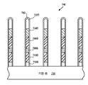
도 7a는 기판 스택 (substrate stack) 을 프로세싱하기 전의 기판 스택의 실시 예의 다이어그램이다.
도 7b는 프로세싱 동안 기판 스택의 또 다른 실시 예의 다이어그램이다.
도 7c는 도 7b의 기판 스택의 부분의 다이어그램이다.
도 7d는 도 7a의 기판 스택을 프로세싱한 후의 기판 스택의 또 다른 실시 예의 다이어그램이다.
도 8은 또 다른 실시 예의 플로우차트이다.
도 9a는 도 8에 도시된 실시 예에 따라 프로세싱된 스택의 개략적인 단면도이다.
도 9b는 도 8에 도시된 실시 예에 따라 프로세싱된 스택의 개략적인 단면도이다.
도 10은 실시 예에서 사용된 플라즈마 프로세싱 시스템의 개략도이다.Embodiments may be best understood with reference to the following description taken in conjunction with the accompanying drawings.
1 is a diagram of an embodiment of a system for illustrating three-state pulsing of a plurality of RF signals to achieve a balance between bow control and mask selectivity.
2A is an embodiment of a graph of a clock signal.
2B is a diagram of an embodiment of a graph to illustrate an embodiment of a digitally pulsed signal.
2C is an embodiment of a graph for illustrating an embodiment of an RF signal generated by a low-frequency RF generator and an embodiment of an RF signal generated by the high-frequency RF generator.
2D is an embodiment of a graph for illustrating an embodiment of an RF signal generated by a low-frequency RF generator and an embodiment of an RF signal generated by the high-frequency RF generator.
FIG. 3A is an embodiment of a graph to illustrate zoom-in of a portion of the RF signal of FIG. 2C, generated by a low frequency RF generator;
FIG. 3B is an embodiment of a graph to illustrate zoom-in of a portion of the RF signal of FIG. 2C, generated by a high frequency RF generator;
4A is an embodiment of a graph of the clock signal of FIG. 2A.
4B is a diagram of an embodiment of a graph to illustrate an embodiment of a digitally pulsed signal.
4C is an embodiment of a graph for illustrating an embodiment of an RF signal generated by a low-frequency RF generator and an embodiment of an RF signal generated by the high-frequency RF generator.
4D is an embodiment of a graph for illustrating an embodiment of an RF signal generated by a low-frequency RF generator and an embodiment of an RF signal generated by the high-frequency RF generator.
5A is an embodiment of a graph to illustrate zoom-in of a portion of the RF signal of FIG. 4C, generated by a low frequency RF generator.
FIG. 5B is an embodiment of a graph to illustrate zoom-in of a portion of the RF signal of FIG. 4C, generated by a high frequency RF generator.
6 is a diagram of an embodiment of a table for illustrating duty cycles associated with tri-states of RF signals generated by a low frequency RF generator and a high frequency RF generator.
7A is a diagram of an embodiment of a substrate stack prior to processing the substrate stack.
7B is a diagram of another embodiment of a substrate stack during processing.
7C is a diagram of a portion of the substrate stack of FIG. 7B .
7D is a diagram of another embodiment of a substrate stack after processing the substrate stack of FIG. 7A .
8 is a flowchart of another embodiment.
9A is a schematic cross-sectional view of a stack processed according to the embodiment shown in FIG. 8 ;
9B is a schematic cross-sectional view of a stack processed according to the embodiment shown in FIG. 8 ;
10 is a schematic diagram of a plasma processing system used in an embodiment.
다음의 실시 예들은 보우 제어 (bow control) 와 마스크 선택도 (mask selectivity) 사이의 균형 (balance) 을 달성하기 위한 멀티-상태 펄싱을 위한 시스템들 및 방법들을 기술한다. 본 실시 예들은 이들 구체적인 상세들 중 일부 또는 전부 없이 실시될 수도 있다는 것이 자명할 것이다. 다른 예들에서, 공지된 프로세스 동작들은 본 실시 예들을 불필요하게 모호하게 하지 않도록 상세히 기술되지 않았다.The following embodiments describe systems and methods for multi-state pulsing to achieve a balance between bow control and mask selectivity. It will be apparent that the present embodiments may be practiced without some or all of these specific details. In other instances, well-known process operations have not been described in detail so as not to unnecessarily obscure the present embodiments.
도 1은 보우 제어와 마스크 선택도 사이의 균형을 달성하기 위해 복수의 RF (radio frequency) 신호들의 3-상태 펄싱을 예시하기 위한 시스템 (100) 의 실시 예의 다이어그램이다. 시스템 (100) 은 RF 생성기 (RFGx), 또 다른 RF 생성기 (RFGy), 임피던스 매칭 네트워크 (IMN), 플라즈마 챔버 (106), 및 호스트 컴퓨터 (110) 를 포함한다.1 is a diagram of an embodiment of a
RF 생성기 (RFGx) 의 예는 400 ㎑ 또는 2 ㎒, 또는 13.56 ㎒의 동작 주파수를 갖는 RF 생성기와 같은 저주파수 RF 생성기이다. RF 생성기 (RFGy) 의 예는 27 ㎒ 또는 60 ㎒의 동작 주파수를 갖는 RF 생성기와 같은 고주파수 RF 생성기이다. 고주파수 RF 생성기의 동작 주파수는 저주파수 RF 생성기의 동작 주파수보다 크다는 것을 주의해야 한다.An example of an RF generator (RFGx) is a low frequency RF generator, such as an RF generator having an operating frequency of 400 kHz or 2 MHz, or 13.56 MHz. An example of an RF generator (RFGy) is a high frequency RF generator, such as an RF generator having an operating frequency of 27 MHz or 60 MHz. It should be noted that the operating frequency of the high frequency RF generator is larger than the operating frequency of the low frequency RF generator.
임피던스 매칭 네트워크 (IMN) 는 인덕터들, 커패시터들, 및 레지스터들과 같은 회로 컴포넌트들의 네트워크이다. 예를 들어, 임피던스 매칭 네트워크는 션트 (shunt) 커패시터 및 직렬 커패시터를 포함하는 회로이다. 션트 커패시터는 션트 커패시터의 일 단부에서 직렬 커패시터에 커플링되고 션트 커패시터의 반대편 단부는 접지 전위에 커플링된다. 직렬 커패시터는 임피던스 매칭 네트워크 (IMN) 의 입력부, 예컨대 입력부 (I2x) 또는 입력부 (I2y) 와 임피던스 매칭 네트워크 (IMN) 의 출력부 (O2) 사이에 커플링된다. 또 다른 예로서, 임피던스 매칭 네트워크 (IMN) 의 하나 이상의 회로 컴포넌트들은 임피던스 매칭 네트워크 (IMN) 의 하나 이상의 회로 컴포넌트들에 직렬로 또는 병렬로 커플링된다. 임피던스 매칭 네트워크 (IMN) 는 하나 이상의 회로 컴포넌트들을 포함하는 브랜치 (branch) 를 갖고, 브랜치는 입력부 (I2x) 와 출력부 (O2) 사이에 커플링된다. 유사하게, 임피던스 매칭 네트워크 (IMN) 는 하나 이상의 회로 컴포넌트들을 포함하는 또 다른 브랜치들을 갖고, 브랜치는 입력부 (I2y) 와 출력부 (O2) 사이에 커플링된다.An impedance matching network (IMN) is a network of circuit components such as inductors, capacitors, and resistors. For example, an impedance matching network is a circuit that includes a shunt capacitor and a series capacitor. The shunt capacitor is coupled to the series capacitor at one end of the shunt capacitor and the opposite end of the shunt capacitor is coupled to ground potential. The series capacitor is coupled between an input of the impedance matching network IMN, such as an input I2x or I2y, and an output O2 of the impedance matching network IMN. As another example, one or more circuit components of an impedance matching network (IMN) are coupled in series or parallel to one or more circuit components of an impedance matching network (IMN). The impedance matching network IMN has a branch comprising one or more circuit components, the branch coupled between an input I2x and an output O2. Similarly, the impedance matching network IMN has further branches comprising one or more circuit components, the branch coupled between the input I2y and the output O2.
플라즈마 챔버 (106) 는 척과 같은 기판 지지부 (104) 를 포함한다. 척은 척 내에 임베딩된 (embed) 하부 전극, 하부 전극 아래에 위치된 설비 플레이트, 및 하부 전극 위에 위치된 세라믹 플레이트를 포함한다. 플라즈마 챔버 (106) 는 접지 전위에 커플링된 상부 전극 (118) 을 더 포함한다. 호스트 컴퓨터 (110) 의 예들은 데스크탑 컴퓨터, 랩탑 컴퓨터, 제어기, 태블릿, 및 스마트 폰을 포함한다. The
RF 생성기 (RFGx) 는 DSP (digital signal processor) (DSPx), 전력 제어기 (PWRS1x), 다른 전력 제어기 (PWRS2x), 또 다른 전력 제어기 (PWRS0x), AFT (auto frequency tuner) (AFTx), 및 전력 공급부 (PSx) 를 포함한다. 본 명세서에 사용된 바와 같이, DSP의 예들은 마이크로프로세서, ASIC (application specific integrated circuit), 또는 PLD (programmable logic device) 를 포함하는 제어기를 포함한다. DSP의 제어기는 또한 복수의 데이터 또는 인스트럭션들을 동일 시간에 페치할 (fetch) 수 있는 메모리 디바이스를 포함한다. DSP의 메모리 디바이스는 DSP의 마이크로프로세서, ASIC, 또는 PLD에 커플링된다. 본 명세서에 사용된 바와 같이, 메모리 디바이스의 예들은 ROM (read-only memory), RAM (random access memory), 플래시 메모리, 저장 디스크 어레이, 하드 디스크, 등을 포함한다.The RF generator (RFGx) includes a digital signal processor (DSP) (DSPx), a power controller (PWRS1x), another power controller (PWRS2x), another power controller (PWRS0x), an auto frequency tuner (AFT) (AFTx), and a power supply. (PSx). As used herein, examples of DSP include a controller including a microprocessor, application specific integrated circuit (ASIC), or programmable logic device (PLD). The DSP's controller also includes a memory device capable of fetching a plurality of data or instructions at the same time. The DSP's memory device is coupled to the DSP's microprocessor, ASIC, or PLD. As used herein, examples of memory devices include read-only memory (ROM), random access memory (RAM), flash memory, storage disk arrays, hard disks, and the like.
본 명세서에 사용된 전력 제어기의 예는 마이크로컨트롤러를 포함한다. 예시를 위해, 전력 제어기는 마이크로프로세서, ASIC, 또는 PLD를 포함한다. 전력 제어기는 전력 제어기의 마이크로프로세서, ASIC, 또는 PLD에 커플링된 메모리 디바이스를 더 포함한다.An example of a power controller as used herein includes a microcontroller. For purposes of illustration, the power controller includes a microprocessor, ASIC, or PLD. The power controller further includes a memory device coupled to the microprocessor, ASIC, or PLD of the power controller.
본 명세서에 사용된 바와 같이, 튜너의 예는 마이크로컨트롤러를 포함한다. 예시를 위해, 튜너는 마이크로프로세서, ASIC, 또는 PLD를 포함한다. 튜너는 튜너의 PLD, 마이크로프로세서, 또는 ASIC에 커플링된 메모리 디바이스를 더 포함한다. As used herein, an example of a tuner includes a microcontroller. To illustrate, a tuner includes a microprocessor, ASIC, or PLD. The tuner further includes a memory device coupled to the PLD, microprocessor, or ASIC of the tuner.
본 명세서에 사용된 바와 같이, 전력 공급부의 예는 사인파 RF 신호와 같은 주기적인, 오실레이팅하는 전자 신호를 생성하는 RF 오실레이터 또는 전자 오실레이터를 포함한다.As used herein, examples of power supplies include RF oscillators or electronic oscillators that generate periodic, oscillating electronic signals, such as sinusoidal RF signals.
DSP (DSPx) 는 전력 제어기들 (PWRS1x, PWRS2x, 및 PWRS0x), 그리고 AFT (AFTx) 에 커플링된다. 더욱이, 전력 제어기들 (PWRS1x, PWRS2x, 및 PWRS0x) 각각은 전력 공급부 (PSx) 에 커플링된다. 또한, AFT (AFTSx) 는 전력 공급부 (PSx) 에 커플링된다.DSP (DSPx) is coupled to power controllers (PWRS1x, PWRS2x, and PWRS0x), and to AFT (AFTx). Moreover, each of the power controllers PWRS1x, PWRS2x, and PWRS0x is coupled to a power supply PSx. Also, the AFT (AFTSx) is coupled to the power supply (PSx).
RF 생성기 (RFGy) 는 DSP (DSPy), 전력 제어기 (PWRS1y), 또 다른 전력 제어기 (PWRS2y), 또 다른 전력 제어기 (PWRS0y), AFT (AFTy), 및 전력 공급부 (PSy) 를 포함한다. DSP (DSPy) 는 전력 제어기들 (PWRS1y, PWRS2y, 및 PWRS0y) 에 그리고 AFT (AFTy) 에 커플링된다. 더욱이, 전력 제어기들 (PWRS1y, PWRS2y, 및 PWRS0y) 각각은 전력 공급부 (PSy) 에 커플링된다. 또한, AFT (AFTSy) 는 전력 공급부 (PSy) 에 커플링된다.The RF generator (RFGy) includes a DSP (DSPy), a power controller (PWRS1y), another power controller (PWRS2y), another power controller (PWRS0y), an AFT (AFTy), and a power supply (PSy). DSP (DSPy) is coupled to power controllers (PWRS1y, PWRS2y, and PWRS0y) and to AFT (AFTy). Moreover, each of the power controllers PWRS1y, PWRS2y, and PWRS0y is coupled to a power supply PSy. Further, the AFT (AFTSy) is coupled to the power supply (PSy).
호스트 컴퓨터는 프로세서 (112) 및 메모리 디바이스 (114) 를 포함한다. 프로세서 (112) 는 메모리 디바이스 (114) 에 커플링된다. 본 명세서에 사용된 바와 같이, 프로세서의 예들은 마이크로프로세서, ASIC, CPU (central processing unit), 또는 PLD를 포함한다. The host computer includes a
프로세서 (112) 는 전달 케이블 (transfer cable) (120x) 을 통해 DSP (DSPx) 에 커플링되고 또 다른 전달 케이블 (120y) 을 통해 DSP (DSPy) 에 커플링된다. 본 명세서에 사용된 바와 같이, 전달 케이블의 예들은 프로세서 (112) 와 DSP 사이에서 데이터의 병렬 전달을 용이하게 하기 위한 병렬 전달 케이블, 프로세서 (112) 와 DSP 사이에서 직렬로 데이터의 전달을 용이하게 하기 위한 직렬 전달 케이블, 및 USB (universal serial bus) 표준을 적용함으로써 프로세서 (112) 와 DSP 사이의 데이터의 전달을 용이하게 하는 USB 전달 케이블을 포함한다.
전력 공급부 (PSx) 는 RF 케이블 (102x) 을 통해 임피던스 매칭 네트워크 (IMN) 의 입력부 (I2x) 에 커플링된다. 예를 들어, RF 생성기 (RFGx) 의 출력부 (O1x) 는 RF 케이블 (102x) 을 통해 입력부 (I2x) 에 커플링된다. 더욱이, 전력 공급부 (PSy) 는 RF 케이블 (102y) 을 통해 임피던스 매칭 네트워크 (IMN) 의 입력부 (I2y) 에 커플링된다. 예를 들어, RF 생성기 (RFGy) 의 출력부 (O1y) 는 RF 케이블 (102y) 을 통해 입력부 (I2y) 에 커플링된다.The power supply PSx is coupled via an
임피던스 매칭 네트워크 (IMN) 의 출력부 (O2) 는 RF 송신 라인 (122) 을 통해 기판 지지부 (104) 의 하부 전극에 커플링된다. RF 송신 라인 (122) 의 예는 알루미늄 솔리드 바 (solid bar) 와 같은, RF 슬리브 (RF sleeve) 에 의해 둘러싸인 절연체에 의해 둘러싸인 도전체를 포함한다. 절연체는 TeflonTM과 같은 유전체 재료일 수 있다. RF 송신 라인 (122) 의 또 다른 예는 하나 이상의 RF 스트랩들을 통해 내측 도전성 로드 (inner conductive rod) 및 외측 하우징을 갖는 RF 실린더에 커플링되는 도전체를 포함한다. RF 실린더의 내측 도전성 로드는 하부 전극에 커플링된다. 앞선 예에서 기술된 바와 같이, 도전체는 RF 슬리브에 의해 둘러싸인 절연체에 의해 둘러싸인다. RF 송신 라인 (122) 의 도전체는 임피던스 매칭 네트워크 (IMN) 의 출력부 (O2) 에 커플링된다. The output O2 of the impedance matching network IMN is coupled to the lower electrode of the
프로세서 (112) 는 클록 신호 및 클록 신호와 동기하여 디지털 펄싱된 신호 (108) 를 생성한다. 클록 신호 및 디지털 펄싱된 신호 (108) 의 예들은 이하에 제공된다. 디지털 펄싱된 신호 (108) 는 상태 S1, 상태 S2, 및 상태 S0과 같은 3 개의 상태들을 갖고, 이는 이하에 예시된다. The
프로세서 (112) 는 RF 생성기 (RFGx) 에 의해 생성될 RF 신호 (102x) 의 상태 S1에 대한 전력 레벨, RF 신호 (102x) 의 상태 S2에 대한 전력 레벨, 및 RF 신호 (102x) 의 상태 S0에 대한 전력 레벨을 메모리 디바이스 (114) 로부터 액세스, 예컨대 판독하거나 획득한다. 더욱이, 프로세서 (112) 는 RF 생성기 (RFGy) 에 의해 생성될 RF 신호 (102y) 의 상태 S1에 대한 전력 레벨, RF 신호 (102y) 의 상태 S2에 대한 전력 레벨, 및 RF 신호 (102y) 의 상태 S0에 대한 전력 레벨을 메모리 디바이스 (114) 로부터 액세스한다. RF 신호 (102x 및 102y) 각각은 사인파 신호이다.
일 실시 예에서, 상태에 대한 RF 신호의 전력 레벨은 상태 동안 RF 신호에 의해 달성되는 전력 레벨이라는 것을 주의해야 한다. 예를 들어, RF 신호의 상태 S1에 대한 전력 레벨은 디지털 펄싱된 신호 (108) 의 상태 S1의 인스턴스 (instance) 동안 달성되는 전력 레벨이고, RF 신호의 상태 S2에 대한 전력 레벨은 디지털 펄싱된 신호 (108) 의 상태 S2의 인스턴스 동안 달성되는 전력 레벨이고, 그리고 RF 신호의 상태 S0에 대한 전력 레벨은 디지털 펄싱된 신호 (108) 의 상태 S0의 인스턴스 동안 달성되는 전력 레벨이다.It should be noted that, in one embodiment, the power level of the RF signal for a state is the power level achieved by the RF signal during the state. For example, the power level for state S1 of the RF signal is the power level achieved during an instance of state S1 of the digital
프로세서 (112) 는 생성될 RF 신호 (102x) 의 상태들 (S1, S2, 및 S0) 에 대한 전력 레벨들을 전달 케이블 (120x) 을 통해 상태들 (S1, S2, 및 S0) 각각의 아이덴티티 (identity) 내에서 DSP (DSPx) 로 전송한다. 상태들 (S1, S2, 및 S0) 의 아이덴티티들을 갖는 RF 신호 (102x) 의 상태들 (S1, S2, 및 S0) 에 대한 전력 레벨들을 수신하면, DSP (DSPx) 는 상태들 (S1, S2, 및 S0) 의 아이덴티티들과 전력 제어기들 (PWRS1x, PWRS2x, 및 PWRS0x) 사이의 일대일 맵핑 또는 링크 또는 일대일 관계와 같은 대응 관계 (correspondence) 를, DSP (DSPx) 의 메모리 디바이스로부터 액세스하고, 그리고 상태 S1에 대한 전력 레벨을 전력 제어기 (PWRS1x) 로 전송하고, 상태 S2에 대한 전력 레벨을 전력 제어기 (PWRS2x) 로 전송하고, 그리고 상태 S0에 대한 전력 레벨을 전력 제어기 (PWRS0x) 로 전송한다. 전력 제어기 (PWRS1x, PWRS2x, 및 PWRS0x) 각각은 DSP (DSPx) 로부터 수신된 각각의 전력 레벨을 전력 제어기의 메모리 디바이스에 저장한다.The
유사하게, 프로세서 (112) 는 생성될 RF 신호 (102y) 의 상태들 (S1, S2, 및 S0) 에 대한 전력 레벨들을 전달 케이블 (120y) 을 통해 상태들 (S1, S2, 및 S0) 각각의 아이덴티티 내에서 DSP (DSPy) 로 전송한다. 상태들 (S1, S2, 및 S0) 의 아이덴티티들을 갖는 RF 신호 (102y) 의 상태들 (S1, S2, 및 S0) 에 대한 전력 레벨들을 수신하면, DSP (DSPy) 는 상태들 (S1, S2, 및 S0) 의 아이덴티티들과 전력 제어기들 (PWRS1y, PWRS2y, 및 PWRS0y) 사이의 일대일 맵핑 또는 링크 또는 일대일 관계와 같은 대응 관계를, DSP (DSPy) 의 메모리 디바이스로부터 액세스하고, 그리고 상태 S1에 대한 전력 레벨을 전력 제어기 (PWRS1y) 로 전송하고, 상태 S2에 대한 전력 레벨을 전력 제어기 (PWRS2y) 로 전송하고, 그리고 상태 S0에 대한 전력 레벨을 전력 제어기 (PWRS0y) 로 전송한다. 전력 제어기 (PWRS1y, PWRS2y, 및 PWRS0y) 각각은 DSP (DSPy) 로부터 수신된 각각의 전력 레벨을 전력 제어기의 메모리 디바이스에 저장한다.Similarly,
프로세서 (112) 는 디지털 펄싱된 신호 (108) 를 전달 케이블 (120x) 을 통해 DSP (DSPx) 로 전송하고 같은 시기에 (simultaneously) 디지털 펄싱된 신호 (108) 를 전달 케이블 (120y) 을 통해 DSP (DSPy) 로 전송한다. 디지털 펄싱된 신호 (108) 의 수신에 응답하여, DSP (DSPx) 는 디지털 펄싱된 신호 (108) 의 논리 레벨로부터 디지털 펄싱된 신호 (108) 의 상태를 식별한다. 예를 들어, DSP (DSPx) 는 디지털 펄싱된 신호 (108) 의 논리 레벨이 0이라고 결정하면 디지털 펄싱된 신호 (108) 의 상태를 S1으로 식별하고, 디지털 펄싱된 신호 (108) 의 논리 레벨이 1이라고 결정하면 디지털 펄싱된 신호 (108) 의 상태를 S2로 식별하고, 그리고 디지털 펄싱된 신호 (108) 의 논리 레벨이 2라고 결정하면 디지털 펄싱된 신호 (108) 의 상태를 S0으로 식별한다. The
디지털 펄싱된 신호 (108) 의 상태 S1 동안, 디지털 펄싱된 신호 (108) 의 상태를 S1로 식별하면 DSP (DSPx) 는 제어 신호를 전력 제어기 (PWRS1x) 로 전송한다. 디지털 펄싱된 신호 (108) 의 상태 S1 동안 제어 신호를 수신하는 것에 응답하여, 전력 제어기 (PWRS1x) 는 전력 제어기 (PWRS1x) 의 메모리 디바이스로부터 상태 S1에 대한 전력 레벨에 액세스하고, 상태 S1에 대한 전력 레벨을 포함하는 신호를 생성하고, 그리고 그 신호를 전력 공급부 (PSx) 로 전송한다. 디지털 펄싱된 신호 (108) 의 상태 S1 동안, 전력 제어기 (PWRS1x) 로부터 상태 S1에 대한 전력 레벨을 포함하는 신호를 수신하는 것에 응답하여, 전력 공급부 (PSx) 는 상태 S1에 대한 전력 레벨을 갖는 RF 신호 (102x) 의 부분을 생성한다.During state S1 of digital
유사하게, 디지털 펄싱된 신호 (108) 의 상태 S2 동안, 디지털 펄싱된 신호 (108) 의 상태를 S2로 식별하면 DSP (DSPx) 는 제어 신호를 전력 제어기 (PWRS2x) 로 전송한다. 디지털 펄싱된 신호 (108) 의 상태 S2 동안 제어 신호를 수신하면, 전력 제어기 (PWRS2x) 는 전력 제어기 (PWRS2x) 의 메모리 디바이스로부터 상태 S2에 대한 전력 레벨에 액세스하고, 상태 S2에 대한 전력 레벨을 포함하는 신호를 생성하고, 그리고 그 신호를 전력 공급부 (PSx) 로 전송한다. 디지털 펄싱된 신호 (108) 의 상태 S2 동안, 전력 제어기 (PWRS2x) 로부터 상태 S2에 대한 전력 레벨을 갖는 신호를 수신하는 것에 응답하여, 전력 공급부 (PSx) 는 상태 S2에 대한 전력 레벨을 갖는 RF 신호 (102x) 의 부분을 생성하도록 RF 신호 (102x) 를 상태 S1에 대한 전력 레벨로부터 상태 S2에 대한 전력 레벨로 전이한다. Similarly, during state S2 of digital
또한, 디지털 펄싱된 신호 (108) 의 상태 S0 동안, 디지털 펄싱된 신호 (108) 의 상태를 S0으로 식별하면 DSP (DSPx) 는 제어 신호를 전력 제어기 (PWRS0x) 로 전송한다. 디지털 펄싱된 신호 (108) 의 상태 S0 동안 제어 신호를 수신하면, 전력 제어기 (PWRS0x) 는 전력 제어기 (PWRS0x) 의 메모리 디바이스로부터 상태 S0에 대한 전력 레벨에 액세스하고, 상태 S0에 대한 전력 레벨을 포함하는 신호를 생성하고, 그리고 신호를 전력 공급부 (PSx) 로 전송한다. 디지털 펄싱된 신호 (108) 의 상태 S0 동안, 전력 제어기 (PWRS0x) 로부터 상태 S0에 대한 전력 레벨을 갖는 신호를 수신하는 것에 응답하여, 전력 공급부 (PSx) 는 상태 S0에 대한 전력 레벨을 갖는 RF 신호 (102x) 의 부분을 생성하도록 RF 신호 (102x) 를 상태 S2에 대한 전력 레벨로부터 상태 S0에 대한 전력 레벨로 전이한다. Also, during state SO of digital
유사한 방식으로, 디지털 펄싱된 신호 (108) 의 수신에 응답하여, DSP (DSPy) 는, DSP (DSPx) 가 디지털 펄싱된 신호 (108) 의 상태를 식별하는 상기 기술된 동일한 방식으로 디지털 펄싱된 신호 (108) 의 논리 레벨로부터 디지털 펄싱된 신호 (108) 의 상태를 식별한다. 예를 들어, DSP (DSPy) 는 디지털 펄싱된 신호 (108) 의 논리 레벨이 0이라고 결정하면 디지털 펄싱된 신호 (108) 의 상태를 S1으로 식별하고, 디지털 펄싱된 신호 (108) 의 논리 레벨이 1이라고 결정하면 디지털 펄싱된 신호 (108) 의 상태를 S2로 식별하고, 그리고 디지털 펄싱된 신호 (108) 의 논리 레벨이 2라고 결정하면 디지털 펄싱된 신호 (108) 의 상태를 S0으로 식별한다. In a similar manner, in response to receiving the digitally
디지털 펄싱된 신호 (108) 의 상태 S1 동안, 디지털 펄싱된 신호 (108) 의 상태를 S1이라고 식별하면 DSP (DSPy) 는 제어 신호를 전력 제어기 (PWRS1y) 로 전송한다. 또한, 디지털 펄싱된 신호 (108) 의 상태 S1 동안 제어 신호를 수신하면, 전력 제어기 (PWRS1y) 는 전력 제어기 (PWRS1y) 의 메모리 디바이스로부터 상태 S1에 대한 전력 레벨에 액세스하고, 상태 S1에 대한 전력 레벨을 포함하는 신호를 생성하고, 그리고 그 신호를 전력 공급부 (PSy) 로 전송한다. 디지털 펄싱된 신호 (108) 의 상태 S1 동안, 전력 제어기 (PWRS1y) 로부터 상태 S1에 대한 전력 레벨을 갖는 신호를 수신하는 것에 응답하여, 전력 공급부 (PSy) 는 상태 S1에 대한 전력 레벨을 갖는 RF 신호 (102y) 의 부분을 생성한다.During state S1 of digital
유사하게, 디지털 펄싱된 신호 (108) 의 상태 S2 동안, 디지털 펄싱된 신호 (108) 의 상태를 S2로 식별하면 DSP (DSPy) 는 제어 신호를 전력 제어기 (PWRS2y) 로 전송한다. 디지털 펄싱된 신호 (108) 의 상태 S2 동안 제어 신호를 수신하면, 전력 제어기 (PWRS2y) 는 전력 제어기 (PWRS2y) 의 메모리 디바이스로부터 상태 S2에 대한 전력 레벨에 액세스하고, 상태 S2에 대한 전력 레벨을 포함하는 신호를 생성하고, 그리고 그 신호를 전력 공급부 (PSy) 로 전송한다. 디지털 펄싱된 신호 (108) 의 상태 S2 동안, 전력 제어기 (PWRS2y) 로부터 상태 S2에 대한 전력 레벨을 갖는 신호를 수신하는 것에 응답하여, 전력 공급부 (PSy) 는 상태 S2에 대한 전력 레벨을 갖는 RF 신호 (102y) 의 부분을 생성하도록 RF 신호 (102y) 를 상태 S1에 대한 전력 레벨로부터 상태 S2에 대한 전력 레벨로 전이한다. Similarly, during state S2 of digital
또한, 디지털 펄싱된 신호 (108) 의 상태 S0 동안, 디지털 펄싱된 신호 (108) 의 상태를 S0으로 식별하면 DSP (DSPy) 는 제어 신호를 전력 제어기 (PWRS0y) 로 전송한다. 디지털 펄싱된 신호 (108) 의 상태 S0 동안 제어 신호를 수신하는 것에 응답하여, 전력 제어기 (PWRS0y) 는 전력 제어기 (PWRS0y) 의 메모리 디바이스로부터 상태 S0에 대한 전력 레벨에 액세스하고, 상태 S0에 대한 전력 레벨을 포함하는 신호를 생성하고, 그리고 신호를 전력 공급부 (PSy) 로 전송한다. 디지털 펄싱된 신호 (108) 의 상태 S0 동안, 전력 제어기 (PWRS0y) 로부터 상태 S0에 대한 전력 레벨을 갖는 신호를 수신하는 것에 응답하여, 전력 공급부 (PSy) 는 상태 S0에 대한 전력 레벨을 갖는 RF 신호 (102y) 의 부분을 생성하도록 RF 신호 (102y) 를 상태 S2에 대한 전력 레벨로부터 상태 S0에 대한 전력 레벨로 전이한다. Also, during state SO of digital
RF 신호 (102x) 는 전력 공급부 (PSx) 에 의해 출력부 (O1x) 및 RF 케이블 (116x) 을 통해 임피던스 매칭 네트워크 (IMN) 의 입력부 (I2x) 로 공급된다. 또한, RF 신호 (102y) 는 전력 공급부 (PSy) 에 의해 출력부 (O1y) 및 RF 케이블 (116y) 을 통해 임피던스 매칭 네트워크 (IMN) 의 입력부 (I2y) 로 공급된다. 임피던스 매칭 네트워크 (IMN) 는 입력부 (I2x) 에서 RF 신호 (102x) 를 수신하고, 그리고 RF 신호 (102x) 가 입력부 (I2x) 에 커플링된 임피던스 매칭 네트워크 (IMN) 의 브랜치 회로를 통해 전달되기 때문에, RF 신호 (102x) 의 임피던스는 제 1 수정된 RF 신호를 출력하도록 브랜치 회로에 의해 수정된다. 유사하게, 임피던스 매칭 네트워크 (IMN) 는 입력부 (I2y) 에서 RF 신호 (102y) 를 수신하고, 그리고 RF 신호 (102y) 가 입력부 (I2x) 에 커플링된 임피던스 매칭 네트워크 (IMN) 의 브랜치 회로를 통해 전달되기 때문에, RF 신호 (102y) 의 임피던스는 제 2 수정된 RF 신호를 출력하도록 브랜치 회로에 의해 수정된다. RF 신호들 (102x 및 102y) 의 임피던스들은 출력부 (O2) 에 커플링된 부하의 임피던스를 입력부들 (I2x 및 I2y) 에 커플링된 소스의 임피던스와 매칭시키도록 수정된다. 출력부 (O2) 에 커플링된 부하의 예는 RF 송신 라인 (122) 및 플라즈마 챔버 (106) 를 포함한다. 입력부들 (I2x 및 I2y) 에 커플링된 소스의 예는 RF 케이블들 (116x 및 116y) 및 RF 생성기들 (RFGx 및 RFGy) 를 포함한다. 입력부 (I2x) 에 커플링된 브랜치 회로는 출력부 (O2) 에서 결합된 수정된 RF 신호 (124) 를 출력하기 위해 제 1 수정된 RF 신호와 제 2 수정된 RF 신호를 결합하도록 출력부 (O2) 에서 입력부 (I2y) 에 커플링된 브랜치 회로에 연결된다.The
결합된 수정된 RF 신호 (124) 는 임피던스 매칭 네트워크 (IMN) 의 출력부 (O2) 로부터 RF 송신 라인 (122) 을 통해 기판 지지부 (104) 의 하부 전극으로 전송된다. 부가하여, 하나 이상의 프로세스 가스들, 예컨대 불소 함유 가스, 또는 산소 함유 가스, 또는 이들의 조합은 플라즈마 챔버 (106) 내의 상부 전극 (118) 과 기판 지지부 (104) 사이의 갭에 공급된다. 결합된 수정된 RF 신호 (124) 및 하나 이상의 프로세스 가스들이 플라즈마 챔버 (106) 에 같은 시기에 공급될 때, 플라즈마는 기판 S를 프로세싱하기 위해 갭 내에 스트라이킹되거나 유지된다. 기판 S의 예들은 기판 층 상에 형성되는 반도체 웨이퍼, 및 기판 층 상에 형성되는 기판 스택을 포함한다. 기판 S를 프로세싱하는 예들은 기판 층 상에 옥사이드 층, 나이트라이드 층, 실리콘 나이트라이드 층, 마스크 층, 또는 이들의 2 이상의 조합과 같은 하나 이상의 재료들을 증착하는 것을 포함한다. 기판을 프로세싱하는 다른 예들은 기판 S를 에칭하거나 기판 S를 스퍼터링하거나 기판 S를 세정하는 것을 포함한다. The combined modified
일 실시 예에서, 기판 지지부 (104) 의 하부 전극은 접지 전위에 커플링되고 상부 전극 (118) 은 임피던스 매칭 네트워크 (IMN) 의 출력부 (O2) 에 커플링된다.In one embodiment, the lower electrode of the
일 실시 예에서, 임피던스 매칭 네트워크 (IMN) 를 통해 기판 지지부 (104) 의 하부 전극에 커플링되는 RF 생성기들 (RFGx 및 RFGy) 에 더하여 하나 이상의 RF 생성기들은 임피던스 매칭 네트워크를 통해 상부 전극 (118) 에 커플링된다.In one embodiment, one or more RF generators in addition to RF generators (RFGx and RFGy) coupled to the lower electrode of the
일 실시 예에서, DSP (DSPx), 전력 제어기 (PWRS1x), 전력 제어기 (PWRS2x), 전력 제어기 (PWRS0x), 및 AFT (AFTSx) 중 하나 이상에 의해 수행되는 것으로 본 명세서에 기술된 기능들 또는 동작들은 RF 생성기 (RFGx) 의 프로세서 또는 제어기에 의해 수행된다. 예를 들어, 전력 제어기 (PWRS1x), 전력 제어기 (PWRS2x), 전력 제어기 (PWRS0x), 및 AFT (AFTx) 에 의해 수행되는 것으로 본 명세서에 기술된 기능들은 DSP (DSPx) 에 의해 수행된다.In one embodiment, the functions or operations described herein as being performed by one or more of DSP (DSPx), power controller (PWRS1x), power controller (PWRS2x), power controller (PWRS0x), and AFT (AFTSx) These are performed by the processor or controller of the RF generator (RFGx). For example, functions described herein as being performed by power controller (PWRS1x), power controller (PWRS2x), power controller (PWRS0x), and AFT (AFTx) are performed by DSP (DSPx).
유사하게, 일 실시 예에서, DSP (DSPy), 전력 제어기 (PWRS1y), 전력 제어기 (PWRS2y), 전력 제어기 (PWRS0y), 및 AFT (AFTSy) 중 하나 이상에 의해 수행되는 것으로 본 명세서에 기술된 기능들 또는 동작들은 RF 생성기 (RFGy) 의 프로세서 또는 제어기에 의해 수행된다. 예를 들어, 전력 제어기 (PWRS1y), 전력 제어기 (PWRS2y), 전력 제어기 (PWRS0y), 및 AFT (AFTy) 에 의해 수행되는 것으로 본 명세서에 기술된 기능들은 DSP (DSPy) 에 의해 수행된다.Similarly, in one embodiment, the functions described herein as being performed by one or more of DSP (DSPy), power controller (PWRS1y), power controller (PWRS2y), power controller (PWRS0y), and AFT (AFTSy) The operations or operations are performed by the processor or controller of the RF generator (RFGy). For example, functions described herein as being performed by power controller (PWRS1y), power controller (PWRS2y), power controller (PWRS0y), and AFT (AFTy) are performed by DSP (DSPy).
일 실시 예에서, DSP (DSPx), 전력 제어기 (PWRS1x), 전력 제어기 (PWRS2x), 전력 제어기 (PWRS0x), AFT (AFTSx), DSP (DSPy), 전력 제어기 (PWRS1y), 전력 제어기 (PWRS2y), 전력 제어기 (PWRS0y), 및 AFT (AFTSy) 중 하나 이상에 의해 수행되는 것으로 본 명세서에 기술된 기능들 또는 동작들은 프로세서 (112) 에 의해 수행된다.In one embodiment, DSP (DSPx), power controller (PWRS1x), power controller (PWRS2x), power controller (PWRS0x), AFT (AFTSx), DSP (DSPy), power controller (PWRS1y), power controller (PWRS2y), Functions or operations described herein as being performed by one or more of a power controller (PWRS0y), and an AFT (AFTSy) are performed by the
일 실시 예에서, 클록 신호는 프로세서 (112) 대신 클록 소스에 의해 생성된다.In one embodiment, the clock signal is generated by a clock source instead of the
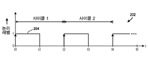
도 2a는 상기 기술된 클록 신호인 클록 신호 (204) 의 그래프 (202) 의 실시 예이다. 클록 신호 (204) 는 프로세서 (112) 에 의해 생성된다. 그래프 (202) 는 y-축에 논리 레벨을 그리고 x-축에 시간 t를 플롯팅한다 (plot). 그래프 (202) 의 y-축은 논리 레벨 0 및 논리 레벨 1을 포함한다. 그래프 (202) 의 x-축은 복수의 시간들 (t0, t1, t2, t3, t4, 및 t5) 을 포함한다. 2A is an embodiment of a
그래프 (202) 의 x-축 상의 임의의 2 개의 연속적인 시간들 사이의 시간 간격은 동일하다. 예를 들어, 시간 t0과 시간 t1 사이의 시간 간격은 시간 t1과 시간 t2 사이의 시간 간격과 같고, 그리고 시간 t1과 시간 t2 사이의 시간 간격은 시간 t2와 t3 사이의 시간 간격과 같다. 시간 t3과 시간 t4 사이의 시간 간격은 시간 t2와 시간 t3 사이의 시간 간격과 같고, 그리고 시간 t4와 시간 t5 사이의 시간 간격은 시간 t3과 t4 사이의 시간 간격과 같다. 시간 t1은 시간 t0에 연속된다. 유사하게, 시간 t2는 시간 t1에 연속적이고, 시간 t3은 시간 t2에 연속적이고, 시간 t4는 시간 t3에 연속적이고, 그리고 시간 t5는 시간 t4에 연속적이다.The time interval between any two consecutive times on the x-axis of
클록 신호 (204) 는 논리 레벨 0과 논리 레벨 1 사이에서 주기적으로 전이한다. 예를 들어, 클록 신호 (204) 의 사이클 1의 전반부 동안, 클록 신호 (204) 는 논리 레벨 1에 있다. 시간 t1에서, 클록 신호 (210) 는 논리 레벨 1 로부터 논리 레벨 0 으로 전이한다. 클록 신호 (204) 의 사이클 1의 후반부 동안, 클록 신호 (204) 는 논리 레벨 0을 갖는다. 시간 t2에서, 클록 신호 (204) 는 논리 레벨 0 으로부터 논리 레벨 1로 전이한다. 클록 신호 (204) 의 사이클 2의 전반부 동안, 클록 신호 (204) 는 논리 레벨 1에 있다. 시간 t3에서, 클록 신호 (204) 는 논리 레벨 1로부터 논리 레벨 0으로 전이한다. 클록 신호 (204) 의 사이클 2의 후반부 동안, 클록 신호는 논리 레벨 0에 있다. 시간 t4에서, 클록 신호 (204) 는 논리 레벨 0으로부터 논리 레벨 1로 전이한다.
클록 신호 (204) 의 사이클 2는 클록 신호 (204) 의 사이클 1에 연속적이다. 예를 들어, 클록 신호 (204) 의 사이클 1과 사이클 2 사이에 다른 클록 사이클들은 없다. 사이클 1은 시간 t0부터 시간 t2까지 발생하고 사이클 2는 시간 t2부터 시간 t4까지 발생한다.
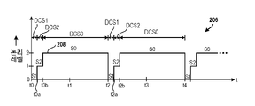
도 2b는 디지털 펄싱된 신호 (208) 의 실시 예를 예시하기 위한 그래프 (206) 의 실시 예의 다이어그램이다. 디지털 펄싱된 신호 (208) 는 도 1의 디지털 펄싱된 신호 (108) 의 예이다. 그래프 (206) 는 디지털 펄싱된 신호 (208) 의 논리 레벨을 y-축에 그리고 시간 t를 x-축에 플롯팅한다. 그래프 (206) 의 y-축은 논리 레벨들 (0, 1, 및 2) 을 포함한다. 그래프 (206) 의 x-축은 시간 t0, 시간 t0a, 시간 t0b, 시간 t1, 시간 t2, 시간 t2a, 시간 t2b, 시간 t3, 및 시간 t4를 포함한다. 시간 t0a는 시간 t0과 시간 t0b 사이에 발생하고, 그리고 시간 t0b는 시간 t0a와 시간 t1 사이에 발생한다. 더욱이, 시간 t2a는 시간 t2와 시간 t2b 사이에 발생하고 그리고 시간 t2b는 시간 t2a와 시간 t3 사이에 발생한다.2B is a diagram of an embodiment of a
디지털 펄싱된 신호 (208) 는 상태들 (S1, S2, 및 S0) 사이에서 주기적으로 전이한다. 예를 들어, 디지털 펄싱된 신호 (208) 는 시간 t0으로부터 시간 t0a까지, 논리 레벨 0에 의해 규정되는 상태 S1을 갖는다. 예시를 위해, 디지털 펄싱된 신호 (208) 의 상태 S1 동안, 디지털 펄싱된 신호 (208) 는 논리 레벨 0에 있다. 디지털 펄싱된 신호 (208) 는 시간 t0a에서 논리 레벨 0으로부터 논리 레벨 1로 전이한다. 디지털 펄싱된 신호 (208) 의 상태 S2는 논리 레벨 1에 의해 규정된다. 예시를 위해, 디지털 펄싱된 신호 (208) 의 상태 S2 동안, 디지털 펄싱된 신호 (208) 는 논리 레벨 1에 있다.The digital
디지털 펄싱된 신호 (208) 는 시간 t0a부터 시간 t0b까지 상태 S2를 갖는다. 시간 t0b에서, 디지털 펄싱된 신호 (208) 는 상태 S2로부터 상태 S0으로 전이하고, 상태 S0은 논리 레벨 2에 의해 규정된다. 예시를 위해, 디지털 펄싱된 신호 (208) 의 상태 S0 동안, 디지털 펄싱된 신호 (208) 는 논리 레벨 2에 있다. 디지털 펄싱된 신호 (208) 는 시간 t0b부터 시간 t2까지 상태 S0을 갖는다. 시간 t2에서, 디지털 펄싱된 신호 (208) 는 상태 S0으로부터 상태 S1로 다시 전이한다. Digital
디지털 펄싱된 신호 (208) 는 시간 t2부터 시간 t2a까지 상태 S1을 갖는다. 디지털 펄싱된 신호 (208) 는 시간 t2a에서 상태 S1로부터 상태 S2로 전이한다. 디지털 펄싱된 신호 (208) 는 시간 t2a부터 시간 t2b까지 상태 S2를 갖는다. 시간 t2b에서, 디지털 펄싱된 신호 (208) 는 상태 S2로부터 상태 S0으로 전이한다. 디지털 펄싱된 신호 (208) 는 시간 t2b부터 시간 t4까지 상태 S0을 갖는다. 시간 t4에서, 디지털 펄싱된 신호 (208) 는 상태 S0으로부터 다시 상태 S1로 전이한다. Digital
디지털 펄싱된 신호 (208) 의 상태들 (S1, S2, 및 S0) 각각의 복수의 인스턴스들이 발생한다는 것을 주의해야 한다. 예를 들어, 디지털 펄싱된 신호 (208) 의 상태 S1의 제 1 인스턴스는 시간 t0과 시간 t0a 사이에 발생하고, 그리고 디지털 펄싱된 신호 (208) 의 상태 S1의 제 2 인스턴스는 시간 t2와 시간 t2a 사이에 발생한다. 또 다른 예로서, 디지털 펄싱된 신호 (208) 의 상태 S2의 제 1 인스턴스는 시간 t0a와 시간 t0b 사이에 발생하고, 그리고 디지털 펄싱된 신호 (208) 의 상태 S2의 제 2 인스턴스는 시간 t2a와 시간 t2b 사이에 발생한다. 또 다른 예로서, 디지털 펄싱된 신호 (208) 의 상태 S0의 제 1 인스턴스는 시간 t0b와 시간 t2 사이에 발생하고, 디지털 펄싱된 신호 (208) 의 상태 S0의 제 2 인스턴스는 시간 t2b와 시간 t4 사이에 발생한다. 또 다른 예로서, 디지털 펄싱된 신호 (208) 의 상태 S2의 제 1 인스턴스는 디지털 펄싱된 신호 (208) 의 상태 S1의 제 1 인스턴스에 연속적이고 그리고 디지털 펄싱된 신호 (208) 의 상태 S0의 제 1 인스턴스는 디지털 펄싱된 신호 (208) 의 상태 S2의 제 1 인스턴스에 연속적이다. 디지털 펄싱된 신호 (208) 의 상태 S1의 제 2 인스턴스는 디지털 펄싱된 신호 (208) 의 상태 S0의 제 1 인스턴스에 연속적이다. 또한, 디지털 펄싱된 신호 (208) 의 상태 S2의 제 2 인스턴스는 디지털 펄싱된 신호 (208) 의 상태 S1의 제 2 인스턴스에 연속적이고 그리고 디지털 펄싱된 신호 (208) 의 상태 S0의 제 2 인스턴스는 디지털 펄싱된 신호 (208) 의 상태 S2의 제 2 인스턴스에 연속적이다. It should be noted that multiple instances of each of the states S1 , S2 , and S0 of the digital
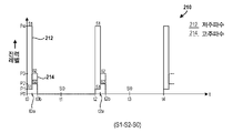
도 2c는 RF 생성기 (RFGx) (도 1) 에 의해 생성된 RF 신호 (212) 의 실시 예 및 RF 생성기 (RFGy) (도 1) 에 의해 생성된 RF 신호 (214) 의 실시 예를 예시하기 위한 그래프 (210) 의 실시 예이다. RF 신호 (212) 는 RF 신호 (102x) (도 1) 의 예이고, RF 신호 (214) 는 RF 신호 (102y) (도 1) 의 예이다. 2C is to illustrate an embodiment of an
RF 신호들 (212 및 214) 은 디지털 펄싱된 신호 (208) 에 동기화된다. 예를 들어, RF 신호들 (212 및 214) 각각은 상태 S1로부터 상태 S2로의 디지털 펄싱된 신호 (208) 의 전이의 시간 t0a에서 상태 S1로부터 상태 S2 로 전이를 개시한다. 또 다른 예로서, RF 신호들 (212 및 214) 각각은 상태 S2로부터 상태 S0으로의 디지털 펄싱된 신호 (208) 의 전이의 시간 t0b에서 상태 S2로부터 상태 S0으로 전이를 개시한다. 또 다른 예로서, RF 신호들 (212 및 214) 각각은 상태 S0으로부터 상태 S1로의 디지털 펄싱된 신호 (208) 의 전이의 시간 t2에서 상태 S0으로부터 상태 S1로 전이를 개시한다.RF signals 212 and 214 are synchronized to the digitally
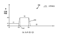
그래프 (210) 는 RF 신호들 (212 및 214) 의 전력 레벨들을 플롯팅한다. 예를 들어, 그래프 (210) 의 y-축은 전력 레벨들 (P0, P1, P2, P3, 및 P4) 을 포함한다. 전력 레벨 P1은 전력 레벨 P0보다 크다. 또한, 전력 레벨 P2는 전력 레벨 P1보다 크고 전력 레벨 P3은 전력 레벨 P2보다 크다. 전력 레벨 P4는 전력 레벨 P3보다 크다.
본 명세서에 사용된 바와 같이, 전력 레벨은 RF 신호의 예컨대, 피크-투-피크 진폭인, 엔벨로프 (envelope) 이다. 예를 들어, 전력 레벨들 (P4, P2, 및 P0) 은 RF 신호 (102x) 의 엔벨로프들이고 전력 레벨들 (P1, P3, 및 P0) 은 RF 신호 (102y) 의 엔벨로프들이다. 또 다른 예로서, 전력 레벨은 예컨대, 전력 레벨의 값보다 크거나 보다 작은, 전력 레벨로부터 미리 결정된 범위 내에 있는 하나 이상의 피크-투-피크 전력 값들을 포함한다. 또 다른 예로서, 전력 레벨은 전력 레벨의 모든 피크-투-피크 전력 값들의 평균 또는 중앙값과 같은 통계적 값이다. 또 다른 예로서, 전력 레벨은 전력 레벨의 모든 피크-투-피크 전력 값들 중 가장 높다. 또 다른 예로서, 전력 레벨은 전력 레벨의 모든 피크-투-피크 전력 값들 중 가장 낮다.As used herein, a power level is the envelope, eg, peak-to-peak amplitude, of an RF signal. For example, power levels P4 , P2 , and P0 are envelopes of
또한, 제 1 전력 레벨은 제 2 전력 레벨과 상이하다. 예를 들어, 전력 레벨 P0의 하나 이상의 전력 값들은 전력 레벨 P1의 하나 이상의 전력 값들을 배제하고 (exclusive) 전력 레벨 P2의 하나 이상의 전력 값들은 전력 레벨들 (P0 및 P1) 각각의 하나 이상의 전력 값들을 배제한다. Also, the first power level is different from the second power level. For example, one or more power values of power level P0 are exclusive of one or more power values of power level P1 and one or more power values of power level P2 are one or more power values of each of power levels P0 and P1. exclude them
또한, 그래프 (210) 는 x-축에 시간 t를 플롯팅한다. 예를 들어, 그래프 (210) 의 x-축은 시간들 (t0, t0a, t0b, t1, t2, t2a, t2b, t3, 및 t4) 을 포함한다.
RF 신호 (212) 는 이하에 기술된 방식으로 RF 신호 (212) 의 상태들 (S1, S2, 및 S0) 사이에서 주기적으로 전이한다. 유사하게, RF 신호 (214) 는 이하에 기술된 방식으로 RF 신호 (214) 의 상태들 (S1, S2, 및 S0) 사이에서 주기적으로 전이한다.RF signal 212 periodically transitions between states S1 , S2 , and S0 of
RF 신호 (212) 의 상태 S1은 전력 레벨 P4에 의해 규정된다. 예를 들어, 디지털 펄싱된 신호 (208) 또는 RF 신호 (212) 의 상태 S1 동안, RF 신호 (212) 는 전력 레벨 P4를 갖는다. State S1 of
RF 신호 (212) 는 시간 t0a로부터 시간 윈도우 (time window) 내에서 상태 S1로부터 상태 S2로 전이한다. RF 신호 (212) 의 상태 S2는 전력 레벨 P2에 의해 규정된다. 예를 들어, 디지털 펄싱된 신호 (208) 또는 RF 신호 (212) 의 상태 S2 동안, RF 신호 (212) 는 전력 레벨 P2를 갖는다.RF signal 212 transitions from state S1 to state S2 within a time window from time t0a. State S2 of
본 명세서에 기술된 RF 신호는 일 상태로부터 연속적인 상태로 순간적으로 전이하지 않는다는 것을 주의해야 한다. 예를 들어, 상태 S1로부터 상태 S2 로의 RF 신호 (212) 의 전이는 순간적이지 않다. 예시를 위해, 상태 S1로부터 상태 S2 로의 RF 신호 (212) 의 전이는 시간 윈도우 내에서 발생한다. 또 다른 예로서, 본 명세서에 사용된 바와 같이, 시간부터의 전이의 시간 윈도우는 그 시간 후 상태 동안 발생하는 시간 기간이다. 예시를 위해, 시간 t0a부터의 시간 윈도우는 시간 t0a 후 디지털 펄싱된 신호 (208) 의 상태 S2 동안 발생하는 시간 기간이다. 시간 t0a 후의 시간 기간은 시간 t0a부터 시간 t0a와 시간 t0b 사이의 시간까지 디지털 펄싱된 신호 (208) 의 상태 S2 동안 발생한다. It should be noted that the RF signals described herein do not instantaneously transition from one state to a continuous state. For example, the transition of RF signal 212 from state S1 to state S2 is not instantaneous. For illustrative purposes, the transition of the RF signal 212 from state S1 to state S2 occurs within a time window. As another example, as used herein, a time window of a transition from time is a period of time that occurs during a state after that time. For illustrative purposes, the time window from time t0a is the time period that occurs during state S2 of digital
RF 신호 (212) 는 시간 t0b부터의 시간 윈도우 내에서 상태 S2로부터 상태 S0으로 전이한다. RF 신호 (212) 의 상태 S0은 전력 레벨 P0에 의해 규정된다. 예를 들어, 디지털 펄싱된 신호 (208) 또는 RF 신호 (212) 의 상태 S0 동안, RF 신호 (212) 는 전력 레벨 P0을 갖는다.RF signal 212 transitions from state S2 to state S0 within a time window from time t0b. The state S0 of the
RF 신호 (212) 는 시간 t2부터의 시간 윈도우 내에서 상태 S0으로부터 상태 S1로 전이한다. RF 신호 (212) 는 시간 t2a부터의 시간 윈도우 내에서 상태 S1로부터 상태 S2로 전이하고 그리고 시간 t2b부터의 시간 윈도우 내에서 상태 S2로부터 상태 S0으로 전이한다. RF signal 212 transitions from state S0 to state S1 within a time window from time t2. RF signal 212 transitions from state S1 to state S2 within the time window from time t2a and from state S2 to state S0 within the time window from time t2b.
유사하게, 디지털 펄싱된 신호 (208) 의 상태 S1 동안, RF 신호 (214) 는 전력 레벨 P1을 갖는다. RF 신호 (214) 의 상태 S1은 전력 레벨 P1에 의해 규정된다. 예를 들어, 디지털 펄싱된 신호 (208) 또는 RF 신호 (214) 의 상태 S1 동안, RF 신호 (214) 는 전력 레벨 P1을 갖는다. Similarly, during state S1 of digital
RF 신호 (214) 는 시간 t0a부터의 시간 윈도우 내에서 상태 S1로부터 상태 S2로 전이한다. RF 신호 (214) 의 상태 S2는 전력 레벨 P3에 의해 규정된다. 예를 들어, 디지털 펄싱된 신호 (208) 또는 RF 신호 (214) 의 상태 S2 동안, RF 신호 (214) 는 전력 레벨 P3을 갖는다.RF signal 214 transitions from state S1 to state S2 within a time window from time t0a. State S2 of
RF 신호 (214) 는 시간 t0b부터의 시간 윈도우 내에서 상태 S2로부터 상태 S0으로 전이한다. RF 신호 (214) 의 상태 S0은 전력 레벨 P0에 의해 규정된다. 예를 들어, 디지털 펄싱된 신호 (208) 또는 RF 신호 (214) 의 상태 S0 동안, RF 신호 (214) 는 전력 레벨 P0을 갖는다.RF signal 214 transitions from state S2 to state S0 within a time window from time t0b. The state S0 of the
RF 신호 (214) 는 시간 t2부터의 시간 윈도우 내에서 상태 S0으로부터 상태 S1로 전이한다. RF 신호 (214) 는 시간 t2a부터의 시간 윈도우 내에서 상태 S1로부터 상태 S2로 전이하고 그리고 시간 t2b부터의 시간 윈도우 내에서 상태 S2로부터 상태 S0으로 전이한다.RF signal 214 transitions from state S0 to state S1 within a time window from time t2. RF signal 214 transitions from state S1 to state S2 within the time window from time t2a and from state S2 to state S0 within the time window from time t2b.
시간 t0과 시간 t0a 사이의 RF 신호 (212) 의 상태 S1은 RF 신호 (212) 의 상태 S1의 제 1 인스턴스이고 그리고 시간 t2와 시간 t2a 사이의 RF 신호 (212) 의 상태 S1은 RF 신호 (212) 의 상태 S1의 제 2 인스턴스이다. 유사하게, 시간 t0a와 시간 t0b 사이의 RF 신호 (212) 의 상태 S2는 RF 신호 (212) 의 상태 S2의 제 1 인스턴스이고 그리고 시간 t2a와 시간 t2b 사이의 RF 신호 (212) 의 상태 S2는 RF 신호 (212) 의 상태 S2의 제 2 인스턴스이다. 또한, 시간 t0b와 시간 t2 사이의 RF 신호 (212) 의 상태 S0은 RF 신호 (212) 의 상태 S0의 제 1 인스턴스이고 그리고 시간 t2b와 시간 t4 사이의 RF 신호 (212) 의 상태 S0은 RF신호 (212) 의 상태 S0의 제 2 인스턴스이다.State S1 of RF signal 212 between time t0 and time t0a is a first instance of state S1 of
유사하게, 시간 t0과 시간 t0a 사이의 RF 신호 (214) 의 상태 S1은 RF 신호 (214) 의 상태 S1의 제 1 인스턴스이고 그리고 시간 t2와 시간 t2a 사이의 RF 신호 (214) 의 상태 S1은 R F 신호 (214) 의 상태 S1의 제 2 인스턴스이다. 유사하게, 시간 t0a와 시간 t0b 사이의 RF 신호 (214) 의 상태 S2는 RF 신호 (214) 의 상태 S2의 제 1 인스턴스이고 그리고 시간 t2a와 시간 t2b 사이의 RF 신호 (214) 의 상태 S2는 RF 신호 (214) 의 상태 S2의 제 2 인스턴스이다. 또한, 시간 t0b와 시간 t2 사이의 RF 신호 (214) 의 상태 S0은 RF 신호 (214) 의 상태 S0의 제 1 인스턴스이고 그리고 시간 t2b와 시간 t4 사이의 RF 신호 (214) 의 상태 S0은 RF 신호 (214) 의 상태 S0의 제 2 인스턴스이다.Similarly, state S1 of RF signal 214 between time t0 and time t0a is a first instance of state S1 of
도 2d는 RF 생성기 (RFGx) (도 1) 에 의해 생성된 RF 신호 (216) 의 실시 예 및 RF 생성기 (RFGy) (도 1) 에 의해 생성된 RF 신호 (218) 의 실시 예를 예시하기 위한 그래프 (215) 의 실시 예이다. RF 신호 (216) 는 RF 신호 (102x) (도 1) 의 예이고, RF 신호 (218) 는 RF 신호 (102y) (도 1) 의 예이다. 2D is to illustrate an embodiment of an
그래프 (215) 는 RF 신호들 (216 및 218) 의 전력 레벨들을 플롯팅한다. 또한, 그래프 (215) 는 x-축에 시간 t를 플롯팅한다. 예를 들어, 그래프 (215) 의 x-축은 시간들 (t0, t1, t2, t3, 및 t4) 을 포함한다. RF 신호들 (216 및 218) 의 상태들 (S1 내지 S3) 의 듀티 사이클들은 도 2c에 예시된 상태들 (S1 내지 S3) 의 듀티 사이클들과 상이하다는 것을 주의해야 한다. 예를 들어, RF 신호들 (216 및 218) 의 상태 S1의 듀티 사이클은 25%이고, RF 신호들 (216 및 218) 의 상태 S2의 듀티 사이클은 40 %이고, 그리고 RF의 신호들 (216 및 218) 의 상태 S3의 듀티 사이클은 35%이다.
도 3a는 RF 신호 (212) 의 부분의 줌-인을 예시하기 위한 그래프 (302) 의 실시 예이다. 그래프 (302) 는 시간 t에 대한 RF 신호 (212) 의 전력 레벨들을 플롯팅한다. RF 신호 (212) 는 시간 t0a부터의 시간 윈도우 내에서 전력 레벨 P4로부터 전력 레벨 P2로 전이한다. 예를 들어, RF 신호 (212) 는 시간 t0a와 시간 t0a1 사이의 시간 기간 동안 전력 레벨 P4로부터 전력 레벨 P2로 전이한다. 시간 t0a1은 RF 신호 (212) 또는 디지털 펄싱된 신호 (208) (도 2b) 의 상태 S2 동안 발생하고, 시간 t0a와 시간 t0b 사이에 발생한다. 유사하게, RF 신호 (212) 는 시간 t0b부터의 시간 윈도우 내에서 전력 레벨 P2로부터 전력 레벨 P0으로 전이한다. 3A is an embodiment of a
도 3b는 RF 신호 (214) 의 부분의 줌-인을 예시하기 위한 그래프 (304) 의 실시 예이다. 그래프 (304) 는 시간 t에 대한 RF 신호 (214) 의 전력 레벨들을 플롯팅한다. RF 신호 (214) 는 시간 t0a부터의 시간 윈도우 내에서 전력 레벨 P1로부터 전력 레벨 P3으로 전이한다. 예를 들어, RF 신호 (214) 는 시간 t0a와 시간 t0a2 사이의 시간 기간 동안 전력 레벨 P1로부터 전력 레벨 P3으로 전이한다. 시간 t0a2은 RF 신호 (214) 또는 디지털 펄싱된 신호 (208) (도 2b) 의 상태 S2 동안 발생하고, 시간 t0a와 시간 t0b 사이에 발생한다. 유사하게, RF 신호 (214) 는 시간 t0b부터의 시간 윈도우 내에서 전력 레벨 P3로부터 전력 레벨 P0으로 전이한다.3B is an embodiment of a
도 4a는 클록 신호 (204) 의 그래프 (202) 의 일 실시 예이다.4A is one embodiment of a
도 4b는 디지털 펄싱된 신호 (404) 의 실시 예를 예시하기 위한 그래프 (402) 의 실시 예의 다이어그램이다. 디지털 펄싱된 신호 (404) 는 도 1의 디지털 펄싱된 신호 (108) 의 예이다. 그래프 (402) 는 디지털 펄싱된 신호 (404) 의 논리 레벨을 y-축에 그리고 시간 t를 x-축에 플롯팅한다. 그래프 (402) 의 y-축은 논리 레벨들 (0, 1, 및 2) 을 포함한다. 그래프 (402) 의 x-축은 시간 t0, 시간 t0a, 시간 t1, 시간 t1a, 시간 t2, 시간 t2a, 시간 t3, 시간 t3a, 및 시간 t4를 포함한다. 시간 t1a는 시간 t1과 시간 t2 사이에 발생하고, 시간 t3a는 시간 t3과 시간 t4 사이에 발생한다. 4B is a diagram of an embodiment of a
디지털 펄싱된 신호 (404) 는 상태들 (S1, S0, 및 S2) 사이에서 주기적으로 전이한다. 예를 들어, 디지털 펄싱된 신호 (404) 는 시간 t0으로부터 시간 t0a까지, 논리 레벨 0에 의해 규정되는 상태 S1을 갖는다. 예시를 위해, 상태 S1 동안, 디지털 펄싱된 신호 (208) 는 논리 레벨 0에 있다. 디지털 펄싱된 신호 (404) 는 시간 t0a에서 논리 레벨 0으로부터 논리 레벨 2로 전이한다. 디지털 펄싱된 신호 (404) 의 상태 S0은 논리 레벨 2에 의해 규정된다. 예시를 위해, 상태 S0 동안, 디지털 펄싱된 신호 (404) 는 논리 레벨 2에 있다.The digital
디지털 펄싱된 신호 (404) 는 시간 t0a로부터 시간 t1a까지 상태 S0을 갖는다. 시간 t1a에서, 디지털 펄싱된 신호 (404) 는 상태 S0으로부터 상태 S2로 전이하고, 상태 S2는 논리 레벨 1에 의해 규정된다. 예시를 위해, 상태 S2 동안, 디지털 펄싱된 신호 (404) 는 논리 레벨 1에 있다.Digital
시간 t2에서, 디지털 펄싱된 신호 (404) 는 상태 S2로부터 상태 S1로 다시 전이한다. 디지털 펄싱된 신호 (404) 는 시간 t2부터 시간 t2a까지 상태 S1을 갖는다. 디지털 펄싱된 신호 (404) 는 시간 t2a에서 상태 S1로부터 상태 S0으로 전이한다. 디지털 펄싱된 신호 (404) 는 시간 t2a부터 시간 t3a까지 상태 S0을 갖는다. 시간 t3a에서, 디지털 펄싱된 신호 (404) 는 상태 S0으로부터 상태 S2로 전이한다. 디지털 펄싱된 신호 (404) 는 시간 t3a부터 시간 t4까지 상태 S2를 갖는다. 시간 t4에서, 디지털 펄싱된 신호 (404) 는 상태 S2로부터 상태 S1로 다시 전이한다. At time t2, the digitally pulsed signal 404 transitions back from state S2 to state S1. Digital
디지털 펄싱된 신호 (404) 의 상태들 (S1, S0, 및 S2) 각각의 복수의 인스턴스들이 발생한다는 것을 주의해야 한다. 예를 들어, 디지털 펄싱된 신호 (404) 의 상태 S1의 제 1 인스턴스는 시간 t0과 시간 t0a 사이에 발생하고, 그리고 디지털 펄싱된 신호 (404) 의 상태 S1의 제 2 인스턴스는 시간 t2와 시간 t2a 사이에 발생한다. 또 다른 예로서, 디지털 펄싱된 신호 (404) 의 상태 S0의 제 1 인스턴스는 시간 t0a와 시간 t1a 사이에 발생하고, 그리고 디지털 펄싱된 신호 (404) 의 상태 S0의 제 2 인스턴스는 시간 t2a와 시간 t3a 사이에 발생한다. 또 다른 예로서, 디지털 펄싱된 신호 (404) 의 상태 S2의 제 1 인스턴스는 시간 t1a와 시간 t2 사이에 발생하고, 그리고 디지털 펄싱된 신호 (404) 의 상태 S2의 제 2 인스턴스는 시간 t3a와 시간 t4 사이에 발생한다. 또 다른 예로서, 상태 S0의 제 1 인스턴스는 디지털 펄싱된 신호 (404) 의 상태 S1의 제 1 인스턴스에 연속적이고 그리고 디지털 펄싱된 신호 (404) 의 상태 S2의 제 1 인스턴스는 상태 S0의 제 1 인스턴스에 연속적이다. 디지털 펄싱된 신호 (404) 의 상태 S1의 제 2 인스턴스는 디지털 펄싱된 신호 (404) 의 상태 S2의 제 1 인스턴스에 연속적이다. 또한, 디지털 펄싱된 신호 (404) 의 상태 S0의 제 2 인스턴스는 디지털 펄싱된 신호 (404) 의 상태 S1의 제 2 인스턴스에 연속적이고 그리고 디지털 펄싱된 신호 (404) 의 상태 S2의 제 2 인스턴스는 디지털 펄싱된 신호 (404) 의 상태 S0의 제 2 인스턴스에 연속적이다. It should be noted that multiple instances of each of the states S1 , S0 , and S2 of the digitally
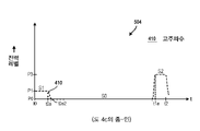
도 4c는 RF 생성기 (RFGx) (도 1) 에 의해 생성된 RF 신호 (408) 의 실시 예 및 RF 생성기 (RFGy) (도 1) 에 의해 생성된 RF 신호 (410) 의 실시 예를 예시하기 위한 그래프 (406) 의 실시 예이다. RF 신호 (408) 는 RF 신호 (102x) (도 1) 의 예이고, RF 신호 (410) 는 RF 신호 (102y) (도 1) 의 예이다.4C is to illustrate an embodiment of an
RF 신호들 (408 및 410) 은 디지털 펄싱된 신호 (404) 에 동기화된다. 예를 들어, RF 신호들 (408 및 410) 각각은 상태 S1로부터 상태 S0으로의 디지털 펄싱된 신호 (404) 의 전이의 시간 t0a에서 상태 S1로부터 상태 S0으로의 전이를 개시한다. 또 다른 예로서, RF 신호들 (408 및 410) 각각은 상태 S0으로부터 상태 S2 로의 디지털 펄싱된 신호 (404) 의 전이 시간 t1a에서 상태 S0으로부터 상태 S2로의 전이를 개시한다. 또 다른 예로서, RF 신호들 (408 및 410) 각각은 상태 S2로부터 상태 S1로의 디지털 펄싱된 신호 (404) 의 전이 시간 t2에서 상태 S2로부터 상태 S1로의 전이를 개시한다.RF signals 408 and 410 are synchronized to the digitally
그래프 (406) 는 RF 신호들 (408 및 410) 의 전력 레벨들을 플롯팅한다. 예를 들어, 그래프 (406) 의 y-축은 전력 레벨들 (P0, P1, P2, P3, 및 P4) 을 포함한다. 또한, 그래프 (406) 는 x-축에 시간 t를 플롯팅한다. 예를 들어, 그래프 (406) 의 x-축은 시간들 (t0, t0a, t1, t1a, t2, t2a, t3, t3a, 및 t4) 을 포함한다.
RF 신호 (408) 는 이하에 기술된 방식으로 RF 신호 (408) 의 상태들 (S1, S0, 및 S2) 사이에서 주기적으로 전이한다. 유사하게, RF 신호 (410) 는 이하에 기술된 방식으로 RF 신호 (410) 의 상태들 (S1, S0, 및 S2) 사이에서 주기적으로 전이한다.RF signal 408 periodically transitions between states S1 , S0 , and S2 of
RF 신호 (408) 의 상태 S1은 전력 레벨 P4에 의해 규정된다. 예를 들어, 디지털 펄싱된 신호 (404) 또는 RF 신호 (408) 의 상태 S1 동안, RF 신호 (408) 는 전력 레벨 P4를 갖는다. State S1 of
RF 신호 (408) 는 시간 t0a부터의 시간 윈도우 내에서 상태 S1로부터 상태 S0으로 전이한다. RF 신호 (408) 의 상태 S0은 전력 레벨 P0에 의해 규정된다. 예를 들어, 디지털 펄싱된 신호 (404) 또는 RF 신호 (408) 의 상태 S0 동안, RF 신호 (408) 는 전력 레벨 P0을 갖는다.RF signal 408 transitions from state S1 to state S0 within a time window from time t0a. The state S0 of the
RF 신호 (408) 는 시간 t1a부터의 시간 윈도우 내에서 상태 S0으로부터 상태 S2로 전이한다. RF 신호 (408) 의 상태 S2는 전력 레벨 P2에 의해 규정된다. 예를 들어, 디지털 펄싱된 신호 (404) 또는 RF 신호 (408) 의 상태 S2 동안, RF 신호 (408) 는 전력 레벨 P2를 갖는다.RF signal 408 transitions from state S0 to state S2 within a time window from time t1a. State S2 of
RF 신호 (408) 는 시간 t2부터의 시간 윈도우 내에서 상태 S2로부터 상태 S1로 전이한다. RF 신호 (408) 는 시간 t2a부터의 시간 윈도우 내에서 상태 S1로부터 상태 S0으로 전이하고 그리고 시간 t3a부터의 시간 윈도우 내에서 상태 S0으로부터 상태 S2로 전이한다. RF signal 408 transitions from state S2 to state S1 within a time window from time t2. RF signal 408 transitions from state S1 to state S0 within the time window from time t2a and from state S0 to state S2 within the time window from time t3a.
유사하게, 디지털 펄싱된 신호 (404) 의 상태 S1 동안, RF 신호 (410) 는 전력 레벨 P1을 갖는다. RF 신호 (410) 의 상태 S1은 전력 레벨 P1에 의해 규정된다. 예를 들어, 디지털 펄싱된 신호 (404) 또는 RF 신호 (410) 의 상태 S1 동안, RF 신호 (410) 는 전력 레벨 P1을 갖는다. Similarly, during state S1 of the digitally
RF 신호 (410) 는 시간 t0a부터의 시간 윈도우 내에서 상태 S1로부터 상태 S0으로 전이한다. RF 신호 (410) 의 상태 S0은 전력 레벨 P0에 의해 규정된다. 예를 들어, 디지털 펄싱된 신호 (404) 또는 RF 신호 (410) 의 상태 S0 동안, RF 신호 (410) 는 전력 레벨 P0을 갖는다.RF signal 410 transitions from state S1 to state S0 within a time window from time t0a. The state S0 of the
RF 신호 (410) 는 시간 t1a부터의 시간 윈도우 내에서 상태 S0으로부터 상태 S2로 전이한다. RF 신호 (410) 의 상태 S2는 전력 레벨 P3에 의해 규정된다. 예를 들어, 디지털 펄싱된 신호 (404) 또는 RF 신호 (410) 의 상태 S2 동안, RF 신호 (410) 는 전력 레벨 P3을 갖는다. RF signal 410 transitions from state S0 to state S2 within a time window from time t1a. State S2 of
RF 신호 (410) 는 시간 t2부터의 시간 윈도우 내에서 상태 S2로부터 상태 S1로 전이한다. RF 신호 (410) 는 시간 t2a부터의 시간 윈도우 내에서 상태 S1로부터 상태 S0으로 전이하고 그리고 시간 t3a부터의 시간 윈도우 내에서 상태 S0으로부터 상태 S2로 전이한다.RF signal 410 transitions from state S2 to state S1 within a time window from time t2. RF signal 410 transitions from state S1 to state S0 within the time window from time t2a and from state S0 to state S2 within the time window from time t3a.
시간 t0과 시간 t0a 사이의 RF 신호 (408) 의 상태 S1은 RF 신호 (408) 의 상태 S1의 제 1 인스턴스이고 그리고 시간 t2와 시간 t2a 사이의 RF 신호 (408) 의 상태 S1은 R F 신호 (408) 의 상태 S1의 제 2 인스턴스이다. 유사하게, 시간 t0a과 시간 t1a 사이의 RF 신호 (408) 의 상태 S0은 RF 신호 (408) 의 상태 S0의 제 1 인스턴스이고 그리고 시간 t2a와 시간 t3a 사이의 RF 신호 (408) 의 상태 S0은 R F 신호 (408) 의 상태 S0의 제 2 인스턴스이다. 또한, 시간 t1a과 시간 t2 사이의 RF 신호 (408) 의 상태 S2는 RF 신호 (408) 의 상태 S2의 제 1 인스턴스이고 그리고 시간 t3a와 시간 t4 사이의 RF 신호 (408) 의 상태 S2는 RF 신호 (408) 의 상태 S2의 제 2 인스턴스이다.State S1 of RF signal 408 between time t0 and time t0a is a first instance of state S1 of
유사하게, 시간 t0과 시간 t0a 사이의 RF 신호 (410) 의 상태 S1은 RF 신호 (410) 의 상태 S1의 제 1 인스턴스이고 그리고 시간 t2와 시간 t2a 사이의 RF 신호 (410) 의 상태 S1은 R F 신호 (410) 의 상태 S1의 제 2 인스턴스이다. 유사하게, 시간 t0a와 시간 t1a 사이의 RF 신호 (410) 의 상태 S0은 RF 신호 (410) 의 상태 S0의 제 1 인스턴스이고 그리고 시간 t2a와 시간 t3a 사이의 RF 신호 (410) 의 상태 S0은 R F 신호 (410) 의 상태 S0의 제 2 인스턴스이다. 또한, 시간 t1a와 시간 t2 사이의 RF 신호 (410) 의 상태 S2는 RF 신호 (410) 의 상태 S2의 제 1 인스턴스이고 그리고 시간 t3a와 시간 t4 사이의 RF 신호 (410) 의 상태 S2는 RF 신호 (410) 의 상태 S2의 제 2 인스턴스이다.Similarly, state S1 of RF signal 410 between time t0 and time t0a is a first instance of state S1 of
도 4d는 RF 생성기 (RFGx) (도 1) 에 의해 생성된 RF 신호 (412) 의 실시 예 및 RF 생성기 (RFGy) (도 1) 에 의해 생성된 RF 신호 (414) 의 실시 예를 예시하기 위한 그래프 (411) 의 실시 예이다. RF 신호 (412) 는 RF 신호 (102x) (도 1) 의 예이고, RF 신호 (414) 는 RF 신호 (102y) (도 1) 의 예이다. 4D is to illustrate an embodiment of an
그래프 (411) 는 RF 신호들 (412 및 414) 의 전력 레벨들을 플롯팅한다. 또한, 그래프 (411) 는 x-축에 시간 t를 플롯팅한다. 예를 들어, 그래프 (411) 의 x-축은 시간 (t0, t1, t2, t3, 및 t4) 을 포함한다. RF 신호들 (412 및 414) 의 상태들 (S1 내지 S3) 의 듀티 사이클들은 도 4c에 예시된 상태들 (S1 내지 S3) 의 듀티 사이클들과 상이하다는 것을 주의해야 한다. 예를 들어, RF 신호들 (412 및 414) 의 상태 S1의 듀티 사이클은 25%이고, RF 신호들 (412 및 414) 의 상태 S2의 듀티 사이클은 40 %이고, RF의 상태 S3의 듀티 사이클은 신호들 (412 및 414) 은 35 %이다.
도 5a는 RF 신호 (408) 의 부분의 줌-인을 예시하기 위한 그래프 (502) 의 실시 예이다. 그래프 (502) 는 시간 t에 대한 RF 신호 (408) 의 전력 레벨들을 플롯팅한다. RF 신호 (408) 는 시간 t0a부터의 시간 윈도우 내에서 전력 레벨 P4로부터 전력 레벨 P0으로 전이한다. 예를 들어, RF 신호 (408) 는 시간 t0a와 시간 t0a1 사이의 시간 기간 동안 전력 레벨 P4로부터 전력 레벨 P0으로 전이한다. 시간 t0a1은 RF 신호 (408) 및 디지털 펄싱된 신호 (404) (도 4b) 의 상태 S0 동안 발생하고 시간 t0a와 시간 t1a 사이에 발생한다. 유사하게, RF 신호 (408) 는 시간 t1a부터의 시간 윈도우 내에서 전력 레벨 P0로부터 전력 레벨 P2로 전이한다. 5A is an embodiment of a
도 5b는 RF 신호 (410) 의 부분의 줌-인을 예시하기 위한 그래프 (504) 의 실시 예이다. 그래프 (504) 는 시간 t에 대한 RF 신호 (410) 의 전력 레벨들을 플롯팅한다. RF 신호 (410) 는 시간 t0a로부터의 시간 윈도우 내에서 전력 레벨 P1로부터 전력 레벨 P0으로 전이한다. 예를 들어, RF 신호 (410) 는 시간 t0a와 시간 t0a2 사이의 시간 기간 동안 전력 레벨 P1로부터 전력 레벨 P0으로 전이한다. 시간 t0a2는 RF 신호 (410) 및 디지털 펄싱된 신호 (404) (도 4b) 의 상태 S0 동안 발생하고, 시간 t0a와 t1a 사이에 발생한다. 유사하게, RF 신호 (410) 는 시간 t1a로부터의 시간 윈도우 내에서 전력 레벨 P0으로부터 전력 레벨 P3으로 전이한다.5B is an embodiment of a
도 6은 상태들 (S1, S2, 및 S0) 과 연관된 듀티 사이클들, 및 상태들 (S1, S2, 및 S0) 동안 전력 레벨들을 예시하기 위한 표 (600) 의 실시 예의 다이어그램이다. 예로서, RF 신호 (102x) (도 1) 또는 디지털 펄싱된 신호 (108) (도 1) 의 상태 S1의 듀티 사이클은 클록 신호 (204) (도 2a) 의 사이클의 3% 내지 25%를 포함하는 범위이다. 예시를 위해, RF 신호 (102x) 또는 디지털 펄싱된 신호 (108) 의 상태 S1의 듀티 사이클은 클록 신호 (204) 의 사이클의 3 % 내지 5 %를 포함하는 범위이다. 또 다른 예로서, RF 신호 (102y) (도 1) 또는 디지털 펄싱된 신호 (108) 의 상태 S1의 듀티 사이클은 클록 신호 (204) (도 2a) 의 사이클의 3 % 내지 25 %를 포함하는 범위이다. 예시를 위해, RF 신호 (102y) 또는 디지털 펄싱된 신호 (108) 의 상태 S1의 듀티 사이클은 클록 신호 (204) 의 사이클의 3 % 내지 5 %를 포함하는 범위이다.6 is a diagram of an embodiment of a table 600 to illustrate the duty cycles associated with states S1 , S2 , and S0 , and power levels during states S1 , S2 , and S0 . By way of example, the duty cycle of state S1 of
또 다른 예로서, RF 신호 (102x) 또는 디지털 펄싱된 신호 (108) 의 상태 S2의 듀티 사이클은 클록 신호 (204) 의 사이클의 3 % 내지 50 %를 포함하는 범위이다. 예시를 위해, RF 신호 (102x) 또는 디지털 펄싱된 신호 (108) 의 상태 S1의 듀티 사이클은 클록 신호 (204) 의 사이클의 3 % 내지 5 %를 포함하는 범위이다. 또 다른 예로서, RF 신호 (102y) 또는 디지털 펄싱된 신호 (108) 의 상태 S2의 듀티 사이클은 클록 신호 (204) 의 사이클의 3 % 내지 50 %를 포함하는 범위이다. 예시를 위해, RF 신호 (102y) 또는 디지털 펄싱된 신호 (108) 의 상태 S2의 듀티 사이클은 클록 신호 (204) 의 사이클의 3 % 내지 5 %를 포함하는 범위이다.As another example, the duty cycle of state S2 of
또 다른 예로서, RF 신호 (102x) 또는 디지털 펄싱된 신호 (108) 의 상태 S0의 듀티 사이클은 클록 신호 (204) 의 사이클의 25 % 내지 94 %를 포함하는 범위이다. 또 다른 예로서, RF 신호 (102y) 또는 디지털 펄싱된 신호 (108) 의 상태 S2의 듀티 사이클은 클록 신호 (204) 의 사이클의 25 % 내지 94 %를 포함하는 범위이다. As another example, the duty cycle of state S0 of
또 다른 예로서, 상태 S1 동안, RF 신호 (102x) 의 전력 레벨과 RF 신호 (102y) 의 전력 레벨 사이의 비는 6 내지 10을 포함하는 범위이다. 예시를 위해, RF 신호 (102x) 의 전력 레벨은 10 ㎾ (킬로와츠) 이고 RF 신호 (102y) 의 전력 레벨은 1 ㎾이다. RF 신호들 (102x 및 102y) 의 상태 S1의 듀티 사이클들 및 상태 S1 동안 RF 신호 (102x) 와 RF 신호 (102y) 사이의 전력 레벨 비들은 마스크 선택도를 증가시킨다는 것을 주의해야 하고, 이는 이하에 더 기술된다. 또 다른 예로서, 상태 S2 동안, RF 신호 (102x) 의 전력 레벨과 RF 신호 (102y) 의 전력 레벨 사이의 비는 0.2 내지 1을 포함하는 범위이다. 또 다른 예로서, 상태 S2 동안, RF 신호 (102x) 의 전력 레벨과 RF 신호 (102y) 의 전력 레벨 사이의 비는 0.2 내지 1 미만을 포함하는 범위이다. 1 미만의 비의 예는 0.4 또는 0.45 또는 0.5 또는 0.8 또는 0.9이다. 예시를 위해, 상태 S2 동안, RF 신호 (102x) 의 전력 레벨은 2 ㎾이고 RF 신호 (102y) 의 전력 레벨은 5 ㎾이다. 또 다른 예시로서, 상태 S2 동안, RF 신호 (102x) 의 전력 레벨은 RF 신호 (102y) 의 전력 레벨의 20 % 내지 100 %이다. 또 다른 예시로서, 상태 S2 동안, RF 신호 (102x) 의 전력 레벨은 RF 신호 (102y) 의 전력 레벨의 20 % 내지 100 % 미만이다. 또 다른 예시로서, 상태 S2 동안, RF 신호 (102x) 의 전력 레벨은 대략 0이 아니고 RF 신호 (102y) 의 전력 레벨은 대략 0이 아니다. 더 예시하기 위해, 상태 S2 동안 RF 신호 (102x) 의 전력 레벨은 0 내지 300 W의 범위가 아니고 상태 S2 동안 RF 신호 (102y) 의 전력 레벨은 0 내지 300 W의 범위가 아니다. RF 신호들 (102x 및 102y) 의 상태 S2의 듀티 사이클들 및 상태 S2 동안 RF 신호 (102x) 와 RF 신호 (102y) 사이의 전력 레벨 비들은 보우 패시베이션 (bow passivation) 을 증가시킨다는 것을 주의해야 하고, 이는 이하에 더 기술된다. 또 다른 예로서, 상태 S0 동안, RF 신호 (102x) 의 전력 레벨은 0 W 내지 300 W를 포함하는 범위이고, RF 신호 (102y) 의 전력 레벨은 0 W 내지 300 W를 포함하는 범위이다. As another example, during state S1 , the ratio between the power level of the
RF 신호들 (102x 및 102y) 의 상태 S0 동안 RF 신호들 (102x 및 102y) 의 전력 레벨들은 거의 같다는 것을 주의해야 한다. 예를 들어, RF 신호들 (102x 및 102y) 의 상태 S0 동안 RF 신호들 (102x 및 102y) 의 전력 레벨들은 서로로부터 미리 결정된 범위 내에 있다. 예시를 위해, RF 신호 (102x) 의 상태 S0 동안 RF 신호 (102x) 의 전력 레벨은 0 내지 300 W의 범위이고 RF 신호 (102y) 의 상태 S0 동안 RF 신호 (102y) 의 전력 레벨은 0 내지 300 W의 범위이다. 또 다른 예로서, RF 신호들 (102x 및 102y) 의 상태 S0 동안 RF 신호들 (102x 및 102y) 의 전력 레벨들은 0이다. It should be noted that the power levels of
RF 신호 (102x) 의 상태들 (S1 내지 S3) 의 듀티 사이클들의 합 또는 총계는 클록 신호 (204) 의 클록 사이클의 100 %와 같다는 것을 더 주의해야 한다. 예를 들어, RF 신호들 (102x 및 102y) 각각의 상태들 (S1, S2, 및 S0) 의 제 1 인스턴스들은 클록 신호 (204) 의 사이클 1 (도 2a) 을 점유하고 (occupy) 그리고 RF 신호들 (102x 및 102y) 각각의 상태들 (S1, S2, 및 S0) 의 제 2 인스턴스들은 클록 신호 (204) 의 사이클 2 (도 2a) 을 점유한다. It should further be noted that the sum or sum of the duty cycles of states S1 to S3 of
일 실시 예에서, RF 신호의 상태의 듀티 사이클은 RF 신호가 시간 기간 동안 고유한 전력 레벨을 갖는 시간 기간이다. 예를 들어, RF 신호 (212) 의 상태 S1의 듀티 사이클은 RF 신호 (212) 가 전력 레벨 P4를 갖는 동안인 시간 t0와 시간 t0a 사이의 시간 기간이다. 또 다른 예로서, RF 신호 (212) 의 상태 S2의 듀티 사이클은 RF 신호 (212) 가 전력 레벨 P2를 갖는 동안인 시간 t0a와 시간 t0b 사이의 시간 기간이다. 또 다른 예로서, RF 신호 (212) 의 상태 S0의 듀티 사이클은 RF 신호 (212) 가 전력 레벨 P0을 갖는 동안인 시간 t0b와 시간 t2 사이의 시간 기간이다. 또 다른 예로서, &&상태 S1동안 RF 신호 (214) 의 상태 S1의 듀티 사이클은 RF 신호 (214) 가 전력 레벨 P1을 갖는 동안인 시간 t0과 시간 t0a 사이의 시간 기간이다. 또 다른 예로서, RF 신호 (214) 의 상태 S2의 듀티 사이클은 RF 신호 (214) 가 전력 레벨 P3을 갖는 동안인 시간 t0a와 시간 t0b 사이의 시간 기간이다. 또 다른 예로서, RF 신호 (214) 의 상태 S0의 듀티 사이클은 RF 신호 (214) 가 전력 레벨 P0을 갖는 동안인 시간 t0b와 시간 t2 사이의 시간 기간이다.In one embodiment, the duty cycle of the state of the RF signal is a period of time during which the RF signal has a unique power level during the period of time. For example, the duty cycle of state S1 of
도 7a는 기판 스택 (700) 의 실시 예의 다이어그램이다. 기판 스택 (700) 은 플라즈마 챔버 (106) (도 1) 내에서 프로세싱되기 전에 기판 S의 예이다. 기판 스택 (700) 은 실리콘으로 이루어진 기판 층 (714) 을 포함한다. 기판 스택 (700) 은 기판 층 (714) 의 상단 상에 오버레이된 정지 층 (stop layer) (712) 을 더 포함한다. 정지 층 (712) 의 예는 옥사이드 또는 나이트라이드과 같은 유전체로부터 제조되는 에칭 정지 층이다. 옥사이드 층 (710) 은 정지 층 (712) 의 상단 상에 증착된다. 또한, 실리콘 나이트라이드 (SiN) 층 (708) 은 옥사이드 층 (710) 의 상단 상에 오버레이되고, 옥사이드 층 (706) 은 실리콘 나이트라이드 층 (708) 의 상단 상에 증착되고, 또 다른 실리콘 나이트라이드 층 (704) 은 옥사이드 층 (706) 의 상단 상에 증착되고, 그리고 마스크 층 (702) 은 실리콘 나이트라이드 층 (704) 의 상단 상에 증착된다. 마스크 층 (702) 은 불투명한 플레이트 또는 막인 포토 리소그래피 마스크이다.7A is a diagram of an embodiment of a
일 실시 예에서, 옥사이드 층 (706) 대신, 나이트라이드 층이 사용된다. 유사하게, 일 실시 예에서, 옥사이드 층 (710) 대신, 나이트라이드 층이 사용된다.In one embodiment, instead of the
도 7b는 마스크 층 (702) (도 7a) 의 피처 (702B) 상에 증착된 패시베이션 층 (722) 과 실리콘 나이트라이드 층 (704) (도 7a) 의 피처 (704B) 상에 증착된 패시베이션 층 (724) 사이의 균형을 예시하기 위한 기판 스택 (720) 의 실시 예의 다이어그램이다. 기판 스택 (720) 은 마스크 층 (702) 의 피처 (702A), 피처 (702B), 실리콘 나이트라이드 층 (704) 의 피처 (704A), 피처 (704B), 옥사이드 층 (706) (도 7a) 의 피처들 (706A 및 706B), 실리콘 나이트라이드 층 (708), 및 옥사이드 층 (710) 을 포함한다. 기판 스택 (720) 의 나머지 층들 (712 및 714) (도 7a) 은 도 7b에 도시되지 않는다.7B shows a
기판 스택 (720) 은 플라즈마 챔버 (106) (도 1) 내에서 도 7a의 기판 스택 (700) 을 에칭함으로써 제조된다. 기판 스택 (720) 은 기판 스택 (700) 의 일부 에칭 후 기판 S (도 1) 의 예이다. RF 신호들 (102x 및 102y) (도 1) 에 기초하여 생성된 결합된 수정된 RF 신호 (124) (도 1) 를 플라즈마 챔버 (106) 로 공급함으로써, 기판 스택 (700) 은 패시베이션 층 (722) 과 패시베이션 층 (724) 사이의 균형을 달성하도록 에칭된다. 예를 들어, 패시베이션 층 (722) 과 패시베이션 층 (724) 사이의 균형은 패시베이션 층들 (722 및 724) 이 마스크 층 (702) 및 실리콘 나이트라이드 층 (704) 의 각각의 피처들을 덮도록 (cover) 실질적으로 같은 방식으로 증착될 때 달성된다. 예시를 위해, 패시베이션 층 (722) 의 폭은 패시베이션 층 (724) 의 폭과 실질적으로 같다. The
패시베이션 층 (724) 의 실질적으로 같은 패시베이션은 보우 제어를 발생시킨다. 예를 들어, 패시베이션 층 (724) 의 실질적으로 같은 패시베이션 때문에, 보우는 실리콘 나이트라이드 층 (704) 의 피처들의 측벽들 상에 형성되지 않는다. 예로서, 패시베이션 층은 수정된 RF 신호 (124) 가 기판 S에 인가될 때 또 다른 층 상에 또는 주위에 증착되는 층이다. 예시를 위해, 패시베이션 층들 (722 및 724) 은 기판 스택 (720) 의 일부 (part) 인 실리콘 나이트라이드 및 옥사이드와 같은, 재료들의 결합 및 하나 이상의 프로세스 가스들의 재료들의 결합을 포함한다.Substantially the same passivation of
2-상태 펄싱에서, RF 신호는 클록 신호의 일 클록 사이클 동안 제 1 상태와 제 2 상태 사이를 주기적으로 교번한다. 2-상태 펄싱의 제 1 상태 동안, 고 마스크 선택도, 피처 (702B) 의 고 레벨의 패시베이션, 및 피처 (704B) 의 무시할만한 또는 최소 패시베이션이 있다. 또한, 제 1 상태 동안, 피처 (702B) 의 고 레벨의 패시베이션 때문에 그리고 피처 (704B) 의 무시할만한 또는 최소 패시베이션 때문에, 보우가 피처 (704B) 에 생성된다. 보우는 바람직하지 않다. 더욱이, 2-상태 펄싱의 제 2 상태에서, 제 1 상태와 비교하여 보다 낮은 마스크 선택도, 피처 (704B) 의 고 레벨의 패시베이션, 및 피처 (702B) 의 최소 또는 무시할만한 패시베이션이 있다. 이와 같이, 2-상태 펄싱 동안, 피처 (702B) 의 패시베이션과 피처 (704B) 의 패시베이션 사이의 균형의 결여가 있고 보우가 생성된다. 제 1 상태 동안 피처 (704B) 와 비교하여 피처 (702B) 의 상대적으로 많은 양의 패시베이션 및 제 2 상태 동안 피처 (704A) 와 비교하여 피처 (704B) 의 상대적으로 많은 양의 패시베이션이 있기 때문에 균형의 결여가 발생한다. 도 2a 내지 도 2c 또는 도 4a 내지 도 4c를 참조하여 예시된 방식으로 RF 신호들 (102x 및 102y) 을 펄싱함으로써, 피처들 (702B 및 704B) 의 패시베이션 사이의 균형이 달성되고 보우가 감소되거나 생성되지 않는다. In two-state pulsing, the RF signal periodically alternates between a first state and a second state for one clock cycle of the clock signal. During the first state of two-state pulsing, there is high mask selectivity, a high level of passivation of
부가하여, 도 2a 내지 도 2c 또는 도 4a 내지 도 4c를 참조하여 예시된 RF 신호들 (102x 및 102y) 의 펄싱은 2-상태 펄싱과 비교하여 마스크 선택도를 증가시킨다. 마스크 선택도의 예는 마스크 층 (702) 의 에칭의 에칭 레이트와 비교하여 기판 스택 (700) (도 7a) 의 임의의 층들 (704 내지 710) 을 에칭하는 에칭 레이트의 비를 포함한다. 마스크 선택도가 보다 클수록, 기판 스택 (700) (도 7a) 이 보다 빠르게 에칭되고 그리고 마스크 선택도가 보다 낮을수록, 기판 스택 (700) 이 보다 느리게 에칭된다. In addition, pulsing of
도 2a 내지 도 2c 또는 도 4a 내지 도 4c를 참조하여 예시된 RF 신호들 (102x 및 102y) 의 펄싱은 마스크 선택도와 보우 제어 사이의 균형을 달성하는 것을 용이하게 한다. 보우 제어는 실리콘 나이트라이드 층 (704) 의 피처들의 측벽들, 예컨대 측벽 (734) 의 패시베이션에 의해 달성된다. 예를 들어, 2-상태 펄싱에 의해 달성된 것과 비교하여 도 2a 내지 도 2c 또는 도 4a 내지 도 4c를 참조하여 예시된 방식으로 RF 신호들 (102x 및 102y) 을 펄싱함으로써 달성된 마스크 층 (702) 의 보다 적은 패시베이션 양은 마스크 선택도를 증가시킨다. 더욱이, 실리콘 나이트라이드 층 (704) 을 에칭함으로써 생성된 피처들의 측벽들의 증가된 패시베이션 양은 2-상태 펄싱을 인가함으로써 달성된 측벽들의 패시베이션 양과 비교하여 결합된 수정된 RF 신호 (124) (도 1) 를 사용하여 달성된다. 실리콘 나이트라이드 층 (704) 을 에칭함으로써 생성된 피처들의 측벽들의 패시베이션의 증가된 양은 실리콘 나이트라이드 층 (704) 을 에칭함으로써 생성된 피처들의 측벽들 내의 보우들을 감소시키거나 제거하고 보우들의 감소 또는 제거는 마스크 선택도를 증가시킨다. The pulsing of
RF 신호들 (102x 및 102y) 의 펄싱은 보우 제어 및 마스크 선택도가 동시에 (concurrently) 실현되는 것을 용이하게 한다. RF 신호들 (102x 및 102y) 의 펄싱을 관리함으로써, 2-상태 펄싱과 연관된 임의의 트레이드-오프들 또는 절충들을 최소화하면서, 보우 제어 및 마스크 선택도 모두에 영향을 주도록 최적의 균형이 달성될 수 있다. The pulsing of the RF signals 102x and 102y facilitates that bow control and mask selectivity are realized concurrently. By managing the pulsing of the RF signals 102x and 102y, an optimal balance can be achieved to affect both bow control and mask selectivity, while minimizing any trade-offs or trade-offs associated with two-state pulsing. have.
도 7c는 기판 스택 (720) (도 7b) 의 부분 (730) 의 줌-인 뷰이다. 부분 (730) 은 마스크 층 (702) (도 7a) 의 피처 (702B), 실리콘 나이트라이드 층 (704) (도 7a) 의 피처 (704B), 및 옥사이드 층 (706) (도 7a) 의 피처 (706B) 를 포함한다. 대시로 (dashed) 도시된 보우 (732) 가 또한 도 7c에 예시된다. 보우 (732) 는 피처 (704B) 의 측벽 (734) 상에 생성된다. 피처 (704B) 의 측벽 (734) 은 피처 (704A) 의 측벽 (726) (도 7b) 과 대면하고 기판 스택 (700) (도 7a) 이 에칭될 때 측벽들 (726) 와 (734) 사이에 갭이 생성된다. 보우 (732) 는 2-상태 펄싱이 기판 S에 인가될 때 생성된다는 것을 주의해야 한다. 그러나, 보우 (732) 는 도 2a 내지 도 2c 또는 도 4a 내지 도 4c를 참조하여 예시된 RF 신호들 (102x 및 102y) 의 펄싱이 결합된 수정된 RF 신호 (124) (도 1) 를 통해 기판 S에 인가될 때 감소되거나 또는 생성되지 않는다. 보우 (732) 는 도 2a 내지 도 2c 및 도 4a 내지 도 4c를 참조하여 예시된, RF 신호들 (102x 및 102y) 의 펄싱으로 피처들 (702B 및 704B) 의 패시베이션 사이의 균형이 달성될 때 감소되거나 생성되지 않는다. 7C is a zoom-in view of
보우 제어는 미리 결정된 임계 치수를 달성하거나 유지하기 위해 보우 (732) 가 감소되거나 생성되지 않을 때 달성된다. 예를 들어, 피처 (704B) 의 측벽 (734) 과 실리콘 나이트라이드 층 (704) 의 피처 (704A) 의 측벽 (734) 과 유사한 측벽 사이의 미리 결정된 폭인 미리 결정된 임계 치수 (CD) 가 효과적인 보우 제어로 인해 달성된다. 미리 결정된 폭은 피처 (704A) 의 측벽 내에 생성된 보우와 유사한 보우와 보우 (732) 사이의 수평 거리와 같은 폭보다 작다.Bow control is achieved when
도 7d는 도 2a 내지 도 2c 또는 도 4a 내지 도 4c를 참조하여 예시된 방법을 적용함으로써 기판 스택 (700) (도 7a) 을 프로세싱한 후 기판 스택 (740) 의 실시 예의 다이어그램이다. 기판 스택 (740) 은 도 2a 내지 도 2c 또는 도 4a 내지 도 4c를 참조하여 예시된 RF 신호들 (102x 및 102y) 의 펄싱이 기판 스택 (700) 에 인가된 후 기판 스택 S의 예이다.7D is a diagram of an embodiment of a
기판 스택 (740) 은 마스크 층 (702) (도 7a) 의 피처들, 실리콘 나이트라이드 층 (704) (도 7a) 의 피처들, 옥사이드 층 (706) (도 7a) 의 피처들, 실리콘 나이트라이드 층 (708) (도 7a) 의 피처들, 옥사이드 층 (710) 의 피처들 (도 7a), 및 정지 층 (712) (도 7a) 의 피처들을 포함한다. 패시베이션 층 (722) (도 7c) 및 패시베이션 층 (724) (도 7c) 과 같은 복수의 패시베이션 부분들을 포함하는 패시베이션 층 (742) 은 피처들 (702B, 704B, 706B), 실리콘 나이트라이드 층 (708) 의 피처 (708B), 옥사이드 층 (710) 의 피처 (710B), 및 정지 층 (712) 의 피처 (712B) 상에 증착된다. 패시베이션 층 (742) 은 도 2a 내지 도 2c 또는 도 4a 내지 도 4c를 참조하여 예시된 RF 신호들 (102x 및 102y) 에 기초하여 생성된 결합된 수정된 RF 신호 (124) 가 기판 스택 (700) 에 인가될 때 증착된다.
도 8은 실시 예의 고 레벨 플로우차트이다. 스택이 제공된다 (단계 804). 도 9a는 실시 예에 따라 프로세싱된 스택 (904) 의 개략적인 단면도이다. 스택 (904) 은 기판 (908) 을 포함한다. 에칭 정지 층과 같은 하나 이상의 중간 층들 (912) 이 기판 (908) 위에 있을 수도 있다. 제 1 실리콘 옥사이드 (SiO2) 층 (916) 은 하나 이상의 중간 층들 (912) 위에 있다. 제 1 실리콘 나이트라이드 (SiN) 층 (920) 은 제 1 SiO2 층 (916) 위에 있다. 제 2 SiO2 층 (924) 은 제 1 SiN 층 (920) 위에 있다. 제 2 SiN 층 (928) 은 제 2 SiO2 층 (924) 위에 있다. 패터닝된 마스크 (932) 는 제 2 SiN 층 (928) 위에 있다. 다양한 실시 예들에서, 하나 이상의 층들이 패터닝된 마스크 (932) 와 제 2 SiN 층 (928) 사이에 있을 수도 있다. 다양한 실시 예들은 부가적인 교번하는 SiN 층들 및 SiO2 층들을 가질 수도 있다. 다른 실시 예들은 다른 재료들의 층들을 가질 수도 있다. 다양한 실시 예들에서, 스택 (904) 은 실리콘 함유 층들을 갖는다. 이 실시 예에서, 패터닝된 마스크 (932) 는 폴리실리콘과 같은 하드마스크이다.8 is a high-level flowchart of an embodiment. A stack is provided (step 804). 9A is a schematic cross-sectional view of a
스택 (904) 은 플라즈마 챔버 (106) 내에 배치될 수도 있다. 에칭 가스가 플라즈마 챔버 (106) 내로 흐른다 (단계 808). 이 실시 예에서, 에칭 가스는 금속 플루오라이드 또는 텅스텐-함유 패시반트 (passivant) 및 에칭 컴포넌트를 포함한다. 이 실시 예에서, 금속 플루오라이드 또는 텅스텐-함유 패시반트는 텅스텐 헥사플루오라이드 (WF6) 이다. 이 실시 예에서, 에칭 컴포넌트는 산소 (O2) 및 헥사플루오로부타디엔 (C4F6) 및/또는 옥타플루오로시클로부탄 (C4F8) 과 같은 플루오로 카본을 포함한다. The
멀티-상태 펄싱 스킴 (scheme) 은 스택 (904) 을 에칭하는 플라즈마로 에칭 가스를 형성하도록 된다. 이 실시 예에서, 멀티-상태 펄싱 스킴은 제 1 주파수 범위에서 1 차 RF 신호 및 제 2 주파수 범위에서 2 차 RF 신호를 생성하는 것을 포함하며, 여기서, 제 1 주파수 범위는 제 2 주파수 범위보다 작다. 1 차 RF 신호 및 2 차 RF 신호는 제 1 상태, 제 2 상태, 및 제 3 상태를 포함하는 적어도 3 개의 상태들 사이에서 펄싱한다. 일 예에서, 1 차 RF 신호는 400 ㎑의 주파수를 갖고 2 차 RF 신호는 60 ㎒의 주파수를 갖는다. 제 1 상태는 3 % 내지 20 %의 듀티 사이클을 갖고, 1 차 RF 신호는 17 ㎾ 내지 30 ㎾의 전력 레벨을 갖고 2 차 RF 신호는 5 ㎾보다 큰 전력 레벨을 갖는다. 보다 구체적인 예에서, 제 1 상태는 3% 내지 5%의 듀티 사이클을 갖고, 1 차 RF 신호는 29 ㎾의 전력 레벨을 갖는다. 제 2 상태는 3 % 내지 40 %의 듀티 사이클을 갖고, 1 차 RF 신호는 8 ㎾보다 큰 전력 레벨을 갖고 2 차 RF 신호는 3 ㎾보다 큰 전력 레벨을 갖는다. 보다 구체적인 예에서, 제 2 상태는 3 % 내지 5 %의 듀티 사이클을 갖고, 1 차 RF 신호는 13 ㎾의 전력 레벨을 갖고 2 차 RF 신호는 5 ㎾의 전력 레벨을 갖는다. 제 3 상태는 40 % 내지 94 %의 듀티 사이클을 갖고, 1 차 RF 신호는 2 ㎾ 미만의 전력 레벨을 갖고 2 차 RF 신호는 1 ㎾의 전력 레벨을 갖는다. 구체적인 예에서, 제 3 상태는 90 % 내지 94 %의 듀티 사이클을 갖고, 1 차 RF 신호는 0 ㎾의 전력 레벨을 갖고 2 차 RF 신호는 0 ㎾의 전력 레벨을 갖는다. 일 실시 예에서, 제 1 상태 동안 1 차 RF 신호의 전력 레벨 대 제 1 상태 동안 2 차 RF 신호의 전력 레벨의 비는 1보다 크고, 제 2 상태 동안 1 차 RF 신호의 전력 레벨 대 제 2 상태 동안 2 차 RF 신호의 전력 레벨의 비는 1 미만이다.The multi-state pulsing scheme is adapted to form an etch gas into a plasma that etches the
도 9b는 에칭이 완료된 후 스택 (904) 의 개략적인 단면도이다. 피처들 (940) 은 에칭 가스를 흘리고 (단계 808) 상기 기술된 멀티-상태 펄싱 스킴을 제공하는 에칭 프로세스에 의해 스택 (904) 내로 에칭된다. 이 실시 예에서, 피처들 (940) 은 콘택트 홀들이다. 이 실시 예에서, 단일 에칭 레시피는 제 1 실리콘 옥사이드 층 및 제 2 실리콘 옥사이드 층 (916, 924) 및 제 1 실리콘 나이트라이드 층 및 제 2 실리콘 나이트라이드 층 (920, 928) 을 선택적으로 에칭할 수 있다. 금속 플루오라이드 또는 텅스텐-함유 패시반트없이, 점선들 (948) 로 나타낸 보잉이 발생할 수도 있다. 금속 플루오라이드 또는 텅스텐 함유 패시반트 단독의 첨가는 점선들 (944) 로 나타낸 바와 같이 네킹 (necking) 을 유발할 것이다. 금속 플루오라이드 또는 텅스텐-함유 패시반트 및 멀티-상태 펄싱 스킴의 결합은 고 에칭 선택도로 네킹 및 보잉을 동일 시간에 (at the same time) 방지할 수 있는 튜닝을 제공한다. 3 개의 전력 레벨들을 갖는 실시 예의 멀티-상태 펄싱 스킴은 금속 플루오라이드 또는 텅스텐-함유 패시반트를 사용하는 동안 네킹을 방지할 수 있는 이온 플럭스 및 바이어스 에너지를 제공한다고 여겨진다. 이 실시 예에서, 폴리실리콘 마스크에 대해 유전체 스택을 에칭하기 위한 에칭 선택도는 적어도 2 대 1이다. 보다 구체적으로, 폴리실리콘 마스크에 대해 유전체 스택을 에칭하기 위한 에칭 선택도는 2 : 1 내지 3 : 1이다.9B is a schematic cross-sectional view of the
다른 실시 예들에서, 제 2 상태 동안 1 차 RF 신호의 전력 레벨은 제 1 상태 동안 1 차 RF 신호의 전력 레벨의 80 % 미만이다. 제 3 상태 동안 1 차 RF 신호의 전력 레벨은 제 2 상태 동안 1 차 RF 신호의 전력 레벨의 20 % 미만이다. 제 3 상태 동안 2 차 RF 신호의 전력 레벨은 제 2 상태 동안 2 차 RF 신호의 전력 레벨의 20 % 미만이다. 제 1 상태는 3% 내지 25%의 듀티 사이클을 갖는다. 제 2 상태는 3% 내지 50 %의 듀티 사이클을 갖는다. 제 3 상태는 25% 내지 94%의 듀티 사이클을 갖는다. 일부 실시 예들에서, 제 1 상태의 듀티 사이클은 제 3 상태의 듀티 사이클보다 작다. 제 2 상태의 듀티 사이클은 제 3 상태의 듀티 사이클보다 작다.In other embodiments, the power level of the primary RF signal during the second state is less than 80% of the power level of the primary RF signal during the first state. The power level of the primary RF signal during the third state is less than 20% of the power level of the primary RF signal during the second state. The power level of the secondary RF signal during the third state is less than 20% of the power level of the secondary RF signal during the second state. The first state has a duty cycle of 3% to 25%. The second state has a duty cycle of 3% to 50%. The third state has a duty cycle of 25% to 94%. In some embodiments, the duty cycle of the first state is less than the duty cycle of the third state. The duty cycle of the second state is less than the duty cycle of the third state.
다양한 실시 예들에서, 제 1 주파수 범위는 80 ㎑ 내지 14 ㎒의 주파수 범위일 수도 있다. 제 1 주파수 범위는 이온 충격을 위한 바이어스를 생성하도록 사용된다. 제 2 주파수 범위는 15 ㎒ 내지 120 ㎒의 주파수 범위일 수도 있다. 제 2 주파수 범위는 플라즈마를 에너자이징하도록 (energize) 사용되고 플라즈마 밀도, 이온 플럭스, 및 플라즈마 해리 (dissociation) 정도를 제어하도록 사용될 수도 있다. 다양한 실시 예들에서, 금속 플루오라이드 또는 텅스텐-함유 패시반트는 텅스텐 플루오라이드이다. 텅스텐 플루오라이드는 텅스텐 헥사플루오라이드, 텅스텐 클로라이드 펜타플루오라이드 (WClF5), 및 텅스텐 디클로라이드 테트라플루오라이드 (WCl2F4) 를 포함할 수 있다. 다른 실시 예들에서, 또 다른 텅스텐-함유 패시반트는 텅스텐 플루오라이드, WFxCly, 여기서 x+y = 4,5,6, 또는 WOxFy, 여기서 2x+y = 4,5,6이다. 예를 들어, 텅스텐-함유 패시반트는 WO2F2 또는 WOF4, 또는 WCl2F4일 수도 있다.In various embodiments, the first frequency range may be a frequency range of 80 kHz to 14 MHz. The first frequency range is used to create a bias for ion bombardment. The second frequency range may be a frequency range of 15 MHz to 120 MHz. The second frequency range is used to energize the plasma and may be used to control the plasma density, ion flux, and degree of plasma dissociation. In various embodiments, the metal fluoride or tungsten-containing passivant is tungsten fluoride. Tungsten fluoride may include tungsten hexafluoride, tungsten chloride pentafluoride (WCIF 5 ), and tungsten dichloride tetrafluoride (WCl 2 F 4 ). In other embodiments, another tungsten-containing passivant is tungsten fluoride, WF x Cl y , where x+y = 4,5,6, or WO x F y , where 2x+y = 4,5,6 . For example, the tungsten-containing passivant may be WO 2 F 2 or WOF 4 , or WCl 2 F 4 .
다양한 실시 예들에서, 스택은 적어도 하나의 실리콘 옥사이드 층을 갖는다. 스택은 실리콘-기반 층을 포함한다. 다양한 실시 예들에서, 마스크는 폴리실리콘과 같은 하드마스크이다. 다른 실시 예들에서, 스택은 실리콘 옥사이드 및 실리콘 나이트라이드의 교번하는 층들을 포함한다. 다양한 실시 예들은 20 : 1보다 큰 높이 대 폭 비들을 갖는 고 종횡비 (HAR) 피처들을 제공한다.In various embodiments, the stack has at least one layer of silicon oxide. The stack includes a silicon-based layer. In various embodiments, the mask is a hardmask, such as polysilicon. In other embodiments, the stack includes alternating layers of silicon oxide and silicon nitride. Various embodiments provide high aspect ratio (HAR) features with height to width ratios greater than 20:1.
다양한 실시 예들에서, 에칭 가스는 몰 수로 1 대 10 내지 1 대 100의 텅스텐-함유 패시반트 대 총 에칭 가스 플로우 레이트 비를 갖는다.In various embodiments, the etch gas has a tungsten-containing passivant to total etch gas flow rate ratio of 1 to 10 to 1 to 100 moles.
도 10은 실시 예에서 사용될 수도 있는 에칭 반응기의 개략도이다. 하나 이상의 실시 예들에서, 플라즈마 프로세싱 시스템 (1000) 은 챔버 벽 (1052) 에 의해 인클로징된 (enclosed) 플라즈마 프로세싱 챔버 (1049) 내에 가스 유입구를 제공하는 가스 분배 플레이트 (1006) 및 정전 척 (ESC) (1008) 을 포함한다. 플라즈마 프로세싱 챔버 (1049) 내에서, 스택 (1018) 은 ESC (1008) 위에 포지셔닝된다. ESC (1008) 는 ESC 소스 (1048) 로부터 바이어스를 제공할 수도 있다. ESC 소스 (1048) 로부터의 1 차 RF 신호는 ESC (1008) 에 바이어스를 제공한다. 에칭 가스 소스 (1010) 는 가스 분배 플레이트 (1006) 를 통해 플라즈마 프로세싱 챔버 (1049) 에 연결된다. 이 실시 예에서, 에칭 가스 소스 (1010) 는 폴리머 패시반트 소스 (1012), 에칭 컴포넌트 가스 소스 (1017), 및 WF6 (또는 텅스텐-함유 패시반트) 소스 (1016) 를 포함할 수도 있다. ESC 온도 제어기 (1050) 는 냉각기 (1014) 에 연결된다. 이 실시 예에서, 냉각기 (1014) 는 ESC (1008) 내부 또는 근방의 채널들 (1005) 에 냉각제를 제공한다. 무선 주파수 (RF) 소스 (1030) 는 이 실시 예에서 ESC (1008) 및 가스 분배 플레이트 (1006) 인 하부 전극 및/또는 상부 전극에 RF 전력을 제공한다. 이 실시 예에서, 2 차 RF 신호는 RF 소스 (1030) 에 의해 제공될 수도 있다. 2 차 RF 신호는 플라즈마를 형성하기 위한 에너지를 제공하도록 사용될 수도 있다. 예시적인 실시 예에서, 400 ㎑, 60 ㎒, 및 선택 가능하게 2 ㎒, 27 ㎒ 전력 소스들은 RF 소스 (1030) 및 ESC 소스 (1048) 를 구성한다. RF 소스 (1030) 및 ESC 소스 (1048) 는 도 1에 도시된, RF 생성기 (RFGx), RF 생성기 (RFGy), 및 임피던스 매칭 네트워크 (IMN) 을 포함할 수도 있다. 이 실시 예에서, 상부 전극은 접지된다. 이 실시 예에서, 하나의 생성기가 주파수 각각에 대해 제공된다. 다른 실시 예들에서, 생성기들은 분리된 RF 소스들에 있을 수도 있고, 또는 분리된 RF 생성기들은 상이한 전극들에 연결될 수도 있다. 예를 들어, 상부 전극은 상이한 RF 소스들에 연결된 내측 전극 및 외측 전극을 가질 수도 있다. RF 소스들 및 전극들의 다른 배열들이 다른 실시 예들에서 사용될 수도 있다. 제어기 (1035) 는 RF 소스 (1030), ESC 소스 (1048), 배기 펌프 (1020), 및 에칭 가스 소스 (1010) 에 제어 가능하게 연결된다. 이러한 에칭 챔버의 예는 CA, Fremont 소재의 Lam Research Corporation에 의해 제작된 수정된 Exelan FlexTM 에칭 시스템이다. 프로세스 챔버는 CCP (capacitively coupled plasma) 반응기 또는 ICP (inductively coupled plasma) 반응기일 수 있다. 다른 실시 예들은 유전체 및 도전성 에칭 챔버들 또는 증착 챔버들과 같은 다른 타입들의 플라즈마 프로세싱 챔버들을 사용할 수도 있다.10 is a schematic diagram of an etch reactor that may be used in an embodiment. In one or more embodiments, the
다른 실시 예들은 상이한 치수들의 챔버들을 가질 수도 있다. 이러한 챔버들은 상이한 상대적인 전력을 사용할 수도 있다. 예를 들어, 보다 큰 챔버는 120 ㎾만큼 높거나 120 ㎾보다 높은 RF 전력들을 사용할 수도 있다. 다른 실시 예들에서, 제 4 상태 또는 제 5 상태가 있을 수도 있도록, 다른 상태들이 부가될 수도 있다.Other embodiments may have chambers of different dimensions. These chambers may use different relative powers. For example, a larger chamber may use RF powers as high as 120 kW or higher than 120 kW. In other embodiments, other states may be added, such that there may be a fourth state or a fifth state.
본 명세서에 기술된 실시 예들은 휴대용 하드웨어 유닛들, 마이크로프로세서 시스템들, 마이크로프로세서-기반 또는 프로그램 가능 가전 제품들, 미니 컴퓨터들, 메인프레임 컴퓨터들 등을 포함하는 다양한 컴퓨터 시스템 구성들로 실시될 수도 있다. 본 명세서에 기술된 실시 예들은 또한 컴퓨터 네트워크를 통해 링크된 원격 프로세싱 하드웨어 유닛들에 의해 태스크들이 수행되는 분산 컴퓨팅 환경들에서 실시될 수 있다. Embodiments described herein may be practiced in various computer system configurations, including portable hardware units, microprocessor systems, microprocessor-based or programmable consumer electronics, mini computers, mainframe computers, and the like. have. Embodiments described herein may also be practiced in distributed computing environments where tasks are performed by remote processing hardware units that are linked through a computer network.
일부 실시 예들에서, 제어기는 상기 기술된 예들의 일부일 수도 있는 시스템의 일부이다. 시스템은 프로세싱 툴 또는 툴들, 챔버 또는 챔버들, 프로세싱을 위한 플랫폼 또는 플랫폼들, 및/또는 특정한 프로세싱 컴포넌트들 (웨이퍼 페데스탈, 가스 플로우 시스템 등) 을 포함하는, 반도체 프로세싱 장비를 포함한다. 시스템은 반도체 웨이퍼 또는 기판의 프로세싱 전에, 프로세싱 동안 및 프로세싱 후 그 동작을 제어하기 위해 전자 장치와 통합된다. 전자장치는 시스템의 다양한 컴포넌트들 또는 서브파트들을 제어할 수도 있는 "제어기"로서 지칭된다. 제어기는, 시스템의 프로세싱 요건들 및/또는 타입에 따라서, 프로세싱 가스들의 전달, 온도 설정사항들 (예를 들어, 가열 및/또는 냉각), 압력 설정사항들, 진공 설정사항들, 전력 설정사항들, RF 생성기 설정사항들, RF 매칭 회로 설정사항들, 주파수 설정사항들, 플로우 레이트 설정사항들, 유체 딜리버리 설정사항들, 포지션 및 동작 설정사항들, 툴 및 다른 전달 툴들 및/또는 특정 시스템과 연결되거나 인터페이싱된 로드록들 내외로의 웨이퍼 전달들을 포함하는, 본 명세서에 개시된 임의의 프로세스를 제어하도록 프로그래밍된다. In some embodiments, the controller is part of a system that may be part of the examples described above. The system includes semiconductor processing equipment, including a processing tool or tools, a chamber or chambers, a platform or platforms for processing, and/or certain processing components (wafer pedestal, gas flow system, etc.). The system is integrated with the electronics to control the operation of the semiconductor wafer or substrate before, during, and after processing. The electronics are referred to as “controllers” that may control various components or subparts of the system. The controller controls delivery of processing gases, temperature settings (eg, heating and/or cooling), pressure settings, vacuum settings, power settings, depending on the processing requirements and/or type of system. , RF generator settings, RF matching circuit settings, frequency settings, flow rate settings, fluid delivery settings, position and motion settings, tool and other delivery tools and/or connection with a specific system. programmed to control any process disclosed herein, including wafer transfers into and out of loaded or interfaced loadlocks.
일반적으로 말하면, 다양한 실시 예들에서, 제어기는 인스트럭션들을 수신하고, 인스트럭션들을 발행하고, 동작을 제어하고, 세정 동작들을 인에이블하고, 엔드 포인트 측정들을 인에이블하는 등을 하는 다양한 집적 회로들, 논리, 메모리, 및/또는 소프트웨어를 갖는 전자 장치로서 규정된다. 집적 회로들은 프로그램 인스트럭션들을 저장하는 펌웨어의 형태의 칩들, DSPs, ASICs (Application Specific Integrated Circuits) 로서 규정되는 칩들, PLD들 및/또는 프로그램 인스트럭션들 (예를 들어, 소프트웨어) 을 실행하는 하나 이상의 마이크로프로세서들, 또는 마이크로컨트롤러들을 포함한다. 프로그램 인스트럭션들은 반도체 웨이퍼 상에서 또는 반도체 웨이퍼에 대한 프로세스를 실행하기 위한 동작 파라미터들을 규정하는, 다양한 개별 설정사항들 (또는 프로그램 파일들) 의 형태로 제어기로 전달되는 인스트럭션들이다. 일부 실시 예들에서, 동작 파라미터들은 하나 이상의 층들, 재료들, 금속들, 옥사이드들, 실리콘, 실리콘 다이옥사이드, 표면들, 회로들, 및/또는 웨이퍼의 다이들의 제조 동안에 하나 이상의 프로세싱 단계들을 달성하도록 프로세스 엔지니어들에 의해서 규정된 레시피의 일부이다. Generally speaking, in various embodiments, the controller includes various integrated circuits, logic, and the like to receive instructions, issue instructions, control an operation, enable cleaning operations, enable endpoint measurements, and the like. It is defined as an electronic device having memory, and/or software. Integrated circuits are chips in the form of firmware that store program instructions, DSPs, chips defined as Application Specific Integrated Circuits (ASICs), PLDs and/or one or more microprocessors executing program instructions (eg, software). , or microcontrollers. Program instructions are instructions passed to the controller in the form of various individual settings (or program files), which define operating parameters for executing a process on or for a semiconductor wafer. In some embodiments, the operating parameters are configured by a process engineer to achieve one or more processing steps during fabrication of one or more layers, materials, metals, oxides, silicon, silicon dioxide, surfaces, circuits, and/or dies of a wafer. It is part of the recipe prescribed by
제어기는, 일부 실시 예들에서, 시스템과 통합되거나, 시스템에 커플링되거나, 이와 달리 시스템에 네트워킹되거나, 또는 이들의 결합인 컴퓨터에 커플링되거나 이의 일부이다. 예를 들어, 제어기는 웨이퍼 프로세싱을 위해 원격 액세스를 가능하게 할 수 있는 공장 (fab) 호스트 컴퓨터 시스템의 전부 또는 일부이거나 "클라우드" 내에 있다. 제어기는 제조 동작들의 현 진행을 모니터링하고, 과거 제조 동작들의 이력을 조사하고, 복수의 제조 동작들로부터 경향들 또는 성능 계측치들을 조사하고, 현 프로세싱의 파라미터들을 변화시키고, 현 프로세싱을 따르는 프로세싱 단계들을 설정하고, 또는 새로운 프로세스를 시작하기 위해서 시스템으로의 원격 액세스를 인에이블한다. The controller, in some embodiments, is coupled to or part of a computer that is integrated with, coupled to, or otherwise networked to the system, or a combination thereof. For example, the controller is in the “cloud” or all or part of a fab host computer system that may enable remote access for wafer processing. The controller monitors the current progress of manufacturing operations, examines the history of past manufacturing operations, examines trends or performance metrics from a plurality of manufacturing operations, changes parameters of the current processing, and performs processing steps following the current processing. Set, or enable remote access to the system to start a new process.
일부 예들에서, 원격 컴퓨터 (예를 들어, 서버) 는 로컬 네트워크 또는 인터넷을 포함하는, 컴퓨터 네트워크를 통해 프로세스 레시피들을 시스템에 제공한다. 원격 컴퓨터는 차후에 원격 컴퓨터로부터 시스템으로 통신될 파라미터들 및/또는 설정사항들의 입력 또는 프로그래밍을 인에이블하는 사용자 인터페이스를 포함한다. 일부 예들에서, 제어기는 웨이퍼를 프로세싱하기 위한 설정들의 형태의 인스트럭션들을 수신한다. 설정들은 웨이퍼 상에서 수행될 프로세스의 타입 및 제어기가 인터페이싱하거나 제어하는 툴의 타입에 특정된다는 것이 이해되어야한다. 따라서, 상기 기술된 바와 같이, 제어기는 예를 들어, 함께 네트워킹되고 예컨대 본 명세서에 기술된 프로세스들을 이행하는 (fulfill) 공통 목적을 향해 작동하는 하나 이상의 개별 제어기들을 포함함으로써 분산된다. 이러한 목적들을 위한 분산형 제어기의 예는 챔버 내의 프로세스를 제어하도록 결합하는 (예를 들어, 플랫폼 레벨에서 또는 원격 컴퓨터의 일부로서) 원격으로 위치된 하나 이상의 집적 회로들과 통신하는 챔버 상의 하나 이상의 집적 회로들을 포함한다. In some examples, a remote computer (eg, server) provides process recipes to the system via a computer network, including a local network or the Internet. The remote computer includes a user interface that enables input or programming of parameters and/or settings to be subsequently communicated from the remote computer to the system. In some examples, the controller receives instructions in the form of settings for processing the wafer. It should be understood that the settings are specific to the type of process to be performed on the wafer and the type of tool the controller interfaces with or controls. Thus, as described above, a controller is distributed, for example, by including one or more separate controllers that are networked together and operate toward a common purpose, such as to fulfill the processes described herein. An example of a distributed controller for these purposes is one or more integrated circuits on the chamber that communicate with one or more remotely located integrated circuits (eg, at platform level or as part of a remote computer) that couple to control a process within the chamber. include circuits.
제한없이, 다양한 실시 예들에서, 본 명세서에 기술된 플라즈마 시스템은 플라즈마 에칭 챔버, 증착 챔버, 스핀-린스 챔버, 금속 도금 챔버, 세정 챔버, 베벨 에지 에칭 챔버, PVD (physical vapor deposition) 챔버, CVD (chemical vapor deposition) 챔버, ALD (atomic layer deposition) 챔버, ALE (atomic layer etch) 챔버, 이온 주입 챔버, 트랙 챔버, 또는 반도체 웨이퍼들의 제조 및/또는 제작 시에 사용되거나 연관될 수도 있는 임의의 다른 반도체 프로세싱 챔버들을 포함할 수도 있다. Without limitation, in various embodiments, the plasma system described herein can be a plasma etch chamber, a deposition chamber, a spin-rinse chamber, a metal plating chamber, a cleaning chamber, a bevel edge etch chamber, a physical vapor deposition (PVD) chamber, a CVD ( A chemical vapor deposition) chamber, an atomic layer deposition (ALD) chamber, an atomic layer etch (ALE) chamber, an ion implantation chamber, a track chamber, or any other semiconductor that may be used or associated in the fabrication and/or fabrication of semiconductor wafers. It may include processing chambers.
상기 기술된 동작들이 병렬 플레이트 플라즈마 챔버, 예를 들어, 용량 커플링된 플라즈마 챔버 등을 참조하여 기술되었지만, 일부 실시 예들에서, 상기 기술된 동작들은 다른 타입들의 플라즈마 챔버들, 예를 들어, ICP (inductively coupled plasma) 반응기, TCP (transformer coupled plasma) 반응기, 도전체 툴들, 유전체 툴들을 포함하는 플라즈마 챔버, ECR (electron cyclotron resonance) 반응기를 포함하는 플라즈마 챔버, 등에 적용된다는 것을 또한 주의한다. 예를 들어, X ㎒ RF 생성기, Y ㎒ RF 생성기, 및 Z ㎒ RF 생성기는 ICP 플라즈마 챔버 내에서 인덕터에 커플링된다. Although the operations described above have been described with reference to a parallel plate plasma chamber, eg, a capacitively coupled plasma chamber, etc., in some embodiments, the operations described above may be used in other types of plasma chambers, eg, ICP ( Note also that it applies to inductively coupled plasma) reactors, transformer coupled plasma (TCP) reactors, conductor tools, plasma chambers comprising dielectric tools, plasma chambers comprising electron cyclotron resonance (ECR) reactors, and the like. For example, an X MHz RF generator, a Y MHz RF generator, and a Z MHz RF generator are coupled to the inductor within the ICP plasma chamber.
상술한 바와 같이, 툴에 의해서 수행될 프로세스 동작에 따라서, 제어기는, 반도체 제작 공장 내의 툴 위치들 및/또는 로드 포트들로부터 그리고 툴 위치들 및/또는 로드 포트들로 웨이퍼들의 컨테이너들을 가져오는 재료 이송시에 사용되는, 다른 툴 회로들 또는 모듈들, 다른 툴 컴포넌트들, 클러스터 툴들, 다른 툴 인터페이스들, 인접 툴들, 이웃하는 툴들, 공장 도처에 위치된 툴들, 메인 컴퓨터, 또 다른 제어기, 또는 툴들 중 하나 이상과 통신한다. As described above, depending on the process operation to be performed by the tool, the controller is configured to bring containers of wafers from and to tool locations and/or load ports within the semiconductor fabrication plant to the material Other tool circuits or modules, other tool components, cluster tools, other tool interfaces, adjacent tools, neighboring tools, tools located throughout the factory, main computer, another controller, or tools, used in transport, communicate with one or more of
상기 실시 예들을 염두에 두고, 실시 예들 중 일부는 컴퓨터 시스템들에 저장된 데이터를 수반하는 다양한 컴퓨터-구현 동작들을 채용한다는 것이 이해되어야 한다. 이러한 컴퓨터 구현된 동작들은 물리량들을 조작하는 동작들이다. With the above embodiments in mind, it should be understood that some of the embodiments employ various computer-implemented operations involving data stored in computer systems. These computer implemented operations are operations that manipulate physical quantities.
실시 예들 중 일부는 또한 이들 동작들을 수행하기 위한 하드웨어 유닛 또는 장치와 관련된다. 장치는 특수 목적 컴퓨터를 위해 특별히 구성된다. 특수 목적 컴퓨터로서 규정될 때, 컴퓨터는 여전히 특수 목적을 위해 동작할 수 있으면서, 특수 목적의 일부가 아닌 다른 프로세싱, 프로그램 실행 또는 루틴들을 수행한다. Some of the embodiments also relate to a hardware unit or apparatus for performing these operations. The device is specifically configured for a special purpose computer. When defined as a special purpose computer, the computer can still operate for the special purpose, while performing other processing, program execution, or routines that are not part of the special purpose.
일부 실시 예들에서, 본 명세서에 기술된 동작들은 선택적으로 활성화된 컴퓨터에 의해 수행되거나 컴퓨터 메모리에 저장된 하나 이상의 컴퓨터 프로그램에 의해 구성되거나 컴퓨터 네트워크를 통해 획득된다. 데이터가 컴퓨터 네트워크를 통해 획득될 때, 데이터는 컴퓨터 네트워크 상의 다른 컴퓨터들, 예를 들어, 컴퓨팅 리소스들의 클라우드에 의해 프로세싱될 수도 있다. In some embodiments, the operations described herein are selectively performed by a computer activated or configured by one or more computer programs stored in a computer memory or obtained over a computer network. When data is obtained via a computer network, the data may be processed by other computers on the computer network, for example, a cloud of computing resources.
본 명세서에 기술된 하나 이상의 실시 예들은 또한 비일시적인 컴퓨터 판독 가능 매체 상의 컴퓨터 판독 가능 코드로서 제조될 수 있다. 비일시적 컴퓨터 판독 가능 매체는 이후에 컴퓨터 시스템에 의해 판독되는, 데이터를 저장하는, 임의의 데이터 저장 하드웨어 유닛, 예를 들어, 메모리 디바이스 등이다. 비 일시적 컴퓨터 판독 가능 매체의 예들은 하드 드라이브들, NAS (network attached storage), ROM, RAM, CD-ROM들 (compact disc-ROMs), CD-R들 (CD-recordables), CD-RW들 (CD-rewritables), 자기 테이프 및 기타 광학 및 비 광학 데이터 저장 하드웨어 유닛을 포함한다. 일부 실시 예들에서, 비일시적인 컴퓨터 판독 가능 매체는 컴퓨터 판독 가능 코드가 분산된 방식으로 저장되고 실행되도록 네트워크-커플링된 컴퓨터 시스템을 통해 분산된 컴퓨터 판독 가능 유형의 (tangible) 매체를 포함한다. One or more embodiments described herein may also be manufactured as computer readable code on a non-transitory computer readable medium. A non-transitory computer-readable medium is any data storage hardware unit that stores data, eg, a memory device, or the like, which is then read by a computer system. Examples of non-transitory computer-readable media include hard drives, network attached storage (NAS), ROM, RAM, compact disc-ROMs, CD-Rs (CD-recordables), CD-RWs ( CD-rewritables), magnetic tape, and other optical and non-optical data storage hardware units. In some embodiments, the non-transitory computer readable medium comprises a computer readable tangible medium distributed over a network-coupled computer system such that the computer readable code is stored and executed in a distributed fashion.
상기 기술된 일부 방법 동작들이 특정한 (specific) 순서로 제시되었지만, 다양한 실시 예들에서, 다른 하우스키핑 동작들이 방법 동작들 사이에 수행되거나, 또는 방법 동작들이 약간 상이한 시간들에 발생하도록 조정되거나, 다양한 간격들로 방법 동작들의 발생을 허용하는 시스템 내에 분산되거나, 또는 상기 기술된 것과 상이한 순서로 수행된다는 것이 이해되어야 한다. Although some method operations described above have been presented in a specific order, in various embodiments, other housekeeping operations are performed between method operations, or are coordinated such that method operations occur at slightly different times, or at various intervals. It should be understood that the method operations may be distributed within a system that allows for the occurrence of the method acts, or performed in an order different from that described above.
일 실시 예에서, 상기 기술된 임의의 실시 예로부터의 하나 이상의 피처들은 본 개시에 기술된 다양한 실시 예들에서 기술된 범위로부터 벗어나지 않고 임의의 다른 실시 예의 하나 이상의 피처들과 결합된다는 것을 더 주의해야 한다. It should be further noted that, in one embodiment, one or more features from any embodiment described above are combined with one or more features of any other embodiment without departing from the scope described in the various embodiments described in this disclosure. .
전술한 실시예들이 이해의 명료성을 위해 일부 상세히 기술되었지만, 특정한 변화들 및 수정들이 첨부된 청구항들의 범위 내에서 실시될 수도 있다는 것이 자명할 것이다. 따라서, 본 실시 예들은 예시적이고 비 제한적인 것으로 간주되고, 실시예들은 본 명세서에 제공된 상세들로 제한되지 않고, 첨부된 청구항들의 범위 및 등가물 내에서 수정될 수도 있다. Although the foregoing embodiments have been described in some detail for purposes of clarity of understanding, it will be apparent that certain changes and modifications may be practiced within the scope of the appended claims. Accordingly, the present embodiments are to be regarded as illustrative and non-limiting, and the embodiments are not limited to the details provided herein, but may be modified within the scope and equivalents of the appended claims.
Claims (26)
제 1 상태, 제 2 상태, 및 제 3 상태를 포함하는 3 개의 상태들 사이에서 펄싱하는, 1 차 RF (radio frequency) 신호를 생성하는 단계;
상기 3 개의 상태들 사이에서 펄싱하는, 2 차 RF 신호를 생성하는 단계를 포함하며,
상기 제 1 상태 동안, 상기 1 차 RF 신호는 상기 2 차 RF 신호의 전력 레벨보다 큰 전력 레벨을 갖고;
상기 제 2 상태 동안, 상기 2 차 RF 신호는 상기 1 차 RF 신호의 전력 레벨보다 큰 전력 레벨을 갖고,
상기 제 3 상태 동안, 상기 1 차 RF 신호의 상기 전력 레벨 및 상기 2 차 RF 신호의 상기 전력 레벨들은 거의 같은, 멀티-상태 펄싱 방법.A method for multi-state pulsing to achieve a balance between bow control and mask selectivity, the method comprising:
generating a primary radio frequency (RF) signal pulsing between three states comprising a first state, a second state, and a third state;
generating a secondary RF signal pulsing between the three states;
during the first state, the primary RF signal has a power level greater than a power level of the secondary RF signal;
during the second state, the secondary RF signal has a power level greater than a power level of the primary RF signal;
and during the third state, the power level of the primary RF signal and the power levels of the secondary RF signal are approximately equal.
상기 제 1 상태의 듀티 사이클은 상기 제 3 상태의 듀티 사이클보다 작고, 상기 제 2 상태의 듀티 사이클은 상기 제 3 상태의 상기 듀티 사이클보다 작은, 멀티-상태 펄싱 방법.The method of claim 1,
wherein the duty cycle of the first state is less than the duty cycle of the third state and the duty cycle of the second state is less than the duty cycle of the third state.
상기 제 1 상태의 상기 듀티 사이클은 클록 신호의 클록 사이클의 3 % 내지 25 % 범위인, 멀티-상태 펄싱 방법.3. The method of claim 2,
and the duty cycle of the first state ranges from 3% to 25% of a clock cycle of a clock signal.
상기 제 2 상태의 상기 듀티 사이클은 상기 클록 신호의 상기 클록 사이클의 3 % 내지 50 % 범위인, 멀티-상태 펄싱 방법.4. The method of claim 3,
and the duty cycle of the second state ranges from 3% to 50% of the clock cycle of the clock signal.
상기 제 3 상태의 상기 듀티 사이클은 상기 클록 신호의 상기 클록 사이클의 25 % 내지 99 %의 범위이고, 상기 제 1 상태의 상기 듀티 사이클, 상기 제 2 상태의 상기 듀티 사이클 및 상기 제 3 상태의 상기 듀티 사이클의 합은 상기 클록 사이클의 100 %와 같은, 멀티-상태 펄싱 방법.5. The method of claim 4,
the duty cycle of the third state ranges from 25% to 99% of the clock cycles of the clock signal, the duty cycle of the first state, the duty cycle of the second state and the duty cycle of the third state wherein the sum of duty cycles is equal to 100% of the clock cycles.
상기 제 1 상태 동안의 상기 1 차 RF 신호의 상기 보다 큰 전력 레벨, 상기 제 2 상태 동안의 상기 2 차 RF 신호의 상기 보다 큰 전력 레벨, 상기 제 1 상태의 상기 보다 작은 듀티 사이클, 및 상기 제 2 상태의 상기 보다 작은 듀티 사이클은 보우 제어와 상기 마스크 선택도 사이의 상기 균형을 달성하는 것을 용이하게 하는, 멀티-상태 펄싱 방법. 3. The method of claim 2,
the greater power level of the primary RF signal during the first state, the greater power level of the secondary RF signal during the second state, the lesser duty cycle of the first state, and the second state and the smaller duty cycle of two states facilitates achieving the balance between bow control and the mask selectivity.
상기 1 차 RF 신호를 임피던스 매칭 네트워크에 공급하는 단계로서, 상기 임피던스 매칭 네트워크는 플라즈마 챔버의 전극에 커플링되는, 상기 1 차 RF 신호를 상기 임피던스 매칭 네트워크를 공급하는 단계;
상기 2 차 RF 신호를 상기 임피던스 매칭 네트워크에 공급하는 단계를 더 포함하는, 멀티-상태 펄싱 방법.The method of claim 1,
supplying the primary RF signal to an impedance matching network, the impedance matching network being coupled to an electrode of a plasma chamber;
and supplying the secondary RF signal to the impedance matching network.
상기 제 1 상태 동안 상기 1 차 RF 신호의 상기 전력 레벨은 상기 제 1 상태 동안 상기 2 차 RF 신호의 상기 전력 레벨보다 적어도 6 배 그리고 최대 10 배 보다 큰, 멀티-상태 펄싱 방법.The method of claim 1,
wherein the power level of the primary RF signal during the first state is at least 6 times and at most 10 times greater than the power level of the secondary RF signal during the first state.
상기 제 2 상태 동안 상기 1 차 RF 신호의 상기 전력 레벨은 상기 제 2 상태 동안 상기 2 차 RF 신호의 상기 전력 레벨의 적어도 20 % 그리고 최대 100 % 미만인, 멀티-상태 펄싱 방법.The method of claim 1,
wherein the power level of the primary RF signal during the second state is at least 20% and at most less than 100% of the power level of the secondary RF signal during the second state.
상기 제 3 상태 동안 상기 1 차 RF 신호의 상기 전력 레벨 및 상기 2 차 RF 신호의 상기 전력 레벨은 0 인, 멀티-상태 펄싱 방법.The method of claim 1,
and the power level of the primary RF signal and the power level of the secondary RF signal during the third state are zero.
상기 1 차 RF 신호는 상기 제 1 상태의 상기 전력 레벨로부터 상기 제 2 상태의 상기 전력 레벨로 펄싱하고, 상기 제 2 상태의 상기 전력 레벨로부터 상기 제 3 상태의 상기 전력 레벨로 펄싱하고, 그리고 상기 제 3 상태의 상기 전력 레벨로부터 상기 제 1 상태의 상기 전력 레벨로 펄싱하는, 멀티-상태 펄싱 방법.The method of claim 1,
the primary RF signal pulses from the power level in the first state to the power level in the second state, pulses from the power level in the second state to the power level in the third state, and pulsing from the power level in a third state to the power level in the first state.
상기 제 1 RF 신호는 상기 디지털 펄싱된 신호의 상기 3 개의 상태들과 동기화하여 상기 3 개의 전력 레벨들 사이에서 펄싱하는, 멀티-상태 펄싱 방법.The method of claim 1,
and the first RF signal pulses between the three power levels in synchronization with the three states of the digitally pulsed signal.
금속 플루오라이드 또는 텅스텐-함유 패시반트 (passivant) 및 에칭 컴포넌트를 포함하는 에칭 가스를 플라즈마 프로세싱 챔버 내로 흘리는 단계;
상기 에칭 가스를 플라즈마로 변환하는 단계로서,
제 1 주파수 범위에서 1 차 RF 신호를 생성하는 단계로서, 상기 1 차 RF 신호는 제 1 상태, 제 2 상태, 및 제 3 상태를 포함하는 적어도 3 개의 상태들 사이에서 펄싱하는, 상기 1 차 RF 신호를 생성하는 단계; 및
제 2 주파수 범위에서 2 차 RF 신호를 생성하는 단계로서, 상기 2 차 RF 신호는 상기 적어도 3 개의 상태들 사이에서 펄싱되고 그리고 상기 제 1 주파수 범위는 상기 제 2 주파수 범위보다 작은, 상기 2 차 RF 신호를 생성하는 단계를 포함하는, 상기 에칭 가스를 상기 플라즈마로 변환하는 단계를 포함하며;
상기 제 2 상태 동안, 상기 1 차 RF 신호는 상기 제 1 상태 동안의 상기 1 차 RF 신호의 전력 레벨의 80 % 미만인 전력 레벨을 갖고;
상기 제 3 상태 동안, 상기 1 차 RF 신호는 상기 제 2 상태 동안 상기 1 차 RF 신호의 상기 전력 레벨의 20 % 미만인 전력 레벨을 갖고; 그리고
상기 제 3 상태 동안, 상기 2 차 RF 신호의 전력 레벨은 상기 제 2 상태 동안 상기 2 차 RF 신호의 전력 레벨의 20 % 미만인, 에칭 방법.A method for etching a stack under a mask in a plasma processing chamber, the method comprising:
flowing an etching gas comprising a metal fluoride or tungsten-containing passivant and an etching component into the plasma processing chamber;
converting the etching gas into plasma,
generating a primary RF signal in a first frequency range, wherein the primary RF signal pulses between at least three states comprising a first state, a second state, and a third state. generating a signal; and
generating a secondary RF signal in a second frequency range, wherein the secondary RF signal is pulsed between the at least three states and wherein the first frequency range is less than the second frequency range. converting the etching gas into the plasma, comprising generating a signal;
during the second state, the primary RF signal has a power level that is less than 80% of a power level of the primary RF signal during the first state;
during the third state, the primary RF signal has a power level that is less than 20% of the power level of the primary RF signal during the second state; and
and during the third state, the power level of the secondary RF signal is less than 20% of the power level of the secondary RF signal during the second state.
상기 제 1 상태의 듀티 사이클은 상기 제 3 상태의 듀티 사이클보다 작고, 상기 제 2 상태의 듀티 사이클은 상기 제 3 상태의 상기 듀티 사이클보다 작은, 에칭 방법.14. The method of claim 13,
wherein the duty cycle of the first state is less than the duty cycle of the third state and the duty cycle of the second state is less than the duty cycle of the third state.
상기 제 1 상태의 듀티 사이클은 클록 신호의 클록 사이클의 3 % 내지 25 % 범위인, 에칭 방법.14. The method of claim 13,
wherein the duty cycle of the first state ranges from 3% to 25% of a clock cycle of the clock signal.
상기 제 2 상태의 듀티 사이클은 상기 클록 신호의 상기 클록 사이클의 3 % 내지 50 % 범위인, 에칭 방법.16. The method of claim 15,
and a duty cycle of the second state ranges from 3% to 50% of the clock cycle of the clock signal.
상기 제 3 상태의 듀티 사이클은 상기 클록 신호의 상기 클록 사이클의 25 % 내지 94 %의 범위이고, 상기 제 1 상태의 상기 듀티 사이클, 상기 제 2 상태의 상기 듀티 사이클 및 상기 제 3 상태의 상기 듀티 사이클의 합은 상기 클록 사이클의 100 %와 같은, 에칭 방법.17. The method of claim 16,
the duty cycle of the third state ranges from 25% to 94% of the clock cycles of the clock signal, the duty cycle of the first state, the duty cycle of the second state and the duty cycle of the third state The sum of cycles equals 100% of the clock cycles.
상기 제 1 주파수 범위는 80 ㎑ 내지 14 ㎒이고, 그리고 상기 제 2 주파수 범위는 15 ㎒ 내지 120 ㎒인, 에칭 방법.14. The method of claim 13,
The first frequency range is from 80 kHz to 14 MHz, and the second frequency range is from 15 MHz to 120 MHz.
상기 금속 플루오라이드 또는 텅스텐-함유 패시반트는 텅스텐 플루오라이드인, 에칭 방법.14. The method of claim 13,
wherein the metal fluoride or tungsten-containing passivant is tungsten fluoride.
상기 금속 플루오라이드 또는 텅스텐-함유 패시반트는 텅스텐 헥사플루오라이드인, 에칭 방법.14. The method of claim 13,
wherein the metal fluoride or tungsten-containing passivant is tungsten hexafluoride.
상기 스택은 실리콘을 포함하는, 에칭 방법.14. The method of claim 13,
wherein the stack comprises silicon.
상기 마스크는 하드마스크인, 에칭 방법.22. The method of claim 21,
wherein the mask is a hardmask.
상기 하드마스크는 폴리실리콘을 포함하는, 에칭 방법.23. The method of claim 22,
wherein the hardmask comprises polysilicon.
상기 스택은 적어도 하나의 실리콘 옥사이드 함유 층을 포함하는, 에칭 방법.24. The method of claim 23,
wherein the stack includes at least one silicon oxide containing layer.
상기 제 1 상태 동안의 상기 1 차 RF 신호의 상기 전력 레벨 대 상기 제 1 상태 동안의 상기 2 차 RF 신호의 상기 전력 레벨의 비는 1보다 크고, 상기 제 2 상태 동안의 상기 1 차 1 RF 신호의 상기 전력 레벨 대 상기 제 2 상태 동안의 상기 2 차 RF 신호의 상기 전력 레벨의 비는 1보다 작은, 에칭 방법.14. The method of claim 13,
a ratio of the power level of the primary RF signal during the first state to the power level of the secondary RF signal during the first state is greater than one, and the primary primary RF signal during the second state the ratio of the power level of to to the power level of the secondary RF signal during the second state is less than one.
상기 멀티-상태 펄싱 스킴 (multi-state pulsing scheme) 은 상기 금속 플루오라이드 또는 텅스텐-함유 패시반트를 사용하여 네킹 (necking) 및 보잉 (bowing) 을 최소화하도록 튜닝되는, 에칭 방법.
14. The method of claim 13,
wherein the multi-state pulsing scheme is tuned to minimize necking and bowing using the metal fluoride or tungsten-containing passivant.
Applications Claiming Priority (5)
| Application Number | Priority Date | Filing Date | Title |
|---|---|---|---|
| US201962948180P | 2019-12-13 | 2019-12-13 | |
| US62/948,180 | 2019-12-13 | ||
| US202062961358P | 2020-01-15 | 2020-01-15 | |
| US62/961,358 | 2020-01-15 | ||
| PCT/US2020/063142 WO2021118862A2 (en) | 2019-12-13 | 2020-12-03 | Multi-state pulsing for achieving a balance between bow control and mask selectivity |
Publications (1)
| Publication Number | Publication Date |
|---|---|
| KR20220113502A true KR20220113502A (en) | 2022-08-12 |
Family
ID=76330734
Family Applications (1)
| Application Number | Title | Priority Date | Filing Date |
|---|---|---|---|
| KR1020227024032A KR20220113502A (en) | 2019-12-13 | 2020-12-03 | MULTI-STATE PULSING to achieve BALANCE between bow control and mask selectivity |
Country Status (5)
| Country | Link |
|---|---|
| US (1) | US20230005717A1 (en) |
| JP (1) | JP2023505782A (en) |
| KR (1) | KR20220113502A (en) |
| CN (1) | CN114787972A (en) |
| WO (1) | WO2021118862A2 (en) |
Families Citing this family (3)
| Publication number | Priority date | Publication date | Assignee | Title |
|---|---|---|---|---|
| US11694876B2 (en) * | 2021-12-08 | 2023-07-04 | Applied Materials, Inc. | Apparatus and method for delivering a plurality of waveform signals during plasma processing |
| US20230187176A1 (en) * | 2021-12-15 | 2023-06-15 | Applied Materials, Inc. | Auxiliary plasma source for robust ignition and restrikes in a plasma chamber |
| WO2023136913A1 (en) * | 2022-01-14 | 2023-07-20 | Lam Research Corporation | Method to control etch profile by rf pulsing |
Family Cites Families (5)
| Publication number | Priority date | Publication date | Assignee | Title |
|---|---|---|---|---|
| US9462672B2 (en) * | 2012-02-22 | 2016-10-04 | Lam Research Corporation | Adjustment of power and frequency based on three or more states |
| CN105453230B (en) * | 2013-08-16 | 2019-06-14 | 应用材料公司 | Tungsten deposition is carried out with tungsten hexafluoride (WF6) eatch-back |
| US10553465B2 (en) * | 2016-07-25 | 2020-02-04 | Lam Research Corporation | Control of water bow in multiple stations |
| US10347498B2 (en) * | 2016-12-31 | 2019-07-09 | L'air Liquide, Societe Anonyme Pour L'etude Et L'exploitation Des Procedes Georges Claude | Methods of minimizing plasma-induced sidewall damage during low K etch processes |
| JP6883495B2 (en) * | 2017-09-04 | 2021-06-09 | 東京エレクトロン株式会社 | Etching method |
-
2020
- 2020-12-03 US US17/779,520 patent/US20230005717A1/en active Pending
- 2020-12-03 WO PCT/US2020/063142 patent/WO2021118862A2/en active Application Filing
- 2020-12-03 KR KR1020227024032A patent/KR20220113502A/en active Search and Examination
- 2020-12-03 JP JP2022534154A patent/JP2023505782A/en active Pending
- 2020-12-03 CN CN202080086253.9A patent/CN114787972A/en active Pending
Also Published As
| Publication number | Publication date |
|---|---|
| WO2021118862A3 (en) | 2021-10-07 |
| JP2023505782A (en) | 2023-02-13 |
| US20230005717A1 (en) | 2023-01-05 |
| CN114787972A (en) | 2022-07-22 |
| WO2021118862A2 (en) | 2021-06-17 |
Similar Documents
| Publication | Publication Date | Title |
|---|---|---|
| US10256077B2 (en) | Sub-pulsing during a state | |
| US10755895B2 (en) | Ion energy control by RF pulse shape | |
| US11915912B2 (en) | Systems and methods for achieving peak ion energy enhancement with a low angular spread | |
| KR102532845B1 (en) | Systems and methods for controlling directionality of ions in an edge region by using an electrode within a coupling ring | |
| US11195706B2 (en) | Systems and methods for achieving a pre-determined factor associated with an edge region within a plasma chamber by synchronizing main and edge RF generators | |
| US10340915B2 (en) | Frequency and match tuning in one state and frequency tuning in the other state | |
| KR20220113502A (en) | MULTI-STATE PULSING to achieve BALANCE between bow control and mask selectivity | |
| US10504744B1 (en) | Three or more states for achieving high aspect ratio dielectric etch | |
| KR20210010946A (en) | Active control of radial etch uniformity | |
| KR20170017749A (en) | Systems and methods for reverse pulsing | |
| JP2023040191A (en) | Systems and methods for applying frequency tuning and match tuning in non-overlapping manner for processing substrate | |
| US20220319856A1 (en) | Etching isolation features and dense features within a substrate | |
| US10304662B2 (en) | Multi regime plasma wafer processing to increase directionality of ions | |
| US20230007885A1 (en) | Systems and methods for using binning to increase power during a low frequency cycle | |
| US20230274914A1 (en) | Low frequency rf generator and associated electrostatic chuck | |
| US20230230807A1 (en) | Control of mask cd |
Legal Events
| Date | Code | Title | Description |
|---|---|---|---|
| A201 | Request for examination |