KR20220105698A - 증강현실 안경 렌즈, 이를 포함하는 증강현실 안경 및 시스템 - Google Patents
증강현실 안경 렌즈, 이를 포함하는 증강현실 안경 및 시스템 Download PDFInfo
- Publication number
- KR20220105698A KR20220105698A KR1020210008006A KR20210008006A KR20220105698A KR 20220105698 A KR20220105698 A KR 20220105698A KR 1020210008006 A KR1020210008006 A KR 1020210008006A KR 20210008006 A KR20210008006 A KR 20210008006A KR 20220105698 A KR20220105698 A KR 20220105698A
- Authority
- KR
- South Korea
- Prior art keywords
- augmented reality
- light emitting
- reality glasses
- eye lens
- disposed
- Prior art date
- Legal status (The legal status is an assumption and is not a legal conclusion. Google has not performed a legal analysis and makes no representation as to the accuracy of the status listed.)
- Pending
Links
Images


Classifications
-
- G—PHYSICS
- G02—OPTICS
- G02B—OPTICAL ELEMENTS, SYSTEMS OR APPARATUS
- G02B27/00—Optical systems or apparatus not provided for by any of the groups G02B1/00 - G02B26/00, G02B30/00
- G02B27/01—Head-up displays
- G02B27/017—Head mounted
- G02B27/0172—Head mounted characterised by optical features
-
- G—PHYSICS
- G02—OPTICS
- G02B—OPTICAL ELEMENTS, SYSTEMS OR APPARATUS
- G02B25/00—Eyepieces; Magnifying glasses
- G02B25/001—Eyepieces
-
- G—PHYSICS
- G02—OPTICS
- G02B—OPTICAL ELEMENTS, SYSTEMS OR APPARATUS
- G02B26/00—Optical devices or arrangements for the control of light using movable or deformable optical elements
-
- G—PHYSICS
- G02—OPTICS
- G02B—OPTICAL ELEMENTS, SYSTEMS OR APPARATUS
- G02B27/00—Optical systems or apparatus not provided for by any of the groups G02B1/00 - G02B26/00, G02B30/00
- G02B27/0093—Optical systems or apparatus not provided for by any of the groups G02B1/00 - G02B26/00, G02B30/00 with means for monitoring data relating to the user, e.g. head-tracking, eye-tracking
-
- G—PHYSICS
- G02—OPTICS
- G02B—OPTICAL ELEMENTS, SYSTEMS OR APPARATUS
- G02B27/00—Optical systems or apparatus not provided for by any of the groups G02B1/00 - G02B26/00, G02B30/00
- G02B27/01—Head-up displays
- G02B27/017—Head mounted
- G02B27/0176—Head mounted characterised by mechanical features
-
- G—PHYSICS
- G02—OPTICS
- G02B—OPTICAL ELEMENTS, SYSTEMS OR APPARATUS
- G02B6/00—Light guides; Structural details of arrangements comprising light guides and other optical elements, e.g. couplings
- G02B6/0001—Light guides; Structural details of arrangements comprising light guides and other optical elements, e.g. couplings specially adapted for lighting devices or systems
- G02B6/0011—Light guides; Structural details of arrangements comprising light guides and other optical elements, e.g. couplings specially adapted for lighting devices or systems the light guides being planar or of plate-like form
- G02B6/0075—Arrangements of multiple light guides
- G02B6/0076—Stacked arrangements of multiple light guides of the same or different cross-sectional area
-
- G—PHYSICS
- G06—COMPUTING OR CALCULATING; COUNTING
- G06T—IMAGE DATA PROCESSING OR GENERATION, IN GENERAL
- G06T19/00—Manipulating 3D models or images for computer graphics
- G06T19/006—Mixed reality
-
- H—ELECTRICITY
- H01—ELECTRIC ELEMENTS
- H01L—SEMICONDUCTOR DEVICES NOT COVERED BY CLASS H10
- H01L23/00—Details of semiconductor or other solid state devices
- H01L23/48—Arrangements for conducting electric current to or from the solid state body in operation, e.g. leads, terminal arrangements ; Selection of materials therefor
- H01L23/488—Arrangements for conducting electric current to or from the solid state body in operation, e.g. leads, terminal arrangements ; Selection of materials therefor consisting of soldered or bonded constructions
- H01L23/498—Leads, i.e. metallisations or lead-frames on insulating substrates, e.g. chip carriers
- H01L23/49811—Additional leads joined to the metallisation on the insulating substrate, e.g. pins, bumps, wires, flat leads
- H01L23/49816—Spherical bumps on the substrate for external connection, e.g. ball grid arrays [BGA]
-
- H—ELECTRICITY
- H01—ELECTRIC ELEMENTS
- H01L—SEMICONDUCTOR DEVICES NOT COVERED BY CLASS H10
- H01L23/00—Details of semiconductor or other solid state devices
- H01L23/52—Arrangements for conducting electric current within the device in operation from one component to another, i.e. interconnections, e.g. wires, lead frames
- H01L23/522—Arrangements for conducting electric current within the device in operation from one component to another, i.e. interconnections, e.g. wires, lead frames including external interconnections consisting of a multilayer structure of conductive and insulating layers inseparably formed on the semiconductor body
- H01L23/528—Layout of the interconnection structure
-
- H—ELECTRICITY
- H01—ELECTRIC ELEMENTS
- H01L—SEMICONDUCTOR DEVICES NOT COVERED BY CLASS H10
- H01L23/00—Details of semiconductor or other solid state devices
- H01L23/52—Arrangements for conducting electric current within the device in operation from one component to another, i.e. interconnections, e.g. wires, lead frames
- H01L23/522—Arrangements for conducting electric current within the device in operation from one component to another, i.e. interconnections, e.g. wires, lead frames including external interconnections consisting of a multilayer structure of conductive and insulating layers inseparably formed on the semiconductor body
- H01L23/532—Arrangements for conducting electric current within the device in operation from one component to another, i.e. interconnections, e.g. wires, lead frames including external interconnections consisting of a multilayer structure of conductive and insulating layers inseparably formed on the semiconductor body characterised by the materials
- H01L23/53204—Conductive materials
- H01L23/53209—Conductive materials based on metals, e.g. alloys, metal silicides
-
- H—ELECTRICITY
- H01—ELECTRIC ELEMENTS
- H01L—SEMICONDUCTOR DEVICES NOT COVERED BY CLASS H10
- H01L25/00—Assemblies consisting of a plurality of semiconductor or other solid state devices
- H01L25/03—Assemblies consisting of a plurality of semiconductor or other solid state devices all the devices being of a type provided for in a single subclass of subclasses H10B, H10D, H10F, H10H, H10K or H10N, e.g. assemblies of rectifier diodes
- H01L25/04—Assemblies consisting of a plurality of semiconductor or other solid state devices all the devices being of a type provided for in a single subclass of subclasses H10B, H10D, H10F, H10H, H10K or H10N, e.g. assemblies of rectifier diodes the devices not having separate containers
- H01L25/075—Assemblies consisting of a plurality of semiconductor or other solid state devices all the devices being of a type provided for in a single subclass of subclasses H10B, H10D, H10F, H10H, H10K or H10N, e.g. assemblies of rectifier diodes the devices not having separate containers the devices being of a type provided for in group H10H20/00
- H01L25/0753—Assemblies consisting of a plurality of semiconductor or other solid state devices all the devices being of a type provided for in a single subclass of subclasses H10B, H10D, H10F, H10H, H10K or H10N, e.g. assemblies of rectifier diodes the devices not having separate containers the devices being of a type provided for in group H10H20/00 the devices being arranged next to each other
-
- H01L33/0008—
-
- H01L33/0062—
-
- H01L33/48—
-
- H01L33/62—
-
- H—ELECTRICITY
- H10—SEMICONDUCTOR DEVICES; ELECTRIC SOLID-STATE DEVICES NOT OTHERWISE PROVIDED FOR
- H10H—INORGANIC LIGHT-EMITTING SEMICONDUCTOR DEVICES HAVING POTENTIAL BARRIERS
- H10H20/00—Individual inorganic light-emitting semiconductor devices having potential barriers, e.g. light-emitting diodes [LED]
- H10H20/01—Manufacture or treatment
- H10H20/011—Manufacture or treatment of bodies, e.g. forming semiconductor layers
- H10H20/013—Manufacture or treatment of bodies, e.g. forming semiconductor layers having light-emitting regions comprising only Group III-V materials
-
- H—ELECTRICITY
- H10—SEMICONDUCTOR DEVICES; ELECTRIC SOLID-STATE DEVICES NOT OTHERWISE PROVIDED FOR
- H10H—INORGANIC LIGHT-EMITTING SEMICONDUCTOR DEVICES HAVING POTENTIAL BARRIERS
- H10H20/00—Individual inorganic light-emitting semiconductor devices having potential barriers, e.g. light-emitting diodes [LED]
- H10H20/80—Constructional details
- H10H20/81—Bodies
-
- H—ELECTRICITY
- H10—SEMICONDUCTOR DEVICES; ELECTRIC SOLID-STATE DEVICES NOT OTHERWISE PROVIDED FOR
- H10H—INORGANIC LIGHT-EMITTING SEMICONDUCTOR DEVICES HAVING POTENTIAL BARRIERS
- H10H20/00—Individual inorganic light-emitting semiconductor devices having potential barriers, e.g. light-emitting diodes [LED]
- H10H20/80—Constructional details
- H10H20/85—Packages
- H10H20/8506—Containers
-
- H—ELECTRICITY
- H10—SEMICONDUCTOR DEVICES; ELECTRIC SOLID-STATE DEVICES NOT OTHERWISE PROVIDED FOR
- H10H—INORGANIC LIGHT-EMITTING SEMICONDUCTOR DEVICES HAVING POTENTIAL BARRIERS
- H10H20/00—Individual inorganic light-emitting semiconductor devices having potential barriers, e.g. light-emitting diodes [LED]
- H10H20/80—Constructional details
- H10H20/85—Packages
- H10H20/857—Interconnections, e.g. lead-frames, bond wires or solder balls
-
- H—ELECTRICITY
- H10—SEMICONDUCTOR DEVICES; ELECTRIC SOLID-STATE DEVICES NOT OTHERWISE PROVIDED FOR
- H10H—INORGANIC LIGHT-EMITTING SEMICONDUCTOR DEVICES HAVING POTENTIAL BARRIERS
- H10H29/00—Integrated devices, or assemblies of multiple devices, comprising at least one light-emitting semiconductor element covered by group H10H20/00
- H10H29/10—Integrated devices comprising at least one light-emitting semiconductor component covered by group H10H20/00
- H10H29/14—Integrated devices comprising at least one light-emitting semiconductor component covered by group H10H20/00 comprising multiple light-emitting semiconductor components
-
- G—PHYSICS
- G02—OPTICS
- G02B—OPTICAL ELEMENTS, SYSTEMS OR APPARATUS
- G02B27/00—Optical systems or apparatus not provided for by any of the groups G02B1/00 - G02B26/00, G02B30/00
- G02B27/01—Head-up displays
- G02B27/0101—Head-up displays characterised by optical features
- G02B2027/014—Head-up displays characterised by optical features comprising information/image processing systems
-
- G—PHYSICS
- G02—OPTICS
- G02B—OPTICAL ELEMENTS, SYSTEMS OR APPARATUS
- G02B27/00—Optical systems or apparatus not provided for by any of the groups G02B1/00 - G02B26/00, G02B30/00
- G02B27/01—Head-up displays
- G02B27/017—Head mounted
- G02B2027/0178—Eyeglass type
-
- G—PHYSICS
- G02—OPTICS
- G02B—OPTICAL ELEMENTS, SYSTEMS OR APPARATUS
- G02B6/00—Light guides; Structural details of arrangements comprising light guides and other optical elements, e.g. couplings
- G02B6/0001—Light guides; Structural details of arrangements comprising light guides and other optical elements, e.g. couplings specially adapted for lighting devices or systems
- G02B6/0011—Light guides; Structural details of arrangements comprising light guides and other optical elements, e.g. couplings specially adapted for lighting devices or systems the light guides being planar or of plate-like form
Landscapes
- Physics & Mathematics (AREA)
- General Physics & Mathematics (AREA)
- Optics & Photonics (AREA)
- Engineering & Computer Science (AREA)
- Microelectronics & Electronic Packaging (AREA)
- Power Engineering (AREA)
- Computer Hardware Design (AREA)
- Condensed Matter Physics & Semiconductors (AREA)
- Computer Graphics (AREA)
- General Engineering & Computer Science (AREA)
- Software Systems (AREA)
- Theoretical Computer Science (AREA)
- Geometry (AREA)
- Holo Graphy (AREA)
Abstract
Description
도 2는 본 개시의 일 실시예에 따른 증강현실 시스템을 설명하기 위한 개략적인 블록도이다.
도 3은 본 개시의 일 실시예에 따른 증강현실 안경의 표시부를 설명하기 위한 개략적인 블록도이다.
도 4는 본 개시의 일 실시예에 따른 증강현실 안경의 안구 추적부를 설명하기 위한 개략적인 블록도이다.
도 5는 일 예로서, 도 4의 안구 추적부가 초점을 조절하는 방법을 설명하기 위한 도면이다.
도 6은 일 예로서, 도 4의 안구 추적부가 시선을 추적하는 방법을 설명하기 위한 도면이다.
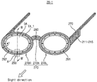
도 7은 본 개시의 일 실시예에 따른 증강현실 안경의 개략적인 사시도이다.
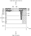
도 8은 도 7의 Ⅰ-Ⅰ'라인을 따라 자른 증강현실 안경의 단면도이다.
도 9는 도 7의 A영역을 확대한 도면이다.
도 10은 도 9의 Ⅱ-Ⅱ'라인을 따라 자른 광 출사부의 단면도이다.
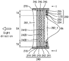
도 11은 본 개시의 일 실시예에 따른 증강현실 안경의 일부 영역을 자른 단면도이다.
도 12는 본 개시의 일 실시예에 따른 증강현실 안경의 일부 영역을 자른 단면도이다.
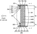
도 13은 본 개시의 일 실시예에 따른 증강현실 안경의 개략적인 사시도이다.
도 14은 도 13의 Ⅲ-Ⅲ’라인을 따라 자른 증강현실 안경의 단면도이다.
도 15는 도 13의 A영역을 확대한 도면이다.
도 16은 도 15의 Ⅵ-Ⅵ’라인을 따라 자른 광 출사부의 단면도이다.
20: 증강현실 안경 30: 제어 기기
40: 통신 네트워크 101: 제1 배선
102: 제2 배선 103: 범프들
210: 표시부 211: 타이밍 제어부
212: 데이터 구동부 213: 주사 구동부
214: 화소부 215: 광학 소자
220: 안구 추적부 230: 제2 통신 모듈
240: 웨이브 가이드 241: 제1 가이드
241D, 242D, 243D: 회절 격자 242: 제2 가이드
243: 제3 가이드 244: 커버 가이드
245: 스페이서들 250: 광 출사부
251: 베이스 기판 253: 충진 부재
254: 제1 패드 255: 제2 패드
256: 절연층 257: n형 반도체층
258: 발광층 259: p형 반도체층
260: 광 수신부 270: 프레임
281: 제1 광학 렌즈 282: 제2 광학 렌즈
291: 좌안 렌즈부 292: 우안 렌즈부
310: 제어부 320: 제1 통신 모듈
DA: 표시 영역 LD: 발광 칩
RA: 리세스 영역 TA: 트래킹 영역
Claims (20)
- 좌안 렌즈부 및 우안 렌즈부; 및
상기 좌안 렌즈부를 지지하는 좌안 렌즈 지지 영역, 상기 우안 렌즈부를 지지하는 우안 렌즈 지지 영역, 및 상기 좌안 렌즈 지지 영역과 상기 우안 렌즈 지지 영역을 연결하는 노즈 브릿지(nose bridge)를 포함하는 프레임을 포함하되,
상기 좌안 렌즈부 및 상기 우안 렌즈부는 각각,
증강현실 이미지를 표시하는 표시 영역; 및
적외선 대역의 파장의 광을 방출하는 복수의 광 출사부들이 위치하고, 상기 표시 영역을 둘러싸는 트래킹 영역을 포함하는, 증강현실 안경. - 제1 항에 있어서,
상기 트래킹 영역은 상기 좌안 렌즈부 및 상기 우안 렌즈부의 각 테두리에 위치하는, 증강현실 안경. - 제2 항에 있어서,
상기 트래킹 영역의 폭은 2mm 이하인, 증강현실 안경. - 제1 항에 있어서,
상기 광 출사부는 전면 발광형인 발광 칩을 포함하는, 증강현실 안경. - 제4 항에 있어서,
상기 각 광 출사부는,
베이스 기판;
상기 베이스 기판 상에 배치되는 상기 발광 칩; 및
상기 발광 칩 상에 배치되는 제1 패드 및 제2 패드를 포함하되,
상기 제1 패드 및 상기 제2 패드는 동일 레벨에 위치하는, 증강현실 안경. - 제5 항에 있어서,
상기 발광 칩은,
상기 베이스 기판 상에 배치되고, 상기 제1 패드와 전기적으로 연결되는 n형 반도체층;
상기 n형 반도체층 상에 배치되는 발광층; 및
상기 발광층 상에 배치되고, 상기 제2 패드와 전기적으로 연결되는 p형 반도체층을 포함하는, 증강현실 안경. - 제5 항에 있어서,
상기 발광 칩은 에피텍셜(epitaxial) 성장형인, 증강현실 안경. - 제7 항에 있어서,
상기 베이스 기판은 GaAs를 포함하는, 증강현실 안경. - 제5 항에 있어서,
상기 제1 패드 및 상기 제2 패드 상에 각각 배치되는 범프들;
상기 범프들 상에 배치되고 상기 제1 패드와 전기적으로 연결되는 제1 배선; 및
상기 범프들 상에 배치되고 상기 제2 패드와 전기적으로 연결되는 제2 배선을 더 포함하되,
상기 제1 배선 및 상기 제2 배선은 각각 상기 프레임 내부로 연장되는, 증강현실 안경. - 제9 항에 있어서,
상기 제1 배선 및 상기 제2 배선의 각 폭은 50μm 내지 150μm인, 증강현실 안경. - 제9 항에 있어서,
상기 제1 배선 및 상기 제2 배선은 각각 불투명 금속인, 증강현실 안경. - 제1 항에 있어서,
상기 노즈 브릿지에 위치하고, 적외선 대역의 파장의 광을 검출하는 광 수신부를 더 포함하는, 증강현실 안경. - 제1 항에 있어서,
상기 좌안 렌즈부 및 상기 우안 렌즈부는 각각,
제1 광학 렌즈;
테두리에 리세스 영역을 포함하는 제2 광학 렌즈; 및
상기 제1 광학 렌즈와 상기 제2 광학 렌즈 사이에 배치되는 웨이브 가이드를 포함하되,
상기 각 광 출사부는 상기 웨이브 가이드와 상기 제2 광학 렌즈 사이에 위치하는, 증강현실 안경. - 제13 항에 있어서,
상기 제2 광학 렌즈는 상기 제1 광학 렌즈보다 사용자의 안구에 가깝게 위치하도록 구성되는, 증강현실 안경. - 제13 항에 있어서,
상기 각 광 출사부는 상기 리세스 영역에 배치되는, 증강현실 안경. - 제13 항에 있어서,
상기 각 광 출사부는,
베이스 기판;
상기 베이스 기판 상에 배치되는 발광 칩;
상기 발광 칩 상에 배치되는 제1 패드 및 제2 패드; 및
상기 발광 칩 상에 배치되는 충진 부재를 포함하되,
상기 충진 부재는 레진을 포함하고, 상기 발광 칩을 덮도록 형성되는, 증강현실 안경. - 제16 항에 있어서,
상기 충진 부재는 상기 제2 광학 렌즈와 상기 발광 칩 사이를 메우는, 증강현실 안경. - 제17 항에 있어서,
상기 충진 부재는 적외선 대역의 파장의 광을 선택적으로 투과하는 블랙 레진을 포함하는, 증강현실 안경. - 통신 모듈, 및 제어부를 포함하는 제어 기기; 및
상기 통신 모듈과 통신 네트워크를 통해 연결되고, 상기 제어부에 의해 제어되어 가상현실 이미지를 표시하고, 사용자의 동공의 위치를 추적하는 증강현실 안경을 포함하되,
상기 증강현실 안경은,
좌안 렌즈부 및 우안 렌즈부; 및
상기 좌안 렌즈부를 고정하는 좌안 렌즈 지지 영역, 상기 우안 렌즈부를 지지하는 우안 렌즈 지지 영역, 및 상기 좌안 렌즈 지지 영역과 상기 우안 렌즈 지지 영역을 연결하는 노즈 브릿지(nose bridge)를 포함하는 프레임을 포함하되,
상기 좌안 렌즈부 및 상기 우안 렌즈부는 각각,
증강현실 이미지를 표시하는 표시 영역; 및
적외선 대역의 파장의 광을 방출하는 복수의 광 출사부들이 위치하고, 상기 표시 영역을 둘러싸는 트래킹 영역을 포함하고,
상기 각 광 출사부는,
베이스 기판;
상기 베이스 기판 상에 배치되는 발광 칩;
상기 발광 칩 상에 배치되고, 동일 층에 형성되는 제1 패드 및 제2 패드; 및
상기 발광 칩을 덮도록 형성되는 충진 부재를 포함하는, 증강현실 시스템. - 사용자가 증강현실 안경 렌즈 너머의 사물을 시각적으로 인식할 수 있도록 구성되고, 증강현실 이미지를 표시하도록 구성되는 증강현실 안경 렌즈에 있어서,
제1 광학 렌즈;
일면에 리세스 영역을 포함하는 제2 광학 렌즈;
상기 제1 광학 렌즈와 상기 제2 광학 렌즈 사이에 배치되는 웨이브 가이드; 및
상기 웨이브 가이드와 상기 제2 광학 렌즈 사이에 배치되고, 상기 리세스 영역에 위치하는 광 출사부를 포함하되,
상기 광 출사부는,
GaAs를 포함하는 베이스 기판;
상기 베이스 기판 상에 배치되고, 에피텍셜 성장형인 발광 칩;
상기 발광 칩 상에 배치되는 제1 패드 및 제2 패드; 및
상기 발광 칩 상에 배치되는 충진 부재를 포함하되,
상기 충진 부재는 레진을 포함하되, 상기 발광 칩을 덮고, 상기 리세스 영역을 메우도록 형성되는, 증강현실 안경 렌즈.
Priority Applications (3)
| Application Number | Priority Date | Filing Date | Title |
|---|---|---|---|
| KR1020210008006A KR20220105698A (ko) | 2021-01-20 | 2021-01-20 | 증강현실 안경 렌즈, 이를 포함하는 증강현실 안경 및 시스템 |
| US17/377,629 US12105288B2 (en) | 2021-01-20 | 2021-07-16 | Augmented reality lenses, and augmented reality glasses and augmented reality system including the same |
| CN202111518341.4A CN114815240A (zh) | 2021-01-20 | 2021-12-13 | 增强现实镜片及包括其的增强现实眼镜和增强现实系统 |
Applications Claiming Priority (1)
| Application Number | Priority Date | Filing Date | Title |
|---|---|---|---|
| KR1020210008006A KR20220105698A (ko) | 2021-01-20 | 2021-01-20 | 증강현실 안경 렌즈, 이를 포함하는 증강현실 안경 및 시스템 |
Publications (1)
| Publication Number | Publication Date |
|---|---|
| KR20220105698A true KR20220105698A (ko) | 2022-07-28 |
Family
ID=82406193
Family Applications (1)
| Application Number | Title | Priority Date | Filing Date |
|---|---|---|---|
| KR1020210008006A Pending KR20220105698A (ko) | 2021-01-20 | 2021-01-20 | 증강현실 안경 렌즈, 이를 포함하는 증강현실 안경 및 시스템 |
Country Status (3)
| Country | Link |
|---|---|
| US (1) | US12105288B2 (ko) |
| KR (1) | KR20220105698A (ko) |
| CN (1) | CN114815240A (ko) |
Cited By (3)
| Publication number | Priority date | Publication date | Assignee | Title |
|---|---|---|---|---|
| WO2024144353A1 (ko) * | 2022-12-29 | 2024-07-04 | 삼성전자 주식회사 | 시선 추적 센서를 포함하는 헤드 마운티드 디스플레이 장치 및 헤드 마운티드 디스플레이 장치의 동작 방법 |
| WO2025095728A1 (ko) * | 2023-11-02 | 2025-05-08 | 엘지이노텍 주식회사 | 광 가이드 장치 및 이를 포함하는 전자 디바이스 |
| US12493345B2 (en) | 2022-12-29 | 2025-12-09 | Samsung Electronics Co., Ltd. | Head mounted display apparatus including eye-tracking sensor and operating method thereof |
Families Citing this family (2)
| Publication number | Priority date | Publication date | Assignee | Title |
|---|---|---|---|---|
| CN116413911B (zh) * | 2021-12-31 | 2025-08-01 | 北京耐德佳显示技术有限公司 | 一种超薄型镜片、使用其的虚像成像装置和近眼显示器 |
| US20240004199A1 (en) * | 2022-07-01 | 2024-01-04 | Google Llc | Partially curved lightguide with pupil replicators |
Family Cites Families (15)
| Publication number | Priority date | Publication date | Assignee | Title |
|---|---|---|---|---|
| US8398239B2 (en) | 2009-03-02 | 2013-03-19 | Honeywell International Inc. | Wearable eye tracking system |
| US8989535B2 (en) * | 2012-06-04 | 2015-03-24 | Microsoft Technology Licensing, Llc | Multiple waveguide imaging structure |
| US10095307B2 (en) | 2016-05-13 | 2018-10-09 | Google Llc | Eye tracking systems and methods for virtual reality environments |
| EP4455840A3 (en) | 2016-09-22 | 2025-01-01 | Magic Leap, Inc. | Augmented reality spectroscopy |
| US10345600B1 (en) | 2017-06-08 | 2019-07-09 | Facebook Technologies, Llc | Dynamic control of optical axis location in head-mounted displays |
| US11102462B2 (en) * | 2017-09-27 | 2021-08-24 | University Of Miami | Vision defect determination via a dynamic eye characteristic-based fixation point |
| CA3086206A1 (en) | 2017-12-20 | 2019-06-27 | Magic Leap, Inc. | Insert for augmented reality viewing device |
| JP7200637B2 (ja) * | 2017-12-25 | 2023-01-10 | 株式会社リコー | 頭部装着型表示装置および表示システム |
| US10572731B1 (en) | 2018-03-13 | 2020-02-25 | Facebook Technologies, Llc | Infrared transparent backlight device for eye tracking applications |
| US10775616B1 (en) | 2018-03-21 | 2020-09-15 | Facebook Technologies, Llc | Lenses integrated with micro-light emitting diodes |
| US10718886B1 (en) | 2018-05-23 | 2020-07-21 | Facebook Technologies, Llc | Optical substrate and transparent routing of light sources |
| US11885964B2 (en) * | 2018-12-26 | 2024-01-30 | Lg Electronics Inc. | Electronic device |
| US11355665B2 (en) * | 2019-06-19 | 2022-06-07 | Facebook Technologies, Llc | Process flow for hybrid TFT-based micro display projector |
| WO2021033784A1 (ko) * | 2019-08-16 | 2021-02-25 | 엘지전자 주식회사 | 표시 모듈을 포함하는 전자 디바이스 |
| KR20210127286A (ko) * | 2020-04-13 | 2021-10-22 | 삼성디스플레이 주식회사 | 광학 장치 |
-
2021
- 2021-01-20 KR KR1020210008006A patent/KR20220105698A/ko active Pending
- 2021-07-16 US US17/377,629 patent/US12105288B2/en active Active
- 2021-12-13 CN CN202111518341.4A patent/CN114815240A/zh active Pending
Cited By (3)
| Publication number | Priority date | Publication date | Assignee | Title |
|---|---|---|---|---|
| WO2024144353A1 (ko) * | 2022-12-29 | 2024-07-04 | 삼성전자 주식회사 | 시선 추적 센서를 포함하는 헤드 마운티드 디스플레이 장치 및 헤드 마운티드 디스플레이 장치의 동작 방법 |
| US12493345B2 (en) | 2022-12-29 | 2025-12-09 | Samsung Electronics Co., Ltd. | Head mounted display apparatus including eye-tracking sensor and operating method thereof |
| WO2025095728A1 (ko) * | 2023-11-02 | 2025-05-08 | 엘지이노텍 주식회사 | 광 가이드 장치 및 이를 포함하는 전자 디바이스 |
Also Published As
| Publication number | Publication date |
|---|---|
| CN114815240A (zh) | 2022-07-29 |
| US20220229296A1 (en) | 2022-07-21 |
| US12105288B2 (en) | 2024-10-01 |
Similar Documents
| Publication | Publication Date | Title |
|---|---|---|
| US12105288B2 (en) | Augmented reality lenses, and augmented reality glasses and augmented reality system including the same | |
| US12125959B2 (en) | Bonding interface for hybrid TFT-based micro display projector | |
| US9779643B2 (en) | Imaging structure emitter configurations | |
| US9368546B2 (en) | Imaging structure with embedded light sources | |
| US9726887B2 (en) | Imaging structure color conversion | |
| US20220131041A1 (en) | Led arrays having a reduced pitch | |
| US20220262976A1 (en) | Reducing bowing of materials before wafer-to-wafer bonding for led manufacturing | |
| TW202134691A (zh) | 微型發光二極體的光萃取 | |
| US20130242056A1 (en) | Imaging structure emitter calibration | |
| US10649239B2 (en) | Eyeglasses with embedded femtoprojectors | |
| US20230034214A1 (en) | Left and right projectors for display device | |
| TW202134737A (zh) | 對準準直器組件與發光二極體陣列 | |
| JP2023503800A (ja) | ディスプレイパッケージの熱抵抗および平坦性を管理すること | |
| JP2023513868A (ja) | Led用の接触表面領域を増加させるための3d構造を備えた装置 | |
| EP4500595A1 (en) | Guided light extraction in trenches | |
| US20220005798A1 (en) | Display Systems Having Monolithic Arrays of Light-Emitting Diodes | |
| KR20230121899A (ko) | 마이크로 발광 다이오드들을 위한 빔성형 2차 광학컴포넌트들 | |
| US20220199871A1 (en) | Beam-shaping secondary optical components for micro light emitting diodes | |
| KR20220150885A (ko) | 상이한 웨이퍼 크기를 갖는 발광 회로와 제어 회로의 통합 | |
| US20240288693A1 (en) | Display device and method for driving the same | |
| KR102787443B1 (ko) | 색 변환 광원 구조를 갖는 디스플레이 장치의 제조방법 및 이의 제조방법 | |
| KR102331938B1 (ko) | 볼록렌즈를 이용해 시야를 넓힌 광학 장치 및 이를 이용한 머리 착용형 디스플레이 장치 |
Legal Events
| Date | Code | Title | Description |
|---|---|---|---|
| PA0109 | Patent application |
St.27 status event code: A-0-1-A10-A12-nap-PA0109 |
|
| R17-X000 | Change to representative recorded |
St.27 status event code: A-3-3-R10-R17-oth-X000 |
|
| PG1501 | Laying open of application |
St.27 status event code: A-1-1-Q10-Q12-nap-PG1501 |
|
| A201 | Request for examination | ||
| PA0201 | Request for examination |
St.27 status event code: A-1-2-D10-D11-exm-PA0201 |
|
| P22-X000 | Classification modified |
St.27 status event code: A-2-2-P10-P22-nap-X000 |
|
| D13-X000 | Search requested |
St.27 status event code: A-1-2-D10-D13-srh-X000 |
|
| E902 | Notification of reason for refusal | ||
| PE0902 | Notice of grounds for rejection |
St.27 status event code: A-1-2-D10-D21-exm-PE0902 |
|
| E13-X000 | Pre-grant limitation requested |
St.27 status event code: A-2-3-E10-E13-lim-X000 |
|
| P11-X000 | Amendment of application requested |
St.27 status event code: A-2-2-P10-P11-nap-X000 |