KR20220098180A - Transmitter Signal Rejection of Phased Array Transceiver - Google Patents
Transmitter Signal Rejection of Phased Array Transceiver Download PDFInfo
- Publication number
- KR20220098180A KR20220098180A KR1020227018963A KR20227018963A KR20220098180A KR 20220098180 A KR20220098180 A KR 20220098180A KR 1020227018963 A KR1020227018963 A KR 1020227018963A KR 20227018963 A KR20227018963 A KR 20227018963A KR 20220098180 A KR20220098180 A KR 20220098180A
- Authority
- KR
- South Korea
- Prior art keywords
- transceivers
- transceiver
- subset
- antenna elements
- duplexer
- Prior art date
Links
- 230000010363 phase shift Effects 0.000 claims abstract description 24
- 238000000034 method Methods 0.000 claims abstract description 11
- 238000006243 chemical reaction Methods 0.000 description 19
- 238000010586 diagram Methods 0.000 description 10
- 230000005540 biological transmission Effects 0.000 description 6
- 230000002776 aggregation Effects 0.000 description 5
- 238000004220 aggregation Methods 0.000 description 5
- 230000000875 corresponding effect Effects 0.000 description 5
- 238000013459 approach Methods 0.000 description 3
- 230000001427 coherent effect Effects 0.000 description 3
- 230000005855 radiation Effects 0.000 description 3
- 230000008901 benefit Effects 0.000 description 2
- 230000002596 correlated effect Effects 0.000 description 2
- 230000008878 coupling Effects 0.000 description 2
- 238000010168 coupling process Methods 0.000 description 2
- 238000005859 coupling reaction Methods 0.000 description 2
- 230000010354 integration Effects 0.000 description 2
- 230000004931 aggregating effect Effects 0.000 description 1
- 230000002238 attenuated effect Effects 0.000 description 1
- 230000002457 bidirectional effect Effects 0.000 description 1
- 239000000969 carrier Substances 0.000 description 1
- 230000008859 change Effects 0.000 description 1
- 238000012937 correction Methods 0.000 description 1
- 230000001934 delay Effects 0.000 description 1
- 238000000586 desensitisation Methods 0.000 description 1
- 230000007274 generation of a signal involved in cell-cell signaling Effects 0.000 description 1
- 230000006872 improvement Effects 0.000 description 1
- 230000004048 modification Effects 0.000 description 1
- 238000012986 modification Methods 0.000 description 1
- 238000012545 processing Methods 0.000 description 1
- 230000035945 sensitivity Effects 0.000 description 1
- 230000001360 synchronised effect Effects 0.000 description 1
Images


Classifications
-
- H—ELECTRICITY
- H04—ELECTRIC COMMUNICATION TECHNIQUE
- H04B—TRANSMISSION
- H04B1/00—Details of transmission systems, not covered by a single one of groups H04B3/00 - H04B13/00; Details of transmission systems not characterised by the medium used for transmission
- H04B1/38—Transceivers, i.e. devices in which transmitter and receiver form a structural unit and in which at least one part is used for functions of transmitting and receiving
- H04B1/40—Circuits
- H04B1/50—Circuits using different frequencies for the two directions of communication
- H04B1/52—Hybrid arrangements, i.e. arrangements for transition from single-path two-direction transmission to single-direction transmission on each of two paths or vice versa
- H04B1/525—Hybrid arrangements, i.e. arrangements for transition from single-path two-direction transmission to single-direction transmission on each of two paths or vice versa with means for reducing leakage of transmitter signal into the receiver
-
- H—ELECTRICITY
- H01—ELECTRIC ELEMENTS
- H01Q—ANTENNAS, i.e. RADIO AERIALS
- H01Q3/00—Arrangements for changing or varying the orientation or the shape of the directional pattern of the waves radiated from an antenna or antenna system
- H01Q3/26—Arrangements for changing or varying the orientation or the shape of the directional pattern of the waves radiated from an antenna or antenna system varying the relative phase or relative amplitude of energisation between two or more active radiating elements; varying the distribution of energy across a radiating aperture
- H01Q3/30—Arrangements for changing or varying the orientation or the shape of the directional pattern of the waves radiated from an antenna or antenna system varying the relative phase or relative amplitude of energisation between two or more active radiating elements; varying the distribution of energy across a radiating aperture varying the relative phase between the radiating elements of an array
- H01Q3/34—Arrangements for changing or varying the orientation or the shape of the directional pattern of the waves radiated from an antenna or antenna system varying the relative phase or relative amplitude of energisation between two or more active radiating elements; varying the distribution of energy across a radiating aperture varying the relative phase between the radiating elements of an array by electrical means
- H01Q3/36—Arrangements for changing or varying the orientation or the shape of the directional pattern of the waves radiated from an antenna or antenna system varying the relative phase or relative amplitude of energisation between two or more active radiating elements; varying the distribution of energy across a radiating aperture varying the relative phase between the radiating elements of an array by electrical means with variable phase-shifters
-
- H—ELECTRICITY
- H04—ELECTRIC COMMUNICATION TECHNIQUE
- H04B—TRANSMISSION
- H04B7/00—Radio transmission systems, i.e. using radiation field
- H04B7/02—Diversity systems; Multi-antenna system, i.e. transmission or reception using multiple antennas
- H04B7/04—Diversity systems; Multi-antenna system, i.e. transmission or reception using multiple antennas using two or more spaced independent antennas
- H04B7/06—Diversity systems; Multi-antenna system, i.e. transmission or reception using multiple antennas using two or more spaced independent antennas at the transmitting station
- H04B7/0613—Diversity systems; Multi-antenna system, i.e. transmission or reception using multiple antennas using two or more spaced independent antennas at the transmitting station using simultaneous transmission
- H04B7/0615—Diversity systems; Multi-antenna system, i.e. transmission or reception using multiple antennas using two or more spaced independent antennas at the transmitting station using simultaneous transmission of weighted versions of same signal
- H04B7/0617—Diversity systems; Multi-antenna system, i.e. transmission or reception using multiple antennas using two or more spaced independent antennas at the transmitting station using simultaneous transmission of weighted versions of same signal for beam forming
-
- H—ELECTRICITY
- H04—ELECTRIC COMMUNICATION TECHNIQUE
- H04L—TRANSMISSION OF DIGITAL INFORMATION, e.g. TELEGRAPHIC COMMUNICATION
- H04L5/00—Arrangements affording multiple use of the transmission path
- H04L5/14—Two-way operation using the same type of signal, i.e. duplex
- H04L5/1461—Suppression of signals in the return path, i.e. bidirectional control circuits
Abstract
안테나 요소의 어레이 및, 각각 (1) 송신기 체인; (2) 수신기 체인; 및 (3) 송신기 체인에 전기적으로 연결된 입력, 수신기 체인에 전기적으로 연결된 출력, 및 상이한 안테나 요소에 전기적으로 연결된 듀플렉스 포트를 갖는 듀플렉서를 포함하는, 송수신기를 하는 방법에 있어서, 방법은: 송수신기의 제1 및 제2 서브세트가 함께 복수의 송수신기 중 모든 상기 송수신기를 구성하도록 복수의 송수신기 중에서 송수신기의 제1 및 제2 서브세트를 식별하는 단계; 송수신기의 상기 제2 서브세트 내의 송수신기에 대해서는 아니고, 송수신기의 제1 서브세트 내의 각 송수신기에 대해, 듀플렉서의 듀플렉스 포트와 듀플렉스 포트가 전기적으로 연결된 안테나 요소 사이에 Φ 도 위상 시프트를 도입하는 단계를 포함하고, 여기서 Φ = -(2n+1)90°이고, n은 정수이다.an array of antenna elements, each comprising: (1) a transmitter chain; (2) receiver chain; and (3) a duplexer having an input electrically coupled to the transmitter chain, an output electrically coupled to the receiver chain, and a duplex port electrically coupled to a different antenna element, the method comprising: identifying first and second subsets of transceivers among a plurality of transceivers such that the first and second subsets together constitute all of the transceivers of the plurality of transceivers; introducing a Φ degree phase shift between the duplex port of the duplexer and the antenna element to which the duplex port is electrically connected, for each transceiver in the first subset of transceivers but not for the transceivers in the second subset of transceivers , where Φ = -(2n+1)90°, and n is an integer.

Description
본 발명은 일반적으로 위상 어레이 송수신기(phased array transceiver)에서의 신호 처리에 관한 것으로, 보다 구체적으로 위상 어레이 송수신기의 수신기 측에서 원하지 않는 신호의 감쇠(attenuation)에 관한 것이다.FIELD OF THE INVENTION The present invention relates generally to signal processing in a phased array transceiver, and more particularly to attenuation of unwanted signals at the receiver side of a phased array transceiver.
본 출원은, 제목이 "위상 어레이 수신기의 송신기 신호 제거"인, 2019년 11월 12일에 출원된 가출원 일련번호 62/934,148의 35 USC 119(e)에 따른 이익을 주장하고, 그 전체 내용은 여기에 참조로 포함된다.This application claims the benefit under 35 USC 119(e) of Provisional Application Serial No. 62/934,148, filed on November 12, 2019, entitled "Transmitter Signal Rejection of a Phased Array Receiver," the entire contents of which are incorporated herein by reference.
주파수 분할 듀플렉스(Frequency Division Duplex)(FDD) 위상 어레이 시스템에서 송신기 신호와 방출은 수신기를 둔감하게 하지 않도록 듀플렉서(duplexer)를 통해 감쇠된다. 전송 캐리어(transmit carrier)의 조합이 각 수신 채널에 바로 안착하는 상호변조 왜곡 곱(intermodulation distortion product)의 결과를 초래하도록 듀플렉스 간격이 있는 특정 무선 대역(certain wireless band)이 있다. 듀플렉서는 송수신 감쇠량이 많지만, 항상 이러한 경우에 충분하지 않으며 더 높은 감쇠를 달성하는 것은 종종 비실용적이다. 또한, 이러한 잔류 상호변조 곱(residual intermodulation product)은, 위상 어레이 시스템이 작동하는 데 필요한 모든 송신기 신호가 동위상이기 때문에, 위상 어레이 수신 결합기(phased array receive combiner)의 출력에서 합산되는 경향이 있다.In a Frequency Division Duplex (FDD) phased array system, the transmitter signal and emissions are attenuated through a duplexer so as not to desensitize the receiver. There are certain wireless bands with duplex spacing such that the combination of transmit carriers results in an intermodulation distortion product that settles directly on each receive channel. Duplexers have a lot of transmit and receive attenuation, but this is not always sufficient in these cases and it is often impractical to achieve higher attenuation. Also, these residual intermodulation products tend to add up at the output of the phased array receive combiner because all the transmitter signals required for the phased array system to work are in phase.
여기에 설명된 실시예는 송신기 신호 및 왜곡 곱의 위상이 수신기 결합기에서 쌍으로 제거되도록, 어레이의 다른 모든 요소에 대한 안테나 요소와 듀플렉서 사이에 의도적인 위상 시프트(deliberate phase shift)를 도입함으로써 위에서 설명된 문제를 해결한다. 위상 시프트는 단순한 지연 요소(delay element)(예를 들어, 1/4 파장 전송 라인) 또는 임의의 다른 위상 시프팅 회로 배치(phase shifting circuit arrangement)로 구현될 수 있다.The embodiments described herein are described above by introducing a deliberate phase shift between the antenna element and the duplexer for all other elements of the array such that the phase of the transmitter signal and distortion product is removed in pairs at the receiver combiner. solve the problem The phase shift may be implemented with a simple delay element (eg, a quarter wave transmission line) or any other phase shifting circuit arrangement.
일반적으로, 일 측면에서, 본 발명은: 안테나 요소(antenna elements)의 어레이(array); 및 각각 (1) 송신기 체인(transmitter chain); (2) 수신기 체인(receiver chain); 및 (3) 송신기 체인에 전기적으로 연결된 송신 입력(transmit input), 수신기 체인에 전기적으로 연결된 수신 출력(receive output), 및 안테나 요소의 어레이 내의 대응하는 상이한 안테나 요소에 전기적으로 연결된 듀플렉스 포트(duplexed port)를 갖는 듀플렉서(duplexer)를 포함하는, 복수의 트랜시버를 포함하는 위상 어레이 시스템을(phased array system)을 특징으로 한다. 복수의 송수신기(transceiver)는 송수신기의 제1 서브세트 및 송수신기의 제2 서브세트를 포함하고, 여기서 송수신기의 제1 서브세트는 송수신기의 제1 서브세트 내의 각각의 송수신기가 해당 송수신기 내의 듀플렉서의 듀플렉스 포트와 듀플렉서의 듀플렉스 포트가 전기적으로 연결된 안테나 요소 사이에 연결된 Φ 도 위상 시프팅 요소(phase shifting element)를 더 포함한다는 점에서 송수신기의 제2 서브세트와 상이하고, 여기서 Φ = -(2n+1)90°이고, n은 정수이다.Generally, in one aspect, the present invention provides: an array of antenna elements; and (1) a transmitter chain, respectively; (2) receiver chain; and (3) a transmit input electrically coupled to the transmitter chain, a receive output electrically coupled to the receiver chain, and a duplexed port electrically coupled to corresponding different antenna elements in the array of antenna elements. ), comprising a duplexer having a phased array system comprising a plurality of transceivers. A plurality of transceivers includes a first subset of transceivers and a second subset of transceivers, wherein the first subset of transceivers is configured such that each transceiver in the first subset of transceivers is configured to have a duplex port of a duplexer within the corresponding transceiver. differs from the second subset of transceivers in that Φ coupled between the duplex port of the duplexer and the electrically connected antenna element also further comprises a phase shifting element, where Φ = -(2n+1) 90°, and n is an integer.
바람직한 실시예는 다음 특징 중 하나 이상을 포함한다. 수량 n=0. 송수신기의 제1 서브세트의 송수신기의 수와 송수신기의 제2 서브세트의 송수신기의 수는 동일하거나 거의 동일하다. 안테나 요소의 어레이 내의 안테나 요소는 복수의 열로 구성되고 홀수 번호 열의 안테나 요소는 송수신기의 제1 서브세트의 송수신기에 연결되고 짝수 번호 열의 안테나 요소는 송수신기의 제2 서브세트의 송수신기에 연결된다. 대안적으로, 안테나 요소의 어레이 내의 안테나 요소는 복수의 행으로 구성되고, 홀수 행의 안테나 요소는 송수신기의 제1 서브세트의 송수신기에 연결되고 짝수 행의 안테나 요소는 송수신기의 제2 서브세트의 송수신기에 연결된다.Preferred embodiments include one or more of the following features. Quantity n=0. The number of transceivers in the first subset of transceivers and the number of transceivers in the second subset of transceivers are equal or approximately equal. The antenna elements in the array of antenna elements are configured in a plurality of rows, wherein the antenna elements in the odd numbered rows are coupled to the transceivers in the first subset of transceivers and the antenna elements in the even numbered rows are coupled to the transceivers in the second subset of transceivers. Alternatively, the antenna elements in the array of antenna elements are comprised of a plurality of rows, wherein the antenna elements in the odd rows are coupled to the transceivers of the first subset of transceivers and the antenna elements in the even rows are the transceivers of the second subset of transceivers. is connected to
일반적으로, 다른 측면에서, 본 발명은: 안테나 요소(antenna elements)의 어레이(array); 및 각각 (1) 송신기 체인(transmitter chain); (2) 수신기 체인(receiver chain); 및 (3) 송신기 체인에 전기적으로 연결된 송신 입력, 수신기 체인에 전기적으로 연결된 수신 출력, 및 안테나 요소의 어레이 내의 대응하는 상이한 안테나 요소에 전기적으로 연결된 듀플렉스 포트를 갖는 듀플렉서(duplexer)를 포함하는, 송수신기(transceiver)를 채용하는 방법을 특징으로 한다. 방법은: 송수신기의 제1 및 제2 서브세트가 함께 복수의 송수신기 중 모든 송수신기를 구성하도록 송수신기의 제1 서브세트 및 송수신기의 제2 서브세트를 복수의 송수신기 중에서 식별하는 단계; 송수신기의 제2 서브세트 내의 송수신기에 대해서는 아니고, 송수신기의 제1 서브세트 내의 각 송수신기에 대해, 송수신기 내의 듀플렉서의 듀플렉스 포트와 듀플렉서의 듀플렉스 포트가 전기적으로 연결된 안테나 요소 사이에 Φ 도 위상 시프트를 도입하는 단계를 포함하며, 여기서 Φ = -(2n+1)90°이고, n은 정수이다.Generally, in another aspect, the present invention provides: an array of antenna elements; and (1) a transmitter chain, respectively; (2) receiver chain; and (3) a duplexer having a transmit input electrically coupled to the transmitter chain, a receive output electrically coupled to the receiver chain, and duplex ports electrically coupled to corresponding different antenna elements in the array of antenna elements. (Transceiver) is characterized by employing a method. The method includes: identifying a first subset of transceivers and a second subset of transceivers among the plurality of transceivers such that the first and second subsets of transceivers together constitute all transceivers of the plurality of transceivers; For each transceiver in the first subset of transceivers, but not for transceivers in the second subset of transceivers, introducing a phase shift of Φ degrees between the duplex port of the duplexer in the transceiver and the antenna element to which the duplex port of the duplexer is electrically connected. step, wherein Φ = -(2n+1)90°, and n is an integer.
바람직한 실시예는 다음 특징 중 하나 이상을 포함한다. 수량 n=0. 복수의 송수신기 중 각각의 송수신기에 대해, 그 송수신기에 대한 송신기 체인은 그 송수신기에 대한 전송 신호 경로(transmit signal path)를 정의하고, 방법은: 송수신기의 제2 서브세트 내의 송수신기에 대해서는 아니고, 송수신기의 제1 서브세트 내의 각 송수신기에 대해, 해당 송수신기의 전송 신호 경로에 +90 도 위상 시프트를 도입하는 단계를 더 포함한다. 복수의 송수신기 중 각 송수신기 내에서 해당 송수신기에 대한 수신기 체인은 해당 송수신기에 대한 수신 신호 경로를 정의하고, 방법은: 송수신기의 제2 서브세트 내의 송수신기에 대해서는 이니고, 송수신기의 제1 서브세트 내의 각 송수신기에 대해, 해당 송수신기의 수신 신호 경로에 +90 도 위상 시프트를 도입하는 단계를 더 포함한다.Preferred embodiments include one or more of the following features. Quantity n=0. For each transceiver of the plurality of transceivers, a transmitter chain for that transceiver defines a transmit signal path for that transceiver, the method comprising: not for the transceivers in the second subset of transceivers, for each transceiver in the first subset, introducing a +90 degree phase shift in the transmit signal path of that transceiver. Within each transceiver of the plurality of transceivers, a receiver chain for a corresponding transceiver defines a receive signal path for that transceiver, the method comprising: for a transceiver in a second subset of transceivers, for the transceiver, introducing a +90 degree phase shift in the receive signal path of the transceiver.
두 개의 어레이 요소를 사용하는 단순화된 송수신기 블록도를 사용하는 도 1은 기본 개념을 도시한다.
도 2는 지연 요소가 교정 루프(calibration loop)의 외부에 있는 실시예를 도시한다.
도 3은 지연 요소가 교정 루프 내부에 있는 실시예를 도시한다.
도 4는 지연 요소가 피드백 네트워크(feedback network) 내부에 있는 실시예를 도시한다.
도 5는 예시적인 무선 헤드(radio head) 및 위상 어레이 안테나(phased array antenna)의 내부 구조를 나타내는 예시적인 고차원 블록도이다.
도 6은 도 5에 도시된 것과 같은 Tx/Rx 모듈의 예시적인 고차원 블록도이다.
도 7은 다중 송신 빔 중 하나만에 대한 회로를 보여주는 능동형 안테나 어레이 시스템(active antenna array system)의 송신기 측의 예시적인 블록도이다.
도 8은 다중 수신 빔 중 하나만에 대한 회로를 나타내는 능동형 안테나 어레이 시스템의 수신기 측의 예시적인 블록도이다.
본 발명의 하나 이상의 실시예의 세부사항은 첨부 도면 및 아래의 설명에 설명되어 있다. 본 발명의 다른 특징, 목적 및 이점은 상세한 설명 및 도면, 그리고 청구범위로부터 명백할 것이다.Figure 1, using a simplified transceiver block diagram using two array elements, shows the basic concept.
Figure 2 shows an embodiment in which the delay element is outside the calibration loop.
Figure 3 shows an embodiment in which the delay element is inside a calibration loop.
Figure 4 shows an embodiment in which the delay element is inside a feedback network.
5 is an exemplary high-dimensional block diagram illustrating the internal structure of an exemplary radio head and phased array antenna.
FIG. 6 is an exemplary high-dimensional block diagram of a Tx/Rx module such as that shown in FIG. 5 .
7 is an exemplary block diagram of the transmitter side of an active antenna array system showing circuitry for only one of the multiple transmit beams.
8 is an exemplary block diagram of the receiver side of an active antenna array system showing circuitry for only one of multiple receive beams.
The details of one or more embodiments of the invention are set forth in the accompanying drawings and the description below. Other features, objects and advantages of the present invention will be apparent from the detailed description and drawings, and from the claims.
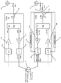
도 1을 참조하면, 두 개의 어레이 요소(array element)에 대한 단순화된 송수신기 블록도(transceiver block diagram)가 도시되어 있다. 이것은 두 개의 송수신기(transceiver)(TXRU) 모듈(10a, 10b)을 나타내며, 각각은 RF 송신기 체인(transmitter chain)(12a, 12b)(여기서는 위상 회전자(phase rotator) 또는 위상 설정 블록(phase setting block)(14a, 14b) 및 Tx 블록(16a, 16b)으로 표시됨), RF 수신기 체인(receiver chain)(18a, 18b)(위상 회전자 또는 위상 설정 블록(20a, 20b) 및 Rx 블록(22a, 22b)으로 표시됨), 및 송신기 및 수신기 체인을 안테나 요소(antenna element)(32a, 32b)에 연결하는 듀플렉서(duplexer)(26a, 26b)를 포함한다. RF 체인은 무엇보다도 디지털-아날로그 및 아날로그-디지털 변환 및 업다운 변환 작업을 수행한다. 상부 송수신기(10a)는 수정이 없고 추가된 위상 시프트(phase shift)가 없다. (나중에 명백해지겠지만, 그럼에도 불구하고 이 예에서 듀플렉서(26a)와 안테나 요소(32a) 사이에 0° 위상 시프트를 도입하는 위상 지연 요소(30a)로 표현된다.) 하부 송수신기(10b)는 듀플렉서(26b)와 안테나 요소(32b) 사이의 듀플렉스 라인(duplexed line)에 90° 위상 지연(phase delay)을 추가하는 위상 지연 요소(phase delay element)(30b)를 포함한다. 위상 지연은 한 주파수에서 90° 위상 시프트를 제공하는 1/4 파장 라인으로 구현할 수 있다. 대안적으로, 넓은 주파수 대역에서 90° 위상 시프트를 제공하는 보다 복잡한 RF 네트워크를 사용할 수 있다.1, a simplified transceiver block diagram for two array elements is shown. It represents two transceiver (TXRU)
TXRU(10b)에서 위상 지연 요소(30b)에 의해 도입된 이러한 위상 지연은 듀플렉스 라인 상의 송신 및 수신 신호 모두에 의해 보여진다. 위상 지연은 위상 어레이 시스템의 인테그랄 파트(integral part)이고 이 경우 모든 송신 신호가 각 안테나 요소에서 동위상으로 나타나고 수신 신호가 수신기 결합기(또는 통합 네트워크(aggregation network))(34)의 입력에서 동위상으로 나타나는 것을 보장하는 위상 회전자(14b 및 20b)에 의해 보상된다. 다시 말해서, 위상 회전자(14b 및 20b)는 송신 및 수신 신호에 +90° 위상 시프트를 도입한다. 그러나, 제1 송수신기(10a)와 제2 송수신기(10b) 사이의 차이는 송수신기 쌍으로부터의 잔류 송신기 신호가 수신기 위상 결합기(receiver phase combiner)(34)의 출력에 나타나는 위상에 있다. 상부 송수신기(10a)로부터의 잔류 송신기 신호는 송신 또는 수신 경로에서 어떠한 위상 시프트도 경험하지 않으므로, 위상 시프트 없이 수신기 결합기(34)의 출력에 나타난다. 하부 송수신기(10b)로부터의 잔류 송신기 신호는 두 개의 위상 회전을 경험하는데, 하나는 송신기 체인(12b)이고 다른 하나는 수신기 체인(18b)이며, 따라서 수신기 결합기(34)의 출력에서 상부 송수신기(10a)의 위상과 위상차로 나타나서, 잔류 송신기 신호 제거가 발생한다.This phase delay introduced by
도 1과 같은 위상 지연 요소에서, 두 송수신기 모듈의 다양한 위치에서 신호는 다음과 같다. 상단 송수신기(10a)의 듀플렉서(26a)에 전달된 송신 신호(transmit signal)가 S1tx라고 가정하면, 안테나 요소(32a)에 전달된 신호는 S1tx가 될 것이고 수신 경로로 누출되는 잔류 신호는 αS1tx가 될 것이며, 여기서 α는 듀플렉서(26a)의 송신 측에서 수신 측으로의 결합 측정이다. 수신된 신호가 S1rx라고 가정하면, 듀플렉서(26a)의 수신기 라인 상의 신호는 S1rx가 될 것이고 수신기 체인(18a)의 출력에서 βS1rx가 될 것이며, 여기서 β는 적용되는 아날로그 빔포밍 프리코딩 가중치에 의해 결정되는 수신기 체인(18a)에 의해 적용되는 이득의 측정치이다. 유사하게, 수신기 체인(18a)의 출력에 나타나는 잔류 송신 신호(residual transmit signal)는 αβS1tx가 될 것이다.In the phase delay element as shown in Fig. 1, signals at various positions of the two transceiver modules are as follows. Assuming that the transmit signal transmitted to the
하단 송수신기(10b)에서, 듀플렉서(26b)에 전달되는 송신 신호는 S2tx+90°이고 안테나 요소(32b)에 전달되는 신호는 원하는 대로 S2tx+90°-90° 또는 S2tx일 것이다. 수신 경로로 누출되는 잔류 신호는 αS2tx + 90°가 된다. 수신된 신호가 S2rx라고 가정하면, 듀플렉서(26b)의 수신기 라인 상의 신호는 S2rx - 90°가 될 것이고 수신기 체인(18b)의 출력은 βS2rx + 90° - 90° 또는 βS2tx가 될 것이다. 유사하게, 수신기 체인의 출력에 나타나는 잔류 전송 신호는 αβS2tx + 90° + 90° 또는 αβS2tx + 180°가 될 것이며, 이는 상단 송수신기(10a)의 수신기 체인(18a)의 출력에 나타나는 잔류 송신 신호와 위상이 180° 상이하다.At the
두 개의 수신된 신호에 의해 공급된 신호가 통합 네트워크 또는 신호 결합기 네트워크(34)에 의해 결합될 때 결과는 다음과 같다: βS1rx + βS2rx. 결합된 잔류 신호는 다음과 같다: αβS1tx + (αβS2tx + 180°). 이것은 αβ(S1tx - S2tx)와 같다. 빔포밍을 달성하기 위해 위상만 조정된다면, S1의 크기는 S2의 크기와 같으며 결과는 0이고, 즉, 순 잔류 신호(net residual signal)는 0이다. 반면에 위상과 이득이 모두 빔포밍을 달성하도록 조정되는 경우(예를 들어, 결과 빔에서 사이드로브를 줄이기 위해 진폭 테이퍼링이 사용됨), 그런 다음 S1![]()
![]()
듀플렉서(26b)와 안테나 요소(32b) 사이에 위상 지연 요소(30b)를 구현하기 위해 1/4 파장 라인이 사용되는 경우, 결과적인 위상차는 1/4 파장 라인이 설계된 주파수에서 오프셋된 주파수에 대해 약간의 차이가 있음을 유의해야 한다. 그럼에도 불구하고, 결합기 네트워크(combiner network)(34)의 입력에서의 결과적인 제거는 여전히 클 것이다.If a quarter-wave line is used to implement the
이 쌍을 이루는 요소 제거는 전체 어레이에 걸쳐 구현되어, 결과적인 잔류 송신기 신호(residual transmitter signal)가 수신 결합기 출력에서 최소화된다. 이 제거(cancellation) 없이 상관된 잔류 송신기 신호는 요소 수로 선형적으로 추가되어, 수신 결합기(receive combiner)의 출력에서 잔류 전력이 10logN 추가되고, 잠재적으로 수신기 감도 저하를 유발할 수 있다.This paired element rejection is implemented across the entire array so that the resulting residual transmitter signal is minimized at the receive combiner output. Without this cancellation, the correlated residual transmitter signal is added linearly by the number of elements, adding 10 logN of residual power at the output of the receive combiner, potentially causing receiver desensitization.
모든 수신 신호(듀플렉서(26a, 26b)를 통해 누출되는 원치 않는 잔류 신호 포함)는 수신 결합기에 나타나는 것에 유의하라. 따라서, 잔류 신호의 절반이 90° 위상 지연을 경험하고 절반은 그렇지 않은 경우(즉, 절반은 0° 위상에 있고 나머지 절반은 180° 위상에 있음), 전체 또는 거의 전체 제거가 발생한다. 안테나 요소가 위상 지연을 수신하는 것과 그렇지 않은 것에 대한 선택 가능성은 많다. 예를 들어, 어레이의 다른 모든 안테나 요소는 위상 지연에 적용하도록 선택되거나 어레이의 다른 모든 행(또는 열)의 모든 안테나 요소가 선택될 수 있다. 안테나 어레이가 안테나 서브패널(antenna sub-panel)의 어레이로 구성되는 경우, 선택은 안테나 서브패널이 함께 설계 및/또는 조립되는 방식으로 부분적으로 안내될 수 있다. Note that any received signal (including unwanted residual signals leaking through
또한 수학적으로 동일한 결과를 생성하는 위상 지연의 다른 조합이 있지만, 구현하기에 실용적이지 않을 수 있다. 일반적으로 듀플렉서와 안테나 요소 사이에 적용되는 위상 시프트는 Φ = -(2n+1)90°일 수 있으며, 여기서 n은 정수이다. 이 경우 수신기 체인과 송신기 체인 내에서 적용될 위상 시프트는 -Φ이다. 수신기 체인의 출력에 나타나는 결과적인 잔류 전송 신호는 αβS2tx + 2(2n+1)90°가 될 것이며 αβS2tx + 4n90° + 2x90° = αβS2tx + n360 + 180°로도 쓸 수 있다. 따라서, 다시 수신기 체인의 출력에서 결과적인 잔류 신호는 다른 수신기 체인에서 출력된 잔류 신호와 180° 위상이 상이하다.There are also other combinations of phase delays that produce mathematically equivalent results, but may not be practical to implement. In general, the phase shift applied between the duplexer and the antenna element may be Φ = -(2n+1)90°, where n is an integer. In this case, the phase shift to be applied within the receiver chain and the transmitter chain is -Φ. The resulting residual transmitted signal appearing at the output of the receiver chain will be αβS2tx + 2(2n+1)90°, which can also be written as αβS2tx + 4n90° + 2x90° = αβS2tx + n360 + 180°. Thus, again the resulting residual signal at the output of the receiver chain is 180° out of phase with the residual signal output from the other receiver chain.
기본 원칙은 다음과 같이 요약할 수 있다. 송신기 잔류 신호에 대한 왕복 위상 오프셋은 위상 시프트 요소(요소의 절반)에 대해 180°(또는 거의 180°)여야 한다. 송신기 위상 시프트는 송신기 입력에서 관련 안테나 요소까지 순 0°(net 0 degree)여야 한다. 그리고 수신기 위상 시프트는 연결된 안테나 요소에서 수신기 결합기의 입력(또는 이와 동등하게 수신기 체인의 출력)까지 순 0°여야 한다.The basic principles can be summarized as follows. The round-trip phase offset for the transmitter residual signal should be 180° (or nearly 180°) with respect to the phase shift element (half of the element). The transmitter phase shift shall be net 0 degrees from the transmitter input to the associated antenna element. And the receiver phase shift shall be net 0° from the connected antenna element to the input of the receiver combiner (or equivalently the output of the receiver chain).
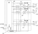
도 2는 송신 및 수신 경로의 위상을 조정하여 어레이의 모든 요소로 들어오고 나가는 신호가 완전히 상호 연관되고 일관성이 있도록 하는 교정 루프가 추가된 쌍을 이루는 요소 송수신기 제거 블록도(element transceiver cancellation block diagram)를 보여준다. 수신 측의 교정 루프는 센서 요소(sensor element)(40)를 통해 듀플렉서(26b)의 출력 라인 상의 신호를 감지하고 위상 설정 요소(phase setting element)(20b)에 피드백 신호를 제공하는 Rx 피드백 네트워크(feedback network)(36)를 포함한다. 송신측의 교정 루프는 센서 요소(42)를 통해 듀플렉서(26b)의 출력 라인 상의 신호를 감지하고 위상 설정 요소(14b)에 피드백 신호를 제공하는 Tx 피드백 네트워크(38)를 포함한다. 이 경우, 위상 지연 요소(30b)에 의해 도입된 위상 시프트는 교정 루프 외부에 있으며, 보상(compensation)을 위해 송신 및 수신 경로 위상 회전자의 수동 조정을 필요로 한다. 보다 구체적으로, 교정 루프에 대한 피드백은 듀플렉서(26b)와 위상 지연 요소(30b) 사이에 있는 위치로부터 취해진다. 이것은 최적의 솔루션은 아니지만 실행 가능하다.FIG. 2 is a paired element transceiver cancellation block diagram with the addition of a correction loop that phases the transmit and receive paths so that signals to and from all elements of the array are fully correlated and consistent; shows The calibration loop on the receiving side senses the signal on the output line of the
교정 루프의 Rx 및 Tx 피드백 네트워크(36, 38)는 알려진 방식으로 구현된다. 예를 들어, 몇 가지 접근 방식을 공개하는 다음 하라: 2019년 3월 5일 발행된 미하이 바누(Mihai Banu) 및 위핑 팽(Yiping Feng)의 "엑티스 어레이 교정(Active Array Calibration)"이라는 제목의 US 10,225,067; 및 2018년 6월 26일자로 발행된 미하이 바누(Mihai Banu)의 "직렬 상효연결 교정(Calibrating A Serial Interconnection)"이라는 제목의 US 10,009,165가 있으며, 이둘 모두 참조에 의해 전체가 여기에 통합된다. The Rx and
도 3은 교정 루프 내부에 위상 지연 요소(30b)가 있는 쌍을 이루는 요소 송수신기 소거 블록도에서 위상 어레이 시스템 교정의 일부로 보상이 자동으로 처리되는 것을 보여준다. 보다 구체적으로, 교정 루프에 대한 피드백은 위상 지연 요소(30b)와 안테나 요소(32b) 사이에 있는 위치로부터 취해진다. Figure 3 shows that compensation is handled automatically as part of a phased array system calibration in a paired element transceiver cancellation block diagram with a
도 4는 추가된 위상 지연 요소(30b)를 제외하지만 피드백 루프의 일부로 추가된 상응하는 위상 시프트 요소(44, 46)가 추가된 쌍을 이루는 요소 송수신기 제거 블록도를 보여준다. 이 대안은 추가된 위상 시프트 요소 후에 피드백 감지 포인트(feedback sense point)를 갖는 것이 유리하지 않거나 가능하지 않을 수 있는 경우에 표시된다.Figure 4 shows a block diagram of removing a paired element transceiver except for the added
위에서 설명한 접근 방식이 구현될 수 있는 아날로그 위상 어레이 시스템의 예가 도 5 내지 8에 나와 있다.Examples of analog phased array systems in which the approach described above can be implemented are shown in Figures 5-8.
도 5를 참조하면, 안테나 어레이(110)는 M개의 안테나 요소의 2차원 어레이를 포함한다. 라디오 헤드(190)는 어레이의 안테나 요소의 수, 즉 M과 동일한 수의 다중 프론트-엔드 모듈(multiple front-end module)(TXRU 모듈)(200)을 포함한다. 각 안테나 요소에 대한 TXRU 모듈(200)이 있다. IF 분배 및 통합 네트워크 및 LO 신호 분배 네트워크를 포함하는 신호 분배 네트워크(signal distribution network)(195)도 있다. 이 신호 분배 네트워크(195)는 BBU에서 TXRU 모듈(200)로 전송 신호를 전달하고, TXRU 모듈(200)에서 BBU로 수신된 신호를 전달하며, IF 송신 신호를 RF 송신 신호로 상향 변환((up-converting))하고 RF 수신 신호를 IF 수신 신호로 하향 변환((down-converting))하기 위해 코히어런트 로컬 발진기 신호((coherent local oscillator signal))를 TXRU 모듈(200)에 제공한다.Referring to FIG. 5 , the
도 6은 다중 요소 안테나 어레이의 단일 안테나 요소(single antenna element)(210)에 연결하는 회로의 블록도를 도시한다. M개의 안테나 요소를 갖는 안테나 어레이 시스템에서, 이 회로는 각 안테나 요소에 대해 복제된다. 각각의 안테나 요소(210)에 대해, 안테나 요소(210)에 연결된 프론트-엔드 모듈(또는 TXRU 모듈)(200)이 있다. 프론트-엔드 모듈(front-end module)에는 송신기 측(transmitter side)과 수신기 측(eceiver side)이 있다. 송신기 측은 N개의 상향 변환 모듈(up-conversion module)(202) 및 전력 증폭기(power amplifier)(PA)(206)를 포함한다. 수신기 측은 저잡음 증폭기(low noise amplifier)(LNA)(212) 및 N개의 하향 변환 모듈(down-conversion module)(216)을 포함한다. N개의 상향 변환 모듈(202)은 어레이가 N개의 독립적인 송신 빔을 생성할 수 있게 하고 N개의 하향 변환 모듈(216)은 어레이가 N개의 독립적인 수신 빔을 생성하는 것을 가능하게 한다. (참고: 하나의 빔만 생성할 수 있는 도시된 예의 경우 N=1이다.) 6 shows a block diagram of a circuit for coupling to a
프론트-엔드 모듈(200)은 또한 송신기 측의 PA(206)로부터의 구동 신호를 안테나 요소(210)에 결합하고 안테나 요소(210)로부터 수신된 신호를 수신기 측의 LNA(212)에 결합하는 듀플렉서 회로(duplexer circuit)(208)를 포함한다. 상향 변환 모듈(202)의 입력은 기저대역 유닛(미도시)으로부터 빔 송신 신호 스트림(beam transmit signal stream)(Bt1)을 수신하기 위한 것이다. 그리고 하향 변환 모듈(216)의 출력은 빔 수신 신호 스트림(beam received signal stream)(Br1)을 출력하기 위한 것이다.The front-
상향 변환 모듈(202)이 더 자세히 도시된 능동형 안테나 어레이 시스템이 도 7에 도시되어 있고; 하향 변환 모듈(216)이 더 상세히 도시된 능동형 안테나 어레이 시스템이 도 8에 도시되어 있다. 실제적으로, 별도로 표시된 이 두 시스템은 동일한 능동형 안테나 어레이 시스템에서 구현되지만 도면을 단순화하기 위해 여기에 별도로 표시된다. 도 7의 능동형 안테나 어레이 시스템은 안테나 어레이의 M개의 요소(210)에 의해 생성된 단일 송신 빔을 통해 하나의 송신 신호 스트림을 송신하기 위한 것이다. 유사하게, 도 8의 능동형 안테나 어레이 시스템은 안테나 어레이에 의해 생성된 단일 수신 빔 패턴에서 신호 스트림을 수신하기 위한 것이다.An active antenna array system in which the up-
M개의 상향 변환 모듈(202) 및 M개의 하향 변환 모듈(216)에 코히어런트 또는 위상 동기화된 LO(로컬 발진기(local oscillator)) 신호를 분배하기 위한 LO 분배 네트워크(distribution network)(220)가 있다. 도 7에 도시된 바와 같이, IF 송신 신호를 각각의 상향 변환 모듈(202)에 전달하기 위한 IF 분배 네트워크(224)도 존재한다. 그리고 도 8에 도시된 바와 같이, 하향 변환 모듈(216) 각각으로부터 수신된 신호를 통합하기 위한 IF 통합 네트워크(226)가 있다. An
분배 및 통합 네트워크는 신호의 일관된 분배/통합을 보장하기 위해 전기적으로 동일한 경로를 갖는 수동형 선형 상호 네트워크(passive linear reciprocal network)일 수 있다. 대안적으로, 이들 네트워크 중 하나 이상은, 2008년 7월 21일 출원된 "위상 동기화 로컬 캐리어를 사용한 다중 지점 신호 생성을 위한 방법 및 시스템"이라는 제목의 US 8,259,884 및 2011년 6월 30일에 제출된 "저비용, 활성 안테나 어레이"라는 제목의 US 8,622,959 또는 2016년 9월 8일자로 출원된 "직렬 상호 연결 보정"이라는 제목의 US 9,673,965에 설명된 직렬 상호 연결 접근 방식에 설명된 양방향 신호 네트워크를 사용하여 구현될 수 있고, 그 모든 내용은 여기에 참조로 포함된다. The distribution and integration network may be a passive linear reciprocal network with electrically identical paths to ensure consistent distribution/integration of signals. Alternatively, one or more of these networks are filed in US 8,259,884 and June 30, 2011, entitled "Method and System for Multi-Point Signal Generation Using Phase Synchronized Local Carrier," filed July 21, 2008. Use the bidirectional signal network described in US 8,622,959, entitled "Low-Cost, Active Antenna Array," or the serial interconnect approach described in US 9,673,965, filed September 8, 2016, entitled "Serial Interconnect Calibration". may be implemented, and all contents thereof are incorporated herein by reference.
일반적으로, 각각의 상향 변환 모듈(202)은 믹서(mixer)(203) 및 각각 A 및 P로 식별되는 다양한 진폭 및 위상 설정 회로를 포함한다. LO 신호 및 분산된 IF 송신 신호 스트림은 모두 IF 송신 신호 스트림을 전력 증폭기(206)에 제공되는 RF 송신 신호 스트림으로 상향 변환하는 믹서(203)에 제공된다. 유사하게, 각각의 하향 변환 모듈(216)은 또한 믹서(217) 및 유사하게 A 및 P로 각각 식별되는 다양한 진폭 및 위상 설정 회로를 포함한다. 하향 변환 모듈(216)의 믹서(217)는 하향 변환된 IF 수신 신호 스트림을를 생성하기 위해 안테나 요소(210)에 결합된 저잡음 증폭기(212)로부터 수신된 RF 신호 스트림과 LO 분배 네트워크(220)에 의해 제공되는 LO 신호를 곱한다. 하향 변환된 IF 신호 스트림은 다른 안테나 요소로부터 수신된 IF 신호 스트림과의 통합 및 기지국으로의 다시 전송을 위해 IF 통합 네트워크(226)에 제공된다.Generally, each up-
진폭 및 위상 설정 회로 A 및 P는 개별 안테나 신호의 상대적 위상 또는 진폭을 변경하여 안테나 어레이에 의해 생성되는 송수신 빔 패턴의 크기, 방향 및 강도를 설정하는 데 사용된다. (참고: 안테나 어레이에서, 송신 빔(transmit beam)은 안테나 어레이에 의해 생성되는 방사 패턴(adiation pattern)이다. 그 방사 패턴은 안테나 어레이 앞에서 측정될 수 있다. 이에 반해, 수신 빔(receive beam)은 안테나 어레이에 의해 형성되는 방사 패턴이 아니라 안테나 감도의 패턴이다. 그럼에도 불구하고, 이러한 차이에도 불구하고 둘 다 일반적으로 빔이라고 한다.) 진폭 설정 회로(amplitude setting circuit)는 기본적으로 입력 신호 진폭에 대한 출력 신호 진폭의 비율을 프로그래밍할 수 있고 전자 제어에 의해 설정되는 가변 이득 증폭기(variable gain amplifier)와 동일하다. 위상 설정 회로(phase setting circuit)는 전자 제어 하에서 입력 신호를 위상(또는 시간)으로 시프트하는 기본적인 기능을 가지고 있다. 이러한 진폭 및 위상 설정 회로는 별도의 제어 프로세서(control processor)(213)에 의해 공급되는 디지털 제어 신호(일명 빔포밍 프리코딩 벡터)에 의해 제어된다.Amplitude and phase setting circuits A and P are used to change the relative phase or amplitude of individual antenna signals to set the magnitude, direction, and strength of the transmit/receive beam pattern generated by the antenna array. (Note: In an antenna array, the transmit beam is the radiation pattern produced by the antenna array. The radiation pattern can be measured in front of the antenna array. In contrast, the receive beam is It is the pattern of antenna sensitivity, not the radiation pattern formed by the antenna array. Nevertheless, despite these differences, both are commonly referred to as beams.) The amplitude setting circuit is basically It is equivalent to a variable gain amplifier that is programmable to the ratio of the output signal amplitude and is set by electronic control. A phase setting circuit has the basic function of shifting an input signal in phase (or time) under electronic control. This amplitude and phase setting circuit is controlled by a digital control signal (aka beamforming precoding vector) supplied by a
도 7 및 8에 표시된 진폭 설정 및 위상 설정 회로의 유형은 기본 송신기 및 수신기에 개별 안테나 신호의 진폭 및 위상 값을 독립적으로 제어할 수 있는 기능을 제공하는 많은 가능성 중 하나일 뿐이다. 진폭 및 위상 설정 회로의 수와 배치는 도 7과 8에 나와 있는 것과 다를 수 있다. 또한, 상향 변환 및 하향 변환 모듈에 존재할 수 있지만 당업자에게 잘 알려져 있기 때문에 도면에는 도시되지 않은 다른 구성요소가 있다. 여기에는 예를 들어 채널 IF 필터 및 자동 이득 제어(automatic gain control)가 포함될 수 있다.The types of amplitude setting and phase setting circuits shown in Figures 7 and 8 are just one of many possibilities that give the basic transmitter and receiver the ability to independently control the amplitude and phase values of individual antenna signals. The number and arrangement of amplitude and phase setting circuits may differ from those shown in FIGS. 7 and 8 . Also, there are other components that may be present in the up-conversion and down-conversion modules, but not shown in the figures as they are well known to those skilled in the art. This may include, for example, a channel IF filter and automatic gain control.
다른 실시예는 다음 청구범위 내에 있다. 예를 들어, 위에서 설명된 실시예는 IF 신호를 RF 송신기 체인 내에서 RF로 상향 변환하는 것을 포함하며, 이 경우 위상 회전은 송신기 체인에서 상향 변환 후(또는 수신기 체인에서 하향 변환 전에) 적용된다 대안적으로, 상향 변환된 RF 신호는 신호 분배 네트워크에 의해 공급될 수 있으며, 이 경우 상향 및 하향 변환은 송수신기 모듈에서 발생하지 않는다.Other embodiments are within the scope of the following claims. For example, the embodiment described above involves upconverting an IF signal to RF within an RF transmitter chain, in which case the phase rotation is applied after upconversion in the transmitter chain (or before downconversion in the receiver chain). Alternatively, the up-converted RF signal may be supplied by a signal distribution network, in which case up- and down-conversion does not occur in the transceiver module.
Claims (10)
안테나 요소의 어레이; 및
각각 (1) 송신기 체인; (2) 수신기 체인; 및 (3) 상기 송신기 체인에 전기적으로 연결된 송신 입력, 상기 수신기 체인에 전기적으로 연결된 수신 출력, 및 안테나 요소의 상기 어레이 내의 대응하는 상이한 안테나 요소에 전기적으로 연결된 듀플렉스 포트를 갖는 듀플렉서를 포함하는, 복수의 송수신기를 포함하고,
상기 복수의 송수신기는 송수신기의 제1 서브세트 및 송수신기의 제2 서브세트를 구성하고, 송수신기의 상기 제1 서브세트는 송수신기의 상기 제1 서브세트 내의 각각의 송수신기가 해당 송수신기 내의 듀플렉서의 듀플렉스 포트와 상기 듀플렉서의 듀플렉스 포트가 전기적으로 연결된 안테나 요소 사이에 연결된 Φ 도 위상 시프팅 요소를 더 포함한다는 점에서 송수신기의 상기 제2 서브세트와 상이하고, 여기서 Φ = -(2n+1)90°이고, n은 정수인
위상 어레이 시스템.
A phased array system comprising:
an array of antenna elements; and
each (1) transmitter chain; (2) receiver chain; and (3) a duplexer having a transmit input electrically coupled to the transmitter chain, a receive output electrically coupled to the receiver chain, and a duplex port electrically coupled to corresponding different antenna elements in the array of antenna elements. including a transceiver of
The plurality of transceivers constitute a first subset of transceivers and a second subset of transceivers, wherein each transceiver in the first subset of transceivers comprises a duplex port of a duplexer in the corresponding transceiver and differs from the second subset of transceivers in that the duplex port of the duplexer further comprises a phase shifting element with a Φ coupled between electrically connected antenna elements, wherein Φ = -(2n+1)90°; n is an integer
phased array system.
n=0인
위상 어레이 시스템.
According to claim 1,
where n=0
phased array system.
송수신기의 상기 제1 서브세트 내의 송수신기의 수와 송수신기의 상기 제2 서브세트 내의 송수신기의 수는 동일하거나 거의 동일한
위상 어레이 시스템.
According to claim 1,
the number of transceivers in the first subset of transceivers and the number of transceivers in the second subset of transceivers are equal or approximately equal
phased array system.
송수신기의 상기 제1 서브세트 내의 송수신기의 수와 송수신기의 상기 제2 서브세트 내의 송수신기의 수는 동일한
위상 어레이 시스템.
According to claim 1,
the number of transceivers in the first subset of transceivers and the number of transceivers in the second subset of transceivers are equal
phased array system.
안테나 요소의 어레이 내의 상기 안테나 요소는 복수의 열로 구성되고, 홀수 번호 열의 상기 안테나 요소는 송수신기의 상기 제1 서브세트의 송수신기에 연결되고 짝수 번호 열의 상기 안테나 요소는 송수신기의 상기 제2 서브세트에 있는 송수신기에 연결되는
위상 어레이 시스템.
According to claim 1,
wherein the antenna elements in the array of antenna elements are configured in a plurality of columns, wherein the antenna elements in odd numbered columns are coupled to the transceivers in the first subset of transceivers and the antenna elements in even numbered columns are in the second subset of transceivers. connected to the transceiver
phased array system.
안테나 요소의 어레이 내의 상기 안테나 요소는 복수의 행으로 구성되고, 홀수 번호 행의 상기 안테나 요소는 송수신기의 상기 제1 서브세트의 송수신기에 연결되고 짝수 번호 행의 상기 안테나 요소는 송수신기의 상기 제2 서브세트에 있는 송수신기에 연결되는
위상 어레이 시스템.
According to claim 1,
The antenna elements in the array of antenna elements are configured in a plurality of rows, wherein the antenna elements in odd numbered rows are coupled to the transceivers of the first subset of transceivers and the antenna elements in even numbered rows are connected to the second sub of transceivers. connected to the transceiver in the set
phased array system.
상기 방법은:
송수신기의 제1 및 제2 서브세트가 함께 복수의 송수신기 중 모든 상기 송수신기를 구성하도록 복수의 송수신기 중에서 송수신기의 제1 서브세트 및 송수신기의 제2 서브세트를 식별하는 단계;
송수신기의 상기 제2 서브세트 내의 상기 송수신기에 대해서는 아니고, 송수신기의 상기 제1 서브세트 내의 각 송수신기에 대해, 해당 송수신기 내의 상기 듀플렉서의 듀플렉스 포트와 해당 듀플렉서의 듀플렉스 포트가 전기적으로 연결된 안테나 요소 사이에 Φ 도 위상 시프트를 도입하는 단계를 포함하고, 여기서 Φ = -(2n+1)90°이고, n은 정수인
방법.
an array of antenna elements, each comprising: (1) a transmitter chain; (2) receiver chain; and (3) a duplexer having a transmit input electrically coupled to the transmitter chain, a receive output electrically coupled to the receiver chain, and a duplex port electrically coupled to corresponding different antenna elements in the array of antenna elements. In a method of employing a transceiver of
The method is:
identifying a first subset of transceivers and a second subset of transceivers among a plurality of transceivers such that the first and second subsets of transceivers together constitute all of the transceivers of the plurality of transceivers;
For each transceiver in the first subset of transceivers, but not for the transceiver in the second subset of transceivers, Φ between the duplex port of the duplexer in the transceiver and the antenna element to which the duplex port of the duplexer is electrically connected. introducing a degree phase shift, where Φ = -(2n+1)90°, and n is an integer
Way.
K = 2 인
방법.
8. The method of claim 7,
K = 2 persons
Way.
상기 복수의 송수신기 중 각각의 송수신기 내에서, 상기 송수신기에 대한 상기 송신기 체인은 해당 송수신기에 대한 전송 신호 경로를 정의하고, 및
송수신기의 상기 제2 서브세트 내의 상기 송수신기에 대해서는 아니고, 송수신기의 상기 제1 서브세트 내의 각 송수신기에 대해, 해당 송수신기의 전송 신호 경로에 +90 도 위상 시프트를 도입하는 단계를 더 포함하는
방법.
9. The method of claim 8,
within each transceiver of the plurality of transceivers, the transmitter chain to the transceiver defines a transmit signal path to the transceiver, and
introducing a +90 degree phase shift in the transmit signal path of that transceiver for each transceiver in the first subset of transceivers but not for the transceiver in the second subset of transceivers
Way.
상기 복수의 송수신기 중 각각의 송수신기 내에서 해당 송수신기에 대한 상기 수신기 체인은 해당 송수신기에 대한 수신 신호 경로를 정의하고, 및
송수신기의 상기 제2 서브세트 내의 상기 송수신기에 대해서는 아니고, 송수신기의 상기 제1 서브세트 내의 각 송수신기에 대해, 해당 송수신기의 수신 신호 경로에 +90 도 위상 시프트를 도입하는 단계를 더 포함하는
방법.10. The method of claim 9,
In each transceiver of the plurality of transceivers, the receiver chain for the corresponding transceiver defines a receive signal path for the corresponding transceiver, and
introducing a +90 degree phase shift in the receive signal path of that transceiver for each transceiver in the first subset of transceivers but not for the transceiver in the second subset of transceivers
Way.
Applications Claiming Priority (3)
| Application Number | Priority Date | Filing Date | Title |
|---|---|---|---|
| US201962934148P | 2019-11-12 | 2019-11-12 | |
| US62/934,148 | 2019-11-12 | ||
| PCT/US2020/059330 WO2021096770A1 (en) | 2019-11-12 | 2020-11-06 | Transmitter signal cancellation in phased array transceivers |
Publications (1)
| Publication Number | Publication Date |
|---|---|
| KR20220098180A true KR20220098180A (en) | 2022-07-11 |
Family
ID=73699412
Family Applications (1)
| Application Number | Title | Priority Date | Filing Date |
|---|---|---|---|
| KR1020227018963A KR20220098180A (en) | 2019-11-12 | 2020-11-06 | Transmitter Signal Rejection of Phased Array Transceiver |
Country Status (7)
| Country | Link |
|---|---|
| US (1) | US11606115B2 (en) |
| EP (1) | EP4059146A1 (en) |
| JP (1) | JP2023501572A (en) |
| KR (1) | KR20220098180A (en) |
| CN (1) | CN114930727A (en) |
| CA (1) | CA3158212A1 (en) |
| WO (1) | WO2021096770A1 (en) |
Families Citing this family (2)
| Publication number | Priority date | Publication date | Assignee | Title |
|---|---|---|---|---|
| CN114499581B (en) * | 2022-01-25 | 2022-10-11 | 电子科技大学 | Aperture-level same-frequency full-duplex phased array antenna broadband coupling signal cancellation method |
| CN117040577A (en) * | 2023-08-10 | 2023-11-10 | 上海安其威微电子科技有限公司 | Phased array receiving and transmitting system, device and method with feedback path |
Family Cites Families (24)
| Publication number | Priority date | Publication date | Assignee | Title |
|---|---|---|---|---|
| US6091970A (en) * | 1997-12-24 | 2000-07-18 | Nortel Networks Corporation | Pseudo-omnidirectional base station arrangement |
| CN1118200C (en) * | 1999-08-10 | 2003-08-13 | 信息产业部电信科学技术研究院 | Baseband processing method based on intelligent antoma and interference cancel |
| US6788268B2 (en) * | 2001-06-12 | 2004-09-07 | Ipr Licensing, Inc. | Method and apparatus for frequency selective beam forming |
| KR101031692B1 (en) * | 2002-12-18 | 2011-04-29 | 파나소닉 주식회사 | Radio communication apparatus, radio communication method, antenna apparatus and first duplexer |
| EP2854326A1 (en) | 2007-07-20 | 2015-04-01 | Blue Danube Labs Inc | Method and system for multi-point signal generation with phase synchronized local carriers |
| US8260144B2 (en) * | 2008-03-12 | 2012-09-04 | Hypres Inc. | Digital radio frequency tranceiver system and method |
| FR2934164B1 (en) | 2008-07-23 | 2010-09-17 | Perouse Lab | SYSTEM FOR INJECTING A LIQUID IN A BODY, IN PARTICULAR IN THE BODY OF A PATIENT. |
| CN103109457B (en) * | 2010-05-17 | 2016-08-03 | 泰科电子服务股份有限公司 | There is the duplexer strengthening isolation |
| EP2487800B1 (en) * | 2011-02-11 | 2013-06-19 | Alcatel Lucent | Active antenna arrays |
| US8571154B1 (en) * | 2012-04-19 | 2013-10-29 | Bae Systems Information And Electronic Systems Integration Inc. | Control interval expansion of variable time delay control structure for channel matching |
| EP2923446B1 (en) * | 2012-11-22 | 2019-02-20 | Telefonaktiebolaget LM Ericsson (publ) | Transceiver front-end |
| US9923621B2 (en) * | 2013-02-16 | 2018-03-20 | Cable Television Laboratories, Inc. | Multiple-input multiple-output (MIMO) communication system |
| US20140269449A1 (en) * | 2013-03-15 | 2014-09-18 | Qualcomm Incorporated | Full-duplex wireless transceiver with hybrid circuit and reconfigurable radiation pattern antenna |
| CN103312366B (en) * | 2013-05-31 | 2015-04-08 | 华为技术有限公司 | Active antenna, base station and interference inhibiting method |
| EP3097645B1 (en) * | 2014-01-21 | 2017-08-23 | Telefonaktiebolaget LM Ericsson (publ) | Transceiver arrangement and communication device |
| WO2015130257A1 (en) * | 2014-02-25 | 2015-09-03 | Intel Corporation | Apparatus, system and method of simultaneous transmit and receive (str) wireless communication |
| WO2015131397A1 (en) * | 2014-03-07 | 2015-09-11 | 华为技术有限公司 | Interference elimination device and method |
| US9521023B2 (en) * | 2014-10-17 | 2016-12-13 | Kumu Networks, Inc. | Systems for analog phase shifting |
| GB201418814D0 (en) * | 2014-10-22 | 2014-12-03 | Analog Devices Technology | Full duplex radio |
| CA2996608A1 (en) | 2015-09-10 | 2017-03-16 | Blue Danube Systems, Inc. | Active array calibration |
| US9972893B2 (en) * | 2015-12-29 | 2018-05-15 | Commscope Technologies Llc | Duplexed phased array antennas |
| US9960874B2 (en) * | 2016-07-20 | 2018-05-01 | Zinwave, Ltd. | Techniques for managing interference in a network environment |
| US10419062B2 (en) * | 2016-10-12 | 2019-09-17 | Massachusetts Institute Of Technology | Simultaneous transmit and receive with digital phased arrays |
| WO2019069395A1 (en) * | 2017-10-04 | 2019-04-11 | Nec Corporation | Remote radio head, beamforming method and storage medium |
-
2020
- 2020-11-06 CN CN202080092188.0A patent/CN114930727A/en active Pending
- 2020-11-06 WO PCT/US2020/059330 patent/WO2021096770A1/en unknown
- 2020-11-06 JP JP2022527704A patent/JP2023501572A/en active Pending
- 2020-11-06 EP EP20819943.0A patent/EP4059146A1/en active Pending
- 2020-11-06 KR KR1020227018963A patent/KR20220098180A/en not_active Application Discontinuation
- 2020-11-06 US US17/091,100 patent/US11606115B2/en active Active
- 2020-11-06 CA CA3158212A patent/CA3158212A1/en active Pending
Also Published As
| Publication number | Publication date |
|---|---|
| CN114930727A (en) | 2022-08-19 |
| CA3158212A1 (en) | 2021-05-20 |
| EP4059146A1 (en) | 2022-09-21 |
| US11606115B2 (en) | 2023-03-14 |
| WO2021096770A1 (en) | 2021-05-20 |
| JP2023501572A (en) | 2023-01-18 |
| US20210143862A1 (en) | 2021-05-13 |
Similar Documents
| Publication | Publication Date | Title |
|---|---|---|
| US8185162B2 (en) | Electrically tilted antenna system with polarisation diversity | |
| JP4875164B2 (en) | Repeater technology for multiple inputs and multiple outputs using beamformers | |
| US8805300B2 (en) | Agile and adaptive wideband MIMO antenna isolation | |
| EP2412109B1 (en) | Crosstalk cancellation for mimo tranceiver | |
| US8063822B2 (en) | Antenna system | |
| US11374557B2 (en) | Radio design, control, and architecture | |
| US10680790B2 (en) | Antenna system | |
| US9979447B2 (en) | Radio frequency distribution network for a split beam user specific tilt antenna | |
| KR20220098180A (en) | Transmitter Signal Rejection of Phased Array Transceiver | |
| US11533074B2 (en) | Full-duplex transceiver apparatus | |
| KR20180102612A (en) | Antenna mapping and diversity | |
| US20150111504A1 (en) | Calibration coupleing unit, ccu, and a method therein for enabling calibration of base station | |
| JP2016195331A (en) | Array antenna transmitter receiver and calibration value calculation method | |
| US9548529B1 (en) | Integrated duplexer and combiner | |
| US10951295B2 (en) | Reconfigurable fully-connected bidirectional hybrid beamforming transceiver | |
| Jungnickel et al. | A MIMO system with reciprocal transceivers for the time-division duplex mode | |
| US11251822B1 (en) | Software defined radio (SDR) filter relaxation technique for multiple-input and multiple-output (MIMO) and large antenna array (LAA) applications | |
| Roberts et al. | Full-duplex transceivers for next-generation wireless communication systems | |
| EP3982549A1 (en) | Multi-antenna transceiver system for multi-band operation | |
| KR20220149722A (en) | Method and transmitter for analog beam steering | |
| CN114631265A (en) | Antenna transceiving module, multi-input multi-output antenna transceiving system and base station | |
| CN111953371A (en) | Full duplex communication device and method | |
| CN113748612B (en) | Power density exposure control | |
| EP3618314B1 (en) | Calibration system, antenna system and method | |
| Knox | Simplified Tapped Delay Line Architecture for Active Cancellation in a 2× 2 IBFD MIMO Transceiver |
Legal Events
| Date | Code | Title | Description |
|---|---|---|---|
| E902 | Notification of reason for refusal |