KR20220095133A - Light-emitting device, light-emitting apparatus, electronic device, and lighting device - Google Patents
Light-emitting device, light-emitting apparatus, electronic device, and lighting device Download PDFInfo
- Publication number
- KR20220095133A KR20220095133A KR1020210186072A KR20210186072A KR20220095133A KR 20220095133 A KR20220095133 A KR 20220095133A KR 1020210186072 A KR1020210186072 A KR 1020210186072A KR 20210186072 A KR20210186072 A KR 20210186072A KR 20220095133 A KR20220095133 A KR 20220095133A
- Authority
- KR
- South Korea
- Prior art keywords
- layer
- light emitting
- emitting device
- electrode
- electron
- Prior art date
Links
Images


Classifications
-
- H—ELECTRICITY
- H10—SEMICONDUCTOR DEVICES; ELECTRIC SOLID-STATE DEVICES NOT OTHERWISE PROVIDED FOR
- H10K—ORGANIC ELECTRIC SOLID-STATE DEVICES
- H10K50/00—Organic light-emitting devices
- H10K50/80—Constructional details
- H10K50/84—Passivation; Containers; Encapsulations
- H10K50/844—Encapsulations
-
- H01L51/504—
-
- H—ELECTRICITY
- H10—SEMICONDUCTOR DEVICES; ELECTRIC SOLID-STATE DEVICES NOT OTHERWISE PROVIDED FOR
- H10K—ORGANIC ELECTRIC SOLID-STATE DEVICES
- H10K50/00—Organic light-emitting devices
- H10K50/10—OLEDs or polymer light-emitting diodes [PLED]
- H10K50/11—OLEDs or polymer light-emitting diodes [PLED] characterised by the electroluminescent [EL] layers
- H10K50/125—OLEDs or polymer light-emitting diodes [PLED] characterised by the electroluminescent [EL] layers specially adapted for multicolour light emission, e.g. for emitting white light
- H10K50/13—OLEDs or polymer light-emitting diodes [PLED] characterised by the electroluminescent [EL] layers specially adapted for multicolour light emission, e.g. for emitting white light comprising stacked EL layers within one EL unit
-
- H01L27/3244—
-
- H01L51/5072—
-
- H01L51/5092—
-
- H—ELECTRICITY
- H10—SEMICONDUCTOR DEVICES; ELECTRIC SOLID-STATE DEVICES NOT OTHERWISE PROVIDED FOR
- H10K—ORGANIC ELECTRIC SOLID-STATE DEVICES
- H10K50/00—Organic light-emitting devices
- H10K50/10—OLEDs or polymer light-emitting diodes [PLED]
- H10K50/11—OLEDs or polymer light-emitting diodes [PLED] characterised by the electroluminescent [EL] layers
- H10K50/125—OLEDs or polymer light-emitting diodes [PLED] characterised by the electroluminescent [EL] layers specially adapted for multicolour light emission, e.g. for emitting white light
- H10K50/13—OLEDs or polymer light-emitting diodes [PLED] characterised by the electroluminescent [EL] layers specially adapted for multicolour light emission, e.g. for emitting white light comprising stacked EL layers within one EL unit
- H10K50/131—OLEDs or polymer light-emitting diodes [PLED] characterised by the electroluminescent [EL] layers specially adapted for multicolour light emission, e.g. for emitting white light comprising stacked EL layers within one EL unit with spacer layers between the electroluminescent layers
-
- H—ELECTRICITY
- H10—SEMICONDUCTOR DEVICES; ELECTRIC SOLID-STATE DEVICES NOT OTHERWISE PROVIDED FOR
- H10K—ORGANIC ELECTRIC SOLID-STATE DEVICES
- H10K50/00—Organic light-emitting devices
- H10K50/10—OLEDs or polymer light-emitting diodes [PLED]
- H10K50/14—Carrier transporting layers
- H10K50/16—Electron transporting layers
-
- H—ELECTRICITY
- H10—SEMICONDUCTOR DEVICES; ELECTRIC SOLID-STATE DEVICES NOT OTHERWISE PROVIDED FOR
- H10K—ORGANIC ELECTRIC SOLID-STATE DEVICES
- H10K50/00—Organic light-emitting devices
- H10K50/10—OLEDs or polymer light-emitting diodes [PLED]
- H10K50/17—Carrier injection layers
-
- H—ELECTRICITY
- H10—SEMICONDUCTOR DEVICES; ELECTRIC SOLID-STATE DEVICES NOT OTHERWISE PROVIDED FOR
- H10K—ORGANIC ELECTRIC SOLID-STATE DEVICES
- H10K50/00—Organic light-emitting devices
- H10K50/10—OLEDs or polymer light-emitting diodes [PLED]
- H10K50/17—Carrier injection layers
- H10K50/171—Electron injection layers
-
- H—ELECTRICITY
- H10—SEMICONDUCTOR DEVICES; ELECTRIC SOLID-STATE DEVICES NOT OTHERWISE PROVIDED FOR
- H10K—ORGANIC ELECTRIC SOLID-STATE DEVICES
- H10K50/00—Organic light-emitting devices
- H10K50/80—Constructional details
- H10K50/805—Electrodes
- H10K50/82—Cathodes
- H10K50/822—Cathodes characterised by their shape
-
- H—ELECTRICITY
- H10—SEMICONDUCTOR DEVICES; ELECTRIC SOLID-STATE DEVICES NOT OTHERWISE PROVIDED FOR
- H10K—ORGANIC ELECTRIC SOLID-STATE DEVICES
- H10K59/00—Integrated devices, or assemblies of multiple devices, comprising at least one organic light-emitting element covered by group H10K50/00
- H10K59/10—OLED displays
- H10K59/12—Active-matrix OLED [AMOLED] displays
-
- H—ELECTRICITY
- H10—SEMICONDUCTOR DEVICES; ELECTRIC SOLID-STATE DEVICES NOT OTHERWISE PROVIDED FOR
- H10K—ORGANIC ELECTRIC SOLID-STATE DEVICES
- H10K71/00—Manufacture or treatment specially adapted for the organic devices covered by this subclass
-
- H—ELECTRICITY
- H10—SEMICONDUCTOR DEVICES; ELECTRIC SOLID-STATE DEVICES NOT OTHERWISE PROVIDED FOR
- H10K—ORGANIC ELECTRIC SOLID-STATE DEVICES
- H10K2102/00—Constructional details relating to the organic devices covered by this subclass
- H10K2102/301—Details of OLEDs
- H10K2102/341—Short-circuit prevention
Abstract
Description
본 발명의 일 형태는 발광 디바이스, 발광 장치, 전자 기기, 및 조명 장치에 관한 것이다.One embodiment of the present invention relates to a light emitting device, a light emitting device, an electronic device, and a lighting device.
또한 본 발명의 일 형태는 상기 기술분야에 한정되지 않는다. 본 명세서 등에 개시(開示)되는 발명의 일 형태의 기술분야는 물건, 방법, 또는 제조 방법에 관한 것이다. 또는 본 발명의 일 형태는 공정(process), 기계(machine), 제품(manufacture), 또는 조성물(composition of matter)에 관한 것이다. 그러므로 더 구체적으로 본 명세서에서 개시하는 본 발명의 일 형태의 기술분야로서는 반도체 장치, 표시 장치, 발광 장치, 축전 장치, 기억 장치, 이들의 구동 방법, 또는 이들의 제조 방법을 일례로서 들 수 있다.In addition, one aspect of this invention is not limited to the said technical field. The technical field of one embodiment of the invention disclosed in this specification and the like relates to an article, a method, or a manufacturing method. Or one aspect of the present invention relates to a process, a machine, a product (manufacture), or a composition (composition of matter). Therefore, more specifically, as a technical field of one embodiment of the present invention disclosed in this specification, a semiconductor device, a display device, a light emitting device, a power storage device, a memory device, a driving method thereof, or a manufacturing method thereof can be mentioned as an example.
파인 메탈 마스크(FMM)를 사용하지 않고 발광층을 형성할 수 있는 유기 EL 디스플레이의 제조 방법이 알려져 있다. 그 일례로서는, 절연 기판 상방에 형성된 제 1 화소 전극 및 제 2 화소 전극을 포함한 전극 어레이 상방에, 호스트 재료와 도펀트 재료의 혼합물을 포함한 제 1 루미네선스성 유기 재료를 퇴적시켜, 전극 어레이를 포함한 표시 영역에 걸친 연속막으로서 제 1 발광층을 형성하는 공정과, 제 1 발광층 중 제 1 화소 전극 상방에 위치한 부분에 자외광을 조사하지 않고 제 1 발광층 중 제 2 화소 전극 상방에 위치한 부분에 자외광을 조사하는 공정과, 제 1 발광층 위에, 호스트 재료와 도펀트 재료의 혼합물을 포함하고 또한 제 1 루미네선스성 유기 화합물과는 다른 제 2 루미네선스성 유기 재료를 퇴적시켜, 표시 영역에 걸친 연속막으로서 제 2 발광층을 형성하는 공정과, 제 2 발광층 상방에 대향 전극을 형성하는 공정을 포함하는, 유기 EL 디스플레이의 제조 방법이 있다(특허문헌 1 참조).A method for manufacturing an organic EL display capable of forming a light emitting layer without using a fine metal mask (FMM) is known. As an example, a first luminescent organic material containing a mixture of a host material and a dopant material is deposited on an electrode array including a first pixel electrode and a second pixel electrode formed on an insulating substrate, and an electrode array is included. A step of forming the first light emitting layer as a continuous film over the display area; a step of irradiating on the first light emitting layer, depositing a second luminescent organic material comprising a mixture of a host material and a dopant material and different from the first luminescent organic compound, continuously over the display area There exists a manufacturing method of an organic electroluminescent display including the process of forming a 2nd light emitting layer as a film|membrane, and the process of forming a counter electrode above the 2nd light emitting layer (refer patent document 1).
본 발명의 일 형태는 편의성, 유용성, 또는 신뢰성이 우수한 신규 발광 디바이스를 제공하는 것을 과제 중 하나로 한다. 또한 본 발명의 일 형태는 편의성, 유용성, 또는 신뢰성이 우수한 신규 발광 장치를 제공하는 것을 과제 중 하나로 한다. 또한 본 발명의 일 형태는 편의성, 유용성, 또는 신뢰성이 우수한 신규 전자 기기를 제공하는 것을 과제 중 하나로 한다. 또한 본 발명의 일 형태는 편의성, 유용성, 또는 신뢰성이 우수한 신규 조명 장치를 제공하는 것을 과제 중 하나로 한다.One aspect of the present invention aims to provide a novel light emitting device excellent in convenience, usefulness, or reliability. Another object of one aspect of the present invention is to provide a novel light emitting device excellent in convenience, usefulness, or reliability. Another object of one embodiment of the present invention is to provide a novel electronic device having excellent convenience, usefulness, or reliability. Another object of one aspect of the present invention is to provide a novel lighting device having excellent convenience, usefulness, or reliability.
또한 이들 과제의 기재는 다른 과제의 존재를 방해하는 것은 아니다. 또한 본 발명의 일 형태는 이들 과제 모두를 해결할 필요는 없다. 또한 이들 외의 과제는 명세서, 도면, 청구항 등의 기재에서 저절로 명백해지는 것이며 명세서, 도면, 청구항 등의 기재에서 이들 외의 과제를 추출할 수 있다.In addition, the description of these subjects does not impede the existence of other subjects. In addition, one embodiment of the present invention does not need to solve all of these problems. In addition, subjects other than these will become apparent by itself in the description of the specification, drawings, claims, etc., and other subjects can be extracted from the description of the specification, drawings, claims, and the like.
본 발명의 일 형태는 제 1 전극 위에 EL층을 개재(介在)하여 제 2 전극을 가지고, EL층은 적어도 발광층과, 전자 수송층과, 전자 주입층을 가지고, 발광층 위에 전자 수송층을 가지고, 발광층 및 전자 수송층의 측면과 접촉하는 절연층을 가지고, 전자 수송층 위에 전자 주입층을 가지고, 전자 주입층은 전자 수송층 및 절연층과 접촉하는 발광 디바이스이다.One embodiment of the present invention has a second electrode on the first electrode with an EL layer interposed therebetween, the EL layer has at least a light emitting layer, an electron transport layer, and an electron injection layer, and an electron transport layer on the light emitting layer, a light emitting layer and A light emitting device having an insulating layer in contact with a side surface of the electron transport layer, and an electron injection layer on the electron transport layer, wherein the electron injection layer is in contact with the electron transport layer and the insulating layer.
또는 본 발명의 일 형태는 제 1 전극 위에 EL층을 개재하여 제 2 전극을 가지고, EL층은 적어도 정공 주입층과, 발광층과, 전자 수송층과, 전자 주입층을 가지고, 제 1 전극 위에 정공 주입층을 가지고, 정공 주입층 위에 발광층을 가지고, 발광층 위에 전자 수송층을 가지고, 정공 주입층, 발광층, 및 전자 수송층의 측면과 접촉하는 절연층을 가지고, 전자 수송층 위에 전자 주입층을 가지고, 전자 주입층은 전자 수송층 및 절연층과 접촉하는 발광 디바이스이다.Alternatively, one embodiment of the present invention has a second electrode on the first electrode with an EL layer interposed therebetween, the EL layer having at least a hole injection layer, a light emitting layer, an electron transport layer, and an electron injection layer, and hole injection on the first electrode has a layer, a light emitting layer over the hole injection layer, an electron transport layer over the light emitting layer, a hole injection layer, a light emitting layer, and an insulating layer in contact with a side surface of the electron transport layer, an electron injection layer over the electron transport layer, an electron injection layer is a light emitting device in contact with the electron transport layer and the insulating layer.
또한 상기 각 구성의 발광 디바이스에서, 전자 주입층은 유기 화합물과 전자 공여체를 혼합한 복합 재료, 또는 유기 화합물과 알칼리 금속, 알칼리 토금속, 희토류 금속, 또는 주기율표의 5족, 7족, 9족, 11족, 또는 13족에 속하는 금속 중 어느 것을 혼합한 복합 재료를 포함하여도 좋다.Further, in the light emitting device of each of the above structures, the electron injection layer is a composite material in which an organic compound and an electron donor are mixed, or an organic compound and an alkali metal, alkaline earth metal, rare earth metal, or
또한 본 발명의 일 형태는 상기 각 구성의 발광 디바이스와, 트랜지스터 또는 기판을 가지는 발광 장치이다.Further, one embodiment of the present invention is a light-emitting device having the light-emitting device of each of the above structures, and a transistor or a substrate.
또한 본 발명의 일 형태는 서로 인접한 제 1 발광 디바이스와 제 2 발광 디바이스를 가지고, 제 1 발광 디바이스는 제 1 전극 위에 제 1 EL층을 개재하여 제 2 전극을 가지고, 제 1 EL층은 적어도 제 1 발광층과, 제 1 전자 수송층과, 전자 주입층을 가지고, 제 1 발광층 위에 제 1 전자 수송층을 가지고, 제 1 발광층 및 제 1 전자 수송층의 측면과 접촉하는 제 1 절연층을 가지고, 제 1 전자 수송층 위에 전자 주입층을 가지고, 제 2 발광 디바이스는 제 3 전극 위에 제 2 EL층을 개재하여 제 2 전극을 가지고, 제 2 EL층은 적어도 제 2 발광층과, 제 2 전자 수송층과, 전자 주입층을 가지고, 제 2 발광층 위에 제 2 전자 수송층을 가지고, 제 2 발광층 및 제 2 전자 수송층의 측면과 접촉하는 제 2 절연층을 가지고, 제 1 전자 수송층 및 제 2 전자 수송층 위에 전자 주입층을 가지고, 전자 주입층은 제 1 전자 수송층, 제 2 전자 수송층, 제 1 절연층, 및 제 2 절연층과 접촉하는 발광 장치이다.Further, one embodiment of the present invention has a first light emitting device and a second light emitting device adjacent to each other, wherein the first light emitting device has a second electrode on the first electrode with a first EL layer interposed therebetween, and the first EL layer includes at least a second light emitting device. a first light emitting layer, a first electron transport layer, an electron injection layer, a first electron transport layer on the first light emitting layer, a first insulating layer in contact with a side surface of the first light emitting layer and the first electron transport layer; an electron injection layer over the transport layer, the second light emitting device has a second electrode over the third electrode with a second EL layer interposed therebetween, the second EL layer includes at least a second light emitting layer, a second electron transport layer, and an electron injection layer having a second electron transport layer on the second light emitting layer, a second insulating layer in contact with the side surfaces of the second light emitting layer and the second electron transport layer, and an electron injection layer on the first electron transport layer and the second electron transport layer, The electron injection layer is a light emitting device in contact with the first electron transport layer, the second electron transport layer, the first insulating layer, and the second insulating layer.
또한 본 발명의 일 형태는 서로 인접한 제 1 발광 디바이스와 제 2 발광 디바이스를 가지고, 제 1 발광 디바이스는 제 1 전극 위에 제 1 EL층을 개재하여 제 2 전극을 가지고, 제 1 EL층은 적어도 제 1 정공 주입층과, 제 1 발광층과, 제 1 전자 수송층과, 전자 주입층을 가지고, 제 1 전극 위에 제 1 정공 주입층을 가지고, 제 1 정공 주입층 위에 제 1 발광층을 가지고, 제 1 발광층 위에 제 1 전자 수송층을 가지고, 제 1 정공 주입층, 제 1 발광층, 및 제 1 전자 수송층의 측면과 접촉하는 제 1 절연층을 가지고, 제 1 전자 수송층 위에 전자 주입층을 가지고, 제 2 발광 디바이스는 제 3 전극 위에 제 2 EL층을 개재하여 제 2 전극을 가지고, 제 2 EL층은 적어도 제 2 정공 주입층과, 제 2 발광층과, 제 2 전자 수송층과, 전자 주입층을 가지고, 제 3 전극 위에 제 2 정공 주입층을 가지고, 제 2 정공 주입층 위에 제 2 발광층을 가지고, 제 2 발광층 위에 제 2 전자 수송층을 가지고, 제 2 정공 주입층, 제 2 발광층, 및 제 2 전자 수송층의 측면과 접촉하는 제 2 절연층을 가지고, 제 1 전자 수송층 및 제 2 전자 수송층 위에 전자 주입층을 가지고, 전자 주입층은 제 1 전자 수송층, 제 2 전자 수송층, 제 1 절연층, 및 제 2 절연층과 접촉하는 발광 장치이다.Further, one embodiment of the present invention has a first light emitting device and a second light emitting device adjacent to each other, wherein the first light emitting device has a second electrode on the first electrode with a first EL layer interposed therebetween, and the first EL layer includes at least a second light emitting device. 1 hole injection layer, a first emission layer, a first electron transport layer, an electron injection layer, a first hole injection layer on the first electrode, a first emission layer on the first hole injection layer, a first emission layer a second light emitting device having a first electron transport layer thereon, a first hole injection layer, a first light emitting layer, and a first insulating layer in contact with a side surface of the first electron transport layer, an electron injection layer over the first electron transport layer, a second light emitting device has a second electrode on the third electrode with a second EL layer interposed therebetween, wherein the second EL layer has at least a second hole injection layer, a second light emitting layer, a second electron transport layer, and an electron injection layer; a second hole injection layer over the electrode, a second light emitting layer over the second hole injection layer, a second electron transport layer over the second light emitting layer, a second hole injection layer, a second light emitting layer, and a side surface of the second electron transport layer a second insulating layer in contact with the first electron transport layer and an electron injection layer over the second electron transport layer, the electron injection layer having a first electron transport layer, a second electron transport layer, a first insulating layer, and a second insulating layer It is a light emitting device in contact with
상기 구성의 발광 장치에서, 제 2 전극은 전자 주입층을 개재하여 제 1 발광층 및 제 2 발광층의 측면에 위치하여도 좋다.In the light emitting device of the above configuration, the second electrode may be positioned on the side surfaces of the first light emitting layer and the second light emitting layer with an electron injection layer interposed therebetween.
또한 상기 각 구성의 발광 장치에서, 제 2 전극은 전자 주입층을 개재하여 제 1 전자 수송층, 제 2 전자 수송층, 제 1 발광층, 및 제 2 발광층의 측면에 위치하여도 좋다.Further, in the light emitting device having each of the above structures, the second electrode may be positioned on the side surfaces of the first electron transport layer, the second electron transport layer, the first light emitting layer, and the second light emitting layer with the electron injection layer interposed therebetween.
또한 상기 각 구성의 발광 장치에서, 전자 주입층은 유기 화합물과 전자 공여체를 혼합한 복합 재료, 혹은 유기 화합물과 알칼리 금속, 알칼리 토금속, 희토류 금속, 또는 주기율표의 5족, 7족, 9족, 11족, 또는 13족에 속하는 금속 중 어느 것을 혼합한 복합 재료를 포함하여도 좋다.In addition, in the light emitting device of each configuration, the electron injection layer is a composite material in which an organic compound and an electron donor are mixed, or an organic compound and an alkali metal, alkaline earth metal, rare earth metal, or
또한 본 발명의 일 형태는 상기 각 구성의 발광 장치와, 센서, 조작 버튼, 스피커, 또는 마이크로폰을 가지는 전자 기기이다.Further, one embodiment of the present invention is an electronic device including the light emitting device of each of the above structures, and a sensor, operation button, speaker, or microphone.
또한 본 발명의 일 형태는 상기 각 구성의 발광 장치와 하우징을 가지는 조명 장치이다.Further, one embodiment of the present invention is a lighting device having the light emitting device and the housing having the respective configurations described above.
본 명세서에 첨부한 도면에서는 구성 요소를 기능별로 분류하고 각각 독립된 블록으로서 블록도를 도시하였지만, 실제의 구성 요소는 기능별로 완전히 분리되기 어렵고, 하나의 구성 요소가 복수의 기능에 관련될 수도 있다.In the drawings attached to this specification, the components are classified by function and block diagrams are shown as independent blocks. However, it is difficult for an actual component to be completely separated by function, and one component may be related to a plurality of functions.
본 명세서에서 트랜지스터가 가지는 소스와 드레인은 트랜지스터의 극성 및 각 단자에 공급되는 전위 레벨에 따라 그 호칭이 서로 바뀐다. 일반적으로, n채널형 트랜지스터에서는 낮은 전위가 공급되는 단자가 소스라고 불리고, 높은 전위가 공급되는 단자가 드레인이라고 불린다. 또한 p채널형 트랜지스터에서는 낮은 전위가 공급되는 단자가 드레인이라고 불리고, 높은 전위가 공급되는 단자가 소스라고 불린다. 본 명세서에서는 편의상 소스와 드레인이 고정되어 있는 것으로 가정하여 트랜지스터의 접속 관계를 설명하는 경우가 있지만, 실제로는 상술한 전위의 관계에 따라 소스와 드레인의 호칭이 서로 바뀐다.In this specification, the names of the source and drain of the transistor are changed according to the polarity of the transistor and the level of the potential supplied to each terminal. In general, in an n-channel transistor, a terminal to which a low potential is supplied is called a source, and a terminal to which a high potential is supplied is called a drain. Further, in the p-channel transistor, the terminal to which a low potential is supplied is called a drain, and the terminal to which a high potential is supplied is called a source. In this specification, for convenience, the connection relationship between the transistors is described by assuming that the source and the drain are fixed.
본 명세서에서, 트랜지스터의 소스란 활성층으로서 기능하는 반도체막의 일부인 소스 영역, 또는 상기 반도체막에 접속된 소스 전극을 의미한다. 마찬가지로, 트랜지스터의 드레인이란 상기 반도체막의 일부인 드레인 영역, 또는 상기 반도체막에 접속된 드레인 전극을 의미한다. 또한 게이트는 게이트 전극을 의미한다.In this specification, the source of the transistor means a source region that is a part of a semiconductor film functioning as an active layer, or a source electrode connected to the semiconductor film. Similarly, the drain of the transistor means a drain region that is a part of the semiconductor film or a drain electrode connected to the semiconductor film. Also, the gate means a gate electrode.
본 명세서에서 트랜지스터가 직렬로 접속되어 있는 상태란 예를 들어 제 1 트랜지스터의 소스 및 드레인 중 한쪽만이 제 2 트랜지스터의 소스 및 드레인 중 한쪽에만 접속되어 있는 상태를 의미한다. 또한 트랜지스터가 병렬로 접속되어 있는 상태란 제 1 트랜지스터의 소스 및 드레인 중 한쪽이 제 2 트랜지스터의 소스 및 드레인 중 한쪽에 접속되고, 제 1 트랜지스터의 소스 및 드레인 중 다른 쪽이 제 2 트랜지스터의 소스 및 드레인 중 다른 쪽에 접속되어 있는 상태를 의미한다.In this specification, the state in which the transistors are connected in series means, for example, a state in which only one of the source and the drain of the first transistor is connected to only one of the source and the drain of the second transistor. The state in which the transistors are connected in parallel means that one of the source and drain of the first transistor is connected to one of the source and drain of the second transistor, and the other of the source and drain of the first transistor is the source and drain of the second transistor. It means that the drain is connected to the other side.
본 명세서에서 접속이란 전기적인 접속을 의미하며, 전류, 전압, 또는 전위를 공급할 수 있는 상태 또는 전송(傳送)할 수 있는 상태에 상당한다. 따라서, 접속되어 있는 상태란 반드시 직접 접속되어 있는 상태를 의미하는 것은 아니며, 전류, 전압, 또는 전위를 공급할 수 있도록 또는 전송할 수 있도록 배선, 저항, 다이오드, 트랜지스터 등의 회로 소자를 통하여 간접적으로 접속되어 있는 상태도 그 범주에 포함한다.In this specification, a connection means an electrical connection, and corresponds to a state capable of supplying current, voltage, or potential or a state capable of transmitting. Therefore, the connected state does not necessarily mean a directly connected state, and is indirectly connected through circuit elements such as wiring, resistors, diodes, and transistors to supply or transmit current, voltage, or potential. The status quo is also included in that category.
본 명세서에서 회로도상 독립되어 있는 구성 요소들이 서로 접속되어 있는 경우이어도 실제로는 예를 들어 배선의 일부가 전극으로서 기능하는 경우 등, 하나의 도전막이 복수의 구성 요소의 기능을 겸비하는 경우도 있다. 본 명세서에서 접속이란, 이와 같이 하나의 도전막이 복수의 구성 요소의 기능을 겸비하는 경우도 그 범주에 포함한다.In the present specification, even when independent components on the circuit diagram are connected to each other, in reality, for example, when a part of wiring functions as an electrode, there are cases where one conductive film has both functions of a plurality of components. In this specification, the term "connection" includes a case where one conductive film has both the functions of a plurality of components in this way.
또한 본 명세서에서 트랜지스터의 제 1 전극 및 제 2 전극 중 한쪽이 소스 전극을 가리키고, 다른 쪽이 드레인 전극을 가리킨다.Also, in this specification, one of the first electrode and the second electrode of the transistor indicates a source electrode, and the other indicates a drain electrode.
본 발명의 일 형태에 의하여, 편의성, 유용성, 또는 신뢰성이 우수한 신규 발광 디바이스를 제공할 수 있다. 또한 본 발명의 일 형태에 의하여, 편의성, 유용성, 또는 신뢰성이 우수한 신규 발광 장치를 제공할 수 있다. 또한 본 발명의 일 형태에 의하여, 편의성, 유용성, 또는 신뢰성이 우수한 신규 전자 기기를 제공할 수 있다. 또한 본 발명의 일 형태에 의하여, 편의성, 유용성, 또는 신뢰성이 우수한 신규 조명 장치를 제공할 수 있다.According to one embodiment of the present invention, it is possible to provide a novel light emitting device excellent in convenience, usefulness, or reliability. In addition, according to one embodiment of the present invention, it is possible to provide a novel light emitting device excellent in convenience, usefulness, or reliability. In addition, according to one embodiment of the present invention, it is possible to provide a novel electronic device excellent in convenience, usefulness, or reliability. In addition, according to one embodiment of the present invention, it is possible to provide a novel lighting device excellent in convenience, usefulness, or reliability.
또한 이들 효과의 기재는 다른 효과의 존재를 방해하는 것은 아니다. 또한 본 발명의 일 형태는 이들 효과 모두를 반드시 가질 필요는 없다. 또한 이들 이외의 효과는 명세서, 도면, 청구항 등의 기재로부터 저절로 명백해질 것이고, 명세서, 도면, 청구항 등의 기재로부터 이들 이외의 효과를 추출할 수 있다.In addition, the description of these effects does not prevent the existence of other effects. In addition, one embodiment of the present invention does not necessarily have all of these effects. In addition, effects other than these will become apparent from the description of the specification, drawings, claims, and the like, and effects other than these can be extracted from the description of the specification, drawings, claims, and the like.
도 1의 (A) 내지 (C)는 실시형태에 따른 발광 디바이스의 구성을 설명하는 도면이다.
도 2의 (A) 내지 (E)는 실시형태에 따른 발광 디바이스의 구성을 설명하는 도면이다.
도 3의 (A) 및 (B)는 실시형태에 따른 발광 장치의 구성을 설명하는 도면이다.
도 4의 (A) 및 (B)는 실시형태에 따른 발광 장치의 제조 방법을 설명하는 도면이다.
도 5의 (A) 내지 (C)는 실시형태에 따른 발광 장치의 제조 방법을 설명하는 도면이다.
도 6의 (A) 내지 (C)는 실시형태에 따른 발광 장치의 제조 방법을 설명하는 도면이다.
도 7의 (A) 및 (B)는 실시형태에 따른 발광 장치의 제조 방법을 설명하는 도면이다.
도 8은 실시형태에 따른 발광 장치를 설명하는 도면이다.
도 9의 (A) 및 (B)는 실시형태에 따른 발광 장치 및 발광 디바이스를 설명하는 도면이다.
도 10은 실시형태에 따른 발광 장치를 설명하는 도면이다.
도 11의 (A) 내지 (C)는 실시형태에 따른 발광 장치의 제조 방법을 설명하는 도면이다.
도 12의 (A) 및 (B)는 실시형태에 따른 발광 장치의 제조 방법을 설명하는 도면이다.
도 13은 실시형태에 따른 발광 장치를 설명하는 도면이다.
도 14의 (A) 및 (B)는 실시형태에 따른 발광 장치를 설명하는 도면이다.
도 15의 (A) 및 (B)는 실시형태에 따른 발광 장치를 설명하는 도면이다.
도 16의 (A) 및 (B)는 실시형태에 따른 발광 장치를 설명하는 도면이다.
도 17의 (A) 및 (B)는 실시형태에 따른 발광 장치를 설명하는 도면이다.
도 18의 (A) 내지 (E)는 실시형태에 따른 전자 기기를 설명하는 도면이다.
도 19의 (A) 내지 (E)는 실시형태에 따른 전자 기기를 설명하는 도면이다.
도 20의 (A) 및 (B)는 실시형태에 따른 전자 기기를 설명하는 도면이다.
도 21의 (A) 및 (B)는 실시형태에 따른 전자 기기를 설명하는 도면이다.
도 22는 실시형태에 따른 전자 기기를 설명하는 도면이다.
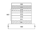
도 23은 실시예 1 내지 실시예 4에서 사용한 발광 디바이스의 구조를 나타낸 도면이다.
도 24는 발광 디바이스 1, 발광 디바이스 2, 비교 발광 디바이스 3, 및 참고 발광 디바이스 4의 휘도-전류 밀도 특성을 나타낸 것이다.
도 25는 발광 디바이스 1, 발광 디바이스 2, 비교 발광 디바이스 3, 및 참고 발광 디바이스 4의 휘도-전압 특성을 나타낸 것이다.
도 26은 발광 디바이스 1, 발광 디바이스 2, 비교 발광 디바이스 3, 및 참고 발광 디바이스 4의 전류 효율-휘도 특성을 나타낸 것이다.
도 27은 발광 디바이스 1, 발광 디바이스 2, 비교 발광 디바이스 3, 및 참고 발광 디바이스 4의 전류 밀도-전압 특성을 나타낸 것이다.
도 28은 발광 디바이스 1, 발광 디바이스 2, 비교 발광 디바이스 3, 및 참고 발광 디바이스 4의 블루 인덱스-휘도 특성을 나타낸 것이다.
도 29는 발광 디바이스 1, 발광 디바이스 2, 비교 발광 디바이스 3, 및 참고 발광 디바이스 4의 발광 스펙트럼을 나타낸 것이다.
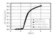
도 30은 발광 디바이스 1, 발광 디바이스 2, 비교 발광 디바이스 3, 및 참고 발광 디바이스 4의 신뢰성을 나타낸 도면이다.
도 31은 발광 디바이스 5 및 참고 발광 디바이스 6의 휘도-전류 밀도 특성을 나타낸 것이다.
도 32는 발광 디바이스 5 및 참고 발광 디바이스 6의 휘도-전압 특성을 나타낸 것이다.
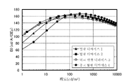
도 33은 발광 디바이스 5 및 참고 발광 디바이스 6의 전류 효율-휘도 특성을 나타낸 것이다.
도 34는 발광 디바이스 5 및 참고 발광 디바이스 6의 전류 밀도-전압 특성을 나타낸 것이다.
도 35는 발광 디바이스 5 및 참고 발광 디바이스 6의 블루 인덱스-휘도 특성을 나타낸 것이다.
도 36은 발광 디바이스 5 및 참고 발광 디바이스 6의 발광 스펙트럼을 나타낸 것이다.
도 37은 발광 디바이스 5 및 참고 발광 디바이스 6의 신뢰성을 나타낸 도면이다.
도 38은 발광 디바이스 7 및 참고 발광 디바이스 8의 휘도-전류 밀도 특성을 나타낸 것이다.
도 39는 발광 디바이스 7 및 참고 발광 디바이스 8의 휘도-전압 특성을 나타낸 것이다.
도 40은 발광 디바이스 7 및 참고 발광 디바이스 8의 전류 효율-휘도 특성을 나타낸 것이다.
도 41은 발광 디바이스 7 및 참고 발광 디바이스 8의 전류 밀도-전압 특성을 나타낸 것이다.
도 42는 발광 디바이스 7 및 참고 발광 디바이스 8의 발광 스펙트럼을 나타낸 것이다.
도 43은 발광 디바이스 7 및 참고 발광 디바이스 8의 신뢰성을 나타낸 도면이다.
도 44는 발광 디바이스 9 및 참고 발광 디바이스 10의 휘도-전류 밀도 특성을 나타낸 것이다.
도 45는 발광 디바이스 9 및 참고 발광 디바이스 10의 휘도-전압 특성을 나타낸 것이다.
도 46은 발광 디바이스 9 및 참고 발광 디바이스 10의 전류 효율-휘도 특성을 나타낸 것이다.
도 47은 발광 디바이스 9 및 참고 발광 디바이스 10의 전류 밀도-전압 특성을 나타낸 것이다.
도 48은 발광 디바이스 9 및 참고 발광 디바이스 10의 발광 스펙트럼을 나타낸 것이다.
도 49는 발광 디바이스 9 및 참고 발광 디바이스 10의 신뢰성을 나타낸 도면이다.
도 50은 발광 디바이스 11, 발광 디바이스 12, 및 참고 발광 디바이스 13의 휘도-전류 밀도 특성을 나타낸 것이다.
도 51은 발광 디바이스 11, 발광 디바이스 12, 및 참고 발광 디바이스 13의 휘도-전압 특성을 나타낸 것이다.
도 52는 발광 디바이스 11, 발광 디바이스 12, 및 참고 발광 디바이스 13의 전류 효율-휘도 특성을 나타낸 것이다.
도 53은 발광 디바이스 11, 발광 디바이스 12, 및 참고 발광 디바이스 13의 전류 밀도-전압 특성을 나타낸 것이다.
도 54는 발광 디바이스 11, 발광 디바이스 12, 및 참고 발광 디바이스 13의 전력 효율-휘도 특성을 나타낸 것이다.
도 55는 발광 디바이스 11, 발광 디바이스 12, 및 참고 발광 디바이스 13의 외부 양자 효율-휘도 특성을 나타낸 것이다.
도 56은 발광 디바이스 11, 발광 디바이스 12, 및 참고 발광 디바이스 13의 발광 스펙트럼을 나타낸 것이다.
도 57은 발광 디바이스 11, 발광 디바이스 12, 및 참고 발광 디바이스 13의 신뢰성을 나타낸 도면이다.1A to 1C are diagrams for explaining the configuration of a light emitting device according to an embodiment.
2A to 2E are diagrams for explaining the configuration of a light emitting device according to an embodiment.
3A and 3B are diagrams for explaining the configuration of a light emitting device according to an embodiment.
4A and 4B are views for explaining a method of manufacturing a light emitting device according to an embodiment.
5A to 5C are views for explaining a method of manufacturing a light emitting device according to an embodiment.
6A to 6C are views for explaining a method of manufacturing a light emitting device according to an embodiment.
7A and 7B are views for explaining a method of manufacturing a light emitting device according to an embodiment.
8 is a view for explaining a light emitting device according to an embodiment.
9A and 9B are diagrams for explaining a light emitting apparatus and a light emitting device according to an embodiment.
10 is a diagram for explaining a light emitting device according to an embodiment.
11A to 11C are views for explaining a method of manufacturing a light emitting device according to an embodiment.
12A and 12B are views for explaining a method of manufacturing a light emitting device according to an embodiment.
13 is a view for explaining a light emitting device according to an embodiment.
14A and 14B are views for explaining a light emitting device according to an embodiment.
15A and 15B are diagrams for explaining a light emitting device according to an embodiment.
16A and 16B are diagrams for explaining a light emitting device according to an embodiment.
17A and 17B are views for explaining a light emitting device according to an embodiment.
18A to 18E are diagrams for explaining an electronic device according to an embodiment.
19A to 19E are diagrams for explaining an electronic device according to an embodiment.
20A and 20B are diagrams for explaining an electronic device according to an embodiment.
21A and 21B are diagrams for explaining an electronic device according to an embodiment.
It is a figure explaining the electronic device which concerns on embodiment.
23 is a diagram showing the structure of a light emitting device used in Examples 1 to 4;
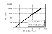
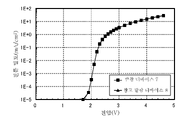
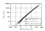
24 shows the luminance-current density characteristics of light emitting
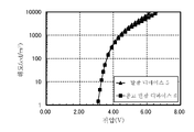
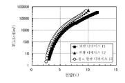
25 shows the luminance-voltage characteristics of light emitting
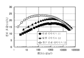
26 shows the current efficiency-luminance characteristics of light emitting
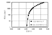
27 shows the current density-voltage characteristics of light emitting
28 shows blue index-luminance characteristics of light emitting
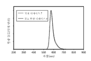
29 shows emission spectra of light emitting
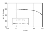
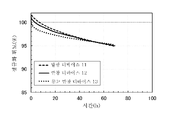
30 is a view showing reliability of light emitting
31 shows the luminance-current density characteristics of light emitting
32 shows the luminance-voltage characteristics of the
33 shows the current efficiency-luminance characteristics of the
34 shows the current density-voltage characteristics of the
Fig. 35 shows blue index-luminance characteristics of light emitting
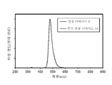
36 shows emission spectra of light emitting
37 is a view showing reliability of light emitting
38 shows the luminance-current density characteristics of the
39 shows the luminance-voltage characteristics of the
40 shows the current efficiency-luminance characteristics of the
41 shows the current density-voltage characteristics of the
42 shows the emission spectra of the
43 is a view showing reliability of the
44 shows the luminance-current density characteristics of the
45 shows the luminance-voltage characteristics of the
46 shows the current efficiency-luminance characteristics of the
47 shows the current density-voltage characteristics of the
48 shows the emission spectra of the
49 is a view showing reliability of the
50 shows the luminance-current density characteristics of the light emitting device 11, the light emitting device 12, and the reference light emitting device 13. FIG.
51 shows the luminance-voltage characteristics of the light emitting device 11, the light emitting device 12, and the reference light emitting device 13. FIG.
52 shows the current efficiency-luminance characteristics of the light emitting device 11 , the light emitting device 12 , and the reference light emitting device 13 .
53 shows the current density-voltage characteristics of the light emitting device 11, the light emitting device 12, and the reference light emitting device 13;
54 shows the power efficiency-luminance characteristics of the light emitting device 11 , the light emitting device 12 , and the reference light emitting device 13 .
55 shows the external quantum efficiency-luminance characteristics of the light emitting device 11, the light emitting device 12, and the reference light emitting device 13;
56 shows the emission spectra of the light-emitting device 11, the light-emitting device 12, and the reference light-emitting device 13;
57 is a view showing the reliability of the light emitting device 11, the light emitting device 12, and the reference light emitting device 13;
실시형태에 대하여 도면을 사용하여 자세히 설명한다. 다만, 본 발명은 아래의 설명에 한정되지 않고, 본 발명의 취지 및 그 범위에서 벗어남이 없이 그 형태 및 자세한 사항을 다양하게 변경할 수 있는 것은 통상의 기술자라면 용이하게 이해할 수 있다. 따라서 본 발명은 아래에 나타내는 실시형태의 기재 내용에 한정되어 해석되는 것은 아니다. 또한 아래에서 설명하는 발명의 구성에서, 동일한 부분 또는 같은 기능을 가지는 부분에는 동일한 부호를 상이한 도면 간에서 공통적으로 사용하고, 그 반복적인 설명은 생략한다.EMBODIMENT OF THE INVENTION It demonstrates in detail using drawing about embodiment. However, the present invention is not limited to the description below, and it can be easily understood by those skilled in the art that various changes can be made in form and details without departing from the spirit and scope of the present invention. Therefore, this invention is limited to the description of embodiment shown below and is not interpreted. In addition, in the configuration of the invention described below, the same reference numerals are commonly used between different drawings for the same parts or parts having the same function, and a repetitive description thereof will be omitted.
(실시형태 1)(Embodiment 1)
본 실시형태에서는 본 발명의 일 형태의 발광 디바이스 및 표시 패널의 구성에 대하여 도 1 및 도 2를 참조하여 설명한다.In this embodiment, the structure of the light emitting device and display panel of one embodiment of this invention is demonstrated with reference to FIG.1 and FIG.2.
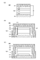
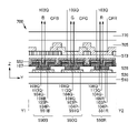
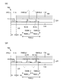
도 1의 (A) 내지 (C)는 본 발명의 일 형태의 발광 디바이스(100)를 설명하는 단면도이다.1A to 1C are cross-sectional views illustrating a
도 1의 (A) 내지 (C)에 나타낸 바와 같이, 발광 디바이스(100)는 제 1 전극(101)과, 제 2 전극(102)과, EL층(103)을 가진다. 제 1 전극(101)은 제 2 전극(102)과 중첩된 영역을 가지고, EL층(103)은 제 1 전극(101)과 제 2 전극(102) 사이에 끼워진 영역을 가진다. 또한 EL층(103)은 제 1 전극(101) 위에 정공 주입·수송층(104), 발광층(113), 전자 수송층(108), 및 전자 주입층(109)이 순차적으로 적층된 구조를 가진다.1A to 1C , the
전자 주입층(109)은 제 2 전극(102)으로부터의 전자의 주입 효율을 높이기 위한 층이고, 제 2 전극(102)에 사용하는 재료의 일함수의 값과, 전자 주입층(109)에 사용하는 재료의 LUMO 준위의 값을 비교하였을 때, 그 차이가 작은(0.5eV 이하) 재료를 사용하여 형성하는 것이 바람직하다. 따라서, 전자 주입층(109)에는 리튬, 세슘, 플루오린화 리튬(LiF), 플루오린화 세슘(CsF), 플루오린화 칼슘(CaF2), 8-(퀴놀리놀레이토)리튬(약칭: Liq), 2-(2-피리딜)페놀레이토 리튬(약칭: LiPP), 2-(2-피리딜)-3-피리디놀레이토 리튬(약칭: LiPPy), 4-페닐-2-(2-피리딜)페놀레이토 리튬(약칭: LiPPP), 리튬 산화물(LiOx), 탄산 세슘 등과 같은 알칼리 금속, 알칼리 토금속, 또는 이들의 화합물을 사용할 수 있다. 또한 플루오린화 어븀(ErF3) 등의 희토류 금속 화합물을 사용할 수 있다. 또한 전자 주입층(109)에 전자화물(electride)을 사용하여도 좋다. 전자화물로서는, 예를 들어 칼슘과 알루미늄의 혼합 산화물에 전자를 고농도로 첨가한 물질 등이 있다.The
또한 전자 주입층(109)에 유기 화합물과 전자 공여체(도너)를 혼합한 복합 재료를 사용하여도 좋다. 이와 같은 복합 재료는, 전자 공여체에 의하여 유기 화합물에 전자가 발생하기 때문에, 전자 주입성 및 전자 수송성이 우수하다. 이 경우, 유기 화합물로서는 발생한 전자의 수송이 우수한 재료인 것이 바람직하고, 구체적으로는 예를 들어 후술하는 전자 수송층에 사용되는 전자 수송성 재료(금속 착체 및 헤테로 방향족 화합물 등)를 사용할 수 있다. 전자 공여체로서는 유기 화합물에 대하여 전자 공여성을 나타내는 물질이면 좋다. 구체적으로는 알칼리 금속, 알칼리 토금속, 및 희토류 금속이 바람직하고, 리튬, 세슘, 마그네슘, 칼슘, 어븀, 이터븀 등을 들 수 있다. 또한 알칼리 금속 산화물 및 알칼리 토금속 산화물이 바람직하고, 리튬 산화물, 칼슘 산화물, 바륨 산화물 등을 들 수 있다. 또한 산화 마그네슘 등의 루이스 염기를 사용할 수도 있다. 또한 테트라싸이아풀발렌(약칭: TTF) 등의 유기 화합물을 사용할 수도 있다.In addition, a composite material in which an organic compound and an electron donor (donor) are mixed may be used for the
그 외에도, 전자 주입층(109)에 유기 화합물과 금속을 혼합한 복합 재료를 사용하여도 좋다. 또한 여기서 사용하는 유기 화합물로서는, LUMO(Lowest Unoccupied Molecular Orbital) 준위가 -3.6eV 이상 -2.3eV 이하인 것이 바람직하다. 또한 비공유 전자쌍을 가지는 재료가 바람직하다.Alternatively, a composite material in which an organic compound and a metal are mixed may be used for the
따라서 상기 유기 화합물로서는, 피리딘 골격, 다이아진 골격(피리미딘, 피라진 등), 또는 트라이아진 골격을 가지는 헤테로 고리 화합물 등 비공유 전자쌍을 가지는 재료가 바람직하다. 피리딘 골격을 가지는 헤테로 고리 화합물, 다이아진 골격을 가지는 헤테로 고리 화합물 및 트라이아진 골격을 가지는 헤테로 고리 화합물의 자세한 내용에 대해서는 본 실시형태에서 설명한다.Therefore, as the organic compound, a material having a lone pair of electrons, such as a heterocyclic compound having a pyridine skeleton, a diazine skeleton (pyrimidine, pyrazine, etc.), or a triazine skeleton, is preferable. The details of the heterocyclic compound having a pyridine skeleton, the heterocyclic compound having a diazine skeleton, and the heterocyclic compound having a triazine skeleton are described in the present embodiment.
유기 화합물과 금속을 혼합한 복합 재료에 사용하는 금속으로서는, 주기율표의 5족, 7족, 9족, 또는 11족에 속하는 전이 금속 및 13족에 속하는 재료를 사용하는 것이 바람직하고, 예를 들어 Ag, Cu, Al, 또는 In 등이 있다. 또한 이때 유기 화합물은 상기 금속과의 사이에 반점유 궤도(SOMO: Singly Occupied Molecular Orbital)를 형성한다.As the metal used for the composite material in which an organic compound and a metal are mixed, it is preferable to use a transition metal belonging to
또한 전자 주입층(109)은 적층 구조를 가져도 좋다. 적층 구조는 재료의 일부가 상이한 복수의 층으로 구성되어도 좋고, 재료가 모두 상이한 복수의 층으로 구성되어도 좋다.In addition, the
전자 주입층(109)에 사용할 수 있는 재료의 자세한 내용에 대해서는 본 실시형태에서 설명한다.The details of the material that can be used for the
또한 제 1 전극(101), 제 2 전극(102), 정공 주입·수송층(104), 발광층(113), 및 전자 수송층(108)으로서 사용할 수 있는 재료에 대해서는 본 실시형태에서 설명한다. 또한 전자 수송층(108)은 적층 구조를 가져도 좋고, 제 1 전극(101) 측으로부터 발광층(113)을 통과하여 제 2 전극(102) 측으로 이동하는 정공을 차단하기 위한 정공 차단층을 가져도 좋다. 또한 정공 주입·수송층(104)을 형성하는 재료로서는, 본 실시형태에서 설명하는 정공 주입층 및 정공 수송층의 재료를 사용할 수 있다. 또한 정공 주입·수송층(104)은 단층으로 형성하여도 좋고, 복수의 층으로 형성하여도 좋다. 또한 정공 주입층 및 정공 수송층을 따로 형성하여도 좋다. 또한 정공 주입·수송층(104)은 정공 주입층 및 정공 수송층 중 어느 한쪽만이어도 좋다.Materials that can be used as the
전자 주입층(109)은 EL층(103)의 일부이지만, EL층(103)의 다른 층(정공 주입·수송층(104), 발광층(113), 및 전자 수송층(108))과는 다른 형상을 가져도 좋다. 일반적으로 EL층의 일부의 층의 형상을 다른 층의 형상과 다르게 하는 경우, 제조 공정에서 다른 층이 대기 등에 노출될 가능성이 있기 때문에, 발광 디바이스의 신뢰성 및 휘도가 저하될 수 있다. 그러나 전자 주입층(109)의 형상을 다른 층의 형상과 다르게 하는 경우, 제조 공정에서 대기 등에 노출될 가능성이 있는 것은 발광층(113)의 상면에 전자 수송층(108)을 형성한 후이므로, 정공 주입·수송층(104) 및 발광층(113)이 대기 등에 노출되는 것을 방지하여, 발광 디바이스(100)의 신뢰성 및 휘도의 저하를 억제할 수 있다. 따라서 발광 디바이스(100)에서 전자 주입층(109)의 형상을 EL층(103)의 다른 층(정공 주입·수송층(104), 발광층(113), 및 전자 수송층(108))의 형상과 다르게 할 수 있다.The
또한 전자 수송층(108)이 복수의 층을 가지는 경우, 대기 등에 노출될 가능성이 있는 것이, 전자 수송층(108)의 일부의 층을 형성한 후이며 전자 수송층(108)의 나머지 층을 형성하기 전이어도, 발광 디바이스(100)의 신뢰성 및 휘도의 저하를 억제할 수 있는 경우가 있다.In addition, when the
전자 주입층(109)이 EL층(103)의 다른 층(정공 주입·수송층(104), 발광층(113), 및 전자 수송층(108))과는 다른 형상을 가지는 발광 디바이스(100)의 예를 도 1의 (B) 및 (C)에 나타내었다.An example of the
도 1의 (B)에 나타낸 바와 같이, 전자 주입층(109)과 제 2 전극(102)을 정공 주입·수송층(104), 발광층(113), 및 전자 수송층(108)과는 다른 형상으로 할 수 있다. 전자 주입층(109) 및 제 2 전극(102)을 복수의 발광 디바이스에 의하여 공유되는 층으로 할 수 있으므로 발광 디바이스(100)의 제조 공정을 간략화하여 스루풋을 향상시킬 수 있다.As shown in FIG. 1B , the
또한 도 1의 (B)에 나타낸 바와 같이, 발광 디바이스(100)는 절연층(107)을 가져도 좋다. 절연층(107)은 제 1 전극(101)의 일부, 정공 주입·수송층(104)의 측면, 발광층(113)의 측면, 및 전자 수송층(108)의 측면과 접촉한다. 또한 전자 주입층(109)은 절연층(107)을 개재하여 제 1 전극(101)의 측면, 정공 주입·수송층(104)의 측면, 발광층(113)의 측면, 및 전자 수송층(108)의 측면에 위치하고, 또한 절연층(107)을 개재하지 않고 전자 수송층(108)의 상면과 접촉한다. 제 2 전극(102)은 절연층(107) 및 전자 주입층(109)을 개재하여 정공 주입·수송층(104)의 측면, 발광층(113)의 측면, 및 전자 수송층(108)의 측면에 위치하고, 전자 주입층(109)을 개재하여 제 1 전극(101)의 측면에 위치하고, 또한 전자 주입층(109)을 개재하여 전자 수송층(108)의 상면에 위치한다. 또한 절연층(107)은 발광층(113)의 측면과 전자 주입층(109) 사이에 위치한다고도 할 수 있다.Further, as shown in FIG. 1B , the
제 2 전극(102)이 절연층(107) 및 전자 주입층(109)을 개재하여 제 1 전극(101)의 측면, 정공 주입·수송층(104)의 측면, 발광층(113)의 측면, 및 전자 수송층(108)의 측면에 위치하는 구성을 가짐으로써 제 2 전극(102)과 정공 주입·수송층(104) 간의 도통 및 제 2 전극(102)과 제 1 전극(101) 간의 도통을 방지할 수 있다.The
상기 효과를 얻기 위하여 절연층(107)은 반드시 필수적인 것은 아니지만, 절연층(107)을 가지는 구성이면, 정공 주입·수송층(104)의 측면(또는 단부), 발광층(113)의 측면, 및 전자 수송층(108)의 측면을 보호할 수 있어 바람직하다.In order to obtain the above effect, the insulating
또한 절연층(107)을 가지는 구성이면, 제 2 전극(102)과 정공 주입·수송층(104) 간의 도통 및 제 2 전극(102)과 제 1 전극(101) 간의 도통을 더 방지할 수 있어 바람직하다.In addition, if the structure has the insulating
따라서 발광 디바이스(100)에는 다양한 구조를 적용할 수 있다. 예를 들어, 복수의 발광 디바이스(100)를 배치할 때, 서로 인접한 발광 디바이스(100) 각각에 포함되는 전자 주입층(109)끼리 및 제 2 전극(102)끼리가 연결된 구조로 할 수 있다.Accordingly, various structures may be applied to the
절연층(107)으로서 사용할 수 있는 재료에 대해서는 아래의 실시형태에서 설명한다.Materials that can be used as the insulating
또한 도 1의 (C)에 나타낸 바와 같이, 먼저 정공 주입·수송층(104)(정공 주입층만이어도 좋음)을 패터닝한 후, 발광층(113) 및 전자 수송층(108)을 순차적으로 적층함으로써, 정공 주입·수송층(104)이 발광층(113)으로 둘러싸여도 좋다. 이 경우, 발광층(113)이 정공 주입·수송층(104)의 상면 및 측면과 접촉하기 때문에 전자 주입층(109)은 정공 주입·수송층(104)의 측면과 접촉하지 않고, 제 1 전극(101)의 측면, 발광층(113)의 측면, 및 전자 수송층(108)의 측면과 접촉한다. 또한 제 2 전극(102)은 전자 주입층(109)을 개재하여 발광층(113)의 측면 그리고 전자 수송층(108)의 측면 및 상면에 위치한다.In addition, as shown in FIG. 1C , after first patterning the hole injection/transport layer 104 (only a hole injection layer may be sufficient), the
정공 주입·수송층(104)의 단부가 발광층(113)으로 둘러싸임으로써, 절연층(107)을 제공하지 않아도 제 2 전극(102)과 정공 주입·수송층(104) 간의 도통을 방지할 수 있다.Since the end of the hole injection/
또한 본 발명의 일 형태는 도 1의 (B) 및 (C)의 구성에 한정되지 않는다. 예를 들어 서로 인접한 발광 디바이스들 사이에 절연층 등을 제공하고, 제 2 전극(102) 및 전자 주입층(109)을 상기 절연층 위에 형성하는 구조로 하면, 제 2 전극(102) 및 전자 주입층(109)은 제 1 전극(101)의 측면, 정공 주입·수송층(104)의 측면, 발광층(113)의 측면, 및 전자 수송층(108)의 측면의 일부 또는 전체에 위치하지 않는 경우가 있다.In addition, one aspect of this invention is not limited to the structure of FIG. 1(B) and (C). For example, if an insulating layer is provided between adjacent light emitting devices and the
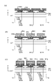
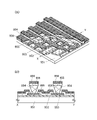
또한 본 발명의 일 형태의 발광 디바이스의 구성은 도 1에 나타낸 구성에 한정되지 않는다. 발광 디바이스의 기본적인 구조에 대하여 도 2를 사용하여 설명한다.In addition, the structure of the light emitting device of one embodiment of this invention is not limited to the structure shown in FIG. The basic structure of the light emitting device will be described with reference to FIG. 2 .
<<발광 디바이스의 기본적인 구조>><<Basic structure of light emitting device>>
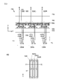
발광 디바이스의 기본적인 구조에 대하여 설명한다. 도 2의 (A)에는 한 쌍의 전극 사이에 발광층을 포함한 EL층을 가지는 발광 디바이스를 나타내었다. 구체적으로는, 제 1 전극(101)과 제 2 전극(102) 사이에 EL층(103)이 끼워진 구조를 가진다.The basic structure of the light emitting device will be described. Fig. 2A shows a light emitting device having an EL layer including a light emitting layer between a pair of electrodes. Specifically, it has a structure in which the
또한 도 2의 (B)에는 한 쌍의 전극 사이에 복수(도 2의 (B)에서는 2층)의 EL층(103a, 103b)을 가지고, EL층 사이에 전하 발생층(106)을 가지는 적층 구조(탠덤 구조)의 발광 디바이스를 나타내었다. 탠덤 구조의 발광 디바이스에 의하여, 전류 스트레스가 작고 신뢰성이 높은 발광 장치를 실현할 수 있다.In addition, in Fig. 2B, a plurality of
전하 발생층(106)은 제 1 전극(101)과 제 2 전극(102) 간에 전위차를 발생시켰을 때, 한쪽의 EL층(103a 또는 103b)에 전자를 주입하고, 다른 쪽의 EL층(103b 또는 103a)에 정공을 주입하는 기능을 가진다. 따라서, 도 2의 (B)에서 제 1 전극(101)에 제 2 전극(102)보다 전위가 높게 되도록 전압을 인가하면, 전하 발생층(106)으로부터 EL층(103a)에 전자가 주입되고, EL층(103b)에 정공이 주입된다.When a potential difference is generated between the
또한 전하 발생층(106)은 광 추출 효율의 관점에서 가시광에 대하여 투광성을 가지는 것(구체적으로는, 전하 발생층(106)에 대한 가시광의 투과율이 40% 이상인 것)이 바람직하다. 또한 전하 발생층(106)은 제 1 전극(101) 및 제 2 전극(102)보다 도전율이 낮은 경우에도 기능한다.In addition, from the viewpoint of light extraction efficiency, the
또한 도 2의 (C)에는 본 발명의 일 형태의 발광 디바이스의 EL층(103)의 적층 구조를 나타내었다. 다만, 이 경우, 제 1 전극(101)은 양극으로서 기능하고, 제 2 전극(102)은 음극으로서 기능하는 것으로 한다. EL층(103)은 제 1 전극(101) 위에 정공(홀) 주입층(111), 정공(홀) 수송층(112), 발광층(113), 전자 수송층(114), 전자 주입층(115)이 순차적으로 적층된 구조를 가진다. 또한 발광층(113)은 발광색이 다른 복수의 발광층이 적층된 구성을 가져도 좋다. 예를 들어 적색을 발광하는 발광 물질을 포함한 발광층과, 녹색을 발광하는 발광 물질을 포함한 발광층과, 청색을 발광하는 발광 물질을 포함한 발광층이 적층된 구조, 또는 이들이 캐리어 수송성 재료를 가지는 층을 개재하여 적층된 구조이어도 좋다. 또는 황색을 발광하는 발광 물질을 포함한 발광층과, 청색을 발광하는 발광 물질을 포함한 발광층의 조합이어도 좋다. 다만, 발광층(113)의 적층 구조는 상술한 것에 한정되지 않는다. 예를 들어, 발광층(113)은 발광색이 같은 복수의 발광층이 적층된 구성을 가져도 좋다. 예를 들어, 청색을 발광하는 발광 물질을 포함한 제 1 발광층과, 청색을 발광하는 발광 물질을 포함한 제 2 발광층이 적층된 구조, 또는 이들이 캐리어 수송성 재료를 가지는 층을 개재하여 적층된 구조이어도 좋다. 발광색이 같은 복수의 발광층이 적층된 구성의 경우, 단층의 구성보다 신뢰성을 높일 수 있는 경우가 있다. 또한 도 2의 (B)에 도시된 탠덤 구조와 같이 복수의 EL층이 제공되는 경우에도, 각 EL층의 층은 상술한 바와 같이 양극 측으로부터 순차적으로 적층된다. 또한 제 1 전극(101)이 음극이고, 제 2 전극(102)이 양극인 경우에는, EL층(103)의 층의 적층 순서는 반대가 된다. 구체적으로는, 음극인 제 1 전극(101) 위의 111이 전자 주입층, 112가 전자 수송층, 113이 발광층, 114가 정공(홀) 수송층, 115가 정공(홀) 주입층이 된다.Fig. 2C shows a laminated structure of the
EL층(103, 103a, 103b)에 포함되는 발광층(113)은 각각 발광 물질과 복수의 물질을 적절히 조합하여 가지고, 원하는 발광색을 나타내는 형광 발광 또는 인광 발광을 얻을 수 있는 구성으로 할 수 있다. 또한 발광층(113)을 발광색이 상이한 적층 구조로 하여도 좋다. 또한 이 경우 적층된 각 발광층에 사용되는 발광 물질 및 기타 물질에는 각각 상이한 재료를 사용하면 좋다. 또한 도 2의 (B)에 나타낸 복수의 EL층(103a, 103b)으로부터 각각 상이한 발광색이 얻어지는 구성으로 하여도 좋다. 이 경우에도 각 발광층에 사용되는 발광 물질 및 기타 물질을 상이한 재료로 하면 좋다.The light-emitting
또한 본 발명의 일 형태의 발광 디바이스에서, 예를 들어 도 2의 (C)에서, 제 1 전극(101)을 반사 전극으로 하고, 제 2 전극(102)을 반투과·반반사 전극으로 하고, 미소 광공진기(마이크로캐비티) 구조로 함으로써, EL층(103)에 포함되는 발광층(113)으로부터 얻어지는 발광을 전극들 사이에서 공진시켜 제 2 전극(102)으로부터 얻어지는 발광을 강하게 할 수 있다.Further, in the light emitting device of one embodiment of the present invention, for example, in FIG. 2C , the
또한 발광 디바이스의 제 1 전극(101)이 반사성을 가지는 도전성 재료와 투광성을 가지는 도전성 재료(투명 도전막)의 적층 구조로 이루어지는 반사 전극인 경우, 투명 도전막의 막 두께를 제어함으로써 광학 조정을 수행할 수 있다. 구체적으로는, 발광층(113)으로부터 얻어지는 광의 파장 λ에 대하여 제 1 전극(101)과 제 2 전극(102) 사이의 광학 거리(막 두께와 굴절률의 곱)가 mλ/2(다만, m은 1 이상의 정수임) 또는 그 근방이 되도록 조정하는 것이 바람직하다.Further, when the
또한 발광층(113)으로부터 얻어지는 원하는 광(파장: λ)을 증폭시키기 위하여, 제 1 전극(101)으로부터 발광층(113)에서 원하는 광이 얻어지는 영역(발광 영역)까지의 광학 거리와, 제 2 전극(102)으로부터 발광층(113)에서 원하는 광이 얻어지는 영역(발광 영역)까지의 광학 거리를 각각 (2m'+1)λ/4(다만, m'는 1 이상의 정수임) 또는 그 근방이 되도록 조절하는 것이 바람직하다. 또한 여기서 발광 영역이란 발광층(113)에서의 정공(홀)과 전자의 재결합 영역을 뜻한다.In addition, in order to amplify the desired light (wavelength: λ) obtained from the light-emitting
이와 같은 광학 조정을 수행함으로써 발광층(113)으로부터 얻어지는 특정의 단색광의 스펙트럼을 좁혀 색 순도가 좋은 발광을 얻을 수 있다.By performing such optical adjustment, the spectrum of the specific monochromatic light obtained from the
다만, 상술한 경우, 제 1 전극(101)과 제 2 전극(102) 사이의 광학 거리는, 엄밀하게 말하면, 제 1 전극(101)에서의 반사 영역으로부터 제 2 전극(102)에서의 반사 영역까지의 총두께이다. 그러나, 제 1 전극(101) 및 제 2 전극(102)에서의 반사 영역을 엄밀하게 결정하는 것은 어렵기 때문에, 제 1 전극(101)과 제 2 전극(102)의 임의의 위치를 반사 영역으로 가정함으로써 상술한 효과를 충분히 얻을 수 있는 것으로 한다. 또한 제 1 전극(101)과, 원하는 광이 얻어지는 발광층 사이의 광학 거리는, 엄밀하게 말하면, 제 1 전극(101)에서의 반사 영역과, 원하는 광이 얻어지는 발광층에서의 발광 영역 사이의 광학 거리이다. 그러나, 제 1 전극(101)에서의 반사 영역, 및 원하는 광이 얻어지는 발광층에서의 발광 영역을 엄밀하게 결정하는 것은 어렵기 때문에, 제 1 전극(101)의 임의의 위치를 반사 영역으로, 원하는 광이 얻어지는 발광층의 임의의 위치를 발광 영역으로 가정함으로써 상술한 효과를 충분히 얻을 수 있는 것으로 한다.However, in the above-described case, the optical distance between the
도 2의 (D)에 나타낸 발광 디바이스는 탠덤 구조를 가지는 발광 디바이스이고, 마이크로캐비티 구조를 가지기 때문에, 각 EL층(103a, 103b)으로부터 파장이 다른 광(단색광)을 추출할 수 있다. 따라서, 다른 발광색을 얻기 위한 구분 형성(예를 들어, RGB)이 불필요하다. 따라서 고정세(高精細)화를 실현하기 쉽다. 또한 착색층(컬러 필터)과 조합할 수도 있다. 또한 특정 파장의 정면 방향의 발광 강도를 높일 수 있어 저소비 전력화를 도모할 수 있다.The light emitting device shown in Fig. 2D is a light emitting device having a tandem structure, and since it has a microcavity structure, light (monochromatic light) having different wavelengths can be extracted from each of the EL layers 103a and 103b. Accordingly, there is no need to form a division (eg, RGB) to obtain different luminous colors. Therefore, it is easy to realize high taxation. It can also be combined with a colored layer (color filter). In addition, the intensity of light emission in the front direction of a specific wavelength can be increased, so that power consumption can be reduced.
도 2의 (E)에 나타낸 발광 디바이스는, 도 2의 (B)에 나타낸 탠덤 구조의 발광 디바이스의 일례이며, 도면에 나타낸 바와 같이, 3개의 EL층(103a, 103b, 103c)이 전하 발생층(106a, 106b)을 개재하여 적층된 구조를 가진다. 또한 3개의 EL층(103a, 103b, 103c)은 각각 발광층(113a, 113b, 113c)을 가지고, 각 발광층의 발광색은 자유로이 조합할 수 있다. 예를 들어, 발광층(113a)을 청색으로, 발광층(113b)을 적색, 녹색, 및 황색 중 어느 하나 또는 복수의 색으로, 발광층(113c)을 청색으로 할 수도 있고, 발광층(113a)을 적색으로, 발광층(113b)을 청색, 녹색, 및 황색 중 어느 하나 또는 복수의 색으로, 발광층(113c)을 적색으로 할 수도 있다.The light emitting device shown in FIG. 2E is an example of the light emitting device of the tandem structure shown in FIG. 2B, and as shown in the figure, three
또한 상술한 본 발명의 일 형태의 발광 디바이스에서, 제 1 전극(101) 및 제 2 전극(102) 중 적어도 한쪽을 투광성을 가지는 전극(투명 전극, 반투과·반반사 전극 등)으로 한다. 투광성을 가지는 전극이 투명 전극인 경우, 투명 전극의 가시광의 투과율은 40% 이상으로 한다. 또한 반투과·반반사 전극인 경우, 반투과·반반사 전극의 가시광의 반사율은 20% 이상 80% 이하, 바람직하게는 40% 이상 70% 이하로 한다. 또한 이들 전극은 저항률을 1Х10-2Ωcm 이하로 하는 것이 바람직하다.Further, in the light emitting device of one embodiment of the present invention described above, at least one of the
또한 상술한 본 발명의 일 형태의 발광 디바이스에서, 제 1 전극(101) 및 제 2 전극(102) 중 한쪽이 반사성을 가지는 전극(반사 전극)인 경우, 반사성을 가지는 전극의 가시광의 반사율은 40% 이상 100% 이하, 바람직하게는 70% 이상 100% 이하로 한다. 또한 이 전극은 저항률을 1Х10-2Ωcm 이하로 하는 것이 바람직하다.Further, in the light emitting device of one embodiment of the present invention described above, when one of the
<<발광 디바이스의 구체적인 구조>><<Specific structure of light emitting device>>
다음으로, 본 발명의 일 형태의 발광 디바이스의 구체적인 구조에 대하여 도 2를 사용하여 설명한다. 또한 여기서는 탠덤 구조를 가지는 도 2의 (D)를 사용하여 설명한다. 또한 싱글 구조를 가지는 도 2의 (A) 및 (C)의 발광 디바이스에 대해서도 EL층의 구성은 같다. 또한 도 2의 (D)에 나타낸 발광 디바이스가 마이크로캐비티 구조를 가지는 경우에는, 제 1 전극(101)을 반사 전극으로서 형성하고, 제 2 전극(102)을 반투과·반반사 전극으로서 형성한다. 따라서, 원하는 전극 재료를 하나 또는 복수 사용하여 단층으로 또는 적층하여 형성할 수 있다. 또한 제 2 전극(102)은 EL층(103b)을 형성한 후에 상술한 바와 같이 재료를 선택하여 형성한다.Next, the specific structure of the light emitting device of one embodiment of this invention is demonstrated using FIG. In addition, the description will be made using FIG. 2(D) having a tandem structure. Also, the structure of the EL layer is the same for the light emitting devices of Figs. 2A and 2C having a single structure. When the light emitting device shown in Fig. 2D has a microcavity structure, the
<제 1 전극 및 제 2 전극><First electrode and second electrode>
제 1 전극(101) 및 제 2 전극(102)을 형성하는 재료로서는 상술한 양쪽 전극의 기능을 만족시킬 수 있다면 아래에 나타내는 재료를 적절히 조합하여 사용할 수 있다. 예를 들어 금속, 합금, 전기 전도성 화합물, 및 이들의 혼합물 등을 적절히 사용할 수 있다. 구체적으로는 In-Sn 산화물(ITO라고도 함), In-Si-Sn 산화물(ITSO라고도 함), In-Zn 산화물, In-W-Zn 산화물을 들 수 있다. 그 외에, 알루미늄(Al), 타이타늄(Ti), 크로뮴(Cr), 망가니즈(Mn), 철(Fe), 코발트(Co), 니켈(Ni), 구리(Cu), 갈륨(Ga), 아연(Zn), 인듐(In), 주석(Sn), 몰리브데넘(Mo), 탄탈럼(Ta), 텅스텐(W), 팔라듐(Pd), 금(Au), 백금(Pt), 은(Ag), 이트륨(Y), 네오디뮴(Nd) 등의 금속, 및 이들을 적절히 조합하여 포함하는 합금을 사용할 수도 있다. 그 외에, 위에서 예시하지 않은 원소 주기율표의 1족 또는 2족에 속하는 원소(예를 들어 리튬(Li), 세슘(Cs), 칼슘(Ca), 스트론튬(Sr)), 유로퓸(Eu), 이터븀(Yb) 등의 희토류 금속 및 이들을 적절히 조합하여 포함하는 합금, 그리고 그래핀 등을 사용할 수 있다.As a material for forming the
도 2의 (D)에 나타낸 발광 디바이스에서 제 1 전극(101)이 양극인 경우, 제 1 전극(101) 위에 EL층(103a)의 정공 주입층(111a) 및 정공 수송층(112a)이 진공 증착법에 의하여 순차적으로 적층 형성된다. EL층(103a) 및 전하 발생층(106)이 형성된 후, 전하 발생층(106) 위에 EL층(103b)의 정공 주입층(111b) 및 정공 수송층(112b)이 마찬가지로 순차적으로 적층 형성된다.In the light emitting device shown in Fig. 2D, when the
<정공 주입층><Hole Injection Layer>
정공 주입층(111, 111a, 111b)은 양극인 제 1 전극(101) 및 전하 발생층(106, 106a, 106b)으로부터 EL층(103, 103a, 103b)에 정공(홀)을 주입하는 층이고, 유기 억셉터 재료 및 정공 주입성이 높은 재료 중 어느 한쪽 또는 양쪽을 포함한 층이다.The hole injection layers 111, 111a, and 111b are a layer that injects holes (holes) into the EL layers 103, 103a, 103b from the
유기 억셉터 재료는, 유기 억셉터 재료의 LUMO 준위의 값과 가까운 HOMO 준위의 값을 가지는 다른 유기 화합물과의 사이에서 전하 분리가 일어나면, 상기 유기 화합물에 정공(홀)을 발생시킬 수 있는 재료이다. 따라서 유기 억셉터 재료로서는, 퀴노다이메테인 유도체, 클로라닐 유도체, 헥사아자트라이페닐렌 유도체 등의 전자 흡인기(예를 들어, 할로젠기 또는 사이아노기)를 가지는 화합물을 사용할 수 있다. 예를 들어, 7,7,8,8-테트라사이아노-2,3,5,6-테트라플루오로퀴노다이메테인(약칭: F4-TCNQ), 3,6-다이플루오로-2,5,7,7,8,8-헥사사이아노퀴노다이메테인, 클로라닐, 2,3,6,7,10,11-헥사사이아노-1,4,5,8,9,12-헥사아자트라이페닐렌(약칭: HAT-CN), 1,3,4,5,7,8-헥사플루오로테트라사이아노-나프토퀴노다이메테인(약칭: F6-TCNNQ), 2-(7-다이사이아노메틸렌-1,3,4,5,6,8,9,10-옥타플루오로-7H-피렌-2-일리덴)말로노나이트릴 등을 사용할 수 있다. 또한 유기 억셉터 재료 중에서도 특히 HAT-CN과 같이, 복수의 헤테로 원자를 가지는 축합 방향족 고리에 전자 흡인기가 결합된 화합물은 억셉터성이 높고 열에 대하여 막질이 안정적이기 때문에 바람직하다. 그 외에도, 전자 흡인기(특히 플루오로기와 같은 할로젠기 또는 사이아노기)를 가지는 [3]라디알렌 유도체는 전자 수용성이 매우 높기 때문에 바람직하고, 구체적으로는 α,α',α''-1,2,3-사이클로프로페인트라이일리덴트리스[4-사이아노-2,3,5,6-테트라플루오로벤젠아세토나이트릴], α,α',α''-1,2,3-사이클로프로페인트라이일리덴트리스[2,6-다이클로로-3,5-다이플루오로-4-(트라이플루오로메틸)벤젠아세토나이트릴], α,α',α''-1,2,3-사이클로프로페인트라이일리덴트리스[2,3,4,5,6-펜타플루오로벤젠아세토나이트릴] 등을 사용할 수 있다.The organic acceptor material is a material capable of generating holes (holes) in the organic compound when charge separation occurs between the organic acceptor material and another organic compound having a HOMO level close to the LUMO level value of the organic acceptor material. . Therefore, as the organic acceptor material, a compound having an electron withdrawing group (eg, a halogen group or a cyano group) such as a quinodimethane derivative, a chloranyl derivative, and a hexaazatriphenylene derivative can be used. For example, 7,7,8,8-tetracyano-2,3,5,6-tetrafluoroquinodimethane (abbreviation: F 4 -TCNQ), 3,6-difluoro-2, 5,7,7,8,8-hexacyanoquinodimethane, chloranyl, 2,3,6,7,10,11-hexacyano-1,4,5,8,9,12-hexa Azatriphenylene (abbreviation: HAT-CN), 1,3,4,5,7,8-hexafluorotetracyano-naphthoquinodimethane (abbreviation: F6-TCNNQ), 2-(7-di Cyanomethylene-1,3,4,5,6,8,9,10-octafluoro-7H-pyren-2-ylidene)malononitrile and the like can be used. Also, among organic acceptor materials, a compound in which an electron withdrawing group is bonded to a condensed aromatic ring having a plurality of hetero atoms, such as HAT-CN, is preferable because of its high acceptor property and stable film quality against heat. In addition, [3]radialene derivatives having an electron withdrawing group (especially a halogen group or cyano group such as a fluoro group) are preferable because their electron acceptability is very high, and specifically, α,α′,α′′-1 ,2,3-cyclopropanetriylidentris[4-cyano-2,3,5,6-tetrafluorobenzeneacetonitrile], α,α',α''-1,2,3- Cyclopropanetriylidentris [2,6-dichloro-3,5-difluoro-4- (trifluoromethyl) benzeneacetonitrile], α, α', α''-1,2, 3-cyclopropanetriylidentris[2,3,4,5,6-pentafluorobenzeneacetonitrile] and the like can be used.
또한 정공 주입성이 높은 재료로서는 원소 주기율표의 4족 내지 8족에 속하는 금속의 산화물(몰리브데넘 산화물, 바나듐 산화물, 루테늄 산화물, 텅스텐 산화물, 망가니즈 산화물 등의 전이 금속 산화물 등)을 사용할 수 있다. 구체적으로는 산화 몰리브데넘, 산화 바나듐, 산화 나이오븀, 산화 탄탈럼, 산화 크로뮴, 산화 텅스텐, 산화 망가니즈, 산화 레늄을 들 수 있다. 상술한 것 중에서도 산화 몰리브데넘은 대기 중에서도 안정적이고, 흡습성이 낮고, 취급하기 쉽기 때문에 바람직하다. 그 외에, 프탈로사이아닌(약칭: H2Pc) 또는 구리 프탈로사이아닌(약칭: CuPc) 등의 프탈로사이아닌계 화합물 등을 사용할 수 있다.In addition, as a material with high hole injection property, oxides of metals belonging to
또한 상기 재료 외에, 저분자 화합물인 4,4',4"-트리스(N,N-다이페닐아미노)트라이페닐아민(약칭: TDATA), 4,4',4"-트리스[N-(3-메틸페닐)-N-페닐아미노]트라이페닐아민(약칭: MTDATA), 4,4'-비스[N-(4-다이페닐아미노페닐)-N-페닐아미노]바이페닐(약칭: DPAB), N,N'-비스{4-[비스(3-메틸페닐)아미노]페닐}-N,N'-다이페닐-(1,1'-바이페닐)-4,4'-다이아민(약칭: DNTPD), 1,3,5-트리스[N-(4-다이페닐아미노페닐)-N-페닐아미노]벤젠(약칭: DPA3B), 3-[N-(9-페닐카바졸-3-일)-N-페닐아미노]-9-페닐카바졸(약칭: PCzPCA1), 3,6-비스[N-(9-페닐카바졸-3-일)-N-페닐아미노]-9-페닐카바졸(약칭: PCzPCA2), 3-[N-(1-나프틸)-N-(9-페닐카바졸-3-일)아미노]-9-페닐카바졸(약칭: PCzPCN1) 등의 방향족 아민 화합물 등을 사용할 수 있다.In addition to the above materials, 4,4',4"-tris(N,N-diphenylamino)triphenylamine (abbreviation: TDATA), 4,4',4"-tris[N-(3-) Methylphenyl)-N-phenylamino]triphenylamine (abbreviation: MTDATA), 4,4'-bis[N-(4-diphenylaminophenyl)-N-phenylamino]biphenyl (abbreviation: DPAB), N; N'-bis{4-[bis(3-methylphenyl)amino]phenyl}-N,N'-diphenyl-(1,1'-biphenyl)-4,4'-diamine (abbreviation: DNTPD); 1,3,5-tris[N-(4-diphenylaminophenyl)-N-phenylamino]benzene (abbreviation: DPA3B), 3-[N-(9-phenylcarbazol-3-yl)-N- Phenylamino]-9-phenylcarbazole (abbreviation: PCzPCA1), 3,6-bis[N-(9-phenylcarbazol-3-yl)-N-phenylamino]-9-phenylcarbazole (abbreviation: PCzPCA2) ), 3-[N-(1-naphthyl)-N-(9-phenylcarbazol-3-yl)amino]-9-phenylcarbazole (abbreviation: PCzPCN1), etc. .
또한 고분자 화합물(올리고머, 덴드리머, 폴리머 등)인 폴리(N-바이닐카바졸)(약칭: PVK), 폴리(4-바이닐트라이페닐아민)(약칭: PVTPA), 폴리[N-(4-{N'-[4-(4-다이페닐아미노)페닐]페닐-N'-페닐아미노}페닐)메타크릴아마이드](약칭: PTPDMA), 폴리[N,N'-비스(4-뷰틸페닐)-N,N'-비스(페닐)벤지딘](약칭: Poly-TPD) 등을 사용할 수 있다. 또는 폴리(3,4-에틸렌다이옥시싸이오펜)/폴리(스타이렌설폰산)(약칭: PEDOT/PSS), 폴리아닐린/폴리(스타이렌설폰산)(약칭: PAni/PSS) 등의 산을 첨가한 고분자계 화합물 등을 사용할 수도 있다.Poly(N-vinylcarbazole) (abbreviation: PVK), poly(4-vinyltriphenylamine) (abbreviation: PVTPA), poly[N-(4-{N) '-[4-(4-diphenylamino)phenyl]phenyl-N'-phenylamino}phenyl)methacrylamide] (abbreviation: PTPDMA), poly[N,N'-bis(4-butylphenyl)-N ,N'-bis(phenyl)benzidine] (abbreviation: Poly-TPD) and the like can be used. or poly(3,4-ethylenedioxythiophene)/poly(styrenesulfonic acid) (abbreviation: PEDOT/PSS), polyaniline/poly(styrenesulfonic acid) (abbreviation: PAni/PSS), etc. A system compound or the like can also be used.
또한 정공 주입성이 높은 재료로서는 정공 수송성 재료와 상술한 유기 억셉터 재료(전자 수용성 재료)를 포함한 복합 재료를 사용할 수도 있다. 이 경우 유기 억셉터 재료에 의하여 정공 수송성 재료로부터 전자가 추출되어 정공 주입층(111)에서 정공이 발생하고, 정공 수송층(112)을 통하여 발광층(113)에 정공이 주입된다. 또한 정공 주입층(111)은 정공 수송성 재료와 유기 억셉터 재료(전자 수용성 재료)를 포함한 복합 재료로 이루어지는 단층으로 형성하여도 좋고, 정공 수송성 재료를 포함한 층과 유기 억셉터 재료(전자 수용성 재료)를 포함한 층을 적층하여 형성하여도 좋다.Moreover, as a material with high hole injection property, the composite material containing a hole transport material and the organic acceptor material (electron acceptor material) mentioned above can also be used. In this case, electrons are extracted from the hole transport material by the organic acceptor material to generate holes in the
또한 정공 수송성 재료로서는 전계 강도[V/cm]의 제곱근이 600일 때의 정공 이동도가 1Х10-6cm2/Vs 이상인 물질인 것이 바람직하다. 또한 전자 수송성보다 정공 수송성이 높은 물질이면 이들 외의 물질을 사용할 수 있다.In addition, it is preferable that the hole transport material is a material having a hole mobility of 1Х10 -6 cm 2 /Vs or more when the square root of the electric field strength [V/cm] is 600. In addition, materials other than these can be used as long as they have higher hole-transporting properties than electron-transporting properties.
정공 수송성 재료로서는 π전자 과잉형 헤테로 방향족 화합물(예를 들어 카바졸 유도체, 퓨란 유도체, 또는 싸이오펜 유도체) 및 방향족 아민(방향족 아민 골격을 가지는 화합물) 등 정공 수송성이 높은 재료가 바람직하다.As the hole-transporting material, a material having high hole-transporting properties such as a π-electron-rich heteroaromatic compound (eg, a carbazole derivative, a furan derivative, or a thiophene derivative) and an aromatic amine (a compound having an aromatic amine skeleton) is preferable.
또한 상기 카바졸 유도체(카바졸 골격을 가지는 화합물)로서는, 바이카바졸 유도체(예를 들어 3,3'-바이카바졸 유도체), 카바졸릴기를 가지는 방향족 아민 등을 들 수 있다.Examples of the carbazole derivative (compound having a carbazole skeleton) include a bicarbazole derivative (eg, a 3,3'-bicarbazole derivative), an aromatic amine having a carbazolyl group, and the like.
또한 상기 바이카바졸 유도체(예를 들어, 3,3'-바이카바졸 유도체)로서, 구체적으로는 3,3'-비스(9-페닐-9H-카바졸)(약칭: PCCP), 9,9'-비스(1,1'-바이페닐-4-일)-3,3'-바이-9H-카바졸(약칭: BisBPCz), 9,9'-비스(1,1'-바이페닐-3-일)-3,3'-바이-9H-카바졸(약칭: BismBPCz), 9-(1,1'-바이페닐-3-일)-9'-(1,1'-바이페닐-4-일)-9H,9'H-3,3'-바이카바졸(약칭: mBPCCBP), 9-(2-나프틸)-9'-페닐-9H,9'H-3,3'-바이카바졸(약칭: βNCCP) 등을 들 수 있다.In addition, as the bicarbazole derivative (eg, 3,3'-bicarbazole derivative), specifically, 3,3'-bis(9-phenyl-9H-carbazole) (abbreviation: PCCP), 9, 9'-bis(1,1'-biphenyl-4-yl)-3,3'-bi-9H-carbazole (abbreviation: BisBPCz), 9,9'-bis(1,1'-biphenyl- 3-yl)-3,3'-bi-9H-carbazole (abbreviation: BismBPCz), 9-(1,1'-biphenyl-3-yl)-9'-(1,1'-biphenyl- 4-yl)-9H,9'H-3,3'-bicarbazole (abbreviation: mBPCCBP), 9-(2-naphthyl)-9'-phenyl-9H,9'H-3,3'- Bicarbazole (abbreviation: βNCCP) etc. are mentioned.
또한 상기 카바졸릴기를 가지는 방향족 아민으로서, 구체적으로는 4-페닐-4'-(9-페닐-9H-카바졸-3-일)트라이페닐아민(약칭: PCBA1BP), N-(4-바이페닐)-N-(9,9-다이메틸-9H-플루오렌-2-일)-9-페닐-9H-카바졸-3-아민(약칭: PCBiF), N-(1,1'-바이페닐-4-일)-N-[4-(9-페닐-9H-카바졸-3-일)페닐]-9,9-다이메틸-9H-플루오렌-2-아민(약칭: PCBBiF), 4,4'-다이페닐-4''-(9-페닐-9H-카바졸-3-일)트라이페닐아민(약칭: PCBBi1BP), 4-(1-나프틸)-4'-(9-페닐-9H-카바졸-3-일)트라이페닐아민(약칭: PCBANB), 4,4'-다이(1-나프틸)-4''-(9-페닐-9H-카바졸-3-일)트라이페닐아민(약칭: PCBNBB), 4-페닐다이페닐-(9-페닐-9H-카바졸-3-일)아민(약칭: PCA1BP), N,N'-비스(9-페닐카바졸-3-일)-N,N'-다이페닐벤젠-1,3-다이아민(약칭: PCA2B), N,N',N''-트라이페닐-N,N',N''-트리스(9-페닐카바졸-3-일)벤젠-1,3,5-트라이아민(약칭: PCA3B), 9,9-다이메틸-N-페닐-N-[4-(9-페닐-9H-카바졸-3-일)페닐]플루오렌-2-아민(약칭: PCBAF), N-페닐-N-[4-(9-페닐-9H-카바졸-3-일)페닐]스파이로-9,9'-바이플루오렌-2-아민(약칭: PCBASF), 3-[N-(9-페닐카바졸-3-일)-N-페닐아미노]-9-페닐카바졸(약칭: PCzPCA1), 3,6-비스[N-(9-페닐카바졸-3-일)-N-페닐아미노]-9-페닐카바졸(약칭: PCzPCA2), 3-[N-(1-나프틸)-N-(9-페닐카바졸-3-일)아미노]-9-페닐카바졸(약칭: PCzPCN1), 3-[N-(4-다이페닐아미노페닐)-N-페닐아미노]-9-페닐카바졸(약칭: PCzDPA1), 3,6-비스[N-(4-다이페닐아미노페닐)-N-페닐아미노]-9-페닐카바졸(약칭: PCzDPA2), 3,6-비스[N-(4-다이페닐아미노페닐)-N-(1-나프틸)아미노]-9-페닐카바졸(약칭: PCzTPN2), 2-[N-(9-페닐카바졸-3-일)-N-페닐아미노]스파이로-9,9'-바이플루오렌(약칭: PCASF), N-[4-(9H-카바졸-9-일)페닐]-N-(4-페닐)페닐아닐린(약칭: YGA1BP), N,N'-비스[4-(카바졸-9-일)페닐]-N,N'-다이페닐-9,9-다이메틸플루오렌-2,7-다이아민(약칭: YGA2F), 4,4',4''-트리스(카바졸-9-일)트라이페닐아민(약칭: TCTA) 등을 들 수 있다.In addition, as the aromatic amine having a carbazolyl group, specifically, 4-phenyl-4'-(9-phenyl-9H-carbazol-3-yl)triphenylamine (abbreviation: PCBA1BP), N-(4-biphenyl) )-N-(9,9-dimethyl-9H-fluoren-2-yl)-9-phenyl-9H-carbazol-3-amine (abbreviation: PCBiF), N-(1,1'-biphenyl) -4-yl)-N-[4-(9-phenyl-9H-carbazol-3-yl)phenyl]-9,9-dimethyl-9H-fluoren-2-amine (abbreviation: PCBBiF), 4 ,4'-diphenyl-4''-(9-phenyl-9H-carbazol-3-yl)triphenylamine (abbreviation: PCBBi1BP), 4-(1-naphthyl)-4'-(9-phenyl -9H-carbazol-3-yl)triphenylamine (abbreviation: PCBANB), 4,4'-di(1-naphthyl)-4''-(9-phenyl-9H-carbazol-3-yl) Triphenylamine (abbreviation: PCBNBB), 4-phenyldiphenyl-(9-phenyl-9H-carbazol-3-yl)amine (abbreviation: PCA1BP), N,N'-bis(9-phenylcarbazole-3 -yl)-N,N'-diphenylbenzene-1,3-diamine (abbreviation: PCA2B), N,N',N''-triphenyl-N,N',N''-tris(9- Phenylcarbazol-3-yl)benzene-1,3,5-triamine (abbreviation: PCA3B), 9,9-dimethyl-N-phenyl-N-[4-(9-phenyl-9H-carbazole- 3-yl)phenyl]fluoren-2-amine (abbreviation: PCBAF), N-phenyl-N-[4-(9-phenyl-9H-carbazol-3-yl)phenyl]spiro-9,9' -bifluoren-2-amine (abbreviation: PCBASF), 3-[N-(9-phenylcarbazol-3-yl)-N-phenylamino]-9-phenylcarbazole (abbreviation: PCzPCA1), 3, 6-bis[N-(9-phenylcarbazol-3-yl)-N-phenylamino]-9-phenylcarbazole (abbreviation: PCzPCA2), 3-[N-(1-naphthyl)-N-( 9-phenylcarbazol-3-yl)amino]-9-phenylcarbazole (abbreviation: PCzPCN1), 3-[N-(4-diphenylaminophenyl)-N-phenylamino]-9-phenylcarbazole ( Abbreviation: PCzDPA1), 3,6-bis[N-(4-diphenylaminophenyl)-N-phenylamino]-9-phenylcarbazole (abbreviation: PCzDPA2), 3,6-bis[N-(4- Diphenylaminophenyl)-N-(1-naphthyl)amino]-9-phenylcarbazole (abbreviation: PCzTPN2), 2 -[N-(9-phenylcarbazol-3-yl)-N-phenylamino]spiro-9,9'-bifluorene (abbreviation: PCASF), N-[4-(9H-carbazole-9) -yl)phenyl]-N-(4-phenyl)phenylaniline (abbreviation: YGA1BP), N,N'-bis[4-(carbazol-9-yl)phenyl]-N,N'-diphenyl-9 ,9-dimethylfluorene-2,7-diamine (abbreviation: YGA2F), 4,4',4''-tris(carbazol-9-yl)triphenylamine (abbreviation: TCTA), and the like. have.
또한 카바졸 유도체로서는, 상술한 것에 더하여 3-[4-(9-페난트릴)-페닐]-9-페닐-9H-카바졸(약칭: PCPPn), 3-[4-(1-나프틸)-페닐]-9-페닐-9H-카바졸(약칭: PCPN), 1,3-비스(N-카바졸릴)벤젠(약칭: mCP), 4,4'-다이(N-카바졸릴)바이페닐(약칭: CBP), 3,6-비스(3,5-다이페닐페닐)-9-페닐카바졸(약칭: CzTP), 1,3,5-트리스[4-(N-카바졸릴)페닐]벤젠(약칭: TCPB), 9-[4-(10-페닐-9-안트라센일)페닐]-9H-카바졸(약칭: CzPA) 등을 들 수 있다.Further, as the carbazole derivative, in addition to the above-mentioned, 3-[4-(9-phenanthryl)-phenyl]-9-phenyl-9H-carbazole (abbreviation: PCPPn), 3-[4-(1-naphthyl) -Phenyl]-9-phenyl-9H-carbazole (abbreviation: PCPN), 1,3-bis(N-carbazolyl)benzene (abbreviation: mCP), 4,4'-di(N-carbazolyl)biphenyl (abbreviation: CBP), 3,6-bis(3,5-diphenylphenyl)-9-phenylcarbazole (abbreviation: CzTP), 1,3,5-tris[4-(N-carbazolyl)phenyl] benzene (abbreviation: TCPB), 9-[4-(10-phenyl-9-anthracenyl)phenyl]-9H-carbazole (abbreviation: CzPA), etc. are mentioned.
또한 상기 퓨란 유도체(퓨란 골격을 가지는 화합물)로서, 구체적으로는 4,4',4''-(벤젠-1,3,5-트라이일)트라이(다이벤조퓨란)(약칭: DBF3P-II), 4-{3-[3-(9-페닐-9H-플루오렌-9-일)페닐]페닐}다이벤조퓨란(약칭: mmDBFFLBi-II) 등을 들 수 있다.Further, as the furan derivative (compound having a furan skeleton), specifically 4,4',4''-(benzene-1,3,5-triyl)tri(dibenzofuran) (abbreviation: DBF3P-II) , 4-{3-[3-(9-phenyl-9H-fluoren-9-yl)phenyl]phenyl}dibenzofuran (abbreviation: mmDBFFLBi-II); and the like.
또한 상기 싸이오펜 유도체(싸이오펜 골격을 가지는 화합물)로서, 구체적으로는 1,3,5-트라이(다이벤조싸이오펜-4-일)-벤젠(약칭: DBT3P-II), 2,8-다이페닐-4-[4-(9-페닐-9H-플루오렌-9-일)페닐]다이벤조싸이오펜(약칭: DBTFLP-III), 4-[4-(9-페닐-9H-플루오렌-9-일)페닐]-6-페닐다이벤조싸이오펜(약칭: DBTFLP-IV) 등을 들 수 있다.In addition, as the thiophene derivative (compound having a thiophene skeleton), specifically, 1,3,5-tri(dibenzothiophen-4-yl)-benzene (abbreviation: DBT3P-II), 2,8-di Phenyl-4-[4-(9-phenyl-9H-fluoren-9-yl)phenyl]dibenzothiophene (abbreviation: DBTFLP-III), 4-[4-(9-phenyl-9H-fluorene- 9-yl)phenyl]-6-phenyldibenzothiophene (abbreviation: DBTFLP-IV) and the like.
또한 상기 방향족 아민으로서, 구체적으로는 4,4'-비스[N-(1-나프틸)-N-페닐아미노]바이페닐(약칭: NPB 또는 α-NPD), N,N'-비스(3-메틸페닐)-N,N'-다이페닐-[1,1'-바이페닐]-4,4'-다이아민(약칭: TPD), 4,4'-비스[N-(스파이로-9,9'-바이플루오렌-2-일)-N-페닐아미노]바이페닐(약칭: BSPB), 4-페닐-4'-(9-페닐플루오렌-9-일)트라이페닐아민(약칭: BPAFLP), 4-페닐-3'-(9-페닐플루오렌-9-일)트라이페닐아민(약칭: mBPAFLP), N-(9,9-다이메틸-9H-플루오렌-2-일)-N-{9,9-다이메틸-2-[N'-페닐-N'-(9,9-다이메틸-9H-플루오렌-2-일)아미노]-9H-플루오렌-7-일}페닐아민(약칭: DFLADFL), N-(9,9-다이메틸-2-다이페닐아미노-9H-플루오렌-7-일)다이페닐아민(약칭: DPNF), 2-[N-(4-다이페닐아미노페닐)-N-페닐아미노]스파이로-9,9'-바이플루오렌(약칭: DPASF), 2,7-비스[N-(4-다이페닐아미노페닐)-N-페닐아미노]-스파이로-9,9'-바이플루오렌(약칭: DPA2SF), 4,4',4''-트리스[N-(1-나프틸)-N-페닐아미노]트라이페닐아민(약칭: 1'-TNATA), 4,4',4''-트리스(N,N-다이페닐아미노)트라이페닐아민(약칭: TDATA), 4,4',4''-트리스[N-(3-메틸페닐)-N-페닐아미노]트라이페닐아민(약칭: m-MTDATA), N,N'-다이(p-톨릴)-N,N'-다이페닐-p-페닐렌다이아민(약칭: DTDPPA), 4,4'-비스[N-(4-다이페닐아미노페닐)-N-페닐아미노]바이페닐(약칭: DPAB), DNTPD, 1,3,5-트리스[N-(4-다이페닐아미노페닐)-N-페닐아미노]벤젠(약칭: DPA3B), N-(4-바이페닐)-6,N-다이페닐벤조[b]나프토[1,2-d]퓨란-8-아민(약칭: BnfABP), N,N-비스(4-바이페닐)-6-페닐벤조[b]나프토[1,2-d]퓨란-8-아민(약칭: BBABnf), 4,4'-비스(6-페닐벤조[b]나프토[1,2-d]퓨란-8-일)-4''-페닐트라이페닐아민(약칭: BnfBB1BP), N,N-비스(4-바이페닐)벤조[b]나프토[1,2-d]퓨란-6-아민(약칭: BBABnf(6)), N,N-비스(4-바이페닐)벤조[b]나프토[1,2-d]퓨란-8-아민(약칭: BBABnf(8)), N,N-비스(4-바이페닐)벤조[b]나프토[2,3-d]퓨란-4-아민(약칭: BBABnf(II)(4)), N,N-비스[4-(다이벤조퓨란-4-일)페닐]-4-아미노-p-터페닐(약칭: DBfBB1TP), N-[4-(다이벤조싸이오펜-4-일)페닐]-N-페닐-4-바이페닐아민(약칭: ThBA1BP), 4-(2-나프틸)-4',4''-다이페닐트라이페닐아민(약칭: BBAβNB), 4-[4-(2-나프틸)페닐]-4',4''-다이페닐트라이페닐아민(약칭: BBAβNBi), 4,4'-다이페닐-4''-(6;1'-바이나프틸-2-일)트라이페닐아민(약칭: BBAαNβNB), 4,4'-다이페닐-4''-(7;1'-바이나프틸-2-일)트라이페닐아민(약칭: BBAαNβNB-03), 4,4'-다이페닐-4''-(7-페닐)나프틸-2-일트라이페닐아민(약칭: BBAPβNB-03), 4,4'-다이페닐-4''-(6;2'-바이나프틸-2-일)트라이페닐아민(약칭: BBA(βN2)B), 4,4'-다이페닐-4''-(7;2'-바이나프틸-2-일)트라이페닐아민(약칭: BBA(βN2)B-03), 4,4'-다이페닐-4''-(4;2'-바이나프틸-1-일)트라이페닐아민(약칭: BBAβNαNB), 4,4'-다이페닐-4''-(5;2'-바이나프틸-1-일)트라이페닐아민(약칭: BBAβNαNB-02), 4-(4-바이페닐릴)-4'-(2-나프틸)-4''-페닐트라이페닐아민(약칭: TPBiAβNB), 4-(3-바이페닐릴)-4'-[4-(2-나프틸)페닐]-4''-페닐트라이페닐아민(약칭: mTPBiAβNBi), 4-(4-바이페닐릴)-4'-[4-(2-나프틸)페닐]-4''-페닐트라이페닐아민(약칭: TPBiAβNBi), 4-페닐-4'-(1-나프틸)트라이페닐아민(약칭: αNBA1BP), 4,4'-비스(1-나프틸)트라이페닐아민(약칭: αNBB1BP), 4,4'-다이페닐-4''-[4'-(카바졸-9-일)바이페닐-4-일]트라이페닐아민(약칭: YGTBi1BP), 4'-[4-(3-페닐-9H-카바졸-9-일)페닐]트리스(1,1'-바이페닐-4-일)아민(약칭: YGTBi1BP-02), 4-[4'-(카바졸-9-일)바이페닐-4-일]-4'-(2-나프틸)-4''-페닐트라이페닐아민(약칭: YGTBiβNB), N-[4-(9-페닐-9H-카바졸-3-일)페닐]-N-[4-(1-나프틸)페닐]-9,9'-스파이로바이(9H-플루오렌)-2-아민(약칭: PCBNBSF), N,N-비스([1,1'-바이페닐]-4-일)-9,9'-스파이로바이[9H-플루오렌]-2-아민(약칭: BBASF), N,N-비스([1,1'-바이페닐]-4-일)-9,9'-스파이로바이[9H-플루오렌]-4-아민(약칭: BBASF(4)), N-(1,1'-바이페닐-2-일)-N-(9,9-다이메틸-9H-플루오렌-2-일)-9,9'-스파이로바이(9H-플루오렌)-4-아민(약칭: oFBiSF), N-(4-바이페닐)-N-(9,9-다이메틸-9H-플루오렌-2-일)다이벤조퓨란-4-아민(약칭: FrBiF), N-[4-(1-나프틸)페닐]-N-[3-(6-페닐다이벤조퓨란-4-일)페닐]-1-나프틸아민(약칭: mPDBfBNBN), 4-페닐-4'-[4-(9-페닐플루오렌-9-일)페닐]트라이페닐아민(약칭: BPAFLBi), N,N-비스(9,9-다이메틸-9H-플루오렌-2-일)-9,9'-스파이로바이-9H-플루오렌-4-아민, N,N-비스(9,9-다이메틸-9H-플루오렌-2-일)-9,9'-스파이로바이-9H-플루오렌-3-아민, N,N-비스(9,9-다이메틸-9H-플루오렌-2-일)-9,9'-스파이로바이-9H-플루오렌-2-아민, N,N-비스(9,9-다이메틸-9H-플루오렌-2-일)-9,9'-스파이로바이-9H-플루오렌-1-아민 등을 들 수 있다.Further, as the aromatic amine, specifically, 4,4'-bis[N-(1-naphthyl)-N-phenylamino]biphenyl (abbreviation: NPB or α-NPD), N,N'-bis(3 -Methylphenyl)-N,N'-diphenyl-[1,1'-biphenyl]-4,4'-diamine (abbreviation: TPD), 4,4'-bis[N-(spiro-9, 9'-bifluoren-2-yl)-N-phenylamino]biphenyl (abbreviation: BSPB), 4-phenyl-4'-(9-phenylfluoren-9-yl)triphenylamine (abbreviation: BPAFLP) ), 4-phenyl-3'-(9-phenylfluoren-9-yl)triphenylamine (abbreviation: mBPAFLP), N-(9,9-dimethyl-9H-fluoren-2-yl)-N -{9,9-dimethyl-2-[N'-phenyl-N'-(9,9-dimethyl-9H-fluoren-2-yl)amino]-9H-fluoren-7-yl}phenyl Amine (abbreviation: DFLADFL), N-(9,9-dimethyl-2-diphenylamino-9H-fluoren-7-yl)diphenylamine (abbreviation: DPNF), 2-[N-(4-diphenyl) Phenylaminophenyl)-N-phenylamino]spiro-9,9'-bifluorene (abbreviation: DPASF), 2,7-bis[N-(4-diphenylaminophenyl)-N-phenylamino]- Spiro-9,9'-bifluorene (abbreviation: DPA2SF), 4,4',4''-tris[N-(1-naphthyl)-N-phenylamino]triphenylamine (abbreviation: 1' -TNATA), 4,4',4''-tris(N,N-diphenylamino)triphenylamine (abbreviation: TDATA), 4,4',4''-tris[N-(3-methylphenyl) -N-phenylamino]triphenylamine (abbreviation: m-MTDATA), N,N'-di(p-tolyl)-N,N'-diphenyl-p-phenylenediamine (abbreviation: DTDPPA), 4 ,4'-bis[N-(4-diphenylaminophenyl)-N-phenylamino]biphenyl (abbreviation: DPAB), DNTPD, 1,3,5-tris[N-(4-diphenylaminophenyl) -N-phenylamino]benzene (abbreviation: DPA3B), N-(4-biphenyl)-6,N-diphenylbenzo[b]naphtho[1,2-d]furan-8-amine (abbreviation: BnfABP) ), N,N-bis(4-biphenyl)-6-phenylbenzo[b]naphtho[1,2-d]furan-8-amine (abbreviation: BBABnf), 4,4'-bis(6- Phenylbenzo[b]naphtho[1,2-d]furan-8- yl)-4''-phenyltriphenylamine (abbreviation: BnfBB1BP), N,N-bis(4-biphenyl)benzo[b]naphtho[1,2-d]furan-6-amine (abbreviation: BBABnf) (6)), N,N-bis(4-biphenyl)benzo[b]naphtho[1,2-d]furan-8-amine (abbreviation: BBABnf(8)), N,N-bis(4) -Biphenyl)benzo[b]naphtho[2,3-d]furan-4-amine (abbreviation: BBABnf(II)(4)), N,N-bis[4-(dibenzofuran-4-yl) )phenyl]-4-amino-p-terphenyl (abbreviation: DBfBB1TP), N-[4-(dibenzothiophen-4-yl)phenyl]-N-phenyl-4-biphenylamine (abbreviation: ThBA1BP) , 4-(2-naphthyl)-4',4''-diphenyltriphenylamine (abbreviation: BBAβNB), 4-[4-(2-naphthyl)phenyl]-4',4''-di Phenyltriphenylamine (abbreviation: BBAβNBi), 4,4'-diphenyl-4''-(6;1'-binaphthyl-2-yl)triphenylamine (abbreviation: BBAαNβNB), 4,4'- Diphenyl-4''-(7;1'-binaphthyl-2-yl)triphenylamine (abbreviation: BBAαNβNB-03), 4,4'-diphenyl-4''-(7-phenyl)naph Tyl-2-yltriphenylamine (abbreviation: BBAPβNB-03), 4,4'-diphenyl-4''-(6;2'-binaphthyl-2-yl)triphenylamine (abbreviation: BBA ( βN2)B), 4,4′-diphenyl-4′′-(7;2′-binaphthyl-2-yl)triphenylamine (abbreviation: BBA(βN2)B-03), 4,4′ -Diphenyl-4''-(4;2'-binaphthyl-1-yl)triphenylamine (abbreviation: BBAβNαNB), 4,4'-diphenyl-4''-(5;2'-bi Naphthyl-1-yl)triphenylamine (abbreviation: BBAβNαNB-02), 4-(4-biphenylyl)-4′-(2-naphthyl)-4′′-phenyltriphenylamine (abbreviation: TPBiAβNB) ), 4-(3-biphenylyl)-4'-[4-(2-naphthyl)phenyl]-4''-phenyltriphenylamine (abbreviation: mTPBiAβNBi), 4-(4-biphenylyl) -4'-[4-(2-naphthyl)phenyl]-4''-phenyltriphenylamine (abbreviation: TPBiAβNBi), 4-phenyl-4'-(1-naphthyl)triphenylamine (abbreviation: αNBA1BP ), 4,4'-bis (1-naphthyl) triphenylamine ( Abbreviation: αNBB1BP), 4,4'-diphenyl-4''-[4'-(carbazol-9-yl)biphenyl-4-yl]triphenylamine (abbreviation: YGTBi1BP), 4'-[4 -(3-phenyl-9H-carbazol-9-yl)phenyl]tris(1,1'-biphenyl-4-yl)amine (abbreviation: YGTBi1BP-02), 4-[4'-(carbazole- 9-yl)biphenyl-4-yl]-4'-(2-naphthyl)-4''-phenyltriphenylamine (abbreviation: YGTBiβNB), N-[4-(9-phenyl-9H-carbazole) -3-yl)phenyl]-N-[4-(1-naphthyl)phenyl]-9,9'-spirobi(9H-fluoren)-2-amine (abbreviation: PCBNBSF), N,N- Bis([1,1'-biphenyl]-4-yl)-9,9'-spirobi[9H-fluorene]-2-amine (abbreviation: BBASF), N,N-bis([1, 1'-biphenyl]-4-yl)-9,9'-spirobi[9H-fluorene]-4-amine (abbreviation: BBASF(4)), N-(1,1'-biphenyl- 2-yl)-N-(9,9-dimethyl-9H-fluoren-2-yl)-9,9'-spirobi(9H-fluoren)-4-amine (abbreviation: oFBiSF), N -(4-biphenyl)-N-(9,9-dimethyl-9H-fluoren-2-yl)dibenzofuran-4-amine (abbreviation: FrBiF), N-[4-(1-naphthyl) )phenyl]-N-[3-(6-phenyldibenzofuran-4-yl)phenyl]-1-naphthylamine (abbreviation: mPDBfBNBN), 4-phenyl-4'-[4-(9-phenylflu) Oren-9-yl)phenyl]triphenylamine (abbreviation: BPAFLBi), N,N-bis(9,9-dimethyl-9H-fluoren-2-yl)-9,9'-spirobi-9H -fluoren-4-amine, N,N-bis(9,9-dimethyl-9H-fluoren-2-yl)-9,9'-spirobi-9H-fluoren-3-amine, N ,N-bis(9,9-dimethyl-9H-fluoren-2-yl)-9,9'-spirobi-9H-fluoren-2-amine, N,N-bis(9,9- Dimethyl-9H-fluoren-2-yl)-9,9'-spirobi-9H-fluoren-1-amine etc. are mentioned.
그 외에도, 정공 수송성 재료로서, 고분자 화합물(올리고머, 덴드리머, 폴리머 등)인 폴리(N-바이닐카바졸)(약칭: PVK), 폴리(4-바이닐트라이페닐아민)(약칭: PVTPA), 폴리[N-(4-{N'-[4-(4-다이페닐아미노)페닐]페닐-N'-페닐아미노}페닐)메타크릴아마이드](약칭: PTPDMA), 폴리[N,N'-비스(4-뷰틸페닐)-N,N'-비스(페닐)벤지딘](약칭: Poly-TPD) 등을 사용할 수 있다. 또는 폴리(3,4-에틸렌다이옥시싸이오펜)/폴리(스타이렌설폰산)(약칭: PEDOT/PSS), 폴리아닐린/폴리(스타이렌설폰산)(약칭: PAni/PSS) 등의 산을 첨가한 고분자계 화합물 등을 사용할 수도 있다.In addition, poly(N-vinylcarbazole) (abbreviation: PVK), poly(4-vinyltriphenylamine) (abbreviation: PVTPA), poly[ N-(4-{N'-[4-(4-diphenylamino)phenyl]phenyl-N'-phenylamino}phenyl)methacrylamide] (abbreviation: PTPDMA), poly[N,N'-bis( 4-butylphenyl)-N,N'-bis(phenyl)benzidine] (abbreviation: Poly-TPD) and the like can be used. or poly(3,4-ethylenedioxythiophene)/poly(styrenesulfonic acid) (abbreviation: PEDOT/PSS), polyaniline/poly(styrenesulfonic acid) (abbreviation: PAni/PSS), etc. A system compound or the like can also be used.
다만 정공 수송성 재료는 상술한 것에 한정되지 않고, 공지의 다양한 재료 중 1종류 또는 복수 종류의 조합을 정공 수송성 재료로서 사용하여도 좋다.However, the hole-transporting material is not limited to the above, and one type or a combination of a plurality of types of known various materials may be used as the hole-transporting material.
또한 정공 주입층(111, 111a, 111b)은 공지의 다양한 성막 방법을 사용하여 형성할 수 있고, 예를 들어 진공 증착법을 사용하여 형성할 수 있다.In addition, the hole injection layers 111 , 111a , and 111b may be formed using various known film forming methods, for example, may be formed using a vacuum deposition method.
<정공 수송층><Hole transport layer>
정공 수송층(112, 112a, 112b)은 정공 주입층(111, 111a, 111b)에 의하여 제 1 전극(101)으로부터 주입된 정공을 발광층(113, 113a, 113b, 113c)으로 수송하는 층이다. 또한 정공 수송층(112, 112a, 112b)은 정공 수송성 재료를 포함한 층이다. 따라서 정공 수송층(112, 112a, 112b)에는 정공 주입층(111, 111a, 111b)에 사용할 수 있는 정공 수송성 재료를 사용할 수 있다.The
또한 본 발명의 일 형태의 발광 디바이스에서, 정공 수송층(112, 112a, 112b)과 같은 유기 화합물을 발광층(113, 113a, 113b, 113c)에 사용할 수 있다. 정공 수송층(112, 112a, 112b)과 발광층(113, 113a, 113b, 113c)에 같은 유기 화합물을 사용하면, 정공 수송층(112, 112a, 112b)으로부터 발광층(113, 113a, 113b, 113c)으로 정공을 효율적으로 수송할 수 있으므로 더 바람직하다.Further, in the light emitting device of one embodiment of the present invention, an organic compound such as the
<발광층><Light emitting layer>
발광층(113, 113a, 113b, 113c)은 발광 물질을 포함한 층이다. 또한 발광층(113, 113a, 113b, 113c)에 사용할 수 있는 발광 물질로서는, 청색, 자색, 청자색, 녹색, 황록색, 황색, 주황색, 적색 등의 발광색을 나타내는 물질을 적절히 사용할 수 있다. 또한 복수의 발광층을 가지는 경우에는, 각 발광층에 상이한 발광 물질을 사용함으로써 상이한 발광색을 나타내는 구성(예를 들어, 보색 관계에 있는 발광색을 조합하여 얻어지는 백색 발광)으로 할 수 있다. 또한 하나의 발광층이 상이한 발광 물질을 가지는 적층 구조로 하여도 좋다.The
또한 발광층(113, 113a, 113b, 113c)은 발광 물질(게스트 재료)에 더하여 한 종류 또는 복수 종류의 유기 화합물(호스트 재료 등)을 가져도 좋다.Further, the light-emitting
또한 발광층(113, 113a, 113b, 113c)에 복수의 호스트 재료를 사용하는 경우, 새로 추가하는 제 2 호스트 재료로서 기존의 게스트 재료 및 제 1 호스트 재료의 에너지 갭보다 큰 에너지 갭을 가지는 물질을 사용하는 것이 바람직하다. 또한 제 2 호스트 재료의 최저 단일항 여기 에너지 준위(S1 준위)는 제 1 호스트 재료의 S1 준위보다 높고, 제 2 호스트 재료의 최저 삼중항 여기 에너지 준위(T1 준위)는 게스트 재료의 T1 준위보다 높은 것이 바람직하다. 또한 제 2 호스트 재료의 최저 삼중항 여기 에너지 준위(T1 준위)는 제 1 호스트 재료의 T1 준위보다 높은 것이 바람직하다. 이와 같은 구성으로 함으로써 2종류의 호스트 재료로 들뜬 복합체를 형성할 수 있다. 또한 들뜬 복합체를 효율적으로 형성하기 위해서는 정공을 받기 쉬운 화합물(정공 수송성 재료)과 전자를 받기 쉬운 화합물(전자 수송성 재료)을 조합하는 것이 특히 바람직하다. 또한 이 구성에 의하여, 고효율, 저전압, 장수명을 동시에 실현할 수 있다.In addition, when a plurality of host materials are used for the
또한 상기 호스트 재료(제 1 호스트 재료 및 제 2 호스트 재료를 포함함)로서 사용하는 유기 화합물로서는, 발광층에 사용하는 호스트 재료로서의 조건을 만족시키면, 상술한 정공 수송층(112, 112a, 112b)에 사용할 수 있는 정공 수송성 재료 또는 후술하는 전자 수송층(114, 114a, 114b)에 사용할 수 있는 전자 수송성 재료 등의 유기 화합물을 들 수 있고, 복수 종류의 유기 화합물(상술한 제 1 호스트 재료 및 제 2 호스트 재료)로 이루어지는 들뜬 복합체이어도 좋다. 또한 복수 종류의 유기 화합물로 여기 상태를 형성하는 들뜬 복합체(엑사이플렉스, 엑시플렉스, 또는 Exciplex라고도 함)는 S1 준위와 T1 준위의 차이가 매우 작고, 삼중항 여기 에너지를 단일항 여기 에너지로 변환할 수 있는 TADF 재료로서의 기능을 가진다. 또한 들뜬 복합체를 형성하는 복수 종류의 유기 화합물의 조합으로서는, 예를 들어 한쪽이 π전자 부족형 헤테로 방향족 고리를 가지고, 다른 쪽이 π전자 과잉형 헤테로 방향족 고리를 가지는 것이 바람직하다. 또한 들뜬 복합체를 형성하는 조합으로서, 한쪽에 이리듐, 로듐, 또는 백금계의 유기 금속 착체 혹은 금속 착체 등의 인광 발광 물질을 사용하여도 좋다.In addition, as the organic compound used as the host material (including the first host material and the second host material), if the conditions as the host material used for the light emitting layer are satisfied, it can be used in the
발광층(113, 113a, 113b, 113c)에 사용할 수 있는 발광 물질로서는, 특별한 한정은 없고, 단일항 여기 에너지를 가시광 영역의 발광으로 변환하는 발광 물질, 또는 삼중항 여기 에너지를 가시광 영역의 발광으로 변환하는 발광 물질을 사용할 수 있다.The light emitting material that can be used for the
<<단일항 여기 에너지를 발광으로 변환하는 발광 물질>><<Light-emitting material that converts singlet excitation energy into light emission>>
발광층(113, 113a, 113b, 113c)에 사용할 수 있는 단일항 여기 에너지를 발광으로 변환할 수 있는 발광 물질로서는 아래에 나타낸 형광을 발하는 물질(형광 발광 물질)을 들 수 있다. 예를 들어, 피렌 유도체, 안트라센 유도체, 트라이페닐렌 유도체, 플루오렌 유도체, 카바졸 유도체, 다이벤조싸이오펜 유도체, 다이벤조퓨란 유도체, 다이벤조퀴녹살린 유도체, 퀴녹살린 유도체, 피리딘 유도체, 피리미딘 유도체, 페난트렌 유도체, 나프탈렌 유도체 등이 있다. 특히 피렌 유도체는 발광 양자 수율이 높아 바람직하다. 피렌 유도체의 구체적인 예로서는, N,N'-비스(3-메틸페닐)-N,N'-비스[3-(9-페닐-9H-플루오렌-9-일)페닐]피렌-1,6-다이아민(약칭: 1,6mMemFLPAPrn), N,N'-다이페닐-N,N'-비스[4-(9-페닐-9H-플루오렌-9-일)페닐]피렌-1,6-다이아민(약칭: 1,6FLPAPrn), N,N'-비스(다이벤조퓨란-2-일)-N,N'-다이페닐피렌-1,6-다이아민(약칭: 1,6FrAPrn), N,N'-비스(다이벤조싸이오펜-2-일)-N,N'-다이페닐피렌-1,6-다이아민(약칭: 1,6ThAPrn), N,N'-(피렌-1,6-다이일)비스[(N-페닐벤조[b]나프토[1,2-d]퓨란)-6-아민](약칭: 1,6BnfAPrn), N,N'-(피렌-1,6-다이일)비스[(N-페닐벤조[b]나프토[1,2-d]퓨란)-8-아민](약칭: 1,6BnfAPrn-02), N,N'-(피렌-1,6-다이일)비스[(6,N-다이페닐벤조[b]나프토[1,2-d]퓨란)-8-아민](약칭: 1,6BnfAPrn-03) 등을 들 수 있다.Examples of the light-emitting material capable of converting the singlet excitation energy that can be used in the light-emitting
또한 5,6-비스[4-(10-페닐-9-안트릴)페닐]-2,2'-바이피리딘(약칭: PAP2BPy), 5,6-비스[4'-(10-페닐-9-안트릴)바이페닐-4-일]-2,2'-바이피리딘(약칭: PAPP2BPy), N,N'-비스[4-(9H-카바졸-9-일)페닐]-N,N'-다이페닐스틸벤-4,4'-다이아민(약칭: YGA2S), 4-(9H-카바졸-9-일)-4'-(10-페닐-9-안트릴)트라이페닐아민(약칭: YGAPA), 4-(9H-카바졸-9-일)-4'-(9,10-다이페닐-2-안트릴)트라이페닐아민(약칭: 2YGAPPA), N,9-다이페닐-N-[4-(10-페닐-9-안트릴)페닐]-9H-카바졸-3-아민(약칭: PCAPA), 4-(10-페닐-9-안트릴)-4'-(9-페닐-9H-카바졸-3-일)트라이페닐아민(약칭: PCBAPA), 4-[4-(10-페닐-9-안트릴)페닐]-4'-(9-페닐-9H-카바졸-3-일)트라이페닐아민(약칭: PCBAPBA), 페릴렌, 2,5,8,11-테트라-tert-뷰틸페릴렌(약칭: TBP), N,N''-(2-tert-뷰틸안트라센-9,10-다이일다이-4,1-페닐렌)비스[N,N',N'-트라이페닐-1,4-페닐렌다이아민](약칭: DPABPA), N,9-다이페닐-N-[4-(9,10-다이페닐-2-안트릴)페닐]-9H-카바졸-3-아민(약칭: 2PCAPPA), N-[4-(9,10-다이페닐-2-안트릴)페닐]-N,N',N'-트라이페닐-1,4-페닐렌다이아민(약칭: 2DPAPPA) 등을 사용할 수 있다.Also 5,6-bis[4-(10-phenyl-9-anthryl)phenyl]-2,2'-bipyridine (abbreviation: PAP2BPy), 5,6-bis[4'-(10-phenyl-9) -Anthryl)biphenyl-4-yl]-2,2'-bipyridine (abbreviation: PAPP2BPy), N,N'-bis[4-(9H-carbazol-9-yl)phenyl]-N,N '-Diphenylstilbene-4,4'-diamine (abbreviation: YGA2S), 4-(9H-carbazol-9-yl)-4'-(10-phenyl-9-anthryl)triphenylamine ( Abbreviation: YGAPA), 4-(9H-carbazol-9-yl)-4'-(9,10-diphenyl-2-anthryl)triphenylamine (abbreviation: 2YGAPPA), N,9-diphenyl- N-[4-(10-phenyl-9-anthryl)phenyl]-9H-carbazol-3-amine (abbreviation: PCAPA), 4-(10-phenyl-9-anthryl)-4'-(9 -Phenyl-9H-carbazol-3-yl)triphenylamine (abbreviation: PCBAPA), 4-[4-(10-phenyl-9-anthryl)phenyl]-4'-(9-phenyl-9H-carba) Zol-3-yl) triphenylamine (abbreviation: PCBAPBA), perylene, 2,5,8,11-tetra-tert-butylperylene (abbreviation: TBP), N,N''-(2-tert- Butylanthracene-9,10-diyldi-4,1-phenylene)bis[N,N',N'-triphenyl-1,4-phenylenediamine] (abbreviation: DPABPA), N,9- Diphenyl-N-[4-(9,10-diphenyl-2-anthryl)phenyl]-9H-carbazol-3-amine (abbreviation: 2PCAPPA), N-[4-(9,10-diphenyl) -2-anthryl)phenyl]-N,N',N'-triphenyl-1,4-phenylenediamine (abbreviation: 2DPAPPA) and the like can be used.
또한 N-[9,10-비스(1,1'-바이페닐-2-일)-2-안트릴]-N,9-다이페닐-9H-카바졸-3-아민(약칭: 2PCABPhA), N-(9,10-다이페닐-2-안트릴)-N,N',N'-트라이페닐-1,4-페닐렌다이아민(약칭: 2DPAPA), N-[9,10-비스(1,1'-바이페닐-2-일)-2-안트릴]-N,N',N'-트라이페닐-1,4-페닐렌다이아민(약칭: 2DPABPhA), 9,10-비스(1,1'-바이페닐-2-일)-N-[4-(9H-카바졸-9-일)페닐]-N-페닐안트라센-2-아민(약칭: 2YGABPhA), N,N,9-트라이페닐안트라센-9-아민(약칭: DPhAPhA), 쿠마린545T, N,N'-다이페닐퀴나크리돈(약칭: DPQd), 루브렌, 5,12-비스(1,1'-바이페닐-4-일)-6,11-다이페닐테트라센(약칭: BPT), 2-(2-{2-[4-(다이메틸아미노)페닐]에텐일}-6-메틸-4H-피란-4-일리덴)프로페인다이나이트릴(약칭: DCM1), 2-{2-메틸-6-[2-(2,3,6,7-테트라하이드로-1H,5H-벤조[ij]퀴놀리진-9-일)에텐일]-4H-피란-4-일리덴}프로페인다이나이트릴(약칭: DCM2), N,N,N',N'-테트라키스(4-메틸페닐)테트라센-5,11-다이아민(약칭: p-mPhTD), 7,14-다이페닐-N,N,N',N'-테트라키스(4-메틸페닐)아세나프토[1,2-a]플루오란텐-3,10-다이아민(약칭: p-mPhAFD), 2-{2-아이소프로필-6-[2-(1,1,7,7-테트라메틸-2,3,6,7-테트라하이드로-1H,5H-벤조[ij]퀴놀리진-9-일)에텐일]-4H-피란-4-일리덴}프로페인다이나이트릴(약칭: DCJTI), 2-{2-tert-뷰틸-6-[2-(1,1,7,7-테트라메틸-2,3,6,7-테트라하이드로-1H, 5H-벤조[ij]퀴놀리진-9-일)에텐일]-4H-피란-4-일리덴}프로페인다이나이트릴(약칭: DCJTB), 2-(2,6-비스{2-[4-(다이메틸아미노)페닐]에텐일}-4H-피란-4-일리덴)프로페인다이나이트릴(약칭: BisDCM), 2-{2,6-비스[2-(8-메톡시-1,1,7,7-테트라메틸-2,3,6,7-테트라하이드로-1H,5H-벤조[ij]퀴놀리진-9-일)에텐일]-4H-피란-4-일리덴}프로페인다이나이트릴(약칭: BisDCJTM), 1,6BnfAPrn-03, 3,10-비스[N-(9-페닐-9H-카바졸-2-일)-N-페닐아미노]나프토[2,3-b;6,7-b']비스벤조퓨란(약칭: 3,10PCA2Nbf(IV)-02), 3,10-비스[N-(다이벤조퓨란-3-일)-N-페닐아미노]나프토[2,3-b;6,7-b']비스벤조퓨란(약칭: 3,10FrA2Nbf(IV)-02) 등을 들 수 있다. 특히, 1,6FLPAPrn, 1,6mMemFLPAPrn, 1,6BnfAPrn-03과 같은 피렌다이아민 화합물 등을 사용할 수 있다.Also N-[9,10-bis(1,1'-biphenyl-2-yl)-2-anthryl]-N,9-diphenyl-9H-carbazol-3-amine (abbreviation: 2PCABPhA); N-(9,10-diphenyl-2-anthryl)-N,N',N'-triphenyl-1,4-phenylenediamine (abbreviation: 2DPAPA), N-[9,10-bis( 1,1'-Biphenyl-2-yl)-2-anthryl]-N,N',N'-triphenyl-1,4-phenylenediamine (abbreviation: 2DPABPhA), 9,10-bis( 1,1'-Biphenyl-2-yl)-N-[4-(9H-carbazol-9-yl)phenyl]-N-phenylanthracen-2-amine (abbreviation: 2YGABPhA), N,N,9 -Triphenylanthracen-9-amine (abbreviation: DPhAPhA), coumarin 545T, N,N'-diphenylquinacridone (abbreviation: DPQd), rubrene, 5,12-bis(1,1'-biphenyl- 4-yl)-6,11-diphenyltetracene (abbreviation: BPT), 2-(2-{2-[4-(dimethylamino)phenyl]ethenyl}-6-methyl-4H-pyran-4 -ylidene) propanedinitrile (abbreviation: DCM1), 2-{2-methyl-6-[2-(2,3,6,7-tetrahydro-1H,5H-benzo[ij]quinolizine) -9-yl)ethenyl]-4H-pyran-4-ylidene}propanedinitrile (abbreviation: DCM2), N,N,N',N'-tetrakis(4-methylphenyl)tetracene-5 ,11-diamine (abbreviation: p-mPhTD), 7,14-diphenyl-N,N,N',N'-tetrakis(4-methylphenyl)acenaphtho[1,2-a]fluoranthene -3,10-diamine (abbreviation: p-mPhAFD), 2-{2-isopropyl-6-[2-(1,1,7,7-tetramethyl-2,3,6,7-tetrahydro -1H,5H-benzo[ij]quinolizin-9-yl)ethenyl]-4H-pyran-4-ylidene}propanedinitrile (abbreviation: DCJTI), 2-{2-tert-butyl- 6-[2-(1,1,7,7-tetramethyl-2,3,6,7-tetrahydro-1H, 5H-benzo[ij]quinolizin-9-yl)ethenyl]-4H- Pyran-4-ylidene}propanedinitrile (abbreviation: DCJTB), 2-(2,6-bis{2-[4-(dimethylamino)phenyl]ethenyl}-4H-pyran-4-yl den) propanedinitrile (abbreviation: BisDCM), 2-{2,6-bis[2-(8-methoxy-1,1,7,7-) Tetramethyl-2,3,6,7-tetrahydro-1H,5H-benzo[ij]quinolizin-9-yl)ethenyl]-4H-pyran-4-ylidene}propanedinitrile (abbreviated : BisDCJTM), 1,6BnfAPrn-03, 3,10-bis[N-(9-phenyl-9H-carbazol-2-yl)-N-phenylamino]naphtho[2,3-b;6,7 -b']bisbenzofuran (abbreviation: 3,10PCA2Nbf(IV)-02), 3,10-bis[N-(dibenzofuran-3-yl)-N-phenylamino]naphtho[2,3- b;6,7-b']bisbenzofuran (abbreviation: 3,10FrA2Nbf(IV)-02) etc. are mentioned. In particular, a pyrenediamine compound such as 1,6FLPAPrn, 1,6mMemFLPAPrn, or 1,6BnfAPrn-03 may be used.
<<삼중항 여기 에너지를 발광으로 변환하는 발광 물질>><<Luminescent material that converts triplet excitation energy into light emission>>
다음으로, 발광층(113)에 사용할 수 있는, 삼중항 여기 에너지를 발광으로 변환하는 발광 물질로서는, 예를 들어 인광을 발하는 물질(인광 발광 물질), 또는 열 활성화 지연 형광을 나타내는 열 활성화 지연 형광(Thermally activated delayed fluorescence: TADF) 재료가 있다.Next, as a light emitting material that converts triplet excitation energy into light emission that can be used for the
인광 발광 물질이란, 저온(예를 들어 77K) 이상 실온 이하의 온도 범위(즉, 77K 이상 313K 이하)의 어느 온도에서 인광을 나타내고, 형광을 나타내지 않는 화합물을 가리킨다. 상기 인광 발광 물질로서는 스핀 궤도 상호 작용이 큰 금속 원소를 가지는 것이 바람직하고, 유기 금속 착체, 금속 착체(백금 착체), 희토류 금속 착체 등을 들 수 있다. 구체적으로는 전이 금속 원소가 바람직하고, 특히 백금족 원소(루테늄(Ru), 로듐(Rh), 팔라듐(Pd), 오스뮴(Os), 이리듐(Ir), 또는 백금(Pt))를 가지는 것이 바람직하고, 이 중에서도 이리듐을 가짐으로써 단일항 기저 상태와 삼중항 여기 상태 사이의 직접 전이에 관련되는 전이 확률을 높일 수 있어 바람직하다.The phosphorescent material refers to a compound that shows phosphorescence at any temperature in a temperature range from low temperature (eg 77K) to room temperature or less (ie, 77K or more and 313K or less) and does not show fluorescence. The phosphorescent material preferably has a metal element having a large spin orbital interaction, and examples thereof include an organometallic complex, a metal complex (platinum complex), and a rare earth metal complex. Specifically, a transition metal element is preferable, and it is particularly preferable to have a platinum group element (ruthenium (Ru), rhodium (Rh), palladium (Pd), osmium (Os), iridium (Ir), or platinum (Pt)). , among these, having iridium is preferable because the transition probability related to the direct transition between the singlet ground state and the triplet excited state can be increased.
<<인광 발광 물질(450nm 이상 570nm 이하: 청색 또는 녹색)>><<Phosphorescent light emitting material (450 nm or more and 570 nm or less: blue or green)>>
청색 또는 녹색을 나타내고 발광 스펙트럼의 피크 파장이 450nm 이상 570nm 이하인 인광 발광 물질로서는 다음과 같은 물질을 들 수 있다.Examples of the phosphorescent material having a blue or green color and having a peak wavelength of 450 nm or more and 570 nm or less in the emission spectrum include the following substances.
예를 들어, 트리스{2-[5-(2-메틸페닐)-4-(2,6-다이메틸페닐)-4H-1,2,4-트라이아졸-3-일-κN2]페닐-κC}이리듐(III)(약칭: [Ir(mpptz-dmp)3]), 트리스(5-메틸-3,4-다이페닐-4H-1,2,4-트라이아졸레이토)이리듐(III)(약칭: [Ir(Mptz)3]), 트리스[4-(3-바이페닐)-5-아이소프로필-3-페닐-4H-1,2,4-트라이아졸레이토]이리듐(III)(약칭: [Ir(iPrptz-3b)3]), 트리스[3-(5-바이페닐)-5-아이소프로필-4-페닐-4H-1,2,4-트라이아졸레이토]이리듐(III)(약칭: [Ir(iPr5btz)3]) 등의 4H-트라이아졸 골격을 가지는 유기 금속 착체, 트리스[3-메틸-1-(2-메틸페닐)-5-페닐-1H-1,2,4-트라이아졸레이토]이리듐(III)(약칭: [Ir(Mptz1-mp)3]), 트리스(1-메틸-5-페닐-3-프로필-1H-1,2,4-트라이아졸레이토)이리듐(III)(약칭: [Ir(Prptz1-Me)3]) 등의 1H-트라이아졸 골격을 가지는 유기 금속 착체, fac-트리스[1-(2,6-다이아이소프로필페닐)-2-페닐-1H-이미다졸]이리듐(III)(약칭: [Ir(iPrpmi)3]), 트리스[3-(2,6-다이메틸페닐)-7-메틸이미다조[1,2-f]페난트리디네이토]이리듐(III)(약칭: [Ir(dmpimpt-Me)3]) 등의 이미다졸 골격을 가지는 유기 금속 착체, 비스[2-(4',6'-다이플루오로페닐)피리디네이토-N,C2']이리듐(III)테트라키스(1-피라졸릴)보레이트(약칭: FIr6), 비스[2-(4',6'-다이플루오로페닐)피리디네이토-N,C2']이리듐(III)피콜리네이트(약칭: FIrpic), 비스{2-[3',5'-비스(트라이플루오로메틸)페닐]피리디네이토-N,C2'}이리듐(III)피콜리네이트(약칭: [Ir(CF3ppy)2(pic)]), 비스[2-(4',6'-다이플루오로페닐)피리디네이토-N,C2']이리듐(III)아세틸아세토네이트(약칭: FIr(acac))와 같이 전자 흡인기를 가지는 페닐피리딘 유도체를 리간드로 하는 유기 금속 착체 등이 있다.For example, tris{2-[5-(2-methylphenyl)-4-(2,6-dimethylphenyl)-4H-1,2,4-triazol-3-yl-κN 2 ]phenyl-κC} Iridium(III) (abbreviation: [Ir(mpptz-dmp) 3 ]), tris(5-methyl-3,4-diphenyl-4H-1,2,4-triazolato)iridium(III) (abbreviation: [Ir(Mptz) 3 ]), tris[4-(3-biphenyl)-5-isopropyl-3-phenyl-4H-1,2,4-triazolato]iridium(III) (abbreviation: [Ir (iPrptz-3b) 3 ]), tris[3-(5-biphenyl)-5-isopropyl-4-phenyl-4H-1,2,4-triazolato]iridium(III) (abbreviation: [Ir (iPr5btz) 3 ]) an organometallic complex having a 4H-triazole skeleton such as tris[3-methyl-1-(2-methylphenyl)-5-phenyl-1H-1,2,4-triazolato]iridium (III) (abbreviation: [Ir(Mptz1-mp) 3 ]), tris(1-methyl-5-phenyl-3-propyl-1H-1,2,4-triazolato)iridium(III) (abbreviation: Organometallic complex having a 1H-triazole skeleton such as [Ir(Prptz1-Me) 3 ]), fac-tris[1-(2,6-diisopropylphenyl)-2-phenyl-1H-imidazole]iridium (III) (abbreviation: [Ir(iPrpmi) 3 ]), tris[3-(2,6-dimethylphenyl)-7-methylimidazo[1,2-f]phenanthridineto]iridium (III) ) (abbreviation: [Ir(dmpimpt-Me) 3 ]) an organometallic complex having an imidazole skeleton such as bis[2-(4',6'-difluorophenyl)pyridinato-N,C 2 ' ] iridium(III)tetrakis(1-pyrazolyl)borate (abbreviation: FIr6), bis[2-(4',6'-difluorophenyl)pyridinato-N,C 2' ]iridium ( III) picolinate (abbreviation: FIrpic), bis{2-[3',5'-bis(trifluoromethyl)phenyl]pyridinato-N,C2 ' }iridium(III)picolinate ( Abbreviation: [Ir(CF 3 ppy) 2 (pic)]), bis[2-(4′,6′-difluorophenyl)pyridinato-N,C 2′ ]iridium(III)acetylacetonate (abbreviation: FIr(acac )), there are organometallic complexes using a phenylpyridine derivative having an electron withdrawing group as a ligand.
<<인광 발광 물질(495nm 이상 590nm 이하: 녹색 또는 황색)>><<Phosphorescent light emitting material (495 nm or more and 590 nm or less: green or yellow)>>
녹색 또는 황색을 나타내고 발광 스펙트럼의 피크 파장이 495nm 이상 590nm 이하인 인광 발광 물질로서는 다음과 같은 물질을 들 수 있다.Examples of the phosphorescent light-emitting material exhibiting green or yellow color and having a peak wavelength of 495 nm or more and 590 nm or less in the emission spectrum include the following substances.
예를 들어, 트리스(4-메틸-6-페닐피리미디네이토)이리듐(III)(약칭: [Ir(mppm)3]), 트리스(4-t-뷰틸-6-페닐피리미디네이토)이리듐(III)(약칭: [Ir(tBuppm)3]), (아세틸아세토네이토)비스(6-메틸-4-페닐피리미디네이토)이리듐(III)(약칭: [Ir(mppm)2(acac)]), (아세틸아세토네이토)비스(6-tert-뷰틸-4-페닐피리미디네이토)이리듐(III)(약칭: [Ir(tBuppm)2(acac)]), (아세틸아세토네이토)비스[6-(2-노보닐)-4-페닐피리미디네이토]이리듐(III)(약칭: [Ir(nbppm)2(acac)]), (아세틸아세토네이토)비스[5-메틸-6-(2-메틸페닐)-4-페닐피리미디네이토]이리듐(III)(약칭: [Ir(mpmppm)2(acac)]), (아세틸아세토네이토)비스{4,6-다이메틸-2-[6-(2,6-다이메틸페닐)-4-피리미딘일-κN3]페닐-κC}이리듐(III)(약칭: [Ir(dmppm-dmp)2(acac)]), (아세틸아세토네이토)비스(4,6-다이페닐피리미디네이토)이리듐(III)(약칭: [Ir(dppm)2(acac)]) 등의 피리미딘 골격을 가지는 유기 금속 이리듐 착체, (아세틸아세토네이토)비스(3,5-다이메틸-2-페닐피라지네이토)이리듐(III)(약칭: [Ir(mppr-Me)2(acac)]), (아세틸아세토네이토)비스(5-아이소프로필-3-메틸-2-페닐피라지네이토)이리듐(III)(약칭: [Ir(mppr-iPr)2(acac)]) 등의 피라진 골격을 가지는 유기 금속 이리듐 착체, 트리스(2-페닐피리디네이토-N,C2')이리듐(III)(약칭: [Ir(ppy)3]), 비스(2-페닐피리디네이토-N,C2')이리듐(III)아세틸아세토네이트(약칭: [Ir(ppy)2(acac)]), 비스(벤조[h]퀴놀리네이토)이리듐(III)아세틸아세토네이트(약칭: [Ir(bzq)2(acac)]), 트리스(벤조[h]퀴놀리네이토)이리듐(III)(약칭: [Ir(bzq)3]), 트리스(2-페닐퀴놀리네이토-N,C2')이리듐(III)(약칭: [Ir(pq)3]), 비스(2-페닐퀴놀리네이토-N,C2')이리듐(III)아세틸아세토네이트(약칭: [Ir(pq)2(acac)]), 비스[2-(2-피리딘일-κN)페닐-κC][2-(4-페닐-2-피리딘일-κN)페닐-κC]이리듐(III)(약칭: [Ir(ppy)2(4dppy)]), 비스[2-(2-피리딘일-κN)페닐-κC][2-(4-메틸-5-페닐-2-피리딘일-κN)페닐-κC]와 같은 피리딘 골격을 가지는 유기 금속 이리듐 착체, 비스(2,4-다이페닐-1,3-옥사졸레이토-N,C2')이리듐(III)아세틸아세토네이트(약칭: [Ir(dpo)2(acac)]), 비스{2-[4'-(퍼플루오로페닐)페닐]피리디네이토-N,C2'}이리듐(III)아세틸아세토네이트(약칭: [Ir(p-PF-ph)2(acac)]), 비스(2-페닐벤조싸이아졸레이토-N,C2')이리듐(III)아세틸아세토네이트(약칭: [Ir(bt)2(acac)]) 등의 유기 금속 착체 외에, 트리스(아세틸아세토네이토)(모노페난트롤린)터븀(III)(약칭: [Tb(acac)3(Phen)]) 등의 희토류 금속 착체가 있다.For example, tris(4-methyl-6-phenylpyrimidinato)iridium(III) (abbreviation: [Ir(mppm) 3 ]), tris(4-t-butyl-6-phenylpyrimidinato) Iridium (III) (abbreviation: [Ir(tBuppm) 3 ]), (acetylacetonato)bis(6-methyl-4-phenylpyrimidinato)iridium(III) (abbreviation: [Ir(mppm) 2 ( acac)]), (acetylacetonato)bis(6-tert-butyl-4-phenylpyrimidinato)iridium(III) (abbreviation: [Ir(tBuppm) 2 (acac)]), (acetylacetonate To)bis[6-(2-norbornyl)-4-phenylpyrimidinato]iridium(III) (abbreviation: [Ir(nbppm) 2 (acac)]), (acetylacetonato)bis[5- Methyl-6-(2-methylphenyl)-4-phenylpyrimidinato]iridium(III) (abbreviation: [Ir(mpmppm) 2 (acac)]), (acetylacetonato)bis{4,6-di methyl-2-[6-(2,6-dimethylphenyl)-4-pyrimidinyl-κN3]phenyl-κC}iridium(III) (abbreviation: [Ir(dmppm-dmp) 2 (acac)]), ( Organometallic iridium complexes having a pyrimidine skeleton, such as acetylacetonato)bis(4,6-diphenylpyrimidinato)iridium(III) (abbreviation: [Ir(dppm) 2 (acac)]), (acetyl Acetonato)bis(3,5-dimethyl-2-phenylpyrazinato)iridium(III) (abbreviation: [Ir(mppr-Me) 2 (acac)]), (acetylacetonato)bis(5 -Isopropyl-3-methyl-2-phenylpyrazinato) iridium (III) (abbreviation: [Ir (mppr-iPr) 2 (acac)]) organometallic iridium complex having a pyrazine skeleton, tris (2- Phenylpyridinato-N,C 2' )iridium(III) (abbreviation: [Ir(ppy) 3 ]), bis(2-phenylpyridinato-N,C 2' )iridium(III)acetylaceto nate (abbreviated: [Ir(ppy) 2 (acac)]), bis(benzo[h]quinolinato)iridium(III)acetylacetonate (abbreviated: [Ir(bzq) 2 (acac)]), tris (benzo [h] quinolinato) iridium (III) (abbreviation: [Ir (bzq) 3 ]), tris (2-phenylquinol) Lineato-N,C 2′ )iridium(III) (abbreviated: [Ir(pq) 3 ]), bis(2-phenylquinolinato-N,C 2′ )iridium(III)acetylacetonate (abbreviated : [Ir(pq) 2 (acac)]), bis[2-(2-pyridinyl-κN)phenyl-κC][2-(4-phenyl-2-pyridinyl-κN)phenyl-κC]iridium ( III) (abbreviation: [Ir(ppy) 2 (4dppy)]), bis[2-(2-pyridinyl-κN)phenyl-κC][2-(4-methyl-5-phenyl-2-pyridinyl- κN)phenyl-κC] an organometallic iridium complex having a pyridine backbone, bis(2,4-diphenyl-1,3-oxazolato-N,C 2′ )iridium(III)acetylacetonate (abbreviation: [Ir(dpo) 2 (acac)]), bis{2-[4′-(perfluorophenyl)phenyl]pyridinato-N,C 2′ }iridium(III)acetylacetonate (abbreviated as: [ Ir(p-PF-ph) 2 (acac)]), bis(2-phenylbenzothiazolato-N,C 2′ )iridium(III)acetylacetonate (abbreviation: [Ir(bt) 2 (acac) In addition to organometallic complexes such as ]), there are rare earth metal complexes such as tris(acetylacetonato)(monophenanthroline)terbium(III) (abbreviation: [Tb(acac) 3 (Phen)]).
<<인광 발광 물질(570nm 이상 750nm 이하: 황색 또는 적색)>><<Phosphorescent light emitting material (570 nm or more and 750 nm or less: yellow or red)>>
황색 또는 적색을 나타내고 발광 스펙트럼의 피크 파장이 570nm 이상 750nm 이하인 인광 발광 물질로서는 다음과 같은 물질을 들 수 있다.Examples of the phosphorescent material exhibiting yellow or red color and having a peak wavelength of 570 nm or more and 750 nm or less in the emission spectrum include the following substances.
예를 들어, (다이아이소뷰티릴메타네이토)비스[4,6-비스(3-메틸페닐)피리미디네이토]이리듐(III)(약칭: [Ir(5mdppm)2(dibm)]), 비스[4,6-비스(3-메틸페닐)피리미디네이토](다이피발로일메타네이토)이리듐(III)(약칭: [Ir(5mdppm)2(dpm)]), (다이피발로일메타네이토)비스[4,6-다이(나프탈렌-1-일)피리미디네이토]이리듐(III)(약칭: [Ir(d1npm)2(dpm)]) 등의 피리미딘 골격을 가지는 유기 금속 착체, (아세틸아세토네이토)비스(2,3,5-트라이페닐피라지네이토)이리듐(III)(약칭: [Ir(tppr)2(acac)]), 비스(2,3,5-트라이페닐피라지네이토)(다이피발로일메타네이토)이리듐(III)(약칭: [Ir(tppr)2(dpm)]), 비스{4,6-다이메틸-2-[3-(3,5-다이메틸페닐)-5-페닐-2-피라진일-κN]페닐-κC}(2,6-다이메틸-3,5-헵테인다이오네이토-κ2O,O')이리듐(III)(약칭: [Ir(dmdppr-P)2(dibm)]), 비스{4,6-다이메틸-2-[5-(4-사이아노-2,6-다이메틸페닐)-3-(3,5-다이메틸페닐)-2-피라진일-κN]페닐-κC}(2,2,6,6-테트라메틸-3,5-헵테인다이오네이토-κ2O,O')이리듐(III)(약칭: [Ir(dmdppr-dmCP)2(dpm)]), 비스[2-(5-(2,6-다이메틸페닐)-3-(3,5-다이메틸페닐)-2-피라진일-κN)-4,6-다이메틸페닐-κC](2,2',6,6'-테트라메틸-3,5-헵테인다이오네이토-κ2O,O')이리듐(III)(약칭: [Ir(dmdppr-dmp)2(dpm)]), (아세틸아세토네이토)비스[2-메틸-3-페닐퀴녹살리네이토-N,C2']이리듐(III)(약칭: [Ir(mpq)2(acac)]), (아세틸아세토네이토)비스(2,3-다이페닐퀴녹살리네이토-N,C2')이리듐(III)(약칭: [Ir(dpq)2(acac)]), (아세틸아세토네이토)비스[2,3-비스(4-플루오로페닐)퀴녹살리네이토]이리듐(III)(약칭: [Ir(Fdpq)2(acac)]) 등의 피라진 골격을 가지는 유기 금속 착체, 트리스(1-페닐아이소퀴놀리네이토-N,C2')이리듐(III)(약칭: [Ir(piq)3]), 비스(1-페닐아이소퀴놀리네이토-N,C2')이리듐(III)아세틸아세토네이트(약칭: [Ir(piq)2(acac)]), 비스[4,6-다이메틸-2-(2-퀴놀린일-κN)페닐-κC](2,4-펜테인다이오네이토-κ2O,O')이리듐(III)(약칭: [Ir(dmpqn)2(acac)]) 등의 피리딘 골격을 가지는 유기 금속 착체, 2,3,7,8,12,13,17,18-옥타에틸-21H,23H-포르피린백금(II)(약칭: [PtOEP]) 등의 백금 착체, 트리스(1,3-다이페닐-1,3-프로페인다이오네이토)(모노페난트롤린)유로퓸(III)(약칭: [Eu(DBM)3(Phen)]), 트리스[1-(2-테노일)-3,3,3-트라이플루오로아세토네이토](모노페난트롤린)유로퓸(III)(약칭: [Eu(TTA)3(Phen)]) 등의 희토류 금속 착체가 있다.For example, (diisobutyrylmethanato)bis[4,6-bis(3-methylphenyl)pyrimidinato]iridium(III) (abbreviation: [Ir(5mdppm) 2 (dibm)]), bis [4,6-bis(3-methylphenyl)pyrimidinato](dipivaloylmethanato)iridium(III) (abbreviation: [Ir(5mdppm) 2 (dpm)]), (dipivaloylmethanato) An organometallic complex having a pyrimidine skeleton, such as nato)bis[4,6-di(naphthalen-1-yl)pyrimidinato]iridium(III) (abbreviation: [Ir(d1npm) 2 (dpm)]) , (acetylacetonato)bis(2,3,5-triphenylpyrazinato)iridium(III) (abbreviation: [Ir(tppr) 2 (acac)]), bis(2,3,5-triphenyl Pyrazinato) (dipivaloylmethanato) iridium (III) (abbreviation: [Ir(tppr) 2 (dpm)]), bis{4,6-dimethyl-2-[3-(3,5) -dimethylphenyl)-5-phenyl-2-pyrazinyl-κN]phenyl-κC}(2,6-dimethyl-3,5-heptanedionato-κ 2 O,O′) iridium (III) ( Abbreviation: [Ir(dmdppr-P) 2 (dibm)]), bis{4,6-dimethyl-2-[5-(4-cyano-2,6-dimethylphenyl)-3-(3,5) -dimethylphenyl)-2-pyrazinyl-κN]phenyl-κC}(2,2,6,6-tetramethyl-3,5-heptanedionato-κ 2 O,O′) iridium (III) ( Abbreviation: [Ir(dmdppr-dmCP) 2 (dpm)]), bis[2-(5-(2,6-dimethylphenyl)-3-(3,5-dimethylphenyl)-2-pyrazinyl-κN) -4,6-Dimethylphenyl-κC](2,2′,6,6′-tetramethyl-3,5-heptanediionato-κ 2 O,O′)iridium (III) (abbreviation: [Ir (dmdppr-dmp) 2 (dpm)]), (acetylacetonato)bis[2-methyl-3-phenylquinoxalineto-N,C 2′ ]iridium(III) (abbreviation: [Ir(mpq) 2 (acac)]), (acetylacetonato)bis(2,3-diphenylquinoxalinato-N,C 2′ )iridium(III) (abbreviation: [Ir(dpq) 2 (acac)]) , (acetylacetonato)bis[2,3-bis(4-fluorophenyl)quinoxalinato]iridium(III) (abbreviated as: Organometallic complex having a pyrazine skeleton such as [Ir(Fdpq) 2 (acac)]), tris(1-phenylisoquinolinato-N,C 2' )iridium(III) (abbreviation: [Ir(piq)) 3 ]), bis(1-phenylisoquinolinato-N,C 2′ )iridium(III)acetylacetonate (abbreviation: [Ir(piq) 2 (acac)]), bis[4,6-di Methyl-2-(2-quinolinyl-κN)phenyl-κC](2,4-pentanedionato-κ 2 O,O′) iridium (III) (abbreviation: [Ir(dmpqn) 2 (acac) ]), organometallic complex having a pyridine skeleton, etc., platinum, such as 2,3,7,8,12,13,17,18-octaethyl-21H,23H-porphyrinplatinum (II) (abbreviation: [PtOEP]) Complex, tris(1,3-diphenyl-1,3-propanedioneto)(monophenanthroline)europium(III) (abbreviation: [Eu(DBM) 3 (Phen)]), tris[1- Rare earth metal complexes such as (2-thenoyl)-3,3,3-trifluoroacetonato] (monophenanthroline) europium (III) (abbreviation: [Eu(TTA) 3 (Phen)]) have.
<<TADF 재료>><<TADF material>>
또한 TADF 재료로서는 아래에 나타내는 재료를 사용할 수 있다. TADF 재료란, S1 준위와 T1 준위의 차이가 작고(바람직하게는 0.2eV 이하), 삼중항 여기 상태를 매우 작은 열 에너지에 의하여 단일항 여기 상태로 업컨버트(역항간 교차)할 수 있고, 단일항 여기 상태로부터의 발광(형광)을 효율적으로 나타내는 재료를 가리킨다. 또한 열 활성화 지연 형광이 효율적으로 얻어지는 조건으로서는 삼중항 여기 에너지 준위와 단일항 여기 에너지 준위의 에너지 차이가 0eV 이상 0.2eV 이하, 바람직하게는 0eV 이상 0.1eV 이하인 것을 들 수 있다. 또한 TADF 재료에서의 지연 형광이란, 일반적인 형광과 같은 스펙트럼을 가지면서도 수명이 현저히 긴 발광을 말한다. 그 수명은 1Х10-6초 이상, 바람직하게는 1Х10-3초 이상이다.Moreover, as a TADF material, the material shown below can be used. The TADF material has a small difference between the S1 level and the T1 level (preferably 0.2 eV or less), can upconvert the triplet excited state to a singlet excited state with very small thermal energy (intersection crossover), and It refers to a material which efficiently exhibits light emission (fluorescence) from an anti-excited state. Further, as a condition for efficiently obtaining thermally activated delayed fluorescence, the energy difference between the triplet excitation energy level and the singlet excitation energy level is 0 eV or more and 0.2 eV or less, preferably 0 eV or more and 0.1 eV or less. In addition, delayed fluorescence in the TADF material refers to light emission with a significantly longer lifetime while having the same spectrum as general fluorescence. Its lifetime is at least 1Х10 -6 seconds, preferably at least 1Х10 -3 seconds.
TADF 재료로서는 예를 들어 풀러렌, 및 그 유도체, 프로플라빈 등의 아크리딘 유도체, 에오신 등이 있다. 또한 마그네슘(Mg), 아연(Zn), 카드뮴(Cd), 주석(Sn), 백금(Pt), 인듐(In), 또는 팔라듐(Pd) 등을 포함하는 금속 함유 포르피린을 들 수 있다. 금속 함유 포르피린으로서는, 예를 들어 프로토포르피린-플루오린화 주석 착체(약칭: SnF2(Proto IX)), 메소포르피린-플루오린화 주석 착체(약칭: SnF2(Meso IX)), 헤마토포르피린-플루오린화 주석 착체(약칭: SnF2(Hemato IX)), 코프로포르피린테트라메틸에스터-플루오린화 주석 착체(약칭: SnF2(Copro III-4Me)), 옥타에틸포르피린-플루오린화 주석 착체(약칭: SnF2(OEP)), 에티오포르피린-플루오린화 주석 착체(약칭: SnF2(Etio I)), 옥타에틸포르피린-염화 백금 착체(약칭: PtCl2OEP) 등이 있다.Examples of the TADF material include fullerene and its derivatives, acridine derivatives such as proplavin, and eosin. Moreover, the metal containing porphyrin containing magnesium (Mg), zinc (Zn), cadmium (Cd), tin (Sn), platinum (Pt), indium (In), or palladium (Pd), etc. is mentioned. As the metal-containing porphyrin, for example, protoporphyrin-tin fluoride complex (abbreviation: SnF 2 (Proto IX)), mesoporphyrin-tin fluoride complex (abbreviation: SnF 2 (Meso IX)), hematoporphyrin-fluorination Tin complex (abbreviation: SnF 2 (Hemato IX)), coproporphyrintetramethylester-tin fluoride complex (abbreviation: SnF 2 (Copro III-4Me)), octaethylporphyrin-tin fluoride complex (abbreviation: SnF 2 ) (OEP)), etioporphyrin-tin fluoride complex (abbreviation: SnF 2 (Etio I)), octaethylporphyrin-platinum chloride complex (abbreviation: PtCl 2 OEP), and the like.
[화학식 1][Formula 1]

그 외에도, 2-(바이페닐-4-일)-4,6-비스(12-페닐인돌로[2,3-a]카바졸-11-일)-1,3,5-트라이아진(약칭: PIC-TRZ), 2-{4-[3-(N-페닐-9H-카바졸-3-일)-9H-카바졸-9-일]페닐}-4,6-다이페닐-1,3,5-트라이아진(약칭: PCCzPTzn), 2-[4-(10H-페녹사진-10-일)페닐]-4,6-다이페닐-1,3,5-트라이아진(약칭: PXZ-TRZ), 3-[4-(5-페닐-5,10-다이하이드로페나진-10-일)페닐]-4,5-다이페닐-1,2,4-트라이아졸(약칭: PPZ-3TPT), 3-(9,9-다이메틸-9H-아크리딘-10-일)-9H-크산텐-9-온(약칭: ACRXTN), 비스[4-(9,9-다이메틸-9,10-다이하이드로아크리딘)페닐]설폰(약칭: DMAC-DPS), 10-페닐-10H,10'H-스파이로[아크리딘-9,9'-안트라센]-10'-온(약칭: ACRSA), 4-(9'-페닐-3,3'-바이-9H-카바졸-9-일)벤조퓨로[3,2-d]피리미딘(약칭: 4PCCzBfpm), 4-[4-(9'-페닐-3,3'-바이-9H-카바졸-9-일)페닐]벤조퓨로[3,2-d]피리미딘(약칭: 4PCCzPBfpm), 9-[3-(4,6-다이페닐-1,3,5-트라이아진-2-일)페닐]-9'-페닐-2,3'-바이-9H-카바졸(약칭: mPCCzPTzn-02) 등의 π전자 과잉형 헤테로 방향족 고리 및 π전자 부족형 헤테로 방향족 고리를 가지는 헤테로 고리 화합물을 사용하여도 좋다.In addition, 2-(biphenyl-4-yl)-4,6-bis(12-phenylindolo[2,3-a]carbazol-11-yl)-1,3,5-triazine (abbreviated : PIC-TRZ), 2-{4-[3-(N-phenyl-9H-carbazol-3-yl)-9H-carbazol-9-yl]phenyl}-4,6-diphenyl-1, 3,5-triazine (abbreviation: PCCzPTzn), 2-[4-(10H-phenoxazin-10-yl)phenyl]-4,6-diphenyl-1,3,5-triazine (abbreviation: PXZ- TRZ), 3- [4- (5-phenyl-5,10-dihydrophenazin-10-yl) phenyl] -4,5-diphenyl-1,2,4-triazole (abbreviation: PPZ-3TPT ), 3-(9,9-dimethyl-9H-acridin-10-yl)-9H-xanthene-9-one (abbreviation: ACRXTN), bis[4-(9,9-dimethyl-9) ,10-dihydroacridine)phenyl]sulfone (abbreviation: DMAC-DPS), 10-phenyl-10H,10'H-spiro[acridine-9,9'-anthracene]-10'-one ( Abbreviation: ACRSA), 4-(9'-phenyl-3,3'-bi-9H-carbazol-9-yl)benzofuro[3,2-d]pyrimidine (abbreviation: 4PCCzBfpm), 4-[ 4-(9'-phenyl-3,3'-bi-9H-carbazol-9-yl)phenyl]benzofuro[3,2-d]pyrimidine (abbreviation: 4PCCzPBfpm), 9-[3-( π electrons such as 4,6-diphenyl-1,3,5-triazin-2-yl)phenyl]-9'-phenyl-2,3'-bi-9H-carbazole (abbreviation: mPCCzPTzn-02) A heterocyclic compound having an excess heteroaromatic ring and a ?-electron deficient heteroaromatic ring may be used.
또한 π전자 과잉형 헤테로 방향족 고리와 π전자 부족형 헤테로 방향족 고리가 직접 결합된 물질은 π전자 과잉형 헤테로 방향족 고리의 도너성과 π전자 부족형 헤테로 방향족 고리의 억셉터성이 모두 강해져, 단일항 여기 상태와 삼중항 여기 상태의 에너지 차이가 작아지기 때문에 특히 바람직하다.In addition, in a substance in which a π-electron-rich heteroaromatic ring and a π-electron-deficient heteroaromatic ring are directly bonded, both the donor of the π-electron-rich heteroaromatic ring and the acceptor of the π-electron-deficient heteroaromatic ring are strong, singlet excitation It is particularly preferable because the energy difference between the state and the triplet excited state is small.
[화학식 2][Formula 2]

또한 상술한 것 외에, 삼중항 여기 에너지를 발광으로 변환하는 기능을 가지는 재료로서는, 페로브스카이트 구조를 가지는 전이 금속 화합물의 나노 구조체를 들 수 있다. 특히 금속 할로젠 페로브스카이트류의 나노 구조체가 바람직하다. 상기 나노 구조체로서는 나노 입자, 나노 막대가 바람직하다.In addition to the above, examples of the material having a function of converting triplet excitation energy into light emission include a nanostructure of a transition metal compound having a perovskite structure. In particular, a nanostructure of metal halide perovskite is preferable. As the nanostructure, nanoparticles and nanorods are preferable.
발광층(113, 113a, 113b, 113c)에서 상술한 발광 물질(게스트 재료)와 조합하여 사용하는 유기 화합물(호스트 재료 등)로서는 발광 물질(게스트 재료)의 에너지 갭보다 큰 에너지 갭을 가지는 물질을 한 종류 또는 복수 종류 선택하여 사용하면 좋다.In the
<<형광 발광용 호스트 재료>><<Host material for fluorescence>>
발광층(113, 113a, 113b, 113c)에 사용하는 발광 물질이 형광 발광 물질인 경우, 조합하는 유기 화합물(호스트 재료)로서, 단일항 여기 상태의 에너지 준위가 크고, 삼중항 여기 상태의 에너지 준위가 작은 유기 화합물, 또는 형광 양자 수율이 높은 유기 화합물을 사용하는 것이 바람직하다. 따라서 이와 같은 조건을 만족시키는 유기 화합물이면 본 실시형태에서 나타내는 정공 수송성 재료(상술하였음) 및 전자 수송성 재료(후술함) 등을 사용할 수 있다.When the light-emitting material used for the light-emitting
상술한 구체적인 예와 일부 중복되지만, 발광 물질(형광 발광 물질)과의 조합이 바람직하다는 관점에서, 유기 화합물(호스트 재료)로서는 안트라센 유도체, 테트라센 유도체, 페난트렌 유도체, 피렌 유도체, 크리센 유도체, 다이벤조[g,p]크리센 유도체 등의 축합 다환 방향족 화합물을 들 수 있다.Although partially overlapping with the specific examples described above, from the viewpoint that combination with a light-emitting material (fluorescent light-emitting material) is preferable, as an organic compound (host material), anthracene derivatives, tetracene derivatives, phenanthrene derivatives, pyrene derivatives, chrysene derivatives, Condensed polycyclic aromatic compounds, such as a dibenzo [g,p] chrysene derivative, are mentioned.
또한 형광 발광 물질과 조합하여 사용하는 것이 바람직한 유기 화합물(호스트 재료)의 구체적인 예로서는 9-페닐-3-[4-(10-페닐-9-안트릴)페닐]-9H-카바졸(약칭: PCzPA), 3,6-다이페닐-9-[4-(10-페닐-9-안트릴)페닐]-9H-카바졸(약칭: DPCzPA), 3-[4-(1-나프틸)-페닐]-9-페닐-9H-카바졸(약칭: PCPN), 9,10-다이페닐안트라센(약칭: DPAnth), N,N-다이페닐-9-[4-(10-페닐-9-안트릴)페닐]-9H-카바졸-3-아민(약칭: CzA1PA), 4-(10-페닐-9-안트릴)트라이페닐아민(약칭: DPhPA), YGAPA, PCAPA, N,9-다이페닐-N-{4-[4-(10-페닐-9-안트릴)페닐]페닐}-9H-카바졸-3-아민(약칭: PCAPBA), N-(9,10-다이페닐-2-안트릴)-N,9-다이페닐-9H-카바졸-3-아민(약칭: 2PCAPA), 6,12-다이메톡시-5,11-다이페닐크리센, N,N,N',N',N'',N'',N''',N'''-옥타페닐다이벤조[g,p]크리센-2,7,10,15-테트라아민(약칭: DBC1), 9-[4-(10-페닐-9-안트라센일)페닐]-9H-카바졸(약칭: CzPA), 7-[4-(10-페닐-9-안트릴)페닐]-7H-다이벤조[c,g]카바졸(약칭: cgDBCzPA), 6-[3-(9,10-다이페닐-2-안트릴)페닐]-벤조[b]나프토[1,2-d]퓨란(약칭: 2mBnfPPA), 9-페닐-10-{4-(9-페닐-9H-플루오렌-9-일)바이페닐-4'-일}안트라센(약칭: FLPPA), 9,10-비스(3,5-다이페닐페닐)안트라센(약칭: DPPA), 9,10-다이(2-나프틸)안트라센(약칭: DNA), 2-tert-뷰틸-9,10-다이(2-나프틸)안트라센(약칭: t-BuDNA), 9,9'-바이안트릴(약칭: BANT), 9,9'-(스틸벤-3,3'-다이일)다이페난트렌(약칭: DPNS), 9,9'-(스틸벤-4,4'-다이일)다이페난트렌(약칭: DPNS2), 1,3,5-트라이(1-피렌일)벤젠(약칭: TPB3), 5,12-다이페닐테트라센, 5,12-비스(바이페닐-2-일)테트라센 등을 들 수 있다.Further, as a specific example of an organic compound (host material) preferably used in combination with a fluorescent substance, 9-phenyl-3-[4-(10-phenyl-9-anthryl)phenyl]-9H-carbazole (abbreviation: PCzPA) ), 3,6-diphenyl-9-[4-(10-phenyl-9-anthryl)phenyl]-9H-carbazole (abbreviation: DPCzPA), 3-[4-(1-naphthyl)-phenyl ]-9-phenyl-9H-carbazole (abbreviation: PCPN), 9,10-diphenylanthracene (abbreviation: DPAnth), N,N-diphenyl-9-[4-(10-phenyl-9-anthryl) )phenyl]-9H-carbazol-3-amine (abbreviation: CzA1PA), 4-(10-phenyl-9-anthryl)triphenylamine (abbreviation: DPhPA), YGAPA, PCAPA, N,9-diphenyl- N-{4-[4-(10-phenyl-9-anthryl)phenyl]phenyl}-9H-carbazol-3-amine (abbreviation: PCAPBA), N-(9,10-diphenyl-2-an Tril)-N,9-diphenyl-9H-carbazol-3-amine (abbreviation: 2PCAPA), 6,12-dimethoxy-5,11-diphenylchrysene, N,N,N',N' ,N'',N'',N''',N'''-octaphenyldibenzo[g,p]chrysene-2,7,10,15-tetraamine (abbreviation: DBC1), 9-[ 4-(10-phenyl-9-anthracenyl)phenyl]-9H-carbazole (abbreviation: CzPA), 7-[4-(10-phenyl-9-anthryl)phenyl]-7H-dibenzo[c, g]carbazole (abbreviation: cgDBCzPA), 6-[3-(9,10-diphenyl-2-anthryl)phenyl]-benzo[b]naphtho[1,2-d]furan (abbreviation: 2mBnfPPA) , 9-phenyl-10-{4-(9-phenyl-9H-fluoren-9-yl)biphenyl-4'-yl}anthracene (abbreviation: FLPPA), 9,10-bis(3,5-di Phenylphenyl)anthracene (abbreviation: DPPA), 9,10-di(2-naphthyl)anthracene (abbreviation: DNA), 2-tert-butyl-9,10-di(2-naphthyl)anthracene (abbreviation: t -BuDNA), 9,9'-bianthryl (abbreviation: BANT), 9,9'-(stilbene-3,3'-diyl)diphenanthrene (abbreviation: DPNS), 9,9'-( Stilbene-4,4'-diyl)diphenanthrene (abbreviation: DPNS2), 1,3,5-tri(1-pyrenyl)benzene (abbreviation: TPB3), 5,12-diphenyltetracene, 5 , 12-bis(biphenyl-2-yl)tetracene etc. are mentioned.
<<인광 발광용 호스트 재료>><<Host material for phosphorescence>>
또한 발광층(113, 113a, 113b, 113c)에 사용하는 발광 물질이 인광 발광 물질인 경우, 조합하는 유기 화합물(호스트 재료)로서, 발광 물질의 삼중항 여기 에너지(기저 상태와 삼중항 여기 상태의 에너지 차이)보다 삼중항 여기 에너지가 큰 유기 화합물을 선택하면 좋다. 또한 들뜬 복합체를 형성하기 위하여 복수의 유기 화합물(예를 들어 제 1 호스트 재료 및 제 2 호스트 재료(또는 어시스트 재료) 등)을 발광 물질과 조합하여 사용하는 경우에는 이들 복수의 유기 화합물을 인광 발광 물질과 혼합하여 사용하는 것이 바람직하다.In addition, when the light-emitting material used for the light-emitting
이와 같은 구성으로 함으로써, 들뜬 복합체로부터 발광 물질로의 에너지 이동인 ExTET(Exciplex-Triplet Energy Transfer)를 사용한 발광을 효율적으로 얻을 수 있다. 또한 복수의 유기 화합물의 조합으로서는 들뜬 복합체가 형성되기 쉬운 것이 좋고, 정공을 받기 쉬운 화합물(정공 수송성 재료)과 전자를 받기 쉬운 화합물(전자 수송성 재료)을 조합하는 것이 특히 바람직하다.By setting it as such a structure, light emission using ExTET (Exciplex-Triplet Energy Transfer), which is energy transfer from an exciplex to a light emitting substance, can be obtained efficiently. In addition, as a combination of a plurality of organic compounds, it is preferable that an exciplex is easily formed, and it is particularly preferable to combine a compound that easily accepts holes (hole-transporting material) and a compound that easily accepts electrons (electron-transporting material).
상술한 구체적인 예와 일부 중복되지만, 발광 물질(인광 발광 물질)과의 조합이 바람직하다는 관점에서, 유기 화합물(호스트 재료, 어시스트 재료)로서는 방향족 아민, 카바졸 유도체, 다이벤조싸이오펜 유도체, 다이벤조퓨란 유도체, 아연 및 알루미늄계 금속 착체, 옥사다이아졸 유도체, 트라이아졸 유도체, 벤즈이미다졸 유도체, 퀴녹살린 유도체, 다이벤조퀴녹살린 유도체, 피리미딘 유도체, 트라이아진 유도체, 피리딘 유도체, 바이피리딘 유도체, 페난트롤린 유도체 등을 들 수 있다.Although partially overlapping with the above-mentioned specific examples, from the viewpoint that combination with a light emitting material (phosphorescent material) is preferable, as an organic compound (host material, assist material), aromatic amines, carbazole derivatives, dibenzothiophene derivatives, dibenzos Furan derivatives, zinc and aluminum-based metal complexes, oxadiazole derivatives, triazole derivatives, benzimidazole derivatives, quinoxaline derivatives, dibenzoquinoxaline derivatives, pyrimidine derivatives, triazine derivatives, pyridine derivatives, bipyridine derivatives, phenane Trollin derivatives, etc. are mentioned.
또한 상기 유기 화합물 중에서, 정공 수송성이 높은 유기 화합물인 방향족 아민 및 카바졸 유도체의 구체적인 예로서는, 상술한 정공 수송성 재료의 구체적인 예와 같은 것을 들 수 있고, 이들은 모두 호스트 재료로서 바람직하다.Further, among the above organic compounds, specific examples of aromatic amines and carbazole derivatives, which are organic compounds with high hole-transporting properties, include those similar to the specific examples of hole-transporting materials described above, and all of them are preferable as host materials.
또한 상기 유기 화합물 중에서, 정공 수송성이 높은 유기 화합물인 다이벤조싸이오펜 유도체 및 다이벤조퓨란 유도체의 구체적인 예로서는, 4-{3-[3-(9-페닐-9H-플루오렌-9-일)페닐]페닐}다이벤조퓨란(약칭: mmDBFFLBi-II), 4,4',4''-(벤젠-1,3,5-트라이일)트라이(다이벤조퓨란)(약칭: DBF3P-II), DBT3P-II, 2,8-다이페닐-4-[4-(9-페닐-9H-플루오렌-9-일)페닐]다이벤조싸이오펜(약칭: DBTFLP-III), 4-[4-(9-페닐-9H-플루오렌-9-일)페닐]-6-페닐다이벤조싸이오펜(약칭: DBTFLP-IV), 4-[3-(트라이페닐렌-2-일)페닐]다이벤조싸이오펜(약칭: mDBTPTp-II) 등을 들 수 있고, 이들은 모두 호스트 재료로서 바람직하다.Further, among the above organic compounds, specific examples of dibenzothiophene derivatives and dibenzofuran derivatives, which are organic compounds with high hole transport properties, include 4-{3-[3-(9-phenyl-9H-fluoren-9-yl)phenyl ]phenyl}dibenzofuran (abbreviation: mmDBFFLBi-II), 4,4',4''-(benzene-1,3,5-triyl)tri(dibenzofuran) (abbreviation: DBF3P-II), DBT3P -II, 2,8-diphenyl-4-[4-(9-phenyl-9H-fluoren-9-yl)phenyl]dibenzothiophene (abbreviation: DBTFLP-III), 4-[4-(9 -Phenyl-9H-fluoren-9-yl)phenyl]-6-phenyldibenzothiophene (abbreviation: DBTFLP-IV), 4-[3-(triphenylen-2-yl)phenyl]dibenzothiophene (abbreviation: mDBTPTp-II) etc. are mentioned, All of these are preferable as a host material.
또한 상술한 것 중에서, 전자 수송성이 높은 유기 화합물(전자 수송성 재료)인 금속 착체의 구체적인 예로서는, 아연계 또는 알루미늄계 금속 착체인, 트리스(8-퀴놀리놀레이토)알루미늄(III)(약칭: Alq), 트리스(4-메틸-8-퀴놀리놀레이토)알루미늄(III)(약칭: Almq3), 비스(10-하이드록시벤조[h]퀴놀리네이토)베릴륨(II)(약칭: BeBq2), 비스(2-메틸-8-퀴놀리놀레이토)(4-페닐페놀레이토)알루미늄(III)(약칭: BAlq), 비스(8-퀴놀리놀레이토)아연(II)(약칭: Znq) 외에, 퀴놀린 골격 또는 벤조퀴놀린 골격을 가지는 금속 착체 등을 들 수 있고, 이들은 모두 호스트 재료로서 바람직하다.Moreover, among the above, as a specific example of the metal complex which is an organic compound (electron-transporting material) with high electron-transporting property, tris(8-quinolinolato)aluminum(III) (abbreviation: Alq) which is a zinc-type or aluminum-type metal complex. ), tris (4-methyl-8-quinolinolato) aluminum (III) (abbreviation: Almq 3 ), bis (10-hydroxybenzo [h] quinolinato) beryllium (II) (abbreviation: BeBq 2 ) ), bis(2-methyl-8-quinolinolato)(4-phenylphenollato)aluminum(III)(abbreviation: BAlq), bis(8-quinolinolato)zinc(II)(abbreviation: Znq) In addition, a metal complex etc. which have a quinoline skeleton or a benzoquinoline skeleton are mentioned, These are all preferable as a host material.
그 외에, 비스[2-(2-벤즈옥사졸릴)페놀레이토]아연(II)(약칭: ZnPBO), 비스[2-(2-벤조싸이아졸릴)페놀레이토]아연(II)(약칭: ZnBTZ) 등의 옥사졸계, 싸이아졸계 리간드를 가지는 금속 착체 등도 바람직한 호스트 재료로서 들 수 있다.In addition, bis[2-(2-benzothiazolyl)phenolato]zinc(II) (abbreviation: ZnPBO), bis[2-(2-benzothiazolyl)phenolato]zinc(II) (abbreviation: ZnBTZ) ) and the like, metal complexes having oxazole-based and thiazole-based ligands are also mentioned as preferred host materials.
또한 상술한 유기 화합물 중에서, 전자 수송성이 높은 유기 화합물(전자 수송성 재료)인, 옥사다이아졸 유도체, 트라이아졸 유도체, 벤즈이미다졸 유도체, 퀴녹살린 유도체, 다이벤조퀴녹살린 유도체, 페난트롤린 유도체 등의 구체적인 예로서는, 2-(4-바이페닐릴)-5-(4-tert-뷰틸페닐)-1,3,4-옥사다이아졸(약칭: PBD), 1,3-비스[5-(p-tert-뷰틸페닐)-1,3,4-옥사다이아졸-2-일]벤젠(약칭: OXD-7), 9-[4-(5-페닐-1,3,4-옥사다이아졸-2-일)페닐]-9H-카바졸(약칭: CO11), 3-(4-바이페닐릴)-4-페닐-5-(4-tert-뷰틸페닐)-1,2,4-트라이아졸(약칭: TAZ), 2,2',2''-(1,3,5-벤젠트라이일)트리스(1-페닐-1H-벤즈이미다졸)(약칭: TPBI), 2-[3-(다이벤조싸이오펜-4-일)페닐]-1-페닐-1H-벤즈이미다졸(약칭: mDBTBIm-II), 4,4'-비스(5-메틸벤즈옥사졸-2-일)스틸벤(약칭: BzOS), 바소페난트롤린(약칭: Bphen), 바소큐프로인(약칭: BCP), 2,9-비스(나프탈렌-2-일)-4,7-다이페닐-1,10-페난트롤린(약칭: NBphen), 2,2-(1,3-페닐렌)비스[9-페닐-1,10-페난트롤린](약칭: mPPhen2P), 2-[3-(다이벤조싸이오펜-4-일)페닐]다이벤조[f,h]퀴녹살린(약칭: 2mDBTPDBq-II), 2-[3'-(다이벤조싸이오펜-4-일)바이페닐-3-일]다이벤조[f,h]퀴녹살린(약칭: 2mDBTBPDBq-II), 2-[3'-(9H-카바졸-9-일)바이페닐-3-일]다이벤조[f,h]퀴녹살린(약칭: 2mCzBPDBq), 2-[4-(3,6-다이페닐-9H-카바졸-9-일)페닐]다이벤조[f,h]퀴녹살린(약칭: 2CzPDBq-III), 7-[3-(다이벤조싸이오펜-4-일)페닐]다이벤조[f,h]퀴녹살린(약칭: 7mDBTPDBq-II), 및 6-[3-(다이벤조싸이오펜-4-일)페닐]다이벤조[f,h]퀴녹살린(약칭: 6mDBTPDBq-II) 등을 들 수 있고, 이들은 모두 호스트 재료로서 바람직하다.In addition, among the above-mentioned organic compounds, organic compounds (electron transport materials) with high electron transport properties, such as oxadiazole derivatives, triazole derivatives, benzimidazole derivatives, quinoxaline derivatives, dibenzoquinoxaline derivatives, phenanthroline derivatives, etc. Specific examples include 2-(4-biphenylyl)-5-(4-tert-butylphenyl)-1,3,4-oxadiazole (abbreviation: PBD), 1,3-bis[5-(p- tert-Butylphenyl)-1,3,4-oxadiazol-2-yl]benzene (abbreviation: OXD-7), 9-[4-(5-phenyl-1,3,4-oxadiazole-2) -yl)phenyl]-9H-carbazole (abbreviation: CO11), 3-(4-biphenylyl)-4-phenyl-5-(4-tert-butylphenyl)-1,2,4-triazole ( Abbreviation: TAZ), 2,2',2''-(1,3,5-benzenetriyl)tris(1-phenyl-1H-benzimidazole) (abbreviation: TPBI), 2-[3-(di Benzothiophen-4-yl)phenyl]-1-phenyl-1H-benzimidazole (abbreviation: mDBTBIm-II), 4,4'-bis(5-methylbenzoxazol-2-yl)stilbene (abbreviation : BzOS), vasophenanthroline (abbreviation: Bphen), vasocubroin (abbreviation: BCP), 2,9-bis(naphthalen-2-yl)-4,7-diphenyl-1,10-phenantrol Lin (abbreviation: NBphen), 2,2-(1,3-phenylene)bis[9-phenyl-1,10-phenanthroline] (abbreviation: mPPhen2P), 2-[3-(dibenzothiophene- 4-yl)phenyl]dibenzo[f,h]quinoxaline (abbreviation: 2mDBTPDBq-II), 2-[3'-(dibenzothiophen-4-yl)biphenyl-3-yl]dibenzo[f ,h]quinoxaline (abbreviation: 2mDBTBPDBq-II), 2-[3'-(9H-carbazol-9-yl)biphenyl-3-yl]dibenzo[f,h]quinoxaline (abbreviation: 2mCzBPDBq) , 2-[4-(3,6-diphenyl-9H-carbazol-9-yl)phenyl]dibenzo[f,h]quinoxaline (abbreviation: 2CzPDBq-III), 7-[3-(dibenzo thiophen-4-yl)phenyl]dibenzo[f,h]quinoxaline (abbreviation: 7mDBTPDBq-II), and 6-[3-(dibenzothiophen-4-yl)phenyl]dibenzo[f,h ]quinoxaline (abbreviation: 6mDBTPDBq-II) and the like, all of which serve as host materials. It is desirable
또한 상술한 것 중에서, 전자 수송성이 높은 유기 화합물(전자 수송성 재료)인, 다이아진 골격을 가지는 헤테로 고리 화합물, 트라이아진 골격을 가지는 헤테로 고리 화합물, 피리딘 골격을 가지는 헤테로 고리 화합물의 구체적인 예로서는, 4,6-비스[3-(페난트렌-9-일)페닐]피리미딘(약칭: 4,6mPnP2Pm), 4,6-비스[3-(4-다이벤조싸이엔일)페닐]피리미딘(약칭: 4,6mDBTP2Pm-II), 4,6-비스[3-(9H-카바졸-9-일)페닐]피리미딘(약칭: 4,6mCzP2Pm), 2-{4-[3-(N-페닐-9H-카바졸-3-일)-9H-카바졸-9-일]페닐}-4,6-다이페닐-1,3,5-트라이아진(약칭: PCCzPTzn), 9-[3-(4,6-다이페닐-1,3,5-트라이아진-2-일)페닐]-9'-페닐-2,3'-바이-9H-카바졸(약칭: mPCCzPTzn-02), 3,5-비스[3-(9H-카바졸-9-일)페닐]피리딘(약칭: 35DCzPPy), 1,3,5-트라이[3-(3-피리딜)페닐]벤젠(약칭: TmPyPB) 등을 들 수 있고, 이들은 모두 호스트 재료로서 바람직하다.In addition, among the above, specific examples of heterocyclic compounds having a diazine skeleton, heterocyclic compounds having a triazine skeleton, and heterocyclic compounds having a pyridine skeleton, which are organic compounds (electron-transporting materials) with high electron transport properties, include 4, 6-bis[3-(phenanthren-9-yl)phenyl]pyrimidine (abbreviation: 4,6mPnP2Pm), 4,6-bis[3-(4-dibenzothienyl)phenyl]pyrimidine (abbreviation: 4,6mDBTP2Pm-II), 4,6-bis[3-(9H-carbazol-9-yl)phenyl]pyrimidine (abbreviation: 4,6mCzP2Pm), 2-{4-[3-(N-phenyl- 9H-carbazol-3-yl)-9H-carbazol-9-yl]phenyl}-4,6-diphenyl-1,3,5-triazine (abbreviation: PCCzPTzn), 9-[3-(4) ,6-diphenyl-1,3,5-triazin-2-yl)phenyl]-9'-phenyl-2,3'-bi-9H-carbazole (abbreviation: mPCCzPTzn-02), 3,5- Bis[3-(9H-carbazol-9-yl)phenyl]pyridine (abbreviation: 35DCzPPy), 1,3,5-tri[3-(3-pyridyl)phenyl]benzene (abbreviation: TmPyPB), etc. and all of them are preferred as host materials.
그 외에, 폴리(2,5-피리딘다이일)(약칭: PPy), 폴리[(9,9-다이헥실플루오렌-2,7-다이일)-co-(피리딘-3,5-다이일)](약칭: PF-Py), 폴리[(9,9-다이옥틸플루오렌-2,7-다이일)-co-(2,2'-바이피리딘-6,6'-다이일)](약칭: PF-BPy) 등의 고분자 화합물 등도 호스트 재료로서 바람직하다.In addition, poly(2,5-pyridinediyl) (abbreviation: PPy), poly[(9,9-dihexylfluorene-2,7-diyl)-co-(pyridine-3,5-diyl) )] (abbreviation: PF-Py), poly[(9,9-dioctylfluorene-2,7-diyl)-co-(2,2'-bipyridine-6,6'-diyl)] A polymer compound such as (abbreviation: PF-BPy) is also preferable as the host material.
또한 정공 수송성이 높은 유기 화합물이고 또한 전자 수송성이 높은 유기 화합물인, 바이폴러성의 9-페닐-9'-(4-페닐-2-퀴나졸린일)-3,3'-바이-9H-카바졸(약칭: PCCzQz) 등을 호스트 재료로서 사용할 수도 있다.Bipolar 9-phenyl-9'-(4-phenyl-2-quinazolinyl)-3,3'-bi-9H-carbazole, which is an organic compound with high hole-transporting property and also with high electron-transporting property (abbreviation: PCCzQz) etc. can also be used as a host material.
<전자 수송층><Electron transport layer>
전자 수송층(114, 114a, 114b)은 후술하는 전자 주입층(115, 115a, 115b)에 의하여 제 2 전극(102) 및 전하 발생층(106, 106a, 106b)으로부터 주입된 전자를 발광층(113, 113a, 113b, 113c)으로 수송하는 층이다. 또한 전자 수송층(114, 114a, 114b)은 전자 수송성 재료를 포함한 층이다. 전자 수송층(114, 114a, 114b)에 사용하는 전자 수송성 재료는 전계 강도[V/cm]의 제곱근이 600일 때의 전자 이동도가 1Х10-6cm2/Vs 이상인 물질이 바람직하다. 또한 정공 수송성보다 전자 수송성이 높은 물질이면 이들 외의 물질을 사용할 수 있다. 또한 전자 수송층(114, 114a, 114b)은 단층으로도 기능하지만, 필요에 따라 2층 이상의 적층 구조로 함으로써 디바이스 특성을 향상시킬 수도 있다.The
<<전자 수송성 재료>><<Electron transport material>>
전자 수송층(114, 114a, 114b)에 사용할 수 있는 전자 수송성 재료로서는, 퓨로다이아진 골격의 퓨란 고리에 방향족 고리가 축합한 구조를 가지는 유기 화합물, 퀴놀린 골격을 가지는 금속 착체, 벤조퀴놀린 골격을 가지는 금속 착체, 옥사졸 골격을 가지는 금속 착체, 싸이아졸 골격을 가지는 금속 착체 등 외에, 옥사다이아졸 유도체, 트라이아졸 유도체, 이미다졸 유도체, 옥사졸 유도체, 싸이아졸 유도체, 페난트롤린 유도체, 퀴놀린 리간드를 가지는 퀴놀린 유도체, 벤조퀴놀린 유도체, 퀴녹살린 유도체, 다이벤조퀴녹살린 유도체, 피리딘 유도체, 바이피리딘 유도체, 피리미딘 유도체, 그 외의 질소 함유 헤테로 방향족 화합물을 포함하는 π전자 부족형 헤테로 방향족 화합물 등의 전자 수송성이 높은 재료(전자 수송성 재료)를 사용할 수 있다.Examples of the electron transporting material usable for the
또한 전자 수송성 재료의 구체적인 예로서는, 2-[3'-(다이벤조싸이오펜-4-일)바이페닐-3-일]다이벤조[f,h]퀴녹살린(약칭: 2mDBTBPDBq-II), 5-[3-(4,6-다이페닐-1,3,5-트라이아진-2-일)페닐]-7,7-다이메틸-5H,7H-인데노[2,1-b]카바졸(약칭: mINc(II)PTzn), 2-{3-[3-(다이벤조싸이오펜-4-일)페닐]페닐}-4,6-다이페닐-1,3,5-트라이아진(약칭: mDBtBPTzn), 4-[3-(다이벤조싸이오펜-4-일)페닐]-8-(나프탈렌-2-일)-[1]벤조퓨로[3,2-d]피리미딘(약칭: 8βN-4mDBtPBfpm), 3,8-비스[3-(다이벤조싸이오펜-4-일)페닐]벤조퓨로[2,3-b]피라진(약칭: 3,8mDBtP2Bfpr), 4,8-비스[3-(다이벤조싸이오펜-4-일)페닐]-[1]벤조퓨로[3,2-d]피리미딘(약칭: 4,8mDBtP2Bfpm), 9-[(3'-다이벤조싸이오펜-4-일)바이페닐-3-일]나프토[1',2':4,5]퓨로[2,3-b]피라진(약칭: 9mDBtBPNfpr), 8-[3'-(다이벤조싸이오펜-4-일)(1,1'-바이페닐-3-일)]나프토[1',2':4,5]퓨로[3,2-d]피리미딘(약칭: 8mDBtBPNfpm), 8-[(2,2'-바이나프탈렌)-6-일]-4-[3-(다이벤조싸이오펜-4-일)페닐]-[1]벤조퓨로[3,2-d]피리미딘(약칭: 8(βN2)-4mDBtPBfpm), 8-(1,1'-바이페닐-4-일)-4-[3-(다이벤조싸이오펜-4-일)페닐]-[1]벤조퓨로[3,2-d]피리미딘(약칭: 8BP-4mDBtPBfpm), 트리스(8-퀴놀리놀레이토)알루미늄(III)(약칭: Alq3), Almq3, BeBq2, 비스(2-메틸-8-퀴놀리놀레이토)(4-페닐페놀레이토)알루미늄(III)(약칭: BAlq), 비스(8-퀴놀리놀레이토)아연(II)(약칭: Znq) 등의 퀴놀린 골격 또는 벤조퀴놀린 골격을 가지는 금속 착체, 비스[2-(2-벤즈옥사졸릴)페놀레이토]아연(II)(약칭: ZnPBO), 비스[2-(2-벤조싸이아졸릴)페놀레이토]아연(II)(약칭: ZnBTZ) 등의 옥사졸 골격 또는 싸이아졸 골격을 가지는 금속 착체 등을 들 수 있다.Further, specific examples of the electron-transporting material include 2-[3'-(dibenzothiophen-4-yl)biphenyl-3-yl]dibenzo[f,h]quinoxaline (abbreviation: 2mDBTBPDBq-II), 5- [3-(4,6-diphenyl-1,3,5-triazin-2-yl)phenyl]-7,7-dimethyl-5H,7H-indeno[2,1-b]carbazole ( Abbreviation: mINc(II)PTzn), 2-{3-[3-(dibenzothiophen-4-yl)phenyl]phenyl}-4,6-diphenyl-1,3,5-triazine (abbreviation: mDBtBPTzn), 4-[3-(dibenzothiophen-4-yl)phenyl]-8-(naphthalen-2-yl)-[1]benzofuro[3,2-d]pyrimidine (abbreviation: 8βN -4mDBtPBfpm), 3,8-bis[3-(dibenzothiophen-4-yl)phenyl]benzofuro[2,3-b]pyrazine (abbreviation: 3,8mDBtP2Bfpr), 4,8-bis[3 -(dibenzothiophen-4-yl)phenyl]-[1]benzofuro[3,2-d]pyrimidine (abbreviation: 4,8mDBtP2Bfpm), 9-[(3'-dibenzothiophene-4) -yl)biphenyl-3-yl]naphtho[1',2':4,5]furo[2,3-b]pyrazine (abbreviation: 9mDBtBPNfpr), 8-[3'-(dibenzothiophene- 4-yl) (1,1'-biphenyl-3-yl)]naphtho[1',2':4,5]furo[3,2-d]pyrimidine (abbreviation: 8mDBtBPNfpm), 8-[ (2,2'-binaphthalene)-6-yl]-4-[3-(dibenzothiophen-4-yl)phenyl]-[1]benzofuro[3,2-d]pyrimidine (abbreviated : 8(βN2)-4mDBtPBfpm), 8-(1,1'-biphenyl-4-yl)-4-[3-(dibenzothiophen-4-yl)phenyl]-[1]benzofuro[ 3,2-d]pyrimidine (abbreviation: 8BP-4mDBtPBfpm), tris(8-quinolinolato)aluminum(III) (abbreviation: Alq 3 ), Almq 3 , BeBq 2 , bis(2-methyl-8- Having a quinoline skeleton or a benzoquinoline skeleton such as quinolinolato) (4-phenylphenollato)aluminum (III) (abbreviation: BAlq), bis(8-quinolinolato)zinc (II) (abbreviation: Znq) Metal complex, bis[2-(2-benzoxazolyl)phenolato]zinc(II) (abbreviation: ZnPBO), bis[2-(2-benzothiazolyl)phenolato]zinc(II) ) (abbreviated abbreviation: ZnBTZ) and the like, and a metal complex having an oxazole skeleton or a thiazole skeleton.
또한 금속 착체 이외에도 PBD, OXD-7, CO11 등의 옥사다이아졸 유도체, TAZ, p-EtTAZ 등의 트라이아졸 유도체, TPBI, mDBTBIm-II 등의 이미다졸 유도체(벤즈이미다졸 유도체를 포함함), BzOS 등의 옥사졸 유도체, Bphen, BCP, NBphen, mPPhen2P 등의 페난트롤린 유도체, 2mDBTPDBq-II, 2mDBTBPDBq-II, 2mCzBPDBq, 2CzPDBq-III, 7mDBTPDBq-II, 및 6mDBTPDBq-II 등의 퀴녹살린 유도체 또는 다이벤조퀴녹살린 유도체, 35DCzPPy, TmPyPB 등의 피리딘 유도체, 4,6mPnP2Pm, 4,6mDBTP2Pm-II, 4,6mCzP2Pm 등의 피리미딘 유도체, 및 PCCzPTzn, mPCCzPTzn-02 등의 트라이아진 유도체를 전자 수송성 재료로서 사용할 수 있다.In addition to the metal complex, oxadiazole derivatives such as PBD, OXD-7, and CO11, triazole derivatives such as TAZ and p-EtTAZ, imidazole derivatives such as TPBI and mDBTBIm-II (including benzimidazole derivatives), BzOS oxazole derivatives such as Bphen, BCP, NBphen, phenanthroline derivatives such as mPPhen2P, quinoxaline derivatives such as 2mDBTPDBq-II, 2mDBTBPDBq-II, 2mCzBPDBq, 2CzPDBq-III, 7mDBTPDBq-II, and 6mDBTPDBq-II, or dibenzo Pyridine derivatives such as quinoxaline derivatives, 35DCzPPy and TmPyPB, pyrimidine derivatives such as 4,6mPnP2Pm, 4,6mDBTP2Pm-II and 4,6mCzP2Pm, and triazine derivatives such as PCCzPTzn and mPCCzPTzn-02 can be used as the electron transporting material. .
또한 폴리(2,5-피리딘다이일)(약칭: PPy), 폴리[(9,9-다이헥실플루오렌-2,7-다이일)-co-(피리딘-3,5-다이일)](약칭: PF-Py), 폴리[(9,9-다이옥틸플루오렌-2,7-다이일)-co-(2,2'-바이피리딘-6,6'-다이일)](약칭: PF-BPy) 등의 고분자 화합물을 전자 수송성 재료로서 사용할 수도 있다.Also poly(2,5-pyridinediyl) (abbreviation: PPy), poly[(9,9-dihexylfluorene-2,7-diyl)-co-(pyridine-3,5-diyl)] (abbreviation: PF-Py), poly[(9,9-dioctylfluorene-2,7-diyl)-co-(2,2'-bipyridine-6,6'-diyl)] (abbreviation : A high molecular compound such as PF-BPy) can also be used as the electron transporting material.
또한 전자 수송층(114, 114a, 114b)은 단층뿐만 아니라, 상기 물질로 이루어지는 층이 2층 이상 적층된 구조를 가져도 좋다.In addition, the
<전자 주입층><Electron injection layer>
전자 주입층(115, 115a, 115b)은 전자 주입성이 높은 물질을 포함한 층이다. 또한 전자 주입층(115, 115a, 115b)은 제 2 전극(102)으로부터의 전자의 주입 효율을 높이기 위한 층이고, 제 2 전극(102)에 사용하는 재료의 일함수의 값과, 전자 주입층(115, 115a, 115b)에 사용하는 재료의 LUMO 준위의 값을 비교하였을 때, 그 차이가 작은(0.5eV 이하) 재료를 사용하는 것이 바람직하다. 따라서, 전자 주입층(115, 115a, 115b)에는 리튬, 세슘, 플루오린화 리튬(LiF), 플루오린화 세슘(CsF), 플루오린화 칼슘(CaF2), 8-(퀴놀리놀레이토)리튬(약칭: Liq), 2-(2-피리딜)페놀레이토 리튬(약칭: LiPP), 2-(2-피리딜)-3-피리디놀레이토 리튬(약칭: LiPPy), 4-페닐-2-(2-피리딜)페놀레이토 리튬(약칭: LiPPP), 리튬 산화물(LiOx), 탄산 세슘 등과 같은 알칼리 금속, 알칼리 토금속, 또는 이들의 화합물을 사용할 수 있다. 또한 플루오린화 어븀(ErF3) 등의 희토류 금속 화합물을 사용할 수 있다. 또한 전자 주입층(115, 115a, 115b)에 전자화물을 사용하여도 좋다. 전자화물로서는, 예를 들어 칼슘과 알루미늄의 혼합 산화물에 전자를 고농도로 첨가한 물질 등이 있다. 또한 상술한 전자 수송층(114, 114a, 114b)을 구성하는 물질을 사용할 수도 있다.The electron injection layers 115 , 115a , and 115b are layers including a material having high electron injection property. In addition, the electron injection layers 115 , 115a , and 115b are layers for increasing the injection efficiency of electrons from the
또한 전자 주입층(115, 115a, 115b)에 유기 화합물과 전자 공여체(도너)를 혼합한 복합 재료를 사용하여도 좋다. 이와 같은 복합 재료는, 전자 공여체에 의하여 유기 화합물에 전자가 발생하기 때문에, 전자 주입성 및 전자 수송성이 우수하다. 이 경우 유기 화합물은 발생한 전자의 수송에 우수한 재료인 것이 바람직하고, 구체적으로는 예를 들어 상술한 전자 수송층(114, 114a, 114b)에 사용하는 전자 수송성 재료(금속 착체 및 헤테로 방향족 화합물 등)를 사용할 수 있다. 전자 공여체로서는 유기 화합물에 대하여 전자 공여성을 나타내는 물질이면 좋다. 구체적으로는 알칼리 금속, 알칼리 토금속, 및 희토류 금속이 바람직하고, 리튬, 세슘, 마그네슘, 칼슘, 어븀, 이터븀 등을 들 수 있다. 또한 알칼리 금속 산화물 및 알칼리 토금속 산화물이 바람직하고, 리튬 산화물, 칼슘 산화물, 바륨 산화물 등을 들 수 있다. 또한 산화 마그네슘 등의 루이스 염기를 사용할 수도 있다. 또한 테트라싸이아풀발렌(약칭: TTF) 등의 유기 화합물을 사용할 수도 있다.In addition, a composite material in which an organic compound and an electron donor (donor) are mixed may be used for the electron injection layers 115, 115a, 115b. Such a composite material is excellent in electron injection properties and electron transport properties because electrons are generated in the organic compound by the electron donor. In this case, the organic compound is preferably a material excellent in transporting the generated electrons, and specifically, for example, an electron transporting material (metal complex, heteroaromatic compound, etc.) used for the
그 외에도, 전자 주입층(115, 115a, 115b)에 유기 화합물과 금속을 혼합한 복합 재료를 사용하여도 좋다. 또한 여기서 사용하는 유기 화합물로서는, LUMO(Lowest Unoccupied Molecular Orbital) 준위가 -3.6eV 이상 -2.3eV 이하인 것이 바람직하다. 또한 비공유 전자쌍을 가지는 재료가 바람직하다.Alternatively, a composite material in which an organic compound and a metal are mixed may be used for the electron injection layers 115, 115a, and 115b. In addition, the organic compound used herein preferably has a LUMO (Lowest Unoccupied Molecular Orbital) level of -3.6 eV or more and -2.3 eV or less. Also preferred is a material having a lone pair of electrons.
따라서 상기 유기 화합물로서는, 피리딘 골격, 다이아진 골격(피리미딘, 피라진 등), 또는 트라이아진 골격을 가지는 헤테로 고리 화합물 등 비공유 전자쌍을 가지는 재료가 바람직하다.Therefore, as the organic compound, a material having a lone pair of electrons, such as a heterocyclic compound having a pyridine skeleton, a diazine skeleton (pyrimidine, pyrazine, etc.), or a triazine skeleton, is preferable.
또한 피리딘 골격을 가지는 헤테로 고리 화합물로서는, 3,5-비스[3-(9H-카바졸-9-일)페닐]피리딘(약칭: 35DCzPPy), 1,3,5-트라이[3-(3-피리딜)페닐]벤젠(약칭: TmPyPB), 바소큐프로인(약칭: BCP), 2,9-비스(나프탈렌-2-일)-4,7-다이페닐-1,10-페난트롤린(약칭: NBPhen), 2,2-(1,3-페닐렌)비스[9-페닐-1,10-페난트롤린](약칭: mPPhen2P), 바소페난트롤린(약칭: Bphen) 등을 들 수 있다.In addition, as a heterocyclic compound having a pyridine skeleton, 3,5-bis[3-(9H-carbazol-9-yl)phenyl]pyridine (abbreviation: 35DCzPPy), 1,3,5-tri[3-(3- Pyridyl)phenyl]benzene (abbreviation: TmPyPB), vasocubroin (abbreviation: BCP), 2,9-bis(naphthalen-2-yl)-4,7-diphenyl-1,10-phenanthroline ( Abbreviation: NBPhen), 2,2-(1,3-phenylene)bis[9-phenyl-1,10-phenanthroline] (abbreviation: mPPhen2P), vasophenanthroline (abbreviation: Bphen), etc. have.
또한 다이아진 골격을 가지는 헤테로 고리 화합물로서는, 2-[3-(다이벤조싸이오펜-4-일)페닐]다이벤조[f,h]퀴녹살린(약칭: 2mDBTPDBq-II), 2-[3'-(다이벤조싸이오펜-4-일)바이페닐-3-일]다이벤조[f,h]퀴녹살린(약칭: 2mDBTBPDBq-II), 2-[3'-(9H-카바졸-9-일)바이페닐-3-일]다이벤조[f,h]퀴녹살린(약칭: 2mCzBPDBq), 2-[4-(3,6-다이페닐-9H-카바졸-9-일)페닐]다이벤조[f,h]퀴녹살린(약칭: 2CzPDBq-III), 7-[3-(다이벤조싸이오펜-4-일)페닐]다이벤조[f,h]퀴녹살린(약칭: 7mDBTPDBq-II), 6-[3-(다이벤조싸이오펜-4-일)페닐]다이벤조[f,h]퀴녹살린(약칭: 6mDBTPDBq-II), 4,6-비스[3-(페난트렌-9-일)페닐]피리미딘(약칭: 4,6mPnP2Pm), 4,6-비스[3-(4-다이벤조싸이엔일)페닐]피리미딘(약칭: 4,6mDBTP2Pm-II), 4,6-비스[3-(9H-카바졸-9-일)페닐]피리미딘(약칭: 4,6mCzP2Pm), 4-{3-[3'-(9H-카바졸-9-일)]바이페닐-3-일}벤조퓨로[3,2-d]피리미딘(약칭: 4mCzBPBfpm) 등을 들 수 있다.In addition, as a heterocyclic compound having a diazine skeleton, 2-[3-(dibenzothiophen-4-yl)phenyl]dibenzo[f,h]quinoxaline (abbreviation: 2mDBTPDBq-II), 2-[3' -(dibenzothiophen-4-yl)biphenyl-3-yl]dibenzo[f,h]quinoxaline (abbreviation: 2mDBTBPDBq-II), 2-[3'-(9H-carbazol-9-yl) )biphenyl-3-yl]dibenzo[f,h]quinoxaline (abbreviation: 2mCzBPDBq), 2-[4-(3,6-diphenyl-9H-carbazol-9-yl)phenyl]dibenzo[ f,h]quinoxaline (abbreviation: 2CzPDBq-III), 7-[3-(dibenzothiophen-4-yl)phenyl]dibenzo[f,h]quinoxaline (abbreviation: 7mDBTPDBq-II), 6- [3-(dibenzothiophen-4-yl)phenyl]dibenzo[f,h]quinoxaline (abbreviation: 6mDBTPDBq-II), 4,6-bis[3-(phenanthren-9-yl)phenyl] Pyrimidine (abbreviation: 4,6mPnP2Pm), 4,6-bis[3-(4-dibenzothienyl)phenyl]pyrimidine (abbreviation: 4,6mDBTP2Pm-II), 4,6-bis[3-( 9H-carbazol-9-yl)phenyl]pyrimidine (abbreviation: 4,6mCzP2Pm), 4-{3-[3'-(9H-carbazol-9-yl)]biphenyl-3-yl}benzofu and rho[3,2-d]pyrimidine (abbreviation: 4mCzBPBfpm).
또한 트라이아진 골격을 가지는 헤테로 고리 화합물로서는, 2-{4-[3-(N-페닐-9H-카바졸-3-일)-9H-카바졸-9-일]페닐}-4,6-다이페닐-1,3,5-트라이아진(약칭: PCCzPTzn), 2,4,6-트리스[3'-(피리딘-3-일)-바이페닐-3-일]-1,3,5-트라이아진(약칭: TmPPPyTz), 2,4,6-트리스(2-피리딜)-1,3,5-트라이아진(약칭: 2Py3Tz) 등을 들 수 있다.Further, as a heterocyclic compound having a triazine skeleton, 2-{4-[3-(N-phenyl-9H-carbazol-3-yl)-9H-carbazol-9-yl]phenyl}-4,6- Diphenyl-1,3,5-triazine (abbreviation: PCCzPTzn), 2,4,6-tris[3'-(pyridin-3-yl)-biphenyl-3-yl]-1,3,5- triazine (abbreviation: TmPPPyTz), 2,4,6-tris(2-pyridyl)-1,3,5-triazine (abbreviation: 2Py3Tz), etc. are mentioned.
또한 금속으로서는, 주기율표의 5족, 7족, 9족, 또는 11족에 속하는 전이 금속 및 13족에 속하는 재료를 사용하는 것이 바람직하고, 예를 들어 Ag, Cu, Al, 또는 In 등이 있다. 또한 이때 유기 화합물은 전이 금속과의 사이에 반점유 궤도(SOMO)를 형성한다.In addition, as the metal, it is preferable to use a transition metal belonging to
또한 예를 들어, 발광층(113b)으로부터 얻어지는 광을 증폭시키는 경우에는 제 2 전극(102)과 발광층(113b) 사이의 광학 거리가, 발광층(113b)이 나타내는 광의 파장 λ의 1/4 미만이 되도록 형성하는 것이 바람직하다. 이 경우 전자 수송층(114b) 또는 전자 주입층(115b)의 막 두께를 바꿈으로써 조정할 수 있다.Also, for example, when amplifying light obtained from the
또한 도 2의 (D)에 나타낸 발광 디바이스와 같이, 2개의 EL층(103a, 103b) 사이에 전하 발생층(106)을 제공함으로써, 복수의 EL층이 한 쌍의 전극 사이에 적층된 구조(탠덤 구조라고도 함)로 할 수도 있다.Also, as in the light emitting device shown in Fig. 2D, by providing the
<전하 발생층><Charge generation layer>
전하 발생층(106)은, 제 1 전극(양극)(101)과 제 2 전극(음극)(102) 사이에 전압을 인가하였을 때, EL층(103a)에 전자를 주입하고, EL층(103b)에 정공을 주입하는 기능을 가진다. 또한 전하 발생층(106)은 정공 수송성 재료에 전자 수용체(억셉터)가 첨가된 구성(P형층이라고도 함)이어도 좋고, 전자 수송성 재료에 전자 공여체(도너)가 첨가된 구성(전자 주입 버퍼층이라고도 함)이어도 좋다. 또한 이들 양쪽 구성이 적층되어도 좋다. 또한 P형층과 전자 주입 버퍼층 사이에 전자 릴레이층이 제공되어도 좋다. 또한 상술한 재료를 사용하여 전하 발생층(106)을 형성함으로써, EL층이 적층된 경우의 구동 전압의 상승을 억제할 수 있다.The
전하 발생층(106)에서, 유기 화합물인 정공 수송성 재료에 전자 수용체가 첨가된 구성(P형층)으로 하는 경우, 정공 수송성 재료로서는 본 실시형태에서 설명한 재료를 사용할 수 있다. 또한 전자 수용체로서는 7,7,8,8-테트라사이아노-2,3,5,6-테트라플루오로퀴노다이메테인(약칭: F4-TCNQ), 클로라닐 등을 들 수 있다. 또한 원소 주기율표의 4족 내지 8족에 속하는 금속의 산화물을 들 수 있다. 구체적으로는 산화 바나듐, 산화 나이오븀, 산화 탄탈럼, 산화 크로뮴, 산화 몰리브데넘, 산화 텅스텐, 산화 망가니즈, 산화 레늄 등을 들 수 있다. 또한 상술한 억셉터 재료를 사용하여도 좋다. 또한 P형층은 정공 수송성 재료와 전자 수용체를 혼합한 혼합막이어도 좋고, 정공 수송성 재료를 포함한 단일막과 전자 수용체를 포함한 단일막의 적층이어도 좋다.In the case where the
또한 전하 발생층(106)에서, 전자 수송성 재료에 전자 공여체가 첨가된 구성(전자 주입 버퍼층)으로 하는 경우, 전자 수송성 재료로서는 본 실시형태에서 설명한 재료를 사용할 수 있다. 또한 전자 공여체로서는 알칼리 금속, 알칼리 토금속, 희토류 금속, 원소 주기율표의 2족, 13족에 속하는 금속, 또는 이들의 산화물, 탄산염을 사용할 수 있다. 구체적으로는 리튬(Li), 세슘(Cs), 마그네슘(Mg), 칼슘(Ca), 이터븀(Yb), 인듐(In), 산화 리튬(Li2O), 탄산 세슘 등을 사용하는 것이 바람직하다. 또한 테트라싸이아나프타센 등의 유기 화합물을 전자 공여체로서 사용하여도 좋다.Further, in the case where the
전하 발생층(106)에서, P형층과 전자 주입 버퍼층 사이에 전자 릴레이층을 제공하는 경우, 전자 릴레이층은 적어도 전자 수송성을 가지는 물질을 포함하고, 전자 주입 버퍼층과 P형층의 상호 작용을 방지하여 전자를 원활하게 전달하는 기능을 가진다. 전자 릴레이층에 포함되는 전자 수송성을 가지는 물질의 LUMO 준위는, P형층에서의 억셉터성 물질의 LUMO 준위와, 전하 발생층(106)과 접촉하는 전자 수송층에 포함되는 전자 수송성을 가지는 물질의 LUMO 준위 사이인 것이 바람직하다. 전자 릴레이층에 사용되는 전자 수송성을 가지는 물질에서의 LUMO 준위의 구체적인 에너지 준위는 -5.0eV 이상, 바람직하게는 -5.0eV 이상 -3.0eV 이하인 것이 좋다. 또한 전자 릴레이층에 사용되는 전자 수송성을 가지는 물질로서는 프탈로사이아닌계 재료 또는 금속-산소 결합과 방향족 리간드를 가지는 금속 착체를 사용하는 것이 바람직하다.In the
또한 도 2의 (D)에는 2개의 EL층(103)이 적층된 구성을 나타내었지만, 상이한 EL층 사이에 전하 발생층을 제공하여 3개 이상의 EL층이 적층된 구조로 하여도 좋다.Although Fig. 2D shows a configuration in which two
<기판><substrate>
본 실시형태에서 설명한 발광 디바이스는 다양한 기판 위에 형성할 수 있다. 또한 기판의 종류는 특정한 것에 한정되지 않는다. 기판의 일례로서는 반도체 기판(예를 들어 단결정 기판 또는 실리콘 기판), SOI 기판, 유리 기판, 석영 기판, 플라스틱 기판, 금속 기판, 스테인리스강 기판, 스테인리스강 포일을 가지는 기판, 텅스텐 기판, 텅스텐 포일을 가지는 기판, 가요성 기판, 접합 필름, 섬유상의 재료를 포함하는 종이, 또는 기재 필름 등을 들 수 있다.The light emitting device described in this embodiment can be formed on various substrates. In addition, the kind of a board|substrate is not limited to a specific thing. Examples of the substrate include a semiconductor substrate (eg, a single crystal substrate or a silicon substrate), an SOI substrate, a glass substrate, a quartz substrate, a plastic substrate, a metal substrate, a stainless steel substrate, a substrate having a stainless steel foil, a tungsten substrate, a substrate having a tungsten foil and a substrate, a flexible substrate, a bonding film, a paper containing a fibrous material, or a base film.
또한 유리 기판의 일례로서는 바륨보로실리케이트 유리, 알루미노보로실리케이트 유리, 또는 소다석회 유리 등을 들 수 있다. 또한 가요성 기판, 접합 필름, 기재 필름 등의 일례로서는, 폴리에틸렌테레프탈레이트(PET), 폴리에틸렌나프탈레이트(PEN), 폴리에터설폰(PES)으로 대표되는 플라스틱, 아크릴 등의 합성 수지, 폴리프로필렌, 폴리에스터, 폴리플루오린화바이닐, 또는 폴리염화바이닐, 폴리아마이드, 폴리이미드, 아라미드, 에폭시, 무기 증착 필름, 또는 종이류 등을 들 수 있다.Moreover, as an example of a glass substrate, barium borosilicate glass, aluminoborosilicate glass, or soda-lime glass, etc. are mentioned. Moreover, as an example of a flexible substrate, a bonding film, a base film, etc., synthetic resins, such as plastics represented by polyethylene terephthalate (PET), polyethylene naphthalate (PEN), and polyether sulfone (PES), acrylic, polypropylene, polyester, polyvinyl fluoride, or polyvinyl chloride, polyamide, polyimide, aramid, epoxy, inorganic vapor deposition film, or paper.
또한 본 실시형태에서 설명하는 발광 디바이스의 제작에는, 증착법 등의 진공 프로세스, 스핀 코팅법, 및 잉크젯법 등의 용액 프로세스를 사용할 수 있다. 증착법을 사용하는 경우에는 스퍼터링법, 이온 플레이팅법, 이온 빔 증착법, 분자선 증착법, 진공 증착법 등의 물리 증착법(PVD법), 및 화학 증착법(CVD법) 등을 사용할 수 있다. 특히, 발광 디바이스의 EL층에 포함되는 기능층(정공 주입층(111, 111a, 111b), 정공 수송층(112, 112a, 112b), 발광층(113, 113a, 113b, 113c), 전자 수송층(114, 114a, 114b), 전자 주입층(115, 115a, 115b)), 및 전하 발생층(106, 106a, 106b)에 대해서는, 증착법(진공 증착법 등), 도포법(딥 코팅법, 다이 코팅법, 바 코팅법, 스핀 코팅법, 스프레이 코팅법 등), 인쇄법(잉크젯법, 스크린(공판 인쇄)법, 오프셋(평판 인쇄)법, 플렉소(철판 인쇄)법, 그라비어법, 마이크로 콘택트법 등) 등의 방법으로 형성할 수 있다.In addition, a solution process, such as a vacuum process, such as a vapor deposition method, a spin coating method, and an inkjet method, can be used for manufacture of the light emitting device demonstrated in this embodiment. When the vapor deposition method is used, a physical vapor deposition method (PVD method) such as a sputtering method, an ion plating method, an ion beam deposition method, a molecular beam deposition method, and a vacuum deposition method, and a chemical vapor deposition method (CVD method) can be used. In particular, functional layers (hole injection layers 111, 111a, 111b),
또한 상기 도포법, 인쇄법 등의 성막 방법을 적용하는 경우, 고분자 화합물(올리고머, 덴드리머, 폴리머 등), 중분자 화합물(저분자와 고분자의 중간 영역의 화합물: 분자량 400 이상 4000 이하), 무기 화합물(퀀텀닷(quantum dot) 재료 등) 등을 사용할 수 있다. 또한 퀀텀닷 재료로서는 콜로이드상 퀀텀닷 재료, 합금형 퀀텀닷 재료, 코어·셸형 퀀텀닷 재료, 코어형 퀀텀닷 재료 등을 사용할 수 있다.In addition, when the film forming method such as the coating method or the printing method is applied, high molecular compounds (oligomers, dendrimers, polymers, etc.), medium molecular compounds (compounds in the intermediate region between low molecular weight and high molecular weight:
본 실시형태에서 설명하는 발광 디바이스의 EL층(103, 103a, 103b)을 구성하는 각 기능층(정공 주입층(111, 111a, 111b), 정공 수송층(112, 112a, 112b), 발광층(113, 113a, 113b, 113c), 전자 수송층(114, 114a, 114b), 전자 주입층(115, 115a, 115b)), 및 전하 발생층(106, 106a, 106b)은 본 실시형태에서 설명한 재료에 한정되지 않고, 각 층의 기능을 만족시킬 수 있는 것이라면, 그 외의 재료를 조합하여 사용할 수 있다.Each functional layer (hole injection layers 111, 111a, 111b),
본 실시형태에서 설명한 구성은 다른 실시형태에서 설명하는 구성과 적절히 조합하여 사용할 수 있는 것으로 한다.It is assumed that the configuration described in the present embodiment can be used in appropriate combination with the configuration described in other embodiments.
(실시형태 2)(Embodiment 2)
본 실시형태에서는, 본 발명의 일 형태의 발광 장치(표시 패널이라고도 함)의 구체적인 구성예 및 제조 방법에 대하여 설명한다.In the present embodiment, a specific configuration example and a manufacturing method of a light emitting device (also referred to as a display panel) of one embodiment of the present invention will be described.
<발광 장치(700)의 구성예 1><Configuration example 1 of light emitting
도 3의 (A)에 나타낸 발광 장치(700)는 발광 디바이스(550B), 발광 디바이스(550G), 발광 디바이스(550R), 및 격벽(528)을 가진다. 또한 발광 디바이스(550B), 발광 디바이스(550G), 발광 디바이스(550R), 및 격벽(528)은 제 1 기판(510) 위에 제공된 기능층(520) 위에 형성된다. 기능층(520)에는 복수의 트랜지스터로 구성된 구동 회로(GD), 구동 회로(SD), 화소 회로 등 외에, 이들을 전기적으로 접속하는 배선 등이 포함된다. 또한 이들 구동 회로는 발광 디바이스(550B), 발광 디바이스(550G), 및 발광 디바이스(550R) 각각에 전기적으로 접속되고, 이들을 구동할 수 있다. 또한 발광 장치(700)는 기능층(520) 및 각 발광 디바이스 위에 절연층(705)을 가지고, 절연층(705)은 제 2 기판(770)과 기능층(520)을 접합하는 기능을 가진다. 또한 구동 회로(GD), 구동 회로(SD)에 대해서는 실시형태 3에서 후술한다.The
또한 발광 디바이스(550B), 발광 디바이스(550G), 및 발광 디바이스(550R)는 실시형태 1에서 설명한 디바이스 구조를 가진다. 특히, 도 2의 (A)에 나타낸 구조에서의 EL층(103)이 각 발광 디바이스에서 상이한 경우를 나타낸다.Further, the
발광 디바이스(550B)는 전극(551B), 전극(552), EL층(103B), 및 절연층(107B)을 가진다. 또한 각 층의 구체적인 구성은 실시형태 1에 나타낸 바와 같다. 또한 EL층(103B)은, 발광층을 포함한, 기능이 상이한 복수의 층으로 이루어지는 적층 구조를 가진다. 도 3의 (A)에는, EL층(103B)에 포함되는 층 중에서, 정공 주입·수송층(104B), 발광층(113B), 전자 수송층(108B), 및 전자 주입층(109)만을 도시하였지만, 본 발명의 이에 한정되지 않는다. 또한 정공 주입·수송층(104B)은 실시형태 1에서 설명한 정공 주입층 및 정공 수송층의 기능을 가지는 층을 나타내고, 적층 구조를 가져도 좋다. 또한 본 명세서에서는, 모든 발광 디바이스에서, 정공 주입·수송층을 이와 같이 바꿔 읽을 수 있는 것으로 한다. 또한 전자 수송층(108B)은 적층 구조를 가져도 좋고, 또한 양극 측으로부터 발광층을 통과하여 음극 측으로 이동하는 정공을 차단하기 위한 정공 차단층을 발광층(113B)과 접촉한 상태로 가져도 좋다. 또한 전자 주입층(109)에 대해서도, 일부 또는 전부가 상이한 재료를 사용하여 형성되는 적층 구조를 가져도 좋은 것으로 한다.The
또한 절연층(107B)은 도 3의 (A)에 나타낸 바와 같이, 전극(551B) 위에 EL층(103B)의 일부의 층(본 실시형태에서는 발광층(113B) 위의 전자 수송층(108B)까지 형성) 위에 형성된 레지스트를 남긴 채 형성된다. 따라서 절연층(107B)은 EL층(103B)의 일부의 층(상기 참조)의 측면(또는 단부)과 접촉하여 형성된다. 이에 의하여, EL층(103B)의 측면으로부터 내부로 산소, 수분, 또는 이들의 구성 원소가 들어가는 것을 억제할 수 있다. 또한 절연층(107B)에는 예를 들어, 산화 알루미늄, 산화 마그네슘, 산화 하프늄, 산화 갈륨, 인듐 갈륨 아연 산화물, 질화 실리콘, 또는 질화산화 실리콘 등을 사용할 수 있다. 절연층(107B)의 형성에는 스퍼터링법, CVD법, MBE법, PLD법, ALD법 등을 사용할 수 있고, 피복성이 양호한 ALD법이 더 바람직하다.In addition, as shown in Fig. 3A, the insulating
또한 EL층(103B)의 일부의 층(발광층(113B) 위의 전자 수송층(108B)까지 형성) 및 절연층(107B)을 덮어 전자 주입층(109)이 형성된다. 또한 전자 주입층(109)은 층 내의 전기 저항이 상이한 2층 이상으로 이루어지는 적층 구조를 가지는 것이 바람직하다. 예를 들어 전자 수송층(108B)과 접촉하는 제 1 층을 전자 수송성 재료만으로 형성하고, 그 위에 금속 재료를 포함한 전자 수송성 재료로 형성되는 제 2 층을 적층하는 구조, 또는 제 1 층과 전자 수송층(108B) 사이에 금속 재료를 포함한 전자 수송성 재료로 형성되는 제 3 층을 더 가지는 구조이어도 좋다.Further, an
전극(552)은 전자 주입층(109) 위에 형성된다. 또한 전극(551B)과 전극(552)은 서로 중첩된 영역을 가진다. 또한 전극(551B)과 전극(552) 사이에 EL층(103B)을 가진다. 따라서 전자 주입층(109)이 절연층(107B)을 개재하여 EL층(103B)의 일부의 층의 측면(또는 단부)에 위치하는 구조, 또는 전극(552)이 전자 주입층(109) 및 절연층(107B)을 개재하여 EL층(103B)의 일부의 층의 측면(또는 단부)에 위치하는 구조를 가진다. 이에 의하여, EL층(103B)과 전극(552), 더 구체적으로는 EL층(103B)에 포함되는 정공 주입·수송층(104B)과 전극(552)이 전기적으로 단락되는 것을 방지할 수 있다.An
도 3의 (A)에 나타낸 EL층(103B)은 실시형태 1에서 설명한 EL층(103, 103a, 103b, 103c)과 같은 구성을 가진다. 또한 EL층(103B)은 예를 들어 청색광을 사출할 수 있다.The
발광 디바이스(550G)는 전극(551G), 전극(552), EL층(103G), 및 절연층(107G)을 가진다. 또한 각 층의 구체적인 구성은 실시형태 1에 나타낸 바와 같다. 또한 EL층(103G)은, 발광층을 포함한, 기능이 상이한 복수의 층으로 이루어지는 적층 구조를 가진다. 도 3의 (A)에서는, EL층(103G)에 포함되는 층 중에서, 정공 주입·수송층(104G), 발광층(113G), 전자 수송층(108G), 및 전자 주입층(109)만을 도시하였지만, 본 발명의 이에 한정되지 않는다. 또한 정공 주입·수송층(104G)은 실시형태 1에서 설명한 정공 주입층 및 정공 수송층의 기능을 가지는 층을 나타내고, 적층 구조를 가져도 좋다.The
또한 전자 수송층(108G)은 적층 구조를 가져도 좋고, 또한 양극 측으로부터 발광층(113G)을 통과하여 음극 측으로 이동하는 정공을 차단하기 위한 정공 차단층을 발광층(113G)과 접촉한 상태로 가져도 좋다. 또한 전자 주입층(109)에 대해서도, 일부 또는 전부가 상이한 재료를 사용하여 형성되는 적층 구조를 가져도 좋은 것으로 한다.In addition, the
또한 절연층(107G)은 도 3의 (A)에 나타낸 바와 같이, 전극(551G) 위에 EL층(103G)의 일부의 층(본 실시형태에서는 발광층(113G) 위의 전자 수송층(108G)까지 형성) 위에 형성된 레지스트를 남긴 채 형성된다. 따라서 절연층(107G)은 EL층(103G)의 일부의 층(상기 참조)의 측면(또는 단부)과 접촉하여 형성된다. 이에 의하여, EL층(103G)의 측면으로부터 내부로 산소, 수분, 또는 이들의 구성 원소가 들어가는 것을 억제할 수 있다. 또한 절연층(107G)에는 예를 들어, 산화 알루미늄, 산화 마그네슘, 산화 하프늄, 산화 갈륨, 인듐 갈륨 아연 산화물, 질화 실리콘, 또는 질화산화 실리콘 등을 사용할 수 있다. 절연층(107G)의 형성에는 스퍼터링법, CVD법, MBE법, PLD법, ALD법 등을 사용할 수 있고, 피복성이 양호한 ALD법이 더 바람직하다.In addition, the insulating
또한 EL층(103G)의 일부의 층(발광층(113G) 위의 전자 수송층(108G)까지 형성) 및 절연층(107G)을 덮어 전자 주입층(109)이 형성된다. 또한 전자 주입층(109)은 층 내의 전기 저항이 상이한 2층 이상으로 이루어지는 적층 구조를 가지는 것이 바람직하다. 예를 들어 전자 수송층(108G)과 접촉하는 제 1 층을 전자 수송성 재료만으로 형성하고, 그 위에 금속 재료를 포함한 전자 수송성 재료로 형성되는 제 2 층을 적층하는 구조, 또는 제 1 층과 전자 수송층(108G) 사이에 금속 재료를 포함한 전자 수송성 재료로 형성되는 제 3 층을 더 가지는 구조이어도 좋다.Further, an
또한 전극(552)은 전자 주입층(109) 위에 형성된다. 또한 전극(551G)과 전극(552)은 서로 중첩된 영역을 가진다. 또한 전극(551G)과 전극(552) 사이에 EL층(103G)을 가진다. 따라서 전자 주입층(109)이 절연층(107G)을 개재하여 EL층(103G)의 일부의 층의 측면(또는 단부)에 위치하는 구조, 또는 전극(552)이 전자 주입층(109) 및 절연층(107G)을 개재하여 EL층(103G)의 일부의 층의 측면(또는 단부)에 위치하는 구조를 가진다. 이에 의하여, EL층(103G)과 전극(552), 더 구체적으로는 EL층(103G)에 포함되는 정공 주입·수송층(104G)과 전극(552)이 전기적으로 단락되는 것을 방지할 수 있다.Also, an
도 3의 (A)에 나타낸 EL층(103G)은 실시형태 1에서 설명한 EL층(103, 103a, 103b, 103c)과 같은 구성을 가진다. 또한 EL층(103G)은 예를 들어 녹색광을 사출할 수 있다.The
발광 디바이스(550R)는 전극(551R), 전극(552), EL층(103R), 및 절연층(107R)을 가진다. 또한 각 층의 구체적인 구성은 실시형태 1에 나타낸 바와 같다. 또한 EL층(103R)은, 발광층을 포함한, 기능이 상이한 복수의 층으로 이루어지는 적층 구조를 가진다. 도 3의 (A)에는, EL층(103R)에 포함되는 층 중에서, 정공 주입·수송층(104R), 발광층(113R), 전자 수송층(108R), 및 전자 주입층(109)만을 도시하였지만, 본 발명의 이에 한정되지 않는다. 또한 정공 주입·수송층(104R)은 실시형태 1에서 설명한 정공 주입층 및 정공 수송층의 기능을 가지는 층을 나타내고, 적층 구조를 가져도 좋다. 또한 본 명세서에서는, 모든 발광 디바이스에서, 정공 주입·수송층을 이와 같이 바꿔 읽을 수 있는 것으로 한다. 또한 전자 수송층(108R)은 적층 구조를 가져도 좋고, 또한 양극 측으로부터 발광층을 통과하여 음극 측으로 이동하는 정공을 차단하기 위한 정공 차단층을 발광층과 접촉한 상태로 가져도 좋다. 또한 전자 주입층(109)에 대해서도, 일부 또는 전부가 상이한 재료를 사용하여 형성되는 적층 구조를 가져도 좋은 것으로 한다.The
또한 절연층(107R)은 도 3의 (A)에 나타낸 바와 같이, 전극(551R) 위에 EL층(103R)의 일부의 층(본 실시형태에서는 발광층(113R) 위의 전자 수송층(108R)까지 형성) 위에 형성된 레지스트를 남긴 채 형성된다. 따라서 절연층(107R)은 EL층(103R)의 일부의 층(상기 참조)의 측면(또는 단부)과 접촉하여 형성된다. 이에 의하여, EL층(103R)의 측면으로부터 내부로 산소, 수분, 또는 이들의 구성 원소가 들어가는 것을 억제할 수 있다. 또한 절연층(107R)에는 예를 들어, 산화 알루미늄, 산화 마그네슘, 산화 하프늄, 산화 갈륨, 인듐 갈륨 아연 산화물, 질화 실리콘, 또는 질화산화 실리콘 등을 사용할 수 있다. 절연층(107R)의 형성에는 스퍼터링법, CVD법, MBE법, PLD법, ALD법 등을 사용할 수 있고, 피복성이 양호한 ALD법이 더 바람직하다.In addition, the insulating
또한 EL층(103R)의 일부의 층(발광층(113R) 위의 전자 수송층(108R)까지 형성) 및 절연층(107R)을 덮어 전자 주입층(109)이 형성된다. 또한 전자 주입층(109)은 층 내의 전기 저항이 상이한 2층 이상으로 이루어지는 적층 구조를 가지는 것이 바람직하다. 예를 들어 전자 수송층(108R)과 접촉하는 제 1 층을 전자 수송성 재료만으로 형성하고, 그 위에 금속 재료를 포함한 전자 수송성 재료로 형성되는 제 2 층을 적층하는 구조, 또는 제 1 층과 전자 수송층(108R) 사이에 금속 재료를 포함한 전자 수송성 재료로 형성되는 제 3 층을 더 가지는 구조이어도 좋다.Further, an
전극(552)은 전자 주입층(109) 위에 형성된다. 또한 전극(551R)과 전극(552)은 서로 중첩된 영역을 가진다. 또한 전극(551R)과 전극(552) 사이에 EL층(103R)을 가진다. 따라서 전자 주입층(109)이 절연층(107R)을 개재하여 EL층(103R)의 일부의 층의 측면(또는 단부)에 위치하는 구조, 또는 전극(552)이 전자 주입층(109) 및 절연층(107R)을 개재하여 EL층(103R)의 일부의 층의 측면(또는 단부)에 위치하는 구조를 가진다. 이에 의하여, EL층(103R)과 전극(552), 더 구체적으로는 EL층(103R)에 포함되는 정공 주입·수송층(104R)과 전극(552)이 전기적으로 단락되는 것을 방지할 수 있다.An
도 3의 (A)에 나타낸 EL층(103R)은 실시형태 1에서 설명한 EL층(103, 103a, 103b, 103c)과 같은 구성을 가진다. 또한 EL층(103R)은 예를 들어 적색광을 사출할 수 있다.The
EL층(103B), EL층(103G), 및 EL층(103R) 사이에는 각각 간격(580)을 가진다. 각 EL층에서, 특히 양극과 발광층 사이에 위치하는 정공 수송 영역에 포함되는 정공 주입층은 도전율이 높은 경우가 많으므로, 서로 인접한 발광 디바이스에 의하여 공유되는 층으로서 형성되면, 크로스토크의 원인이 될 수 있다. 따라서 본 구성예에서 나타낸 바와 같이 각 EL층 사이에 간격(580)을 제공함으로써 서로 인접한 발광 디바이스 사이에서의 크로스토크의 발생을 억제할 수 있다.A
1000ppi를 넘는 고정세의 발광 장치(표시 패널)에서, EL층(103B), EL층(103G), 및 EL층(103R) 사이가 전기적으로 도통되면, 크로스토크가 발생하여 발광 장치의 표시 가능한 색역이 좁아진다. 1000ppi를 넘는 고정세의 표시 패널, 바람직하게는 2000ppi를 넘는 고정세의 표시 패널, 더 바람직하게는 5000ppi를 넘는 초고정세의 표시 패널에 간격(580)을 제공함으로써 선명한 색채의 표시가 가능한 표시 패널을 제공할 수 있다.In a high-definition light-emitting device (display panel) exceeding 1000 ppi, when electrical conduction between the
도 3의 (B)는 도 3의 (A)에 나타낸 발광 장치의 X-Y 방향의 상면도이고, Y1-Y2를 따라 절단한 단면도가 도 3의 (A)에 상당한다. 도 3의 (B)에 나타낸 바와 같이, 격벽(528)은 개구부(528B), 개구부(528G), 개구부(528R)를 가진다. 또한 도 3의 (A)에 나타낸 바와 같이, 개구부(528B)는 전극(551B)과 중첩되고, 개구부(528G)는 전극(551G)과 중첩되고, 개구부(528R)는 전극(551R)과 중첩된다.Fig. 3B is a top view in the X-Y direction of the light emitting device shown in Fig. 3A, and a cross-sectional view taken along Y1-Y2 corresponds to Fig. 3A. As shown in Fig. 3B, the
또한 이들 EL층(EL층(103B), EL층(103G), 및 EL층(103R))의 분리 가공에서, 포토리소그래피법을 사용한 패턴 형성을 수행하기 때문에 고정세의 발광 장치(표시 패널)를 제작할 수 있다. 또한 포토리소그래피법을 사용한 패턴 형성에 의하여 가공된 EL층(정공 주입·수송층, 발광층, 및 전자 수송층)의 단부(측면)는 실질적으로 동일한 표면을 가지는(또는 실질적으로 동일한 평면 위에 위치하는) 형상이 된다. 또한 이때 각 EL층 사이에 제공되는 간격(580)은 5μm 이하가 바람직하고, 1μm 이하가 더 바람직하다.In addition, in the separation processing of these EL layers (
EL층에서, 특히 양극과 발광층 사이에 위치하는 정공 수송 영역에 포함되는 정공 주입층은 도전율이 높은 경우가 많으므로, 서로 인접한 발광 디바이스에 의하여 공유되는 층으로서 형성되면, 크로스토크의 원인이 될 수 있다. 따라서 본 구성예에서 나타낸 바와 같이 포토리소그래피법을 사용한 패턴 형성에 의하여 EL층을 분리 가공함으로써 서로 인접한 발광 디바이스 사이에서의 크로스토크의 발생을 억제할 수 있다.In the EL layer, particularly, the hole injection layer included in the hole transport region located between the anode and the light emitting layer has high conductivity in many cases, so that when formed as a layer shared by light emitting devices adjacent to each other, it may cause crosstalk. have. Accordingly, as shown in the present structural example, the occurrence of crosstalk between light emitting devices adjacent to each other can be suppressed by separating and processing the EL layer by pattern formation using the photolithography method.
<발광 장치의 제조 방법의 예 1><Example 1 of manufacturing method of light emitting device>
도 4의 (A)에 나타낸 바와 같이, 전극(551B), 전극(551G), 및 전극(551R)을 형성한다. 예를 들어 제 1 기판(510) 위에 형성된 기능층(520) 위에 도전막을 형성하고, 포토리소그래피법을 사용하여 소정의 형상으로 가공한다.As shown in Fig. 4A, an
또한 도전막의 형성에는, 스퍼터링법, 화학 기상 퇴적(CVD: Chemical Vapor Deposition)법, 진공 증착법, 펄스 레이저 퇴적(PLD: Pulsed Laser Deposition)법, 원자층 퇴적(ALD: Atomic Layer Deposition)법 등을 사용하여 형성할 수 있다. CVD법으로서는, 플라스마 화학 기상 퇴적(PECVD: Plasma Enhanced CVD)법 또는 열 CVD법 등이 있다. 또한 열 CVD법 중 하나에 유기 금속 화학 기상 퇴적(MOCVD: Metal Organic CVD)법이 있다.In addition, in the formation of the conductive film, sputtering method, chemical vapor deposition (CVD) method, vacuum deposition method, pulsed laser deposition (PLD: pulsed laser deposition) method, atomic layer deposition (ALD: atomic layer deposition) method, etc. are used can be formed by Examples of the CVD method include a plasma chemical vapor deposition (PECVD: Plasma Enhanced CVD) method or a thermal CVD method. Also, as one of the thermal CVD methods, there is a metal organic chemical vapor deposition (MOCVD) method.
또한 도전막의 가공에는 상술한 포토리소그래피법 이외에, 나노 임프린트법, 샌드블라스트법(sandblasting method), 리프트 오프법 등을 사용하여도 좋다. 또한 메탈 마스크 등의 차폐 마스크를 사용한 성막 방법에 의하여 섬 형상의 박막을 직접 형성하여도 좋다.In addition to the photolithography method described above, a nanoimprint method, a sandblasting method, a lift-off method, or the like may be used for processing the conductive film. Alternatively, the island-shaped thin film may be directly formed by a film forming method using a shielding mask such as a metal mask.
포토리소그래피법을 사용한 가공 방법에는 대표적으로는 다음 2개의 방법이 있다. 하나는 가공하고자 하는 박막 위에 레지스트 마스크를 형성하고, 에칭 등에 의하여 상기 박막을 가공하고, 레지스트 마스크를 제거하는 방법이다. 다른 하나는 감광성을 가지는 박막을 성막한 후에, 노광, 현상을 수행하여 상기 박막을 원하는 형상으로 가공하는 방법이다.As a processing method using the photolithography method, there are typically the following two methods. One is a method of forming a resist mask on a thin film to be processed, processing the thin film by etching or the like, and removing the resist mask. Another method is to process the thin film into a desired shape by forming a thin film having photosensitivity, then exposing and developing the thin film.
포토리소그래피법에서 노광에 사용하는 광으로서는, 예를 들어 i선(파장 365nm), g선(파장 436nm), h선(파장 405nm), 또는 이들을 혼합시킨 광을 사용할 수 있다. 그 외에, 자외선, KrF 레이저 광, 또는 ArF 레이저 광 등을 사용할 수도 있다. 또한 액침 노광 기술에 의하여 노광을 수행하여도 좋다. 또한 노광에 사용하는 광으로서는 극단 자외(EUV: Extreme Ultra-violet)광 또는 X선을 사용하여도 좋다. 또한 노광에 사용하는 광 대신에 전자 빔을 사용할 수도 있다. 극단 자외광, X선, 또는 전자 빔을 사용하면, 매우 미세한 가공을 수행할 수 있기 때문에 바람직하다. 또한 전자 빔 등의 빔을 주사하여 노광을 수행하는 경우에는, 포토마스크가 필요하지 않다.As light used for exposure in the photolithography method, for example, i-line (wavelength 365 nm), g-line (wavelength 436 nm), h-line (
레지스트 마스크를 사용한 박막의 에칭에는 드라이 에칭법, 웨트 에칭법, 샌드블라스트법 등을 사용할 수 있다.A dry etching method, a wet etching method, a sandblasting method, etc. can be used for etching the thin film using a resist mask.
다음으로, 도 4의 (B)에 나타낸 바와 같이, 전극(551B), 전극(551G), 및 전극(551R) 사이 각각에 격벽(528)을 형성한다. 예를 들어 전극(551B), 전극(551G), 및 전극(551R)을 덮는 절연막을 형성하고, 포토리소그래피법을 사용하여 개구부를 형성하고, 전극(551B), 전극(551G), 및 전극(551R)의 일부를 노출시킴으로써 형성할 수 있다. 또한 격벽(528)에 사용할 수 있는 재료로서는, 무기 재료, 유기 재료, 또는 무기 재료와 유기 재료의 복합 재료 등을 들 수 있다. 구체적으로는 무기 산화물막, 무기 질화물막, 또는 무기 산화질화물막 등, 혹은 이들 중에서 선택된 복수의 막을 적층한 적층 재료, 더 구체적으로는, 산화 실리콘막, 아크릴을 포함한 막, 또는 폴리이미드를 포함한 막 등, 혹은 이들 중에서 선택된 복수의 막을 적층한 적층 재료를 사용할 수 있다.Next, as shown in Fig. 4B,
다음으로, 도 5의 (A)에 나타낸 바와 같이, 전극(551B), 전극(551G), 전극(551R), 및 격벽(528) 위에 정공 주입·수송층(104B), 발광층(113B), 및 전자 수송층(108B)을 형성한다. 예를 들어 진공 증착법을 사용하여 전극(551B), 전극(551G), 전극(551R), 및 격벽(528) 위에 이들을 덮도록 정공 주입·수송층(104B), 발광층(113B), 및 전자 수송층(108B)을 형성한다.Next, as shown in FIG. 5A , on the
다음으로, 도 5의 (B)에 나타낸 바와 같이, 전극(551B) 위의 정공 주입·수송층(104B), 발광층(113B), 및 전자 수송층(108B)을 소정의 형상으로 가공한다. 예를 들어, 포토리소그래피법을 사용하여 레지스트를 형성하고, 전극(551G) 위의 정공 주입·수송층(104B), 발광층(113B), 및 전자 수송층(108B), 그리고 전극(551R) 위의 정공 주입·수송층(104B), 발광층(113B), 및 전자 수송층(108B)을 에칭에 의하여 제거하여, 측면을 가지는(또는 측면이 노출된) 형상, 바꿔 말하면, 지면과 교차되는 방향(X축 방향)으로 연장되는 띠 형상으로 가공한다. 구체적으로는, 전극(551B)과 중첩된 정공 주입·수송층(104B), 발광층(113B), 및 전자 수송층(108B) 위에 형성된 레지스트(REG)를 사용하여 드라이 에칭을 수행한다(도 5의 (B) 참조). 또한 격벽(528)을 에칭 스토퍼로서 사용할 수 있다.Next, as shown in FIG. 5B, the hole injection/
다음으로, 도 5의 (C)에 나타낸 바와 같이, 레지스트(REG)가 형성된 상태에서, 레지스트(REG), 전극(551G), 전극(551R), 및 격벽(528) 위에 정공 주입·수송층(104G), 발광층(113G), 및 전자 수송층(108G)을 형성한다. 예를 들어 진공 증착법을 사용하여 전극(551G), 전극(551R), 및 격벽(528) 위에 이들을 덮도록 정공 주입·수송층(104G), 발광층(113G), 및 전자 수송층(108G)을 형성한다.Next, as shown in FIG. 5C , in the state in which the resist REG is formed, the hole injection/
다음으로, 도 6의 (A)에 나타낸 바와 같이, 전극(551G) 위의 정공 주입·수송층(104G), 발광층(113G), 및 전자 수송층(108G)을 소정의 형상으로 가공한다. 예를 들어, 포토리소그래피법을 사용하여 전극(551G) 위의 정공 주입·수송층(104G), 발광층(113G), 및 전자 수송층(108G) 위에 레지스트를 형성하고, 에칭에 의하여, 전극(551B) 위의 정공 주입·수송층(104G), 발광층(113G), 전자 수송층(108G), 및 전극(551R) 위의 정공 주입·수송층(104G), 발광층(113G), 및 전자 수송층(108G)을 제거하여, 측면을 가지는(또는 측면이 노출된) 형상, 바꿔 말하면, 지면과 교차되는 방향(X축 방향)으로 연장되는 띠 형상으로 가공한다. 구체적으로는, 전극(551G)과 중첩된 정공 주입·수송층(104G), 발광층(113G), 및 전자 수송층(108G) 위에 형성된 레지스트 REG를 사용하여 드라이 에칭을 수행한다. 또한 격벽(528)을 에칭 스토퍼로서 사용할 수 있다.Next, as shown in FIG. 6A, the hole injection/
다음으로, 도 6의 (B)에 나타낸 바와 같이, 전극(551B) 및 전극(551G) 위에 레지스트(REG)가 형성된 상태에서, 레지스트(REG), 전극(551R), 및 격벽(528) 위에 정공 주입·수송층(104R), 발광층(113R), 및 전자 수송층(108R)을 형성한다. 예를 들어 진공 증착법을 사용하여 전극(551R), 레지스트(REG), 및 격벽(528) 위에 이들을 덮도록 정공 주입·수송층(104R), 발광층(113R), 및 전자 수송층(108R)을 형성한다.Next, as shown in FIG. 6B , in a state in which the resist REG is formed on the
다음으로, 도 6의 (C)에 나타낸 바와 같이, 전극(551R) 위의 정공 주입·수송층(104R), 발광층(113R), 및 전자 수송층(108R)을 소정의 형상으로 가공한다. 예를 들어, 포토리소그래피법을 사용하여 전극(551R) 위의 정공 주입·수송층(104R), 발광층(113R), 및 전자 수송층(108R) 위에 레지스트를 형성하고, 에칭에 의하여, 전극(551B) 위의 정공 주입·수송층(104R), 발광층(113R), 전자 수송층(108R), 및 전극(551G) 위의 정공 주입·수송층(104R), 발광층(113R), 및 전자 수송층(108R)을 제거하여, 측면을 가지는(또는 측면이 노출된) 형상, 바꿔 말하면, 지면과 교차되는 방향(X축 방향)으로 연장되는 띠 형상으로 가공한다. 구체적으로는, 전극(551R)과 중첩된 정공 주입·수송층(104R), 발광층(113R), 및 전자 수송층(108R) 위에 형성된 레지스트 REG를 사용하여 드라이 에칭을 수행한다. 또한 격벽(528)을 에칭 스토퍼로서 사용할 수 있다.Next, as shown in FIG. 6C, the hole injection/
또한 도 5의 (A) 내지 (C) 및 도 6의 (A) 내지 (C)에 나타낸 바와 같이, 먼저 전극(551B) 위에 정공 주입·수송층(104B), 발광층(113B), 및 전자 수송층(108B)을 형성한 다음, 전극(551G) 위에 정공 주입·수송층(104G), 발광층(113G), 및 전자 수송층(108G)을 형성하고, 마지막으로 전극(551R) 위에 정공 주입·수송층(104R), 발광층(113R), 및 전자 수송층(108R)을 형성하는 것이 바람직하다.In addition, as shown in FIGS. 5A to 6C and FIGS. 6A to 6C , first, on the
상술한 공정에서, 전극(551G) 위의 정공 주입·수송층(104B), 발광층(113B), 및 전자 수송층(108B), 그리고 전극(551R) 위의 정공 주입·수송층(104B), 발광층(113B), 및 전자 수송층(108B)을 에칭에 의하여 제거할 때 전극(551G) 및 전극(551R)의 표면이 에칭 가스에 노출된다. 또한 전극(551R) 위의 정공 주입·수송층(104G), 발광층(113G), 및 전자 수송층(108G)을 에칭에 의하여 제거할 때, 전극(551R)의 표면이 에칭 가스에 노출된다. 따라서 전극(551B)의 표면은 에칭 가스에 노출되지 않지만, 전극(551G)의 표면은 에칭 가스에 한 번 노출되고, 전극(551R)의 표면은 에칭 가스에 두 번 노출된다.In the process described above, the hole injection/
전극 표면이 에칭 가스에 노출되면 전극 표면에 손상이 발생할 경우가 있다. 또한 표면에 손상이 발생한 전극을 사용하여 발광 디바이스를 형성하면 발광 디바이스의 특성이 악화될 경우가 있다. 또한 전극의 표면 상태가 발광 디바이스의 특성에 영향을 줄 정도는 발광 디바이스의 구조, 사용하는 재료 등에 의존한다. 발광 디바이스(550B), 발광 디바이스(550G), 및 발광 디바이스(550R)를 비교하면, 전극의 표면 상태의 영향을 가장 받기 쉬운 것은 발광 디바이스(550B)의 경우이다.When the electrode surface is exposed to an etching gas, the electrode surface may be damaged. In addition, when a light emitting device is formed using an electrode with a damaged surface, the characteristics of the light emitting device may deteriorate. In addition, the degree to which the surface state of the electrode affects the characteristics of the light emitting device depends on the structure of the light emitting device, the material used, and the like. Comparing the
이 경우, 먼저 전극(551B) 위에 정공 주입·수송층(104B), 발광층(113B), 및 전자 수송층(108B)을 형성함으로써 전극(551B)의 표면이 에칭 가스에 노출되는 것을 방지하여, 전극의 표면 상태의 영향을 가장 받기 쉬운 발광 디바이스(550B)의 특성이 악화되는 것을 방지할 수 있다.In this case, the surface of the
다음으로, 레지스트(REG), 정공 주입·수송층(104B), 발광층(113B), 전자 수송층(108B), 정공 주입·수송층(104G), 발광층(113G), 전자 수송층(108G), 정공 주입·수송층(104R), 발광층(113R), 전자 수송층(108R), 및 격벽(528) 위에 절연층(107)을 형성한다. 예를 들어 ALD법을 사용하여 레지스트(REG), 정공 주입·수송층(104B), 발광층(113B), 전자 수송층(108B), 정공 주입·수송층(104G), 발광층(113G), 전자 수송층(108G), 정공 주입·수송층(104R), 발광층(113R), 전자 수송층(108R), 및 격벽(528) 위에 이들을 덮도록 절연층(107)을 형성한다. 이 경우, 절연층(107)은 도 6의 (C)에 나타낸 바와 같이, 정공 주입·수송층(104B), 발광층(113B), 전자 수송층(108B), 정공 주입·수송층(104G), 발광층(113G), 전자 수송층(108G), 정공 주입·수송층(104R), 발광층(113R), 및 전자 수송층(108R)의 측면과 접촉하여 형성된다. 이에 의하여, 정공 주입·수송층(104B), 발광층(113B), 전자 수송층(108B), 정공 주입·수송층(104G), 발광층(113G), 전자 수송층(108G), 정공 주입·수송층(104R), 발광층(113R), 및 전자 수송층(108R)의 측면으로부터 내부로 산소, 수분, 또는 이들의 구성 원소가 들어가는 것을 억제할 수 있다. 또한 절연층(107)에 사용되는 재료로서는 예를 들어, 산화 알루미늄, 산화 마그네슘, 산화 하프늄, 산화 갈륨, 인듐 갈륨 아연 산화물, 질화 실리콘, 또는 질화산화 실리콘 등을 사용할 수 있다.Next, resist (REG), hole injection/
다음으로, 도 7의 (A)에 나타낸 바와 같이, 레지스트(REG)를 제거하여 절연층(107B, 107G, 107R) 및 전자 수송층(108B, 108G, 108R) 위에 전자 주입층(109)을 형성한다. 전자 주입층(109)은 예를 들어 진공 증착법을 사용하여 형성한다. 또한 전자 주입층(109)이 절연층(107B, 107G, 107R)을 개재하여 각 EL층(103B, 103G, 103R)의 일부의 층(다만, 정공 주입·수송층(104R, 104G, 104B), 발광층(113B, 113G, 113R), 및 전자 수송층(108B, 108G, 108R)을 포함함)의 측면에 위치하는 구조를 가진다.Next, as shown in FIG. 7A, the resist REG is removed to form an
다음으로, 도 7의 (B)에 나타낸 바와 같이, 전극(552)을 형성한다. 전극(552)은 예를 들어 진공 증착법을 사용하여 형성한다. 또한 전극(552)은 전자 주입층(109) 위에 형성된다. 또한 전극(552)은 전자 주입층(109) 및 절연층(107B, 107G, 107R)을 개재하여 각 EL층(103B, 103G, 103R)의 일부의 층(다만, 정공 주입·수송층(104R, 104G, 104B), 발광층(113B, 113G, 113R), 및 전자 수송층(108B, 108G, 108R)을 포함함)의 측면(또는 단부)에 위치하는 구조를 가진다. 이에 의하여, 각 EL층(103B, 103G, 103R)과 전극(552), 더 구체적으로는, 각 EL층(103B, 103G, 103R)이 각각 가지는 정공 주입·수송층(104B, 104G, 104R)과 전극(552)이 전기적으로 단락되는 것을 방지할 수 있다.Next, as shown in Fig. 7B, an
상술한 공정에 의하여, 발광 디바이스(550B), 발광 디바이스(550G), 및 발광 디바이스(550R)에서의 EL층(103B), EL층(103G), 및 EL층(103R)을 각각 분리 가공할 수 있다.By the above-described process, the
또한 이들 EL층(EL층(103B), EL층(103G), 및 EL층(103R))의 분리 가공에서, 포토리소그래피법을 사용한 패턴 형성을 수행하기 때문에 고정세의 발광 장치(표시 패널)를 제작할 수 있다. 또한 포토리소그래피법을 사용한 패턴 형성에 의하여 가공된 EL층(정공 주입·수송층, 발광층, 및 전자 수송층)의 단부(측면)는 실질적으로 동일한 표면을 가지는(또는 실질적으로 동일한 평면 위에 위치하는) 형상이 된다.In addition, in the separation processing of these EL layers (
EL층에서, 특히 양극과 발광층 사이에 위치하는 정공 수송 영역에 포함되는 정공 주입층은 도전율이 높은 경우가 많으므로, 서로 인접한 발광 디바이스에 의하여 공유되는 층으로서 형성되면, 크로스토크의 원인이 될 수 있다. 따라서 본 구성예에서 나타낸 바와 같이 포토리소그래피법을 사용한 패턴 형성에 의하여 EL층을 분리 가공함으로써 서로 인접한 발광 디바이스 사이에서의 크로스토크의 발생을 억제할 수 있다.In the EL layer, particularly, the hole injection layer included in the hole transport region located between the anode and the light emitting layer has high conductivity in many cases, so that when formed as a layer shared by light emitting devices adjacent to each other, it may cause crosstalk. have. Accordingly, as shown in the present structural example, the occurrence of crosstalk between light emitting devices adjacent to each other can be suppressed by separating and processing the EL layer by pattern formation using the photolithography method.
<발광 장치(700)의 구성예 2><Configuration example 2 of the
도 8에 나타낸 발광 장치(700)는 발광 디바이스(550B), 발광 디바이스(550G), 발광 디바이스(550R), 및 격벽(528)을 가진다. 또한 발광 디바이스(550B), 발광 디바이스(550G), 발광 디바이스(550R), 및 격벽(528)은 제 1 기판(510) 위에 제공된 기능층(520) 위에 형성된다. 기능층(520)에는 복수의 트랜지스터로 구성된 구동 회로(GD), 구동 회로(SD) 등 외에, 이들을 전기적으로 접속하는 배선 등이 포함된다. 또한 이들 구동 회로는 발광 디바이스(550B), 발광 디바이스(550G), 및 발광 디바이스(550R) 각각에 전기적으로 접속되고, 이들을 구동할 수 있다.The
또한 발광 디바이스(550B), 발광 디바이스(550G), 및 발광 디바이스(550R)는 실시형태 1에서 설명한 디바이스 구조를 가진다. 특히, 도 2의 (A)에 나타낸 구조에서의 EL층(103)이 각 발광 디바이스에서 상이한 경우를 나타낸다.Further, the
또한 도 8에 나타낸 각 발광 디바이스의 구체적인 구성은 도 3에서 설명한 발광 디바이스(550B), 발광 디바이스(550G), 및 발광 디바이스(550R)와 같다.In addition, the specific configuration of each light emitting device shown in FIG. 8 is the same as that of the
도 8에 나타낸 바와 같이, 각 발광 디바이스(550B, 550G, 550R)의 EL층(103B, 103G, 103R)이 각각 가지는 정공 주입·수송층(104B, 104G, 104R)이 EL층(103B, 103G, 103R)을 구성하는 다른 기능층보다 작고, 그 위에 적층되는 기능층으로 덮인 구조를 가진다.As shown in Fig. 8, the hole injection/
또한 본 구성의 경우에는, 각 EL층에서의 정공 주입·수송층(104B, 104G, 104R)이 다른 기능층으로 덮임으로써 완전히 분리되기 때문에, 구성예 1에서 설명한, 전극(552)과의 단락을 방지하기 위한 절연층(107)(도 3의 (A) 참조)은 불필요하다.In addition, in the case of this configuration, since the hole injection/
또한 본 구성의 각 EL층(EL층(103B), EL층(103G), 및 EL층(103R))의 분리 가공에서, 포토리소그래피법을 사용한 패턴 형성을 수행하기 때문에, 가공된 EL층(발광층 및 전자 수송층)의 단부(측면)가 실질적으로 동일한 표면을 가지는(또는 실질적으로 동일한 평면 위에 위치하는) 형상이 된다.In addition, in the separation processing of each EL layer (
EL층에서, 특히 양극과 발광층 사이에 위치하는 정공 수송 영역에 포함되는 정공 주입층은 도전율이 높은 경우가 많으므로, 서로 인접한 발광 디바이스에 의하여 공유되는 층으로서 형성되면, 크로스토크의 원인이 될 수 있다. 따라서 본 구성예에서 나타낸 바와 같이 포토리소그래피법을 사용한 패턴 형성에 의하여 EL층을 분리 가공함으로써 서로 인접한 발광 디바이스 사이에서의 크로스토크의 발생을 억제할 수 있다.In the EL layer, particularly, the hole injection layer included in the hole transport region located between the anode and the light emitting layer has high conductivity in many cases, so that when formed as a layer shared by light emitting devices adjacent to each other, it may cause crosstalk. have. Accordingly, as shown in the present structural example, the occurrence of crosstalk between light emitting devices adjacent to each other can be suppressed by separating and processing the EL layer by pattern formation using the photolithography method.
본 명세서 등에서, 메탈 마스크 또는 FMM(파인 메탈 마스크, 고정세의 메탈 마스크)를 사용하여 제작된 디바이스를 MM(메탈 마스크) 구조의 디바이스라고 부르는 경우가 있다. 또한 본 명세서 등에서, 메탈 마스크 또는 FMM을 사용하지 않고 제작된 디바이스를 MML(메탈 마스크 리스) 구조의 디바이스라고 부르는 경우가 있다.In this specification and the like, a device manufactured using a metal mask or FMM (fine metal mask, high-definition metal mask) may be referred to as a MM (metal mask) structure device. In addition, in this specification and the like, a device manufactured without using a metal mask or an FMM may be referred to as a device of an MML (metal maskless) structure.
또한 본 명세서 등에서, 각 색의 발광 디바이스(여기서는, 청색(B), 녹색(G), 및 적색(R))에서 발광층을 구분 형성하는 구조, 또는 발광층을 구분 도포하는 구조를 SBS(Side By Side) 구조라고 부르는 경우가 있다. 또한 본 명세서 등에서, 백색광을 발할 수 있는 발광 디바이스를 백색 발광 디바이스라고 부르는 경우가 있다. 또한 백색 발광 디바이스는 착색층(예를 들어 컬러 필터)과 조합함으로써 풀 컬러 표시의 표시 장치를 실현할 수 있다.In addition, in this specification and the like, a structure for separately forming a light emitting layer in a light emitting device of each color (here, blue (B), green (G), and red (R)), or a structure for separately applying a light emitting layer is defined as SBS (Side By Side). ) is sometimes called a structure. In addition, in this specification and the like, a light emitting device capable of emitting white light is sometimes referred to as a white light emitting device. In addition, the white light emitting device can realize a full-color display display by combining it with a colored layer (eg, a color filter).
또한 발광 디바이스는 싱글 구조와 탠덤 구조로 크게 나눌 수 있다. 싱글 구조의 디바이스는 한 쌍의 전극 사이에 1개의 EL층을 가지고, 상기 EL층은 1개 이상의 발광층을 포함한 구성으로 하는 것이 바람직하다. 백색 발광을 얻기 위해서는, 2개 이상의 발광층의 각 발광이 보색의 관계가 되는 발광층을 선택하면 좋다. 예를 들어 제 1 발광층의 발광색과 제 2 발광층의 발광색을 보색의 관계가 되도록 함으로써 발광 디바이스 전체로서 백색을 발광하는 구성을 얻을 수 있다. 또한 발광층을 3개 이상 가지는 발광 디바이스의 경우도 같다.In addition, the light emitting device can be roughly divided into a single structure and a tandem structure. It is preferable that the device of a single structure has one EL layer between a pair of electrodes, and the EL layer includes one or more light emitting layers. In order to obtain white light emission, a light-emitting layer in which light emission of two or more light-emitting layers has a complementary color relationship may be selected. For example, by making the light emitting color of the first light emitting layer and the light emitting color of the second light emitting layer have a complementary color relationship, it is possible to obtain a configuration in which the entire light emitting device emits white light. The same is true for a light emitting device having three or more light emitting layers.
탠덤 구조의 디바이스는 한 쌍의 전극 사이에 2개 이상의 복수의 EL층을 가지고, 각 EL층은 1개 이상의 발광층을 포함한 구성으로 하는 것이 바람직하다. 백색 발광을 얻기 위해서는 복수의 EL층의 발광층으로부터의 광을 조합하여 백색 발광을 얻을 수 있는 구성으로 하면 좋다. 또한 백색 발광을 얻을 수 있는 구성에 대해서는, 싱글 구조의 구성과 같다. 또한 탠덤 구조의 디바이스에서 복수의 EL층 사이에는 전하 발생층 등의 중간층을 제공하면 바람직하다.It is preferable that the device of the tandem structure has two or more plural EL layers between a pair of electrodes, and each EL layer includes one or more light emitting layers. In order to obtain white light emission, it is good to combine the light from the light emitting layers of a plurality of EL layers to obtain white light emission. In addition, about the structure which can obtain white light emission, it is the same as that of a single structure. In addition, in the device of the tandem structure, it is preferable to provide an intermediate layer such as a charge generating layer between the plurality of EL layers.
또한 상술한 백색 발광 디바이스(싱글 구조 또는 탠덤 구조)와 SBS 구조의 발광 디바이스를 비교하면, SBS 구조의 발광 디바이스는 백색 발광 디바이스보다 소비 전력을 낮게 할 수 있다. 소비 전력을 낮게 하고자 하는 경우에는 SBS 구조의 발광 디바이스를 사용하는 것이 바람직하다. 한편, 백색 발광 디바이스는 제조 프로세스가 SBS 구조의 발광 디바이스보다 간단하기 때문에 제조 비용을 낮게 할 수 있거나, 또는 제조 수율을 높게 할 수 있어 바람직하다.In addition, when the above-described white light emitting device (single structure or tandem structure) is compared with the light emitting device of the SBS structure, the light emitting device of the SBS structure can consume less power than the white light emitting device. When it is desired to reduce power consumption, it is preferable to use a light emitting device having an SBS structure. On the other hand, the white light emitting device is preferable because the manufacturing process is simpler than that of the light emitting device of the SBS structure, so that the manufacturing cost can be lowered or the manufacturing yield can be made high.
<발광 장치(700)의 구성예 3><Configuration example 3 of the
도 9의 (A)에 나타낸 발광 장치(700)는 발광 디바이스(550B), 발광 디바이스(550G), 발광 디바이스(550R), 및 격벽(528)을 가진다. 또한 발광 디바이스(550B), 발광 디바이스(550G), 발광 디바이스(550R), 및 격벽(528)은 제 1 기판(510) 위에 제공된 기능층(520) 위에 형성된다. 기능층(520)에는 복수의 트랜지스터로 구성된 구동 회로(GD), 구동 회로(SD) 등 외에, 이들을 전기적으로 접속하는 배선 등이 포함된다. 또한 이들 구동 회로는 발광 디바이스(550B), 발광 디바이스(550G), 및 발광 디바이스(550R) 각각에 전기적으로 접속되고, 이들을 구동할 수 있다.The
또한 발광 디바이스(550B), 발광 디바이스(550G), 및 발광 디바이스(550R)는 실시형태 1에서 설명한 디바이스 구조를 가진다. 특히, 각 발광 디바이스가 도 2의 (B)에 나타낸 구조, 소위 탠덤 구조를 가지는 EL층(103)을 공유하는 경우를 나타낸다.Further, the
발광 디바이스(550B)는 전극(551B), 전극(552), EL층(103P, 103Q), 전하 발생층(106B), 및 절연층(107)을 가지고, 도 9의 (A)에 나타낸 적층 구조를 가진다. 또한 각 층의 구체적인 구성은 실시형태 1에 나타낸 바와 같다. 또한 전극(551B)과 전극(552)은 중첩된다. 또한 EL층(103P)과 EL층(103Q)은 전하 발생층(106B)을 개재하여 적층되고, 또한 전극(551B)과 전극(552) 사이에 EL층(103P), EL층(103Q), 및 전하 발생층(106B)을 가진다. 또한 EL층(103P, 103Q)은, 실시형태 1에서 설명한 EL층(103, 103a, 103b, 103c)과 같이, 발광층을 포함한, 기능이 상이한 복수의 층으로 이루어지는 적층 구조를 가진다. 또한 EL층(103P)은 예를 들어 청색의 광을 사출할 수 있고, EL층(103Q)은 예를 들어 황색의 광을 사출할 수 있다.The
도 9의 (A)에서는, EL층(103P)에 포함되는 층 중에서 정공 주입·수송층(104P)만을 도시하고, EL층(103Q)에 포함되는 층 중에서 정공 주입·수송층(104Q), 발광층(113Q), 전자 수송층(108Q), 및 전자 주입층(109)만을 도시하였지만, 본 발명의 일 형태는 이에 한정되지 않는다. 아래에서, 각 EL층에 포함되는 층도 포함하여 설명할 수 있는 경우에는, 편의상 EL층(EL층(103P), EL층(103Q))을 사용하여 설명할 때가 있다. 또한 전자 수송층은 적층 구조를 가져도 좋고, 또한 양극 측으로부터 발광층을 통과하여 음극 측으로 이동하는 정공을 차단하기 위한 정공 차단층을 가져도 좋다. 또한 전자 주입층(109)에 대해서도, 일부 또는 전부가 상이한 재료를 사용하여 형성되는 적층 구조를 가져도 좋은 것으로 한다.In Fig. 9A, only the hole injection/
또한 절연층(107)은 도 9의 (A)에 나타낸 바와 같이, 전극(551B) 위에 EL층(103Q)의 일부의 층(본 실시형태에서는 발광층(113Q) 위의 전자 수송층(108Q)까지 형성) 위에 형성된 레지스트를 남긴 채 형성된다. 따라서 절연층(107)은 EL층(103Q)의 일부의 층(상기 참조), EL층(103P), 및 전하 발생층(106B)의 측면(또는 단부)과 접촉하여 형성된다. 이에 의하여, EL층(103P), EL층(103Q), 및 전하 발생층(106B) 각각의 측면으로부터 내부로 산소, 수분, 또는 이들의 구성 원소가 들어가는 것을 억제할 수 있다. 또한 절연층(107)에는 예를 들어, 산화 알루미늄, 산화 마그네슘, 산화 하프늄, 산화 갈륨, 인듐 갈륨 아연 산화물, 질화 실리콘, 또는 질화산화 실리콘 등을 사용할 수 있다. 절연층(107)의 형성에는 스퍼터링법, CVD법, MBE법, PLD법, ALD법 등을 사용할 수 있고, 피복성이 양호한 ALD법이 더 바람직하다.Further, as shown in Fig. 9A, the insulating
또한 EL층(103Q)의 일부의 층(발광층(113Q) 위의 전자 수송층(108Q)까지 형성) 및 절연층(107)을 덮어 전자 주입층(109)이 형성된다. 또한 전자 주입층(109)은 층 내의 전기 저항이 상이한 2층 이상으로 이루어지는 적층 구조를 가지는 것이 바람직하다. 예를 들어 전자 수송층(108Q)과 접촉하는 제 1 층을 전자 수송성 재료만으로 형성하고, 그 위에 금속 재료를 포함한 전자 수송성 재료로 형성되는 제 2 층을 적층하는 구조, 또는 제 1 층과 전자 수송층(108Q) 사이에 금속 재료를 포함한 전자 수송성 재료로 형성되는 제 3 층을 더 가지는 구조이어도 좋다.Further, an
또한 전극(552)은 전자 주입층(109) 위에 형성된다. 또한 전극(551B)과 전극(552)은 서로 중첩된 영역을 가진다. 또한 전극(551B)과 전극(552) 사이에 EL층(103P), EL층(103Q), 및 전하 발생층(106B)을 가진다. 따라서 전자 주입층(109)이 절연층(107)을 개재하여 EL층(103Q), EL층(103P), 및 전하 발생층(106B)의 측면(또는 단부)에 위치하는 구조, 또는 전극(552)이 전자 주입층(109) 및 절연층(107)을 개재하여 EL층(103Q), EL층(103P), 및 전하 발생층(106B)의 측면(또는 단부)에 위치하는 구조를 가진다. 이에 의하여, EL층(103P)과 전극(552), 더 구체적으로는 EL층(103P)에 포함되는 정공 주입·수송층(104P)과 전극(552)이 전기적으로 단락되는 것을 방지할 수 있다. 또한 EL층(103Q)과 전극(552), 더 구체적으로는 EL층(103Q)에 포함되는 정공 주입·수송층(104Q)과 전극(552)이 전기적으로 단락되는 것을 방지할 수 있다. 또한 전하 발생층(106B)과 전극(552)이 전기적으로 단락되는 것을 방지할 수 있다.Also, an
발광 디바이스(550G)는 전극(551G), 전극(552), EL층(103P, 103Q), 전하 발생층(106G), 및 절연층(107)을 가지고, 도 9의 (A)에 나타낸 적층 구조를 가진다. 또한 각 층의 구체적인 구성은 실시형태 1에 나타낸 바와 같다. 또한 전극(551G)과 전극(552)은 중첩된다. 또한 EL층(103P)과 EL층(103Q)은 전하 발생층(106G)을 개재하여 적층되고, 또한 전극(551G)과 전극(552) 사이에 EL층(103P), EL층(103Q), 및 전하 발생층(106G)을 가진다.The
또한 절연층(107)은 도 9의 (A)에 나타낸 바와 같이, 전극(551G) 위에 EL층(103Q)의 일부의 층(본 실시형태에서는 발광층(113Q) 위의 전자 수송층(108Q)까지 형성) 위에 형성된 레지스트를 남긴 채 형성된다. 따라서 절연층(107)은 EL층(103Q)의 일부의 층(상기 참조), EL층(103P), 및 전하 발생층(106G)의 측면(또는 단부)과 접촉하여 형성된다. 이에 의하여, EL층(103P), EL층(103Q), 및 전하 발생층(106G) 각각의 측면으로부터 내부로 산소, 수분, 또는 이들의 구성 원소가 들어가는 것을 억제할 수 있다. 또한 절연층(107)에는 예를 들어, 산화 알루미늄, 산화 마그네슘, 산화 하프늄, 산화 갈륨, 인듐 갈륨 아연 산화물, 질화 실리콘, 또는 질화산화 실리콘 등을 사용할 수 있다. 절연층(107)의 형성에는 스퍼터링법, CVD법, MBE법, PLD법, ALD법 등을 사용할 수 있고, 피복성이 양호한 ALD법이 더 바람직하다.In addition, as shown in Fig. 9A, the insulating
또한 EL층(103Q)의 일부의 층(발광층(113Q) 위의 전자 수송층(108Q)까지 형성) 및 절연층(107)을 덮어 전자 주입층(109)이 형성된다. 또한 전자 주입층(109)은 층 내의 전기 저항이 상이한 2층 이상으로 이루어지는 적층 구조를 가지는 것이 바람직하다. 예를 들어 전자 수송층(108Q)과 접촉하는 제 1 층을 전자 수송성 재료만으로 형성하고, 그 위에 금속 재료를 포함한 전자 수송성 재료로 형성되는 제 2 층을 적층하는 구조, 또는 제 1 층과 전자 수송층(108Q) 사이에 금속 재료를 포함한 전자 수송성 재료로 형성되는 제 3 층을 더 가지는 구조이어도 좋다.Further, an
또한 전극(552)은 전자 주입층(109) 위에 형성된다. 또한 전극(551G)과 전극(552)은 서로 중첩된 영역을 가진다. 또한 전극(551G)과 전극(552) 사이에 EL층(103P), EL층(103Q), 및 전하 발생층(106G)을 가진다. 따라서 전자 주입층(109)이 절연층(107)을 개재하여 EL층(103Q), EL층(103P), 및 전하 발생층(106G)의 측면(또는 단부)에 위치하는 구조, 또는 전극(552)이 전자 주입층(109) 및 절연층(107)을 개재하여 EL층(103Q), EL층(103P), 및 전하 발생층(106G)의 측면(또는 단부)에 위치하는 구조를 가진다. 이에 의하여, EL층(103P)과 전극(552), 더 구체적으로는 EL층(103P)에 포함되는 정공 주입·수송층(104P)과 전극(552)이 전기적으로 단락되는 것을 방지할 수 있다. 또한 EL층(103Q)과 전극(552), 더 구체적으로는 EL층(103Q)에 포함되는 정공 주입·수송층(104Q)과 전극(552)이 전기적으로 단락되는 것을 방지할 수 있다. 또한 전하 발생층(106G)과 전극(552)이 전기적으로 단락되는 것을 방지할 수 있다.Also, an
발광 디바이스(550R)는 전극(551R), 전극(552), EL층(103P, 103Q), 전하 발생층(106R), 및 절연층(107)을 가지고, 도 9의 (A)에 나타낸 적층 구조를 가진다. 또한 각 층의 구체적인 구성은 실시형태 1에 나타낸 바와 같다. 또한 전극(551R)과 전극(552)은 중첩된다. 또한 EL층(103P)과 EL층(103Q)은 전하 발생층(106R)을 개재하여 적층되고, 또한 전극(551R)과 전극(552) 사이에 EL층(103P), EL층(103Q), 및 전하 발생층(106R)을 가진다.The
또한 절연층(107)은 도 9의 (A)에 나타낸 바와 같이, 전극(551R) 위에 EL층(103Q)의 일부의 층(본 실시형태에서는 발광층(113Q) 위의 전자 수송층(108Q)까지 형성) 위에 형성된 레지스트를 남긴 채 형성된다. 따라서 절연층(107)은 EL층(103Q)의 일부의 층(상기 참조), EL층(103P), 및 전하 발생층(106R)의 측면(또는 단부)과 접촉하여 형성된다. 이에 의하여, EL층(103P), EL층(103Q), 및 전하 발생층(106R) 각각의 측면으로부터 내부로 산소, 수분, 또는 이들의 구성 원소가 들어가는 것을 억제할 수 있다. 또한 절연층(107)에는 예를 들어, 산화 알루미늄, 산화 마그네슘, 산화 하프늄, 산화 갈륨, 인듐 갈륨 아연 산화물, 질화 실리콘, 또는 질화산화 실리콘 등을 사용할 수 있다. 절연층(107)의 형성에는 스퍼터링법, CVD법, MBE법, PLD법, ALD법 등을 사용할 수 있고, 피복성이 양호한 ALD법이 더 바람직하다.In addition, the insulating
또한 EL층(103Q)의 일부의 층(발광층(113Q) 위의 전자 수송층(108Q)까지 형성) 및 절연층(107)을 덮어 전자 주입층(109)이 형성된다. 또한 전자 주입층(109)은 층 내의 전기 저항이 상이한 2층 이상으로 이루어지는 적층 구조를 가지는 것이 바람직하다. 예를 들어 전자 수송층(108Q)과 접촉하는 제 1 층을 전자 수송성 재료만으로 형성하고, 그 위에 금속 재료를 포함한 전자 수송성 재료로 형성되는 제 2 층을 적층하는 구조, 또는 제 1 층과 전자 수송층(108Q) 사이에 금속 재료를 포함한 전자 수송성 재료로 형성되는 제 3 층을 더 가지는 구조이어도 좋다.Further, an
또한 전극(552)은 전자 주입층(109) 위에 형성된다. 또한 전극(551R)과 전극(552)은 서로 중첩된 영역을 가진다. 또한 전극(551R)과 전극(552) 사이에 EL층(103P), EL층(103Q), 및 전하 발생층(106R)을 가진다. 따라서 전자 주입층(109)이 절연층(107)을 개재하여 EL층(103Q), EL층(103P), 및 전하 발생층(106R)의 측면(또는 단부)에 위치하는 구조, 또는 전극(552)이 전자 주입층(109) 및 절연층(107)을 개재하여 EL층(103Q), EL층(103P), 및 전하 발생층(106R)의 측면(또는 단부)에 위치하는 구조를 가진다. 이에 의하여, EL층(103P)과 전극(552), 더 구체적으로는 EL층(103P)에 포함되는 정공 주입·수송층(104P)과 전극(552)이 전기적으로 단락되는 것을 방지할 수 있다. 또한 EL층(103Q)과 전극(552), 더 구체적으로는 EL층(103Q)에 포함되는 정공 주입·수송층(104Q)과 전극(552)이 전기적으로 단락되는 것을 방지할 수 있다. 또한 전하 발생층(106R)과 전극(552)이 전기적으로 단락되는 것을 방지할 수 있다.Also, an
또한 각 발광 디바이스가 가지는 EL층(103P, 103Q) 및 전하 발생층(106B, 106G, 106R)을 발광 디바이스마다 분리 가공할 때, 포토리소그래피법을 사용한 패턴 형성을 수행하기 때문에, 가공된 EL층(EL층(103P), 정공 주입·수송층(104Q), 발광층(113Q), 및 전자 수송층(108Q)) 및 전하 발생층(106)의 단부(측면)가 실질적으로 동일한 표면을 가지는(또는 실질적으로 동일한 평면 위에 위치하는) 형상이 된다.In addition, when the EL layers 103P, 103Q and the charge generating layers 106B, 106G, and 106R of each light emitting device are separately processed for each light emitting device, pattern formation is performed using a photolithography method, so that the processed EL layer ( The ends (sides) of the
각 발광 디바이스가 가지는 EL층(103P, 103Q) 및 전하 발생층(106B, 106G, 106R)은 서로 인접한 발광 디바이스와의 사이에 각각 간격(580)을 가진다. EL층(103P, 103Q)에서의 정공 수송 영역에 포함되는 정공 주입층 및 전하 발생층(106B, 106G, 106R)은 도전율이 높은 경우가 많으므로, 서로 인접한 발광 디바이스에 의하여 공유되는 층으로서 형성되면, 크로스토크의 원인이 될 수 있다. 따라서 본 구성예에서 나타낸 바와 같이 간격(580)을 제공함으로써 서로 인접한 발광 디바이스 사이에서의 크로스토크의 발생을 억제할 수 있다.The EL layers 103P, 103Q and the charge generating layers 106B, 106G, and 106R of each light emitting device each have a
1000ppi를 넘는 고정세의 발광 장치(표시 패널)에서, EL층(103B), EL층(103G), 및 EL층(103R) 사이가 전기적으로 도통되면, 크로스토크가 발생하여 발광 장치의 표시 가능한 색역이 좁아진다. 1000ppi를 넘는 고정세의 표시 패널, 바람직하게는 2000ppi를 넘는 고정세의 표시 패널, 더 바람직하게는 5000ppi를 넘는 초고정세의 표시 패널에 간격(580)을 제공함으로써 선명한 색채의 표시가 가능한 표시 패널을 제공할 수 있다.In a high-definition light-emitting device (display panel) exceeding 1000 ppi, when electrical conduction between the
본 구성예에서, 발광 디바이스(550B), 발광 디바이스(550G), 및 발광 디바이스(550R)는 모두 백색광을 사출한다. 그러므로 제 2 기판(770)은 착색층(CFB), 착색층(CFG), 및 착색층(CFR)을 가진다. 또한 이들 착색층은 도 9의 (A)에 나타낸 바와 같이 부분적으로 중첩하여 제공되어도 좋다. 부분적으로 중첩하여 제공되면, 중첩된 부분이 차광막으로서 기능할 수도 있다. 본 구성예에서는, 예를 들어 착색층(CFB)에는 청색광(B)을 우선적으로 투과시키는 재료를 사용하고, 착색층(CFG)에는 녹색광(G)을 우선적으로 투과시키는 재료를 사용하고, 착색층(CFR)에는 적색광(R)을 우선적으로 투과시키는 재료를 사용한다.In this structural example, the
도 9의 (B)에는, 발광 디바이스(550B), 발광 디바이스(550G), 및 발광 디바이스(550R)가 백색광을 사출하는 발광 디바이스인 경우의 발광 디바이스(550B)의 구성을 나타내었다. 전극(551B) 위에 EL층(103P) 및 EL층(103Q)이 전하 발생층(106B)을 개재하여 적층된다. 또한 EL층(103P)은 청색광(EL(1))을 사출하는 발광층(113B)을 가지고, EL층(103Q)은 녹색광(EL(2))을 사출하는 발광층(113G) 및 적색광(EL(3))을 사출하는 발광층(113R)을 가진다.Fig. 9B shows the configuration of the light-emitting
또한 상기 착색층 대신에 색 변환층을 사용할 수 있다. 예를 들어 나노 입자, 퀀텀닷 등을 색변환층에 사용할 수 있다.Also, a color conversion layer may be used instead of the colored layer. For example, nanoparticles, quantum dots, etc. may be used for the color conversion layer.
예를 들어 착색층(CFG) 대신에 청색광을 녹색광으로 변환하는 색변환층을 사용할 수 있다. 이에 의하여, 발광 디바이스(550G)가 사출하는 청색광을 녹색광으로 변환할 수 있다. 또한 착색층(CFR) 대신에 청색광을 적색광으로 변환하는 색변환층을 사용할 수 있다. 이에 의하여, 발광 디바이스(550R)가 사출하는 청색광을 적색광으로 변환할 수 있다.For example, a color conversion layer that converts blue light into green light may be used instead of the coloring layer CFG. Accordingly, the blue light emitted by the
<발광 장치(700)의 구성예 4><Configuration example 4 of the
도 10에 나타낸 발광 장치(표시 패널)(700)는 발광 디바이스(550B), 발광 디바이스(550G), 발광 디바이스(550R), 및 격벽(528)을 가진다. 또한 발광 디바이스(550B), 발광 디바이스(550G), 발광 디바이스(550R), 및 격벽(528)은 제 1 기판(510) 위에 제공된 기능층(520) 위에 형성된다. 기능층(520)에는 복수의 트랜지스터로 구성된 구동 회로(GD), 구동 회로(SD) 등 외에, 이들을 전기적으로 접속하는 배선 등이 포함된다. 또한 이들 구동 회로는 발광 디바이스(550B), 발광 디바이스(550G), 및 발광 디바이스(550R)에 전기적으로 접속되고, 이들을 구동할 수 있다.The light emitting apparatus (display panel) 700 shown in FIG. 10 has a
또한 발광 디바이스(550B), 발광 디바이스(550G), 및 발광 디바이스(550R)는 실시형태 1에서 설명한 디바이스 구조를 가진다. 특히, 각 발광 디바이스가 도 2의 (B)에 나타낸 구조, 소위 탠덤 구조를 가지는 EL층(103)을 공유하는 경우에 적합하다.Further, the
또한 도 10에 나타낸 각 발광 디바이스의 구체적인 구성은 도 9의 (A)에서 설명한 발광 디바이스(550B), 발광 디바이스(550G), 및 발광 디바이스(550R)와 같고, 모두 백색광을 사출한다.In addition, the specific structure of each light emitting device shown in FIG. 10 is the same as that of the
또한 본 구성예에서 나타낸 발광 장치는 제 1 기판(510) 위에 형성되는 각 발광 디바이스 위에 형성되는 착색층(CFB), 착색층(CFG), 및 착색층(CFR)을 가지는 점에서 도 9의 (A)에 나타낸 발광 장치의 구성과 다르다.In addition, the light emitting device shown in this structural example has a colored layer (CFB), a colored layer (CFG), and a colored layer (CFR) formed over each light emitting device formed over the first substrate 510 ( It differs from the structure of the light emitting device shown in A).
즉 제 1 기판(510) 위에 형성된 각 발광 디바이스의 전극(552) 위에 절연층(573)을 가지고, 절연층(573) 위에 착색층(CFB), 착색층(CFG), 및 착색층(CFR)을 가진다.That is, an insulating
또한 착색층(CFB), 착색층(CFG), 및 착색층(CFR) 위에 절연층(705)을 가진다. 절연층(705)은 기능층(520), 각 발광 디바이스(550B, 550G, 550R), 및 착색층(CFB), 착색층(CFG), 및 착색층(CFR)을 가지는, 제 1 기판(510)의 착색층(CFB, CFG, CFR) 측에서 제 2 기판(770)과의 사이에 끼워진 영역을 가지고, 제 1 기판(510)과 제 2 기판(770)을 접합하는 기능을 가진다.In addition, an insulating
또한 상기 절연층(573) 및 절연층(705)에는 무기 재료, 유기 재료, 또는 무기 재료와 유기 재료의 복합 재료 등을 사용할 수 있다.In addition, an inorganic material, an organic material, or a composite material of an inorganic material and an organic material, etc. can be used for the insulating
또한 무기 재료로서는, 무기 산화물막, 무기 질화물막, 또는 무기 산화질화물막 등, 혹은 이들 중에서 선택된 복수의 막을 적층한 적층 재료를 사용할 수 있다. 예를 들어 산화 실리콘막, 질화 실리콘막, 산화질화 실리콘막, 산화 알루미늄막 등, 또는 이들 중에서 선택된 복수의 막을 적층한 적층 재료를 포함한 막을 사용할 수 있다. 또한 질화 실리콘막은 치밀한 막이고, 불순물의 확산을 억제하는 기능이 우수하다. 또는 산화물 반도체(예를 들어 IGZO막 등)로서, 산화 알루미늄막과 상기 산화 알루미늄막 위의 IGZO막의 적층 구조 등을 사용할 수 있다.In addition, as the inorganic material, an inorganic oxide film, an inorganic nitride film, an inorganic oxynitride film, or the like, or a laminate material in which a plurality of films selected from these are laminated can be used. For example, a film including a silicon oxide film, a silicon nitride film, a silicon oxynitride film, an aluminum oxide film, or the like, or a laminate material in which a plurality of films selected from these are laminated can be used. Further, the silicon nitride film is a dense film and has an excellent function of suppressing diffusion of impurities. Alternatively, as the oxide semiconductor (eg, IGZO film, etc.), a laminate structure of an aluminum oxide film and an IGZO film on the aluminum oxide film, etc. can be used.
또한 유기 재료로서는, 폴리에스터, 폴리올레핀, 폴리아마이드, 폴리이미드, 폴리카보네이트, 폴리실록산, 또는 아크릴 등, 혹은 이들 중에서 선택된 복수의 수지의 적층 재료 또는 복합 재료 등을 사용할 수 있다. 또는 반응 경화형 접착제, 광 경화형 접착제, 열 경화형 접착제, 또는/및 혐기형 접착제 등의 유기 재료를 사용할 수 있다.As the organic material, polyester, polyolefin, polyamide, polyimide, polycarbonate, polysiloxane, or acryl, or a laminate material or composite material of a plurality of resins selected from these can be used. Alternatively, an organic material such as a reaction curing adhesive, a light curing adhesive, a heat curing adhesive, and/or an anaerobic adhesive may be used.
<발광 장치의 제조 방법의 예 2><Example 2 of manufacturing method of light emitting device>
다음으로, 도 10에 나타낸 발광 장치의 제작 방법을 도 11 및 도 12를 사용하여 설명한다.Next, the manufacturing method of the light emitting device shown in FIG. 10 is demonstrated using FIG. 11 and FIG.
도 11의 (A)에 나타낸 바와 같이, 제 1 기판(510) 위에 형성된, 전극(551B, 551G, 551R) 및 격벽(528)(도 4의 (B) 참조) 위에, 이들을 덮도록 EL층(103P)(정공 주입·수송층(104P)을 포함함), 전하 발생층(106B, 106G, 106R)이 되는 전하 발생층(106), 정공 주입·수송층(104Q), 발광층(113Q), 및 전자 수송층(108Q)을 형성한다.11A, on the
다음으로, 도 11의 (B)에 나타낸 바와 같이, 전극(551B, 551G, 551R) 위의 EL층(103P(정공 주입·수송층(104P)을 포함함)), 전하 발생층(106), 정공 주입·수송층(104Q), 발광층(113Q), 및 전자 수송층(108Q)을 소정의 형상으로 가공한다. 예를 들어 포토리소그래피법을 사용하여 전극(551G, 551B, 551R) 위의 정공 주입·수송층(104Q), 발광층(113Q), 및 전자 수송층(108Q) 위에 레지스트(REG)를 형성하고, 에칭에 의하여 상부에 레지스트(REG)가 형성되지 않은 부분을 제거하여 측면을 가지는(또는 측면이 노출된) 형상, 바꿔 말하면, 지면과 교차되는 방향(X축 방향)으로 연장되는 띠 형상으로 가공한다. 구체적으로는, 전자 수송층(108Q) 위에 형성한 레지스트(REG)를 사용하여 드라이 에칭을 수행한다(도 11의 (C) 참조). 또한 격벽(528)을 에칭 스토퍼로서 사용할 수 있다.Next, as shown in Fig. 11B, the
다음으로, 레지스트(REG), EL층(103P), 전하 발생층(106B, 106G, 106R), 정공 주입·수송층(104Q), 발광층(113Q), 전자 수송층(108Q), 및 격벽(528) 위에 절연층(107)을 형성한다. 예를 들어 ALD법을 사용하여, 레지스트(REG), EL층(103P), 전하 발생층(106B, 106G, 106R), 정공 주입·수송층(104Q), 발광층(113Q), 전자 수송층(108Q), 및 격벽(528) 위에 이들을 덮도록 절연층(107)을 형성한다. 이 경우, 절연층(107)은 도 11의 (C)에 나타낸 바와 같이, EL층(103P)의 측면, 전하 발생층(106B, 106G, 106R)의 측면, 정공 주입·수송층(104Q)의 측면, 발광층(113Q)의 측면, 및 전자 수송층(108Q)의 측면과 접촉하여 형성된다. 이에 의하여, EL층(103P)의 측면, 전하 발생층(106B, 106G, 106R)의 측면, 정공 주입·수송층(104Q)의 측면, 발광층(113Q)의 측면, 및 전자 수송층(108Q)의 측면으로부터 내부로 산소, 수분, 또는 이들의 구성 원소가 들어가는 것을 억제할 수 있다. 또한 절연층(107)에 사용되는 재료로서는 예를 들어, 산화 알루미늄, 산화 마그네슘, 산화 하프늄, 산화 갈륨, 인듐 갈륨 아연 산화물, 질화 실리콘, 또는 질화산화 실리콘 등을 사용할 수 있다.Next, on the resist (REG), the
다음으로, 도 12의 (A)에 나타낸 바와 같이, 레지스트(REG)를 제거하여 절연층(107), 전자 수송층(108Q), 및 격벽(528) 위에 전자 주입층(109)을 형성한다. 전자 주입층(109)은 예를 들어 진공 증착법을 사용하여 형성한다. 또한 전자 주입층(109)은 절연층(107)을 개재하여 EL층(103P, 103Q)의 일부의 층(정공 주입·수송층(104Q), 발광층(113Q), 및 전자 수송층(108Q))의 측면 및 전하 발생층(106B, 106G, 106R)의 측면에 위치하는 구조를 가진다.Next, as shown in FIG. 12A , the resist REG is removed to form the
다음으로, 전자 주입층(109) 위에 전극(552)을 형성한다. 전극(552)은 예를 들어 진공 증착법을 사용하여 형성한다. 또한 전극(552)은 전자 주입층(109) 및 절연층(107)을 개재하여 EL층(103P), EL층(103Q)의 일부의 층(정공 주입·수송층(104Q), 발광층(113Q), 및 전자 수송층(108Q)), 및 전하 발생층(106B, 106G, 106R)의 측면(또는 단부)에 위치하는 구조를 가진다. 이에 의하여, 각 EL층(103P, 103Q)과 전극(552), 더 구체적으로는, 각 EL층(103P, 103Q)이 각각 가지는 정공 주입·수송층(104P, 104Q)과 전극(552)이 전기적으로 단락되는 것을 방지할 수 있다.Next, an
상술한 바와 같이 하여, 발광 디바이스(550B), 발광 디바이스(550G), 및 발광 디바이스(550R)의 EL층(103P)(정공 주입·수송층(104P)을 포함함), 전하 발생층(106B, 106G, 106R), 및 EL층(103Q)의 일부의 층(정공 주입·수송층(104Q), 발광층(113Q), 및 전자 수송층(108Q)을 포함함)을 한 번의 포토리소그래피법을 사용한 패턴 형성에 의하여 개개로 분리하여 형성할 수 있다.As described above, the
전자 주입층(109)에 사용하는 재료로서는, 실시형태 1에서 설명한 정공 수송성 재료를 사용할 수 있다.As a material used for the
또한 전자 주입층(109)은 EL층(103P)(정공 주입·수송층(104P)을 포함함), 전하 발생층(106B, 106G, 106R), 및 EL층(103Q)(정공 주입·수송층(104Q), 전자 수송층(108Q)을 포함함)을 에칭 가공할 때 노출된 측면에도 형성된다.Further, the
또한 전극(552)은 전자 주입층(109) 위에 형성된다. 또한 전극(552)이 절연층(107)을 개재하여 EL층(103P)(정공 주입·수송층(104P)을 포함함), 전하 발생층(106B, 106G, 106R), 및 EL층(103Q)의 일부의 층(정공 주입·수송층(104Q), 발광층(113Q), 및 전자 수송층(108Q)을 포함함)의 측면에 위치하는 구조를 가진다. 이에 의하여, EL층(103P)과 전극(552), 더 구체적으로는 EL층(103P)에 포함되는 정공 주입·수송층(104P)과 전극(552)이 전기적으로 단락되는 것을 방지할 수 있다. 또한 EL층(103Q)과 전극(552), 더 구체적으로는 EL층(103Q)에 포함되는 정공 주입·수송층(104Q)과 전극(552)이 전기적으로 단락되는 것을 방지할 수 있다. 또한 전하 발생층(106B, 106G, 106R)과 전극(552)이 전기적으로 단락되는 것을 방지할 수 있다.Also, an
다음으로, 절연층(573), 착색층(CFB), 착색층(CFG), 착색층(CFR), 및 절연층(705)을 형성한다(도 12의 (B) 참조).Next, the insulating
예를 들어 평탄한 막과 치밀한 막을 적층하여 절연층(573)을 형성한다. 구체적으로는, 도포법을 사용하여 평탄한 막을 형성하고, 화학 기상 퇴적법 또는 원자층 퇴적(ALD: Atomic Layer Deposition)법 등을 사용하여, 평탄한 막 위에 치밀한 막을 적층한다. 이에 의하여, 결함이 적은 양질의 절연층(573)을 형성할 수 있다.For example, the insulating
예를 들어 컬러 레지스트를 사용하여 착색층(CFB), 착색층(CFG), 및 착색층(CFR)을 소정의 형상으로 형성한다. 또한 격벽(528) 위에서 착색층(CFR)과 착색층(CFB)이 중첩되도록 가공한다. 이에 의하여, 서로 인접한 발광 디바이스가 사출하는 광이 들어가는 현상을 억제할 수 있다.For example, a colored layer (CFB), a colored layer (CFG), and a colored layer (CFR) are formed in a predetermined shape using a color resist. In addition, it is processed so that the colored layer CFR and the colored layer CFB are overlapped on the
절연층(705)에는 무기 재료, 유기 재료, 또는 무기 재료와 유기 재료의 복합 재료 등을 사용할 수 있다.An inorganic material, an organic material, or a composite material of an inorganic material and an organic material, etc. can be used for the insulating
또한 각 발광 디바이스가 가지는 EL층(103P, 103Q) 및 전하 발생층(106B, 106G, 106R)을 발광 디바이스마다 분리 가공할 때, 포토리소그래피법을 사용한 패턴 형성을 수행하기 때문에 고정세의 발광 장치(표시 패널)를 제작할 수 있다. 또한 포토리소그래피법을 사용한 패턴 형성에 의하여 가공된 EL층의 단부(측면)는 실질적으로 동일한 표면을 가지는(또는 실질적으로 동일한 평면 위에 위치하는) 형상이 된다.In addition, when the EL layers 103P, 103Q and the charge generation layers 106B, 106G, and 106R of each light emitting device are separately processed for each light emitting device, pattern formation is performed using a photolithography method, so that a high-definition light emitting device ( display panel) can be produced. Further, the ends (side surfaces) of the processed EL layers by pattern formation using the photolithography method are shaped to have substantially the same surface (or to be located on substantially the same plane).
또한 EL층(103P, 103Q)에서의 정공 수송 영역에 포함되는 정공 주입층 및 전하 발생층(106B, 106G, 106R)은 도전율이 높은 경우가 많으므로, 서로 인접한 발광 디바이스에 의하여 공유되는 층으로서 형성되면, 크로스토크의 원인이 될 수 있다. 따라서 본 구성예에서 나타낸 바와 같이 포토리소그래피법을 사용한 패턴 형성에 의하여 EL층을 분리 가공함으로써 서로 인접한 발광 디바이스 사이에서의 크로스토크의 발생을 억제할 수 있다.Further, since the hole injection layers and the charge generating layers 106B, 106G, and 106R included in the hole transport region in the EL layers 103P and 103Q often have high electrical conductivity, they are formed as a layer shared by light emitting devices adjacent to each other. If it does, it can cause crosstalk. Accordingly, as shown in the present structural example, the occurrence of crosstalk between light emitting devices adjacent to each other can be suppressed by separating and processing the EL layer by pattern formation using the photolithography method.
<발광 장치(700)의 구성예 5><Configuration example 5 of the
도 13에 나타낸 발광 장치(표시 패널)(700)는 발광 디바이스(550B), 발광 디바이스(550G), 발광 디바이스(550R), 및 격벽(528)을 가진다. 또한 발광 디바이스(550B), 발광 디바이스(550G), 발광 디바이스(550R), 및 격벽(528)은 제 1 기판(510) 위에 제공된 기능층(520) 위에 형성된다. 기능층(520)에는 복수의 트랜지스터로 구성된 구동 회로(GD), 구동 회로(SD) 등 외에, 이들을 전기적으로 접속하는 배선 등이 포함된다. 또한 이들 구동 회로는 발광 디바이스(550B), 발광 디바이스(550G), 및 발광 디바이스(550R)에 전기적으로 접속되고, 이들을 구동할 수 있다.The light emitting apparatus (display panel) 700 shown in FIG. 13 has a
또한 발광 디바이스(550B), 발광 디바이스(550G), 및 발광 디바이스(550R)는 실시형태 1에서 설명한 디바이스 구조를 가진다. 특히, 각 발광 디바이스가 도 2의 (B)에 나타낸 구조, 소위 탠덤 구조를 가지는 EL층(103)을 공유하는 경우에 적합하다.Further, the
도 13에 나타낸 바와 같이, 각 발광 디바이스들 사이, 예를 들어 발광 디바이스(550B)와 발광 디바이스(550G) 사이에는 간격(580)을 가진다. 따라서 이 간격(580)에 절연층(540)을 형성하는 구성을 가진다.As shown in FIG. 13 , there is a
예를 들어 포토리소그래피법을 사용한 패턴 형성에 의하여, EL층(103P)(정공 주입·수송층(104P)을 포함함), 전하 발생층(106B, 106G, 106R), 및 EL층(103Q)(정공 주입·수송층(104Q)을 포함함)을 각각 분리 형성한 후, 포토리소그래피법을 사용하여, 격벽(528) 위의 간격(580)에 절연층(540)을 형성할 수 있다. 또한 EL층(103Q)(정공 주입·수송층(104Q)을 포함함) 및 절연층(540) 위에 전극(552)을 형성할 수 있다.For example, by pattern formation using a photolithography method, the
또한 본 구성의 경우에는, 각 EL층이 절연층(540)에 의하여 완전히 분리되기 때문에 구성예 3에서 설명한 절연층(107)(도 9의 (A) 참조)은 불필요하다.In addition, in the case of this configuration, since each EL layer is completely separated by the insulating
또한 각 발광 디바이스가 가지는 EL층(103P, 103Q) 및 전하 발생층(106B, 106G, 106R)을 발광 디바이스마다 분리 가공할 때, 포토리소그래피법을 사용한 패턴 형성을 수행하기 때문에 고정세의 발광 장치(표시 패널)를 제작할 수 있다. 또한 포토리소그래피법을 사용한 패턴 형성에 의하여 가공된 EL층의 단부(측면)는 실질적으로 동일한 표면을 가지는(또는 실질적으로 동일한 평면 위에 위치하는) 형상이 된다.In addition, when the EL layers 103P, 103Q and the charge generation layers 106B, 106G, and 106R of each light emitting device are separately processed for each light emitting device, pattern formation is performed using a photolithography method, so that a high-definition light emitting device ( display panel) can be produced. Further, the ends (side surfaces) of the processed EL layers by pattern formation using the photolithography method are shaped to have substantially the same surface (or to be located on substantially the same plane).
또한 EL층(103P, 103Q)에서의 정공 수송 영역에 포함되는 정공 주입층 및 전하 발생층(106B, 106G, 106R)은 도전율이 높은 경우가 많으므로, 서로 인접한 발광 디바이스에 의하여 공유되는 층으로서 형성되면, 크로스토크의 원인이 될 수 있다. 따라서 본 구성예에서 나타낸 바와 같이 포토리소그래피법을 사용한 패턴 형성에 의하여 EL층을 분리 가공함으로써 서로 인접한 발광 디바이스 사이에서의 크로스토크의 발생을 억제할 수 있다.Further, since the hole injection layers and the charge generating layers 106B, 106G, and 106R included in the hole transport region in the EL layers 103P and 103Q often have high electrical conductivity, they are formed as a layer shared by light emitting devices adjacent to each other. If it does, it can cause crosstalk. Accordingly, as shown in the present structural example, the occurrence of crosstalk between light emitting devices adjacent to each other can be suppressed by separating and processing the EL layer by pattern formation using the photolithography method.
본 실시형태에서 설명한 구성은 다른 실시형태에서 설명하는 구성과 적절히 조합하여 사용할 수 있는 것으로 한다.It is assumed that the configuration described in the present embodiment can be used in appropriate combination with the configuration described in other embodiments.
(실시형태 3)(Embodiment 3)
본 실시형태에서는 본 발명의 일 형태의 발광 장치에 대하여 도 14의 (A) 내지 도 16의 (B)를 사용하여 설명한다. 또한 도 14의 (A) 내지 도 16의 (B)에 나타낸 발광 장치(700)는 실시형태 1에서 설명한 발광 디바이스를 가진다. 또한 본 실시형태에서 설명하는 발광 장치(700)는 전자 기기 등의 표시부에 적용할 수 있으므로 표시 패널이라고 부를 수도 있다.In this embodiment, a light emitting device of one embodiment of the present invention will be described with reference to Figs. 14A to 16B. Further, the
본 실시형태에서 설명하는 발광 장치(700)는 도 14의 (A)에 나타낸 바와 같이, 표시 영역(231)을 가지고, 표시 영역(231)은 한 쌍의 화소(703(i, j))를 가진다. 또한 도 14의 (B)에 나타낸 바와 같이, 한 쌍의 화소(703(i, j))와 인접한 한 쌍의 화소(703(i+1, j))를 가진다.The
또한 화소(703(i, j))에는 복수의 화소를 사용할 수 있다. 예를 들어 색상이 서로 다른 색을 표시하는 복수의 화소를 사용할 수 있다. 또한 복수의 화소 각각을 부화소라고 바꿔 말할 수 있다. 또는 복수의 부화소를 한 세트로 하여, 화소라고 바꿔 말할 수 있다.In addition, a plurality of pixels can be used for the pixel 703 (i, j). For example, a plurality of pixels displaying different colors may be used. In addition, each of the plurality of pixels may be referred to as a sub-pixel. Alternatively, a plurality of sub-pixels may be used as a set to be referred to as a pixel.
이 경우, 상기 복수의 화소가 표시하는 색을 가법 혼색 또는 감법 혼색할 수 있다. 또는 각각의 화소로는 표시할 수 없는 색상의 색을 표시할 수 있다.In this case, the colors displayed by the plurality of pixels may be additively mixed or subtracted. Alternatively, a color that cannot be displayed by each pixel may be displayed.
구체적으로는, 청색을 표시하는 화소(702B(i, j)), 녹색을 표시하는 화소(702G(i, j)), 및 적색을 표시하는 화소(702R(i, j))를 화소(703(i, j))에 사용할 수 있다. 또한 화소(702B(i, j)), 화소(702G(i, j)), 및 화소(702R(i, j)) 각각을 부화소라고 바꿔 말할 수 있다.Specifically, a
또한 상기 한 세트에 더하여 백색 등을 표시하는 화소를 화소(703(i, j))에 사용하여도 좋다. 또한 시안을 표시하는 화소, 마젠타를 표시하는 화소, 및 황색을 표시하는 화소 각각을 부화소로서 화소(703(i, j))에 사용하여도 좋다.In addition to the above set, a pixel displaying white or the like may be used for the pixel 703(i, j). Further, each of a pixel displaying cyan, a pixel displaying magenta, and a pixel displaying yellow may be used for the pixel 703(i, j) as sub-pixels.
또한 상기 한 세트에 더하여 적외선을 사출하는 화소를 화소(703(i, j))에 사용하여도 좋다. 구체적으로는, 650nm 이상 1000nm 이하의 파장을 가지는 광을 포함한 광을 사출하는 화소를 화소(703(i, j))에 사용할 수 있다.In addition to the above set, a pixel emitting infrared rays may be used for the pixel 703(i, j). Specifically, a pixel emitting light including light having a wavelength of 650 nm or more and 1000 nm or less can be used for the pixel 703(i, j).
도 14의 (A)에 나타낸 표시 영역(231)의 주변에는, 구동 회로(GD) 및 구동 회로(SD)를 가진다. 또한 구동 회로(GD), 구동 회로(SD) 등과 전기적으로 접속된 단자(519)를 가진다. 단자(519)는 예를 들어 플렉시블 프린트 회로 기판(FPC1)(도 16 참조)과 전기적으로 접속될 수 있다.A driving circuit GD and a driving circuit SD are provided around the
또한 구동 회로(GD)는 제 1 선택 신호 및 제 2 선택 신호를 공급하는 기능을 가진다. 예를 들어 구동 회로(GD)는 후술하는 도전막(G1(i))과 전기적으로 접속되고 제 1 선택 신호를 공급하고, 후술하는 도전막(G2(i))과 전기적으로 접속되고 제 2 선택 신호를 공급한다. 또한 구동 회로(SD)는 화상 신호 및 제어 신호를 공급하는 기능을 가지고, 제어 신호는 제 1 레벨 및 제 2 레벨을 포함한다. 예를 들어 구동 회로(SD)는 후술하는 도전막(S1g(j))과 전기적으로 접속되고 화상 신호를 공급하고, 후술하는 도전막(S2g(j))과 전기적으로 접속되고 제어 신호를 공급한다.In addition, the driving circuit GD has a function of supplying the first selection signal and the second selection signal. For example, the driving circuit GD is electrically connected to a conductive film G1(i) to be described later, supplies a first selection signal, is electrically connected to a conductive film G2(i) to be described later, and is electrically connected to a second selection signal supply the signal. The driving circuit SD also has a function of supplying an image signal and a control signal, and the control signal includes a first level and a second level. For example, the driving circuit SD is electrically connected to a conductive film S1g(j) to be described later and supplies an image signal, and is electrically connected to a conductive film S2g(j) to be described later and supplies a control signal. .
또한 도 16의 (A)에 나타낸 바와 같이, 발광 장치(700)는 제 1 기판(510)과 제 2 기판(770) 사이에 기능층(520)을 가진다. 기능층(520)에는 상술한 구동 회로(GD), 구동 회로(SD) 등 외에, 이들을 전기적으로 접속하는 배선 등이 포함된다. 도 16의 (A)에는 기능층(520)이 화소 회로(530B(i, j)), 화소 회로(530G(i, j)), 및 구동 회로(GD)를 포함한 구성을 나타내었지만, 이에 한정되지 않는다.Also, as shown in FIG. 16A , the
또한 기능층(520)이 가지는 각 화소 회로(예를 들어 도 16의 (A)에 나타낸 화소 회로(530B(i, j)), 화소 회로(530G(i, j))는 기능층(520) 위에 형성되는 각 발광 디바이스(예를 들어 도 16의 (A)에 나타낸 발광 디바이스(550B(i, j)), 발광 디바이스(550G(i, j)))와 전기적으로 접속된다. 또한 기능층(520) 및 각 발광 디바이스 위에 절연층(705)이 제공되어 있고, 절연층(705)은 제 2 기판(770)과 기능층(520)을 접합하는 기능을 가진다.In addition, each pixel circuit of the functional layer 520 (for example, the
또한 제 2 기판(770)으로서 매트릭스로 배치된 터치 센서를 가지는 기판을 사용할 수 있다. 예를 들어 정전 용량 방식의 터치 센서 또는 광학식 터치 센서를 가지는 기판을 제 2 기판(770)에 사용할 수 있다. 이에 의하여, 본 발명의 일 형태의 발광 장치를 터치 패널로서 사용할 수 있다.Also, as the
또한 화소 회로(530G(i, j))의 구체적인 구성을 도 15의 (A)에 나타내었다.Also, a specific configuration of the
도 15의 (A)에 나타낸 바와 같이, 화소 회로(530G(i, j))는 스위치(SW21), 스위치(SW22), 트랜지스터(M21), 커패시터(C21), 및 노드(N21)를 가진다. 또한 화소 회로(530G(i, j))는 노드(N22), 커패시터(C22), 및 스위치(SW23)를 가진다.As shown in FIG. 15A , the
트랜지스터(M21)는 노드(N21)와 전기적으로 접속되는 게이트 전극과, 발광 디바이스(550G(i, j))와 전기적으로 접속되는 제 1 전극과, 도전막(ANO)과 전기적으로 접속되는 제 2 전극을 가진다.The transistor M21 has a gate electrode electrically connected to the node N21, a first electrode electrically connected to the
스위치(SW21)는 노드(N21)와 전기적으로 접속되는 제 1 단자와, 도전막(S1g(j))과 전기적으로 접속되는 제 2 단자를 가지고, 도전막(G1(i))의 전위에 기초하여, 도통 상태 또는 비도통 상태를 제어하는 기능을 가진다.The switch SW21 has a first terminal electrically connected to the node N21 and a second terminal electrically connected to the conductive film S1g(j), based on the potential of the conductive film G1(i) Thus, it has a function of controlling the conduction state or the non-conduction state.
스위치(SW22)는 도전막(S2g(j))과 전기적으로 접속되는 제 1 단자를 가지고, 도전막(G2(i))의 전위에 기초하여, 도통 상태 또는 비도통 상태를 제어하는 기능을 가진다.The switch SW22 has a first terminal electrically connected to the conductive film S2g(j), and has a function of controlling the conduction state or the non-conduction state based on the potential of the conductive film G2(i). .
커패시터(C21)는 노드(N21)와 전기적으로 접속되는 도전막과, 스위치(SW22)의 제 2 전극과 전기적으로 접속되는 도전막을 가진다.The capacitor C21 has a conductive film electrically connected to the node N21 and a conductive film electrically connected to the second electrode of the switch SW22.
이에 의하여, 화상 신호를 노드(N21)에 저장할 수 있다. 또는 스위치(SW22)를 사용하여 노드(N21)의 전위를 변경할 수 있다. 또는 발광 디바이스(550G(i j))가 사출하는 광의 강도를 노드(N21)의 전위를 사용하여 제어할 수 있다.Thereby, the image signal can be stored in the node N21. Alternatively, the potential of the node N21 may be changed using the switch SW22. Alternatively, the intensity of light emitted by the
다음으로, 도 15의 (A)에서 설명한 트랜지스터(M21)의 구체적인 구조의 일례를 도 15의 (B)에 나타내었다. 또한 트랜지스터(M21)로서는 보텀 게이트형 트랜지스터 또는 톱 게이트형 트랜지스터 등을 적절히 사용할 수 있다.Next, an example of the specific structure of the transistor M21 described with reference to FIG. 15A is shown in FIG. 15B. Moreover, as the transistor M21, a bottom-gate transistor, a top-gate transistor, etc. can be used suitably.
도 15의 (B)에 나타낸 트랜지스터는 반도체막(508), 도전막(504), 절연막(506), 도전막(512A), 및 도전막(512B)을 가진다. 트랜지스터는 예를 들어 절연막(501C) 위에 형성된다.The transistor shown in FIG. 15B has a
반도체막(508)은 도전막(512A)에 전기적으로 접속되는 영역(508A), 도전막(512B)에 전기적으로 접속되는 영역(508B)을 가진다. 반도체막(508)은 영역(508A)과 영역(508B) 사이에 영역(508C)을 가진다.The
도전막(504)은 영역(508C)과 중첩된 영역을 가지고, 도전막(504)은 게이트 전극의 기능을 가진다.The
절연막(506)은 반도체막(508)과 도전막(504) 사이에 끼워진 영역을 가진다. 절연막(506)은 게이트 절연막의 기능을 가진다.The insulating
도전막(512A)은 소스 전극의 기능 및 드레인 전극의 기능 중 한쪽을 가지고, 도전막(512B)은 소스 전극의 기능 및 드레인 전극의 기능 중 다른 쪽을 가진다.The
또한 도전막(524)을 트랜지스터에 사용할 수 있다. 도전막(524)은 도전막(504)과의 사이에 반도체막(508)을 끼우는 영역을 가진다. 도전막(524)은 제 2 게이트 전극의 기능을 가진다. 절연막(501D)은 반도체막(508)과 도전막(524) 사이에 끼워지고, 제 2 게이트 절연막의 기능을 가진다.In addition, the
또한 화소 회로의 트랜지스터에 사용하는 반도체막을 형성하는 공정에서, 구동 회로의 트랜지스터에 사용하는 반도체막을 형성할 수 있다. 예를 들어 화소 회로의 트랜지스터에 사용하는 반도체막과 조성이 같은 반도체막을 구동 회로에 사용할 수 있다.In addition, in the step of forming the semiconductor film used for the transistor of the pixel circuit, the semiconductor film used for the transistor of the driving circuit can be formed. For example, a semiconductor film having the same composition as a semiconductor film used for a transistor in a pixel circuit can be used for the driver circuit.
또한 반도체막(508)에는 14족 원소를 포함한 반도체막을 사용할 수 있다. 구체적으로는, 실리콘을 포함한 반도체를 반도체막(508)에 사용할 수 있다.Also, a semiconductor film containing a group 14 element can be used for the
또한 반도체막(508)에는 수소화 비정질 실리콘을 사용할 수 있다. 또는 미결정 실리콘 등을 반도체막(508)에 사용할 수 있다. 이에 의하여, 예를 들어 폴리실리콘을 반도체막(508)에 사용하는 발광 장치(또는 표시 패널)보다 표시 불균일이 적은 발광 장치를 제공할 수 있다. 또는 발광 장치의 대형화가 용이하다.In addition, hydrogenated amorphous silicon can be used for the
또한 반도체막(508)에는 폴리실리콘을 사용할 수 있다. 이에 의하여, 예를 들어 수소화 비정질 실리콘을 반도체막(508)에 사용하는 트랜지스터보다 트랜지스터의 전계 효과 이동도를 높일 수 있다. 또한 예를 들어 수소화 비정질 실리콘을 반도체막(508)에 사용하는 트랜지스터보다 구동 능력을 높일 수 있다. 또는 예를 들어 수소화 비정질 실리콘을 반도체막(508)에 사용하는 트랜지스터보다 화소의 개구율을 향상시킬 수 있다.In addition, polysilicon can be used for the
또는 예를 들어 수소화 비정질 실리콘을 반도체막(508)에 사용하는 트랜지스터보다 트랜지스터의 신뢰성을 높일 수 있다.Alternatively, for example, the reliability of the transistor can be increased compared to a transistor using hydrogenated amorphous silicon for the
또는 트랜지스터의 제작에 요구되는 온도를, 예를 들어 단결정 실리콘을 사용하는 트랜지스터의 제작에 요구되는 온도보다 낮게 할 수 있다.Alternatively, a temperature required for manufacturing a transistor may be lower than a temperature required for manufacturing a transistor using, for example, single crystal silicon.
또는 구동 회로의 트랜지스터에 사용하는 반도체막을, 화소 회로의 트랜지스터에 사용하는 반도체막과 동일한 공정으로 형성할 수 있다. 또는 화소 회로를 형성하는 기판과 동일한 기판 위에 구동 회로를 형성할 수 있다. 또는 전자 기기를 구성하는 부품 수를 저감할 수 있다.Alternatively, the semiconductor film used for the transistor of the driver circuit can be formed in the same process as the semiconductor film used for the transistor of the pixel circuit. Alternatively, the driving circuit may be formed on the same substrate as the substrate on which the pixel circuit is formed. Alternatively, the number of components constituting the electronic device can be reduced.
또한 반도체막(508)에는 단결정 실리콘을 사용할 수 있다. 이에 의하여, 예를 들어 수소화 비정질 실리콘을 반도체막(508)에 사용하는 발광 장치(또는 표시 패널)보다 정세도(精細度)를 높일 수 있다. 또는 예를 들어 폴리실리콘을 반도체막(508)에 사용하는 발광 장치보다 표시 불균일이 적은 발광 장치를 제공할 수 있다. 또는 예를 들어 스마트 글라스 또는 헤드 마운트 디스플레이를 제공할 수 있다.In addition, single crystal silicon can be used for the
또한 반도체막(508)에는 금속 산화물을 사용할 수 있다. 이에 의하여, 수소화 비정질 실리콘을 반도체막에 사용한 트랜지스터를 이용하는 화소 회로와 비교하여, 화소 회로가 화상 신호를 유지할 수 있는 시간을 길게 할 수 있다. 구체적으로는 플리커의 발생을 억제하면서, 선택 신호를 30Hz 미만, 바람직하게는 1Hz 미만, 더 바람직하게는 1분에 한 번 미만의 빈도로 공급할 수 있다. 그 결과, 전자 기기의 사용자에게 축적되는 피로를 저감할 수 있다. 또한 구동에 따른 소비 전력을 저감할 수 있다.In addition, a metal oxide can be used for the
또한 반도체막(508)에는 산화물 반도체를 사용할 수 있다. 구체적으로는 인듐을 포함한 산화물 반도체, 인듐과 갈륨과 아연을 포함한 산화물 반도체, 또는 인듐과 갈륨과 아연과 주석을 포함한 산화물 반도체를 반도체막(508)에 사용할 수 있다.In addition, an oxide semiconductor can be used for the
또한 산화물 반도체를 반도체막에 사용함으로써 반도체막에 수소화 비정질 실리콘을 사용한 트랜지스터보다 오프 상태에서의 누설 전류가 작은 트랜지스터를 얻을 수 있다. 따라서 산화물 반도체를 반도체막에 사용한 트랜지스터를 스위치 등에 이용하는 것이 바람직하다. 또한 산화물 반도체를 반도체막에 사용한 트랜지스터를 스위치에 이용하는 회로는 수소화 비정질 실리콘을 반도체막에 사용한 트랜지스터를 스위치에 이용하는 회로보다 플로팅 노드의 전위를 오랫동안 유지할 수 있다.In addition, by using an oxide semiconductor for the semiconductor film, a transistor having a smaller leakage current in the OFF state than a transistor using hydrogenated amorphous silicon for the semiconductor film can be obtained. Therefore, it is preferable to use a transistor in which an oxide semiconductor is used for a semiconductor film for a switch or the like. In addition, a circuit using a transistor using an oxide semiconductor as a semiconductor film for a switch can maintain the potential of the floating node for a longer time than a circuit using a transistor using hydrogenated amorphous silicon as a semiconductor film for a switch.
도 16의 (A)에서는 제 2 기판(770) 측으로 광을 추출하는 구조(톱 이미션형)의 발광 장치를 나타내었지만, 도 16의 (B)에 나타낸 바와 같이 제 1 기판(510) 측으로 광을 추출하는 구조(보텀 이미션형)의 발광 장치로 하여도 좋다. 또한 보텀 이미션형 발광 장치의 경우에는 제 1 전극(101)이 반투과·반반사 전극으로서 기능하도록 형성되고, 제 2 전극(102)이 반사 전극으로서 기능하도록 형성된다.16A shows a light emitting device having a structure (top emission type) that extracts light toward the
또한 도 16의 (A) 및 (B)에서는, 액티브 매트릭스형 발광 장치에 대하여 설명하였지만, 실시형태 1에 나타낸 발광 디바이스의 구성은 도 17의 (A) 및 (B)에 나타낸 패시브 매트릭스형 발광 장치에 적용하여도 좋다.In addition, although the active matrix type light emitting device has been described in FIGS. 16A and 16B, the configuration of the light emitting device shown in
또한 도 17의 (A)는 패시브 매트릭스형 발광 장치를 도시한 사시도이고, 도 17의 (B)는 도 17의 (A)를 X-Y를 따라 절단한 단면도이다. 도 17에서, 기판(951) 위에는 전극(952)과 전극(956) 사이에 EL층(955)이 제공되어 있다. 전극(952)의 단부는 절연층(953)으로 덮여 있다. 그리고 절연층(953) 위에는 격벽층(954)이 제공되어 있다. 격벽층(954)의 측벽은, 기판면에 가까워짐에 따라, 한쪽 측벽과 다른 쪽의 측벽 사이의 간격이 좁아지는 경사를 가진다. 즉 격벽층(954)의 단축 방향의 단면은 사다리꼴 형상이고, 저변(절연층(953)과 접하는 변)이 상변보다 짧다. 이와 같이 격벽층(954)을 제공함으로써, 정전기 등에 기인한 발광 디바이스의 불량을 방지할 수 있다.17A is a perspective view showing a passive matrix type light emitting device, and FIG. 17B is a cross-sectional view taken along X-Y of FIG. 17A. In FIG. 17 , an
본 실시형태에서 설명한 구성은 다른 실시형태에서 설명하는 구성과 적절히 조합하여 사용할 수 있는 것으로 한다.It is assumed that the configuration described in the present embodiment can be used in appropriate combination with the configuration described in other embodiments.
(실시형태 4)(Embodiment 4)
본 실시형태에서는 본 발명의 일 형태의 전자 기기의 구성에 대하여, 도 18의 (A) 내지 도 20의 (B)를 사용하여 설명한다.In this embodiment, the structure of the electronic device of one embodiment of this invention is demonstrated using FIG.18(A) - FIG.20(B).
도 18의 (A) 내지 도 20의 (B)는 본 발명의 일 형태의 전자 기기의 구성을 설명하는 도면이다. 도 18의 (A)는 전자 기기의 블록도이고, 도 18의 (B) 내지 (E)는 전자 기기의 구성을 설명하는 사시도이다. 또한 도 19의 (A) 내지 (E)는 전자 기기의 구성을 설명하는 사시도이다. 또한 도 20의 (A) 및 (B)는 전자 기기의 구성을 설명하는 사시도이다.18A to 20B are diagrams for explaining the configuration of an electronic device of one embodiment of the present invention. Fig. 18A is a block diagram of an electronic device, and Figs. 18B to 18E are perspective views for explaining the configuration of the electronic device. 19A to 19E are perspective views for explaining the configuration of the electronic device. 20A and 20B are perspective views for explaining the configuration of an electronic device.
본 실시형태에서 설명하는 전자 기기(5200B)는 연산 장치(5210)와 입출력 장치(5220)를 가진다(도 18의 (A) 참조).The
연산 장치(5210)는 조작 정보를 공급받는 기능을 가지고, 조작 정보에 기초하여 화상 정보를 공급하는 기능을 가진다.The
입출력 장치(5220)는 표시부(5230), 입력부(5240), 검지부(5250), 통신부(5290)를 가지고, 조작 정보를 공급하는 기능 및 화상 정보를 공급받는 기능을 가진다. 또한 입출력 장치(5220)는 검지 정보를 공급하는 기능, 통신 정보를 공급하는 기능, 및 통신 정보를 공급받는 기능을 가진다.The input/
입력부(5240)는 조작 정보를 공급하는 기능을 가진다. 예를 들어 입력부(5240)는 전자 기기(5200B)의 사용자의 조작에 기초하여 조작 정보를 공급한다.The
구체적으로는 키보드, 하드웨어 버튼, 포인팅 디바이스, 터치 센서, 조도 센서, 촬상 장치, 음성 입력 장치, 시선 입력 장치, 자세 검출 장치 등을 입력부(5240)로서 사용할 수 있다.Specifically, a keyboard, a hardware button, a pointing device, a touch sensor, an illuminance sensor, an imaging device, a voice input device, a gaze input device, a posture detection device, etc. may be used as the
표시부(5230)는 표시 패널을 가지고, 화상 정보를 표시하는 기능을 가진다. 예를 들어, 실시형태 2에서 설명한 표시 패널을 표시부(5230)에 사용할 수 있다.The
검지부(5250)는 검지 정보를 공급하는 기능을 가진다. 예를 들어 전자 기기가 사용되는 주변의 환경을 검지하고, 검지 정보로서 공급하는 기능을 가진다.The
구체적으로는, 조도 센서, 촬상 장치, 자세 검출 장치, 압력 센서, 인체 감지 센서 등을 검지부(5250)로서 사용할 수 있다.Specifically, an illuminance sensor, an imaging device, a posture detection device, a pressure sensor, a human body sensor, or the like can be used as the
통신부(5290)는 통신 정보를 공급받는 기능 및 공급하는 기능을 가진다. 예를 들어 무선 통신 또는 유선 통신에 의하여, 다른 전자 기기 또는 통신망에 접속되는 기능을 가진다. 구체적으로는, 무선 구내 통신, 전화 통신, 근거리 무선 통신 등의 기능을 가진다.The
도 18의 (B)는 원통 형상의 기둥 등을 따르는 외형을 가지는 전자 기기를 나타낸 것이다. 일례로서, 디지털 사이니지 등을 들 수 있다. 본 발명의 일 형태의 표시 패널은 표시부(5230)에 적용할 수 있다. 또한 사용 환경의 조도에 따라 표시 방법을 변경하는 기능을 가져도 좋다. 또한 사람의 존재를 검지하여 표시 내용을 변경하는 기능을 가진다. 이로써, 예를 들어 건물의 기둥에 설치할 수 있다. 또는 광고 또는 안내 등을 표시할 수 있다.18B shows an electronic device having an external shape along a cylindrical column or the like. As an example, digital signage etc. are mentioned. The display panel of one embodiment of the present invention can be applied to the
도 18의 (C)는 사용자가 사용하는 포인터의 궤적에 기초하여 화상 정보를 생성하는 기능을 가지는 전자 기기를 나타낸 것이다. 일례로서, 전자 칠판, 전자 게시판, 전자 간판 등을 들 수 있다. 구체적으로는, 대각선의 길이가 20인치 이상, 바람직하게는 40인치 이상, 더 바람직하게는 55인치 이상인 표시 패널을 사용할 수 있다. 또는 복수의 표시 패널을 배치하여 하나의 표시 영역으로서 사용할 수 있다. 또는 복수의 표시 패널을 배치하여 멀티스크린으로서 사용할 수 있다.18C shows an electronic device having a function of generating image information based on a trajectory of a pointer used by a user. As an example, an electronic blackboard, an electronic bulletin board, an electronic signboard, etc. are mentioned. Specifically, a display panel having a diagonal length of 20 inches or more, preferably 40 inches or more, and more preferably 55 inches or more, may be used. Alternatively, a plurality of display panels may be arranged and used as one display area. Alternatively, it can be used as a multi-screen by arranging a plurality of display panels.
도 18의 (D)는 다른 장치로부터 정보를 수신하여 표시부(5230)에 표시할 수 있는 전자 기기를 나타낸 것이다. 일례로서, 웨어러블형 전자 기기 등을 들 수 있다. 구체적으로는, 몇 가지 선택지를 표시할 수 있거나, 또는 사용자가 선택지 중에서 몇 가지를 선택하고, 이 정보의 송신자에게 답장을 보낼 수 있다. 또는 예를 들어 사용 환경의 조도에 따라 표시 방법을 변경하는 기능을 가진다. 이에 의하여, 예를 들어, 웨어러블형 전자 기기의 소비 전력을 저감할 수 있다. 또는 예를 들어 맑은 날씨의 옥외 등 외광이 강한 환경에서도 적합하게 사용할 수 있도록 웨어러블형 전자 기기에 화상을 표시할 수 있다.18D illustrates an electronic device capable of receiving information from another device and displaying it on the
도 18의 (E)는 하우징의 측면을 따라 완만하게 구부러진 곡면을 가지는 표시부(5230)를 가지는 전자 기기를 나타낸 것이다. 일례로서, 휴대 전화 등을 들 수 있다. 또한 표시부(5230)는 표시 패널을 가지고, 표시 패널은 예를 들어 앞면, 측면, 상면, 및 뒷면에 표시를 하는 기능을 가진다. 이에 의하여, 예를 들어 휴대 전화의 앞면뿐만 아니라 측면, 상면, 및 뒷면에도 정보를 표시할 수 있다.18E illustrates an electronic device having a
도 19의 (A)는 인터넷으로부터 정보를 수신하여 표시부(5230)에 표시할 수 있는 전자 기기를 나타낸 것이다. 일례로서, 스마트폰 등을 들 수 있다. 예를 들어 작성한 메시지를 표시부(5230)에서 확인할 수 있다. 또는 작성한 메시지를 다른 장치에 송신할 수 있다. 또는 예를 들어 사용 환경의 조도에 따라 표시 방법을 변경하는 기능을 가진다. 이에 의하여, 스마트폰의 소비 전력을 저감할 수 있다. 또는 예를 들어 맑은 날씨의 옥외 등 외광이 강한 환경에서도 적합하게 사용할 수 있도록 표시부(5230)에 화상을 표시할 수 있다.19A illustrates an electronic device capable of receiving information from the Internet and displaying it on the
도 19의 (B)는 리모트 컨트롤러를 입력부(5240)로 할 수 있는 전자 기기를 나타낸 것이다. 일례로서, 텔레비전 시스템 등을 들 수 있다. 예를 들어 방송국 또는 인터넷으로부터 정보를 수신하여 표시부(5230)에 표시할 수 있다. 또는 검지부(5250)를 사용하여 사용자를 촬영할 수 있다. 또는 사용자의 영상을 송신할 수 있다. 또는 사용자의 시청 이력을 취득하여 클라우드 서비스에 제공할 수 있다. 또는 클라우드 서비스로부터 추천 정보를 취득하여 표시부(5230)에 표시할 수 있다. 또는 추천 정보에 기초하여 프로그램 또는 동영상을 표시할 수 있다. 또는 예를 들어 사용 환경의 조도에 따라 표시 방법을 변경하는 기능을 가진다. 이에 의하여, 날씨가 맑은 날에 옥내에 들어오는 강한 외광이 닿아도 적합하게 사용할 수 있도록 표시부(5230)에 영상을 표시할 수 있다.19B shows an electronic device capable of using a remote controller as an
도 19의 (C)는 인터넷으로부터 교재를 수신하여 표시부(5230)에 표시할 수 있는 전자 기기를 나타낸 것이다. 일례로서, 태블릿 컴퓨터 등을 들 수 있다. 입력부(5240)를 사용하여 리포트를 입력하여 인터넷에 송신할 수 있다. 또는 클라우드 서비스로부터 리포트의 첨삭 결과 또는 평가를 취득하여 표시부(5230)에 표시할 수 있다. 또는 평가에 기초하여 적합한 교재를 선택하여 표시할 수 있다.19C illustrates an electronic device capable of receiving a teaching material from the Internet and displaying it on the
예를 들어 다른 전자 기기로부터 화상 신호를 수신하여 표시부(5230)에 표시할 수 있다. 또는 스탠드 등에 기대어 세우고 표시부(5230)를 서브 디스플레이로서 사용할 수 있다. 예를 들어 맑은 날씨의 실외 등 외광이 강한 환경에서도 적합하게 사용할 수 있도록 표시부(5230)에 화상을 표시할 수 있다.For example, an image signal may be received from another electronic device and displayed on the
도 19의 (D)는 복수의 표시부(5230)를 가지는 전자 기기를 나타낸 것이다. 일례로서, 디지털 카메라 등을 들 수 있다. 예를 들어 검지부(5250)로 촬영하면서 표시부(5230)에 표시할 수 있다. 또는 촬영한 영상을 표시부(5230)에 표시할 수 있다. 또는 입력부(5240)를 사용하여 촬영한 영상을 장식할 수 있다. 또는 촬영한 영상에 메시지를 첨부할 수 있다. 또는 인터넷에 송신할 수 있다. 또는 사용 환경의 조도에 따라 촬영 조건을 변경하는 기능을 가진다. 이에 의하여, 들어 맑은 날씨의 옥외 등 외광이 강한 환경에서도 적합하게 열람할 수 있도록 표시부(5230)에 피사체를 표시할 수 있다.19D illustrates an electronic device having a plurality of
도 19의 (E)는 다른 전자 기기를 슬레이브로서 사용하고, 본 실시형태의 전자 기기를 마스터로서 사용하여, 다른 전자 기기를 제어할 수 있는 전자 기기를 나타낸 것이다. 일례로서, 휴대 가능한 퍼스널 컴퓨터 등을 들 수 있다. 예를 들어 화상 정보의 일부를 표시부(5230)에 표시하고, 화상 정보의 다른 일부를 다른 전자 기기의 표시부에 표시할 수 있다. 또는 화상 신호를 공급할 수 있다. 또는 통신부(5290)를 사용하여, 다른 전자 기기의 입력부로부터 기록되는 정보를 취득할 수 있다. 이에 의하여, 예를 들어 휴대 가능한 퍼스널 컴퓨터를 사용하여, 넓은 표시 영역을 이용할 수 있다.19E shows an electronic device capable of controlling another electronic device by using another electronic device as a slave and using the electronic device of the present embodiment as a master. As an example, a portable personal computer etc. are mentioned. For example, a part of the image information may be displayed on the
도 20의 (A)는 가속도 또는 방위를 검지하는 검지부(5250)를 가지는 전자 기기를 나타낸 것이다. 일례로서, 고글형 전자 기기 등을 들 수 있다. 검지부(5250)는 사용자의 위치 또는 사용자가 향하는 방향에 따른 정보를 공급할 수 있다. 또는 전자 기기는 사용자의 위치 또는 사용자가 향하는 방향에 기초하여 오른쪽 눈용 화상 정보 및 왼쪽 눈용 화상 정보를 생성할 수 있다. 또는 표시부(5230)는 오른쪽 눈용 표시 영역 및 왼쪽 눈용 표시 영역을 가진다. 이에 의하여, 예를 들어 몰입감을 느낄 수 있는 가상 현실 공간의 영상을 표시부(5230)에 표시할 수 있다.FIG. 20A shows an electronic device having a
도 20의 (B)는 촬상 장치, 가속도 또는 방위를 검지하는 검지부(5250)를 가지는 전자 기기를 나타낸 것이다. 일례로서, 안경형 전자 기기 등을 들 수 있다. 검지부(5250)는 사용자의 위치 또는 사용자가 향하는 방향에 따른 정보를 공급할 수 있다. 또는 전자 기기는 사용자의 위치 또는 사용자가 향하는 방향에 기초하여 화상 정보를 생성할 수 있다. 이에 의하여, 예를 들어 현실의 풍경에 정보를 첨부하여 표시할 수 있다. 또는 증강 현실 공간의 영상을 안경형 전자 기기에 표시할 수 있다.Fig. 20B shows an image pickup device and an electronic device having a
또한 본 실시형태는 본 명세서에서 설명하는 다른 실시형태와 적절히 조합할 수 있다.In addition, this embodiment can be combined suitably with other embodiment described in this specification.
(실시형태 5)(Embodiment 5)
본 실시형태에서는, 실시형태 2에 기재된 발광 디바이스를 조명 장치로서 사용하는 구성에 대하여 도 21을 사용하여 설명한다. 또한 도 21의 (A)는 도 21의 (B)에 나타낸 조명 장치의 상면도에서의 e-f를 따라 절단한 단면도이다.In this embodiment, the structure using the light emitting device of
본 실시형태의 조명 장치는, 지지체인 투광성을 가지는 기판(400) 위에 제 1 전극(401)이 형성되어 있다. 제 1 전극(401)은 실시형태 1의 제 1 전극(101)에 상당한다. 제 1 전극(401) 측으로부터 발광을 추출하는 경우, 제 1 전극(401)을 투광성을 가지는 재료로 형성한다.In the lighting device of the present embodiment, the
제 2 전극(404)에 전압을 공급하기 위한 패드(412)가 기판(400) 위에 형성된다.A
제 1 전극(401) 위에는 EL층(403)이 형성되어 있다. EL층(403)의 구성은, 실시형태 1에서의 EL층(103)의 구성, 또는 EL층(103a, 103b, 103c)과 전하 발생층(106)(106a, 106b)을 조합한 구성 등에 상당한다. 또한 이들 구성에 대해서는 위의 기재를 참조하기 바란다.An
EL층(403)을 덮도록 제 2 전극(404)을 형성한다. 제 2 전극(404)은 실시형태 1에서의 제 2 전극(102)에 상당한다. 발광을 제 1 전극(401) 측으로부터 추출하는 경우, 제 2 전극(404)은 반사율이 높은 재료로 형성된다. 제 2 전극(404)은 패드(412)와 접속됨으로써 전압이 공급된다.A
상술한 바와 같이, 제 1 전극(401), EL층(403), 및 제 2 전극(404)을 가지는 발광 디바이스를 본 실시형태에 기재된 조명 장치는 가진다. 상기 발광 디바이스는 발광 효율이 높은 발광 디바이스이므로, 본 실시형태의 조명 장치를 소비 전력이 작은 조명 장치로 할 수 있다.As described above, the lighting apparatus described in this embodiment has a light emitting device having the
상기 구성을 가지는 발광 디바이스가 형성된 기판(400)과, 밀봉 기판(407)을, 실재(405, 406)를 사용하여 고착하여 밀봉함으로써 조명 장치가 완성된다. 실재(405, 406)는 어느 한쪽이라도 된다. 또한 안쪽의 실재(406)(도 21의 (B)에는 도시되지 않았음)에는 건조제를 혼합할 수도 있고, 이로써 수분을 흡착할 수 있어 신뢰성 향상으로 이어진다.The lighting apparatus is completed by fixing and sealing the
또한 패드(412)와 제 1 전극(401)의 일부를 실재(405, 406) 밖으로 연장시켜 제공함으로써 외부 입력 단자로 할 수 있다. 또한 그 위에 컨버터 등을 탑재한 IC칩(420) 등을 제공하여도 좋다.In addition, the
(실시형태 6)(Embodiment 6)
본 실시형태에서는, 본 발명의 일 형태의 발광 장치 또는 그 일부인 발광 디바이스를 적용하여 제작되는 조명 장치의 응용예에 대하여 도 22를 사용하여 설명한다.In this embodiment, an application example of a lighting device manufactured by applying the light emitting device of one embodiment of the present invention or a light emitting device that is a part thereof will be described with reference to FIG. 22 .
실내의 조명 장치로서는, 천장등(8001)으로서 응용할 수 있다. 천장등(8001)에는 천장 직부형 및 천장 매립형이 있다. 또한 이와 같은 조명 장치는 발광 장치를 하우징 또는 커버와 조합함으로써 구성된다. 그 외에도, 코드 펜던트형(천장에서 코드로 매다는 방식)으로도 응용할 수 있다.As an indoor lighting device, it can be applied as a
또한 풋라이트(8002)는 바닥에 빛을 조사하여 발밑을 비추어 안전성을 높일 수 있다. 예를 들어, 침실, 계단, 및 통로 등에서 사용하는 것이 효과적이다. 그 경우, 방의 크기 및 구조에 따라 크기 및 형상을 적절히 변경할 수 있다. 또한 발광 장치와 지지대를 조합하여 구성되는 거치형 조명 장치로 할 수도 있다.In addition, the foot light 8002 can increase safety by illuminating the foot by irradiating light on the floor. For example, it is effective to use it in a bedroom, a staircase, a passage, etc. In that case, the size and shape can be appropriately changed according to the size and structure of the room. In addition, it may be set as a stationary lighting device configured by combining the light emitting device and the support.
또한 시트형 조명(8003)은 얇은 시트형의 조명 장치이다. 벽면에 붙여서 사용하기 때문에, 장소를 차지하지 않고 폭넓은 용도로 사용할 수 있다. 또한 대면적화도 용이하다. 또한 곡면을 가지는 벽면 및 하우징에 사용할 수도 있다.In addition, the sheet-shaped
또한 광원으로부터의 광의 방향이 원하는 방향만이 되도록 제어된 조명 장치(8004)를 사용할 수도 있다.It is also possible to use a
또한 전기 스탠드(8005)는 광원(8006)을 가지고, 광원(8006)에는 본 발명의 일 형태의 발광 장치 또는 그 일부인 발광 디바이스를 적용할 수 있다.In addition, the
또한 상기 외에도 실내에 설치된 가구의 일부에 본 발명의 일 형태의 발광 장치 또는 그 일부인 발광 디바이스를 적용함으로써, 가구로서의 기능을 가지는 조명 장치로 할 수 있다.In addition to the above, by applying the light emitting device of one embodiment or a light emitting device that is a part of the present invention to a part of furniture installed indoors, a lighting device having a function as furniture can be obtained.
상술한 바와 같이, 발광 장치를 적용한 다양한 조명 장치를 얻을 수 있다. 또한 이들 조명 장치는 본 발명의 일 형태에 포함되는 것으로 한다.As described above, various lighting devices to which the light emitting device is applied can be obtained. In addition, these lighting devices shall be included in one aspect of this invention.
또한 본 실시형태에서 설명한 구성은 다른 실시형태에서 설명한 구성과 적절히 조합하여 사용할 수 있다.In addition, the structure demonstrated in this embodiment can be used combining suitably with the structure demonstrated in other embodiment.
(실시예 1)(Example 1)
본 실시예에서는 본 발명의 일 형태의 발광 디바이스로서 제작한 청색 형광 발광 디바이스인 발광 디바이스 1 및 발광 디바이스 2의 소자 구조, 제작 방법, 및 그 특성에 대하여 설명한다. 또한 소자 특성에 대해서는 비교 발광 디바이스 3 및 참조 발광 디바이스 4를 제작하고, 디바이스 특성을 비교하였다. 본 실시예에서 사용하는 발광 디바이스의 디바이스 구조를 도 23에 나타내었고, 구체적인 구성을 표 1에 나타낸다. 또한 본 실시예에서 사용하는 재료의 화학식을 아래에 나타낸다.In this embodiment, the element structure, manufacturing method, and characteristics of light emitting
[표 1][Table 1]

[화학식 3][Formula 3]

<<발광 디바이스의 제조>><<Manufacture of light-emitting device>>
본 실시예에 나타내는 모든 발광 디바이스는, 도 23에 나타낸 바와 같이, 기판(900) 위에 형성된 제 1 전극(901) 위에 정공 주입층(911), 정공 수송층(912), 발광층(913), 전자 수송층(914), 전자 주입층(915)이 순차적으로 적층되고, 전자 주입층(915) 위에 제 2 전극(903)이 적층된 구조를 가진다. 또한 각 발광 디바이스는, 표 1에 나타낸 바와 같이, 각 기능층에 같은 재료를 사용한 디바이스 구조를 가진다. 그러나, 이들 발광 디바이스는 제조 프로세스의 일부가 상이하고, 제 1 전극(901)으로부터 제 2 전극(903) 및 캡층(CAP)(904)까지 연속적으로 형성한 참고 발광 디바이스 4에 대하여, 전자 수송층(914-2)을 형성한 후, 일시적으로 질소 분위기(노점: -78.0℃, 수분 농도: 0.8ppm, 산소 농도: 1ppm)에 1시간 노출시키고(N2 노출 처리라고도 함), 그 후, 전자 주입층(915), 제 2 전극(903), 및 캡층(904)을 연속적으로 성막함으로써 형성한 발광 디바이스를 발광 디바이스 1이라고 부른다. 또한 전자 수송층(914-1)을 형성한 후, 일시적으로 질소 분위기(노점: -78.0℃, 수분 농도: 0.8ppm, 산소 농도: 1ppm)에 1시간 노출시키고, 그 후, 전자 수송층(914-2), 전자 주입층(915), 제 2 전극(903), 및 캡층(904)을 연속적으로 성막함으로써 형성한 발광 디바이스를 발광 디바이스 2라고 부른다. 또한 발광층(913)을 형성한 후, 일시적으로 질소 분위기(노점: -78.0℃, 수분 농도: 0.8ppm, 산소 농도: 1ppm)에 1시간 노출시키고, 그 후, 전자 수송층(914)(914-1, 914-2), 전자 주입층(915), 제 2 전극(903), 및 캡층(904)을 연속적으로 성막함으로써 형성한 발광 디바이스를 비교 발광 디바이스로서 비교 발광 디바이스 3이라고 부른다.All of the light emitting devices shown in this embodiment have a
먼저, 기판(900) 위에 제 1 전극(901)을 형성하였다. 전극 면적은 4mm2(2mmХ2mm)로 하였다. 또한 기판(900)으로서는 유리 기판을 사용하였다. 또한 제 1 전극(901)은, 산화 실리콘을 포함한 인듐 주석 산화물(ITSO)을 스퍼터링법에 의하여 10nm의 막 두께로 성막하고, 그 후, 은(Ag)을 스퍼터링법에 의하여 100nm의 막 두께로 성막하고, 그리고 ITSO를 10nm의 막 두께로 성막함으로써 형성하였다.First, a
여기서, 전처리로서, 기판(900)의 표면을 물로 세정하고, 200℃에서 1시간 소성한 후, UV 오존 처리를 370초 수행하였다. 그 후, 1Х10-4Pa 정도까지 내부가 감압된 진공 증착 장치에 기판을 도입하고, 진공 증착 장치 내의 가열실에서, 170℃에서 30분간의 진공 소성을 수행한 후, 기판을 30분 정도 방랭하였다.Here, as a pretreatment, the surface of the
다음으로, 제 1 전극(901) 위에 정공 주입층(911)을 형성하였다. 정공 주입층(911)은, 진공 증착 장치 내를 1Х10-4Pa까지 감압한 후, N-(1,1'-바이페닐-4-일)-N-[4-(9-페닐-9H-카바졸-3-일)페닐]-9,9-다이메틸-9H-플루오렌-2-아민(약칭: PCBBiF)과, 분자량이 672이며 플루오린을 포함한 전자 억셉터 재료(OCHD-003)를 PCBBiF:OCHD-003=1:0.03(질량비)로 막 두께가 10nm가 되도록 공증착하여 형성하였다.Next, a
다음으로, 정공 주입층(911) 위에 정공 수송층(912)(정공 수송층(912-1) 및 정공 수송층(912-2))을 형성하였다. 먼저, PCBBiF를 사용하여 막 두께가 97.5nm가 되도록 증착하여 정공 수송층(912-1)을 형성하였다. 다음으로, N,N-비스[4-(다이벤조퓨란-4-일)페닐]-4-아미노-p-터페닐(약칭: DBfBB1TP)을 사용하여 막 두께가 10nm가 되도록 증착하여 정공 수송층(912-2)을 형성하였다.Next, a hole transport layer 912 (a hole transport layer 912-1 and a hole transport layer 912-2) was formed on the
다음으로, 정공 수송층(912) 위에 발광층(913)을 형성하였다.Next, a
발광층(913)은 9-(1-나프틸)-10-[4-(2-나프틸)페닐]안트라센(약칭: αN-βNPAnth)에 더하여, 게스트 재료(형광 발광 재료)로서 3,10-비스[N-(9-페닐-9H-카바졸-2-일)-N-페닐아미노]나프토[2,3-b;6,7-b']비스벤조퓨란(약칭: 3,10PCA2Nbf(IV)-02)을 사용하여, 중량비가 αN-βNPAnth:3,10PCA2Nbf(IV)-02)=1:0.015가 되도록 공증착하여 형성하였다. 또한 막 두께는 25nm로 하였다. 또한 비교 발광 디바이스 3에 대해서는, 여기서 발광층(913)의 표면을 일시적으로 질소 분위기(노점: -78.0℃, 수분 농도: 0.8ppm, 산소 농도: 1ppm)에 1시간 노출시키는 N2 노출 처리를 수행하였다.The light-emitting
다음으로, 발광층(913) 위에 전자 수송층(914)(전자 수송층(914-1) 및 전자 수송층(914-2))을 형성하였다.Next, an electron transport layer 914 (electron transport layer 914-1 and electron transport layer 914-2) was formed on the
2-[3'-(9,9-다이메틸-9H-플루오렌-2-일)-1,1'-바이페닐-3-일]-4,6-다이페닐-1,3,5-트라이아진(약칭: mFBPTzn)을 사용하여 막 두께가 20nm가 되도록 증착하여 전자 수송층(914-1)을 형성하였다.2-[3'-(9,9-dimethyl-9H-fluoren-2-yl)-1,1'-biphenyl-3-yl]-4,6-diphenyl-1,3,5- The electron transport layer 914-1 was formed by deposition using triazine (abbreviation: mFBPTzn) to have a film thickness of 20 nm.
발광 디바이스 2에 대해서는, 여기서 전자 수송층(914-1)의 표면을 일시적으로 질소 분위기(노점: -78.0℃, 수분 농도: 0.8ppm, 산소 농도: 1ppm)에 1시간 노출시키는 N2 노출 처리를 수행하였다. 다음으로, 2-{4-[9,10-다이(나프탈렌-2-일)-2-안트릴]페닐}-1-페닐-1H-벤즈이미다졸(약칭: ZADN)과 8-하이드록시퀴놀리네이토-리튬(약칭: Liq)을 사용하여, 중량비가 ZADN: Liq=1:1이 되도록 공증착하여 막 두께가 15nm가 되도록 전자 수송층(914-2)을 형성하였다. 또한 발광 디바이스 1에 대해서는, 여기서 전자 수송층(914-2)의 표면을 일시적으로 질소 분위기(수분 농도: 1ppm, 산소 농도: 1ppm)에 1시간 노출시키는 N2 노출 처리를 수행하였다.For the
다음으로, 전자 수송층(914) 위에 전자 주입층(915)을 형성하였다. 전자 주입층(915)은 플루오린화 리튬(LiF)을 사용하여 막 두께가 1nm가 되도록 증착하여 형성하였다.Next, an
다음으로, 전자 주입층(915) 위에 제 2 전극(903)을 형성하였다. 제 2 전극(903)은 은(Ag)과 마그네슘(Mg)을 사용하여 중량비가 Ag:Mg=1:0.1이 되도록 공증착하여 형성하였다. 또한 막 두께는 15nm로 하였다. 또한 본 실시예에서 제 2 전극(903)은 투광성을 가지고, 음극으로서 기능한다.Next, the
상술한 공정을 거쳐, 기판(900) 위에, 한 쌍의 전극 사이에 EL층(902)을 끼우는 발광 디바이스이고, 제 2 전극(903)으로부터 광을 추출하는 톱 이미션형 발광 디바이스를 형성하였다. 또한 표 1에 나타낸 참고 발광 디바이스 4는 여기까지의 공정에서 질소 분위기에 노출시키는(N2 노출) 처리를 한 번도 수행하지 않은 발광 디바이스이다. 또한 상기 공정에서 설명한 정공 주입층(911), 정공 수송층(912), 발광층(913), 전자 수송층(914), 및 전자 주입층(915)은 본 발명의 일 형태의 EL층을 구성하는 기능층이다. 또한 본 실시예에서 설명하는 제작 방법의 증착 공정에서는 모두 저항 가열법에 의한 증착법을 사용하였다.Through the above-described steps, a top emission type light emitting device which is a light emitting device in which the
또한 상술한 바와 같이 제작한 발광 디바이스는 제 2 전극(903) 위에 캡층(CAP)(904)을 가진다. 또한 캡층(904)은 4,4',4''-(벤젠-1,3,5-트라이일)트라이(다이벤조싸이오펜)(약칭: DBT3P-II)을 사용하여 막 두께가 80nm가 되도록 증착하여 형성하였다.In addition, the light emitting device manufactured as described above has a cap layer (CAP) 904 on the
또한 캡층까지 성막한 소자는 다른 기판(도시하지 않았음)에 의하여 밀봉된다. 또한 다른 기판(도시하지 않았음)을 사용하여 밀봉할 때는, 질소 분위기의 글러브 박스 내에서 자외광에 의하여 고체화되는 실재가 도포된 다른 기판(도시하지 않았음)을 기판(900) 위에 고정하고, 기판(900) 위에 형성된 발광 디바이스의 주위에 실재가 부착되도록 기판들을 접착시켰다. 밀봉 시에는 365nm의 자외광을 6J/cm2 조사하여 실재를 고체화시키고, 80℃에서 1시간의 열처리를 수행함으로써 실재를 안정화시켰다.In addition, the element formed up to the cap layer is sealed by another substrate (not shown). In addition, when sealing using another substrate (not shown), another substrate (not shown) coated with a substance solidified by ultraviolet light in a glove box in a nitrogen atmosphere is fixed on the
<<발광 디바이스의 동작 특성>><<Operational characteristics of light-emitting device>>
제작한 각 발광 디바이스의 동작 특성을 측정하였다. 또한 측정은 실온에서 수행하였다. 또한 각 발광 디바이스의 동작 특성의 결과로서, 휘도-전류 밀도 특성을 도 24에, 휘도-전압 특성을 도 25에, 전류 효율-휘도 특성을 도 26에, 전류 밀도-전압 특성을 도 27에, 블루 인덱스(BI)-휘도 특성을 도 28에 각각 나타내었다. 또한 휘도, CIE 색도, 및 발광 스펙트럼의 측정에는 분광 방사계(SR-UL1R, Topcon Technohouse Corporation 제조)를 사용하여 상온에서 측정하였다.The operation characteristics of each produced light emitting device were measured. In addition, the measurement was performed at room temperature. Also, as a result of the operation characteristics of each light emitting device, the luminance-current density characteristic is shown in Fig. 24, the luminance-voltage characteristic is shown in Fig. 25, the current efficiency-luminance characteristic is shown in Fig. 26, and the current density-voltage characteristic is shown in Fig. 27, The blue index (BI)-luminance characteristics are respectively shown in FIG. 28 . In addition, the luminance, CIE chromaticity, and emission spectrum were measured at room temperature using a spectroradiometer (SR-UL1R, manufactured by Topcon Technohouse Corporation).
또한 도 28에 나타낸 블루 인덱스(BI)란, 전류 효율(cd/A)을 y 색도로 더 나눈 값이고, 청색 발광의 발광 특성을 나타내는 지표 중 하나이다. 청색 발광은 y 색도가 작을수록 색 순도가 높은 발광이 되는 경향이 있다. 색 순도가 높은 청색 발광은 휘도 성분이 작아도 넓은 범위의 청색을 표현할 수 있기 때문에, 색 순도가 높은 청색 발광을 사용함으로써, 청색을 표현하기 위하여 필요한 휘도가 저하되므로 소비 전력의 저감 효과가 얻어진다. 그러므로 청색 순도의 지표 중 하나인 y 색도를 고려한 BI가 청색 발광의 효율을 나타내는 수단으로서 적합하게 사용되고, 발광 디바이스의 BI가 높을수록 디스플레이에 사용되는 청색 발광 디바이스로서의 효율이 양호하다고 할 수 있다.In addition, the blue index (BI) shown in FIG. 28 is a value obtained by further dividing the current efficiency (cd/A) by the y chromaticity, and is one of the indexes indicating the light emission characteristic of blue light emission. Blue light emission tends to become light emission with a higher color purity as the y chromaticity decreases. Since blue light emission with high color purity can express a wide range of blue even if the luminance component is small, by using blue light emission with high color purity, the luminance required to express blue is lowered, thereby reducing power consumption. Therefore, it can be said that BI in consideration of y chromaticity, which is one of the indicators of blue purity, is suitably used as a means of indicating the efficiency of blue light emission.
상기 결과에 따르면, 본 실시예에 나타낸 발광 디바이스 1 및 발광 디바이스 2는, 도 24 내지 도 28에 나타낸 초기 특성에서, 전류 효율 및 전력 효율 등에 관해서는 저휘도 측에서 약간의 차이가 있지만, 발광 디바이스 특성에 영향을 주는 고휘도 측에서는 참고 발광 디바이스 4와 같은 정도의 양호한 발광 효율을 나타내는 것을 알 수 있었다.According to the above results, the
또한 각 발광 디바이스를 1000cd/m2 정도의 휘도로 발광시키기 위한 전류 밀도(10mA/cm2 내지 15mA/cm2)로 전류를 흘렸을 때의 발광 스펙트럼을 도 29에 나타내었다. 도 29에 나타낸 바와 같이, 이들 발광 디바이스의 발광 스펙트럼은 460nm 부근에 피크를 가지고, 모두 발광층(913)에 포함되는 3,10PCA2Nbf(IV)-02의 발광에서 유래하는 것이 시사된다.In addition, the emission spectrum when a current is passed at a current density (10 mA/cm 2 to 15 mA/cm 2 ) for causing each light emitting device to emit light with a luminance of about 1000 cd/m 2 is shown in FIG. 29 . As shown in FIG. 29 , the emission spectrum of these light emitting devices has a peak around 460 nm, suggesting that they all originate from emission of 3,10PCA2Nbf(IV)-02 included in the
다음으로, 발광 디바이스 1, 발광 디바이스 2, 비교 발광 디바이스 3, 및 참고 발광 디바이스 4에 대한 신뢰성 시험을 수행하였다. 신뢰성 시험의 결과를 도 30에 나타내었다. 도 30에서, 세로축은 초기 휘도를 100%로 하였을 때의 정규화 휘도(%)를 나타내고, 가로축은 디바이스의 구동 시간(h)을 나타낸다. 또한 신뢰성 시험은 50mA/cm2의 전류 밀도로 일정한 전류를 흘려 휘도 변화를 측정하는 정전류 밀도 구동 시험을 실온에서 수행하였다. 도 30의 결과에 따르면, 전자 수송층(914-2)의 성막 후에 N2 노출을 수행한 발광 디바이스 1, 및 전자 수송층(914-1)의 성막 후에 N2 노출을 수행한 발광 디바이스 2는, 발광 디바이스의 제조 공정에서 질소 분위기에 노출시키는(N2 노출) 처리를 한 번도 수행하지 않은 참고 발광 디바이스 4와 같은 정도의 높은 신뢰성을 나타내었다. 한편, 발광층(913)의 성막 후에 N2 노출을 수행한 비교 발광 디바이스 3은 발광 디바이스 1 및 발광 디바이스 2와 비교하여 낮은 신뢰성을 나타내는 것을 알 수 있었다. 따라서, 청색 형광 발광 디바이스의 EL층을 형성함에 있어서, 적어도 발광층(913)의 형성 직후가 아니라 발광층(913) 위에 형성되는 전자 수송층(914) 등의 기능층의 형성 후이면, N2 노출을 수행하여도 발광 디바이스의 신뢰성에 영향을 주기 어렵다는 결과가 나타났다. 이 결과에 따르면, 발광층(913) 위에 형성되는 전자 수송층(914) 등의 기능층의 형성 후이면, 대기 노출 및 포토리소그래피법을 사용한 패턴 형성 등을 수행할 수 있다고 할 수 있다. 즉, 복수의 발광 디바이스를 제조함에 있어서, 전자 수송층(914) 등의 기능층 형성 후에 포토리소그래피법을 사용한 패턴 형성 등을 수행하고, 그 후에 형성되는 기능층을 복수의 발광 디바이스에 의하여 공유되는 층을 사용하여 형성할 수 있으므로 제조 공정을 간략화할 수 있다.Next, reliability tests were performed on the
(실시예 2)(Example 2)
본 실시예에서는 본 발명의 일 형태의 발광 디바이스로서 제작한 청색 형광 발광 디바이스인 발광 디바이스 5의 소자 구조, 제작 방법, 및 그 특성에 대하여 설명한다. 발광 디바이스 5는 전자 수송층(914-2)의 표면을 일시적으로 질소 분위기(수분 농도: 0.5ppm, 산소 농도: 4ppm)에 1시간 노출시키는 N2 노출 처리를 수행하고, 그 후, 전자 주입층(915), 제 2 전극(903), 및 캡층(904)을 순차적으로 형성한 발광 디바이스이다. 또한 소자 특성에 대해서는, 질소 분위기에 노출시키는(N2 노출) 처리를 한 번도 수행하지 않은 참고 발광 디바이스 6을 제작하고, 디바이스 특성을 비교하였다. 본 실시예에서 사용하는 발광 디바이스의 디바이스 구조를 도 23에 나타내었고, 구체적인 구성을 표 2에 나타낸다. 또한 본 실시예에서 사용하는 재료의 화학식을 아래에 나타낸다. 또한 소자는 실시예 1과 같은 식으로 제작하였다.In this embodiment, the element structure, manufacturing method, and characteristics of light emitting
[표 2][Table 2]

[화학식 4][Formula 4]

또한 상기 화학식에서, 2-[3'-(다이벤조싸이오펜-4-일)바이페닐-3-일]다이벤조[f,h]퀴녹살린(약칭: 2mDBTBPDBq-II), 2,9-비스(나프탈렌-2-일)-4,7-다이페닐-1,10-페난트롤린(약칭: NBPhen)을 나타낸다.Also in the above formula, 2-[3'-(dibenzothiophen-4-yl)biphenyl-3-yl]dibenzo[f,h]quinoxaline (abbreviation: 2mDBTBPDBq-II), 2,9-bis (naphthalen-2-yl)-4,7-diphenyl-1,10-phenanthroline (abbreviation: NBPhen).
<<발광 디바이스의 동작 특성>><<Operational characteristics of light-emitting device>>
제작한 각 발광 디바이스의 동작 특성을 측정하였다. 또한 측정은 실온에서 수행하였다. 또한 각 발광 디바이스의 동작 특성의 결과로서, 휘도-전류 밀도 특성을 도 31에, 휘도-전압 특성을 도 32에, 전류 효율-휘도 특성을 도 33에, 전류 밀도-전압 특성을 도 34에, 블루 인덱스(BI)-휘도 특성을 도 35에 각각 나타내었다. 또한 휘도, CIE 색도, 및 발광 스펙트럼의 측정에는 분광 방사계(SR-UL1R, Topcon Technohouse Corporation 제조)를 사용하여 상온에서 측정하였다.The operation characteristics of each produced light emitting device were measured. In addition, the measurement was performed at room temperature. Further, as a result of the operation characteristics of each light emitting device, the luminance-current density characteristic is shown in Fig. 31, the luminance-voltage characteristic is shown in Fig. 32, the current efficiency-luminance characteristic is shown in Fig. 33, and the current density-voltage characteristic is shown in Fig. 34, The blue index (BI)-luminance characteristics are respectively shown in FIG. 35 . In addition, the luminance, CIE chromaticity, and emission spectrum were measured at room temperature using a spectroradiometer (SR-UL1R, manufactured by Topcon Technohouse Corporation).
상기 결과에 따르면, 본 실시예에 나타낸 발광 디바이스 5는, 도 31 내지 도 35에 나타낸 초기 특성에서, 전류 효율 및 전력 효율 등에 관해서는 저휘도 측에서 약간의 차이가 있지만, 발광 디바이스 특성에 영향을 주는 고휘도 측에서는 참고 발광 디바이스 6과 같은 정도의 양호한 발광 효율을 나타내는 것을 알 수 있었다.According to the above results, the
또한 각 발광 디바이스를 1000cd/m2 정도의 휘도로 발광시키기 위한 전류 밀도(10mA/cm2 내지 20mA/cm2)로 전류를 흘렸을 때의 발광 스펙트럼을 도 36에 나타내었다. 도 36에 나타낸 바와 같이, 이들 발광 디바이스의 발광 스펙트럼은 457nm 부근에 피크를 가지고, 모두 발광층(913)에 포함되는 3,10PCA2Nbf(IV)-02의 발광에서 유래하는 것이 시사된다.In addition, the emission spectrum when a current is passed at a current density (10 mA/cm 2 to 20 mA/cm 2 ) for causing each light emitting device to emit light with a luminance of about 1000 cd/m 2 is shown in FIG. 36 . As shown in FIG. 36 , the emission spectrum of these light emitting devices has a peak at around 457 nm, suggesting that all of them originate from emission of 3,10PCA2Nbf(IV)-02 included in the
다음으로, 발광 디바이스 5 및 참고 발광 디바이스 6에 대한 신뢰성 시험을 수행하였다. 신뢰성 시험의 결과를 도 37에 나타내었다. 도 37에서, 세로축은 초기 휘도를 100%로 하였을 때의 정규화 휘도(%)를 나타내고, 가로축은 디바이스의 구동 시간(h)을 나타낸다. 또한 신뢰성 시험은 50mA/cm2의 전류 밀도로 일정한 전류를 흘려 휘도 변화를 측정하는 정전류 밀도 구동 시험을 실온에서 수행하였다. 도 37의 결과에 따르면, 전자 수송층(914-2)의 성막 후에 N2 노출을 수행한 발광 디바이스 5는 발광 디바이스의 제조 공정에서 질소 분위기에 노출시키는(N2 노출) 처리를 한 번도 수행하지 않은 참고 발광 디바이스 6과 같은 정도의 높은 신뢰성을 나타내었다. 따라서, 청색 형광 발광 디바이스의 EL층을 형성함에 있어서, 전자 수송층(914) 등의 기능층의 형성 후이면, N2 노출이 발광 디바이스의 신뢰성에 영향을 주기 어렵다는 결과가 나타났다. 전자 수송층(914) 등의 기능층의 형성 후이면, 대기 노출 및 포토리소그래피법을 사용한 패턴 형성 등을 수행할 수 있다고 할 수 있다. 즉, 복수의 발광 디바이스를 제조함에 있어서, 전자 수송층 등의 기능층 형성 후에 포토리소그래피법을 사용한 패턴 형성 등을 수행하고, 그 후에 형성되는 기능층을 복수의 발광 디바이스에 의하여 공유되는 층을 사용하여 형성할 수 있으므로 제조 공정을 간략화할 수 있다.Next, reliability tests were performed on light emitting
(실시예 3)(Example 3)
본 실시예에서는 본 발명의 일 형태의 발광 디바이스로서 제작한 적색 인광 발광 디바이스인 발광 디바이스 7의 소자 구조, 제작 방법, 및 그 특성에 대하여 설명한다. 발광 디바이스 7은 전자 수송층(914-2)의 표면을 일시적으로 질소 분위기(노점: -80℃ 부근, 수분 농도: 0.5ppm, 산소 농도: 3ppm)에 1시간 노출시키는 N2 노출 처리를 수행하고, 그 후, 전자 주입층(915), 제 2 전극(903), 및 캡층(904)을 순차적으로 형성한 발광 디바이스이다. 또한 소자 특성에 대해서는, 질소 분위기에 노출시키는(N2 노출) 처리를 한 번도 수행하지 않은 참고 발광 디바이스 8을 제작하고, 디바이스 특성을 비교하였다. 본 실시예에서 사용하는 발광 디바이스의 디바이스 구조를 도 23에 나타내었고, 구체적인 구성을 표 3에 나타낸다. 또한 본 실시예에서 사용하는 재료의 화학식을 아래에 나타낸다. 또한 소자는 실시예 1과 같은 식으로 제작하였다.In this embodiment, the element structure, manufacturing method, and characteristics of light emitting
[표 3][Table 3]

[화학식 5][Formula 5]

또한 상기 화학식에서, 9-[(3'-다이벤조싸이오펜-4-일)바이페닐-3-일]나프토[1',2':4,5]퓨로[2,3-b]피라진(약칭: 9mDBtBPNfpr)을 나타낸다.Also in the above formula, 9-[(3'-dibenzothiophen-4-yl)biphenyl-3-yl]naphtho[1',2':4,5]puro[2,3-b]pyrazine (abbreviation: 9mDBtBPNfpr).
<<발광 디바이스의 동작 특성>><<Operational characteristics of light-emitting device>>
제작한 각 발광 디바이스의 동작 특성을 측정하였다. 또한 측정은 실온에서 수행하였다. 또한 각 발광 디바이스의 동작 특성의 결과로서, 휘도-전류 밀도 특성을 도 38에, 휘도-전압 특성을 도 39에, 전류 효율-휘도 특성을 도 40에, 전류 밀도-전압 특성을 도 41에 각각 나타내었다. 또한 휘도, CIE 색도, 및 발광 스펙트럼의 측정에는 분광 방사계(SR-UL1R, Topcon Technohouse Corporation 제조)를 사용하여 상온에서 측정하였다.The operation characteristics of each produced light emitting device were measured. In addition, the measurement was performed at room temperature. Further, as a result of the operation characteristics of each light emitting device, the luminance-current density characteristic is shown in Fig. 38, the luminance-voltage characteristic is shown in Fig. 39, the current efficiency-luminance characteristic is shown in Fig. 40, and the current density-voltage characteristic is shown in Fig. 41, respectively. indicated. In addition, the luminance, CIE chromaticity, and emission spectrum were measured at room temperature using a spectroradiometer (SR-UL1R, manufactured by Topcon Technohouse Corporation).
상술한 결과에 따르면, 본 실시예에 나타낸 발광 디바이스 7은, 도 38 내지 도 41에 나타낸 초기 특성에서, 참고 발광 디바이스 8과 같은 정도의 양호한 발광 효율을 나타내는 것을 알 수 있었다.According to the above results, it was found that the
또한 각 발광 디바이스를 1000cd/m2 정도의 휘도로 발광시키기 위한 전류 밀도(10mA/cm2 내지 20mA/cm2)로 전류를 흘렸을 때의 발광 스펙트럼을 도 42에 나타내었다. 도 42에 나타낸 바와 같이, 이들 발광 디바이스의 발광 스펙트럼은 624nm 부근에 피크를 가지고, 모두 발광층(913)에 포함되는 적색 인광 도펀트 OCPG-006의 발광에서 유래하는 것이 시사된다.In addition, the emission spectrum when a current is passed at a current density (10 mA/cm 2 to 20 mA/cm 2 ) for causing each light emitting device to emit light with a luminance of about 1000 cd/m 2 is shown in FIG. 42 . As shown in FIG. 42 , the emission spectrum of these light emitting devices has a peak around 624 nm, suggesting that they all originate from emission of the red phosphorescent dopant OCPG-006 included in the
다음으로, 발광 디바이스 7 및 참고 발광 디바이스 8에 대한 신뢰성 시험을 수행하였다. 신뢰성 시험의 결과를 도 43에 나타내었다. 도 43에서, 세로축은 초기 휘도를 100%로 하였을 때의 정규화 휘도(%)를 나타내고, 가로축은 디바이스의 구동 시간(h)을 나타낸다. 또한 신뢰성 시험은 50mA/cm2의 전류 밀도로 일정한 전류를 흘려 휘도 변화를 측정하는 정전류 밀도 구동 시험을 실온에서 수행하였다. 도 43의 결과에 따르면, 전자 수송층(914-2)의 성막 후에 N2 노출을 수행한 발광 디바이스 7은 발광 디바이스의 제조 공정에서 질소 분위기에 노출시키는(N2 노출) 처리를 한 번도 수행하지 않은 참고 발광 디바이스 8과 같은 정도의 높은 신뢰성을 나타내었다. 따라서, 적색 인광 발광 디바이스의 EL층을 형성함에 있어서, 전자 수송층(914) 등의 기능층의 형성 후이면, N2 노출이 발광 디바이스의 신뢰성에 영향을 주기 어렵다는 결과가 나타났다. 이 결과에 따르면, 전자 수송층(914) 등의 기능층의 형성 후이면, 대기 노출 및 포토리소그래피법을 사용한 패턴 형성 등을 수행할 수 있다고 할 수 있다. 즉, 복수의 발광 디바이스를 제조함에 있어서, 전자 수송층 등의 기능층 형성 후에 포토리소그래피법을 사용한 패턴 형성 등을 수행하고, 그 후에 형성되는 기능층을 복수의 발광 디바이스에 의하여 공유되는 층을 사용하여 형성할 수 있으므로 제조 공정을 간략화할 수 있다.Next, reliability tests were performed on the
(실시예 4)(Example 4)
본 실시예에서는 본 발명의 일 형태의 발광 디바이스로서 제작한 녹색 인광 발광 디바이스인 발광 디바이스 9의 소자 구조, 제작 방법, 및 그 특성에 대하여 설명한다. 발광 디바이스 9는 전자 수송층(914-2)의 표면을 일시적으로 질소 분위기(노점: -80℃ 부근, 수분 농도: 0.5ppm, 산소 농도: 3ppm)에 1시간 노출시키는 N2 노출 처리를 수행하고, 그 후, 전자 주입층(915), 제 2 전극(903), 및 캡층(904)을 순차적으로 형성한 발광 디바이스이다. 또한 소자 특성에 대해서는, 질소 분위기에 노출시키는(N2 노출) 처리를 한 번도 수행하지 않은 참고 발광 디바이스 10을 제작하고, 디바이스 특성을 비교하였다. 본 실시예에서 사용하는 발광 디바이스의 디바이스 구조를 도 23에 나타내었고, 구체적인 구성을 표 4에 나타낸다. 또한 본 실시예에서 사용하는 재료의 화학식을 아래에 나타낸다. 또한 소자는 실시예 1과 같은 식으로 제작하였다.In this embodiment, the element structure, manufacturing method, and characteristics of light emitting
[표 4][Table 4]

[화학식 6][Formula 6]

또한 상기 화학식에서, 8-(1,1'-바이페닐-4-일)-4-[3-(다이벤조싸이오펜-4-일)페닐]-[1]벤조퓨로[3,2-d]피리미딘(약칭: 8BP-4mDBtPBfpm), [2-d3-메틸-(2-피리딘일-κN)벤조퓨로[2,3-b]피리딘-κC]비스[2-(2-피리딘일-κN)페닐-κC]이리듐(III)(약칭: [Ir(ppy)2(mbfpypy-d3)]), 9-페닐-9H-3-(9-페닐-9H-카바졸-3-일)카바졸(약칭: PCCP)을 나타낸다.Also in the above formula, 8-(1,1'-biphenyl-4-yl)-4-[3-(dibenzothiophen-4-yl)phenyl]-[1]benzofuro[3,2- d]pyrimidine (abbreviation: 8BP-4mDBtPBfpm), [2-d 3 -methyl-(2-pyridinyl-κN)benzofuro[2,3-b]pyridine-κC]bis[2-(2-pyridine) 1-κN)phenyl-κC]iridium(III) (abbreviation: [Ir(ppy) 2 (mbfpypy-d 3 )]), 9-phenyl-9H-3-(9-phenyl-9H-carbazole-3- 1) carbazole (abbreviation: PCCP).
<<발광 디바이스의 동작 특성>><<Operational characteristics of light-emitting device>>
제작한 각 발광 디바이스의 동작 특성을 측정하였다. 또한 측정은 실온(25℃로 유지된 분위기)에서 수행하였다. 또한 각 발광 디바이스의 동작 특성의 결과로서, 휘도-전류 밀도 특성을 도 44에, 휘도-전압 특성을 도 45에, 전류 효율-휘도 특성을 도 46에, 전류 밀도-전압 특성을 도 47에 각각 나타내었다. 또한 휘도, CIE 색도, 및 발광 스펙트럼의 측정에는 분광 방사계(SR-UL1R, Topcon Technohouse Corporation 제조)를 사용하여 상온에서 측정하였다.The operation characteristics of each produced light emitting device were measured. In addition, the measurement was performed at room temperature (atmosphere maintained at 25°C). Further, as a result of the operation characteristics of each light emitting device, the luminance-current density characteristic is shown in Fig. 44, the luminance-voltage characteristic is shown in Fig. 45, the current efficiency-luminance characteristic is shown in Fig. 46, and the current density-voltage characteristic is shown in Fig. 47, respectively. indicated. In addition, the luminance, CIE chromaticity, and emission spectrum were measured at room temperature using a spectroradiometer (SR-UL1R, manufactured by Topcon Technohouse Corporation).
상술한 결과에 따르면, 본 실시예에 나타낸 발광 디바이스 9는, 도 44 내지 도 47에 나타낸 초기 특성에서, 참고 발광 디바이스 10과 같은 정도의 양호한 발광 효율을 나타내는 것을 알 수 있었다.According to the results described above, it was found that the
또한 각 발광 디바이스를 1000cd/m2 정도의 휘도로 발광시키기 위한 전류 밀도(10mA/cm2 내지 20mA/cm2)로 전류를 흘렸을 때의 발광 스펙트럼을 도 48에 나타내었다. 도 48에 나타낸 바와 같이, 이들 발광 디바이스의 발광 스펙트럼은 528nm 부근에 피크를 가지고, 모두 발광층(913)에 포함되는 녹색 인광 도펀트 [Ir(ppy)2(mbfpypy-d3)]의 발광에서 유래하는 것이 시사된다.In addition, the emission spectrum when a current is passed at a current density (10 mA/cm 2 to 20 mA/cm 2 ) for causing each light emitting device to emit light with a luminance of about 1000 cd/m 2 is shown in FIG. 48 . As shown in FIG. 48 , the emission spectrum of these light emitting devices has a peak around 528 nm, and all of them are derived from the emission of the green phosphorescent dopant [Ir(ppy) 2 (mbfpypy-d 3 )] contained in the
다음으로, 발광 디바이스 9 및 참고 발광 디바이스 10에 대한 신뢰성 시험을 수행하였다. 신뢰성 시험의 결과를 도 49에 나타내었다. 도 49에서, 세로축은 초기 휘도를 100%로 하였을 때의 정규화 휘도(%)를 나타내고, 가로축은 디바이스의 구동 시간(h)을 나타낸다. 또한 신뢰성 시험은 50mA/cm2의 전류 밀도로 일정한 전류를 흘려 휘도 변화를 측정하는 정전류 밀도 구동 시험을 실온에서 수행하였다. 도 49의 결과에 따르면, 전자 수송층(914-2)의 성막 후에 N2 노출을 수행한 발광 디바이스 9는 발광 디바이스의 제조 공정에서 질소 분위기에 노출시키는(N2 노출) 처리를 한 번도 수행하지 않은 참고 발광 디바이스 10과 같은 정도의 높은 신뢰성을 나타내었다. 따라서, 녹색 인광 발광 디바이스의 EL층을 형성함에 있어서, 전자 수송층(914) 등의 기능층의 형성 후이면, N2 노출이 발광 디바이스의 신뢰성에 영향을 주기 어렵다는 결과가 나타났다. 이 결과에 따르면, 전자 수송층(914) 등의 기능층의 형성 후이면, 대기 노출 및 포토리소그래피법을 사용한 패턴 형성 등을 수행할 수 있다고 할 수 있다. 즉, 복수의 발광 디바이스를 제조함에 있어서, 전자 수송층 등의 기능층 형성 후에 포토리소그래피법을 사용한 패턴 형성 등을 수행하고, 그 후에 형성되는 기능층을 복수의 발광 디바이스에 의하여 공유되는 층을 사용하여 형성할 수 있으므로 제조 공정을 간략화할 수 있다.Next, reliability tests were performed on the
(실시예 5)(Example 5)
본 실시예에서는 본 발명의 일 형태의 발광 디바이스로서 제작한 적색 인광 발광 디바이스인 발광 디바이스 11 및 발광 디바이스 12의 소자 구조, 제작 방법, 및 그 특성에 대하여 설명한다. 발광 디바이스 11은 전자 수송층(914-2)의 형성 후에 포토리소그래피법을 사용한 패턴 형성을 수행하고, 그 후, 전자 주입층(915), 제 2 전극(903), 및 캡층(904)을 순차적으로 형성한 발광 디바이스이다. 또한 발광 디바이스 12는 실시형태 1에서 도 1의 (B)를 사용하여 설명한 발광 디바이스(100)와 같이, 전자 수송층(914-2)의 형성 후에, 포토리소그래피법을 사용한 패턴 형성을 수행한 후, 정공 주입층(911), 정공 수송층(912), 발광층(913), 전자 수송층(914-1), 및 전자 수송층(914-2)의 측면(또는 단부)을 보호하는 절연막을 형성한 발광 디바이스이다. 또한 소자 특성에 대해서는, 포토리소그래피법을 사용한 패턴 형성을 수행하지 않은 참고 발광 디바이스 13을 제작하고, 디바이스 특성을 비교하였다. 본 실시예에서 사용하는 발광 디바이스의 디바이스 구조를 도 23에 나타내었고, 구체적인 구성을 표 5에 나타낸다. 또한 본 실시예에서 사용하는 재료의 화학식을 아래에 나타낸다.In this embodiment, the element structure, manufacturing method, and characteristics of the light emitting device 11 and the light emitting device 12 which are red phosphorescence light emitting devices manufactured as a light emitting device of one embodiment of the present invention will be described. The light emitting device 11 performs pattern formation using a photolithography method after formation of the electron transport layer 914 - 2 , and then sequentially forms the
[표 5][Table 5]

[화학식 7][Formula 7]

또한 상기 화학식에서, 2-[4'-(9-페닐-9H-카바졸-3-일)-3,1'-바이페닐-1-일]다이벤조[f,h]퀴녹살린(약칭: 2mpPCBPDBq), 비스{4,6-다이메틸-2-[3-(3,5-다이메틸페닐)-5-페닐-2-피라진일-κN]페닐-κC}(2,6-다이메틸-3,5-헵테인다이오네이토-κ2O,O')이리듐(III)(약칭: [Ir(dmdppr-P)2(dibm)])을 나타낸다.Also in the above formula, 2-[4'-(9-phenyl-9H-carbazol-3-yl)-3,1'-biphenyl-1-yl]dibenzo[f,h]quinoxaline (abbreviation: 2mpPCBPDBq), bis{4,6-dimethyl-2-[3-(3,5-dimethylphenyl)-5-phenyl-2-pyrazinyl-κN]phenyl-κC}(2,6-dimethyl-3 ,5-heptanedionato-κ 2 O,O′) iridium (III) (abbreviation: [Ir(dmdppr-P) 2 (dibm)]).
<<발광 디바이스의 동작 특성>><<Operational characteristics of light-emitting device>>
제작한 각 발광 디바이스의 동작 특성을 측정하였다. 또한 측정은 실온에서 수행하였다. 또한 각 발광 디바이스의 동작 특성의 결과로서, 휘도-전류 밀도 특성을 도 50에, 휘도-전압 특성을 도 51에, 전류 효율-휘도 특성을 도 52에, 전류 밀도-전압 특성을 도 53에, 전력 효율-휘도 특성을 도 54에, 외부 양자 효율-휘도 특성을 도 55에 각각 나타내었다. 또한 휘도, CIE 색도, 및 발광 스펙트럼의 측정에는 분광 방사계(SR-UL1R, Topcon Technohouse Corporation 제조)를 사용하여 상온에서 측정하였다.The operation characteristics of each produced light emitting device were measured. In addition, the measurement was performed at room temperature. Further, as a result of the operation characteristics of each light emitting device, the luminance-current density characteristic is shown in Fig. 50, the luminance-voltage characteristic is shown in Fig. 51, the current efficiency-luminance characteristic is shown in Fig. 52, and the current density-voltage characteristic is shown in Fig. 53, The power efficiency-luminance characteristic is shown in FIG. 54, and the external quantum efficiency-luminance characteristic is shown in FIG. 55, respectively. In addition, the luminance, CIE chromaticity, and emission spectrum were measured at room temperature using a spectroradiometer (SR-UL1R, manufactured by Topcon Technohouse Corporation).
상기 결과에 따르면, 포토리소그래피법을 사용한 패턴 형성을 수행한 발광 디바이스 11 및 발광 디바이스 12는 양호한 초기 특성을 나타내는 것을 알 수 있었다.According to the above results, it was found that the light-emitting device 11 and the light-emitting device 12, which were subjected to pattern formation using the photolithography method, showed good initial characteristics.
또한 도 51에 나타낸 휘도-전압 특성에서, 발광 디바이스 11은 참고 발광 디바이스 13과 비교하여 전압이 높아졌다는 결과가 나타난 한편, 발광 디바이스 12는 참고 발광 디바이스 13과 같은 결과가 나타났다. 이것으로부터, 포토리소그래피법을 사용한 패턴 형성 후에 정공 주입층(911), 정공 수송층(912), 발광층(913), 전자 수송층(914-1), 및 전자 수송층(914-2)의 측면(또는 단부)을 보호하는 절연막을 형성함으로써 발광 디바이스의 고전압화를 억제할 수 있다는 것을 알 수 있었다.Also, in the luminance-voltage characteristic shown in FIG. 51 , the light emitting device 11 showed a higher voltage compared with the reference light emitting device 13 , while the light emitting device 12 showed the same results as the reference light emitting device 13 . From this, after the pattern formation using the photolithography method, the side surface (or the edge part) of the
또한 각 발광 디바이스를 1000cd/m2 정도의 휘도로 발광시키기 위한 전류 밀도(10mA/cm2 내지 20mA/cm2)로 전류를 흘렸을 때의 발광 스펙트럼을 도 56에 나타내었다. 도 56에 나타낸 바와 같이, 이들 발광 디바이스의 발광 스펙트럼은 635nm 부근에 피크를 가지고, 모두 발광층(913)에 포함되는 적색 인광 도펀트 Ir(dmdppr-P)2(dibm)의 발광에서 유래하는 것이 시사된다.In addition, the emission spectrum when a current is passed at a current density (10 mA/cm 2 to 20 mA/cm 2 ) for causing each light emitting device to emit light with a luminance of about 1000 cd/m 2 is shown in FIG. 56 . As shown in FIG. 56 , the emission spectrum of these light emitting devices has a peak around 635 nm, and it is suggested that they all originate from emission of the red phosphorescent dopant Ir(dmdppr-P) 2 (dibm) contained in the
다음으로, 발광 디바이스 11, 발광 디바이스 12, 및 참고 발광 디바이스 13에 대한 신뢰성 시험을 수행하였다. 신뢰성 시험의 결과를 도 57에 나타내었다. 도 57에서, 세로축은 초기 휘도를 100%로 하였을 때의 정규화 휘도(%)를 나타내고, 가로축은 디바이스의 구동 시간(h)을 나타낸다. 또한 신뢰성 시험은 50mA/cm2의 전류 밀도로 일정한 전류를 흘려 휘도 변화를 측정하는 정전류 밀도 구동 시험을 실온에서 수행하였다.Next, reliability tests were performed on the light emitting device 11, the light emitting device 12, and the reference light emitting device 13. The results of the reliability test are shown in FIG. 57 . In FIG. 57 , the vertical axis represents the normalized luminance (%) when the initial luminance is 100%, and the horizontal axis represents the driving time (h) of the device. In addition, the reliability test was performed at room temperature by a constant current density driving test in which a constant current was passed at a current density of 50 mA/cm 2 to measure the change in luminance.
도 57의 결과에 따르면, 발광 디바이스 11 및 발광 디바이스 12는 참고 발광 디바이스 13과 비교하여 신뢰성에 큰 차이가 없는 것을 알 수 있었다. 따라서, 발광 디바이스의 EL층을 형성함에 있어서, 전자 수송층(914) 등의 기능층의 형성 후이면, 포토리소그래피법을 사용한 패턴 형성을 수행하여도 발광 디바이스의 신뢰성에 영향을 주기 어렵다는 결과가 나타났다. 즉, 복수의 발광 디바이스를 제조함에 있어서, 전자 수송층 등의 기능층 형성 후에 포토리소그래피법을 사용한 패턴 형성 등을 수행하고, 그 후에 형성되는 기능층을 복수의 발광 디바이스에 의하여 공유되는 층을 사용하여 형성할 수 있으므로 제조 공정을 간략화할 수 있다.According to the result of FIG. 57 , it was found that the light emitting device 11 and the light emitting device 12 had no significant difference in reliability compared with the reference light emitting device 13 . Therefore, in forming the EL layer of the light emitting device, after the formation of the functional layer such as the
100: 발광 디바이스
101: 제 1 전극
102: 제 2 전극
103: EL층
103a: EL층
103b: EL층
103c: EL층
103B: EL층
103G: EL층
103R: EL층
103P: EL층
103Q: EL층
104: 정공 주입·수송층
104B: 정공 주입·수송층
104G: 정공 주입·수송층
104R: 정공 주입·수송층
104P: 정공 주입·수송층
104Q: 정공 주입·수송층
106: 전하 발생층
106a: 전하 발생층
106b: 전하 발생층
106B: 전하 발생층
106G: 전하 발생층
106R: 전하 발생층
107: 절연층
107B: 절연층
107G: 절연층
107R: 절연층
108: 전자 수송층
108B: 전자 수송층
108G: 전자 수송층
108R: 전자 수송층
108Q: 전자 수송층
109: 전자 주입층
111: 정공 주입층
111a: 정공 주입층
111b: 정공 주입층
112: 정공 수송층
112a: 정공 수송층
112b: 정공 수송층
113: 발광층
113a: 발광층
113b: 발광층
113c: 발광층
113B: 발광층
113G: 발광층
113R: 발광층
113Q: 발광층
114: 전자 수송층
114b: 전자 수송층
115: 전자 주입층
115b: 전자 주입층
231: 표시 영역
400: 기판
401: 제 1 전극
403: EL층
404: 제 2 전극
405: 실재
406: 실재
407: 밀봉 기판
412: 패드
420: IC칩
501C: 절연막
501D: 절연막
504: 도전막
506: 절연막
508: 반도체막
508A: 영역
508B: 영역
508C: 영역
510: 제 1 기판
512A: 도전막
512B: 도전막
519: 단자
520: 기능층
524: 도전막
528: 격벽
528B: 개구부
528G: 개구부
528R: 개구부
530B: 화소 회로
530G: 화소 회로
540: 절연층
550B: 발광 디바이스
550G: 발광 디바이스
550R: 발광 디바이스
551B: 전극
551G: 전극
551R: 전극
552: 전극
573: 절연층
580: 간격
700: 발광 장치
702B: 화소
702G: 화소
702R: 화소
703: 화소
705: 절연층
770: 기판
900: 기판
901: 제 1 전극
902: EL층
903: 제 2 전극
904: 캡층
911: 정공 주입층
912: 정공 수송층
913: 발광층
914: 전자 수송층
914-1: 전자 수송층
914-2: 전자 수송층
915: 전자 주입층
951: 기판
952: 전극
953: 절연층
954: 격벽층
955: EL층
956: 전극
5200B: 전자 기기
5210: 연산 장치
5220: 입출력 장치
5230: 표시부
5240: 입력부
5250: 검지부
5290: 통신부
8001: 천장등
8002: 풋라이트
8003: 시트형 조명
8004: 조명 장치
8005: 전기 스탠드
8006: 광원100: light emitting device
101: first electrode
102: second electrode
103: EL layer
103a: EL layer
103b: EL layer
103c: EL layer
103B: EL layer
103G: EL layer
103R: EL layer
103P: EL layer
103Q: EL layer
104: hole injection/transport layer
104B: hole injection/transport layer
104G: hole injection/transport layer
104R: hole injection/transport layer
104P: hole injection/transport layer
104Q: hole injection/transport layer
106: charge generation layer
106a: charge generation layer
106b: charge generation layer
106B: charge generation layer
106G: charge generation layer
106R: charge generation layer
107: insulating layer
107B: insulating layer
107G: insulating layer
107R: insulating layer
108: electron transport layer
108B: electron transport layer
108G: electron transport layer
108R: electron transport layer
108Q: electron transport layer
109: electron injection layer
111: hole injection layer
111a: hole injection layer
111b: hole injection layer
112: hole transport layer
112a: hole transport layer
112b: hole transport layer
113: light emitting layer
113a: light emitting layer
113b: light emitting layer
113c: light emitting layer
113B: light emitting layer
113G: light emitting layer
113R: light emitting layer
113Q: light emitting layer
114: electron transport layer
114b: electron transport layer
115: electron injection layer
115b: electron injection layer
231: display area
400: substrate
401: first electrode
403: EL layer
404: second electrode
405: Real
406: Real
407: sealing substrate
412: pad
420: IC chip
501C: insulating film
501D: insulating film
504: conductive film
506: insulating film
508: semiconductor film
508A: Area
508B: Realm
508C: Realm
510: first substrate
512A: conductive film
512B: conductive film
519: terminal
520: functional layer
524: conductive film
528: bulkhead
528B: opening
528G: opening
528R: opening
530B: pixel circuit
530G: pixel circuit
540: insulating layer
550B: light emitting device
550G: light emitting device
550R: light emitting device
551B: electrode
551G: electrode
551R: electrode
552: electrode
573: insulating layer
580: gap
700: light emitting device
702B: Pixel
702G: Pixel
702R: Pixel
703: pixel
705: insulating layer
770: substrate
900: substrate
901: first electrode
902: EL layer
903: second electrode
904: cap layer
911: hole injection layer
912: hole transport layer
913: light emitting layer
914: electron transport layer
914-1: electron transport layer
914-2: electron transport layer
915: electron injection layer
951: substrate
952: electrode
953: insulating layer
954: barrier layer
955: EL layer
956: electrode
5200B: Electronic Devices
5210: arithmetic unit
5220: input/output device
5230: display unit
5240: input unit
5250: detection unit
5290: communication department
8001: ceiling lamp
8002: foot light
8003: sheet type lighting
8004: lighting device
8005: electric stand
8006: light source
Claims (22)
제 1 전극 위에 EL층을 개재(介在)하여 제 2 전극을 포함하고,
상기 EL층은 발광층, 전자 수송층, 및 전자 주입층을 포함하고,
상기 전자 수송층은 상기 발광층 위에 있고,
절연층이 상기 발광층 및 상기 전자 수송층의 측면과 접촉하고,
상기 전자 주입층은 상기 전자 수송층 위에 있고,
상기 전자 주입층은 상기 전자 수송층 및 상기 절연층과 접촉하는, 발광 디바이스.A light emitting device comprising:
a second electrode with an EL layer interposed on the first electrode;
The EL layer includes a light emitting layer, an electron transport layer, and an electron injection layer,
the electron transport layer is on the light emitting layer,
An insulating layer is in contact with the side surfaces of the light emitting layer and the electron transport layer,
the electron injection layer is on the electron transport layer;
and the electron injection layer is in contact with the electron transport layer and the insulating layer.
상기 전자 주입층은 유기 화합물과 전자 공여체를 혼합한 복합 재료, 혹은 유기 화합물과 알칼리 금속, 알칼리 토금속, 희토류 금속, 및 주기율표의 5족, 7족, 9족, 11족, 또는 13족에 속하는 금속 중 어느 것을 혼합한 복합 재료를 포함하는, 발광 디바이스.The method of claim 1,
The electron injection layer is a composite material in which an organic compound and an electron donor are mixed, or an organic compound and an alkali metal, alkaline earth metal, rare earth metal, and a metal belonging to Group 5, Group 7, 9, 11, or 13 of the periodic table. A light emitting device comprising a composite material in which any one of them is mixed.
제 1 항에 따른 발광 디바이스; 및
트랜지스터 및 기판 중 적어도 하나
를 포함하는, 발광 장치.A light emitting device comprising:
a light emitting device according to claim 1; and
at least one of a transistor and a substrate
Including, a light emitting device.
제 3 항에 따른 발광 장치; 및
센서, 조작 버튼, 스피커, 및 마이크로폰 중 적어도 하나
를 포함하는, 전자 기기.As an electronic device,
The light emitting device according to claim 3; and
at least one of a sensor, an operation button, a speaker, and a microphone
Including, an electronic device.
제 3 항에 따른 발광 장치; 및
하우징
을 포함하는, 조명 장치.A lighting device comprising:
The light emitting device according to claim 3; and
housing
A lighting device comprising a.
제 1 전극 위에 EL층을 개재하여 제 2 전극을 포함하고,
상기 EL층은 정공 주입층, 발광층, 전자 수송층, 및 전자 주입층을 포함하고,
상기 정공 주입층은 상기 제 1 전극 위에 있고,
상기 발광층은 상기 정공 주입층 위에 있고,
상기 전자 수송층은 상기 발광층 위에 있고,
절연층이 상기 정공 주입층, 상기 발광층, 및 상기 전자 수송층의 측면과 접촉하고,
상기 전자 주입층은 상기 전자 수송층 위에 있고,
상기 전자 주입층은 상기 전자 수송층 및 상기 절연층과 접촉하는, 발광 디바이스.A light emitting device comprising:
a second electrode with an EL layer interposed on the first electrode;
The EL layer includes a hole injection layer, a light emitting layer, an electron transport layer, and an electron injection layer,
The hole injection layer is on the first electrode,
The light emitting layer is on the hole injection layer,
the electron transport layer is on the light emitting layer,
an insulating layer is in contact with side surfaces of the hole injection layer, the light emitting layer, and the electron transport layer;
the electron injection layer is on the electron transport layer;
and the electron injection layer is in contact with the electron transport layer and the insulating layer.
상기 전자 주입층은 유기 화합물과 전자 공여체를 혼합한 복합 재료, 혹은 유기 화합물과 알칼리 금속, 알칼리 토금속, 희토류 금속, 및 주기율표의 5족, 7족, 9족, 11족, 또는 13족에 속하는 금속 중 어느 것을 혼합한 복합 재료를 포함하는, 발광 디바이스.7. The method of claim 6,
The electron injection layer is a composite material in which an organic compound and an electron donor are mixed, or an organic compound and an alkali metal, alkaline earth metal, rare earth metal, and a metal belonging to Group 5, Group 7, 9, 11, or 13 of the periodic table. A light emitting device comprising a composite material in which any one of them is mixed.
제 6 항에 따른 발광 디바이스; 및
트랜지스터 및 기판 중 적어도 하나
를 포함하는, 발광 장치.A light emitting device comprising:
a light emitting device according to claim 6; and
at least one of a transistor and a substrate
Including, a light emitting device.
제 8 항에 따른 발광 장치; 및
센서, 조작 버튼, 스피커, 및 마이크로폰 중 적어도 하나
를 포함하는, 전자 기기.As an electronic device,
The light emitting device according to claim 8; and
at least one of a sensor, an operation button, a speaker, and a microphone
Including, an electronic device.
제 8 항에 따른 발광 장치; 및
하우징
을 포함하는, 조명 장치.A lighting device comprising:
The light emitting device according to claim 8; and
housing
A lighting device comprising a.
서로 인접한 제 1 발광 디바이스와 제 2 발광 디바이스를 포함하고,
상기 제 1 발광 디바이스는 제 1 전극 위에 제 1 EL층을 개재하여 제 2 전극을 포함하고,
상기 제 1 EL층은 제 1 발광층, 제 1 전자 수송층, 및 전자 주입층을 포함하고,
상기 제 1 전자 수송층은 상기 제 1 발광층 위에 있고,
제 1 절연층이 상기 제 1 발광층 및 상기 제 1 전자 수송층의 측면과 접촉하고,
상기 전자 주입층은 상기 제 1 전자 수송층 위에 있고,
상기 제 2 발광 디바이스는 제 3 전극 위에 제 2 EL층을 개재하여 상기 제 2 전극을 포함하고,
상기 제 2 EL층은 제 2 발광층, 제 2 전자 수송층, 및 상기 전자 주입층을 포함하고,
상기 제 2 전자 수송층은 상기 제 2 발광층 위에 있고,
제 2 절연층이 상기 제 2 발광층 및 상기 제 2 전자 수송층의 측면과 접촉하고,
상기 전자 주입층은 상기 제 1 전자 수송층 및 상기 제 2 전자 수송층 위에 있고,
상기 전자 주입층은 상기 제 1 전자 수송층, 상기 제 2 전자 수송층, 상기 제 1 절연층, 및 상기 제 2 절연층과 접촉하는, 발광 장치.A light emitting device comprising:
a first light emitting device and a second light emitting device adjacent to each other;
The first light emitting device includes a second electrode with a first EL layer on the first electrode,
The first EL layer includes a first light emitting layer, a first electron transport layer, and an electron injection layer,
the first electron transport layer is over the first light emitting layer;
a first insulating layer is in contact with side surfaces of the first light emitting layer and the first electron transport layer;
the electron injection layer is over the first electron transport layer;
the second light emitting device includes the second electrode with a second EL layer interposed on the third electrode;
The second EL layer includes a second light emitting layer, a second electron transport layer, and the electron injection layer,
the second electron transport layer is over the second light emitting layer;
a second insulating layer is in contact with side surfaces of the second light emitting layer and the second electron transport layer;
the electron injection layer is on the first electron transport layer and the second electron transport layer;
and the electron injection layer is in contact with the first electron transport layer, the second electron transport layer, the first insulating layer, and the second insulating layer.
상기 제 2 전극은 상기 전자 주입층을 개재하여 상기 제 1 발광층 및 상기 제 2 발광층의 측면에 위치하는, 발광 장치.12. The method of claim 11,
The second electrode is positioned on side surfaces of the first light emitting layer and the second light emitting layer with the electron injection layer interposed therebetween.
상기 제 2 전극은 상기 전자 주입층을 개재하여 상기 제 1 전자 수송층, 상기 제 2 전자 수송층, 상기 제 1 발광층, 및 상기 제 2 발광층의 측면에 위치하는, 발광 장치.12. The method of claim 11,
The second electrode is positioned on side surfaces of the first electron transport layer, the second electron transport layer, the first light emitting layer, and the second light emitting layer with the electron injection layer interposed therebetween.
상기 전자 주입층은 유기 화합물과 전자 공여체를 혼합한 복합 재료, 혹은 유기 화합물과 알칼리 금속, 알칼리 토금속, 희토류 금속, 및 주기율표의 5족, 7족, 9족, 11족, 또는 13족에 속하는 금속 중 어느 것을 혼합한 복합 재료를 포함하는, 발광 장치.12. The method of claim 11,
The electron injection layer is a composite material in which an organic compound and an electron donor are mixed, or an organic compound and an alkali metal, alkaline earth metal, rare earth metal, and a metal belonging to Group 5, Group 7, 9, 11, or 13 of the periodic table. A light emitting device comprising a composite material in which any of them are mixed.
제 11 항에 따른 발광 장치; 및
센서, 조작 버튼, 스피커, 및 마이크로폰 중 적어도 하나
를 포함하는, 전자 기기.As an electronic device,
The light emitting device according to claim 11; and
at least one of a sensor, an operation button, a speaker, and a microphone
Including, an electronic device.
제 11 항에 따른 발광 장치; 및
하우징
을 포함하는, 조명 장치.A lighting device comprising:
The light emitting device according to claim 11; and
housing
A lighting device comprising a.
서로 인접한 제 1 발광 디바이스와 제 2 발광 디바이스를 포함하고,
상기 제 1 발광 디바이스는 제 1 전극 위에 제 1 EL층을 개재하여 제 2 전극을 포함하고,
상기 제 1 EL층은 제 1 정공 주입층, 제 1 발광층, 제 1 전자 수송층, 및 전자 주입층을 포함하고,
상기 제 1 정공 주입층은 상기 제 1 전극 위에 있고,
상기 제 1 발광층은 상기 제 1 정공 주입층 위에 있고,
상기 제 1 전자 수송층은 상기 제 1 발광층 위에 있고,
제 1 절연층이 상기 제 1 정공 주입층, 상기 제 1 발광층, 및 상기 제 1 전자 수송층의 측면과 접촉하고,
상기 전자 주입층은 상기 제 1 전자 수송층 위에 있고,
상기 제 2 발광 디바이스는 제 3 전극 위에 제 2 EL층을 개재하여 상기 제 2 전극을 포함하고,
상기 제 2 EL층은 제 2 정공 주입층, 제 2 발광층, 제 2 전자 수송층, 및 상기 전자 주입층을 포함하고,
상기 제 2 정공 주입층은 상기 제 3 전극 위에 있고,
상기 제 2 발광층은 상기 제 2 정공 주입층 위에 있고,
상기 제 2 전자 수송층은 상기 제 2 발광층 위에 있고,
제 2 절연층이 상기 제 2 정공 주입층, 상기 제 2 발광층, 및 상기 제 2 전자 수송층의 측면과 접촉하고,
상기 전자 주입층은 상기 제 1 전자 수송층 및 상기 제 2 전자 수송층 위에 있고,
상기 전자 주입층은 상기 제 1 전자 수송층, 상기 제 2 전자 수송층, 상기 제 1 절연층, 및 상기 제 2 절연층과 접촉하는, 발광 장치.A light emitting device comprising:
a first light emitting device and a second light emitting device adjacent to each other;
The first light emitting device includes a second electrode with a first EL layer on the first electrode,
The first EL layer includes a first hole injection layer, a first light emitting layer, a first electron transport layer, and an electron injection layer,
the first hole injection layer is on the first electrode;
the first light emitting layer is on the first hole injection layer,
the first electron transport layer is over the first light emitting layer;
a first insulating layer is in contact with side surfaces of the first hole injection layer, the first light emitting layer, and the first electron transport layer;
the electron injection layer is over the first electron transport layer;
the second light emitting device includes the second electrode with a second EL layer interposed on the third electrode;
The second EL layer includes a second hole injection layer, a second light emitting layer, a second electron transport layer, and the electron injection layer,
the second hole injection layer is on the third electrode;
the second light emitting layer is on the second hole injection layer,
the second electron transport layer is over the second light emitting layer;
a second insulating layer is in contact with side surfaces of the second hole injection layer, the second light emitting layer, and the second electron transport layer;
the electron injection layer is on the first electron transport layer and the second electron transport layer;
and the electron injection layer is in contact with the first electron transport layer, the second electron transport layer, the first insulating layer, and the second insulating layer.
상기 제 2 전극은 상기 전자 주입층을 개재하여 상기 제 1 발광층 및 상기 제 2 발광층의 측면에 위치하는, 발광 장치.18. The method of claim 17,
The second electrode is positioned on side surfaces of the first light emitting layer and the second light emitting layer with the electron injection layer interposed therebetween.
상기 제 2 전극은 상기 전자 주입층을 개재하여 상기 제 1 전자 수송층, 상기 제 2 전자 수송층, 상기 제 1 발광층, 및 상기 제 2 발광층의 측면에 위치하는, 발광 장치.18. The method of claim 17,
The second electrode is positioned on side surfaces of the first electron transport layer, the second electron transport layer, the first light emitting layer, and the second light emitting layer with the electron injection layer interposed therebetween.
상기 전자 주입층은 유기 화합물과 전자 공여체를 혼합한 복합 재료, 혹은 유기 화합물과 알칼리 금속, 알칼리 토금속, 희토류 금속, 및 주기율표의 5족, 7족, 9족, 11족, 또는 13족에 속하는 금속 중 어느 것을 혼합한 복합 재료를 포함하는, 발광 장치.18. The method of claim 17,
The electron injection layer is a composite material in which an organic compound and an electron donor are mixed, or an organic compound and an alkali metal, alkaline earth metal, rare earth metal, and a metal belonging to Group 5, Group 7, 9, 11, or 13 of the periodic table. A light emitting device comprising a composite material in which any of them are mixed.
제 17 항에 따른 발광 장치; 및
센서, 조작 버튼, 스피커, 및 마이크로폰 중 적어도 하나
를 포함하는, 전자 기기.As an electronic device,
The light emitting device according to claim 17; and
at least one of a sensor, an operation button, a speaker, and a microphone
Including, an electronic device.
제 17 항에 따른 발광 장치; 및
하우징
을 포함하는, 조명 장치.A lighting device comprising:
The light emitting device according to claim 17; and
housing
A lighting device comprising a.
Applications Claiming Priority (4)
| Application Number | Priority Date | Filing Date | Title |
|---|---|---|---|
| JP2020219886 | 2020-12-29 | ||
| JPJP-P-2020-219886 | 2020-12-29 | ||
| JPJP-P-2021-188595 | 2021-11-19 | ||
| JP2021188595 | 2021-11-19 |
Publications (1)
| Publication Number | Publication Date |
|---|---|
| KR20220095133A true KR20220095133A (en) | 2022-07-06 |
Family
ID=81972287
Family Applications (1)
| Application Number | Title | Priority Date | Filing Date |
|---|---|---|---|
| KR1020210186072A KR20220095133A (en) | 2020-12-29 | 2021-12-23 | Light-emitting device, light-emitting apparatus, electronic device, and lighting device |
Country Status (6)
| Country | Link |
|---|---|
| US (1) | US20220209162A1 (en) |
| JP (1) | JP2022104825A (en) |
| KR (1) | KR20220095133A (en) |
| CN (1) | CN114695787A (en) |
| DE (1) | DE102021134032A1 (en) |
| TW (1) | TW202230849A (en) |
Citations (1)
| Publication number | Priority date | Publication date | Assignee | Title |
|---|---|---|---|---|
| JP2012160473A (en) | 2007-03-29 | 2012-08-23 | Japan Display Central Co Ltd | Method for manufacturing organic el display |
-
2021
- 2021-12-21 DE DE102021134032.2A patent/DE102021134032A1/en active Pending
- 2021-12-22 US US17/559,054 patent/US20220209162A1/en active Pending
- 2021-12-23 KR KR1020210186072A patent/KR20220095133A/en unknown
- 2021-12-24 TW TW110148713A patent/TW202230849A/en unknown
- 2021-12-24 JP JP2021210479A patent/JP2022104825A/en active Pending
- 2021-12-29 CN CN202111642395.1A patent/CN114695787A/en active Pending
Patent Citations (1)
| Publication number | Priority date | Publication date | Assignee | Title |
|---|---|---|---|---|
| JP2012160473A (en) | 2007-03-29 | 2012-08-23 | Japan Display Central Co Ltd | Method for manufacturing organic el display |
Also Published As
| Publication number | Publication date |
|---|---|
| US20220209162A1 (en) | 2022-06-30 |
| CN114695787A (en) | 2022-07-01 |
| DE102021134032A1 (en) | 2022-06-30 |
| TW202230849A (en) | 2022-08-01 |
| JP2022104825A (en) | 2022-07-11 |
Similar Documents
| Publication | Publication Date | Title |
|---|---|---|
| US20220336755A1 (en) | Mixed Material For Light-Emitting Device | |
| KR20220155211A (en) | Light-receiving device, light-emitting and light-receiving apparatus, and electronic device | |
| US20220209162A1 (en) | Light-emitting device, light-emitting apparatus, electronic device, and lighting device | |
| WO2022172130A1 (en) | Light-emitting device, light-emitting apparatus, electronic equipment, and lighting apparatus | |
| WO2022130107A1 (en) | Light emitting device, light emitting apparatus, electronic device and lighting device | |
| WO2022172116A1 (en) | Light-emitting device, light-emitting apparatus, electronic equipment, and illumination apparatus | |
| WO2022137023A1 (en) | Light emission device, light emission apparatus, electronic equipment, and illumination device | |
| WO2022172125A1 (en) | Light emitting devices, light emitting apparatus, electronic device, and lighting device | |
| WO2022172119A1 (en) | Light emitting device, light emitting apparatus, electronic appliance, and lighting apparatus | |
| US20240155863A1 (en) | Light-Emitting Device, Light-Emitting Apparatus, Electronic Appliance, and Lighting Device | |
| US20240138259A1 (en) | Organic compound, light-emitting device, light-emitting apparatus, electronic device, and lighting device | |
| WO2022157599A1 (en) | Organic compound, luminescent device, luminescent apparatus, electronic appliance, and illuminator | |
| US20220285629A1 (en) | Mixed material | |
| KR20230004278A (en) | Light-emitting device and light-emitting apparatus | |
| KR20230032923A (en) | Light-emitting device, light-emitting apparatus, electronic appliance, and lighting device | |
| KR20220146335A (en) | Light-emitting device, light-emitting apparatus, electronic appliance, and lighting device | |
| JP2022115848A (en) | Organic compound, light-emitting device, light-emitting apparatus, electronic equipment, and lighting apparatus | |
| JP2022159214A (en) | Organic compound, light-emitting device, light-emitting system, electronic apparatus, and lighting system | |
| KR20230014062A (en) | Light-emitting device, light-emitting apparatus, light-emitting and light-receiving apparatus, electronic appliance, and lighting device | |
| JP2022161853A (en) | Organic compound, light-emitting device, light-emitting equipment, electronic device and lighting device | |
| KR20230000969A (en) | Light-receiving device and light-emitting and light-receiving apparatus | |
| JP2023164408A (en) | Photoelectric conversion device and light receiving and emitting device |