KR20210070302A - Fabrication techniques and structures for gettering materials in ultrasonic transducer cavities - Google Patents
Fabrication techniques and structures for gettering materials in ultrasonic transducer cavities Download PDFInfo
- Publication number
- KR20210070302A KR20210070302A KR1020217011234A KR20217011234A KR20210070302A KR 20210070302 A KR20210070302 A KR 20210070302A KR 1020217011234 A KR1020217011234 A KR 1020217011234A KR 20217011234 A KR20217011234 A KR 20217011234A KR 20210070302 A KR20210070302 A KR 20210070302A
- Authority
- KR
- South Korea
- Prior art keywords
- cavity
- getter material
- ultrasonic transducer
- substrate
- electrode
- Prior art date
Links
- 239000000463 material Substances 0.000 title claims abstract description 61
- 238000000034 method Methods 0.000 title claims abstract description 38
- 238000005247 gettering Methods 0.000 title description 8
- 238000004519 manufacturing process Methods 0.000 title description 7
- 239000012528 membrane Substances 0.000 claims abstract description 32
- 239000000758 substrate Substances 0.000 claims abstract description 31
- PXHVJJICTQNCMI-UHFFFAOYSA-N Nickel Chemical compound [Ni] PXHVJJICTQNCMI-UHFFFAOYSA-N 0.000 claims description 10
- XKRFYHLGVUSROY-UHFFFAOYSA-N Argon Chemical compound [Ar] XKRFYHLGVUSROY-UHFFFAOYSA-N 0.000 claims description 6
- IJGRMHOSHXDMSA-UHFFFAOYSA-N Atomic nitrogen Chemical compound N#N IJGRMHOSHXDMSA-UHFFFAOYSA-N 0.000 claims description 6
- 239000010936 titanium Substances 0.000 claims description 6
- 239000007789 gas Substances 0.000 claims description 5
- RTAQQCXQSZGOHL-UHFFFAOYSA-N Titanium Chemical compound [Ti] RTAQQCXQSZGOHL-UHFFFAOYSA-N 0.000 claims description 4
- 229910045601 alloy Inorganic materials 0.000 claims description 4
- 239000000956 alloy Substances 0.000 claims description 4
- 229910017052 cobalt Inorganic materials 0.000 claims description 4
- 239000010941 cobalt Substances 0.000 claims description 4
- GUTLYIVDDKVIGB-UHFFFAOYSA-N cobalt atom Chemical compound [Co] GUTLYIVDDKVIGB-UHFFFAOYSA-N 0.000 claims description 4
- 229910052759 nickel Inorganic materials 0.000 claims description 4
- 229910052719 titanium Inorganic materials 0.000 claims description 4
- LEONUFNNVUYDNQ-UHFFFAOYSA-N vanadium atom Chemical compound [V] LEONUFNNVUYDNQ-UHFFFAOYSA-N 0.000 claims description 4
- XLYOFNOQVPJJNP-UHFFFAOYSA-N water Chemical compound O XLYOFNOQVPJJNP-UHFFFAOYSA-N 0.000 claims description 4
- 229910052786 argon Inorganic materials 0.000 claims description 3
- QVGXLLKOCUKJST-UHFFFAOYSA-N atomic oxygen Chemical compound [O] QVGXLLKOCUKJST-UHFFFAOYSA-N 0.000 claims description 3
- 229910052757 nitrogen Inorganic materials 0.000 claims description 3
- 239000001301 oxygen Substances 0.000 claims description 3
- 229910052760 oxygen Inorganic materials 0.000 claims description 3
- QCWXUUIWCKQGHC-UHFFFAOYSA-N Zirconium Chemical compound [Zr] QCWXUUIWCKQGHC-UHFFFAOYSA-N 0.000 claims 2
- 229910052720 vanadium Inorganic materials 0.000 claims 2
- 229910052726 zirconium Inorganic materials 0.000 claims 2
- 239000010410 layer Substances 0.000 description 76
- 239000011797 cavity material Substances 0.000 description 51
- 229910052751 metal Inorganic materials 0.000 description 20
- 239000002184 metal Substances 0.000 description 20
- 238000002604 ultrasonography Methods 0.000 description 19
- 230000008569 process Effects 0.000 description 13
- 239000012212 insulator Substances 0.000 description 12
- XUIMIQQOPSSXEZ-UHFFFAOYSA-N Silicon Chemical compound [Si] XUIMIQQOPSSXEZ-UHFFFAOYSA-N 0.000 description 9
- 229910052710 silicon Inorganic materials 0.000 description 9
- 239000010703 silicon Substances 0.000 description 9
- 230000015572 biosynthetic process Effects 0.000 description 8
- VYPSYNLAJGMNEJ-UHFFFAOYSA-N Silicium dioxide Chemical compound O=[Si]=O VYPSYNLAJGMNEJ-UHFFFAOYSA-N 0.000 description 7
- 238000000059 patterning Methods 0.000 description 7
- 229910052814 silicon oxide Inorganic materials 0.000 description 7
- 230000008901 benefit Effects 0.000 description 6
- 238000005530 etching Methods 0.000 description 6
- 239000007772 electrode material Substances 0.000 description 5
- 235000012489 doughnuts Nutrition 0.000 description 4
- TWNQGVIAIRXVLR-UHFFFAOYSA-N oxo(oxoalumanyloxy)alumane Chemical compound O=[Al]O[Al]=O TWNQGVIAIRXVLR-UHFFFAOYSA-N 0.000 description 4
- 238000005229 chemical vapour deposition Methods 0.000 description 3
- 238000001459 lithography Methods 0.000 description 3
- 239000013545 self-assembled monolayer Substances 0.000 description 3
- 210000001519 tissue Anatomy 0.000 description 3
- 238000012285 ultrasound imaging Methods 0.000 description 3
- 238000000137 annealing Methods 0.000 description 2
- 239000006227 byproduct Substances 0.000 description 2
- 239000003990 capacitor Substances 0.000 description 2
- 239000007769 metal material Substances 0.000 description 2
- 238000002161 passivation Methods 0.000 description 2
- VSZWPYCFIRKVQL-UHFFFAOYSA-N selanylidenegallium;selenium Chemical compound [Se].[Se]=[Ga].[Se]=[Ga] VSZWPYCFIRKVQL-UHFFFAOYSA-N 0.000 description 2
- OKTJSMMVPCPJKN-UHFFFAOYSA-N Carbon Chemical compound [C] OKTJSMMVPCPJKN-UHFFFAOYSA-N 0.000 description 1
- OAICVXFJPJFONN-UHFFFAOYSA-N Phosphorus Chemical compound [P] OAICVXFJPJFONN-UHFFFAOYSA-N 0.000 description 1
- 230000004913 activation Effects 0.000 description 1
- 238000003491 array Methods 0.000 description 1
- 230000000295 complement effect Effects 0.000 description 1
- 238000000151 deposition Methods 0.000 description 1
- 230000008021 deposition Effects 0.000 description 1
- 238000002059 diagnostic imaging Methods 0.000 description 1
- 201000010099 disease Diseases 0.000 description 1
- 208000037265 diseases, disorders, signs and symptoms Diseases 0.000 description 1
- 230000007274 generation of a signal involved in cell-cell signaling Effects 0.000 description 1
- 229910002804 graphite Inorganic materials 0.000 description 1
- 239000010439 graphite Substances 0.000 description 1
- 238000003384 imaging method Methods 0.000 description 1
- 238000002513 implantation Methods 0.000 description 1
- 239000011810 insulating material Substances 0.000 description 1
- 229910001092 metal group alloy Inorganic materials 0.000 description 1
- 229910044991 metal oxide Inorganic materials 0.000 description 1
- 150000004706 metal oxides Chemical class 0.000 description 1
- 229910021421 monocrystalline silicon Inorganic materials 0.000 description 1
- 238000004806 packaging method and process Methods 0.000 description 1
- 230000003071 parasitic effect Effects 0.000 description 1
- 230000007170 pathology Effects 0.000 description 1
- 229910052698 phosphorus Inorganic materials 0.000 description 1
- 239000011574 phosphorus Substances 0.000 description 1
- 238000000206 photolithography Methods 0.000 description 1
- 229920002120 photoresistant polymer Polymers 0.000 description 1
- 239000002243 precursor Substances 0.000 description 1
- 230000009467 reduction Effects 0.000 description 1
- 230000004044 response Effects 0.000 description 1
- 150000003839 salts Chemical class 0.000 description 1
- 239000000523 sample Substances 0.000 description 1
- 239000002094 self assembled monolayer Substances 0.000 description 1
- 239000004065 semiconductor Substances 0.000 description 1
- 230000035945 sensitivity Effects 0.000 description 1
- 210000004872 soft tissue Anatomy 0.000 description 1
- 230000005236 sound signal Effects 0.000 description 1
- 230000003068 static effect Effects 0.000 description 1
- 230000002123 temporal effect Effects 0.000 description 1
- 238000002560 therapeutic procedure Methods 0.000 description 1
- BNCXNUWGWUZTCN-UHFFFAOYSA-N trichloro(dodecyl)silane Chemical compound CCCCCCCCCCCC[Si](Cl)(Cl)Cl BNCXNUWGWUZTCN-UHFFFAOYSA-N 0.000 description 1
- ZDHXKXAHOVTTAH-UHFFFAOYSA-N trichlorosilane Chemical compound Cl[SiH](Cl)Cl ZDHXKXAHOVTTAH-UHFFFAOYSA-N 0.000 description 1
- 239000005052 trichlorosilane Substances 0.000 description 1
Images


Classifications
-
- B—PERFORMING OPERATIONS; TRANSPORTING
- B81—MICROSTRUCTURAL TECHNOLOGY
- B81C—PROCESSES OR APPARATUS SPECIALLY ADAPTED FOR THE MANUFACTURE OR TREATMENT OF MICROSTRUCTURAL DEVICES OR SYSTEMS
- B81C1/00—Manufacture or treatment of devices or systems in or on a substrate
- B81C1/00015—Manufacture or treatment of devices or systems in or on a substrate for manufacturing microsystems
- B81C1/00261—Processes for packaging MEMS devices
- B81C1/00277—Processes for packaging MEMS devices for maintaining a controlled atmosphere inside of the cavity containing the MEMS
- B81C1/00285—Processes for packaging MEMS devices for maintaining a controlled atmosphere inside of the cavity containing the MEMS using materials for controlling the level of pressure, contaminants or moisture inside of the package, e.g. getters
-
- A—HUMAN NECESSITIES
- A61—MEDICAL OR VETERINARY SCIENCE; HYGIENE
- A61B—DIAGNOSIS; SURGERY; IDENTIFICATION
- A61B8/00—Diagnosis using ultrasonic, sonic or infrasonic waves
- A61B8/44—Constructional features of the ultrasonic, sonic or infrasonic diagnostic device
- A61B8/4483—Constructional features of the ultrasonic, sonic or infrasonic diagnostic device characterised by features of the ultrasound transducer
-
- B—PERFORMING OPERATIONS; TRANSPORTING
- B06—GENERATING OR TRANSMITTING MECHANICAL VIBRATIONS IN GENERAL
- B06B—METHODS OR APPARATUS FOR GENERATING OR TRANSMITTING MECHANICAL VIBRATIONS OF INFRASONIC, SONIC, OR ULTRASONIC FREQUENCY, e.g. FOR PERFORMING MECHANICAL WORK IN GENERAL
- B06B1/00—Methods or apparatus for generating mechanical vibrations of infrasonic, sonic, or ultrasonic frequency
- B06B1/02—Methods or apparatus for generating mechanical vibrations of infrasonic, sonic, or ultrasonic frequency making use of electrical energy
- B06B1/0292—Electrostatic transducers, e.g. electret-type
-
- B—PERFORMING OPERATIONS; TRANSPORTING
- B81—MICROSTRUCTURAL TECHNOLOGY
- B81B—MICROSTRUCTURAL DEVICES OR SYSTEMS, e.g. MICROMECHANICAL DEVICES
- B81B7/00—Microstructural systems; Auxiliary parts of microstructural devices or systems
- B81B7/0032—Packages or encapsulation
- B81B7/0035—Packages or encapsulation for maintaining a controlled atmosphere inside of the chamber containing the MEMS
- B81B7/0038—Packages or encapsulation for maintaining a controlled atmosphere inside of the chamber containing the MEMS using materials for controlling the level of pressure, contaminants or moisture inside of the package, e.g. getters
-
- B—PERFORMING OPERATIONS; TRANSPORTING
- B81—MICROSTRUCTURAL TECHNOLOGY
- B81C—PROCESSES OR APPARATUS SPECIALLY ADAPTED FOR THE MANUFACTURE OR TREATMENT OF MICROSTRUCTURAL DEVICES OR SYSTEMS
- B81C1/00—Manufacture or treatment of devices or systems in or on a substrate
- B81C1/00015—Manufacture or treatment of devices or systems in or on a substrate for manufacturing microsystems
- B81C1/00134—Manufacture or treatment of devices or systems in or on a substrate for manufacturing microsystems comprising flexible or deformable structures
- B81C1/00158—Diaphragms, membranes
-
- G—PHYSICS
- G10—MUSICAL INSTRUMENTS; ACOUSTICS
- G10K—SOUND-PRODUCING DEVICES; METHODS OR DEVICES FOR PROTECTING AGAINST, OR FOR DAMPING, NOISE OR OTHER ACOUSTIC WAVES IN GENERAL; ACOUSTICS NOT OTHERWISE PROVIDED FOR
- G10K13/00—Cones, diaphragms, or the like, for emitting or receiving sound in general
-
- H—ELECTRICITY
- H04—ELECTRIC COMMUNICATION TECHNIQUE
- H04R—LOUDSPEAKERS, MICROPHONES, GRAMOPHONE PICK-UPS OR LIKE ACOUSTIC ELECTROMECHANICAL TRANSDUCERS; DEAF-AID SETS; PUBLIC ADDRESS SYSTEMS
- H04R31/00—Apparatus or processes specially adapted for the manufacture of transducers or diaphragms therefor
- H04R31/003—Apparatus or processes specially adapted for the manufacture of transducers or diaphragms therefor for diaphragms or their outer suspension
-
- B—PERFORMING OPERATIONS; TRANSPORTING
- B81—MICROSTRUCTURAL TECHNOLOGY
- B81B—MICROSTRUCTURAL DEVICES OR SYSTEMS, e.g. MICROMECHANICAL DEVICES
- B81B2201/00—Specific applications of microelectromechanical systems
- B81B2201/02—Sensors
- B81B2201/0271—Resonators; ultrasonic resonators
-
- G—PHYSICS
- G10—MUSICAL INSTRUMENTS; ACOUSTICS
- G10K—SOUND-PRODUCING DEVICES; METHODS OR DEVICES FOR PROTECTING AGAINST, OR FOR DAMPING, NOISE OR OTHER ACOUSTIC WAVES IN GENERAL; ACOUSTICS NOT OTHERWISE PROVIDED FOR
- G10K11/00—Methods or devices for transmitting, conducting or directing sound in general; Methods or devices for protecting against, or for damping, noise or other acoustic waves in general
- G10K11/18—Methods or devices for transmitting, conducting or directing sound
- G10K11/26—Sound-focusing or directing, e.g. scanning
- G10K11/28—Sound-focusing or directing, e.g. scanning using reflection, e.g. parabolic reflectors
-
- H—ELECTRICITY
- H04—ELECTRIC COMMUNICATION TECHNIQUE
- H04R—LOUDSPEAKERS, MICROPHONES, GRAMOPHONE PICK-UPS OR LIKE ACOUSTIC ELECTROMECHANICAL TRANSDUCERS; DEAF-AID SETS; PUBLIC ADDRESS SYSTEMS
- H04R19/00—Electrostatic transducers
- H04R19/005—Electrostatic transducers using semiconductor materials
Landscapes
- Engineering & Computer Science (AREA)
- Microelectronics & Electronic Packaging (AREA)
- Manufacturing & Machinery (AREA)
- Physics & Mathematics (AREA)
- Health & Medical Sciences (AREA)
- Acoustics & Sound (AREA)
- Life Sciences & Earth Sciences (AREA)
- Signal Processing (AREA)
- Computer Hardware Design (AREA)
- Mechanical Engineering (AREA)
- Pathology (AREA)
- Molecular Biology (AREA)
- Biophysics (AREA)
- Nuclear Medicine, Radiotherapy & Molecular Imaging (AREA)
- Multimedia (AREA)
- Radiology & Medical Imaging (AREA)
- Biomedical Technology (AREA)
- Heart & Thoracic Surgery (AREA)
- Medical Informatics (AREA)
- Gynecology & Obstetrics (AREA)
- Surgery (AREA)
- Animal Behavior & Ethology (AREA)
- General Health & Medical Sciences (AREA)
- Public Health (AREA)
- Veterinary Medicine (AREA)
- Transducers For Ultrasonic Waves (AREA)
- Pressure Sensors (AREA)
- Ultra Sonic Daignosis Equipment (AREA)
Abstract
초음파 변환기 디바이스를 형성하는 방법은 멤브레인과 기판 사이에 밀봉된 공동을 형성하기 위해 멤브레인을 기판에 접합시키는 단계를 포함한다. 밀봉된 공동 내부에 위치한 노출된 표면은 공동의 최하부 전극으로부터 전기적으로 절연된 게터 재료를 포함한다.A method of forming an ultrasonic transducer device includes bonding a membrane to a substrate to form a sealed cavity between the membrane and the substrate. The exposed surface located inside the sealed cavity comprises a getter material electrically insulated from the bottom electrode of the cavity.
Description
관련 출원에 대한 상호 참조CROSS-REFERENCE TO RELATED APPLICATIONS
본 출원은 대리인 관리 번호 B1348.70103US00으로 2018년 9월 28일에 출원되고, 발명의 명칭이 "초음파 변환기 공동내의 게터링 재료를 위한 제조 기술 및 구조(FABRICATION TECHNIQUES AND STRUCTURES FOR GETTERING MATERIALS IN ULTRASONIC TRANSDUCER CAVITIES)"인 미국 특허 출원 일련 번호 제 62/738,502호의 35 U.S.C. §119(e) 하에서의 이익을 주장하고, 이는 여기서 그 전체가 참조로서 본원에 통합된다.This application is filed September 28, 2018 under Attorney Docket No. B1348.70103US00 and is entitled "FABRICATION TECHNIQUES AND STRUCTURES FOR GETTERING MATERIALS IN ULTRASONIC TRANSDUCER CAVITIES. )," 35 USC of U.S. Patent Application Serial No. 62/738,502 Alleges benefit under § 119(e), which is hereby incorporated by reference in its entirety.
기술 분야technical field
본 개시내용은 일반적으로 미세 가공된 초음파 변환기들에 관한 것이고, 더 구체적으로, 생산 동안 초음파 변환기 공동에 존재하는 게터링 재료들을 위한 제조 기술들 및 연관된 구조들에 관한 것이다.The present disclosure relates generally to microfabricated ultrasonic transducers, and more specifically to fabrication techniques and associated structures for gettering materials present in an ultrasonic transducer cavity during production.
초음파 디바이스들은 인간이 들을 수 있는 것보다 높은 주파수의 음파를 사용하여 진단 이미징 및/또는 치료를 수행하기 위해 사용될 수 있다. 초음파 이미징은 예를 들어 질병의 원인을 찾거나 임의의 병리를 배제하기 위해 내부 연조직 신체 구조를 보는 데 사용될 수 있다. 초음파 펄스들이 조직으로 전송될 때(예를 들어, 탐침을 사용함으로써) 음파들은 조직으로부터 반사되는데, 상이한 조직들은 다양한 수준의 사운드를 반사시킨다. 이 반사된 음파들은 그러면 기록될 수 있고, 조작자에게 초음파 이미지로 디스플레이된다. 사운드 신호의 세기(진폭) 및 파동이 신체를 통해 이동하는 데 걸리는 시간은 초음파 이미지들을 생성하는 데 사용되는 정보를 제공한다.Ultrasound devices may be used to perform diagnostic imaging and/or therapy using sound waves of higher frequencies than humans can hear. Ultrasound imaging can be used to view the internal soft tissue body structures, for example, to find the cause of a disease or rule out any pathology. When ultrasound pulses are transmitted to tissue (eg, by using a probe), sound waves are reflected from the tissue, where different tissues reflect varying levels of sound. These reflected sound waves can then be recorded and displayed as ultrasound images to the operator. The strength (amplitude) of the sound signal and the time it takes for the wave to travel through the body provide information used to generate ultrasound images.
일부 초음파 이미징 디바이스들은 기판 위에 매달린(suspended) 유연한 멤브레인을 포함하여 미세 가공된 초음파 변환기를 사용하여 제조될 수 있다. 공동은 기판 일부와 멤브레인 사이에 위치하여, 이러한 기판, 공동 및 멤브레인의 결합이 가변 축전기를 형성한다. 적절한 전기 신호에 의해 작동되면, 멤브레인은 진동에 의해 초음파 신호를 생성한다. 초음파 신호 수신에 대한 응답으로, 멤브레인은 진동하게 되고, 결과로서, 출력 전기 신호가 생성될 수 있다.Some ultrasound imaging devices can be fabricated using a microfabricated ultrasound transducer that includes a flexible membrane suspended over a substrate. A cavity is positioned between a portion of the substrate and the membrane, such that the combination of the substrate, cavity and membrane forms a variable capacitor. When actuated by an appropriate electrical signal, the membrane vibrates and generates an ultrasonic signal. In response to receiving the ultrasonic signal, the membrane may vibrate and, as a result, an output electrical signal may be generated.
일 태양에서, 초음파 변환기 디바이스를 형성하는 방법은 멤브레인을 기판에 접합하여 그들 사이에 밀봉된 공동을 형성하는 단계를 포함하는데, 밀봉된 공동 내부에 위치한 노출된 표면은 게터 재료를 포함하고, 게터 재료는 공동의 하부 전극으로부터 전기적으로 절연된다.In one aspect, a method of forming an ultrasonic transducer device includes bonding a membrane to a substrate to form a sealed cavity therebetween, wherein an exposed surface located within the sealed cavity comprises a getter material, and wherein the getter material comprises a getter material. is electrically insulated from the lower electrode of the cavity.
다른 태양에서, 초음파 변환기 디바이스는 밀봉된 공동을 사이에 두고서 기판에 접합된 멤브레인을 포함한다. 밀봉된 공동 내부에 위치된 노출된 표면은 게터 재료를 포함하고, 게터 재료는 공동의 하부 전극으로부터 전기적으로 절연된다.In another aspect, an ultrasonic transducer device includes a membrane bonded to a substrate with a sealed cavity therebetween. The exposed surface positioned within the sealed cavity comprises a getter material, the getter material being electrically insulated from the lower electrode of the cavity.
본 출원의 다양한 태양들과 실시예들이 다음의 도면들을 참조하여 설명될 것이다. 도면들은 반드시 일정한 비율로 도시되지 않은 것이 이해되어야 한다. 여러 도면들에 나타나는 항목들은 그들이 나타나는 모든 도면들에 동일한 참조 번호로 표시된다.
도 1은 실시예에 따른 공동 게터 재료를 갖는 미세 가공된 초음파 변환기의 횡단면도이다.
도 2는 화살표 2-2를 따라 취해진 도 1의 초음파 변환기 평면도이다.
도 3은 화살표 3-3을 따라 취해진 도 1의 초음파 변환기 평면도이다.
도 4는 다른 실시예에 따른 공동 게터 재료를 갖는 미세가공된 초음파 변환기의 횡단면도이다.
도 5는 화살표 5-5를 따라 취해진 도 4의 초음파 변환기의 평면도이다.
도 6은 화살표 6-6을 따라 취해진 도 4의 초음파 변환기의 평면도이다.
도 7은 다른 실시예에 따른 공동 게터 재료를 갖는 미세 가공된 초음파 변환기의 횡단면도이다.
도 8은 화살표 8-8을 따라 취해진 도 7의 초음파 변환기의 평면도이다.
도 9는 화살표 9-9를 따라 취해진 도 7의 초음파 변환기의 평면도이다.
도 10 내지 도 19는 도 1 내지 도 9의 초음파 변환기 실시예를 형성하는 프로세스 흐름 과정을 도시하는데, 여기서:
도 10은 CMOS 기판 위에서의 전극 층의 형성을 도시한다.
도 11a는 도 1의 실시예에 따른 도 10의 전극 층의 패턴화를 도시한다.
도 11b는 도 4의 실시예에 따른 도 10의 전극 층의 패턴화를 도시한다.
도 11c는 도 7의 실시예에 따른 도 10의 전극 층의 패턴화를 도시한다.
도 12a는 도 11a의 구조 위에서의 절연 층의 형성을 도시한다.
도 12b는 도 11b의 구조 위에서의 절연 층의 형성을 도시한다.
도 12c는 도 11c의 구조 위에서의 절연 층의 형성을 도시한다.
도 13a는 도 12a의 구조 위에서의 절연 층의 평탄화를 도시한다.
도 13b는 도 12b의 구조 위에서의 절연 층의 평탄화를 도시한다.
도 13c는 도 12c의 구조 위에서의 절연 층의 평탄화를 도시한다.
도 14는 도 13a의 구조 위에서의 절연 스택의 형성을 도시한다.
도 15는 절연 스택 내의 공동의 형성을 도시한다.
도 16은 게터 재료로 작용하는 인접한 전극 재료를 노출시키기 위해 절연 스택의 하부 절연 층의 부분을 제거하는 것을 도시한다.
도 17은 도 16의 구조에 접합될 SOI(silicon-on-insulator) 웨이퍼를 도시한다.
도 18은 도 16의 구조에 접합된 SOI 웨이퍼를 도시한다.
도 19는 미세 가공된 초음파 변환기의 멤브레인을 정의하기 위해 SOI 웨이퍼의 부분을 제거하는 것을 도시한다.
도 20은 여기에 설명된 임의의 프로세스 흐름 과정을 사용하여 형성된 예시적인 초음파 변환기 디바이스의 평면도를 도시한다.Various aspects and embodiments of the present application will be described with reference to the following drawings. It should be understood that the drawings are not necessarily drawn to scale. Items appearing in several figures are denoted by the same reference number in all figures in which they appear.
1 is a cross-sectional view of a microfabricated ultrasonic transducer having a cavity getter material according to an embodiment.
FIG. 2 is a plan view of the ultrasonic transducer of FIG. 1 taken along arrow 2-2;
Fig. 3 is a plan view of the ultrasonic transducer of Fig. 1 taken along arrow 3-3;
4 is a cross-sectional view of a microfabricated ultrasonic transducer having a cavity getter material according to another embodiment.
FIG. 5 is a plan view of the ultrasonic transducer of FIG. 4 taken along arrows 5-5;
FIG. 6 is a plan view of the ultrasonic transducer of FIG. 4 taken along arrows 6-6;
7 is a cross-sectional view of a microfabricated ultrasonic transducer with a cavity getter material according to another embodiment.
8 is a plan view of the ultrasonic transducer of FIG. 7 taken along arrows 8-8;
9 is a plan view of the ultrasonic transducer of FIG. 7 taken along arrows 9-9;
10-19 illustrate a process flow sequence forming the ultrasonic transducer embodiment of FIGS. 1-9 , wherein:
10 shows the formation of an electrode layer on a CMOS substrate.
11A shows the patterning of the electrode layer of FIG. 10 according to the embodiment of FIG. 1 ;
11B shows the patterning of the electrode layer of FIG. 10 according to the embodiment of FIG. 4 .
11C shows the patterning of the electrode layer of FIG. 10 according to the embodiment of FIG. 7 .
12A illustrates the formation of an insulating layer over the structure of FIG. 11A .
12B illustrates the formation of an insulating layer over the structure of FIG. 11B .
12C illustrates the formation of an insulating layer over the structure of FIG. 11C.
13A shows planarization of an insulating layer over the structure of FIG. 12A.
13B shows planarization of the insulating layer over the structure of FIG. 12B.
13C shows planarization of the insulating layer over the structure of FIG. 12C.
14 shows the formation of an insulating stack over the structure of FIG. 13A.
15 shows the formation of a cavity in an insulating stack.
16 illustrates removing a portion of the lower insulating layer of the insulating stack to expose an adjacent electrode material that acts as a getter material.
FIG. 17 shows a silicon-on-insulator (SOI) wafer to be bonded to the structure of FIG. 16;
18 shows an SOI wafer bonded to the structure of FIG. 16;
19 shows removing a portion of an SOI wafer to define the membrane of a microfabricated ultrasonic transducer.
20 depicts a top view of an exemplary ultrasonic transducer device formed using any of the process flow procedures described herein.
초음파 이미징 디바이스들에서 사용하기에 적절한 변환기의 한 종류는 예를 들어, 실리콘으로 제조될 수 있고 초음파 에너지를 전송하고 수신하도록 구성된 미세 가공된 초음파 변환기(micromachined ultrasound transducer, MUT)다. MUT는 CMUT들(capacitive micromachined ultrasound transducers) 및 PMUT들(piezoelectric micromachined ultrasound transducers)을 포함할 수 있고, 이들은 예를 들어, 낮은 생산 비용 및 제조 시간, 및/또는 증가된 주파수 대역폭과 같은, 더 통상적인 초음파 변환기 설계들보다 일부 장점들을 제공할 수 있다. CMUT 디바이스와 관련하여, 기본 구조는 유연한 멤브레인 위에 또는 내부에 존재하는 단단한 최하부 전극 및 최상부 전극을 가진 평행판 축전기이다. 따라서, 공동은 최하부 및 최상부 전극들 사이에 정의된다. (예를 들어, 본 출원의 양수인에 의해 생산된 것과 같은) 일부 설계들에서, CMUT 변환기들은 변환기의 동작을 제어하는 집적 회로에 직접 집적될 수 있다. CMUT 초음파 디바이스를 생산하는 한 방법은 멤브레인 기판을 CMOS(complementary metal oxide semiconductor) 기판과 같은 집적 회로 기판에 접합하는 것이다. 이것은 집적 회로의 디바이스들에 대한 손상을 방지하기 위해 충분히 낮은 온도들에서 수행될 수 있다.One type of transducer suitable for use in ultrasound imaging devices is, for example, a micromachined ultrasound transducer (MUT), which may be made of silicon and configured to transmit and receive ultrasound energy. MUTs may include capacitive micromachined ultrasound transducers (CMUTs) and piezoelectric micromachined ultrasound transducers (PMUTs), which are more conventional, such as, for example, low production cost and manufacturing time, and/or increased frequency bandwidth. It may provide some advantages over ultrasonic transducer designs. With respect to the CMUT device, the basic structure is a parallel plate capacitor with a rigid bottom electrode and a top electrode residing on or within a flexible membrane. Thus, a cavity is defined between the lowermost and uppermost electrodes. In some designs (eg, as produced by the assignee of the present application), CMUT converters may be integrated directly into an integrated circuit that controls the operation of the converter. One way to produce a CMUT ultrasound device is to bond a membrane substrate to an integrated circuit substrate such as a complementary metal oxide semiconductor (CMOS) substrate. This can be done at sufficiently low temperatures to prevent damage to the devices of the integrated circuit.
그러나, 멤브레인 기판을 CMOS 기판에 접합하는 동안, 수증기 및 기타 가스 부산물, 및 접합(bond)의 전파(propagation) 때문에 다이 및 웨이퍼에 걸쳐 공동 압력에 차이가 있을 수 있다. 결과적으로, 이것은 예를 들어, 전송/수신 압력 감도 뿐만 아니라 붕괴 전압과 같은 특정 CMUT-기반의 동작 매개 변수들의 원치 않는 가변성을 발생시킬 수 있다. 따라서, 디바이스의 수명 전반에서뿐만 아니라 생산 프로세스 동안 이러한 변환기 디바이스 내부에서 공동 압력을 제어할 수 있는 것이 바람직하다.However, during bonding of a membrane substrate to a CMOS substrate, there may be a difference in cavity pressure across the die and wafer due to water vapor and other gaseous by-products, and propagation of the bond. Consequently, this can result in unwanted variability in certain CMUT-based operating parameters such as, for example, transmit/receive pressure sensitivity as well as decay voltage. It is therefore desirable to be able to control the cavity pressure inside such transducer devices during the production process as well as throughout the life of the device.
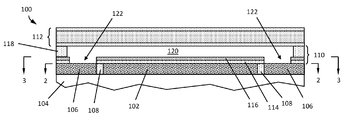
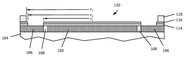
이제 도 1을 참조하면, 실시예에 따른 공동 게터 재료를 갖는 미세 가공된 초음파 변환기(100)의 횡단면도가 보여진다. 보여진 대로, 초음파 변환기(100)는 기판(104)(예를 들어, 실리콘과 같은 CMOS 기판) 위에 형성된 하부 전극(102)을 포함한다. CMOS 기판(104)은 CMOS 회로들, 배선 층들, 재분배 층들, 및 절연/패시베이션 층들을 포함할 수 있지만, 반드시 이에 제한되지는 않는다. 예시적인 실시예에서, 하부 전극(102)에 적절한 재료들은 티타늄(Ti), 지르코늄(Zr), 바나듐(V), 코발트(Co), 니켈(Ni) 뿐만 아니라 그들의 합금 중 하나 이상을 포함한다.Referring now to FIG. 1 , there is shown a cross-sectional view of a microfabricated
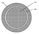
도 1에 더 보여진 것과 같이, 하부 전극(102)은 기판(104)위에 또한 형성된 인접한 금속 영역들(106)로부터 전기적으로 절연된다. 따라서 인접한 금속 영역들(106)의 노출된 부분들은 공동 형성 동안 게터 재료로 작용할 수 있다. 인접한 금속 영역들(106)은 하부 전극(102)에 의해 동일한 금속 재료로부터 형성될 수 있고, 절연체 재료(108)(예를 들어, 실리콘 산화물)로 하부 전극(102)으로부터 전기적으로 절연된다. 더 도시하면, 도 2는 도 1의 화살표 2-2를 따라 취해진 하부 전극, 인접한 금속 영역들(106) 및 절연체 재료(108)의 탑다운 뷰이다. 초음파 변환기(100)의 이 부분의 예시적인 기하학적 구조가 일반적으로 원 형상이지만, 예를 들어, 직사각형, 육각형, 팔각형, 및 다른 다면 형상들 등과 같은 다른 구성들도 또한 고려된다는 것이 이해되어야 한다.As further shown in FIG. 1 , the
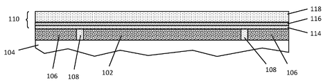
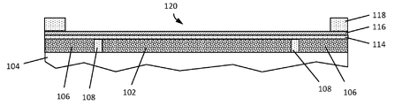
다시 도 1을 참조하면, 절연체 층(예를 들어, 절연체 스택(110)과 같은 하나 이상의 개별 절연체 층들)은 하부 전극(102) 및 인접한 금속 영역들(106)의 부분들 위에 형성된다. 스택(110)의 부분들은 스택(110)에 접합된 움직일 수 있는 멤브레인(112)(예를 들어, 산화된 표면을 갖는 도핑된 실리콘 디바이스 층을 갖는 SOI 웨이퍼)을 위한 지지를 제공한다. 도시된 실시예에서, 절연체 스택(110)은 제1 산화물 층(114)(예를 들어, CVD(chemical vapor deposition) 실리콘 산화물), 제2 산화물 층(116)(예를 들어, ALD(atomic layer deposition) 알루미늄 산화물), 및 제3 산화물 층(118)(예를 들어, 스퍼터 퇴적된 실리콘 산화물)을 포함한다. 제3 산화물 층(118)의 적절한 리소그래픽 패턴화 및 에칭에 의해, 공동(120)은 초음파 변환기(100)를 위해 정의될 수 있다. 또한, 제2 산화물 층(116)이 제3 산화물 층(118)에 대해 에칭 선택비를 갖는 재료로부터 선택된 실시예에서, 제2 산화물 층(116)은 공동(120)을 정의하기 위해 제3 산화물 층(118)의 부분들을 제거하기 위한 에칭 정지부로서 작용할 수 있다.Referring again to FIG. 1 , an insulator layer (eg, one or more individual insulator layers such as insulator stack 110 ) is formed over portions of
공동(120)을 정의하는 제3 산화물 층의 에칭뿐만 아니라, 다른 에칭은 제2 산화물 층(116) 및 제1 산화물 층(114)을 통해 개구들(122)을 정의하는 데 사용되고, 그것에 의해 금속 영역들(106) 부분의 최상부 표면을 노출시킨다. 제2 산화물 층(116)의 남은 부분들 및 금속 영역들의 노출된 부분들을 도시하는 공동(120)의 탑다운 뷰는 도 1에서 화살표 3-3을 따라 취해진 도 3에 도시된다. 금속 영역들(106)의 노출된 부분들은 유리하게 공동(120)을 밀봉하기 위한 멤브레인(112)의 접합 동작 동안 존재하는 하나 이상의 가스들의 게터 재료로 작용할 수 있다. 초음파 변환기(100)를 형성하는 데 사용되는 추가적인 예시적인 프로세싱 동작들이 이하에서 논의된다.An etching of the third oxide layer defining the
게터링 기술 및 금속 영역들(106)의 부분을 노출시키기 위한 산화물 층들(116 및 114) 부분의 연관된 제거는 다수의 변환기 전극 구조들 중 임의의 것과 함께 구현될 수 있다는 것이 이해될 것이다. 예를 들어, 도 4 내지 도 6은 다른 실시예에 따른 공동 게터 재료를 갖는 미세 가공된 초음파 변환기(400)의 횡단면 및 탑다운 뷰들을 도시한다. 설명의 편의를 위해, 다양한 실시예들에서 유사한 요소들은 유사한 참조 번호들로 지정된다. 특히, 도 4 및 도 5(도 4의 선 5-5를 따라 취해진)에 도시된 것과 같이, 하부 전극(102)은 "도넛" 패턴을 가지도록 형성된다; 즉, 전술한 실시예의 전극 구조의 가장 내부의 반경에 대응하는 영역은 전도성 전극 재료가 아니라, 대신에 절연 재료(예를 들어, 산화물(108))로 형성된다. 산화물 층들(116 및 114)이 오직 공동 기하학적 구조의 외부 영역으로부터 제거되기 때문에, 도 6의 탑다운 뷰는 도 3의 실시예의 것과 실질적으로 유사하다는 것이 주목될 것이다It will be appreciated that the gettering technique and associated removal of a portion of the oxide layers 116 and 114 to expose a portion of the
도 4의 전극 기하학적 구조는 초음파 변환기(400)의 동작의 붕괴 모드(collapse mode)를 포함하여 함께 다양한 동작 모드들로 사용될 수 있고, 멤브레인(112)의 적어도 일부가 공동(120)의 바닥 표면(예를 들어, 제2 산화물 층(116))과 물리적으로 접촉하게 된다. 이 경우에, 하부 전극 재료의 중앙 부분을 절연체 재료로 대체하는 것은, 초음파 변환기 공동의 바닥과 물리적으로 접촉한 전극의 중앙 부분이 초음파 신호 생성에 최소한으로 기여하기 때문에, 상당히 성능 타협 없이, 초음파 변환기(400)의 기생 축전 용량을 감소시키는 데 도움이 될 수 있다. 이러한 전극 구조에 대한 또 다른 이점은, 그것이 없었다면 반복적인 붕괴에 의해 야기되었을 멤브레인(112) 상의 충전 감소일 수 있다. 도넛 형상의 하부 전극에 관한 추가적인 정보는 2018년 5월 3일에 출원되고 본 출원의 양수인에게 양도된 미국 특허 출원 일련 번호 제62/666,643호, 및 공동 계류중인 2019년 5월 2일에 출원되고 본 출원의 양수인에게 양도된 공동 계류중인 미국 특허 출원 일련 번호 제16/401,630호에서 찾아질 수 있고, 이들 둘 다의 내용 전체는 본원에 참조로서 통합된다.The electrode geometry of FIG. 4 can be used in a variety of modes of operation together, including a collapse mode of operation of the
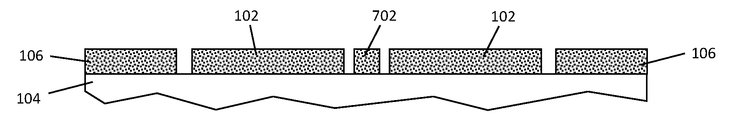
이제 도 7 내지 도 9를 참조하면, 또 다른 실시예에 따른 공동 게터 재료를 갖는 미세 가공된 초음파 변환기(700)의 횡단면 및 탑다운 뷰가 도시되어 있다. 다시, 설명의 편의를 위해 다양한 실시예들에서 유사한 요소들은 유사한 참조 번호들로 지정된다. 특히 도 7 및 도 8(도 7의 선 8-8을 따라 취해진)에 도시된 것과 같이, 하부 전극(102)은 여전히 "도넛" 패턴을 가지도록 형성된다. 그러나, 도 4 내지 도 6의 실시예와 대조적으로, 추가적인 전극(702)은 공동 영역의 중앙 부분에 형성된다. 전극(702)은 예를 들어 산화물(108)에 의해 그로부터 절연되는 것과 같이, 하부 전극(102)으로부터 전기적으로 절연되도록 패턴화된다. 다른 실시예들의 경우와 같이, 도 9의 탑다운 뷰는 도 3 및 도 6의 실시예의 것과 실질적으로 유사하다.Referring now to FIGS. 7-9 , shown are cross-sectional and top-down views of a
도 7에 보여진 유형의 전극 기하학적 구조는, 이전 실시예와 관련하여 설명된 이점들 뿐만 아니라, 멤브레인(112) 및 접지 사이의 바이패스 축전 용량에 또한 기여할 수 있으며, 이는 차례로 멤브레인(112)의 전압에 대한 노이즈 감소에 기여할 수 있다. 전극(702)의 다른 이점은 전극(702)이 공동(120)의 바닥을 향해 멤브레인(112)을 끌어당기는 것을 통해 초음파 변환기(700)에 대해 더 낮은 붕괴 전압을 제공하는 것을 돕는 것일 수 있다. 이 전극 디자인에 관한 추가적인 정보는 앞서 언급한 공동 계류중인 미국 특허 출원 일련 번호 제62/666,643호 및 제16/401,630호에서 또한 찾아질 수 있다.An electrode geometry of the type shown in FIG. 7 may also contribute to the bypass capacitance between the
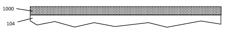
이제 일반적으로 도 10 내지 도 19를 참조하면, 위에서 설명된 초음파 변환기 실시예를 형성하기 위한 예시적인 프로세스 흐름 과정이 도시되어 있다. 도 10에서, 전극 층(1000)은 예를 들어 실리콘 기판과 같은 CMOS 기판(104)위에 형성된다. 다시, CMOS 기판(104)은 CMOS 회로들, 배선 층들, 재분배 층들 및 절연/패시베이션 층들을 포함할 수 있지만, 반드시 이에 제한 되는 것은 아니다. 또한, 이전에 언급한 것과 같이, 전극 층(1000)에 적절한 재료들은 티타늄(Ti), 지르코늄(Zr), 바나듐(V), 코발트(Co), 니켈(Ni) 뿐만 아니라 그들의 합금 중 하나 이상을 포함한다.Referring now generally to FIGS. 10-19 , an exemplary process flow procedure for forming the ultrasonic transducer embodiments described above is illustrated. In Fig. 10, an
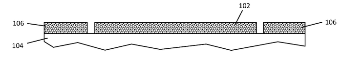
원하는 특정 하부 전극 패턴에 따라, 프로세스는 도 11a, 도 11b 또는 도 11c 중 임의의 것으로 진행될 수 있다. 예를 들어, 도 11a에서, 포토리소그래피 프로세스는 도 1의 전극 패턴, 즉 하부 전극(102) 및 인접한 금속 영역들(106)을 정의하기 위해 전극 층(1000)내로 개구를 패턴화하고 에칭하는 데 사용된다. 이 특정한 실시예에서, 하부 전극(102)의 중심 영역은 온전히 유지된다. 도 11b는 도 4 실시예의 전극 층(1000)의 패턴화(즉, "도넛" 패턴을 정의하기 위해 제거된 전극의 중심 부분)를 도시하고, 도 11c는 도 7 실시예의 전극 층(1000)의 패턴화(즉, 도넛 패턴의 중심 부분에서의 추가적인 전극(702)의 형성)를 도시한다.Depending on the particular bottom electrode pattern desired, the process may proceed to any of FIGS. 11A, 11B or 11C. For example, in FIG. 11A , the photolithography process involves patterning and etching an opening into the
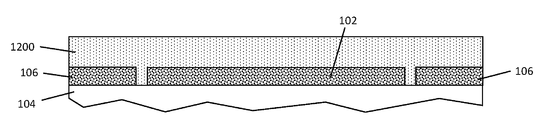
일단, 전극 패턴이 정의되면, 프로세스는 그 후 도 12a, 도 12b 및 도 12c에 도시된 것과 같이 절연 충진 동작으로 진행될 수 있다. 보여진 것과 같이, 절연 층(1200)(예를 들어, 실리콘 산화물)은 패턴화된 전극 재료 위에 형성된다. 그리고 나서, 각각 도 13a, 도 13b 및 도 13c에 보여진 것과 같이, 위에 설명된 절연체 재료(108)를 형성하기 위해 절연 층(1200)이 평탄화된다. 이 시점에서, 도시된 전극 설계 실시예들 각각에 대한 프로세싱은 실질적으로 동일하다. 따라서, 간결함을 위해 나머지 도면들은 단지 제1 실시예의 맥락(즉, 도 13a로부터)에서만 도시되지만, 후속 프로세스들이 다른 실시예들에 동일하게 적용될 수 있음이 이해되어야 한다.Once the electrode pattern is defined, the process can then proceed to an insulating filling operation as shown in FIGS. 12A, 12B and 12C. As shown, an insulating layer 1200 (eg, silicon oxide) is formed over the patterned electrode material. The insulating
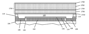
이제 도 14를 참조하면, 위에 설명된 절연체 스택(110)은 도 13a에 도시된 하부 전극(102) 및 인접한 금속 영역들(106)과 같은 하부 전극 층 위에 형성된다. 도시된 실시예에서, 절연체 스택(110)은 하부 전극(102) 및 인접한 금속 영역들(106) 위에 형성되는 제1 산화물 층(114)(예를 들어, 약 1 내지 100㎚의 두께를 갖는 CVD 실리콘 산화물), 제1 산화물 층(114)위에 형성되는 제2 산화물 층(116)(예를 들어, 약 5 내지 100㎚의 두께를 갖는 ALD 알루미늄 산화물), 및 제2 산화물 층(116) 위에 형성되는 제3 산화물 층(118)(예를 들어, 약 1 내지 300㎚의 두께를 갖는 스퍼터 퇴적된 실리콘 산화물)을 포함한다.Referring now to FIG. 14 , the
도 15에서, 제1 리소그래픽 패턴화 및 에칭 프로세스는 제2 산화물 층(116)을 에칭 정지부로 사용하여 제3 산화물 층(118)의 부분을 제거함으로써 공동(120)을 정의하기 위해 수행된다. 추가적인 이점으로, 공동(1500)의 바닥에 존재하는 제2 산화물 층(116)의 알루미늄 산화물 재료는 또한 최상부 멤브레인이 디바이스 동작(예를 들어, 변환기 동작의 붕괴 모드 동안 같은)동안 제2 산화물 층(116)에 접촉하게 되는 경우에 (나중에 형성된) 상부 멤브레인의 충전을 감소시키는 데 도움이 될 수 있다. 선택적으로, 알루미늄 산화물의 얇은 층(도시되지 않음), 및 또한 헵타데카플루오로 테트라하이드로데실 트리클로로실란 또는 도데실트리클로로실란 전구체(도시되지 않음)를 갖는 얇은 자기 조립 단층(self-assembled monolayer, SAM)이 패턴화 후 및 포토레지스트 제거 전에 제2 산화물 층(116) 상에 형성될 수 있다. 공동(120)의 바닥에 형성된 SAM은 전술한 붕괴 동작 모드, 또는 상부 멤브레인이 공동(120)의 바닥에 물리적으로 접촉하는 다른 모드에서, 공동(120)의 바닥에 대한 최상부 멤브레인의 임의의 정지 마찰을 감소시키는 데 도움이 될 수 있다. 이 시점에서, 도시된 실시예가 단일 공동을 도시하지만, 임의의 적절한 수의 공동들 및 대응하는 전극 구조들이 형성될 수 있다는 것(예를 들어, 수백, 수천, 수만 등)이 이해되어야 한다.In FIG. 15 , a first lithographic patterning and etching process is performed to define the
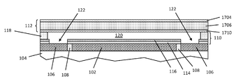
이제 도 16을 참조하면, 제2 리소그래픽 패턴화 및 에칭 프로세스는 공동(120)의 외부 둘레에서 인접한 금속 영역들(106)을 노출시키기 위해 수행된다. 제2 에칭은 제2 산화물 층(116) 및 제1 산화물 층(114)의 부분을 제거하고, 게터 재료로 작용할 인접한 금속 영역들(106) 상에서 정지한다. 이 시점에서, 도 16에 도시된 디바이스는 멤브레인 접합을 위해 준비된다. 제2 산화물 층(116)과 제1 산화물 층(114)을 통해 형성되는 개구(들)의 특정 크기 또는 크기 범위(및 따라서 노출될 인접한 금속 영역 재료의 결과적인 양)는, 접합 프로세스 동안 얼마나 많은 가스가 소비/게터되어야할 필요가 있는지에 대한 하나 이상의 계산들에 기초하여 선택될 수 있다. 또한, 각각의 공동에 얼마나 많은 게터 재료 면적이 형성되어야 할 지의 결정은 예를 들어, 얼마나 많은 가스가 접합 프로세스 동안 방출되는지, 디바이스 수명, 및 게터가 활성화된 후의 바람직한 공동 압력과 같은 요인들에 의존할 수 있다. 최종 압력은 게터 활성화에 의해 조정될 수 있고, 이는 차례로 상승된 온도들에서 어닐링하여 달성될 수 있다. 실시예에서, 어닐링 시간이 여분의 게터 재료로 단축될 수 있기 때문에, 표적 양보다 적게 노출된 게터 재료보다는 표적 양보다 많이 노출된 게터 재료를 갖는 것이 일반적으로 바람직하다. 단지 예시로서, 약 0.030㎠의 단면적을 갖는 변환기 공동의 경우, 효율적인 게터링을 위한 이 공동 내부의 게터 재료 영역의 예시적인 범위는 약 1x10⁻⁴㎠ 내지 약 2.5x10⁻⁴㎠ 일 수 있다. 실시예에서, 프로세스 변동들 및 계산된 게터 효율을 허용하기 위해 게터 재료 노출에 대한 추가 마진을 구축하는 것이 바람직할 수 있다. 따라서, 도 16에 보여진 이러한 특정한 예에 대해, 게터 재료(금속 영역들(106))의 내부 반경(r1)은 약 83미크론(㎛)이고, 게터 재료의 외부 반경(r2)은 약 96미크론(㎛)이고, 변환기 공동 반경(r3)은 약 98㎛이다. 원형 공동 구성에서, 결과적인 게터 영역은 약 7.3x10⁻³㎠이며, 이는 원하는 게터링 능력을 위해 필요한 예시적인 계산된 범위보다 대략 10배 더 많다. 다시, 이러한 값들은 단지 예시적일 뿐이고, 본 개시는 이러한 값들 및 범위들에 제한되지 않음이 이해되어야 한다.Referring now to FIG. 16 , a second lithographic patterning and etching process is performed to expose
도 17에 보여진 것과 같이, 기판(1700)(예를 들어, SOI(silicon-on-insulator) 기판)은 핸들 층(1702)(예를 들어, 실리콘 층), 매립 산화물(BOX)층(1704), 및 실리콘 디바이스 층(1706)을 포함한다. 산화물 층(1708)은 선택적으로 핸들 층(1702)의 뒷면에 제공될 수 있다. 실리콘 디바이스 층(1706)은 일부 실시예에서 단결정 실리콘으로 형성될 수 있고, 도핑될 수 있다. 이러한 도핑은 고농도로 도핑된 P형 또는 대안적으로 N형일 수 있고, 실리콘 디바이스 층(1706)을 통해 균일하거나, 특정 영역들에서 주입에 의해 패턴화될 수 있다. 또한, 산화물 층(1710)(예를 들어, 열 실리콘 산화물)이 실리콘 디바이스 층(1706) 상에 형성된다.17 , a substrate 1700 (eg, a silicon-on-insulator (SOI) substrate) includes a handle layer 1702 (eg, a silicon layer), a buried oxide (BOX)
도 18에 보여지는 것과 같이, 기판(1700)은 기판(104) 및 기판(104)에 형성된 전술한 구조들에 접합된다. 도시된 실시예에서, 층(1710)의 산화물 재료는 기판(104)의 회로에 대한 손상을 방지할 수 있는 저온 산화물 접합 방법들(예를 들어, 450℃ 미만)에 의해 산화물 재료(118)에 접합된다. 위에서 언급한 것과 같이, H2O기반 부산물들 및 접합의 전파때문에 다이 및 웨이퍼에 걸쳐 공동 압력들에 차이가 존재할 수 있다. 인접한 금속 영역들(106)의 금속 표면이 기판(1700)의 접합 동안 노출되기 때문에, 금속은 산소, 질소, 아르곤, 수증기 등과 같은 가스들을 소비할 수 있고, 그 결과 초음파 디바이스의 다양한 공동들(120)에 걸쳐 더 균일한 압력을 발생시킨다.As shown in FIG. 18 , a
접합 후에, 산화물 층(1708) 및 핸들 층(1702)은 적절한 기술에 의해 제거되고(예를 들어, 에칭, 연마 등), 그에 의해 위에서 논의되고 도 19에서 도시된 멤브레인(112)을 정의한다. 선택적으로, BOX 층(1704)은 또한 추가적인 프로세싱에 앞서 제거될 수 있는데, 이는 초음파 디바이스를 생산하는 데 사용되는 최종 배선, 상호 연결 및/또는 패키징 단계를 완료하기 위한 적합한 단계들을 포함할 수 있다.After bonding, the
도 20은 본원에 설명된 프로세스 흐름 과정들 중 임의의 것을 사용하여 형성되는 초음파 변환기 디바이스(2000)의 예시의 평면도를 도시한다. 도시된 것과 같이, 변환기 디바이스는 위에서 설명된 것과 같은 개별 변환기들(100)의 배열을 포함한다. 도 20에 보여진 특정한 수의 변환기들(100)은 임의의 제한적인 의미로 해석되어서는 안되고, 예를 들어, 대략 수십, 수백, 수천, 수만 또는 그 이상일 수 있는 원하는 이미징 어플리케이션에 적합한 임의의 수를 포함할 수 있다. 웨이퍼 또는 다이에 걸쳐 균등한 공동 압력을 제공하는 능력이 주어지면, 상기 설명된 게터링 기술들은 점점 더 커지는 배열에서 특히 유리하다는 것이 이해될 것이다. 도 20은 변환기들(100)의 멤브레인들(상부 전극들)에 전기 신호를 분배할 수 있는 금속(2002)의 예시적인 위치를 더 도시한다.20 shows a top view of an example of an
예시적인 실시예가 멤브레인 접합 동안 게터 재료로 사용되는 동일한 최하부 전극 금속 재료를 도시하고 설명하지만, 다른 비금속 또는 비금속 합금 게터 재료들이 또한 유사한 방식으로 사용될 수 있다는 것이 이해되어야 한다. 예를 들어, 흑연, 인 및/또는 특정한 염들은 공동 게터 재료로 작용할 수 있다. 게다가, 게터 재료의 특정한 배치와 관련하여, 공동 바닥뿐만 아니라 다른 위치들도 또한 고려된다. 예를 들어, 추가적인 프로세싱 동작들로, 멤브레인 접합 동안의 게터링을 위해 게터 재료가 공동 측벽들 및/또는 멤브레인 자체(밀봉된 공동의 최상부) 상에 배치되게 하는 방식으로 층들이 형성될 수 있다. 이러한 추가적인 게터 층(들)은 또한 바닥 전극 재료와는 다른 레벨에서 형성될 수 있다.Although the exemplary embodiment shows and describes the same bottom electrode metal material used as the getter material during membrane bonding, it should be understood that other non-metallic or non-metallic alloy getter materials may also be used in a similar manner. For example, graphite, phosphorus and/or certain salts may act as a co-getter material. Moreover, with respect to the particular placement of the getter material, other locations as well as the cavity floor are also considered. For example, in additional processing operations, the layers may be formed in such a way that the getter material is disposed on the cavity sidewalls and/or the membrane itself (top of the sealed cavity) for gettering during membrane bonding. These additional getter layer(s) may also be formed at a different level than the bottom electrode material.
위에서 설명한 실시예들은 임의의 다양한 방식으로 구현될 수 있다. 예를 들어, 실시예들은 하드웨어, 소프트웨어 또는 그들의 결합을 사용하여 구현될 수 있다. 소프트웨어로 구현될 때, 소프트웨어 코드는 단일 컴퓨팅 디바이스에 제공되든, 다수의 컴퓨팅 디바이스에 분배되든, 임의의 적절한 프로세서(예를 들어, 마이크로 프로세서) 또는 프로세서들의 집합에서 실행될 수 있다. 위에서 설명한 기능들을 수행하는 임의의 구성 요소 또는 구성 요소들의 집합은 전술한 기능들을 제어하는 하나 이상의 제어기로 일반적으로 간주될 수 있다는 것이 이해되어야 한다. 하나 이상의 제어기들은 전용 하드웨어, 또는 위에서 언급된 기능들을 수행하는 마이크로코드 또는 소프트웨어를 사용하여 프로그램된 범용 하드웨어(예를 들어, 하나 이상의 프로세서들)와 같은 다양한 방식들로 구현될 수 있다.The embodiments described above may be implemented in any of a variety of ways. For example, embodiments may be implemented using hardware, software, or a combination thereof. When implemented in software, the software code may execute on any suitable processor (eg, microprocessor) or collection of processors, whether provided on a single computing device or distributed across multiple computing devices. It should be understood that any component or collection of components that perform the functions described above may be generally regarded as one or more controllers that control the functions described above. The one or more controllers may be implemented in various ways, such as dedicated hardware, or general-purpose hardware (eg, one or more processors) programmed using microcode or software to perform the functions mentioned above.
본 출원의 다양한 태양은 단독으로, 결합하여, 또는 앞에서 설명된 실시예에서 특별히 논의되지 않은 다양한 배열들로 사용될 수 있고, 그러므로 그것의 응용에 있어서 앞선 설명에서 제시되거나 도면들에 도시된 구성 요소들의 세부 사항들 및 배열로 제한되지 않는다. 예를 들어, 일 실시예에서 설명된 특징들은 다른 실시예들에서 설명된 특징들과 임의의 방식으로 결합될 수 있다.The various aspects of the present application may be used alone, in combination, or in various arrangements not specifically discussed in the above-described embodiment, and therefore, in their application, of the components presented in the preceding description or shown in the drawings. It is not limited to details and arrangement. For example, features described in one embodiment may be combined in any manner with features described in other embodiments.
또한, 특정한 태양들은 예시가 제공된 방법으로 실시될 수 있다. 방법의 일부로 수행되는 동작들은 임의의 적절한 방식으로 순서가 정해질 수 있다. 따라서, 비록 예시적인 실시예에서 순차적인 동작으로 보여지지만, 일부 동작을 동시에 수행하는 것을 포함할 수 있는, 도시된 것과 상이한 순서로 동작들이 수행되는 실시예가 구성될 수 있다.Also, certain aspects may be practiced in the manner in which the examples are provided. The operations performed as part of the method may be ordered in any suitable manner. Thus, although shown as sequential operations in the exemplary embodiment, embodiments may be configured in which the operations are performed in an order different from that shown, which may include performing some operations simultaneously.
청구항 요소를 한정하기 위해 청구항에서 "제1", "제2", "제3" 등과 같은 서수 용어를 사용하는 것은 그 자체로 하나의 청구항 요소가 다른 청구항 요소에 비해 임의의 우선 순위, 우선 또는 순서를 가짐을 내포하거나 방법의 동작들이 수행되는 시간적 순서를 내포하는 것이 아니라, 단지 특정 이름을 가진 한 청구항 요소를 동일한 이름을 가진(그러나 서수 용어 사용을 위한) 다른 요소로부터 구별하여 청구항 요소들을 구별하기 위한 라벨로 사용된다.The use of ordinal terms such as "first", "second", "third", etc. in a claim to define a claim element is itself a sign that one claim element has any priority, precedence, or priority over another claim element. Distinguishing claim elements by merely distinguishing one claim element with a particular name from another element with the same name (but for use in ordinal terminology), not by implying having an order or implying the temporal order in which the operations of the method are performed. used as a label for
용어 "대략" 및 "약"은 일부 실시예에서 표적 값의 ±20% 이내, 일부 실시예에서 표적 값의 ±10% 이내, 일부 실시예에서 표적 값의 ±5% 이내, 및 일부 실시예에서 심지어 표적 값의 ±2% 이내를 의미하기 위해 사용될 수 있다. 용어 "대략" 및 "약"은 표적 값을 포함할 수 있다.The terms “approximately” and “about” are in some embodiments within ±20% of the target value, in some embodiments within ±10% of the target value, in some embodiments within ±5% of the target value, and in some embodiments. It can even be used to mean within ±2% of the target value. The terms “approximately” and “about” may include target values.
Claims (16)
그들 사이에 밀봉된 공동을 형성하도록 기판에 멤브레인을 접합하는 단계
를 포함하고, 상기 밀봉된 공동 내부에 위치한 노출된 표면은 게터 재료를 포함하고, 상기 게터 재료는 상기 공동의 최하부 전극으로부터 전기적으로 절연되는, 방법.A method of forming an ultrasonic transducer device, comprising:
bonding the membrane to the substrate to form a sealed cavity therebetween.
wherein the exposed surface located within the sealed cavity comprises a getter material, wherein the getter material is electrically insulated from a bottom electrode of the cavity.
상기 노출된 표면은 상기 기판의 최상부 표면을 포함하는, 방법.According to claim 1,
wherein the exposed surface comprises a top surface of the substrate.
상기 게터 재료는 상기 공동의 최하부 전극과 동일한 재료를 포함하는, 방법.According to claim 1,
wherein the getter material comprises the same material as the bottom electrode of the cavity.
상기 게터 재료는 티타늄, 지르코늄, 바나듐, 코발트, 니켈, 및 이들의 합금 중 하나 이상을 포함하는, 방법.According to claim 1,
wherein the getter material comprises one or more of titanium, zirconium, vanadium, cobalt, nickel, and alloys thereof.
상기 게터 재료로부터 하나 이상의 절연 층을 제거하는 단계를 더 포함하는, 방법.5. The method of claim 4,
and removing one or more insulating layers from the getter material.
상기 게터 재료는 상기 공동의 외부 둘레에 배치되는, 방법.6. The method of claim 5,
wherein the getter material is disposed around the outer perimeter of the cavity.
상기 공동은 원 형상이고, 상기 게터 재료는 상기 공동의 외부 반경에 배치되는, 방법.6. The method of claim 5,
wherein the cavity is circular in shape and the getter material is disposed at an outer radius of the cavity.
상기 게터 재료는 상기 공동으로부터 산소, 질소, 아르곤, 또는 수증기 중 하나 이상을 제거하도록 구성되는, 방법.According to claim 1,
wherein the getter material is configured to remove one or more of oxygen, nitrogen, argon, or water vapor from the cavity.
밀봉된 공동을 사이에 두고서 기판에 접합되는 멤브레인
을 포함하고, 상기 밀봉된 공동 내부에 위치한 노출된 표면은 게터 재료를 포함하고, 상기 게터 재료는 상기 공동의 최하부 전극으로부터 전기적으로 절연되는, 디바이스.An ultrasonic transducer device comprising:
Membrane bonded to the substrate with a sealed cavity interposed therebetween
wherein the exposed surface located within the sealed cavity comprises a getter material, the getter material being electrically insulated from a bottom electrode of the cavity.
상기 노출된 표면은 상기 기판의 최상부 표면을 포함하는, 디바이스.10. The method of claim 9,
wherein the exposed surface comprises a top surface of the substrate.
상기 게터 재료는 티타늄, 지르코늄, 바나듐, 코발트, 니켈, 및 이들의 합금 중 하나 이상을 포함하는, 디바이스.10. The method of claim 9,
wherein the getter material comprises one or more of titanium, zirconium, vanadium, cobalt, nickel, and alloys thereof.
상기 최하부 전극 위에 형성되지만, 상기 게터 재료 위에 존재하지 않는 하나 이상의 절연 층을 더 포함하는, 디바이스.12. The method of claim 11,
and one or more insulating layers formed over the bottom electrode but not over the getter material.
상기 게터 재료는 상기 공동의 외부 둘레에 배치되는, 디바이스.13. The method of claim 12,
wherein the getter material is disposed around the outer perimeter of the cavity.
상기 공동은 원 형상이고, 상기 게터 재료는 상기 공동의 외부 반경에 배치되는, 디바이스.13. The method of claim 12,
wherein the cavity is circular in shape and the getter material is disposed at an outer radius of the cavity.
상기 게터 재료는 산소, 질소, 아르곤, 또는 수증기 중 하나 이상을 포함하는 하나 이상의 가스를 제거하도록 선택되는, 디바이스.10. The method of claim 9,
wherein the getter material is selected to remove one or more gases comprising one or more of oxygen, nitrogen, argon, or water vapor.
상기 게터 재료는 상기 공동의 상기 최하부 전극과 동일한 재료를 포함하는, 디바이스.10. The method of claim 9,
and the getter material comprises the same material as the bottom electrode of the cavity.
Applications Claiming Priority (3)
| Application Number | Priority Date | Filing Date | Title |
|---|---|---|---|
| US201862738502P | 2018-09-28 | 2018-09-28 | |
| US62/738,502 | 2018-09-28 | ||
| PCT/US2019/053352 WO2020069252A1 (en) | 2018-09-28 | 2019-09-27 | Fabrication techniques and structures for gettering materials in ultrasonic transducer cavities |
Publications (1)
| Publication Number | Publication Date |
|---|---|
| KR20210070302A true KR20210070302A (en) | 2021-06-14 |
Family
ID=69946946
Family Applications (1)
| Application Number | Title | Priority Date | Filing Date |
|---|---|---|---|
| KR1020217011234A KR20210070302A (en) | 2018-09-28 | 2019-09-27 | Fabrication techniques and structures for gettering materials in ultrasonic transducer cavities |
Country Status (9)
| Country | Link |
|---|---|
| US (1) | US11655141B2 (en) |
| EP (1) | EP3856679B1 (en) |
| JP (1) | JP7385652B2 (en) |
| KR (1) | KR20210070302A (en) |
| CN (1) | CN112770999A (en) |
| AU (1) | AU2019350989A1 (en) |
| CA (1) | CA3111475A1 (en) |
| TW (1) | TW202042750A (en) |
| WO (1) | WO2020069252A1 (en) |
Families Citing this family (14)
| Publication number | Priority date | Publication date | Assignee | Title |
|---|---|---|---|---|
| AU2019263404A1 (en) | 2018-05-03 | 2020-11-19 | Butterfly Network, Inc. | Pressure port for ultrasonic transducer on CMOS sensor |
| TW202025970A (en) * | 2018-11-13 | 2020-07-16 | 美商蝴蝶網路公司 | Getter technology for micromachined ultrasonic transducer cavities |
| CA3119753A1 (en) | 2018-11-15 | 2020-05-22 | Butterfly Network, Inc. | Anti-stiction bottom cavity surface for micromachined ultrasonic transducer devices |
| US11766696B2 (en) | 2019-02-07 | 2023-09-26 | Bfly Operations, Inc. | Bi-layer metal electrode for micromachined ultrasonic transducer devices |
| TW202102312A (en) | 2019-02-25 | 2021-01-16 | 美商蝴蝶網路公司 | Adaptive cavity thickness control for micromachined ultrasonic transducer devices |
| US11484911B2 (en) | 2019-04-12 | 2022-11-01 | Bfly Operations, Inc. | Bottom electrode via structures for micromachined ultrasonic transducer devices |
| EP3953064B1 (en) * | 2019-04-12 | 2024-09-11 | BFLY Operations, Inc. | Segmented getter openings for micromachined ultrasound transducer devices |
| US11501562B2 (en) | 2019-04-30 | 2022-11-15 | Bfly Operations, Inc. | Ultrasound face scanning and identification apparatuses and methods |
| US11684951B2 (en) | 2019-08-08 | 2023-06-27 | Bfly Operations, Inc. | Micromachined ultrasonic transducer devices having truncated circle shaped cavities |
| US11988640B2 (en) | 2020-03-11 | 2024-05-21 | Bfly Operations, Inc. | Bottom electrode material stack for micromachined ultrasonic transducer devices |
| US20210328564A1 (en) | 2020-04-16 | 2021-10-21 | Butterfly Network, Inc. | Methods and circuitry for built-in self-testing of circuitry and/or transducers in ultrasound devices |
| US20210403321A1 (en) * | 2020-06-30 | 2021-12-30 | Butterfly Network, Inc. | Formation of self-assembled monolayer for ultrasonic transducers |
| CN112461438A (en) * | 2020-12-11 | 2021-03-09 | 中国科学院空天信息创新研究院 | High-sensitivity resonant differential pressure sensor and preparation method thereof |
| CN113731779B (en) * | 2021-07-30 | 2022-06-10 | 中北大学 | Capacitive micro-machined ultrasonic transducer based on SOI buried oxide layer sacrificial release technology and preparation method thereof |
Family Cites Families (45)
| Publication number | Priority date | Publication date | Assignee | Title |
|---|---|---|---|---|
| JPH08330607A (en) * | 1995-05-29 | 1996-12-13 | Matsushita Electric Works Ltd | Small semiconductor device and small infrared sensor |
| US6430109B1 (en) | 1999-09-30 | 2002-08-06 | The Board Of Trustees Of The Leland Stanford Junior University | Array of capacitive micromachined ultrasonic transducer elements with through wafer via connections |
| US6694817B2 (en) | 2001-08-21 | 2004-02-24 | Georgia Tech Research Corporation | Method and apparatus for the ultrasonic actuation of the cantilever of a probe-based instrument |
| US6779387B2 (en) | 2001-08-21 | 2004-08-24 | Georgia Tech Research Corporation | Method and apparatus for the ultrasonic actuation of the cantilever of a probe-based instrument |
| US6958255B2 (en) | 2002-08-08 | 2005-10-25 | The Board Of Trustees Of The Leland Stanford Junior University | Micromachined ultrasonic transducers and method of fabrication |
| US6836020B2 (en) | 2003-01-22 | 2004-12-28 | The Board Of Trustees Of The Leland Stanford Junior University | Electrical through wafer interconnects |
| JP2005235452A (en) * | 2004-02-17 | 2005-09-02 | Toshiba Corp | Display device |
| US7615834B2 (en) | 2006-02-28 | 2009-11-10 | The Board Of Trustees Of The Leland Stanford Junior University | Capacitive micromachined ultrasonic transducer(CMUT) with varying thickness membrane |
| JP2009088254A (en) * | 2007-09-28 | 2009-04-23 | Toshiba Corp | Electronic component package, and manufacturing method for electronic component package |
| US7843022B2 (en) | 2007-10-18 | 2010-11-30 | The Board Of Trustees Of The Leland Stanford Junior University | High-temperature electrostatic transducers and fabrication method |
| US8483014B2 (en) | 2007-12-03 | 2013-07-09 | Kolo Technologies, Inc. | Micromachined ultrasonic transducers |
| WO2009135255A1 (en) | 2008-05-07 | 2009-11-12 | Signostics Pty Ltd | Docking system for medical diagnostic scanning using a handheld device |
| US8402831B2 (en) | 2009-03-05 | 2013-03-26 | The Board Of Trustees Of The Leland Standford Junior University | Monolithic integrated CMUTs fabricated by low-temperature wafer bonding |
| JP2011029910A (en) * | 2009-07-24 | 2011-02-10 | Seiko Instruments Inc | Piezoelectric vibrator, manufacturing method of piezoelectric vibrator, oscillator, electronic device, and radio wave clock |
| JP5534398B2 (en) | 2009-08-25 | 2014-06-25 | エスアイアイ・クリスタルテクノロジー株式会社 | Package and package manufacturing method, piezoelectric vibrator, oscillator, electronic device, and radio-controlled timepiece |
| US8241931B1 (en) | 2009-10-19 | 2012-08-14 | Analog Devices, Inc. | Method of forming MEMS device with weakened substrate |
| JP5404335B2 (en) | 2009-11-17 | 2014-01-29 | キヤノン株式会社 | Electromechanical transducer and method for manufacturing the same |
| WO2013049794A1 (en) | 2011-09-30 | 2013-04-04 | Clean Energy Labs, Llc | Electrically conductive membrane transducer and methods to make and use same |
| ITTO20111100A1 (en) * | 2011-11-30 | 2013-05-31 | St Microelectronics Srl | OSCILLATOR DEVICE AND PROCESS OF MANUFACTURE OF THE SAME |
| US9499392B2 (en) | 2013-02-05 | 2016-11-22 | Butterfly Network, Inc. | CMOS ultrasonic transducers and related apparatus and methods |
| KR102170559B1 (en) * | 2013-03-15 | 2020-10-27 | 버터플라이 네트워크, 인크. | Complementary metal oxide semiconductor(CMOS) Ultrasonic transducers |
| US9233839B2 (en) * | 2013-08-01 | 2016-01-12 | Taiwan Semiconductor Manufacturing Company Limited | MEMS device and method of forming the same |
| KR102155695B1 (en) | 2014-02-12 | 2020-09-21 | 삼성전자주식회사 | Electro acoustic transducer |
| TWI661534B (en) | 2014-04-18 | 2019-06-01 | 美商蝴蝶網路公司 | Ultrasonic transducers in complementary metal oxide semiconductor (cmos) wafers and related apparatus and methods |
| US9067779B1 (en) | 2014-07-14 | 2015-06-30 | Butterfly Network, Inc. | Microfabricated ultrasonic transducers and related apparatus and methods |
| US9428377B2 (en) * | 2014-07-25 | 2016-08-30 | Semiconductor Manufacturing International (Shanghai) Corporation | Methods and structures for thin-film encapsulation and co-integration of same with microelectronic devices and microelectromechanical systems (MEMS) |
| JP2016039512A (en) | 2014-08-08 | 2016-03-22 | キヤノン株式会社 | Device having electrode connected with through wiring and manufacturing method of the same |
| US20160009544A1 (en) | 2015-03-02 | 2016-01-14 | Butterfly Network, Inc. | Microfabricated ultrasonic transducers and related apparatus and methods |
| US10427188B2 (en) * | 2015-07-30 | 2019-10-01 | North Carolina State University | Anodically bonded vacuum-sealed capacitive micromachined ultrasonic transducer (CMUT) |
| US9630831B1 (en) * | 2015-10-15 | 2017-04-25 | Taiwan Semiconductor Manufacturing Company Ltd. | Semiconductor sensing structure |
| US9938134B2 (en) | 2016-04-14 | 2018-04-10 | Taiwan Semiconductor Manufacturing Co., Ltd. | Getter electrode to improve vacuum level in a microelectromechanical systems (MEMS) device |
| AU2018225762A1 (en) | 2017-02-27 | 2019-08-22 | Butterfly Network, Inc. | Capacitive micromachined ultrasonic transducers (CMUTs) and related apparatus and methods |
| US10196261B2 (en) | 2017-03-08 | 2019-02-05 | Butterfly Network, Inc. | Microfabricated ultrasonic transducers and related apparatus and methods |
| TW201908021A (en) | 2017-06-21 | 2019-03-01 | 美商蝴蝶網路公司 | Micromachined ultrasonic transducer with individual cells of electrically isolated electrode portions |
| AU2018290333A1 (en) | 2017-06-23 | 2019-12-05 | Butterfly Network, Inc. | Differential ultrasonic transducer element for ultrasound devices |
| EP3709894A4 (en) | 2017-11-15 | 2021-08-04 | Butterfly Network, Inc. | Ultrasound apparatuses and methods for fabricating ultrasound devices |
| KR20200115558A (en) | 2018-01-30 | 2020-10-07 | 버터플라이 네트워크, 인크. | Methods and devices for packaging ultrasonic on-chip |
| CN112004611A (en) | 2018-03-09 | 2020-11-27 | 蝴蝶网络有限公司 | Ultrasound transducer device and method for producing an ultrasound transducer device |
| CN108529550B (en) * | 2018-04-28 | 2019-12-20 | 北京航天控制仪器研究所 | Wafer-level packaging MEMS chip structure based on wafer bonding process and processing method thereof |
| TW201946700A (en) | 2018-05-03 | 2019-12-16 | 美商蝴蝶網路公司 | Ultrasound devices |
| WO2019213448A1 (en) | 2018-05-03 | 2019-11-07 | Butterfly Network, Inc. | Vertical packaging for ultrasound-on-a-chip and related methods |
| AU2019263404A1 (en) | 2018-05-03 | 2020-11-19 | Butterfly Network, Inc. | Pressure port for ultrasonic transducer on CMOS sensor |
| JP2021529459A (en) | 2018-07-06 | 2021-10-28 | バタフライ ネットワーク,インコーポレイテッド | Methods and equipment for packaging ultrasonic on-chips |
| US11484911B2 (en) | 2019-04-12 | 2022-11-01 | Bfly Operations, Inc. | Bottom electrode via structures for micromachined ultrasonic transducer devices |
| EP3953064B1 (en) | 2019-04-12 | 2024-09-11 | BFLY Operations, Inc. | Segmented getter openings for micromachined ultrasound transducer devices |
-
2019
- 2019-09-27 EP EP19868109.0A patent/EP3856679B1/en active Active
- 2019-09-27 US US16/585,283 patent/US11655141B2/en active Active
- 2019-09-27 JP JP2021510705A patent/JP7385652B2/en active Active
- 2019-09-27 TW TW108135059A patent/TW202042750A/en unknown
- 2019-09-27 AU AU2019350989A patent/AU2019350989A1/en not_active Abandoned
- 2019-09-27 KR KR1020217011234A patent/KR20210070302A/en not_active Application Discontinuation
- 2019-09-27 WO PCT/US2019/053352 patent/WO2020069252A1/en unknown
- 2019-09-27 CN CN201980062783.7A patent/CN112770999A/en active Pending
- 2019-09-27 CA CA3111475A patent/CA3111475A1/en active Pending
Also Published As
| Publication number | Publication date |
|---|---|
| CA3111475A1 (en) | 2020-04-02 |
| EP3856679C0 (en) | 2024-05-01 |
| AU2019350989A1 (en) | 2021-03-25 |
| JP2022501877A (en) | 2022-01-06 |
| EP3856679A4 (en) | 2022-11-02 |
| EP3856679B1 (en) | 2024-05-01 |
| US11655141B2 (en) | 2023-05-23 |
| TW202042750A (en) | 2020-12-01 |
| JP7385652B2 (en) | 2023-11-22 |
| EP3856679A1 (en) | 2021-08-04 |
| WO2020069252A1 (en) | 2020-04-02 |
| CN112770999A (en) | 2021-05-07 |
| US20200102214A1 (en) | 2020-04-02 |
Similar Documents
| Publication | Publication Date | Title |
|---|---|---|
| EP3856679B1 (en) | Fabrication techniques and structures for gettering materials in ultrasonic transducer cavities | |
| US11571711B2 (en) | Anti-stiction bottom cavity surface for micromachined ultrasonic transducer devices | |
| JP2019522449A (en) | Electrical contact arrangement for micromachined ultrasonic transducers | |
| EP3953064B1 (en) | Segmented getter openings for micromachined ultrasound transducer devices | |
| US11638931B2 (en) | Getter technology for micromachined ultrasonic transducer cavities | |
| US20200254487A1 (en) | Bi-layer metal electrode for micromachined ultrasonic transducer devices | |
| US11806747B2 (en) | Bottom electrode via structures for micromachined ultrasonic transducer devices | |
| CN115367696A (en) | Adaptive cavity thickness control for micromachined ultrasonic transducer devices | |
| US11684951B2 (en) | Micromachined ultrasonic transducer devices having truncated circle shaped cavities | |
| JP6752727B2 (en) | Ultrasound Transducer and Ultrasound Imaging Device |
Legal Events
| Date | Code | Title | Description |
|---|---|---|---|
| E902 | Notification of reason for refusal |