KR20210061367A - Imaging device, manufacturing method thereof, and electronic device - Google Patents
Imaging device, manufacturing method thereof, and electronic device Download PDFInfo
- Publication number
- KR20210061367A KR20210061367A KR1020217010639A KR20217010639A KR20210061367A KR 20210061367 A KR20210061367 A KR 20210061367A KR 1020217010639 A KR1020217010639 A KR 1020217010639A KR 20217010639 A KR20217010639 A KR 20217010639A KR 20210061367 A KR20210061367 A KR 20210061367A
- Authority
- KR
- South Korea
- Prior art keywords
- layer
- transistor
- photoelectric conversion
- single crystal
- conversion device
- Prior art date
Links
- 238000003384 imaging method Methods 0.000 title claims abstract description 99
- 238000004519 manufacturing process Methods 0.000 title claims description 27
- 239000000758 substrate Substances 0.000 claims abstract description 83
- 238000006243 chemical reaction Methods 0.000 claims abstract description 72
- 229910021421 monocrystalline silicon Inorganic materials 0.000 claims abstract description 57
- 230000015572 biosynthetic process Effects 0.000 claims abstract description 30
- 229910044991 metal oxide Inorganic materials 0.000 claims abstract description 14
- 150000004706 metal oxides Chemical class 0.000 claims abstract description 14
- 238000000034 method Methods 0.000 claims description 64
- 230000003287 optical effect Effects 0.000 claims description 19
- 239000003990 capacitor Substances 0.000 claims description 17
- 229910052782 aluminium Inorganic materials 0.000 claims description 11
- 229910052733 gallium Inorganic materials 0.000 claims description 10
- 229910052738 indium Inorganic materials 0.000 claims description 9
- 229910052719 titanium Inorganic materials 0.000 claims description 8
- 229910052725 zinc Inorganic materials 0.000 claims description 8
- 229910052727 yttrium Inorganic materials 0.000 claims description 7
- 229910052684 Cerium Inorganic materials 0.000 claims description 6
- 229910052779 Neodymium Inorganic materials 0.000 claims description 6
- 229910052746 lanthanum Inorganic materials 0.000 claims description 6
- 229910052726 zirconium Inorganic materials 0.000 claims description 6
- 229910052732 germanium Inorganic materials 0.000 claims description 5
- 229910052718 tin Inorganic materials 0.000 claims description 5
- 238000001514 detection method Methods 0.000 abstract description 19
- 230000005622 photoelectricity Effects 0.000 abstract 1
- 239000010410 layer Substances 0.000 description 255
- 239000004065 semiconductor Substances 0.000 description 81
- 239000010408 film Substances 0.000 description 38
- 239000011701 zinc Substances 0.000 description 33
- 238000010586 diagram Methods 0.000 description 26
- 230000006870 function Effects 0.000 description 26
- 229910052751 metal Inorganic materials 0.000 description 23
- 239000000463 material Substances 0.000 description 18
- 239000002184 metal Substances 0.000 description 17
- 239000013078 crystal Substances 0.000 description 14
- 125000004429 atom Chemical group 0.000 description 13
- 239000001257 hydrogen Substances 0.000 description 13
- 229910052739 hydrogen Inorganic materials 0.000 description 13
- UFHFLCQGNIYNRP-UHFFFAOYSA-N Hydrogen Chemical compound [H][H] UFHFLCQGNIYNRP-UHFFFAOYSA-N 0.000 description 11
- 229910052760 oxygen Inorganic materials 0.000 description 11
- 238000005498 polishing Methods 0.000 description 11
- QVGXLLKOCUKJST-UHFFFAOYSA-N atomic oxygen Chemical compound [O] QVGXLLKOCUKJST-UHFFFAOYSA-N 0.000 description 9
- 230000007547 defect Effects 0.000 description 9
- 239000001301 oxygen Substances 0.000 description 9
- 210000003462 vein Anatomy 0.000 description 9
- 239000004020 conductor Substances 0.000 description 8
- 238000000227 grinding Methods 0.000 description 8
- IJGRMHOSHXDMSA-UHFFFAOYSA-N Atomic nitrogen Chemical compound N#N IJGRMHOSHXDMSA-UHFFFAOYSA-N 0.000 description 7
- XUIMIQQOPSSXEZ-UHFFFAOYSA-N Silicon Chemical compound [Si] XUIMIQQOPSSXEZ-UHFFFAOYSA-N 0.000 description 7
- 239000000969 carrier Substances 0.000 description 7
- 238000009792 diffusion process Methods 0.000 description 7
- 229910052710 silicon Inorganic materials 0.000 description 7
- 239000010703 silicon Substances 0.000 description 7
- 229910052721 tungsten Inorganic materials 0.000 description 7
- VYPSYNLAJGMNEJ-UHFFFAOYSA-N Silicium dioxide Chemical compound O=[Si]=O VYPSYNLAJGMNEJ-UHFFFAOYSA-N 0.000 description 6
- XLOMVQKBTHCTTD-UHFFFAOYSA-N Zinc monoxide Chemical compound [Zn]=O XLOMVQKBTHCTTD-UHFFFAOYSA-N 0.000 description 6
- XAGFODPZIPBFFR-UHFFFAOYSA-N aluminium Chemical compound [Al] XAGFODPZIPBFFR-UHFFFAOYSA-N 0.000 description 6
- 150000001875 compounds Chemical class 0.000 description 6
- 239000000203 mixture Substances 0.000 description 6
- 229910052814 silicon oxide Inorganic materials 0.000 description 6
- 239000010936 titanium Substances 0.000 description 6
- GYHNNYVSQQEPJS-UHFFFAOYSA-N Gallium Chemical compound [Ga] GYHNNYVSQQEPJS-UHFFFAOYSA-N 0.000 description 5
- RTAQQCXQSZGOHL-UHFFFAOYSA-N Titanium Chemical compound [Ti] RTAQQCXQSZGOHL-UHFFFAOYSA-N 0.000 description 5
- 238000005096 rolling process Methods 0.000 description 5
- 238000001004 secondary ion mass spectrometry Methods 0.000 description 5
- 238000004544 sputter deposition Methods 0.000 description 5
- WFKWXMTUELFFGS-UHFFFAOYSA-N tungsten Chemical compound [W] WFKWXMTUELFFGS-UHFFFAOYSA-N 0.000 description 5
- 239000010937 tungsten Substances 0.000 description 5
- XEEYBQQBJWHFJM-UHFFFAOYSA-N Iron Chemical compound [Fe] XEEYBQQBJWHFJM-UHFFFAOYSA-N 0.000 description 4
- PXHVJJICTQNCMI-UHFFFAOYSA-N Nickel Chemical compound [Ni] PXHVJJICTQNCMI-UHFFFAOYSA-N 0.000 description 4
- 239000000470 constituent Substances 0.000 description 4
- 229910052802 copper Inorganic materials 0.000 description 4
- 239000010949 copper Substances 0.000 description 4
- 229910052735 hafnium Inorganic materials 0.000 description 4
- VBJZVLUMGGDVMO-UHFFFAOYSA-N hafnium atom Chemical compound [Hf] VBJZVLUMGGDVMO-UHFFFAOYSA-N 0.000 description 4
- APFVFJFRJDLVQX-UHFFFAOYSA-N indium atom Chemical compound [In] APFVFJFRJDLVQX-UHFFFAOYSA-N 0.000 description 4
- 239000002105 nanoparticle Substances 0.000 description 4
- 229910052715 tantalum Inorganic materials 0.000 description 4
- GUVRBAGPIYLISA-UHFFFAOYSA-N tantalum atom Chemical compound [Ta] GUVRBAGPIYLISA-UHFFFAOYSA-N 0.000 description 4
- 230000008685 targeting Effects 0.000 description 4
- VWQVUPCCIRVNHF-UHFFFAOYSA-N yttrium atom Chemical compound [Y] VWQVUPCCIRVNHF-UHFFFAOYSA-N 0.000 description 4
- ZOXJGFHDIHLPTG-UHFFFAOYSA-N Boron Chemical compound [B] ZOXJGFHDIHLPTG-UHFFFAOYSA-N 0.000 description 3
- MYMOFIZGZYHOMD-UHFFFAOYSA-N Dioxygen Chemical compound O=O MYMOFIZGZYHOMD-UHFFFAOYSA-N 0.000 description 3
- 229910052581 Si3N4 Inorganic materials 0.000 description 3
- QCWXUUIWCKQGHC-UHFFFAOYSA-N Zirconium Chemical compound [Zr] QCWXUUIWCKQGHC-UHFFFAOYSA-N 0.000 description 3
- 238000009825 accumulation Methods 0.000 description 3
- 239000000853 adhesive Substances 0.000 description 3
- 230000001070 adhesive effect Effects 0.000 description 3
- 229910052796 boron Inorganic materials 0.000 description 3
- ZMIGMASIKSOYAM-UHFFFAOYSA-N cerium Chemical compound [Ce][Ce][Ce][Ce][Ce][Ce][Ce][Ce][Ce][Ce][Ce][Ce][Ce][Ce][Ce][Ce][Ce][Ce][Ce][Ce][Ce][Ce][Ce][Ce][Ce][Ce][Ce][Ce][Ce][Ce][Ce][Ce][Ce][Ce][Ce][Ce][Ce][Ce] ZMIGMASIKSOYAM-UHFFFAOYSA-N 0.000 description 3
- 230000000875 corresponding effect Effects 0.000 description 3
- 239000006059 cover glass Substances 0.000 description 3
- 229910001882 dioxygen Inorganic materials 0.000 description 3
- 230000000694 effects Effects 0.000 description 3
- 238000010894 electron beam technology Methods 0.000 description 3
- 238000002149 energy-dispersive X-ray emission spectroscopy Methods 0.000 description 3
- 239000007789 gas Substances 0.000 description 3
- GNPVGFCGXDBREM-UHFFFAOYSA-N germanium atom Chemical compound [Ge] GNPVGFCGXDBREM-UHFFFAOYSA-N 0.000 description 3
- 238000010438 heat treatment Methods 0.000 description 3
- 239000012535 impurity Substances 0.000 description 3
- FZLIPJUXYLNCLC-UHFFFAOYSA-N lanthanum atom Chemical compound [La] FZLIPJUXYLNCLC-UHFFFAOYSA-N 0.000 description 3
- 230000007246 mechanism Effects 0.000 description 3
- QEFYFXOXNSNQGX-UHFFFAOYSA-N neodymium atom Chemical compound [Nd] QEFYFXOXNSNQGX-UHFFFAOYSA-N 0.000 description 3
- 229910052757 nitrogen Inorganic materials 0.000 description 3
- 230000008569 process Effects 0.000 description 3
- 239000011347 resin Substances 0.000 description 3
- 229920005989 resin Polymers 0.000 description 3
- HQVNEWCFYHHQES-UHFFFAOYSA-N silicon nitride Chemical compound N12[Si]34N5[Si]62N3[Si]51N64 HQVNEWCFYHHQES-UHFFFAOYSA-N 0.000 description 3
- 238000005477 sputtering target Methods 0.000 description 3
- 238000003860 storage Methods 0.000 description 3
- 239000011787 zinc oxide Substances 0.000 description 3
- VUFNLQXQSDUXKB-DOFZRALJSA-N 2-[4-[4-[bis(2-chloroethyl)amino]phenyl]butanoyloxy]ethyl (5z,8z,11z,14z)-icosa-5,8,11,14-tetraenoate Chemical group CCCCC\C=C/C\C=C/C\C=C/C\C=C/CCCC(=O)OCCOC(=O)CCCC1=CC=C(N(CCCl)CCCl)C=C1 VUFNLQXQSDUXKB-DOFZRALJSA-N 0.000 description 2
- 239000004925 Acrylic resin Substances 0.000 description 2
- 229920000178 Acrylic resin Polymers 0.000 description 2
- XKRFYHLGVUSROY-UHFFFAOYSA-N Argon Chemical compound [Ar] XKRFYHLGVUSROY-UHFFFAOYSA-N 0.000 description 2
- OKTJSMMVPCPJKN-UHFFFAOYSA-N Carbon Chemical compound [C] OKTJSMMVPCPJKN-UHFFFAOYSA-N 0.000 description 2
- RYGMFSIKBFXOCR-UHFFFAOYSA-N Copper Chemical compound [Cu] RYGMFSIKBFXOCR-UHFFFAOYSA-N 0.000 description 2
- 102000001554 Hemoglobins Human genes 0.000 description 2
- 108010054147 Hemoglobins Proteins 0.000 description 2
- FYYHWMGAXLPEAU-UHFFFAOYSA-N Magnesium Chemical compound [Mg] FYYHWMGAXLPEAU-UHFFFAOYSA-N 0.000 description 2
- ZOKXTWBITQBERF-UHFFFAOYSA-N Molybdenum Chemical compound [Mo] ZOKXTWBITQBERF-UHFFFAOYSA-N 0.000 description 2
- 239000004642 Polyimide Substances 0.000 description 2
- 238000002441 X-ray diffraction Methods 0.000 description 2
- HCHKCACWOHOZIP-UHFFFAOYSA-N Zinc Chemical compound [Zn] HCHKCACWOHOZIP-UHFFFAOYSA-N 0.000 description 2
- 230000004913 activation Effects 0.000 description 2
- 229910052783 alkali metal Inorganic materials 0.000 description 2
- 150000001340 alkali metals Chemical class 0.000 description 2
- 229910052784 alkaline earth metal Inorganic materials 0.000 description 2
- 150000001342 alkaline earth metals Chemical class 0.000 description 2
- 238000004458 analytical method Methods 0.000 description 2
- 238000000231 atomic layer deposition Methods 0.000 description 2
- 239000002585 base Substances 0.000 description 2
- 229910052790 beryllium Inorganic materials 0.000 description 2
- ATBAMAFKBVZNFJ-UHFFFAOYSA-N beryllium atom Chemical compound [Be] ATBAMAFKBVZNFJ-UHFFFAOYSA-N 0.000 description 2
- 229910052799 carbon Inorganic materials 0.000 description 2
- 230000015556 catabolic process Effects 0.000 description 2
- 230000001276 controlling effect Effects 0.000 description 2
- 230000002950 deficient Effects 0.000 description 2
- AJNVQOSZGJRYEI-UHFFFAOYSA-N digallium;oxygen(2-) Chemical compound [O-2].[O-2].[O-2].[Ga+3].[Ga+3] AJNVQOSZGJRYEI-UHFFFAOYSA-N 0.000 description 2
- 239000002019 doping agent Substances 0.000 description 2
- 230000005684 electric field Effects 0.000 description 2
- 238000000605 extraction Methods 0.000 description 2
- 230000005669 field effect Effects 0.000 description 2
- 229910001195 gallium oxide Inorganic materials 0.000 description 2
- 239000011521 glass Substances 0.000 description 2
- 229910000449 hafnium oxide Inorganic materials 0.000 description 2
- WIHZLLGSGQNAGK-UHFFFAOYSA-N hafnium(4+);oxygen(2-) Chemical compound [O-2].[O-2].[Hf+4] WIHZLLGSGQNAGK-UHFFFAOYSA-N 0.000 description 2
- 238000005468 ion implantation Methods 0.000 description 2
- 150000002500 ions Chemical class 0.000 description 2
- 229910052742 iron Inorganic materials 0.000 description 2
- 229910052749 magnesium Inorganic materials 0.000 description 2
- 239000011777 magnesium Substances 0.000 description 2
- 230000014759 maintenance of location Effects 0.000 description 2
- 229910052750 molybdenum Inorganic materials 0.000 description 2
- 239000011733 molybdenum Substances 0.000 description 2
- 239000002159 nanocrystal Substances 0.000 description 2
- 229910052759 nickel Inorganic materials 0.000 description 2
- 150000004767 nitrides Chemical class 0.000 description 2
- 230000035515 penetration Effects 0.000 description 2
- 239000012071 phase Substances 0.000 description 2
- 229910021420 polycrystalline silicon Inorganic materials 0.000 description 2
- 229920001721 polyimide Polymers 0.000 description 2
- 239000002356 single layer Substances 0.000 description 2
- 239000007787 solid Substances 0.000 description 2
- 229910052720 vanadium Inorganic materials 0.000 description 2
- GPPXJZIENCGNKB-UHFFFAOYSA-N vanadium Chemical compound [V]#[V] GPPXJZIENCGNKB-UHFFFAOYSA-N 0.000 description 2
- 229910001233 yttria-stabilized zirconia Inorganic materials 0.000 description 2
- OAICVXFJPJFONN-UHFFFAOYSA-N Phosphorus Chemical compound [P] OAICVXFJPJFONN-UHFFFAOYSA-N 0.000 description 1
- ATJFFYVFTNAWJD-UHFFFAOYSA-N Tin Chemical compound [Sn] ATJFFYVFTNAWJD-UHFFFAOYSA-N 0.000 description 1
- NRTOMJZYCJJWKI-UHFFFAOYSA-N Titanium nitride Chemical compound [Ti]#N NRTOMJZYCJJWKI-UHFFFAOYSA-N 0.000 description 1
- 230000009471 action Effects 0.000 description 1
- 229910021417 amorphous silicon Inorganic materials 0.000 description 1
- 239000003963 antioxidant agent Substances 0.000 description 1
- 230000003078 antioxidant effect Effects 0.000 description 1
- 229910052786 argon Inorganic materials 0.000 description 1
- 229910052785 arsenic Inorganic materials 0.000 description 1
- RQNWIZPPADIBDY-UHFFFAOYSA-N arsenic atom Chemical compound [As] RQNWIZPPADIBDY-UHFFFAOYSA-N 0.000 description 1
- 230000000903 blocking effect Effects 0.000 description 1
- 229910052800 carbon group element Inorganic materials 0.000 description 1
- 239000000919 ceramic Substances 0.000 description 1
- 238000005229 chemical vapour deposition Methods 0.000 description 1
- 238000004140 cleaning Methods 0.000 description 1
- 239000002131 composite material Substances 0.000 description 1
- 230000002596 correlated effect Effects 0.000 description 1
- 229910021419 crystalline silicon Inorganic materials 0.000 description 1
- 230000006378 damage Effects 0.000 description 1
- 230000007423 decrease Effects 0.000 description 1
- 230000018044 dehydration Effects 0.000 description 1
- 238000006297 dehydration reaction Methods 0.000 description 1
- 230000001066 destructive effect Effects 0.000 description 1
- 238000003745 diagnosis Methods 0.000 description 1
- 229910001873 dinitrogen Inorganic materials 0.000 description 1
- 238000002524 electron diffraction data Methods 0.000 description 1
- 238000005516 engineering process Methods 0.000 description 1
- 230000012447 hatching Effects 0.000 description 1
- 150000002431 hydrogen Chemical class 0.000 description 1
- 125000004435 hydrogen atom Chemical group [H]* 0.000 description 1
- 229910003437 indium oxide Inorganic materials 0.000 description 1
- PJXISJQVUVHSOJ-UHFFFAOYSA-N indium(iii) oxide Chemical compound [O-2].[O-2].[O-2].[In+3].[In+3] PJXISJQVUVHSOJ-UHFFFAOYSA-N 0.000 description 1
- AMGQUBHHOARCQH-UHFFFAOYSA-N indium;oxotin Chemical compound [In].[Sn]=O AMGQUBHHOARCQH-UHFFFAOYSA-N 0.000 description 1
- 239000011261 inert gas Substances 0.000 description 1
- 238000007689 inspection Methods 0.000 description 1
- 239000011810 insulating material Substances 0.000 description 1
- 230000001678 irradiating effect Effects 0.000 description 1
- -1 is contained Inorganic materials 0.000 description 1
- 239000004973 liquid crystal related substance Substances 0.000 description 1
- 238000013507 mapping Methods 0.000 description 1
- 239000011159 matrix material Substances 0.000 description 1
- 238000005259 measurement Methods 0.000 description 1
- 238000000691 measurement method Methods 0.000 description 1
- 239000007769 metal material Substances 0.000 description 1
- 150000002739 metals Chemical class 0.000 description 1
- 229910021424 microcrystalline silicon Inorganic materials 0.000 description 1
- 230000001590 oxidative effect Effects 0.000 description 1
- TWNQGVIAIRXVLR-UHFFFAOYSA-N oxo(oxoalumanyloxy)alumane Chemical compound O=[Al]O[Al]=O TWNQGVIAIRXVLR-UHFFFAOYSA-N 0.000 description 1
- SIWVEOZUMHYXCS-UHFFFAOYSA-N oxo(oxoyttriooxy)yttrium Chemical compound O=[Y]O[Y]=O SIWVEOZUMHYXCS-UHFFFAOYSA-N 0.000 description 1
- 238000002161 passivation Methods 0.000 description 1
- 229910052698 phosphorus Inorganic materials 0.000 description 1
- 239000011574 phosphorus Substances 0.000 description 1
- 229910052697 platinum Inorganic materials 0.000 description 1
- 229920005591 polysilicon Polymers 0.000 description 1
- 239000011241 protective layer Substances 0.000 description 1
- 230000003252 repetitive effect Effects 0.000 description 1
- 230000000717 retained effect Effects 0.000 description 1
- 239000000523 sample Substances 0.000 description 1
- 238000005070 sampling Methods 0.000 description 1
- 230000035945 sensitivity Effects 0.000 description 1
- 229910052709 silver Inorganic materials 0.000 description 1
- 229910000679 solder Inorganic materials 0.000 description 1
- 239000007790 solid phase Substances 0.000 description 1
- 239000000126 substance Substances 0.000 description 1
- 239000010409 thin film Substances 0.000 description 1
- XLYOFNOQVPJJNP-UHFFFAOYSA-N water Substances O XLYOFNOQVPJJNP-UHFFFAOYSA-N 0.000 description 1
- 238000001039 wet etching Methods 0.000 description 1
- YVTHLONGBIQYBO-UHFFFAOYSA-N zinc indium(3+) oxygen(2-) Chemical compound [O--].[Zn++].[In+3] YVTHLONGBIQYBO-UHFFFAOYSA-N 0.000 description 1
Images


Classifications
-
- H—ELECTRICITY
- H01—ELECTRIC ELEMENTS
- H01L—SEMICONDUCTOR DEVICES NOT COVERED BY CLASS H10
- H01L27/00—Devices consisting of a plurality of semiconductor or other solid-state components formed in or on a common substrate
- H01L27/14—Devices consisting of a plurality of semiconductor or other solid-state components formed in or on a common substrate including semiconductor components sensitive to infrared radiation, light, electromagnetic radiation of shorter wavelength or corpuscular radiation and specially adapted either for the conversion of the energy of such radiation into electrical energy or for the control of electrical energy by such radiation
- H01L27/144—Devices controlled by radiation
- H01L27/146—Imager structures
- H01L27/14643—Photodiode arrays; MOS imagers
- H01L27/14649—Infrared imagers
-
- G—PHYSICS
- G02—OPTICS
- G02B—OPTICAL ELEMENTS, SYSTEMS OR APPARATUS
- G02B5/00—Optical elements other than lenses
- G02B5/20—Filters
- G02B5/22—Absorbing filters
-
- H—ELECTRICITY
- H01—ELECTRIC ELEMENTS
- H01L—SEMICONDUCTOR DEVICES NOT COVERED BY CLASS H10
- H01L21/00—Processes or apparatus adapted for the manufacture or treatment of semiconductor or solid state devices or of parts thereof
- H01L21/02—Manufacture or treatment of semiconductor devices or of parts thereof
-
- H—ELECTRICITY
- H01—ELECTRIC ELEMENTS
- H01L—SEMICONDUCTOR DEVICES NOT COVERED BY CLASS H10
- H01L27/00—Devices consisting of a plurality of semiconductor or other solid-state components formed in or on a common substrate
- H01L27/14—Devices consisting of a plurality of semiconductor or other solid-state components formed in or on a common substrate including semiconductor components sensitive to infrared radiation, light, electromagnetic radiation of shorter wavelength or corpuscular radiation and specially adapted either for the conversion of the energy of such radiation into electrical energy or for the control of electrical energy by such radiation
- H01L27/144—Devices controlled by radiation
- H01L27/146—Imager structures
- H01L27/14601—Structural or functional details thereof
- H01L27/14609—Pixel-elements with integrated switching, control, storage or amplification elements
- H01L27/14612—Pixel-elements with integrated switching, control, storage or amplification elements involving a transistor
- H01L27/14616—Pixel-elements with integrated switching, control, storage or amplification elements involving a transistor characterised by the channel of the transistor, e.g. channel having a doping gradient
-
- H—ELECTRICITY
- H01—ELECTRIC ELEMENTS
- H01L—SEMICONDUCTOR DEVICES NOT COVERED BY CLASS H10
- H01L27/00—Devices consisting of a plurality of semiconductor or other solid-state components formed in or on a common substrate
- H01L27/14—Devices consisting of a plurality of semiconductor or other solid-state components formed in or on a common substrate including semiconductor components sensitive to infrared radiation, light, electromagnetic radiation of shorter wavelength or corpuscular radiation and specially adapted either for the conversion of the energy of such radiation into electrical energy or for the control of electrical energy by such radiation
- H01L27/144—Devices controlled by radiation
- H01L27/146—Imager structures
- H01L27/14601—Structural or functional details thereof
- H01L27/1462—Coatings
-
- H—ELECTRICITY
- H01—ELECTRIC ELEMENTS
- H01L—SEMICONDUCTOR DEVICES NOT COVERED BY CLASS H10
- H01L27/00—Devices consisting of a plurality of semiconductor or other solid-state components formed in or on a common substrate
- H01L27/14—Devices consisting of a plurality of semiconductor or other solid-state components formed in or on a common substrate including semiconductor components sensitive to infrared radiation, light, electromagnetic radiation of shorter wavelength or corpuscular radiation and specially adapted either for the conversion of the energy of such radiation into electrical energy or for the control of electrical energy by such radiation
- H01L27/144—Devices controlled by radiation
- H01L27/146—Imager structures
- H01L27/14601—Structural or functional details thereof
- H01L27/14625—Optical elements or arrangements associated with the device
- H01L27/14627—Microlenses
-
- H—ELECTRICITY
- H01—ELECTRIC ELEMENTS
- H01L—SEMICONDUCTOR DEVICES NOT COVERED BY CLASS H10
- H01L27/00—Devices consisting of a plurality of semiconductor or other solid-state components formed in or on a common substrate
- H01L27/14—Devices consisting of a plurality of semiconductor or other solid-state components formed in or on a common substrate including semiconductor components sensitive to infrared radiation, light, electromagnetic radiation of shorter wavelength or corpuscular radiation and specially adapted either for the conversion of the energy of such radiation into electrical energy or for the control of electrical energy by such radiation
- H01L27/144—Devices controlled by radiation
- H01L27/146—Imager structures
- H01L27/14601—Structural or functional details thereof
- H01L27/14636—Interconnect structures
-
- H—ELECTRICITY
- H01—ELECTRIC ELEMENTS
- H01L—SEMICONDUCTOR DEVICES NOT COVERED BY CLASS H10
- H01L27/00—Devices consisting of a plurality of semiconductor or other solid-state components formed in or on a common substrate
- H01L27/14—Devices consisting of a plurality of semiconductor or other solid-state components formed in or on a common substrate including semiconductor components sensitive to infrared radiation, light, electromagnetic radiation of shorter wavelength or corpuscular radiation and specially adapted either for the conversion of the energy of such radiation into electrical energy or for the control of electrical energy by such radiation
- H01L27/144—Devices controlled by radiation
- H01L27/146—Imager structures
- H01L27/14683—Processes or apparatus peculiar to the manufacture or treatment of these devices or parts thereof
-
- H—ELECTRICITY
- H01—ELECTRIC ELEMENTS
- H01L—SEMICONDUCTOR DEVICES NOT COVERED BY CLASS H10
- H01L29/00—Semiconductor devices specially adapted for rectifying, amplifying, oscillating or switching and having potential barriers; Capacitors or resistors having potential barriers, e.g. a PN-junction depletion layer or carrier concentration layer; Details of semiconductor bodies or of electrodes thereof ; Multistep manufacturing processes therefor
- H01L29/66—Types of semiconductor device ; Multistep manufacturing processes therefor
- H01L29/68—Types of semiconductor device ; Multistep manufacturing processes therefor controllable by only the electric current supplied, or only the electric potential applied, to an electrode which does not carry the current to be rectified, amplified or switched
- H01L29/76—Unipolar devices, e.g. field effect transistors
- H01L29/772—Field effect transistors
- H01L29/78—Field effect transistors with field effect produced by an insulated gate
- H01L29/786—Thin film transistors, i.e. transistors with a channel being at least partly a thin film
-
- H—ELECTRICITY
- H04—ELECTRIC COMMUNICATION TECHNIQUE
- H04N—PICTORIAL COMMUNICATION, e.g. TELEVISION
- H04N23/00—Cameras or camera modules comprising electronic image sensors; Control thereof
- H04N23/20—Cameras or camera modules comprising electronic image sensors; Control thereof for generating image signals from infrared radiation only
-
- H—ELECTRICITY
- H04—ELECTRIC COMMUNICATION TECHNIQUE
- H04N—PICTORIAL COMMUNICATION, e.g. TELEVISION
- H04N25/00—Circuitry of solid-state image sensors [SSIS]; Control thereof
- H04N25/70—SSIS architectures; Circuits associated therewith
- H04N25/76—Addressed sensors, e.g. MOS or CMOS sensors
- H04N25/77—Pixel circuitry, e.g. memories, A/D converters, pixel amplifiers, shared circuits or shared components
-
- H—ELECTRICITY
- H04—ELECTRIC COMMUNICATION TECHNIQUE
- H04N—PICTORIAL COMMUNICATION, e.g. TELEVISION
- H04N5/00—Details of television systems
- H04N5/30—Transforming light or analogous information into electric information
- H04N5/33—Transforming infrared radiation
Landscapes
- Engineering & Computer Science (AREA)
- Physics & Mathematics (AREA)
- Power Engineering (AREA)
- General Physics & Mathematics (AREA)
- Microelectronics & Electronic Packaging (AREA)
- Computer Hardware Design (AREA)
- Condensed Matter Physics & Semiconductors (AREA)
- Electromagnetism (AREA)
- Signal Processing (AREA)
- Multimedia (AREA)
- Optics & Photonics (AREA)
- Ceramic Engineering (AREA)
- Manufacturing & Machinery (AREA)
- Solid State Image Pick-Up Elements (AREA)
- Thin Film Transistor (AREA)
- Transforming Light Signals Into Electric Signals (AREA)
Abstract
적외광의 검출에 적합한 촬상 장치를 제공한다. 제 1 층과, 제 2 층과, 제 3 층과, 제 4 층이 이 순서대로 적층된 촬상 장치로서, 제 1 층은 적외광 투과 필터를 가지고, 제 2 층은 단결정 실리콘을 가지고, 제 3 층은 디바이스 형성층을 가지고, 제 4 층은 지지 기판을 가지고, 제 2 층은 단결정 실리콘을 광 흡수층으로 하는 광전 변환 디바이스를 가지고, 제 3 층은 금속 산화물을 채널 형성 영역에 가지는 트랜지스터를 가지고, 광전 변환 디바이스와 트랜지스터는 전기적으로 접속되고, 광전 변환 디바이스는 적외광 투과 필터를 투과한 광을 수광하는 촬상 장치이다.An imaging device suitable for detection of infrared light is provided. An imaging device in which a first layer, a second layer, a third layer, and a fourth layer are stacked in this order, wherein the first layer has an infrared light transmitting filter, the second layer has single crystal silicon, and the third The layer has a device formation layer, the fourth layer has a supporting substrate, the second layer has a photoelectric conversion device using single crystal silicon as a light absorbing layer, the third layer has a transistor having a metal oxide in the channel formation region, and photoelectricity The conversion device and the transistor are electrically connected, and the photoelectric conversion device is an imaging device that receives light that has passed through an infrared light transmitting filter.
Description
본 발명의 일 형태는 촬상 장치에 관한 것이다.One aspect of the present invention relates to an imaging device.
또한, 본 발명의 일 형태는, 상기 기술분야에 한정되지 않는다. 본 명세서 등에서 개시(開示)하는 발명의 일 형태의 기술분야는, 물건, 방법, 또는 제조 방법에 관한 것이다. 또는, 본 발명의 일 형태는 공정(process), 기계(machine), 제품(manufacture), 또는 조성물(composition of matter)에 관한 것이다. 따라서, 더 구체적으로 본 명세서에서 개시하는 본 발명의 일 형태의 기술분야로서는, 반도체 장치, 표시 장치, 액정 표시 장치, 발광 장치, 조명 장치, 축전 장치, 기억 장치, 촬상 장치, 이들의 구동 방법, 또는 이들의 제조 방법을 일례로서 들 수 있다.In addition, one embodiment of the present invention is not limited to the above technical field. The technical field of one embodiment of the invention disclosed in this specification and the like relates to an object, a method, or a manufacturing method. Alternatively, one aspect of the present invention relates to a process, a machine, a manufacture, or a composition of matter. Therefore, more specifically, as the technical field of one embodiment of the present invention disclosed in this specification, semiconductor devices, display devices, liquid crystal displays, light-emitting devices, lighting devices, power storage devices, memory devices, imaging devices, driving methods thereof, Or, these manufacturing methods are mentioned as an example.
또한, 본 명세서 등에서 반도체 장치란, 반도체 특성을 이용함으로써 기능할 수 있는 장치 전반을 가리킨다. 트랜지스터, 반도체 회로는 반도체 장치의 일 형태이다. 또한, 기억 장치, 표시 장치, 촬상 장치, 전자 기기는 반도체 장치를 가지는 경우가 있다.In addition, in this specification and the like, a semiconductor device refers to an entire device that can function by using semiconductor properties. Transistors and semiconductor circuits are a form of semiconductor device. In addition, a memory device, a display device, an imaging device, and an electronic device may have a semiconductor device.
기판 위에 형성된 산화물 반도체 박막을 사용하여 트랜지스터를 구성하는 기술이 주목되고 있다. 예를 들어, 산화물 반도체를 가지는 오프 전류가 매우 낮은 트랜지스터를 화소 회로에 사용하는 구성의 촬상 장치가 특허문헌 1에 개시되어 있다.A technology for constructing a transistor using an oxide semiconductor thin film formed on a substrate is attracting attention. For example,
촬상 장치는 가시광을 화상화하는 수단으로서 사용될뿐더러, 다양한 용도로 사용된다. 예를 들어, 개인 인증, 불량 해석, 의료 진단, 보안 용도 등에 사용된다. 이들 용도로서는, 가시광 이외에, X선 등의 단파장의 광, 적외광 등의 장파장의 광 등을 용도에 따라 사용한다.The imaging device is used not only as a means for imaging visible light, but also for various purposes. For example, it is used for personal authentication, fault analysis, medical diagnosis, and security purposes. For these uses, in addition to visible light, short-wavelength light such as X-ray, long-wavelength light such as infrared light, and the like are used depending on the application.
본 발명의 일 형태에서는, 적외광의 검출에 적합한 촬상 장치를 제공하는 것을 목적의 하나로 한다. 또는, 생체 인증에 적합한 촬상 장치를 제공하는 것을 목적의 하나로 한다. 또는, 동체 촬상에 적합한 촬상 장치를 제공하는 것을 목적의 하나로 한다. 또는, 상기 촬상 장치의 제작 방법을 제공하는 것을 목적의 하나로 한다.An object of one embodiment of the present invention is to provide an imaging device suitable for detection of infrared light. Another object of the present invention is to provide an imaging device suitable for biometric authentication. Another object is to provide an imaging device suitable for moving body imaging. Another object is to provide a method of manufacturing the imaging device.
또는, 소비전력이 낮은 촬상 장치를 제공하는 것을 목적의 하나로 한다. 또는, 신뢰성이 높은 촬상 장치를 제공하는 것을 목적의 하나로 한다. 또는, 소형의 촬상 장치를 제공하는 것을 목적의 하나로 한다. 또는, 신규 촬상 장치를 제공하는 것을 목적의 하나로 한다. 또는, 상기 촬상 장치의 동작 방법을 제공하는 것을 목적 중 하나로 한다. 또는, 신규 반도체 장치 등을 제공하는 것을 목적의 하나로 한다.Another object is to provide an imaging device with low power consumption. Another object is to provide an imaging device with high reliability. Alternatively, it is an object of the present invention to provide a compact imaging device. Alternatively, it is an object of the present invention to provide a novel imaging device. Another object is to provide a method of operating the imaging device. Another object is to provide a novel semiconductor device or the like.
또한, 이들의 과제의 기재는 다른 과제의 존재를 방해하는 것은 아니다. 또한, 본 발명의 일 형태는, 이들 과제의 모두를 해결할 필요는 없는 것으로 한다. 또한, 이들 이외의 과제는, 명세서, 도면, 청구항 등의 기재로부터 저절로 명백해지는 것이며, 명세서, 도면, 청구항 등의 기재로부터 이들 이외의 과제를 추출할 수 있다.In addition, description of these issues does not hinder the existence of other issues. In addition, one embodiment of the present invention assumes that it is not necessary to solve all of these problems. In addition, problems other than these will become apparent from description of the specification, drawings, claims, and the like, and subjects other than these can be extracted from descriptions such as the specification, drawings, and claims.
본 발명의 일 형태는, 촬상 디바이스에 단결정 실리콘을 가지고, 회로를 구성하는 트랜지스터의 채널 형성 영역에 금속 산화물을 가지는 촬상 장치 및 그 제작 방법에 관한 것이다.One embodiment of the present invention relates to an imaging device having single crystal silicon in an imaging device and a metal oxide in a channel formation region of a transistor constituting a circuit, and a manufacturing method thereof.
본 발명의 일 형태는, 단결정 실리콘 기판과, 지지 기판을 가지는 촬상 장치의 제작 방법으로서, 단결정 실리콘 기판의 제 1 면 측에 단결정 실리콘 기판의 도전형과 반대의 도전형의 영역을 제공하여 광전 변환 디바이스를 형성하고, 광전 변환 디바이스 위에 금속 산화물을 채널 형성 영역에 가지고 또한 광전 변환 디바이스와 전기적으로 접속되는 트랜지스터를 형성하고, 트랜지스터 위에 제 1 절연층을 형성하고, 지지 기판 위에 제 2 절연층을 형성하고, 제 1 절연층의 표면과 제 2 절연층의 표면을 결합시키고, 단결정 실리콘 기판의 제 1 면과 대향하는 면을 연삭 및 연마하여 광전 변환 디바이스의 광 흡수층을 박층화하는 촬상 장치의 제작 방법이다.One aspect of the present invention is a method of manufacturing an imaging device having a single crystal silicon substrate and a support substrate, and photoelectric conversion by providing a region of a conductivity type opposite to that of the single crystal silicon substrate on the first side of the single crystal silicon substrate. A device is formed, a transistor having a metal oxide in a channel formation region on the photoelectric conversion device and electrically connected to the photoelectric conversion device is formed, a first insulating layer is formed on the transistor, and a second insulating layer is formed on the supporting substrate. And bonding the surface of the first insulating layer and the surface of the second insulating layer, grinding and polishing the surface facing the first surface of the single crystal silicon substrate to thin the light absorbing layer of the photoelectric conversion device. to be.
본 발명의 다른 일 형태는, 단결정 실리콘 기판과 지지 기판을 가지는 촬상 장치의 제작 방법으로서, 단결정 실리콘 기판의 제 1 면 측에 단결정 실리콘 기판의 도전형과 반대의 도전형의 영역을 제공하여 광전 변환 디바이스를 형성하고, 광전 변환 디바이스 위에 제 1 절연층 및 광전 변환 디바이스와 전기적으로 접속되는 제 1 도전층을 형성하고, 지지 기판 위에 금속 산화물을 채널 형성 영역에 가지는 트랜지스터를 형성하고, 트랜지스터 위에 제 2 절연층 및 트랜지스터와 전기적으로 접속되는 제 2 도전층을 형성하고, 제 1 절연층의 표면과 제 2 절연층의 표면, 그리고 제 1 도전층의 표면과 제 2 도전층의 표면을 결합시키고, 단결정 실리콘 기판의 제 1 면과 대향하는 면을 연삭 및 연마하여 광전 변환 디바이스의 광 흡수층을 박층화하는 촬상 장치의 제작 방법이다.Another aspect of the present invention is a method of manufacturing an imaging device having a single crystal silicon substrate and a support substrate, by providing a region of a conductivity type opposite to that of the single crystal silicon substrate on the first surface side of the single crystal silicon substrate to perform photoelectric conversion. Forming a device, forming a first insulating layer on the photoelectric conversion device and a first conductive layer electrically connected to the photoelectric conversion device, forming a transistor having a metal oxide in a channel formation region on a support substrate, and forming a second on the transistor An insulating layer and a second conductive layer electrically connected to the transistor are formed, and the surface of the first insulating layer and the surface of the second insulating layer, and the surface of the first conductive layer and the surface of the second conductive layer are combined, and a single crystal It is a manufacturing method of an imaging device in which a light absorbing layer of a photoelectric conversion device is thinned by grinding and polishing a surface of a silicon substrate opposite to the first surface.
또한, 단결정 실리콘 기판의 연마한 면 측에, 단결정 실리콘 기판과 같은 도전형이며 단결정 실리콘 기판보다 캐리어 농도가 높은 영역을 제공하여 광전 변환 디바이스를 형성하여도 좋다.Further, a photoelectric conversion device may be formed by providing a region of the same conductivity type as the single crystal silicon substrate and having a higher carrier concentration than the single crystal silicon substrate on the polished side of the single crystal silicon substrate.
광전 변환 디바이스와 접하는 제 3 절연층을 형성하고, 제 3 절연층을 개재(介在)하여 광전 변환 디바이스와 중첩되도록 광학 필터층을 형성하여도 좋다.A third insulating layer in contact with the photoelectric conversion device may be formed, and an optical filter layer may be formed so as to overlap the photoelectric conversion device through the third insulating layer.
또한, 본 발명의 다른 일 형태는, 제 1 층과, 제 2 층과, 제 3 층과, 제 4 층이 이 순서대로 적층된 촬상 장치로서, 제 1 층, 제 2 층, 제 3 층, 및 제 4 층은 각각이 서로 중첩되는 영역을 가지고, 제 1 층은 광학 필터층을 가지고, 제 2 층은 단결정 실리콘을 가지고, 제 3 층은 디바이스 형성층을 가지고, 제 4 층은 지지 기판을 가지고, 제 2 층은 단결정 실리콘을 광 흡수층으로 하는 광전 변환 디바이스를 가지고, 제 3 층은 금속 산화물을 채널 형성 영역에 가지는 트랜지스터를 가지고, 광전 변환 디바이스와 트랜지스터는 전기적으로 접속되고, 광전 변환 디바이스는 광학 필터층을 투과한 광을 수광하는 촬상 장치이다.In addition, another aspect of the present invention is an imaging device in which a first layer, a second layer, a third layer, and a fourth layer are stacked in this order, the first layer, the second layer, the third layer, And the fourth layer each has a region overlapping each other, the first layer has an optical filter layer, the second layer has single crystal silicon, the third layer has a device formation layer, and the fourth layer has a support substrate, The second layer has a photoelectric conversion device using single crystal silicon as a light absorbing layer, the third layer has a transistor having a metal oxide in a channel formation region, the photoelectric conversion device and the transistor are electrically connected, and the photoelectric conversion device is an optical filter layer. It is an imaging device that receives light that has passed through.
디바이스 형성층은 제 1 트랜지스터와, 제 2 트랜지스터와, 제 3 트랜지스터와, 제 4 트랜지스터와, 커패시터를 가지고, 광전 변환 디바이스의 한쪽의 전극은 제 1 트랜지스터의 소스 및 드레인 중 한쪽과 전기적으로 접속되고, 제 1 트랜지스터의 소스 및 드레인 중 다른 쪽은 제 2 트랜지스터의 소스 및 드레인 중 한쪽과 전기적으로 접속되고, 제 2 트랜지스터의 소스 및 드레인 중 한쪽은 커패시터의 한쪽의 전극과 전기적으로 접속되고, 커패시터의 한쪽의 전극은 제 3 트랜지스터의 게이트와 전기적으로 접속되고, 제 3 트랜지스터의 소스 및 드레인 중 한쪽은 제 4 트랜지스터의 소스 및 드레인 중 한쪽과 전기적으로 접속할 수 있다.The device formation layer has a first transistor, a second transistor, a third transistor, a fourth transistor, and a capacitor, and one electrode of the photoelectric conversion device is electrically connected to one of a source and a drain of the first transistor, The other of the source and drain of the first transistor is electrically connected to one of the source and drain of the second transistor, and one of the source and drain of the second transistor is electrically connected to the electrode of one of the capacitors, and one of the capacitors. The electrode of is electrically connected to the gate of the third transistor, and one of the source and the drain of the third transistor can be electrically connected to one of the source and the drain of the fourth transistor.
광학 필터층으로서는 가시광을 차폐하여 적외광을 투과시키는 층을 사용할 수 있다.As the optical filter layer, a layer that shields visible light and transmits infrared light can be used.
트랜지스터의 채널 형성 영역이 가지는 금속 산화물은 In과, Zn과, M(M은 Al, Ti, Ga, Ge, Sn, Y, Zr, La, Ce, Nd, 또는 Hf)을 가지는 것이 바람직하다.The metal oxide of the channel formation region of the transistor preferably has In, Zn, and M (M is Al, Ti, Ga, Ge, Sn, Y, Zr, La, Ce, Nd, or Hf).
본 발명의 일 형태를 사용함으로써, 적외광의 검출에 적합한 촬상 장치를 제공할 수 있다. 또는, 생체 인증에 적합한 촬상 장치를 제공할 수 있다. 또는, 동체 촬상에 적합한 촬상 장치를 제공할 수 있다. 또는, 상기 촬상 장치의 제작 방법을 제공할 수 있다.By using one aspect of the present invention, an imaging device suitable for detection of infrared light can be provided. Alternatively, an imaging device suitable for biometric authentication can be provided. Alternatively, an imaging device suitable for imaging a moving body can be provided. Alternatively, a method of manufacturing the imaging device can be provided.
또는, 소비전력이 낮은 촬상 장치를 제공할 수 있다. 또는, 신뢰성이 높은 촬상 장치를 제공할 수 있다. 또는, 소형의 촬상 장치를 제공할 수 있다. 또는, 신규 촬상 장치를 제공할 수 있다. 또는, 상기 촬상 장치의 동작 방법을 제공할 수 있다. 또는, 신규 반도체 장치 등을 제공할 수 있다.Alternatively, an imaging device having low power consumption can be provided. Alternatively, an imaging device with high reliability can be provided. Alternatively, a compact imaging device can be provided. Alternatively, a novel imaging device can be provided. Alternatively, a method of operating the imaging device may be provided. Alternatively, a novel semiconductor device or the like can be provided.
도 1은 촬상 장치를 설명하는 도면이다.
도 2의 (A), (B)는 화소 회로를 설명하는 도면이다.
도 3의 (A)는 롤링 셔터 방식을 설명하는 도면이다. 도 3의 (B)는 글로벌 셔터 방식을 설명하는 도면이다.
도 4의 (A), (B)는 촬상 장치의 제작 방법을 설명하는 도면이다.
도 5의 (A) 내지 (C)는 촬상 장치의 제작 방법을 설명하는 도면이다.
도 6의 (A), (B)는 촬상 장치의 제작 방법을 설명하는 도면이다.
도 7의 (A) 내지 (C)는 촬상 장치의 제작 방법을 설명하는 도면이다.
도 8의 (A), (B)는 촬상 장치의 제작 방법을 설명하는 도면이다.
도 9의 (A) 내지 (D)는 촬상 장치의 제작 방법을 설명하는 도면이다.
도 10의 (A) 내지 (C)는 촬상 장치를 설명하는 도면이다.
도 11의 (A), (B)는 화소 회로의 동작을 설명하는 타이밍 차트이다.
도 12의 (A), (B)는 화소 회로를 설명하는 도면이다.
도 13은, 촬상 장치를 설명하는 블록도이다.
도 14의 (A), (B)는 촬상 장치의 화소의 구성을 설명하는 도면이다.
도 15의 (A) 내지 (D)는 트랜지스터를 설명하는 도면이다.
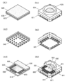
도 16의 (A1) 내지 도 16의 (A3), 도 16의 (B1) 내지 도 16의 (B3)은 촬상 장치가 제공된 패키지, 카메라 모듈을 설명하는 사시도이다.
도 17의 (A) 내지 (C)는 전자 기기를 설명하는 도면이다.
도 18의 (A) 내지 (C)는 전자 기기를 설명하는 도면이다.1 is a diagram illustrating an imaging device.
2A and 2B are diagrams for explaining a pixel circuit.
3A is a diagram illustrating a rolling shutter system. 3B is a diagram illustrating a global shutter method.
4A and 4B are diagrams illustrating a method of manufacturing an imaging device.
5A to 5C are diagrams illustrating a method of manufacturing an imaging device.
6A and 6B are diagrams illustrating a method of manufacturing an imaging device.
7A to 7C are diagrams for explaining a method of manufacturing an imaging device.
8A and 8B are diagrams illustrating a method of manufacturing an imaging device.
9A to 9D are diagrams for explaining a method of manufacturing an imaging device.
10A to 10C are diagrams illustrating an imaging device.
11A and 11B are timing charts for explaining the operation of the pixel circuit.
12A and 12B are diagrams for explaining a pixel circuit.
13 is a block diagram illustrating an imaging device.
14A and 14B are diagrams for explaining a configuration of a pixel of an imaging device.
15A to 15D are diagrams for explaining a transistor.
16(A1) to 16(A3) and FIG. 16(B1) to FIG. 16(B3) are perspective views explaining a package and a camera module provided with an imaging device.
17A to 17C are diagrams for describing an electronic device.
18A to 18C are diagrams for explaining an electronic device.
실시형태에 대하여, 도면을 사용하여 자세히 설명한다. 다만, 본 발명은 이하의 설명에 한정되지 않으며, 본 발명의 취지 및 그 범위로부터 벗어남이 없이 그 형태 및 자세한 사항을 다양하게 변경할 수 있는 것은 통상의 기술자라면 용이하게 이해할 수 있다. 따라서, 본 발명은 이하에 나타내는 실시형태의 기재 내용에 한정하여 해석되는 것은 아니다. 또한, 이하에서 설명하는 발명의 구성에 있어서, 동일 부분 또는 같은 기능을 가지는 부분에는 동일한 부호를 상이한 도면 간에서 공통적으로 사용하고, 이의 반복적인 설명은 생략하는 경우가 있다. 또한, 도면을 구성하는 같은 요소의 해칭을, 상이한 도면 간에서 적절히 생략 또는 변경하는 경우도 있다.Embodiments will be described in detail with reference to the drawings. However, the present invention is not limited to the following description, and it can be easily understood by those of ordinary skill in the art that various changes can be made in its form and details without departing from the spirit and scope of the present invention. Therefore, the present invention is not interpreted as being limited to the description of the embodiments shown below. In addition, in the configuration of the invention described below, the same reference numerals are used in common between different drawings for the same part or parts having the same function, and a repetitive description thereof may be omitted. In addition, hatching of the same elements constituting the drawings may be appropriately omitted or changed between different drawings.
또한 회로도상에서는 단일 요소로서 도시된 경우에도 기능적으로 문제가 없으면 상기 요소가 복수로 구성되어도 좋다. 예를 들어 스위치로서 동작하는 트랜지스터는 복수가 직렬 또는 병렬로 접속되어도 좋은 경우가 있다. 또한 커패시터를 분할하여 복수의 위치에 배치하는 경우도 있다.In addition, even when shown as a single element on the circuit diagram, if there is no functional problem, a plurality of the above elements may be formed. For example, in some cases, a plurality of transistors operating as a switch may be connected in series or in parallel. In addition, the capacitor may be divided and disposed at a plurality of positions.
또한, 하나의 도전체가 배선, 전극, 및 단자 등의 복수의 기능을 가지는 경우가 있으며, 본 명세서에서는 동일한 요소에 대하여 복수의 호칭을 사용하는 경우가 있다. 또한 회로도상에서 요소 간이 직접 접속되는 것처럼 도시된 경우에도 실제로는 상기 요소 간이 복수의 도전체를 통하여 접속되어 있는 경우가 있고, 본 명세서에서는 이와 같은 구성도 직접 접속의 범주에 포함한다.In addition, in some cases, one conductor may have a plurality of functions such as wiring, electrodes, and terminals, and in this specification, a plurality of designations may be used for the same element. In addition, even when shown as if the elements are directly connected in the circuit diagram, there are cases in which the elements are actually connected through a plurality of conductors, and in the present specification, such a configuration is also included in the category of direct connection.
(실시형태 1)(Embodiment 1)
본 실시형태에서는, 본 발명의 일 형태인 촬상 장치 및 그 제작 방법에 대하여 도면을 참조하여 설명한다.In this embodiment, an imaging device and a manufacturing method thereof, which are one embodiment of the present invention, will be described with reference to the drawings.
본 발명의 일 형태는 적외광에 대응한 촬상 장치이다. 수광한 적외광을 화상 데이터화함으로써, 생체 인증, 공업 제품의 불량 해석, 양품 선별 등의 용도에 사용할 수 있다. 또한, 글로벌 셔터 방식으로 촬상할 수 있는 화소 회로를 사용함으로써, 움직이는 피사체이어도 왜곡이 없는 화상을 얻을 수 있다.One embodiment of the present invention is an imaging device corresponding to infrared light. By converting the received infrared light into image data, it can be used for applications such as biometric authentication, defect analysis of industrial products, and good product selection. In addition, by using a pixel circuit capable of capturing an image by the global shutter method, an image without distortion can be obtained even with a moving subject.
<촬상 장치><Imaging device>
도 1은 본 발명의 일 형태의 촬상 장치를 설명하는 도면이다. 촬상 장치는 층(11), 층(12), 층(13), 및 층(14)을 가진다.1 is a diagram illustrating an imaging device of one embodiment of the present invention. The imaging device has a
층(11)은, 광학 필터층을 가진다. 광학 필터층으로서는, 예를 들어 가시광을 차폐하고, 적외광을 투과시키는 층(이하, 적외광 투과 필터)을 사용할 수 있다. 본 명세서에서 적외광 투과 필터란, 주로 근적외광보다 파장이 짧은 광(주로 가시광)을 차폐하는 필터를 가리킨다. 노이즈가 되는 가시광을 차폐함으로써, 선명한 적외광 화상을 취득할 수 있다. 또한, 광학 필터층으로서, 다른 특정의 파장의 광을 투과시키는 층을 사용하고, 상기 광을 사용한 촬상에 특화된 촬상 장치로 할 수도 있다.The
층(12)은 광전 변환 디바이스(광전 변환 소자라고도 함)를 가진다. 광전 변환 디바이스로서는 포토다이오드를 사용할 수 있다. 본 발명의 일 형태에서는, 적외광을 사용한 촬상을 하기 위하여, 적외광을 광전 변환할 수 있는 포토다이오드를 사용한다. 예를 들어, 단결정 실리콘을 광전 변환부에 사용한 pn 접합형 포토다이오드, 다결정 실리콘 또는 미결정 실리콘을 광전 변환층에 사용한 pin 접합형 포토다이오드 등을 사용할 수 있다. 또는, 화합물 반도체 등, 적외 영역의 광을 광전 변환할 수 있는 재료를 사용하여도 좋다. 본 실시형태에서는, 광전 변환 디바이스로서, 단결정 실리콘을 사용한 pn 접합형 포토다이오드를 사용한 예를 설명한다. 또한, 수광면은 층(11) 측으로 한다.The
층(13)은, 디바이스 형성층을 가진다. 디바이스 형성층은, 화소 회로를 구성하는 트랜지스터 등을 가진다. 상기 트랜지스터로서는, 채널 형성 영역에 금속 산화물을 사용한 트랜지스터(이하, OS 트랜지스터)를 사용하는 것이 바람직하다. OS 트랜지스터는 오프 전류가 매우 낮다는 특성을 가지기 때문에, 예를 들어 화소 회로에서 장시간에 걸쳐 데이터를 유지할 수 있어, 화소 회로의 구성 요소로서 적합하다.The
층(14)은 지지 기판을 가진다. 본 발명의 일 형태에서는, 단결정 실리콘 기판의 제 1 면 측에 상기 단결정 실리콘 기판의 도전형과 반대의 도전형의 영역을 형성하여 포토다이오드를 제작한다. 이때, 단결정 실리콘 기판은 지지체로서도 기능하는 두께(예를 들어, 수백μm)가 필요하다.
그러나, 포토다이오드의 광 흡수층으로서 기능하는 영역이 광의 침입 방향에 대하여 지나치게 두꺼우면, 공핍층으로부터의 거리가 확산 길이를 넘은 영역에서 발생되는 광 캐리어는 재결합되어, 외부로 추출할 수 없다. 따라서, 단결정 실리콘 기판을 박층화시켜, 광 흡수층이 적절한 두께가 되도록 조정할 필요가 있다. 지지 기판은 상기 박층화의 공정(연삭, 연마)에서 필요한 요소가 된다. 또한, 완성된 촬상 장치의 지지 기판이 되기도 한다.However, if the region serving as the light absorbing layer of the photodiode is too thick with respect to the light penetration direction, the light carriers generated in the region whose distance from the depletion layer exceeds the diffusion length are recombined and cannot be extracted to the outside. Therefore, it is necessary to thin the single crystal silicon substrate and adjust the light absorbing layer to an appropriate thickness. The supporting substrate becomes a necessary element in the thinning process (grinding and polishing). It also serves as a support substrate for the completed imaging device.
<화소 회로><pixel circuit>
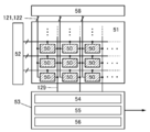
도 2의 (A)는 층(11)이 가지는 광전 변환 디바이스 및 층(12)의 디바이스 형성층이 가지는 트랜지스터 등으로 구성되는 화소 회로의 일례를 설명하는 회로도이다. 화소 회로는 광전 변환 디바이스(101)와, 트랜지스터(103)와, 트랜지스터(104)와, 트랜지스터(105)와, 트랜지스터(106)와, 커패시터(108)를 가질 수 있다. 또한, 커패시터(108)를 제공하지 않는 구성으로 하여도 좋다.FIG. 2A is a circuit diagram illustrating an example of a pixel circuit composed of a photoelectric conversion device included in the
광전 변환 디바이스(101)의 한쪽의 전극(캐소드)은 트랜지스터(103)의 소스 및 드레인 중 한쪽과 전기적으로 접속된다. 트랜지스터(103)의 소스 및 드레인 중 다른 쪽은 트랜지스터(104)의 소스 및 드레인 중 한쪽과 전기적으로 접속된다. 트랜지스터(104)의 소스 및 드레인 중 한쪽은 커패시터(108)의 한쪽의 전극과 전기적으로 접속된다. 커패시터(108)의 한쪽의 전극은 트랜지스터(105)의 게이트와 전기적으로 접속된다. 트랜지스터(105)의 소스 및 드레인 중 한쪽은 트랜지스터(106)의 소스 및 드레인 중 한쪽과 전기적으로 접속된다.One electrode (cathode) of the
여기서, 트랜지스터(103)의 소스 및 드레인 중 다른 쪽, 커패시터(108)의 한쪽의 전극, 트랜지스터(105)의 게이트를 접속하는 배선을 노드(FD)로 한다. 노드(FD)는 전하 축적부로서 기능시킬 수 있다.Here, a wiring connecting the other of the source and drain of the
광전 변환 디바이스(101)의 다른 쪽의 전극(애노드)은 배선(121)과 전기적으로 접속된다. 트랜지스터(103)의 게이트는 배선(127)과 전기적으로 접속된다. 트랜지스터(104)의 소스 및 드레인 중 다른 쪽은 배선(122)과 전기적으로 접속된다. 트랜지스터(105)의 소스 및 드레인 중 다른 쪽은 배선(123)에 전기적으로 접속된다. 트랜지스터(104)의 게이트는 배선(126)과 전기적으로 접속된다. 트랜지스터(106)의 게이트는 배선(128)과 전기적으로 접속된다. 커패시터(108)의 다른 쪽의 전극은, 예를 들어 GND 배선 등의 기준 전위선과 전기적으로 접속된다. 트랜지스터(106)의 소스 및 드레인 중 다른 쪽은 배선(129)과 전기적으로 접속된다.The other electrode (anode) of the
배선(127, 126, 128)은 각 트랜지스터의 도통을 제어하는 신호선으로서의 기능을 가질 수 있다. 배선(129)은 출력선으로서의 기능을 가질 수 있다.The
배선(121, 122, 123)은 전원선으로서의 기능을 가질 수 있다. 도 2의 (A)에 도시된 구성에서는 광전 변환 디바이스(101)의 캐소드 측이 트랜지스터(103)와 전기적으로 접속되는 구성이고, 노드(FD)를 고전위로 리셋하여 동작시키는 구성이기 때문에 배선(122)은 고전위(배선(121)보다 높은 전위)로 한다.The
도 2의 (A)에서는 광전 변환 디바이스(101)의 캐소드가 노드(FD)와 전기적으로 접속되는 구성을 도시하였지만, 도 2의 (B)에 도시된 바와 같이 광전 변환 디바이스(101)의 애노드 측이 트랜지스터(103)의 소스 및 드레인 중 한쪽과 전기적으로 접속되는 구성으로 하여도 좋다.2A shows a configuration in which the cathode of the
상기 구성에서는, 노드(FD)를 저전위로 리셋하여 동작시키는 구성이기 때문에 배선(122)은 저전위(배선(121)보다 낮은 전위)로 한다.In the above configuration, since the node FD is reset to a low potential to operate, the
트랜지스터(103)는 노드(FD)의 전위를 제어하는 기능을 가진다. 트랜지스터(104)는 노드(FD)의 전위를 리셋하는 기능을 가진다. 트랜지스터(105)는 소스 폴로어 회로로서 기능하고, 노드(FD)의 전위를 화상 데이터로서 배선(129)에 출력할 수 있다. 트랜지스터(106)는 화상 데이터를 출력하는 화소를 선택하는 기능을 가진다.The
트랜지스터(103) 및 트랜지스터(104)에는 OS 트랜지스터를 사용하는 것이 바람직하다. OS 트랜지스터는 오프 전류가 매우 낮다는 특성을 가진다. 트랜지스터(103, 104)에 OS 트랜지스터를 사용함으로써, 노드(FD)에서 전하를 유지할 수 있는 기간을 매우 길게 할 수 있다. 그러므로, 회로 구성이나 동작 방법을 복잡하게 하지 않고, 모든 화소에서 동시에 전하의 축적 동작을 수행하는 글로벌 셔터 방식을 적용할 수 있다.It is preferable to use OS transistors for the
<촬상 장치의 동작 방식><Operation method of the imaging device>
도 3의 (A)는 롤링 셔터 방식의 동작 방법을 모식화한 도면이고, 도 3의 (B)는 글로벌 셔터 방식을 모식화한 도면이다. En은 n 번째 열(n은 자연수)의 노광(축적 동작), Rn은 n 번째 열의 판독 동작을 나타낸다. 도 3의 (A), (B)에서는, 첫 번째 행으로부터 M 번째 행(M은 자연수)까지의 동작을 나타낸다.Fig. 3A is a diagram schematically illustrating an operation method of a rolling shutter system, and Fig. 3B is a diagram schematically illustrating a global shutter system. En represents the exposure (accumulation operation) of the n-th column (n is a natural number), and Rn represents the read operation of the n-th column. In (A) and (B) of Fig. 3, the operation from the first row to the M-th row (M is a natural number) is shown.
롤링 셔터 방식은 노광과 데이터의 판독을 순차적으로 수행하는 동작 방법이고, 어떤 행의 판독 기간과 다른 행의 노광 기간을 중첩시키는 방식이다. 노광 후 바로 판독 동작을 수행하기 때문에, 데이터의 유지 기간이 비교적 짧은 회로 구성이어도 촬상을 수행할 수 있다. 그러나, 촬상의 동시성이 없는 데이터로 1프레임의 화상이 구성되기 때문에, 동체 촬상에 있어서는 화상에 왜곡이 발생된다.The rolling shutter method is an operation method of sequentially performing exposure and reading of data, and is a method of superimposing the reading period of one row and the exposure period of another row. Since the read operation is performed immediately after exposure, imaging can be performed even with a circuit configuration in which the data retention period is relatively short. However, since an image of one frame is composed of data without simultaneous imaging, distortion occurs in the image in moving object imaging.
한편, 글로벌 셔터 방식은 모든 화소에서 동시에 노광을 수행하여 각 화소에 데이터를 유지하고, 행마다 데이터를 판독하는 동작 방법이다. 따라서, 동체 촬상이어도 왜곡이 없는 화상을 얻을 수 있다.Meanwhile, in the global shutter method, exposure is performed on all pixels at the same time, data is retained in each pixel, and data is read for each row. Therefore, an image without distortion can be obtained even in moving body imaging.
채널 형성 영역에 Si를 사용한 트랜지스터(이하, Si 트랜지스터) 등의 비교적 오프 전류가 높은 트랜지스터를 화소 회로에 사용한 경우에는, 전하 축적부로부터 데이터 전위가 유출되기 쉽기 때문에 롤링 셔터 방식이 많이 사용된다. Si 트랜지스터를 사용하여 글로벌 셔터 방식을 실현하기 위해서는, 별도로 메모리 회로 등을 제공할 필요가 있고, 더 복잡한 동작을 고속으로 수행하여야 한다. 한편, 화소 회로에 OS 트랜지스터를 사용한 경우에는, 전하 축적부로부터의 데이터 전위의 유출이 거의 없기 때문에 용이하게 글로벌 셔터 방식을 실현할 수 있다. 또한, 본 발명의 일 형태의 촬상 장치를 롤링 셔터 방식으로 동작시킬 수도 있다.When a transistor having a relatively high off-current such as a transistor using Si (hereinafter, referred to as Si transistor) in the channel formation region is used in the pixel circuit, the data potential is easily leaked from the charge accumulating portion, and thus the rolling shutter method is often used. In order to realize the global shutter method using the Si transistor, it is necessary to separately provide a memory circuit or the like, and a more complex operation must be performed at high speed. On the other hand, when the OS transistor is used in the pixel circuit, since there is little leakage of the data potential from the charge storage unit, the global shutter system can be easily realized. Further, the imaging device of one embodiment of the present invention may be operated by a rolling shutter method.
또한, 트랜지스터(105, 106)에도 OS 트랜지스터를 적용하여도 좋다. 또한, OS 트랜지스터 및 Si 트랜지스터를 임의적으로 조합하여 적용하여도 좋다. 또한, 모든 트랜지스터를 OS 트랜지스터 또는 Si 트랜지스터로 하여도 좋다. Si 트랜지스터로서는, 비정질 실리콘을 가지는 트랜지스터, 결정성의 실리콘(대표적으로는, 저온 폴리실리콘, 단결정 실리콘 등)을 가지는 트랜지스터 등을 들 수 있다.Further, an OS transistor may be applied to the
<제작 방법><Production method>
다음으로, 본 발명의 일 형태의 촬상 장치의 제작 방법에 대하여 설명을 한다. 제작 방법은 제 1 방법과 제 2 방법이 있고, 모두 접합 공법을 사용한다.Next, a method of manufacturing the imaging device of one embodiment of the present invention will be described. There are a 1st method and a 2nd method as a manufacturing method, and both use a bonding method.
<제 1 방법><
제 1 방법은 단결정 실리콘 기판에 제공된 광전 변환 디바이스 위에 트랜지스터 등을 제작하고, 지지 기판을 접합시키는 방법이다.The first method is a method of fabricating a transistor or the like on a photoelectric conversion device provided on a single crystal silicon substrate, and bonding a support substrate.
우선, 단결정 실리콘 기판(21)의 제 1 면 측에 광전 변환 디바이스(101)를 형성한다(도 4의 (A) 참조). 또한, 본 명세서에서의 촬상 장치의 제작 방법을 설명하는 도면에서는, 전체의 일부를 나타낸 사시도 및 이 일부의 단면을 도시하였다. 또한, 도면 중에 도시된 트랜지스터 및 다이오드의 기호는 디바이스의 위치를 간이적으로 나타낸 것이고, 전기적인 접속이나 회로 구성을 반영하는 것이 아니다. 도 4의 (A)에서는 복수의 화소 각각에 대응하는 복수의 광전 변환 디바이스(101)를 도시하였다.First, a
광전 변환 디바이스(101)는 단결정 실리콘 기판(21)의 일부의 영역과 단결정 실리콘 기판에 제공된 영역(22)의 접합에 의하여 형성할 수 있다. 영역(22)은 단결정 실리콘 기판(21)과 반대의 도전형을 가지는 영역이다. 여기서는, 단결정 실리콘 기판(21)의 도전형을 p형으로 하고, 영역(22)의 도전형을 n형으로 한다. 즉, 광전 변환 디바이스(101)는 pn 접합형 포토다이오드이다.The
영역(22)은 단결정 실리콘 기판(21)의 제 1 면에 n형의 도펀트(인, 비소 등)를 이온 도핑이나 이온 주입 등의 공법을 사용하여 첨가함으로써 형성할 수 있다.The
다음으로, 광전 변환 디바이스(101) 위에 디바이스 형성층(23)을 형성한다(도 5의 (A) 참조). 디바이스 형성층(23)에는 화소 회로가 가지는 트랜지스터나 커패시터 이외에, 필요에 따라 복수의 절연막이 제공된다. 또한, 광전 변환 디바이스(101)와 상기 트랜지스터는 전기적으로 접속된다.Next, a
트랜지스터나 커패시터는 입체 구조를 가지기 때문에, 디바이스 형성층(23)의 상부에는 요철이 생긴다. 상기 요철은 후공정에 영향을 미치기 때문에, 절연층(24)을 제공하여 표면의 요철을 평탄화한다(도 5의 (B) 참조). 또한, 절연층(24)은 단층에 한정되지 않고, 복수의 층의 적층이어도 좋다. 예를 들어, 산화 실리콘막 등의 무기막, 아크릴 수지 또는 폴리이미드 등의 유기막을 사용할 수 있다. 또한, 다음 공정에서는 무기막끼리를 접합시키기 때문에, 적어도 최표면은 무기막으로 한다. 또한, 필요에 따라 CMP(chemical mechanical polishing) 등을 사용하여 표면을 평탄화하여도 좋다.Since the transistor or capacitor has a three-dimensional structure, irregularities are formed on the top of the
다음으로, 지지 기판(25) 위에 절연층(26)을 형성하고, 절연층(26)의 표면과 절연층(24)의 표면을 밀착시켜, 접합 처리를 수행한다(도 5의 (C) 참조).Next, the insulating
지지 기판(25)에는 유리 기판, 세라믹 기판, 반도체 기판, 금속 기판 등의 평탄성이 높은 경질 재료를 사용하는 것이 바람직하다. 절연층(26)에는 산화 실리콘막 등의 무기막을 사용하는 것이 바람직하고, 적어도 절연층(24)의 최표면과 절연층(26)의 최표면은 같은 재료로 형성되어 있는 것이 바람직하다.For the
또한, 접합 직전에, 절연층(26)의 표면 및 절연층(24)의 표면을 친수성화하는 것이 바람직하다. 접합면을 친수성화시킴으로써 원자 레벨의 견고한 접착력을 얻을 수 있다. 또한, 필요에 따라 가열 처리나 가압 처리를 수행하여도 좋다.In addition, immediately before bonding, it is preferable to hydrophilize the surface of the insulating
다음으로, 연삭 연마 도구(27)를 사용하여 단결정 실리콘 기판(21)의 제 1 면과 대향하는 면을 연삭 및 연마하여, 단결정 실리콘 기판(21)을 박층화한다(도 6의 (A) 참조). 연삭 연마 도구(27)로서는, 그라인딩 장치, 래핑 장치, 폴리싱 장치, CMP 장치 등을 필요에 따라 적절히 사용하면 좋다. 또한, 웨트 에칭을 병용하여도 좋다.Next, the surface facing the first surface of the single
단결정 실리콘 기판(21)의 두께는, 광의 침입 길이, 확산 길이, 공핍층 두께 등을 고려하여 결정하면 좋다. 예를 들어, 근적외광을 촬상의 대상으로 하는 경우에는 3μm 이상 100μm 이하, 바람직하게는 5μm 이상 50μm 이하, 더 바람직하게는 10μm 이상 25μm 이하로 한다.The thickness of the single
단결정 실리콘 기판(21)을 원하는 두께로 박층화한 후, 단결정 실리콘 기판(21)의 제 1 면과 대향하는 면 측에 p+형의 도전형을 가지는 영역(28)을 형성하여도 좋다(도 6의 (B) 참조). 영역(28)은 단결정 실리콘 기판(21)보다 캐리어 농도가 높고 저저항의 영역이고, 광전 변환 디바이스(101)의 캐리어 추출 전극(공통 전극)으로서 작용한다. 또한, 화소 회로에서는, 배선(121) 또는 그 일부로서도 작용한다. 또한, 영역(28)을 제공하지 않는 구성으로 하여도 좋다. After thinning the single crystal silicon substrate 21 to a desired thickness, a region 28 having a p + type conductivity type may be formed on the side of the surface opposite to the first surface of the single crystal silicon substrate 21 (Fig. 6(B)). The
영역(28)은 단결정 실리콘 기판(21)의 제 1 면과 대향하는 면에 p형 도펀트(붕소, 알루미늄 등)를 이온 도핑, 이온 주입, 기상 확산, 고상 확산 등의 공법을 사용하여 첨가하여 형성할 수 있다. 이상이 제 1 방법이다.The
<제 2 방법><The second method>
제 2 방법은 단결정 실리콘 기판에 제공한 광전 변환 디바이스와, 지지 기판 위에 제공한 트랜지스터 등을 접합하는 방법이다. 또한, 이하의 설명에서, 제 1 방법과 중복되는 설명은 생략한다.The second method is a method of bonding a photoelectric conversion device provided on a single crystal silicon substrate and a transistor provided on a support substrate. In addition, in the following description, descriptions overlapping with the first method will be omitted.
우선, 제 1 방법과 마찬가지로 광전 변환 디바이스(101)를 형성한다(도 4의 (A) 참조). 그리고, 광전 변환 디바이스(101) 위에 절연층(31) 및 도전층(32)을 형성한다(도 4의 (B) 참조). 절연층(31)은 절연층(26)과 같은 재료로 구성할 수 있다. 도전층(32)은 광전 변환 디바이스(101)와 트랜지스터를 전기적으로 접속하기 위한 플러그이고, 한쪽 단부는 광전 변환 디바이스(101)와 전기적으로 접속되어 있다.First, the
도전층(32)은 절연층(31)에 개구부를 제공한 후, 타이타늄, 텅스텐, 탄탈럼, 및 이들의 질화물 등의 도전물 중 어느 것, 또는 상기 도전물의 복수를 상기 개구부가 충전되도록 제공하고, 불필요한 도전물을 CMP 등으로 제거함으로써 형성할 수 있다. 도전층(32)은 절연층(31)에 매설되어 있고, 표면은 절연층(31)의 표면과 이어지는 평면이 되어 있다.After providing an opening in the insulating
다음으로, 지지 기판(25) 위에 디바이스 형성층(23)을 형성한다(도 7의 (A) 참조). 디바이스 형성층(23)에는 화소 회로가 가지는 트랜지스터나 커패시터 이외에, 필요에 따라 복수의 절연막이 제공된다. 그리고, 절연층(33) 및 도전층(34)을 형성한다(도 7의 (B) 참조). 절연층(33)은 절연층(24)과 같은 재료로 구성할 수 있다. 도전층(34)은 광전 변환 디바이스(101)와 트랜지스터를 전기적으로 접속하기 위한 플러그이고, 한쪽 단부는 트랜지스터와 전기적으로 접속되어 있다.Next, a
도전층(34)은 절연층(33)에 개구부를 제공한 후, 타이타늄, 텅스텐, 탄탈럼, 및 이들의 질화물 등의 도전물 중 어느 것, 또는 상기 도전물의 복수를 상기 개구부가 충전되도록 제공하고, 불필요한 도전물을 CMP 등으로 제거함으로써 형성할 수 있다. 도전층(34)은 절연층(33)에 매설되어 있고, 표면은 절연층(33)의 표면과 이어지는 평면이 되어 있다.After providing an opening in the insulating
다음으로, 절연층(31)의 표면 및 절연층(33)의 표면, 그리고 도전층(32) 및 도전층(34)의 표면을 밀착시켜, 접합 처리를 수행한다(도 7의 (C) 참조).Next, the surface of the insulating
또한, 접합 직전에 절연층(31)의 표면 및 절연층(33)의 표면의 친수성화, 그리고 도전층(32)의 표면 및 도전층(34)의 표면의 활성화를 수행하는 것이 바람직하다. 접합면에 상기 처리를 수행함으로써 원자 레벨의 견고한 접착력을 얻을 수 있다. 또한, 필요에 따라 가열 처리나 가압 처리를 수행하여도 좋다.In addition, it is preferable to perform hydrophilization of the surface of the insulating
다음으로, 연삭 연마 도구(27)를 사용하여 단결정 실리콘 기판(21)의 제 1 면과 대향하는 면을 연삭 및 연마하여, 단결정 실리콘 기판(21)을 박층화한다(도 8의 (A) 참조).Next, the surface facing the first surface of the single
단결정 실리콘 기판(21)을 원하는 두께로 박층화한 후, 단결정 실리콘 기판(21)의 제 1 면과 대향하는 면 측에 p+형의 도전형을 가지는 영역(28)을 형성하여도 좋다(도 8의 (B) 참조). 이상이 제 2 방법이다. After thinning the single crystal silicon substrate 21 to a desired thickness, a region 28 having a p + type conductivity type may be formed on the side of the surface opposite to the first surface of the single crystal silicon substrate 21 (Fig. See (B) of 8). This is the second method.
<변형예 1><Modified Example 1>
제 1 방법 또는 제 2 방법으로 제작한 광전 변환 디바이스(101)에 가공을 더 수행하여도 좋다. 예를 들어, 도 9의 (A) 내지 (D)에 도시된 바와 같이, 광전 변환 디바이스(101)의 영역(28) 및 광 흡수층이 되는 영역을 화소마다 분단하여도 좋다.The
우선, 영역(28)을 포함하는 단결정 실리콘 기판(21)을 화소마다 분단하는 홈을 제공한다(도 9의 (A) 참조). 다음으로, 상기 홈 및 영역(28) 위에 산화 실리콘 등의 절연층(35)을 제공한다(도 9의 (B) 참조). 다음으로, 절연층(35)에, 영역(28)에 도달하는 개구부(36)를 제공한다(도 9의 (C) 참조). 그리고, 절연층(35) 및 개구부(36) 위에 대상이 되는 파장의 광에 대하여 투광성을 가지는 도전층(37)을 제공한다(도 9의 (D) 참조).First, a groove for dividing the single
도전층(37)은 광전 변환 디바이스(101)의 캐리어 추출 전극(공통 전극)으로서 작용한다. 또한, 화소 회로에서는, 배선(121) 또는 그 일부로서도 작용한다. 또한, 도전층(37)으로서는, 인듐 주석 산화물 등의 도전성 산화물의 이외에, 도전성 유기막, 메탈 메시, 영역(28)과 같은 도전형을 가지는 반도체막 등을 사용할 수 있다.The
또한, 화소 사이에 제공한 홈에 절연층(35)을 제공함으로써, 인접한 화소로부터 침입하는 미광을 억제할 수 있어, 더 선명한 화상을 취득할 수 있다.Further, by providing the insulating
<변형예 2><Modified Example 2>
제 1 방법, 제 2 방법으로 제작한 구성 및 변형예로서 나타낸 구성에 대하여, 구성 요소를 더 부가하여도 좋다. 예를 들어, 도 10의 (A)에 도시된 바와 같이, 영역(28) 위에 보호층으로서 절연층(38)을 제공할 수 있다. 절연층(38)에는 넓은 파장 범위의 광에 대하여 투광성을 가지는 산화 실리콘막 등을 사용할 수 있다. 또한, 패시베이션막으로서 작용하는 질화 실리콘막을 적층하는 구성으로 하여도 좋다. 또한, 반사 방지막으로서 산화 하프늄 등의 유전체막을 적층하는 구성으로 하여도 좋다.Constituent elements may be further added to the configurations produced by the first method and the second method, and to the configurations shown as modified examples. For example, as shown in FIG. 10A, an insulating
절연층(38) 위에는 차광층(39)이 형성되어도 좋다. 차광층(30)은 비스듬한 방향으로부터의 광의 침입을 억제하는 기능을 가진다. 차광층(39)에는 알루미늄, 텅스텐 등의 금속층을 사용할 수 있다. 또는, 상기 금속층과 반사 방지막으로서의 기능을 가지는 유전체막을 적층하는 구성으로 할 수 있다. 또는, 금속층 대신에 수지층을 사용하여도 좋다.A
절연층(38) 및 차광층(39) 위에는 평탄화막으로서 절연층(40)을 제공하는 구성으로 할 수 있다. 절연층(40)으로서는 유기 수지막 등을 사용할 수 있다.The insulating
또한, 절연층(40) 위에 광학 필터층(41)을 제공하여도 좋다. 광학 필터층(41)으로서는, 목적에 대응하는 광이 투과하는 재료를 선택하여 형성하면 좋다. 광학 필터층으로서는, 예를 들어 적외광 투과 필터를 사용할 수 있다. 적외광 투과 필터를 사용함으로써, 적외광에만 감도를 가지는 촬상 장치로 할 수 있다.Further, an
적외광 투과 필터로서는, 예를 들어 유리나 수지 등의 적외광을 투과시키는 기초 재료에 적외광을 투과시키고 가시광을 흡수하는 재료를 분산시켜 형성한 층을 사용할 수 있다. 투과하는 적외광의 파장은 기초 재료에 분산되는 재료를 적절히 선택함으로써 조정할 수 있다. 예를 들어, 생체 인증 등에 사용되는 정맥의 촬상을 목적으로 하는 경우에는, 적어도 헤모글로빈을 흡수하고 근적외광이 투과하는 재료를 선택하면 좋다.As the infrared light transmitting filter, for example, a layer formed by dispersing a material that transmits infrared light and absorbs visible light to a base material that transmits infrared light such as glass or resin can be used. The wavelength of transmitted infrared light can be adjusted by appropriately selecting a material that is dispersed in the base material. For example, when the purpose of imaging veins used for biometric authentication or the like is intended, a material that absorbs at least hemoglobin and transmits near-infrared light may be selected.
또한, 마이크로 렌즈 어레이(42)를 제공하고, 하나의 렌즈에 의하여 집광된 광이 하나의 화소에서 수광되는 구성으로 하여도 좋다. 마이크로 렌즈 어레이(42)를 제공함으로써, 차광층(39)이 제공된 구성이어도 효율적으로 광을 수광할 수 있다.In addition, a
또한, 도 10의 (A) 내지 (C)에 나타낸 구성 요소 중 어느 것이 생략된 구성이어도 좋다. 또는, 그 외의 구성 요소가 더 제공된 구성이어도 좋다.Further, any of the constituent elements shown in Figs. 10A to 10C may be omitted. Alternatively, other components may be further provided.
<화소 회로의 동작><Operation of the pixel circuit>
다음으로, 도 2의 (A)에 도시된 화소 회로의 동작의 일례를 도 11의 (A)의 타이밍 차트를 사용하여 설명한다. 또한, 본 명세서에서의 타이밍 차트의 설명에서는 고전위를 "H", 저전위를 "L"로 나타낸다. 배선(121)에는 항상 "L"이 공급되고, 배선(122, 123)에는 항상 "H"가 공급되어 있는 상태로 한다.Next, an example of the operation of the pixel circuit shown in Fig. 2A will be described using the timing chart of Fig. 11A. In addition, in the description of the timing chart in this specification, the high potential is represented by "H" and the low potential is represented by "L". The
기간 T1에 있어서, 배선(126)의 전위를 "H", 배선(127)의 전위를 "H", 배선(128)의 전위를 "L"로 하면, 트랜지스터(103, 104)가 도통되고, 노드(FD)에는 배선(123)의 전위 "H"가 공급된다(리셋 동작).In the period T1, when the potential of the
기간 T2에 있어서, 배선(126)의 전위를 "L", 배선(127)의 전위를 "H", 배선(128)의 전위를 "L"로 하면, 트랜지스터(104)가 비도통이 되고 리셋 전위의 공급이 차단된다. 또한, 광전 변환 디바이스(101)의 동작에 따라 노드(FD)의 전위가 저하한다(축적 동작).In the period T2, when the potential of the
기간 T3에 있어서, 배선(126)의 전위를 "L", 배선(127)의 전위를 "L", 배선(128)의 전위를 "L"로 하면, 트랜지스터(103)가 비도통이 되고, 노드(FD)의 전위는 확정되고 유지된다(유지 동작). 이때, 노드(FD)에 접속되는 트랜지스터(103) 및 트랜지스터(104)에 오프 전류가 낮은 OS 트랜지스터를 사용함으로써, 노드(FD)로부터의 불필요한 전하의 유출을 억제할 수 있고, 데이터의 유지 시간을 길게 할 수 있다.In the period T3, when the potential of the
기간 T4에 있어서, 배선(126)의 전위를 "L", 배선(127)의 전위를 "L", 배선(128)의 전위를 "H"로 하면, 트랜지스터(106)가 도통되고, 트랜지스터(105)의 소스 폴로어 동작에 의하여 노드(FD)의 전위가 배선(129)으로 판독된다(판독 동작).In the period T4, when the potential of the
이상이 도 2의 (A)에 도시된 화소 회로의 동작의 일례이다.The above is an example of the operation of the pixel circuit shown in Fig. 2A.
도 2의 (B)에 도시된 화소 회로는 도 11의 (B)의 타이밍 차트에 따라서 동작시킬 수 있다. 또한, 배선(121, 123)에는 항상 "H"가 공급되고, 배선(122)에는 항상 "L"이 공급되어 있는 상태로 한다. 기본적인 동작은 상기 도 11의 (A)의 타이밍 차트의 설명과 마찬가지이다.The pixel circuit shown in FIG. 2B can be operated according to the timing chart of FIG. 11B. In addition, "H" is always supplied to the
본 발명의 일 형태에 있어서는, 도 12의 (A), (B)에 예시한 바와 같이, 트랜지스터에 백 게이트를 제공한 구성으로 하여도 좋다. 도 12의 (A)는 백 게이트가 프런트 게이트와 전기적으로 접속된 구성을 나타낸 것이고, 온 전류를 높이는 효과를 가진다. 도 12의 (B)는 백 게이트가 정전위를 공급할 수 있는 배선과 전기적으로 접속된 구성을 나타낸 것이고, 트랜지스터의 문턱 전압을 제어할 수 있다.In one embodiment of the present invention, as illustrated in Figs. 12A and 12B, a structure in which a back gate is provided to the transistor may be employed. 12A shows a configuration in which the back gate is electrically connected to the front gate, and has an effect of increasing the ON current. 12B shows a configuration in which a back gate is electrically connected to a wiring capable of supplying a positive potential, and a threshold voltage of a transistor can be controlled.
또한, 도 12의 (A), (B)를 조합하는 등, 각각의 트랜지스터가 적절한 동작을 수행할 수 있는 구성으로 하여도 좋다. 또한, 백 게이트가 제공되지 않은 트랜지스터를 화소 회로가 가져도 좋다.In addition, each transistor may be configured to perform an appropriate operation, such as combining (A) and (B) of FIG. 12. Further, the pixel circuit may have a transistor in which a back gate is not provided.
도 13은 본 발명의 일 형태의 촬상 장치를 설명하는 블록도이다. 상기 촬상 장치는 매트릭스상으로 배열된 본 발명의 일 형태의 화소 회로(50)를 가지는 화소 어레이(51)와, 화소 어레이(51)의 행을 선택하는 기능을 가지는 회로(52)(로 드라이버(row driver))와, 화소 회로(50)로부터 데이터를 판독하는 기능을 가지는 회로(53)와, 전원 전위를 공급하는 회로(58)를 가진다.13 is a block diagram illustrating an imaging device of one embodiment of the present invention. The imaging device includes a
회로(53)는 화소 어레이(51)의 열을 선택하는 기능을 가지는 회로(54)(칼럼 드라이버(column driver))와, 화소 회로(50)의 출력 데이터에 대하여 상관 이중 샘플링 처리를 수행하기 위한 회로(55)(CDS 회로)와, 회로(55)로부터 출력된 아날로그 데이터를 디지털 데이터로 변환하는 기능을 가지는 회로(56)(A/D 변환 회로 등) 등을 가질 수 있다.The
회로(52, 54)에는 시프트 레지스터 회로나 디코더 회로를 사용할 수 있다. 회로(52, 53, 58)의 일부 또는 모두는 도 1에 도시된 층(13)에 제공된 OS 트랜지스터로 형성되어 있어도 좋다. 또는, 회로(52, 53, 58)의 일부는 층(12)에 제공된 Si 트랜지스터로 형성되어 있어도 좋다.For the
본 실시형태는 다른 실시형태와 적절히 조합할 수 있다.This embodiment can be appropriately combined with other embodiments.
(실시형태 2)(Embodiment 2)
본 실시형태에서는, 본 발명의 일 형태의 촬상 장치의 구조예 등에 대하여 자세히 설명한다.In this embodiment, a structural example of the imaging device of one embodiment of the present invention will be described in detail.
도 14의 (A)는 제 1 방법으로 제작할 수 있는 화소의 단면의 일례를 설명하는 도면이다. 도 14의 (B)는 제 2 방법으로 제작할 수 있는 화소의 단면의 일례를 설명하는 도면이다.14A is a diagram illustrating an example of a cross section of a pixel that can be produced by the first method. 14B is a diagram illustrating an example of a cross section of a pixel that can be produced by the second method.
층(12)에는 광전 변환 디바이스(101)로서, n형의 도전형을 가지는 영역(22), p형 도전형을 가지는 영역(단결정 실리콘 기판(21)), 및 p+형의 도전형을 가지는 영역(28)을 가지는 pn 접합형 포토다이오드가 제공된다. 층(13)에는 OS 트랜지스터가 제공된다. 도 14의 (A), (B)에서는 도 2의 (A)에 도시된 회로 구성을 예로 들어, 트랜지스터(103, 105, 106)를 예시하였다. 층(14)에는 지지 기판(25) 등이 제공된다.In the
또한, 도 14의 (A)에서의 층(13)에서, 절연층(24)은 절연층(63) 및 절연층(64)의 2층인 예를 나타내었다. 절연층(63)에는, 예를 들어 아크릴 수지나 폴리이미드 등의 유기막을 사용할 수 있다. 절연층(64)에는 산화 실리콘막 등의 무기막을 사용할 수 있다.In addition, in the
또한, 도 14의 (B)에서의 층(13)에서, 절연층(31)은 절연층(63), 절연층(65), 및 절연층(64)의 3층인 예를 나타내었다.In addition, in the
절연층(65)은 수소의 확산을 방지하는 기능을 가지고, OS 트랜지스터가 형성되는 영역과 광전 변환 디바이스(101) 등의 Si 디바이스가 형성되는 영역 사이에 제공된다. 광전 변환 디바이스(101) 근방에 제공되는 절연층 내의 수소는, 실리콘의 댕글링 본드를 종단한다. 한편, 트랜지스터(102, 105, 106)의 채널 형성 영역의 근방에 제공되는 절연층 내의 수소는, 산화물 반도체층 내에 캐리어를 생성하는 요인 중 하나가 된다.The insulating
절연층(65)에 의하여 한쪽의 층에 수소를 가둠으로써 Si 디바이스의 신뢰성을 향상시킬 수 있다. 또한, 한쪽의 층으로부터 다른 쪽의 층으로의 수소의 확산이 억제됨으로써 트랜지스터(102, 105, 106)의 신뢰성도 향상시킬 수 있다.By confining hydrogen in one layer by the insulating
절연층(65)으로서는, 예를 들어 산화 알루미늄, 산화질화 알루미늄, 산화 갈륨, 산화질화 갈륨, 산화 이트륨, 산화질화 이트륨, 산화 하프늄, 산화질화 하프늄, 이트리아 안정화 지르코니아(YSZ) 등을 사용할 수 있다.As the insulating
또한, 절연층(65)은 상기 효과가 얻어지는 위치이면, 다른 위치에 제공되어 있어도 좋다. 예를 들어, 절연층(63)과 절연층(65)을 바꾸어도 좋다.Further, the insulating
도 15의 (A)에 OS 트랜지스터의 자세한 내용을 나타내었다. 도 15의 (A)에 도시된 OS 트랜지스터는 산화물 반도체층과 도전층의 적층 위에 절연층이 제공되고, 상기 반도체층에 달하는 홈을 제공함으로써 소스 전극(205) 및 드레인 전극(206)을 형성하는 셀프 얼라인형의 구성이다.15A shows the details of the OS transistor. In the OS transistor shown in FIG. 15A, an insulating layer is provided on the stack of an oxide semiconductor layer and a conductive layer, and a groove reaching the semiconductor layer is provided to form the
OS 트랜지스터는 산화물 반도체층(207)에 형성되는 채널 형성 영역, 소스 영역(203) 및 드레인 영역(204) 이외에, 게이트 전극(201), 게이트 절연막(202)을 가지는 구성으로 할 수 있다. 상기 홈에는 적어도 게이트 절연막(202) 및 게이트 전극(201)이 제공된다. 상기 홈에는, 산화물 반도체층(208)이 더 제공되어 있어도 좋다.The OS transistor may have a structure including a
OS 트랜지스터는, 도 15의 (B)에 도시된 바와 같이 게이트 전극(201)을 마스크로서 사용하여 반도체층에 소스 영역(203) 및 드레인 영역(204)이 형성되는 셀프 얼라인형의 구성으로 하여도 좋다.The OS transistor may have a self-aligned configuration in which the
또는, 도 15의 (C)에 도시된 바와 같이, 소스 전극(205) 또는 드레인 전극(206)과 게이트 전극(201)이 중첩되는 영역을 가지는 논셀프 얼라인형의 톱 게이트형 트랜지스터이어도 좋다.Alternatively, as shown in FIG. 15C, a non-self-aligned top-gate transistor having a region where the
트랜지스터(103, 105, 106)는 백 게이트(535)를 가지는 구조를 나타내었지만, 백 게이트를 가지지 않는 구조이어도 좋다. 백 게이트(535)는 도 15의 (D)에 도시된 트랜지스터의 채널 폭 방향의 단면도와 같이, 대향하여 제공되는 트랜지스터의 프런트 게이트와 전기적으로 접속되어도 좋다. 또한, 도 15의 (D)에는 도 15의 (A)의 트랜지스터의 A1-A2 단면을 나타내었지만, 그 외의 구조의 트랜지스터도 마찬가지이다. 또한, 백 게이트(535)에 프런트 게이트와 상이한 고정 전위를 공급할 수 있는 구성이어도 좋다.The
OS 트랜지스터에 사용하는 반도체 재료로서는, 에너지 갭이 2eV 이상, 바람직하게는 2.5eV 이상, 더 바람직하게는 3eV 이상인 금속 산화물을 사용할 수 있다. 대표적으로는 인듐을 포함한 산화물 반도체 등이 있고, 예를 들어 후술하는 CAAC-OS 또는 CAC-OS 등을 사용할 수 있다. CAAC-OS는 결정을 구성하는 원자가 안정적이고, 신뢰성을 중시하는 트랜지스터 등에 적합하다. 또한 CAC-OS는 고이동도 특성을 나타내므로, 고속 구동을 수행하는 트랜지스터 등에 적합하다.As the semiconductor material used for the OS transistor, a metal oxide having an energy gap of 2 eV or more, preferably 2.5 eV or more, and more preferably 3 eV or more can be used. Typical examples include oxide semiconductors containing indium, and for example, CAAC-OS or CAC-OS, which will be described later, can be used. CAAC-OS is suitable for transistors that have stable atoms constituting crystals and value reliability. In addition, since CAC-OS exhibits high mobility characteristics, it is suitable for transistors that perform high-speed driving.
OS 트랜지스터는 반도체층의 에너지 갭이 크기 때문에, 수 yA/μm(채널 폭 1μm당 전류값)라는 매우 낮은 오프 전류 특성을 나타낸다. 또한 OS 트랜지스터는 임팩트 이온화, 애벌란시(avalanche) 항복, 및 단채널 효과 등이 일어나지 않는다는 등, Si 트랜지스터와는 상이한 특징을 가지고, 내압 및 신뢰성이 높은 회로를 형성할 수 있다. 또한 Si 트랜지스터에서 문제가 되는 결정성의 불균일성에 기인하는 전기 특성의 편차도 OS 트랜지스터에서는 일어나기 어렵다.The OS transistor exhibits a very low off-current characteristic of several yA/µm (current value per 1 µm channel width) because the energy gap of the semiconductor layer is large. In addition, the OS transistor has different characteristics from the Si transistor, such as that impact ionization, avalanche breakdown, and short-channel effects do not occur, and a circuit with high breakdown voltage and high reliability can be formed. In addition, variations in electrical characteristics due to non-uniformity of crystallinity, which is a problem in Si transistors, are also unlikely to occur in OS transistors.
OS 트랜지스터가 가지는 반도체층은, 예를 들어 인듐, 아연, 및 M(알루미늄, 타이타늄, 갈륨, 저마늄, 이트륨, 지르코늄, 란타넘, 세륨, 주석, 네오디뮴, 또는 하프늄 등의 금속)을 포함하는 In-M-Zn계 산화물로 표기되는 막으로 할 수 있다. In-M-Zn계 산화물은, 예를 들어 스퍼터링법, ALD(Atomic layer deposition)법, 또는 MOCVD(Metal organic chemical vapor deposition)법 등을 사용하여 형성할 수 있다.The semiconductor layer of the OS transistor includes, for example, indium, zinc, and M (metals such as aluminum, titanium, gallium, germanium, yttrium, zirconium, lanthanum, cerium, tin, neodymium, or hafnium). -M-Zn-based oxide film can be used. The In-M-Zn-based oxide can be formed using, for example, a sputtering method, an atomic layer deposition (ALD) method, or a metal organic chemical vapor deposition (MOCVD) method.
In-M-Zn계 산화물을 스퍼터링법으로 성막하는 경우, 스퍼터링 타깃의 금속 원소의 원자수비는, In≥M, Zn≥M을 충족시키는 것이 바람직하다. 이러한 스퍼터링 타깃의 금속 원소의 원자수비로서, In:M:Zn=1:1:1, In:M:Zn=1:1:1.2, In:M:Zn=3:1:2, In:M:Zn=4:2:3, In:M:Zn=4:2:4.1, In:M:Zn=5:1:6, In:M:Zn=5:1:7, In:M:Zn=5:1:8 등이 바람직하다. 또한, 성막되는 반도체층의 원자수비는 각각, 상기 스퍼터링 타깃에 포함되는 금속 원소의 원자수비의 ±40%의 변동을 포함한다.In the case of forming a film of an In-M-Zn-based oxide by a sputtering method, it is preferable that the atomic ratio of the metal elements of the sputtering target satisfies In≧M and Zn≧M. As the atomic ratio of the metal elements of the sputtering target, In:M:Zn=1:1:1, In:M:Zn=1:1:1.2, In:M:Zn=3:1:2, In:M :Zn=4:2:3, In:M:Zn=4:2:4.1, In:M:Zn=5:1:6, In:M:Zn=5:1:7, In:M:Zn =5:1:8 and the like are preferred. Further, the atomic ratio of the semiconductor layer to be formed includes a variation of ±40% of the atomic ratio of the metal elements included in the sputtering target, respectively.
반도체층으로서는 캐리어 밀도가 낮은 산화물 반도체를 사용한다. 예를 들어, 반도체층은, 캐리어 밀도가 1Х1017/cm3 이하, 바람직하게는 1Х1015/cm3 이하, 더 바람직하게는 1Х1013/cm3 이하, 더욱 바람직하게는 1Х1011/cm3 이하, 더더욱 바람직하게는 1Х1010/cm3 미만이고, 1Х10-9/cm3 이상의 산화물 반도체를 사용할 수 있다. 이러한 산화물 반도체를 고순도 진성 또는 실질적으로 고순도 진성인 산화물 반도체라고 부른다. 산화물 반도체는 결함 준위 밀도가 낮고, 안정된 특성을 가지는 산화물 반도체라고 할 수 있다.As the semiconductor layer, an oxide semiconductor having a low carrier density is used. For example, the semiconductor layer has a carrier density of 1 Х10 17 /cm 3 or less, preferably 1 Х10 15 /cm 3 or less, more preferably 1 Х10 13 /cm 3 or less, more preferably 1 Х10 11 /cm 3 or less, Even more preferably, an oxide semiconductor of less than 1Х10 10 /cm 3 and greater than 1Х10 -9 /cm 3 may be used. Such oxide semiconductors are referred to as high-purity intrinsic or substantially high-purity intrinsic oxide semiconductors. The oxide semiconductor has a low density of defect states and can be said to be an oxide semiconductor having stable characteristics.
또한, 이들에 한정되지 않고, 필요로 하는 트랜지스터의 반도체 특성 및 전기 특성(전계 효과 이동도, 문턱 전압 등)에 따라 적절한 조성의 것을 사용하면 좋다. 또한 필요로 하는 트랜지스터의 반도체 특성을 얻기 위하여, 반도체층의 캐리어 밀도나 불순물 농도, 결함 밀도, 금속 원소와 산소의 원자수비, 원자간 거리, 밀도 등을 적절한 것으로 하는 것이 바람직하다.Further, the present invention is not limited thereto, and a composition having an appropriate composition may be used depending on the semiconductor properties and electrical properties (field effect mobility, threshold voltage, etc.) of the transistor required. In addition, in order to obtain the required semiconductor characteristics of the transistor, it is preferable to set the carrier density or impurity concentration of the semiconductor layer, the defect density, the atomic ratio of the metal element to the oxygen, the distance between atoms, the density, etc. as appropriate.
반도체층을 구성하는 산화물 반도체에서, 14족 원소의 하나인 실리콘이나 탄소가 포함되면, 산소 결손이 증가되어 n형화된다. 그러므로, 반도체층에서의 실리콘이나 탄소의 농도(이차 이온 질량 분석법에 의하여 얻어지는 농도)를 2Х1018atoms/cm3 이하, 바람직하게는 2Х1017atoms/cm3 이하로 한다.In the oxide semiconductor constituting the semiconductor layer, when silicon or carbon, which is one of the
또한, 알칼리 금속 및 알칼리 토금속은, 산화물 반도체와 결합되면 캐리어를 생성하는 경우가 있고, 트랜지스터의 오프 전류가 증대되는 경우가 있다. 그러므로, 반도체층에서의 알칼리 금속 또는 알칼리 토금속의 농도(이차 이온 질량 분석법에 의하여 얻어지는 농도)를 1Х1018atoms/cm3 이하, 바람직하게는 2Х1016atoms/cm3 이하로 한다.Further, when the alkali metal and alkaline earth metal are combined with the oxide semiconductor, carriers may be generated, and the off current of the transistor may increase. Therefore, the concentration of the alkali metal or alkaline earth metal (the concentration obtained by secondary ion mass spectrometry) in the semiconductor layer is set to 1 X 10 18 atoms/cm 3 or less, preferably 2 X 10 16 atoms/cm 3 or less.
또한, 반도체층을 구성하는 산화물 반도체에 질소가 포함되어 있으면, 캐리어인 전자가 생김으로써 캐리어 밀도가 증가하여, n형화되기 쉽다. 이 결과, 질소가 포함되는 산화물 반도체를 사용한 트랜지스터는 노멀리 온 특성이 되기 쉽다. 그러므로 반도체층에서의 질소 농도(이차 이온 질량 분석법에 의하여 얻어지는 농도)는 5Х1018atoms/cm3 이하로 하는 것이 바람직하다.In addition, when nitrogen is contained in the oxide semiconductor constituting the semiconductor layer, electrons as carriers are generated, thereby increasing the carrier density, which tends to be n-type. As a result, a transistor using an oxide semiconductor containing nitrogen tends to have a normal-on characteristic. Therefore, it is preferable that the nitrogen concentration in the semiconductor layer (the concentration obtained by secondary ion mass spectrometry) is 5 10 18 atoms/cm 3 or less.
또한 반도체층을 구성하는 산화물 반도체에 수소가 포함되면 금속 원자와 결합하는 산소와 반응하여 물이 되기 때문에 산화물 반도체 내에 산소 결손을 형성하는 경우가 있다. 산화물 반도체 내의 채널 형성 영역에 산소 결손이 포함되면, 트랜지스터는 노멀리 온 특성이 되는 경우가 있다. 또한 산소 결손에 수소가 들어간 결함은 도너로서 기능하고, 캐리어인 전자가 생성되는 경우가 있다. 또한 수소의 일부가 금속 원자와 결합하는 산소와 결합하여, 캐리어인 전자가 생성되는 경우가 있다. 따라서 수소가 많이 포함되어 있는 산화물 반도체를 사용한 트랜지스터는 노멀리 온 특성이 되기 쉽다.In addition, when hydrogen is contained in the oxide semiconductor constituting the semiconductor layer, it reacts with oxygen bonded to metal atoms to become water, and thus oxygen vacancies are sometimes formed in the oxide semiconductor. When oxygen vacancies are contained in the channel formation region in the oxide semiconductor, the transistor may become normally-on. In addition, defects containing hydrogen in oxygen vacancies function as donors, and electrons as carriers may be generated. In addition, there are cases in which a part of hydrogen is bonded to oxygen bonded to a metal atom, thereby generating electrons as carriers. Therefore, a transistor using an oxide semiconductor containing a large amount of hydrogen tends to have a normally-on characteristic.
산소 결손에 수소가 들어간 결함은 산화물 반도체의 도너로서 기능할 수 있다. 그러나 상기 결함을 정량적으로 평가하는 것은 어렵다. 그러므로 산화물 반도체에서는 도너 농도가 아니라 캐리어 농도로 평가되는 경우가 있다. 따라서 본 명세서 등에서는 산화물 반도체의 파라미터로서 도너 농도가 아니라 전계가 인가되지 않는 상태를 상정한 캐리어 농도를 사용하는 경우가 있다. 즉 본 명세서 등에 기재된 '캐리어 농도'는 '도너 농도'라고 바꿔 말할 수 있는 경우가 있다.Defects containing hydrogen in oxygen vacancies can function as donors for oxide semiconductors. However, it is difficult to quantitatively evaluate the defect. Therefore, in oxide semiconductors, it is sometimes evaluated by carrier concentration rather than donor concentration. Therefore, in the present specification and the like, there is a case where a carrier concentration assuming a state in which an electric field is not applied is used, not a donor concentration as a parameter of the oxide semiconductor. That is, the "carrier concentration" described in this specification and the like may be referred to as "donor concentration" in some cases.
따라서 산화물 반도체 내의 수소는 가능한 한 저감되어 있는 것이 바람직하다. 구체적으로는, 산화물 반도체에서 이차 이온 질량 분석법(SIMS: Secondary Ion Mass Spectrometry)으로 얻어지는 수소 농도를 1Х1020atoms/cm3 미만, 바람직하게는 1Х1019atoms/cm3 미만, 더 바람직하게는 5Х1018atoms/cm3 미만, 더 바람직하게는 1Х1018atoms/cm3 미만으로 한다. 수소 등의 불순물이 충분히 저감된 산화물 반도체를 트랜지스터의 채널 형성 영역에 사용함으로써, 안정된 전기 특성을 부여할 수 있다.Therefore, it is preferable that the hydrogen in the oxide semiconductor is reduced as much as possible. Specifically, the hydrogen concentration obtained by secondary ion mass spectrometry (SIMS: Secondary Ion Mass Spectrometry) in an oxide semiconductor is less than 1 X 10 20 atoms/
또한, 산화물 반도체(금속 산화물)는 단결정 산화물 반도체와, 이 외의 비단결정 산화물 반도체로 나누어진다. 비단결정 산화물 반도체로서는, 예를 들어 CAAC-OS(C-Axis Aligned Crystalline Oxide Semiconductor), 다결정 산화물 반도체, nc-OS(nanocrystalline oxide semiconductor), a-like OS(amorphous-like oxide semiconductor), 및 비정질 산화물 반도체 등이 있다. 비단결정 구조에서, 비정질 구조는 결함 준위 밀도가 가장 높고, CAAC-OS는 결함 준위 밀도가 가장 낮다.Further, oxide semiconductors (metal oxides) are divided into single crystal oxide semiconductors and other non-single crystal oxide semiconductors. Examples of the non-single crystal oxide semiconductor include CAAC-OS (C-Axis Aligned Crystalline Oxide Semiconductor), polycrystalline oxide semiconductor, nc-OS (nanocrystalline oxide semiconductor), a-like OS (amorphous-like oxide semiconductor), and amorphous oxide. Semiconductors and the like. In the non-single crystal structure, the amorphous structure has the highest density of defect states, and CAAC-OS has the lowest density of defect states.
비정질 구조의 산화물 반도체막은, 예를 들어 원자 배열이 무질서하며 결정 성분을 가지지 않는다. 또는, 비정질 구조의 산화물막은, 예를 들어 완전한 비정질 구조이며, 결정부를 가지지 않는다.The oxide semiconductor film having an amorphous structure, for example, has a disordered atomic arrangement and does not have a crystal component. Alternatively, the oxide film having an amorphous structure is, for example, a completely amorphous structure and does not have a crystal part.
또한, 반도체층이 비정질 구조의 영역, 미결정 구조의 영역, 다결정 구조의 영역, CAAC-OS의 영역, 단결정 구조의 영역 중, 2종류 이상을 가지는 혼합막이어도 좋다. 혼합막은, 예를 들어 상술한 영역 중 어느 2종류 이상의 영역을 포함하는 단층 구조 또는 적층 구조를 가지는 경우가 있다.Further, the semiconductor layer may be a mixed film having two or more types of amorphous structure region, microcrystalline region region, polycrystalline region region, CAAC-OS region, and single crystal region region. The mixed film may have, for example, a single-layer structure or a laminated structure including any two or more types of regions among the regions described above.
이하에서는, 비단결정의 반도체층의 일 형태인 CAC(Cloud-Aligned Composite)-OS의 구성에 대하여 설명한다.Hereinafter, a configuration of a CAC (Cloud-Aligned Composite)-OS, which is a form of a non-single crystal semiconductor layer, will be described.
CAC-OS란, 예를 들어 산화물 반도체를 구성하는 원소가 0.5nm 이상 10nm 이하, 바람직하게는 1nm 이상 2nm 이하, 또는 그 근방의 크기로 편재한 재료의 한 구성이다. 또한, 이하에서는 산화물 반도체에서, 하나 또는 그 이상의 금속 원소가 편재하고, 상기 금속 원소를 가지는 영역이, 0.5nm 이상 10nm 이하, 바람직하게는 1nm 이상 2nm 이하, 또는 그 근방의 크기로 혼합한 상태를 모자이크 패턴 또는 패치 패턴이라고도 한다.CAC-OS is, for example, a structure of a material in which an element constituting an oxide semiconductor is not less than 0.5 nm and not more than 10 nm, preferably not less than 1 nm and not more than 2 nm, or in the vicinity thereof. In addition, hereinafter, in the oxide semiconductor, one or more metal elements are ubiquitous, and the region having the metal element is 0.5 nm or more and 10 nm or less, preferably 1 nm or more and 2 nm or less, or a state in which a mixed state in the vicinity thereof. It is also called a mosaic pattern or patch pattern.
또한 산화물 반도체는 적어도 인듐을 포함하는 것이 바람직하다. 특히 인듐 및 아연을 포함하는 것이 바람직하다. 또한 이에 더하여 알루미늄, 갈륨, 이트륨, 구리, 바나듐, 베릴륨, 붕소, 실리콘, 타이타늄, 철, 니켈, 저마늄, 지르코늄, 몰리브데넘, 란타넘, 세륨, 네오디뮴, 하프늄, 탄탈럼, 텅스텐, 및 마그네슘 등 중에서 선택된 1종류 또는 복수 종류가 포함되어도 좋다.In addition, it is preferable that the oxide semiconductor contains at least indium. It is particularly preferable to contain indium and zinc. In addition, aluminum, gallium, yttrium, copper, vanadium, beryllium, boron, silicon, titanium, iron, nickel, germanium, zirconium, molybdenum, lanthanum, cerium, neodymium, hafnium, tantalum, tungsten, and magnesium One type or a plurality of types selected from among the like may be included.
예를 들어, In-Ga-Zn 산화물에서의 CAC-OS(CAC-OS 중에서도 In-Ga-Zn 산화물을 특히 CAC-IGZO라고 불러도 좋음)란, 인듐 산화물(이하, InOX1(X1은 0보다 큰 실수)로 함) 또는 인듐 아연 산화물(이하, InX2ZnY2OZ2(X2, Y2, 및 Z2는 0보다 큰 실수)로 함)과, 갈륨 산화물(이하, GaOX3(X3은 0보다 큰 실수)으로 함) 또는 갈륨 아연 산화물(이하, GaX4ZnY4OZ4(X4, Y4, 및 Z4는 0보다 큰 실수)로 함) 등으로 재료가 분리함으로써 모자이크 패턴이 되고, 모자이크 패턴의 InOX1 또는 InX2ZnY2OZ2가 막 내에 균일하게 분포한 구성(이하, 클라우드상이라고도 함)이다.For example, CAC-OS in In-Ga-Zn oxide (In-Ga-Zn oxide among CAC-OS may be called CAC-IGZO in particular) means indium oxide (hereinafter, InO X1 (X1 is greater than 0)). Real number)) or indium zinc oxide (hereinafter, In X2 Zn Y2 O Z2 (X2, Y2, and Z2 are real numbers greater than 0)) and gallium oxide (hereinafter, GaO X3 (X3 is a real number greater than 0)) ) as hereinafter), or gallium zinc oxide (hereinafter, Ga X4 Zn Y4 O Z4 (X4, Y4, and Z4 are, by the material is separated by the like referred to as the real number greater than 0)) being a mosaic pattern, a mosaic pattern of InO X1 or It is a configuration in which In X2 Zn Y2 O Z2 is uniformly distributed in the film (hereinafter, also referred to as cloud phase).
즉, CAC-OS는 GaOX3이 주성분인 영역과, InX2ZnY2OZ2 또는 InOX1이 주성분인 영역이 혼합되는 구성을 가지는 복합 산화물 반도체이다. 또한, 본 명세서에서, 예를 들어 제 1 영역의 원소 M에 대한 In의 원자수비가 제 2 영역의 원소 M에 대한 In의 원자수비보다 큰 것을 '제 1 영역은 제 2 영역과 비교하여 In의 농도가 높다'라고 한다.That is, CAC-OS is a complex oxide semiconductor having a configuration in which a region whose main component is GaO X3 and a region whose main component is In X2 Zn Y2 O Z2 or InO X1 are mixed. In addition, in the present specification, for example, when the atomic number ratio of In to the element M in the first region is greater than the atomic ratio of In to the element M in the second region,'the first region is compared with the second region, The concentration is high.'
또한 IGZO는 통칭이며, In, Ga, Zn, 및 O로 이루어지는 하나의 화합물을 뜻하는 경우가 있다. 대표적인 예로서, InGaO3(ZnO)m1(m1은 자연수임) 또는 In(1+x0)Ga(1-x0)O3(ZnO)m0(-1≤x0≤1, m0은 임의의 수임)으로 나타내어지는 결정성 화합물을 들 수 있다.In addition, IGZO is a generic name, and may mean one compound consisting of In, Ga, Zn, and O. As a representative example, InGaO 3 (ZnO) m1 (m1 is a natural number) or In (1+x0) Ga (1-x0) O 3 (ZnO) m0 (-1≤x0≤1, m0 is an arbitrary number). The crystalline compounds shown are mentioned.
상기 결정성 화합물은 단결정 구조, 다결정 구조, 또는 CAAC 구조를 가진다. 또한 CAAC 구조는, 복수의 IGZO의 나노 결정이 c축 배향을 가지고 또한 a-b면에서는 배향하지 않고 연결된 결정 구조이다.The crystalline compound has a single crystal structure, a polycrystalline structure, or a CAAC structure. In addition, the CAAC structure is a crystal structure in which a plurality of IGZO nanocrystals have c-axis orientation and are connected without orientation in the a-b plane.
한편, CAC-OS는 산화물 반도체의 재료 구성에 관한 것이다. CAC-OS란 In, Ga, Zn, 및 O를 포함한 재료 구성에서, 일부에 Ga를 주성분으로 하는 나노 입자상으로 관찰되는 영역, 및 일부에 In을 주성분으로 하는 나노 입자상으로 관찰되는 영역이 각각 모자이크 패턴으로 무작위로 분산되는 구성을 말한다. 따라서, CAC-OS에서 결정 구조는 부차적인 요소이다.On the other hand, CAC-OS relates to the material composition of the oxide semiconductor. CAC-OS is a mosaic pattern in a material composition containing In, Ga, Zn, and O, in which a region observed in the form of nanoparticles containing Ga as a main component in a part, and a region observed in the form of nanoparticles containing In as a main component in a part, respectively, is a mosaic pattern. It refers to a randomly distributed configuration. Therefore, the crystal structure is a secondary factor in CAC-OS.
또한 CAC-OS는 조성이 상이한 2종류 이상의 막의 적층 구조를 포함하지 않는 것으로 한다. 예를 들어, In을 주성분으로 하는 막과, Ga를 주성분으로 하는 막의 2층으로 이루어지는 구조는 포함하지 않는다.In addition, it is assumed that the CAC-OS does not include a laminated structure of two or more types of films having different compositions. For example, a structure consisting of two layers of a film containing In as a main component and a film containing Ga as a main component is not included.
또한 GaOX3이 주성분인 영역과, InX2ZnY2OZ2 또는 InOX1이 주성분인 영역에서는, 명확한 경계를 관찰할 수 없는 경우가 있다.In addition , in a region in which GaO X3 is the main component and a region in which In X2 Zn Y2 O Z2 or InO X1 is the main component, a clear boundary may not be observed in some cases.
또한 갈륨 대신에 알루미늄, 이트륨, 구리, 바나듐, 베릴륨, 보론, 실리콘, 타이타늄, 철, 니켈, 저마늄, 지르코늄, 몰리브데넘, 란타넘, 세륨, 네오디뮴, 하프늄, 탄탈럼, 텅스텐, 및 마그네슘 등 중에서 선택된 1종류 또는 복수 종류가 포함되는 경우, CAC-OS는 일부에 상기 금속 원소를 주성분으로 하는 나노 입자상으로 관찰되는 영역과, 일부에 In을 주성분으로 하는 나노 입자상으로 관찰되는 영역이 각각 모자이크 패턴으로 무작위로 분산되어 있는 구성을 말한다.Also, instead of gallium, aluminum, yttrium, copper, vanadium, beryllium, boron, silicon, titanium, iron, nickel, germanium, zirconium, molybdenum, lanthanum, cerium, neodymium, hafnium, tantalum, tungsten, and magnesium, etc. When one or more types selected from among the CAC-OS are included, the area observed in the form of nanoparticles containing the metal element as a main component in part and the area observed in the form of nanoparticles containing In as the main component are each mosaic pattern. It refers to a randomly distributed configuration.
CAC-OS는 예를 들어 기판을 의도적으로 가열하지 않는 조건하에서 스퍼터링법으로 형성할 수 있다. 또한, CAC-OS를 스퍼터링법으로 형성하는 경우, 성막 가스로서 불활성 가스(대표적으로는 아르곤), 산소 가스, 및 질소 가스 중에서 선택된 어느 하나 또는 복수를 사용하면 좋다. 또한 성막 시의 성막 가스의 총유량에 대한 산소 가스의 유량비는 낮을수록 바람직하고, 예를 들어 산소 가스의 유량비를 0% 이상 30% 미만, 바람직하게는 0% 이상 10% 이하로 하는 것이 바람직하다.CAC-OS can be formed, for example, by sputtering under conditions in which the substrate is not intentionally heated. In addition, when CAC-OS is formed by sputtering, any one or more selected from an inert gas (typically argon), oxygen gas, and nitrogen gas may be used as the film forming gas. In addition, the lower the flow rate ratio of oxygen gas to the total flow rate of the film-forming gas at the time of film formation, the more preferable, and for example, the flow rate ratio of the oxygen gas is preferably 0% or more and less than 30%, preferably 0% or more and 10% or less. .
CAC-OS는 X선 회절(XRD: X-ray diffraction) 측정법의 하나인 Out-of-plane법에 의한 θ/2θ 스캔을 사용하여 측정하였을 때 명확한 피크가 확인되지 않는다는 특징을 가진다. 즉 X선 회절 측정으로부터 측정 영역의 a-b면 방향 및 c축 방향의 배향이 보이지 않는 것을 알 수 있다.CAC-OS has a characteristic that no clear peak is found when measured using θ/2θ scan by the out-of-plane method, which is one of the X-ray diffraction (XRD) measurement methods. That is, it can be seen from the X-ray diffraction measurement that the orientation of the a-b plane direction and the c-axis direction of the measurement region is not visible.
또한 CAC-OS는 프로브 직경이 1nm인 전자선(나노 빔 전자선이라고도 함)을 조사함으로써 얻어지는 전자선 회절 패턴에서, 링 형상으로 휘도가 높은 영역(링 영역)과, 상기 링 영역에 복수의 휘점이 관측된다. 따라서, 전자선 회절 패턴으로부터 CAC-OS의 결정 구조가 평면 방향 및 단면 방향에서 배향성을 가지지 않는 nc(nano-crystal) 구조를 가지는 것을 알 수 있다.In addition, in the CAC-OS, in an electron beam diffraction pattern obtained by irradiating an electron beam with a probe diameter of 1 nm (also referred to as a nano-beam electron beam), a ring-shaped high luminance area (ring area) and a plurality of bright spots are observed in the ring area. . Accordingly, it can be seen from the electron diffraction pattern that the crystal structure of CAC-OS has a nano-crystal (nc) structure that does not have orientation in the planar direction and the cross-sectional direction.
또한, 예를 들어 In-Ga-Zn 산화물에서의 CAC-OS에서는, 에너지 분산형 X선 분광법(EDX: Energy Dispersive X-ray spectroscopy)을 사용하여 취득한 EDX 매핑에 의하여, GaOX3이 주성분인 영역과, InX2ZnY2OZ2 또는 InOX1이 주성분인 영역이 편재되고 혼합된 구조를 가지는 것을 확인할 수 있다.In addition, in CAC-OS in In-Ga-Zn oxide, for example, by EDX mapping acquired using Energy Dispersive X-ray spectroscopy (EDX) , the region where GaO X3 is the main component and , In X2 Zn Y2 O Z2 or InO X1 , it can be seen that the region of the main component has a ubiquitous and mixed structure.
CAC-OS는 금속 원소가 균일하게 분포된 IGZO 화합물과는 상이한 구조이고, IGZO 화합물과 상이한 성질을 가진다. 즉, CAC-OS는 GaOX3 등이 주성분인 영역과, InX2ZnY2OZ2 또는 InOX1이 주성분인 영역으로 서로 상분리(相分離)되어, 각 원소를 주성분으로 하는 영역이 모자이크 패턴인 구조를 가진다.CAC-OS has a structure different from the IGZO compound in which metallic elements are uniformly distributed, and has different properties from the IGZO compound. In other words, CAC-OS is phase-separated into a region whose main component is GaO X3 , and a region whose main component is In X2 Zn Y2 O Z2 or InO X1 , so that the region containing each element as the main component is a mosaic pattern. Have.
여기서, InX2ZnY2OZ2 또는 InOX1이 주성분인 영역은 GaOX3 등이 주성분인 영역과 비교하여 도전성이 높은 영역이다. 즉, InX2ZnY2OZ2 또는 InOX1이 주성분인 영역을 캐리어가 흐름으로써, 산화물 반도체로서의 도전성이 발현된다. 따라서, InX2ZnY2OZ2 또는 InOX1이 주성분인 영역이 산화물 반도체 내에 클라우드상으로 분포됨으로써 높은 전계 효과 이동도(μ)를 실현할 수 있다.Here, a region in which In X2 Zn Y2 O Z2 or InO X1 is the main component is a region having higher conductivity than a region in which GaO X3 or the like is the main component. That is, when carriers flow through a region in which In X2 Zn Y2 O Z2 or InO X1 is the main component, conductivity as an oxide semiconductor is expressed. Therefore, a high field effect mobility (μ) can be achieved by distributing a region in which In X2 Zn Y2 O Z2 or InO X1 is the main component in a cloud shape in the oxide semiconductor.
한편, GaOX3 등이 주성분인 영역은 InX2ZnY2OZ2 또는 InOX1이 주성분인 영역과 비교하여 절연성이 높은 영역이다. 즉, GaOX3 등이 주성분인 영역이 산화물 반도체 내에 분포됨으로써 누설 전류가 억제되어 양호한 스위칭 동작을 실현할 수 있다.On the other hand, a region in which GaO X3 or the like is the main component is a region having high insulating properties compared to a region in which In X2 Zn Y2 O Z2 or InO X1 is the main component. That is, since the region mainly composed of GaO X3 or the like is distributed in the oxide semiconductor, leakage current is suppressed, and good switching operation can be realized.
따라서, CAC-OS를 반도체 디바이스에 사용한 경우, GaOX3 등에 기인하는 절연성과, InX2ZnY2OZ2 또는 InOX1에 기인하는 도전성이 상보적으로 작용함으로써, 높은 온 전류(Ion) 및 높은 전계 효과 이동도(μ)를 실현할 수 있다.Therefore, when CAC-OS is used in a semiconductor device, insulating properties due to GaO X3, etc., and conductivity due to In X2 Zn Y2 O Z2 or InO X1 act complementarily, resulting in a high on current (I on ) and a high electric field. Effective mobility (μ) can be achieved.
또한 CAC-OS를 사용한 반도체 디바이스는 신뢰성이 높다. 따라서, CAC-OS는, 다양한 반도체 장치의 구성 재료로서 적합하다.In addition, semiconductor devices using CAC-OS have high reliability. Therefore, CAC-OS is suitable as a constituent material of various semiconductor devices.
도 14의 (A)에서는, 층(13)과 층(14)의 기계적인 접속을 접합 기술로 얻는 구성예를 나타내었다. 또한, 도 14의 (B)에서는, 층(12)과 층(13)의 기계적인 접속 및 전기적인 접속을 접합 기술로 얻는 구성예를 나타내었다. 이하에서 도 14의 (B)를 예로서 접합 기술에 대하여 설명한다.In Fig. 14A, a configuration example in which the mechanical connection between the
층(12)에는 절연층(33) 및 도전층(34)이 제공된다. 도전층(34)은 절연층(33)에 매설된 영역을 가진다. 도전층(34)은 영역(22)과 전기적으로 접속된다. 또한, 절연층(33), 도전층(34)의 표면은 각각 높이가 일치하도록 평탄화되어 있다.The
층(13)에는 절연층(31) 및 도전층(32)이 제공된다. 도전층(32)은 절연층(31)에 매설된 영역을 가진다. 도전층(32)은 트랜지스터(103)와 전기적으로 접속된다. 또한, 절연층(31) 및 도전층(32)의 표면은 각각 높이가 일치하도록 평탄화되어 있다.The
여기서, 도전층(32) 및 도전층(34)은 주성분이 동일한 금속 원소인 것이 바람직하다. 또한, 절연층(31) 및 절연층(33)의 표면은 동일한 성분으로 구성되어 있는 것이 바람직하다.Here, it is preferable that the
예를 들어, 도전층(32, 34)에는 Cu, Al, Sn, Zn, W, Ag, Pt, 또는 Au 등을 사용할 수 있다. 접합의 용이성을 고려하여, 바람직하게는 Cu, Al, W, 또는 Au를 사용한다. 또한, 절연층(31, 33)의 표면에는 산화 실리콘, 산화질화 실리콘, 질화산화 실리콘, 질화 실리콘, 질화 타이타늄 등을 사용할 수 있다.For example, Cu, Al, Sn, Zn, W, Ag, Pt, or Au may be used for the
즉, 도전층(32) 및 도전층(34)의 조합에 상술한 것 중에서 동일한 금속 재료를 사용하는 것이 바람직하다. 또한, 절연층(31) 및 절연층(33)의 각각에 상술한 것 중에서 동일한 절연 재료를 사용하는 것이 바람직하다. 상기 구성으로 함으로써, 층(12)과 층(13)의 경계를 접합 위치로 하여 접합할 수 있다.That is, it is preferable to use the same metal material among those described above for the combination of the
상기 접합에 의하여, 도전층(32)과 도전층(34)의 전기적인 접속을 얻을 수 있다. 또한, 절연층(31)과 절연층(33)의 기계적인 강도를 가지는 접속을 얻을 수 있다.By the above bonding, electrical connection between the
금속층끼리의 접합에는, 표면의 산화막 및 불순물의 흡착층 등을 스퍼터링 처리 등으로 제거하고, 청정화 및 활성화된 표면끼리를 접촉시켜 접합하는 표면 활성화 접합법을 사용할 수 있다. 또는, 온도와 압력을 병용하여 표면끼리를 접합하는 확산 접합법 등을 사용할 수 있다. 둘 다 원자 레벨의 결합이 일어나기 때문에, 전기적뿐만 아니라 기계적으로도 우수한 접합을 얻을 수 있다.For bonding between metal layers, a surface-activated bonding method in which the oxide film on the surface and the adsorbing layer of impurities are removed by sputtering treatment or the like, and the cleaned and activated surfaces are brought into contact with each other to be bonded. Alternatively, a diffusion bonding method in which surfaces are bonded together using temperature and pressure can be used. Since both are bonded at the atomic level, excellent bonding can be obtained not only electrically but also mechanically.
또한, 절연층끼리의 접합에는 연마 등에 의하여 높은 평탄성을 얻은 후, 산소 플라스마 등으로 친수성 처리를 수행한 표면끼리를 접촉시켜 임시적으로 접합하고, 가열 처리에 의한 탈수로 제대로 접합하는 친수성 접합법 등을 사용할 수 있다. 친수성 접합법도 원자 레벨의 결합이 일어나기 때문에, 기계적으로 우수한 접합을 얻을 수 있다.In addition, for bonding of the insulating layers, a hydrophilic bonding method, in which high flatness is obtained by polishing or the like, is temporarily bonded by contacting the surfaces subjected to hydrophilic treatment with oxygen plasma, etc., and properly bonded by dehydration by heat treatment, etc. I can. Since the hydrophilic bonding method also causes bonding at the atomic level, mechanically excellent bonding can be obtained.
층(12)과, 층(13)을 접합하는 경우, 각각의 접합면에는 절연층과 금속층이 혼재하기 때문에, 예를 들어 표면 활성화 접합법 및 친수성 접합법을 조합하여 수행하면 좋다.In the case of bonding the
예를 들어, 연마 후에 표면을 청정화하고, 금속층의 표면에 산화 방지 처리를 수행한 후에, 친수성 처리를 수행하여 접합하는 방법 등을 사용할 수 있다. 또한, 금속층의 표면을 Au 등의 난(難)산화성 금속으로 하고 친수성 처리를 수행하여도 좋다. 또한, 상술한 방법 이외의 접합 방법을 사용하여도 좋다.For example, a method of cleaning the surface after polishing, performing an antioxidant treatment on the surface of the metal layer, and then performing a hydrophilic treatment to bond them may be used. Further, the surface of the metal layer may be made of a hardly oxidizing metal such as Au, and hydrophilic treatment may be performed. Further, a bonding method other than the above-described method may be used.
이하에서는, 이미지 센서 칩을 제공한 패키지 및 카메라 모듈의 일례에 대하여 설명한다. 상기 이미지 센서 칩에는 상기 촬상 장치의 구성을 사용할 수 있다.Hereinafter, an example of a package including an image sensor chip and a camera module will be described. The configuration of the imaging device may be used for the image sensor chip.
도 16의 (A1)은 이미지 센서 칩이 제공된 패키지의 상면 측의 외관 사시도이다. 상기 패키지는 이미지 센서 칩(650)을 고정하는 패키지 기판(610), 커버 유리(620), 및 이들을 접착하는 접착제(630) 등을 가진다.FIG. 16A1 is an external perspective view of a package provided with an image sensor chip from the top side thereof. The package includes a
도 16의 (A2)는 상기 패키지의 하면 측의 외관 사시도이다. 패키지의 하면에는 땜납 볼을 범프(640)로 한 BGA(Ball grid array)를 가진다. 또한, BGA에 한정되지 않고, LGA(Land grid array)나 PGA(Pin Grid Array) 등을 가져도 좋다.Fig. 16A2 is an external perspective view of the lower surface side of the package. A ball grid array (BGA) with solder balls as
도 16의 (A3)은 커버 유리(620) 및 접착제(630)의 일부를 생략하여 도시한 패키지의 사시도이다. 패키지 기판(610) 위에는 전극 패드(660)가 형성되고, 전극 패드(660) 및 범프(640)는 스루 홀을 통하여 전기적으로 접속되어 있다. 전극 패드(660)는 이미지 센서 칩(650)과 와이어(670)에 의하여 전기적으로 접속된다.(A3) of FIG. 16 is a perspective view of a package shown by omitting some of the
또한, 도 16의 (B1)은 이미지 센서 칩이 렌즈 일체형의 패키지에 제공된 카메라 모듈의 상면 측의 외관 사시도이다. 상기 카메라 모듈은 이미지 센서 칩(651)을 고정하는 패키지 기판(611), 렌즈 커버(621), 및 렌즈(635) 등을 가진다. 또한, 패키지 기판(611)과 이미지 센서 칩(651) 사이에는 촬상 장치의 구동 회로 및 신호 변환 회로 등의 기능을 가지는 IC칩(690)도 제공되어 있고, SiP(System in package)로서의 구성을 가진다.Further, (B1) of FIG. 16 is an external perspective view of an upper surface side of a camera module in which an image sensor chip is provided in a lens-integrated package. The camera module includes a
도 16의 (B2)는 상기 카메라 모듈의 하면 측의 외관 사시도이다. 패키지 기판(611)의 하면 및 측면에는 실장용 랜드(641)가 제공된 QFN(Quad flat no-lead package)의 구성을 가진다. 또한, 상기 구성은 일례이고, QFP(Quad flat package)나 상술한 BGA가 제공되어 있어도 좋다.Fig. 16B2 is an external perspective view of the lower surface side of the camera module. The
도 16의 (B3)은 렌즈 커버(621) 및 렌즈(635)의 일부를 생략하여 도시한 모듈의 사시도이다. 랜드(641)는 전극 패드(661)와 전기적으로 접속되고, 전극 패드(661)는 이미지 센서 칩(651) 또는 IC칩(690)과 와이어(671)에 의하여 전기적으로 접속되어 있다.16(B3) is a perspective view of a module in which a
이미지 센서 칩을 상술한 바와 같은 형태의 패키지에 제공함으로써, 인쇄 기판 등으로의 실장이 용이하게 되어, 다양한 반도체 장치, 전자 기기에 이미지 센서 칩을 실장할 수 있다.By providing the image sensor chip in the package of the above-described shape, mounting on a printed board or the like is facilitated, and the image sensor chip can be mounted on various semiconductor devices and electronic devices.
본 실시형태는 다른 실시형태와 적절히 조합할 수 있다.This embodiment can be appropriately combined with other embodiments.
(실시형태 3)(Embodiment 3)
본 실시형태에서는, 본 발명의 일 형태에 따른 촬상 장치를 사용할 수 있는 전자 기기의 일례를 설명한다. 본 발명의 일 형태의 촬상 장치는 적외광 투과 필터가 불필요한 구성으로 할 수도 있고, 박형화가 용이하고, 다양한 기기에 제공하기 쉬워진다. 또한, 적외광 투과 필터는 촬상 장치에 제공하지 않고, 전자 기기의 광로에 제공하여도 좋다.In this embodiment, an example of an electronic device that can use the imaging device according to one embodiment of the present invention will be described. The imaging device of one embodiment of the present invention may have a configuration that does not require an infrared light transmitting filter, is easily reduced in thickness, and is easily provided to various devices. In addition, the infrared light transmitting filter may not be provided to the imaging device, but may be provided to the optical path of the electronic device.
도 17의 (A)는 손가락의 정맥을 대상으로 한 생체 인증 기기이며, 하우징(911), 광원(912), 검지 스테이지(913) 등을 가진다. 검지 스테이지(913)에 손가락을 올림으로써 정맥의 형상을 촬상할 수 있다. 검지 스테이지(913)의 상부에는 광원(912)이 설치되고, 하부에는 촬상 장치(914)가 설치된다. 검지 스테이지(913)는 적외광을 투과시키는 재료로 구성되어 있고, 광원(912)으로부터 조사되고, 손가락을 투과한 적외광을 촬상 장치(914)로 촬상할 수 있다. 또한, 검지 스테이지(913)와 촬상 장치(914) 사이에 광학계가 제공되어 있어도 좋다. 상기 기기의 구성은 손바닥의 정맥을 대상으로 한 생체 인증 기기에 이용할 수도 있다.Fig. 17A is a biometric authentication device targeting a vein of a finger, and includes a
광원(912)은 박형의 EL 디바이스로 형성할 수 있다. 상기 EL 디바이스는 만곡된 형상으로 설치할 수 있어, 대상물에 대하여 좋은 균일성으로 광을 조사할 수 있다. 특히 파장 700nm 이상 1200nm 이하에 피크를 가지는 근적외광을 발하는 EL 디바이스인 것이 바람직하다. 예를 들어, 파장 760nm 및 그 근방의 광은 정맥 내의 헤모글로빈에 흡수되기 쉽기 때문에, 손가락이 손바닥 등을 투과한 광을 수광하여 화상화함으로써 정맥의 위치를 검출할 수 있다. 상기 작용은 생체 인증으로서 이용할 수 있다. 또한, 글로벌 셔터 방식과 조합함으로써, 피사체가 움직여도 정밀도가 높은 센싱이 가능하게 된다.The
또한, 광원(912)은 도 17의 (B)에 도시된 발광부(915, 916, 917)와 같이, 복수의 발광부를 가질 수 있다. 발광부(915, 916, 917)의 각각은 발광하는 파장이 상이하여도 좋고, 또한, 각각을 다른 타이밍으로 조사할 수도 있다. 따라서, 조사하는 광의 파장이나 각도를 변경함으로써 상이한 화상을 연속적으로 촬상할 수 있기 때문에, 복수의 화상을 인증에 이용하여 높은 보안성을 실현할 수 있다.In addition, the
도 17의 (C)는 손바닥의 정맥을 대상으로 한 생체 인증 기기이며, 하우징(921), 조작 버튼(922), 검지부(923), 광원(924) 등을 가진다. 검지부(923) 위를 손으로 가림으로써 손바닥의 정맥의 형상을 인식할 수 있다. 또한, 조작 버튼에 의하여 비밀번호 등을 입력할 수도 있다. 검지부(923)의 주위에는 광원(924)이 배치되고 대상물(손)에 조사한다. 그리고, 대상물로부터의 반사광이 검지부(923)에 입사된다. 광원(924)은 근적외광을 발하는 박형의 EL 디바이스로 형성되어 있다. 검지부(923) 직하에는 촬상 장치(925)가 배치되고, 대상물의 상(손의 전체상)을 취득할 수 있다. 또한, 검지부(923)와 촬상 장치(925) 사이에 광학계가 제공되어 있어도 좋다. 상기 기기의 구성은 손가락의 정맥을 대상으로 한 생체 인증 기기에 이용할 수도 있다.Fig. 17C is a biometric authentication device targeting a vein in the palm of the hand, and has a
도 18의 (A)는 비파괴 검사 기기이며, 하우징(931), 조작 패널(932), 반송 기구(933), 모니터(934), 검지 유닛(935), 광원(938) 등을 가진다. 피검사 부재(936)는 반송 기구(933)로 검지 유닛(935)의 직하에 운반된다. 피검사 부재(936)에는 광원(938)으로부터 적외광이 조사되고, 그 투과광을 검지 유닛(935) 내에 제공된 본 발명의 일 형태의 촬상 장치(937)로 촬상한다. 촬상된 화상은 모니터(934)에 표시된다. 그 후, 하우징(931)의 출구까지 운반되고, 불량품이 분별되어 회수된다. 근적외광을 사용한 촬상에 의하여, 피검사 부재 내부의 결함이나 이물질 등의 불량 요소를 비파괴로 고속으로 검출할 수 있다.18A is a non-destructive inspection device, and includes a
도 18의 (B)는 감시 카메라이며, 하우징(951), 렌즈(952), 광원(953), 지지부(954) 등을 가진다. 광원(953)으로부터 사출된 적외광이 조사된 피사체를 본 발명의 일 형태의 촬상 장치(955)로 촬상할 수 있다. 또한, 상기 감시 카메라는, 구조형 광의 구성을 가져도 좋다. 구조형 광에서는, 광원(953)으로부터 선상 또는 점상 등의 지향성이 있는 광이 피사체에 조사되고, 다른 각도에서 상기 광의 촬상을 수행한다. 피사체에 조사된 광은 피사체의 형상에 의하여 왜곡되기 때문에, 이 광을 화상으로서 취득하고, 그 화상으로부터 피사체의 형상이나 깊이 등의 정보를 얻을 수 있다. 또한, 상기 감시 카메라는 ToF(Time of Flight) 센서의 구성을 가져도 좋다. ToF 센서에서는, 광원(953)으로부터 사출된 광이 피사체에서 반사되고, 센서(촬상 장치(955))에 도달할 때까지의 시간을 검출한다. 상기 시간을 촬상 장치(955)의 화소마다 검출함으로써 피사체까지의 거리의 정보를 자세히 얻을 수 있다. 즉, 피사체의 표면 형상이나 개수를 인식할 수 있다.18B is a surveillance camera, and has a
도 18의 (C)는 휴대 전화기이며, 하우징(981), 표시부(982), 조작 버튼(983), 외부 접속 포트(984), 스피커(985), 마이크로폰(986), 제 1 카메라(987), 제 2 카메라(988) 등을 가진다. 상기 휴대 전화기는 표시부(982)에 터치 센서를 구비한다. 하우징(981) 및 표시부(982)는 가요성을 가진다. 전화를 걸거나 또는 문자를 입력하는 등의 다양한 조작은 손가락이나 스타일러스 등으로 표시부(982)를 터치함으로써 수행할 수 있다. 제 1 카메라로는 가시광 화상을 취득할 수 있고, 제 2 카메라로는 적외광 화상을 취득할 수 있다. 상기 휴대 전화기에서의 적외광 화상 취득을 위한 요소에 본 발명의 일 형태의 촬상 장치를 적용할 수 있다.Fig. 18C is a mobile phone, a
본 실시형태는 다른 실시형태와 적절히 조합할 수 있다.This embodiment can be appropriately combined with other embodiments.
11: 층, 12: 층, 13: 층, 14: 층, 21: 단결정 실리콘 기판, 22: 영역, 23: 디바이스 형성층, 24: 절연층, 25: 지지 기판, 26: 절연층, 27: 연삭 연마 도구, 28: 영역, 30: 차광층, 31: 절연층, 32: 도전층, 33: 절연층, 34: 도전층, 35: 절연층, 36: 개구부, 37: 도전층, 38: 절연층, 39: 차광층, 40: 절연층, 41: 광학 필터층, 42: 마이크로 렌즈 어레이, 50: 화소 회로, 51: 화소 어레이, 52: 회로, 53: 회로, 54: 회로, 55: 회로, 56: 회로, 58: 회로, 63: 절연층, 64: 절연층, 65: 절연층, 101: 광전 변환 디바이스, 102: 트랜지스터, 103: 트랜지스터, 104: 트랜지스터, 105: 트랜지스터, 106: 트랜지스터, 108: 커패시터, 121: 배선, 122: 배선, 123: 배선, 126: 배선, 127: 배선, 128: 배선, 129: 배선, 201: 게이트 전극, 202: 게이트 절연막, 203: 소스 영역, 204: 드레인 영역, 205: 소스 전극, 206: 드레인 전극, 207: 산화물 반도체층, 208: 산화물 반도체층, 535: 백 게이트, 610: 패키지 기판, 611: 패키지 기판, 620: 커버 유리, 621: 렌즈 커버, 630: 접착제, 635: 렌즈, 640: 범프, 641: 랜드, 650: 이미지 센서 칩, 651: 이미지 센서 칩, 660: 전극 패드, 661: 전극 패드, 670: 와이어, 671: 와이어, 690: IC칩, 911: 하우징, 912: 광원, 913: 검지 스테이지, 914: 촬상 장치, 915: 발광부, 916: 발광부, 917: 발광부, 921: 하우징, 922: 조작 버튼, 923: 검지부, 924: 광원, 925: 촬상 장치, 931: 하우징, 932: 조작 패널, 933: 반송 기구, 934: 모니터, 935: 검지 유닛, 936: 피검사 부재, 937: 촬상 장치, 938: 광원, 951: 하우징, 952: 렌즈, 953: 광원, 954: 지지부, 955: 촬상 장치, 981: 하우징, 982: 표시부, 983: 조작 버튼, 984: 외부 접속 포트, 985: 스피커, 986: 마이크로폰, 987: 카메라, 988: 카메라11: layer, 12: layer, 13: layer, 14: layer, 21: single crystal silicon substrate, 22: region, 23: device formation layer, 24: insulating layer, 25: supporting substrate, 26: insulating layer, 27: grinding polishing Tool, 28: region, 30: light-shielding layer, 31: insulating layer, 32: conductive layer, 33: insulating layer, 34: conductive layer, 35: insulating layer, 36: opening, 37: conductive layer, 38: insulating layer, 39: light-shielding layer, 40: insulating layer, 41: optical filter layer, 42: microlens array, 50: pixel circuit, 51: pixel array, 52: circuit, 53: circuit, 54: circuit, 55: circuit, 56: circuit , 58: circuit, 63: insulating layer, 64: insulating layer, 65: insulating layer, 101: photoelectric conversion device, 102: transistor, 103: transistor, 104: transistor, 105: transistor, 106: transistor, 108: capacitor, 121: wiring, 122: wiring, 123: wiring, 126: wiring, 127: wiring, 128: wiring, 129: wiring, 201: gate electrode, 202: gate insulating film, 203: source region, 204: drain region, 205: Source electrode, 206: drain electrode, 207: oxide semiconductor layer, 208: oxide semiconductor layer, 535: back gate, 610: package substrate, 611: package substrate, 620: cover glass, 621: lens cover, 630: adhesive, 635 : Lens, 640: bump, 641: land, 650: image sensor chip, 651: image sensor chip, 660: electrode pad, 661: electrode pad, 670: wire, 671: wire, 690: IC chip, 911: housing, 912: light source, 913: detection stage, 914: imaging device, 915: light emitting portion, 916: light emitting portion, 917: light emitting portion, 921: housing, 922: operation button, 923: detection portion, 924: light source, 925: imaging device , 931: housing, 932: operation panel, 933: conveying mechanism, 934: monitor, 935: detection unit, 936: member to be inspected, 937: imaging device, 938: light source , 951: housing, 952: lens, 953: light source, 954: support, 955: imaging device, 981: housing, 982: display, 983: operation button, 984: external connection port, 985: speaker, 986: microphone, 987 : Camera, 988: camera
Claims (11)
상기 단결정 실리콘 기판의 제 1 면 측에 상기 단결정 실리콘 기판의 도전형과 반대의 도전형의 영역을 제공하여 광전 변환 디바이스를 형성하고,
상기 광전 변환 디바이스 위에 금속 산화물을 채널 형성 영역에 가지고 또한 상기 광전 변환 디바이스와 전기적으로 접속되는 트랜지스터를 형성하고,
상기 트랜지스터 위에 제 1 절연층을 형성하고,
상기 지지 기판 위에 제 2 절연층을 형성하고,
상기 제 1 절연층의 표면과 상기 제 2 절연층의 표면을 결합시키고,
상기 단결정 실리콘 기판의 제 1 면과 대향하는 면을 연삭 및 연마하여 상기 광전 변환 디바이스의 광 흡수층을 박층화하는, 촬상 장치의 제작 방법.As a method of manufacturing an imaging device having a single crystal silicon substrate and a support substrate,
Forming a photoelectric conversion device by providing a region of a conductivity type opposite to that of the single crystal silicon substrate on the first surface side of the single crystal silicon substrate,
Forming a transistor having a metal oxide in a channel formation region on the photoelectric conversion device and electrically connected to the photoelectric conversion device,
Forming a first insulating layer on the transistor,
Forming a second insulating layer on the support substrate,
Bonding the surface of the first insulating layer and the surface of the second insulating layer,
A method of manufacturing an imaging device, wherein the surface of the single crystal silicon substrate opposite to the first surface is ground and polished to thin the light absorbing layer of the photoelectric conversion device.
상기 단결정 실리콘 기판의 제 1 면 측에 상기 단결정 실리콘 기판의 도전형과 반대의 도전형의 영역을 제공하여 광전 변환 디바이스를 형성하고,
상기 광전 변환 디바이스 위에 제 1 절연층 및 상기 광전 변환 디바이스와 전기적으로 접속되는 제 1 도전층을 형성하고,
상기 지지 기판 위에 금속 산화물을 채널 형성 영역에 가지는 트랜지스터를 형성하고,
상기 트랜지스터 위에 제 2 절연층 및 상기 트랜지스터와 전기적으로 접속되는 제 2 도전층을 형성하고,
상기 제 1 절연층의 표면과 상기 제 2 절연층의 표면 및 상기 제 1 도전층의 표면과 상기 제 2 도전층의 표면을 결합시키고,
상기 단결정 실리콘 기판의 제 1 면과 대향하는 면을 연삭 및 연마하여 상기 광전 변환 디바이스의 광 흡수층을 박층화하는, 촬상 장치의 제작 방법.As a method of manufacturing an imaging device having a single crystal silicon substrate and a support substrate,
Forming a photoelectric conversion device by providing a region of a conductivity type opposite to that of the single crystal silicon substrate on the first surface side of the single crystal silicon substrate,
Forming a first insulating layer on the photoelectric conversion device and a first conductive layer electrically connected to the photoelectric conversion device,
Forming a transistor having a metal oxide in a channel formation region on the support substrate,
Forming a second insulating layer on the transistor and a second conductive layer electrically connected to the transistor,
Bonding the surface of the first insulating layer and the surface of the second insulating layer and the surface of the first conductive layer and the surface of the second conductive layer,
A method of manufacturing an imaging device, wherein the surface of the single crystal silicon substrate opposite to the first surface is ground and polished to thin the light absorbing layer of the photoelectric conversion device.
상기 단결정 실리콘 기판의 연마한 면 측에 상기 단결정 실리콘 기판과 도전형이 같고 상기 단결정 실리콘 기판보다 캐리어 농도가 높은 영역을 제공하여 상기 광전 변환 디바이스를 형성하는, 촬상 장치의 제작 방법.The method according to claim 1 or 2,
A method of manufacturing an imaging apparatus, wherein the photoelectric conversion device is formed by providing a region having the same conductivity type as the single crystal silicon substrate and having a higher carrier concentration than the single crystal silicon substrate on a side of the polished surface of the single crystal silicon substrate.
상기 광전 변환 디바이스와 접하는 제 3 절연층을 형성하고,
상기 제 3 절연층을 개재하여 상기 광전 변환 디바이스와 중첩되도록 광학 필터층을 형성하는, 촬상 장치의 제작 방법.The method according to any one of claims 1 to 3,
Forming a third insulating layer in contact with the photoelectric conversion device,
An optical filter layer is formed so as to overlap with the photoelectric conversion device via the third insulating layer.
상기 광학 필터층은 가시광을 차폐하고 적외광을 투과시키는 층인, 촬상 장치의 제작 방법.The method of claim 4,
The optical filter layer is a layer that shields visible light and transmits infrared light.
상기 금속 산화물은 In과, Zn과, M(M은 Al, Ti, Ga, Sn, Y, Zr, La, Ce, Nd, 또는 Hf)을 가지는, 촬상 장치의 제작 방법.The method according to any one of claims 1 to 5,
The metal oxide has In, Zn, and M (M is Al, Ti, Ga, Sn, Y, Zr, La, Ce, Nd, or Hf).
상기 제 1 층, 상기 제 2 층, 상기 제 3 층, 및 상기 제 4 층은 각각이 서로 중첩되는 영역을 가지고,
상기 제 1 층은 광학 필터층을 가지고,
상기 제 2 층은 단결정 실리콘을 가지고,
상기 제 3 층은 디바이스 형성층을 가지고,
상기 제 4 층은 지지 기판을 가지고,
상기 제 2 층은 상기 단결정 실리콘을 광 흡수층으로 하는 광전 변환 디바이스를 가지고,
상기 제 3 층은 금속 산화물을 채널 형성 영역에 가지는 트랜지스터를 가지고,
상기 광전 변환 디바이스와 상기 트랜지스터는 전기적으로 접속되고,
상기 광전 변환 디바이스는 상기 광학 필터층을 투과한 광을 수광하는, 촬상 장치.As an imaging device in which a first layer, a second layer, a third layer, and a fourth layer are stacked in this order,
The first layer, the second layer, the third layer, and the fourth layer each have a region overlapping each other,
The first layer has an optical filter layer,
The second layer has single crystal silicon,
The third layer has a device formation layer,
The fourth layer has a support substrate,
The second layer has a photoelectric conversion device using the single crystal silicon as a light absorbing layer,
The third layer has a transistor having a metal oxide in a channel formation region,
The photoelectric conversion device and the transistor are electrically connected,
The photoelectric conversion device receives light that has passed through the optical filter layer.
상기 광학 필터층은 가시광을 차폐하고 적외광을 투과시키는 층인, 촬상 장치.The method of claim 7,
The optical filter layer is a layer that shields visible light and transmits infrared light.
상기 디바이스 형성층은 제 1 트랜지스터와, 제 2 트랜지스터와, 제 3 트랜지스터와, 제 4 트랜지스터와, 커패시터를 가지고,
상기 광전 변환 디바이스의 한쪽의 전극은 상기 제 1 트랜지스터의 소스 및 드레인 중 한쪽과 전기적으로 접속되고,
상기 제 1 트랜지스터의 소스 및 드레인 중 다른 쪽은 상기 제 2 트랜지스터의 소스 및 드레인 중 한쪽과 전기적으로 접속되고,
상기 제 2 트랜지스터의 소스 및 드레인 중 한쪽은 상기 커패시터의 한쪽의 전극과 전기적으로 접속되고,
상기 커패시터의 한쪽의 전극은 상기 제 3 트랜지스터의 게이트와 전기적으로 접속되고,
상기 제 3 트랜지스터의 소스 및 드레인 중 한쪽은 상기 제 4 트랜지스터의 소스 및 드레인 중 한쪽과 전기적으로 접속되는, 촬상 장치.The method according to claim 7 or 8,
The device formation layer has a first transistor, a second transistor, a third transistor, a fourth transistor, and a capacitor,
One electrode of the photoelectric conversion device is electrically connected to one of a source and a drain of the first transistor,
The other of the source and the drain of the first transistor is electrically connected to one of the source and the drain of the second transistor,
One of the source and the drain of the second transistor is electrically connected to one electrode of the capacitor,
One electrode of the capacitor is electrically connected to the gate of the third transistor,
One of a source and a drain of the third transistor is electrically connected to one of a source and a drain of the fourth transistor.
상기 금속 산화물은 In과, Zn과, M(M은 Al, Ti, Ga, Ge, Sn, Y, Zr, La, Ce, Nd, 또는 Hf)을 가지는 촬상 장치.The method according to any one of claims 7 to 9,
The metal oxide is an imaging device having In, Zn, and M (M is Al, Ti, Ga, Ge, Sn, Y, Zr, La, Ce, Nd, or Hf).
제 7 항 내지 제 10 항 중 어느 한 항에 기재된 촬상 장치와 광원을 가지는, 전자 기기.As an electronic device,
An electronic device comprising the imaging device according to any one of claims 7 to 10 and a light source.
Applications Claiming Priority (3)
| Application Number | Priority Date | Filing Date | Title |
|---|---|---|---|
| JP2018177347 | 2018-09-21 | ||
| JPJP-P-2018-177347 | 2018-09-21 | ||
| PCT/IB2019/057958 WO2020058919A1 (en) | 2018-09-21 | 2019-09-20 | Imaging device, method for manufacturing same, and electronic apparatus |
Publications (1)
| Publication Number | Publication Date |
|---|---|
| KR20210061367A true KR20210061367A (en) | 2021-05-27 |
Family
ID=69888442
Family Applications (1)
| Application Number | Title | Priority Date | Filing Date |
|---|---|---|---|
| KR1020217010639A KR20210061367A (en) | 2018-09-21 | 2019-09-20 | Imaging device, manufacturing method thereof, and electronic device |
Country Status (5)
| Country | Link |
|---|---|
| US (1) | US20220102419A1 (en) |
| JP (2) | JP7500427B2 (en) |
| KR (1) | KR20210061367A (en) |
| CN (1) | CN112703598A (en) |
| WO (1) | WO2020058919A1 (en) |
Families Citing this family (2)
| Publication number | Priority date | Publication date | Assignee | Title |
|---|---|---|---|---|
| US12009379B2 (en) * | 2017-05-01 | 2024-06-11 | Visera Technologies Company Limited | Image sensor |
| US12041800B2 (en) | 2019-11-22 | 2024-07-16 | Semiconductor Energy Laboratory Co., Ltd. | Imaging device and electronic device |
Citations (1)
| Publication number | Priority date | Publication date | Assignee | Title |
|---|---|---|---|---|
| JP2011119711A (en) | 2009-11-06 | 2011-06-16 | Semiconductor Energy Lab Co Ltd | Semiconductor device |
Family Cites Families (8)
| Publication number | Priority date | Publication date | Assignee | Title |
|---|---|---|---|---|
| JP2009043772A (en) * | 2007-08-06 | 2009-02-26 | Panasonic Corp | Solid-state imaging apparatus, and manufacturing method thereof |
| JP5402040B2 (en) * | 2009-02-06 | 2014-01-29 | ソニー株式会社 | Solid-state imaging device and manufacturing method thereof, imaging device, semiconductor device and manufacturing method thereof, and semiconductor substrate |
| JP5442394B2 (en) * | 2009-10-29 | 2014-03-12 | ソニー株式会社 | SOLID-STATE IMAGING DEVICE, ITS MANUFACTURING METHOD, AND ELECTRONIC DEVICE |
| JP2012054321A (en) * | 2010-08-31 | 2012-03-15 | Sony Corp | Solid state image sensor and method of manufacturing the same, and solid state image pick-up device and image pick-up device |
| JP2013016676A (en) * | 2011-07-05 | 2013-01-24 | Sony Corp | Solid state image pickup device, manufacturing method of the same and electronic apparatus |
| JP6214132B2 (en) * | 2012-02-29 | 2017-10-18 | キヤノン株式会社 | Photoelectric conversion device, imaging system, and method of manufacturing photoelectric conversion device |
| JP2014150231A (en) * | 2013-02-04 | 2014-08-21 | Toshiba Corp | Solid-state image pickup device manufacturing method therefor |
| US10020336B2 (en) * | 2015-12-28 | 2018-07-10 | Semiconductor Energy Laboratory Co., Ltd. | Imaging device and electronic device using three dimentional (3D) integration |
-
2019
- 2019-09-20 JP JP2020547476A patent/JP7500427B2/en active Active
- 2019-09-20 KR KR1020217010639A patent/KR20210061367A/en unknown
- 2019-09-20 WO PCT/IB2019/057958 patent/WO2020058919A1/en active Application Filing
- 2019-09-20 CN CN201980060662.9A patent/CN112703598A/en active Pending
- 2019-09-20 US US17/275,795 patent/US20220102419A1/en active Pending
-
2024
- 2024-06-05 JP JP2024091790A patent/JP2024107145A/en active Pending
Patent Citations (1)
| Publication number | Priority date | Publication date | Assignee | Title |
|---|---|---|---|---|
| JP2011119711A (en) | 2009-11-06 | 2011-06-16 | Semiconductor Energy Lab Co Ltd | Semiconductor device |
Also Published As
| Publication number | Publication date |
|---|---|
| WO2020058919A1 (en) | 2020-03-26 |
| JP7500427B2 (en) | 2024-06-17 |
| CN112703598A (en) | 2021-04-23 |
| JP2024107145A (en) | 2024-08-08 |
| US20220102419A1 (en) | 2022-03-31 |
| JPWO2020058919A1 (en) | 2021-10-07 |
Similar Documents
| Publication | Publication Date | Title |
|---|---|---|
| JP7268231B2 (en) | Imaging device | |
| JP6959468B2 (en) | Camera module and electronic equipment | |
| JP6734132B2 (en) | Imaging device | |
| JP7020783B2 (en) | Imaging device | |
| JP6749781B2 (en) | Imaging device | |
| JP2017059829A (en) | Imaging device, module, electronic apparatus and operation method for imaging device | |
| JP2024107145A (en) | Imaging device | |
| JP7350753B2 (en) | Imaging devices and electronic equipment | |
| US11521996B2 (en) | Imaging panel comprising a photoelectric conversion element and a first pixel circuit, and imaging device | |
| WO2019243949A1 (en) | Method for operating imaging device | |
| JP7524430B2 (en) | Imaging device | |
| US20220406849A1 (en) | Imaging Device and Electronic Device | |
| WO2021048676A1 (en) | Imaging device and electronic apparatus |