KR20210021292A - Systems and methods for determining characteristics of semiconductor devices - Google Patents
Systems and methods for determining characteristics of semiconductor devices Download PDFInfo
- Publication number
- KR20210021292A KR20210021292A KR1020207034153A KR20207034153A KR20210021292A KR 20210021292 A KR20210021292 A KR 20210021292A KR 1020207034153 A KR1020207034153 A KR 1020207034153A KR 20207034153 A KR20207034153 A KR 20207034153A KR 20210021292 A KR20210021292 A KR 20210021292A
- Authority
- KR
- South Korea
- Prior art keywords
- shg
- sample
- test structure
- region
- semiconductor device
- Prior art date
Links
Images


Classifications
-
- G—PHYSICS
- G01—MEASURING; TESTING
- G01R—MEASURING ELECTRIC VARIABLES; MEASURING MAGNETIC VARIABLES
- G01R31/00—Arrangements for testing electric properties; Arrangements for locating electric faults; Arrangements for electrical testing characterised by what is being tested not provided for elsewhere
- G01R31/26—Testing of individual semiconductor devices
- G01R31/265—Contactless testing
- G01R31/2656—Contactless testing using non-ionising electromagnetic radiation, e.g. optical radiation
-
- G—PHYSICS
- G01—MEASURING; TESTING
- G01N—INVESTIGATING OR ANALYSING MATERIALS BY DETERMINING THEIR CHEMICAL OR PHYSICAL PROPERTIES
- G01N21/00—Investigating or analysing materials by the use of optical means, i.e. using sub-millimetre waves, infrared, visible or ultraviolet light
- G01N21/62—Systems in which the material investigated is excited whereby it emits light or causes a change in wavelength of the incident light
- G01N21/63—Systems in which the material investigated is excited whereby it emits light or causes a change in wavelength of the incident light optically excited
- G01N21/636—Systems in which the material investigated is excited whereby it emits light or causes a change in wavelength of the incident light optically excited using an arrangement of pump beam and probe beam; using the measurement of optical non-linear properties
-
- H—ELECTRICITY
- H01—ELECTRIC ELEMENTS
- H01L—SEMICONDUCTOR DEVICES NOT COVERED BY CLASS H10
- H01L22/00—Testing or measuring during manufacture or treatment; Reliability measurements, i.e. testing of parts without further processing to modify the parts as such; Structural arrangements therefor
- H01L22/30—Structural arrangements specially adapted for testing or measuring during manufacture or treatment, or specially adapted for reliability measurements
- H01L22/34—Circuits for electrically characterising or monitoring manufacturing processes, e. g. whole test die, wafers filled with test structures, on-board-devices incorporated on each die, process control monitors or pad structures thereof, devices in scribe line
-
- G—PHYSICS
- G01—MEASURING; TESTING
- G01N—INVESTIGATING OR ANALYSING MATERIALS BY DETERMINING THEIR CHEMICAL OR PHYSICAL PROPERTIES
- G01N21/00—Investigating or analysing materials by the use of optical means, i.e. using sub-millimetre waves, infrared, visible or ultraviolet light
- G01N21/84—Systems specially adapted for particular applications
- G01N21/88—Investigating the presence of flaws or contamination
- G01N21/95—Investigating the presence of flaws or contamination characterised by the material or shape of the object to be examined
- G01N21/9501—Semiconductor wafers
- G01N21/9505—Wafer internal defects, e.g. microcracks
-
- G—PHYSICS
- G01—MEASURING; TESTING
- G01R—MEASURING ELECTRIC VARIABLES; MEASURING MAGNETIC VARIABLES
- G01R31/00—Arrangements for testing electric properties; Arrangements for locating electric faults; Arrangements for electrical testing characterised by what is being tested not provided for elsewhere
- G01R31/26—Testing of individual semiconductor devices
- G01R31/2601—Apparatus or methods therefor
-
- H—ELECTRICITY
- H01—ELECTRIC ELEMENTS
- H01L—SEMICONDUCTOR DEVICES NOT COVERED BY CLASS H10
- H01L22/00—Testing or measuring during manufacture or treatment; Reliability measurements, i.e. testing of parts without further processing to modify the parts as such; Structural arrangements therefor
- H01L22/10—Measuring as part of the manufacturing process
- H01L22/12—Measuring as part of the manufacturing process for structural parameters, e.g. thickness, line width, refractive index, temperature, warp, bond strength, defects, optical inspection, electrical measurement of structural dimensions, metallurgic measurement of diffusions
-
- H—ELECTRICITY
- H01—ELECTRIC ELEMENTS
- H01L—SEMICONDUCTOR DEVICES NOT COVERED BY CLASS H10
- H01L22/00—Testing or measuring during manufacture or treatment; Reliability measurements, i.e. testing of parts without further processing to modify the parts as such; Structural arrangements therefor
- H01L22/30—Structural arrangements specially adapted for testing or measuring during manufacture or treatment, or specially adapted for reliability measurements
-
- H—ELECTRICITY
- H01—ELECTRIC ELEMENTS
- H01L—SEMICONDUCTOR DEVICES NOT COVERED BY CLASS H10
- H01L27/00—Devices consisting of a plurality of semiconductor or other solid-state components formed in or on a common substrate
- H01L27/02—Devices consisting of a plurality of semiconductor or other solid-state components formed in or on a common substrate including semiconductor components specially adapted for rectifying, oscillating, amplifying or switching and having at least one potential-jump barrier or surface barrier; including integrated passive circuit elements with at least one potential-jump barrier or surface barrier
- H01L27/04—Devices consisting of a plurality of semiconductor or other solid-state components formed in or on a common substrate including semiconductor components specially adapted for rectifying, oscillating, amplifying or switching and having at least one potential-jump barrier or surface barrier; including integrated passive circuit elements with at least one potential-jump barrier or surface barrier the substrate being a semiconductor body
- H01L27/06—Devices consisting of a plurality of semiconductor or other solid-state components formed in or on a common substrate including semiconductor components specially adapted for rectifying, oscillating, amplifying or switching and having at least one potential-jump barrier or surface barrier; including integrated passive circuit elements with at least one potential-jump barrier or surface barrier the substrate being a semiconductor body including a plurality of individual components in a non-repetitive configuration
- H01L27/0611—Devices consisting of a plurality of semiconductor or other solid-state components formed in or on a common substrate including semiconductor components specially adapted for rectifying, oscillating, amplifying or switching and having at least one potential-jump barrier or surface barrier; including integrated passive circuit elements with at least one potential-jump barrier or surface barrier the substrate being a semiconductor body including a plurality of individual components in a non-repetitive configuration integrated circuits having a two-dimensional layout of components without a common active region
- H01L27/0617—Devices consisting of a plurality of semiconductor or other solid-state components formed in or on a common substrate including semiconductor components specially adapted for rectifying, oscillating, amplifying or switching and having at least one potential-jump barrier or surface barrier; including integrated passive circuit elements with at least one potential-jump barrier or surface barrier the substrate being a semiconductor body including a plurality of individual components in a non-repetitive configuration integrated circuits having a two-dimensional layout of components without a common active region comprising components of the field-effect type
-
- G—PHYSICS
- G01—MEASURING; TESTING
- G01N—INVESTIGATING OR ANALYSING MATERIALS BY DETERMINING THEIR CHEMICAL OR PHYSICAL PROPERTIES
- G01N21/00—Investigating or analysing materials by the use of optical means, i.e. using sub-millimetre waves, infrared, visible or ultraviolet light
- G01N21/84—Systems specially adapted for particular applications
- G01N21/8422—Investigating thin films, e.g. matrix isolation method
- G01N2021/8438—Mutilayers
-
- G—PHYSICS
- G01—MEASURING; TESTING
- G01N—INVESTIGATING OR ANALYSING MATERIALS BY DETERMINING THEIR CHEMICAL OR PHYSICAL PROPERTIES
- G01N21/00—Investigating or analysing materials by the use of optical means, i.e. using sub-millimetre waves, infrared, visible or ultraviolet light
- G01N21/84—Systems specially adapted for particular applications
- G01N2021/8461—Investigating impurities in semiconductor, e.g. Silicon
Abstract
제2 고조파 생성(SHG)은 반도체 웨이퍼 상의 층상 반도체 구조 표면과 같은 표면을 조사하는데 사용할 수 있다. 경우에 따라서, SHG는 금속과 산화물 사이와 같은 계면 영역을 평가하는데 사용된다. 입력 편광, 출력 편광 및 입사 빔의 방위각과 같은 다양한 파라미터들이 상기 SHG 신호에 영향을 미칠 수 있다. 따라서, 이러한 파라미터들은 상기 웨이퍼 상의 패턴들의 상이한 유형들에 따라 달라진다. 다양한 테스트 구조들에 대한 SHG 계측은 샘플을 특성화하는데 도움이 될 수 있다.The second harmonic generation (SHG) can be used to irradiate a surface such as a layered semiconductor structure surface on a semiconductor wafer. In some cases, SHG is used to evaluate interfacial regions such as between metal and oxide. Various parameters such as input polarization, output polarization, and azimuth angle of the incident beam may affect the SHG signal. Thus, these parameters depend on different types of patterns on the wafer. SHG measurements for various test structures can help characterize the sample.

Description
본 출원은 제2 고조파 생성(Second Harmonic Generation: SHG) 기반 웨이퍼 검사(wafer inspection), 반도체 계측(semiconductor metrology), 재료 특성화(materials characterization), 표면 특성화(surface characterization) 및/또는 계면 분석(interface analysis)을 위한 시스템과 관련된다.This application is based on Second Harmonic Generation (SHG) based wafer inspection, semiconductor metrology, materials characterization, surface characterization, and/or interface analysis. ) Related to the system for.
이 출원은 2018년4월27일에 출원된 미국 가출원 제62/663,942호, 발명의 명칭: "광 제2 고조파 생성에 의한, 패턴화된 웨이퍼 평가 방법(METHODS TO EVALUATE PATTERNED WAFER BY OPTICAL SECOND HARMONIC GENERATION)"; 2018년4월27일에 출원된 미국 가출원 제62/663,925호, 발명의 명칭: "SHG 측정에 의한 계면 전기적 속성에 대한 파라미터 모델링(PARAMETRIC MODELING FOR INTERFACIAL ELECTRIC PROPERTIES BY SHG MEASUREMENT)"; 및 2018년4월27일에 출원된 미국 가출원 제62/663,924호, 발명의 명칭: "광 제2 고조파 생성에 의한 공정 유도 차징의 검출을 위한 테스트 구조물 설계(TEST STRUCTURE DESIGN FOR DETECTION OF PROCESS INDUCED CHARGING BY OPTICAL SECOND HARMONIC GENERATION)"의 35 U.S.C. §119(e) 규정 하의 이익을 주장한다.This application is a U.S. Provisional Application No. 62/663,942 filed on April 27, 2018, title of invention: "METHODS TO EVALUATE PATTERNED WAFER BY OPTICAL SECOND HARMONIC GENERATION )"; US Provisional Application No. 62/663,925, filed April 27, 2018, title of invention: "PARAMETRIC MODELING FOR INTERFACIAL ELECTRIC PROPERTIES BY SHG MEASUREMENT"; And US Provisional Application No. 62/663,924 filed on April 27, 2018, title of invention: "TEST STRUCTURE DESIGN FOR DETECTION OF PROCESS INDUCED CHARGING BY OPTICAL SECOND HARMONIC GENERATION)" 35 USC Claims an interest under § 119(e).
비선형 광학(nonlinear optics)에서, 광 빔 입력(들)은 상기 입력(들)의 합, 차 또는 고조파 주파수(harmonic frequencies)로 출력된다. 제2 고조파 생성(Second Harmonic Generation: SHG)은 입사 광 빔의 2배의 주파수를 가지는 각도로 재료로부터 광이 방출되는 비선형 효과이다. 상기 공정은 에너지 E의 2개의 광자를 결합하여 상기 입사 방사의 단일 광자 2E (즉, 주파수의 2배 (2ω) 또는 파장의 절반의 광의 생성)를 생성하는 것으로 간주될 수 있다.In nonlinear optics, the light beam input(s) is output as the sum, difference or harmonic frequencies of the input(s). Second Harmonic Generation (SHG) is a nonlinear effect in which light is emitted from a material at an angle having a frequency twice that of an incident light beam. The process can be considered to combine two photons of energy E to produce a single photon 2E of the incident radiation (i.e., the generation of light at twice the frequency (2ω) or half the wavelength).
상기 SHG 기술이 채용된 과학적 연구들에 관한 조사가 T. F. Heinz 등의 "반도체 표면으로부터 광 제2 고조파 생성(Optical Second-Harmonic Generation from Semiconductor Surfaces)", A.C. Tam, J.L. Cole 및 W.C. Stwalley가 편집한 Advances in Laser Science III에 공개된 (American Institute of Physics, New York, 1988) p.452에 의해 제공된다. 검토된 바와 같이, 상기 SHG 과정은 대칭의 중심을 나타내는 재료(가령, 인버전 또는 중심 대칭 재료)의 벌크 내에서 발생하지 않는다. 이들 재료의 경우, 상기 SHG 공정은 벌크 재료의 인버전 대칭이 파괴되는 표면들(surfaces) 및/또는 계면들(interfaces)에서만 인식될 수 있다. 따라서 SHG 공정은 표면 및 계면 속성에 고유한 감도를 제공한다.Investigation into scientific studies employing the SHG technology was conducted by T. F. Heinz et al., "Optical Second-Harmonic Generation from Semiconductor Surfaces", A.C. Tam, J.L. Cole and W.C. 452 published in Advances in Laser Science III, edited by Stwalley (American Institute of Physics, New York, 1988). As examined, the SHG process does not occur within the bulk of the material (eg, inversion or centrosymmetric material) that exhibits the center of symmetry. For these materials, the SHG process can only be recognized on surfaces and/or interfaces where the inversion symmetry of the bulk material is broken. Thus, the SHG process provides inherent sensitivity to surface and interfacial properties.
그렇게 이해된, 상기 SHG 효과는 Heinz 등의 미국 특허 제5,294,289호에 설명되어 있다. Downer 등의 미국 특허 제5,557,409호, 제6,795,175호; 제6,781,686호; 제6,788,405호; 제6,819,844호; 제6,882,414호 및 Hunt에 의한 제7,304,305호, Tolk 등에 의한 제6,856,159호 및 Alles 등의 제7,158,284호 각각은 또한 다른 접근들 또는 채용될 수 있는 "툴"을 설명한다. 하지만, 이러한 특허들의 교시들은 반도체 제조 및 계측에서 사용되는 확립된 기술로서 SHG의 채택에 대한 주된 장애들의 일부를 극복하지는 못한 것으로 나타난다.The SHG effect, so understood, is described in US Pat. No. 5,294,289 to Heinz et al. U.S. Patent Nos. 5,557,409 and 6,795,175 to Downer et al.; 6,781,686; 6,788,405; 6,819,844; 6,882,414 and 7,304,305 to Hunt, 6,856,159 to Tolk et al., and 7,158,284 to Alles et al. each also describe other approaches or "tools" that may be employed. However, the teachings of these patents do not appear to overcome some of the major obstacles to the adoption of SHG as an established technology used in semiconductor manufacturing and metrology.
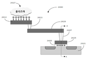
파트 IPart I
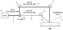
적층 반도체 기판 내의 전자들이 펌프 광 소스와 합 주파수 생성(Sum Frequency Generation: SFG)(예를 들어, 일반적으로 SHG)의 목적을 위해 상이한 파워 특성을 가지고 있는 프로브 광 소스 각각에 의해 다양하게, 여기되는(excited), SHG 계측 툴(SHG metrology tool)이 설명된다. 이러한 접근에 대하여, 계측 특성화 툴은 "프로브(probe)" 광 소스로서 작동하는 짧은 또는 매우 짧은 펄스 레이저(예를 들어, 펨토초 고체 레이저)와 함께, 적층 반도체 소자 템플릿 내의 헤테로 계면(들)을 가로질러 포텐셜 차이를 유도하기 위한 "펌프(pump)"로서 작동하는 "추가적인" 통합된 광 소스(예를 들어, UV 플래쉬 램프 또는 레이저)가 제공된다. 단일 레이저 SHG 또는 듀얼 또는 다중 레이저 SFG 시스템으로부터 구분되는 바와 같이, 서로 일제히 또는 결합(다양한 시간-옵셋 및/또는 추가로 설명되는 바와 같은 가변적인 펌프 에너지 방법들을 통해)에서 다른 목적들을 위해 2개의 상이한 소스를 사용함으로써 활용성이 유도된다. Electrons in the stacked semiconductor substrate are variously excited by a pump light source and each probe light source having different power characteristics for the purpose of Sum Frequency Generation (SFG) (e.g., usually SHG). (excited), the SHG metrology tool is described. For this approach, metrology characterization tools traverse heterointerface(s) within a stacked semiconductor device template, with a short or very short pulsed laser (e.g., femtosecond solid state laser) acting as a "probe" light source. An “additional” integrated light source (eg, UV flash lamp or laser) is provided that acts as a “pump” to drive the potential difference. Two different for different purposes in combination or in combination with each other (via various time-offset and/or variable pump energy methods as further described), as distinguished from a single laser SHG or dual or multiple laser SFG system. Use of the source is derived.
하나의 방법에서, 상기 펌프는 일부 재료들의 총 특성화 시간이 감소되는 것을 가능하게 하기 위한 프리-여기하는(pre-exciting) 또는 프리-여기 광 소스(pre-excitation light source)로서 채용된다. 많은 이러한 실행에 있어서, 시간-의존성 전기장(time-dependent electric field)은 프로브/프로빙 레이저에 의해 1차적으로 생성되지는 않는다. 상기 방법의 한 변형에서, 상기 펌프는 전체 웨이퍼를 UV 플래쉬하기 위해 사용되고, 그 후에 래스터(raster)하기 위해 상기 프로브 레이저를 사용하거나 그렇지 않으면 전체 웨이퍼를 스캔하거나 포인트 당 최소 프로브 시간을 사용하면서 그것의 일부분을 스캔한다(예를 들어, 하드웨어만큼 빠른 스캐닝은 상기 레이저를 이동시킬 수 있다). 이러한 측면에서의 선택사항들은 웨이퍼 쉬프트에 의한 (스캔) 칼럼을 따라 단계별로 로-바이-로 스캐닝(row-by-row scanning)을 포함한다. 다른 접근은 웨이퍼 회전과 반지름을 따른 스캐닝을 채용할 수 있다. In one method, the pump is employed as a pre-exciting or pre-excitation light source to enable the total characterization time of some materials to be reduced. In many of these implementations, a time-dependent electric field is not primarily generated by the probe/probing laser. In one variant of the method, the pump is used to UV flash the entire wafer and then use the probe laser to raster or otherwise scan the entire wafer or use its minimum probe time per point. Scan a portion (eg, scanning as fast as hardware can move the laser). Options in this respect include row-by-row scanning step by step along the (scan) column by wafer shift. Another approach could employ wafer rotation and scanning along the radius.
다른 변형에서, 상기 펌프는 샘플 사이트에서 상기 재료 계면의 빠른 차지 업(charge up)을 가능하게 하고, 그것을 "웨이퍼 계측 기술들" 명칭으로 2014년 4월 17일에 출원된 미국 가출원 제61/980,860호, "차지 붕괴 측정 시스템 및 방법" 제목으로 섹션 II로서 언급된 일부에서 추가적으로 기술되어질 빠른-블로킹 및/또는 광학적 딜레이 방법과 연계하여 프로브로 차징된 계면의 붕괴의 관찰이 이어진다. 관계없이, 다양한 실시예들에서, 프리-여기를 위한 펌프 사용의 의도는 계면에 영향을 줄 만큼 충분한 양으로 차지 캐리어들을 예를 들어 유전체 내로 주입하는 것이다. In another variation, the pump enables rapid charge up of the material interface at the sample site, which is referred to in the US Provisional Application 61/980,860, filed April 17, 2014 under the designation "Wafer Metrology Technologies". The observation of the collapse of the probe-charged interface follows in conjunction with the fast-blocking and/or optical delay method, which will be further described in the part referred to as section II under the heading "Charge Collapse Measurement Systems and Methods". Regardless, in various embodiments, the intention of using a pump for pre-excitation is to inject charge carriers into the dielectric, for example, in an amount sufficient to affect the interface.
다른 방법에서, 상기 펌프 레이저는 샘플 자리에 상기 프로브 레이저에 의해 이미 생성되고 있는 SHG 신호에 영향을 주기 위해, 포스트-여기하는(post-exciting) 또는 포스트-여기 광 소스(post-excitation light source)로서 채용된다. 또 다른 방법은 프로브 프리-(probe pre-) 및 포스트- 펌프 레이저 에너지 인가(post-pump laser energy application)에 의해 생성된 SHG 신호의 비교/대조를 채용한다. 상기 샘플을 프로빙하고 펌핑에 앞서 상기 SHG 응답을 측정하고, 이후 상기 펌프 광 소스로부터의 방사를 인가함으로써, 상기 SHG 응답 프리-(response pre-) 및 포스트-펌프(post-pump)에의 차이점이 절연체 내의 트랩 밀도(trap density)와 같은 추가적인 재료 특성을 결정하기 위해 사용될 수 있다. In another method, the pump laser is a post-exciting or post-excitation light source to influence the SHG signal already being generated by the probe laser at the sample site. It is adopted as Another method employs comparison/contrast of the SHG signal generated by probe pre- and post-pump laser energy application. By probing the sample and measuring the SHG response prior to pumping, and then applying radiation from the pump light source, the difference between the SHG response pre- and post-pump is an insulator. It can be used to determine additional material properties such as trap density within.
여기서 논의되는 다양한 방법들에서, 시간 차이(예를 들어, 프로브 레이저 사용과 관련된 펌프 소스에 의한 프리- 및/또는 포스트-여기의 측면에서)가 재료 계면에 관한 추가의 정보를 명시하는 조사 곡선들(interrogation curves)을 전달하기 위해 채용된다.In the various methods discussed here, the time difference (e.g., in terms of pre- and/or post-excitation by the pump source associated with the probe laser use) is the irradiation curves that specify additional information about the material interface. (interrogation curves) are employed to convey.
다양한 방법들에서, 상기 펌프 및 프로브 소스들은 임계 주입 캐리어 에너지(threshold injection carrier energy)를 결정하기 위한 SHG 신호를 제공하기 위해 사용되는 조합과, 동시에 사용된다. 구체적으로, 프로브 레이저를 프로빙하는 동안에, 조정가능 펌프 레이저는 주파수에 있어서 램프-업(ramped-up)된다. 특정 주파수에서, SGH 신호는 변곡점(또는 불연속 영역)을 나타낸다. 상기 변곡점에서(또는 불연속 영역에서) 펌프 레이저 주파수에 대응하는 값은 임계 주입 캐리어 에너지와 연관될 수 있다. In various methods, the pump and probe sources are used concurrently with the combination used to provide the SHG signal to determine the threshold injection carrier energy. Specifically, while probing the probe laser, the adjustable pump laser is ramped-up in frequency. At certain frequencies, the SGH signal represents an inflection point (or discontinuous region). The value corresponding to the pump laser frequency at the inflection point (or in the discontinuous region) may be associated with the critical implant carrier energy.
펌프와 프로브 시스템의 다양한 실시예들은 특정한 하드웨어-기반의 유리한 가능성이 또한 제공한다. 펌프가 플래시 램프인 예에서, 관련성이 높은 비용 절감이 2-레이저 시스템들과 관련되어 성취될 수 있다. 플래시 램프로서 제공되든 혹은 제2 레이저로 제공되든지 간에, 너무 강한 조사는 절연체의 디그레이드하고 임계 평균 파워가 초과되면 심지어 기판을 디그레이드할 수 있기 때문에, 여기서 고려된 것과 같은 펌프와 프로브의 결합은 또한 조사되는 기판에 광학적 데미지를 줄 위험을 저감할 수 있다. 기판에 광학적 손상을 데미지를 야기하는 임계 평균 파워는 실험적 교정 연구에 의해 결정될 수 있다. Various embodiments of the pump and probe system also offer certain hardware-based advantageous possibilities. In the example where the pump is a flash lamp, relevant cost savings can be achieved in connection with two-laser systems. The combination of the pump and probe as considered here, whether provided as a flash lamp or as a second laser, can degrade the insulator and even the substrate if the critical average power is exceeded. In addition, it is possible to reduce the risk of optical damage to the irradiated substrate. The critical average power causing optical damage to the substrate can be determined by experimental calibration studies.
주제의 하드웨어와 연계된 후자의 가능성을 이해하기 위해, 약간의 배경지식에 제공된다. 즉, 펌프와 프로브 에너지 두 가지만으로도 이러한 하드웨어를 가지고 SHG 신호를 만들어 낼 수 있다. 펌프와 프로브 소스들이 SGH 신호를 생성하기 위해 함께 작동할 필요는 없지만, 일반적으로 펌프가 매립된 계면 SHG를 적절히 구동할 피크 파워가 없기 때문에, 관련된 물질의 특성들은 주로 프로브에 의해 생성되는 SHG 크기로부터 주된 방법들 내에서 유도된다. 시간-의존적 SHG 강도 곡선들은 계면을 가로질러, 예를 들어 유전체와 기판 사이에서 차지 캐리어의 분포에 따라 변화할 것이다. 예를 들어 유전체와 반도체 기판 사이와 같이, 계면을 가로질러 캐리어의 주입을 위해 소요되는 시간은 샘플에 목표를 둔 평균적인 파워에 달려있다. 일부 실시예들에서, 프로브만으로도 유전체와 기판 사이의 계면을 가로지르는 캐리어의 주입을 가능하게 할 수 있다. 이러한 실시예들에서 평균적인 파워를 피크 파워와 구분할 수 없는 것 때문에, 물질의 광학적 데미지 임계값을 초과하지 않으면서 유전체와 기판 사이의 계면을 가로지르는 캐리어의 주입을 가능하게 하는 목표 평균 파워에 도달하는 데 소요되는 시간은 펌프와 프로브를 결합해서 사용하는 실시예들보다 더 클 수 있다. 높은 평균 파워이지만 낮은 피크 파워 광학적 소스를 프로빙 이전에 유전체와 기판 사이의 계면을 가로질러 캐리어를 주입하기 위해 펌프로서 사용함으로써, 증가된 평균 파워의 시간 절약이 언급된 평균 파워에서 높은 피크 파워가 유도되는 포텐셜 데미지 복잡화없이 얻어질 수 있다.In order to understand the latter possibility associated with the subject's hardware, some background information is provided. In other words, it is possible to generate SHG signals with such hardware using only the pump and probe energy. The pump and probe sources do not have to work together to generate the SGH signal, but since the pump typically does not have the peak power to properly drive the buried interface SHG, the properties of the material involved are mainly from the SHG size produced by the probe. It is derived within the main methods. Time-dependent SHG intensity curves will vary with the distribution of charge carriers across the interface, for example between the dielectric and the substrate. The time it takes for the implantation of a carrier across the interface, for example between a dielectric and a semiconductor substrate, depends on the average power targeted for the sample. In some embodiments, the probe alone may enable injection of a carrier across the interface between the dielectric and the substrate. Due to the inability to distinguish the average power from the peak power in these embodiments, a target average power is reached that allows the injection of carriers across the interface between the dielectric and the substrate without exceeding the optical damage threshold of the material. The time required to do this may be greater than in embodiments in which a pump and a probe are combined. By using a high average power but low peak power optical source as a pump to inject carriers across the interface between the dielectric and substrate prior to probing, a time saving of increased average power results in a high peak power at the stated average power. It can be obtained without complicating potential damage.
따라서, 펌프에 비교되는 바와 같이, 주된 프로브는 전형적으로 낮은 평균 힘을 가진 더 높은 피크 파워 소스이다. 다르게 표현하면, 프로브 레이저는 전형적으로 상대적으로 매우 약하다. 일 양태에서, 그것은 초기의 시간-독립적 신호를 만들어 내기 위해 기판 계면에 존재하는 본래의 전기장에 최소의 방해를 가능하게 한다. Thus, as compared to a pump, the dominant probe is typically a higher peak power source with a lower average force. In other words, probe lasers are typically relatively very weak. In one aspect, it allows minimal disturbance to the intrinsic electric field present at the substrate interface to generate an initial time-independent signal.
더 높은 평균 파워지만 낮은 피크 파워를 가지면서, 펌프는 물질 계면에서 또는 계면을 가로질러 에너지 레벨에서의 점프 업을 위해 차지 캐리어를 야기함으로써 전기장(E)을 유도한다. 상대적으로 높은 평균 파워 소스를 펌프로서 사용하고 모든 이용 가능한 전자들에게 적어도 절연체에 점프해 들어가기 충분한 에너지를 줌으로써 빠르게 계면을 "차징 업"함으로써, 높은 피크 파워(높은 SHG 전환율을 제공하는)이지만 낮은 평균 파워(짧은 펄스 기간과 이러한 펄스의 제한된 수 때문에)의 프로브 레이저가 표면이 시간-독립적인 SHG 신호 데이터를 제공하도록 빠르게 정보를 취득할 수 있는 상황이 생성된다. With higher average power but lower peak power, the pump induces an electric field E by causing charge carriers to jump up in energy levels at or across the material interface. High peak power (providing high SHG conversion) but low average by using a relatively high average power source as a pump and quickly "charging up" the interface by giving all available electrons at least enough energy to jump into the insulator. A situation is created in which a probe laser of power (due to the short pulse duration and limited number of these pulses) can quickly acquire information so that the surface provides time-independent SHG signal data.
따라서, 여기서 설명된 다양한 실시예들에서, 프로브 레이저가 전자들을 더 높은 에너지 레벨로 혹은 계면을 가로질러 이동시키기 위해 요구되는 시간 단축이 달성될 수 있고, 이는 안정된 상태의 SHG 신호 및/또는 차지 캐리어 시간 동적 측정의 더 빠른 평가를 가능하게 한다. 이 접근은 또한 SHG 프로브의 효과를 기판 계면에서의 전기장에 대한 그 자체의 영향으로부터 구분할 수 있게 해준다. 그것은 또한 프로브 빔으로부터 획득된 신호의 적어도 일부에 걸쳐 시간-독립적 SHG 데이터의 더 빠른 획득을 가능하게 해 줄 뿐 아니라, SHG 과정에서의 시간-의존성이 더 빨라지거나 무시되는 것을 가능하게 해준다. 마찬가지로, 다른 양태는 라인 툴 환경에서의 (더) 빠른 처리량뿐만 아니라, 계면 내로의 캐리어 주입(예를 들어, 반도체와 유전체 사이)을 위한 더 빠른 및/또는 더 정확한 임계 에너지의 결정을 가능하게 한다. 상황이 무엇이든지 간에, 제공되는 이용 가능한 시간 단축은 유리하게는 반도체 산업에서의 인-라인 계측 툴의 어떤 종류에 있어서 높은 처리량 테스팅을 가능하게 할 수 있다. 예시에 의해, 절연체 상의 10nm 실리콘 아래 25nm 매립된 산화물 층(10nm 소자 층/ 25nm BOX SOI)을 포함한 소자 상에 SHG 기술의 이전에 존재하는 적용을 사용하여 시간 의존 곡선을 만들어 내는 것은 포인트 당 6에서 12+ 초가 소요된다. 여기서 기술된 바와 같이 프리-여기를 사용하면서, 시간 의존은 물질과 펌프/프로브 파워를 적용하여, 1 초 이하에 생성될 수 있다. 이 진보는 10x+의 표면 영역이 라인 상에 이용 가능한 시간/웨이퍼가 주어진 웨이퍼 위에 커버될 수 있도록 하거나 혹은 시간의 10% 이내 범위에서 동일한 신뢰가 가능하게 할 것이다. 그리고 이런 종류의 숫자들이 물질, 층의 두께 그리고 특정 펌프/프로브 파워와 파장에 따라 변화하는 동안에, 그들은 조사하고 있어야 한다. Thus, in various embodiments described herein, the shortening of the time required for the probe laser to move electrons to a higher energy level or across the interface can be achieved, which means that the SHG signal and/or charge carrier in a stable state It enables faster evaluation of time dynamic measurements. This approach also makes it possible to distinguish the effect of the SHG probe from its own effect on the electric field at the substrate interface. It also enables faster acquisition of time-independent SHG data over at least a portion of the signal acquired from the probe beam, as well as enabling the time-dependence in the SHG process to be faster or neglected. Likewise, other aspects enable faster and/or more accurate determination of critical energy for carrier injection into the interface (e.g. between semiconductor and dielectric) as well as (more) faster throughput in a line tool environment. . Whatever the situation, the reduction in available time provided can advantageously enable high throughput testing for some kind of in-line metrology tool in the semiconductor industry. By way of example, creating a time-dependent curve using a previously existing application of SHG technology on a device with a 25 nm buried oxide layer (10 nm device layer/25 nm BOX SOI) under 10 nm silicon on an insulator is at 6 per point. It takes 12+ seconds. Using pre-excitation as described herein, time dependence can be created in less than 1 second by applying the material and pump/probe power. This advance will allow a 10x+ surface area to be covered over a given wafer with the time/wafer available on the line, or the same reliability within 10% of the time. And while these kinds of numbers vary with material, layer thickness, and specific pump/probe power and wavelength, they should be investigating.
여기에서의 발명 실시예들은 위에서 기술된 접근들과 관련된 방법들 각각, 그 방법을 실행하기 위한 하드웨어, 하드웨어와 그것의 결과물 결합한 생성 시스템을 포함한다.Inventive embodiments herein include each of the methods associated with the approaches described above, hardware for executing the method, and a generation system that combines hardware and its products.
파트 IIPart II
지금까지, SHG-기반의 계측 툴의 제한된 채택만이 있었다. 이 사실은 검출된 계면 특성들 간의 구분을 하는 현존 시스템의 불가능에서 기인한다고 믿어진다. 즉, 현존 SHG 기술이 계면의 전기적으로 활성의 기형들의 위치와 존재를 결정하는 수단을 제공하는 반면, 그 방법들은 상대적 측정값에 의존하고 실질적으로 전기적으로 활성인 기형 종류들(예를 들어, 구리 대 본드 보이드와 같은 얻어진 오염물질들)의 타입들을 분석할 수 없고/없거나 검출된 오염물질들을 정량화할 수 없다. So far, there has been only limited adoption of SHG-based metrology tools. This fact is believed to stem from the inability of existing systems to make a distinction between detected interfacial properties. That is, while existing SHG technology provides a means to determine the location and presence of electrically active anomalies at the interface, those methods rely on relative measurements and substantially electrically active anomaly types (e.g., copper). Versus the resulting contaminants such as bond voids) cannot be analyzed and/or the detected contaminants cannot be quantified.
하지만, 본 시스템들과 방법들이 다양하게 그런 활동을 위해 요구되는 결정을 하기 위한 정량적 정보를 캡처하는 것을 가능하게 한다. 이런 시스템들과 방법들에 있어서, (펄스 레이저로 또는 플래쉬 램프 또는 다른 전자기적 에너지 소스 또는 광 소스 또는 다른 수단으로 특정한 자리에서) 웨이퍼 샘플을 광학적 전자기적 방사로 차징 한 후에, 복수의 측정들이 붕괴 기간을 제어하는 헤테로-계면과 연결된 관련된 일시적인 전기장 붕괴를 모니터링하도록 만들어진다.However, the present systems and methods make it possible to capture quantitative information to make the decisions required for such an activity in a variety of ways. In these systems and methods, after charging the wafer sample with optical electromagnetic radiation (at a specific location with a pulse laser or flash lamp or other electromagnetic energy source or light source or other means), multiple measurements collapse. It is made to monitor the transient electric field decay associated with the hetero-interface controlling the duration.
다중의 포인트들로 특징지어지고 생성된 붕괴 곡선 데이터를 이용하여, 결함이 있는 타입 또는 오염물질(들)의 구별 및/또는 정량화가 가능하도록 샘플 자리에 있는 기형과 문제의 분광학적 변수가 결정될 수 있다. 모두에 있어서, 붕괴 의존적 데이터는 수집되고 차지 캐리어 수명, 만약 오염요소가 감지되면 종 구분을 위해 및/또는 만약 감지되면 오염물질의 정량화를 위해, 트랩 에너지 및/또는 트랩된 차지 밀도가 결함들 및 오염물질들이 서로 구별될 수 있도록 결정될 수 있는, 시스템을 제공하기 위해 사용된다.Using the decay curve data generated and characterized by multiple points, the deformities in the sample site and the spectroscopic parameters in question can be determined to allow the identification and/or quantification of the defective type or contaminant(s). . In both cases, decay dependent data are collected and the charge carrier lifetime, if a contaminant is detected for species identification and/or if detected, for quantification of the contaminant, the trap energy and/or the trapped charge density is determined by the defects and It is used to provide a system that can be determined so that contaminants can be distinguished from each other.
이러한 활동은 전체 웨이퍼 또는 다른 물질 샘플 또는 그것의 영역을 스캔하기 위해 전형적으로 반복되는 선택된 방법론과 사이트-바이-사이트 기초 상에서 결정된다. 이러한 결정을 가능하게 하기 위해 요구되는 컴퓨터 프로세싱에 있어서, 그것은 "실시간으로" (즉 결과를 출력하는 데에 어떠한 실질적인 딜레이없이 스캐닝하는 동안) 발생하거나 또는 포스트-프로세싱을 통해 일어날 수 있다. 그러나, 다양한 실시예들에서, 제어 소프트웨어는 아래에 설명되는 바와 같이 방법론 당 주 데이터를 얻기 위한 정확한 시스템 타이밍을 제공하기 위해 지연없이 운영될 수 있다. This activity is determined on a site-by-site basis with a selected methodology typically repeated to scan an entire wafer or sample of other material or an area thereof. For the computer processing required to make this determination possible, it can occur "in real time" (ie, while scanning without any substantial delay in outputting the result) or through post-processing. However, in various embodiments, the control software can be operated without delay to provide accurate system timing to obtain main data per methodology as described below.
선택적으로, 샘플 물질 차지-업은 SHG 신호 생성과 연계하여 모니터링된다. 이러한 경우에, 이 신호를 통해 얻어진 정보는 물질 분석과 결정을 하는 데 채용될 수 있다. Optionally, sample material charge-up is monitored in conjunction with SHG signal generation. In these cases, the information obtained through this signal can be employed to make material analysis and decisions.
어떤 경우, 시스템 실시예들은 102초 범위에서 피코초(10-12초) 범위에서 작동하는 빠른 셔터와 함께 초단파 펄스 레이저를 포함할 수 있다. 이러한 시스템들은 복수의 짧은 블로킹 간격의 도입 후에 샘플 자리에서 박막 물질의 표면 및 매립된 계면들로부터 SHG 신호 생성을 모니터하기 위해 사용될 수 있다. 이런 간격들은 흥미로운 필드 붕괴를 모니터하기 위해 시간이 정해질 수 있다.In some cases, system embodiments may include an ultrashort pulsed laser with a fast shutter operating in the picosecond (10 -12 seconds) range in the 10 2 second range. These systems can be used to monitor SHG signal generation from the surface and buried interfaces of the thin film material at the sample site after introduction of a plurality of short blocking intervals. These intervals can be timed to monitor interesting field collapse.
본 시스템은 또한 광학적 라인 딜레이를 포함할 수 있다. 딜레이 라인은, 특히 만일 분산 보상과 편광 제어 광학과 결합된다면, 섬유-기반 소자일 수 있다. 대안적으로, 딜레이 라인은 미러-기반이 될 수 있고 MacDonald에 의한 미국 특허 제147,799호, Bishop 등에 의한 제6,356,377호 또는 Wu 등에 의한 제6,751,374호에서의 예들을 닮을 수 있다. 어떤 경우에는, 피코초(10-12초)에서 펨토초(10-15초)까지, 그리고 가능하다면 아토초(10-18초)까지의 범위 내의 물질의 레이저 정보취득을 허용하기 위해 시스템 내에서 딜레이가 사용된다. 이러한 정보취득은 단일 붕괴 곡선을 따라 많은 차지 붕괴-의존적 데이터 포인트들을 검출하는데 유용하다.The system may also include optical line delay. The delay line can be a fiber-based device, especially if combined with dispersion compensation and polarization control optics. Alternatively, the delay line may be mirror-based and resemble the examples in US Pat. No. 147,799 to MacDonald, 6,356,377 to Bishop et al., or 6,751,374 to Wu et al. In some cases, there is a delay within the system to allow laser acquisition of materials in the range of picoseconds (10 -12 seconds) to femtoseconds (10 -15 seconds), and possibly attoseconds (10 -18 seconds). Used. This acquisition is useful for detecting many charge decay-dependent data points along a single decay curve.
본 방법은 연속적인 차지-업 단계들 후에 획득된 붕괴 데이터 포인트들을 위한 SHG 신호를 측정하는 것을 포함하는 것을 포함한다. 추가적으로 SHG 신호를 얻기 위한 조건들은 각각의 차지-업 단계에서 다를 수 있다. 이 방법에서, 다중 데이터 포인트들(적어도 2개의 그러나 전형적으로는 3개 또는 그 이상)이 서로 관련되고 단일의 복합 붕괴 곡선으로서 표현될 수 있다. 또 다른 방법은 하나의 차징 단계 후에 최소한으로 방해받는(즉, SHG 신호를 생성하는데 사용되는 광은 물질을 현저히 리차지하지 않음) SHG 신호 정보취득 단계들을 사용한다. The method includes measuring the SHG signal for decay data points acquired after successive charge-up steps. Additionally, conditions for obtaining the SHG signal may be different in each charge-up step. In this way, multiple data points (at least two but typically three or more) are related to each other and can be represented as a single complex decay curve. Another method uses SHG signal acquisition steps that are minimally disturbed (ie, the light used to generate the SHG signal does not significantly recharge the material) after one charging step.
일시적인 차지 붕괴를 결정하기 위한 또 다른 방법은 샘플 물질(보다 정확하게는, 광학적 방사에 의해 차지된 그것의 구조물들)로부터의 디스차지 전류를 측정하는 것을 포함한다. 이 신호의 시간 의존성은 마치 SHG 감지가 채용된 것과 동일한 방법으로 처리될 수 있다. 추가로, 위와 같이, 이러한 감지는 하나의 붕괴 간격의 범위 내에서 및/또는 그 중의 복수의 주어진 레벨로의 따르는 차지 동안에 행해질 수 있다. 어떤 경우, 이러한 사용을 위한 전극-구체적 하드웨어는 아래에 상세히 되어 있다.Another method for determining the transient charge decay involves measuring the discharge current from the sample material (more precisely, its structures occupied by optical radiation). The time dependence of this signal can be handled in the same way as if SHG detection was employed. Additionally, as above, this detection can be done within the range of one collapse interval and/or during subsequent charging to a plurality of given levels therein. In some cases, electrode-specific hardware for this use is detailed below.
차지 또는 디스차지 레벨에 관해서, 차지 다이나믹이 표준 직선형 시간에서 또는 로그 시간 스케일에 대하여 지켜질 때, 이것은 분명한 포화도의 지점까지 취해질 수 있다. 위와 같이, 이것이 중요한 정보를 생산해 낼 수도 있기 때문에, 본 방법들은 선택적으로 차징 운동을 관찰하고, 기록하고 분석한다.Regarding the charge or discharge level, when the charge dynamic is observed at a standard linear time or against a log time scale, this can be taken up to the point of obvious saturation. As above, since this may produce important information, these methods selectively observe, record and analyze charging movements.
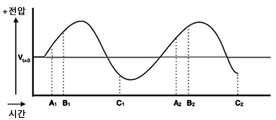
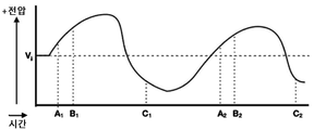
연속적인 차지/조사 단계들에 있어서, 만약 샘플의 초기 차지 상태가 측정되고 포화 레벨이 초기 차지 상태로부터 멀지 않다면, 시스템은 더 많은 또는 이어지는 특성화를 생략할 수 있다. 이 맥락에서, "멀지 않은"으로 간주되는 것은 샘플링의 주어진 시간을 위해 주된 본 툴이 사용될 때를 배움으로써 결정되는 초기 차지 상태에 대한 차지 증가의 약 1%에서 약 10%를 의미할 수 있다. For successive charge/irradiation steps, if the initial charge state of the sample is measured and the saturation level is not far from the initial charge state, the system may omit further or subsequent characterization. In this context, to be considered "not far" can mean about 1% to about 10% of the charge increase for the initial charge state as determined by learning when the main present tool is used for a given time of sampling.
다르게 표현하면, 소위 "포화"는 상대적인 용어이다. 선형 시간 스케일을 사용하면서, 물질은 아주 빠르게 포화되는 것으로 나타날 것이다. 그러나 만약 차징과 연관된 SHG 신호 강도가 10-100초의 로그 스케일로 관찰된다면, 포화의 후반부가 다른 시간 상수로 발생하고 상대적으로 더 점진적이거나 시간 소모적이라는 것이 관찰될 수 있다. 따라서, 여기서 제시된 방법론의 예시들이 포화도까지의 차징을 논의하지만, 딜레이와 다른 타이밍들은 분명한 포화에 대하여 발생하는 것으로 간주될 수 있다. 100%의 포화를 위해 모든 시간을 기다리는 것보다는, 이것이 도달하기에는 불필요하게 시간 소모적으로 보이기 때문에, 대신에, 완전한 포화를 위해 얼마나 긴 시간이 소모되는 지와 상관없이, 도구는 분명한 포화에 도달할 때까지 소모되는 시간까지 또는 중요한 파라미터들을 끌어낼 수 있는 시간까지 딜레이할 수 있다. In other words, so-called "saturation" is a relative term. Using a linear time scale, the material will appear to saturate very quickly. However, if the SHG signal strength associated with charging is observed on a log scale of 10 -100 seconds, it can be observed that the second half of saturation occurs with a different time constant and is relatively more gradual or time consuming. Thus, while examples of the methodology presented here discuss charging to saturation, delays and other timings can be considered to occur for apparent saturation. Rather than waiting all the time for 100% saturation, since this seems unnecessarily time consuming to reach, instead, no matter how long it takes for full saturation, the tool will be able to reach the apparent saturation. It can be delayed until the time wasted up to or until the time to pull out important parameters.
추가로, 포화를 향한 차지-업의 양 또는 정도를 모니터링 할 때, 본 방법들과 시스템들은 여전히 유의미한 붕괴 곡선 정보를 만들어 내면서, 차지를 가지고 또는 (위에 설명된 바와 같은) 포화도 이하의 리-차징 레벨을 가지고 작동할 수 있다는 것이 이해되어야 한다. 그러나 이러한 측정 없이는, 대략의 포화가 알려진 파라미터 일 때(예를 들어 주어진 물질을 가지고 본 툴의 경험에 의해), 포화까지의 차지는 타겟 레벨로서 채용된다.Additionally, when monitoring the amount or extent of charge-up towards saturation, the methods and systems still produce significant decay curve information, while re-charging with charge or sub-saturation (as described above). It should be understood that you can operate with levels. Without this measurement, however, when approximate saturation is a known parameter (eg by experience of this tool with a given material), the charge to saturation is employed as the target level.
테스트되는 샘플을 가로지르는 DC 바이어스를 도입하는 것은 또한 물질의 분석에 도움이 될 수 있다. DC 바이어스를 적극적으로 사용하는 것은 광-유도 전압이 어떤 효과를 갖기 전에 계면에서 초기 차지 분배를 변화시킨다. 그렇게 하기 위해서, 테스트되는 샘플은 샘플 탑 표면 프로브를 사용하여 샘플을 가로지르는 DC 바이어싱을 위한 그라운드로서 사용될 수 있는 전도성 척(chuck) 상에 실장될 수 있다. 유도 전압 바이어스를 도입하는 다른 수단들은 또한 "웨이퍼 계측 기술들"이라는 명칭으로 2014년 4월 17에 출원된 미국 가출원 제61/980,860호의 섹션 IV 제목 "필드-바이어스 SHG 계측"의 일부분에서 더 설명되듯이, 표면 프로브의 사용 없이 가능하다.Introducing a DC bias across the sample being tested can also aid in the analysis of the material. Active use of DC bias changes the initial charge distribution at the interface before the light-induced voltage has any effect. To do so, the sample to be tested can be mounted on a conductive chuck that can be used as a ground for DC biasing across the sample using a sample top surface probe. Other means of introducing induced voltage bias are also described further in section IV title “Field-bias SHG measurement” of US Provisional Application No. 61/980,860 filed April 17, 2014 under the designation “Wafer Measurement Technologies”. This is possible without the use of a surface probe.
또한 본 시스템은 차지 붕괴 결정을 위한 블로킹-타입 분석에 포함된 주된 레이저에 더해서, 2차적인 광 소스를 이용할 수 있다. 이러한 한 세트의 소스들은 "웨이퍼 계측 기술들"이라는 명칭으로 2014년 4월 17에 출원된 미국 가출원 제61/980,860호의 섹션 I 제목 "펌프 및 프로브 타입 SHG 계측"의 부분에서 더 기술되듯이, 광 펌프/프로브 결합으로서 채용될 수 있다. The system can also use a secondary light source in addition to the main laser included in the blocking-type analysis for charge decay determination. One such set of sources is optical, as further described in the section I title “Pump and Probe Type SHG Metrology” of US Provisional Application No. 61/980,860, filed April 17, 2014 under the designation “Wafer Metrology Technologies”. It can be employed as a pump/probe combination.
여기서 언급된 모든 본 발명의 실시예들은 여기서 단독으로 또는 구성요소들 또는 참조된 출원중인 특허출원, 방법론을 실행하기 위한 하드웨어, 하드웨어와 그것의 결과물(공정에 의한 결과물을 포함하여)을 결합한 생성 시스템들의 특징들과 결합되어서 여기서 기술된 접근들과 관련된 방법론 각각을 포함한다.All of the embodiments of the present invention mentioned herein are here alone or components or referenced pending patent applications, hardware for executing the methodology, and generation systems combining hardware and its products (including those by process). It includes each of the methodologies related to the approaches described herein, combined with the features of
파트part III III
다양한 필드-바이어스(예를 들어, 용량성 결합 및/또는 변화 자기장과 함께, 자기장 바이어스, DC 바이어스 및/또는 AC 필드 단독으로 유도된 전압 바이어스) SHG-기반의 시스템들과 사용되는 그들의 방법들이 기술된다. 이것들은 차례로 다루어진다. 그들은 독립적으로 및/또는 결합된 시스템으로 사용될 수 있다. 여기서 기술된 다양한 실시예들은 위에 기술된 접근들, 방법론을 실행하기 위한 하드웨어, 하드웨어와 그것의 결과물(공정에 의한 결과물을 포함)을 결합한 생성 시스템들과 관련된 방법론 각각을 포함한다.Various field-bias (e.g., magnetic field bias, DC bias and/or voltage bias induced by AC field alone, with capacitive coupling and/or changing magnetic field) SHG-based systems and their methods used are described. do. These are dealt with in turn. They can be used independently and/or as a combined system. The various embodiments described herein include each of the approaches described above, hardware for implementing the methodology, and methodologies associated with generation systems that combine hardware and its products (including those by process).
자기장 바이어스Magnetic field bias
샘플에 적용된 정지된 또는 변화하는 자기장은 물질의 2차 광학적 민감성 텐서(tensor)가 변화하도록 야기할 것이다. 따라서, 자기장은 샘플로부터의 SHG 신호를 최적값으로 증가시키기 위해 사용될 수 있었다. 더욱이, 변화하는 자기장은 아래 더 기술되어지는 바와 같이 바이어스를 유도하기 위해 사용될 수 있다.A stationary or changing magnetic field applied to the sample will cause the material's secondary optical sensitivity tensor to change. Thus, the magnetic field could be used to increase the SHG signal from the sample to an optimum value. Moreover, a varying magnetic field can be used to induce bias as described further below.
DC 접촉 DC contact 프로브를Probe 제거하기 위한 유도 전압 바이어스 Induced voltage bias to eliminate
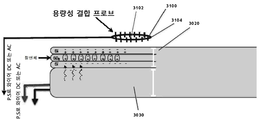
시스템들과 방법들은 정보 취득된 표면에의 대응하는 또는 통합된 유도 전압 필드를 만들어 내기 위해, 프로브 레이저의 펄스 및/또는 AC의 전압, 변화하거나 진동하는 샘플에 인가된 바이어스의 미리 정해진 크기를 가진 검출기의 이득을 동기화시키는 시스템 내의 접촉 바이어스 프로브의 사용없이 그것의 계면을 가로질러 별도의 전기장을 받는 적층 반도체 물질의 SHG 반응을 특성화하기 위해 기술된다. Systems and methods have a predetermined magnitude of the pulse of the probe laser and/or the voltage of AC, and the bias applied to the changing or vibrating sample, to create a corresponding or integrated induced voltage field on the information acquired surface. It is described to characterize the SHG response of a layered semiconductor material subjected to a separate electric field across its interface without the use of a contact bias probe in the system to synchronize the gain of the detector.
본 하드웨어는 접촉없이 샘플의 "소자" 표면에서 또는 표면을 따라 전압을 유도하는(예를 들어, 유도하도록 구성된 요소) 수단과 함께, "웨이퍼 계측 기술들"이라는 명칭으로 2014년 4월 17에 출원된 미국 가출원 제61/980,860호의 섹션 II 제목 "차지 붕괴 측정 시스템 및 방법"의 부분에서 더 기술되듯이, SHG 장치를 포함한다. 이러한 수단 또는 요소는 배면 접촉 프로브 또는 이러한 척과 연통하면서 파워 소스에 연결된 용량성 결합 프로브들을 포함하면서 또는 그것의 여러 층의 계면을 가로질러 외부 전압 필드를 유도하는 목적을 위해, 변화하는 자기장을 샘플에 적용함으로써, 프로브 또는 전도성 있는 척과의 배면 접촉을 통한 것일 수 있다.The present hardware was filed on April 17, 2014 under the name "Wafer Metrology Technologies", with means of inducing (eg, an element configured to induce) a voltage at or along the "element" surface of the sample without contact. US Provisional Application No. 61/980,860, section II titled "Charge Collapse Measurement Systems and Methods", includes SHG devices. Such a means or element includes a back contact probe or capacitively coupled probes connected to a power source in communication with such a chuck, or for the purpose of inducing an external voltage field across the interfaces of several layers thereof, by applying a varying magnetic field to the sample. By application, it may be through back contact with a probe or a conductive chuck.
변화하는 파형(선택적으로 AC) 파워 서플라이(위의 임의의 접근을 통해)에 의해 생성된 일시적인 전기장은 다층의 반도체 물질의 계면을 가로질러 전기장을 유도할 수 있다. 전압과 물질 계면 전기장 사이의 관계는 전송 기능에 의해 모델화될 수 있거나 그렇지 않다면 다양한(용량성의 또는 다른) 외적 영향들을 설명함으로써 만들어질 수 있다. 이 함수의 결과물은, AC(또는 다른) 전류의 특정 크기와 주파수가 주어진다면, 계면에서의 전기장의 크기의 지속적인 거의-즉각적인 값을 위한 테스팅 포인트의 SHG 특성화를 위해, 레이저 셔터 및/또는 포톤 카운터를 동시에 유발하기 위한 타이밍 큐로 사용될 수 있다. 이와 같이, 시스템은 접촉 전기적 프로브를 통해 탑측(즉, 기판의 소자층에서)에 인가되는 일정한(DC) 전압을 시뮬레이트할 수 있다. The transient electric field generated by the changing waveform (optionally AC) power supply (via any of the above approaches) can induce an electric field across the interface of the multilayer semiconductor material. The relationship between the voltage and the material interfacial electric field can be modeled by the transmission function or otherwise made by accounting for various (capacitive or other) external influences. The result of this function is a laser shutter and/or photon counter for SHG characterization of the testing point for a continuous near-instant value of the magnitude of the electric field at the interface, given a specific magnitude and frequency of the AC (or other) current. It can be used as a timing cue to trigger simultaneously. As such, the system can simulate a constant (DC) voltage applied to the top side (ie, in the device layer of the substrate) through the contact electrical probe.
AC의 샘플의 배면으로의 직접적인 인가를 가지고, 시스템은 "중성" 또는 그라운드 상태에서의 척과 그리고 평형상태 잠재력에서 벌크와 시작한다. 그리고 나서, 교류의 바이어스가 척에 인가되고, 이는 벌크 또는 다층의 반도체 물질의 기판 층에 있다. 소자 층은 직접 전도체와 연결되지 않고, 묻힌 산화물 층에 의해 벌크로부터 분리되기 때문에, 전위 필드 또는 전압이 장치와 벌크 층들 사이에서 생성(즉, 유도)될 것이다.With direct application of AC to the back of the sample, the system starts with the chuck in a "neutral" or ground state and the bulk at the equilibrium potential. Then, a bias of alternating current is applied to the chuck, which is in the substrate layer of bulk or multilayer semiconductor material. Since the device layer is not directly connected to the conductor and is separated from the bulk by the buried oxide layer, a potential field or voltage will be created (ie induced) between the device and the bulk layers.
대안적으로, 샘플의 위쪽을 터치하지 않으면서도 가까이에 있는(약 1 내지 약 2mm 내) 용량성 결합 프로브(들)이 사용될 수 있다. 경로를 통해 통과하는 입사 레이저를 위한 그리고 샘플로부터 이쪽을 통해서 지나가는 SHG 빔을 위한 작은 홀을 가지고 맴돌면서, 이 측면에서 선호되는 접근은 전체 웨이퍼를 덮도록(그러나 터치없이) 사이즈화된 플레이트일 수 있다. Alternatively, capacitive coupling probe(s) in close proximity (within about 1 to about 2 mm) without touching the top of the sample can be used. Hovering with a small hole for the incident laser passing through the path and for the SHG beam passing through it from the sample, the preferred approach in this aspect could be a plate sized to cover the entire wafer (but without touch). have.
일부 실시예들에서, 비접촉성 전극은 MEMS 기술을 사용해서 실행될 수 있다. 예를 들어, 일 실시예에서, Si 웨이퍼는 양쪽 면 모두에서 산화될 수 있다. 나선형의 또는 격자모양의 전극은 그 후 웨이퍼의 한 개 이상의 위치에 침전에 의해 위치될 수 있다. 산화물질은 그런 위치들에서 웨이퍼의 배면으로부터 제거될 수 있다. 이러한 실시예에서 근거리 필드 유도성 커플링을 통해 전극에 적용되는 전자기장은 유도적으로 웨이퍼를 바이어스할 수 있다. 외부 전기 전류에 의해 만들어지는 자기장은 침전된 전극 내의 전류를 유도함으로써 웨이퍼를 가로질러 전기적 전류를 생성하기 위해 사용될 수 있다.In some embodiments, the contactless electrode may be implemented using MEMS technology. For example, in one embodiment, the Si wafer may be oxidized on both sides. Spiral or lattice-shaped electrodes can then be placed by sedimentation at one or more locations on the wafer. Oxides can be removed from the back side of the wafer at such locations. In this embodiment, the electromagnetic field applied to the electrode through the near field inductive coupling may inductively bias the wafer. The magnetic field created by the external electric current can be used to generate an electric current across the wafer by inducing a current in the deposited electrode.
어떤 경우에는, 예를 들어 "웨이퍼 계측 기술들"이라는 명칭으로 2014년 4월 17에 출원된 미국 가출원 제61/980,860호의 섹션 I 제목 "펌프 및 프로브 타입 SHG 계측"의 일부분에서 더 설명되듯이, SHG 방법이 샘플의 정보를 취득하기 위해 사용된다. 같은 것이 아래 논의되는 다른 실시예들과 관련해서도 사실이다. In some cases, for example, as further explained in part of the section I title “Pump and Probe Type SHG Metrology” of U.S. Provisional Application No. 61/980,860 filed April 17, 2014 under the designation “Wafer Metrology Technologies”, The SHG method is used to obtain sample information. The same is true with respect to the other embodiments discussed below.
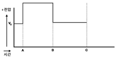
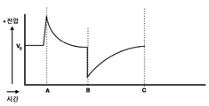
관계없이, 본 실시예들에서, 계면에 가로질러 전압의 함수로서 SHG를 모니터링하는 것이 바람직하기 때문에, SHG 신호는 파워 서플라이와 동기화될 것이다. 이 동기화는 SHG 신호 생성과 SHG 신호 처리 소프트웨어를 위해 사용되는 레이저(들)을 제어함으로써 또는 전압 변화와 맞추어 SHG 신호 처리 소프트웨어만을 제어함으로써 달성될 수 있다. 척의 전압 또한 제어될 수 있다. Regardless, in these embodiments, since it is desirable to monitor the SHG as a function of voltage across the interface, the SHG signal will be synchronized with the power supply. This synchronization can be achieved by controlling the laser(s) used for SHG signal generation and SHG signal processing software, or by controlling only the SHG signal processing software to match voltage changes. The voltage of the chuck can also be controlled.
이 동기화의 이점은 웨이퍼의 앞 표면상의 접촉 전압 바이어스 프로브를 사용하지 않고, DC 바이어스된 SHG 측정과 유사할 전압에 기반을 둔 SHG 측정이 성취될 수 있다는 것이다. DC 바이어스를 적용하는 대신, 시스템은 전압 사이클 상의 개별적 포인트들에 있는 SHG 데이터를 수집하기 위해, SHG 측정 및/또는 생산과 동시에 발생되는 AC 바이어스를 사용할 것이다. AC 바이어스는 근거리 필드 유도성 결합을 사용하여 또는 샘플의 용량 결합을 통해 적용될 수 있다. 바이어싱 기술로 수집된 SHG 데이터는 DC 바이어스된 SHG와 동일한 물질 특성 정보를 만들어낼 것이다. The advantage of this synchronization is that without the use of a contact voltage bias probe on the front surface of the wafer, voltage-based SHG measurements can be achieved that will be similar to DC biased SHG measurements. Instead of applying a DC bias, the system will use an AC bias generated concurrently with SHG measurement and/or production to collect SHG data at individual points on the voltage cycle. AC bias can be applied using near field inductive coupling or via capacitive coupling of the sample. SHG data collected by biasing technology will yield the same material property information as DC biased SHG.
노이즈를 최소화하고 계면을 가로지르는 전압의 함수로서 SHG 강도의 통계적으로 관련된 지표(들)을 얻기 위해, 많은 포톤 카운팅 윈도우가 아래에 추가로 설명되는 바와 같이 바람직할 수 있다. In order to minimize noise and obtain a statistically relevant indicator(s) of SHG intensity as a function of voltage across the interface, many photon counting windows may be desirable, as described further below.
계면 누설 특성화를 위한 유도 전압 바이어스Induced voltage bias for characterizing interface leakage
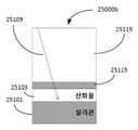
위와 같은 적층 반도체 물질에 인가되는 SHG와 전압 변화(교류적인, 가변적인 및/또는 펄스 전압 또는 전류 신호 또는 샘플의 소자 층에서의 전압 변화를 유도하는 방식을 자기장을 변화시키는 소자와 같은)를 이용해서, 시스템들과 방법들이 계면의 누출 전류 및/또는 적층 재료들(예를 들어, 반도체)의 층들 사이의 캐리어 방사 에너지를 특성화하기 위해 기술된다. Using the SHG and voltage change (such as a device that changes the magnetic field, a method that induces a change in voltage at the device layer of the sample or an alternating, variable and/or pulsed voltage or current signal) applied to the above stacked semiconductor material. Thus, systems and methods are described to characterize the leakage current at the interface and/or the carrier radiation energy between layers of stacked materials (eg, semiconductor).
교류의, 가변적인 또는 펄스 전압이 적층 반도체 물질에 인가되는 동안에 또는 그 직후에, 적층 반도체/유전체 구조를 향한 펄스는 레이저에 의해 생성되는 광학적 펄스로부터의 SHG 반응을 측정함으로써, 계면 누설 전류 및/또는 층들 사이의 캐리어 주입 에너지가 특성화될 수 있다. 일부 실시예들에서, 유도 전압의 붕괴의 시간 상수의 함수로서 계면으로부터의 SHG 신호의 시간변화가 측정될 수 있다. 이것은 계면을 가로지르는 차지 캐리어 모빌리티에 관한 정보를 생산한다.During or immediately after an alternating, variable or pulsed voltage is applied to the layered semiconductor material, the pulses towards the layered semiconductor/dielectric structure are measured by measuring the SHG response from the optical pulses generated by the laser, thereby measuring the interfacial leakage current and/or Alternatively, the carrier injection energy between the layers can be characterized. In some embodiments, the time change of the SHG signal from the interface may be measured as a function of the time constant of decay of the induced voltage. This produces information about the charge carrier mobility across the interface.
임계 Critical 캐리어carrier 주입 에너지 Injected energy 특징화를Characterization 위한 유도 전압 바이어스 For induced voltage bias
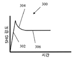
광 유도 차지 캐리어의 적층 반도체 물질 내의 유전체 내로의 주입을 위한 에너지 임계를 결정하기 위해, 조정가능 파장 레이저 여기를 사용하는 대신, 샘플 소자층에 있는 변화된 전기장과 연계되어 적용된 SHG 측정을 위한 시스템들과 방법들이 설명된다. 보다 구체적으로, 광 유도 차지 캐리어의 유전체 내로의 주입에 필수적인 임계 에너지를 측정하기 위해, SHG 생성을 위해 그 물질을 실질적으로 단색광인 입사 광자 빔에 노출시킬 수 있고, 그리고 나서 SHG 반응이 중요한 변곡 또는 불연속 또는 이전 측정값으로부터의 기울기에 있어서의 급변을 가질 때까지 각 증가하는 전압 변화를 측정하면서, 노출된 적층 반도체 물질의 계면을 가로질러 증가하도록 전압을 변화시킬 수 있다. 기울기에서 이 변화는 최대값 또는 최소값(예를 들어, 국부 최대값 또는 최소값) 또는 커스프 또는 계단 함수 등이 될 수 있다. 이런 모든 과정들로 인한 순 차지 변화 전달은 제3 고조파 주입 전류의 기여들, 강한 전기장으로 인한 유전체로의 "포워드" 누설 전류 및 "백워드" 디스차지 누설 전류의 총합으로서 기술될 수 있다. 등식의 형태로 표현하면 다음과 같다: Instead of using tunable wavelength laser excitation to determine the energy threshold for the implantation of light-induced charge carriers into the dielectric in the stacked semiconductor material, systems for SHG measurements applied in conjunction with the varied electric field in the sample element layer and Methods are described. More specifically, in order to measure the critical energy necessary for the injection of the light-induced charge carrier into the dielectric, the material can be exposed to an incident photon beam that is substantially monochromatic light for SHG generation, and then the SHG response is an important inflection or The voltage can be varied to increase across the interface of the exposed stacked semiconductor material, measuring each increasing voltage change until there is a discontinuity or abrupt change in slope from a previous measurement. This change in slope can be a maximum or minimum value (eg, a local maximum or minimum value) or a cusp or step function, etc. The net charge change transfer due to all these processes can be described as the sum of the contributions of the third harmonic injection current, the "forward" leakage current and the "backward" discharge leakage current into the dielectric due to the strong electric field. Expressed in the form of an equation:
![]()
![]()
여기서 언급된 본 발명의 모든 실시예들은 단독으로 또는 참조된 출원중인 특허 출원들, 방법론을 시행하기 위한 하드웨어, 하드웨어와 그것의 결과물(공정에 의한 결과물을 포함)을 결합한 생성 시스템으로부터의 요소들과 특성들과 결합해서 또는 단독으로, 여기서 기술된 접근들과 관련된 방법론의 각각을 포함한다.All embodiments of the present invention referred to herein, alone or with referenced pending patent applications, hardware for implementing the methodology, elements from a generation system that combines hardware and its products (including those of the process) Includes each of the methodologies related to the approaches described herein, either alone or in combination with features.
여기에 개시된 시스템, 방법 및 장치는 각각 몇 가지 혁신적인 양태를 가지며, 그 중 하나가 여기에 개시된 바람직한 속성에 대해 단독으로 책임지지는 않는다. 다양한 예제 시스템 및 방법이 아래에 제공된다.Each of the systems, methods, and apparatus disclosed herein has several innovative aspects, one of which is not solely responsible for the desirable attributes disclosed herein. Various example systems and methods are provided below.
패턴화된 웨이퍼들의 평가(EVALUATION OF PATTERNED WAFERS)EVALUATION OF PATTERNED WAFERS
예제 1:Example 1:
샘플의 표면을 광학적으로 조사하기(optically interrogating) 위한 시스템으로서,As a system for optically interrogating the surface of a sample,
가변 에너지(variable energy)로 방사(radiation)를 방출하도록 구성되는 광원(optical source);An optical source configured to emit radiation with variable energy;
조사된 표면으로부터 상기 방사에 의해 제2 고조파 생성(SHG) 광을 검출하도록 구성되는 광학적 검출기(optical detector) - 상기 조사된 표면은 다수의 영역들을 가지는 패턴화된 구조(patterned structure)를 포함함 -; 및An optical detector configured to detect second harmonic generation (SHG) light by the radiation from the irradiated surface-the irradiated surface comprises a patterned structure having a plurality of regions- ; And
상이한 영역들에 대해 하기를 하도록 구성되는 제어 전자장치들(control electronics):Control electronics configured to do the following for different areas:
- 조사 조건 세트를 결정함;-Determining a set of investigation conditions;
- 상기 조사 조건 세트에 기초하여 제1 SHG 광 신호를 수신함;-Receiving a first SHG optical signal based on the set of irradiation conditions;
- 상기 영역에서 상기 검출된 SHG 광의 특성을 결정함;-Determining the characteristics of the detected SHG light in the region;
- 상기 조사 조건 세트들을 업데이트함; 및-Updating the survey condition sets; And
- 상기 업데이트된 조사 조건 세트에 기초하여 제2 SHG 광 신호를 수신함; 을 포함하는, 시스템.-Receiving a second SHG optical signal based on the updated set of irradiation conditions; Containing, system.
예제 2:Example 2:
예제 1에 있어서, In example 1,
상기 조사 조건 세트는 여기 편광 상태(excitation polarization state)를 포함하고, 상기 여기 편광 상태는 입력 광과 관련된 편광 상태를 포함하는, 시스템.Wherein the set of irradiation conditions includes an excitation polarization state, and the excitation polarization state includes a polarization state associated with the input light.
예제 3:Example 3:
예제 1 또는 2에 있어서, In Example 1 or 2,
상기 조사 조건 세트는 출력 편광 상태(output polarization state)를 포함하고, 상기 출력 편광 상태는 출력 신호와 관련된 편광 상태를 포함하는, 시스템.Wherein the set of irradiation conditions includes an output polarization state, and the output polarization state includes a polarization state associated with an output signal.
예제 4:Example 4:
예제 1 내지 3 중 어느 한 예제에 있어서, In any one of Examples 1 to 3,
상기 조사 조건 세트는 입사 면 및 패턴 배향 사이의 방위각(azimuthal angle)을 포함하는, 시스템.Wherein the set of irradiation conditions includes an azimuthal angle between an incident plane and a pattern orientation.
예제 5:Example 5:
예제 1 내지 4 중 어느 한 예제에 있어서, In any one of Examples 1 to 4,
상기 조사 조건 세트는:The set of irradiation conditions is:
여기 편광 상태(excitation polarization state) - 상기 여기 편광 상태는 입력 광과 관련된 편광 상태를 포함함 -,Excitation polarization state-the excited polarization state includes a polarization state related to the input light -,
출력 편광 상태(output polarization state) - 상기 출력 편광 상태는 출력 신호와 관련된 편광 상태를 포함함 -, 및Output polarization state-the output polarization state includes a polarization state associated with the output signal -, and
입사 면 및 패턴 배향 사이의 방위각(azimuthal angle)을 포함하는, 시스템.The system comprising an azimuthal angle between the incident plane and the pattern orientation.
예제 6:Example 6:
예제 4 또는 5에 있어서, In Example 4 or 5,
상기 조사된 표면은 상기 방위각을 선택하기 위해 회전 스테이지에 의해 포지션닝되는, 시스템.Wherein the irradiated surface is positioned by a rotating stage to select the azimuth angle.
예제 7:Example 7:
예제 4 내지 6 중 어느 한 예제에 있어서, In any one of Examples 4 to 6,
상기 조사 조건 세트를 결정하기 위해, 상기 제어 전자장치들은 상기 패턴의 구조를 기반으로 상기 방위각을 선택하도록 구성되는, 시스템.And the control electronics are configured to select the azimuth angle based on the structure of the pattern to determine the set of irradiation conditions.
예제 8:Example 8:
예제 4 내지 7 중 어느 한 예제에 있어서, In any one of Examples 4 to 7,
상기 조사 조건 세트를 결정하기 위해, 상기 제어 전자장치들은 상기 출력 신호가 증가되도록 상기 방위각을 선택하도록 구성되는, 시스템.Wherein to determine the set of irradiation conditions, the control electronics are configured to select the azimuth angle such that the output signal is increased.
예제 9:Example 9:
예제 4 내지 8 중 어느 한 예제에 있어서, In any one of Examples 4 to 8,
상기 조사 조건 세트를 업데이트하기 위해, 상기 제어 전자장치들은 상기 패턴 구조에 의해 감소된 음영(reduced shadowing)과 관련된 상기 방위각을 선택하도록 구성되는, 시스템.Wherein to update the set of irradiation conditions, the control electronics are configured to select the azimuth angle associated with reduced shadowing by the pattern structure.
예제 10:Example 10:
예제 9에 있어서, In Example 9,
상기 구조는 트렌치(trench)를 포함하고, 상기 조사 조건 세트를 업데이트하기 위해, 상기 제어 전자장치들은 상기 입사 면이 상기 트렌치의 길이와 동일 선상에 있도록(collinear) 상기 방위각을 선택하도록 구성되는, 시스템.The structure comprises a trench, and to update the set of irradiation conditions, the control electronics are configured to select the azimuth angle so that the incident surface is collinear with the length of the trench. .
예제 11 : Example 11 :
예제 2 내지 4 중 어느 한 예제에 있어서, In any one of Examples 2 to 4,
상기 조사 조건 세트를 업데이트하기 위해, 상기 제어 전자장치들은 상기 출력 신호가 증가되도록 상기 여기 편광 상태를 업데이트하도록 구성되는, 시스템.Wherein to update the set of irradiation conditions, the control electronics are configured to update the excitation polarization state such that the output signal is increased.
예제 12:Example 12:
예제 3 또는 4에 있어서, In Example 3 or 4,
상기 조사 조건 세트를 업데이트하기 위해, 상기 제어 전자장치들은 상기 출력 신호가 증가되도록 상기 출력 편광 상태를 업데이트하도록 구성되는, 시스템.Wherein the control electronics are configured to update the output polarization state such that the output signal is increased to update the set of irradiation conditions.
예제 13:Example 13:
예제 1 내지 12 중 어느 한 예제에 있어서, In any one of Examples 1 to 12,
상기 영역에서 상기 검출된 SHG 광의 특성을 결정하는 것은 상기 제2 SHG 광 신호가 상기 제1 SHG 광 신호보다 높은지 여부를 결정하는 것을 포함하는, 시스템.The system, wherein determining the characteristic of the detected SHG light in the region comprises determining whether the second SHG optical signal is higher than the first SHG optical signal.
예제 14:Example 14:
예제 1 내지 13 중 어느 한 예제에 있어서, In any one of Examples 1 to 13,
상기 영역에서 상기 검출된 SHG 광의 특성을 결정하는 것은 상기 제2 SHG 광 신호에 대한 신호 대 잡음비가 상기 제1 SHG 광 신호에 대한 신호 대 잡음비보다 높은지 여부를 결정하는 것을 포함하는, 시스템.Wherein determining the characteristic of the detected SHG light in the area comprises determining whether a signal-to-noise ratio for the second SHG optical signal is higher than a signal-to-noise ratio for the first SHG optical signal.
예제 15:Example 15:
예제 1 내지 14 중 어느 한 예제에 있어서, In any one of Examples 1 to 14,
상기 제2 SHG 광 신호는 상기 제1 SHG 광 신호보다 더 큰 강도를 가지는, 시스템.The second SHG optical signal has a greater intensity than the first SHG optical signal.
예제 16:Example 16:
샘플 표면을 광학적으로 조사하는 방법으로서, As a method of optically irradiating the sample surface,
광원을 사용하여 조사될 표면에 방사를 제공하는 단계;Providing radiation to the surface to be illuminated using a light source;
광 검출기를 사용하여 상기 방사에 의해 생성된 SHG(Second Harmonic Generation) 효과 신호를 검출하는 단계;Detecting a Second Harmonic Generation (SHG) effect signal generated by the radiation using an optical detector;
조사 조건 세트를 결정하는 단계;Determining a set of irradiation conditions;
상기 조사 조건 세트에 기초하여 제1 SHG 광 신호를 수신하는 단계;Receiving a first SHG optical signal based on the set of irradiation conditions;
상기 표면의 영역에서 상기 검출된 SHG 광의 특성을 결정하는 단계;Determining characteristics of the detected SHG light in the area of the surface;
상기 조사 조건 세트를 업데이트하는 단계; 및Updating the set of survey conditions; And
상기 업데이트된 조사 조건 세트에 기초하여 제2 SHG 광 신호를 수신하는 단계; 를 포함하는, 방법.Receiving a second SHG optical signal based on the updated set of irradiation conditions; Containing, method.
예제 17:Example 17:
예제 16에 있어서, In Example 16,
상기 질문 조건 세트는 여기 편광 상태를 포함하고, 상기 여기 편광 상태는 입력 광과 관련된 편광 상태를 포함하는, 방법.Wherein the set of query conditions includes an excited polarization state, and the excitation polarization state includes a polarization state associated with input light.
예제 18:Example 18:
예제 16 또는 17에 있어서,In Example 16 or 17,
상기 조사 조건의 세트는 출력 편광 상태를 포함하고, 상기 출력 편광 상태는 출력 신호와 관련된 편광 상태를 포함하는, 방법.Wherein the set of irradiation conditions includes an output polarization state, and the output polarization state includes a polarization state associated with an output signal.
예제 19:Example 19:
예제 16 내지 18 중 어느 한 예제에 있어서, In any one of Examples 16 to 18,
상기 조사 조건 세트는 입사 면 및 패턴 방향 사이의 방위각을 포함하는, 방법.Wherein the set of irradiation conditions includes an azimuth angle between the incident surface and the pattern direction.
예제 20:Example 20:
예제 16에 있어서, In Example 16,
상기 조사 조건 세트는:The set of irradiation conditions is:
여기 편광 상태 - 상기 여기 편광 상태는 입력 광과 관련된 편광 상태를 포함함 -,An excited polarization state-the excited polarization state includes a polarization state associated with the input light -,
출력 편광 상태 - 상기 출력 편광 상태는 출력 신호와 관련된 편광 상태를 포함함 -,Output polarization state-the output polarization state includes a polarization state associated with the output signal -,
입사 면과 패턴 배향 사이의 방위각을 포함하는, 방법.Comprising an azimuth angle between the incident plane and the pattern orientation.
예제 21:Example 21:
예제 19 또는 20에 있어서, In Example 19 or 20,
상기 조사된 표면은 상기 방위각을 선택하기 위해 회전 스테이지에 의해 포지셔닝되는, 방법.Wherein the irradiated surface is positioned by a rotating stage to select the azimuth angle.
예제 22:Example 22:
예제 19 내지 21 중 어느 한 예제에 있어서, In any one of Examples 19 to 21,
상기 조사 조건 세트를 결정하는 단계는, 상기 조사된 표면의 패턴 구조에 기초하여 상기 방위각을 선택하는 것을 포함하는, 방법.The method of determining the set of irradiation conditions comprises selecting the azimuth angle based on the pattern structure of the irradiated surface.
예제 23:Example 23:
예제 19 내지 22 중 어느 한 예제에 있어서, In any one of Examples 19 to 22,
상기 조사 조건 세트를 업데이트하는 단계는, 상기 조사된 표면의 패턴 구조에 의해 감소된 음영과 관련된 상기 방위각을 선택하는 것을 포함하는, 방법.Wherein updating the set of irradiation conditions includes selecting the azimuth angle associated with the reduced shading by the pattern structure of the irradiated surface.
예제 24:Example 24:
예제 23에 있어서, In Example 23,
상기 패턴 구조는 트렌치를 포함하고, 상기 조사 조건 세트를 업데이트하는 단계는, 상기 입사 면이 상기 트렌치의 길이와 동일 선상에 있도록 상기 방위각을 선택하는 것을 포함하는, 방법.Wherein the patterned structure includes a trench, and updating the set of irradiation conditions includes selecting the azimuth angle such that the incident surface is flush with the length of the trench.
예제 25Example 25
예제 17 또는 20에 있어서, In Example 17 or 20,
상기 조사 조건 세트를 업데이트하는 단계는, 상기 출력 신호가 증가되도록 상기 여기 편광 상태를 선택하는 것을 포함하는, 방법.Wherein updating the set of irradiation conditions includes selecting the excited polarization state such that the output signal is increased.
예제 26:Example 26:
예제 18 또는 20에 있어서, In Example 18 or 20,
상기 조사 조건 세트를 업데이트하는 단계는, 상기 출력 신호가 증가되도록 상기 출력 편광 상태를 선택하는 것을 포함하는, 방법.Wherein updating the set of irradiation conditions includes selecting the output polarization state such that the output signal is increased.
예제 27:Example 27:
예제 16 내지 26 중 어느 한 예제에 있어서, In any one of Examples 16 to 26,
상기 제2 SHG 광 신호는 상기 제1 SHG 광 신호보다 더 큰 강도를 가지는, 방법.The second SHG optical signal has a greater intensity than the first SHG optical signal.
예제 28:Example 28:
예제 16 내지 27 중 어느 한 예제에 있어서, In any one of Examples 16 to 27,
상기 표면의 영역에서 상기 검출된 SHG 광의 특성을 결정하는 단계는, 상기 제2 SHG 광 신호가 상기 제1 SHG 광 신호보다 높은지 여부를 결정하는 것을 포함하는, 방법.The step of determining the characteristic of the detected SHG light in the area of the surface comprises determining whether the second SHG optical signal is higher than the first SHG optical signal.
예제 29:Example 29:
예제 16 내지 28 중 어느 한 예제에 있어서, In any one of Examples 16 to 28,
상기 표면의 영역에서 상기 검출된 SHG 광의 특성을 결정하는 단계는, 상기 제2 SHG 광 신호에 대한 신호 대 잡음비가 상기 제1 SHG 광 신호에 대한 신호 대 잡음비보다 높은지 여부를 결정하는 것을 포함하는, 방법.Determining the characteristic of the detected SHG light in the area of the surface comprises determining whether a signal-to-noise ratio for the second SHG optical signal is higher than a signal-to-noise ratio for the first SHG optical signal, Way.
예제 30:Example 30:
예제 1 내지 15 중 어느 한 예제에 있어서, In any one of Examples 1 to 15,
상기 시스템은 상기 샘플이 제조 또는 생산 라인 내에 있는 동안 상기 샘플을 인라인으로 조사하도록 구성되는, 시스템.The system is configured to inspect the sample inline while the sample is in a manufacturing or production line.
예제 31:Example 31:
예제 1 내지 15 및 30 중 어느 한 예제에 있어서, In any one of Examples 1 to 15 and 30,
상기 샘플에 펌프 방사를 제공하기 위한 펌프 소스를 추가로 포함하는, 시스템.The system further comprising a pump source for providing pump radiation to the sample.
예제 32:Example 32:
예제 16 내지 29 중 어느 한 예제에 있어서, In any one of Examples 16 to 29,
상기 조사된 표면에 방사를 인가하는 것은 펌프 방사 및 프로브 방사를 인가하는 것을 포함하는, 방법.And applying radiation to the irradiated surface comprises applying pump radiation and probe radiation.
예제 33:Example 33:
예제 16 내지 29 및 32 중 어느 한 예제에 있어서, In any one of Examples 16 to 29 and 32,
상기 샘플을 조사하는 것은 상기 샘플이 제조 또는 생산 라인 내에 있는 동안 인라인으로 수행되는, 방법.Wherein irradiating the sample is performed in-line while the sample is in a manufacturing or production line.
파라미터 parameter 모델링modelling (PARAMETRIC MODELING)(PARAMETRIC MODELING)
예제 1:Example 1:
제2 고조파 생성(second harmonic generation)을 사용하여 샘플을 특성화하기(characterizing) 위한 시스템으로서, A system for characterizing a sample using second harmonic generation, comprising:
조사용 광학 빔(interrogating optical beam)을 상기 샘플로 전파하도록 구성된 광원(optical source) - 상기 조사용 광학 빔은 상기 샘플로부터 제2 고조파 생성 광을 생성함 -;An optical source configured to propagate an interrogating optical beam to the sample, the irradiating optical beam generating second harmonic generating light from the sample;
상기 샘플로부터 상기 제2 고조파 생성 광을 수신하도록 구성되는 검출기(detector); 및A detector configured to receive the second harmonic generated light from the sample; And
제1 시간에 상기 제2 고조파 생성 광의 제1 강도 레벨(first intensity level) 및 상기 제1 강도 레벨에서의 상기 제1 시간보다 늦은 제2 시간에 상기 제2 고조파 생성 광의 제2 강도 레벨(second intensity level) 사이의 차이에 기반하여 상기 샘플의 특성을 획득하도록 구성되는 전자장치들(electronics);A first intensity level of the second harmonic generated light at a first time and a second intensity level of the second harmonic generated light at a second time later than the first time at the first intensity level electronics configured to obtain a characteristic of the sample based on the difference between the level);
을 포함하는, 시스템.Containing, system.
예제 2:Example 2:
예제 1에 있어서, In example 1,
상기 전자장치들은 상기 제1 시간에 상기 제2 고조파 생성 광의 상기 제1 강도 레벨 및 상기 제1 시간에 상기 제2 고조파 생성 광의 상기 제1 강도 레벨과 관련하여 상기 제1 시간보다 늦은 제2 시간에 상기 제2 고조파 생성 광의 상기 제2 강도 레벨 사이의 차이의 비율을 기반으로 상기 샘플의 특성을 획득하도록 구성되는, 시스템.The electronic devices are configured at a second time later than the first time in relation to the first intensity level of the second harmonic generated light at the first time and the first intensity level of the second harmonic generated light at the first time. Wherein the system is configured to obtain properties of the sample based on a ratio of a difference between the second intensity levels of the second harmonic generated light.
예제 3:Example 3:
예제 1 또는 2에 있어서, In Example 1 or 2,
상기 제1 시간 및 상기 제2 시간 사이의 시간에서 상기 제2 고조파 생성 광의 적어도 하나의 추가 강도 레벨(additional intensity level)을 획득하는 단계를 추가로 포함하는, 시스템.Further comprising obtaining at least one additional intensity level of the second harmonic generated light at a time between the first time and the second time.
예제 4:Example 4:
예제 1 내지 3 중 어느 한 예제에 있어서, In any one of Examples 1 to 3,
상기 획득된 샘플의 상기 특성은 상기 샘플의 산화물 층의 두께, 산화물 층 내의 벌크 트랩들 량 또는 상기 샘플의 표면 속성들 중 적어도 하나를 포함하는, 시스템.The system, wherein the property of the obtained sample comprises at least one of a thickness of the oxide layer of the sample, an amount of bulk traps in the oxide layer or surface properties of the sample.
예제 5:Example 5:
예제 1 내지 4 중 어느 한 예제에 있어서, In any one of Examples 1 to 4,
상기 획득된 샘플의 상기 특성은 상기 샘플의 산화물 층의 두께를 포함하는, 시스템.The system, wherein the property of the obtained sample includes the thickness of the oxide layer of the sample.
예제 6:Example 6:
예제 1 내지 5 중 어느 한 예제에 있어서, In any one of Examples 1 to 5,
상기 획득된 샘플의 상기 특성은 산화물 층 내에 벌크 트랩들 량을 포함하는, 시스템.The system, wherein the property of the obtained sample includes an amount of bulk traps within the oxide layer.
예제 7:Example 7:
예제 1 내지 6 중 어느 한 예제에 있어서, In any one of Examples 1 to 6,
상기 획득된 샘플의 상기 특성은 상기 샘플의 표면 속성들을 포함하는, 시스템.The system, wherein the property of the obtained sample includes surface properties of the sample.
예제 8:Example 8:
제2 고조파 생성을 사용하여 계면 영역을 가지는 샘플을 특성화하는 방법으로서, As a method of characterizing a sample having an interface region using second harmonic generation,
상기 계면 영역 상의 계측 시스템의 광원으로부터 방사를 안내하는 단계;Directing radiation from a light source of a metrology system on the interface area;
상기 계측 시스템의 광학적 검출 시스템을 사용하여 상기 계면 영역으로부터 제2 고조파 생성 광을 검출하는 단계;Detecting second harmonic generated light from the interfacial region using an optical detection system of the metrology system;
상기 제 2 고조파 생성 광의 강도 레벨에 기반하여 상기 샘플의 특성을 결정하는 단계; 를 포함하는, 방법.Determining a characteristic of the sample based on an intensity level of the second harmonic generated light; Containing, method.
예제 9:Example 9:
예제 8에 있어서, In Example 8,
상기 계면 영역은 반도체 층 및 산화물 층 사이의 정션, 금속 및 산화물 사이의 정션, 제1 반도체 영역 및 제2 반도체 영역 사이의 정션을 포함하는, 방법.Wherein the interfacial region comprises a junction between a semiconductor layer and an oxide layer, a junction between a metal and an oxide, a junction between a first semiconductor region and a second semiconductor region.
예제 10:Example 10:
예제 8 또는 9에 있어서, In Example 8 or 9,
상기 제2 고조파 생성 광의 상기 강도 레벨에 기반하여 결정된 상기 샘플의 상기 특성은, 상기 샘플의 산화물 층의 차징 량, 상기 샘플의 계면 영역의 차징 량 또는 상기 샘플의 계면 본딩 상태들과 관련된 정보 중 적어도 하나를 포함하는, 방법.The characteristic of the sample determined based on the intensity level of the second harmonic generated light is at least one of information related to a charging amount of the oxide layer of the sample, a charging amount of the interface region of the sample, or interfacial bonding states of the sample. Including one, the method.
예제 11:Example 11:
예제 8 내지 10 중 어느 한 예제에 있어서, In any one of Examples 8 to 10,
상기 제2 고조파 생성 광의 상기 강도 레벨에 기반하여 결정된 상기 샘플의 상기 특성은 상기 샘플의 산화물 층의 차징 량을 포함하는, 방법.The method, wherein the property of the sample determined based on the intensity level of the second harmonic generated light comprises a charging amount of the oxide layer of the sample.
예제 12:Example 12:
예제 8 내지 11 중 어느 한 예제에 있어서, In any one of Examples 8 to 11,
상기 제2 고조파 생성 광의 상기 강도 레벨에 기반하여 결정된 상기 샘플의 상기 특성은 상기 샘플의 계면 영역의 차징 량을 포함하는, 방법.The method, wherein the characteristic of the sample determined based on the intensity level of the second harmonic generated light comprises a charging amount of an interface region of the sample.
예제 13:Example 13:
예제 8 내지 12 중 어느 한 예제에 있어서, In any one of Examples 8 to 12,
상기 제2 고조파 생성 광의 상기 강도 레벨에 기반하여 결정된 상기 샘플의 상기 특성은 상기 샘플의 계면 본딩 상태들과 관련된 정보를 포함하는, 방법.Wherein the characteristic of the sample determined based on the intensity level of the second harmonic generated light includes information related to interfacial bonding states of the sample.
예제 14:Example 14:
제2 고조파 생성을 사용하여 계면 영역을 가지는 샘플을 특성화하는 방법으로서, As a method of characterizing a sample having an interface region using second harmonic generation,
상기 계면 영역 상의 계측 시스템의 광원으로부터 방사를 안내하는 단계;Directing radiation from a light source of a metrology system on the interface area;
상기 계측 시스템의 광학적 검출 시스템을 사용하여 상기 계면 영역으로부터 제2 고조파 생성 광을 검출하는 단계;Detecting second harmonic generated light from the interfacial region using an optical detection system of the metrology system;
제1 시간에 상기 제2 고조파 생성 광의 제1 강도 레벨 및 제1 시간보다 늦은 제2 시간에 상기 제2 고조파 생성 광의 제2 강도 레벨 사이의 차이에 기반하여 상기 샘플의 특성을 결정하는 단계; 를 포함하는, 방법.Determining a characteristic of the sample based on a difference between a first intensity level of the second harmonic generated light at a first time and a second intensity level of the second harmonic generated light at a second time later than a first time; Containing, method.
예제 15:Example 15:
예제 14에 있어서, In Example 14,
상기 제1 시간에 상기 제2 고조파 생성 광의 상기 제1 강도 레벨 및 상기 제1 시간에 상기 제2 고조파 생성 광의 상기 제1 강도 레벨과 관련하여 상기 제1 시간보다 늦은 제2 시간에 상기 제2 고조파 생성 광의 상기 제2 강도 레벨 사이의 차이의 비율에 따라 상기 샘플의 특성을 획득하도록 구성되는, 방법.The second harmonic at a second time later than the first time in relation to the first intensity level of the second harmonic generated light at the first time and the first intensity level of the second harmonic generated light at the first time Configured to obtain properties of the sample according to a ratio of the difference between the second intensity levels of the generated light.
예제 16:Example 16:
예제 14 또는 15에 있어서, In Example 14 or 15,
상기 제1 시간 및 상기 제2 시간 사이의 시간에서 상기 제2 고조파 생성 광의 적어도 하나의 추가 강도 레벨을 획득하는 단계를 추가 포함하는, 방법.And obtaining at least one additional intensity level of the second harmonic generated light at a time between the first time and the second time.
예제 17:Example 17:
예제 14 내지 16 중 어느 한 예제에 있어서, In any one of Examples 14 to 16,
상기 획득된 샘플의 상기 특성은 상기 샘플의 산화물 층의 두께, 산화물 층의 벌크 트랩들 량 또는 상기 샘플의 표면 속성들 중 적어도 하나를 포함하는, 방법.The method, wherein the property of the obtained sample comprises at least one of a thickness of an oxide layer of the sample, an amount of bulk traps in the oxide layer or surface properties of the sample.
예제 18:Example 18:
예제 14 내지 17 중 어느 한 예제에 있어서, In any one of Examples 14 to 17,
상기 획득된 샘플의 상기 특성은 상기 샘플의 산화물 층의 두께를 포함하는, 방법.The method, wherein the property of the obtained sample includes the thickness of the oxide layer of the sample.
예제 19:Example 19:
예제 14 내지 18 중 어느 한 예제에 있어서, In any one of Examples 14 to 18,
상기 획득된 샘플의 상기 특성은 산화물 층 내의 벌크 트랩들 량을 포함하는, 방법.The method, wherein the property of the obtained sample includes the amount of bulk traps in the oxide layer.
예제 20:Example 20:
예제 14 내지 19 중 어느 한 예제에 있어서, In any one of Examples 14 to 19,
상기 획득된 샘플의 상기 특성은 상기 샘플의 표면 속성들을 포함하는, 방법.The method, wherein the property of the obtained sample comprises surface properties of the sample.
예제 21:Example 21:
예제 1 내지 8 중 어느 한 예제에 있어서, In any one of Examples 1 to 8,
상기 시스템은 상기 샘플이 제조 또는 생산 라인 내에 있는 동안 상기 샘플을 인라인으로 특성화하도록 구성되는, 시스템.The system is configured to characterize the sample in-line while the sample is in a manufacturing or production line.
예제 22:Example 22:
예제 1 내지 8 및 21 중 어느 한 예제에 있어서, In any one of Examples 1 to 8 and 21,
상기 샘플에 펌프 방사를 제공하기 위한 펌프 소스를 추가로 포함하는, 시스템.The system further comprising a pump source for providing pump radiation to the sample.
예제 23:Example 23:
예제 8 내지 13 중 어느 한 예제에 있어서, In any one of Examples 8 to 13,
상기 계면 영역 상에 방사를 안내하는 단계는 펌프 방사 및 프로브 방사를 인가하는 것을 포함하는, 방법.Wherein directing radiation onto the interfacial region comprises applying pump radiation and probe radiation.
예제 24:Example 24:
예제 8 내지 13 및 23 중 어느 한 예제에 있어서, In any one of Examples 8 to 13 and 23,
상기 샘플 특성화하는 단계는 상기 샘플이 제조 또는 생산 라인 내에 있는 동안 인라인으로 수행되는, 방법.Wherein the step of characterizing the sample is performed in-line while the sample is in a manufacturing or production line.
예제 25:Example 25:
예제 14 내지 20 중 어느 한 예제에 있어서, In any one of Examples 14 to 20,
상기 계면 영역 상에 방사를 안내하는 단계는 펌프 방사 및 프로브 방사를 인가하는 것을 포함하는, 방법.Wherein directing radiation onto the interfacial region comprises applying pump radiation and probe radiation.
예제 26:Example 26:
예제 14 내지 20 및 25 중 어느 한 예제에 있어서, In any one of Examples 14 to 20 and 25,
상기 샘플 특성화는 상기 샘플이 제조 또는 생산 라인 내에 있는 동안 인라인으로 수행되는, 방법.Wherein the sample characterization is performed in-line while the sample is in a manufacturing or production line.
테스트 구조물들(TEST STRUCTURES)TEST STRUCTURES
예제 1:Example 1:
반도체 장치 제조 구조물(semiconductor device fabrication structure)로서,As a semiconductor device fabrication structure,
반도체 기판(semiconductor substrate);A semiconductor substrate;
상기 반도체 기판 상에 지지되고, 하기를 포함하는 테스트 구조물(test structure):A test structure supported on the semiconductor substrate and comprising:
- 반도체(semiconductor)와 접촉하여(contacting) 계면 영역(interfacial region)을 형성하는 산화물 층(oxide layer);-An oxide layer which forms an interfacial region in contact with a semiconductor;
- 주변 환경(ambient environment)에 노출되는 전기 도전성 영역(electrically conducting region); 및-An electrically conducting region exposed to the ambient environment; And
- 상기 주변 환경에 노출되는 상기 전기 도전성 영역 및 상기 산화물 층 사이에 전기적 경로(electrical path)를 제공하는 인터커넥트(interconnect);-An interconnect providing an electrical path between the oxide layer and the electrically conductive region exposed to the surrounding environment;
를 포함하고,Including,
여기서, 상기 테스트 구조물은 상기 계면 영역에서 광학적 계측 시스템(optical metrology system)으로부터 광 빔(beam of light)을 수신하고, 상기 광학적 계측 시스템에 의해 수신될 수 있는 제2 고조파 생성 광(second harmonic generated light)을 생성하도록 구성되는,Here, the test structure receives a beam of light from an optical metrology system in the interface region, and second harmonic generated light that can be received by the optical metrology system. Configured to generate ),
반도체 장치 제조 구조물.Semiconductor device manufacturing structure.
예제 2:Example 2:
예제 1에 있어서, In example 1,
상기 계면 영역은 상기 산화물 층 및 상기 반도체 기판에 의해 형성되는, 반도체 장치 제조 구조물.The interfacial region is formed by the oxide layer and the semiconductor substrate.
예제 3:Example 3:
예제 1에 있어서, In example 1,
상기 계면 영역은 상기 산화물 층 및 상기 반도체 기판 상의(on) 반도체 층(layer of semiconductor)에 의해 형성되는, 반도체 장치 제조 구조물.Wherein the interfacial region is formed by the oxide layer and a layer of semiconductor on the semiconductor substrate.
예제 4:Example 4:
예제 1 내지 3 중 어느 한 예제에 있어서, In any one of Examples 1 to 3,
상기 반도체 기판 상에 지지되는 집적 회로 장치들(integrated circuit devices); 을 추가 포함하는, 반도체 장치 제조 구조물.Integrated circuit devices supported on the semiconductor substrate; A semiconductor device manufacturing structure further comprising a.
예제 5:Example 5:
예제 1 내지 4 중 어느 한 예제에 있어서, In any one of Examples 1 to 4,
상기 테스트 구조물은 2개의 집적 회로들 사이의 공간 내에 포함되는, 반도체 장치 제조 구조물.Wherein the test structure is contained within a space between two integrated circuits.
예제 6:Example 6:
예제 1 내지 5 중 어느 한 예제에 있어서, In any one of Examples 1 to 5,
상기 테스트 구조물은 상기 반도체 장치 제조 구조물이 절단되어(cut) 분리 다이들(separate dies)을 형성하는 공간 내에 포함되는, 반도체 장치 제조 구조물.The test structure is included in a space in which the semiconductor device manufacturing structure is cut to form separate dies.
예제 7:Example 7:
예제 1 내지 6 중 어느 한 예제에 있어서, In any one of Examples 1 to 6,
상기 테스트 구조물은 기능성 트랜지스터(functional transistor)로 구성되지 않는, 반도체 장치 제조 구조물.Wherein the test structure is not composed of a functional transistor.
예제 8:Example 8:
예제 1 내지 7 중 어느 한 예제에 있어서, In any one of Examples 1 to 7,
상기 테스트 구조물은 집적 회로에 전기적으로 연결되지 않는, 반도체 장치 제조 구조물.Wherein the test structure is not electrically connected to an integrated circuit.
예제 9:Example 9:
예제 1 내지 8 중 어느 한 예제에 있어서, In any one of Examples 1 to 8,
상기 인터커넥트는 상기 산화물 층의 일측(side)에 위치하여, 상기 계면 영역에 광학적 접근(optical access)을 제공하는, 반도체 장치 제조 구조물.Wherein the interconnect is located on a side of the oxide layer to provide optical access to the interface region.
예제 10:Example 10:
예제 1 내지 9 중 어느 한 예제에 있어서, In any one of Examples 1 to 9,
상기 테스트 구조물은 상기 산화물 층 위에(over) 배리어 층(barrier layer)을 추가 포함하는, 반도체 장치 제조 구조물.Wherein the test structure further comprises a barrier layer over the oxide layer.
예제 11:Example 11:
예제 10에 있어서, In Example 10,
상기 배리어 층은 TiN을 포함하는, 반도체 장치 제조 구조물.Wherein the barrier layer comprises TiN.
예제 12:Example 12:
예제 10 또는 11에 있어서, In Example 10 or 11,
상기 배리어 층은 약 1nm 내지 약 5nm의 두께(thickness)를 가지는, 반도체 장치 제조 구조물.Wherein the barrier layer has a thickness of about 1 nm to about 5 nm.
예제 13:Example 13:
예제 1 내지 12 중 어느 한 예제에 있어서, In any one of Examples 1 to 12,
하기를 포함하는 제2 테스트 구조물(second test structure):A second test structure comprising:
- 반도체와 접촉하여 제2 계면 영역(second interfacial region)을 형성하는 제2 산화물 영역(second oxide region); 을 추가 포함하고,-A second oxide region in contact with the semiconductor to form a second interfacial region; Including the addition,
여기서, 상기 제2 테스트 구조물은 상기 제2 계면 영역에서 광학적 계측 시스템(optical metrology system)으로부터 광 빔(beam of light)을 수신하고, 상기 광학적 계측 시스템에 의해 수신될 수 있는 제2 고조파 생성 광(second harmonic generated light)을 생성하도록 구성되는, 반도체 장치 제조 구조물.Here, the second test structure receives a beam of light from an optical metrology system in the second interface region, and a second harmonic generating light that can be received by the optical metrology system ( second harmonic generated light).
예제 14:Example 14:
예제 13에 있어서, In Example 13,
상기 제2 테스트 구조물은 상기 주변 환경에 노출된 전기 콘택 패드(electric contact pad)에 전기적으로 접속되지 않는(not electrically connected), 반도체 장치 제조 구조물.The second test structure is not electrically connected to an electric contact pad exposed to the surrounding environment (not electrically connected).
예제 15:Example 15:
예제 13 또는 14에 있어서, In Example 13 or 14,
상기 제2 테스트 구조물은 2개의 집적 회로들 사이의 공간 내에 포함되는, 반도체 장치 제조 구조물.The second test structure is contained within a space between two integrated circuits.
예제 16:Example 16:
예제 13 내지 15 중 어느 한 예제에 있어서, In any one of Examples 13 to 15,
상기 제2 테스트 구조물은 상기 반도체 장치 제조 구조물이 절단되어(cut) 분리 다이들(separate dies)을 형성하는 공간 내에 포함되는, 반도체 장치 제조 구조물.The second test structure is included in a space in which the semiconductor device manufacturing structure is cut to form separate dies.
예제 17:Example 17:
예제 13 내지 16 중 어느 한 예제에 있어서, In any one of Examples 13 to 16,
상기 제2 테스트 구조물은 기능성 트랜지스터(functional transistor)로 구성되지 않는, 반도체 장치 제조 구조물.The second test structure is not composed of a functional transistor (functional transistor), a semiconductor device manufacturing structure.
예제 18:Example 18:
예제 13 내지 17 중 어느 한 예제에 있어서, In any one of Examples 13 to 17,
상기 제2 테스트 구조물은 집적 회로에 전기적으로 연결되지 않는, 반도체 장치 제조 구조물.Wherein the second test structure is not electrically connected to an integrated circuit.
예제 19:Example 19:
예제 13 내지 18 중 어느 한 예제에 있어서, In any one of Examples 13 to 18,
상기 제2 테스트 구조물은 상기 산화물 층 위에(over) 배리어 층(barrier layer)을 추가 포함하는, 반도체 장치 제조 구조물.Wherein the second test structure further comprises a barrier layer over the oxide layer.
예제 20:Example 20:
예제 19에 있어서, In Example 19,
상기 배리어 층은 TiN을 포함하는, 반도체 장치 제조 구조물.Wherein the barrier layer comprises TiN.
예제 21:Example 21:
예제 19 또는 20에 있어서, In Example 19 or 20,
상기 배리어 층은 약 1nm 내지 약 5nm의 두께(thickness)를 가지는, 반도체 장치 제조 구조물.Wherein the barrier layer has a thickness of about 1 nm to about 5 nm.
예제 22:Example 22:
제2 고조파 생성(second harmonic generation)을 사용하여 샘플(sample)을 특성화하기(characterizing) 위한 시스템으로서,As a system for characterizing a sample using second harmonic generation,
하기를 포함하는 계측 시스템(metrology system): A metrology system including:
- 광 빔(light beam)을 상기 샘플 위로(onto) 향하도록 구성되는 광원(optical source);-An optical source configured to direct a light beam onto the sample;
- 상기 빔이 상기 샘플 상에 입사되는 위치를 변경하기 위한 포지셔닝 시스템(positioning system);-A positioning system for changing the position at which the beam is incident on the sample;
- 상기 샘플로부터 제2 고조파 생성 광(second harmonic generated light)을 수신하도록 구성되는 광학적 검출 시스템(optical detection system); 및-An optical detection system configured to receive second harmonic generated light from the sample; And
- 상기 광 빔이 상기 포지셔닝 시스템을 사용하여 입사되는 상기 샘플 상의 위치를 제어하고, 상기 제2 고조파 생성 광에 기초하여 상기 광학적 검출 시스템으로부터 신호를 수신하도록 구성되는 전자장치들(electronics); 을 포함하고,Electronics configured to control a position on the sample where the light beam is incident using the positioning system and to receive a signal from the optical detection system based on the second harmonic generated light; Including,
여기서, 상기 전자장치들은 하기를 포함하는 테스트 구조물(test structure) 위로(onto) 상기 광 빔을 향하도록 구성되어,Here, the electronic devices are configured to face the light beam on to a test structure including the following,
- 반도체(semiconductor)와 접촉하여(contacting) 계면 영역(interfacial region)을 형성하는 산화물 층(oxide layer);-An oxide layer which forms an interfacial region in contact with a semiconductor;
- 주변 환경(ambient environment)에 노출되는 전기 도전성 영역(electrically conducting region); 및-An electrically conducting region exposed to the ambient environment; And
- 상기 주변 환경에 노출되는 상기 전기 도전성 영역 및 상기 산화물 층 사이에 전기적 경로(electrical path)를 제공하는 인터커넥트(interconnect);-An interconnect providing an electrical path between the oxide layer and the electrically conductive region exposed to the surrounding environment;
상기 광 빔은 상기 광학적 검출 시스템에 의해 수신되는 제2 고조파 생성 광을 생성하는 상기 계면 영역 상에 입사되도록 하는, 샘플 특성화 시스템.Wherein the light beam is caused to be incident on the interfacial region generating second harmonic generated light received by the optical detection system.
예제 23:Example 23:
예제 22에 있어서, In Example 22,
상기 전자장치들은 상기 테스트 구조물로부터 상기 제2 고조파 생성 신호에 기초하여 상기 계면 영역의 공정-유도 차징(process-induced charging) 효과들을 특성화하도록 추가로 구성되는, 샘플 특성화 시스템.The electronics are further configured to characterize process-induced charging effects of the interface region based on the second harmonic generation signal from the test structure.
예제 24:Example 24:
예제 22에 있어서, In Example 22,
상기 전자장치들은 상기 테스트 구조물로부터 상기 제2 고조파 생성 신호에 기초하여 공정-유도 차징(process-induced charging) 효과들로 인한 상기 계면 영역의 전기적 특성들 내의 변화를 결정하도록 추가로 구성되는, 샘플 특성화 시스템.The electronics are further configured to determine a change in electrical properties of the interface region due to process-induced charging effects based on the second harmonic generation signal from the test structure. system.
예제 25:Example 25:
예제 22 내지 24 중 어느 한 예제에 있어서, In any one of Examples 22 to 24,
상기 전자장치들은 반도체와 접촉하여 제2 계면 영역을 형성하는 제 2 산화물 영역을 포함하는 제2 테스트 구조물(second test structure) 위로 상기 광 빔이 향하도록 구성되어, 상기 광 빔이 상기 광학적 검출 시스템에 의해 수신되는 제2 고조파 생성 광을 생성하는 상기 제2 계면 영역 상에 입사되는, 샘플 특성화 시스템.The electronic devices are configured to direct the light beam onto a second test structure including a second oxide region forming a second interface region in contact with a semiconductor, so that the light beam is directed to the optical detection system. Incident on the second interfacial region generating second harmonic generated light received by the sample characterization system.
예제 26:Example 26:
예제 25예 있어서, In Example 25,
상기 제2 테스트 구조물은 상기 주변 환경에 노출되는 전기 도전성 영역에 전기적으로 연결되지 않는, 샘플 특성화 시스템.Wherein the second test structure is not electrically connected to an electrically conductive region exposed to the surrounding environment.
예제 27:Example 27:
예제 25 또는 26에 있어서, In Example 25 or 26,
상기 전자장치들은 상기 테스트 구조물로부터의 상기 제2 고조파 생성 광 및 상기 제2 테스트 구조물로부터 상기 제2 고조파 생성 광의 비교에 기초하여 상기 계면 영역의 공정-유도 차징 효과들을 특성화하도록 추가로 구성되는, 샘플 특성화 시스템.The electronic devices are further configured to characterize process-induced charging effects of the interface region based on a comparison of the second harmonic generated light from the test structure and the second harmonic generated light from the second test structure. Characterization system.
예제 28:Example 28:
예제 25 또는 26에 있어서, In Example 25 or 26,
상기 전자장치들은 상기 테스트 구조물로부터의 상기 제2 고조파 생성 광 및 상기 제2 테스트 구조물로부터의 상기 제2 고조파 생성 광의 비교에 기초하여 공정-유도 차징 효과들로 인한 상기 계면 영역의 전기적 특성들 내의 변화를 결정하도록 추가로 구성되는, 샘플 특성화 시스템.The electronic devices change in electrical properties of the interface region due to process-induced charging effects based on a comparison of the second harmonic generation light from the test structure and the second harmonic generation light from the second test structure. The sample characterization system, further configured to determine.
예제 29:Example 29:
예제 25 또는 26에 있어서, In Example 25 or 26,
상기 전자장치들은 상기 테스트 구조물로부터의 상기 제2 고조파 생성 광 및 상기 제2 테스트 구조물로부터의 상기 제2 고조파 생성 광 사이의 차이에 기초하여 상기 계면 영역의 공정-유도 차징 효과들을 특성화하도록 추가로 구성되는, 샘플 특성화 시스템.The electronic devices are further configured to characterize process-induced charging effects of the interface region based on a difference between the second harmonic generated light from the test structure and the second harmonic generated light from the second test structure. Being a sample characterization system.
예제 30:Example 30:
공정-유도 차징 효과들로 인한 반도체 장치의 계면 영역과 관련된 전기적 특성 내의 변화를 결정하는 방법으로서,A method of determining changes in electrical properties related to an interface region of a semiconductor device due to process-induced charging effects,
하기를 포함하는 테스트 구조물(test structure)을 제공하는 단계:Providing a test structure comprising:
- 계면 영역(interfacial region);-Interfacial region;
- 상기 계면 영역 위의(over) 유전체 재료(dielectric material);-A dielectric material over the interfacial region;
- 상기 유전체 재료의 상부면 상의(on) 전기 도전성 영역(electrically conducting region) - 상기 전기 도전성 영역은 주변 환경에 노출됨 -; 및-An electrically conducting region on the top surface of the dielectric material, the electrically conducting region exposed to the surrounding environment; And
- 상기 유전체 재료를 통과하여 상기 계면 영역 및 전기 도전성 영역 사이에 전기적 연결을 제공하는 인터커넥트(interconnect);-An interconnect through the dielectric material to provide an electrical connection between the interface region and the electrically conductive region;
상기 계면 영역 상의 계측 시스템의 적어도 하나의 광원으로부터 방사를 안내하는 단계; 및Directing radiation from at least one light source of a metrology system on the interfacial area; And
상기 계측 시스템의 광학적 검출 시스템에 의해 상기 계면 영역으로부터 제2 고조파 생성 광을 검출하는 단계; 를 포함하는, 방법.Detecting second harmonic generated light from the interface region by an optical detection system of the metrology system; Containing, method.
예제 31:Example 31:
예제 30에 있어서, In Example 30,
상기 계면 영역은 반도체 층 및 산화물 층 사이의 정션(junction)을 포함하는, 방법.Wherein the interfacial region comprises a junction between a semiconductor layer and an oxide layer.
예제 32:Example 32:
예제 30 또는 31에 있어서, In Example 30 or 31,
상기 계면 영역과 관련된 상기 전기적 특성 내의 변화를 결정하는 단계; 를 추가 포함하는, 방법.Determining a change in the electrical property associated with the interfacial region; The method further comprising.
예제 33:Example 33:
예제 30 내지 32 중 어느 한 예제에 있어서, In any one of Examples 30 to 32,
제2 계면 영역을 포함하는 제2 테스트 구조물을 제공하는 단계;Providing a second test structure comprising a second interfacial region;
상기 적어도 하나의 광원으로부터의 방사를 상기 제2 계면 영역 상에 안내하는 단계; 및Directing radiation from the at least one light source onto the second interface area; And
상기 계측 시스템의 광학적 검출 시스템에 의해 상기 제2 계면 영역으로부터의 제2 고조파 생성 광을 검출하는 단계; 를 추가 포함하는, 방법.Detecting second harmonic generated light from the second interface region by an optical detection system of the metrology system; The method further comprising.
예제 34:Example 34:
예제 33에 있어서,In Example 33,
상기 제2 계면 영역은 전기 도전성 영역에 전기적으로 연결되지 않는, 방법.The second interfacial region is not electrically connected to an electrically conductive region.
예제 35:Example 35:
예제 33 또는 34에 있어서,In Example 33 or 34,
상기 계면 영역으로부터의 상기 제2 고조파 생성 광 및 상기 제2 계면 영역으로부터의 상기 제2 고조파 생성 광에 기초하여 상기 테스트 구조물의 상기 계면 영역과 연관된 상기 전기적 특성 내의 변화를 결정하는 단계; 를 추가 포함하는, 방법.Determining a change in the electrical property associated with the interface region of the test structure based on the second harmonic generated light from the interface region and the second harmonic generated light from the second interface region; The method further comprising.
예제 36:Example 36:
예제 22 내지 29 중 어느 한 예에 있어서,In any one of Examples 22 to 29,
상기 시스템은 샘플이 제조 또는 생산 라인에 있는 동안 상기 샘플을 인라인(in-line)으로 특성화하도록 구성되는, 시스템.Wherein the system is configured to characterize the sample in-line while the sample is on a manufacturing or production line.
예제 37:Example 37:
예제 22 내지 29 및 36 중 어느 한 예제에 있어서,In any one of Examples 22 to 29 and 36,
상기 샘플에 펌프 방사(pump radiation)를 제공하기 위한 펌프 소스(pump source)를 추가로 포함하는, 시스템.The system further comprising a pump source for providing pump radiation to the sample.
예제 38:Example 38:
예제 30 내지 35 중 어느 한 예제에 있어서,In any one of Examples 30 to 35,
상기 계면 영역 상에 방사를 안내하는 단계는 펌프 방사 및 프로브 방사를 인가하는 것을 포함하는, 방법.Wherein directing radiation onto the interfacial region comprises applying pump radiation and probe radiation.
예제 39:Example 39:
예제 30 내지 35 및 38 중 어느 한 예제에 있어서,In any one of Examples 30 to 35 and 38,
상기 샘플의 상기 계면 영역과 관련된 상기 전기적 특성 내의 상기 변화를 결정하는 단계는 상기 샘플이 제조 또는 생산 라인에 있는 동안 인라인으로 수행되는, 방법.Wherein determining the change in the electrical property associated with the interfacial region of the sample is performed in-line while the sample is on a manufacturing or production line.
도 1A는 SHG 계측 시스템 실시예의 다이어그램이다;
도 1B는 SHG 시스템 내에서 사용되기 위한 척의 사시도이다.
도 1C는 다른 SHG 계측 시스템 실시예의 다이어그램이다.
도 2A/2B 및 3A/3B는 특징적인 SHG 신호를 생성하기 위한 예시적인 펌프/프로브 시스템 사용을 도시하는 다이어그램이다.
도 4는 임계 주입 캐리어 에너지를 결정하기 위한 프로브/펌프 시스템 사용을 도시하는 다이어그램이다.
도 5는 다이어그램에 제시된 바와 같이 신호들을 생성하기 위한 방법들을 상세화한 순서도이다.
도 6A 내지 6C는 시스템 실시예들의 다이어그램이다.
도 7은 시스템 기능들의 차트이다.
도 8A 및 도 8B는 기능을 전달하는 방식을 나타내는 차트들이다;
도 9는 그래픽의 출력으로 시스템 기능을 나타낸다.
도 10 및 11은 SHG 조사 관련 방법 실시예들을 도면들이다.
도 12A 내지 12E는 도 10과 11에 사용될 수 있는 도 6C의 시스템과 결부된 시간 동역학을 도면에 나타낸다.
도 13은 일시적인 전기장 붕괴를 관찰하기 위한 전류-기반의 정보취득 방법을 나타내는 도면이다;
도 14A 및 14B는 도 13의 방법에 사용될 수 있는 하드웨어 환경을 도시한다.
도 15A 및 15B는 여기서 사용될 수 있는 SHG 시스템 요소들의 도식적인 도표들이다.
도 16A는 여기서의 제1 척 환경의 투시도이다;
도 16B는 도 16A 내의 척 환경의 측면 모습이다.
도 17A 및 17B는 부분적인 절단면, 여기서의 제2 척 구성의 사시도이다;
도 17C는 도 17A/17B의 척의 절단면 위 모습이다.
도 18A 및18B는 DC 바이어스 제거를 위한 샘플에 제시되고 적용된 AC 전압과 관련된다.
도 19A 및 19B는 누설 전류를 테스트하기 위한 샘플에 적용되고 제시된 AC 전압과 관련된다.
도 20은 평가 대상 웨이퍼 상의 상이한 패턴들에 대한 조사 조건들을 설정하기 위해 사용될 수 있는 예시적인 SHG 시스템의 개략도를 도시한다.
도 21은 예시적인 평가 대상 패턴의 영역의 개략도를 도시한다.
도 22는 상기 패턴에 대한 조사 조건들에 대한 예시적인 결정 프로세스를 예시한다.
도 23은 계면 영역을 포함하는 샘플로부터 획득된 시간 의존성 SHG 신호를 예시한다.
도 24는 다운스트림 플라즈마 공정을 적용받는 반도체 장치의 구현을 예시한다.
도 24A는 축 A-A를 따라 도 24에 도시된 반도체 장치의 단면을 도시한다.
도 25A 및 25B는 공정 유도 차징 및/또는 손상을 결정하기 위해 광학적으로 조사될 수 있는 테스트 구조물들의 구현을 예시한다.
도 26A 및 26B는 도 25A 및 25B에 도시된 테스트 구조물들의 3차원(3D) 레이아웃을 개략적으로 도시한다.1A is a diagram of an embodiment of an SHG metrology system;
1B is a perspective view of a chuck for use in an SHG system.
1C is a diagram of another SHG metrology system embodiment.
2A/2B and 3A/3B are diagrams illustrating the use of an exemplary pump/probe system to generate characteristic SHG signals.
4 is a diagram illustrating the use of a probe/pump system to determine critical implant carrier energy.
5 is a flowchart detailing methods for generating signals as shown in the diagram.
6A-6C are diagrams of system embodiments.
7 is a chart of system functions.
8A and 8B are charts showing how to convey functionality;
9 shows the system functions as a graphic output.
10 and 11 are diagrams illustrating example embodiments of a method related to SHG irradiation.
12A-12E illustrate the time dynamics associated with the system of FIG. 6C that may be used in FIGS. 10 and 11.
13 is a diagram showing a current-based information acquisition method for observing a transient electric field collapse;
14A and 14B illustrate a hardware environment that may be used in the method of FIG. 13.
15A and 15B are schematic diagrams of SHG system elements that may be used herein.
16A is a perspective view of a first chuck environment herein;
16B is a side view of the chuck environment in FIG. 16A.
17A and 17B are partial cutaway views, a perspective view of the second chuck configuration here;
Fig. 17C is a view on the cut side of the chuck of Figs. 17A/17B.
18A and 18B are presented and related to the AC voltage applied to the sample for DC bias rejection.
Figures 19A and 19B relate to the AC voltage presented and applied to a sample for testing leakage current.
20 shows a schematic diagram of an exemplary SHG system that can be used to set irradiation conditions for different patterns on a wafer to be evaluated.
21 shows a schematic diagram of a region of an exemplary evaluation target pattern.
22 illustrates an exemplary decision process for irradiation conditions for the pattern.
23 illustrates a time dependent SHG signal obtained from a sample including an interfacial region.
24 illustrates an implementation of a semiconductor device to which a downstream plasma process is applied.
24A shows a cross section of the semiconductor device shown in FIG. 24 along axis AA.
25A and 25B illustrate an implementation of test structures that may be optically irradiated to determine process induced charging and/or damage.
26A and 26B schematically illustrate a three-dimensional (3D) layout of the test structures shown in FIGS. 25A and 25B.
파트 IPart I
도 1은 본 방법과 관련되어 사용될 수 있는 시스템(100) 다이어그램이다. 다른 적절한 시스템 변화들은 2014년4월17일에 출원된 미국 가출원 제61/980,860호의 "웨이퍼 계측 기술들" 명칭으로, "차지 붕괴 측정 시스템 및 방법" 제목으로 섹션 II로서 언급된 일부에 제시되는데, 예를 들어 중간 광학, 광학적 딜레이 라인(들)과 선택적 전극 특징의 포함에 관한 것이다.1 is a diagram of a
도시된 바와 같이, 시스템(100)은 전자기적 방사의 정보취득 빔(12)을 진공 척(30)에 의해 고정되는 샘플 웨이퍼(20)에 조준하기 위한 주요한 또는 프로브 레이저(10)를 포함한다. 도 1B에 도시된 바와 같이, 척(30)은 x- 와 y- 스테이지들을, 그리고 선택적으로는 또한 샘플 사이트(22)를 레이저(들)이 목표하는 곳과 상대적인 웨이퍼를 가로질러 회전적 스테이지를 포함하거나 그 위에 세트된다. x-y 스테이지는 다른 하드웨어의 움직임 없이 많은 웨이퍼 표면 사이트들 또는 로케이션들(22)을 스캔하는 것을 가능하게 한다. 회전 스테이지는 선택적으로 스트레인과 같은 SHG에 대한 크리스탈 구조 영향, 그리고 연관된 결함 또는 특성화되고 있는 물질에 대한 우려 부분을 측정하는 것을 가능하게 한다. 더 많은 선택적인 특성들, 측면들 및/또는 척(30)의 사용들은 "웨이퍼 계측 기술들" 명칭으로 2014년 4월 17일에 출원된 미국 가출원 제61/980,860호의 "웨이퍼 계측 기술들" 명칭으로, "필드-바이어스 SHG 계측" 제목으로 섹션 IV로서 언급된 일부에 제시된다. 샘플 사이트(22)는 한 개 이상의 층들을 포함할 수 있다. 샘플 사이트(22)는 적어도 두 개의 층을 포함하는 합성의 기판을 포함할 수 있다. 샘플 사이트(22)는 두 개의 다른 물질들 사이의(두 개의 다른 반도체 물질들 사이, 두 개의 다르게 도프된 반도체 물질들 사이, 반도체와 산화물 사이, 반도체와 유전체 물질 사이, 반도체와 금속 또는 산화물과 금속 사이) 계면을 포함할 수 있다. As shown, the
시스템(100)이 사용될 때, 검출기(40)를 겨냥한 반사된 방사의 빔(14)은 SHG 신호를 포함할 것이다. 상기 검출기는 광전자 증 배관, CCD 카메라, 애벌랜치 검출기, 포토다이오드 검출기, 스트레이크 카메라 및 실리콘 검출기 중 어떤 것도 될 수 있다. 시스템(100)은 또한 한 개 이상의 셔터-타입 장치(50)를 포함할 수 있다. 사용되는 셔터 하드웨어 타입은 레이저 방사가 블록되고, 덤프되고 또는 다르게 샘플 사이트로부터 멀리 방향이 향해지는 시간 프레임에 달려 있을 것이다. 포켈의 셀 또는 케러 셀과 같은 전기광학의 블로킹 장치는 아주 짧은 블로킹 기간(즉, 10-9 내지 10-12 초 차원의 가동 시간으로)을 획득하기 위해 사용될 수 있다. When
더 긴 블로킹 시간 간격(예를 들어, 약 10-5 초 및 위로)을 위해, 기계적 셔터 또는 플라이휠 초퍼 타입 장치들이 사용될 수 있다. 하지만, 전기 광학의 블로킹 장치들은 더 넓은 범위의 물질들이 아래 방법들을 따라 검사되는 것을 가능하게 할 것이다. 전형적으로 피코초에서 마이크로초로의 순서로, 아주 작은 시간 간격을 따로따로 게이트 할 수 있는 광양자 카운팅 시스템(44)이 시간-의존적 신호 카운트를 해결하기 위해 사용될 수 있다. 더 빠른 시간 프레임을 위해 광학적 딜레이 라인(들)이 위에 언급된 바와 같이 협력될 수 있다. For longer blocking time intervals (eg about 10 -5 seconds and up) mechanical shutter or flywheel chopper type devices can be used. However, electro-optical blocking devices will enable a wider range of materials to be inspected according to the methods below. A
시스템(100)은 펌프 소스로도 언급되는 추가적인 전자기 방사 소스(600)를 포함할 수 있다. 다양한 시행들에 있어서, 방사 소스(60)는 지시된 빔(62)을 발산하는 것 또는 갈라지는 또는 광학적으로 평행하게 된 진동(62)을 발산하는 UV 플래시 램프로서 도시될 수 있다. 레이저 소스의 경우, 그것의 빔(62)은 빔(12)과 평행(예를 들어 추가의 미러 또는 프리즘 등에 의해 향해지는 것과 같이)할 수 있다. 광의 소스(60) 출력 파장은 약 80nm에서 약 1000nm까지 중 어느 곳이든 될 수 있다. 더 적은 포톤을 사용하고 더 긴 파장에서 보다 더 낮은 최고 강도를 가지고 차지 여기를 몰아가기 위해서 이러한 범위(예를 들어 약 450nm보다 적은)에서 더 짧은 파장 길이를 사용하는 것이 가능하다.
플래시 램프에 있어서, 플래시 당 에너지 또는 플래시 동안의 파워 레벨은 기판 물질 의존적일 수 있다. 플래시 당 총 에너지 1 J에서 10 J까지를 생산하는 플래시 램프는 FD-SOI(fully depleted silicon-on-insulator)를 위해 적당할 것이다. 하지만 펄스 또는 일정한 UV 소스 또한 실행 가능할 것이다. 펌프 특성과 사용에 있어 중요한 요소는 파지 캐리어가 조사될 재료의 절연체 안으로 방사되는 것이다. 적절한 플래시 램프의 제조자들은 Hellma USA, Inc. 및 Hamamatsu Photonics K.K.를 포함한다. For flash lamps, the energy per flash or the power level during the flash may be substrate material dependent. Flash lamps producing from 1 J to 10 J of total energy per flash would be suitable for a fully depleted silicon-on-insulator (FD-SOI). However, pulsed or constant UV sources would also be viable. An important factor in pump properties and use is that the gripping carrier is radiated into the insulation of the material to be irradiated. Manufacturers of suitable flash lamps are Hellma USA, Inc. And Hamamatsu Photonics K.K..
레이저가 소스(60)로 사용될 때, 그것은 나노초, 피코초 또는 펨토초 또는 더 빠른 진도 레이저 소스 중 어떤 것도 될 수 있다. 그것은 심지어 지속적인 고체 레이저일 수도 있다. 다양한 실시예들에서, 펌프 소스는 파장 길이에 있어 조절 가능하다. 조절 가능한 레이저와 관련된 상업적으로 이용 가능한 선택들은 Spectra Physics' Velocity and Vortex Tunable Lasers를 포함한다. 추가적인 조절 가능한 고체 상태 해결책들은 고체 레이저들의 LOTIS Ltd.'s LT-22xx 시리즈에서 이용 가능하다. When a laser is used as the
레이저로서 제공되든 플래시 램프로서 제공되든지 간에, 펌프 소스(60)는 상대적으로 높은 평균 파워로 선택될 수 있다. 이것은 약 10mW에서 약 10W까지 일 수 있지만, 더 전형적으로는 조사될 재료에 따라, 약 100mW에서 4W이다(다시, 고려할 것은 차지 캐리어 이동성이 차지 캐리어가 물질 구체적일 수 있는 재료의 계면(예를 들어 유전체 계면)으로 주입되는 그런 방식으로 유입된다는 것이다). 펌프 소스(60)의 평균 파워는 물질의 광학적 손상 임계의 아래로 선택된다. 예를 들어, 조사되는 물질이 실리콘에 대한 광학적 데미지 임계값을 초과하지 않기 위해 실리콘을 포함할 때, 펌프 소스(60)는 1-2 W의 평균 광학적 파워를 갖도록 선택된다. Whether provided as a laser or as a flash lamp, the
프로브 레이저(10)는 나노초, 피코초 또는 펨토초 또는 더 빠른 진도 레이저 소스 중 어떤 것이든 될 수 있다. 현재 상업적으로 이용 가능한 두 가지 선택으로, 피크 파워, 파장 길이 그리고 필요한 신뢰도를 가진 레이저들은 도프된 파이버와 Ti:Sapphire units이다. Coherent's VITESSE 및 Spectra Physics' MAI TAI 레이저들은 적절한 Ti:Sapphire 장치들의 예들이다. 펨토레이저 Gmbh와 다른 생산자들은 또한 다른 관련된 Ti:Sapphire 장치들을 생산한다. 적절한 도프된 파이버 레이저들은 IMRA, OneFive, 및 Toptica Photonics에 의해 생산된다. Hamamatsu와 같은 많은 생산자들로부터의 피코초 및/또는 나노초 레이저들은 또한 기판 물질과 펌프 타입에 따라 선택될 수 있다. 레이저(10)는 약 10kW와 1GW 사의의 최고 파워를 가지지만, 약 150mW 이하의 평균에서 전달 파워를 가진, 약 100nm에서 약 200nm 사이의 파장 길이 범위 내에서 작동할 수 있다. The
다양한 다른 선택적인 소위 "중간의" 광학적 요소들이 시스템(100)에 사용될 수 있다. 예를 들어, 시스템은 선택적으로 레이저(10) 및/또는 소스(60)로부터 직접 반사된 방사와 동축인 SHG 신호를 통과시키기 위한 이색성의 반사하는 또는 굴절하는 필터(70)를 포함할 수 있다. 대안적으로, 더 약한 SHG 신호를 많은 더 강한 여러 자릿수 반사된 주요 빔으로부터 구분하기 위해 프리즘이 사용될 수 있다. 하지만, 프리즘 접근이 조정불량에 매우 민감한 것으로 증명되었기 때문에, 위에 참조된 것과 같은 이색성의 시스템이 선호될 수 있다. 다른 선택들은 회절 격자 또는 Pellicle 빔 스프리터를 포함한다. 포커싱과 평행하는/원주식 구조 광학을 위해 광학적 번들(80)이 제공될 수 있다. 대안적으로, 필터 휠(90), 편광자(92) 및/또는 줌 렌즈(94) 유닛 또는 조합들이 그 시스템에서 사용될 수 있다. 또한 각을 이룬(또는 아크-타입) 회전 조정(감지 장치에 대한 대응하는 조절과 함께)과 인라인 광학적 요소들도 바람직하다. A variety of other optional so-called “intermediate” optical elements may be used in
도 1C에서 도시된 실행에서, 레이저(10)로부터의 빔(12)은 두 광학적 길 사이의 빔 스프리터(74)에 의해 나누어진다. 빔 스프리터(74)는 두 광학적 길 사이에서 불균등하게 빔(12)을 나눌 수 있다. 예를 들어, 빔(12)의 에너지의 70%는 제1 광 경로(예를 들어, 빔(16)과 같이)를 따라 방향이 맞추어지고 빔(12)의 에너지의 30%는 제2 광 경로를 따라 방향이 정해질 수 있다(빔(18)처럼). 또 다른 예로서, 빔(12)의 에너지의 60%가 제1 광학적 길을 따라 방향이 향해지고 빔(12)의 에너지의 40%가 제2 광학적 길을 따라 방향이 향해질 수 있다. 또 다른 예로서, 빔(12)의 에너지의 80%가 제1 광학적 길을 따라 방향이 향해지고 빔(12)의 에너지의 20%가 제2 광학적 길을 따라 방향이 향해질 수 있다. 펌프 빔 안에서 파워의 대부분을 소비하고, 프로브 빔 안에서 소수를 소비하면서, 분배는 따라서 불균등(예, 이런 범위들 밖에서뿐만 아니라 한 길에 60-90% 사이이고, 또 다른 길에 40-10% 사이인 것처럼, 70-30%, 80-20%, 60-40% 또는 그 사이의 어떤 범위)할 수 있다. 예를 들어, 분배는 범프와 프로브에 대해 각각 60-70%와 40-30%, 범프와 프로브에 대해 각각 80-90% 대 20-10%, 범프와 프로브에 대해 각각 90-99.999% 대 10-0.001%일 수 있다. 다른 실시예들에서, 예를 들어, 상기 펌프 빔은 50.001% 및 99.999% 사이에 있을 수 있을 때, 상기 프로브 빔은 0.001% 및 49.99% 사이에 있을 수 있다. 두 빔들의 합은 100% 또는 대략 거기에 가까울 수 있다. 분배는 어떤 경우들에서 특징지어지는 특정 물질 시스템에 의해 결정될 수 있다. 도 1C에 제시된 예에서, 빔(12)의 빔 에너지의 5%가 제1 광학적 길을 따라 방향이 향해지고, 빔(12)의 빔 에너지의 95%가 제2 광학적 길을 따라 방향이 향해진다. In the implementation shown in Figure 1C, the
빔 스프리터(74)는 유전체 미러, 스프리터 큐브, 금속 코팅된 미러, 박막 미러 또는 파장 길이 스프리터를 포함할 수 있다. 빔(12)이 광학적 진동을 포함하는 실행에 있어서, 스프리터(74)는 광학적 진동이 넓어지지 않도록 하기 위해, 두 개의 광학적 길 사이에서 빔(12)을 나누는 무시해도 될 정도의 분산을 갖는 광학적 요소를 포함할 수 있다. 도 1C에 도시된 바와 같이, 빔들의 각각은 다양한 미러 요소(2072)를 사용해서, 다시 방향이 정해지거나 겨냥될 수 있다. The
검출기(40)의 결과물 및/또는 광양자 카운팅 시스템(44)은 전자 장치(48)에 인풋될 수 있다. 전자 장치(48)는 컴퓨팅 장치, 컴퓨터, 태블릿, 마이크로 컨트롤러 또는 FPGA가 될 수 있다. 전자 장치(48)는 한 개 이상의 소프트웨어 모듈을 실행하도록 구성될 수 있는 프로세서, 처리 전자장치들, 제어 전자장치들, 처리/제어 전자장치들, 또는 전자장치들을 포함한다. 실시 시스템을 실행할 뿐 아니라, 프로세서는 웹 브라우저, 전화 애플리케이션, 이메일 프로그램 또는 어떤 다른 소프트웨어 애플리케이션을 포함한, 하나 이상의 소프트웨어 애플리케이션을 실행하도록 구성될 수 있다. 전자 장치(48)는 컴퓨터로 해독할 수 있는 일시적인 아닌 RAM, ROM, EEPROM과 같은 저장 매체 내에 포함된 지시사항을 실행함으로써, 여기서 논의된 방법들을 실행시킬 수 있다. 전자 장치(48)는 사용자와 상호작용하기 위해 디스플레이 장치 및/또는 그래픽 유저 계면을 포함할 수 있다. 전자 장치(48)는 네트워크 계면을 통해 한 개 이상의 장치들과 통신 가능하다. 네트워크 계면은 예를 들어 유선 Ethernet, 블루투스® 또는 무선 연결과 같은, 통신 가능한 트랜스미터, 리시버 및/또는 트랜스시버를 포함할 수 있다. The result of the
다른 선택사항들에 대해, SHG 신호는 그것을 만들어 내는 반사된 빔에 비해 약하기 때문에, SHG 카운트의 신호 대 잡음비를 향상시키는 것이 바람직하다. 여기서 기술된 블로킹 및/또는 딜레이 과정을 위한 광양자 카운팅 시스템(44)에 대한 광양자 카운팅 게이트 타임이 감소하기 때문에, 향상이 더욱 중요하다. 사용될 수 있는 잡음을 감소시키는 한 방법은 적극적으로 광양자 카운터를 냉각시키는 것이다. 이것은 액체 질소 또는 헬륨 또는 Peliter 장치의 사용을 통한 고체 상태 냉각과 같은 극저온을 이용한 액체를 사용해서 행해질 수 있다. 향상의 다른 분야들은 셔터 스피드와 연관된 것으로서 MBC(Marx Bank Circuit)의 사용을 포함할 수 있다. 더욱이, 시스템(100)은 생산 라인 환경 내에서 인라인 결합될 수 있다. 시스템(100)을 앞서가나 뒤따르는 생산 라인 요소들은 에피택시 성장 시스템 및/또는 증착 (CVD, PVD, 스퍼터링 등) 시스템의 어떤 것도 포함할 수 있다.For other options, it is desirable to improve the signal-to-noise ratio of the SHG count, since the SHG signal is weak compared to the reflected beam that produces it. The improvement is more important because the photon counting gate time for the
이제 도 2A/2B 및 3A/3B를 보면, 이것들은 그들의 사용 방법 내에 있는 주된 펌프/프로브 시스템으로 생산될 수 있는 SHG 곡선의 예시 타입들을 보여주는 도식적인 도식이다. 도 2A 및 2B에서, 그런 신호를 받아들이는 타임 케일은 밀리초(10-3 s)의 순서로 있다. 따라서, 이것들은 "빠른" 과정이다. 아래서 좀 더 설명되는 바와 같이, 그들은 현존 접근들에 비해 시간 측면에서 향상된 몇 개의 규모 순서를 제공할 수 있다. 예를 들어, 각 지점에서 지속된 측정값들이 얻어지지 않을 수 있기 때문에, 실험 물질의 전체 표면을 SHG 프로빙에 앞서 UV 방사에 노출시킬 수 있는 플래시 램프는 전반적인 스캔 시간을 과감하게 줄여준다. Turning now to Figures 2A/2B and 3A/3B, these are schematic diagrams showing exemplary types of SHG curves that can be produced with the main pump/probe system within their method of use. In Figures 2A and 2B, the time scale for accepting such a signal is in the order of milliseconds (10 -3 s). Thus, these are "fast" processes. As explained further below, they can provide several order of magnitude improvements in terms of time compared to existing approaches. For example, since persistent measurements at each point may not be obtained, a flash lamp capable of exposing the entire surface of the test material to UV radiation prior to SHG probing drastically reduces the overall scan time.
구체적으로, 도 2A에서 SHG 신호(200)는 초기 강도(202)로 측정될 수 있다. 이 신호는 표면 위치에 작용되는 프로브 소스 방사에 의해 생산된다. 주어진 일시적 오프셋(O1) 이후 펌프 소스 광(프로브가 머무는 것에 더하여) 방사를 더하자마자, 신호 강도는 시간-의존성 곡선(204)을 따라 더 낮은 레벨(206)로 떨어진다. 반대로, 도 2B에서, 프로브 방사에 의해 생산된 낮은 레벨(212)에서의 SHG 신호(200')는 타임 옵셋(O2) 이후 펌프 방사를 적용하자마자, 시간-의존성 곡선(214)을 따라 더 높은 정체기(216)까지 증가한다. 신호(200, 200')는 또한 곡선의 시작과 끝에 시간-독립적 요소 또는 부분을 포함한다. Specifically, the
도 2A 및 2B에서의 관찰은 모두 기판 물질과 다른 레이저 파워들에 따라 주된 시스템으로 만들어질 수 있다. 다양한 실시예들에서, 차지 분류는 광양자로부터의 여기 후에 서로 서로로부터 분리하는 전자들과 홀들을 포함한다. 레이저로부터의 광양자에 의해 실리콘 원자가 전자대로부터 SiO2 전도대 안으로 방사되는 전자들은 주로 산화물의 위 표면에 갇히게 된다. 홀들은 주로 Si/SiO2 계면에 가까운 실리콘 원자가 전자대에서 모인다. 입사 방사로부터 또는 내부 광양자 발산으로부터의 여기로 인한 차지 캐리어들의 분류는 주된 시스템 내부에 존재하는 전기장(들)에 기여하는데, 그것은 측정된 SHG를 변화시킨다. 문제의 샘플의 구성과 구조뿐 아니라, 실험 장소에서의 산소 가스의 존재와 같은, 다양한 요소들이 관찰이 도 2A 또는 2B에서와 같이 이루어질지 여부를 결정할 것이다. Both observations in Figures 2A and 2B can be made with the main system depending on the substrate material and different laser powers. In various embodiments, the charge classification includes electrons and holes that separate from each other after excitation from a photon. Electrons radiated from the silicon valence electron band into the SiO 2 conduction band by photons from the laser are mainly trapped in the upper surface of the oxide. The holes mainly gather in the electron band of silicon atoms close to the Si/SiO 2 interface. The classification of charge carriers due to excitation from incident radiation or from internal photon emission contributes to the electric field(s) present inside the main system, which changes the measured SHG. Various factors, such as the composition and structure of the sample in question, as well as the presence of oxygen gas at the experimental site, will determine whether the observation will be made as in Figures 2A or 2B.
사실, 신호(200, 200')의 결합은 몇 예시들에서 관찰되어 왔다. 그런 예들에서, 신호 강도는 처음에는 피크에서 떨어지고, 바닥에 이르고 그리고 나서 다시 점근선까지 올라간다. 일반적으로, SHG 강도 곡선을 비직선형 민감도 텐서에 의해 결정되는데, 그것은 분자의 방향, 원자의 조직, 전자의 구조와 외적 필드들에 의해 영향을 받는다. 계면을 가로질러 움직이는 차지 캐리어들은 구조 내의 차지 상태와 SHG 신호 생성이 발생하는 하위-계면 층에 있는 전기장을 변화시킬 것이다. 계면을 가로지르는 차지 캐리어의 타입(포지티브 또는 네거티브), 계면을 가로지르는 필드의 초기 상태에 따라서, 다른 시간-의존성 곡선들이 관찰될 것이다. 감지된 SHG 신호의 강도는 스폿 크기, 평균 레이저 파워 그리고 피크 레이저 파워에 달려있다. 다양한 실행에 있어서, 시스템(100)은 약 400카운트/세컨드와 약 7백만 카운트/세컨드의 사이의 범위 내에 강도를 갖는 SHG 신호를 감지하도록 환경이 설정된다. 여기서 기술된 펌프/프로브 시스템은 포화 수준에 도달하기 위해 계면을 가로질러 움직이는 차지 캐리어를 위해 요구되는 시간을 단축할 수 있다. 다양한 실시예들에서, 포화 수준에 도달하기 위해 계면을 가로질러 움직이는 차지 캐리어를 위해 요구되는 시간은 여기서 기술된 펌프/프로브 시스템 내에서 1 밀리초에서 1000 초 사이가 될 수 있다. 계면을 포함하는 구역 내의 차지 캐리어 밀도가 포화수준에 도달할 때뿐만 아니라 계면을 포함하는 구역 내의 차지 캐리어 밀도가 포화 수준 이하일 때에도 SHG 신호의 시간 변화를 획득하는 것이 이롭기 때문에, 시스템은 펌프 광을 턴 온/턴 오프한 후에 약 1 마이크로초 내에 SHG 신호 측정을 획득하도록 환경이 설정될 수 있다. 예를 들어, 시스템은 펌프 광(또는 프로브 광)을 턴 온/턴 오프한 후에 10초 내에, 펌프 광을 턴 온/턴 오프한 후에 약 6초 내에, 펌프 광을 턴 온/턴 오프한 후에 약 1초 내에, 펌프 광을 턴 온/턴 오프한 후에 약 100 밀리세컨드 내에, 또는 펌프 광을 턴 온/턴 오프한 후에 약 1 밀리초 내에, 펌프 방사를 턴 온하거나 턴 오프한 후에 1 마이크로 초 내에, 펌프 광을 턴 온/턴 오프한 후에 1 나노초 내에 또는 그런 범위들의 밖에서뿐만 아니라 이런 값들(예를 들어, 나노초보다 큰, 마이크로초보다 큰, 밀리초보다 큰 등과 같은 시간 동안) 중 어떤 것에 의해 형성되는 어떤 범위 내에서, SHG 신호 측정을 획득하도록 환경이 설정될 수 있다. 이런 값들과 범위들은 한 개의 지점에서 얻어진 데이터를 얻기 위해 적용되지만, 적절한 이미지 광학이 있으면, 웨이퍼의 실질적인 범위까지, 한 번에 전체 웨이퍼를 포함하는 정도까지 증가될 수 있다. 위의 삽입구에 의해 나타내어진 것처럼, 이런 값들과 범위들은 또한 프로브 방사까지 적용된다. 차징 타임과 SHG 신호를 얻기 위해 요구되는 시간을 줄이는 것이 계면의 더 빠른 검사를 가능하게 하고 테스팅 및/또는 생산 라인 제조의 처리량을 증가시킬 수 있다.In fact, the combination of
비교에 의해, 도 3A 및 3B는 도식적으로 SHG 현존 SHG 기술에서와 같이 기판 정보를 취득하기 위해 사용되는 단지 한 개의 방사 소스가 있는 대응하는 물질을 위한 신호 곡선(300, 300')을 나타낸다. 도 3A 및 3B의 신호(300, 300')를 생산하기 위한 타임 스케일은 십에서 수백(102 초) 초까지의 순서 상에 있다.By comparison, Figures 3A and 3B schematically show the signal curves 300, 300' for corresponding materials with only one radiation source used to acquire substrate information as in SHG existing SHG technology. The time scale for producing the
그런 시간에 걸쳐, (도 2A 및 도 2B에서의 신호와 유사하게) 이 신호들은 처음의(302) 및/또는 시간 의존성 신호들 후에 특징지어질 수 있는 낮은 또는 높은 정체기(306, 316)를 포함한다. 따라서 유사한(동일한) 분석이 신호들(200/200') 및 300/300')로 행해지는 동안에, 주된 차이점은 주된 시스템들(즉, 물질 프리-여기를 위한 더 높은 평균 파워 펌프와 결합된 낮은 피크 파워 펨토-초 프로브 레이저를 이용하여)을 가지고 필요한 신호 정보를 얻는데 있어서 막대하게 향상된 시간 측면의 효율성을 가능하게 한다는 것이다. 더욱이, 주된 접근은 필터-휠 또는 다른 어떤 방법들의 사용 없이, 시간-독립적 SHG 측정을 결정하는 더 쉬운 방법을 제공한다. Over such time, these signals (similar to the signals in Figs. 2A and 2B) contain low or
어떤 경우에, 도 4는 임계 주입 캐리어 에너지를 결정하기 위한 방법을 도시한다. 이 경우에, 펌프는 조정 가능한 파장 길이 레이저를 포함한다. 이것은 시간에 걸쳐 샘플 상의 펌프 입사로부터의 포톤의 출력 주파수(및 따라서 에너지 E=hυ)의 증가를 가능하게 한다. 관찰된 SHG 활동은 신호(400)로 도시되었다. 그렇게 적용되거나 사용된 펌프 레이저를 가지고, 프로브 레이저의 적용으로 만들어진 초기 SHG 신호 레벨(402)은 신호가 급변하는(즉, 변곡, 불연속, 최대값, 최소값 단계 함수, 커스프, 또는 404 소트에서의 기울기의 급변을 생성하는) 수준까지 관찰된다. 이 지점에서의 주파수는 임계 에너지에 대응하도록 취해진다. 다양한 실행에서, 임계 에너지는 두 반도체 물질들 또는 한 반도체 물질과 한 유전체 물질(예를 들어 Si 및 SiO2, Si 및 Si3N4, Si 및 Ta2O5, Si 및 BaTiO3, Si 및 BaZrO3, Si 및 ZrO2, Si 및 HfO2, Si 및 La2O3, Si 및 Al2O3, Si 및 Y2O3, Si 및 ZrSiO4)과 같은, 두 물질들 사이의 계면을 가로질러 한 반도체 물질의 원자가 전자대로부터 다른 반도체 물질의 전도대로 전자를 전송하기 위해 요구되는 에너지이다. 시스템(100)은 약 1.0eV와 약 6.0eV 사이의 범위에 있는 임계 에너지를 측정하기 위해 구성될 수 있다. 여기에 기술된 시스템과 방법들은 예를 들어, 두 개의 서로 다른 반도체들, 한 개의 반도체와 한 개의 금속 사이, 한 개의 반도체와 한 개의 절연체 사이들과 같은, 다양한 계면을 위한 임계 에너지를 결정하도록 구성된다. In some cases, Figure 4 shows a method for determining the critical implanted carrier energy. In this case, the pump includes an adjustable wavelength length laser. This makes it possible to increase the output frequency of the photon from the pump incidence on the sample (and thus energy E=hv) over time. The observed SHG activity is shown as
도 5는 SHG를 가진 반도체 장치를 특징짓기 위한 방법의 실행을 도시하는 순서도(500)이다. 다양한 과정 순서로가 나타내진다. 어떤 그럼 방법들은 샘플을 원하는 장소에 위치시키면서 502에서 시작할 수 있다. 더 기술될 내용과 같이 많은 표면 위치 또는 샘플의 지역에서 또는 샘플의 모든 표면 위치에 있는 모든 표면 위치를 스캔하기 위한 어떤 주어진 SHG 검출 이벤트(520) 후에 연속적인 배치가 일어날 수 있다. 대안적으로, 그런 활동은 검출된 SHG 신호에 관한 540에서 주어진 결정 후에도 일어날 수 있다. 대안적인 결정에 대한 추가적 세부사항들은 위에 참조된 이 출원의 다른 부분을 참조하면 이해될 것이다. 어떤 경우에든, 샘플 배치 또는 재배치를 이어서, 주어진 순서로가 선택된다. 5 is a
한 과정 순서로를 따라서, 504에서 프로브 소스 방사가 주어진 위치에서 샘플 표면에 적용된다. 다음으로, 506에서 펌프 소스 방사가 적용된다. 이 예에서, 펌프 방사가 방사 파장 길이를 감소시킴으로써 직선으로 광양자 에너지를 증가시키는 다양한 방법으로 적용된다. 결과적인 SHG는 520에서 검출된다. 542에서 신호 분석이 캐리어 주입 임계 에너지가 결정되는 것을 가능하게 한다. 다양한 실행에 있어서, 펌프 방사 에너지는 반도체 계면의 임계 에너지에 대응할 수 있다. 다양한 실시에 있어서, 펌프 방사에서 나오는 광양자가 두 배의 에너지를 가지고 전자를 생산할 수 있기 때문에, 펌프 방사의 에너지는 반도체 계면의 임계 에너지의 아래 일 수 있다. 그런 실행에 있어서, 증가된 해상도와 강도를 가지고 관찰을 제공할 수 있는 차지 타임은 증가된다. 차지 타임을 증가시키는 것은 처리량을 감소시킬 수 있는 샘플 사이트를 검사하기 위해 요구되는 시간을 또한 증가시킬 수 있다.Following a sequence of steps, at 504 a probe source radiation is applied to the sample surface at a given location. Next, at 506 pump source radiation is applied. In this example, pump radiation is applied in various ways to increase the photon energy in a straight line by reducing the radiation wavelength length. The resulting SHG is detected at 520. Signal analysis at 542 enables the carrier injection threshold energy to be determined. In various implementations, the pump radiated energy may correspond to the critical energy of the semiconductor interface. In various implementations, the energy of the pump radiation can be below the critical energy of the semiconductor interface, since the photon from the pump radiation can produce electrons with twice the energy. In such implementations, the charge time that can provide observation with increased resolution and intensity is increased. Increasing the charge time can also increase the time required to inspect the sample site, which can reduce throughput.
또 다른 순서로(대쉬 라인, 부분적)를 따라서, 508에서 펌프 방사가 기판에 적용된다. 즉각 조사되도록 표면 또는 웨이퍼의 전체 표면만을 향할 수 있다. 다음으로, 510에서 조사될 샘플의 부분이 프로브 소스 방사에 노출된다. 결과적인 SHG는 520에서 검출된다. 방법의 펌프-프로브-검출 측면들은 502에서 샘플 재배치 후에 잠재적으로 반복할 수 있다. 그러나 나타내어진 바와 같이, 펌프 방사에 처음에 노출된 전체 기판 있었던 위의 예시에서와 같이, 액션 박스(508)는 생략될 수 있고 펌핑은 다시 연속적인 스캔 과정으로부터 피해지거나 생략될 수 있다. 어떤 경우에도, 본 특허 출원 내의 다른 부분에서 논의된 바와 같이, 블록(542)에서와 같이 임계 에너지를 위한 것 이외의 결정을 하기 위해, 544에서 다양한 SHG-기반의 다양한 신호 분석이 행해질 수 있다. In another order (dash line, partial), at 508 pump radiation is applied to the substrate. The surface or the entire surface of the wafer can be directed for immediate irradiation. Next, at 510, the portion of the sample to be irradiated is exposed to the probe source radiation. The resulting SHG is detected at 520. The pump-probe-detection aspects of the method are potentially repeatable after sample relocation at 502. However, as shown, as in the example above, where the entire substrate was initially exposed to pump radiation, the
또 다른 과정 순서로를 따라서, 504와 510으로의 프로브 방사 적용 직후에 520에의 SHG 신호 데이터 집합을 가지고, 펌프 방사가 508에 적용되기 전과 후에 프로브 조사가 504와 510에서 수행된다. 또 다시, 그것의 기판이나 지역의 모든 부분과 같은 많은 지점에서, 재배치와 프로브-검출-프로브-검출 방법 또는 반복된 하위-방법을 위한 순서도 요소(502)로 되돌아가면서, 이 방법은 반복적으로 샘플에 행해질 수 있다. Following another process sequence, with the SHG signal data set to 520 immediately after application of probe radiation to 504 and 510, probe irradiation at 504 and 510 before and after pump radiation is applied to 508. Again, at many points, such as any part of its substrate or region, repositioning and returning to the
현저하게 SHG 분석 방법들 또는 하위-방법들 중 어떤 것도 즉시의 또는 거의 즉시의 아웃풋들에서처럼, 실시간에 수행될 수 있다. 그렇게 하는 과정에서, 수집된 데이터에 의해 결정되는 분광 사진술의 특성들의 어떤 것도 기계 상에 또는 멀리 통합된 소프트웨어에 의해 소프트웨어 패키지에 의해 계산될 수 있다. 대안적으로, SHG 신호 분석은 SHG 데이터의 일부 또는 전부가 삭제되거나 수합된 후에 후처리에서 다루어질 수 있다. Remarkably, any of the SHG analysis methods or sub-methods can be performed in real time, as in immediate or near-instant outputs. In doing so, any of the spectroscopic properties determined by the collected data can be calculated by the software package on the machine or by remotely integrated software. Alternatively, SHG signal analysis may be handled in post-processing after some or all of the SHG data has been deleted or aggregated.
여기서 기술된 시스템들과 방법들은 샘플을 특징짓기 위해 사용될 수 있다. 예를 들어, 여기에 기술된 시스템들과 방법들은 위에 논의된 바와 같이 결함이나 오염물질들을 검출하기 위해 사용될 수 있다. 여기 기술된 시스템들과 방법들은 반도체 웨이퍼의 제조와 생산 동안에 샘플을 특성화하도록 환경 설정될 수 있다. 따라서, 시스템들과 방법들은 반도체 제작 설비에서 반도체 제작 라인을 따라 사용될 수 있다. 여기서 기술된 시스템들과 방법들은 반도체 제조/생산 라인과 통합될 수 있다. 여기서 기술된 시스템들과 방법들은 자동화된 웨이퍼 처리 능력을 가진 반도체 제조 라인 안으로 통합될 수 있다. 예를 들어, 시스템은 EFEM을 갖출 수 있는데, 그것은 FOUP와 같은 웨이퍼 카세트를 받아들인다. 이런 카세트의 각각은 인간 조작자나 또는 제작/생산 라인을 따라 과정별로 카세트를 이동시키는 자동화된 카세트-작동 로봇에 의해 기계로 운송된다. The systems and methods described herein can be used to characterize the sample. For example, the systems and methods described herein can be used to detect defects or contaminants as discussed above. The systems and methods described herein can be configured to characterize samples during manufacture and production of semiconductor wafers. Thus, systems and methods can be used along a semiconductor fabrication line in a semiconductor fabrication facility. The systems and methods described herein can be integrated with a semiconductor manufacturing/production line. The systems and methods described herein can be integrated into a semiconductor manufacturing line with automated wafer handling capabilities. For example, the system can be equipped with an EFEM, which accepts a wafer cassette such as a FOUP. Each of these cassettes is transported to the machine either by a human operator or by an automated cassette-operated robot that moves the cassette process-by-process along the production/production line.
다양한 실시예들에서, 시스템은 일단 카세트가 EFEM 위에 올려지면, FOUP가 열리고 로봇 팔이 FOUP에서 개별적인 웨이퍼를 선택해서 그것을 시스템에 포함된 자동적으로 작동되는 문을 통해 라이트-타이트 처리 박스 안으로 그리고 바이어스-가능한 진공 척으로 이동하도록, 환경이 설정된다. 그 척은 그것인 샘플을 위에 놓을 수 있도록, 로봇 팔과 보충적으로 맞도록 디자인될 수 있다. 이 과정의 어느 시점에서, 웨이퍼는 그것의 독특한 레이저 표시의 확인을 위한 스캐너 위에 고정될 수 있다. In various embodiments, the system allows the FOUP to open once the cassette is placed on the EFEM and the robotic arm selects an individual wafer from the FOUP and biases it into the light-tight processing box through an automatically actuated door included in the system. The environment is set so as to move as possible with a vacuum chuck. The chuck can be designed to fit complementarily with the robotic arm so that it can place a sample on it. At some point in this process, the wafer can be mounted on the scanner for identification of its unique laser markings.
따라서, 반도체 제조/조립 라인에 통합되도록 구성된 시스템은 FOUP로부터 또는 다른 타입의 카세트로부터 자동화된 웨이퍼 조작 능력을 가질 수 있다: 위에서 논의된 바와 같은 EFEM과의 통합, 로봇 조작과 양립할 수 있는 방법으로 디자인된 척, 로봇 막대/팔의 움직임을 가능하게 하도록 열리고 닫히는 자동화된 라이트-타이트 문들 그리고 웨이퍼 로딩/언로딩과 웨이퍼 확인을 위한 EFEM으로 신호를 보내는 소프트웨어.Thus, a system configured to be integrated into a semiconductor manufacturing/assembly line can have automated wafer handling capabilities from FOUPs or from other types of cassettes: integration with EFEM as discussed above, in a way compatible with robotic operation. Designed chuck, automated light-tight doors that open and close to enable movement of the robotic rod/arm, and software that signals EFEM for wafer loading/unloading and wafer verification.
파트part II II
도 6A는 주된 방법론과 연결되어 사용될 수 있는 제1 시스템(2100)의 도식이다. 대안적인 시스템(2100' 및 2100")은 도 6B 및 6C에 제시되었다. 각 시스템은 진공 척(2030)에 의해 고정되어진 샘플 웨이퍼(2020)에 있는 전자기 방사의 주된 빔(2012)을 검출하기 위한 주된 레이저(2010)를 포함한다. 척(2030)은 x- 그리고 y- 스테이지들 또는 선택적으로 레이저가 조준되는 곳과 상대적인 웨이퍼를 가로지르는 샘플 사이트(2022)를 위치시키기 위한 회전 스테이지를 포함하거나 또는 그 위에 세팅된다. 검출기(2040)에 방향이 향해진 반사된 방사의 빔(2014)은 SHG 신호를 포함할 것이다. 상기 검출기는 광전자 증 배관, CCD 카메라, 애벌랜치 검출기, 포토다이오드 검출기, 스트레이크 카메라 및 실리콘 검출기 중 어떤 것도 될 수 있다. 샘플 사이트(2022)는 한 개 또는 그 이상의 층들을 포함할 수 있다. 샘플 사이트(2022)는 적어도 두 개의 층을 포함하는 합성 기판을 포함할 수 있다. 샘플 사이트(2022)는 두 서로 다른 물질 사이의 계면을 포함할 수 있다.6A is a schematic of a
실시예들의 각각에 또한 흔한 것은 한 개 이상의 셔터-타입 장치(2050)의 포함이다. 이것들은 아래의 방법들과 연결되어 기술된 바와 같이 사용된다. 사용된 셔터 하드웨어의 타입은 레이저 방사가 막아지고, 버려지고 또는 샘플사이트로부터 멀리 방향이 향해지게 되는 타임 프레임(timeframe)에 달려있을 것이다. Also common to each of the embodiments is the inclusion of one or more shutter-
포켈의 셀 또는 켈러 셀과 같은 전기 광학 블로킹 장치는 아주 짧은 블로킹 기간(즉, 10-9 내지 10-12 초의 스위칭 시간을 가지고)을 획득하기 위해 사용된다. 더 긴 블로킹 간격(예를 들어, 약 10-5 초로부터 위로)을 위해서는 기계적인 셔터들 또는 플라이휠 차퍼 타입 장치들이 사용될 수 있다. Electro-optical blocking devices such as Pockel's cell or Keller's cell are used to obtain very short blocking periods (ie, with a switching time of 10 -9 to 10 -12 seconds). For longer blocking intervals (eg, from about 10 -5 seconds up) mechanical shutters or flywheel chopper type devices can be used.
하지만, 전기 광학 블로킹 장치는 더 넓은 범위의 물질들이 아래의 방법을 따라 테스트되는 것이 가능하게 할 것이다. 전형적으로 피코초에서 마이크로초로의 순서에 놓여있는, 아주 작은 시간 간격을 별도로 게이팅 할 수 있는 광양자 카운팅 시스템(2044)은 시간 의존성 신호 카운트를 해결하기 위해 포함될 수 있다. However, the electro-optic blocking device will enable a wider range of materials to be tested according to the method below. A
방법들을 더 빠른 타임 프레임 안으로 밀어 넣기 위한 하드웨어가 고려될 수 있다. 즉, 도 6C에 도시된 바와 같이, 시스템들은 딜레이 라인 하드웨어(2060)를 포함할 수 있다. 대응하는 수의 시간-딜레이된 조사를 위한 많은 셋-타임 딜레이 라인들 사이의 빔 스프리팅과 스위칭(또는 셔터링 온/오프)이 가능하다. 하지만, 펌프 진동 후에 즉각적인 것(10-12 초의 딜레이가 많은 방법론에 대하여 요구될 수 있음에도 불구하고)으로부터 수십 나노초까지의 범위에 있는 타임 프레임 상의 많은 일시적인 차지 딜레이 조사 이벤트를 위한 한 개의 해결책을 제공하는 것으로서 다양한 딜레이 라인이 선호된다. 바람직한 딜레이 시간은 만약 더 느린, 킬로헤르츠 반복 레이저를 사용한다면 심지어 마이크로초 범위까지 갈 수 있다. 그리고 그런 하드웨어가 독특하게 특정 방법을 실행하기 위해 맞추어질 때(방법과 이러한 하드웨어 모두가 앞서 알려지지 않은 것으로 믿어진다), 그것은 또한 다른 사용에도 쓰일 수 있을 것이다. Hardware can be considered to push methods into a faster time frame. That is, as shown in FIG. 6C, the systems may include
도 6C에 도시된 시행에서, 레이저(2010)로부터의 빔(2012)은 두 시각의 길들 사이에서 빔 스프리터(2070)에 의해 나누어질 수 있다. 빔 스프리터(2070)는 두 시각의 길들 사이에서 불균등하게 빔(2012)을 나눌 수 있다. 예를 들어, 빔(2012)의 에너지의 70%는 제1 광학적 길(예를 들어 빔 2016과 같이)을 따라 방향이 향해지고 빔(12)의 에너지의 30%는 제2 광학적 길(예를 들어 빔(2018)과 같이)을 따라 방향이 향해질 수 있다. 또 다른 예시로서, 빔(2012)의 에너지의 60%는 제1 광학적 길을 따라 방향이 향해지고 빔(2012)의 에너지의 40%는 제2 광학적 길을 따라 방향이 향해질 수 있다. 또 다른 예로서, 빔(2012)의 80%는 제1 광학적 길을 따라 방향이 향해지고 빔(2012)의 에너지의 20%는 제2 광학적 길을 따라 방향이 향해질 수 있다. 빔 스프리터(2070)는 절연체 미러, 스프리터 큐브, 금속 코팅된 미러, 박막 미러 또는 도파관 스프리터를 포함할 수 있다. 빔(2012)이 광학적 진동들을 포함하는 실행에서, 빔 스프리터(2070)는 광학적 진동들이 넓어지지 않도록 두 광학적 길들 사이의 빔(2012)을 나누는 무시해도 좋은 분산을 가진 광학적 요소를 포함할 수 있다(예를 들어 그 전체가 여기에 참조로서 포함되는 미국 특허 제6,819,844호에 나타난 바와 같은). 도 6C에서 쌍촉 화살로 표시되듯이, 주요 빔(2012)로부터의 빔(2070)에서 벗겨진 "조사" 빔(2016)의 길은 빔들의 각각이 다양한 미러 요소들(2072)에 의해 방향이 향해지거나 겨냥이 되도록 하는 "펌프" 빔(2018)에 상대적인 그것의 도착 타이밍을 변화시키도록 길어지거나 짧아질 수 있다. 또 다른 접근은 광학적 딜레이 요소 내의 광학 섬유 및/또는 다른 광학적 경로들을 사용한다.In the implementation shown in FIG. 6C, the
검출기(2040)로부터의 산출 및/또는 광양자 카운팅 시스템(2044)은 전자 장치(2048)로 인풋될 수 있다(도 6A 및 6B 참조). 전자 장치(2048)는 카운팅 장치, 컴퓨터, 태블릿, 마이크로컨트롤러 또는 FPGA가 될 수 있다. 전자 장치(2048)는 한 개 이상의 소프트웨어 모듈을 실행하도록 구성될 수 있는 프로세서, 처리 전자장치들, 제어 전자장치들, 처리/제어 전자장치들, 또는 전자 장치들을 포함한다. 작동 시스템을 실행하는 것에 더해서, 프로세서는 웹 브라우저, 전화 애플리케이션, 이 메일 프로그램 또는 어떤 다른 소프트웨어 애플리케이션을 포함한, 한 개 이상의 소프트웨어 애플리케이션을 실행하도록 환경 설정될 수 있다. 전자 장치(2048)는 RAM, ROM, EEPROM 등과 같은 기계로 읽을 수 있는 저장 장치에 포함된 지시사항을 시행함으로써 여기에 논의된 방법들을 실행할 수 있다. 전자 장치(2048)는 사용자와 상호작용하기 위해, 디스플레이 장치 및/또는 그래픽 사용자 계면을 포함할 수 있다. 전자 장치(2048)는 한 개 이상의 장치와 네트워크 계면을 통해 통신 가능하다. 네트워크 계면은 유선 또는 무선 연결로 통신할 수 있는 트랜스미터, 리시버 및/또는 트랜스시버를 포함할 수 있다. The calculation and/or
시스템(2100")의 또 다른 잠재적 측면은 초기 빔 스프리터가 작동하는 방식과 관련된다. 즉, 펌프 빔에 파워의 다수를 보내고 프로브 빔에 소수를 보내면서, 분배는 불균등할 수 있다(예를 들어, 70-30%, 80-20%, 60-40% 또는 한 경로에서 60-90%, 다른 경로에서 40-10%와 같은 그 안의 임의의 범위). 예를 들어, 분배는 펌프와 프로브 각각에 60-70% 대 40-30%, 70-80% 대 30-20%, 80-90% 대 20-10%, 또는 90-99.999% 대 10-0.001%일 수 있다. 다른 실시예들에서, 예를 들면, 펌프 빔이 50.001% 및 99.999% 사이일 때, 프로브 빔은 0.001% 및 49.99% 사이에 있을 수 있다. 두 빔들의 합의 100%이거나 그 값에 근접할 수 있다. 분리는 일부 경우들에서 특징지어지는 특정 물질 시스템에 의해 결정될 수 있다. 그렇게 하는 값은 물질 차징에 뒤따르는 SHG 조사에 관련된 파워가 아래 논의된 바와 같이 바람직하게 감소되거나 최소화되는 도 10 및 11에 제시된 것과 같은 방법들을 촉진하는데 도움이 될 것이다. 또 다른 측면은 펌프 프로브 빔들이 다른 각도에서 들여와 지는 것이다. 그런 접근은 펌프 및 프로브 SHG 반응을 분리해서 측정하는 것을 촉진한다. 그런 경우들에서, 두 검출기는 각 반사되는 빔 길에 대해 한 개씩 사용되는 것이 이롭다. Another potential aspect of the
다양한 다른 선택적 광학이 제시된 실시예들을 분류한다. 예를 들어, 레이저(2010)로부터 직접 오는 반사된 방사와 동축인 SHG 신호를 선택적으로 통과시키기 위한 2색 성의 반사하는 또는 굴절하는 필터(2080)를 포함하는 실시예 2100 및 2100'이 제시된다. 대안으로서, 더 약한 SHG 신호를 많은-순서-강도-더 강한 반사된 주된 빔과 구분하기 위해 사용된다. 하지만, 프리즘 접근이 정렬 불량에 아주 민감한 것으로 판명되었기 때문에, 위에서 참조된 2색 성의 시스템이 선호될 수 있다. 다른 선택들은 회절 그레이팅이나 Pellicle 빔 스프리터의 사용을 포함한다. 시스템(2100)에 제시된 바와 같이, 포커싱의 광학적 번들(2082)과 평행하게 하는/평행 광학이 제공될 수 있다. 시스템(2100')에 제시된 바와 같이, 필터 휠(2084), 줌 렌즈(2086) 및/또는 편광자(2088)가 시스템에 사용될 수 있다. 또한, 시스템(2100')에 제시된 바와 같은 각이 진 회전의 조정이 바람직할 수 있다. 추가적인 방사 소스(2090)는 또한 "웨이퍼 계측 기술들" 명칭으로 2014년 4월 17일에 출원된 미국 가출원 제61/980,860호, referred to as Section II entitled, "차지 붕괴 측정 시스템 및 방법" 제목으로 섹션 I 제목 "펌프 및 프로브 타입 SHG 계측"의 부분과 및/또는 아래의 방법에서의 초기 차지/포화도와 연관되어 위에서 참조된 그런 특징들을 제공하기 위해 시스템 내에서 통합될 수 있다. 이런 시스템들에서, 레이저(10)는 최대 파워 약 10kW와 1GW를 가지지만, 약 100mW 이하의 평균에서 파워를 전달하면서, 약 700nm 및 약 2000nm 사이의 범위의 파장 길이 내에서 작동할 수 있다. A variety of different optional optics classify the presented embodiments. For example, Examples 2100 and 2100' are provided including a dichroic reflective or refracting
다양한 실시예들에서, 10mW 및 10W 사이의 평균 파워들은 충분해야 한다. 추가적인 라이트 소스(2090)(다른 레이저 또는 플래쉬 램프도 됨)은 약 10mW와 10W 사이의 평균 파워를 전달하면서, 약 80nm과 약 800nm 사이의 파장 길이 범위 내에서 작동할 수 있다. 그러나 이런 범위들 밖의 값들도 가능하다. In various embodiments, average powers between 10mW and 10W should be sufficient. An additional light source 2090 (which may be another laser or flash lamp) can operate within a wavelength range of between about 80 nm and about 800 nm, delivering an average power between about 10 mW and 10 W. However, values outside these ranges are possible.
다른 시스템 선택들에 관해서는, 그것을 생산하는 반사된 빔과 비교해서 SHG 신호가 약하기 때문에, SHG 카운트의 신호 대 잡음비를 향상시키는 것이 바람직할 수 있다. 여기서 기술된 블로킹 및/또는 딜레이 과정을 위한 광양자 카운팅 게이트 타임이 감소하기 때문에, 향상이 더욱더 유용해진다. 사용될 수 있는 잡음을 줄이는 한 방법은 적극적으로 검출기를 냉각하는 것이다. 냉각은 열의 소음 때문에 임의로 생성되는 허위-양성 광양자 탐지의 수를 줄일 수 있다. 이것은 액체 질소 또는 헬륨과 같은 저온의 액체를 사용해서 또는 Peltier 장치의 사용을 통해 고체 상태 냉각을 사용해서 행해질 수 있다. 향상의 다른 영역들은 셔터 스피드와 관련된 것으로서 MBC의 사용을 포함할 수 있다. As for other system options, it may be desirable to improve the signal-to-noise ratio of the SHG count as the SHG signal is weak compared to the reflected beam that produces it. As the photon counting gate time for the blocking and/or delay process described herein is reduced, the enhancement becomes even more useful. One way to reduce the noise that can be used is to actively cool the detector. Cooling can reduce the number of false-positive photon detections randomly generated due to the noise of heat. This can be done using low temperature liquids such as liquid nitrogen or helium, or using solid state cooling through the use of a Peltier device. Other areas of enhancement may include the use of MBC as related to shutter speed.
이 향상들은 도 6A 내지 6C 안의 시스템 중 어떤 것에도 적용될 수 있다. 마찬가지로, 시스템(2100 및 2100')과 연결되어 위에서 기술된 위의 특성들 중 어떤 것 또는 전부가 시스템(2100")에서 통합될 수 있다. 사실, 특성들 또는 요소들의 믹스-앤-매치가 시스템의 전체 사이에서 고려된다. These enhancements can be applied to any of the systems in Figures 6A-6C. Likewise, any or all of the above features described above in connection with
그런 시스템이 주된 방법을 운영하면서, 레이저 블로킹 및/또는 딜레이 관련 기술들을 사용해서, 지금까지 가능하지 않았던 다양한 결정들이 만들어질 수 있다. 도 7은 그런 가능성을 나타내는 과정 맵 또는 결함 트리(2200)를 도시한다. 즉, 소위 검출된 문제(2210)는 결함(2210)과 오염요소(2220) 사이에서 분석될 수 있다. 결함의 측면에서, 결함 종류(2222) 및/또는 결함 수량화(2224) 결정이 또한 만들어질 수 있다. 상기 오염요소의 측면에서, 오염요소 종류들 또는 타입(2232) 및/또는 오염요소 수량화(2234) 결정이 이루어질 수 있다. 결함과 오염요소 사이의 분석 그리고 종류들의 확인이 차지 캐리어 수명 결정, 트랩 에너지, 트랩 캡처 크로스-섹션 및/또는 트랩 밀도 그리고 이것들을 조사표 또는 테이터베이스의 값들과 비교하는 것과 연결해서 수행될 수 있다. 핵심적으로 이런 표들과 데이터베이스들은 주된 방법들에 의해 특징지어지는 재료의 특성들의 목록을 그리고 언급된 특성들을 특정 결함이나 오염물질에 대응하는 표나 데이터베이스의 엔트리와 짝을 짓는 것을 포함한다. With such a system operating the dominant method, various decisions can be made that hitherto not possible using laser blocking and/or delay related techniques. 7 shows a process map or
트랩 캡쳐 크로스-섹션 그리고 트랩 밀도는 선택적으로 검출된 자칭 동역학과 연결되어 관찰될 수 있다. 차지 캐리어 수명과 트랩 에너지를 결정하는 것에 대해서, I. Lundstrom에 의한 작업에 기반을 둔 다음 방정식이 지침을 제공한다.The trap capture cross-section and trap density can be observed in conjunction with the selectively detected self-proclaimed dynamics. For determining the charge carrier lifetime and trap energy, the following equations based on work by I. Lundstrom provide guidance.

방정식에서 τ은 트랩 디스차지의 터널 메커니즘을 위한 지속적인 터널 시간이고, φr 은 트랩 에너지를 나타내고, Eox 은 계면에 전기장의 세기를 나타내고, 나머지 방정식 변수들과 상황은 주된 문제가 그 전체로 참조에 의해 합해지는 I. Lundstrom, JAP, v.43,n.12,p.5045,1972에 기술된다. In the equation, τ is the continuous tunnel time for the tunnel mechanism of the trap discharge, φ r represents the trap energy, E ox represents the strength of the electric field at the interface, and the remaining equation variables and situations refer to the main problem as a whole. Combined by I. Lundstrom, JAP, v.43,n.12,p.5045,1972.
어떤 경우에도, 주된 샘플 조사에 의해 획득되는 붕괴 곡선 데이터는 물리적 모델들과 관련된 수학을 사용하여 트랩 에너지와 차지 캐리어 수명의 파라미터를 결정하기 위해 사용될 수 있다. (도 8A 및 8B에 도시된 것들과 같은 곡선들(2300, 2300')의 대표적인 세트)는 위의 방정식에서 계산될 수 있다. In any case, the decay curve data obtained by the primary sample survey can be used to determine the parameters of trap energy and charge carrier lifetime using math associated with physical models. (A representative set of
이런 곡선들은 시상수(세로축) 및 다른 트랩과 장벽 에너지를 위한 절연체 두께(가로축) 사이의 관계를 나타낸다. 세로축은 나노초(1E-9s)까지 내려가는 초고속의 시간 척도를 포함한다. 가로축은 터널 거리들이다. 다른 곡선들은 지속적인 장벽 에너지의 선들이다. 예를 들어, 도 8B에서, 0.7 eV의 기록된 장벽 에너지의 에너지 깊이를 가진 트랩에 잡힌 전자는 만약 절연체 두께가 40 옹스트롬이면, 약 1E-5초의 트랩에서 벗어나는 시간을 보여줄 것이다. These curves represent the relationship between the time constant (vertical axis) and insulator thickness (horizontal axis) for different trap and barrier energies. The vertical axis contains the ultrafast time scale down to nanoseconds (1E-9s). The horizontal axis is the tunnel distances. Other curves are lines of continuous barrier energy. For example, in Fig. 8B, electrons caught in a trap with an energy depth of 0.7 eV of recorded barrier energy will show a time out of the trap of about 1E-5 seconds if the insulator thickness is 40 Angstroms.
Poisson/Transport 해결사를 이용한 추가적인 모델링이 차지 캐리어 수명과 알려진 트랩 에너지를 사용하면서 MOS같은 구조들 그리고 더 색다른 장치들 내의 트랩 밀도를 결정하기 위해 사용될 수 있다. 구체적으로, 팸토초 광학적 진동으로 인한 빛-방사된 전류는 절연체 전도대에 도달한 차지 캐리어의 폭발을 유발한다. 이 전류의 평균값은 캐리어 집중도와 그 지역에서의 그것의 수명과 관련된다. 계면을 가로지른 E-필드는 SHG가 이 현상들을 측정하는 대용물이다.Additional modeling using the Poisson/Transport solver can be used to determine the trap density in MOS-like structures and more exotic devices while using the charge carrier lifetime and known trap energy. Specifically, the light-emitted current due to the femtosecond optical vibration causes an explosion of charge carriers reaching the insulator conduction band. The average value of this current is related to the carrier concentration and its lifetime in that area. The E-field across the interface is a substitute for SHG to measure these phenomena.
도 8A의 플롯에서, 산화물(20) 옹스트롬이 약 3eV의 에너지를 가진 트랩을 위한 1msec 디스차지 시간 상수를 갖는다는 것이 관찰될 수 있다. 프롯을 주된 시스템에서 사용되는 예와 연결시키기 위해, 20 옹스트롬 산화물이 레이저 여기 후에 조사된다고 가정하자. 도 8에 제시된 바와 같이, 결과는 1 μsec에서 약 1 msec까지 관찰 가능한 전류이고 그리고 나서는 그 전류는 소멸된다.In the plot of FIG. 8A, it can be observed that the
이 출원에서 논의된 붕괴 곡선은 다른 에너지들과 다른 이완/재결합 시간 상수를 가진 트랩들로부터의 많은 과정들의 산물일 수 있다. 그럼에도 불구하고, 다양한 실시예들에서, 붕괴 곡선은 일반적으로 지수함수 f(t) = Aexp(-λt) + B에 의해 표현될 수 있다. 거기서 A는 붕괴 진폭이고, B는 기준선 오프셋 상수를 나타내고, λ은 붕괴 상수를 나타낸다. 이 일반적인 지수함수는 대략적으로 붕괴 데이터 곡선으로부터 실험적으로 획득된 "붕괴의 정도"를 특징짓기 위해 사용될 수 있다. 다양한 실시예들에서, 붕괴 곡선을 위한 붕괴의 정도를 특징짓기 위해 반감기 t1/2, 평균 수명 τ, 붕괴 상수 λ를 사용하는 것이 가능하다. 예를 들어, 파라미터 A, B 그리고 λ는 아래 논의되는 바와 같이 실험적으로 획득되는 붕괴 데이터 포인트로부터 획득될 수 있다. 평균 수명 τ은 질적으로 부분적인 또는 전체-붕괴로 불리우는 것을 위한 기준 척도를 세팅하는 방법으로서 방사의 붕괴의 이론을 사용하면서 파라미터 A, B 그리고 λ로부터 계산될 수 있다. 예를 들어, 일부 실시예들에서, τ은 방정식 (t1/2)/(ln(2))에 의해 주어질 수 있다. The decay curves discussed in this application can be the product of many processes from traps with different energies and different relaxation/recombination time constants. Nevertheless, in various embodiments, the decay curve may generally be expressed by the exponential function f(t) = Aexp(-λt) + B. Where A is the decay amplitude, B is the baseline offset constant, and λ is the decay constant. This general exponential function can be used to roughly characterize the "degree of collapse" obtained experimentally from the decay data curve. In various embodiments, it is possible to use the half-
다양한 실행에 있어서, 차지 상태는 평균 수명 τ의 시간 간격 후에 완전히 붕괴되었던 것으로 간주될 수 있는데, 그것은 완전한 포화도로부터 ~95% 붕괴에 대응한다. 부분적인 붕괴는 평균 수명 τ의 특정수가 경과한 후에 신호의 측면에서 표현될 수 있다. In various implementations, the charge state can be considered to have completely collapsed after a time interval of average lifetime τ, which corresponds to ~95% decay from complete saturation. The partial decay can be expressed in terms of the signal after a certain number of average lifetimes τ have elapsed.
작동에 있어서, 시스템은 적어도 부분적으로 웨이퍼의 부분 또는 전체 웨이퍼 상의 하나 하나씩의 기반 위의 주된 방법론에 기반을 둔 파라미터들을 결정한다. 전체 웨이퍼는 이런 파라미터들이 스캔된 각 포인트마다 결정될 때, 10분 미만의 시간에 스캔될 수 있다. 다양한 실시예들에서, 웨이퍼의 위치는 약 100 밀리초와 약 3 초 사이의 시간 간격 내에 스캔될 수 있다. 예를 들어, 웨이퍼의 위치는 약 950 밀리초 내에 스캔될 수 있다. In operation, the system determines parameters based at least in part on the main methodology on a basis one by one on a portion of the wafer or on the entire wafer. The entire wafer can be scanned in less than 10 minutes, as these parameters are determined for each point scanned. In various embodiments, the location of the wafer may be scanned within a time interval between about 100 milliseconds and about 3 seconds. For example, the location of the wafer can be scanned in about 950 milliseconds.
결정된 파라미터들의 공간적인 분배를 담고 있는 데이터의 매트릭스는 개별적인 색깔-코드 된 열 지도 또는 등고선 지도로서, 양적인 조사, 피드백 그리고 표현으로서 도면에 기입될 수 있다. 도 9는 그런 지도(5400)를 도시한다. 그것은 어떻게 결함(2402)이 묘사될 수 있는지를 묘사한다. 그렇지만, 도 7에서 더욱 정확한 주된 문제들 중 어떤 것을 보여주는 것이 가능하다. 일단 양적인 데이터가 획득되면, 그런 결과물을 제공하는 것은 단지 프롯팅 프로그램/스크립트에서 코드를 변화시키는 문제이다.The matrix of data containing the spatial distribution of the determined parameters can be entered in the drawings as individual color-coded heat maps or contour maps, as quantitative surveys, feedback and representations. 9 shows such a map 5400. It describes how the
아래서 다루어진 그런 정보 및/또는 다른 정보는 컴퓨터 모니터 또는 전용의 시스템 디스플레이 상에 나타낼 수 있고/있거나 후의 참조를 위해 또는 디지털 미디어 상의 분선을 위한 사용을 위해 기록될 수 있다. 게다가, 층 두께 변이성을 위해 수정하기 위해 각 웨이퍼 공간적 분배는 편광 해석법 데이터의 참조에 의해 상호 비교될 수 있고, 예를 들어, Total Reflection X-ray Fluorescence (TXRF), Time of Flight Secondary Ion Mass Spectroscopy (TOF-SIMS)등에 의해 획득된 독립적 오염 특성과 x표-눈금 표시가 될 수 있다. 문제의 샘플들이 더 이상의 테스팅을 보증하는 어떤 결함들이나 문제적 특성들을 가지는지를 결정하기 위해, 이런 초기의 또는 수정된 공간적 분배는 그 후에 설명서 내에서 있는 것으로 알려진 웨이퍼들에서 나온 이것들과 비교될 수 있다. 하지만, 일반적으로, TXRF와 같은 느리고 비싼 직접적인 방법들에 의해 또는 그에 저항해서, 저비용 SHG와 그것으로 눈금이 매겨진 다른 방법들을 이용하는 것이 바람직하다. Such and/or other information discussed below may be displayed on a computer monitor or a dedicated system display and/or recorded for later reference or use for segmentation on digital media. In addition, each wafer spatial distribution to correct for layer thickness variability can be compared to each other by reference of polarization analysis data, e.g. Total Reflection X-ray Fluorescence (TXRF), Time of Flight Secondary Ion Mass Spectroscopy ( TOF-SIMS), etc., can be independent contamination characteristics and x-mark-scale marks. To determine if the samples in question have any defects or problematic characteristics that warrant further testing, this initial or modified spatial distribution can then be compared to those from wafers known to be in the specification. . However, in general, by or against slow and expensive direct methods such as TXRF, it is desirable to use low-cost SHG and other methods that are calibrated with it.
자치적으로 웨이퍼들을 표시할 수 있도록 도구들이 적절하게 표시될 때까지, 인간의 결정들이 받아들여질 수 있거나 또는 불만족스러운 웨이퍼가 무엇인지에 대한 기준을 결정함에 있어서 처음에 사용될 수 있다. 제조상의 잘-특성화된 과정을 위해, 인간 결정들은 표시된 웨이퍼들의 특성에 기반을 둔 채, 생산과의 어떤 시스템의 문제의 근본 원인을 결정하기 위해 만들어질 필요만이 있을 것이다. Human decisions can be accepted or used initially in determining the criteria for what wafers are unsatisfactory until the tools are properly marked so that they can autonomously mark wafers. For a well-characterized process in manufacturing, human decisions will only need to be made to determine the root cause of the problem of any system with production, based on the characteristics of the indicated wafers.
그러나 실행되어질 때, 도 10은 그런 결정을 하는데 사용될 수 있는 그것의 제1 방법 실시예를 도시하는 플롯(2500)을 제공한다. 이 방법은, 아래 논의되고 도시된 다른 것들과 같이, 기간을 위해 조사 레이저가 게이트 되는 많은 셔터 블로킹 이벤트와의 SHG 반응을 특성화 하는데 달려있다.However, when implemented, FIG. 10 provides a
이러한 제1 예시에서, 조사될 샘플의 부분은 포화도까지 차지된다. 이 예에서, 비록 별개의 펌프와 프로브 소스들이 다른 실시예들에서 사용될 수 있지만, 한 개의 소스는 펌프 빔과 프로브 빔으로서 생산하기 위해 사용된다. 그러는 동안에, SHG 신호는 모니터링될 수 있다. 포화 수준은 물질 특성화 및/또는 차징(Ich)과 연관된 SHG 신호 강도의 점근적 행동에 의해 알려질 수 있다. 포화에 도달하자마자, 레이저(펌프 빔)로부터의 전자기의 방사가 샘플 섹션으로부터 막아진다. 레이저(펌프 빔)는 선택된 기간(tbl1) 동안 그렇게 게이트된다. 게이팅이 멈춘 후에, SHG 강도 측정(Idch1)이 표면을 노출하는 레이저(프로브 빔)로 이루어지고, 따라서 제1 디스차지 포인트에서 차지의 붕괴가 관찰된다. 물질 부분(상기 펌프 빔을 가지고)을 포화까지 일정 시간(tch)에 걸쳐 차지한 후에, 혼합식의 붕괴 곡선이 되는 것을 따라 또 다른 포인트를 확인하기 위해, 제2 블로킹 이벤트가 제1과는 다른 시간(tbl2)에 발생한다. 레이저(프로브 빔)를 뚫어주자마자, SHG 신호 강도(Idchs2)는 다시 측정된다. 이 감소된 신호는 제2 게이팅 이벤트 또는 블로킹 간격에 걸친 차지 붕괴를 나타낸다. 레이저(펌프 빔)에 의해 포화까지 한 번 차지되면, 제3 다르게-시간이 주어진 블로킹 이벤트(tbl3)가 따르고, 뒤이은 SHG 조사와 신호 강도 측정(Idch3)이 SHG 강도와의 관계에서 차지 붕괴의 제3 측정을 위해 이루어진다. In this first example, the portion of the sample to be irradiated is occupied by the degree of saturation. In this example, one source is used to produce the pump beam and probe beam, although separate pump and probe sources may be used in other embodiments. In the meantime, the SHG signal can be monitored. The level of saturation can be known by the asymptotic behavior of the SHG signal intensity associated with material characterization and/or charging (I ch ). As soon as saturation is reached, electromagnetic radiation from the laser (pump beam) is blocked from the sample section. The laser (pump beam) is so gated for a selected period t bl1. After the gating has stopped, the SHG intensity measurement (I dch1 ) is made with the laser (probe beam) exposing the surface, so the collapse of the charge is observed at the first discharge point. After occupying the material part (with the pump beam ) over a period of time (t ch ) to saturation, the second blocking event is different from the first in order to identify another point along which becomes a mixed decay curve. Occurs at time (t bl2 ). As soon as the laser (probe beam) is pierced, the SHG signal strength (I dchs2 ) is measured again. This reduced signal indicates a second gating event or charge decay over the blocking interval. Once occupied by the laser (pump beam) to saturation, a third differently-timed blocking event (t bl3 ) follows, followed by SHG irradiation and signal intensity measurement (I dch3 ) in relation to SHG intensity. It is made for a third measure of decay.
비록 위의 예시에서 샘플이 포화 수준까지 차지되지만, 다른 예들에서는, 샘플이 포화도 아래의 차지 수준까지 차지될 수 있다. 비록 위의 예에서, 세 개의 블로킹 타임들(tbl1, tbl2 및 tbl3)이 다르지만, 다른 예들에서는, 세 개의 블로킹 타임들(tbl1, tbl2 및 tbl3)이 같을 수 있다. 다양한 예들에서, 샘플은 처음에는 차징 레벨까지 차지될 수 있고, SHG 강도 측정(Idch1), (Idch2) 및 (Idch3)은 초기 차징 이벤트 후에 다른 시간 간격에서 획득될 수 있다.Although in the above example the sample is occupied to the saturation level, in other examples, the sample can be occupied to a charge level below the saturation. Although in the above example, the three blocking times t bl1 , t bl2 and t bl3 are different, in other examples, the three blocking times t bl1 , t bl2 and t bl3 may be the same. In various examples, the sample may initially be occupied up to the charging level, and SHG intensity measurements (I dch1 ), (I dch2 ) and (I dch3 ) may be obtained at different time intervals after the initial charging event.
위에서 참조된 바와 같이, 이 세 개의 지점들(Idch1, Idch2 및 Idch3에 대응하는)은 복합적인 차지 붕괴 곡선을 만들기 위해 사용될 수 있다. 여기서 "복합적" 곡선은 그것의 요소들이 많은 관련된 이벤트들로부터 왔다는 의미에서 언급된다. 그리고 네 개 이상의 차단-검출 사이클이 사용되기 위해 더 많은 반복이 사용될 수 있지만, 두 개 정도의 그런 사이클만 사용될 수도 있다는 것이 관찰되어야만 한다. 한 붕괴-관련 데이터 포인트가 유의미한 붕괴 곡선 특성을 제공하지는 않겠지만, 어떤 실용성을 제공하기 위해 곡선이 만들어지거나 또는 추론되는 기반이 되는 라인을 한 쌍은 정의한다. 기하급수적인 붕괴 피팅을 위한 세 개 이상의 포인트들은 더 나은 정확도를 가진 근사 값을 제공할 것이다. 다르게 표현하면, 두 개의 미지의 파라미터 M0와 타우(tau)를 발견하기 위해 어떤 단순한 동역학은 일반적인 공식, Measurable(t)=M0*exp(-t/tau)를 가질 것이고, 이 단순한 동역학을 가정하기 위해 적어도 2 포인트가 필요로 된다. 분산적 역학에서 만약 n-포인트들이 측정되고 그 후에 근사치의 그 순서를 위해 적절한 모델을 적용한다면, 정확한 (n-1)-순서 수정 파라미터를 추출하기 위해서 가능한 많은 포인트를 측정하는 것이 바람직하다. 또한 측정값들의 세트는 그것을 특정 타입의 결함에 적용하는 타우를 가지고 진정 실질적이고 정확하기 위해서는, 다른 전기장들(E)을 위해 측정되어야 한다. As referenced above, these three points ( corresponding to I dch1 , I dch2 and I dch3 ) can be used to create a complex charge decay curve. Here the "composite" curve is referred to in the sense that its elements come from many related events. And it should be observed that although more iterations may be used for more than four block-detection cycles to be used, only two or so such cycles may be used. A decay-related data point may not provide a significant decay curve characteristic, but in order to provide some practicality, a pair defines the lines on which the curve is built or inferred. Three or more points for an exponential decay fit will give an approximation with better accuracy. In other words, to find the two unknown parameters M 0 and tau, some simple kinetics will have the general formula, Measurable(t)=M 0 *exp(-t/tau), and take this simple kinetics. At least 2 points are required to make an assumption. In decentralized mechanics, if n-points are measured and then apply an appropriate model for that order of approximations, it is desirable to measure as many points as possible to extract the correct (n-1)-order correction parameter. Also the set of measurements has to be measured for different electric fields (E) in order to be truly practical and accurate with tau applying it to a particular type of defect.
위의 방법은 몇 개의 타임 포인트에서의 측정값을 획득함으로써, 파라미터 대 시간(parameter vs. time) 동역학 곡선을 제공할 수 있다. 시간 상수(t)는 파라미터 대 시간 동역학 곡선에서 추출될 수 있다. 시간 상수는 특정 타입의 결함에 특징적인 시간 상수의 결과로 나타낼 수 있다. The above method can provide a parameter vs. time kinetics curve by acquiring measurements at several time points. The time constant (t) can be extracted from the parameter versus time kinetics curve. The time constant can be expressed as the result of a time constant characteristic of a particular type of defect.
어떤 경우에, 물질을 조사(프로브) 레이저로 포화시키는 동안에, 획득된 붕괴-의존성 테이터보다 SHG 데이터 획득이 앞설 수 있다. 하지만, 차징이 포화가 되기 위해 반드시 필요한 것은 아니다. 또한, 차징 레이저의 블로킹에 앞서 측정이 반드시 이루어져야 하는 것도 아닐 것이다. 나아가, 차징이 반드시 조사/프로브 레이저로 실행되어야 하는 것도 아닐 것이다.In some cases, while saturating the material with an irradiation (probe) laser, the acquisition of SHG data may precede the decay-dependent data obtained. However, it is not necessary for charging to be saturated. In addition, it is unlikely that measurements must be made prior to blocking of the charging laser. Furthermore, charging will not necessarily have to be performed with an irradiation/probe laser.
한 샘플 사이트에서의 주요 테스트 후에는, 상관없이, 동일한 테스팅을 위해 또 다른 부분을 찾기 위해 샘플 물질은 전형적으로 이동되거나 나타내어진다. 이런 방식으로, 샘플 물질의 많은 부분들 또는 심지어 모든 부분이 위에서 논의된 바와 같이 전체 웨이퍼를 스캔하는 동안에 조사되거나 정량화될 수 있다. After a major test at one sample site, no matter what, the sample material is typically transferred or represented to find another part for the same testing. In this way, many or even all of the sample material can be investigated or quantified during scanning of the entire wafer as discussed above.
도 11 및 플롯(2600)은 플롯(2600)에 제시된 스캐닝에 의해 차지 붕괴 관련 데이터를 획득하는데 대안을 도시한다. 이 방법에서, 첫 번째로 포화도까지 차지한 후에, 많은 블로킹 타임 간격에 걸쳐 지속적인 디스차지가 다른 SHG 강도들(Idch1, Idch2, Idch3)을 측정하는 조사 또는 프로브 레이저로부터의 레이저 진동에 의해 조사된다. 합리적인 SHG 신호를 여전히 획득하면서 블로킹 간격들 사이의 물질을 리차지 하는 것을 피하기 위해 조사/프로브 레이저의 평균 파워가 감소되도록, 조사/프로브 레이저로부터의 레이저 진동의 강도 및/또는 진동수는 선택된다. 그렇게 하기 위해, 한 개에서 세 개의 작은 레이저 진동들이 적용될 수 있다. 그렇게 감소되면, 조사 또는 프로브 레이저 펄스들로부터 유발되는 물질 여기가 무시되거나 눈금 또는 모델링 고려사항들에 의해 고려될 수 있다. 11 and
다양한 실시예들에서, 별도의 펌프 소스가 차징을 위해 사용될 수 있다. 하지만, 일부 실시예들에서, 프로브 빔은 샘플을 차지하기 위해 사용될 수 있다. In various embodiments, a separate pump source may be used for charging. However, in some embodiments, a probe beam may be used to occupy a sample.
어떤 경우에는, 진동들 사이의 붕괴가 기대되는 일시적인 차지 붕괴 프로필을 설명하기 위해 또는 다른 실질적 이유로 인해, 동일하거나 조정될 수 있다. 유사하게, 붕괴가 위의 "게이팅" 또는 "블로킹"의 용어로 묘사되는 반면에, 붕괴는 도 6C와 연결해서 기술된 한 개 이상의 광학적 딜레이 라인들을 사용해서 만들어질 수 있다는 것이 이해되어야 한다. 더 나아가, 동일한 것이 도 10에서 논의된 블로킹/게이팅에도 적용된다. In some cases, the collapse between oscillations may be the same or adjusted to account for the expected transient charge collapse profile or for other practical reasons. Similarly, while collapse is described in terms of “gating” or “blocking” above, it should be understood that collapse may be made using one or more optical delay lines described in connection with FIG. 6C. Furthermore, the same applies to the blocking/gating discussed in FIG. 10.
나아가, 위에서와 같이, 도 11의 방법은 블로킹 또는 지역 시간 또는 이벤트의 수에 변화를 줌으로써 실행될 수 있다. 또한 SHG 신호는 포화도까지의 파지 중에 측정될 수도 되지 않을 수도 있다. 어쨌든, 최종 게이팅 시간이 SHG 신호를 0으로 만들도록, 도 11의 방법은 실행될 수 있다. 이것의 확인은 동일한 사이트에서 차지 강도(Ich)가 측정되는 모드로 그 방법을 반복함으로써 또는 포화도까지 (리)차지 때의 SHG 신호를 단지 관찰함으로써 획득될 수 있다.Furthermore, as above, the method of FIG. 11 can be implemented by changing the number of events or blocking or local time. Also, the SHG signal may or may not be measured during gripping up to saturation. In any case, the method of FIG. 11 can be implemented so that the final gating time will zero the SHG signal. Confirmation of this can be obtained by repeating the method in a mode in which the charge intensity (I ch ) is measured at the same site, or simply by observing the SHG signal when it is (re) charged to the saturation.
도 12A 내지 12E는 주된 하드웨어가 부식-관련 데이터 포인트를 획득하기 위해 사용되는 방식에 관한 지침이다. 도 12A는 중간의 또는 교류의 펄스들이 소위 "펄스 피킹(pulse picking)" 방식으로 셔터 하드웨어에 의해 막아지는 레이저 펄스(2702)의 연속을 도시하는 차트(2700)를 제공한다. 주어진 시간 간격에 걸쳐서, 개별적 펄스들을 통과시키고 다른 것들을 막는 것이 가능하다.12A-12E are guidance on how the primary hardware is used to obtain corrosion-related data points. 12A provides a
도 12B는 SHG 조사를 위한 블로킹 기술의 해결책이 프로브 레이저의 반복률에 의해 제한될 수 있는 방식을 도시하는 차트(2710)를 제공한다. 구체적으로, 붕괴 곡선(2712)과 같은 붕괴 곡선과 함께 제시될 때, 도 12A에서와 같이 동일한 시간 프레임에서 작동하도록 도시된 펄스있는 레이저를 사용하여 모든 다른 진동을 막으면서 시간 붕괴 프로필을 해결하는 것이 가능하다. 그러나 더 짧은 곡선(2714)은 그런 환경 하에서 해결되거나 관찰될 수 없다. 그렇게, 광학적 붕괴 단계를 사용하는 것은 추가적인 유틸리티를 제공할 수 있다.12B provides a
따라서, 도 12C의 차트(2720)는 레이저의 반복률과 관련된 곡선의 붕괴시간의 측면에서, 어떻게 샘플을 차지하는 것과 관련된 참조 시간과 관해 붕괴를 막고 도입하는 것이 유용성의 겹치는 영역을 제공할 수 있는지를 도시한다. 그것은 또한 단지 붕괴 단계들만이 붕괴 곡선의 조사를 가능하게 할 때 어떻게 짧은 시간 범위가 있는지, 그리고 단지 펌핑 및/또는 프로빙 빔만이 실질적인 때 더 긴 시간 범위가 있는지를 나타낸다. Thus, the
도 12D 및 12E는 결합된 블록/붕괴 도구의 유용성을 도시한다. 차트(2730)는 개별적 레이저 펄스(2702)에 의해 제공되는 예시적인 SHG 신호를 도시한다. 붕괴 단계만으로, 그런 펄스들 각각의 사이의 범위(X)만이 광학적 붕괴를 변화시키는 것에 의해 조사될 수 있다. 반대로, 범위(Y)에 걸친 추가적인 유용성은 붕괴 단계 그리고 블로킹 또는 차퍼, 셔터 또는 모듈레이터와 같은 셔터 수단을 결합하는 시스템으로 성취될 수 있다. 차트(2740)에 의해 도시되듯이, 그런 시스템은 한 개에서 몇몇 개의 펄스 횟수의 범위 내에서 붕괴 곡선들을 측정할 수 있다.12D and 12E illustrate the utility of the combined block/collapse tool.
도 13은 여기서의 제3 실시예를 도시하는 플롯(2800)을 제공한다. 이 실시예는 레이저 또는 다른 전자기적 방사 소스에 의해 차지되고 그 후에 샘플로의 레이저 방사의 적용을 막거나 멈추고 그로 인해 다시 차지를 가능하게 한 후에, 디스차지 전류(Jdch1, Jdch2, Jdch3)가 시간 간격들(예를 들어, ti=t0, 2t0, 3t0, 7t0, 10t0, 20t0, 30t0, 70t0, 여기서 t0는 측정이 시작될 때 약 10-6 초 또는 10-3 초의 크기 변수)에서 측정된다는 사실을 제외하고, 도 11에 있는 예를 닮았다. 이 접근은 기판 내의 e-h-플라즈마가 붕괴된 후에, 그리고 디스차지 전류가 보이기 시작할 때, 그래서 웨이퍼의 중요한 물리적 파라미터를 제공하기 시작할 하는 순간에 의해 기판 내의 모바일 캐리어 수명의 측정을 가능하게 한다. 그리고 캐리어 수명이 결정된 후에, 전류의 디스차지는 마치 그것이 디스차지된 차지의 SHG 센싱에 의해 획득된 것처럼 동일한 방식으로, 그것의 시간 의존성에서 방해받을 수 있다.13 provides a
다양한 실시예들은 값들의 범위를 갖는 시간 상수를 측정하기 위해 사용될 수 있다. 예를 들어, 시간 상수는 0.1 펨토초 및 1 펨토초, 1 펨토초 및 10 펨토초, 10 펨토초 및 100 펨토초, 100 펨토초 및 1 피코초 사이, 1 피코초 및 10 피코초 사이, 10 피코초 및 100 피코초 사이, 100 피코초 및 1 나노초 사이, 1 나노초 및 10 나노초 사이, 10 나노초 및 100 나노초 사이, 100 나노초 및 1 마이크로초 사이, 1 나노초 및 100 마이크로초 사이, 100 마이크로초 및 1 밀리초 사이, 1 마이크로초 및 100 밀리초 사이, 100 마이크로초 및 1초 사이, 1 초 및 10 초 사이, 또는 10 초 및 100 초 사이 범위 또는 더 크거나 더 작을 수 있다. 유사하게, 프로브와 펌프(또는 펌프와 프로브) 시간 딜레이들(Δ)은 예를 들어 0.1 펨토초 및 1 펨토초, 1 펨토초 및 10 펨토초, 10 펨토초 및 100 펨토초, 100 펨토초 및 1 피코초, 1 피코초 및 10 피코초 사이, 10 피코초 및 100 피코초 사이, 100 피코초 및 1 나노초, 1 나노초 및 10 나노초 사이, 10 나노초 및 100 나노초 사이, 100 나노초 및 1 마이크로초 사이, 1 나노초 및 100 마이크로초 사이, 100 마이크로초 및 1 밀리초, 1 마이크로초 및 100 밀리초, 100 마이크로초 및 1 초 사이, 1 초 및 10 초 사이, 10 초 및 100 초 사이가 될 수 있다. 이들 값들 밖도 또한, 가능하다.Various embodiments can be used to measure a time constant having a range of values. For example, the time constant is 0.1 femtosecond and 1 femtosecond, 1 femtosecond and 10 femtosecond, 10 femtosecond and 100 femtosecond, between 100 femtosecond and 1 picosecond, between 1 picosecond and 10 picosecond, between 10 picosecond and 100 picosecond. , Between 100 picoseconds and 1 nanosecond, between 1 and 10 nanoseconds, between 10 and 100 nanoseconds, between 100 nanoseconds and 1 microsecond, between 1 nanosecond and 100 microseconds, between 100 microseconds and 1 millisecond, 1 microsecond It may range between seconds and 100 milliseconds, between 100 microseconds and 1 second, between 1 second and 10 seconds, or between 10 seconds and 100 seconds, or larger or smaller. Similarly, the probe and pump (or pump and probe) time delays (Δ) are for example 0.1 femtosecond and 1 femtosecond, 1 femtosecond and 10 femtosecond, 10 femtosecond and 100 femtosecond, 100 femtosecond and 1 picosecond, 1 picosecond. And between 10 picoseconds, between 10 picoseconds and 100 picoseconds, between 100 picoseconds and 1 nanosecond, between 1 nanosecond and 10 nanoseconds, between 10 nanoseconds and 100 nanoseconds, between 100 nanoseconds and 1 microsecond, between 1 nanosecond and 100 microseconds. It can be between, 100 microseconds and 1 millisecond, 1 microsecond and 100 milliseconds, between 100 microseconds and 1 second, between 1 second and 10 seconds, between 10 seconds and 100 seconds. Outside of these values is also possible.
다양한 물리적 접근들이 도 13의 방법을 실행하기 위한 적절한 시스템을 제공하는데 취해질 수 있다. 그런 방법은 위에 기술된 방법들처럼 수정될 수 있다. 두 개의 그런 접근들이 도 14A와 14B에 도시되어 있다.Various physical approaches can be taken to provide a suitable system for implementing the method of FIG. 13. Such a method can be modified like the methods described above. Two such approaches are shown in Figures 14A and 14B.
시스템(2900과 2900')은 가시 광 범위에서 투명한 도전성 물질로 만들어진 게이트 전극(2910과 2920)을 각각 사용한다. 그런 전극은 조사되기 위해 웨이퍼(2020)를 접촉할 수 있다. 그렇지만 그들이 최소 거리에 의해서 단지 분리만 되었을 때는 그럴 필요가 없다. 다양한 실행들에서, 절연체 내의 전기장은 CV-곡선의 AC 측정을 사용하여 전극-절연체-기판 구조 파라미터를 추출함으로써 측정될 수 있다. CV-곡선 측정은 시장에서 구할 수 있는 표준 CV-측정 셋업을 주된 도구의 물질 샘플에 연결하여, 사용함으로써 행해질 수 있다. 웨이퍼는 전기적 기판 접촉을 제공하는 전도성 척(2030) 위에 고정될 수 있다. 게이트 전극을 위한 또 다른 대안적 구조는 얇은 반투명 금속 층에 의한 일부 광양자의 흡수로 인한 민감성을 감소시킬 수 있는 10-30A 두께의 유리 위의 초박리 Au 필름 또는 Al 필름일 것이다.
그러나, 전극(2910 및 2920)은 어떤 흡수 문제도 제시하지 않는다. 이런 전극들은 ZnO, SnO 등의 전기적 접촉(2932)과 연결된 물질로 만들어진 투명 전도체 게이트 층(2930)을 포함할 수 있다. 반-반사 탑 코트(2934)는 그 구조에 포함될 수 있다. 게이트 층(2930)은 제시된 두께(Dgc)의 절연체(SiO2)로 만들어진 투명 캐리어(2936) 위에 세워질 수 있다. 다양한 실시예들에서, 투명한 캐리어는 예를 들어 전기적 측정을 실행하기 위해, 미국 가출원 제61/980,860호 섹션 IV 부분적으로 설명된 바와 같이, 사용할 수 있는 비접촉 전극을 위한 게이트로서 사용되는 절연체를 포함한다. 웨이퍼가 입사 레이저 방사로부터 차지될 때, 그것의 계면 한 개 이상을 가로지른 전기장이 변화할 것이다. 그리고 웨이퍼의 층들은 용량적으로 플레이트 콘덴서와 유사한 전극에 있는 플레이트와 결합될 것이다. 전극의 차징은 전류로서 측정될 차지 캐리어의 움직임을 포함할 것이다. Dgc은 비접촉 접근을 가진 반도체 절연체 상의 CV 곡선을 측정함으로써 측정되고 전압이 알려질 때 전기장(E) 계산에 사용될 것이다. 게이트와 샘플 사이의 미비한 틈(negligible gap distance)은 공기 틈이 될 수 있다. 대안적으로, 전극은 공기 틈 또는 절연체에 의해 분리되기 보다는 직접 샘플과 접촉할 수 있다. 따라서, 보통의 CV 또는 IV 측정들은 다양한 실시예들에서 수행될 수 있다. However,
또는 물과 SiO2 사이의 가까운 굴절의 인덱스가 주어지면, 이온이 제거된 물로 틈을 채우는 것이 어떤 나쁜 영향 없이 경계-층 반사를 줄이는데 도움이 될 것이다. 이온이 제거된 물은 전기적으로 민감하고 화학적으로 순수한 절연체 웨이퍼 주변에서 청결을 유지할 수 있다. 이온이 제거된 물은 사실 보통의 물 보다 덜 전도성을 띤다. Alternatively, given the index of close refraction between water and SiO 2 , filling the gap with deionized water will help reduce boundary-layer reflections without any adverse effects. Deionized water is electrically sensitive and can maintain cleanliness around chemically pure insulator wafers. Deionized water is in fact less conductive than normal water.
도 14B에서, 관련된 구조는 차이점들이 캐리어 또는 게이트-홀더(2938)의 구조가 된 상태로 제시된다. 여기서, 그것은 이상적으로는 중앙에 새겨짐으로써 그리고 물질을 MEMS 기술을 사용하여 생산되는 전극 주위에 남겨 둠으로써 형성되는, 링으로서 환경이 설정된다. 그러나 어떤 경우에는, 레이저와 SHG 방사가 통과해야만 하는 커다란 채워지지 않는 영역 때문에, 위에서 기술된 바와 같이 DI 물로 동일한 것을 채우는 것이 바람직하다. In Fig. 14B, the related structure is presented with the differences being the structure of the carrier or gate-
상관없이, 전극(2910) 전반에서, 구조들(2920)은 전형적으로 사용되고 있는 물질을 활성화시키는 방사성과 관련해서 정적일 것이다. 사용의 전과 후에, 전극 구조는 로봇 팔 또는 캐리어 조립체(미도시)에 의해 집어넣어 질 수 있다. Regardless, throughout
위에서 기술된 바와 같이, 다양한 실시예들에서, 전류 흐름 측정과 같은 전기적 측정을 수행하기 위해, 전극은 직접 웨이퍼와 접촉한다. 하지만, 예를 들어 용량적으로 샘플과 결합된 전극을 사용하는 것과 같은, 전류 측정의 비접촉 방법들도 사용될 수 있다. As described above, in various embodiments, in order to perform electrical measurements, such as current flow measurements, the electrodes are in direct contact with the wafer. However, non-contact methods of current measurement can also be used, for example using electrodes capacitively coupled with the sample.
여기서 기술된 시스템들과 방법들은 샘플을 특징짓기 위해 사용될 수 있다. 예를 들어, 여기서 기술된 시스템들과 방법들은 위에서 논의된 바와 같은 결함이나 오염물질을 탐지하기 위해 사용될 수 있다. 여기서 기술된 시스템들과 방법들은 반도체 웨이퍼의 제조 또는 생산 과정에서 샘플을 특징짓기 위해 환경이 설정될 수 있다. 따라서, 반도체 제조 시설에서 시스템들과 방법들은 반도체 제조 라인을 따라 사용될 수 있다. 여기서 기술된 시스템들과 방법들은 반도체 제조/생산 라인과 통합될 수 있다. 여기서 기술된 시스템들과 방법들은 자동화된 웨이퍼 처리 능력을 가진 반도체 생산 라인으로 통합될 수 있다. 예를 들어, 시스템은 부착된 EFEM을 갖출 수 있는데, 그것은 FOUP와 같은 웨이퍼 카세트를 받아들인다. 이런 카세트들의 각각은 카세트를 제조/생산 라인을 따라 과정마다 이동시키는 인간 조작자에 의해 또는 자동화된 카세트-처리 로봇에 의해 기계로 전송될 수 있다. The systems and methods described herein can be used to characterize the sample. For example, the systems and methods described herein can be used to detect defects or contaminants as discussed above. The systems and methods described herein may be configured to characterize a sample during the manufacture or production of a semiconductor wafer. Thus, systems and methods in a semiconductor manufacturing facility can be used along the semiconductor manufacturing line. The systems and methods described herein can be integrated with a semiconductor manufacturing/production line. The systems and methods described herein can be integrated into a semiconductor production line with automated wafer handling capabilities. For example, the system may have an EFEM attached, which accepts a wafer cassette such as a FOUP. Each of these cassettes can be transferred to the machine by a human operator who moves the cassette process-by-process along the manufacturing/production line or by an automated cassette-handling robot.
다양한 실시예들에서, 시스템은 일단 카세트가 EFEM 위에 놓이면, FOUP가 열리고 로봇 팔이 FOUP로부터 개별적 웨이퍼를 선택하고 그것을 자동적으로 자동화된 시스템에 포함된 문을 통해 라이트-타이트 처리 박스로 이동시키고, 다시 바이어스-가능한 진공 척으로 이동시키도록 환경이 설정될 수 있다. 척은 그것이 샘플을 위에 놓을 수 있도록 로봇 팔과 보완적으로 맞게 디자인될 수 있다. 이 과정의 일부 포인트에서, 웨이퍼는 그것의 독특한 레이저 표식의 확인을 위해 스캐너 위로 놓일 수 있다. In various embodiments, the system allows once the cassette is placed on the EFEM, the FOUP opens and the robotic arm selects an individual wafer from the FOUP and automatically moves it to the light-tight processing box through a door included in the automated system, and back. The environment can be set to move with a bias-enabled vacuum chuck. The chuck can be designed to complement the robotic arm so that it can place the sample on top. At some point in this process, the wafer can be placed on the scanner for identification of its unique laser mark.
따라서, 반도체 제조/조립 라인에 통합되도록 환경이 설정된 시스템은 자동화된 웨이퍼 처리 기능을 FOUP 또는 다른 타입의 카세트로부터 가질 수 있다; 위에 논의된 바와 같은 EFEM과의 통합, 로봇 처리와 양립 가능한 방식으로 디자인된 척, 로봇 막대/팔의 움직임을 가능하게 하도록 열리고 닫히는 자동화된 라이트-타이트 문들 그리고 웨이퍼 로딩/언로딩과 웨이퍼 확인을 위한 EFEM으로의 소프트웨어 신호전송.Thus, systems configured to be integrated into a semiconductor manufacturing/assembly line may have automated wafer handling capabilities from FOUPs or other types of cassettes; Integration with EFEM as discussed above, a chuck designed in a way compatible with robotic handling, automated light-tight doors that open and close to allow movement of the robotic rod/arm, and for wafer loading/unloading and wafer verification. Software signaling to EFEM.
파트part III III
도 15A 및 15B는 미국 가출원 제61/980,860호, filed on April 17, 2014, titled "웨이퍼 계측 기술(Wafer metrology Technologies)" referred to as Section I entitled "펌프 및 프로브 타입 SHG 계측(Pump and Probe Type SHG metrology)"의 부분에서 더욱 기술된 바와 같이, 주된 시스템들과 방법들에서 사용하기 위한 적절한 하드웨어를 나타낸다. 예를 들어, 중간의 광학, 광학적 딜레이 라인과 광학적 전극 특성의 포함과 같은, 다른 시스템과 방법 선택들은 미국 가출원 제61/980,860호, filed on April 17, 2014, titled "웨이퍼 계측 기술(Wafer metrology Technologies)" referred to as Section II entitled "차지 붕괴 측정 시스템 및 방법(Charge Decay Measurement Systems and Methods)"의 부분에 제시되었다. 15A and 15B are US Provisional Application No. 61/980,860, filed on April 17, 2014, titled "Wafer metrology Technologies" referred to as Section I entitled "Pump and Probe Type SHG metrology), and represents appropriate hardware for use in the main systems and methods. Other system and method options, such as the inclusion of intermediate optics, optical delay lines and optical electrode properties, are described in US Provisional Application No. 61/980,860, filed on April 17, 2014, titled "Wafer metrology Technologies. )" referred to as Section II entitled "Charge Decay Measurement Systems and Methods".
도시된 바와 같이, 시스템(3000)은 진공 척(3030)에 의해 고정된 샘플 웨이퍼(3020)에의 전자기적 방사의 조사 광선(3012)을 검출하기 위해, 주요한 또는 프로브 레이저(3010)를 포함한다. 도 15B에 도시된 바와 같이, 척(3030)은 x- 및 y- 스테이지들과 선택적으로 레이저들이 조준된 장소와 상대적으로 웨이퍼를 가로질러 샘플 사이트(3022)를 위치시키기 위한 회전 스테이지를 포함하거나 그 위에 세트된다. x-y 스테이지는 많은 웨이퍼 표면 사이트들 또는 로케이션(3022)을 다른 하드웨어의 움직임 없이 스캔하는 것을 가능하게 한다. 회전 스테이지는 선택적으로 SHG로의 크리스탈 영향을 측정하는 것을 가능하게 한다. 더 많은 선택적 특성들, 측면들 및/또는 척(3030)의 사용들이 본 명세서의 다른 곳에 제시된다. 샘플 사이트(3022)는 한 개 이상의 층을 포함할 수 있다. 샘플 사이트(3022)는 두 서로 다른 재료 사이의 계면을 포함할 수 있다. As shown, the
시스템(3000)이 사용될 때, 검출기(3040)로 방향을 향한 반사된 방사의 빔(3014)은 SHG 신호를 포함할 것이다. 검출기(3040)는 광전자 증 배관, CCD 카메라, 애벌랜치 검출기, 포토다이오드 검출기, 스트레이크 카메라 및 실리콘 검출기 중 어떤 것이든 될 수 있다. 시스템(300)은 또한 한 개 이상의 셔터-타입 장치(3050)를 포함할 수 있다. 사용되는 셔터 하드웨어 타입은 레이저 방사가 막아지고, 버려지고, 아니면 샘플 사이트(3022)로부터 멀리 방향이 향해지게 되는 타임 프레임에 의존할 것이다. Pockel's Cell 또는 Kerr Cell과 같은 전기 광학의 블로킹 장치는 아주 짧은 블로킹 기간(즉 10-9 내지 10-12 초 차원의 가동 시간을 가지고)을 획득하기 위해 사용될 수 있다. When the
좀 더 긴 블로킹 타임 간격(예를 들어 약 10-5 초로부터 그 이상)을 위해, 기계적 셔터 또는 플라이휠 차퍼 타입 장치들이 사용될 수 있다. 그러나, 전기 광학의 블로킹 장치들은 더 넓은 범위의 재료들이 아래의 방법들을 따라 테스트되는 것을 가능하게 할 것이다. 피코초에서 마이크로초로의 순서로 아주 작은 시간 간격을 개별적을 게이팅(gating)할 수 있는 광양자 카운팅 시스템(3044)이 시간 의존성 신호 카운트를 해결하기 위해, 사용될 수 있다. 더 빠른 타임 프레임 광학적 딜레이 라인이 위에 언급된 바와 같이 합쳐질 수 있다. For longer blocking time intervals (eg from about 10 -5 seconds to more) mechanical shutter or flywheel chopper type devices can be used. However, electro-optical blocking devices will enable a wider range of materials to be tested according to the methods below. A
시스템(3000)은 펌프 소스라고도 언급되는 추가적인 전자기적 방사 소스(3060)를 포함할 수 있다. 다양한 실행들에 있어서, 방사 소스(3060)는 방향이 정해진 빔(3062)을 발산하는 것으로서 또는 UV 분기하거나 선택적으로 평행하게 된 펄스(3064)를 발산하는 플래시 램프로서 도시되는, 레이저일 수 있다. 레이저 소스의 경우에, 그것의 빔(3062)은 빔(3012)과 동일 선상에 있을 수 있다. 빛의 소스(3060) 결과물 파장 길이는 약 80nm 내지 약 1000nm의 어떤 곳에도 있을 수 있다. 이 범위 내에서 더 짧은 파장 길이를 사용하면서, 더 적은 광양자들 사용하면서 및/또는 더 긴 파장 길이에서보다 더 낮은 피크 강도를 가지고 차지 여기를 구동하는 것이 가능하다.
플래시 램프의 경우, 플래시 당 에너지 또는 플래시 동안의 파워 레벨은 기판 재료 의존적일 수 있다. 총 에너지 1J에서 10kJ을 생산하는 플래시 램프는 완전히 고갈된 FD-SOI에게 적합할 것이다. 그러나, 펄스되는 또는 지속적인 UV 소스 또한 실행 가능하다. 펌프 특성과 사용에 있어서 중요한 요소는 차지 캐리어가 조사될 물질의 절연체 안으로 방사된다는 것이다. 적절한 플래시 램프의 생산자들은 Hellma USA, Inc. and Hamamatsu Photonics K.K.을 포함한다. In the case of a flash lamp, the energy per flash or the power level during the flash may be substrate material dependent. A flash lamp that produces 1J to 10kJ of total energy would be suitable for a fully depleted FD-SOI. However, pulsed or continuous UV sources are also feasible. An important factor in pump properties and use is that the charge carriers radiate into the insulation of the material to be irradiated. Manufacturers of suitable flash lamps are Hellma USA, Inc. and Hamamatsu Photonics K.K.
레이저가 소스(306)로 사용될 때, 그것은 나노초, 피코초 또는 펨토초 또는 더 빠른 펄스 레이저 소스가 될 것이다. 그것은 심지어 지속적인 고체 레이저일 수도 있다. 다양한 실시예들에서, 펌프 소스는 파장 길이에 있어 조정 가능하다. 조정 가능한 레이저들에 관한 상업적으로 이용 가능한 선택들은 Spectra Physics' Velocity 및 Vortex Tunable Lasers를 포함한다. 추가적인 고체 상태 해결책들은 고체 레이저들의 LOTIS Ltd.'s LT-22xx 시리즈에서도 이용 가능하다. When a laser is used as the
레이저로 제공되든 플래시 램프로 제공되든지 간에, 펌프 소스(3060)는 상대적으로 높은 평균 파워를 위해 선택될 수 있다. 이것은 약 10mW에서 약 10W가 될 수 있지만, 조사될 재료에 따라서, 좀 더 전형적으로는 약 100mW에서 약 4W일 수 있는데, 그것은 재료에 따라 세부적이다. 펌프 소스(3060)의 평균 파워는 물질의 광학적 손상 임계의 아래로 선택된다. 예를 들어, 펌프 소스(3060)는 조사하는 물질이 실리콘을 위한 광학적 손상 임계를 초과하지 않도록 실리콘을 포함할 때, 1-2 W 사이의 평균 광학적 파워를 갖도록 선택될 수 있다.Whether provided as a laser or a flash lamp, the
프로브 레이저(3010)는 나노초, 피코초 또는 펨토초 또는 더 빠른 레이저 소스 중 어떤 것일 수 있다. 필요로 되는 피크 파워, 파장 길이 그리고 신뢰성을 가진 레이저에 관해, 현재 상업적으로 이용 가능한 두 가지 선택은 도프된 파이버와 Ti:Sapphire 유닛이다. Coherent's VITESSE 및 Spectra Physics' MAI TAI 레이저들은 적절한 Ti:Sapphire 장치의 예들이다. 펨토 레이저 Gmbh와 다른 생산들은 또한 다른 관련된 Ti:Sapphire 장치를 생산한다. 적절하게 도프된 광섬유 레이저는 IMRA, OneFive, 및 Toptica Photonics에 의해 생산된다. Hamamatsu와 같은 많은 생산자에서의 피코초 및/또는 나노초 레이저들은 또한 기판 물질과 펌프 타입에 따라 선택 사항들이다. 레이저(3010)은 약 10 kW 와 1GW 사이의 피크 파워를 가지지만, 약 150 mW 이하의 평균에서 파워를 전달하면서, 약 100nm에서 약 2000nm 사이의 파장 길이 범위 내에서 작동한다.The
다양한 다른 선택적인 소위 "중간의(intermediate)" 광학적 구성요소들이 시스템(3000)에서 사용될 수 있다. 예를 들어, 시스템(3000)은 레이저(3010) 및/또는 소스(3060)에서 직접적으로 반사된 방사와 동축인 SHG 신호를 선택적으로 통과시키기 위한 이색성의 반사적 또는 굴절적 필터(3070)를 포함할 수 있다. 대안적으로, 더 약한 SHG 신호를 다차 규모 강도의(many-orders-of-magnitude-stronger) 반사된 주요 빔으로부터 구별하기 위해 프리즘이 사용될 수 있다. 그러나, 프리즘 접근이 조정 불량에 아주 민감한 것으로 증명되었기 때문에, 위에 참조된 것과 같은 이색성의 시스템이 선호될 수 있다. 다른 선택들은 회절 격자 또는 Pellicle 빔 스프리터의 사용을 포함한다. 포커싱 그리고 평행화/원주식 광학을 위한 광학적 번들(3080)이 제공될 수 있다. A variety of other optional so-called "intermediate" optical components may be used in
대안적으로, 필터 휠(3090), 편광자(3092) 및/도는 줌 렌즈(3094) 유닛 또는 집합이 그 시스템에서 사용될 수 있다. 또한 각이 있는 회전의 조절과 인라인 광학적 구성요소들이 바람직하다. Alternatively, a
검출기(3040) 및/또는 광양자 카운팅 시스템(3044)의 결과물은 전자 장치(3048)에 인풋될 수 있다. 전자 장치(3048)는 계산 장치, 컴퓨터, 태블릿, 마이크로컨트롤러 또는 FPGA일 수 있다. 전자 장치는 한 개 이상의 소프트웨어 모듈을 실행하도록 구성될 수 있는 프로세서, 처리 전자장치들, 제어 전자장치들, 처리/제어 전자장치들, 또는 전자장치들을 포함할 수 있다. 작동 시스템에 더해서, 처리 장치는 브라우저, 전화 애플리케이션, 이메일 프로그램 또는 어떤 다른 소프트웨어 애플리케이션을 포함한, 한 개 이상의 소프트웨어 에플리케이션을 실행하도록 환경이 설정될 수 있다. 전자 장치(3048)는 RAM, ROM, EEPROM 등과 같은, 기계로 읽을 수 있는 비-일시적인 저장 매체에 포함된 명령들을 실행함으로써 여기서 논의된 방법들을 실행할 수 있다. 전자 장치(3048)는 사용자와 상호작용하기 위해, 디스플레이 장치 및/또는 그래픽 사용자 계면을 포함할 수 있다. 전자 장치(3048)는 네트워크 계면을 통해 한 개 이상의 장치들과 통신할 수 있다. 네트워크 계면은 예를 들어, Ethernet, Bluetooth® 또는 무선 연결과 같은 통신 가능한 전송기, 수신기 그리고 휴대용 무선기를 포함할 수 있다. The output of the
다른 선택사항에 대해서, SHG 신호는 그것을 생산하는 반사된 빔에 비해 약하기 때문에, SHG 카운트의 신호 대 잡음비를 향상시키는 것이 바람직하다. 광양자 시스템(3044)을 위한 광양자 카운팅 게이트 타임이 여기서 기술된 블로킹 및/또는 붕괴 과정에 의해 감소하기 때문에, 향상이 더욱 중요하다. 이것은 Peltier 장치의 사용을 통해 액체 질소 또는 헬륨 또는 고체 상태 냉각과 같은 극저온 액체를 사용해서 행해질 수 있다. 향상의 다른 측면들은 셔터 스피드와 관련된 MBC의 사용을 포함할 수 있다. 더욱이, 시스템(3000)은 생산 라인 환경 내에서 결합된 인라인 일 수 있다. 시스템(100)을 앞서거나 뒤따르는 생산 라인 요소들은 에피택시의 성장 시스템, 리소그래피 및/또는 증착(CVD, PVD, 스퍼터링 등) 시스템들의 어떤 것도 포함할 수 있다. For other options, it is desirable to improve the signal-to-noise ratio of the SHG count because the SHG signal is weak compared to the reflected beam that produces it. The improvement is more important because the photon counting gate time for the
어떤 경우에서는, 도 16A 및 16B가 주된 SHG 시스템에 사용될 수 있는 목적-세부적인 척 하드웨어의 제1 세트의 모습을 제공한다. 척(3030)은 거기에 덧붙여 진공 또는 다른 수단에 의해 웨이퍼(3020)을 고정한다. 척(3030)은 전도성이 있고 파워 공급에 연결된다. 선택적으로, 용량 결합 프로브(3100) 또한 파워 공급(3120)에 연결된다. 파워 공급은 컴퓨터로 조정되거나, 적어도 그것의 결과물은 위에 요약된 타이밍 이유로 인해 컴퓨터에 의해 조정된다. 프로브(3100)는 마찬가지로 조절되고 모니터링될 수 있다. 그것이 파워 공급(3120)에 부착된 용량성 회로의 일부분이라는 점에서 그것은 조절될 것이다. 그것은 전압이 의도된 대로 유도되는 것을 확실히 하기 위해, 전압계에 의해 척(3030)과 함께 모니터링될 수 있다. In some cases, Figures 16A and 16B provide a view of a first set of purpose-detailed chuck hardware that can be used in a primary SHG system. In addition to the
프로브(3100)는 선택적 빔(3012), 포트(예를 들어, 0.2 mm 직경)(3014)가 방해받지 않고 통과하는 것을 가능하게 하기 위해, 홀(3102) 또는 링(3104) 내의 홀을 포함하고, 그것이 장치 표면이 스캔될 때 (재)배치된 샘플 사이트(3022) 위에서 중심을 두고 남아있는 광학적 요소들과 함께 이동하거나 머무르도록 하기 위해, 광학과 상대적으로 고정된다. 결합은 샘플 장치 표면에 가까이 위치되지만 접촉하지는 않는다. 그것은 캔틸레버 팔 또는 다른 것에 의해 지지된다. 프로브(3100)는 도 16B에 제시된 바와 같이 링(3104)으로써 제공되거나, 그것은 더 큰 디스크 또는 플레이트를 포함할 수 있다.The
도 16B의 가로면에 제시된 예와 같이, 웨이퍼(3020) 또는 장치 표면은 SiO2 절연체에 의해 실리콘 벌크 층으로부터 분리된다. 따라서, 위에서 설명된 바와 같이, 그렇지 않으면 그것이 전기적으로 절연되거나 전도성의 척(3030)과 접촉하고 있는 아래 있는 실리콘으로부터 고립되기 때문에, 장치 표면에 대한 유도적 바이어스가 필요하다. As in the example shown in the transverse plane of FIG. 16B, the
도 17A 내지 17C는 파워 공급(3120)에 연결된 전기적 코일을 포함하는 전자기 척(3030)을 세부적으로 나타낸다. 사용할 때, 웨이퍼(3020)는 척(3030)의 위에 놓이고 고정된다. AC가 코일(3130)에 인가될 때, 이것은 웨이퍼(3020)을 통해 변화하는 자기장을 생성한다. 자기장은 그것의 장치 표면을 포함해서 웨이퍼(3020)를 가로질러 전기적 잠재력을 포함한다. 그리고 전기장은 위에서 언급된 SHG 조사의 다양한 모드들이 가능하게 한다. 그 중 일부는 아래 세부적으로 제시된다. 대안적으로, DC 전류는 아래 기술되는 것과 같이 다른 영향들을 위해 척을 가로질러 지속적 자기장을 형성하면서, 척(3030)에 평행하게 방향이 향해진 코일(3130)에 인가될 수 있다. 17A-17C show details of an
도 18A는 시간에 걸쳐 기판 벌크 층에 적용된 예시 AC 전압 프로필을 나타낸다. 도 18B는 장치와 장치가 제조되는 기판의 벌크 층들 사이에서의 유도 전압에 대한 가설적 반응을 나타낸다. 다양한 실시예들에서, 기판은 실리콘 웨이퍼 또는 반도체 재료의 부분을 포함할 수 있다. 도 19A는 시간에 걸쳐 기판 벌크 층에 적용된 예시 AC 전압 프로필을 나타낸다. 도 19B는 장치와 벌크 층들 사이의 유도 전압에 대한 가설적 반응을 나타낸다. 주목할 만하게, 도 18A 또는 19A의 전압 인풋은 제시된 것과 다를 수 있고, 잠재적으로 계단들, 경사로들, 사인파 또는 다른 형태들로 적용될 수 있다.18A shows an exemplary AC voltage profile applied to a substrate bulk layer over time. 18B shows the hypothetical response to induced voltages between the device and the bulk layers of the substrate on which the device is fabricated. In various embodiments, the substrate may comprise a silicon wafer or portion of a semiconductor material. 19A shows an exemplary AC voltage profile applied to a substrate bulk layer over time. 19B shows the hypothetical response to the induced voltage between the device and the bulk layers. Notably, the voltage input of Figures 18A or 19A may be different than what is presented, and potentially may be applied in steps, ramps, sine waves or other forms.
도 18A 및 18B에 관하여 좀 더 구체적으로, 위에서 암시된 바와 같이, 잡음을 최소화하고 계면을 가로지르는 전압의 기능으로서 통계적으로 관련성 있는 SHG 강도 지표를 획득하기 위해서, 많은 광양자 카운팅 윈도우들이 바람직할 수 있다. 그런 목표를 위해, 벌크와 장치 층들 사이의 전압인 전압 A가 두 포인트에서 동일할 수 있도록, 예시 포인트 A1과 A2가 시간이 정해진다. 이것은 전압 B에 있는 예시 포인트 B1과 B2의 경우와, 전압 C에 있는 예시 포인트 C1과 C2의 경우에도 적용된다는 사실이다. 예시로서 전압 A를 사용하면, SHG는 기록되고, 원하는 특정 시간에 따라서 임의대로 긴 연속으로 포인트 A1에 있는 카운트들은 A2와 더 나아가 A3, A4, An... 포인트에서의 카운트로 합산된다. SHG 강도가 벌크-장치 전압 A의 기능으로서 플롯될 수 있도록 하기 위해, 이 기간에 측정되는 카운트의 총 수는 이 "게이트"가 초당 카운트의 평균수를 발견하는 방법으로써 걸쳐지는 시간에 의해 나누어진다. 원하는 측정 시간에 따라 임의대로 연속되게 B3, B4, Bn... 에서 뿐만 아니라 포인트 B1과 B2에서 전압 B의 측정치를 획득하기 위해 동일한 방법이 사용될 수 있다. SHG 강도가 벌크-장치 전압 B의 기능으로서 플롯될 수 있도록 하기 위해, 이 기간에 측정된 카운트의 총 수는 그 후 이 "게이트"가 초당 카운트의 평균수를 발견하는 방법으로써 걸쳐지는 시간에 의해 나누어진다. 마찬가지로, 원하는 측정 시간에 따라 임의대로 연속되게 C3, C4, Cn... 에서 뿐만 아니라 포인트 C1과 C2에서 전압 C의 측정치를 획득하기 위해 동일한 방법이 사용될 수 있다. SHG 강도가 벌크-장치 전압 C의 기능으로서 플롯될 수 있도록 하기 위해, 이 기간에 측정된 카운트의 총 수는 그 후 이 "게이트"가 초당 카운트의 평균수를 발견하는 방법으로써 걸쳐지는 시간에 의해 나누어진다. 바이어스 전압의 기능으로서의 SHG 강도의 유용성에 관한 추가적 세부사항들은 DC 바이어싱 글에서 발견되는데, 그 예로는 "제2 고조파 생성에 의해 측정된 조사된 SOI 웨이퍼의 차지 트래핑(Charge Trapping in Irradiated SOI Wafers Measured by Second Harmonic Generation)" IEEE Transactions on Nuclear Science, Vol. 51, No. 6. Dec. 2004 및 "전기장 유도 제2 고조파 생성을 사용하는 실리콘 집적 회로의 광학 프로빙(Optical probing of a silicon integrated circuit using electric-eld-induced second-harmonic generation)" Applied Physics Letters 88, 114107, (2006)이 있다. 이 각각의 출판은 그것의 전체에서의 참조를 통해 여기서 통합되었다. 도 19A 및 19B에 관련되어 좀 더 세부적으로, 이 도표들은 SOI 장치를 조사하기 위한 예를 도시한다. 이 예에서, 전도성 척은 '중성(neutral)' 그라운드 상태에서 시작하고, 벌크와 장치 층들은 평행 전위에 있다. 순간적으로, 척에 적용된 'A' 전압은 그 전압을 샘플의 전도성 벌크 층에 적용하면서, 빠르게 변화된다. 샘플의 장치 층이 얇게 묻혀진 산화물 층에 의해 벌크로부터 분리되고 전도체와 직접 연결되지 않기 때문에, 전위 분야 또는 전압은 장치와 벌크 층들 사이에서 유도될 것이다. 타임 'A'와 'B' 사이에서, 척에 적용된 전압은 변화되지 않는다. 벌크 및 장치 층들 사이의 절연체가 완전하지 않기 때문에, 유도된 전위는 벌크 및 장치 층들 사이의 전위가 그것의 자연적 상태로 돌아가도록 야기시키면서, 층들 사이의 누수 전류를 몰아갈 것이다. 전기장 내의 이 스파이크와 붕괴는 SHG를 통해 누수 전류에 대한 통찰을 제공하도록 모니터링된다. 순간적으로, 척에 적용된 'B' 전압은 계면을 가로지른 전압이 뒤바뀌도록 야기시키면서, 그라운드로 돌아간다.More specifically with respect to Figures 18A and 18B, as implied above, in order to minimize noise and obtain a statistically relevant SHG intensity indicator as a function of voltage across the interface, many photon counting windows may be desirable. . To that end, the example points A1 and A2 are timed so that the voltage A, the voltage between the bulk and the device layers, can be the same at both points. The fact is that this also applies for example points B1 and B2 at voltage B and for example points C1 and C2 at voltage C. Using voltage A as an example, SHG is recorded, and the counts at point A1 in randomly long succession according to the specific time desired are summed to A2 and further counts at points A3, A4, An... In order to allow the SHG intensity to be plotted as a function of the bulk-device voltage A, the total number of counts measured in this period is divided by the time that this "gate" spans as a way to find the average number of counts per second. The same method can be used to obtain measurements of voltage B at points B1 and B2 as well as at B3, B4, Bn... in random succession depending on the desired measurement time. To ensure that the SHG intensity can be plotted as a function of bulk-device voltage B, the total number of counts measured in this period is then divided by the time that this "gate" spans as a method to find the average number of counts per second. Lose. Likewise, the same method can be used to obtain measurements of voltage C at points C1 and C2 as well as at C3, C4, Cn... in random succession depending on the desired measurement time. To ensure that the SHG intensity can be plotted as a function of the bulk-device voltage C, the total number of counts measured in this period is then divided by the time that this "gate" spans as a method to find the average number of counts per second. Lose. Additional details regarding the usefulness of SHG intensity as a function of bias voltage can be found in the DC biasing article, for example, "Charge Trapping in Irradiated SOI Wafers Measured by Second Harmonic Generation)" IEEE Transactions on Nuclear Science, Vol. 51, No. 6. Dec. 2004 and "Optical probing of a silicon integrated circuit using electric-eld-induced second-harmonic generation" Applied Physics Letters 88, 114107, (2006). . Each of these publications is incorporated herein by reference in its entirety. In more detail with respect to Figs. 19A and 19B, these diagrams show an example for examining SOI devices. In this example, the conductive chuck starts with a'neutral' ground state, and the bulk and device layers are at parallel potential. Instantly, the'A' voltage applied to the chuck changes rapidly, applying that voltage to the conductive bulk layer of the sample. Since the device layer of the sample is separated from the bulk by the thinly buried oxide layer and is not directly connected to the conductor, a potential field or voltage will be induced between the device and the bulk layers. Between times'A' and'B', the voltage applied to the chuck does not change. Since the insulator between the bulk and device layers is not complete, the induced potential will drive the leakage current between the layers, causing the potential between the bulk and device layers to return to their natural state. These spikes and collapses in the electric field are monitored to provide insight into leakage currents through the SHG. Instantaneously, the'B' voltage applied to the chuck returns to ground, causing the voltage across the interface to reverse.
본 명세서에서 기술된 시스템들 및 방법들은 샘플을 특성화하기 위해 사용될 수 있다. 예를 들어, 여기에 기술된 시스템들과 방법들은 위에서 논의된 바와 같이 결함과 오염물질들을 검출하기 위해 사용될 수 있다. 여기서 기술된 시스템들 및 방법들은 반도체 웨이퍼의 제조와 생산 동안에 샘플을 특성화하도록 환경 설정될 수 있다. 따라서, 시스템들 및 방법들은 반도체 제조 시설에서 반도체 제조 라인을 따라 사용될 수 있다. 여기서 기술된 시스템들과 방법들은 반도체 제조/생산 라인과 결합될 수 있다. 여기서 기술된 시스템들 및 방법들은 자동화된 웨이퍼 처리 능력을 가진 반도체 제조 라인으로 합쳐질 수 있다. 예를 들어, 시스템은 부착된 EFEM을 갖출 수 있는데, 그것은 FOUP와 같은 그런 웨이퍼 카세트를 수용한다. 이런 카세트들의 각각은 인간 조작자에 의해 또는 제조/생산 라인을 따라 처리를 따라 카세트를 이동시키는 자동화된 카세트-처리 로봇에 의해 기계로 운반될 수 있다. The systems and methods described herein can be used to characterize a sample. For example, the systems and methods described herein can be used to detect defects and contaminants as discussed above. The systems and methods described herein can be configured to characterize a sample during manufacture and production of a semiconductor wafer. Thus, systems and methods can be used along a semiconductor manufacturing line in a semiconductor manufacturing facility. The systems and methods described herein can be combined with a semiconductor manufacturing/production line. The systems and methods described herein can be incorporated into a semiconductor manufacturing line with automated wafer handling capabilities. For example, the system may have an EFEM attached, which accommodates such a wafer cassette such as a FOUP. Each of these cassettes may be transported to the machine either by a human operator or by an automated cassette-handling robot that moves the cassettes along the process along the manufacturing/production line.
다양한 실시예들에서, 시스템은 일단 카세트가 EFEM 위에 올려지면, FOUP가 열리고, 로봇 팔은 FOUP에서 개별적 웨이퍼들을 선택하고 그것은 시스템에 포함된 자동적으로 자동화된 문을 통해 라이트-타이트 퍼리 박스 안으로 그리고 바이어스-가능한 진공 척으로, 이동시키도록 환경 설정될 수 있다. 척은 그것인 샘플을 위에 놓을 수 있도록 로봇팔과 상호보완적으로 맞도록 디자인될 수 있다. 이 과정의 어떤 시점에서, 웨이퍼는 그것의 독특한 레이저 표시의 확인을 위해 스캐너 위에 고정될 수 있다.In various embodiments, the system allows the FOUP to open once the cassette is placed on the EFEM, and the robotic arm selects individual wafers from the FOUP and it biases into and into the light-tight furry box through an automatically automated door included in the system. -With possible vacuum chuck, it can be configured to move. The chuck can be designed to fit complementarily with the robotic arm so that it can place a sample on it. At some point in this process, the wafer can be held onto the scanner for identification of its unique laser markings.
따라서, 반도체 제조/조립 라인에 합쳐지도록 환경이 설정된 시스템은 FOUP로부터 또는 다른 타입의 카세트로부터 자동화된 웨이퍼 처리 능력을 가질 수 있다; 위에서 논의된 바와 같은 EFEM과의 통합, 로봇 처리와 양립 가능한 방식으로 디자인된 척, 로봇 막대/팔의 움직임이 가능하도록 열리고 닫히는 자동화된 라이트-타이트 문 그리고 웨이퍼 로딩/언로딩과 웨이퍼 확인을 위해 EFEM으로 진호를 보내는 소프트웨어.Thus, systems configured to be incorporated into a semiconductor manufacturing/assembly line may have automated wafer handling capabilities from FOUPs or from other types of cassettes; Integration with EFEM as discussed above, chuck designed in a manner compatible with robotic handling, automated light-tight doors that open and close to allow movement of the robotic rod/arm, and EFEM for wafer loading/unloading and wafer verification. Software that sends a sign.
패턴화된 웨이퍼 평가(PATTERNED WAFER EVALUATION)Patterned wafer evaluation (PATTERNED WAFER EVALUATION)
비-패턴화된 웨이퍼들(un-patterned wafers)을 위해 개발된 웨이퍼들 조사(interrogation of wafers)의 가장 잘 알려진 방법(BKM)은 많은 패턴 웨이퍼들에는 적합하지 않을 수 있다. 예를 들어, 제2 고조파 생성(SHG)의 많은 속성들이 비-패턴화된 또는 블랭크 웨이퍼들(un-patterned or blank wafers)에 대한 응답으로 이해되고, 종종 1차원 모델로 취급될 수 있다. 그러나 패턴화된 웨이퍼들(patterned wafers)에 대해 유사한 조사(interrogation) 방법들을 사용하는 SHG 응답은 패턴 기하학(pattern geometry)에 크게 의존할 수 있다. 따라서 이러한 문제를 설명하기 위해 특정 패턴 기하학에 대해 상이한 조사 방법들이 사용될 수 있다. 이들 조사 방법들은 패턴화된 웨이퍼의 영역들에 걸쳐 조사 조건 세트(a set of interrogation conditions)를 변경하고, 상기 SHG 응답을 측정함으로써 결정될 수 있다. 예를 들어, 웨이퍼는 상이한 패턴 기하학들(different pattern geometries)을 가지는 다수의 영역들을 포함할 수 있다. 상이한 패턴 기하학을 가지는 상이한 영역에 사용되는 상기 조사 조건은 상이할 수 있다.The best known method of interrogation of wafers (BKM) developed for un-patterned wafers may not be suitable for many patterned wafers. For example, many of the properties of second harmonic generation (SHG) are understood in response to un-patterned or blank wafers, and can often be treated as a one-dimensional model. However, the SHG response using similar interrogation methods for patterned wafers can be highly dependent on pattern geometry. Thus, different investigation methods can be used for a particular pattern geometry to account for this problem. These irradiation methods can be determined by changing a set of interrogation conditions across regions of the patterned wafer and measuring the SHG response. For example, a wafer may include multiple regions with different pattern geometries. The irradiation conditions used for different areas having different pattern geometries may be different.
도 20은 웨이퍼를 조사하기 위한 조건들을 설정하기 위해 사용될 수 있는 예시적인 구성요소들의 모식도를 도시한다. 도시된 바와 같이, 웨이퍼(4120)를 조사하기 위한 시스템(4000)은, 광원(light source)(4110), 편광 광학(polarization optics)(가령, 편광자)(4112), 포커싱 광학(focusing optics)(가령, 포커싱 렌즈)(4114), 회전 스테이지(rotational stage)(4116), 병진 스테이지(translational stage)(4118), 수집 광학(collecting optics)(가령, 시준 광학)(4124), 편광 광학(polarization optics)(가령, 편광 필터링 광학 또는 편광자)(4122), 스펙트럼 필터(spectral filter)(4126) 및 검출기(detector)(4130)를 포함할 수 있다. 예시된 구성에서 상기 광원(4110), 편광 광학(가령, 편광자)(4112) 및 포커싱 광학(가령, 포커싱 렌즈)(4114)은 광을 상기 샘플(가령, 웨이퍼)로 안내하게 하기 위한 제1광학 경로(first optical path)에 있고, 상기 수집 광학(가령, 시준 광학)(4124), 편광 광학(가령, 편광 필터링 광학 또는 편광자)(4122), 스펙트럼 필터(4126) 및 검출기(4130)는 상기 샘플로부터 반사된 광을 위한 제2 광학 경로(second optical path)에 있다.20 shows a schematic diagram of exemplary components that can be used to set conditions for irradiating a wafer. As shown, the
시스템(4000)이 사용 시, 입력 광(4132)은 광원(4110)으로부터 방출될 수 있다. 상기 광원(4110)은 레이저(laser) 소스 또는 다른 전자기 방사(electromagnetic radiation) 소스를 포함할 수 있다. 예를 들어, 상기 광원(4110)은 나노초, 피코초, 펨토초 또는 연속 레이저와 같은 펄스 레이저(pulsed laser)와 같은 레이저일 수 있다. 다양한 구현에서 상기 레이저는 고체 레이저(solid-state laser)를 포함한다. 다른 예에서, 상기 광원(4110)은 발산(diverging) 또는 광학적으로 시준된 광(optically collimated light)을 방출하는 램프일 수 있다. 상기 광원(4110)은 임의의 수의 파장들을 가지는 광(4130)을 방출할 수 있다. 예를 들어, 상기 광원(4110)은 80nm 내지 1000nm 사이의 광(4130)을 방출할 수 있다.When
상기 시스템(4000)은 편광 광학(4112)으로 상기 입력 광(4132)을 편광시킬 수 있다. 상기 편광 광학(4112)은 상기 입력 광(4132)의 상기 편광 상태를 변경하기 위한 편광자(들)을 포함할 수 있다. 일부 구현에서, 상기 광원(4110)은 선형 편광(linearly polarized light)과 같은 편광을 출력할 수 있다. 상기 편광 광학(4112)은 상기 입력 광(4132)의 상기 편광 상태를 변경하기 위한 임의의 적절한 유형의 편광자(들)을 포함할 수 있다. 예를 들어, 상기 편광 광학은 상기 입력 광(4132)을 선형으로 편광시킬 수 있는 흡수 편광자(absorptive polarizer)를 포함할 수 있다. 일부 구현에서, 상기 편광 광학(4112)은, 예를 들어, 선형 편광된 광의 방향을 변경하기 위해 (가령, 수직 편광에서 수평 편광으로) 상기 편광 상태를 변경하도록 구성되는 편광 제어 광학(polarization control optics)을 포함할 수 있다. 일부 구현에서, 예를 들어, 상기 편광 광학(4112)은 상기 샘플 상에 입사되는 광에 대해 특정 각도(θ1)을 가지는 선형 편광된 광(linearly polarized light)을 제공한다. 상기 편광 광학(4112)은 상기 편광 상태, 예를 들어, 상기 웨이퍼(4120)에 대한 상기 입력 광(4132)의 상기 선형 편광의 배향(θ1), 상기 웨이퍼(4120)의 영역 또는 상기 웨이퍼(4120) 상의 패턴을 변경할 수 있다. 예를 들어, 편광 광학(4112)은 상기 웨이퍼(4120) 상의 패턴에 대해 s-편광된 광을 생성할 수 있다. 다양한 구현에서, 하나 이상의 하드웨어 프로세서는 상기 입력 광(4132)의 상기 편광 상태를 변경하기 위해 상기 편광 광학(4112)을 제어할 수 있다.The
상기 시스템(4000)은 상기 포커싱 광학(4114)으로 상기 입력 광(4132)을 포커싱할 수 있다. 상기 포커싱 광학(4114)은 상기 웨이퍼(4120)의 영역(4136)을 향해 상기 입력 광(4132)을 포커싱하기 위한 임의의 적절한 포커싱 광학을 포함할 수 있다. 예를 들어, 포커싱 광학(4114)은 상기 웨이퍼(4120)의 상기 영역(4136)을 향해 상기 입력 광(4132)을 포커싱할 수 있는 포커싱 렌즈(focusing lens)(들)을 포함할 수 있다. 상기 시스템은 상기 샘플에서 반사된 광을 수집하는 수집 광학(collecting optics)을 포함할 수 있다. 상기 수집 광학은, 예를 들어, 상기 샘플로부터 상기 SHG 광을 수집하도록 배치된 하나 이상의 렌즈(lenses) 또는 미러(mirrors)를 포함할 수 있다.The
일부 구현에서, 상기 수집 광학(4124)은 상기 샘플로부터 상기 SHG 광을 수집하기 위한 시준 광학(collimating optics)을 포함한다. 상기 시준 광학(4124)은 상기 웨이퍼(4120)로부터 수집된 출력 광(4134)을 시준하기 위한 임의의 적절한 시준 광학을 포함할 수 있다. 예를 들어, 시준 광학(4124)은 시준 렌즈와 같은 시준기(collimator)(들)을 포함할 수 있다. 이러한 시준 렌즈는, 예를 들어, 초점 거리(f)를 가질 수 있고, 상기 초점 거리(f)에 대응하는 상기 샘플로부터 멀리 떨어진 위치에 배치될 수 있다. 다른 구성들도 가능하다.In some implementations, the
상기 시스템(4000)은, 예를 들어, 특정 편광 상태를 포함하는 특정 편광 특성들을 가지는 광을 상기 편광 광학(4122)을 사용하여 상기 검출기(4130)로 안내할 수 있다. 상기 편광 광학(4122)은, 예를 들어, 상기 출력 광(4134)의 특정 편광 상태를 선택하고 통과시키도록 구성된 편광 필터(polarization filter) 또는 편광자(polarizer)(들)을 포함할 수 있다. 상기 편광 광학(4122)은 임의의 적합한 유형의 편광자(들)를 포함할 수 있다. 예를 들어, 상기 편광 광학(4122)은 선형 편광 광을 선택적으로 투과시킬 수 있는 흡수 편광자(absorptive polarizer)를 포함할 수 있다. 예를 들어, 하나 이상의 하드웨어 프로세서를 포함할 수 있는 제어 전자장치들(control electronics)은 상기 출력 광(4134)으로부터 선택된 상기 편광 상태를 변경하기 위해 상기 편광 광학(4122)을 제어할 수 있다. 예를 들어, 상기 편광자(4122)는 특정 각도(θ2)를 가지는 선형 편광을 선택하도록 회전하도록 구성될 수 있다. 상기 제어 전자장치들은, 예를 들어, 상기 편광자(4122)를 회전시킴으로써, 가령 선택적으로 투과되는 선형 편광의 각도를 변경하도록 구성될 수 있다.The
상기 시스템(4000)은 다른 선택적 광학적 요소들을 포함할 수 있다. 예를 들어, 상기 시스템(4000)은 광의 특정 파장을 선택하기 위해 스펙트럼 필터(spectral filter)(4126)를 포함할 수 있다. 예를 들어, 상기 필터(4126)는 대역 통과 필터(band pass filter), 고역 통과 필터(high pass filter) 또는 저역 통과 필터(low pass filter)일 수 있다. 상기 필터(4126)는, 예를 들어, 특정 파장 또는 파장 범위를 가지는 광을 선택적으로 투과시킬 수 있다.The
상기 시스템(4000)은 검출기(detector)(4130)를 포함할 수 있다. 상기 검출기는 광전자 증 배관(photomultiplier tube), 애벌랜치 검출기(avalanche detector), 포토 다이오드 검출기(photodiode detector), 스트레이크 카메라(streak camera) 및 실리콘 검출기(silicon detector) 중 어느 하나일 수 있다. 상기 검출기(4130)는 SHG 신호를 포함할 수 있는 출력 광(4134)을 검출할 수 있다.The
상기 웨이퍼(4120)는 척을 포함할 수 있는 샘플 스테이지(4140)를 사용하여 제자리에 고정될 수 있다. 상기 샘플 스테이지 또는 척(4140)은 회전 스테이지(rotational stage)(4120) 및 상기 웨이퍼(4120)가 상기 웨이퍼의 평면에서 이동하도록 위치시킬 수 있는 병진 스테이지(translation stage)(4118)를 포함할 수 있다. 예를 들어, 상기 회전 스테이지(4120)는 웨이퍼 영역(4136)에 대해 축(4128)을 중심으로 웨이퍼(4120)를 회전시킬 수 있다. 상기 병진 스테이지는 상기 웨이퍼(4120)의 상기 x 및 y 위치를 변경할 수 있다. 상기 회전 스테이지(4120) 및 상기 병진 스테이지(4118)는, 예를 들어, 하나 이상의 하드웨어 프로세서를 포함할 수 있는 제어 전자장치들에 의해 제어될 수 있다.The
웨이퍼(4120)는 패턴화된 웨이퍼(patterned wafer)일 수 있다. 상기 웨이퍼(4120)는 다중 영역들(multiple regions)을 가질 수 있다. 상이한 영역들은 상기 웨이퍼 상에 상이한 패턴을 가질 수 있다. 예를 들어, 상이한 영역들은 상기 시스템(4000) 또는 상기 웨이퍼(4120)의 결정된 지점에서 원점을 가지는 좌표계에 대해 상이한 패턴 배향들을 가질 수 있다. 예를 들어, 상기 결정된 원점은 상기 웨이퍼(4120)의 중심점일 수 있다. 다른 예에서, 상기 결정된 원점은 상기 샘플 스테이지 또는 척(4140)의 중심점 또는 상기 시스템(4000)의 상이한 지점일 수 있다. 상기 좌표계는 카테시안 좌표계(cartesian coordinate system), 극 좌표계(polar coordinate) 또는 기타 적절한 좌표계일 수 있다. 패턴 배향은 결정된 원점에 대한 상기 영역(4136) 내의 패턴의 형상 또는 형상들의 배향일 수 있다. 일부 예에서, 상기 웨이퍼(4120)의 영역(4136)은 트렌치 패턴(trench pattern)을 포함할 수 있다. 상기 트렌치 패턴은 상기 웨이퍼(4120)의 중심에 원점을 가지는 좌표계의 축에 대해 길이가 평행(parallel)하거나 경사진 각도(oblique angle)로 배향될 수 있다.The
도 21은 평가 대상 웨이퍼(4120)의 예시적인 영역의 모식도를 예시한다. 상기 웨이퍼(4120)는 (삽입 그림(4151)에 도시된 바와 같이) 패턴 형상(4152)을 가질 수 있는 패턴(4150)을 포함할 수 있다. 상기 입력 광(4132)은 상기 패턴(4150) 및 특히 상기 패턴 형상(4152)을 포함하고, 출력 광(4134)을 초래할 수 있는 상기 웨이퍼의 위치(4136)에서 상기 웨이퍼(4120) 상에 입사될 수 있다. 상기 입력 광(4132)은 입사 면(4162)과 상기 웨이퍼 (4120) 사이의 방위각(azimuthal angle)(4164), 예를 들어 패턴(4150) 또는 패턴 형상(4152)의 배향을 만들 수 있다. 예를 들어, 상기 패턴 형상(4152)은 (위에서 설명된 바와 같이) 상기 웨이퍼(4120)의 축 또는 다른 기준에 대해 배향될 수 있다. 일례에서, 예를 들면, 상기 패턴 형상(4152)은 상기 웨이퍼(4120)의 중심에 원점을 가지는 좌표계의 축에 평행한 라인(4160)을 따라 배향된 길이를 가지는 트렌치(trench)의 벽(wall)일 수 있다. 상기 입력 광(4132)의 상기 입사 면(4162)은 상기 라인(4160)에 대해 각도(f)(4164)를 만들 수 있다. 상기 각도(f)(4164)는 축(4128)을 중심으로 상기 웨이퍼(4120)를 방위각으로 회전시킴으로써 변경될 수 있다. 일부 구현에서, 이러한 축(4128)은 상기 광 빔이 상기 웨이퍼 상에 입사하는 스팟을 통과한다. 회전은, 예를 들어, 도 21의 상기 회전 스테이지(4116)에 의해 달성될 수 있다. 일부 배열에서, 상기 광 빔이 상기 웨이퍼 상에 입사되는 상기 스팟을 통과하는 상기 축(4128)은 상기 회전 스테이지의 상기 회전 중심을 통해 연장된다.21 exemplifies a schematic diagram of an exemplary region of the
상기 방위각(f)(4164)은 증가된 SHG 신호 또는 상기 SHG 신호에 대해 증가된 신호 대 잡음비(signal-to-noise ratio)를 제공하는 것으로 결정될 수 있다. 마찬가지로, 증가된 SHG 신호 또는 상기 SHG 신호에 대해 증가된 신호 대 잡음비를 제공하기 위해 다른 파라미터들이 조정될 수 있다. 예를 들어, 상기 입력 광 빔의 상기 편광(가령, 상기 선형 편광된 입력 빔의 상기 편광 각도)은 SHG 신호 또는 상기 SHG 신호에 대한 신호 대 잡음비를 증가시키기 위해 변경될 수 있다. 마찬가지로, 수집되어 상기 검출기 상으로 안내되는 광의 편광(가령, 상기 편광 필터의 상기 편광 각도)은 SHG 신호 또는 SHG 신호에 대한 신호 대 잡음비를 증가시키기 위해 변경될 수 있다. 이러한 파라미터들의 임의의 하나 또는 조합이 변경될 수 있고, 그러한 파라미터들은 상기 SHG 신호 또는 상기 SHG 신호에 대한 신호 대 잡음비를 증가시키는 것 이외의 다른 이유들로 조정될 수 있다. 이들 파라미터들은, 예를 들어, 상기 SHG 신호 또는 상기 SHG 신호의 신호 대 잡음비를 증가시키기 위해 상기 웨이퍼 상의 상이한 패턴들에 대해 상이하게 변경될 수 있다. 예를 들어, 일 유형의 패턴에 대해 상기 시스템이 제1 방위각 방향으로 설정될 때 더 큰 SHG 신호 또는 신호 대 잡음비를 획득할 수 있고, 다른 유형의 패턴에 대해 상기 시스템이 제2 상이한 방위각 방향으로 설정될 때 더 큰 SHG 신호 또는 신호 대 잡음비를 산출할 수 있다. 마찬가지로, 일 유형의 패턴에 대해 예를 들어, 상기 입력 빔이 편광(P1) 또는 편광 각도(θ1)을 갖도록 설정될 때 더 큰 SHG 신호 또는 신호 대 잡음비를 획득할 수 있고, 다른 유형의 패턴에 대해 상기 입력 빔이 상이한 편광(P1) 또는 상이한 편광 각도(θ1)을 갖도록 설정될 때 더 큰 SHG 신호 또는 신호 대 잡음비를 산출할 수 있다. 마찬가지로, 일 유형의 패턴에 대해, 예를 들어, 상기 편광(P2) 또는 편광 각도(θ2)가 있을 때 더 큰 SHG 신호 또는 신호 대 잡음비를 획득할 수 있고, 다른 패턴 유형에 대해 상이한 편광(P2) 또는 상이한 편광 각도(θ2)가 있을 때 더 큰 SHG 신호 또는 신호 대 잡음비를 획득할 수 있다. 따라서 상기 측정된 신호의 품질, 예를 들어, 상기 SHG 신호의 강도, SHG 신호의 상기 신호 대 잡음비 또는 다른 메트릭(another metric)은, 상기 입력 편광(P1), 상기 출력 편광(P2), 상기 입력 광 빔의 방위각(φ)(4164) 등과 같이 샘플을 조사하기 위한 조건들을 변경함으로써 개선될 수 있다.The azimuth (f) 4164 may be determined to provide an increased SHG signal or an increased signal-to-noise ratio for the SHG signal. Likewise, other parameters can be adjusted to provide an increased SHG signal or an increased signal-to-noise ratio for the SHG signal. For example, the polarization of the input light beam (eg, the polarization angle of the linearly polarized input beam) may be changed to increase the signal-to-noise ratio for the SHG signal or the SHG signal. Likewise, the polarization of light that is collected and guided onto the detector (eg, the polarization angle of the polarization filter) can be changed to increase the signal-to-noise ratio for the SHG signal or the SHG signal. Any one or combination of these parameters may be changed, and such parameters may be adjusted for reasons other than increasing the signal-to-noise ratio for the SHG signal or for the SHG signal. These parameters can be changed differently for different patterns on the wafer, for example to increase the signal-to-noise ratio of the SHG signal or the SHG signal. For example, for one type of pattern, a larger SHG signal or signal-to-noise ratio can be obtained when the system is set in a first azimuth direction, and for a different type of pattern, the system is in a second different azimuth direction. When set, it can yield a larger SHG signal or signal-to-noise ratio. Similarly, for one type of pattern, for example, a larger SHG signal or signal-to-noise ratio can be obtained when the input beam is set to have a polarization (P 1 ) or a polarization angle (θ 1 ), and other types of When the input beam is set to have a different polarization (P 1 ) or a different polarization angle (θ 1 ) for the pattern, a larger SHG signal or a signal-to-noise ratio may be calculated. Similarly, for one type of pattern, for example, a larger SHG signal or signal-to-noise ratio can be obtained when there is the polarization (P 2 ) or polarization angle (θ 2 ), and different polarizations for different pattern types. A larger SHG signal or signal-to-noise ratio can be obtained when there are (P 2 ) or different polarization angles (θ 2 ). Therefore, the quality of the measured signal, for example, the intensity of the SHG signal, the signal-to-noise ratio or another metric of the SHG signal, is the input polarization (P 1 ), the output polarization (P 2 ), It can be improved by changing conditions for irradiating the sample, such as the azimuth angle (φ) 4164 of the input light beam.
증가된 SHG 신호 또는 증가된 신호 대 잡음비를 생성하는 파라미터들의 값들은 상이한 패턴들(4120)에 대해 상이할 수 있으므로, 상기 시스템은 상이한 패턴들이 위치하는 상기 웨이퍼 상의 상이한 위치들에 대해 상기 파라미터들(가령, P1, P2, φ 중 하나 이상)을 조정하도록 구성될 수 있다. 상이한 패턴들에 대한 상기 파라미터들을 변경하는 기능은 증가 및/또는 개선된 신호들 및/또는 결과들 또는 측정들을 제공한다. 이러한 패턴들은 웨이퍼 상에 복제될 수 있고, 특정 패턴에 대해 상기 결정된 파라미터들은 동일한 다른 패턴들에 사용될 수 있다. 마찬가지로 이러한 패턴들은 상이한 웨이퍼들 상에 복제될 수 있고, 특정 패턴에 대해 상기 결정된 파라미터들은 동일하지만 상이한 웨이퍼들 상에 있는 다른 패턴들에 사용될 수 있다.Since the values of the parameters that produce an increased SHG signal or an increased signal-to-noise ratio may be different for
도 22는 웨이퍼의 조사 조건들을 설정하기 위한 예시적인 결정 프로세스(4200)를 도시한다. 프로세스(4200)는 결정 블록(4210), 스캐닝 블록(4212), 조건 블록(4214) 및 완료 블록(4216)을 포함할 수 있다.22 shows an
블록(4210)에서, 하나 이상의 하드웨어 프로세서들과 같은 제어 전자장치들은 스캔 설정 또는 조사 조건들을 설정할 수 있다. 스캔 또는 조사 조건들은 입력 (또는 여기) 편광 상태(input polarization state)(P1), 출력 편광 상태(output polarization state)(P2) 및 상기 방위각(φ)(4162)(전술한 바와 같이)을 포함할 수 있다. 상기 입력 편광 상태(P1)는 전술한 바와 같이, 상기 입사 광 빔의 상기 편광 각도와 같은 상기 입력 광(4132)과 연관된 편광 상태일 수 있다. 상기 입력 편광 상태는 선형 편광기의 배향과 같은 상기 편광 광학(4112)의 배향에 의해 결정될 수 있고, 상기 편광자를 회전시킴으로써 변경될 수 있다. 상기 편광 광학(4112)의 상기 배향은 상기 편광 광학(가령, 선형 편광자)을 유지하는 스테이지를 회전시키는 것과 같이 하나 이상의 하드웨어 프로세서들과 같은 제어 전자장치들에 의해 제어될 수 있다. 상기 출력 편광 상태(P2)는 수집되어 상기 검출기(4130)로 안내되는 상기 광(4134)과 관련된 편광 상태일 수 있다. 예를 들어, 상기 편광 상태는 선형 편광에 대한 상기 편광 각도에 대응할 수 있다. 상기 출력 편광 상태는 상기 편광 광학(4122)의 배향에 의해 결정될 수 있고, 예를 들어, 선형 편광의 특정 편광 또는 배향을 선택하는 선형 편광자(linear polarizer) 또는 편광 필터(polarization filter)를 포함할 수 있다. 상기 편광 광학(가령, 상기 선형 편광자)(4122)의 상기 배향은 예를 들어, 상기 편광 광학(가령, 선형 편광자)(4122)을 유지하는 스테이지를 회전시키는 것과 같이, 가능하면 하나 이상의 하드웨어 프로세서를 포함하는 제어 전자장치들에 의해 제어될 수 있다. 상기 방위각(4162)은 웨이퍼 위치에 의해 결정될 수 있다. 상기 웨이퍼 위치는 상기 회전 스테이지(4116) 및 병진 스테이지(4118)에 의해 결정될 수 있다. 상기 회전 스테이지(4116) 및 병진 스테이지(4118)는 예를 들어, 하나 이상의 하드웨어 프로세서를 포함하는 제어 전자장치들에 의해 제어될 수 있다.In
블록(4212)에서, 상기 시스템(4000)은 상기 평가 대상 웨이퍼를 스캔할 수 있다. 상기 시스템(4000)은 블록(4210)에서 결정된 상기 조사 조건을 사용하여 상기 웨이퍼를 스캔할 수 있다. 상기 시스템(4000)은 상기 웨이퍼(4120)의 일부를 스캔할 수 있다. 예를 들어, 상기 시스템(4000)은 상기 웨이퍼(4120)의 영역(4136)만을 스캔할 수 있다. 상기 스캔의 일부로서, 상기 시스템(4000)은 SHG 응답 신호를 측정할 수 있다. 상기 SHG 응답 신호는 상기 출력 광(4134)을 처리함으로써, 예를 들어, 하나 이상의 하드웨어 프로세서를 포함하는 제어 전자장치들에 의해 결정될 수 있다.In
블록(4214)에서, 상기 시스템(4000)은 상기 SHG 응답 신호가 조건을 충족하는지 여부를 결정할 수 있다. 일부 예들에서, 상기 조건은 SHG 신호가 강도 임계 값(intensity threshold value)을 충족하는지 여부일 수 있다. 상기 강도 임계 값은 상기 SHG 신호의 특성을 결정하기에 충분히 큰 SHG 신호 강도 값에 대응할 수 있다. 예를 들어, SHG 응답 신호는 상기 출력 광(4134)에 대해 약할 수 있다. 상기 강도 임계 값은 감소된 신호 대 잡음비(또는 SHG 응답 신호 대 출력 광(4134)의 비율)와 연관된 상기 SHG 신호의 강도에 대응할 수 있다. 상기 SHG 신호가 상기 임계 값을 초과하면, 상기 시스템(4000)은 블록(4216)에서 상기 조사 조건들을 완료할 수 있다. 상기 SHG 신호가 상기 임계 값을 초과하지 않으면, 상기 시스템(4000)은 블록(4120)으로 돌아갈 수 있다. 이러한 프로세스는 상기 신호가 상기 조건을 만족하는 것으로 간주될 때까지 (가령, SHG가 충분히 높은 신호 또는 신호 대 잡음비를 가질 때까지) 상기 스캔 설정들을 완료할 때까지 수 회 반복될 수 있다. 일부 경우에, 상기 프로세서는 3, 4, 5, 6, 7, 8, 9, 10, 15, 20, 25회 또는 그 이상 반복될 수 있고, 또는 3 ~ 25, 4 ~ 25, 5 ~ 25, 5 ~ 20, 6 ~ 25, 6 ~ 20 등과 같은 값들로 형성된 임의의 범위의 값을 반복할 수 있다.At
일부 예들에서, 상기 조건은 상기 SHG 신호가 이전에 측정된 SHG 신호 또는 신호들에 대해 증가되는지 여부일 수 있다. 예를 들어, 상기 시스템(4000)은 초기 조사 조건들(또는 스캔 설정들)을 사용하여 영역(4136)에서 상기 웨이퍼(4120)의 제1 스캔을 수행하여 베이스라인 SHG 신호를 생성할 수 있다. 그 다음, 상기 시스템(4000)은 초기 조사 조건들과 상이한 상기 조사 조건들을 업데이트하고, 상기 웨이퍼(4120)의 동일한 영역(4136)의 스캔을 수행할 수 있다. 상기 블록(4214)에서, 상기 시스템(4000)은 상기 제2 스캔으로부터의 상기 SHG 신호를 상기 제1 스캔으로부터의 상기 SHG 신호와 비교할 수 있다. 상기 제2 스캔으로부터의 상기 SHG 신호가 상기 제1 스캔으로부터의 상기 SHG 신호보다 큰 경우, 상기 시스템은 블록(4216)에서 상기 조사 조건들을 완료할 수 있다. 상기 제2 스캔으로부터의 상기 SHG 신호가 상기 제1 스캔으로부터의 상기 SHG 신호보다 작으면, 상기 시스템(4000)은 블록(4120)으로 돌아갈 수 있다. 대안으로, 주어진 영역 또는 패턴에 대해 상이한 파라미터들을 평가하는 상기 프로세스는 최대 값(maximum value)이 획득되거나 최대 값에 충분히 가까운 값이 될때까지 계속될 수 있다. 일부 구현에서, 예를 들어, 상기 SHG 신호, 또는 신호 대 잡음비 또는 다른 값은 상이한 파라미터에 대해 모니터링될 수 있다. 피크를 식별할 수 있는 경우, 해당 피크와 관련된 상기 파라미터들을 선택할 수 있다.In some examples, the condition may be whether the SHG signal is increased relative to the previously measured SHG signal or signals. For example, the
상기 시스템(4000)은 다른 방법 및 프로세스를 사용하여 조사 조건들을 결정할 수 있다. 예를 들어, 상기 시스템(4000)은 임의의 적절한 최적화 기술, 분류 알고리즘(sorting algorithm), 기계 학습(machine learning) 또는 다른 적절한 방법을 사용하여 SHG 신호를 증가시키는 조사 조건들을 결정할 수 있다.The
상기 시스템(4000)은 웨이퍼(4120) 상의 다중 영역들(multiple regions)(4136)에 대해 상기 프로세스(4200)를 수행할 수 있다. 예를 들어, 상기 시스템(4000)은 웨이퍼(4120) 상의 상이한 영역들(4136)에 위치된 상이한 패턴들에 대해 상기 프로세스(4200)를 수행할 수 있다. 상기 파라미터들에 대한 상이한 값들은 SHG 신호 증가 또는 신호 대 잡음비 감소를 결정하거나 그렇지 않으면 상이한 위치들의 상이한 패턴들에 대해 선택될 수 있다. 상기 파라미터들은 상기 웨이퍼 상의 상이한 위치들에 위치된 유사하거나 동일한 패턴에 재사용될 수 있다. 마찬가지로, 선택된 상기 파라미터들(가령, SHG 신호 또는 신호 대 잡음비 증가 등)은 (가능하면 상기 웨이퍼들 상의 동일한 위치 또는 상기 웨이퍼들 상의 상이한 위치들 상에 있을 수 있는) 상이한 웨이퍼들 상에 위치된 유사하거나 동일한 패턴에 재사용될 수 있다.The
따라서, 다양한 구현에서, 스캔 조건들(P1, P2, φ)의 적절한 선택에 의해, 특정 패턴 구조들로부터 선택된 관심 영역으로부터의 신호들이 강화되거나 억제될 수 있다. 예를 들어, 상기 관심 영역이 (가령, 상기 특정 패턴 구조에 의해 광이 차단되지 않는) 음영 효과 없이 광학적으로 접근될 수 있도록, 방위각(φ)이 선택될 수 있다. 예를 들어, 상기 트렌치의 바닥을 평가할 때, 상기 입사 면은 상기 트렌치 배향을 따라 배치될 수 있으므로, 상기 패턴의 상단 부분(top portion)이 상기 레이저 빔과 상기 SHG 신호를 차단하지 않는다. 또한, 예를 들어, 광의 상기 편광 상태는 로컬 광 필드 분포(local optical field distribution)의 상기 경계 조건에 의해 지배되는 인터페이스 영역으로부터의 상기 신호를 향상시키기 위해 상기 평가 대상 계면에 수직일 수 있다.Thus, in various implementations, signals from regions of interest selected from specific pattern structures may be enhanced or suppressed by appropriate selection of scan conditions P 1 , P 2, φ. For example, the azimuth angle φ may be selected so that the region of interest can be optically approached without a shading effect (eg, light is not blocked by the specific pattern structure). For example, when evaluating the bottom of the trench, the incidence surface may be disposed along the trench orientation, so that the top portion of the pattern does not block the laser beam and the SHG signal. Further, for example, the polarization state of light may be perpendicular to the evaluation target interface to enhance the signal from an interface region dominated by the boundary condition of a local optical field distribution.
따라서, 특정 구현에서, 상이한 조건들을 가지는 웨이퍼들이 평가될 수 있다. 상기 웨이퍼는 특정 스캔 설정들(P1, P2, φ)로 스캐닝될 수 있다. 상기 SHG 신호는, 예를 들어, 신호가 증가했는지, 신호가 피크인지, 신호가 최대인지, 신호 대 잡음이 감소했는지, 신호 대 잡음이 최소화되는지, 또는 다른 목표가 획득되는지를 결정하기 위해 평가될 수 있다. 그렇다면 최종 광학적 설정들(P1, P2, φ)을 해당 생산 레시피에 맞게 설정할 수 있다. 그러나 그렇지 않은 경우 하나 이상의 상기 광학적 설정들(P1, P2, φ)을 변경할 수 있다. 이러한 광학적 설정들(P1, P2, φ)로 상기 웨이퍼를 스캔할 수 있다. 상기 SHG 신호는, 예를 들어, 증가된 신호인지, 신호의 피크인지, 신호의 최대인지, 신호 대 잡음비가 감소했는지, 신호 대 잡음비가 최소화되는지 또는 기타 목표가 획득되는지를 결정하기 위해 평가될 수 있다. 그렇다면 최종 광학적 설정들(P1, P2, φ)을 해당 생산 레시피에 맞게 설정할 수 있다. 그러나 그렇지 않은 경우 하나 이상의 상기 광학적 설정들(P1, P2, φ)을 변경하고, 해당 광학적 설정들(P1, P2, φ)로 상기 웨이퍼를 스캔할 수 있다. 이러한 루프는 원하는 목표가 달성될 때까지 반복될 수 있다. 이러한 루프는, 예를 들어, 상기 SHG 신호의 평가가 상기 SHG 신호가 원하는 메트릭, 가령 증가된 신호인지, 신호의 피크인지, 신호의 최대인지, 신호 대 잡음비가 감소했는지, 신호 대 잡음비가 최소화되는지 또는 기타 목표가 획득되는지를 만족한다고 결정하면 종료될 수 있다. 그렇다면 상기 최종 광학 설정들(P1, P2, φ)을 해당 생산 레시피에 따라 설정할 수 있다. 그러나 다양한 다른 접근법들이 가능하다. Thus, in a particular implementation, wafers having different conditions may be evaluated. The wafer may be scanned with specific scan settings P 1 , P 2 , φ. The SHG signal can be evaluated, for example, to determine if the signal has increased, if the signal is a peak, if the signal is maximum, if the signal to noise has decreased, if the signal to noise is minimized, or if another goal is obtained. have. If so, the final optical settings (P 1 , P 2 , φ) can be set according to the production recipe. However, if not, one or more of the optical settings P 1 , P 2 , and φ may be changed. The wafer can be scanned with these optical settings (P 1 , P 2, φ). The SHG signal can be evaluated, for example, to determine whether an increased signal, a peak of the signal, a maximum of the signal, a reduced signal-to-noise ratio, a signal-to-noise ratio is minimized, or other targets are obtained. . If so, the final optical settings (P 1 , P 2 , φ) can be set according to the production recipe. However, if not, one or more of the optical settings (P 1 , P 2 , φ) may be changed, and the wafer may be scanned with the corresponding optical settings (P 1 , P 2, φ). This loop can be repeated until the desired goal is achieved. Such a loop, for example, whether the evaluation of the SHG signal is the desired metric, such as whether the SHG signal is an increased signal, a peak of the signal, a maximum of the signal, whether the signal-to-noise ratio is reduced, the signal to noise ratio is minimized Or it can be terminated when it is determined that it is satisfied that other goals are being achieved. If so, the final optical settings (P 1 , P 2 , φ) may be set according to a corresponding production recipe. However, a variety of other approaches are possible.
계면 전기적 속성들을 결정하기 위한 To determine interfacial electrical properties SHGSHG 측정들의 파라미터 Parameters of measurements 모델링modelling (PARAMETRIC MODELLING OF (PARAMETRIC MODELLING OF SHGSHG MEASUREMENTS FOR DETERMINATION OF INTERFACIAL ELECTRICAL PROPERTIES) MEASUREMENTS FOR DETERMINATION OF INTERFACIAL ELECTRICAL PROPERTIES)
예를 들어, 반도체 웨이퍼와 같은 샘플의 SHG 측정으로부터 획득된 다양한 파라미터들을 사용하여 상기 샘플을 특성화할 수 있다. 예를 들어, 계면 영역을 포함하는 샘플의 SHG 측정으로부터 획득된 파라미터들을 사용하여 계면 전기적 속성들을 결정할 수 있다. SHG 측정들의 파라메트릭 모델링 및 계면 전기적 속성들을 포함하되 이에 국한되지 않는 상기 샘플의 다양한 특성들과의 정량적 상관 관계는 고용량 반도체 제조에서 샘플들의 비파괴 테스트 및 신속한 테스트에 유용할 수 있다.For example, the sample can be characterized using various parameters obtained from SHG measurements of a sample such as a semiconductor wafer. For example, the interfacial electrical properties can be determined using parameters obtained from SHG measurements of a sample including the interfacial region. Parametric modeling of SHG measurements and quantitative correlation with various properties of the sample, including, but not limited to, interfacial electrical properties, can be useful for non-destructive testing and rapid testing of samples in high-capacity semiconductor manufacturing.
도 23은 계면 영역을 포함하는 샘플로부터 획득된 시간 의존성 SHG 신호(time dependent SHG signal)를 예시한다. 상기 계면 영역은 반도체-산화물 정션(semiconductor-oxide junction), 금속-반도체 정션(metal-semiconductor junction), 금속-산화물 정션(metal-oxide junction) 및/또는 상이한 조성들 및/또는 도핑 농도들을 가지는 2개의 반도체 재료들 사이의 정션을 포함할 수 있다. 상기 SHG 신호는 위에서 설명한 상기 펌프/프로브 시스템을 통해 획득될 수 있다. 예를 들어, 상기 SHG 신호는 상기 계면 영역의 하나 이상의 영역에 상기 프로브 빔을 포커싱하고, 상기 펌프 빔을 턴 온/오프하는 방식으로 생성될 수 있다. 다른 예로서, 상기 SHG 신호는 상기 샘플을 상기 펌프 빔에 노출시키고, 상기 계면 영역의 하나 이상의 영역들에 포커싱된 상기 프로브 빔을 턴 온/오프하는 방식으로 생성될 수 있다. 상기 펌프 및 상기 프로브 빔은 셔터(가령, 전술한 바와 같이 기계식 셔터 또는 광학적 셔터)를 열고/닫아서 턴 온/오프할 수 있다. 전술한 바와 같은 일부 구현에서, 단일 빔이 펌핑 및 프로브로 사용된다. 상기 샘플 상에 입사되는 상기 광을 변조하기 위한 다른 접근법들이 가능하다. 결과적으로 상기 SHG 신호가 생성될 것이고, 시간이 지남에 따라 증가할 것이다. 예를 들어, 도 23을 참조하면, 상기 SHG 신호의 강도는 초기 강도(I0)(23101)에서 최종 강도(If)(23103)까지 시간에 따라 증가한다. 다양한 구현에서, 상기 SHG 신호의 상기 강도는 상기 최종 강도(If)(23103) 부근에서 평탄화 (또는 포화)될 수 있다. 일부 다른 구현에서, 상기 SHG 측정들은 상기 강도가 포화 레벨 (또는 최대 강도)에 도달하기 전에 (가령, 프로브 빔 턴 온/턴 오프에 의해) 중지될 수 있다. 이러한 구현에서, 상기 최종 강도(If)(23103)는 상기 최대 강도 또는 상기 포화 강도보다 작을 수 있다.23 illustrates a time dependent SHG signal obtained from a sample including an interfacial region. The interfacial region is a semiconductor-oxide junction, a metal-semiconductor junction, a metal-oxide junction and/or 2 having different compositions and/or doping concentrations. And a junction between the four semiconductor materials. The SHG signal may be obtained through the pump/probe system described above. For example, the SHG signal may be generated by focusing the probe beam on at least one area of the interface area and turning on/off the pump beam. As another example, the SHG signal may be generated by exposing the sample to the pump beam and turning on/off the probe beam focused on one or more regions of the interface region. The pump and the probe beam can be turned on/off by opening/closing a shutter (eg, a mechanical shutter or an optical shutter as described above). In some implementations as described above, a single beam is used as the pump and probe. Other approaches are possible for modulating the light incident on the sample. As a result, the SHG signal will be generated and will increase over time. For example, referring to FIG. 23, the intensity of the SHG signal increases with time from the initial intensity (I0) 23101 to the final intensity (I f) 23103. In various implementations, the intensity of the SHG signal may be flattened (or saturated) near the final intensity (I f) 23103. In some other implementations, the SHG measurements may be stopped (eg, by probe beam turn on/off) before the intensity reaches a saturation level (or maximum intensity). In this implementation, the final intensity (I f ) 23103 may be less than the maximum intensity or the saturation intensity.
예를 들어, 상기 SHG 신호의 증가 속도와 같은 상기 SHG 신호의 증가는 상기 테스트 대상 샘플의 물리적 파라미터들 (가령, 상기 계면 전기적 특성들)과 상관될 수 있다. 예를 들어, (If-Io)/I0에 의해 주어진 시간 의존성(TD) SHG 신호 강도(%Δ)의 비율은 상기 계면 영역에 갇힌 차지 수의 시간 의존성 진화에 비례할 수 있다. 상기 초기 강도(I0) 및 시간 의존성(TD) SHG 신호 강도 비율은 상기 계면 영역의 다양한 특성들에 대한 정보를 제공할 수 있다. 예를 들어, 상기 초기 강도(I0)는 평형 상태(가령, 준 평형 상태)에서 전기장 분포의 스냅 샷을 제공할 수 있다. 또 다른 예로서, 시간 의존성(TD) SHG 신호 강도의 비율 (가령, (If-Io)/Io)은 상기 레이저 유도 차지 밀도 및/또는 차지 주입 속도의 변화를 포함하지만 이에 제한되지 않는 차지 수송에 관한 정보를 제공할 수 있다. 상기 SHG 신호 강도의 상기 초기 강도(I0)는 상기 계면 전하 밀도(interfacial charge density)(Dit), 상기 계면 영역이 금속-산화물 정션 또는 반도체-산화물 정션을 포함할 때 산화물 차지 밀도(oxide charge density), 계면 본딩 상태들(interfacial bonding states) 또는 이들의 조합을 결정하는데 사용될 수 있다. 상기 시간 의존성(TD) SHG 신호 강도의 비율은 상기 계면 영역이 산화물 층의 두께, 산화물 층 내의 벌크 트랩 밀도를 포함하지만 이에 제한되지 않는 금속-산화물 정션 또는 반도체-산화물 정션을 포함할 때 산화물의 다양한 특성들을 결정하는데 사용될 수 있다. 상기 시간 의존성(TD) SHG 신호 강도의 비율은 일부 구현에서 상기 샘플의 다양한 표면 특성들을 결정하는데 사용될 수 있다.For example, an increase in the SHG signal such as an increase rate of the SHG signal may be correlated with physical parameters (eg, the interfacial electrical characteristics) of the sample to be tested. For example, the ratio of the time dependent (TD) SHG signal intensity (%Δ) given by (I f -I o )/I 0 may be proportional to the time dependent evolution of the number of charges trapped in the interface region. The initial intensity (I 0 ) and time-dependent (TD) SHG signal intensity ratio may provide information on various characteristics of the interface region. For example, the initial intensity I 0 may provide a snapshot of the electric field distribution in an equilibrium state (eg, quasi-equilibrium state). As another example, the ratio of time dependent (TD) SHG signal intensity (e.g., (I f -I o )/I o ) includes, but is not limited to, the change in the laser induced charge density and/or charge injection rate. You can provide information about charge transport. The initial intensity (I 0 ) of the SHG signal intensity is the interfacial charge density (D it ), when the interface region includes a metal-oxide junction or a semiconductor-oxide junction, oxide charge density (oxide charge) density), interfacial bonding states, or a combination thereof. The ratio of the time dependent (TD) SHG signal intensity is determined by the various oxides when the interfacial region comprises a metal-oxide junction or a semiconductor-oxide junction including, but not limited to, the thickness of the oxide layer and the bulk trap density within the oxide layer. It can be used to determine properties. The ratio of the time dependent (TD) SHG signal intensity can be used to determine various surface properties of the sample in some implementations.
위에서 논의한 바와 같이, 상기 시간 의존성(TD) SHG 신호는 단일 샘플의 상이한 위치들에서 획득될 수 있고, 상기 TD SHG 신호로부터 획득된 정보는 상기 샘플 및/또는 국부적인 결함들의 변화들을 결정하는데 사용될 수 있다. 전술한 상기 TD SHG 신호에서 획득된 정보를 사용하여 상이한 샘플들을 특성화할 수 있다. 상이한 처리 방법들/기술들을 사용하여 상이한 샘플들을 처리할 수 있다. 이러한 방식으로, 상기 TD SHG 신호로부터 획득된 정보를 사용하여 다양한 처리 기술들을 특성화할 수 있다.As discussed above, the time dependent (TD) SHG signal can be obtained at different locations of a single sample, and the information obtained from the TD SHG signal can be used to determine changes in the sample and/or local defects. have. Different samples can be characterized using information obtained from the TD SHG signal described above. Different processing methods/techniques can be used to process different samples. In this way, various processing techniques can be characterized using information obtained from the TD SHG signal.
SHG에SHG 의한 공정 유도 차징 Process induced charging 의of 인라인 검출을 위한 테스트 구조물들(TEST STRUCTURES FOR IN-LINE DETECTION OF PROCESS INDUCED CHARGING BY TEST STRUCTURES FOR IN-LINE DETECTION OF PROCESS INDUCED CHARGING BY SHGSHG ))
반도체 장치 제조는 많은 공정 단계를 포함한다. 처리 단계 중 일부는 플라즈마를 사용할 수 있다. 플라즈마 공정들은 반도체 장치의 다양한 부분들에 차지 축적을 유도하고/하거나 손상을 일으킬 수 있다. 예를 들어, 도 24를 참조하면, 반도체 재료의 층(24101) 및 산화물 재료의 층(24103)에 의해 형성된 층상 반도체-산화물 정션(ayered semiconductor-oxide junction)을 포함하는 반도체 장치(24000)(가령, 트랜지스터 또는 MOSFET)를 포함하는 집적 회로를 고려해본다. 상기 반도체 장치(24000)는 산화물 재료의 층(24103) 위에 배치된 금속 게이트(metal gate)(24105)를 추가 포함한다. 상기 반도체 장치(24000)의 다양한 다른 층들을 통과하는 비아(via) 또는 인터커넥트(interconnect)(24107)는 상기 금속 게이트(24105)를 상기 집적 회로의 표면 상의 전기적 콘택들(electrical contacts) 또는 전기적 배선들(electrical lines) 또는 다른 전도성 표면들에 전기적으로 접촉하도록 제공될 수 있다. 상기 금속 게이트(24105)는 금속(가령, 텅스텐)을 포함할 수 있다. 상기 집적 회로는 상기 집적 회로의 다른 층들에 대한 전기적 콘택 층들로서 역할을 하도록 구성된 추가 금속 층들(additional metal layers)(24109 및 24113) 및 상기 집적 회로의 상기 표면 상의 전기적 콘택들에 추가 금속 층들(24109 및 24113)을 전기적으로 접촉시키는 비아 또는 인터커넥트(24111)를 포함할 수 있다. 도 24A는 상기 축 A-A를 따른 상기 반도체 장치(24000)의 단면을 도시한다. 상기 반도체 장치(24000)의 다양한 구현은 도 24A에 도시된 바와 같이 상기 금속 게이트(24105 및 24103) 사이에 배리어 층(barrier layer)(24115)을 포함할 수 있다. 상기 배리어 층(24115)은 상기 금속 게이트(24105)로부터 상기 산화물 층(24103)으로의 금속의 상호 확산을 방지하거나 감소시키도록 구성될 수 있다. 다양한 구현에서, 상기 배리어 층(24115)은 TiN을 포함할 수 있다. 상기 배리어 층(24115)은 약 1nm 내지 약 5nm의 두께를 가질 수 있다. 다양한 구현에서, 상기 금속 게이트(24115) 및 상기 비아 또는 상기 인터커넥트(24107)는, 상기 반도체 장치(24000)의 다른 전기 도전성 층(가령, 금속 라인들 또는 다른 금속 또는 전도성 형상들)으로부터 상기 금속 게이트(24105) 및 상기 비아 또는 상기 인터커넥트(24107)를 분리하기 위한 레벨 간 유전체(inter-level dielectric)(ILD) 재료로 둘러싸일 수 있다.Manufacture of semiconductor devices involves many process steps. Some of the processing steps may use plasma. Plasma processes can lead to charge accumulation and/or damage to various parts of the semiconductor device. For example, referring to FIG. 24, a
상기 반도체 장치(24000)의 다운스트림 제조(downstream fabrication)에서 상기 플라즈마 공정 단계들(24117)(가령, 나중에 수행되는 플라즈마 처리)은 상기 반도체 재료의 층(24101)과 상기 산화물 재료의 층(24103) 사이의 상기 정션(junction)에 차지들(charges)을 축적시킬 수 있다. 상기 반도체 장치(24000)의 다운스트림 제조에서 상기 플라즈마 공정 단계들(24117)은 또한 상기 산화물 재료의 층(24103)에 손상을 일으킬 수 있다. 이는 양질의 금속 게이트가 증착되더라도 상기 반도체 장치(24000)의 신뢰성을 저하시킬 수 있다. 상기 반도체 장치(24000)의 제조가 완료된 후 전기적 테스트(electrical testing)는 상기 반도체 장치(24000)의 포괄적인 특성을 제공할 수 있다. 그러나 이러한 테스트는 프로빙 테스트를 통해 웨이퍼 입력에 필요한 시간에 대응하는 제조 주기 시간(manufacturing cycle time)을 증가시킬 수 있다. 제조 주기 시간의 증가는, 예를 들어, 다운스트림 플라즈마 공정으로 인한 결함과 같은 공정 결함을 검출하는데 지연될 수 있다.In the downstream fabrication of the
전술한 바와 같이, SHG는, 예를 들어, 상기 산화물 층(24103)과 상기 반도체 층(24101) 사이의 상기 정션과 같은 계면 영역들의 상기 전기적 속성들을 특성화하는데 사용될 수 있다. 또한 SHG 측정은 몇 분 안에 획득될 수 있다. 따라서, 본 명세서에서 논의된 SHG 계측 시스템들 및 방법들을 사용하여 계면 영역들(예를 들어, 다운스트림 플라즈마 공정에 의해 유도된 차지 축적 및/또는 다운스트림 플라즈마 공정의 결과로 상기 산화물 층(24103)에 대한 손상을 식별하기 위한 다운스트림 플라즈마 공정 단계들 후 상기 산화물 층(24103) 및 상기 반도체 층(24101) 사이의 상기 정션)의 상기 전기적 특성들을 결정할 수 있다. 그러나, 상기 반도체 장치(24000)의 상기 금속 게이트(24105)는 일반적으로 광 투과성이 아니다. 따라서, 다양한 구현에서, 본 명세서에서 설명된 상기 SHG 계측 시스템들의 상기 펌프 및 상기 프로브 빔들을 사용하여 상기 산화물 층(24103) 및 상기 반도체 층(24101) 사이의 상기 정션에 광학적으로 접근하는 것은 실용적이지 않을 수 있다. 상기 정션 위의 층들 상의 다양한 형상들은 특히 상기 정션이 1, 2, 3, 4, 5, 6 또는 그 이상의 층 아래에 있을 때, 상기 펌프 및/또는 프로브 빔들이 상기 정션에 도달하는 것을 차단할 수 있다. 이러한 형상들은 불투명하거나 적어도 상기 광을 감쇠시킬 수 있다.As described above, SHG can be used to characterize the electrical properties of interfacial regions such as the junction between the
본 출원은 본 명세서에 설명된 SHG 계측 기술을 적용하여, 다운스트림 플라즈마 공정의 결과로서 산화물 층 및 반도체 층 사이의 정션 내의 공정 유도 차지 축적(process induced charge accumulation) 및/또는 산화물 층에 대한 손상(damage to the oxide layer)을 결정할 수 있는 다양한 테스트 구조물들(various test structures)을 고려한다. 다운스트림 플라즈마 처리의 결과로서 산화물 층 및 반도체 층 사이의 상기 정션에서의 공정 유도 차지 축적 및/또는 산화물 층에 대한 손상의 결정은 상기 반도체 장치의 제조 동안 또는 제조 후에 인라인(in-line)으로 수행될 수 있다. 반도체 제조 기술에서, 다수의 기능성 장치들(functional devices)이 상기 반도체 웨이퍼 상에 동시에 제조된다. 상기 다수의 기능성 장치들은 상기 반도체 웨이퍼의 비-기능성 부분(non-functional portion)이라고도 하는 공간에 의해 서로 이격될 수 있다. 반도체 웨이퍼의 리얼 에스테이트는 비싸기 때문에 2개의 기능성 장치 사이의 공간은 일반적으로 작게 유지된다. 예를 들어, 2개의 기능성 장치 사이의 상기 공간의 크기는 톱이 상기 반도체 웨이퍼를 기능성 반도체 장치를 포함하는 다수의 개별 다이로 절단하거나 다이싱할 수 있도록 충분히 작을 수 있다. 다양한 구현에서, 상기 반도체 웨이퍼의 2개의 기능성 장치 사이의 상기 공간은 스크라이브 라인(scribe line)으로 지칭될 수 있다. 본 출원에서 고려되는 다양한 테스트 구조물은 2개의 기능성 장치 사이의 공간에서 제작될 수 있을 정도로 충분히 작은 크기를 가질 수 있어 상기 반도체 웨이퍼 상의 귀중한 리얼 에스테이트를 절약할 수 있다. 또한 상기 테스트 구조물들이 상기 기능성 장치와 동일한 반도체 웨이퍼에서 동시에 제작되기 때문에 상기 테스트 구조물들은 상기 기능성 장치와 동일한 공정 플로우를 겪는다. 따라서 상기 테스트 구조물들은 상기 기능성 장치들과 동일한 공정 유도 결함을 나타낼 것으로 예상된다.The present application applies the SHG metrology technique described herein, as a result of the downstream plasma process, process induced charge accumulation in the junction between the oxide layer and the semiconductor layer and/or damage to the oxide layer ( Consider the various test structures that can determine the damage to the oxide layer. Determination of process-induced charge accumulation and/or damage to the oxide layer at the junction between the oxide layer and the semiconductor layer as a result of downstream plasma treatment is performed in-line during or after the manufacture of the semiconductor device. Can be. In semiconductor manufacturing technology, a plurality of functional devices are simultaneously manufactured on the semiconductor wafer. The plurality of functional devices may be spaced apart from each other by a space also referred to as a non-functional portion of the semiconductor wafer. Because the real estate of semiconductor wafers is expensive, the space between the two functional devices is generally kept small. For example, the size of the space between two functional devices may be small enough such that a saw can cut or dice the semiconductor wafer into a number of individual dies containing functional semiconductor devices. In various implementations, the space between two functional devices of the semiconductor wafer may be referred to as a scribe line. The various test structures contemplated in this application may have a size small enough to be fabricated in a space between two functional devices, saving valuable real estate on the semiconductor wafer. In addition, since the test structures are simultaneously fabricated on the same semiconductor wafer as the functional device, the test structures undergo the same process flow as the functional device. Therefore, the test structures are expected to exhibit the same process induced defects as the functional devices.
도 25A는 2개의 기능성 장치 사이의 공간에서 제조되는 제1 테스트 구조물(25000a)의 구현을 도시한다. 상기 기능성 장치들 중 하나 또는 둘 모두는 상술한 상기 기능성 장치(24000)와 동일할 수 있다. 상기 제1 테스트 구조물(25000a)은 상기 반도체 장치(24000)의 상기 대응하는 층들(24101, 24103, 24115 및 24107)과 실질적으로 유사하거나 동일한 반도체 층(25101), 산화물 층(25103), 배리어 층(25115), 및 비아 또는 인터커넥트(25107)를 포함한다. 상기 배리어 층(25115) 및 상기 비아 또는 인터커넥트(25107)는 상기 반도체 장치(24000)의 상기 ILD(24119)와 실질적으로 유사하거나 동일한 레벨 간 유전체 재료(25119)에 의해 둘러싸일 수 있다. 상기 제1 테스트 구조물(25000a)은 상기 반도체 장치(24000)의 상기 금속 게이트(24105)와 유사한 금속 게이트(metal gate)를 포함하지 않는다. 따라서, 상기 인터커넥트(25107)는 상기 레벨 간 유전체 재료(25119)의 상부면에 배치된 전기 도전성 영역(25117)에 상기 산화물 층(25103)을 전기적으로 연결한다. 상기 레벨 간 유전체 재료(25119)의 상기 상부면 및 상기 전기 도전성 영역(25117)은 플라즈마 공정이 그 차징을 유발할 수 있도록 위치된다. 예를 들어, 상기 전기 도전성 영역(25117)은 상기 전기 도전성 영역(25117)이 플라즈마 차징에 노출되도록 주변 환경에 노출될 수 있다. 상기 제1 테스트 구조물(25000a)의 상기 산화물 층(25103)은 상기 전기 도전성 영역(25117)의 플라즈마 차징이 상기 제1 테스트 구조물의 상기 산화물 층(25103)의 차징을 야기하도록 상기 인터커넥트(25107)에 의해 상기 전기 도전성 영역(25117)에 전기적으로 연결된다. 상술한 바와 같이, 상기 금속 게이트 전극은 광(가령, 상기 펌프 및/또는 프로브 빔)이 상기 정션 상에 입사할 수 있도록 상기 제1 테스트 구조물(25000a)로부터 제외될 수 있다. 마찬가지로, 상기 제1 테스트 구조물(25000a)은 상기 제1 테스트 구조물(25000a)에 직접적인 광 경로를 제공하는 위치에 배치될 수 있어, 상기 SHG 계측 시스템으로부터의 광(가령, 펌프 및/또는 프로브 빔)이 제1 테스트 구조물(25000a)에 입사될 수 있고, 상기 제1 테스트 구조물(25000a)로부터의 그 SHG 광이 상기 SHG 계측 시스템의 상기 검출기에 도달할 수 있다. 마찬가지로, 상기 제1 테스트 구조물(25000a)은 상기 제1 테스트 구조물(25000a) 위의 다른 구조물들이 (가령, 상기 펌프 및/또는 프로브 빔으로부터의) 광이 상기 제1 테스트 구조물(25000a)에 도달하는 것을 방해하지 않는 위치에 배치될 수 있다. 예를 들어, 상기 인터커넥트(25107)는 상기 SHG 계측 시스템(가령, 펌프 및/또는 프로브 빔)으로부터의 광이 상기 제1 테스트 구조물(25000a)의 산화물 층(25103) 및 상기 반도체 층(25101) 사이의 상기 계면 영역 상에 입사될 수 있고, 상기 계면 영역으로부터의 그 SHG 광은 SHG 계측 시스템의 검출기에 도달할 수 있도록 할 수 있다. 추가로, 상기 배리어 층(25115)의 두께는 본 명세서에서 논의된 상기 SHG 계측 시스템으로부터 상기 프로브 및/또는 펌프 광(25109)을 투과시키기에 충분히 얇을 수 있어(가령, 약 1nm 내지 약 5nm 사이), 상기 프로브 및/또는 펌프 광(25109)이 상기 반도체 층(25101) 및 상기 산화물 층(25103) 사이의 상기 정션 상에 입사되도록 한다. 상기 제1 테스트 구조물(25000a)로부터의 SHG 광은 상기 반도체 층(25101) 및 산화물 층(25103) 사이의 상기 정션의 전기적 특성들을 결정하기 위해 검출 및 분석될 수 있다.25A shows an implementation of a
상기 제1 테스트 구조물(25000a)은 상기 반도체 장치(24000)와 동시에 제조될 수 있다. 상기 제1 테스트 구조물(25000a) 및 상기 반도체 장치(24000)를 제조하는 설계 및 공정 플로우는 상기 제1 테스트 구조물(25000a)에서 생략된 상기 금속 게이트(24105)를 증착하는 단계를 제외하고 동일할 수 있다. 따라서, 상기 제1 테스트 구조물(25000a)은 상기 제1 테스트 구조물에 전기적으로 연결된 다른 전도성 형상들(가령, 상기 전기 도전성 영역(25117) 또는 상기 제1 테스트 구조물(25000a) 위의 다른 금속 형상들)의 플라즈마 차징의 결과로서 상기 반도체 장치(24000)로서 유사한 공정 유도 결함들 및/또는 차지 축적을 나타낼 수 있을 것으로 기대된다. 또한, 상기 제1 테스트 구조물(25000a)은 기능성 반도체 장치(functional semiconductor device)로서 구성되지 않는다. 예를 들어, 상기 제1 테스트 구조물(25000a)은 바이폴라 정션 트랜지스터, MOSFET, MESFET로 구성되지 않는다. 따라서, 상기 제1 테스트 구조물(25000a)은 스위치, 증폭기, 정류기, 연산 증폭기 또는 이들의 조합으로 기능하도록 구성되지 않는다. 또한, 상기 제1 테스트 구조물(25000a)은 2개의 기능성 반도체 장치 사이 공간(가령, 스크라이브 라인)에서 제조되기 때문에 상기 제1 테스트 구조물(25000a)은 전자 회로 (가령, 집적 회로)에 연결되지 않거나 그 일부가 될 수 없다.The
도 25B는 반도체 웨이퍼의 2개의 기능성 장치 사이의 공간에서 또한 제조되는 제2 테스트 구조물(second test structure)(25000b)의 구현을 도시한다. 상기 제2 테스트 구조물(25000b)은 제1 테스트 구조물(25000a)과 유사하지만 인터커넥트(25107)를 포함하지 않는다. 상기 제2 테스트 구조물(25000b)은 또한 기능성 반도체 장치로 구성되지 않는다. 예를 들어, 상기 제2 테스트 구조물(25000b)은 바이폴라 접합 트랜지스터, MOSFET, MESFET로 구성되지 않는다. 따라서, 상기 제2 테스트 구조물(25000b)은 스위치, 증폭기, 정류기, 연산 증폭기 또는 이들의 조합으로 기능하도록 구성되지 않는다. 또한, 상기 제2 테스트 구조물(25000b)이 2개의 기능성 반도체 장치 사이의 공간(가령, 스크라이브 라인)에서 제조되기 때문에, 상기 제2 테스트 구조물(25000b)은 전자 회로(가령, 집적 회로)에 연결되지 않거나 그 일부일 수 없다. 상기 제2 테스트 구조물(25000b)은 계면 차징으로부터 상기 SHG 신호에 대한 기여도를 결정하는데 유용할 수 있고, 아래에 설명되는 바와 같이 플라즈마 차징이 아니다. 상기 제1 구조물(25000a)은 테스트 패드(test pad)로 지칭될 수 있고, 상기 제2 테스트 구조물(25000b)은 플로팅/레퍼런스 테스트 패드(floating/reference test pad)로 지칭될 수 있다.25B shows an implementation of a
도 26A 및 도 26B는 상기 제1 테스트 구조물(25000a) 및 상기 제2 테스트 구조물(25000b)의 3차원(3D) 레이아웃을 개략적으로 도시한다. 다운스트림 플라즈마 공정은 주변 환경에 노출된 상기 제1 테스트 구조물(25000a)의 표면에 차지들(26101)을 유도할 수 있다. 예를 들어, 상기 차지들은 주변 환경에 노출되는 상기 층간 유전체(ILD)(25119)의 상부면 상의 전기 도전성 영역(25117) 상에서 유도될 수 있다. 상기 공정 유도 차지들은 상기 제1 테스트 구조물(25000a)의 상기 비아 또는 인터커넥트(25107)를 통한 전류 플로우를 야기할 수 있고, 이는 상기 제1 테스트 구조물(25000a)의 상기 계면 영역에서 차지들(26103)의 축적을 초래할 수 있다. 상기 계면 영역 내의 차지들의 축적과 상기 계면 영역의 재료들에 그들이 미치는 영향은 상술한 바와 같이, SHG 계측을 사용하여 특성화될 수 있다. 상술한 바와 같이, 상기 제1 테스트 구조물(25000a)은 상기 제1 테스트 구조물(25000a)에 직접적인 광 경로를 제공하는 위치에 배치될 수 있어, 상기 SHG 계측 시스템(가령, 펌프 및/또는 프로브 빔들)으로부터의 광이 상기 제1 테스트 구조물(25000a) 상에 입사될 수 있고, 상기 제1 테스트 구조물(25000a)로부터의 그 SHG 광이 상기 SHG 계측 시스템 내의 상기 검출기에 도달할 수 있도록 한다. 따라서, 본 명세서에서 논의된 상기 SHG 계측 시스템으로부터 방출된 펌프 및/또는 프로브 빔(25109)은 상기 계면 영역 상에 포커싱될 수 있다. 특정 이론에 의존하지 않고, 상기 공정 유도 계면 영역의 차징 및/또는 결과적인 손상은 일반적으로 상기 비아 또는 인터커넥트(25107) 부근에 국한된다. 따라서, 다양한 구현에서, 상기 펌프 및/또는 프로브 빔(25109)은 상기 비아 또는 인터커넥트(25107)를 둘러싸는 상기 계면 영역의 부분에 집중될 수 있다. 다양한 구현에서, 상기 펌프 및/또는 프로브 빔(25109)의 스팟 크기(spot size)는 상기 스팟 크기가, 예를 들어, 20-40 미크론 또는 이 범위를 벗어날 수 있지만, 약 30 미크론일 수 있다. 상기 제1 테스트 구조물(25000a)로부터의 상기 SHG 광(25111)은 본 명세서에서 논의된 상기 SHG 계측 시스템들의 상기 검출 시스템에 의해 검출되고, 상기 계면 영역의 특성들을 결정하기 위해 분석된다. 상기 SHG 광(25111)은 상기 층간 유전체 재료(25119) 및 다른 기하학적 효과로부터의 기여뿐만 아니라 상기 계면 영역에서 공정 유도 차징 및/또는 상기 계면 영역에 대한 손상으로부터의 기여를 포함한다. 상기 계면 영역의 상기 공정 유도 차징 및/또는 상기 계면 영역에 대한 손상으로부터 기여를 분리하기 위해, 상기 제2 테스트 구조물(25000b)로부터의 상기 SHG 신호(25113)가 사용된다. 상기 비아 또는 인터커넥트(25107)를 포함하지 않는 상기 제2 테스트 구조물(25000b)은 상기 계면 영역의 공정 유도 차징 및/또는 상기 계면 영역에 대한 손상을 나타내지 않는다. 따라서, 상기 제2 테스트 구조물(25000b)로부터의 상기 SHG 신호(25113)는 상기 층간 유전체 재료(25119) 및 다른 기하학적 효과로부터의 기여를 포함하지만 플라즈마 차징(plasma charging)으로부터의 기여는 포함하지 않는다. 상기 제1 테스트 구조물(25000a)로부터의 상기 SHG 신호(25111) 및 상기 제2 테스트 구조물(25000b)로부터의 상기 SHG 신호(25113) 사이의 차이는 상기 계면 영역의 상기 공정 유도 차징 및/또는 상기 계면 영역에 대한 손상으로부터의 기여를 분리한다. 따라서, 상기 SHG 신호(25111)로부터 상기 SHG 신호(25113)를 뺀 차이 신호의 특성들을 분석하여, 상기 계면 층의 상기 산화물 층의 공정 유도 차징 및/또는 상기 계면 층의 상기 산화물 층에 대한 손상의 결과로서 상기 계면 영역의 전기적 특성들의 변화가 결정될 수 있다. 상기 SHG 신호(25111)로부터 상기 SHG 신호(25113)을 뺀 차이 신호의 특성은 자기 정규화(self-nomalization)로 인한 계면 전기적 특성들과도 연관될 수 있다.26A and 26B schematically show a three-dimensional (3D) layout of the
상술한 다양한 테스트 구조물들은 유리하게는 공정 유도 차징 효과로부터 게이트 유전체 상의 계면 전기적 속성(interfacial electric property) 변화의 광학적 검출을 용이하게 한다. 다양한 테스트 구조물들은 대부분의 MOSFET 기반 반도체 장치 제조와 호환될 수 있으며, 생산 웨이퍼들 또는 짧은 루프 테스트 웨이퍼들 상의 플라즈마 관련 공정들의 인라인 제어 및 모니터링을 위한 스크라이브 라인 테스트 패드 설계 키트들(scribe-line test pad design kits) 내에 포함될 수 있다. 공정 유도 차징 효과들로부터의 게이트 유전체의 계면 전기적 특성 변화에 대한 인라인 광학적 검출은, 편차 이벤트 모니터 및 공정 조건 튜닝을 위한 주기 시간을 크게 줄여, 수율을 향상시킬 수 있다.The various test structures described above advantageously facilitate optical detection of changes in interfacial electric properties on the gate dielectric from process induced charging effects. Various test structures are compatible with the manufacture of most MOSFET-based semiconductor devices, and scribe-line test pad design kits for in-line control and monitoring of plasma-related processes on production wafers or short loop test wafers. design kits). Inline optical detection of changes in the interfacial electrical properties of the gate dielectric from process induced charging effects can greatly reduce the cycle time for deviation event monitor and process condition tuning, thereby improving yield.
변형례Variant
특징들의 선택에 관한 세부 사항과 함께 예시적인 발명 실시 예가 상술되어 있다. 다른 세부 사항에 관해서, 이들은 당해 기술 분야의 당업자에게 일반적으로 공지되거나 인정되는 것뿐만 아니라 위에서 언급된 특허 및 공보와 관련하여 평가될 수 있다. 공통적으로 또는 논리적으로 사용되는 추가 행위의 측면에서 본 발명의 방법에 기초한 측면과 관련하여 동일하게 적용될 수 있다. 제조 및 사용 방법을 포함하는 그러한 방법에 관해서는 논리적으로 가능한 모든 순서로 진행되고, 열거된 모든 사건 순서로 수행될 수 있다. 또한, 값의 범위가 제공되는 경우, 그 범위의 상한선과 하한선 사이의 모든 개재 값 및 언급된 범위 내의 임의의 다른 명시된 또는 개재된 값이 포함되는 것으로 이해된다. 또한, 설명된 본 발명의 변형의 임의의 선택적인 특징이 독립적으로 또는 여기에 기술된 임의의 하나 이상의 특징들과 조합하여 제시되고 청구 될 수 있다는 것이 고려된다.Exemplary inventive embodiments have been described above with details regarding the selection of features. With regard to other details, these may be evaluated in connection with the patents and publications mentioned above, as well as those generally known or recognized by those skilled in the art. The same can be applied with respect to the aspect based on the method of the present invention in terms of additional actions commonly or logically used. With regard to such methods, including methods of manufacture and use, they may proceed in any logically possible order, and may be performed in any order of events listed. Further, where a range of values is provided, it is understood that all intervening values between the upper and lower limits of that range and any other specified or intervening values within the stated range are included. It is also contemplated that any optional feature of the described variations of the invention may be presented and claimed independently or in combination with any one or more features described herein.
여기서 사용된 바와 같이, 항목들의 목록 "~중 적어도 하나"를 언급하는 어구는 하나의 구성요소를 포함해서, 그럼 항목들의 어떤 결합을 언급한다. 한 예로서, "a, b 또는 c 중 적어도 하나"는 a, b, c, a-b, a-c, b-c 및 a-b-c를 포함하는 것으로 의도된다.As used herein, a phrase referring to “at least one of” a list of items includes one component, then refers to any combination of items. As an example, “at least one of a, b or c” is intended to include a, b, c, a-b, a-c, b-c and a-b-c.
본 발명 실시 예가 몇몇 실시 예를 참조하여 설명되었지만, 선택적으로 다양한 특징을 포함하면서, 이러한 각 변형과 관련하여 설명되거나 지시된 것으로 제한되지 않는다. 설명된 실시 예들 중 임의의 것에 변경이 가해질 수 있고 (일부 명료함을 위하여 여기에 열거되거나 포함되지 않더라도) 등가물이 본 발명의 사상 및 범위를 벗어나지 않은 범위 내에서 대체될 수 있다. 개별 구현의 맥락에서 이 명세서에 설명된 특정 기능은 단일 구현에서 조합하여 구현될 수도 있다. 반대로, 단일 구현의 맥락에서 설명되는 다양한 기능은 여러 구현에서 개별적으로 또는 임의의 적절한 하위 조합으로 구현될 수도 있다. 더욱이, 특징들이 특정 조합들로 작용하는 것으로 위에서 설명될 수 있고, 심지어 처음에 그렇게 주장될 수도 있지만, 청구된 조합으로부터 하나 이상의 특징이 어떤 경우에는 조합으로부터 절제될 수 있고, 청구된 조합은 하위 조합 또는 하위 조합의 변형에 대한 것일 수 있다.Although the embodiments of the present invention have been described with reference to some embodiments, it is not limited to those described or indicated in connection with each such modification while optionally including various features. Changes may be made to any of the described embodiments and equivalents may be substituted without departing from the spirit and scope of the present invention (although not listed or included herein for the sake of clarity). Certain functions described in this specification in the context of separate implementations may be implemented in combination in a single implementation. Conversely, various functions described in the context of a single implementation may be implemented individually or in any suitable subcombination in the various implementations. Moreover, while features may be described above as acting in certain combinations, and may even be claimed to do so in the first place, one or more features from the claimed combination may in some cases be excised from the combination, and the claimed combination is a subcombination. Or it may be for a variation of a sub-combination.
여기서 기술된 다양한 예시적인 프로세스는 범용 프로세서, 디지털 신호 프로세서(DSP), 주문형 집적 회로(ASIC), 필드 프로그래머블 게이트 어레이(FPGA) 또는 다른 프로그램 가능 논리 장치, 개별 게이트 또는 트랜지스터 논리, 이산 하드웨어 구성요소들 또는 이들의 임의의 조합을 포함할 수 있다. 범용 프로세서는 마이크로 프로세서 일 수 있지만, 선택적으로 프로세서는 임의의 종래 프로세서, 제어기, 마이크로 제어기 또는 상태 기계일 수 있다. 상기 프로세서는 사용자 인터페이스와 통신하는 사용자 인터페이스 포트를 가지며 사용자에 의해 입력된 명령을 수신하고, 적어도 하나의 메모리 (가령, 하드 드라이브 또는 다른 유사한 저장 장치 및 랜덤 액세스 메모리)를 갖는 컴퓨터 시스템의 일부일 수 있고, 이러한 메모리는 프로세서의 제어하에 그리고 사용자 인터페이스 포트를 통한 통신 및 VGA, DVI, HDMI, DisplayPort 또는 VGA와 같은 임의의 종류의 비디오 출력 포맷을 통해 출력을 생성하는 비디오 출력을 포함하는 전자 정보를 저장한다.The various exemplary processes described herein include general purpose processors, digital signal processors (DSPs), application specific integrated circuits (ASICs), field programmable gate arrays (FPGAs) or other programmable logic devices, individual gate or transistor logic, discrete hardware components. Or any combination thereof. The general purpose processor may be a microprocessor, but optionally the processor may be any conventional processor, controller, microcontroller or state machine. The processor has a user interface port that communicates with the user interface, receives commands entered by the user, and may be part of a computer system having at least one memory (e.g., a hard drive or other similar storage device and random access memory), and , These memories store electronic information, including video outputs that generate outputs under the control of the processor and through communication through a user interface port and through any kind of video output format such as VGA, DVI, HDMI, DisplayPort or VGA. .
프로세서는 또한 컴퓨팅 디바이스들의 조합, 가령 DSP와 마이크로 프로세서의 조합, 복수의 마이크로 프로세서, DSP 코어와 관련된 하나 이상의 마이크로 프로세서, 또는 임의의 다른 이러한 구성으로 구현될 수 있다. 이러한 장치는 여기에 설명 된 바와 같이, 장치의 값을 선택하는 데 사용될 수도 있다.The processor may also be implemented with a combination of computing devices, such as a combination of a DSP and a microprocessor, a plurality of microprocessors, one or more microprocessors associated with a DSP core, or any other such configuration. Such a device may be used to select the value of the device, as described here.
본 명세서에 개시된 실시 예들과 관련하여 설명된 방법 또는 알고리즘의 단계들은 하드웨어, 프로세서에 의해 실행되는 소프트웨어 모듈, 또는 이 둘의 조합으로 직접 구현될 수 있다. 소프트웨어 모듈은 RAM(Random Access Memory), 플래시 메모리, ROM, EPROM, EEPROM, 레지스터, 하드 디스크, 이동식 디스크, CD-ROM, 또는 당 업계에 공지된 임의의 다른 형태의 저장 매체에 저장될 수 있다. 예시적인 저장 매체는 프로세서가 저장 매체로부터 정보를 판독하고 저장 매체에 정보를 기록 할 수 있도록 프로세서에 연결된다. 선택적으로, 저장 매체는 프로세서에 통합될 수 있다. 프로세서 및 저장 매체는 ASIC에 상주할 수 있다. ASIC은 사용자 단말기에 상주할 수 있다. 선택적으로, 프로세서 및 저장 매체는 사용자 단말기에 개별 컴포넌트로서 존재할 수 있다.The steps of a method or algorithm described in connection with the embodiments disclosed herein may be directly implemented in hardware, a software module executed by a processor, or a combination of both. The software modules may be stored in random access memory (RAM), flash memory, ROM, EPROM, EEPROM, registers, hard disks, removable disks, CD-ROMs, or any other type of storage medium known in the art. An exemplary storage medium is coupled to the processor so that the processor can read information from and write information to the storage medium. Optionally, the storage medium may be integrated into the processor. The processor and storage medium can reside on the ASIC. The ASIC can reside on the user terminal. Optionally, the processor and storage medium may exist as separate components in the user terminal.
하나 이상의 예시적인 실시 예들에서, 기술된 기능들은 하드웨어, 소프트웨어, 펌웨어, 또는 이들의 임의의 조합으로 구현될 수 있다. 소프트웨어로 구현되는 경우, 기능은 컴퓨터 판독 가능 매체 상에 하나 이상의 명령, 코드 또는 다른 정보로서 저장되거나 결과 분석/계산 데이터 출력에 저장되거나 전송될 수 있다. 컴퓨터 판독 가능 매체는 컴퓨터 저장 매체 및 한 장소에서 다른 장소로 컴퓨터 프로그램의 전송을 용이하게 하는 임의의 매체를 포함하는 통신 매체 모두를 포함한다. 저장 매체는 컴퓨터에 의해 액세스 될 수 있는 이용 가능한 임의의 매체 일 수 있다. 예를 들어, 그러한 컴퓨터 판독 가능 매체는 RAM, ROM, EEPROM, CD-ROM 또는 다른 광 디스크 저장 장치, 자기 디스크 저장 장치 또는 다른 자기 저장 장치, 또는 휴대하기 위해 사용될 수 있는 임의의 다른 매체 또는 지시 또는 데이터 구조물의 형태로 원하는 프로그램 코드를 저장하고 컴퓨터에 의해 액세스 될 수 있다. 메모리 저장 장치는 또한 자기 하드 디스크 드라이브, 광 디스크 드라이브 또는 플래시 메모리 기반 저장 드라이브 또는 기타 고체, 자기 또는 광학 저장 장치일 수 있다.In one or more exemplary embodiments, the described functions may be implemented in hardware, software, firmware, or any combination thereof. When implemented in software, the functionality may be stored as one or more instructions, codes, or other information on a computer-readable medium, or may be stored or transmitted to the result analysis/calculation data output. Computer-readable media includes both computer storage media and communication media including any medium that facilitates transfer of a computer program from one place to another. The storage medium can be any available medium that can be accessed by a computer. For example, such computer-readable media may be RAM, ROM, EEPROM, CD-ROM, or other optical disk storage device, magnetic disk storage device or other magnetic storage device, or any other medium or instructions that may be used to carry or It stores the desired program code in the form of a data structure and can be accessed by a computer. The memory storage device may also be a magnetic hard disk drive, an optical disk drive, or a flash memory based storage drive or other solid, magnetic or optical storage device.
또한, 임의의 접속은 적절하게 컴퓨터 판독 가능 매체라고 지칭된다. 예를 들어 동축 케이블, 광 섬유 케이블, 트위스트 페어, 디지털 가입자 회선(DSL) 또는 적외선, 라디오 및 마이크로파와 같은 무선 기술을 사용하여 웹 사이트, 서버 또는 기타 원격 소스에서 소프트웨어를 전송한 경우, 동축 케이블, 광 섬유 케이블, 트위스트 페어, DSL 또는 적외선, 무선 및 마이크로파와 같은 무선 기술은 매체의 정의에 포함된다. 본 명세서에서 사용되는 디스크 및 디스크는 CD(compact disc), 레이저 디스크, 광학 디스크, DVD(digital versatile disc), 플로피 디스크 및 Blu-ray 디스크를 포함하며, 디스크(disks)는 일반적으로 데이터를 자기적으로 재생하는 반면, 디스크(discs)는 광학적으로 레이저로 데이터를 재생한다. 상기의 조합은 컴퓨터 판독 가능 매체의 범위 내에 포함되어야 한다.Also, any connection is properly termed a computer-readable medium. For example, if the software was transmitted from a website, server, or other remote source using a coaxial cable, fiber optic cable, twisted pair, digital subscriber line (DSL) or wireless technology such as infrared, radio and microwave, coaxial cable, Wireless technologies such as fiber optic cable, twisted pair, DSL or infrared, radio and microwave are included in the definition of the medium. Discs and discs used herein include compact discs (CDs), laser discs, optical discs, digital versatile discs (DVDs), floppy discs, and Blu-ray discs, and discs generally magnetically store data. In contrast, discs optically reproduce data with a laser. Combinations of the above should be included within the scope of computer-readable media.
여기에 설명 된 작업은 웹 사이트에서 또는 웹 사이트를 통해 수행될 수 있다. 웹 사이트는 서버 컴퓨터 상에서 동작되거나 클라이언트 컴퓨터로 다운로드 되거나 서버 팜을 통해 국부적으로 동작될 수 있다. 상기 웹 사이트는 휴대 전화나 PDA 또는 다른 클라이언트를 통해 액세스할 수 있다. 상기 웹 사이트는 MHTML 또는 XML과 같은 양식 및 CSS(Cascading Style Sheet) 또는 기타 양식을 통해 HTML 코드를 사용할 수 있다.The operations described here can be performed on or through a website. Web sites can be run on a server computer, downloaded to a client computer, or run locally through a server farm. The web site can be accessed through a mobile phone, PDA or other client. The web site may use HTML code through a form such as MHTML or XML, Cascading Style Sheet (CSS) or other forms.
또한, 본 발명자들은 "수단"이라는 단어를 사용하는 청구항들만이 수단 기능 형태로 표현된 청구항 중 그 수단을 지원하는 구조물, 재질, 동작 등이 청구항에 기재되지 아니한 청구항을 해석하는데 있어서, 특정 된 기능을 수행하기 위한 모든 수단들이 권리범위에 해당되는 것이 아니라 명세서에 기재된 실시예에 해당하는 구조 또는 물질과 그 균등물까지가 권리범위에 되도록 해석되어야 한다. 또한, 그 제한이 청구 범위에 명시적으로 포함되지 않는 한, 명세서로부터 어떻게든 제한적으로 해석되지 않는다. 여기에 설명된 컴퓨터는 범용 또는 워크스테이션과 같은 특정 용도의 컴퓨터 일 수 있는 모든 종류의 컴퓨터를 포함할 수 있다. 상기 프로그램은 C, Java, BREW 또는 다른 프로그래밍 언어로 작성될 수 있다. 프로그램은 가령 자기 또는 광학 등, 컴퓨터 하드 드라이브, 이동식 디스크 또는 메모리 스틱 또는 SD 매체와 같은 매체 또는 다른 제거 가능한 매체 상에 상주할 수 있다. 또한, 프로그램들은 네트워크를 통해 실행될 수 있는데, 예를 들어, 서버 또는 다른 머신이 로컬 머신으로 신호를 전송함으로써, 로컬 머신이 여기서 설명된 동작들을 수행할 수 있게 한다.In addition, the inventors of the present invention in interpreting claims in which only the claims using the word "means" are expressed in the form of means functions, for which structures, materials, operations, etc. that support the means are not described in the claims. All means for carrying out this should be construed so that they do not fall within the scope of the rights, but structures or substances corresponding to the embodiments described in the specification and their equivalents are within the scope of the rights. Further, it is not to be construed as limiting in any way from the specification, unless the limitation is expressly included in the claims. The computer described herein may include any kind of computer that may be a general purpose or a specific purpose computer such as a workstation. The program can be written in C, Java, BREW or other programming languages. The program may reside on a medium such as a computer hard drive, a removable disk or a memory stick or SD medium, such as magnetic or optical, or other removable medium. In addition, programs can be executed over a network, for example by a server or other machine sending a signal to the local machine, allowing the local machine to perform the operations described herein.
또한, 여기에 제공된 임의의 실시 예와 관련하여 설명된 모든 특징, 성분, 구성요소, 기능, 동작 및 단계는 임의의 다른 실시 예로부터의 것들과 자유롭게 조합 가능하고 대체 가능하도록 의도된다. 특정 특징, 성분, 구성요소, 기능 또는 단계가 단지 하나의 실시 예와 관련하여 설명되는 경우, 그 특징, 성분, 구성요소, 기능 또는 단계는 달리 명시적으로 언급되지 않는 한, 본 발명에 기재된 모든 다른 실시 예와 함께 사용될 수 있다는 것을 이해해야 한다. 따라서 이러한 단락은 선행 기준으로 사용되며 청구의 도입을 서면으로 지원하며, 다음의 설명이 특정 경우에 그러한 조합 또는 대체가 가능하다는 것을 명시하지 않더라도, 성분, 구성요소, 기능, 및 다른 실시 예로부터의 단계 또는 단계를 결합하거나, 하나의 실시 예에서 다른 실시 예로의 특징, 성분, 구성요소, 기능 및 단계를 다른 것으로 대체할 수 있다. 모든 가능한 조합의 암송을 표현하고 대체는 지나치게 부담이 되며, 특히 각각의 모든 조합 및 치환의 허용성은 당업자에 의해 용이하게 인식될 것이라는 점을 고려하면 명백하게 인정된다.In addition, all features, components, components, functions, operations, and steps described in connection with any embodiment provided herein are intended to be freely combinable and replaceable with those from any other embodiment. Where a particular feature, component, component, function or step is described in connection with only one embodiment, the feature, component, component, function or step is all described in the present invention unless expressly stated otherwise. It should be understood that it may be used with other embodiments. Accordingly, these paragraphs serve as an precedent basis and support the introduction of the claim in writing, and although the following description does not state that such combinations or substitutions are possible in certain instances, components, components, functions, and from other embodiments. Steps or steps may be combined, or features, components, components, functions, and steps of one embodiment may be replaced by another. Expressing the recitation of all possible combinations and substitutions are overly burdensome, especially given that the permissibility of each and every combination and substitution will be readily recognized by those skilled in the art.
어떤 경우에는 엔티티가 본 발명의 설명에서 다른 엔티티에 연결되는 것으로 설명된다. 용어 "상호 연결", "결합 된" 또는 "접속된"(또는 이들 형태들 중 임의의 것)은 본 명세서에서 상호 교환적으로 사용될 수 있고, 2개의 엔티티의 직접 결합 (무시할 수 없는, 가령 기생, 중재 엔티티를 포함하지 않고) 및 2개의 엔티티의 간접 결합 (하나 이상의 무시할 수 없는 개입 엔티티를 포함하고)에 일반적이다. 실체가 직접적으로 결합 된 것으로 도시되거나 임의의 개재 실체의 설명 없이 함께 결합 된 것으로 기술된 경우, 이들 실체가 문맥상 다르게 지시되지 않는 한 이들 실체는 간접적으로 결합 될 수 있음을 이해해야 한다.In some cases, entities are described as being linked to other entities in the description of the invention. The terms “interconnected”, “coupled” or “connected” (or any of these forms) may be used interchangeably herein, and a direct combination of two entities (not negligible, such as parasitic , Not including an intervening entity) and an indirect combination of two entities (including one or more non-negligible intervening entities). Where entities are depicted as being directly bound or described as being bound together without a description of any intervening entity, it is to be understood that these entities may be indirectly bound unless the context dictates otherwise.
단일 항목에 대한 언급은 동일한 항목이 복수 존재할 가능성을 포함한다. 특히, 단수 형태 "하나", 및 "상기"는 본 명세서 및 첨부된 청구의 범위에서 사용 된 바와 같이 다르게 언급되지 않는 한 복수 대상을 포함한다. 즉, 기사의 사용은 위의 설명과 아래의 주장에서 주제 항목의 "적어도 하나"를 허용한다.Reference to a single item includes the possibility of multiple occurrences of the same item. In particular, the singular forms “a” and “above” include plural objects unless otherwise stated as used in this specification and appended claims. In other words, the use of articles allows "at least one" of the subject items in the description above and in the argument below.
청구 범위는 임의의 선택적인 요소 (가령, 본 발명의 설명에 의해 "전형적", "사용 가능" 또는 "사용할 수 있는" 등으로 지정된 요소)를 배제하기 위해 기재 될 수 있음을 또한 주지한다. 따라서 이러한 진술은 청구항 구성요소의 기재 또는 "부정적인" 청구 제한 언어의 다른 사용과 관련하여 "단독으로", "오직" 등과 같은 배타적인 용어의 사용에 대한 선행 기준으로서의 역할을 하도록 의도된다. 그러한 배타적인 용어의 사용 없이, 청구 범위에서의 "포함하는" 이라는 용어는 주어진 수의 요소가 청구 범위에 열거되는지 또는 특징의 추가는 청구 범위에 기재된 요소의 특성을 변형시키는 것으로 간주 될 수 있는지 여부와 관계없이, 임의의 추가 요소를 허락할 수 있다. 그러나 청구범위에서의 그러한 "포함하는" 용어는 배타적 유형의 "구성된" 언어로 수정될 수 있는 것으로 고려된다. 또한 여기에서 특별히 정의 된 경우를 제외하고는 여기에 사용된 모든 기술 및 과학 용어는 청구 유효성을 유지하면서 가능한 한 일반적으로 이해되는 의미로 광범위하게 제공되어야 한다.It is also noted that the claims may be set forth to exclude any optional elements (eg, elements designated as “typical,” “available,” or “available” by the description of the present invention). Accordingly, such statements are intended to serve as a prerequisite for the use of exclusive terms such as "alone", "only" and the like with respect to the description of claim elements or other use of "negative" claim limit language. Without the use of such exclusive terms, the term “comprising” in a claim means whether a given number of elements is listed in the claim or whether the addition of a feature may be considered to modify the nature of the element described in the claim. Regardless of, arbitrary additional elements can be allowed. However, it is contemplated that such "comprising" terms in the claims may be modified in "consisting of" language of the exclusive type. In addition, except as specifically defined herein, all technical and scientific terms used herein are to be provided as broadly as possible in a generally understood sense while maintaining claim validity.
상기 실시 예들은 다양한 변형 및 치환 형태가 가능하지만, 그 특정 예들이 도면에 도시되어 있으며 본 명세서에서 상세히 설명된다. 그러나 이들 실시 예는 개시된 특정 형태에 한정되지 않으며, 반대로, 이들 실시 예는 본 발명의 기술사상 내에 있는 모든 변경, 등가물 및 대안을 포함하는 것으로 이해되어야 한다. 또한, 실시 예의 임의의 특징, 기능, 단계, 또는 요소는 청구 범위에 기재되거나 청구 범위에 추가될 수 있으며, 또한 기능, 단계 또는 구성 요소에 의해 청구항의 진법 범위를 정의하는 부정적 제한 사항 (위에서 언급한 것처럼 또는 다른 방식으로)에 추가될 수 있다. 따라서 변형 예 또는 발명 개념의 폭은 제공된 예에 한정되지 않고, 아래 청구항 언어의 범위에 의해서만 제한된다.Various modifications and substitutions of the above embodiments are possible, but specific examples thereof are shown in the drawings and described in detail herein. However, these embodiments are not limited to the specific form disclosed, and on the contrary, these embodiments are to be understood as including all changes, equivalents, and alternatives within the spirit of the present invention. In addition, any feature, function, step, or element of the embodiments may be listed in the claims or added to the claims, and also negative restrictions that define the base scope of the claim by the function, step or component (mentioned above). Can be added as one or in another way). Thus, the breadth of variations or inventive concepts is not limited to the examples provided, but only by the scope of the following claim language.
Claims (39)
반도체 기판(semiconductor substrate);
상기 반도체 기판 상에 지지되고, 하기를 포함하는 테스트 구조물(test structure):
- 반도체(semiconductor)와 접촉하여(contacting) 계면 영역(interfacial region)을 형성하는 산화물 층(oxide layer);
- 주변 환경(ambient environment)에 노출되는 전기 도전성 영역(electrically conducting region); 및
- 상기 주변 환경에 노출되는 상기 전기 도전성 영역 및 상기 산화물 층 사이에 전기적 경로(electrical path)를 제공하는 인터커넥트(interconnect);
를 포함하고,
여기서, 상기 테스트 구조물은 상기 계면 영역에서 광학적 계측 시스템(optical metrology system)으로부터 광 빔(beam of light)을 수신하고, 상기 광학적 계측 시스템에 의해 수신될 수 있는 제2 고조파 생성 광(second harmonic generated light)을 생성하도록 구성되는,
반도체 장치 제조 구조물.As a semiconductor device fabrication structure,
A semiconductor substrate;
A test structure supported on the semiconductor substrate and comprising:
-An oxide layer which forms an interfacial region in contact with a semiconductor;
-An electrically conducting region exposed to the ambient environment; And
-An interconnect providing an electrical path between the oxide layer and the electrically conductive region exposed to the surrounding environment;
Including,
Here, the test structure receives a beam of light from an optical metrology system in the interface region, and second harmonic generated light that can be received by the optical metrology system. Configured to generate ),
Semiconductor device manufacturing structure.
상기 계면 영역은 상기 산화물 층 및 상기 반도체 기판에 의해 형성되는,
반도체 장치 제조 구조물.The method of claim 1,
The interface region is formed by the oxide layer and the semiconductor substrate,
Semiconductor device manufacturing structure.
상기 계면 영역은 상기 산화물 층 및 상기 반도체 기판 상의(on) 반도체 층(layer of semiconductor)에 의해 형성되는,
반도체 장치 제조 구조물.The method of claim 1,
The interfacial region is formed by the oxide layer and a layer of semiconductor on the semiconductor substrate,
Semiconductor device manufacturing structure.
상기 반도체 기판 상에 지지되는 집적 회로 장치들(integrated circuit devices);
을 추가 포함하는,
반도체 장치 제조 구조물.The method according to any one of claims 1 to 3,
Integrated circuit devices supported on the semiconductor substrate;
Including the addition,
Semiconductor device manufacturing structure.
상기 테스트 구조물은 2개의 집적 회로들 사이의 공간 내에 포함되는,
반도체 장치 제조 구조물.The method according to any one of claims 1 to 4,
The test structure is contained within a space between two integrated circuits,
Semiconductor device manufacturing structure.
상기 테스트 구조물은 상기 반도체 장치 제조 구조물이 절단되어(cut) 분리 다이들(separate dies)을 형성하는 공간 내에 포함되는,
반도체 장치 제조 구조물.The method according to any one of claims 1 to 5,
The test structure is included in a space in which the semiconductor device manufacturing structure is cut to form separate dies,
Semiconductor device manufacturing structure.
상기 테스트 구조물은 기능성 트랜지스터(functional transistor)로 구성되지 않는,
반도체 장치 제조 구조물.The method according to any one of claims 1 to 6,
The test structure is not composed of a functional transistor,
Semiconductor device manufacturing structure.
상기 테스트 구조물은 집적 회로에 전기적으로 연결되지 않는,
반도체 장치 제조 구조물.The method according to any one of claims 1 to 7,
The test structure is not electrically connected to the integrated circuit,
Semiconductor device manufacturing structure.
상기 인터커넥트는 상기 산화물 층의 일측(side)에 위치하여, 상기 계면 영역에 광학적 접근(optical access)을 제공하는,
반도체 장치 제조 구조물.The method according to any one of claims 1 to 8,
The interconnect is located on a side of the oxide layer to provide optical access to the interface region,
Semiconductor device manufacturing structure.
상기 테스트 구조물은 상기 산화물 층 위에(over) 배리어 층(barrier layer)을 추가 포함하는,
반도체 장치 제조 구조물.The method according to any one of claims 1 to 9,
The test structure further comprises a barrier layer over the oxide layer,
Semiconductor device manufacturing structure.
상기 배리어 층은 TiN을 포함하는,
반도체 장치 제조 구조물.The method of claim 10,
The barrier layer comprises TiN,
Semiconductor device manufacturing structure.
상기 배리어 층은 약 1nm 내지 약 5nm의 두께(thickness)를 가지는,
반도체 장치 제조 구조물.The method of claim 10 or 11,
The barrier layer has a thickness of about 1 nm to about 5 nm,
Semiconductor device manufacturing structure.
하기를 포함하는 제2 테스트 구조물(second test structure):
- 반도체와 접촉하여 제2 계면 영역(second interfacial region)을 형성하는 제2 산화물 영역(second oxide region);
을 추가 포함하고,
여기서, 상기 제2 테스트 구조물은 상기 제2 계면 영역에서 광학적 계측 시스템(optical metrology system)으로부터 광 빔(beam of light)을 수신하고, 상기 광학적 계측 시스템에 의해 수신될 수 있는 제2 고조파 생성 광(second harmonic generated light)을 생성하도록 구성되는,
반도체 장치 제조 구조물.The method according to any one of claims 1 to 12,
A second test structure comprising:
-A second oxide region in contact with the semiconductor to form a second interfacial region;
Including the addition,
Here, the second test structure receives a beam of light from an optical metrology system in the second interface region, and a second harmonic generating light that can be received by the optical metrology system ( second harmonic generated light),
Semiconductor device manufacturing structure.
상기 제2 테스트 구조물은 상기 주변 환경에 노출된 전기 콘택 패드(electric contact pad)에 전기적으로 접속되지 않는(not electrically connected),
반도체 장치 제조 구조물.The method of claim 13,
The second test structure is not electrically connected to an electric contact pad exposed to the surrounding environment,
Semiconductor device manufacturing structure.
상기 제2 테스트 구조물은 2개의 집적 회로들 사이의 공간 내에 포함되는,
반도체 장치 제조 구조물.The method of claim 13 or 14,
The second test structure is contained within a space between two integrated circuits,
Semiconductor device manufacturing structure.
상기 제2 테스트 구조물은 상기 반도체 장치 제조 구조물이 절단되어(cut) 분리 다이들(separate dies)을 형성하는 공간 내에 포함되는,
반도체 장치 제조 구조물.The method according to any one of claims 13 to 15,
The second test structure is included in a space in which the semiconductor device manufacturing structure is cut to form separate dies,
Semiconductor device manufacturing structure.
상기 제2 테스트 구조물은 기능성 트랜지스터(functional transistor)로 구성되지 않는,
반도체 장치 제조 구조물.The method according to any one of claims 13 to 16,
The second test structure is not composed of a functional transistor,
Semiconductor device manufacturing structure.
상기 제2 테스트 구조물은 집적 회로에 전기적으로 연결되지 않는,
반도체 장치 제조 구조물.The method according to any one of claims 13 to 17,
The second test structure is not electrically connected to an integrated circuit,
Semiconductor device manufacturing structure.
상기 제2 테스트 구조물은 상기 산화물 층 위에(over) 배리어 층(barrier layer)을 추가 포함하는,
반도체 장치 제조 구조물.The method according to any one of claims 13 to 18,
The second test structure further comprises a barrier layer over the oxide layer,
Semiconductor device manufacturing structure.
상기 배리어 층은 TiN을 포함하는,
반도체 장치 제조 구조물.The method of claim 19,
The barrier layer comprises TiN,
Semiconductor device manufacturing structure.
상기 배리어 층은 약 1nm 내지 약 5nm의 두께(thickness)를 가지는,
반도체 장치 제조 구조물.The method of claim 19 or 20,
The barrier layer has a thickness of about 1 nm to about 5 nm,
Semiconductor device manufacturing structure.
하기를 포함하는 계측 시스템(metrology system):
- 광 빔(light beam)을 상기 샘플 위로(onto) 향하도록 구성되는 광원(optical source);
- 상기 빔이 상기 샘플 상에 입사되는 위치를 변경하기 위한 포지셔닝 시스템(positioning system);
- 상기 샘플로부터 제2 고조파 생성 광(second harmonic generated light)을 수신하도록 구성되는 광학적 검출 시스템(optical detection system); 및
- 상기 광 빔이 상기 포지셔닝 시스템을 사용하여 입사되는 상기 샘플 상의 상기 위치를 제어하고, 상기 제2 고조파 생성 광에 기초하여 상기 광학적 검출 시스템으로부터 신호를 수신하도록 구성되는 전자장치들(electronics);
을 포함하고,
여기서, 상기 전자장치들은 테스트 구조물(test structure) 위로(onto) 상기 광 빔을 향하도록 구성되어, 상기 광 빔이 상기 광학적 검출 시스템에 의해 수신되는 제2 고조파 생성 광을 생성하는 하기 계면 영역 상에 입사되며, 상기 테스트 구조물은:
반도체(semiconductor)와 접촉하여(contacting) 계면 영역(interfacial region)을 형성하는 산화물 층(oxide layer);
주변 환경(ambient environment)에 노출되는 전기 도전성 영역(electrically conducting region); 및
상기 주변 환경에 노출되는 상기 전기 도전성 영역 및 상기 산화물 층 사이에 전기적 경로(electrical path)를 제공하는 인터커넥트(interconnect);를 포함하는,
샘플 특성화 시스템.As a system for characterizing a sample using second harmonic generation,
A metrology system including:
-An optical source configured to direct a light beam onto the sample;
-A positioning system for changing the position at which the beam is incident on the sample;
-An optical detection system configured to receive second harmonic generated light from the sample; And
Electronics configured to control the position on the sample to which the light beam is incident using the positioning system and to receive a signal from the optical detection system based on the second harmonic generated light;
Including,
Here, the electronic devices are configured to face the light beam on to a test structure, so that the light beam is on the following interface area to generate the second harmonic generated light received by the optical detection system. Incident, the test structure:
An oxide layer that forms an interfacial region in contact with a semiconductor;
An electrically conducting region exposed to the ambient environment; And
Including; an interconnect providing an electrical path between the oxide layer and the electrically conductive region exposed to the surrounding environment;
Sample characterization system.
상기 전자장치들은 상기 테스트 구조물로부터 상기 제2 고조파 생성 신호에 기초하여 상기 계면 영역의 공정-유도 차징(process-induced charging) 효과들을 특성화하도록 추가로 구성되는,
샘플 특성화 시스템.The method of claim 22,
The electronic devices are further configured to characterize process-induced charging effects of the interface region based on the second harmonic generation signal from the test structure,
Sample characterization system.
상기 전자장치들은 상기 테스트 구조물로부터 상기 제2 고조파 생성 신호에 기초하여 공정-유도 차징(process-induced charging) 효과들로 인한 상기 계면 영역의 전기적 특성들 내의 변화를 결정하도록 추가로 구성되는,
샘플 특성화 시스템.The method of claim 22,
The electronics are further configured to determine a change in electrical properties of the interface region due to process-induced charging effects based on the second harmonic generation signal from the test structure,
Sample characterization system.
상기 전자장치들은 반도체와 접촉하여 제2 계면 영역을 형성하는 제 2 산화물 영역을 포함하는 제2 테스트 구조물(second test structure) 위로 상기 광 빔이 향하도록 구성되어, 상기 광 빔이 상기 광학적 검출 시스템에 의해 수신되는 제2 고조파 생성 광을 생성하는 상기 제2 계면 영역 상에 입사되는,
샘플 특성화 시스템.The method according to any one of claims 22 to 24,
The electronic devices are configured to direct the light beam onto a second test structure including a second oxide region forming a second interface region in contact with a semiconductor, so that the light beam is directed to the optical detection system. Incident on the second interface region that generates second harmonic generated light received by
Sample characterization system.
상기 제2 테스트 구조물은 상기 주변 환경에 노출되는 전기 도전성 영역에 전기적으로 연결되지 않는,
샘플 특성화 시스템.The method of claim 25,
The second test structure is not electrically connected to the electrically conductive region exposed to the surrounding environment,
Sample characterization system.
상기 전자장치들은 상기 테스트 구조물로부터의 상기 제2 고조파 생성 광 및 상기 제2 테스트 구조물로부터 상기 제2 고조파 생성 광의 비교에 기초하여 상기 계면 영역의 공정-유도 차징 효과들을 특성화하도록 추가로 구성되는,
샘플 특성화 시스템.The method of claim 25 or 26,
The electronic devices are further configured to characterize process-induced charging effects of the interface region based on a comparison of the second harmonic generated light from the test structure and the second harmonic generated light from the second test structure.
Sample characterization system.
상기 전자장치들은 상기 테스트 구조물로부터의 상기 제2 고조파 생성 광 및 상기 제2 테스트 구조물로부터의 상기 제2 고조파 생성 광의 비교에 기초하여 공정-유도 차징 효과들로 인한 상기 계면 영역의 전기적 특성들 내의 변화를 결정하도록 추가로 구성되는,
샘플 특성화 시스템.The method of claim 25 or 26,
The electronic devices change in electrical properties of the interface region due to process-induced charging effects based on a comparison of the second harmonic generation light from the test structure and the second harmonic generation light from the second test structure. Is further configured to determine,
Sample characterization system.
상기 전자장치들은 상기 테스트 구조물로부터의 상기 제2 고조파 생성 광 및 상기 제2 테스트 구조물로부터의 상기 제2 고조파 생성 광 사이의 차이에 기초하여 상기 계면 영역의 공정-유도 차징 효과들을 특성화하도록 추가로 구성되는,
샘플 특성화 시스템.The method of claim 25 or 26,
The electronic devices are further configured to characterize process-induced charging effects of the interface region based on a difference between the second harmonic generated light from the test structure and the second harmonic generated light from the second test structure. felled,
Sample characterization system.
하기를 포함하는 테스트 구조물(test structure)을 제공하는 단계:
- 계면 영역(interfacial region);
- 상기 계면 영역 위의(over) 유전체 재료(dielectric material);
- 상기 유전체 재료의 상부면 상의(on) 전기 도전성 영역(electrically conducting region) - 상기 전기 도전성 영역은 주변 환경에 노출됨 -; 및
- 상기 유전체 재료를 통과하여 상기 계면 영역 및 전기 도전성 영역 사이에 전기적 연결을 제공하는 인터커넥트(interconnect);
상기 계면 영역 상의 계측 시스템의 적어도 하나의 광원으로부터 방사(radiation)를 안내하는 단계; 및
상기 계측 시스템의 광학적 검출 시스템에 의해 상기 계면 영역으로부터 제2 고조파 생성 광을 검출하는 단계;
를 포함하는,
방법.A method for determining changes in electrical properties related to an interface region of a semiconductor device due to process-induced charging effects, comprising:
Providing a test structure comprising:
-Interfacial region;
-A dielectric material over the interfacial region;
-An electrically conducting region on the upper surface of the dielectric material, the electrically conducting region exposed to the surrounding environment; And
-An interconnect through the dielectric material to provide an electrical connection between the interface region and the electrically conductive region;
Directing radiation from at least one light source of a metrology system on the interfacial area; And
Detecting second harmonic generated light from the interface region by an optical detection system of the metrology system;
Containing,
Way.
상기 계면 영역은 반도체 층 및 산화물 층 사이의 정션(junction)을 포함하는,
방법.The method of claim 30,
The interfacial region comprises a junction between the semiconductor layer and the oxide layer,
Way.
상기 계면 영역과 관련된 상기 전기적 특성 내의 변화를 결정하는 단계;
를 추가 포함하는,
방법.The method of claim 30 or 31,
Determining a change in the electrical property associated with the interfacial region;
Further comprising,
Way.
제2 계면 영역을 포함하는 제2 테스트 구조물을 제공하는 단계;
상기 적어도 하나의 광원으로부터의 방사를 상기 제2 계면 영역 상에 안내하는 단계; 및
상기 계측 시스템의 광학적 검출 시스템에 의해 상기 제2 계면 영역으로부터의 제2 고조파 생성 광을 검출하는 단계;
를 추가 포함하는,
방법.The method according to any one of claims 30 to 32,
Providing a second test structure comprising a second interfacial region;
Directing radiation from the at least one light source onto the second interface area; And
Detecting second harmonic generated light from the second interface region by an optical detection system of the metrology system;
Further comprising,
Way.
상기 제2 계면 영역은 전기 도전성 영역에 전기적으로 연결되지 않는,
방법.The method of claim 33,
The second interface region is not electrically connected to the electrically conductive region,
Way.
상기 계면 영역으로부터의 상기 제2 고조파 생성 광 및 상기 제2 계면 영역으로부터의 상기 제2 고조파 생성 광에 기초하여 상기 테스트 구조물의 상기 계면 영역과 연관된 상기 전기적 특성 내의 변화를 결정하는 단계;
를 추가 포함하는,
방법.The method of claim 33 or 34,
Determining a change in the electrical property associated with the interface region of the test structure based on the second harmonic generated light from the interface region and the second harmonic generated light from the second interface region;
Further comprising,
Way.
상기 시스템은 샘플이 제조 또는 생산 라인에 있는 동안 상기 샘플을 인라인(in-line)으로 특성화하도록 구성되는,
시스템.The method according to any one of claims 22 to 29,
The system is configured to characterize the sample in-line while the sample is on a manufacturing or production line,
system.
상기 샘플에 펌프 방사(pump radiation)를 제공하기 위한 펌프 소스(pump source)를 추가로 포함하는,
시스템.The method according to any one of claims 22 to 29 and 36,
Further comprising a pump source for providing pump radiation to the sample,
system.
상기 계면 영역 상에 방사를 안내하는 단계는 펌프 방사 및 프로브 방사를 인가하는 것을 포함하는,
방법.The method according to any one of claims 30 to 35,
The step of guiding radiation onto the interface region comprises applying pump radiation and probe radiation,
Way.
상기 샘플의 상기 계면 영역과 관련된 상기 전기적 특성 내의 상기 변화를 결정하는 단계는 상기 샘플이 제조 또는 생산 라인에 있는 동안 인라인으로 수행되는,
방법.
The method according to any one of claims 30 to 35 and 38,
The step of determining the change in the electrical property associated with the interfacial region of the sample is performed in-line while the sample is on a manufacturing or production line,
Way.
Applications Claiming Priority (7)
| Application Number | Priority Date | Filing Date | Title |
|---|---|---|---|
| US201862663924P | 2018-04-27 | 2018-04-27 | |
| US201862663942P | 2018-04-27 | 2018-04-27 | |
| US201862663925P | 2018-04-27 | 2018-04-27 | |
| US62/663,942 | 2018-04-27 | ||
| US62/663,924 | 2018-04-27 | ||
| US62/663,925 | 2018-04-27 | ||
| PCT/US2019/029485 WO2019210265A1 (en) | 2018-04-27 | 2019-04-26 | Systems and methods for determining characteristics of semiconductor devices |
Publications (1)
| Publication Number | Publication Date |
|---|---|
| KR20210021292A true KR20210021292A (en) | 2021-02-25 |
Family
ID=68295805
Family Applications (1)
| Application Number | Title | Priority Date | Filing Date |
|---|---|---|---|
| KR1020207034153A KR20210021292A (en) | 2018-04-27 | 2019-04-26 | Systems and methods for determining characteristics of semiconductor devices |
Country Status (6)
| Country | Link |
|---|---|
| US (1) | US20200088784A1 (en) |
| EP (1) | EP3785291A4 (en) |
| JP (1) | JP7447016B2 (en) |
| KR (1) | KR20210021292A (en) |
| CN (1) | CN113056814A (en) |
| WO (1) | WO2019210265A1 (en) |
Families Citing this family (7)
| Publication number | Priority date | Publication date | Assignee | Title |
|---|---|---|---|---|
| EP3132467A4 (en) | 2014-04-17 | 2017-11-01 | Femtometrix, Inc. | Wafer metrology technologies |
| WO2016077617A1 (en) | 2014-11-12 | 2016-05-19 | Femtometrix, Inc. | Systems for parsing material properties from within shg signals |
| EP3344972B1 (en) | 2015-09-03 | 2022-12-14 | California Institute of Technology | Optical systems and methods of characterizing high-k dielectrics |
| JP7072805B2 (en) * | 2017-02-28 | 2022-05-23 | 国立大学法人東京工業大学 | Time-resolved photoemission electron microscope device and method of acquiring carrier dynamics images by the device |
| WO2019222260A1 (en) | 2018-05-15 | 2019-11-21 | Femtometrix, Inc. | Second harmonic generation (shg) optical inspection system designs |
| CN114253135B (en) * | 2021-12-13 | 2024-03-26 | 深圳智现未来工业软件有限公司 | Chip performance parameter testing method and device based on machine learning |
| CN114823406B (en) * | 2022-03-31 | 2023-03-24 | 上海微崇半导体设备有限公司 | Method and device for measuring semiconductor multilayer structure based on second harmonic |
Family Cites Families (23)
| Publication number | Priority date | Publication date | Assignee | Title |
|---|---|---|---|---|
| JPH0816607B2 (en) | 1990-10-30 | 1996-02-21 | インターナショナル・ビジネス・マシーンズ・コーポレイション | Thin film processing control method |
| JP3202362B2 (en) * | 1992-07-21 | 2001-08-27 | 株式会社半導体エネルギー研究所 | Method for manufacturing semiconductor device |
| JP2003209248A (en) | 1993-07-16 | 2003-07-25 | Fujitsu Ltd | Method of manufacturing semiconductor device |
| US5557409A (en) | 1994-10-13 | 1996-09-17 | Advanced Micro Devices Inc. | Characterization of an external silicon interface using optical second harmonic generation |
| US6396075B1 (en) * | 1998-05-27 | 2002-05-28 | Texas Instruments Incorporated | Transient fuse for change-induced damage detection |
| US6856159B1 (en) | 1999-03-18 | 2005-02-15 | Vanderbilt University | Contactless optical probe for use in semiconductor processing metrology |
| US7158284B2 (en) * | 1999-03-18 | 2007-01-02 | Vanderbilt University | Apparatus and methods of using second harmonic generation as a non-invasive optical probe for interface properties in layered structures |
| US6791099B2 (en) * | 2001-02-14 | 2004-09-14 | Applied Materials, Inc. | Laser scanning wafer inspection using nonlinear optical phenomena |
| US6795175B2 (en) | 2002-05-21 | 2004-09-21 | The Boeing Company | System and method for imaging contamination on a surface |
| US6788405B2 (en) | 2002-06-12 | 2004-09-07 | The Boeing Company | Nonlinear optical system for sensing the presence of contamination on a semiconductor wafer |
| US7304305B2 (en) | 2002-06-19 | 2007-12-04 | The Boeing Company | Difference-frequency surface spectroscopy |
| US6781686B2 (en) | 2002-06-19 | 2004-08-24 | The Boeing Company | Femtosecond optical surface imaging |
| US6882414B2 (en) | 2002-06-19 | 2005-04-19 | The Boeing Company | Broadband infrared spectral surface spectroscopy |
| US6819844B2 (en) | 2002-06-20 | 2004-11-16 | The Boeing Company | Fiber-optic based surface spectroscopy |
| JP3957705B2 (en) | 2004-05-28 | 2007-08-15 | 株式会社半導体理工学研究センター | Plasma processing equipment |
| JP5109123B2 (en) * | 2007-03-08 | 2012-12-26 | 国立大学法人東京工業大学 | Detecting apparatus and method for detecting electric field distribution or carrier distribution based on intensity of higher harmonics |
| CN101726496A (en) * | 2008-10-24 | 2010-06-09 | 中国科学院微电子研究所 | Optical system for representing interfacial characteristics of silicon and silicon dioxide and method |
| JP2012023238A (en) | 2010-07-15 | 2012-02-02 | Renesas Electronics Corp | Semiconductor device, and manufacturing method and design method of semiconductor device |
| JP5925006B2 (en) * | 2012-03-26 | 2016-05-25 | ルネサスエレクトロニクス株式会社 | Manufacturing method of semiconductor integrated circuit device |
| EP2750167A1 (en) * | 2012-12-31 | 2014-07-02 | Imec | Method for tuning the effective work function of a gate structure in a semiconductor device |
| JP5943888B2 (en) | 2013-08-28 | 2016-07-05 | 株式会社東芝 | Manufacturing method of semiconductor device |
| EP3132467A4 (en) * | 2014-04-17 | 2017-11-01 | Femtometrix, Inc. | Wafer metrology technologies |
| WO2016077617A1 (en) * | 2014-11-12 | 2016-05-19 | Femtometrix, Inc. | Systems for parsing material properties from within shg signals |
-
2019
- 2019-04-26 WO PCT/US2019/029485 patent/WO2019210265A1/en active Application Filing
- 2019-04-26 US US16/396,455 patent/US20200088784A1/en active Pending
- 2019-04-26 CN CN201980043920.2A patent/CN113056814A/en active Pending
- 2019-04-26 KR KR1020207034153A patent/KR20210021292A/en unknown
- 2019-04-26 EP EP19791719.8A patent/EP3785291A4/en active Pending
- 2019-04-26 JP JP2020560412A patent/JP7447016B2/en active Active
Also Published As
| Publication number | Publication date |
|---|---|
| CN113056814A (en) | 2021-06-29 |
| US20200088784A1 (en) | 2020-03-19 |
| EP3785291A1 (en) | 2021-03-03 |
| JP7447016B2 (en) | 2024-03-11 |
| EP3785291A4 (en) | 2022-01-26 |
| JP2021531641A (en) | 2021-11-18 |
| WO2019210265A1 (en) | 2019-10-31 |
Similar Documents
| Publication | Publication Date | Title |
|---|---|---|
| US11293965B2 (en) | Wafer metrology technologies | |
| US11946863B2 (en) | Second Harmonic Generation (SHG) optical inspection system designs | |
| KR20210021292A (en) | Systems and methods for determining characteristics of semiconductor devices | |
| JP2021522686A (en) | Bias field nonlinear optical measurement method using corona discharge | |
| US20220364850A1 (en) | Second-harmonic generation for critical dimensional metrology | |
| US20240077302A1 (en) | Dimensional metrology using non-linear optics | |
| JP2024059785A (en) | Design of a second harmonic generation (SHG) optical inspection system | |
| TW202102843A (en) | Field-biased nonlinear optical metrology using corona discharge source | |
| CN117881958A (en) | Second harmonic generation for critical dimension metrology |