KR20210003118A - System and method for asynchronous time-based image detection - Google Patents
System and method for asynchronous time-based image detection Download PDFInfo
- Publication number
- KR20210003118A KR20210003118A KR1020207030863A KR20207030863A KR20210003118A KR 20210003118 A KR20210003118 A KR 20210003118A KR 1020207030863 A KR1020207030863 A KR 1020207030863A KR 20207030863 A KR20207030863 A KR 20207030863A KR 20210003118 A KR20210003118 A KR 20210003118A
- Authority
- KR
- South Korea
- Prior art keywords
- time
- light
- signal
- converter
- conversion cycle
- Prior art date
Links
- 238000000034 method Methods 0.000 title claims description 64
- 238000001514 detection method Methods 0.000 title claims description 7
- 238000006243 chemical reaction Methods 0.000 claims abstract description 108
- 230000004044 response Effects 0.000 claims abstract description 27
- 239000003990 capacitor Substances 0.000 claims description 80
- 230000000977 initiatory effect Effects 0.000 claims description 14
- 238000012545 processing Methods 0.000 claims description 13
- 238000007599 discharging Methods 0.000 claims description 5
- 230000003287 optical effect Effects 0.000 claims description 5
- 230000001360 synchronised effect Effects 0.000 claims description 4
- 238000010586 diagram Methods 0.000 description 31
- 230000006870 function Effects 0.000 description 14
- 239000004065 semiconductor Substances 0.000 description 11
- 230000008859 change Effects 0.000 description 9
- 238000005259 measurement Methods 0.000 description 6
- 230000008901 benefit Effects 0.000 description 5
- 238000005516 engineering process Methods 0.000 description 5
- 238000012805 post-processing Methods 0.000 description 5
- 238000012937 correction Methods 0.000 description 4
- 230000007423 decrease Effects 0.000 description 4
- 238000009499 grossing Methods 0.000 description 4
- 229910044991 metal oxide Inorganic materials 0.000 description 4
- 150000004706 metal oxides Chemical class 0.000 description 4
- 238000012986 modification Methods 0.000 description 4
- 230000004048 modification Effects 0.000 description 4
- 238000003384 imaging method Methods 0.000 description 3
- 238000004519 manufacturing process Methods 0.000 description 3
- 230000008569 process Effects 0.000 description 3
- 238000005070 sampling Methods 0.000 description 3
- 230000006978 adaptation Effects 0.000 description 2
- 230000000295 complement effect Effects 0.000 description 2
- 230000035945 sensitivity Effects 0.000 description 2
- 101100446506 Mus musculus Fgf3 gene Proteins 0.000 description 1
- 101000767160 Saccharomyces cerevisiae (strain ATCC 204508 / S288c) Intracellular protein transport protein USO1 Proteins 0.000 description 1
- 238000004458 analytical method Methods 0.000 description 1
- 238000013459 approach Methods 0.000 description 1
- 238000004891 communication Methods 0.000 description 1
- 230000002596 correlated effect Effects 0.000 description 1
- 230000000875 corresponding effect Effects 0.000 description 1
- 230000008878 coupling Effects 0.000 description 1
- 238000010168 coupling process Methods 0.000 description 1
- 238000005859 coupling reaction Methods 0.000 description 1
- 230000003247 decreasing effect Effects 0.000 description 1
- 238000003475 lamination Methods 0.000 description 1
- 238000012423 maintenance Methods 0.000 description 1
- 230000003071 parasitic effect Effects 0.000 description 1
- 230000009467 reduction Effects 0.000 description 1
- 230000002441 reversible effect Effects 0.000 description 1
- 230000002123 temporal effect Effects 0.000 description 1
- 238000012546 transfer Methods 0.000 description 1
Images


Classifications
-
- H04N5/37455—
-
- H—ELECTRICITY
- H04—ELECTRIC COMMUNICATION TECHNIQUE
- H04N—PICTORIAL COMMUNICATION, e.g. TELEVISION
- H04N25/00—Circuitry of solid-state image sensors [SSIS]; Control thereof
- H04N25/50—Control of the SSIS exposure
- H04N25/53—Control of the integration time
- H04N25/533—Control of the integration time by using differing integration times for different sensor regions
-
- H—ELECTRICITY
- H04—ELECTRIC COMMUNICATION TECHNIQUE
- H04N—PICTORIAL COMMUNICATION, e.g. TELEVISION
- H04N25/00—Circuitry of solid-state image sensors [SSIS]; Control thereof
- H04N25/70—SSIS architectures; Circuits associated therewith
- H04N25/71—Charge-coupled device [CCD] sensors; Charge-transfer registers specially adapted for CCD sensors
- H04N25/75—Circuitry for providing, modifying or processing image signals from the pixel array
-
- H—ELECTRICITY
- H04—ELECTRIC COMMUNICATION TECHNIQUE
- H04N—PICTORIAL COMMUNICATION, e.g. TELEVISION
- H04N25/00—Circuitry of solid-state image sensors [SSIS]; Control thereof
- H04N25/70—SSIS architectures; Circuits associated therewith
- H04N25/76—Addressed sensors, e.g. MOS or CMOS sensors
- H04N25/77—Pixel circuitry, e.g. memories, A/D converters, pixel amplifiers, shared circuits or shared components
- H04N25/772—Pixel circuitry, e.g. memories, A/D converters, pixel amplifiers, shared circuits or shared components comprising A/D, V/T, V/F, I/T or I/F converters
-
- H04N5/378—
Abstract
이미지 센서는 복수의 픽셀을 포함하고, 각각의 픽셀은, 감광 요소; 및 제1 출력에서, 상기 감광 요소에 도달하는 광의 세기에 선형적으로 비례하는 전류 신호를 제공하고, 제2 출력에서, 상기 감광 요소에 도달하는 광의 세기의 로그 함수인 전압 신호를 제공하도록 구성된 광-신호 변환기를 포함한다. 각각의 픽셀은 상기 광-신호 변환기의 제2 출력의 전압 신호에 비례하는 상기 검출기의 신호가 임계값을 초과할 때 트리거 신호를 생성하도록 구성된 검출기; 및 상기 감광 요소 상의 광의 세기를 측정하고 시간 영역에서 인코딩하도록 구성된 광-시간 변환기를 더 포함한다. 광-시간 변환 사이클은 상기 트리거 신호를 수신한 것에 응답하여 상기 광-시간 변환기에 의해 개시될 수 있다.The image sensor includes a plurality of pixels, each pixel comprising: a photosensitive element; And at a first output, a current signal linearly proportional to the intensity of light reaching the photosensitive element, and at a second output, a light configured to provide a voltage signal that is a log function of the intensity of light reaching the photosensitive element. -Includes a signal converter. Each pixel comprises a detector configured to generate a trigger signal when a signal of the detector proportional to a voltage signal of a second output of the optical-to-signal converter exceeds a threshold value; And a light-to-time converter configured to measure the intensity of light on the photosensitive element and encode in the time domain. A light-to-time conversion cycle may be initiated by the light-to-time converter in response to receiving the trigger signal.
Description
본 발명은 일반적으로 이미지 감지 분야에 관한 것이다. 보다 구체적으로 본 발명을 제한함이 없이, 본 발명은 비동기식 시간 기반 이미지 감지를 위한 시스템 및 방법에 관한 것이다. 본 명세서에 개시된 이미지 센서 및 기술은 신속하고 효율적으로 움직임을 검출하는 것으로부터 이익을 얻는 보안 시스템, 자율 차량, 및 다른 시스템과 같은 다양한 애플리케이션 및 비전 시스템에 사용될 수 있다.The present invention relates generally to the field of image sensing. More specifically, without limiting the invention, the invention relates to a system and method for asynchronous time-based image sensing. The image sensors and techniques disclosed herein can be used in a variety of applications and vision systems, such as security systems, autonomous vehicles, and other systems that benefit from detecting motion quickly and efficiently.
현존하는 이미지 센서는 장면의 디지털 이미지를 캡처하기 위해 반도체 전하 결합 소자(CCD), 상보형 금속 산화물 반도체(CMOS) 센서, N형 금속 산화물 반도체(NMOS) 센서 또는 다른 센서를 포함하는 복수의 픽셀을 사용한다. 그러나, 기존 이미지 센서는 각 프레임이 장면의 전체 이미지로 캡처되기 때문에 신속한 움직임을 검출하는 데 느리다. 더욱이, 이러한 이미지 센서는 많은 양의 데이터를 생성하여, 캡처된 이미지로부터 예를 들어 움직임 정보 등을 선별하는 데 필요한 후처리의 양을 기하급수적으로 증가시킨다.Existing image sensors incorporate a plurality of pixels including a semiconductor charge-coupled device (CCD), a complementary metal oxide semiconductor (CMOS) sensor, an N-type metal oxide semiconductor (NMOS) sensor or other sensor to capture a digital image of the scene. use. However, conventional image sensors are slow to detect rapid motion because each frame is captured as a full image of the scene. Moreover, these image sensors generate a large amount of data, exponentially increasing the amount of post-processing required to select, for example, motion information, etc. from the captured image.
실제로, 많은 기존 기술은 전체 이미지를 캡처하는 이미지 센서에 의해 제공되는 방대한 세부 사항을 요구하지 않는다. 예를 들어, 보안 시스템 또는 다른 유사한 시스템은 움직임 데이터에만 관심이 있을 수 있고, 움직임이 없는 이미지 부분에는 관심이 없을 수 있다. 또 다른 예로, 자율 차량은 사람이 인지하는 시간(일반적으로 약 1초 이하)에 필적하는 결정을 내리기 위해 캡처된 데이터를 신속하고 효율적으로 처리해야 한다. 이러한 효율은 상황과 관련된 캡처된 데이터 부분을 얻기 위해 (예를 들어, 후처리를 통해) 대량의 데이터를 폐기해야 하는 경우 제한된다.In fact, many existing technologies do not require the vast details provided by the image sensor to capture the entire image. For example, a security system or other similar system may be interested only in motion data and not in a portion of the image that is not in motion. As another example, autonomous vehicles must process captured data quickly and efficiently to make decisions that rival human perceived time (typically less than a second). This efficiency is limited when large amounts of data have to be discarded (eg through post-processing) in order to obtain a portion of the captured data relevant to the situation.
상기 사항을 고려하여, 본 발명의 실시형태는 복수의 픽셀을 갖는 비동기식 이미지 센서를 제공한다. 비동기식으로 동작함으로써, 이미지 센서는 현존하는 이미지 센서보다 전력을 덜 사용하고 불필요한 데이터를 덜 생성한다. 또한, 비동기식 이미지 센서의 출력은 관심 있는 픽셀(예를 들어, 움직임으로 인해 변하는 픽셀)로 제한되므로, 관심 있는 픽셀을 식별하는 데 비용이 많이 들어가거나 비효율적인 후처리를 필요로 하지 않는다. 따라서, 캡처된 이미지에서 데이터 중복을 줄이는 것은 비용이 드는 후처리에 의해 수행되는 것이 아니라 픽셀 자체에 의해 수행된다.In view of the above, an embodiment of the present invention provides an asynchronous image sensor having a plurality of pixels. By operating asynchronously, image sensors use less power and generate less unnecessary data than existing image sensors. In addition, since the output of the asynchronous image sensor is limited to the pixels of interest (eg, pixels that change due to movement), identifying the pixels of interest does not require expensive or inefficient post-processing. Thus, reducing data redundancy in the captured image is not done by costly post-processing, but by the pixels themselves.
또한, 본 발명의 실시형태는 시간 기반 이미지 센서를 제공한다. 이미지 센서 내에서 광-시간 변환(light-to-time conversion)을 수행함으로써, 아날로그 출력은 디지털 출력으로 변환하기 위한 후처리를 덜 요구한다. 또한, 광-시간 변환은 픽셀 단위로 수행될 수 있다. 이는 픽셀의 출력이 보조 회로에 의한 샘플링 및 유지 및/또는 다른 처리와 같은 추가 처리를 요구하지 않고 디지털 신호로 즉시 변환할 준비가 되기 때문에 복잡한 판독 시스템의 필요성을 줄여준다.Further, an embodiment of the present invention provides a time-based image sensor. By performing light-to-time conversion within the image sensor, the analog output requires less post-processing to convert to a digital output. Also, the light-time conversion may be performed in units of pixels. This reduces the need for complex readout systems because the pixel's output is ready to be converted immediately to a digital signal without requiring additional processing such as sampling and maintenance and/or other processing by auxiliary circuitry.
본 발명의 일 예시적인 실시형태에 따르면, 복수의 픽셀을 포함하는 비동기식 시간 기반 이미지 센서가 제공된다. 상기 픽셀은 어레이로 배열될 수 있다. 각각의 픽셀은 감광 요소, 상기 감광 요소에 연결된 광-신호 변환기(photo-signal converter), 검출기, 및 상기 광-신호 변환기의 제1 출력에 연결된 광-시간 변환기를 포함할 수 있다. 상기 광-신호 변환기는 상기 감광 요소에 도달하는 광의 세기에 선형적으로 비례하는 전류 신호를 제1 출력에 제공하고, 상기 감광 요소에 도달하는 광의 세기의 로그 함수(logarithm)인 전압 신호를 제2 출력에 제공하도록 구성될 수 있다. 상기 검출기는 상기 광-신호 변환기의 제2 출력의 전압 신호에 비례하는 상기 검출기의 신호가 적어도 하나의 임계값을 초과할 때 다른 픽셀의 검출기와 독립적으로 자율적으로 트리거 신호를 생성하도록 구성될 수 있다. 일부 실시형태에서, 상기 검출기의 신호는 전압 신호 또는 전류 신호이다. 또 다른 실시형태에서, 상기 검출기는 상기 광-신호 변환기의 제2 출력의 미리 정해진 상태를 검출한 것에 응답하여 트리거 신호를 생성하도록 구성된다.According to an exemplary embodiment of the present invention, an asynchronous time-based image sensor comprising a plurality of pixels is provided. The pixels may be arranged in an array. Each pixel may include a photosensitive element, a photo-signal converter connected to the photosensitive element, a detector, and a photo-time converter connected to a first output of the photo-signal converter. The optical-signal converter provides a current signal linearly proportional to the intensity of light reaching the photosensitive element to a first output, and a voltage signal that is a logarithm of the intensity of light reaching the photosensitive element. It can be configured to provide to the output. The detector may be configured to autonomously generate a trigger signal independently of a detector of another pixel when a signal of the detector proportional to a voltage signal of the second output of the optical-signal converter exceeds at least one threshold value. . In some embodiments, the detector's signal is a voltage signal or a current signal. In yet another embodiment, the detector is configured to generate a trigger signal in response to detecting a predetermined state of the second output of the optical-to-signal converter.
일부 실시형태에서, 상기 광-시간 변환기는 상기 감광 요소 상의 광의 세기를 측정하고 시간 영역에서 인코딩하도록 구성될 수 있다. 일부 실시형태에서, 광-시간 변환 사이클은 상기 검출기로부터 트리거 신호를 수신한 것에 응답하여 상기 광-시간 변환기에 의해 개시된다.In some embodiments, the light-to-time converter may be configured to measure the intensity of light on the photosensitive element and encode in the time domain. In some embodiments, a photo-time conversion cycle is initiated by the photo-time converter in response to receiving a trigger signal from the detector.
일부 실시형태에서, 상기 광-시간 변환기는 상기 광-시간 변환 사이클의 개시를 상기 복수의 픽셀의 외부에 있는 판독 시스템으로 전달하도록 구성될 수 있다. 추가적으로 또는 대안적으로, 상기 광-시간 변환기는 상기 광-시간 변환 사이클의 완료를 상기 판독 시스템으로 전달하도록 구성될 수 있다.In some embodiments, the light-to-time converter may be configured to communicate the initiation of the light-to-time conversion cycle to a reading system external to the plurality of pixels. Additionally or alternatively, the light-to-time converter may be configured to communicate completion of the light-to-time conversion cycle to the reading system.
상기 광-신호 변환기가 판독 시스템과 통신하는 임의의 실시형태에서, 상기 판독 시스템은 각 픽셀에 대한 어드레스 정보를 각 픽셀의 광-시간 변환기로부터 수신된 광-시간 변환 사이클 개시 및 완료 정보와 결합하도록 구성될 수 있다. 이러한 실시형태에서, 픽셀 어드레스 정보 및 광-시간 변환 사이클 개시 및 완료 정보는 복수의 픽셀의 외부의 디지털 처리 시스템에 의해 동기화되고 타임스탬핑될 수 있다.In any embodiment in which the optical-to-signal converter communicates with a reading system, the reading system combines address information for each pixel with optical-time conversion cycle initiation and completion information received from each pixel's optical-time converter. Can be configured. In this embodiment, the pixel address information and the light-time conversion cycle start and finish information can be synchronized and time stamped by a digital processing system external to the plurality of pixels.
위에 나열된 임의의 실시형태에서, 상기 광-시간 변환기는 상기 광-신호 변환기의 제1 출력의 전류 신호에 의해 상기 광-시간 변환 사이클 동안 충전되도록 구성된 적어도 하나의 커패시터를 포함할 수 있고, 상기 광-시간 변환 사이클은 상기 커패시터 양단의 전압이 기준 전압에 도달한 것을 비교기를 사용하여 검출한 것에 응답하여 상기 광-시간 변환기에 의해 완료될 수 있다. 이러한 실시형태에서, 상기 기준 전압은 복수의 기준 전압 레벨 사이에서 가변적일 수 있다. 예를 들어, 상기 광-시간 변환기는 상기 커패시터 양단의 전압이 기준 전압에 도달할 때마다 기준 전압을 상이한 기준 전압 레벨로 감소시키도록 구성될 수 있다.In any of the embodiments listed above, the light-to-time converter may comprise at least one capacitor configured to be charged during the light-to-time conversion cycle by a current signal of the first output of the light-to-signal converter, wherein the light The -time conversion cycle can be completed by the photo-time converter in response to detecting using a comparator that the voltage across the capacitor has reached the reference voltage. In this embodiment, the reference voltage may be variable between a plurality of reference voltage levels. For example, the optical-time converter may be configured to reduce a reference voltage to a different reference voltage level whenever the voltage across the capacitor reaches a reference voltage.
위에 나열된 임의의 실시형태에서, 상기 광-시간 변환기는 커패시터와 병렬인 스위치를 개방함으로써 상기 광-시간 변환 사이클을 개시하도록 구성될 수 있다. 이러한 실시형태에서, 상기 광-시간 변환기는 또한 상기 광-시간 변환 사이클을 개시하도록 상기 스위치를 개방하기 전에 상기 커패시터를 방전시키도록 상기 스위치를 폐쇄하도록 구성될 수 있다.In any of the embodiments listed above, the photo-time converter can be configured to initiate the photo-time conversion cycle by opening a switch in parallel with the capacitor. In this embodiment, the photo-time converter may also be configured to close the switch to discharge the capacitor before opening the switch to initiate the photo-time conversion cycle.
위에 나열된 임의의 실시형태에서, 상기 광-시간 변환기는 상기 검출기로부터 트리거 신호를 수신한 것에 응답하여 상기 검출기에 리셋 신호를 보내도록 구성될 수 있다. 추가적으로 또는 대안적으로, 상기 광-시간 변환기는 현재 광-시간 변환 사이클의 완료 전에 다른 트리거 신호가 수신될 때 새로운 광-시간 변환 사이클을 리셋하고 개시하도록 더 구성될 수 있다.In any of the embodiments listed above, the photo-time converter may be configured to send a reset signal to the detector in response to receiving a trigger signal from the detector. Additionally or alternatively, the light-time converter may be further configured to reset and initiate a new light-time conversion cycle when another trigger signal is received prior to completion of the current light-time conversion cycle.
위에 나열된 임의의 실시형태에서, 상기 광-신호 변환기에 대한 제1 공급 전압은 상기 광-시간 변환기에 대한 제2 공급 전압과 상이할 수 있다.In any of the embodiments listed above, the first supply voltage to the optical-to-signal converter may be different from the second supply voltage to the optical-time converter.
위에 나열된 임의의 실시형태에서, 상기 광-신호 변환기는 이득-부스트 광-신호 변환기일 수 있다.In any of the embodiments listed above, the optical-signal converter may be a gain-boost optical-signal converter.
본 발명의 다른 예시적인 실시형태에 따르면, 복수의 픽셀을 포함하는 비동기식 시간 기반 이미지 센서가 제공된다. 각각의 픽셀은 감광 요소; 상기 감광 요소에 연결된 광-신호 변환기; 검출기; 상기 광-신호 변환기의 제1 출력에 병렬로 연결된 커패시터 및 스위치; 상기 제1 출력에 연결된 비교기; 및 상기 비교기 및 검출기에 연결된 논리 회로를 포함할 수 있다. 상기 광-신호 변환기는 상기 감광 요소에 도달하는 광의 세기에 선형적으로 비례하는 전류 신호를 제1 출력에 제공하고, 상기 감광 요소에 도달하는 광의 세기의 로그 함수인 전압 신호를 제2 출력에 제공하도록 구성될 수 있다. 상기 검출기는 상기 광-신호 변환기의 제2 출력의 전압 신호에 비례하는 상기 검출기의 신호가 임계값을 초과할 때 다른 픽셀의 검출기와 독립적으로 자율적으로 트리거 신호를 생성하도록 구성될 수 있다. 일부 실시형태에서, 상기 검출기의 신호는 전압 신호 또는 전류 신호이다. 또 다른 실시형태에서, 상기 검출기는 상기 광-신호 변환기의 제2 출력의 미리 정해진 상태를 검출한 것에 응답하여 트리거 신호를 생성하도록 구성된다.According to another exemplary embodiment of the present invention, an asynchronous time-based image sensor comprising a plurality of pixels is provided. Each pixel includes a photosensitive element; An optical-to-signal converter connected to the photosensitive element; Detector; A capacitor and a switch connected in parallel to the first output of the optical-signal converter; A comparator connected to the first output; And a logic circuit connected to the comparator and the detector. The optical-signal converter provides a current signal linearly proportional to the intensity of light reaching the photosensitive element to a first output, and a voltage signal that is a log function of the intensity of light reaching the photosensitive element to a second output. Can be configured to The detector may be configured to autonomously generate a trigger signal independently of a detector of another pixel when a signal of the detector which is proportional to a voltage signal of the second output of the optical-signal converter exceeds a threshold value. In some embodiments, the detector's signal is a voltage signal or a current signal. In yet another embodiment, the detector is configured to generate a trigger signal in response to detecting a predetermined state of the second output of the optical-to-signal converter.
일부 실시형태에서, 상기 논리 회로는 상기 검출기로부터 트리거 신호를 수신한 것에 응답하여 스위치를 개방함으로써 광-시간 변환 사이클을 개시하고, 상기 커패시터 양단의 전압이 기준 전압에 도달한 것을 상기 비교기를 사용하여 검출한 것에 응답하여 상기 광-시간 변환 사이클을 완료하도록 구성될 수 있다. 또한, 상기 논리 회로는 상기 광-시간 변환 사이클의 개시 및 완료를 상기 이미지 센서의 외부의 판독 시스템으로 전달하도록 구성될 수 있다. 위의 실시형태에서, 상기 커패시터는 상기 광-신호 변환기의 제1 출력의 전류 신호에 의해 상기 광-시간 변환 사이클 동안 충전될 수 있다.In some embodiments, the logic circuit initiates a photo-time conversion cycle by opening a switch in response to receiving a trigger signal from the detector, and using the comparator to indicate that the voltage across the capacitor has reached a reference voltage. It may be configured to complete the light-to-time conversion cycle in response to detecting. Further, the logic circuit may be configured to communicate the initiation and completion of the light-time conversion cycle to a reading system external to the image sensor. In the above embodiment, the capacitor may be charged during the light-time conversion cycle by a current signal of the first output of the light-to-signal converter.
일부 실시형태에서, 상기 판독 시스템은 각 픽셀에 대한 어드레스 정보를 각 픽셀의 논리 회로로부터 수신된 광-시간 변환 사이클 개시 및 완료 정보와 결합하도록 구성될 수 있다. 이러한 실시형태에서, 픽셀 어드레스 정보 및 광-시간 변환 사이클 개시 및 완료 정보는 복수의 픽셀의 외부의 디지털 처리 시스템에 의해 동기화되고 타임스탬핑될 수 있다.In some embodiments, the reading system may be configured to combine address information for each pixel with light-time conversion cycle start and finish information received from each pixel's logic circuit. In this embodiment, the pixel address information and the light-time conversion cycle start and finish information can be synchronized and time stamped by a digital processing system external to the plurality of pixels.
위에 나열된 임의의 실시형태에서, 상기 기준 전압은 복수의 기준 전압 레벨 사이에서 가변적일 수 있다. 이러한 실시형태에서, 상기 비교기는 상기 커패시터 양단의 전압이 기준 전압에 도달할 때마다 상기 기준 전압을 상이한 기준 전압 레벨로 감소시키도록 구성될 수 있다.In any of the embodiments listed above, the reference voltage may be variable between a plurality of reference voltage levels. In this embodiment, the comparator may be configured to reduce the reference voltage to a different reference voltage level whenever the voltage across the capacitor reaches a reference voltage.
위에 나열된 임의의 실시형태에서, 상기 논리 회로는 상기 광-시간 변환 사이클을 개시하도록 스위치를 개방하기 전에 상기 커패시터를 방전하도록 스위치를 폐쇄하도록 구성된다. 추가적으로 또는 대안적으로, 상기 논리 회로는 검출기로부터 트리거 신호를 수신한 것에 응답하여 상기 검출기로 리셋 신호를 보내도록 구성될 수 있다. 추가적으로 또는 대안적으로, 상기 논리 회로는 현재 광-시간 변환 사이클의 완료 전에 다른 트리거 신호가 수신될 때 새로운 광-시간 변환 사이클을 리셋하고 개시하도록 구성될 수 있다.In any of the embodiments listed above, the logic circuit is configured to close the switch to discharge the capacitor before opening the switch to initiate the light-to-time conversion cycle. Additionally or alternatively, the logic circuit may be configured to send a reset signal to the detector in response to receiving a trigger signal from the detector. Additionally or alternatively, the logic circuit may be configured to reset and initiate a new light-time conversion cycle when another trigger signal is received prior to completion of the current light-time conversion cycle.
위에 나열된 임의의 실시형태에서, 상기 광-신호 변환기에 대한 제1 공급 전압은 커패시터, 스위치 및 비교기에 대한 제2 공급 전압과 상이할 수 있다.In any of the embodiments listed above, the first supply voltage to the optical-to-signal converter may be different from the second supply voltage to the capacitor, switch and comparator.
위에 나열된 임의의 실시형태에서, 상기 광-신호 변환기는 이득-부스트 광-신호 변환기일 수 있다.In any of the embodiments listed above, the optical-signal converter may be a gain-boost optical-signal converter.
본 발명의 다른 예시적인 실시형태에 따르면, 복수의 픽셀을 사용하는 비동기식 시간 기반 이미지 감지 방법이 제공된다. 각각의 픽셀은 감광 요소; 상기 감광 요소에 연결된 광-신호 변환기; 검출기; 및 상기 광-신호 변환기에 연결된 광-시간 변환기를 포함할 수 있다. 방법은, 상기 광-신호 변환기의 제1 출력에서, 상기 감광 요소에 도달하는 광의 세기에 선형적으로 비례하는 전류 신호를 제공하는 단계; 및 상기 광-신호 변환기의 제2 출력에서, 상기 감광 요소에 도달하는 광의 세기의 로그 함수인 전압 신호를 제공하는 단계를 포함할 수 있다. 방법은 상기 광-신호 변환기의 제2 출력의 전압 신호에 비례하는 상기 검출기의 신호가 적어도 하나의 임계값을 초과할 때 다른 픽셀의 검출기와 독립적이고 자율적으로 상기 검출기를 사용하여 트리거 신호를 생성하는 단계; 및 상기 광-시간 변환기를 사용하여, 상기 감광 요소 상의 광의 세기를 시간 경과 정보로 인코딩하는 단계로서, 상기 시간 경과 정보는 광-시간 변환 사이클의 개시 시간 및 상기 광-시간 변환 사이클의 완료 시간을 포함하는, 상기 광의 세기를 시간 경과 정보로 인코딩하는 단계를 더 포함할 수 있다. 일부 실시형태에서, 상기 광-시간 변환 사이클은 상기 검출기로부터 트리거 신호를 수신한 것에 응답하여 상기 광-시간 변환기에 의해 개시된다. 일부 실시형태에서, 상기 검출기의 신호는 전압 신호 또는 전류 신호이다. 또 다른 실시형태에서, 방법은 상기 광-신호 변환기의 제2 출력의 미리 정해진 상태를 검출한 것에 응답하여 트리거 신호를 생성하는 단계를 포함할 수 있다.According to another exemplary embodiment of the present invention, an asynchronous time-based image sensing method using a plurality of pixels is provided. Each pixel includes a photosensitive element; An optical-to-signal converter connected to the photosensitive element; Detector; And an optical-time converter connected to the optical-signal converter. The method further comprises providing, at a first output of the optical-signal converter, a current signal linearly proportional to the intensity of light reaching the photosensitive element; And providing, at the second output of the optical-signal converter, a voltage signal that is a log function of the intensity of light reaching the photosensitive element. The method comprises generating a trigger signal using the detector independently and autonomously from the detector of another pixel when the signal of the detector proportional to the voltage signal of the second output of the optical-signal converter exceeds at least one threshold value. step; And encoding the intensity of light on the photosensitive element into time lapse information using the light-time converter, wherein the time lapse information indicates a start time of a light-time conversion cycle and a completion time of the light-time conversion cycle. Including, the step of encoding the intensity of the light into time lapse information may further include. In some embodiments, the photo-time conversion cycle is initiated by the photo-time converter in response to receiving a trigger signal from the detector. In some embodiments, the detector's signal is a voltage signal or a current signal. In yet another embodiment, the method may include generating a trigger signal in response to detecting a predetermined state of the second output of the optical-to-signal converter.
일부 실시형태에서, 방법은 상기 광-시간 변환기를 사용하여 광-시간 변환 사이클의 개시 시간을 복수의 픽셀의 외부에 있는 판독 시스템으로 전달하는 단계; 및 또한 상기 광-시간 변환기를 사용하여 상기 광-시간 변환 사이클의 완료 시간을 상기 판독 시스템으로 전달하는 단계를 더 포함할 수 있다.In some embodiments, a method further comprises: passing an onset time of a light-time conversion cycle to a reading system external to a plurality of pixels using the light-to-time converter; And also transferring the completion time of the light-time conversion cycle to the reading system using the light-time converter.
위에 나열된 임의의 실시형태에서, 방법은 상기 광-시간 변환 사이클 동안 상기 광-신호 변환기의 제1 출력의 전류 신호를 사용하여 커패시터를 충전하는 단계; 및 상기 커패시터 양단의 전압이 기준 전압에 도달한 것으로 결정될 때 비교기를 사용하여 상기 광-시간 변환 사이클의 완료 시간을 검출하는 단계를 더 포함할 수 있다.In any of the embodiments listed above, the method further comprises: charging a capacitor using a current signal of a first output of the light-to-signal converter during the light-to-time conversion cycle; And detecting a completion time of the light-time conversion cycle using a comparator when it is determined that the voltage across the capacitor reaches the reference voltage.
위에 나열된 임의의 실시형태에서, 방법은, 상기 판독 시스템에서, 각 픽셀에 대한 어드레스 정보를 각각의 픽셀의 광-시간 변환기로부터 수신된 광-시간 변환 사이클 개시 및 완료 정보와 결합하는 단계를 더 포함할 수 있다. 이러한 실시형태에서, 방법은 복수의 픽셀의 외부의 디지털 처리 시스템에 의해 픽셀 어드레스 정보 및 광-시간 변환 사이클 개시 및 완료 정보를 동기화하고 타임스탬핑하는 단계를 더 포함할 수 있다.In any of the embodiments listed above, the method further comprises combining, in the reading system, address information for each pixel with light-time conversion cycle initiation and completion information received from the light-to-time converter of each pixel. can do. In such embodiments, the method may further include synchronizing and timestamping the pixel address information and the light-to-time conversion cycle start and finish information by a digital processing system external to the plurality of pixels.
위에 나열된 임의의 실시형태에서, 방법은 복수의 기준 전압 레벨 사이에서 상기 기준 전압을 변화시키는 단계를 더 포함할 수 있다. 이러한 실시형태에서, 방법은 상기 커패시터 양단의 전압이 기준 전압에 도달할 때마다 상기 기준 전압을 더 낮은 기준 전압 레벨로 감소시키는 단계를 더 포함할 수 있다.In any of the embodiments listed above, the method may further comprise varying the reference voltage between a plurality of reference voltage levels. In such embodiments, the method may further include reducing the reference voltage to a lower reference voltage level whenever the voltage across the capacitor reaches a reference voltage.
위에 나열된 임의의 실시형태에서, 방법은 상기 광-시간 변환 사이클을 개시하는 단계가 커패시터와 병렬인 스위치를 개방하는 것을 포함하는 것을 더 포함할 수 있다. 추가적으로 또는 대안적으로, 방법은 상기 광-시간 변환 사이클을 개시하도록 스위치를 개방하기 전에 상기 커패시터를 방전하도록 스위치를 폐쇄하는 단계를 더 포함할 수 있다.In any of the embodiments listed above, the method may further comprise initiating the light-to-time conversion cycle comprising opening a switch in parallel with the capacitor. Additionally or alternatively, the method may further comprise closing the switch to discharge the capacitor prior to opening the switch to initiate the light-time conversion cycle.
위에 나열된 임의의 실시형태에서, 방법은 상기 검출기로부터 트리거 신호를 수신한 것에 응답하여 상기 검출기에 리셋 신호를 보내는 단계를 더 포함할 수 있다. 추가적으로 또는 대안적으로, 방법은 현재 광-시간 변환 사이클이 완료되기 전에 다른 트리거 신호가 수신되면, 새로운 광-시간 변환 사이클을 리셋하고 개시하는 단계, 및 상기 복수의 픽셀의 외부에 있는 판독 시스템으로 취소(cancellation) 신호를 보내는 단계를 더 포함할 수 있다.In any of the embodiments listed above, the method may further comprise sending a reset signal to the detector in response to receiving a trigger signal from the detector. Additionally or alternatively, the method further comprises resetting and initiating a new light-time conversion cycle if another trigger signal is received prior to completion of the current light-time conversion cycle, and to a readout system external to the plurality of pixels. It may further include the step of sending a cancellation (cancellation) signal.
본 발명의 추가적인 목적 및 장점은 다음의 상세한 설명에서 부분적으로 제시될 것이며, 부분적으로는 본 설명으로부터 명백해질 것이며, 또는 본 발명을 실시하는 것에 의해 학습될 수 있을 것이다. 본 발명의 목적 및 장점은 첨부된 청구 범위에서 구체적으로 적시된 요소 및 조합에 의해 실현되고 달성될 수 있다.Additional objects and advantages of the present invention will be presented in part in the following detailed description, in part will become apparent from this description, or may be learned by practicing the present invention. The objects and advantages of the present invention can be realized and achieved by the elements and combinations specifically pointed out in the appended claims.
전술한 일반적인 설명 및 이하의 상세한 설명은 단지 예시적이고 설명을 위한 것일 뿐, 본 발명을 개시된 실시형태를 제한하는 것은 아닌 것으로 이해되어야 한다.It is to be understood that the foregoing general description and the following detailed description are for illustrative purposes only and are for illustrative purposes only, and are not intended to limit the disclosed embodiments.
본 명세서의 일부를 형성하는 첨부 도면은 여러 실시형태를 예시하고, 본 설명과 함께, 개시된 실시형태의 원리 및 특징을 설명하는 역할을 한다.
도 1은 본 발명의 실시형태에 따른 예시적인 픽셀의 개략도;
도 2a는 본 발명의 실시형태에 따라 도 1의 복수의 픽셀을 포함하는 예시적인 이미지 센서의 개략도;
도 2b는 본 발명의 실시형태에 따라 이벤트 판독 회로를 갖는 도 1의 예시적인 픽셀의 개략도;
도 3은 본 발명의 실시형태에 따라 시간 기반 이미지 감지를 위한 예시적인 방법의 흐름도;
도 4a는 본 발명의 실시형태에 따른 예시적인 광-신호 변환기의 개략도;
도 4b는 본 발명의 실시형태에 따른 다른 예시적인 광-신호 변환기의 개략도;
도 5는 본 발명의 실시형태에 따른 예시적인 검출기의 개략도;
도 6은 본 발명의 실시형태에 따라 도 5의 검출기에 의해 생성된 트리거의 그래픽도;
도 7은 본 발명의 실시형태에 따른 예시적인 광-시간 변환기의 개략도;
도 8은 본 발명의 실시형태에 따른 다른 예시적인 광-시간 변환기의 개략도;
도 9a는 본 발명의 실시형태에 따라 도 7 또는 도 8의 광-시간 변환기에 의한 광-시간 변환의 그래픽도;
도 9b는 본 발명의 실시형태에 따라 도 7 또는 도 8의 광-시간 변환기에 의한 신속한 순차적인 트리거를 갖는 광-시간 변환의 그래픽도;
도 9c는 본 발명의 실시형태에 따라 도 7 또는 도 8의 광-시간 변환기에 의해 변하는 기준 전압에 따른 광-시간 변환의 그래픽도;
도 10은 본 발명의 실시형태에 따른 이미지 센서의 예시적인 픽셀의 개략도;
도 11은 본 발명의 실시형태에 따른 이미지 센서의 다른 예시적인 픽셀의 개략도; 및
도 12는 현존하는 이미지 센서 및 본 발명의 실시형태에 따른 이미지 센서로부터 예시적인 출력을 도시하는 도면.The accompanying drawings, which form part of this specification, illustrate various embodiments and, together with the description, serve to explain the principles and features of the disclosed embodiments.
1 is a schematic diagram of an exemplary pixel according to an embodiment of the present invention;
2A is a schematic diagram of an exemplary image sensor including a plurality of pixels of FIG. 1 in accordance with an embodiment of the present invention;
2B is a schematic diagram of the exemplary pixel of FIG. 1 with an event readout circuit in accordance with an embodiment of the present invention;
3 is a flow diagram of an exemplary method for time-based image sensing in accordance with an embodiment of the present invention;
4A is a schematic diagram of an exemplary optical to signal converter according to an embodiment of the present invention;
4B is a schematic diagram of another exemplary optical-to-signal converter according to an embodiment of the present invention;
5 is a schematic diagram of an exemplary detector according to an embodiment of the present invention;
6 is a graphical diagram of a trigger generated by the detector of FIG. 5 in accordance with an embodiment of the invention;
7 is a schematic diagram of an exemplary light-to-time converter according to an embodiment of the present invention;
8 is a schematic diagram of another exemplary light-to-time converter according to an embodiment of the present invention;
9A is a graphical diagram of a light-to-time conversion by the light-to-time converter of FIG. 7 or 8 in accordance with an embodiment of the invention;
9B is a graphical diagram of a light-to-time conversion with a quick sequential trigger by the light-to-time converter of FIG. 7 or 8 in accordance with an embodiment of the invention;
9C is a graphical diagram of a light-to-time conversion according to a reference voltage varied by the light-to-time converter of FIG. 7 or 8 in accordance with an embodiment of the invention;
10 is a schematic diagram of exemplary pixels of an image sensor according to an embodiment of the present invention;
11 is a schematic diagram of another exemplary pixel of an image sensor according to an embodiment of the present invention; And
12 is a diagram showing exemplary outputs from an existing image sensor and an image sensor according to an embodiment of the present invention.
개시된 실시형태는 비동기식 시간 기반 이미지 감지를 위한 시스템 및 방법에 관한 것이다. 유리하게는, 예시적인 실시형태는 신속하고 효율적인 이미지 감지를 제공할 수 있다. 본 발명의 실시형태는 신속하고 효율적으로 움직임을 검출하는 것으로부터 이익을 얻는 보안 시스템, 자율 차량 및 다른 시스템과 같은 다양한 애플리케이션 및 비전 시스템에서 구현되고 사용될 수 있다. 본 발명의 실시형태가 일반적으로 이미징 시스템을 참조하여 설명되지만, 이러한 시스템은 카메라, 라이다(LIDAR) 또는 다른 이미징 시스템의 일부일 수 있는 것으로 이해된다.The disclosed embodiments relate to a system and method for asynchronous time-based image sensing. Advantageously, exemplary embodiments can provide fast and efficient image sensing. Embodiments of the present invention can be implemented and used in a variety of applications and vision systems, such as security systems, autonomous vehicles, and other systems that benefit from detecting movement quickly and efficiently. While embodiments of the present invention are generally described with reference to an imaging system, it is understood that such a system may be part of a camera, LIDAR, or other imaging system.
본 발명의 일 양태에 따르면, 비동기식 시간 기반 이미지 센서가 설명된다. 이미지 센서는 복수의 픽셀을 가질 수 있다. 본 명세서에서 사용된 "픽셀"이란 광을 전기 신호로 변환하는 센서의 최소 요소를 의미한다. 또한, 본 명세서에 개시된 픽셀은 이미징 시스템을 위한 임의의 적절한 크기 및 형상의 어레이로 제공될 수 있다.In accordance with one aspect of the present invention, an asynchronous time-based image sensor is described. The image sensor may have a plurality of pixels. As used herein, "pixel" refers to the smallest element of a sensor that converts light into an electrical signal. Further, the pixels disclosed herein may be provided in an array of any suitable size and shape for an imaging system.
일부 실시형태에서, 각각의 픽셀은 감광 요소를 포함할 수 있다. 예를 들어, 감광 요소는 광을 전기 신호로 변환하도록 구성된 광 다이오드(예를 들어, p-n 접합 또는 PIN 구조) 또는 임의의 다른 요소를 포함할 수 있다. 광다이오드는 광다이오드에 도달하는 광의 세기에 비례하는 전류(IPh)를 생성할 수 있다.In some embodiments, each pixel can include a photosensitive element. For example, the photosensitive element may comprise a photodiode (eg, a pn junction or PIN structure) or any other element configured to convert light into an electrical signal. The photodiode can generate a current (I Ph ) proportional to the intensity of light reaching the photodiode.
일부 실시형태에서, 각각의 픽셀은 감광 요소에 연결된 광-신호 변환기를 더 포함할 수 있다. 광-신호 변환기는 감광 요소에 도달하는 광의 세기에 선형적으로 비례하는 전류 신호를 제1 출력에 제공하고, 감광 요소에 도달하는 광의 세기의 로그 함수인 전압 신호를 제2 출력에 제공하도록 구성될 수 있다. 예를 들어, 광-신호 변환기는 금속 산화물 반도체(MOS) 트랜지스터, 상보형 금속 산화물 반도체(CMOS) 트랜지스터, 또는 전자 신호를 증폭하거나 스위칭하도록 구성된 임의의 다른 3단자 회로 요소와 같은 복수의 트랜지스터를 포함할 수 있다.In some embodiments, each pixel may further comprise a light-to-signal converter coupled to the photosensitive element. The optical-signal converter is configured to provide a current signal linearly proportional to the intensity of light reaching the photosensitive element to the first output and a voltage signal that is a log function of the intensity of light reaching the photosensitive element to the second output. I can. For example, an optical-to-signal converter includes a plurality of transistors, such as a metal oxide semiconductor (MOS) transistor, a complementary metal oxide semiconductor (CMOS) transistor, or any other three-terminal circuit element configured to amplify or switch an electronic signal. can do.
일부 실시형태에서, 각 픽셀은 검출기를 더 포함할 수 있다. 검출기는 광-신호 변환기의 제2 출력의 전압 신호에 비례하는 검출기의 신호가 임계값을 초과할 때 다른 픽셀의 검출기와 독립적으로 자율적으로 트리거 신호를 생성하도록 구성될 수 있다. 예를 들어, 검출기는, 제어 신호의 수신 시 리셋되고, 임계값이 초과될 때 트리거 신호를 보내도록 배열된 하나 이상의 전압 비교기 및 하나 이상의 커패시터를 포함할 수 있다.In some embodiments, each pixel may further comprise a detector. The detector may be configured to autonomously generate a trigger signal independently of the detector of another pixel when a signal of the detector proportional to the voltage signal of the second output of the optical-signal converter exceeds a threshold value. For example, the detector may include one or more voltage comparators and one or more capacitors arranged to reset upon receipt of a control signal and to send a trigger signal when a threshold is exceeded.
일부 실시형태에서, 각 픽셀은 광-신호 변환기의 제1 출력에 연결된 광-시간 변환기를 더 포함할 수 있다. 광-시간 변환기는 감광 요소 상의 광의 세기를 측정하고 시간 영역에서 인코딩하도록 구성될 수 있다. 예를 들어, 광-시간 변환기는 비교기뿐만 아니라 병렬인 커패시터와 스위치를 포함할 수 있다. 광-시간 변환 사이클은 검출기로부터 트리거 신호를 수신한 것에 응답하여 광-시간 변환기에 의해 개시될 수 있다. 따라서, 광의 세기는 광-시간 변환기의 비교기로부터 트리거 신호와 완료 신호 사이의 시간으로 인코딩될 수 있다.In some embodiments, each pixel may further comprise a light-to-time converter coupled to the first output of the light-to-signal converter. The light-to-time converter can be configured to measure the intensity of light on the photosensitive element and encode in the time domain. For example, an optical-to-time converter may include a comparator as well as parallel capacitors and switches. The photo-time conversion cycle may be initiated by the photo-time converter in response to receiving a trigger signal from the detector. Thus, the light intensity can be encoded as the time between the trigger signal and the completion signal from the comparator of the light-time converter.
본 명세서에 사용된 "커패시터"라는 용어는 선택적으로 중간에 유전체가 있는 2개의 병렬(또는 실질적으로 평행한) 판을 포함하는 개별 장치를 지칭하거나 또는 예를 들어 다른 회로 요소를 반도체로 구현하는 것으로 인해 회로 노드에 존재하는 기생 커패시턴스를 지칭한다.As used herein, the term "capacitor" refers to a separate device comprising two parallel (or substantially parallel) plates, optionally with a dielectric in the middle, or to embody, for example, other circuit elements in a semiconductor. It refers to the parasitic capacitance present in the circuit node due to.
본 발명의 다른 양태에 따르면, 적어도 하나의 커패시터를 포함하는 다른 비동기식 시간 기반 이미지 센서가 설명된다. 이미지 센서는 전술한 바와 같은 복수의 픽셀을 가질 수 있다. 일부 실시형태에서, 각각의 픽셀은 전술한 바와 같은 감광 요소를 포함할 수 있다. 더욱이, 각각의 픽셀은 전술한 바와 같이 감광 요소에 연결된 광-신호 변환기 및 검출기를 포함할 수 있다.According to another aspect of the present invention, another asynchronous time-based image sensor comprising at least one capacitor is described. The image sensor may have a plurality of pixels as described above. In some embodiments, each pixel may include a photosensitive element as described above. Moreover, each pixel may comprise an optical-to-signal converter and detector connected to the photosensitive element as described above.
일부 실시형태에서, 각각의 픽셀은 광-신호 변환기의 제1 출력에 병렬로 연결된 커패시터 및 스위치; 및 제1 출력에 또한 연결된 비교기를 더 포함할 수 있다. 일부 실시형태에서, 각각의 픽셀은 비교기 및 검출기에 연결된 논리 회로를 더 포함할 수 있다. 논리 회로는 검출기로부터 트리거 신호를 수신한 것에 응답하여 스위치를 개방함으로써 광-시간 변환 사이클을 개시하고, 커패시터 양단의 전압이 기준 전압에 도달한 것을 비교기를 사용하여 검출한 것에 응답하여 광-시간 변환 사이클을 완료하도록 구성될 수 있다. 또한, 논리 회로는 광-시간 변환 사이클의 개시 및 완료를 이미지 센서의 외부의 시스템 또는 데이터베이스로 (예를 들어, 어드레스-이벤트 표현(address-event representation: AER) 프로토콜을 사용하여) 전달하도록 구성될 수 있다. 상기 실시형태에서, 커패시터는 광-신호 변환기의 제1 출력의 전류 신호에 의해 광-시간 변환 사이클 동안 충전될 수 있다.In some embodiments, each pixel includes a capacitor and a switch connected in parallel to the first output of the optical to signal converter; And a comparator also connected to the first output. In some embodiments, each pixel may further include logic circuitry coupled to the comparator and detector. The logic circuit initiates a photo-time conversion cycle by opening the switch in response to receiving a trigger signal from the detector, and photo-time conversion in response to detecting using a comparator that the voltage across the capacitor has reached the reference voltage. It can be configured to complete the cycle. In addition, the logic circuit may be configured to communicate the initiation and completion of the light-time conversion cycle to a system or database external to the image sensor (e.g., using an address-event representation (AER) protocol). I can. In the above embodiment, the capacitor can be charged during the light-time conversion cycle by the current signal of the first output of the light-to-signal converter.
본 발명의 다른 양태에 따르면, 복수의 픽셀을 사용하는 비동기식 시간 기반 이미지 감지를 위한 방법이 제공된다. 전술한 바와 같이, 각각의 픽셀은 감광 요소, 이 감광 요소에 연결된 광-신호 변환기, 검출기, 및 이 광-신호 변환기에 연결된 광-시간 변환기를 포함할 수 있다.According to another aspect of the present invention, a method for asynchronous time-based image sensing using a plurality of pixels is provided. As described above, each pixel may comprise a photosensitive element, a light-to-signal converter connected to the photosensitive element, a detector, and a light-to-time converter connected to the light-to-signal converter.
일부 실시형태에서, 방법은, 광-신호 변환기의 제1 출력에서, 감광 요소에 도달하는 광의 세기에 선형적으로 비례하는 전류 신호를 제공하는 단계를 포함할 수 있다. 예를 들어, 전술한 바와 같이, 복수의 트랜지스터가 제1 출력을 제공하도록 배열될 수 있다.In some embodiments, the method may include providing, at a first output of the light-to-signal converter, a current signal that is linearly proportional to the intensity of light reaching the photosensitive element. For example, as described above, a plurality of transistors may be arranged to provide a first output.
일부 실시형태에서, 방법은, 광-신호 변환기의 제2 출력에서, 감광 요소에 도달하는 광의 세기의 로그 함수인 전압 신호를 제공하는 단계를 더 포함할 수 있다. 예를 들어, 복수의 트랜지스터는 제1 출력에 추가하여 제2 출력을 제공하도록 배열될 수 있다.In some embodiments, the method may further comprise providing, at a second output of the light-to-signal converter, a voltage signal that is a log function of the intensity of light reaching the photosensitive element. For example, a plurality of transistors may be arranged to provide a second output in addition to the first output.
일부 실시형태에서, 방법은, 광-신호 변환기의 제2 출력의 전압 신호에 비례하는 검출기의 신호가 임계값을 초과하는 경우 다른 픽셀의 검출기와 독립적으로 자율적으로 검출기를 사용하여 트리거 신호를 생성하는 단계를 더 포함할 수 있다. 예를 들어, 트리거 신호를 생성하기 위해 복수의 비교기 및 커패시터가 배열될 수 있다. 일부 실시형태에서, 검출기의 신호는 전압 신호 또는 전류 신호이다. 또 다른 실시형태에서, 검출기는 광-신호 변환기의 제2 출력의 미리 정해진 상태를 검출한 것에 응답하여 트리거 신호를 생성하도록 구성된다.In some embodiments, the method comprises generating a trigger signal using the detector independently of the detector of other pixels when the signal of the detector proportional to the voltage signal of the second output of the light-to-signal converter exceeds a threshold value. It may further include a step. For example, a plurality of comparators and capacitors may be arranged to generate a trigger signal. In some embodiments, the detector's signal is a voltage signal or a current signal. In yet another embodiment, the detector is configured to generate a trigger signal in response to detecting a predetermined state of the second output of the optical to signal converter.
일부 실시형태에서, 방법은 광-시간 변환기를 사용하여 감광 요소 상의 광의 세기를 시간 경과 정보로 인코딩하는 단계를 더 포함할 수 있다. 시간 경과 정보는 (예를 들어, 트리거 신호에 기초하여) 광-시간 변환 사이클의 개시 시간 및 (예를 들어, 광-시간 변환기의 완료 신호에 기초하여) 광-시간 변환 사이클의 완료 시간을 포함할 수 있다. 광-시간 변환 사이클은 검출기로부터 트리거 신호를 수신한 것에 응답하여 광-시간 변환기에 의해 개시될 수 있다.In some embodiments, the method may further include encoding the intensity of light on the photosensitive element into time course information using a light-to-time converter. The time lapse information includes the start time of the light-time conversion cycle (e.g., based on the trigger signal) and the completion time of the light-time conversion cycle (e.g., based on the completion signal of the light-time converter) can do. The photo-time conversion cycle may be initiated by the photo-time converter in response to receiving a trigger signal from the detector.
도 1은 본 발명의 실시형태에 따른 예시적인 픽셀(100)의 개략도이다. 도 1의 예에서 도시된 바와 같이, 픽셀(100)은 감광 요소(101)(예를 들어, 광다이오드) 및 광-신호 변환기(103)를 포함한다. 감광 요소(101)는 요소(101)에 도달하는 광의 세기에 비례하는 전류(IPh)를 생성할 수 있다. 광-신호 변환기(103)는 IPh를 입력으로 받아들이고 2개의 출력(out1 및 out2)을 제공한다. 제1 출력(out1)은 감광 요소에 도달하는 광의 세기에 선형적으로 비례하는 전류 신호를 출력할 수 있다. 제2 출력(out2)은 감광 요소에 도달하는 광의 세기의 로그 함수인 전압 신호를 출력할 수 있다.1 is a schematic diagram of an
도 1에 추가로 도시된 바와 같이, 제2 출력(out2)은 검출기(105)에 의해 수신될 수 있다. 검출기(105)는 광-신호 변환기(103)의 제2 출력의 전압 신호에 비례하는 검출기의 신호가 임계값을 초과할 때 다른 픽셀의 검출기와 독립적으로 자율적으로 트리거 신호를 생성하도록 구성될 수 있다. 일부 실시형태에서, 검출기의 신호는 전압 신호 또는 전류 신호를 포함할 수 있다. 또 다른 실시형태에서, 검출기는 광-신호 변환기의 제2 출력의 미리 정해진 상태를 검출한 것에 응답하여 트리거 신호를 생성하도록 구성된다. 도 1에 도시된 바와 같이, 검출기(105)는 트리거 신호를 광-시간 변환기(107)로 보낼 수 있다. 또한, 검출기(105)는 광-시간 변환기(107)가 검출기(105)에 제어 신호를 보낸 후에 리셋될 수 있다.As further shown in FIG. 1, the second output out2 may be received by the detector 105. The detector 105 may be configured to autonomously generate a trigger signal independently of the detector of another pixel when a signal of the detector proportional to the voltage signal of the second output of the optical-
도 1에 추가로 도시된 바와 같이, 제1 출력(out1)은 광-시간 변환기(107)에 의해 수신될 수 있다. 광-시간 변환기(107)는 감광 요소 상의 광의 세기를 측정하고 시간 영역에서 인코딩하도록 구성될 수 있다. 예를 들어, 광-시간 변환기(107)는 광의 세기를, 트리거 신호와, 광-시간 변환기(107)의 커패시터 양단 전압이 기준 전압에 도달하는 시간 사이의 시간으로 인코딩할 수 있다. 특정 양태에서, 광-시간 변환기(107)는 인코딩 동안 기준 전압을 변경할 수 있다. 따라서, 광-시간 변환기는 광의 세기를, 트리거 신호와, 광-시간 변환기(107)의 커패시터 양단의 전압이 대응하는 기준 전압에 도달하는 복수의 시간 사이의 시간으로 인코딩할 수 있다.As further shown in FIG. 1, the first output out1 may be received by the light-to-
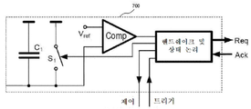
도 1에 추가로 도시된 바와 같이, 광-시간 변환기(107)는 인코딩된 세기를 판독 회로(109)로 보낼 수 있다. 예를 들어, 광-시간 변환기(107)는 트리거 신호 및 완료 신호(또는 기준 전압이 변경되는 실시형태에서 복수의 완료 신호)를 판독 회로(109)로 보낼 수 있다. 도 1에 도시된 바와 같이 판독 회로(109)는 픽셀(100)의 외부에 있을 수 있다. 일부 실시형태에서, 판독 회로(109)는 AER 기반 회로(예를 들어, 도 2b 참조)를 포함할 수 있다.As further shown in FIG. 1, the light-to-
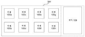
도 2a는 복수의 픽셀을 포함하는 이미지 센서(200)의 개략도이다. 예를 들어, 센서(200)의 각각의 픽셀은 도 1의 픽셀(100)을 포함할 수 있다. 도 2a에서, 이미지 센서(200)는 픽셀(100a, 100b, 100c, 100d, 100e, 10Of, 100g 및 100h)을 갖는 것으로 도시된다. 8개의 픽셀(100a 내지 100h)로 도시되어 있지만, 임의의 수의 픽셀이 이미지 센서(200)에서 사용될 수 있다. 더욱이, 직사각형 어레이로 배열된 것으로 도시되었지만, 이미지 센서(200)의 픽셀은 정사각형, 마름모, 평행사변형, 직사각형, 원형, 타원 등과 같은 임의의 적절한 형상으로 배열될 수 있다.2A is a schematic diagram of an
도 2a에 추가로 도시된 바와 같이, 판독 회로(109)는, 픽셀(100a, 100b, 100c, 100d, 100e, 10Of, 100g 및 100h)의 외부에 있지만 여전히 센서(200)의 일부를 형성하는 판독 회로로서 구현될 수 있다. 대안적인 실시형태(도시되지 않음)에서, 판독 회로(109)는 센서(200)뿐만 아니라 픽셀(100a, 100b, 100c, 100d, 100e, 10Of, 100g 및 100h)의 외부에 있을 수 있다.As further shown in Figure 2A, the
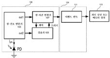
도 2b는 이벤트 판독 회로(111)를 갖는 예시적인 픽셀(100)의 개략도이다. 도 2b의 픽셀(100)은 (도 1의 감광 요소(101)와 유사한) 광다이오드(PD), 2개의 출력(out1 및 out2)을 포함하는 광-신호 변환기(103), 검출기(105), 및 광-시간 변환기(107)를 포함한다. 도 2b에 더 도시된 바와 같이, 광-시간 변환기(107)는 픽셀(100)의 외부에 있을 수 있는 회로(111)로 신호를 보낸다. 도 2b의 예에서, 회로(111)는 예를 들어 기존 AER 프로토콜을 사용하여 복수의 픽셀 각각과 통신하도록 구성된 이벤트 판독 회로이다. 따라서, 회로(111)는 다른 픽셀(도시되지 않음)의 다른 광-시간 변환기로부터의 시간과 함께 픽셀(100)로부터의 펄스(또는 펄스 에지)의 시간을 판독할 수 있다. 더욱이, 회로(111)는 판독 시간을 처리 유닛 또는 메모리 장치(113)로 전달할 수 있다. 도 2b에 도시된 바와 같이, 처리 유닛 또는 메모리(113)는 픽셀(100) 및 회로(111)의 외부에 있을 수 있고, 또한 센서의 외부에 있을 수 있다.2B is a schematic diagram of an
회로(111)에 대한 AER 프로토콜을 사용함으로써, 어레이의 각각의 픽셀은 픽셀이 통신 이벤트를 갖는 경우 임의의 시점에서 출력 신호에 대한 액세스를 개별적이고 자율적으로 요청할 수 있다. 이러한 이벤트는 예를 들어 광-시간 변환의 시작 또는 종료일 수 있다. 회로(111)는 요청 픽셀의 어드레스(예를 들어, 좌표로 인코딩된 어레이의 위치) 및 타임스탬프를 픽셀로부터 수신된 이벤트 식별자에 추가할 수 있다. 그런 다음 회로(111)는 어드레스, 타임스탬프 및 이벤트를 포함하는 결과 데이터 패킷을 디지털 버스를 통해 처리 유닛 또는 메모리 장치(예를 들어, 도 2b의 113)로 전송하고, 수신확인 신호를 요청 픽셀로 반환할 수 있다.By using the AER protocol for
전술한 바와 같이, 회로(111)는 예를 들어 행 및 열 우선 요청 및 수신확인 라인에 기초하여 모든 픽셀 간에 공유될 수 있다. 픽셀로부터의 요청이 충돌할 것 같지 않은 경우에, 회로(111)에 대한 액세스는 데이터의 충돌 및 후속 손실을 방지하기 위해 요청을 큐잉하는 회로부(도시되지 않음)에 의해 중재될 수 있다.As described above,
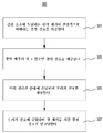
도 3은 예를 들어 도 1의 픽셀(100)을 사용하여 시간 기반 이미지 감지를 위한 예시적인 방법(300)의 흐름도이다. 도 3의 단계(301)에서, 픽셀은, 광-신호 변환기의 제1 출력에서, 감광 요소에 도달하는 광의 세기에 선형적으로 비례하는 전류 신호를 제공할 수 있다. 예를 들어, 픽셀은 도 7의 광-신호 변환기(700) 및/또는 도 8의 광-신호 변환기(800)를 포함할 수 있다. 제1 출력은 감광 요소로부터의 전류(IPh)와 같을 수 있고 또는 감광 요소에 도달하는 광의 세기에 선형적으로 비례하는 다른 전류를 포함할 수 있다. 예를 들어, 광-신호 변환기(700)는 감광 요소에 도달하는 광의 세기에 여전히 선형적으로 비례하는 IPh보다 더 큰 전류를 출력하도록 이득을 포함할 수 있다.3 is a flow diagram of an
단계(303)에서, 픽셀은, 광-신호 변환기의 제2 출력에서, 감광 요소에 도달하는 광의 세기의 로그 함수인 전압 신호를 제공할 수 있다. 예를 들어, 픽셀은 도 7의 광-신호 변환기(700) 및/또는 도 8의 광-신호 변환기(800)를 포함할 수 있다. 제2 출력은 선택적으로 일정한 최소값을 갖는 전류(IPh)의 로그 함수인 전압(아래 수식 1 참조)을 포함할 수 있다. In
방법(300)의 단계는 다양한 방식으로 구현될 수 있다. 예를 들어, 일부 실시형태에서, 단계(301 및 303)는 중첩되거나 또는 동시에 일어날 수 있다. 예를 들어, 신호 변환기는 연속적으로 제1 출력 및 제2 출력을 모두 제공할 수 있다.The steps of
단계(305)에서, 픽셀은 광-신호 변환기의 제2 출력의 전압 신호에 비례하는 검출기의 신호가 임계값을 초과할 때 다른 픽셀의 검출기와 독립적으로 자율적으로 검출기를 사용하여 트리거 신호를 생성할 수 있다. 예를 들어, 검출기는 도 5의 검출기(500)를 포함할 수 있다. 검출기는 제2 출력의 전압에 비례하는 신호가 임계값을 넘어 증가(또는 임계값 미만으로 감소)할 때 트리거할 수 있다. 따라서, 검출기는 전압 신호의 크기가 임계값을 초과할 때마다 트리거하여, 세기의 증가와 세기의 감소를 모두 캡처할 수 있다. 또한, 본 명세서에 개시된 바와 같이, 하나를 초과하는 임계값이 이 단계의 일부로 사용될 수 있다.In
단계(307)에서, 픽셀은, 광-시간 변환기를 사용하여, 감광 요소 상의 광의 세기를 시간 경과 정보로 인코딩할 수 있으며, 시간 경과 정보는 광-시간 변환 사이클의 개시 시간 및 광-시간 변환 사이클의 완료 시간을 포함한다. 예를 들어, 검출기는 도 7의 광-시간 변환기(700) 및/또는 도 8의 광-시간 변환기(800)를 포함할 수 있다. 일부 실시형태에서, 광-시간 변환 사이클은 검출기로부터 트리거 신호를 수신한 것에 응답하여 광-시간 변환기에 의해 개시될 수 있다. 추가적으로 또는 대안적으로, 광-시간 변환 사이클은 외부에서 개시될 수 있다. 예를 들어, 광-시간 변환 사이클은 미리 결정된 시간 간격으로 실행될 수 있다. 다른 예에서, 외부 회로부(예를 들어, 논리 회로)가 픽셀이 특정 시간 기간에 광-시간 변환을 실행하지 않았다고 결정하는 경우, 광-시간 변환 사이클은 픽셀의 외부에서 개시될 수 있다. 따라서, 일부 실시형태에서, 픽셀은 검출기로부터의 트리거 신호에 기초하여 광-시간 변환 사이클을 개시할 수 있고, 특정 시간 기간 후에 검출기로부터의 트리거 신호가 발생하지 않을 때에는 외부 트리거에 기초하여 개시할 수 있다.In
예시적인 방법(300)은 추가 단계를 포함할 수 있다. 예를 들어, 일부 실시형태에서, 방법(300)은, 광-시간 변환기를 사용하여, 광-시간 변환 사이클의 개시 시간을 복수의 픽셀의 외부에 있는 판독 회로 또는 시스템으로 전달하는 단계를 포함할 수 있다. 또한, 방법(300)은 광-시간 변환기를 사용하여 광-시간 변환 사이클의 완료 시간을 판독 회로 또는 시스템으로 전달하는 단계를 포함할 수 있다. 예를 들어, 광-시간 변환기는 도 7 및 도 8에 도시된 바와 같이 Req 버스를 통해 개시 시간 및 완료 시간을 전달할 수 있다. The
판독 시스템을 갖는 실시형태에서, 방법(300)은, 판독 시스템에서, 각 픽셀에 대한 어드레스 정보를 각 픽셀의 광-시간 변환기로부터 수신된 광-시간 변환 사이클 개시 및 완료 정보와 결합하는 단계를 더 포함할 수 있다. 이러한 실시형태에서, 방법(300)은 복수의 픽셀의 외부의 디지털 처리 시스템에 의해 픽셀 어드레스 정보 및 광-시간 변환 사이클 개시 및 완료 정보를 동기화하고 타임스탬핑하는 단계를 더 포함할 수 있다. 도 2a를 참조하여 전술한 바와 같이, 디지털 처리 시스템은 판독 회로부(109)의 적어도 일부를 포함할 수 있고, 따라서 픽셀의 외부에 있는 이미지 센서의 일부를 형성할 수 있다. 대안적으로, 디지털 처리 시스템은 이미지 센서 및 픽셀의 외부에 있을 수 있다.In an embodiment with a reading system, the
추가적으로 또는 대안적으로, 방법(300)은, 광-시간 변환 사이클 동안, 광-신호 변환기의 제1 출력의 전류 신호를 사용하여 커패시터를 충전하는 단계, 및 커패시터 양단의 전압이 기준 전압에 도달했다고 결정될 때, 비교기를 사용하여, 광-시간 변환 사이클의 완료 시간을 검출하는 단계를 포함할 수 있다. 예를 들어, 광-시간 변환기의 논리 회로는 기준 전압에 도달했다는 비교기로부터의 신호를 수신한 것에 기초하여 완료 시간을 결정할 수 있다. 일부 실시형태에서, 방법(300)은 복수의 기준 전압 레벨 사이에서 기준 전압을 변화시키는 단계를 더 포함할 수 있다. 예를 들어, 방법(300)은 커패시터 양단의 전압이 기준 전압에 도달할 때마다 기준 전압을 더 크거나 더 작은 기준 전압 레벨로 각각 증가시키거나 감소시키는 단계를 더 포함할 수 있다. 따라서, 광-시간 변환기는 Req 버스를 통해 복수의 완료 시간을 보낼 수 있고, 각 완료 시간은 연관된 기준 전압을 갖는다.Additionally or alternatively, the
전술한 추가 측정을 하면 측정 평활화 및 에러 정정이 가능할 수 있다. 예를 들어, 완료 시간은 복수의 세기 측정값을 계산하는 데 사용될 수 있으며, 이들 측정값으로부터 평균, 중앙값 또는 다른 통계 값이 "실제" 세기 측정값으로서 추출될 수 있다. 이러한 예에서, 완료 시간은 "실제" 세기 측정값의 추정된 에러률(또는 신뢰 범위)을 계산하기 위해 더 사용될 수 있다. 추가적으로 또는 대안적으로, 완료 시간은 "실제" 완료 시간을 (연관된 기준 전압으로) 계산하도록 먼저 평활화되거나 통계적으로 대조될 수 있다. 이러한 예에서, 완료 시간은 "실제" 완료 시간의 추정된 에러률(또는 신뢰 범위)을 계산하기 위해 더 사용될 수 있다.Measurement smoothing and error correction may be possible by performing the above-described additional measurement. For example, the completion time may be used to calculate a plurality of intensity measurements, from which an average, median, or other statistical value may be extracted as a "real" intensity measure. In this example, the completion time can be further used to calculate the estimated error rate (or confidence range) of the "real" intensity measurement. Additionally or alternatively, the completion time may be first smoothed or statistically contrasted to calculate the “real” completion time (with an associated reference voltage). In this example, the completion time can be further used to calculate the estimated error rate (or confidence range) of the “real” completion time.
더욱이, 적어도 2개의 임계값을 사용하면 시간 영역에서 상관된 이중 샘플링이 가능할 수 있다. 이러한 샘플링은 광-시간 변환기의 리셋으로 인한 잡음을 줄이고 비교기의 오프셋 에러를 줄일 수 있다.Moreover, using at least two thresholds may enable correlated double sampling in the time domain. This sampling can reduce the noise caused by the reset of the optical-time converter and reduce the offset error of the comparator.
일부 실시형태에서, 방법(300)은 커패시터와 병렬인 스위치를 개방함으로써 광-시간 변환 사이클을 개시하는 단계를 더 포함할 수 있다. 이러한 실시형태에서, 방법(300)은 광-시간 변환 사이클을 개시하도록 스위치를 개방하기 전에 커패시터를 방전하도록 스위치를 폐쇄하는 단계를 더 포함할 수 있다. 스위치는 커패시터를 접지(또는 정전압 공급원)에 연결하여 커패시터를 방전시킬 수 있다.In some embodiments,
또 다른 실시형태에서, 방법(300)은 검출기로부터 트리거 신호를 수신한 것에 응답하여 리셋 신호를 검출기에 보내는 단계를 포함할 수 있다. 예를 들어, 광-시간 변환기의 논리 회로는 검출기가 다른 트리거 이벤트(즉, 전압의 변화)를 검출하기 위해 리셋하고 준비하도록 제어 신호를 검출기에 보낼 수 있다.In yet another embodiment,
일부 실시형태에서, 방법(300)은, 현재 광-시간 변환 사이클의 완료 전에 다른 트리거 신호가 수신될 때, 새로운 광-시간 변환 사이클을 리셋하고 개시하는 단계를 포함할 수 있다. 예를 들어, 광-시간 변환기는, 검출기가 리셋되도록 제어 신호를 검출기에 보내고, 광-시간 변환을 개시하고, 광-시간 변환이 완료되기 전에 (예를 들어, 비교기가 하나 이상의 기준 전압에 도달했음을 나타내는 신호를 보내기 전에) 검출기로부터 다른 트리거 신호를 수신할 수 있다. 따라서, 광-시간 변환기는 커패시터를 방전시키고 새로운 트리거 신호에 기초하여 새로운 광-시간 변환을 시작할 수 있다. 이러한 실시형태에서, 광-시간 변환기는 이전 변환이 Req 버스를 통해 중단되었음을 나타내는 신호를 더 보낼 수 있다.In some embodiments,
도 4a는 광-신호 변환기(400)의 개략도이다. 광-신호 변환기(400)는 도 1의 픽셀(100)에서 사용될 수 있다(광-신호 변환기(103) 참조). 4A is a schematic diagram of an optical-to-
도 4a에 도시된 바와 같이, 변환기(400)는 드레인, 소스 및 게이트를 갖는 트랜지스터(M1)를 포함할 수 있다. 게이트는 변환기(400)의 제2 출력(out2)에 연결될 수 있다. 변환기(400)는 드레인, 소스 및 게이트를 갖는 트랜지스터(M5)를 더 포함할 수 있다. 소스는 광다이오드(PD)(즉, 감광 요소)에 연결될 수 있고, 게이트는 전압(Vd)에 의해 바이어스될 수 있다. 트랜지스터(M1 및 M5)는 공통 소스를 가질 수 있다.As shown in FIG. 4A, the
도 4a에 추가로 도시된 바와 같이, 변환기(400)는 드레인, 소스 및 게이트를 갖는 제2 트랜지스터(M2)를 포함할 수 있다. 게이트는 광다이오드(PD) 및 트랜지스터(M5)의 드레인에 연결될 수 있고, 소스는 접지될 수 있고(예를 들어, 낮은 공급 전압에 연결될 수 있고), 드레인은 트랜지스터(M3)의 소스에 연결될 수 있다. 트랜지스터(M3)는 또한 드레인, 소스 및 게이트를 가진다. 게이트는 전압(Vcas)에 의해 바이어스될 수 있고, 드레인은 out2에 (그리고 이에 따라 M1의 게이트에도) 연결될 수 있다. M3의 드레인은 트랜지스터(M4)의 드레인에 더 연결된다. M4의 게이트는 전압(Vpr)에 의해 바이어스될 수 있고, 소스는 공급 전압(미도시)에 연결될 수 있다.As further illustrated in FIG. 4A, the
트랜지스터(M1, M2, M3)는 n형 트랜지스터일 수 있는 반면, 트랜지스터(M4 및 M5)는 p형 트랜지스터일 수 있다. 도 4a에 더 도시된 바와 같이, 트랜지스터(M1)의 드레인은 트랜지스터(M6)의 소스에 연결될 수 있다. 트랜지스터(M6)의 게이트는 전압(Vc)에 의해 바이어스될 수 있고, 트랜지스터(M6)의 드레인은 변환기(400)의 제1 출력(out1)에 연결될 수 있다.Transistors M1, M2, and M3 may be n-type transistors, while transistors M4 and M5 may be p-type transistors. As further illustrated in FIG. 4A, the drain of the transistor M1 may be connected to the source of the transistor M6. The gate of the transistor M6 may be biased by the voltage V c , and the drain of the transistor M6 may be connected to the first output out1 of the
도 4b는 다른 광-신호 변환기(450)의 개략도이다. 광-신호 변환기(450)는 예를 들어 도 1의 픽셀(100)에서 광-신호 변환기(400)에 추가하여 또는 대신에 사용될 수 있다. 4B is a schematic diagram of another optical-to-
도 4b에 도시된 바와 같이, 변환기(450)는 드레인, 소스 및 게이트를 갖는 트랜지스터(M1)를 포함할 수 있다. 게이트는 변환기(450)의 제2 출력(out2)에 연결될 수 있다. 변환기(450)는 드레인, 소스 및 게이트를 갖는 트랜지스터(M5)를 더 포함할 수 있다. 소스는 광다이오드(PD)(즉, 감광 요소)에 연결될 수 있고, 게이트는 트랜지스터(M2)의 드레인에 연결될 수 있다.As shown in FIG. 4B, the
트랜지스터(M2)는 또한 드레인, 소스 및 게이트를 갖는다. 게이트는 광다이오드(PD) 및 트랜지스터(M5)의 소스에 연결될 수 있고, 소스는 접지될 수 있고(예를 들어, 낮은 공급 전압에 연결될 수 있고), 드레인은 트랜지스터(M3)의 소스에 (그리고 이에 따라 또한 트랜지스터(M5)의 게이트에) 연결될 수 있다. 트랜지스터(M3)는 또한 드레인, 소스 및 게이트를 갖는다. 게이트는 트랜지스터(M5)의 드레인에 (그리고 이에 따라 또한 M1의 소스에) 연결될 수 있고, 드레인은 out2에 (그리고 이에 따라 또한 M1의 게이트에) 연결될 수 있다. M3의 드레인은 트랜지스터(M4)의 드레인에 더 연결될 수 있다. M4의 게이트는 전압(Vpr)에 의해 바이어스될 수 있고, 소스는 공급 전압(미도시)에 연결될 수 있다.Transistor M2 also has a drain, a source and a gate. The gate can be connected to the photodiode PD and the source of the transistor M5, the source can be grounded (eg, can be connected to a low supply voltage), and the drain is connected to the source of the transistor M3 (and Accordingly, it can also be connected to the gate of the transistor M5). Transistor M3 also has a drain, a source and a gate. The gate may be connected to the drain of transistor M5 (and thus also to the source of M1), and the drain may be connected to out2 (and thus also to the gate of M1). The drain of M3 may be further connected to the drain of the transistor M4. The gate of M4 may be biased by a voltage V pr , and a source may be connected to a supply voltage (not shown).
트랜지스터(M1, M2, M3)는 n형 트랜지스터일 수 있는 반면, 트랜지스터(M4)는 p형 트랜지스터일 수 있다. 도 4a의 실시형태에서, M5는 p형 트랜지스터일 수 있는 반면, 도 4b의 실시형태에서, M5는 n형 트랜지스터일 수 있다. 도 4a에 더 도시된 바와 같이, 트랜지스터(M1)의 드레인은 트랜지스터(M6)의 소스에 연결될 수 있다. 트랜지스터(M6)의 게이트는 전압(Vc)에 의해 바이어스될 수 있고, 트랜지스터(M6)의 드레인은 변환기(400)의 제1 출력(out1)에 연결될 수 있다.Transistors M1, M2, and M3 may be n-type transistors, while transistor M4 may be a p-type transistor. In the embodiment of FIG. 4A, M5 may be a p-type transistor, whereas in the embodiment of FIG. 4B, M5 may be an n-type transistor. As further illustrated in FIG. 4A, the drain of the transistor M1 may be connected to the source of the transistor M6. The gate of the transistor M6 may be biased by the voltage V c , and the drain of the transistor M6 may be connected to the first output out1 of the
광-신호 변환기(400) 및 광-신호 변환기(450)의 제2 출력은 아래 수식 1에 따라 감광 요소에 도달하는 광의 세기의 로그 함수인 값일 수 있다:The second output of the optical-
![]()
![]()
수식 1
수식 1의 예에서, Vlog는 도달하는 광의 세기의 로그 함수에 비례하는 전압이고, VDC는 광에 독립적인 직류 전압 레벨이고, Av는 전압 이득 계수이고, UT는 열 전압(상기rmal voltage)이고, Iph는 감광 요소에서 출력되는 전류이다.In the example of
광-신호 변환기(400)에서, Vlog는 아래 수식 2를 따를 수 있다:In the optical-

수식 2Equation 2
수식 2의 예에서, Vlog는 도달하는 광의 세기의 로그 함수에 비례하는 전압이고, UT는 열 전압이고, nM1은 트랜지스터(M1)에 대한 하위-임계값 기울기 계수이고, nM5는 트랜지스터(M5)에 대한 하위-임계값 기울기 계수이고, LM1은 트랜지스터(M1)의 채널 길이이고, LM5는 트랜지스터(M5)의 채널 길이이고, WM1은 트랜지스터(M1)의 채널 폭이고, WM5는 트랜지스터(M5)의 채널 폭이고, I0,M1은 트랜지스터(M1)의 하위-임계값 포화 전류이고, I0,M5는 트랜지스터(M5)의 하위-임계값 포화 전류이고, Vd는 트랜지스터(M5)에 적용된 바이어스 전압이고, Iph는 감광 요소에서 출력된 전류이다.In the example of Equation 2, V log is a voltage proportional to the logarithmic function of the intensity of light arriving, U T is the column voltage, n M1 is the lower-threshold slope coefficient for transistor M1, and n M5 is the transistor Is the lower-threshold slope factor for (M5), L M1 is the channel length of transistor M1, L M5 is the channel length of transistor M5, W M1 is the channel width of transistor M1, and W M5 is the channel width of transistor M5, I 0,M1 is the lower-threshold saturation current of transistor M1, I 0,M5 is the lower-threshold saturation current of transistor M5, and V d is It is the bias voltage applied to the transistor M5, and I ph is the current output from the photosensitive element.
따라서, (도달하는 광의 세기가 변하는 것으로 인해) 광전류가 Iph1로부터 Iph2로 변하면, 아래 수식 3을 따를 수 있는 ΔVlog가 생성된다:Thus, (due to the varying intensity of the light reaching) the photo current turns into I ph1 ph2 from I, the ΔV log that can follow an equation 3 below is created:

수식 3Equation 3
한편, 광-신호 변환기(450)에서 Vlog는 아래 수식을 따를 수 있다:Meanwhile, in the optical-
아래 수식 4:Equation 4:

수식 4Equation 4
수식 4의 예에서, Vlog는 도달하는 광의 세기의 로그 함수에 비례하는 전압이고, UT는 열 전압이고, nM1은 트랜지스터(M1)에 대한 하위-임계값 기울기 계수이고, LM1은 트랜지스터(M1)의 채널 길이이고, WM1은 트랜지스터(M1)의 채널 폭이고, I0,M1은 트랜지스터(M1)의 하위-임계값 포화 전류이고, Vd는 감광 요소(PD) 양단의 역 전압이고, Iph는 감광 요소에서 출력된 전류이다.In the example of Equation 4, V log is the voltage proportional to the logarithmic function of the intensity of the light arriving, U T is the column voltage, n M1 is the lower-threshold slope coefficient for transistor M1 , and L M1 is the transistor Is the channel length of (M1), W M1 is the channel width of transistor M1 , I 0,M1 is the sub-threshold saturation current of transistor M1, and V d is the reverse voltage across the photosensitive element PD And I ph is the current output from the photosensitive element.
따라서, (도달하는 광의 세기가 변하는 것으로 인해) 광전류가 Iph1로부터 Iph2로 변하면, 아래 수식 5를 따를 수 있는 ΔVlog가 생성된다:Thus, (due to the varying intensity of the light reaching) the photo current turns into I ph1 ph2 from I, the ΔV log to follow the following equation 5 is generated:

수식 5Equation 5
따라서, 광-신호 변환기(450)는 광-신호 변환기(400)보다 제조하기가 더 쉽고 더 저렴할 수 있지만, 광-신호 변환기(400)는 광-신호 변환기(450)보다 더 많은 이득을 생성할 수 있다.Thus, the optical-
도 5는 예시적인 검출기(500)의 개략도이다. 검출기(500)는 도 1의 픽셀(100)에서 사용될 수 있다(검출기(105) 참조). 도 5에 도시된 바와 같이, 검출기(500)는 광-신호 변환기(도시되지 않음)의 제2 출력에 연결된 증폭기(501)를 포함한다. 증폭기(501)는 단일 이득 증폭기일 수 있다. 일부 실시형태에서, 증폭기(501)는 반전될 수 있다. 커패시터(503)는 증폭기(501)에 연결될 수 있다.5 is a schematic diagram of an
검출기(500)는 커패시터(503)와 공통 노드에 병렬로 연결된, 증폭기(505), 커패시터(507) 및 스위치(509)를 더 포함할 수 있다. 따라서, 검출기(500)가 제어 신호(예를 들어, 광-시간 변환기의 논리 회로로부터의 수신확인 신호)를 수신할 때마다, 스위치(509)는 폐쇄되어 검출기(500)를 단락시켜 새로운 검출을 준비할 수 있다.The
증폭기(505)(반전 증폭기일 수 있음)는 커패시터(503)로부터의 전압의 변화를 증폭시켜 이 변화가 Vdiff에서 정해진 전압 레벨(즉, 이전 리셋 신호에서 커패시터(503)의 전압 레벨)로부터의 편차이도록 한다. Vdiff가 음의 방향으로 임계값을 교차할 때마다, 증폭기(511a)는 트리거 신호를 광-시간 변환기로 보낸다. 유사하게, Vdiff가 양의 방향으로 임계값(상기와 동일하거나 다른 임계값일 수 있음)을 교차할 때마다, 증폭기(511b)는 트리거 신호를 광-시간 변환기로 보낸다. 따라서, 검출기(500)는 하나의 임계값을 초과하는 세기의 증가를 검출할 수 있을 뿐만 아니라, 동일하거나 상이한 임계값 미만으로 세기의 감소를 검출할 수 있다.Amplifier 505 (which may be an inverting amplifier) amplifies the change in voltage from
검출기(500)를 사용함으로써, 픽셀(100)은, 고정된 시간 단계(δt)에서 동기식 픽셀 정보를 획득하는 대신, 아래 수식 6에 의해 주어진 광 증분으로 비동기식 픽셀 정보를 획득하도록 구성될 수 있다:By using the

수식 6Equation 6
수식 6의 예에서, θen은 최소 검출 가능한 시간적 콘트라스트("콘트라스트 감도"라고도 지칭됨)이고, Iph는 감광 요소에서 출력되는 전류이다. 잡음은 본 발명의 비동기식 픽셀의 콘트라스트 감도를 더 제한할 수 있다.In the example of Equation 6, θ en is the minimum detectable temporal contrast (also referred to as “contrast sensitivity”), and I ph is the current output from the photosensitive element. Noise may further limit the contrast sensitivity of the asynchronous pixels of the present invention.
도 5의 검출기(500)를 참조하여 설명되었지만, 광-신호 변환기의 제2 출력을 참조하여 검출기의 신호(예를 들어, 전압 신호 또는 전류 신호)를 분석하거나, 보다 일반적으로 광-신호 변환기의 제2 출력의 하나 이상의 미리 정해진 상태를 검출하도록 구성된 임의의 적합한 검출기가 사용될 수 있다. 더욱이, 이러한 분석을 수행하도록 배열된 트랜지스터, 커패시터, 스위치 및/또는 다른 회로 구성 요소의 임의의 조합이 본 발명에 따라 각 픽셀의 검출기에 사용될 수 있다.Although described with reference to the
도 6은 도 5의 검출기(500)에 의해 생성된 트리거의 그래픽도이다. 도 6에서, VP는 검출기(500)의 커패시터(503)에서의 전압을 나타내며, 따라서 광-신호 변환기의 제2 출력으로부터의 출력에 비례하는 전압이다. 더욱이, Vdiff는, VP의 반전 및 증폭된 버전이고 광-신호 변환기의 제2 출력으로부터의 출력에 비례하는 검출기(500)의 전압 신호이다. 도 6에 더 도시된 바와 같이, VP의 증가("+ 이벤트"로 도시)와 VP의 감소("-이벤트"로 도시)는 모두 트리거 신호를 생성할 수 있다. Vdiff는 VP의 반전 및 증폭된 버전이므로, VP의 증가는 Vdiff의 감소로 나타나고, 그 반대의 경우도 마찬가지이다. 또한, 도 6은 "+ 임계값"이 "- 임계값"과 (크기가) 동일한 것으로 설정될 수 있지만 또한 상이하게 설정될 수도 있는 방식을 도시한다. 마지막으로, 도 6은 (예를 들어, 스위치(509)를 폐쇄함으로써) 각각의 트리거 후에 Vdiff가 기준선("리셋 레벨"로 도시됨)으로 리셋되는 방식을 보여준다.6 is a graphic diagram of a trigger generated by
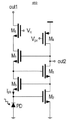
도 7은 예시적인 광-시간 변환기(700)의 개략도이다. 변환기(700)는 도 1의 픽셀(100)에서 사용될 수 있다(변환기(107) 참조). 7 is a schematic diagram of an exemplary light-to-
도 7에 도시된 바와 같이, 변환기(700)는 커패시터(C1), 스위치(S1) 및 비교기(기준 전압(Vref)을 가짐)를 포함할 수 있다. 이들 요소는 광-신호 변환기(도시되지 않음)의 제1 출력에 연결될 수 있다. 따라서 스위치(S1)가 개방될 때마다 커패시터(C1)는 제1 출력의 전류로 인해 충전된다. C1 양단의 전압이 Vref에 도달하면, 비교기는 완료 신호를 생성할 수 있다.As shown in FIG. 7, the
도 7에 추가로 도시된 바와 같이, 핸드쉐이크 및 상태 논리 회로(즉, 변환기(700)의 논리 회로)는 검출기로부터 트리거 신호를 수신하면 스위치(S1)를 개방할 수 있다. 또한, 핸드쉐이크 및 상태 논리 회로는 트리거 신호의 수신을 수신확인하는 제어 신호를 검출기에 보낼 수 있다. 도 7에 더 도시된 바와 같이, 핸드쉐이크 및 상태 논리 회로는 트리거 신호 및 완료 신호를 비교기로부터 Req 버스를 통해 판독 회로(도시되지 않음)로 보낼 수 있다. 일부 실시형태에서, 핸드쉐이크 및 상태 논리 회로는 또한 Ack 버스를 통해 판독 회로로부터 수신확인 신호를 수신할 수 있다. 설명되지는 않았지만, 핸드쉐이크 및 상태 논리 회로는 또한 (예를 들어, 트리거 신호의 수신 전 또는 수신 시) S1을 폐쇄하여 커패시터(C1)를 방전시켜 광-시간 변환을 준비할 수 있다.As further shown in FIG. 7, the handshake and state logic circuit (ie, the logic circuit of the converter 700) may open the switch S1 upon receiving a trigger signal from the detector. In addition, the handshake and state logic circuit may send a control signal to the detector acknowledging receipt of the trigger signal. As further shown in FIG. 7, the handshake and state logic circuit may send a trigger signal and a completion signal from the comparator to a readout circuit (not shown) via the Req bus. In some embodiments, the handshake and state logic circuit may also receive an acknowledgment signal from the read circuit via the Ack bus. Although not described, the handshake and state logic circuit may also close S1 (eg, before or upon receipt of a trigger signal) to discharge capacitor C1 to prepare for photo-time conversion.
도 7에 도시되지는 않았지만, 핸드쉐이크 및 상태 논리 회로는 광-시간 변환을 통해 Vref를 변경할 수 있다. 따라서, 복수의 완료 시간이 획득되고 Req 버스를 통해 출력될 수 있다. 전술한 바와 같이, 복수의 측정값을 사용하면 평활화 및/또는 에러 정정이 가능할 수 있다.Although not shown in FIG. 7, the handshake and state logic circuit may change V ref through light-time conversion. Thus, a plurality of completion times can be obtained and output through the Req bus. As described above, smoothing and/or error correction may be possible by using a plurality of measurement values.
따라서, 광-시간 변환기(700)는 아래 수식 7에 따라 시간 내에 감광 요소에 도달하는 광의 세기를 인코딩할 수 있다:Accordingly, the light-

수식 7
수식 7의 예에서, tint는 광의 세기가 인코딩되는 시간이고, C1은 커패시터(C1)의 커패시턴스이고, Iph는 감광 요소에서 출력된 전류(또는 광-신호 변환기의 제1 출력으로부터 광-시간 변환기(700)에서 수신된 전류)이고, V시작은 (예를 들어, 트리거 신호의 수신 시) 커패시터(C1)의 상부 판에 연결된 정전압이고, Vref는 비교기의 기준 전압이다. V시작은 도 9a, 도 9b 및 도 9c에서 Vpix,0으로 도시되고 아래에 설명된다. 일부 실시형태에서, V시작(또는 Vpix,0)은 광-시간 변환기의 공급 전압(예를 들어, 도 8에서 Vsup,LTC로 도시되고 아래에 설명됨)과 동일할 수 있고(또는 공급 전압으로부터 도출될 수 있고), C1의 상부 판(및 S1의 상부 단자)에 영구적으로 연결된다.In the example of
도 8은 다른 예시적인 광-시간 변환기(800)의 개략도이다. 변환기(800)는 도 1의 픽셀(100)에서 변환기(700)에 추가하여 또는 대신에 사용될 수 있다. 8 is a schematic diagram of another exemplary light-to-
도 8에 도시된 바와 같이, 변환기(800)는 커패시터(C1), 스위치(S1) 및 비교기(기준 전압(Vref)을 가짐)를 포함할 수 있다. 도 7의 변환기(700)와 유사하게, 이들 요소는 광-신호 변환기(도시되지 않음)의 제1 출력에 연결될 수 있다. 따라서 스위치(S1)가 개방될 때마다, 커패시터(C1)는 제1 출력의 전류로 인해 충전된다. C1 양단의 전압이 Vref에 도달하면, 비교기는 완료 신호를 생성할 수 있다. 또한, 커패시터(C1) 및/또는 스위치(S1)는 광-시간 변환기(800)의 공급 전압(Vsup,LTC)에도 연결될 수 있다.As shown in FIG. 8, the
도 8에 추가로 도시된 바와 같이, 변환기(800)는 커패시터(C1), 스위치(S1) 및 비교기의 공통 노드에 연결된 커패시터(C2)를 포함할 수 있다. 커패시터(C2)는 C1과 결합 커패시터로 기능하여 상이한 공급 전압을 사용할 수 있게 한다.As further illustrated in FIG. 8, the
도 8에 추가로 도시된 바와 같이, 핸드쉐이크 및 상태 논리 회로(즉, 변환기(800)의 논리 회로)는 검출기로부터 트리거 신호를 수신하면 스위치(S1)를 개방할 수 있다. 또한, 핸드쉐이크 및 상태 논리 회로는 트리거 신호의 수신을 수신확인하는 제어 신호를 검출기에 보낼 수 있다. 도 8에 더 도시된 바와 같이, 핸드쉐이크 및 상태 논리 회로는 비교기로부터 Req 버스를 통해 판독 회로(도시되지 않음)로 트리거 신호 및 완료 신호를 보낼 수 있다. 일부 실시형태에서, 핸드쉐이크 및 상태 논리 회로는 또한 판독 회로로부터 Ack 버스를 통해 수신확인 신호를 수신할 수 있다. 도시되지는 않았지만, 핸드쉐이크 및 상태 논리 회로는 (예를 들어, 트리거 신호의 수신 전 또는 수신 시) S1을 폐쇄하여 커패시터(C1)를 방전시켜 광-시간 변환을 준비할 수 있다.As further shown in FIG. 8, the handshake and state logic circuit (ie, the logic circuit of the converter 800) may open the switch S1 upon receiving a trigger signal from the detector. In addition, the handshake and state logic circuit may send a control signal to the detector acknowledging receipt of the trigger signal. As further shown in FIG. 8, the handshake and state logic circuit may send a trigger signal and a completion signal from the comparator to the read circuit (not shown) via the Req bus. In some embodiments, the handshake and state logic circuit can also receive an acknowledgment signal from the read circuit over the Ack bus. Although not shown, the handshake and state logic circuit can prepare for light-time conversion by discharging the capacitor C1 by closing S1 (eg, before or upon receiving a trigger signal).
도 7에 도시되지는 않았지만, 핸드쉐이크 및 상태 논리 회로는 광-시간 변환을 통해 Vref를 변경할 수 있다. 따라서, 복수의 완료 시간이 획득되고 Req 버스를 통해 출력될 수 있다. 전술한 바와 같이, 복수의 측정값을 사용하면 평활화 및/또는 에러 정정이 가능할 수 있다.Although not shown in FIG. 7, the handshake and state logic circuit may change V ref through light-time conversion. Thus, a plurality of completion times can be obtained and output through the Req bus. As described above, smoothing and/or error correction may be possible by using a plurality of measurement values.
도 8에 추가로 도시된 바와 같이, 광-시간 변환기(800)는 광-신호 변환기의 제1 출력에 연결된 소스, 전압(V바이어스)에 의해 바이어스된 게이트, 및 광-신호 변환기의 공급 전압(Vsup,PSC)에 연결된 드레인을 갖는 트랜지스터(MOF)를 포함할 수 있다. 트랜지스터(MOF)를 통합함으로써, 광-시간 변환기(800)는 광-신호 변환기가 제2 출력에서 도달하는 광의 로그 함수에 비례하는 전압 출력을 전달하는 것을 중지하기 위하여 광-신호 변환기의 제1 출력의 전압이 너무 낮게 떨어지는 것을 방지할 수 있다. 광-시간 변환기(800)는 또한 MOF와 병렬인 스위치(S2)(또는 예를 들어, 스위치로서 작용하는 트랜지스터)를 포함할 수 있다. 따라서, 핸드쉐이크 및 상태 논리 회로는 스위치(S1)와 유사하게 스위치(S2)를 제어할 수 있다(즉, 스위치(S2)를 개방하여 광-시간 변환 사이클을 시작하고/하거나 스위치(S2)를 폐쇄하여 방전시켜 광-시간 변환 사이클을 준비할 수 있다).As further shown in FIG. 8, the light-to-
광-시간 변환기(800)의 MOF 트랜지스터는 아래 수식 9에 의해 제어될 수 있다:The M OF transistor of the photo-
![]()
![]()
수식 9Equation 9
수식 9의 예에서, V바이어스는 MOF 트랜지스터에 적용되는 일정한 바이어스 전압이고, 광-신호 변환기의 제1 출력에서 최소 허용 가능한 전압인 VPRI,out에 의존하고, 광-신호 변환기의 출력을 측정하는 것으로부터 또는 출력을 시뮬레이션하는 것으로부터 도출될 수 있다. V바이어스는, 감광 요소에서 출력된 최대 전류이고, 감광 요소의 출력을 측정하는 것으로부터 도출되거나 또는 감광 요소의 하나 이상의 반도체 파라미터에 기초하여 계산될 수 있는 Iph,max의 함수인 VGS,MOF에 더 의존한다.In the example of Equation 9, V bias is the constant bias voltage applied to the M OF transistor, depends on the minimum allowable voltage V PRI,out at the first output of the optical-signal converter, and measures the output of the optical-signal converter. It can be derived from doing or simulating the output. V bias, and the maximum output current from the photosensitive element, or derived from those of measuring an output of the photosensitive element or can be calculated based on one or more semiconductor parameter of the light-sensitive element I ph, which is a function of max V GS, MOF Depend more on
일부 실시형태에서, 광-신호 변환기에 대한 제1 공급 전압(Vsup,PSC)은 광-시간 변환기에 대한 제2 공급 전압(Vsup,LTC)과 상이할 수 있다. 예를 들어, Vsup,PSC의 크기는 Vsup,LTC의 크기보다 더 클 수 있다. 공급 전압의 이러한 차이는 예를 들어 처리 가능한 광 레벨의 넓은 동적 범위가 필요한 경우에 유용할 수 있다. 일부 경우에, 광-신호 변환기는 충분히 더 높은 DC 전압 범위를 필요로 할 수 있으며, 본 명세서에 개시된 바와 같이 이득 부스팅이 이용되는 경우 더욱 더 그렇다. 광-신호 변환기에 필요한 공급 전압은 나노미터 반도체 기술에서 일반적으로 사용되는 값으로 감소되지 않을 수 있다. 그 결과, 광-시간 변환기를 포함하는 픽셀 내 회로부의 나머지 부분에 비해 광-신호 변환기를 구현하기 위해 다른 반도체 기술이 사용될 수 있다. 이러한 접근법을 사용하면 필요에 따라 다른 공급 전압이 제공될 수 있다.In some embodiments, the first supply voltage V sup,PSC to the optical-to-signal converter may be different from the second supply voltage V sup,LTC to the optical-time converter. For example, the size of V sup,PSC may be larger than the size of V sup,LTC . This difference in supply voltage can be useful, for example, where a wide dynamic range of light levels that can be processed is required. In some cases, the light-to-signal converter may require a sufficiently higher DC voltage range, even more so when gain boosting is used as disclosed herein. The supply voltage required for the optical-signal converter may not be reduced to values commonly used in nanometer semiconductor technology. As a result, other semiconductor technologies can be used to implement the optical-signal converter compared to the rest of the circuit portion in the pixel including the optical-time converter. Using this approach, different supply voltages can be provided as needed.
V리셋 자체는 도 5, 도 7, 도 8, 도 10 및 도 11의 예를 참조하여 설명된 "트리거" 신호로부터 도출되거나 트리거 신호에 의해 제어된다(또는 위에서 설명한 바와 같이 이전 검출 후에 이미 적용된 경우 적어도 해제된다). The V reset itself is derived from the "trigger" signal described with reference to the example of FIGS. 5, 7, 8, 10 and 11 or is controlled by the trigger signal (or if it has already been applied after the previous detection as described above. At least released).
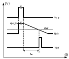
도 9a는 도 7의 광-시간 변환기(700) 또는 도 8의 광-시간 변환기(800)에 의한 광-시간 변환의 그래픽도이다. 도 9a의 예에 도시된 바와 같이, 광-시간 변환기의 커패시터는 트리거 신호(도 9a에서 V리셋으로 표시됨)를 수신하면 충전(또는 도 9a에 도시된 방전)을 시작한다. 커패시터 양단의 전압이 Vref에 도달하면, 완료 신호(도 9a에서 Vout으로 표시됨)가 생성된다. (충전 전류에 선형적으로 비례하는) 광의 세기는 위에서 설명한 바와 같이 트리거 신호와 완료 신호 사이의 시간(도 9a에서 tint로 표시됨)으로 인코딩된다. 9A is a graphical diagram of a light-time conversion by the light-
도 9b는 도 7의 광-시간 변환기(700) 또는 도 8의 광-시간 변환기(800)에 의한 신속한 순차적 트리거를 갖는 광-시간 변환의 그래픽도이다. 도 9b의 예에 도시된 바와 같이, 광-시간 변환기의 커패시터는 트리거 신호(도 9b에서 V리셋의 제1 스파이크로 표시됨)를 수신하면 충전(또는 도 9b에 도시된 방전)을 시작한다. 그러나, 광-시간 변환기는 Vref에 도달하기 전에 제2 트리거 신호(도 9b에서 V리셋의 제2 스파이크로 표시됨)를 수신한다. 따라서, 광-시간 변환기는 (예를 들어, 스위치를 뒤집어 커패시터를 접지 또는 다른 전압 공급원에 연결함으로써) 커패시터를 신속하게 방전(또는 충전)한 다음 (예를 들어, 스위치를 개방함으로써) 커패시터를 다시 충전(또는 방전)하기 시작한다. 커패시터 양단의 전압이 Vref에 도달하면, 그런 다음 완료 신호(도 9b에서 Vout으로 표시됨)가 도 9a에서와 같이 생성된다. 도 9b에 도시되지는 않았지만, 광-시간 변환기는, 예를 들어, 제1 측정값의 시간-디지털 변환을 취소하도록 두 트리거 사이에 판독 회로에 취소 신호를 보낼 수 있다. 예를 들어, 일부 실시형태에서, 이러한 취소 신호는 제2 트리거 신호(도 9b에서 V리셋의 제2 스파이크로 표시됨)로부터 도출될 수 있다. 더욱이, (충전 전류에 선형적으로 비례하는) 광의 세기는 따라서 취소 신호와 완료 신호 사이의 시간(도 9a에서 tint로 표시됨)으로 인코딩될 수 있다.9B is a graphical diagram of a light-to-time conversion with rapid sequential triggering by the light-to-
도 9c는 도 7의 광-시간 변환기(700) 또는 도 8의 광-시간 변환기(800)에 의해 변하는 기준 전압을 갖는 광-시간 변환의 그래픽도이다. 도 9c의 예에 도시된 바와 같이, 광-시간 변환기의 커패시터는 트리거 신호(도 9c에서 V리셋으로 표시됨)를 수신하면 충전(또는 도 9c에 도시된 방전)을 시작한다. 커패시터 양단의 전압이 Vref1에 도달하면, 제1 완료 신호(도 9c에서 Vout의 제1 스파이크로 표시됨)가 생성된다. 커패시터 양단의 전압이 Vref2에 도달하면, 제2 완료 신호(도 9c에서 Vout의 제2 스파이크로 표시됨)가 생성된다. 커패시터 양단의 전압이 Vref3에 도달하면, 최종 완료 신호(도 9c에서 Vout의 제3 스파이크로 표시됨)가 생성된다. 3개의 기준 전압이 도시되었지만, 2, 4, 5 등과 같은 임의의 수의 기준 전압이 사용될 수 있다. 따라서 (충전 전류에 선형적으로 비례하는) 광의 세기는 위에서 설명한 바와 같이 신호 사이의 시간(도 9c에서 tint1 및 tint2로 표시됨)으로 인코딩된다. 다수의 완료 신호는 위에서 설명한 바와 같이 신호 평활화 및/또는 에러 정정을 하는 데 사용될 수 있다.9C is a graphical diagram of a light-time conversion with a reference voltage varied by the light-
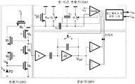
도 10은 도 4a의 변환기(400), 도 5의 검출기(500), 및 도 7의 광-시간 변환기(700)를 포함하는 예시적인 이미지 센서의 개략도이다. 도 10에 도시된 바와 같이, 변환기(400)는 광-시간 변환기(700)에 연결된 제1 출력, 및 검출기(500)에 연결된 제2 출력을 갖는다. 검출기(500)는 트리거 신호를 광-시간 변환기(700)에 보내고, 광-시간 변환기는 제어 신호를 검출기(500)에 보낸다. 마지막으로, 광-시간 변환기(700)는 신호를 Req 버스를 통해 판독 회로부(도시되지 않음)로 보내고, Ack 버스를 통해 수신확인 신호를 수신할 수 있다.FIG. 10 is a schematic diagram of an exemplary image sensor including the
도 11은 도 4a의 변환기(400), 도 5의 검출기(500), 및 도 8의 광-시간 변환기(800)를 포함하는 다른 예시적인 이미지 센서의 개략도이다. 도 11에 도시된 바와 같이, 변환기(400)는 광-시간 변환기(800)에 연결된 제1 출력, 및 검출기(500)에 연결된 제2 출력을 갖는다. 검출기(500)는 트리거 신호를 광-시간 변환기(800)로 보내고, 광-시간 변환기는 제어 신호를 검출기(500)로 보낸다. 마지막으로, 광-시간 변환기(800)는 Req 버스를 통해 판독 회로부(도시되지 않음)에 신호를 보내고, Ack 버스를 통해 수신확인 신호를 수신할 수 있다.FIG. 11 is a schematic diagram of another exemplary image sensor including the
도 12는 본 발명의 실시형태에 따른 이미지 센서, 예를 들어, 도 10 및 도 11의 픽셀을 포함하는 이미지 센서로부터의 예시적인 출력(1220 및 1230)에 비해 현존하는 이미지 센서로부터의 예시적인 출력(1210)을 도시한다. 도 12에 도시된 바와 같이, 전체 이미지(1210)는 이미지 내의 정지 배경으로 인해 상당한 외부 상세 사항을 포함한다. 도 10 또는 도 11에 도시된 이미지 센서의 출력(1220)은 콘트라스트 검출 이벤트로 표현될 수 있다(예를 들어, 음의 변화를 나타내는 검은색 픽셀과, 양의 변화를 나타내는 흰색 픽셀, 여기서 회색 영역은 활성화되지 않은 픽셀임). 따라서, 도 10 또는 도 11에 도시된 이미지 센서의 출력은 장면 내 움직임이 있는 흑백 사진(1230)을 현상하는데 사용될 수 있다. 사진(1230)은 출력(1220)에서 활성화된 픽셀로부터의 세기 레벨을 사용하여 생성될 수 있다. 알 수 있는 바와 같이, 출력(1220) 및 사진(1230)은 상당히 적은 데이터를 포함하여서, 전체 이미지(1210)보다 예를 들어 장면 내의 변화를 추적하거나 인식하기 위해 후처리하기에 더 쉽고 더 효율적이다.12 is an exemplary output from an existing image sensor compared to
본 발명에 따라 구성된 픽셀의 다른 부분을 제조하기 위해, 광-신호 변환기는 하나의 특정 전압 범위를 필요로 할 수 있는 반면, 픽셀의 다른 부분(예를 들어, 광-시간 변환기, 검출기 등)은 예를 들어, 제조의 소형화 및/또는 확장성을 수행하기 위해, 다른 전압 범위를 필요로 할 수 있다. 예를 들어, 위에서 논의된 바와 같이, 광-신호 변환기에 대한 공급 전압은 광-시간 변환기에 공급되는 것보다 상이하고 더 높을 수 있다.In order to manufacture different parts of a pixel constructed according to the invention, an optical-to-signal converter may require one specific voltage range, while other parts of the pixel (e.g., light-to-time converter, detector, etc.) For example, different voltage ranges may be required to achieve miniaturization and/or scalability of manufacturing. For example, as discussed above, the supply voltage to the light-to-signal converter may be different and higher than that supplied to the light-to-time converter.
따라서, 일부 실시형태에서, 광-신호 변환기 및 이미지 센서의 픽셀 내 회로부의 나머지 부분을 각각 구현하기 위해 상이한 반도체 기술이 사용될 수 있다. 예를 들어, 두 개의 반도체 공정(이는 상이한 기본 기술에 기초하고, 상이한 최소 피처 크기를 가지고, 상이한 공급 전압 등을 가질 수 있음)은 두 회로 유형에 대해 개별적으로 최적화될 수 있다. 이들 공정의 결과(예를 들어, 광-신호 변환기 및 픽셀 내 회로부의 나머지 부분)는 웨이퍼 간 적층 기술을 사용하여 통합될 수 있다.Thus, in some embodiments, different semiconductor technologies may be used to implement the light-to-signal converter and the rest of the circuitry in pixels of the image sensor, respectively. For example, two semiconductor processes (which are based on different basic technologies, may have different minimum feature sizes, different supply voltages, etc.) can be optimized separately for both circuit types. The results of these processes (eg, optical-to-signal converters and the rest of the circuitry in the pixel) can be integrated using an inter-wafer lamination technique.
전술한 설명은 예시를 위한 목적으로 제시되었다. 본 설명은 모든 예시를 다 제시한 것도 아니고, 본 발명을 개시된 정확한 형태 또는 실시형태로 제한되는 것도 아니다. 실시형태의 수정 및 적응은 본 명세서를 고려하는 것으로부터 그리고 개시된 실시형태를 실시하는 것으로부터 명백해질 것이다. 예를 들어, 설명된 구현은 하드웨어를 포함하지만, 본 발명과 일치하는 시스템 및 방법은 하드웨어 및 소프트웨어로 구현될 수 있다. 또한, 특정 구성 요소가 서로 결합된 것으로 설명되었지만, 이러한 구성 요소는 서로 통합되거나 임의의 적절한 방식으로 분포될 수 있다.The foregoing description has been presented for purposes of illustration. This description is not intended to present all examples, nor is the present invention limited to the precise forms or embodiments disclosed. Modifications and adaptations of the embodiments will become apparent from consideration of the present specification and from practice of the disclosed embodiments. For example, the described implementation includes hardware, but systems and methods consistent with the present invention may be implemented in hardware and software. Further, although certain components have been described as being combined with each other, these components may be integrated with each other or distributed in any suitable manner.
더욱이, 예시적인 실시형태가 본 명세서에 설명되었지만, 본 범위는 본 발명에 기초한 등가 요소, 수정, 생략, 조합(예를 들어, 다양한 실시형태에 걸친 양태), 적응 및/또는 변경을 갖는 임의의 및 모든 실시형태를 포함한다. 청구 범위의 요소는 청구 범위에 사용된 언어에 기초하여 광범위하게 해석되어야 하고, 본 명세서에 설명된 예로 제한되지 않고 또는 본 출원의 진행 과정 동안 제한되지 않으며, 이러한 예는 비-배타적인 것으로 해석되어야 한다. 또한, 개시된 방법의 단계는 단계의 순서 변경 및/또는 단계 삽입 또는 삭제를 포함하여 임의의 방식으로 수정될 수 있다.Moreover, although exemplary embodiments have been described herein, the scope of the present invention is not limited to any equivalent elements, modifications, omissions, combinations (e.g., aspects across various embodiments), adaptations, and/or changes based on the present invention. And all embodiments. Elements of the claims are to be interpreted broadly based on the language used in the claims, and are not limited to the examples described herein or during the course of this application, and such examples are to be construed as non-exclusive. do. Further, the steps of the disclosed method may be modified in any manner, including changing the order of steps and/or inserting or deleting steps.
본 발명의 특징 및 장점은 설명된 명세서로부터 명백하며, 따라서 첨부된 청구 범위는 본 발명의 진정한 사상 및 범위 내에 속하는 모든 시스템 및 방법을 포괄하는 것으로 의도된다. 본 명세서에 사용된 단수형 요소는 "하나 이상의" 요소를 의미한다. 유사하게, 복수형 용어를 사용하는 것은 주어진 문맥에서 불명확하지 않는 한 반드시 복수를 나타내는 것은 아니다. "및" 또는 "또는"과 같은 단어는 구체적으로 달리 지시하지 않는 한 "및/또는"을 의미한다. 또한, 본 발명을 연구함으로써 많은 수정 및 변형이 쉽게 발생할 수 있으므로, 본 발명은 도시되고 설명된 정확한 구성 및 동작으로 제한되는 것은 바람직하지 않으며, 따라서 모든 적절한 수정 및 등가물이 본 발명의 범위 내에 속할 수 있다.Features and advantages of the present invention are apparent from the described specification, and therefore the appended claims are intended to cover all systems and methods falling within the true spirit and scope of the present invention. As used herein, the singular element means “one or more” elements. Similarly, the use of plural terms does not necessarily indicate plural unless it is unclear in a given context. Words such as "and" or "or" mean "and/or" unless specifically indicated otherwise. In addition, since many modifications and variations can easily occur by studying the present invention, it is not preferable that the present invention be limited to the exact configuration and operation shown and described, and therefore all suitable modifications and equivalents may fall within the scope of the present invention. have.
본 명세서를 고려하는 것으로부터 그리고 본 명세서에 개시된 실시형태를 실시하는 것으로부터 다른 실시형태도 명백해질 것이다. 본 명세서 및 실시형태는 단지 예로서 고려된 것으로 의도되며, 개시된 실시형태의 진정한 범위 및 사상은 다음의 청구 범위에 의해 한정된다.Other embodiments will become apparent from consideration of this specification and from carrying out the embodiments disclosed herein. This specification and embodiments are intended to be considered by way of example only, and the true scope and spirit of the disclosed embodiments are defined by the following claims.
Claims (19)
감광 요소;
상기 감광 요소에 연결되고, 상기 감광 요소에 도달하는 광의 세기에 선형적으로 비례하는 전류 신호를 제1 출력에 제공하고, 상기 감광 요소에 도달하는 광의 세기의 로그 함수인 전압 신호를 제2 출력에 제공하도록 구성된 광-신호 변환기;
검출기로서, 상기 광-신호 변환기의 제2 출력의 전압 신호에 비례하는 상기 검출기의 신호가 임계값을 초과하는 경우 다른 픽셀의 검출기와 독립적으로 자율적으로 트리거 신호를 생성하도록 구성된, 상기 검출기; 및
상기 광-신호 변환기의 제1 출력에 연결되고, 상기 감광 요소 상의 광의 세기를 측정하고 시간 영역에서 인코딩하도록 구성된 광-시간 변환기로서, 광-시간 변환 사이클은 상기 검출기로부터 상기 트리거 신호를 수신한 것에 응답하여 상기 광-시간 변환기에 의해 개시되는, 상기 광-시간 변환기를 포함하는, 비동기식 시간 기반 이미지 센서.As an asynchronous time-based image sensor comprising a plurality of pixels,
Photosensitive element;
A current signal connected to the photosensitive element and linearly proportional to the intensity of light reaching the photosensitive element is provided to a first output, and a voltage signal that is a log function of the intensity of light reaching the photosensitive element is provided to a second output. An optical to signal converter configured to provide;
A detector, the detector configured to autonomously generate a trigger signal independently of a detector of another pixel when a signal of the detector proportional to a voltage signal of a second output of the optical-signal converter exceeds a threshold value; And
An optical-time converter connected to a first output of the optical-signal converter and configured to measure the intensity of light on the photosensitive element and encode in a time domain, wherein a photo-time conversion cycle is based on receiving the trigger signal from the detector. Asynchronous time-based image sensor comprising the light-to-time converter, initiated by the light-to-time converter in response.
상기 광-신호 변환기의 제1 출력에 병렬로 연결된 커패시터 및 스위치;
상기 제1 출력에 연결된 비교기; 및
상기 비교기 및 검출기에 연결된 논리 회로를 포함하고, 상기 논리 회로는, 상기 검출기로부터 트리거 신호를 수신한 것에 응답하여 상기 스위치를 개방함으로써 상기 광-시간 변환 사이클을 개시하고, 상기 커패시터 양단의 전압이 기준 전압에 도달함을 상기 비교기를 사용하여 검출한 것에 응답하여 상기 광-시간 변환 사이클을 완료하고, 상기 광-시간 변환 사이클의 개시 및 완료를 상기 이미지 센서의 외부의 판독 시스템으로 전달하도록 구성되고,
상기 커패시터는 상기 광-신호 변환기의 제1 출력의 전류 신호에 의해 상기 광-시간 변환 사이클 동안 충전되도록 구성된, 비동기식 시간 기반 이미지 센서.The method of claim 1, wherein the optical-time converter,
A capacitor and a switch connected in parallel to the first output of the optical-signal converter;
A comparator connected to the first output; And
And a logic circuit coupled to the comparator and detector, wherein the logic circuit initiates the photo-time conversion cycle by opening the switch in response to receiving a trigger signal from the detector, wherein the voltage across the capacitor is referenced. Completing the light-time conversion cycle in response to detecting using the comparator that a voltage is reached, and communicating the initiation and completion of the light-time conversion cycle to a reading system external to the image sensor,
Wherein the capacitor is configured to be charged during the light-to-time conversion cycle by a current signal of the first output of the light-to-signal converter.
상기 광-신호 변환기의 제1 출력에서, 상기 감광 요소에 도달하는 광의 세기에 선형적으로 비례하는 전류 신호를 제공하는 단계;
상기 광-신호 변환기의 제2 출력에서, 상기 감광 요소에 도달하는 광의 세기의 로그 함수인 전압 신호를 제공하는 단계;
상기 광-신호 변환기의 제2 출력의 전압 신호에 비례하는 상기 검출기의 신호가 임계값을 초과하는 경우 다른 픽셀의 검출기와 독립적으로 자율적으로 상기 검출기를 사용하여 트리거 신호를 생성하는 단계; 및
상기 광-시간 변환기를 사용하여 상기 감광 요소 상의 광의 세기를 시간 경과 정보로 인코딩하는 단계로서, 상기 시간 경과 정보는 상기 광-시간 변환 사이클의 개시 시간 및 상기 광-시간 변환 사이클의 완료 시간을 포함하는, 상기 광의 세기를 시간 경과 정보로 인코딩하는 단계를 포함하고,
상기 광-시간 변환 사이클은 상기 검출기로부터 상기 트리거 신호를 수신한 것에 응답하여 상기 광-시간 변환기에 의해 개시되는, 복수의 픽셀을 사용하여 비동기식 시간 기반 이미지 감지를 제공하는 방법.A method of providing asynchronous time-based image detection using a plurality of pixels, each pixel comprising a photosensitive element, an optical-signal converter connected to the photosensitive element, a detector, and a photo-time converter connected to the photo-signal converter. And, the method,
Providing, at a first output of the light-to-signal converter, a current signal linearly proportional to the intensity of light reaching the photosensitive element;
Providing, at a second output of the light-to-signal converter, a voltage signal that is a log function of the intensity of light reaching the photosensitive element;
Generating a trigger signal using the detector independently of the detector of another pixel when a signal of the detector proportional to the voltage signal of the second output of the optical-signal converter exceeds a threshold value; And
Encoding the intensity of light on the photosensitive element into time lapse information using the light-to-time converter, wherein the time lapse information includes a start time of the light-time conversion cycle and a completion time of the light-time conversion cycle. Including the step of encoding the intensity of the light into time lapse information,
The photo-time conversion cycle is initiated by the photo-time converter in response to receiving the trigger signal from the detector. A method of providing asynchronous time-based image sensing using a plurality of pixels.
상기 광-시간 변환기를 사용하여, 상기 광-시간 변환 사이클의 개시 시간을 상기 복수의 픽셀의 외부에 있는 판독 시스템으로 전달하는 단계; 및
상기 광-시간 변환기를 사용하여 상기 광-시간 변환 사이클의 완료 시간을 상기 판독 시스템으로 더 전달하는 단계를 더 포함하는, 복수의 픽셀을 사용하여 비동기식 시간 기반 이미지 감지를 제공하는 방법.The method of claim 13,
Passing, using the light-to-time converter, an initiation time of the light-to-time conversion cycle to a reading system external to the plurality of pixels; And
Further comprising using the light-to-time converter to communicate the completion time of the light-to-time conversion cycle to the reading system. 2. A method of providing asynchronous time-based image sensing using a plurality of pixels.
상기 광-시간 변환 사이클 동안 상기 광-신호 변환기의 제1 출력의 전류 신호를 사용하여 커패시터를 충전하는 단계;
상기 커패시터 양단의 전압이 기준 전압에 도달했다고 결정될 때 비교기를 사용하여 상기 광-시간 변환 사이클의 완료 시간을 검출하는 단계;
바람직하게는 상기 판독 시스템에서, 각 픽셀에 대한 어드레스 정보를 각 픽셀의 상기 광-시간 변환기로부터 수신된 상기 광-시간 변환 사이클 개시 및 완료 정보와 결합시키는 단계; 및
상기 복수의 픽셀의 외부에 있는 디지털 처리 시스템에 의해 상기 픽셀 어드레스 정보 및 상기 광-시간 변환 사이클 개시 및 완료 정보를 바람직하게는 동기화하고 타임스탬핑하는 단계를 더 포함하는, 복수의 픽셀을 사용하여 비동기식 시간 기반 이미지 감지를 제공하는 방법.The method of claim 13 or 14,
Charging a capacitor using the current signal of the first output of the light-to-signal converter during the light-to-time conversion cycle;
Detecting a completion time of the photo-time conversion cycle using a comparator when it is determined that the voltage across the capacitor has reached a reference voltage;
Advantageously in said reading system, combining address information for each pixel with said light-time conversion cycle start and end information received from said light-time converter of each pixel; And
Asynchronously using a plurality of pixels, further comprising synchronizing and timestamping the pixel address information and the light-time conversion cycle start and end information, preferably by a digital processing system external to the plurality of pixels. How to provide time-based image detection.
상기 기준 전압을 복수의 기준 전압 레벨 사이에서 변화시키는 단계를 더 포함하고, 선택적으로, 상기 커패시터 양단의 전압이 상기 기준 전압에 도달할 때마다 상기 기준 전압을 더 낮은 기준 전압 레벨로 감소시키는 단계를 더 포함하는, 복수의 픽셀을 사용하여 비동기식 시간 기반 이미지 감지를 제공하는 방법.The method according to any one of claims 13 to 15,
Further comprising changing the reference voltage between a plurality of reference voltage levels, and optionally, reducing the reference voltage to a lower reference voltage level whenever the voltage across the capacitor reaches the reference voltage. Further comprising a method of providing asynchronous time-based image detection using a plurality of pixels.
상기 검출기로부터 상기 트리거 신호를 수신한 것에 응답하여 리셋 신호를 상기 검출기로 보내는 단계를 더 포함하는, 복수의 픽셀을 사용하여 비동기식 시간 기반 이미지 감지를 제공하는 방법.The method according to any one of claims 13 to 17,
And sending a reset signal to the detector in response to receiving the trigger signal from the detector. 2. A method of providing asynchronous time-based image sensing using a plurality of pixels.
현재 광-시간 변환 사이클이 완료되기 전에 다른 트리거 신호가 수신될 때, 새로운 광-시간 변환 사이클을 리셋하고 개시하는 단계; 및
취소 신호를 상기 복수의 픽셀의 외부에 있는 판독 시스템으로 보내는 단계를 더 포함하는, 복수의 픽셀을 사용하여 비동기식 시간 기반 이미지 감지를 제공하는 방법.The method according to any one of claims 13 to 18,
When another trigger signal is received before the current light-time conversion cycle is complete, resetting and initiating a new light-time conversion cycle; And
And sending a cancellation signal to a reading system external to the plurality of pixels. A method of providing asynchronous time-based image sensing using a plurality of pixels.
Applications Claiming Priority (3)
| Application Number | Priority Date | Filing Date | Title |
|---|---|---|---|
| EP18170201.0 | 2018-04-30 | ||
| EP18170201 | 2018-04-30 | ||
| PCT/EP2019/061133 WO2019211317A1 (en) | 2018-04-30 | 2019-04-30 | Systems and methods for asynchronous, time-based image sensing |
Publications (1)
| Publication Number | Publication Date |
|---|---|
| KR20210003118A true KR20210003118A (en) | 2021-01-11 |
Family
ID=62110881
Family Applications (1)
| Application Number | Title | Priority Date | Filing Date |
|---|---|---|---|
| KR1020207030863A KR20210003118A (en) | 2018-04-30 | 2019-04-30 | System and method for asynchronous time-based image detection |
Country Status (6)
| Country | Link |
|---|---|
| US (1) | US11412162B2 (en) |
| EP (1) | EP3777131B1 (en) |
| JP (1) | JP7458325B2 (en) |
| KR (1) | KR20210003118A (en) |
| CN (1) | CN112005543A (en) |
| WO (1) | WO2019211317A1 (en) |
Cited By (1)
| Publication number | Priority date | Publication date | Assignee | Title |
|---|---|---|---|---|
| KR20230011603A (en) * | 2021-07-14 | 2023-01-25 | 연세대학교 산학협력단 | Image sensor and image capturing method |
Families Citing this family (6)
| Publication number | Priority date | Publication date | Assignee | Title |
|---|---|---|---|---|
| KR20230173210A (en) | 2018-06-27 | 2023-12-26 | 프로페시 | Image sensor with a plurality of super-pixels |
| WO2020102110A1 (en) * | 2018-11-13 | 2020-05-22 | Magic Leap, Inc. | Event-based ir camera |
| EP3903074A1 (en) | 2019-04-25 | 2021-11-03 | Prophesee SA | Systems and methods for imaging and sensing vibrations |
| JP7393152B2 (en) * | 2019-08-09 | 2023-12-06 | キヤノン株式会社 | Photoelectric conversion device, imaging system, moving object and exposure control device |
| CN111107287B (en) * | 2019-11-29 | 2021-06-04 | 豪威芯仑传感器(上海)有限公司 | Pixel acquisition circuit and image sensor |
| WO2022032462A1 (en) * | 2020-08-11 | 2022-02-17 | Huawei Technologies Co., Ltd. | Sensor circuit, pixel circuit, and method for controlling pixel circuit |
Family Cites Families (8)
| Publication number | Priority date | Publication date | Assignee | Title |
|---|---|---|---|---|
| AT504582B1 (en) * | 2006-11-23 | 2008-12-15 | Arc Austrian Res Centers Gmbh | METHOD FOR GENERATING AN IMAGE IN ELECTRONIC FORM, PICTURE ELEMENT FOR AN IMAGE SENSOR FOR GENERATING AN IMAGE AND PICTOR SENSOR |
| EP2795894B1 (en) * | 2011-12-19 | 2020-06-17 | Universität Zürich | Photoarray, particularly for combining sampled brightness sensing with asynchronous detection of time-dependent image data |
| ES2476115B1 (en) * | 2012-12-11 | 2015-04-20 | Consejo Superior De Investigaciones Científicas (Csic) | METHOD AND DEVICE FOR THE DETECTION OF THE TEMPORARY VARIATION OF LIGHT INTENSITY IN A PHOTOSENSOR MATRIX |
| ES2811152T3 (en) * | 2013-09-16 | 2021-03-10 | Prophesee | Single photodiode dynamic pixel circuit and method of operation |
| CN103595931A (en) * | 2013-11-05 | 2014-02-19 | 天津大学 | CMOS asynchronous time domain image sensor capable of achieving real-time time stamp |
| FR3020699A1 (en) * | 2014-04-30 | 2015-11-06 | Centre Nat Rech Scient | METHOD OF FOLLOWING SHAPE IN A SCENE OBSERVED BY AN ASYNCHRONOUS LIGHT SENSOR |
| CN104808057B (en) * | 2015-05-04 | 2018-02-02 | 中国电子科技集团公司第二十六研究所 | A kind of acousto-optic real-time signal analyzer based on asynchronous detection |
| US10827135B2 (en) * | 2018-11-26 | 2020-11-03 | Bae Systems Information And Electronic Systems Integration Inc. | BDI based pixel for synchronous frame-based and asynchronous event-driven readouts |
-
2019
- 2019-04-30 CN CN201980027430.3A patent/CN112005543A/en active Pending
- 2019-04-30 WO PCT/EP2019/061133 patent/WO2019211317A1/en unknown
- 2019-04-30 US US17/051,148 patent/US11412162B2/en active Active
- 2019-04-30 JP JP2020560332A patent/JP7458325B2/en active Active
- 2019-04-30 EP EP19720626.1A patent/EP3777131B1/en active Active
- 2019-04-30 KR KR1020207030863A patent/KR20210003118A/en not_active Application Discontinuation
Cited By (1)
| Publication number | Priority date | Publication date | Assignee | Title |
|---|---|---|---|---|
| KR20230011603A (en) * | 2021-07-14 | 2023-01-25 | 연세대학교 산학협력단 | Image sensor and image capturing method |
Also Published As
| Publication number | Publication date |
|---|---|
| WO2019211317A1 (en) | 2019-11-07 |
| US11412162B2 (en) | 2022-08-09 |
| CN112005543A (en) | 2020-11-27 |
| US20210235028A1 (en) | 2021-07-29 |
| JP2021522730A (en) | 2021-08-30 |
| EP3777131B1 (en) | 2024-04-03 |
| JP7458325B2 (en) | 2024-03-29 |
| EP3777131A1 (en) | 2021-02-17 |
Similar Documents
| Publication | Publication Date | Title |
|---|---|---|
| KR20210003118A (en) | System and method for asynchronous time-based image detection | |
| EP3563564B1 (en) | Dynamic vision sensor architecture | |
| CN106664379B (en) | High dynamic range pixel and method for operating a high dynamic range pixel | |
| US8780240B2 (en) | Method for the generation of an image in electronic form, picture element (pixel) for an image sensor for the generation of an image as well as image sensor | |
| US6069377A (en) | Image sensor incorporating saturation time measurement to increase dynamic range | |
| US10012534B2 (en) | Photodetection circuit having at least one counter operative in response to a mode switching circuit and operating method thereof | |
| US10827135B2 (en) | BDI based pixel for synchronous frame-based and asynchronous event-driven readouts | |
| JP2016533140A (en) | Dynamic, single photodiode pixel circuit and method of operation thereof | |
| US11368645B2 (en) | Image sensor with a plurality of super-pixels | |
| EP3443741B1 (en) | Digital unit cell with analog counter element | |
| US9986194B2 (en) | Solid state imaging device and imaging system | |
| CN115967864B (en) | Method, circuit, equipment and medium for collecting optical signals in image sensor | |
| TWI566521B (en) | Extended dynamic range charge transimpedance amplifier input cell for light sensor | |
| US20200169681A1 (en) | Ctia based pixel for simultaneous synchronous frame-based & asynchronous event-driven readouts | |
| Wu et al. | A Single-Slope PWM Imaging Method for Multi-Mode Dynamic Vision Sensor | |
| US11885673B2 (en) | Pixel circuit including an open-loop amplifier with well controlled gain for event-based vision sensor and method of controlling thereof | |
| WO2021185190A1 (en) | Pixel circuit, image sensor, and image pickup device and method for using the same | |
| US10623670B1 (en) | Simultaneous multiple well size integration | |
| KR20190091357A (en) | Extended high dynamic range direct injection circuit for imaging applications | |
| JP6170618B2 (en) | How to avoid pixel saturation | |
| JP6170618B6 (en) | How to avoid pixel saturation |
Legal Events
| Date | Code | Title | Description |
|---|---|---|---|
| A201 | Request for examination | ||
| E902 | Notification of reason for refusal |