KR20200132675A - Parallel memory operations in multi-bonded memory device - Google Patents
Parallel memory operations in multi-bonded memory device Download PDFInfo
- Publication number
- KR20200132675A KR20200132675A KR1020200035484A KR20200035484A KR20200132675A KR 20200132675 A KR20200132675 A KR 20200132675A KR 1020200035484 A KR1020200035484 A KR 1020200035484A KR 20200035484 A KR20200035484 A KR 20200035484A KR 20200132675 A KR20200132675 A KR 20200132675A
- Authority
- KR
- South Korea
- Prior art keywords
- semiconductor die
- memory
- bonding pads
- die
- word line
- Prior art date
Links
Images


Classifications
-
- G—PHYSICS
- G11—INFORMATION STORAGE
- G11C—STATIC STORES
- G11C16/00—Erasable programmable read-only memories
- G11C16/02—Erasable programmable read-only memories electrically programmable
- G11C16/06—Auxiliary circuits, e.g. for writing into memory
- G11C16/10—Programming or data input circuits
-
- G—PHYSICS
- G11—INFORMATION STORAGE
- G11C—STATIC STORES
- G11C11/00—Digital stores characterised by the use of particular electric or magnetic storage elements; Storage elements therefor
- G11C11/56—Digital stores characterised by the use of particular electric or magnetic storage elements; Storage elements therefor using storage elements with more than two stable states represented by steps, e.g. of voltage, current, phase, frequency
- G11C11/5621—Digital stores characterised by the use of particular electric or magnetic storage elements; Storage elements therefor using storage elements with more than two stable states represented by steps, e.g. of voltage, current, phase, frequency using charge storage in a floating gate
- G11C11/5628—Programming or writing circuits; Data input circuits
-
- G—PHYSICS
- G11—INFORMATION STORAGE
- G11C—STATIC STORES
- G11C11/00—Digital stores characterised by the use of particular electric or magnetic storage elements; Storage elements therefor
- G11C11/56—Digital stores characterised by the use of particular electric or magnetic storage elements; Storage elements therefor using storage elements with more than two stable states represented by steps, e.g. of voltage, current, phase, frequency
- G11C11/5621—Digital stores characterised by the use of particular electric or magnetic storage elements; Storage elements therefor using storage elements with more than two stable states represented by steps, e.g. of voltage, current, phase, frequency using charge storage in a floating gate
- G11C11/5642—Sensing or reading circuits; Data output circuits
-
- G—PHYSICS
- G11—INFORMATION STORAGE
- G11C—STATIC STORES
- G11C11/00—Digital stores characterised by the use of particular electric or magnetic storage elements; Storage elements therefor
- G11C11/56—Digital stores characterised by the use of particular electric or magnetic storage elements; Storage elements therefor using storage elements with more than two stable states represented by steps, e.g. of voltage, current, phase, frequency
- G11C11/5671—Digital stores characterised by the use of particular electric or magnetic storage elements; Storage elements therefor using storage elements with more than two stable states represented by steps, e.g. of voltage, current, phase, frequency using charge trapping in an insulator
-
- G—PHYSICS
- G11—INFORMATION STORAGE
- G11C—STATIC STORES
- G11C16/00—Erasable programmable read-only memories
- G11C16/02—Erasable programmable read-only memories electrically programmable
- G11C16/04—Erasable programmable read-only memories electrically programmable using variable threshold transistors, e.g. FAMOS
- G11C16/0483—Erasable programmable read-only memories electrically programmable using variable threshold transistors, e.g. FAMOS comprising cells having several storage transistors connected in series
-
- G—PHYSICS
- G11—INFORMATION STORAGE
- G11C—STATIC STORES
- G11C16/00—Erasable programmable read-only memories
- G11C16/02—Erasable programmable read-only memories electrically programmable
- G11C16/06—Auxiliary circuits, e.g. for writing into memory
- G11C16/08—Address circuits; Decoders; Word-line control circuits
-
- G—PHYSICS
- G11—INFORMATION STORAGE
- G11C—STATIC STORES
- G11C16/00—Erasable programmable read-only memories
- G11C16/02—Erasable programmable read-only memories electrically programmable
- G11C16/06—Auxiliary circuits, e.g. for writing into memory
- G11C16/24—Bit-line control circuits
-
- G—PHYSICS
- G11—INFORMATION STORAGE
- G11C—STATIC STORES
- G11C16/00—Erasable programmable read-only memories
- G11C16/02—Erasable programmable read-only memories electrically programmable
- G11C16/06—Auxiliary circuits, e.g. for writing into memory
- G11C16/26—Sensing or reading circuits; Data output circuits
-
- G—PHYSICS
- G11—INFORMATION STORAGE
- G11C—STATIC STORES
- G11C16/00—Erasable programmable read-only memories
- G11C16/02—Erasable programmable read-only memories electrically programmable
- G11C16/06—Auxiliary circuits, e.g. for writing into memory
- G11C16/34—Determination of programming status, e.g. threshold voltage, overprogramming or underprogramming, retention
- G11C16/3436—Arrangements for verifying correct programming or erasure
- G11C16/3454—Arrangements for verifying correct programming or for detecting overprogrammed cells
- G11C16/3459—Circuits or methods to verify correct programming of nonvolatile memory cells
-
- G—PHYSICS
- G11—INFORMATION STORAGE
- G11C—STATIC STORES
- G11C5/00—Details of stores covered by group G11C11/00
- G11C5/02—Disposition of storage elements, e.g. in the form of a matrix array
- G11C5/025—Geometric lay-out considerations of storage- and peripheral-blocks in a semiconductor storage device
-
- G—PHYSICS
- G11—INFORMATION STORAGE
- G11C—STATIC STORES
- G11C5/00—Details of stores covered by group G11C11/00
- G11C5/02—Disposition of storage elements, e.g. in the form of a matrix array
- G11C5/04—Supports for storage elements, e.g. memory modules; Mounting or fixing of storage elements on such supports
-
- G—PHYSICS
- G11—INFORMATION STORAGE
- G11C—STATIC STORES
- G11C5/00—Details of stores covered by group G11C11/00
- G11C5/06—Arrangements for interconnecting storage elements electrically, e.g. by wiring
- G11C5/063—Voltage and signal distribution in integrated semi-conductor memory access lines, e.g. word-line, bit-line, cross-over resistance, propagation delay
-
- G—PHYSICS
- G11—INFORMATION STORAGE
- G11C—STATIC STORES
- G11C7/00—Arrangements for writing information into, or reading information out from, a digital store
- G11C7/06—Sense amplifiers; Associated circuits, e.g. timing or triggering circuits
-
- G—PHYSICS
- G11—INFORMATION STORAGE
- G11C—STATIC STORES
- G11C8/00—Arrangements for selecting an address in a digital store
- G11C8/08—Word line control circuits, e.g. drivers, boosters, pull-up circuits, pull-down circuits, precharging circuits, for word lines
-
- H—ELECTRICITY
- H01—ELECTRIC ELEMENTS
- H01L—SEMICONDUCTOR DEVICES NOT COVERED BY CLASS H10
- H01L25/00—Assemblies consisting of a plurality of individual semiconductor or other solid state devices ; Multistep manufacturing processes thereof
- H01L25/18—Assemblies consisting of a plurality of individual semiconductor or other solid state devices ; Multistep manufacturing processes thereof the devices being of types provided for in two or more different subgroups of the same main group of groups H01L27/00 - H01L33/00, or in a single subclass of H10K, H10N
-
- H01L27/11529—
-
- H—ELECTRICITY
- H10—SEMICONDUCTOR DEVICES; ELECTRIC SOLID-STATE DEVICES NOT OTHERWISE PROVIDED FOR
- H10B—ELECTRONIC MEMORY DEVICES
- H10B41/00—Electrically erasable-and-programmable ROM [EEPROM] devices comprising floating gates
- H10B41/10—Electrically erasable-and-programmable ROM [EEPROM] devices comprising floating gates characterised by the top-view layout
-
- H—ELECTRICITY
- H10—SEMICONDUCTOR DEVICES; ELECTRIC SOLID-STATE DEVICES NOT OTHERWISE PROVIDED FOR
- H10B—ELECTRONIC MEMORY DEVICES
- H10B41/00—Electrically erasable-and-programmable ROM [EEPROM] devices comprising floating gates
- H10B41/20—Electrically erasable-and-programmable ROM [EEPROM] devices comprising floating gates characterised by three-dimensional arrangements, e.g. with cells on different height levels
- H10B41/23—Electrically erasable-and-programmable ROM [EEPROM] devices comprising floating gates characterised by three-dimensional arrangements, e.g. with cells on different height levels with source and drain on different levels, e.g. with sloping channels
- H10B41/27—Electrically erasable-and-programmable ROM [EEPROM] devices comprising floating gates characterised by three-dimensional arrangements, e.g. with cells on different height levels with source and drain on different levels, e.g. with sloping channels the channels comprising vertical portions, e.g. U-shaped channels
-
- H—ELECTRICITY
- H10—SEMICONDUCTOR DEVICES; ELECTRIC SOLID-STATE DEVICES NOT OTHERWISE PROVIDED FOR
- H10B—ELECTRONIC MEMORY DEVICES
- H10B41/00—Electrically erasable-and-programmable ROM [EEPROM] devices comprising floating gates
- H10B41/30—Electrically erasable-and-programmable ROM [EEPROM] devices comprising floating gates characterised by the memory core region
- H10B41/35—Electrically erasable-and-programmable ROM [EEPROM] devices comprising floating gates characterised by the memory core region with a cell select transistor, e.g. NAND
-
- H—ELECTRICITY
- H10—SEMICONDUCTOR DEVICES; ELECTRIC SOLID-STATE DEVICES NOT OTHERWISE PROVIDED FOR
- H10B—ELECTRONIC MEMORY DEVICES
- H10B41/00—Electrically erasable-and-programmable ROM [EEPROM] devices comprising floating gates
- H10B41/40—Electrically erasable-and-programmable ROM [EEPROM] devices comprising floating gates characterised by the peripheral circuit region
- H10B41/41—Electrically erasable-and-programmable ROM [EEPROM] devices comprising floating gates characterised by the peripheral circuit region of a memory region comprising a cell select transistor, e.g. NAND
-
- H—ELECTRICITY
- H10—SEMICONDUCTOR DEVICES; ELECTRIC SOLID-STATE DEVICES NOT OTHERWISE PROVIDED FOR
- H10B—ELECTRONIC MEMORY DEVICES
- H10B43/00—EEPROM devices comprising charge-trapping gate insulators
- H10B43/10—EEPROM devices comprising charge-trapping gate insulators characterised by the top-view layout
-
- H—ELECTRICITY
- H10—SEMICONDUCTOR DEVICES; ELECTRIC SOLID-STATE DEVICES NOT OTHERWISE PROVIDED FOR
- H10B—ELECTRONIC MEMORY DEVICES
- H10B43/00—EEPROM devices comprising charge-trapping gate insulators
- H10B43/20—EEPROM devices comprising charge-trapping gate insulators characterised by three-dimensional arrangements, e.g. with cells on different height levels
- H10B43/23—EEPROM devices comprising charge-trapping gate insulators characterised by three-dimensional arrangements, e.g. with cells on different height levels with source and drain on different levels, e.g. with sloping channels
- H10B43/27—EEPROM devices comprising charge-trapping gate insulators characterised by three-dimensional arrangements, e.g. with cells on different height levels with source and drain on different levels, e.g. with sloping channels the channels comprising vertical portions, e.g. U-shaped channels
-
- H—ELECTRICITY
- H10—SEMICONDUCTOR DEVICES; ELECTRIC SOLID-STATE DEVICES NOT OTHERWISE PROVIDED FOR
- H10B—ELECTRONIC MEMORY DEVICES
- H10B43/00—EEPROM devices comprising charge-trapping gate insulators
- H10B43/30—EEPROM devices comprising charge-trapping gate insulators characterised by the memory core region
- H10B43/35—EEPROM devices comprising charge-trapping gate insulators characterised by the memory core region with cell select transistors, e.g. NAND
-
- H—ELECTRICITY
- H10—SEMICONDUCTOR DEVICES; ELECTRIC SOLID-STATE DEVICES NOT OTHERWISE PROVIDED FOR
- H10B—ELECTRONIC MEMORY DEVICES
- H10B43/00—EEPROM devices comprising charge-trapping gate insulators
- H10B43/40—EEPROM devices comprising charge-trapping gate insulators characterised by the peripheral circuit region
-
- G—PHYSICS
- G11—INFORMATION STORAGE
- G11C—STATIC STORES
- G11C2207/00—Indexing scheme relating to arrangements for writing information into, or reading information out from, a digital store
- G11C2207/10—Aspects relating to interfaces of memory device to external buses
- G11C2207/105—Aspects related to pads, pins or terminals
Abstract
Description
발명자들:Inventors:
하드웰 치바노즈Hardwell Chibanoz
마사토시 니시가와Masato City Nishigawa
휴대용 소비자 전자기기에 대한 수요의 강한 성장은 고용량 저장 디바이스들에 대한 필요성을 이끌고 있다. 디지털 정보 저장 및 교환에 대한 계속 증가하는 수요를 충족시키기 위해 플래시 메모리 저장 카드들과 같은 비휘발성 반도체 메모리 디바이스들이 널리 사용된다. 그들의 휴대성, 다목적성 및 세련되지 않은 설계는, 그들의 높은 신뢰도 및 대용량성과 함께, 그러한 메모리 디바이스들을, 예를 들어 디지털 카메라들, 디지털 뮤직 플레이어들, 비디오 게임 콘솔들, PDA들 및 셀룰러 전화기들을 비롯한 매우 다양한 전자 디바이스들에서 사용하기에 이상적으로 만들었다.The strong growth in demand for portable consumer electronics is driving the need for high capacity storage devices. Nonvolatile semiconductor memory devices such as flash memory storage cards are widely used to meet the ever-increasing demand for digital information storage and exchange. Their portability, versatility and unsophisticated design, along with their high reliability and large capacity, make such memory devices, for example, digital cameras, digital music players, video game consoles, PDAs and cellular telephones. Made ideal for use in a wide variety of electronic devices.
최근에, 초고밀도 메모리 디바이스들이 3차원(3D) 구조물을 사용하여 제안되었다. 3D 구조물의 일례는 층들로 형성된 메모리 셀들의 스트링들을 갖는 적층형 메모리 구조물이다. 하나의 그러한 저장 디바이스는 때때로 BiCS(Bit Cost Scalable) 아키텍처로 지칭된다. 3D 메모리 구조물들은, 이 용어가 본 명세서에 사용되는 바와 같이, 표면적당 저장될 수 있는 비트들의 수를 지칭하는 높은 면 밀도(areal density)를 허용한다. 메모리 셀들에 더하여, 3D 메모리 디바이스들은 메모리 셀들에 대한 판독/기록을 제어하기 위한 로직 회로를 포함한다.Recently, ultra-high density memory devices have been proposed using a three-dimensional (3D) structure. An example of a 3D structure is a stacked memory structure having strings of memory cells formed of layers. One such storage device is sometimes referred to as a Bit Cost Scalable (BiCS) architecture. 3D memory structures allow a high areal density, as this term is used herein, which refers to the number of bits that can be stored per surface area. In addition to memory cells, 3D memory devices include logic circuitry for controlling read/write to the memory cells.
3D 아키텍처에 관계없이, 증가된 밀도(예를 들어, 면 밀도)가 바람직하다. 면 밀도를 증가시키는 하나의 기법은 3D 구조물에서 메모리 셀 층들의 수를 증가시키는 것이다. 그러나, 본 발명의 반도체 제조 기법들은 신뢰성 있게 형성될 수 있는 메모리 셀들의 층들의 수를 제한한다. 또한, 더 많은 수의 메모리 셀들의 층들을 갖는 구조물을 형성하는 것은 제조 비용을 급격히 증가시킬 수 있다.Regardless of the 3D architecture, an increased density (eg, areal density) is desirable. One technique to increase the areal density is to increase the number of memory cell layers in the 3D structure. However, the semiconductor fabrication techniques of the present invention limit the number of layers of memory cells that can be reliably formed. Also, forming a structure with a larger number of layers of memory cells can dramatically increase manufacturing cost.
높은 프로그램 및 판독 처리량을 갖는 것이 또한 바람직하다. 높은 프로그램 및 판독 처리량을 증가시키기 위한 하나의 기법은 다이당 메모리 셀들의 평면들의 수를 증가시키는 것이다. 그러나, 이는 중요한 사양인 다이 크기를 증가시킨다. 반도체 제조 기법들의 경우, 비용은 전형적으로 다이 크기에 따라 선형적으로 스케일링되지 않는다. 예를 들어, 반도체 다이의 크기를 2배로 하는 것은 제조 비용을 2배 이상으로 할 수 있다.It is also desirable to have high program and read throughput. One technique for increasing high program and read throughput is to increase the number of planes of memory cells per die. However, this increases the die size, an important feature. For semiconductor manufacturing techniques, cost typically does not scale linearly with die size. For example, doubling the size of a semiconductor die can double the manufacturing cost.
도 1a는 메모리 디바이스의 기능적 블록도이다.
도 1b는 본 기술의 실시예들에 따른, 다수의 제어 반도체 다이가 형성되는 반도체 웨이퍼의 평면도이다.
도 1c는 본 기술의 실시예들에 따른, 다수의 제1 메모리 반도체 다이가 형성되는 반도체 웨이퍼의 평면도이다.
도 1d는 본 기술의 실시예들에 따른, 다수의 제2 메모리 반도체 다이가 형성되는 반도체 웨이퍼의 평면도이다.
도 2a는 집적 메모리 모듈의 일 실시예의 블록도이다.
도 2b는 집적 메모리 모듈의 다른 실시예의 블록도이다.
도 3a는 감지 블록의 일 실시예를 도시한 블록도이다.
도 3b는 메모리 시스템의 일 실시예를 도시한 블록도이다.
도 4는 모놀리식 3차원 메모리 어레이의 하나의 예시적인 실시예의 일부분의 사시도이다.
도 5는 어레이로 구성된 메모리 셀들의 NAND 스트링들을 프로그래밍하기 위한 프로세스의 일 실시예를 설명하는 흐름도이다.
도 6은 집적 메모리 모듈의 일 실시예의 상세들을 도시한 도면이다.
도 7은 집적 메모리 모듈의 다른 실시예의 상세들을 도시한 도면이다.
도 8은 반도체 다이의 평면 표면 상의 접합 패드들의 예시적인 패턴을 도시한다.
도 9는 도 6의 실시예와 부합하는 집적 메모리 모듈의 일 실시예의 측면도를 도시한다.
도 10은 도 7의 실시예와 부합하는 집적 메모리 모듈의 일 실시예의 측면도를 도시한다.
도 11은 집적 메모리 모듈을 포함하는 비휘발성 메모리를 동작시키는 프로세스의 일 실시예의 흐름도이다.
도 12는 집적 메모리 모듈에서의 병렬 프로그래밍 프로세스의 일 실시예의 흐름도이다.
도 13은 집적 메모리 모듈에서의 병렬 감지 프로세스의 일 실시예의 흐름도이다.1A is a functional block diagram of a memory device.
1B is a plan view of a semiconductor wafer on which a plurality of control semiconductor dies are formed according to embodiments of the present technology.
1C is a plan view of a semiconductor wafer on which a plurality of first memory semiconductor dies are formed, according to embodiments of the present technology.
1D is a plan view of a semiconductor wafer on which a plurality of second memory semiconductor dies are formed, according to embodiments of the present technology.
2A is a block diagram of an embodiment of an integrated memory module.
2B is a block diagram of another embodiment of an integrated memory module.
3A is a block diagram illustrating an embodiment of a sensing block.
3B is a block diagram illustrating an embodiment of a memory system.
4 is a perspective view of a portion of one exemplary embodiment of a monolithic three-dimensional memory array.
5 is a flow diagram illustrating one embodiment of a process for programming NAND strings of memory cells configured in an array.
6 is a diagram illustrating details of an embodiment of an integrated memory module.
7 is a diagram showing details of another embodiment of an integrated memory module.
8 shows an exemplary pattern of bonding pads on a planar surface of a semiconductor die.
9 illustrates a side view of an embodiment of an integrated memory module consistent with the embodiment of FIG. 6.
10 illustrates a side view of an embodiment of an integrated memory module consistent with the embodiment of FIG. 7.
11 is a flow diagram of one embodiment of a process of operating a nonvolatile memory including an integrated memory module.
12 is a flow diagram of one embodiment of a parallel programming process in an integrated memory module.
13 is a flow diagram of one embodiment of a parallel sensing process in an integrated memory module.
본 기술은 이제 도면들을 참조하여 설명될 것이며, 도면들은 실시예들에서 집적 메모리 모듈을 포함하는 반도체 디바이스에 관한 것이다. 집적 메모리 모듈의 실시예들은 면 밀도를 포함하는, 높은 저장 밀도를 갖는다. 집적 메모리 모듈의 실시예들은 높은 프로그램 및 판독 처리량을 갖는다. 집적 메모리 모듈의 실시예들은 프로그램 또는 판독 처리량을 희생시키지 않으면서 높은 저장 밀도(예를 들어, 면 밀도)를 갖는다.The present technology will now be described with reference to the drawings, which in embodiments relate to a semiconductor device including an integrated memory module. Embodiments of the integrated memory module have a high storage density, including areal density. Embodiments of the integrated memory module have high program and read throughput. Embodiments of the integrated memory module have a high storage density (eg, areal density) without sacrificing program or read throughput.
일부 실시예들에서, 집적 메모리 모듈은 단일의 집적된 비휘발성 메모리로서 함께 동작하는 3개의 반도체 다이를 포함할 수 있다. 하나의 반도체 다이는 감지 증폭기들 및 드라이버들을 포함할 수 있는 제어 회로부를 포함할 수 있다. 2개의 반도체 다이는 비휘발성 메모리 셀들을 포함할 수 있다. 3개의 반도체 다이는 단일의 집적된 비휘발성 메모리로서 서로 접합될 수 있다.In some embodiments, an integrated memory module may include three semiconductor die operating together as a single integrated nonvolatile memory. One semiconductor die can include control circuitry that can include sense amplifiers and drivers. The two semiconductor dies may include non-volatile memory cells. The three semiconductor dies can be bonded together as a single integrated non-volatile memory.
본 명세서에 기술된 집적 메모리 모듈의 실시예들은 반도체 다이 크기를 증가시키지 않으면서 높은 저장 밀도(예를 들어, 면 밀도)를 갖는다. 반도체 다이 중 하나 상에 제어 회로부를 배치하는 것은 메모리 셀들을 포함하는 2개의 반도체 다이 상의 공간을 확보할 수 있어서, 메모리 셀 다이 상에 추가적인 메모리 셀들이 배치될 수 있게 할 수 있다. 2개의 반도체 다이 각각이 비휘발성 메모리 셀들을 가지면 집적된 비휘발성 메모리의 면 밀도를 증가시킬 수 있다. 또한, 집적된 비휘발성 메모리는 단일의 반도체 다이 상의 메모리 셀들의 층들의 수를 증가시키는 것과 연관된 문제들 없이 메모리 셀들의 층들의 수를 증가시킬 수 있다.Embodiments of the integrated memory module described herein have a high storage density (eg, areal density) without increasing the semiconductor die size. Placing the control circuit unit on one of the semiconductor dies can reserve space on the two semiconductor dies including memory cells, so that additional memory cells can be disposed on the memory cell die. When each of the two semiconductor dies has nonvolatile memory cells, it is possible to increase the areal density of the integrated nonvolatile memory. Further, integrated non-volatile memory can increase the number of layers of memory cells without problems associated with increasing the number of layers of memory cells on a single semiconductor die.
대체적으로, 더 많은 수의 메모리 셀들을 병렬로 프로그래밍함으로써 프로그램 처리량이 증가될 수 있다. 마찬가지로, 더 많은 수의 메모리 셀들을 병렬로 판독함으로써 판독 처리량이 증가될 수 있다. 일부 메모리 아키텍처들에서, 동일한 워드 라인에 접속되는 메모리 셀들은 병렬로 프로그래밍될 수 있거나 또는 판독될 수 있다. 프로그래밍 및/또는 판독 처리량을 증가시키기 위한 하나의 가능한 기법은 워드 라인들의 크기를 증가시키는 것이다. 그러나, 이러한 해결책은 워드 라인들 상의 로딩(loading)을 증가시키는 경향이 있으며, 이는 성능에 부정적인 영향을 줄 수 있다. 본 명세서에 기술된 집적 메모리 모듈의 실시예들은 워드 라인들의 크기의 상당한 증가 없이 높은 프로그래밍 처리량을 갖는다. 일부 실시예들에서, 제1 반도체 다이 상의 제1 선택된 워드 라인에 접속된 제1 그룹의 메모리 셀들은 제2 반도체 다이 상의 제2 선택된 워드 라인에 접속된 제2 그룹의 메모리 셀들과 병렬로 프로그래밍된다. 선택적으로, 제3 반도체 다이 상의 동일한 워드 라인 드라이버는 프로그래밍 전압을 제1 및 제2 선택된 워드 라인들 양측 모두에 제공하는 데 사용될 수 있다. 따라서, 프로그래밍 처리량은 워드 라인들의 크기를 상당히 증가시키지 않고 증가될 수 있다. 더욱이, 프로그래밍 처리량은 워드 라인들의 로딩을 상당히 증가시키지 않고 증가될 수 있다. 추가적으로, 일부 실시예들에서, 제1, 제2, 및 제3 반도체 다이는 집적 메모리 디바이스로 서로 접합된다. 따라서, 집적 메모리 디바이스는 높은 프로그래밍 처리량 및 높은 면 밀도 양측 모두를 갖는다.Alternatively, program throughput can be increased by programming a larger number of memory cells in parallel. Likewise, read throughput can be increased by reading a larger number of memory cells in parallel. In some memory architectures, memory cells connected to the same word line may be programmed or read in parallel. One possible technique for increasing programming and/or read throughput is to increase the size of the word lines. However, this solution tends to increase the loading on word lines, which can negatively impact performance. Embodiments of the integrated memory module described herein have high programming throughput without a significant increase in the size of word lines. In some embodiments, the first group of memory cells connected to the first selected word line on the first semiconductor die are programmed in parallel with the second group of memory cells connected to the second selected word line on the second semiconductor die. . Optionally, the same word line driver on the third semiconductor die can be used to provide a programming voltage to both the first and second selected word lines. Thus, the programming throughput can be increased without significantly increasing the size of the word lines. Moreover, programming throughput can be increased without significantly increasing the loading of word lines. Additionally, in some embodiments, the first, second, and third semiconductor die are bonded together into an integrated memory device. Thus, integrated memory devices have both high programming throughput and high areal density.
유사하게, 일부 실시예들에서, 제1 반도체 다이 상의 제1 선택된 워드 라인에 접속된 제1 그룹의 메모리 셀들은 제2 반도체 다이 상의 제2 선택된 워드 라인에 접속된 제2 그룹의 메모리 셀들과 병렬로 판독될 수 있다. 따라서, 판독 처리량은 워드 라인들의 크기를 상당히 증가시키지 않고 증가될 수 있다. 더욱이, 판독 처리량은 워드 라인들 상의 로딩을 상당히 증가시키지 않고 증가될 수 있다. 추가적으로, 일부 실시예들에서, 제1, 제2, 및 제3 반도체 다이는 집적 메모리 디바이스로 서로 접합된다. 따라서, 집적 메모리 디바이스의 실시예들은 높은 판독 처리량 및 높은 면 밀도 양측 모두를 갖는다.Similarly, in some embodiments, the first group of memory cells connected to the first selected word line on the first semiconductor die is parallel to the second group of memory cells connected to the second selected word line on the second semiconductor die. Can be read as. Thus, the read throughput can be increased without significantly increasing the size of the word lines. Moreover, the read throughput can be increased without significantly increasing the loading on the word lines. Additionally, in some embodiments, the first, second, and third semiconductor die are bonded together into an integrated memory device. Thus, embodiments of integrated memory devices have both high read throughput and high areal density.
다이당 메모리 셀들의 수를 증가시키는 하나의 가능한 방식은 평면 내의 메모리 셀들의 블록들의 수를 증가시키는 것이다. 그러나, 그러한 해결책은 비트 라인들 상의 로딩을 증가시키는 경향이 있으며, 이는 성능에 영향을 줄 수 있다. 본 명세서에 기술된 집적 메모리 모듈의 실시예들은 비트 라인들 상의 로딩을 증가시키지 않고 높은 저장 용량, 높은 프로그래밍 처리량, 및 높은 판독 처리량을 갖는다.One possible way to increase the number of memory cells per die is to increase the number of blocks of memory cells in the plane. However, such a solution tends to increase the loading on the bit lines, which can affect performance. Embodiments of the integrated memory module described herein have high storage capacity, high programming throughput, and high read throughput without increasing the loading on bit lines.
본 발명은 많은 상이한 형태들로 구현될 수 있고 본 명세서에서 기술되는 실시예들로 제한되는 것으로 해석되어서는 안 된다는 것이 이해된다. 오히려, 이러한 실시예들은 본 개시내용이 철저하고 완전하도록 그리고 본 발명을 당업자에게 충분히 전달하도록 제공된다. 실제로, 본 발명은 첨부된 청구범위에 의해 정의되는 바와 같은 본 발명의 범주 및 사상 내에 포함되는 이러한 실시예들의 대안들, 수정들 및 등가물들을 포함하고자 한다. 더욱이, 본 발명의 아래의 상세한 설명에서, 많은 구체적인 세부사항들이 본 발명의 철저한 이해를 제공하기 위해 기술된다. 그러나, 본 발명이 그러한 구체적인 세부사항들 없이 실시될 수 있다는 것은 당업자에게 명백할 것이다.It is understood that the invention may be implemented in many different forms and should not be construed as being limited to the embodiments described herein. Rather, these embodiments are provided so that the present disclosure will be thorough and complete and will fully convey the present invention to those skilled in the art. Indeed, the invention is intended to cover alternatives, modifications and equivalents of these embodiments that fall within the scope and spirit of the invention as defined by the appended claims. Moreover, in the detailed description of the invention below, many specific details are set forth to provide a thorough understanding of the invention. However, it will be apparent to a person skilled in the art that the present invention may be practiced without such specific details.
본 명세서에서 사용될 수 있는 바와 같은 "상단"과 "하단", "상부"와 "하부", 및 "수직"과 "수평"이라는 용어들, 및 그들의 형태들은 단지 예시로서 그리고 설명의 목적만을 위한 것이며, 언급된 항목이 위치 및 배향에서 교환될 수 있기 때문에 기술의 설명을 제한하고자 하는 것은 아니다. 또한, 본 명세서에서 사용된 바와 같이, "실질적으로" 및/또는 "약"이라는 용어들은 특정된 치수 또는 파라미터가 주어진 응용예에 대해 허용가능한 제조 공차 내에서 달라질 수 있음을 의미한다. 일 실시예에서, 허용가능한 제조 공차는 주어진 치수의 ± 0.25%이다.The terms "top" and "bottom", "top" and "bottom", and "vertical" and "horizontal" as may be used herein, and their forms are for illustrative purposes only and for illustrative purposes only. However, it is not intended to limit the description of the description as the items mentioned may be exchanged in position and orientation. Also, as used herein, the terms "substantially" and/or "about" mean that a specified dimension or parameter may vary within acceptable manufacturing tolerances for a given application. In one embodiment, the acceptable manufacturing tolerance is ± 0.25% of a given dimension.
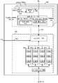
도 1a 내지 도 4는 본 명세서에서 제안되는 기술을 구현하는 데 사용될 수 있는 메모리 시스템의 일례를 설명한다. 도 1a는 집적 메모리 모듈(100)의 일 실시예를 포함하는 예시적인 시스템의 기능적 블록도이다. 도 1a는 또한 제어기(122) 및 호스트 디바이스(140)를 도시한다. 일 실시예에서, 집적 메모리 모듈(100)은 3개의 반도체 다이(또는 더 간결하게, "다이")를 포함한다. 제1 메모리 다이(102a)는 메모리 구조물(126a)을 포함하고, 제2 메모리 다이(102b)는 메모리 구조물(126b)을 포함한다. 제어 다이(104)는 제어 회로부(150)를 포함한다. 일부 실시예들에서, 아래에서 더 상세히 설명되는 바와 같이, 제1 메모리 다이(102a), 제2 메모리 다이(102b), 및 제어 다이(104)는 서로 접합된다.1A-4 illustrate an example of a memory system that can be used to implement the techniques proposed herein. 1A is a functional block diagram of an exemplary system including an embodiment of an
제어 회로부(110)는 메모리 구조물들(126) 상에서 메모리 동작들(예컨대, 기록, 판독, 소거 및 기타)을 수행한다. 제어 회로부(110)는 상태 머신(112), 온-칩 어드레스 디코더(114), 전력 제어 회로(116), 저장 영역(118), 및 판독/기록 회로들(128)을 포함한다. 다른 실시예에서, 판독/기록 회로들(128) 중 일부는 제1 메모리 다이(102a) 상에 위치되고, 다른 판독/기록 회로들(128)은 제2 메모리 다이(102b) 상에 위치된다. 일부 실시예들에서, 제어 회로부(110)는 메모리 구조물(126b)에서의 메모리 동작들과 병렬로 메모리 구조물(126a)에서의 메모리 동작들을 제어하도록 구성된다. 본 명세서에서, 용어 "메모리 다이", "메모리 반도체 다이" 등은 저장을 위한 비휘발성 메모리 셀들을 포함하는 반도체 다이를 의미한다. 본 명세서에서, 용어 "제어 다이", "제어 반도체 다이" 등은 메모리 다이 상의 비휘발성 메모리 셀들에 대해 메모리 동작들을 수행하기 위한 제어 회로부를 포함하는 반도체 다이를 의미한다. 전형적으로, 다수의 반도체 다이가 단일의 반도체(예를 들어, 실리콘) 웨이퍼로부터 형성된다.The
온-칩 어드레스 디코더(114)는 로우 디코더들 및 컬럼 디코더들(도 1a에는 명확히 도시되지 않음)에 의해 사용되는 하드웨어 어드레스에 호스트(140) 또는 제어기(122)에 의해 사용되는 어드레스들 사이의 어드레스 인터페이스를 제공한다. 전력 제어 회로(116)는 메모리 동작들 동안 워드 라인들, 비트 라인들, 및 선택 라인들에 공급되는 전력 및 전압들을 제어한다. 전력 제어 회로(116)는, 일 실시예에서, 전압 회로부를 포함한다. 전력 제어 회로(116)는 전압들을 생성하기 위한 전하 펌프들을 포함할 수 있다. 전력 제어 회로(116)는, 일 실시예에서, 상태 머신(112)의 제어 하에서 실행된다.The on-
판독/기록 회로들(128)은, 일부 실시예들에서, 감지 블록들(감지 증폭기들(SA)을 포함할 수 있음)을 포함한다. 일부 실시예들에서, 감지 증폭기들은 비트 라인 드라이버들을 포함한다. 판독/기록 회로들(128)은, 일 실시예에서, 상태 머신(112)의 제어 하에서 실행된다. 일부 실시예들에서, 각각의 메모리 구조물(126)은 로우 디코더(도 1a에는 도시되지 않음)를 통해 워드 라인들에 의해, 그리고 컬럼 디코더(도 1a 에는 도시되지 않음)를 통해 비트 라인들에 의해 어드레스가능하다.The read/
상태 머신(112) 및/또는 제어기(122)(또는 동등하게 기능화된 회로들)는 도 1a에 도시된 다른 회로들의 전부 또는 그들의 서브세트와 조합하여 하나 이상의 제어 회로들로 간주될 수 있다. 하나 이상의 제어 회로들은 하드웨어만을 포함할 수 있거나, 또는 (펌웨어를 포함하는) 소프트웨어와 하드웨어의 조합을 포함할 수 있다. 예를 들어, 펌웨어에 의해 프로그래밍된 제어기가 제어 회로의 일례이다. 하나 이상의 제어 회로들은 프로세서, PGA(Programmable Gate Array), FPGA(Field Programmable Gate Array), ASIC(Application Specific Integrated Circuit), 집적 회로 또는 다른 타입의 회로를 포함할 수 있다. 일부 실시예들에서, 하나 이상의 제어 회로들은 메모리 구조물(126b)에서의 메모리 동작들과 병렬로 메모리 구조물(126a)에서의 메모리 동작들을 제어하도록 구성된다.
통로(152)는 제어 회로부(110) 내의 하나 이상의 컴포넌트들과 메모리 다이(102a) 상의 메모리 구조물 사이의 통로이다. 신호(예컨대, 전압, 전류)를 제공하기 위해 또는 수신하기 위해 통로가 사용될 수 있다. 통로는 전기 전도성 경로를 포함한다. 통로는 접합 패드, 금속 상호접속부, 비아, 트랜지스터, 전기 전도성 재료 및 전기 신호를 전송 또는 반송할 수 있는 다른 재료 중 하나 이상을 포함할 수 있지만, 이에 한정되지는 않는다. 통로(152)는, 일 실시예에서, 제어 회로부(110)가 메모리 다이(102a) 상의 워드 라인들, 선택 라인들, 및 비트 라인들에 전압들을 제공할 수 있게 한다. 통로(154)는 제어 회로부(110) 내의 하나 이상의 컴포넌트들과 메모리 다이(102b) 상의 메모리 구조물 사이의 통로이다. 통로(154)는, 일 실시예에서, 제어 회로부(110)가 메모리 다이(102b) 상의 워드 라인들, 선택 라인들, 및 비트 라인들에 전압들을 제공할 수 있게 한다. 통로들(152, 154)은, 예를 들어 비트 라인들로부터 신호들을 수신하는 데 사용될 수 있다.
일부 시스템들에서, 집적 메모리 모듈(100)과 동일한 패키지(예컨대, 착탈식 저장 카드) 내에 제어기(122)가 포함된다. 제어기(122)와 동일한 패키지 내에 몇몇 집적 메모리 모듈들(100)이 있을 수 있음에 유의한다. 그러나, 다른 시스템들에서, 제어기는 집적 메모리 모듈(100)과는 별개의 패키지 내에 있을 수 있다. 도 1a의 실시예에서, 제어기(122)는 집적 메모리 모듈(100)과 상이한 다이 상에 있다. 일부 실시예들에서는, 하나의 제어기(122)가 다수의 집적 메모리 모듈들(100)과 통신할 것이다. 다른 실시예들에서, 각각의 집적 메모리 모듈(100)은 그 자신의 제어기를 갖는다. 커맨드들 및 데이터가 데이터 버스(120)를 통하여 호스트(140)와 제어기(122) 사이에서, 그리고 라인들(124)을 통하여 제어기(122)와 하나 이상의 집적 메모리 모듈(100) 사이에서 전달된다. 일 실시예에서, 집적 메모리 모듈(100)은 라인들(124)에 접속되는 한 세트의 입력 및/또는 출력(I/O) 핀들을 포함한다. 라인들(124)은 보편성을 위해 집적 메모리 모듈(100)에 접속되는 것으로 도시되어 있다. 라인들(124)은 다이(102a, 102b 및/또는 104) 중 임의의 것 또는 모두에 접속할 수 있다. 일 실시예에서, 라인들(124)은 제어기(122)를 메모리 다이(104)에 직접 접속시킨다. 일 실시예에서, 라인들(124)은 제어기(122)를 메모리 다이(102a)에 직접 접속시킨다. 일 실시예에서, 라인들(124)은 제어기(122)를 메모리 다이(102a)에 직접 접속시킨다. 라인들(124)이 제어기를 메모리 다이 중 어느 하나의 다이(102a 또는 102b)에 직접 접속시키면, 통로들 중 하나(152 또는 154)는 제어기(122)와 제어 회로부(110) 사이의 통신을 허용하는 데 사용될 수 있다.In some systems, the
(온-칩 또는 오프-칩) 제어기(122)(이는, 일 실시예에서, 전기 회로임)는, 하나 이상의 프로세서들(122c), ROM(122a), RAM(122b), 메모리 인터페이스(MI)(122d) 및 호스트 인터페이스(HI)(122e)를 포함할 수 있으며, 이들은 모두 상호접속된다. 저장 디바이스들(ROM(122a), RAM(122b))은 한 세트의 명령어들(펌웨어를 포함함)과 같은 코드(소프트웨어)를 저장하고, 하나 이상의 프로세서들(122c)은 한 세트의 명령어들을 실행하여 본 명세서에서 기술되는 기능을 제공하도록 동작가능하다. 대안으로 또는 추가로, 하나 이상의 프로세서들(122c)은 하나 이상의 워드 라인들에 접속된 메모리 셀들의 예약된 영역과 같은 메모리 구조물 내의 저장 디바이스로부터의 코드에 액세스할 수 있다. RAM(122b)은 캐싱 프로그램 데이터를 포함한, 제어기(122)에 대한 데이터를 저장하기 위한 것일 수 있다. ROM(122a), RAM(122b) 및 프로세서(122c)와 통신 상태에 있는 메모리 인터페이스(122d)는 제어기(122)와 하나 이상의 집적 메모리 모듈(100) 사이에 전기적 인터페이스를 제공하는 전기 회로이다. 예를 들어, 메모리 인터페이스(122d)는 신호들의 포맷 또는 타이밍을 변경할 수 있고, 버퍼를 제공할 수 있고, 서지(surge)들로부터 분리될 수 있고, I/O를 래칭할 수 있고, 등등일 수 있다. 하나 이상의 프로세서들(122c)은 메모리 인터페이스(122d)를 통해 제어 회로부(110)(또는 집적 메모리 모듈(100)의 다른 컴포넌트)에 커맨드들을 발행할 수 있다. 호스트 인터페이스(122e)는 호스트(140)로부터 커맨드들, 어드레스들 및/또는 데이터를 수신하여 호스트(140)에 데이터 및/또는 상태를 제공하기 위해 호스트(140)의 데이터 버스(120)와의 전기적 인터페이스를 제공한다.The (on-chip or off-chip) controller 122 (which, in one embodiment, is an electrical circuit), includes one or more processors 122c,
일 실시예에서, 메모리 구조물(126)은 다수의 메모리 레벨들이 웨이퍼와 같은 단일 기판 위에 형성되는 비휘발성 메모리 셀들의 3차원 메모리 어레이를 포함한다. 메모리 구조물은 실리콘(또는 다른 타입의) 기판 위에 활성 영역이 배치되어 있는 메모리 셀들의 어레이들의 하나 이상의 물리적 레벨들에서 모놀리식으로 형성되는 임의의 타입의 비휘발성 메모리를 포함할 수 있다. 일례에서, 비휘발성 메모리 셀들은 전하 트래핑 재료를 갖는 수직 NAND 스트링들을 포함한다.In one embodiment,
다른 실시예에서, 메모리 구조물(126)은 비휘발성 메모리 셀들의 2차원 메모리 어레이를 포함한다. 일례에서, 비휘발성 메모리 셀들은 플로팅 게이트들을 활용하는 NAND 플래시 메모리 셀들이다. 다른 타입들의 메모리 셀들(예컨대, NOR-타입 플래시 메모리)이 또한 사용될 수 있다.In another embodiment,
메모리 구조물(126)에 포함된 메모리 어레이 아키텍처 또는 메모리 셀의 정확한 타입은 상기의 예들로 제한되지 않는다. 많은 상이한 타입들의 메모리 어레이 아키텍처들 또는 메모리 기술들이 메모리 구조물(126)을 형성하는 데 이용될 수 있다. 어떠한 특정의 비휘발성 메모리 기술도 본 명세서에서 제안되는 새롭게 청구되는 실시예들의 목적을 위해 필요하지는 않다. 메모리 구조물(126)의 메모리 셀들에 적절한 기술들의 다른 예들은 위상 변화 메모리(예컨대, PCM) 등을 포함한다. 메모리 구조물(126)의 메모리 셀 아키텍처들에 대한 적절한 기술들의 예들은 2차원 어레이들, 3차원 어레이들, 교차점 어레이(cross-point array)들, 적층형 2차원 어레이들, 수직 비트 라인 어레이들 등을 포함한다.The exact type of memory cell or memory array architecture included in the
당업자는, 본 명세서에서 설명되는 기술이 단일의 특정 메모리 구조물에 제한되는 것이 아니라, 본 명세서에서 설명되는 바와 같은 기술의 사상 및 범주 내에서 그리고 당업자에 의해 이해되는 바와 같이 많은 관련 메모리 구조물들을 커버함을 인식할 것이다.Those of skill in the art, the technology described herein is not limited to a single particular memory structure, but covers many related memory structures as understood by those skilled in the art and within the spirit and scope of the technology as described herein. Will recognize.
저장 디바이스는 한 세트의 명령어들과 같은 코드를 포함하고, 프로세서는 한 세트의 명령어들을 실행하여 본 명세서에서 설명되는 기능을 제공하도록 동작가능하다. 대안으로 또는 추가로, 프로세서는 하나 이상의 워드 라인들에서 메모리 셀들의 예약된 영역으로부터의 코드에 액세스할 수 있다.The storage device includes code, such as a set of instructions, and the processor is operable to execute the set of instructions to provide the functionality described herein. Alternatively or additionally, the processor can access code from a reserved area of memory cells in one or more word lines.
예를 들어, 코드는 예컨대, 프로그래밍, 판독 및 소거 동작들을 위해 메모리 구조물에 액세스하기 위해 제어기에 의해 사용될 수 있다. 코드는 부트 코드 및 제어 코드(예를 들어, 한 세트의 명령어들)를 포함할 수 있다. 부트 코드는 부팅 또는 시동 프로세스 동안 제어기를 초기화하고 제어기가 메모리 구조물에 액세스할 수 있게 하는 소프트웨어이다. 코드는 하나 이상의 메모리 구조물을 제어하기 위해 제어기에 의해 사용될 수 있다. 전력 공급 시에, 프로세서(122c)는 실행을 위해 ROM(122a) 또는 메모리 구조물(126)로부터 부트 코드를 페치(fetch)하고, 부트 코드는 시스템 컴포넌트들을 초기화하고 제어 코드를 RAM(122b)에 로딩한다. 일단 제어 코드가 RAM에 로딩되면, 그것은 프로세서에 의해 실행된다. 제어 코드는 메모리의 제어 및 할당, 명령어들의 처리의 우선 순위화, 및 입력 및 출력 포트들의 제어와 같은 기본 작업들을 수행하도록 드라이버들을 포함한다.For example, code can be used by a controller to access a memory structure, eg, for programming, read and erase operations. The code may include a boot code and a control code (eg, a set of instructions). The boot code is software that initializes the controller during the boot or startup process and allows the controller to access memory structures. The code can be used by the controller to control one or more memory structures. Upon power up, processor 122c fetches boot code from
대체적으로, 제어 코드는 아래에서 추가로 논의되는 흐름도들의 단계들을 포함한 본 명세서에 기술된 기능들을 수행하기 위한, 그리고 아래에서 추가로 논의되는 것들을 포함한 전압 파형들을 제공하기 위한 명령어들을 포함할 수 있다. 제어 회로는 명령어들을 실행하여 본 명세서에 기술된 기능들을 수행하도록 구성될 수 있다.Alternatively, the control code may include instructions for performing functions described herein, including steps in flow charts further discussed below, and for providing voltage waveforms, including those discussed further below. The control circuitry may be configured to execute instructions to perform the functions described herein.
도 1b는 반도체 웨이퍼(135a)의 평면도이다. 웨이퍼(135a)는 집적 회로들(103)의 많은 사본들을 갖는다. 일 실시예에서, 집적 회로들(103) 각각은 제어 회로부(110)(도 1a 참조)를 포함한다. 웨이퍼(135a)는, 일부 실시예들에서, 집적 회로들(103)의 사본들 중 하나를 각각 포함하는 반도체 다이들로 다이싱된다. 따라서, 다수의 제어 반도체 다이들(104)이 웨이퍼(135a)로부터 형성될 수 있다. 또한, 웨이퍼(135a)가 다이싱되기 전에도, 용어 "제어 반도체 다이"가 본 명세서에서 사용되는 바와 같이, 집적 회로(103)가 존재하는 각각의 영역은 제어 반도체 다이(104)로 지칭될 수 있다는 것에 유의한다.1B is a plan view of a
도 1c는 반도체 웨이퍼(135b)의 평면도이다. 웨이퍼(135b)는 집적 회로들(105a)의 많은 사본들을 갖는다. 일 실시예에서, 집적 회로들(105a) 각각은 메모리 구조물(126a)(도 1a 참조)을 포함한다. 웨이퍼(135b)는, 일부 실시예들에서, 집적 회로들(105a)의 사본들 중 하나를 각각 포함하는 반도체 다이들로 다이싱된다. 따라서, 다수의 제1 메모리 반도체 다이들(102a)이 웨이퍼(135b)로부터 형성될 수 있다. 또한, 웨이퍼(135b)가 다이싱되기 전에도, 용어 "메모리 반도체 다이"가 본 명세서에서 사용되는 바와 같이, 집적 회로(105a)가 존재하는 각각의 영역은 메모리 반도체 다이(102a)로 지칭될 수 있다는 것에 유의한다.1C is a plan view of a
도 1d는 반도체 웨이퍼(135c)의 평면도이다. 웨이퍼(135c)는 집적 회로들(105b)의 많은 사본들을 갖는다. 일 실시예에서, 집적 회로들(105b) 각각은 메모리 구조물(126b)(도 1a 참조)을 포함한다. 웨이퍼(135c)는, 일부 실시예들에서, 집적 회로들(105b)의 사본들 중 하나를 각각 포함하는 반도체 다이들로 다이싱된다. 따라서, 다수의 제2 메모리 반도체 다이들(102b)이 웨이퍼(135c)로부터 형성될 수 있다. 또한, 웨이퍼(135c)가 다이싱되기 전에도, 용어 "메모리 반도체 다이"가 본 명세서에서 사용되는 바와 같이, 집적 회로(105b)가 존재하는 각각의 영역은 메모리 반도체 다이(102b)로 지칭될 수 있다는 것에 유의한다.1D is a plan view of a
반도체 웨이퍼들(135)은 CZ, FZ 또는 다른 프로세스 중 어느 하나에 따라 성장된 단결정 실리콘의 잉곳(ingot)으로서 시작할 수 있다. 반도체 웨이퍼들(135)은 매끄러운 표면들을 제공하기 위해 주 표면들 상에서 절단 및 폴리싱될 수 있다. 집적 회로들(103, 105a, 105b)은 주 표면들 상에 그리고/또는 주 표면들 내에 형성될 수 있다. 웨이퍼들(135)을 반도체 다이들로 다이싱하는 것은 접합 전에 또는 그 후에 발생할 수 있다. 일 실시예에서, 3개의 웨이퍼들(135a, 135b, 135c)은 서로 접합된다. 3개의 웨이퍼들을 서로 접합한 후에, 다이싱이 수행된다. 따라서, 다수의 집적 메모리 모듈들(100)은 3개의 웨이퍼들(135)로부터 형성될 수 있다. 다른 실시예에서, 3개의 웨이퍼들(135a, 135b, 135c)은 반도체 다이들(104, 102a, 102b)로 다이싱된다. 이어서, 반도체 다이들(104, 102a, 102b) 각각은 서로 접합되어 집적 메모리 모듈(100)을 형성한다. 다이싱이 접합 이전에 또는 그 후에 발생하는지 여부에 관계없이, 집적 메모리 모듈(100)은 서로 접합된 제어 반도체 다이(104), 제1 메모리 반도체 다이(102a), 및 제2 메모리 반도체 다이(102b)를 포함한다고 말할 수 있다.The semiconductor wafers 135 may begin as an ingot of single crystal silicon grown according to either CZ, FZ, or another process. Semiconductor wafers 135 may be cut and polished on major surfaces to provide smooth surfaces.
도 2a는 집적 메모리 모듈(100)의 일 실시예의 블록도이다. 메모리 다이(102a)는 메모리 셀들의 제1 평면(220)을 포함한다. 메모리 다이(102b)는 메모리 셀들의 제2 평면(230)을 포함한다. 각각의 메모리 다이(102a, 102b)는 추가적인 평면들을 가질 수 있다. 각각의 평면은 M개의 블록들로 분할된다. 일례에서, 각각의 평면은 약 2000개의 블록들을 갖는다. 그러나, 상이한 수들의 블록들이 또한 사용될 수 있다. 일 실시예에서, 메모리 셀들을 포함하는 블록은 소거의 단위이다. 즉, 블록의 모든 메모리 셀들은 함께 소거된다. 다른 실시예들에서, 메모리 셀들은 다른 이유들로, 예컨대, 신호전달(signaling) 및 선택 회로들을 인에이블시키도록 메모리 구조물(126)을 구성하기 위해 블록들로 그룹화될 수 있다. 하나의 대표적인 비트 라인(BL)이 각각의 평면에 대해 도시된다. 각각의 평면당 수천 또는 수만 개의 그러한 비트 라인들이 있을 수 있다. 각각의 블록은 아래에서 더 충분히 설명되는 바와 같이, 다수의 워드 라인들로 분할될 수 있다. 일 실시예에서, 블록은 접속된 메모리 셀들의 그룹들을 표현하는데, 이는 블록의 메모리 셀들이 비단선(unbroken) 워드 라인들과 비단선 비트 라인들의 공통 세트를 공유하기 때문이다. 도 2a의 구조물에서, 양측 평면들(220, 230) 모두의 블록 0 및 블록 M-1은 메모리 구조물의 에지에 있다(또는, 달리, 메모리 구조물의 에지 영역/섹션에 위치되는 것으로 언급됨).2A is a block diagram of an embodiment of an
제어 다이(104)는, 일 실시예에서, 다수의 감지 증폭기들(SA)(250)을 포함한다. 각각의 감지 증폭기(250)는, 이 예에서, 하나의 비트 라인에 접속된다. 일 실시예에서, 감지 증폭기는 비트 라인 드라이버를 포함한다. 따라서, 감지 증폭기는 그것이 접속되는 비트 라인에 전압을 제공할 수 있다. 감지 증폭기는 비트 라인의 상태를 감지하도록 구성된다. 일 실시예에서, 감지 증폭기는 비트 라인에서 흐르는 전류를 감지하도록 구성된다. 일 실시예에서, 감지 증폭기는 비트 라인 상의 전압을 감지하도록 구성된다.The control die 104 includes, in one embodiment, a number of sense amplifiers (SA) 250. Each
제어 다이(104)는 다수의 워드 라인 드라이버들(260(1) 내지 260(n))을 포함한다. 워드 라인 드라이버들(260)은 워드 라인들에 전압들을 제공하도록 구성된다. 이 예에서, 메모리 셀들의 블록당 "n"개의 워드 라인들이 있다. 일 실시예에서, 각각의 평면(220, 230) 내의 블록들 중 하나는 메모리 어레이 동작을 위한 시간에 선택된다. 메모리 동작이 프로그래밍 또는 판독인 경우, 일 실시예에서, 선택된 블록 내의 하나의 워드 라인이 메모리 동작을 위해 선택된다. 메모리 동작이 소거인 경우, 일 실시예에서, 선택된 블록 내의 워드 라인들 모두가 소거를 위해 선택된다. 워드 라인 드라이버들(260)은 메모리 다이(102a) 내의 제1 선택된 블록(예를 들어, 블록 2) 내의 워드 라인들에, 그리고 또한 메모리 다이(102b) 내의 제2 선택된 블록(예컨대, 블록 2) 내의 워드 라인들에 전압들을 제공한다. 일부 실시예들에서, 단일의 워드 라인 드라이버는 메모리 다이(102a) 내의 제1 워드 라인에 그리고 메모리 다이(102b) 내의 제2 워드 라인에 전압을 동시에 제공한다. 따라서, 워드 라인 드라이버들(260)의 수가 감소될 수 있다.The control die 104 includes a number of word line drivers 260(1) to 260(n).
제어 다이(104)는 또한, 워드 라인 드라이버들(260) 및/또는 비트 라인 드라이버들에 전압들을 제공하는 데 사용될 수 있는 전하 펌프들, 전압 생성기들 등을 포함할 수 있다. 도 2a의 아키텍처는 그러한 전하 펌프들, 전압 생성기들 등이 메모리 다이(102a, 102b) 양측 모두로 동시에 전달되는 전압들을 생성하는 것을 허용한다.Control die 104 may also include charge pumps, voltage generators, and the like that may be used to provide voltages to
제1 메모리 다이(102a)는 제1 메모리 다이(102a)의 제1 주 표면(282) 상에 다수의 접합 패드들(270(a), 270(b))을 갖는다. 대응하는 "n"개의 워드 라인 드라이버들(260(1) 내지 260(n))로부터 전압들을 수신하기 위해 "n"개의 접합 패드들(270(a))이 있을 수 있다. 평면(220)과 연관된 각각의 비트 라인에 대해 하나의 접합 패드(270(b))가 있을 수 있다. 도면 부호 270은 대체적으로 주 표면(282) 상의 접합 패드들을 지칭하는 데 사용될 것이다.The
제어 다이(104)는 제어 다이(104)의 제1 주 표면(284) 상에 다수의 접합 패드들(274(a), 274(b))을 갖는다. 대응하는 "n"개의 워드 라인 드라이버들(260(1) 내지 260(n))로부터 메모리 다이(102a)로 전압들을 전달하기 위해 "n"개의 접합 패드들(274(a))이 있을 수 있다. 평면(220)과 연관된 각각의 비트 라인에 대해 하나의 접합 패드(274b)가 있을 수 있다. 도면 부호 274는 대체적으로 주 표면(282) 상의 접합 패드들을 지칭하는 데 사용될 것이다. 접합 패드 쌍들(270(a)/274(a)) 및 접합 패드 쌍들(270(b)/274(b))이 있을 수 있음에 유의한다. 일부 실시예들에서, 접합 패드들(270 및/또는 274)은 플립-칩 접합 패드들이다.The control die 104 has a number of bonding pads 274(a) and 274(b) on the first
제어 다이(104)는 제어 다이(104)의 제2 주 표면(288) 상에 다수의 접합 패드들(276(a), 276(b))을 갖는다. 대응하는 "n"개의 워드 라인 드라이버들(260(1) 내지 260(n))로부터 메모리 다이(102b)로 전압들을 전달하기 위해 "n"개의 접합 패드들(276(a))이 있을 수 있다. 메모리 다이(102b) 상의 평면(230)과 연관된 각각의 비트 라인에 대해 하나의 접합 패드(276b)가 있을 수 있다. 도면 부호 276은 대체적으로 주 표면(288) 상의 접합 패드들을 지칭하는 데 사용될 것이다.Control die 104 has a number of bonding pads 276(a) and 276(b) on a second
제2 메모리 다이(102b)는 제2 메모리 다이(102b)의 제1 주 표면(286) 상에 다수의 접합 패드들(272(a), 272(b))을 갖는다. 대응하는 "n"개의 워드 라인 드라이버들(260(1) 내지 260(n))로부터 전압들을 수신하기 위해 "n"개의 접합 패드들(272(a))이 있을 수 있다. 평면(230)과 연관된 각각의 비트 라인에 대해 하나의 접합 패드(272(b))가 있을 수 있다. 도면 부호 272는 대체적으로 주 표면(286) 상의 접합 패드들을 지칭하는 데 사용될 것이다. 접합 패드 쌍들(272(a)/276(a)) 및 접합 패드 쌍들(272(b)/276(b))이 있을 수 있음에 유의한다. 일부 실시예들에서, 접합 패드들(272 및/또는 276)은 플립-칩 접합 패드들이다.The
접합 패드들(270)의 패턴은 일 실시예에서 접합 패드들(274)의 패턴과 일치한다. 접합 패드들(270)은 일 실시예에서 접합 패드들(274)에 접합(예를 들어, 플립 칩 접합)된다. 따라서, 접합 패드들(270, 274)은 제1 메모리 다이(102a)를 제어 다이(104)에 전기적으로 그리고 물리적으로 커플링시킨다. 또한, 접합 패드들(270, 274)은 제1 메모리 다이(102a)와 제어 다이(104) 사이의 내부 신호 전송을 허용한다. 접합 패드들(272)의 패턴은 일 실시예에서 접합 패드들(276)의 패턴과 일치한다. 접합 패드들(272)은 일 실시예에서 접합 패드들(276)에 접합(예를 들어, 플립 칩 접합)된다. 따라서, 접합 패드들(272, 276)은 제2 메모리 다이(102b)를 제어 다이(104)에 전기적으로 그리고 물리적으로 커플링시킨다. 또한, 접합 패드들(272, 276)은 제2 메모리 다이(102b)와 제어 다이(104) 사이의 내부 신호 전송을 허용한다. 따라서, 제1 메모리 다이(102a), 제2 메모리 다이(102b), 및 제어 다이(104)는 서로 접합된다.The pattern of the
본 명세서에서, "내부 신호 전송"은 다이들(102(a), 102(b), 104) 중 2개의 다이 사이의 신호 전송을 의미한다. 내부 신호 전송은 제어 다이(104)와 제1 메모리 다이(102(a)) 사이에 또는 제어 다이(104)와 제2 메모리 다이(102(b)) 사이에 있을 수 있다. 일부 경우들에서, 내부 신호 전송은 제1 메모리 다이(102(a))와 제2 메모리 다이(102(b)) 사이에 있다. 내부 신호 전송은 제어 다이(104) 상의 회로부가 제2 메모리 다이(102b)와 병렬로 제1 메모리 다이(102a) 내의 메모리 동작들을 제어하는 것을 허용한다. 따라서, 접합 패드들(270, 272, 274, 276)은 메모리 동작 신호 전송을 위해 사용될 수 있다. 본 명세서에서, "메모리 동작 신호 전송"은 메모리 다이(102)에서의 메모리 동작에 관련된 임의의 신호들을 지칭한다. 메모리 동작 신호 전송은 전압을 제공하는 것, 전류를 제공하는 것, 전압을 수신하는 것, 전류를 수신하는 것, 전압을 감지하는 것, 및/또는 전류를 감지하는 것을 포함할 수 있지만, 이에 제한되지 않는다.In this specification, “internal signal transmission” refers to signal transmission between two of the dies 102(a), 102(b), and 104. The internal signal transmission may be between the control die 104 and the first memory die 102(a) or between the control die 104 and the second memory die 102(b). In some cases, the internal signal transfer is between the first memory die 102(a) and the second memory die 102(b). The internal signal transfer allows circuitry on the control die 104 to control memory operations within the
접합 패드들(270 내지 276)은 예를 들어 구리, 알루미늄 및 이들의 합금들로 형성될 수 있다. 접합 패드들(272 내지 278)과 주 표면들(282 내지 288) 사이에는 라이너(liner)가 있을 수 있다. 라이너는 예를 들어 티타늄/티타늄 질화물 스택으로 형성될 수 있다. 접합 패드들(270 내지 276) 및 라이너는 기상 증착 및/또는 도금 기법들에 의해 적용될 수 있다. 접합 패드들 및 라이너들은 함께 720 nm의 두께를 가질 수 있지만, 이러한 두께는 추가의 실시예들에서 더 클 수 있거나 또는 더 작을 수 있다.The
다이들 내의 다양한 요소들을 접합 패드들(270 내지 276)에 전기적으로 접속시키기 위해 금속 상호접속부들 및/또는 비아들이 사용될 수 있다. 금속 상호접속부들 및/또는 비아들로 구현될 수 있는 몇몇 전도성 통로들이 도시되어 있다. 예를 들어, 감지 증폭기(250)는 통로(212)에 의해 접합 패드(274(b))에, 또는 통로(214)에 의해 접합 패드(276(b))에 전기적으로 접속될 수 있다. 수천 개의 그러한 감지 증폭기들, 통로들, 및 접합 패드들이 있을 수 있다. 워드 라인 드라이버들(260)은 통로들(202)에 의해 접합 패드들(274(a))에 전기적으로 접속될 수 있다. 통로들(202)이 각각의 워드 라인 드라이버(260(1) 내지 260(n))에 대한 별개의 전도성 통로를 포함할 수 있음에 유의한다. 마찬가지로, 각각의 워드 라인 드라이버(260(1) 내지 260(n))에 대해 별개의 접합 패드(274(a))가 있을 수 있다. 메모리 다이(102a)의 블록(2) 내의 워드 라인들은 통로들(204)에 의해 접합 패드들(270(a))에 전기적으로 접속될 수 있다. 메모리 다이(102b)의 블록(2) 내의 워드 라인들은 통로들(208)에 의해 접합 패드들(272(a))에 전기적으로 접속될 수 있다. 도 2a에서, 블록 내의 대응하는 "n"개의 워드 라인들에 대해 "n"개의 통로들(204) 및 "n"개의 통로들(208)이 있다. 마찬가지로, "n"개의 워드 라인 드라이버들(260), "n"개의 통로들(202), 및 "n"개의 통로들(206)이 있을 수 있다. 각각의 통로(204)에 대해 별개의 쌍의 접합 패드들(270(a), 274(a))이 있을 수 있다. 각각의 통로(208)에 대해 별개의 쌍의 접합 패드들(272(a), 276(a))이 있을 수 있다. 도 6은 금속 상호접속부들 및/또는 비아들을 갖는 집적 메모리 모듈(100)의 일 실시예의 추가 상세들을 도시한다.Metal interconnects and/or vias may be used to electrically connect various elements within the dies to the bonding pads 270-276. Several conductive passages are shown that may be implemented with metal interconnects and/or vias. For example, the
도 2b는 집적 메모리 모듈(100)의 다른 실시예를 도시한다. 감지 증폭기들(SA)(250)은 도 2b에 도시된 실시예에서 제1 메모리 다이(102a) 및 제2 메모리 다이(102b) 상에 위치된다. 따라서, 접합 패드들(270(b), 272(b), 274(b), 276(b))이 집적 메모리 모듈(100)의 실시예에서 필요하지 않다. 그러나, 접합 패드들(270(a), 272(a), 274(a), 및 276(a))에 더하여 다른 접합 패드들이 있을 수 있다. 따라서, 접합 패드들(270, 274)은 제1 메모리 다이(102a)를 제어 다이(104)에 전기적으로 그리고 물리적으로 커플링시킨다. 또한, 접합 패드들(270(a), 274(a))은 제1 메모리 다이(102a)와 제어 다이(104) 사이의 내부 신호 전송을 허용한다. 더욱이, 접합 패드들(272, 276)은 제2 메모리 다이(102b)를 제어 다이(104)에 전기적으로 그리고 물리적으로 커플링시킨다. 또한, 접합 패드들(272(a), 276(a))은 제1 메모리 다이(102a)와 제어 다이(104) 사이의 내부 신호 전송을 허용한다.2B shows another embodiment of the
도 3a는 감지 블록(350)의 일 실시예를 도시한 블록도이다. 판독/기록 회로들(128)은, 일부 실시예들에서, 다수의 감지 블록들을 포함한다. 개별 감지 블록(350)은 감지 회로들(250(1) 내지 250(4)) 또는 감지 증폭기들로 지칭되는 하나 이상의 코어 부분들, 및 관리 회로(190)로 지칭되는 공통 부분으로 분할된다. 일 실시예에서, 각각의 비트 라인/NAND 스트링에 대한 별개의 감지 회로 및 한 세트의 다수의, 예컨대 4개 또는 8개의 감지 회로들에 대한 하나의 공통 관리 회로(190)가 있을 것이다. 그룹 내의 감지 회로들 각각은 데이터 버스(172)를 통해 연관된 관리 회로와 통신한다. 따라서, 한 세트의 저장 요소들(메모리 셀들)의 감지 회로들과 통신하는 하나 이상의 관리 회로들이 있다.3A is a block diagram showing an embodiment of the
감지 회로(250(1))는, 일례로서, 접속된 비트 라인 내의 전도 전류가 사전결정된 임계 레벨을 초과하는지 또는 그 미만인지 여부를 결정함으로써 감지를 수행하는 감지 회로부(170)를 포함한다. 감지는 판독 또는 검증 동작에서 발생할 수 있다. 감지 회로는 또한, 프로그램 동작에서 프로그램 전압의 인가 동안 비트 라인 전압을 공급한다.The sensing circuit 250(1) includes, as an example, a sensing circuit portion 170 that performs sensing by determining whether the conduction current in the connected bit line exceeds or falls below a predetermined threshold level. Sensing can occur in read or verify operations. The sensing circuit also supplies the bit line voltage during application of the program voltage in the program operation.
감지 회로는 Vbl 셀렉터(173), 감지 노드(171), 비교 회로(175) 및 트립 래치(trip latch)(174)를 포함할 수 있다. 프로그램 전압의 인가 동안, Vbl 셀렉터(173)는 프로그램 인에이블 전압(예컨대, V_pgm_enable) 또는 프로그램-금지 전압(예컨대, Vbl_inh)을 메모리 셀에 접속된 비트 라인으로 패스할 수 있다. 본 명세서에서, "프로그램 인에이블 전압"은 프로그램 전압(예컨대, Vpgm)이 또한 메모리 셀에 인가되는 동안 메모리 셀의 프로그래밍을 가능하게 하는, 메모리 셀에 인가된 전압으로서 정의된다. 소정 실시예들에서, 프로그램 인에이블 전압은 메모리 셀에 커플링된 비트 라인에 인가되는 반면, 프로그램 전압은 메모리 셀의 제어 게이트에 인가된다. 본 명세서에서, "프로그램 금지 전압"은, 프로그램 전압(예컨대, Vpgm)이 또한 메모리 셀에 인가되는(예컨대, 메모리 셀의 제어 게이트에 인가되는) 동안 메모리 셀에 커플링된 비트 라인에 인가되어 메모리 셀의 프로그래밍을 금지하는 전압으로서 정의된다. 부스팅 전압들(예컨대, Vpass)이 비트 라인에 인가된 프로그램 금지 전압과 함께 선택되지 않은 워드 라인들에 인가될 수 있다는 것에 유의한다.The sensing circuit may include a Vbl selector 173, a sensing node 171, a comparison circuit 175, and a trip latch 174. During application of the program voltage, the Vbl selector 173 may pass a program enable voltage (eg, V_pgm_enable) or a program-inhibit voltage (eg, Vbl_inh) to a bit line connected to the memory cell. In this specification, "program enable voltage" is defined as a voltage applied to a memory cell that enables programming of a memory cell while a program voltage (eg, Vpgm) is also applied to the memory cell. In certain embodiments, the program enable voltage is applied to the bit line coupled to the memory cell, while the program voltage is applied to the control gate of the memory cell. In this specification, the "program inhibit voltage" is applied to the bit line coupled to the memory cell while the program voltage (e.g., Vpgm) is also applied to the memory cell (e.g., applied to the control gate of the memory cell) It is defined as the voltage that inhibits programming of the cell. Note that boosting voltages (eg, Vpass) may be applied to unselected word lines along with a program inhibit voltage applied to the bit line.
프로그램 금지 전압들은 프로그래밍되지 않는 메모리 셀들에 커플링된 비트 라인들 및/또는 프로그래밍 프로세스의 실행을 통해 그들 각자의 타깃 임계 전압에 도달한 메모리 셀들을 갖는 비트 라인들에 인가된다. 이들은 "선택되지 않은 비트 라인들"로 지칭될 수 있다. 프로그램 금지 전압들은 프로그래밍될 메모리 셀을 갖는 비트 라인들("선택된 비트 라인들")에는 인가되지 않는다. 프로그램 금지 전압이 선택되지 않은 비트 라인에 인가될 때, 일 실시예에서, 비트 라인은 NAND 채널로부터 컷오프(cut off)된다. 따라서, 일 실시예에서, 프로그램 금지 전압은 NAND 채널로 패스되지 않는다. 부스팅 전압들은 선택되지 않은 워드 라인들에 인가되어 NAND 채널의 전위를 상승시키며, 이는 메모리 셀 - 메모리 셀의 제어 게이트에서 프로그램 전압을 수신함 - 의 프로그래밍을 금지한다.Program inhibit voltages are applied to bit lines coupled to unprogrammed memory cells and/or to bit lines having memory cells that have reached their respective target threshold voltage through execution of a programming process. These may be referred to as “unselected bit lines”. Program inhibit voltages are not applied to the bit lines ("selected bit lines") having a memory cell to be programmed. When a program inhibit voltage is applied to an unselected bit line, in one embodiment, the bit line is cut off from the NAND channel. Thus, in one embodiment, the program inhibit voltage is not passed to the NAND channel. Boosting voltages are applied to unselected word lines to raise the potential of the NAND channel, which inhibits programming of the memory cell-receiving the program voltage at the control gate of the memory cell.
트랜지스터(55)(예컨대, nMOS)는, 트랜지스터의 제어 게이트 전압을 충분히 높게, 예를 들어 Vbl 셀렉터로부터 패스된 Vbl보다 높게 설정함으로써 Vbl 셀렉터(173)로부터 Vbl을 패스시키기 위한 패스 게이트로서 구성될 수 있다. 예를 들어, 셀렉터(56)는 전력 공급원 전압(Vdd), 예컨대 3 내지 4 V를 트랜지스터(55)의 제어 게이트로 패스할 수 있다.The transistor 55 (e.g., nMOS) can be configured as a pass gate for passing Vbl from the Vbl selector 173 by setting the control gate voltage of the transistor sufficiently high, for example, higher than Vbl passed from the Vbl selector. have. For example, the
판독 및 검증 동작들과 같은 감지 동작들 동안, 비트 라인 전압은 셀렉터(56)에 의해 패스되는 전압에 기초하여 트랜지스터(55)에 의해 설정된다. 비트 라인 전압은 트랜지스터의 제어 게이트 전압에서 그것의 Vt(예컨대, 1 V)를 뺀 것과 대략 동일하다. 예를 들어, Vbl+Vt가 셀렉터(56)에 의해 패스되면, 비트 라인 전압은 Vbl일 것이다. 이는 소스 라인이 0 V에 있다고 상정한다. 트랜지스터(55)는 제어 게이트 전압에 따라 비트 라인 전압을 클램핑하고 패스 게이트보다는 소스-팔로워(source-follower)로서 작용한다. Vbl 셀렉터(173)는 트랜지스터(55) 상의 제어 게이트 전압보다 높은 Vdd와 같은 상대적으로 높은 전압을 패스하여 소스-팔로워 모드를 제공할 수 있다. 따라서, 감지 동안 트랜지스터(55)는 비트 라인을 충전한다.During sensing operations such as read and verify operations, the bit line voltage is set by
하나의 접근법에서, 각각의 감지 회로의 셀렉터(56)는 Vbl 또는 Vdd를 패스하기 위해 다른 감지 회로들의 셀렉터들과는 별개로 제어될 수 있다. 각각의 감지 회로의 Vbl 셀렉터(173)는 또한, 다른 감지 회로들의 Vbl 셀렉터들과는 별개로 제어될 수 있다.In one approach, the
감지 동안, 감지 노드(171)는 Vsense_init=3 V와 같은 초기 전압까지 충전된다. 감지 노드는 이어서 트랜지스터(55)를 통해 비트 라인에 접속되고, 감지 노드의 감쇠의 양은 메모리 셀이 전도성 상태에 있는지 또는 비전도성 상태에 있는지 여부를 결정하는 데 사용된다. 비교 회로(175)는 감지 시간에 감지 노드 전압을 트립 전압과 비교하는 데 사용된다. 감지 노드 전압이 트립 전압(Vtrip) 미만으로 감쇠하는 경우, 메모리 셀은 전도성 상태에 있고 그것의 Vt는 검증 신호의 전압 이하이다. 감지 노드 전압이 Vtrip 미만으로 감쇠하지 않는 경우, 메모리 셀은 비전도성 상태에 있고 그것의 Vt는 검증 신호의 전압을 초과한다. 감지 회로부(170)는 메모리 셀이 전도성 상태에 있는지 또는 비전도성 상태에 있는지 여부에 기초하여 비교 회로(175)에 의해 설정되는 트립 래치(174)를 포함한다. 트립 래치에서의 데이터는 프로세서(192)에 의해 판독되는 비트일 수 있다.During sensing, sensing node 171 is charged to an initial voltage such as Vsense_init=3 V. The sense node is then connected to the bit line through
관리 회로(190)는 프로세서(192), 데이터 래치들(194, 195, 196, 197)의 4개의 예시적인 세트들 및 데이터 래치들(194)의 세트와 데이터 버스(120) 사이에 커플링된 I/O 인터페이스(196)를 포함한다. 예를 들어, 개별 래치들 LDL, MDL 및 UDL을 포함하는 데이터 래치들의 하나의 세트가 각각의 감지 회로에 대해 제공될 수 있다. 일부 경우들에서, 추가 데이터 래치들이 사용될 수 있다. LDL은 데이터의 하부 페이지에 대한 비트를 저장하고, MDL은 데이터의 중간 페이지에 대한 비트를 저장하고, UDL은 데이터의 상부 페이지에 대한 비트를 저장한다. 이것은 메모리 셀당 8-레벨 또는 3-비트의 메모리 디바이스 내에 있다.The
데이터의 페이지는 주어진 시간에 프로그래밍되는 데이터의 단위이다. 일 실시예에서, 데이터의 하나의 페이지가 하나의 블록의 일부분 내로 프로그래밍된다. 예를 들어, 페이지는 블록 내의 선택된 워드 라인에 접속된 메모리 셀들로 프로그래밍될 수 있다. 다른 실시예들에서, 하나의 페이지는 다수의 블록들에 걸쳐 프로그래밍될 수 있다. 예를 들어, 페이지의 제1 부분은 제1 메모리 다이(102a) 상의 제1 블록 내의 제1 선택된 워드 라인에 접속된 메모리 셀들 내로 프로그래밍될 수 있고, 페이지의 제2 부분은 제2 메모리 다이(102b) 상의 제2 블록 내의 제2 선택된 워드 라인에 접속된 메모리 셀들 내로 프로그래밍될 수 있다. 페이지의 정확한 크기, 블록의 정확한 크기 모두는 특정 구현예에 기초하여 달라진다. 일례에서, 페이지는 2048 비트들의 데이터를 저장하고, 데이터의 페이지는 각각의 블록 내에 1024 비트들의 데이터를 갖는 상태로 2개의 블록들에 저장되고, 데이터의 페이지를 저장하는 2개의 블록들은 상이한 메모리 다이들(102a, 102b) 내에 있다.A page of data is a unit of data that is programmed at a given time. In one embodiment, one page of data is programmed into a portion of one block. For example, a page may be programmed with memory cells connected to a selected word line within a block. In other embodiments, one page can be programmed across multiple blocks. For example, a first portion of the page may be programmed into memory cells connected to a first selected word line in a first block on a
프로세서(192)는, 예컨대 감지된 메모리 셀에 저장된 데이터를 결정하고 결정된 데이터를 데이터 래치들의 세트에 저장하기 위해, 계산들을 수행한다. 데이터 래치들(194 내지 197)의 각각의 세트는 판독 동작 동안 프로세서(192)에 의해 결정된 데이터 비트들을 저장하는 데, 그리고 기록 데이터가 메모리 내로 프로그래밍되려는 것으로 나타내는 프로그램 동작 동안 데이터 버스(120)로부터 불러오는 데이터 비트들을 저장하는 데 사용된다. I/O 인터페이스(196)는 데이터 래치들(194 내지 197)과 데이터 버스(120) 사이에 인터페이스를 제공한다.Processor 192 performs calculations, eg, to determine the data stored in the sensed memory cell and store the determined data in a set of data latches. Each set of data latches 194-197 stores data bits determined by the processor 192 during a read operation, and reads from the
프로세서(192)는 또한, 래치들의 상태에 기초하여, 어느 전압이 비트 라인에 인가되는지를 결정하는 데 사용될 수 있다. 이것은 약한 프로그램 인에이블 전압이 비트 라인에 인가되는 시간의 길이 및/또는 크기를 관리하는 데 사용될 수 있다.The processor 192 can also be used to determine which voltage is applied to the bit line based on the state of the latches. This can be used to manage the length and/or amount of time a weak program enable voltage is applied to the bit line.
판독 동안, 시스템의 동작은 어드레싱된 메모리 셀에 대한 상이한 제어 게이트 전압들의 공급을 제어하는 상태 머신(112)의 제어 하에 있다. 그것이 메모리에 의해 지원되는 다양한 메모리 상태들에 대응하는 다양한 사전정의된 제어 게이트 전압들을 통해 스텝형으로 진행됨에 따라, 감지 회로는 이들 전압들 중 하나에서 트리핑할 수 있고, 대응하는 출력이 데이터 버스(172)를 통해 감지 회로로부터 프로세서(192)에 제공될 것이다. 그 시점에서, 프로세서(192)는 감지 회로의 트리핑 이벤트(들) 및 상태 머신으로부터 입력 라인들(193)을 통해 인가된 제어 게이트 전압에 대한 정보를 고려하여 결과적인 메모리 상태를 결정한다. 이어서, 그것은 메모리 상태에 대한 이진 인코딩을 계산하고, 결과의 데이터 비트들을 데이터 래치들(194 내지 197)에 저장한다.During readout, operation of the system is under the control of the
일부 구현예들은 다수의 프로세서들(192)을 포함할 수 있다. 일 실시예에서, 각각의 프로세서(192)는 출력 라인들(도시되지 않음)을 포함하여 출력 라인들 각각이 함께 와이어드-OR(wired-OR)되게 한다. 일부 실시예들에서, 출력 라인들은 와이어드-OR 라인에 접속되기 전에 반전된다. 이러한 구성은, 와이어드-OR를 수신하는 상태 머신이, 프로그래밍되고 있는 모든 비트들이 원하는 레벨에 도달했을 때를 결정할 수 있기 때문에, 프로그램 검증 테스트 동안 프로그래밍 프로세스가 완료될 때의 빠른 결정을 가능하게 한다. 예를 들어, 각각의 비트가 그의 원하는 레벨에 도달했을 때, 그 비트에 대한 로직 0이 와이어드-OR 라인으로 전송될 것이다(또는 데이터 1이 반전된다). 모든 비트들이 데이터 0 (또는 반전된 데이터 1)을 출력할 때, 상태 머신은 프로그래밍 프로세스를 종료하는 것을 알고 있다. 각각의 프로세서가 8개의 감지 회로들과 통신하기 때문에, 상태 머신은 와이어드-OR 라인을 8회 판독할 필요가 있거나, 또는 상태 머신이 와이어드-OR 라인을 1회만 판독하면 되도록 로직이 프로세서(192)에 추가되어 연관된 비트 라인들의 결과들을 누산한다. 유사하게, 로직 레벨들을 정확하게 선택함으로써, 전반적인 상태 머신은 제1 비트가 그의 상태를 변경하는 때를 검출할 수 있고 그에 따라서 알고리즘들을 변경할 수 있다.Some implementations may include multiple processors 192. In one embodiment, each processor 192 includes output lines (not shown) so that each of the output lines are wired-OR together. In some embodiments, the output lines are inverted before being connected to the wired-OR line. This configuration allows a quick decision when the programming process is complete during a program verify test, since the state machine receiving the wired-OR can determine when all the bits being programmed have reached the desired level. For example, when each bit reaches its desired level, a logic 0 for that bit will be sent to the wired-OR line (or
메모리 셀들에 대한 프로그램 또는 검증 동작들 동안, 프로그래밍될 데이터(기록 데이터)는 데이터 버스(120)로부터 데이터 래치들(194 내지 197)의 세트에, LDL, MDL 및 UDL 래치들에, 메모리 셀당 3비트 구현예에 저장된다.During program or verify operations for memory cells, data to be programmed (write data) is from
프로그램 동작은, 상태 머신의 제어 하에서, 한 세트의 프로그래밍 전압 펄스들을 어드레싱된 메모리 셀들의 제어 게이트들에 인가한다. 각각의 전압 펄스는 증분식 스텝 펄스 프로그래밍으로 지칭되는 프로세스에서 스텝 크기만큼 이전의 프로그램 펄스로부터 크기가 스텝형으로 증가될 수 있다. 각각의 프로그램 전압 다음에는 메모리 셀들이 원하는 메모리 상태로 프로그래밍되었는지를 결정하도록 검증 동작이 뒤따른다. 일부 경우들에서, 프로세서(192)는 원하는 메모리 상태에 대한 재판독(read back)된 메모리 상태를 모니터링한다. 두 상태들이 일치할 때, 프로세서(192)는, 예컨대 그의 래치들을 업데이트함으로써 비트 라인을 프로그램 금지 모드로 설정한다. 이것은 비트 라인에 커플링된 메모리 셀을 추가로 프로그래밍하는 것을, 그의 제어 게이트에 추가 프로그램 펄스들이 인가되더라도, 금지한다.The program operation, under the control of the state machine, applies a set of programming voltage pulses to the control gates of the addressed memory cells. Each voltage pulse may be stepped in size from the previous program pulse by a step size in a process referred to as incremental step pulse programming. Each program voltage is followed by a verify operation to determine if the memory cells have been programmed to the desired memory state. In some cases, processor 192 monitors the read back memory state for the desired memory state. When the two states coincide, the processor 192 sets the bit line to the program inhibit mode, for example by updating its latches. This prohibits further programming of the memory cell coupled to the bit line, even if additional program pulses are applied to its control gate.
데이터 래치들(194 내지 197)의 각각의 세트는 각각의 감지 회로에 대한 데이터 래치들의 스택으로서 구현될 수 있다. 일 실시예에서, 감지 회로(250)당 3개의 데이터 래치들이 있다. 일부 구현들에서, 데이터 래치들은 그에 저장된 병렬 데이터가 데이터 버스(120)에 대한 직렬 데이터로 변환되도록, 그리고 그 반대로 되도록 시프트 레지스터로서 구현된다. 메모리 셀들의 판독/기록 블록에 대응하는 데이터 래치들 모두는, 데이터의 블록이 직렬 전송(serial transfer)에 의해 입력 또는 출력될 수 있도록, 블록 시프트 레지스터를 형성하기 위해 함께 연결될 수 있다. 특히, 판독/기록 회로들의 뱅크는 그의 데이터 래치들의 세트 각각이, 이들이 마치 전체 판독/기록 블록에 대한 시프트 레지스터의 일부인 것처럼, 순차적으로 데이터 버스 내로 또는 데이터 버스 외부로 데이터를 시프트하도록 구성된다.Each set of data latches 194-197 may be implemented as a stack of data latches for each sensing circuit. In one embodiment, there are three data latches per
데이터 래치들은 연관된 메모리 셀이 프로그램 동작에서 소정 이정표(milepost)들에 언제 도달했는지를 식별한다. 예를 들어, 래치들은 메모리 셀의 Vt가 특정 검증 전압 미만임을 식별할 수 있다. 데이터 래치들은 메모리 셀이 현재 데이터의 페이지로부터 하나 이상의 비트들을 저장하는지 여부를 나타낸다. 예를 들어, LDL 래치들은 하부 페이지의 데이터를 저장하는 데 사용될 수 있다. LDL 래치는 하부 페이지 비트가 연관된 메모리 셀에 저장될 때 (예를 들어, 0에서 1로) 플립된다. 중간 또는 상부 페이지 비트가 각각 연관된 메모리 셀에 저장될 때 MDL 또는 UDL 래치가 플립된다. 이는 연관된 메모리 셀이 프로그래밍을 완료할 때 발생한다.Data latches identify when the associated memory cell has reached certain milestones in a program operation. For example, the latches can identify that the Vt of the memory cell is below a certain verify voltage. Data latches indicate whether the memory cell is storing one or more bits from the current page of data. For example, LDL latches can be used to store data of a lower page. The LDL latch is flipped (eg, from 0 to 1) when the lower page bit is stored in the associated memory cell. The MDL or UDL latch is flipped when the middle or upper page bits are respectively stored in the associated memory cell. This occurs when the associated memory cell has finished programming.
도 3b는 제어기(122)의 일 실시예의 더 상세한 사항들을 도시한 예시적인 메모리 시스템(300)의 블록도이다. 도 3b의 제어기는 플래시 메모리 제어기이지만, 집적 메모리 모듈(100)이 플래시로 제한되지 않는다는 것에 유의한다. 따라서, 제어기(122)는 플래시 메모리 제어기의 예로 제한되지 않는다. 본 명세서에 사용되는 바와 같이, 플래시 메모리 제어기는, 플래시 메모리에 저장된 데이터를 관리하고 컴퓨터 또는 전자 디바이스와 같은 호스트와 통신하는 디바이스이다. 플래시 메모리 제어기는 본 명세서에 기술된 특정 기능에 더하여 다양한 기능을 가질 수 있다. 예를 들어, 플래시 메모리 제어기는 메모리가 적절하게 동작하고 있음을 보장하도록, 불량한 플래시 메모리 셀들을 매핑 아웃(mapping out)하도록, 그리고 향후의 결함(failed) 셀들을 대신하기 위한 여분의 메모리 셀들을 할당하도록 플래시 메모리를 포맷화할 수 있다. 여분의 셀들의 일부는, 플래시 메모리 제어기를 동작시키고 다른 특징들을 구현하기 위하여 펌웨어를 보유하는 데 사용될 수 있다. 동작 시, 호스트가 플래시 메모리로부터 데이터를 판독하거나 그에 데이터를 기록할 필요가 있는 경우, 이는 플래시 메모리 제어기와 통신할 것이다. 호스트가, 데이터가 판독/기록될 논리적 어드레스를 제공하는 경우, 플래시 메모리 제어기는 호스트로부터 수신된 논리적 어드레스를 플래시 메모리 내의 물리적 어드레스로 변환할 수 있다. (대안으로, 호스트는 물리적 어드레스를 제공할 수 있다). 플래시 메모리 제어기는 또한, 마모 레벨링(wear leveling)(달리 반복적으로 기록될 메모리의 특정 블록들의 마모를 피하도록 기록들을 분포시킴) 및 가비지 수집(garbage collection)(블록이 풀(full)이 된 후에, 데이터의 유효 페이지들만을 새로운 블록으로 이동시켜, 풀 블록이 소거 및 재사용될 수 있게 함)과 같은, 그러나 그에 제한되지 않는, 다양한 메모리 관리 기능들을 수행할 수 있다.3B is a block diagram of an
제어기(122)와 집적 메모리 모듈(100) 사이의 인터페이스는 토글 모드(Toggle Mode) 200, 400, 또는 800과 같은 임의의 적합한 플래시 인터페이스일 수 있다. 일 실시예에서, 메모리 시스템(300)은 카드 기반 시스템, 예컨대, SD(Secure Digital) 또는 마이크로-SD(Micro Secure Digital) 카드일 수 있다. 대안의 실시예에서, 메모리 시스템(300)은 임베디드 메모리 시스템의 일부일 수 있다. 예를 들어, 플래시 메모리는 호스트 내에 임베드될 수 있다. 다른 예에서, 메모리 시스템(300)은 솔리드 스테이트 드라이브(solid state drive, SSD)의 형태일 수 있다.The interface between the
일부 실시예들에서, 비휘발성 메모리 시스템(300)은 제어기(122)와 집적 메모리 모듈(100) 사이에 단일의 채널을 포함하고, 본 명세서에서 설명되는 주제는 단일의 메모리 채널을 갖는 것으로 제한되지 않는다. 예를 들어, 일부 메모리 시스템 아키텍처들에서, 2개, 4개, 8개 또는 그 이상의 채널들이, 제어기 용량에 따라, 제어기와 메모리 다이 사이에 존재할 수 있다. 도면들에 단일 채널이 도시되어 있더라도, 본 명세서에서 설명된 임의의 실시예들에는, 제어기와 메모리 다이 사이에 하나 초과의 채널이 존재할 수 있다.In some embodiments, the
집적 메모리 모듈(100) 상의 메모리 셀들은 하나 이상의 평면들에 배열될 수 있다. 일 실시예에서, 메모리 동작들은 동일한 메모리 다이 상의 상이한 평면들 상의 메모리 셀들의 그룹들에 대해 병렬로 수행된다. 일 실시예에서, 메모리 동작들은 동일한 집적 메모리 모듈(100)에서 상이한 메모리 다이 상의 상이한 평면들 상의 메모리 셀들의 그룹들에 대해 병렬로 수행된다. 일 실시예에서, 메모리 동작들은 상이한 집적 메모리 모듈들(100) 상의 메모리 셀들의 그룹들에 대해 병렬로 수행된다.Memory cells on the
도 3b에 도시된 바와 같이, 제어기(122)는 호스트와 인터페이싱하는 프론트엔드 모듈(front end module)(308), 하나 이상의 집적 메모리 모듈들(100)과 인터페이싱하는 백엔드 모듈(back end module)(310), 및 이제 상세히 설명될 기능들을 수행하는 다양한 다른 모듈들을 포함한다.As shown in FIG. 3B, the
도 3b에 도시된 제어기(122)의 컴포넌트들은, 예를 들어, 다른 컴포넌트들과 함께 사용하기 위하여 설계된 패키징된 기능적 하드웨어 유닛(예컨대, 전기 회로), 관련된 기능들 중 특정 기능을 통상 수행하는 (마이크로)프로세서 또는 프로세싱 회로부에 의해 실행가능한 프로그램 코드(예컨대, 소프트웨어 또는 펌웨어)의 일부, 또는 더 큰 시스템과 인터페이싱하는 자립형 하드웨어 또는 소프트웨어 컴포넌트의 형태를 취할 수 있다. 예를 들어, 각각의 모듈은 ASIC, FPGA, 회로, 디지털 논리 회로, 아날로그 회로, 이산 회로들의 조합, 게이트들, 또는 임의의 다른 타입의 하드웨어, 또는 이들의 조합을 포함할 수 있다. 대안으로 또는 추가로, 각각의 모듈은 제어기(122)가 본 명세서에서 기술되는 기능들을 수행하기 위해 프로세서를 프로그래밍하도록 프로세서 판독가능 디바이스(예컨대, 메모리) 내에 저장된 소프트웨어를 포함할 수 있다. 도 3b에 도시된 아키텍처는 도 1a에 도시된 제어기(122)의 컴포넌트들(즉, RAM, ROM, 프로세서, 인터페이스)을 사용할 수 있는(또는 사용할 수 없는) 하나의 예시적인 구현예이다.Components of the
제어기(122)의 모듈들을 다시 참조하면, 버퍼 관리자/버스 제어기(314)는, 랜덤 액세스 메모리(RAM)(316) 내의 버퍼들을 관리하고 제어기(122)의 내부 버스 중재를 제어한다. 판독 전용 메모리(ROM)(318)는 시스템 부트 코드(system boot code)를 저장한다. 도 3b에 제어기(122)와 분리되어 위치된 것으로 도시되어 있지만, 다른 실시예들에서, RAM(316) 및 ROM(318) 중 하나 또는 양측 모두는 제어기 내에 위치될 수 있다. 또 다른 실시예들에서, RAM 및 ROM의 일부분들은 제어기(122) 내부와 제어기 외부에 양측 모두에 위치될 수 있다. 추가로, 일부 구현예들에서, 제어기(122), RAM(316), 및 ROM(318)은 별도의 반도체 다이 상에 위치될 수 있다.Referring back to the modules of
프론트엔드 모듈(308)은 호스트 또는 다음 레벨의 저장 제어기와의 전기적 인터페이스를 제공하는 호스트 인터페이스(320) 및 물리 계층 인터페이스(physical layer interface, PHY)(322)를 포함한다. 호스트 인터페이스(320)의 타입의 선택은 사용되는 메모리의 타입에 종속될 수 있다. 호스트 인터페이스들(320)의 예들은 SATA, SATA 익스프레스, SAS, 파이버 채널(Fibre Channel), USB, PCIe, 및 NVMe를 포함하지만 이로 제한되지 않는다. 호스트 인터페이스(320)는, 전형적으로, 데이터, 제어 신호들, 및 타이밍 신호들에 대한 전달을 가능하게 한다.The front-
백엔드 모듈(310)은 ECC(Error Correction Code) 엔진(324)을 포함하고, 이 ECC 엔진은 호스트로부터 수신된 데이터 바이트들을 인코딩하고 비휘발성 메모리로부터 판독된 데이터 바이트들을 디코딩 및 에러 정정한다. 일부 실시예들에서, ECC 엔진(324)은 한 번에 저장되고 있는 데이터의 각각의 단위(예컨대, 페이지)에 대한 패리티 비트들을 계산한다. 패리티 비트들(에러 정정 코드로도 지칭됨)은 데이터의 단위(예컨대, 페이지)로 저장될 수 있다. 일 실시예에서, 패리티 비트들은 데이터의 단위(예컨대, 페이지)로부터 원격으로 저장된다. 일 실시예에서, 제어기(122)는 제2 메모리 다이(102b) 상의 페이지의 제2 부분을 프로그래밍하는 것과 병렬로 제1 메모리 다이(102a) 상의 페이지의 제1 부분을 프로그래밍하도록 집적 메모리 모듈(100)에 지시한다. 페이지에 대한 패리티 비트들은 메모리 다이(102a, 102b) 중 어느 하나 상에 저장될 수 있고; 메모리 다이들(102a, 102b) 사이에 분할될 수 있고; 또는 다른 곳에 저장될 수 있다. 일 실시예에서, 제어기(122)는 제2 메모리 다이(102b) 상의 제2 페이지를 프로그래밍하는 것과 병렬로 제1 메모리 다이(102a) 상의 제1 페이지를 프로그래밍하도록 집적 메모리 모듈(100)에 지시한다. 제1 페이지에 대한 패리티 비트들은 제1 메모리 다이(102a) 상에 저장될 수 있고, 제2 페이지에 대한 패리티 비트들은 제2 메모리 다이(102b) 상에 저장될 수 있다. 대안으로, 제1 페이지 및 제2 페이지에 대한 패리티 비트들은 다른 곳에 저장될 수 있다.The
커맨드 시퀀서(command sequencer)(326)는 집적 메모리 모듈(100)로 송신될 커맨드 시퀀스들, 예컨대, 프로그램 및 소거 커맨드 시퀀스들을 생성한다. RAID(Redundant Array of Independent Dies) 모듈(328)은 RAID 패리티(parity)의 생성 및 결함 데이터의 복구를 관리한다. RAID 패리티는 비휘발성 메모리 시스템(300)에 기록되는 데이터에 대한 무결성 보호(integrity protection)의 추가 레벨로서 사용될 수 있다. 일부 경우들에서, RAID 모듈(328)은 ECC 엔진(324)의 일부일 수 있다. RAID 패리티는 통상의 명칭이 암시하는 바와 같이 여분의 다이 또는 다이들로서 추가될 수 있지만, 이는 또한, 예컨대 여분의 평면, 또는 여분의 블록, 또는 블록 내의 여분의 WL들로서, 기존의 다이 내에 추가될 수 있다는 것에 유의하여야 한다. 집적 메모리 모듈(100)에 접속되도록 구성되는 메모리 인터페이스(330)는 집적 메모리 모듈(100)에 커맨드 시퀀스들을 제공하고, 집적 메모리 모듈(100)로부터 상태 정보를 수신한다. 일 실시예에서, 메모리 인터페이스(330)는 토글 모드 200, 400, 또는 800 인터페이스와 같은 DDR(Double Data Rate) 인터페이스일 수 있다. 플래시 제어 계층(232)은 백엔드 모듈(210)의 전체 동작을 제어한다.The
도 3b에 예시된 시스템(300)의 추가 컴포넌트들은 집적 메모리 모듈(100)의 메모리 셀들의 마모 레벨링을 수행하는 매체 관리 계층(338)을 포함한다. 시스템(300)은, 또한, 제어기(122)와 인터페이싱할 수 있는 외부 전기적 인터페이스들, 외부 RAM, 저항기들, 커패시터들, 또는 다른 컴포넌트들과 같은 다른 개별 컴포넌트들(340)을 포함한다. 대안의 실시예들에서, 물리 계층 인터페이스(322), RAID 모듈(328), 매체 관리 계층(338) 및 버퍼 관리/버스 제어기(314) 중 하나 이상은 제어기(122)에서 필수가 아닌 선택적인 컴포넌트들이다.Additional components of the
FTL(Flash Translation Layer) 또는 MML(Media Management Layer)(338)은 호스트와의 인터페이싱 및 플래시 에러들을 다룰 수 있는 플래시 관리의 일부로서 통합될 수 있다. 특히, MML은 플래시 관리에서의 모듈일 수도 있고, NAND 관리의 실질을 담당할 수도 있다. 특히, MML(338)은, 호스트로부터의 기록들을 집적 메모리 모듈(100)의 메모리(126)로의 기록들로 변환하는 메모리 디바이스 펌웨어에서의 알고리즘을 포함할 수 있다. MML(338)이 필요할 수 있는데, 그 이유는, 1) 메모리가 제한된 내구성을 가질 수 있고/있거나; 2) 메모리(126)가 단지 다수의 페이지들에만 기록될 수 있고/있거나; 3) 메모리(126)가 그것이 블록(또는 일부 실시예들에서 블록 내의 계층)으로서 소거되지 않는 한 기록되지 않을 수 있기 때문이다. MML(338)은 호스트에 대해 가시적(visible)이지 않을 수 있는 메모리(126)의 이러한 잠재적인 제한들을 이해한다. 따라서, MML(338)은 호스트로부터의 기록들을 메모리(126)로의 기록들로 변환하는 것을 시도한다.The Flash Translation Layer (FTL) or Media Management Layer (MML) 338 may be integrated as part of flash management capable of handling flash errors and interfacing with the host. In particular, MML may be a module in flash management or may be in charge of the substance of NAND management. In particular,
제어기(122)는 하나 이상의 집적 메모리 모듈들(100)과 인터페이싱할 수 있다. 일 실시예에서, 제어기(122) 및 다수의 집적 메모리 모듈들(100)(비휘발성 저장 시스템(300)을 함께 포함)은 호스트 내부의 하드 디스크 드라이브 대신에, NAS 디바이스로서, 랩톱에서, 태블릿에서, 서버에서, 등등에서 에뮬레이팅(emulate)할 수 있거나, 대체할 수 있거나, 사용될 수 있는 SSD를 구현한다. 추가로, SSD는 하드 드라이브로서 작동하게 될 필요는 없다.The
ECC(324), 시퀀서(326), RAID(328), 플래시 제어 계층(332), 매체 관리 계층(338), 및/또는 버퍼 관리/버스 제어부(314) 중 하나 이상은 프로세서 회로로 지칭될 수 있다. 프로세서 회로는 하드웨어만을 포함할 수 있거나, 또는 (펌웨어를 포함한) 소프트웨어와 하드웨어의 조합을 포함할 수 있다. 예를 들어, 본 명세서에서 기술되는 기능들을 수행하도록 펌웨어에 의해 프로그래밍된 제어기가 제어 회로의 일례이다. 프로세서 회로는 프로세서, PGA, FPGA, ASIC, 집적 회로 또는 다른 타입의 회로를 포함할 수 있다.At least one of the
비휘발성 저장 시스템의 일부 실시예들은 하나의 제어기(122)에 접속되는 하나의 집적 메모리 모듈(100)을 포함할 것이다. 그러나, 다른 실시예들은 하나 이상의 제어기들(122)과 통신하는 다수의 집적 메모리 모듈들(100)을 포함할 수 있다. 일례에서, 집적 메모리 모듈들(100)은 한 세트의 메모리 패키지들로 그룹화될 수 있다. 각각의 메모리 패키지는 제어기(122)와 통신하는 하나 이상의 집적 메모리 모듈들(100)을 포함한다. 일 실시예에서, 메모리 패키지는 하나 이상의 집적 메모리 모듈들(100)이 상부에 장착된 인쇄 회로 보드(또는 유사한 구조물)를 포함한다. 일부 실시예들에서, 메모리 패키지는 메모리 패키지의 메모리 다이들을 케이싱(encase)하기 위한 몰딩 재료를 포함할 수 있다. 일부 실시예들에서, 제어기(122)는 메모리 패키지들 중 임의의 것으로부터 물리적으로 분리된다.Some embodiments of a nonvolatile storage system will include one
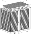
도 4는 복수의 비휘발성 메모리 셀들을 포함하는 메모리 구조물(126)을 포함할 수 있는 모놀리식 3차원 메모리 어레이의 하나의 예시적인 실시예의 일부분의 사시도이다. 예를 들어, 도 4는 메모리를 포함하는 하나의 블록의 일부분을 도시한다. 도시된 구조물은 교번하는 유전체 층들 및 전도성 층들의 스택 위에 위치된 한 세트의 비트 라인들(BL)을 포함하며, 이때 재료들의 수직 컬럼들이 유전체 층들 및 전도성 층들을 통과하여 연장된다. 예시적인 목적을 위해, 유전체 층들 중 하나의 유전체 층은 D로 마킹되고 전도성 층들(워드 라인 층들로도 지칭됨) 중 하나의 전도성 층은 W로 마킹된다. 교번하는 유전체 층들 및 전도성 층들의 수는 특정 구현 요건들에 기초하여 달라질 수 있다. 일 세트의 실시예들은 108 내지 300개의 교번하는 유전체 층들 및 전도성 층들을 포함한다. 하나의 예시적인 실시예는 96개의 데이터 워드 라인 층들, 8개의 선택 층들, 6개의 더미 워드 라인 층들 및 110개의 유전체 층들을 포함한다. 108 내지 300개 초과 또는 미만의 층들이 또한 사용될 수 있다. 교번하는 유전체 층들 및 전도성 층들은, 일 실시예에서, 국소 상호접속부들(LI)에 의해 4개의 "핑거(finger)들" 또는 서브블록들로 분할된다. 도 4는 2개의 핑거들 및 2개의 국소 상호접속부들(LI)을 도시한다. 교번하는 유전체 층들 및 워드 라인 층들 아래에는 소스 라인 층(SL)이 있다. 재료들의 수직 컬럼들(메모리 홀(hole)들로도 알려짐)이 교번하는 유전체 층들 및 전도성 층들의 스택에 형성된다. 예를 들어, 수직 컬럼들/메모리 홀들 중 하나가 MH로 마킹된다. 도 4에서, 유전체 층들은 판독기가 교번하는 유전체 층들 및 전도성 층들의 스택 내에 위치된 메모리 홀들을 볼 수 있도록 시스루(see-through)로 도시되어 있다는 것에 유의하여야 한다. 일 실시예에서, NAND 스트링들은 수직 컬럼/메모리 홀을 전하 트래핑 재료를 포함하는 재료들로 충전함으로써 형성되어, 수직 컬럼의 메모리 셀들을 생성한다. 각각의 메모리 셀은 데이터의 하나 이상의 비트들을 저장할 수 있다.4 is a perspective view of a portion of one exemplary embodiment of a monolithic three-dimensional memory array that may include a
도 5는 어레이로 구성된 메모리 셀들의 NAND 스트링들을 프로그래밍하기 위한 프로세스(500)의 일 실시예를 설명하는 흐름도이다. 하나의 예시적인 실시예에서, 도 5의 프로세스는 제어 다이(104) 상의 제어 회로부(110)를 사용하여 제2 메모리 다이(102b)와 병렬로 제1 메모리 다이(102a) 상에서 수행된다. 예를 들어, 도 5의 프로세스는 제어 다이(104) 상의 상태 머신(112)의 지시에 의해 수행될 수 있다.5 is a flow diagram illustrating one embodiment of a
전형적으로, 프로그램 동작 동안 (선택된 워드 라인을 통해) 제어 게이트들에 인가되는 프로그램 전압은 일련의 프로그램 펄스들로서 인가된다. 프로그래밍 펄스들 중 적어도 일부 사이에는 검증을 수행하기 위한 한 세트의 검증 펄스들이 있다. 일부 실시예들에서, 모든 상태들이 프로그램 펄스 이후에 검증되지는 않는다. 많은 구현예들에서, 프로그램 펄스들의 크기는 각각의 연속적인 펄스로 사전결정된 스텝 크기만큼 증가된다. 도 5의 단계(540)에서, 프로그래밍 전압(Vpgm)은 시작 크기(예컨대, 약 12 내지 16V 또는 다른 적절한 레벨)로 초기화되고, 상태 머신(112)에 의해 유지되는 프로그램 카운터(PC)가 1에서 초기화된다.Typically, a program voltage applied to the control gates (via a selected word line) during a program operation is applied as a series of program pulses. Between at least some of the programming pulses there is a set of verify pulses for performing verification. In some embodiments, not all states are verified after the program pulse. In many implementations, the size of the program pulses is increased by a predetermined step size with each successive pulse. In
일 실시예에서, 프로그래밍되도록 선택된 메모리 셀들의 그룹(본 명세서에서 선택된 메모리 셀들로 지칭됨)은 동시에 프로그래밍되고, 메모리 다이(102a) 내의 제1 선택된 워드 라인에 접속된 제1 메모리 셀들 및 메모리 다이(102b) 내의 제2 선택된 워드 라인에 접속된 제2 메모리 셀들을 포함한다. 제1 및 제2 선택된 워드 라인들에 또한 접속되는 프로그래밍을 위해 선택되지 않은 다른 메모리 셀들(선택되지 않은 메모리 셀들)이 있을 것이다. 즉, 선택된 워드 라인들은 또한 프로그래밍되는 것이 금지되기로 되어 있는 메모리 셀들에 접속될 것이다. 예를 들어, 데이터가 한 세트의 메모리 셀들에 기록될 때, 메모리 셀들 중 일부는 소거 상태에 머무를 필요가 있을 것이고, 따라서 그들은 프로그래밍되지 않을 것이다. 추가적으로, 메모리 셀들이 그들의 의도된 타깃 데이터 상태에 도달함에 따라, 그들은 추가 프로그래밍되는 것이 금지될 것이다. 프로그래밍되는 것이 금지될 선택된 워드 라인에 접속된 메모리 셀들을 포함하는 이들 NAND 스트링들(예컨대, 선택되지 않은 NAND 스트링들)은 그들의 채널들이 부스팅되게 하여 프로그래밍을 금지한다. 채널이 부스팅된 전압을 가질 때, 채널과 워드 라인 사이의 전압 차이는 프로그래밍을 야기하기에 충분히 크지 않다. 부스팅을 돕기 위해, 단계(542)에서, 메모리 시스템은 프로그래밍되는 것이 금지될 선택된 워드 라인에 접속된 메모리 셀들을 포함하는 NAND 스트링들의 채널들을 사전충전할 것이다.In one embodiment, a group of memory cells selected to be programmed (referred to herein as selected memory cells) are simultaneously programmed, the first memory cells connected to the first selected word line in the
단계(544)에서, 프로그래밍되는 것이 금지될 선택된 워드 라인(들)에 접속된 메모리 셀들을 포함하는 NAND 스트링들은 그들의 채널들이 부스팅되게 하여 프로그래밍을 금지한다. 이러한 NAND 스트링들은 본 명세서에서 "선택되지 않은 NAND 스트링들"로 지칭된다. 일 실시예에서, 선택되지 않은 워드 라인들은 부스팅 스킴(scheme)들을 수행하기 위해 하나 이상의 부스팅 전압들(예컨대, 약 7 내지 11 볼트)을 수신한다. 프로그램 금지 전압이 선택되지 않은 NAND 스트링에 커플링된 비트 라인들에 인가된다.At
단계(546)에서, 프로그램 신호(Vpgm)의 프로그램 펄스가 선택된 워드 라인(들)에 인가된다. 일 실시예에서, NAND 스트링 상의 메모리 셀이 프로그래밍되어야 하면, 대응하는 비트 라인은 프로그램 인에이블 전압에서 바이어스된다. 본 명세서에서, 그러한 NAND 스트링은 "선택된 NAND 스트링"으로 지칭된다.In
단계(546)에서, 프로그램 펄스는 선택된 워드 라인(들)에 접속된 모든 메모리 셀들에 동시에 인가되어, 선택된 워드 라인에 접속된 모든 메모리 셀들이 (그들이 프로그래밍되는 것이 금지되지 않는다면) 동시에 프로그래밍된다. 예를 들어, 제어 다이(104) 상의 워드 라인 드라이버(260)는 제1 메모리 다이(102a) 내의 제1 선택된 워드 라인 및 제2 메모리 다이(102b) 내의 제2 선택된 워드 라인 양측 모두에 프로그램 펄스를 제공하는 데 사용된다. 따라서, 제1 선택된 워드 라인에 접속된 메모리 셀들은 제2 선택된 워드 라인에 접속된 메모리 셀들과 동시에 프로그래밍된다. 따라서, 프로그래밍 처리량은 높다. 더욱이, 워드 라인 로딩은 별개의 메모리 다이(102a, 102b) 상에 있는 제1 및 제2 선택된 워드 라인들로 인해 낮게 유지된다.In
단계(548)에서, 메모리 셀들의 타깃 상태들에 도달한 메모리 셀들은 추가 프로그래밍으로부터 록아웃(lock out)된다. 단계(548)는 하나 이상의 검증 기준 레벨들에서 검증을 수행하는 단계를 포함할 수 있다. 일 실시예에서, 검증 프로세스는, 프로그래밍을 위해 선택된 메모리 셀들의 임계 전압들이 적절한 검증 기준 전압에 도달했는지 여부를 테스트함으로써 수행된다. 단계(548)에서, 메모리 셀이 그의 타깃 상태에 도달했다는 것을 (Vt의 테스트에 의해) 메모리 셀이 검증된 후에 메모리 셀은 록아웃될 수 있다.In
단계(550)에서, 모든 메모리 셀들이 그들의 타깃 임계 전압들에 도달했다고(통과) 결정되면, 모든 선택된 메모리 셀들이 그들의 타깃 상태들로 프로그래밍되고 검증되었기 때문에 프로그래밍 프로세스는 완료되고 성공적이다. 단계(552)에서 "통과"의 상태가 보고된다. 그렇지 않고, 단계(550)에서, 모든 메모리 셀들이 그들의 타깃 임계 전압들에 도달하지 않았다고(실패) 결정되면, 프로그래밍 프로세스는 단계(554)로 계속된다.In
단계(554)에서, 메모리 시스템은 그들 각자의 타깃 임계 전압 분포에 아직 도달하지 않은 메모리 셀들의 수를 카운트한다. 즉, 시스템은, 지금까지 그들의 타깃 상태에 도달하는 데 실패한 메모리 셀들의 수를 카운트한다. 이러한 카운팅은 상태 머신, 제어기(122), 또는 다른 로직에 의해 행해질 수 있다. 일 구현예에서, 감지 블록들 각각은 그들 각자의 셀들의 상태(통과/실패)를 저장할 것이다. 일 실시예에서, 최종 검증 단계를 실패한, 현재 프로그래밍되고 있는 메모리 셀들의 총 수를 반영하는 하나의 총 카운트가 있다. 다른 실시예에서, 각각의 데이터 상태에 대해 별개의 카운트들이 계속된다.In
단계(556)에서, 단계(554)로부터의 카운트가 사전결정된 한계 이하인지 여부가 결정된다. 일 실시예에서, 사전결정된 한계는 메모리 셀들의 페이지에 대한 판독 프로세스 동안 에러 정정 코드들(ECC)에 의해 정정될 수 있는 비트들의 수이다. 실패한 셀들의 수가 사전결정된 한계 이하이면, 프로그래밍 프로세스가 중지될 수 있고 단계(552)에서 "통과"의 상태가 보고된다. 이러한 상황에서, 완전히 프로그래밍되지 않았던 몇몇의 나머지 메모리 셀들이 판독 프로세스 동안 ECC를 사용하여 정정될 수 있도록 충분한 메모리 셀들이 정확하게 프로그래밍되었다. 일부 실시예들에서, 단계(556)에서 사용되는 사전결정된 한계는 향후/추가 에러들을 허용하도록 판독 프로세스 동안 에러 정정 코드들(ECC)에 의해 정정될 수 있는 비트들의 수 미만이다. 페이지에 대해 메모리 셀들의 전체보다 적은 메모리 셀들을 프로그래밍하는 경우, 또는 단지 하나의 데이터 상태(또는 전체보다 적은 상태들)에 대한 카운트를 비교하는 경우, 사전결정된 한계는 메모리 셀들의 페이지에 대한 판독 프로세스 동안 ECC에 의해 정정될 수 있는 비트들의 수의 (비례하는 또는 비례하지 않는) 일부분일 수 있다. 일부 실시예들에서, 한계는 사전결정되지 않는다. 대신에, 그것은 페이지에 대해 이미 카운트된 에러들의 수, 수행되는 프로그램-소거 사이클들의 수 또는 다른 기준들에 기초하여 변한다.In
실패한 메모리 셀들의 수가 사전결정된 한계 이상이면, 프로그래밍 프로세스는 단계(558)에서 계속되고 프로그램 카운터(PC)가 프로그램 한계 값(PL)에 대해 체크된다. 프로그램 한계 값들의 예들은 6, 12, 16, 19 및 30을 포함하지만; 다른 값들이 사용될 수 있다. 프로그램 카운터(PC)가 프로그램 한계 값(PL) 이상이면, 프로그램 프로세스는 실패한 것으로 간주되고 단계(562)에서 실패의 상태가 보고된다. 프로그램 카운터(PC)가 프로그램 한계 값(PL) 미만이면, 프로세스는 단계(560)에서 계속되고, 이 시간 동안 프로그램 카운터(PC)는 1만큼 증분되고 프로그램 전압(Vpgm)은 다음 크기로 스텝형으로 증가된다. 예를 들어, 다음 펄스는 이전 펄스보다 스텝 크기(예컨대, 0.1 내지 1.0 볼트의 스텝 크기)만큼 큰 크기를 가질 것이다. 단계(560) 후에, 프로세스는 단계(542)로 루프 백(loop back)되고, 다른 프로그램 펄스가 선택된 워드 라인에 인가되어, 도 5의 프로그래밍 프로세스의 다른 반복(단계들(542 내지 560))이 수행되게 한다.If the number of failed memory cells is above the predetermined limit, the programming process continues at
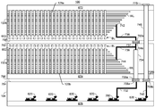
도 6은 집적 메모리 모듈(100)의 일 실시예의 도면이다. 도 6에 도시된 실시예에서, 제1 메모리 다이(102a)는 제어 다이(104)에 접합되고, 제어 다이(104)는 제2 메모리 다이(102b)에 접합된다. 따라서, 제1, 제2 및 제3 반도체 다이는 서로 접합된다. 이러한 접합 구성은 도 2a에 도시된 실시예와 유사하다. 인접한 다이들의 쌍들 사이의 갭이 도시되어 있지만, 그러한 갭은 에폭시 또는 다른 수지 또는 중합체로 충전될 수 있다(예를 들어, 도 9 참조)는 것에 유의한다.6 is a diagram of an embodiment of an
각각의 메모리 다이(102a, 102b)는 메모리 구조물(126)을 포함한다. 메모리 구조물(126a)은 메모리 다이(102a)의 기판(672)에 인접한다. 메모리 구조물(126b)은 메모리 다이(102b)의 기판(674)에 인접한다. 기판들(672, 674)은 일부 실시예들에서 실리콘 웨이퍼의 일부분으로부터 형성된다. 이 예에서, 메모리 구조물들(126)은 각각 3차원 메모리 어레이를 포함한다. 메모리 구조물들(126)은 도 4에 도시된 예와 유사한 구조를 갖는다. 유전체 층들에 의해 분리되는 다수의 워드 라인 층들(WL)이 있다. 유전체 층들은 워드 라인 층들 사이의 갭들로 표현된다. 따라서, 워드 라인 층들 및 유전체 층들은 스택을 형성한다. 도 6에 도시된 것보다 많은 워드 라인 층들이 있을 수 있다. 도 4의 예에서와 같이, 스택을 관통하여 연장되는 다수의 컬럼들이 있다. 하나의 컬럼(602)은 각각의 스택에서 도면 부호 602로 지칭된다. 컬럼들은 메모리 셀들을 포함한다. 예를 들어, 각각의 컬럼은 NAND 스트링을 포함할 수 있다. 스택에 인접한 다수의 비트 라인들(BL)이 있다.Each memory die 102a, 102b includes a
워드 라인 드라이버(260)는 메모리 다이(102a) 내의 제1 워드 라인(642) 및 메모리 다이(102b) 내의 제2 워드 라인(644)에 전압들을 동시에 제공한다. 워드 라인 드라이버(260)로부터 제1 워드 라인(642)으로의 통로는 전도성 통로(632), 접합 패드(274a1), 접합 패드(270a1), 및 전도성 통로(634)를 포함한다. 워드 라인 드라이버(260)로부터 제2 워드 라인(644)으로의 통로는 전도성 통로(632), 실리콘 관통 비아(through silicon via, TSV)(668), 접합 패드(276a1), 접합 패드(272a1), 및 전도성 통로(636)를 포함한다. 전도성 통로들(632, 634, 636)은 각각 (다이의 주 표면들에 대하여 수직으로 연장될 수 있는) 하나 이상의 비아들 및 (다이의 주 표면들에 대하여 수평으로 연장될 수 있는) 하나 이상의 금속 상호접속부들을 포함할 수 있다. 전도성 통로들(632, 634, 636)은 트랜지스터들 또는 다른 회로 요소들을 포함할 수 있다. 일 실시예에서, 트랜지스터들은, 사실상 통로를 개방 또는 폐쇄하는 데 사용될 수 있다. 따라서, 동일한 워드 라인 드라이버(260)는 제1 워드 라인(642) 및 제2 워드 라인(644) 양측 모두에 전압을 동시에 제공하는 데 사용될 수 있다. 다른 워드 라인 드라이버들(도 6에 도시되지 않음)은 다른 워드 라인들에 전압들을 제공한다. 따라서, 접합 패드들(274a1, 270a1)에 더하여 추가의 접합 패드(274a, 270a)가 존재한다. 마찬가지로, 접합 패드들(276a1, 272a1)에 더하여 추가의 접합 패드(276a, 272a)가 존재한다. 당업계에 알려진 바와 같이, 접합 패드들은, 예를 들어 구리, 알루미늄 및 이들의 합금으로 형성될 수 있다.The
감지 증폭기(250a)는 메모리 다이(102a) 내의 비트 라인과 통신한다. 감지 증폭기(250a)로부터 비트 라인으로의 통로는 전도성 통로(652), 접합 패드(274b), 접합 패드(270b), 및 전도성 통로(634)를 포함한다. 감지 증폭기(250b)는 메모리 다이(102b) 내의 비트 라인과 통신한다. 감지 증폭기(250b)로부터 비트 라인으로의 통로는 전도성 통로(654), TSV(656), 접합 패드(276b), 접합 패드(272b), 및 전도성 통로(648)를 포함한다. 전도성 통로들(652, 654, 648)은 각각 (다이의 주 표면들에 대하여 수직으로 연장될 수 있는) 하나 이상의 비아들 및 (다이의 주 표면들에 대하여 수평으로 연장될 수 있는) 하나 이상의 금속 상호접속부들을 포함할 수 있다. 금속 상호접속부들은 당업계에 알려진 바와 같이 예를 들어 구리 및 구리 합금들을 포함하는 다양한 전기 전도성 금속으로 형성될 수 있고, 비아들은 당업계에 알려진 바와 같이 예를 들어 텅스텐, 구리 및 구리 합금들을 포함하는 다양한 전기 전도성 금속들로 라이닝되고/되거나 충전될 수 있다. 전도성 통로들(652, 654, 648)은 트랜지스터들 또는 다른 회로 요소들을 포함할 수 있다. 일 실시예에서, 트랜지스터들은, 사실상 통로를 개방 또는 폐쇄하는 데 사용될 수 있다.
제어 다이(104)는 실리콘 웨이퍼로부터 형성될 수 있는 기판(676)을 갖는다. 감지 증폭기들(250), 워드 라인 드라이버(들)(260), 및 다른 회로부(620)는 기판(676) 상에 그리고/또는 기판 내에 형성될 수 있다. 회로부(620)는 제어 회로부(110)(도 1a 참조)의 일부 또는 전부를 포함할 수 있다. 일부 실시예들에서, 감지 증폭기들(250), 워드 라인 드라이버(들)(260), 및/또는 다른 회로부(620)는 CMOS 회로들을 포함한다.The control die 104 has a
제어 다이(104) 상의 회로부가 집적 메모리 모듈(100) 외부의 엔티티와 통신할 수 있게 하는 외부 신호 경로가 있다. 따라서, 제어 다이(104) 상의 회로부(620)는 예를 들어 제어기(122)(도 1a 참조)와 통신할 수 있다. 선택적으로, 제어 다이(104) 상의 회로부는, 예를 들어 호스트(140)와 통신할 수 있다. 외부 통로는 제어 다이(104) 내의 비아(658), 접합 패드(274c), 접합 패드(270c), 실리콘 관통 비아(TSV)(660), 및 외부 패드(678)를 포함한다. TSV(660)는 기판(672)을 관통하여 연장된다.There is an external signal path that allows circuitry on the control die 104 to communicate with entities external to the
TSV들(656, 660)은 반도체 다이들(102, 104) 내의 집적 회로들의 형성 전에, 형성 동안 또는 형성 후에 형성될 수 있다. TSV들은 웨이퍼들을 관통하여 홀들을 에칭함으로써 형성될 수 있다. 예를 들어, 홀들은 기판들(672, 676)을 관통하여 에칭될 수 있다. 홀들은 또한, 웨이퍼들에 인접한 재료를 관통하여 에칭될 수 있다. 홀들은, 이어서, 금속 확산에 대항하는 장벽으로 라이닝될 수 있다. 장벽 층은 이어서 시드 층으로 라이닝될 수 있고, 시드 층은 구리와 같은 전기 도체로 도금될 수 있지만, 알루미늄, 주석, 니켈, 금, 도핑된 폴리실리콘, 및 이들의 합금들 또는 조합들과 같은 다른 적합한 재료들이 사용될 수 있다.
도 6에 도시된 실시예에 대한 수많은 변형이 가능하다. 하나의 변형은 감지 증폭기들(250a)이 제1 메모리 다이(102a) 상에 위치되는 것, 및 감지 증폭기들(250b)이 제2 메모리 다이(102b) 상에 위치되는 것이다.Numerous variations on the embodiment shown in FIG. 6 are possible. One variation is that the
도 7은 집적 메모리 모듈(100)의 일 실시예의 도면이다. 도 7에 도시된 실시예에서, 제1 메모리 다이(102a)는 제2 메모리 다이(102b)에 접합되고, 제1 메모리 다이(102a)는 제어 다이(104)에 접합된다. 구체적으로, 제2 메모리 다이(102b)의 제1 주 표면(786) 상의 접합 패드들(702)은 제1 메모리 다이(102a)의 제1 주 표면(782) 상의 접합 패드들(704)에 접합된다. 또한, 제1 메모리 다이(102a)의 제2 주 표면(790) 상의 접합 패드들(706)은 제어 다이(104)의 제1 주 표면(784) 상의 접합 패드들(708)에 접합된다. 따라서, 제1, 제2 및 제3 반도체 다이는 서로 접합된다. 도 7에 도시된 것보다 많은 다른 접합 패드들이 있을 수 있다는 것에 유의한다. 또한, 인접한 다이들의 쌍들 사이의 갭이 도시되어 있지만, 그러한 갭은 에폭시 또는 다른 수지 또는 중합체로 충전될 수 있다(예를 들어, 도 10 참조)는 것에 유의한다. 일부 실시예들에서, 접합 패드들(702, 704, 706 및/또는 708)은 플립-칩 접합 패드들이다.7 is a diagram of an embodiment of an
제어 다이(104) 상의 워드 라인 드라이버들(260)이 메모리 다이들(102a, 102b) 내의 워드 라인들로 전압들을 전달하게 하는 내부 신호 경로가 있다. 내부 신호 통로는 제어 다이(104) 내의 통로(732), 접합 패드(708a), 접합 패드(706a), TSV(734), 및 제1 메모리 다이(102a) 내의 워드 라인(744)으로의 통로(736)를 포함한다. 내부 신호 경로는 통로(737), 접합 패드(704a), 접합 패드(702a), 및 제2 메모리 다이(102b) 내의 워드 라인(742)으로의 통로(738)를 추가로 포함한다. TSV(734)는 기판(674)을 관통하여 연장된다.There is an internal signal path that causes the
제어 다이(104) 상의 회로부(620)가 집적 메모리 모듈(100) 외부의 엔티티와 통신할 수 있게 하는 외부 신호 경로가 있다. 따라서, 제어 다이(104) 상의 회로부(620)는 예를 들어 제어기(122)(도 1a 참조)와 통신할 수 있다. 선택적으로, 제어 다이(104) 상의 회로부는, 예를 들어 호스트(140)와 통신할 수 있다. 외부 통로는 제어 다이(104) 내의 비아(740), 접합 패드(708b), 접합 패드(706b), 실리콘 관통 비아(TSV)(746), 및 외부 패드(778)를 포함한다. TSV(746)는 기판(674)을 관통하여 연장된다.There is an external signal path that allows
도 7에 도시된 실시예에 대한 수많은 변형이 가능하다. 하나의 변형은 감지 증폭기(250)가 제어 다이(104) 상에 위치되는 것이다.Numerous variations on the embodiment shown in FIG. 7 are possible. One variation is that the
도 8은 반도체 다이의 평면 표면 상의 접합 패드들의 예시적인 패턴을 도시한다. 반도체 다이는 제1 메모리 다이(102a), 제2 메모리 다이(102b), 또는 제어 다이(104) 중 임의의 것일 수 있다. 접합 패드들은, 반도체 다이에 적절한 바와 같은 접합 패드들(270, 272, 274, 또는 276) 중 임의의 것일 수 있다. 대안으로, 접합 패드들은 접합 패드들(702, 704, 706, 또는 708)(도 7 참조) 중 임의의 것일 수 있다. 도 8에 도시된 것보다 더 많은 접합 패드들이 있을 수 있다. 일례로서, 2개의 반도체 다이 사이에 100,000개 이상의 상호접속부들이 필요할 수 있다. 그러한 많은 수들의 전기 상호접속부들을 지지하기 위해, 접합 패드들에는 작은 면적 및 피치가 제공될 수 있다. 일부 실시예들에서, 접합 패드들은 플립-칩 접합 패드들이다.8 shows an exemplary pattern of bonding pads on a planar surface of a semiconductor die. The semiconductor die may be any of the
일부 실시예들에서, 접합 패드들은 소위 Cu-Cu 접합 프로세스에서, 솔더 또는 다른 추가 재료 없이, 서로 직접 접합된다. Cu-Cu 접합 프로세스에서, 접합 패드들은 고도로 평면적이도록 제어되고, 그렇지 않은 경우 접합 패드 상에 정착되어 밀접한 접합을 방지할 수 있는 주변 미립자들이 거의 없는 고도로 제어된 환경에서 형성된다. 그러한 적절하게 제어되는 조건들 하에서, 접합 패드들은 표면 장력에 기초하여 상호 접합을 형성하도록 서로에 대해 정렬 및 가압된다. 그러한 접합들은 실온에서 형성될 수 있지만, 열이 또한 가해질 수 있다. Cu-Cu 접합을 사용하는 실시예들에서, 접합 패드들은 약 5 μm 정사각형일 수 있고, 3 μm 내지 5 μm의 피치로 서로 이격될 수 있다. 이러한 프로세스는 본 명세서에서 Cu-Cu 접합으로 지칭되지만, 이러한 용어는 또한 접합 패드들이 Cu 이외의 재료들로 형성되는 경우에도 적용할 수 있다.In some embodiments, the bonding pads are directly bonded to each other in a so-called Cu-Cu bonding process, without solder or other additional material. In the Cu-Cu bonding process, bonding pads are controlled to be highly planar, otherwise they are formed in a highly controlled environment with few surrounding particulates that can settle on the bonding pad and prevent close bonding. Under such properly controlled conditions, the bonding pads are aligned and pressed against each other to form a mutual bond based on the surface tension. Such bonds can be formed at room temperature, but heat can also be applied. In embodiments using Cu-Cu bonding, the bonding pads may be about 5 μm square and spaced apart from each other with a pitch of 3 μm to 5 μm. This process is referred to herein as Cu-Cu bonding, but this term is also applicable when bonding pads are formed of materials other than Cu.
접합 패드들의 면적이 작을 때, 제2 반도체 다이들을 서로 접합하는 것이 어려울 수 있다. 접합 패드들의 크기 및 이들 사이의 피치는, 접합 패드들을 포함하는 반도체 다이들의 표면들 상에 필름 층을 제공함으로써 추가로 감소될 수 있다. 필름 층은 접합 패드들 주위에 제공된다. 다이들이 합쳐질 때, 접합 패드들은 서로 접합할 수 있고, 각각의 다이들 상의 필름 층들이 서로 접합할 수 있다. 그러한 접합 기법은 하이브리드 접합으로 지칭될 수 있다. 하이브리드 접합을 사용하는 실시예들에서, 접합 패드들은 약 3 μm 정사각형일 수 있고, 1 μm 내지 5 μm의 피치로 서로 이격될 수 있다. 훨씬 더 작은 크기들 및 피치들을 갖는 접합 패드들을 제공하는 접합 기법들이 사용될 수 있다.When the area of the bonding pads is small, it may be difficult to bond the second semiconductor dies to each other. The size of the bonding pads and the pitch between them can be further reduced by providing a film layer on the surfaces of the semiconductor dies comprising the bonding pads. A film layer is provided around the bonding pads. When the dies are brought together, the bonding pads can bond to each other, and the film layers on each of the dies can bond to each other. Such conjugation technique can be referred to as hybrid conjugation. In embodiments using hybrid bonding, the bonding pads may be about 3 μm square and spaced apart from each other with a pitch of 1 μm to 5 μm. Bonding techniques may be used that provide bonding pads with even smaller sizes and pitches.
위에 언급된 바와 같이, 일부 실시예들은 다이들(102, 104)의 표면 상에 필름을 포함할 수 있다. 그러한 필름이 초기에 제공되지 않는 경우, 다이들 사이의 공간은 에폭시 또는 다른 수지 또는 중합체로 언더필(under fill)될 수 있다. 언더필 재료는 액체로서 적용될 수 있고, 이어서 고체 층으로 경화될 수 있다. 이러한 언더필 단계는 다이들(102, 104) 사이의 전기적 접속들을 보호하고, 다이들을 함께 추가로 고정시킨다. 다양한 재료들이 언더필 재료로서 사용될 수 있지만, 실시예들에서, 그것은 미국 캘리포니아주 소재의 오피스들을 갖는 헨켈 코포레이션(Henkel Corp.)으로부터의 하이졸(Hysol) 에폭시 수지일 수 있다.As mentioned above, some embodiments may include a film on the surface of the dies 102 and 104. If such a film is not initially provided, the spaces between the dies may be underfilled with epoxy or other resin or polymer. The underfill material can be applied as a liquid and then cured into a solid layer. This underfill step protects the electrical connections between the dies 102 and 104 and further secures the dies together. A variety of materials may be used as the underfill material, but in embodiments it may be a Hysol epoxy resin from Henkel Corp. with offices in California, USA.
집적 메모리 모듈(100) 내의 반도체 다이들(102, 104)은 각자의 다이들(102, 104) 상의 접합 패드들을 초기에 서로 정렬시킴으로써 서로 접합될 수 있다. 이 후에, 접합 패드들은, 접합 패드 크기 및 접합 패드 간격(즉, 접합 패드 피치)에 부분적으로 의존하여, 다양한 접합 기법들 중 어느 하나에 의해 서로 접합될 수 있다. 접합 패드 크기 및 피치는, 이어서, 제1 반도체 다이(102)와 제2 반도체 다이(104) 사이에 요구되는 전기적 상호접속부들의 수에 의해 좌우될 수 있다. 일부 실시예들에서, 다이들(102a, 102b, 104)의 접합은 웨이퍼들을 다이싱하기 전에 수행된다. 따라서, 몇몇 웨이퍼들(135a, 135b, 135c)이 서로 접합될 수 있고, 이어서 다이싱될 수 있다. 일부 실시예들에서, 다이들(102a, 102b, 104)의 접합은 웨이퍼들을 다이싱한 후에 수행된다.The semiconductor dies 102 and 104 in the
도 9는 집적 메모리 모듈(100)의 일 실시예의 측면도를 도시한다. 집적 메모리 모듈(100)은 도 2a 및 도 6의 예들과 부합된다. 제1 메모리 다이(102a)는 제어 다이(104)에 접합된 것으로 도시되어 있고, 제어 다이(104)는 제2 메모리 다이(102b)에 접합된 것으로 도시되어 있다. 따라서, 제1 메모리 다이(102a), 제2 메모리 다이(102b), 및 제어 다이(104)는 서로 접합된다. 접합 패드들(270, 272, 274, 276) 중 일부가 도시되어 있다. 더 많은 접합 패드들이 있을 수 있다. 다이들(102, 104) 사이의 공간은 전술된 에폭시 또는 다른 수지 또는 중합체로부터 형성될 수 있는 고체 층(148)으로 충전된다.9 shows a side view of an embodiment of the
도 10은 집적 메모리 모듈(100)의 일 실시예의 측면도를 도시한다. 집적 메모리 모듈(100)은 도 7의 예들과 부합된다. 제1 메모리 다이(102a)는 제2 메모리 다이(102b)에 접합된 것으로 도시되어 있고, 제어 다이(104)는 제1 메모리 다이(102a)에 접합된 것으로 도시되어 있다. 따라서, 제1 메모리 다이(102a), 제2 메모리 다이(102b), 및 제어 다이(104)는 서로 접합된다. 접합 패드들(702, 704, 706, 708) 중 일부가 도시되어 있다. 더 많은 접합 패드들이 있을 수 있다. 다이들(102, 104) 사이의 공간은 전술된 에폭시 또는 다른 수지 또는 중합체로부터 형성될 수 있는 고체 층(148)으로 충전된다.10 shows a side view of an embodiment of the
도 11은 집적 메모리 모듈(100)을 포함하는 비휘발성 메모리를 동작시키는 프로세스(1100)의 일 실시예의 흐름도이다. 프로세스(1100)는 제1 메모리 다이(102a) 및 제2 메모리(102b)에서 병렬로 메모리 동작을 수행하는 데 사용될 수 있다. 메모리 동작은 프로그래밍, 판독, 또는 소거일 수 있다. 프로세스(1100)는 다이들(102(a), 102(b), 104) 사이에서 신호들(예컨대, 전압들, 전류들)을 전송하기 위해 본 명세서에 기술된 내부 신호 경로들 중 임의의 것을 사용할 수 있지만, 본 명세서에 기술된 예들로 제한되지 않는다.11 is a flow diagram of one embodiment of a
단계(1102)는 제어 반도체 다이(104)로부터 제1 쌍들의 접합 패드들을 통해 제1 반도체 다이(102a) 상의 비휘발성 메모리 셀들의 제1 3차원 어레이 내의 제1 선택된 블록에 메모리 동작 전압들의 세트를 제공하는 단계를 포함한다. 접합 패드들 중 제1 패드들은 제1 반도체 다이를 제2 반도체 다이에 전기적으로 그리고 물리적으로 커플링시킨다.Step 1102 is to apply a set of memory operating voltages from the control semiconductor die 104 to a first selected block in the first three-dimensional array of nonvolatile memory cells on the
도 6과 부합하는 일 실시예에서, 단계(1102)는 제어 다이(104) 상의 WL 드라이버들(260(1) 내지 260(n))로부터 접합 패드 쌍들(272(a)/276(a))을 통해 제1 메모리 다이(102a) 내의 선택된 블록 내의 워드 라인들에 전압들을 제공하는 단계를 포함한다. 전압들은, 일부 실시예들에서, 선택된 워드 라인에 대한 전압 및 선택되지 않은 워드 라인들에 대한 전압들을 포함한다.In one embodiment consistent with FIG. 6, step 1102 includes bonding pad pairs 272(a)/276(a) from WL drivers 260(1)-260(n) on control die 104. And providing voltages to the word lines in the selected block in the
도 7과 부합하는 다른 실시예에서, 단계(1102)는 제어 다이(104) 상의 WL 드라이버(260(1) 내지 260(n))로부터 접합 패드 쌍들(708(a)/706(a))을 통해 제1 메모리 다이(102a) 내의 선택된 블록 내의 워드 라인들에 전압들을 제공하는 단계를 포함한다. 전압들은, 일부 실시예들에서, 선택된 워드 라인에 대한 전압 및 선택되지 않은 워드 라인들에 대한 전압들을 포함한다.In another embodiment consistent with FIG. 7, step 1102 includes bonding pad pairs 708(a)/706(a) from WL drivers 260(1)-260(n) on control die 104. And providing voltages to word lines in the selected block within the
단계(1104)는 제어 반도체 다이(104)로부터 제2 쌍들의 접합 패드들을 통해 제2 메모리 반도체 다이(102(b)) 상의 비휘발성 메모리 셀들의 제2 3차원 어레이 내의 제2 선택된 블록에 메모리 동작 전압들의 세트를 제공하는 단계를 포함한다. 메모리 동작 전압들의 세트는 제1 선택된 블록 및 제2 선택된 블록에서 병렬로 메모리 동작들을 제어하기 위해 제1 메모리 다이(102(a)) 및 제2 메모리 다이(102(b))에 병렬로 제공된다.Step 1104 is a memory operation on a second selected block in a second three-dimensional array of nonvolatile memory cells on the second memory semiconductor die 102(b) through second pairs of bonding pads from the control semiconductor die 104 And providing a set of voltages. A set of memory operating voltages is provided in parallel to the first memory die 102(a) and the second memory die 102(b) to control memory operations in parallel in the first selected block and in the second selected block. .
도 6과 부합하는 일 실시예에서, 단계(1104)는 제어 다이(104) 상의 WL 드라이버들(260(1) 내지 260(n))로부터 접합 패드 쌍들(276(a)/272(a))을 통해 제2 메모리 다이(102b) 내의 선택된 블록 내의 워드 라인들에 전압들을 제공하는 단계를 포함한다. 전압들은, 일부 실시예들에서, 선택된 워드 라인에 대한 전압 및 선택되지 않은 워드 라인들에 대한 전압들을 포함한다.In one embodiment consistent with FIG. 6, step 1104 includes bonding pad pairs 276(a)/272(a) from WL drivers 260(1)-260(n) on control die 104. And providing voltages to the word lines in the selected block in the
도 7과 부합하는 다른 실시예에서, 단계(1104)는 제어 다이(104) 상의 WL 드라이버(260(1) 내지 260(n))로부터 접합 패드 쌍들(704(a)/702(a))을 통해 제2 메모리 다이(102b) 내의 선택된 블록 내의 워드 라인들에 전압들을 제공하는 단계를 포함한다. 전압들은, 일부 실시예들에서, 선택된 워드 라인에 대한 전압 및 선택되지 않은 워드 라인들에 대한 전압들을 포함한다.In another embodiment consistent with FIG. 7, step 1104 includes bonding pad pairs 704(a)/702(a) from WL drivers 260(1)-260(n) on control die 104. And providing voltages to word lines in the selected block in the
도 6과 부합하는 일 실시예에서, 제2 세트 쌍들의 접합 패드들은 제어 다이(104)를 제2 메모리 다이(102b)에 전기적으로 그리고 물리적으로 커플링시킨다. 도 7과 부합하는 일 실시예에서, 제2 쌍들의 접합 패드들은 제1 메모리 다이(102a)를 제2 메모리 다이(102b)에 전기적으로 그리고 물리적으로 커플링시킨다.In one embodiment consistent with FIG. 6, the second set of pairs of bonding pads electrically and physically couple the control die 104 to the
도 12는 집적 메모리 모듈에서의 병렬 프로그래밍 프로세스(1200)의 일 실시예의 흐름도이다. 프로세스(1200)는 제1 메모리 다이(102a) 상의 제1 세트의 메모리 셀들을 제2 메모리(102b) 상의 제2 세트의 메모리 셀들과 병렬로 프로그래밍하는 데 사용될 수 있다. 프로세스(1200)는 다이들(102(a), 102(b), 104) 사이에서 신호들(예컨대, 전압들, 전류들)을 전송하기 위해 본 명세서에 기술된 내부 신호 경로들 중 임의의 것을 사용할 수 있지만, 본 명세서에 기술된 예들로 제한되지 않는다. 일부 실시예들에서, 제1 메모리 다이(102a) 상의 메모리 셀들이 제2 메모리 다이(102b) 상의 메모리 셀들과 병렬로 프로그래밍되더라도, 제어 다이(104)는 제2 메모리 다이(102b) 상의 메모리 셀들과는 독립적으로 제1 메모리 다이(102a) 상의 메모리 셀들을 소거할 수 있다.12 is a flow diagram of one embodiment of a
단계(1202)는 제어 다이(104)에서 일정 단위의 데이터를 수신하는 단계를 포함한다. 프로세스는 메모리 셀당 하나의 비트, 또는 메모리 셀당 다수의 비트들을 프로그래밍하는 데 사용될 수 있다. 메모리 셀당 하나의 비트가 프로그래밍되는 일 실시예에서, 데이터의 단위는 데이터의 페이지이다. 이 경우에, 페이지의 제1 부분은 제1 메모리 다이(102a) 상의 메모리 셀들 내로 프로그래밍되고, 페이지의 제2 부분은 제2 메모리 다이(102b) 상의 메모리 셀들 내로 프로그래밍된다. 메모리 셀당 하나의 비트가 프로그래밍되는 일 실시예에서, 데이터 유닛의 단위는 데이터의 2개의 페이지들이다. 이 경우에, 제1 페이지는 제1 메모리 다이(102a) 상의 메모리 셀들 내로 프로그래밍되고, 제2 페이지는 제2 메모리 다이(102b) 상의 메모리 셀들 내로 프로그래밍된다.Step 1202 includes receiving a unit of data from the control die 104. The process can be used to program one bit per memory cell, or multiple bits per memory cell. In one embodiment in which one bit is programmed per memory cell, the unit of data is a page of data. In this case, a first portion of the page is programmed into memory cells on the
전체 페이지 또는 부분 페이지를 각각의 메모리 다이(102)에 프로그래밍하는 개념은 메모리 셀당 다수의 비트들이 프로그래밍되는 경우들로 확장될 수 있다. 메모리 셀당 2개의 비트들을 프로그래밍할 때, 일 실시예에서, 2개의 전체 페이지들은 제1 메모리 다이(102a) 상의 메모리 셀들 내에 프로그래밍되고, 2개의 전체 페이지들은 제2 메모리 다이(102b) 상의 메모리 셀들 내에 프로그래밍된다. 메모리 셀당 2개의 비트들을 프로그래밍할 때, 일 실시예에서, 2개의 부분 페이지들은 제1 메모리 다이(102a) 상의 메모리 셀들 내에 프로그래밍되고, 2개의 부분 페이지들은 제2 메모리 다이(102b) 상의 메모리 셀들 내에 프로그래밍된다. 페이지 크기들이 부분 페이지 예에서 더 클 수 있다는 것에 유의한다.The concept of programming an entire page or a partial page to each memory die 102 can be extended to cases where multiple bits per memory cell are programmed. When programming two bits per memory cell, in one embodiment, two full pages are programmed into memory cells on
단계(1204)는 데이터의 일부분(예를 들어, 절반)을 메모리 다이(102a)와 연관되는 감지 증폭기들(250) 내의 래치들로 전송하는 단계를 포함한다. 감지 증폭기들은 제어 다이(104) 상에 위치된다. 전술한 바와 같이, 데이터의 이러한 부분은 전체 페이지 또는 페이지의 일부분일 수 있다. 단계(1204)는 또한, 페이지에 대한 패리티 비트들을 감지 증폭기들(250) 내의 래치들로 전송하는 단계를 포함할 수 있다.Step 1204 includes transferring a portion (eg, half) of the data to latches in
단계(1206)는 데이터의 일부분(예를 들어, 절반)을 메모리 다이(102b)와 연관되는 감지 증폭기들(250) 내의 래치들로 전송하는 단계를 포함한다. 감지 증폭기들은 제어 다이(104) 상에 위치된다. 단계(1206)는 또한, 페이지에 대한 패리티 비트들을 감지 증폭기들(250) 내의 래치들로 전송하는 단계를 포함할 수 있다.Step 1206 includes transferring a portion (eg, half) of the data to latches in
단계(1208)는, 하나 이상의 프로그램 전압들을 제2 메모리 다이(102b) 내의 제2 선택된 워드 라인에 인가하는 것과 동시에 하나 이상의 프로그램 전압들을 제1 메모리 다이(102a) 내의 제1 선택된 워드 라인에 인가하는 단계를 포함한다. 프로그램 전압들은, 일 실시예에서, 제어 다이(104) 상의 동일한 워드 라인 드라이버에 의해 제공된다. 따라서, 프로세스(1200)는 제1 메모리 다이(102(a)) 및 제2 메모리 다이(102(b)) 내의 메모리 셀들에 대해 병렬로 메모리 동작들을 제어하는 일 실시예이다.Step 1208 includes applying one or more program voltages to a second selected word line in the
도 13은 집적 메모리 모듈에서의 병렬 감지 프로세스(1300)의 일 실시예의 흐름도이다. 프로세스(1300)는 제1 메모리 다이(102a) 상의 제1 세트의 메모리 셀들을 제2 메모리(102b) 상의 제2 세트의 메모리 셀들과 병렬로 감지하는 데 사용될 수 있다. 일 실시예에서, 감지 동작은 판독 동작이다. 일 실시예에서, 감지 동작은 프로그램 검증이다. 프로세스(1300)는 다이들(102(a), 102(b), 104) 사이에서 신호들(예컨대, 전압들, 전류들)을 전송하기 위해 본 명세서에 기술된 내부 신호 경로들 중 임의의 것을 사용할 수 있지만, 본 명세서에 기술된 예들로 제한되지 않는다.13 is a flow diagram of one embodiment of a
단계(1302)는, WL 드라이버(260)를 사용하여, 하나 이상의 판독 비교 전압들을 제2 메모리 다이(102b) 내의 제2 선택된 워드 라인에 인가하는 것과 병렬로 하나 이상의 판독 비교 전압들을 제1 메모리 다이(102a) 내의 제1 선택된 워드 라인에 인가하는 단계를 포함한다. WL 드라이버(260)는 일 실시예에서 제어 다이(104) 상에 위치된다.Step 1302 uses the
단계(1304)는 제어 다이(104) 상의 제1 세트의 감지 증폭기들(250)을 사용하여 제1 메모리 다이(102a) 내의 비트 라인들을 감지하는 단계를 포함한다. 단계(1304)는 일 실시예에서, 제1 메모리 다이(102(a)) 내의 제1 선택된 블록의 비트 라인들을 접합 패드들(270b)을 통해 감지하는 단계를 포함한다. 단계(1304)는 일 실시예에서, 제1 메모리 다이(102(a)) 내의 제1 선택된 블록의 비트 라인들을 접합 패드들(274b)을 통해 감지하는 단계를 포함한다. 단계(1304)는 일 실시예에서, 제1 메모리 다이(102(a)) 내의 제1 선택된 블록의 비트 라인들을 접합 패드들(270b) 및 접합 패드들(274b)을 통해 감지하는 단계를 포함한다.Step 1304 includes sensing bit lines in
단계(1306)는 제어 다이(104) 상의 제2 세트의 감지 증폭기들(250)을 사용하여 제2 메모리 다이(102b) 내의 비트 라인들을 감지하는 단계를 포함한다. 단계(1306)는 일 실시예에서, 제2 메모리 다이(102(b)) 내의 제2 선택된 블록의 비트 라인들을 접합 패드들(272b)을 통해 감지하는 단계를 포함한다. 단계(1306)는 일 실시예에서, 제2 메모리 다이(102(b)) 내의 제2 선택된 블록의 비트 라인들을 접합 패드들(276b)을 통해 감지하는 단계를 포함한다. 단계(1306)는 일 실시예에서, 제2 메모리 다이(102(b)) 내의 제2 선택된 블록의 비트 라인들을 접합 패드들(272b) 및 접합 패드들(276b)을 통해 감지하는 단계를 포함한다.Step 1306 includes sensing the bit lines in
단계들(1304, 1306)은 병렬로 수행된다. 따라서, 프로세스(1300)는 제1 메모리 다이(102(a)) 및 제2 메모리 다이(102(b)) 내의 메모리 셀들에 대해 병렬로 메모리 동작들을 제어하는 일 실시예이다.Steps 1304 and 1306 are performed in parallel. Thus,
제1 실시예는 제1 비휘발성 메모리 셀들을 포함하는 제1 반도체 다이, 제2 비휘발성 메모리 셀들을 포함하는 제2 반도체 다이, 및 제어 회로부를 포함하는 제3 반도체 다이를 포함하는 장치를 포함한다. 제1, 제2 및 제3 반도체 다이는 서로 접합된다. 제어 회로부는 제2 메모리 셀들과 병렬로 제1 메모리 셀들에서의 메모리 동작들을 제어하도록 구성된다.The first embodiment includes a device including a first semiconductor die including first nonvolatile memory cells, a second semiconductor die including second nonvolatile memory cells, and a third semiconductor die including control circuitry. . The first, second and third semiconductor dies are bonded to each other. The control circuit unit is configured to control memory operations in the first memory cells in parallel with the second memory cells.
제2 실시예에서, 제1 실시예를 개선하기 위해, 제어 회로부는 제2 반도체 다이 내의 제2 워드 라인에 접속된 제2 비휘발성 메모리 셀들의 제2 그룹으로 데이터를 프로그래밍하는 것과 병렬로 제1 반도체 다이 내의 제1 워드 라인에 접속된 제1 비휘발성 메모리 셀들의 제1 그룹으로 데이터를 프로그래밍하도록 추가로 구성된다.In the second embodiment, to improve the first embodiment, the control circuitry includes a first in parallel with programming data into a second group of second nonvolatile memory cells connected to a second word line in the second semiconductor die. Further configured to program data into the first group of first nonvolatile memory cells connected to the first word line in the semiconductor die.
제3 실시예에서, 제1 실시예 또는 제2 실시예를 개선하기 위해, 제어 회로부는 제2 그룹 내로 페이지의 제2 부분을 프로그래밍하는 것과 병렬로 제1 그룹 내로 페이지의 제1 부분을 프로그래밍하도록 추가로 구성된다.In a third embodiment, to improve the first or second embodiment, the control circuitry is configured to program the first portion of the page into the first group in parallel with programming the second portion of the page into the second group. It is composed additionally.
제4 실시예에서, 제1 실시예 내지 제3 실시예 중 어느 하나를 개선하기 위해, 제어 회로부는 제2 반도체 다이 내의 제2 워드 라인에 접속된 메모리 셀들로부터 데이터를 판독하는 것과 병렬로 제1 반도체 다이 내의 제1 워드 라인에 접속된 메모리 셀들로부터 데이터를 판독하도록 추가로 구성된다.In the fourth embodiment, in order to improve any one of the first to third embodiments, the control circuit portion is provided in parallel with reading data from the memory cells connected to the second word line in the second semiconductor die. It is further configured to read data from memory cells connected to the first word line in the semiconductor die.
제5 실시예에서, 제1 실시예 내지 제4 실시예 중 어느 하나를 개선하기 위해, 제어 회로부는 제1 반도체 다이 및 제2 반도체 다이 양측 모두에 메모리 동작을 위한 전압을 제공하도록 구성된 회로부를 포함한다.In the fifth embodiment, to improve any one of the first to fourth embodiments, the control circuit portion includes a circuit portion configured to provide a voltage for memory operation to both the first semiconductor die and the second semiconductor die. do.
제6 실시예에서, 제1 실시예 내지 제5 실시예 중 어느 하나를 개선하기 위해, 제3 반도체 다이는 제1 반도체 다이에 접합되고; 제3 반도체 다이는 제2 반도체 다이에 접합된다.In the sixth embodiment, in order to improve any one of the first to fifth embodiments, a third semiconductor die is bonded to the first semiconductor die; The third semiconductor die is bonded to the second semiconductor die.
제7 실시예에서, 제1 실시예 내지 제5 실시예 중 어느 하나를 개선하기 위해, 제3 반도체 다이는 제1 반도체 다이에 접합되고; 제1 반도체 다이는 제2 반도체 다이에 접합된다.In the seventh embodiment, in order to improve any one of the first to fifth embodiments, a third semiconductor die is bonded to the first semiconductor die; The first semiconductor die is bonded to the second semiconductor die.
제8 실시예에서, 제1 실시예 내지 제7 실시예 중 어느 하나를 개선하기 위해, 제어 회로부는 제1 그룹의 접합 패드들을 통해 제1 반도체 다이 상의 제1 비트 라인들에 접속된 제1 복수의 감지 증폭기들; 및 제2 그룹의 접합 패드들을 통해 제2 반도체 다이 상의 제2 비트 라인들에 접속된 제2 복수의 감지 증폭기들을 포함한다.In the eighth embodiment, in order to improve any one of the first to seventh embodiments, the control circuit unit includes a first plurality of bit lines connected to the first bit lines on the first semiconductor die through the bonding pads of the first group. Sense amplifiers; And a second plurality of sense amplifiers connected to second bit lines on the second semiconductor die through the second group of bonding pads.
제9 실시예에서, 제1 실시예 내지 제8 실시예 중 어느 하나를 개선하기 위해, 제어 회로부는 제1 반도체 다이 상의 제1 워드 라인에 그리고 제2 반도체 다이 상의 제2 워드 라인에 접속된 워드 라인 드라이버를 포함한다. 제어 회로부는 제1 워드 라인 및 제2 워드 라인에 전압을 동시에 전달하기 위해 워드 라인 드라이버를 제어하도록 구성된다.In the ninth embodiment, in order to improve any one of the first to eighth embodiments, the control circuit unit includes a word connected to the first word line on the first semiconductor die and to the second word line on the second semiconductor die. Includes line drivers. The control circuit unit is configured to control the word line driver to simultaneously transmit a voltage to the first word line and the second word line.
제10 실시예에서, 제1 실시예 내지 제6 실시예, 제8 실시예 또는 제9 실시예 중 어느 하나를 개선하기 위해, 제1 반도체 다이는 제1 그룹의 접합 패드들을 포함하고; 제2 반도체 다이는 제2 그룹의 접합 패드들을 포함하고; 제3 반도체 다이는 제3 반도체 다이를 제1 반도체 다이에 전기적으로 그리고 물리적으로 커플링시키도록 그리고 제1 반도체 다이와 제3 반도체 다이 사이의 내부 신호 전송을 허용하도록 제1 그룹의 접합 패드들에 접합된 제3 그룹의 접합 패드들을 포함하고; 제3 반도체 다이는 제3 반도체 다이를 제2 반도체 다이에 전기적으로 그리고 물리적으로 커플링시키도록 그리고 제2 반도체 다이와 제3 반도체 다이 사이의 내부 신호 전송을 허용하도록 제2 그룹의 접합 패드들에 접합된 제4 그룹의 접합 패드들을 포함한다.In the tenth embodiment, to improve any one of the first to sixth, eighth, or ninth embodiments, the first semiconductor die includes a first group of bonding pads; The second semiconductor die includes a second group of bonding pads; The third semiconductor die is bonded to the first group of bonding pads to electrically and physically couple the third semiconductor die to the first semiconductor die and to allow internal signal transfer between the first semiconductor die and the third semiconductor die. A third group of bonded pads; The third semiconductor die is bonded to the second group of bonding pads to electrically and physically couple the third semiconductor die to the second semiconductor die and to allow internal signal transfer between the second semiconductor die and the third semiconductor die. A fourth group of bonded pads.
제11 실시예에서, 제1 실시예 내지 제5 실시예, 또는 제7 실시예 내지 제9 실시예 중 어느 하나를 개선하기 위해, 제1 반도체 다이는 제1 그룹의 접합 패드들을 포함하고; 제2 반도체 다이는 제2 그룹의 접합 패드들을 포함하고; 제3 반도체 다이는 제3 반도체 다이를 제1 반도체 다이에 전기적으로 그리고 물리적으로 커플링시키도록 그리고 제1 반도체 다이와 제3 반도체 다이 사이의 내부 신호 전송을 허용하도록 제1 그룹의 접합 패드들에 접합된 제3 그룹의 접합 패드들을 포함하고; 제1 반도체 다이는 제2 반도체 다이를 제1 반도체 다이에 전기적으로 그리고 물리적으로 커플링시키도록 그리고 제2 반도체 다이와 제1 반도체 다이 사이의 내부 신호 전송을 허용하도록 제2 그룹의 접합 패드들에 접합된 제4 그룹의 접합 패드들을 추가로 포함한다.In the eleventh embodiment, in order to improve any one of the first to fifth embodiments, or the seventh to ninth embodiments, the first semiconductor die includes a first group of bonding pads; The second semiconductor die includes a second group of bonding pads; The third semiconductor die is bonded to the first group of bonding pads to electrically and physically couple the third semiconductor die to the first semiconductor die and to allow internal signal transfer between the first semiconductor die and the third semiconductor die. A third group of bonded pads; The first semiconductor die is bonded to the second group of bonding pads to electrically and physically couple the second semiconductor die to the first semiconductor die and to allow internal signal transfer between the second semiconductor die and the first semiconductor die. And a fourth group of bonding pads.
일 실시예는 비휘발성 메모리를 동작시키는 방법을 포함한다. 본 방법은 제어 반도체 다이로부터 제1 쌍들의 접합 패드들을 통해 제1 메모리 반도체 다이 상의 비휘발성 메모리 셀들의 제1 3차원 어레이 내의 제1 선택된 블록에 메모리 동작 전압들의 세트를 제공하는 단계를 포함한다. 제1 쌍들의 접합 패드들은 제어 반도체 다이를 제1 메모리 반도체 다이에 전기적으로 그리고 물리적으로 커플링시킨다. 본 방법은 또한, 제어 반도체 다이로부터 제2 쌍들의 접합 패드들을 통해 제2 메모리 반도체 다이 상의 비휘발성 메모리 셀들의 제2 3차원 어레이 내의 제2 선택된 블록에 메모리 동작 전압들의 세트를 제공하는 단계를 포함한다. 메모리 동작 전압들의 세트는 제1 선택된 블록 및 제2 선택된 블록에서 병렬로 메모리 동작들을 제어하기 위해 제1 메모리 반도체 다이 및 제2 메모리 반도체 다이에 병렬로 제공된다. 제2 쌍들의 접합 패드들은 제어 반도체 다이를 제2 메모리 반도체 다이에 또는 제1 메모리 반도체 다이를 제2 메모리 반도체 다이에 전기적으로 그리고 물리적으로 커플링시킨다.One embodiment includes a method of operating a nonvolatile memory. The method includes providing a set of memory operating voltages from a control semiconductor die to a first selected block in a first three-dimensional array of nonvolatile memory cells on a first memory semiconductor die through first pairs of junction pads. The first pairs of bonding pads electrically and physically couple the control semiconductor die to the first memory semiconductor die. The method also includes providing a set of memory operating voltages from a control semiconductor die to a second selected block in a second three-dimensional array of nonvolatile memory cells on a second memory semiconductor die via second pairs of junction pads. do. A set of memory operating voltages is provided in parallel to the first memory semiconductor die and the second memory semiconductor die to control memory operations in parallel in the first selected block and in the second selected block. The second pairs of bonding pads electrically and physically couple the control semiconductor die to the second memory semiconductor die or the first memory semiconductor die to the second memory semiconductor die.
일 실시예는 비휘발성 메모리 셀들의 제1 3차원 어레이를 포함하는 제1 반도체 다이, 비휘발성 메모리 셀들의 제2 3차원 어레이를 포함하는 제2 반도체 다이, 제2 3차원 어레이와 병렬로 제1 3차원 어레이에서의 메모리 동작들을 제어하도록 구성된 제어 회로부를 포함하는 제3 반도체 다이를 포함하는, 집적 메모리 모듈을 포함한다. 집적 메모리 모듈은 제1 반도체 다이를 제3 반도체 다이에 전기적으로 그리고 물리적으로 커플링시키도록 구성된 제1 쌍들의 접합 패드들을 추가로 포함한다. 제1 쌍들의 접합 패드들은 제1 반도체 다이와 제3 반도체 다이 사이의 메모리 동작 신호 전송을 허용하도록 구성된다. 집적 메모리 모듈은 제2 반도체 다이를 제3 반도체 다이에 전기적으로 그리고 물리적으로 커플링시키도록 또는 제1 반도체 다이를 제2 반도체 다이에 전기적으로 그리고 물리적으로 커플링시키도록 구성된 제2 쌍들의 접합 패드들을 추가로 포함한다. 제2 쌍들의 접합 패드들은 제2 반도체 다이와 제3 반도체 다이 사이 또는 제1 반도체 다이와 제2 반도체 다이 사이의 메모리 동작 신호 전송을 허용하도록 추가로 구성된다.An embodiment includes a first semiconductor die including a first 3D array of nonvolatile memory cells, a second semiconductor die including a second 3D array of nonvolatile memory cells, and a first in parallel with the second 3D array. And a third semiconductor die including a control circuit portion configured to control memory operations in a three-dimensional array. The integrated memory module further includes first pairs of bonding pads configured to electrically and physically couple the first semiconductor die to the third semiconductor die. The first pairs of bonding pads are configured to allow transmission of a memory operation signal between the first semiconductor die and the third semiconductor die. The integrated memory module comprises a second pair of bonding pads configured to electrically and physically couple a second semiconductor die to a third semiconductor die or to electrically and physically couple a first semiconductor die to a second semiconductor die. Includes additional. The second pairs of bonding pads are further configured to allow transmission of a memory operation signal between the second semiconductor die and the third semiconductor die or between the first semiconductor die and the second semiconductor die.
본 발명의 전술한 상세한 설명은 예시 및 설명의 목적으로 제시되었다. 그것은 본 발명을 개시된 정확한 형태로 제한하거나 망라하도록 의도되지 않는다. 상기의 교시 내용의 관점에서 많은 수정 및 변형이 가능하다. 기술된 실시예들은 본 발명의 원리 및 그의 실제 응용을 가장 잘 설명하기 위해 선택되었고, 이에 의해, 당업자가 다양한 실시예들에서 그리고 고려된 특정 용도에 적합하게 된 바와 같은 다양한 수정예들로 본 발명을 가장 잘 활용할 수 있게 하였다. 본 발명의 범주는 명세서에 첨부된 청구범위에 의해 정의되는 것으로 의도된다.The foregoing detailed description of the invention has been presented for purposes of illustration and description. It is not intended to limit or cover the invention to the precise form disclosed. Many modifications and variations are possible in view of the above teaching content. The described embodiments have been selected to best explain the principles of the invention and its practical application, whereby a person skilled in the art can use the invention in various embodiments and with various modifications as are made suitable for the particular application considered. Was made the best use. It is intended that the scope of the invention be defined by the claims appended to the specification.
Claims (20)
제1 비휘발성 메모리 셀들을 포함하는 제1 반도체 다이;
제2 비휘발성 메모리 셀들을 포함하는 제2 반도체 다이; 및
제어 회로부를 포함하는 제3 반도체 다이를 포함하고, 상기 제1 반도체 다이, 상기 제2 반도체 다이 및 상기 제3 반도체 다이는 서로 접합되고, 상기 제어 회로부는 상기 제2 메모리 셀들과 병렬로 상기 제1 메모리 셀들에서의 메모리 동작들을 제어하도록 구성되는, 장치.As a device,
A first semiconductor die including first nonvolatile memory cells;
A second semiconductor die including second nonvolatile memory cells; And
And a third semiconductor die including a control circuit unit, wherein the first semiconductor die, the second semiconductor die, and the third semiconductor die are bonded to each other, and the control circuit unit is in parallel with the second memory cells. An apparatus configured to control memory operations in memory cells.
상기 제2 반도체 다이 내의 제2 워드 라인에 접속된 상기 제2 비휘발성 메모리 셀들의 제2 그룹으로 데이터를 프로그래밍하는 것과 병렬로 상기 제1 반도체 다이 내의 제1 워드 라인에 접속된 상기 제1 비휘발성 메모리 셀들의 제1 그룹으로 데이터를 프로그래밍하도록 추가로 구성되는, 장치.The method of claim 1, wherein the control circuit unit,
The first non-volatile connected to the first word line in the first semiconductor die in parallel with programming data into the second group of second non-volatile memory cells connected to the second word line in the second semiconductor die The apparatus further configured to program data into the first group of memory cells.
페이지의 제2 부분을 상기 제2 그룹으로 프로그래밍하는 것과 병렬로 상기 페이지의 제1 부분을 상기 제1 그룹으로 프로그래밍하도록 추가로 구성되는, 장치.The method of claim 2, wherein the control circuit unit,
Further configured to program a first portion of a page into the first group in parallel with programming a second portion of a page into the second group.
상기 제2 반도체 다이 내의 제2 워드 라인에 접속된 메모리 셀들로부터 데이터를 판독하는 것과 병렬로 상기 제1 반도체 다이 내의 제1 워드 라인에 접속된 메모리 셀들로부터 데이터를 판독하도록 추가로 구성되는, 장치.The method of claim 1, wherein the control circuit unit,
Further configured to read data from memory cells connected to a first word line in the first semiconductor die in parallel with reading data from memory cells connected to a second word line in the second semiconductor die.
상기 제1 반도체 다이 및 상기 제2 반도체 다이 양측 모두에 메모리 동작을 위한 전압을 제공하도록 구성된 회로부를 포함하는, 장치.The method of claim 1, wherein the control circuit unit,
And circuitry configured to provide a voltage for memory operation to both sides of the first semiconductor die and the second semiconductor die.
상기 제3 반도체 다이는 상기 제1 반도체 다이에 접합되고;
상기 제3 반도체 다이는 상기 제2 반도체 다이에 접합되는, 장치.The method of claim 1,
The third semiconductor die is bonded to the first semiconductor die;
Wherein the third semiconductor die is bonded to the second semiconductor die.
상기 제3 반도체 다이는 상기 제1 반도체 다이에 접합되고;
상기 제1 반도체 다이는 상기 제2 반도체 다이에 접합되는, 장치.The method of claim 1,
The third semiconductor die is bonded to the first semiconductor die;
Wherein the first semiconductor die is bonded to the second semiconductor die.
제1 그룹의 접합 패드들을 통해 상기 제1 반도체 다이 상의 제1 비트 라인들에 접속되는 제1 복수의 감지 증폭기들; 및
제2 그룹의 접합 패드들을 통해 상기 제2 반도체 다이 상의 제2 비트 라인들에 접속되는 제2 복수의 감지 증폭기들을 포함하는, 장치.The method of claim 1, wherein the control circuit unit,
A first plurality of sense amplifiers connected to first bit lines on the first semiconductor die through bonding pads of a first group; And
An apparatus comprising a second plurality of sense amplifiers connected to second bit lines on the second semiconductor die through a second group of bonding pads.
상기 제1 반도체 다이 상의 제1 워드 라인에 그리고 상기 제2 반도체 다이 상의 제2 워드 라인에 접속된 워드 라인 드라이버를 포함하고, 상기 제어 회로부는 상기 제1 워드 라인에 그리고 상기 제2 워드 라인에 전압을 동시에 전달하기 위해 상기 워드 라인 드라이버를 제어하도록 구성되는, 장치.The method of claim 1, wherein the control circuit unit,
A word line driver connected to a first word line on the first semiconductor die and to a second word line on the second semiconductor die, wherein the control circuit unit comprises a voltage to the first word line and to the second word line. Configured to control the word line driver to simultaneously deliver s.
상기 제1 반도체 다이는 제1 그룹의 접합 패드들을 포함하고;
상기 제2 반도체 다이는 제2 그룹의 접합 패드들을 포함하고;
상기 제3 반도체 다이는 상기 제3 반도체 다이를 상기 제1 반도체 다이에 전기적으로 그리고 물리적으로 커플링시키도록 그리고 상기 제1 반도체 다이와 상기 제3 반도체 다이 사이의 내부 신호 전송을 허용하도록 상기 제1 그룹의 접합 패드들에 접합된 제3 그룹의 접합 패드들을 포함하고;
상기 제3 반도체 다이는 상기 제3 반도체 다이를 상기 제2 반도체 다이에 전기적으로 그리고 물리적으로 커플링시키도록 그리고 상기 제2 반도체 다이와 상기 제3 반도체 다이 사이의 내부 신호 전송을 허용하도록 상기 제2 그룹의 접합 패드들에 접합된 제4 그룹의 접합 패드들을 포함하는, 장치.The method of claim 1,
The first semiconductor die includes a first group of bonding pads;
The second semiconductor die includes a second group of bonding pads;
The third semiconductor die is the first group to electrically and physically couple the third semiconductor die to the first semiconductor die and to allow internal signal transmission between the first semiconductor die and the third semiconductor die. A third group of bonding pads bonded to the bonding pads of the;
The third semiconductor die is the second group to electrically and physically couple the third semiconductor die to the second semiconductor die and to allow internal signal transfer between the second semiconductor die and the third semiconductor die. An apparatus comprising a fourth group of bonding pads bonded to the bonding pads of.
상기 제1 반도체 다이는 제1 그룹의 접합 패드들을 포함하고;
상기 제2 반도체 다이는 제2 그룹의 접합 패드들을 포함하고;
상기 제3 반도체 다이는 상기 제3 반도체 다이를 상기 제1 반도체 다이에 전기적으로 그리고 물리적으로 커플링시키도록 그리고 상기 제1 반도체 다이와 상기 제3 반도체 다이 사이의 내부 신호 전송을 허용하도록 상기 제1 그룹의 접합 패드들에 접합된 제3 그룹의 접합 패드들을 포함하고;
상기 제1 반도체 다이는 상기 제2 반도체 다이를 상기 제1 반도체 다이에 전기적으로 그리고 물리적으로 커플링시키도록 그리고 상기 제2 반도체 다이와 상기 제1 반도체 다이 사이의 내부 신호 전송을 허용하도록 상기 제2 그룹의 접합 패드들에 접합된 제4 그룹의 접합 패드들을 추가로 포함하는, 장치.The method of claim 1,
The first semiconductor die includes a first group of bonding pads;
The second semiconductor die includes a second group of bonding pads;
The third semiconductor die is the first group to electrically and physically couple the third semiconductor die to the first semiconductor die and to allow internal signal transmission between the first semiconductor die and the third semiconductor die. A third group of bonding pads bonded to the bonding pads of the;
The first semiconductor die is the second group to electrically and physically couple the second semiconductor die to the first semiconductor die and to allow an internal signal transfer between the second semiconductor die and the first semiconductor die. The apparatus further comprising a fourth group of bonding pads bonded to the bonding pads of.
제어 반도체 다이로부터 제1 쌍들의 접합 패드들을 통해 제1 메모리 반도체 다이 상의 비휘발성 메모리 셀들의 제1 3차원 어레이 내의 제1 선택된 블록에 메모리 동작 전압들의 세트를 제공하는 단계 - 상기 제1 쌍들의 접합 패드들은 상기 제어 반도체 다이를 상기 제1 메모리 반도체 다이에 전기적으로 그리고 물리적으로 커플링시킴 -; 및
상기 제어 반도체 다이로부터 제2 쌍들의 접합 패드들을 통해 제2 메모리 반도체 다이 상의 비휘발성 메모리 셀들의 제2 3차원 어레이 내의 제2 선택된 블록에 상기 메모리 동작 전압들의 세트를 제공하는 단계를 포함하고, 상기 메모리 동작 전압들의 세트는 상기 제1 선택된 블록 및 상기 제2 선택된 블록에서 병렬로 메모리 동작들을 제어하기 위해 상기 제1 메모리 반도체 다이 및 상기 제2 메모리 반도체 다이에 병렬로 제공되고, 상기 제2 쌍들의 접합 패드들은 상기 제어 반도체 다이를 상기 제2 메모리 반도체 다이에 또는 상기 제1 메모리 반도체 다이를 상기 제2 메모리 반도체 다이에 전기적으로 그리고 물리적으로 커플링시키는, 방법.As a method of operating a non-volatile memory,
Providing a set of memory operating voltages from a control semiconductor die to a first selected block in a first three-dimensional array of nonvolatile memory cells on a first memory semiconductor die through bonding pads of the first pairs-bonding of the first pairs Pads electrically and physically couple the control semiconductor die to the first memory semiconductor die; And
Providing the set of memory operating voltages from the control semiconductor die to a second selected block in a second three-dimensional array of nonvolatile memory cells on a second memory semiconductor die through second pairs of junction pads, the A set of memory operating voltages is provided in parallel to the first memory semiconductor die and the second memory semiconductor die to control memory operations in parallel in the first selected block and the second selected block, and the second pairs of Junction pads electrically and physically coupling the control semiconductor die to the second memory semiconductor die or the first memory semiconductor die to the second memory semiconductor die.
상기 제어 반도체 다이로부터 상기 제1 쌍들의 접합 패드들을 통해 상기 제1 선택된 블록에 상기 메모리 동작 전압들의 세트를 제공하는 단계는, 상기 제어 반도체 다이 상의 워드 라인 드라이버로부터 상기 제1 선택된 블록 내의 제1 선택된 워드 라인에 전압을 제공하는 단계를 포함하고;
상기 제어 반도체 다이로부터 상기 제2 쌍들의 접합 패드들을 통해 상기 제2 선택된 블록에 상기 메모리 동작 전압들의 세트를 제공하는 단계는, 상기 제어 반도체 다이 상의 상기 워드 라인 드라이버로부터 상기 제2 선택된 블록 내의 제2 선택된 워드 라인에 전압을 제공하는 단계를 포함하는, 방법.The method of claim 12,
Providing the set of memory operating voltages from the control semiconductor die to the first selected block through the bonding pads of the first pairs may include: a first selected block in the first selected block from a word line driver on the control semiconductor die. Providing a voltage to the word line;
Providing the set of memory operating voltages from the control semiconductor die to the second selected block through the bonding pads of the second pairs may include: a second selected block in the second selected block from the word line driver on the control semiconductor die. Providing a voltage to the selected word line.
상기 제1 쌍들의 접합 패드들을 통해 상기 제1 메모리 반도체 다이 내의 상기 제1 선택된 블록의 제1 비트 라인들을 감지하는 단계; 및
상기 제2 쌍들의 접합 패드들을 통해 상기 제2 메모리 반도체 다이 내의 상기 제2 선택된 블록의 제2 비트 라인들을 감지하는 단계를 추가로 포함하는, 방법.The method of claim 12,
Sensing first bit lines of the first selected block in the first memory semiconductor die through the bonding pads of the first pairs; And
Further comprising sensing second bit lines of the second selected block in the second memory semiconductor die through the second pairs of bonding pads.
비휘발성 메모리 셀들의 제1 3차원 어레이를 포함하는 제1 반도체 다이;
비휘발성 메모리 셀들의 제2 3차원 어레이를 포함하는 제2 반도체 다이;
상기 제2 3차원 어레이와 병렬로 상기 제1 3차원 어레이에서의 메모리 동작들을 제어하도록 구성된 제어 회로부를 포함하는 제3 반도체 다이;
상기 제1 반도체 다이를 상기 제3 반도체 다이에 전기적으로 그리고 물리적으로 커플링시키도록 구성된 제1 쌍들의 접합 패드들 - 상기 제1 쌍들의 접합 패드들은 상기 제1 반도체 다이와 상기 제3 반도체 다이 사이의 메모리 동작 신호 전송을 허용하도록 구성됨 -; 및
상기 제2 반도체 다이를 상기 제3 반도체 다이에 전기적으로 그리고 물리적으로 커플링시키도록 또는 상기 제1 반도체 다이를 상기 제2 반도체 다이에 전기적으로 그리고 물리적으로 커플링시키도록 구성된 제2 쌍들의 접합 패드들 - 상기 제2 쌍들의 접합 패드들은 상기 제2 반도체 다이와 상기 제3 반도체 다이 사이 또는 상기 제1 반도체 다이와 상기 제2 반도체 다이 사이의 메모리 동작 신호 전송을 허용하도록 추가로 구성됨 - 을 포함하는, 집적 메모리 모듈.As an integrated memory module,
A first semiconductor die comprising a first three-dimensional array of nonvolatile memory cells;
A second semiconductor die comprising a second three-dimensional array of nonvolatile memory cells;
A third semiconductor die including a control circuit unit configured to control memory operations in the first 3D array in parallel with the second 3D array;
First pairs of bonding pads configured to electrically and physically couple the first semiconductor die to the third semiconductor die-the bonding pads of the first pairs are between the first semiconductor die and the third semiconductor die Configured to allow transmission of memory operation signals -; And
Second pairs of bonding pads configured to electrically and physically couple the second semiconductor die to the third semiconductor die or to electrically and physically couple the first semiconductor die to the second semiconductor die S, wherein the second pairs of bonding pads are further configured to allow transmission of a memory operation signal between the second semiconductor die and the third semiconductor die or between the first semiconductor die and the second semiconductor die. Memory module.
상기 제1 쌍들의 접합 패드들 중 하나의 접합 패드의 제1 부재에 접속된 상기 제3 반도체 다이 상의 워드 라인 드라이버 - 상기 워드 라인 드라이버는 상기 제2 쌍들의 접합 패드들 중 하나의 접합 패드의 제1 부재에 접속됨 -;
상기 제1 쌍들의 접합 패드들 중 하나의 접합 패드의 제2 부재에 접속된 상기 제1 3차원 메모리 어레이 내의 제1 선택된 워드 라인; 및
상기 제2 쌍들의 접합 패드들 중 하나의 접합 패드의 제2 부재에 접속된 상기 제2 3차원 메모리 어레이 내의 제2 선택된 워드 라인을 추가로 포함하는, 집적 메모리 모듈.The method of claim 15,
A word line driver on the third semiconductor die connected to a first member of a bonding pad of one of the bonding pads of the first pair. The word line driver is a first bonding pad of one of the bonding pads of the second pair. 1 connected to member -;
A first selected word line in the first 3D memory array connected to a second member of one of the bonding pads of the first pairs; And
The integrated memory module further comprising a second selected word line in the second three-dimensional memory array connected to a second member of one of the second pairs of bonding pads.
상기 제1 쌍들의 접합 패드들의 제1 부재들에 접속된 상기 제3 반도체 다이 상의 제1 감지 증폭기들;
상기 제1 쌍들의 접합 패드들의 제2 부재들에 접속된 상기 제1 반도체 다이 내의 제1 비트 라인들;
상기 제2 쌍들의 접합 패드들의 제1 부재들에 접속된 상기 제3 반도체 다이 상의 제2 감지 증폭기들; 및
상기 제2 쌍들의 접합 패드들의 제2 부재들에 접속된 상기 제2 반도체 다이 내의 제2 비트 라인들을 추가로 포함하는, 집적 메모리 모듈.The method of claim 15,
First sense amplifiers on the third semiconductor die connected to first members of the first pairs of bonding pads;
First bit lines in the first semiconductor die connected to second members of the first pairs of bonding pads;
Second sense amplifiers on the third semiconductor die connected to first members of the second pairs of bonding pads; And
The integrated memory module further comprising second bit lines in the second semiconductor die connected to second members of the second pairs of bonding pads.
상기 제2 쌍들의 접합 패드들은 상기 제2 반도체 다이를 상기 제3 반도체 다이에 전기적으로 그리고 물리적으로 커플링시켜 상기 제2 반도체 다이와 상기 제3 반도체 다이 사이의 메모리 동작 신호 전송을 허용하도록 추가로 구성되는, 집적 메모리 모듈.The method of claim 15,
The bonding pads of the second pairs are further configured to electrically and physically couple the second semiconductor die to the third semiconductor die to allow transmission of a memory operation signal between the second semiconductor die and the third semiconductor die. Being an integrated memory module.
상기 제2 쌍들의 접합 패드들은 상기 제1 반도체 다이를 상기 제2 반도체 다이에 전기적으로 그리고 물리적으로 커플링시켜 상기 제1 반도체 다이와 상기 제2 반도체 다이 사이의 메모리 동작 신호 전송을 허용하도록 추가로 구성되는, 집적 메모리 모듈.The method of claim 15,
The second pairs of bonding pads are further configured to electrically and physically couple the first semiconductor die to the second semiconductor die to allow transmission of a memory operation signal between the first semiconductor die and the second semiconductor die. Being an integrated memory module.
Priority Applications (1)
| Application Number | Priority Date | Filing Date | Title |
|---|---|---|---|
| KR1020220059799A KR20220092818A (en) | 2019-05-17 | 2022-05-16 | Parallel memory operations in multi-bonded memory device |
Applications Claiming Priority (2)
| Application Number | Priority Date | Filing Date | Title |
|---|---|---|---|
| US16/415,377 | 2019-05-17 | ||
| US16/415,377 US11024385B2 (en) | 2019-05-17 | 2019-05-17 | Parallel memory operations in multi-bonded memory device |
Related Child Applications (1)
| Application Number | Title | Priority Date | Filing Date |
|---|---|---|---|
| KR1020220059799A Division KR20220092818A (en) | 2019-05-17 | 2022-05-16 | Parallel memory operations in multi-bonded memory device |
Publications (1)
| Publication Number | Publication Date |
|---|---|
| KR20200132675A true KR20200132675A (en) | 2020-11-25 |
Family
ID=73019218
Family Applications (2)
| Application Number | Title | Priority Date | Filing Date |
|---|---|---|---|
| KR1020200035484A KR20200132675A (en) | 2019-05-17 | 2020-03-24 | Parallel memory operations in multi-bonded memory device |
| KR1020220059799A KR20220092818A (en) | 2019-05-17 | 2022-05-16 | Parallel memory operations in multi-bonded memory device |
Family Applications After (1)
| Application Number | Title | Priority Date | Filing Date |
|---|---|---|---|
| KR1020220059799A KR20220092818A (en) | 2019-05-17 | 2022-05-16 | Parallel memory operations in multi-bonded memory device |
Country Status (5)
| Country | Link |
|---|---|
| US (1) | US11024385B2 (en) |
| JP (1) | JP6994067B2 (en) |
| KR (2) | KR20200132675A (en) |
| CN (1) | CN111951851A (en) |
| DE (1) | DE102020106870A1 (en) |
Cited By (1)
| Publication number | Priority date | Publication date | Assignee | Title |
|---|---|---|---|---|
| KR20220103604A (en) * | 2021-01-15 | 2022-07-22 | 샌디스크 테크놀로지스 엘엘씨 | Non-volatile memory with memory array between circuits |
Families Citing this family (2)
| Publication number | Priority date | Publication date | Assignee | Title |
|---|---|---|---|---|
| JP2021072313A (en) * | 2019-10-29 | 2021-05-06 | キオクシア株式会社 | Semiconductor storage device |
| CN111758160B (en) * | 2020-05-20 | 2021-10-01 | 长江存储科技有限责任公司 | 3D NAND flash memory device and integration method thereof |
Family Cites Families (19)
| Publication number | Priority date | Publication date | Assignee | Title |
|---|---|---|---|---|
| US6871257B2 (en) | 2002-02-22 | 2005-03-22 | Sandisk Corporation | Pipelined parallel programming operation in a non-volatile memory system |
| JP5065618B2 (en) * | 2006-05-16 | 2012-11-07 | 株式会社日立製作所 | Memory module |
| US7494846B2 (en) | 2007-03-09 | 2009-02-24 | Taiwan Semiconductor Manufacturing Company, Ltd. | Design techniques for stacking identical memory dies |
| US7924628B2 (en) * | 2007-11-14 | 2011-04-12 | Spansion Israel Ltd | Operation of a non-volatile memory array |
| US7957173B2 (en) * | 2008-10-14 | 2011-06-07 | Mosaid Technologies Incorporated | Composite memory having a bridging device for connecting discrete memory devices to a system |
| JP2010257552A (en) * | 2009-04-28 | 2010-11-11 | Elpida Memory Inc | Semiconductor storage device |
| US8595429B2 (en) | 2010-08-24 | 2013-11-26 | Qualcomm Incorporated | Wide input/output memory with low density, low latency and high density, high latency blocks |
| US8582373B2 (en) * | 2010-08-31 | 2013-11-12 | Micron Technology, Inc. | Buffer die in stacks of memory dies and methods |
| US9406346B2 (en) * | 2011-06-30 | 2016-08-02 | Sandisk Technologies Llc | Smart bridge for memory core |
| US8879332B2 (en) * | 2012-02-10 | 2014-11-04 | Macronix International Co., Ltd. | Flash memory with read tracking clock and method thereof |
| US9478502B2 (en) * | 2012-07-26 | 2016-10-25 | Micron Technology, Inc. | Device identification assignment and total device number detection |
| KR20140023748A (en) * | 2012-08-17 | 2014-02-27 | 에스케이하이닉스 주식회사 | Semiconductor apparatus |
| JP5802631B2 (en) | 2012-09-06 | 2015-10-28 | 株式会社東芝 | Semiconductor device |
| US9798620B2 (en) * | 2014-02-06 | 2017-10-24 | Sandisk Technologies Llc | Systems and methods for non-blocking solid-state memory |
| US9952784B2 (en) * | 2015-03-11 | 2018-04-24 | Sandisk Technologies Llc | Multichip dual write |
| US9721672B1 (en) | 2016-04-15 | 2017-08-01 | Sandisk Technologies Llc | Multi-die programming with die-jumping induced periodic delays |
| US9792995B1 (en) | 2016-04-26 | 2017-10-17 | Sandisk Technologies Llc | Independent multi-plane read and low latency hybrid read |
| WO2018055734A1 (en) * | 2016-09-23 | 2018-03-29 | 東芝メモリ株式会社 | Memory device |
| KR20180064734A (en) * | 2016-12-06 | 2018-06-15 | 삼성전자주식회사 | Semiconductor memory device and memory module having the same |
-
2019
- 2019-05-17 US US16/415,377 patent/US11024385B2/en active Active
-
2020
- 2020-03-11 JP JP2020042190A patent/JP6994067B2/en active Active
- 2020-03-12 DE DE102020106870.0A patent/DE102020106870A1/en active Pending
- 2020-03-23 CN CN202010207063.XA patent/CN111951851A/en active Pending
- 2020-03-24 KR KR1020200035484A patent/KR20200132675A/en not_active IP Right Cessation
-
2022
- 2022-05-16 KR KR1020220059799A patent/KR20220092818A/en not_active Application Discontinuation
Cited By (1)
| Publication number | Priority date | Publication date | Assignee | Title |
|---|---|---|---|---|
| KR20220103604A (en) * | 2021-01-15 | 2022-07-22 | 샌디스크 테크놀로지스 엘엘씨 | Non-volatile memory with memory array between circuits |
Also Published As
| Publication number | Publication date |
|---|---|
| US11024385B2 (en) | 2021-06-01 |
| JP6994067B2 (en) | 2022-01-14 |
| KR20220092818A (en) | 2022-07-04 |
| CN111951851A (en) | 2020-11-17 |
| JP2020191149A (en) | 2020-11-26 |
| US20200365210A1 (en) | 2020-11-19 |
| DE102020106870A1 (en) | 2020-11-19 |
Similar Documents
| Publication | Publication Date | Title |
|---|---|---|
| KR20220092818A (en) | Parallel memory operations in multi-bonded memory device | |
| CN113228242A (en) | Connectivity detection for wafer-to-wafer alignment and bonding | |
| US11081474B1 (en) | Dynamic resource management in circuit bound array architecture | |
| US10991444B1 (en) | Tiered read reference calibration | |
| US11488682B2 (en) | Calibration for integrated memory assembly | |
| US11482296B2 (en) | ECC in integrated memory assembly | |
| US11373710B1 (en) | Time division peak power management for non-volatile storage | |
| US11579812B2 (en) | Local data compaction for integrated memory assembly | |
| US20220188151A1 (en) | Non-volatile memory with intelligent compute task distrubution | |
| US11763911B2 (en) | On-chip-copy for integrated memory assembly | |
| US11081167B1 (en) | Sense amplifier architecture for low supply voltage operations | |
| US11226772B1 (en) | Peak power reduction management in non-volatile storage by delaying start times operations | |
| US11188268B1 (en) | Programmable processor in an integrated memory assembly | |
| US11256591B2 (en) | Die memory operation scheduling plan for power control in an integrated memory assembly | |
| US11321167B2 (en) | Adaptive folding for integrated memory assembly | |
| US11114178B1 (en) | Physical defect detection in an integrated memory assembly | |
| US11809327B2 (en) | Data auto-relocation in an integrated memory assembly | |
| US11393540B2 (en) | Adjacent memory cell interference mitigation | |
| US11626160B2 (en) | Dynamic sense node voltage to compensate for variances when sensing threshold voltages of memory cells | |
| US11935593B2 (en) | Dummy cell resistance tuning in NAND strings | |
| US11430531B2 (en) | Read integration time calibration for non-volatile storage | |
| US20240086074A1 (en) | Nand string read voltage adjustment |
Legal Events
| Date | Code | Title | Description |
|---|---|---|---|
| E902 | Notification of reason for refusal | ||
| AMND | Amendment | ||
| E902 | Notification of reason for refusal | ||
| E601 | Decision to refuse application | ||
| X091 | Application refused [patent] | ||
| AMND | Amendment | ||
| X601 | Decision of rejection after re-examination |