KR20200095903A - Memory system and operating method thereof - Google Patents
Memory system and operating method thereof Download PDFInfo
- Publication number
- KR20200095903A KR20200095903A KR1020190013867A KR20190013867A KR20200095903A KR 20200095903 A KR20200095903 A KR 20200095903A KR 1020190013867 A KR1020190013867 A KR 1020190013867A KR 20190013867 A KR20190013867 A KR 20190013867A KR 20200095903 A KR20200095903 A KR 20200095903A
- Authority
- KR
- South Korea
- Prior art keywords
- read
- memory
- data
- target
- memory system
- Prior art date
Links
- 230000015654 memory Effects 0.000 title claims abstract description 217
- 238000011017 operating method Methods 0.000 title description 2
- 238000000034 method Methods 0.000 claims description 30
- 230000004044 response Effects 0.000 claims description 14
- 238000010586 diagram Methods 0.000 description 12
- 238000012545 processing Methods 0.000 description 12
- 238000009826 distribution Methods 0.000 description 10
- 230000007423 decrease Effects 0.000 description 8
- 239000000872 buffer Substances 0.000 description 7
- 238000013500 data storage Methods 0.000 description 5
- 230000008859 change Effects 0.000 description 4
- 238000012937 correction Methods 0.000 description 4
- 230000006866 deterioration Effects 0.000 description 4
- 238000007667 floating Methods 0.000 description 4
- 238000004891 communication Methods 0.000 description 3
- 230000005291 magnetic effect Effects 0.000 description 3
- 230000008901 benefit Effects 0.000 description 2
- 238000007726 management method Methods 0.000 description 2
- 230000008569 process Effects 0.000 description 2
- 239000004065 semiconductor Substances 0.000 description 2
- 239000007787 solid Substances 0.000 description 2
- 230000003068 static effect Effects 0.000 description 2
- 101000934888 Homo sapiens Succinate dehydrogenase cytochrome b560 subunit, mitochondrial Proteins 0.000 description 1
- 102100025393 Succinate dehydrogenase cytochrome b560 subunit, mitochondrial Human genes 0.000 description 1
- 230000003247 decreasing effect Effects 0.000 description 1
- 238000005516 engineering process Methods 0.000 description 1
- 230000005294 ferromagnetic effect Effects 0.000 description 1
- 230000006870 function Effects 0.000 description 1
- 238000002347 injection Methods 0.000 description 1
- 239000007924 injection Substances 0.000 description 1
- 230000003993 interaction Effects 0.000 description 1
- 238000012986 modification Methods 0.000 description 1
- 230000004048 modification Effects 0.000 description 1
- 230000009897 systematic effect Effects 0.000 description 1
- 238000012546 transfer Methods 0.000 description 1
- 238000013519 translation Methods 0.000 description 1
- 238000012795 verification Methods 0.000 description 1
Images


Classifications
-
- G—PHYSICS
- G11—INFORMATION STORAGE
- G11C—STATIC STORES
- G11C16/00—Erasable programmable read-only memories
- G11C16/02—Erasable programmable read-only memories electrically programmable
- G11C16/06—Auxiliary circuits, e.g. for writing into memory
- G11C16/26—Sensing or reading circuits; Data output circuits
-
- G—PHYSICS
- G06—COMPUTING; CALCULATING OR COUNTING
- G06F—ELECTRIC DIGITAL DATA PROCESSING
- G06F1/00—Details not covered by groups G06F3/00 - G06F13/00 and G06F21/00
- G06F1/04—Generating or distributing clock signals or signals derived directly therefrom
- G06F1/14—Time supervision arrangements, e.g. real time clock
-
- G—PHYSICS
- G06—COMPUTING; CALCULATING OR COUNTING
- G06F—ELECTRIC DIGITAL DATA PROCESSING
- G06F11/00—Error detection; Error correction; Monitoring
- G06F11/07—Responding to the occurrence of a fault, e.g. fault tolerance
- G06F11/0703—Error or fault processing not based on redundancy, i.e. by taking additional measures to deal with the error or fault not making use of redundancy in operation, in hardware, or in data representation
- G06F11/0751—Error or fault detection not based on redundancy
- G06F11/0754—Error or fault detection not based on redundancy by exceeding limits
- G06F11/076—Error or fault detection not based on redundancy by exceeding limits by exceeding a count or rate limit, e.g. word- or bit count limit
-
- G—PHYSICS
- G06—COMPUTING; CALCULATING OR COUNTING
- G06F—ELECTRIC DIGITAL DATA PROCESSING
- G06F11/00—Error detection; Error correction; Monitoring
- G06F11/07—Responding to the occurrence of a fault, e.g. fault tolerance
- G06F11/08—Error detection or correction by redundancy in data representation, e.g. by using checking codes
- G06F11/10—Adding special bits or symbols to the coded information, e.g. parity check, casting out 9's or 11's
- G06F11/1008—Adding special bits or symbols to the coded information, e.g. parity check, casting out 9's or 11's in individual solid state devices
- G06F11/1044—Adding special bits or symbols to the coded information, e.g. parity check, casting out 9's or 11's in individual solid state devices with specific ECC/EDC distribution
-
- G—PHYSICS
- G06—COMPUTING; CALCULATING OR COUNTING
- G06F—ELECTRIC DIGITAL DATA PROCESSING
- G06F11/00—Error detection; Error correction; Monitoring
- G06F11/07—Responding to the occurrence of a fault, e.g. fault tolerance
- G06F11/08—Error detection or correction by redundancy in data representation, e.g. by using checking codes
- G06F11/10—Adding special bits or symbols to the coded information, e.g. parity check, casting out 9's or 11's
- G06F11/1008—Adding special bits or symbols to the coded information, e.g. parity check, casting out 9's or 11's in individual solid state devices
- G06F11/1048—Adding special bits or symbols to the coded information, e.g. parity check, casting out 9's or 11's in individual solid state devices using arrangements adapted for a specific error detection or correction feature
-
- G—PHYSICS
- G06—COMPUTING; CALCULATING OR COUNTING
- G06F—ELECTRIC DIGITAL DATA PROCESSING
- G06F11/00—Error detection; Error correction; Monitoring
- G06F11/30—Monitoring
- G06F11/3003—Monitoring arrangements specially adapted to the computing system or computing system component being monitored
- G06F11/3037—Monitoring arrangements specially adapted to the computing system or computing system component being monitored where the computing system component is a memory, e.g. virtual memory, cache
-
- G—PHYSICS
- G06—COMPUTING; CALCULATING OR COUNTING
- G06F—ELECTRIC DIGITAL DATA PROCESSING
- G06F11/00—Error detection; Error correction; Monitoring
- G06F11/30—Monitoring
- G06F11/3058—Monitoring arrangements for monitoring environmental properties or parameters of the computing system or of the computing system component, e.g. monitoring of power, currents, temperature, humidity, position, vibrations
-
- G—PHYSICS
- G06—COMPUTING; CALCULATING OR COUNTING
- G06F—ELECTRIC DIGITAL DATA PROCESSING
- G06F3/00—Input arrangements for transferring data to be processed into a form capable of being handled by the computer; Output arrangements for transferring data from processing unit to output unit, e.g. interface arrangements
- G06F3/06—Digital input from, or digital output to, record carriers, e.g. RAID, emulated record carriers or networked record carriers
- G06F3/0601—Interfaces specially adapted for storage systems
- G06F3/0602—Interfaces specially adapted for storage systems specifically adapted to achieve a particular effect
- G06F3/061—Improving I/O performance
-
- G—PHYSICS
- G06—COMPUTING; CALCULATING OR COUNTING
- G06F—ELECTRIC DIGITAL DATA PROCESSING
- G06F3/00—Input arrangements for transferring data to be processed into a form capable of being handled by the computer; Output arrangements for transferring data from processing unit to output unit, e.g. interface arrangements
- G06F3/06—Digital input from, or digital output to, record carriers, e.g. RAID, emulated record carriers or networked record carriers
- G06F3/0601—Interfaces specially adapted for storage systems
- G06F3/0628—Interfaces specially adapted for storage systems making use of a particular technique
- G06F3/0655—Vertical data movement, i.e. input-output transfer; data movement between one or more hosts and one or more storage devices
- G06F3/0658—Controller construction arrangements
-
- G—PHYSICS
- G06—COMPUTING; CALCULATING OR COUNTING
- G06F—ELECTRIC DIGITAL DATA PROCESSING
- G06F3/00—Input arrangements for transferring data to be processed into a form capable of being handled by the computer; Output arrangements for transferring data from processing unit to output unit, e.g. interface arrangements
- G06F3/06—Digital input from, or digital output to, record carriers, e.g. RAID, emulated record carriers or networked record carriers
- G06F3/0601—Interfaces specially adapted for storage systems
- G06F3/0628—Interfaces specially adapted for storage systems making use of a particular technique
- G06F3/0655—Vertical data movement, i.e. input-output transfer; data movement between one or more hosts and one or more storage devices
- G06F3/0659—Command handling arrangements, e.g. command buffers, queues, command scheduling
-
- G—PHYSICS
- G11—INFORMATION STORAGE
- G11C—STATIC STORES
- G11C11/00—Digital stores characterised by the use of particular electric or magnetic storage elements; Storage elements therefor
- G11C11/21—Digital stores characterised by the use of particular electric or magnetic storage elements; Storage elements therefor using electric elements
- G11C11/34—Digital stores characterised by the use of particular electric or magnetic storage elements; Storage elements therefor using electric elements using semiconductor devices
- G11C11/40—Digital stores characterised by the use of particular electric or magnetic storage elements; Storage elements therefor using electric elements using semiconductor devices using transistors
- G11C11/401—Digital stores characterised by the use of particular electric or magnetic storage elements; Storage elements therefor using electric elements using semiconductor devices using transistors forming cells needing refreshing or charge regeneration, i.e. dynamic cells
- G11C11/4063—Auxiliary circuits, e.g. for addressing, decoding, driving, writing, sensing or timing
- G11C11/407—Auxiliary circuits, e.g. for addressing, decoding, driving, writing, sensing or timing for memory cells of the field-effect type
- G11C11/4074—Power supply or voltage generation circuits, e.g. bias voltage generators, substrate voltage generators, back-up power, power control circuits
-
- G—PHYSICS
- G11—INFORMATION STORAGE
- G11C—STATIC STORES
- G11C16/00—Erasable programmable read-only memories
- G11C16/02—Erasable programmable read-only memories electrically programmable
- G11C16/06—Auxiliary circuits, e.g. for writing into memory
- G11C16/34—Determination of programming status, e.g. threshold voltage, overprogramming or underprogramming, retention
- G11C16/3418—Disturbance prevention or evaluation; Refreshing of disturbed memory data
-
- G—PHYSICS
- G11—INFORMATION STORAGE
- G11C—STATIC STORES
- G11C29/00—Checking stores for correct operation ; Subsequent repair; Testing stores during standby or offline operation
- G11C29/04—Detection or location of defective memory elements, e.g. cell constructio details, timing of test signals
- G11C29/08—Functional testing, e.g. testing during refresh, power-on self testing [POST] or distributed testing
- G11C29/12—Built-in arrangements for testing, e.g. built-in self testing [BIST] or interconnection details
- G11C29/38—Response verification devices
- G11C29/42—Response verification devices using error correcting codes [ECC] or parity check
-
- G—PHYSICS
- G11—INFORMATION STORAGE
- G11C—STATIC STORES
- G11C7/00—Arrangements for writing information into, or reading information out from, a digital store
- G11C7/04—Arrangements for writing information into, or reading information out from, a digital store with means for avoiding disturbances due to temperature effects
-
- G—PHYSICS
- G06—COMPUTING; CALCULATING OR COUNTING
- G06F—ELECTRIC DIGITAL DATA PROCESSING
- G06F11/00—Error detection; Error correction; Monitoring
- G06F11/07—Responding to the occurrence of a fault, e.g. fault tolerance
- G06F11/14—Error detection or correction of the data by redundancy in operation
- G06F11/1402—Saving, restoring, recovering or retrying
-
- G—PHYSICS
- G06—COMPUTING; CALCULATING OR COUNTING
- G06F—ELECTRIC DIGITAL DATA PROCESSING
- G06F2201/00—Indexing scheme relating to error detection, to error correction, and to monitoring
- G06F2201/81—Threshold
-
- G—PHYSICS
- G11—INFORMATION STORAGE
- G11C—STATIC STORES
- G11C16/00—Erasable programmable read-only memories
- G11C16/02—Erasable programmable read-only memories electrically programmable
- G11C16/04—Erasable programmable read-only memories electrically programmable using variable threshold transistors, e.g. FAMOS
- G11C16/0483—Erasable programmable read-only memories electrically programmable using variable threshold transistors, e.g. FAMOS comprising cells having several storage transistors connected in series
-
- G—PHYSICS
- G11—INFORMATION STORAGE
- G11C—STATIC STORES
- G11C29/00—Checking stores for correct operation ; Subsequent repair; Testing stores during standby or offline operation
- G11C29/04—Detection or location of defective memory elements, e.g. cell constructio details, timing of test signals
- G11C2029/0409—Online test
-
- G—PHYSICS
- G11—INFORMATION STORAGE
- G11C—STATIC STORES
- G11C29/00—Checking stores for correct operation ; Subsequent repair; Testing stores during standby or offline operation
- G11C29/04—Detection or location of defective memory elements, e.g. cell constructio details, timing of test signals
- G11C2029/0411—Online error correction
Abstract
Description
본 발명은 메모리 시스템 및 그의 동작방법에 관한 것으로, 보다 구체적으로 데이터 처리의 효율을 향상시킬 수 있는 메모리 시스템 및 그것의 동작방법에 관한 것이다.The present invention relates to a memory system and a method of operating the same, and more particularly, to a memory system capable of improving data processing efficiency and a method of operating the same.
최근 컴퓨터 환경에 대한 패러다임(paradigm)이 언제, 어디서나 컴퓨터 시스템을 사용할 수 있도록 하는 유비쿼터스 컴퓨팅(ubiquitous computing)으로 전환되고 있다. 이로 인해 휴대폰, 디지털 카메라, 노트북 컴퓨터 등과 같은 휴대용 전자 장치의 사용이 급증하고 있다. 이와 같은 휴대용 전자 장치는 일반적으로 메모리 장치를 이용하는 메모리 시스템, 다시 말해 데이터 저장 장치를 사용한다. 데이터 저장 장치는 휴대용 전자 장치의 주 기억 장치 또는 보조 기억 장치로 사용된다.Recently, the paradigm of the computer environment has been shifted to ubiquitous computing, which enables computer systems to be used anytime, anywhere. As a result, the use of portable electronic devices such as mobile phones, digital cameras, and notebook computers is rapidly increasing. Such a portable electronic device generally uses a memory system using a memory device, that is, a data storage device. The data storage device is used as a main storage device or an auxiliary storage device of a portable electronic device.
메모리 장치를 이용한 데이터 저장 장치는 기계적인 구동부가 없어서 안정성 및 내구성이 뛰어나며, 또한 정보의 액세스 속도가 매우 빠르고 전력 소모가 적다는 장점이 있다. 이러한 장점을 갖는 메모리 시스템의 일 예로 데이터 저장 장치는, USB(Universal Serial Bus) 메모리 장치, 다양한 인터페이스를 갖는 메모리 카드, 솔리드 스테이트 드라이브(SSD: Solid State Drive) 등을 포함한다.A data storage device using a memory device has excellent stability and durability because there is no mechanical driving unit, and has an advantage in that the access speed of information is very fast and power consumption is low. As an example of a memory system having such advantages, a data storage device includes a Universal Serial Bus (USB) memory device, a memory card having various interfaces, a solid state drive (SSD), and the like.
본 발명의 실시 예에 따른 메모리 시스템은 온도에 따라 데이터를 효율적으로 처리할 수 있다.The memory system according to an exemplary embodiment of the present invention may efficiently process data according to temperature.
본 발명의 실시 예들에 따른 메모리 시스템은 복수의 메모리 셀들을 포함하는 메모리 장치; 및 호스트로부터 제공된 리드 커맨드에 대응하는 데이터가 저장된 타겟 메모리 셀에 제 1 리드 전압을 인가하여 제 1 리드 동작을 수행하도록 상기 메모리 장치를 제어하는 컨트롤러를 포함하고, 상기 컨트롤러는 상기 제 1 리드 데이터 - 상기 제 1 리드 동작에 의하여 리드된 데이터- 의 페일 비트가 사전 설정된 임계 값보다 크거나 같은 경우, 상기 호스트로부터 제공된 RTC 정보 및 위치 정보에 기초하여 온도 테이블 내 기록된 외부 온도를 확인하고, 상기 외부 온도 및 리드 전압 테이블에 기초하여 제 2 리드 전압을 설정하며, 상기 제 2 리드 전압을 활용하여 상기 데이터에 대하여 제 2 리드동작을 수행할 수 있다.A memory system according to embodiments of the present invention includes a memory device including a plurality of memory cells; And a controller for controlling the memory device to perform a first read operation by applying a first read voltage to a target memory cell in which data corresponding to a read command provided from the host is stored, wherein the controller includes the first read data − When the fail bit of the data read by the first read operation is greater than or equal to a preset threshold value, the external temperature recorded in the temperature table is checked based on the RTC information and location information provided from the host, and the external temperature is A second read voltage may be set based on a temperature and a read voltage table, and a second read operation may be performed on the data by using the second read voltage.
본 발명의 실시 예에 따른 메모리 시스템의 동작방법은 호스트로부터 RTC 정보 및 위치 정보를 제공받는 단계; 상기 호스트로부터 제공된 리드 커맨드에 대응하는 데이터가 저장된 타겟 메모리 셀에 제 1 리드 전압을 인가하여 제 1 리드 동작을 수행하는 단계; 상기 제 1 리드 데이터 - 상기 제 1 리드 동작에 의하여 리드된 데이터 -의 페일 비트가 사전 설정된 임계 값보다 크거나 같은 경우, 상기 RTC 정보 및 상기 위치 정보에 기초하여 온도 테이블 내 기록된 외부 온도를 확인하는 단계; 상기 외부 온도 및 리드 전압 테이블에 기초하여 제 2 리드 전압을 설정하는 단계; 및 상기 제 2 리드 전압을 상기 타겟 메모리 셀에 인가하여 제 2 리드 동작을 수행하는 단계를 포함할 수 있다.An operating method of a memory system according to an embodiment of the present invention includes receiving RTC information and location information from a host; Performing a first read operation by applying a first read voltage to a target memory cell in which data corresponding to a read command provided from the host is stored; When the fail bit of the first read data-the data read by the first read operation-is greater than or equal to a preset threshold, the external temperature recorded in the temperature table is checked based on the RTC information and the location information. Step to do; Setting a second read voltage based on the external temperature and read voltage table; And performing a second read operation by applying the second read voltage to the target memory cell.
본 발명의 실시 예에 따른 데이터 처리 시스템은 온도에 따라 리드 리트라이 (Read Retry) 동작을 효율적으로 수행할 수 있다.The data processing system according to the exemplary embodiment of the present invention may efficiently perform a read retry operation according to temperature.
도 1은 본 발명의 실시 예에 따른 메모리 시스템을 포함하는 데이터 처리 시스템의 일 예를 개략적으로 도시한 도면이다.
도 2는 본 발명의 실시 예에 따른 메모리 시스템에서 메모리 장치의 일 예를 개략적으로 도시한 도면이다.
도 3는 메모리 장치 내 메모리 셀의 산포를 나타낸 도면이다.
도 4a 및 도 4b는 메모리 셀의 특성 열화로 인하여 변형된 메모리 셀의 상태를 나타낸 도면이다.
도 5a는 본 발명의 실시 예에 따른 온도 테이블을 나타낸다.
도 5b는 본 발명의 실시 예에 따른 리드 전압 테이블을 나타낸다.
도 6 는 본 발명의 실시 예에 따른 리드 동작을 나타낸 흐름도이다.
도 7은 본 발명의 실시 예에 따른 리드 리트라이 동작을 나태는 흐름도이다.
도 8 내지 도 11은 본 발명의 실시 예에 따른 메모리 시스템을 포함하는 데이터 처리 시스템의 다른 일 예들을 개략적으로 도시한 도면이다.1 is a diagram schematically illustrating an example of a data processing system including a memory system according to an embodiment of the present invention.
2 is a schematic diagram illustrating an example of a memory device in a memory system according to an embodiment of the present invention.
3 is a diagram illustrating a distribution of memory cells in a memory device.
4A and 4B are diagrams illustrating a state of a memory cell deformed due to deterioration in characteristics of the memory cell.
5A shows a temperature table according to an embodiment of the present invention.
5B shows a read voltage table according to an embodiment of the present invention.
6 is a flowchart illustrating a read operation according to an embodiment of the present invention.
7 is a flowchart showing a read retry operation according to an embodiment of the present invention.
8 to 11 are diagrams schematically illustrating other examples of a data processing system including a memory system according to an embodiment of the present invention.
이하, 본 발명에 따른 바람직한 실시 예를 첨부한 도면을 참조하여 상세히 설명한다. 하기의 설명에서는 본 발명에 따른 동작을 이해하는데 필요한 부분만이 설명되며 그 이외 부분의 설명은 본 발명의 요지를 흩뜨리지 않도록 생략될 것이라는 것을 유의하여야 한다.Hereinafter, exemplary embodiments of the present invention will be described in detail with reference to the accompanying drawings. In the following description, it should be noted that only parts necessary to understand the operation according to the present invention will be described, and descriptions of other parts will be omitted so as not to distract the gist of the present invention.
이하, 도면들을 참조하여 본 발명의 실시 예들에 대해서 보다 구체적으로 설명하기로 한다.Hereinafter, embodiments of the present invention will be described in more detail with reference to the drawings.
도 1은 본 발명의 실시 예에 따른 메모리 시스템을 포함하는 데이터 처리 시스템의 일 예를 개략적으로 도시한 도면이다.1 is a diagram schematically illustrating an example of a data processing system including a memory system according to an embodiment of the present invention.
도 1을 참조하면, 데이터 처리 시스템(100)은, 호스트(Host)(102) 및 메모리 시스템(110)을 포함한다.Referring to FIG. 1, the
그리고, 호스트(102)는, 전자 장치, 예컨대 휴대폰, MP3 플레이어, 랩탑 컴퓨터 등과 같은 휴대용 전자 장치들, 또는 데스크탑 컴퓨터, 게임기, TV, 프로젝터 등과 같은 전자 장치들을 포함, 즉 유무선 전자 장치들을 포함한다.In addition, the
또한, 호스트(102)는, 적어도 하나의 운영 시스템(OS: operating system) 혹은 복수의 운영 시스템들을 포함할 수 있으며, 또한 사용자의 요청에 상응한 메모리 시스템(110)과의 동작 수행을 위해 운영 시스템을 실행한다. 여기서, 호스트(102)는, 사용자 요청에 해당하는 복수의 커맨드들을 메모리 시스템(110)으로 전송하며, 그에 따라 메모리 시스템(110)에서는 커맨드들에 해당하는 동작들, 즉 사용자 요청에 상응하는 동작들을 수행한다. 운영 시스템은 호스트(102)의 기능 및 동작을 전반적으로 관리 및 제어하고, 데이터 처리 시스템(100) 또는 메모리 시스템(110)을 사용하는 사용자와 호스트(102) 간에 상호 동작을 제공한다.In addition, the
호스트(102)를 포함하는 전자 장치는 외부 통신망에 접속하여 RTC 정보(Real Time Clock information) 및 위치 정보(Country information)를 외부 통신망으로부터 제공받을 수 있다. 그리고, 호스트(102)는 제공받은 RTC 정보 및 위치 정보에 기초하여 기존 RTC 정보 및 위치 정보를 새롭게 업데이트 할 수 있다. RTC 정보는 절대 시간 혹은 상대 시간을 포함할 수 있다. 위치 정보는 국가 및 도시 정보를 포함할 수 있다.The electronic device including the
호스트(102)는 메모리 시스템(110)에 RTC 정보을 제공할 수 있다. 호스트(102)는 사전 설정된 주기마다 RTC 정보를 메모리 시스템(110)에 제공할 수 있다. RTC 정보가 제공되는 주기는 설계자에 의하여 설정될 수 있다. 예를 들면, 호스트(102)는 시스템 부팅 시에 RTC 정보를 메모리 시스템(110)에 제공할 수 있다. 메모리 시스템(110)은 RTC 정보를 호스트(102)로부터 제공받아 RTC 정보를 업데이트할 수 있다. 메모리 시스템(110)은 RTC 정보를 활용하여 효율적으로 내부 동작(internal operation)을 수행할 수 있다.The
호스트(102)는 RTC 정보와 함께 호스트(102)가 포함된 전자 장치가 현재 사용되는 위치 정보를 메모리 시스템(110)에 제공할 수 있다. The
예를 들어, 호스트(102)를 포함하는 전자 장치가 2018년 12월 24일 16시 20분에 서울에서 시스템 부팅 동작을 수행한 경우, 호스트(102)는 '2018-12-24, 16:20'을 나타내는 RTC 정보와 '서울'을 나타내는 위치정보를 메모리 시스템(110)으로 제공할 수 있다.For example, if the electronic device including the
또한, 메모리 시스템(110)은, 호스트(102)의 요청에 응답하여 동작하며, 특히 호스트(102)에 의해서 액세스되는 데이터를 저장한다. 다시 말해, 메모리 시스템(110)은, 호스트(102)의 주 기억 장치 또는 보조 기억 장치로 사용될 수 있다. 여기서, 메모리 시스템(110)은 호스트(102)와 연결되는 호스트 인터페이스 프로토콜에 따라, 다양한 종류의 저장 장치(솔리드 스테이트 드라이브(SSD: Solid State Drive), MMC, eMMC(embedded MMC))들 중 어느 하나로 구현될 수 있다.In addition, the
아울러, 메모리 시스템(110)을 구현하는 저장 장치들은, DRAM(Dynamic Random Access Memory), SRAM(Static RAM) 등과 같은 휘발성 메모리 장치와, ROM(Read Only Memory), MROM(Mask ROM), PROM(Programmable ROM), EPROM(Erasable ROM), EEPROM(Electrically Erasable ROM), FRAM(Ferromagnetic ROM), PRAM(Phase change RAM), MRAM(Magnetic RAM), RRAM(Resistive RAM), 플래시 메모리 등과 같은 비휘발성 메모리 장치로 구현될 수 있다.In addition, storage devices implementing the
메모리 시스템(110)은 메모리 장치(150), 및 컨트롤러(130)를 포함한다.The
여기서, 컨트롤러(130) 및 메모리 장치(150)는 하나의 반도체 장치로 집적될 수 있다. 일 예로, 컨트롤러(130) 및 메모리 장치(150)는 하나의 반도체 장치로 집적되어 SSD, PC 카드(PCMCIA: Personal Computer Memory Card International Association), SD 카드(SD, miniSD, microSD, SDHC), 유니버설 플래시 기억 장치(UFS) 등으로 구성할 수 있다. 또한, 다른 일 예로, 메모리 시스템(110)은, 컴퓨팅 시스템을 구성하는 다양한 구성 요소들 중 하나(컴퓨터, 스마트폰, 휴대용 게임기) 등을 구성할 수 있다.Here, the
한편, 메모리 시스템(110)에서의 메모리 장치(150)는, 전원이 공급되지 않아도 저장된 데이터를 유지할 수 있으며, 특히 라이트(write) 동작을 통해 호스트(102)로부터 제공된 데이터를 저장하고, 리드(read) 동작을 통해 저장된 데이터를 호스트(102)로 제공한다. 여기서, 메모리 장치(150)는, 복수의 메모리 블록(memory block, 152)들을 포함하며, 각각의 메모리 블록들은, 복수의 페이지들(pages)을 포함하며, 또한 각각의 페이지들은, 복수의 워드라인(WL: Word Line)들이 연결된 복수의 메모리 셀들을 포함한다. 또한, 메모리 장치(150)는, 복수의 메모리 블록들이 각각 포함된 복수의 플래인들(plane)을 포함하며, 특히 복수의 플래인들이 각각 포함된 복수의 메모리 다이(memory die)들을 포함할 수 있다. 아울러, 메모리 장치(150)는, 비휘발성 메모리 장치, 일 예로 플래시 메모리가 될 수 있으며, 이때 플래시 메모리는 3차원(dimension) 입체 스택(stack) 구조가 될 수 있다.Meanwhile, the
메모리 시스템(110)에서의 컨트롤러(130)는, 호스트(102)로부터의 요청에 응답하여 메모리 장치(150)를 제어한다. 예컨대, 컨트롤러(130)는, 메모리 장치(150)로부터 리드된 데이터를 호스트(102)로 제공하고, 호스트(102)로부터 제공된 데이터를 메모리 장치(150)에 저장하며, 이를 위해 컨트롤러(130)는, 메모리 장치(150)의 리드, 라이트, 프로그램(program), 이레이즈(erase) 등의 동작을 제어한다.The
컨트롤러(130)는, 호스트 인터페이스(Host I/F) 유닛(132), 프로세서(Processor)(134), 에러 정정 코드(ECC: Error Correction Code) 유닛(136), 메모리 인터페이스(Memory I/F) 유닛(142) 및 메모리(Memory)(144)를 포함할 수 있다. 비록 도면에 도시되진 아니하였으나, 컨트롤러(130)는 컨트롤러(130)에 포함된 구성 요소들의 파워를 제공 및 관리할 수 있는 파워 관리 유닛(PMU: Power Management Unit)을 더 포함할 수 있다.The
호스트 인터페이스 유닛(132)은, 호스트(102)의 커맨드(command) 및 데이터를 처리하며, USB(Universal Serial Bus), SATA(Serial Advanced Technology Attachment), SCSI(Small Computer System Interface), ESDI(Enhanced Small Disk Interface), 등과 같은 다양한 인터페이스 프로토콜들 중 적어도 하나를 통해 호스트(102)와 통신하도록 구성될 수 있다. 여기서, 호스트 인터페이스 유닛(132)은, 호스트(102)와 데이터를 주고 받는 영역으로 호스트 인터페이스 계층(HIL: Host Interface Layer, 이하 'HIL'이라 칭하기로 함)이라 불리는 펌웨어(firmware)를 통해 구동될 수 있다.The
또한, 메모리 인터페이스 유닛(142)은, 컨트롤러(130)가 호스트(102)로부터의 요청에 응답하여 메모리 장치(150)를 제어하기 위해, 컨트롤러(130)와 메모리 장치(150) 간의 인터페이싱을 수행하는 메모리/스토리지(storage) 인터페이스가 된다. In addition, the
ECC 유닛(136)은 메모리 장치(150)에서 처리되는 데이터의 페일 비트(fail bit)를 정정하며, ECC 인코더와 ECC 디코더를 포함할 수 있다.The
ECC 인코더(ECC encoder)는 메모리 장치(150)에 프로그램될 데이터를 에러 정정 인코딩(error correction encoding)하여, 패리티(parity) 비트가 부가된 데이터를 생성하며, 패리티 비트가 부가된 데이터는 메모리 장치(150)에 저장될 수 있다. 그리고, ECC 디코더(ECC decoder)는 메모리 장치(150)에 저장된 데이터를 리드할 경우, 메모리 장치(150)로부터 리드된 데이터에 포함되는 페일 비트(fail bit)를 검출 및 정정한다. 나아가, ECC 유닛(136)은 리드 데이터에 포함된 fail bit)의 수가 사전 설정된 임계 값보다 크거나 같은 경우, 프로세서(134)에 리드 리트라이 요청을 제공할 수 있다.The ECC encoder generates data to which a parity bit is added by performing error correction encoding on data to be programmed in the
ECC 유닛(136)은 LDPC(low density parity check) 코드(code), BCH(Bose, Chaudhri, Hocquenghem) 코드, 터보 코드(turbo code), 리드-솔로몬 코드(Reed-Solomon code), 컨벌루션 코드(convolution code), RSC(recursive systematic code), TCM(trellis-coded modulation), BCM(Block coded modulation) 등의 코디드 모듈레이션(coded modulation)을 사용하여 에러 정정을 수행할 수 있다. 다만, 이에 한정되는 것은 아니다. 또한, ECC 유닛(136)은 오류 정정을 위한 회로, 모듈, 시스템, 또는 장치를 모두 포함할 수 있다.The
프로세서(134)는, 메모리 시스템(110)의 전체적인 동작을 제어하며, 특히 호스트(102)로부터의 라이트 요청 또는 리드 요청에 응답하여, 메모리 장치(150)에 대한 프로그램 동작 또는 리드 동작을 제어할 수 있다. 예를 들면, 프로세서(134)는 기 설정된 리드 전압을 리드 커맨드에 대응하는 데이터가 저장된 타겟 메모리 셀에 인가하여 리드 동작을 수행하도록 메모리 장치(150)를 제어할 수 있다. 나아가, 프로세서(134)는 ECC 유닛(136)으로부터 제공된 리드 리트라이 요청에 응답하여, 메모리 장치(150)에 대한 리드 리트라이 동작을 제어할 수 있다. 본 발명의 실시 예에 따른 리드 리트라이 동작은 도 7을 통하여 자세히 설명된다.The
프로세서(134)는, 메모리 시스템(110)의 제반 동작을 제어하기 위해 플래시 변환 계층(FTL: Flash Translation Layer, 이하 'FTL'이라 칭하기로 함)이라 불리는 펌웨어(firmware)를 구동한다. 또한, 프로세서(134)는, 마이크로프로세서 또는 중앙 처리 장치(CPU) 등으로 구현될 수 있다.The
또한, 컨트롤러(130)는, 마이크로프로세서 또는 중앙 처리 장치(CPU) 등으로 구현된 프로세서(134)를 통해, 호스트(102)로부터 요청된 동작을 메모리 장치(150)에서 수행, 다시 말해 호스트(102)로부터 수신된 커맨드에 해당하는 커맨드 동작을, 메모리 장치(150)와 수행한다. 또한 메모리 장치(150)에 대한 백그라운드(background) 동작을 수행할 수도 있다. 메모리 장치(150)에 대한 백그라운드 동작은, 가비지 컬렉션(GC: Garbage Collection) 동작, 웨어 레벨링(WL: Wear Leveling) 동작, 맵 플러시(map flush) 동작, 배드 블록 관리(bad block management) 동작 등을 포함할 수 있다.In addition, the
아울러, 메모리(144)는, 메모리 시스템(110) 및 컨트롤러(130)의 동작 메모리로서, 메모리 시스템(110) 및 컨트롤러(130)의 구동을 위한 데이터를 저장한다.In addition, the
여기서, 메모리(144)는, 휘발성 메모리로 구현될 수 있으며, 예컨대 정적 랜덤 액세스 메모리(SRAM: Static Random Access Memory), 또는 동적 랜덤 액세스 메모리(DRAM: Dynamic Random Access Memory) 등으로 구현될 수 있다. 아울러, 메모리(144)는 컨트롤러(130)의 내부에 존재하거나, 또는 컨트롤러(130)의 외부에 존재할 수 있으며, 이때 메모리 인터페이스를 통해 컨트롤러(130)로부터 데이터가 입출력되는 외부 휘발성 메모리로 구현될 수도 있다.Here, the
또한, 메모리(144)는, 호스트(102)와 메모리 장치(150) 간 데이터 라이트 및 리드 등의 동작을 수행하기 위해 필요한 데이터), 및 데이터 라이트 및 리드 등의 동작 수행 시의 데이터를 저장할 수 있다. 이러한 데이터 저장을 위해, 메모리(144)는 프로그램 메모리, 데이터 메모리, 라이트 버퍼(buffer)/캐시(cache), 리드 버퍼/캐시, 데이터 버퍼/캐시, 맵(map) 버퍼/캐시 등을 포함한다.In addition, the
뿐만 아니라, 메모리(144)는 리드 리트라이 동작에 활용되는 온도 테이블(510) 및 리드 전압 테이블(530)을 저장할 수 있다. 온도 테이블(510) 및 리드 전압 테이블(530)은 메모리 장치(150)에도 저장될 수 있으며, 프로세서(134)에 의하여 메모리 장치(150)로부터 메모리(144)에 로드될 수 있다. 온도 테이블(510) 및 리드 전압 테이블(530) 각각은 도 5a 및 도 5b를 통하여 구체적으로 설명된다. In addition, the
도 2는 본 발명의 실시 예에 따른 메모리 장치(150)에서 메모리 블록들의 메모리 셀 어레이 회로를 개략적으로 도시한 도면이다.FIG. 2 is a schematic diagram of a memory cell array circuit of memory blocks in a
메모리 장치(150)는 복수의 메모리 블록들을 포함할 있다. 각각의 블록들은, 복수의 페이지들(Pages), 예컨대 2M개의 페이지들(2MPages)을 포함할 수 있다. 여기서, 설명의 편의를 위해, 복수의 메모리 블록들이 각각 2M개의 페이지들을 포함하는 것을 일 예로 하여 설명하지만, 복수의 메모리들은, 각각 M개의 페이지들을 포함할 수도 있다. 그리고, 각각의 페이지들은, 복수의 워드라인(WL: Word Line)들이 연결된 복수의 메모리 셀들을 포함한다.The
또한, 메모리 장치(150)는, 복수의 메모리 블록들을 하나의 메모리 셀에 저장 또는 표현할 수 있는 비트의 수에 따라, 하나의 메모리 셀에 1 비트 데이터를 저장하는 메모리 셀들에 의해 구현된 복수의 페이지들을 포함하는 단일 레벨 셀(SLC: Single Level Cell) 메모리, 하나의 메모리 셀에 2 비트 데이터를 저장할 수 있는 메모리 셀들에 의해 구현된 복수의 페이지들을 포함하는 멀티 레벨 셀(MLC: Multi Level Cell) 메모리 블록, 하나의 메모리 셀에 3 비트 데이터를 저장할 수 있는 메모리 셀들에 의해 구현된 복수의 페이지들을 포함하는 트리플 레벨 셀(TLC: Triple Level Cell) 메모리 블록, 하나의 메모리 셀에 4 비트 데이터를 저장할 수 있는 메모리 셀들에 의해 구현된 복수의 페이지들을 포함하는 쿼드러플 레벨 셀(QLC: Quadruple Level Cell) 메모리 블록, 또는 하나의 메모리 셀에 5 비트 또는 그 이상의 비트 데이터를 저장할 수 있는 메모리 셀들에 의해 구현된 복수의 페이지들을 포함하는 다중 레벨 셀(multiple level cell) 메모리 블록 등을 포함할 수 있다.In addition, the
이하에서는, 설명의 편의를 위해, 메모리 장치(150)가, 플래시 메모리, 예컨대 NAND 플래시 메모리 등과 같은 비휘발성 메모리 등으로 구현되는 것을 일 예로 설명하지만, 상변환 메모리(PCRAM: Phase Change Random Access Memory), 저항 메모리(RRAM(ReRAM): Resistive Random Access Memory), 강유전체 메모리(FRAM: Ferroelectrics Random Access Memory), 및 스핀 주입 자기 메모리(STT-RAM(STT-MRAM): Spin Transfer Torque Magnetic Random Access Memory) 등과 같은 메모리들 중 어느 하나의 메모리로 구현될 수도 있다.Hereinafter, for convenience of description, it is described as an example that the
메모리 시스템(110)의 메모리 장치(150)에 포함된 복수의 메모리 블록들에서 각 메모리 블록(330), 메모리 셀 어레이로 구현되어 비트라인들(BL0 to BLm-1)에 각각 연결된 복수의 셀 스트링들(340)을 포함할 수 있다. 각 열(column)의 셀 스트링(340)은, 적어도 하나의 드레인 선택 트랜지스터(DST)와, 적어도 하나의 소스 선택 트랜지스터(SST)를 포함할 수 있다. 선택 트랜지스터들(DST, SST) 사이에는, 복수 개의 메모리 셀들, 또는 메모리 셀 트랜지스터들(MC0 to MCn-1)이 직렬로 연결될 수 있다. 각각의 메모리 셀(MC0 to MCn-1)은, 셀 당 복수의 비트들의 데이터 정보를 저장하는 MLC로 구성될 수 있다. 셀 스트링들(340)은 대응하는 비트라인들(BL0 to BLm-1)에 각각 전기적으로 연결될 수 있다.A plurality of cell strings implemented as a
여기서, 도 2는, 낸드 플래시 메모리 셀로 구성된 각 메모리 블록(330)을 일 예로 도시하고 있으나, 본 발명의 실시 예에 따른 메모리 장치(150)에 포함된 복수의 메모리 블록은, 낸드 플래시 메모리에만 국한되는 것은 아니라 노어 플래시 메모리(NOR-type Flash memory), 적어도 두 종류 이상의 메모리 셀들이 혼합된 하이브리드 플래시 메모리, 메모리 칩 내에 컨트롤러가 내장된 One-NAND 플래시 메모리 등으로도 구현될 수 있다. Here, FIG. 2 illustrates each
그리고, 메모리 장치(150)의 전압 공급 회로(310)는, 동작 모드에 따라서 각각의 워드라인들로 공급될 워드라인 전압들(예를 들면, 프로그램 전압, 리드 전압, 패스 전압 등)과, 메모리 셀들이 형성된 벌크(예를 들면, 웰 영역)로 공급될 전압을 제공할 수 있으며, 이때 전압 공급 회로(310)은 제어 회로(도시하지 않음)의 제어에 의해 컨트롤러(130)로부터 워드라인 전압들을 제공받을 수 있다. 또한, 전압 공급 회로(310)는 제어 회로의 제어에 응답하여 메모리 셀 어레이의 메모리 블록들(또는 섹터들) 중 하나를 선택하고, 선택된 메모리 블록의 워드라인들 중 하나를 선택할 수 있으며, 리드 전압을 선택된 워드라인 및 비선택된 워드라인들로 각각 제공할 수 있다.Further, the
아울러, 메모리 장치(150)의 리드/라이트(read/write) 회로(320)는, 제어 회로에 의해서 제어되며, 동작 모드에 따라 감지 증폭기(sense amplifier)로서 또는 라이트 드라이버(write driver)로서 동작할 수 있다. 예를 들면, 검증/정상 리드 동작의 경우 리드/라이트 회로(320)는, 메모리 셀 어레이로부터 데이터를 리드하기 위한 감지 증폭기로서 동작할 수 있다. 또한, 프로그램 동작의 경우 리드/라이트 회로(320)는, 메모리 셀 어레이에 저장될 데이터에 따라 비트라인들을 구동하는 라이트 드라이버로서 동작할 수 있다. 리드/라이트 회로(320)는, 프로그램 동작 시 셀 어레이에 라이트될 데이터를 버퍼(미도시)로부터 수신하고, 입력된 데이터에 따라 비트라인들을 구동할 수 있다. 이를 위해, 리드/라이트 회로(320)는, 열(column)들(또는 비트라인들) 또는 열쌍(column pair)(또는 비트라인 쌍들)에 각각 대응되는 복수 개의 페이지 버퍼들(PB)(322,324,326)을 포함할 수 있으며, 각각의 페이지 버퍼(page buffer)(322,324,326)에는 복수의 래치들(도시하지 않음)이 포함될 수 있다.In addition, the read/
또한, 메모리 장치(150)는, 2차원 또는 3차원의 메모리 장치로 구현될 수 있으며, 3차원 입체 스택 구조의 비휘발성 메모리 장치로 구현될 수 있으며, 3차원 구조로 구현될 경우, 복수의 메모리 블록들(BLK0 to BLKN-1)을 포함할 수 있다. 여기서, 도 5는, 도 1에 도시한 메모리 장치(150)의 메모리 블록들을 보여주는 블록도로서, 각각의 메모리 블록들은, 3차원 구조(또는 수직 구조)로 구현될 수 있다. 예를 들면, 각각의 메모리 블록들은 제1방향 내지 제3방향들, 예컨대 x-축 방향, y-축 방향, 및 z-축 방향을 따라 신장된 구조물들을 포함하여, 3차원 구조로 구현될 수 있다.Further, the
그리고, 메모리 장치(150)에 포함된 각 메모리 블록(330)은, 제2방향을 따라 신장된 복수의 낸드 스트링들(NS)을 포함할 수 있으며, 제1방향 및 제3방향들을 따라 복수의 낸드 스트링들(NS)이 제공될 수 있다. 여기서, 각 낸드 스트링(NS)은, 비트라인(BL), 적어도 하나의 스트링 선택라인(SSL), 적어도 하나의 접지 선택라인(GSL), 복수의 워드라인들(WL), 적어도 하나의 더미 워드라인(DWL), 그리고 공통 소스라인(CSL)에 연결될 수 있으며, 복수의 트랜지스터 구조들(TS)을 포함할 수 있다.In addition, each
즉, 메모리 장치(150)의 복수의 메모리 블록들에서 각 메모리 블록(330)은, 복수의 비트라인들(BL), 복수의 스트링 선택라인들(SSL), 복수의 접지 선택라인들(GSL), 복수의 워드라인들(WL), 복수의 더미 워드라인들(DWL), 그리고 복수의 공통 소스라인(CSL)에 연결될 수 있으며, 그에 따라 복수의 낸드 스트링들(NS)을 포함할 수 있다. 또한, 각 메모리 블록(330)에서, 하나의 비트라인(BL)에 복수의 낸드 스트링들(NS)이 연결되어, 하나의 낸드 스트링(NS)에 복수의 트랜지스터들이 구현될 수 있다. 아울러, 각 낸드 스트링(NS)의 스트링 선택 트랜지스터(SST)는, 대응하는 비트라인(BL)과 연결될 수 있으며, 각 낸드 스트링(NS)의 접지 선택 트랜지스터(GST)는, 공통 소스라인(CSL)과 연결될 수 있다. 여기서, 각 낸드 스트링(NS)의 스트링 선택 트랜지스터(SST) 및 접지 선택 트랜지스터(GST) 사이에 메모리 셀들(MC)이 제공, 즉 메모리 장치(150)의 복수의 메모리 블록들에서 각 메모리 블록(330)에는 복수의 메모리 셀들이 구현될 수 있다.That is, in the plurality of memory blocks of the
도 3는 메모리 장치(150)의 메모리 셀의 산포를 나타낸 도면이다.3 is a diagram illustrating a distribution of memory cells of the
도 2와 같은 구조의 메모리 장치(150)의 메모리 셀들은 각각, 프로그램 되어 있는 프로그램 데이터의 비트의 개수에 따라, 도 3과 같은 산포 중 어느 하나의 산포에 포함되는 문턱 전압(Vth)을 가질 수 있다.Each of the memory cells of the
도 3의 (a)는 메모리 셀들이 각각 하나의 비트로 프로그램되는 단일 레벨 셀(SLC)의 셀 산포를 나타내고, 도 3의 (b)는 메모리 셀들이 각각 2비트로 프로그램 되는 2비트 멀티 레벨 셀(MLC)의 셀 산포를 나타내며, 도 3의 (c)는 메모리 셀들이 각각 3비트로 프로그램 되는 트리플 레벨 셀(TLC)의 셀 산포를 나타낸다.FIG. 3A shows the cell distribution of a single level cell SLC in which each memory cell is programmed with one bit, and FIG. 3B shows a 2-bit multi-level cell MLC in which each memory cell is programmed with 2 bits. ), and FIG. 3C shows the cell distribution of a triple-level cell TLC in which each memory cell is programmed with 3 bits.
단일 레벨 셀의 경우, 메모리 셀 어레이의 메모리 셀들 각각은 프로그램 된 데이터의 값에 따라, 도 3의 (a)와 같이 이레이즈 상태(E) 및 프로그램 상태(P) 중 하나의 상태에 포함되는 문턱 전압을 가질 수 있다. 멀티 레벨 셀의 경우, 메모리 셀 어레이의 메모리 셀들 각각은 도 3의 (b)와 같이, 이레이즈 상태(E) 및 제 1 프로그램 상태(P1) 내지 제 3 프로그램 상태(P3) 중 하나의 상태에 포함되는 문턱 전압을 가질 수 있다. 트리플 레벨 셀의 경우, 메모리 셀 어레이의 메모리 셀들 각각은 도 3의 (c)와 같이 이레이즈 상태(E) 및 제 1 프로그램 상태(P1) 내지 제 7 프로그램 상태(P7) 중 하나의 상태에 포함되는 문턱 전압을 가질 수 있다.In the case of a single-level cell, each of the memory cells of the memory cell array is a threshold included in one of the erase state (E) and the program state (P), as shown in Fig. 3A, according to the value of the programmed data. Can have voltage. In the case of a multi-level cell, each of the memory cells of the memory cell array is in one of an erase state (E) and a first program state (P1) to a third program state (P3), as shown in FIG. 3B. It may have an included threshold voltage. In the case of a triple-level cell, each of the memory cells of the memory cell array is included in one of an erase state (E) and a first program state (P1) to a seventh program state (P7) as shown in FIG. 3(c). It may have a threshold voltage.
그러나, 이에 한정되는 것은 아니며, 메모리 셀 어레이의 메모리 셀들 각각은 도 3에서는 도시되지 아니하였으나, 4 비트 이상으로 프로그램될 수 있다. 또한, 도 1의 메모리 장치(150)는 서로 다른 개수의 비트로 프로그램 되는 메모리 셀들을 포함할 수 있다.However, the present invention is not limited thereto, and each of the memory cells of the memory cell array is not illustrated in FIG. 3, but may be programmed with 4 bits or more. Also, the
메모리 장치(150)의 경우, 시간이 지남에 따라, 플로팅 게이트(floating gate) 혹은 터널 산화물(tunnel oxide)에 포획(trap)된 전자들이 방출되는 차지 로스(charge loss)가 발생할 수 있다. 또한, 프로그램 및 이레이즈를 반복하면서 터널 산화물이 열화되어 차지 로스(charge loss)를 더욱 증가될 수 있다. 차지 로스는 문턱 전압을 감소시킬 수 있다.In the case of the
또한, 프로그램 디스터번스, 이레이즈 디스터번스 및/또는 백 패턴 디펜던시 현상은 문턱 전압의 산포를 증가시킬 수 있다. 따라서, 상술한 이유로 인한 메모리 장치(150) 내 메모리 셀의 특성 열화로 인하여, 도 3에 도시된 각각의 상태의 문턱 전압 산포가 서로 중첩될 수 있다.In addition, program disturbance, erasure disturbance, and/or back pattern dependency may increase the distribution of the threshold voltage. Accordingly, due to the deterioration of the characteristics of the memory cells in the
도 4a 및 도 4b는 메모리 셀의 특성 열화로 인하여 변형된 메모리 셀의 상태를 나타낸 도면이다. 특히, 도 4a 및 도 4b는 온도에 의하여 변형된 메모리 셀의 상태를 나타낸다. 도 4a 및 도 4b에서는 예로써, 제 1 메모리 셀 상태(S1) 및 제 2 메모리 셀 상태(S2)만을 도시한다. 그리고, 제 2 메모리 셀 상태(S2)만을 활용하여 특성 열화가 설명된다.4A and 4B are diagrams illustrating a state of a memory cell deformed due to deterioration in characteristics of the memory cell. In particular, FIGS. 4A and 4B show a state of a memory cell deformed by temperature. 4A and 4B illustrate only the first memory cell state S1 and the second memory cell state S2 by way of example. In addition, the deterioration of characteristics is described using only the second memory cell state S2.
반면에, 도 4a의 (a)를 참조하면, 본 발명의 실시 예에 따른 메모리 시스템(110)을 포함하는 전자 장치의 외부 온도가 감소하는 경우, 플로팅 게이트 혹은 터널 산화물에 포획된 전자 이동도가 감소할 수 있다. 전자 이동도의 감소에 의하여 메모리 셀로 흐르는 전류의 인가량이 감소할 수 있다. 전류의 인가량의 감소에 의하여 메모리 셀의 문턱 전압이 증가될 수 있다. 그 결과, 도 4a의 (a)에 도시된 제 2 메모리 셀 상태(S2)와 같이 문턱 전압이 증가할 수 있다.On the other hand, referring to (a) of FIG. 4A, when the external temperature of the electronic device including the
반면에, 도 4a의 (b)를 참조하면, 본 발명의 실시 예에 따른 메모리 시스템(110)을 포함하는 전자 장치의 외부 온도가 상승하는 경우, 메모리 장치(150) 내 플로팅 게이트 혹은 터널 산화물에 포획된 전자 이동도가 증가할 수 있다. 전자 이동도의 증가로 인하여, 메모리 셀로 흐르는 전류의 인가량이 증가할 수 있으며, 전자들이 플로팅 게이트 혹은 터널 산화물로부터 빠르게 방출될 수 있다. 전자가 방출되면 차지 로스가 발생될 수 있다. 그 결과, 도 4a의 (b)에 도시된 제 2 메모리 셀 상태(S2)와 같이 문턱 전압이 감소될 수 있다.On the other hand, referring to (b) of FIG. 4A, when the external temperature of the electronic device including the
뿐만 아니라, 메모리 셀의 문턱 전압은 온도에 따라 문턱 전압의 증가폭 혹은 감소폭이 달라질 수 있다. 즉, 외부 온도가 높을수록, 메모리 셀의 문턱 전압은 더 많이 감소할 수 있다. 반대로, 외부 온도가 낮을수록, 메모리 셀의 문턱 전압은 더 많이 증가할 수 있다. In addition, as for the threshold voltage of the memory cell, an increase or decrease in the threshold voltage may vary according to temperature. That is, the higher the external temperature, the more the threshold voltage of the memory cell may decrease. Conversely, the lower the external temperature, the more the threshold voltage of the memory cell may increase.
예를 들면, 외부 온도가 10°일 때, 메모리 셀이 제 1 메모리 셀 상태(S1) 및 제 2 메모리 셀 상태(S2)를 갖는다고 가정한다.For example, when the external temperature is 10°, it is assumed that the memory cell has a first memory cell state S1 and a second memory cell state S2.
도 4b의 (a)는 외부 온도가 20°인 경우, 문턱 전압이 감소된 제 2 메모리 셀 상태(S2`)의 문턱 전압 산포를 나타낸다. 그리고, 도 4b의 (b)는 외부 온도가 30°인 경우, 문턱 전압이 감소된 제 2 메모리 셀 상태(S2``)를 나타낸다.4B (a) shows the threshold voltage distribution of the second memory cell state S2′ in which the threshold voltage is reduced when the external temperature is 20°. In addition, (b) of FIG. 4B shows a second memory cell state (S2``) in which the threshold voltage is reduced when the external temperature is 30°.
도 4b를 참조하면, 외부 온도가 30°에서 형성된 메모리 셀의 문턱 전압이 외부 온도가 20°에서 형성된 메모리 셀의 문턱 전압보다 'Vd'만큼 더 감소될 수 있다.Referring to FIG. 4B, a threshold voltage of a memory cell formed at an external temperature of 30° may be further reduced by “V d ”than a threshold voltage of a memory cell formed at an external temperature of 20°.
비록, 상기에서 제 2 메모리 셀 상태(S2)만을 설명하고 있으나, 제 1 메모리 셀 상태(S1)도 동일한 원리로 문턱 전압이 증가 혹은 감소할 수 있다.Although only the second memory cell state S2 is described above, the threshold voltage may increase or decrease according to the same principle in the first memory cell state S1.
문턱 전압 산포가 변형되면, 메모리 장치(150)로부터 리드되는 데이터에는 많은 페일 비트(fail bit)가 포함될 수 있다. When the threshold voltage distribution is changed, data read from the
도 4c는 변형된 문턱 전압 산포를 반영하여 메모리 장치에 인가되는 리드 전압의 변화를 나타낸다.4C illustrates a change in a read voltage applied to the memory device by reflecting a modified threshold voltage distribution.
도 4c의 (a)를 참조하면, 호스트(102)의 리드 커맨드에 따라 데이터를 리드하기 위하여 컨트롤러(130)내 프로세서(134)는 메모리 장치(150)에 디폴트 리드 전압(RV0)을 인가할 수 있다. 디폴트 리드 전압(RV0)은 기 설정된 초기 리드 전압을 나타낸다. 디폴트 리드 전압(RV0)은 설계자에 의하여 설정될 수 있으며, 추후 변경될 수도 있다.Referring to (a) of FIG. 4C, in order to read data according to the read command of the
다만, 도 4c의 (b)에 도시된 바와 같이, 외부 온도가 상승하여, 제 2 메모리 셀 상태(S2)의 문턱 전압이 감소한 경우, 프로세서(134)가 디폴트 리드 전압(RV0)을 활용하여 데이터를 리드한다면, 리드 데이터는 페일 비트를 다수 포함할 수 있다. 도 1 에서 설명된 바와 같이, 페일 비트가 사전 설정된 임계 값보다 크거나 같다면, ECC 유닛(136)은 프로세서(134)에 리드 리트라이 요청을 제공할 수 있다. 그리고, 프로세서(134)는 리드 리트라이 요청에 응답하여 리드 리트라이 동작을 수행하기 위하여 리드 전압을 재설정할 수 있다. 특히, 본 발명의 실시 예에 따른 프로세서(134)는 리드 리트라이 동작 시, 외부 온도를 반영하여 리드 전압을 효율적으로 재설정할 수 있다.However, as shown in (b) of FIG. 4C, when the external temperature increases and the threshold voltage of the second memory cell state S2 decreases, the
이하에서는 도 5a 내지 도 7을 통하여 본 발명의 실시 예에 따른 리드 리트라이 동작이 설명된다.Hereinafter, a read retry operation according to an embodiment of the present invention will be described with reference to FIGS. 5A to 7.
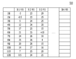
도 5a는 본 발명의 실시 예에 따른 온도 테이블(510)을 나타내며, 도 5b는 본 발명의 실시 예에 따른 리드 전압 테이블(530)을 나타낸다. 온도 테이블(510) 및 리드 전압 테이블(530)은 리드 리트라이 동작에서 활용될 수 있다.5A shows a temperature table 510 according to an embodiment of the present invention, and FIG. 5B shows a read voltage table 530 according to an embodiment of the present invention. The temperature table 510 and the read voltage table 530 may be used in a read retry operation.
도 5a를 참조하면, 온도 테이블(510)의 필드(field)는 복수의 위치 정보를 나타내며, 온도 테이블(510)의 엔트리(entry)는 '월(month)'을 나타낼 수 있다. 온도 테이블(510) 내에 기록된 값(value)들은 해당 위치에 해당 월의 평균 온도를 나타낼 수 있다. 예를 들면, 온도 테이블(510)을 참조하면, 제 1 위치의 3월 평균 온도는 '5°'이다. 온도 테이블(510)은 제 1 위치 내지 제 K 위치 각각의 월별 평균 온도를 나타낼 수 있다. 온도 테이블(510) 내 'K'는 설계자에 의하여 설정될 수 있다. Referring to FIG. 5A, a field of the temperature table 510 indicates a plurality of location information, and an entry of the temperature table 510 may indicate a “month”. Values recorded in the temperature table 510 may indicate the average temperature of the month at the corresponding location. For example, referring to the temperature table 510, the average temperature in March at the first position is '5°'. The temperature table 510 may represent the monthly average temperature of each of the first to K-th positions. 'K' in the temperature table 510 may be set by a designer.
프로세서(134)는 호스트(102)로부터 제공받은 RTC 정보 및 위치 정보에 따라 온도 테이블(510)을 활용하여 해당 위치의 해당 월의 평균 온도인 타겟 온도(T)를 확인할 수 있다. 예를 들어, 호스트(102) 및 메모리 시스템(110)을 포함하는 전자 장치가 2018년 12월 24일 16시 20분에 제 1 위치에서 시스템 부팅 동작을 수행한 경우, 프로세서(134)는 온도 테이블(510)을 활용하여 타겟 온도(T)가 '0.5'인 것을 확인할 수 있다.The
도 5b를 참조하면, 리드 전압 테이블(530)의 필드는 온도, 인덱스, 제 1 리드 전압(RV1), 제 2 리드 전압(RV2) 및 제 3 리드 전압(RV3)를 나타낸다.Referring to FIG. 5B, fields of the read voltage table 530 represent temperature, index, first read voltage RV1, second read voltage RV2, and third read voltage RV3.
리드 전압 테이블(530)의 온도 필드는 복수의 온도 구간들을 나타낼 수 있다. 도 5b에 도시된 리드 전압 테이블(530)의 온도 필드는 동일한 온도 차이로 엔트리가 구분되어 있다. 하지만, 이는 일 실시 예일 뿐이며, 이에 제한되는 것은 아니다. 상기 온도 차이는 설계자에 의하여 설정될 수 있다.The temperature field of the read voltage table 530 may represent a plurality of temperature sections. In the temperature field of the read voltage table 530 shown in FIG. 5B, entries are divided by the same temperature difference. However, this is only an example and is not limited thereto. The temperature difference may be set by a designer.
리드 전압 테이블(530)의 인덱스는 1 내지 N 값을 나타낼 수 있다. 인덱스는 리드 리트라이 동작에서 리드 전압의 설정 순서를 나타낸다. 프로세서(134)는 제 1 인덱스에 해당하는 리드 전압부터 제 N 인덱스에 해당하는 리드 전압까지 순차적으로 리드 전압을 설정할 수 있다. 'N'은 설계자에 의하여 설정될 수 있다. 또한, 프로세서(134)는 타겟 온도(T)를 반영하여 리드 전압의 설정 순서를 변경할 수 있다.The index of the read voltage table 530 may represent 1 to N values. The index indicates the setting order of the read voltage in the read retry operation. The
리드 전압 테이블(530)의 제 1 내지 제 3 리드 전압(RV1 내지 RV3)는 디폴트 리드 전압과 상이하고, 각기 서로 다른 리드 전압들을 나타낸다. 도 5b에 도시된 리드 전압 테이블(530)은 멀티 레벨 셀에 대한 리드 리트라이 동작을 위한 테이블이다. 멀티 레벨 셀에 대한 리드 동작은 3개의 서로 다른 리드 전압을 필요로 하기 때문에, 도 5b에 도시된 리드 전압 테이블(530)에 제 1 내지 제 3 리드 전압(RV1 내지 RV3) 필드가 포함될 수 있다. 단일 레벨 셀에 대한 리드 리트라이 동작을 위한 테이블은 오직 하나의 리드 전압에 대한 필드를 가질 수 있다. 트리플 레벨 셀에 대한 리드 리트라이 동작을 위한 테이블은 7개의 리드 전압에 대한 필드를 가질 수 있다.The first to third read voltages RV1 to RV3 of the read voltage table 530 are different from the default read voltages and represent different read voltages. The read voltage table 530 shown in FIG. 5B is a table for a read retry operation for a multi-level cell. Since the read operation for the multi-level cell requires three different read voltages, the first to third read voltages RV1 to RV3 fields may be included in the read voltage table 530 illustrated in FIG. 5B. A table for a read retry operation for a single level cell may have only one read voltage field. A table for a read retry operation for a triple level cell may have 7 fields for read voltages.
프로세서(134)는 리드 리트라이 동작 시 리드 전압 테이블(530)을 활용하여 리드 전압을 설정할 수 있다. 예를 들면, 타겟 온도(T)가 '15°'인 경우, 프로세서(134)는 리드 전압 테이블(530) 내 온도 필드에서 '15°'가 포함된 타겟 엔트리(10°= T< 20°)를 확인할 수 있다. 그리고, 프로세서(134)는 타겟 엔트리에 복수의 인덱스들 각각에 해당하는 리드 전압들을 리드 리트라이 동작에 활용될 리드 전압으로 설정할 수 있다. The
나아가, 프로세서(134)는 타겟 온도(T)를 반영하여 리드 전압의 설정 순서를 조정할 수 있다. 예를 들어, 타겟 온도(T)가 '10°'인 경우, 프로세서(134)가 제 1 인덱스에 포함된 리드 전압들을 우선적으로 설정한다고 가정한다. 타겟 온도(T)가 '15°'인 경우, 프로세서(134)는 제 N/2 인덱스에 포함된 리드 전압들을 우선적으로 설정할 수 있다. 프로세서(134)가 타겟 온도를 반영하여 리드 전압들을 설정함으로써, 프로세서(134)는 효율적인 리드 리트라이 동작을 수행할 수 있다.Furthermore, the
도 6 는 본 발명의 실시 예에 따른 리드 동작을 나타낸 흐름도이다.6 is a flowchart illustrating a read operation according to an embodiment of the present invention.
단계 S601에서, 호스트(102)는 리드 커맨드를 컨트롤러(130)에 제공할 수 있다. 호스트(102)는 리드 커맨드와 함께 리드 데이터에 대응하는 논리주소를 컨트롤러(130)에 제공할 수 있다. 리드 데이터는 리드하려고 하는 데이터를 의미한다.In step S601, the
단계 S603에서, 컨트롤러(130) 내 프로세서(134)는 호스트(102)로부터 제공받은 논리주소에 대응하는 물리주소를 확인할 수 있다.In step S603, the
그리고, 단계 S605에서, 프로세서(134)는 상기 물리주소에 저장된 데이터를 리드하기 위하여 디폴트 리드 전압을 설정할 수 있다. Then, in step S605, the
단계 S607에서, 프로세서(134)는 메모리 장치(150)에 리드 요청을 제공할 수 있다. 프로세서(134)는 리드 요청과 함께 디폴트 리드 전압 및 물리주소를 함께 메모리 장치(150)에 제공할 수 있다. 구체적으로, 프로세서(134)는 디폴트 리드 전압을 리드 커맨드에 대응하는 데이터가 저장된 타겟 메모리 셀에 인가하여 리드 동작을 수행하도록 메모리 장치(150)를 제어할 수 있다.In step S607, the
단계 S609에서, 메모리 장치(150)는 제공받은 디폴트 리드 전압 및 물리주소에 기초하여 데이터를 리드할 수 있다.In step S609, the
그리고, 단계 S611에서, 메모리 장치(150)는 리드 데이터를 컨트롤러(130)에 제공할 수 있다.In addition, in step S611, the
단계 S613에서, 컨트롤러(130) 내 ECC 유닛(136)은 프로세서(134)의 제어에 의하여 메모리 장치(150)로부터 제공받은 리드 데이터에 대하여 디코딩 동작을 수행할 수 있다. ECC 유닛(136)은 디코딩 동작을 통하여 리드 데이터의 페일 비트(fail bit) 수를 카운트할 수 있다.In step S613, the
단계 S615에서, ECC 유닛(136)은 카운트한 리드 데이터의 페일 비트 수와 사전 설정된 임계 값을 비교할 수 있다.In step S615, the
만약, 페일 비트 수가 사전 설정된 임계 값보다 작은 경우(단계 S515에서, 'No'), 단계 S617에서, 컨트롤러(130)는 리드 커맨드에 응답하여 리드 데이터를 호스트(102)로 제공할 수 있다.If the number of fail bits is less than a preset threshold value ('No' in step S515), in step S617, the
반면에, 페일 비트 수가 사전 설정된 임계 값보다 크거나 같은 경우(단계 S517에서, 'Yes'), 단계 S519에서, ECC유닛(136)은 프로세서(134)에 리드 리트라이 요청을 제공할 수 있으며, 프로세서(134)는 리드 리트라이 요청에 응답하여 리드 리트라이 동작을 수행할 수 있다.On the other hand, when the number of fail bits is greater than or equal to a preset threshold value ('Yes' in step S517), in step S519, the
도 7은 본 발명의 실시 예에 따른 리드 리트라이 동작을 나태는 흐름도이다. 도 7에 도시된 단계 S701 내지 단계 S727은 도 6에 도시된 단계 S619에 포함될 수 있다.7 is a flowchart showing a read retry operation according to an embodiment of the present invention. Steps S701 to S727 shown in FIG. 7 may be included in step S619 shown in FIG. 6.
단계 S701에서, 호스트(102)는 컨트롤러(130)에 RTC 정보 및 위치 정보를 제공할 수 있다. 비록, RTC 정보 및 위치정보가 컨트롤러(130)에 제공되는 동작이 단계 S701에 도시되어 있지만, 1에서 설명된 바와 같이, 호스트(102)는 사전 설정된 주기에 따라 RTC 정보 및 위치 정보를 컨트롤러(130)에 제공할 수 있다.In step S701, the
단계 S703에서, 컨트롤러(130) 내 프로세서(134)는 호스트(102)로부터 제공받은 RTC 정보 및 위치 정보에 따라 데이터 처리 시스템(100)을 포함하는 전자 장치의 외부 평균 온도, 즉 타겟 온도를 온도 테이블(510)을 활용하여 확인할 수 있다.In step S703, the
그리고, 단계 S705에서, 프로세서(134)는 리드 전압 테이블(530)에 포함된 복수의 엔트리들 중 단계 S703에서 확인된 온도가 포함된 타겟 엔트리를 확인할 수 있다.Then, in step S705, the
단계 S707에서, 프로세서(134)는 타겟 엔트리 내에 포함된 복수의 인덱스들 중에서 단계 S703에서 확인된 온도에 기초하여 리드 전압 테이블(530) 내 인덱스 값인 'i'값을 설정하여 타겟 인덱스를 선택할 수 있다.In step S707, the
그리고, 단계 S709에서, 프로세서(134)는 타겟 엔트리 내 'i' 번째 인덱스에 포함된 전압을 리드 전압으로 설정할 수 있다.Then, in step S709, the
단계 S711에서, 프로세서(134)는 설정된 리드 전압을 활용하여 리드 커맨드에 대응하는 데이터를 리드하기 위한 리드 요청을 메모리 장치(150)에 제공할 수 있다. 구체적으로, 프로세서(134)는 설정된 리드 전압을 리드 커맨드에 대응하는 데이터가 저장된 타겟 메모리 셀에 인가하여 리드 동작을 수행하도록 메모리 장치(150)를 제어할 수 있다.In step S711, the
단계 S713에서, 메모리 장치(150)는 단계 S709에서 설정된 리드 전압을 활용하여 데이터를 리드할 수 있다.In step S713, the
단계 S715에서, 메모리 장치(150)는 리드 요청에 응답하여 리드 데이터를 컨트롤러(130)에 제공할 수 있다.In step S715, the
단계 S717에서, 컨트롤러(130) 내 ECC 유닛(136)은 프로세서(134)의 제어에 의하여 리드 데이터에 대한 디코딩 동작을 수행할 수 있다.In step S717, the
그리고, 단계 S719에서, ECC 유닛(136)은 리드 데이터의 페일 비트 수와 사전 설정된 임계 값을 비교할 수 있다.Then, in step S719, the
만약, 리드 데이터의 페일 비트 수가 사전 설정된 임계 값보다 작은 경우(단계 S719에서 'No'), 단계 S721에서, 컨트롤러(130)는 리드 커맨드에 응답하여 리드 데이터를 호스트(102)로 제공할 수 있다.If the number of fail bits of the read data is smaller than a preset threshold ('No' in step S719), in step S721, the
반면에, 리드 데이터의 페일 비트 수가 사전 설정된 임계 값보다 크거나 같은 경우(단계 S719에서, 'Yes'), 단계 S723에서, ECC 유닛(136)은 리드 리트라이 요청을 프로세서(134)에 제공할 수 있으며, 리드 요청에 응답하여 프로세서(134)는 'i'값을 'N'과 비교할 수 있다. 'N'은 리드 전압 테이블(530) 내 복수의 엔트리들 각각에 포함된 인덱스 중 마지막 인덱스를 나타낸다.On the other hand, if the number of fail bits of the read data is greater than or equal to a preset threshold (in step S719,'Yes'), in step S723, the
'i'값이 'N'보다 작은 경우(단계 S723에서, 'No'), 단계 S725에서, 프로세서(134)는 'i'값을 '1'증가시킬 수 있다. 그리고, 컨트롤러(130) 및 메모리 장치(150)는 단계 S709 내지 단계 S719를 다시 수행할 수 있다. If the'i' value is less than'N' ('No' in step S723), the
반면에, 'i'값이 'N'보다 크거나 같은 경우(단계 S723에서, 'Yes'), 단계 S727에서, 컨트롤러(130)는 리드 커맨드에 응답하여 리드 실패를 호스트(102)에 통지할 수 있다.On the other hand, if the'i' value is greater than or equal to'N' (in step S723,'Yes'), in step S727, the
상기와 같이, 본 발명의 실시 예에 따른 메모리 시스템(110)은 호스트(102)로부터 제공받은 RTC 정보 및 위치 정보를 활용하여 효율적인 리드 리트라이 동작을 수행할 수 있다.As described above, the
도 14 내지 도 17은 본 발명의 실시 예에 따른 메모리 시스템을 포함하는 데이터 처리 시스템의 다른 일 예를 개략적으로 도시한 도면이다. 여기서, 도 14 내지 도 17은 본 발명의 실시 예에 따른 메모리 시스템이 적용된 UFS(Universal Flash Storage)를 개략적으로 도시한 도면이다.14 to 17 are diagrams schematically illustrating another example of a data processing system including a memory system according to an embodiment of the present invention. Here, FIGS. 14 to 17 are diagrams schematically illustrating UFS (Universal Flash Storage) to which a memory system according to an embodiment of the present invention is applied.
도 14 내지 도 17을 참조하면, 각각의 UFS 시스템들(6500,6600,6700,6800)은, 호스트들(6510,6610,6710,6810), UFS 장치들(6520,6620,6720,6820), 및 UFS 카드들(6530,6630,6730,6830)을 각각 포함할 수 있다. 여기서, 각각의 호스트(6510,6610,6710,6810)은, 유선/무선 전자 기기들, 특히 모바일 전자 기기 등의 어플리케이션 프로세서가 될 수 있으며, 또한 각각의 UFS 장치들(6520,6620,6720,6820)은, 임베디드 UFS(Embedded UFS) 장치들이 되고, 아울러 각각의 UFS 카드들(6530,6630,6730,6830)은, 외부 임베디드 UFS(External Embedded UFS) 장치 또는 리무벌 UFS 카드(Removable UFS Card)가 될 수 있다.14 to 17, each of the
또한, 각 UFS 시스템들(6500,6600,6700,6800)에서, 각각의 호스트들(6510,6610,6710,6810), UFS 장치들(6520,6620,6720,6820), 및 UFS 카드들(6530,6630,6730,6830) 간은, 각각 UFS 프로토콜을 통해 외부의 장치들, 예컨대 유선/무선 전자 기기들, 특히 모바일 전자 기기 등과 통신할 수 있으며, UFS 장치들(6520,6620,6720,6820)과 UFS 카드들(6530,6630,6730,6830)은, 도 1에서 설명한 메모리 시스템(110)으로 구현될 수 있다. 예컨대, 각 UFS 시스템들(6500,6600,6700,6800)에서, UFS 장치들(6520,6620,6720,6820)은, 도 11 내지 도 13에서 설명한 데이터 처리 시스템(6200), SSD(6300), 또는 eMMC(6400) 형태로 구현될 수 있으며, UFS 카드들(6530,6630,6730,6830)은, 도 10에서 설명한 메모리 카드 시스템(6100) 형태로 구현될 수 있다.Also, in each of the
아울러, 각 UFS 시스템들(6500,6600,6700,6800)에서, 각각의 호스트들(6510,6610,6710,6810), UFS 장치들(6520,6620,6720,6820), 및 UFS 카드들(6530,6630,6730,6830) 간은, UFS(Universal Flash Storage) 인터페이스, 예컨대 MIPI(Mobile Industry Processor Interface)에서의 MIPI M-PHY 및 MIPI UniPro(Unified Protocol)을 통해 통신을 수행할 수 있으며, 아울러 UFS 장치들(6520,6620,6720,6820)과 UFS 카드들(6530,6630,6730,6830) 간은, UFS 프로토콜이 아닌 다른 프로토콜을 통해 통신할 수 있으며, 예컨대 다양한 카드 프로토콜, 일 예로 UFDs, MMC, SD(secure digital), mini SD, Micro SD 등을 통해 통신할 수 있다.In addition, in each of the
한편, 본 발명의 상세한 설명에서는 구체적인 실시 예에 관해 설명하였으나, 본 발명의 범위에서 벗어나지 않는 한도 내에서 여러 가지 변형이 가능함은 물론이다. 그러므로, 본 발명의 범위는 설명된 실시 예에 국한되어 정해져서는 안되며 후술하는 특허청구의 범위뿐만 아니라 이 특허청구의 범위와 균등한 것들에 의해 정해져야 한다.Meanwhile, although specific embodiments have been described in the detailed description of the present invention, various modifications may be made without departing from the scope of the present invention. Therefore, the scope of the present invention should not be defined by being limited to the described embodiments, and should be determined by the scope of the claims and equivalents as well as the scope of the claims to be described later.
Claims (20)
복수의 메모리 셀들을 포함하는 메모리 장치; 및
호스트로부터 제공된 리드 커맨드에 대응하는 데이터가 저장된 타겟 메모리 셀에 제 1 리드 전압을 인가하여 제 1 리드 동작을 수행하도록 상기 메모리 장치를 제어하는 컨트롤러
를 포함하고,
상기 컨트롤러는
상기 제 1 리드 데이터 - 상기 제 1 리드 동작에 의하여 리드된 데이터- 의 페일 비트가 사전 설정된 임계 값보다 크거나 같은 경우, 상기 호스트로부터 제공된 RTC 정보 및 위치 정보에 기초하여 온도 테이블 내 기록된 외부 온도를 확인하고, 상기 외부 온도 및 리드 전압 테이블에 기초하여 제 2 리드 전압을 설정하며, 상기 제 2 리드 전압을 활용하여 상기 데이터에 대하여 제 2 리드동작을 수행하는
메모리 시스템.
In the memory system,
A memory device including a plurality of memory cells; And
A controller that controls the memory device to perform a first read operation by applying a first read voltage to a target memory cell in which data corresponding to a read command provided from a host is stored
Including,
The controller is
When the fail bit of the first read data-data read by the first read operation-is greater than or equal to a preset threshold, the external temperature recorded in the temperature table based on RTC information and location information provided from the host To check, set a second read voltage based on the external temperature and read voltage table, and perform a second read operation on the data by using the second read voltage.
Memory system.
상기 온도 테이블은 복수의 위치 정보 각각의 '월'(month) 평균 온도를 나타내며,
상기 리드 전압 테이블은 복수의 온도 구간들, 상기 복수의 온도 구간들 각각에 포함된 복수의 인덱스들 및 상기 복수의 인덱스들 각각에 대응하는 리드 전압을 나타내는
메모리 시스템.
The method of claim 1,
The temperature table represents the'month' average temperature of each of a plurality of location information,
The read voltage table represents a plurality of temperature sections, a plurality of indexes included in each of the plurality of temperature sections, and a read voltage corresponding to each of the plurality of indexes.
Memory system.
상기 컨트롤러는
상기 온도 테이블 및 상기 리드 전압 테이블을 저장하는 메모리,
상기 제 1 리드 데이터에 대한 디코딩 동작을 통하여 상기 페일 비트 수를 카운트하고, 상기 페일 비트 수와 사전 설정된 임계 값을 비교하는 ECC 유닛, 및
상기 제 1 리드 데이터의 페일 비트가 사전 설정된 임계 값보다 크거나 같은 경우, 상기 외부 온도를 확인하고, 상기 제 2 리드 전압을 설정하며, 상기 제 2 리드 전압을 상기 타겟 메모리 셀에 인가하여 상기 제 2 리드동작을 수행하도록 상기 메모리 장치를 제어하는 프로세서
를 포함하는 메모리 시스템.
The method of claim 1,
The controller is
A memory for storing the temperature table and the read voltage table,
An ECC unit that counts the number of fail bits through a decoding operation on the first read data and compares the number of fail bits with a preset threshold value, and
When the fail bit of the first read data is greater than or equal to a preset threshold, the external temperature is checked, the second read voltage is set, and the second read voltage is applied to the target memory cell, 2 Processor for controlling the memory device to perform a read operation
Memory system comprising a.
상기 컨트롤러는
상기 리드 전압 테이블에 포함된 복수의 온도 구간들 중 상기 외부 온도가 포함된 타겟 온도 구간을 확인하는
메모리 시스템.
According to claim 2,
The controller is
Checking a target temperature section including the external temperature among a plurality of temperature sections included in the read voltage table
Memory system.
상기 컨트롤러는
상기 타겟 온도 구간에 포함된 복수의 인덱스들 중에서 상기 외부 온도에 기초하여 타겟 인덱스를 선택하는
메모리 시스템.
The method of claim 4,
The controller is
Selecting a target index based on the external temperature from among a plurality of indexes included in the target temperature section
Memory system.
상기 컨트롤러는
상기 타겟 인덱스에 포함된 전압을 상기 제 2 리드 전압으로 설정하고, 상기 제 2 리드 전압을 상기 타겟 메모리 셀에 인가하여 상기 제 2 리드 동작을 수행하도록 상기 메모리 장치를 제어하는
메모리 시스템.
The method of claim 5,
The controller is
Controlling the memory device to perform the second read operation by setting a voltage included in the target index as the second read voltage and applying the second read voltage to the target memory cell
Memory system.
상기 컨트롤러는
제 2 리드 데이터 - 상기 제 2 리드 동작에 의하여 리드된 데이터 - 에 대한 디코딩 동작을 수행하고, 상기 제 2 리드 데이터의 페일 비트 수가 사전 설정된 임계 값보다 크거나 같은 경우, 상기 타겟 인덱스가 상기 타겟 엔트리 내 마지막 인덱스인지 확인하는
메모리 시스템.
The method of claim 6,
The controller is
When a decoding operation is performed on the second read data-data read by the second read operation-and the number of fail bits of the second read data is greater than or equal to a preset threshold, the target index is the target entry To check if it is my last index
Memory system.
상기 컨트롤러는
상기 타겟 인덱스가 상기 타겟 엔트리 내 마지막 인덱스가 아니라면, 상기 타겟 엔트리 내에서 타겟 인덱스의 다음 인덱스에 포함된 전압을 제 3 리드 전압으로 설정하고, 상기 제 3 리드 전압을 상기 타겟 메모리 셀에 인가하여 제 3 리드동작을 수행하도록 상기 메모리 장치를 제어하는
메모리 시스템.
The method of claim 7,
The controller is
If the target index is not the last index in the target entry, the voltage included in the next index of the target index in the target entry is set as a third read voltage, and the third read voltage is applied to the target memory cell to be 3 controlling the memory device to perform a read operation
Memory system.
상기 컨트롤러는
상기 타겟 인덱스가 상기 타겟 엔트리 내 마지막 인덱스라면, 상기 데이터에 대한 리드 실패를 상기 호스트에 통지하는
메모리 시스템.
The method of claim 7,
The controller is
If the target index is the last index in the target entry, notifying the host of a failure to read the data
Memory system.
상기 컨트롤러는
상기 제 2 리드 데이터의 페일 비트 수가 사전 설정된 임계 값보다 작은 경우, 상기 제 2 데이터를 상기 리드 커맨드에 응답하여 상기 호스트로 제공하는
메모리 시스템.
The method of claim 7,
The controller is
When the number of fail bits of the second read data is less than a preset threshold, providing the second data to the host in response to the read command
Memory system.
호스트로부터 RTC 정보 및 위치 정보를 제공받는 단계;
상기 호스트로부터 제공된 리드 커맨드에 대응하는 데이터가 저장된 타겟 메모리 셀에 제 1 리드 전압을 인가하여 제 1 리드 동작을 수행하는 단계;
상기 제 1 리드 데이터 - 상기 제 1 리드 동작에 의하여 리드된 데이터 -의 페일 비트가 사전 설정된 임계 값보다 크거나 같은 경우, 상기 RTC 정보 및 상기 위치 정보에 기초하여 온도 테이블 내 기록된 외부 온도를 확인하는 단계;
상기 외부 온도 및 리드 전압 테이블에 기초하여 제 2 리드 전압을 설정하는 단계; 및
상기 제 2 리드 전압을 상기 타겟 메모리 셀에 인가하여 제 2 리드 동작을 수행하는 단계
를 포함하는 메모리 시스템의 동작방법.
In the method of operating a memory system,
Receiving RTC information and location information from a host;
Performing a first read operation by applying a first read voltage to a target memory cell in which data corresponding to a read command provided from the host is stored;
When the fail bit of the first read data-the data read by the first read operation-is greater than or equal to a preset threshold, the external temperature recorded in the temperature table is checked based on the RTC information and the location information. Step to do;
Setting a second read voltage based on the external temperature and read voltage table; And
Performing a second read operation by applying the second read voltage to the target memory cell
A method of operating a memory system comprising a.
상기 온도 테이블은 복수의 위치 정보 각각의 '월'(month) 평균 온도를 나타내며,
상기 리드 전압 테이블은 복수의 온도 구간들, 상기 복수의 온도 구간들 각각에 포함된 복수의 인덱스들 및 상기 복수의 인덱스들 각각에 대응하는 리드 전압을 나타내는
메모리 시스템의 동작방법.
The method of claim 11,
The temperature table represents the'month' average temperature of each of a plurality of location information,
The read voltage table represents a plurality of temperature sections, a plurality of indexes included in each of the plurality of temperature sections, and a read voltage corresponding to each of the plurality of indexes.
How the memory system works.
상기 온도 테이블 및 상기 리드 전압 테이블을 저장하는 단계;
상기 제 1 리드 데이터에 대한 디코딩 동작을 수행하여 상기 제 1 리드 데이터의 페일 비트 수를 카운트하는 단계;
상기 제 1 리드 데이터의 페일 비트 수와 사전 설정된 임계 값을 비교하는 단계
를 더 포함하는 메모리 시스템의 동작방법.
The method of claim 11,
Storing the temperature table and the read voltage table;
Counting the number of fail bits of the first read data by performing a decoding operation on the first read data;
Comparing the number of fail bits of the first read data and a preset threshold
The method of operating a memory system further comprising.
상기 제 2 리드 전압을 설정하는 단계는
상기 리드 전압 테이블에 포함된 복수의 온도 구간들 중 상기 외부 온도가 포함된 타겟 온도 구간을 확인하는 단계
를 포함하는 메모리 시스템의 동작방법.
The method of claim 12,
Setting the second read voltage comprises:
Checking a target temperature section including the external temperature among a plurality of temperature sections included in the read voltage table
A method of operating a memory system comprising a.
상기 제 2 리드 전압을 설정하는 단계는
상기 타겟 온도 구간에 포함된 복수의 인덱스들 중에서 상기 외부온도에 기초하여 타겟 인덱스를 선택하고, 상기 타겟 인덱스에 포함된 전압을 상기 제 2 리드 전압으로 설정하는 단계
를 포함하는 메모리 시스템의 동작방법.
The method of claim 14,
Setting the second read voltage comprises:
Selecting a target index based on the external temperature from among a plurality of indexes included in the target temperature section, and setting a voltage included in the target index as the second read voltage
A method of operating a memory system comprising a.
상기 제 2 리드 동작을 수행하는 단계는
상기 타겟 인덱스에 포함된 전압을 제 2 리드 전압으로 활용하여 상기 제 2 리드 동작을 수행하는
메모리 시스템의 동작방법.
The method of claim 15,
The step of performing the second read operation
Performing the second read operation by using the voltage included in the target index as a second read voltage
How the memory system works.
제 2 리드 데이터 - 상기 제 2 리드 동작에 의하여 리드된 데이터 - 에 대한 디코딩 동작을 수행하는 단계; 및
상기 제 2 리드 데이터의 페일 비트 수가 사전 설정된 임계 값보다 크거나 같은 경우, 상기 타겟 인덱스가 상기 타겟 엔트리 내 마지막 인덱스인지 확인하는 단계
를 더 포함하는 메모리 시스템의 동작방법.
The method of claim 16,
Performing a decoding operation on second read data-data read by the second read operation; And
When the number of fail bits of the second read data is greater than or equal to a preset threshold, checking whether the target index is the last index in the target entry
The method of operating a memory system further comprising.
상기 타겟 인덱스가 상기 타겟 엔트리 내 마지막 인덱스가 아니라면, 상기 타겟 엔트리 내에서 타겟 인덱스의 다음 인덱스에 포함된 전압을 제 3 리드 전압으로 설정하는 단계; 및
상기 제 3 리드 전압을 상기 타겟 메모리 셀에 인가하여 제 3 리드 동작을 수행하는 단계
를 더 포함하는 메모리 시스템의 동작방법.
The method of claim 17,
If the target index is not the last index in the target entry, setting a voltage included in the next index of the target index in the target entry as a third read voltage; And
Performing a third read operation by applying the third read voltage to the target memory cell
The method of operating a memory system further comprising.
상기 타겟 인덱스가 상기 타겟 엔트리 내 마지막 인덱스라면, 상기 데이터에 대한 리드 실패를 상기 호스트에 통지하는 단계
를 더 포함하는 메모리 시스템의 동작방법.
The method of claim 17,
If the target index is the last index in the target entry, notifying the host of a failure to read the data
The method of operating a memory system further comprising.
상기 제 2 리드 데이터의 페일 비트 수가 사전 설정된 임계 값보다 작은 경우, 상기 제 2 리드 데이터를 상기 호스트로 제공하는 단계
를 더 포함하는 메모리 시스템의 동작방법.
The method of claim 17,
If the number of fail bits of the second read data is smaller than a preset threshold, providing the second read data to the host
The method of operating a memory system further comprising.
Priority Applications (3)
| Application Number | Priority Date | Filing Date | Title |
|---|---|---|---|
| KR1020190013867A KR20200095903A (en) | 2019-02-01 | 2019-02-01 | Memory system and operating method thereof |
| CN201911300224.3A CN111540399A (en) | 2019-02-01 | 2019-12-16 | Memory system and operating method thereof |
| US16/723,075 US11334462B2 (en) | 2019-02-01 | 2019-12-20 | Memory system and operating method thereof |
Applications Claiming Priority (1)
| Application Number | Priority Date | Filing Date | Title |
|---|---|---|---|
| KR1020190013867A KR20200095903A (en) | 2019-02-01 | 2019-02-01 | Memory system and operating method thereof |
Publications (1)
| Publication Number | Publication Date |
|---|---|
| KR20200095903A true KR20200095903A (en) | 2020-08-11 |
Family
ID=71836473
Family Applications (1)
| Application Number | Title | Priority Date | Filing Date |
|---|---|---|---|
| KR1020190013867A KR20200095903A (en) | 2019-02-01 | 2019-02-01 | Memory system and operating method thereof |
Country Status (3)
| Country | Link |
|---|---|
| US (1) | US11334462B2 (en) |
| KR (1) | KR20200095903A (en) |
| CN (1) | CN111540399A (en) |
Cited By (2)
| Publication number | Priority date | Publication date | Assignee | Title |
|---|---|---|---|---|
| US11842067B2 (en) | 2021-10-20 | 2023-12-12 | SK Hynix Inc. | Memory controller, memory system including the same, and method of operating the memory system |
| US11978519B2 (en) | 2021-07-06 | 2024-05-07 | SK Hynix Inc. | Storage device and operating method thereof |
Families Citing this family (1)
| Publication number | Priority date | Publication date | Assignee | Title |
|---|---|---|---|---|
| US11681469B2 (en) * | 2021-02-22 | 2023-06-20 | Micron Technology, Inc. | Storing and recovering critical data in a memory device |
Family Cites Families (19)
| Publication number | Priority date | Publication date | Assignee | Title |
|---|---|---|---|---|
| CN100345076C (en) * | 2003-12-24 | 2007-10-24 | 鸿富锦精密工业(深圳)有限公司 | Battery feeding type memory electricity quantity measuring system and method |
| US20070255937A1 (en) * | 2006-04-26 | 2007-11-01 | Sheng-Hsin Lo | Basic input / output system (BIOS) set-value access method |
| KR101737020B1 (en) * | 2009-09-09 | 2017-05-29 | 마벨 월드 트레이드 리미티드 | Memory with multiple power supplies and/or multiple low power modes |
| CN102142186B (en) * | 2011-03-01 | 2013-01-09 | 合肥国轩高科动力能源有限公司 | Remote monitoring system for lithium battery pack |
| US8472274B2 (en) * | 2011-03-02 | 2013-06-25 | Apple Inc. | Using temperature sensors with a memory device |
| CN102263303B (en) * | 2011-06-02 | 2016-09-14 | 福州天和新能电子科技有限公司 | Modular lithium power battery and management systems and management method thereof |
| KR102306804B1 (en) | 2015-01-21 | 2021-09-30 | 삼성전자주식회사 | Method and apparatus for reducing power consumption of electronic device |
| KR102291806B1 (en) | 2015-04-20 | 2021-08-24 | 삼성전자주식회사 | Nonvolatile memory system and operation method thereof |
| KR102512448B1 (en) * | 2016-03-28 | 2023-03-22 | 에스케이하이닉스 주식회사 | Memory system and operation method thereof |
| CN205787727U (en) * | 2016-05-23 | 2016-12-07 | 深圳市恒昌通电子有限公司 | It is applicable to the integrated main controller of unmanned plane |
| KR20180070974A (en) | 2016-12-19 | 2018-06-27 | 삼성전자주식회사 | Read operation method of nonvoltile memory, memory system including the same and operation method thereof |
| US10304559B2 (en) * | 2016-12-30 | 2019-05-28 | Western Digital Technologies, Inc. | Memory write verification using temperature compensation |
| CN106679703B (en) * | 2017-02-24 | 2022-11-08 | 河北稳控科技有限公司 | Data reading device of vibrating wire type sensor and working method thereof |
| KR20190001300A (en) * | 2017-06-27 | 2019-01-04 | 에스케이하이닉스 주식회사 | Controller and memory system and operating method of memory system |
| US10535383B2 (en) * | 2018-02-28 | 2020-01-14 | Sandisk Technologies Llc | Throughput performance for cross temperature handling scenarios |
| US10636488B2 (en) * | 2018-06-05 | 2020-04-28 | Western Digital Technologies, Inc. | Multi-sensing scan for cross-temperature mitigation |
| CN109062145A (en) * | 2018-08-13 | 2018-12-21 | 大古智能科技(上海)有限公司 | Numerically-controlled machine tool motion control card based on WIFI communication |
| US11250926B2 (en) * | 2019-10-16 | 2022-02-15 | Sandisk Technologies Llc | Positive feedback and parallel searching enhanced optimal read method for non-volatile memory |
| US11037641B1 (en) * | 2019-12-05 | 2021-06-15 | Sandisk Technologies Llc | Temperature and cycling dependent refresh operation for memory cells |
-
2019
- 2019-02-01 KR KR1020190013867A patent/KR20200095903A/en not_active Application Discontinuation
- 2019-12-16 CN CN201911300224.3A patent/CN111540399A/en not_active Withdrawn
- 2019-12-20 US US16/723,075 patent/US11334462B2/en active Active
Cited By (2)
| Publication number | Priority date | Publication date | Assignee | Title |
|---|---|---|---|---|
| US11978519B2 (en) | 2021-07-06 | 2024-05-07 | SK Hynix Inc. | Storage device and operating method thereof |
| US11842067B2 (en) | 2021-10-20 | 2023-12-12 | SK Hynix Inc. | Memory controller, memory system including the same, and method of operating the memory system |
Also Published As
| Publication number | Publication date |
|---|---|
| US20200250061A1 (en) | 2020-08-06 |
| CN111540399A (en) | 2020-08-14 |
| US11334462B2 (en) | 2022-05-17 |
Similar Documents
| Publication | Publication Date | Title |
|---|---|---|
| CN110765035B (en) | Memory system and operating method thereof | |
| CN109390003B (en) | Memory system and operating method thereof | |
| KR102532563B1 (en) | Memory device and operating method thereof | |
| KR20190044798A (en) | Controller and operation method thereof | |
| US11922065B2 (en) | Memory system and operating method thereof | |
| KR20200065298A (en) | Memory system and operating method thereof | |
| KR20200010933A (en) | Memory system and operating method thereof | |
| CN111367468A (en) | Memory system and operating method thereof | |
| CN109656470B (en) | Memory system and operating method thereof | |
| US11334462B2 (en) | Memory system and operating method thereof | |
| KR20180076425A (en) | Controller and operating method of controller | |
| KR20200019430A (en) | Controller and operating method thereof | |
| KR102586786B1 (en) | Memory system and operating method thereof | |
| KR102520412B1 (en) | Memory system and operation method thereof | |
| KR102567314B1 (en) | Memory system and operating method thereof | |
| KR102659036B1 (en) | Memory system and operating method thereof | |
| KR102579824B1 (en) | Memory system and operation method thereof | |
| KR20200074647A (en) | Memory system and operating method thereof | |
| KR20200029810A (en) | Data processing system and operating method thereof | |
| KR20200068944A (en) | Memory system and operating method thereof | |
| KR20190082513A (en) | Controller and operation method thereof | |
| KR102654308B1 (en) | Memory system and operating method thereof | |
| KR102513498B1 (en) | Controller, operating method thereof and memory system including the controller | |
| KR20200053965A (en) | Memory system and operation method thereof | |
| KR20200064567A (en) | Data processing system and operating method thereof |
Legal Events
| Date | Code | Title | Description |
|---|---|---|---|
| A201 | Request for examination | ||
| E902 | Notification of reason for refusal |