KR20200095103A - Data storage device and operating method thereof - Google Patents
Data storage device and operating method thereof Download PDFInfo
- Publication number
- KR20200095103A KR20200095103A KR1020190012769A KR20190012769A KR20200095103A KR 20200095103 A KR20200095103 A KR 20200095103A KR 1020190012769 A KR1020190012769 A KR 1020190012769A KR 20190012769 A KR20190012769 A KR 20190012769A KR 20200095103 A KR20200095103 A KR 20200095103A
- Authority
- KR
- South Korea
- Prior art keywords
- core
- mapping
- logical block
- cpu
- cores
- Prior art date
Links
Images


Classifications
-
- G—PHYSICS
- G06—COMPUTING; CALCULATING OR COUNTING
- G06F—ELECTRIC DIGITAL DATA PROCESSING
- G06F3/00—Input arrangements for transferring data to be processed into a form capable of being handled by the computer; Output arrangements for transferring data from processing unit to output unit, e.g. interface arrangements
- G06F3/06—Digital input from, or digital output to, record carriers, e.g. RAID, emulated record carriers or networked record carriers
- G06F3/0601—Interfaces specially adapted for storage systems
- G06F3/0628—Interfaces specially adapted for storage systems making use of a particular technique
- G06F3/0629—Configuration or reconfiguration of storage systems
- G06F3/0631—Configuration or reconfiguration of storage systems by allocating resources to storage systems
-
- G—PHYSICS
- G06—COMPUTING; CALCULATING OR COUNTING
- G06F—ELECTRIC DIGITAL DATA PROCESSING
- G06F3/00—Input arrangements for transferring data to be processed into a form capable of being handled by the computer; Output arrangements for transferring data from processing unit to output unit, e.g. interface arrangements
- G06F3/06—Digital input from, or digital output to, record carriers, e.g. RAID, emulated record carriers or networked record carriers
- G06F3/0601—Interfaces specially adapted for storage systems
- G06F3/0602—Interfaces specially adapted for storage systems specifically adapted to achieve a particular effect
- G06F3/061—Improving I/O performance
-
- G—PHYSICS
- G06—COMPUTING; CALCULATING OR COUNTING
- G06F—ELECTRIC DIGITAL DATA PROCESSING
- G06F12/00—Accessing, addressing or allocating within memory systems or architectures
- G06F12/02—Addressing or allocation; Relocation
- G06F12/0223—User address space allocation, e.g. contiguous or non contiguous base addressing
- G06F12/023—Free address space management
- G06F12/0238—Memory management in non-volatile memory, e.g. resistive RAM or ferroelectric memory
- G06F12/0246—Memory management in non-volatile memory, e.g. resistive RAM or ferroelectric memory in block erasable memory, e.g. flash memory
-
- G—PHYSICS
- G06—COMPUTING; CALCULATING OR COUNTING
- G06F—ELECTRIC DIGITAL DATA PROCESSING
- G06F3/00—Input arrangements for transferring data to be processed into a form capable of being handled by the computer; Output arrangements for transferring data from processing unit to output unit, e.g. interface arrangements
- G06F3/06—Digital input from, or digital output to, record carriers, e.g. RAID, emulated record carriers or networked record carriers
- G06F3/0601—Interfaces specially adapted for storage systems
- G06F3/0602—Interfaces specially adapted for storage systems specifically adapted to achieve a particular effect
- G06F3/0614—Improving the reliability of storage systems
- G06F3/0616—Improving the reliability of storage systems in relation to life time, e.g. increasing Mean Time Between Failures [MTBF]
-
- G—PHYSICS
- G06—COMPUTING; CALCULATING OR COUNTING
- G06F—ELECTRIC DIGITAL DATA PROCESSING
- G06F3/00—Input arrangements for transferring data to be processed into a form capable of being handled by the computer; Output arrangements for transferring data from processing unit to output unit, e.g. interface arrangements
- G06F3/06—Digital input from, or digital output to, record carriers, e.g. RAID, emulated record carriers or networked record carriers
- G06F3/0601—Interfaces specially adapted for storage systems
- G06F3/0628—Interfaces specially adapted for storage systems making use of a particular technique
- G06F3/0629—Configuration or reconfiguration of storage systems
- G06F3/0635—Configuration or reconfiguration of storage systems by changing the path, e.g. traffic rerouting, path reconfiguration
-
- G—PHYSICS
- G06—COMPUTING; CALCULATING OR COUNTING
- G06F—ELECTRIC DIGITAL DATA PROCESSING
- G06F3/00—Input arrangements for transferring data to be processed into a form capable of being handled by the computer; Output arrangements for transferring data from processing unit to output unit, e.g. interface arrangements
- G06F3/06—Digital input from, or digital output to, record carriers, e.g. RAID, emulated record carriers or networked record carriers
- G06F3/0601—Interfaces specially adapted for storage systems
- G06F3/0628—Interfaces specially adapted for storage systems making use of a particular technique
- G06F3/0638—Organizing or formatting or addressing of data
- G06F3/064—Management of blocks
-
- G—PHYSICS
- G06—COMPUTING; CALCULATING OR COUNTING
- G06F—ELECTRIC DIGITAL DATA PROCESSING
- G06F3/00—Input arrangements for transferring data to be processed into a form capable of being handled by the computer; Output arrangements for transferring data from processing unit to output unit, e.g. interface arrangements
- G06F3/06—Digital input from, or digital output to, record carriers, e.g. RAID, emulated record carriers or networked record carriers
- G06F3/0601—Interfaces specially adapted for storage systems
- G06F3/0628—Interfaces specially adapted for storage systems making use of a particular technique
- G06F3/0653—Monitoring storage devices or systems
-
- G—PHYSICS
- G06—COMPUTING; CALCULATING OR COUNTING
- G06F—ELECTRIC DIGITAL DATA PROCESSING
- G06F3/00—Input arrangements for transferring data to be processed into a form capable of being handled by the computer; Output arrangements for transferring data from processing unit to output unit, e.g. interface arrangements
- G06F3/06—Digital input from, or digital output to, record carriers, e.g. RAID, emulated record carriers or networked record carriers
- G06F3/0601—Interfaces specially adapted for storage systems
- G06F3/0628—Interfaces specially adapted for storage systems making use of a particular technique
- G06F3/0655—Vertical data movement, i.e. input-output transfer; data movement between one or more hosts and one or more storage devices
- G06F3/0658—Controller construction arrangements
-
- G—PHYSICS
- G06—COMPUTING; CALCULATING OR COUNTING
- G06F—ELECTRIC DIGITAL DATA PROCESSING
- G06F3/00—Input arrangements for transferring data to be processed into a form capable of being handled by the computer; Output arrangements for transferring data from processing unit to output unit, e.g. interface arrangements
- G06F3/06—Digital input from, or digital output to, record carriers, e.g. RAID, emulated record carriers or networked record carriers
- G06F3/0601—Interfaces specially adapted for storage systems
- G06F3/0668—Interfaces specially adapted for storage systems adopting a particular infrastructure
- G06F3/0671—In-line storage system
- G06F3/0673—Single storage device
- G06F3/0679—Non-volatile semiconductor memory device, e.g. flash memory, one time programmable memory [OTP]
-
- G—PHYSICS
- G06—COMPUTING; CALCULATING OR COUNTING
- G06F—ELECTRIC DIGITAL DATA PROCESSING
- G06F3/00—Input arrangements for transferring data to be processed into a form capable of being handled by the computer; Output arrangements for transferring data from processing unit to output unit, e.g. interface arrangements
- G06F3/06—Digital input from, or digital output to, record carriers, e.g. RAID, emulated record carriers or networked record carriers
- G06F3/0601—Interfaces specially adapted for storage systems
- G06F3/0668—Interfaces specially adapted for storage systems adopting a particular infrastructure
- G06F3/0671—In-line storage system
- G06F3/0673—Single storage device
- G06F3/068—Hybrid storage device
-
- G—PHYSICS
- G06—COMPUTING; CALCULATING OR COUNTING
- G06F—ELECTRIC DIGITAL DATA PROCESSING
- G06F2212/00—Indexing scheme relating to accessing, addressing or allocation within memory systems or architectures
- G06F2212/10—Providing a specific technical effect
- G06F2212/1032—Reliability improvement, data loss prevention, degraded operation etc
- G06F2212/1036—Life time enhancement
-
- G—PHYSICS
- G06—COMPUTING; CALCULATING OR COUNTING
- G06F—ELECTRIC DIGITAL DATA PROCESSING
- G06F2212/00—Indexing scheme relating to accessing, addressing or allocation within memory systems or architectures
- G06F2212/72—Details relating to flash memory management
- G06F2212/7211—Wear leveling
Abstract
Description
본 발명은 전자 장치에 관한 것으로, 보다 구체적으로는 데이터 저장 장치 및 그 동작 방법에 관한 것이다.The present invention relates to an electronic device, and more particularly, to a data storage device and an operating method thereof.
최근 컴퓨터 환경에 대한 패러다임(paradigm)이 언제, 어디서나 컴퓨터 시스템을 사용할 수 있도록 하는 유비쿼터스 컴퓨팅(ubiquitous computing)으로 전환되고 있다. 이로 인해 휴대폰, 디지털 카메라, 노트북 컴퓨터 등과 같은 휴대용 전자 장치의 사용이 급증하고 있다. 이와 같은 휴대용 전자 장치는 일반적으로 메모리 장치를 이용하는 데이터 저장 장치를 사용한다. 데이터 저장 장치는 휴대용 전자 장치에서 사용되는 데이터를 저장하기 위해서 사용된다.Recently, the paradigm of the computer environment has been shifted to ubiquitous computing, which enables computer systems to be used anytime, anywhere. As a result, the use of portable electronic devices such as mobile phones, digital cameras, and notebook computers is rapidly increasing. Such portable electronic devices generally use a data storage device using a memory device. Data storage devices are used to store data used in portable electronic devices.
메모리 장치를 이용한 데이터 저장 장치는 기계적인 구동부가 없어서 안정성 및 내구성이 뛰어나며 정보의 액세스 속도가 매우 빠르고 전력 소모가 적다는 장점이 있다. 이러한 장점을 갖는 데이터 저장 장치는 USB(Universal Serial Bus) 메모리 장치, 다양한 인터페이스를 갖는 메모리 카드, UFS(Universal Flash Storage) 장치, 솔리드 스테이트 드라이브(Solid State Drive)를 포함한다.A data storage device using a memory device has advantages of excellent stability and durability because there is no mechanical driving unit, and information access speed is very fast and power consumption is low. Data storage devices having such advantages include universal serial bus (USB) memory devices, memory cards having various interfaces, universal flash storage (UFS) devices, and solid state drives.
본 발명의 실시 예는 코어 별로 할당된 저장 영역들 간의 마모도를 평준화할 수 있는 데이터 저장 장치 및 그 동작 방법을 제공한다.An embodiment of the present invention provides a data storage device capable of equalizing wear and tear between storage areas allocated for each core and a method of operating the same.
본 발명의 실시 예에 따른 데이터 저장 장치는 불휘발성 메모리 장치; 및 상기 불휘발성 메모리 장치의 동작을 제어하는 컨트롤러를 포함하고, 상기 컨트롤러는, 제1 CPU 및 복수의 코어들을 포함하는 제2 CPU를 포함한다. 상기 제1 CPU는 기 설정된 주기 마다 상기 제2 CPU의 상기 복수의 코어들 각각에 대한 프로그램/소거(program/erase, P/E) 평균 카운트를 비교하고, 상기 복수의 코어들 중 상기 P/E 평균 카운트의 차이 값이 기 설정된 임계 값 이상인 제1 코어와 제2 코어가 존재하면, 호스트로부터 수신되는 논리 블록 어드레스들에 맵핑되는 코어를 변경하는 리-맵핑 동작을 수행한다.A data storage device according to an embodiment of the present invention includes a nonvolatile memory device; And a controller for controlling an operation of the nonvolatile memory device, wherein the controller includes a first CPU and a second CPU including a plurality of cores. The first CPU compares a program/erase (P/E) average count for each of the plurality of cores of the second CPU every preset period, and the P/E among the plurality of cores When the first core and the second core having a difference value of the average count equal to or greater than a preset threshold value exist, a re-mapping operation of changing cores mapped to logical block addresses received from the host is performed.
본 발명의 실시 예에 따른 데이터 저장 장치의 동작 방법은 기 설정된 주기 마다 상기 제2 CPU의 상기 복수의 코어들 각각에 대한 프로그램/소거(program/erase, P/E) 평균 카운트를 비교하는 단계; 상기 제2 CPU의 상기 복수의 코어들 중 상기 P/E 평균 카운트의 차이 값이 기 설정된 임계 값 이상인 제1 코어와 제2 코어가 존재하는지 여부를 확인하는 단계; 및 상기 제1 코어와 상기 제2 코어가 존재하면, 호스트로부터 수신되는 논리 블록 어드레스들에 맵핑되는 코어를 변경하는 리-맵핑 동작을 수행하는 단계를 포함한다.A method of operating a data storage device according to an exemplary embodiment of the present invention includes comparing a program/erase (P/E) average count for each of the plurality of cores of the second CPU at each preset period; Checking whether a first core and a second core having a difference value of the average P/E count equal to or greater than a preset threshold among the plurality of cores of the second CPU exist; And if the first core and the second core exist, performing a re-mapping operation of changing a core mapped to logical block addresses received from a host.
본 실시 예에 따르면, 코어 별로 맵핑된 논리 블록 어드레스들을 리-맵핑하여 코어 별 저장 영역 간의 웨어-레벨링(wear-leveling)을 수행할 수 있다. 이에 따라, 코어 별 저장 영역 간의 마모도를 평준화할 수 있다.According to the present embodiment, by re-mapping logical block addresses mapped for each core, wear-leveling between storage areas for each core may be performed. Accordingly, it is possible to level the wear between the storage areas for each core.
도 1은 본 발명의 실시 예에 따른 데이터 저장 장치를 나타낸 도면이다.
도 2는 HIL(host interface layer)의 제1 CPU에서 FTL(flash translation layer)의 제2 CPU의 각 코어로 논리 블록 어드레스들을 맵핑하는 것을 나타낸 도면이다.
도 3은 도 1의 휘발성 메모리를 나타낸 도면이다.
도 4는 FTL의 제2 CPU에 포함된 코어들 각각에 대한 P/E 평균 카운트들을 포함하는 P/E 평균 카운트 테이블을 나타낸 도면이다.
도 5는 논리 블록 어드레스 그룹들 각각의 코어 별 액세스 카운트를 포함하는 코어 액세스 카운트 테이블을 나타낸 도면이다.
도 6은 논리 블록 어드레스 그룹 별 코어 맵핑 오프셋을 포함하는 코어 맵핑 오프셋 테이블을 나타낸 도면이다.
도 7은 본 발명의 실시 예에 따른 데이터 저장 장치의 동작 방법을 나타낸 순서도이다.
도 8은 본 발명의 실시 예에 따른 솔리드 스테이트 드라이브(SSD)를 포함하는 데이터 처리 시스템을 예시적으로 나타낸 도면이다.
도 9는 도 8의 컨트롤러의 구성을 예시적으로 나타낸 도면이다.
도 10은 본 발명의 실시 예에 따른 데이터 저장 장치를 포함하는 데이터 처리 시스템을 예시적으로 나타낸 도면이다.
도 11은 본 발명의 실시 예에 따른 데이터 저장 장치를 포함하는 데이터 처리 시스템을 예시적으로 나타낸 도면이다.
도 12는 본 발명의 실시 예에 따른 데이터 저장 장치를 포함하는 네트워크 시스템을 예시적으로 나타낸 도면이다.
도 13은 본 발명의 실시 예에 따른 데이터 저장 장치에 포함된 불휘발성 메모리 장치를 예시적으로 나타낸 블록도이다.1 is a diagram illustrating a data storage device according to an embodiment of the present invention.
2 is a diagram illustrating mapping of logical block addresses from a first CPU of a host interface layer (HIL) to each core of a second CPU of a flash translation layer (FTL).
3 is a diagram illustrating the volatile memory of FIG. 1.
4 is a diagram illustrating a P/E average count table including P/E average counts for each of the cores included in the second CPU of the FTL.
5 is a diagram illustrating a core access count table including an access count for each core of each of the logical block address groups.
6 is a diagram illustrating a core mapping offset table including core mapping offsets for each logical block address group.
7 is a flowchart illustrating a method of operating a data storage device according to an embodiment of the present invention.
8 is a diagram illustrating a data processing system including a solid state drive (SSD) according to an exemplary embodiment of the present invention.
9 is a diagram illustrating an exemplary configuration of the controller of FIG. 8.
10 is a diagram illustrating a data processing system including a data storage device according to an exemplary embodiment of the present invention.
11 is a diagram illustrating a data processing system including a data storage device according to an exemplary embodiment of the present invention.
12 is a diagram illustrating a network system including a data storage device according to an embodiment of the present invention.
13 is a block diagram schematically illustrating a nonvolatile memory device included in a data storage device according to an embodiment of the present invention.
이하, 첨부한 도면에 의거하여 본 발명의 바람직한 실시 예를 설명하도록 한다. Hereinafter, preferred embodiments of the present invention will be described based on the accompanying drawings.
도 1은 본 발명의 실시 예에 따른 데이터 저장 장치(10)의 구성을 예시적으로 나타낸 도면이다.1 is a diagram illustrating a configuration of a
도 1을 참조하면, 본 실시 예에 따른 데이터 저장 장치(10)는 휴대폰, MP3 플레이어, 랩탑 컴퓨터, 데스크탑 컴퓨터, 게임기, TV, 차량용 인포테인먼트(in-vehicle infotainment) 시스템 등과 같은 호스트(도시되지 않음)에 의해서 액세스되는 데이터를 저장할 수 있다. 데이터 저장 장치(10)는 메모리 시스템으로 불릴 수 있다.Referring to FIG. 1, the
데이터 저장 장치(10)는 호스트와 연결되는 인터페이스 프로토콜에 따라서 다양한 종류의 저장 장치들 중 어느 하나로 제조될 수 있다. 예를 들어, 데이터 저장 장치(10)는 솔리드 스테이트 드라이브(solid state drive, SSD), MMC, eMMC, RS-MMC, micro-MMC 형태의 멀티미디어 카드(multimedia card), SD, mini-SD, micro-SD 형태의 시큐어 디지털(secure digital) 카드, USB(universal storage bus) 저장 장치, UFS(universal flash storage) 장치, PCMCIA(personal computer memory card international association) 카드 형태의 저장 장치, PCI(peripheral component interconnection) 카드 형태의 저장 장치, PCI-E(PCI-express) 카드 형태의 저장 장치, CF(compact flash) 카드, 스마트 미디어(smart media) 카드, 메모리 스틱(memory stick) 등과 같은 다양한 종류의 저장 장치들 중 어느 하나로 구성될 수 있다.The
데이터 저장 장치(10)는 다양한 종류의 패키지(package) 형태들 중 어느 하나로 제조될 수 있다. 예를 들어, 데이터 저장 장치(10)는 POP(package on package), SIP(system in package), SOC(system on chip), MCP(multi-chip package), COB(chip on board), WFP(wafer-level fabricated package), WSP(wafer-level stack package) 등과 같은 다양한 종류의 패키지 형태들 중 어느 하나로 제조될 수 있다.The
데이터 저장 장치(10)는 불휘발성 메모리 장치(100) 및 컨트롤러(200)를 포함할 수 있다.The
불휘발성 메모리 장치(100)는 데이터 저장 장치(10)의 저장 매체로서 동작할 수 있다. 불휘발성 메모리 장치(100)는 메모리 셀에 따라서 낸드(NAND) 플래시 메모리 장치, 노어(NOR) 플래시 메모리 장치, 강유전체 커패시터를 이용한 강유전체 램(ferroelectric random access memory, FRAM), 티엠알(tunneling magneto-resistive, TMR) 막을 이용한 마그네틱 램(magnetic random access memory, MRAM), 칼코겐 화합물(chalcogenide alloys)을 이용한 상 변화 램(phase change random access memory, PRAM), 전이 금속 화합물(transition metal oxide)을 이용한 저항성 램(resistive random access memory, ReRAM) 등과 같은 다양한 형태의 불휘발성 메모리 장치들 중 어느 하나로 구성될 수 있다.The
도면의 간략화를 위해, 도 1에서는 불휘발성 메모리 장치(100)를 하나의 블록으로 도시하였으나, 불휘발성 메모리 장치(100)는 복수의 메모리 칩들을 포함할 수 있다. 본 실시 예는 복수의 메모리 칩들로 구성된 불휘발성 메모리 장치(100)를 포함하는 데이터 저장 장치(10)에 대해서도 동일하게 적용될 수 있다.For simplification of the drawing, the
불휘발성 메모리 장치(100)는 복수의 비트라인들(도시되지 않음) 및 복수의 워드라인들(도시되지 않음)이 교차하는 영역들에 각각 배치되는 복수의 메모리 셀들을 갖는 메모리 셀 어레이(도시되지 않음)를 포함할 수 있다. 메모리 셀 어레이는 복수의 메모리 블록들을 포함할 수 있고, 복수의 메모리 블록들은 각각 복수의 페이지들을 포함할 수 있다.The
예를 들어, 메모리 셀 어레이의 각 메모리 셀은 하나의 비트를 저장하는 싱글 레벨 셀(single, level cell, SLC), 2 비트의 데이터를 저장할 수 있는 멀티 레벨 셀(multi-level cell, MLC), 3 비트의 데이터를 저장할 수 있는 트리플 레벨 셀(triple level cell, TLC) 또는 4 비트의 데이터를 저장할 수 있는 쿼드 레벨 셀(quad level cell, QLC)일 수 있다. 메모리 셀 어레이(110)는 싱글 레벨 셀, 멀티 레벨 셀, 트리플 레벨 셀, 및 쿼드 레벨 셀 중 적어도 하나 이상을 포함할 수 있다. 예를 들어, 메모리 셀 어레이(110)는 2차원 수평 구조의 메모리 셀들을 포함할 수도 있고, 또는 3차원 수직 구조의 메모리 셀들을 포함할 수도 있다.For example, each memory cell of the memory cell array is a single-level cell (SLC) storing one bit, a multi-level cell (MLC) capable of storing two bits of data, It may be a triple level cell (TLC) capable of storing 3 bits of data or a quad level cell (QLC) capable of storing 4 bits of data. The
컨트롤러(200)는 데이터 저장 장치(10)의 제반 동작을 제어할 수 있다. 컨트롤러(200)는 호스트로부터 수신된 요청을 처리할 수 있다. 컨트롤러(200)는 호스트로부터 수신된 요청들에 근거하여 불휘발성 메모리 장치(100)의 동작을 제어하기 위한 제어 신호들을 생성하고, 생성된 제어 신호들을 불휘발성 메모리 장치(100)로 제공할 수 있다. 컨트롤러(200)는 호스트 인터페이스 계층(host interface layer, HIL)(이하, ‘HIL’이라 함) 및 플래시 변환 계층(flash translation layer, FTL) (이하, ‘FTL’이라 함)을 포함할 수 있다.The
컨트롤러(200)의 HIL은 중앙 처리 장치(central processing unit, CPU)를 포함할 수 있다. 설명의 편의를 위해, HIL의 CPU를 ‘제1 CPU(CPU 1)’라 한다. 또한, 컨트롤러(200)의 FTL은 중앙 처리 장치(central processing unit, CPU)를 포함할 수 있다. 설명의 편의를 위해, FTL의 CPU를 ‘제2 CPU(CPU 2)’라 한다.The HIL of the
제1 CPU(210)는 호스트의 프로토콜에 대응하여 호스트와 데이터 저장 장치(10) 사이를 인터페이싱하도록 구성될 수 있다. 이에 따라, 제1 CPU(210)는 프로토콜 CPU(protocol CPU)로도 불릴 수 있다. 예를 들어, 제1 CPU(210)는 USB(universal serial bus), UFS(universal flash storage), MMC(multimedia card), PATA(parallel advanced technology attachment), SATA(serial advanced technology attachment), SCSI(small computer system interface), SAS(serial attached SCSI), PCI(peripheral component interconnection), PCI-E(PCI express) 프로토콜 중 어느 하나를 통해 호스트와 통신할 수 있다.The
제1 CPU(210)는 호스트로부터 전송되는 커맨드들을 수신하고, 수신된 커맨드들을 스케줄링하여 제2 CPU(220)로 제공하도록 구성될 수 있다. 제1 CPU(210)는 호스트로부터 커맨드와 함께 수신된 논리 블록 어드레스(logical block address, LBA)를 제2 CPU(220)로 제공할 수 있다. 이때, 제2 CPU(220)가 복수의 코어(core)를 포함하는 경우, 제1 CPU(210)는 호스트로부터 수신된 논리 블록 어드레스들을 각각 대응하는 코어로 제공할 수 있다. 이에 대해서는 이후 도 2를 참조하여 상세히 설명한다.The
제1 CPU(210)는 리-맵핑 모듈(215)을 포함할 수 있다. 리-맵핑 모듈(215)은 특정 조건에서 제1 CPU(210)에 의해 구동될 수 있다. 여기에서, 특정 조건은 리-맵핑을 수행해야 할 조건을 의미한다. 일 실시 예에서, 특정 조건은 제2 CPU(220)의 복수의 코어들(Core 0 ~ Core i-1) 중에서 프로그램/소거 평균 카운트(P/E average count)가 기 설정된 임계 값 이상 차이가 나는 2개의 코어가 존재하는 경우일 수 있다.The
특정 조건에 도달하는 경우 즉, 복수의 코어들(Core 0 ~ Core i-1) 중 프로그램/소거 평균 카운트가 기 설정된 임계 값 이상 차이가 나는 2 개의 코어가 존재하는 경우, 제1 CPU(210)는 리-맵핑 모듈(215)을 구동시킬 수 있다.When a specific condition is reached, that is, when there are two cores in which the program/erase average count differs by more than a preset threshold among the plurality of cores (
리-맵핑 모듈(215)은 복수의 논리 블록 어드레스 그룹들 중 리-맵핑 대상 논리 블록 어드레스 그룹을 선택하고, 리-맵핑 대상 논리 블록 어드레스 그룹에 대한 코어 맵핑 오프셋을 변경할 수 있다. 여기에서, 코어 맵핑 오프셋은 논리 블록 어드레스 그룹 내에 포함된 복수의 논리 블록 어드레스들 각각에 맵핑될 코어를 결정하기 위한 오프셋을 의미할 수 있다.The
제1 CPU(210)는 호스트로부터 수신된 데이터(예컨대, 라이트 데이터)를 휘발성 메모리(300)에 임시 저장할 수 있다. 또한, 제1 CPU(210)는 휘발성 메모리(300)에 임시 저장된 데이터(예컨대, 리드 데이터)를 호스트로 전송할 수 있다. 이를 위해, 컨트롤러(200)는 제1 CPU(210)의 제어에 따라 호스트로부터 수신된 라이트 데이터를 휘발성 메모리(300)로 전송하거나 또는 휘발성 메모리(300)에 저장된 리드 데이터를 호스트로 전송하도록 구성된 별도의 데이터 전송 블록(도시하지 않음)을 더 포함할 수도 있다.The
제2 CPU(220)는 복수의 코어들(Core 0 ~ Core i-1)을 포함할 수 있다. 복수의 코어들(Core 0 ~ Core i-1)에는 각각 불휘발성 메모리 장치(100)의 일부 저장 영역이 할당될 수 있다. 예컨대, 불휘발성 메모리 장치(100)는 복수의 저장 영역들을 포함할 수 있고, 복수의 저장 영역들 중 적어도 하나의 저장 영역이 각 코어(Core 0 ~ Core i-1)의 전용 저장 영역으로서 할당될 수 있다. 여기에서, 저장 영역은 다이(die) 또는 메모리 칩(memory chip)을 의미할 수 있다.The
복수의 코어들(Core 0 ~ Core i-1)은 각각 할당된 전용 저장 영역에 대한 동작 제어 및 관리를 독립적으로 수행할 수 있다. 예를 들어, 복수의 코어들(Core 0 ~ Core i-1)은 각각 전용 저장 영역에서 쓰기 동작, 읽기 동작, 및 소거 동작 등이 수행되도록 전용 저장 영역을 제어할 수 있다. 또한, 복수의 코어들(Core 0 ~ Core i-1)은 각각 전용 저장 영역에 대한 맵핑 정보를 독립적으로 관리하고, 전용 저장 영역에 대한 가비지 컬렉션(garbage collection), 웨어-레벨링(wear-leveling)을 독립적으로 수행할 수 있다.The plurality of
복수의 코어들(Core 0 ~ Core i-1)은 각각 휘발성 메모리(300)(또는 도시하지 않은 컨트롤러(200)의 내부 메모리)에 로딩된 펌웨어 또는 소프트웨어의 구동을 통해서 데이터 저장 장치(10)의 제반 동작을 제어할 수 있다. 복수의 코어들(Core 0 ~ Core i-1)은 각각 펌웨어 또는 소프트웨어와 같은 코드 형태의 명령(instruction) 또는 알고리즘을 해독하고 구동할 수 있다. 이에 따라, 복수의 코어들(Core 0 ~ Core i-1)은 각각 FTL(flash translation layer) 코어로도 불릴 수 있다.The plurality of cores (
제2 CPU(220)의 복수의 코어들(Core 0 ~ Core i-1)은 각각 제1 CPU(210)를 통해 제공된 커맨드에 근거하여 불휘발성 메모리 장치(100)의 동작을 제어하기 위한 제어 신호들을 생성하고, 생성된 제어 신호들을 불휘발성 메모리 장치(100)로 제공할 수 있다. 제어 신호들은 불휘발성 메모리 장치(100)를 제어하기 위한 커맨드, 어드레스, 동작 제어 신호 등을 포함할 수 있다.The plurality of
복수의 코어들(Core 0 ~ Core i-1)은 각각 휘발성 메모리(300)에 저장된 라이트 데이터를 불휘발성 메모리 장치(100)의 대응하는 저장 영역으로 제공하거나, 또는 대응하는 저장 영역으로부터 독출된 리드 데이터를 휘발성 메모리(300)에 저장할 수 있다. 이를 위해, 컨트롤러(200)는 복수의 코어들(Core 0 ~ Core i-1) 각각의 제어에 따라 휘발성 메모리(300)에 저장된 라이트 데이터를 불휘발성 메모리 장치(100)로 전송하거나 또는 불휘발성 메모리 장치(100)로부터 독출된 리드 데이터를 휘발성 메모리(300)로 전송하도록 구성된 별도의 데이터 전송 블록(도시하지 않음)을 더 포함할 수도 있다.Each of the plurality of cores (
휘발성 메모리(300)는 동적 랜덤 액세스 메모리(DRAM)와 같은 랜덤 액세스 메모리로 구성될 수 있으나, 특별히 이에 한정되는 것은 아니다. 도 1에서는 컨트롤러(200) 외부에 구비된 휘발성 메모리(300)만을 도시하였으나, 특별히 이에 한정되는 것은 아니며, 컨트롤러(200)의 내부에도 메모리가 구비될 수 있다. 컨트롤러(200)의 내부 메모리는 정적 랜덤 액세스 메모리(SRAM)일 수 있으나, 특별히 이에 한정되는 것은 아니다.The
휘발성 메모리(300)는 호스트로부터 불휘발성 메모리 장치(100)로 전송될 라이트 데이터 또는 불휘발성 메모리 장치(100)로부터 호스트로 전송될 리드 데이터를 임시 저장하도록 구성될 수 있다. 또한, 휘발성 메모리(300)는 불휘발성 메모리 장치(100)에 대한 맵 데이터(또는 맵핑 정보)를 저장하도록 구성될 수 있다. 본 실시 예를 설명함에 있어서 맵 데이터와 맵핑 정보는 상호 교환적으로 사용될 수 있다. 휘발성 메모리(300)의 내부 구성에 대해서는 이후 도 3을 참조하여 상세히 설명한다.The
도 2는 제1 CPU(210)에서 제2 CPU(220)의 각 코어(Core 0 ~ Core i-1)에 맵핑되는 논리 블록 어드레스를 판단하고, 각 코어(Core 0 ~ Core i-1)로 맵핑된 논리 블록 어드레스를 제공하는 것을 나타낸 도면이다.2 is a
도 2를 참조하면, 불휘발성 메모리 장치(100)는 복수의 다이(D)들(또는, 복수의 저장 영역들)을 포함할 수 있다. 제2 CPU(220)의 각 코어(Core 0 ~ Core i-1)에는 j개의 다이들(D1~Dj)이 할당 및 연결될 수 있다. 여기에서, j는 2 이상의 자연수일 수 있다. 도 2에서는 제2 CPU(220)의 각 코어(Core 0 ~ Core i-1)에 동일한 수의 다이들 즉, j개의 다이들(D1~Dj)이 할당 및 연결된 것으로 도시하였으나, 각 코어(Core 0 ~ Core i-1)에 할당 및 연결되는 다이들의 수는 서로 다를 수 있다. 제2 CPU(220)의 복수의 코어들(Core 0 ~ Core i-1)은 각각 할당된 다이들(D1~Dj)에 대한 동작 제어 및 관리를 독립적으로 수행할 수 있다.Referring to FIG. 2, the
한편, 제1 CPU(210)는 호스트(host)로부터 수신된 논리 블록 어드레스들(LBAs)을 각각 대응하는 제2 CPU(220)의 코어로 제공할 수 있다. 일 실시 예에서, 제1 CPU(210)는 모듈러 연산(modular arithmetic)을 이용하여 호스트로부터 수신된 논리 블록 어드레스에 맵핑되는 코어를 판단하고, 해당 코어에 수신된 논리 블록 어드레스를 제공할 수 있다.Meanwhile, the
예를 들어, 호스트로부터 수신된 논리 블록 어드레스가 ‘LBA0’이면, 제1 CPU(210)는 논리 블록 어드레스 번호 ‘0’을 제2 CPU(220)의 코어 수(예컨대, ‘i’)로 나눈 나머지 값 즉, ‘0’을 논리 블록 어드레스 ‘LBA0’에 맵핑되는 코어 번호로 판단하고, 논리 블록 어드레스 ‘LBA0’을 제2 CPU(220)의 코어 0(Core 0)으로 제공할 수 있다. 이와 같은 방식으로, 제1 CPU(210)는 호스트로부터 수신된 논리 블록 어드레스들 각각에 맵핑되는 코어를 판단하고, 각 코어에 대응하는 논리 블록 어드레스를 제공할 수 있다. 도 2에서, ‘LBA#0’, ‘LBA#1’, ‘LBA#i-1’은 각각 제2 CPU(220)의 코어 수로 나눈 나머지 값이 ‘0’, ‘1’, ‘i-1’인 논리 블록 어드레스들을 나타낸다.For example, if the logical block address received from the host is'LBA0', the
이와 같이, 제2 CPU(220)의 각 코어(Core 0 ~ Core i-1) 별로 제공되는 논리 블록 어드레스들이 연산에 의해 결정되고 고정적임에 따라, 호스트로부터 특정 논리 블록 어드레스에 대한 프로그램 커맨드가 반복적으로 수신되면, 특정 논리 블록 어드레스에 맵핑된 코어의 전용 다이들 중 특정 다이에 대한 프로그램/소거 카운트(program/erase count)가 급격히 증가할 수 있다. 그 결과, 특정 논리 블록 어드레스에 맵핑된 코어의 특정 다이는 다른 코어들에 할당된 다이들보다 빨리 마모될 수 있다. 즉, 제2 CPU(220)의 복수의 코어들(Core 0 ~ Core i-1)의 다이들 간의 불균일한 마모가 초래되어 성능 하락에 영향을 미칠 수 있다.In this way, as the logical block addresses provided for each core (
따라서, 본 실시 예에서는 특정 조건에서 코어들 간의 논리 블록 어드레스 리-맵핑을 수행한다. 예를 들어, 제1 CPU(210)는 기 설정된 주기 마다 제2 CPU(220)의 복수의 코어들(Core 0 ~ Core i-1) 각각의 P/E 평균 카운트를 비교하고, 복수의 코어들(Core 0 ~ Core i-1) 중 P/E 평균 카운트의 차이 값이 기 설정된 임계 값 이상인 제1 코어와 제2 코어가 존재하는지 여부를 확인한다. 제1 코어와 제2 코어가 존재하면, 제1 CPU(210)는 특정 조건 즉, 코어들 간의 논리 블록 어드레스 리-맵핑을 수행해야 할 조건에 도달한 것으로 판단하고 리-맵핑 모듈(215)을 구동시킬 수 있다. 이후부터는 설명의 편의를 위해, 제1 코어의 P/E 평균 카운트가 제2 코어의 P/E 평균 카운트보다 큰 것으로 가정한다.Accordingly, in this embodiment, logical block address re-mapping between cores is performed under a specific condition. For example, the
리-맵핑 모듈(215)은 복수의 논리 블록 어드레스 그룹들 중에서 제1 코어의 액세스 카운트가 제2 코어의 액세스 카운트보다 큰 제1 조건과 제1 코어의 액세스 카운트와 제2 코어의 액세스 카운트 간의 차이가 가장 큰 제2 조건을 만족하는 논리 블록 어드레스 그룹을 리-맵핑 대상 논리 블록 어드레스 그룹으로 선택할 수 있다. 또한, 리-맵핑 모듈(215)은 리-맵핑 대상 논리 블록 어드레스 그룹의 논리 블록 어드레스들 각각에 맵핑되는 코어를 변경하기 위한 코어 맵핑 오프셋을 재설정할 수 있다. 또한, 코어 맵핑 오프셋을 재설정하기 전에, 리-맵핑 모듈(215)은 리-맵핑 대상 논리 블록 어드레스 그룹의 논리 블록 어드레스들 각각에 대응하는 물리 블록 어드레스들에 저장된 데이터를 이동시키기 위한 지시를 각 코어(Core 0 ~ Core i-1)로 제공할 수 있다.The
도 3은 도 1의 휘발성 메모리(300)의 구성을 나타낸 도면이다.3 is a diagram showing the configuration of the
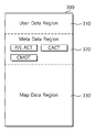
도 3을 참조하면, 휘발성 메모리(300)는 호스트로부터 불휘발성 메모리 장치(100)로 전송될 라이트 데이터 및 불휘발성 메모리 장치(100)로부터 독출되어 호스트로 전송될 리드 데이터 등을 임시로 저장하는 사용자 데이터 영역(310), 펌웨어 등과 같은 소프트웨어 및 소프트웨어를 구동시키는데 필요한 메타 데이터 등을 저장하는 메타 데이터 영역(320) 및 맵 데이터를 저장하는 맵 데이터 영역(330)을 포함할 수 있다.Referring to FIG. 3, the
메타 데이터 영역(320)에는 제2 CPU(220)의 복수의 코어들(Core 0 ~ Core i-1) 각각의 P/E 평균 카운트를 저장하도록 구성된 P/E 평균 카운트 테이블(P/E ACT), 논리 블록 어드레스 그룹 별로 각 코어(Core 0 ~ Core i-1)에 대한 액세스 카운트를 저장하도록 구성된 코어 액세스 카운트 테이블(CACT), 및 논리 블록 어드레스 그룹 별 코어 맵핑 오프셋을 저장하도록 구성된 코어 맵핑 오프셋 테이블(CMOT)이 저장될 수 있다. P/E 평균 카운트 테이블(P/E ACT), 코어 액세스 카운트 테이블(CACT) 및 코어 맵핑 오프셋 테이블(CMOT)은 HIL의 제1 CPU(210)에 의해 생성되고, 저장되고, 갱신될 수 있으나, 특별히 이에 한정되는 것은 아니다.In the
제1 CPU(210)는 기 설정된 주기 마다 휘발성 메모리(300)에 저장된 P/E 평균 카운트 테이블(P/E ACT)을 참조하여 복수의 코어들(Core 0 ~ Core i-1) 각각의 P/E 평균 카운트를 비교하고, 복수의 코어들(Core 0 ~ Core i-1) 중 P/E 평균 카운트의 차이 값이 기 설정된 임계 값 이상인 제1 코어와 제2 코어가 존재하는지 여부를 확인할 수 있다. 제1 코어와 제2 코어가 존재하면, 제1 CPU(210)는 리-맵핑 모듈(215)을 구동시킬 수 있다.The
P/E 평균 카운트 테이블(P/E ACT)은 코어 별로 각 코어(Core 0 ~ Core i-1)의 전용 다이들(또는 저장 영역들) 각각의 P/E 카운트의 평균 값을 포함할 수 있다.The P/E average count table (P/E ACT) may include an average value of the P/E count of each of the dedicated dies (or storage areas) of each core (
리-맵핑 모듈(215)은 휘발성 메모리(300)에 저장된 코어 액세스 카운트 테이블(CACT)을 참조하여, 제1 코어의 액세스 카운트가 제2 코어의 액세스 카운트보다 큰 제1 조건과 제1 코어의 액세스 카운트와 제2 코어의 액세스 카운트 간의 차이가 가장 큰 제2 조건을 만족하는 논리 블록 어드레스 그룹을 리-맵핑 대상 논리 블록 어드레스 그룹으로 선택할 수 있다.The
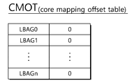
코어 액세스 카운트 테이블(CACT)은 복수의 논리 블록 어드레스 그룹들(LBAG0 ~ LBAGn) 각각에 대한 코어 별 액세스 카운트들(Core 0 access count ~ Core i-1 access count)을 포함할 수 있다. 하나의 논리 블록 어드레스 그룹은 복수의 논리 블록 어드레스들을 포함하고, 복수의 코어들(Core 0 ~ Core i-1) 각각에는 복수의 논리 블록 어드레스들 중 적어도 하나의 논리 블록 어드레스가 맵핑될 수 있다. 예를 들어, 도 5를 참조하면, 논리 블록 어드레스 그룹(LBAG0)에 포함된 복수의 논리 블록 어드레스들 중 코어 수 ‘i’로 나눈 나머지 값이 ‘0’인 적어도 하나의 논리 블록 어드레스 ‘LBA#0’은 ‘Core 0’에 맵핑될 수 있다. 마찬가지로, 논리 블록 어드레스 그룹(LBAG0)에 포함된 복수의 논리 블록 어드레스들 중 코어 수 ‘i’로 나눈 나머지 값이 ‘1’ 내지 ‘i-1’인 논리 블록 어드레스들은 각각 ‘Core 1’ 내지 ‘Core i-1’에 맵핑될 수 있다.The core access count table CACT may include core-specific access counts (
따라서, 도 5에 도시된 코어 별 액세스 카운트들(Core 0 access count ~ Core i-1 access count)은 각 코어 별로 맵핑된 논리 블록 어드레스들에 대한 액세스 카운트의 합을 의미할 수 있다. 예컨대, 논리 블록 어드레스 그룹 0(LBAG0)에서 ‘Core 0’의 액세스 카운트는 LBAG0에 포함된 논리 블록 어드레스들 중 ‘Core 0’에 맵핑된 논리 블록 어드레스들 각각에 대한 액세스 카운트의 합을 의미한다.Accordingly, the access counts for each core (
이와 같이, 본 실시 예에서, P/E 평균 카운트의 차이 값이 기 설정된 임계 값 이상인 제1 코어와 제2 코어(제1 코어의 P/E 카운트 > 제2 코어의 P/E 카운트)가 존재할 때, 제1 코어의 액세스 카운트가 제2 코어의 액세스 카운트보다 크고, 제1 코어와 제2 코어의 액세스 카운트의 차이 값이 가장 큰 논리 블록 어드레스 그룹을 리-맵핑 대상 논리 블록 어드레스 그룹으로 선택하는 것은 해당 논리 블록 어드레스 그룹 내에서 제1 코어에 맵핑된 논리 블록 어드레스들 지속적으로 증가할 가능성이 높기 때문이다.As described above, in this embodiment, there are a first core and a second core (P/E count of the first core> P/E count of the second core) having a difference value of the P/E average count equal to or greater than a preset threshold. When the access count of the first core is greater than the access count of the second core, the logical block address group having the largest difference between the access counts of the first core and the second core is selected as the re-mapping target logical block address group. This is because there is a high possibility that the logical block addresses mapped to the first core within the corresponding logical block address group will continuously increase.
또한, 리-맵핑 모듈(215)은 리-맵핑 대상 논리 블록 어드레스 그룹의 논리 블록 어드레스들 각각에 대응하는 물리 블록 어드레스들에 저장된 데이터를 리-맵핑될 코어의 전용 다이로 이동시키기 위한 지시를 각 코어(Core 0 ~ Core i-1)로 제공할 수 있다. 제2 CPU(220)의 복수의 코어들(Core 0 ~ Core i-1)은 각각 리-맵핑 모듈(215)의 지시에 따라 리-맵핑될 코어로 데이터를 이동시킬 수 있다. 이에 따라, 리-맵핑 전에 각 코어에 저장된 데이터를 무효 데이터로 만들 수 있다.In addition, the
또한, 리-맵핑 모듈(215)은 데이터의 이동이 완료되면, 코어 맵핑 오프셋 테이블(CMOT)에 저장된 리-맵핑 대상 논리 블록 어드레스 그룹에 대응하는 코어 맵핑 오프셋을 재설정할 수 있다. 예를 들어, 전술한 바와 같이, 제1 코어의 P/E 평균 카운트가 제2 코어의 P/E 평균 카운트보다 크면, 제1 코어가 소스 코어가 되고, 제2 코어가 타겟 코어가 될 수 있다. 즉, 리-맵핑 모듈(215)은 제1 코어에 맵핑된 논리 블록 어드레스가 제2 코어에 맵핑되도록 리-맵핑을 수행할 수 있다. 이를 위해, 리-맵핑 모듈(215)은 제1 코어로부터 제2 코어까지의 오프셋을 리-맵핑 대상 논리 블록 어드레스 그룹의 코어 맵핑 오프셋으로 재설정할 수 있다. 일 실시 예에서, 제1 코어가 ‘Core 0’이고, 제2 코어가 ‘Core 3’인 경우, 오프셋은 ‘3’이므로, 도 6의 코어 맵핑 오프셋 테이블(CMOT)에서 리-맵핑 대상 논리 어드레스 그룹(예컨대, LBAG0)에 대응하는 코어 맵핑 오프셋은 ‘3’으로 재설정될 수 있다.In addition, when data movement is completed, the
도 6을 참조하면, 초기 단계에서 생성된 코어 맵핑 오프셋 테이블(CMOT)에서 각 논리 블록 어드레스 그룹(LBAG0~LBGAn)의 코어 맵핑 오프셋의 디폴트 값은 ‘0’으로 설정된다. 이에 따라, 리-맵핑 이전에 호스트로부터 수신되는 논리 블록 어드레스는 코어 수로 나눈 나머지 값에 해당하는 코어에 맵핑될 수 있다. 한편, 리-맵핑 이후에 호스트로부터 수신되는 논리 블록 어드레스는 코어 수로 나눈 나머지 값에 재설정된 코어 맵핑 오프셋(예컨대, 3)을 더한 값을 다시 코어 수로 나눈 나머지 값에 해당하는 코어에 맵핑될 수 있다.Referring to FIG. 6, a default value of the core mapping offset of each logical block address group LBAG0 to LBGAn in the core mapping offset table CMOT generated in the initial stage is set to '0'. Accordingly, a logical block address received from the host prior to re-mapping may be mapped to a core corresponding to the remaining value divided by the number of cores. Meanwhile, the logical block address received from the host after re-mapping may be mapped to a core corresponding to a remaining value obtained by dividing a value obtained by adding a reset core mapping offset (eg, 3) to the remaining value divided by the number of cores. .
예를 들어, 제2 CPU(220)의 코어 수가 4개(Core 0 ~ Core 3)이고, 제1 코어는 ‘Core 0’, 제2 코어는 ‘Core 3’이고, 제1 코어의 P/E 평균 카운트가 제2 코어의 P/E 평균 카운트보다 큰 것으로 가정하면, 코어 리맵핑 오프셋은 ‘3’으로 설정될 수 있다. 이에 따라, 당초 ‘Core 0’에 맵핑된 ‘LBA0, LBA4, LBA8, ...’은 ‘Core 3’으로 리-맵핑되고, 당초 ‘Core 1’에 맵핑된 ‘LBA1, LBA5, LBA9, ...’는 ‘Core 0’으로 리-맵핑되고, 당초 ‘Core 2’에 맵핑된 ‘LBA2, LBA6, LBA10, ...’은 ‘Core 1’로 리-맵핑되고, 당초 ‘Core 3’에 맵핑된 ‘LBA3, LBA7, LBA11, ...’은 ‘Core 2’로 리-맵핑될 수 있다.For example, the number of cores of the
한편, 제2 코어의 P/E 평균 카운트가 제1 코어의 P/E 평균 카운트보다 큰 것으로 가정하면, 코어 리맵핑 오프셋은 ‘1’로 설정될 수 있다. 이에 따라, 당초 ‘Core 0’에 맵핑된 ‘LBA0, LBA4, LBA8, ...’은 ‘Core 1’로 리-맵핑되고, 당초 ‘Core 1’에 맵핑된 ‘LBA1, LBA5, LBA9, ...’는 ‘Core 2’로 리-맵핑되고, 당초 ‘Core 2’에 맵핑된 ‘LBA2, LBA6, LBA10, ...’은 ‘Core 3’으로 리-맵핑되고, 당초 ‘Core 3’에 맵핑된 ‘LBA3, LBA7, LBA11, ...’은 ‘Core 0’으로 리-맵핑될 수 있다.Meanwhile, assuming that the average P/E count of the second core is larger than the average P/E count of the first core, the core remapping offset may be set to '1'. Accordingly,'LBA0, LBA4, LBA8, ...' originally mapped to'Core 0'is re-mapped to'Core 1', and'LBA1, LBA5, LBA9, .. '.' is re-mapped to'Core 2', and'LBA2, LBA6, LBA10, ...' originally mapped to'Core 2'is re-mapped to'Core 3'and originally mapped to'Core 3' The'LBA3, LBA7, LBA11, ...' which has been converted can be re-mapped to'Core 0'.
도 7은 본 실시 예에 따른 데이터 저장 장치의 동작 방법을 나타낸 순서도이다. 도 7을 참조하여 본 실시 예에 따른 데이터 저장 장치의 동작 방법을 설명함에 있어서, 도 1 내지 도 6 중 적어도 하나의 도면이 참조될 수 있다.7 is a flowchart illustrating a method of operating a data storage device according to the present embodiment. In describing the method of operating the data storage device according to the present embodiment with reference to FIG. 7, at least one of FIGS. 1 to 6 may be referred to.
S710 단계에서, 컨트롤러(200)의 제1 CPU(210)는 기 설정된 주기 마다 휘발성 메모리(300)에 저장된 P/E 평균 카운트 테이블(P/E ACT)을 참조하여 복수의 코어들(Core 0 ~ Core i-1) 각각의 P/E 평균 카운트를 비교할 수 있다.In step S710, the
S720 단계에서, 제1 CPU(210)는 복수의 코어들(Core 0 ~ Core i-1) 중 P/E 평균 카운트의 차이 값이 기 설정된 임계 값 이상인 제1 코어와 제2 코어가 존재하는지 여부를 판단할 수 있다. 설명의 편의를 위해, 본 실시 예에서는, 제1 코어의 P/E 평균 카운트가 제2 코어의 P/E 평균 카운트보다 큰 것으로 가정한다. 제1 코어와 제2 코어가 존재하지 않으면, 해당 프로세스는 종료될 수 있다. 제1 코어와 제2 코어가 존재하면, 프로세스는 S730 단계로 진행될 수 있다. 본 단계에서, 제1 코어와 제2 코어가 존재하면, 제1 CPU(210)는 리-맵핑 모듈(215)을 구동시켜 S730 내지 S750 단계들을 수행할 수 있다. In step S720, the
S730 단계에서, 제1 CPU(210)에 의해 구동된 리-맵핑 모듈(215)은 휘발성 메모리(300)에 저장된 코어 액세스 카운트 테이블(CACT)을 참조하여, 제1 코어의 액세스 카운트가 제2 코어의 액세스 카운트보다 큰 제1 조건 및 제1 코어의 액세스 카운트와 제2 코어의 액세스 카운트 간의 차이 값이 가장 큰 제2 조건을 만족하는 논리 블록 어드레스 그룹을 리-맵핑 대상 논리 블록 어드레스 그룹(LBAG)으로 선택할 수 있다.In step S730, the
S740 단계에서, 리-맵핑 모듈(215)은 리-맵핑 대상 논리 블록 어드레스 그룹에 포함된 논리 블록 어드레스들 각각에 대응하는 물리 블록 어드레스들에 저장된 데이터를 리-맵핑될 코어의 전용 다이(die)들(또는 저장 영역들)로 이동시키기 위한 지시를 각 코어(Core 0 ~ Core i-1)에 제공할 수 있다. 각 코어(Core 0 ~ Core i-1)는 리-맵핑 모듈(215)의 지시에 따라 리-맵핑될 코어의 전용 다이(die)들로 데이터를 이동시킬 수 있다. 데이터의 이동이 완료되면, 프로세스는 S750으로 진행될 수 있다.In step S740, the
S750 단계에서, 리-맵핑 모듈(215)은 코어 맵핑 오프셋 테이블(CMOT)에서 리-맵핑 대상 논리 블록 어드레스 그룹에 대응하는 코어 맵핑 오프셋을 재설정할 수 있다. 예를 들어, 리-맵핑 모듈(215)은 소스 코어(즉, 제1 코어)로부터 타켓 코어(즉, 제2 코어)까지의 오프셋을 리-맵핑 대상 논리 블록 어드레스 그룹의 코어 맵핑 오프셋으로 재설정할 수 있다.In operation S750, the
도 8은 본 발명의 실시 예에 따른 솔리드 스테이트 드라이브(SSD)를 포함하는 데이터 처리 시스템을 예시적으로 나타낸 도면이다. 도 8을 참조하면, 데이터 처리 시스템(2000)은 호스트 장치(2100)와 솔리드 스테이트 드라이브(solid state drive)(2200)(이하, SSD라 칭함)를 포함할 수 있다.8 is a diagram illustrating a data processing system including a solid state drive (SSD) according to an exemplary embodiment of the present invention. Referring to FIG. 8, the
SSD(2200)는 컨트롤러(2210), 버퍼 메모리 장치(2220), 불휘발성 메모리 장치들(2231~223n), 전원 공급기(2240), 신호 커넥터(2250) 및 전원 커넥터(2260)를 포함할 수 있다.The
컨트롤러(2210)는 SSD(2200)의 제반 동작을 제어할 수 있다.The
버퍼 메모리 장치(2220)는 불휘발성 메모리 장치들(2231~223n)에 저장될 데이터를 임시 저장할 수 있다. 또한, 버퍼 메모리 장치(2220)는 불휘발성 메모리 장치들(2231~223n)로부터 읽혀진 데이터를 임시 저장할 수 있다. 버퍼 메모리 장치(2220)에 임시 저장된 데이터는 컨트롤러(2210)의 제어에 따라 호스트 장치(2100) 또는 불휘발성 메모리 장치들(2231~223n)로 전송될 수 있다.The
불휘발성 메모리 장치들(2231~223n)은 SSD(2200)의 저장 매체로 사용될 수 있다. 불휘발성 메모리 장치들(2231~223n) 각각은 복수의 채널들(CH1~CHn)을 통해 컨트롤러(2210)와 연결될 수 있다. 하나의 채널에는 하나 또는 그 이상의 불휘발성 메모리 장치가 연결될 수 있다. 하나의 채널에 연결되는 불휘발성 메모리 장치들은 동일한 신호 버스 및 데이터 버스에 연결될 수 있다.The
전원 공급기(2240)는 전원 커넥터(2260)를 통해 입력된 전원(PWR)을 SSD(2200) 내부에 제공할 수 있다. 전원 공급기(2240)는 보조 전원 공급기(2241)를 포함할 수 있다. 보조 전원 공급기(2241)는 서든 파워 오프(sudden power off)가 발생되는 경우, SSD(2200)가 정상적으로 종료될 수 있도록 전원을 공급할 수 있다. 보조 전원 공급기(2241)는 전원(PWR)을 충전할 수 있는 대용량 캐패시터들(capacitors)을 포함할 수 있다.The
컨트롤러(2210)는 신호 커넥터(2250)를 통해서 호스트 장치(2100)와 신호(SGL)를 주고 받을 수 있다. 여기에서, 신호(SGL)는 커맨드, 어드레스, 데이터 등을 포함할 수 있다. 신호 커넥터(2250)는 호스트 장치(2100)와 SSD(2200)의 인터페이스 방식에 따라 다양한 형태의 커넥터로 구성될 수 있다.The
도 9는 도 8의 컨트롤러의 구성을 예시적으로 나타낸 도면이다. 도 9를 참조하면, 컨트롤러(2210)는 호스트 인터페이스 유닛(2211), 컨트롤 유닛(2212), 랜덤 액세스 메모리(2213), 에러 정정 코드(ECC) 유닛(2214) 및 메모리 인터페이스 유닛(2215)을 포함할 수 있다.9 is a diagram illustrating an exemplary configuration of the controller of FIG. 8. Referring to FIG. 9, the
호스트 인터페이스 유닛(2211)은, 호스트 장치(2100)의 프로토콜에 따라서, 호스트 장치(2100)와 SSD(2200)를 인터페이싱할 수 있다. 예를 들면, 호스트 인터페이스 유닛(2211)은, 시큐어 디지털(secure digital), USB(universal serial bus), MMC(multi-media card), eMMC(embedded MMC), PCMCIA(personal computer memory card international association), PATA(parallel advanced technology attachment), SATA(serial advanced technology attachment), SCSI(small computer system interface), SAS(serial attached SCSI), PCI(peripheral component interconnection), PCI-E(PCI Expresss), UFS(universal flash storage) 프로토콜들 중 어느 하나를 통해서 호스트 장치(2100)와 통신할 수 있다. 또한, 호스트 인터페이스 유닛(2211)은 호스트 장치(2100)가 SSD(2200)를 범용 데이터 저장 장치, 예를 들면, 하드 디스크 드라이브(HDD)로 인식하도록 지원하는 디스크 에뮬레이션(disk emulation) 기능을 수행할 수 있다.The
컨트롤 유닛(2212)은 호스트 장치(2100)로부터 입력된 신호(SGL)를 분석하고 처리할 수 있다. 컨트롤 유닛(2212)은 SSD(2200)를 구동하기 위한 펌웨어 또는 소프트웨어에 따라서 내부 기능 블럭들의 동작을 제어할 수 있다. 랜덤 액세스 메모리(2213)는 이러한 펌웨어 또는 소프트웨어를 구동하기 위한 동작 메모리로서 사용될 수 있다.The
에러 정정 코드(ECC) 유닛(2214)은 불휘발성 메모리 장치들(2231~223n)로 전송될 데이터의 패리티 데이터를 생성할 수 있다. 생성된 패리티 데이터는 데이터와 함께 불휘발성 메모리 장치들(2231~223n)에 저장될 수 있다. 에러 정정 코드(ECC) 유닛(2214)은 패리티 데이터에 근거하여 불휘발성 메모리 장치들(2231~223n)로부터 독출된 데이터의 에러를 검출할 수 있다. 만약, 검출된 에러가 정정 범위 내이면, 에러 정정 코드(ECC) 유닛(2214)은 검출된 에러를 정정할 수 있다.The error correction code (ECC)
메모리 인터페이스 유닛(2215)은, 컨트롤 유닛(2212)의 제어에 따라서, 불휘발성 메모리 장치들(2231~223n)에 커맨드 및 어드레스와 같은 제어 신호를 제공할 수 있다. 그리고 메모리 인터페이스 유닛(2215)은, 컨트롤 유닛(2212)의 제어에 따라서, 불휘발성 메모리 장치들(2231~223n)과 데이터를 주고받을 수 있다. 예를 들면, 메모리 인터페이스 유닛(2215)은 버퍼 메모리 장치(2220)에 저장된 데이터를 불휘발성 메모리 장치들(2231~223n)로 제공하거나, 불휘발성 메모리 장치들(2231~223n)로부터 읽혀진 데이터를 버퍼 메모리 장치(2220)로 제공할 수 있다.The
도 10은 본 발명의 실시 예에 따른 데이터 저장 장치를 포함하는 데이터 처리 시스템을 예시적으로 나타낸 도면이다. 도 10을 참조하면, 데이터 처리 시스템(3000)은 호스트 장치(3100)와 데이터 저장 장치(3200)를 포함할 수 있다.10 is a diagram illustrating a data processing system including a data storage device according to an exemplary embodiment of the present invention. Referring to FIG. 10, the
호스트 장치(3100)는 인쇄 회로 기판(printed circuit board)과 같은 기판(board) 형태로 구성될 수 있다. 비록 도시되지 않았지만, 호스트 장치(3100)는 호스트 장치의 기능을 수행하기 위한 내부 기능 블럭들을 포함할 수 있다.The
호스트 장치(3100)는 소켓(socket), 슬롯(slot) 또는 커넥터(connector)와 같은 접속 터미널(3110)을 포함할 수 있다. 데이터 저장 장치(3200)는 접속 터미널(3110)에 마운트(mount)될 수 있다.The
데이터 저장 장치(3200)는 인쇄 회로 기판과 같은 기판 형태로 구성될 수 있다. 데이터 저장 장치(3200)는 메모리 모듈 또는 메모리 카드로 불릴 수 있다. 데이터 저장 장치(3200)는 컨트롤러(3210), 버퍼 메모리 장치(3220), 불휘발성 메모리 장치(3231~3232), PMIC(power management integrated circuit)(3240) 및 접속 터미널(3250)을 포함할 수 있다.The
컨트롤러(3210)는 데이터 저장 장치(3200)의 제반 동작을 제어할 수 있다. 컨트롤러(3210)는 도 9에 도시된 컨트롤러(2210)와 동일하게 구성될 수 있다.The
버퍼 메모리 장치(3220)는 불휘발성 메모리 장치들(3231~3232)에 저장될 데이터를 임시 저장할 수 있다. 또한, 버퍼 메모리 장치(3220)는 불휘발성 메모리 장치들(3231~3232)로부터 읽혀진 데이터를 임시 저장할 수 있다. 버퍼 메모리 장치(3220)에 임시 저장된 데이터는 컨트롤러(3210)의 제어에 따라 호스트 장치(3100) 또는 불휘발성 메모리 장치들(3231~3232)로 전송될 수 있다.The
불휘발성 메모리 장치들(3231~3232)은 데이터 저장 장치(3200)의 저장 매체로 사용될 수 있다.The
PMIC(3240)는 접속 터미널(3250)을 통해 입력된 전원을 데이터 저장 장치(3200) 내부에 제공할 수 있다. PMIC(3240)는, 컨트롤러(3210)의 제어에 따라서, 데이터 저장 장치(3200)의 전원을 관리할 수 있다.The
접속 터미널(3250)은 호스트 장치의 접속 터미널(3110)에 연결될 수 있다. 접속 터미널(3250)을 통해서, 호스트 장치(3100)와 데이터 저장 장치(3200) 간에 커맨드, 어드레스, 데이터 등과 같은 신호와, 전원이 전달될 수 있다. 접속 터미널(3250)은 호스트 장치(3100)와 데이터 저장 장치(3200)의 인터페이스 방식에 따라 다양한 형태로 구성될 수 있다. 접속 터미널(3250)은 데이터 저장 장치(3200)의 어느 한 변에 배치될 수 있다.The
도 11은 본 발명의 실시 예에 따른 데이터 저장 장치를 포함하는 데이터 처리 시스템을 예시적으로 나타낸 도면이다. 도 11을 참조하면, 데이터 처리 시스템(4000)은 호스트 장치(4100)와 데이터 저장 장치(4200)를 포함할 수 있다.11 is a diagram illustrating a data processing system including a data storage device according to an exemplary embodiment of the present invention. Referring to FIG. 11, the
호스트 장치(4100)는 인쇄 회로 기판(printed circuit board)과 같은 기판(board) 형태로 구성될 수 있다. 비록 도시되지 않았지만, 호스트 장치(4100)는 호스트 장치의 기능을 수행하기 위한 내부 기능 블럭들을 포함할 수 있다.The
데이터 저장 장치(4200)는 표면 실장형 패키지 형태로 구성될 수 있다. 데이터 저장 장치(4200)는 솔더 볼(solder ball)(4250)을 통해서 호스트 장치(4100)에 마운트될 수 있다. 데이터 저장 장치(4200)는 컨트롤러(4210), 버퍼 메모리 장치(4220) 및 불휘발성 메모리 장치(4230)를 포함할 수 있다.The
컨트롤러(4210)는 데이터 저장 장치(4200)의 제반 동작을 제어할 수 있다. 컨트롤러(4210)는 도 9에 도시된 컨트롤러(2210)와 동일하게 구성될 수 있다.The
버퍼 메모리 장치(4220)는 불휘발성 메모리 장치(4230)에 저장될 데이터를 임시 저장할 수 있다. 또한, 버퍼 메모리 장치(4220)는 불휘발성 메모리 장치들(4230)로부터 읽혀진 데이터를 임시 저장할 수 있다. 버퍼 메모리 장치(4220)에 임시 저장된 데이터는 컨트롤러(4210)의 제어에 따라 호스트 장치(4100) 또는 불휘발성 메모리 장치(4230)로 전송될 수 있다.The
불휘발성 메모리 장치(4230)는 데이터 저장 장치(4200)의 저장 매체로 사용될 수 있다.The
도 12는 본 발명의 실시 예에 따른 데이터 저장 장치를 포함하는 네트워크 시스템(5000)을 예시적으로 나타낸 도면이다. 도 12는 참조하면, 네트워크 시스템(5000)은 네트워크(5500)를 통해서 연결된 서버 시스템(5300) 및 복수의 클라이언트 시스템들(5410~5430)을 포함할 수 있다.12 is a diagram illustrating a
서버 시스템(5300)은 복수의 클라이언트 시스템들(5410~5430)의 요청에 응답하여 데이터를 서비스할 수 있다. 예를 들면, 서버 시스템(5300)은 복수의 클라이언트 시스템들(5410~5430)로부터 제공된 데이터를 저장할 수 있다. 다른 예로서, 서버 시스템(5300)은 복수의 클라이언트 시스템들(5410~5430)로 데이터를 제공할 수 있다.The
서버 시스템(5300)은 호스트 장치(5100) 및 데이터 저장 장치(5200)를 포함할 수 있다. 데이터 저장 장치(5200)는 도 1의 데이터 저장 장치(10), 도 8의 데이터 저장 장치(2200), 도 10의 데이터 저장 장치(3200) 및 도 11의 데이터 저장 장치(4200)로 구성될 수 있다.The
도 13은 본 발명의 실시 예에 따른 데이터 저장 장치에 포함된 불휘발성 메모리 장치를 예시적으로 보여주는 블록도이다. 도 13을 참조하면, 불휘발성 메모리 장치(100)는 메모리 셀 어레이(110), 행 디코더(120), 열 디코더(130), 데이터 읽기/쓰기 블럭(140), 전압 발생기(150) 및 제어 로직(160)을 포함할 수 있다.13 is a block diagram illustrating a nonvolatile memory device included in a data storage device according to an exemplary embodiment of the present invention. 13, the
메모리 셀 어레이(110)는 워드 라인들(WL1~WLm)과 비트 라인들(BL1~BLn)이 서로 교차된 영역에 배열된 메모리 셀(MC)들을 포함할 수 있다.The
행 디코더(120)는 워드 라인들(WL1~WLm)을 통해서 메모리 셀 어레이(110)와 연결될 수 있다. 행 디코더(120)는 제어 로직(160)의 제어에 따라 동작할 수 있다. 행 디코더(120)는 외부 장치(도시되지 않음)로부터 제공된 어드레스를 디코딩할 수 있다. 행 디코더(120)는 디코딩 결과에 근거하여 워드 라인들(WL1~WLm)을 선택하고, 구동할 수 있다. 예시적으로, 행 디코더(120)는 전압 발생기(150)로부터 제공된 워드 라인 전압을 워드 라인들(WL1~WLm)에 제공할 수 있다.The
데이터 읽기/쓰기 블럭(140)은 비트 라인들(BL1~BLn)을 통해서 메모리 셀 어레이(110)와 연결될 수 있다. 데이터 읽기/쓰기 블럭(140)은 비트 라인들(BL1~BLn) 각각에 대응하는 읽기/쓰기 회로들(RW1~RWn)을 포함할 수 있다. 데이터 읽기/쓰기 블럭(140)은 제어 로직(160)의 제어에 따라 동작할 수 있다. 데이터 읽기/쓰기 블럭(140)은 동작 모드에 따라서 쓰기 드라이버로서 또는 감지 증폭기로서 동작할 수 있다. 예를 들면, 데이터 읽기/쓰기 블럭(140)은 쓰기 동작 시 외부 장치로부터 제공된 데이터를 메모리 셀 어레이(110)에 저장하는 쓰기 드라이버로서 동작할 수 있다. 다른 예로서, 데이터 읽기/쓰기 블럭(140)은 읽기 동작 시 메모리 셀 어레이(110)로부터 데이터를 독출하는 감지 증폭기로서 동작할 수 있다.The data read/
열 디코더(130)는 제어 로직(160)의 제어에 따라 동작할 수 있다. 열 디코더(130)는 외부 장치로부터 제공된 어드레스를 디코딩할 수 있다. 열 디코더(130)는 디코딩 결과에 근거하여 비트 라인들(BL1~BLn) 각각에 대응하는 데이터 읽기/쓰기 블럭(140)의 읽기/쓰기 회로들(RW1~RWn)과 데이터 입출력 라인(또는 데이터 입출력 버퍼)을 연결할 수 있다.The
전압 발생기(150)는 불휘발성 메모리 장치(100)의 내부 동작에 사용되는 전압을 생성할 수 있다. 전압 발생기(150)에 의해서 생성된 전압들은 메모리 셀 어레이(110)의 메모리 셀들에 인가될 수 있다. 예를 들면, 프로그램 동작 시 생성된 프로그램 전압은 프로그램 동작이 수행될 메모리 셀들의 워드 라인에 인가될 수 있다. 다른 예로서, 소거 동작 시 생성된 소거 전압은 소거 동작이 수행될 메모리 셀들의 웰-영역에 인가될 수 있다. 다른 예로서, 읽기 동작 시 생성된 읽기 전압은 읽기 동작이 수행될 메모리 셀들의 워드 라인에 인가될 수 있다.The
제어 로직(160)은 외부 장치로부터 제공된 제어 신호에 근거하여 불휘발성 메모리 장치(100)의 제반 동작을 제어할 수 있다. 예를 들면, 제어 로직(160)은 불휘발성 메모리 장치(100)의 읽기, 쓰기, 소거 동작과 같은 불휘발성 메모리 장치(100)의 동작을 제어할 수 있다.The
본 발명이 속하는 기술분야의 통상의 기술자는 본 발명이 그 기술적 사상이나 필수적 특징을 변경하지 않고서 다른 구체적인 형태로 실시될 수 있으므로, 이상에서 기술한 실시 예들은 모든 면에서 예시적인 것이며 한정적이 아닌 것으로서 이해해야만 한다. 본 발명의 범위는 상기 상세한 설명보다는 후술하는 특허청구범위에 의하여 나타내어지며, 특허청구범위의 의미 및 범위 그리고 그 등가개념으로부터 도출되는 모든 변경 또는 변형된 형태가 본 발명의 범위에 포함되는 것으로 해석되어야 한다.Since a person skilled in the art to which the present invention pertains can implement the present invention in other specific forms without changing its technical spirit or essential features, the embodiments described above are illustrative in all respects and are not limitative. Must understand. The scope of the present invention is indicated by the claims to be described later rather than the detailed description, and all changes or modified forms derived from the meaning and scope of the claims and their equivalent concepts should be interpreted as being included in the scope of the present invention. do.
10: 데이터 저장 장치
100: 불휘발성 메모리 장치
200: 컨트롤러
210: 제1 CPU
220: 제2 CPU
300: 휘발성 메모리10: data storage device 100: nonvolatile memory device
200: controller 210: first CPU
220: second CPU 300: volatile memory
Claims (14)
상기 컨트롤러는, 제1 CPU 및 복수의 코어들을 포함하는 제2 CPU를 포함하고,
상기 제1 CPU는 기 설정된 주기 마다 상기 제2 CPU의 상기 복수의 코어들 각각에 대한 프로그램/소거(program/erase, P/E) 평균 카운트를 비교하고, 상기 복수의 코어들 중 상기 P/E 평균 카운트의 차이 값이 기 설정된 임계 값 이상인 제1 코어와 제2 코어가 존재하면, 호스트로부터 수신되는 논리 블록 어드레스들에 맵핑되는 코어를 변경하는 리-맵핑 동작을 수행하는 데이터 저장 장치.Nonvolatile memory devices; And a controller controlling an operation of the nonvolatile memory device,
The controller includes a first CPU and a second CPU including a plurality of cores,
The first CPU compares a program/erase (P/E) average count for each of the plurality of cores of the second CPU every preset period, and the P/E among the plurality of cores A data storage device that performs a re-mapping operation of changing a core mapped to logical block addresses received from a host when there are a first core and a second core whose average count difference value is greater than or equal to a preset threshold.
상기 데이터 저장 장치는, 휘발성 메모리를 더 포함하고,
상기 휘발성 메모리는,
상기 제2 CPU의 상기 복수의 코어들 각각에 대한 상기 P/E 평균 카운트로 구성된 프로그램/소거 카운트 테이블;
복수의 논리 블록 어드레스 그룹들 각각에 대한 코어 별 액세스 카운트로 구성된 코어 액세스 카운트 테이블; 및
상기 복수의 논리 블록 어드레스 그룹들 각각에 대한 코어 맵핑 오프셋으로 구성된 코어 맵핑 오프셋 테이블
을 포함하는 데이터 저장 장치.The method of claim 1,
The data storage device further includes a volatile memory,
The volatile memory,
A program/erase count table consisting of the average P/E count for each of the plurality of cores of the second CPU;
A core access count table including access counts for each core for each of the plurality of logical block address groups; And
A core mapping offset table consisting of core mapping offsets for each of the plurality of logical block address groups
Data storage device comprising a.
상기 제1 CPU는 상기 리-맵핑 동작을 수행하도록 구성된 리-맵핑 모듈을 포함하는 데이터 저장 장치.According to claim 2,
And the first CPU includes a re-mapping module configured to perform the re-mapping operation.
상기 제1 CPU는 상기 제2 CPU의 상기 복수의 코어들 중 상기 제1 코어와 상기 제2 코어가 존재하면, 상기 리-맵핑 모듈을 구동시켜 상기 리-맵핑 동작을 수행하는 데이터 저장 장치.The method of claim 3,
When the first and second cores among the plurality of cores of the second CPU exist, the first CPU drives the re-mapping module to perform the re-mapping operation.
상기 제1 코어의 P/E 평균 카운트가 상기 제2 코어의 P/E 평균 카운트보다 큰 경우,
상기 리-맵핑 모듈은 상기 코어 액세스 카운트 테이블을 참조하여 상기 복수의 논리 블록 어드레스 그룹들 중 상기 제1 코어의 액세스 카운트가 상기 제2 코어의 액세스 카운트보다 크고, 상기 제1 코어의 상기 액세스 카운트와 상기 제2 코어의 상기 액세스 카운트의 차이가 가장 큰 논리 블록 어드레스 그룹을 리-맵핑 대상 논리 블록 어드레스 그룹으로 선택하는 데이터 저장 장치.The method of claim 3,
When the average P/E count of the first core is greater than the average P/E count of the second core,
The re-mapping module refers to the core access count table, wherein the access count of the first core among the plurality of logical block address groups is greater than the access count of the second core, and the access count of the first core A data storage device for selecting a logical block address group having the largest difference in the access count of the second core as a re-mapping target logical block address group.
상기 리-맵핑 모듈은 상기 코어 맵핑 오프셋 테이블에서 상기 리-맵핑 대상 논리 블록 어드레스 그룹에 대응하는 상기 코어 맵핑 오프셋을 재설정하는 데이터 저장 장치.The method of claim 5,
The re-mapping module resets the core mapping offset corresponding to the logical block address group to be re-mapped in the core mapping offset table.
상기 리-맵핑 모듈은 리-맵핑 대상 논리 블록 어드레스 그룹에 대응하는 상기 코어 맵핑 오프셋을 상기 제1 코어부터 상기 제2 코어까지의 오프셋으로 변경하여 상기 코어 맵핑 오프셋을 재설정하는 데이터 저장 장치.The method of claim 6,
The re-mapping module resets the core mapping offset by changing the core mapping offset corresponding to the logical block address group to be re-mapped into an offset from the first core to the second core.
상기 리-맵핑 모듈은 상기 코어 맵핑 오프셋을 재설정하기 전에, 상기 리-맵핑 대상 논리 블록 어드레스 그룹에 포함된 논리 블록 어드레스들 각각에 대응하는 데이터를 리-맵핑될 코어의 전용 저장 영역으로 이동시키기 위한 지시를 상기 제2 CPU의 상기 복수의 코어들 각각에 제공하는 데이터 저장 장치.The method of claim 6,
The re-mapping module is configured to move data corresponding to each of the logical block addresses included in the re-mapping target logical block address group to a dedicated storage area of the core to be re-mapped, before resetting the core mapping offset. A data storage device for providing instructions to each of the plurality of cores of the second CPU.
상기 제2 CPU의 상기 복수의 코어들은 각각 상기 리-맵핑 모듈로부터 제공된 상기 지시에 따라 상기 리-맵핑 대상 논리 블록 어드레스 그룹에 포함된 상기 논리 블록 어드레스들 중 대응하는 적어도 하나의 논리 블록 어드레스에 대응하는 데이터를 상기 리-맵핑될 코어의 상기 전용 저장 영역으로 이동시키는 데이터 저장 장치.The method of claim 8,
Each of the plurality of cores of the second CPU corresponds to at least one corresponding logical block address among the logical block addresses included in the re-mapping target logical block address group according to the instruction provided from the re-mapping module. Data storage device for moving the data to be re-mapped to the dedicated storage area of the core to be remapped.
기 설정된 주기 마다 상기 제2 CPU의 상기 복수의 코어들 각각에 대한 프로그램/소거(program/erase, P/E) 평균 카운트를 비교하는 단계;
상기 제2 CPU의 상기 복수의 코어들 중 상기 P/E 평균 카운트의 차이 값이 기 설정된 임계 값 이상인 제1 코어와 제2 코어가 존재하는지 여부를 확인하는 단계; 및
상기 제1 코어와 상기 제2 코어가 존재하면, 호스트로부터 수신되는 논리 블록 어드레스들에 맵핑되는 코어를 변경하는 리-맵핑 동작을 수행하는 단계
를 포함하는 데이터 저장 장치의 동작 방법.Nonvolatile memory devices; And a controller having a first CPU and a second CPU including a plurality of cores for controlling an operation of the nonvolatile memory device, the method comprising:
Comparing a program/erase (P/E) average count for each of the plurality of cores of the second CPU every preset period;
Checking whether a first core and a second core having a difference value of the average P/E count equal to or greater than a preset threshold among the plurality of cores of the second CPU exist; And
If the first core and the second core exist, performing a re-mapping operation of changing a core mapped to logical block addresses received from a host
A method of operating a data storage device comprising a.
상기 제1 코어의 P/E 평균 카운트가 상기 제2 코어의 P/E 평균 카운트보다 큰 경우,
상기 리-맵핑 동작을 수행하는 단계는,
복수의 논리 블록 어드레스 그룹들 중 상기 제1 코어의 액세스 카운트가 상기 제2 코어의 액세스 카운트보다 크고, 상기 제1 코어의 상기 액세스 카운트와 상기 제2 코어의 상기 액세스 카운트의 차이가 가장 큰 논리 블록 어드레스 그룹을 리-맵핑 대상 논리 블록 어드레스 그룹으로 선택하는 단계; 및
상기 리-맵핑 대상 논리 블록 어드레스 그룹에 대응하는 코어 맵핑 오프셋을 재설정하는 단계
를 포함하는 데이터 저장 장치의 동작 방법.The method of claim 10,
When the average P/E count of the first core is greater than the average P/E count of the second core,
The step of performing the re-mapping operation,
Among a plurality of logical block address groups, the access count of the first core is greater than the access count of the second core, and the difference between the access count of the first core and the access count of the second core is the largest Selecting an address group as a re-mapping target logical block address group; And
Resetting a core mapping offset corresponding to the re-mapping target logical block address group
A method of operating a data storage device comprising a.
상기 코어 맵핑 오프셋은 각 논리 블록 어드레스 그룹에 포함된 복수의 논리 블록 어드레스들 각각에 맵핑되는 코어를 결정하는 오프셋인 데이터 저장 장치의 동작 방법. The method of claim 11,
The core mapping offset is an offset for determining a core mapped to each of a plurality of logical block addresses included in each logical block address group.
상기 코어 맵핑 오프셋을 재설정하는 단계는,
상기 리-맵핑 대상 논리 블록 어드레스 그룹에 대응하는 상기 코어 맵핑 오프셋을 상기 제1 코어로부터 상기 제2 코어까지의 오프셋으로 변경하는 단계
를 포함하는 데이터 저장 장치의 동작 방법.The method of claim 12,
The step of resetting the core mapping offset,
Changing the core mapping offset corresponding to the re-mapping target logical block address group to an offset from the first core to the second core
A method of operating a data storage device comprising a.
상기 코어 맵핑 오프셋을 재설정하는 단계 이전에,
상기 리-맵핑 대상 논리 블록 어드레스 그룹에 포함된 논리 블록 어드레스들 각각에 대응하는 데이터를 리-맵핑될 코어의 전용 저장 영역으로 이동시키는 단계
를 더 포함하는 데이터 저장 장치의 동작 방법.The method of claim 11,
Before the step of resetting the core mapping offset,
Moving data corresponding to each of the logical block addresses included in the re-mapping target logical block address group to a dedicated storage area of the core to be re-mapped
The method of operating a data storage device further comprising.
Priority Applications (3)
| Application Number | Priority Date | Filing Date | Title |
|---|---|---|---|
| KR1020190012769A KR20200095103A (en) | 2019-01-31 | 2019-01-31 | Data storage device and operating method thereof |
| US16/660,651 US10949105B2 (en) | 2019-01-31 | 2019-10-22 | Data storage device and operating method of the data storage device |
| CN201911079270.5A CN111506516B (en) | 2019-01-31 | 2019-11-07 | Data storage device and operation method thereof |
Applications Claiming Priority (1)
| Application Number | Priority Date | Filing Date | Title |
|---|---|---|---|
| KR1020190012769A KR20200095103A (en) | 2019-01-31 | 2019-01-31 | Data storage device and operating method thereof |
Publications (1)
| Publication Number | Publication Date |
|---|---|
| KR20200095103A true KR20200095103A (en) | 2020-08-10 |
Family
ID=71837434
Family Applications (1)
| Application Number | Title | Priority Date | Filing Date |
|---|---|---|---|
| KR1020190012769A KR20200095103A (en) | 2019-01-31 | 2019-01-31 | Data storage device and operating method thereof |
Country Status (3)
| Country | Link |
|---|---|
| US (1) | US10949105B2 (en) |
| KR (1) | KR20200095103A (en) |
| CN (1) | CN111506516B (en) |
Cited By (11)
| Publication number | Priority date | Publication date | Assignee | Title |
|---|---|---|---|---|
| US11126379B2 (en) | 2019-11-25 | 2021-09-21 | SK Hynix Inc. | Memory system |
| US11194520B2 (en) | 2017-10-27 | 2021-12-07 | SK Hynix Inc. | Memory system and operating method thereof |
| US11360707B2 (en) | 2019-11-21 | 2022-06-14 | SK Hynix Inc. | Memory controller for replacing bad blocks with reserved blocks and operating method thereof |
| US11366763B2 (en) | 2019-02-27 | 2022-06-21 | SK Hynix Inc. | Controller including cache memory, memory system, and operating method thereof |
| US11436148B2 (en) | 2020-06-30 | 2022-09-06 | SK Hynix Inc. | Memory controller and method of operating the same |
| US11449235B2 (en) | 2020-06-25 | 2022-09-20 | SK Hynix Inc. | Storage device for processing merged transactions and method of operating the same |
| US11494313B2 (en) | 2020-04-13 | 2022-11-08 | SK Hynix Inc. | Cache memory including dedicated areas, storage device and method for storing data in the dedicated areas of the cache memory |
| US11573891B2 (en) | 2019-11-25 | 2023-02-07 | SK Hynix Inc. | Memory controller for scheduling commands based on response for receiving write command, storage device including the memory controller, and operating method of the memory controller and the storage device |
| US11599464B2 (en) | 2020-05-21 | 2023-03-07 | SK Hynix Inc. | Memory controller and method of operating the same |
| US11645197B2 (en) | 2020-05-18 | 2023-05-09 | SK Hynix Inc. | Memory controller and method of operating the same |
| US11934309B2 (en) | 2020-04-13 | 2024-03-19 | SK Hynix Inc. | Memory controller, storage device including the memory controller, and method of operating the memory controller and the storage device |
Families Citing this family (1)
| Publication number | Priority date | Publication date | Assignee | Title |
|---|---|---|---|---|
| KR20220049842A (en) * | 2020-10-15 | 2022-04-22 | 에스케이하이닉스 주식회사 | Memory system and operation method thereof |
Family Cites Families (28)
| Publication number | Priority date | Publication date | Assignee | Title |
|---|---|---|---|---|
| US7653778B2 (en) * | 2006-05-08 | 2010-01-26 | Siliconsystems, Inc. | Systems and methods for measuring the useful life of solid-state storage devices |
| US9153337B2 (en) | 2006-12-11 | 2015-10-06 | Marvell World Trade Ltd. | Fatigue management system and method for hybrid nonvolatile solid state memory system |
| US20090150640A1 (en) | 2007-12-11 | 2009-06-11 | Royer Steven E | Balancing Computer Memory Among a Plurality of Logical Partitions On a Computing System |
| US7870363B2 (en) | 2007-12-28 | 2011-01-11 | Intel Corporation | Methods and arrangements to remap non-volatile storage |
| JP5221157B2 (en) * | 2008-02-04 | 2013-06-26 | 株式会社日立製作所 | Computer system and physical disk recovery method |
| KR101516580B1 (en) | 2009-04-22 | 2015-05-11 | 삼성전자주식회사 | Controller, data storage device and data storage system having the same, and method thereof |
| US8601202B1 (en) * | 2009-08-26 | 2013-12-03 | Micron Technology, Inc. | Full chip wear leveling in memory device |
| TWI423024B (en) | 2009-11-23 | 2014-01-11 | Phison Electronics Corp | Data storing method for a flash memory, and flash memory controller and flash memory storage system using the same |
| US8869161B2 (en) | 2010-11-18 | 2014-10-21 | Fujitsu Limited | Characterization and assignment of workload requirements to resources based on predefined categories of resource utilization and resource availability |
| CN102511044B (en) | 2011-09-06 | 2013-10-02 | 华为技术有限公司 | Method for deleting the data and device thereof |
| US8839073B2 (en) * | 2012-05-04 | 2014-09-16 | Lsi Corporation | Zero-one balance management in a solid-state disk controller |
| US9274839B2 (en) | 2012-09-27 | 2016-03-01 | Intel Corporation | Techniques for dynamic physical memory partitioning |
| CN111522585A (en) | 2012-12-28 | 2020-08-11 | 英特尔公司 | Optimal logical processor count and type selection for a given workload based on platform thermal and power budget constraints |
| WO2014192132A1 (en) | 2013-05-31 | 2014-12-04 | 株式会社日立製作所 | Load distribution device and method |
| KR102128472B1 (en) | 2014-02-17 | 2020-06-30 | 삼성전자주식회사 | Storage device for performing in-storage computing operations, method thereof, and system including same |
| US10261697B2 (en) | 2015-06-08 | 2019-04-16 | Samsung Electronics Co., Ltd. | Storage device and operating method of storage device |
| TWI601059B (en) * | 2015-11-19 | 2017-10-01 | 慧榮科技股份有限公司 | Data storage device and data storage method |
| US10101939B2 (en) * | 2016-03-09 | 2018-10-16 | Toshiba Memory Corporation | Storage system having a host that manages physical data locations of a storage device |
| KR102509986B1 (en) | 2016-03-28 | 2023-03-14 | 삼성전자주식회사 | Multi-core processor and method for controlling thereof |
| KR102610537B1 (en) | 2016-11-10 | 2023-12-06 | 삼성전자주식회사 | Solid state drive device and storage system having the same |
| US10338983B2 (en) * | 2016-12-30 | 2019-07-02 | EMC IP Holding Company LLC | Method and system for online program/erase count estimation |
| KR102395538B1 (en) * | 2017-04-28 | 2022-05-10 | 에스케이하이닉스 주식회사 | Data storage device and operating method thereof |
| CN107391391B (en) | 2017-07-19 | 2019-05-14 | 深圳大普微电子科技有限公司 | Method, system and the solid state hard disk of data copy are realized in the FTL of solid state hard disk |
| US20190227618A1 (en) | 2018-01-23 | 2019-07-25 | Goke Us Research Laboratory | Power Management for a Data Storage Apparatus |
| JP6967986B2 (en) | 2018-01-29 | 2021-11-17 | キオクシア株式会社 | Memory system |
| US10956318B2 (en) | 2018-06-19 | 2021-03-23 | Macronix International Co., Ltd. | Overlapping ranges of pages in memory systems |
| US20200233588A1 (en) | 2019-01-23 | 2020-07-23 | Alibaba Group Holding Limited | Efficient lightweight storage nodes |
| KR20200117256A (en) | 2019-04-03 | 2020-10-14 | 에스케이하이닉스 주식회사 | Controller, Memory system including the controller and operating method of the memory system |
-
2019
- 2019-01-31 KR KR1020190012769A patent/KR20200095103A/en active Search and Examination
- 2019-10-22 US US16/660,651 patent/US10949105B2/en active Active
- 2019-11-07 CN CN201911079270.5A patent/CN111506516B/en active Active
Cited By (11)
| Publication number | Priority date | Publication date | Assignee | Title |
|---|---|---|---|---|
| US11194520B2 (en) | 2017-10-27 | 2021-12-07 | SK Hynix Inc. | Memory system and operating method thereof |
| US11366763B2 (en) | 2019-02-27 | 2022-06-21 | SK Hynix Inc. | Controller including cache memory, memory system, and operating method thereof |
| US11360707B2 (en) | 2019-11-21 | 2022-06-14 | SK Hynix Inc. | Memory controller for replacing bad blocks with reserved blocks and operating method thereof |
| US11126379B2 (en) | 2019-11-25 | 2021-09-21 | SK Hynix Inc. | Memory system |
| US11573891B2 (en) | 2019-11-25 | 2023-02-07 | SK Hynix Inc. | Memory controller for scheduling commands based on response for receiving write command, storage device including the memory controller, and operating method of the memory controller and the storage device |
| US11494313B2 (en) | 2020-04-13 | 2022-11-08 | SK Hynix Inc. | Cache memory including dedicated areas, storage device and method for storing data in the dedicated areas of the cache memory |
| US11934309B2 (en) | 2020-04-13 | 2024-03-19 | SK Hynix Inc. | Memory controller, storage device including the memory controller, and method of operating the memory controller and the storage device |
| US11645197B2 (en) | 2020-05-18 | 2023-05-09 | SK Hynix Inc. | Memory controller and method of operating the same |
| US11599464B2 (en) | 2020-05-21 | 2023-03-07 | SK Hynix Inc. | Memory controller and method of operating the same |
| US11449235B2 (en) | 2020-06-25 | 2022-09-20 | SK Hynix Inc. | Storage device for processing merged transactions and method of operating the same |
| US11436148B2 (en) | 2020-06-30 | 2022-09-06 | SK Hynix Inc. | Memory controller and method of operating the same |
Also Published As
| Publication number | Publication date |
|---|---|
| CN111506516A (en) | 2020-08-07 |
| CN111506516B (en) | 2023-03-07 |
| US10949105B2 (en) | 2021-03-16 |
| US20200249854A1 (en) | 2020-08-06 |
Similar Documents
| Publication | Publication Date | Title |
|---|---|---|
| US11216362B2 (en) | Data storage device and operating method thereof | |
| US10949105B2 (en) | Data storage device and operating method of the data storage device | |
| US10789161B2 (en) | Data storage device to identify and process a sequential read request and operating method thereof | |
| US10877887B2 (en) | Data storage device and operating method thereof | |
| KR102419036B1 (en) | Data storage device and operating method thereof | |
| US11249897B2 (en) | Data storage device and operating method thereof | |
| KR20200085967A (en) | Data storage device and operating method thereof | |
| US20200218653A1 (en) | Controller, data storage device, and operating method thereof | |
| US20200057725A1 (en) | Data storage device and operating method thereof | |
| US11520694B2 (en) | Data storage device and operating method thereof | |
| KR20200025184A (en) | Nonvolatile memory device, data storage apparatus including the same and operating method thereof | |
| KR20200121645A (en) | Controller, operating method thereof and memory system | |
| KR20190054383A (en) | Data storage device and operating method thereof | |
| CN111916140A (en) | Controller, method of operating the same, and memory system including the same | |
| KR20210144249A (en) | Storage device and operating method of the same | |
| KR20210156010A (en) | Storage device and operating method thereof | |
| KR20210156090A (en) | Storage device and operating method thereof | |
| KR20210147696A (en) | Data storage device and operating method thereof | |
| KR102469174B1 (en) | Data storage device and operating method thereof | |
| US20210397558A1 (en) | Storage device and operating method thereof | |
| US11281590B2 (en) | Controller, operating method thereof and storage device including the same | |
| US11157401B2 (en) | Data storage device and operating method thereof performing a block scan operation for checking for valid page counts | |
| KR20190041082A (en) | Data storage device and operating method thereof | |
| KR20210001206A (en) | Controller, memory system and operating method thereof | |
| KR20210079894A (en) | Data storage device and operating method thereof |
Legal Events
| Date | Code | Title | Description |
|---|---|---|---|
| A201 | Request for examination |