KR20200093363A - Memory system - Google Patents
Memory system Download PDFInfo
- Publication number
- KR20200093363A KR20200093363A KR1020190010756A KR20190010756A KR20200093363A KR 20200093363 A KR20200093363 A KR 20200093363A KR 1020190010756 A KR1020190010756 A KR 1020190010756A KR 20190010756 A KR20190010756 A KR 20190010756A KR 20200093363 A KR20200093363 A KR 20200093363A
- Authority
- KR
- South Korea
- Prior art keywords
- memory
- blocking
- interface
- setting
- interface device
- Prior art date
Links
Images


Classifications
-
- G—PHYSICS
- G06—COMPUTING; CALCULATING OR COUNTING
- G06F—ELECTRIC DIGITAL DATA PROCESSING
- G06F13/00—Interconnection of, or transfer of information or other signals between, memories, input/output devices or central processing units
- G06F13/14—Handling requests for interconnection or transfer
- G06F13/16—Handling requests for interconnection or transfer for access to memory bus
- G06F13/1668—Details of memory controller
- G06F13/1689—Synchronisation and timing concerns
-
- G—PHYSICS
- G06—COMPUTING; CALCULATING OR COUNTING
- G06F—ELECTRIC DIGITAL DATA PROCESSING
- G06F13/00—Interconnection of, or transfer of information or other signals between, memories, input/output devices or central processing units
- G06F13/14—Handling requests for interconnection or transfer
- G06F13/16—Handling requests for interconnection or transfer for access to memory bus
- G06F13/1605—Handling requests for interconnection or transfer for access to memory bus based on arbitration
-
- G—PHYSICS
- G06—COMPUTING; CALCULATING OR COUNTING
- G06F—ELECTRIC DIGITAL DATA PROCESSING
- G06F13/00—Interconnection of, or transfer of information or other signals between, memories, input/output devices or central processing units
- G06F13/14—Handling requests for interconnection or transfer
- G06F13/16—Handling requests for interconnection or transfer for access to memory bus
- G06F13/1668—Details of memory controller
-
- G—PHYSICS
- G06—COMPUTING; CALCULATING OR COUNTING
- G06F—ELECTRIC DIGITAL DATA PROCESSING
- G06F3/00—Input arrangements for transferring data to be processed into a form capable of being handled by the computer; Output arrangements for transferring data from processing unit to output unit, e.g. interface arrangements
- G06F3/06—Digital input from, or digital output to, record carriers, e.g. RAID, emulated record carriers or networked record carriers
- G06F3/0601—Interfaces specially adapted for storage systems
- G06F3/0602—Interfaces specially adapted for storage systems specifically adapted to achieve a particular effect
- G06F3/0614—Improving the reliability of storage systems
-
- G—PHYSICS
- G06—COMPUTING; CALCULATING OR COUNTING
- G06F—ELECTRIC DIGITAL DATA PROCESSING
- G06F3/00—Input arrangements for transferring data to be processed into a form capable of being handled by the computer; Output arrangements for transferring data from processing unit to output unit, e.g. interface arrangements
- G06F3/06—Digital input from, or digital output to, record carriers, e.g. RAID, emulated record carriers or networked record carriers
- G06F3/0601—Interfaces specially adapted for storage systems
- G06F3/0602—Interfaces specially adapted for storage systems specifically adapted to achieve a particular effect
- G06F3/062—Securing storage systems
- G06F3/0622—Securing storage systems in relation to access
-
- G—PHYSICS
- G06—COMPUTING; CALCULATING OR COUNTING
- G06F—ELECTRIC DIGITAL DATA PROCESSING
- G06F3/00—Input arrangements for transferring data to be processed into a form capable of being handled by the computer; Output arrangements for transferring data from processing unit to output unit, e.g. interface arrangements
- G06F3/06—Digital input from, or digital output to, record carriers, e.g. RAID, emulated record carriers or networked record carriers
- G06F3/0601—Interfaces specially adapted for storage systems
- G06F3/0628—Interfaces specially adapted for storage systems making use of a particular technique
- G06F3/0629—Configuration or reconfiguration of storage systems
- G06F3/0637—Permissions
-
- G—PHYSICS
- G06—COMPUTING; CALCULATING OR COUNTING
- G06F—ELECTRIC DIGITAL DATA PROCESSING
- G06F3/00—Input arrangements for transferring data to be processed into a form capable of being handled by the computer; Output arrangements for transferring data from processing unit to output unit, e.g. interface arrangements
- G06F3/06—Digital input from, or digital output to, record carriers, e.g. RAID, emulated record carriers or networked record carriers
- G06F3/0601—Interfaces specially adapted for storage systems
- G06F3/0628—Interfaces specially adapted for storage systems making use of a particular technique
- G06F3/0655—Vertical data movement, i.e. input-output transfer; data movement between one or more hosts and one or more storage devices
- G06F3/0658—Controller construction arrangements
-
- G—PHYSICS
- G06—COMPUTING; CALCULATING OR COUNTING
- G06F—ELECTRIC DIGITAL DATA PROCESSING
- G06F3/00—Input arrangements for transferring data to be processed into a form capable of being handled by the computer; Output arrangements for transferring data from processing unit to output unit, e.g. interface arrangements
- G06F3/06—Digital input from, or digital output to, record carriers, e.g. RAID, emulated record carriers or networked record carriers
- G06F3/0601—Interfaces specially adapted for storage systems
- G06F3/0628—Interfaces specially adapted for storage systems making use of a particular technique
- G06F3/0655—Vertical data movement, i.e. input-output transfer; data movement between one or more hosts and one or more storage devices
- G06F3/0659—Command handling arrangements, e.g. command buffers, queues, command scheduling
-
- G—PHYSICS
- G06—COMPUTING; CALCULATING OR COUNTING
- G06F—ELECTRIC DIGITAL DATA PROCESSING
- G06F3/00—Input arrangements for transferring data to be processed into a form capable of being handled by the computer; Output arrangements for transferring data from processing unit to output unit, e.g. interface arrangements
- G06F3/06—Digital input from, or digital output to, record carriers, e.g. RAID, emulated record carriers or networked record carriers
- G06F3/0601—Interfaces specially adapted for storage systems
- G06F3/0668—Interfaces specially adapted for storage systems adopting a particular infrastructure
- G06F3/0671—In-line storage system
- G06F3/0673—Single storage device
- G06F3/0679—Non-volatile semiconductor memory device, e.g. flash memory, one time programmable memory [OTP]
-
- G—PHYSICS
- G06—COMPUTING; CALCULATING OR COUNTING
- G06F—ELECTRIC DIGITAL DATA PROCESSING
- G06F9/00—Arrangements for program control, e.g. control units
- G06F9/06—Arrangements for program control, e.g. control units using stored programs, i.e. using an internal store of processing equipment to receive or retain programs
- G06F9/44—Arrangements for executing specific programs
- G06F9/4401—Bootstrapping
- G06F9/4411—Configuring for operating with peripheral devices; Loading of device drivers
-
- G—PHYSICS
- G11—INFORMATION STORAGE
- G11C—STATIC STORES
- G11C11/00—Digital stores characterised by the use of particular electric or magnetic storage elements; Storage elements therefor
- G11C11/21—Digital stores characterised by the use of particular electric or magnetic storage elements; Storage elements therefor using electric elements
- G11C11/34—Digital stores characterised by the use of particular electric or magnetic storage elements; Storage elements therefor using electric elements using semiconductor devices
- G11C11/40—Digital stores characterised by the use of particular electric or magnetic storage elements; Storage elements therefor using electric elements using semiconductor devices using transistors
- G11C11/401—Digital stores characterised by the use of particular electric or magnetic storage elements; Storage elements therefor using electric elements using semiconductor devices using transistors forming cells needing refreshing or charge regeneration, i.e. dynamic cells
- G11C11/4063—Auxiliary circuits, e.g. for addressing, decoding, driving, writing, sensing or timing
- G11C11/407—Auxiliary circuits, e.g. for addressing, decoding, driving, writing, sensing or timing for memory cells of the field-effect type
- G11C11/409—Read-write [R-W] circuits
Abstract
Description
본 발명은 메모리 시스템에 관한 것으로, 더욱 상세하게는 메모리 장치를 포함하는 메모리 시스템에 관한 것이다.The present invention relates to a memory system, and more particularly, to a memory system including a memory device.
메모리 시스템은 호스트 장치의 라이트 요청에 응답하여, 호스트 장치로부터 제공된 데이터를 저장하도록 구성될 수 있다. 또한, 메모리 시스템은 호스트 장치의 리드 요청에 응답하여, 저장된 데이터를 호스트 장치로 제공하도록 구성될 수 있다. 호스트 장치는 데이터를 처리할 수 있는 전자 장치로서, 컴퓨터, 디지털 카메라 또는 휴대폰 등을 포함할 수 있다. 메모리 시스템은 호스트 장치에 내장되어 동작하거나, 분리 가능한 형태로 제작되어 호스트 장치에 연결됨으로써 동작할 수 있다.The memory system may be configured to store data provided from the host device in response to a write request from the host device. Further, the memory system may be configured to provide stored data to the host device in response to a read request from the host device. The host device is an electronic device capable of processing data, and may include a computer, a digital camera, or a mobile phone. The memory system may operate by being built in a host device or manufactured in a detachable form and connected to a host device.
본 발명의 실시 예는 메모리 장치에 연결된 인터페이스 장치의 설정을 효율적으로 조정할 수 있는 메모리 시스템을 제공하는 데 있다.An embodiment of the present invention is to provide a memory system that can efficiently adjust settings of an interface device connected to a memory device.
본 발명의 실시 예에 따른 메모리 시스템은 메모리 장치; 상기 메모리 장치를 제어하도록 구성된 메모리 컨트롤러; 및 상기 메모리 장치와 상기 메모리 컨트롤러 사이의 제어 신호 및 데이터 전송을 위한 인터페이싱 동작을 수행하도록 구성된 인터페이스 장치를 포함하되, 상기 인터페이스 장치는, 상기 메모리 컨트롤러의 블로킹 활성화 신호를 포함하는 설정 커맨드에 응답하여 상기 인터페이스 동작에 대한 블로킹 기능을 활성화시키고, 상기 블로킹 기능이 활성화된 동안에 상기 메모리 컨트롤러의 인터페이스 설정 커맨드에 응답하여 인터페이스 설정 동작을 수행할 수 있다.A memory system according to an embodiment of the present invention includes a memory device; A memory controller configured to control the memory device; And an interface device configured to perform an interfacing operation for transmitting control signals and data between the memory device and the memory controller, wherein the interface device responds to a setting command including a blocking activation signal of the memory controller. The blocking function for the interface operation may be activated, and the interface setting operation may be performed in response to the interface setting command of the memory controller while the blocking function is activated.
본 발명의 실시 예에 따른 메모리 시스템은 메모리 장치; 상기 메모리 장치를 제어하기 위한 커맨드를 생성하도록 구성된 메모리 컨트롤러; 및 블로킹 기능이 비활성화된 동안에 상기 메모리 컨트롤러로부터 전송된 상기 커맨드에 응답하여, 인터페이싱 동작을 수행함으로써 상기 메모리 장치로 상기 커맨드를 전송하도록 구성된 인터페이스 장치를 포함하되, 상기 메모리 컨트롤러는 블로킹 활성화 신호를 포함하는 상기 커맨드를 상기 인터페이스 장치로 전송하고, 상기 인터페이스 장치는 상기 블로킹 활성화 신호를 포함하는 상기 커맨드에 응답하여 상기 블로킹 기능을 활성화시키고, 상기 블로킹 기능이 활성화된 동안에 상기 인터페이싱 동작을 수행하지 않을 수 있다.A memory system according to an embodiment of the present invention includes a memory device; A memory controller configured to generate a command for controlling the memory device; And an interface device configured to transmit the command to the memory device by performing an interfacing operation in response to the command transmitted from the memory controller while the blocking function is deactivated, wherein the memory controller includes a blocking activation signal. The command may be transmitted to the interface device, and the interface device may activate the blocking function in response to the command including the blocking activation signal, and may not perform the interfacing operation while the blocking function is activated.
본 발명의 실시 예에 따른 메모리 시스템은 메모리 장치; 메모리 컨트롤러; 및 상기 메모리 장치와 상기 메모리 컨트롤러 사이에서 인터페이싱 동작을 수행하고, 블로킹 설정부를 포함하도록 구성된 인터페이스 장치를 포함하되, 상기 메모리 컨트롤러는 상기 블로킹 설정부를 액세스함으로써 상기 인터페이스 장치의 블로킹 기능을 활성화시키고, 상기 인터페이스 장치는 상기 블로킹 기능이 활성화된 동안에, 상기 인터페이싱 동작을 수행하지 않을 수 있다.A memory system according to an embodiment of the present invention includes a memory device; Memory controller; And an interface device configured to perform an interfacing operation between the memory device and the memory controller and include a blocking setting unit, wherein the memory controller activates a blocking function of the interface device by accessing the blocking setting unit, and the interface The device may not perform the interfacing operation while the blocking function is activated.
본 발명의 실시 예에 따른 메모리 시스템은 모리 장치에 연결된 인터페이스 장치의 설정을 효율적으로 조정할 수 있다.The memory system according to an embodiment of the present invention can efficiently adjust the settings of an interface device connected to a memory device.
도 1은 본 발명의 실시 예에 따른 메모리 시스템을 도시한 블록도,
도 2는 본 발명의 실시 예에 따라, 인터페이스 장치가 인터페이싱 동작을 수행하는 방법을 도시하는 도면,
도 3은 본 발명의 실시 예에 따라, 메모리 컨트롤러가 인터페이스 장치의 블로킹 기능을 활성화시키는 방법을 도시하는 도면,
도 4는 본 발명의 실시 예에 따라, 메모리 컨트롤러가 인터페이스 장치의 인터페이스 설정 동작을 제어하는 방법을 도시하는 도면,
도 5는 본 발명의 실시 예에 따라, 메모리 컨트롤러가 인터페이스 장치의 블로킹 기능을 비활성화시키는 방법을 도시하는 도면,
도 6은 본 발명의 실시 예에 따라, 인터페이스 장치가 설정 커맨드에 대해 인터페이싱 동작을 수행하는 방법을 도시하는 도면,
도 7은 본 발명의 실시 예에 따라 셋 피쳐(set feature) 커맨드의 사용 방법을 도시한 도면,
도 8은 본 발명의 다른 실시 예에 따른 메모리 시스템을 예시적으로 도시하는 도면,
도 9는 본 발명의 실시 예에 따른 메모리 시스템을 포함하는 데이터 처리 시스템을 예시적으로 도시하는 도면,
도 10은 본 발명의 실시 예에 따른 메모리 시스템을 포함하는 데이터 처리 시스템을 예시적으로 도시하는 도면,
도 11은 본 발명의 실시 예에 따른 메모리 시스템을 포함하는 네트워크 시스템을 예시적으로 도시하는 도면,
도 12는 본 발명의 실시 예에 따른 메모리 시스템에 포함된 비휘발성 메모리 장치를 예시적으로 도시하는 블럭도이다.1 is a block diagram showing a memory system according to an embodiment of the present invention;
2 is a diagram illustrating a method of performing an interfacing operation by an interface device according to an embodiment of the present invention;
3 is a diagram illustrating a method in which a memory controller activates a blocking function of an interface device according to an embodiment of the present invention;
4 is a diagram illustrating a method for a memory controller to control an interface setting operation of an interface device according to an embodiment of the present invention;
5 is a diagram illustrating a method of deactivating a blocking function of an interface device by a memory controller according to an embodiment of the present invention;
6 is a diagram illustrating a method for an interface device to perform an interfacing operation on a setting command according to an embodiment of the present invention;
7 is a diagram illustrating a method of using a set feature command according to an embodiment of the present invention;
8 exemplarily shows a memory system according to another embodiment of the present invention;
9 is a diagram exemplarily showing a data processing system including a memory system according to an embodiment of the present invention;
10 exemplarily shows a data processing system including a memory system according to an embodiment of the present invention;
11 exemplarily illustrates a network system including a memory system according to an embodiment of the present invention,
12 is a block diagram exemplarily showing a nonvolatile memory device included in a memory system according to an embodiment of the present invention.
본 발명의 이점 및 특징, 그리고 그것을 달성하는 방법은 첨부되는 도면과 함께 상세하게 후술되어 있는 실시 예들을 통해 설명될 것이다. 그러나 본 발명은 여기에서 설명되는 실시 예들에 한정되지 않고 다른 형태로 구체화될 수도 있다. 단지, 본 실시 예들은 본 발명이 속하는 기술분야에서 통상의 지식을 가진 자에게 본 발명의 기술적 사상을 용이하게 실시할 수 있을 정도로 상세히 설명하기 위하여 제공되는 것이다.Advantages and features of the present invention and a method of achieving the same will be described through embodiments described below in detail with reference to the accompanying drawings. However, the present invention is not limited to the embodiments described herein and may be embodied in other forms. However, the present embodiments are provided to explain in detail that the technical spirit of the present invention can be easily carried out to a person having ordinary knowledge in the technical field to which the present invention pertains.
도면들에 있어서, 본 발명의 실시 예들은 도시된 특정 형태로 제한되는 것이 아니며 명확성을 기하기 위하여 과장된 것이다. 본 명세서에서 특정한 용어들이 사용되었으나. 이는 본 발명을 설명하기 위한 목적에서 사용된 것이며, 의미 한정이나 특허 청구 범위에 기재된 본 발명의 권리 범위를 제한하기 위하여 사용된 것은 아니다.In the drawings, embodiments of the present invention are not limited to the specific form shown and are exaggerated for clarity. Although specific terms are used herein. This is used for the purpose of describing the present invention, and is not used to limit the scope of the present invention described in the meaning or the claims.
본 명세서에서 ‘및/또는’이란 표현은 전후에 나열된 구성요소들 중 적어도 하나를 포함하는 의미로 사용된다. 또한, ‘연결되는/결합되는’이란 표현은 다른 구성 요소와 직접적으로 연결되거나 다른 구성 요소를 통해서 간접적으로 연결되는 것을 포함하는 의미로 사용된다. 본 명세서에서 단수형은 문구에서 특별히 언급하지 않는 한 복수형도 포함한다. 또한, 명세서에서 사용되는 ‘포함한다’ 또는 ‘포함하는’으로 언급된 구성 요소, 단계, 동작 및 소자는 하나 이상의 다른 구성 요소, 단계, 동작 및 소자의 존재 또는 추가를 의미한다.In this specification, the expression “and/or” is used to mean including at least one of the components listed before and after. Also, the expression “connected/combined” is used as a meaning including directly connected to other components or indirectly connected through other components. In the present specification, the singular form includes the plural form unless otherwise specified in the phrase. In addition, components, steps, operations and elements referred to as “comprises” or “comprising” as used in the specification mean the presence or addition of one or more other components, steps, operations and elements.
이하, 도면들을 참조하여 본 발명의 실시 예에 대해 상세히 설명하기로 한다.Hereinafter, embodiments of the present invention will be described in detail with reference to the drawings.
도 1은 본 발명의 실시 예에 따른 메모리 시스템(10)을 도시한 블록도이다.1 is a block diagram illustrating a
메모리 시스템(10)은 외부의 호스트 장치의 라이트 요청에 응답하여, 호스트 장치로부터 제공된 데이터를 저장하도록 구성될 수 있다. 또한, 메모리 시스템(10)은 호스트 장치의 리드 요청에 응답하여, 저장된 데이터를 호스트 장치로 제공하도록 구성될 수 있다.The
메모리 시스템(10)은 PCMCIA(Personal Computer Memory Card International Association) 카드, CF(Compact Flash) 카드, 스마트 미디어 카드, 메모리 스틱, 다양한 멀티미디어 카드(MMC, eMMC, RS-MMC, MMC-micro), SD(Secure Digital) 카드(SD, Mini-SD, Micro-SD), UFS(Universal Flash Storage) 또는 SSD(Solid State Drive) 등으로 구성될 수 있다.The
메모리 시스템(10)은 메모리 컨트롤러(100), 인터페이스 장치(200), 및 메모리 장치(300)를 포함할 수 있다.The
메모리 컨트롤러(100)는 메모리 시스템(10)의 제반 동작을 제어할 수 있다. 메모리 컨트롤러(100)는 호스트 장치의 요청에 따른 포그라운드 동작을 수행하기 위해서 인터페이스 장치(200)를 통해 메모리 장치(300)를 제어할 수 있다. 포그라운드 동작은 호스트 장치의 라이트 요청 및 리드 요청에 따라 메모리 장치(300)에 데이터를 라이트하고 메모리 장치(300)로부터 데이터를 리드하는 동작을 포함할 수 있다.The
또한, 메모리 컨트롤러(100)는 호스트 장치의 요청과 독립적으로 내부적으로 필요한 백그라운드 동작을 수행하기 위해서 인터페이스 장치(200)를 통해 메모리 장치(300)를 제어할 수 있다. 백그라운드 동작은 메모리 장치(300)에 대한 웨어 레벨링 동작, 가비지 컬렉션 동작, 및 소거 동작 등을 포함할 수 있다. 백그라운드 동작도 포그라운드 동작처럼 메모리 장치(300)에 데이터를 라이트하고 메모리 장치(300)로부터 데이터를 리드하는 동작을 포함할 수 있다.In addition, the
메모리 컨트롤러(100)는 인터페이스 장치(200)를 통해 메모리 장치(300)를 제어할 수 있다. 메모리 컨트롤러(100)는 메모리 장치(300)를 제어하기 위한 커맨드를 생성하고, 인터페이스 장치(200)로 커맨드를 전송할 수 있다. The
또한, 메모리 컨트롤러(100)는 인터페이스 장치(200)의 블로킹 기능을 활성화시키고 인터페이스 장치(200)의 내부 설정을 조정할 수 있다. 이를 위해, 메모리 컨트롤러(100)는 아래에서 상세하게 설명될 설정 커맨드 및 인터페이스 설정 커맨드를 생성하고, 인터페이스 장치(200)로 전송할 수 있다. 이때 메모리 컨트롤러(100)는 메모리 장치(300)를 제어하기 위한 소정 커맨드들의 구성들을 그대로 이용함으로써 설정 커맨드 및 인터페이스 설정 커맨드를 생성할 수 있다. In addition, the
구체적으로, 메모리 컨트롤러(100)는 인터페이스 장치(200)로 블로킹 활성화 신호를 포함하는 설정 커맨드를 전송할 수 있다. 블로킹 활성화 신호는 인터페이스 장치(200)로 하여금 블로킹 기능을 활성화시키도록 할 수 있다. 인터페이스 장치(200)는 블로킹 기능이 활성화된 동안에 메모리 컨트롤러(100)와 메모리 장치(300) 사이에서 인터페이싱 동작을 수행하지 않을 수 있다. Specifically, the
따라서, 메모리 컨트롤러(100)는 인터페이스 장치(200)의 블로킹 기능이 활성화된 동안에, 인터페이스 장치(200)로 인터페이스 설정 커맨드를 전송할 수 있다. 인터페이스 설정 커맨드는 인터페이스 장치(200)로 하여금 인터페이스 설정 동작을 수행하도록 할 수 있다. 즉, 메모리 컨트롤러(100)는 인터페이스 장치(200)의 블로킹 기능이 활성화된 동안에, 인터페이스 장치(200)의 내부 설정을 조정할 수 있다.Accordingly, the
그리고 메모리 컨트롤러(100)는 인터페이스 장치(200)의 블로킹 기능이 활성화된 동안에, 인터페이스 장치(200)로 블로킹 비활성화 신호를 포함하는 설정 커맨드를 전송할 수 있다. 블로킹 비활성화 신호는 인터페이스 장치(200)로 하여금 블로킹 기능을 비활성화시키도록 할 수 있다. 인터페이스 장치(200)의 블로킹 기능이 비활성화된 후 메모리 컨트롤러(100)는 인터페이스 장치(200)를 통해 메모리 장치(300)를 제어할 수 있게 된다.In addition, while the blocking function of the
한편, 메모리 컨트롤러(100)는 인터페이스 장치(200)의 블로킹 기능이 비활성화된 동안에, 블로킹 활성화 신호를 포함하지 않는 설정 커맨드를 메모리 장치(300)를 제어하기 위해서 사용할 수 있다. 인터페이스 장치(200)의 블로킹 기능이 비활성화된 동안에, 설정 커맨드는 인터페이스 장치(200)를 통해 메모리 장치(300)로 전송될 수 있다. 즉, 설정 커맨드는 인터페이스 장치(200)의 블로킹 기능만을 제어하기 위해 별도로 구성되거나 새롭게 설계된 커맨드가 아니고, 메모리 장치(300)를 제어하기 위한 커맨드를 이용할 수 있다.Meanwhile, while the blocking function of the
실시 예에 따라, 메모리 컨트롤러(100)는 인터페이스 장치(200)의 블로킹 기능을 활성화시키기 위한 커맨드와 블로킹 기능을 비활성화시키기 위한 커맨드를 서로 다른 구성들을 가지도록 생성할 수 있다.According to an embodiment, the
인터페이스 장치(200)는 블로킹 기능이 비활성화된 동안에, 메모리 컨트롤러(100)와 메모리 장치(300) 사이에서 인터페이싱 동작을 수행할 수 있다. 인터페이스 장치(200)는 인터페이싱 동작을 수행함으로써 메모리 컨트롤러(100)로부터 전송된 제어 신호 및 데이터 등을 포함하는 커맨드를 메모리 장치(300)로 전송할 수 있다. 인터페이스 장치(200)는 메모리 컨트롤러(100)로부터 전송된 커맨드를 튜닝하여 메모리 장치(300)로 전송할 수 있다. 인터페이스 장치(200)는 메모리 컨트롤러(100)와 메모리 장치(300)가 직접 연결될 경우 캐패시턴스가 증가하는 현상을 해결하기 위해서, 메모리 컨트롤러(100)와 메모리 장치(300) 사이에 별도 칩으로 연결되어 인터페이싱 동작을 수행할 수 있다.The
인터페이스 장치(200)는 메모리 컨트롤러(100)로부터 전송된 설정 커맨드가 블로킹 활성화 신호를 포함할 때, 블로킹 기능을 활성화시킬 수 있다. 인터페이스 장치(200)는 블로킹 기능이 활성화된 동안에 인터페이싱 동작을 수행하지 않을 수 있다. 즉, 인터페이스 장치(200)는 블로킹 기능이 활성화된 동안에, 메모리 컨트롤러(100)로부터 전송된 커맨드를 메모리 장치(300)로 전송하지 않을 수 있다.The
인터페이스 장치(200)는 블로킹 기능이 활성화된 동안에, 메모리 컨트롤러(100)로부터 전송된 인터페이스 설정 커맨드에 응답하여 인터페이스 설정 동작을 수행할 수 있다. The
한편, 인터페이스 장치(200)의 블로킹 기능이 활성화된 동안에, 인터페이스 장치(200)와 메모리 장치(300) 간의 신호 전송이 완전히 차단되지는 않을 수 있다. 인터페이스 장치(200)는 메모리 컨트롤러(100)로부터 전송된 인터페이스 설정 커맨드에 응답하여, 메모리 장치(300)와 신호를 주고받음으로써 인터페이스 설정 동작을 수행할 수 있다.Meanwhile, while the blocking function of the
그리고 인터페이스 장치(200)는 블로킹 기능이 활성화된 동안에, 메모리 컨트롤러(100)로부터 전송된 설정 커맨드가 블로킹 비활성화 신호를 포함할 때, 블로킹 기능을 비활성화시킬 수 있다.In addition, while the blocking function is activated, the
인터페이스 장치(200)는 블로킹 설정부(210) 및 인터페이스 설정부(220)를 포함할 수 있다.The
블로킹 설정부(210)는 메모리 컨트롤러(100)로부터 전송된 블로킹 활성화 신호 또는 블로킹 비활성화 신호를 저장할 수 있다. 인터페이스 장치(200)는 블로킹 설정부(210)에 블로킹 활성화 신호를 저장함으로써 블로킹 기능을 활성화시킬 수 있다. 그리고 인터페이스 장치(200)는 블로킹 설정부(210)에 블로킹 비활성화 신호를 저장함으로써 블로킹 기능을 비활성화시킬 수 있다.The blocking
실시 예에 따라, 블로킹 설정부(210)는 소정 어드레스를 부여받을 수 있다. 이러한 경우 메모리 컨트롤러(100)는 블로킹 설정부(210)의 어드레스 및 블로킹 활성화 신호/블로킹 비활성화 신호를 포함하는 설정 커맨드를 생성할 수 있다. 즉, 메모리 컨트롤러(100)는 블로킹 설정부(210)를 어드레스를 통해 액세스함으로써 인터페이스 장치(200)의 블로킹 기능을 제어할 수 있다. 인터페이스 장치(200)는 메모리 컨트롤러(100)로부터 전송된 설정 커맨드가 블로킹 설정부(210)의 어드레스를 포함할 때, 설정 커맨드에 포함된 블로킹 활성화 신호/블로킹 비활성화 신호를 블로킹 설정부(210)에 저장할 수 있다. 인터페이스 장치(200)는 블로킹 활성화 신호가 블로킹 설정부(210)에 저장될 때 블로킹 기능을 활성화시키고, 블로킹 비활성화 신호가 블로킹 설정부(210)에 저장될 때 블로킹 기능을 비활성화시킬 수 있다.According to an embodiment, the blocking
인터페이스 설정부(220)는 인터페이스 장치(200)가 인터페이싱 동작을 수행하기 위해 참조하는 인터페이스 설정 값을 저장할 수 있다. 인터페이스 장치(200)는 인터페이스 설정 동작을 수행함으로써 인터페이스 설정부(220)에 저장된 인터페이스 설정 값을 조정할 수 있다. 인터페이스 설정 값은, 예를 들어, 인터페이스 장치(200)가 사용하는 다양한 내부 데이터 값들, 전압 레벨들, 및 동작 임계값들 등을 포함할 수 있다.The
블로킹 설정부(210)와 인터페이스 설정부(220) 각각은 블로킹 활성화 신호/블로킹 비활성화 신호 또는 인터페이스 설정 값을 저장하기 위한 플립플롭, 래치, 및 레지스터 등을 포함할 수 있다.Each of the
메모리 장치(300)는 메모리 컨트롤러(100)의 제어에 따라 데이터를 저장할 수 있다. 메모리 장치(300)는 인터페이스 장치(200)로부터 메모리 컨트롤러(100)에 의해 생성된 커맨드를 전송받고, 커맨드에 응답하여 내부 동작을 수행할 수 있다.The
메모리 장치(300)는 비휘발성 메모리 장치 또는 휘발성 메모리 장치를 포함할 수 있다.The
비휘발성 메모리 장치는 낸드 플래시(NAND Flash) 또는 노어 플래시(NOR Flash)와 같은 플래시 메모리 장치, FeRAM(Ferroelectrics Random Access Memory), PCRAM(Phase-Change Random Access Memory), MRAM(Magnetic Random Access Memory) 또는 ReRAM(Resistive Random Access Memory) 등을 포함할 수 있다.Non-volatile memory devices include flash memory devices such as NAND Flash or NOR Flash, Ferroelectrics Random Access Memory (FeRAM), Phase-Change Random Access Memory (PCRAM), Magnetic Random Access Memory (MRAM), or ReRAM (Resistive Random Access Memory).
휘발성 메모리 장치는 DRAM(Dynamic Random Access Memory) 및 SRAM(Static Random Access Memory) 등을 포함할 수 있다.The volatile memory device may include dynamic random access memory (DRAM) and static random access memory (SRAM).
한편, 도 1은 메모리 시스템(10)이 1개의 인터페이스 장치(200) 및 1개의 메모리 장치(300)를 포함하는 것으로 도시하나, 본 발명의 실시 예는 이에 제한되지 않는다. 실시 예에 따라 메모리 시스템(10)은 메모리 컨트롤러(100)에 연결된 복수의 인터페이스들을 포함할 수 있고, 각 인터페이스는 복수의 메모리 장치들에 연결될 수 있다.Meanwhile, FIG. 1 illustrates that the
도 2는 본 발명의 실시 예에 따라, 인터페이스 장치(200)가 인터페이싱 동작을 수행하는 방법을 도시하는 도면이다. 도 2를 참조하면, 인터페이스 장치(200)는 블로킹 기능이 비활성화된 동안에, 인터페이싱 동작을 수행함으로써 메모리 컨트롤러(100)로부터 전송된 커맨드를 메모리 장치(300)로 전송할 수 있다.2 is a diagram illustrating a method in which the
구체적으로, 블로킹 설정부(210)에 포함된 영역(210a)은 메모리 컨트롤러(100)로부터 전송된 블로킹 활성화 신호 또는 블로킹 비활성화 신호를 저장하기 위한 곳일 수 있다. 음영이 채워진 영역(210a)은 현재 블로킹 비활성화 신호를 저장하고 있다는 것을 나타낼 수 있다.Specifically, the
따라서, 메모리 컨트롤러(100)는 메모리 장치(300)를 제어하기 위한 커맨드를 생성하고 인터페이스 장치(200)로 커맨드를 전송할 수 있다. 인터페이스 장치(200)는 메모리 컨트롤러(100)로부터 커맨드를 수신하고 메모리 장치(300)로 커맨드를 전송할 수 있다. 커맨드는, 예를 들어, 메모리 장치(300)의 라이트 동작, 리드 동작, 또는 소거 동작 등의 내부 동작을 제어하기 위한 커맨드일 수 있다.Accordingly, the
도 3은 본 발명의 실시 예에 따라, 메모리 컨트롤러(100)가 인터페이스 장치(200)의 블로킹 기능을 활성화시키는 방법을 도시하는 도면이다. 도 3을 참조하면, 인터페이스 장치(200)는 메모리 컨트롤러(100)로부터 전송된 설정 커맨드에 응답하여 블로킹 기능을 활성화시킬 수 있다.3 is a diagram illustrating a method in which the
구체적으로, 메모리 컨트롤러(100)는 블로킹 활성화 신호를 포함하는 설정 커맨드를 생성하고, 인터페이스 장치(200)로 설정 커맨드를 전송할 수 있다. 인터페이스 장치(200)는 메모리 컨트롤러(100)로부터 전송된 설정 커맨드에 응답하여 블로킹 설정부(210)의 영역(210a)에 블로킹 활성화 신호를 저장함으로써 블로킹 기능을 활성화시킬 수 있다. 빗금이 채워진 영역(210a)은 현재 블로킹 활성화 신호를 저장하고 있다는 것을 나타낼 수 있다.Specifically, the
한편, 상술한 바와 같이, 메모리 컨트롤러(100)는 블로킹 설정부(210)의 어드레스 및 블로킹 활성화 신호를 포함하는 설정 커맨드를 생성하고, 인터페이스 장치(200)로 설정 커맨드를 전송할 수 있다. 인터페이스 장치(200)는 설정 커맨드에서 블로킹 설정부(210)의 어드레스를 인식하고 영역(210a)에 블로킹 활성화 신호를 저장함으로써, 블로킹 기능을 활성화시킬 수 있다. Meanwhile, as described above, the
실시 예에 따라, 블로킹 설정부(210)의 어드레스는, 인터페이스 장치(200)는 인식할 수 있지만, 메모리 장치(300)는 인식할 수 없는 값일 수 있다. According to an embodiment, the address of the
도 4는 본 발명의 실시 예에 따라, 메모리 컨트롤러(100)가 인터페이스 장치(200)의 인터페이스 설정 동작을 제어하는 방법을 도시하는 도면이다. 도 4를 참조하면, 인터페이스 장치(200)는 블로킹 기능이 활성화된 동안에, 메모리 컨트롤러(100)로부터 전송된 인터페이스 설정 커맨드에 응답하여 인터페이스 설정 동작을 수행할 수 있다.4 is a diagram illustrating a method of controlling an interface setting operation of the
구체적으로, 메모리 컨트롤러(100)는 인터페이스 설정 커맨드를 생성하고 인터페이스 장치(200)로 인터페이스 설정 커맨드를 전송할 수 있다. 인터페이스 장치(200)는 블로킹 기능이 활성화되었기 때문에, 인터페이스 설정 커맨드를 메모리 장치(300)로 전송하지 않을 수 있다. 인터페이스 장치(200)는 메모리 컨트롤러(100)로부터 전송된 인터페이스 설정 커맨드에 응답하여 인터페이스 설정 동작을 수행함으로써 인터페이스 설정부(220)에 저장된 인터페이스 설정 값을 조정할 수 있다.Specifically, the
도 5는 본 발명의 실시 예에 따라, 메모리 컨트롤러(100)가 인터페이스 장치(200)의 블로킹 기능을 비활성화시키는 방법을 도시하는 도면이다. 도 5를 참조하면, 인터페이스 장치(200)는 메모리 컨트롤러(100)로부터 전송된 설정 커맨드에 응답하여 블로킹 기능을 비활성화시킬 수 있다.5 is a diagram illustrating a method in which the
구체적으로, 메모리 컨트롤러(100)는 블로킹 비활성화 신호를 포함하는 설정 커맨드를 생성하고, 인터페이스 장치(200)로 설정 커맨드를 전송할 수 있다. 인터페이스 장치(200)는 메모리 컨트롤러(100)로부터 전송된 설정 커맨드에 응답하여 블로킹 설정부(210)의 영역(210a)에 블로킹 비활성화 신호를 저장함으로써 블로킹 기능을 비활성화시킬 수 있다.Specifically, the
한편, 상술한 바와 같이, 메모리 컨트롤러(100)는 블로킹 설정부(210)의 어드레스 및 블로킹 비활성화 신호를 포함하는 설정 커맨드를 생성하고, 인터페이스 장치(200)로 설정 커맨드를 전송할 수 있다. 인터페이스 장치(200)는 설정 커맨드에서 블로킹 설정부(210)의 어드레스를 인식하고 블로킹 설정부(210)의 영역(210a)에 블로킹 비활성화 신호를 저장함으로써, 블로킹 기능을 비활성화시킬 수 있다. Meanwhile, as described above, the
도 6은 본 발명의 실시 예에 따라, 인터페이스 장치(200)가 설정 커맨드에 대해 인터페이싱 동작을 수행하는 방법을 도시하는 도면이다. 도 6을 참조하면, 인터페이스 장치(200)는 블로킹 기능이 비활성화된 동안에, 인터페이싱 동작을 수행함으로써 메모리 컨트롤러(100)로부터 전송된 설정 커맨드를 메모리 장치(300)로 전송할 수 있다.6 is a diagram illustrating a method of performing an interfacing operation on a setting command by the
구체적으로, 메모리 컨트롤러(100)는 인터페이스 장치(200)의 블로킹 기능이 비활성화된 동안에, 메모리 장치(300)의 메모리 설정 동작을 제어하기 위해 설정 커맨드를 생성하고 설정 커맨드를 인터페이스 장치(200)로 전송할 수 있다. 즉, 메모리 컨트롤러(100)는 인터페이스 장치(200)의 블로킹 기능이 비활성화된 동안에, 메모리 장치(300)의 메모리 설정 동작을 제어하기 위해서 설정 커맨드를 사용할 수 있다. 이때 설정 커맨드는 블로킹 설정부(210)의 어드레스를 포함하지 않고, 블로킹 활성화 신호 또는 블로킹 비활성화 신호를 포함하지 않을 수 있다.Specifically, while the blocking function of the
인터페이스 장치(200)는 메모리 컨트롤러(100)로부터 설정 커맨드를 수신하고 메모리 장치(300)로 설정 커맨드를 전송할 수 있다.The
메모리 장치(300)는 인터페이스 장치(200)로부터 전송된 설정 커맨드에 응답하여 메모리 설정 동작을 수행할 수 있다. 구체적으로, 메모리 장치(300)는 내부 동작을 수행하기 위해 참조하는 메모리 설정부(310)를 포함할 수 있다. 메모리 장치(300)는 메모리 설정 동작을 수행함으로써 메모리 설정부(310)에 저장된 메모리 설정 값을 조정할 수 있다. 메모리 설정 값은, 예를 들어, 메모리 장치(300)가 사용하는 다양한 내부 데이터 값들, 전압 레벨들, 동작 임계값들 등을 포함할 수 있다.The
실시 예에 따라 메모리 설정부(310)는 소정 어드레스를 부여받을 수 있다. 이러한 경우 메모리 컨트롤러(100)는 메모리 장치(300)의 메모리 설정 동작을 제어하기 위해서 메모리 설정부(310)의 어드레스를 포함하는 설정 커맨드를 생성할 수 있다. 인터페이스 장치(200)는 블로킹 기능이 비활성화된 동안에 메모리 컨트롤러(100)로부터 전송된 설정 커맨드가 블로킹 설정부(210)의 어드레스를 포함하지 않으므로, 메모리 장치(300)로 설정 커맨드를 전송할 수 있다. 메모리 장치(300)는 설정 커맨드에서 메모리 설정부(310)의 어드레스를 인식하고 메모리 설정부(310)에 저장된 메모리 설정 값을 조정할 수 있다.According to an embodiment, the
실시 예에 따라, 메모리 컨트롤러(100)는 블로킹 기능이 비활성화된 동안에 메모리 장치(300)의 메모리 설정 동작을 제어하기 위해 설정 커맨드를 사용한 것처럼, 블로킹 기능이 활성화된 동안에 인터페이스 장치(200)의 인터페이스 설정 동작을 제어하기 위해 설정 커맨드를 사용할 수 있다. 즉, 설정 커맨드는 블로킹 기능이 활성화된 동안에 상술된 인터페이스 설정 커맨드로서 사용될 수 있다. 이때, 인터페이스 설정부(220)는 소정 어드레스를 부여받을 수 있다. 따라서 메모리 컨트롤러(100)는 블로킹 기능이 활성화된 동안에, 인터페이스 설정부(220)의 어드레스를 포함하는 설정 커맨드를 생성하고 인터페이스 장치(200)로 설정 커맨드를 전송할 수 있다. 인터페이스 장치(200)는 메모리 컨트롤러(100)로부터 전송된 설정 커맨드에서 인터페이스 설정부(220)의 어드레스를 인식하고 인터페이스 설정부(220)에 저장된 인터페이스 설정 값을 조정할 수 있다.According to an embodiment, the
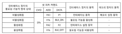
도 7은 본 발명의 실시 예에 따라 셋 피쳐(set feature) 커맨드의 사용 방법을 도시한 도면이다.7 is a diagram illustrating a method of using a set feature command according to an embodiment of the present invention.
도 7을 참조하면, 실시 예에 따라, 메모리 장치(300)가 플래시 메모리 장치(300)일 때, Open NAND Flash Interface (ONFI)에서 정의된 셋 피쳐 커맨드가 도1 내지 도6에서 상술된 설정 커맨드 및 인터페이스 설정 커맨드로서 사용될 수 있다. 즉, 메모리 컨트롤러(100)는 셋 피쳐 커맨드를 사용하여, 메모리 장치(300)의 메모리 설정 동작을 제어할 뿐만 아니라, 인터페이스 장치(200)의 블로킹 기능 및 인터페이스 설정 동작을 제어할 수 있다. Referring to FIG. 7, according to an embodiment, when the
셋 피쳐 커맨드는 커맨드 사이클, 어드레스 사이클, 및 데이터 사이클에서 각각 전송되는 커맨드 신호(CMD), 어드레스 신호(ADD), 및 데이터 신호(DATA)를 포함할 수 있다. 커맨드 신호(CMD)는 현재 전송되는 커맨드가 셋 피쳐 커맨드임을 나타내는 신호일 수 있다. 커맨드 신호(CMD)는, 예를 들어, EFh로 전송될 수 있다. 각 동작을 제어하기 위해서, 메모리 컨트롤러(100)는 셋 피쳐 커맨드에서 어드레스 신호(ADD) 및 데이터 신호(DATA)를 후술될 바와 같이 생성할 수 있다.The set feature command may include a command signal (CMD), an address signal (ADD), and a data signal (DATA) transmitted in a command cycle, an address cycle, and a data cycle, respectively. The command signal CMD may be a signal indicating that the currently transmitted command is a set feature command. The command signal CMD may be transmitted, for example, to EFh. In order to control each operation, the
우선 메모리 컨트롤러(100)는 인터페이스 장치(200)의 블로킹 기능이 비활성화된 동안에 메모리 장치(300)의 메모리 설정 동작을 제어하기 위해서, 어드레스 신호(ADD)로서 메모리 장치(300)가 메모리 설정 동작을 수행할 메모리 설정부(도 6의 310)의 어드레스(PA1)를 생성할 수 있다. 그리고 메모리 컨트롤러(100)는 데이터 신호(DATA)로서 메모리 장치(300)가 메모리 설정부(310)에 저장할 메모리 설정 값(P1)을 생성할 수 있다. 따라서, 인터페이스 장치(200)는 메모리 컨트롤러(100)로부터 전송된 셋 피쳐 커맨드에 응답하여, 인터페이싱 동작을 수행함으로써 메모리 장치(300)로 셋 피쳐 커맨드를 전송할 수 있다. 메모리 장치(300)는 인터페이스 장치(200)로부터 전송된 셋 피쳐 커맨드에 응답하여, 메모리 설정부(310)의 어드레스(PA1)를 인식하고 메모리 설정부(310)에 메모리 설정 값(P1)을 저장할 수 있다.First, in order to control the memory setting operation of the
그리고, 메모리 컨트롤러(100)는 인터페이스 장치(200)의 블로킹 기능이 비활성화된 동안에 블로킹 기능을 활성화시키기 위해서, 어드레스 신호(ADD)로서 인터페이스 장치(200)의 블로킹 설정부(210)의 어드레스(FFh)를 생성할 수 있다. 그리고 메모리 컨트롤러(100)는 데이터 신호(DATA)로서 블로킹 활성화 신호(BLK_ON)를 생성할 수 있다. 따라서, 인터페이스 장치(200)는 메모리 컨트롤러(100)로부터 전송된 셋 피쳐 커맨드에 응답하여, 블로킹 설정부(210)의 어드레스(FFh)를 인식하고 블로킹 설정부(210)에 블로킹 활성화 신호(BLK_ON)를 저장함으로써 블로킹 기능을 활성화시킬 수 있다.Then, the
그리고, 메모리 컨트롤러(100)는 인터페이스 장치(200)의 블로킹 기능이 활성화된 동안에 인터페이스 장치(200)의 인터페이스 설정 동작을 제어하기 위해서, 어드레스 신호(ADD)로서 인터페이스 장치(200)가 인터페이스 설정 동작을 수행할 인터페이스 설정부(220)의 어드레스(PA2)를 생성할 수 있다. 그리고 메모리 컨트롤러(100)는 데이터 신호(DATA)로서 인터페이스 장치(200)가 인터페이스 설정부(220)에 저장할 인터페이스 설정 값(P2)을 생성할 수 있다. 따라서, 인터페이스 장치(200)는 메모리 컨트롤러(100)로부터 전송된 셋 피쳐 커맨드에 응답하여, 인터페이스 설정부(220)의 어드레스(PA2)를 인식하고 인터페이스 설정부(220)에 인터페이스 설정 값(P2)을 저장할 수 있다.The
그리고, 메모리 컨트롤러(100)는 인터페이스 장치(200)의 블로킹 기능이 활성화된 동안에 블로킹 기능을 비활성화시키기 위해서, 어드레스 신호(ADD)로서 인터페이스 장치(200)의 블로킹 설정부(210)의 어드레스(FFh)를 생성할 수 있다. 그리고 메모리 컨트롤러(100)는 데이터 신호(DATA)로서 블로킹 비활성화 신호(BLK_OFF)를 생성할 수 있다. 따라서, 인터페이스 장치(200)는 메모리 컨트롤러(100)로부터 전송된 셋 피쳐 커맨드에 응답하여, 블로킹 설정부(210)의 어드레스(FFh)를 인식하고 블로킹 설정부(210)에 블로킹 비활성화 신호(BLK_OFF)를 저장함으로써 블로킹 기능을 비활성화시킬 수 있다.Then, the
실시 예에 따라, 셋 피쳐 커맨드가 복수 회의 데이터 사이클들을 포함할 경우, 메모리 컨트롤러(100)는 인터페이스 장치(200)와 사전에 약속된 적어도 하나의 데이터 사이클에서 블로킹 활성화 신호(BLK_ON) 또는 블로킹 비활성화 신호(BLK_OFF)를 전송할 수 있다.According to an embodiment, when the set feature command includes a plurality of data cycles, the
실시 예에 따라, 인터페이스 설정 커맨드는 셋 피쳐 커맨드뿐만 아니라, ONFI에서 정의된 ZQ 캘리브레이션 커맨드 및 트레이닝 커맨드를 포함할 수 있다. ZQ 캘리브레이션 커맨드 및 트레이닝 커맨드를 인터페이스 설정 커맨드로서 사용하는 방법은 셋 피쳐 커맨드를 사용한 방법과 유사하므로 상세한 설명이 생략될 것이다.According to an embodiment, the interface setting command may include a ZQ calibration command and a training command defined in ONFI, as well as a set feature command. The method of using the ZQ calibration command and the training command as the interface setting command is similar to the method using the set feature command, so a detailed description will be omitted.
도 8은 본 발명의 다른 실시 예에 따른 메모리 시스템(1000)을 예시적으로 도시하는 도면이다.8 is a diagram exemplarily showing a memory system 1000 according to another embodiment of the present invention.
도 8을 참조하면, 메모리 시스템(1000)은 컨트롤러 및 비휘발성 메모리 장치들(1201~120n)을 포함할 수 있다.Referring to FIG. 8, the memory system 1000 may include a controller and
컨트롤러는 메모리 시스템(1000)의 제반 동작을 제어할 수 있다. 컨트롤러는 호스트 인터페이스 유닛(1110), 컨트롤 유닛(1120), 랜덤 액세스 메모리(1130), 에러 정정 코드(ECC) 유닛(1140) 및 메모리 인터페이스 유닛(1150)을 포함할 수 있다.The controller may control various operations of the memory system 1000. The controller may include a
호스트 인터페이스 유닛(1110)은 외부의 호스트 장치와 신호를 주고 받을 수 있다. 여기에서, 신호는 커맨드, 어드레스, 데이터 등을 포함할 수 있다. 호스트 인터페이스 유닛(1110)은, 호스트 장치의 프로토콜에 따라서, 호스트 장치와 메모리 시스템(1000)을 인터페이싱할 수 있다. 예를 들면, 호스트 인터페이스 유닛(1110)은, 시큐어 디지털(secure digital), USB(universal serial bus), MMC(multi-media card), eMMC(embedded MMC), PCMCIA(personal computer memory card international association), PATA(parallel advanced technology attachment), SATA(serial advanced technology attachment), SCSI(small computer system interface), SAS(serial attached SCSI), PCI(peripheral component interconnection), PCI-E(PCI Expresss), UFS(universal flash storage)와 같은 표준 인터페이스 프로토콜들 중 어느 하나를 통해서 호스트 장치와 통신할 수 있다.The
컨트롤 유닛(1120)은 호스트 장치로부터 입력된 신호를 분석하고 처리할 수 있다. 컨트롤 유닛(1120)은 메모리 시스템(1000)을 구동하기 위한 펌웨어 또는 소프트웨어에 따라서 백그라운드 기능 블럭들의 동작을 제어할 수 있다. The control unit 1120 may analyze and process signals input from the host device. The control unit 1120 may control the operation of the background function blocks according to firmware or software for driving the memory system 1000.
컨트롤 유닛(1120)은 메모리 컨트롤러(1121)를 포함할 수 있다. 메모리 컨트롤러(1121)는 도 1의 메모리 컨트롤러(100)와 실질적으로 동일하게 구성될 수 있다.The control unit 1120 may include a
랜덤 액세스 메모리(1130)는 펌웨어 또는 소프트웨어를 구동하기 위한 동작 메모리로서 사용될 수 있다. 또한, 랜덤 액세스 메모리(1130)는 비휘발성 메모리 장치들(1201~120n)에 저장될 데이터를 임시 저장할 수 있다. 또한, 랜덤 액세스 메모리(1130)는 비휘발성 메모리 장치들(1201~120n)로부터 읽혀진 데이터를 임시 저장할 수 있다. 실시 예에 따라, 랜덤 액세스 메모리(1130)는 도8에 도시된 바와 달리 컨트롤러(1100)의 외부에 위치할 수도 있다.The
에러 정정 코드(ECC) 유닛(1140)은 비휘발성 메모리 장치들(1201~120n)로 전송될 데이터의 패리티 데이터를 생성할 수 있다. 생성된 패리티 데이터는 데이터와 함께 비휘발성 메모리 장치들(1201~120n)에 저장될 수 있다. 에러 정정 코드(ECC) 유닛(1140)은 패리티 데이터에 근거하여 비휘발성 메모리 장치들(1201~120n)로부터 독출된 데이터의 에러를 검출할 수 있다. 만약, 검출된 에러가 정정 범위 내이면, 에러 정정 코드(ECC) 유닛(1140)은 검출된 에러를 정정할 수 있다.The error correction code (ECC)
메모리 인터페이스 유닛(1150)은, 컨트롤 유닛(1120)의 제어에 따라서, 비휘발성 메모리 장치들(1201~120n)에 커맨드 및 어드레스와 같은 제어 신호를 제공할 수 있다. 그리고 메모리 인터페이스 유닛(1150)은, 컨트롤 유닛(1120)의 제어에 따라서, 비휘발성 메모리 장치들(1201~120n)과 데이터를 주고받을 수 있다. 예를 들면, 메모리 인터페이스 유닛(1150)은 랜덤 액세스 메모리(1130)에 저장된 데이터를 비휘발성 메모리 장치들(1201~120n)로 제공하거나, 비휘발성 메모리 장치들(1201~120n)로부터 읽혀진 데이터를 랜덤 액세스 메모리(1130)로 제공할 수 있다. 메모리 인터페이스 유닛은 도 1의 인터페이스 장치(200)와 실질적으로 동일하게 동작할 수 있다.The
비휘발성 메모리 장치들(1201~120n)은 메모리 시스템(1000)의 저장 매체로 사용될 수 있다. 비휘발성 메모리 장치들(1201~120n) 각각은 복수의 채널들(CH1~CHn)을 통해 컨트롤러와 연결될 수 있다. 하나의 채널에는 하나 또는 그 이상의 비휘발성 메모리 장치가 연결될 수 있다. 하나의 채널에 연결되는 비휘발성 메모리 장치들(1201~120n)은 동일한 신호 버스 및 데이터 버스에 연결될 수 있다.The
도 9는 본 발명의 실시 예에 따른 메모리 시스템을 포함하는 데이터 처리 시스템을 예시적으로 도시하는 도면이다. 도 9를 참조하면, 데이터 처리 시스템(2000)은 호스트 장치(2100)와 메모리 시스템(2200)을 포함할 수 있다.9 is a diagram exemplarily showing a data processing system including a memory system according to an embodiment of the present invention. Referring to FIG. 9, the
호스트 장치(2100)는 인쇄 회로 기판(printed circuit board)과 같은 기판(board) 형태로 구성될 수 있다. 비록 도시되지 않았지만, 호스트 장치(2100)는 호스트 장치의 기능을 수행하기 위한 백그라운드 기능 블럭들을 포함할 수 있다.The
호스트 장치(2100)는 소켓(socket), 슬롯(slot) 또는 커넥터(connector)와 같은 접속 터미널(2110)을 포함할 수 있다. 메모리 시스템(2200)은 접속 터미널(2110)에 마운트(mount)될 수 있다.The
메모리 시스템(2200)은 인쇄 회로 기판과 같은 기판 형태로 구성될 수 있다. 메모리 시스템(2200)은 메모리 모듈 또는 메모리 카드로 불릴 수 있다. 메모리 시스템(2200)은 컨트롤러(2210), 버퍼 메모리 장치(2220), 비휘발성 메모리 장치(2231~2232), PMIC(power management integrated circuit)(2240) 및 접속 터미널(2250)을 포함할 수 있다.The
컨트롤러(2210)는 메모리 시스템(2200)의 제반 동작을 제어할 수 있다. 컨트롤러(2210)는 도 8에 도시된 컨트롤러(1100)와 동일하게 구성될 수 있다.The
버퍼 메모리 장치(2220)는 비휘발성 메모리 장치들(2231~2232)에 저장될 데이터를 임시 저장할 수 있다. 또한, 버퍼 메모리 장치(2220)는 비휘발성 메모리 장치들(2231~2232)로부터 읽혀진 데이터를 임시 저장할 수 있다. 버퍼 메모리 장치(2220)에 임시 저장된 데이터는 컨트롤러(2210)의 제어에 따라 호스트 장치(2100) 또는 비휘발성 메모리 장치들(2231~2232)로 전송될 수 있다.The
비휘발성 메모리 장치들(2231~2232)은 메모리 시스템(2200)의 저장 매체로 사용될 수 있다.The nonvolatile memory devices 2231-2232 may be used as a storage medium of the
PMIC(2240)는 접속 터미널(2250)을 통해 입력된 전원을 메모리 시스템(2200) 백그라운드에 제공할 수 있다. PMIC(2240)는, 컨트롤러(2210)의 제어에 따라서, 메모리 시스템(2200)의 전원을 관리할 수 있다.The
접속 터미널(2250)은 호스트 장치의 접속 터미널(2110)에 연결될 수 있다. 접속 터미널(2250)을 통해서, 호스트 장치(2100)와 메모리 시스템(2200) 간에 커맨드, 어드레스, 데이터 등과 같은 신호와, 전원이 전달될 수 있다. 접속 터미널(2250)은 호스트 장치(2100)와 메모리 시스템(2200)의 인터페이스 방식에 따라 다양한 형태로 구성될 수 있다. 접속 터미널(2250)은 메모리 시스템(2200)의 어느 한 변에 배치될 수 있다.The
도 10은 본 발명의 실시 예에 따른 메모리 시스템을 포함하는 데이터 처리 시스템을 예시적으로 도시하는 도면이다. 도 10을 참조하면, 데이터 처리 시스템(3000)은 호스트 장치(3100)와 메모리 시스템(3200)을 포함할 수 있다.10 is a diagram exemplarily showing a data processing system including a memory system according to an embodiment of the present invention. Referring to FIG. 10, the
호스트 장치(3100)는 인쇄 회로 기판(printed circuit board)과 같은 기판(board) 형태로 구성될 수 있다. 비록 도시되지 않았지만, 호스트 장치(3100)는 호스트 장치의 기능을 수행하기 위한 백그라운드 기능 블럭들을 포함할 수 있다.The
메모리 시스템(3200)은 표면 실장형 패키지 형태로 구성될 수 있다. 메모리 시스템(3200)은 솔더 볼(solder ball)(3250)을 통해서 호스트 장치(3100)에 마운트될 수 있다. 메모리 시스템(3200)은 컨트롤러(3210), 버퍼 메모리 장치(3220) 및 비휘발성 메모리 장치(3230)를 포함할 수 있다.The
컨트롤러(3210)는 메모리 시스템(3200)의 제반 동작을 제어할 수 있다. 컨트롤러(3210)는 도 8에 도시된 컨트롤러(1100)와 동일하게 구성될 수 있다.The
버퍼 메모리 장치(3220)는 비휘발성 메모리 장치(3230)에 저장될 데이터를 임시 저장할 수 있다. 또한, 버퍼 메모리 장치(3220)는 비휘발성 메모리 장치들(3230)로부터 읽혀진 데이터를 임시 저장할 수 있다. 버퍼 메모리 장치(3220)에 임시 저장된 데이터는 컨트롤러(3210)의 제어에 따라 호스트 장치(3100) 또는 비휘발성 메모리 장치(3230)로 전송될 수 있다.The
비휘발성 메모리 장치(3230)는 메모리 시스템(3200)의 저장 매체로 사용될 수 있다.The
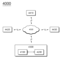
도 11은 본 발명의 실시 예에 따른 메모리 시스템을 포함하는 네트워크 시스템을 예시적으로 도시하는 도면이다. 도 11을 참조하면, 네트워크 시스템(4000)은 네트워크(4500)를 통해서 연결된 서버 시스템(4300) 및 복수의 클라이언트 시스템들(4410~4430)을 포함할 수 있다.11 is a diagram exemplarily showing a network system including a memory system according to an embodiment of the present invention. Referring to FIG. 11, the
서버 시스템(4300)은 복수의 클라이언트 시스템들(4410~4430)의 요청에 응답하여 데이터를 서비스할 수 있다. 예를 들면, 서버 시스템(4300)은 복수의 클라이언트 시스템들(4410~4430)로부터 제공된 데이터를 저장할 수 있다. 다른 예로서, 서버 시스템(4300)은 복수의 클라이언트 시스템들(4410~4430)로 데이터를 제공할 수 있다.The
서버 시스템(4300)은 호스트 장치(4100) 및 메모리 시스템(4200)을 포함할 수 있다. 메모리 시스템(4200)은 도 1의 메모리 시스템(10), 도 8의 메모리 시스템(1000), 도 9의 메모리 시스템(2200), 도 10의 메모리 시스템(3200)으로 구성될 수 있다.The
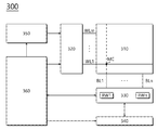
도 12는 본 발명의 실시 예에 따른 메모리 시스템에 포함된 비휘발성 메모리 장치를 예시적으로 도시하는 블럭도이다. 도 12를 참조하면, 비휘발성 메모리 장치(300)는 메모리 셀 어레이(310), 행 디코더(320), 데이터 읽기/쓰기 블럭(330), 열 디코더(340), 전압 발생기(350) 및 제어 로직(360)을 포함할 수 있다.12 is a block diagram exemplarily showing a nonvolatile memory device included in a memory system according to an embodiment of the present invention. Referring to FIG. 12, the
메모리 셀 어레이(310)는 워드 라인들(WL1~WLm)과 비트 라인들(BL1~BLn)이 서로 교차된 영역에 배열된 메모리 셀(MC)들을 포함할 수 있다.The
행 디코더(320)는 워드 라인들(WL1~WLm)을 통해서 메모리 셀 어레이(310)와 연결될 수 있다. 행 디코더(320)는 제어 로직(360)의 제어에 따라 동작할 수 있다. 행 디코더(320)는 외부 장치(도시되지 않음)로부터 제공된 어드레스를 디코딩할 수 있다. 행 디코더(320)는 디코딩 결과에 근거하여 워드 라인들(WL1~WLm)을 선택하고, 구동할 수 있다. 예시적으로, 행 디코더(320)는 전압 발생기(350)로부터 제공된 워드 라인 전압을 워드 라인들(WL1~WLm)에 제공할 수 있다.The
데이터 읽기/쓰기 블럭(330)은 비트 라인들(BL1~BLn)을 통해서 메모리 셀 어레이(310)와 연결될 수 있다. 데이터 읽기/쓰기 블럭(330)은 비트 라인들(BL1~BLn) 각각에 대응하는 읽기/쓰기 회로들(RW1~RWn)을 포함할 수 있다. 데이터 읽기/쓰기 블럭(330)은 제어 로직(360)의 제어에 따라 동작할 수 있다. 데이터 읽기/쓰기 블럭(330)은 동작 모드에 따라서 쓰기 드라이버로서 또는 감지 증폭기로서 동작할 수 있다. 예를 들면, 데이터 읽기/쓰기 블럭(330)은 쓰기 동작 시 외부 장치로부터 제공된 데이터를 메모리 셀 어레이(310)에 저장하는 쓰기 드라이버로서 동작할 수 있다. 다른 예로서, 데이터 읽기/쓰기 블럭(330)은 읽기 동작 시 메모리 셀 어레이(310)로부터 데이터를 독출하는 감지 증폭기로서 동작할 수 있다.The data read/
열 디코더(340)는 제어 로직(360)의 제어에 따라 동작할 수 있다. 열 디코더(340)는 외부 장치로부터 제공된 어드레스를 디코딩할 수 있다. 열 디코더(340)는 디코딩 결과에 근거하여 비트 라인들(BL1~BLn) 각각에 대응하는 데이터 읽기/쓰기 블럭(330)의 읽기/쓰기 회로들(RW1~RWn)과 데이터 입출력 라인(또는 데이터 입출력 버퍼)을 연결할 수 있다.The
전압 발생기(350)는 비휘발성 메모리 장치(300)의 백그라운드 동작에 사용되는 전압을 생성할 수 있다. 전압 발생기(350)에 의해서 생성된 전압들은 메모리 셀 어레이(310)의 메모리 셀들에 인가될 수 있다. 예를 들면, 프로그램 동작 시 생성된 프로그램 전압은 프로그램 동작이 수행될 메모리 셀들의 워드 라인에 인가될 수 있다. 다른 예로서, 소거 동작 시 생성된 소거 전압은 소거 동작이 수행될 메모리 셀들의 웰-영역에 인가될 수 있다. 다른 예로서, 읽기 동작 시 생성된 읽기 전압은 읽기 동작이 수행될 메모리 셀들의 워드 라인에 인가될 수 있다.The
제어 로직(360)은 외부 장치로부터 제공된 제어 신호에 근거하여 비휘발성 메모리 장치(300)의 제반 동작을 제어할 수 있다. 예를 들면, 제어 로직(360)은 비휘발성 메모리 장치(300)의 읽기, 쓰기, 소거 동작을 제어할 수 있다.The
본 발명이 속하는 기술분야의 통상의 기술자는 본 발명이 그 기술적 사상이나 필수적 특징을 변경하지 않고서 다른 구체적인 형태로 실시될 수 있으므로, 이상에서 기술한 실시 예들은 모든 면에서 예시적인 것이며 한정적인 것이 아닌 것으로서 이해해야만 한다. 본 발명의 범위는 상기 상세한 설명보다는 후술하는 특허청구범위에 의하여 나타내어지며, 특허청구범위의 의미 및 범위 그리고 그 등가개념으로부터 도출되는 모든 변경 또는 변형된 형태가 본 발명의 범위에 포함되는 것으로 해석되어야 한다.Since a person skilled in the art to which the present invention pertains can implement the present invention in other specific forms without changing its technical spirit or essential features, the embodiments described above are illustrative in all respects and are not limiting. It must be understood as one. The scope of the present invention is indicated by the following claims rather than the above detailed description, and it should be interpreted that all changes or modified forms derived from the meaning and scope of the claims and equivalent concepts thereof are included in the scope of the present invention. do.
10: 메모리 시스템
100: 메모리 컨트롤러
200: 인터페이스 장치
210: 블로킹 설정부
220: 인터페이스 설정부
300: 메모리 장치10: memory system 100: memory controller
200: interface device 210: blocking setting unit
220: interface setting unit 300: memory device
Claims (21)
상기 메모리 장치를 제어하도록 구성된 메모리 컨트롤러; 및
상기 메모리 장치와 상기 메모리 컨트롤러 사이의 제어 신호 및 데이터 전송을 위한 인터페이싱 동작을 수행하도록 구성된 인터페이스 장치를 포함하되,
상기 인터페이스 장치는, 상기 메모리 컨트롤러의 블로킹 활성화 신호를 포함하는 설정 커맨드에 응답하여 상기 인터페이스 동작에 대한 블로킹 기능을 활성화시키고, 상기 블로킹 기능이 활성화된 동안에 상기 메모리 컨트롤러의 인터페이스 설정 커맨드에 응답하여 인터페이스 설정 동작을 수행하는 메모리 시스템.Memory devices;
A memory controller configured to control the memory device; And
An interface device configured to perform an interfacing operation for transmitting control signals and data between the memory device and the memory controller,
The interface device activates a blocking function for the interface operation in response to a setting command including a blocking activation signal of the memory controller, and sets an interface in response to an interface setting command of the memory controller while the blocking function is activated Memory system that performs the operation.
상기 인터페이스 장치는,
블로킹 설정부를 포함하고,
상기 설정 커맨드가 상기 블로킹 설정부의 어드레스를 포함할 때, 상기 블로킹 설정부에 상기 블로킹 활성화 신호를 저장함으로써 상기 블로킹 기능을 활성화시키는 메모리 시스템.According to claim 1,
The interface device,
It includes a blocking setting unit,
A memory system that activates the blocking function by storing the blocking activation signal in the blocking setting unit when the setting command includes the address of the blocking setting unit.
상기 인터페이스 장치는 상기 블로킹 기능이 활성화된 동안에 블로킹 비활성화 신호를 포함하는 상기 설정 커맨드에 응답하여 상기 블로킹 기능을 비활성화시키는 메모리 시스템.According to claim 1,
The interface device deactivates the blocking function in response to the setting command including a blocking deactivation signal while the blocking function is activated.
상기 인터페이스 장치는,
블로킹 설정부를 포함하고,
상기 설정 커맨드가 상기 블로킹 설정부의 어드레스를 포함할 때, 상기 블로킹 설정부에 상기 블로킹 활성화 신호 또는 상기 블로킹 비활성화 신호를 저장함으로써 상기 블로킹 기능을 활성화시키거나 또는 비활성화시키는 메모리 시스템.According to claim 3,
The interface device,
It includes a blocking setting unit,
A memory system that activates or deactivates the blocking function by storing the blocking activation signal or the blocking deactivation signal in the blocking setting unit when the setting command includes the address of the blocking setting unit.
상기 인터페이스 장치는,
상기 인터페이싱 동작을 수행하기 위해 참조하는 인터페이스 설정 값이 저장된 인터페이스 설정부를 포함하고,
상기 인터페이스 설정부의 어드레스를 포함하는 상기 인터페이스 설정 커맨드에 응답하여 상기 인터페이스 설정 동작을 수행함으로써 상기 인터페이스 설정 값을 조정하는 메모리 시스템.According to claim 1,
The interface device,
And an interface setting unit in which an interface setting value referenced to perform the interfacing operation is stored,
A memory system that adjusts the interface setting value by performing the interface setting operation in response to the interface setting command including the address of the interface setting unit.
상기 인터페이스 장치는 상기 블로킹 기능이 비활성화된 동안에 커맨드를 수신할 경우, 상기 인터페이싱 동작을 수행함으로써 상기 메모리 장치로 상기 커맨드를 전송하는 메모리 시스템.According to claim 1,
When the interface device receives a command while the blocking function is deactivated, the memory system transmits the command to the memory device by performing the interfacing operation.
상기 메모리 장치는 내부 동작을 수행하기 위해 참조하는 메모리 설정 값이 저장된 메모리 설정부를 포함하고,
상기 인터페이스 장치는 상기 블로킹 기능이 비활성화된 동안에 상기 메모리 설정부의 어드레스를 포함하는 상기 설정 커맨드에 응답하여, 상기 인터페이싱 동작을 수행함으로써 상기 메모리 장치로 상기 설정 커맨드를 전송하고,
상기 메모리 장치는 상기 설정 커맨드에 응답하여 상기 메모리 설정 값을 조정하는 메모리 시스템.According to claim 1,
The memory device includes a memory setting unit in which a memory setting value referenced to perform an internal operation is stored,
The interface device transmits the setting command to the memory device by performing the interfacing operation in response to the setting command including the address of the memory setting unit while the blocking function is deactivated,
The memory device adjusts the memory setting value in response to the setting command.
상기 메모리 장치를 제어하기 위한 커맨드를 생성하도록 구성된 메모리 컨트롤러; 및
블로킹 기능이 비활성화된 동안에 상기 메모리 컨트롤러로부터 전송된 상기 커맨드에 응답하여, 인터페이싱 동작을 수행함으로써 상기 메모리 장치로 상기 커맨드를 전송하도록 구성된 인터페이스 장치를 포함하되,
상기 메모리 컨트롤러는 블로킹 활성화 신호를 포함하는 상기 커맨드를 상기 인터페이스 장치로 전송하고,
상기 인터페이스 장치는 상기 블로킹 활성화 신호를 포함하는 상기 커맨드에 응답하여 상기 블로킹 기능을 활성화시키고, 상기 블로킹 기능이 활성화된 동안에 상기 인터페이싱 동작을 수행하지 않는 메모리 시스템.Memory devices;
A memory controller configured to generate a command for controlling the memory device; And
And an interface device configured to transmit the command to the memory device by performing an interfacing operation in response to the command transmitted from the memory controller while the blocking function is deactivated.
The memory controller transmits the command including the blocking activation signal to the interface device,
The interface device activates the blocking function in response to the command including the blocking activation signal, and does not perform the interfacing operation while the blocking function is activated.
상기 인터페이스 장치는 블로킹 설정부를 포함하고,
상기 메모리 컨트롤러는 상기 블로킹 설정부의 어드레스 및 상기 블로킹 활성화 신호를 포함하는 상기 커맨드를 상기 인터페이스 장치로 전송하고,
상기 인터페이스 장치는 상기 어드레스를 인식하고 상기 블로킹 설정부에 상기 블로킹 활성화 신호를 저장함으로써, 상기 블로킹 기능을 활성화시키는 메모리 시스템.The method of claim 8,
The interface device includes a blocking setting unit,
The memory controller transmits the command including the address of the blocking setting unit and the blocking activation signal to the interface device,
The interface device recognizes the address and stores the blocking activation signal in the blocking setting unit to activate the blocking function.
상기 메모리 컨트롤러는 상기 블로킹 기능이 활성화된 동안에 블로킹 비활성화 신호를 포함하는 상기 커맨드를 상기 인터페이스로 전송하고,
상기 인터페이스는 상기 블로킹 비활성화 신호를 포함하는 상기 커맨드에 응답하여 상기 블로킹 기능을 비활성화시키는 메모리 시스템.The method of claim 8,
The memory controller transmits the command including a blocking deactivation signal to the interface while the blocking function is activated,
The interface deactivates the blocking function in response to the command including the blocking deactivation signal.
상기 인터페이스 장치는 블로킹 설정부를 포함하고,
상기 메모리 컨트롤러는 상기 블로킹 설정부의 어드레스 및 상기 블로킹 비활성화 신호를 포함하는 상기 커맨드를 상기 인터페이스 장치로 전송하고,
상기 인터페이스 장치는 상기 어드레스를 인식하고 상기 블로킹 설정부에 상기 블로킹 비활성화 신호를 저장함으로써, 상기 블로킹 기능을 비활성화시키는 메모리 시스템.The method of claim 10,
The interface device includes a blocking setting unit,
The memory controller transmits the command including the address of the blocking setting unit and the blocking deactivation signal to the interface device,
The interface device recognizes the address and stores the blocking deactivation signal in the blocking setting unit, thereby deactivating the blocking function.
상기 메모리 컨트롤러는 상기 블로킹 기능이 활성화된 동안에 인터페이스 설정 커맨드를 상기 인터페이스 장치로 전송하고,
상기 인터페이스 장치는 상기 인터페이스 설정 커맨드에 응답하여 상기 인터페이싱 동작을 수행하기 위해 참조하는 인터페이스 설정 값을 조정하는 메모리 시스템.The method of claim 8,
The memory controller transmits an interface setting command to the interface device while the blocking function is activated,
The interface device adjusts an interface setting value referenced to perform the interfacing operation in response to the interface setting command.
상기 인터페이스 장치는 상기 인터페이스 설정 값이 저장된 인터페이스 설정부를 포함하고,
상기 메모리 컨트롤러는 상기 인터페이스 설정부의 어드레스를 포함하는 상기 인터페이스 설정 커맨드를 상기 인터페이스 장치로 전송하고,
상기 인터페이스 장치는 상기 인터페이스 설정 커맨드에 응답하여 상기 어드레스를 인식하고 상기 인터페이스 설정 값을 조정하는 메모리 시스템.The method of claim 12,
The interface device includes an interface setting unit in which the interface setting value is stored,
The memory controller transmits the interface setting command including the address of the interface setting unit to the interface device,
The interface device recognizes the address in response to the interface setting command and adjusts the interface setting value.
상기 메모리 장치는 내부 동작을 수행하기 위해 참조하는 메모리 설정 값이 저장된 메모리 설정부를 포함하고,
상기 메모리 컨트롤러는 상기 블로킹 기능이 비활성화된 동안에 상기 메모리 설정부의 어드레스를 포함하는 상기 커맨드를 상기 인터페이스 장치로 전송하고,
상기 인터페이스 장치는 상기 메모리 설정부의 어드레스를 포함하는 상기 커맨드에 응답하여, 상기 인터페이싱 동작을 수행함으로써 상기 메모리 장치로 상기 커맨드를 전송하고,
상기 메모리 장치는 상기 커맨드에 응답하여 상기 어드레스를 인식하고 상기 메모리 설정 값을 조정하는 메모리 시스템.The method of claim 8,
The memory device includes a memory setting unit in which a memory setting value referenced to perform an internal operation is stored,
The memory controller transmits the command including the address of the memory setting unit to the interface device while the blocking function is deactivated,
The interface device transmits the command to the memory device by performing the interfacing operation in response to the command including the address of the memory setting unit,
The memory device recognizes the address in response to the command and adjusts the memory setting value.
메모리 컨트롤러; 및
상기 메모리 장치와 상기 메모리 컨트롤러 사이에서 인터페이싱 동작을 수행하고, 블로킹 설정부를 포함하도록 구성된 인터페이스 장치를 포함하되,
상기 메모리 컨트롤러는 상기 블로킹 설정부를 액세스함으로써 상기 인터페이스 장치의 블로킹 기능을 활성화시키고,
상기 인터페이스 장치는 상기 블로킹 기능이 활성화된 동안에, 상기 인터페이싱 동작을 수행하지 않는 메모리 시스템.Memory devices;
Memory controller; And
An interface device configured to perform an interfacing operation between the memory device and the memory controller and include a blocking setting unit,
The memory controller activates the blocking function of the interface device by accessing the blocking setting unit,
The interface device does not perform the interfacing operation while the blocking function is activated.
상기 메모리 컨트롤러는 상기 블로킹 설정부의 어드레스 및 블로킹 활성화 신호를 포함하는 설정 커맨드를 상기 인터페이스로 전송하고,
상기 인터페이스는 상기 설정 커맨드에 응답하여 상기 어드레스를 인식하고 상기 블로킹 설정부에 상기 블로킹 활성화 신호를 저장함으로써 상기 블로킹 기능을 활성화시키는 메모리 시스템.The method of claim 15,
The memory controller transmits a setting command including an address of the blocking setting unit and a blocking activation signal to the interface,
The interface recognizes the address in response to the setting command and stores the blocking activation signal in the blocking setting unit to activate the blocking function.
상기 메모리 컨트롤러는 상기 블로킹 기능이 활성화된 동안에, 상기 블로킹 설정부의 어드레스 및 블로킹 비활성화 신호를 포함하는 설정 커맨드를 상기 인터페이스 장치로 전송하고,
상기 인터페이스 장치는 상기 설정 커맨드에 응답하여 상기 어드레스를 인식하고 상기 블로킹 설정부에 상기 블로킹 비활성화 신호를 저장함으로써 상기 블로킹 기능을 비활성화시키는 메모리 시스템.The method of claim 15,
While the blocking function is activated, the memory controller transmits a setting command including an address of the blocking setting unit and a blocking deactivation signal to the interface device,
The interface device recognizes the address in response to the setting command and stores the blocking deactivation signal in the blocking setting unit to deactivate the blocking function.
상기 메모리 컨트롤러는 상기 블로킹 기능이 활성화된 동안에 인터페이스 설정 커맨드를 상기 인터페이스 장치로 전송하고,
상기 인터페이스 장치는 상기 인터페이스 설정 커맨드에 응답하여 상기 인터페이싱 동작을 수행하기 위해 참조하는 인터페이스 설정 값을 조정하는 메모리 시스템.The method of claim 15,
The memory controller transmits an interface setting command to the interface device while the blocking function is activated,
The interface device adjusts an interface setting value referenced to perform the interfacing operation in response to the interface setting command.
상기 인터페이스 장치는 상기 인터페이스 설정 값이 저장된 인터페이스 설정부를 포함하고,
상기 메모리 컨트롤러는 상기 인터페이스 설정부의 어드레스를 포함하는 상기 인터페이스 설정 커맨드를 상기 인터페이스 장치로 전송하고,
상기 인터페이스 장치는 상기 인터페이스 설정 커맨드에 응답하여 상기 어드레스를 인식하고 상기 인터페이스 설정 값을 조정하는 메모리 시스템.The method of claim 15,
The interface device includes an interface setting unit in which the interface setting value is stored,
The memory controller transmits the interface setting command including the address of the interface setting unit to the interface device,
The interface device recognizes the address in response to the interface setting command and adjusts the interface setting value.
상기 인터페이스 장치는 상기 블로킹 기능이 비활성화된 동안에 상기 인터페이싱 동작을 수행하는 메모리 시스템.The method of claim 15,
The interface device performs the interfacing operation while the blocking function is deactivated.
상기 메모리 장치는 내부 동작을 수행하기 위해 참조하는 메모리 설정 값이 저장된 메모리 설정부를 포함하고,
상기 메모리 컨트롤러는 상기 블로킹 기능이 비활성화된 동안에 상기 메모리 설정부의 어드레스를 포함하는 설정 커맨드를 상기 인터페이스 장치로 전송하고,
상기 인터페이스 장치는 상기 인터페이싱 동작을 수행함으로써 상기 메모리 장치로 상기 설정 커맨드를 전송하고,
상기 메모리 장치는 상기 설정 커맨드에 응답하여 상기 어드레스를 인식하고 상기 메모리 설정 값을 조정하는 메모리 시스템.The method of claim 15,
The memory device includes a memory setting unit in which a memory setting value referenced to perform an internal operation is stored,
The memory controller transmits a setting command including the address of the memory setting unit to the interface device while the blocking function is deactivated,
The interface device transmits the setting command to the memory device by performing the interfacing operation,
The memory device recognizes the address in response to the setting command and adjusts the memory setting value.
Priority Applications (4)
| Application Number | Priority Date | Filing Date | Title |
|---|---|---|---|
| KR1020190010756A KR20200093363A (en) | 2019-01-28 | 2019-01-28 | Memory system |
| US16/570,315 US11042493B2 (en) | 2019-01-28 | 2019-09-13 | Memory system |
| CN201910972964.5A CN111488296B (en) | 2019-01-28 | 2019-10-14 | Memory system |
| US17/350,341 US11593285B2 (en) | 2019-01-28 | 2021-06-17 | Memory system |
Applications Claiming Priority (1)
| Application Number | Priority Date | Filing Date | Title |
|---|---|---|---|
| KR1020190010756A KR20200093363A (en) | 2019-01-28 | 2019-01-28 | Memory system |
Publications (1)
| Publication Number | Publication Date |
|---|---|
| KR20200093363A true KR20200093363A (en) | 2020-08-05 |
Family
ID=71732562
Family Applications (1)
| Application Number | Title | Priority Date | Filing Date |
|---|---|---|---|
| KR1020190010756A KR20200093363A (en) | 2019-01-28 | 2019-01-28 | Memory system |
Country Status (3)
| Country | Link |
|---|---|
| US (2) | US11042493B2 (en) |
| KR (1) | KR20200093363A (en) |
| CN (1) | CN111488296B (en) |
Families Citing this family (1)
| Publication number | Priority date | Publication date | Assignee | Title |
|---|---|---|---|---|
| KR20200093363A (en) * | 2019-01-28 | 2020-08-05 | 에스케이하이닉스 주식회사 | Memory system |
Family Cites Families (16)
| Publication number | Priority date | Publication date | Assignee | Title |
|---|---|---|---|---|
| JP2003297080A (en) * | 2002-03-29 | 2003-10-17 | Mitsubishi Electric Corp | Semiconductor memory device |
| KR100816053B1 (en) * | 2006-11-21 | 2008-03-21 | 엠텍비젼 주식회사 | Memory device, memory system and dual port memory device with self-copy function |
| US7930576B2 (en) * | 2007-04-10 | 2011-04-19 | Standard Microsystems Corporation | Sharing non-sharable devices between an embedded controller and a processor in a computer system |
| WO2010011534A1 (en) * | 2008-07-23 | 2010-01-28 | Rambus Inc. | Reconfigurable memory controller |
| TWI413898B (en) * | 2009-09-15 | 2013-11-01 | Phison Electronics Corp | Method and system for data protection, storage device, and storage device controller |
| US8527825B2 (en) * | 2010-09-21 | 2013-09-03 | Qualcomm Incorporated | Debugger based memory dump using built in self test |
| KR101522293B1 (en) | 2013-08-29 | 2015-05-21 | 주식회사 유니테스트 | Test device capable of individual control for a plurality storage |
| KR20150051673A (en) * | 2013-11-05 | 2015-05-13 | 에스케이하이닉스 주식회사 | Memory device and system including the same |
| US9729320B2 (en) * | 2014-02-25 | 2017-08-08 | Cavium, Inc. | Apparatus and method for software enabled access to protected hardware resources |
| KR102251809B1 (en) | 2014-05-28 | 2021-05-13 | 삼성전자주식회사 | Memory system, memory interface device and interfacing method in memory system |
| KR102389232B1 (en) * | 2015-10-16 | 2022-04-22 | 에스케이하이닉스 주식회사 | Refresh control device and system including the same |
| US10430361B1 (en) * | 2015-12-17 | 2019-10-01 | Cru Acquisition Group, Llc | Combination write blocker |
| CN108345808B (en) * | 2017-01-25 | 2021-12-31 | 三星电子株式会社 | Nonvolatile memory device and solid state drive including the same |
| KR102519572B1 (en) * | 2018-05-11 | 2023-04-07 | 에스케이하이닉스 주식회사 | Memory system and operating method of memory system |
| US11086803B2 (en) * | 2018-10-05 | 2021-08-10 | Micron Technology, Inc. | Dynamically configuring transmission lines of a bus |
| KR20200093363A (en) * | 2019-01-28 | 2020-08-05 | 에스케이하이닉스 주식회사 | Memory system |
-
2019
- 2019-01-28 KR KR1020190010756A patent/KR20200093363A/en active Search and Examination
- 2019-09-13 US US16/570,315 patent/US11042493B2/en active Active
- 2019-10-14 CN CN201910972964.5A patent/CN111488296B/en active Active
-
2021
- 2021-06-17 US US17/350,341 patent/US11593285B2/en active Active
Also Published As
| Publication number | Publication date |
|---|---|
| US11042493B2 (en) | 2021-06-22 |
| US20210311890A1 (en) | 2021-10-07 |
| CN111488296B (en) | 2023-08-01 |
| US20200242056A1 (en) | 2020-07-30 |
| US11593285B2 (en) | 2023-02-28 |
| CN111488296A (en) | 2020-08-04 |
Similar Documents
| Publication | Publication Date | Title |
|---|---|---|
| US11101017B2 (en) | Memory system and test system | |
| US11704048B2 (en) | Electronic device | |
| US11157201B2 (en) | Memory system and operating method thereof | |
| US10546618B2 (en) | Nonvolatile memory device, data storage device including the same and operating method thereof | |
| US20230273748A1 (en) | Memory system, operating method thereof and computing system | |
| KR20190076296A (en) | Memory system and operating method thereof | |
| US10629275B2 (en) | Data storage device and operating method thereof | |
| US20200150898A1 (en) | Memory system and operating method thereof | |
| US11593285B2 (en) | Memory system | |
| KR102475688B1 (en) | Nonvolatile memory device, data storage apparatus including the same and operating method thereof | |
| US10776008B2 (en) | Memory system and operating method thereof | |
| TW201824279A (en) | Operating methods of nonvolatile memory device and data storage device including the same | |
| US10553292B1 (en) | Memory system with memory region read counts and a memory group read count and operating method thereof | |
| US11544004B2 (en) | Nonvolatile memory device and memory system including the same | |
| KR20210094773A (en) | Memory system and data processing system including the same | |
| KR20200072620A (en) | Electronic device | |
| KR20210035517A (en) | Memory system and data processing system including the same |
Legal Events
| Date | Code | Title | Description |
|---|---|---|---|
| A201 | Request for examination |