KR20200080194A - Memory device and fabricating method of thereof - Google Patents
Memory device and fabricating method of thereof Download PDFInfo
- Publication number
- KR20200080194A KR20200080194A KR1020190175590A KR20190175590A KR20200080194A KR 20200080194 A KR20200080194 A KR 20200080194A KR 1020190175590 A KR1020190175590 A KR 1020190175590A KR 20190175590 A KR20190175590 A KR 20190175590A KR 20200080194 A KR20200080194 A KR 20200080194A
- Authority
- KR
- South Korea
- Prior art keywords
- electrode
- change layer
- resistance change
- unit process
- memory device
- Prior art date
Links
Images


Classifications
-
- H—ELECTRICITY
- H10—SEMICONDUCTOR DEVICES; ELECTRIC SOLID-STATE DEVICES NOT OTHERWISE PROVIDED FOR
- H10N—ELECTRIC SOLID-STATE DEVICES NOT OTHERWISE PROVIDED FOR
- H10N70/00—Solid-state devices without a potential-jump barrier or surface barrier, and specially adapted for rectifying, amplifying, oscillating or switching
- H10N70/20—Multistable switching devices, e.g. memristors
- H10N70/24—Multistable switching devices, e.g. memristors based on migration or redistribution of ionic species, e.g. anions, vacancies
- H10N70/245—Multistable switching devices, e.g. memristors based on migration or redistribution of ionic species, e.g. anions, vacancies the species being metal cations, e.g. programmable metallization cells
-
- H01L45/1616—
-
- C—CHEMISTRY; METALLURGY
- C23—COATING METALLIC MATERIAL; COATING MATERIAL WITH METALLIC MATERIAL; CHEMICAL SURFACE TREATMENT; DIFFUSION TREATMENT OF METALLIC MATERIAL; COATING BY VACUUM EVAPORATION, BY SPUTTERING, BY ION IMPLANTATION OR BY CHEMICAL VAPOUR DEPOSITION, IN GENERAL; INHIBITING CORROSION OF METALLIC MATERIAL OR INCRUSTATION IN GENERAL
- C23C—COATING METALLIC MATERIAL; COATING MATERIAL WITH METALLIC MATERIAL; SURFACE TREATMENT OF METALLIC MATERIAL BY DIFFUSION INTO THE SURFACE, BY CHEMICAL CONVERSION OR SUBSTITUTION; COATING BY VACUUM EVAPORATION, BY SPUTTERING, BY ION IMPLANTATION OR BY CHEMICAL VAPOUR DEPOSITION, IN GENERAL
- C23C16/00—Chemical coating by decomposition of gaseous compounds, without leaving reaction products of surface material in the coating, i.e. chemical vapour deposition [CVD] processes
- C23C16/44—Chemical coating by decomposition of gaseous compounds, without leaving reaction products of surface material in the coating, i.e. chemical vapour deposition [CVD] processes characterised by the method of coating
- C23C16/455—Chemical coating by decomposition of gaseous compounds, without leaving reaction products of surface material in the coating, i.e. chemical vapour deposition [CVD] processes characterised by the method of coating characterised by the method used for introducing gases into reaction chamber or for modifying gas flows in reaction chamber
- C23C16/45523—Pulsed gas flow or change of composition over time
- C23C16/45525—Atomic layer deposition [ALD]
- C23C16/45527—Atomic layer deposition [ALD] characterized by the ALD cycle, e.g. different flows or temperatures during half-reactions, unusual pulsing sequence, use of precursor mixtures or auxiliary reactants or activations
- C23C16/45529—Atomic layer deposition [ALD] characterized by the ALD cycle, e.g. different flows or temperatures during half-reactions, unusual pulsing sequence, use of precursor mixtures or auxiliary reactants or activations specially adapted for making a layer stack of alternating different compositions or gradient compositions
-
- H—ELECTRICITY
- H10—SEMICONDUCTOR DEVICES; ELECTRIC SOLID-STATE DEVICES NOT OTHERWISE PROVIDED FOR
- H10N—ELECTRIC SOLID-STATE DEVICES NOT OTHERWISE PROVIDED FOR
- H10N70/00—Solid-state devices without a potential-jump barrier or surface barrier, and specially adapted for rectifying, amplifying, oscillating or switching
- H10N70/011—Manufacture or treatment of multistable switching devices
- H10N70/021—Formation of the switching material, e.g. layer deposition
- H10N70/023—Formation of the switching material, e.g. layer deposition by chemical vapor deposition, e.g. MOCVD, ALD
-
- C—CHEMISTRY; METALLURGY
- C23—COATING METALLIC MATERIAL; COATING MATERIAL WITH METALLIC MATERIAL; CHEMICAL SURFACE TREATMENT; DIFFUSION TREATMENT OF METALLIC MATERIAL; COATING BY VACUUM EVAPORATION, BY SPUTTERING, BY ION IMPLANTATION OR BY CHEMICAL VAPOUR DEPOSITION, IN GENERAL; INHIBITING CORROSION OF METALLIC MATERIAL OR INCRUSTATION IN GENERAL
- C23C—COATING METALLIC MATERIAL; COATING MATERIAL WITH METALLIC MATERIAL; SURFACE TREATMENT OF METALLIC MATERIAL BY DIFFUSION INTO THE SURFACE, BY CHEMICAL CONVERSION OR SUBSTITUTION; COATING BY VACUUM EVAPORATION, BY SPUTTERING, BY ION IMPLANTATION OR BY CHEMICAL VAPOUR DEPOSITION, IN GENERAL
- C23C16/00—Chemical coating by decomposition of gaseous compounds, without leaving reaction products of surface material in the coating, i.e. chemical vapour deposition [CVD] processes
- C23C16/22—Chemical coating by decomposition of gaseous compounds, without leaving reaction products of surface material in the coating, i.e. chemical vapour deposition [CVD] processes characterised by the deposition of inorganic material, other than metallic material
- C23C16/30—Deposition of compounds, mixtures or solid solutions, e.g. borides, carbides, nitrides
- C23C16/40—Oxides
- C23C16/403—Oxides of aluminium, magnesium or beryllium
-
- C—CHEMISTRY; METALLURGY
- C23—COATING METALLIC MATERIAL; COATING MATERIAL WITH METALLIC MATERIAL; CHEMICAL SURFACE TREATMENT; DIFFUSION TREATMENT OF METALLIC MATERIAL; COATING BY VACUUM EVAPORATION, BY SPUTTERING, BY ION IMPLANTATION OR BY CHEMICAL VAPOUR DEPOSITION, IN GENERAL; INHIBITING CORROSION OF METALLIC MATERIAL OR INCRUSTATION IN GENERAL
- C23C—COATING METALLIC MATERIAL; COATING MATERIAL WITH METALLIC MATERIAL; SURFACE TREATMENT OF METALLIC MATERIAL BY DIFFUSION INTO THE SURFACE, BY CHEMICAL CONVERSION OR SUBSTITUTION; COATING BY VACUUM EVAPORATION, BY SPUTTERING, BY ION IMPLANTATION OR BY CHEMICAL VAPOUR DEPOSITION, IN GENERAL
- C23C16/00—Chemical coating by decomposition of gaseous compounds, without leaving reaction products of surface material in the coating, i.e. chemical vapour deposition [CVD] processes
- C23C16/44—Chemical coating by decomposition of gaseous compounds, without leaving reaction products of surface material in the coating, i.e. chemical vapour deposition [CVD] processes characterised by the method of coating
- C23C16/455—Chemical coating by decomposition of gaseous compounds, without leaving reaction products of surface material in the coating, i.e. chemical vapour deposition [CVD] processes characterised by the method of coating characterised by the method used for introducing gases into reaction chamber or for modifying gas flows in reaction chamber
- C23C16/45523—Pulsed gas flow or change of composition over time
- C23C16/45525—Atomic layer deposition [ALD]
- C23C16/45553—Atomic layer deposition [ALD] characterized by the use of precursors specially adapted for ALD
-
- C—CHEMISTRY; METALLURGY
- C23—COATING METALLIC MATERIAL; COATING MATERIAL WITH METALLIC MATERIAL; CHEMICAL SURFACE TREATMENT; DIFFUSION TREATMENT OF METALLIC MATERIAL; COATING BY VACUUM EVAPORATION, BY SPUTTERING, BY ION IMPLANTATION OR BY CHEMICAL VAPOUR DEPOSITION, IN GENERAL; INHIBITING CORROSION OF METALLIC MATERIAL OR INCRUSTATION IN GENERAL
- C23C—COATING METALLIC MATERIAL; COATING MATERIAL WITH METALLIC MATERIAL; SURFACE TREATMENT OF METALLIC MATERIAL BY DIFFUSION INTO THE SURFACE, BY CHEMICAL CONVERSION OR SUBSTITUTION; COATING BY VACUUM EVAPORATION, BY SPUTTERING, BY ION IMPLANTATION OR BY CHEMICAL VAPOUR DEPOSITION, IN GENERAL
- C23C16/00—Chemical coating by decomposition of gaseous compounds, without leaving reaction products of surface material in the coating, i.e. chemical vapour deposition [CVD] processes
- C23C16/44—Chemical coating by decomposition of gaseous compounds, without leaving reaction products of surface material in the coating, i.e. chemical vapour deposition [CVD] processes characterised by the method of coating
- C23C16/52—Controlling or regulating the coating process
-
- G—PHYSICS
- G11—INFORMATION STORAGE
- G11C—STATIC STORES
- G11C13/00—Digital stores characterised by the use of storage elements not covered by groups G11C11/00, G11C23/00, or G11C25/00
- G11C13/0002—Digital stores characterised by the use of storage elements not covered by groups G11C11/00, G11C23/00, or G11C25/00 using resistive RAM [RRAM] elements
- G11C13/0009—RRAM elements whose operation depends upon chemical change
- G11C13/0011—RRAM elements whose operation depends upon chemical change comprising conductive bridging RAM [CBRAM] or programming metallization cells [PMCs]
-
- G—PHYSICS
- G11—INFORMATION STORAGE
- G11C—STATIC STORES
- G11C13/00—Digital stores characterised by the use of storage elements not covered by groups G11C11/00, G11C23/00, or G11C25/00
- G11C13/0002—Digital stores characterised by the use of storage elements not covered by groups G11C11/00, G11C23/00, or G11C25/00 using resistive RAM [RRAM] elements
- G11C13/0021—Auxiliary circuits
- G11C13/0069—Writing or programming circuits or methods
-
- H01L45/147—
-
- H—ELECTRICITY
- H10—SEMICONDUCTOR DEVICES; ELECTRIC SOLID-STATE DEVICES NOT OTHERWISE PROVIDED FOR
- H10N—ELECTRIC SOLID-STATE DEVICES NOT OTHERWISE PROVIDED FOR
- H10N70/00—Solid-state devices without a potential-jump barrier or surface barrier, and specially adapted for rectifying, amplifying, oscillating or switching
- H10N70/801—Constructional details of multistable switching devices
- H10N70/821—Device geometry
- H10N70/826—Device geometry adapted for essentially vertical current flow, e.g. sandwich or pillar type devices
-
- H—ELECTRICITY
- H10—SEMICONDUCTOR DEVICES; ELECTRIC SOLID-STATE DEVICES NOT OTHERWISE PROVIDED FOR
- H10N—ELECTRIC SOLID-STATE DEVICES NOT OTHERWISE PROVIDED FOR
- H10N70/00—Solid-state devices without a potential-jump barrier or surface barrier, and specially adapted for rectifying, amplifying, oscillating or switching
- H10N70/801—Constructional details of multistable switching devices
- H10N70/881—Switching materials
- H10N70/883—Oxides or nitrides
- H10N70/8836—Complex metal oxides, e.g. perovskites, spinels
Abstract
Description
본 발명은 메모리 소자 및 그 제조 방법에 관한 것으로서, 보다 구체적으로는 제1 전극 및 제2 전극 사이에 금속 산화물층이 배치된 메모리 소자 및 그 제조 방법에 관련된 것이다. The present invention relates to a memory device and a method for manufacturing the same, and more particularly, to a memory device in which a metal oxide layer is disposed between a first electrode and a second electrode, and a method for manufacturing the same.
다양한 IoT 기반 기술 및 제품이 상용화됨에 따라 세계 전반에서 메모리 수요가 급증하고 있으며 그에 따라 데이터 저장 및 관리를 위한 전력소모가 기하급수적으로 증가하고 있는 추세이다. 이러한 전력소모량 증가의 근본적인 제어를 위해선 메모리 소자 자체의 전력소모량 개선이 필수적이다. As various IoT-based technologies and products are commercialized, the demand for memory is rapidly increasing throughout the world, and accordingly, power consumption for data storage and management is increasing exponentially. For the fundamental control of the increase in power consumption, it is necessary to improve the power consumption of the memory device itself.
저항변화 메모리(ReRAM)는 차세대 저전력 메모리 중 하나로써, 메모리 구동시 기존의 비휘발성 메모리에 비해 50~100배 적은 전력을 소모한다. Conductive Bridging RAM(CBRAM)은 금속 이온의 전도성 필라멘트 형성/분산을 통한 소재의 저항변화로 메모리가 구동되는 ReRAM의 한 종류이다. 이때 금속 이온의 이동도에 의해 메모리 구동시의 전력 소모량이 결정되므로 고이동도를 갖는 금속 이온을 CBRAM 구조에 적용하여 구현할수 있는 기술개발이 필수적이다. Resistive change memory (ReRAM) is one of the next-generation low-power memories, and consumes 50 to 100 times less power than conventional non-volatile memory when driving memory. Conductive Bridging RAM (CBRAM) is a type of ReRAM in which memory is driven by a change in the resistance of a material through the formation/dispersion of conductive filaments of metal ions. At this time, since the power consumption during driving of the memory is determined by the mobility of the metal ions, it is essential to develop a technology that can be implemented by applying the metal ions with high mobility to the CBRAM structure.
이에 따라, 저항변화 메모리와 관련된 다양한 기술들이 연구되고 있다. 예를 들어, 대한민국 특허 공개 공보 10-2016-0122133(출원번호: 10-2016-7020931, 출원인: 마이크로칩 테크놀로지 인코포레이티드)에는, 기판상에 하부 전극 층을 형성하는 것, 산화물 구역을 형성하기 위해 상기 하부 전극 층의 노출된 구역을 산화시키는 것, 상기 산화물 구역에 인접한(proximate) 상기 하부 전극 층의 구역을 제거하고, 이로써 상기 산화물 구역에 인접 한 뾰족한 팁 구역을 갖는 하부 전극을 형성하는 것, 그리고 전해질 구역이 상부 전극과 상기 하부 전극의 뾰족한 팁 구역 사이에 배치되도록 적어도 상기 하부 전극 및 상 기 산화물 구역의 일부분 위에 상기 전해질 구역 및 상기 상부 전극을 형성하는 것을 포함하는 저항성 메모리 셀 형성 방법이 개시되어 있다. 이 밖에도, 저항변화 메모리와 관련된 다양한 기술들이 지속적으로 연구개발되고 있다. Accordingly, various technologies related to resistance change memory have been studied. For example, in the Republic of Korea Patent Publication No. 10-2016-0122133 (Application No.: 10-2016-7020931, Applicant: Microchip Technology Inc.), forming a lower electrode layer on a substrate, forming an oxide region In order to oxidize the exposed region of the lower electrode layer, removing the region of the lower electrode layer proximate to the oxide region, thereby forming a lower electrode having a pointed tip region adjacent the oxide region And forming the electrolyte region and the upper electrode over at least a portion of the lower electrode and the oxide region such that the electrolyte region is disposed between the upper electrode and the pointed tip region of the lower electrode. This is disclosed. In addition, various technologies related to resistance change memory are continuously researched and developed.
본 발명이 해결하고자 하는 일 기술적 과제는, 전력 소모량이 감소된 메모리 소자 및 그 제조 방법을 제공하는 데 있다. One technical problem to be solved by the present invention is to provide a memory device with reduced power consumption and a method for manufacturing the same.
본 발명이 해결하고자 하는 다른 기술적 과제는, 작동 속도가 향상된 메모리 소자 및 그 제조 방법을 제공하는 데 있다. Another technical problem to be solved by the present invention is to provide a memory device with improved operation speed and a method for manufacturing the same.
본 발명이 해결하고자 하는 또 다른 기술적 과제는, 높은 양산성을 갖는 메모리 소자 및 그 제조 방법을 제공하는 데 있다. Another technical problem to be solved by the present invention is to provide a memory device having a high mass productivity and a manufacturing method thereof.
본 발명이 해결하고자 하는 또 다른 기술적 과제는, CBRAM으로 사용되는 메모리 소자 및 그 제조 방법을 제공하는 데 있다. Another technical problem to be solved by the present invention is to provide a memory device used as a CBRAM and a manufacturing method thereof.
본 발명이 해결하고자 하는 기술적 과제는 상술된 것에 제한되지 않는다. The technical problem to be solved by the present invention is not limited to the above.
상술된 기술적 과제들을 해결하기 위해 본 발명은 메모리 소자를 제공한다. In order to solve the above technical problems, the present invention provides a memory device.
일 실시 예에 따르면, 상기 메모리 소자는 제1 전극, 상기 제1 전극 상에 배치되고, 알칼리 금속 및 전이 금속을 포함하는 저항 변화층, 및 상기 저항 변화층 상에 배치된 제2 전극을 포함하되, 상기 저항 변화층 내의 상기 알칼리 금속의 함량은 40 at% 초과 88 at% 미만인 것을 포함할 수 있다. According to an embodiment, the memory device includes a first electrode, a resistance change layer disposed on the first electrode, and including a alkali metal and a transition metal, and a second electrode disposed on the resistance change layer, , The content of the alkali metal in the resistance change layer may include more than 40 at% and less than 88 at%.
일 실시 예에 따르면, 상기 제1 전극 또는 상기 제2 전극에 중 어느 하나의 전극에 전압이 인가되는 경우, 상기 알칼리 금속의 이온은 상기 제1 전극 및 상기 제2 전극을 연결하는 이온 브릿지(bridge)를 형성하는 것을 포함할 수 있다. According to an embodiment, when a voltage is applied to any one of the first electrode or the second electrode, the ion of the alkali metal is an ion bridge connecting the first electrode and the second electrode ).
일 실시 예에 따르면, 상기 제1 전극 또는 상기 제2 전극 사이에 기준 전압 이상의 하이 레벨(high level) 전압이 인가되는 경우 상기 제1 전극 및 상기 제2 전극 사이에 상기 이온 브릿지가 형성되어 상기 저항 변화층은 저(low)저항 상태를 갖고, 상기 제1 전극 또는 상기 제2 전극 사이에 상기 기준 전압 이하의 로우 레벨(low level) 전압이 인가되는 경우 상기 제1 전극 및 상기 제2 전극 사이에 형성된 상기 이온 브릿지가 끊어져 상기 저항 변화층은 고(high)저항 상태를 갖는 것을 포함할 수 있다. According to an embodiment, when a high level voltage higher than or equal to a reference voltage is applied between the first electrode or the second electrode, the ion bridge is formed between the first electrode and the second electrode, and the resistance is The change layer has a low resistance state, and when a low level voltage below the reference voltage is applied between the first electrode or the second electrode, between the first electrode and the second electrode The formed ion bridge may be cut off, and the resistance change layer may include one having a high resistance state.
일 실시 예에 따르면, 상기 저항 변화층 내에서 상기 알칼리 금속의 함량은 상기 전이 금속의 함량 보다 높은 것을 포함할 수 있다. According to one embodiment, the content of the alkali metal in the resistance change layer may include a higher content of the transition metal.
일 실시 예에 따르면, 상기 알칼리 금속은 리튬(Li)을 포함하고, 상기 전이 금속은 알루미늄(Al)을 포함할 수 있다. According to an embodiment, the alkali metal may include lithium (Li), and the transition metal may include aluminum (Al).
일 실시 예에 따르면, 상기 저항 변화층은, 상기 알칼리 금속을 포함하는 제1 저항 변화층 및 상기 전이 금속을 포함하는 제2 저항 변화층을 포함하되, 상기 제1 저항 변화층 및 상기 제2 저항 변화층은, 교대로 복수개 배치되는 것을 포함할 수 있다. According to one embodiment, the resistance change layer includes a first resistance change layer including the alkali metal and a second resistance change layer including the transition metal, wherein the first resistance change layer and the second resistance The change layer may include a plurality of alternating layers.
상술된 기술적 과제들을 해결하기 위해 본 발명은 CBRAM을 제공한다. In order to solve the above technical problems, the present invention provides a CBRAM.
일 실시 예에 따르면, 상기 CBRAM은 상술된 실시 예에 따른 메모리 소자를 포함할 수 있다. According to an embodiment, the CBRAM may include a memory device according to the above-described embodiment.
상술된 기술적 과제들을 해결하기 위해 본 발명은 메모리 소자의 제조 방법을 제공한다. In order to solve the above-described technical problems, the present invention provides a method for manufacturing a memory device.
일 실시 예에 따르면, 상기 메모리 소자의 제조 방법은 기판 상에 제1 전극을 형성하는 단계, 알칼리 금속을 포함하는 제1 전구체 및 제1 반응 소스를 반응 시키는 제1 유닛 공정(first unit process), 전이 금속을 포함하는 제2 전구체 및 제2 반응 소스를 반응시키는 제2 유닛 공정(second unit process)을 수행하여, 상기 제1 전극 상에 상기 알칼리 금속 및 상기 전이 금속을 포함하는 저항 변화층을 형성하는 단계, 및 상기 저항 변화층 상에 제2 전극을 형성하는 단계를 포함하고, 상기 제1 유닛 공정 및 상기 제2 유닛 공정은 각각 복수회 반복 수행되되, 상기 제1 유닛 공정 및 상기 제2 유닛 공정의 반복 수행 비율을 제어하여, 상기 저항 변화층 내의 상기 알칼리 금속의 함량을 제어하는 것을 포함할 수 있다. According to an embodiment, the method of manufacturing the memory device includes forming a first electrode on a substrate, a first unit process of reacting a first precursor including an alkali metal and a first reaction source, A second unit process of reacting a second precursor including a transition metal and a second reaction source is performed to form a resistance change layer including the alkali metal and the transition metal on the first electrode. And forming a second electrode on the resistance change layer, wherein the first unit process and the second unit process are repeatedly performed multiple times, respectively, and the first unit process and the second unit are performed. Controlling the repetition rate of the process may include controlling the content of the alkali metal in the resistance change layer.
일 실시 예에 따르면, 상기 제1 유닛 공정의 반복 수행 비율은, 상기 제2 유닛 공정의 반복 수행 비율 대비 4배 초과 16배 미만으로 제어되는 것을 포함할 수 있다. According to an embodiment, the repetition rate of the first unit process may be controlled to be greater than 4 times and less than 16 times compared to the repetition rate of the second unit process.
일 실시 예에 따르면, 상기 제1 유닛 공정은, 상기 제1 전극 상에 상기 제1 전구체를 제공하는 단계, 및 상기 제1 전구체가 제공된 상기 제1 전극 상에 상기 제1 반응 소스를 제공하는 단계를 포함하고, 상기 제2 유닛 공정은, 상기 제1 전극 상에 상기 제2 전구체를 제공하는 단계, 및 상기 제2 전구체가 제공된 상기 제1 전극 상에 상기 제2 반응 소스를 제공하는 단계를 포함할 수 있다. According to an embodiment, the first unit process may include providing the first precursor on the first electrode, and providing the first reaction source on the first electrode provided with the first precursor. The second unit process includes providing the second precursor on the first electrode, and providing the second reaction source on the first electrode provided with the second precursor. can do.
일 실시 예에 따르면, 상기 저항 변화층 내의 상기 알칼리 금속의 함량이 상기 전이 금속의 함량보다 높도록, 상기 제1 유닛 공정 및 상기 제2 유닛 공정의 온도가 제어되는 것을 포함할 수 있다. According to an embodiment, the temperature of the first unit process and the second unit process may be controlled such that the content of the alkali metal in the resistance change layer is higher than the content of the transition metal.
일 실시 예에 따르면, 상기 제1 유닛 공정 및 상기 제2 유닛 공정은 90℃ 이하의 온도에서 수행되는 것을 포함할 수 있다. According to an embodiment, the first unit process and the second unit process may include being performed at a temperature of 90° C. or less.
일 실시 예에 따르면, 상기 제1 전구체는 LiHMDS(Lithium bis(trimethylsilyl)amide)를 포함하고, 상기 제2 전구체는 TMA(Trimethylaluminium)을 포함할 수 있다. According to an embodiment, the first precursor may include LiHMDS (Lithium bis (trimethylsilyl)amide), and the second precursor may include TMA (Trimethylaluminium).
일 실시 예에 따르면, 상기 제1 반응 소스 및 상기 제2 반응 소스는 서로 동일하고, 상기 제1 반응 소스 및 상기 제2 반응 소스는 H2O를 포함할 수 있다. According to an embodiment, the first reaction source and the second reaction source are the same as each other, and the first reaction source and the second reaction source may include H 2 O.
본 발명의 실시 예에 따른 메모리 소자의 제조 방법은, 기판 상에 제1 전극을 형성하는 단계, 알칼리 금속을 포함하는 제1 전구체 및 제1 반응 소스를 반응 시키는 제1 유닛 공정(first unit process), 전이 금속을 포함하는 제2 전구체 및 제2 반응 소스를 반응시키는 제2 유닛 공정(second unit process)을 수행하여, 상기 제1 전극 상에 상기 알칼리 금속 및 상기 전이 금속을 포함하는 저항 변화층을 형성하는 단계, 및 상기 저항 변화층 상에 제2 전극을 형성하는 단계를 포함하고, 상기 제1 유닛 공정 및 상기 제2 유닛 공정은 각각 복수회 반복 수행되되, 상기 제1 유닛 공정 및 상기 제2 유닛 공정의 반복 수행 비율을 제어하여, 상기 저항 변화층 내의 상기 알칼리 금속의 함량이 제어될 수 있다. 이에 따라, 구동시 전력소모량이 낮고 작동 속도가 빠른 메모리 소자가 제공될 수 있다. 또한, 상기 저항 변화층이 원자층 증착법(ALD)으로 형성됨에 따라, 높은 양산성을 가질 수 있다. A method of manufacturing a memory device according to an embodiment of the present invention includes forming a first electrode on a substrate, a first unit process of reacting a first precursor containing an alkali metal and a first reaction source , By performing a second unit process (second unit process) of reacting a second precursor and a second reaction source containing a transition metal, the resistance change layer comprising the alkali metal and the transition metal on the first electrode Forming, and forming a second electrode on the resistance change layer, wherein the first unit process and the second unit process are each performed repeatedly a plurality of times, the first unit process and the second By controlling the repetition rate of the unit process, the content of the alkali metal in the resistance change layer may be controlled. Accordingly, a memory device with low power consumption and fast operation speed when driving can be provided. In addition, as the resistance change layer is formed by atomic layer deposition (ALD), it may have high mass productivity.
도 1은 본 발명의 실시 예에 따른 메모리 소자의 제조 방법을 설명하는 순서도이다.
도 2는 본 발명의 실시 예에 따른 메모리 소자의 제조 방법 중 제1 전극 형성 단계를 나타내는 도면이다.
도 3 내지 도 5는 본 발명의 실시 예에 따른 메모리 소자의 제조 방법 중 저항 변화층 형성 단계를 나타내는 도면이다.
도 6은 본 발명의 실시 예에 따른 메모리 소자를 나타내는 도면이다.
도 7은 본 발명의 실시 예에 따른 메모리 소자가 포함하는 저항 변화층 내에 이온 브릿지가 형성된 것을 나타내는 도면이다.
도 8은 본 발명의 실시 예에 따른 CBRAM의 스위칭 특성을 나타내는 그래프이다.
도 9는 저항 변화층이 포함하는 Li의 농도에 따른 Reset Current를 나타내는 그래프이다.
도 10은 저항 변화층이 포함하는 Li의 농도에 따른 On current 및 Off current를 나타내는 그래프이다.
도 11은 저항 변화층이 포함하는 Li의 농도에 따른 ION/IOFF ratio를 나타내는 그래프이다.
도 12는 저항 변화층이 포함하는 Li의 농도에 따른 CBRAM의 동작 전류 특성을 나타내는 그래프이다.
도 13은 서로 다른 온도에서 형성된 저항 변화층의 성장 속도를 나타내는 그래프이다.
도 14는 서로 다른 온도에서 형성된 저항 변화층의 이온 전도도를 나타내는 그래프이다. 1 is a flowchart illustrating a method of manufacturing a memory device according to an embodiment of the present invention.
2 is a diagram illustrating a first electrode forming step of a method of manufacturing a memory device according to an embodiment of the present invention.
3 to 5 are diagrams illustrating steps of forming a resistance change layer in a method of manufacturing a memory device according to an embodiment of the present invention.
6 is a diagram illustrating a memory device according to an embodiment of the present invention.
7 is a view showing that an ion bridge is formed in a resistance change layer included in a memory device according to an embodiment of the present invention.
8 is a graph showing switching characteristics of a CBRAM according to an embodiment of the present invention.
9 is a graph showing reset current according to the concentration of Li included in the resistance change layer.
10 is a graph showing On current and Off current according to the concentration of Li included in the resistance change layer.
11 is a graph showing the I ON /I OFF ratio according to the concentration of Li included in the resistance change layer.
12 is a graph showing operating current characteristics of CBRAM according to the concentration of Li included in the resistance change layer.
13 is a graph showing the growth rate of the resistance change layer formed at different temperatures.
14 is a graph showing ion conductivity of a resistance change layer formed at different temperatures.
이하, 첨부된 도면들을 참조하여 본 발명의 바람직한 실시 예를 상세히 설명할 것이다. 그러나 본 발명의 기술적 사상은 여기서 설명되는 실시 예에 한정되지 않고 다른 형태로 구체화 될 수도 있다. 오히려, 여기서 소개되는 실시 예는 개시된 내용이 철저하고 완전해질 수 있도록 그리고 당업자에게 본 발명의 사상이 충분히 전달될 수 있도록 하기 위해 제공되는 것이다.Hereinafter, preferred embodiments of the present invention will be described in detail with reference to the accompanying drawings. However, the technical spirit of the present invention is not limited to the embodiments described herein and may be embodied in other forms. Rather, the embodiments introduced herein are provided to ensure that the disclosed contents are thorough and complete and that the spirit of the present invention is sufficiently conveyed to those skilled in the art.
본 명세서에서, 어떤 구성요소가 다른 구성요소 상에 있다고 언급되는 경우에 그것은 다른 구성요소 상에 직접 형성될 수 있거나 또는 그들 사이에 제 3의 구성요소가 개재될 수도 있다는 것을 의미한다. 또한, 도면들에 있어서, 막 및 영역들의 두께는 기술적 내용의 효과적인 설명을 위해 과장된 것이다. In the present specification, when a component is referred to as being on another component, it means that it may be formed directly on another component, or a third component may be interposed between them. In addition, in the drawings, the thicknesses of the films and regions are exaggerated for effective description of technical content.
또한, 본 명세서의 다양한 실시 예 들에서 제1, 제2, 제3 등의 용어가 다양한 구성요소들을 기술하기 위해서 사용되었지만, 이들 구성요소들이 이 같은 용어들에 의해서 한정되어서는 안 된다. 이들 용어들은 단지 어느 구성요소를 다른 구성요소와 구별시키기 위해서 사용되었을 뿐이다. 따라서, 어느 한 실시 예에 제 1 구성요소로 언급된 것이 다른 실시 예에서는 제 2 구성요소로 언급될 수도 있다. 여기에 설명되고 예시되는 각 실시 예는 그것의 상보적인 실시 예도 포함한다. 또한, 본 명세서에서 '및/또는'은 전후에 나열한 구성요소들 중 적어도 하나를 포함하는 의미로 사용되었다.Further, in various embodiments of the present specification, terms such as first, second, and third are used to describe various components, but these components should not be limited by these terms. These terms are only used to distinguish one component from another component. Therefore, what is referred to as the first component in one embodiment may be referred to as the second component in another embodiment. Each embodiment described and illustrated herein also includes its complementary embodiment. Also, in this specification,'and/or' is used to mean including at least one of the components listed before and after.
명세서에서 단수의 표현은 문맥상 명백하게 다르게 뜻하지 않는 한 복수의 표현을 포함한다. 또한, "포함하다" 또는 "가지다" 등의 용어는 명세서상에 기재된 특징, 숫자, 단계, 구성요소 또는 이들을 조합한 것이 존재함을 지정하려는 것이지, 하나 또는 그 이상의 다른 특징이나 숫자, 단계, 구성요소 또는 이들을 조합한 것들의 존재 또는 부가 가능성을 배제하는 것으로 이해되어서는 안 된다. 또한, 본 명세서에서 "연결"은 복수의 구성 요소를 간접적으로 연결하는 것, 및 직접적으로 연결하는 것을 모두 포함하는 의미로 사용된다.In the specification, a singular expression includes a plural expression unless the context clearly indicates otherwise. Also, terms such as “include” or “have” are intended to indicate the existence of features, numbers, steps, elements or combinations thereof described in the specification, and one or more other features, numbers, steps, or configurations. It should not be understood as excluding the possibility of the presence or addition of elements or combinations thereof. In addition, in this specification, "connecting" is used in a sense to include both indirectly connecting a plurality of components, and directly connecting.
또한, 하기에서 본 발명을 설명함에 있어 관련된 공지 기능 또는 구성에 대한 구체적인 설명이 본 발명의 요지를 불필요하게 흐릴 수 있다고 판단되는 경우에는 그 상세한 설명은 생략할 것이다.In addition, in the following description of the present invention, when it is determined that a detailed description of related known functions or configurations may unnecessarily obscure the subject matter of the present invention, the detailed description will be omitted.
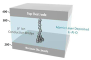
도 1은 본 발명의 실시 예에 따른 메모리 소자의 제조 방법을 설명하는 순서도이고, 도 2는 본 발명의 실시 예에 따른 메모리 소자의 제조 방법 중 제1 전극 형성 단계를 나타내는 도면이고, 도 3 내지 도 5는 본 발명의 실시 예에 따른 메모리 소자의 제조 방법 중 저항 변화층 형성 단계를 나타내는 도면이고, 도 6은 본 발명의 실시 예에 따른 메모리 소자를 나타내는 도면이고, 도 7은 본 발명의 실시 예에 따른 메모리 소자가 포함하는 저항 변화층 내에 이온 브릿지가 형성된 것을 나타내는 도면이다. 1 is a flowchart illustrating a method of manufacturing a memory device according to an exemplary embodiment of the present invention, and FIG. 2 is a view showing a first electrode forming step of a method of manufacturing a memory device according to an exemplary embodiment of the present invention. 5 is a view showing a step of forming a resistance change layer in a method of manufacturing a memory device according to an embodiment of the present invention, FIG. 6 is a view showing a memory device according to an embodiment of the present invention, and FIG. 7 is an embodiment of the present invention A diagram showing that an ion bridge is formed in a resistance change layer included in a memory device according to an example.
도 1 및 도 2를 참조하면, 기판(100) 상에 제1 전극(200)이 형성될 수 있다(S100). 일 실시 예에 따르면, 상기 기판(100)은 반도체 기판일 수 있다. 예를 들어, 상기 기판(100)은 실리콘 산화물(SiO2) 기판 일 수 있다. 이와 달리, 다른 실시 예에 따르면, 상기 기판(100)은 금속 기판, 플라스틱 기판, 또는 유리 기판 등일 수 있다. 1 and 2, the
상기 제1 전극(200)은 도전성 금속 물질을 포함할 수 있다. 예를 들어, 상기 제1 전극(200)은 백금(Pt), 루테늄(Ru), 티타늄 질화물(TiN), 및 탄탈륨 질화물(TaN) 중 어느 하나를 포함할 수 있다. 일 실시 예에 따르면, 상기 제1 전극(200)은 물리적 증착법을 이용하여 상기 기판(100) 상에 형성될 수 있다. 예를 들어, 상기 물리적 증착법은 스퍼터링(sputtering)을 포함할 수 있다. The
도 1 내지 도 5를 참조하면, 상기 제1 전극(200) 상에 저항 변화층(300)이 형성될 수 있다(S200). 후술되는 바와 같이, 상기 제1 전극(200) 및 제2 전극(400) 사이에 기준 전압 이상의 전압이 인가되는 경우, 상기 저항 변화층(300)에는 상기 제1 전극(200) 및 상기 제2 전극(400) 사이를 연결하는 이온 브릿지(bridge)가 형성될 수 있다. 또한, 상기 저항 변화층(300)은 후술되는 상기 제1 전극(200) 및 제2 전극(400)에 인가되는 전압의 크기에 따라, 저항이 변화될 수 있다. 보다 구체적인 설명은 후술된다. Referring to FIGS. 1 to 5, a
일 실시 예에 따르면, 상기 저항 변화층(300)은 원자층 증착법(Atomic Layer Deposition)으로 형성될 수 있다. 구체적으로, 상기 저항 변화층(300) 형성 단계는, 도 3에 도시된 바와 같이, 상기 제1 전극(200) 상에 제1 전구체를 제공하는 단계, 퍼지(purge) 단계, 상기 제1 전구체가 제공된 상기 제1 전극(200) 상에 제1 반응 소스를 제공하는 단계, 퍼지(purge) 단계, 상기 제1 전극(200) 상에 제2 전구체를 제공하는 단계, 퍼지(purge) 단계, 상기 제2 전구체가 제공된 상기 제1 전극(200) 상에 제2 반응 소스를 제공하는 단계, 및 퍼지(purge) 단계를 포함할 수 있다. According to one embodiment, the
일 실시 예에 따르면, 상기 제1 전구체는 알칼리 금속을 포함할 수 있다. 예를 들어, 상기 알칼리 금속은 리튬(Li)을 포함할 수 있다. 구체적으로, 상기 제1 전구체는 LiHMDS(Lithium bis(trimethylsilyl)amide)를 포함할 수 있다. 이와 달리, 상기 제2 전구체는 전이 금속을 포함할 수 있다. 예를 들어, 상기 전이 금속은 알루미늄(Al)을 포함할 수 있다. 구체적으로, 상기 제2 전구체는 TMA(Trimethylaluminium)을 포함할 수 있다. 일 실시 예에 따르면, 상기 제1 반응 소스 및 상기 제2 반응 소스는 서로 같을 수 있다. 예를 들어, 상기 제1 반응 소스 및 상기 제2 반응 소스는 물(H2O)을 포함할 수 있다. 이에 따라, 상기 저항 변화층(300)은, 상기 알칼리 금속(예를 들어, 리튬), 상기 전이 금속(예를 들어, 알루미늄), 및 산소(O)를 포함할 수 있다. According to one embodiment, the first precursor may include an alkali metal. For example, the alkali metal may include lithium (Li). Specifically, the first precursor may include LiHMDS (Lithium bis (trimethylsilyl) amide). Alternatively, the second precursor may include a transition metal. For example, the transition metal may include aluminum (Al). Specifically, the second precursor may include TMA (Trimethylaluminium). According to an embodiment, the first reaction source and the second reaction source may be the same. For example, the first reaction source and the second reaction source may include water (H 2 O). Accordingly, the
다른 예를 들어, 상기 제1 반응 소스 및 상기 제2 반응 소스는 서로 다를 수 있다. 예를 들어, 상기 제1 반응 소스는, 오존(O3)이고, 상기 제2 반응 소스는 물(H2O)일 수 있다. 이 경우, 누설전류 감소 효과가 향상될 수 있다. For another example, the first reaction source and the second reaction source may be different. For example, the first reaction source may be ozone (O 3 ), and the second reaction source may be water (H 2 O). In this case, the effect of reducing the leakage current can be improved.
상기 제1 전구체 제공 단계-퍼지 단계-제1 반응 소스 제공 단계-퍼지 단계는 제1 유닛 공정(first unit process)로 정의될 수 있다. 반면, 상기 제2 전구체 제공 단계-퍼지 단계-제2 반응 소스 제공 단계-퍼지 단계는 제2 유닛 공정(second unit process)로 정의될 수 있다. 또한, 상기 제1 유닛 공정 및 상기 제2 유닛 공정이 순차적으로 수행되는 경우, 상기 제1 유닛 공정 및 상기 제2 유닛 공정은 그룹 공정(group process)로 정의될 수 있다. The first precursor providing step-purging step-first reaction source providing step-purging step may be defined as a first unit process. On the other hand, the second precursor providing step-purging step-second reaction source providing step-purging step may be defined as a second unit process. In addition, when the first unit process and the second unit process are sequentially performed, the first unit process and the second unit process may be defined as a group process.
일 실시 예에 따르면, 상기 제1 유닛 공정이 수행되는 경우, 제1 저항 변화층(310)이 형성될 수 있다. 즉, 상기 제1 전구체 및 상기 제1 반응 소스가 반응되어, 상기 제1 저항 변화층(310)이 형성될 수 있다. 이와 달리, 상기 제2 유닛 공정이 수행되는 경우, 제2 저항 변화층(320)이 형성될 수 있다. 즉, 상기 제2 전구체 및 상기 제2 반응 소스가 반응되어, 상기 제2 저항 변화층(320)이 형성될 수 있다. According to an embodiment, when the first unit process is performed, a first
일 실시 예에 따르면, 상기 그룹 공정은 반복적으로 수행될 수 있다. 이에 따라, 상기 제1 전극(200) 상에 상기 제1 저항 변화층(310) 및 상기 제2 저항 변화층(320)이 교대로, 그리고 반복적으로 형성될 수 있다. 이 경우, 복수의 상기 제1 저항 변화층(310) 및 복수의 상기 제2 저항 변화층(320)은 상기 저항 변화층(300)으로 정의될 수 있다. According to one embodiment, the group process may be repeatedly performed. Accordingly, the first
다른 실시 예에 따르면, 상기 제1 유닛 공정 및 상기 제2 유닛 공정이 각각 복수회 반복 수행될 수 있다. 상기 제1 유닛 공정이 및 상기 제2 유닛 공정이 복수회 반복 수행되는 경우, 상기 제1 저항 변화층(310) 및 상기 제2 저항 변화층(320)의 두께가 각각 제어될 수 있다. 예를 들어, 상기 제1 유닛 공정의 반복 수행 횟수가 증가되는 경우, 상기 제1 저항 변화층(310)의 두께가 증가될 수 있다. 또한, 상기 제2 유닛 공정의 반복 수행 횟수가 증가되는 경우, 상기 제2 저항 변화층(320)의 두께가 증가될 수 있다. 이에 따라, 상기 제1 전극(200) 상에 두께가 제어된 상기 제1 저항 변화층(310) 및 제2 저항 변화층(320)이 배치될 수 있다. 이 경우, 두께가 제어된 상기 제1 저항 변화층(310) 및 상기 제2 저항 변화층(320)은 상기 저항 변화층(300)으로 정의될 수 있다. According to another embodiment, each of the first unit process and the second unit process may be repeatedly performed. When the first unit process and the second unit process are repeatedly performed a plurality of times, thicknesses of the first
일 실시 예에 따르면, 상기 저항 변화층(300)은 상기 제1 저항 변화층(310) 및 상기 제2 저항 변화층(320)이 물리적 및 시각적으로 구분되지 않을 수 있다. 보다 구체적으로, 상기 제1 저항 변화층(310) 및 상기 제2 저항 변화층(320)이 각각 소정의 두께 이상의 두께를 갖지 못하는 경우, 상기 저항 변화층(300) 내에서 상기 제1 저항 변화층(310) 및 상기 제2 저항 변화층(320)이 물리적 및 시각적으로 구분되지 않을 수 있다. According to an embodiment, in the
이와 달리, 다른 실시 예에 따르면, 상기 저항 변화층(300)은 상기 제1 저항 변화층(310) 및 상기 제2 저항 변화층(320)이 물리적 및 시각적으로 구분될 수 있다. 보다 구체적으로, 상기 제1 저항 변화층(310) 및 상기 제2 저항 변화층(320)이 각각 소정의 두께 이상으로 형성되는 경우, 상기 저항 변화층(300) 내에서 상기 제1 저항 변화층(310) 및 상기 제2 저항 변화층(320)이 SEM 사진 및 TEM 사진 등을 통해 물리적 및 시각적으로 구분될 수 있다. Alternatively, according to another embodiment, in the
일 실시 예에 따르면, 상기 저항 변화층(300) 내의 상기 알칼리 금속의 함량을 제어하기 위하여, 상기 제1 유닛 공정 및 상기 제2 유닛 공정의 비율이 제어될 수 있다. 보다 구체적으로, 상기 제1 유닛 공정의 반복 수행 비율: 상기 제2 유닛 공정의 반복 수행 비율이 4:1인 경우, 상기 저항 변화층 내의 상기 알칼리 금속의 함량은 40 at%일 수 있다. 이와 달리, 상기 제1 유닛 공정의 반복 수행 비율: 상기 제2 유닛 공정의 반복 수행 비율이 9:1인 경우, 상기 저항 변화층 내의 상기 알칼리 금속의 함량은 60 at%일 수 있다. 이와 달리, 상기 제1 유닛 공정의 반복 수행 비율: 상기 제2 유닛 공정의 반복 수행 비율이 16:1인 경우, 상기 저항 변화층 내의 상기 알칼리 금속의 함량은 88 at%일 수 있다.According to an embodiment, in order to control the content of the alkali metal in the
즉, 상기 제1 유닛 공정의 반복 수행 비율이 상기 제2 유닛 공정의 반복 수행 비율 대비 4배 초과 16배 미만으로 제어되는 경우, 상기 저항 변화층(300) 내의 상기 알칼리 금속의 함량은 40 at% 초과 88 at% 미만으로 제어될 수 있다. 상술된 알칼리 금속의 함량 범위에서, 후술되는 메모리 소자의 전기적 특성이 향상될 수 있다. 구체적으로, 상술된 알칼리 금속의 함량 범위에서, 후술되는 메모리 소자의 온/오프 특성(ION/IOFF ratio)이 향상될 수 있다. That is, when the repetition rate of the first unit process is controlled to be more than 4 times and less than 16 times compared to the repetition rate of the second unit process, the content of the alkali metal in the
또한, 상기 저항 변화층(300) 내에서 상기 알칼리 금속(예를 들어, 리튬)의 함량이 상기 전이 금속(예를 들어, 알루미늄)의 함량보다 높을 수 있다. 이 경우, 후술되는 메모리 소자의 reset에 요구되는 전류(reset current), On current(LRS), Off current(HRS) 등이 감소되어, 저전력에서 효과적으로 구동될 수 있다. In addition, the content of the alkali metal (eg, lithium) in the
일 실시 예에 따르면, 상기 저항 변화층(300)에서 상기 알칼리 금속(예를 들어, 리튬)의 함량이 상기 전이 금속(예를 들어, 알루미늄)의 함량보다 높게 제어되기 위해, 상기 제1 유닛 공정 및 상기 제2 유닛 공정의 온도가 제어될 수 있다. 예를 들어, 상기 제1 유닛 공정 및 상기 제2 유닛 공정은 90℃이하의 온도에서 수행될 수 있다. 보다 구체적으로, 상기 제1 유닛 공정을 통해 형성되는 상기 제1 저항 변화층(310)의 성장률(growth rate)은 온도에 따라 다를 수 있다. 예를 들어, 90℃이하의 저온에서 형성되는 상기 제1 저항 변화층(310)의 성장률은, 225℃이상의 고온에서 형성되는 상기 제1 저항 변화층(310)의 성장률 보다 클 수 있다. According to an embodiment, in order to control the content of the alkali metal (eg, lithium) in the
이에 따라, 상기 저항 변화층(300) 내의 상기 알칼리 금속의 함량이 높은 경우, 상기 저항 변화층(300)의 증착 공정 온도가 상대적으로 낮게 제어될 수 있고, 이로 인해, 상대적으로 높은 상기 알칼리 금속 함량을 포함하는 상기 저항 변화층(300)이 용이하게 형성될 수 있다.Accordingly, when the content of the alkali metal in the
도 1 및 도 6을 참조하면, 상기 저항 변화층(300) 상에 제2 전극(400)이 형성될 수 있다(S300). 이에 따라, 상기 실시 예에 따른 메모리 소자가 제조될 수 있다. 일 실시 예에 따르면, 상기 메모리 소자는, CBRAM(Conductive Bridging RAM)으로 사용될 수 있다. 1 and 6, a
상기 제2 전극(400)은 도전성 금속 물질을 포함할 수 있다. 일 실시 예에 따르면, 상기 제2 전극(400)은 상기 제1 전극(200)과 같은 물질을 포함할 수 있다. 예를 들어, 상기 제2 전극(400)은 백금(Pt), 루테늄(Ru), 티타늄 질화물(TiN), 및 탄탈륨 질화물(TaN) 중 어느 하나를 포함할 수 있다. 일 실시 예에 따르면, 상기 제2 전극(400)은 물리적 증착법을 이용하여 상기 저항 변화층(300) 상에 형성될 수 있다. 예를 들어, 상기 물리적 증착법은 스퍼터링(sputtering)을 포함할 수 있다. The
도 7을 참조하면, 상기 제1 전극(200) 및 상기 제2 전극(400) 사이에 기준 전압 이상의 하이 레벨(high level) 전압이 인가되는 경우, 상기 제1 전극(200) 및 상기 제2 전극(400) 사이에 상기 제1 전극(200) 및 상기 제2 전극(400)을 연결하는 이온 브릿지(bridge)가 상기 저항 변화층(300) 내에 형성될 수 있다. 상기 이온 브릿지는, 상술된 알칼리 금속(예를 들어, 리튬)의 이온을 포함할 수 있다. 상기 저항 변화층(300)에 상기 이온 브릿지가 형성되는 경우, 상기 저항 변화층(300)은 저(low) 저항 상태를 가질 수 있다. Referring to FIG. 7, when a high level voltage equal to or higher than a reference voltage is applied between the
이와 달리, 상기 제1 전극(200) 및 상기 제2 전극(400) 사이에 상기 기준 전압 이하의 로우 레벨(low level) 전압이 인가되는 경우, 상기 저항 변화층(300)에 형성된 상기 이온 브릿지(bridge)는 소멸 또는 끊어질 수 있다. 이에 따라, 상기 저항 변화층(300)은 고(high) 저항 상태를 가질 수 있다. Alternatively, when a low level voltage below the reference voltage is applied between the
상술된 바와 같이, 상기 이온 브릿지는 리튬 이온으로 구성됨에 따라, 상기 저항 변화층(300)의 상태 변화가 빠르게 발생될 수 있다. 즉, 상기 이온 브릿지의 형성 및 소멸이 빠르게 발생될 수 있다. 이에 따라, 메모리 소자의 작동 속도가 빨라질 수 있다. As described above, as the ion bridge is composed of lithium ions, a state change of the
일 실시 예에 따르면, 상기 저항 변환층(300)은, 상기 제1 전극(200)에 인접한 제1 영역, 상기 제2 전극(400)에 인접한 제2 영역, 및 상기 제1 영역 및 상기 제2 영역 사이의 중간 영역을 포함할 수 있다. 이 경우, 상술된 바와 같이, 상기 저항 변화층(300) 내의 상기 알칼리 금속의 함량이 40at% 초과 88at% 미만이되, 상기 제1 영역에서, 상기 중간 영역으로 갈수록, 그리고, 상기 제2 영역에서 상기 중간 영역으로 갈수록, 상기 알칼리 금속의 함량이 증가 또는 감소될 수 있다. 이에 따라, 누설전류 제어 효과가 향상될 수 있다. 상기 알칼리 금속의 함량은, 상술된 바와 같이, 상기 제1 유닛 공정 및 상기 제2 유닛 공정의 수행 비율에 따라서 제어될 수 있다. 보다 구체적으로, 상기 알칼리 금속(예를 들어, 리튬)의 함량이 상대적으로 낮은 영역에서는, 누설 전류를 감소시키는 베리어층의 기능을 수행함으로써, 누설전류 제어 효과를 향상시킬 수 있다 According to an embodiment, the
본 발명의 실시 예에 따른 메모리 소자의 제조 방법은, 상기 기판(100) 상에 상기 제1 전극(200)을 형성하는 단계, 알칼리 금속을 포함하는 제1 전구체 및 제1 반응 소스를 반응 시키는 제1 유닛 공정(first unit process), 전이 금속을 포함하는 제2 전구체 및 제2 반응 소스를 반응시키는 제2 유닛 공정(second unit process)을 수행하여, 상기 제1 전극(200) 상에 상기 알칼리 금속 및 상기 전이 금속을 포함하는 상기 저항 변화층(300)을 형성하는 단계, 및 상기 저항 변화층(300) 상에 상기 제2 전극(400)을 형성하는 단계를 포함하고, 상기 제1 유닛 공정 및 상기 제2 유닛 공정은 각각 복수회 반복 수행되되, 상기 제1 유닛 공정 및 상기 제2 유닛 공정의 반복 수행 비율을 제어하여, 상기 저항 변화층(300) 내의 상기 알칼리 금속의 함량이 제어될 수 있다. 이에 따라, 구동시 전력소모량이 낮고 작동 속도가 빠른 메모리 소자가 제공될 수 있다. 또한, 상기 저항 변화층(300)이 원자층 증착법(ALD)으로 형성됨에 따라, 높은 양산성을 가질 수 있다. A method of manufacturing a memory device according to an embodiment of the present invention includes forming the
이상, 본 발명의 실시 예에 따른 메모리 소자 및 그 제조 방법이 설명되었다. 이하, 본 발명의 실시 예에 따른 메모리 소자 및 그 제조 방법의 구체적인 실험 예 및 특성 평가 결과가 설명된다. In the above, a memory device and a manufacturing method according to an embodiment of the present invention have been described. Hereinafter, specific experimental examples and characteristic evaluation results of a memory device and a method of manufacturing the same according to embodiments of the present invention will be described.
실험 예 1에 따른 메모리 소자 제조 Memory device fabrication according to Experimental Example 1
SIO2 기판 상에 질화티타늄(TiN) 하부 전극을 형성한 후, 하부 전극 상에 LiHMDS 제공-퍼지-H2O 제공-퍼지-TMA 제공-퍼지-H2O 제공-퍼지를 수행하여, 저항 변화층을 형성하고, 저항 변화층 상에 질화티타늄(TiN) 상부 전극을 형성하여 실시 예에 따른 메모리 소자를 제조하였다.After forming a titanium nitride (TiN) lower electrode on the SIO 2 substrate, LiHMDS provided on the lower electrode-purge-H 2 O provided-purge-TMA provided-purge-H 2 O provided-purged to change the resistance A memory device according to an embodiment was manufactured by forming a layer and forming a titanium nitride (TiN) upper electrode on the resistance change layer.
상술된 공정에서, LiHMDS 제공-퍼지-H2O 제공-퍼지는 제1 유닛 공정으로 정의되고, TMA 제공-퍼지-H2O 제공-퍼지는 제2 유닛 공정으로 정의되며, 각 유닛 공정들은 반복 수행되었다. In the above-described process, LiHMDS provision-purge-H 2 O provision-purge is defined as the first unit process, TMA provision-purge-H 2 O provision-purge is defined as the second unit process, and each unit process is repeatedly performed .
보다 구체적으로, 상기 제1 유닛 공정: 제2 유닛 공정의 비율을 1:9로 제어하여, 저항 변화층 내의 Li 농도를 5 at%로 제조하였다. 이에 따라, 실험 예 1에 따른 메모리 소자를 제조하였다. More specifically, by controlling the ratio of the first unit process: the second unit process to 1:9, the Li concentration in the resistance change layer was prepared at 5 at%. Accordingly, a memory device according to Experimental Example 1 was manufactured.
실험 예 2에 따른 메모리 소자 제조Memory device fabrication according to Experimental Example 2
상술된 실험 예 1에 따른 메모리 소자를 제조하되, 상기 제1 유닛 공정: 제2 유닛 공정의 비율을 1:1로 제어하여, 저항 변화층 내의 Li 농도를 30 at%로 제조하였다. 이에 따라, 실험 예 2에 따른 메모리 소자를 제조하였다. A memory device according to Experimental Example 1 described above was manufactured, and the ratio of the first unit process: the second unit process was controlled to 1:1, so that the Li concentration in the resistance change layer was 30 at%. Accordingly, a memory device according to Experimental Example 2 was manufactured.
실험 예 3에 따른 메모리 소자 제조Memory device fabrication according to Experimental Example 3
상술된 실험 예 1에 따른 메모리 소자를 제조하되, 상기 제1 유닛 공정: 제2 유닛 공정의 비율을 4:1로 제어하여, 저항 변화층 내의 Li 농도를 40 at%로 제조하였다. 이에 따라, 실험 예 3에 따른 메모리 소자를 제조하였다. A memory device according to Experimental Example 1 described above was manufactured, and the ratio of the first unit process: the second unit process was controlled to 4:1, so that the Li concentration in the resistance change layer was 40 at%. Accordingly, a memory device according to Experimental Example 3 was manufactured.
실험 예 4에 따른 메모리 소자 제조Memory device fabrication according to Experimental Example 4
상술된 실험 예 1에 따른 메모리 소자를 제조하되, 상기 제1 유닛 공정: 제2 유닛 공정의 비율을 9:1로 제어하여, 저항 변화층 내의 Li 농도를 60 at%로 제조하였다. 이에 따라, 실험 예 4에 따른 메모리 소자를 제조하였다. A memory device according to Experimental Example 1 described above was manufactured, and the ratio of the first unit process: the second unit process was controlled to 9:1, so that the Li concentration in the resistance change layer was 60 at%. Accordingly, a memory device according to Experimental Example 4 was manufactured.
실험 예 5에 따른 메모리 소자 제조Memory device fabrication according to Experimental Example 5
상술된 실험 예 1에 따른 메모리 소자를 제조하되, 상기 제1 유닛 공정: 제2 유닛 공정의 비율을 16:1로 제어하여, 저항 변화층 내의 Li 농도를 88 at%로 제조하였다. 이에 따라, 실험 예 5에 따른 메모리 소자를 제조하였다. A memory device according to Experimental Example 1 described above was manufactured, and the ratio of the first unit process: the second unit process was controlled to be 16:1, so that the Li concentration in the resistance change layer was 88 at%. Accordingly, a memory device according to Experimental Example 5 was manufactured.
상술된 실험 예 1 내지 5에 따른 메모리 소자의 제조 공정이 아래의 <표 1>을 통해 정리된다. The manufacturing process of the memory device according to Experimental Examples 1 to 5 described above is summarized through <Table 1> below.
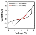
도 8은 본 발명의 실험 예 1 및 2에 따른 메모리 소자의 스위칭 특성을 나타내는 그래프이다. 8 is a graph showing switching characteristics of a memory device according to Experimental Examples 1 and 2 of the present invention.
도 8을 참조하면, 상기 실험 예 1 및 실험 예 2에 따른 메모리 소자를 준비한 후, 각각에 대하여 전압(V)에 따른 전류(mA)를 측정하여 나타내었다. 도 8에서 확인할 수 있듯이, 상기 실험 예 1 및 실험 예 2에 따른 메모리 소자는 전형적인 Atomic Switching 특성 곡선이 나타나는 것을 확인할 수 있었다. Referring to FIG. 8, after preparing the memory devices according to Experimental Example 1 and Experimental Example 2, the currents (mA) according to the voltages (V) were measured for each. As can be seen in Figure 8, it can be seen that the memory elements according to Experimental Example 1 and Experimental Example 2 show typical Atomic Switching characteristic curves.
도 9는 본 발명의 실험 예에 따른 메모리 소자들의 Reset Current를 나타내는 그래프이다. 9 is a graph showing Reset Current of memory devices according to an experimental example of the present invention.
도 9를 참조하면, 저항 변화층이 포함하는 리튬(Li)의 함유량이 서로 다른 상기 실험 예 1 내지 실험 예 5에 따른 메모리 소자를 준비하고, 각각에 대해 Reset에 요구되는 전류(Reset current)를 측정하여 나타내었다. Referring to FIG. 9, a memory device according to Experimental Examples 1 to 5 in which the content of lithium (Li) contained in the resistance change layer is different is prepared, and a reset current required for each is reset. It was measured and indicated.
도 9에서 확인할 수 있듯이, 저항 변화층이 포함하는 리튬의 함유량이 증가함에 따라, Reset에 요구되는 전류 값이 점차적으로 감소하는 것을 확인할 수 있었다. 특히, 저항 변화층이 포함하는 리튬의 함유량이 40 at%를 초과함에 따라 Reset에 요구되는 전류 값이 현저하게 감소하는 것을 확인할 수 있었다. As can be seen in Figure 9, as the content of lithium contained in the resistance change layer increases, it was confirmed that the current value required for reset gradually decreases. Particularly, it was confirmed that as the content of lithium contained in the resistance change layer exceeded 40 at%, the current value required for reset was significantly reduced.
도 10은 본 발명의 실험 예에 따른 메모리 소자들의 On current 및 Off current를 나타내는 그래프이다. 10 is a graph showing On current and Off current of memory devices according to an experimental example of the present invention.
도 10을 참조하면, 저항 변화층이 포함하는 리튬(Li)의 함유량이 서로 다른 상기 실험 예 1 내지 실험 예 5에 따른 메모리 소자를 준비하고, 각각에 대해 On current(LRS) 및 Off current(HRS)를 측정하여 나타내었다. Referring to FIG. 10, memory elements according to Experimental Examples 1 to 5 having different contents of lithium (Li) included in the resistance change layer are prepared, and On current (LRS) and Off current (HRS) are respectively provided. ) Was measured.
도 10에서 확인할 수 있듯이, 저항 변화층이 포함하는 리튬(Li)의 함유량이 증가함에 따라, On current(LRS) 및 Off current(HRS) 모두 점차적으로 감소하는 것을 확인할 수 있었다. 특히, 저항 변화층이 포함하는 리튬의 함유량이 40 at%를 초과함에 따라 On current(LRS) 및 Off current(HRS) 모두 현저하게 감소하는 것을 확인할 수 있었다. As can be seen in Figure 10, as the content of the lithium (Li) contained in the resistance change layer increases, it was confirmed that both the On current (LRS) and the Off current (HRS) gradually decrease. In particular, it was confirmed that both the On current (LRS) and the Off current (HRS) significantly decreased as the content of lithium contained in the resistance change layer exceeded 40 at%.
도 9 및 도 10을 통해 알 수 있듯이, 본 발명의 실험 예에 따른 메모리 소자의 경우, 저항 변화층 내의 리튬(Li) 함유량이 높을수록 저전력 구동에 효과적이라는 것을 알 수 있었다. 9 and 10, it can be seen that in the case of the memory device according to the experimental example of the present invention, the higher the lithium (Li) content in the resistance change layer, the more effective it is to drive low power.
도 11은 본 발명의 실험 예에 따른 메모리 소자들의 ION/IOFF ratio를 나타내는 그래프이고, 도 12는 본 발명의 실험 예에 따른 메모리 소자들의 동작 전류 특성을 나타내는 그래프이다. 11 is a graph showing the I ON /I OFF ratio of memory devices according to an experimental example of the present invention, and FIG. 12 is a graph showing the operating current characteristics of memory devices according to an experimental example of the present invention.
도 11 및 도 12를 참조하면, 상기 실험 예 1 내지 실험 예 5에 따른 메모리 소자의 온/오프 특성(ION/IOFF ratio)을 측정하여 도 11에 나타내었고, 동작 전압(V)에 따른 동작 전류(mA)를 측정하여 도 12에 나타내었다. 11 and 12, the on/off characteristics (I ON /I OFF ratio) of the memory devices according to Experimental Examples 1 to 5 are measured, and are shown in FIG. 11, depending on the operating voltage (V). The operating current (mA) was measured and shown in FIG. 12.
도 11 및 도 12에서 확인할 수 있듯이, Li의 함유량이 높아짐에 따라 동일 동작 전압 구간에서 동작 전류가 감소하는 것을 확인할 수 있었다. 또한, Li의 함유량이 40 at%를 초과하는 구간부터 ION/IOFF ratio가 급격히 상승하다가, 60 at% 에서 최고 값을 갖고 이후 88 at%까지 점차적으로 감소하는 것을 확인할 수 있었다. 11 and 12, it was confirmed that as the content of Li increased, the operating current decreased in the same operating voltage section. In addition, it was confirmed that the I ON /I OFF ratio rapidly increased from the section where the Li content exceeded 40 at%, and then gradually decreased to 88 at% after having the highest value at 60 at%.
이에 따라, 메모리 소자의 전기적 특성을 향상시키기 위해서는, 리튬(Li)의 함유량이 제어되어야 하고, 리튬의 함유량이 60 at%일 경우 가장 높은 ION/IOFF ratio를 나타내므로, 메모리 소자의 전기적 특성을 향상시키기 위해서는, 리튬의 함유량이 40 at% 초과 88 at% 미만으로 제어되어야 함을 알 수 있었다. Accordingly, in order to improve the electrical characteristics of the memory device, the content of lithium (Li) must be controlled, and when the content of lithium is 60 at%, the highest I ON /I OFF ratio is exhibited. In order to improve, it was found that the content of lithium should be controlled to be greater than 40 at% and less than 88 at%.
또한, 리튬의 함유량이 40 at% 초과 88 at% 미만으로 제어되기 위해서는, 저항 변화층 형성과정에서 제1 유닛 공정의 반복 수행 비율이 제2 유닛 공정의 반 복 수행 비율 대비 4배 초과 16배 미만으로 제어되어야 함을 알 수 있었다. In addition, in order for the content of lithium to be controlled to be greater than 40 at% and less than 88 at%, the repetition rate of the first unit process in the process of forming the resistance change layer is more than 4 times and less than 16 times the repetition rate of the second unit process It was found that it should be controlled.
도 13은 서로 다른 온도에서 형성된 저항 변화층의 성장 속도를 나타내는 그래프이고, 도 14는 서로 다른 온도에서 형성된 저항 변화층의 이온 전도도를 나타내는 그래프이다. 13 is a graph showing the growth rate of the resistance change layer formed at different temperatures, and FIG. 14 is a graph showing the ionic conductivity of the resistance change layer formed at different temperatures.
도 13 및 도 14를 참조하면, 90℃의 온도 및 225℃의 온도에서 각각 형성된 저항 변화층을 포함하는 메모리 소자를 준비하고, 제1 유닛 공정에 따라 형성되는 제1 저항 변화층 및 제2 유닛 공정에 따라 형성되는 제2 저항 변화층의 성장율(Growth Rate)를 측정하여 도 13에 나타내었고, 메모리 소자가 포함하는 저항 변화층의 Li 농도에 따른 이온 전도도(ion conductivity, S/cm)를 측정하여 도 14에 나타내었다. 13 and 14, a memory device including a resistance change layer formed at a temperature of 90° C. and a temperature of 225° C. is prepared, and the first resistance change layer and the second unit are formed according to the first unit process. The growth rate of the second resistive change layer formed according to the process is measured and shown in FIG. 13, and the ion conductivity (S/cm) according to the Li concentration of the resistive change layer included in the memory device is measured. It is shown in Figure 14.
도 13 및 도 14에서 확인할 수 있듯이, 저항 변화층 형성 온도에 따라 성장율을 현저하게 차이가 나지만, 이온 전도도는 실질적으로 일치하는 것을 확인할 수 있었다. 즉, 이온 전도도는 저항 변화층 형성 온도가 아니라, 저항 변화층 내 Li의 농도에 영향이 있다는 것을 알 수 있었다. As can be seen in Figures 13 and 14, although the growth rate is significantly different according to the resistance change layer formation temperature, it was confirmed that the ionic conductivity is substantially the same. That is, it was found that the ionic conductivity has an influence on the concentration of Li in the resistive change layer, not the temperature of forming the resistive change layer.
결과적으로, 상대적으로 저온(90℃)에서의 저항 변화층 성장률이 상대적으로 고온(225℃)에서의 저항 변화층 성장률 보다 높으므로, Li의 함량이 높은 저항 변화층을 형성하기 위해서는, 90℃ 이하의 공정 조건으로 저항 변화층을 형성하는 것이 효과적임을 알 수 있다.As a result, since the growth rate of the resistance change layer at a relatively low temperature (90°C) is higher than the growth rate of the resistance change layer at a relatively high temperature (225°C), in order to form a resistance change layer having a high Li content, 90°C or less It can be seen that it is effective to form a resistance change layer under the process conditions of.
이상, 본 발명을 바람직한 실시 예를 사용하여 상세히 설명하였으나, 본 발명의 범위는 특정 실시 예에 한정되는 것은 아니며, 첨부된 특허청구범위에 의하여 해석되어야 할 것이다. 또한, 이 기술분야에서 통상의 지식을 습득한 자라면, 본 발명의 범위에서 벗어나지 않으면서도 많은 수정과 변형이 가능함을 이해하여야 할 것이다.As described above, the present invention has been described in detail using preferred embodiments, but the scope of the present invention is not limited to specific embodiments, and should be interpreted by the appended claims. In addition, those skilled in the art should understand that many modifications and variations are possible without departing from the scope of the present invention.
100: 기판
200: 제1 전극
300: 저항 변화층
310: 제1 저항 변화층
320: 제2 저항 변화층
400: 제2 전극100: substrate
200: first electrode
300: resistance change layer
310: first resistance change layer
320: second resistance change layer
400: second electrode
Claims (14)
상기 제1 전극 상에 배치되고, 알칼리 금속 및 전이 금속을 포함하는 저항 변화층; 및
상기 저항 변화층 상에 배치된 제2 전극을 포함하되,
상기 저항 변화층 내의 상기 알칼리 금속의 함량은 40 at% 초과 88 at% 미만인 것을 포함하는 메모리 소자.
A first electrode;
A resistance change layer disposed on the first electrode and comprising an alkali metal and a transition metal; And
Including a second electrode disposed on the resistance change layer,
The content of the alkali metal in the resistance change layer comprises more than 40 at% and less than 88 at%.
상기 제1 전극 또는 상기 제2 전극에 중 어느 하나의 전극에 전압이 인가되는 경우, 상기 알칼리 금속의 이온은 상기 제1 전극 및 상기 제2 전극을 연결하는 이온 브릿지(bridge)를 형성하는 것을 포함하는 메모리 소자.
According to claim 1,
When a voltage is applied to either the first electrode or the second electrode, the alkali metal ions include forming an ion bridge connecting the first electrode and the second electrode. Memory element to say.
상기 제1 전극 또는 상기 제2 전극 사이에 기준 전압 이상의 하이 레벨(high level) 전압이 인가되는 경우 상기 제1 전극 및 상기 제2 전극 사이에 상기 이온 브릿지가 형성되어 상기 저항 변화층은 저(low)저항 상태를 갖고,
상기 제1 전극 또는 상기 제2 전극 사이에 상기 기준 전압 이하의 로우 레벨(low level) 전압이 인가되는 경우 상기 제1 전극 및 상기 제2 전극 사이에 형성된 상기 이온 브릿지가 끊어져 상기 저항 변화층은 고(high)저항 상태를 갖는 것을 포함하는 메모리 소자.
According to claim 2,
When a high level voltage higher than a reference voltage is applied between the first electrode or the second electrode, the ion bridge is formed between the first electrode and the second electrode so that the resistance change layer is low. ) Has a resistance state,
When a low level voltage below the reference voltage is applied between the first electrode or the second electrode, the ion bridge formed between the first electrode and the second electrode is cut off, so that the resistance change layer is high. A memory device comprising a (high) resistance state.
상기 저항 변화층 내에서 상기 알칼리 금속의 함량은 상기 전이 금속의 함량 보다 높은 것을 포함하는 메모리 소자.
According to claim 1,
A memory device comprising a content of the alkali metal in the resistance change layer higher than that of the transition metal.
상기 알칼리 금속은 리튬(Li)을 포함하고, 상기 전이 금속은 알루미늄(Al)을 포함하는 메모리 소자.
According to claim 1,
The alkali metal includes lithium (Li), and the transition metal includes aluminum (Al).
상기 저항 변화층은, 상기 알칼리 금속을 포함하는 제1 저항 변화층 및 상기 전이 금속을 포함하는 제2 저항 변화층을 포함하되,
상기 제1 저항 변화층 및 상기 제2 저항 변화층은, 교대로 복수개 배치되는 것을 포함하는 메모리 소자.
According to claim 1,
The resistive change layer includes a first resistive change layer comprising the alkali metal and a second resistive change layer comprising the transition metal,
The first resistance change layer and the second resistance change layer, a memory device comprising a plurality of alternately arranged.
A CBRAM comprising the memory element according to claim 1.
알칼리 금속을 포함하는 제1 전구체 및 제1 반응 소스를 반응 시키는 제1 유닛 공정(first unit process), 전이 금속을 포함하는 제2 전구체 및 제2 반응 소스를 반응시키는 제2 유닛 공정(second unit process)을 수행하여, 상기 제1 전극 상에 상기 알칼리 금속 및 상기 전이 금속을 포함하는 저항 변화층을 형성하는 단계; 및
상기 저항 변화층 상에 제2 전극을 형성하는 단계를 포함하고,
상기 제1 유닛 공정 및 상기 제2 유닛 공정은 각각 복수회 반복 수행되되, 상기 제1 유닛 공정 및 상기 제2 유닛 공정의 반복 수행 비율을 제어하여, 상기 저항 변화층 내의 상기 알칼리 금속의 함량을 제어하는 것을 포함하는 메모리 소자의 제조 방법.
Forming a first electrode on the substrate;
A first unit process for reacting a first precursor comprising an alkali metal and a first reaction source, a second unit process for reacting a second precursor containing a transition metal and a second reaction source ) To form a resistance change layer comprising the alkali metal and the transition metal on the first electrode; And
And forming a second electrode on the resistance change layer,
The first unit process and the second unit process are each performed repeatedly a plurality of times, controlling the repetition rate of the first unit process and the second unit process to control the content of the alkali metal in the resistance change layer Method of manufacturing a memory device comprising a.
상기 제1 유닛 공정의 반복 수행 비율은, 상기 제2 유닛 공정의 반복 수행 비율 대비 4배 초과 16배 미만으로 제어되는 것을 포함하는 메모리 소자의 제조 방법.
The method of claim 8,
The method of manufacturing a memory device comprising controlling the repetition performance ratio of the first unit process to be more than 4 times and less than 16 times compared to a repetition performance rate of the second unit process.
상기 제1 유닛 공정은,
상기 제1 전극 상에 상기 제1 전구체를 제공하는 단계; 및
상기 제1 전구체가 제공된 상기 제1 전극 상에 상기 제1 반응 소스를 제공하는 단계를 포함하고,
상기 제2 유닛 공정은,
상기 제1 전극 상에 상기 제2 전구체를 제공하는 단계; 및
상기 제2 전구체가 제공된 상기 제1 전극 상에 상기 제2 반응 소스를 제공하는 단계를 포함하는 메모리 소자의 제조 방법.
The method of claim 8,
The first unit process,
Providing the first precursor on the first electrode; And
Providing the first reaction source on the first electrode provided with the first precursor,
The second unit process,
Providing the second precursor on the first electrode; And
And providing the second reaction source on the first electrode provided with the second precursor.
상기 저항 변화층 내의 상기 알칼리 금속의 함량이 상기 전이 금속의 함량보다 높도록,
상기 제1 유닛 공정 및 상기 제2 유닛 공정의 온도가 제어되는 것을 포함하는 메모리 소자의 제조 방법.
The method of claim 8,
The content of the alkali metal in the resistance change layer is higher than the content of the transition metal,
A method of manufacturing a memory device comprising controlling the temperature of the first unit process and the second unit process.
상기 제1 유닛 공정 및 상기 제2 유닛 공정은 90℃ 이하의 온도에서 수행되는 것을 포함하는 메모리 소자의 제조 방법.
The method of claim 11,
The first unit process and the second unit process is a method of manufacturing a memory device comprising performing at a temperature of 90 ℃ or less.
상기 제1 전구체는 LiHMDS(Lithium bis(trimethylsilyl)amide)를 포함하고, 상기 제2 전구체는 TMA(Trimethylaluminium)을 포함하는 메모리 소자의 제조 방법.
The method of claim 8,
The first precursor comprises LiHMDS (Lithium bis (trimethylsilyl) amide), the second precursor is TMA (Trimethylaluminium) comprises a memory device manufacturing method.
상기 제1 반응 소스 및 상기 제2 반응 소스는 서로 동일하고, 상기 제1 반응 소스 및 상기 제2 반응 소스는 H2O를 포함하는 메모리 소자의 제조 방법.
The method of claim 8,
The first reaction source and the second reaction source are the same as each other, and the first reaction source and the second reaction source include H 2 O.
Applications Claiming Priority (2)
| Application Number | Priority Date | Filing Date | Title |
|---|---|---|---|
| KR20180169696 | 2018-12-26 | ||
| KR1020180169696 | 2018-12-26 |
Publications (2)
| Publication Number | Publication Date |
|---|---|
| KR20200080194A true KR20200080194A (en) | 2020-07-06 |
| KR102275269B1 KR102275269B1 (en) | 2021-07-09 |
Family
ID=71129855
Family Applications (1)
| Application Number | Title | Priority Date | Filing Date |
|---|---|---|---|
| KR1020190175590A KR102275269B1 (en) | 2018-12-26 | 2019-12-26 | Memory device and fabricating method of thereof |
Country Status (3)
| Country | Link |
|---|---|
| US (1) | US20210273158A1 (en) |
| KR (1) | KR102275269B1 (en) |
| WO (1) | WO2020138975A1 (en) |
Cited By (1)
| Publication number | Priority date | Publication date | Assignee | Title |
|---|---|---|---|---|
| KR20220130433A (en) * | 2021-03-18 | 2022-09-27 | 강원대학교산학협력단 | Metal oxide memristor doped with alkali metal and manufacturing method thereof |
Citations (5)
| Publication number | Priority date | Publication date | Assignee | Title |
|---|---|---|---|---|
| KR20130030739A (en) * | 2011-09-19 | 2013-03-27 | 에이에스엠 인터내셔널 엔.브이. | Nanolayer deposition process for composite films |
| JP2013546195A (en) * | 2010-12-17 | 2013-12-26 | サントル ナショナル ドゥ ラ ルシェルシュ シアンティフィク | Memory resistance element and electronic memory based on such element |
| KR20160122133A (en) | 2014-02-19 | 2016-10-21 | 마이크로칩 테크놀로지 인코포레이티드 | Resistive memory cell having a reduced conductive path area |
| KR101676322B1 (en) * | 2015-08-27 | 2016-11-16 | 한양대학교 산학협력단 | Thermoelectric device and method of fabricating the same |
| KR20170026343A (en) * | 2014-06-26 | 2017-03-08 | 인텔 코포레이션 | Oxide-based three-terminal resistive switching logic devices |
Family Cites Families (12)
| Publication number | Priority date | Publication date | Assignee | Title |
|---|---|---|---|---|
| DE102004052647B4 (en) * | 2004-10-29 | 2009-01-02 | Qimonda Ag | Method for improving the thermal properties of semiconductor memory cells in the manufacturing process and non-volatile, resistively switching memory cell |
| WO2010029634A1 (en) * | 2008-09-11 | 2010-03-18 | 株式会社 東芝 | Resistance-varying element, and information recording/reproducing device |
| KR101851275B1 (en) * | 2008-11-28 | 2018-04-24 | 주식회사 원익아이피에스 | Method for depositing multiple metal system oxide thin film |
| JP5708929B2 (en) * | 2010-12-13 | 2015-04-30 | ソニー株式会社 | Storage element, manufacturing method thereof, and storage device |
| US9315894B2 (en) * | 2011-03-30 | 2016-04-19 | Asm Ip Holding B.V. | Atomic layer deposition of metal phosphates and lithium silicates |
| US8921821B2 (en) * | 2013-01-10 | 2014-12-30 | Micron Technology, Inc. | Memory cells |
| CN105862012B (en) * | 2016-05-27 | 2018-06-05 | 上海交通大学 | Li3PO4 based composite electrolyte films and preparation method thereof and ionic device |
| KR101836973B1 (en) * | 2017-02-02 | 2018-03-09 | 포항공과대학교 산학협력단 | Method for manufacturing large-area metal calcogenide thin film and method for manufacturing electronic device comprising said metal calcogenide thin film |
| US10553874B2 (en) * | 2017-08-04 | 2020-02-04 | Uchicago Argonne, Llc | Protective coatings for lithium anodes |
| WO2019187032A1 (en) * | 2018-03-30 | 2019-10-03 | 富士通株式会社 | Variable resistance element, manufacturing method therefor, and storage device |
| JP7155752B2 (en) * | 2018-08-24 | 2022-10-19 | 富士通株式会社 | Variable resistance element, manufacturing method thereof, and storage device |
| US11283019B2 (en) * | 2018-12-31 | 2022-03-22 | Research & Business Foundation Sungkyunkwan University | Resistance random access memory device and fabricating method of the same |
-
2019
- 2019-12-26 KR KR1020190175590A patent/KR102275269B1/en active IP Right Grant
- 2019-12-26 WO PCT/KR2019/018519 patent/WO2020138975A1/en active Application Filing
-
2021
- 2021-05-11 US US17/316,794 patent/US20210273158A1/en active Pending
Patent Citations (5)
| Publication number | Priority date | Publication date | Assignee | Title |
|---|---|---|---|---|
| JP2013546195A (en) * | 2010-12-17 | 2013-12-26 | サントル ナショナル ドゥ ラ ルシェルシュ シアンティフィク | Memory resistance element and electronic memory based on such element |
| KR20130030739A (en) * | 2011-09-19 | 2013-03-27 | 에이에스엠 인터내셔널 엔.브이. | Nanolayer deposition process for composite films |
| KR20160122133A (en) | 2014-02-19 | 2016-10-21 | 마이크로칩 테크놀로지 인코포레이티드 | Resistive memory cell having a reduced conductive path area |
| KR20170026343A (en) * | 2014-06-26 | 2017-03-08 | 인텔 코포레이션 | Oxide-based three-terminal resistive switching logic devices |
| KR101676322B1 (en) * | 2015-08-27 | 2016-11-16 | 한양대학교 산학협력단 | Thermoelectric device and method of fabricating the same |
Cited By (1)
| Publication number | Priority date | Publication date | Assignee | Title |
|---|---|---|---|---|
| KR20220130433A (en) * | 2021-03-18 | 2022-09-27 | 강원대학교산학협력단 | Metal oxide memristor doped with alkali metal and manufacturing method thereof |
Also Published As
| Publication number | Publication date |
|---|---|
| WO2020138975A1 (en) | 2020-07-02 |
| US20210273158A1 (en) | 2021-09-02 |
| KR102275269B1 (en) | 2021-07-09 |
Similar Documents
| Publication | Publication Date | Title |
|---|---|---|
| US9553264B2 (en) | Memory cells and semiconductor structures including electrodes comprising a metal, and related methods | |
| US8441060B2 (en) | Nonvolatile memory element and nonvolatile memory device incorporating nonvolatile memory element | |
| TWI518956B (en) | Resistive ram and fabrication method | |
| US8350244B2 (en) | Variable resistance device, method for manufacturing variable resistance device, and semiconductor storage device using variable resistance device | |
| US10181560B2 (en) | Conductive-bridging random access memory and method for fabricating the same | |
| WO2011071009A1 (en) | Variable-resistance element using an electrochemical reaction, and manufacturing method therefor | |
| EP2927975B1 (en) | Resistive random access memory and method of fabricating the same | |
| US9543516B2 (en) | Method for forming a doped metal oxide for use in resistive switching memory elements | |
| WO2012140887A1 (en) | Nonvolatile storage element and method of manufacturing thereof | |
| US9246091B1 (en) | ReRAM cells with diffusion-resistant metal silicon oxide layers | |
| TW201638946A (en) | Resistive random access memory | |
| US9831426B2 (en) | CBRAM device and manufacturing method thereof | |
| US20210273158A1 (en) | Memory device and manufacturing method therefor | |
| CN112909159B (en) | Resistive random access memory | |
| US8859382B2 (en) | Methods of forming metal oxide and memory cells | |
| Guo et al. | The improved resistive switching of HfO 2: Cu film with multilevel storage | |
| US20170012197A1 (en) | Variable-Resisance Element and Production Method Therefor | |
| US11152566B2 (en) | Resistive random access memory | |
| JP6825085B2 (en) | Manufacturing method of resistance changing element and resistance changing element | |
| TWI549326B (en) | Resistive ram and method of manufacturing the same |
Legal Events
| Date | Code | Title | Description |
|---|---|---|---|
| E902 | Notification of reason for refusal | ||
| E701 | Decision to grant or registration of patent right | ||
| GRNT | Written decision to grant |