KR20200071484A - Nonvolatile memory device and memory system including nonvolatile memory device - Google Patents
Nonvolatile memory device and memory system including nonvolatile memory device Download PDFInfo
- Publication number
- KR20200071484A KR20200071484A KR1020180159264A KR20180159264A KR20200071484A KR 20200071484 A KR20200071484 A KR 20200071484A KR 1020180159264 A KR1020180159264 A KR 1020180159264A KR 20180159264 A KR20180159264 A KR 20180159264A KR 20200071484 A KR20200071484 A KR 20200071484A
- Authority
- KR
- South Korea
- Prior art keywords
- data
- write data
- write
- read
- controller
- Prior art date
Links
- 230000002093 peripheral effect Effects 0.000 claims abstract description 36
- 230000002787 reinforcement Effects 0.000 claims abstract 3
- 238000012937 correction Methods 0.000 claims description 34
- 238000000034 method Methods 0.000 claims description 33
- 230000003416 augmentation Effects 0.000 claims description 3
- 230000003014 reinforcing effect Effects 0.000 claims 4
- 238000001514 detection method Methods 0.000 description 38
- 230000008569 process Effects 0.000 description 16
- 238000012546 transfer Methods 0.000 description 10
- 230000010076 replication Effects 0.000 description 7
- 230000004044 response Effects 0.000 description 7
- 101100275375 Arabidopsis thaliana COR47 gene Proteins 0.000 description 6
- 238000010586 diagram Methods 0.000 description 4
- 238000011017 operating method Methods 0.000 description 4
- 101000711846 Homo sapiens Transcription factor SOX-9 Proteins 0.000 description 3
- 101100232371 Hordeum vulgare IAT3 gene Proteins 0.000 description 3
- 102100034204 Transcription factor SOX-9 Human genes 0.000 description 3
- 230000008859 change Effects 0.000 description 2
- 230000006870 function Effects 0.000 description 2
- 101000580780 Arabidopsis thaliana Cysteine protease RD19A Proteins 0.000 description 1
- 125000004122 cyclic group Chemical group 0.000 description 1
- 238000013461 design Methods 0.000 description 1
- 238000004519 manufacturing process Methods 0.000 description 1
- 238000012986 modification Methods 0.000 description 1
- 230000004048 modification Effects 0.000 description 1
- 238000012545 processing Methods 0.000 description 1
- 239000004065 semiconductor Substances 0.000 description 1
- 238000005728 strengthening Methods 0.000 description 1
Images


Classifications
-
- G—PHYSICS
- G11—INFORMATION STORAGE
- G11C—STATIC STORES
- G11C16/00—Erasable programmable read-only memories
- G11C16/02—Erasable programmable read-only memories electrically programmable
- G11C16/06—Auxiliary circuits, e.g. for writing into memory
- G11C16/10—Programming or data input circuits
- G11C16/107—Programming all cells in an array, sector or block to the same state prior to flash erasing
-
- G—PHYSICS
- G06—COMPUTING; CALCULATING OR COUNTING
- G06F—ELECTRIC DIGITAL DATA PROCESSING
- G06F11/00—Error detection; Error correction; Monitoring
- G06F11/07—Responding to the occurrence of a fault, e.g. fault tolerance
- G06F11/08—Error detection or correction by redundancy in data representation, e.g. by using checking codes
- G06F11/10—Adding special bits or symbols to the coded information, e.g. parity check, casting out 9's or 11's
- G06F11/1008—Adding special bits or symbols to the coded information, e.g. parity check, casting out 9's or 11's in individual solid state devices
- G06F11/1068—Adding special bits or symbols to the coded information, e.g. parity check, casting out 9's or 11's in individual solid state devices in sector programmable memories, e.g. flash disk
-
- G—PHYSICS
- G06—COMPUTING; CALCULATING OR COUNTING
- G06F—ELECTRIC DIGITAL DATA PROCESSING
- G06F3/00—Input arrangements for transferring data to be processed into a form capable of being handled by the computer; Output arrangements for transferring data from processing unit to output unit, e.g. interface arrangements
- G06F3/06—Digital input from, or digital output to, record carriers, e.g. RAID, emulated record carriers or networked record carriers
- G06F3/0601—Interfaces specially adapted for storage systems
- G06F3/0602—Interfaces specially adapted for storage systems specifically adapted to achieve a particular effect
- G06F3/0625—Power saving in storage systems
-
- G—PHYSICS
- G11—INFORMATION STORAGE
- G11C—STATIC STORES
- G11C16/00—Erasable programmable read-only memories
- G11C16/02—Erasable programmable read-only memories electrically programmable
- G11C16/06—Auxiliary circuits, e.g. for writing into memory
- G11C16/10—Programming or data input circuits
-
- G—PHYSICS
- G06—COMPUTING; CALCULATING OR COUNTING
- G06F—ELECTRIC DIGITAL DATA PROCESSING
- G06F11/00—Error detection; Error correction; Monitoring
- G06F11/07—Responding to the occurrence of a fault, e.g. fault tolerance
- G06F11/08—Error detection or correction by redundancy in data representation, e.g. by using checking codes
- G06F11/10—Adding special bits or symbols to the coded information, e.g. parity check, casting out 9's or 11's
- G06F11/1008—Adding special bits or symbols to the coded information, e.g. parity check, casting out 9's or 11's in individual solid state devices
- G06F11/1048—Adding special bits or symbols to the coded information, e.g. parity check, casting out 9's or 11's in individual solid state devices using arrangements adapted for a specific error detection or correction feature
-
- G—PHYSICS
- G06—COMPUTING; CALCULATING OR COUNTING
- G06F—ELECTRIC DIGITAL DATA PROCESSING
- G06F3/00—Input arrangements for transferring data to be processed into a form capable of being handled by the computer; Output arrangements for transferring data from processing unit to output unit, e.g. interface arrangements
- G06F3/06—Digital input from, or digital output to, record carriers, e.g. RAID, emulated record carriers or networked record carriers
- G06F3/0601—Interfaces specially adapted for storage systems
- G06F3/0602—Interfaces specially adapted for storage systems specifically adapted to achieve a particular effect
- G06F3/0604—Improving or facilitating administration, e.g. storage management
-
- G—PHYSICS
- G06—COMPUTING; CALCULATING OR COUNTING
- G06F—ELECTRIC DIGITAL DATA PROCESSING
- G06F3/00—Input arrangements for transferring data to be processed into a form capable of being handled by the computer; Output arrangements for transferring data from processing unit to output unit, e.g. interface arrangements
- G06F3/06—Digital input from, or digital output to, record carriers, e.g. RAID, emulated record carriers or networked record carriers
- G06F3/0601—Interfaces specially adapted for storage systems
- G06F3/0628—Interfaces specially adapted for storage systems making use of a particular technique
- G06F3/0655—Vertical data movement, i.e. input-output transfer; data movement between one or more hosts and one or more storage devices
- G06F3/0659—Command handling arrangements, e.g. command buffers, queues, command scheduling
-
- G—PHYSICS
- G06—COMPUTING; CALCULATING OR COUNTING
- G06F—ELECTRIC DIGITAL DATA PROCESSING
- G06F3/00—Input arrangements for transferring data to be processed into a form capable of being handled by the computer; Output arrangements for transferring data from processing unit to output unit, e.g. interface arrangements
- G06F3/06—Digital input from, or digital output to, record carriers, e.g. RAID, emulated record carriers or networked record carriers
- G06F3/0601—Interfaces specially adapted for storage systems
- G06F3/0668—Interfaces specially adapted for storage systems adopting a particular infrastructure
- G06F3/0671—In-line storage system
- G06F3/0673—Single storage device
- G06F3/0679—Non-volatile semiconductor memory device, e.g. flash memory, one time programmable memory [OTP]
-
- G—PHYSICS
- G11—INFORMATION STORAGE
- G11C—STATIC STORES
- G11C16/00—Erasable programmable read-only memories
- G11C16/02—Erasable programmable read-only memories electrically programmable
- G11C16/06—Auxiliary circuits, e.g. for writing into memory
- G11C16/08—Address circuits; Decoders; Word-line control circuits
-
- G—PHYSICS
- G11—INFORMATION STORAGE
- G11C—STATIC STORES
- G11C16/00—Erasable programmable read-only memories
- G11C16/02—Erasable programmable read-only memories electrically programmable
- G11C16/06—Auxiliary circuits, e.g. for writing into memory
- G11C16/10—Programming or data input circuits
- G11C16/14—Circuits for erasing electrically, e.g. erase voltage switching circuits
- G11C16/16—Circuits for erasing electrically, e.g. erase voltage switching circuits for erasing blocks, e.g. arrays, words, groups
-
- G—PHYSICS
- G11—INFORMATION STORAGE
- G11C—STATIC STORES
- G11C16/00—Erasable programmable read-only memories
- G11C16/02—Erasable programmable read-only memories electrically programmable
- G11C16/06—Auxiliary circuits, e.g. for writing into memory
- G11C16/26—Sensing or reading circuits; Data output circuits
-
- G—PHYSICS
- G11—INFORMATION STORAGE
- G11C—STATIC STORES
- G11C29/00—Checking stores for correct operation ; Subsequent repair; Testing stores during standby or offline operation
- G11C29/52—Protection of memory contents; Detection of errors in memory contents
-
- G—PHYSICS
- G06—COMPUTING; CALCULATING OR COUNTING
- G06F—ELECTRIC DIGITAL DATA PROCESSING
- G06F3/00—Input arrangements for transferring data to be processed into a form capable of being handled by the computer; Output arrangements for transferring data from processing unit to output unit, e.g. interface arrangements
- G06F3/06—Digital input from, or digital output to, record carriers, e.g. RAID, emulated record carriers or networked record carriers
- G06F3/0601—Interfaces specially adapted for storage systems
- G06F3/0628—Interfaces specially adapted for storage systems making use of a particular technique
- G06F3/0646—Horizontal data movement in storage systems, i.e. moving data in between storage devices or systems
- G06F3/065—Replication mechanisms
-
- G—PHYSICS
- G11—INFORMATION STORAGE
- G11B—INFORMATION STORAGE BASED ON RELATIVE MOVEMENT BETWEEN RECORD CARRIER AND TRANSDUCER
- G11B20/00—Signal processing not specific to the method of recording or reproducing; Circuits therefor
- G11B20/10—Digital recording or reproducing
- G11B20/18—Error detection or correction; Testing, e.g. of drop-outs
- G11B20/1816—Testing
- G11B2020/1823—Testing wherein a flag is set when errors are detected or qualified
-
- G—PHYSICS
- G11—INFORMATION STORAGE
- G11C—STATIC STORES
- G11C11/00—Digital stores characterised by the use of particular electric or magnetic storage elements; Storage elements therefor
- G11C11/56—Digital stores characterised by the use of particular electric or magnetic storage elements; Storage elements therefor using storage elements with more than two stable states represented by steps, e.g. of voltage, current, phase, frequency
- G11C11/5621—Digital stores characterised by the use of particular electric or magnetic storage elements; Storage elements therefor using storage elements with more than two stable states represented by steps, e.g. of voltage, current, phase, frequency using charge storage in a floating gate
- G11C11/5628—Programming or writing circuits; Data input circuits
-
- G—PHYSICS
- G11—INFORMATION STORAGE
- G11C—STATIC STORES
- G11C13/00—Digital stores characterised by the use of storage elements not covered by groups G11C11/00, G11C23/00, or G11C25/00
- G11C13/0002—Digital stores characterised by the use of storage elements not covered by groups G11C11/00, G11C23/00, or G11C25/00 using resistive RAM [RRAM] elements
- G11C13/0021—Auxiliary circuits
- G11C13/0069—Writing or programming circuits or methods
-
- G—PHYSICS
- G11—INFORMATION STORAGE
- G11C—STATIC STORES
- G11C29/00—Checking stores for correct operation ; Subsequent repair; Testing stores during standby or offline operation
- G11C29/04—Detection or location of defective memory elements, e.g. cell constructio details, timing of test signals
- G11C2029/0409—Online test
-
- G—PHYSICS
- G11—INFORMATION STORAGE
- G11C—STATIC STORES
- G11C29/00—Checking stores for correct operation ; Subsequent repair; Testing stores during standby or offline operation
- G11C29/04—Detection or location of defective memory elements, e.g. cell constructio details, timing of test signals
- G11C2029/0411—Online error correction
-
- G—PHYSICS
- G11—INFORMATION STORAGE
- G11C—STATIC STORES
- G11C29/00—Checking stores for correct operation ; Subsequent repair; Testing stores during standby or offline operation
- G11C29/04—Detection or location of defective memory elements, e.g. cell constructio details, timing of test signals
- G11C29/08—Functional testing, e.g. testing during refresh, power-on self testing [POST] or distributed testing
- G11C29/12—Built-in arrangements for testing, e.g. built-in self testing [BIST] or interconnection details
- G11C2029/4402—Internal storage of test result, quality data, chip identification, repair information
-
- G—PHYSICS
- G11—INFORMATION STORAGE
- G11C—STATIC STORES
- G11C2211/00—Indexing scheme relating to digital stores characterized by the use of particular electric or magnetic storage elements; Storage elements therefor
- G11C2211/56—Indexing scheme relating to G11C11/56 and sub-groups for features not covered by these groups
- G11C2211/564—Miscellaneous aspects
- G11C2211/5646—Multilevel memory with flag bits, e.g. for showing that a "first page" of a word line is programmed but not a "second page"
-
- G—PHYSICS
- G11—INFORMATION STORAGE
- G11C—STATIC STORES
- G11C2211/00—Indexing scheme relating to digital stores characterized by the use of particular electric or magnetic storage elements; Storage elements therefor
- G11C2211/56—Indexing scheme relating to G11C11/56 and sub-groups for features not covered by these groups
- G11C2211/564—Miscellaneous aspects
- G11C2211/5647—Multilevel memory with bit inversion arrangement
-
- G—PHYSICS
- G11—INFORMATION STORAGE
- G11C—STATIC STORES
- G11C29/00—Checking stores for correct operation ; Subsequent repair; Testing stores during standby or offline operation
- G11C29/04—Detection or location of defective memory elements, e.g. cell constructio details, timing of test signals
- G11C29/08—Functional testing, e.g. testing during refresh, power-on self testing [POST] or distributed testing
- G11C29/12—Built-in arrangements for testing, e.g. built-in self testing [BIST] or interconnection details
- G11C29/38—Response verification devices
- G11C29/42—Response verification devices using error correcting codes [ECC] or parity check
-
- G—PHYSICS
- G11—INFORMATION STORAGE
- G11C—STATIC STORES
- G11C7/00—Arrangements for writing information into, or reading information out from, a digital store
- G11C7/10—Input/output [I/O] data interface arrangements, e.g. I/O data control circuits, I/O data buffers
- G11C7/1006—Data managing, e.g. manipulating data before writing or reading out, data bus switches or control circuits therefor
-
- Y—GENERAL TAGGING OF NEW TECHNOLOGICAL DEVELOPMENTS; GENERAL TAGGING OF CROSS-SECTIONAL TECHNOLOGIES SPANNING OVER SEVERAL SECTIONS OF THE IPC; TECHNICAL SUBJECTS COVERED BY FORMER USPC CROSS-REFERENCE ART COLLECTIONS [XRACs] AND DIGESTS
- Y02—TECHNOLOGIES OR APPLICATIONS FOR MITIGATION OR ADAPTATION AGAINST CLIMATE CHANGE
- Y02D—CLIMATE CHANGE MITIGATION TECHNOLOGIES IN INFORMATION AND COMMUNICATION TECHNOLOGIES [ICT], I.E. INFORMATION AND COMMUNICATION TECHNOLOGIES AIMING AT THE REDUCTION OF THEIR OWN ENERGY USE
- Y02D10/00—Energy efficient computing, e.g. low power processors, power management or thermal management
Abstract
Description
본 발명은 반도체 메모리에 관한 것으로, 더 상세하게는 데이터를 선택적으로 반전하여 비교 및 쓰기를 수행하는 불휘발성 메모리 장치 및 불휘발성 메모리 장치를 포함하는 메모리 시스템에 관한 것이다.The present invention relates to a semiconductor memory, and more particularly, to a nonvolatile memory device and a memory system including the nonvolatile memory device for performing comparison and writing by selectively inverting data.
메모리 시스템은 다양한 종류의 불휘발성 메모리 장치들을 포함한다. 불휘발성 메모리 장치는 플래시 메모리, 상 변화(Phase-change) 메모리, 강유전체(ferroelectric) 메모리, 자기(magnetic) 메모리, 저항성(resistive) 메모리 등을 포함하며, 전원이 차단된 때에도 데이터를 유지할 수 있다.The memory system includes various types of nonvolatile memory devices. The nonvolatile memory device includes a flash memory, a phase-change memory, a ferroelectric memory, a magnetic memory, a resistive memory, etc., and can retain data even when the power is cut off.
불휘발성 메모리 장치들 중에서 플래시 메모리는 쓰기 동작을 위해 쓰기 동작보다 큰 단위로 소거 동작이 먼저 수행되어야 하는 쓰기-전-소거(erase-before-write) 특성을 갖는다. 쓰기-전-소거 특성으로 인해 플래시 메모리는 덮어쓰기를 지원하지 않는다.Among nonvolatile memory devices, a flash memory has an erase-before-write characteristic in which an erase operation must be performed first in a larger unit than a write operation for a write operation. Due to the pre-write-erase characteristics, flash memory does not support overwrite.
상 변화 메모리, 강유전체 메모리, 자기 메모리, 그리고 저항성 메모리는 자유로운 덮어쓰기를 지원하며, 쓰기 동작과 소거 동작보다는, 쓰기 동작에 속하며 하나의 비트 값을 기입하는 셋 동작 및 쓰기 동작에 속하며 다른 하나의 비트 값을 기입하는 리셋 동작을 수행하는 것으로 여겨진다.The phase change memory, ferroelectric memory, magnetic memory, and resistive memory support free overwrite, and belong to the write operation and set operation to write one bit value, and the other bit, rather than the write operation and the erase operation. It is believed to perform a reset operation to write values.
불휘발성 메모리 장치들에 데이터를 기입하는 것은 전력을 소비한다. 특히 불휘발성 메모리 장치들의 제조 기술이 발전함에 따라, 불휘발성 메모리 장치들에 데이터를 기입하는 양 및 빈도가 증가하고 있다. 따라서, 불휘발성 메모리 장치들에 데이터를 기입할 때의 전력 소비를 줄이기 위한 요구가 존재한다.Writing data to nonvolatile memory devices consumes power. In particular, as the manufacturing technology of nonvolatile memory devices develops, the amount and frequency of writing data to nonvolatile memory devices increases. Accordingly, there is a need to reduce power consumption when writing data to nonvolatile memory devices.
본 발명의 목적은 쓰기 동작 시에 감소된 전력을 소비하면서도 읽기 동작 시에 데이터의 무결성을 강화하는 불휘발성 메모리 장치 및 불휘발성 메모리 장치를 포함하는 메모리 시스템을 제공하는 데에 있다.It is an object of the present invention to provide a nonvolatile memory device and a memory system including a nonvolatile memory device that enhances data integrity during a read operation while consuming reduced power during a write operation.
본 발명의 실시 예에 따른 불휘발성 메모리 장치는 메모리 셀들을 포함하는 메모리 셀 블록, 그리고 메모리 셀들에 기입될 제1 쓰기 데이터를 외부 장치로부터 수신하고, 제1 쓰기 데이터를 이용하여 메모리 셀들에 대해 비교 및 쓰기 동작을 수행하도록 구성되는 주변 블록을 포함한다. 비교 및 쓰기 동작은 주변 블록이 메모리 셀들로부터 읽기 데이터를 읽는 동작, 주변 블록이 제1 쓰기 데이터를 반전하여 제2 쓰기 데이터를 생성하는 동작, 주변 블록이 제1 쓰기 데이터에 제1 플래그 비트를 추가하여 제3 쓰기 데이터를 생성하고, 그리고 제2 쓰기 데이터에 제2 플래그 비트를 추가하여 제4 쓰기 데이터를 생성하는 동작, 주변 블록이 제3 쓰기 데이터 및 제4 쓰기 데이터에 대해 보강 동작을 수행하여 제5 쓰기 데이터 및 제6 쓰기 데이터를 각각 생성하는 동작, 그리고 주변 블록이 제5 쓰기 데이터 및 제6 쓰기 데이터를 읽기 데이터와 비교하고, 비교의 결과에 따라 제5 쓰기 데이터 및 제6 쓰기 데이터 중 하나를 메모리 셀들에 기입하는 동작을 포함한다.A nonvolatile memory device according to an embodiment of the present invention receives a memory cell block including memory cells, and first write data to be written to the memory cells from an external device, and compares the memory cells using the first write data And a peripheral block configured to perform a write operation. In the comparison and write operation, the peripheral block reads the read data from the memory cells, the peripheral block inverts the first write data to generate the second write data, and the peripheral block adds the first flag bit to the first write data To generate the third write data, and adding the second flag bit to the second write data to generate the fourth write data, and the peripheral block performing an augmentation operation on the third write data and the fourth write data. The operation of generating the fifth write data and the sixth write data, and the neighboring block compares the fifth write data and the sixth write data with the read data, and among the fifth write data and the sixth write data according to the result of the comparison. And writing one to the memory cells.
본 발명의 실시 예에 따른 메모리 시스템은 메모리 셀들을 포함하는 불휘발성 메모리 장치, 그리고 메모리 셀들에 기입될 제1 쓰기 데이터를 이용하여 메모리 셀들에 대해 비교 및 쓰기 동작을 수행하도록 구성되는 제어기를 포함한다. 비교 및 쓰기 동작은 제어기가 메모리 셀들로부터 읽기 데이터를 읽는 동작, 제어기가 제1 쓰기 데이터를 반전하여 제2 쓰기 데이터를 생성하는 동작, 제어기가 제1 쓰기 데이터에 제1 플래그 비트를 추가하여 제3 쓰기 데이터를 생성하고, 그리고 제2 쓰기 데이터에 제2 플래그 비트를 추가하여 제4 쓰기 데이터를 생성하는 동작, 제어기가 제3 쓰기 데이터 및 제4 쓰기 데이터에 대해 보강 동작을 수행하여 제5 쓰기 데이터 및 제6 쓰기 데이터를 각각 생성하는 동작, 그리고 제어기가 제5 쓰기 데이터 및 제6 쓰기 데이터를 읽기 데이터와 비교하고, 비교의 결과에 따라 제5 쓰기 데이터 및 제6 쓰기 데이터 중 하나를 메모리 셀들에 기입하는 동작을 포함한다.A memory system according to an embodiment of the present invention includes a nonvolatile memory device including memory cells, and a controller configured to perform a comparison and write operation on memory cells using first write data to be written to the memory cells. . The comparison and write operation is performed by the controller reading the read data from the memory cells, the controller inverting the first write data to generate the second write data, and the controller adding the first flag bit to the first write data to generate a third The operation of generating the write data and adding the second flag bit to the second write data to generate the fourth write data, and the controller performing an augmentation operation on the third and fourth write data to perform the fifth write data And generating the sixth write data, respectively, and the controller comparing the fifth write data and the sixth write data with the read data, and according to the result of the comparison, one of the fifth write data and the sixth write data to the memory cells. This includes writing.
본 발명의 실시 예에 따른 메모리 시스템은 메모리 셀들을 포함하는 불휘발성 메모리 장치, 그리고 메모리 셀들에 기입될 제1 쓰기 데이터를 이용하여 메모리 셀들에 대해 비교 및 쓰기 동작을 수행하도록 구성되는 제어기를 포함한다. 비교 및 쓰기 동작은 제어기가 메모리 셀들로부터 읽기 데이터를 읽는 동작, 제어기가 제1 쓰기 데이터에 대해 제1 인코딩을 수행하여 제2 쓰기 데이터를 생성하는 동작, 제어기가 제2 쓰기 데이터에 대해 제2 인코딩을 수행하여 제3 쓰기 데이터를 생성하는 동작, 제어기가 제3 쓰기 데이터를 반전하여 제4 쓰기 데이터를 생성하는 동작, 제어기가 제3 쓰기 데이터에 제1 플래그 비트를 추가하여 제5 쓰기 데이터를 생성하고, 그리고 제4 쓰기 데이터에 제2 플래그 비트를 추가하여 제6 쓰기 데이터를 생성하는 동작, 그리고 제어기가 제5 쓰기 데이터 및 제6 쓰기 데이터를 읽기 데이터와 비교하고, 비교의 결과에 따라 제5 쓰기 데이터 및 제6 쓰기 데이터 중 하나를 메모리 셀들에 기입하는 동작을 포함한다.A memory system according to an embodiment of the present invention includes a nonvolatile memory device including memory cells, and a controller configured to perform a comparison and write operation on memory cells using first write data to be written to the memory cells. . The comparison and write operation includes: the controller reading the read data from the memory cells, the controller performing the first encoding on the first write data to generate the second write data, and the controller performing the second encoding on the second write data. To generate the third write data, the controller to invert the third write data to generate the fourth write data, the controller to add the first flag bit to the third write data to generate the fifth write data And generating a sixth write data by adding a second flag bit to the fourth write data, and the controller compares the fifth write data and the sixth write data with the read data, and the fifth according to the result of the comparison. And writing one of the write data and the sixth write data to memory cells.
본 발명의 실시 예들에 따르면, 비교 및 쓰기 동작을 통해 쓰기 동작 시의 전력 소비가 감소한다. 또한, 본 발명의 실시 예들에 따르면, 기입된 데이터 및 플래그 정보의 무결성은 강화 동작을 통해 향상된다.According to embodiments of the present invention, power consumption during a write operation is reduced through a comparison and a write operation. Further, according to embodiments of the present invention, the integrity of the written data and flag information is improved through a strengthening operation.
도 1은 본 발명의 실시 예에 따른 메모리 시스템을 보여주는 블록도이다.
도 2는 도 1의 메모리 시스템의 동작 방법의 예를 보여주는 순서도이다.
도 3은 도 1의 불휘발성 메모리 장치가 제어기로부터 전송된 제1 쓰기 데이터를 기입하는 비교 및 쓰기 동작을 수행하는 과정의 예를 보여준다.
도 4는 본 발명의 실시 예에 따른 불휘발성 메모리 장치가 데이터를 읽는 읽기 동작을 수행하는 과정의 예를 보여준다.
도 5는 본 발명의 수정 예에 따른 메모리 시스템을 보여주는 블록도이다.
도 6은 도 5의 메모리 시스템의 동작 방법의 예를 보여주는 순서도이다.
도 7은 도 5의 제어기가 데이터를 불휘발성 메모리 장치에 기입하는 비교 및 쓰기 동작을 수행하는 과정의 예를 보여준다.
도 8은 도 5의 제어기가 불휘발성 메모리 장치로부터 데이터를 읽는 읽기 동작을 수행하는 과정의 예를 보여준다.
도 9는 5의 메모리 시스템의 동작 방법의 다른 예를 보여주는 순서도이다.
도 10은 도 5의 제어기가 데이터를 불휘발성 메모리 장치에 기입하는 비교 및 쓰기 동작을 수행하는 과정의 예를 보여준다.
도 11은 도 5의 제어기가 불휘발성 메모리 장치로부터 데이터를 읽는 읽기 동작을 수행하는 과정의 예를 보여준다.
도 12는 5의 메모리 시스템의 동작 방법의 다른 예를 보여주는 순서도이다.
도 13은 도 5의 제어기가 데이터를 불휘발성 메모리 장치에 기입하는 비교 및 쓰기 동작을 수행하는 과정의 예를 보여준다.
도 14는 도 5의 제어기가 불휘발성 메모리 장치로부터 데이터를 읽는 읽기 동작을 수행하는 과정의 예를 보여준다.
도 15는 본 발명의 응용 예에 따른 메모리 시스템을 보여준다.1 is a block diagram illustrating a memory system according to an embodiment of the present invention.
2 is a flowchart illustrating an example of an operating method of the memory system of FIG. 1.
FIG. 3 shows an example of a process in which the nonvolatile memory device of FIG. 1 performs comparison and write operations for writing the first write data transmitted from the controller.
4 shows an example of a process in which a nonvolatile memory device performs a read operation to read data according to an embodiment of the present invention.
5 is a block diagram showing a memory system according to a modification of the present invention.
6 is a flowchart illustrating an example of an operating method of the memory system of FIG. 5.
7 shows an example of a process in which the controller of FIG. 5 performs a comparison and write operation of writing data to a nonvolatile memory device.
8 shows an example of a process in which the controller of FIG. 5 performs a read operation to read data from a nonvolatile memory device.
9 is a flowchart illustrating another example of an operation method of the memory system of 5.
FIG. 10 shows an example of a process in which the controller of FIG. 5 performs a comparison and write operation of writing data to a nonvolatile memory device.
11 shows an example of a process in which the controller of FIG. 5 performs a read operation to read data from a nonvolatile memory device.
12 is a flowchart showing another example of an operation method of the memory system of FIG. 5.
13 shows an example of a process in which the controller of FIG. 5 performs a comparison and write operation of writing data to a nonvolatile memory device.
FIG. 14 shows an example of a process in which the controller of FIG. 5 performs a read operation to read data from a nonvolatile memory device.
15 shows a memory system according to an application example of the present invention.
이하에서, 본 발명의 기술 분야에서 통상의 지식을 가진 자가 본 발명을 용이하게 실시할 수 있을 정도로, 본 발명의 실시 예들이 명확하고 상세하게 기재될 것이다.Hereinafter, embodiments of the present invention will be described clearly and in detail so that those skilled in the art of the present invention can easily implement the present invention.
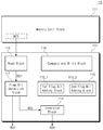
도 1은 본 발명의 실시 예에 따른 메모리 시스템(100)을 보여주는 블록도이다. 도 1을 참조하면, 메모리 시스템(100)은 불휘발성 메모리 장치(110) 및 제어기(120)를 포함한다. 불휘발성 메모리 장치(110)는 상 변화 메모리, 강유전체 메모리, 자기 메모리, 저항성 메모리 등을 포함할 수 있다.1 is a block diagram illustrating a
불휘발성 메모리 장치(110)는 전원이 차단된 때에도 데이터를 유지할 수 있다. 불휘발성 메모리 장치(110)는 메모리 시스템(100)을 포함하는 호스트 시스템 내에서 주기억 장치 또는 보조기억 장치로 사용될 수 있다.The
불휘발성 메모리 장치(110)는 제어기(120)로부터 명령(CMD) 및 주소(ADDR)를 수신할 수 있다. 불휘발성 메모리 장치(110)는 제어기(120)와 제어 신호들(CTRL)을 교환하고, 그리고 데이터(DATA)를 교환할 수 있다. 불휘발성 메모리 장치(110)는 명령(CMD) 및 제어 신호들(CTRL)에 따라, 주소(ADDR)가 가리키는 메모리 셀들을 액세스할 수 있다. 불휘발성 메모리 장치(110)는 액세스 중 읽기 동작의 결과의 데이터(DATA) 또는 액세스 중 쓰기 동작을 위한 데이터(DATA)를 제어기(120)와 교환할 수 있다.The
불휘발성 메모리 장치(110)는 메모리 셀 블록(111) 및 주변 블록(112)을 포함할 수 있다. 메모리 셀 블록(111)은 메모리 셀들(예를 들어, 불휘발성 메모리 셀들)을 포함할 수 있다. 메모리 셀들은 행들 및 열들로 배열될 수 있다. 행들 및 열들로 배열된 메모리 셀들은 다양한 사이즈의 단위들로 액세스될 수 있다. 메모리 셀들의 액세스는 셋 동작 및 리셋 동작을 포함하는 쓰기 동작, 그리고 읽기 동작을 포함할 수 있다.The
주변 블록(112)은 메모리 셀 블록(111)을 액세스하도록 구성된다. 주변 블록(112)은 읽기 블록(113), 반전 블록(114), 플래그 비트 추가 블록(115), 비교 및 쓰기 블록(116), 그리고 플래그 비트 검출 블록(117)을 포함할 수 있다.
읽기 블록(113)은 읽기 동작을 요청하는 명령(CMD)에 응답하여, 메모리 셀 블록(111)의 메모리 셀들 중 주소(ADDR)가 가리키는 선택된 메모리 셀들에 대해 읽기 동작을 수행할 수 있다. 예를 들어, 읽기 블록(113)은 선택된 메모리 셀들에 다양한 전압들, 다양한 전류들, 또는 다양한 전압들 및 전류들의 조합들을 제공함으로써, 선택된 메모리 셀들로부터 데이터를 읽을 수 있다.The
반전 블록(114)은 입력되는 데이터를 반전하여 출력하도록 구성된다. 예를 들어, 반전 블록(114)은 제어기(120)로부터 불휘발성 메모리 장치(110)로 전달되는 데이터(DATA)를 반전하거나, 또는 불휘발성 메모리 장치(110)의 내부의 데이터를 반전하여 데이터(DATA)로서 제어기(120)로 제공할 수 있다.The
플래그 비트 추가 블록(115)은 제어기(120)로부터 전송되는 데이터(DATA) 또는 반전 블록(114)에 의해 반전된 데이터에 플래그 비트 및 적어도 하나의 복제(replica) 플래그 비트를 추가할 수 있다. 예를 들어, 플래그 비트 추가 블록(115)은 반전 여부를 가리키는 하나의 플래그 비트를 추가하고, 동일한 복제 플래그 비트를 적어도 하나 더 추가할 수 있다.The flag
비교 및 쓰기 블록(116)은 쓰기 동작을 요청하는 명령(CMD)에 응답하여, 메모리 셀 블록(111)의 메모리 셀들 중 주소(ADDR)가 가리키는 선택된 메모리 셀들에 대해 비교 및 쓰기 동작을 수행할 수 있다. 비교 및 쓰기 블록(116)은 제어기(120)로부터 전송되는 데이터(DATA)로부터 둘 이상의 후보 데이터들을 생성하고, 둘 이상의 후보 데이터들을 선택된 메모리 셀들에 저장된 기존 데이터와 비교할 수 있다.The compare and write
비교 및 쓰기 블록(116)은 둘 이상의 후보 데이터들 각각을 기존 데이터와 비교할 수 있다. 비교 및 쓰기 블록(116)은 각 후보 데이터의 비트들과 기존 데이터의 비트들 중 서로 다른 비트들의 수를 카운트할 수 있다. 비교 및 쓰기 블록(116)은 카운트가 작은 후보 데이터를 선택된 메모리 셀들에 기입할 수 있다.The compare and write
예를 들어, 비교 및 쓰기 블록(116)은 카운트가 후보 데이터들 각각의 비트들의 수의 절반보다 작은 후보 데이터를 선택하고, 선택된 후보 데이터를 선택된 메모리 셀들에 기입할 수 있다. 비교 및 쓰기 블록(116)은 선택된 메모리 셀들에 다양한 전압들, 다양한 전류들, 또는 다양한 전압들 및 전류들의 조합들을 제공함으로써, 선택된 메모리 셀들에 선택된 후보 데이터를 기입할 수 있다.For example, the comparison and write
플래그 비트 검출 블록(117)은 메모리 셀 블록(111)의 선택된 메모리 셀들로부터 읽기 블록(113)에 의해 읽혀진 데이터로부터 플래그 비트 또는 플래그 비트들을 검출하고 제거할 수 있다. 플래그 비트의 값 또는 플래그 비트들의 값들에 따라, 플래그 비트 검출 블록(117)은 데이터를 반전 블록(114)으로 제공하거나 또는 제어기(120)에 제공할 수 있다.The flag
제어기(120)는 불휘발성 메모리 장치(110)가 쓰기 동작 또는 읽기 동작을 수행하도록 제어할 수 있다. 제어기(120)는 불휘발성 메모리 장치(110)에 명령(CMD) 및 주소(ADDR)를 전달할 수 있다. 제어기(120)는 불휘발성 메모리 장치(110)와 제어 신호들(CTRL)을 교환하고, 그리고 데이터(DATA)를 교환할 수 있다. 제어기(120)는 쓰기 동작, 읽기 동작 또는 검사 동작을 수행하도록 불휘발성 메모리 장치(110)를 제어할 수 있다.The
제어기(120)는 인코딩 블록(121) 및 디코딩 블록(122)을 포함할 수 있다. 인코딩 블록(121)은 제어기(120)가 쓰기 동작 시에 불휘발성 메모리 장치(110)로 전송할 데이터에 대해 에러 정정 인코딩을 수행할 수 있다. 에러 정정 인코딩을 수행함으로써, 인코딩 블록(121)은 원본 데이터에 패리티를 추가할 수 있다. 패리티는 하나 또는 그보다 많은 비트들을 포함하며, 에러 정정 기능을 제공할 수 있다. 인코딩 블록(121)에 의해 인코딩된 데이터(DATA)는 불휘발성 메모리 장치(110)로 전송될 수 있다.The
디코딩 블록(122)은 제어기(120)가 읽기 동작 시에 불휘발성 메모리 장치(110)로부터 수신한 데이터(DATA)에 대해 에러 정정 디코딩을 수행할 수 있다. 데이터(DATA)의 패리티를 이용하여 에러 정정 디코딩을 수행함으로써, 디코딩 블록(122)은 수신된 데이터(DATA)로부터 에러들을 정정하고 그리고 패리티를 제거하여, 원본 데이터를 복원할 수 있다.The
도 2는 도 1의 메모리 시스템(100)의 동작 방법의 예를 보여주는 순서도이다. 도 1 및 도 2를 참조하면, S110 단계에서, 제어기(120)는 불휘발성 메모리 장치(110)에 제1 명령(CMD1), 제1 주소(ADDR1) 및 제1 데이터(DATA1)를 전송할 수 있다. 예를 들어, 제1 명령(CMD1)은 쓰기 명령일 수 있다. 제1 데이터(DATA1)는 불휘발성 메모리 장치(110)에 기입될 데이터일 수 있다.2 is a flowchart illustrating an example of an operating method of the
제1 명령(CMD1)에 응답하여, 불휘발성 메모리 장치(110)는 비교 및 쓰기 동작을 수행할 수 있다. 비교 및 쓰기 동작은 S115 단계 내지 S140 단계를 통해 수행될 수 있다.In response to the first command CMD1, the
비교 및 쓰기 동작의 S115 단계에서, 불휘발성 메모리 장치(110)는 메모리 셀 블록(111)의 메모리 셀들 중에서 제1 주소(ADDR1)에 의해 선택된 메모리 셀들에 저장된 데이터, 예를 들어 기존 데이터를 읽을 수 있다.In step S115 of the comparison and write operation, the
비교 및 쓰기 동작의 S120 단계에서, 불휘발성 메모리 장치(110)는 제1 데이터(DATA1)를 반전할 수 있다. 또한, 불휘발성 메모리 장치(110)는 제1 데이터(DATA1) 및 반전 데이터에 각각 플래그 비트들을 추가할 수 있다. 제1 데이터(DATA1)에 비반전을 가리키는 제1 플래그 비트(예를 들어, '1' 또는 '0')가 추가될 수 있다. 반전 데이터에 반전을 가리키는 제2 플래그 비트(예를 들어, '0' 또는 '1')가 추가될 수 있다.In step S120 of the comparison and write operation, the
비교 및 쓰기 동작의 S125 단계에서, 불휘발성 메모리 장치(110)는 복제(replica) 플래그 비트를 추가할 수 있다. 예를 들어, 불휘발성 메모리 장치(110)는 제1 데이터(DATA1)에 비반전을 가리키는 제1 플래그 비트와 동일한 적어도 하나의 제1 복제 플래그 비트를 추가할 수 있다. 또한, 불휘발성 메모리 장치(110)는 반전 데이터에 반전을 가리키는 제2 플래그 비트와 동일한 적어도 하나의 제2 복제 플래그 비트를 추가할 수 있다.In step S125 of the comparison and write operation, the
복제 플래그 비트의 추가는 플래그 비트의 신뢰성을 높이며, 또한 제1 데이터(DATA1)를 불휘발성 메모리 장치(110)에 기입하고 읽는 동안 제1 데이터(DATA1)무결성을 강화(reinforcement)할 수 있다.The addition of the replication flag bit increases the reliability of the flag bit, and also enhances the integrity of the first data DATA1 while writing and reading the first data DATA1 to the
제1 데이터(DATA1)에 제1 플래그 비트 및 적어도 하나의 제1 복제 플래그 비트가 추가되어 제1 후보 데이터가 생성될 수 있다. 반전 데이터에 제2 플래그 비트 및 적어도 하나의 제2 복제 플래그 비트가 추가되어 제2 후보 데이터가 생성될 수 있다.First candidate data may be generated by adding a first flag bit and at least one first replication flag bit to the first data DATA1. The second candidate data may be generated by adding a second flag bit and at least one second replication flag bit to the inverted data.
비교 및 쓰기 동작의 S130 단계에서, 불휘발성 메모리 장치(110)는 기존 데이터를 제1 후보 데이터 및 제2 후보 데이터와 각각 비교할 수 있다. 예를 들어, 불휘발성 메모리 장치(110)는 기존 데이터의 비트들과 제1 후보 데이터의 비트들 중 서로 다른 비트들의 개수, 즉 제1 해밍 거리를 계산할 수 있다. 또한, 불휘발성 메모리 장치(110)는 기존 데이터의 비트들과 제2 후보 데이터의 비트들 중 서로 다른 비트들의 개수, 즉 제2 해밍 거리를 계산할 수 있다.In step S130 of the comparison and write operation, the
비교 및 쓰기 동작의 S135 단계에서, 불휘발성 메모리 장치(110)는 비교의 결과에 따라 제1 및 제2 후보 데이터들 중 하나를 선택할 수 있다. 예를 들어, 불휘발성 메모리 장치(110)는 기존 데이터와 더 적은 해밍 거리를 갖는 후보 데이터를 선택할 수 있다. 비교 및 쓰기 동작의 S140 단계에서, 불휘발성 메모리 장치(110)는 선택된 후보 데이터를 제1 주소(ADDR1)에 의해 선택된 메모리 셀들에 기입할 수 있다.In step S135 of the comparison and write operation, the
비교 및 쓰기 동작에 따르면, 제1 데이터(DATA1)로부터 생성된 제1 및 제2 후보 데이터들 중에서 기존 데이터와의 차이(예를 들어, 해밍 거리)가 더 적은 후보 데이터가 불휘발성 메모리 장치에 기입될 수 있다. 따라서, 기존 데이터가 저장된 메모리 셀들에 필요한 셋 동작들의 수 또는 리셋 동작의 수가 감소하고, 쓰기 동작의 전력 소비가 절감된다.According to the comparison and write operation, among the first and second candidate data generated from the first data DATA1, candidate data with less difference (eg, Hamming distance) from existing data is written to the nonvolatile memory device Can be. Accordingly, the number of set operations or the number of reset operations required for memory cells in which existing data is stored is reduced, and the power consumption of the write operation is reduced.
S145 단계에서, 제어기(120)는 불휘발성 메모리 장치(110)에 제2 명령(CMD2) 및 제2 주소(ADDR2)를 전송할 수 있다. 예를 들어, 제2 명령(CMD2)은 읽기 명령일 수 있다.In step S145, the
제2 명령(CMD2)에 응답하여, 불휘발성 메모리 장치(110)는 읽기 동작을 수행할 수 있다. 읽기 동작은 S150 단계 내지 S160 단계를 통해 수행될 수 있다. 읽기 동작의 S150 단계에서, 불휘발성 메모리 장치(110)는 제2 주소(ADDR2)에 의해 선택된 메모리 셀들로부터 데이터를 읽을 수 있다.In response to the second command CMD2, the
읽기 동작의 S155 단계에서, 불휘발성 메모리 장치(110)는 읽혀진 데이터로부터 플래그 비트 및 적어도 하나의 복제 플래그 비트를 검출할 수 있다. 플래그 비트 및 적어도 하나의 복제 플래그 비트에 기반하여, 불휘발성 메모리 장치(110)는 읽혀진 데이터 또는 읽혀진 데이터의 반전 데이터 중 하나의 데이터를 선택할 수 있다.In step S155 of the read operation, the
읽기 동작의 S160 단계에서, 불휘발성 메모리 장치(110)는 선택된 데이터로부터 플래그 비트 및 적어도 하나의 복제 플래그 비트를 제거하여 제2 데이터(DATA2)로서 제어기(120)로 전송할 수 있다.In step S160 of the read operation, the
상술된 바와 같이, 본 발명의 실시 예에 따른 불휘발성 메모리 장치(110) 또는 메모리 시스템(100)은 비교 및 쓰기 동작을 수행함으로써 전력 소비를 절감할 수 있다. 또한, 본 발명의 실시 예에 따른 메모리 시스템(100) 또는 불휘발성 메모리 장치(110)는 복제 플래그 비트를 추가함으로써, 플래그 비트 및 원본 데이터의 무결성을 강화할 수 있다.As described above, the
도 3은 도 1의 불휘발성 메모리 장치(110)가 제어기(120)로부터 전송된 제1 쓰기 데이터(WD1)를 기입하는 비교 및 쓰기 동작을 수행하는 과정의 예를 보여준다. 도 1 내지 도 3을 참조하면, 도 2의 S110 단계의 제1 데이터(DATA1)로서, 제1 쓰기 데이터(WD1)가 불휘발성 메모리 장치(110)에 입력될 수 있다.FIG. 3 shows an example of a process in which the
도 2의 S115 단계에 따라, 읽기 블록(113)은 메모리 셀 블록(111)의 선택됨 메모리 셀들(MCS)로부터 제1 읽기 데이터(RD1)를 읽을 수 있다. 제1 읽기 데이터(RD1)는 플래그 비트 검출 블록(117)을 거치지 않고 비교 및 쓰기 블록(116)에 제공될 수 있다.According to step S115 of FIG. 2, the
도 2의 S120 단계 및 S125 단계에 따라, 제1 쓰기 데이터(WD1)는 반전 블록(114) 및 플래그 비트 추가 블록(115)에 전달될 수 있다. 반전 블록(114)은 제1 쓰기 데이터(WD1)를 반전하여 제2 쓰기 데이터(WD2)를 생성할 수 있다. 제2 쓰기 데이터(WD2)는 플래그 비트 추가 블록(115)에 전달된다.According to steps S120 and S125 of FIG. 2, the first write data WD1 may be transferred to the
플래그 비트 추가 블록(115)은 제1 플래그 비트 추가 블록(115_1) 및 제2 플래그 비트 추가 블록(115_2)을 포함한다. 제1 플래그 비트 추가 블록(115_1)은 반전 블록(114)으로부터 제2 쓰기 데이터(WD2)를 수신할 수 있다. 제1 플래그 비트 추가 블록(115_1)은 제2 쓰기 데이터(WD2)에 플래그 비트들을 추가하여 제3 쓰기 데이터(WD3)를 생성할 수 있다.The flag
예를 들어, 제1 플래그 비트 추가 블록(115_1)은 반전을 나타내는 플래그 비트(예를 들어, '1' 또는 '0')를 제2 쓰기 데이터(WD2)에 추가할 수 있다. 또한, 제1 플래그 비트 추가 블록(115_1)은 적어도 하나의 동일한 플래그 비트(예를 들어, 복제 비트(replica bit))를 제2 쓰기 데이터(WD2)에 더 추가할 수 있다. 제3 쓰기 데이터(WD3)는 예를 들어 '111' 또는 '000'과 같은 플래그 비트들을 포함할 수 있다. 제3 쓰기 데이터(WD3)에서 플래그 비트들은 연속하여 배치되거나 또는 분산되어 배치될 수 있다.For example, the first flag bit adding block 115_1 may add a flag bit indicating inversion (eg, '1' or '0') to the second write data WD2. Also, the first flag bit addition block 115_1 may further add at least one identical flag bit (eg, a replica bit) to the second write data WD2. The third write data WD3 may include flag bits such as '111' or '000', for example. In the third write data WD3, the flag bits may be continuously arranged or distributed.
제2 플래그 비트 추가 블록(115_2)은 제1 쓰기 데이터(WD1)를 수신할 수 있다. 제2 플래그 비트 추가 블록(115_2)은 제1 쓰기 데이터(WD1)에 플래그 비트들을 추가하여 제4 쓰기 데이터(WD4)를 생성할 수 있다.The second flag bit addition block 115_2 may receive the first write data WD1. The second flag bit adding block 115_2 may generate fourth write data WD4 by adding flag bits to the first write data WD1.
예를 들어, 제2 플래그 비트 추가 블록(115_2)은 원본을 나타내는 플래그 비트(예를 들어, '0' 또는 '1')를 제1 쓰기 데이터(WD1)에 추가할 수 있다. 또한, 제2 플래그 비트 추가 블록(115_2)은 적어도 하나의 동일한 플래그 비트(예를 들어, 복제 비트(replica bit))를 제1 쓰기 데이터(WD1)에 더 추가할 수 있다. 제4 쓰기 데이터(WD4)는 예를 들어 '000' 또는 '111'과 같은 플래그 비트들을 포함할 수 있다. 제4 쓰기 데이터(WD4)에서 플래그 비트들은 연속하여 배치되거나 또는 분산되어 배치될 수 있다.For example, the second flag bit adding block 115_2 may add a flag bit (eg, '0' or '1') indicating the original to the first write data WD1. Also, the second flag bit adding block 115_2 may further add at least one identical flag bit (eg, a replica bit) to the first write data WD1. The fourth write data WD4 may include flag bits such as '000' or '111', for example. In the fourth write data WD4, the flag bits may be continuously arranged or distributed.
플래그 비트 추가 블록(115)은 제3 쓰기 데이터(WD3) 및 제4 쓰기 데이터(WD4)를 생성할 수 있다. 제3 쓰기 데이터(WD3) 및 제4 쓰기 데이터(WD4)는 메모리 셀 블록(111)에 기입될 수 있는 후보 데이터들일 수 있다. 제3 쓰기 데이터(WD3) 및 제4 쓰기 데이터(WD4)는 비교 및 쓰기 블록(116)에 제공된다.The flag
도 2의 S130 단계에 따라, 비교 및 쓰기 블록(116)은 제3 쓰기 데이터(WD3)와 제1 읽기 데이터(RD1)를 비교할 수 있다. 제3 쓰기 데이터(WD3) 및 제1 읽기 데이터(RD1)의 각각은 비트들의 시퀀스를 포함한다. 비트들의 시퀀스 상의 특정한 위치에서, 제3 쓰기 데이터(WD3)의 비트와 제1 읽기 데이터(RD1)의 비트가 동일하면, 제3 쓰기 데이터(WD3)를 기입할 때에 특정한 위치에 대응하는 메모리 셀에 대한 셋 동작 또는 리셋 동작은 불필요하다.According to step S130 of FIG. 2, the comparison and write
비트들의 시퀀스 상의 특정한 위치에서, 제3 쓰기 데이터(WD3)의 비트와 제1 읽기 데이터(RD1)의 비트가 동일하지 않으면, 제3 쓰기 데이터(WD3)를 기입할 때에 특정한 위치에 대응하는 메모리 셀에 대한 셋 동작 또는 리셋 동작이 필요하다.If the bit of the third write data WD3 and the bit of the first read data RD1 are not the same at a specific position on the sequence of bits, the memory cell corresponding to the specific position when writing the third write data WD3 A set operation or reset operation is required.
메모리 시스템(100) 또는 불휘발성 메모리 장치(110)는 셋 동작 또는 리셋 동작이 필요한 메모리 셀들의 수를 줄임으로써, 쓰기 동작 시의 소비 전력을 줄일 수 있다. 비교 및 쓰기 블록(116)은 제1 읽기 데이터(RD1) 및 제3 쓰기 데이터(WD3) 사이에서, 셋 동작 또는 리셋 동작이 필요한 위치들의 개수를 제1 차이(예를 들어, 제1 해밍 거리)로 검출할 수 있다.The
마찬가지로, 비교 및 쓰기 블록(116)은 제4 쓰기 데이터(WD4)와 제1 읽기 데이터(RD1)를 비교할 수 있다. 비교 및 쓰기 블록(116)은 제1 읽기 데이터(RD1)와 제4 쓰기 데이터(WD4) 사이에서, 셋 동작 또는 리셋 동작이 필요한 위치들의 개수를 제2 차이(예를 들어, 제2 해밍 거리)로 검출할 수 있다.Similarly, the comparison and write
도 2의 S135 단계에 따라, 제1 차이 및 제2 차이에 기반하여, 비교 및 쓰기 블록(116)은 제3 및 제4 쓰기 데이터들(WD3, WD4) 중에서 제1 읽기 데이터(RD1)와의 차이가 더 적은 쓰기 데이터를 제5 쓰기 데이터(WD5)로 선택할 수 있다.According to step S135 of FIG. 2, based on the first difference and the second difference, the comparison and write
도 2의 S140 단계에 따라, 비교 및 쓰기 블록(116)은 제5 쓰기 데이터(WD5)를 선택된 메모리 셀들(MCS)에 기입할 수 있다. 따라서, 선택된 메모리 셀들(MCS)에 데이터를 기입할 때의 소비 전력이 절감된다.According to step S140 of FIG. 2, the comparison and write
도 4는 본 발명의 실시 예에 따른 불휘발성 메모리 장치(110)가 데이터를 읽는 읽기 동작을 수행하는 과정의 예를 보여준다. 도 1, 도 2 및 도 4를 참조하면, 도 2의 S150 단계에 따라, 읽기 블록(113)은 선택된 메모리 셀들(MCS)로부터 제2 읽기 데이터(RD2)를 읽을 수 있다. 제2 읽기 데이터(RD2)는 플래그 비트 검출 블록(117)으로 전달된다.4 shows an example of a process in which the
도 2의 S155 단계 및 S160에 따라, 플래그 비트 검출 블록(117)은 제2 읽기 데이터(RD2)로부터 플래그 비트 및 적어도 하나의 복제 플래그 비트를 검출할 수 있다. 이하에서, 읽기 동작 시에 읽혀진 데이터의 플래그 비트 및 적어도 하나의 복제 플래그 비트는 '플래그 비트들'로 통칭될 수 있다.According to steps S155 and S160 of FIG. 2, the flag
플래그 비트 검출 블록(117)은 제2 읽기 데이터(RD2)로부터 플래그 비트들을 제거하여 제3 읽기 데이터(RD3)를 생성할 수 있다. 플래그 비트 검출 블록(117)은 플래그 비트들에 따라 제3 읽기 데이터(RD3)를 그대로 출력하거나 또는 반전 블록(114)에 전달할 수 있다.The flag
예를 들어, 플래그 비트 검출 블록(117)은 플래그 비트들에 기반하여 투표(voting)를 수행할 수 있다. 원본을 가리키는 플래그 비트들의 수가 반전을 가리키는 플래그 비트들의 수보다 많을 때, 불휘발성 메모리 장치(110)는 제3 읽기 데이터(RD3)를 그대로 출력할 수 있다.For example, the flag
원본을 가리키는 플래그 비트들의 수가 반전을 가리키는 플래그 비트들의 수보다 적을 때, 플래그 비트 검출 블록(117)은 제3 읽기 데이터(RD3)를 반전 블록(114)에 전달할 수 있다. 반전 블록(114)은 제3 읽기 데이터를 반전하여 제4 읽기 데이터(RD4)를 생성할 수 있다. 불휘발성 메모리 장치(110)는 제4 읽기 데이터(RD4)를 읽기 동작의 결과로 선택하여 출력할 수 있다.When the number of flag bits indicating the original is less than the number of flag bits indicating the inversion, the flag
다른 예로서, 플래그 비트 검출 블록(117)은 플래그 비트들에 기반하여 만장일치의(unanimous) 판단을 수행할 수 있다. 모든 플래그 비트들이 원본을 가리킬 때, 불휘발성 메모리 장치(110)는 제3 읽기 데이터(RD3)를 선택하여 출력할 수 있다.As another example, the flag
모든 플래그 비트들이 반전을 가리킬 때, 플래그 비트 검출 블록(117)은 제3 읽기 데이터(RD3)를 반전 블록(114)에 전달할 수 있다. 불휘발성 메모리 장치(110)는 반전 블록(114)으로부터 출력되는 제4 읽기 데이터(RD4)를 선택하여 출력할 수 있다.When all the flag bits indicate inversion, the flag
일부 플래그 비트들이 원본을 가리키고 그리고 나머지 플래그 비트들이 반전을 가리킬 때, 플래그 비트 검출 블록(117)은 제3 읽기 데이터(RD3)를 반전 블록(114)에 전달할 수 있다. 불휘발성 메모리 장치(110)는 제3 읽기 데이터(RD3) 및 제4 읽기 데이터(RD4)를 모두 선택하여 순차적으로 출력할 수 있다.When some of the flag bits indicate the original and the remaining flag bits indicate an inversion, the flag
상술된 바와 같이, 본 발명의 실시 예에 따른 메모리 시스템(100)은 플래그 비트에 복제 비트들을 추가함으로써, 메모리 셀 블록(111)으로부터 읽혀지는 데이터의 무결성을 강화할 수 있다.As described above, the
도 1 내지 도 4에서, 인코딩 블록(121) 및 디코딩 블록(122)은 제어기(120)에 배치되는 것으로 설명되었다. 그러나 인코딩 블록(121) 및 디코딩 블록(122)은 불휘발성 메모리 장치(110)에 배치될 수도 있다.1 to 4, it has been described that the
도 5는 본 발명의 수정 예에 따른 메모리 시스템(100a)을 보여주는 블록도이다. 도 5를 참조하면, 메모리 시스템(100a)은 불휘발성 메모리 장치(110a) 및 제어기(120a)를 포함한다.5 is a block diagram showing a
도 1 내지 도 4를 참조하여 설명된 바와 같이, 불휘발성 메모리 장치(110a)는 제어기(120a)와 명령(CMD), 주소(ADDR), 제어 신호들(CTRL), 그리고 데이터(DATA)를 교환할 수 있다. 불휘발성 메모리 장치(110a)는 메모리 셀 블록(111) 및 주변 블록(112a)을 포함할 수 있다. 메모리 셀 블록(111)은 도 1 내지 도 4를 참조하여 설명된 것과 동일하게 구성되고 동일하게 동작할 수 있다.As described with reference to FIGS. 1 to 4, the
주변 블록(112a)은 읽기 블록(113) 및 쓰기 블록(118)을 포함할 수 있다. 읽기 블록(113)은 도 1 내지 도 4를 참조하여 설명된 바와 같이, 메모리 셀 블록(111)의 선택된 메모리 셀들로부터 데이터를 읽는 읽기 동작을 수행할 수 있다. 읽기 블록(113)은 읽혀진 데이터를 데이터(DATA)로서 제어기(120a)로 제공할 수 있다.The
쓰기 블록(118)은 제어기(120a)로부터 전달되는 데이터(DATA)를 메모리 셀 블록(111)의 선택된 메모리 셀들에 데이터를 기입하는 쓰기 동작을 수행할 수 있다. 도 1 내지 도 4를 참조하여 설명된 것과 달리, 불휘발성 메모리 장치(110a)는 쓰기 명령에 따라 비교 및 쓰기 동작을 수행하지 않고, 쓰기 명령에 따라 쓰기 동작만을 수행할 수 있다. 비교 및 쓰기 동작은 제어기(120)에 의해 수행될 수 있다.The
제어기(120a)는 불휘발성 메모리 장치(110)와 명령(CMD), 주소(ADDR), 제어 신호들(CTRL) 및 데이터(DATA)를 교환할 수 있다. 제어기(120a)는 불휘발성 메모리 장치가 쓰기 동작 또는 읽기 동작을 수행하도록 제어할 수 있다. 제어기(120a)는 도 1 내지 도 4를 참조하여 설명된 것과 유사하게 불휘발성 메모리 장치(110a)에 대해 비교 및 쓰기 동작을 수행할 수 있다. 비교 및 쓰기 동작을 수행함으로써, 제어기(120a)는 쓰기 동작 시의 전력 소비를 줄일 수 있다.The
제어기(120a)는 인코딩 블록(121), 디코딩 블록(122), 비교 블록(123), 반전 블록(124), 플래그 비트 추가 블록(125), 그리고 플래그 비트 검출 블록(126)을 포함할 수 있다.The
인코딩 블록(121)은 제1 데이터에 대해 에러 정정 인코딩을 수행할 수 있다. 예를 들어, 인코딩 블록(121)은 원본 데이터(또는 입력 데이터)에 에러 정정을 위한 패리티를 추가하여 제2 데이터를 생성할 수 있다.The
디코딩 블록(122)은 에러가 존재할 수 있는 제2 데이터에 대해 에러 정정 디코딩을 수행할 수 있다. 예를 들어, 디코딩 블록(122)은 제2 데이터에 존재하는 에러(또는 에러들)를 정정하고 패리티를 제거하여 제1 데이터를 복원할 수 있다.The
인코딩 블록(121) 및 디코딩 블록(122)은 서로 짝지워질(paired) 수 있다. 인코딩 블록(121) 및 디코딩 블록(122)은 동일한 에러 정정 알고리즘에 기반하여 각각 인코딩 및 디코딩을 수행할 수 있다.The
비교 블록(123)은 도 1 내지 도 4를 참조하여 설명된 비교 및 쓰기 블록(116)과 유사하게, 기존 데이터와 후보 데이터들을 비교할 수 있다. 비교 블록(123)은 비교 결과에 따라, 후보 데이터들 중 쓰기 동작의 전력 소비를 더 절감하는 후보 데이터를 선택할 수 있다.The
반전 블록(124)은 불휘발성 메모리 장치(110a)에 기입될 데이터를 반전할 수 있다. 예를 들어, 반전 블록(124)은 제어기(120a) 내에서 불휘발성 메모리 장치(110a)에 기입될 데이터가 가공되는 다양한 단계들 중 하나에서 해당 데이터를 반전할 수 있다. 반전 블록(124)에 의해, 불휘발성 메모리 장치(110a)에 기입될 둘 이상의 후보 데이터들이 생성될 수 있다.The
플래그 비트 추가 블록(125)은 도 1 내지 도 4를 참조하여 설명된 플래그 비트 추가 블록(115)과 유사하게, 반전 블록(124)에 의해 반전된 데이터 및 반전 블록(124)에 의해 반전되지 않은 데이터의 각각에 플래그 비트 및 적어도 하나의 복제 플래그 비트를 추가할 수 있다. 예를 들어, 플래그 비트 추가 블록(125)은 제어기(120a) 내에서 불휘발성 메모리 장치(110a)에 기입될 데이터가 가공되는 다양한 단계들 중 하나에서 플래그 비트들을 추가할 수 있다.The flag
플래그 비트 검출 블록(126)은 도 1 내지 도 4를 참조하여 설명된 플래그 비트 검출 블록(117)과 유사하게, 불휘발성 메모리 장치(110a)로부터 전달되는 데이터(DATA)로부터 플래그 비트들을 검출할 수 있다. 예를 들어, 플래그 비트 검출 블록(126)은 제어기(120a) 내에서 불휘발성 메모리 장치(110a)로부터 수신된 데이터(DATA)가 가공되는 다양한 단계들 중 하나에서 플래그 비트들을 검출할 수 있다.The flag
예시적으로, 제어기(120a) 내에 제공되는 인코딩 블록(121), 디코딩 블록(122), 비교 블록(123), 반전 블록(124), 플래그 비트 추가 블록(125), 그리고 플래그 비트 검출 블록(126)이 불휘발성 메모리 장치(110a)로 전송될 데이터(DATA) 또는 불휘발성 메모리 장치(110a)로부터 수신된 데이터(DATA)를 처리하는 순서 및 방법은 다양하게 조직화될 수 있으며, 다양하게 수정될 수 있다.Exemplarily, the
도 6은 도 5의 메모리 시스템(100a)의 동작 방법의 예를 보여주는 순서도이다. 도 5 및 도 6을 참조하면, 불휘발성 메모리 장치(110a)에 데이터를 기입할 때, 제어기(120a)는 비교 및 쓰기 동작을 수행할 수 있다. 비교 및 쓰기 동작은 S210 단계 내지 S245 단계를 통해 수행될 수 있다.6 is a flowchart illustrating an example of an operating method of the
비교 및 쓰기 동작의 S210 단계에서, 제어기(120a)는 제3 명령(CMD3) 및 제3 주소(ADDR3)를 불휘발성 메모리 장치(110a)로 전송할 수 있다. 제3 명령(CMD3)은 읽기 명령이며, 비교를 위해 전송될 수 있다. 제3 주소(ADDR3)는 불휘발성 메모리 장치(110a)의 메모리 셀들 중에서 데이터가 기입될 메모리 셀들(예를 들어, 선택된 메모리 셀들)을 가리킬 수 있다.In step S210 of the comparison and write operation, the
비교 및 쓰기 동작의 S215 단계에서, 불휘발성 메모리 장치(110a)는 제3 명령(CMD3) 및 제3 주소(ADDR3)에 응답하여 읽기 동작을 수행하고, 읽기 동작을 통해 읽혀진 제3 데이터(DATA3)를 제어기(120a)로 전송할 수 있다.In step S215 of the comparison and write operation, the
비교 및 쓰기 동작의 S220 단계에서, 제어기(120a)는 불휘발성 메모리 장치(110a)에 기입될 원본 데이터에 대해 에러 정정 인코딩을 수행할 수 있다. 비교 및 쓰기 동작의 S225 단계에서, 제어기(120a)는 인코딩된 데이터를 반전할 수 있다.In step S220 of the comparison and write operation, the
또한, 제어기(120a)는 인코딩된 데이터 및 반전 데이터에 각각 플래그 비트들을 추가할 수 있다. 인코딩된 데이터)에 비반전을 가리키는 제1 플래그 비트(예를 들어, '1' 또는 '0')가 추가될 수 있다. 반전 데이터에 반전을 가리키는 제2 플래그 비트(예를 들어, '0' 또는 '1')가 추가될 수 있다.In addition, the
비교 및 쓰기 동작의 S230 단계에서, 불휘발성 메모리 장치(110)는 복제(replica) 플래그 비트를 추가할 수 있다. 도 2의 S125 단계를 참조하여 설명된 바와 같이, 제어기(120a)는 인코딩된 데이터 및 반전 데이터에 각각 복제 플래그 비트들을 추가하여 제1 및 제2 후보 데이터들을 생성할 수 있다.In step S230 of the comparison and write operation, the
비교 및 쓰기 동작의 S235 단계에서, 제어기(120a)는 불휘발성 메모리 장치(110a)로부터 읽혀진 제3 데이터(DATA3), 즉 기존 데이터를 제1 후보 데이터 및 제2 후보 데이터와 각각 비교할 수 있다. 예를 들어, 도 2의 S130 단계와 마찬가지로, 제어기(120a)는 제3 데이터(DATA3)와 제1 및 제2 후보 데이터들 사이의 제1 및 제2 해밍 거리들을 각각 계산할 수 있다.In step S235 of the comparison and write operation, the
비교 및 쓰기 동작의 S240 단계에서, 제어기(120a)는 비교의 결과에 따라 제1 및 제2 후보 데이터들 중 하나를 선택할 수 있다. 예를 들어, 제어기(120a)는 기존 데이터와 더 적은 해밍 거리를 갖는 후보 데이터를 선택할 수 있다.In step S240 of the compare and write operation, the
비교 및 쓰기 동작의 S245 단계에서, 제어기(120a)는 제4 명령(CMD4), 제4 주소(ADDR4) 및 선택된 후보 데이터를 제4 데이터(DATA4)로서 불휘발성 메모리 장치(110a)에 전송할 수 있다.In step S245 of the comparison and write operation, the
제4 명령(CMD4)은 쓰기 명령일 수 있다. 제4 주소(ADDR4)는 제3 주소(ADDR3)와 마찬가지로 불휘발성 메모리 장치(110a)의 동일한 선택된 메모리 셀들을 가리킬 수 있다. 제4 명령(CMD4) 및 제4 주소(ADDR4)에 응답하여, 불휘발성 메모리 장치(110a)는 수신된 제4 데이터(DATA4)를 선택된 메모리 셀들에 기입할 수 있다.The fourth command CMD4 may be a write command. The fourth address ADDR4 may point to the same selected memory cells of the
불휘발성 메모리 장치(110a)로부터 데이터를 읽을 때, 제어기(120a)는 읽기 동작을 수행할 수 있다. 읽기 동작은 S250 단계 내지 S265 단계를 통해 수행될 수 있다.When reading data from the
읽기 동작의 S250 단계에서, 제어기(120a)는 불휘발성 메모리 장치(110a)에 제5 명령(CMD5) 및 제5 주소(ADDR5)를 전송할 수 있다. 예를 들어, 제5 명령(CMD5)은 읽기 명령일 수 있다. 제5 주소(ADDR5)는 불휘발성 메모리 장치(110a) 내의 선택된 메모리 셀들을 가리킬 수 있다. 제5 주소(ADDR5)는 제3 주소(ADDR3) 및 제4 주소(ADDR4)와 같거나 다를 수 있다In step S250 of the read operation, the
읽기 동작의 S255 단계에서, 제5 명령(CMD5) 및 제5 주소(ADDR5)에 응답하여, 불휘발성 메모리 장치(110a)는 선택된 메모리 셀들로부터 데이터를 읽고, 읽혀진 데이터를 제5 데이터(DATA5)로서 제어기(120a)로 전송할 수 있다.In step S255 of the read operation, in response to the fifth command CMD5 and the fifth address ADDR5, the
읽기 동작의 S260 단계에서, 제어기(120a)는 제5 데이터(DATA5)로부터 플래그 비트 및 적어도 하나의 복제 플래그 비트를 검출할 수 있다. 플래그 비트 및 적어도 하나의 복제 플래그 비트에 기반하여, 제어기(120a)는 제6 데이터(DATA6) 또는 제6 데이터(DATA6)의 반전 데이터 중 하나를 선택할 수 있다.In step S260 of the read operation, the
읽기 동작의 S265 단계에서, 제어기(120a)는 선택된 데이터로부터 플래그 비트 및 적어도 하나의 복제 플래그 비트를 제거하고, 에러 정정 디코딩을 수행할 수 있다. 제어기(120a)는 디코딩된 데이터를 읽기 동작의 결과로 획득할 수 있다.In step S265 of the read operation, the
도 7은 도 5의 제어기(120a)가 데이터를 불휘발성 메모리 장치(110a)에 기입하는 비교 및 쓰기 동작을 수행하는 과정의 예를 보여준다. 도 5 내지 도 7을 참조하면, 도 6의 S210 단계 및 S215 단계를 참조하여 설명된 바와 같이, 제어기(120a)는 불휘발성 메모리 장치(110a)로부터 제3 데이터(DATA3)로서 제5 읽기 데이터(RD5)를 수신할 수 있다. 제5 읽기 데이터(RD5)는 비교 블록(123)에 전달될 수 있다.7 shows an example of a process in which the
도 6의 S220 단계를 참조하여 설명된 바와 같이, 인코딩 블록(121)은 제6 쓰기 데이터(WD6)에 대해 에러 정정 인코딩을 수행하여 제7 쓰기 데이터(WD7)를 생성할 수 있다. 제7 쓰기 데이터(WD7)는 제6 쓰기 데이터(WD6) 및 에러 정정을 위한 패리티를 포함할 수 있다.As described with reference to step S220 of FIG. 6, the
도 6의 S225 단계 및 S230 단계를 참조하여 설명된 바와 같이, 반전 블록(124)은 제7 쓰기 데이터(WD7)를 반전하여 제8 쓰기 데이터(WD8)를 생성할 수 있다. 플래그 비트 추가 블록(125)은 제1 플래그 비트 추가 블록(125_1) 및 제2 플래그 비트 추가 블록(125_2)을 포함할 수 있다.As described with reference to steps S225 and S230 of FIG. 6, the
제1 플래그 비트 추가 블록(125_1)은 제8 쓰기 데이터에 반전을 나타내는 플래그 비트 및 적어도 하나의 동일한 복제 플래그 비트를 추가하여 제9 쓰기 데이터(WD9)를 생성할 수 있다. 제2 플래그 비트 추가 블록(125_2)은 제7 쓰기 데이터(WD7)에 비반전을 나타내는 플래그 비트 및 적어도 하나의 동일한 복제 플래그 비트를 추가하여 제10 쓰기 데이터(WD10)를 생성할 수 있다.The first flag bit adding block 125_1 may generate the ninth write data WD9 by adding a flag bit indicating inversion to the eighth write data and at least one identical duplicate flag bit. The second flag bit addition block 125_2 may generate the tenth write data WD10 by adding a flag bit indicating non-inversion and at least one identical duplicate flag bit to the seventh write data WD7.
제9 쓰기 데이터 및 제10 쓰기 데이터는 S230 단계에서 언급된 제1 후보 데이터 및 제2 후보 데이터에 각각 대응할 수 있다. 도 6의 S235 단계를 참조하여 설명된 바와 같이, 비교 블록(123)은 제5 읽기 데이터(RD5)를 제9 쓰기 데이터(WD9) 및 제10 쓰기 데이터(WD10)와 각각 비교할 수 있다. 예를 들어, 비교 블록(123)은 제9 및 제10 쓰기 데이터들(WD9, WD10)의 제5 읽기 데이터(RD5)에 대한 해밍 거리들을 계산할 수 있다.The ninth write data and the tenth write data may respectively correspond to the first candidate data and the second candidate data mentioned in step S230. As described with reference to step S235 of FIG. 6, the
도 6의 S240 단계를 참조하여 설명된 바와 같이, 비교 및 쓰기 블록(116)은 제5 읽기 데이터(RD5)와 제9 쓰기 데이터(WD9) 사이의 제3 차이, 그리고 제5 읽기 데이터(RD5)와 제10 쓰기 데이터(WD10) 사이의 제4 차이에 기반하여, 제9 및 제10 쓰기 데이터들(WD9, WD10) 중 하나를 선택할 수 있다.As described with reference to step S240 of FIG. 6, the comparison and writing
도 6의 S245 단계를 참조하여 설명된 바와 같이, 비교 블록(123)에 의해 선택된 데이터는 제11 쓰기 데이터(WD11)일 수 있다. 제어기(120a)는 제11 쓰기 데이터(WD11)를 제4 데이터(DATA4)로서 불휘발성 메모리 장치(110a)로 전송할 수 있다.As described with reference to step S245 of FIG. 6, the data selected by the
도 8은 도 5의 제어기(120a)가 불휘발성 메모리 장치(110a)로부터 데이터를 읽는 읽기 동작을 수행하는 과정의 예를 보여준다. 도 5, 도 6 및 도 8을 참조하면, 도 6의 S250 단계 및 S255 단계를 참조하여 설명된 바와 같이, 제어기(120a)는 불휘발성 메모리 장치(110a)로부터 제5 데이터(DATA5)로서 제6 읽기 데이터(RD6)를 수신할 수 있다. 제6 읽기 데이터(RD6)는 플래그 비트 검출 블록(126)에 전달될 수 있다.8 shows an example of a process in which the
도 6의 S260 단계 및 S265 단계를 참조하여 설명된 바와 같이, 플래그 비트 검출 블록(126)은 제6 읽기 데이터(RD6)로부터 플래그 비트 및 적어도 하나의 복제 플래그 비트(즉, 플래그 비트들)를 검출할 수 있다. 플래그 비트 검출 블록(126)은 제6 읽기 데이터(RD6)로부터 플래그 비트들을 검출하여 제7 읽기 데이터(RD7)를 생성할 수 있다.As described with reference to steps S260 and S265 of FIG. 6, the flag
플래그 비트 검출 블록(126)은 플래그 비트들에 따라 제7 읽기 데이터(RD7)를 디코딩 블록(122)에 전달하거나 또는 반전 블록(124)에 전달할 수 있다. 예를 들어, 플래그 비트 검출 블록(126)은 플래그 비트들에 기반하여 투표(voting)를 수행할 수 있다. 플래그 비트 검출 블록(126)은 플래그 비트들이 가리키는 대세적인 상태, 예를 들어 비반전 상태 또는 반전 상태에 따라 제7 읽기 데이터(RD7)를 디코딩 블록(122) 또는 반전 블록(124)으로 전달할 수 있다.The flag
다른 예로서, 플래그 비트 검출 블록(126)은 만장일치의(unanimous) 판단을 수행할 수 있다. 플래그 비트 검출 블록(126)은 플래그 비트들이 일관적으로 가리키는 상태, 예를 들어 비반전 상태 또는 반전 상태에 따라 제7 읽기 데이터(RD7)를 디코딩 블록(122) 또는 반전 블록(124)으로 전달할 수 있다. 반전 블록(124)은 플래그 비트 검출 블록(126)으로부터 제7 읽기 데이터(RD7)가 전달될 때에, 제7 읽기 데이터를 반전하여 제8 읽기 데이터(RD8)를 생성할 수 있다.As another example, the flag
디코딩 블록(122)은 플래그 비트 검출 블록(126)으로부터 전달되는 제7 읽기 데이터(RD7)에 대해 에러 정정 디코딩을 수행하거나(예를 들어, 비반전 상태가 판단된 때에), 또는 반전 블록(124)으로부터 전달되는 제8 읽기 데이터(RD8)에 대해 에러 정정 디코딩을 수행(예를 들어, 반전 상태가 판단된 때에)할 수 있다.The
다른 예로서, 일부 플래그 비트들이 원본을 가리키고 그리고 나머지 플래그 비트들이 반전을 가리킬 때, 플래그 비트 검출 블록(126)은 제7 읽기 데이터(RD7)를 디코딩 블록(122)으로 전달하고 그리고 반전 블록(124)에도 전달할 수 있다. 디코딩 블록(122)은 제7 읽기 데이터(RD7) 및 제8 읽기 데이터(RD8)에 대해 순차적으로 또는 동시에 에러 정정 디코딩을 수행할 수 있다.As another example, when some flag bits point to the original and the remaining flag bits point to invert, the flag
디코딩 블록(122)이 제7 읽기 데이터(RD7) 및 제8 읽기 데이터(RD8)에 대해 동시에 에러 정정 디코딩을 수행하도록 구성될 때, 디코딩 블록(122)은 독자적으로 에러 정정 디코딩을 수행할 수 있는 적어도 두 개의 서브 블록들을 포함할 수 있다.When the
도 1 내지 도 8을 참조하여 설명된 바와 같이, 본 발명의 실시 예에 따른 불휘발성 메모리 장치(110) 또는 제어기(120a)는 비교 및 쓰기 동작을 수행할 수 있다. 불휘발성 메모리 장치(110) 또는 제어기(120a)는 비반전 상태(또는 원본 상태) 또는 반전 상태를 가리키는 둘 이상의 플래그 비트들을 기입할 수 있다. 따라서, 데이터를 기입할 때의 전력 소비가 절감되고, 데이터의 무결성이 강화된다.As described with reference to FIGS. 1 to 8, the
도 9는 5의 메모리 시스템(100a)의 동작 방법의 다른 예를 보여주는 순서도이다. 도 5 및 도 9를 참조하면, 불휘발성 메모리 장치(110a)에 데이터를 기입할 때, 제어기(120a)는 비교 및 쓰기 동작을 수행할 수 있다. 비교 및 쓰기 동작은 S310 단계 내지 S335 단계를 통해 수행될 수 있다.9 is a flowchart illustrating another example of an operation method of the
비교 및 쓰기 동작의 S310 단계에서, 제어기(120a)는 제6 명령(CMD6) 및 제6 주소(ADDR6)를 불휘발성 메모리 장치(110a)로 전송할 수 있다. 제6 명령(CMD6)은 읽기 명령이며, 비교를 위해 전송될 수 있다. 비교 및 쓰기 동작의 S215 단계에서, 불휘발성 메모리 장치(110a)는 읽혀진 제6 데이터(DATA6)를 제어기(120a)로 전송할 수 있다.In step S310 of the comparison and write operation, the
비교 및 쓰기 동작의 S320 단계에서, 제어기(120a)는 불휘발성 메모리 장치(110a)에 기입될 원본 데이터를 반전할 수 있다. 제어기는 원본 데이터에 비반전을 나타내는 제1 플래그 비트를 추가하고, 반전 데이터에 반전을 나타내는 제2 플래그 비트를 추가할 수 있다. 도 5 내지 도 8을 참조하여 설명된 바와 같이, 제어기(120a)는 원본 데이터 및 반전 데이터에 복제 플래그 비트들을 각각 더 추가할 수도 있다.In step S320 of the comparison and write operation, the
비교 및 쓰기 동작의 S325 단계에서, 제어기(120a)는 원본 데이터 및 제1 플래그 비트에 대해 에러 정정 인코딩을 수행하여 제1 후보 데이터를 생성할 수 있다. 제어기(120a)는 반전 데이터 및 제2 플래그 비트에 대해 에러 정정 인코딩을 수행하여 제2 후보 데이터를 생성할 수 있다.In step S325 of the comparison and write operation, the
비교 및 쓰기 동작의 S330 단계에서, 제어기(120a)는 제1 및 제2 후보 데이터들과 제6 데이터(DATA6)를 비교하여 해밍 거리들을 계산할 수 있다. 비교 및 쓰기 동작의 S335 단계에서, 제어기(120a)는 비교의 결과에 따라 더 적은 해밍 거리를 갖는 후보 데이터를 선택할 수 있다. S325 단계 및 S330 단계는 도 6의 S235 단계 및 S240 단계와 동일하게 수행될 수 있다.In step S330 of the comparison and write operation, the
S340 단계에서, 제어기(120a)는 제7 명령(CMD7), 제7 주소(ADDR7) 및 제7 데이터(DATA7)를 불휘발성 메모리 장치(110a)로 전송할 수 있다. 제7 명령(CMD7)은 쓰기 명령일 수 있다. 제7 주소(ADDR7)는 선택된 메모리 셀들을 가리킬 수 있다. 제7 데이터(DATA7)는 선택된 후보 데이터일 수 있다. 불휘발성 메모리 장치(110a)는 제7 데이터(DATA7)를 선택된 메모리 셀들에 기입할 수 있다.In step S340, the
읽기 동작은 S345 단계 내지 S360 단계를 통해 수행된다. 읽기 동작의 S345 단계에서, 제어기(120a)는 불휘발성 메모리 장치(110a)에 제8 명령(CMD8) 및 제8 주소(ADDR8)를 전송할 수 있다. 제8 명령(CMD8)은 읽기 명령일 수 있다.The read operation is performed through steps S345 to S360. In step S345 of the read operation, the
읽기 동작의 S350 단계에서, 불휘발성 메모리 장치(110a)는 제8 주소(ADDR8)에 의해 선택된 메모리 셀들로부터 읽은 제8 데이터(DATA8)를 제어기(120a)로 전송할 수 있다.In step S350 of the read operation, the
읽기 동작의 S355 단계에서, 제어기(120a)는 제8 데이터(DATA8)에 대해 에러 정정 디코딩을 수행할 수 있다. 읽기 동작의 S360 단계에서, 제어기(120a)는 디코딩된 데이터로부터 플래그 비트를 검출하고, 플래그 비트에 따라 디코딩된 데이터로부터 플래그 비트를 제거하거나 또는 디코딩된 데이터로부터 플래그 비트를 제거하고 그리고 그것을 반전하여 원본 데이터를 획득할 수 있다.In step S355 of the read operation, the
S320 단계 및 S325 단계를 참조하여 설명된 바와 같이, 본 발명의 실시 예에 따른 제어기(120a)는 플래그 비트를 부여한 후에 에러 정정 인코딩을 수행할 수 있다. 따라서, 플래그 비트는 에러에 대해 강건해지며, 데이터의 무결성이 강화된다.As described with reference to steps S320 and S325, the
도 10은 도 5의 제어기(120a)가 데이터를 불휘발성 메모리 장치(110a)에 기입하는 비교 및 쓰기 동작을 수행하는 과정의 예를 보여준다. 도 5, 도 9 및 도 10을 참조하면, 도 9의 S310 단계 및 S315 단계를 참조하여 설명된 바와 같이, 제어기(120a)는 불휘발성 메모리 장치(110a)로부터 제6 데이터(DATA6)로서 제9 읽기 데이터(RD9)를 수신할 수 있다. 제9 읽기 데이터(RD9)는 디코딩 블록(122)을 거치지 않고 비교 블록(123)에 전달될 수 있다.FIG. 10 shows an example of a process in which the
도 9의 S320 단계를 참조하여 설명된 바와 같이, 반전 블록(124)은 제12 쓰기 데이터(WD12)를 반전하여 제13 쓰기 데이터(WD13)를 생성할 수 있다. 제12 쓰기 데이터(WD12)는 불휘발성 메모리 장치(110a)에 기입될 원본 데이터일 수 있다. 제12 쓰기 데이터(WD12) 및 제13 쓰기 데이터(WD13)는 플래그 비트 추가 블록(125)에 전달된다.As described with reference to step S320 of FIG. 9, the
제1 플래그 비트 추가 블록(125_1)은 제13 쓰기 데이터(WD13)에 플래그 비트를 추가하여 제14 쓰기 데이터(WD14)를 생성할 수 있다. 제2 플래그 비트 추가 블록(125_2)은 제12 쓰기 데이터(WD12)에 플래그 비트를 추가하여 제15 쓰기 데이터(WD15)를 생성할 수 있다. 도 7을 참조하여 설명된 바와 같이, 복제 플래그 비트가 더 추가될 수 있다.The first flag bit adding block 125_1 may generate 14th write data WD14 by adding a flag bit to the 13th write data WD13. The second flag bit adding block 125_2 may generate the fifteenth write data WD15 by adding a flag bit to the twelfth write data WD12. As described with reference to FIG. 7, a replication flag bit may be further added.
도 9의 S325 단계를 참조하여 설명된 바와 같이, 인코딩 블록(121)은 제14 쓰기 데이터(WD14)에 대해 에러 정정 인코딩을 수행하여 제16 쓰기 데이터를 생성할 수 있다. 인코딩 블록(121)은 제15 쓰기 데이터(WD15)에 에러 정정 인코딩을 수행하여 제17 쓰기 데이터(WD17)를 생성할 수 있다. 제16 및 제17 쓰기 데이터들(WD16, WD17)은 도 9의 S325 단계에서 언급된 제1 및 제2 후보 데이터들일 수 있다.As described with reference to step S325 of FIG. 9, the
인코딩 블록(121)은 제14 및 제15 쓰기 데이터들(WD14, WD15)에 대해 순차적으로 또는 병렬적으로 인코딩을 수행할 수 있다. 인코딩 블록(121)이 병렬적 인코딩을 수행하도록 구성될 때, 인코딩 블록(121)은 서로 독립적으로 인코딩을 수행하는 둘 이상의 서브 블록들을 포함할 수 있다.The
도 9의 S330 단계 및 S335 단계를 참조하여 설명된 바와 같이, 비교 블록(123)은 제9 읽기 데이터(RD9)를 제16 및 제17 쓰기 데이터들(WD16, WD17)과 비교할 수 있다. 비교 블록(123)은 제16 및 제17 쓰기 데이터들(WD16, WD17) 중에서 제6 읽기 데이터(RD6)와의 차이(예를 들어, 해밍 거리)가 더 적은 데이터를 제18 쓰기 데이터(WD18)로 선택할 수 있다. As described with reference to steps S330 and S335 of FIG. 9, the
도 9의 S340 단계를 참조하여 설명된 바와 같이, 제어기(120a)는 제18 쓰기 데이터(WD18)를 제7 데이터(DATA7)로서 불휘발성 메모리 장치(110a)로 전송할 수 있다.As described with reference to step S340 of FIG. 9, the
도 11은 도 5의 제어기(120a)가 불휘발성 메모리 장치(110a)로부터 데이터를 읽는 읽기 동작을 수행하는 과정의 예를 보여준다. 도 5, 도 9 및 도 11을 참조하면, 도 9의 S345 단계 및 S350 단계를 참조하여 설명된 바와 같이, 제어기(120a)는 불휘발성 메모리 장치(110a)로부터 제8 데이터(DATA8)로서 제10 읽기 데이터(RD10)를 수신할 수 있다. 제10 읽기 데이터(RD10)는 디코딩 블록(122)에 전달될 수 있다.11 shows an example of a process in which the
도 9의 S355 단계를 참조하여 설명된 바와 같이, 디코딩 블록(122)은 제10 읽기 데이터에 대해 에러 정정 디코딩을 수행하여 제11 읽기 데이터(RD11)를 생성할 수 있다.As described with reference to step S355 of FIG. 9, the
도 9의 S360 단계를 참조하여 설명된 바와 같이, 플래그 비트 검출 블록(126)은 제11 읽기 데이터(RD11)로부터 플래그 비트(또는 플래그 비트들)를 검출할 수 있다. 플래그 비트 검출 블록(126)은 제11 읽기 데이터(RD11)로부터 플래그 비트를 제거하여 제12 읽기 데이터(RD12)를 생성할 수 있다.As described with reference to step S360 of FIG. 9, the flag
플래그 비트가 비반전을 가리킬 때, 제어기(120a)는 제12 읽기 데이터(RD12)를 읽기 동작의 결과로 획득할 수 있다. 플래그 비트가 반전을 가리킬 때, 제어기(120a)는 제12 읽기 데이터(RD12)를 반전 블록(124)에 전달할 수 있다. 반전 블록(124)은 제12 읽기 데이터(RD12)를 반전하여 제13 읽기 데이터(RD13)를 생성할 수 있다. 제어기(120a)는 읽기 동작의 결과로 제13 읽기 데이터(RD13)를 획득할 수 있다.When the flag bit indicates non-inverting, the
도 12는 5의 메모리 시스템(100a)의 동작 방법의 다른 예를 보여주는 순서도이다. 도 5 및 도 12를 참조하면, 불휘발성 메모리 장치(110a)에 데이터를 기입할 때, 제어기(120a)는 비교 및 쓰기 동작을 수행할 수 있다. 비교 및 쓰기 동작은 S410 단계 내지 S445 단계를 통해 수행될 수 있다.12 is a flowchart illustrating another example of an operation method of the
비교 및 쓰기 동작의 S410 단계에서, 제어기(120a)는 제9 명령(CMD9) 및 제9 주소(ADDR9)를 불휘발성 메모리 장치(110a)로 전송할 수 있다. 제9 명령(CMD9)은 읽기 명령이며, 비교를 위해 전송될 수 있다. 비교 및 쓰기 동작의 S415 단계에서, 불휘발성 메모리 장치(110a)는 읽혀진 제9 데이터(DATA9)를 제어기(120a)로 전송할 수 있다.In step S410 of the comparison and write operation, the
S420 단계에서, 제어기(120a)는 불휘발성 메모리 장치(110a)에 기입될 원본 데이터에 대해 제1 인코딩을 수행할 수 있다. S425 단계에서, 제어기(120a)는 제1 인코딩이 수행된 결과에 대해 제2 인코딩을 수행할 수 있다. 제2 인코딩은 원본 데이터를 불휘발성 메모리 장치(110a)에 기입하고 읽는 동안에 발생하는 에러를 정정하기 위한 것이다.In step S420, the
제1 인코딩은 현재 데이터가 올바른 데이터인지 식별하기 위한 것으로, 에러 검출 또는 정정을 위한 다양한 수단들 중 하나가 사용될 수 있다. 예를 들어, 제1 인코딩은 순환 리던던시 체크(CRC)에 기반할 수 있다.The first encoding is for identifying whether the current data is correct data, and one of various means for error detection or correction can be used. For example, the first encoding may be based on cyclic redundancy check (CRC).
S430 단계에서, 도 9의 S320 단계와 마찬가지로, 제어기(120a)는 제2 인코딩이 수행된 데이터의 반전 데이터를 생성할 수 있다. 제어기(120a)는 제2 인코딩이 수행된 데이터 및 반전 데이터에 각각 플래그 비트들을 추가하여 제1 및 제2 후보 데이터들을 생성할 수 있다. 도 5 내지 도 8을 참조하여 설명된 바와 같이, 제어기(120a)는 적어도 하나의 복제 플래그 비트를 더 추가할 수 있다.In step S430, as in step S320 of FIG. 9, the
S435 단계에서, 제어기(120a)는 제어기(120a)는 제1 및 제2 후보 데이터들과 제9 데이터(DATA9)를 비교하여 해밍 거리들을 계산할 수 있다. S340 단계에서, 제어기(120a)는 비교의 결과에 따라 더 적은 해밍 거리를 갖는 후보 데이터를 선택할 수 있다. S435 단계 및 S340 단계는 도 6의 S235 단계 및 S240 단계와 동일하게 수행될 수 있다.In operation S435, the
S440 단계에서, 제어기(120a)는 제10 명령(CMD10), 제10 주소(ADDR10) 및 제10 데이터(DATA10)를 불휘발성 메모리 장치(110a)로 전송할 수 있다. 제10 명령(CMD10)은 쓰기 명령일 수 있다. 제10 주소(ADDR10)는 선택된 메모리 셀들을 가리킬 수 있다. 제10 데이터(DATA10)는 선택된 후보 데이터일 수 있다. 불휘발성 메모리 장치(110a)는 제10 데이터(DATA10)를 선택된 메모리 셀들에 기입할 수 있다.In step S440, the
읽기 동작은 S450 단계 내지 S480 단계를 통해 수행된다. S450 단계에서, 제어기(120a)는 불휘발성 메모리 장치(110a)에 제11 명령(CMD11) 및 제11 주소(ADDR11)를 전송할 수 있다. 제11 명령(CMD11)은 읽기 명령일 수 있다. S455 단계에서, 불휘발성 메모리 장치(110a)는 제11 주소(ADDR11)에 의해 선택된 메모리 셀들로부터 읽은 제11 데이터(DATA11)를 제어기(120a)로 전송할 수 있다.The read operation is performed through steps S450 to S480. In step S450, the
S460 단계에서, 제어기(120a)는 제11 데이터(DATA11)로부터 플래그 비트를 검출하고, 플래그 비트에 따라 제11 데이터(DATA11)로부터 플래그 비트를 제거한 데이터를 선택하거나 또는 제11 데이터(DATA11)로부터 플래그 비트를 제거하고 그리고 그것을 반전한 데이터를 선택할 수 있다.In step S460, the
S465 단계에서, 제어기(120a)는 선택된 데이터에 대해 제2 디코딩을 수행할 수 있다. 제2 디코딩은 S425 단계의 제2 인코딩에 부합할 수 있다. 제어기(120a)는 제2 디코딩을 수행함으로써, 선택된 데이터에 포함된 에러들을 정정할 수 있다.In step S465, the
S470 단계에서, 제어기(120a)는 선택된 데이터에 대해 제1 디코딩을 수행할 수 있다. 제1 디코딩은 S420 단계의 제1 인코딩에 부합할 수 있다. 제어기(120a)는 제1 디코딩을 수행함으로써, 선택된 데이터가 올바르게 선택되었는지 판단할 수 있다. 예를 들어, 제어기(120a)는 플래그 비트에 포함된 에러로 인해 S460 단계에서 잘못된 데이터가 선택되었는지 판단할 수 있다.In step S470, the
제1 디코딩이 성공이면, 올바른 데이터가 선택된 것으로 판단된다. 제어기(120a)는 제1 디코딩이 수행된 데이터를 읽기 동작의 결과로 획득할 수 있다. 제1 디코딩이 실패이면, 올바르지 않은 데이터가 선택된 것으로 판단된다.If the first decoding is successful, it is determined that the correct data is selected. The
S480 단계에서, 제어기(120a)는 S460 단계에서 선택되지 않은 다른 하나의 데이터를 선택할 수 있다. 이후에, S465 단계 및 S470 단계에서, 제어기(120a)는 선택된 다른 하나의 데이터에 대해 제2 디코딩 및 제1 디코딩을 순차적으로 수행할 수 있다.In step S480, the
상술된 바와 같이, 본 발명의 실시 예에 따른 제어기(120a)는 플래그 비트의 에러로 인해 잘못된 데이터가 선택되었는지를 판단할 수 있는 제1 인코딩 및 제1 디코딩을 수행하도록 구성된다. 제2 인코딩 및 제2 디코딩에 더하여 제1 인코딩 및 제1 디코딩을 수행함으로써, 데이터의 무결성이 강화된다.As described above, the
도 13은 도 5의 제어기(120a)가 데이터를 불휘발성 메모리 장치(110a)에 기입하는 비교 및 쓰기 동작을 수행하는 과정의 예를 보여준다. 도 5, 도 12 및 도 13을 참조하면, 도 12의 S410 단계 및 S415 단계를 참조하여 설명된 바와 같이, 제어기(120a)는 불휘발성 메모리 장치(110a)로부터 제9 데이터(DATA9)로서 제14 읽기 데이터(RD14)를 수신할 수 있다. 제14 읽기 데이터(RD14)는 플래그 비트 검출 블록(126)을 거치지 않고 비교 블록(123)에 전달될 수 있다.13 shows an example of a process in which the
인코딩 블록(121)은 제1 인코딩 블록(121_1) 및 제2 인코딩 블록(121_2)을 포함할 수 있다. 도 12의 S420 단계를 참조하여 설명된 바와 같이, 제1 인코딩 블록(121_1)은 제19 쓰기 데이터(WD19)에 제1 인코딩을 수행하여 제20 쓰기 데이터(WD20)를 생성할 수 있다. 제20 쓰기 데이터(WD20)는 불휘발성 메모리 장치(110a)에 기입될 원본 데이터일 수 있다.The
도 12의 S430 단계를 참조하여 설명된 바와 같이, 제2 인코딩 블록(121_2)은 제20 쓰기 데이터에 제2 인코딩을 수행하여 제21 쓰기 데이터(WD21)를 생성할 수 있다.As described with reference to step S430 of FIG. 12, the second encoding block 121_2 may generate the 21st write data WD21 by performing the second encoding on the 20th write data.
도 12의 S430 단계를 참조하여 설명된 바와 같이, 반전 블록(124)은 제21 쓰기 데이터(WD21)를 반전하여 제22 쓰기 데이터(WD22)를 생성할 수 있다. 제1 플래그 비트 추가 블록(125_1)은 제22 쓰기 데이터(WD22)에 플래그 비트를 추가하여 후보 데이터인 제23 쓰기 데이터(WD23)를 생성할 수 있다. 제2 플래그 비트 추가 블록(125_2)은 제21 쓰기 데이터(WD21)에 플래그 비트를 추가하여 다른 하나의 후보 데이터인 제24 쓰기 데이터(WD24)를 생성할 수 있다.As described with reference to step S430 of FIG. 12, the
도 9의 S435 단계 및 S440 단계를 참조하여 설명된 바와 같이, 비교 블록(123)은 제23 및 제24 쓰기 데이터들(WD23, WD24)을 제14 읽기 데이터(RD14)와 비교하고, 비교 결과에 따라 제23 및 제24 쓰기 데이터들(WD23, WD24) 중 하나를 제25 쓰기 데이터(WD25)로 선택할 수 있다. 도 9의 S445 단계를 참조하여 설명된 바와 같이, 제어기(120a)는 제25 쓰기 데이터(WD25)를 제10 데이터(DATA10)로서 불휘발성 메모리 장치(110a)로 전송할 수 있다.As described with reference to steps S435 and S440 of FIG. 9, the
도 14는 도 5의 제어기(120a)가 불휘발성 메모리 장치(110a)로부터 데이터를 읽는 읽기 동작을 수행하는 과정의 예를 보여준다. 도 5, 도 12 및 도 14를 참조하면, 도 12의 S450 단계 및 S455 단계를 참조하여 설명된 바와 같이, 제어기(120a)는 불휘발성 메모리 장치(110a)로부터 제11 데이터(DATA11)로서 제15 읽기 데이터(RD15)를 수신할 수 있다. 제15 읽기 데이터(RD15)는 플래그 비트 검출 블록(126)에 전달될 수 있다.14 shows an example of a process in which the
도 12의 S460 단계를 참조하여 설명된 바와 같이, 플래그 비트 검출 블록(126)은 제15 읽기 데이터(RD15)로부터 플래그 비트(또는 플래그 비트들)를 검출할 수 있다. 플래그 비트 검출 블록(126)은 제15 읽기 데이터(RD15)로부터 플래그 비트를 제거하여 제16 읽기 데이터(RD16)를 생성할 수 있다.As described with reference to step S460 of FIG. 12, the flag
플래그 비트가 비반전을 가리킬 때, 플래그 비트 검출 블록(126)은 제16 읽기 데이터(RD16)를 디코딩 블록(122)에 전달할 수 있다. 플래그 비트가 반전을 가리킬 때, 플래그 비트 검출 블록(126)은 제16 읽기 데이터(RD16)를 반전 블록(124)에 전달할 수 있다. 반전 블록(124)은 제16 읽기 데이터(RD16)를 반전하여 제17 읽기 데이터(RD17)를 생성할 수 있다. 제17 읽기 데이터(RD17)는 디코딩 블록(122)에 전달될 수 있다.When the flag bit indicates non-inverting, the flag
디코딩 블록(122)은 제1 디코딩 블록(122_1) 및 제2 디코딩 블록(122_2)을 포함한다. 도 12의 S465 단계를 참조하여 설명된 바와 같이, 제2 디코딩 블록(122_2)은 제16 읽기 데이터(RD16) 또는 제17 읽기 데이터(RD17)에 대해 제2 디코딩을 수행하여 제18 읽기 데이터(RD18)를 생성할 수 있다.The
도 12의 S470 단계를 참조하여 설명된 바와 같이, 제1 디코딩 블록(122_1)은 제18 읽기 데이터(RD18)에 대해 제1 디코딩을 수행할 수 있다. 제1 디코딩이 성공이면, 제어기(120a)는 제1 디코딩의 결과인 제19 읽기 데이터(RD19)를 읽기 동작의 결과로 획득할 수 있다. 제1 디코딩이 실패이면, 제어기(120a)는 다른 하나의 데이터(예를 들어, 제16 읽기 데이터(RD16) 및 제17 읽기 데이터(RD17) 중 하나)에 대해 제2 디코딩을 수행하도록 디코딩 블록(122)을 제어할 수 있다.As described with reference to step S470 of FIG. 12, the first decoding block 122_1 may perform the first decoding on the 18th read data RD18. If the first decoding is successful, the
예시적으로, 제16 읽기 데이터(RD16) 및 제17 읽기 데이터(RD17) 모두에서 제1 디코딩이 실패하면, 제어기(120a)는 제16 읽기 데이터(RD16)의 제1 디코딩의 결과 및 제17 읽기 데이터(RD17)의 제1 디코딩의 결과를 모두 출력할 수 있다.For example, if the first decoding fails on both the 16th read data RD16 and the 17th read data RD17, the
예시적으로, 도 1 내지 도 11을 참조하여 설명된 실시 예들에서, 인코딩 블록(121) 및 디코딩 블록(122)은 도 12 내지 도 14를 참조하여 설명된 바와 같이 단계적인 인코딩 및 디코딩을 수행하도록 구성될 수 있다.Illustratively, in the embodiments described with reference to FIGS. 1 to 11, the
도 5 내지 도 14에서, 인코딩 블록(121) 및 디코딩 블록(122)은 제어기(120a)에 배치되는 것으로 설명되었다. 그러나 인코딩 블록(121) 및 디코딩 블록(122)은 불휘발성 메모리 장치(110a)에 배치될 수도 있다. 제어기(120a)에 배치된 구성 요소들은 불휘발성 메모리 장치(110a)에 배치될 수도 있다. 제어기(120a)에 의해 수행되는 것으로 설명된 기능들 및 동작들은 불휘발성 메모리 장치(110a)에서 수행될 수 있다.5 to 14, the
도 15는 본 발명의 응용 예에 따른 메모리 시스템(200)을 보여준다. 도 15를 참조하면, 메모리 시스템(200)은 불휘발성 메모리 장치들(210_1~210_n) 및 제어기(220)를 포함한다.15 shows a
예시적으로, 제어기(220)는 불휘발성 메모리 장치들(210_1~210_n) 각각에 대해 비교 및 쓰기 동작을 수행할 수 있다. 불휘발성 메모리 장치들(210_1~210_n) 각각은 플래그 비트(들)를 저장할 수 있다.For example, the
다른 예로서, 제어기(220)는 둘 이상의 불휘발성 메모리 장치들에 대해 비교 및 쓰기 동작을 수행할 수 있다. 둘 이상의 불휘발성 메모리 장치들에 기입되는 데이터의 반전 여부를 알리는 플래그 비트가 생성될 수 있다.As another example, the
상술된 내용은 본 발명을 실시하기 위한 구체적인 실시 예들이다. 본 발명은 상술된 실시 예들뿐만 아니라, 단순하게 설계 변경되거나 용이하게 변경할 수 있는 실시 예들 또한 포함할 것이다. 또한, 본 발명은 실시 예들을 이용하여 용이하게 변형하여 실시할 수 있는 기술들도 포함될 것이다. 따라서, 본 발명의 범위는 상술된 실시 예들에 국한되어 정해져서는 안되며 후술하는 특허청구범위뿐만 아니라 이 발명의 특허청구범위와 균등한 것들에 의해 정해져야 할 것이다.The above are specific embodiments for carrying out the present invention. The present invention will include not only the above-described embodiments, but also simple design changes or easily changeable embodiments. In addition, the present invention will also include techniques that can be easily modified and implemented using embodiments. Therefore, the scope of the present invention should not be limited to the above-described embodiments, but should be determined not only by the claims to be described later but also by the claims and equivalents of the present invention.
100, 100a: 메모리 시스템
110, 110a: 불휘발성 메모리 장치
120, 120: 제어기100, 100a:
120, 120: controller
Claims (20)
상기 메모리 셀들에 기입될 제1 쓰기 데이터를 외부 장치로부터 수신하고, 상기 제1 쓰기 데이터를 이용하여 상기 메모리 셀들에 대해 비교 및 쓰기 동작을 수행하도록 구성되는 주변 블록을 포함하고,
상기 비교 및 쓰기 동작은:
상기 주변 블록이 상기 메모리 셀들로부터 읽기 데이터를 읽는 동작;
상기 주변 블록이 상기 제1 쓰기 데이터를 반전하여 제2 쓰기 데이터를 생성하는 동작;
상기 주변 블록이 상기 제1 쓰기 데이터에 제1 플래그 비트를 추가하여 제3 쓰기 데이터를 생성하고, 그리고 상기 제2 쓰기 데이터에 제2 플래그 비트를 추가하여 제4 쓰기 데이터를 생성하는 동작;
상기 주변 블록이 상기 제3 및 제4 쓰기 데이터들에 대해 각각 보강 동작을 수행하여 제5 및 제6 쓰기 데이터들을 각각 생성하는 동작; 그리고
상기 주변 블록이 상기 제5 및 제6 쓰기 데이터들을 상기 읽기 데이터와 각각 비교하고, 비교의 결과에 따라 상기 제5 및 제6 쓰기 데이터들 중 하나를 상기 메모리 셀들에 기입하는 동작을 포함하는 불휘발성 메모리 장치.A memory cell block including memory cells; And
A peripheral block configured to receive first write data to be written to the memory cells from an external device, and to perform a comparison and write operation on the memory cells using the first write data,
The comparison and writing operations are:
The peripheral block reading read data from the memory cells;
Generating, by the peripheral block, second write data by inverting the first write data;
Generating, by the peripheral block, third write data by adding a first flag bit to the first write data, and generating fourth write data by adding a second flag bit to the second write data;
Generating, by the peripheral block, fifth and sixth write data, respectively, by performing a reinforcement operation on the third and fourth write data, respectively; And
Non-volatile including the operation of the peripheral block comparing the fifth and sixth write data with the read data, and writing one of the fifth and sixth write data to the memory cells according to a result of the comparison. Memory device.
상기 보강 동작은 상기 제1 플래그 비트 및 상기 제2 플래그 비트의 무결성을 향상하는 불휘발성 메모리 장치.According to claim 1,
The reinforcing operation improves the integrity of the first flag bit and the second flag bit.
상기 보강 동작은 상기 주변 블록이 상기 제3 쓰기 데이터에 상기 제1 플래그 비트를 더 추가하고, 그리고 상기 제4 쓰기 데이터에 상기 제2 플래그 비트를 더 추가하는 것을 포함하는 불휘발성 메모리 장치.According to claim 1,
The reinforcing operation includes the peripheral block adding the first flag bit to the third write data, and further adding the second flag bit to the fourth write data.
상기 주변 블록은 상기 메모리 셀들에 대해 읽기 동작을 수행하도록 더 구성되고,
상기 읽기 동작은:
상기 주변 블록이 상기 메모리 셀들로부터 제1 읽기 데이터를 읽는 동작;
상기 주변 블록이 상기 제1 읽기 데이터에서 플래그 비트들을 검출하고, 상기 제1 읽기 데이터에서 상기 플래그 비트들을 제거하여 제2 읽기 데이터를 생성하는 동작; 그리고
상기 주변 블록이 상기 플래그 비트들에 따라 상기 제2 읽기 데이터, 상기 제2 읽기 데이터의 반전 데이터, 또는 상기 제2 읽기 데이터 및 상기 반전 데이터를 출력하는 동작을 포함하는 불휘발성 메모리 장치.According to claim 3,
The peripheral block is further configured to perform a read operation on the memory cells,
The read operation is:
The peripheral block reading first read data from the memory cells;
The peripheral block detecting flag bits in the first read data, and removing the flag bits from the first read data to generate second read data; And
And the peripheral block outputting the second read data, the inverted data of the second read data, or the second read data and the inverted data according to the flag bits.
상기 플래그 비트들 중 절반을 넘는 비트들이 상기 제2 플래그 비트에 대응할 때, 상기 주변 블록은 상기 제2 읽기 데이터의 상기 반전 데이터를 출력하는 불휘발성 메모리 장치.The method of claim 4,
When more than half of the flag bits correspond to the second flag bit, the peripheral block outputs the inverted data of the second read data.
상기 플래그 비트들 모두가 상기 제2 플래그 비트에 대응할 때, 상기 주변 블록은 상기 제2 읽기 데이터의 상기 반전 데이터를 출력하는 불휘발성 메모리 장치.The method of claim 4,
When all of the flag bits correspond to the second flag bit, the peripheral block outputs the inverted data of the second read data.
상기 플래그 비트들 중 일부가 상기 제1 플래그 비트에 대응하고 나머지 일부가 상기 제2 플래그 비트에 대응할 때, 상기 주변 블록은 상기 제2 읽기 데이터 및 상기 제2 읽기 데이터의 반전 데이터를 모두 출력하는 불휘발성 메모리 장치.The method of claim 4,
When some of the flag bits correspond to the first flag bit and the other part corresponds to the second flag bit, the peripheral block is configured to output both the second read data and the inverted data of the second read data. Volatile memory device.
상기 보강 동작은 상기 주변 블록이 상기 제3 쓰기 데이터 및 상기 제4 쓰기 데이터에 대해 각각 에러 정정 인코딩을 수행하는 것을 포함하는 불휘발성 메모리 장치.According to claim 1,
The reinforcing operation includes a non-volatile memory device in which the peripheral block performs error correction encoding on the third write data and the fourth write data, respectively.
상기 주변 블록은 상기 메모리 셀들에 대해 읽기 동작을 수행하도록 더 구성되고,
상기 읽기 동작은:
상기 주변 블록이 상기 메모리 셀들로부터 제1 읽기 데이터를 읽는 동작;
상기 주변 블록이 상기 제1 읽기 데이터에 대해 에러 정정 디코딩을 수행하여 제2 읽기 데이터를 생성하는 동작;
상기 주변 블록이 상기 제2 읽기 데이터로부터 플래그 비트를 검출하고, 상기 제2 읽기 데이터에서 상기 플래그 비트를 제거하여 제3 읽기 데이터를 생성하는 동작;
상기 주변 블록이 상기 플래그 비트에 따라 상기 제3 읽기 데이터, 상기 제3 읽기 데이터의 반전 데이터, 또는 상기 제3 읽기 데이터 및 상기 반전 데이터 모두를 출력하는 동작을 포함하는 불휘발성 메모리 장치.According to claim 1,
The peripheral block is further configured to perform a read operation on the memory cells,
The read operation is:
The peripheral block reading first read data from the memory cells;
Generating, by the peripheral block, second read data by performing error correction decoding on the first read data;
The peripheral block detecting a flag bit from the second read data, and removing the flag bit from the second read data to generate third read data;
And the peripheral block outputting the third read data, the inverted data of the third read data, or both the third read data and the inverted data according to the flag bit.
상기 주변 블록은 상기 제5 쓰기 데이터와 상기 읽기 데이터 사이의 제1 해밍 거리를 계산하고, 상기 제6 쓰기 데이터와 상기 읽기 데이터 사이의 제2 해밍 거리를 계산하고, 상기 제1 해밍 거리가 상기 제2 해밍 거리보다 클 때 상기 제6 쓰기 데이터를 상기 메모리 셀들에 기입하는 불휘발성 메모리 장치.According to claim 1,
The peripheral block calculates a first hamming distance between the fifth write data and the read data, calculates a second hamming distance between the sixth write data and the read data, and the first hamming distance is the first A nonvolatile memory device that writes the sixth write data to the memory cells when it is greater than two Hamming distances.
상기 메모리 셀들에 기입될 제1 쓰기 데이터를 이용하여 상기 메모리 셀들에 대해 비교 및 쓰기 동작을 수행하도록 구성되는 제어기를 포함하고,
상기 비교 및 쓰기 동작은:
상기 제어기가 상기 메모리 셀들로부터 읽기 데이터를 읽는 동작;
상기 제어기가 상기 제1 쓰기 데이터를 반전하여 제2 쓰기 데이터를 생성하는 동작;
상기 제어기가 상기 제1 쓰기 데이터에 제1 플래그 비트를 추가하여 제3 쓰기 데이터를 생성하고, 그리고 상기 제2 쓰기 데이터에 제2 플래그 비트를 추가하여 제4 쓰기 데이터를 생성하는 동작;
상기 제어기가 상기 제3 및 제4 쓰기 데이터들에 대해 각각 보강 동작을 수행하여 제5 및 제6 쓰기 데이터들을 각각 생성하는 동작; 그리고
상기 제어기가 상기 제5 및 제6 쓰기 데이터들을 상기 읽기 데이터와 각각 비교하고, 비교의 결과에 따라 상기 제5 및 제6 쓰기 데이터들 중 하나를 상기 메모리 셀들에 기입하는 동작을 포함하는 메모리 시스템.A non-volatile memory device including memory cells; And
And a controller configured to perform a comparison and write operation on the memory cells using first write data to be written to the memory cells,
The comparison and writing operations are:
The controller reading read data from the memory cells;
Generating, by the controller, second write data by inverting the first write data;
The controller generating third write data by adding a first flag bit to the first write data, and generating fourth write data by adding a second flag bit to the second write data;
The controller generating a fifth and sixth write data respectively by performing an augmentation operation on the third and fourth write data, respectively; And
And the controller comparing the fifth and sixth write data with the read data, respectively, and writing one of the fifth and sixth write data to the memory cells according to a result of the comparison.
상기 보강 동작은 상기 제어기가 상기 제3 쓰기 데이터에 상기 제1 플래그 비트를 더 추가하고, 그리고 상기 제4 쓰기 데이터에 상기 제2 플래그 비트를 더 추가하는 것을 포함하는 메모리 시스템.The method of claim 11,
The reinforcing operation includes the controller further adding the first flag bit to the third write data, and further adding the second flag bit to the fourth write data.
상기 제어기는 상기 제1 쓰기 데이터에 대해 제1 에러 정정 인코딩을 수행하고, 그리고 상기 제1 에러 정정 인코딩의 결과에 상기 제1 플래그 비트를 추가하여 상기 제3 쓰기 데이터를 생성하고,
상기 제어기는 상기 제2 쓰기 데이터에 대해 제2 에러 정정 인코딩을 수행하고, 그리고 상기 제2 에러 정정 인코딩의 결과에 상기 제2 플래그 비트를 추가하여 상기 제4 쓰기 데이터를 생성하는 메모리 시스템.The method of claim 12,
The controller performs first error correction encoding on the first write data, and generates the third write data by adding the first flag bit to the result of the first error correction encoding,
The controller performs a second error correction encoding on the second write data, and adds the second flag bit to the result of the second error correction encoding to generate the fourth write data.
상기 보강 동작은 상기 제어기가 상기 제3 쓰기 데이터 및 상기 제4 쓰기 데이터에 대해 각각 에러 정정 인코딩을 수행하는 것을 포함하는 메모리 시스템.The method of claim 11,
The reinforcement operation includes the controller performing error correction encoding on the third write data and the fourth write data, respectively.
상기 제어기는 상기 제3 쓰기 데이터 및 상기 제4 쓰기 데이터의 에러 정정 인코딩을 병렬로 수행하는 메모리 시스템.The method of claim 13,
And the controller performs error correction encoding of the third write data and the fourth write data in parallel.
제2 불휘발성 메모리 장치를 더 포함하고,
상기 제어기는 쓰기 데이터를 상기 제1 쓰기 데이터 및 제2 쓰기 데이터로 분할하고, 상기 제2 쓰기 데이터를 이용하여 상기 제2 불휘발성 메모리 장치의 메모리 셀들에 대해 제2 비교 및 쓰기 동작을 수행하도록 더 구성되고,
상기 제2 비교 및 쓰기 동작은 상기 비교 및 쓰기 동작과 동시에 수행되는 메모리 시스템.The method of claim 11,
Further comprising a second nonvolatile memory device,
The controller further divides the write data into the first write data and the second write data, and further performs a second comparison and write operation on the memory cells of the second nonvolatile memory device using the second write data. Composed,
The second comparison and write operation is performed simultaneously with the comparison and write operation.
상기 불휘발성 메모리 장치는 제1 불휘발성 메모리 장치 및 제2 불휘발성 메모리 장치를 포함하고, 상기 메모리 셀들은 상기 제1 불휘발성 메모리 장치의 제1 메모리 셀들 및 상기 제2 불휘발성 메모리 장치의 제2 메모리 셀들을 포함하고,
상기 제어기는 상기 제5 쓰기 데이터 및 상기 제6 쓰기 데이터 중 상기 하나를 분할하여 상기 제1 메모리 셀들 및 상기 제2 메모리 셀들에 각각 기입하도록 더 구성되는 메모리 시스템.The method of claim 11,
The nonvolatile memory device includes a first nonvolatile memory device and a second nonvolatile memory device, and the memory cells include first memory cells of the first nonvolatile memory device and second of the second nonvolatile memory device. Including memory cells,
And the controller is further configured to divide the one of the fifth write data and the sixth write data to write to the first memory cells and the second memory cells, respectively.
상기 메모리 셀들에 기입될 제1 쓰기 데이터를 이용하여 상기 메모리 셀들에 대해 비교 및 쓰기 동작을 수행하도록 구성되는 제어기를 포함하고,
상기 비교 및 쓰기 동작은:
상기 제어기가 상기 메모리 셀들로부터 읽기 데이터를 읽는 동작;
상기 제어기가 상기 제1 쓰기 데이터에 대해 제1 인코딩을 수행하여 제2 쓰기 데이터를 생성하는 동작;
상기 제어기가 상기 제2 쓰기 데이터에 대해 제2 인코딩을 수행하여 제3 쓰기 데이터를 생성하는 동작;
상기 제어기가 상기 제3 쓰기 데이터를 반전하여 제4 쓰기 데이터를 생성하는 동작;
상기 제어기가 상기 제3 쓰기 데이터에 제1 플래그 비트를 추가하여 제5 쓰기 데이터를 생성하고, 그리고 상기 제4 쓰기 데이터에 제2 플래그 비트를 추가하여 제6 쓰기 데이터를 생성하는 동작; 그리고
상기 제어기가 상기 제5 및 제6 쓰기 데이터들을 상기 읽기 데이터와 각각 비교하고, 비교의 결과에 따라 상기 제5 및 제6 쓰기 데이터들 중 하나를 상기 메모리 셀들에 기입하는 동작을 포함하는 메모리 시스템.A non-volatile memory device including memory cells; And
And a controller configured to perform a comparison and write operation on the memory cells using first write data to be written to the memory cells,
The comparison and writing operations are:
The controller reading read data from the memory cells;
Generating, by the controller, second write data by performing a first encoding on the first write data;
Generating, by the controller, second encoding on the second write data to generate third write data;
Generating, by the controller, the fourth write data by inverting the third write data;
Generating a fifth write data by adding a first flag bit to the third write data, and generating a sixth write data by adding a second flag bit to the fourth write data; And
And the controller comparing the fifth and sixth write data with the read data, respectively, and writing one of the fifth and sixth write data to the memory cells according to a result of the comparison.
상기 제어기는 상기 메모리 셀들에 대해 읽기 동작을 수행하도록 더 구성되고,
상기 읽기 동작은:
상기 제어기가 상기 메모리 셀들로부터 제1 읽기 데이터를 읽는 동작;
상기 제어기가 상기 제1 읽기 데이터로부터 플래그 비트를 검출하고, 상기 제1 읽기 데이터로부터 상기 플래그 비트를 제거하여 제2 읽기 데이터를 생성하는 동작;
상기 제어기가 상기 플래그 비트에 따라 상기 제2 읽기 데이터를 유지하거나 반전하여 제3 읽기 데이터를 생성하는 동작;
상기 제어기가 상기 제3 읽기 데이터에 대해 상기 제2 인코딩에 대응하는 제2 디코딩을 수행하여 제4 읽기 데이터를 생성하는 동작;
상기 제어기가 상기 제4 읽기 데이터에 대해 상기 제1 인코딩에 대응하는 제1 디코딩을 수행하여 제5 읽기 데이터를 생성하는 동작; 그리고
상기 제1 디코딩이 성공이면, 상기 제어기가 상기 제5 읽기 데이터를 출력하는 동작을 포함하는 메모리 시스템.The method of claim 18,
The controller is further configured to perform a read operation on the memory cells,
The read operation is:
The controller reading first read data from the memory cells;
The controller detecting a flag bit from the first read data, and removing the flag bit from the first read data to generate second read data;
Generating, by the controller, third read data by holding or inverting the second read data according to the flag bit;
Generating, by the controller, second read data corresponding to the second encoding on the third read data to generate fourth read data;
Generating, by the controller, first read data corresponding to the first encoding on the fourth read data to generate fifth read data; And
And if the first decoding is successful, the controller outputs the fifth read data.
상기 읽기 동작은:
상기 제1 디코딩이 실패이면, 상기 제어기가 상기 제2 디코딩에 사용된 상기 제3 읽기 데이터의 반전 데이터에 대해 상기 제2 디코딩을 수행하여 제6 읽기 데이터를 생성하고, 상기 제어기가 상기 제6 읽기 데이터에 대해 상기 제1 디코딩을 수행하여 제7 읽기 데이터를 생성하고, 그리고 상기 제7 읽기 데이터에 대한 상기 제1 디코딩이 성공이면, 상기 제어기가 상기 제7 읽기 데이터를 출력하는 동작을 더 포함하는 메모리 시스템.The method of claim 19,
The read operation is:
If the first decoding fails, the controller performs the second decoding on the inverted data of the third read data used for the second decoding to generate sixth read data, and the controller reads the sixth read And performing the first decoding on the data to generate seventh read data, and when the first decoding of the seventh read data is successful, the controller further comprising outputting the seventh read data. Memory system.
Priority Applications (5)
| Application Number | Priority Date | Filing Date | Title |
|---|---|---|---|
| KR1020180159264A KR20200071484A (en) | 2018-12-11 | 2018-12-11 | Nonvolatile memory device and memory system including nonvolatile memory device |
| US16/506,307 US11144388B2 (en) | 2018-12-11 | 2019-07-09 | Nonvolatile memory device and memory system including nonvolatile memory device |
| DE102019123510.3A DE102019123510B4 (en) | 2018-12-11 | 2019-09-03 | Non-volatile memory device and memory system comprising the non-volatile memory device |
| CN201910847251.6A CN111312316A (en) | 2018-12-11 | 2019-09-09 | Nonvolatile memory device and memory system |
| US17/479,067 US20220004457A1 (en) | 2018-12-11 | 2021-09-20 | Nonvolatile memory device and memory system including nonvolatile memory device |
Applications Claiming Priority (1)
| Application Number | Priority Date | Filing Date | Title |
|---|---|---|---|
| KR1020180159264A KR20200071484A (en) | 2018-12-11 | 2018-12-11 | Nonvolatile memory device and memory system including nonvolatile memory device |
Publications (1)
| Publication Number | Publication Date |
|---|---|
| KR20200071484A true KR20200071484A (en) | 2020-06-19 |
Family
ID=70859491
Family Applications (1)
| Application Number | Title | Priority Date | Filing Date |
|---|---|---|---|
| KR1020180159264A KR20200071484A (en) | 2018-12-11 | 2018-12-11 | Nonvolatile memory device and memory system including nonvolatile memory device |
Country Status (4)
| Country | Link |
|---|---|
| US (2) | US11144388B2 (en) |
| KR (1) | KR20200071484A (en) |
| CN (1) | CN111312316A (en) |
| DE (1) | DE102019123510B4 (en) |
Families Citing this family (4)
| Publication number | Priority date | Publication date | Assignee | Title |
|---|---|---|---|---|
| KR20200071484A (en) * | 2018-12-11 | 2020-06-19 | 삼성전자주식회사 | Nonvolatile memory device and memory system including nonvolatile memory device |
| US10937495B2 (en) * | 2019-07-02 | 2021-03-02 | Winbond Electronics Corp. | Resistive memory apparatus and method for writing data thereof |
| KR20210004135A (en) * | 2019-07-03 | 2021-01-13 | 에스케이하이닉스 주식회사 | Fail information control circuit, semiconductor apparatus including the same and fail information control method of the semiconductor apparatus |
| TWI737495B (en) * | 2020-09-17 | 2021-08-21 | 大陸商珠海南北極科技有限公司 | Control method for a memory device |
Family Cites Families (22)
| Publication number | Priority date | Publication date | Assignee | Title |
|---|---|---|---|---|
| JPH05164607A (en) * | 1991-12-10 | 1993-06-29 | Murata Mfg Co Ltd | Temperature compensating type pyroelectric infrared-ray detector |
| KR100460708B1 (en) | 1997-09-23 | 2005-05-24 | 삼성전자주식회사 | Error check and correcting circuit for testing of semiconductor memory |
| US7549011B2 (en) | 2001-08-30 | 2009-06-16 | Micron Technology, Inc. | Bit inversion in memory devices |
| JP2006004475A (en) * | 2004-06-15 | 2006-01-05 | Toshiba Corp | Semiconductor integrated circuit device |
| KR100613463B1 (en) * | 2005-07-06 | 2006-08-22 | 주식회사 하이닉스반도체 | Data output device & output method of semiconductor device |
| KR100827702B1 (en) | 2006-11-01 | 2008-05-07 | 삼성전자주식회사 | Resistive semiconductor memory device |
| US7577028B2 (en) | 2007-03-23 | 2009-08-18 | Intel Corporation | Memory storage technique for a bi-directionally programmable memory device |
| JP4719236B2 (en) * | 2008-03-21 | 2011-07-06 | 株式会社東芝 | Semiconductor memory device and semiconductor memory system |
| US8583986B2 (en) * | 2008-12-17 | 2013-11-12 | Seagate Technology Llc | Solid-state memory with error correction coding |
| KR101650130B1 (en) * | 2010-05-14 | 2016-08-24 | 삼성전자주식회사 | Storage device comprising a non-volatile memory device and copy-back method thereof |
| US8848465B2 (en) | 2011-07-06 | 2014-09-30 | Samsung Electronics Co., Ltd. | Memory devices including selective RWW and RMW decoding |
| KR102049281B1 (en) * | 2012-10-23 | 2019-11-27 | 삼성전자주식회사 | Memory system including nonvolatile memory and controller and programming method of programming data into nonvolatile memory |
| US9183082B2 (en) * | 2013-01-29 | 2015-11-10 | Qualcomm Incorporated | Error detection and correction of one-time programmable elements |
| CN104142892B (en) * | 2013-05-09 | 2017-08-11 | 华为技术有限公司 | A kind of data read-write method, apparatus and system |
| KR20160025927A (en) * | 2014-08-28 | 2016-03-09 | 에스케이하이닉스 주식회사 | Semiconductor memory apparatus |
| US9979416B2 (en) | 2014-12-10 | 2018-05-22 | Rambus Inc. | Memory controller and method of data bus inversion using an error detection correction code |
| CN108028668B (en) * | 2015-09-07 | 2019-03-19 | 三菱电机株式会社 | Code device, decoding apparatus and sending device |
| KR20170032052A (en) * | 2015-09-14 | 2017-03-22 | 에스케이하이닉스 주식회사 | Error correction apparatus and method for error correction |
| KR20180020006A (en) * | 2016-08-17 | 2018-02-27 | 에스케이하이닉스 주식회사 | Data storage device and operating method thereof |
| JP6606039B2 (en) | 2016-09-09 | 2019-11-13 | 東芝メモリ株式会社 | Memory system and control method |
| KR20180085396A (en) * | 2017-01-18 | 2018-07-27 | 에스케이하이닉스 주식회사 | Non-volatile memory device, and data writing method thereof |
| KR20200071484A (en) * | 2018-12-11 | 2020-06-19 | 삼성전자주식회사 | Nonvolatile memory device and memory system including nonvolatile memory device |
-
2018
- 2018-12-11 KR KR1020180159264A patent/KR20200071484A/en not_active Application Discontinuation
-
2019
- 2019-07-09 US US16/506,307 patent/US11144388B2/en active Active
- 2019-09-03 DE DE102019123510.3A patent/DE102019123510B4/en active Active
- 2019-09-09 CN CN201910847251.6A patent/CN111312316A/en active Pending
-
2021
- 2021-09-20 US US17/479,067 patent/US20220004457A1/en active Pending
Also Published As
| Publication number | Publication date |
|---|---|
| DE102019123510B4 (en) | 2024-03-21 |
| CN111312316A (en) | 2020-06-19 |
| US20200183784A1 (en) | 2020-06-11 |
| US11144388B2 (en) | 2021-10-12 |
| US20220004457A1 (en) | 2022-01-06 |
| DE102019123510A1 (en) | 2020-06-18 |
Similar Documents
| Publication | Publication Date | Title |
|---|---|---|
| CN107506257B (en) | Error checking, correcting and decoding method and device | |
| CN101763903B (en) | Flash memory controller, error correction code controller therein, and the methods and systems thereof | |
| US9043678B2 (en) | Detecting effect of corrupting event on preloaded data in non-volatile memory | |
| KR20200071484A (en) | Nonvolatile memory device and memory system including nonvolatile memory device | |
| US20150085571A1 (en) | Updating read voltages | |
| US10114693B2 (en) | Memory systems and electronic systems performing an adaptive error correction operation with pre-checked error rate, and methods of operating the memory systems | |
| JP2012118979A (en) | System, method, and computer program for probabilistic multilayer error correction of nand flash memory | |
| WO2008076550A1 (en) | Method, system, and apparatus for ecc protection of small data structures | |
| CN104094237A (en) | Enhanced error correction in memory devices | |
| WO2009156870A1 (en) | Method and apparatus for error correction | |
| US20200342949A1 (en) | Bad block management for memory sub-systems | |
| US11550663B2 (en) | Changing of error correction codes based on the wear of a memory sub-system | |
| KR20130027138A (en) | Method of correcting errors and memory device using the same | |
| US11709733B2 (en) | Metadata-assisted encoding and decoding for a memory sub-system | |
| US20210067178A1 (en) | Method for selectively inverting words to be written to a memory and device for implementing same | |
| CN113094307B (en) | Mapping information management method, memory storage device and memory controller | |
| CN111240584B (en) | Control method of memory and non-transient computer readable medium | |
| TWI541818B (en) | Encoding data in a memory array | |
| US11632137B2 (en) | Early decoding termination for a memory sub-system | |
| US20220058087A1 (en) | Error read flow component | |
| CN117632579A (en) | Memory control method and memory storage device |
Legal Events
| Date | Code | Title | Description |
|---|---|---|---|
| E902 | Notification of reason for refusal | ||
| E902 | Notification of reason for refusal |