KR20200063257A - Dynamic L2P cache - Google Patents
Dynamic L2P cache Download PDFInfo
- Publication number
- KR20200063257A KR20200063257A KR1020207014899A KR20207014899A KR20200063257A KR 20200063257 A KR20200063257 A KR 20200063257A KR 1020207014899 A KR1020207014899 A KR 1020207014899A KR 20207014899 A KR20207014899 A KR 20207014899A KR 20200063257 A KR20200063257 A KR 20200063257A
- Authority
- KR
- South Korea
- Prior art keywords
- cache
- memory
- determining
- instructions
- volatile memory
- Prior art date
Links
Images


Classifications
-
- G—PHYSICS
- G06—COMPUTING; CALCULATING OR COUNTING
- G06F—ELECTRIC DIGITAL DATA PROCESSING
- G06F12/00—Accessing, addressing or allocating within memory systems or architectures
- G06F12/02—Addressing or allocation; Relocation
- G06F12/08—Addressing or allocation; Relocation in hierarchically structured memory systems, e.g. virtual memory systems
- G06F12/0802—Addressing of a memory level in which the access to the desired data or data block requires associative addressing means, e.g. caches
- G06F12/0866—Addressing of a memory level in which the access to the desired data or data block requires associative addressing means, e.g. caches for peripheral storage systems, e.g. disk cache
- G06F12/0871—Allocation or management of cache space
-
- G—PHYSICS
- G06—COMPUTING; CALCULATING OR COUNTING
- G06F—ELECTRIC DIGITAL DATA PROCESSING
- G06F12/00—Accessing, addressing or allocating within memory systems or architectures
- G06F12/02—Addressing or allocation; Relocation
- G06F12/0223—User address space allocation, e.g. contiguous or non contiguous base addressing
- G06F12/023—Free address space management
- G06F12/0238—Memory management in non-volatile memory, e.g. resistive RAM or ferroelectric memory
- G06F12/0246—Memory management in non-volatile memory, e.g. resistive RAM or ferroelectric memory in block erasable memory, e.g. flash memory
-
- G—PHYSICS
- G06—COMPUTING; CALCULATING OR COUNTING
- G06F—ELECTRIC DIGITAL DATA PROCESSING
- G06F3/00—Input arrangements for transferring data to be processed into a form capable of being handled by the computer; Output arrangements for transferring data from processing unit to output unit, e.g. interface arrangements
- G06F3/06—Digital input from, or digital output to, record carriers, e.g. RAID, emulated record carriers or networked record carriers
- G06F3/0601—Interfaces specially adapted for storage systems
- G06F3/0628—Interfaces specially adapted for storage systems making use of a particular technique
- G06F3/0655—Vertical data movement, i.e. input-output transfer; data movement between one or more hosts and one or more storage devices
- G06F3/0656—Data buffering arrangements
-
- G—PHYSICS
- G06—COMPUTING; CALCULATING OR COUNTING
- G06F—ELECTRIC DIGITAL DATA PROCESSING
- G06F3/00—Input arrangements for transferring data to be processed into a form capable of being handled by the computer; Output arrangements for transferring data from processing unit to output unit, e.g. interface arrangements
- G06F3/06—Digital input from, or digital output to, record carriers, e.g. RAID, emulated record carriers or networked record carriers
- G06F3/0601—Interfaces specially adapted for storage systems
- G06F3/0628—Interfaces specially adapted for storage systems making use of a particular technique
- G06F3/0655—Vertical data movement, i.e. input-output transfer; data movement between one or more hosts and one or more storage devices
- G06F3/0658—Controller construction arrangements
-
- G—PHYSICS
- G06—COMPUTING; CALCULATING OR COUNTING
- G06F—ELECTRIC DIGITAL DATA PROCESSING
- G06F3/00—Input arrangements for transferring data to be processed into a form capable of being handled by the computer; Output arrangements for transferring data from processing unit to output unit, e.g. interface arrangements
- G06F3/06—Digital input from, or digital output to, record carriers, e.g. RAID, emulated record carriers or networked record carriers
- G06F3/0601—Interfaces specially adapted for storage systems
- G06F3/0628—Interfaces specially adapted for storage systems making use of a particular technique
- G06F3/0655—Vertical data movement, i.e. input-output transfer; data movement between one or more hosts and one or more storage devices
- G06F3/0659—Command handling arrangements, e.g. command buffers, queues, command scheduling
-
- G—PHYSICS
- G06—COMPUTING; CALCULATING OR COUNTING
- G06F—ELECTRIC DIGITAL DATA PROCESSING
- G06F9/00—Arrangements for program control, e.g. control units
- G06F9/06—Arrangements for program control, e.g. control units using stored programs, i.e. using an internal store of processing equipment to receive or retain programs
- G06F9/46—Multiprogramming arrangements
- G06F9/50—Allocation of resources, e.g. of the central processing unit [CPU]
- G06F9/5005—Allocation of resources, e.g. of the central processing unit [CPU] to service a request
- G06F9/5011—Allocation of resources, e.g. of the central processing unit [CPU] to service a request the resources being hardware resources other than CPUs, Servers and Terminals
- G06F9/5016—Allocation of resources, e.g. of the central processing unit [CPU] to service a request the resources being hardware resources other than CPUs, Servers and Terminals the resource being the memory
-
- G—PHYSICS
- G06—COMPUTING; CALCULATING OR COUNTING
- G06F—ELECTRIC DIGITAL DATA PROCESSING
- G06F9/00—Arrangements for program control, e.g. control units
- G06F9/06—Arrangements for program control, e.g. control units using stored programs, i.e. using an internal store of processing equipment to receive or retain programs
- G06F9/46—Multiprogramming arrangements
- G06F9/54—Interprogram communication
- G06F9/544—Buffers; Shared memory; Pipes
-
- G—PHYSICS
- G06—COMPUTING; CALCULATING OR COUNTING
- G06F—ELECTRIC DIGITAL DATA PROCESSING
- G06F2212/00—Indexing scheme relating to accessing, addressing or allocation within memory systems or architectures
- G06F2212/10—Providing a specific technical effect
- G06F2212/1016—Performance improvement
- G06F2212/1021—Hit rate improvement
-
- G—PHYSICS
- G06—COMPUTING; CALCULATING OR COUNTING
- G06F—ELECTRIC DIGITAL DATA PROCESSING
- G06F2212/00—Indexing scheme relating to accessing, addressing or allocation within memory systems or architectures
- G06F2212/22—Employing cache memory using specific memory technology
- G06F2212/222—Non-volatile memory
-
- G—PHYSICS
- G06—COMPUTING; CALCULATING OR COUNTING
- G06F—ELECTRIC DIGITAL DATA PROCESSING
- G06F2212/00—Indexing scheme relating to accessing, addressing or allocation within memory systems or architectures
- G06F2212/50—Control mechanisms for virtual memory, cache or TLB
- G06F2212/502—Control mechanisms for virtual memory, cache or TLB using adaptive policy
-
- G—PHYSICS
- G06—COMPUTING; CALCULATING OR COUNTING
- G06F—ELECTRIC DIGITAL DATA PROCESSING
- G06F2212/00—Indexing scheme relating to accessing, addressing or allocation within memory systems or architectures
- G06F2212/72—Details relating to flash memory management
- G06F2212/7201—Logical to physical mapping or translation of blocks or pages
-
- Y—GENERAL TAGGING OF NEW TECHNOLOGICAL DEVELOPMENTS; GENERAL TAGGING OF CROSS-SECTIONAL TECHNOLOGIES SPANNING OVER SEVERAL SECTIONS OF THE IPC; TECHNICAL SUBJECTS COVERED BY FORMER USPC CROSS-REFERENCE ART COLLECTIONS [XRACs] AND DIGESTS
- Y02—TECHNOLOGIES OR APPLICATIONS FOR MITIGATION OR ADAPTATION AGAINST CLIMATE CHANGE
- Y02D—CLIMATE CHANGE MITIGATION TECHNOLOGIES IN INFORMATION AND COMMUNICATION TECHNOLOGIES [ICT], I.E. INFORMATION AND COMMUNICATION TECHNOLOGIES AIMING AT THE REDUCTION OF THEIR OWN ENERGY USE
- Y02D10/00—Energy efficient computing, e.g. low power processors, power management or thermal management
Abstract
일부 예에 관찰되는 작동 조건들에 응답하여 메모리 소자에서의 L2P 캐시의 크기를 동적으로 조절하는 방법들, 시스템들 및 기계 판독 가능한 매체들이 개시된다. L2P 캐시는 판독 또는 기록 버퍼와 같은 도너 메모리 위치로부터의 메모리 공간을 차용할 수 있다. 예를 들어, 시스템이 많은 양의 판독 요청을 통지하면, 시스템은 기록 버퍼를 희생시키면서(이는 감소될 수 있다) L2P 캐시의 크기를 증가시킬 수 있다. 마찬가지로, 시스템이 많은 양의 기록 요청을 통지하면, 시스템은 판독 버퍼를 희생시키면서(이는 감소될 수 있다) L2P 캐시의 크기를 증가시킬 수 있다. Methods, systems, and machine-readable media are disclosed for dynamically resizing an L2P cache in a memory device in response to operating conditions observed in some examples. The L2P cache can borrow memory space from donor memory locations, such as read or write buffers. For example, if the system notifies a large amount of read requests, the system can increase the size of the L2P cache at the expense of the write buffer (which can be reduced). Likewise, if the system notifies a large amount of write requests, the system can increase the size of the L2P cache at the expense of the read buffer (which can be reduced).
Description
우선권 적용Priority application
본 출원은 2017년 10월 30일에 출원된 미국 출원 제15/797,812호의 우선권 이익을 주장하며, 이는 그 전체가 참고로 본 출원에 통합된다. This application claims priority benefit of U.S. Application No. 15/797,812 filed on October 30, 2017, the entirety of which is incorporated herein by reference.
메모리 소자들은 통상적으로 컴퓨터들 또는 그 외 다른 전자 기기들에 내부, 반도체, 집적 회로들로서 제공된다. 휘발성 및 비휘발성 메모리를 비롯한 많은 상이한 유형의 메모리가 있다. Memory devices are typically provided as internal, semiconductor, integrated circuits in computers or other electronic devices. There are many different types of memory, including volatile and nonvolatile memory.
휘발성 메모리는 그것의 데이터를 유지하는데 전력을 필요로 하고, 다른 것들 중에서도, 랜덤 액세스 메모리(RAM), 동적 랜덤 액세스 메모리(DRAM) 또는 동기식 동적 랜덤 액세스 메모리(SDRAM)를 포함한다. Volatile memory requires power to maintain its data and includes, among other things, random access memory (RAM), dynamic random access memory (DRAM) or synchronous dynamic random access memory (SDRAM).
비휘발성 메모리는 전력이 공급되지 않을 때 저장된 데이터를 유지할 수 있고, 다른 것들 중에서도, 플래시 메모리, 판독 전용 메모리(ROM), 전기적 소거 가능 프로그램 가능 ROM(EEPROM), 정적 RAM(SRAM), 소거 가능 프로그램 가능 ROM(EPROM), 가변 저항 메모리 이를테면 상 변화 랜덤 액세스 메모리(PCRAM), 저항 랜덤 액세스 메모리(RRAM) 및 자기 저항 랜덤 액세스 메모리(MRAM) 또는 3D XPoint™ 메모리를 포함한다. Non-volatile memory can retain stored data when no power is supplied, and, among other things, flash memory, read-only memory (ROM), electrically erasable programmable ROM (EEPROM), static RAM (SRAM), erasable programs Possible ROM (EPROM), variable resistance memory such as phase change random access memory (PCRAM), resistance random access memory (RRAM) and magnetoresistive random access memory (MRAM) or 3D XPoint™ memory.
플래시 메모리는 광범위한 전자 분야의 비휘발성 메모리로서 이용된다. 플래시 메모리는 통상적으로 메모리 밀도를 높이고, 신뢰성을 높이며, 전력 소비를 낮출 수 있는 1-트랜지스터, 플로팅 게이트 또는 전하 트랩 메모리 셀들의 하나 이상의 그룹을 포함한다. Flash memory is used as a non-volatile memory in a wide range of electronics. Flash memory typically includes one or more groups of 1-transistor, floating gate or charge trap memory cells that can increase memory density, increase reliability, and lower power consumption.
플래시 메모리 어레이 아키텍처들의 두 가지 공통 유형은 NAND 및 NOR 아키텍처들을 포함하며, 각각의 기본 메모리 셀 구성이 배열되는 논리 형태의 이름을 따서 명명된다. 메모리 어레이의 메모리 셀들은 통상적으로 매트릭스로 배열된다. 일례로, 어레이의 로우에서의 각 플로팅 게이트 메모리 셀의 게이트들이 액세스 라인(예를 들어, 워드 라인)에 연결된다. NOR 아키텍처에서, 어레이의 컬럼에서의 각 메모리 셀의 드레인들은 데이터 라인(예를 들어, 비트 라인)에 연결된다. NAND 아키텍처에서, 어레이의 스트링에서의 각 메모리 셀의 드레인들은 소스 라인과 비트 라인 간에 직렬, 소스-드레인으로 함께 연결된다. The two common types of flash memory array architectures include NAND and NOR architectures, and are named after the logical form in which each basic memory cell configuration is arranged. Memory cells of a memory array are typically arranged in a matrix. In one example, the gates of each floating gate memory cell in the row of the array are connected to an access line (eg, word line). In the NOR architecture, the drains of each memory cell in a column of the array are connected to a data line (eg, bit line). In the NAND architecture, the drains of each memory cell in the string of the array are connected together in series, source-drain between the source line and the bit line.
NOR 및 NAND 아키텍처 반도체 메모리 어레이들은 모두 그것들의 게이트에 연결된 워드 라인을 선택함으로써 특정 메모리 셀들을 활성화하는 디코더들을 통해 액세스된다. NOR 아키텍처 반도체 메모리 어레이에서, 활성화되면, 선택된 메모리 셀들은 그것들의 데이터 값들을 비트 라인들 상에 두어, 특정 셀이 프로그래밍되는 상태에 따라 상이한 전류가 흐르게 한다. NAND 아키텍처 반도체 메모리 어레이에서, 드레인 측 선택 게이트(SGD, drain-side select gate) 라인에 하이 바이어스 전압이 인가된다. 각 그룹의 선택되지 않은 메모리 셀들의 게이트들에 연결된 워드 라인들은 특정 패스 전압(예를 들어, Vpass)으로 구동되어 각 그룹의 선택되지 않은 메모리 셀들을 패스 트랜지스터들(예를 들어, 그것들에 저장된 데이터 값들에 의해 제한되지 않는 방식으로 전류를 전달하는)로 작동시킨다. 그 다음 전류는 단지 각 그룹의 선택된 메모리 셀들에 의해 제한되는 각 직렬 연결된 그룹을 통해 소스 라인에서 비트 라인으로 흘러, 선택된 메모리 셀들의 현재 인코딩된 데이터 값들을 비트 라인들 상에 둔다. Both NOR and NAND architecture semiconductor memory arrays are accessed through decoders that activate specific memory cells by selecting the word line connected to their gate. In a NOR architecture semiconductor memory array, when activated, selected memory cells place their data values on bit lines, allowing a different current to flow depending on the state in which a particular cell is programmed. In a NAND architecture semiconductor memory array, a high bias voltage is applied to a drain-side select gate (SGD) line. The word lines connected to the gates of each group of unselected memory cells are driven with a specific pass voltage (eg, Vpass) to pass unselected memory cells of each group to pass transistors (eg, data stored in them). Operating in a manner not limited by the values). The current then flows from the source line to the bit line through each series-connected group limited only by the selected memory cells in each group, putting the currently encoded data values of the selected memory cells on the bit lines.
NOR 또는 NAND 아키텍처 반도체 메모리 어레이에서의 각 플래시 메모리 셀은 개별적으로 또는 집합적으로 하나 또는 다수의 프로그래밍된 상태로 프로그래밍될 수 있다. 예를 들어, 싱글 레벨 셀(SLC)은 두 개의 프로그래밍된 상태 (예를 들어, 1 또는 0) 중 하나를 나타내어, 1 비트의 데이터를 나타낼 수 있다. Each flash memory cell in a NOR or NAND architecture semiconductor memory array can be individually or collectively programmed into one or multiple programmed states. For example, a single level cell (SLC) may represent one of two programmed states (eg, 1 or 0) to represent 1 bit of data.
그러나, 플래시 메모리 셀들은 또한 둘보다 많은 프로그램 상태 중 하나를 나타낼 수 있어, 각 셀이 하나보다 많은 바이너리 디지트(예를 들어, 하나보다 많은 비트)를 나타낼 수 있기 때문에 메모리 셀들의 수를 증가시키지 않고도 보다 높은 밀도의 메모리들을 제조할 수 있다. 그러한 셀들은 멀티 상태 메모리 셀들, 멀티 디지트 셀들 또는 멀티 레벨 셀들(MLC들)로서 지칭될 수 있다. 특정 예들에서, MLC는 셀마다 2 비트의 데이터(예를 들어, 4개의 프로그래밍된 상태 중 하나)를 저장할 수 있는 메모리 셀을 지칭할 수 있고, 트리플 레벨 셀(TLC)은 셀마다 3 비트의 데이터(예를 들어, 8개의 프로그램된 상태 중 하나)를 저장할 수있는 메모리 셀을 지칭할 수 있으며, 쿼드 레벨 셀(QLC)은 셀마다 4 비트의 데이터를 저장할 수 있다. MLC는 여기서 그보다 넓은 맥락으로, 셀마다 1보다 많은 비트의 데이터를 저장할 수 있는(즉, 2개 이상의 프로그래밍된 상태를 나타낼 수 있는) 임의의 메모리 셀을 지칭하기 위해 사용된다. However, flash memory cells can also represent one of more than two program states, without increasing the number of memory cells since each cell can represent more than one binary digit (eg, more than one bit). Higher density memories can be manufactured. Such cells may be referred to as multi-state memory cells, multi-digit cells or multi-level cells (MLCs). In certain examples, MLC may refer to a memory cell capable of storing 2 bits of data per cell (eg, one of 4 programmed states), and triple level cell (TLC) 3 bits of data per cell A memory cell capable of storing (eg, one of eight programmed states) may be referred to, and a quad level cell (QLC) may store 4 bits of data per cell. MLC is used herein in a broader context to refer to any memory cell capable of storing more than 1 bit of data per cell (ie, representing two or more programmed states).
종래의 메모리 어레이들은 반도체 기판의 표면 상에 배열되는 2차원(2D) 구조들이다. 소정의 영역에 대한 메모리 용량을 증가시키고, 비용을 감소시키기 위해, 개별 메모리 셀들의 크기가 감소되었다. 그러나, 개별 메모리 셀들의 크기 감소, 그리고 그에 따라 2D 메모리 어레이들의 메모리 밀도에 대한 기술적 한계가 있다. 이에 반응하여, 메모리 밀도를 더 높이고 메모리 비용은 더 낮추기 위해 3차원(3D) NAND 아키텍처 반도체 메모리 소자들과 같은 3D 메모리 구조들이 개발되고 있다. Conventional memory arrays are two-dimensional (2D) structures arranged on the surface of a semiconductor substrate. In order to increase memory capacity for a given area and reduce cost, the size of individual memory cells has been reduced. However, there are technical limitations on the size reduction of individual memory cells, and thus the memory density of 2D memory arrays. In response, 3D memory structures such as three-dimensional (3D) NAND architecture semiconductor memory devices are being developed to further increase memory density and lower memory cost.
그러한 3D NAND 소자들은 보통 소스에 근접한 하나 이상의 소스측 선택 게이트(SGS)와 비트 라인에 근접한 하나 이상의 드레인측 선택 게이트(SGD) 간에 직렬(예를 들어, 드레인-소스)로 연결되는 저장 셀들의 스트링들을 포함한다. 일례로, SGS들 또는 SGD들은 하나 이상의 전계 효과 트랜지스터(FET) 또는 금속 산화물 반도체(MOS) 구조 소자 등을 포함할 수 있다. 일부 예에서, 스트링들은 각각의 워드 라인들을 포함하는 다수의 수직으로 이격된 티어를 통해 수직으로 연장될 것이다. 반도체 구조(예를 들어, 폴리실리콘 구조)는 저장 셀들의 스트링에 인접하여 연장되어 스트링의 저장 셀들에 대한 채널을 형성할 수 있다. 수직 스트링의 예에서, 폴리실리콘 구조는 수직으로 연장되는 필라의 형태일 수 있다. 일부 예에서, 스트링은 "접히고" 그에 따라 U자형 필라에 관해 배열될 수 있다. 다른 예들에서는, 다수의 수직 구조가 서로 적층되어 저장 셀 스트링들의 적층된 어레이들을 형성할 수 있다. Such 3D NAND devices are typically a string of storage cells connected in series (e.g., drain-source) between one or more source-side select gates (SGS) proximate the source and one or more drain-side select gates (SGD) proximate the bit line. Includes For example, SGS or SGD may include one or more field effect transistor (FET) or metal oxide semiconductor (MOS) structural elements. In some examples, strings will extend vertically through a number of vertically spaced tiers comprising respective word lines. The semiconductor structure (eg, polysilicon structure) may extend adjacent to the string of storage cells to form a channel for the storage cells of the string. In the example of a vertical string, the polysilicon structure may be in the form of a vertically extending pillar. In some examples, the string may be “folded” and thus arranged with respect to the U-shaped pillar. In other examples, multiple vertical structures can be stacked on top of each other to form stacked arrays of storage cell strings.
메모리 어레이들 또는 소자들은 함께 조합되어 메모리 시스템의 저장 볼륨, 이를테면 고체 상태 드라이브(SSD), 유니버셜 플래시 저장(UFS™) 소자, 멀티 미디어 카드(MMC) 고체 상태 저장 소자, 내장형 MMC 소자(eMMC™) 등을 형성할 수 있다. SSD는 다른 것들 중에서도, 컴퓨터의 주 저장 소자로 사용될 수 있으며, 예를 들어, 성능, 크기, 무게, 견고성, 작동 온도 범위 및 전력 소비에 대하여 이동 부분들을 갖는 종래의 하드 드라이브들에 비해 이점들을 갖는다. 예를 들어, SSD들은 탐색 시간, 레이턴시 또는 자기 디스크 드라이브들(예를 들어, 전기 기계적 등)과 연관된 다른 지연을 감소시킬 수 있다. SSD들은 내부 배터리 공급 요건들을 제거하기 위해 플래시 메모리 셀들과 같은 비휘발성 메모리 셀들을 사용함에 따라, 드라이브가 보다 다목적이고 컴팩트하게 된다. Memory arrays or elements can be combined together to store the storage volume of a memory system, such as a solid state drive (SSD), universal flash storage (UFS™) device, multimedia card (MMC) solid state storage device, embedded MMC device (eMMC™) And the like. SSDs can be used as the main storage element of a computer, among other things, and have advantages over conventional hard drives with moving parts for, for example, performance, size, weight, robustness, operating temperature range and power consumption. . For example, SSDs can reduce seek time, latency, or other delays associated with magnetic disk drives (eg, electromechanical, etc.). SSDs use non-volatile memory cells, such as flash memory cells, to eliminate internal battery supply requirements, making the drive more versatile and compact.
SSD는 다수의 다이 또는 논리 유닛(예를 들어, 논리 유닛 수 또는 LUN)을 포함하여 다수의 메모리 소자를 포함할 수 있고, 메모리 소자들을 작동시키거나 또는 외부 시스템들과 인터페이싱하는데 필요한 논리 기능들을 수행하는 하나 이상의 프로세서 또는 다른 제어기를 포함할 수 있다. 그러한 SSD들은 다수의 메모리 어레이 및 그 주변 회로를 포함하는 하나 이상의 플래시 메모리 다이를 포함할 수 있다. 플래시 메모리 어레이들은 다수의 물리적 페이지로 편성된 메모리 셀들의 다수의 블록을 포함할 수 있다. 많은 예에서, SSD들은 또한 DRAM 또는 SRAM(또는 다른 형태들의 메모리 다이 또는 다른 메모리 구조들)을 포함할 것이다. SSD는 메모리 소자들과 호스트 간에서 데이터(예를 들어, 사용자 데이터 및 관련 무결성 데이터, 이를테면 에러 데이터 및 어드레스 데이터 등)를 전달하기 위한 판독 또는 기록 동작들, 또는 메모리 소자들에서 데이터를 소거하기 위한 소거 동작들과 같은 메모리 동작들과 관련하여 호스트로부터 명령들을 수신할 수 있다. An SSD can include multiple memory elements, including multiple die or logical units (eg, number of logical units or LUNs), and perform the logical functions necessary to operate memory elements or interface with external systems. It may include one or more processors or other controllers. Such SSDs may include one or more flash memory dies comprising multiple memory arrays and peripheral circuitry. Flash memory arrays may include multiple blocks of memory cells organized into multiple physical pages. In many examples, SSDs will also include DRAM or SRAM (or other types of memory die or other memory structures). An SSD is a read or write operation for transferring data (e.g., user data and related integrity data, such as error data and address data, etc.) between memory elements and a host, or for erasing data from memory elements. Commands may be received from the host in connection with memory operations, such as erase operations.
반드시 일정한 비율로 그려진 것은 아닌 도면들에서, 상이한 도면들에서 같은 부호들은 유사한 구성요소들을 기술할 수 있다. 끝에 붙은 첨자들이 상이한 같은 부호들은 유사한 구성요소들의 상이한 인스턴스들을 나타낼 수 있다. 도면들은 일반적으로 제한이 아닌 예로서, 본 문서에서 논의되는 다양한 실시 예를 도시한다.
도 1은 메모리 소자를 포함하는 환경의 일례를 도시한다.
도 2 및 도 3은 3D NAND 아키텍처 반도체 메모리 어레이의 일례의 개략도들을 도시한다.
도 4는 메모리 모듈의 예시적인 블록도를 도시한다.
도 5는 본 개시의 일부 예에 따른 L2P 캐시 메모리 크기 조절을 도시한다.
도 6은 본 개시의 일부 예에 따른 작동 조건에 기초하여 L2P 캐시 크기를 조절하는 방법의 흐름도를 도시한다.
도 7은 본 개시의 일부 예에 따른 메모리 제어기의 개략도를 도시한다.
도 8은 하나 이상의 실시 예가 구현될 수 있는 기계의 일례를 도시한 블록도이다. In drawings that are not necessarily drawn to scale, the same reference numbers in different drawings may describe similar elements. The same signs with different suffixes may indicate different instances of similar components. The drawings are generally non-limiting and illustrate various embodiments discussed herein.
1 shows an example of an environment including a memory element.
2 and 3 show schematic diagrams of an example of a 3D NAND architecture semiconductor memory array.
4 shows an exemplary block diagram of a memory module.
5 illustrates L2P cache memory sizing according to some examples of the present disclosure.
6 illustrates a flow diagram of a method for adjusting L2P cache size based on operating conditions in accordance with some examples of the present disclosure.
7 shows a schematic diagram of a memory controller in accordance with some examples of the present disclosure.
8 is a block diagram illustrating an example of a machine in which one or more embodiments may be implemented.
일부 예에 관찰되는 작동 조건들에 응답하여 메모리 소자에서의 L2P 캐시의 크기를 동적으로 조절하는 방법들, 시스템들 및 기계 판독 가능한 매체들이 개시된다. L2P 캐시는 판독 버퍼, 기록 버퍼 또는 판독 및 기록 버퍼 양자와 같은 도너 메모리 위치로부터의 메모리 공간을 재할당할 수 있다. 예를 들어, 시스템이 많은 양의 판독 요청을 통지하면, 시스템은 기록 버퍼를 희생시키면서(이는 감소될 수 있다) L2P 캐시의 크기를 증가시킬 수 있다. 그에 따라, 펌웨어에 의해 기록 버퍼(또는 판독 버퍼)에 할당되었던 휘발성 메모리가 그 대신 L2P 캐시에 재할당될 수 있다. 마찬가지로, 시스템이 많은 양의 기록 요청을 통지하면, 시스템은 판독 버퍼를 희생시키면서(이는 감소될 수 있다) L2P 캐시의 크기를 증가시킬 수 있다. 일부 예에서, 증가는 일시적일 수 있고 L2P 캐시는 작동 조건들의 변화에 응답하여 그것의 통상 크기로 되돌아갈 수 있다. L2P 캐시의 크기를 증가시킴으로써, NAND 소자는 캐시 적중의 확률을 증가시키고 성능을 증가시킬 수 있다. Methods, systems, and machine-readable media are disclosed for dynamically resizing an L2P cache in a memory device in response to operating conditions observed in some examples. The L2P cache can reallocate memory space from donor memory locations such as read buffers, write buffers or both read and write buffers. For example, if the system notifies a large amount of read requests, the system can increase the size of the L2P cache at the expense of the write buffer (which can be reduced). Accordingly, volatile memory that has been allocated to the write buffer (or read buffer) by the firmware can instead be reallocated to the L2P cache. Likewise, if the system notifies a large amount of write requests, the system can increase the size of the L2P cache at the expense of the read buffer (which can be reduced). In some examples, the increase may be temporary and the L2P cache may return to its normal size in response to changes in operating conditions. By increasing the size of the L2P cache, the NAND device can increase the probability of a cache hit and increase performance.
전자 기기들, 이를테면 모바일 전자 기기들(예를 들어, 스마트 폰, 태블릿 등), 자동차 어플리케이션들에 사용하기 위한 전자 기기들(예를 들어, 자동차 센서, 제어 유닛, 운전자 보조 시스템, 승객 안전 또는 안락 시스템 등) 및 인터넷에 연결된 가전 제품들 또는 기기들(예를 들어, 사물 인터넷(IoT, internet-of-things) 기기 등)은 다른 것들 중에서도, 전자 기기 유형, 사용 환경, 성능 기대치 등에 따라 다양한 저장 요구를 갖는다. Electronic devices, such as mobile electronic devices (eg, smartphones, tablets, etc.), electronic devices for use in automotive applications (eg, automotive sensors, control units, driver assistance systems, passenger safety or comfort) System, etc.) and home appliances or devices connected to the Internet (e.g., Internet-of-things (IoT) devices, etc.), among others, depending on the type of electronic device, usage environment, performance expectations, etc. Have a demand
전자 기기들은 다음의 여러 주요 구성요소로 분류될 수 있다: 프로세서(예를 들어, 중앙 처리 유닛(CPU) 또는 다른 메인 프로세서); 메모리(예를 들어, 하나 이상의 휘발성 또는 비휘발성 랜덤 액세스 메모리(RAM) 메모리 소자, 이를테면 동적 RAM(DRAM), 모바일 또는 저전력 이중 데이터 속도 동기식 DRAM(DDR SDRAM) 등); 및 저장 소자(예를 들어, 비휘발성 메모리(NVM) 소자, 이를테면 플래시 메모리, 판독 전용 메모리(ROM), SSD, MMC, 또는 다른 메모리 카드 구조 또는 어셈블리 등). 특정 예들에서, 전자 기기들은 사용자 인터페이스(예를 들어, 디스플레이, 터치 스크린, 키보드, 하나 이상의 버튼 등), 그래픽 처리 유닛(GPU), 전력 관리 회로, 기저 대역 프로세서 또는 하나 이상의 트랜시버 회로 등을 포함할 수 있다. Electronic devices can be classified into several main components: a processor (eg, a central processing unit (CPU) or other main processor); Memory (eg, one or more volatile or nonvolatile random access memory (RAM) memory elements, such as dynamic RAM (DRAM), mobile or low power dual data rate synchronous DRAM (DDR SDRAM), etc.); And storage elements (eg, non-volatile memory (NVM) elements, such as flash memory, read-only memory (ROM), SSD, MMC, or other memory card structures or assemblies, etc.). In certain examples, electronic devices may include a user interface (eg, display, touch screen, keyboard, one or more buttons, etc.), a graphics processing unit (GPU), power management circuitry, baseband processor or one or more transceiver circuitry, and the like. Can be.
도 1은 통신 인터페이스를 통해 통신하도록 구성된 호스트 기기(105) 및 메모리 소자(110)를 포함하는 환경(100)의 일례를 도시한다. 호스트 기기(105) 또는 메모리 소자(110)는 다양한 제품(150), 이를테면 사물 인터넷(IoT) 기기들(예를 들어, 냉장고 또는 다른 가전 제품, 센서, 모터 또는 액추에이터, 모바일 통신 기기, 자동차, 드론 등)의 처리, 통신 또는 제어를 지원하기 위해 제품(150)에 포함될 수 있다. 1 shows an example of an
메모리 소자(110)는 메모리 제어기(115) 및 예를 들어, 다수의 개별 메모리 다이(예를 들어, 3차원(3D) NAND 다이의 스택)를 포함하는 메모리 어레이(120)를 포함한다. 3D 아키텍처 반도체 메모리 기술에서, 수직 구조들이 적층되어, 티어들, 물리적 페이지들의 수, 그리고 그에 따라 메모리 소자(예를 들어, 저장 소자)의 밀도를 증가시킨다. 일례로, 메모리 소자(110)는 호스트 기기(105)의 별개의 메모리 또는 저장 소자 구성요소일 수 있다. 다른 예들에서, 메모리 소자(110)는 호스트 기기(105)의 하나 이상의 다른 구성요소와 적층되거나 그 외 포함되는 집적 회로(예를 들어, 시스템 온 칩(SOC) 등)의 일 부분일 수 있다. The
메모리 소자(110)와 호스트 기기(105)의 하나 이상의 다른 구성요소 간에 데이터를 전송하기 위해 하나 이상의 통신 인터페이스, 이를테면 SATA(Serial Advanced Technology Attachment) 인터페이스, PCIe(Peripheral Component Interconnect Express) 인터페이스, USB(Universal Serial Bus) 인터페이스, UFS(Universal Flash Storage) 인터페이스, eMMC™ 인터페이스 또는 하나 이상의 다른 커넥터 또는 인터페이스가 사용될 수 있다. 호스트 기기(105)는 호스트 시스템, 전자 기기, 프로세서, 메모리 카드 리더, 또는 메모리 소자(110) 외부의 하나 이상의 다른 전자 기기를 포함할 수 있다. 일부 예에서, 호스트(105)는 도 8의 기계(800)를 참조하여 논의될 구성요소들의 일부 또는 전부를 갖는 기계일 수 있다. One or more communication interfaces, such as Serial Advanced Technology Attachment (SATA) interface, Peripheral Component Interconnect Express (PCIe) interface, Universal Serial Bus (USB) to transfer data between the
메모리 제어기(115)는 호스트(105)로부터 명령들을 수신할 수 있고, 이를테면 메모리 어레이의 메모리 셀들, 평면들, 서브-블록들, 블록들 또는 페이지들 중 하나 이상으로(예를 들어, 기록 또는 소거) 또는 그것들로부터(예를 들어, 판독) 데이터를 전달하기 위해 메모리 어레이와 통신할 수 있다. 메모리 제어기(115)는 다른 것들 중에서도, 하나 이상의 구성요소 또는 집적 회로를 포함하는 회로 또는 펌웨어를 포함할 수 있다. 예를 들어, 메모리 제어기(115)는 메모리 어레이(120)에 걸친 액세스를 제어하고 호스트(105)와 메모리 소자(110) 간 변환 계층을 제공하도록 구성된 하나 이상의 메모리 제어 유닛, 회로 또는 구성요소를 포함할 수 있다. 메모리 제어기(115)는 데이터를 메모리 어레이(120)로 또는 그로부터 전달하기 위해 하나 이상의 입력/출력(I/O) 회로들, 라인들 또는 인터페이스들을 포함할 수 있다. 메모리 제어기(115)는 메모리 관리자(125) 및 어레이 제어기(135)를 포함할 수 있다. The
메모리 관리자(125)는 다른 것들 중에서도, 다양한 메모리 관리 기능과 연관된 다수의 구성요소 또는 집적 회로와 같은 회로 또는 펌웨어를 포함할 수 있다. 본 설명을 위해, 예시적인 메모리 동작 및 관리 기능들이 NAND 메모리의 상황에서 설명될 것이다. 해당 기술분야의 통상의 기술자는 다른 형태들의 비휘발성 메모리가 유사한 메모리 동작들 또는 관리 기능들을 가질 수 있음을 인식할 것이다. 그러한 NAND 관리 기능들은 어 레벨링(예를 들어, 가비지 수집 또는 재생), 에러 검출 또는 정정, 블록 폐기 또는 하나 이상의 다른 메모리 관리 기능을 포함한다. 메모리 관리자(125)는 호스트 명령들(예를 들어, 호스트로부터 수신되는 명령들)을 기기 명령들(예를 들어, 메모리 어레이의 동작과 연관된 명령들 등)로 파싱 또는 포맷팅하거나, 또는 어레이 제어기(135) 또는 메모리 소자(110)의 하나 이상의 다른 구성요소에 대한 기기 명령들(예를 들어, 다양한 메모리 관리 기능을 실현하기 위한)을 생성할 수 있다.
메모리 관리자(125)는 메모리 소자(110)의 하나 이상의 구성요소와 연관된 다양한 정보(예를 들어, 메모리 제어기(115)에 연결되는 메모리 어레이 또는 하나 이상의 메모리 셀와 연관된 다양한 정보)를 유지하도록 구성된 관리 테이블 집합(130)을 포함할 수 있다. 예를 들어, 관리 테이블들(130)은 메모리 제어기(115)에 연결되는 메모리 셀들의 하나 이상의 블록에 대한 블록 에이지, 블록 소거 카운트, 에러 이력 또는 하나 이상의 에러 카운트(예를 들어, 기록 동작 에러 카운트, 판독 비트 에러 카운트, 판독 동작 에러 카운트, 소거 에러 카운트 등)에 관한 정보를 포함할 수 있다. 특정 예들에서, 에러 카운트들 중 하나 이상에 대해 검출된 에러들의 수가 임계치를 초과할 경우, 비트 에러를 정정 불가능한 비트 에러라고 지칭 할 수 있다. 관리 테이블(130)은 다른 것들 중에서도 정정 가능한 또는 정정 불가능한 비트 에러들의 카운트를 유지할 수 있다. The
어레이 제어기(135)는 다른 것들 중에서도, 메모리 제어기(115)에 연결되는 메모리 소자(110)의 하나 이상의 메모리 셀에 데이터를 기록하거나, 그것들로부터 데이터를 판독하거나, 또는 그것들을 소거하는 것과 연관된 메모리 동작들을 제어하도록 구성된 회로 또는 구성요소들을 포함할 수 있다. 메모리 동작들은 예를 들어, 호스트(105)로부터 수신되거나, 또는 메모리 관리자(125)에 의해(예를 들어, 웨어 레벨링, 에러 검출 또는 정정 등과 관련하여) 내부적으로 생성되는 호스트 명령들에 기초할 수 있다.
어레이 제어기(135)는 에러 정정 코드(ECC, error correction code) 구성요소(140)를 포함할 수 있으며, 이는 ECC 엔진 또는 메모리 제어기(115)에 연결되는 메모리 소자(110)의 하나 이상의 메모리 셀에 데이터를 기록하거나 그것들로부터 데이터를 판독하는 것과 연관된 에러들을 검출 또는 정정하도록 구성된 다른 회로를 포함할 수 있다. 메모리 제어기(115)는 호스트(105)와 메모리 소자(110) 간에 전달되는 데이터의 무결성을 유지 또는 저장된 데이터의 무결성을 유지하면서(예를 들어, 리던던트 RAID 저장 장치 등을 사용하여), 데이터의 다양한 동작 또는 저장과 연관된 에러 발생들(예를 들어, 비트 에러들, 동작 에러들 등)을 능동적으로 검출하고 그로부터 복구하도록 구성될 수 있고, 향후 에러들을 방지하기 위해 실패 메모리 자원들(예를 들어, 메모리 셀들, 메모리 어레이들, 페이지들, 블록들 등)을 제거(예를 들어, 폐기)할 수 있다. The
메모리 어레이(120)는 예를 들어, 다수의 소자, 평면, 서브-블록, 블록 또는 페이지로 배열된 여러 메모리 셀을 포함할 수 있다. 일례로, 48 GB TLC NAND 메모리 소자는 페이지당 18,592 바이트(B)의 데이터(16,384 + 2208 바이트), 블록당 1536 페이지, 평면당 548 블록 및 소자당 4 이상의 평면을 포함할 수 있다. 다른 예로서, 32 GB MLC 메모리 소자(셀당 2 비트의 데이터(즉, 4개의 프로그램 가능 상태)를 저장하는)는 페이지당 18,592 바이트(B)의 데이터(16,384 + 2208 바이트), 블록당 1024 페이지, 평면당 548 블록, 소자당 4 평면, 그러나 대응하는 TLC 메모리 소자로서 절반의 필요 기록 시간 두 배의 프로그램/소거(P/E) 사이클을 포함할 수 있다 . 다른 예들은 다른 숫자들 또는 배열들을 포함할 수 있다. 일부 예에서, 메모리 소자 또는 그 일 부분은 SLC 모드 또는 요구되는 MLC 모드(이를테면 TLC, QLC 등)에서 선택적으로 작동될 수 있다.
작동시, 데이터는 통상적으로 페이지 단위로 NAND 메모리 소자(110)에 기록되거나 그로부터 판독되고, 블록 단위로 소거된다. 그러나, 하나 이상의 메모리 동작(예를 들어, 판독, 기록, 소거 등)은 요구되는 바에 따라 보다 크거나 보다 작은 메모리 셀들의 그룹들에 관해 수행될 수도 있다. NAND 메모리 소자(110)의 데이터 전달 크기는 통상적으로 페이지로 지칭되는 반면, 호스트의 데이터 전달 크기는 통상적으로 섹터로 지칭된다. In operation, data is typically written to or read from the
데이터의 페이지는 다수의 바이트의 사용자 데이터(예를 들어, 다수의 섹터의 데이터를 포함하는 데이터 페이로드) 및 그에 대응하는 메타 데이터를 포함할 수 있지만, 페이지의 크기는 보통 사용자 데이터를 저장하깅 위해 사용된 바이트 수만을 지칭한다. 일례로, 4 KB의 페이지 크기를 갖는 데이터의 페이지는 4 KB의 사용자 데이터(예를 들어, 섹터 크기 512 B를 가정하여 8개의 섹터)뿐만 아니라 사용자 데이터에 대응하는 다수의 바이트(예를 들어, 32 B, 54 B, 224 B 등)의 메타 데이터, 이를테면 무결성 데이터(예를 들어, 에러 검출 또는 정정 코드 데이터), 어드레스 데이터(예를 들어, 논리 어드레스 데이터 등), 또는 사용자와 연관된 다른 메타 데이터를 포함할 수 있다. A page of data may contain multiple bytes of user data (e.g., a data payload containing multiple sectors of data) and corresponding metadata, but the size of the page is usually used to store user data. It only refers to the number of bytes used. In one example, a page of data having a page size of 4 KB is not only 4 KB of user data (eg, 8 sectors assuming sector size 512 B), but also a number of bytes corresponding to user data (eg, Meta data of 32 B, 54 B, 224 B, etc., such as integrity data (e.g. error detection or correction code data), address data (e.g. logical address data, etc.), or other metadata associated with the user It may include.
상이한 유형들의 메모리 셀들 또는 메모리 어레이들(120)은 상이한 페이지 크기들을 제공할 수 있거나, 또는 그것들과 연관된 상이한 양의 메타 데이터를 필요로 할 수 있다. 예를 들어, 상이한 메모리 소자 유형들은 상이한 비트 에러율을 가질 수 있으며, 이는 데이터의 페이지의 무결성을 보장하기 위해 필요한 메타 데이터의 양을 상이하게 할 수 있다(예를 들어, 높은 비트 에러율을 갖는 메모리 소자는 보다 낮은 비트 에러율을 갖는 메모리 소자보다 더 많은 바이트의 에러 수정 코드 데이터를 필요로 할 수 있다). 일례로, 멀티 레벨 셀(MLC) NAND 플래시 소자는 대응하는 싱글 레벨 셀(SLC) NAND 플래시 소자보다 더 높은 비트 에러율을 가질 수 있다. 그에 따라, MLC 소자는 대응하는 SLC 소자보다 더 많은 메타 데이터 바이트의 에러 데이터를 필요로 할 수 있다. Different types of memory cells or
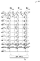
도 2는 블록들(예를 들어, 블록 A(201A), 블록 B(201B) 등) 및 서브-블록들(예를 들어, 서브-블록 A0(201A0), 서브-블록 An(201An), 서브-블록 B0(201B0), 서브-블록 Bn(201Bn) 등)로 편성된 메모리 셀들의 다수의 스트링(예를 들어, 제1-제3 A0 메모리 스트링들(205A0-207A0), 제1-제3 An 메모리 스트링들(205An-207An), 제1-제3 B0 메모리 스트링들(205B0-207B0), 제1-제3 Bn 메모리 스트링들(205Bn-207Bn) 등)을 포함하는 3D NAND 아키텍처 반도체 메모리 어레이(200)의 예시적인 개략도를 도시한다. 메모리 어레이(200)는 블록, 소자 또는 메모리 소자의 다른 유닛에서 통상적으로 발견될 수 있는 보다 많은 수의 유사한 구조의 일 부분을 나타낸다. 2 shows blocks (eg, block A 201A, block
메모리 셀들의 각 스트링은 소스 라인(SRC)(235) 또는 소스측 선택 게이트(SGS)(예를 들어, 제1-제3 A0 SGS(231A0-233A0), 제1-제3 An SGS(231An-233An), 제1-제3 B0 SGS(231B0-233B0), 제1-제3 Bn SGS(231Bn-233Bn) 등) 및 드레인측 선택 게이트(SGD)(예를 들어, 제1-제3 A0 SGD(226A0-228A0), 제1-제3 An SGD(226An-228An), 제1-제3 B0 SGD(226B0-228B0), 제1-제3 Bn SGD(226Bn-228Bn) 등) 간에 Z 방향, 소스-드레인으로 적층되는 전하 저장 트랜지스터들(예를 들어, 플로팅 게이트 트랜지스터들, 전하 트랩 구조들 등)의 다수의 티어를 포함한다. 3D 메모리 어레이에서의 메모리 셀들의 각 스트링은 X 방향을 따라 데이터 라인들(예를 들어, 비트 라인들(BL) BL0-BL2 220-222)로서, 그리고 Y 방향을 따라 물리 페이지들로서 배열될 수 있다. Each string of memory cells is a source line (SRC) 235 or a source-side selection gate (SGS) (eg, first-third A0 SGS (231A0-233A0), first-third An SGS (231An-) 233An), 1st-3rd B0 SGS (231B0-233B0), 1st-3rd Bn SGS (231Bn-233Bn, etc.) and drain side selection gate (SGD) (e.g. 1st-3rd A0 SGD Z direction between (226A0-228A0), 1st-3rd An SGD(226An-228An), 1st-3rd B0 SGD(226B0-228B0), 1st-3rd Bn SGD(226Bn-228Bn, etc.), It includes multiple tiers of charge storage transistors (eg, floating gate transistors, charge trap structures, etc.) stacked as source-drain. Each string of memory cells in a 3D memory array may be arranged as data lines along the X direction (eg, bit lines BL BL0-BL2 220-222) and as physical pages along the Y direction. .
물리적 페이지 내에서, 각 티어는 메모리 셀들의 로우를 나타내고, 메모리 셀들의 각 스트링은 컬럼을 나타낸다. 서브-블록은 하나 이상의 물리적 페이지를 포함할 수 있다. 블록은 다수(예를 들어, 128, 256, 384 등)의 서브-블록(또는 물리적 페이지)을 포함할 수 있다. 여기에는 두 개의 블록을 갖고, 각 블록은 두 개의 서브-블록을 갖고, 각 서브-블록은 단일 물리적 페이지를 갖고, 각 물리적 페이지는 메모리 셀들의 세 개의 스트링을 가지며, 각 스트링은 메모리 셀들의 여덟 개의 티어를 갖는 것으로 도시되어 있지만, 다른 예들에서, 메모리 어레이(200)는 보다 많거나 적은 블록, 서브-블록, 물리 페이지, 메모리 셀들의 스트링, 메모리 셀 또는 티어를 포함할 수 있다. 예를 들어, 메모리 셀의 각 스트링은 요구되는 바에 따라, 보다 많거나 적은(예를 들어, 16, 32, 64, 128 등) 티어 뿐만 아니라 전하 저장 트랜지스터들(예를 들어, 선택 게이트들, 데이터 라인들 등) 위 또는 아래에 하나 이상의 추가 반도체 물질 티어를 포함할 수 있다. 일례로, 48 GB TLC NAND 메모리 소자는 페이지당 18,592 바이트(B)의 데이터(16,384 + 2208 바이트), 블록당 1536 페이지, 평면당 548 블록 및 소자당 4 이상의 평면을 포함할 수 있다. Within a physical page, each tier represents a row of memory cells, and each string of memory cells represents a column. A sub-block can include one or more physical pages. A block can include multiple (eg, 128, 256, 384, etc.) sub-blocks (or physical pages). It has two blocks, each block has two sub-blocks, each sub-block has a single physical page, each physical page has three strings of memory cells, and each string has eight of the memory cells. Although shown as having two tiers, in other examples,
메모리 어레이(200)에서의 각 메모리 셀은 요구되는 바에 따라 특정 티어 또는 티어의 일 부분에 걸쳐 제어 게이트들(CG들)을 총괄하여 연결하는 액세스 라인(예를 들어, 워드 라인들(WL) WL00-WL70(210A-217A), WL01-WL71(210B- 217B) 등)에 연결되는(예를 들어, 전기적으로 또는 그 외 작동 가능하게 연결되는) 제어 게이트(CG)를 포함한다. 3D 메모리 어레이에서의 특정 티어들 그리고 그에 따라 스트링에서의 특정 메모리 셀들은 각각의 액세스 라인들을 사용하여 액세스 또는 제어될 수 있다. 선택 게이트들의 그룹들은 다양한 선택 라인을 사용하여 액세스될 수 있다. 예를 들어, 제1-제3 A0 SGD(226A0-228A0)는 A0 SGD 라인 SGDA0(225A0)을 사용하여 액세스될 수 있고, 제1-제3 An SGD(226An-228An)는 An SGD 라인 SGDAn(225An)을 사용하여 액세스될 수 있고, 제1-제3 B0 SGD(226B0-228B0)는 B0 SGD 라인 SGDB0(225B0)을 사용하여 액세스될 수 있으며, 제1-제3 Bn SGD(226Bn-228Bn)는 Bn SGD 라인 SGDBn(225Bn)을 사용하여 액세스될 수 있다. 제1-제3 A0 SGS(231A0-233A0) 및 제1-제3 An SGS(231An-233An)는 게이트 선택 라인 SGS0(230A)를 사용하여 액세스될 수 있고, 제1-제3 B0 SGS(231B0-233B0) 및 제1-제3 Bn SGS(231Bn-233Bn)는 게이트 선택 라인 SGS1(230B)를 사용하여 액세스될 수 있다. Each memory cell in the
일례로, 메모리 어레이(200)는 어레이의 각각의 티어의 각 메모리 셀의 제어 게이트들(CG들) 또는 선택 게이트(또는 CG들 또는 선택 게이트들의 일 부분)를 연결하도록 구성된 다수의 레벨의 반도체 물질(예를 들어, 폴리실리콘 등)을 포함할 수 있다. 어레이에서의 메모리 셀들의 특정 스트링들은 비트 라인들(BL들) 및 선택 게이트들 등의 조합을 사용하여 액세스, 선택 또는 제어될 수 있고, 특정 스트링들에서의 하나 이상의 티어에서의 특정 메모리 셀들은 하나 이상의 액세스 라인(예를 들어, 워드 라인)을 사용하여 액세스, 선택 또는 제어될 수 있다. In one example,
도 3은 스트링들(예를 들어, 제1-제3 스트링들(305-307) 및 티어들(예를 들어, 각각의 워드 라인들(WL) WL0-WL7(310-317), 드레인측 선택 게이트(SGD) 라인(325), 소스측 선택 게이트(SGS) 라인(330) 등)의 2차원 어레이로 배열된 복수의 메모리 셀(302), 및 감지 증폭기들 또는 소자들(360)을 포함하는 NAND 아키텍처 반도체 메모리 어레이(300)의 일 부분의 예시적인 개략도를 도시한다ㅏ. 예를 들어, 메모리 어레이(300)는 도 2에 도시된 바와 같은 3D NAND 아키텍처 반도체 메모리 소자의 메모리 셀들의 하나의 물리적 페이지의 일 부분의 예시적인 개략도를 도시할 수 있다. 3 shows strings (eg, first-third strings 305-307 and tiers (eg, respective word lines WL) WL0-WL7 310-317, drain side selection A plurality of
메모리 셀들의 각 스트링은 각각의 소스측 선택 게이트(SGS)(예를 들어, 제1-제3 SGS(331-333)를 사용하여 소스 라인(SRC)에 연결되고, 각각의 드레인측 선택 게이트(SGD)(예를 들어, 제1-제3 SGD(326-328)를 사용하여 각각의 데이터 라인(예를 들어, 제1-제3 비트 라인들(BL) BL0-BL2(320-322))에 연결된다. 도 3의 예에 여덟 개의 티어(예를 들어, 워드 라인들(WL) WL0-WL7(310-317)을 사용) 및 세 개의 데이터 라인(BL0-BL2(326-328))을 갓는 것으로 도시되어 있지만, 다른 예들은 요구되는 바에 따라 보다 많거나 적은 티어 또는 데이터 라인을 갖는 메모리 셀들의 스트링들을 포함할 수 있다. Each string of memory cells is connected to a source line SRC using a respective source-side select gate (SGS) (eg, first-third SGS 331-333), and each drain-side select gate ( SGD) (e.g., each data line using the first-third SGD (326-328) (e.g., first-third bit lines BL) BL0-BL2 (320-322)) Eight tiers (e.g., using word lines WL WL0-WL7 310-317) and three data lines BL0-BL2 (326-328) in the example of FIG. Although shown as being flat, other examples may include strings of memory cells with more or fewer tiers or data lines as desired.
예시적인 메모리 어레이(300)와 같은 NAND 아키텍처 반도체 메모리 어레이에서, 선택된 메모리 셀(302)의 상태는 선택된 메모리 셀을 포함하는 특정 데이터 라인과 연관된 전류 또는 전압 변화를 감지함으로써 액세스될 수 있다. 메모리 어레이(300)는 하나 이상의 드라이버를 사용하여 (예를 들어, 제어 회로, 하나 이상의 프로세서, 디지털 로직 등에 의해) 액세스될 수 있다. 일례로, 하나 이상의 드라이버는 특정 메모리 셀 또는 메모리 셀들의 집합에 관해 수행되도록 요구되는 동작의 유형에 따라 하나 이상의 데이터 라인(예를 들어, 비트 라인(BL0-BL2)), 액세스 라인(예를 들어, 워드 라인(WL0-WL7)) 또는 선택 게이트들을 특정 전위를 구동함으로써, 특정 메모리 셀 또는 메모리 셀들의 집합을 활성화할 수 있다. In a NAND architecture semiconductor memory array, such as the
데이터를 메모리 셀에 프로그래밍 또는 기록하기 위해, 프로그래밍 전압(Vpgm)(예를 들어, 하나 이상의 프로그래밍 펄스 등)이 선택된 워드 라인(예를 들어, WL4)에, 그리고 그에 따라 선택된 워드 라인들에 연결되는 메모리 셀의 제어 게이트(예를 들어, WL4에 연결되는 메모리 셀들의 제1-제3 제어 게이트들(CG들)(341-343)에 인가될 수 있다. 프로그래밍 펄스들은 예를 들어, 15V 또는 그 부근에서 시작될 수 있고, 특정 예들에서, 각 프로그래밍 펄스 인가 동안 크기가 증가할 수 있다. 프로그램 전압이 선택된 워드 라인들에 인가되는 동안, 접지 전위(예를 들어, Vss)와 같은 전위가 프로그래밍의 타겟이 되는 메모리 셀들의 데이터 라인들(예를 들어, 비트 라인들) 및 기판들(그리고 그에 따라 소스들과 드레인들 간의 채널들)에 인가되어, 채널들로부터 타겟 메모리 셀들의 플로팅 게이트들로 전하가 전달될 수 있다(예를 들어, 직접 주입 또는 FN(Fowler-Nordheim) 터널링 등). To program or write data to a memory cell, a programming voltage (Vpgm) (e.g., one or more programming pulses, etc.) is coupled to the selected word line (e.g., WL4) and thus to the selected word lines. The control gate of the memory cell (eg, first-third control gates (CGs) 341-343 of the memory cells connected to WL4) may be applied. It may start in the vicinity, and in certain examples, the magnitude may increase during each programming pulse application While the program voltage is applied to selected word lines, a potential such as ground potential (eg, Vss) is the target of programming. Applied to the data lines (e.g., bit lines) and substrates (and thus channels between the sources and drains) of these memory cells, so that charges from the channels to the floating gates of the target memory cells Can be delivered (eg direct injection or Fowler-Nordheim (FN) tunneling).
대조적으로, 프로그래밍의 타겟이 되지 않는 메모리 셀들을 갖는 하나 이상의 워드 라인에는 패스 전압(Vpass)이 인가될 수 있거나, 프로그래밍의 타겟이 되지 않는 메모리 셀들을 갖는 데이터 라인들(예를 들어, 비트 라인들)에는 저해 전압(예를 들어, Vcc)이 인가되어 예를 들어, 채널들로부터 그러한 타겟이 되지 않는 메모리 셀들의 플로팅 게이트들로 전하가 전달되는 것을 저해할 수 있다. 패스 전압은 예를 들어, 프로그래밍의 타겟이 되는 워드 라인에 인가된 패스 전압의 근접성에 따라 변할 수 있다. 저해 전압은 접지 전위(예를 들어, Vss)에 관한 외부 소스 또는 공급(예를 들어, 배터리, AC-DC 변환기 등)으로부터의 전압과 같은 공급 전압(Vcc)을 포함할 수 있다. In contrast, a pass voltage Vpass may be applied to one or more word lines having memory cells that are not targeted for programming, or data lines (eg, bit lines) having memory cells that are not targeted for programming. ) May be applied with an inhibit voltage (eg, Vcc) to inhibit the transfer of charge, for example, from channels to floating gates of non-targeted memory cells. The pass voltage may vary, for example, depending on the proximity of the pass voltage applied to the word line targeted for programming. The suppression voltage can include a supply voltage (Vcc), such as a voltage from an external source or supply (eg, battery, AC-DC converter, etc.) relative to the ground potential (eg, Vss).
예를 들어, 프로그래밍 전압(예를 들어, 15V 이상)이 WL4와 같은 특정 워드 라인에인가될 경우, 10V의 패스 전압이 WL3, WL5 등과 같은 하나 이상의 다른 워드 라인에 인가되어 타겟이 되지 않는 메모리 셀들의 프로그래밍을 저해하거나, 또는 프로그래밍의 타겟이 되지 않는 그러한 메모리 셀들 상에 저장된 값들을 유지할 수 있다. 인가된 프로그램 전압과 타겟이 되지 않는 메모리 셀들 간의 거리가 증가함에 따라, 비 타겟이 되지 않는 메모리 셀들의 프로그래밍을 억제하는데 필요한 패스 전압은 감소될 수 있다. 예를 들어, WL4에 15V의 프로그래밍 전압이 인가되는 경우, WL3 및 WL5에는 10V의 패스 전압이 인가될 수 있고, WL2 및 WL6에는 8V의 패스 전압이 인가될 수 있으며, WL1 및 WL7에는 7V의 패스 전압이 인가될 수 있는 등이다. 다른 예들에서, 패스 전압들 또는 워드 라인들의 수 등은 보다 높거나 낮거나, 도는 보다 많거나 적을 수 있다. For example, when a programming voltage (eg, 15 V or more) is applied to a specific word line, such as WL4, a 10 V pass voltage is applied to one or more other word lines, such as WL3, WL5, etc., so that it is not targeted. Values that are stored on those memory cells that do not interfere with programming or are not targeted for programming. As the distance between the applied program voltage and non-target memory cells increases, the pass voltage required to suppress programming of non-target memory cells can be reduced. For example, when a programming voltage of 15V is applied to WL4, a pass voltage of 10V may be applied to WL3 and WL5, a pass voltage of 8V may be applied to WL2 and WL6, and a pass of 7V to WL1 and WL7. Voltage may be applied. In other examples, the pass voltages or number of word lines, etc. may be higher or lower, or more or less.
하나 이상의 데이터 라인(예를 들어, 제1, 제2 또는 제3 비트 라인들(BL0-BL2)(320-322))에 연결되는 감지 증폭기들(360)은 특정 데이터 라인 상의 전압 또는 전류를 감지함으로써 각각의 데이터 라인들에서의 각 메모리 셀의 상태를 검출할 수 있다.
하나 이상의 프로그래밍 펄스(예를 들어, Vpgm)의 인가들 간에는, 선택된 메모리 셀이 그것의 의도된 프로그래밍된 상태에 도달했는지를 결정하기 위해 검증 동작이 수행될 수 있다. 선택된 메모리 셀이 그것의 의도된 프로그래밍된 상태에 도달했을 경우, 그것은 추가 프로그래밍이 저해될 수 있다. 선택된 메모리 셀이 그것의 의도된 프로그래밍된 상태에 도달하지 않았을 경우, 추가 프로그래밍 펄스들이 인가될 수 있다. 선택된 메모리 셀이 특성 수(예를 들어, 최대 수)의 프로그래밍 펄스 이후에 그것의 의도된 프로그래밍된 상태에 도달하지 않았을 경우, 선택된 메모리 셀, 또는 그러한 선택된 메모리 셀과 연관된 스트링, 블록 또는 페이지는 결함으로 마킹될 수 있다. Between applications of one or more programming pulses (eg, Vpgm), a verify operation can be performed to determine if the selected memory cell has reached its intended programmed state. If the selected memory cell has reached its intended programmed state, it can inhibit further programming. Additional programming pulses may be applied if the selected memory cell has not reached its intended programmed state. If the selected memory cell has not reached its intended programmed state after a number of characteristic (eg, maximum) programming pulses, the selected memory cell, or a string, block, or page associated with the selected memory cell is defective It can be marked as.
메모리 셀 또는 메모리 셀들의 그룹을 소거하기 위해(예를 들어, 소거는 통상적으로 블록 또는 서브-블록 단위로 수행됨), 소거 전압(Vers)(예를 들어, 통상적으로 Vpgm)이 소거의 타겟이 되는 메모리 셀들의 기판들(그리고 그에 따라 소스들과 드레인들 간의 채널들)에 인가될 수 있는 한편(예를 들어, 하나 이상의 비트 라인, 선택 게이트 등을 사용하여), 타겟 메모리 셀들의 워드 라인들은 접지 전위(예를 들어, Vss)와 같은 전위로 유지되어, 타겟 메모리 셀들의 플로팅 게이트들로부터 채널들로 전하가 전달될 수 있다(예를 들어, 직접 주입 또는 FN(Fowler-Nordheim) 터널링 등). To erase a memory cell or group of memory cells (e.g., erase is typically performed on a block or sub-block basis), the erase voltage Vers (e.g., Vpgm, for example) is the target of erase. While it can be applied to the substrates of memory cells (and thus channels between sources and drains) (eg, using one or more bit lines, select gates, etc.), the word lines of target memory cells are grounded. The potential is maintained at the same potential (eg, Vss), so that charge can be transferred from the floating gates of the target memory cells to the channels (eg direct injection or Fowler-Nordheim (FN) tunneling, etc.).
도 4는 복수의 메모리 셀(404)을 갖는 메모리 어레이(402), 및 메모리 어레이(402)와의 통신을 제공하거나 메모리 어레이(402)상에서 하나 이상의 메모리 동작을 수행하기 위한 하나 이상의 회로 또는 구성요소를 포함하는 메모리 소자(400)의 예시적인 블록도를 도시한다. 메모리 소자(400)는 로우 디코더(412), 컬럼 디코더(414), 감지 증폭기들(420), 페이지 버퍼(422), 선택기(424), 입력/출력(I/O) 회로(426) 및 메모리 제어 유닛(430)을 포함할 수 있다. 4 illustrates a
메모리 어레이(402)의 메모리 셀들(404)은 제1 및 제2 블록들(402A, 402B)과 같은 블록들로 배열될 수 있다. 각 블록은 서브-블록을 포함할 수 있다. 예를 들어, 제1 블록(402A)은 제1 및 제2 서브-블록들(402A0, 402An)을 포함할 수 있고, 제2 블록(402B)은 제1 및 제2 서브-블록들(402B0, 402Bn)을 포함할 수 있다. 각 서브-블록은 각 페이지가 다수의 메모리 셀(404)을 포함하는 다수의 물리적 페이지를 포함할 수 있다. 여기에는 두 개의 블록을 갖고, 각 블록은 두 개의 서브-블록을 거지며, 각 서브-블록은 다수의 메모리 셀(404)을 갖는 것으로 도시되어 있지만, 다른 예들에서, 메모리 어레이(402)는 보다 많거나 적은 블록, 서브-블록, 메모리 셀 등을 포함할 수 있다. 다른 예들에서, 메모리 셀들(404)은 다수의 로우, 컬럼, 페이지, 서브-블록, 블록 등으로 배열될 수 있고, 예를 들어, 액세스 라인들(406), 제1 데이터 라인들(410), 또는 하나 이상의 선택 게이트, 소스 라인들 등을 사용하여 액세스될 수 있다. The
메모리 제어 유닛(430)은 예를 들어, 요구되는 동작(예를 들어, 기록, 판독, 소거 등)을 나타내는 하나 이상의 클록 신호 또는 제어 신호, 또는 하나 이상의 어드레스 라인(416) 상에 수신되는 하나 이상의 어드레스 신호(A0-AX)를 포함하여, 제어 라인들(432) 상에 수신되는 하나 이상의 신호 또는 명령에 따라 메모리 소자(400)의 메모리 동작들을 제어할 수 있다. 메모리 소자(400) 외부의 하나 이상의 소자는 제어 라인들(432)상의 제어 신호들의 값, 또는 어드레스 라인(416) 상의 어드레스 신호들을 제어할 수 있다. 메모리 소자(400) 외부의 소자들의 예들은 호스트, 메모리 제어기, 프로세서, 또는도 4에 도시되지 않은 하나 이상의 회로 또는 구성요소를 포함할 수 있지만, 이에 제한되지는 않는다. The
메모리 소자(400)는 액세스 라인들(406) 및 제1 데이터 라인들(410)을 사용하여 메모리 셀들(404) 중 하나 이상에(예를 들어, 기록 또는 소거)하거나 그로부터(예를 들어, 판독) 데이터를 전달할 수 있다. 로우 디코더(412) 및 컬럼 디코더(414)는 어드레스 라인(416)으로부터 어드레스 신호들(A0-AX)을 수신 및 디코딩할 수 있고, 메모리 셀들(404) 중 어느 메모리 셀이 액세스되어야 할지를 결정할 수 있으며, 신호들을 액세스 라인들(406) 중 하나 이상(예를 들어, 복수의 워드 라인(WL0-WLm) 중 하나 이상) 또는 제1 데이터 라인들(410) 중 하나 이상(예를 들어, 복수의 비트 라인(BL0-BLn) 중 하나 이상)에 제공할 수 있다. The
메모리 소자(400)는 감지 증폭기들(420)과 같은 감지 회로를 포함할 수 있으며, 이는 제1 데이터 라인들(410)을 사용하여 메모리 셀들(404) 상의 데이터의 값들을 결정(예를 들어, 판독)하거나, 또는 그것들에 기록될 데이터의 값들을 결정하도록 구성된다. 예를 들어, 메모리 셀들(404)의 선택된 스트링에서, 감지 증폭기들(420) 중 하나 이상은 선택된 스트링을 통해 데이터 라인들(410)로 메모리 어레이(402)에 흐르는 판독 전류에 응답하여 선택된 메모리 셀(404)의 로직 레벨을 판독할 수 있다. The
메모리 소자(400) 외부의 하나 이상의 소자는 I/O 라인들(DQ0-DQN)(408), 어드레스 라인들(416)(A0-AX) 또는 제어 라인들(432)을 사용하여 메모리 소자(400)와 통신할 수 있다. 입력/출력(I/O) 회로(426)는 예를 들어, 제어 라인들(432) 및 어드레스 라인들(416)에 따라 I/O 라인들(408)을 사용하여, 메모리 소자(400)의 입력 또는 출력, 이를테면 페이지 버퍼(422) 또는 메모리 어레이(402)의 입력 또는 출력 데이터의 값들을 전달할 수 있다. 페이지 버퍼(422)는 데이터가 메모리 어레이(402)의 관련 부분들로 프로그래밍되기 전에 메모리 소자(400) 외부의 하나 이상의 소자로부터 수신된 데이터를 저장할 수 있거나, 또는 데이터가 메모리 소자(400) 외부의 하나 이상의 소자로 전송되기 전에 메모리 어레이(402)로부터 판독된 데이터를 저장할 수 있다. One or more devices external to the
컬럼 디코더(414)는 어드레스 신호들(A0-AX)을 수신하고 하나 이상의 컬럼 선택 신호(CSEL1-CSELn)로 디코딩할 수 있다. 선택기(424)(예를 들어, 선택 회로)는 컬럼 선택 신호들(CSEL1-CSELn)을 수신하고 페이지 버퍼(422)에서 메모리 셀들(404)로부터 판독되거나 그것들로 프로그래밍될 데이터의 값들을 나타내는 데이터를 선택할 수 있다. 선택된 데이터는 제2 데이터 라인들(418)을 사용하여 페이지 버퍼(422)와 I/O 회로(426) 간에서 전달될 수 있다. The
메모리 제어 유닛(430)은 외부 소스 또는 공급(예를 들어, 내부 또는 외부 배터리, AC-DC 변환기 등)으로부터 공급 전압(Vcc)(434) 및 음의 공급(Vss)(436)(예를 들어, 접지 전위)과 같은 양 및 음의 공급 신호들을 수신할 수 있다. 특정 예들에서, 메모리 제어 유닛(430)은 양 또는 음의 공급 신호들을 내부적으로 제공하기 위해 조절기(428)를 포함할 수 있다. The
메모리 소자로 데이터를 판독, 기록 또는 소거하고자 하는 호스트 소프트웨어는 판독, 기록 또는 소거를 위한 하나 이상의 메모리 위치(예를 들어, 메모리 페이지)를 어드레싱하는 하나 이상의 논리 블록 어드레스(LBA)를 지정하는 명령을 발행한다. 자기 저장 장치와 달리, NAND 소자들에서, 이것들은 메모리 소자들의 실제 물리적 위치들에 대응하지 않는다. 대신, 이러한 LBA들은 NAND에 의해 논리-물리(L2P) 테이블을 사용하여 NAND 메모리 셀들의 하나 이상의 물리적 페이지로 매핑된다. 이러한 매핑의 이유는 NAND가 NAND에서의 값을 수정할 수 없기 때문에 - 그것은 값을 소거한 다음 새로운 값을 기록해야 하기 때문이다. 이를 복잡하게 만드는 것은 NAND가 한 번에 메모리의 블록(많은 페이지를 갖는)만 소거할 수 있다는 것이다. 삭제 또는 수정 요청이 메모리 블록보다 적은 경우, 이러한 요청을 이행하고 소거되어서는 안 되는 데이터를 보존하려면, NAND는 유효한 모든 페이지를 다른 블록으로 이동시킨 다음 오래된 블록을 소거해야 할 수 있다(이러한 프로세스를 가비지 수집이라 한다). 이러한 솔루션은 느리고, 또한 NAND 메모리 셀이 더 이상 전하를 보유할 수 없기 전에 그것은 단지 제한된 수의 프로그램 및 소거 사이클만을 갖기 때문에 NAND 수명을 감소시킨다. Host software that wants to read, write, or erase data into a memory device may issue instructions that specify one or more logical block addresses (LBAs) addressing one or more memory locations (eg, memory pages) for reading, writing, or erasing. To issue. Unlike magnetic storage devices, in NAND elements, these do not correspond to the actual physical locations of the memory elements. Instead, these LBAs are mapped by NAND to one or more physical pages of NAND memory cells using logical-physical (L2P) tables. The reason for this mapping is because NAND cannot modify the value in NAND-it must erase the value and then write the new value. What complicates this is that NAND can only erase blocks of memory (with many pages) at a time. If a delete or modify request is less than a block of memory, to fulfill these requests and preserve data that should not be erased, NAND may have to move all valid pages to another block and then erase the old block (this process This is called garbage collection). This solution is slow and also reduces the NAND lifespan because it only has a limited number of program and erase cycles before the NAND memory cell can no longer hold charge.
결과적으로, NAND는 삭제 요청을 수신하거나 메모리에서 값을 수정하라는 요청을 수신할 때, 단순히 오래된 위치를 유효하지 않은 것으로 마킹하고 수정의 경우, 메모리 소자 상의 새로운 물리적 위치(하나 이상의 페이지)에 새로운 값을 기록한다. 수정 요청들의 경우, NAND는 그 다음 해당 LBA 지점과 관련된 후속 요청들이 올바른 물리적 위치를 가리키도록 그것의 LBA - 새로운 실제 물리적 위치의 매핑을 업데이트한다. As a result, when NAND receives a delete request or a request to modify a value in memory, it simply marks the old location as invalid and, in the case of modification, a new value in a new physical location (one or more pages) on the memory element. Record. In the case of modification requests, the NAND then updates its LBA-mapping of the new actual physical location so that subsequent requests associated with that LBA point point to the correct physical location.
최종적으로 NAND는 어드버타이징된 저장 레벨을 유지하기 위해 이전에 마킹된 유효하지 않은 페이지들을 비운다. 전술된 바와 같이, NAND는 한 번에 데이터의 블록들만을 소거한다. 이러한 결과로서, NAND 소자는 먼저 가비지 수집을 수행하여 소거될 블록의 유효한 페이지들의 데이터를 다른 블록들의 새로운 페이지들로 복사한다. 데이터가 복사되면, 소거될 블록의 페이지들이 유효하지 않은 것으로 마킹되고 블록이 소거될 수 있다. Finally, NAND flushes previously marked invalid pages to maintain the advertised storage level. As described above, NAND erases only blocks of data at a time. As a result of this, the NAND element first performs garbage collection to copy data of valid pages of the block to be erased to new pages of other blocks. When data is copied, the pages of the block to be erased are marked as invalid and the block can be erased.
논리 어드레스들을 물리적 어드레스들에 매핑하는데 사용되는 L2P 테이블에는 상당한 메모리 자원들이 필요하다. 예를 들어, 2 기가바이트(GB)가 저장되는 NAND는 2 메가바이트(MB) L2P 테이블을 가질 수 있고 128GB NAND는 128MB L2P 테이블로 매핑될 수 있다. NAND 메모리 소자들은 다수의 뱅크로 분할될 수 있는 내부 메모리(예를 들어, 1 - 2MB)를 갖는 제어기(예를 들어, CPU)를 가질 수 있다. 하나의 뱅크는 프로세서에 밀연결되고 단일 클록 사이클로 액세스된다. 이러한 밀연결되는 RAM은 256Kbyte 정도이고 펌웨어에 의해 사용되는 펌웨어 및 데이터를 저장한다. 다른 뱅크들(다중 뱅크 SRAM 구성 - MRAM으로 불리는)은 액세스하기 더 느리다. MRAM은 통상적으로 1-2Mbyte이고 밀연결되는 메모리보다 느리다. The L2P table used to map logical addresses to physical addresses requires significant memory resources. For example, a NAND in which 2 gigabytes (GB) is stored may have a 2 megabyte (MB) L2P table, and a 128 GB NAND may be mapped to a 128 MB L2P table. NAND memory elements can have a controller (eg, CPU) with internal memory (eg, 1-2 MB) that can be divided into multiple banks. One bank is tightly coupled to the processor and accessed in a single clock cycle. This tightly coupled RAM is about 256 Kbytes and stores the firmware and data used by the firmware. Other banks (multi-bank SRAM configuration-called MRAM) are slower to access. MRAM is typically 1-2 Mbytes and slower than tightly coupled memory.
이해될 수 있는 바와 같이, L2P 테이블은 밀연결되는 메모리 또는 MRAM 중 어느 하나에 완전히 맞지 않을 것이다. NAND 메모리 소자들은 밀연결되는 메모리 또는 MRAM의 양을 증가시킬 수 있지만, 이는 복잡성, 크기 및 비용을 증가시킨다. 다른 접근법은 L2P 테이블의 캐시인 MRAM(또는 일부 예에서는, 밀연결되는 메모리)의 영역을 갖는 것이다. 캐시는 가장 흔하게 또는 가장 최근에 액세스된 논리 블록들에 대한 물리적 어드레스들을 나타낼 수 있다. 캐시의 논리 어드레스들에 대한 호스트로부터의 요청들은 캐시를 사용하여 서비스된다. L2P 캐시가 지정된 논리 어드레스에 대한 물리적 어드레스를 포함하지 않는 경우, NAND 소자가 NAND로부터 L2P 테이블의 해당 부분을 로딩해야 한다. 이는 캐시 부적중으로 불리고 NAND가 요청을 서비스하는데 걸리는 시간량을 증가시킨다. 캐시의 문제점은 그것의 크기 범위가 약 32Kbyte에서 128Kbyte로 비교적 작다는 것이다. 캐시 부적중은 호스트 동작을 다음 두 가지 NAND 동작으로 바꾼다: 호스트 요청을 서비스하는데 필요한 L2P 정보를 검색하는 동작 하나 및 요청을 실제로 서비스하는 두 번째 동작. 그에 따라, 캐시 적중 수를 증가시키는 기술들이 성능에 주목할 만한 영향을 미친다. As can be appreciated, the L2P table will not fit completely into either the memory or MRAM that is tightly coupled. NAND memory devices can increase the amount of memory or MRAM that is tightly coupled, but this increases complexity, size and cost. Another approach is to have an area of MRAM (or, in some examples, tightly coupled memory) that is a cache of L2P tables. The cache can represent physical addresses for the most commonly or most recently accessed logical blocks. Requests from the host for the cache's logical addresses are served using the cache. If the L2P cache does not contain the physical address for the specified logical address, the NAND device must load the corresponding portion of the L2P table from the NAND. This is called cache misses and increases the amount of time it takes for NAND to service the request. The problem with the cache is that its size range is relatively small, from about 32Kbytes to 128Kbytes. A cache miss replaces the host action with two NAND actions: one action to retrieve the L2P information needed to service the host request, and a second action to actually service the request. Accordingly, techniques that increase the number of cache hits have a noticeable effect on performance.
일부 예에 관찰되는 NAND 작동 조건들에 응답하여 메모리 소자에서의 L2P 캐시의 크기를 동적으로 조절하는 방법들, 시스템들 및 기계 판독 가능한 매체들이 개시된다. L2P 캐시는 (판독 또는 기록 버퍼와 같은) 도너 메모리 위치로부터의 메모리 공간을 차용할 수 있다. 예를 들어, 시스템이 많은 양의 판독 요청을 통지하면, 시스템은 기록 버퍼를 희생시키면서(이는 감소될 수 있다) L2P 캐시의 크기를 증가시킬 수 있다. 마찬가지로, 시스템이 많은 양의 기록 요청을 통지하면, 시스템은 판독 버퍼를 희생시키면서(이는 감소될 수 있다) L2P 캐시의 크기를 증가시킬 수 있다. 일부 예에서, 증가는 일시적일 수 있고 L2P 캐시는 작동 조건들의 변화에 응답하여 그것의 통상 크기로 되돌아갈 수 있다. 예를 들어, 증가를 촉진한 조건의 부재의 응답하여. L2P 캐시의 크기를 증가시킴으로써, NAND 소자는 캐시 적중의 확률을 증가시키고 단일 NAND 동작이 NAND로부터 L2P 테이블 정보를 로딩하기 위한 제2 NAND 동작을 요청할 확률을 감소시킬 수 있다. Methods, systems, and machine-readable media are disclosed for dynamically resizing an L2P cache in a memory device in response to NAND operating conditions observed in some examples. The L2P cache can borrow memory space from donor memory locations (such as read or write buffers). For example, if the system notifies a large amount of read requests, the system can increase the size of the L2P cache at the expense of the write buffer (which can be reduced). Likewise, if the system notifies a large amount of write requests, the system can increase the size of the L2P cache at the expense of the read buffer (which can be reduced). In some examples, the increase may be temporary and the L2P cache may return to its normal size in response to changes in operating conditions. For example, in response to the absence of conditions that promoted the increase. By increasing the size of the L2P cache, the NAND element can increase the probability of a cache hit and decrease the probability that a single NAND operation will request a second NAND operation to load L2P table information from the NAND.
일부 예에서, L2P 캐시 프로파일은 하나 이상의 NAND 작동 조건에 기초하여 캐시 거동들을 지정할 수 있다. 예를 들어, L2P 캐시 프로파일은 캐시가 어떤 작동 조건들 하에서 디폴트 크기로부터 증가하고, 다시 디폴트 크기로 감소하는지, 얼만큼, 크기가 얼마나 빨리 변하는지, 그리고 L2P 캐시가 사용할 다른 메모리 위치(예를 들어, 판독, 기록 또는 다른 버퍼)를 기술하는 하나 이상의 규칙을 포함할 수 있다. 예를 들어, L2P 캐시 프로파일에서의 하나 이상의 규칙은 캐시 크기가 디폴트 크기로부터 증가할 때 그리고 캐시 크기를 디폴트 크기로 되돌리는 때를 지정할 수 있다. In some examples, the L2P cache profile can specify cache behaviors based on one or more NAND operating conditions. For example, the L2P cache profile increases the cache from the default size under certain operating conditions, decreases back to the default size, how much, how quickly the size changes, and other memory locations that the L2P cache will use (e.g. , Read, write, or other buffer). For example, one or more rules in the L2P cache profile can specify when the cache size increases from the default size and when the cache size returns to the default size.
L2P 캐시 프로파일은 정적 - 즉, 제조시 NAND 상으로 로딩되어 변경되지 않고 유지된다(NAND 상의 데이터 구조 또는 휘발성 작동 메모리로서) - 일 수 있다. 다른 예들에서, 디폴트 L2P 캐시 프로파일은 제조시에 NAND 상에 로딩될 수 있지만, 그 후 수정될 수 있다 - 예를 들어, 호스트 기기의 운영 체제인 NAND의 펌웨어에 의해(예를 들어, UFS와 같은 호스트 인터페이스를 통해 변경을 전송함으로써) 등. 일부 예에서, L2P 캐시 프로파일의 규칙들은 펌웨어 명령어들의 부분으로서 인스턴스화될 수 있다. The L2P cache profile can be static-that is, loaded onto the NAND during manufacture and remains unchanged (as a data structure on the NAND or volatile working memory). In other examples, the default L2P cache profile may be loaded on the NAND at manufacture, but then modified-for example, by the firmware of the NAND, which is the host device's operating system (eg, UFS, for example). Etc.) by sending changes through the host interface. In some examples, the rules of the L2P cache profile can be instantiated as part of the firmware instructions.
L2P 캐시 크기 변경을 트리거할 수 있는 예시적인 작동 조건들은 다음 중 하나 이상을 포함할 수 있다: 호스트 명령 큐 깊이 크기, 큐의 명령 유형(예를 들어, 판독, 기록, 소거 및 다른 명령들), 큐 내의 명령들의 상이한 유형들 간 비(예를 들어, 판독/기록 비, 기록/판독 비), L2P 캐시 적중률, L2P 캐시 부적중률 등. 규칙들은 다음 형태를 가질 수 있따: [작동 조건]이 [결정된 값] [보다 크다면, 과 같다면, 보다 작다면], [기록 또는 판독] 버퍼로부터 [양]만큼 L2P 캐시를 [증가/감소]시킨다. Exemplary operating conditions that can trigger an L2P cache size change can include one or more of the following: host command queue depth size, command type of queue (eg, read, write, erase, and other commands), Ratios between different types of instructions in the queue (eg, read/write ratio, write/read ratio), L2P cache hit ratio, L2P cache miss ratio, and the like. The rules can take the form: [Operating conditions] [determined value] [if greater than, if equal, less than], [increase/decrease L2P cache by [quantity] from [write or read] buffer ].
일부 예에서, 캐시 증가는 즉시 구현된다 - 즉, 도너 메모리의 데이터가 L2P 캐시에 즉시 할당될 수 있다. 다른 예들에서, 시스템은 L2P 캐시 증가를 구현할 때까지 도너 메모리(예를 들어, 기록/및/또는 판독 버퍼)가 비워질 때까지 대기할 수 있다. 또 다른 예들에서, NAND는 도너 메모리를 비우기 위한 노력을 가속할 수 있다. 또 다른 예들에서, L2P 캐시는 시간에 따라 점진적으로 페이징(phasing)될 수 있다. 예를 들어, 시간 t에서 L2P 캐시는 X KB만큼 증가될 수 있고, 시간 t+1에서 다른 X KB 증가될 수 있다(시간 t-1의 총 증가가 2X KB일 경우). In some examples, the cache increase is implemented immediately-that is, data from the donor memory can be immediately allocated to the L2P cache. In other examples, the system may wait until the donor memory (eg, write/and/or read buffer) is emptied until implementing an L2P cache increase. In still other examples, NAND can accelerate efforts to free donor memory. In still other examples, the L2P cache can be paged gradually over time. For example, at time t the L2P cache can be increased by X KB, and at time t+1 it can be increased by another X KB (if the total increase in time t-1 is 2X KB).
일례로, 프로파일의 L2P 캐시 규칙은 명령들의 대부분(예를 들어, 판독/기록 비가 50%를 초과하는)이 판독 명령들인 경우 큐 깊이가 5개 명령을 초과할 때, 기록 버퍼로부터 공간을 차용하여 5개 명령을 초과하는 매 판독 명령마다 L2P 캐시를 10%씩 25%까지 증가시킨다는 것일 수 있다. 다른 캐시 규칙은 명령들의 대부분이 판독 명령들인 경우 큐 깊이가 5개 명령을 초과할 때, 판독 및 기록 버퍼들 양자로부터 큐 내 판독 명령들 대 기록 명령들의 비율에 기초한 비율로 공간을 차용하여 5개 명령을 초과하는 매 판독 명령마다 L2P 캐시를 10%씩 25%까지 증가시킨다는 것일 수 있다. 또 다른 예시적인 규칙은 L2P 캐시 적중%가 판독 또는 기록 버퍼로부터 취하여 미리 결정된 값보다 작은 경우 L2P 캐시를 증가시키는 것일 수 있다. In one example, the profile's L2P cache rule can be used to borrow space from the write buffer when the queue depth exceeds 5 instructions if most of the instructions (e.g., read/write ratio exceeds 50%) are read instructions. It could be that the L2P cache is increased by 10% to 25% for every read command that exceeds 5 commands. Another cache rule is to borrow 5 spaces at a ratio based on the ratio of read commands to write commands in the queue from both read and write buffers when the queue depth exceeds 5 commands if most of the commands are read commands. It may be that the L2P cache is increased by 10% to 25% for every read command that exceeds the command. Another exemplary rule may be to increase the L2P cache when the% L2P cache hit is less than a predetermined value taken from the read or write buffer.
다수의 규칙이 정의될 수 있고 규칙들은 쌓일 수 있다 - 즉, 작동 조건들이 하나 이상의 증가 규칙을 충족하는 경우, 양 규칙 모두에 대해 캐시가 증가될 수 있다. 이는 작동 조건들이 다수의 규칙이 트리거될 수 있도록 하는 것인 경우에 그러할 수 있다. 예를 들어, 이하의 규칙들을 갖는 L2P 캐시 프로파일을 고려한다: Multiple rules can be defined and rules can be stacked-that is, if the operating conditions satisfy one or more incremental rules, the cache can be increased for both rules. This may be the case when operating conditions are such that multiple rules can be triggered. For example, consider an L2P cache profile with the following rules:
· 명령들의 대부분(예를 들어, 판독/기록 비가 50%를 초과하는)이 판독 명령들인 경우 큐 깊이가 5개 명령을 초과하면, 기록 버퍼로부터 공간을 차용하여 5개 명령을 초과하는 매 판독 명령마다 L2P 캐시를 10%씩 25%까지 증가시킨다;· If most of the instructions (e.g., read/write ratio exceeds 50%) are read instructions, if the queue depth exceeds 5 instructions, borrow every space from the write buffer to exceed every 5 instructions Increases L2P cache by 10% to 25%;
· L2P 캐시 적중%가 판독 또는 기록 버퍼로부터 취하여 미리 결정된 값보다 작은 경우 L2P 캐시를 증가시킨다; · Increase the L2P cache if the% L2P cache hit is less than a predetermined value taken from the read or write buffer;
NAND의 큐 깊이이 5개 명령을 초과하고 큐 버퍼의 명령들 중 50% 초과가 판독 명령 들인 경우, L2P 캐시는 기록 버퍼를 희생하여 증가될 수 있다. 동시에, L2P 캐시 적중%가 미리 결정된 값보다 작은 경우, L2P 캐시는 훨씬 더 많이 증가될 수 있다. 유사하게, 규칙들은 - 예를 들어, 작동 조건들이 하나의 규칙이 L2P 캐시를 증가시킬 것을 나타내고 다른 규칙은 L2P 캐시를 감소시킬 것을 나타내는 것과 같은 경우 - 부분적으로 또는 완전히 서로 상쇄될 수 있다. 이 경우, L2P 캐시는 이러한 규칙들의 합인 크기를 증가 또는 감소시킬 수 있다. 규칙들은 L2P 캐시를 디폴트 크기 미만으로 감소시킬 수도 있다(적어도 일시적으로). If the NAND queue depth exceeds 5 instructions and more than 50% of the queue buffer's instructions are read instructions, the L2P cache can be increased at the expense of the write buffer. At the same time, if the L2P cache hit percentage is less than a predetermined value, the L2P cache can be increased even more. Similarly, rules may partially or completely cancel each other-for example, when operating conditions indicate that one rule will increase the L2P cache and the other rule indicates that the L2P cache will be reduced. In this case, the L2P cache can increase or decrease the size that is the sum of these rules. Rules may reduce the L2P cache below the default size (at least temporarily).
도너 메모리 위치들은 호스트 판독 명령들을 버퍼링하는데 사용되는 판독 버퍼, 호스트로부터의 기록 데이터를 버퍼링하는 기록 버퍼 등을 포함할 수 있다. 도너 메모리 위치는 L2P 캐시로서 사용하기 위해 아직 할당되지 않은 비휘발성 메모리의 임의의 메모리 위치일 수 있다. Donor memory locations may include a read buffer used to buffer host read commands, a write buffer buffering write data from the host, and the like. The donor memory location can be any memory location in non-volatile memory that has not yet been allocated for use as an L2P cache.
예를 들어, L2P 캐시가 판독 또는 기록 버퍼들로부터 너무 많은 메모리를 메모리를 취함으로써 성능을 저하시키는 것을 방지하기 위해, 각 도너 메모리 위치들로부터 취해질 수 있는 양을 제한하는 캐시 크기 규칙들이 정의될 수 있다. 일부 예에서, 규칙은 도너 메모리 버퍼 이용%이 미리 결정된 임계율을 초과하는 경우 L2P 캐시에 대여된 임의의 메모리의 일부 또는 전부가 리턴되도록 지정할 수 있다. 특정 예들에서, 이는 L2P 캐시가 판독/기록 버퍼들로부터 전환하고 성능을 저하시키는 것을 방지한다. For example, cache size rules can be defined that limit the amount that can be taken from each donor memory location to prevent the L2P cache from degrading performance by taking too much memory from read or write buffers. have. In some examples, the rules may specify that some or all of the random memory borrowed in the L2P cache is returned when the donor memory buffer utilization exceeds a predetermined threshold. In certain examples, this prevents the L2P cache from switching from read/write buffers and degrading performance.
언급된 바와 같이, L2P 캐시 규칙들은 또한 어떤 조건들 하에서 L2P 캐시가 디폴트 크기로 다시 되돌아 갈 수 있는지를 지정할 수 있다. 예시적인 규칙은 큐 깊이가 미리 결정된 임계치 미만의 레벨로 될돌아 가면 L2P 캐시가 디폴트로 다시 되돌아 갈 수 있음을 지정할 수 있다. 다른 예들에서, 예시적인 규칙은 감소가 시간의 함수로서 발생할 수 있음을 지정할 수 있다. 즉, 초기 L2P 캐시 증가는 L2P 캐시가 그것의 디폴트 크기로 되돌아 갈 때까지 시간이에 따라 감속될 수 있다. As mentioned, L2P cache rules can also specify under what conditions the L2P cache can go back to its default size. The example rule may specify that the L2P cache can return back to the default if the queue depth goes back to a level below a predetermined threshold. In other examples, an example rule can specify that a reduction can occur as a function of time. That is, the initial L2P cache increase may slow down over time until the L2P cache returns to its default size.
L2P 캐시 증가 또는 감소(예를 들어, 재할당)는 일부 예에서 단순히 L2P 캐시 및 도너 메모리 위치들(예를 들어, 판독 또는 기록 버퍼들)의 경계들을 마킹하는 포인터들을 이동시킴으로써 실현될 수 있다. 기록 명령이 논리-물리 매핑을 변경하므로 이러한 변경 사항들은 L2P 캐시와 별개의 메모리 위치에 있는 업데이트 목록에 저장될 수 있다. 그에 따라, 호스트 기록은 먼저 L2P 매핑에 대한 L2P 테이블을 확인한 다음, 업데이트 목록을 확인하여 L2P 매핑이 업데이트되었는지 확인할 수 있다. 따라서, L2P 캐시의 엔트리들이 항상 "클린"한 것은 아닐 수 있다 - 즉, 수정되지 않을 수 있다. 그에 따라, L2P 캐시 크기의 "빠른 반동(snapback)"의 결과로서 L2P 캐시 엔트리들이 회복될 때, 그러한 엔트리들은 손실되지 않고, NAND 또는 업데이트 목록 상에 있다. L2P cache increase or decrease (eg, reallocation) may be realized in some examples simply by moving pointers marking the boundaries of the L2P cache and donor memory locations (eg, read or write buffers). Since the write command changes the logical-physical mapping, these changes can be stored in an update list in a memory location separate from the L2P cache. Accordingly, the host record may first check the L2P table for the L2P mapping, and then check the update list to determine whether the L2P mapping has been updated. Thus, the entries in the L2P cache may not always be "clean"-that is, they may not be modified. Accordingly, when L2P cache entries are recovered as a result of a "snapback" of the L2P cache size, those entries are not lost and are on the NAND or update list.
도 5는 본 개시의 일부 예에 따른 L2P 캐시 메모리 크기 조절을 도시한다. 작동 메모리(530)는 제어기에 대한 데이터 구조들, 코드, 변수들 등을 저장할 수 있는 비휘발성 메모리(예를 들어, SRAM, DDR RAM 등)일 수 있다. 작동 메모리(530)는 밀연결되거나, MRAM 등일 수 있다. 작동 메모리(530)는 하나 이상의 데이터 구조, 예를 들어, 판독 버퍼(532), L2P 캐시(534), 기록 버퍼(536) 및 다른 구조들, 코드, 명령 큐 등(명료성을 위해 도시되지 않은 다른 항목들)을 저장할 수 있다. 판독 버퍼(532)는 호스트가 그러한 페이지들을 소모할 준비가 될 때까지 메모리로부터 판독되는 하나 이상의 페이지를 저장하는데 이용될 수 있다. 기록 버퍼(536)는 호스트에 의해 NAND에 데이터를 기록하는데 이용될 수 있다. NAND는 NAND에 기록하기 전에 데이터를 버퍼링할 수 있다. L2P 캐시(534)는 시간(510)에서 제1 크기이다. 작동 조건이 검출될 수 있고 작동 메모리(530)는 515에 도시된 바와 같이 L2P 캐시(534)의 크기가 판독 버퍼(532)를 희생하여 증가할 수 있도록 재구성될 수 있다(517). 다른 예들에서는, 기록 버퍼(536)가 L2P 캐시(534)의 커진 크기를 수용하기 위해 감소될 수 있다. 또 다른 예들에서는, 판독 버퍼(532) 및 기록 버퍼(536) 양자가 L2P 캐시(534)를 수용하기 위해 감소될 수 있다. 5 illustrates L2P cache memory sizing according to some examples of the present disclosure. The working
이제 본 개시의 일부 예에 따른 작동 조건에 기초하여 L2P 캐시 크기를 조절하는 방법(600)의 흐름도인 도 6을 참조한다. 동작 605에서, 제어기는 NAND의 하나 이상의 작동 조건을 결정할 수 있다. 예를 들어, 제어기는 다음 중 하나 이상 또는 조합을 결정할 수 있다: 명령 큐 깊이, 큐 내의 명령들의 명령 유형들(예를 들어, 기록 vs. 판독 vs. 소거), 캐시 통계(예를 들어, 캐시 적중 또는 부적중 비) 등. 동작 610에서, 제어기는 작동 특성에 기초하여 L2P 캐시가 조절되어야 할지 여부를 결정할 수 있다. 예를 들어, 캐시 프로파일의 하나 이상의 규칙에 기초하여, 하나 이상의 작동 조건에 기초하여 L2P 캐시를 증가시킬지 감소시킬지를 결정하는데 사용될 수 있다. 캐시가 조절되지 않을 경우, 시스템은 동작 605로 되돌아 갈 수 있다. 예를 들어, 작동 조건들을 결정하고 이후 시간에 규칙들을 점검하고, 다른 작동 조건을 결정하며 그 작동 조건이 L2P 캐시의 변화를 나타내는지를 결정하는 등. L2P 캐시가 조정되어야 할 경우, L2P 캐시는 동작 620에서 예를 들어, 작동 메모리의 도너 메모리 영역의 크기를 감소시킴으로써, 재조절될 수 있다. 다른 예들에서, L2P 캐시의 크기는 도너 메모리를 되돌림으로써 감소될 수 있다. 증가 또는 감소될 메모리 영역은 캐시 프로파일의 캐시 규칙들에 의해 지정될 수 있다. Reference is now made to FIG. 6, which is a flow diagram of a
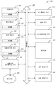
도 7은 본 개시의 일부 예에 따른 메모리 제어기(115)의 개략도를 도시한다. 도 1에 도시된 구성요소들 이외에도, 일부 예에서, 메모리 제어기(115)는 추가 구성요소들을 가질 수 있다. 예를 들어, 제어기(135)는 L2P 캐시의 크기를 관리하고, L2P 캐시에 있는 L2P 테이블의 엔트리들을 관리할 수 있는 등의 L2P 캐시 관리자(750)를 포함할 수 있다. 예를 들어, L2P 캐시 관리자(750)는 하나 이상의 NAND 작동 조건에 기초하여 L2P 캐시의 크기를 증가 또는 감소시키기 위한 도 6에 도시된 방법을 수행할 수 있다. L2P 캐시, 판독 버퍼들 및 기록 버퍼들은 작동 메모리(745)에 저장될 수 있다. 예를 들어, 작동 메모리(745)는 작동 메모리(530)의 일 실시 예일 수 있다. 작동 메모리(745)는 코드, 버퍼, L2P 캐시, 기계 판독 가능 펌에어 명령 등을 저장하는 휘발성 메모리일 수 있다. 작동 메모리(745)는 밀연결되거나 MRAM일 수 있다. 7 shows a schematic diagram of a
도 8은 여기서 논의된 임의의 하나 이상의 기술(예를 들어, 방법론)이 수행할 수 있는 예시적인 기계(800)의 블록도를 도시한다. 대안적인 실시 예들에서, 기계(800)는 독립형 기기로서 작동할 수 있거나 다른 기계들에 연결(예를 들어, 네트워킹)될 수 있다. 네트워킹된 전개에서, 기계(800)는 서버-클라이언트 네트워크 환경들에서 서버 기계, 클라이언트 기계 또는 양자의 역할로 작동할 수 있다. 일례로, 기계(800)은 피어 투 피어(P2P)(또는 다른 분산된) 네트워크 환경에서 피어 기계으로서의 역할을 할 수 있다. 기계(800)는 개인용 컴퓨터(PC), 태블릿 PC, 셋톱 박스(STB), 개인용 정보 단말기(PDA), 모바일 전화, 웹 기기, IoT 기기, 자동차 시스템 또는 해당 기계이 취해질 조치들을 지정하는 명령들을 실행할 수 있는(순차적 또는 그 외) 임의의 기계일 수 있다. 나아가, 단일 기계 만이 도시되어 있지만, "기계"라는 용어는 또한 클라우드 컴퓨팅, SaaS(Software as a Service), 기타 컴퓨터 클러스터 구성들과 같이, 여기서 논의된 임의의 하나 이상의 방법론을 수행하기 위한 명령들의 집합(또는 다수의 집합)을 개별적으로 또는 공동으로 실행하는 임의의 기계 집합을 포함하는 것으로 간주된다. 8 shows a block diagram of an
여기서 설명된 바와 같은 예들은 로직, 구성요소들, 기기들, 패키지들 또는 메커니즘들을 포함하거나 이에 의해 작동할 수 있다. 회로는 하드웨어(예를 들어, 단순 회로, 게이트, 논리 등)를 포함하는 유형의 개체들로 구현된 회로 집단(예를 들어, 집합)이다. 회로 멤버쉽은 시간이 지남에 따라 유연하고 기저 하드웨어 변동이 있을 수 있다. 회로들은 작동시 단독으로 또는 조합하여 특정 작업들을 수행할 수 있는 멤버들을 포함한다. 일례로, 회로의 하드웨어는 불변으로 특정 동작(예를 들어, 하드웨어에 내장된)을 수행하도록 설계될 수 있다. 일례로, 회로의 하드웨어는 특정 작업의 명령들을 인코딩하기 위해 물리적으로 변형된(예를 들어, 자기적으로, 전기적으로, 불변의 질량 입자들의 가동 배치 등) 컴퓨터 판독 가능 매체를 포함하여 물리적 구성들(예를 들어, 실행 유닛들, 트랜지스터들, 단순 회로들 등)에 가변적으로 연결되는 것을 포함할 수 있다. 물리적 구성요소들을 연결할 때, 하드웨어 구성요소의 기저 전기적 속성들은 예를 들어, 절연체에서 도체로 또는 그 반대로 변경된다. 명령들은 참여 하드웨어(예를 들어, 실행 유닛들 또는 로딩 메커니즘)가 작동 중에 특정 작업들의 부분들을 수행하기 위해 가변 연결을 통해 하드웨어에서 회로의 멤버들을 생성할 수 있게 한다. 따라서, 컴퓨터 판독 가능 매체는 기기가 작동할 때 회로의 다른 구성요소들에 통신 가능하게 연결된다. 일례로, 임의의 물리적 구성요소들은 하나보다 많은 회로의 하나 이상의 멤버에 사용될 수 있다. 예를 들어, 동작 하에서, 실행 유닛들은 한 시점에 제1 회로의 제1 회로에 사용될 수 있고, 상이한 시간에 제1 회로에서 제2 회로에 의해, 또는 제2 회로에서 제3 회로에 의해 재사용될 수 있다. Examples as described herein may include or operate on logic, components, devices, packages or mechanisms. A circuit is a group of circuits (e.g., a collection) implemented with entities of the type that include hardware (e.g., simple circuits, gates, logic, etc.). Circuit membership is flexible over time and may have underlying hardware variations. Circuits include members that, when operated, alone or in combination can perform specific tasks. In one example, the hardware of the circuit can be designed to perform certain operations (eg, embedded in the hardware) invariably. In one example, the hardware of a circuit comprises physically configurable physically configurable media including computer readable media (e.g., magnetically, electrically, immovable batches of immutable mass particles, etc.) to encode instructions for a particular task. (Eg, execution units, transistors, simple circuits, etc.). When connecting physical components, the underlying electrical properties of the hardware component change, for example, from insulator to conductor or vice versa. The instructions enable participating hardware (eg, execution units or loading mechanisms) to generate members of circuitry in hardware via a variable connection to perform portions of certain tasks during operation. Thus, the computer-readable medium is communicatively coupled to other components of the circuit when the device is operating. In one example, any physical component may be used on more than one member of more than one circuit. For example, under operation, execution units can be used in a first circuit of a first circuit at a time, and reused by a second circuit in a first circuit, or by a third circuit in a second circuit at different times. Can be.
기계(예를 들어, 컴퓨터 시스템)(800)(예를 들어, 호스트 기기(105), 메모리 소자(110) 등)은 하드웨어 프로세서(802)(예를 들어, 중앙 처리 유닛(CPU), 그래픽 처리 유닛(GPU), 하드웨어 프로세서 코어, 또는 이들의 임의의 조합, 이를테면 메모리 제어기(115) 등), 메인 메모리(804) 및 정적 메모리(806)를 포함할 수 있으며, 이들 중 일부 또는 전부는 인터링크(예를 들어, 버스)(808)를 통해 서로 통신할 수 있다. 기계(800)는 디스플레이 유닛(810), 영숫자 입력 기기(812)(예를 들어, 키보드) 및 사용자 인터페이스(UI) 내비게이션 기기(814)(예를 들어, 마우스)를 더 포함할 수 있다. 일례로, 디스플레이 유닛(810), 입력 기기(812) 및 UI 내비게이션 기기(814)는 터치 스크린 디스플레이일 수 있다. 기계(800)는 저장 소자(예를 들어, 구동 유닛)(816), 신호 생성 기기(818)(예를 들어, 스피커), 네트워크 인터페이스 기기(820) 및 하나 이상의 센서(816), 이를테면 GPS(global positioning system) 센서, 나침반, 가속도계 또는 다른 센서를 추가로 포함할 수 있다. 기계(800)는 하나 이상의 주변 기기(예를 들어, 프린터, 카드 리더 등)와 통신 또는 제어하기 위해 직렬(예를 들어, USB(universal serial bus), 병렬 또는 다른 유선 또는 무선(예를 들어, 적외선(IR), 근거리 통신(NFC) 등)) 연결과 같은 출력 제어기(828)를 포함할 수 있다. The machine (e.g., computer system) 800 (e.g.,
저장 기기(816)는 여기에 설명된 기술들 또는 기능들 중 임의의 하나 이상에 의해 채용되거나 이용되는 하나 이상의 데이터 구조 또는 명령 집합(824)(예를 들어, 소프트웨어)이 저장되는 기계 판독 가능 매체(822)를 포함할 수 있다. 명령들(824)은 또한 기계(800)에 의해 실행되는 동안 메인 메모리(804) 내에, 정적 메모리(806) 내에, 또는 하드웨어 프로세서(802) 내에 완전히 또는 적어도 부분적으로 상주할 수 있다. 예를 들어, 하드웨어 프로세서(802), 메인 메모리(804), 정적 메모리(806) 또는 저장 기기(816)의 하나 또는 임의의 조합은 기계 판독 가능 매체(822)를 구성할 수 있다. The
기계 판독 가능 매체(822)가 단일 매체로서 도시되어 있지만, "기계 판독 가능 매체"라는 용어는 하나 이상의 명령(824)을 저장하도록 구성된 단일 매체 또는 다수의 매체(예를 들어, 중앙 집중식 또는 분산 데이터베이스, 또는 관련 캐시들 및 서버들)를 포함할 수 있다. Although machine-
"기계 판독 가능 매체"라는 용어는 기계(800)에 의한 실행을 위한 명령들을 저장, 인코딩 또는 전달할 수 있고 기계(800)가 본 개시 내용의 기술들 중 임의의 하나 이상을 수행하게 하거나, 또는 그러한 명령들에 의해 사용되거나 그것들과 연관된 데이터 구조들을 저장, 인코딩 또는 전달할 수 있는 임의의 매체를 포함할 수 있다. 비제한적 기계 판독 가능 매체의 예들은 고체 상태 메모리, 및 광학 및 자기 매체를 포함할 수 있다. 일례로, 대량 기계 판독 가능 매체는 불변(예를 들어, 움직이지 않는) 질량체를 갖는 복수의 입자를 갖는 기계 판독 가능 매체를 포함한다. 따라서, 대량 기계 판독 가능 매체는 일시적 전파 신호들이 아니다. 대량 기계 판독 가능 매체의 구체적인 예들은: 비휘발성 메모리, 이를테면 반도체 메모리 소자(예를 들어, EPROM(Electrically Programmable Read-Only Memory), EEPROM(Electrically Erasable Programmable Read-Only Memory)) 및 플래시 메모리 소자; 자기 디스크, 이를테면 내부 하드 디스크 및 이동식 디스크; 광-자기 디스크; 및 CD-ROM 및 DVD-ROM 디스크를 포함할 수 있다. The term "machine-readable medium" may store, encode or transfer instructions for execution by
명령들(824)(예를 들어, 소프트웨어, 프로그램, 운영 체제(OS) 등) 또는 다른 데이터는 저장 소자(821) 상에 저장되고, 프로세서(802)에 의해 사용하기 위해 메모리(804)에 의해 액세스될 수 있다. 메모리(804)(예를 들어, DRAM)는 통상적으로 빠르지 만 휘발성이며, 그에 따라 "오프" 조건에 있는 동안을 포함하여 장기 저장에 적합한 저장 소자(821)(예를 들어, SSD)와 상이한 유형의 저장 장치이다. 명령들(824) 또는 사용자 또는 기계(800)에 의해 사용되는 데이터는 통상적으로 프로세서(802)에 의한 사용을 위해 메모리(804)에 로딩된다. 메모리(804)가 가득 찰 때, 저장 소자(821)로부터의 가상 공간은 메모리(804)를 보충하기 위해 할당될 수 있다; 그러나, 저장 장치(821)는 통상적으로 메모리(804)보다 느리고, 기록 속도는 통상적으로 판독 속도보다 적어도 2배 느리기 때문에, 가상 메모리의 사용은 (메모리(804), 예를 들어 DRAM과는 대조적으로) 저장 소자 레이턴시로 인해 사용자 경험을 크게 감소시킬 수 있다. 나아가, 가상 메모리에 저장 소자(821)를 사용하면 저장 소자(821)의 사용 가능한 수명을 크게 줄일 수 있다. Instructions 824 (eg, software, program, operating system (OS), etc.) or other data are stored on the
가상 메모리와 대조적으로, 가상 메모리 압축(예를 들어, Linux® 커널 특징 "ZRAM")은 메모리의 부분을 압축된 블록 저장 장치로서 사용하여 저장 소자(821) 로의 페이징을 방지한다. 페이징은 그러한 데이터를 저장 소자(821)에 기록할 필요가 있을 때까지 압축된 블록에서 발생한다. 가상 메모리 압축은 사용 가능한 메모리(804)의 크기를 증가시키면서, 저장 소자(821) 상의 웨어를 감소시킨다. In contrast to virtual memory, virtual memory compression (eg, Linux® kernel feature “ZRAM”) uses a portion of memory as a compressed block storage device to prevent paging to
모바일 전자 기기들 또는 모바일 저장 장치에 최적화된 저장 소자들은 전통적으로 MMC 고체 상태 저장 소자(예를 들어, microSD™(micro Secure Digital) 카드 등)를 포함한다. MMC 기기들은 호스트 기기와 다수의 병렬 인터페이스(예를 들어, 8-비트 병렬 인터페이스)를 포함하고, 종종 호스트 기기에서 분리 가능하고 이와 별개의 구성요소들이다. 대조적으로, eMMC™ 기기들은 회로 보드에 부착되어 있고 판독 속도가 직렬 ATA™(Serial AT(Advanced Technology) Attachment 또는 SATA) 기반 SSD 기기들에 필적하는 호스트 기기의 구성요소로 간주된다. 그러나 가상 또는 증강 현실 기기들을 완전히 활성화하고 네트워크 속도를 높이는 등 모바일 기기 성능에 대한 요구가 계속 증가하고 있다. 이러한 요구에 부응하여, 저장 소자들은 병렬에서 직렬 통신 인터페이스들로 전환되었다. 제어기들 및 펌웨어를 비롯한 UFS(Universal Flash Storage) 소자들은 전용 판독/기록 경로들이 있는 저전압 차동 신호(LVDS) 직렬 인터페이스를 사용하여 호스트 기기와 통신하여, 나아가 판독/기록 속도를 향상시킨다. Storage elements optimized for mobile electronic devices or mobile storage devices traditionally include MMC solid state storage elements (eg, micro Secure Digital (microSD™) cards, etc.). MMC devices include a host device and a number of parallel interfaces (eg, 8-bit parallel interfaces), often separate and separate components from the host device. In contrast, eMMC™ devices are considered a component of the host device that is attached to the circuit board and has read speeds comparable to Serial ATA™ (Serial AT (Serial AT) Attachment or SATA) based SSD devices. However, the demand for mobile device performance continues to increase, such as fully enabling virtual or augmented reality devices and increasing network speed. In response to this need, storage elements have been switched from parallel to serial communication interfaces. Universal Flash Storage (UFS) devices, including controllers and firmware, communicate with the host device using a low voltage differential signal (LVDS) serial interface with dedicated read/write paths, further improving read/write speed.
명령들(824)은 또한 다수의 전송 프로토콜(예를 들어, 프레임 릴레이, 인터넷 프로토콜(IP), 전송 제어 프로토콜(TCP), 사용자 데이터그램 프로토콜(UDP), 하이퍼텍스트 전송 프로토콜(HTTP) 등) 중 어느 하나를 이용하여 네트워크 인터페이스 기기(820)를 통해 전송 매체를 사용하여 통신 네트워크(826)을 통해 송신 또는 수신될 수 있다. 예시적인 통신 네트워크들은 다른 것들 중에서도, 근거리 통신망(LAN), 광역 통신망(WAN), 패킷 데이터 네트워크(예를 들어, 인터넷), 모바일 전화 네트워크(예를 들어, 셀룰러 네트워크), POTS(Plain Old Telephone) 네트워크, 및 무선 데이터 네트워크(예를 들어, Wi-Fi®로 알려진 IEEE(Institute of Electrical and Electronics Engineers) 802.11 표준 계열, WiMax®로 알려진 IEEE 802. 16 표준 계열), IEEE 802.15.4 표준 계열, 피어 투 피어(P2P) 네트워크. 를 포함할 수 있다. 일례로, 네트워크 인터페이스 기기(820)는 통신 네트워크(826)에 연결하기 위한 하나 이상의 물리적 잭(예를 들어, 이더넷, 동축 또는 전화 잭) 또는 하나 이상의 안테나를 포함할 수 있다. 일례로, 네트워크 인터페이스 기기(820)는 단일 입력 다중 출력(SIMO), 다중 입력 다중 출력(MIMO), 또는 다중 입력 단일 출력(MISO) 기술 중 적어도 하나를 사용하여 무선으로 통신하기 위한 복수의 안테나를 포함한다. "전송 매체"라는 용어는 기계(800)에 의한 실행을 위한 명령들을 저장, 인코딩 또는 전달할 수 있는 임의의 무형 매체를 포함하는 것으로 간주되어야 하고, 그러한 소프트웨어의 통신을 가능하게 하기 위해 디지털 또는 아날로그 통신 신호들 또는 다른 무형 매체를 포함한다. The
상기한 상세한 설명은 상세한 설명의 부분을 형성하는 첨부 도면들에 대한 참조를 포함한다. 도면들은 예로서 본 발명이 실시될 수 있는 구체적인 실시 예들을 도시한다. 이러한 실시 예들은 여기서 "예"라고도 한다. 그러한 예들은 도시되거나 설명된 것 이외의 요소들을 포함할 수 있다. 그러나, 본 발명자들은 또한 도시되거나 설명된 요소들만이 제공되는 예들을 고려한다. 또한, 본 발명자들은 또한 여기서 도시 또는 설명된 특정 예(또는 이의 하나 이상의 양태) 또는 다른 예들(또는 이의 하나 이상의 양태)에 대하여, 도시되거나 설명된 요소들(또는 이의 하나 이상의 양태)의 임의의 조합 또는 치환을 사용하는 예들을 고려한다. The foregoing detailed description includes references to the accompanying drawings, which form a part of the detailed description. The drawings show, by way of example, specific embodiments in which the invention can be practiced. These embodiments are also referred to herein as "yes". Such examples may include elements other than those shown or described. However, the inventors also contemplate examples in which only elements shown or described are provided. In addition, the present inventors may also use any combination of elements (or one or more aspects thereof) shown or described herein for specific examples (or one or more aspects thereof) or other examples (or one or more aspects thereof) shown or described herein. Or consider examples using substitution.
본 문서에서, "한" 또는 "하나의"라는 용어는 특허 문서에서 일반적으로 사용되는 바와 같이, "적어도 하나" 또는 "하나 이상"의 임의의 다른 예 또는 사용과 무관하게 하나보다 많은을 포함하는 것으로 사용된다. 본 문서에서, "또는"이라는 용어는 달리 표기되지 않는 한, 비배타적인 것을 지칭하기 위해 또는 "A 또는 B"가 "A이지만 B는 아닌", "B이지만 A는 아닌" 그리고 "A 및 B"를 포함할 수 있도록 사용된다. 첨부된 청구항들에서, "포함하는" 및 "여기서"라는 용어들은 "포함한" 및 "이때"의 각각의 용어들의 알기 쉬운 영어와 동등한 것으로 사용된다. 또한, 이하의 청구범위에서, "포함하는" 및 "포함한"이라는 용어들은 개방형이며, 즉 청구범위에서 그러한 용어 뒤에 나열된 것 외에 요소들을 포함하는 시스템, 장치, 물품 또는 프로세스는 여전히 해당 청구항의 범위 내에 속하는 것으로 간주된다. 또한, 이하의 청구범위에서, "제1", "제2"및 "제3" 등의 용어들은 단지 라벨들로서 사용되며, 그것들의 목적에 수치적 요건들을 부과하도록 의도되지 않는다. In this document, the term “one” or “one” includes more than one, regardless of any other example or use of “at least one” or “one or more”, as commonly used in patent documents. Is used. In this document, the terms “or” are used to refer to non-exclusive or “A or B” is “A but not B”, “B but not A” and “A and B,” unless otherwise indicated. It is used to include ". In the appended claims, the terms “comprising” and “here” are used to be equivalent to the plain English of each of the terms “including” and “at this time”. Also, in the claims that follow, the terms “comprising” and “comprising” are open, that is, systems, devices, articles or processes that include elements other than those listed after such terms in the claims are still within the scope of the claims. It is considered to belong. Also, in the following claims, the terms "first", "second" and "third" are used only as labels, and are not intended to impose numerical requirements on their purpose.
다양한 예에서, 여기에 설명된 구성요소들, 제어기들, 프로세서들, 유닛들, 엔진들 또는 테이블들은 다른 것들 중에서도 물리적 기기 상에 저장된 물리적 회로 또는 펌웨어를 포함할 수 있다. 여기서 사용될 때, "프로세서"는 이에 제한되지는 않지만 마이크로 프로세서, 마이크로 제어기, 그래픽 프로세서, 디지털 신호 프로세서(DSP), 또는 프로세서들 또는 멀티 코어 기기들의 그룹을 비롯한 임의의 다른 유형의 프로세서 또는 처리 회로와 같은 임의의 유형의 계산 회로를 의미한다. In various examples, the components, controllers, processors, units, engines or tables described herein may include physical circuitry or firmware stored on a physical device, among others. As used herein, a "processor" is not limited to a microprocessor, microcontroller, graphics processor, digital signal processor (DSP), or any other type of processor or processing circuit, including a group of processors or multi-core devices. Refers to any type of computing circuit, such as.
본 문서에서 사용될 때 "수평"이라는 용어는 임의의 시점에 기판의 실제 배향과 관계 없이, 웨이퍼 또는 다이의 기저와 같이 기판의 통상의 평면 또는 표면에 평행한 평면으로서 정의된다. 수직이라는 용어는 위에서 정의된 바와 같이 수평에 수직인 방향을 지칭한다. "상(on)", "위(over)" 및 "아래(under)"와 같은 전치사들은 기판의 배향에 관계없이 기판의 상부 또는 노출된 표면 상에 있는 통상의 평면 또는 표면에 대하여 정의되며; "상"은 ~ "상"에 놓이는 다른 구조물에 관한 하나의 구조물의 직접 접촉을 제시하도록 의도되는 한편(반대되는 표기가 없는 경우); "위" 및 "아래"라는 용어들은 이에 제한되지는 않지만 그에 따라 구체적으로 식별되지 않는 한 식별된 구조들 간의 직접 접촉을 명시적으로 포함하는 구조들(또는 층들, 특징부들 등)의 상대적 배치를 명시적으로 식별도록 의도된다. 유사하게, 구조가 수평 방향이 아니라 언급된 구조에 관해 수직으로 연장되더라도 그것이 어떤 시점에서 논의 중인 구성의 최외곽 부분인 경우에 구조가 언급된 구조 "위에" 있을 수 있기 때문에, "위" 및 "아래"라는 용어들은 수평 배향들로 제한되지 않는다. As used herein, the term "horizontal" is defined as a plane parallel to the normal plane or surface of the substrate, such as the base of a wafer or die, regardless of the actual orientation of the substrate at any time. The term vertical refers to a direction perpendicular to the horizontal as defined above. Prepositions such as “on,” “over,” and “under” are defined relative to the normal plane or surface on the top or exposed surface of the substrate, regardless of the orientation of the substrate; "Phase" is intended to present direct contact of one structure with respect to another structure placed in ~"Phase" (unless otherwise indicated); The terms “above” and “below” refer to the relative placement of structures (or layers, features, etc.) that explicitly include direct contact between the identified structures, unless limited to this, but are not specifically limited thereto. It is intended to be explicitly identified. Similarly, even if the structure extends vertically with respect to the structure mentioned, not in the horizontal direction, it is "above" and "because the structure may be "above" the mentioned structure in case it is the outermost part of the configuration under discussion at some point The terms "below" are not limited to horizontal orientations.
웨이퍼 및 "기판"이라는 용어들은 여기서 일반적으로 그 위에 집적 회로들이 형성되는 임의의 구조를 나타내고, 그리고 또한 집적 회로 제조의 다양한 스테이지들 동안 그러한 구조들을 나타낸다. 따라서, 이하의 상세한 설명은 한정하는 의미로 취해지지 않으며, 다양한 실시 예의 범위는 첨부된 청구항들에 의해서만, 그러한 청구항들에 부여되는 등가물들의 전체 범위와 함께, 정의된다. The terms wafer and "substrate" here generally refer to any structure on which integrated circuits are formed, and also refer to such structures during various stages of integrated circuit fabrication. Accordingly, the following detailed description is not to be taken in a limiting sense, and the scope of various embodiments is defined only by the appended claims, along with the full scope of equivalents to which such claims are entitled.
본 개시에 따라 여기에 설명된 다양한 실시 예는 메모리 셀들의 수직 구조(예를 들어, 메모리 셀들의 NAND 스트링들)를 이용하는 메모리를 포함한다. 여기서 사용될 때, 방향 형용사들은 메모리 셀들이 형성되는 기판의 표면에 관해 취해질 것이다(즉, 수직 구조는 기판 표면으로부터 연장되는 것으로 간주될 것이고, 수직 구조의 하단은 기판 표면에 가장 가까운 단부로 간주될 것이며, 수직 구조물의 상단은 기판 표면으로부터 가장 먼 단부로 간주될 것이다). Various embodiments described herein in accordance with the present disclosure include memory that utilizes vertical structures of memory cells (eg, NAND strings of memory cells). As used herein, directional adjectives will be taken relative to the surface of the substrate on which memory cells are formed (ie, the vertical structure will be considered to extend from the substrate surface, and the bottom of the vertical structure will be considered the end closest to the substrate surface. , The top of the vertical structure will be considered the farthest end from the substrate surface).
여기서 사용될 때, 수평, 수직, 법선, 평행, 수선 등과 같은 방향 형용사들은 상대적인 배향들을 지칭할 수 있고, 달리 언급되지 않는 한 특정 기하학적 속성들에 대한 엄격한 준수를 요구하지는 않는다. 예를 들어, 여기서 사용될 때, 수직 구조물은 기판의 표면에 엄격히 수선일 필요는 없지만, 대신에 기판의 표면에 대체로 수선일 수 있고, 기판의 표면과 예각을 형성할 수 있다(예를 들어, 60도 - 120도 등). As used herein, directional adjectives such as horizontal, vertical, normal, parallel, vertical, etc. can refer to relative orientations and do not require strict adherence to certain geometric properties unless otherwise stated. For example, as used herein, the vertical structure need not be strictly repaired to the surface of the substrate, but instead can be generally repaired to the surface of the substrate and can form an acute angle with the surface of the substrate (eg, 60 Degrees-120 degrees, etc.).
여기에 설명된 일부 실시 예에서, 상이한 도핑 구성이 소스측 선택 게이트(SGS), 제어 게이트(CG) 및 드레인측 선택 게이트(SGD)에 적용될 수 있으며, 이러한 예에서 이들 각각은 이러한 티어들(예를 들어, 폴리실리콘 등)이 에칭 용액에 노출될 때 상이한 에칭 속도들을 가질 수 있도록 하는 결과, 폴리실리콘으로 형성되거나 적어도 폴리실리콘을 포함할 수 있다. 예를 들어, 3D 반도체 소자에서 모놀리식 필라를 형성하는 공정에서, SGS 및 CG는 오목하게 형성할 수 있는 한편, SGD는 덜 오목하거나 오목하지 않을 수 있다. 그에 따라 이러한 도핑 구성들은 에칭 용액(예를 들어, 테트라메틸암모늄 하이드 록사이드(TMCH))을 사용함으로써 3D 반도체 소자에서 별개의 티어들(예를 들어, SGS, CG 및 SGD)로의 선택적 에칭을 가능하게 할 수 있다. In some embodiments described herein, different doping configurations can be applied to the source side select gate (SGS), the control gate (CG) and the drain side select gate (SGD), each of which in this example each of these tiers (eg For example, polysilicon, etc.) may be formed of polysilicon or include at least polysilicon as a result of having different etch rates when exposed to the etching solution. For example, in the process of forming a monolithic pillar in a 3D semiconductor device, SGS and CG may be formed concave, while SGD may be less concave or not concave. As such, these doping configurations enable selective etching of 3D semiconductor devices into separate tiers (eg, SGS, CG and SGD) by using an etching solution (eg, tetramethylammonium hydroxide (TMCH)). I can do it.
메모리 셀이 작동은 여기서 사용될 때, 메모리 셀로부터 판독, 그에 기록 또는 그것을 소거하는 것을 포함한다. 의도된 상태로 메모리 셀을 배치하는 동작은 여기서 "프로그래밍"으로 지칭되고, 메모리 셀에 기록하거나 그로부터 소거하는 것 양자를 포함할 수 있다(예를 들어, 메모리 셀은 소거된 상태로 프로그래밍될 수 있다). When a memory cell is used herein, it includes reading from, writing to, or erasing it from the memory cell. Placing a memory cell in its intended state is referred to herein as “programming” and can include both writing to and erasing from the memory cell (eg, the memory cell can be programmed to an erased state). ).
본 개시의 하나 이상의 실시 예에 따르면, 메모리 소자의 내부 또는 외부에 위치된 메모리 제어기(예를 들어, 프로세서, 제어기, 펌웨어 등)는 (예를 들어, 웨어 사이클들을 기록, 그것들이 발생할 때 메모리 소자의 동작들을 카운팅, 그것이 개시하는 메모리 소자의 동작들을 추적, 웨어 상태에 대응하는 메모리 소자 특성들을 평가하여 등) 웨어 사이클들의 양 또는 웨어 상태를 결정(예를 들어, 선택, 설정, 조절, 컴퓨팅, 변경, 삭제, 통신, 구성, 유도, 정의, 이용, 수정, 적용 등)할 수 있다. According to one or more embodiments of the present disclosure, a memory controller (eg, processor, controller, firmware, etc.) located inside or outside of a memory device (eg, writes wear cycles, when the memory device occurs) Counting the operations of the memory device, tracking the operations of the memory element it initiates, evaluating memory element characteristics corresponding to the wear state, etc. to determine the amount of wear cycles or wear state (e.g., selecting, setting, adjusting, computing You can change, delete, communicate, configure, derive, define, use, modify, apply, etc.).
본 개시의 하나 이상의 실시 예에 따르면, 메모리 액세스 소자는 각 메모리 동작마다 웨어 사이클 정보를 메모리 소자에 제공하도록 구성될 수 있다. 메모리 소자 제어 회로(예를 들어, 제어 로직)는 웨어 사이클 정보에 대응하는 메모리 소자 성능 변화를 보상하도록 프로그래밍될 수 있다. 메모리 소자는 웨어 사이클 정보를 수신하고 마모 사이클 정보에 응답하여 하나 이상의 작동 파라미터(예를 들어, 값, 특성)를 결정할 수 있다. According to one or more embodiments of the present disclosure, the memory access element may be configured to provide wear cycle information to the memory element for each memory operation. The memory device control circuit (eg, control logic) may be programmed to compensate for memory device performance changes corresponding to wear cycle information. The memory device can receive wear cycle information and determine one or more operating parameters (eg, values, characteristics) in response to wear cycle information.
어떤 요소가 다른 요소 "상"에 있거나 "그에 연결"되거나 "그것과 연결"되는 것으로 언급될 때, 그것은 직접 다른 요소 상에 있거나 그에 연결되거나 그것과 연결될 수 있거나 중간에 다른 요소들이 존재할 수 있다는 것이 이해될 것이다. 대조적으로, 어떤 요소가 다른 요소 "바로 상"에 있거나 "그에 바로 연결"되거나 "그것과 바로 연결"되는 것으로 언급될 때, 그것은 중간에 다른 요소들 또는 층들이 존재할 수 없다. 도면들에서 두 개의 요소가 그것들을 연결하는 선으로 도시되어 있는 경우, 달리 표시되지 않는 한, 두 개의 요소는 연결되거나 직접 연결될 수 있다. When an element is referred to as being "on" or "connected to" another element, or "connected to it", it means that other elements may be directly on or connected to, connected to, or in the middle of other elements. Will be understood. In contrast, when an element is referred to as being “on top of” another element, “directly connected” to it, or “directly connected to it,” it cannot have other elements or layers in between. In the drawings, if two elements are shown with lines connecting them, the two elements may be connected or directly connected, unless indicated otherwise.
여기에 설명된 방법 예들은 적어도 부분적으로 기계 또는 컴퓨터 구현될 수 있다. 일부 예는 상기한 예들에 설명된 바와 같은 방법들을 수행하도록 전자 기기를 구성하도록 작동 가능한 명령들로 인코딩된 컴퓨터 판독 가능한 매체 또는 기계 판독 가능한 매체를 포함할 수 있다. 그러한 방법들의 구현은 코드, 이를테면 마이크로 코드, 어셈블리 언어 코드, 상위 레벨 언어 코드 또는 그 밖에 유사한 것을 포함할 수 있다. 그러한 코드는 다양한 방법을 수행하기 위한 컴퓨터 판독 가능한 명령들을 포함할 수 있다. 코드는 컴퓨터 프로그램 제품들의 부분들을 형성할 수 있다. 나아가, 코드는 이를테면 실행 동안 또는 다른 때에, 하나 이상의 휘발성 또는 비휘발성 유형의 컴퓨터 판독 가능한 매체 상에 유형으로 저장될 수 있다. 이러한 유형의 컴퓨터 판독 가능한 매체들의 예들은 하드 디스크, 착탈식 자기 디스크, 착탈식 광 디스크(예를 들어, 컴팩트 디스크 및 디지털 비디오 디스크), 자기 카세트, 메모리 카드 또는 스틱, 랜덤 액세스 메모리( RAM), 판독 전용 메모리(ROM), 고체 상태 드라이브(SSD), 유니버셜 플래시 저장(UFS) 소자, 내장형 MMC(eMMC, embedded MMC) 소자 및 기타 같은 종류의 것을 포함할 수 있다. The method examples described herein can be at least partially machine or computer implemented. Some examples may include computer readable media or computer readable media encoded with instructions operable to configure the electronic device to perform methods as described in the examples above. Implementations of such methods may include code, such as micro code, assembly language code, high level language code, or the like. Such code can include computer readable instructions for performing various methods. Code can form portions of computer program products. Further, the code may be stored tangibly on one or more volatile or nonvolatile types of computer readable media, such as during execution or at other times. Examples of computer readable media of this type include hard disks, removable magnetic disks, removable optical disks (eg, compact disks and digital video disks), magnetic cassettes, memory cards or sticks, random access memory (RAM), read only Memory (ROM), solid state drive (SSD), universal flash storage (UFS) devices, embedded MMC (eMMC, embedded MMC) devices, and the like.
상기 설명은 제한적이 아니라 예시적인 것으로 의도된다. 예를 들어, 상술된 예들(또는 이의 하나 이상의 양태)은 서로 조합하여 사용될 수 있다. 상기 설명을 검토하면 이를테면 해당 기술분야의 통상의 기술자에 의해 다른 실시 예들이 사용될 수 있다. 그것은 청구항들의 범위 또는 의미를 해석하거나 제한하는 데 사용되지 않을 것이라는 이해로 제출된다. 또한, 상기 상세한 설명에서, 다양한 특징은 본 개시를 간소화하기 위해 함께 그룹화될 수 있다. 이는 청구되지 않은 개시된 특징이 모든 청구항에 필수적인 것임을 의도하는 것으로 해석되어서는 안 된다. 그보다, 본 발명의 대상은 개시된 특정 실시 예의 모든 특징보다 적을 수 있다. 그에 따라, 이하의 청구항들은 이에 의해 상세한 설명으로 통합되며, 각 청구항은 별개의 실시 예로서 독립되고, 그러한 실시 예들은 다양한 조합 또는 치환으로 서로 조합될 수있는 것으로 고려된다. 본 발명의 범위는 첨부된 청구항들을 참조하여, 그러한 청구항들의 권리가 주어지는 균등물들의 전체 범위와 함께 결정되어야 한다. The above description is intended to be illustrative and not restrictive. For example, the above-described examples (or one or more aspects thereof) may be used in combination with each other. Reviewing the above description, for example, other embodiments may be used by those skilled in the art. It is submitted with the understanding that it will not be used to interpret or limit the scope or meaning of the claims. Also, in the detailed description above, various features may be grouped together to simplify the present disclosure. This should not be construed as intending that the disclosed features not claimed are essential to all claims. Rather, the subject matter of the present invention may be less than all the features of the particular embodiment disclosed. Accordingly, the following claims are hereby incorporated into the detailed description, with each claim being independent of separate embodiments, and it is contemplated that such embodiments may be combined with each other in various combinations or substitutions. The scope of the invention should be determined with reference to the appended claims, along with the full scope of equivalents to which such claims are entitled.
다른 비고들 및 예들Other remarks and examples
예 1은 NAND 메모리 소자의 제어기에 의해 수행되는 방법이고, 상기 제어기는 휘발성 메모리와 통신하며, 상기 방법은: 상기 NAND 소자의 제1 작동 조건을 결정하는 단계; 상기 제1 작동 조건에 기초하여, 논리-물리(L2P, Logical to Physical) 캐시에 할당되는 휘발성 메모리의 양이 증가되어야 함을 결정하는 단계; 상기 L2P 캐시에 할당되는 상기 휘발성 메모리의 양이 증가되어야 한다는 결정에 응답하여, 상기 L2P 캐시의 도너 메모리 위치에 할당된 휘발성 메모리의 양을 재할당하는 단계; 및 이전에는 상기 도너 메모리 위치에 할당되었고 이제 상기 L2P 캐시를 증가시키는 결과로서 상기 L2P 캐시에 할당된 상기 휘발성 메모리의 영역의 상기 L2P 캐시에 추가 L2P 테이블 엔트리들을 저장하는 단계를 포함한다. Example 1 is a method performed by a controller of a NAND memory element, the controller communicating with volatile memory, the method comprising: determining a first operating condition of the NAND element; Determining, based on the first operating condition, the amount of volatile memory allocated to a logical-physical (L2P) cache to be increased; In response to determining that the amount of volatile memory allocated to the L2P cache should be increased, reallocating the amount of volatile memory allocated to the donor memory location of the L2P cache; And storing additional L2P table entries in the L2P cache of an area of the volatile memory previously allocated to the donor memory location and now allocated to the L2P cache as a result of increasing the L2P cache.
예 2에서, 예 1의 대상은 선택적으로 상기 제1 작동 조건이 명령 큐 깊이인 것을 포함한다. In Example 2, the subject of Example 1 optionally includes that the first operating condition is a command queue depth.
예 3에서, 예 2의 대상은 선택적으로 P) 캐시가 증가되어야 한다는 단계가 상기 명령 큐 깊이가 결정된 명령 수 임계치를 초과함을 결정하는 단계를 포함하는 것을 포함한다. In Example 3, the subject of Example 2 includes, optionally, P) determining that the cache should be increased comprising determining that the instruction queue depth exceeds a determined instruction number threshold.
예 4에서, 예 2-3 중 어느 하나의 예의 대상은 선택적으로 P) 캐시가 증가되어야 한다는 단계가 상기 명령 큐 깊이가 결정된 명령 수 임계치를 초과하고 판독 명령들 대 기록 명령들의 비가 결정된 비 임계치를 초과함을 결정하는 단계를 포함하는 것을 포함한다. In Example 4, the subject of the example of any of Examples 2-3, wherein P) that the cache should be increased is such that the instruction queue depth exceeds the determined instruction number threshold and the ratio of read instructions to write instructions is determined non-threshold And determining to exceed.
예 5에서, 예 4의 대상은 선택적으로 상기 도너 메모리 위치가 판독 버퍼인 것을 포함한다. In Example 5, the subject of Example 4 optionally includes that the donor memory location is a read buffer.
예 6에서, 예 2-5 중 어느 하나의 예의 대상은 선택적으로 P) 캐시가 증가되어야 한다는 단계가 상기 명령 큐 깊이가 결정된 명령 수 임계치를 초과하고 기록 명령들 대 판독 명령들의 비가 결정된 비 임계치를 초과함을 결정하는 단계를 포함하는 것을 포함한다. In Example 6, the subject of the example of any of Examples 2-5, optionally, P) that the cache should be increased is that the instruction queue depth exceeds the determined instruction count threshold and the ratio of write instructions to read instructions is determined non-threshold And determining to exceed.
예 7에서, 예 6의 대상은 선택적으로 상기 도너 메모리 위치가 기록 버퍼인 것을 포함한다. In Example 7, the subject of Example 6 optionally includes that the donor memory location is a write buffer.
예 8에서, 예 1-7 중 어느 하나의 예의 대상은 선택적으로 상기 도너 메모리 위치가 판독 버퍼 및 기록 버퍼 양자의 일 부분인 것을 포함한다. In Example 8, the subject of any one of Examples 1-7 optionally includes that the donor memory location is part of both a read buffer and a write buffer.
예 9는: 휘발성 메모리; 제어기로서: 상기 NAND 메모리 소자의 제1 작동 조건을 결정하는 동작들; 상기 제1 작동 조건에 기초하여, 논리-물리(L2P, Logical to Physical) 캐시에 할당되는 휘발성 메모리의 양이 증가되어야 함을 결정하는 동작들; 상기 L2P 캐시에 할당되는 상기 휘발성 메모리의 양이 증가되어야 한다는 결정에 응답하여, 상기 L2P 캐시의 도너 메모리 위치에 할당된 휘발성 메모리의 양을 재할당하는 동작들; 및 이전에는 상기 도너 메모리 위치에 할당되었고 이제 상기 L2P 캐시를 증가시키는 결과로서 상기 L2P 캐시에 할당된 상기 휘발성 메모리의 영역의 상기 L2P 캐시에 추가 L2P 테이블 엔트리들을 저장하는 동작들을 수행하는 명령들을 실행하는, 상기 제어기를 포함하는, NAND 메모리 소자이다. Example 9 is: volatile memory; As a controller: operations for determining a first operating condition of the NAND memory element; Based on the first operating condition, determining that an amount of volatile memory allocated to a logical-physical (L2P) cache should be increased; In response to determining that the amount of volatile memory allocated to the L2P cache should be increased, reallocating the amount of volatile memory allocated to the donor memory location of the L2P cache; And executing instructions to perform operations to store additional L2P table entries in the L2P cache of an area of the volatile memory previously allocated to the donor memory location and now allocated to the L2P cache as a result of increasing the L2P cache. It is a NAND memory device, including the controller.
예 10에서, 예 9의 대상은 선택적으로 상기 제1 작동 조건이 명령 큐 깊이인 것을 포함한다. In Example 10, the subject of Example 9 optionally includes that the first operating condition is a command queue depth.
예 11에서, 예 10의 대상은 선택적으로 P) 캐시가 증가되어야 한다는 동작들이 상기 명령 큐 깊이가 결정된 명령 수 임계치를 초과함을 결정하는 동작들을 포함하는 것을 포함한다. In Example 11, the subject of Example 10 includes, optionally, P) operations that require that the cache be increased include operations that determine that the instruction queue depth exceeds a determined instruction number threshold.
예 12에서, 예 10-11 중 어느 하나의 예의 대상은 선택적으로 P) 캐시가 증가되어야 한다는 동작들이 상기 명령 큐 깊이가 결정된 명령 수 임계치를 초과하고 판독 명령들 대 기록 명령들의 비가 결정된 비 임계치를 초과함을 결정하는 동작들을 포함하는 것을 포함한다. In Example 12, the subject of the example of any of Examples 10-11, optionally, P) the operations that the cache should be increased is the non-threshold where the instruction queue depth exceeds the determined instruction count threshold and the ratio of read instructions to write instructions is determined And determining the excess.
예 13에서, 예 12의 대상은 선택적으로 상기 도너 메모리 위치가 판독 버퍼인 것을 포함한다. In Example 13, the subject of Example 12 optionally includes that the donor memory location is a read buffer.
예 14에서, 예 10-13 중 어느 하나의 예의 대상은 선택적으로 P) 캐시가 증가되어야 한다는 동작들이 상기 명령 큐 깊이가 결정된 명령 수 임계치를 초과하고 기록 명령들 대 판독 명령들의 비가 결정된 비 임계치를 초과함을 결정하는 동작들을 포함하는 것을 포함한다. In Example 14, the subject of the example of any of Examples 10-13, optionally, P) operations where the cache should be increased is the non-threshold where the command queue depth exceeds the determined command count threshold and the ratio of write commands to read commands is determined And determining the excess.
예 15에서, 예 14의 대상은 선택적으로 상기 도너 메모리 위치가 기록 버퍼인 것을 포함한다. In Example 15, the subject of Example 14 optionally includes that the donor memory location is a write buffer.
예 16에서, 예 9-15 중 어느 하나의 예의 대상은 선택적으로 상기 도너 메모리 위치가 판독 버퍼 및 기록 버퍼 양자의 일 부분인 것을 포함한다. In Example 16, the subject matter of any of Examples 9-15 optionally includes that the donor memory location is part of both the read buffer and the write buffer.
예 17은 기계에 의해 실행될 때, 상기 기계가 동작들을 수행하게 하는 명령들을 포함하는 기계 판독 가능한 매체이며, 상기 동작들은: NAND 메모리 소자의 제1 작동 조건을 결정하는 동작들; 상기 제1 작동 조건에 기초하여, 논리-물리(L2P, Logical to Physical) 캐시에 할당되는 휘발성 메모리의 양이 증가되어야 함을 결정하는 동작들; 상기 L2P 캐시에 할당되는 상기 휘발성 메모리의 양이 증가되어야 한다는 결정에 응답하여, 상기 L2P 캐시의 도너 메모리 위치에 할당된 휘발성 메모리의 양을 재할당하는 동작들; 및 이전에는 상기 도너 메모리 위치에 할당되었고 이제 상기 L2P 캐시를 증가시키는 결과로서 상기 L2P 캐시에 할당된 상기 휘발성 메모리의 영역의 상기 L2P 캐시에 추가 L2P 테이블 엔트리들을 저장하는 동작들을 포함한다. Example 17 is a machine-readable medium comprising instructions that, when executed by a machine, cause the machine to perform operations, the operations comprising: operations for determining a first operating condition of a NAND memory element; Based on the first operating condition, determining that an amount of volatile memory allocated to a logical-physical (L2P) cache should be increased; In response to determining that the amount of volatile memory allocated to the L2P cache should be increased, reallocating the amount of volatile memory allocated to the donor memory location of the L2P cache; And storing additional L2P table entries in the L2P cache of an area of the volatile memory previously assigned to the donor memory location and now allocated to the L2P cache as a result of increasing the L2P cache.
예 18에서, 예 17의 대상은 선택적으로 상기 제1 작동 조건이 명령 큐 깊이인 것을 포함한다. In Example 18, the subject of Example 17 optionally includes that the first operating condition is a command queue depth.
예 19에서, 예 18의 대상은 선택적으로 P) 캐시가 증가되어야 한다는 동작들이 상기 명령 큐 깊이가 결정된 명령 수 임계치를 초과함을 결정하는 동작들을 포함하는 것을 포함한다. In Example 19, the subject of Example 18 includes, optionally, P) operations that determine that the cache should be increased include operations that determine that the instruction queue depth exceeds a determined instruction number threshold.
예 20에서, 예 18-19 중 어느 하나의 예의 대상은 선택적으로 P) 캐시가 증가되어야 한다는 동작들이 상기 명령 큐 깊이가 결정된 명령 수 임계치를 초과하고 판독 명령들 대 기록 명령들의 비가 결정된 비 임계치를 초과함을 결정하는 동작들을 포함하는 것을 포함한다. In Example 20, the subject of the example of any of Examples 18-19 is optionally P) The number of operations for which the cache should be increased exceeds the instruction count depth determined instruction number threshold and the ratio of read instructions to write instructions determined non-threshold value And determining the excess.
예 21에서, 예 20의 대상은 선택적으로 상기 도너 메모리 위치가 판독 버퍼인 것을 포함한다. In Example 21, the subject of Example 20 optionally includes that the donor memory location is a read buffer.
예 22에서, 예 18-21 중 어느 하나의 예의 대상은 선택적으로 P) 캐시가 증가되어야 한다는 동작들이 상기 명령 큐 깊이가 결정된 명령 수 임계치를 초과하고 기록 명령들 대 판독 명령들의 비가 결정된 비 임계치를 초과함을 결정하는 동작들을 포함하는 것을 포함한다. In Example 22, the subject of the example of any of Examples 18-21 is optionally P) The number of operations for which the cache should be increased exceeds the determined number of instructions threshold and the ratio of write instructions to read instructions is determined non-threshold And determining the excess.
예 23에서, 예 22의 대상은 선택적으로 상기 도너 메모리 위치가 기록 버퍼인 것을 포함한다. In Example 23, the subject of Example 22 optionally includes that the donor memory location is a write buffer.
예 24에서, 예 17-23 중 어느 하나의 예의 대상은 선택적으로 상기 도너 메모리 위치가 판독 버퍼 및 기록 버퍼 양자의 일 부분인 것을 포함한다. In Example 24, the subject matter of any of Examples 17-23 optionally includes that the donor memory location is part of both a read buffer and a write buffer.
예 25는 장치로서, 상기 NAND 소자의 제1 작동 조건을 결정하는 수단들; means for determining based upon the first operational condition, that an amount of volatile memory allocated to a Logical to Physical (L2P) cache should be increased; 상기 L2P 캐시에 할당되는 상기 휘발성 메모리의 양이 증가되어야 한다는 결정에 응답하여, 상기 L2P 캐시의 도너 메모리 위치에 할당된 휘발성 메모리의 양을 재할당하는 수단들; 및 이전에는 상기 도너 메모리 위치에 할당되었고 이제 상기 L2P 캐시를 증가시키는 결과로서 상기 L2P 캐시에 할당된 상기 휘발성 메모리의 영역의 상기 L2P 캐시에 추가 L2P 테이블 엔트리들을 저장하는 수단들을 포함한다. Example 25 is an apparatus, comprising: means for determining a first operating condition of the NAND element; means for determining based upon the first operational condition, that an amount of volatile memory allocated to a Logical to Physical (L2P) cache should be increased; Means for reallocating the amount of volatile memory allocated to the donor memory location of the L2P cache in response to determining that the amount of volatile memory allocated to the L2P cache should be increased; And means for storing additional L2P table entries in the L2P cache of an area of the volatile memory previously allocated to the donor memory location and now allocated to the L2P cache as a result of increasing the L2P cache.
예 26에서, 예 25의 대상은 선택적으로 상기 제1 작동 조건이 명령 큐 깊이인 것을 포함한다. In Example 26, the subject of Example 25 optionally includes that the first operating condition is a command queue depth.
예 27에서, 예 26의 대상은 선택적으로 P) 캐시가 증가되어야 한다는 수단들이 상기 명령 큐 깊이가 결정된 명령 수 임계치를 초과함을 결정하는 수단들을 포함하는 것을 포함한다. In Example 27, the subject of Example 26 includes, optionally, P) means for which the cache should be increased includes means for determining that the instruction queue depth exceeds a determined instruction number threshold.
예 28에서, 예 26-27 중 어느 하나의 예의 대상은 선택적으로 P) 캐시가 증가되어야 한다는 수단들이 상기 명령 큐 깊이가 결정된 명령 수 임계치를 초과하고 판독 명령들 대 기록 명령들의 비가 결정된 비 임계치를 초과함을 결정하는 수단들을 포함하는 것을 포함한다. In Example 28, the subject of the example of any of Examples 26-27 is optionally P) means that the cache should be increased, the instruction queue depth exceeds the determined instruction number threshold and the ratio of read instructions to write instructions is determined non-threshold And means for determining excess.
예 29에서, 예 28의 대상은 선택적으로 도너 메모리 위치가 판독 버퍼인 것을 포함한다. In Example 29, the subject of Example 28 optionally includes that the donor memory location is a read buffer.
예 30에서, 예 26-27 중 어느 하나의 예의 대상은 선택적으로 P) 캐시가 증가되어야 한다는 수단들이 상기 명령 큐 깊이가 결정된 명령 수 임계치를 초과하고 기록 명령들 대 판독 명령들의 비가 결정된 비 임계치를 초과함을 결정하는 수단들을 포함하는 것을 포함한다. In Example 30, the subject of any one of Examples 26-27 is optionally P) means that the cache should be increased, the instruction queue depth exceeds the determined instruction count threshold and the ratio of write instructions to read instructions determined non-threshold And means for determining excess.
예 31에서, 예 30의 대상은 선택적으로 상기 도너 메모리 위치가 기록 버퍼인 것을 포함한다.In Example 31, the subject of Example 30 optionally includes that the donor memory location is a write buffer.
예 32에서, 예 25-31 중 어느 하나의 예의 대상은 선택적으로 상기 도너 메모리 위치가 판독 버퍼 및 기록 버퍼 양자의 일 부분인 것을 포함한다. In Example 32, the subject of any of Examples 25-31 optionally includes that the donor memory location is part of both a read buffer and a write buffer.
Claims (20)
상기 NAND 소자의 제1 작동 조건을 결정하는 단계;
상기 제1 작동 조건에 기초하여, 논리-물리(L2P, Logical to Physical) 캐시에 할당되는 휘발성 메모리의 양이 증가되어야 함을 결정하는 단계;
상기 L2P 캐시에 할당되는 상기 휘발성 메모리의 양이 증가되어야 한다는 결정에 응답하여, 상기 L2P 캐시의 도너 메모리 위치에 할당된 휘발성 메모리의 양을 재할당하는 단계; 및
이전에는 상기 도너 메모리 위치에 할당되었고 이제 상기 L2P 캐시를 증가시키는 결과로서 상기 L2P 캐시에 할당된 상기 휘발성 메모리의 영역의 상기 L2P 캐시에 추가 L2P 테이블 엔트리들을 저장하는 단계를 포함하는, 방법. A method performed by a controller of a NAND memory element, the controller communicating with volatile memory, the method comprising:
Determining a first operating condition of the NAND element;
Determining, based on the first operating condition, that an amount of volatile memory allocated to a logical-physical (L2P) cache should be increased;
In response to determining that the amount of volatile memory allocated to the L2P cache should be increased, reallocating the amount of volatile memory allocated to the donor memory location of the L2P cache; And
And storing additional L2P table entries in the L2P cache of an area of the volatile memory previously allocated to the donor memory location and now allocated to the L2P cache as a result of increasing the L2P cache.
휘발성 메모리;
제어기로서:
상기 NAND 메모리 소자의 제1 작동 조건을 결정하는 동작들;
상기 제1 작동 조건에 기초하여, 논리-물리(L2P, Logical to Physical) 캐시에 할당되는 휘발성 메모리의 양이 증가되어야 함을 결정하는 동작들;
상기 L2P 캐시에 할당되는 상기 휘발성 메모리의 양이 증가되어야 한다는 결정에 응답하여, 상기 L2P 캐시의 도너 메모리 위치에 할당된 휘발성 메모리의 양을 재할당하는 동작들; 및
이전에는 상기 도너 메모리 위치에 할당되었고 이제 상기 L2P 캐시를 증가시키는 결과로서 상기 L2P 캐시에 할당된 상기 휘발성 메모리의 영역의 상기 L2P 캐시에 추가 L2P 테이블 엔트리들을 저장하는 동작들을 수행하는 명령들을 실행하는, 상기 제어기를 포함하는, NAND 메모리 소자. As a NAND memory element,
Volatile memory;
As a controller:
Operations for determining a first operating condition of the NAND memory element;
Based on the first operating condition, determining that an amount of volatile memory allocated to a logical-physical (L2P) cache should be increased;
In response to determining that the amount of volatile memory allocated to the L2P cache should be increased, reallocating the amount of volatile memory allocated to the donor memory location of the L2P cache; And
Executing instructions to perform operations to store additional L2P table entries in the L2P cache of an area of the volatile memory previously allocated to the donor memory location and now allocated to the L2P cache as a result of increasing the L2P cache, A NAND memory device comprising the controller.
NAND 메모리 소자의 제1 작동 조건을 결정하는 동작들;
상기 제1 작동 조건에 기초하여, 논리-물리(L2P, Logical to Physical) 캐시에 할당되는 휘발성 메모리의 양이 증가되어야 함을 결정하는 동작들;
상기 L2P 캐시에 할당되는 상기 휘발성 메모리의 양이 증가되어야 한다는 결정에 응답하여, 상기 L2P 캐시의 도너 메모리 위치에 할당된 휘발성 메모리의 양을 재할당하는 동작들; 및
이전에는 상기 도너 메모리 위치에 할당되었고 이제 상기 L2P 캐시를 증가시키는 결과로서 상기 L2P 캐시에 할당된 상기 휘발성 메모리의 영역의 상기 L2P 캐시에 추가 L2P 테이블 엔트리들을 저장하는 동작들을 포함하는, 기계 판독 가능한 매체. A machine-readable medium comprising instructions that, when executed by a machine, cause the machine to perform operations, the operations being:
Operations for determining a first operating condition of the NAND memory element;
Based on the first operating condition, determining that an amount of volatile memory allocated to a logical-physical (L2P) cache should be increased;
In response to determining that the amount of volatile memory allocated to the L2P cache should be increased, reallocating the amount of volatile memory allocated to the donor memory location of the L2P cache; And
Machine readable medium comprising storing additional L2P table entries in the L2P cache of an area of the volatile memory previously allocated to the donor memory location and now allocated to the L2P cache as a result of increasing the L2P cache .
Applications Claiming Priority (3)
| Application Number | Priority Date | Filing Date | Title |
|---|---|---|---|
| US15/797,812 | 2017-10-30 | ||
| US15/797,812 US10409726B2 (en) | 2017-10-30 | 2017-10-30 | Dynamic L2P cache |
| PCT/US2018/054995 WO2019089193A1 (en) | 2017-10-30 | 2018-10-09 | Dynamic l2p cache |
Publications (1)
| Publication Number | Publication Date |
|---|---|
| KR20200063257A true KR20200063257A (en) | 2020-06-04 |
Family
ID=66245479
Family Applications (1)
| Application Number | Title | Priority Date | Filing Date |
|---|---|---|---|
| KR1020207014899A KR20200063257A (en) | 2017-10-30 | 2018-10-09 | Dynamic L2P cache |
Country Status (5)
| Country | Link |
|---|---|
| US (3) | US10409726B2 (en) |
| KR (1) | KR20200063257A (en) |
| CN (2) | CN114116535A (en) |
| TW (1) | TWI704455B (en) |
| WO (1) | WO2019089193A1 (en) |
Families Citing this family (12)
| Publication number | Priority date | Publication date | Assignee | Title |
|---|---|---|---|---|
| US10409726B2 (en) | 2017-10-30 | 2019-09-10 | Micron Technology, Inc. | Dynamic L2P cache |
| US10970205B2 (en) * | 2018-05-31 | 2021-04-06 | Micron Technology, Inc. | Logical-to-physical data structures for tracking logical block addresses indicative of a collision |
| US11182205B2 (en) * | 2019-01-02 | 2021-11-23 | Mellanox Technologies, Ltd. | Multi-processor queuing model |
| US11237953B2 (en) | 2019-05-21 | 2022-02-01 | Micron Technology, Inc. | Host device physical address encoding |
| US11262946B2 (en) * | 2019-11-25 | 2022-03-01 | Micron Technology, Inc. | Cache-based memory read commands |
| CN111857572B (en) * | 2020-06-20 | 2022-07-26 | 苏州浪潮智能科技有限公司 | Data writing method, device and equipment of TLC solid state disk and storage medium |
| US11520767B2 (en) * | 2020-08-25 | 2022-12-06 | Servicenow, Inc. | Automated database cache resizing |
| TWI798680B (en) * | 2021-04-14 | 2023-04-11 | 群聯電子股份有限公司 | Method for managing host memory buffer, memory storage apparatus and memory control circuit unit |
| CN112965670B (en) * | 2021-04-22 | 2023-08-01 | 群联电子股份有限公司 | Host memory buffer management method, memory device and control circuit unit |
| CN113342040B (en) * | 2021-06-16 | 2022-09-06 | 一飞(海南)科技有限公司 | Method for dynamically acquiring flight performance waypoints of formation of unmanned aerial vehicles and flight controller |
| US20230041949A1 (en) * | 2021-08-05 | 2023-02-09 | Macronix International Co., Ltd. | Programming memory devices |
| CN117149091A (en) * | 2023-10-23 | 2023-12-01 | 四川云海芯科微电子科技有限公司 | Solid state disk data storage method and related device |
Family Cites Families (15)
| Publication number | Priority date | Publication date | Assignee | Title |
|---|---|---|---|---|
| US6493800B1 (en) | 1999-03-31 | 2002-12-10 | International Business Machines Corporation | Method and system for dynamically partitioning a shared cache |
| US6678813B1 (en) | 1999-10-28 | 2004-01-13 | Hewlett-Packard Development Company, L.P. | Dynamically adaptive buffer mechanism |
| US8516219B2 (en) * | 2009-07-24 | 2013-08-20 | Apple Inc. | Index cache tree |
| US9773431B2 (en) * | 2009-11-10 | 2017-09-26 | Maxim Integrated Products, Inc. | Block encryption security for integrated microcontroller and external memory system |
| GB2496798B (en) | 2010-07-27 | 2016-10-12 | Ibm | Logical to physical address mapping in storage systems comprising solid state memory devices |
| US8504774B2 (en) | 2010-10-13 | 2013-08-06 | Microsoft Corporation | Dynamic cache configuration using separate read and write caches |
| US8788742B2 (en) * | 2011-05-23 | 2014-07-22 | International Business Machines Corporation | Using an attribute of a write request to determine where to cache data in a storage system having multiple caches including non-volatile storage cache in a sequential access storage device |
| US8886911B2 (en) | 2011-05-31 | 2014-11-11 | Micron Technology, Inc. | Dynamic memory cache size adjustment in a memory device |
| CN104115231B (en) * | 2011-12-23 | 2017-12-26 | 英特尔公司 | For determining the methods, devices and systems of the access to memory array |
| US9575884B2 (en) * | 2013-05-13 | 2017-02-21 | Qualcomm Incorporated | System and method for high performance and low cost flash translation layer |
| US9734066B1 (en) * | 2014-05-22 | 2017-08-15 | Sk Hynix Memory Solutions Inc. | Workload-based adjustable cache size |
| GB2526849B (en) | 2014-06-05 | 2021-04-14 | Advanced Risc Mach Ltd | Dynamic cache allocation policy adaptation in a data processing apparatus |
| US10254972B2 (en) * | 2016-09-13 | 2019-04-09 | Toshiba Memory Corporation | Storage device and storage system |
| US10459644B2 (en) * | 2016-10-28 | 2019-10-29 | Western Digital Techologies, Inc. | Non-volatile storage system with integrated compute engine and optimized use of local fast memory |
| US10409726B2 (en) | 2017-10-30 | 2019-09-10 | Micron Technology, Inc. | Dynamic L2P cache |
-
2017
- 2017-10-30 US US15/797,812 patent/US10409726B2/en active Active
-
2018
- 2018-10-09 CN CN202111211685.0A patent/CN114116535A/en active Pending
- 2018-10-09 WO PCT/US2018/054995 patent/WO2019089193A1/en active Application Filing
- 2018-10-09 CN CN201880078171.2A patent/CN111433753B/en active Active
- 2018-10-09 KR KR1020207014899A patent/KR20200063257A/en not_active IP Right Cessation
- 2018-10-30 TW TW107138349A patent/TWI704455B/en active
-
2019
- 2019-08-07 US US16/534,710 patent/US11119933B2/en active Active
-
2021
- 2021-09-10 US US17/471,538 patent/US11726919B2/en active Active
Also Published As
| Publication number | Publication date |
|---|---|
| US10409726B2 (en) | 2019-09-10 |
| US20210406187A1 (en) | 2021-12-30 |
| CN111433753B (en) | 2021-11-05 |
| CN114116535A (en) | 2022-03-01 |
| US11726919B2 (en) | 2023-08-15 |
| US20190129856A1 (en) | 2019-05-02 |
| CN111433753A (en) | 2020-07-17 |
| TW201931131A (en) | 2019-08-01 |
| TWI704455B (en) | 2020-09-11 |
| US20190361812A1 (en) | 2019-11-28 |
| US11119933B2 (en) | 2021-09-14 |
| WO2019089193A1 (en) | 2019-05-09 |
Similar Documents
| Publication | Publication Date | Title |
|---|---|---|
| US11726919B2 (en) | Dynamic L2P cache | |
| US11768765B2 (en) | Host device physical address encoding | |
| US11720489B2 (en) | Scheme to improve efficiency of device garbage collection in memory devices | |
| US11735269B2 (en) | Secure erase for data corruption | |
| CN111758091A (en) | Single level cell cache management | |
| CN111538682A (en) | Hybrid logical-to-physical caching scheme | |
| US20210157501A1 (en) | Common pool management | |
| US11163692B2 (en) | Memory constrained translation table management | |
| CN113129978B (en) | Increasing memory access parallelism using parity checking | |
| WO2019046128A1 (en) | Log data storage for flash memory | |
| WO2021035551A1 (en) | Write buffer control in managed memory system | |
| CN114093407A (en) | Memory device, data processing system, method and storage medium | |
| CN113168377A (en) | SLC cache allocation |
Legal Events
| Date | Code | Title | Description |
|---|---|---|---|
| E902 | Notification of reason for refusal | ||
| AMND | Amendment | ||
| E601 | Decision to refuse application | ||
| X091 | Application refused [patent] | ||
| AMND | Amendment | ||
| X601 | Decision of rejection after re-examination |