KR20200062831A - Chemical Liquid Supply Apparatus and Semiconductor Processing Apparatus Having the Same - Google Patents
Chemical Liquid Supply Apparatus and Semiconductor Processing Apparatus Having the Same Download PDFInfo
- Publication number
- KR20200062831A KR20200062831A KR1020180148713A KR20180148713A KR20200062831A KR 20200062831 A KR20200062831 A KR 20200062831A KR 1020180148713 A KR1020180148713 A KR 1020180148713A KR 20180148713 A KR20180148713 A KR 20180148713A KR 20200062831 A KR20200062831 A KR 20200062831A
- Authority
- KR
- South Korea
- Prior art keywords
- chemical
- chemical liquid
- external electrode
- supply pipe
- liquid supply
- Prior art date
Links
Images


Classifications
-
- H—ELECTRICITY
- H01—ELECTRIC ELEMENTS
- H01L—SEMICONDUCTOR DEVICES NOT COVERED BY CLASS H10
- H01L21/00—Processes or apparatus adapted for the manufacture or treatment of semiconductor or solid state devices or of parts thereof
- H01L21/67—Apparatus specially adapted for handling semiconductor or electric solid state devices during manufacture or treatment thereof; Apparatus specially adapted for handling wafers during manufacture or treatment of semiconductor or electric solid state devices or components ; Apparatus not specifically provided for elsewhere
- H01L21/67005—Apparatus not specifically provided for elsewhere
- H01L21/67011—Apparatus for manufacture or treatment
- H01L21/67017—Apparatus for fluid treatment
- H01L21/67028—Apparatus for fluid treatment for cleaning followed by drying, rinsing, stripping, blasting or the like
- H01L21/6704—Apparatus for fluid treatment for cleaning followed by drying, rinsing, stripping, blasting or the like for wet cleaning or washing
-
- H—ELECTRICITY
- H01—ELECTRIC ELEMENTS
- H01L—SEMICONDUCTOR DEVICES NOT COVERED BY CLASS H10
- H01L21/00—Processes or apparatus adapted for the manufacture or treatment of semiconductor or solid state devices or of parts thereof
- H01L21/02—Manufacture or treatment of semiconductor devices or of parts thereof
- H01L21/02041—Cleaning
- H01L21/02043—Cleaning before device manufacture, i.e. Begin-Of-Line process
- H01L21/02052—Wet cleaning only
-
- H—ELECTRICITY
- H01—ELECTRIC ELEMENTS
- H01L—SEMICONDUCTOR DEVICES NOT COVERED BY CLASS H10
- H01L21/00—Processes or apparatus adapted for the manufacture or treatment of semiconductor or solid state devices or of parts thereof
- H01L21/02—Manufacture or treatment of semiconductor devices or of parts thereof
- H01L21/02041—Cleaning
- H01L21/02057—Cleaning during device manufacture
-
- H—ELECTRICITY
- H01—ELECTRIC ELEMENTS
- H01L—SEMICONDUCTOR DEVICES NOT COVERED BY CLASS H10
- H01L21/00—Processes or apparatus adapted for the manufacture or treatment of semiconductor or solid state devices or of parts thereof
- H01L21/67—Apparatus specially adapted for handling semiconductor or electric solid state devices during manufacture or treatment thereof; Apparatus specially adapted for handling wafers during manufacture or treatment of semiconductor or electric solid state devices or components ; Apparatus not specifically provided for elsewhere
- H01L21/67005—Apparatus not specifically provided for elsewhere
- H01L21/67011—Apparatus for manufacture or treatment
- H01L21/67017—Apparatus for fluid treatment
- H01L21/67023—Apparatus for fluid treatment for general liquid treatment, e.g. etching followed by cleaning
-
- H—ELECTRICITY
- H01—ELECTRIC ELEMENTS
- H01L—SEMICONDUCTOR DEVICES NOT COVERED BY CLASS H10
- H01L21/00—Processes or apparatus adapted for the manufacture or treatment of semiconductor or solid state devices or of parts thereof
- H01L21/67—Apparatus specially adapted for handling semiconductor or electric solid state devices during manufacture or treatment thereof; Apparatus specially adapted for handling wafers during manufacture or treatment of semiconductor or electric solid state devices or components ; Apparatus not specifically provided for elsewhere
- H01L21/67005—Apparatus not specifically provided for elsewhere
- H01L21/67011—Apparatus for manufacture or treatment
- H01L21/67017—Apparatus for fluid treatment
- H01L21/67028—Apparatus for fluid treatment for cleaning followed by drying, rinsing, stripping, blasting or the like
- H01L21/6704—Apparatus for fluid treatment for cleaning followed by drying, rinsing, stripping, blasting or the like for wet cleaning or washing
- H01L21/67051—Apparatus for fluid treatment for cleaning followed by drying, rinsing, stripping, blasting or the like for wet cleaning or washing using mainly spraying means, e.g. nozzles
-
- H—ELECTRICITY
- H01—ELECTRIC ELEMENTS
- H01L—SEMICONDUCTOR DEVICES NOT COVERED BY CLASS H10
- H01L21/00—Processes or apparatus adapted for the manufacture or treatment of semiconductor or solid state devices or of parts thereof
- H01L21/67—Apparatus specially adapted for handling semiconductor or electric solid state devices during manufacture or treatment thereof; Apparatus specially adapted for handling wafers during manufacture or treatment of semiconductor or electric solid state devices or components ; Apparatus not specifically provided for elsewhere
- H01L21/67005—Apparatus not specifically provided for elsewhere
- H01L21/67011—Apparatus for manufacture or treatment
- H01L21/67017—Apparatus for fluid treatment
- H01L21/67063—Apparatus for fluid treatment for etching
- H01L21/67075—Apparatus for fluid treatment for etching for wet etching
- H01L21/6708—Apparatus for fluid treatment for etching for wet etching using mainly spraying means, e.g. nozzles
-
- H—ELECTRICITY
- H01—ELECTRIC ELEMENTS
- H01L—SEMICONDUCTOR DEVICES NOT COVERED BY CLASS H10
- H01L21/00—Processes or apparatus adapted for the manufacture or treatment of semiconductor or solid state devices or of parts thereof
- H01L21/67—Apparatus specially adapted for handling semiconductor or electric solid state devices during manufacture or treatment thereof; Apparatus specially adapted for handling wafers during manufacture or treatment of semiconductor or electric solid state devices or components ; Apparatus not specifically provided for elsewhere
- H01L21/67005—Apparatus not specifically provided for elsewhere
- H01L21/67011—Apparatus for manufacture or treatment
- H01L21/6715—Apparatus for applying a liquid, a resin, an ink or the like
-
- H—ELECTRICITY
- H01—ELECTRIC ELEMENTS
- H01L—SEMICONDUCTOR DEVICES NOT COVERED BY CLASS H10
- H01L21/00—Processes or apparatus adapted for the manufacture or treatment of semiconductor or solid state devices or of parts thereof
- H01L21/67—Apparatus specially adapted for handling semiconductor or electric solid state devices during manufacture or treatment thereof; Apparatus specially adapted for handling wafers during manufacture or treatment of semiconductor or electric solid state devices or components ; Apparatus not specifically provided for elsewhere
- H01L21/67005—Apparatus not specifically provided for elsewhere
- H01L21/67242—Apparatus for monitoring, sorting or marking
- H01L21/67259—Position monitoring, e.g. misposition detection or presence detection
-
- H—ELECTRICITY
- H01—ELECTRIC ELEMENTS
- H01L—SEMICONDUCTOR DEVICES NOT COVERED BY CLASS H10
- H01L21/00—Processes or apparatus adapted for the manufacture or treatment of semiconductor or solid state devices or of parts thereof
- H01L21/67—Apparatus specially adapted for handling semiconductor or electric solid state devices during manufacture or treatment thereof; Apparatus specially adapted for handling wafers during manufacture or treatment of semiconductor or electric solid state devices or components ; Apparatus not specifically provided for elsewhere
- H01L21/683—Apparatus specially adapted for handling semiconductor or electric solid state devices during manufacture or treatment thereof; Apparatus specially adapted for handling wafers during manufacture or treatment of semiconductor or electric solid state devices or components ; Apparatus not specifically provided for elsewhere for supporting or gripping
- H01L21/687—Apparatus specially adapted for handling semiconductor or electric solid state devices during manufacture or treatment thereof; Apparatus specially adapted for handling wafers during manufacture or treatment of semiconductor or electric solid state devices or components ; Apparatus not specifically provided for elsewhere for supporting or gripping using mechanical means, e.g. chucks, clamps or pinches
- H01L21/68714—Apparatus specially adapted for handling semiconductor or electric solid state devices during manufacture or treatment thereof; Apparatus specially adapted for handling wafers during manufacture or treatment of semiconductor or electric solid state devices or components ; Apparatus not specifically provided for elsewhere for supporting or gripping using mechanical means, e.g. chucks, clamps or pinches the wafers being placed on a susceptor, stage or support
- H01L21/68764—Apparatus specially adapted for handling semiconductor or electric solid state devices during manufacture or treatment thereof; Apparatus specially adapted for handling wafers during manufacture or treatment of semiconductor or electric solid state devices or components ; Apparatus not specifically provided for elsewhere for supporting or gripping using mechanical means, e.g. chucks, clamps or pinches the wafers being placed on a susceptor, stage or support characterised by a movable susceptor, stage or support, others than those only rotating on their own vertical axis, e.g. susceptors on a rotating caroussel
-
- H—ELECTRICITY
- H05—ELECTRIC TECHNIQUES NOT OTHERWISE PROVIDED FOR
- H05F—STATIC ELECTRICITY; NATURALLY-OCCURRING ELECTRICITY
- H05F3/00—Carrying-off electrostatic charges
-
- H—ELECTRICITY
- H05—ELECTRIC TECHNIQUES NOT OTHERWISE PROVIDED FOR
- H05F—STATIC ELECTRICITY; NATURALLY-OCCURRING ELECTRICITY
- H05F1/00—Preventing the formation of electrostatic charges
Abstract
Description
본 개시의 실시예들은 약액 공급 장치 및 이를 포함하는 반도체 제조 장치에 관한 것이다.Embodiments of the present disclosure relates to a chemical liquid supply device and a semiconductor manufacturing device including the same.
약액 공급 장치는 반도체 제조 공정에서 필요로 하는 다양한 약액을 반도체 제조 장치의 공정 챔버의 내부로 공급하는 장치이다. 예를 들면, 상기 약액 공급 장치는 세정 공정에서 약액을 기판의 표면에 공급하여 기판의 표면에 부착된 각종 오염 물질 또는 도포된 막질과 같이 오염 물질이 아니지만 없애기 위해서 크리닝하는 경우에 훨씬 영향을 줄 수 있는 물질을 제거한다. 상기 세정 공정은 반도체 제조를 위해 필수적인 공정이다. 상기 반도체 제조 공정에서 기판의 표면에 잔류하는 파티클(particle), 유기 오염물, 금속 오염물 등의 오염 물질은 반도체 소자의 특성과 생산 수율에 영향을 미친다. 상기 세정 공정은 반도체 제조 공정의 각 단위 공정의 전후 단계에서 실시될 수 있다.The chemical liquid supply device is a device that supplies various chemical liquids required in the semiconductor manufacturing process into the process chamber of the semiconductor manufacturing device. For example, the chemical liquid supply device is not a contaminant such as various contaminants attached to the surface of the substrate or applied film quality by supplying the chemical liquid to the surface of the substrate during the cleaning process, but may have a much greater effect when cleaning to remove. Remove any substances. The cleaning process is an essential process for semiconductor manufacturing. In the semiconductor manufacturing process, contaminants such as particles, organic contaminants, and metal contaminants remaining on the surface of the substrate affect the properties and production yield of semiconductor devices. The cleaning process may be performed at the front and rear stages of each unit process of the semiconductor manufacturing process.
상기 약액 공급 장치는 저장 용기에 저장된 약액을 저장 용기와 연결된 공급 배관을 통하여 공정 챔버의 내부로 공급한다. 상기 배관을 통과하는 약액은 공급 배관의 내주면 또는 흐르는 경로 상에 위치하는 다양한 부품과의 마찰로 인하여 정전기 현상을 발생시킬 수 있다. 상기 약액에 발생되는 정전기 현상은 정전기적 인력에 의하여 기판 표면에 파티클을 흡착시켜 반도체 공정의 수율을 저하시킬 수 있으며, 대전된 약액의 토출로 기판에 직접적인 전기적 충격을 줄 수 있다. 한편, 상기 약액의 정전기 정도를 제어하기 위하여 배관 내부에 직접적으로 조치를 하기에는 약액과의 반응에 따른 문제등이 있다.The chemical liquid supply device supplies the chemical liquid stored in the storage container to the interior of the process chamber through a supply pipe connected to the storage container. The chemical liquid passing through the pipe may generate an electrostatic phenomenon due to friction with various parts located on the inner circumferential surface or the flowing path of the supply pipe. The electrostatic phenomenon generated in the chemical liquid may adsorb particles on the surface of the substrate by electrostatic attraction, thereby lowering the yield of the semiconductor process, and discharge the charged chemical liquid to directly affect the substrate. On the other hand, in order to directly control the inside of the pipe to control the degree of static electricity of the chemical liquid, there are problems due to reaction with the chemical liquid.
본 개시의 실시예들에 따른 과제는 약액 공급 배관의 내부를 흐르는 약액의 정전기 수준을 약액 공급 배관의 외부에서 제어할 수 있는 약액 공급 장치 및 이를 포함하는 반도체 제조 장치를 제공하는데 있다.An object according to embodiments of the present disclosure is to provide a chemical liquid supply device capable of controlling an electrostatic level of a chemical liquid flowing inside the chemical liquid supply pipe from the outside of the chemical liquid supply pipe and a semiconductor manufacturing device including the same.
본 개시의 실시예들에 따른 약액 공급 장치는 반도체 제조 공정이 진행되는 공정 챔버에 약액을 공급하는 약액 공급 장치이며, 내부에 약액이 흐르며, 상기 약액이 분사되는 분사단이 상기 공정 챔버의 내측으로 연장되는 약액 공급 배관과, 상기 약액 공급 배관의 외측에 위치하는 외부 전극 및 상기 외부 전극에 전원을 인가하는 전원 공급 모듈을 포함할 수 있다.The chemical liquid supply device according to the embodiments of the present disclosure is a chemical liquid supply device that supplies a chemical liquid to a process chamber in which a semiconductor manufacturing process is performed. A chemical liquid flows therein, and an injection end where the chemical liquid is injected is inside the process chamber. It may include an extended chemical supply pipe, an external electrode located outside the chemical supply pipe, and a power supply module that applies power to the external electrode.
본 개시의 실시예들에 따른 약액 공급 장치는 전기 절연성 물질로 형성되며, 내부에 약액이 흐르는 약액 공급 배관 및상기 약액 공급 배관의 외측에 전계를 형성하는 외부 전극을 포함하며, 상기 약액에 전계를 인가하여 상기 약액과 상기 약액 공급 배관의 내주면의 마찰에 의하여 발생되는 정전기를 감소시킬 수 있다.A chemical liquid supply device according to embodiments of the present disclosure is formed of an electrically insulating material, and includes a chemical liquid supply pipe through which a chemical liquid flows, and an external electrode that forms an electric field outside the chemical liquid supply pipe, and applies an electric field to the chemical liquid. By applying, it is possible to reduce static electricity generated by friction between the chemical solution and the inner peripheral surface of the chemical supply pipe.
본 개시의 실시예들에 따른 반도체 제조 장치는 상부가 개방되고 내부 공간을 구비하는 박스 형상의 챔버 하우징 및 상기 챔버 하우징의 바닥면으로부터 돌출되어 회전하는 회전축 및 상기 회전축의 상부에 연결되며 상면에 반도체 기판이 안착되는 회전판을 구비하는 스핀 척을 포함하는 공정 챔버와, 약액이 저장되는 약액 저장 탱크와, 상기 약액 저장 탱크와 연결되는 약액 공급 펌프와, 상기 약액 공급 펌프와 연결되어 상기 약액이 내부를 흐르며, 상기 약액이 분사되는 분사단이 상기 공정 챔버의 회전판의 상부로 연장되는 약액 공급 배관과, 상기 약액 공급 배관의 외측에서 상기 분사단에 인접하여 위치하는 외부 전극 및 상기 외부 전극에 전원을 인가하는 전원 공급 모듈을 포함할 수 있다.The semiconductor manufacturing apparatus according to the embodiments of the present disclosure is connected to an upper portion of the rotating shaft protruding from the bottom surface of the chamber housing and the chamber housing having a box shape with an open top and an inner space, and an upper surface of the semiconductor. A process chamber including a spin chuck having a rotating plate on which a substrate is mounted, a chemical liquid storage tank for storing chemical liquids, a chemical liquid supply pump connected to the chemical liquid storage tank, and a chemical liquid supply pump connected to the chemical liquid storage tank to allow the chemical liquid to internally Flowing, the injection end to which the chemical is injected is applied to the chemical supply pipe extending to the top of the rotating plate of the process chamber, and the external electrode and the external electrode located adjacent to the injection end outside the chemical supply pipe It may include a power supply module.
본 개시의 실시예들에 따르면, 약액 공급 배관을 통하여 공급되는 약액의 정전기 수준을 약액 공급 배관의 외부에서 제어하므로, 약액과 직접 접촉하는데 따른 전극의 부식, 유지 보수의 위험성과 같은 문제를 유발하지 않는다.According to embodiments of the present disclosure, since the electrostatic level of the chemical liquid supplied through the chemical liquid supply pipe is controlled from the outside of the chemical liquid supply pipe, it does not cause problems such as corrosion of the electrode and risk of maintenance due to direct contact with the chemical liquid. Does not.
또한, 본 개시의 실시예들에 따르면, 약액에 대전된 정전기에 따른 아킹(arcing) 현상 또는 기타 급격한 전하 이동 현상과 반도체 기판에 대한 파티클의 흡착을 감소시켜 반도체 공정의 수율을 증가시킬 수 있다.Further, according to embodiments of the present disclosure, arcing due to static electricity charged in the chemical solution or other rapid charge transfer phenomenon and particle adsorption to the semiconductor substrate may be reduced to increase the yield of the semiconductor process.
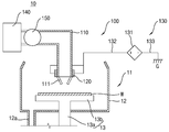
도 1은 본 개시의 일 실시예에 따른 약액 공급 장치와 이를 포함하는 반도체 제조 장치의 개략적인 구성도이다.
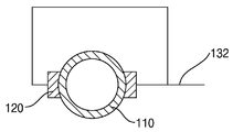
도 2a는 도 1의 약액 공급 배관 및 외부 전극의 부분 수직 단면도이다.
도 2b는 도 2a의 A-A에 대한 수평 단면도이다.
도 3은 본 개시의 다른 실시예에 따른 약액 공급 배관 및 외부 전극의 부분 수평 단면도이다.
도 4a는 본 개시의 다른 실시예에 따른 약액 공급 배관 및 외부 전극의 부분 수직 단면도이다.
도 4b는 도 4a의 B-B에 대한 수평 단면도이다.
도 5a는 본 개시의 다른 실시예에 따른 약액 공급 배관 및 외부 전극의 부분 수직 단면도이다.
도 5b는 도 5a의 C-C에 대한 수평 단면도이다.
도 6a는 본 개시의 다른 실시예에 따른 약액 공급 배관 및 외부 전극의 측면도이다.
도 6b는 도 6a의 D-D에 대한 수평 단면도이다.
도 7은 본 개시의 다른 실시예에 따른 약액 공급 배관 및 외부 전극의 측면도이다.
도 8a는 본 개시의 다른 실시예에 따른 약액 공급 배관과 외부 전극 및 보호층의 수직 단면도이다.
도 8b는 도 8a의 E-E에 따른 수평 단면도이다.
도 9는 본 개시의 다른 실시예에 따른 약액 공급 배관과 외부 전극 및 전원 공급 모듈의 개략적인 구성도이다.
도 10은 본 개시의 다른 실시예에 따른 약액 공급 장치와 이를 포함하는 반도체 제조 장치의 개략적인 구성도이다.1 is a schematic configuration diagram of a chemical liquid supply device and a semiconductor manufacturing device including the same according to an embodiment of the present disclosure.
2A is a partial vertical cross-sectional view of the chemical supply pipe and the external electrode of FIG. 1.
2B is a horizontal sectional view of AA of FIG. 2A.
3 is a partial horizontal cross-sectional view of a chemical supply pipe and an external electrode according to another embodiment of the present disclosure.
4A is a partial vertical cross-sectional view of a chemical supply pipe and an external electrode according to another embodiment of the present disclosure.
4B is a horizontal cross-sectional view of BB of FIG. 4A.
5A is a partial vertical cross-sectional view of a chemical supply pipe and an external electrode according to another embodiment of the present disclosure.
5B is a horizontal cross-sectional view of the CC of FIG. 5A.
6A is a side view of a chemical supply pipe and an external electrode according to another embodiment of the present disclosure.
6B is a horizontal cross-sectional view of DD in FIG. 6A.
7 is a side view of a chemical supply pipe and an external electrode according to another embodiment of the present disclosure.
8A is a vertical cross-sectional view of a chemical supply pipe and an external electrode and a protective layer according to another embodiment of the present disclosure.
8B is a horizontal sectional view according to EE of FIG. 8A.
9 is a schematic configuration diagram of a chemical supply pipe and an external electrode and a power supply module according to another embodiment of the present disclosure.
10 is a schematic configuration diagram of a chemical liquid supply device and a semiconductor manufacturing device including the same according to another embodiment of the present disclosure.
이하에서, 본 개시의 실시예들에 따른 약액 공급 장치 및 이를 포함하는 반도체 제조 장치에 대하여 설명한다.Hereinafter, a chemical liquid supply device and a semiconductor manufacturing device including the same according to embodiments of the present disclosure will be described.
먼저, 본 개시의 일 실시예에 따른 약액 공급 장치 및 반도체 제조 장치에 대하여 설명한다.First, a chemical liquid supply device and a semiconductor manufacturing device according to an embodiment of the present disclosure will be described.
도 1은 본 개시의 일 실시예에 따른 약액 공급 장치와 이를 포함하는 반도체 제조 장치의 개략적인 구성도이다. 도 2a는 도 1의 약액 공급 배관 및 외부 전극의 부분 수직 단면도이다. 도 2b는 도 2a의 A-A에 대한 수평 단면도이다.1 is a schematic configuration diagram of a chemical liquid supply device and a semiconductor manufacturing device including the same according to an embodiment of the present disclosure. 2A is a partial vertical cross-sectional view of the chemical supply pipe and the external electrode of FIG. 1. FIG. 2B is a horizontal sectional view taken along line A-A in FIG. 2A.
본 개시의 일 실시예에 따른 약액 공급 장치(100)는, 도 1과 도 2a 및 도 2b를 참조하면, 약액 공급 배관(110)과 외부 전극(120) 및 전원 공급 모듈(130)을 포함한다. 상기 약액 공급 장치(100)는 약액 저장 탱크(140) 및 약액 공급 펌프(150)를 더 포함할 수 있다. 상기 약액 공급 장치(100)는 반도체 제조 공정이 진행되는 공정 챔버(11)와 함께 반도체 제조 장치(10)를 형성할 수 있다. 즉, 상기 반도체 제조 장치(10)는 공정 챔버(11) 및 약액 공급 장치(100)를 포함할 수 있다.The chemical
상기 약액 공급 장치(100)는, 도 1을 참조하면, 약액 공급 배관(110)이 공정 챔버(11)의 회전 척(chuck)에 안착되는 반도체 기판(W)의 상부로 연장된다. 상기 약액 공급 장치(100)는 반도체 제조 공정중에 반도체 기판(W)의 표면으로 약액을 공급한다. 상기 반도체 제조 공정은 세정 공정 또는 식각 공정과 같은 다양한 공정일 수 있다. 예를 들면, 상기 세정 공정은 탈이온수 또는 유기 용제와 같은 세정액을 이용하여 반도체 기판의 표면에 존재하는 불순물을 제거하는 공정이다. 또한, 상기 식각 공정은 식각액을 이용하여 반도체 기판에 형성되는 박막 중 불필요한 영역을 제거하는 공정이다. 상기 식각 공정은 박막을 제거한 후에, 세척액을 이용하여 식각액을 세척하기 위한 세척 공정이 추가로 진행될 수 있다. 상기 공정 챔버는 식각 챔버 또는 세정 챔버와 같은 다양한 챔버일 수 있다. 상기 약액은 식각액, 세척액 또는 세정액과 같은 반도체 기판의 습식 처리를 위한 약액일 수 있다. 예를 들면, 상기 약액은 HF 또는 SF6을 포함하는 표준 세정액(standard cleaning-1, SC-1) 또는 수산화암모늄(NH4OH)을 순수(pure water)에 용해시킨 수산화암모늄 수용액일 수 있다. 상기 약액은 메탄올, 에탄올, 2-프로판올, n-부탄올, 아이소프로필알코올, 에틸 글리콜, 프로필 글리콜, 부틸 글리콜, 에틸 디글리콜, 부틸 디글리콜, n-펜탄, 아세톤, 에틸 아세테이트, 메틸 에틸 케톤, n-헵탄, 톨루엔, 메틸 이소부틸 케톤, 이소부틸 아세테이트, n-부틸 아세테이트, sec-부틸 알콜, 2-에톡시에탄올, 메틸 n-아밀 케톤, 2-에톡시 에틸 아세테이트, n-디케인, 2-부톡시 에탄올, 이소포렌과 같은 유기 용제일 수 있다.Referring to FIG. 1, the
상기 반도체 제조 공정은 반도체 소자의 품질 및 수율에 큰 영향을 미치는 파티클의 제거가 중요하다. 또한, 상기 파티클은 반도체 기판에 흡착될 수 있으며, 약액에 대전된 정전기 수준에 따라 흡착되는 정도가 증가될 수 있다. 특히, 상기 파티클은 크기가 작은 경우에 화학 필터에 의하여 제거되기 어려우므로, 반도체 기판에 흡착되는 정도를 감소시키기 위해서는 약액의 정전기를 감소 또는 제거하는 것이 필요하다. 또한, 상기 반도체 제조 공정은 반도체 기판의 표면에서 정전기에 의한 아킹 현상 또는 기타 급격한 전하 이동 현상이 발생하는 경우에 반도체 소자의 손상을 초래할 수 있다. 따라서, 상기 반도체 기판에 공급되는 약액은 정전기 수준이 제어되는 것이 반도체 소자의 품질 및 수율을 확보하는데 필요하다. In the semiconductor manufacturing process, it is important to remove particles that greatly affect the quality and yield of the semiconductor device. In addition, the particles may be adsorbed on the semiconductor substrate, and the degree of adsorption may be increased depending on the level of static electricity charged in the chemical solution. In particular, since the particles are difficult to be removed by a chemical filter when the size is small, it is necessary to reduce or remove the static electricity of the chemical solution to reduce the degree of adsorption on the semiconductor substrate. In addition, the semiconductor manufacturing process may cause damage to the semiconductor device when an arcing phenomenon caused by static electricity or other rapid charge transfer phenomenon occurs on the surface of the semiconductor substrate. Therefore, it is necessary for the chemical liquid supplied to the semiconductor substrate to control the level of static electricity to ensure the quality and yield of the semiconductor device.
상기 반도체 제조 장치(10)는, 도 1을 참조하면, 공정 챔버(11) 및 약액 공급 장치(100)를 포함할 수 있다. 상기 공정 챔버(11)는 세정 챔버 또는 식각 챔버일 수 있다. 예를 들면, 상기 공정 챔버(11)는, 도 1을 참조하면, 챔버 하우징(12) 및 스핀 척(13)을 포함할 수 있다. 상기 챔버 하우징(12)은 상부가 개방되고 일정한 용적을 갖는 내부 공간을 갖는 박스 형상으로 형성될 수 있다. 상기 챔버 하우징(12)의 바닥에는 반도체 기판(W)을 고정하여 회전시키는 스핀 척(13)이 배치된다. 또한, 상기 챔버 하우징(12)은 바닥면에 사용된 세정액을 외부로 배출하는 배출관(12a)이 형성된다. 상기 스핀 척(13)은 바닥면으로부터 돌출된 회전축(13a)과 회전축(13a)의 상부에 연결되고 상면에 반도체 기판(W)이 고정되는 회전판(13b)을 포함한다. 상기 회전판(13b)에 반도체 기판(W)을 고정한 후 회전축(13a)을 회전시킴으로써 반도체 기판(W)을 회전할 수 있다. 상기 챔버 하우징(12)의 상부에는 세정액을 공급하는 약액 공급 배관(110)이 배치된다. 상기 약액 공급 배관(110)은 회전하는 반도체 기판(W)의 상면으로 세정액을 공급하여 반도체 기판(W)상에 부착된 오염물을 제거한다.1, the
상기 약액 공급 장치(100)는 약액 공급 배관(110)의 외측에 외부 전극(120)이 위치하며, 외부 전극(120)에 전원 공급 모듈(130)이 전기적으로 연결된다. 상기 약액 공급 장치(100)는 전원 공급 모듈(130)에서 외부 전극(120)으로 전원을 공급하여 약액 공급 배관(110)의 외측에 전계를 형성할 수 있다. 따라서, 상기 약액 공급 장치(100)는 약액과 약액 공급 배관(110)의 내주면의 마찰에 의하여 발생되거나, 기타 다양한 유동에 의한 작용으로 발생되는 정전기를 유동시켜 정전기 수준을 감소시킬 수 있다. 보다 구체적으로는 상기 약액의 마찰은 약액의 내부에 + 전하와 - 전하가 배열되는 정전기 대전을 발생시킬 수 있다. 상기 외부 전극(120)에 의한 전계는 + 전하와 - 전하의 배열 상태를 변화시켜 정전기 대전량을 조절하거나 감소시킬 수 있다. In the chemical
상기 약액 공급 배관(110)은 소정 길이를 갖는 배관 구조물로 형성된다. 상기 약액 공급 배관(110)은 유입단이 약액 공급 펌프(150)에 연결되며, 분사단이 공정 챔버(11)의 내부로 연장된다. 따라서, 상기 약액 공급 배관(110)은 약액 공급 펌프(150)와 공정 챔버(11) 사이의 거리에 따라 소정 길이로 형성될 수 있다. 상기 약액 공급 배관(110)은 반도체 제조 공정의 특성에 따라 다양한 약액을 필요한 유량으로 공급할 수 있다. 따라서, 상기 약액 공급 배관(110)은 적정한 내경을 가지는 관으로 형성될 수 있다. 상기 약액 공급 배관(110)은 공정 챔버(11)의 내부에 상하 방향으로 배치될 수 있고, 경사진 방향으로 배치되어 하부 방향으로 약액을 공급할 수 있다. 상기 약액 공급 배관(110)은 분사단이 공정 챔버(11)의 스핀 척(13)의 상부로부터 소정 높이로 이격되는 위치로 연장될 수 있다. 상기 약액 공급 배관(110)은 약액 공급 펌프(150)에 의하여 약액 저장 탱크(140)로부터 공급되는 약액을 반도체 기판(W)의 표면으로 공급한다.The
한편, 상기 약액 공급 배관(110)은 분사단에 분사 노즐(111)이 추가로 형성될 수 있다. 상기 분사 노즐(111)은 약액 공급 배관(110)의 분사단의 직경을 감소시켜 공급되는 약액의 압력이 증가되도록 할 수 있다.On the other hand, the
상기 약액 공급 배관(110)은 내부를 흐르는 약액에 대한 내화학성을 가지며, 전기 절연성이 있는 물질로 형성될 수 있다. 예를 들면, 상기 약액 공급 배관(110)은 PVDF(Polyvinylidene fluoride), PFA(perfluoroalkoxy) 또는 테프론(Polytetrafluoroethylene; PTFE)와 같은 불소 수지로 형성될 수 있다. 또한, 상기 약액 공급 배관(110)은 스타이렌 수지(Styrene Resin), 폴리아미드 수지(Polyamid Resin) 또는 PEEK(Polyetheretherketone) 수지로 형성될 수 있다.The
상기 외부 전극(120)은 소정 면적을 갖는 평판 또는 블록 형상으로 형성될 수 있다. 상기 외부 전극(120)은 약액 공급 배관(110)의 외측에 필요한 전하를 공급할 수 있는 면적으로 형성된다. 상기 외부 전극(120)은 부착되는 약액 공급 배관(110)의 직경에 따라 적정한 폭과 길이로 형성될 수 있다. 여기서, 상기 폭은 약액 공급 배관(110)의 중심 축 방향에 대하여 수직한 방향의 거리를 의미하며, 길이는 중심 축 방향에 대하여 평행한 방향의 거리를 의미한다. 상기 외부 전극(120)은 약액 공급 배관(110)의 외측에 위치한다. 상기 외부 전극(120)은 1개 또는 2개로 형성될 수 있다. 상기 외부 전극(120)은 1개로 형성되는 경우에 약액 공급 배관(110)의 외주면에서 소정의 위치에 결합될 수 있다. 상기 외부 전극(120)은 바람직하게는 2개로 형성되는 경우에 약액 공급 배관(110)의 외주면에서 원주 방향을 따라 서로 이격되어 결합될 수 있다. 또한, 상기 외부 전극(120)은 외주면의 원주 길이의 1/2보다 작은 폭으로 형성될 수 있다. 상기 외부 전극(120)은 폭과 길이가 같거나, 길이가 폭보다 작은 길이로 형성될 수 있다. 상기 외부 전극(120)은 중심 축을 기준으로 서로 대칭으로 위치할 수 있다.The
상기 외부 전극(120)은 약액 공급 배관(110)의 분사단에 인접한 위치에 위치할 수 있다. 또한, 상기 외부 전극(120)은 하단이 약액 공급 배관(110)의 분사단과 일치하도록 형성될 수 있다. 여기서, 상기 외부 전극(120)의 하단은 도 1에서 하부 방향에 위치하는 단부를 의미한다. 상기 외부 전극(120)은 하단이 약액 공급 배관(110)의 분사단과 일치하도록 위치되는 경우에 약액이 분사되기 전까지 전계에 노출되도록 할 수 있다. 상기 약액은 약액 공급 배관(110)에서 분사될 때까지 전계가 인가되어 정전기가 효과적으로 제거될 수 있다.The
상기 외부 전극(120)은 약액 공급 배관(110)의 외주면에 직접 접촉되거나 외주면과 접촉되지 않고 이격되어 위치할 수 있다. 상기 외부 전극(120)은 약액 공급 배관(110)의 외주면에 별도의 접착제에 의하여 결합될 수 있다. 이러한 경우에 상기 외부 전극(120)은 접착제가 전체적으로 도포되는 경우에 약액 공급 배관(110)의 외주면에서 이격되어 위치할 수 있다. 또한, 상기 외부 전극(120)은 접착제가 부분적으로 도포되는 경우에 약액 공급 배관(110)의 외주면에 부분적으로 직접 접촉될 수 있다. 또한, 상기 외부 전극(120)은 약액 공급 배관(110)의 외주면에 볼트에 의하여 고정될 수 있다. 이러한 경우에 상기 외부 전극(120)은 약액 공급 배관(110)의 외주면에 직접 접촉될 수 있다. 이때, 상기 볼트는 약액 공급 배관(110)을 관통하지 않도록 결합된다. 상기 외부 전극(120)은 약액 공급 배관(110)의 외측에 전계(electric field)를 형성하여 약액과 약액 공급 배관(110)의 내주면의 마찰에 의하여 발생되는 정전기를 감소 또는 제거할 수 있다.The
상기 외부 전극(120)은 구리, 니켈, 알루미늄과 같은 도전성 금속으로 형성될 수 있다. 또한, 상기 외부 전극(120)은 카본과 수지가 혼합된 복합 재료로 형성될 수 있다. 예를 들면, 상기 외부 전극(120)은 탄소를 함유하는 PVDF(polyvinylidenefluoride), 탄소를 함유하는 PEEK(polyetheretherketone), 탄소를 함유하는 PFA(perfluoroalkoxy) 또는 탄소를 함유하는 PTFE(polytetrafluoroethylene)로 형성될 수 있다.The
상기 전원 공급 모듈(130)은 외부 전극(120)에 전기적으로 연결되며, + 전원 또는 - 전원을 인가할 수 있다. 상기 전원 공급 모듈(130)은 외부 전극(120)에 + 단자가 연결되는 경우 - 단자는 접지로 연결될 수 있다. 상기 전원 공급 모듈(130)은 kV 정도의 전압을 공급할 수 있다. 예를 들면, 상기 전원 공급 모듈(130)은 수 kV 레벨의 전압을 외부 전극(120)에 인가할 수 있다. 상기 전원 공급 모듈(130)은 직류 전원 또는 교류 전원을 공급할 수 있다.The
상기 전원 공급 모듈(130)은 전원 소스(131)와 전원선(132) 및 접지선(133)을 포함할 수 있다. 상기 전원 공급 모듈(130)은 외부 전극(120)과 전기적으로 연결된다. 상기 전원 소스(131)는 외부 전극(120)에 직류 전압인 + 전압 또는 - 전압을 인가할 수 있다. 또한, 상기 전원 소스(131)는 외부 전극(120)에 교류 전압을 인가할 수 있다. 상기 전원선(132)은 전원 소스(131)와 외부 전극(120)을 전기적으로 연결한다. 상기 접지선(133)은 전원 소스(131)를 접지(G)로 연결한다.The
상기 약액 저장 탱크(140)는 약액을 저장할 수 있는 일반적인 탱크로 형성될 수 있다. 상기 약액 저장 탱크(140)는 약액에 대한 내약품성을 가지는 수지 재질로 형성될 수 있다. 예를 들면, 상기 약액 저장 탱크(140)는 PVDF(Polyvinylidene fluoride), PFA(perfluoroalkoxy) 또는 테프론(Polytetrafluoroethylene; PTFE)와 같은 불소 수지로 형성될 수 있다. 또한, 상기 약액 저장 탱크(140)는 스타이렌 수지(Styrene Resin), 폴리아미드 수지(Polyamid Resin) 또는 PEEK(Polyetheretherketone) 수지로 형성될 수 있다. 또한, 상기 약액 저장 탱크(140)는 내부식성이 있는 금속 재질로 형성될 수 있다. 예를 들면, 상기 약액 저장 탱크(140)는 스테인레스스틸 재질로 형성될 수 있다.The
상기 약액 공급 펌프(150)는 약액을 공급하는 일반적인 펌프로 형성될 수 있다. 상기 약액 공급 펌프(150)는 약액 저장 탱크(140)와 약액 공급 배관(110) 사이에 연결된다. 상기 약액 공급 펌프(150)는 약액 저장 탱크(140)에 저장되어 있는 약액을 약액 공급 배관(110)으로 공급한다. The
다음은 본 개시의 다른 실시예에 따른 약액 공급 장치에 대하여 설명한다.Next, a chemical liquid supply device according to another embodiment of the present disclosure will be described.
도 3은 본 개시의 다른 실시예에 따른 약액 공급 배관 및 외부 전극의 부분 수평 단면도이다.3 is a partial horizontal cross-sectional view of a chemical supply pipe and an external electrode according to another embodiment of the present disclosure.
본 개시의 다른 실시예에 따른 약액 공급 장치(200)는, 도 1 및 도 3을 참조하면, 약액 공급 배관(110)과 외부 전극(220) 및 전원 공급 모듈(130)을 포함한다. 상기 약액 공급 장치(200)는 도 1과 도 2a 및 도 2b에 따른 약액 공급 장치(100)와 대비하여 외부 전극(220)의 구성이 다르게 형성된다. 따라서, 이하에서, 상기 약액 공급 장치(200)는 차이가 있는 외부 전극(220)을 중심으로 설명한다. 또한, 상기 약액 공급 장치(200)는 도 1과 도 2a 및 도 2b에 따른 약액 공급 장치(100)와 동일 또는 유사한 구성에 대하여 동일한 도면 부호를 사용하며, 여기서 상세한 설명을 생략한다. 한편, 이하에서 설명되는 다른 실시예들에서도 도 1과 도 2a 및 도 2b에 따른 약액 공급 장치(100)와 차이가 있는 구성에 대하여 다른 도면 부호를 부여하고 차이점을 중심으로 설명한다.The chemical
상기 외부 전극(220)은 바람직하게는 4개로 형성되며, 약액 공급 배관(110)의 외주면에 원주 방향을 따라 서로 이격되어 위치할 수 있다. 상기 외부 전극(220)은 외주면의 원주 길이의 1/4보다 작은 폭으로 형성될 수 있다. 상기 외부 전극(220)은 약액 공급 배관(110)의 원주 방향을 따라 동일한 간격으로 이격될 수 있다. 상기 외부 전극(220)은 약액 공급 배관(110)의 외주면에 전체적으로 동일한 간격으로 위치하므로 약액 공급 배관(110)의 외측에 전계를 보다 균일하게 형성할 수 있다.The
다음은 본 개시의 다른 실시예에 따른 약액 공급 장치에 대하여 설명한다.Next, a chemical liquid supply device according to another embodiment of the present disclosure will be described.
도 4a는 본 개시의 다른 실시예에 따른 약액 공급 배관 및 외부 전극의 부분 수직 단면도이다. 도 4b는 도 4a의 B-B에 대한 수평 단면도이다.4A is a partial vertical cross-sectional view of a chemical supply pipe and an external electrode according to another embodiment of the present disclosure. 4B is a horizontal cross-sectional view taken along line B-B of FIG. 4A.
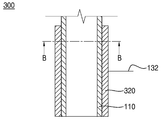
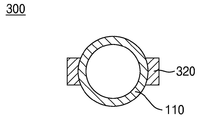
본 개시의 다른 실시예에 따른 약액 공급 장치(300)는, 도 1과 도 4a 및 도 4b를 참조하면, 약액 공급 배관(110)과 외부 전극(320) 및 전원 공급 모듈(130)을 포함한다.The chemical
상기 외부 전극(320)은 길이가 폭보다 긴 형상으로 형성될 수 있다. 예를 들면, 상기 외부 전극(320)은 바 형상 또는 띠 형상으로 형성될 수 있다. 또한, 상기 외부 전극(320)은 약액 공급 배관(110)의 직경 또는 원주 길이보다 큰 길이로 형성될 수 있다. 또한, 상기 외부 전극(320)은 약액에 발생되는 정전기 수준에 따라 충분히 긴 길이로 형성될 수 있다. 상기 외부 전극(320)은 최대로 약액 공급 배관(110)의 길이에 대응되는 길이로 형성될 수 있다.The
상기 외부 전극(320)은 길이 방향이 약액 공급 배관(110)의 축 방향으로 연장되도록 위치할 수 있다. 상기 외부 전극(320)은 적어도 1개로 형성되며, 바람직하게는 적어도 2개로 형성될 수 있다. 따라서, 상기 외부 전극(320)은 약액 공급 배관(110)의 외측에 도 1의 실시예에 따른 외부 전극(320)보다 긴 길이로 전계를 형성할 수 있다. 따라서, 상기 약액 공급 장치는 약액에 보다 긴 시간동안 외부 전극(320)에 의한 전계를 인가하여 정전기를 보다 효율적으로 감소시킬 수 있다. 상기 외부 전극(320)은 적어도 2개로 형성되는 경우에 약액 공급 배관(110)의 외주면을 따라 동일한 간격으로 이격되어 위치할 수 있다. 상기 외부 전극(320)은 각각 또는 함께 전원 공급 모듈(130)에 전기적으로 연결될 수 있다.The
다음은 본 개시의 다른 실시예에 따른 약액 공급 장치에 대하여 설명한다.Next, a chemical liquid supply device according to another embodiment of the present disclosure will be described.
도 5a는 본 개시의 다른 실시예에 따른 약액 공급 배관 및 외부 전극의 부분 수직 단면도이다. 도 5b는 도 5a의 C-C에 대한 수평 단면도이다.5A is a partial vertical cross-sectional view of a chemical supply pipe and an external electrode according to another embodiment of the present disclosure. 5B is a horizontal cross-sectional view of C-C of FIG. 5A.
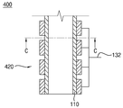
본 개시의 다른 실시예에 따른 약액 공급 장치(400)는, 도 1과 도 5a 및 도 5b를 참조하면, 약액 공급 배관(110)과 외부 전극(420) 및 전원 공급 모듈(130)을 포함한다.The chemical
상기 외부 전극(420)은 길이가 폭과 같거나 짧은 형상으로 형성될 수 있다. 상기 외부 전극(420)은 적어도 2개가 약액 공급 배관(110)의 축 방향을 따라 서로 이격되어 위치한다. 따라서, 상기 외부 전극(420)은 약액 공급 배관(110)의 축 방향을 따라 소정 길이 범위에 적어도 2개가 이격되면서 위치할 수 있다. 또한, 상기 외부 전극(420)은 약액 공급 배관(110)의 원주 방향으로 복수 개가 서로 이격되어 위치할 수 있다. The
상기 약액 공급 장치(400)는 약액 공급 배관(110)의 내부를 흐르는 약액에 보다 긴 시간동안 외부 전극(420)에 의하여 형성되는 전계를 인가하여 정전기를 보다 효율적으로 감소시킬 수 있다. 또한, 상기 약액 공급 장치(400)는 약액이 약액 공급 배관(110)의 내부를 흐를 때 약액에 일정 간격으로 전계를 인가하여 정전기를 감소 또는 제거할 수 있다. 즉, 상기 약액은 약액 공급 배관(110)의 내주면과 마찰에 의하여 부정형적으로 정전기를 발생시킬 수 있으므로 펄스 형식으로 전계를 인가하여 보다 효율적으로 정전기를 감소 또는 제거할 수 있다.The chemical
다음은 본 개시의 다른 실시예에 따른 약액 공급 장치에 대하여 설명한다.Next, a chemical liquid supply device according to another embodiment of the present disclosure will be described.
도 6a는 본 개시의 다른 실시예에 따른 약액 공급 배관 및 외부 전극의 측면도이다. 도 6b는 도 6a의 C-C에 대한 수평 단면도이다.6A is a side view of a chemical supply pipe and an external electrode according to another embodiment of the present disclosure. 6B is a horizontal cross-sectional view of C-C of FIG. 6A.
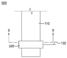
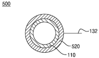
본 개시의 다른 실시예에 따른 약액 공급 장치(500)는, 도 1과 도 6a 및 도 6b를 참조하면, 약액 공급 배관(110)과 외부 전극(520) 및 전원 공급 모듈(130)을 포함한다.The
상기 외부 전극(520)은 링 형상으로 형성되며, 내경이 약액 공급 배관(110)의 외경과 같거나 큰 직경으로 형성될 수 있다. 상기 외부 전극(520)은 약액 공급 배관(110)의 외주면을 감싸도록 위치한다. 상기 외부 전극(520)은 소정 길이로 형성되며, 약액에서 발생되는 정전기의 정도에 따라 적정한 길이로 형성될 수 있다.The
따라서, 상기 약액 공급 장치(500)는 외부 전극(520)에 의하여 약액 공급 배관(110)의 외주면을 따라 균일하게 전계를 형성하여 내부를 흐르는 약액에서 발생되는 정전기를 보다 효율적으로 감소 또는 제거할 수 있다.Therefore, the chemical
다음은 본 개시의 다른 실시예에 따른 약액 공급 장치에 대하여 설명한다.Next, a chemical liquid supply device according to another embodiment of the present disclosure will be described.
도 7은 본 개시의 다른 실시예에 따른 약액 공급 배관 및 외부 전극의 측면도이다. 7 is a side view of a chemical supply pipe and an external electrode according to another embodiment of the present disclosure.
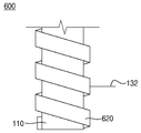
본 개시의 다른 실시예에 따른 약액 공급 장치(600)는, 도 1 및 도 7을 참조하면, 약액 공급 배관(110)과 외부 전극(620) 및 전원 공급 모듈(130)을 포함한다.The chemical
상기 외부 전극(620)은 소정 길이를 갖는 바 형상 또는 띠 형상으로 형성된다. 상기 외부 전극은 약액 공급 배관(110)의 외주면에 나선형을 이루면서 위치할 수 있다. 상기 외부 전극(620)은 적어도 약액 공급 배관(110)의 원주 길이보다 긴 길이로 형성될 수 있다. 상기 외부 전극(620)은 바람직하게는 약액 공급 배관(110)의 원주 길이의 2배 이상의 길이로 형성될 수 있다. 상기 외부 전극(620)은 약액 공급 배관(110)의 외주면을 따라 전계를 균일하게 형성할 수 있다. 또한, 상기 외부 전극(620)은 약액 공급 배관(110)의 축 방향을 따라 일정 간격으로 전하를 인가할 수 있다. The
따라서, 상기 약액 공급 장치(600)는 외부 전극에 의하여 전계를 약액 공급 배관(110)의 원주 방향을 따라 균일하게 인가하면서, 축 방향을 따라 소정 간격으로 인가하여 정전기를 보다 효율적으로 감소 또는 제거할 수 있다.Therefore, the chemical
다음은 본 개시의 다른 실시예에 따른 약액 공급 장치에 대하여 설명한다.Next, a chemical liquid supply device according to another embodiment of the present disclosure will be described.
도 8a는 본 개시의 다른 실시예에 따른 약액 공급 배관과 외부 전극 및 보호층의 수직 단면도이다. 도 8b는 도 8a의 E-E에 따른 수평 단면도이다.8A is a vertical cross-sectional view of a chemical supply pipe and an external electrode and a protective layer according to another embodiment of the present disclosure. 8B is a horizontal sectional view taken along line E-E in FIG. 8A.
본 개시의 다른 실시예에 따른 약액 공급 장치(700)는, 도 1과 도 8a 및 도 8b를 참조하면, 약액 공급 배관(110)과 외부 전극(120)과 전원 공급 모듈(130) 및 보호층(740)을 포함한다.The
상기 보호층(740)은 외부 전극의 노출면을 감싸며, 약액 공급 배관(110)의 외주면에 소정 두께로 코팅되어 형성될 수 있다. 여기서, 상기 노출면은 외부 전극의 외측면과 상측면 및 하측면과 같이 약액 공급 배관(110)의 외주면과 접촉하지 않고 대기중으로 노출되는 면을 의미한다. 상기 보호층(740)은 외부 전극에서 대기중으로 노출되는 표면을 감싸면서 약액 공급 배관(110)의 외주면에 결합된다. 상기 보호층(740)은 외부 전극을 외부의 환경으로부터 보호할 수 있다. 예를 들면, 상기 보호층(740)은 외부의 충격 또는 부식성 화학 약품에 의하여 외부 전극이 손상되는 것을 방지할 수 있다. 한편, 상기 전원 공급 모듈(130)은 보호층(740)을 관통하여 외부 전극에 전기적으로 연결될 수 있다.The protective layer 740 surrounds the exposed surface of the external electrode, and may be formed by coating a predetermined thickness on the outer circumferential surface of the
상기 보호층(740)은 전기 절연성 수지 물질로 형성될 수 있다. 예를 들면, 상기 보호층(740)은 PVDF(polyvinylidenefluoride), PEEK(polyetheretherketone), PFA(perfluoroalkoxy) 및 PTFE(polytetrafluoroethylene)로 이루어진 군에서 선택되는 어느 하나의 수지일 수 있다.The protective layer 740 may be formed of an electrically insulating resin material. For example, the protective layer 740 may be any resin selected from the group consisting of polyvinylidenefluoride (PVDF), polyetheretherketone (PEEK), perfluoroalkoxy (PFA) and polytetrafluoroethylene (PTFE).
한편, 상기 보호층(740)은, 구체적으로 도시하지 않았지만, 도 2a 및 도 2b의 실시예에 따른 약액 공급 장치(100)외에 다른 실시예에 따른 약액 공급 장치들에도 적용될 수 있다. 예를 들면, 상기 보호층(740)은 도 3의 외부 전극(220), 도 4a의 외부 전극(320), 도 5a의 외부 전극(420), 도 6a의 외부 전극(520) 또는 도 7의 외부 전극(620)을 감싸도록 형성될 수 있다.On the other hand, the protective layer 740, although not specifically illustrated, may be applied to chemical solution supply devices according to other embodiments in addition to the chemical
다음은 본 개시의 다른 실시예에 따른 약액 공급 장치에 대하여 설명한다.Next, a chemical liquid supply device according to another embodiment of the present disclosure will be described.
도 9는 본 개시의 다른 실시예에 따른 약액 공급 배관과 외부 전극 및 전원 공급 모듈의 개략적인 구성도이다.9 is a schematic configuration diagram of a chemical supply pipe and an external electrode and a power supply module according to another embodiment of the present disclosure.
본 개시의 다른 실시예에 따른 약액 공급 장치(800)는, 도 1 및 도 9를 참조하면, 약액 공급 배관(110)과 외부 전극(820) 및 전원 공급 모듈(830)을 포함한다. The chemical
상기 외부 전극(820)은 제 1 외부 전극(821) 및 제 2 외부 전극(822)을 포함한다. 상기 제 1 외부 전극(821)과 제 2 외부 전극(822)은 각각 도 2a 및 도 2b, 도 3 또는 도 6a 및 도 6b에 따른 외부 전극으로 형성될 수 있다. 상기 제 1 외부 전극(821)과 제 2 외부 전극(822)은 약액 공급 배관(110)의 축 방향을 따라 서로 이격되어 위치할 수 있다. 상기 제 1 외부 전극(821)과 제 2 외부 전극(822)은 약액 공급 배관(110)의 분사단에 인접하여 서로 이격되어 위치할 수 있다.The
상기 전원 공급 모듈(830)은 제 1 전원 모듈(830a) 및 제 2 전원 모듈(830b)을 포함할 수 있다. 상기 제 1 전원 모듈(830a)과 제 2 전원 모듈(830b)은 각각 도 1의 전원 공급 모듈(130)과 동일 또는 유사하게 형성될 수 있다. 다만, 제 1 전원 모듈(830a)과 제 2 전원 모듈(830b)은 각각 제 1 외부 전극(821) 및 제 2 외부 전극(822)과 전기적으로 연결된다. 또한, 상기 제 1 전원 모듈(830a)과 제 2 전원 모듈(830b)은 서로 반대 극성의 전원을 제 1 외부 전극(821)과 제 2 외부 전극(822)에 인가한다.The
상기 제 1 전원 모듈(830a)은 제 1 전원 소스(831a)와 제 1 전원선(832a) 및 제 1 접지선(833a)을 포함할 수 있다. 상기 제 1 전원 모듈(830a)은 제 1 외부 전극(821)과 전기적으로 연결되며, 제 1 외부 전극(821)에 + 전원을 인가할 수 있다. 상기 제 1 전원선(832a)은 제 1 전원 소스(831a)와 제 1 외부 전극(821)을 전기적으로 연결한다. 제 1 접지선(833a)은 제 1 전원 소스(831a)를 접지로 연결한다. The
상기 제 2 전원 모듈(830b)은 제 2 전원 소스(831b)와 제 2 전원선(832b) 및 제 2 접지선(833b)을 포함할 수 있다. 상기 제 2 전원 모듈(830b)은 제 2 외부 전극(822)과 전기적으로 연결되며, 제 2 외부 전극(822)에 - 전원을 인가할 수 있다. 상기 제 2 전원선(832b)은 제 2 전원 소스(831b)와 제 2 외부 전극(822)을 전기적으로 연결한다. 제 2 접지선(833b)은 제 2 전원 소스(831b)를 접지로 연결한다.The
상기 약액 공급 장치(800)는 약액 공급 배관(110)의 외부에 위치하는 외부 전극(820)에 + 전하와 - 전하를 순차적으로 공급한다. 따라서, 상기 약액 공급 장치(800)는 약액 공급 배관(110)의 내부를 흐르는 약액에 발생되는 정전기를 보다 효율적으로 제거할 수 있다.The chemical
다음은 본 개시의 다른 실시예에 따른 약액 공급 장치에 대하여 설명한다.Next, a chemical liquid supply device according to another embodiment of the present disclosure will be described.
도 10은 본 개시의 다른 실시예에 따른 약액 공급 장치와 이를 포함하는 반도체 제조 장치의 개략적인 구성도이다.10 is a schematic configuration diagram of a chemical liquid supply device and a semiconductor manufacturing device including the same according to another embodiment of the present disclosure.
본 개시의 다른 실시예에 따른 약액 공급 장치(900)는, 도 10을 참조하면, 약액 공급 배관(110)과 외부 전극(120)과 전원 공급 모듈(130) 및 전하 측정 모듈(950)을 포함한다.The
상기 약액 공급 장치(900)는 약액 공급 배관(110)에서 공급되는 약액의 정전기 대전량에 따라 전원 공급 모듈(130)에서 공급되는 전원의 크기를 조절할 수 있다. 예를 들면, 상기 약액 공급 배관(110)에서 공급되는 약액의 정전기 대전량이 많은 경우에 전원 공급 모듈(130)에서 공급되는 전압의 크기를 증가시켜 약액의 정전기 대전량을 감소시킬 수 있다. 따라서, 상기 약액 공급 장치(900)는 측정된 결과에 근거하여 약액에 발생되는 정전기를 제어할 수 있다.The
상기 전하 측정 모듈(950)은 약액의 정전기 대전량을 나타내는 전하량을 측정하는데 사용되는 패러데이 컵 어셈블리(Faraday Cup Assemmbly)(또는 패러데이 케이지 어셈블리(Faraday Cage Assembly))로 형성될 수 있다. 상기 패러데이 컵은 전하량을 측정하는 일반적인 구성으로 형성될 수 있다. 예를 들면, 상기 패러테이 컵 어셈블리는 약액의 이온 수를 측정하는 페러데이 컵과 패러데이 컵의 외측을 감싸는 커버 및 패러데이 컵에 연결되는 다수의 패러데이 케이블을 포함할 수 있다. 상기 전하 측정 모듈(950)은 약액 공급 배관(110)의 하부에 위치하여 약액 공급 배관(110)에서 분사되는 약액의 전하량을 측정할 수 있다. 상기 전하 측정 모듈(950)은 측정시에 수동으로 공정 챔버의 내부로 이동할 수 있다. 또한, 상기 전하 측정 모듈(950)은 별도의 이동수단(미도시)에 의하여 공정 챔버의 내부로 이동할 수 있다. 상기 전하 측정 모듈(950)은 반도체 공정이 시작되기 전에 약액 공급 배관(110)에서 공급되는 약액의 전하량을 측정한다.The
또한, 상기 전하 측정 모듈(950)은 비접촉식 정전기 측정 센서일 수 있다. 예를 들면, 상기 전하 측정 모듈(950)은 전압 측정기, 표면 전위계, 전하 측정기, 또는 정전기 방전 검출기 등일 수 있다. 또한, 상기 전하 측정 모듈(950)은 정전 전압계(electrostatic Voltmeter) 또는 CPM(Charged Plate Monitor)일 수 있다. 상기 비접촉식 정전기 측정 센서는 약액 공급 배관(110)에서 공급되는 약액과 일정 거리로 이격된 위치에서 약액의 정전기 수준을 측정할 수 있다.Further, the
이상, 첨부된 도면을 참조하여 본 개시에 따른 실시 예들을 설명하였지만, 본 발명이 속하는 기술 분야에서 통상의 지식을 가진 자는 본 발명이 그 기술적 사상이나 필수적인 특징을 변경하지 않고서 다른 구체적인 형태로 실시될 수 있다는 것을 이해할 수 있을 것이다. 이상에서 기술한 실시 예는 모든 면에서 예시적인 것이며 한정적이 아닌 것으로 이해하여야 한다.The embodiments according to the present disclosure have been described above with reference to the accompanying drawings, but those having ordinary knowledge in the technical field to which the present invention pertains may be implemented in other specific forms without changing the technical spirit or essential features of the present invention. You will understand that you can. It should be understood that the embodiments described above are illustrative in all respects and not restrictive.
10: 반도체 제조 장치
100, 200, 300, 400, 500, 600, 700, 800, 900: 약액 공급 장치
110: 약액 공급 배관
120, 220, 320, 420, 520, 620, 720, 820: 외부 전극
821: 제 1 외부 전극
822: 제 2 외부 전극
130, 830: 전원 공급 모듈
131: 전원 소스
132: 전원선
133: 접지선
140: 약액 저장 탱크
150: 약액 공급 펌프
760: 보호층
970: 전하 측정 모듈10: semiconductor manufacturing apparatus
100, 200, 300, 400, 500, 600, 700, 800, 900: chemical supply
110: chemical supply pipe
120, 220, 320, 420, 520, 620, 720, 820: external electrode
821: first external electrode 822: second external electrode
130, 830: power supply module 131: power source
132: power line 133: ground wire
140: chemical storage tank 150: chemical supply pump
760: protective layer 970: charge measurement module
Claims (20)
내부에 약액이 흐르며, 상기 약액이 분사되는 분사단이 상기 공정 챔버의 내측으로 연장되는 약액 공급 배관과,
상기 약액 공급 배관의 외측에 위치하는 외부 전극 및
상기 외부 전극에 전원을 인가하는 전원 공급 모듈을 포함하는 약액 공급 장치.A chemical liquid supply device that supplies a chemical liquid to a process chamber in which a semiconductor manufacturing process proceeds,
A chemical liquid supply pipe through which a chemical liquid flows, and an injection end where the chemical liquid is injected extends into the process chamber;
An external electrode located outside the chemical supply pipe and
Chemical supply device comprising a power supply module for applying power to the external electrode.
상기 약액이 저장되는 약액 저장 탱크 및
상기 약액 저장 탱크와 상기 약액 공급 배관 사이에 위치하는 약액 공급 펌프를 더 포함하는 약액 공급 장치. According to claim 1,
A chemical liquid storage tank in which the chemical liquid is stored, and
And a chemical liquid supply pump positioned between the chemical liquid storage tank and the chemical liquid supply pipe.
상기 약액 공급 배관은 전기 절연성 물질로 형성되는 약액 공급 장치.According to claim 1,
The chemical supply pipe is a chemical supply device formed of an electrically insulating material.
상기 외부 전극은 상기 약액 공급 배관의 외주면과 직접 접촉하거나 이격되어 위치하는 약액 공급 장치.According to claim 1,
The external electrode is a chemical liquid supply device that is located in direct contact with or spaced apart from the outer peripheral surface of the chemical liquid supply pipe.
상기 외부 전극은 적어도 2개로 형성되고, 상기 약액 공급 배관의 원주 길이의 1/2보다 작은 폭으로 형성되며, 상기 약액 공급 배관의 외주면에 원주 방향을 따라 이격되어 위치하는 약액 공급 장치. According to claim 1,
The external electrode is formed of at least two, and is formed with a width smaller than 1/2 of the circumferential length of the chemical supply pipe, and the chemical liquid supply device is spaced apart along the circumferential direction on the outer circumferential surface of the chemical supply pipe.
상기 외부 전극은 폭과 같거나 짧은 길이로 형성되는 약액 공급 장치.The method of claim 5,
The external electrode is a chemical supply device formed of a length equal to or shorter than the width.
상기 외부 전극은 폭보다 긴 길이로 형성되며,
적어도 2개가 상기 약액 공급 배관의 축 방향을 따라 이격되어 위치하는 약액 공급 장치.The method of claim 5,
The external electrode is formed to have a length longer than the width,
At least two chemical liquid supply devices are spaced apart along the axial direction of the chemical supply pipe.
상기 외부 전극은 폭보다 긴 길이로 형성되는 약액 공급 장치.The method of claim 5,
The external electrode is a chemical supply device formed to a length longer than the width.
상기 외부 전극은 상기 약액 공급 배관의 중심 축을 기준으로 서로 대칭으로 위치하는 약액 공급 장치.The method of claim 5,
The external electrodes are chemical liquid supply devices positioned symmetrically to each other with respect to a central axis of the chemical liquid supply pipe.
상기 외부 전극은 상기 약액 공급 배관의 외경과 같거나 큰 내경을 갖는 링 형상으로 형성되는 약액 공급 장치.According to claim 1,
The external electrode is a chemical liquid supply device formed in a ring shape having an inner diameter equal to or greater than the outer diameter of the chemical liquid supply pipe.
상기 외부 전극은 띠 형상 또는 바 형상으로 형성되며, 상기 약액 공급 배관의 외주면을 따라 나선형으로 이루면서 위치하는 약액 공급 장치.According to claim 1,
The external electrode is formed in a strip shape or a bar shape, and the chemical liquid supply device is located while forming a spiral along the outer peripheral surface of the chemical liquid supply pipe.
상기 외부 전극은 하단이 상기 약액 공급 배관의 분사단과 일치하도록 위치하는 약액 공급 장치.According to claim 1,
The external electrode is a chemical supply device, the lower end of which is positioned to coincide with the injection end of the chemical supply pipe.
전기 절연성 수지 물질로 형성되며, 상기 외부 전극의 노출면을 감싸면서 상기 약액 공급 배관의 외주면에 소정 두께로 코팅되는 보호층을 포함하는 약액 공급 장치.According to claim 1,
A chemical liquid supply device formed of an electrically insulating resin material and including a protective layer coated with a predetermined thickness on an outer circumferential surface of the chemical liquid supply pipe while surrounding an exposed surface of the external electrode.
상기 외부 전극은 상기 약액 공급 배관의 외주면에서 서로 이격되어 위치하는 제 1 외부 전극 및 제 2 외부 전극을 포함하고,
상기 전원 공급 모듈은 상기 제 1 외부 전극에 전원을 공급하는 제 1 전원 모듈 및 상기 제 2 외부 전극에 전원을 공급하는 제 2 전원 모듈을 포함하며,
상기 제 1 전원 모듈은 상기 제 2 전원 모듈과 반대 극성의 전원을 인가하는 약액 공급 장치.According to claim 1,
The external electrode includes a first external electrode and a second external electrode spaced apart from each other on an outer circumferential surface of the chemical supply pipe,
The power supply module includes a first power module supplying power to the first external electrode and a second power module supplying power to the second external electrode,
The first power module is a chemical supply device for applying a power of the opposite polarity to the second power module.
상기 약액 공급 배관에서 분사되는 상기 약액의 전하량을 측정하는 전하 측정 모듈을 포함하는 약액 공급 장치.According to claim 1,
Chemical charge supply device including a charge measurement module for measuring the amount of charge of the chemical liquid injected from the chemical supply pipe.
상기 약액 공급 배관의 외측에 전계를 형성하는 외부 전극을 포함하며,
상기 약액에 전계를 인가하여 상기 약액과 상기 약액 공급 배관의 내주면의 마찰에 의하여 발생되는 정전기를 감소시키는 약액 공급 장치.It is formed of an electrically insulating material, and the chemical liquid supply pipe through which the chemical liquid flows, and
It includes an external electrode forming an electric field on the outside of the chemical supply pipe,
A chemical liquid supply device that applies an electric field to the chemical liquid to reduce static electricity generated by friction between the chemical liquid and an inner peripheral surface of the chemical liquid supply pipe.
상기 외부 전극에 + 전원 또는 - 전원을 인가하는 전원 공급 모듈을 더 포함하는 약액 공급 장치.The method of claim 16,
A chemical supply device further comprising a power supply module that applies + or-power to the external electrode.
상기 약액 공급 배관에서 분사되는 상기 약액의 전하량을 측정하는 전하 측정 모듈을 포함하는 약액 공급 장치.The method of claim 16
Chemical charge supply device including a charge measurement module for measuring the amount of charge of the chemical liquid injected from the chemical supply pipe.
상기 외부 전극은 적어도 2개로 형성되고, 상기 약액 공급 배관의 원주 길이의 1/2보다 작은 폭으로 형성되며, 상기 약액 공급 배관의 외주면에 원주 방향을 따라 이격되어 위치하며,
상기 외부 전극의 하단은 상기 약액 공급 배관의 분사단과 일치하도록 위치하는 약액 공급 장치.The method of claim 16
The external electrode is formed of at least two, is formed to a width smaller than 1/2 of the circumferential length of the chemical supply pipe, and is spaced apart along the circumferential direction on the outer circumferential surface of the chemical supply pipe,
The lower end of the external electrode is positioned to match the injection end of the chemical supply pipe, the chemical supply device.
약액이 저장되는 약액 저장 탱크와,
상기 약액 저장 탱크와 연결되는 약액 공급 펌프와,
상기 약액 공급 펌프와 연결되어 상기 약액이 내부를 흐르며, 상기 약액이 분사되는 분사단이 상기 공정 챔버의 회전판의 상부로 연장되는 약액 공급 배관과,
상기 약액 공급 배관의 외측에서 상기 분사단에 인접하여 위치하는 외부 전극 및
상기 외부 전극에 전원을 인가하는 전원 공급 모듈을 포함하는 반도체 제조 장치.A box-shaped chamber housing having an open top and an interior space, and a rotating shaft protruding from the bottom surface of the chamber housing and a spin chuck connected to an upper portion of the rotating shaft and having a rotating plate on which a semiconductor substrate is mounted on an upper surface. A process chamber,
A chemical liquid storage tank in which the chemical liquid is stored,
A chemical supply pump connected to the chemical storage tank,
A chemical liquid supply pipe connected to the chemical liquid supply pump, through which the chemical liquid flows, and an injection end through which the chemical liquid is injected extends to an upper portion of a rotating plate of the process chamber;
An external electrode located adjacent to the injection end on the outside of the chemical supply pipe and
A semiconductor manufacturing apparatus including a power supply module that applies power to the external electrode.
Priority Applications (3)
| Application Number | Priority Date | Filing Date | Title |
|---|---|---|---|
| KR1020180148713A KR20200062831A (en) | 2018-11-27 | 2018-11-27 | Chemical Liquid Supply Apparatus and Semiconductor Processing Apparatus Having the Same |
| US16/387,779 US20200168478A1 (en) | 2018-11-27 | 2019-04-18 | Chemical liquid supply apparatus and semiconductor processing apparatus having the same |
| CN201910583940.0A CN111223792A (en) | 2018-11-27 | 2019-07-01 | Chemical liquid supply device and semiconductor processing device having the same |
Applications Claiming Priority (1)
| Application Number | Priority Date | Filing Date | Title |
|---|---|---|---|
| KR1020180148713A KR20200062831A (en) | 2018-11-27 | 2018-11-27 | Chemical Liquid Supply Apparatus and Semiconductor Processing Apparatus Having the Same |
Publications (1)
| Publication Number | Publication Date |
|---|---|
| KR20200062831A true KR20200062831A (en) | 2020-06-04 |
Family
ID=70770966
Family Applications (1)
| Application Number | Title | Priority Date | Filing Date |
|---|---|---|---|
| KR1020180148713A KR20200062831A (en) | 2018-11-27 | 2018-11-27 | Chemical Liquid Supply Apparatus and Semiconductor Processing Apparatus Having the Same |
Country Status (3)
| Country | Link |
|---|---|
| US (1) | US20200168478A1 (en) |
| KR (1) | KR20200062831A (en) |
| CN (1) | CN111223792A (en) |
Cited By (1)
| Publication number | Priority date | Publication date | Assignee | Title |
|---|---|---|---|---|
| KR20230103525A (en) * | 2021-12-31 | 2023-07-07 | 세메스 주식회사 | Substrate processing apparatus |
Families Citing this family (2)
| Publication number | Priority date | Publication date | Assignee | Title |
|---|---|---|---|---|
| JP7297591B2 (en) * | 2019-08-09 | 2023-06-26 | 東京エレクトロン株式会社 | Substrate processing apparatus and manufacturing method thereof |
| US11721561B2 (en) * | 2020-07-17 | 2023-08-08 | Taiwan Semiconductor Manufacturing Company Ltd. | System and method for supplying chemical solution |
Family Cites Families (4)
| Publication number | Priority date | Publication date | Assignee | Title |
|---|---|---|---|---|
| DE3423462A1 (en) * | 1984-06-26 | 1986-01-02 | Uniroyal Englebert Textilcord S.A., Steinfort | METHOD AND DEVICE FOR ELECTROSTATICLY FLOCKING A THREAD OR YARN-SHAPED MATERIAL |
| CN102282916A (en) * | 2009-01-13 | 2011-12-14 | 里巴贝鲁株式会社 | Apparatus and method for producing plasma |
| US20140299273A1 (en) * | 2013-04-08 | 2014-10-09 | Lam Research Corporation | Multi-segment electrode assembly and methods therefor |
| JP6342838B2 (en) * | 2014-06-25 | 2018-06-13 | 東京エレクトロン株式会社 | Processing liquid supply method, processing liquid supply apparatus, and computer-readable recording medium |
-
2018
- 2018-11-27 KR KR1020180148713A patent/KR20200062831A/en unknown
-
2019
- 2019-04-18 US US16/387,779 patent/US20200168478A1/en not_active Abandoned
- 2019-07-01 CN CN201910583940.0A patent/CN111223792A/en not_active Withdrawn
Cited By (1)
| Publication number | Priority date | Publication date | Assignee | Title |
|---|---|---|---|---|
| KR20230103525A (en) * | 2021-12-31 | 2023-07-07 | 세메스 주식회사 | Substrate processing apparatus |
Also Published As
| Publication number | Publication date |
|---|---|
| US20200168478A1 (en) | 2020-05-28 |
| CN111223792A (en) | 2020-06-02 |
Similar Documents
| Publication | Publication Date | Title |
|---|---|---|
| KR20200062831A (en) | Chemical Liquid Supply Apparatus and Semiconductor Processing Apparatus Having the Same | |
| US10435234B2 (en) | Chemical liquid supply apparatus and semiconductor processing apparatus having the same | |
| US20140290703A1 (en) | Substrate processing apparatus and substrate processing method | |
| Volný et al. | Surface effects and electrochemical cell capacitance in desorption electrospray ionization | |
| JP2008153322A (en) | Two-fluid nozzle, substrate processor, and method for processing substrates | |
| US9593030B2 (en) | Liquid treatment apparatus and liquid treatment method | |
| KR101980994B1 (en) | Substrate processing device and substrate processing method | |
| KR100830265B1 (en) | Substrate processing apparatus and substrate processing method | |
| US20080178917A1 (en) | Substrate processing apparatus and substrate processing method | |
| KR101807002B1 (en) | Apparatus for spraying liquid plasma jet | |
| KR102164671B1 (en) | Ionizer and substrate transfer system having the same | |
| Di Natale et al. | Absorption of sulphur dioxide by electrosprayed droplets | |
| KR20180130124A (en) | Apparatus and method for evaluating plasma-resistant coating parts | |
| Teschke et al. | Floating liquid bridge charge dynamics | |
| JP6952302B2 (en) | Cleaning equipment and cleaning method | |
| RU2555272C2 (en) | Electrochemical installation to shape nanosized coating | |
| JP2007317790A (en) | Substrate-treating apparatus and substrate treatment method | |
| KR20160056565A (en) | Liquid processing device using plasma | |
| JP6472230B2 (en) | Vacuum processing method | |
| JP7390217B2 (en) | Substrate processing equipment and conductive piping deterioration degree determination method | |
| Apfel’baum et al. | Stationary prebreakdown volt-ampere characteristics of weakly conductive liquid dielectrics and slightly ionized gases | |
| Seike et al. | Electrostatic discharge prevention in ultra-pure water spray cleaning aimed at CFM | |
| CN113631916B (en) | Gas analyzer and method for controlling gas analyzer | |
| TWI830156B (en) | Plasma treatment device | |
| Yang et al. | Self-sustaining discharges in needle-to-plane geometry with hundreds of microns electrode gaps |