KR20200047845A - Semiconductor package - Google Patents
Semiconductor package Download PDFInfo
- Publication number
- KR20200047845A KR20200047845A KR1020180127570A KR20180127570A KR20200047845A KR 20200047845 A KR20200047845 A KR 20200047845A KR 1020180127570 A KR1020180127570 A KR 1020180127570A KR 20180127570 A KR20180127570 A KR 20180127570A KR 20200047845 A KR20200047845 A KR 20200047845A
- Authority
- KR
- South Korea
- Prior art keywords
- chip
- semiconductor
- disposed
- region
- semiconductor chip
- Prior art date
Links
Images


Classifications
-
- H—ELECTRICITY
- H01—ELECTRIC ELEMENTS
- H01L—SEMICONDUCTOR DEVICES NOT COVERED BY CLASS H10
- H01L23/00—Details of semiconductor or other solid state devices
- H01L23/48—Arrangements for conducting electric current to or from the solid state body in operation, e.g. leads, terminal arrangements ; Selection of materials therefor
- H01L23/488—Arrangements for conducting electric current to or from the solid state body in operation, e.g. leads, terminal arrangements ; Selection of materials therefor consisting of soldered or bonded constructions
-
- H—ELECTRICITY
- H01—ELECTRIC ELEMENTS
- H01L—SEMICONDUCTOR DEVICES NOT COVERED BY CLASS H10
- H01L24/00—Arrangements for connecting or disconnecting semiconductor or solid-state bodies; Methods or apparatus related thereto
- H01L24/01—Means for bonding being attached to, or being formed on, the surface to be connected, e.g. chip-to-package, die-attach, "first-level" interconnects; Manufacturing methods related thereto
- H01L24/26—Layer connectors, e.g. plate connectors, solder or adhesive layers; Manufacturing methods related thereto
- H01L24/31—Structure, shape, material or disposition of the layer connectors after the connecting process
- H01L24/33—Structure, shape, material or disposition of the layer connectors after the connecting process of a plurality of layer connectors
-
- H—ELECTRICITY
- H01—ELECTRIC ELEMENTS
- H01L—SEMICONDUCTOR DEVICES NOT COVERED BY CLASS H10
- H01L21/00—Processes or apparatus adapted for the manufacture or treatment of semiconductor or solid state devices or of parts thereof
- H01L21/70—Manufacture or treatment of devices consisting of a plurality of solid state components formed in or on a common substrate or of parts thereof; Manufacture of integrated circuit devices or of parts thereof
- H01L21/71—Manufacture of specific parts of devices defined in group H01L21/70
- H01L21/76—Making of isolation regions between components
-
- H—ELECTRICITY
- H01—ELECTRIC ELEMENTS
- H01L—SEMICONDUCTOR DEVICES NOT COVERED BY CLASS H10
- H01L23/00—Details of semiconductor or other solid state devices
- H01L23/28—Encapsulations, e.g. encapsulating layers, coatings, e.g. for protection
- H01L23/31—Encapsulations, e.g. encapsulating layers, coatings, e.g. for protection characterised by the arrangement or shape
- H01L23/3107—Encapsulations, e.g. encapsulating layers, coatings, e.g. for protection characterised by the arrangement or shape the device being completely enclosed
- H01L23/3114—Encapsulations, e.g. encapsulating layers, coatings, e.g. for protection characterised by the arrangement or shape the device being completely enclosed the device being a chip scale package, e.g. CSP
-
- H—ELECTRICITY
- H01—ELECTRIC ELEMENTS
- H01L—SEMICONDUCTOR DEVICES NOT COVERED BY CLASS H10
- H01L23/00—Details of semiconductor or other solid state devices
- H01L23/48—Arrangements for conducting electric current to or from the solid state body in operation, e.g. leads, terminal arrangements ; Selection of materials therefor
- H01L23/481—Internal lead connections, e.g. via connections, feedthrough structures
-
- H—ELECTRICITY
- H01—ELECTRIC ELEMENTS
- H01L—SEMICONDUCTOR DEVICES NOT COVERED BY CLASS H10
- H01L23/00—Details of semiconductor or other solid state devices
- H01L23/48—Arrangements for conducting electric current to or from the solid state body in operation, e.g. leads, terminal arrangements ; Selection of materials therefor
- H01L23/482—Arrangements for conducting electric current to or from the solid state body in operation, e.g. leads, terminal arrangements ; Selection of materials therefor consisting of lead-in layers inseparably applied to the semiconductor body
- H01L23/485—Arrangements for conducting electric current to or from the solid state body in operation, e.g. leads, terminal arrangements ; Selection of materials therefor consisting of lead-in layers inseparably applied to the semiconductor body consisting of layered constructions comprising conductive layers and insulating layers, e.g. planar contacts
-
- H—ELECTRICITY
- H01—ELECTRIC ELEMENTS
- H01L—SEMICONDUCTOR DEVICES NOT COVERED BY CLASS H10
- H01L23/00—Details of semiconductor or other solid state devices
- H01L23/52—Arrangements for conducting electric current within the device in operation from one component to another, i.e. interconnections, e.g. wires, lead frames
- H01L23/522—Arrangements for conducting electric current within the device in operation from one component to another, i.e. interconnections, e.g. wires, lead frames including external interconnections consisting of a multilayer structure of conductive and insulating layers inseparably formed on the semiconductor body
- H01L23/525—Arrangements for conducting electric current within the device in operation from one component to another, i.e. interconnections, e.g. wires, lead frames including external interconnections consisting of a multilayer structure of conductive and insulating layers inseparably formed on the semiconductor body with adaptable interconnections
-
- H—ELECTRICITY
- H01—ELECTRIC ELEMENTS
- H01L—SEMICONDUCTOR DEVICES NOT COVERED BY CLASS H10
- H01L23/00—Details of semiconductor or other solid state devices
- H01L23/52—Arrangements for conducting electric current within the device in operation from one component to another, i.e. interconnections, e.g. wires, lead frames
- H01L23/522—Arrangements for conducting electric current within the device in operation from one component to another, i.e. interconnections, e.g. wires, lead frames including external interconnections consisting of a multilayer structure of conductive and insulating layers inseparably formed on the semiconductor body
- H01L23/528—Geometry or layout of the interconnection structure
-
- H—ELECTRICITY
- H01—ELECTRIC ELEMENTS
- H01L—SEMICONDUCTOR DEVICES NOT COVERED BY CLASS H10
- H01L24/00—Arrangements for connecting or disconnecting semiconductor or solid-state bodies; Methods or apparatus related thereto
- H01L24/01—Means for bonding being attached to, or being formed on, the surface to be connected, e.g. chip-to-package, die-attach, "first-level" interconnects; Manufacturing methods related thereto
- H01L24/02—Bonding areas ; Manufacturing methods related thereto
- H01L24/04—Structure, shape, material or disposition of the bonding areas prior to the connecting process
- H01L24/06—Structure, shape, material or disposition of the bonding areas prior to the connecting process of a plurality of bonding areas
-
- H—ELECTRICITY
- H01—ELECTRIC ELEMENTS
- H01L—SEMICONDUCTOR DEVICES NOT COVERED BY CLASS H10
- H01L24/00—Arrangements for connecting or disconnecting semiconductor or solid-state bodies; Methods or apparatus related thereto
- H01L24/01—Means for bonding being attached to, or being formed on, the surface to be connected, e.g. chip-to-package, die-attach, "first-level" interconnects; Manufacturing methods related thereto
- H01L24/02—Bonding areas ; Manufacturing methods related thereto
- H01L24/07—Structure, shape, material or disposition of the bonding areas after the connecting process
- H01L24/08—Structure, shape, material or disposition of the bonding areas after the connecting process of an individual bonding area
-
- H—ELECTRICITY
- H01—ELECTRIC ELEMENTS
- H01L—SEMICONDUCTOR DEVICES NOT COVERED BY CLASS H10
- H01L24/00—Arrangements for connecting or disconnecting semiconductor or solid-state bodies; Methods or apparatus related thereto
- H01L24/01—Means for bonding being attached to, or being formed on, the surface to be connected, e.g. chip-to-package, die-attach, "first-level" interconnects; Manufacturing methods related thereto
- H01L24/02—Bonding areas ; Manufacturing methods related thereto
- H01L24/07—Structure, shape, material or disposition of the bonding areas after the connecting process
- H01L24/09—Structure, shape, material or disposition of the bonding areas after the connecting process of a plurality of bonding areas
-
- H—ELECTRICITY
- H01—ELECTRIC ELEMENTS
- H01L—SEMICONDUCTOR DEVICES NOT COVERED BY CLASS H10
- H01L24/00—Arrangements for connecting or disconnecting semiconductor or solid-state bodies; Methods or apparatus related thereto
- H01L24/01—Means for bonding being attached to, or being formed on, the surface to be connected, e.g. chip-to-package, die-attach, "first-level" interconnects; Manufacturing methods related thereto
- H01L24/42—Wire connectors; Manufacturing methods related thereto
- H01L24/44—Structure, shape, material or disposition of the wire connectors prior to the connecting process
- H01L24/46—Structure, shape, material or disposition of the wire connectors prior to the connecting process of a plurality of wire connectors
-
- H—ELECTRICITY
- H01—ELECTRIC ELEMENTS
- H01L—SEMICONDUCTOR DEVICES NOT COVERED BY CLASS H10
- H01L24/00—Arrangements for connecting or disconnecting semiconductor or solid-state bodies; Methods or apparatus related thereto
- H01L24/91—Methods for connecting semiconductor or solid state bodies including different methods provided for in two or more of groups H01L24/80 - H01L24/90
- H01L24/92—Specific sequence of method steps
-
- H—ELECTRICITY
- H01—ELECTRIC ELEMENTS
- H01L—SEMICONDUCTOR DEVICES NOT COVERED BY CLASS H10
- H01L24/00—Arrangements for connecting or disconnecting semiconductor or solid-state bodies; Methods or apparatus related thereto
- H01L24/93—Batch processes
- H01L24/94—Batch processes at wafer-level, i.e. with connecting carried out on a wafer comprising a plurality of undiced individual devices
-
- H—ELECTRICITY
- H01—ELECTRIC ELEMENTS
- H01L—SEMICONDUCTOR DEVICES NOT COVERED BY CLASS H10
- H01L24/00—Arrangements for connecting or disconnecting semiconductor or solid-state bodies; Methods or apparatus related thereto
- H01L24/93—Batch processes
- H01L24/95—Batch processes at chip-level, i.e. with connecting carried out on a plurality of singulated devices, i.e. on diced chips
- H01L24/96—Batch processes at chip-level, i.e. with connecting carried out on a plurality of singulated devices, i.e. on diced chips the devices being encapsulated in a common layer, e.g. neo-wafer or pseudo-wafer, said common layer being separable into individual assemblies after connecting
-
- H—ELECTRICITY
- H01—ELECTRIC ELEMENTS
- H01L—SEMICONDUCTOR DEVICES NOT COVERED BY CLASS H10
- H01L25/00—Assemblies consisting of a plurality of individual semiconductor or other solid state devices ; Multistep manufacturing processes thereof
- H01L25/03—Assemblies consisting of a plurality of individual semiconductor or other solid state devices ; Multistep manufacturing processes thereof all the devices being of a type provided for in the same subgroup of groups H01L27/00 - H01L33/00, or in a single subclass of H10K, H10N, e.g. assemblies of rectifier diodes
- H01L25/04—Assemblies consisting of a plurality of individual semiconductor or other solid state devices ; Multistep manufacturing processes thereof all the devices being of a type provided for in the same subgroup of groups H01L27/00 - H01L33/00, or in a single subclass of H10K, H10N, e.g. assemblies of rectifier diodes the devices not having separate containers
- H01L25/065—Assemblies consisting of a plurality of individual semiconductor or other solid state devices ; Multistep manufacturing processes thereof all the devices being of a type provided for in the same subgroup of groups H01L27/00 - H01L33/00, or in a single subclass of H10K, H10N, e.g. assemblies of rectifier diodes the devices not having separate containers the devices being of a type provided for in group H01L27/00
- H01L25/0655—Assemblies consisting of a plurality of individual semiconductor or other solid state devices ; Multistep manufacturing processes thereof all the devices being of a type provided for in the same subgroup of groups H01L27/00 - H01L33/00, or in a single subclass of H10K, H10N, e.g. assemblies of rectifier diodes the devices not having separate containers the devices being of a type provided for in group H01L27/00 the devices being arranged next to each other
-
- H—ELECTRICITY
- H01—ELECTRIC ELEMENTS
- H01L—SEMICONDUCTOR DEVICES NOT COVERED BY CLASS H10
- H01L25/00—Assemblies consisting of a plurality of individual semiconductor or other solid state devices ; Multistep manufacturing processes thereof
- H01L25/03—Assemblies consisting of a plurality of individual semiconductor or other solid state devices ; Multistep manufacturing processes thereof all the devices being of a type provided for in the same subgroup of groups H01L27/00 - H01L33/00, or in a single subclass of H10K, H10N, e.g. assemblies of rectifier diodes
- H01L25/04—Assemblies consisting of a plurality of individual semiconductor or other solid state devices ; Multistep manufacturing processes thereof all the devices being of a type provided for in the same subgroup of groups H01L27/00 - H01L33/00, or in a single subclass of H10K, H10N, e.g. assemblies of rectifier diodes the devices not having separate containers
- H01L25/065—Assemblies consisting of a plurality of individual semiconductor or other solid state devices ; Multistep manufacturing processes thereof all the devices being of a type provided for in the same subgroup of groups H01L27/00 - H01L33/00, or in a single subclass of H10K, H10N, e.g. assemblies of rectifier diodes the devices not having separate containers the devices being of a type provided for in group H01L27/00
- H01L25/0657—Stacked arrangements of devices
-
- H—ELECTRICITY
- H01—ELECTRIC ELEMENTS
- H01L—SEMICONDUCTOR DEVICES NOT COVERED BY CLASS H10
- H01L2224/00—Indexing scheme for arrangements for connecting or disconnecting semiconductor or solid-state bodies and methods related thereto as covered by H01L24/00
- H01L2224/01—Means for bonding being attached to, or being formed on, the surface to be connected, e.g. chip-to-package, die-attach, "first-level" interconnects; Manufacturing methods related thereto
- H01L2224/02—Bonding areas; Manufacturing methods related thereto
- H01L2224/023—Redistribution layers [RDL] for bonding areas
- H01L2224/0237—Disposition of the redistribution layers
- H01L2224/02372—Disposition of the redistribution layers connecting to a via connection in the semiconductor or solid-state body
-
- H—ELECTRICITY
- H01—ELECTRIC ELEMENTS
- H01L—SEMICONDUCTOR DEVICES NOT COVERED BY CLASS H10
- H01L2224/00—Indexing scheme for arrangements for connecting or disconnecting semiconductor or solid-state bodies and methods related thereto as covered by H01L24/00
- H01L2224/01—Means for bonding being attached to, or being formed on, the surface to be connected, e.g. chip-to-package, die-attach, "first-level" interconnects; Manufacturing methods related thereto
- H01L2224/02—Bonding areas; Manufacturing methods related thereto
- H01L2224/04—Structure, shape, material or disposition of the bonding areas prior to the connecting process
- H01L2224/0401—Bonding areas specifically adapted for bump connectors, e.g. under bump metallisation [UBM]
-
- H—ELECTRICITY
- H01—ELECTRIC ELEMENTS
- H01L—SEMICONDUCTOR DEVICES NOT COVERED BY CLASS H10
- H01L2224/00—Indexing scheme for arrangements for connecting or disconnecting semiconductor or solid-state bodies and methods related thereto as covered by H01L24/00
- H01L2224/01—Means for bonding being attached to, or being formed on, the surface to be connected, e.g. chip-to-package, die-attach, "first-level" interconnects; Manufacturing methods related thereto
- H01L2224/02—Bonding areas; Manufacturing methods related thereto
- H01L2224/04—Structure, shape, material or disposition of the bonding areas prior to the connecting process
- H01L2224/05—Structure, shape, material or disposition of the bonding areas prior to the connecting process of an individual bonding area
- H01L2224/05001—Internal layers
- H01L2224/05005—Structure
- H01L2224/05009—Bonding area integrally formed with a via connection of the semiconductor or solid-state body
-
- H—ELECTRICITY
- H01—ELECTRIC ELEMENTS
- H01L—SEMICONDUCTOR DEVICES NOT COVERED BY CLASS H10
- H01L2224/00—Indexing scheme for arrangements for connecting or disconnecting semiconductor or solid-state bodies and methods related thereto as covered by H01L24/00
- H01L2224/01—Means for bonding being attached to, or being formed on, the surface to be connected, e.g. chip-to-package, die-attach, "first-level" interconnects; Manufacturing methods related thereto
- H01L2224/02—Bonding areas; Manufacturing methods related thereto
- H01L2224/04—Structure, shape, material or disposition of the bonding areas prior to the connecting process
- H01L2224/05—Structure, shape, material or disposition of the bonding areas prior to the connecting process of an individual bonding area
- H01L2224/0554—External layer
- H01L2224/0556—Disposition
- H01L2224/05568—Disposition the whole external layer protruding from the surface
-
- H—ELECTRICITY
- H01—ELECTRIC ELEMENTS
- H01L—SEMICONDUCTOR DEVICES NOT COVERED BY CLASS H10
- H01L2224/00—Indexing scheme for arrangements for connecting or disconnecting semiconductor or solid-state bodies and methods related thereto as covered by H01L24/00
- H01L2224/01—Means for bonding being attached to, or being formed on, the surface to be connected, e.g. chip-to-package, die-attach, "first-level" interconnects; Manufacturing methods related thereto
- H01L2224/02—Bonding areas; Manufacturing methods related thereto
- H01L2224/04—Structure, shape, material or disposition of the bonding areas prior to the connecting process
- H01L2224/05—Structure, shape, material or disposition of the bonding areas prior to the connecting process of an individual bonding area
- H01L2224/0554—External layer
- H01L2224/0556—Disposition
- H01L2224/0557—Disposition the external layer being disposed on a via connection of the semiconductor or solid-state body
-
- H—ELECTRICITY
- H01—ELECTRIC ELEMENTS
- H01L—SEMICONDUCTOR DEVICES NOT COVERED BY CLASS H10
- H01L2224/00—Indexing scheme for arrangements for connecting or disconnecting semiconductor or solid-state bodies and methods related thereto as covered by H01L24/00
- H01L2224/01—Means for bonding being attached to, or being formed on, the surface to be connected, e.g. chip-to-package, die-attach, "first-level" interconnects; Manufacturing methods related thereto
- H01L2224/02—Bonding areas; Manufacturing methods related thereto
- H01L2224/04—Structure, shape, material or disposition of the bonding areas prior to the connecting process
- H01L2224/06—Structure, shape, material or disposition of the bonding areas prior to the connecting process of a plurality of bonding areas
- H01L2224/061—Disposition
- H01L2224/0612—Layout
- H01L2224/0613—Square or rectangular array
- H01L2224/06131—Square or rectangular array being uniform, i.e. having a uniform pitch across the array
-
- H—ELECTRICITY
- H01—ELECTRIC ELEMENTS
- H01L—SEMICONDUCTOR DEVICES NOT COVERED BY CLASS H10
- H01L2224/00—Indexing scheme for arrangements for connecting or disconnecting semiconductor or solid-state bodies and methods related thereto as covered by H01L24/00
- H01L2224/01—Means for bonding being attached to, or being formed on, the surface to be connected, e.g. chip-to-package, die-attach, "first-level" interconnects; Manufacturing methods related thereto
- H01L2224/02—Bonding areas; Manufacturing methods related thereto
- H01L2224/04—Structure, shape, material or disposition of the bonding areas prior to the connecting process
- H01L2224/06—Structure, shape, material or disposition of the bonding areas prior to the connecting process of a plurality of bonding areas
- H01L2224/061—Disposition
- H01L2224/0612—Layout
- H01L2224/0613—Square or rectangular array
- H01L2224/06134—Square or rectangular array covering only portions of the surface to be connected
- H01L2224/06135—Covering only the peripheral area of the surface to be connected, i.e. peripheral arrangements
-
- H—ELECTRICITY
- H01—ELECTRIC ELEMENTS
- H01L—SEMICONDUCTOR DEVICES NOT COVERED BY CLASS H10
- H01L2224/00—Indexing scheme for arrangements for connecting or disconnecting semiconductor or solid-state bodies and methods related thereto as covered by H01L24/00
- H01L2224/01—Means for bonding being attached to, or being formed on, the surface to be connected, e.g. chip-to-package, die-attach, "first-level" interconnects; Manufacturing methods related thereto
- H01L2224/02—Bonding areas; Manufacturing methods related thereto
- H01L2224/07—Structure, shape, material or disposition of the bonding areas after the connecting process
- H01L2224/08—Structure, shape, material or disposition of the bonding areas after the connecting process of an individual bonding area
- H01L2224/081—Disposition
- H01L2224/0812—Disposition the bonding area connecting directly to another bonding area, i.e. connectorless bonding, e.g. bumpless bonding
- H01L2224/08135—Disposition the bonding area connecting directly to another bonding area, i.e. connectorless bonding, e.g. bumpless bonding the bonding area connecting between different semiconductor or solid-state bodies, i.e. chip-to-chip
- H01L2224/08145—Disposition the bonding area connecting directly to another bonding area, i.e. connectorless bonding, e.g. bumpless bonding the bonding area connecting between different semiconductor or solid-state bodies, i.e. chip-to-chip the bodies being stacked
- H01L2224/08146—Disposition the bonding area connecting directly to another bonding area, i.e. connectorless bonding, e.g. bumpless bonding the bonding area connecting between different semiconductor or solid-state bodies, i.e. chip-to-chip the bodies being stacked the bonding area connecting to a via connection in the body
-
- H—ELECTRICITY
- H01—ELECTRIC ELEMENTS
- H01L—SEMICONDUCTOR DEVICES NOT COVERED BY CLASS H10
- H01L2224/00—Indexing scheme for arrangements for connecting or disconnecting semiconductor or solid-state bodies and methods related thereto as covered by H01L24/00
- H01L2224/01—Means for bonding being attached to, or being formed on, the surface to be connected, e.g. chip-to-package, die-attach, "first-level" interconnects; Manufacturing methods related thereto
- H01L2224/02—Bonding areas; Manufacturing methods related thereto
- H01L2224/07—Structure, shape, material or disposition of the bonding areas after the connecting process
- H01L2224/08—Structure, shape, material or disposition of the bonding areas after the connecting process of an individual bonding area
- H01L2224/081—Disposition
- H01L2224/0812—Disposition the bonding area connecting directly to another bonding area, i.e. connectorless bonding, e.g. bumpless bonding
- H01L2224/08151—Disposition the bonding area connecting directly to another bonding area, i.e. connectorless bonding, e.g. bumpless bonding the bonding area connecting between a semiconductor or solid-state body and an item not being a semiconductor or solid-state body, e.g. chip-to-substrate, chip-to-passive
- H01L2224/08221—Disposition the bonding area connecting directly to another bonding area, i.e. connectorless bonding, e.g. bumpless bonding the bonding area connecting between a semiconductor or solid-state body and an item not being a semiconductor or solid-state body, e.g. chip-to-substrate, chip-to-passive the body and the item being stacked
- H01L2224/08225—Disposition the bonding area connecting directly to another bonding area, i.e. connectorless bonding, e.g. bumpless bonding the bonding area connecting between a semiconductor or solid-state body and an item not being a semiconductor or solid-state body, e.g. chip-to-substrate, chip-to-passive the body and the item being stacked the item being non-metallic, e.g. insulating substrate with or without metallisation
- H01L2224/0823—Disposition the bonding area connecting directly to another bonding area, i.e. connectorless bonding, e.g. bumpless bonding the bonding area connecting between a semiconductor or solid-state body and an item not being a semiconductor or solid-state body, e.g. chip-to-substrate, chip-to-passive the body and the item being stacked the item being non-metallic, e.g. insulating substrate with or without metallisation the bonding area connecting to a pin of the item
-
- H—ELECTRICITY
- H01—ELECTRIC ELEMENTS
- H01L—SEMICONDUCTOR DEVICES NOT COVERED BY CLASS H10
- H01L2224/00—Indexing scheme for arrangements for connecting or disconnecting semiconductor or solid-state bodies and methods related thereto as covered by H01L24/00
- H01L2224/01—Means for bonding being attached to, or being formed on, the surface to be connected, e.g. chip-to-package, die-attach, "first-level" interconnects; Manufacturing methods related thereto
- H01L2224/02—Bonding areas; Manufacturing methods related thereto
- H01L2224/07—Structure, shape, material or disposition of the bonding areas after the connecting process
- H01L2224/09—Structure, shape, material or disposition of the bonding areas after the connecting process of a plurality of bonding areas
- H01L2224/091—Disposition
- H01L2224/0918—Disposition being disposed on at least two different sides of the body, e.g. dual array
- H01L2224/09181—On opposite sides of the body
-
- H—ELECTRICITY
- H01—ELECTRIC ELEMENTS
- H01L—SEMICONDUCTOR DEVICES NOT COVERED BY CLASS H10
- H01L2224/00—Indexing scheme for arrangements for connecting or disconnecting semiconductor or solid-state bodies and methods related thereto as covered by H01L24/00
- H01L2224/01—Means for bonding being attached to, or being formed on, the surface to be connected, e.g. chip-to-package, die-attach, "first-level" interconnects; Manufacturing methods related thereto
- H01L2224/10—Bump connectors; Manufacturing methods related thereto
- H01L2224/12—Structure, shape, material or disposition of the bump connectors prior to the connecting process
- H01L2224/13—Structure, shape, material or disposition of the bump connectors prior to the connecting process of an individual bump connector
- H01L2224/13001—Core members of the bump connector
- H01L2224/1302—Disposition
- H01L2224/13023—Disposition the whole bump connector protruding from the surface
-
- H—ELECTRICITY
- H01—ELECTRIC ELEMENTS
- H01L—SEMICONDUCTOR DEVICES NOT COVERED BY CLASS H10
- H01L2224/00—Indexing scheme for arrangements for connecting or disconnecting semiconductor or solid-state bodies and methods related thereto as covered by H01L24/00
- H01L2224/01—Means for bonding being attached to, or being formed on, the surface to be connected, e.g. chip-to-package, die-attach, "first-level" interconnects; Manufacturing methods related thereto
- H01L2224/10—Bump connectors; Manufacturing methods related thereto
- H01L2224/12—Structure, shape, material or disposition of the bump connectors prior to the connecting process
- H01L2224/13—Structure, shape, material or disposition of the bump connectors prior to the connecting process of an individual bump connector
- H01L2224/13001—Core members of the bump connector
- H01L2224/1302—Disposition
- H01L2224/13025—Disposition the bump connector being disposed on a via connection of the semiconductor or solid-state body
-
- H—ELECTRICITY
- H01—ELECTRIC ELEMENTS
- H01L—SEMICONDUCTOR DEVICES NOT COVERED BY CLASS H10
- H01L2224/00—Indexing scheme for arrangements for connecting or disconnecting semiconductor or solid-state bodies and methods related thereto as covered by H01L24/00
- H01L2224/01—Means for bonding being attached to, or being formed on, the surface to be connected, e.g. chip-to-package, die-attach, "first-level" interconnects; Manufacturing methods related thereto
- H01L2224/10—Bump connectors; Manufacturing methods related thereto
- H01L2224/12—Structure, shape, material or disposition of the bump connectors prior to the connecting process
- H01L2224/14—Structure, shape, material or disposition of the bump connectors prior to the connecting process of a plurality of bump connectors
- H01L2224/141—Disposition
- H01L2224/1412—Layout
- H01L2224/1413—Square or rectangular array
- H01L2224/14131—Square or rectangular array being uniform, i.e. having a uniform pitch across the array
-
- H—ELECTRICITY
- H01—ELECTRIC ELEMENTS
- H01L—SEMICONDUCTOR DEVICES NOT COVERED BY CLASS H10
- H01L2224/00—Indexing scheme for arrangements for connecting or disconnecting semiconductor or solid-state bodies and methods related thereto as covered by H01L24/00
- H01L2224/01—Means for bonding being attached to, or being formed on, the surface to be connected, e.g. chip-to-package, die-attach, "first-level" interconnects; Manufacturing methods related thereto
- H01L2224/10—Bump connectors; Manufacturing methods related thereto
- H01L2224/12—Structure, shape, material or disposition of the bump connectors prior to the connecting process
- H01L2224/14—Structure, shape, material or disposition of the bump connectors prior to the connecting process of a plurality of bump connectors
- H01L2224/141—Disposition
- H01L2224/1412—Layout
- H01L2224/1413—Square or rectangular array
- H01L2224/14134—Square or rectangular array covering only portions of the surface to be connected
- H01L2224/14135—Covering only the peripheral area of the surface to be connected, i.e. peripheral arrangements
-
- H—ELECTRICITY
- H01—ELECTRIC ELEMENTS
- H01L—SEMICONDUCTOR DEVICES NOT COVERED BY CLASS H10
- H01L2224/00—Indexing scheme for arrangements for connecting or disconnecting semiconductor or solid-state bodies and methods related thereto as covered by H01L24/00
- H01L2224/01—Means for bonding being attached to, or being formed on, the surface to be connected, e.g. chip-to-package, die-attach, "first-level" interconnects; Manufacturing methods related thereto
- H01L2224/10—Bump connectors; Manufacturing methods related thereto
- H01L2224/15—Structure, shape, material or disposition of the bump connectors after the connecting process
- H01L2224/16—Structure, shape, material or disposition of the bump connectors after the connecting process of an individual bump connector
- H01L2224/161—Disposition
- H01L2224/16135—Disposition the bump connector connecting between different semiconductor or solid-state bodies, i.e. chip-to-chip
- H01L2224/16145—Disposition the bump connector connecting between different semiconductor or solid-state bodies, i.e. chip-to-chip the bodies being stacked
- H01L2224/16146—Disposition the bump connector connecting between different semiconductor or solid-state bodies, i.e. chip-to-chip the bodies being stacked the bump connector connecting to a via connection in the semiconductor or solid-state body
-
- H—ELECTRICITY
- H01—ELECTRIC ELEMENTS
- H01L—SEMICONDUCTOR DEVICES NOT COVERED BY CLASS H10
- H01L2224/00—Indexing scheme for arrangements for connecting or disconnecting semiconductor or solid-state bodies and methods related thereto as covered by H01L24/00
- H01L2224/01—Means for bonding being attached to, or being formed on, the surface to be connected, e.g. chip-to-package, die-attach, "first-level" interconnects; Manufacturing methods related thereto
- H01L2224/10—Bump connectors; Manufacturing methods related thereto
- H01L2224/15—Structure, shape, material or disposition of the bump connectors after the connecting process
- H01L2224/16—Structure, shape, material or disposition of the bump connectors after the connecting process of an individual bump connector
- H01L2224/161—Disposition
- H01L2224/16151—Disposition the bump connector connecting between a semiconductor or solid-state body and an item not being a semiconductor or solid-state body, e.g. chip-to-substrate, chip-to-passive
- H01L2224/16221—Disposition the bump connector connecting between a semiconductor or solid-state body and an item not being a semiconductor or solid-state body, e.g. chip-to-substrate, chip-to-passive the body and the item being stacked
- H01L2224/16225—Disposition the bump connector connecting between a semiconductor or solid-state body and an item not being a semiconductor or solid-state body, e.g. chip-to-substrate, chip-to-passive the body and the item being stacked the item being non-metallic, e.g. insulating substrate with or without metallisation
- H01L2224/16238—Disposition the bump connector connecting between a semiconductor or solid-state body and an item not being a semiconductor or solid-state body, e.g. chip-to-substrate, chip-to-passive the body and the item being stacked the item being non-metallic, e.g. insulating substrate with or without metallisation the bump connector connecting to a bonding area protruding from the surface of the item
-
- H—ELECTRICITY
- H01—ELECTRIC ELEMENTS
- H01L—SEMICONDUCTOR DEVICES NOT COVERED BY CLASS H10
- H01L2224/00—Indexing scheme for arrangements for connecting or disconnecting semiconductor or solid-state bodies and methods related thereto as covered by H01L24/00
- H01L2224/01—Means for bonding being attached to, or being formed on, the surface to be connected, e.g. chip-to-package, die-attach, "first-level" interconnects; Manufacturing methods related thereto
- H01L2224/26—Layer connectors, e.g. plate connectors, solder or adhesive layers; Manufacturing methods related thereto
- H01L2224/31—Structure, shape, material or disposition of the layer connectors after the connecting process
- H01L2224/32—Structure, shape, material or disposition of the layer connectors after the connecting process of an individual layer connector
- H01L2224/321—Disposition
- H01L2224/32151—Disposition the layer connector connecting between a semiconductor or solid-state body and an item not being a semiconductor or solid-state body, e.g. chip-to-substrate, chip-to-passive
- H01L2224/32221—Disposition the layer connector connecting between a semiconductor or solid-state body and an item not being a semiconductor or solid-state body, e.g. chip-to-substrate, chip-to-passive the body and the item being stacked
- H01L2224/32245—Disposition the layer connector connecting between a semiconductor or solid-state body and an item not being a semiconductor or solid-state body, e.g. chip-to-substrate, chip-to-passive the body and the item being stacked the item being metallic
-
- H—ELECTRICITY
- H01—ELECTRIC ELEMENTS
- H01L—SEMICONDUCTOR DEVICES NOT COVERED BY CLASS H10
- H01L2224/00—Indexing scheme for arrangements for connecting or disconnecting semiconductor or solid-state bodies and methods related thereto as covered by H01L24/00
- H01L2224/73—Means for bonding being of different types provided for in two or more of groups H01L2224/10, H01L2224/18, H01L2224/26, H01L2224/34, H01L2224/42, H01L2224/50, H01L2224/63, H01L2224/71
- H01L2224/732—Location after the connecting process
- H01L2224/73251—Location after the connecting process on different surfaces
-
- H—ELECTRICITY
- H01—ELECTRIC ELEMENTS
- H01L—SEMICONDUCTOR DEVICES NOT COVERED BY CLASS H10
- H01L2224/00—Indexing scheme for arrangements for connecting or disconnecting semiconductor or solid-state bodies and methods related thereto as covered by H01L24/00
- H01L2224/80—Methods for connecting semiconductor or other solid state bodies using means for bonding being attached to, or being formed on, the surface to be connected
- H01L2224/80001—Methods for connecting semiconductor or other solid state bodies using means for bonding being attached to, or being formed on, the surface to be connected by connecting a bonding area directly to another bonding area, i.e. connectorless bonding, e.g. bumpless bonding
- H01L2224/80009—Pre-treatment of the bonding area
- H01L2224/8001—Cleaning the bonding area, e.g. oxide removal step, desmearing
- H01L2224/80013—Plasma cleaning
-
- H—ELECTRICITY
- H01—ELECTRIC ELEMENTS
- H01L—SEMICONDUCTOR DEVICES NOT COVERED BY CLASS H10
- H01L2224/00—Indexing scheme for arrangements for connecting or disconnecting semiconductor or solid-state bodies and methods related thereto as covered by H01L24/00
- H01L2224/80—Methods for connecting semiconductor or other solid state bodies using means for bonding being attached to, or being formed on, the surface to be connected
- H01L2224/80001—Methods for connecting semiconductor or other solid state bodies using means for bonding being attached to, or being formed on, the surface to be connected by connecting a bonding area directly to another bonding area, i.e. connectorless bonding, e.g. bumpless bonding
- H01L2224/8034—Bonding interfaces of the bonding area
- H01L2224/80357—Bonding interfaces of the bonding area being flush with the surface
-
- H—ELECTRICITY
- H01—ELECTRIC ELEMENTS
- H01L—SEMICONDUCTOR DEVICES NOT COVERED BY CLASS H10
- H01L2224/00—Indexing scheme for arrangements for connecting or disconnecting semiconductor or solid-state bodies and methods related thereto as covered by H01L24/00
- H01L2224/80—Methods for connecting semiconductor or other solid state bodies using means for bonding being attached to, or being formed on, the surface to be connected
- H01L2224/80001—Methods for connecting semiconductor or other solid state bodies using means for bonding being attached to, or being formed on, the surface to be connected by connecting a bonding area directly to another bonding area, i.e. connectorless bonding, e.g. bumpless bonding
- H01L2224/808—Bonding techniques
- H01L2224/80894—Direct bonding, i.e. joining surfaces by means of intermolecular attracting interactions at their interfaces, e.g. covalent bonds, van der Waals forces
- H01L2224/80895—Direct bonding, i.e. joining surfaces by means of intermolecular attracting interactions at their interfaces, e.g. covalent bonds, van der Waals forces between electrically conductive surfaces, e.g. copper-copper direct bonding, surface activated bonding
-
- H—ELECTRICITY
- H01—ELECTRIC ELEMENTS
- H01L—SEMICONDUCTOR DEVICES NOT COVERED BY CLASS H10
- H01L2224/00—Indexing scheme for arrangements for connecting or disconnecting semiconductor or solid-state bodies and methods related thereto as covered by H01L24/00
- H01L2224/80—Methods for connecting semiconductor or other solid state bodies using means for bonding being attached to, or being formed on, the surface to be connected
- H01L2224/80001—Methods for connecting semiconductor or other solid state bodies using means for bonding being attached to, or being formed on, the surface to be connected by connecting a bonding area directly to another bonding area, i.e. connectorless bonding, e.g. bumpless bonding
- H01L2224/808—Bonding techniques
- H01L2224/80894—Direct bonding, i.e. joining surfaces by means of intermolecular attracting interactions at their interfaces, e.g. covalent bonds, van der Waals forces
- H01L2224/80896—Direct bonding, i.e. joining surfaces by means of intermolecular attracting interactions at their interfaces, e.g. covalent bonds, van der Waals forces between electrically insulating surfaces, e.g. oxide or nitride layers
-
- H—ELECTRICITY
- H01—ELECTRIC ELEMENTS
- H01L—SEMICONDUCTOR DEVICES NOT COVERED BY CLASS H10
- H01L2224/00—Indexing scheme for arrangements for connecting or disconnecting semiconductor or solid-state bodies and methods related thereto as covered by H01L24/00
- H01L2224/91—Methods for connecting semiconductor or solid state bodies including different methods provided for in two or more of groups H01L2224/80 - H01L2224/90
- H01L2224/92—Specific sequence of method steps
- H01L2224/9202—Forming additional connectors after the connecting process
-
- H—ELECTRICITY
- H01—ELECTRIC ELEMENTS
- H01L—SEMICONDUCTOR DEVICES NOT COVERED BY CLASS H10
- H01L2224/00—Indexing scheme for arrangements for connecting or disconnecting semiconductor or solid-state bodies and methods related thereto as covered by H01L24/00
- H01L2224/91—Methods for connecting semiconductor or solid state bodies including different methods provided for in two or more of groups H01L2224/80 - H01L2224/90
- H01L2224/92—Specific sequence of method steps
- H01L2224/922—Connecting different surfaces of the semiconductor or solid-state body with connectors of different types
- H01L2224/9222—Sequential connecting processes
-
- H—ELECTRICITY
- H01—ELECTRIC ELEMENTS
- H01L—SEMICONDUCTOR DEVICES NOT COVERED BY CLASS H10
- H01L2224/00—Indexing scheme for arrangements for connecting or disconnecting semiconductor or solid-state bodies and methods related thereto as covered by H01L24/00
- H01L2224/93—Batch processes
- H01L2224/94—Batch processes at wafer-level, i.e. with connecting carried out on a wafer comprising a plurality of undiced individual devices
-
- H—ELECTRICITY
- H01—ELECTRIC ELEMENTS
- H01L—SEMICONDUCTOR DEVICES NOT COVERED BY CLASS H10
- H01L2224/00—Indexing scheme for arrangements for connecting or disconnecting semiconductor or solid-state bodies and methods related thereto as covered by H01L24/00
- H01L2224/93—Batch processes
- H01L2224/95—Batch processes at chip-level, i.e. with connecting carried out on a plurality of singulated devices, i.e. on diced chips
- H01L2224/96—Batch processes at chip-level, i.e. with connecting carried out on a plurality of singulated devices, i.e. on diced chips the devices being encapsulated in a common layer, e.g. neo-wafer or pseudo-wafer, said common layer being separable into individual assemblies after connecting
-
- H—ELECTRICITY
- H01—ELECTRIC ELEMENTS
- H01L—SEMICONDUCTOR DEVICES NOT COVERED BY CLASS H10
- H01L2225/00—Details relating to assemblies covered by the group H01L25/00 but not provided for in its subgroups
- H01L2225/03—All the devices being of a type provided for in the same subgroup of groups H01L27/00 - H01L33/648 and H10K99/00
- H01L2225/04—All the devices being of a type provided for in the same subgroup of groups H01L27/00 - H01L33/648 and H10K99/00 the devices not having separate containers
- H01L2225/065—All the devices being of a type provided for in the same subgroup of groups H01L27/00 - H01L33/648 and H10K99/00 the devices not having separate containers the devices being of a type provided for in group H01L27/00
- H01L2225/06503—Stacked arrangements of devices
- H01L2225/06541—Conductive via connections through the device, e.g. vertical interconnects, through silicon via [TSV]
-
- H—ELECTRICITY
- H01—ELECTRIC ELEMENTS
- H01L—SEMICONDUCTOR DEVICES NOT COVERED BY CLASS H10
- H01L23/00—Details of semiconductor or other solid state devices
- H01L23/28—Encapsulations, e.g. encapsulating layers, coatings, e.g. for protection
- H01L23/31—Encapsulations, e.g. encapsulating layers, coatings, e.g. for protection characterised by the arrangement or shape
- H01L23/3107—Encapsulations, e.g. encapsulating layers, coatings, e.g. for protection characterised by the arrangement or shape the device being completely enclosed
- H01L23/3121—Encapsulations, e.g. encapsulating layers, coatings, e.g. for protection characterised by the arrangement or shape the device being completely enclosed a substrate forming part of the encapsulation
- H01L23/3128—Encapsulations, e.g. encapsulating layers, coatings, e.g. for protection characterised by the arrangement or shape the device being completely enclosed a substrate forming part of the encapsulation the substrate having spherical bumps for external connection
-
- H—ELECTRICITY
- H01—ELECTRIC ELEMENTS
- H01L—SEMICONDUCTOR DEVICES NOT COVERED BY CLASS H10
- H01L24/00—Arrangements for connecting or disconnecting semiconductor or solid-state bodies; Methods or apparatus related thereto
- H01L24/01—Means for bonding being attached to, or being formed on, the surface to be connected, e.g. chip-to-package, die-attach, "first-level" interconnects; Manufacturing methods related thereto
- H01L24/18—High density interconnect [HDI] connectors; Manufacturing methods related thereto
- H01L24/19—Manufacturing methods of high density interconnect preforms
-
- H—ELECTRICITY
- H01—ELECTRIC ELEMENTS
- H01L—SEMICONDUCTOR DEVICES NOT COVERED BY CLASS H10
- H01L24/00—Arrangements for connecting or disconnecting semiconductor or solid-state bodies; Methods or apparatus related thereto
- H01L24/80—Methods for connecting semiconductor or other solid state bodies using means for bonding being attached to, or being formed on, the surface to be connected
-
- H—ELECTRICITY
- H01—ELECTRIC ELEMENTS
- H01L—SEMICONDUCTOR DEVICES NOT COVERED BY CLASS H10
- H01L2924/00—Indexing scheme for arrangements or methods for connecting or disconnecting semiconductor or solid-state bodies as covered by H01L24/00
- H01L2924/15—Details of package parts other than the semiconductor or other solid state devices to be connected
- H01L2924/181—Encapsulation
- H01L2924/1815—Shape
- H01L2924/1816—Exposing the passive side of the semiconductor or solid-state body
- H01L2924/18161—Exposing the passive side of the semiconductor or solid-state body of a flip chip
Abstract
Description
본 발명은 반도체 패키지에 관한 것이다.
The present invention relates to a semiconductor package.
전자 산업의 발달로 전자 부품의 고기능화, 고속화, 및 소형화 요구가 증대되고 있다. 이러한 추세에 따라, 기능적인 측면에서는 복합화 및 다기능화를 요구하는 시스템 인 패키지(System in Package, SIP)가 연구되고 있으며, 구조적인 측면에서는 하나의 패키지 기판에 여러 반도체 칩들을 적층하여 실장하거나 패키지 위에 패키지를 적층하는 패키지 온 패키지(Package on Package, PoP) 구조가 개발되고 있다. 특히, 이와 같은 반도체 패키지들에 있어서, 두께 감소를 위한 다양한 시도가 이루어지고 있다.
With the development of the electronics industry, demands for high functionalization, high speed, and miniaturization of electronic components are increasing. According to this trend, in the functional aspect, a system in package (SIP) requiring complex and multifunctionality is being researched, and in the structural aspect, several semiconductor chips are stacked on one package substrate to be mounted or mounted on the package A package on package (PoP) structure for stacking packages has been developed. In particular, in such semiconductor packages, various attempts have been made to reduce thickness.
본 발명의 기술적 사상이 이루고자 하는 기술적 과제 중 하나는, 최소화된 두께를 가지며 신뢰성이 확보된 반도체 패키지를 제공하는 것이다.
One of the technical problems to be achieved by the technical idea of the present invention is to provide a semiconductor package having a minimized thickness and securing reliability.
예시적인 실시예들에 따른 반도체 패키지는, 일면 상에 배치된 제1 본딩층을 포함하는 제1 반도체 칩, 및 상기 제1 반도체 칩 상에 적층되며, 상기 제1 반도체 칩을 향하는 일면 상에 배치된 제2 본딩층 및 복수의 제2 반도체 칩들을 포함하는 칩 구조물을 포함하고, 상기 복수의 제2 반도체 칩들은 각각 칩 영역 및 상기 칩 영역을 둘러싸는 스크라이브 영역을 포함하고, 상기 칩 구조물에서 상기 복수의 제2 반도체 칩들은 상기 스크라이브 영역에 의해 서로 연결된 상태이고, 상기 제1 및 제2 본딩층들은, 대응되도록 배치되어 서로 접합되는 제1 및 제2 금속 패드들 및 상기 제1 및 제2 금속 패드들을 둘러싸는 제1 및 제2 본딩 절연층들을 각각 포함할 수 있다.A semiconductor package according to example embodiments includes a first semiconductor chip including a first bonding layer disposed on one surface, and a first semiconductor chip stacked on the first semiconductor chip and disposed on one surface facing the first semiconductor chip. A second bonding layer and a chip structure including a plurality of second semiconductor chips, the plurality of second semiconductor chips each including a chip region and a scribe region surrounding the chip region, wherein the chip structure comprises The plurality of second semiconductor chips are connected to each other by the scribe region, and the first and second bonding layers are disposed so as to correspond to each other, and the first and second metal pads and the first and second metal pads are joined to each other. Each of the first and second bonding insulating layers surrounding the pads may be included.
예시적인 실시예들에 따른 반도체 패키지는, 일면 상에 배치된 제1 본딩층을 포함하고, 반도체 소자들이 배치되는 소자 영역 및 상기 소자 영역의 적어도 일측에 배치되며 관통 비아들이 배치되는 비아 영역을 갖는 제1 반도체 칩, 및 상기 제1 반도체 칩 상에 적층되어 상기 제1 본딩층을 통해 상기 제1 반도체 칩과 접합되며, 상기 제1 본딩층과 연결되는 제2 본딩층 및 복수의 제2 반도체 칩들을 포함하는 칩 구조물을 포함하고, 상기 복수의 제2 반도체 칩들은 각각 칩 영역 및 상기 칩 영역을 둘러싸는 스크라이브 영역을 포함하고, 상기 칩 구조물에서 상기 복수의 제2 반도체 칩들은 상기 스크라이브 영역에 의해 서로 연결된 상태일 수 있다.A semiconductor package according to example embodiments includes a first bonding layer disposed on one surface, a device region in which semiconductor devices are disposed, and a via region in which at least one side of the device region is disposed and through vias are disposed. A first semiconductor chip, and a second bonding layer and a plurality of second semiconductor chips stacked on the first semiconductor chip and bonded to the first semiconductor chip through the first bonding layer and connected to the first bonding layer And a plurality of second semiconductor chips, each of which includes a chip region and a scribe region surrounding the chip region, and in the chip structure, the plurality of second semiconductor chips are formed by the scribe region. It may be connected to each other.
예시적인 실시예들에 따른 반도체 패키지는, 일면 상에 배치된 제1 금속 패드들을 포함하는 제1 반도체 칩, 상기 제1 반도체 칩 상에 배치되며, 상기 제1 반도체 칩과 전기적으로 연결되는 제1 재배선층, 하면 상에 배치되어 상기 제1 금속 패드들과 접합되는 제2 금속 패드들을 포함하는 제1 재배선부, 및 상기 제1 재배선부 상에 배치되며, 복수의 제2 반도체 칩들을 포함하는 칩 구조물을 포함하고, 상기 제1 반도체 칩은 평면 상에서의 크기가 상기 칩 구조물의 크기와 실질적으로 동일할 수 있다.
A semiconductor package according to example embodiments includes a first semiconductor chip including first metal pads disposed on one surface, a first semiconductor chip disposed on the first semiconductor chip, and electrically connected to the first semiconductor chip A redistribution layer, a first redistribution unit disposed on a lower surface and including second metal pads bonded to the first metal pads, and a chip disposed on the first redistribution unit and including a plurality of second semiconductor chips The structure may include a structure, and the size of the first semiconductor chip may be substantially the same as the size of the chip structure.
메모리 구조물 및 반도체 칩을 하이브리드 본딩으로 연결함으로써, 최소화된 두께를 가지며 신뢰성이 확보된 반도체 패키지가 제공될 수 있다.By connecting the memory structure and the semiconductor chip by hybrid bonding, a semiconductor package having a minimized thickness and securing reliability can be provided.
본 발명의 다양하면서도 유익한 장점과 효과는 상술한 내용에 한정되지 않으며, 본 발명의 구체적인 실시예를 설명하는 과정에서 보다 쉽게 이해될 수 있을 것이다.
Various and beneficial advantages and effects of the present invention are not limited to the above, and will be more easily understood in the course of describing specific embodiments of the present invention.
도 1은 예시적인 실시예들에 따른 반도체 패키지의 개략적인 단면도이다.
도 2a 및 도 2b는 예시적인 실시예들에 따른 반도체 패키지의 부분 확대도들이다.
도 3은 예시적인 실시예들에 따른 반도체 패키지의 일부 구성의 개략적인 평면도이다.
도 4a 및 도 4b는 예시적인 실시예들에 따른 반도체 패키지의 일부 구성의 개략적인 평면도들이다.
도 5는 예시적인 실시예들에 따른 반도체 패키지의 개략적인 단면도이다.
도 6은 예시적인 실시예들에 따른 반도체 패키지의 개략적인 단면도이다.
도 7은 예시적인 실시예들에 따른 반도체 패키지의 개략적인 단면도이다.
도 8a 및 도 8b는 예시적인 실시예들에 따른 반도체 패키지의 부분 확대도들이다.
도 9는 예시적인 실시예들에 따른 반도체 패키지의 개략적인 단면도이다.
도 10은 예시적인 실시예들에 따른 반도체 패키지의 개략적인 단면도이다.
도 11a 내지 도 11f는 예시적인 실시예들에 따른 반도체 패키지의 제조 방법을 개략적으로 나타내는 주요 단계별 도면들이다.
도 12a 내지 도 12d는 예시적인 실시예들에 따른 반도체 패키지의 제조 방법을 개략적으로 나타내는 주요 단계별 도면들이다.1 is a schematic cross-sectional view of a semiconductor package in accordance with example embodiments.
2A and 2B are partially enlarged views of a semiconductor package according to example embodiments.
3 is a schematic plan view of some components of a semiconductor package according to example embodiments.
4A and 4B are schematic plan views of some configurations of a semiconductor package according to example embodiments.
5 is a schematic cross-sectional view of a semiconductor package in accordance with example embodiments.
6 is a schematic cross-sectional view of a semiconductor package in accordance with example embodiments.
7 is a schematic cross-sectional view of a semiconductor package according to example embodiments.
8A and 8B are partially enlarged views of a semiconductor package according to example embodiments.
9 is a schematic cross-sectional view of a semiconductor package in accordance with example embodiments.
10 is a schematic cross-sectional view of a semiconductor package in accordance with example embodiments.
11A to 11F are main step-by-step diagrams schematically showing a method of manufacturing a semiconductor package according to example embodiments.
12A to 12D are main step-by-step diagrams schematically showing a method of manufacturing a semiconductor package according to example embodiments.
이하, 첨부된 도면을 참조하여 본 발명의 바람직한 실시예들을 다음과 같이 설명한다.
Hereinafter, preferred embodiments of the present invention will be described with reference to the accompanying drawings.
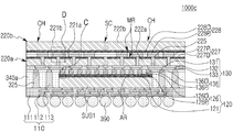
도 1은 예시적인 실시예들에 따른 반도체 패키지의 개략적인 단면도이다.1 is a schematic cross-sectional view of a semiconductor package in accordance with example embodiments.
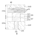
도 2a 및 도 2b는 예시적인 실시예들에 따른 반도체 패키지의 부분 확대도들이다. 도 2a 및 도 2b에서는 각각 도 1의 'A' 영역 및 'B' 영역을 확대하여 도시한다.2A and 2B are partially enlarged views of a semiconductor package according to example embodiments. 2A and 2B are enlarged views of regions 'A' and 'B' of FIG. 1, respectively.
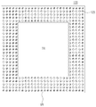
도 3은 예시적인 실시예들에 따른 반도체 패키지의 일부 구성의 개략적인 평면도이다. 도 3에서는 제1 반도체 칩(120)의 평면도를 도시한다.3 is a schematic plan view of some components of a semiconductor package according to example embodiments. 3 shows a top view of the
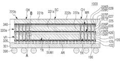
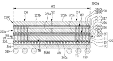
도 1 내지 도 3을 참조하면, 반도체 패키지(1000)는, 기판(301), 범프들(190)에 의해 기판(301) 상에 실장되는 제1 반도체 칩(120), 제1 반도체 칩(120)의 상부에 적층되어 배치되는 제1 및 제2 칩 구조물들(220a, 220b), 제1 반도체 칩(120) 및 제1 및 제2 칩 구조물들(220a, 220b)을 봉지하는 봉지부(340), 및 기판(301)의 하면에 배치되는 접속 단자들(390)을 포함한다.
1 to 3, the
기판(301)에는 제1 반도체 칩(120) 및 제1 및 제2 칩 구조물들(220a, 220b)이 실장될 수 있다. 기판(301)은 예를 들어, 실리콘(Si), 유리(glass), 세라믹(ceramic), 또는 플라스틱(plastic)을 포함할 수 있다. 기판(301)은 상면 상에 기판 패드들(326)이 배치되고, 하면 상에 접속 단자들(390)이 배치될 수 있다. 기판(301)은 내부에 배선 패턴들을 포함하는 다층 구조를 가질 수 있으나, 이에 한정되지는 않는다.
The
제1 반도체 칩(120)은 바디부(121), 하면 상의 접속 패드들(122), 바디부(121)의 적어도 일부를 관통하는 관통 비아들(125), 및 제1 본딩층(126)을 포함할 수 있다. 제1 반도체 칩(120)은 로직 반도체 칩 및/또는 메모리 반도체 칩을 포함할 수 있다. 상기 로직 반도체 칩은 마이크로 프로세서(micro-processor)일 수 있고, 예를 들어 중앙처리장치(central processing unit, CPU), 컨트롤러(controller), 또는 주문형 반도체(application specific integrated circuit, ASIC) 등일 수 있다. 상기 메모리 반도체 칩은 DRAM(dynamic random access memory), SRAM(static random access memory) 등과 같은 휘발성 메모리, 또는 플래시 메모리 등과 같은 비휘발성 메모리일 수 있다. The
제1 반도체 칩(120)은 이와 같은 반도체 소자들이 배치되는 소자 영역(TR) 및 소자 영역(TR) 주변에 배치되며 관통 비아들(125)이 배치되는 비아 영역(VR)을 갖는다. 소자 영역(TR)과 비아 영역(VR)은 평면적으로 구분되는 영역들일 수 있으며, 도 3에 도시된 것과 같이, 비아 영역(VR)은 중앙에 위치하는 소자 영역(TR)을 둘러싸도록 배치될 수 있다. 소자 영역(TR)은 예를 들어, 로직 반도체 칩을 구성하는 트랜지스터들이 배치되는 영역일 수 있다. 비아 영역(VR)은 관통 비아들(125)이 배치되어 상부의 제1 및 제2 칩 구조물들(220a, 220b)과 하부의 기판(301)을 전기적으로 연결하는 영역일 수 있다. 소자 영역(TR) 및 비아 영역(VR)은 하나의 기판 상에 형성된 서로 다른 영역이므로, 일체를 이룰 수 있으며, 공면인 상면 및 하면을 가질 수 있다.The
바디부(121)는 제1 기판 영역(SUB1) 및 제1 기판 영역(SUB1)의 하면 상의 반도체 영역(AR)을 포함할 수 있다. 제1 기판 영역(SUB1)과 반도체 영역(AR)은 제1 반도체 칩(120)의 상면에 수직한 방향을 따라 구분되는 영역들일 수 있다. 제1 기판 영역(SUB1)은 제1 반도체 칩(120) 전체에서 소자 영역(TR) 및 비아 영역(VR)에 걸쳐 하나로 배치될 수 있다. 제1 기판 영역(SUB1)은 실리콘(Si)과 같은 반도체 물질을 포함하는 영역일 수 있다. 반도체 영역(AR)은 제1 기판 영역(SUB1)을 기반으로 반도체 칩을 구성하는 트랜지스터 및/또는 메모리 셀들과 같은 소자들이 형성된 영역일 수 있으며, 특히 평면 상에서 소자 영역(TR)에 대응되는 영역에 상기 소자들이 형성될 수 있다. 반도체 영역(AR)은 기판(301)을 향하는 제1 반도체 칩(120)의 하부에 위치할 수 있다. 따라서, 제1 반도체 칩(120)은 하면이 활성면이고, 상면이 비활성면일 수 있다. 다만, 이와 같은 활성면의 배치 위치는 실시예들에 따라 변경될 수 있다.The
관통 비아들(125)은 적어도 바디부(121)의 제1 기판 영역(SUB1) 및 반도체 영역(AR) 전체를 관통할 수 있다. 관통 비아들(125)은 기판(301)과 제1 및 제2 칩 구조물들(220a, 220b)의 사이에 전기적 연결을 제공할 수 있다. 관통 비아들(125)은 도전성 물질로 이루어질 수 있으며, 예를 들어, 텅스텐(W), 알루미늄(Al), 및 구리(Cu) 중 적어도 하나를 포함할 수 있다. 도 2a에 도시된 것과 같이, 관통 비아(125)는 절연성의 비아 절연층(125I)에 의해 제1 기판 영역(SUB1)으로부터 전기적으로 분리될 수 있다.The through
접속 패드들(122)은 제1 반도체 칩(120)의 하면에서 관통 비아들(125)과 연결되도록 배치될 수 있다. 접속 패드들(122)은 텅스텐(W), 알루미늄(Al), 구리(Cu) 등과 같은 도전성 물질로 이루어질 수 있다.The
제1 본딩층(126)은 제1 반도체 칩(120)의 상면에 배치되며, 제1 금속 패드들(126P) 및 제1 금속 패드들(126P)을 둘러싸도록 배치되는 제1 본딩 절연층(126D)을 포함할 수 있다. 제1 본딩층(126)은 상부의 제1 칩 구조물(220a)의 제2 본딩층(226)과 본딩되어, 제1 칩 구조물(220a)을 제1 반도체 칩(120)과 연결하는 층일 수 있다. 제1 금속 패드들(126P)은 비아 영역(VR) 상에서 관통 비아들(125)과 대응되도록 배치될 수 있으나, 이에 한정되지는 않는다. 예를 들어, 제1 금속 패드들(126P) 중 일부는 관통 비아들(125)이 형성되지 않은 영역에 배치되어 전기적 연결 기능을 수행하지 않고, 단지 본딩 기능을 수행할 수도 있다.
The
범프들(190)은 제1 반도체 칩(120)의 하면 상에 배치되어, 접속 패드들(122)을 기판(301) 상의 기판 패드들(326)과 연결할 수 있다. 범프들(190)은 도전성 물질, 예를 들어 솔더(solder), 주석(Sn), 은(Ag), 구리(Cu) 및 알루미늄(Al) 중 적어도 하나를 포함할 수 있다. 범프들(190)의 형태는 범프 형상 이외에, 볼, 랜드, 범프, 필라, 핀 등 다양한 형태로 변경될 수 있다. 범프들(190)은 접속 단자들(390)보다 작은 크기를 갖는 마이크로 범프들일 수 있다.
The
제1 및 제2 칩 구조물들(220a, 220b)은 제1 반도체 칩(120) 상에 순차적으로 적층될 수 있다. 제1 및 제2 칩 구조물들(220a, 220b)은 제1 반도체 칩(120)과 평면 상에서 실질적으로 동일한 크기를 가질 수 있다. 제1 및 제2 칩 구조물들(220a, 220b)은 각각 두 개의 제2 하부 반도체 칩들(221a, 222a) 및 제2 상부 반도체 칩들(221b, 222b)을 포함할 수 있다. 제2 반도체 칩들(221a, 222a, 221b, 222b)은 로직 반도체 칩 및/또는 메모리 반도체 칩을 포함할 수 있다. 예를 들어, 제1 반도체 칩(120)은 AP 칩이고, 제2 반도체 칩들(221a, 222a, 221b, 222b)은 메모리 칩들일 수 있다. The first and
제1 및 제2 칩 구조물들(220a, 220b) 내에서, 제2 하부 반도체 칩들(221a, 222a) 및 제2 상부 반도체 칩들(221b, 222b)은 두 개가 서로 절단되지 않은 상태로 하나의 구조물을 이룰 수 있다. 즉, 제1 및 제2 칩 구조물들(220a, 220b)은 소잉 또는 싱귤레이션 되지 않은 상태의 제2 하부 반도체 칩들(221a, 222a) 및 제2 상부 반도체 칩들(221b, 222b)로 이루어질 수 있다. 제1 및 제2 칩 구조물들(220a, 220b)이 포함하는 제2 반도체 칩들(221a, 222a, 221b, 222b)의 개수는 실시예들에서 다양하게 변경될 수 있다. Within the first and
제2 하부 반도체 칩들(221a, 222a) 및 제2 상부 반도체 칩들(221b, 222b)은 각각 칩 영역(CH) 및 칩 영역(CH)의 적어도 일측의 스크라이브 영역(SC)을 포함할 수 있다. 스크라이브 영역(SC)은, 나란하게 배치되는 제2 하부 반도체 칩들(221a, 222a) 및 제2 상부 반도체 칩들(221b, 222b) 각각에서, 칩 영역들(CH)의 사이에 위치할 수 있다. 실시예들에 따라, 나란히 배치되는 제2 하부 반도체 칩들(221a, 222a)의 사이 및 제2 상부 반도체 칩들(221b, 222b)의 사이 영역뿐 아니라, 평면 상에서 서로 마주하지 않는 외측 영역에도 스크라이브 영역(SC)이 더 배치될 수 있다. 각각의 제1 및 제2 칩 구조물들(220a, 220b) 내에서, 제2 하부 반도체 칩들(221a, 222a) 및 제2 상부 반도체 칩들(221b, 222b)은 스크라이브 영역(SC)에 의해 서로 연결된 상태일 수 있다. 이와 같이, 제2 반도체 칩들(221a, 222a, 221b, 222b)이 서로 연결된 상태로 실장됨으로써, 패키지 전체의 크기를 최소화할 수 있다.
The second
제1 칩 구조물(220a)은, 제2 하부 반도체 칩들(221a, 222a)의 적어도 일부를 관통하는 칩 관통 비아들(225) 및 제2 및 제3 본딩층들(226, 227)을 더 포함할 수 있다. 제2 칩 구조물(220b)은 제4 본딩층(228)을 더 포함할 수 있다. The
제2 하부 반도체 칩들(221a, 222a) 및 제2 상부 반도체 칩들(221b, 222b)은 각각 제2 및 제3 기판 영역(SUB2, SUB3) 및 제2 및 제3 기판 영역(SUB2, SUB3)의 하면 상의 상부 반도체 영역(MR)을 포함할 수 있다. 제2 및 제3 기판 영역들(SUB2, SUB3)은 실리콘(Si)과 같은 반도체 물질을 포함하는 영역일 수 있다. 상부 반도체 영역들(MR)은 제2 및 제3 기판 영역들(SUB2, SUB3)을 기반으로 반도체 칩을 구성하는 트랜지스터 및/또는 메모리 셀들과 같은 소자들이 형성된 영역일 수 있다. 상부 소자 영역들(MR)에는, 도 2a 및 도 2b에 도시된 것과 같이, 상기 소자들을 구성하는 소자층들(DL)이 배치될 수 있다. 따라서, 제2 반도체 칩들(221a, 222a, 221b, 222b)은 각각 하면이 활성면일 수 있으나, 이에 한정되지는 않는다.The lower surfaces of the second
칩 관통 비아들(225)은 제1 반도체 칩(120)의 비아 영역(VR)과 중첩되는 영역에 배치될 수 있다. 실시예들에 따라, 칩 관통 비아들(225)은 관통 비아들(125)과 대응되도록 배치되거나, 더 적은 개수로 배치될 수 있으나, 이에 한정되지는 않는다. 칩 관통 비아들(225)은 적어도 제2 하부 반도체 칩들(221a, 222a)의 제2 기판 영역(SUB2)을 관통할 수 있으며, 상부 소자 영역(MR)의 적어도 일부를 관통할 수 있다. 칩 관통 비아들(225)은 제2 칩 구조물(220b)과 제 반도체 칩(120) 사이에 전기적 연결을 제공할 수 있다. 칩 관통 비아들(225)은 제1 칩 구조물(220a)의 상부 소자 영역(MR)의 상기 소자들과도 전기적으로 연결될 수 있으나, 이에 한정되지는 않는다. 칩 관통 비아들(225)은 도전성 물질로 이루어질 수 있으며, 예를 들어, 텅스텐(W), 알루미늄(Al), 및 구리(Cu) 중 적어도 하나를 포함할 수 있다. 도 2a 및 도 2b에 도시된 것과 같이, 칩 관통 비아들(225)은 절연성의 상부 비아 절연층(225I)에 의해 제2 기판 영역(SUB2)으로부터 전기적으로 분리될 수 있다.The chip through
제2 내지 제4 본딩층들(226, 227, 228)은 제2 내지 제4 금속 패드들(226P, 227P, 228P) 및 제2 내지 제4 금속 패드들(226P, 227P, 228P)을 둘러싸도록 배치되는 제2 내지 제4 본딩 절연층들(226D, 227D, 228D)을 포함할 수 있다. The second to fourth bonding layers 226, 227, and 228 surround the second to
제2 본딩층(226)은 하부의 제1 반도체 칩(120)의 제1 본딩층(126)과 본딩되어, 제1 칩 구조물(220a)을 제1 반도체 칩(120)과 연결하는 층일 수 있다. 제2 금속 패드들(226P)은 제1 금속 패드들(126P)과 전기적으로 연결되며, 제1 칩 구조물(220a)의 상부 소자 영역(MR)의 소자들 및 칩 관통 비아들(225)과 전기적으로 연결될 수 있다. The
제3 및 제4 본딩층들(227, 228)은 서로 접합되어, 제2 칩 구조물(220b)을 제1 칩 구조물(220a)을 포함하는 하부의 구조물과 연결하는 층일 수 있다. 제3 본딩층(227)은 제1 칩 구조물(220a)의 비활성면, 즉 제2 하부 반도체 칩들(221a, 222a)의 비활성면 상에 배치되고, 제4 본딩층(228)은 제2 칩 구조물(220b)의 활성면, 즉 제2 상부 반도체 칩들(221b, 222b)의 활성면 상에 배치될 수 있다. 제3 금속 패드들(227P)은 제1 칩 구조물(220a)의 상면을 이루며, 칩 관통 비아들(225)과 연결될 수 있다. 제4 금속 패드들(228P)은 제2 칩 구조물(220b)의 상부 소자 영역(MR)의 소자들과 전기적으로 연결될 수 있다.
The third and fourth bonding layers 227 and 228 may be a layer that is joined to each other and connects the
도 2a 및 도 2b에 도시된 것과 같이, 제1 및 제2 금속 패드들(126P, 226P)은 서로 대응되는 위치에 배치되어 직접 접합될 수 있으며, 제3 및 제4 금속 패드들(227P, 228P)은 서로 대응되는 위치에 배치되어 직접 접합될 수 있다. 제1 내지 제4 금속 패드들(126P, 226P, 227P, 228P)은 텅스텐(W), 알루미늄(Al), 구리(Cu), 텅스텐 질화물(WN), 탄탈륨 질화물(TaN), 및 티타늄 질화물(TiN) 중 적어도 하나를 포함할 수 있으며, 예를 들어, 구리(Cu)로 이루어진 경우, 구리(Cu)-구리(Cu) 본딩에 의해 물리적 및 전기적으로 연결될 수 있다. 서로 연결되는 제1 내지 제4 금속 패드들(126P, 226P, 227P, 228P)은 크기가 서로 동일하거나 유사할 수 있으나, 이에 한정되지는 않는다. 2A and 2B, the first and
제1 및 제2 본딩 절연층들(126D, 226D) 및 제3 및 제4 본딩 절연층들(227D, 228D)은 각각 유전체-유전체 본딩에 의해 접합될 수 있다. 제1 내지 제4 본딩 절연층들(126D, 226D, 227D, 228D)은 절연성 물질, 예를 들어, SiO, SiN, SiCN, SiOC, SiON 및 SiOCN 중 적어도 하나를 포함할 수 있다.
The first and second
반도체 패키지(1000)에서, 제1 반도체 칩(120)과 제1 칩 구조물(220a), 및 제1 칩 구조물(220a)과 제2 칩 구조물(220b)은 각각 하이브리드 본딩에 의해 접합될 수 있다. 이 경우, 접합 두께가 최소화될 수 있어, 범프 등에 의해 연결되는 경우에 비하여 반도체 패키지(1000)의 두께가 감소될 수 있다. 즉, 반도체 패키지(1000)는 예를 들어, AP 칩인 제1 반도체 칩(120) 상에 메모리 칩들을 포함하는 제1 및 제2 칩 구조물들(220a, 220b)이 적층되는 구조를 가지면서도, 최소화된 두께를 가질 수 있다. 따라서, 반도체 패키지(1000) 내에서 상대적으로 반도체 칩(120) 및 제1 및 제2 칩 구조물들(220a, 220b)의 두께를 상향할 수 있는 마진이 있어, 방열 측면에서 유리할 수 있다. 또한, 반도체 패키지(1000)는 최소화된 두께를 가지면서도 재배선층을 포함하지 않아, 공정이 단순화될 수 있다.
In the
봉지부(340)는 기판(301)의 상면, 범프들(190), 제1 반도체 칩(120), 및 제1 및 제2 칩 구조물들(220a, 220b)을 감싸도록 배치되어, 제1 반도체 칩(120) 및 제1 및 제2 칩 구조물들(220a, 220b)을 보호하는 역할을 할 수 있다. 봉지부(340)는 예를 들어, 실리콘(silicone) 계열 물질, 열경화성 물질, 열가소성 물질, UV 처리 물질 등으로 이루어질 수 있다. 봉지부(340)는 레진과 같은 폴리머로 형성될 수 있으며, 예컨대, EMC(Epoxy Molding Compound)로 형성될 수 있다. 다만, 실시예들에 따라, 봉지부(340)는 생략되는 것도 가능하다.
The
접속 단자들(390)은 기판(301)의 하부에 배치될 수 있다. 접속 단자들(390)은 반도체 패키지(1000)를 반도체 패키지(1000)가 실장되는 전자기기의 메인보드 등과 연결할 수 있다. 접속 단자들(390)은 도전성 물질, 예를 들어 솔더(solder), 주석(Sn), 은(Ag), 구리(Cu) 및 알루미늄(Al) 중 적어도 하나를 포함할 수 있다. 접속 단자들(390)의 형태는 볼 형상 이외에, 랜드(land), 범프, 필라, 핀 등 다양한 형태로 변경될 수 있다.
The
도 4a 및 도 4b는 예시적인 실시예들에 따른 반도체 패키지의 일부 구성의 개략적인 평면도들이다. 도 4a 및 도 4b에서는 도 3에 대응되는 영역들을 도시한다.4A and 4B are schematic plan views of some configurations of a semiconductor package according to example embodiments. 4A and 4B show regions corresponding to FIG. 3.
도 4a를 참조하면, 제1 반도체 칩(120a)은 반도체 소자들이 배치되는 소자 영역(TR) 및 소자 영역(TR)의 둘레를 따라 서로 분리되어 배치되며 관통 비아들(125)이 배치되는 제1 내지 제4 비아 영역들(VR1, VR2, VR3, VR4)을 갖는다. 제1 내지 제4 비아 영역들(VR1, VR2, VR3, VR4)은 평면 상에서 소자 영역(TR)의 각각의 면에 접촉되도록 배치될 수 있다.
Referring to FIG. 4A, the
도 4b를 참조하면, 제1 반도체 칩(120b)은 반도체 소자들이 배치되는 소자 영역(TR) 및 소자 영역(TR)의 둘레를 따라 서로 이격되어 배치되며 관통 비아들(125)이 배치되는 제1 및 제2 비아 영역들(VR1, VR2)을 갖는다. 제1 및 제2 비아 영역들(VR1, VR2)은 평면 상에서 소자 영역(TR)의 마주보는 면들 각각에 접촉되도록 배치되며, 제1 반도체 칩(120b)의 일 방향에서의 폭만큼 연장되어 배치될 수 있다. Referring to FIG. 4B, the first semiconductor chip 120b is spaced apart from each other along the circumference of the device area TR and the device area TR where the semiconductor devices are disposed, and the first via
이와 같이, 실시예들에서, 비아 영역들(VR1, VR2)은 복수개로 분리되어 배치될 수 있으며, 소자 영역(TR)의 주변에서 다양한 형태로 배치될 수 있다.
As such, in embodiments, the via areas VR1 and VR2 may be disposed separately in a plurality, and may be arranged in various forms around the device area TR.
도 5는 예시적인 실시예들에 따른 반도체 패키지의 개략적인 단면도이다.5 is a schematic cross-sectional view of a semiconductor package in accordance with example embodiments.
도 5를 참조하면, 반도체 패키지(1000a)에서, 기판(301)은 제1 반도체 칩(120) 및 제1 및 제2 칩 구조물들(220a, 220b)과 실질적으로 동일한 크기를 가질 수 있으며, 제1 반도체 칩(120) 및 제1 및 제2 칩 구조물들(220a, 220b)은 측면이 외측으로 노출될 수 있다. 일 방향에서, 제1 반도체 칩(120)의 폭(W1)은 제1 및 제2 칩 구조물들(220a, 220b)의 폭(W2)과 실질적으로 동일할 수 있다. 즉, 평면 상에서 제1 반도체 칩(120)은 제1 및 제2 칩 구조물들(220a, 220b)과 실질적으로 동일한 크기를 가질 수 있으며, 이는 반도체 패키지(1000a)의 크기와도 실질적으로 동일할 수 있다. 봉지부(340a)는 기판(301)과 범프들(190)의 사이를 채우도록 위치할 수 있다.
Referring to FIG. 5, in the
도 6은 예시적인 실시예들에 따른 반도체 패키지의 개략적인 단면도이다.6 is a schematic cross-sectional view of a semiconductor package in accordance with example embodiments.
도 6을 참조하면, 반도체 패키지(1000b)는 방열층(350) 및 접착층(355)을 더 포함한다. Referring to FIG. 6, the
방열층(350)은 제2 칩 구조물(220b)의 상면 상에 배치될 수 있다. 방열층(350)은 접착층(355)을 매개로 제2 칩 구조물(220b) 상에 적층될 수 있다. 방열층(350)은 제1 및 제2 칩 구조물들(220a, 220b)보다 열전도도가 높은 물질로 이루어질 수 있으며, 이에 의해 제1 및 제2 칩 구조물들(220a, 220b)로부터 발생한 열을 상부로 방출시킬 수 있다. 방열층(350)은 예를 들어, 구리(Cu)와 같은 금속으로 이루어진 금속층일 수 있다.The
방열층(350)은 제1 및 제2 칩 구조물들(220a, 220b)보다 큰 크기를 가질 수 있다. 예를 들어, 방열층(350)은 평면 상에서 반도체 패키지(1000b)와 실질적으로 동일한 크기를 가질 수 있으나, 이에 한정되지는 않는다. 실시예들에 따라, 방열층(350)은 제1 및 제2 칩 구조물들(220a, 220b)과 동일한 크기를 가질 수도 있다.
The
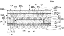
도 7은 예시적인 실시예들에 따른 반도체 패키지의 개략적인 단면도이다.7 is a schematic cross-sectional view of a semiconductor package according to example embodiments.
도 8a 및 도 8b는 예시적인 실시예들에 따른 반도체 패키지의 부분 확대도들이다. 도 8a 및 도 8b에서는 각각 도 7의 'C' 영역 및 'D' 영역을 확대하여 도시한다.8A and 8B are partially enlarged views of a semiconductor package according to example embodiments. 8A and 8B, the 'C' area and the 'D' area of FIG. 7 are respectively enlarged.
도 7 내지 도 8b를 참조하면, 반도체 패키지(1000c)는, 제1 반도체 칩(120a), 제1 반도체 칩(120a)의 하부에 배치되는 제1 재배선부(110), 제1 반도체 칩(120a)의 상부에 배치되는 제2 재배선부(130), 제1 반도체 칩(120a)을 봉지하는 봉지부(340a), 봉지부(340a)를 관통하는 도전성 포스트들(325), 제2 재배선부(130) 상에 적층되어 배치되는 제1 및 제2 칩 구조물들(220a, 220b), 및 제1 재배선부(110)의 하부에 배치되는 접속 단자들(390)을 포함한다. 반도체 패키지(1000c)는 제1 반도체 칩(120)이 제1 반도체 칩(120)의 외측 영역으로 확장되어 재배선되는 팬-아웃(fan-out) 타입의 반도체 패키지일 수 있다. 따라서, 제1 재배선부(110)는 평면 상에서 제1 반도체 칩(120)과 중첩되지 않는 영역을 포함할 수 있다. 도 7 내지 도 8b에서 도 1과 동일한 도면 번호는 동일하거나 대응되는 구성을 나타내며, 도 1을 참조하여 상술한 설명이 동일하게 적용될 수 있다.
7 to 8B, the
제1 반도체 칩(120a)은 도 1의 실시예에서와 달리, 비아 영역(VR)을 포함하지 않을 수 있으며, 도 1의 소자 영역(TR)에 해당하는 영역만을 포함할 수 있다. 제1 반도체 칩(120a)의 바디부(121)는 제1 기판 영역(SUB1) 및 소자 영역(AR)을 포함할 수 있으며, 소자 영역(AR)은 상부에 위치할 수 있다. Unlike the embodiment of FIG. 1, the
또한, 본 실시예에서, 제1 반도체 칩(120a)은 제1 및 제2 칩 구조물들(220a, 220b)보다 작은 크기를 가질 수 있다. 이에 따라, 봉지부(340a)는 제1 및 제2 재배선부들(110, 130)의 사이에서 제1 반도체 칩(120)의 외측에 배치되어, 제1 반도체 칩(120)을 봉지할 수 있다. 봉지부(340a) 내에는 봉지부(340a)를 관통하여 제1 재배선부(110)와 제2 재배선부(130)를 연결하는 도전성 포스트들(325)이 더 배치될 수 있다. 도전성 포스트들(325)은 하단에 상대적으로 큰 폭을 갖는 영역을 가질 수 있으나, 도전성 포스트들(325)의 형상은 이에 한정되지는 않는다.
In addition, in this embodiment, the
제1 재배선부(110)는 제1 반도체 칩(120)의 하부에 배치되어, 제1 반도체 칩(120)을 재배선할 수 있다. 제1 재배선부(110)는 제1 배선 절연층(111), 제1 재배선층들(112), 및 제1 비아들(113)을 포함할 수 있다. 제1 재배선부(110)를 이루는 제1 배선 절연층(111), 제1 재배선층들(112), 및 제1 비아들(113)의 층수 및 배치는 도면에 도시된 것에 한정되지 않으며, 실시예들에서 다양하게 변경될 수 있다. The
제1 배선 절연층(111)은 절연성 물질, 예를 들어 감광성 절연(photo imagable dielectric, PID) 수지로 이루어질 수 있다. 이 경우, 제1 배선 절연층(111)은 무기필러를 더 포함할 수도 있다. 제1 배선 절연층(111)은 제1 재배선층들(112)의 층수에 따라 복수의 층들로 이루어질 수 있으며, 서로 동일하거나 다른 물질로 이루어질 수 있다. 제1 재배선층들(112) 및 제1 비아들(113)은 제1 반도체 칩(120)을 재배선하는 역할을 할 수 있다. 제1 비아들(113)은 도전성 물질로 완전히 충전될 수 있으나, 이에 한정되지는 않으며, 도전성 물질이 비아의 벽을 따라 형성된 형상을 가질 수도 있으며, 테이퍼 형상뿐 아니라, 원통 형상 등 다양한 형상을 가질 수 있다. 제1 재배선층들(112) 및 제1 비아들(113)은 도전성 물질, 예를 들어, 구리(Cu), 알루미늄(Al), 은(Ag), 주석(Sn), 금(Au), 니켈(Ni), 납(Pb), 티타늄(Ti), 또는 이들의 합금을 포함할 수 있다.
The first
제2 재배선부(130)는 제1 반도체 칩(120)의 상부에 배치되며, 반도체 칩(120) 및 제1 재배선부(110)와 전기적으로 연결될 수 있다. 제2 재배선부(130)는 제2 배선 절연층(131), 제2 재배선층들(132), 제2 비아들(133), 및 하면을 이루는 제2 본딩층(136)을 포함할 수 있다. 제2 재배선부(130)를 이루는 제2 배선 절연층(131), 제2 재배선층들(132), 및 제2 비아들(133)의 층수 및 배치는 도면에 도시된 것에 한정되지 않으며, 실시예들에서 다양하게 변경될 수 있다. The
제2 배선 절연층(131)은 제1 배선 절연층(111)과 같이 절연성 물질, 예를 들어 감광성 절연(PID) 수지로 이루어질 수 있다. 제2 재배선층들(132) 및 제2 비아들(133)은 도전성 물질, 예를 들어, 구리(Cu), 알루미늄(Al), 은(Ag), 주석(Sn), 금(Au), 니켈(Ni), 납(Pb), 티타늄(Ti), 또는 이들의 합금을 포함할 수 있다. The second
제2 본딩층(136)은 제2 금속 패드들(136P) 및 제2 금속 패드들(136P)을 둘러싸도록 배치되는 제2 본딩 절연층(136D)을 포함할 수 있다. 제2 금속 패드들(136P)은 상부의 제2 재배선층들(132)과 제2 비아들(133)에 의해 연결될 수 있다. 제2 본딩층(136)은 하부의 제1 반도체 칩(120a)의 제1 본딩층(126)과 본딩되어, 제1 및 제2 칩 구조물들(220a, 220b)을 하부의 제1 반도체 칩(120) 및 제1 재배선부(110)와 연결하는 층일 수 있다.
The
제1 및 제2 칩 구조물들(220a, 220b)은 제1 반도체 칩(120a)의 상부에서, 제2 재배선부(130) 상에 순차적으로 적층될 수 있다. 제1 칩 구조물(220a)은 제2 하부 반도체 칩들(221a, 222a)을 포함할 수 있으며, 제2 하부 반도체 칩들(221a, 222a)의 적어도 일부를 관통하는 칩 관통 비아들(225) 및 제3 본딩층(227)을 더 포함할 수 있다. 제2 칩 구조물(220b)은 제2 상부 반도체 칩들(221b, 222b)을 포함할 수 있으며, 제4 본딩층(228)을 더 포함할 수 있다. 도 8b에 도시된 것과 같이, 제2 하부 반도체 칩들(221a, 222a)은 상면이 활성면이고, 제2 상부 반도체 칩들(221b, 222b)은 하면이 활성면일 수 있다. 따라서, 제1 및 제2 칩 구조물들(220a, 220b)은 페이스-투-페이스(fact-to-face) 형태로 활성면들이 서로 마주보도록 적층될 수 있다.
The first and
도 8a 및 도 8b에 도시된 것과 같이, 제1 및 제2 금속 패드들(126P, 136P)은 서로 대응되는 위치에 배치되어 직접 접합될 수 있으며, 제3 및 제4 금속 패드들(227P, 228P)은 서로 대응되는 위치에 배치되어 직접 접합될 수 있다. 제1 내지 제4 금속 패드들(126P, 136P, 227P, 228P)은 예를 들어, 구리(Cu)로 이루어진 경우, 구리(Cu)-구리(Cu) 본딩에 의해 물리적 및 전기적으로 연결될 수 있다. 서로 연결되는 제1 내지 제4 금속 패드들(126P, 136P, 227P, 228P)은 크기가 서로 동일하거나 유사할 수 있으나, 이에 한정되지는 않는다. 제1 및 제2 본딩 절연층들(126D, 136D) 및 제3 및 제4 본딩 절연층들(227D, 228D)은 각각 유전체-유전체 본딩에 의해 접합될 수 있다.8A and 8B, the first and
반도체 패키지(1000c)에서, 제1 반도체 칩(120)과 제2 재배선부(130), 및 제1 칩 구조물(220a)과 제2 칩 구조물(220b)은 각각 하이브리드 본딩에 의해 접합될 수 있다. 이 경우, 접합 두께가 최소화될 수 있어, 범프 등에 의해 연결되는 경우에 비하여 반도체 패키지(1000c)의 두께가 감소될 수 있다.
In the
도 9는 예시적인 실시예들에 따른 반도체 패키지의 개략적인 단면도이다.9 is a schematic cross-sectional view of a semiconductor package in accordance with example embodiments.
도 9를 참조하면, 반도체 패키지(1000d)에서, 제2 반도체 칩들(221a, 222a, 221b, 222b)은 모두 하면이 활성면일 수 있다. 따라서, 제1 및 제2 칩 구조물들(220a, 220b)은 페이스-투-백(fact-to-back) 형태로 활성면들이 모두 하부를 향하도록 적층될 수 있다. 이와 같이, 실시예들에서, 제1 및 제2 칩 구조물들(220a, 220b)의 적층 방향은 제조 공정 등에 따라 다양하게 결정될 수 있다. 제1 반도체 칩(120)의 경우도 유사하게, 실시예들에 따라 활성면의 방향은 다양하게 변경될 수 있을 것이다.
Referring to FIG. 9, in the
도 10은 예시적인 실시예들에 따른 반도체 패키지의 개략적인 단면도이다.10 is a schematic cross-sectional view of a semiconductor package in accordance with example embodiments.
도 10을 참조하면, 반도체 패키지(1000e)는 제1 반도체 칩(120)을 둘러싸는 코어층(170)을 더 포함할 수 있다.Referring to FIG. 10, the
코어층(170)은 제1 반도체 칩(120)이 실장되도록 상하면을 관통하는 관통홀(CA)을 포함할 수 있다. 관통홀(CA)은 코어층(170)의 중앙에 형성될 수 있으나, 관통홀(CA)의 개수 및 배치는 도시된 것에 한정되지 않는다. 또한, 일부 실시예들에서, 관통홀(CA)은 하면을 완전히 관통하지 않고, 캐비티 형태를 가질 수도 있다. 코어층(170)은 제1 반도체 칩(120)과 유사하게 제1 재배선부(110)와 하이브리드 본딩될 수 있으나, 이에 한정되지는 않는다.The core layer 170 may include a through hole CA penetrating the upper and lower surfaces so that the
코어층(170)은 코어 절연층(171), 코어 배선층들(172), 및 코어 비아들(174)을 포함할 수 있다. 코어 배선층들(172) 및 코어 비아들(174)은 코어층(170)의 상하면을 전기적으로 연결하도록 배치될 수 있다. 코어 배선층들(172)은 제1 및 제2 재배선부들(110, 130)의 제1 및 제2 재배선층들(112, 132)과 연결될 수 있다. 코어 배선층들(172)은 코어 절연층(171) 내부에 배치될 수 있으나, 이에 한정되지는 않는다. 코어 배선층들(172) 중 코어층(170)의 하면을 통해 노출되는 코어 배선층들(172)은 코어 절연층(171)에 매립되어 배치될 수 있으며, 이는 제조 공정에 따른 구조일 수 있다. 실시예들에 따라, 코어층(170)은 코어 배선층들(172) 및 코어 비아들(174)을 포함하지 않고, 코어 절연층(171)으로만 이루어지는 것도 가능하다. 본 실시예에서, 코어 비아들(174)은 하부로 향할수록 폭이 증가하는 테이퍼 형상을 갖는 것으로 도시되었으나, 이에 한정되지는 않으며, 코어 비아들(174)의 형상, 테이퍼 방향 등은 공정 순서에 따라 변경될 수 있다.The core layer 170 may include a core insulating
코어 절연층(171)은 절연성 물질, 예를 들어, 에폭시 수지와 같은 열경화성 수지 또는 폴리이미드와 같은 열가소성 수지를 포함할 수 있으며, 무기필러를 더 포함할 수 있다. 또는, 코어 절연층(171)은 무기필러와 함께 유리 섬유(glass fiber, glass cloth, glass fabric) 등의 심재에 함침된 수지, 예를 들어, 프리프레그(prepreg), ABF(Ajinomoto Build-up Film), 또는 FR-4, BT(Bismaleimide Triazine)를 포함할 수 있다. 코어 배선층들(172) 및 코어 비아들(174)은 구리(Cu) 등과 같은 금속 물질을 포함할 수 있다.The core insulating
봉지부(340b)는 코어층(170)의 관통홀(CA) 내의 공간을 채워 관통홀(CA)을 봉합하고, 코어층(170)의 하면 상으로 연장될 수 있다. 다만, 제조 공정에 따라, 봉지부(340b)는 코어층(170)의 상면 상으로 연장될 수도 있다. 봉지부(340b)는 제1 반도체 칩(120)과 관통홀(CA)의 내측벽 사이의 공간의 적어도 일부를 채울 수 있다. 이에 의해, 봉지부(340b)는 접착층의 역할도 수행할 수 있다.
The
도 11a 내지 도 11f는 예시적인 실시예들에 따른 반도체 패키지의 제조 방법을 개략적으로 나타내는 주요 단계별 도면들이다. 도 11a 내지 도 11f에서는, 도 1의 반도체 패키지의 예시적인 제조 방법을 도시한다.11A to 11F are main step-by-step diagrams schematically showing a method of manufacturing a semiconductor package according to example embodiments. 11A to 11F show exemplary manufacturing methods of the semiconductor package of FIG. 1.
도 11a를 참조하면, 제1 반도체 칩들(120)을 웨이퍼 레벨로 형성할 수 있다.Referring to FIG. 11A,
제1 반도체 칩(120)은, 하나의 반도체 기판 상에, 반도체 소자들을 포함하는 소자 영역(TR)을 형성하고, 소자 영역(TR) 주변에 관통 비아들(125)을 형성하여 비아 영역(VR)을 형성함으로써, 제공될 수 있다. 소자 영역(TR)과 비아 영역(VR)은 계면이 구별되거나, 명확히 구별되지 않을 수도 있다.The
관통 비아들(125)은 예를 들어, 비아-라스트(via-last) 구조로 형성될 수 있다. 다만, 관통 비아들(125)의 구조는 이에 한정되지는 않으며, 비아-미들(via-middle) 또는 비아-라스트(via-last) 구조로 형성될 수 있음은 물론이다. 참고로, 비아-퍼스트는 바디부(121)에서 소자 영역(AR)이 형성되기 전에 관통 비아가 먼저 형성되는 구조를 지칭하고, 비아-미들은 소자 영역(AR)의 트랜지스터 등과 같은 회로를 형성한 후 상부에 배선들이 형성되기 전에 관통 비아가 형성되는 구조를 지칭하며, 비아-라스트는 상기 배선들이 모두 형성된 후에 관통 비아가 형성되는 구조를 지칭할 수 있다. The through
또한, 제1 반도체 칩(120)은 활성면 상에 접속 패드들(122)을 형성하고, 비활성면 상에 제1 금속 패드들(126P) 및 제1 본딩 절연층(126D)을 포함하는 제1 본딩층(126)을 형성하여 준비될 수 있다.
In addition, the
도 11b를 참조하면, 제1 반도체 칩들(120) 상에 제1 칩 구조물(220a)을 접합할 수 있다.Referring to FIG. 11B, the
제1 칩 구조물(220a)은 하나의 기판 상에 제2 하부 반도체 칩들(221a, 222a)을 형성하고, 소잉되지 않은 상태로 준비될 수 있다. 따라서, 제2 하부 반도체 칩들(221a, 222a)은 각각 칩 영역(CH) 및 칩 영역(CH)의 적어도 일측의 스크라이브 영역(SC)을 포함하며, 제2 하부 반도체 칩들(221a, 222a) 각각의 스크라이브 영역들(SC)이 서로 연결된 상태일 수 있다. 제1 칩 구조물(220a)은, 제1 반도체 칩들(120)의 비아 영역(VR)에 대응되거나, 비아 영역(VR)과 중첩되는 영역에 상부 관통 비아들(225)을 형성하고, 하면 및 상면에 각각 제2 및 제3 본딩층들(226, 227)을 형성함으로써 제조될 수 있다.The
제1 칩 구조물(220a)은, 제1 반도체 칩(120)의 제1 본딩층(126)과 제1 칩 구조물(220a)의 제2 본딩층(226)을 하이브리드 본딩함으로써, 서로 연결될 수 있다. 제1 반도체 칩(120)과 제1 칩 구조물(220a)은 별도의 접착층과 같은 접착제의 개재없이 직접 접합(direct bonding)될 수 있다. 예를 들어, 제1 반도체 칩(120)과 제1 칩 구조물(220a)은 가압 공정에 의하여 원자 레벨에서의 결합을 형성할 수 있다. 실시예들에 따라, 본딩 전에, 접합력을 강화하기 위하여, 제1 반도체 칩(120) 및 제1 칩 구조물(220a)의 접합면들에 대하여 수소 플라즈마 처리와 같은 표면 처리 공정이 더 수행될 수도 있다. 제1 반도체 칩(120)과 제1 칩 구조물(220a)은 웨이퍼 레벨에서, 웨이퍼 대 웨이퍼(wafer to wafer)로 본딩될 수 있다.
The
도 11c를 참조하면, 제1 칩 구조물(220a) 상에 제2 칩 구조물(220b)을 접합할 수 있다.Referring to FIG. 11C, the
제2 칩 구조물(220b)은 제1 칩 구조물(220a)과 유사하게, 하나의 기판 상에 제2 상부 반도체 칩들(221b, 222b)을 형성하고, 소잉되지 않은 상태로 준비될 수 있다. 제2 칩 구조물(220b)은 하면 상에 제4 본딩층(228)을 형성하여 제공될 수 있다.The
제2 칩 구조물(220b)은, 제3 본딩층(227)과 제4 본딩층(228)을 하이브리드 본딩함으로써, 제1 반도체 칩(120) 및 제1 칩 구조물(220a)의 적층 구조물 상에 접합될 수 있다. 제1 칩 구조물(220a)과 제2 칩 구조물(220b)은 별도의 접착층과 같은 접착제의 개재없이 직접 접합될 수 있다. 제1 칩 구조물(220a)과 제2 칩 구조물(220b)은 웨이퍼 레벨에서, 웨이퍼 대 웨이퍼로 본딩될 수 있다.
The
도 11d를 참조하면, 제1 반도체 칩(120)의 하면에 범프들(190)을 형성하고, 제1 반도체 칩(120) 및 제1 및 제2 칩 구조물들(220a, 220b)의 적층 구조물을 패키지 단위로 소잉할 수 있다.Referring to FIG. 11D, bumps 190 are formed on a lower surface of the
범프들(190)은 증착 또는 도금 공정 및 리플로우(reflow) 공정을 이용하여 형성할 수 있다. The
상기 적층 구조물은 패키지 단위로 소잉하여, 하나의 패키지가 하나의 제1 반도체 칩(120)과 네 개의 제2 반도체 칩들(221a, 222a, 221b, 222b)을 포함하도록 절단될 수 있다. 절단 공정은, 제1 및 제2 칩 구조물들(220a, 220b)의 스크라이브 영역들(SC) 중 일부를 따라 상기 패키지 단위로 수행될 수 있다. 이에 의해, 하나의 패키지에서, 칩 영역들(CH)의 외측에서는 스크라이브 영역(SC)이 제거되거나 일부 잔존할 수 있으며, 칩 영역들(CH)의 사이에는 스크라이브 영역들(SC)이 그대로 남아있을 수 있다.
The stacked structure is sawed in units of packages, so that one package may be cut to include one
도 11e를 참조하면, 패키지 단위로 절단된 상기 적층 구조물을 기판(301) 상에 실장할 수 있다.Referring to FIG. 11E, the stacked structure cut in package units may be mounted on the
기판(301) 상의 기판 패드들(326)에 범프들(190)을 연결함으로써, 상기 적층 구조물이 실장될 수 있다.
By connecting the
도 11f를 참조하면, 상기 적층 구조물을 봉지하는 봉지부(340)를 형성할 수 있다.Referring to FIG. 11F, an
봉지부(340)는 라미네이션 또는 도포 등의 방법으로 봉지부(340)를 이루는 물질을 상기 적층 구조물 상에 형성한 후, 이를 경화시켜 형성할 수 있다. 상기 도포 방법은, 예를 들어, 스크린 인쇄법 또는 스프레이 인쇄법일 수 있다.The
다음으로, 기판(301)의 하면 상에 접속 단자들(390)을 형성함으로써, 도 1의 반도체 패키지(1000)가 제조될 수 있다.
Next, by forming the
도 12a 내지 도 12d는 예시적인 실시예들에 따른 반도체 패키지의 제조 방법을 개략적으로 나타내는 주요 단계별 도면들이다. 도 12a 내지 도 12d에서는, 도 7의 반도체 패키지의 예시적인 제조 방법을 도시한다. 이하에서는 도 11a 내지 도 11f를 참조한 설명과 중복되는 설명은 생략한다.12A to 12D are main step-by-step diagrams schematically showing a method of manufacturing a semiconductor package according to example embodiments. 12A to 12D illustrate an exemplary method of manufacturing the semiconductor package of FIG. 7. Hereinafter, a description overlapping with reference to FIGS. 11A to 11F will be omitted.
도 12a를 참조하면, 제2 칩 구조물(220b) 상에 제1 칩 구조물(220a)을 접합할 수 있다.Referring to FIG. 12A, the
제1 및 제2 칩 구조물들(220a, 220b)은 도 11b 및 도 11c를 참조하여 상술한 것과 같이 제조되어 준비될 수 있다. 제1 및 제2 칩 구조물들(220a, 220b)은 제3 본딩층(227)과 제4 본딩층(228)을 하이브리드 본딩함으로써, 서로 접합될 수 있다. 제1 칩 구조물(220a)과 제2 칩 구조물(220b)은 별도의 접착층과 같은 접착제의 개재없이 직접 접합될 수 있다. 제1 칩 구조물(220a)과 제2 칩 구조물(220b)은 웨이퍼 레벨에서, 웨이퍼 대 웨이퍼로 본딩될 수 있다.
The first and
도 12b를 참조하면, 제1 및 제2 칩 구조물들(220a, 220b) 상에 제2 재배선부(130)를 형성할 수 있다.Referring to FIG. 12B, the
제2 재배선부(130)는, 제2 배선 절연층(131)을 일부 두께로 형성하는 공정, 제2 배선 절연층(131)의 일부를 관통하는 비아홀을 형성하는 공정, 및 도금 공정 등을 이용하여 상기 비아홀을 매립하여 제2 비아들(133) 및 제2 비아들(133) 상의 제2 재배선층들(132)을 형성하는 공정을 반복하여 수행함으로써 일부가 제조할 수 있다.The
다음으로, 제2 재배선부(130)의 최상부에 패터닝된 제2 본딩 절연층(136D)을 형성하고, 패터닝된 영역 내에 도금 공정 등을 이용하여 제2 금속 패드들(136P)을 형성함으로써, 제2 본딩층(136)을 형성할 수 있다.
Next, by forming a second
도 12c를 참조하면, 제2 재배선부(130) 상에 도전성 포스트들(325)을 형성하고, 제1 반도체 칩들(120)을 접합할 수 있다.Referring to FIG. 12C,
도전성 포스트들(325)은 마스크 패턴들을 형성하고, 도금 또는 증착 공정을 수행함으로써 형성할 수 있다.The
제1 반도체 칩(120)은, 제2 재배선부(130)의 제2 본딩층(136)과 제1 반도체 칩(120)의 제1 본딩층(126)을 하이브리드 본딩함으로써, 서로 접합될 수 있다. 제1 반도체 칩(120)과 제2 재배선부(130)는 별도의 접착층과 같은 접착제의 개재없이 직접 접합될 수 있다.
The
도 12d를 참조하면, 도전성 포스트들(325) 및 제1 반도체 칩들(120)을 봉지하는 봉지부(340a)를 형성하고, 제1 재배선부(110)를 형성한 후, 접속 단자들(390)을 형성할 수 있다.Referring to FIG. 12D, after forming the
제1 재배선부(110)는 제1 배선 절연층(111)을 일부 두께로 형성하는 공정, 제1 배선 절연층(111)의 일부를 관통하는 비아홀을 형성하는 공정, 및 도금 공정 등을 이용하여 상기 비아홀을 매립하여 제1 비아들(113) 및 제1 비아들(113) 상의 제1 재배선층들(112)을 형성하는 공정을 반복하여 수행함으로써 제조할 수 있다.The
제1 재배선부(110) 상에 접속 단자들(390)을 형성한 후, 소잉 공정을 통해 단위 패키지 단위로 절단하여 도 7의 반도체 패키지(1000c)를 제조할 수 있다. 절단 공정은, 제1 및 제2 칩 구조물들(220a, 220b)의 스크라이브 영역들(SC) 중 일부를 따라 상기 패키지 단위로 수행될 수 있다. 이에 의해, 하나의 패키지에서, 칩 영역들(CH)의 외측에서는 스크라이브 영역(SC)이 제거되거나 일부 잔존할 수 있으며, 칩 영역들(CH)의 사이에는 스크라이브 영역들(SC)이 그대로 남아있을 수 있다.
After forming the
본 발명은 상술한 실시예 및 첨부된 도면에 의해 한정되는 것이 아니며 첨부된 청구범위에 의해 한정하고자 한다. 따라서, 청구범위에 기재된 본 발명의 기술적 사상을 벗어나지 않는 범위 내에서 당 기술분야의 통상의 지식을 가진 자에 의해 다양한 형태의 치환, 변형 및 변경이 가능할 것이며, 이 또한 본 발명의 범위에 속한다고 할 것이다.
The present invention is not limited by the above-described embodiments and accompanying drawings, but is intended to be limited by the appended claims. Accordingly, various forms of substitution, modification, and modification will be possible by those skilled in the art without departing from the technical spirit of the present invention as set forth in the claims, and this also belongs to the scope of the present invention. something to do.
100, 1000: 반도체 패키지
110: 제1 재배선부
111: 제1 배선 절연층
112: 제1 재배선층
113: 제1 비아
120: 제1 반도체 칩
121: 바디부
122: 접속 패드
125: 관통 비아
126: 제1 본딩층
130: 제2 재배선부
131: 제2 배선 절연층
132: 제2 재배선층
133: 제2 비아
136: 제2 본딩층
170: 코어층
171: 코어 절연층
172: 코어 배선층
174: 코어 비아
190: 범프
220: 칩 구조물
221, 222: 제2 반도체 칩
225: 상부 관통 비아
226: 제2 본딩층
227: 제3 본딩층
228: 제4 본딩층
301: 기판
326: 기판 패드
340: 봉지부
390: 접속 단자100, 1000: semiconductor package 110: first redistribution unit
111: first wiring insulating layer 112: first redistribution layer
113: first via 120: first semiconductor chip
121: body portion 122: connection pad
125: through via 126: first bonding layer
130: second redistribution unit 131: second wiring insulation layer
132: second redistribution layer 133: second via
136: second bonding layer 170: core layer
171: core insulation layer 172: core wiring layer
174: core via 190: bump
220: chip structure 221, 222: second semiconductor chip
225: upper through via 226: second bonding layer
227: third bonding layer 228: fourth bonding layer
301: substrate 326: substrate pad
340: sealing portion 390: connection terminal
Claims (10)
상기 제1 반도체 칩 상에 적층되며, 상기 제1 반도체 칩을 향하는 일면 상에 배치된 제2 본딩층 및 복수의 제2 반도체 칩들을 포함하는 칩 구조물을 포함하고,
상기 복수의 제2 반도체 칩들은 각각 칩 영역 및 상기 칩 영역을 둘러싸는 스크라이브 영역을 포함하고, 상기 칩 구조물에서 상기 복수의 제2 반도체 칩들은 상기 스크라이브 영역에 의해 서로 연결된 상태이고,
상기 제1 및 제2 본딩층들은, 대응되도록 배치되어 서로 접합되는 제1 및 제2 금속 패드들 및 상기 제1 및 제2 금속 패드들을 둘러싸는 제1 및 제2 본딩 절연층들을 각각 포함하는 반도체 패키지.
A first semiconductor chip including a first bonding layer disposed on one surface; And
It is stacked on the first semiconductor chip, and includes a second bonding layer disposed on one surface facing the first semiconductor chip and a chip structure including a plurality of second semiconductor chips,
Each of the plurality of second semiconductor chips includes a chip area and a scribe area surrounding the chip area, and in the chip structure, the plurality of second semiconductor chips are connected to each other by the scribe area,
The first and second bonding layers are semiconductors including first and second metal pads disposed to correspond to each other and bonded to each other, and first and second bonding insulating layers surrounding the first and second metal pads, respectively. package.
상기 복수의 제2 반도체 칩들은 서로 절단되지 않은 상태로 상기 칩 구조물을 이루는 반도체 패키지.
According to claim 1,
The plurality of second semiconductor chips are semiconductor packages that form the chip structure without being cut off from each other.
상기 칩 구조물은 평면 상에서 상기 제1 반도체 칩과 실질적으로 동일한 크기를 갖는 반도체 패키지.
According to claim 1,
The chip structure is a semiconductor package having a substantially same size as the first semiconductor chip on a plane.
상기 제1 반도체 칩은, 반도체 소자들이 배치되는 소자 영역 및 상기 소자 영역의 적어도 일측에 배치되며 상기 칩 구조물과 상기 제1 반도체 칩을 전기적으로 연결하는 제1 관통 비아들이 배치되는 비아 영역을 갖는 반도체 패키지.
According to claim 1,
The first semiconductor chip is a semiconductor having a device region in which semiconductor elements are disposed and a via region in which at least one side of the device region is disposed and first through vias electrically connecting the chip structure and the first semiconductor chip are disposed. package.
상기 제1 반도체 칩은, 상기 소자 영역 및 상기 비아 영역 전체에 배치되는 하나의 기판을 더 포함하는 반도체 패키지.
According to claim 4,
The first semiconductor chip, the semiconductor package further comprises a substrate disposed over the entire device region and the via region.
상기 칩 구조물은 상기 비아 영역과 중첩되는 영역에 배치되는 제2 관통 비아들을 더 포함하는 반도체 패키지.
According to claim 4,
The chip structure further includes second through vias disposed in an area overlapping the via area.
상기 칩 구조물은 상하로 적층되는 제1 및 제2 칩 구조물들을 포함하고,
하부에 배치되는 상기 제1 칩 구조물은 상기 제2 본딩층 및 제3 본딩층을 포함하고, 상부에 배치되는 상기 제2 칩 구조물은 상기 제3 본딩층과 연결되는 제4 본딩층을 포함하며,
상기 제3 및 제4 본딩층들은, 대응되도록 배치되어 서로 접합되는 제3 및 제4 금속 패드들 및 상기 제3 및 제4 금속 패드들을 둘러싸는 제3 및 제4 본딩 절연층들을 각각 포함하는 반도체 패키지.
According to claim 1,
The chip structure includes first and second chip structures stacked up and down,
The first chip structure disposed on the lower portion includes the second bonding layer and the third bonding layer, and the second chip structure disposed on the upper portion includes a fourth bonding layer connected to the third bonding layer,
The third and fourth bonding layers are semiconductors including third and fourth metal pads which are disposed to correspond to each other and bonded to each other, and third and fourth bonding insulating layers surrounding the third and fourth metal pads, respectively. package.
상기 제1 반도체 칩 상에 적층되어 상기 제1 본딩층을 통해 상기 제1 반도체 칩과 접합되며, 상기 제1 본딩층과 연결되는 제2 본딩층 및 복수의 제2 반도체 칩들을 포함하는 칩 구조물을 포함하고,
상기 복수의 제2 반도체 칩들은 각각 칩 영역 및 상기 칩 영역을 둘러싸는 스크라이브 영역을 포함하고, 상기 칩 구조물에서 상기 복수의 제2 반도체 칩들은 상기 스크라이브 영역에 의해 서로 연결된 상태인 반도체 패키지.
A first semiconductor chip including a first bonding layer disposed on one surface, a device region in which semiconductor elements are disposed, and a via region disposed in at least one side of the device region and through vias are disposed; And
A chip structure stacked on the first semiconductor chip and bonded to the first semiconductor chip through the first bonding layer, the second bonding layer connected to the first bonding layer and a plurality of second semiconductor chips Including,
Each of the plurality of second semiconductor chips includes a chip region and a scribe region surrounding the chip region, and in the chip structure, the plurality of second semiconductor chips are connected to each other by the scribe region.
상기 제1 반도체 칩에서, 상기 소자 영역 및 상기 비아 영역은 공면인 상면 및 하면을 갖는 반도체 패키지.
The method of claim 8,
In the first semiconductor chip, the device region and the via region have a semiconductor package having an upper surface and a lower surface that are coplanar.
상기 제1 반도체 칩 상에 배치되며, 상기 제1 반도체 칩과 전기적으로 연결되는 재배선층, 하면 상에 배치되어 상기 제1 금속 패드들과 접합되는 제2 금속 패드들을 포함하는 재배선부; 및
상기 재배선부 상에 배치되며, 복수의 제2 반도체 칩들을 포함하는 칩 구조물을 포함하고,
상기 복수의 제2 반도체 칩들은 각각 칩 영역 및 상기 칩 영역을 둘러싸는 스크라이브 영역을 포함하고, 상기 칩 구조물에서 상기 복수의 제2 반도체 칩들은 상기 스크라이브 영역에 의해 서로 연결된 상태이며, 상기 칩 영역 및 상기 스크라이브 영역은 하나의 기판 상에 배치되고,
상기 제1 반도체 칩은 평면 상에서의 크기가 상기 칩 구조물의 크기와 실질적으로 동일한 반도체 패키지.A first semiconductor chip including first metal pads disposed on one surface;
A redistribution unit disposed on the first semiconductor chip, the redistribution layer electrically connected to the first semiconductor chip, and a redistribution unit disposed on a lower surface and including second metal pads bonded to the first metal pads; And
A chip structure disposed on the redistribution unit and including a plurality of second semiconductor chips,
Each of the plurality of second semiconductor chips includes a chip area and a scribe area surrounding the chip area, and in the chip structure, the plurality of second semiconductor chips are connected to each other by the scribe area, and the chip area and The scribe region is disposed on one substrate,
The first semiconductor chip is a semiconductor package having a planar size substantially the same as the size of the chip structure.
Priority Applications (3)
| Application Number | Priority Date | Filing Date | Title |
|---|---|---|---|
| KR1020180127570A KR20200047845A (en) | 2018-10-24 | 2018-10-24 | Semiconductor package |
| US16/517,007 US20200135684A1 (en) | 2018-10-24 | 2019-07-19 | Semiconductor package |
| CN201910976753.9A CN111092059A (en) | 2018-10-24 | 2019-10-15 | Semiconductor package |
Applications Claiming Priority (1)
| Application Number | Priority Date | Filing Date | Title |
|---|---|---|---|
| KR1020180127570A KR20200047845A (en) | 2018-10-24 | 2018-10-24 | Semiconductor package |
Publications (1)
| Publication Number | Publication Date |
|---|---|
| KR20200047845A true KR20200047845A (en) | 2020-05-08 |
Family
ID=70325469
Family Applications (1)
| Application Number | Title | Priority Date | Filing Date |
|---|---|---|---|
| KR1020180127570A KR20200047845A (en) | 2018-10-24 | 2018-10-24 | Semiconductor package |
Country Status (3)
| Country | Link |
|---|---|
| US (1) | US20200135684A1 (en) |
| KR (1) | KR20200047845A (en) |
| CN (1) | CN111092059A (en) |
Families Citing this family (8)
| Publication number | Priority date | Publication date | Assignee | Title |
|---|---|---|---|---|
| US11562982B2 (en) * | 2019-04-29 | 2023-01-24 | Taiwan Semiconductor Manufacturing Company, Ltd. | Integrated circuit packages and methods of forming the same |
| US11296053B2 (en) | 2019-06-26 | 2022-04-05 | Invensas Bonding Technologies, Inc. | Direct bonded stack structures for increased reliability and improved yield in microelectronics |
| US11114413B2 (en) * | 2019-06-27 | 2021-09-07 | Taiwan Semiconductor Manufacturing Company, Ltd. | Stacking structure, package structure and method of fabricating the same |
| US11631647B2 (en) | 2020-06-30 | 2023-04-18 | Adeia Semiconductor Bonding Technologies Inc. | Integrated device packages with integrated device die and dummy element |
| US11728273B2 (en) | 2020-09-04 | 2023-08-15 | Adeia Semiconductor Bonding Technologies Inc. | Bonded structure with interconnect structure |
| US11764177B2 (en) | 2020-09-04 | 2023-09-19 | Adeia Semiconductor Bonding Technologies Inc. | Bonded structure with interconnect structure |
| CN115274598A (en) * | 2021-02-01 | 2022-11-01 | 长江存储科技有限责任公司 | Fan-out type chip stacking packaging structure and manufacturing method thereof |
| WO2023278605A1 (en) * | 2021-06-30 | 2023-01-05 | Invensas Bonding Technologies, Inc. | Element with routing structure in bonding layer |
Family Cites Families (3)
| Publication number | Priority date | Publication date | Assignee | Title |
|---|---|---|---|---|
| DE10231385B4 (en) * | 2001-07-10 | 2007-02-22 | Samsung Electronics Co., Ltd., Suwon | Semiconductor chip with bond pads and associated multi-chip package |
| KR100905779B1 (en) * | 2007-08-20 | 2009-07-02 | 주식회사 하이닉스반도체 | Semiconductor package |
| US7838337B2 (en) * | 2008-12-01 | 2010-11-23 | Stats Chippac, Ltd. | Semiconductor device and method of forming an interposer package with through silicon vias |
-
2018
- 2018-10-24 KR KR1020180127570A patent/KR20200047845A/en unknown
-
2019
- 2019-07-19 US US16/517,007 patent/US20200135684A1/en not_active Abandoned
- 2019-10-15 CN CN201910976753.9A patent/CN111092059A/en active Pending
Also Published As
| Publication number | Publication date |
|---|---|
| US20200135684A1 (en) | 2020-04-30 |
| CN111092059A (en) | 2020-05-01 |
Similar Documents
| Publication | Publication Date | Title |
|---|---|---|
| KR102492796B1 (en) | Semiconductor package | |
| KR102127796B1 (en) | Semiconductor package and method | |
| US10756015B2 (en) | Semiconductor package, package-on-package device, and method of fabricating the same | |
| TWI642157B (en) | Semiconductor package and method of forming the same | |
| KR20200047845A (en) | Semiconductor package | |
| KR102538181B1 (en) | Semiconductor package | |
| US11289346B2 (en) | Method for fabricating electronic package | |
| TW201814850A (en) | Package structure and method of forming the same | |
| CN111952274B (en) | Electronic package and manufacturing method thereof | |
| TW201834085A (en) | Package on package structure and manufacturing method thereof | |
| US20230071812A1 (en) | Semiconductor package | |
| US20220208649A1 (en) | Semiconductor package and method of manufacturing the same | |
| KR20210096497A (en) | Semiconductor package comprising heat dissipation structure | |
| US11735542B2 (en) | Semiconductor package | |
| CN109411418B (en) | Electronic package and manufacturing method thereof | |
| US20210257324A1 (en) | Semiconductor package | |
| TWI779917B (en) | Semiconductor package and manufacturing method thereof | |
| US20240136272A1 (en) | Semiconductor packages | |
| US20230420355A1 (en) | Semiconductor package | |
| US20240128195A1 (en) | Semiconductor package | |
| US20230386949A1 (en) | Semiconductor package and method of fabricating the same | |
| US20240113001A1 (en) | Semiconductor package | |
| US20230131730A1 (en) | Package substrate and semiconductor package including the same | |
| TWI831749B (en) | Package board and method of manufacturing the same | |
| KR20240046330A (en) | Semiconductor package |