KR20200047533A - Light deposition of metal oxides for electrochromic devices - Google Patents
Light deposition of metal oxides for electrochromic devices Download PDFInfo
- Publication number
- KR20200047533A KR20200047533A KR1020207004856A KR20207004856A KR20200047533A KR 20200047533 A KR20200047533 A KR 20200047533A KR 1020207004856 A KR1020207004856 A KR 1020207004856A KR 20207004856 A KR20207004856 A KR 20207004856A KR 20200047533 A KR20200047533 A KR 20200047533A
- Authority
- KR
- South Korea
- Prior art keywords
- electrochromic
- metal oxide
- oxide film
- metal
- film
- Prior art date
Links
- 229910044991 metal oxide Inorganic materials 0.000 title claims abstract description 88
- 150000004706 metal oxides Chemical group 0.000 title claims abstract description 85
- 230000008021 deposition Effects 0.000 title description 9
- 239000002243 precursor Substances 0.000 claims abstract description 74
- 239000000758 substrate Substances 0.000 claims abstract description 71
- 238000000034 method Methods 0.000 claims abstract description 61
- 239000000463 material Substances 0.000 claims abstract description 49
- 239000002184 metal Substances 0.000 claims abstract description 44
- 229910052751 metal Inorganic materials 0.000 claims abstract description 41
- 230000005855 radiation Effects 0.000 claims abstract description 16
- 238000000576 coating method Methods 0.000 claims abstract description 14
- 239000011248 coating agent Substances 0.000 claims abstract description 11
- 230000008569 process Effects 0.000 claims abstract description 10
- CBENFWSGALASAD-UHFFFAOYSA-N Ozone Chemical compound [O-][O+]=O CBENFWSGALASAD-UHFFFAOYSA-N 0.000 claims abstract description 6
- QVGXLLKOCUKJST-UHFFFAOYSA-N atomic oxygen Chemical compound [O] QVGXLLKOCUKJST-UHFFFAOYSA-N 0.000 claims abstract description 6
- 239000001301 oxygen Substances 0.000 claims abstract description 6
- 229910052760 oxygen Inorganic materials 0.000 claims abstract description 6
- 239000012298 atmosphere Substances 0.000 claims abstract description 5
- 239000000243 solution Substances 0.000 claims description 62
- 238000000137 annealing Methods 0.000 claims description 29
- 150000002500 ions Chemical class 0.000 claims description 27
- 229910010413 TiO 2 Inorganic materials 0.000 claims description 23
- 229910003455 mixed metal oxide Inorganic materials 0.000 claims description 21
- 239000007787 solid Substances 0.000 claims description 18
- 239000003792 electrolyte Substances 0.000 claims description 13
- RUOJZAUFBMNUDX-UHFFFAOYSA-N propylene carbonate Chemical compound CC1COC(=O)O1 RUOJZAUFBMNUDX-UHFFFAOYSA-N 0.000 claims description 10
- OBETXYAYXDNJHR-UHFFFAOYSA-N 2-Ethylhexanoic acid Chemical compound CCCCC(CC)C(O)=O OBETXYAYXDNJHR-UHFFFAOYSA-N 0.000 claims description 9
- 229910013684 LiClO 4 Inorganic materials 0.000 claims description 9
- SHZIWNPUGXLXDT-UHFFFAOYSA-N caproic acid ethyl ester Natural products CCCCCC(=O)OCC SHZIWNPUGXLXDT-UHFFFAOYSA-N 0.000 claims description 7
- 239000010416 ion conductor Substances 0.000 claims description 7
- 229910013292 LiNiO Inorganic materials 0.000 claims description 5
- POILWHVDKZOXJZ-ARJAWSKDSA-M (z)-4-oxopent-2-en-2-olate Chemical compound C\C([O-])=C\C(C)=O POILWHVDKZOXJZ-ARJAWSKDSA-M 0.000 claims description 4
- 239000004020 conductor Substances 0.000 claims description 4
- JAONJTDQXUSBGG-UHFFFAOYSA-N dialuminum;dizinc;oxygen(2-) Chemical compound [O-2].[O-2].[O-2].[O-2].[O-2].[Al+3].[Al+3].[Zn+2].[Zn+2] JAONJTDQXUSBGG-UHFFFAOYSA-N 0.000 claims description 4
- 239000008151 electrolyte solution Substances 0.000 claims description 4
- 229910001510 metal chloride Inorganic materials 0.000 claims description 4
- 229920003229 poly(methyl methacrylate) Polymers 0.000 claims description 4
- 239000004926 polymethyl methacrylate Substances 0.000 claims description 4
- 229910018871 CoO 2 Inorganic materials 0.000 claims description 3
- 239000011245 gel electrolyte Substances 0.000 claims description 3
- AMGQUBHHOARCQH-UHFFFAOYSA-N indium;oxotin Chemical compound [In].[Sn]=O AMGQUBHHOARCQH-UHFFFAOYSA-N 0.000 claims description 3
- 239000005300 metallic glass Substances 0.000 claims description 3
- NPNMHHNXCILFEF-UHFFFAOYSA-N [F].[Sn]=O Chemical compound [F].[Sn]=O NPNMHHNXCILFEF-UHFFFAOYSA-N 0.000 claims description 2
- 239000012780 transparent material Substances 0.000 claims 1
- 239000010408 film Substances 0.000 description 140
- 239000011521 glass Substances 0.000 description 60
- 239000012528 membrane Substances 0.000 description 40
- 238000002834 transmittance Methods 0.000 description 35
- 238000006303 photolysis reaction Methods 0.000 description 33
- 230000015843 photosynthesis, light reaction Effects 0.000 description 33
- LFQSCWFLJHTTHZ-UHFFFAOYSA-N Ethanol Chemical compound CCO LFQSCWFLJHTTHZ-UHFFFAOYSA-N 0.000 description 30
- KFZMGEQAYNKOFK-UHFFFAOYSA-N Isopropanol Chemical compound CC(C)O KFZMGEQAYNKOFK-UHFFFAOYSA-N 0.000 description 28
- 238000006243 chemical reaction Methods 0.000 description 28
- 230000003287 optical effect Effects 0.000 description 25
- 238000004458 analytical method Methods 0.000 description 22
- 230000008859 change Effects 0.000 description 22
- 229910000480 nickel oxide Inorganic materials 0.000 description 21
- GNRSAWUEBMWBQH-UHFFFAOYSA-N oxonickel Chemical compound [Ni]=O GNRSAWUEBMWBQH-UHFFFAOYSA-N 0.000 description 21
- UQSXHKLRYXJYBZ-UHFFFAOYSA-N Iron oxide Chemical compound [Fe]=O UQSXHKLRYXJYBZ-UHFFFAOYSA-N 0.000 description 20
- 239000000460 chlorine Substances 0.000 description 18
- 238000004876 x-ray fluorescence Methods 0.000 description 18
- 238000000354 decomposition reaction Methods 0.000 description 17
- 229910052801 chlorine Inorganic materials 0.000 description 15
- 239000010409 thin film Substances 0.000 description 14
- ZAMOUSCENKQFHK-UHFFFAOYSA-N Chlorine atom Chemical compound [Cl] ZAMOUSCENKQFHK-UHFFFAOYSA-N 0.000 description 13
- 238000003860 storage Methods 0.000 description 12
- 239000011232 storage material Substances 0.000 description 12
- 239000003570 air Substances 0.000 description 11
- 238000000151 deposition Methods 0.000 description 11
- 238000002329 infrared spectrum Methods 0.000 description 11
- QGLKJKCYBOYXKC-UHFFFAOYSA-N nonaoxidotritungsten Chemical compound O=[W]1(=O)O[W](=O)(=O)O[W](=O)(=O)O1 QGLKJKCYBOYXKC-UHFFFAOYSA-N 0.000 description 11
- 229910001930 tungsten oxide Inorganic materials 0.000 description 11
- 238000009281 ultraviolet germicidal irradiation Methods 0.000 description 11
- 229910021607 Silver chloride Inorganic materials 0.000 description 9
- 229920000139 polyethylene terephthalate Polymers 0.000 description 9
- 239000005020 polyethylene terephthalate Substances 0.000 description 9
- HKZLPVFGJNLROG-UHFFFAOYSA-M silver monochloride Chemical compound [Cl-].[Ag+] HKZLPVFGJNLROG-UHFFFAOYSA-M 0.000 description 9
- 239000000126 substance Substances 0.000 description 9
- PXHVJJICTQNCMI-UHFFFAOYSA-N Nickel Chemical group [Ni] PXHVJJICTQNCMI-UHFFFAOYSA-N 0.000 description 8
- 238000004042 decolorization Methods 0.000 description 8
- 238000005516 engineering process Methods 0.000 description 8
- 230000015572 biosynthetic process Effects 0.000 description 7
- 239000003446 ligand Substances 0.000 description 7
- 230000035699 permeability Effects 0.000 description 7
- 238000002360 preparation method Methods 0.000 description 7
- 238000004544 sputter deposition Methods 0.000 description 7
- XEEYBQQBJWHFJM-UHFFFAOYSA-N Iron Chemical compound [Fe] XEEYBQQBJWHFJM-UHFFFAOYSA-N 0.000 description 6
- 230000000694 effects Effects 0.000 description 6
- 229910001416 lithium ion Inorganic materials 0.000 description 6
- 239000000203 mixture Substances 0.000 description 6
- VLKZOEOYAKHREP-UHFFFAOYSA-N n-Hexane Chemical compound CCCCCC VLKZOEOYAKHREP-UHFFFAOYSA-N 0.000 description 6
- BASFCYQUMIYNBI-UHFFFAOYSA-N platinum Chemical compound [Pt] BASFCYQUMIYNBI-UHFFFAOYSA-N 0.000 description 6
- 230000003595 spectral effect Effects 0.000 description 6
- 238000000411 transmission spectrum Methods 0.000 description 6
- CSCPPACGZOOCGX-UHFFFAOYSA-N Acetone Chemical compound CC(C)=O CSCPPACGZOOCGX-UHFFFAOYSA-N 0.000 description 5
- 238000000026 X-ray photoelectron spectrum Methods 0.000 description 5
- 238000004519 manufacturing process Methods 0.000 description 5
- 238000001228 spectrum Methods 0.000 description 5
- HBBGRARXTFLTSG-UHFFFAOYSA-N Lithium ion Chemical compound [Li+] HBBGRARXTFLTSG-UHFFFAOYSA-N 0.000 description 4
- YRKCREAYFQTBPV-UHFFFAOYSA-N acetylacetone Chemical compound CC(=O)CC(C)=O YRKCREAYFQTBPV-UHFFFAOYSA-N 0.000 description 4
- 230000008901 benefit Effects 0.000 description 4
- 230000005540 biological transmission Effects 0.000 description 4
- 238000004061 bleaching Methods 0.000 description 4
- 238000012512 characterization method Methods 0.000 description 4
- 238000002484 cyclic voltammetry Methods 0.000 description 4
- 238000005265 energy consumption Methods 0.000 description 4
- 238000012544 monitoring process Methods 0.000 description 4
- 239000004033 plastic Substances 0.000 description 4
- 229920003023 plastic Polymers 0.000 description 4
- -1 polyethylene terephthalate Polymers 0.000 description 4
- 238000004528 spin coating Methods 0.000 description 4
- WFKWXMTUELFFGS-UHFFFAOYSA-N tungsten Chemical group [W] WFKWXMTUELFFGS-UHFFFAOYSA-N 0.000 description 4
- 238000004566 IR spectroscopy Methods 0.000 description 3
- OKKJLVBELUTLKV-UHFFFAOYSA-N Methanol Chemical compound OC OKKJLVBELUTLKV-UHFFFAOYSA-N 0.000 description 3
- 239000010405 anode material Substances 0.000 description 3
- 230000015556 catabolic process Effects 0.000 description 3
- 239000010406 cathode material Substances 0.000 description 3
- 238000005229 chemical vapour deposition Methods 0.000 description 3
- 238000009833 condensation Methods 0.000 description 3
- 230000005494 condensation Effects 0.000 description 3
- 238000006731 degradation reaction Methods 0.000 description 3
- 239000007772 electrode material Substances 0.000 description 3
- 238000004070 electrodeposition Methods 0.000 description 3
- 229920006332 epoxy adhesive Polymers 0.000 description 3
- 229910003437 indium oxide Inorganic materials 0.000 description 3
- PJXISJQVUVHSOJ-UHFFFAOYSA-N indium(iii) oxide Chemical compound [O-2].[O-2].[O-2].[In+3].[In+3] PJXISJQVUVHSOJ-UHFFFAOYSA-N 0.000 description 3
- 239000010955 niobium Substances 0.000 description 3
- YHBDIEWMOMLKOO-UHFFFAOYSA-I pentachloroniobium Chemical compound Cl[Nb](Cl)(Cl)(Cl)Cl YHBDIEWMOMLKOO-UHFFFAOYSA-I 0.000 description 3
- 230000002441 reversible effect Effects 0.000 description 3
- 229910052721 tungsten Inorganic materials 0.000 description 3
- 239000010937 tungsten Substances 0.000 description 3
- 229910052720 vanadium Inorganic materials 0.000 description 3
- OBETXYAYXDNJHR-SSDOTTSWSA-M (2r)-2-ethylhexanoate Chemical compound CCCC[C@@H](CC)C([O-])=O OBETXYAYXDNJHR-SSDOTTSWSA-M 0.000 description 2
- ZQVHTTABFLHMPA-UHFFFAOYSA-N 2-(4-chlorophenoxy)-5-nitropyridine Chemical compound N1=CC([N+](=O)[O-])=CC=C1OC1=CC=C(Cl)C=C1 ZQVHTTABFLHMPA-UHFFFAOYSA-N 0.000 description 2
- RURZQVYCZPJWMN-UHFFFAOYSA-N 2-ethylhexanoic acid;nickel Chemical compound [Ni].CCCCC(CC)C(O)=O.CCCCC(CC)C(O)=O RURZQVYCZPJWMN-UHFFFAOYSA-N 0.000 description 2
- XKRFYHLGVUSROY-UHFFFAOYSA-N Argon Chemical compound [Ar] XKRFYHLGVUSROY-UHFFFAOYSA-N 0.000 description 2
- IJGRMHOSHXDMSA-UHFFFAOYSA-N Atomic nitrogen Chemical compound N#N IJGRMHOSHXDMSA-UHFFFAOYSA-N 0.000 description 2
- VEXZGXHMUGYJMC-UHFFFAOYSA-M Chloride anion Chemical compound [Cl-] VEXZGXHMUGYJMC-UHFFFAOYSA-M 0.000 description 2
- 229910021551 Vanadium(III) chloride Inorganic materials 0.000 description 2
- 238000002441 X-ray diffraction Methods 0.000 description 2
- XHCLAFWTIXFWPH-UHFFFAOYSA-N [O-2].[O-2].[O-2].[O-2].[O-2].[V+5].[V+5] Chemical compound [O-2].[O-2].[O-2].[O-2].[O-2].[V+5].[V+5] XHCLAFWTIXFWPH-UHFFFAOYSA-N 0.000 description 2
- ASRYSTKCOQBGBE-UHFFFAOYSA-N [W+6].CC(C)[O-].CC(C)[O-].CC(C)[O-].CC(C)[O-].CC(C)[O-].CC(C)[O-] Chemical compound [W+6].CC(C)[O-].CC(C)[O-].CC(C)[O-].CC(C)[O-].CC(C)[O-].CC(C)[O-] ASRYSTKCOQBGBE-UHFFFAOYSA-N 0.000 description 2
- 239000003125 aqueous solvent Substances 0.000 description 2
- 125000004429 atom Chemical group 0.000 description 2
- 230000001351 cycling effect Effects 0.000 description 2
- 230000035614 depigmentation Effects 0.000 description 2
- 238000010586 diagram Methods 0.000 description 2
- 238000002845 discoloration Methods 0.000 description 2
- 238000000635 electron micrograph Methods 0.000 description 2
- 238000010438 heat treatment Methods 0.000 description 2
- 230000001771 impaired effect Effects 0.000 description 2
- 238000002347 injection Methods 0.000 description 2
- 239000007924 injection Substances 0.000 description 2
- 150000002739 metals Chemical class 0.000 description 2
- 229910000476 molybdenum oxide Inorganic materials 0.000 description 2
- GICWIDZXWJGTCI-UHFFFAOYSA-I molybdenum pentachloride Chemical compound Cl[Mo](Cl)(Cl)(Cl)Cl GICWIDZXWJGTCI-UHFFFAOYSA-I 0.000 description 2
- 239000002105 nanoparticle Substances 0.000 description 2
- 229910052759 nickel Inorganic materials 0.000 description 2
- 229910000484 niobium oxide Inorganic materials 0.000 description 2
- URLJKFSTXLNXLG-UHFFFAOYSA-N niobium(5+);oxygen(2-) Chemical compound [O-2].[O-2].[O-2].[O-2].[O-2].[Nb+5].[Nb+5] URLJKFSTXLNXLG-UHFFFAOYSA-N 0.000 description 2
- 239000013110 organic ligand Substances 0.000 description 2
- PQQKPALAQIIWST-UHFFFAOYSA-N oxomolybdenum Chemical compound [Mo]=O PQQKPALAQIIWST-UHFFFAOYSA-N 0.000 description 2
- 230000004044 response Effects 0.000 description 2
- 229910052710 silicon Inorganic materials 0.000 description 2
- 239000010703 silicon Substances 0.000 description 2
- 229920002379 silicone rubber Polymers 0.000 description 2
- 239000004945 silicone rubber Substances 0.000 description 2
- 239000002904 solvent Substances 0.000 description 2
- 238000005507 spraying Methods 0.000 description 2
- 238000003786 synthesis reaction Methods 0.000 description 2
- XOLBLPGZBRYERU-UHFFFAOYSA-N tin dioxide Chemical compound O=[Sn]=O XOLBLPGZBRYERU-UHFFFAOYSA-N 0.000 description 2
- 229910001887 tin oxide Inorganic materials 0.000 description 2
- 230000007704 transition Effects 0.000 description 2
- ZNOKGRXACCSDPY-UHFFFAOYSA-N tungsten trioxide Chemical compound O=[W](=O)=O ZNOKGRXACCSDPY-UHFFFAOYSA-N 0.000 description 2
- 229910001935 vanadium oxide Inorganic materials 0.000 description 2
- XLYOFNOQVPJJNP-UHFFFAOYSA-N water Substances O XLYOFNOQVPJJNP-UHFFFAOYSA-N 0.000 description 2
- UVPKUTPZWFHAHY-UHFFFAOYSA-L 2-ethylhexanoate;nickel(2+) Chemical compound [Ni+2].CCCCC(CC)C([O-])=O.CCCCC(CC)C([O-])=O UVPKUTPZWFHAHY-UHFFFAOYSA-L 0.000 description 1
- TXQJIMNDEHCONN-UHFFFAOYSA-N 3-(2-methoxyphenoxy)propanoic acid Chemical compound COC1=CC=CC=C1OCCC(O)=O TXQJIMNDEHCONN-UHFFFAOYSA-N 0.000 description 1
- CPELXLSAUQHCOX-UHFFFAOYSA-M Bromide Chemical compound [Br-] CPELXLSAUQHCOX-UHFFFAOYSA-M 0.000 description 1
- IRKWETUSWNUWSU-UHFFFAOYSA-N CCCCC(CC)C(=O)O.CC(C)O Chemical compound CCCCC(CC)C(=O)O.CC(C)O IRKWETUSWNUWSU-UHFFFAOYSA-N 0.000 description 1
- CWYNVVGOOAEACU-UHFFFAOYSA-N Fe2+ Chemical compound [Fe+2] CWYNVVGOOAEACU-UHFFFAOYSA-N 0.000 description 1
- 238000005033 Fourier transform infrared spectroscopy Methods 0.000 description 1
- 229910013716 LiNi Inorganic materials 0.000 description 1
- WHXSMMKQMYFTQS-UHFFFAOYSA-N Lithium Chemical compound [Li] WHXSMMKQMYFTQS-UHFFFAOYSA-N 0.000 description 1
- NTIZESTWPVYFNL-UHFFFAOYSA-N Methyl isobutyl ketone Chemical compound CC(C)CC(C)=O NTIZESTWPVYFNL-UHFFFAOYSA-N 0.000 description 1
- UIHCLUNTQKBZGK-UHFFFAOYSA-N Methyl isobutyl ketone Natural products CCC(C)C(C)=O UIHCLUNTQKBZGK-UHFFFAOYSA-N 0.000 description 1
- ZOKXTWBITQBERF-UHFFFAOYSA-N Molybdenum Chemical compound [Mo] ZOKXTWBITQBERF-UHFFFAOYSA-N 0.000 description 1
- VEQPNABPJHWNSG-UHFFFAOYSA-N Nickel(2+) Chemical compound [Ni+2] VEQPNABPJHWNSG-UHFFFAOYSA-N 0.000 description 1
- GWEVSGVZZGPLCZ-UHFFFAOYSA-N Titan oxide Chemical compound O=[Ti]=O GWEVSGVZZGPLCZ-UHFFFAOYSA-N 0.000 description 1
- 229910021550 Vanadium Chloride Inorganic materials 0.000 description 1
- 238000002835 absorbance Methods 0.000 description 1
- 238000010521 absorption reaction Methods 0.000 description 1
- 238000004378 air conditioning Methods 0.000 description 1
- 239000012080 ambient air Substances 0.000 description 1
- 239000007864 aqueous solution Substances 0.000 description 1
- 239000005328 architectural glass Substances 0.000 description 1
- 229910052786 argon Inorganic materials 0.000 description 1
- 239000004566 building material Substances 0.000 description 1
- 125000003636 chemical group Chemical group 0.000 description 1
- 238000000224 chemical solution deposition Methods 0.000 description 1
- 150000003841 chloride salts Chemical class 0.000 description 1
- 239000003086 colorant Substances 0.000 description 1
- 230000000295 complement effect Effects 0.000 description 1
- 150000001875 compounds Chemical class 0.000 description 1
- 239000013078 crystal Substances 0.000 description 1
- 125000004122 cyclic group Chemical group 0.000 description 1
- 230000007423 decrease Effects 0.000 description 1
- 230000003247 decreasing effect Effects 0.000 description 1
- 230000032798 delamination Effects 0.000 description 1
- 238000005137 deposition process Methods 0.000 description 1
- 238000010612 desalination reaction Methods 0.000 description 1
- 238000003795 desorption Methods 0.000 description 1
- 239000003599 detergent Substances 0.000 description 1
- 230000001627 detrimental effect Effects 0.000 description 1
- 238000003618 dip coating Methods 0.000 description 1
- 230000009977 dual effect Effects 0.000 description 1
- 229920001971 elastomer Polymers 0.000 description 1
- 230000005684 electric field Effects 0.000 description 1
- 239000010411 electrocatalyst Substances 0.000 description 1
- 238000005868 electrolysis reaction Methods 0.000 description 1
- 238000004134 energy conservation Methods 0.000 description 1
- 238000001704 evaporation Methods 0.000 description 1
- 238000000605 extraction Methods 0.000 description 1
- 238000002173 high-resolution transmission electron microscopy Methods 0.000 description 1
- 238000003384 imaging method Methods 0.000 description 1
- 230000006872 improvement Effects 0.000 description 1
- 238000007641 inkjet printing Methods 0.000 description 1
- 238000003780 insertion Methods 0.000 description 1
- 230000037431 insertion Effects 0.000 description 1
- 238000010884 ion-beam technique Methods 0.000 description 1
- 229910052741 iridium Inorganic materials 0.000 description 1
- GKOZUEZYRPOHIO-UHFFFAOYSA-N iridium atom Chemical compound [Ir] GKOZUEZYRPOHIO-UHFFFAOYSA-N 0.000 description 1
- 229910052742 iron Inorganic materials 0.000 description 1
- 239000011244 liquid electrolyte Substances 0.000 description 1
- 229910052744 lithium Inorganic materials 0.000 description 1
- MAZKNBXUMANNDL-UHFFFAOYSA-M lithium;2-ethylhexanoate Chemical compound [Li+].CCCCC(CC)C([O-])=O MAZKNBXUMANNDL-UHFFFAOYSA-M 0.000 description 1
- URIIGZKXFBNRAU-UHFFFAOYSA-N lithium;oxonickel Chemical compound [Li].[Ni]=O URIIGZKXFBNRAU-UHFFFAOYSA-N 0.000 description 1
- 230000007774 longterm Effects 0.000 description 1
- 238000003760 magnetic stirring Methods 0.000 description 1
- 238000001755 magnetron sputter deposition Methods 0.000 description 1
- 230000004048 modification Effects 0.000 description 1
- 238000012986 modification Methods 0.000 description 1
- 229910052750 molybdenum Inorganic materials 0.000 description 1
- 239000011733 molybdenum Substances 0.000 description 1
- PDKHNCYLMVRIFV-UHFFFAOYSA-H molybdenum;hexachloride Chemical compound [Cl-].[Cl-].[Cl-].[Cl-].[Cl-].[Cl-].[Mo] PDKHNCYLMVRIFV-UHFFFAOYSA-H 0.000 description 1
- 239000002121 nanofiber Substances 0.000 description 1
- 239000002135 nanosheet Substances 0.000 description 1
- 239000002070 nanowire Substances 0.000 description 1
- 230000007935 neutral effect Effects 0.000 description 1
- 229910052758 niobium Inorganic materials 0.000 description 1
- GUCVJGMIXFAOAE-UHFFFAOYSA-N niobium atom Chemical compound [Nb] GUCVJGMIXFAOAE-UHFFFAOYSA-N 0.000 description 1
- 150000004767 nitrides Chemical class 0.000 description 1
- 229910052757 nitrogen Inorganic materials 0.000 description 1
- 239000005486 organic electrolyte Substances 0.000 description 1
- 230000003647 oxidation Effects 0.000 description 1
- 238000007254 oxidation reaction Methods 0.000 description 1
- 238000010422 painting Methods 0.000 description 1
- RPESBQCJGHJMTK-UHFFFAOYSA-I pentachlorovanadium Chemical compound [Cl-].[Cl-].[Cl-].[Cl-].[Cl-].[V+5] RPESBQCJGHJMTK-UHFFFAOYSA-I 0.000 description 1
- 238000002256 photodeposition Methods 0.000 description 1
- 229910052697 platinum Inorganic materials 0.000 description 1
- 229920000642 polymer Polymers 0.000 description 1
- 239000005518 polymer electrolyte Substances 0.000 description 1
- 239000011148 porous material Substances 0.000 description 1
- 238000012545 processing Methods 0.000 description 1
- 230000001681 protective effect Effects 0.000 description 1
- 230000009467 reduction Effects 0.000 description 1
- 230000003252 repetitive effect Effects 0.000 description 1
- 238000001878 scanning electron micrograph Methods 0.000 description 1
- 238000007789 sealing Methods 0.000 description 1
- 238000004062 sedimentation Methods 0.000 description 1
- 239000004984 smart glass Substances 0.000 description 1
- 238000000527 sonication Methods 0.000 description 1
- 238000004611 spectroscopical analysis Methods 0.000 description 1
- 230000006641 stabilisation Effects 0.000 description 1
- 238000011105 stabilization Methods 0.000 description 1
- 238000010186 staining Methods 0.000 description 1
- 239000002887 superconductor Substances 0.000 description 1
- 230000002195 synergetic effect Effects 0.000 description 1
- 238000002207 thermal evaporation Methods 0.000 description 1
- GPPXJZIENCGNKB-UHFFFAOYSA-N vanadium Chemical compound [V]#[V] GPPXJZIENCGNKB-UHFFFAOYSA-N 0.000 description 1
- 230000000007 visual effect Effects 0.000 description 1
Images


Classifications
-
- C—CHEMISTRY; METALLURGY
- C03—GLASS; MINERAL OR SLAG WOOL
- C03C—CHEMICAL COMPOSITION OF GLASSES, GLAZES OR VITREOUS ENAMELS; SURFACE TREATMENT OF GLASS; SURFACE TREATMENT OF FIBRES OR FILAMENTS MADE FROM GLASS, MINERALS OR SLAGS; JOINING GLASS TO GLASS OR OTHER MATERIALS
- C03C17/00—Surface treatment of glass, not in the form of fibres or filaments, by coating
- C03C17/22—Surface treatment of glass, not in the form of fibres or filaments, by coating with other inorganic material
- C03C17/23—Oxides
- C03C17/25—Oxides by deposition from the liquid phase
-
- C—CHEMISTRY; METALLURGY
- C09—DYES; PAINTS; POLISHES; NATURAL RESINS; ADHESIVES; COMPOSITIONS NOT OTHERWISE PROVIDED FOR; APPLICATIONS OF MATERIALS NOT OTHERWISE PROVIDED FOR
- C09K—MATERIALS FOR MISCELLANEOUS APPLICATIONS, NOT PROVIDED FOR ELSEWHERE
- C09K9/00—Tenebrescent materials, i.e. materials for which the range of wavelengths for energy absorption is changed as a result of excitation by some form of energy
-
- B—PERFORMING OPERATIONS; TRANSPORTING
- B05—SPRAYING OR ATOMISING IN GENERAL; APPLYING FLUENT MATERIALS TO SURFACES, IN GENERAL
- B05D—PROCESSES FOR APPLYING FLUENT MATERIALS TO SURFACES, IN GENERAL
- B05D3/00—Pretreatment of surfaces to which liquids or other fluent materials are to be applied; After-treatment of applied coatings, e.g. intermediate treating of an applied coating preparatory to subsequent applications of liquids or other fluent materials
- B05D3/06—Pretreatment of surfaces to which liquids or other fluent materials are to be applied; After-treatment of applied coatings, e.g. intermediate treating of an applied coating preparatory to subsequent applications of liquids or other fluent materials by exposure to radiation
- B05D3/061—Pretreatment of surfaces to which liquids or other fluent materials are to be applied; After-treatment of applied coatings, e.g. intermediate treating of an applied coating preparatory to subsequent applications of liquids or other fluent materials by exposure to radiation using U.V.
- B05D3/065—After-treatment
-
- B—PERFORMING OPERATIONS; TRANSPORTING
- B05—SPRAYING OR ATOMISING IN GENERAL; APPLYING FLUENT MATERIALS TO SURFACES, IN GENERAL
- B05D—PROCESSES FOR APPLYING FLUENT MATERIALS TO SURFACES, IN GENERAL
- B05D5/00—Processes for applying liquids or other fluent materials to surfaces to obtain special surface effects, finishes or structures
- B05D5/12—Processes for applying liquids or other fluent materials to surfaces to obtain special surface effects, finishes or structures to obtain a coating with specific electrical properties
-
- C—CHEMISTRY; METALLURGY
- C03—GLASS; MINERAL OR SLAG WOOL
- C03C—CHEMICAL COMPOSITION OF GLASSES, GLAZES OR VITREOUS ENAMELS; SURFACE TREATMENT OF GLASS; SURFACE TREATMENT OF FIBRES OR FILAMENTS MADE FROM GLASS, MINERALS OR SLAGS; JOINING GLASS TO GLASS OR OTHER MATERIALS
- C03C17/00—Surface treatment of glass, not in the form of fibres or filaments, by coating
- C03C17/22—Surface treatment of glass, not in the form of fibres or filaments, by coating with other inorganic material
- C03C17/23—Oxides
- C03C17/25—Oxides by deposition from the liquid phase
- C03C17/256—Coating containing TiO2
-
- C—CHEMISTRY; METALLURGY
- C23—COATING METALLIC MATERIAL; COATING MATERIAL WITH METALLIC MATERIAL; CHEMICAL SURFACE TREATMENT; DIFFUSION TREATMENT OF METALLIC MATERIAL; COATING BY VACUUM EVAPORATION, BY SPUTTERING, BY ION IMPLANTATION OR BY CHEMICAL VAPOUR DEPOSITION, IN GENERAL; INHIBITING CORROSION OF METALLIC MATERIAL OR INCRUSTATION IN GENERAL
- C23C—COATING METALLIC MATERIAL; COATING MATERIAL WITH METALLIC MATERIAL; SURFACE TREATMENT OF METALLIC MATERIAL BY DIFFUSION INTO THE SURFACE, BY CHEMICAL CONVERSION OR SUBSTITUTION; COATING BY VACUUM EVAPORATION, BY SPUTTERING, BY ION IMPLANTATION OR BY CHEMICAL VAPOUR DEPOSITION, IN GENERAL
- C23C14/00—Coating by vacuum evaporation, by sputtering or by ion implantation of the coating forming material
- C23C14/06—Coating by vacuum evaporation, by sputtering or by ion implantation of the coating forming material characterised by the coating material
- C23C14/08—Oxides
- C23C14/088—Oxides of the type ABO3 with A representing alkali, alkaline earth metal or Pb and B representing a refractory or rare earth metal
-
- C—CHEMISTRY; METALLURGY
- C23—COATING METALLIC MATERIAL; COATING MATERIAL WITH METALLIC MATERIAL; CHEMICAL SURFACE TREATMENT; DIFFUSION TREATMENT OF METALLIC MATERIAL; COATING BY VACUUM EVAPORATION, BY SPUTTERING, BY ION IMPLANTATION OR BY CHEMICAL VAPOUR DEPOSITION, IN GENERAL; INHIBITING CORROSION OF METALLIC MATERIAL OR INCRUSTATION IN GENERAL
- C23C—COATING METALLIC MATERIAL; COATING MATERIAL WITH METALLIC MATERIAL; SURFACE TREATMENT OF METALLIC MATERIAL BY DIFFUSION INTO THE SURFACE, BY CHEMICAL CONVERSION OR SUBSTITUTION; COATING BY VACUUM EVAPORATION, BY SPUTTERING, BY ION IMPLANTATION OR BY CHEMICAL VAPOUR DEPOSITION, IN GENERAL
- C23C14/00—Coating by vacuum evaporation, by sputtering or by ion implantation of the coating forming material
- C23C14/58—After-treatment
- C23C14/5846—Reactive treatment
- C23C14/5853—Oxidation
-
- C—CHEMISTRY; METALLURGY
- C23—COATING METALLIC MATERIAL; COATING MATERIAL WITH METALLIC MATERIAL; CHEMICAL SURFACE TREATMENT; DIFFUSION TREATMENT OF METALLIC MATERIAL; COATING BY VACUUM EVAPORATION, BY SPUTTERING, BY ION IMPLANTATION OR BY CHEMICAL VAPOUR DEPOSITION, IN GENERAL; INHIBITING CORROSION OF METALLIC MATERIAL OR INCRUSTATION IN GENERAL
- C23C—COATING METALLIC MATERIAL; COATING MATERIAL WITH METALLIC MATERIAL; SURFACE TREATMENT OF METALLIC MATERIAL BY DIFFUSION INTO THE SURFACE, BY CHEMICAL CONVERSION OR SUBSTITUTION; COATING BY VACUUM EVAPORATION, BY SPUTTERING, BY ION IMPLANTATION OR BY CHEMICAL VAPOUR DEPOSITION, IN GENERAL
- C23C16/00—Chemical coating by decomposition of gaseous compounds, without leaving reaction products of surface material in the coating, i.e. chemical vapour deposition [CVD] processes
- C23C16/22—Chemical coating by decomposition of gaseous compounds, without leaving reaction products of surface material in the coating, i.e. chemical vapour deposition [CVD] processes characterised by the deposition of inorganic material, other than metallic material
- C23C16/30—Deposition of compounds, mixtures or solid solutions, e.g. borides, carbides, nitrides
- C23C16/40—Oxides
-
- G—PHYSICS
- G02—OPTICS
- G02F—OPTICAL DEVICES OR ARRANGEMENTS FOR THE CONTROL OF LIGHT BY MODIFICATION OF THE OPTICAL PROPERTIES OF THE MEDIA OF THE ELEMENTS INVOLVED THEREIN; NON-LINEAR OPTICS; FREQUENCY-CHANGING OF LIGHT; OPTICAL LOGIC ELEMENTS; OPTICAL ANALOGUE/DIGITAL CONVERTERS
- G02F1/00—Devices or arrangements for the control of the intensity, colour, phase, polarisation or direction of light arriving from an independent light source, e.g. switching, gating or modulating; Non-linear optics
- G02F1/01—Devices or arrangements for the control of the intensity, colour, phase, polarisation or direction of light arriving from an independent light source, e.g. switching, gating or modulating; Non-linear optics for the control of the intensity, phase, polarisation or colour
- G02F1/15—Devices or arrangements for the control of the intensity, colour, phase, polarisation or direction of light arriving from an independent light source, e.g. switching, gating or modulating; Non-linear optics for the control of the intensity, phase, polarisation or colour based on an electrochromic effect
- G02F1/1514—Devices or arrangements for the control of the intensity, colour, phase, polarisation or direction of light arriving from an independent light source, e.g. switching, gating or modulating; Non-linear optics for the control of the intensity, phase, polarisation or colour based on an electrochromic effect characterised by the electrochromic material, e.g. by the electrodeposited material
- G02F1/1523—Devices or arrangements for the control of the intensity, colour, phase, polarisation or direction of light arriving from an independent light source, e.g. switching, gating or modulating; Non-linear optics for the control of the intensity, phase, polarisation or colour based on an electrochromic effect characterised by the electrochromic material, e.g. by the electrodeposited material comprising inorganic material
- G02F1/1524—Transition metal compounds
-
- G—PHYSICS
- G02—OPTICS
- G02F—OPTICAL DEVICES OR ARRANGEMENTS FOR THE CONTROL OF LIGHT BY MODIFICATION OF THE OPTICAL PROPERTIES OF THE MEDIA OF THE ELEMENTS INVOLVED THEREIN; NON-LINEAR OPTICS; FREQUENCY-CHANGING OF LIGHT; OPTICAL LOGIC ELEMENTS; OPTICAL ANALOGUE/DIGITAL CONVERTERS
- G02F1/00—Devices or arrangements for the control of the intensity, colour, phase, polarisation or direction of light arriving from an independent light source, e.g. switching, gating or modulating; Non-linear optics
- G02F1/01—Devices or arrangements for the control of the intensity, colour, phase, polarisation or direction of light arriving from an independent light source, e.g. switching, gating or modulating; Non-linear optics for the control of the intensity, phase, polarisation or colour
- G02F1/15—Devices or arrangements for the control of the intensity, colour, phase, polarisation or direction of light arriving from an independent light source, e.g. switching, gating or modulating; Non-linear optics for the control of the intensity, phase, polarisation or colour based on an electrochromic effect
- G02F1/1514—Devices or arrangements for the control of the intensity, colour, phase, polarisation or direction of light arriving from an independent light source, e.g. switching, gating or modulating; Non-linear optics for the control of the intensity, phase, polarisation or colour based on an electrochromic effect characterised by the electrochromic material, e.g. by the electrodeposited material
- G02F1/1523—Devices or arrangements for the control of the intensity, colour, phase, polarisation or direction of light arriving from an independent light source, e.g. switching, gating or modulating; Non-linear optics for the control of the intensity, phase, polarisation or colour based on an electrochromic effect characterised by the electrochromic material, e.g. by the electrodeposited material comprising inorganic material
- G02F1/1525—Devices or arrangements for the control of the intensity, colour, phase, polarisation or direction of light arriving from an independent light source, e.g. switching, gating or modulating; Non-linear optics for the control of the intensity, phase, polarisation or colour based on an electrochromic effect characterised by the electrochromic material, e.g. by the electrodeposited material comprising inorganic material characterised by a particular ion transporting layer, e.g. electrolyte
-
- C—CHEMISTRY; METALLURGY
- C03—GLASS; MINERAL OR SLAG WOOL
- C03C—CHEMICAL COMPOSITION OF GLASSES, GLAZES OR VITREOUS ENAMELS; SURFACE TREATMENT OF GLASS; SURFACE TREATMENT OF FIBRES OR FILAMENTS MADE FROM GLASS, MINERALS OR SLAGS; JOINING GLASS TO GLASS OR OTHER MATERIALS
- C03C2217/00—Coatings on glass
- C03C2217/20—Materials for coating a single layer on glass
- C03C2217/21—Oxides
- C03C2217/212—TiO2
-
- C—CHEMISTRY; METALLURGY
- C03—GLASS; MINERAL OR SLAG WOOL
- C03C—CHEMICAL COMPOSITION OF GLASSES, GLAZES OR VITREOUS ENAMELS; SURFACE TREATMENT OF GLASS; SURFACE TREATMENT OF FIBRES OR FILAMENTS MADE FROM GLASS, MINERALS OR SLAGS; JOINING GLASS TO GLASS OR OTHER MATERIALS
- C03C2217/00—Coatings on glass
- C03C2217/20—Materials for coating a single layer on glass
- C03C2217/21—Oxides
- C03C2217/217—FeOx, CoOx, NiOx
-
- C—CHEMISTRY; METALLURGY
- C03—GLASS; MINERAL OR SLAG WOOL
- C03C—CHEMICAL COMPOSITION OF GLASSES, GLAZES OR VITREOUS ENAMELS; SURFACE TREATMENT OF GLASS; SURFACE TREATMENT OF FIBRES OR FILAMENTS MADE FROM GLASS, MINERALS OR SLAGS; JOINING GLASS TO GLASS OR OTHER MATERIALS
- C03C2217/00—Coatings on glass
- C03C2217/20—Materials for coating a single layer on glass
- C03C2217/21—Oxides
- C03C2217/218—V2O5, Nb2O5, Ta2O5
-
- C—CHEMISTRY; METALLURGY
- C03—GLASS; MINERAL OR SLAG WOOL
- C03C—CHEMICAL COMPOSITION OF GLASSES, GLAZES OR VITREOUS ENAMELS; SURFACE TREATMENT OF GLASS; SURFACE TREATMENT OF FIBRES OR FILAMENTS MADE FROM GLASS, MINERALS OR SLAGS; JOINING GLASS TO GLASS OR OTHER MATERIALS
- C03C2217/00—Coatings on glass
- C03C2217/20—Materials for coating a single layer on glass
- C03C2217/21—Oxides
- C03C2217/219—CrOx, MoOx, WOx
-
- C—CHEMISTRY; METALLURGY
- C03—GLASS; MINERAL OR SLAG WOOL
- C03C—CHEMICAL COMPOSITION OF GLASSES, GLAZES OR VITREOUS ENAMELS; SURFACE TREATMENT OF GLASS; SURFACE TREATMENT OF FIBRES OR FILAMENTS MADE FROM GLASS, MINERALS OR SLAGS; JOINING GLASS TO GLASS OR OTHER MATERIALS
- C03C2218/00—Methods for coating glass
- C03C2218/10—Deposition methods
- C03C2218/11—Deposition methods from solutions or suspensions
- C03C2218/116—Deposition methods from solutions or suspensions by spin-coating, centrifugation
-
- C—CHEMISTRY; METALLURGY
- C03—GLASS; MINERAL OR SLAG WOOL
- C03C—CHEMICAL COMPOSITION OF GLASSES, GLAZES OR VITREOUS ENAMELS; SURFACE TREATMENT OF GLASS; SURFACE TREATMENT OF FIBRES OR FILAMENTS MADE FROM GLASS, MINERALS OR SLAGS; JOINING GLASS TO GLASS OR OTHER MATERIALS
- C03C2218/00—Methods for coating glass
- C03C2218/30—Aspects of methods for coating glass not covered above
- C03C2218/32—After-treatment
Abstract
본 발명은 전기 변색 디바이스에 사용하기 위한 금속 산화물 막을 포함하는 전기 변색 소재를 제조하기 위한 스케일러블 용액 기반 공정을 제공하는 것이다. 전기 변색 소재는 전기 변색 금속 산화물 막으로 코팅된 투명 전도성 기판을 포함하며, 금속 산화물 막은: a) 전도성 기판을 제공하는 단계; b) 하나 이상의 금속 전구체의 용액으로 기판을 코팅하는 단계; 및 c) 산소 분위기에서 근적외선 방사선, UV 방사선 및/또는 오존에 코팅된 기판을 노광하는 단계를 포함하는 공정에 의해 형성된다. 본 발명은 또한 이들 전기 변색 소재를 병합하는 전기 변색 디바이스를 제공한다.The present invention is to provide a scalable solution-based process for producing an electrochromic material comprising a metal oxide film for use in an electrochromic device. The electrochromic material comprises a transparent conductive substrate coated with an electrochromic metal oxide film, the metal oxide film comprising: a) providing a conductive substrate; b) coating the substrate with a solution of one or more metal precursors; And c) exposing the substrate coated with near infrared radiation, UV radiation and / or ozone in an oxygen atmosphere. The present invention also provides an electrochromic device incorporating these electrochromic materials.
Description
본 발명은 전기 변색 막에 관한 것이다. 더욱 구체적으로, 본 발명은 전기 변색 디바이스에 사용하기 위한 전기 변색 금속 산화물 막을 제조하기 위한 공정에 관한 것이다.The present invention relates to an electrochromic film. More specifically, the present invention relates to a process for producing an electrochromic metal oxide film for use in an electrochromic device.
건물의 난방, 환기 및 공조(HVAC: Heating, Ventilating, and Air Conditioning)가 세계 주요 에너지 소비의 30% 내지 40%를 차지한다. 창문의 광학 및 열 속성을 변경하면, 건물의 에너지 소비를 40%까지 줄일 수 있다. 그러므로, 창문의 투과도를 동적으로 조정하여 건물의 에너지 소비를 줄이는 기술을 개발하는 것이 긴요하며, 이는, 태양광에 대한 창문 불투명도를 동적으로 제어하는 성능이 상업용 건물의 경우 에너지 소비를 20%만큼 줄일 수 있으며, 조명 비용을 50%까지 줄일 기회를 제공할 수 있기 때문이다. Heating, Ventilating, and Air Conditioning (HVAC) in buildings account for 30% to 40% of the world's major energy consumption. By changing the optical and thermal properties of the window, the energy consumption of the building can be reduced by up to 40%. Therefore, it is imperative to develop a technique to dynamically reduce the energy consumption of a building by dynamically adjusting the transmittance of the window, which has the ability to dynamically control the window opacity for sunlight to reduce energy consumption by 20% for commercial buildings. This is because it can provide an opportunity to reduce lighting costs by 50%.
(스마트 또는 동적 창문으로도 알려진) 전기 변색 창문은, 인가된 전압에 응답하여 광 투과도의 변화를 겪어서, 건물을 통과하는 일광 및 태양 열의 동적 제어를 가능케 한다. 그러므로 이 기술은 건물 입주자에게 실내 열적 및 시각적 안락함을 제공할 수 있으며 또한 건물 에너지 효율을 개선할 수 있다. 이러한 에너지 보존 기술은 업계에서 큰 관심을 얻어왔으며, 최근, 일부 유리 회사는 상업용 전기 변색 기술에 십억 달러 넘게 조달하였다. 많은 자본 및 노력이 이 기술에 투자되었을지라도, 판매 중인 전기 변색 창문의 높은 가격이 건물 소재로서 그 광범위한 채택을 막아왔다. Electrochromic windows (also known as smart or dynamic windows) undergo a change in light transmittance in response to an applied voltage, allowing dynamic control of daylight and solar heat through the building. Therefore, this technology can provide indoor thermal and visual comfort to the building occupants and also improve the building energy efficiency. These energy conservation technologies have gained great interest in the industry, and recently, some glass companies have raised over $ 1 billion in commercial electrochromic technology. Although much capital and effort has been invested in the technology, the high price of electrochromic windows on sale has prevented its widespread adoption as a building material.
통상의 전기 변색(EC) 디바이스는 능동 전기 변색 층, 전해질 층, 이온 저장 층(상대 전극) 층, 투명 전도체 및 지지 기판으로 구성된 다층 아키텍쳐를 갖는다. 이들 층 중에서, 전기 변색 및 이온 저장 층은 가역적인 색 전환에 기여하는 핵심 구성요소이다. 금속 산화물 층이 능동 전기 변색 층으로서 및/또는 이온 저장 층에서 이용될 수 있다. 능동 전기 변색 층에 사용되는 가장 잘 알려져 있는 전기 변색 소재 코팅이 WO3이며, 이것은 디바이스의 동작 동안 짙은 청색(dark blue)과 무색 상태 사이에서 가역적으로 및 지속적으로 전환할 수 있다. Conventional electrochromic (EC) devices have a multi-layered architecture consisting of an active electrochromic layer, an electrolyte layer, an ion storage layer (relative electrode) layer, a transparent conductor and a supporting substrate. Among these layers, the electrochromic and ion storage layers are key components contributing to reversible color conversion. A metal oxide layer can be used as the active electrochromic layer and / or in the ion storage layer. The most well-known electrochromic material coating used for active electrochromic layers is WO 3 , which can reversibly and continuously switch between dark blue and colorless states during operation of the device.
전기 변색 금속 산화물 층을 생성하는 것이 그러므로 전기 변색 전지 제조의 중요한 단계이다. 스퍼터링이 이들 전기 변색 막을 생성하는데 오늘날 사용되는 가장 일반적인 기술이지만, 이 방법은 진공 및 고온 에너지가 동작하는 것을 필요로 한다. 이들 층을 만드는데 시도되었던 대안적인 기술로는 기상, 화학 증기 퇴적, 전기 퇴적, 졸-겔(sol-gel) 기술, 레이저 절개, 스퍼터링 및 열적 퇴적이 있지만, 비용, 스케일러빌러티(scalability) 및 원하는 조성을 획득하는 것과 같은 결점이 이들 기술이 업계 표준으로서 스퍼터링을 대체하는 것을 막아왔다.Creating an electrochromic metal oxide layer is therefore an important step in the production of electrochromic cells. Sputtering is the most common technique used today to produce these electrochromic films, but this method requires vacuum and high temperature energy to operate. Alternative techniques that have been attempted to make these layers include vapor, chemical vapor deposition, electric deposition, sol-gel technology, laser incision, sputtering and thermal deposition, but cost, scalability and desired The drawbacks of obtaining composition have prevented these technologies from replacing sputtering as an industry standard.
그러므로 전기 변색 또는 광 흡수 막을 제조하는데 일반적으로 사용되는 기존의, 부담되는 고가의 스퍼터링 기술에 대한 대안적인 금속 산화물 퇴적 공정에 대한 명백한 필요가 있다.Therefore, there is a clear need for alternative metal oxide deposition processes to existing, burdensome expensive sputtering techniques commonly used to make electrochromic or light absorbing films.
본 발명의 목적은, 전기 변색 디바이스에 사용하기 위한 금속 산화물의 광 퇴적을 위한 스케일러블 용액 기반 공정을 제공하는 것이다. 본 발명에 따르면, 전기 변색 디바이스에 사용하기 위한 전기 변색 소재가 제공되며, 이 전기 변색 소재는 전기 변색 금속 산화물 막으로 코팅된 투명 전도성 기판을 포함하며, 금속 산화물 막은: a) 전도성 기판을 제공하는 단계; b) 하나 이상의 금속 전구체의 용액으로 기판을 코팅하는 단계; 및 c) 전도성 기판 상에서 하나 이상의 금속 전구체를 금속 산화물 막으로 변환하여, 전기 변색 소재를 형성하도록 코팅된 기판을 산소 분위기에서 근적외선 방사선, UV 방사선 및/또는 오존에 노광하는 단계를 포함하는 공정에 의해 형성된다.It is an object of the present invention to provide a scalable solution based process for light deposition of metal oxides for use in electrochromic devices. According to the present invention, there is provided an electrochromic material for use in an electrochromic device, the electrochromic material comprising a transparent conductive substrate coated with an electrochromic metal oxide film, the metal oxide film comprising: a) providing a conductive substrate step; b) coating the substrate with a solution of one or more metal precursors; And c) converting one or more metal precursors on the conductive substrate to a metal oxide film, exposing the coated substrate to form near-infrared radiation, UV radiation and / or ozone in an oxygen atmosphere. Is formed.
본 발명의 다른 양상에 따르면, 전기 변색 디바이스로서, (a) 본 방법에 따라 준비된 전기 변색 소재를 포함하는 제1 전극, (b) 상대 전극, 및 (c) 이 제1 전극과 상대 전극 사이에서 이온을 전도시키기 위한 이온-전도체 층을 포함하는 전기 변색 디바이스가 제공된다.According to another aspect of the present invention, an electrochromic device comprising: (a) a first electrode comprising an electrochromic material prepared according to the method, (b) a counter electrode, and (c) between the first electrode and the counter electrode. An electrochromic device is provided that includes an ion-conductor layer for conducting ions.
도 1은 전기 변색 전지와 그 구성요소의 개략적인 도면이다.
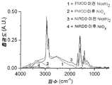
도 2는, 본 발명의 방법에 따른 니켈 전구체의 니켈 산화물로의 분해를 모니터링하는 적외선 스펙트럼을 도시한다.
도 3은, 본 발명에 따른 UV 광 분해 및 NIRDD 방법에 의해 준비된 니켈 산화물의 순환전 전압전류도(cyclic voltammograms)를 도시한다.
도 4의 a는, 본 발명에 따른, FTO 유리 상에 WCl6의 에탄올 용액을 퇴적하며, 그 다음에, UV 조사된 용액에 의한 무정형 텅스텐 산화물 막의 형성의 개략적인 도면이다.
도 4의 b 내지 e는 본 발명에 따라 준비된 무정형 텅스텐 산화물 막을 특징화한 결과를 도시하며, (b) FTO 유리 상의 WCl6에 대한 염소 함량을 판정하는 XRF 분석, (c) 및 (d) FTO 유리 상의 금속 산화물 막의 XPS 분석, 및 (e) 광분해 이전(프레시), UV 조사 이후, 및 어닐링 단계 이후 FTO 유리의 WCl3 막의 IR 스펙트럼을 포함한다.
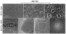
도 5는 본 발명의 실시예에 따라 준비된 a-WO3 막의 전자 현미경 사진을 도시한다.
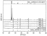
도 6은, 본 발명의 실시예에 따라 준비되며, 600℃까지 점진적으로 더 높은 온도에서 어닐링된 FTO 유리 상의 WO3의 박막의 XRD 회절도(diffractogram)를 도시한다.
도 7은, 본 발명의 실시예에 따라 준비되는 텅스텐 산화물 막의 탈색 및 유색 상태에 대한 투과도 데이터를 도시한다.
도 8은, 본 발명의 실시예에 따라 준비되는 무정형 및 결정형 WO3의 전기 변색성에 관한 데이터를 도시한다.
도 9는, 본 발명의 실시예에 따라 준비되는 니켈 산화물의 탈색 및 유색 상태에 대한 투과도 데이터를 도시한다.
도 10은, 본 발명의 실시예에 따라 준비되는 니켈 산화물 막의 100 주기 동안의 전압 순환(cycling) 및 안정성을 도시하는 도면이다.
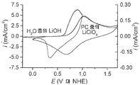
도 11은 물(H20) 및 비수 용매(PC-프로필렌 카보네이트) 중에서에 대한 본 발명의 실시예에 따라 준비되는 니켈 산화물 막의 순환 전압전류도를 도시한다.
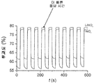
도 12는, 순환 이벤트 동안 본 발명의 실시예에 따라 준비된 니켈 산화물 및 리튬 니켈 산화물 막에 대한 투과도 데이터를 도시한다.
도 13은 본 발명의 실시예에 따라 준비된 무정형 바나듐 산화물 막의 특징화에 관한 데이터를 도시하며, (a) FTO 유리 상의 VCl3에 대한 염소 함량을 판정하는 XRF 분석, (b) 및 (c) FTO 유리 상의 금속 산화물 막의 XPS 분석, 및 (d) 광분해 이전(프레시), UV 조사 이후, 및 어닐링 단계 이후 FTO 유리의 VCl3 막의 IR 스펙트럼을 포함한다.
도 14는, 본 발명의 실시예에 따라 준비된 바나듐 산화물 막의 탈색 및 유색 상태에 대한 투과도 데이터를 도시한다.
도 15는 본 발명의 실시예에 따라 준비된 무정형 니오븀 산화물 막의 특징화에 관한 데이터를 도시하며, (a) FTO 유리 상의 NbCl5에 대한 염소 함량을 판정하는 XRF 분석, (b) 및 (c) FTO 유리 상의 금속 산화물 막의 XPS 분석, 및 (d) 광분해 이전(프레시), UV 조사 이후, 및 어닐링 단계 이후 FTO 유리의 NbCl5 막의 IR 스펙트럼을 포함한다.
도 16은, 본 발명의 실시예에 따라 준비된 니오븀 산화물 막의 탈색 및 유색 상태에 대한 투과도 데이터를 도시한다.
도 17은 본 발명에 따라 준비된 무정형 몰리브덴 산화물 막의 특징화에 관한 데이터를 도시하며, (a) FTO 유리 상의 MoCl5에 대한 염소 함량을 판정하는 XRF 분석, (b) 및 (c) FTO 유리 상의 금속 산화물 막의 XPS 분석, 및 (d) 광분해 이전(프레시), UV 조사 이후, 및 어닐링 단계 이후 FTO 유리의 MoCl5 막의 IR 스펙트럼을 포함한다.
도 18은, 본 발명의 실시예에 따라 준비된 몰리브덴 산화물 막의 탈색 및 유색 상태에 대한 투과도 데이터를 도시한다.
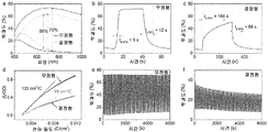
도 19는, (a) 준비되자마자의 WO3; (b) 1시간 동안 공기 중에서 200℃로 어닐링된 WO3; 및 (c) 1시간 동안 공기 중에서 600℃로 어닐링되는 WO3와 조립되는 디바이스의 ΔT, tb,90% 및 tc,90% 및 CE의 판정에 관한 데이터를 도시한다.
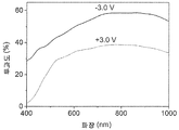
도 20a는, 지시된 전위에서 형성된 유색 및 탈색 상태에서, (각각 100℃에서 어닐링되며) 본 발명에 따라 준비된 V2O5, Nb2O5 또는 MoO3 능동 층을 포함하는 전기 변색 디바이스에 대한 광학 투과도 스펙트럼에 관한 데이터를 도시한다.
도 20b는, 본 발명에 따라 준비된 V2O5, Nb2O5 또는 MoO3 능동 층을 포함하는 전기 변색 디바이스에 대한 전하 밀도의 함수로서의 Δ(OD)의 변화에 관한 데이터를 도시한다.
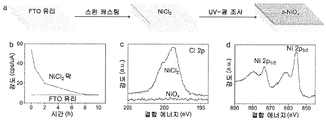
도 21a는 본 발명에 따른, FTO 유리 상에 NiCl2의 에탄올 용액을 퇴적하며, 그 다음에, UV 조사된 용액에 의한 무정형 니켈 산화물 막의 형성의 개략적인 도면이다.
도 21b 내지 도 21d는 본 발명에 따라 준비된 NiOX 막을 특징화한 결과를 도시하며, (b) 시간의 함수로서 염소 함량을 판정하는 XRF 분석, (c) 및 (d) FTO 유리 상의 금속 산화물 막의 XPS 분석을 포함한다.
도 22a는, 본 발명의 실시예에 따라 준비된, 이온 저장 소재로서 FTO 유리 상대 전극 상의 NiOX 막을 사용하는 고체 상태 EC 디바이스의 아키텍쳐의 개략적인 도시이다.
도 22b 내지 도 22d는 본 발명에 따라 준비된 상대 전극 상에 NiOX 막을 이용하는 고체 상태 디바이스를 특징화한 결과를 도시하며, (b) FTO 유리 상대 전극 상에 a-NiOX를 갖고 및 갖지 않고 준비된 EC 디바이스에 대해 획득한 투과도 스펙트럼의 비교, (c) 상대 전극으로서 FTO 상에 a-NiOX를 갖고 준비된 EC 디바이스에 대한 시간의 함수로서의 투과도 변화, 및 (d) FTO 유리 상대 전극 상에 a-NiOX를 사용하여 준비된 고체 상태 EC 디바이스에 대한 전하 밀도 함수로서의 633nm에서의 광학 밀도의 변화를 포함한다.
도 23은, 본 발명의 실시예에 따라 준비된, 상대 전극으로서 무정형 및 결정형 니켈 산화물을 사용하는 EC 디바이스의 성능을 특징화하며 비교한 결과를 도시한다.
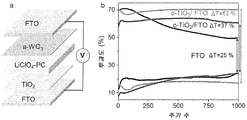
도 24a는, 본 발명의 실시예에 따라 준비된, 이온 저장 소재로서 FTO 유리 상대 전극 상의 TiO2 막을 이용하는 디바이스의 개략적인 도시이다.
도 24b는, 이온 저장 소재로서 FTO 유리 상대 전극 상의 TiO2 막을 이용하는 EC 디바이스를 특정화하며 비교하는 결과를 도시하며, (b) 전기 변색 층으로서 WO3를 가지며, 상대 전극으로서 FTO 상에 퇴적되는 a-TiO2(밝은 회색) 또는 결정형 c-TiO2(짙은 회색)을 갖거나, TiOX 막을 갖지 않는 EC 디바이스에 대한 1000 주기 동안의 700nm의 파장에서의 최대 및 최소 투과도를 포함한다.
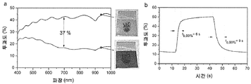
도 25는, 본 발명에 따라 준비된 상이한 두께의 WO3 막을 특징화하는 결과를 도시한다.
도 26은, 본 발명에 따라 준비된 주석-도핑된 인듐 산화물(ITO)로 코팅된 폴리에틸렌 테레프탈레이트(PET) 상의 WO3 막에 대한 투과도 데이터를 도시한다.
도 27은, 본 발명에 따라 준비된 FTO 유리 상의 도핑되지 않은 WO3와 Nb-도핑된 WO3 막에 대한 투과도 데이터를 도시한다.
도 28은, 본 발명에 따라 준비된 FTO 유리 상의 도핑되지 않은 WO3와 Ti-도핑된 WO3 막에 대한 투과도 데이터를 도시한다.1 is a schematic view of an electrochromic battery and its components.
2 shows an infrared spectrum for monitoring the decomposition of nickel precursors into nickel oxide according to the method of the present invention.
3 shows cyclic voltammograms of nickel oxide prepared by the UV light decomposition and NIRDD method according to the present invention.
4A is a schematic illustration of the formation of an amorphous tungsten oxide film by UV irradiated solution, depositing ethanol solution of WCl 6 on FTO glass, according to the present invention.
4B to 4B show the results characterizing the amorphous tungsten oxide film prepared according to the present invention, and (b) XRF analysis to determine the chlorine content for WCl 6 on FTO glass, (c) and (d) FTO XPS analysis of the metal oxide film on glass, and (e) IR spectrum of the WCl 3 film of the FTO glass before photolysis (fresh), after UV irradiation, and after an annealing step.
5 shows an electron micrograph of a-WO 3 membrane prepared according to an embodiment of the present invention.
FIG. 6 shows the XRD diffractogram of a thin film of WO 3 on FTO glass prepared in accordance with an embodiment of the present invention and annealed at progressively higher temperatures to 600 ° C.
Figure 7 shows the transmittance data for the discoloration and color state of the tungsten oxide film prepared according to an embodiment of the present invention.
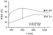
8 shows data relating to the electrochromic properties of amorphous and crystalline WO 3 prepared according to an embodiment of the present invention.
Figure 9 shows the transmittance data for the decolorization and color state of the nickel oxide prepared according to an embodiment of the present invention.
10 is a diagram showing voltage cycling and stability for 100 cycles of a nickel oxide film prepared according to an embodiment of the present invention.
11 shows a cyclic voltammetry diagram of a nickel oxide film prepared according to an embodiment of the present invention in water (H 2 0) and a non-aqueous solvent (PC-propylene carbonate).
12 shows permeability data for nickel oxide and lithium nickel oxide films prepared according to embodiments of the present invention during a cycling event.
13 shows data on characterization of an amorphous vanadium oxide film prepared according to an embodiment of the present invention, (a) XRF analysis to determine chlorine content for VCl 3 on FTO glass, (b) and (c) FTO XPS analysis of the metal oxide film on the glass, and (d) IR spectrum of the VCl 3 film of the FTO glass before photolysis (fresh), after UV irradiation, and after the annealing step.
14 shows transmittance data for decolorization and coloration of a vanadium oxide film prepared according to an embodiment of the present invention.
15 shows data on characterization of an amorphous niobium oxide film prepared according to an embodiment of the present invention, (a) XRF analysis to determine chlorine content for NbCl 5 on FTO glass, (b) and (c) FTO XPS analysis of the metal oxide film on glass, and (d) IR spectrum of the NbCl 5 film of the FTO glass before photolysis (fresh), after UV irradiation, and after an annealing step.
16 shows transmittance data for the decolorization and color state of the niobium oxide film prepared according to the embodiment of the present invention.
17 shows data on characterization of amorphous molybdenum oxide films prepared in accordance with the present invention, (a) XRF analysis to determine chlorine content for MoCl 5 on FTO glass, (b) and (c) metal on FTO glass XPS analysis of the oxide film, and (d) IR spectrum of the MoCl 5 film of the FTO glass before photolysis (fresh), after UV irradiation, and after the annealing step.
18 shows the transmittance data for the decolorization and color state of the molybdenum oxide film prepared according to the embodiment of the present invention.
19 shows, (a) WO 3 as soon as it is ready; (b) WO 3 annealed at 200 ° C. in air for 1 hour; And (c) data for determination of ΔT, t b, 90% and t c, 90% and CE of the device assembled with WO 3 annealed at 600 ° C. in air for 1 hour.
FIG. 20A shows an electrochromic device comprising a V 2 O 5 , Nb 2 O 5 or MoO 3 active layer prepared in accordance with the present invention (each annealed at 100 ° C.), in colored and bleached states formed at the indicated potentials. Shows data relating to the optical transmittance spectrum.
20B shows data regarding the change in Δ (OD) as a function of charge density for an electrochromic device comprising a V 2 O 5 , Nb 2 O 5 or MoO 3 active layer prepared according to the present invention.
21A is a schematic illustration of the formation of an amorphous nickel oxide film by UV irradiated solution, depositing an ethanol solution of NiCl 2 on FTO glass, according to the present invention.
21B-21D show the results characterizing a NiO X film prepared in accordance with the present invention, (b) XRF analysis to determine chlorine content as a function of time, (c) and (d) metal oxide film on FTO glass XPS analysis.
22A is a schematic illustration of the architecture of a solid state EC device using a NiO X film on an FTO glass counter electrode as an ion storage material, prepared according to an embodiment of the present invention.
22B-22D show the results characterizing a solid state device using a NiO X film on a counter electrode prepared in accordance with the present invention, and (b) prepared with and without a-NiO X on FTO glass counter electrode Comparison of transmittance spectra obtained for the EC device, (c) change in transmittance as a function of time for the prepared EC device with a-NiO X on the FTO as counter electrode, and (d) a- on FTO glass counter electrode And a change in optical density at 633 nm as a function of charge density for a solid state EC device prepared using NiO X.
23 shows the results of characterizing and comparing the performance of EC devices using amorphous and crystalline nickel oxides as counter electrodes prepared according to an embodiment of the present invention.
24A is a schematic illustration of a device prepared using a TiO 2 film on an FTO glass counter electrode as an ion storage material, prepared in accordance with an embodiment of the present invention.
24B shows the results of characterizing and comparing an EC device using a TiO 2 film on an FTO glass counter electrode as an ion storage material, (b) having WO 3 as an electrochromic layer, a deposited on the FTO as a counter electrode Maximum and minimum transmittance at a wavelength of 700 nm for 1000 cycles for EC devices with -TiO 2 (light gray) or crystalline c-TiO 2 (dark gray), or without a TiO X film.
25 shows the results characterizing different thickness WO 3 membranes prepared according to the present invention.
26 shows permeability data for a WO 3 film on polyethylene terephthalate (PET) coated with tin-doped indium oxide (ITO) prepared according to the present invention.
27 shows permeability data for undoped WO 3 and Nb-doped WO 3 membranes on FTO glass prepared according to the present invention.
28 shows permeability data for undoped WO 3 and Ti-doped WO 3 membranes on FTO glass prepared according to the present invention.
정의Justice
"무정형"은, 그 원자 구조가 장거리 질서(long-range order) 없는 화학 조성을 의미한다. "Amorphous" means a chemical composition whose atomic structure is not in long-range order.
"전기 변색 전지"는, 인가된 전기 바이어스의 사용을 통한, 유색 상태(즉, 창문을 통한 광의 낮은 투과도)로부터 투명 상태(즉, 창문을 통한 광의 높은 투과도)로 및/또는 투명 상태로부터 유색 상태로 투명도를 전환할 수 있는 전지를 지칭한다. An “electrochromic cell” is a colored state from a colored state (ie, a low transmittance of light through a window) through a use of an applied electrical bias (ie, a high transmittance of light through a window) and / or from a colored state. Refers to a battery that can convert the transparency to.
"리간드(Ligand)"는 금속에 배위결합되거나, 화학 결합되거나 이온 결합되는 임의의 화학족을 의미한다. 통상의 리간드 예는 염화물, 브롬화물, 질화물, 2-에틸헥사노에이트 및 아세틸아세토네이트이지만 이들로 제한되지 않는다. "Ligand" means any chemical group that is coordinated, chemically bound or ionic bound to a metal. Common ligand examples are, but are not limited to, chloride, bromide, nitride, 2-ethylhexanoate and acetylacetonate.
"금속 산화물"은 여기서는 금속과 산소를 포함하는 임의의 단일 고체를 지칭할 수 도 있으며, 금속 대 산소의 비는 미리 규정되지 않으며, 따라서 MOX로서 나타낸다. 전기 변색 소재로서 사용하기에 적절할 수 도 있는 단일 금속 산화물의 예는 NiOX, WO3, MoO3, TiO2, Ta2O5, V2O5, Nb2O5, CoO2, MnO2 및 FeOX를 포함하지만, 이들로 제한되지 않는다. “Metal oxide” may also refer to any single solid comprising metal and oxygen here, and the ratio of metal to oxygen is not predefined and is therefore referred to as MO X. Examples of single metal oxides that may be suitable for use as the electrochromic material include NiO X , WO 3 , MoO 3 , TiO 2 , Ta 2 O 5 , V 2 O 5 , Nb 2 O 5 , CoO 2 , MnO 2 and FeO X , but is not limited to these.
"혼합된 금속 산화물"은 적어도 2개의 금속을 포함하며 산화물인 막을 지칭한다. 전기 변색 소재로서 사용하기에 적절할 수 도 있는 혼합된 금속 산화물의 예는 LiNiOX, TiWOX 및 FeNiOX를 포함하며, 이들로 제한되지 않는다."Mixed metal oxide" refers to a film comprising at least two metals and being an oxide. Examples of mixed metal oxides that may be suitable for use as an electrochromic material include, but are not limited to, LiNiO X , TiWO X and FeNiO X.
"금속 전구체"는, 기판 상에 퇴적되며 그 후 금속 산화물로 변환되는 금속을 포함하는 임의의 화학물질을 기재한다. 통상의 예는, 금속 염화물, 금속 2-에틸헥사노에이트 및 금속 아세틸아세토네이트를 포함하지만 이들로 제한되지 않으며, 금속은 앞서 식별한 금속 중 임의의 금속일 수 도 있다. “Metal precursor” describes any chemical that includes a metal that is deposited on a substrate and then converted to a metal oxide. Common examples include, but are not limited to, metal chloride, metal 2-ethylhexanoate, and metal acetylacetonate, and the metal may be any of the metals identified above.
"환원된 철 산화물"은 철과 산소가 거의 동일한 양으로 존재하는 화합물, FeO를 지칭한다. "Reduced iron oxide" refers to a compound, FeO, in which iron and oxygen are present in approximately the same amount.
"스퍼터링"은, 순수 금속이, 이 금속의 원자를 매질 내에 배출하는 고 에너지에 노출되게 하며, 이때 원자는 후속하여 기판 상에 퇴적되는, 기술을 지칭한다. "Sputtering" refers to a technique in which a pure metal is exposed to high energy that releases atoms of this metal into the medium, where the atoms are subsequently deposited on a substrate.
"기판"은 금속 산화물 코팅이 그 위에 조립되는 소재를 지칭한다. 기판 소재는 본래 전도성일 수 도 있거나, 전도도는, 전도성 막을 소재의 표면에 적용함으로써 야기될 수 도 있다. 적절한 막은 통상 불소 주석 산화물(FTO); 인듐 주석 산화물(ITO); 알루미늄 아연 산화물(AZO) 및 여러 기타와 같은 투명한 전도성 산화물(TCO)을 포함한다. 다른 적절한 지지 소재는 임의의 투명 유리, 플라스틱, 폴리머(예컨대, PET), 또는 관련 전도성 층과 호환적인 고무를 포함한다. "Substrate" refers to a material on which a metal oxide coating is assembled. The substrate material may be conductive in nature, or the conductivity may be caused by applying a conductive film to the surface of the material. Suitable films are usually fluorine tin oxide (FTO); Indium tin oxide (ITO); Transparent conductive oxides (TCO) such as aluminum zinc oxide (AZO) and several others. Other suitable support materials include any transparent glass, plastic, polymer (eg PET), or rubber compatible with the associated conductive layer.
본 발명은, 진공을 필요로 하지 않으며 주변 온도 또는 상승된 온도로 실행될 수 도 있는 스케일러블 제조 공정을 사용하여 제조된 전기 변색 금속 산화물 및/또는 혼합-금속 산화물 막을 포함하는 전기 변색 디바이스에 관한 것이다. The present invention relates to an electrochromic device comprising an electrochromic metal oxide and / or mixed-metal oxide film prepared using a scalable manufacturing process that does not require vacuum and may be performed at ambient or elevated temperatures. .
본 발명의 목적은 그러므로, 전기 변색 디바이스에서 사용하기 위해, 적절한 전도성 기판 상에 코팅되는 금속 산화물 또는 혼합 금속 산화물의 광학 특성 막을 제조하기 위한 저가의, 스케일러블한 용액 기반 공정을 제공하는 것이다. 본 발명에 따라, 본 발명의 공정을 사용하여 형성되는 금속 산화물 및/또는 혼합 금속 산화물 막은 전기 변색, 즉 외부 전기 바이어스가 도입되면 유색 상태로부터 투명 상태로(또는 투명 상태로부터 유색 상태로) 그 투명도를 변환할 수 있다.It is therefore an object of the present invention to provide an inexpensive, scalable solution-based process for producing optical property films of metal oxides or mixed metal oxides coated on suitable conductive substrates for use in electrochromic devices. According to the present invention, the metal oxide and / or mixed metal oxide film formed using the process of the present invention is electrochromic, ie its transparency from a colored state to a transparent state (or from a transparent state to a colored state) when an external electrical bias is introduced. You can convert
본 발명은 또한, 본 발명의 전기 변색 디바이스에 사용하기 위해, 무정형 또는 결정형 상으로, 원하는 금속 산화물 및 혼합 금속 산화물 막을 큰-스케일로 처리하며 제조하는데 적절한 광 화학 방법을 제공한다. The present invention also provides a photochemical method suitable for manufacturing and processing a desired metal oxide and mixed metal oxide film in large-scale, in an amorphous or crystalline phase, for use in the electrochromic device of the present invention.
본 개시는 전기 변색 디바이스를 위해 금속 산화물 및 혼합 금속 산화물을 만드는데 적절한 2개의 방법: 근적외선 구동 분해(NIRDD: Near Infrared Driven Decomposition) 또는 UV 광분해를 기재한다. NIRDD 및 UV 광분해는, 기존의 최신 기술보다 정밀한 성분 제어를 제공하며 제조 비용을 더 낮추는 용액 처리 가능 전구체로 더 낮은 온도에서 동작하는 제조 방법이다. This disclosure describes two methods suitable for making metal oxides and mixed metal oxides for electrochromic devices: Near Infrared Driven Decomposition (NIRDD) or UV photolysis. NIRDD and UV photolysis are manufacturing methods that operate at lower temperatures as solution-processable precursors that provide more precise component control and lower manufacturing costs than current state-of-the-art technologies.
일 실시예에서, 적외선 광을 사용하여 금속 전구체를 분해하여 대응하는 금속 산화물 또는 혼합 금속 산화물을, 공기 중에 형성된다면, 생성하는 근적외선 구동 분해(NIRDD) 방법이 제공된다. PCT 특허 공보 제 WO2016101067A1호는 금속 산화물 및 혼합 금속 산화물의 준비를 위한 NIRDD 방법을 기재하며, 그 전체 개시는 본 명세서에서 참조로서 인용된다.In one embodiment, a near infrared drive decomposition (NIRDD) method is provided that decomposes a metal precursor using infrared light to produce a corresponding metal oxide or mixed metal oxide, if formed in air. PCT patent publication WO2016101067A1 describes a NIRDD method for the preparation of metal oxides and mixed metal oxides, the entire disclosure of which is incorporated herein by reference.
일 실시예에서, UV 광분해 방법이 제공되며, 여기서, 금속 전구체는, 부가적으로 오존 중에서 자외선 방사선을 받아 모든 리간드를 제거하며 유산소 분위기 하에서 원하는 금속 또는 혼합 금속 산화물을 발생시킨다. UV 광분해는 주변 온도 또는 상승 온도로 동작한다. US 특허 제 9,433,928호는 전기 화학적 촉매(electrocatalyst)를 만들기 위한 방법에 사용하기 위한 금속 산화물 및 혼합 금속 산화물을 생성하기 위한 UV 광분해 기술을 기재하며, 그 전체 개시가 본 명세서에서 참조로서 인용된다. In one embodiment, a UV photolysis method is provided, wherein the metal precursor additionally receives ultraviolet radiation in ozone to remove all ligands and generates the desired metal or mixed metal oxide under an aerobic atmosphere. UV photolysis works at ambient or elevated temperatures. US Patent No. 9,433,928 describes a UV photolysis technique for producing metal oxides and mixed metal oxides for use in a method for making electrocatalysts, the entire disclosure of which is incorporated herein by reference.
공기 중의 금속 전구체에 관해 실행될 때, UV 광분해 및 NIRDD는 결국 대응하는 금속의 더 감소한 상을 야기할 수 있다. When performed on metal precursors in the air, UV photolysis and NIRDD can eventually result in a reduced phase of the corresponding metal.
본 발명의 방법을 사용하여 형성되는 전기 변색 금속 산화물 및/또는 혼합 금속 산화물 막은 무정형일 수 있거나 결정형일 수 도 있다. The electrochromic metal oxide and / or mixed metal oxide film formed using the method of the present invention may be amorphous or crystalline.
본 발명의 일 실시예에서, 금속 산화물 또는 혼합 금속 산화물은 투명한 전도성 산화물 층 상에 형성되며, 후속하여 전기 변색 전지에 병합되며, 이러한 전기 변색 전지는 인가된 전기 바이어스의 사용을 통해 불투명에서부터 투명으로 또는 투명에서부터 불투명으로 변환할 수 있다. In one embodiment of the present invention, a metal oxide or mixed metal oxide is formed on a transparent conductive oxide layer, which is subsequently incorporated into an electrochromic cell, which electrochromic cell is opaque to transparent through the use of an applied electrical bias. Or you can convert from transparent to opaque.
본 발명에 따라, 하나 이상의 금속 또는 혼합 금속 산화물 코팅이 전기 변색 전지에서 전기 변색 창문과 같은 "스마트 유리" 응용에 병합되는 층으로서 이용된다. In accordance with the present invention, one or more metal or mixed metal oxide coatings are used as layers incorporated into “smart glass” applications such as electrochromic windows in electrochromic cells.
전기 변색 디바이스의 일반적인 구성은, 투명한 전도성 기판 상에 지지되는 애노드와 캐소드 및 전극간 이온 전도체(전해질)를 포함한다. 애노드 및/또는 캐소드는 전기 변색 소재(들)를 포함할 수 도 있다. 전체 디바이스의 각 구성요소의 기능은 이하에서 상세하게 기재할 것이며 전체 디바이스 아키텍쳐의 개략적인 도면이 도 1에 제시된다. The general configuration of the electrochromic device includes an anode and a cathode and an interelectrode ion conductor (electrolyte) supported on a transparent conductive substrate. The anode and / or cathode may also include electrochromic material (s). The function of each component of the entire device will be described in detail below and a schematic drawing of the entire device architecture is presented in FIG. 1.
전압이 전극 양단에 인가될 때, 전계가 절연 전기 변색 소재 내에 생성되며, 이것은 이 전기 변색 소재의 색 변화(예컨대, 일 전기 변색 상태로부터 다른 전기 변색 상태로 전환할 때 탈색 상태로부터 유색 상태로)를 발생시키는 전기 변색 소재로 또는 그로부터의 이온의 이동을 야기할 수 있다. 인가된 바이어스를 역전시킴으로써, 전기 변색 소재는 다시 전환될 수 있다(예컨대 유색 상태로부터 탈색 상태로). 전기 변색 소재는 초기에는 또한 유색일 수 도 있으며, 인가된 전압으로 무색/탈색 상태로 전환될 수 있으며, 그 후 인가된 바이어스를 역전시킴으로써 다시 유색 상태로 전환될 수 도 있다. 예컨대, 텅스텐 산화물계 막은 이온 삽입으로 유색이 되는 반면, 니켈 산화물계 막은 이온 추출로 유색이 된다. When a voltage is applied across the electrode, an electric field is created in the insulating electrochromic material, which changes the color of the electrochromic material (e.g., from a discolored state to a colored state when switching from one electrochromic state to another). It can cause the movement of ions to or from the electrochromic material that generates. By reversing the applied bias, the electrochromic material can be switched back (eg from a colored state to a bleached state). The electrochromic material may also be colored initially, may be converted to a colorless / discolored state with an applied voltage, and then converted back to a colored state by reversing the applied bias. For example, a tungsten oxide-based film becomes colored by ion insertion, while a nickel oxide-based film becomes colored by ion extraction.
전기 변색 전지에서 전해질 층의 역할은 이온이 애노드 소재와 캐소드 소재 사이에서 일주하게 하는 것이다. 전기 변색 디바이스용 공통 전해질의 예는 프로필렌 카보네이트에서의 LiClO4이다. The role of the electrolyte layer in the electrochromic cell is to cause ions to travel around the anode material and the cathode material. An example of a common electrolyte for electrochromic devices is LiClO 4 in propylene carbonate.
이처럼, 통상의 전기 변색 디바이스는 능동 전기 변색 층, 전해질 층, 이온 저장 층(상대 전극) 층, 투명 전도체 및 지지 기판으로 이루어진 다층 아키텍쳐를 갖는다. 이들 층 중에서, 전기 변색 및 이온 저장 층이 가역적 색 전환에 기여하는 핵심 구성요소이다.As such, a typical electrochromic device has a multi-layered architecture consisting of an active electrochromic layer, an electrolyte layer, an ion storage layer (relative electrode) layer, a transparent conductor and a supporting substrate. Among these layers, the electrochromic and ion storage layers are key components contributing to reversible color conversion.
우수한 전기 변색 소재는 그 유색 상태와 탈색 상태 사이에 높은 색 콘트래스트를 보이고, 유색 상태와 탈색 상태 사이의 급속한 변환을 가지고, 낮은 인가 전압에서 유색 상태와 탈색 상태 사이를 전환할 수 있고, 상태 사이의 순환의 뛰어난 가역성을 보이며 우수한 안정성을 보인다.An excellent electrochromic material shows a high color contrast between its colored and bleached states, has a rapid conversion between the colored and bleached states, and can switch between colored and bleached states at low applied voltages, and It shows excellent reversibility of circulation and shows excellent stability.
본 발명의 바람직한 실시예에 따라, 전기 변색 디바이스에 이용되는 금속 산화물 및 혼합 금속 산화물 막은, NiOX, WOX, NbOX, MoOX, MnOX, CoOX, VOX, TaOX, TiOX 및 LiNiOX 또는 그 조합을 포함한다.According to a preferred embodiment of the present invention, the metal oxide and mixed metal oxide films used in the electrochromic device include NiO X , WO X , NbO X , MoO X , MnO X , CoO X , VO X , TaO X , TiO X and LiNiO X or combinations thereof.
금속 또는 혼합 금속 산화물에 대한 다른 응용은, 단독으로 또는 전기 변색 금속 산화물 코팅과 조합하여, 장파장 태양 방사선의 입력을 방지하는 코팅을 창문 상에 제공하는 것이다. 일 실시예에서, 광 흡수 코팅이 환원된 철 산화물 막에 의해 제공된다. 환원된 철 산화물은, 질소나 아르곤과 같은 불활성 분위기에서 NIRDD 또는 UV 광분해 중 어느 하나에 의해 발생될 수 도 있다. 이들 실시예 모두에서, 환원된 철 산화물 층이 병합될 수 도 있어서 가시광에 영향을 미치지 않고도 근적외선 광을 차단할 수 도 있어서, 가시광이 통과하게 하면서도 근적외선 파장을 흡수하는 역할을 할 수 도 있다. Another application for metal or mixed metal oxides, alone or in combination with electrochromic metal oxide coatings, is to provide a coating on the window that prevents the input of long wavelength solar radiation. In one embodiment, a light absorbing coating is provided by a reduced iron oxide film. The reduced iron oxide may be generated by either NIRDD or UV photolysis in an inert atmosphere such as nitrogen or argon. In all of these embodiments, the reduced iron oxide layer may be incorporated to block near-infrared light without affecting visible light, and may serve to absorb near-infrared wavelengths while allowing visible light to pass through.
작동 전극을 포함하는 가장 잘 알려진 전기 변색 소재 코팅은 디바이스의 동작 동안 짙은 청색과 무색 상태 사이에서 가역적으로 및 지속적으로 전환하는 WO3 막이다. The most well known electrochromic material coatings comprising working electrodes are WO 3 membranes that reversibly and continuously switch between dark blue and colorless states during operation of the device.
텅스텐 삼산화물("WO3")은 전기 변색 디바이스에서 연노랑(또는 투명) 중립 상태와 딥 블루(deep blue) 상태 사이를 순환하는 잘 알려진 캐소드 전기 변색 소재이다. 투명한 막은 리튬 이온 중에서 전기 화학적으로 환원될 수 있어서 유색, 환원 상태("LiWO3")를 형성하며, 투명한 상태로 가역적으로 재-산화된다. 본 발명의 방법은 전기 변색 디바이스에 사용하기 위한 WOX 막을 형성하는데 사용될 수 있다. Tungsten trioxide (“WO 3 ”) is a well-known cathode electrochromic material that circulates between a light yellow (or transparent) neutral state and a deep blue state in an electrochromic device. The transparent film can be electrochemically reduced in lithium ions to form a colored, reduced state ("LiWO 3 ") and reversibly re-oxidize to a transparent state. The method of the present invention can be used to form WO X films for use in electrochromic devices.
다른 전기 변색 캐소드 소재의 예는 Mo03, TiO2, Ta205, V205, NiOX, 및 Nb205를 포함하지만, 이들로 제한되지 않는다. Examples of other electrochromic cathode materials include, but are not limited to, Mo0 3 , TiO 2 ,
니켈 산화물("NiOX")은 텅스텐 산화물에 상보적으로 유색이 되어 전기 변색 전지에서 더 우수한 유색 다크 상태를 만드는 알려진 애노드 전기 변색 소재이다. 본 발명의 방법은 전기 변색 디바이스에 사용하기 위해 NiOX 막을 형성하는데 사용된다. Nickel oxide (“NiO X ”) is a known anode electrochromic material that is complementarily colored to tungsten oxide to create a better colored dark state in electrochromic cells. The method of the present invention is used to form NiO X films for use in electrochromic devices.
우수한 애노드 전기 변색 소재의 다른 예는 IrO2이다. CoO2, MnO2 및 FeO2와 같은 소재는 전기 변색 거동을 보이는 것으로 잘 알려져 있지만, 이상적이지 않으며 이는 이들이 완벽하게 탈색되지 않기 때문이다. Another example of a good anode electrochromic material is IrO 2 . Materials such as CoO 2 , MnO 2 and FeO 2 are well known to exhibit electrochromic behavior, but they are not ideal because they are not completely discolored.
철 산화물("FeO")은 가시광에 대한 근적외선 광의 높은 흡수로 알려진 소재이다. 이것은 아키텍쳐 유리 상의 코팅에 사용될 수 있어서 건물의 내부 태양 난방을 감소시킬 수 있다. FeO의 박막은 스퍼터링 또는 애노드 조건 하에서 화학 증기 퇴적에 의해 만들 수 있다. Iron oxide ("FeO") is a material known for its high absorption of near infrared light to visible light. It can be used for coating on architectural glass, reducing the internal solar heating of buildings. The thin film of FeO can be made by sputtering or chemical vapor deposition under anode conditions.
주석 도핑된 인듐 산화물(ITO) 및 불소 도핑된 주석 산화물(FTO)과 같은 투명한 전도성 금속 산화물(TCOs)이 격리되어 또는 추가 이온 저장 소재로 코팅되는 상대 전극으로서 종종 사용된다. 그 상대 전극을 위해 베어 TCO를 가진 디바이스가 탈색 상태에서 더 우수한 투명도를 보통 보일지라도, 그러한 디바이스에서, 전하는 2개의 전극 사이에서 보통 균형이 맞춰지지 않으며, 이점은 디바이스 안정성에 해로울 수 도 있다. 본 발명의 방법은 안정 금속 산화물 이온 저장 층을 형성하는데 사용될 수 있다. Transparent conductive metal oxides (TCOs) such as tin-doped indium oxide (ITO) and fluorine-doped tin oxide (FTO) are often used as counter electrodes that are isolated or coated with additional ion storage materials. Although a device with a bare TCO for its counter electrode usually exhibits better transparency in the discolored state, in such a device, the charge is usually not balanced between the two electrodes, and the advantage may be detrimental to device stability. The method of the present invention can be used to form a stable metal oxide ion storage layer.
금속 전구체 또는 금속 전구체의 조합이, 유리, 플라스틱, 혼합물 등을 포함할 수 도 있지만, 이들로 제한되지 않는 기판 상에 코팅된다. 본 발명의 실시예에서, 바람직한 기판은 투명하며 유리이거나 플라스틱이거나 한다. The metal precursor or combination of metal precursors may be coated on a substrate, which may include, but is not limited to, glass, plastic, mixtures, and the like. In embodiments of the present invention, the preferred substrate is transparent and is either glass or plastic.
선택한 기판을 코팅하는 것은 스핀 코팅, 페인팅, 딥 코팅, 스프레이 코팅, 울트라-소닉 스프레이 코팅 또는 당업자에게 친숙한 다른 방법을 포함하는 다양한 방법을 사용하여 실행될 수 있다. 코팅 용액은 금속 전구체 또는 전구체들을 호환 가능한 용매에 용해시킨 후, 이 용액을 기판의 표면에 적용함으로써 준비된다. 건조되면, 원하는 전구체 또는 전구체들의 층이 기판 상에 형성된다. 호환 가능한 용매의 예는 물, 메탄올, 에탄올, 이소프로판올, 아세톤, 헥산, 아세틸아세톤 및 메틸 이소부틸 케톤을 포함하지만, 이들로 제한되지 않는다.Coating the selected substrate can be performed using a variety of methods including spin coating, painting, dip coating, spray coating, ultra-sonic spray coating or other methods familiar to those skilled in the art. The coating solution is prepared by dissolving the metal precursor or precursors in a compatible solvent, and then applying this solution to the surface of the substrate. When dried, a desired precursor or layer of precursors is formed on the substrate. Examples of compatible solvents include, but are not limited to, water, methanol, ethanol, isopropanol, acetone, hexane, acetylacetone and methyl isobutyl ketone.
본 발명의 공정에서 사용하기에 적절한 금속 전구체는, 근적외선 방사선, UV 방사선 및/또는 오존에 노광시키면 대응하는 금속 산화물로 변환될 수 있는 임의의 금속 유도체(derivative)를 포함한다. 적절한 전구체는 금속 염화물, 금속 2-에틸헥사노에이트 및 금속 아세틸아세토네이트를 포함하지만, 이들로 제한되지 않는다. 금속 전구체의 예시적인 실시예는 WCl6, Ni(eh)2, NiCl2, VCl3, NbCl5, MoCl5, Li(eh), W(0-/Pr)6 및 Ti(eh)4를 포함한다.Metal precursors suitable for use in the process of the present invention include any metal derivative that can be converted to the corresponding metal oxide upon exposure to near infrared radiation, UV radiation and / or ozone. Suitable precursors include, but are not limited to, metal chloride, metal 2-ethylhexanoate and metal acetylacetonate. Exemplary examples of metal precursors include WCl 6 , Ni (eh) 2 , NiCl 2 , VCl 3 , NbCl 5 , MoCl 5 , Li (eh), W (0- / Pr) 6 and Ti (eh) 4 do.
NIRDD 및/또는 UV 광분해 방법 중 어느 하나가, 기판 상에 코팅되는 금속 전구체를, 주변 온도나 상승 온도에서 공기중에서 원하는 무정형 또는 결졍형 금속 산화물로 변환하는데 사용될 수 있다. 스퍼터링 기술을 사용한 혼합 금속 산화물을 형성하는 것은 비교적 더 힘들다.Either NIRDD and / or UV photolysis methods can be used to convert the metal precursor coated on the substrate to the desired amorphous or crystallized metal oxide in air at ambient or elevated temperatures. It is relatively more difficult to form mixed metal oxides using sputtering technology.
금속 산화물 막의 합성의 일 실시예에서, 전구체 용액은 금속 전구체를 무수 에탄올에 용해시킴으로써 발생된다. 전구체 용액은 그 후 FTO 유리 상에서 스핀-코팅되며, 결과적인 전구체 박막은, 스펙트럼 계측 방법을 사용한 리간드 손실의 모니터링을 통해 분해를 확인할 때까지, UV 또는 NIR 조사선을 받는다. In one embodiment of the synthesis of the metal oxide film, the precursor solution is generated by dissolving the metal precursor in absolute ethanol. The precursor solution is then spin-coated on the FTO glass, and the resulting precursor thin film is subjected to UV or NIR radiation until decomposition is confirmed through monitoring of ligand loss using a spectral metrology method.
특정한 실시예에서, 퇴적되자마자의 막은 10℃/분의 램핑 율을 사용하여 1시간 동안 50 내지 750℃의 범위의 온도에서 공기 중에서 오븐에 어닐링 단계를 겪는다. 일 실시예에서, 막은 1시간 동안 100℃에서 어닐링 단계를 겪는다. 일 실시예에서, 막은 1시간 동안 200℃에서 어닐링 단계를 겪는다. 일 실시예에서, 막은 1시간 동안 200℃에서 어닐링 단계를 겪는다. 일 실시예에서, 막은 1시간 동안 600℃에서 어닐링 단계를 겪는다. In a specific embodiment, as soon as it is deposited, the membrane undergoes an annealing step in an oven in air at a temperature in the range of 50 to 750 ° C for 1 hour using a ramping rate of 10 ° C / min. In one embodiment, the membrane undergoes an annealing step at 100 ° C. for 1 hour. In one embodiment, the membrane undergoes an annealing step at 200 ° C. for 1 hour. In one embodiment, the membrane undergoes an annealing step at 200 ° C. for 1 hour. In one embodiment, the membrane undergoes an annealing step at 600 ° C. for 1 hour.
유기 리간드를 포함하는 전구체의 경우, 원하는 금속 산화물의 형성이 적외선 스펙트럼 계측술에 의해 모니터링될 수 있으며, 이는 금속 전구체로부터의 리간드 손실이 적외선 스펙트럼에서 리간드 신호의 손실을 야기하기 때문이다. 도 2는 UV 광분해 및 NIRDD 방법 모두를 사용한 니켈 2-에틸헥사노에이트 금속 전구체로부터 무정형 니켈 산화물로의 변환을 도시한다.For precursors comprising organic ligands, the formation of the desired metal oxide can be monitored by infrared spectroscopy, because the loss of ligand from the metal precursor causes loss of the ligand signal in the infrared spectrum. 2 shows the conversion of nickel 2-ethylhexanoate metal precursor to amorphous nickel oxide using both UV photolysis and NIRDD methods.
금속 염화물 염을 포함하지만 이들로 제한되지 않는 적외선 스펙트럼 계측술에 의해 추적될 수 없는 전구체의 경우, X-선 형광(XRF) 스펙트럼 계측술이 무정형 금속 산화물로의 변환을 모니터링하는데 사용될 수 있다. For precursors that cannot be traced by infrared spectroscopy, including but not limited to metal chloride salts, X-ray fluorescence (XRF) spectroscopy can be used to monitor conversion to amorphous metal oxides.
본 발명에 따라, NIRDD 및 UV 광분해 방법이 동일한 최종 금속 산화물 막을 발생시키는데 사용될 수 있다. 도 3은 본 발명의 NIRDD 및 UV 광분해 방법 모두를 사용하여 발생된 니켈 산화물 막의 순환 전압전류도를 도시한다. 전압전류 곡선 모두는, NIRDD 및 UV 광분해에 의해 생성되는 무정형 금속 산화물 막이 전기 화학적으로 동일함을 나타낸 동일한 형상과 특성을 도시한다. According to the present invention, NIRDD and UV photolysis methods can be used to generate the same final metal oxide film. Figure 3 shows the cyclic voltammetry of a nickel oxide film generated using both the NIRDD and UV photolysis methods of the present invention. All of the voltage-current curves show the same shape and properties, indicating that the amorphous metal oxide films produced by NIRDD and UV photolysis are electrochemically identical.
다음의 성능 메트릭스는 본 발명의 방법을 사용하여 준비된 금속 산화물 막을 사용하여 형성되는 디바이스에 대해 평가되었다: (i) 최대 광학 변조(ΔT), 완전 유색 상태와 탈색 상태 사이의 광 투과도의 차이; (ii) 각각의 완전 유색 상태와 투명 상태 사이의 투과도의 완전 변화의 90%에 도달하는데 필요한 유색(tc,90%)과탈색(tb,90%)에 전환 시간; 및 (iii) 단위 면적당 전하 변화(ΔQ)에 응답한 광학 밀도의 변화(Δ(OD))에 대응하는 컬러레이션 효율(CE)(coloration efficiency). CE의 값은 Δ(OD)의 그래프에서의 선형 영역을 ΔQ의 함수로서 맞추며, 수학식 1에 따라 경사도를 추출함으로써 획득되었다(여기서 Tb 및 Tc는 각각 주어진 파장에서의 탈색 상태와 유색 상태에서의 투과도이다).The following performance metrics were evaluated for devices formed using a metal oxide film prepared using the method of the present invention: (i) maximum optical modulation (ΔT), difference in light transmission between fully colored and decolored states; (ii) conversion time to colored (t c, 90% ) and decolored (t b, 90% ) required to reach 90% of the complete change in transmittance between each fully colored and transparent state; And (iii) a coloration efficiency (CE) corresponding to a change in optical density (Δ (OD)) in response to a charge change per unit area (ΔQ). The value of CE was obtained by fitting the linear region in the graph of Δ (OD) as a function of ΔQ, and extracting the slope according to Equation 1 (where T b and T c are decolorization and colored states at a given wavelength, respectively). It is the permeability at).

일 실시예에서, 본 발명의 방법에 따라 발생된 무정형 텅스텐 산화물 막은 전기 변색 디바이스에 사용하기에 적절한 전기 변색성을 보인다. 도 4a는 본 발명에 따른, FTO 유리 상에 WCl6의 에탄올 용액을 퇴적하며, 그 다음에, UV 또는 NIR 조사된 용액에 의한 무정형 텅스텐 산화물 막의 형성의 개략적인 도면이다. In one embodiment, the amorphous tungsten oxide film generated according to the method of the present invention exhibits electrochromic properties suitable for use in electrochromic devices. 4A is a schematic illustration of the formation of an amorphous tungsten oxide film by UV or NIR irradiated solution, depositing an ethanol solution of WCl 6 on FTO glass, according to the present invention.
NIRDD 또는 UV 광분해를 사용하여 형성된 무정형 텅스텐 산화물은 도 7에 도시된 바와 같이 전체 가시광 스펙트럼에 걸쳐서 유색 모드에서 감소한 투과도(5 내지 20%)와 탈색 모드에서 광범위한 투과도(35 내지 75%)를 보인다. 무정형 WO3 막은 가시광 및 적외선 범위(400 내지 1000nm)에 걸쳐서 전압-제어된 광 투과도를 입증하였다. 텅스텐 산화물 막의 투명도는 인가된 바이어스를 제어함으로써 정밀하게 조작될 수 있다. 양의 바이어스를 도입하면, 탈색 상태가 생성되며 투과도가 증가한다. 음의 바이어스가 인가되면, 유색 상태를 생성하며 광 투과도는 텅스텐 산화물을 통해 감소한다(도 7).Amorphous tungsten oxide formed using NIRDD or UV photolysis shows reduced transmittance (5-20%) in color mode and broad transmittance (35-75%) in decolorization mode over the entire visible light spectrum, as shown in FIG. 7. The amorphous WO 3 film demonstrated voltage-controlled light transmission over the visible and infrared ranges (400-1000 nm). The transparency of the tungsten oxide film can be precisely manipulated by controlling the applied bias. When a positive bias is introduced, a bleaching state is created and transmittance increases. When a negative bias is applied, a colored state is created and light transmittance decreases through tungsten oxide (FIG. 7).
일 실시예에서, 본 발명의 NIRDD 및 UV 광분해 방법을 사용하여 형성된 무정형 니켈 산화물 막은 전기 변색 디바이스에 사용하기에 적절한 전기 변색성을 또한 보인다. 양의 바이어스를 도입하면, 유색 상태가 생성되며 투과도는 감소한다. 음의 바이어스를 인가하면, 탈색 상태를 생성하며, 광 투과도는 니켈 산화물을 통해 증가한다. 니켈 산화물 막의 투명도는 인가된 바이어스를 제어함으로써 정밀하게 조작될 수 있다. 본 발명에 따라 준비된 니켈 산화물 막의 탈색 모드와 유색 모드 모두에 대한 전체 스펙트럼 투과도 곡선이 도 9에 도시된다. 유색 조건 하에서, 투과도 범위는 15% 내지 45%인 반면, 탈색 모드에서, 투과도는 40% 내지 70%이다. 본 발명의 UV 광분해 또는 NIRDD 방법 중 어느 하나에 의해 형성되는 무정형 니켈 산화물은 도 10에 도시된 바와 같이 유색 모드와 투명 모드 사이의 장기간 안정성 순환을 보인다. 12000s(100 주기)의 시간 기간에 걸쳐 순환되는 샘플인 각 개별 주기 이후 그 투과도 레벨의 5% 내로 반복해서 복귀한다. In one embodiment, amorphous nickel oxide films formed using the NIRDD and UV photolysis methods of the present invention also exhibit electrochromic properties suitable for use in electrochromic devices. When positive bias is introduced, a colored state is created and transmittance is reduced. Applying a negative bias creates a bleaching state, and the light transmittance increases through nickel oxide. The transparency of the nickel oxide film can be precisely manipulated by controlling the applied bias. The overall spectral transmittance curve for both the decoloring mode and the colored mode of the nickel oxide film prepared according to the present invention is shown in FIG. 9. Under the colored condition, the transmittance range is 15% to 45%, while in the decoloring mode, the transmittance is 40% to 70%. The amorphous nickel oxide formed by either the UV photolysis or NIRDD method of the present invention shows a long-term stability cycle between the colored mode and the transparent mode as shown in FIG. 10. After each individual cycle, which is a sample circulated over a period of time of 12000 s (100 cycles), it repeatedly returns within 5% of its transmittance level.
애노드 소재와 캐소드 소재 사이의 전해질/이온 전도체는 원하는 투명도, 전도도 및 내구성을 주도록 변경될 수 있다. 본 발명의 방법을 사용하여 형성된 무정형 니켈 산화물 막은 수용성 및 유기 전해질 모두에서 성공적으로 동작함으로써 전기 변색 디바이스 설계에 추가 융통성을 제공한다. 도 11에 도시한 순환성 전압전류도는, 무정형 니켈 산화물 층의 안정성을 입증하는 수용성 및 비-수용성 용매에서의 반복적, 가역적 산화 및 환원 피크를 드러낸다. The electrolyte / ion conductor between the anode material and the cathode material can be altered to give the desired transparency, conductivity and durability. Amorphous nickel oxide films formed using the methods of the present invention successfully operate in both aqueous and organic electrolytes, providing additional flexibility in electrochromic device designs. The cyclic voltammetry shown in FIG. 11 reveals repetitive, reversible oxidation and reduction peaks in aqueous and non-aqueous solvents demonstrating the stability of the amorphous nickel oxide layer.
혼합 금속 산화물은 다른 응용(예컨대, 초전도체, 전기분해)에서 개별 금속 산화물에 대해 우월한 성능을 달성하는 것으로 알려져 있다. 이러한 성능 개선은 원자 및 나노 스케일에서의 상승 및 유효한 효과를 통해 달성된다. 본 발명의 경우, 리튬이 1:3의 비율로 무정형 니켈 산화물 막에 도입되었다. 혼합 금속 산화물 막(LiNi3OX)는 도 12에 도시된 바와 같이 무정형 니켈 산화물보다 훨씬 빨리(수초만큼) 정상-상태 전기 변색을 달성한다. 더 빠른 정상-상태 전기 변색은 상업적 응용, 특히 불투명에서부터 투명으로의 전기 변색 전지의 급속한 전환을 필요로 하는 것들에 유리하다.Mixed metal oxides are known to achieve superior performance for individual metal oxides in other applications (eg superconductors, electrolysis). This performance improvement is achieved through synergistic and effective effects at the atomic and nanoscale. For the present invention, lithium was introduced into the amorphous nickel oxide film in a ratio of 1: 3. The mixed metal oxide film (LiNi 3 O X ) achieves steady-state electrochromic much faster (by a few seconds) than amorphous nickel oxide, as shown in FIG. 12. Faster steady-state electrochromic is advantageous for commercial applications, particularly those requiring rapid conversion of the electrochromic cell from opaque to transparent.
전기 변색적으로 능동적인 산화물 층을 만들기 위한 본 방법의 일반성은 각각 VCl3, NbCl5 및 MoCl5로부터 유래한 V2O5, Nb2O5 및 MoO3의 무정형 막으로 연장되었다. V2O5, Nb2O5 및 MoO3를 포함하는 전기 변색 디바이스는 70nm의 파장에서 각각 ~20%, ~30% 및 ~35%의 가시광 범위에서의 광학 변조를 보였다(각각 도 14, 도 16 및 도 18). 투과도의 더 큰 변화는 상이한 파장에서 관찰되었다. 준비되자마자의 산화물 막 각각의 XPS 분석은 그 완전히 산화된 화학 상태에서의 각 금속(바나듐, 니오븀 또는 몰리브덴)의 안정화 및 염소 부재를 확인하였다(각각 도 13a, 15a 및 17a). 준비되자마자의 V2O5, Nb2O5 및 MoO3 박막은, 100℃에서 1시간 동안의 추가 어닐링에 의해 효과적으로 제거되었던 잔류 물을 포함하였다(각각 도 13d, 15d 및 17d). V2O5, Nb2O5 및 MoO3를 포함하는 전기 변색 디바이스는 각각 450, 500 및 550nm의 파장에서 36, 22 및 57cm2/C의 컬러레이션 효율을 갖는 가시광 범위의 광학 변조를 보였다(도 20). 도 20a는 나타낸 전위에서 형성되는 유색 상태 및 탈색 상태에서의 3개의 V2O5, 5개의 Nb2O5 또는 5개의 MoO3 능동 층(각각 100℃에서 어닐링됨)을 포함하는 전기 변색 디바이스에 대한 광학 투과도 스펙트럼을 도시한다. 도 20b는 450nm에서의 V2O5, 550nm에서의 Nb2O5 및 550nm에서의 MoO3에 대한 Δ(OD)의 그래프를 전하 밀도의 함수로서 도시한다. 각 그래프의 선형 영역을 맞춤으로써 획득한 CE 값이 또한 도 20b에 나타내어 있다. The generality of this method for making electrochromically active oxide layers was extended to amorphous films of V 2 O 5 , Nb 2 O 5 and MoO 3 derived from VCl 3 , NbCl 5 and MoCl 5 respectively. The electrochromic device comprising V 2 O 5 , Nb 2 O 5 and MoO 3 showed optical modulation in the visible light range of ˜20%, ˜30% and ˜35% at a wavelength of 70 nm, respectively (FIG. 14, FIG. 16 and 18). Larger changes in transmittance were observed at different wavelengths. Upon preparation, XPS analysis of each of the oxide films confirmed the stabilization and absence of chlorine of each metal (vanadium, niobium or molybdenum) in its fully oxidized chemical state (FIGS. 13A, 15A and 17A, respectively). Upon preparation, the V 2 O 5 , Nb 2 O 5 and MoO 3 thin films contained residues that were effectively removed by further annealing at 100 ° C. for 1 hour (FIGS. 13D, 15D and 17D, respectively). Electrochromic devices comprising V 2 O 5 , Nb 2 O 5 and MoO 3 showed optical modulation in the visible light range with coloration efficiencies of 36, 22 and 57 cm 2 / C at wavelengths of 450, 500 and 550 nm, respectively ( Fig. 20). FIG. 20A is an electrochromic device comprising three V 2 O 5 , five Nb 2 O 5 or five MoO 3 active layers (annealed at 100 ° C. respectively) in colored and decolored states formed at the dislocations shown. The optical transmittance spectrum is shown. 20B shows a graph of Δ (OD) for V 2 O 5 at 450 nm, Nb 2 O 5 at 550 nm and MoO 3 at 550 nm as a function of charge density. The CE values obtained by fitting the linear region of each graph are also shown in FIG. 20B.
UV 분해 및 NIRRD에 의해 발생된 FeO 막은 가시광에 투명함을 유지하면서 근적외선 영역에서 강한 흡광도를 보인다. 전기 변색 디바이스에 적용된 FeO 막은 디바이스의 상태, 온이든 오프든지에 상관 없이 근적외광을 차단할 것이다. The FeO film generated by UV decomposition and NIRRD shows a strong absorbance in the near infrared region while maintaining transparency to visible light. The FeO film applied to the electrochromic device will block near-infrared light regardless of the device's state, on or off.
표 1은 상이한 방법으로 준비된 여러 전기 변색 금속 산화물의 CE를 비교한다. 모든 경우에, 본 명세서에서 기재한 방법은 다른 방법에 의해 만든 막과 유사하거나 그보다 더 우수한 금속 산화물 막을 제공한다. Table 1 compares the CE of several electrochromic metal oxides prepared in different ways. In all cases, the methods described herein provide metal oxide films similar to or better than films made by other methods.
(nm)Wavelength a
(nm)
a CE 값에 대한 광학 데이터가 기록되었던 파장. a Wavelength at which optical data for CE values were recorded.
본 발명의 방법은 상대 전극 상에서 이온 저장 층으로서 금속 산화물 막을 퇴적하는데 또한 사용될 수 있다. TCO 기판 상에 코팅된 이온 저장 소재는, 컬러레이션 동안 WO3에 끼워 넣는 Li-이온을 디바이스가 탈색하며 릴리스하는 동안 Li-이온을 저장함으로써 동작 동안 작동 전극(통상 WO3)에 의해 생성되는 전하를 효율적으로 균형을 맞을 수 있다. NiO 및 IrO2는 EC 디바이스에서 일반적으로 사용되는 이온 저장 소재이며, EC 디바이스에 대해 상보적인 컬러레이션을 제공함으로써 컬러레이션 강도를 개선할 수 있다. 그러나 NiO 및 IrO2의 고유 색으로 인해, 광학 변조 값이 손상될 수 도 있다. CeO2와 같은 광학적 수동 이온 저장 소재의 사용이 탈색 상태에서 디바이스의 투명도를 보존할 수 있는 반면, 그 이온 저장 성능은 제한된다. 그러므로 뛰어난 이온 저장 성능을 또한 입증하는 대안적인 광학 수동 상대 전극 소재를 찾는 것이 매우 바람직할 수 있다. TiO2는, 리튬 이온 배터리에서 애노드 소재로서 사용될 때 뛰어난 리튬 이온 저장 성능을 보이며, 이점은 TiO2 박막이 EC 디바이스의 상대 전극 상의 적용을 위한 이온-저장 소재로서 사용될 수 있음을 나타낸다. The method of the present invention can also be used to deposit a metal oxide film as an ion storage layer on a counter electrode. The ion storage material coated on the TCO substrate is the charge generated by the working electrode (usually WO 3 ) during operation by storing the Li-ion during release and the device discoloring the Li-ion interposed in WO 3 during coloration. Can be balanced efficiently. NiO and IrO 2 are ion storage materials commonly used in EC devices, and can improve coloration intensity by providing complementary coloration for EC devices. However, due to the intrinsic colors of NiO and IrO 2 , the optical modulation value may be impaired. While the use of an optically passive ion storage material such as CeO 2 can preserve the transparency of the device in a discolored state, its ion storage performance is limited. Therefore, it may be highly desirable to find alternative optical passive counter electrode materials that also demonstrate excellent ion storage performance. TiO 2 shows excellent lithium ion storage performance when used as an anode material in lithium ion batteries, and the advantage indicates that the TiO 2 thin film can be used as an ion-storage material for application on the counter electrode of the EC device.
일 실시예에서, 본 발명의 방법에 따라 준비된 무정형 TiO2 막은 EC 디바이스에 사용하기 위한 상대 전극 소재로서 이용된다.In one embodiment, an amorphous TiO 2 film prepared according to the method of the present invention is used as a counter electrode material for use in EC devices.
일 실시예에서, 이온 저장 금속 산화물 막은 본 발명에 따라 준비된 광퇴적 전기 변색 막에 결합되어, 최신 기술의 전기 변색 성능을 보여주는 고체 상태 전기 변색 디바이스를 형성한다. 고체 상태 전기 변색 디바이스는 액체 전해질을 사용하는 디바이스에 존재하는 안전 및 밀봉 문제를 회피할 수 있다. In one embodiment, the ion storage metal oxide film is combined with a photodeposited electrochromic film prepared in accordance with the present invention to form a solid state electrochromic device that demonstrates the state of the art electrochromic performance. Solid state electrochromic devices can avoid the safety and sealing problems present in devices using liquid electrolytes.
본 발명은 이제 특정한 실시예를 참조하여 기재될 것이다. 다음의 예는 본 발명의 실시예를 기재하고자 하며 본 발명을 어떤 식으로든 제한하고자 하지는 않음을 이해해야 할 것이다.The invention will now be described with reference to specific embodiments. It should be understood that the following examples are intended to describe embodiments of the invention and are not intended to limit the invention in any way.
예Yes
예 1: NiOExample 1: NiO XX UV 광분해 UV photolysis
본 예에서, 불소-도핑된 주석 산화물(FTO; TEC 7; 7Ω/sq) 기판은 2.5×2.5cm2으로 절단되며, 15분 동안 Extran®300 세제에서, 15분 동안 탈염 H20, 15분 동안 아세톤에서 초음파 분해되어 세척되며, 20분 동안 O3(g)의 UV 광에 노광되며 스핀 코팅된다. 전구체 용액은 광능동 니켈 혼합물이다. 이 예에서, 니켈(II) 2-에틸헤사노에이트(2-에틸헥사노익산에서의 78%(w/w), Strem Chemicals)가 사용되었다. 에탄올에서의 0.2 M 용액이 준비되었으며 깨끗한 FTO 표면에 적용된다. 샘플은 스핀-코팅되어(3000rpm, 60s), 니켈(II) 2-에틸헥사노에이트의 박막을 산출하였다. 코팅된 기판은 그 후 UV 방사선에 노출되었다. 본 예에서, 샘플은 24시간 동안 이중 파장 UV 램프(l=185, 254nm) 하에 놓였다. 전구체 분해는 적외선(IR) 스펙트럼 계측술에 의해 모니터링되었으며, 대응하는 리간드에 대응하는 스트레치가 사라질 때 완료되는 것으로 간주되었다.In this example, the fluorine-doped tin oxide (FTO; TEC 7; 7Ω / sq) substrate is cut into 2.5 × 2.5 cm 2 , in an
예 2: NiOExample 2: NiO XX NIRDD NIRDD
본 예에서, 동일한 전구체가 예 1과 동일한 기판에 적용되어 동일한 방식으로 스핀-코팅된다. 이 경우에, 샘플은 적외선 램프 아래에 놓여서 전구체 분해를 야기하여 a-NiOX 막을 형성한다. 형성된 막은 분해 후 투명하다. 전구체 분해는 예 1에서와 동일한 방식으로 추적될 수 있다.In this example, the same precursor is applied to the same substrate as in Example 1 and spin-coated in the same way. In this case, the sample is placed under the infrared lamp to cause precursor decomposition to form an a-NiO X film. The formed film is transparent after decomposition. Precursor decomposition can be traced in the same way as in Example 1.
예 3: 디바이스 조립Example 3: Device assembly
(예 4 내지 15에서 형성된 것들을 포함한) 본 방법에 따라 준비된 막은, 상대 전극으로서 역할하는 베어 FTO 유리 위에 중앙이 빈 원(직경=1.6cm)을 가진 2×2cm2(square) 실리콘 고무 시트(20A, 두께=1mm; McMaster-CARR)를 놓음으로써 제조된 전기 변색 디바이스에 병합되었다. FTO 유리는 그 후 실리콘 스페이서 상에 놓인 전기 변색 능동 금속 산화물 막(작동 전극)으로 코팅되어 폐쇄된 전지를 형성한다. 에폭시 접착제가 전지의 3개의 면을 밀봉하는데 사용되었다. 1-M LiClO4 프로필렌 카보네이트 전해질 용액이 밀봉되지 않은 면을 통해 주사기로 전지에 주입되었다. 주입 전, 바이얼(vial)에서의 전해질과 빈 전지는 각각 5분 동안 건조 N2로 퍼징되어 주변 공기를 날려 버렸다. 에폭시 접착제로 제4 면을 밀봉하여 최종 전기 변색 디바이스를 제공하였다. 조립된 디바이스는 2.0cm2의 능동 면적을 가졌다.Membranes prepared according to this method (including those formed in Examples 4-15) are 2 × 2 cm 2 (square) silicone rubber sheets (20A) with hollow centers (diameter = 1.6 cm) on bare FTO glass serving as counter electrodes. , Thickness = 1 mm; McMaster-CARR). The FTO glass is then coated with an electrochromic active metal oxide film (working electrode) placed on a silicon spacer to form a closed cell. Epoxy adhesive was used to seal the three sides of the cell. A 1-M LiClO 4 propylene carbonate electrolyte solution was injected into the cell with a syringe through the unsealed side. Prior to injection, the electrolyte in the vial and the empty cell were purged with dry N 2 for 5 minutes each to blow away the ambient air. The fourth side was sealed with an epoxy adhesive to provide the final electrochromic device. The assembled device had an active area of 2.0 cm 2 .
예 4: WOExample 4: WO 33 UV 광분해 UV photolysis
본 예에서, 투명한 전도성 산화물은 예 1과 동일한 방식으로 준비되었다. 무수 에탄올이 텅스텐(VI) 염화물(WCl6, 시그마-알드리흐(Sigma-Aldrich))에 추가되어, 0.25 M 용액을 만든다. 이 용액은 16시간 동안 스터링되었으며 기판 상에 스핀-코팅되어(3000rpm, 60s) 기판 상에 짙은 청색 막을 산출하였다. 기판은 그 후 전구체를 분해하여 a-WO3을 형성하기 위해 UV 램프(l=185 또는 l=185, 254nm) 아래에서 놓였다. 금속 산화물로의 변환은 X-선 형광에 의해 모니터링되었다. 전기 변색 디바이스는 예 3에서 기재된 바와 같이 조립되었으며, 이때 작동 전극으로서 FTO 유리 상의 WO3 막(텅스텐 전구체의 5개의 후속한 퇴적에 대응함)의 600nm 막을 갖는다. (a-WO3로 명명된) 디바이스에서의 무정형 WO3 막은 디바이스에 놓이기 전 1시간 동안 100℃에서 어닐링되어 기판으로부터의 박리를 억제하였다.In this example, a transparent conductive oxide was prepared in the same manner as in Example 1. Anhydrous ethanol was added to tungsten (VI) chloride (WCl 6 , Sigma-Aldrich) to make a 0.25 M solution. The solution was stirred for 16 hours and spin-coated on the substrate (3000 rpm, 60 s) to produce a dark blue film on the substrate. The substrate was then placed under a UV lamp (l = 185 or l = 185, 254nm) to decompose the precursor to form a-WO 3 . The conversion to metal oxide was monitored by X-ray fluorescence. The electrochromic device was assembled as described in Example 3, with a 600 nm film of a WO 3 film on FTO glass (corresponding to five subsequent depositions of tungsten precursor) as the working electrode. The amorphous WO 3 film in the device (designated a-WO 3 ) was annealed at 100 ° C. for 1 hour before being placed in the device to suppress delamination from the substrate.
도 4b는, 염소 전구체가 텅스텐에 대한 UV 광분해 동안 분해됨에 따라 FTO 유리 상의 WCl6에 대한 염소 함량을 XRF 모니터링한 결과를 도시하며, UV 조사의 3분 내에 전구체의 완전한 분해를 XRF 분석에 의해 확인한다. 도 4c 및 도 4d는, FTO 유리 상의 금속 산화물 막의 XPS 분석이, W6+와 일치하는 W4f 스펙트럼 시그니쳐가 존재한다면, WO3의 식과 일치함을 도시한다. 도 4e는 3분 동안 UV 조사선을 받기 이전 및 이후 FTO 유리 상의 에탄올 스핀-캐스트에 용해되는 WCl6의 IR 스펙트럼뿐만 아니라 3분 동안 UV 광에 노광되며 1시간 동안 100℃에서 어닐링된 후 형성된 WO3의 층 상에 기록되는 IR 스펙트럼을 도시한다.FIG. 4B shows the results of XRF monitoring of the chlorine content for WCl 6 on FTO glass as the chlorine precursor decomposes during UV photolysis for tungsten, confirming complete decomposition of the precursor by XRF analysis within 3 minutes of UV irradiation do. 4C and 4D show that the XPS analysis of the metal oxide film on the FTO glass is consistent with the formula of WO 3 if a W4f spectral signature matching W 6+ is present. FIG. 4e shows the IR spectrum of WCl 6 dissolved in ethanol spin-cast on FTO glass before and after receiving UV radiation for 3 minutes, as well as after exposure to UV light for 3 minutes and annealing at 100 ° C. for 1 hour, WO 3 It shows the IR spectrum recorded on the layer.
도 5는, 본 발명의 UV 조사 방법에 따라 준비되며, 100℃에서 1시간 동안 어닐링된 단일 WO3 층의 SEM, TEM 및 HRTEM 특징화를 도시한다. 도 5의 전자 마이크로그래프는 200nm 두께의 균일한, 고다공성의 무정형 막을 도시한다. 횡단면 SEM 이미지에 도시된 이리듐 및 백금 층은, 막 전도도를 증가시킴으로써 대전 현상을 감소시키며, 횡단면을 만드는데 사용된 집속된 이온 빔으로부터 기저의 막을 보호하도록 퇴적되었다. 5 shows SEM, TEM and HRTEM characterization of a single WO 3 layer prepared according to the UV irradiation method of the present invention and annealed at 100 ° C. for 1 hour. The electron micrograph of FIG. 5 shows a uniform, highly porous
WO3 박막의 무정형 속성은, FTO 기판보다 결정형 상의 증거를 보여주지 않는 XRD 회절도에 의해 또한 지원되었다. 이 막은 각각 60분 동안 100℃부터 600℃까지 100℃ 간격으로 어닐링되었다. 결정형 상의 존재, 즉 단결정 WO3은, 막이 400℃를 초과하여 가열되었을 때 단지 검출되었다. 결정형 WO3 막은 또한 전기 변색성을 보인다.The amorphous nature of the WO 3 thin film was also supported by XRD diffractograms, which showed no evidence of crystalline form than the FTO substrate. The membranes were annealed at 100 ° C intervals from 100 ° C to 600 ° C for 60 minutes each. The presence of the crystalline phase, i.e., single crystal WO 3 , was only detected when the film was heated above 400 ° C. Crystalline WO 3 membranes also exhibit electrochromic properties.
예 5. 무정형 및 결정형 WOExample 5. Amorphous and crystalline WO 33 의 전기 변색성의 비교Comparison of electrochromic properties
예 4에서 발생된 무정형 WO3 막에 관한 어닐링 효과를 검사하였다. (c-WO3로서 표시된) 벤치마크 결정형 막은 예 4에 기재한 동일한 프로토콜을 따라서, 그러나 400℃에서 추가 1시간 어닐링 단계로 준비되었다.The annealing effect on the amorphous WO 3 membrane generated in Example 4 was examined. Benchmark crystalline membranes (labeled c-WO 3 ) were prepared following the same protocol described in Example 4, but at an additional 1 hour annealing step at 400 ° C.
유색 및 탈색 바이어스 하에서의 디바이스의 광학 투과도 스펙트럼은, 무정형 WO3에 대해 700nm에서 측정된 ~70%의 투과도 값의 변화가 결정형 WO3에 대해 측정된 값보다 ~15% 더 높음을 도시한다(도 8a). 디바이스가, 무정형 및 결정형 막을 포함하는 디바이스에 대해 유색에서 탈색으로 전환되며 다시 유색으로 전환될 때 700nm에서의 투과도 변화가 각각 도 8b 및 도 8c에 도시된다. 전환 시간은 나타내어져 있다. 유색의 전환 시간(투명 상태에서부터 유색 상태로의 투과도의 완전 변화의 90%에 도달하는데 필요한 시간으로 규정되는 tc,90%)(12s) 및 무정형 WO3에 대해 측정된 유색 상태로부터 투명 상태로의 탈색 전환 시간(tb,90%)(5s) 값은 결정형 WO3에 대한 값들보다 뚜렷하게 빨랐으며, 각각 5배 및 35배 더 긴 tc,90% 및 tb,90%를 보여준다(도 8c). 도 8d는 700nm에서의 광학 밀도의 변화(Δ(OD))를 전하 밀도의 함수로서 도시한다. CE 값은 그래프의 선형 영역을 맞춤(fitting)으로써 판정되었다. 무정형 WO3의 컬러레이션 효율(CE)은 700nm의 파장에서 133cm2/C인 것으로 계산되었으며, 이것은 결정형 WO3의 컬러레이션 효율의 거의 2배이다(도 8d). 도 8e 및 도 8f는, 30s 간격으로 100 주기 동안 유색 상태와 탈색 상태 사이를 전기 변색 전환하는 동안 700nm에서의 투과도 변화를 도시한다. 30s 동안 -3.5V로부터 30s 동안 3.0V까지 인가된 바이어스를 전환하는 1000 주기에 걸쳐 (UV 광분해 또는 NIRDD 중 어느 하나에 의해 형성되는) 무정형 WO3의 안정성은 초기 투과도 변화의 90%가 유지되었음을 확인하였다(도 8e). 무정형 산화물의 초기 100 주기에서 열화는 거의 무시할 만하며(도 8e), 그러나 결정형 텅스텐 산화물에 대한 투과도 변화는 동일한 100 주기 동안 상당한 열화를 보였다(도 8f).The optical transmittance spectrum of the device under the colored and depigmentation bias shows that the change in transmittance value of ~ 70% measured at 700 nm for amorphous WO 3 is ~ 15% higher than the value measured for crystalline WO 3 (Figure 8A) ). The change in transmittance at 700 nm is shown in FIGS. 8B and 8C, respectively, when the device is converted from color to decolorization and back to color for devices comprising amorphous and crystalline films. Conversion times are indicated. Conversion time of color (t c, 90%, defined as the time required to reach 90% of the complete change in transmittance from the transparent state to the colored state) (12s) and from the colored state measured for amorphous WO 3 to the transparent state The decolorization conversion time (t b, 90% ) of (5s) was significantly faster than those for crystalline WO 3 , showing t c, 90% and
예 6. 전기 변색 성능에 대한 어닐링 온도의 영향Example 6. Effect of annealing temperature on electrochromic performance
무정형 WO3 막이 예 4에서 기재된 방법에 따라 준비되었다. 준비되자마자의 WO3 막은 또한 200℃에서 어닐링 단계와 600℃에서 어닐링 단계를 겪게 된다(어닐링은 1시간 동안 공기 중에서 실행됨). 결과적인 막은 특징화되었으며, 조립된 디바이스의 ΔT, tb,90% 및 tc,90%와 CE 값이 도 19에 제공된다: (a) 준비되자마자의 WO3; (b) 200℃에서 어닐링된 WO3; 및 (c) 600℃에서 어닐링된 WO3.Amorphous WO 3 membrane was prepared according to the method described in Example 4. Upon preparation, the WO 3 membrane also undergoes an annealing step at 200 ° C. and an annealing step at 600 ° C. (annealing is performed in air for 1 hour). The resulting membrane was characterized and ΔT, t b, 90% and t c, 90% and CE values of the assembled device are provided in Figure 19: (a) WO 3 as soon as ready; (b) WO 3 annealed at 200 ° C .; And (c) WO 3 annealed at 600 ° C.
(℃)Annealing temperature
(℃)
(%)ΔT
(%)
(s)t c, 90%
(s)
(s)t b, 90%
(s)
(cm2/C)CE
(cm 2 / C)
a 디바이스 능동 층은 ~600nm이다(5개의 연속 퇴적 층). 유색 및 탈색 형태에 대한 동작 전위는 -3.5V 및 +3.0V이다. 광학 데이터는 700nm에서 측정되었다. ΔT, tc,90% 및 tb,90%와 CE 값은 또한 도 19에 도시되어 있다. a The device active layer is ˜600 nm (5 consecutive deposited layers). The operating potentials for colored and bleached forms are -3.5V and + 3.0V. Optical data was measured at 700 nm. ΔT, t c, 90% and t b, 90% and CE values are also shown in FIG. 19.
예 7: 전기 변색 성능에 대한 WOExample 7: WO for electrochromic performance 33 막 두께의 영향 Effect of film thickness
상이한 두께에서의 a-WO3의 전기 변색 성능이, 막의 10개까지의 층을 연속적으로 추가함으로써 막 두께에 의해 성능이 어떻게 영향을 받는지를 판정하도록 평가되었다(표 3). 700nm에서의 ΔT 값은 1 내지 5개의 층에서 각각 29%에서부터 70%까지 증가한다. 추가 층이 더 어두운 착색이 되었을지라도, 이들 층은 광학 변조에 유익을 주지 못하였으며, 이러한 광학 변조는 10개의 층으로 62%까지 감소하였으며, 이는 더 두꺼운 층의 손상된 투명도 때문이다. 게다가, 전환 시간과 CE 값은 모두 막 두께에 역비례하는 것을 알게 되었다. 1개의 층에 대해 관찰한 2s의 유색 및 탈색 시간은 10개의 층에 대해 20s보다 크게까지 증가한 반면, 193cm2/C의 컬러레이션 효율은 10개의 층으로 117cm2/C로 감소하였다. The electrochromic performance of a-WO 3 at different thicknesses was evaluated to determine how performance is affected by film thickness by continuously adding up to 10 layers of the film (Table 3). The ΔT value at 700 nm increases from 29% to 70% respectively in 1 to 5 layers. Although the additional layer became darker in color, these layers did not benefit optical modulation, and this optical modulation was reduced by 62% to 10 layers, due to the impaired transparency of the thicker layer. Moreover, it was found that both the conversion time and the CE value are inversely proportional to the film thickness. Color and bleaching time of 2s observed for one layer is larger than the other hand up to 20s for 10 layers, coloration efficiency of 193cm 2 / C was decreased to 117cm 2 / C in 10 layers.
(%)ΔT
(%)
(s)t b, 90%
(s)
(s)t c, 90%
(s)
(cm2/C)CE
(cm 2 / C)
a 각각 -3.5V 및 +3.0V에서 발생된 유색 상태와 탈색 상태. 광학 데이터는 700nm에서 측정되었다. ΔT, tc,90% 및 tb,90%와 CE 값은 또한 도 25에 도시되어 있다. b SEM 횡단면 이미징이 각각 1개의 층 및 5개의 층에 대해 200nm와 600nm의 막 두께를 검증하였다. a Colored and bleached states generated at -3.5V and + 3.0V, respectively. Optical data was measured at 700 nm. ΔT, t c, 90% and t b, 90% and CE values are also shown in FIG. 25. b SEM cross-sectional imaging verified film thicknesses of 200 nm and 600 nm for one layer and five layers, respectively.
예 8: WOExample 8: WO 33 NIRDD NIRDD
본 예에서, 투명한 전도성 산화물이 예 1과 동일한 방식으로 준비되고 있다. 무수 에탄올이 텅스텐(Vl) 염화물(WCl6, 시그마-알드리히)에 추가되어 0.25M 용액을 만든다. 이 용액은 16시간 동안 스터링되며, 기판 상에 스핀-코팅되어(3000rpm, 60s), 기판 상에 짙은 청색 막을 산출한다. 기판은 그 후 전구체를 분해하여 a-WO3를 형성하기 위해 IR 램프 아래에 놓이며, 금속 산화물로의 변환은 X-선 형광에 의해 모니터링된다. 무정형 또는 결정형 상이 산화물로의 전환 후 어닐링을 통해 획득될 수 있다. 전기 변색 디바이스는 예 3에 기재된 바와 같이 조립되었다.In this example, a transparent conductive oxide is prepared in the same manner as in Example 1. Anhydrous ethanol was added to tungsten (Vl) chloride (WCl 6 , Sigma-Aldrich) to make a 0.25M solution. The solution was stirred for 16 hours and spin-coated on the substrate (3000 rpm, 60s), yielding a dark blue film on the substrate. The substrate is then placed under the IR lamp to decompose the precursor to form a-WO 3 , and conversion to metal oxide is monitored by X-ray fluorescence. Amorphous or crystalline phases can be obtained through annealing after conversion to oxide. The electrochromic device was assembled as described in Example 3.
예 9: UV 광분해 또는 NIRDD에 의한 LiNiOExample 9: LiNiO by UV photolysis or NIRDD XX 및 다른 혼합 금속 조성 And other mixed metal compositions
본 예에서, 투명 전도성 산화물이 예 1과 동일한 방식으로 준비되었다. 니켈(II) 2-에틸헥사노에이트(2-에틸헥사노익산에서 78%(w/w), Strem Chemicals) 및 리튬 2-에틸헥사노에이트(Strem Chemicals))의 0.2M 용액이 Li:Ni의 가변 비율, 예컨대 25:75, 40:60, 50:50, 75:25로 헥산에서 준비되었다. 용액은 TCO 기판에 적용되며 기판 상에 스핀-코팅된다(3000rpm, 60s). 전구체는 UV 램프(l=185 또는 l=185, 254nm)나 IR 램프 중 어느 하나 아래에서 분해되어 a-LiNiOX를 형성한다. 금속 산화물로의 변환은 예 1에서처럼 모니터링되었다. 전기 변색 디바이스는 예 3에서 기재된 바와 같이 조립되었다.In this example, a transparent conductive oxide was prepared in the same manner as in Example 1. A 0.2M solution of nickel (II) 2-ethylhexanoate (78% (w / w) in 2-ethylhexanoic acid, Strem Chemicals) and lithium 2-ethylhexanoate (Strem Chemicals) is Li: Ni Prepared in hexane with variable ratios of, for example 25:75, 40:60, 50:50, 75:25. The solution was applied to a TCO substrate and spin-coated on the substrate (3000 rpm, 60s). The precursor decomposes under either a UV lamp (l = 185 or l = 185, 254nm) or an IR lamp to form a-LiNiO X. Conversion to metal oxide was monitored as in Example 1. The electrochromic device was assembled as described in Example 3.
예 10: VExample 10:
본 예에서, 투명한 전도체 산화물이 예 1에서와 동일한 방식으로 준비되었다. 무수 에탄올이 바나듐(III) 염화물(VCl3, 시그마-알드리흐(Sigma-Aldrich))에 추가되어, 0.25M 용액을 만들었다. 이 용액은 16시간 동안 스터링되었으며 기판 상에 스핀-코팅되어(3000rpm, 60s) 기판 상에 짙은 청색 막을 산출하였다. 기판은 그 후 전구체를 분해하여 a-V2O5를 형성하기 위해 UV 램프(l=185 또는 l=185, 254nm) 아래에서 놓였다. 금속 산화물로의 변환은 예 4에서처럼 모니터링되었다.In this example, a transparent conductor oxide was prepared in the same way as in Example 1. Anhydrous ethanol was added to vanadium (III) chloride (VCl 3 , Sigma-Aldrich) to make a 0.25M solution. The solution was stirred for 16 hours and spin-coated on the substrate (3000 rpm, 60 s) to produce a dark blue film on the substrate. The substrate was then placed under a UV lamp (l = 185 or l = 185, 254nm) to decompose the precursor to form aV 2 O 5 . Conversion to metal oxide was monitored as in Example 4.
도 13a는, XRF 분석에 의해 측정된, 조사 시간의 함수로서의 FTO 유리 상의 바나듐 염화물 전구체 막에 대한 염소 함량의 그래프를 도시하며, 10분의 조사 이후의 전구체의 완전한 분해를 확인하였다. 도 13b 및 도 13c는, FTO 유리 상의 금속 산화물 막의 XPS 분석이, FTO 유리 상의 준비되자마자의 V2O5의 식과 일치함을 도시한다. 도 13c는, V5+로 진단되는, 각각 525.40eV 및 517.85eV에서의 V2p1/2 및 V2p3/2 신호의 특성을 갖는 확장된 XPS 스펙트럼이다. 도 13d는 10분 동안 UV 조사선을 받기 이전(프레시) 및 이후(광분해됨) FTO 유리 상의 VCl5 스핀-캐스트의 에탄올 용액의 IR 스펙트럼이다. 1시간 동안 100℃에서 어닐링된 준비되자마자의 산화물 막이 또한 도 13d에서 나타나 있다(어닐링됨).13A shows a graph of chlorine content for a vanadium chloride precursor film on FTO glass as a function of irradiation time, measured by XRF analysis, confirming complete decomposition of the precursor after 10 minutes of irradiation. 13B and 13C show that XPS analysis of the metal oxide film on FTO glass is consistent with the formula of V 2 O 5 as soon as it is prepared on FTO glass. 13C is an extended XPS spectrum with the characteristics of V2p 1/2 and V2p 3/2 signals at 525.40eV and 517.85eV, diagnosed as V 5+ , respectively. 13D is an IR spectrum of an ethanol solution of VCl 5 spin-cast on FTO glass before (fresh) and after (photodegraded) UV irradiation for 10 minutes. An oxide film as soon as ready for annealing at 100 ° C. for 1 hour is also shown in FIG. 13D (annealed).
예 11: VExample 11:
본 예에서, 투명한 전도성 산화물이 예 1과 동일한 방식으로 준비되고 있다. 무수 에탄올이 바나듐(III) 염화물(VCl3, 시그마-알드리히)에 추가되어 0.25M 용액을 만든다. 이 용액은 16시간 동안 스터링되며, 기판 상에 스핀-코팅되어(3000rpm, 60s), 기판 상에 짙은 청색 막을 산출한다. 기판은 그 후 전구체를 분해하여 a-V2O5를 형성하기 위해 IR 램프 아래에 놓이며, 금속 산화물로의 변환은 X-선 형광에 의해 모니터링된다. 무정형 또는 결정형 상이 산화물로의 전환 후 어닐링을 통해 획득될 수 있다. 전기 변색 디바이스는 예 3에 기재된 바와 같이 조립되었다.In this example, a transparent conductive oxide is prepared in the same manner as in Example 1. Anhydrous ethanol was added to vanadium (III) chloride (VCl 3 , Sigma-Aldrich) to make a 0.25M solution. The solution was stirred for 16 hours and spin-coated on the substrate (3000 rpm, 60s), yielding a dark blue film on the substrate. The substrate is then placed under the IR lamp to decompose the precursor to form aV 2 O 5 , and conversion to metal oxide is monitored by X-ray fluorescence. Amorphous or crystalline phases can be obtained through annealing after conversion to oxide. The electrochromic device was assembled as described in Example 3.
예 12: NbExample 12: Nb 22 OO 55 UV 광분해 UV photolysis
본 예에서, 투명한 전도성 산화물은 예 1과 동일한 방식으로 준비되었다. 무수 에탄올이 니오븀(V) 염화물(NbCl5, 시그마-알드리흐)에 추가되어, 0.25M 용액을 만들었다. 이 용액은 16시간 동안 스터링되었으며 기판 상에 스핀-코팅되어(3000rpm, 60s) 기판 상에 짙은 청색 막을 산출하였다. 기판은 그 후 전구체를 분해하여 a-Nb2O3을 형성하기 위해 UV 램프(l=185 또는 l=185, 254nm) 아래에서 놓였다. 금속 산화물로의 변환은 예 4에서처럼 모니터링되었다. 전기 변색 디바이스는 예 3에서 기재된 바와 같이 조립되었다.In this example, a transparent conductive oxide was prepared in the same manner as in Example 1. Anhydrous ethanol was added to niobium (V) chloride (NbCl 5 , Sigma-Aldrich) to make a 0.25M solution. The solution was stirred for 16 hours and spin-coated on the substrate (3000 rpm, 60 s) to produce a dark blue film on the substrate. The substrate was then placed under a UV lamp (l = 185 or l = 185, 254nm) to decompose the precursor to form a-Nb 2 O 3 . Conversion to metal oxide was monitored as in Example 4. The electrochromic device was assembled as described in Example 3.
도 15a는, XRF 분석에 의해 측정된, 조사 시간의 함수로서의 FTO 유리 상의 니오븀 염화물 전구체 막에 대한 염소 함량의 그래프를 도시하며, 10분의 조사 이후의 전구체의 완전한 분해를 확인하였다. 도 15b 및 도 15c는, FTO 유리 상의 금속 산화물 막의 XPS 분석이, FTO 유리 상의 준비되자마자의 Nb2O5의 식과 일치함을 도시한다. 도 15c는, Nb5+로 진단되는, 각각 210.10eV 및 207.40eV에서의 Nb3d3/2 및 Nb3d5/2의 특성을 갖는 확장된 XPS 스펙트럼이다. 도 15d는 10분 동안 UV 조사선을 받기 이전(프레시) 및 이후(광분해됨) FTO 유리 상의 NbCl5 스핀-캐스트의 에탄올 용액의 IR 스펙트럼이다. 1시간 동안 100℃에서 어닐링된 준비되자마자의 산화물 막이 또한 도 15d에 나타내어져 있다(어닐링되어 있다).15A shows a graph of chlorine content for a niobium chloride precursor film on FTO glass as a function of irradiation time, measured by XRF analysis, confirming complete decomposition of the precursor after 10 minutes of irradiation. 15B and 15C show that XPS analysis of the metal oxide film on FTO glass is consistent with the formula of Nb 2 O 5 as soon as it is prepared on FTO glass. 15C is an extended XPS spectrum with the properties of Nb3d 3/2 and Nb3d 5/2 at 210.10 eV and 207.40 eV, respectively, diagnosed with Nb 5+ . 15D is an IR spectrum of an ethanol solution of NbCl 5 spin-cast on FTO glass before (fresh) and after (photodegraded) UV irradiation for 10 minutes. An oxide film as soon as ready for annealing at 100 ° C. for 1 hour is also shown in FIG. 15D (annealed).
예 13: NbExample 13:
본 예에서, 투명한 전도성 산화물이 예 1과 동일한 방식으로 준비되고 있다. 무수 에탄올이 니오븀(V) 염화물(NbCl5, 시그마-알드리히)에 추가되어 0.25M 용액을 만든다. 이 용액은 16시간 동안 스터링되며, 기판 상에 스핀-코팅되어(3000rpm, 60s), 기판 상에 짙은 청색 막을 산출한다. 기판은 그 후 전구체를 분해하여 a-Nb2O3를 형성하기 위해 IR 램프 아래에 놓이며, 금속 산화물로의 변환은 X-선 형광에 의해 모니터링된다. 무정형 또는 결정형 상이 산화물로의 전환 후 어닐링을 통해 획득될 수 있다. 전기 변색 디바이스는 예 3에 기재된 바와 같이 조립되었다.In this example, a transparent conductive oxide is prepared in the same manner as in Example 1. Anhydrous ethanol was added to niobium (V) chloride (NbCl 5 , Sigma-Aldrich) to make a 0.25M solution. The solution was stirred for 16 hours and spin-coated on the substrate (3000 rpm, 60s), yielding a dark blue film on the substrate. The substrate is then placed under the IR lamp to decompose the precursor to form a-Nb 2 O 3 , and conversion to metal oxide is monitored by X-ray fluorescence. Amorphous or crystalline phases can be obtained through annealing after conversion to oxide. The electrochromic device was assembled as described in Example 3.
예 14: MoOExample 14: MoO 33 UV 광분해 UV photolysis
본 예에서, 투명한 전도성 산화물은 예 1과 동일한 방식으로 준비되었다. 무수 에탄올이 몰리브덴(V) 염화물(MoCl5, 시그마-알드리흐)에 추가되어, 0.25M 용액을 만들었다. 이 용액은 16시간 동안 스터링되었으며 기판 상에 스핀-코팅되어(3000rpm, 60s) 기판 상에 짙은 청색 막을 산출하였다. 기판은 그 후 전구체를 분해하여 a-MoO3 을 형성하기 위해 UV 램프(l=185 또는 l=185, 254nm) 또는 IR 램프 아래에서 놓였다. 금속 산화물로의 변환은 예 4에서처럼 모니터링되었다. 전기 변색 디바이스는 예 3에서 기재된 바와 같이 조립되었다.In this example, a transparent conductive oxide was prepared in the same manner as in Example 1. Anhydrous ethanol was added to molybdenum (V) chloride (MoCl 5 , Sigma-Aldrich) to make a 0.25M solution. The solution was stirred for 16 hours and spin-coated on the substrate (3000 rpm, 60 s) to produce a dark blue film on the substrate. The substrate was then placed under a UV lamp (l = 185 or l = 185, 254nm) or IR lamp to decompose the precursor to form a-MoO 3 . Conversion to metal oxide was monitored as in Example 4. The electrochromic device was assembled as described in Example 3.
도 17a는, XRF 분석에 의해 측정된, 조사 시간의 함수로서의 FTO 유리 상의 몰리브덴 염화물 전구체 막에 대한 염소 함량의 그래프를 도시하며, 30분의 조사 이후의 전구체의 완전한 분해를 확인하였다. 도 17b 및 도 17c는, FTO 유리 상의 금속 산화물 막의 XPS 분석이, FTO 유리 상의 준비되자마자의 MoO3의 식과 일치함을 도시한다. 도 17c는, Mo6+로 진단되는, 각각 236.28eV 및 233.15eV에서의 Mo3d3/2 및Mo3d5/2의 특성을 갖는 확장된 XPS 스펙트럼이다. 도 17d는 30분 동안 UV 조사선을 받기 이전(프레시) 및 이후(광분해됨) FTO 유리 상의 MoCl5 스핀-캐스트의 에탄올 용액의 IR 스펙트럼이다. 1시간 동안 100℃에서 어닐링된 준비되자마자의 산화물 막이 또한 도 17d에 나타내어져 있다(어닐링되어 있다).17A shows a graph of the chlorine content for the molybdenum chloride precursor film on FTO glass as a function of irradiation time, measured by XRF analysis, confirming complete decomposition of the precursor after 30 minutes of irradiation. 17B and 17C show that XPS analysis of the metal oxide film on FTO glass is consistent with the formula of MoO 3 as soon as it is prepared on FTO glass. 17C is an extended XPS spectrum with the properties of Mo3d 3/2 and Mo3d 5/2 at 236.28 eV and 233.15 eV, respectively, diagnosed as Mo 6+ . 17D is an IR spectrum of an ethanol solution of MoCl 5 spin-cast on FTO glass before (fresh) and after (photodegraded) UV irradiation for 30 minutes. An oxide film as soon as ready for annealing at 100 ° C. for 1 hour is also shown in FIG. 17D (annealed).
예 15: MoOExample 15: MoO 33 NIRDD NIRDD
본 예에서, 투명한 전도성 산화물이 예 1과 동일한 방식으로 준비되고 있다. 무수 에탄올이 몰리브덴(V) 염화물(MoCl5, 시그마-알드리히)에 추가되어 0.25M 용액을 만든다. 이 용액은 16시간 동안 스터링되며, 기판 상에 스핀-코팅되어(3000rpm, 60s), 기판 상에 짙은 청색 막을 산출한다. 기판은 그 후 전구체를 분해하여 a-MoO3를 형성하기 위해 IR 램프 아래에 놓이며, 금속 산화물로의 변환은 X-선 형광에 의해 모니터링된다. 무정형 또는 결정형 상이 산화물로의 전환 후 어닐링을 통해 획득될 수 있다. 전기 변색 디바이스는 예 3에 기재된 바와 같이 조립되었다.In this example, a transparent conductive oxide is prepared in the same manner as in Example 1. Anhydrous ethanol is added to molybdenum (V) chloride (MoCl 5 , Sigma-Aldrich) to make a 0.25M solution. The solution was stirred for 16 hours and spin-coated on the substrate (3000 rpm, 60s), yielding a dark blue film on the substrate. The substrate is then placed under the IR lamp to decompose the precursor to form a-MoO 3 , and conversion to metal oxide is monitored by X-ray fluorescence. Amorphous or crystalline phases can be obtained through annealing after conversion to oxide. The electrochromic device was assembled as described in Example 3.
예 16: EC 디바이스에서 이온 저장 소재로서의 무정형 TiOExample 16: Amorphous TiO as ion storage material in EC devices 22 의 사용Use of
무정형 TiO2 막이 본 발명의 용액 기반 광퇴적 방법을 사용하여 발생하였다. TiO2 막을 형성하기 위해, 155mg Ti(IV) 2-에틸헥사노에이트가 1mL HPLC-급 이소프로판올에 용해되어 0.25M 용액을 산출하였다. 이 용액은 FTO-코팅된 유리 기판 상에 피펫으로 투여되었으며 1분 동안 분당 3000회로 스핀 캐스트되었다(Laurell 모델 WS-650MZ-23NPP-Lite). 결과적인 전구체 막은 UV(Atlantic Ultraviolet G18T5VH/U; Imax=185) 조사선을 10분 받았다. 막은 10℃/min의 램핑 율로 1시간 동안 상이한 온도에서 공기중에서 오븐에서 어닐링되었다(Ney Vulcan 3-550). WO3 막이, 0.22M WCl6 이소프로판올 용액이 전구체 용액으로서 사용되었으며 UV 조사 시간이 5분이었던 점을 제외하고는 동일한 절차로 발생되었다.Amorphous TiO 2 film was generated using the solution-based photodeposition method of the present invention. To form a TiO 2 film, 155 mg Ti (IV) 2-ethylhexanoate was dissolved in 1 mL HPLC-grade isopropanol to yield a 0.25 M solution. This solution was pipetted onto an FTO-coated glass substrate and spin casted 3000 times per minute for 1 minute (Laurell model WS-650MZ-23NPP-Lite). The resulting precursor film was irradiated with UV (Atlantic Ultraviolet G18T5VH / U; Imax = 185) for 10 minutes. The membrane was annealed in an oven in air at different temperatures for 1 hour with a ramping rate of 10 ° C / min (Ney Vulcan 3-550). The WO 3 membrane was generated in the same procedure, except that a 0.22M WCl 6 isopropanol solution was used as the precursor solution and the UV irradiation time was 5 minutes.
결과적인 무정형 TiO2 막은 400℃에서 TiO2(JCPDS 021-1272)를 아나타제화(anatase)하도록 결정화될 수 있다. 결정형 TiO2는 무정형 막에 거의 동일한 모폴로지(morphology)를 보이며, 무정형 막보다 약간 더 얇은 대략 60nm의 두께이다.The resulting amorphous TiO 2 film can be crystallized to anatase TiO 2 (JCPDS 021-1272) at 400 ° C. Crystalline TiO 2 shows almost the same morphology to the amorphous film, and is approximately 60 nm thick, slightly thinner than the amorphous film.
도 24a는, 이온 저장 소재로서 TiO2를 이용하며 전기 변색 층으로서 WO3를 이용하는 EC 디바이스의 개략적인 도시이다. EC 디바이스는 예 3에서 기재한 것과 동일한 방법을 사용하여 조립되었다. 24A is a schematic illustration of an EC device using TiO 2 as the ion storage material and WO 3 as the electrochromic layer. The EC device was assembled using the same method as described in Example 3.
도 24b는, 전기 변색 층으로서 WO3, 상대 전극으로서 FTO 상에 퇴적되는 a-TiO2(밝은 회색) 및 결정형 c-TiO2(짙은 회색)을 갖는 EC 디바이스 - 추후 베어 FTO(흑색)에 또한 비교될 것임 - 에 대한 1000 주기 동안 700nm의 파장에서의 최대 및 최소 투과도를 도시한다. 각 주기마다, 디바이스는 30s 동안 -3.5V에서 유색이 되었으며, 후속하여 다른 30s 동안 +3.0V에서 탈색이 되었다. 도 24b에 도시된 바와 같이, 상대 전극으로서 TiO2 코팅을 가진 EC 디바이스는 베어 FTO를 사용하는 디바이스와 비교하여 개선된 순환 안정성을 보여줬다. 이점은 FTO 상의 TiO2 막의 얇은 층에 의해 제공되는 보호 효과로 인한 것일 수 도 있으며, 이러한 얇은 막은, 순환하는 1000회 이후 상대 전극에서 a-TiO2를 사용하는 디바이스의 낮은 내부 저항의 잔류에 의해 도시되는 바와 같이, 열화로부터 결정형 FTO 기판을 보호한다(표 4). FIG. 24B also shows on the EC device with WO 3 as the electrochromic layer, a-TiO 2 (light gray) and crystalline c-TiO 2 (dark gray) deposited on the FTO as counter electrode-later on the bare FTO (black) It will be compared-shows the maximum and minimum transmission at a wavelength of 700 nm for 1000 cycles. For each cycle, the device was colored at -3.5V for 30s, followed by bleaching at + 3.0V for another 30s. As shown in FIG. 24B, EC devices with a TiO 2 coating as counter electrode showed improved cyclic stability compared to devices using bare FTO. The advantage may be due to the protective effect provided by the thin layer of TiO 2 film on the FTO, which is due to the residual internal resistance of the device using a-TiO 2 at the counter electrode after 1000 cycles of circulation. As shown, the crystalline FTO substrate is protected from degradation (Table 4).
Resistance after 1000 cycles (Ω)
a 저항은 iR 보상에 의해 측정되었다. a Resistance was measured by iR compensation.
예 17: 고체 상태 전기 변색 디바이스의 준비Example 17: Preparation of a solid state electrochromic device
WO3 및 NiOX 막은 이전에 보고한 방법의 약간의 수정에 의해 합성되었다. WO 3 and NiO X membranes were synthesized by some modification of the previously reported method.
고체 상태 EC 디바이스에 사용하기 위해 WO3 막을 준비하기 위해, 0.4g WCl6를 4ml 2-프로판올(0.25M)에 용해하여 준비한 전구체 용액은 60s 동안 3000rpm에서 FTO 유리 상에 스핀-코팅되었다(Laurell 모델 WS-650MZ-23NPP-Lite). 결과적인 전구체 박막은, XRF 분석을 사용하여 염소 함량을 모니터링함으로써 완전한 분해가 확인되었을 때까지, UV(Atlantic Ultraviolet G18T5VH/U; λmax=185) 조사선을 받게 되었다.To prepare a WO 3 membrane for use in solid state EC devices, the precursor solution prepared by dissolving 0.4 g WCl 6 in 4 ml 2-propanol (0.25 M) was spin-coated onto FTO glass at 3000 rpm for 60 s (Laurell model). WS-650MZ-23NPP-Lite). The resulting precursor thin film was subjected to UV (Atlantic Ultraviolet G18T5VH / U; λ max = 185) irradiation until complete decomposition was confirmed by monitoring the chlorine content using XRF analysis.
고체 상태 EC 디바이스에서 이온 저장 소재로서 사용하기 위해 NiOX 막을 준비하기 위해, NiCl2 수용액(0.25M)이 전구체 용액으로서 사용되었으며, 남은 절차는 WO3 막의 준비에 대한 것과 동일하게 유지된다. 도 21a는, FTO 유리 상에 스핀-캐스트된 NiCl2 전구체 막의 UV 광 조사가 무정형 NiOX(a-NiOX)의 형성을 야기함을 도시하는 개략적 예시이다.To prepare the NiO X film for use as an ion storage material in a solid state EC device, an aqueous solution of NiCl 2 (0.25M) was used as the precursor solution, and the remaining procedure remained the same as for the preparation of the WO 3 film. 21A is a schematic illustration showing that UV light irradiation of a NiCl 2 precursor film spin-cast on FTO glass causes the formation of amorphous NiO X (a-NiO X ).
결과적인 a-NiOX 막의 분석은 도 21b 내지 21d에 도시된다. 도 21b는, UV 조사 시간의 함수로서 XRF 분석기에 의해 판정되는 전구체 막에서의 Cl 염소의 그래프를 도시하며, 염소 이온은 8시간만에 UV 광에 의해 완벽하게 제거되고 있음을 확인한다. 도 21c는, Cl 2p에 대응하는 결합 에너지 범위에서 형성되자마자의 NiOX와 NiCl2 전구체의 XPS 스펙트럼이다. Cl 2p 신호가 형성되자마자의 NiOX에서 보이지 않으며, 이점은 UV 조사선에 의한 염소 이온의 완전한 분해를 확인한다. 도 21d는, Ni2+의 범위와 잘 매칭하는, Ni 2p에 대응하는 결합 에너지 범위에서의 NiOX의 XPS 스펙트럼이다.Analysis of the resulting a-NiO X film is shown in FIGS. 21B-21D. 21B shows a graph of Cl chlorine in the precursor film as determined by the XRF analyzer as a function of UV irradiation time, confirming that chlorine ions are completely removed by UV light in 8 hours. 21C is the XPS spectrum of the NiO X and NiCl 2 precursors as soon as they are formed in the binding energy range corresponding to
고체 상태 디바이스에서 사용하기 위해 전해질을 준비하기 위해, LiCl04 및 PMMA가 밤새 100℃로 오븐에서 건조되었다. 프로필렌 카보네이트(PC)는 20%의 w/v의 분자 여과기 타입-3A에 추가함으로써 밤새 건조되었다. 분자 여과기는 밤새 300℃로 어닐링함으로써 사용 전 활성화되었다. 0.532g LiClO4는 10ml 프로필렌 카보네이트에 용해되어 0.5M 용액을 형성하였다. 1.339g PMMA가 그 후 자기 스터링 하에서 LiClO4-PC 용액에 추가되었다. 혼합물은 스터링되었으며 밤새 핫 플레이트 상에서 60℃로 가열되어 투명한 무색 겔 전해질을 형성하였다. To prepare the electrolyte for use in a solid state device, LiCl0 4 and PMMA were dried in an oven overnight at 100 ° C. Propylene carbonate (PC) was dried overnight by adding to 20% w / v molecular filter type 3A. The molecular filter was activated prior to use by annealing to 300 ° C overnight. 0.532 g LiClO 4 was dissolved in 10 ml propylene carbonate to form a 0.5 M solution. 1.339 g PMMA was then added to the LiClO 4 -PC solution under magnetic stirring. The mixture was stirred and heated to 60 ° C. on a hot plate overnight to form a clear colorless gel electrolyte.
디바이스의 조립 전에, NiOX 막의 프리리씨에이션(prelithiation)이 작동 전극으로서 FTO 유리 상의 NiOX 막, 기준 전극으로서 Ag/AgCl, 및 상대 전극으로서 Pt 와이어를 갖는 종래의 3개의 전극 시스템을 사용하여 1 M-LiClO4 프로필렌 카보네이트 전해질에서 실행되었다. 리튬 이온이 10분 동안 -1.5V(vs Ag/AgCl)의 전위를 인가함으로써 NiOX에 주입되었다. 전기 변색 디바이스는, 상대 전극으로서 역할을 하는 FTO 유리 상의 프리리씨에이션된 NiOX 막 위에 중앙이 빈 원(직경=1.6cm)의 2×2cm2(square) 실리콘 고무 시트를 놓음으로써 제조되었다(50A, 두께=1mm; McMaster-CARR). LiClO4-PC-PMMA의 겔 전해질이 그 후 빈 원에 드롭-캐스트되었다. FTO 유리는 그 후 실리콘 스페이서 상에 놓인 WO3 막(작동 전극)으로 코팅되어 폐쇄된 전지를 형성하였다. 에폭시 접착제가 전지를 밀봉하는데 사용되었다. 조립된 디바이스는 2.0cm2의 능동 영역을 가졌다. 조립된 디바이스는, 성질 특징화하기 이전에 밤새 오븐에서 60℃에서 가열되었다. Prior to assembly of the device, using a conventional three electrode system with a Pt wire as an Ag / AgCl, and a counter electrode as NiO X film, a reference electrode on the NiO X film free Lee negotiation (prelithiation) The FTO glass as the working electrode 1 M-LiClO 4 propylene carbonate electrolyte. Lithium ions were implanted into NiO X by applying a potential of -1.5V (vs Ag / AgCl) for 10 minutes. The electrochromic device was made by placing a 2 × 2 cm 2 (square) silicone rubber sheet of a hollow center (diameter = 1.6 cm) on a pre-preformed NiO X film on FTO glass serving as a counter electrode ( 50A, thickness = 1 mm; McMaster-CARR). The gel electrolyte of LiClO4-PC-PMMA was then drop-cast to an empty circle. The FTO glass was then coated with a WO 3 membrane (working electrode) placed on a silicon spacer to form a closed cell. Epoxy adhesive was used to seal the cell. The assembled device had an active area of 2.0 cm 2 . The assembled device was heated at 60 ° C. in an oven overnight before characterizing the properties.
도 22a는, 이온 저장 소재로서 FTO 유리 상대 전극 상에 NiOX 막을 사용한 고체 상태 EC 디바이스의 아키텍쳐의 개략적 도시이다. 22A is a schematic illustration of the architecture of a solid state EC device using a NiO X film on an FTO glass counter electrode as an ion storage material.
도 22b는, 탈색 및 유색 상태에서 FTO 유리 상대 전극 상에서 a-NiOX를 갖고 및 갖지 않고 준비된 EC 디바이스에 대해 획득한 투과도 스펙트럼의 비교를 도시한다. 스펙트럼은 60s 동안 -2.1V에서 유색 또는 +2.1V에서 탈색한 후 기록되었다.22B shows a comparison of the transmittance spectrum obtained for EC devices prepared with and without a-NiO X on the FTO glass counter electrode in the decolorized and colored state. Spectra were recorded after staining at -2.1 V or desorption at +2.1 V for 60 s.
도 22c는, 상대 전극으로서 FTO 상의 a-NiOX를 갖고 준비된 EC 디바이스에 대한 633nm의 파장에서의 투과도 변화를 시간의 함수로서 도시한다. 디바이스는 30s 동안 +2.1V에서 탈색되었으며, 그 후 다른 30s 동안 -2.4V에서 유색이 된다. 전환 시간을 나타낸다. 22C shows the change in transmittance at a wavelength of 633 nm for an EC device prepared with a-NiO X on the FTO as a counter electrode as a function of time. The device was discolored at + 2.1V for 30s, then colored at -2.4V for another 30s. Represents conversion time.
도 22d는, 상대 전극으로서 FTO 유리 상의 a-NiOX를 사용하여 준비된 고체 상태 EC 디바이스에 대한 전하 밀도의 함수로서 633nm에서 광학 밀도의 변화를 도시한다. 22D shows the change in optical density at 633 nm as a function of charge density for a solid state EC device prepared using a-NiO X on FTO glass as the counter electrode.
예 18: 상대 전극으로서 무정형 및 결정형 NiO를 사용하여 준비된 고체 상태 EC 디바이스의 비교Example 18: Comparison of solid state EC devices prepared using amorphous and crystalline NiO as counter electrodes
도 23a는, 유색 및 탈색 상태에서 상대 전극으로서 본 방법을 사용하여 준비된 a-NiOX 및 c-NiO 막을 사용하여 준비된 EC 디바이스의 투과도 스펙트럼의 비교를 도시한다. 스펙트럼은 60s 동안 -2.1V에서의 유색과 +2.1V에서의 탈색 후 기록되었다. 도 23b는 상대 전극으로서 FTO 상의 a-NiOX 및 c-NiO를 갖는 EC 디바이스에 대한 633nm의 파장에서의 투과도 변화를 시간의 함수로서 도시한다. 디바이스는 30s 동안 +2.1V에서 탈색되었으며, 그 후 다른 30s 동안 -2.1V에서 유색이 되었다. 전환 시간을 나타낸다. 도 23c는, 상대 전극으로서 FTO 상의 a-NiOX 및 c-NiO를 사용한 전하 밀도의 함수로서 633nm에서 각 디바이스의 광학 밀도의 변화를 도시한다. 컬러레이션 효율 값은 그래프의 선형 영역을 맞춤으로써 판정되었다. 23A shows a comparison of transmittance spectra of EC devices prepared using a-NiO X and c-NiO films prepared using the present method as counter electrodes in colored and bleached states. Spectra were recorded after colored at -2.1V and depigmentation at + 2.1V for 60s. 23B shows the change in transmittance at a wavelength of 633 nm as a function of time for an EC device with a-NiO X and c-NiO on the FTO as counter electrode. The device was discolored at + 2.1V for 30s, then colored at -2.1V for another 30s. Represents conversion time. 23C shows the change in optical density of each device at 633 nm as a function of charge density using a-NiO X and c-NiO on the FTO as counter electrodes. The coloration efficiency values were determined by fitting a linear region of the graph.
예 19: 본 발명의 고체 상태 디바이스와 종래 기술 디바이스의 비교Example 19: Comparison of the solid state device of the present invention with a prior art device
표 5에 기재한 모든 디바이스는 전기 변색 층으로서 WO3 막과, 이온 저장 층으로서 NiO 막과, 폴리머계 전해질을 사용한다. 본 작업은, 본 발명에 따라 형성된 무정형 NiO 막이, 앞서 기록되지 않았던 그 결정형 상대에 비해 우수한 성능을 보임을 명확히 입증한다. 본 발명의 방법은, 고체 상태 전기 변색 창문에 사용하기 위한 금속 산화물 막의 퇴적을 위해 용액-처리 방법을 사용하는 것을 향한 상당한 진전을 또한 나타낸다.All devices listed in Table 5 use a WO 3 film as the electrochromic layer, a NiO film as the ion storage layer, and a polymer electrolyte. This work clearly demonstrates that the amorphous NiO film formed in accordance with the present invention exhibits superior performance compared to its crystalline counterpart, which was not previously recorded. The method of the present invention also represents significant progress towards using a solution-treatment method for the deposition of metal oxide films for use in solid state electrochromic windows.
(s)t c, 90% b
(s)
(s)t b, 90% c
(s)
(cm2/C)CE d
(cm 2 / C)
스퍼터링magnetron
Sputtering
a는 특정 파장에서 완전 유색 상태와 탈색 상태 사이의 광 투과도 차이에 의해 판정되는 최대 광학 변조(ΔT) a is the maximum optical modulation (ΔT) determined by the difference in light transmittance between a fully colored state and a decolored state at a specific wavelength
b는 탈색 상태로부터 유색 상태로의 완전 투과도 변화의 90%에 도달하는데 필요한 시간에 의해 규정되는 유색의 전환 시간(tc,90%) b is the conversion time of the color (t c, 90% ) , which is defined by the time required to reach 90% of the change in complete permeability from the decolorized state to the colored state
c는 유색 상태로부터 탈색 상태로의 탈색의 전환 시간(tb,90%) c is the transition time from the colored state to the decolored state (t b, 90% )
d는 단위 면적 당 전하의 주입에 의해 얻어지는 광학 밀도의 변화로서 규정되는 컬러레이션 효율(CE) d is the coloration efficiency (CE) defined as the change in optical density obtained by injection of charge per unit area
e는 633nm의 파장에서의 -2.5V로부터 +2.5V로의 전위 범위에서 측정됨 e is measured in the potential range from -2.5V to + 2.5V at a wavelength of 633nm
f는 550nm의 파장에서의 -2.5V로부터 +2.5V로의 전위 범위에서 측정됨 f is measured in the potential range from -2.5V to + 2.5V at a wavelength of 550nm
h는 550nm의 파장에서의 -1.8V로부터 +1.8V로의 전위 범위에서 측정됨 h is measured in the potential range from -1.8V to + 1.8V at a wavelength of 550nm
h는 633nm의 파장에서의 -2.1V로부터 +2.1V로의 전위 범위에서 측정됨 h is measured in the potential range from -2.1V to + 2.1V at a wavelength of 633nm
예 20: 주석-도핑된 인듐 산화물(ITO)로 코팅된 폴리에틸렌 테레프탈레이트(PET) 상의 전기 변색 막의 광분해Example 20: Photolysis of an electrochromic film on polyethylene terephthalate (PET) coated with tin-doped indium oxide (ITO)
본 발명의 방법은 가요성 기판 상의 금속 산화물 막의 퇴적에 유용한 것으로 또한 입증되었다.The method of the present invention has also proved useful for the deposition of metal oxide films on flexible substrates.
전구체 용액은 이소프로판올에 텅스텐(VI) 이소프로폭사이드 5%w/v의 4ml를 대략 2ml까지 회전 증발시켜서 준비하였다. 그 후, 0.152ml 아세틸아세톤이 텅스텐(VI) 이소프로폭사이드 용액에 추가되었다. 30분 후, 전구체 용액은 60s 동안 3000rpm에서 ITO-PET 기판 상에 스핀-코팅되었다(Laurell 모델 WS-650MZ-23NPP-Lite). 결과적인 전구체 박막은, FTIR 분석에 의해 확인된 유기 리간드의 완전한 분해까지 UV(Atlantic Ultraviolet G18T5VH/U; λmax=185) 조사선을 받았다. 다층 박막을 발생시키기 위해, 스핀-코팅 및 UV 광 조사 단계는 다수 회 반복되었다. 퇴적되자마자의 막은 1시간 동안 100℃에서 공기 중에서 오븐에서 어닐링되었다(Ney Vulcan 3-550).The precursor solution was prepared by rotary evaporating 4 ml of 5% w / v of tungsten (VI) isopropoxide in isopropanol to approximately 2 ml. Then, 0.152 ml acetylacetone was added to the tungsten (VI) isopropoxide solution. After 30 minutes, the precursor solution was spin-coated on an ITO-PET substrate at 3000 rpm for 60 s (Laurell model WS-650MZ-23NPP-Lite). The resulting precursor thin film was subjected to UV (Atlantic Ultraviolet G18T5VH / U; λ max = 185) irradiation until complete decomposition of the organic ligands identified by FTIR analysis. In order to generate a multilayer thin film, the spin-coating and UV light irradiation steps were repeated multiple times. Upon deposition, the membrane was annealed in an oven in air at 100 ° C. for 1 hour (Ney Vulcan 3-550).
전기 변색성은, 3개의 전극 구성을 갖는 스펙트럼 전기 변색 전지에서 측정되었다. ITO-PET 상의 WO3 막은 작동 전극으로서 사용되었고, Ag/AgCl이 기준 전극으로서 사용되었으며, Pt가 상대 전극으로서 사용되었다. 1M-LiClO4 프로필렌 카보네이트가 전해질로서 사용되었다. 광학 속성은 PerkinElmer Lambda 35 UV-Vis 스펙트로포토미터(spectrophotometer)에 의해 기록되었다. 전위는 CHI660D 전위가변기(potentiostat)에 의해 인가되었다.Electrochromicity was measured in a spectral electrochromic cell having a three-electrode configuration. The WO 3 film on ITO-PET was used as a working electrode, Ag / AgCl was used as a reference electrode, and Pt was used as a counter electrode. 1M-LiClO 4 propylene carbonate was used as electrolyte. Optical properties were recorded by a
도 26a는, 60초 동안 -/+0.7V(vs Ag/AgCl)에서 전위를 유지한 후 ITO-코팅된 PET 플라스틱 기판 상의 유색 및 탈색 WO3의 투과도 스펙트럼을 도시한다. 사진은 탈색 상태와 유색 상태에서의 ITO-PET 기판 상의 광퇴적된 WO3 막이다.26A shows the transmittance spectrum of colored and bleached WO 3 on ITO-coated PET plastic substrates after maintaining the potential at − / + 0.7 V (vs Ag / AgCl) for 60 seconds. The photo is a photodeposited WO 3 film on an ITO-PET substrate in a decolorized and colored state.
도 26b는 700nm에서의 투과도 변화를 시간의 함수로서 도시한다. WO3 막은 30s 동안 +0.7V의 전위에서 유지되었으며 다른 30초 동안 -0.7V에서 유지되었다. 전환 시간을 나타내고 있다.26B shows the change in transmittance at 700 nm as a function of time. The WO 3 membrane was maintained at a potential of +0.7 V for 30 s and -0.7 V for another 30 seconds. Conversion time is indicated.
예 21: WOExample 21: WO 33 막 성능에 대한 Nb 도핑의 영향 Effect of Nb doping on membrane performance
WO3 막의 합성의 경우, 0.25M WCl6 이소프로판올 전구체 용액은 2-프로판올의 2ml에 0.200g WCl6를 용해시킴으로써 준비되었다. 10% Nb-도핑된 WO3에 대한 전구체 용액은 0.25M WCl6 이소프로판올 용액의 1.57ml에 0.1M NbCl5 에탄올 용액 0.43ml를 추가함으로써 준비되었다. 전구체 용액은 그 후 60s 동안 3000rpm에서 FTO 유리 상에 스핀-코팅되었다(Laurell 모델 WS-650MZ-23NPP-Lite). 결과적인 전구체 박막은 15분 동안 UV(Atlantic Ultraviolet G18T5VH/U; λmax=185) 조사선을 받았다. 다층 박막을 발생시키기 위해, 스핀-코팅 및 UV 광 조사 단계는 다수 회 반복되었다. 퇴적되자마자의 막은 1시간 동안 100℃에서 공기 중에서 오븐에서 어닐링되었다(Ney Vulcan 3-550).For the synthesis of the WO 3 membrane, a 0.25 M WCl 6 isopropanol precursor solution was prepared by dissolving 0.200 g WCl 6 in 2 ml of 2-propanol. The precursor solution for 10% Nb-doped WO 3 was prepared by adding 0.43 ml of 0.1 M NbCl 5 ethanol solution to 1.57 ml of 0.25 M WCl 6 isopropanol solution. The precursor solution was then spin-coated onto FTO glass at 3000 rpm for 60 s (Laurell model WS-650MZ-23NPP-Lite). The resulting precursor thin film was irradiated with UV (Atlantic Ultraviolet G18T5VH / U; λ max = 185) for 15 minutes. In order to generate a multilayer thin film, the spin-coating and UV light irradiation steps were repeated multiple times. Upon deposition, the membrane was annealed in an oven in air at 100 ° C. for 1 hour (Ney Vulcan 3-550).
전기 변색성은, 3개의 전극 구성을 갖는 스펙트럼 전기 변색 전지에서 측정되었다. FTO 유리 상의 도핑되거나 도핑되지 않은 WO3 막이 작동 전극으로서 사용되었으며, Ag/AgCl이 기준 전극으로서 사용되었으며, Pt가 상대 전극으로서 사용되었다. 1 M-LiClO4 프로필렌 카보네이트가 전해질로 사용되었다. 광학 속성은 PerkinElmer Lambda 35 UV-Vis 스펙트로포토미터에 의해 기록되었다. 전위는 CHI660D 전위가변기에 의해 인가되었다.Electrochromicity was measured in a spectral electrochromic cell having a three-electrode configuration. A doped or undoped WO 3 film on FTO glass was used as the working electrode, Ag / AgCl was used as the reference electrode, and Pt was used as the counter electrode. 1 M-LiClO 4 propylene carbonate was used as electrolyte. Optical properties were recorded by a
도 26a는, 60초 동안 -0.8V(유색) 및 -0.8V(변색)(vs Ag/AgCl)에서 전위를 유지한 후 FTO 유리 상의 도핑되지 않은 WO3(흑색) 및 Nb-도핑된 WO3(회색)에 대한 투과도 스펙트럼의 비교를 도시한다. 도 26b는 도핑되지 않은 WO3(흑색) 및 Nb-도핑된 WO3(회색)에 대한 10개의 전기 변색 주기 동안 시간의 함수로서 투과도 변화의 비교를 도시한다. 각 주기에서, 막은 30초 동안 -0.8V(vs Ag/AgCl)에서 유지된 다음, 다른 30초 동안 +0.8V에서 유지되었다.FIGURE 26a, 60 sec -0.8V (ferrous) and -0.8V (discoloration) (vs Ag / AgCl) which is not doped WO 3 (black), and Nb- on the FTO glass and kept in a potential-doped WO 3 for The comparison of the transmittance spectrum for (gray) is shown. 26B shows a comparison of the change in transmittance as a function of time during ten electrochromic cycles for undoped WO 3 (black) and Nb-doped WO 3 (grey). In each cycle, the membrane was maintained at -0.8 V (vs Ag / AgCl) for 30 seconds, then at +0.8 V for another 30 seconds.
예 22: WOExample 22: WO 33 막 성능에 대한 Ti 도핑의 영향 Effect of Ti doping on membrane performance
0.25M WCl6 이소프로판올 전구체 용액은 2-프로판올의 2ml에 0.200g WCl6를 용해시킴으로써 준비되었다. 0.25M Ti(IV) 2-에틸헥사노에이트 전구체 용액은 2ml 2-프로판올에 0.282g Ti(IV) 2-에틸헥사노에이트를 용해시킴으로써 준비되었다. 1%, 5%, 10% Ti-도핑된 WO3에 대한 전구체 용액은 1.98ml, 1.9ml 및 1.8ml의 0.25M WCl6 이소프로판올 용액 각각과 0.02ml, 0.10ml 및 0.20ml의 0.25M Ti(IV) 2-에틸헥사노에이트 이소프로판올 용액을 혼합함으로써 준비되었다. 전구체 용액은 그 후 60s 동안 3000rpm에서 FTO 유래 상에 스핀-코팅되었다(Laurell 모델 WS-650MZ-23NPP-Lite). 결과적인 전구체 박막은 10분 동안 UV(Atlantic Ultraviolet G18T5VH/U; λmax=185) 조사선을 받았다. 다층 박막을 발생시키기 위해, 스핀-코팅 및 UV 광 조사 단계는 다수 회 반복되었다. 퇴적되자마자의 막은 1시간 동안 100℃에서 공기 중에서 오븐에서 어닐링되었다(Ney Vulcan 3-550).A 0.25 M WCl 6 isopropanol precursor solution was prepared by dissolving 0.200 g WCl 6 in 2 ml of 2-propanol. A 0.25 M Ti (IV) 2-ethylhexanoate precursor solution was prepared by dissolving 0.282 g Ti (IV) 2-ethylhexanoate in 2 ml 2-propanol. The precursor solutions for 1%, 5% and 10% Ti-doped WO 3 were 1.98ml, 1.9ml and 1.8ml of 0.25M WCl 6 isopropanol solution and 0.02ml, 0.10ml and 0.20ml of 0.25M Ti (IV) ) 2-ethylhexanoate isopropanol solution. The precursor solution was then spin-coated on the FTO-derived phase at 3000 rpm for 60 s (Laurell model WS-650MZ-23NPP-Lite). The resulting precursor thin film was irradiated with UV (Atlantic Ultraviolet G18T5VH / U; λ max = 185) for 10 minutes. In order to generate a multilayer thin film, the spin-coating and UV light irradiation steps were repeated multiple times. Upon deposition, the membrane was annealed in an oven in air at 100 ° C. for 1 hour (Ney Vulcan 3-550).
전기 변색성은, 3개의 전극 구성을 갖는 스펙트럼 전기 변색 전지에서 측정되었다. FTO 유리 상의 도핑된 또는 도핑되지 않은 WO3 막이 작동 전극으로서 사용되었으며, Ag/AgCl이 기준 전극으로서 사용되었으며, Pt가 상대 전극으로서 사용되었다. 1 M-LiClO4 프로필렌 카보네이트가 전해질로 사용되었다. 광학 속성은 PerkinElmer Lambda 35 UV-Vis 스펙트로포토미터에 의해 기록되었다. 전위는 CHI660D 전위가변기에 의해 인가되었다.Electrochromicity was measured in a spectral electrochromic cell having a three-electrode configuration. Doped or undoped WO 3 membrane on FTO glass was used as working electrode, Ag / AgCl was used as reference electrode, and Pt was used as counter electrode. 1 M-LiClO 4 propylene carbonate was used as electrolyte. Optical properties were recorded by a
도 27은, 도핑되지 않은 및 Ti-도핑된 WO3 막에 대한 1000 주기 동안의 최대 및 최소 투과도를 도시한다. 각 주기에서, 막은 30초 동안 -0.8V(vs Ag/AgCl)에서 유지된 다음, 다른 30초 동안 +0.8V에서 유지되었다.27 shows the maximum and minimum transmission for 1000 cycles for undoped and Ti-doped WO 3 membranes. In each cycle, the membrane was maintained at -0.8 V (vs Ag / AgCl) for 30 seconds, then at +0.8 V for another 30 seconds.
참고문헌references
논문Paper
Smith, R. D., Prevot, M. S., Fagan, R. D., Zhang, Z., Sedach, P. A., Siu, M. K. J., Trudel, S., Berlinguette, C. P.. Photochemical route for accessing amorphous metal oxide materials for water oxidation catalysis. Science, 2013, 340, 60. Smith, R. D., Prevot, M. S., Fagan, R. D., Zhang, Z., Sedach, P. A., Siu, M. K. J., Trudel, S., Berlinguette, C. P..Photochemical route for accessing amorphous metal oxide materials for water oxidation catalysis. Science, 2013, 340, 60.
Salvatore, D. A., Dettelbach, K. E., Hudkins, J. R., Berlinguette, C. P.. Near-Infrared-Driven Decomposition of Metal Precursors Drives the Formation of Amorphous Metal and Metal Oxide Films. Science Advances, 2015, 1, e1400215.Salvatore, D. A., Dettelbach, K. E., Hudkins, J. R., Berlinguette, C. P .. Near-Infrared-Driven Decomposition of Metal Precursors Drives the Formation of Amorphous Metal and Metal Oxide Films. Science Advances, 2015, 1, e1400215.
Passerini, S., Scrosati, B., Gorenstein, A., Andersson, A., & Granqvist, C.. An electrochromic window based on Li(x) W03/(PEO) 8LiCI04/NiO. Journal of the Electrochemical Society, 1989, 136, 3394.Passerini, S., Scrosati, B., Gorenstein, A., Andersson, A., & Granqvist, C..An electrochromic window based on Li (x) W0 3 / (PEO) 8LiCI0 4 / NiO. Journal of the Electrochemical Society, 1989, 136, 3394.
Wen, R-T., Granqvist, C. G., Niklasson, G. A.. Anodic Electrochromism for Energy-Efficient Windows: Cation/Anion-Based Surface Processes and Effects of Crystal Facets in Nickel Oxide Thin Films. Advanced Functional Materials, 2015, 25, 3359.Wen, R-T., Granqvist, C. G., Niklasson, G. A .. Anodic Electrochromism for Energy-Efficient Windows: Cation / Anion-Based Surface Processes and Effects of Crystal Facets in Nickel Oxide Thin Films. Advanced Functional Materials, 2015, 25, 3359.
Mahmoud, S., Aly, S., Abdel-Rahman, M., & Abdel-Hady, K.. Electrochromic characterisation of electrochemically deposited nickel oxide films. Physica B: Condensed Matter, 2000, 293, 125.Mahmoud, S., Aly, S., Abdel-Rahman, M., & Abdel-Hady, K .. Electrochromic characterisation of electrochemically deposited nickel oxide films. Physica B: Condensed Matter, 2000, 293, 125.
Svensson, J., & Granqvist, C.. Electrochromic hydrated nickel oxide coatings for energy efficient windows: optical properties and colouration mechanism. Applied Physics Letters, 1986, 49, 1566.Svensson, J., & Granqvist, C .. Electrochromic hydrated nickel oxide coatings for energy efficient windows: optical properties and colouration mechanism. Applied Physics Letters, 1986, 49, 1566.
Mortimer, R. J.. Electrochromic materials. Annual Reviews of Materials Research, 2011, 41, 241.Mortimer, R. J .. Electrochromic materials. Annual Reviews of Materials Research, 2011, 41, 241.
Wen, R., Niklasson, G. A., & Granqvist, C. G.. Electrochromic nickel oxide films and their compatibility with potassium hydroxide and lithium perchlorate in propylene carbonate: Optical, electrochemical and stress-related properties. Thin Solid Films, 2014, 565, 128.Wen, R., Niklasson, G. A., & Granqvist, C. G .. Electrochromic nickel oxide films and their compatibility with potassium hydroxide and lithium perchlorate in propylene carbonate: Optical, electrochemical and stress-related properties. Thin Solid Films, 2014, 565, 128.
Estrada, W., Andersson, A. M., & Granqvist, C. G.. Electrochromic nickel-oxide-based coatings made by reactive dc magnetron sputtering: Preparation and optical properties. Journal of Applied Physics, 1988, 64, 3678.Estrada, W., Andersson, A. M., & Granqvist, C. G .. Electrochromic nickel-oxide-based coatings made by reactive dc magnetron sputtering: Preparation and optical properties. Journal of Applied Physics, 1988, 64, 3678.
Wen, R., Niklasson, G. A., & Granqvist, C. G.. Electrochromic performance of Ni oxide thin films intercalated with Li+ ions. Journal of Physics: Conference Series, 2014, 559, 012006.Wen, R., Niklasson, GA, & Granqvist, CG. Electrochromic performance of Ni oxide thin films intercalated with Li + ions. Journal of Physics: Conference Series, 2014, 559, 012006.
Dalavi, D. S., Devan, R. S., Patil, R. S., Ma, Y., & Patil, P. S.. Electrochromic performance of sol-gel deposited NiO thin film. Materials Letters, 2013, 90, 60.Dalavi, D. S., Devan, R. S., Patil, R. S., Ma, Y., & Patil, P. S .. Electrochromic performance of sol-gel deposited NiO thin film. Materials Letters, 2013, 90, 60.
Niklasson, G. A., & Granqvist, C. G.. Electrochromics for smart windows: thin films of tungsten oxide and nickel oxide, and devices based on these. Journal of Materials Chemistry, 2007, 17, 127.Niklasson, G. A., & Granqvist, C. G .. Electrochromics for smart windows: thin films of tungsten oxide and nickel oxide, and devices based on these. Journal of Materials Chemistry, 2007, 17, 127.
Chiang, K., & Wu, J.. Fuel-Assisted Solution Route to Nanostructured Nickel Oxide Films for Electrochromic Device Application. ACS Applied Materials & Interfaces, 2013, 5, 6502.Chiang, K., & Wu, J .. Fuel-Assisted Solution Route to Nanostructured Nickel Oxide Films for Electrochromic Device Application. ACS Applied Materials & Interfaces, 2013, 5, 6502.
Gillaspie, D. T., Tenent, R. C, & Dillon, A. C.. Metal-oxide films for electrochromic applications: present technology and future directions. Journal of Materials Chemistry, 2010, 20, 9585.Gillaspie, D. T., Tenent, R. C, & Dillon, A. C .. Metal-oxide films for electrochromic applications: present technology and future directions. Journal of Materials Chemistry, 2010, 20, 9585.
Runnerstrom, E. L., Llordes, A., Lounis, S. D. & Milliron, D. J.. Nanostructured electrochromic smart windows: traditional materials and NIR-selective plasmonic nanocrystals. Chemical Communications, 2014, 50, 10555.Runnerstrom, E. L., Llordes, A., Lounis, S. D. & Milliron, D. J .. Nanostructured electrochromic smart windows: traditional materials and NIR-selective plasmonic nanocrystals. Chemical Communications, 2014, 50, 10555.
Srivastava, A. K., Deepa, M., Singh, S., Kishore, R. & Agnihotry, S. A.. Microstructural and electrochromic characteristics of electrodeposited and annealed W03 films. Solid State Ionics, 2005, 176, 1 161.Srivastava, AK, Deepa, M., Singh, S., Kishore, R. & Agnihotry, SA. Microstructural and electrochromic characteristics of electrodeposited and annealed W0 3 films. Solid State Ionics, 2005, 176, 1 161.
Azens, A., Kullman, L., & Granqvist, C.. Ozone coloration of Ni and Cr oxide films. Solar Energy Materials and Solar Cells, 2003, 76, 147.Azens, A., Kullman, L., & Granqvist, C..Ozone coloration of Ni and Cr oxide films. Solar Energy Materials and Solar Cells, 2003, 76, 147.
Wu, W., Wu, J., & Chen, J.. Resistive Switching Behavior and Multiple Transmittance States in Solution-Processed Tungsten Oxide. ACS Applied Materials & Interfaces, 2011, 3, 2616.Wu, W., Wu, J., & Chen, J .. Resistive Switching Behavior and Multiple Transmittance States in Solution-Processed Tungsten Oxide. ACS Applied Materials & Interfaces, 2011, 3, 2616.
Nakaoka, K., Ueyama, J., & Ogura, K.. Semiconductor and electrochromic properties of electrochemically deposited nickel oxide films. Journal of Electroanalytical Chemistry, 2004, 571, 93.Nakaoka, K., Ueyama, J., & Ogura, K .. Semiconductor and electrochromic properties of electrochemically deposited nickel oxide films. Journal of Electroanalytical Chemistry, 2004, 571, 93.
Livage, J., & Ganguli, D.. Sol-gel electrochromic coatings and devices: a review. Solar Energy Materials and Solar Cells, 2001, 68, 365.Livage, J., & Ganguli, D .. Sol-gel electrochromic coatings and devices: a review. Solar Energy Materials and Solar Cells, 2001, 68, 365.
Azens, A., Kullman, L, Vaivars, G., Nordborg, H., & Granqvist, C.. Sputter-deposited nickel oxide for electrochromic applications. Solid State Ionics, 1998, 113, 449.Azens, A., Kullman, L, Vaivars, G., Nordborg, H., & Granqvist, C .. Sputter-deposited nickel oxide for electrochromic applications. Solid State Ionics, 1998, 113, 449.
Cheng, W., Baudrin, E., Dunn, B., & Zink, J. I.. Synthesis and electrochromic properties of mesoporous tungsten oxide. Journal of Materials Chemistry, 2001, 11, 92.Cheng, W., Baudrin, E., Dunn, B., & Zink, J. I .. Synthesis and electrochromic properties of mesoporous tungsten oxide. Journal of Materials Chemistry, 2001, 11, 92.
Decker, F., Passerini, S., Pileggi, R., & Scrosati, B.. The electrochromic process in non-stoichiometric nickel oxide thin film electrodes. Electrochimica Acta, 1992, 37, 1033. Decker, F., Passerini, S., Pileggi, R., & Scrosati, B .. The electrochromic process in non-stoichiometric nickel oxide thin film electrodes. Electrochimica Acta, 1992, 37, 1033.
Passerini, S., Scrosati, B., & Gorenstein, A.. The intercalation of lithium in nickel oxide and its electrochromic properties. Journal of the Electrochemical Society, 1990, 137, 3297.Passerini, S., Scrosati, B., & Gorenstein, A .. The intercalation of lithium in nickel oxide and its electrochromic properties. Journal of the Electrochemical Society, 1990, 137, 3297.
Korosec, R. C., & Bukovec, P.. The role of thermal analysis in optimization of the electrochromic effect of nickel oxide thin films, prepared by the sol-gel method: Part II. Thermochimica Acta, 2004, 410, 65.Korosec, R. C., & Bukovec, P .. The role of thermal analysis in optimization of the electrochromic effect of nickel oxide thin films, prepared by the sol-gel method: Part II. Thermochimica Acta, 2004, 410, 65.
Liang, L., Zhang, J., Zhou, Y., Xie, J., Zhang, X., Guan, M., Pan, B., & Xie, Y. High-performance flexible electrochromic device based on facile semiconductor- to-metal transition realized by W03-2H20 ultrathin nanosheets. Scientific Reports, 2013, 3, 1936.Liang, L., Zhang, J., Zhou, Y., Xie, J., Zhang, X., Guan, M., Pan, B., & Xie, Y. High-performance flexible electrochromic device based on facile semiconductor -to-metal transition realized by W0 3 -
Liao, C.-C, Chen, F.-R. & Kai, J.-J.. W03_x nanowires based electrochromic devices. Solar Energy Materials and Solar Cells, 2006, 90, 1 147.Liao, C.-C, Chen, F.-R. & Kai, J.-J .. W0 3_x nanowires based electrochromic devices. Solar Energy Materials and Solar Cells, 2006, 90, 1 147.
Zhang, J., Tu, J.-p., Xia, X.-h., Wang, X.-l. & Gu, C.-d.. Hydrothermally synthesized W03 nanowire arrays with highly improved electrochromic performance. Journal of Materials Chemistry, 2011, 21, 5492.Zhang, J., Tu, J.-p., Xia, X.-h., Wang, X.-l. & Gu, C.-d .. Hydrothermally synthesized W0 3 nanowire arrays with highly improved electrochromic performance. Journal of Materials Chemistry, 2011, 21, 5492.
Brezesinski, T., Fattakhova Rohlfing, D., Sallard, S., Antonietti, M. & Smarsly, B. M.. Highly crystalline W03 thin films with ordered 3D mesoporosity and improved electrochromic performance. Small 2006, 2, 1203.Brezesinski, T., Fattakhova Rohlfing, D., Sallard, S., Antonietti, M. & Smarsly, BM. Highly crystalline W0 3 thin films with ordered 3D mesoporosity and improved electrochromic performance. Small 2006, 2, 1203.
Liu, J.-W., Zheng, J., Wang, J.-L., Xu, J., Li, H.-H. & Yu, S.-H.. Ultrathin W18049 nanowire assemblies for electrochromic devices. Nano Letters, 2013, 13, 3589.Liu, J.-W., Zheng, J., Wang, J.-L., Xu, J., Li, H.-H. & Yu, S.-H ..
Scherer, M. R. J., Li, L., Cunha, P. M. S., Scherman, O. A. & Steiner, U.. Enhanced electrochromism in gyroid-structured vanadium pentoxide. Advanced Materials, 2012, 24, 1217.Scherer, M. R. J., Li, L., Cunha, P. M. S., Scherman, O. A. & Steiner, U .. Enhanced electrochromism in gyroid-structured vanadium pentoxide. Advanced Materials, 2012, 24, 1217.
Tong, Z., Lv, H., Zhang, X., Yang, H., Tian, Y., Li, N., Zhao, J., & Li, Y.. Novel morphology changes from 3D ordered macroporous structure to V205 nanofiber grassland and its application in electrochromism. Scientific Reports, 2015, 5, 16864. Tong, Z., Lv, H., Zhang, X., Yang, H., Tian, Y., Li, N., Zhao, J., & Li, Y..Novel morphology changes from 3D ordered macroporous structure to
Llordes, A., Wang, Y., Fernandez-Martinez, A., Xiao, P., Lee, T., Poulain, A., Zandi, O., Saez Cabezas, C.A., Henkelman, G., & Milliron, D.J.. Linear topology in amorphous metal oxide electrochromic networks obtained via low-temperature solution processing. Nature Materials, 2016, 15, 1267.Llordes, A., Wang, Y., Fernandez-Martinez, A., Xiao, P., Lee, T., Poulain, A., Zandi, O., Saez Cabezas, CA, Henkelman, G., & Milliron, DJ.Linear topology in amorphous metal oxide electrochromic networks obtained via low-temperature solution processing. Nature Materials, 2016, 15, 1267.
Maruyama, T. & Kanagawa, T.. Electrochromic properties of molybdenum trioxide thin films prepared by chemical vapor deposition. Journal of the Electrochemical Society, 1995, 142, 1644.Maruyama, T. & Kanagawa, T .. Electrochromic properties of molybdenum trioxide thin films prepared by chemical vapor deposition. Journal of the Electrochemical Society, 1995, 142, 1644.
Hsu, C.-S., Chan, C.-C., Huang, H.-T., Peng, C.-H. & Hsu, W.-C. Electrochromic properties of nanocrystalline Mo03 thin films. Thin Solid Films, 2008, 516, 4839.Hsu, C.-S., Chan, C.-C., Huang, H.-T., Peng, C.-H. & Hsu, W.-C. Electrochromic properties of nanocrystalline Mo0 3 thin films. Thin Solid Films, 2008, 516, 4839.
Qirong Liu, Guobo Dong, Yu Xiao, Marie-Paule Delplancke-Ogletree, Francois Reniers, Xungang Diao, Electrolytes-relevant cyclic durability of nickel oxide thin films as an ion-storage layer in an all-solid-state complementary electrochromic device, Solar Energy Materials and Solar Cells, 2016, 157, Pages 844-852.Qirong Liu, Guobo Dong, Yu Xiao, Marie-Paule Delplancke-Ogletree, Francois Reniers, Xungang Diao, Electrolytes-relevant cyclic durability of nickel oxide thin films as an ion-storage layer in an all-solid-state complementary electrochromic device, Solar Energy Materials and Solar Cells, 2016, 157, Pages 844-852.
J. Zhang, J.P. Tu, X.H. Xia, Y. Qiao, Y. Lu, An all-solid-state electrochromic device based on NiO/W03 complementary structure and solid hybrid polyelectrolyte, Solar Energy Materials and Solar Cells, Volume 93, Issue 10, 2009, 1840-1845.J. Zhang, JP Tu, XH Xia, Y. Qiao, Y. Lu, An all-solid-state electrochromic device based on NiO / W0 3 complementary structure and solid hybrid polyelectrolyte, Solar Energy Materials and Solar Cells, Volume 93,
G. Cai, P, Darmawan, M. Cui, J. Chen, X. Wang, A. L.-S. Eh, S. Magdassi and P. S. Lee, Inkjet-printed all solid-state electrochromic devices based on NiO/W03 nanoparticle complementary electrodes, Nanoscale, 2016, 8, 348-357G. Cai, P, Darmawan, M. Cui, J. Chen, X. Wang, AL-S. Eh, S. Magdassi and PS Lee, Inkjet-printed all solid-state electrochromic devices based on NiO / W0 3 nanoparticle complementary electrodes, Nanoscale, 2016, 8, 348-357
특허Patent
Tseung, A. C. C., Shen, P. K., Syed-Bokhari, J. (1992). Electrochromic and Electrocatalytic Material. US Patent 5,470,673. Washington, DC: U.S.Tseung, A. C. C., Shen, P. K., Syed-Bokhari, J. (1992). Electrochromic and Electrocatalytic Material. US Patent 5,470,673. Washington, DC: U.S.
Gillaspie, D. T., Weir, D. G. (2013). Electrochromic Nickel Oxide Simultaneously Doped with Lithium and a Metal Dopant. US Patent No. 8,687,261. Washington, DC: U.S. Gillaspie, D. T., Weir, D. G. (2013). Electrochromic Nickel Oxide Simultaneously Doped with Lithium and a Metal Dopant. US Patent No. 8,687,261. Washington, DC: U.S.
Jiang, C., Kwak, B. S. L. (2014). Electrochromic Tungsten Oxide Film Deposition. US Patent 8,894,827. Washington, DC: U.S.Jiang, C., Kwak, B. S. L. (2014). Electrochromic Tungsten Oxide Film Deposition. US Patent 8,894,827. Washington, DC: U.S.
Hutchins, M. G., McMeeking, G. (1991) Making Electrochromic Films. EP0493043. Paris: France.Hutchins, M. G., McMeeking, G. (1991) Making Electrochromic Films. EP0493043. Paris: France.
Brand, W. L. (1972). Method of Vapor Depositing A Tungsten-Tungsten Oxide Coating. US Patent 3,669,724. Washington, DC: U.S.Brand, W. L. (1972). Method of Vapor Depositing A Tungsten-Tungsten Oxide Coating. US Patent 3,669,724. Washington, DC: U.S.
Weir, D. G., Engtrakul, C., Lin, F. (2014). Ternary Nickel Oxide Materials For Electrochromic Devices. WO2014/025876. Washington, DC: U.S.Weir, D. G., Engtrakul, C., Lin, F. (2014). Ternary Nickel Oxide Materials For Electrochromic Devices. WO2014 / 025876. Washington, DC: U.S.
Bailey, J. A., Budd, K. D., Tran, T. T. (1998). Process for Producing Tungsten Oxide. US Patent 5,772,978. Washington, DC: U.S.Bailey, J. A., Budd, K. D., Tran, T. T. (1998). Process for Producing Tungsten Oxide. US Patent 5,772,978. Washington, DC: U.S.
Tambo, F. (1995). Tungsten Oxide Film, Process for Producing Same and Electrochromic Device Using Same. US Patent 5,384,157. Washington, DC: U.S.Tambo, F. (1995). Tungsten Oxide Film, Process for Producing Same and Electrochromic Device Using Same. US Patent 5,384,157. Washington, DC: U.S.
Burdis, M. S., Weir, D. G. J. (2013). Electrochromic Devices and Methods US Patent Application 13/895,680. Washington, DC: U.S.Burdis, M. S., Weir, D. G. J. (2013). Electrochromic Devices and Methods
Milliron, D., Llordes, A., Buonsanti, R., Garcia, G. (2014). Electrochromic Nanocomposite Films. US Patent Application 14/234,610. Washington, DC: U.S.Milliron, D., Llordes, A., Buonsanti, R., Garcia, G. (2014). Electrochromic Nanocomposite Films.
Moser, F.H., Lynam, N.R. (1991). Method for Deposition of Electrochromic Layers. US Patent 4,996,083. Washington, DC: U.S.Moser, F.H., Lynam, N.R. (1991). Method for Deposition of Electrochromic Layers. US Patent 4,996,083. Washington, DC: U.S.
Lee, S.-H., Tracy, E., Pitts, R., Jorgensen, G.J. (2005). Electrochromic Counter Electrode. US Patent 6,859,297 B2. Washington, DC: U.S.Lee, S.-H., Tracy, E., Pitts, R., Jorgensen, G.J. (2005). Electrochromic Counter Electrode. US Patent 6,859,297 B2. Washington, DC: U.S.
Jang, K.S., Park, J.D., Oh, J.S., Park, J.Y., Choi, S.J., Kwon, W.J., Lee, B.B. (2009). Electrode Comprising Lithium Nickel Oxide Layer, Method for Preparing the Same, and Electrochromic Jang, K.S., Park, J.D., Oh, J.S., Park, J.Y., Choi, S.J., Kwon, W.J., Lee, B.B. (2009). Electrode Comprising Lithium Nickel Oxide Layer, Method for Preparing the Same, and Electrochromic
Device Comprising the Same. US Patent 7,564,611 B2. Washington, DC: U.S.Device Comprising the Same. US Patent 7,564,611 B2. Washington, DC: U.S.
Wang, Z., Kurman, E., Kozlowski, M., Scobey, M., Dixon, J., Pradhan, A. (2013). Electrochromic Devices. US Patent 8,432,603 B2 Washington, DC: U.S. Wang, Z., Kurman, E., Kozlowski, M., Scobey, M., Dixon, J., Pradhan, A. (2013). Electrochromic Devices. US Patent 8,432,603 B2 Washington, DC: U.S.
Claims (29)
a) 상기 투명 전도성 기판을 제공하는 단계;
b) 하나 이상의 금속 전구체의 용액으로 상기 투명 전도성 기판을 코팅하는 단계; 및
c) 상기 투명 전도성 기판 상에서 상기 하나 이상의 금속 전구체를 상기 전기 변색 금속 산화물 막으로 변환하여, 상기 전기 변색 소재를 형성하도록, 상기 코팅된 투명 전도성 기판을 산소 분위기에서 근적외선 방사선, UV 방사선 및/또는 오존에 노광하는 단계를 포함하는 공정에 의해 형성되는, 전기 변색 소재.An electrochromic material for use in an electrochromic device, the electrochromic material comprising a transparent conductive substrate coated with an electrochromic metal oxide film, wherein the electrochromic metal oxide film is:
a) providing the transparent conductive substrate;
b) coating the transparent conductive substrate with a solution of one or more metal precursors; And
c) The coated transparent conductive substrate is subjected to near infrared radiation, UV radiation and / or ozone in an oxygen atmosphere to convert the one or more metal precursors on the transparent conductive substrate into the electrochromic metal oxide film to form the electrochromic material. An electrochromic material formed by a process comprising exposing to a material.
(a) 청구항 1 내지 청구항 18 중 어느 한 항에 기재된 전기 변색 소재를 포함하는 제1 전극,
(b) 상대 전극, 및
(c) 상기 제1 전극과 상기 상대 전극 사이에 이온을 전도하기 위한 이온-전도체 층을 포함하는, 전기 변색 디바이스.An electrochromic device,
(a) A first electrode comprising the electrochromic material according to any one of claims 1 to 18,
(b) a counter electrode, and
(c) an electrochromic device comprising an ion-conductor layer for conducting ions between the first electrode and the counter electrode.
Applications Claiming Priority (3)
| Application Number | Priority Date | Filing Date | Title |
|---|---|---|---|
| US201762534785P | 2017-07-20 | 2017-07-20 | |
| US62/534,785 | 2017-07-20 | ||
| PCT/CA2018/050885 WO2019014776A1 (en) | 2017-07-20 | 2018-07-20 | Photodeposition of metal oxides for electrochromic devices |
Publications (1)
| Publication Number | Publication Date |
|---|---|
| KR20200047533A true KR20200047533A (en) | 2020-05-07 |
Family
ID=65015290
Family Applications (1)
| Application Number | Title | Priority Date | Filing Date |
|---|---|---|---|
| KR1020207004856A KR20200047533A (en) | 2017-07-20 | 2018-07-20 | Light deposition of metal oxides for electrochromic devices |
Country Status (7)
| Country | Link |
|---|---|
| US (1) | US20200165161A1 (en) |
| EP (1) | EP3655496B1 (en) |
| JP (1) | JP2020527760A (en) |
| KR (1) | KR20200047533A (en) |
| CN (1) | CN111630134A (en) |
| CA (1) | CA3070511A1 (en) |
| WO (1) | WO2019014776A1 (en) |
Families Citing this family (17)
| Publication number | Priority date | Publication date | Assignee | Title |
|---|---|---|---|---|
| KR102201549B1 (en) * | 2017-06-27 | 2021-01-12 | 주식회사 엘지화학 | Decoration element and preparing method thereof |
| KR102035907B1 (en) * | 2017-12-15 | 2019-10-23 | 주식회사 엘지화학 | Decoration element and preparing method thereof |
| CN108417179B (en) * | 2018-05-16 | 2023-12-05 | 京东方科技集团股份有限公司 | Light emitting device and display apparatus |
| WO2020005965A1 (en) * | 2018-06-25 | 2020-01-02 | The Regents Of The University Of California | Optically-transparent, thermally-insulating nanoporous coatings and monoliths |
| CN108663868B (en) * | 2018-07-05 | 2021-01-05 | 东华大学 | Preparation method of tungsten oxide electrochromic electrode |
| CN112703445A (en) | 2018-09-06 | 2021-04-23 | 安比莱特 | N-type ion storage layer with minimum color change degree, electrochromic device using same and preparation method thereof |
| CN110488551A (en) * | 2019-08-23 | 2019-11-22 | 南京邮电大学 | A kind of flexibility electrochromism sull, device and preparation method thereof |
| CN111943523B (en) * | 2020-08-24 | 2022-08-09 | 上海第二工业大学 | Niobium pentoxide electrochromic film, hydrothermal synthesis method and application thereof |
| CN114901596B (en) | 2020-08-26 | 2024-01-30 | 安比莱特 | VO with charge balance material for electrochromic device X Vanadium oxide of formula |
| CN113277744B (en) * | 2021-05-28 | 2023-01-24 | 哈尔滨工业大学 | Method for regulating morphology of nickel oxide electrochromic film by using solvent |
| CN113548809B (en) * | 2021-08-12 | 2022-09-06 | 合肥工业大学 | NiO x Electrochromic porous material and preparation method thereof |
| CN113621270B (en) * | 2021-08-27 | 2022-10-11 | 合肥工业大学 | Preparation method and application of nickel oxide nanocrystalline electrochromic ink |
| WO2023102643A1 (en) * | 2021-12-06 | 2023-06-15 | Miru Smart Technologies Corp. | Method of manufacturing curved electrochromic devices |
| CN114716155A (en) * | 2022-03-24 | 2022-07-08 | 厦门理工学院 | Preparation method of thin film electrode for electrochromic device, thin film electrode and application |
| CN114933420A (en) * | 2022-05-31 | 2022-08-23 | 中国人民解放军火箭军工程大学 | Gradient temperature-based hydrothermal preparation method of multilayer nano-sheet NiO electrochromic film |
| CN114911106B (en) * | 2022-06-02 | 2023-08-11 | 延安大学 | Preparation method of core-shell vanadium pentoxide-tungsten trioxide@molybdenum trioxide nano flower-like electrochromic film |
| CN114994999B (en) * | 2022-07-12 | 2023-08-25 | 延安大学 | Preparation method of core-shell zinc oxide @ tungsten trioxide @ molybdenum trioxide Eu QDs nanosheet microcrystalline electrode material |
Family Cites Families (15)
| Publication number | Priority date | Publication date | Assignee | Title |
|---|---|---|---|---|
| US5384157A (en) * | 1991-12-20 | 1995-01-24 | Fuji Xerox Co., Ltd. | Tungsten oxide film, process for producing same and electrochromic device using same |
| US5661092A (en) * | 1995-09-01 | 1997-08-26 | The University Of Connecticut | Ultra thin silicon oxide and metal oxide films and a method for the preparation thereof |
| GB2326636B (en) * | 1997-06-28 | 2000-11-01 | Secr Defence | Sol-Gel route to transparent metal oxide films |
| US6582972B1 (en) * | 2000-04-07 | 2003-06-24 | Symetrix Corporation | Low temperature oxidizing method of making a layered superlattice material |
| CN1305997C (en) * | 2004-03-10 | 2007-03-21 | 复旦大学 | Metal oxide pore material with excellent electrochromism performance and its preparation process |
| FR2911130B1 (en) * | 2007-01-05 | 2009-11-27 | Saint Gobain | THIN FILM DEPOSITION METHOD AND PRODUCT OBTAINED |
| US8432603B2 (en) * | 2009-03-31 | 2013-04-30 | View, Inc. | Electrochromic devices |
| WO2011155635A1 (en) * | 2010-06-08 | 2011-12-15 | 住友金属鉱山株式会社 | Method for producing metal oxide film, metal oxide film, element using the metal oxide film, substrate with metal oxide film, and device using the substrate with metal oxide film |
| US8687261B2 (en) * | 2011-07-21 | 2014-04-01 | Sage Electrochromics, Inc. | Electrochromic nickel oxide simultaneously doped with lithium and a metal dopant |
| WO2013141375A1 (en) * | 2012-03-22 | 2013-09-26 | 大日本印刷株式会社 | Sheet for controlling heat rays |
| PT2946246T (en) * | 2013-01-21 | 2019-07-11 | Kinestral Tech Inc | Multi-layer electrochromic device with lithium nickel oxide based anode |
| JP6117124B2 (en) * | 2013-03-19 | 2017-04-19 | 富士フイルム株式会社 | Oxide semiconductor film and manufacturing method thereof |
| US20150225845A1 (en) * | 2014-02-12 | 2015-08-13 | Electronics And Telecommunications Research Institute | Method for forming metal oxide thin film and device for printing metal oxide thin film |
| EP3320393B1 (en) * | 2015-07-10 | 2023-05-31 | View, Inc. | Bird friendly electrochromic devices |
| KR101830873B1 (en) * | 2015-10-05 | 2018-02-21 | 영남대학교 산학협력단 | manufacturing method of smart window with porous membrane |
-
2018
- 2018-07-20 US US16/632,636 patent/US20200165161A1/en active Pending
- 2018-07-20 EP EP18834936.9A patent/EP3655496B1/en active Active
- 2018-07-20 CA CA3070511A patent/CA3070511A1/en active Pending
- 2018-07-20 JP JP2020524658A patent/JP2020527760A/en active Pending
- 2018-07-20 WO PCT/CA2018/050885 patent/WO2019014776A1/en unknown
- 2018-07-20 KR KR1020207004856A patent/KR20200047533A/en not_active Application Discontinuation
- 2018-07-20 CN CN201880048500.9A patent/CN111630134A/en active Pending
Also Published As
| Publication number | Publication date |
|---|---|
| EP3655496C0 (en) | 2023-12-27 |
| EP3655496B1 (en) | 2023-12-27 |
| CA3070511A1 (en) | 2019-01-24 |
| US20200165161A1 (en) | 2020-05-28 |
| EP3655496A1 (en) | 2020-05-27 |
| JP2020527760A (en) | 2020-09-10 |
| WO2019014776A1 (en) | 2019-01-24 |
| EP3655496A4 (en) | 2021-06-23 |
| CN111630134A (en) | 2020-09-04 |
Similar Documents
| Publication | Publication Date | Title |
|---|---|---|
| EP3655496B1 (en) | Photodeposition of metal oxides for electrochromic devices | |
| Cheng et al. | Photodeposited amorphous oxide films for electrochromic windows | |
| Granqvist et al. | Recent advances in electrochromics for smart windows applications | |
| US20200089071A1 (en) | Electrochromic nickel oxide simultaneously doped with lithium and a metal dopant | |
| US9798214B2 (en) | Methods of charging solid state plasmonic electrochromic smart window devices | |
| Zhang et al. | Dual-band electrochromic devices with a transparent conductive capacitive charge-balancing anode | |
| US10545387B2 (en) | Electrochromic device for applying voltage to electrodes | |
| Cheng et al. | Solution-deposited solid-state electrochromic windows | |
| Fu et al. | Investigation of electrochromic device based on multi-step electrodeposited PB films | |
| Tutel et al. | Cobalt-doped MoO3 thin films and dual-band electrochromic devices with excellent cyclic stability | |
| Chen et al. | The effect of humidity control on all-thin-film electrochromic devices and their superior sustainable recoverability | |
| KR20160084246A (en) | Manufacturing method of complex for photoelectrochromic device and photoelectrochromic device | |
| KR102230604B1 (en) | Method of manufacturing light-sensitive photochromic device and the device thereof | |
| Giannuzzi et al. | From capacitance-controlled to diffusion-controlled electrochromism in Nb-Doped TiO2 nanocrystalline electrodes | |
| JP4849844B2 (en) | Dye-sensitized solar cell | |
| Wu et al. | Electrochromic materials: Scope for the cyclic decay mechanisms and performance stability optimisation strategies | |
| US20230305351A1 (en) | Electrochromic bi-layered devices for dynamic light throughput control and a process for the preparation thereof | |
| US10877347B1 (en) | Thin film lithium tungsten oxides for electrochromic applications and methods of making the same | |
| Zydlewski et al. | Dual-Band Electrochromic Devices Utilizing Niobium Oxide Nanocrystals | |
| Zhang et al. | A pH and voltage dual-adjustment of electrochromic material achieves multicolor change based on alizarin red and Dawson-type polyoxometalate | |
| Haritha et al. | Sol–gel derived ZnO thin film as a transparent counter electrode for WO3 based electrochromic devices | |
| 박재혁 | Preparation of Dip-coated Electrochromic Thin Film and Its Application to Photoelectrochromic Systems | |
| Liu et al. | Enhanced Coloration Efficiency of Electrochromic Thin Film Based on TiO2 and Chitosan | |
| Guo et al. | Green Energy and Resources | |
| Jiao | Nanostructured electrochromic and photoelectrochemical materials and devices |
Legal Events
| Date | Code | Title | Description |
|---|---|---|---|
| A201 | Request for examination | ||
| E902 | Notification of reason for refusal | ||
| E90F | Notification of reason for final refusal |