KR20200040980A - Display device - Google Patents
Display device Download PDFInfo
- Publication number
- KR20200040980A KR20200040980A KR1020180120723A KR20180120723A KR20200040980A KR 20200040980 A KR20200040980 A KR 20200040980A KR 1020180120723 A KR1020180120723 A KR 1020180120723A KR 20180120723 A KR20180120723 A KR 20180120723A KR 20200040980 A KR20200040980 A KR 20200040980A
- Authority
- KR
- South Korea
- Prior art keywords
- layer
- light
- substrate
- color filter
- disposed
- Prior art date
Links
- 238000000149 argon plasma sintering Methods 0.000 claims abstract description 135
- 239000000758 substrate Substances 0.000 claims abstract description 113
- 239000010410 layer Substances 0.000 claims description 548
- 238000006243 chemical reaction Methods 0.000 claims description 79
- 230000010287 polarization Effects 0.000 claims description 75
- 239000000463 material Substances 0.000 claims description 73
- 239000011159 matrix material Substances 0.000 claims description 60
- 239000004973 liquid crystal related substance Substances 0.000 claims description 59
- 239000011347 resin Substances 0.000 claims description 50
- 229920005989 resin Polymers 0.000 claims description 50
- 239000011241 protective layer Substances 0.000 claims description 48
- VYPSYNLAJGMNEJ-UHFFFAOYSA-N Silicium dioxide Chemical compound O=[Si]=O VYPSYNLAJGMNEJ-UHFFFAOYSA-N 0.000 claims description 38
- 238000000034 method Methods 0.000 claims description 28
- PXHVJJICTQNCMI-UHFFFAOYSA-N Nickel Chemical compound [Ni] PXHVJJICTQNCMI-UHFFFAOYSA-N 0.000 claims description 25
- 239000012044 organic layer Substances 0.000 claims description 23
- 239000011368 organic material Substances 0.000 claims description 22
- GWEVSGVZZGPLCZ-UHFFFAOYSA-N Titan oxide Chemical compound O=[Ti]=O GWEVSGVZZGPLCZ-UHFFFAOYSA-N 0.000 claims description 17
- 239000010949 copper Substances 0.000 claims description 17
- 239000010931 gold Substances 0.000 claims description 17
- 229910052751 metal Inorganic materials 0.000 claims description 16
- 239000002184 metal Substances 0.000 claims description 16
- 239000010936 titanium Substances 0.000 claims description 16
- 229910052782 aluminium Inorganic materials 0.000 claims description 12
- XAGFODPZIPBFFR-UHFFFAOYSA-N aluminium Chemical compound [Al] XAGFODPZIPBFFR-UHFFFAOYSA-N 0.000 claims description 11
- 229910052802 copper Inorganic materials 0.000 claims description 9
- 229910052737 gold Inorganic materials 0.000 claims description 9
- 229910052759 nickel Inorganic materials 0.000 claims description 9
- 235000012239 silicon dioxide Nutrition 0.000 claims description 9
- 229910052709 silver Inorganic materials 0.000 claims description 9
- RYGMFSIKBFXOCR-UHFFFAOYSA-N Copper Chemical compound [Cu] RYGMFSIKBFXOCR-UHFFFAOYSA-N 0.000 claims description 8
- ZOKXTWBITQBERF-UHFFFAOYSA-N Molybdenum Chemical compound [Mo] ZOKXTWBITQBERF-UHFFFAOYSA-N 0.000 claims description 8
- BQCADISMDOOEFD-UHFFFAOYSA-N Silver Chemical compound [Ag] BQCADISMDOOEFD-UHFFFAOYSA-N 0.000 claims description 8
- RTAQQCXQSZGOHL-UHFFFAOYSA-N Titanium Chemical compound [Ti] RTAQQCXQSZGOHL-UHFFFAOYSA-N 0.000 claims description 8
- 229910045601 alloy Inorganic materials 0.000 claims description 8
- 239000000956 alloy Substances 0.000 claims description 8
- PCHJSUWPFVWCPO-UHFFFAOYSA-N gold Chemical compound [Au] PCHJSUWPFVWCPO-UHFFFAOYSA-N 0.000 claims description 8
- 229910052750 molybdenum Inorganic materials 0.000 claims description 8
- 239000011733 molybdenum Substances 0.000 claims description 8
- 239000004332 silver Substances 0.000 claims description 8
- 229910052719 titanium Inorganic materials 0.000 claims description 8
- 238000000926 separation method Methods 0.000 claims description 7
- 239000000377 silicon dioxide Substances 0.000 claims description 7
- 229910052681 coesite Inorganic materials 0.000 claims description 6
- 229910052906 cristobalite Inorganic materials 0.000 claims description 6
- 229910052682 stishovite Inorganic materials 0.000 claims description 6
- 229910052905 tridymite Inorganic materials 0.000 claims description 6
- 239000002245 particle Substances 0.000 description 56
- 239000002096 quantum dot Substances 0.000 description 31
- 230000003287 optical effect Effects 0.000 description 28
- 229910052814 silicon oxide Inorganic materials 0.000 description 21
- 101100366322 Arabidopsis thaliana ADC1 gene Proteins 0.000 description 15
- 101150032645 SPE1 gene Proteins 0.000 description 15
- 229910010272 inorganic material Inorganic materials 0.000 description 15
- 239000011147 inorganic material Substances 0.000 description 15
- 102100036464 Activated RNA polymerase II transcriptional coactivator p15 Human genes 0.000 description 13
- 101000713904 Homo sapiens Activated RNA polymerase II transcriptional coactivator p15 Proteins 0.000 description 13
- 229910004444 SUB1 Inorganic materials 0.000 description 13
- 230000005540 biological transmission Effects 0.000 description 13
- 229910052581 Si3N4 Inorganic materials 0.000 description 12
- 150000001875 compounds Chemical class 0.000 description 12
- HQVNEWCFYHHQES-UHFFFAOYSA-N silicon nitride Chemical compound N12[Si]34N5[Si]62N3[Si]51N64 HQVNEWCFYHHQES-UHFFFAOYSA-N 0.000 description 12
- 101150046160 POL1 gene Proteins 0.000 description 11
- 101100117436 Thermus aquaticus polA gene Proteins 0.000 description 11
- 230000000694 effects Effects 0.000 description 11
- 229910004438 SUB2 Inorganic materials 0.000 description 9
- 101100311330 Schizosaccharomyces pombe (strain 972 / ATCC 24843) uap56 gene Proteins 0.000 description 9
- 230000005684 electric field Effects 0.000 description 9
- 230000006870 function Effects 0.000 description 9
- 101150018444 sub2 gene Proteins 0.000 description 9
- QVGXLLKOCUKJST-UHFFFAOYSA-N atomic oxygen Chemical compound [O] QVGXLLKOCUKJST-UHFFFAOYSA-N 0.000 description 7
- 239000011230 binding agent Substances 0.000 description 7
- 238000000576 coating method Methods 0.000 description 7
- 238000002156 mixing Methods 0.000 description 7
- 229910052760 oxygen Inorganic materials 0.000 description 7
- 239000001301 oxygen Substances 0.000 description 7
- 239000011248 coating agent Substances 0.000 description 6
- 229910052710 silicon Inorganic materials 0.000 description 6
- 239000004925 Acrylic resin Substances 0.000 description 5
- 229920000178 Acrylic resin Polymers 0.000 description 5
- 229910004286 SiNxOy Inorganic materials 0.000 description 5
- XUIMIQQOPSSXEZ-UHFFFAOYSA-N Silicon Chemical compound [Si] XUIMIQQOPSSXEZ-UHFFFAOYSA-N 0.000 description 5
- 239000003086 colorant Substances 0.000 description 5
- 238000009792 diffusion process Methods 0.000 description 5
- 229910044991 metal oxide Inorganic materials 0.000 description 5
- 150000004706 metal oxides Chemical class 0.000 description 5
- 239000000203 mixture Substances 0.000 description 5
- 230000035515 penetration Effects 0.000 description 5
- 239000010703 silicon Substances 0.000 description 5
- 230000004888 barrier function Effects 0.000 description 4
- 239000011521 glass Substances 0.000 description 4
- 150000003949 imides Chemical class 0.000 description 4
- 239000007769 metal material Substances 0.000 description 4
- 230000008569 process Effects 0.000 description 4
- 238000001228 spectrum Methods 0.000 description 4
- 239000011800 void material Substances 0.000 description 4
- XLOMVQKBTHCTTD-UHFFFAOYSA-N Zinc monoxide Chemical compound [Zn]=O XLOMVQKBTHCTTD-UHFFFAOYSA-N 0.000 description 3
- 239000000853 adhesive Substances 0.000 description 3
- 230000001070 adhesive effect Effects 0.000 description 3
- 239000003822 epoxy resin Substances 0.000 description 3
- 239000010408 film Substances 0.000 description 3
- 239000007789 gas Substances 0.000 description 3
- 229910003437 indium oxide Inorganic materials 0.000 description 3
- PJXISJQVUVHSOJ-UHFFFAOYSA-N indium(iii) oxide Chemical compound [O-2].[O-2].[O-2].[In+3].[In+3] PJXISJQVUVHSOJ-UHFFFAOYSA-N 0.000 description 3
- 238000004519 manufacturing process Methods 0.000 description 3
- TWNQGVIAIRXVLR-UHFFFAOYSA-N oxo(oxoalumanyloxy)alumane Chemical compound O=[Al]O[Al]=O TWNQGVIAIRXVLR-UHFFFAOYSA-N 0.000 description 3
- RVTZCBVAJQQJTK-UHFFFAOYSA-N oxygen(2-);zirconium(4+) Chemical compound [O-2].[O-2].[Zr+4] RVTZCBVAJQQJTK-UHFFFAOYSA-N 0.000 description 3
- 229920003023 plastic Polymers 0.000 description 3
- 229920000647 polyepoxide Polymers 0.000 description 3
- -1 polysiloxane Polymers 0.000 description 3
- 239000010453 quartz Substances 0.000 description 3
- 229910001928 zirconium oxide Inorganic materials 0.000 description 3
- 229910018072 Al 2 O 3 Inorganic materials 0.000 description 2
- 229910017115 AlSb Inorganic materials 0.000 description 2
- 229910004613 CdTe Inorganic materials 0.000 description 2
- 239000004593 Epoxy Substances 0.000 description 2
- 229910002601 GaN Inorganic materials 0.000 description 2
- 229910005540 GaP Inorganic materials 0.000 description 2
- 229910005542 GaSb Inorganic materials 0.000 description 2
- 229910001218 Gallium arsenide Inorganic materials 0.000 description 2
- 229910000673 Indium arsenide Inorganic materials 0.000 description 2
- GPXJNWSHGFTCBW-UHFFFAOYSA-N Indium phosphide Chemical compound [In]#P GPXJNWSHGFTCBW-UHFFFAOYSA-N 0.000 description 2
- 229910004298 SiO 2 Inorganic materials 0.000 description 2
- 229910006404 SnO 2 Inorganic materials 0.000 description 2
- 229910007709 ZnTe Inorganic materials 0.000 description 2
- 229910021417 amorphous silicon Inorganic materials 0.000 description 2
- UHYPYGJEEGLRJD-UHFFFAOYSA-N cadmium(2+);selenium(2-) Chemical compound [Se-2].[Cd+2] UHYPYGJEEGLRJD-UHFFFAOYSA-N 0.000 description 2
- 230000008859 change Effects 0.000 description 2
- 239000004020 conductor Substances 0.000 description 2
- 238000010586 diagram Methods 0.000 description 2
- 238000001035 drying Methods 0.000 description 2
- SZVJSHCCFOBDDC-UHFFFAOYSA-N ferrosoferric oxide Chemical compound O=[Fe]O[Fe]O[Fe]=O SZVJSHCCFOBDDC-UHFFFAOYSA-N 0.000 description 2
- 230000014509 gene expression Effects 0.000 description 2
- WPYVAWXEWQSOGY-UHFFFAOYSA-N indium antimonide Chemical compound [Sb]#[In] WPYVAWXEWQSOGY-UHFFFAOYSA-N 0.000 description 2
- RPQDHPTXJYYUPQ-UHFFFAOYSA-N indium arsenide Chemical compound [In]#[As] RPQDHPTXJYYUPQ-UHFFFAOYSA-N 0.000 description 2
- 238000003475 lamination Methods 0.000 description 2
- 230000031700 light absorption Effects 0.000 description 2
- 238000002161 passivation Methods 0.000 description 2
- 229910052698 phosphorus Inorganic materials 0.000 description 2
- 239000000049 pigment Substances 0.000 description 2
- 239000004033 plastic Substances 0.000 description 2
- 239000003361 porogen Substances 0.000 description 2
- 238000007789 sealing Methods 0.000 description 2
- SBIBMFFZSBJNJF-UHFFFAOYSA-N selenium;zinc Chemical compound [Se]=[Zn] SBIBMFFZSBJNJF-UHFFFAOYSA-N 0.000 description 2
- 239000004065 semiconductor Substances 0.000 description 2
- 239000002904 solvent Substances 0.000 description 2
- XOLBLPGZBRYERU-UHFFFAOYSA-N tin dioxide Chemical compound O=[Sn]=O XOLBLPGZBRYERU-UHFFFAOYSA-N 0.000 description 2
- 229910001887 tin oxide Inorganic materials 0.000 description 2
- OGIDPMRJRNCKJF-UHFFFAOYSA-N titanium oxide Inorganic materials [Ti]=O OGIDPMRJRNCKJF-UHFFFAOYSA-N 0.000 description 2
- YBNMDCCMCLUHBL-UHFFFAOYSA-N (2,5-dioxopyrrolidin-1-yl) 4-pyren-1-ylbutanoate Chemical compound C=1C=C(C2=C34)C=CC3=CC=CC4=CC=C2C=1CCCC(=O)ON1C(=O)CCC1=O YBNMDCCMCLUHBL-UHFFFAOYSA-N 0.000 description 1
- 229910017083 AlN Inorganic materials 0.000 description 1
- 101100366333 Arabidopsis thaliana ADC2 gene Proteins 0.000 description 1
- VYZAMTAEIAYCRO-UHFFFAOYSA-N Chromium Chemical compound [Cr] VYZAMTAEIAYCRO-UHFFFAOYSA-N 0.000 description 1
- 229910005335 FePt Inorganic materials 0.000 description 1
- 229910005543 GaSe Inorganic materials 0.000 description 1
- 229910004262 HgTe Inorganic materials 0.000 description 1
- BPQQTUXANYXVAA-UHFFFAOYSA-N Orthosilicate Chemical compound [O-][Si]([O-])([O-])[O-] BPQQTUXANYXVAA-UHFFFAOYSA-N 0.000 description 1
- 229910002665 PbTe Inorganic materials 0.000 description 1
- OAICVXFJPJFONN-UHFFFAOYSA-N Phosphorus Chemical compound [P] OAICVXFJPJFONN-UHFFFAOYSA-N 0.000 description 1
- 206010034972 Photosensitivity reaction Diseases 0.000 description 1
- 239000004820 Pressure-sensitive adhesive Substances 0.000 description 1
- 101150089804 SPE2 gene Proteins 0.000 description 1
- 101100366397 Saccharomyces cerevisiae (strain ATCC 204508 / S288c) SPE3 gene Proteins 0.000 description 1
- 238000010521 absorption reaction Methods 0.000 description 1
- 230000002411 adverse Effects 0.000 description 1
- 230000008901 benefit Effects 0.000 description 1
- 230000000903 blocking effect Effects 0.000 description 1
- 239000003990 capacitor Substances 0.000 description 1
- 239000003795 chemical substances by application Substances 0.000 description 1
- 238000005229 chemical vapour deposition Methods 0.000 description 1
- 229910052804 chromium Inorganic materials 0.000 description 1
- 239000011651 chromium Substances 0.000 description 1
- 239000011247 coating layer Substances 0.000 description 1
- 230000000295 complement effect Effects 0.000 description 1
- 239000000470 constituent Substances 0.000 description 1
- 238000010924 continuous production Methods 0.000 description 1
- 239000011258 core-shell material Substances 0.000 description 1
- 230000007797 corrosion Effects 0.000 description 1
- 238000005260 corrosion Methods 0.000 description 1
- 230000008878 coupling Effects 0.000 description 1
- 238000010168 coupling process Methods 0.000 description 1
- 238000005859 coupling reaction Methods 0.000 description 1
- 239000013078 crystal Substances 0.000 description 1
- 230000007547 defect Effects 0.000 description 1
- 238000005137 deposition process Methods 0.000 description 1
- 239000006185 dispersion Substances 0.000 description 1
- 238000009826 distribution Methods 0.000 description 1
- 238000001312 dry etching Methods 0.000 description 1
- 239000000945 filler Substances 0.000 description 1
- 238000001914 filtration Methods 0.000 description 1
- 229910052732 germanium Inorganic materials 0.000 description 1
- 230000004313 glare Effects 0.000 description 1
- 230000005283 ground state Effects 0.000 description 1
- 229910021480 group 4 element Inorganic materials 0.000 description 1
- LNEPOXFFQSENCJ-UHFFFAOYSA-N haloperidol Chemical compound C1CC(O)(C=2C=CC(Cl)=CC=2)CCN1CCCC(=O)C1=CC=C(F)C=C1 LNEPOXFFQSENCJ-UHFFFAOYSA-N 0.000 description 1
- 125000005462 imide group Chemical group 0.000 description 1
- 230000006872 improvement Effects 0.000 description 1
- 239000012535 impurity Substances 0.000 description 1
- 229910052738 indium Inorganic materials 0.000 description 1
- AMGQUBHHOARCQH-UHFFFAOYSA-N indium;oxotin Chemical compound [In].[Sn]=O AMGQUBHHOARCQH-UHFFFAOYSA-N 0.000 description 1
- 239000011810 insulating material Substances 0.000 description 1
- 229910052742 iron Inorganic materials 0.000 description 1
- JEIPFZHSYJVQDO-UHFFFAOYSA-N iron(III) oxide Inorganic materials O=[Fe]O[Fe]=O JEIPFZHSYJVQDO-UHFFFAOYSA-N 0.000 description 1
- 239000002346 layers by function Substances 0.000 description 1
- 229910003465 moissanite Inorganic materials 0.000 description 1
- 239000002707 nanocrystalline material Substances 0.000 description 1
- 239000002121 nanofiber Substances 0.000 description 1
- 239000002105 nanoparticle Substances 0.000 description 1
- 239000002064 nanoplatelet Substances 0.000 description 1
- 239000002071 nanotube Substances 0.000 description 1
- 239000002070 nanowire Substances 0.000 description 1
- 239000011146 organic particle Substances 0.000 description 1
- 230000000149 penetrating effect Effects 0.000 description 1
- 239000011574 phosphorus Substances 0.000 description 1
- 230000036211 photosensitivity Effects 0.000 description 1
- 229910052697 platinum Inorganic materials 0.000 description 1
- 238000005498 polishing Methods 0.000 description 1
- 229910021420 polycrystalline silicon Inorganic materials 0.000 description 1
- 229920000642 polymer Polymers 0.000 description 1
- 229920001296 polysiloxane Polymers 0.000 description 1
- 230000008707 rearrangement Effects 0.000 description 1
- 230000009467 reduction Effects 0.000 description 1
- 239000011342 resin composition Substances 0.000 description 1
- 230000004044 response Effects 0.000 description 1
- HBMJWWWQQXIZIP-UHFFFAOYSA-N silicon carbide Chemical compound [Si+]#[C-] HBMJWWWQQXIZIP-UHFFFAOYSA-N 0.000 description 1
- 229910010271 silicon carbide Inorganic materials 0.000 description 1
- 239000010944 silver (metal) Substances 0.000 description 1
- 239000007790 solid phase Substances 0.000 description 1
- 238000004528 spin coating Methods 0.000 description 1
- 238000005507 spraying Methods 0.000 description 1
- OCGWQDWYSQAFTO-UHFFFAOYSA-N tellanylidenelead Chemical compound [Pb]=[Te] OCGWQDWYSQAFTO-UHFFFAOYSA-N 0.000 description 1
- 229920002803 thermoplastic polyurethane Polymers 0.000 description 1
- 239000010409 thin film Substances 0.000 description 1
- 238000002834 transmittance Methods 0.000 description 1
- 238000007740 vapor deposition Methods 0.000 description 1
- YVTHLONGBIQYBO-UHFFFAOYSA-N zinc indium(3+) oxygen(2-) Chemical compound [O--].[Zn++].[In+3] YVTHLONGBIQYBO-UHFFFAOYSA-N 0.000 description 1
Images


Classifications
-
- G—PHYSICS
- G02—OPTICS
- G02F—OPTICAL DEVICES OR ARRANGEMENTS FOR THE CONTROL OF LIGHT BY MODIFICATION OF THE OPTICAL PROPERTIES OF THE MEDIA OF THE ELEMENTS INVOLVED THEREIN; NON-LINEAR OPTICS; FREQUENCY-CHANGING OF LIGHT; OPTICAL LOGIC ELEMENTS; OPTICAL ANALOGUE/DIGITAL CONVERTERS
- G02F1/00—Devices or arrangements for the control of the intensity, colour, phase, polarisation or direction of light arriving from an independent light source, e.g. switching, gating or modulating; Non-linear optics
- G02F1/01—Devices or arrangements for the control of the intensity, colour, phase, polarisation or direction of light arriving from an independent light source, e.g. switching, gating or modulating; Non-linear optics for the control of the intensity, phase, polarisation or colour
- G02F1/13—Devices or arrangements for the control of the intensity, colour, phase, polarisation or direction of light arriving from an independent light source, e.g. switching, gating or modulating; Non-linear optics for the control of the intensity, phase, polarisation or colour based on liquid crystals, e.g. single liquid crystal display cells
- G02F1/133—Constructional arrangements; Operation of liquid crystal cells; Circuit arrangements
- G02F1/1333—Constructional arrangements; Manufacturing methods
- G02F1/1335—Structural association of cells with optical devices, e.g. polarisers or reflectors
- G02F1/133509—Filters, e.g. light shielding masks
- G02F1/133514—Colour filters
-
- G—PHYSICS
- G02—OPTICS
- G02B—OPTICAL ELEMENTS, SYSTEMS OR APPARATUS
- G02B5/00—Optical elements other than lenses
- G02B5/30—Polarising elements
- G02B5/3025—Polarisers, i.e. arrangements capable of producing a definite output polarisation state from an unpolarised input state
- G02B5/3058—Polarisers, i.e. arrangements capable of producing a definite output polarisation state from an unpolarised input state comprising electrically conductive elements, e.g. wire grids, conductive particles
-
- G—PHYSICS
- G02—OPTICS
- G02F—OPTICAL DEVICES OR ARRANGEMENTS FOR THE CONTROL OF LIGHT BY MODIFICATION OF THE OPTICAL PROPERTIES OF THE MEDIA OF THE ELEMENTS INVOLVED THEREIN; NON-LINEAR OPTICS; FREQUENCY-CHANGING OF LIGHT; OPTICAL LOGIC ELEMENTS; OPTICAL ANALOGUE/DIGITAL CONVERTERS
- G02F1/00—Devices or arrangements for the control of the intensity, colour, phase, polarisation or direction of light arriving from an independent light source, e.g. switching, gating or modulating; Non-linear optics
- G02F1/01—Devices or arrangements for the control of the intensity, colour, phase, polarisation or direction of light arriving from an independent light source, e.g. switching, gating or modulating; Non-linear optics for the control of the intensity, phase, polarisation or colour
- G02F1/13—Devices or arrangements for the control of the intensity, colour, phase, polarisation or direction of light arriving from an independent light source, e.g. switching, gating or modulating; Non-linear optics for the control of the intensity, phase, polarisation or colour based on liquid crystals, e.g. single liquid crystal display cells
- G02F1/133—Constructional arrangements; Operation of liquid crystal cells; Circuit arrangements
- G02F1/1333—Constructional arrangements; Manufacturing methods
- G02F1/1335—Structural association of cells with optical devices, e.g. polarisers or reflectors
- G02F1/133509—Filters, e.g. light shielding masks
-
- G—PHYSICS
- G02—OPTICS
- G02B—OPTICAL ELEMENTS, SYSTEMS OR APPARATUS
- G02B5/00—Optical elements other than lenses
- G02B5/30—Polarising elements
- G02B5/3025—Polarisers, i.e. arrangements capable of producing a definite output polarisation state from an unpolarised input state
-
- G—PHYSICS
- G02—OPTICS
- G02F—OPTICAL DEVICES OR ARRANGEMENTS FOR THE CONTROL OF LIGHT BY MODIFICATION OF THE OPTICAL PROPERTIES OF THE MEDIA OF THE ELEMENTS INVOLVED THEREIN; NON-LINEAR OPTICS; FREQUENCY-CHANGING OF LIGHT; OPTICAL LOGIC ELEMENTS; OPTICAL ANALOGUE/DIGITAL CONVERTERS
- G02F1/00—Devices or arrangements for the control of the intensity, colour, phase, polarisation or direction of light arriving from an independent light source, e.g. switching, gating or modulating; Non-linear optics
- G02F1/01—Devices or arrangements for the control of the intensity, colour, phase, polarisation or direction of light arriving from an independent light source, e.g. switching, gating or modulating; Non-linear optics for the control of the intensity, phase, polarisation or colour
- G02F1/13—Devices or arrangements for the control of the intensity, colour, phase, polarisation or direction of light arriving from an independent light source, e.g. switching, gating or modulating; Non-linear optics for the control of the intensity, phase, polarisation or colour based on liquid crystals, e.g. single liquid crystal display cells
- G02F1/133—Constructional arrangements; Operation of liquid crystal cells; Circuit arrangements
- G02F1/1333—Constructional arrangements; Manufacturing methods
- G02F1/1335—Structural association of cells with optical devices, e.g. polarisers or reflectors
- G02F1/133504—Diffusing, scattering, diffracting elements
-
- G—PHYSICS
- G02—OPTICS
- G02F—OPTICAL DEVICES OR ARRANGEMENTS FOR THE CONTROL OF LIGHT BY MODIFICATION OF THE OPTICAL PROPERTIES OF THE MEDIA OF THE ELEMENTS INVOLVED THEREIN; NON-LINEAR OPTICS; FREQUENCY-CHANGING OF LIGHT; OPTICAL LOGIC ELEMENTS; OPTICAL ANALOGUE/DIGITAL CONVERTERS
- G02F1/00—Devices or arrangements for the control of the intensity, colour, phase, polarisation or direction of light arriving from an independent light source, e.g. switching, gating or modulating; Non-linear optics
- G02F1/01—Devices or arrangements for the control of the intensity, colour, phase, polarisation or direction of light arriving from an independent light source, e.g. switching, gating or modulating; Non-linear optics for the control of the intensity, phase, polarisation or colour
- G02F1/13—Devices or arrangements for the control of the intensity, colour, phase, polarisation or direction of light arriving from an independent light source, e.g. switching, gating or modulating; Non-linear optics for the control of the intensity, phase, polarisation or colour based on liquid crystals, e.g. single liquid crystal display cells
- G02F1/133—Constructional arrangements; Operation of liquid crystal cells; Circuit arrangements
- G02F1/1333—Constructional arrangements; Manufacturing methods
- G02F1/1335—Structural association of cells with optical devices, e.g. polarisers or reflectors
- G02F1/133524—Light-guides, e.g. fibre-optic bundles, louvered or jalousie light-guides
-
- G—PHYSICS
- G02—OPTICS
- G02F—OPTICAL DEVICES OR ARRANGEMENTS FOR THE CONTROL OF LIGHT BY MODIFICATION OF THE OPTICAL PROPERTIES OF THE MEDIA OF THE ELEMENTS INVOLVED THEREIN; NON-LINEAR OPTICS; FREQUENCY-CHANGING OF LIGHT; OPTICAL LOGIC ELEMENTS; OPTICAL ANALOGUE/DIGITAL CONVERTERS
- G02F1/00—Devices or arrangements for the control of the intensity, colour, phase, polarisation or direction of light arriving from an independent light source, e.g. switching, gating or modulating; Non-linear optics
- G02F1/01—Devices or arrangements for the control of the intensity, colour, phase, polarisation or direction of light arriving from an independent light source, e.g. switching, gating or modulating; Non-linear optics for the control of the intensity, phase, polarisation or colour
- G02F1/13—Devices or arrangements for the control of the intensity, colour, phase, polarisation or direction of light arriving from an independent light source, e.g. switching, gating or modulating; Non-linear optics for the control of the intensity, phase, polarisation or colour based on liquid crystals, e.g. single liquid crystal display cells
- G02F1/133—Constructional arrangements; Operation of liquid crystal cells; Circuit arrangements
- G02F1/1333—Constructional arrangements; Manufacturing methods
- G02F1/1335—Structural association of cells with optical devices, e.g. polarisers or reflectors
- G02F1/133528—Polarisers
- G02F1/133548—Wire-grid polarisers
-
- G—PHYSICS
- G02—OPTICS
- G02F—OPTICAL DEVICES OR ARRANGEMENTS FOR THE CONTROL OF LIGHT BY MODIFICATION OF THE OPTICAL PROPERTIES OF THE MEDIA OF THE ELEMENTS INVOLVED THEREIN; NON-LINEAR OPTICS; FREQUENCY-CHANGING OF LIGHT; OPTICAL LOGIC ELEMENTS; OPTICAL ANALOGUE/DIGITAL CONVERTERS
- G02F1/00—Devices or arrangements for the control of the intensity, colour, phase, polarisation or direction of light arriving from an independent light source, e.g. switching, gating or modulating; Non-linear optics
- G02F1/01—Devices or arrangements for the control of the intensity, colour, phase, polarisation or direction of light arriving from an independent light source, e.g. switching, gating or modulating; Non-linear optics for the control of the intensity, phase, polarisation or colour
- G02F1/13—Devices or arrangements for the control of the intensity, colour, phase, polarisation or direction of light arriving from an independent light source, e.g. switching, gating or modulating; Non-linear optics for the control of the intensity, phase, polarisation or colour based on liquid crystals, e.g. single liquid crystal display cells
- G02F1/133—Constructional arrangements; Operation of liquid crystal cells; Circuit arrangements
- G02F1/1333—Constructional arrangements; Manufacturing methods
- G02F1/1335—Structural association of cells with optical devices, e.g. polarisers or reflectors
- G02F1/13356—Structural association of cells with optical devices, e.g. polarisers or reflectors characterised by the placement of the optical elements
- G02F1/133565—Structural association of cells with optical devices, e.g. polarisers or reflectors characterised by the placement of the optical elements inside the LC elements, i.e. between the cell substrates
-
- G—PHYSICS
- G02—OPTICS
- G02F—OPTICAL DEVICES OR ARRANGEMENTS FOR THE CONTROL OF LIGHT BY MODIFICATION OF THE OPTICAL PROPERTIES OF THE MEDIA OF THE ELEMENTS INVOLVED THEREIN; NON-LINEAR OPTICS; FREQUENCY-CHANGING OF LIGHT; OPTICAL LOGIC ELEMENTS; OPTICAL ANALOGUE/DIGITAL CONVERTERS
- G02F1/00—Devices or arrangements for the control of the intensity, colour, phase, polarisation or direction of light arriving from an independent light source, e.g. switching, gating or modulating; Non-linear optics
- G02F1/01—Devices or arrangements for the control of the intensity, colour, phase, polarisation or direction of light arriving from an independent light source, e.g. switching, gating or modulating; Non-linear optics for the control of the intensity, phase, polarisation or colour
- G02F1/13—Devices or arrangements for the control of the intensity, colour, phase, polarisation or direction of light arriving from an independent light source, e.g. switching, gating or modulating; Non-linear optics for the control of the intensity, phase, polarisation or colour based on liquid crystals, e.g. single liquid crystal display cells
- G02F1/133—Constructional arrangements; Operation of liquid crystal cells; Circuit arrangements
- G02F1/1333—Constructional arrangements; Manufacturing methods
- G02F1/1335—Structural association of cells with optical devices, e.g. polarisers or reflectors
- G02F1/1336—Illuminating devices
- G02F1/133602—Direct backlight
-
- G—PHYSICS
- G02—OPTICS
- G02F—OPTICAL DEVICES OR ARRANGEMENTS FOR THE CONTROL OF LIGHT BY MODIFICATION OF THE OPTICAL PROPERTIES OF THE MEDIA OF THE ELEMENTS INVOLVED THEREIN; NON-LINEAR OPTICS; FREQUENCY-CHANGING OF LIGHT; OPTICAL LOGIC ELEMENTS; OPTICAL ANALOGUE/DIGITAL CONVERTERS
- G02F1/00—Devices or arrangements for the control of the intensity, colour, phase, polarisation or direction of light arriving from an independent light source, e.g. switching, gating or modulating; Non-linear optics
- G02F1/01—Devices or arrangements for the control of the intensity, colour, phase, polarisation or direction of light arriving from an independent light source, e.g. switching, gating or modulating; Non-linear optics for the control of the intensity, phase, polarisation or colour
- G02F1/13—Devices or arrangements for the control of the intensity, colour, phase, polarisation or direction of light arriving from an independent light source, e.g. switching, gating or modulating; Non-linear optics for the control of the intensity, phase, polarisation or colour based on liquid crystals, e.g. single liquid crystal display cells
- G02F1/133—Constructional arrangements; Operation of liquid crystal cells; Circuit arrangements
- G02F1/1333—Constructional arrangements; Manufacturing methods
- G02F1/1335—Structural association of cells with optical devices, e.g. polarisers or reflectors
- G02F1/1336—Illuminating devices
- G02F1/13362—Illuminating devices providing polarized light, e.g. by converting a polarisation component into another one
-
- G—PHYSICS
- G02—OPTICS
- G02F—OPTICAL DEVICES OR ARRANGEMENTS FOR THE CONTROL OF LIGHT BY MODIFICATION OF THE OPTICAL PROPERTIES OF THE MEDIA OF THE ELEMENTS INVOLVED THEREIN; NON-LINEAR OPTICS; FREQUENCY-CHANGING OF LIGHT; OPTICAL LOGIC ELEMENTS; OPTICAL ANALOGUE/DIGITAL CONVERTERS
- G02F1/00—Devices or arrangements for the control of the intensity, colour, phase, polarisation or direction of light arriving from an independent light source, e.g. switching, gating or modulating; Non-linear optics
- G02F1/01—Devices or arrangements for the control of the intensity, colour, phase, polarisation or direction of light arriving from an independent light source, e.g. switching, gating or modulating; Non-linear optics for the control of the intensity, phase, polarisation or colour
- G02F1/13—Devices or arrangements for the control of the intensity, colour, phase, polarisation or direction of light arriving from an independent light source, e.g. switching, gating or modulating; Non-linear optics for the control of the intensity, phase, polarisation or colour based on liquid crystals, e.g. single liquid crystal display cells
- G02F1/133—Constructional arrangements; Operation of liquid crystal cells; Circuit arrangements
- G02F1/1333—Constructional arrangements; Manufacturing methods
- G02F1/133357—Planarisation layers
-
- G—PHYSICS
- G02—OPTICS
- G02F—OPTICAL DEVICES OR ARRANGEMENTS FOR THE CONTROL OF LIGHT BY MODIFICATION OF THE OPTICAL PROPERTIES OF THE MEDIA OF THE ELEMENTS INVOLVED THEREIN; NON-LINEAR OPTICS; FREQUENCY-CHANGING OF LIGHT; OPTICAL LOGIC ELEMENTS; OPTICAL ANALOGUE/DIGITAL CONVERTERS
- G02F1/00—Devices or arrangements for the control of the intensity, colour, phase, polarisation or direction of light arriving from an independent light source, e.g. switching, gating or modulating; Non-linear optics
- G02F1/01—Devices or arrangements for the control of the intensity, colour, phase, polarisation or direction of light arriving from an independent light source, e.g. switching, gating or modulating; Non-linear optics for the control of the intensity, phase, polarisation or colour
- G02F1/13—Devices or arrangements for the control of the intensity, colour, phase, polarisation or direction of light arriving from an independent light source, e.g. switching, gating or modulating; Non-linear optics for the control of the intensity, phase, polarisation or colour based on liquid crystals, e.g. single liquid crystal display cells
- G02F1/133—Constructional arrangements; Operation of liquid crystal cells; Circuit arrangements
- G02F1/1333—Constructional arrangements; Manufacturing methods
- G02F1/1335—Structural association of cells with optical devices, e.g. polarisers or reflectors
- G02F1/1336—Illuminating devices
- G02F1/133602—Direct backlight
- G02F1/133606—Direct backlight including a specially adapted diffusing, scattering or light controlling members
- G02F1/133607—Direct backlight including a specially adapted diffusing, scattering or light controlling members the light controlling member including light directing or refracting elements, e.g. prisms or lenses
Abstract
Description
본 발명은 표시 장치에 관한 것으로, 더욱 상세하게는 액정 표시 장치에 관한 것이다.The present invention relates to a display device, and more particularly, to a liquid crystal display device.
표시 장치는 멀티미디어의 발달과 함께 그 중요성이 점차 커지고 있다. 이에 부응하여 액정 표시 장치(Liquid Crystal Display Device, LCD), 유기 발광 표시 장치(Organic Light Emitting diode Display Device, OLED) 등과 같은 다양한 표시 장치가 개발되고 있다.2. Description of the Related Art With the development of multimedia, the importance of a display device is gradually increasing. In response to this, various display devices such as a liquid crystal display device (LCD) and an organic light emitting diode display device (OLED) have been developed.
예를 들어, 액정 표시 장치는 화소 전극 및 공통 전극 등의 전계 생성 전극과 상기 전계 생성 전극에 의해 전계가 형성되는 액정층을 포함하는 액정 표시 패널 및 상기 액정 표시 패널에 광을 제공하는 광원 유닛을 포함한다. 액정 표시 장치는 전계 생성 전극을 이용하여 액정층 내 액정을 재배열하고 이를 통해 각 화소 별로 액정층을 투과하는 광의 양을 제어함으로써 영상 표시를 구현할 수 있다.For example, the liquid crystal display device includes a liquid crystal display panel including an electric field generating electrode such as a pixel electrode and a common electrode and a liquid crystal layer in which an electric field is formed by the electric field generating electrode, and a light source unit providing light to the liquid crystal display panel. Includes. The liquid crystal display device may implement an image display by rearranging liquid crystals in the liquid crystal layer using an electric field generating electrode and controlling the amount of light passing through the liquid crystal layer for each pixel through the rearrangement.
본 발명이 해결하고자 하는 과제는 측면 시인성이 향상된 액정 표시 장치를 제공하고자 하는 것이다. The problem to be solved by the present invention is to provide a liquid crystal display device with improved side visibility.
본 발명의 과제들은 이상에서 언급한 과제로 제한되지 않으며, 언급되지 않은 또 다른 기술적 과제들은 아래의 기재로부터 당업자에게 명확하게 이해될 수 있을 것이다.The problems of the present invention are not limited to the problems mentioned above, and other technical problems that are not mentioned will be clearly understood by those skilled in the art from the following description.
상기 과제를 해결하기 위한 일 실시예에 따른 표시장치는 제1 기판, 상기 제1 기판과 대향하는 제2 기판, 상기 제1 기판과 상기 제2 기판 사이에 배치되고, 제1 선 격자 패턴을 포함하는 제1 편광층, 상기 제1 편광층과 상기 제2 기판 사이에 배치된 광 산란층, 및 상기 광 산란층과 상기 제2 기판 사이에 배치된 컬러 필터층을 포함한다. A display device according to an exemplary embodiment for solving the above-described problem is disposed between a first substrate, a second substrate facing the first substrate, and between the first substrate and the second substrate, and includes a first line grid pattern. It includes a first polarization layer, a light scattering layer disposed between the first polarization layer and the second substrate, and a color filter layer disposed between the light scattering layer and the second substrate.
상기 광 산란층은 유기 물질을 포함하는 베이스층 및 상기 베이스층 내에 분산된 광 산란체를 포함할 수 있다.The light scattering layer may include a base layer comprising an organic material and a light scattering body dispersed in the base layer.
상기 광 산란체는 TiO2 또는 SiO2를 포함하고, 상기 광 산란체는 상기 광 산란층 100 중량부에 대해 3 내지 11 중량부를 가질 수 있다.The light scattering body includes TiO2 or SiO2, and the light scattering body may have 3 to 11 parts by weight with respect to 100 parts by weight of the light scattering layer.
상기 광 산란층의 두께는 1um 내지 6um이되, 바람직하게는 3um일 수 있다.The thickness of the light scattering layer is 1um to 6um, but may be preferably 3um.
상기 컬러 필터층은 복수개이고, 이웃하는 상기 컬러 필터층은 서로 이격되어 이격 공간을 형성할 수 있다.The color filter layers are plural, and the neighboring color filter layers are spaced apart from each other to form a separation space.
상기 표시 장치는 상기 제2 기판 상에 배치되고, 상기 이격 공간에 중첩하도록 배치된 블랙 매트릭스를 더 포함할 수 있다.The display device may further include a black matrix disposed on the second substrate and overlapping the space.
상기 광 산란층은 이웃하는 상기 컬러 필터층 사이의 상기 이격 공간을 충진할 수 있다.The light scattering layer may fill the space between adjacent color filter layers.
상기 컬러 필터층은 복수개이고, 이웃하는 상기 컬러 필터층은 서로 접촉할 수 있다.A plurality of color filter layers may be provided, and the adjacent color filter layers may contact each other.
상기 컬러 필터층과 상기 광 산란층 사이에 배치된 제1 보호층을 더 포함하되, 상기 제1 보호층의 일면은 상기 컬러 필터층과 접촉하고, 상기 제1 보호층의 타면은 상기 광 산란층과 접촉할 수 있다.Further comprising a first protective layer disposed between the color filter layer and the light scattering layer, one surface of the first protective layer is in contact with the color filter layer, the other surface of the first protective layer is in contact with the light scattering layer can do.
상기 컬러 필터층은 적색 컬러 필터층, 녹색 컬러 필터층 및 청색 컬러 필터층을 포함할 수 있다.The color filter layer may include a red color filter layer, a green color filter layer, and a blue color filter layer.
상기 컬러 필터층은 파장 변환 물질을 포함할 수 있다.The color filter layer may include a wavelength conversion material.
상기 표시 장치는 상기 광 산란층과 상기 제1 편광층 사이에 배치된 평탄화 유기층을 더 포함하 수 있다.The display device may further include a planarization organic layer disposed between the light scattering layer and the first polarization layer.
상기 평탄화 유기층과 상기 제1 편광층 사이에 배치된 평탄화 레진층을 더 포함하되, 상기 평탄화 유기층은 상기 평탄화 레진층보다 두꺼울 수 있다.A planarization resin layer disposed between the planarization organic layer and the first polarization layer is further included, and the planarization organic layer may be thicker than the planarization resin layer.
상기 제1 선 격자 패턴은 알루미늄(Al), 은(Ag), 금(Au), 구리(Cu), 티타늄(Ti), 몰리브덴(Mo), 니켈(Ni) 또는 이들의 합금 중 적어도 하나를 포함할 수 있다.The first line grid pattern includes at least one of aluminum (Al), silver (Ag), gold (Au), copper (Cu), titanium (Ti), molybdenum (Mo), nickel (Ni), or alloys thereof. can do.
상기 제1 편광층은 상기 제1 선 격자 패턴 상에 배치되는 저반사 금속층을 포함할 수 있다.The first polarization layer may include a low-reflection metal layer disposed on the first line lattice pattern.
상기 저반사 금속층은 MoTaOx를 포함하고, 상기 저반사 금속층의 두께는 200Å 내지 400Å일 수 있다.The low-reflection metal layer includes MoTaOx, and the thickness of the low-reflection metal layer may be 200 mm 2 to 400 mm 2.
상기 제1 기판과 상기 제2 기판 사이에 배치된 액정층을 포함하되, 상기 제1 편광층은 상기 액정층과 상기 제2 기판 사이에 위치할 수 있다.It includes a liquid crystal layer disposed between the first substrate and the second substrate, the first polarizing layer may be located between the liquid crystal layer and the second substrate.
상기 표시 장치는 제2 편광층을 더 포함하되, 상기 액정층은 상기 제1 편광층과 상기 제2 편광층 사이에 위치할 수 있다.The display device further includes a second polarization layer, and the liquid crystal layer may be positioned between the first polarization layer and the second polarization layer.
상기 제2 편광층은 상기 제1 기판과 상기 액정층 사이에 배치되고, 제2 선 격자 패턴을 포함할 수 있다.The second polarization layer is disposed between the first substrate and the liquid crystal layer, and may include a second line lattice pattern.
상기 제1 기판 하부에 배치된 백라이트 유닛을 더 포함하되, 상기 제2 기판은 상기 제1 기판의 상부에 위치할 수 있다.Further comprising a backlight unit disposed under the first substrate, the second substrate may be located on top of the first substrate.
상기 백라이트 유닛은 도광판을 포함하고, 상기 도광판 상에 저굴절층이 접촉하여 배치될 수 있다.The backlight unit may include a light guide plate, and a low refractive layer may be disposed in contact with the light guide plate.
상기 광 산란층은 상기 저굴절층과 동일한 물질을 포함할 수 있다.The light scattering layer may include the same material as the low refractive index layer.
상기 과제를 해결하기 위한 다른 실시예에 따른 표시 장치는 제1 기판, 상기 제1 기판과 대향하는 제2 기판, 상기 제1 기판과 상기 제2 기판 사이에 배치되고, 제1 선 격자 패턴을 포함하는 제1 편광층, 상기 제1 편광층과 상기 제2 기판 사이에 배치된 광 산란층, 및 상기 광 산란층과 상기 제1 편광층 사이에 배치된 컬러 필터층을 포함한다.A display device according to another exemplary embodiment for solving the above-described subject is disposed between a first substrate, a second substrate facing the first substrate, and between the first substrate and the second substrate, and includes a first line grid pattern. It includes a first polarization layer, a light scattering layer disposed between the first polarization layer and the second substrate, and a color filter layer disposed between the light scattering layer and the first polarization layer.
상기 제1 기판과 상기 제2 기판 사이에 배치된 액정층을 포함하되, 상기 제1 편광층은 상기 액정층과 상기 제2 기판 사이에 위치하고, 제2 편광층을 더 포함하되, 상기 액정층은 상기 제1 편광층과 상기 제2 편광층 사이에 위치할 수 있다.And a liquid crystal layer disposed between the first substrate and the second substrate, wherein the first polarization layer is located between the liquid crystal layer and the second substrate, and further includes a second polarization layer. It may be located between the first polarization layer and the second polarization layer.
상기 광 산란층은 유기 물질을 포함하는 베이스층 및 상기 베이스층 내에 분산된 광 산란체를 포함하고, 상기 광 산란체는 TiO2 또는 SiO2를 포함하고, 상기 광 산란체는 상기 광 산란층 100 중량부에 대해 3 내지 11 중량부를 가질 수 있다.The light scattering layer includes a base layer comprising an organic material and a light scattering body dispersed in the base layer, the light scattering body comprises TiO2 or SiO2, and the light scattering body is 100 parts by weight of the light scattering layer. It may have 3 to 11 parts by weight.
상기 제1 선 격자 패턴은 알루미늄(Al), 은(Ag), 금(Au), 구리(Cu), 티타늄(Ti), 몰리브덴(Mo), 니켈(Ni) 또는 이들의 합금 중 적어도 하나를 포함하고, 상기 제1 편광층은 상기 제1 선 격자 패턴 상에 배치되는 저반사 금속층을 포함할 수 있다.The first line grid pattern includes at least one of aluminum (Al), silver (Ag), gold (Au), copper (Cu), titanium (Ti), molybdenum (Mo), nickel (Ni), or alloys thereof. In addition, the first polarization layer may include a low-reflection metal layer disposed on the first line grid pattern.
상기 과제를 해결하기 위한 또 다른 실시예에 따른 표시 장치는 제1 기판, 상기 제1 기판과 대향하는 제2 기판, 상기 제1 기판과 상기 제2 기판 사이에 배치되고, 제1 선 격자 패턴을 포함하는 제1 편광층, 상기 제1 편광층과 상기 제2 기판 사이에 배치된 컬러 필터층을 포함하되, 상기 컬러 필터층은 광 산란체를 포함한다.The display device according to another exemplary embodiment for solving the above-described problem is disposed between a first substrate, a second substrate facing the first substrate, and a first line grid pattern. It includes a first polarizing layer, a color filter layer disposed between the first polarizing layer and the second substrate, the color filter layer includes a light scattering body.
상기 광 산란체는 TiO2 또는 SiO2를 포함하고, 상기 광 산란체는 상기 컬러 필터층 100 중량부에 대해 3 내지 11 중량부를 가질 수 있다.The light scattering body includes TiO2 or SiO2, and the light scattering body may have 3 to 11 parts by weight with respect to 100 parts by weight of the color filter layer.
상기 제1 선 격자 패턴은 알루미늄(Al), 은(Ag), 금(Au), 구리(Cu), 티타늄(Ti), 몰리브덴(Mo), 니켈(Ni) 또는 이들의 합금 중 적어도 하나를 포함하고, 상기 제1 편광층은 상기 제1 선 격자 패턴 상에 배치되는 저반사 금속층을 포함할 수 있다.The first line grid pattern includes at least one of aluminum (Al), silver (Ag), gold (Au), copper (Cu), titanium (Ti), molybdenum (Mo), nickel (Ni), or alloys thereof. In addition, the first polarization layer may include a low-reflection metal layer disposed on the first line grid pattern.
기타 실시예의 구체적인 사항들은 상세한 설명 및 도면들에 포함되어 있다.Specific details of other embodiments are included in the detailed description and drawings.
일 실시예에 따른 표시장치에 의하면, 측면 시인성이 향상된 액정 표시 장치를 제공할 수 있다.According to the display device according to an exemplary embodiment, a liquid crystal display device with improved side visibility can be provided.
실시예들에 따른 효과는 이상에서 예시된 내용에 의해 제한되지 않으며, 더욱 다양한 효과들이 본 명세서 내에 포함되어 있다.The effects according to the embodiments are not limited by the contents exemplified above, and more various effects are included in the present specification.
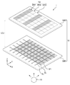
도 1은 일 실시예에 따른 표시 장치의 분해 사시도이다.
도 2는 도 1의 표시 장치의 임의의 화소들의 레이아웃이다.
도 3은 도 2의 III-III' 선을 따라 절개한 상부 표시판의 단면도이다.
도 4는 도 3에 도시한 제1 서브 화소를 개략적으로 나타낸 도면이다.
도 5는 일 실시예에 따른 백라이트 유닛의 사시도이다.
도 6은 도 5의 VI-VI' 선을 따라 절개한 단면도이다.
도 7 및 도 8은 다른 실시예들에 따른 백라이트 유닛의 단면도들이다.
도 9는 또 다른 실시예에 따른 백라이트 유닛의 사시도이다.
도 10a 및 도 10b는 다양한 실시예들에 따른 저굴절층의 단면도들이다.
도 11은 일 실시예에 따른 표시 장치의 단면도이다.
도 12 내지 도 14는 다양한 실시예들에 따른 컬러 필터층의 단면도들이다.
도 15는 또 다른 실시예에 따른 컬러 필터층의 단면도이다.
도 16은 일 실시예에 따른 산란층의 단면도 및 일부 확대도이다.
도 17은 일 실시예에 따른 산란층의 광 산란체 농도에 따른 측면 시인성 향상 효과를 설명하기 위한 그래프이다.
도 18 내지 도 20은 다양한 실시예들에 따른 상부 표시판의 단면도들이다.
도 21은 또 다른 실시예에 따른 표시 장치의 단면도이다.1 is an exploded perspective view of a display device according to an exemplary embodiment.
2 is a layout of arbitrary pixels of the display device of FIG. 1.
3 is a cross-sectional view of the upper panel cut along the line III-III 'of FIG. 2.
FIG. 4 is a diagram schematically showing the first sub-pixel shown in FIG. 3.
5 is a perspective view of a backlight unit according to an embodiment.
6 is a cross-sectional view taken along line VI-VI 'of FIG. 5.
7 and 8 are cross-sectional views of a backlight unit according to other embodiments.
9 is a perspective view of a backlight unit according to another embodiment.
10A and 10B are cross-sectional views of a low refractive layer according to various embodiments.
11 is a cross-sectional view of a display device according to an exemplary embodiment.
12 to 14 are cross-sectional views of a color filter layer according to various embodiments.
15 is a cross-sectional view of a color filter layer according to another embodiment.
16 is a cross-sectional view and a partially enlarged view of a scattering layer according to an embodiment.
17 is a graph for explaining an effect of improving side visibility according to light scatterer concentration of a scattering layer according to an embodiment.
18 to 20 are cross-sectional views of an upper panel according to various embodiments.
21 is a cross-sectional view of a display device according to another exemplary embodiment.
본 발명의 이점 및 특징, 그리고 그것들을 달성하는 방법은 첨부되는 도면과 함께 상세하게 후술되어 있는 실시예들을 참조하면 명확해질 것이다. 그러나 본 발명은 이하에서 개시되는 실시예들에 한정되는 것이 아니라 다른 형태로 구현될 수도 있다. 즉, 본 발명은 청구항의 범주에 의해 정의될 뿐이다. Advantages and features of the present invention, and methods for achieving them will be clarified with reference to embodiments described below in detail together with the accompanying drawings. However, the present invention is not limited to the embodiments disclosed below, but may be implemented in other forms. That is, the present invention is only defined by the scope of the claims.
소자(elements) 또는 층이 다른 소자 또는 층의 "위(on)" 또는 "상(on)"으로 지칭되는 것은 다른 소자 또는 층의 바로 위뿐만 아니라 중간에 다른 층 또는 다른 소자를 개재한 경우를 모두 포함한다. 반면, 소자가 "직접 위(directly on)" 또는 "바로 위"로 지칭되는 것은 중간에 다른 소자 또는 층을 개재하지 않은 것을 나타낸다.Elements or layers referred to as "on" or "on" of another device or layer are not only directly above the other device or layer, but also when intervening another layer or other device in the middle. All inclusive. On the other hand, when a device is referred to as “directly on” or “directly above”, it indicates that no other device or layer is interposed therebetween.
공간적으로 상대적인 용어인 "아래(below)", "아래(beneath)", "하부(lower)", "위(above)", "상부(upper)" 등은 도면에 도시되어 있는 바와 같이 하나의 소자 또는 구성 요소와 다른 소자 또는 구성 요소와의 상관관계를 용이하게 기술하기 위해 사용될 수 있다. 공간적으로 상대적인 용어는 도면에 도시되어 있는 방향에 더하여 사용시 또는 동작 시 소자의 서로 다른 방향을 포함하는 용어로 이해되어야 한다. 예를 들면, 도면에 도시되어 있는 소자를 뒤집을 경우, 다른 소자의 "아래(below 또는 beneath)"로 기술된 소자는 다른 소자의 "위(above)"에 놓여질 수 있다. 따라서, 예시적인 용어인 "아래"는 아래와 위의 방향을 모두 포함할 수 있다. 소자는 다른 방향으로도 배향될 수 있으며, 이 경우 공간적으로 상대적인 용어들은 배향에 따라 해석될 수 있다. The spatially relative terms “below”, “beneath”, “lower”, “above”, “upper”, etc., are as shown in the figure. It can be used to easily describe the correlation of an element or component with another element or component. The spatially relative terms should be understood as terms including different directions of the device in use or operation in addition to the directions shown in the drawings. For example, if the device shown in the figure is turned over, the device described as "below or beneath" the other device may be placed "above" the other device. Thus, the exemplary term “below” can include both the directions below and above. The device can also be oriented in other directions, in which case the spatially relative terms can be interpreted according to the orientation.
비록 제1, 제2 등이 다양한 구성요소들을 서술하기 위해서 사용되나, 이들 구성요소들은 이들 용어에 의해 제한되지 않음은 물론이다. 이들 용어들은 단지 하나의 구성요소를 다른 구성요소와 구별하기 위하여 사용하는 것이다. 따라서, 이하에서 언급되는 제1 구성요소는 본 발명의 기술적 사상 내에서 제2 구성요소일 수도 있음은 물론이다. Although the first, second, etc. are used to describe various components, it goes without saying that these components are not limited by these terms. These terms are only used to distinguish one component from another component. Therefore, it goes without saying that the first component mentioned below may be the second component within the technical spirit of the present invention.
단수의 표현은 문맥상 명백하게 다르게 뜻하지 않는 한, 복수의 표현을 포함한다. 또한 "포함하다" 또는 "가지다" 등의 용어는 특별히 반대되는 기재가 없는 한 다른 구성요소를 제외하는 것이 아니라 다른 구성요소를 더 포함할 수 있음을 의미한다.Singular expressions include plural expressions unless the context clearly indicates otherwise. In addition, terms such as “include” or “have” mean that other components may be further included rather than excluded other components unless specifically stated to the contrary.
명세서 전체를 통하여 동일하거나 유사한 부분에 대해서는 동일한 도면 부호를 사용한다.The same reference numerals are used for the same or similar parts throughout the specification.
이하, 첨부된 도면을 참고로 하여 실시예들에 대해 설명한다. Hereinafter, embodiments will be described with reference to the accompanying drawings.
도 1은 일 실시예에 따른 표시 장치의 분해 사시도이다. 도 2는 도 1의 표시 장치의 임의의 화소들의 레이아웃이다.1 is an exploded perspective view of a display device according to an exemplary embodiment. 2 is a layout of arbitrary pixels of the display device of FIG. 1.
도 1 및 도 2를 참조하면, 표시 장치(1)는 표시 패널(10) 및 표시 패널(10)에 광을 제공하는 백라이트 유닛(20)을 포함한다. 1 and 2, the display device 1 includes a display panel 10 and a backlight unit 20 that provides light to the display panel 10.
표시 패널(10)은 하부 표시판(SUB1), 하부 표시판(SUB1)과 대향하는 상부 표시판(SUB2) 및 이들의 사이에 개재된 액정층(LCL)을 포함할 수 있다. 액정층(LCL)은 하부 표시판(SUB1)과 상부 표시판(SUB2) 및 이들을 합착시키는 실링 부재(미도시)에 의해 밀봉된 상태일 수 있다.The display panel 10 may include a lower display panel SUB1, an upper display panel SUB2 facing the lower display panel SUB1, and a liquid crystal layer LCL interposed therebetween. The liquid crystal layer LCL may be sealed by a lower display panel SUB1, an upper display panel SUB2, and a sealing member (not shown) bonding them.
표시 패널(10)에는 평면상 제1 화소(PX1)를 포함하는 복수의 화소들이 정의될 수 있다. 하나의 화소는 복수의 서브 화소를 포함할 수 있으며, 각 서브 화소는 미리 정해진 하나의 색상을 표현할 수 있다. 본 명세서에서, '화소(pixel)'는 색 표시를 위해 평면 시점에서 표시 영역이 구획되어 정의되는 단일 영역을 의미하며, 하나의 화소는 복수의 서브 화소의 조합으로 하나의 색상을 표현할 수 있다. 즉, 하나의 화소는 다른 화소와 서로 독립적인 색을 표현할 수 있는 표시 패널(10) 기준에서의 최소 단위일 수 있다. 복수의 화소에 대해서는 이하, 제1 화소(PX1)를 기준으로 설명하기로 한다.A plurality of pixels including the first pixel PX1 may be defined on the display panel 10. One pixel may include a plurality of sub-pixels, and each sub-pixel may express one predetermined color. In this specification, 'pixel (pixel)' refers to a single area that is defined by dividing the display area in a plane view for color display, and one pixel can express one color by a combination of a plurality of sub-pixels. That is, one pixel may be a minimum unit in the reference of the display panel 10 that can express colors independent of each other. The plurality of pixels will be described below with reference to the first pixel PX1.
상기 복수의 서브 화소들은 제1 색을 표시하는 제1 서브 화소(SPX1), 제1 색보다 짧은 중심 파장을 갖는 제2 색을 표시하는 제2 서브 화소(SPX2) 및 제2 색보다 짧은 중심 파장을 갖는 제3 색을 표시하는 제3 서브 화소(SPX3)를 포함할 수 있다.The plurality of sub-pixels include a first sub-pixel (SPX1) displaying a first color, a second sub-pixel (SPX2) displaying a second color having a center wavelength shorter than the first color, and a center wavelength shorter than the second color. It may include a third sub-pixel (SPX3) for displaying a third color having a.
예를 들어, 제1 서브 화소(SPX1)는 제1 색(적색)을 표시하는 화소이고, 제1 서브 화소(SPX1)와 제1 방향(X)으로 인접한 제2 서브 화소(SPX2)는 제2 색(녹색)을 표시하는 화소이며, 제2 서브 화소(SPX2)와 제1 방향(X)으로 인접한 제3 서브 화소(SPX3)는 제3 색(청색)을 표시하는 화소일 수 있다. For example, the first sub-pixel SPX1 is a pixel displaying a first color (red), and the second sub-pixel SPX2 adjacent to the first sub-pixel SPX1 in the first direction X is a second. The pixel displaying the color (green), and the third sub pixel SPX3 adjacent to the second sub pixel SPX2 in the first direction X may be a pixel displaying the third color (blue).
표시 패널(10)은 제1 방향(X)으로 연장된 복수의 게이트 라인(GL)들 및 제2 방향(Y)으로 연장되며 게이트 라인(GL)과 절연되도록 배치된 복수의 데이터 라인(DL)들을 포함할 수 있다. 게이트 라인(GL) 및 데이터 라인(DL)은 각각 구동부(미도시)와 연결되어 복수의 서브 화소들마다 배치된 서브 화소 전극(SPE)에 구동 신호를 전달할 수 있다.The display panel 10 includes a plurality of gate lines GL extending in the first direction X and a plurality of data lines DL extending in the second direction Y and disposed to be insulated from the gate line GL. It may include. The gate line GL and the data line DL may be respectively connected to a driving unit (not shown) to transmit a driving signal to the sub-pixel electrode SPE disposed for each of the plurality of sub-pixels.
백라이트 유닛(20)은 표시 패널(10)의 하측에 배치되어 특정 파장을 갖는 광을 표시 패널(10) 측으로 출사할 수 있다. 백라이트 유닛(20)은 광을 직접적으로 방출하는 광원(light source) 및 상기 광원(미도시)으로부터 제공받은 광의 경로를 가이드하여 표시 패널(10) 측으로 출사시키는 도광판(미도시)을 포함하여 이루어질 수 있다. 백라이트 유닛(20)은 도 5 내지 도 9를 참조하여 자세히 후술하기로 한다.The backlight unit 20 is disposed under the display panel 10 to emit light having a specific wavelength to the display panel 10 side. The backlight unit 20 may include a light source that directly emits light (light source) and a light guide plate (not shown) that guides a path of light provided from the light source (not shown) and outputs it to the display panel 10 side. have. The backlight unit 20 will be described later in detail with reference to FIGS. 5 to 9.
이하, 도 3 및 도 4를 참조하여 표시 패널(10)의 하부 표시판(SUB1)에 대하여 더욱 상세하게 설명한다. 제1 화소(PX1)가 포함하는 복수의 서브 화소에 대해서는 이하, 제1 서브 화소(SPX1)를 기준으로 설명하기로 한다.Hereinafter, the lower display panel SUB1 of the display panel 10 will be described in more detail with reference to FIGS. 3 and 4. The plurality of sub-pixels included in the first pixel PX1 will be described below with reference to the first sub-pixel SPX1.
도 3은 도 2의 III-III' 선을 따라 절개한 하부 표시판의 단면도이다. 도 4는 도 3에 도시한 제1 서브 화소를 개략적으로 나타낸 도면이다.3 is a cross-sectional view of the lower display panel cut along the line III-III 'of FIG. 2. FIG. 4 is a diagram schematically showing the first sub-pixel shown in FIG. 3.
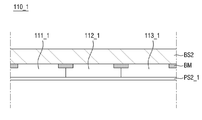
도 3 및 도 4를 참조하면, 하부 표시판(SUB1)은 제1 기판(BS1), 제1 기판(BS1)의 일측면(도 3 기준 상면) 상에 배치된 스위칭 소자(Q1), 스위칭 소자(Q1) 상에 배치된 제1 서브 화소 전극(SPE1)을 포함할 수 있다. 또한, 하부 표시판(SUB1)은 제1 기판(BS1)의 타측면(도 3 기준 하면) 상에 배치된 제1 편광층(POL1)을 포함할 수 있다. 상부 표시판(SUB2)은 하부 표시판(SUB1)의 제1 서브 화소 전극(SPE1)에 대향하여 배치된 공통 전극(CE)을 포함할 수 있다.Referring to FIGS. 3 and 4, the lower display panel SUB1 includes a switching element Q1 and a switching element disposed on one side of the first substrate BS1 and the first substrate BS1 (the upper surface of FIG. 3). Q1) may include the first sub-pixel electrode SPE1. In addition, the lower display panel SUB1 may include a first polarization layer POL1 disposed on the other side (lower surface in FIG. 3) of the first substrate BS1. The upper display panel SUB2 may include a common electrode CE disposed opposite to the first sub-pixel electrode SPE1 of the lower display panel SUB1.
제1 기판(BS1)은 투명한 절연 기판일 수 있다. 예를 들어, 제1 기판(BS1)은 유리 재료, 석영 재료 또는 투광성 플라스틱 재료로 이루어진 기판일 수 있다. 몇몇 실시예에서, 제1 기판(BS1)은 가요성을 가지고 표시 장치(1)는 곡면형 표시 장치일 수 있다.The first substrate BS1 may be a transparent insulating substrate. For example, the first substrate BS1 may be a substrate made of a glass material, a quartz material, or a translucent plastic material. In some embodiments, the first substrate BS1 is flexible and the display device 1 may be a curved display device.
제1 기판(BS1) 상에는 제1 스위칭 소자(Q1)가 배치될 수 있다. 제1 스위칭 소자(Q1)는 제1 서브 화소(SPX1)에 배치되어 후술할 제1 서브 화소 전극(SPE1)에 구동 신호를 전달하거나 차단할 수 있다. 예시적인 실시예에서, 제1 스위칭 소자(Q1)는 게이트 전극(GE), 게이트 전극(GE) 상에 배치된 액티브층(AL) 및 액티브층(AL) 상에서 서로 이격 배치된 소스 전극(SE)과 드레인 전극(DE)을 포함하는 박막 트랜지스터일 수 있다. The first switching element Q1 may be disposed on the first substrate BS1. The first switching element Q1 is disposed on the first sub-pixel SPX1 to transmit or block a driving signal to the first sub-pixel electrode SPE1, which will be described later. In an exemplary embodiment, the first switching element Q1 includes a gate electrode GE, an active layer AL disposed on the gate electrode GE, and a source electrode SE disposed spaced apart from each other on the active layer AL It may be a thin film transistor including a drain electrode (DE).
제어 단자인 게이트 전극(GE)은 게이트 라인(GL)과 연결되어 게이트 구동 신호를 제공받고, 입력 단자인 소스 전극(SE)은 데이터 라인(DL)과 연결되어 데이터 구동 신호를 제공받으며, 출력 단자인 드레인 전극(DE)은 제1 서브 화소 전극(SPE1)과 전기적으로 연결될 수 있다. 액티브층(AL)은 비정질 규소 또는 다결정 규소를 포함하여 이루어지거나 또는 산화물 반도체로 이루어질 수 있다. 액티브층(AL)은 제1 스위칭 소자(Q1)의 채널 역할을 하며 게이트 전극(GE)에 인가되는 게이트 전압에 따라 채널을 턴 온 또는 턴 오프할 수 있다. 게이트 전극(GE)과 액티브층(AL)은 절연막(GI)에 의해 절연될 수 있다. 도면에 도시하지 않았으나, 액티브층(AL)이 비정질 규소 등으로 이루어지는 경우 액티브층(AL)과 소스 전극(SE) 및 드레인 전극(DE) 사이에는 오믹 컨택층(미도시)이 더 배치될 수 있다. The control electrode gate electrode GE is connected to the gate line GL to receive a gate driving signal, and the input terminal source electrode SE is connected to the data line DL to receive a data driving signal, and an output terminal. The phosphorus drain electrode DE may be electrically connected to the first sub-pixel electrode SPE1. The active layer AL may be formed of amorphous silicon or polycrystalline silicon, or may be made of an oxide semiconductor. The active layer AL serves as a channel of the first switching element Q1 and may turn on or off the channel according to the gate voltage applied to the gate electrode GE. The gate electrode GE and the active layer AL may be insulated by the insulating layer GI. Although not shown in the drawing, when the active layer AL is made of amorphous silicon or the like, an ohmic contact layer (not shown) may be further disposed between the active layer AL and the source electrode SE and the drain electrode DE. .
소스 전극(SE) 및 드레인 전극(DE) 상에는 제1 보호층(PS1)이 배치되어 하부에 형성된 배선 및 전극들을 보호할 수 있다. 제1 보호층(PS1)은 무기 재료를 포함하여 이루어질 수 있다. 상기 무기 재료의 예로는 질화규소(SiNx), 산화규소(SiOx), 질화산화규소(SiNxOy), 또는 산화질화규소(SiOxNy) 등을 들 수 있다.The first protective layer PS1 is disposed on the source electrode SE and the drain electrode DE to protect the wiring and electrodes formed underneath. The first protective layer PS1 may be made of an inorganic material. Examples of the inorganic material include silicon nitride (SiNx), silicon oxide (SiOx), silicon nitride oxide (SiNxOy), or silicon oxynitride (SiOxNy).
제1 스위칭 소자(Q1) 상에는 중간층(IL)이 배치될 수 있다. 중간층(IL)은 그 상부의 구성과 하부의 구성을 서로 전기적으로 절연시키고, 제1 기판(BS1) 상에 적층된 복수의 구성요소들의 단차를 평탄화할 수 있다. 중간층(IL)은 하나 이상의 층을 포함하여 이루어질 수 있다. 예를 들어 중간층(IL)은 유기 재료로 이루어지거나, 무기 재료로 이루어지거나, 또는 유기 재료로 이루어진 층과 무기 재료로 이루어진 층의 적층 구조일 수 있다.The intermediate layer IL may be disposed on the first switching element Q1. The intermediate layer IL electrically insulates the upper and lower components from each other, and can planarize the step difference of the plurality of components stacked on the first substrate BS1. The intermediate layer IL may include one or more layers. For example, the intermediate layer IL may be formed of an organic material, an inorganic material, or a layered structure of a layer made of an organic material and a layer made of an inorganic material.
중간층(IL) 상에는 복수의 제1 서브 화소 전극(SPE1)들이 배치될 수 있다. 제1 서브 화소 전극(SPE1)은 후술할 공통 전극(CE)과 함께 액정층(LCL)에 전계를 형성하여 해당 화소 내의 액정들의 배향 방향을 제어할 수 있다. 제1 서브 화소 전극(SPE1)은 중간층(IL)에 형성된 컨택홀(contact hole)을 통해 제1 스위칭 소자(Q1)의 드레인 전극(DE)과 전기적으로 연결될 수 있다. 제1 서브 화소 전극(SPE1)은 제1 서브 화소(SPX1)에 배치되어 스위칭 소자(Q1)를 통해 전압이 인가될 수 있다. 제1 서브 화소 전극(SPE1)은 투명한 도전성 재료로 이루어진 투명 전극일 수 있다. 투명 전극을 형성하는 재료의 예로는 ITO(Indium Tin Oxide) 또는 IZO(Indium Zinc Oxide) 등을 들 수 있다. 도 2는 제1 서브 화소 전극(SPE1)에 슬릿이 형성되지 않은 평판 형상인 경우를 예시하고 있으나, 다른 실시예에서 제1 서브 화소 전극(SPE1)은 방사상의 슬릿 등을 가질 수 있다. A plurality of first sub-pixel electrodes SPE1 may be disposed on the intermediate layer IL. The first sub-pixel electrode SPE1 may form an electric field in the liquid crystal layer LCL together with the common electrode CE, which will be described later, to control the alignment direction of the liquid crystals in the corresponding pixel. The first sub-pixel electrode SPE1 may be electrically connected to the drain electrode DE of the first switching element Q1 through a contact hole formed in the intermediate layer IL. The first sub-pixel electrode SPE1 is disposed in the first sub-pixel SPX1 and a voltage may be applied through the switching element Q1. The first sub-pixel electrode SPE1 may be a transparent electrode made of a transparent conductive material. Examples of the material for forming the transparent electrode include indium tin oxide (ITO) or indium zinc oxide (IZO). 2 illustrates a case in which a slit is not formed in the first sub-pixel electrode SPE1, but in another embodiment, the first sub-pixel electrode SPE1 may have a radial slit or the like.
제1 서브 화소 전극(SPE1) 상에는 제1 액정 배향층(LCA1)이 배치될 수 있다. 제1 액정 배향층(LCA1)은 인접한 액정층(LCL) 내 액정의 초기 배향을 유도할 수 있다. 본 명세서에서, '액정의 초기 배향'이라 함은 액정층(LCL)에 전계가 형성되지 않은 상태에서의 액정의 배열을 의미한다. 제1 액정 배향층(LCA1)은 주쇄의 반복단위 내에 이미드기를 갖는 고분자 유기 재료를 포함하여 이루어질 수 있다.The first liquid crystal alignment layer LCA1 may be disposed on the first sub-pixel electrode SPE1. The first liquid crystal alignment layer LCA1 may induce initial alignment of liquid crystals in the adjacent liquid crystal layer LCL. In the present specification, the term 'initial alignment of the liquid crystal' refers to an arrangement of liquid crystals in a state in which no electric field is formed in the liquid crystal layer LCL. The first liquid crystal alignment layer LCA1 may be formed of a polymer organic material having an imide group in a repeating unit of the main chain.
제1 편광층(POL1)은 제1 기판(BS1)과 백라이트 유닛(도 1의 "20") 사이의 광 경로 상에 배치될 수 있다. 일 실시예로, 제1 편광층(POL1)은 제1 기판(BS1)의 하부에 배치될 수 있다. 다만, 제1 편광층(POL1)의 배치 위치는 도면에 도시된 것으로 제한되지 않는다. 일 실시예로, 제1 편광층(POL1)은 제1 기판(BS1)과 액정층(LCL) 사이에 배치될 수도 있다. 제1 편광층(POL1)은 일 실시예로 반사형 편광층일 수 있다. 제1 편광층(POL1)이 반사형 편광층인 경우, 선 격자 패턴을 포함하여 투과축과 평행한 편광 성분은 투과시키고 반사축과 평행한 편광 성분은 반사할 수 있다. 선 격자 패턴은 알루미늄(Al), 은(Ag), 금(Au), 구리(Cu), 티타늄(Ti), 몰리브덴(Mo), 니켈(Ni) 또는 이들의 합금 등의 금속 재료를 포함할 수 있다.The first polarization layer POL1 may be disposed on the light path between the first substrate BS1 and the backlight unit (“20” in FIG. 1). In an embodiment, the first polarization layer POL1 may be disposed under the first substrate BS1. However, the arrangement position of the first polarization layer POL1 is not limited to that illustrated in the drawings. In an embodiment, the first polarization layer POL1 may be disposed between the first substrate BS1 and the liquid crystal layer LCL. The first polarizing layer POL1 may be a reflective polarizing layer in one embodiment. When the first polarization layer POL1 is a reflective polarization layer, a polarization component parallel to a transmission axis including a line grid pattern may be transmitted and a polarization component parallel to the reflection axis may be reflected. The line lattice pattern may include metal materials such as aluminum (Al), silver (Ag), gold (Au), copper (Cu), titanium (Ti), molybdenum (Mo), nickel (Ni), or alloys thereof. have.
반사형 편광층을 사용하는 경우, 반사된 광이 다시 리사이클링 되어 출사될 수 있으므로 표시 장치의 휘도 이득이 상승할 수 있다.When a reflective polarizing layer is used, the reflected light may be recycled and emitted again, so that the luminance gain of the display device may increase.
제1 편광층(POL1)은 일 실시예로 제1 기판(BS1)과 직접 접촉할 수 있다. 즉, 제1 편광층(POL1)은 제1 기판(BS1)의 일면 상에 연속 공정을 통해 형성될 수 있다. 다른 실시예로, 제1 편광층(POL1)은 제1 기판(BS1)의 일면과 별도의 접착 부재를 통해 결합될 수도 있다. 여기서, 접착 부재는 일 실시예로 감압 접착 부재(PSA) 또는 광학 투명 접착 부재(OCA, OCR)일 수 있다.The first polarization layer POL1 may directly contact the first substrate BS1 in one embodiment. That is, the first polarization layer POL1 may be formed on one surface of the first substrate BS1 through a continuous process. In another embodiment, the first polarization layer POL1 may be combined with one surface of the first substrate BS1 through a separate adhesive member. Here, the adhesive member may be, for example, a pressure-sensitive adhesive member (PSA) or an optically transparent adhesive member (OCA, OCR).
상부 표시판(SUB2)에는 공통 전극(CE)이 배치될 수 있다. 제1 서브 화소 전극(SPE1)은 공통 전극(CE)과 하부 표시판(SUB1)에 수직 방향으로 적어도 일부가 중첩될 수 있다. 이에 따라, 제1 서브 화소(SPX1)는 제1 서브 화소 전극(SPE1)과 공통 전극(CE)이 중첩됨에 따라 형성되는 제1 액정 커패시터(Clc1)를 포함할 수 있다. The common electrode CE may be disposed on the upper display panel SUB2. At least a portion of the first sub-pixel electrode SPE1 may overlap the common electrode CE and the lower display panel SUB1 in the vertical direction. Accordingly, the first sub-pixel SPX1 may include a first liquid crystal capacitor Clc1 formed as the first sub-pixel electrode SPE1 overlaps with the common electrode CE.
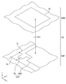
이하, 도 5 내지 도 9를 참조하여, 다양한 실시예에 따른 백라이트 유닛에 대해 설명한다.Hereinafter, a backlight unit according to various embodiments will be described with reference to FIGS. 5 to 9.
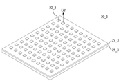
도 5는 일 실시예에 따른 백라이트 유닛의 사시도이다. 도 6은 도 5의 VI-VI' 선을 따라 절개한 단면도이다. 도 7 및 도 8은 다른 실시예들에 따른 백라이트 유닛의 단면도들이다. 도 9는 또 다른 실시예에 따른 백라이트 유닛의 사시도이다. 5 is a perspective view of a backlight unit according to an embodiment. 6 is a cross-sectional view taken along line VI-VI 'of FIG. 5. 7 and 8 are cross-sectional views of a backlight unit according to other embodiments. 9 is a perspective view of a backlight unit according to another embodiment.
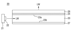
도 5 및 도 6을 참조하면, 백라이트 유닛(20)은 광학 부재(20G) 및 발광 소자 패키지(20P)를 포함할 수 있다. 광학 부재(20G)는 도광판(23), 도광판(23)의 상부에 배치된 저굴절층(24), 저굴절층(24) 상에 배치된 광학 시트(26), 및 도광판(23)의 하부에 배치된 반사 부재(27)를 포함할 수 있다. 발광 소자 패키지(20P)는 인쇄 회로 기판(21) 및 발광 소자(22)를 포함할 수 있다.5 and 6, the backlight unit 20 may include an optical member 20G and a light emitting device package 20P. The optical member 20G includes a light guide plate 23, a low refractive layer 24 disposed on the light guide plate 23, an optical sheet 26 disposed on the low refractive layer 24, and a lower portion of the light guide plate 23 It may include a reflective member 27 disposed on. The light emitting device package 20P may include a printed circuit board 21 and a light emitting device 22.
도광판(23)은 빛의 진행 경로를 인도하는 역할을 한다. 도광판(23)은 대체로 다각 기둥 형상을 가질 수 있다. 도광판(23)의 평면 형상은 직사각형일 수 있지만, 이에 제한되는 것은 아니다. 예시적인 실시예에서, 도광판(23)은 평면 형상이 직사각형이고, 상면(23a), 하면(23b), 및 4개의 측면을 포함하는 육각 기둥 형상일 수 있다. The light guide plate 23 serves to guide the path of the light. The light guide plate 23 may have a substantially polygonal column shape. The planar shape of the light guide plate 23 may be rectangular, but is not limited thereto. In an exemplary embodiment, the light guide plate 23 has a rectangular planar shape, and may have a hexagonal column shape including an upper surface 23a, a lower surface 23b, and four side surfaces.
일 실시예에서, 도광판(23)의 상면(23a)과 하면(23b)은 각각 하나의 평면 상에 위치하며 상면(23a)이 위치하는 평면과 하면(23b)이 위치하는 평면은 대체로 평행하여 도광판(23)이 전체적으로 균일한 두께를 가질 수 있다. 그러나, 이에 제한되는 것은 아니고, 상면(23a)이나 하면(23b)이 복수의 평면으로 이루어지거나, 상면(23a)이 위치하는 평면과 하면(23b)이 위치하는 평면이 교차할 수도 있다. 예를 들어, 쐐기형 도광판과 같이 일 측면(예컨대, 입광면)에서 그에 대향하는 타 측면(예컨대, 대광면)으로 갈수록 두께가 얇아질 수 있다. 또한, 특정 지점까지는 일 측면 (예컨대, 입광면) 근처에서는 그에 대향하는 타 측면 (예컨대, 대광면) 측으로 갈수록 하면(23b)이 상향 경사져 두께가 줄어들다가 이후 상면(23a)과 하면(23b)이 평탄한 형상으로 형성될 수도 있다.In one embodiment, the upper surface 23a and the lower surface 23b of the light guide plate 23 are respectively located on one plane, and the plane on which the upper surface 23a is located and the plane on which the lower surface 23b is located are substantially parallel to the light guide plate (23) may have a uniform thickness as a whole. However, the present invention is not limited thereto, and the upper surface 23a or the lower surface 23b may be formed of a plurality of planes, or the plane on which the upper surface 23a is located and the plane on which the lower surface 23b is located may intersect. For example, the thickness of the wedge-shaped light guide plate from one side (for example, the light receiving surface) to the other side (for example, the large light surface) facing it may be thinner. In addition, until one point (for example, the light incident surface) up to a specific point, the other side (for example, the large light surface) opposite to the other side (eg, the large light surface) is inclined upward to decrease the thickness, and then the upper surface 23a and the lower surface 23b It may be formed in a flat shape.
상기 도광판(23)의 재료는 특별히 제한되지 않으나, 예를 들어 글라스(glass) 재료, 석영(quartz) 재료 또는 플라스틱 재료로 이루어질 수 있다.The material of the light guide plate 23 is not particularly limited, but may be made of, for example, a glass material, a quartz material, or a plastic material.
발광 소자 패키지(20P)는 인쇄 회로 기판(21) 및 인쇄 회로 기판(21) 상에 실장된 발광 소자(22)를 포함할 수 있다. 발광 소자 패키지(20P)는 도광판(23)의 적어도 일 측면에 인접하여 배치되어 광을 제공할 수 있다. 도면에서는 인쇄 회로 기판(21)에 실장된 복수의 발광 소자(22)가 도광판(23)의 일 장변의 측면 인접하여 배치된 경우를 예시하였지만, 이에 제한되는 것은 아니다. 예컨대, 발광 소자 패키지(20P)가 도광판(23)의 양 장변의 측면에 모두 인접 배치되거나, 일 단변 또는 양 단변의 측면에 인접하여 배치될 수도 있다.The light emitting device package 20P may include a printed circuit board 21 and a light emitting device 22 mounted on the printed circuit board 21. The light emitting device package 20P may be disposed adjacent to at least one side of the light guide plate 23 to provide light. In the drawing, the case where the plurality of light emitting elements 22 mounted on the printed circuit board 21 are disposed adjacent to one side of one side of the light guide plate 23 is not limited thereto. For example, the light emitting device package 20P may be disposed adjacent to both sides of both long sides of the light guide plate 23, or may be disposed adjacent to one side or both sides.
발광 소자(22)는 인쇄 회로 기판(21)에 실장될 수 있다. 발광 소자(22)는 백색광(LW)을 방출할 수 있으나 이에 한정되지 않으며 청색광 또는 근자외선 광을 방출할 수도 있다. 발광 소자(22)로부터 방출된 광은 램버시안 분포(Lambertian distribution)를 가질 수 있다.The light emitting element 22 may be mounted on the printed circuit board 21. The light emitting device 22 may emit white light LW, but is not limited thereto, and may emit blue light or near ultraviolet light. The light emitted from the light emitting element 22 may have a Lambertian distribution.
저굴절층(24)은 도광판(23)의 상면(23a)에 배치된다. 저굴절층(24)은 도광판(23)의 상면(23a) 상에 직접 형성되어, 도광판(23)의 상면(23a)과 접촉할 수 있다. 저굴절층(24)은 도광판(23)의 상면(23a)에서 전반사를 도울 수 있다. The low refractive layer 24 is disposed on the upper surface 23a of the light guide plate 23. The low refractive index layer 24 is directly formed on the upper surface 23a of the light guide plate 23 and may contact the upper surface 23a of the light guide plate 23. The low refractive layer 24 may help total reflection on the upper surface 23a of the light guide plate 23.
구체적으로, 도광판(23)에 의하여 입광면으로부터 대광면 측으로 효율적인 광 가이드가 이루어지기 위해서는 도광판(23)의 상면(23a) 및 하면(23b)에서 효과적인 내부 전반사가 이루어지는 것이 바람직하다. 도광판(23)에서 내부 전반사가 이루어질 수 있는 조건 중 하나는 도광판(23)의 굴절률이 도광판(23)과 광학적 계면을 이루는 매질의 굴절률에 비해 큰 것이다. 도광판(23)과 광학적 계면을 이루는 매질의 굴절률이 낮을수록 전반사 임계각이 작아져 더 많은 내부 전반사가 이루어질 수 있다.Specifically, in order for the light guide plate 23 to efficiently guide the light from the light incident surface to the large light surface, it is preferable that effective total internal reflection is performed on the upper surface 23a and the lower surface 23b of the light guide plate 23. One of the conditions in which total internal reflection can be achieved in the light guide plate 23 is that the refractive index of the light guide plate 23 is greater than that of a medium forming an optical interface with the light guide plate 23. The lower the refractive index of the medium constituting the optical interface with the light guide plate 23, the smaller the total reflection critical angle and the more total internal reflection can be achieved.
예컨대, 도광판(23)의 굴절률이 약 1.5인 유리로 이루어진 경우, 도광판(23)의 하면(23b)은 굴절률이 약 1인 공기층에 노출되어 그와 광학적 계면을 이루기 때문에 충분한 전반사가 이루어질 수 있다. 또는, 도광판(23)의 하면(23b)에 배치된 반사 부재(27)를 통해 도광판(23)의 하면(23b)을 통해 출사된 광이 효과적으로 도광판(23)으로 진입할 수 있다.For example, when the refractive index of the light guide plate 23 is made of glass having about 1.5, the lower surface 23b of the light guide plate 23 may be exposed to an air layer having a refractive index of about 1 to form an optical interface therewith, so that sufficient total reflection can be achieved. Alternatively, light emitted through the lower surface 23b of the light guide plate 23 through the reflective member 27 disposed on the lower surface 23b of the light guide plate 23 can effectively enter the light guide plate 23.
반면, 도광판(23)의 상면(23a)에는 다른 광학 기능층들이 적층되어 일체화되어 있기 때문에, 하면(23b)의 경우보다 충분한 전반사가 이루어지기 어렵다. 예를 들어, 도광판(23)의 상면(23a)에 굴절률이 1,5 이상인 물질층이 적층되면, 도광판(23)의 상면(23a)에서는 전반사가 이루어지지 못하며, 도광판(23)과 굴절률 차이가 크지 않은 물질층이 적층되면, 전반사가 이루어지더라도 큰 임계각으로 인해 충분한 전반사가 이루어지지 못한다. On the other hand, since the other optical functional layers are stacked and integrated on the upper surface 23a of the light guide plate 23, sufficient total reflection is less likely to be achieved than in the case of the lower surface 23b. For example, when a material layer having a refractive index of 1,5 or more is stacked on the top surface 23a of the light guide plate 23, total reflection is not made on the top surface 23a of the light guide plate 23, and the difference in refractive index between the light guide plate 23 and When a layer of a material that is not large is laminated, sufficient total reflection cannot be achieved due to a large critical angle even when total reflection is made.
도광판(23)의 상면(23a)과 광학적 계면을 이루는 저굴절층(24)은 도광판(23)보다 낮은 굴절류을 가져 도광판(23)의 상면(23a)에서 전반사가 이루어지도록 한다. 도광판(23)의 굴절률과 저굴절층(24)의 굴절률 차는 0.2 이상일 수 있다. 저굴절층(24)의 굴절률이 도광판(23)의 굴절률보다 0.2 이상 작은 경우, 도광판(23)의 상면(23a)을 통해서 충분한 전반사가 이루어질 수 있다. 도광판(23)의 굴절률과 저굴절층(24)의 굴절률의 차는 상한에는 제한이 없지만, 통상 적용되는 도광판(23)의 물질과 저굴절층(24)의 굴절률을 고려할 때, 1 이하일 수 있다.The low refractive layer 24 forming an optical interface with the top surface 23a of the light guide plate 23 has a lower refractive flow than the light guide plate 23 so that total reflection is made on the top surface 23a of the light guide plate 23. The difference between the refractive index of the light guide plate 23 and the low refractive layer 24 may be 0.2 or more. When the refractive index of the low refractive layer 24 is less than 0.2 of the refractive index of the light guide plate 23, sufficient total reflection may be made through the upper surface 23a of the light guide plate 23. The difference between the refractive index of the light guide plate 23 and the refractive index of the low refractive layer 24 is not limited to an upper limit, but when considering the material of the light guide plate 23 and the refractive index of the low refractive layer 24 that are usually applied, it may be 1 or less.
저굴절층(24)의 굴절률은 1.2 내지 1.4의 범위에 있을 수 있다. 일반적으로 고체상의 매질은 그 굴절률을 1에 가깝게 만들수록 제조 비용이 크게 상승한다. 저굴절층(24)의 굴절률이 1.2 이상이면, 지나친 제조 원가의 증가를 막을 수 있다. 또한, 저굴절층(24)의 굴절률이 1.4 이하인 것이 도광판(23)의 상면(23a) 전반사 임계각을 충분히 작게 하는 데에 유리하다.The refractive index of the low refractive layer 24 may be in the range of 1.2 to 1.4. In general, the production cost of the solid phase increases significantly as the refractive index is brought closer to 1. When the refractive index of the low refractive layer 24 is 1.2 or more, it is possible to prevent excessive increase in manufacturing cost. In addition, the refractive index of the low refractive layer 24 is 1.4 or less, which is advantageous for sufficiently reducing the total reflection critical angle of the upper surface 23a of the light guide plate 23.
상술한 낮은 굴절률을 나타내기 위해 저굴절층(24)은 보이드를 포함할 수 있다. 보이드는 진공으로 이루어지거나, 공기층, 기체 등으로 채워질 수 있다. 보이드의 공간은 파티클이나 매트릭스 등에 의해 정의될 수 있다. 더욱 상세한 설명을 위해 도 10a 및 도 10b가 참조된다. The low-refractive-index layer 24 may include voids to exhibit the low refractive index described above. Voids can be made of vacuum or filled with air layers, gases, etc. The void space can be defined by particles or matrices. Reference is made to FIGS. 10A and 10B for a more detailed description.
도 10a 및 도 10b는 다양한 실시예들에 따른 저굴절층의 단면도들이다.10A and 10B are cross-sectional views of a low refractive layer according to various embodiments.
일 실시예에서, 저굴절층(24)은 도 10a에 도시된 바와 같이, 복수의 파티클(PT), 파티클(PT)을 둘러싸고 전체가 하나로 연결된 매트릭스(MX) 및 보이드(VD)를 포함할 수 있다. 파티클(PT)은 저굴절층(24)의 굴절률 및 기계적 강도를 조절하는 필러(filler)일 수 있다. In one embodiment, the low-refractive layer 24 may include a plurality of particles PT, a matrix MX and a void VD that surround the particles PT and are connected as one, as illustrated in FIG. 10A. have. The particle PT may be a filler that controls the refractive index and mechanical strength of the low refractive layer 24.
저굴절층(24)에는 복수의 매트릭스(MX) 내부에 파티클(PT)들이 분산 배치되고, 매트릭스(MX)가 부분적으로 벌어져 해당 부위에 보이드(VD)가 형성될 수 있다. 예를 들어, 복수의 파티클(PT)과 매트릭스(MX)를 용매에 혼합한 후, 건조 및/또는 경화시키면 용매가 증발하는데, 이때 매트릭스(MX) 사이사이에 보이드(VD)가 형성될 수 있다. In the low refractive layer 24, particles PT are dispersedly disposed inside the plurality of matrices MX, and the matrix MX is partially opened to form voids VD at corresponding portions. For example, after mixing a plurality of particles PT and matrix MX with a solvent, drying and / or curing, the solvent evaporates, and voids VD may be formed between the matrix MX. .
다른 실시예에서, 저굴절층(24)은 도 10b에 도시된 것처럼, 파티클 없이 매트릭스(MX)와 보이드(VD)를 포함할 수도 있다. 예를 들어, 저굴절층(24)은 발포수지와 같이 전체가 하나로 연결된 매트릭스(MX) 및 그 내부에 배치된 복수의 보이드(VD)를 포함할 수도 있다. In another embodiment, the low refractive layer 24 may include a matrix MX and voids VD without particles, as shown in FIG. 10B. For example, the low refractive layer 24 may include a matrix MX in which the whole is connected as one, such as a foamed resin, and a plurality of voids VD disposed therein.
도 10a 및 도 10b에 도시된 바와 같이 저굴절층(24)이 보이드(VD)를 포함하는 경우, 저굴절층(24)의 전체 굴절률은 파티클(PT)/매트릭스(MX)의 굴절률과 보이드(VD)의 굴절률의 사이값을 가질 수 있다. 상술한 바와 같이 보이드(VD)가 굴절률이 1인 진공이나 굴절률이 대략 1인 공기층, 기체 등으로 채워지는 경우, 파티클(PT)/매트릭스(MX)로 1.4 이상의 물질을 사용하더라도 저굴절층(24)의 전체 굴절률은 1.4 이하의 값, 예컨대 약 1.25의 값을 가질 수 있다. 예시적인 실시예에서, 파티클(PT)은 SiO2, Fe2O3, MgF2와 같은 무기 물질로 이루어지고, 매트릭스(MX)는 폴리실록산(polysiloxane)과 같은 유기물로 이루어질 수 있지만, 그 밖의 다른 유기물이나 무기물로 이루어질 수도 있다. 10A and 10B, when the low refractive layer 24 includes voids (VD), the total refractive index of the low refractive layer 24 is that of the particles PT and matrix MX and the voids ( VD). As described above, when the void (VD) is filled with a vacuum having a refractive index of 1 or an air layer having a refractive index of approximately 1, a gas, etc., a low refractive layer (24) even when a material of 1.4 or more is used as the particle (PT) / matrix (MX) ) May have a total refractive index of 1.4 or less, such as about 1.25. In an exemplary embodiment, the particle PT is made of an inorganic material such as SiO 2 , Fe 2 O 3, MgF 2 , and the matrix MX can be made of an organic material such as polysiloxane, but is made of other organic materials or inorganic materials. It might be.
다시, 도 5 및 도 6을 참조하면, 저굴절층(24)의 두께는 0.4um 내지 2um일 수 있다. 저굴절층(24)의 두께가 가시광 파장 범위인 0.4um 이상인 경우 도광판(23) 상면(23a)과 실효적인 광학적 계면을 이룰 수 있어 도광판(23) 상면(23a)에서 스넬의 법칙에 따른 전반사가 잘 이루어질 수 있다. 저굴절층(24)이 너무 두꺼울 경우 광학 부재(20G)의 박막화에 역행하고, 재료 비용이 증가하며 광학 부재(20G)의 휘도 측면에도 불리할 수 있으므로, 저굴절층(24)은 2um 이하의 두께로 형성될 수 있다.Again, referring to FIGS. 5 and 6, the thickness of the low refractive layer 24 may be 0.4 μm to 2 μm. When the thickness of the low refractive layer 24 is 0.4 µm or more in the visible light wavelength range, an effective optical interface can be achieved with the top surface 23a of the light guide plate 23, so total reflection according to Snell's law is applied to the top surface 23a of the light guide plate 23 It can be done well. If the low-refractive layer 24 is too thick, it goes against thinning of the optical member 20G, increases the material cost, and may adversely affect the luminance side of the optical member 20G. It can be formed to a thickness.
저굴절층(24)은 코팅 등의 방법으로 형성될 수 있다. 예를 들어, 도광판(23)의 상면(23a)에 저굴절층용 조성물을 코팅하고, 건조 및 경화하여 저굴절층(24)을 형성할 수 있다. 상기 저굴절층용 조성물의 코팅 방법으로는 슬릿 코팅, 스핀 코팅, 롤 코팅, 스프레이 코팅, 잉크젯 등을 들 수 있으나, 이에 제한되는 것은 아니고, 다른 다양한 적층 방법이 적용될 수 있다. The low refractive layer 24 may be formed by a method such as coating. For example, the low refractive layer 24 may be formed by coating the composition for a low refractive layer on the upper surface 23a of the light guide plate 23 and drying and curing the composition. The coating method of the composition for the low refractive layer may include slit coating, spin coating, roll coating, spray coating, inkjet, and the like, but is not limited thereto, and various other lamination methods may be applied.
도면상 도시하지 않았으나, 저굴절층(24)과 도광판(23) 사이에 배리어층이 더 배치될 수 있다. 배리어층은 수분 및/또는 산소(이하, '수분/산소'로 칭함)의 침투를 막는 역할을 한다. 배리어층은 무기 재료를 포함하여 이루어질 수 있다. 무기 재료의 예로는 질화규소(SiNx), 산화규소(SiOx), 질화산화규소(SiNxOy) 또는 산화질화규소(SiOxNy) 등을 들 수 있다. 배리어층은 화학 기상 증착과 같은 증착 등의 방법으로 형성될 수 있다. Although not illustrated in the drawing, a barrier layer may be further disposed between the low refractive layer 24 and the light guide plate 23. The barrier layer serves to prevent the penetration of moisture and / or oxygen (hereinafter referred to as 'moisture / oxygen'). The barrier layer may be made of an inorganic material. Examples of the inorganic material include silicon nitride (SiNx), silicon oxide (SiOx), silicon nitride oxide (SiNxOy), or silicon oxynitride (SiOxNy). The barrier layer can be formed by a method such as vapor deposition such as chemical vapor deposition.
백라이트 유닛(20)은 적어도 하나의 광학 시트(26)를 더 포함할 수 있다. 광학 시트(26)는 저굴절층(24) 상에 위치할 수 있다. 도면상 광학 시트(26)는 광학 부재(20G) 상에 직접 배치되는 것을 도시하였으나 이에 한정되지 않으며, 광학 부재(20G)와 표시 패널(도 1의 "10") 사이에서 결합 부재에 의해 둘러싸인 공간에 수납될 수도 있다. 광학 시트(26)는 프리즘 시트, 확산 시트, 렌티큘러 렌즈 시트, 마이크로 렌즈 시트 중 적어도 하나를 포함할 수 있다. 광학 시트는 발광 소자 패키지(20P)로부터 방출되는 광의 광학 특성, 예를 들어 집광, 확산, 산란 또는 편광 특성을 변조하여 백라이트 유닛(20)의 출광 품질을 개선할 수 있다.The backlight unit 20 may further include at least one optical sheet 26. The optical sheet 26 can be positioned on the low refractive layer 24. In the drawing, the optical sheet 26 is shown to be disposed directly on the optical member 20G, but is not limited thereto, and the space surrounded by the coupling member between the optical member 20G and the display panel ("10" in FIG. 1). It may be stored in. The optical sheet 26 may include at least one of a prism sheet, a diffusion sheet, a lenticular lens sheet, and a micro lens sheet. The optical sheet may improve optical output quality of the backlight unit 20 by modulating optical characteristics of light emitted from the light emitting device package 20P, for example, condensing, diffusing, scattering, or polarizing characteristics.
반사 부재(27)는 도광판(23)의 하부에 배치될 수 있다. 반사 부재(27)는 반사 필름이나 반사 코팅층을 포함할 수 있다. 반사 부재(27)는 도광판(23)의 하면(23b)으로 출사된 광을 반사하여 다시 도광판(23) 내부로 진입시킨다. 도면상 반사 부재(27)는 도광판(23)의 하부에 접촉되어 배치된 것을 도시하였으나 이에 한정되지 않으며, 도광판(23)과 반사 부재(27) 사이에 공기층이 형성될 수 있다.The reflective member 27 may be disposed under the light guide plate 23. The reflective member 27 may include a reflective film or a reflective coating layer. The reflective member 27 reflects the light emitted to the lower surface 23b of the light guide plate 23 and enters the light guide plate 23 again. In the drawing, the reflective member 27 is illustrated to be disposed in contact with the lower portion of the light guide plate 23, but is not limited thereto, and an air layer may be formed between the light guide plate 23 and the reflective member 27.
도면상 도시되지 않았으나, 도광판(23)의 하면(23b)에는 산란 패턴이 배치될 수 있다. 산란 패턴은 도광판(23) 내부에서 전반사로 진행하는 빛의 진행 각도를 바꿔 도광판(23) 외부로 출사시키는 역할을 한다. Although not illustrated in the drawing, a scattering pattern may be disposed on the lower surface 23b of the light guide plate 23. The scattering pattern serves to change the angle of the light traveling from the inside of the light guide plate 23 to total reflection and to exit the light guide plate 23.
발광 소자(22)에서 방출된 백색광(LW)은 도광판(23)의 입광면으로 입사될 수 있으며, 도광판(23)의 상면(23a) 측으로 출사 될 수 있다. 구체적으로, 도광판(23)의 내부에 입사된 백색광(LW)은 상술한 저굴절층(24) 및 반사 부재(27)에 의해 전반사 및/또는 반사를 할 수 있으며, 이에 따라 대광면 측으로 광 가이드가 이루어질 수 있다. 도광판(23)의 입광면으로 입사된 광이 대광면 측으로 진행하며 도광판(23)의 하면(23b)에 배치된 산란 패턴에 의해 도광판(23)의 상면(23a) 측으로 출사될 수 있다.The white light LW emitted from the light emitting element 22 may be incident on the light incident surface of the light guide plate 23 and may be emitted toward the upper surface 23a of the light guide plate 23. Specifically, the white light (LW) incident on the inside of the light guide plate 23 may be totally reflected and / or reflected by the low-refractive layer 24 and the reflective member 27 described above, thereby guiding the light toward the large light surface. Can be made. Light incident on the light incident surface of the light guide plate 23 proceeds toward the large light surface and may be emitted to the top surface 23a side of the light guide plate 23 by a scattering pattern disposed on the bottom surface 23b of the light guide plate 23.
도 7 및 도 8의 실시예들은 파장 변환 물질을 포함하고, 도 9의 실시예는 도광판을 포함하지 않는 점에서 도 5 및 도 6의 실시예와 차이가 있다. 이전에 설명한 실시예와 동일한 구성에 대해서는 동일하거나 유사한 참조 부호로 지칭하고, 그 설명을 생략하거나 간략화하며, 도 5 및 도 6의 실시예와의 차이점을 위주로 설명하기로 한다. 7 and 8 include a wavelength conversion material, and the embodiment of FIG. 9 is different from the embodiments of FIGS. 5 and 6 in that it does not include a light guide plate. The same configuration as the previously described embodiment will be referred to by the same or similar reference numerals, the description thereof will be omitted or simplified, and the differences from the embodiments of FIGS. 5 and 6 will be mainly described.
도 7 및 도 8을 참조하면, 백라이트 유닛(20_1, 20_2)은 파장 변환층(25_1, 25_2)을 포함할 수 있다. 우선 도 7의 실시예에 대해 설명하면, 파장 변환층(25_1)은 저굴절층(24)의 상면에 배치될 수 있다. 파장 변환층(25_1)과 저굴절층(24) 사이에는 수분/산소의 침투를 막기위한 보호층이 배치될 수 있으나 이에 한정되지 않으며 직접 접촉하여 배치될 수 있다.7 and 8, the backlight units 20_1 and 20_2 may include wavelength conversion layers 25_1 and 25_2. First, referring to the embodiment of FIG. 7, the wavelength conversion layer 25_1 may be disposed on the upper surface of the low refractive layer 24. A protective layer for preventing the penetration of moisture / oxygen may be disposed between the wavelength conversion layer 25_1 and the low refractive layer 24, but is not limited thereto and may be disposed in direct contact.
파장 변환층(25_1)은 입사된 적어도 일부의 빛의 파장을 변환한다. 파장 변환층(25_1)은 바인더층과 바인더층 내에 분산된 파장 변환 입자를 포함할 수 있다. 파장 변환층(25_1)은 파장 변환 입자 외에 바인더층에 분산된 산란 입자를 더 포함할 수 있다. 도 7은 파장 변환층(25_1)의 바인더층 내에 다양한 파장 변환 입자 및 산란 입자가 분산되어 있는 것을 도시한다.The wavelength conversion layer 25_1 converts wavelengths of at least a portion of the incident light. The wavelength conversion layer 25_1 may include a binder layer and wavelength conversion particles dispersed in the binder layer. The wavelength conversion layer 25_1 may further include scattering particles dispersed in the binder layer in addition to the wavelength conversion particles. 7 shows that various wavelength conversion particles and scattering particles are dispersed in the binder layer of the wavelength conversion layer 25_1.
바인더층은 파장 변환 입자가 분산되는 매질로서, 일반적으로 바인더로 지칭될 수 있는 다양한 수지 조성물로 이루어질 수 있다. 다만, 이에 한정되는 것은 아니며, 본 명세서에서 파장 변환 입자 및/또는 산란 입자를 분산 배치시킬 수 있는 매질이면 그 명칭, 추가적인 다른 기능, 구성 물질 등에 상관없이 바인더층으로 지칭될 수 있다.The binder layer is a medium in which wavelength conversion particles are dispersed, and may be made of various resin compositions that can be generally referred to as binders. However, the present invention is not limited thereto, and any medium capable of distributing and distributing wavelength-converting particles and / or scattering particles may be referred to as a binder layer regardless of its name, additional functions, or constituent materials.
파장 변환 입자는 입사된 빛의 파장을 변환하는 입자로, 예를 들어 양자점(Quantum Dot: QD), 형광 물질 또는 인광 물질일 수 있다. 파장 변환 입자의 일 예인 양자점에 대해 상세히 설명하면, 양자점은 수 나노미터 크기의 결정 구조를 가진 물질로, 수백 개에서 수천 개 정도의 원자로 구성되며, 작은 크기로 인해 에너지 밴드 갭(band gap)이 커지는 양자 구속(quantum confinement) 효과를 나타낸다. 양자점에 밴드 갭보다 에너지가 높은 파장의 빛이 입사하는 경우, 양자점은 그 빛을 흡수하여 들뜬 상태로 되고, 특정 파장의 광을 방출하면서 바닥 상태로 떨어진다. 방출된 파장의 빛은 밴드 갭에 해당되는 값을 갖는다. 양자점은 그 크기와 조성 등을 조절하면 양자 구속 효과에 의한 발광 특성을 조절할 수 있다.The wavelength conversion particle is a particle that converts the wavelength of incident light, and may be, for example, a quantum dot (QD), a fluorescent material, or a phosphorescent material. In detail about the quantum dot, which is an example of the wavelength conversion particle, the quantum dot is a material having a crystal structure of several nanometers in size, composed of hundreds to thousands of atoms, and due to its small size, an energy band gap is generated. It shows a quantum confinement effect. When light having a wavelength higher than the band gap enters the quantum dot, the quantum dot absorbs the light and becomes excited, and emits light of a specific wavelength to fall to the ground state. The light of the emitted wavelength has a value corresponding to the band gap. By controlling the size and composition of the quantum dots, light emission characteristics due to the quantum confinement effect can be controlled.
양자점은 예를 들어, Ⅱ-Ⅵ족 화합물, Ⅱ-Ⅴ족 화합물, Ⅲ-Ⅵ족 화합물, Ⅲ-Ⅴ족 화합물, Ⅳ-Ⅵ족 화합물, Ⅰ-Ⅲ-Ⅵ족 화합물, Ⅱ-Ⅳ-Ⅵ족 화합물 및 Ⅱ-Ⅳ-Ⅴ족 화합물 중 적어도 하나를 포함할 수 있다.Quantum dots are, for example, group II-VI compounds, group II-V compounds, group III-VI compounds, group III-V compounds, group IV-VI compounds, group I-III-VI compounds, group II-IV-VI And at least one of a II-IV-V compound.
양자점은 코어(Core) 및 코어를 오버 코팅하는 쉘(Shell)을 포함하는 것일 수 있다. 코어는 이에 한정하는 것은 아니나, 예를 들어, CdS, CdSe, CdTe, ZnS, ZnSe, ZnTe, GaN, GaP, GaAs, GaSb, AlN, AlP, AlAs, AlSb, InP, InAs, InSb, SiC, Ca, Se, In, P, Fe, Pt, Ni, Co, Al, Ag, Au, Cu, FePt, Fe2O3, Fe3O4, Si, 및 Ge 중 적어도 하나일 수 있다. 쉘은 이에 한정하는 것은 아니나, 예를 들어, ZnS, ZnSe, ZnTe, CdS, CdSe, CdTe, HgS, HgSe, HgTe, AlN, AlP, AlAs, AlSb, GaN, GaP, GaAs, GaSb, GaSe, InN, InP, InAs, InSb, TlN, TlP, TlAs, TlSb, PbS, PbSe 및 PbTe 중 적어도 하나를 포함할 수 있다. The quantum dot may include a core and a shell over coating the core. The core is not limited to this, for example, CdS, CdSe, CdTe, ZnS, ZnSe, ZnTe, GaN, GaP, GaAs, GaSb, AlN, AlP, AlAs, AlSb, InP, InAs, InSb, SiC, Ca, Se, In, P, Fe, Pt, Ni, Co, Al, Ag, Au, Cu, FePt, Fe2O3, Fe3O4, Si, and Ge. The shell is not limited to this, for example, ZnS, ZnSe, ZnTe, CdS, CdSe, CdTe, HgS, HgSe, HgTe, AlN, AlP, AlAs, AlSb, GaN, GaP, GaAs, GaSb, GaSe, InN, It may include at least one of InP, InAs, InSb, TlN, TlP, TlAs, TlSb, PbS, PbSe and PbTe.
파장 변환 입자는 입사광을 서로 다른 파장으로 변환하는 복수의 파장 변환 입자를 포함할 수 있다. 예를 들어, 파장 변환 입자는 특정 파장의 입사광을 제1색의 광으로 변환하여 방출하는 제1 파장 변환 입자와 제2색의 광으로 변환하여 방출하는 제2 파장 변환 입자를 포함할 수 있다. 예시적인 실시예에서, 발광 소자(22_1)에서 출사되어 파장 변환 입자에 입사되는 광은 청색광(LB)이고, 상기 제1색의 광은 적색광이고, 상기 제2색의 광은 녹색광일 수 있다. 예를 들어, 상기 청색광(LB)은 430nm 내지 470nm에서 중심 파장을 갖는 광이고, 상기 적색광은 610nm 내지 650nm에서 중심 파장을 갖는 광이고, 상기 녹색광은 530nm 내지 570nm에서 중심 파장을 갖는 광일 수 있다. 그러나, 청색광, 적색광, 녹색광이 위 예시에 제한되는 것은 아니며, 본 기술분야에서 청색, 녹색, 적색으로 인식될 수 있는 파장 범위를 모두 포함하는 것으로 이해되어야 한다. The wavelength conversion particles may include a plurality of wavelength conversion particles that convert incident light to different wavelengths. For example, the wavelength conversion particles may include first wavelength conversion particles that convert and emit incident light of a specific wavelength into light of a first color, and second wavelength conversion particles that convert and emit light of a second color. In an exemplary embodiment, light emitted from the light emitting element 22_1 and incident on the wavelength conversion particle may be blue light LB, light of the first color may be red light, and light of the second color may be green light. For example, the blue light LB may be light having a center wavelength from 430 nm to 470 nm, the red light may be light having a center wavelength from 610 nm to 650 nm, and the green light may be light having a center wavelength from 530 nm to 570 nm. However, it is to be understood that the blue light, the red light, and the green light are not limited to the above examples, and include all wavelength ranges that can be recognized as blue, green, and red in the art.
상기 예시적인 실시예에서, 파장 변환층(25_1)에 입사된 청색광(LB)은 파장 변환층(25_1)을 통과하면서 일부가 제1 파장 변환 입자에 입사하여 녹색광으로 변환되어 방출되고, 다른 일부가 제2 파장 변환 입자에 입사하여 적색광으로 변환되어 방출되며, 나머지 일부는 제1 및 제2 파장 변환 입자에 입사되지 않고 그대로 출사될 수 있다. 따라서, 파장 변환층(25_1)을 통과한 광은 적색광, 녹색광, 및 청색광을 모두 포함하게 된다. 방출되는 서로 다른 파장의 광들의 비율을 적절하게 조절하면 백색광 또는 다른 색의 출사광을 표시할 수 있다. 파장 변환층(25_1)에 변환된 빛들은 좁은 범위의 특정 파장 내에 집중되고, 좁은 반치폭을 갖는 샤프한 스펙트럼을 갖는다. 따라서, 이와 같은 스펙트럼의 빛을 컬러 필터로 필터링하여 색상을 구현할 경우, 색재현성이 개선될 수 있다. 예컨대, 파장 변환층(25_1)을 통과하여 출사된 백색광(LW')은 상술한 실시예에서의 백색광(도 6의 "LW")보다 샤프한 스펙트럼을 가지고, 컬러 구현 시 색재현성이 개선될 수 있다.In the exemplary embodiment, the blue light LB incident on the wavelength converting layer 25_1 passes through the wavelength converting layer 25_1 and partially enters the first wavelength converting particles and is converted into green light and emitted, and the other part is emitted. It is incident on the second wavelength-converting particles, converted into red light, and emitted, and the other part may be emitted as it is without incident on the first and second wavelength-converting particles. Therefore, the light that has passed through the wavelength conversion layer 25_1 includes all of red light, green light, and blue light. When the ratio of light of different wavelengths emitted is appropriately adjusted, white light or emitted light of different colors may be displayed. The light converted into the wavelength conversion layer 25_1 is concentrated within a specific wavelength in a narrow range, and has a sharp spectrum with a narrow half width. Therefore, when color is implemented by filtering light of the spectrum with a color filter, color reproducibility may be improved. For example, the white light LW 'emitted through the wavelength conversion layer 25_1 has a sharper spectrum than the white light ("LW" in FIG. 6) in the above-described embodiment, and color reproducibility may be improved when implementing color. .
상기 예시적인 실시예와는 달리, 입사광이 자외선 등과 같은 단파장의 빛이고 이를 각각 청색광, 녹색광, 적색광으로 변환하는 3 종류의 파장 변환 입자가 파장 변환층(25_1) 내에 배치되어 백색광(LW')을 출사할 수도 있다. Unlike the above exemplary embodiment, the incident light is light of a short wavelength, such as ultraviolet light, and three types of wavelength converting particles that convert them to blue light, green light, and red light are disposed in the wavelength conversion layer 25_1 to generate white light (LW '). You can also run.
파장 변환층(25_1)은 산란 입자를 더 포함할 수 있다. 산란 입자는 비양자점 입자로서, 파장 변환 기능이 없는 입자일 수 있다. 산란 입자는 입사된 빛을 산란시켜 더 많은 입사광이 파장 변환 입자 측으로 입사될 수 있도록 한다. 뿐만 아니라, 산란 입자는 파장별 빛의 출사각을 균일하게 제어하는 역할을 수행할 수 있다. 구체적으로 설명하면 일부의 입사광이 파장 변환 입자에 입사된 후 파장이 변환되어 방출될 때, 그 방출 방향은 무작위인 산란 특성을 갖는다. 만약, 파장 변환층(25_1) 내에 산란 입자가 없다면, 파장 변환 입자 충돌 후 방출하는 녹색광, 적색광은 산란 방출 특성을 갖지만, 파장 변환 입자의 충돌 없이 방출하는 청색 파장은 산란 방출 특성을 갖지 않아 출사 각도에 따라 청색광/녹색광/적색광의 방출량이 상이해질 것이다. 산란 입자는 파장 변환 입자에 충돌하지 않고 방출되는 청색 파장에 대해서도 산란 방출 특성을 부여함으로써, 파장별 빛의 출사각을 유사하게 조절할 수 있다. 산란 입자로는 TiO--2, SiO2 등이 사용될 수 있다. The wavelength conversion layer 25_1 may further include scattering particles. The scattering particles are non-quantum dot particles, and may be particles having no wavelength conversion function. The scattering particles scatter the incident light to allow more incident light to enter the wavelength conversion particle side. In addition, the scattering particles may serve to uniformly control the emission angle of light for each wavelength. Specifically, when some of the incident light is incident on the wavelength conversion particle and the wavelength is converted and emitted, the emission direction has random scattering characteristics. If there are no scattering particles in the wavelength conversion layer 25_1, the green light and red light emitted after collision of the wavelength conversion particles have scattering emission characteristics, but the blue wavelength emitted without collision of the wavelength conversion particles does not have scattering emission characteristics, so that the emission angle Depending on the emission amount of the blue light / green light / red light will be different. The scattering particles may similarly control the emission angle of light for each wavelength by imparting scattering emission characteristics to blue wavelengths emitted without colliding with the wavelength conversion particles. As the scattering particles, TiO-- 2 , SiO 2 and the like can be used.
파장 변환층(25_1)은 코팅 등의 방법으로 형성될 수 있다. 예를 들어, 저굴절층(24)이 형성된 도광판(23) 상에 파장 변환 조성물을 슬릿 코팅하고, 건조 및 경화하여 파장 변환층(25_1)을 형성할 수 있다. 그러나, 이에 제한되는 것은 아니고, 다른 다양한 적층 방법이 적용될 수 있다.The wavelength conversion layer 25_1 may be formed by a method such as coating. For example, the wavelength conversion composition may be slit coated on the light guide plate 23 on which the low refractive index layer 24 is formed, dried and cured to form the wavelength conversion layer 25_1. However, the present invention is not limited thereto, and various other lamination methods may be applied.
도 8의 실시예는 파장 변환층(25_2)이 발광 소자(22_2) 상에 배치된 점에서 도 7의 실시예와 차이가 있다. The embodiment of FIG. 8 is different from the embodiment of FIG. 7 in that the wavelength conversion layer 25_2 is disposed on the light emitting element 22_2.
도 8을 참조하면, 발광 소자 패키지(20P_2)는 인쇄 회로 기판(21), 인쇄 회로 기판(21) 상에 실장된 발광 소자(22_2), 및 발광 소자(22_2) 상에 배치된 파장 변환층(25_2)을 포함할 수 있다.Referring to FIG. 8, the light emitting device package 20P_2 includes a printed circuit board 21, a light emitting device 22_2 mounted on the printed circuit board 21, and a wavelength conversion layer disposed on the light emitting device 22_2 ( 25_2).
발광 소자(22_2)에서 출사되는 광은 청색광일 수 있다. 파장 변환층(25_2)은 제1 파장 변환 물질 및 제2 파장 변환 물질을 포함할 수 있다. 발광 소자(22_2)에서 출사되는 청색광 중 일부는 제1 파장 변환 물질에 의해 적색광으로 변환되고, 다른 일부는 제2 파장 변환 물질에 의해 녹색광으로 변환될 수 있다. 또 다른 일부는 제1 파장 변환 물질 및 제2 파장 변환 물질과 반응하지 않고 청색광이 그대로 출사될 수 있다. 상술한 적색광, 녹색광, 및 청색광은 서로 혼합되어 백색광(LW')을 이룰 수 있다. 즉, 발광 소자 패키지(20P_2)에서 출사되어 도광판(23)으로 입사되는 광은 백색광(LW')일 수 있다. 백색광(LW')은 도광판(23)의 입광면으로 입사되어 대광면 측으로 광 가이드되고, 도광판(23)의 상면 측으로 출사될 수 있다. 도 8의 실시예는 파장 변환층(25_2)이 도광판(23)의 측면에 배치된 발광 소자 패키지(20P_2)에 위치하여 도 7의 실시예에 비해 더 얇은 두께의 백라이트 유닛(20_2)을 제공할 수 있다.The light emitted from the light emitting element 22_2 may be blue light. The wavelength conversion layer 25_2 may include a first wavelength conversion material and a second wavelength conversion material. Some of the blue light emitted from the light emitting element 22_2 may be converted to red light by the first wavelength conversion material, and other parts may be converted to green light by the second wavelength conversion material. Another part does not react with the first wavelength converting material and the second wavelength converting material, and blue light may be emitted as it is. The above-described red light, green light, and blue light may be mixed with each other to form white light (LW '). That is, light emitted from the light emitting device package 20P_2 and incident on the light guide plate 23 may be white light LW '. The white light LW 'may be incident on the light incident surface of the light guide plate 23 and light guided toward the large light surface, and may be emitted toward the top surface of the light guide plate 23. In the embodiment of FIG. 8, the wavelength conversion layer 25_2 is located in the light emitting device package 20P_2 disposed on the side surface of the light guide plate 23 to provide a backlight unit 20_2 having a thinner thickness than the embodiment of FIG. 7. You can.
도 9를 참조하면, 백라이트 유닛(20_3)은 회로 패턴이 형성된 인쇄 회로 기판(21_3), 인쇄 회로 기판(21_3) 상에 서로 이격되어 배치된 복수의 발광 소자(22_3), 및 인쇄 회로 기판(21_3)과 발광 소자(22_3) 사이에 배치된 반사 부재(27_3)를 포함할 수 있다.Referring to FIG. 9, the backlight unit 20_3 includes a printed circuit board 21_3 on which a circuit pattern is formed, a plurality of light emitting elements 22_3 disposed spaced apart from each other on the printed circuit board 21_3, and a printed circuit board 21_3 ) And the reflective member 27_3 disposed between the light emitting element 22_3.
발광 소자(22_3)는 백라이트 유닛(20_3)의 휘도 균일성을 위하여 일정한 간격으로 이격되어 배치될 수 있다. 예를 들어, 복수의 발광 소자(22_3)는 가로 방향 및 세로 방향으로 균일한 간격으로 이격되어 매트릭스 형태로 배열될 수 있다. 또는, 발광 소자(22_3)는 세로 방향으로는 나란히 배열되고, 가로 방향으로는 지그재그로 배열될 수도 있다. 발광 소자(22_3)의 배치는 이에 한정되지 않으며, 휘도 균일성을 얻기 위해 더욱 다양한 방식으로 배열될 수 있다. 인쇄 회로 기판(21_3)은 발광 소자(22_3)가 배치되기 위한 체결홀(미도시) 및 체결 부재(미도시)를 더 포함할 수 있다. The light emitting elements 22_3 may be arranged to be spaced apart at regular intervals for uniformity of luminance of the backlight unit 20_3. For example, the plurality of light emitting elements 22_3 may be arranged in a matrix form spaced apart at uniform intervals in the horizontal and vertical directions. Alternatively, the light emitting elements 22_3 may be arranged side by side in the vertical direction, or may be arranged in a zigzag direction in the horizontal direction. The arrangement of the light emitting elements 22_3 is not limited to this, and may be arranged in more various ways to obtain luminance uniformity. The printed circuit board 21_3 may further include a fastening hole (not shown) and a fastening member (not shown) for disposing the light emitting elements 22_3.
발광 소자(22_3)에서는 백색광(LW)이 출사될 수 있으나, 이에 한정되지 않으며 복수의 발광 소자(22_3)들의 혼합광이 백색광일 수 있다. 예를 들어, 일부의 발광 소자(22_3)는 적색광을 방출하고, 다른 일부의 발광 소자(22_3)는 녹색광을 방출하며, 또 다른 일부의 발광 소자(22_3)는 청색광을 방출할 수 있다. 또는, 일부의 발광 소자(22_3)는 임의의 색의 광을 방출하고, 나머지의 발광 소자(22_3)는 임의의 색의 보색에 해당하는 색의 광을 방출할 수도 있다. 결과적으로, 백라이트 유닛(20_3)은 표시 패널 측으로 백색광(LW)을 제공할 수 있다.The white light LW may be emitted from the light emitting device 22_3, but is not limited thereto, and the mixed light of the plurality of light emitting devices 22_3 may be white light. For example, some of the light emitting elements 22_3 emit red light, some of the light emitting elements 22_3 emit green light, and some of the light emitting elements 22_3 emit blue light. Alternatively, some of the light emitting elements 22_3 may emit light of an arbitrary color, and the other light emitting elements 22_3 may emit light of a color corresponding to a complementary color of an arbitrary color. As a result, the backlight unit 20_3 may provide white light LW toward the display panel.
반사 부재(27_3)는 인쇄 회로 기판(21_3)과 발광 소자(22_3)의 사이에 배치되어 발광 소자(22_3)에서 출사된 광 중 하부 측으로 출사되는 광을 상부 측으로 반사할 수 있다. 반사 부재(27_3)는 알루미늄과 같은 광을 반사하는 물질을 포함할 수 있으나, 이에 한정되지 않는다.The reflective member 27_3 may be disposed between the printed circuit board 21_3 and the light emitting element 22_3 to reflect light emitted from the light emitting element 22_3 toward the lower side toward the upper side. The reflective member 27_3 may include a material that reflects light such as aluminum, but is not limited thereto.
도면상 도시되지 않았으나, 백라이트 유닛(20_3)은 확산판을 더 포함할 수 있다. 확산판은 발광 소자(22_3)의 상부에 배치될 수 있다. 확산판은 발광 소자(22_3)로부터 출사되는 광을 제공받아 확산시킬 수 있다. 즉, 확산판은 백라이트 유닛(20_3)에서 출사되는 광의 휘도 균일성을 향상시킬 수 있다. 확산판은 발광 소자(22_3) 상부에 직접 부착되거나, 공기층을 사이에 두고 발광 소자(22_3)와 일정 간격을 가지도록 이격될 수 있다.Although not shown in the drawing, the backlight unit 20_3 may further include a diffusion plate. The diffusion plate may be disposed on the light emitting element 22_3. The diffusion plate may be diffused by receiving light emitted from the light emitting element 22_3. That is, the diffuser plate can improve luminance uniformity of light emitted from the backlight unit 20_3. The diffusion plate may be directly attached to the upper portion of the light emitting element 22_3, or may be spaced apart from the light emitting element 22_3 with an air layer therebetween.
도 11은 일 실시예에 따른 표시 장치의 단면도이다. 상술한 바와 같이 일 실시예에 따른 표시 장치(1)는 표시 패널(10) 및 백라이트 유닛(20)을 포함할 수 있다. 표시 패널(10)은 하부 표시판(SUB1), 하부 표시판(SUB1)과 대향하는 상부 표시판(SUB2) 및 이들의 사이에 개재된 액정층(LCL)을 포함할 수 있다. 이하 도 11을 참조하여 상부 표시판(SUB2) 및 액정층(LCL)에 대해 자세히 설명하기로 한다.11 is a cross-sectional view of a display device according to an exemplary embodiment. As described above, the display device 1 according to an exemplary embodiment may include the display panel 10 and the backlight unit 20. The display panel 10 may include a lower display panel SUB1, an upper display panel SUB2 facing the lower display panel SUB1, and a liquid crystal layer LCL interposed therebetween. Hereinafter, the upper display panel SUB2 and the liquid crystal layer LLC will be described in detail with reference to FIG. 11.
도 11을 참조하면, 상부 표시판(SUB2)은 제2 기판(BS2), 블랙 매트릭스(Black Matrix; BM), 컬러 필터층(110), 광 산란층(120), 평탄화 유기층(130), 평탄화 레진층(140), 제2 편광층(150), 공통 전극(CE), 및 제2 액정 배향층(LCA2)을 포함할 수 있다. Referring to FIG. 11, the upper display panel SUB2 includes a second substrate BS2, a black matrix (BM), a color filter layer 110, a light scattering layer 120, a planarizing organic layer 130, and a planarizing resin layer It may include (140), the second polarizing layer 150, the common electrode (CE), and the second liquid crystal alignment layer (LCA2).
제2 기판(BS2)은 제1 기판(BS1)과 대향되도록 배치된다. 제2 기판(BS2)은 투명한 유리 재료, 석영 재료 또는 투광성 플라스틱 재료로 이루어진 기판일 수 있으며, 일 실시예로 제1 기판(BS1)과 동일한 재질로 형성될 수 있다.The second substrate BS2 is disposed to face the first substrate BS1. The second substrate BS2 may be a substrate made of a transparent glass material, a quartz material, or a transparent plastic material, and in one embodiment, may be formed of the same material as the first substrate BS1.
블랙 매트릭스(BM)는 제2 기판(BS2) 상에 배치될 수 있다. 블랙 매트릭스(BM)는 복수의 서브 화소 간의 경계에 배치되며, 광의 투과를 차단하여 이웃한 서브 화소들 간의 혼색을 방지할 수 있다. 도 11을 기준으로, 블랙 매트릭스(BM)는 제1 서브 화소(SPX1), 제2 서브 화소(SPX2), 및 제3 서브 화소(SPX3) 간의 경계에 배치된다. 즉, 블랙 매트릭스(BM)는 각 서브 화소(SPX1, SPX2, SPX3)들 상에 광이 투과할 수 있는 개구를 형성할 수 있다. 한편, 블랙 매트릭스(BM)는 광의 투과를 차단할 수 있는 경우라면, 블랙 매트릭스(BM)의 재료는 특별히 제한되지 않는다. 일 실시예로, 블랙 매트릭스(BM)는 유기물 재료를 포함하여 이루어질 수 있다. 다른 실시예로 블랙 매트릭스(BM)는 크롬과 같은 금속 재료를 포함할 수도 있다. The black matrix BM may be disposed on the second substrate BS2. The black matrix BM is disposed at a boundary between a plurality of sub-pixels, and blocks transmission of light to prevent color mixing between neighboring sub-pixels. 11, the black matrix BM is disposed at a boundary between the first sub-pixel SPX1, the second sub-pixel SPX2, and the third sub-pixel SPX3. That is, the black matrix BM may form an opening through which light can pass on each sub-pixel SPX1, SPX2, and SPX3. On the other hand, if the black matrix (BM) can block the transmission of light, the material of the black matrix (BM) is not particularly limited. In one embodiment, the black matrix (BM) may include an organic material. In another embodiment, the black matrix (BM) may include a metal material such as chromium.
도면에는 도시하지 않았으나, 블랙 매트릭스(BM) 상에는 캡핑층이 배치될 수 있다. 캡핑층은 블랙 매트릭스(BM)와 후술하는 컬러 필터층(110) 사이에 배치될 수 있다. 캡핑층은 상부 표시판(SUB2)의 제조 공정 과정에서, 블랙 매트릭스(BM)가 손상 또는 부식되는 것을 방지할 수 있다. 캡핑층의 재료는 특별히 제한되지 않으나, 예를 들어 질화 규소 또는 산화 규소 등의 무기 절연 재료를 포함할 수 있다. 캡핑층은 생략될 수도 있다.Although not illustrated in the drawings, a capping layer may be disposed on the black matrix BM. The capping layer may be disposed between the black matrix BM and the color filter layer 110 described below. The capping layer may prevent the black matrix BM from being damaged or corroded during the manufacturing process of the upper display panel SUB2. The material of the capping layer is not particularly limited, but may include, for example, an inorganic insulating material such as silicon nitride or silicon oxide. The capping layer may be omitted.
또한, 도면에는 도시하지 않았으나, 블랙 매트릭스(BM)는 하부 표시판(SUB1)에도 배치될 수도 있다. 블랙 매트릭스(BM)가 하부 표시판(SUB1)에 배치되는 경우, 일 실시예로 블랙 매트릭스(BM)는 중간층(IL)과 제1 액정 배향층(LCA1) 사이에 배치될 수 있다. In addition, although not shown in the drawing, the black matrix BM may be disposed on the lower display panel SUB1. When the black matrix BM is disposed on the lower display panel SUB1, in one embodiment, the black matrix BM may be disposed between the intermediate layer IL and the first liquid crystal alignment layer LCA1.
컬러 필터층(110)은 블랙 매트릭스(BM) 상에 배치될 수 있다. 컬러 필터층(110)의 적어도 일부는 블랙 매트릭스(BM)와 중첩될 수 있다. 컬러 필터층(110)은 제1 컬러 필터층(111), 제2 컬러 필터층(112), 및 제3 컬러 필터층(113)을 포함할 수 있다. 제1 컬러 필터층(111)은 제1 서브 화소(SPX1)와 중첩되고, 제2 컬러 필터층(112)은 제2 서브 화소(SPX2)와 중첩되며, 제3 컬러 필터층(113)은 제3 서브 화소(SPX3)와 중첩될 수 있다. The color filter layer 110 may be disposed on the black matrix BM. At least a portion of the color filter layer 110 may overlap the black matrix BM. The color filter layer 110 may include a first color filter layer 111, a second color filter layer 112, and a third color filter layer 113. The first color filter layer 111 overlaps the first sub-pixel SPX1, the second color filter layer 112 overlaps the second sub-pixel SPX2, and the third color filter layer 113 is the third sub-pixel (SPX3).
제1 컬러 필터층(111), 제2 컬러 필터층(112), 및 제3 컬러 필터층(113)은 입사광의 특정 파장 대역을 갖는 광을 선택적으로 투과시키고, 다른 광을 흡수하여 차단할 수 있다.The first color filter layer 111, the second color filter layer 112, and the third color filter layer 113 may selectively transmit light having a specific wavelength band of incident light and absorb other light to block it.
일 실시예에서 제1 컬러 필터층(111)은 제1 서브 화소(SPX1) 내의 블랙 매트릭스(BM)가 형성하는 개구 내에 배치될 수 있다. 제1 컬러 필터층(111)은 백라이트 유닛(20)이 제공하는 백색광(L0) 중 제1색의 광(L1)을 선택적으로 투과시키고, 그 외의 광은 흡수하거나 반사할 수 있다. In one embodiment, the first color filter layer 111 may be disposed in an opening formed by the black matrix BM in the first sub-pixel SPX1. The first color filter layer 111 selectively transmits the light L1 of the first color among the white light L0 provided by the backlight unit 20, and may absorb or reflect other light.
또한, 제2 컬러 필터층(112)은 제2 서브 화소(SPX2) 내의 블랙 매트릭스(BM)가 형성하는 개구 내에 배치될 수 있다. 제2 컬러 필터층(111)은 백라이트 유닛(20)이 제공하는 백색광(L0) 중 제2색의 광(L2)을 선택적으로 투과시키고, 그 외의 광은 흡수하거나 반사할 수 있다. Also, the second color filter layer 112 may be disposed in an opening formed by the black matrix BM in the second sub-pixel SPX2. The second color filter layer 111 selectively transmits light L2 of the second color among the white light L0 provided by the backlight unit 20, and may absorb or reflect other light.
또한, 제3 컬러 필터층(113)은 제3 서브 화소(SPX3) 내의 블랙 매트릭스(BM)가 형성하는 개구 내에 배치될 수 있다. 제3 컬러 필터층(113)은 백라이트 유닛(20)이 제공하는 백색광(L0) 중 제3색의 광(L3)을 선택적으로 투과시키고, 그 외의 광은 흡수하거나 반사할 수 있다. Also, the third color filter layer 113 may be disposed in an opening formed by the black matrix BM in the third sub-pixel SPX3. The third color filter layer 113 selectively transmits the light L3 of the third color among the white light L0 provided by the backlight unit 20, and may absorb or reflect other light.
상술한 바와 같이 제1색의 광(L1)은 적색광이고, 제2색의 광(L2)은 녹색광이며, 제3색의 광(L3)은 청색광일 수 있다.As described above, the light L1 of the first color may be red light, the light L2 of the second color may be green light, and the light L3 of the third color may be blue light.
제1 컬러 필터층(111), 제2 컬러 필터층(112), 및 제3 컬러 필터층(113)은 각각 특정 파장 대역의 광을 흡수하는 안료(colorant) 또는 염료(dye)를 포함하여 이루어질 수 있으나, 특정 파장 대역의 광을 흡수하고 다른 특정 파장 대역의 광을 선택적으로 투과할 수 있는 재료라면 이에 제한되지 않는다.The first color filter layer 111, the second color filter layer 112, and the third color filter layer 113 may each include a pigment or a dye that absorbs light in a specific wavelength band, Materials that can absorb light in a specific wavelength band and selectively transmit light in another specific wavelength band are not limited thereto.
제1 컬러 필터층(111), 제2 컬러 필터층(112), 및 제3 컬러 필터층(113)은 서로 이격되어 배치될 수 있다. 즉, 각 컬러 필터층(110) 사이에는 이격 공간이 형성될 수 있다. 상기 각 컬러 필터층(110) 사이에 형성되는 이격 공간은 블랙 매트릭스(BM)와 중첩되어 형성될 수 있다. 다만, 이에 한정되는 것은 아니며 다른 실시예로 각 컬러 필터층(110) 사이에 이격 공간을 포함하지 않을 수 있다. 또 다른 실시예로 블랙 매트릭스(BM)와 중첩되는 영역 내에서 각 컬러 필터층(110)은 서로 중첩될 수 있다. The first color filter layer 111, the second color filter layer 112, and the third color filter layer 113 may be disposed spaced apart from each other. That is, a separation space may be formed between each color filter layer 110. The separation space formed between each color filter layer 110 may be formed to overlap the black matrix BM. However, the present invention is not limited thereto, and in another embodiment, a space between each color filter layer 110 may not be included. In another embodiment, each color filter layer 110 may overlap each other in a region overlapping the black matrix BM.
또한, 제1 컬러 필터층(111), 제2 컬러 필터층(112), 및 제3 컬러 필터층(113)은 평면상 서로 동일한 면적을 가질 수 있다. 각 컬러 필터층(110)이 서로 동일한 면적을 가지는 경우, 외부로 출사되는 제1색의 광(L1), 제2색의 광(L2), 및 제3색의 광(L3)의 광량이 서로 균일할 수 있다. 다만, 컬러 필터층(110)의 면적은 이에 한정되지 않으며, 다른 실시예로 각 컬러 필터층(110)의 면적이 서로 상이할 수 있다. Also, the first color filter layer 111, the second color filter layer 112, and the third color filter layer 113 may have the same area as each other in a plane. When the color filter layers 110 have the same area, the light amount of the first color light L1, the second color light L2, and the third color light L3 emitted to the outside is uniform to each other. can do. However, the area of the color filter layer 110 is not limited thereto, and in other embodiments, the area of each color filter layer 110 may be different from each other.
제1 컬러 필터층(111), 제2 컬러 필터층(112), 및 제3 컬러 필터층(113)은 각 서브 화소들(SPX1, SPX2, SPX3) 상에 배치되어 각 서브 화소들(SPX1, SPX2, SPX3)이 적색, 녹색, 및 청색의 기본색을 표현할 수 있도록 한다. 또한, 제1 컬러 필터층(111), 제2 컬러 필터층(112), 및 제3 컬러 필터층(113)은 표시 장치의 외광에 의한 반사 특성을 향상시킬 수 있다. 외부에서 표시 장치로 입사되는 외광은 모든 대역의 파장을 포함하는 광일 수 있다. 이러한 외광이 컬러 필터층(110)을 투과하는 경우, 각 컬러 필터층(110)에 대응하는 색의 광을 제외한 광은 컬러 필터층(110)에 흡수된다. 또한, 컬러 필터층(110)을 투과한 광이 표시 장치 내부의 반사면에 의해 외부로 반사되는 경우, 또 다시 컬러 필터층(110)에 의해 일부 광이 흡수될 수 있다. 즉, 표시 장치 내부에 입사된 후 다시 외부로 출사되는 외광은 입사될 때의 외광에 비해 광량이 현격히 낮을 수 있다. 따라서, 컬러 필터층(110)은 표시 장치의 외광에 대한 반사 특성을 향상할 수 있다.The first color filter layer 111, the second color filter layer 112, and the third color filter layer 113 are disposed on each sub-pixel SPX1, SPX2, SPX3, and each sub-pixel SPX1, SPX2, SPX3 ) To represent the basic colors of red, green, and blue. Also, the first color filter layer 111, the second color filter layer 112, and the third color filter layer 113 may improve reflection characteristics due to external light of the display device. The external light incident from the outside to the display device may be light including wavelengths of all bands. When such external light is transmitted through the color filter layer 110, light except for the light of the color corresponding to each color filter layer 110 is absorbed by the color filter layer 110. In addition, when the light transmitted through the color filter layer 110 is reflected outside by the reflective surface inside the display device, some light may be absorbed by the color filter layer 110 again. That is, external light that is incident on the inside of the display device and then emitted back to the outside may have a significantly lower amount of light than external light when it is incident. Accordingly, the color filter layer 110 may improve reflection characteristics of external light of the display device.
제2 보호층(PS2)은 컬러 필터층(110) 및 컬러 필터층(110)과 중첩되지 않는 블랙 매트릭스(BM) 상에 배치될 수 있다. 제2 보호층(PS2)은 컬러 필터층(110)의 표면을 따라 대략 균일한 두께로 배치될 수 있다. 제2 보호층(PS2)은 외부로부터 수분/산소가 침투하여 컬러 필터층(110)이 손상 또는 변성되는 것을 방지하는 역할을 할 수 있다. 제2 보호층(PS2)은 질화규소(SiNx), 산화규소(SiOx), 질화산화규소(SiNxOy) 또는 산화질화규소(SiOxNy) 등의 무기 재료로 이루어질 수 있다. 예컨대, 제2 보호층(PS2)은 산화규소(SiOx)를 포함하고, 0.1um의 두께로 형성될 수 있다. The second protective layer PS2 may be disposed on the color filter layer 110 and the black matrix BM that does not overlap the color filter layer 110. The second protective layer PS2 may be disposed to have a substantially uniform thickness along the surface of the color filter layer 110. The second protective layer PS2 may function to prevent the color filter layer 110 from being damaged or denatured by moisture / oxygen penetration from the outside. The second protective layer PS2 may be made of an inorganic material such as silicon nitride (SiNx), silicon oxide (SiOx), silicon nitride oxide (SiNxOy), or silicon oxynitride (SiOxNy). For example, the second protective layer PS2 includes silicon oxide (SiOx) and may be formed to a thickness of 0.1 μm.
광 산란층(120)은 제2 보호층(PS2) 상에 배치될 수 있다. 광 산란층(120)은 제2 보호층(PS2)의 표면을 따라 대략 균일한 두께로 배치될 수 있다. 광 산란층(120)은 입사되는 광의 산란을 유도할 수 있다. 즉, 광 산란층(120)은 표시 장치(1)의 시야각 특성을 향상시킬 수 있다.The light scattering layer 120 may be disposed on the second protective layer PS2. The light scattering layer 120 may be disposed to have a substantially uniform thickness along the surface of the second protective layer PS2. The light scattering layer 120 may induce scattering of incident light. That is, the light scattering layer 120 may improve viewing angle characteristics of the display device 1.
컬러 필터층(110) 간에 서로 이격되어 블랙 매트릭스(BM)와 중첩되는 이격 공간을 형성하고 있는 경우, 광 산란층(120)은 이격 공간을 충진할 수 있다. 제1 컬러 필터층(111) 및 제2 컬러 필터층(112) 사이의 이격 공간에 광 산란층(120)이 배치되면, 블랙 매트릭스(BM)에 의해 차광될 광이 광 산란층(120)에 의해 산란되어 외부로 출사될 수 있다. 즉, 표시 장치(1)의 휘도를 향상시키는 효과를 얻을 수 있다.When the space between the color filter layer 110 is spaced apart from each other to form a space that overlaps the black matrix BM, the light scattering layer 120 may fill the space. When the light scattering layer 120 is disposed in a space between the first color filter layer 111 and the second color filter layer 112, light to be shielded by the black matrix BM is scattered by the light scattering layer 120. And can be released outside. That is, an effect of improving the luminance of the display device 1 can be obtained.
광 산란층(120)의 두께는 1um 내지 6um일 수 있다. 광 산란층(120)의 두께가 너무 얇을 경우 충분한 산란 효과를 얻을 수 없고, 두께가 너무 두꺼울 경우 표시 장치의 정면 휘도가 감소할 수 있다. 일 실시예로 광 산란층(120)의 두께는 3um일 수 있다. The thickness of the light scattering layer 120 may be 1um to 6um. When the thickness of the light scattering layer 120 is too thin, a sufficient scattering effect cannot be obtained, and when the thickness is too thick, the front luminance of the display device may be reduced. In one embodiment, the thickness of the light scattering layer 120 may be 3um.
제3 보호층(PS3)은 광 산란층(120) 상에 배치될 수 있다. 제3 보호층(PS3)은 광 산란층(120)의 표면을 따라 대략 균일한 두께로 배치될 수 있다. 제3 보호층(PS3)은 외부로부터 수분/산소가 침투하여 광 산란층(120)이 손상 또는 변성되는 것을 방지하는 역할을 할 수 있다. 제3 보호층(PS3)은 질화규소(SiNx), 산화규소(SiOx), 질화산화규소(SiNxOy) 또는 산화질화규소(SiOxNy) 등의 무기 재료로 이루어질 수 있다. 예컨대, 제3 보호층(PS3)은 산화규소(SiOx)를 포함하고, 0.1um의 두께로 형성될 수 있다. The third protective layer PS3 may be disposed on the light scattering layer 120. The third protective layer PS3 may be disposed to have a substantially uniform thickness along the surface of the light scattering layer 120. The third protective layer PS3 may function to prevent the light scattering layer 120 from being damaged or denatured by the penetration of moisture / oxygen from the outside. The third protective layer PS3 may be made of an inorganic material such as silicon nitride (SiNx), silicon oxide (SiOx), silicon nitride oxide (SiNxOy), or silicon oxynitride (SiOxNy). For example, the third protective layer PS3 includes silicon oxide (SiOx) and may be formed to a thickness of 0.1 μm.
평탄화 유기층(130)은 제3 보호층(PS3) 상에 배치될 수 있다. 평탄화 유기층(130)은 제2 기판(BS2) 상에 적층된 복수의 구성요소들의 단차를 감소할 수 있다. 즉, 평탄화 유기층(130)은 오버코팅층일 수 있다. 평탄화 유기층(130)은 하나 이상의 층을 포함하여 이루어질 수 있다. 예를 들어, 평탄화 유기층(130)은 복수의 층의 적층 구조일 수 있다. 평탄화 유기층(130)은 평탄화 특성을 갖는 유기 재료로 이루어질 수 있다. 예를 들어, 평탄화 유기층(130)은 카도(cardo)계 수지, 이미드계 수지, 아크릴계 수지 등의 유기 재료를 포함할 수 있다. 평탄화 유기층(130)은 각 서브 화소(SPX1, SPX2, SPX3)의 구분 없이 제3 보호층(PS3) 상에 직접 배치될 수 있다. 평탄화 유기층(130)은 3um 내지 6um의 두께로 형성될 수 있다.The planarization organic layer 130 may be disposed on the third protective layer PS3. The planarization organic layer 130 may reduce the step difference of the plurality of components stacked on the second substrate BS2. That is, the planarization organic layer 130 may be an overcoat layer. The planarization organic layer 130 may include one or more layers. For example, the planarization organic layer 130 may be a stacked structure of a plurality of layers. The planarization organic layer 130 may be made of an organic material having planarization characteristics. For example, the planarization organic layer 130 may include organic materials such as cardo-based resin, imide-based resin, and acrylic resin. The planarization organic layer 130 may be directly disposed on the third protective layer PS3 without distinction of each sub-pixel SPX1, SPX2, SPX3. The planarization organic layer 130 may be formed to a thickness of 3um to 6um.
제4 보호층(PS4)은 평탄화 유기층(130) 상에 배치될 수 있다. 제4 보호층(PS4)은 비금속 무기 재료를 포함하여 평탄화 유기층(130) 및 제2 기판(BS2) 상에 적층된 복수의 구성요소들에 수분/산소가 침투하는 것을 방지하는 역할을 할 수 있다. 예컨대, 제4 보호층(PS4)은 산화규소(SiOx) 또는 질화규소(SiNx)와 같은 무기재료를 포함할 수 있다. 일 실시예로 제4 보호층(PS4)은 산화규소(SiOx)를 포함하고, 0.1um의 두께로 형성될 수 있다. The fourth protective layer PS4 may be disposed on the planarization organic layer 130. The fourth protective layer PS4 may include a non-metallic inorganic material to prevent moisture / oxygen from penetrating the plurality of components stacked on the planarization organic layer 130 and the second substrate BS2. . For example, the fourth protective layer PS4 may include an inorganic material such as silicon oxide (SiOx) or silicon nitride (SiNx). In one embodiment, the fourth protective layer PS4 includes silicon oxide (SiOx) and may be formed to a thickness of 0.1 μm.
평탄화 레진층(140)은 제4 보호층(PS4) 상에 배치될 수 있다. 평탄화 레진층(140)은 후술할 제2 편광층(150)이 형성되기 전 표면을 더욱 평탄화하기 위해 배치될 수 있다. 단차 보상 기능을 가질 수 있으면 평탄화 레진층(140)의 재료는 특별히 제한되지 않으나, 예를 들어 아크릴계 수지, 에폭시계 수지, 이미드계 수지, 카도계 수지 등의 유기 재료를 포함할 수 있다. 평탄화 레진층(140)을 배치한 뒤, 롤러 등을 직접 접촉하여 평탄화할 수 있다. The planarization resin layer 140 may be disposed on the fourth protective layer PS4. The planarization resin layer 140 may be disposed to further planarize the surface before the second polarization layer 150 to be described later is formed. The material of the planarization resin layer 140 is not particularly limited as long as it can have a step compensation function, but may include, for example, organic materials such as acrylic resin, epoxy resin, imide resin, and cardo resin. After the planarization resin layer 140 is disposed, it may be planarized by directly contacting a roller or the like.
몇몇 실시예에서, 평탄화 레진층(140) 상에는 제5 보호층(PS5)이 배치될 수 있다. 제5 보호층(PS5)은 비금속 무기 재료를 포함할 수 있다. 예를 들어, 제5 보호층(PS5)은 산화규소(SiOx), 질화규소(SiNx), 질화산화규소(SiNxOy) 또는 산화질화규소(SiOxNy)를 포함할 수 있다. 제5 보호층(PS5)은 후술할 제2 편광층(150)을 형성하는 과정에서 평탄화 레진층(140)이 손상되는 것을 보호할 수 있다. 본 발명이 이에 제한되는 것은 아니나, 예를 들어, 제2 편광층(150)의 선형 패턴을 건식 식각 공정을 통해 형성하는 경우, 제5 보호층(PS5)은 에치 스토퍼 기능을 수행함으로써 평탄화 레진층(140)이 의도치 않게 식각되는 것을 방지할 수 있다. 또, 유기 재료를 포함하는 평탄화 레진층(140)에 대한 제2 편광층(150)의 부착성을 향상시키고, 수분/산소 등의 불순물 침투에 의한 제2 편광층(150)의 손상 또는 부식을 방지함으로써 표시 장치의 신뢰성과 내구성을 향상시킬 수 있다. 일 실시예로 제5 보호층(PS5)은 산화규소(SiOx)를 포함하고, 0.1um의 두께로 형성될 수 있다.In some embodiments, the fifth protective layer PS5 may be disposed on the planarization resin layer 140. The fifth protective layer PS5 may include a non-metallic inorganic material. For example, the fifth protective layer PS5 may include silicon oxide (SiOx), silicon nitride (SiNx), silicon nitride oxide (SiNxOy), or silicon oxynitride (SiOxNy). The fifth passivation layer PS5 may protect the planarization resin layer 140 from being damaged in the process of forming the second polarization layer 150 to be described later. The present invention is not limited to this, for example, when the linear pattern of the second polarizing layer 150 is formed through a dry etching process, the fifth protective layer PS5 performs a etch stopper function to flatten the resin layer 140 may be prevented from being etched unintentionally. In addition, the adhesion of the second polarizing layer 150 to the planarizing resin layer 140 containing an organic material is improved, and damage or corrosion of the second polarizing layer 150 due to impurity penetration such as moisture / oxygen is prevented. By preventing, the reliability and durability of the display device can be improved. In one embodiment, the fifth protective layer PS5 includes silicon oxide (SiOx) and may be formed to a thickness of 0.1 μm.
다른 실시예에서, 제5 보호층(PS5)은 생략되고 평탄화 레진층(140) 상에 제2 편광층(150)이 직접 배치될 수도 있다. In another embodiment, the fifth protective layer PS5 is omitted, and the second polarizing layer 150 may be directly disposed on the planarizing resin layer 140.
몇몇 실시예에서, 평탄화 레진층(140) 및 제5 보호층(PS5)은 생략될 수 있다. 상술한 평탄화 유기층(130)을 통해 제2 편광층(150)을 형성하기 위한 단차 보상이 충분히 이루어진 경우, 또는 별도의 연마 장치를 통해 표면을 평탄화할 수 있는 경우, 평탄화 레진층(140) 및 제5 보호층(PS5)은 배치되지 않을 수 있다. 이 경우, 제4 보호층(PS4)이 제5 보호층(PS5)의 역할을 수행할 수 있다.In some embodiments, the planarization resin layer 140 and the fifth protective layer PS5 may be omitted. When the level compensation for forming the second polarizing layer 150 through the above-mentioned planarization organic layer 130 is sufficiently made, or when the surface can be planarized through a separate polishing device, the planarization resin layer 140 and the agent 5 The protective layer PS5 may not be disposed. In this case, the fourth protective layer PS4 may serve as the fifth protective layer PS5.
제2 편광층(150)은 제5 보호층(PS5) 상에 배치될 수 있다. 평면도로 표현하지 않았으나, 제2 편광층(150)은 평면상 일 방향(예컨대, 제2 방향(Y))으로 연장된 복수의 선형 패턴들을 포함하여 선 격자 패턴(151)을 형성할 수 있다. 제2 편광층(150)은 액정층(LCL)과 함께 광 셔터 기능을 수행하는 편광 소자, 예컨대 상부 편광 소자 기능을 수행할 수 있다. 예시적인 실시예에서, 제2 편광층(150)은 선형 패턴의 연장 방향(예컨대, 제2 방향(Y))과 대략 평행한 방향으로 진동하는 편광 성분은 반사하고, 선형 패턴의 이격 방향(예컨대, 제1 방향(X))과 대략 평행한 방향으로 진동하는 편광 성분은 투과시키는 반사 편광 특성을 가질 수 있다. 즉, 제2 편광층(150)은 반사형 편광층일 수 있다. 제2 편광층(150)의 선 격자 패턴(151)은 가공이 용이하고 반사 특성이 우수한 재료이면 특별히 제한되지 않으나, 예를 들어 알루미늄(Al), 은(Ag), 금(Au), 구리(Cu), 티타늄(Ti), 몰리브덴(Mo), 니켈(Ni) 또는 이들의 합금 등의 금속 재료를 포함할 수 있다. 일 실시예로 선 격자 패턴(151)의 두께는 1500Å 내지 2500Å일 수 있으나, 바람직하게는 2000Å일 수 있다.The second polarizing layer 150 may be disposed on the fifth protective layer PS5. Although not represented in a plan view, the second polarization layer 150 may form a line grid pattern 151 including a plurality of linear patterns extending in one direction (eg, the second direction Y) on a plane. The second polarization layer 150 may function as a polarization element that performs an optical shutter function, such as an upper polarization element, together with the liquid crystal layer LCL. In an exemplary embodiment, the second polarization layer 150 reflects a polarization component that vibrates in a direction substantially parallel to an extension direction of the linear pattern (eg, the second direction Y), and the separation direction of the linear pattern (eg , The polarization component vibrating in a direction substantially parallel to the first direction (X) may have reflective polarization characteristics to transmit. That is, the second polarization layer 150 may be a reflective polarization layer. The line lattice pattern 151 of the second polarizing layer 150 is not particularly limited as long as it is a material that is easy to process and has excellent reflecting properties, but for example, aluminum (Al), silver (Ag), gold (Au), copper ( Cu), titanium (Ti), molybdenum (Mo), nickel (Ni), or alloys thereof. In one embodiment, the thickness of the line grid pattern 151 may be 1500Å to 2500Å, but preferably 2000 바람직.
제2 편광층(150)은 저반사 금속층(152)을 더 포함할 수 있다. 저반사 금속층(152)은 선 격자 패턴(151)이 형성된 후, 선 격자 패턴(151) 상에 배치될 수 있다. The second polarization layer 150 may further include a low-reflection metal layer 152. The low-reflection metal layer 152 may be disposed on the line grid pattern 151 after the line grid pattern 151 is formed.
제2 편광층(150)의 선 격자 패턴(151)은 상술한 바와 같이 금속 재료로 형성될 수 있다. 예컨대, 선 격자 패턴(151)은 알루미늄(Al)으로 형성될 수 있다. 알루미늄은 반사 특성이 우수한 특징을 가지고 있으므로, 표시 장치(1)의 외부로부터 제2 기판(BS2)을 투과하여 입사되는 외광 또한 반사할 수 있다. 즉, 선 격자 패턴(151)의 외광 반사로 인해 눈부심 현상과 같은 문제가 발생할 수 있다. The line lattice pattern 151 of the second polarization layer 150 may be formed of a metal material as described above. For example, the line grid pattern 151 may be formed of aluminum (Al). Since aluminum has a characteristic having excellent reflection characteristics, external light transmitted through the second substrate BS2 from the outside of the display device 1 can also be reflected. That is, a problem such as glare may occur due to reflection of the external light of the line grid pattern 151.
저반사 금속층(152)이 선 격자 패턴(151) 상에 배치되는 경우, 표시 장치(1)의 내부로 입사된 외광의 적어도 일부를 흡수할 수 있다. 저반사 금속층(152)은 저반사 특성을 가진 금속 물질이라면 제한되지 않으나, 일 실시예로 저반사 금속층(152)은 MoTaOx를 포함하고 증착 공정을 통해 200Å 내지 400Å의 두께로 형성될 수 있으나, 바람직하게는 300Å일 수 있다.When the low-reflection metal layer 152 is disposed on the line grid pattern 151, at least a portion of external light incident into the display device 1 may be absorbed. The low-reflection metal layer 152 is not limited as long as it is a metal material having low-reflection properties, but in one embodiment, the low-reflection metal layer 152 includes MoTaOx and may be formed to a thickness of 200Å to 400Å through a deposition process, but is preferable. It can be 300Å.
제6 보호층(PS6)은 제2 편광층(150) 상에 배치될 수 있다. 제6 보호층(PS6)은 제2 편광층(150) 상에 직접 배치되어 제2 편광층(150)의 선 격자 패턴(151)을 커버 및 보호하고 후술할 공통 전극(CE)과 제2 편광층(150)을 서로 절연시킬 수 있다. 또, 제6 보호층(PS6)은 제2 편광층(150)의 인접한 선 격자 패턴(151)들 사이의 보이드를 정의할 수 있다. 보이드 내부는 비어있거나 소정의 기체가 충진된 상태일 수 있다. 제6 보호층(PS6)은 유기 재료를 포함하거나, 무기 재료를 포함하거나, 또는 유기 재료와 무기 재료의 적층 구조를 가질 수 있다.The sixth protective layer PS6 may be disposed on the second polarization layer 150. The sixth protective layer PS6 is disposed directly on the second polarizing layer 150 to cover and protect the line lattice pattern 151 of the second polarizing layer 150, and the common electrode CE and the second polarization to be described later. The layers 150 can be insulated from each other. Also, the sixth protective layer PS6 may define voids between adjacent line grating patterns 151 of the second polarization layer 150. The inside of the void may be empty or may be filled with a predetermined gas. The sixth protective layer PS6 may include an organic material, an inorganic material, or have a stacked structure of an organic material and an inorganic material.
제6 보호층(PS6) 상에는 공통 전극(CE)이 배치될 수 있다. 공통 전극(CE)은 각 서브 화소 전극(SPE1, SPE2, SPE3)과 함께 액정층(LCL)에 전계를 형성하는 전계 생성 전극일 수 있다. 공통 전극(CE)은 복수의 화소들에 걸쳐 전체적으로 배치되어 공통 전압이 인가될 수 있다. 공통 전극(CE)은 투명한 도전성 재료를 포함할 수 있다. 일 실시예로 공통 전극(CE)은 ITO를 포함하고, 500Å의 두께로 형성될 수 있다.The common electrode CE may be disposed on the sixth protective layer PS6. The common electrode CE may be an electric field generating electrode that forms an electric field in the liquid crystal layer LCL together with each of the sub-pixel electrodes SPE1, SPE2, and SPE3. The common electrode CE is disposed as a whole across a plurality of pixels to apply a common voltage. The common electrode CE may include a transparent conductive material. In one embodiment, the common electrode CE includes ITO and may be formed to a thickness of 500 Pa.
공통 전극(CE) 상에는 제2 액정 배향층(LCA2)이 배치될 수 있다.The second liquid crystal alignment layer LCA2 may be disposed on the common electrode CE.
액정층(LCL)은 초기 배향된 복수의 액정 분자(LC)를 포함한다. 복수의 액정 분자(LC)는 음의 유전율 이방성을 가지고 초기 배향 상태에서 수직 배향될 수 있다. 복수의 액정 분자(LC)는 초기 배향 상태에서 소정의 선 경사(pretilt) 각도를 가질 수도 있다. 복수의 액정 분자(LC)의 초기 배향은 제1 액정 배향층(LCA1) 및 제2 액정 배향층(LCA2)에 의해 유도될 수 있다. 복수의 액정 분자(LC)는 하부 표시판(SUB1)과 상부 표시판(SUB2) 사이에 전계가 형성되면, 특정 방향으로 기울어지거나 또는 회전함으로써 액정층(LCL)을 투과하는 광의 편광 상태를 변화시킬 수 있다. The liquid crystal layer LCL includes a plurality of liquid crystal molecules LC initially aligned. The plurality of liquid crystal molecules LC may be vertically aligned in an initial alignment state with negative dielectric anisotropy. The plurality of liquid crystal molecules LC may have a predetermined line pretilt angle in an initial alignment state. The initial alignment of the plurality of liquid crystal molecules LC may be induced by the first liquid crystal alignment layer LCA1 and the second liquid crystal alignment layer LCA2. When the electric field is formed between the lower display panel SUB1 and the upper display panel SUB2, the plurality of liquid crystal molecules LC may change a polarization state of light passing through the liquid crystal layer LCL by tilting or rotating in a specific direction. .
상술한 컬러 필터층(110)의 다양한 실시예들을 설명하기 위해 도 12 내지 도 15가 참조된다.12 to 15 are described to describe various embodiments of the above-described color filter layer 110.
도 12 내지 도 14는 다양한 실시예들에 따른 컬러 필터층의 단면도들이다. 도 12 및 도 13의 실시예는 각 컬러 필터층(110_1, 110_2)들이 서로 이격되지 않는 점에서, 도 14의 실시예는 각 컬러 필터층(110_3)의 면적이 서로 상이한 점에서 도 11의 실시예의 컬러 필터층(110)과 차이점이 있다. 이하 도 11의 실시예와 차이점을 위주로 설명한다. 12 to 14 are cross-sectional views of a color filter layer according to various embodiments. 12 and 13 in that the color filter layers 110_1 and 110_2 are not spaced apart from each other, and the embodiment of FIG. 14 is different in area from each color filter layer 110_3 in that the color of the embodiment of FIG. 11 is different. There is a difference from the filter layer 110. Hereinafter, differences from the embodiment of FIG. 11 will be mainly described.
도 12를 참조하면, 컬러 필터층(110_1)은 제1 컬러 필터층(111_1), 제2 컬러 필터층(112_1), 및 제3 컬러 필터층(113_1)을 포함할 수 있다. 제1 내지 제3 컬러 필터층(111_1, 112_1, 113_1)들은 서로 이격되지 않고 접촉할 수 있다. 접촉되는 영역은 블랙 매트릭스(BM)와 중첩될 수 있다. 제2 보호층(PS2_1)은 제1 컬러 필터층(111_1), 제2 컬러 필터층(112_1), 및 제3 컬러 필터층(113_1) 상에 대체적으로 제2 기판(BS2)에 평행하게 배치될 수 있다. 제1 컬러 필터층(111_1), 제2 컬러 필터층(112_1), 및 제3 컬러 필터층(113_1)이 서로 접촉하여 배치된 경우, 제2 보호층(PS2_1)은 블랙 매트릭스(BM)와 접촉하지 않을 수 있다.Referring to FIG. 12, the color filter layer 110_1 may include a first color filter layer 111_1, a second color filter layer 112_1, and a third color filter layer 113_1. The first to third color filter layers 111_1, 112_1, and 113_1 may contact each other without being separated from each other. The contacting area may overlap the black matrix BM. The second passivation layer PS2_1 may be disposed on the first color filter layer 111_1, the second color filter layer 112_1, and the third color filter layer 113_1 generally in parallel to the second substrate BS2. When the first color filter layer 111_1, the second color filter layer 112_1, and the third color filter layer 113_1 are disposed in contact with each other, the second protective layer PS2_1 may not contact the black matrix BM. have.
서로 이격되지 않고 접촉하는 경우, 전반적으로 평탄성을 유지할 수 있다. 후술할 제2 편광층(도 11의 "150")을 나노 임프린트(nano imprint) 방식으로 형성될 수 있다. 즉, 배치되는 표면의 평탄성이 유지되지 않는 경우, 제2 편광층(도 11의 "150")이 불균일하게 형성될 수 있다. 따라서, 제1 컬러 필터층(111_1), 제2 컬러 필터층(112_1), 및 제3 컬러 필터층(113_1)이 서로 이격되지 않고 접촉하여 배치되되, 표면의 평탄성을 유지할 수 있다면, 제2 편광층(150)이 균일하게 형성되어 광 셔터 기능을 효과적으로 수행할 수 있다. When they are contacted without being spaced from each other, overall flatness can be maintained. The second polarizing layer (“150” in FIG. 11) to be described later may be formed by a nano imprint method. That is, when the flatness of the surface to be disposed is not maintained, the second polarizing layer (“150” in FIG. 11) may be formed non-uniformly. Accordingly, if the first color filter layer 111_1, the second color filter layer 112_1, and the third color filter layer 113_1 are disposed in contact without being spaced apart from each other, if the flatness of the surface can be maintained, the second polarizing layer 150 ) Is uniformly formed to effectively perform the optical shutter function.
도 13을 참조하면, 컬러 필터층(110_2)은 제1 컬러 필터층(111_2), 제2 컬러 필터층(112_2), 및 제3 컬러 필터층(113_2)을 포함할 수 있다. 13, the color filter layer 110_2 may include a first color filter layer 111_2, a second color filter layer 112_2, and a third color filter layer 113_2.
블랙 매트릭스(BM)는 상술한 바와 같이 광의 투과를 차단할 수 있다. 즉, 블랙 매트릭스(BM)와 제2 기판(BS2)에 수직 방향으로 중첩되는 영역은 비표시 영역(NDA)일 수 있다. 비표시 영역(NDA)외의 컬러 필터층(110_2)과 제2 기판(BS2)에 수직 방향으로 중첩되는 영역은 표시 영역(DA)일 수 있다.The black matrix BM may block transmission of light as described above. That is, the area overlapping the black matrix BM and the second substrate BS2 in the vertical direction may be a non-display area NDA. An area overlapping the color filter layer 110_2 and the second substrate BS2 in the vertical direction other than the non-display area NDA may be the display area DA.
제1 컬러 필터층(111_2), 제2 컬러 필터층(112_2), 및 제3 컬러 필터층(113_2)은 상기 비표시 영역(NDA)에서 적어도 일부가 중첩될 수 있다. 예컨대, 제1 컬러 필터층(111_2)은 비표시 영역(NDA)에서 제2 컬러 필터층(112_2)과 적어도 일부가 중첩될 수 있다. 제1 컬러 필터층(111_2), 제2 컬러 필터층(112_2), 및 제3 컬러 필터층(113_2)이 서로 중첩되더라도 비표시 영역(NDA) 내에 위치하므로 혼색 현상이 발생하는 것을 방지할 수 있다.At least a portion of the first color filter layer 111_2, the second color filter layer 112_2, and the third color filter layer 113_2 may overlap in the non-display area NDA. For example, at least a portion of the first color filter layer 111_2 may overlap the second color filter layer 112_2 in the non-display area NDA. Even if the first color filter layer 111_2, the second color filter layer 112_2, and the third color filter layer 113_2 are overlapped with each other, it is located in the non-display area NDA, thereby preventing color mixing from occurring.
도 12의 실시예와 같이 제1 컬러 필터층(111_2), 제2 컬러 필터층(112_2), 및 제3 컬러 필터층(113_2) 간에 서로 중첩되지 않고 일정한 높이로 접촉되어 배치되는 경우, 비표시 영역(NDA) 내에서 발생할 수 있는 단차를 가장 효과적으로 방지할 수 있다. 다만, 본 실시예와 같이 제1 컬러 필터층(111_2), 제2 컬러 필터층(112_2), 및 제3 컬러 필터층(113_2)이 일부 중첩되어 약간의 단차가 발생하더라도 충분한 단차 보상 효과를 얻을 수 있다.When the first color filter layer 111_2, the second color filter layer 112_2, and the third color filter layer 113_2 are not overlapped with each other and are disposed in contact with a constant height as in the embodiment of FIG. 12, the non-display area NDA ), It is possible to prevent the step that can occur most effectively. However, as in the present embodiment, even if some of the first color filter layer 111_2, the second color filter layer 112_2, and the third color filter layer 113_2 are partially overlapped, a sufficient level compensation effect can be obtained.
제2 보호층(PS2_2)은 제1 컬러 필터층(111_2), 제2 컬러 필터층(112_2), 및 제3 컬러 필터층(113_2)의 표면을 따라 일정한 두께로 형성될 수 있다. The second protective layer PS2_2 may be formed to have a constant thickness along the surfaces of the first color filter layer 111_2, the second color filter layer 112_2, and the third color filter layer 113_2.
도 14를 참조하면, 컬러 필터층(110_3)은 제1 컬러 필터층(111_3), 제2 컬러 필터층(112_3), 및 제3 컬러 필터층(113_3)을 포함할 수 있다.Referring to FIG. 14, the color filter layer 110_3 may include a first color filter layer 111_3, a second color filter layer 112_3, and a third color filter layer 113_3.
앞서 설명한 실시예들은 각 서브 화소의 면적이 서로 동일한 것으로 설명하였으나, 본 실시예에서 각 서브 화소들(SPX1_3, SPX2_3, SPX3_3)의 면적은 서로 상이할 수 있다. 예컨대, 제2 서브 화소(SPX2_3)의 면적이 제1 서브 화소(SPX1_3) 및 제3 서브 화소(SPX3_3)의 면적보다 클 수 있다. In the above-described embodiments, areas of each sub-pixel are the same as each other, but in this embodiment, areas of each sub-pixel (SPX1_3, SPX2_3, SPX3_3) may be different from each other. For example, the area of the second sub-pixel SPX2_3 may be larger than the areas of the first sub-pixel SPX1_3 and the third sub-pixel SPX3_3.
각 서브 화소들(SPX1_3, SPX2_3, SPX3_3)의 면적이 서로 상이한 경우, 컬러 필터층(110_3)을 투과하는 광의 색상 비율이 서로 다를 수 있다. 예를 들어, 제1 서브 화소(SPX1_3)를 투과하는 광이 적색광이고, 제2 서브 화소(SPX2_3)를 투과하는 광이 녹색광이며, 제3 서브 화소(SPX3_3)를 투과하는 광이 청색광일 때, 제2 서브 화소(SPX2_3)의 면적이 가장 넓은 경우, 표시 장치의 최대 휘도 상태에서 컬러 필터층(110_3)을 투과하는 광 중 녹색광의 비율이 가장 높을 수 있다. When the areas of the sub-pixels SPX1_3, SPX2_3, and SPX3_3 are different from each other, the color ratio of light passing through the color filter layer 110_3 may be different. For example, when light passing through the first sub-pixel SPX1_3 is red light, light passing through the second sub-pixel SPX2_3 is green light, and light passing through the third sub-pixel SPX3_3 is blue light, When the area of the second sub-pixel SPX2_3 is the largest, the ratio of green light among the light passing through the color filter layer 110_3 in the maximum luminance state of the display device may be highest.
이처럼, 각 서브 화소들(SPX1_3, SPX2_3, SPX3_3)의 면적을 상이하게 배치하여 특정 서브 화소의 면적을 넓게 하는 경우, 특정 서브 화소가 투과하는 색상의 광을 강조할 수 있다. 즉, 표시 장치의 전반적인 색감을 조절할 수 있다. As described above, when the area of each sub-pixel SPX1_3, SPX2_3, and SPX3_3 is differently arranged to increase the area of a specific sub-pixel, light of a color transmitted by the specific sub-pixel may be emphasized. That is, the overall color of the display device can be adjusted.
도 15는 또 다른 실시예에 따른 컬러 필터층의 단면도이다. 도 15의 실시예에서 컬러 필터층(110_4)은 파장 변환 물질(WC1a, WC2a) 또는 광 산란 물질(TC1a)을 포함하는 점에서 도 11의 실시예와 차이가 있다. 도 15에서는 설명의 편의를 위해, 제1 파장 변환 물질(WC1a), 제2 파장 변환 물질(WC2a) 및 광 산란 물질(TC1a) 각각을 하나만 도시하기로 한다. 한편, 도 3에서는 굴절률에 따라 광 경로가 바뀌는 것을 고려하지 않기로 한다.15 is a cross-sectional view of a color filter layer according to another embodiment. The color filter layer 110_4 in the embodiment of FIG. 15 is different from the embodiment of FIG. 11 in that it includes wavelength conversion materials WC1a, WC2a or light scattering materials TC1a. In FIG. 15, for convenience of description, only one of the first wavelength conversion material WC1a, the second wavelength conversion material WC2a, and the light scattering material TC1a will be illustrated. Meanwhile, in FIG. 3, it is not considered that the optical path changes according to the refractive index.
컬러 필터층(110_4)은 제1 필터(114), 제1 파장 변환 패턴(111_4), 제2 파장 변환 패턴(112_4), 및 제1 광 투과 패턴(113_4)을 포함할 수 있다. 이 경우, 컬러 필터층(110_4)이 백라이트 유닛(도 11의 "20")으로부터 제공받는 광(L0')은 청색광일 수 있다. 다만, 컬러 필터층(110_4)이 제공받는 광은 이에 한정되지 않으며, 근자외선 광일 수도 있다.The color filter layer 110_4 may include a first filter 114, a first wavelength conversion pattern 111_4, a second wavelength conversion pattern 112_4, and a first light transmission pattern 113_4. In this case, the light L0 'provided by the color filter layer 110_4 from the backlight unit ("20" in FIG. 11) may be blue light. However, the light provided by the color filter layer 110_4 is not limited to this, and may be near-ultraviolet light.
제1 필터(114)는 제2 기판(BS2) 및 블랙 매트릭스(BM) 상에 배치될 수 있다. 제1 필터(114)는 제1 서브 화소(SPX1) 및 제2 서브 화소(SPX2)와 중첩하여 배치되되, 제3 서브 화소(SPX3)와 중첩하지 않을 수 있다. 제1 필터(114)는 특정 파장 대역을 갖는 광을 투과시키고, 다른 특정 파장 대역을 갖는 광을 차단하는 컷 오프 필터(cut-off filter)일 수 있다. 일 실시예로 제1 필터(114)는 적색광 및 녹색광을 투과시키되, 청색광은 차단하는 청색 차단 필터일 수 있다. The first filter 114 may be disposed on the second substrate BS2 and the black matrix BM. The first filter 114 is disposed to overlap the first sub-pixel SPX1 and the second sub-pixel SPX2, but may not overlap the third sub-pixel SPX3. The first filter 114 may be a cut-off filter that transmits light having a specific wavelength band and blocks light having another specific wavelength band. In an embodiment, the first filter 114 may be a blue blocking filter that transmits red light and green light, but blocks blue light.
제1 필터(114)는 일 실시예로 감광성(photosensitivity)을 갖는 유기 재료를 포함할 수 있다. 제1 필터(114)는 일 실시예로 두께가 약 0.5um 이상 2um, 또는 약 0.5um 이상 1.5um 이하일 수 있다. 제1 필터(114)의 두께가 0.5um 이상일 경우 특정 파장 대역의 광에 대한 충분한 흡수능을 부여할 수 있다. 제1 필터(114)의 두께가 2um 이하일 경우 제1 필터(114)가 형성하는 단차를 최소화할 수 있으며, 후술할 제1 파장 변환 패턴(111_4) 및 제2 파장 변환 패턴(112_4)과 블랙 매트릭스(BM) 사이의 거리를 최소화하여 혼색 불량을 억제할 수 있다.The first filter 114 may include an organic material having photosensitivity in one embodiment. The first filter 114 may have a thickness of about 0.5 um to 2 um, or about 0.5 um to 1.5 um in one embodiment. When the thickness of the first filter 114 is 0.5 μm or more, sufficient absorption capacity for light in a specific wavelength band may be imparted. When the thickness of the first filter 114 is 2 μm or less, the level difference formed by the first filter 114 can be minimized, and the first wavelength conversion pattern 111_4 and the second wavelength conversion pattern 112_4 described later and the black matrix Mixing defects can be suppressed by minimizing the distance between (BM).
제1 파장 변환 패턴(111_4) 및 제2 파장 변환 패턴(112_4)은 제1 필터(114) 상에 배치될 수 있다. 제1 파장 변환 패턴(111_4) 및 제2 파장 변환 패턴(112_4)은 외부로부터 제공받은 광의 파장 대역을 변환 또는 시프트 시킬 수 있는 물질을 포함할 수 있다. 이에 따라, 제1 파장 변환 패턴(111_4) 및 제2 파장 변환 패턴(112_4)은 외부로 방출되는 광의 표시 색을 제1 파장 변환 패턴(111_4) 및 제2 파장 변환 패턴(112_4)으로 입사되는 광의 표시 색과 다르게 변환시킬 수 있다.The first wavelength conversion pattern 111_4 and the second wavelength conversion pattern 112_4 may be disposed on the first filter 114. The first wavelength conversion pattern 111_4 and the second wavelength conversion pattern 112_4 may include a material capable of converting or shifting a wavelength band of light provided from the outside. Accordingly, the first wavelength conversion pattern (111_4) and the second wavelength conversion pattern (112_4) of the light entering the first wavelength conversion pattern (111_4) and the second wavelength conversion pattern (112_4) the display color of the light emitted to the outside It can be converted differently from the display color.
제1 파장 변환 패턴(111_4)은 제1 필터(114) 상에 배치되되, 제1 서브 화소(SPX1) 내에 중첩되어 배치될 수 있다. 제2 파장 변환 패턴(112_4)은 제1 필터(114) 상에 배치되되, 제2 서브 화소(SPX2) 내에 중첩되어 배치될 수 있다. The first wavelength conversion pattern 111_4 is disposed on the first filter 114, and may be overlapped in the first sub-pixel SPX1. The second wavelength conversion pattern 112_4 is disposed on the first filter 114, and may be overlapped in the second sub-pixel SPX2.
제1 파장 변환 패턴(111_4)은 백라이트 유닛(도 11의 "20")으로부터 청색광을 제공받아, 중심 파장을 변환 또는 시프트(shift) 시켜 외부로 방출할 수 있다. 제1 파장 변환 패턴(111_4)에 의해 변환된 광(L1')은 적색광일 수 있다. 또한, 제2 파장 변환 패턴(112_4)은 백라이트 유닛(도 11의 "20")으로부터 청색광을 제공받아, 중심 파장을 변환 또는 시프트(shift) 시켜 외부로 방출할 수 있다. 제2 파장 변환 패턴(112_4)에 의해 변환된 광(L2')은 녹색광일 수 있다. The first wavelength conversion pattern 111_4 may receive blue light from the backlight unit ("20" in FIG. 11), and may convert or shift the center wavelength to emit the light to the outside. The light L1 'converted by the first wavelength conversion pattern 111_4 may be red light. In addition, the second wavelength conversion pattern 112_4 may receive blue light from the backlight unit (“20” in FIG. 11) and convert or shift the center wavelength to emit the light to the outside. The light L2 'converted by the second wavelength conversion pattern 112_4 may be green light.
상기 백라이트 유닛(20)으로부터 제공받는 청색광(L0')은 430nm 내지 470nm에서 중심 파장을 갖는 광이고, 상기 적색광(L1')은 610nm 내지 650nm에서 중심 파장을 갖는 광이고, 상기 녹색광(L2')은 530nm 내지 570nm에서 중심 파장을 갖는 광일 수 있다. The blue light L0 'received from the backlight unit 20 is light having a central wavelength from 430 nm to 470 nm, the red light L1' is light having a central wavelength from 610 nm to 650 nm, and the green light L2 ' May be light having a central wavelength at 530 nm to 570 nm.
제1 파장 변환 패턴(111_4)은 제1 파장 변환 물질(111_4a) 및 제1 광 투과성 수지(111_4b)를 포함할 수 있다.The first wavelength conversion pattern 111_4 may include a first wavelength conversion material 111_4a and a first light transmissive resin 111_4b.
제1 파장 변환 물질(111_4a)은 청색광(L0')을 적색광(L1')으로 변환시키는 물질일 수 있다. 상기 제1 파장 변환 물질(111_4a)은 일 실시예로 제1 양자점을 포함할 수 있다. 제1 퀀텀 도트의 입자 크기는 제1 파장 변환 물질(111_4a)이 청색광(L0')을 적색광(L1')으로 변환시킬 수 있는 경우라면 특별히 제한되지 않는다.The first wavelength converting material 111_4a may be a material that converts blue light L0 'into red light L1'. The first wavelength conversion material 111_4a may include a first quantum dot in one embodiment. The particle size of the first quantum dot is not particularly limited as long as the first wavelength conversion material 111_4a is capable of converting blue light L0 'into red light L1'.
제1 파장 변환 물질(111_4a)은 제1 광 투과성 수지(111_4b) 내에서 자연스럽게 배위된 형태로 분산될 수 있다. 제1 광 투과성 수지(111_4b)는 제1 파장 변환 물질(111_4a)의 파장 변환 성능에 영향을 미치지 않으면서, 광 흡수를 일으키지 않는 범위 내의 투명한 매질이라면, 특별히 제한되지 않는다. 예를 들어, 제1 광 투과성 수지(111_4b)는 에폭시(epoxy)계 수지, 아크릴(acryl)계 수지 등의 유기 재료를 포함할 수 있다. The first wavelength conversion material 111_4a may be dispersed in a naturally coordinated form in the first light-transmitting resin 111_4b. The first light-transmitting resin 111_4b is not particularly limited as long as it is a transparent medium within a range that does not cause light absorption without affecting the wavelength conversion performance of the first wavelength converting material 111_4a. For example, the first light-transmitting resin 111_4b may include an organic material such as an epoxy-based resin or an acryl-based resin.
제2 파장 변환 패턴(112_4)은 제2 파장 변환 물질(112_4a) 및 제2 광 투과성 수지(112_4b)를 포함할 수 있다.The second wavelength conversion pattern 112_4 may include a second wavelength conversion material 112_4a and a second light transmissive resin 112_4b.
제2 파장 변환 물질(112_4a)은 청색광(L0')을 녹색광(L2')으로 변환시키는 물질일 수 있다. 상기 제2 파장 변환 물질(112_4a)은 일 실시예로 제2 양자점을 포함할 수 있다. 제2 퀀텀 도트의 입자 크기는 제2 파장 변환 물질(112_4a)이 청색광(L0')을 녹색광(L2')으로 변환시킬 수 있는 경우라면 특별히 제한되지 않는다.The second wavelength conversion material 112_4a may be a material that converts blue light L0 'into green light L2'. The second wavelength conversion material 112_4a may include a second quantum dot in one embodiment. The particle size of the second quantum dot is not particularly limited as long as the second wavelength converting material 112_4a can convert blue light L0 'to green light L2'.
제2 파장 변환 물질(112_4a)은 제2 광 투과성 수지(112_4b) 내에서 자연스럽게 배위된 형태로 분산될 수 있다. 제2 광 투과성 수지(112_4b)는 제2 파장 변환 물질(112_4a)의 파장 변환 성능에 영향을 미치지 않으면서, 광 흡수를 일으키지 않는 범위 내의 투명한 매질이라면, 특별히 제한되지 않는다. 예를 들어, 제2 광 투과성 수지(112_4b)는 에폭시(epoxy)계 수지, 아크릴(acryl)계 수지 등의 유기 재료를 포함할 수 있다. The second wavelength converting material 112_4a may be dispersed in a naturally coordinated form in the second light transmissive resin 112_4b. The second light-transmitting resin 112_4b is not particularly limited as long as it is a transparent medium within a range that does not cause light absorption without affecting the wavelength conversion performance of the second wavelength converting material 112_4a. For example, the second light-transmitting resin 112_4b may include an organic material such as an epoxy-based resin or an acryl-based resin.
제1 양자점 및 제2 양자점은 코어-쉘 구조를 가질 수 있다. 코어는 반도체 나노 결정 물질일 수 있다. 제1 퀀텀 도트 및 제2 퀀텀 도트의 코어는 일 실시예로, II-VI족 화합물, III-V족 화합물, IV-VI족 화합물, IV족 원소, IV족 화합물 및 이들의 조합에서 선택될 수 있다. 각 화합물 또는 원소의 예는 도 7 및 도 8의 실시예에서 양자점에 대해 설명한 내용과 중복되므로, 생략하기로 한다.The first quantum dot and the second quantum dot may have a core-shell structure. The core can be a semiconductor nanocrystalline material. The core of the first quantum dot and the second quantum dot may be selected from group II-VI compounds, group III-V compounds, group IV-VI compounds, group IV elements, group IV compounds, and combinations thereof, in one embodiment. have. Examples of each compound or element overlap with the description of quantum dots in the examples of FIGS. 7 and 8, and thus will be omitted.
제1 양자점 및 제2 양자점의 형태는 일 실시예로 구형, 피라미드형, 다중 가지형(multi-arm), 또는 입방체(cubic)의 나노 입자, 나노 튜브, 나노와이어, 나노 섬유, 나노 판상 입자 등의 형태일 수 있다.The shapes of the first quantum dots and the second quantum dots are, for example, spherical, pyramidal, multi-arm, or cubic nanoparticles, nanotubes, nanowires, nanofibers, nanoplatelets, etc. It may be in the form of.
제1 양자점 및 제2 양자점은 일 실시예로, 약 45nm 이하, 바람직하게는 약 40nm 이하, 더욱 바람직하게는 약 30nm 이하의 발광 파장 스펙트럼의 반치폭(full width of half maximum, FWHM)을 가질 수 있으며, 이 범위에서 색 순도 또는 색 재현성을 향상시킬 수 있다. 또한 제1 양자점 및 제2 양자점을를 통해 발광되는 광은 전 방향으로 방출되므로, 광 시야각이 향상될 수 있다. The first quantum dot and the second quantum dot, in one embodiment, may have a full width of about 45 nm or less, preferably about 40 nm or less, and more preferably about 30 nm or less of the emission wavelength spectrum (full width of half maximum, FWHM). , In this range, color purity or color reproducibility can be improved. In addition, since light emitted through the first quantum dot and the second quantum dot is emitted in all directions, the optical viewing angle can be improved.
제1 양자점의 크기(예컨대 입경 크기)는 일 실시예로 제2 양자점의 크기보다 클 수 있다. 예를 들어, 제1 양자점의 크기는 약 55Å 내지 65Å일 수 있다. 또한, 제2 양자점의 크기는 약 40Å 내지 50Å일 수 있다. 제1 양자점 및 제2 양자점이 각각 방출하는 광은 입사 광의 입사각과 무관하게 여러 방향으로 방출된다. The size of the first quantum dot (eg, particle size) may be larger than the size of the second quantum dot in one embodiment. For example, the size of the first quantum dot may be about 55 mm 2 to 65 mm 2. Also, the size of the second quantum dot may be about 40 mm 2 to 50 mm 2. The light emitted by the first quantum dot and the second quantum dot respectively is emitted in various directions regardless of the incident angle of the incident light.
또한, 제1 파장 변환 패턴(111_4)에서 방출되는 적색광(L1') 및 제2 파장 변환 패턴(112_4)에서 방출되는 녹색광(L2')은 편광이 해소된 비편광(unpolarized)된 상태일 수 있다. 본 명세서에서, '비편광된 광'이란 특정 방향의 편광 성분만으로 이루어지지 않은 광, 즉 특정 방향만으로 편광되지 않은 광, 다시 말해서 무작위화된 편광(random polarization) 성분으로 이루어진 광을 의미한다. 비편광된 광의 예로는 자연 광(natural light)을 들 수 있다.In addition, the red light L1 'emitted from the first wavelength conversion pattern 111_4 and the green light L2' emitted from the second wavelength conversion pattern 112_4 may be in an unpolarized state in which polarization is resolved. . In the present specification, the term “non-polarized light” refers to light that is not composed of only polarization components in a specific direction, that is, light that is not polarized only in a specific direction, that is, light that is composed of randomized polarization components. An example of unpolarized light is natural light.
제1 광 투과 패턴(113_4)은 제2 기판(BS2) 및 블랙 매트릭스(BM) 상에 배치될 수 있다. 제1 광 투과 패턴(113_4)은 제1 필터(114)가 배치되지 않는 제3 서브 화소(SPX3)와 중첩되어 배치될 수 있다. 제1 광 투과 패턴(113_4)은 외부로부터 입사되는 광의 색을 변환시키지 않고 그대로 투과시킬 수 있다. 다시 말해, 제1 광 투과 패턴(113_4)은 백라이트 유닛(20)으로부터 청색광(L0')을 제공받되, 중심 파장을 변환 또는 시프트시키지 않고, 그대로 투과시킬 수 있다. 즉, 제1 광 투과 패턴(113_4)으로 입사되는 광(L0')의 색상과 제1 광 투과 패턴(113_4)으로부터 출사되는 광(L3')의 색상은 청색으로 서로 동일할 수 있다. The first light transmission pattern 113_4 may be disposed on the second substrate BS2 and the black matrix BM. The first light transmission pattern 113_4 may be disposed to overlap the third sub-pixel SPX3 in which the first filter 114 is not disposed. The first light transmission pattern 113_4 can be transmitted as it is without changing the color of light incident from the outside. In other words, the first light transmission pattern 113_4 is provided with blue light L0 'from the backlight unit 20, but can be transmitted as it is without changing or shifting the center wavelength. That is, the color of the light L0 'incident on the first light transmission pattern 113_4 and the color of the light L3' emitted from the first light transmission pattern 113_4 may be the same as blue.
제1 광 투과 패턴(113_4)은 광 산란 물질(113_4a) 및 제3 광 투과성 수지(113_4b)를 포함할 수 있다. 광 산란 물질(113_4a)은 제3 광 투과성 수지(113_4b) 내에 분산되어 제1 광 투과 패턴(113_4)으로 제공되는 광을 산란시켜 외부로 방출할 수 있다. 제1 광 투과 패턴(113_4)은 백라이트 유닛(20)으로부터 제공되는 청색광(L0')을 산란시켜 외부로 방출할 수 있다. The first light transmitting pattern 113_4 may include a light scattering material 113_4a and a third light transmitting resin 113_4b. The light scattering material 113_4a may be dispersed in the third light transmissive resin 113_4b to scatter light provided by the first light transmission pattern 113_4 to emit light to the outside. The first light transmission pattern 113_4 may scatter blue light L0 'provided from the backlight unit 20 and emit it to the outside.
광 산란 물질(113_4a)은 입사 광을 입사각과 무관하게 여러 방향으로 산란시켜 방출할 수 있다. 여기서, 방출광(L3')은 편광이 해소되어 비편광 상태일 수 있다. 즉, 광 산란 물질(113_4a)은 백라이트 유닛(20)으로부터 제공되는 청색광(L0')의 중심 파장을 변환시키지 않으면서, 입사각과 무관하게 여러 방향으로 산란시킬 수 있다. The light scattering material 113_4a may emit incident light by scattering it in various directions regardless of the incident angle. Here, the emitted light L3 'may be in a non-polarized state because polarization is canceled. That is, the light scattering material 113_4a may scatter in various directions irrespective of the angle of incidence without converting the center wavelength of the blue light L0 'provided from the backlight unit 20.
광 산란 물질(113_4a)은 일 실시예로 제3 광 투과성 수지(113_4b)와 상이한 굴절률을 갖는 물질일 수 있다. 또한, 광 산란 물질(113_4a)은 입사 광을 산란시킬 수 있는 경우라면 특별히 제한되지는 않는다. 예를 들어, 광 산란 물질(113_4a)은 금속 산화물 또는 유기 입자일 수 있다. 상기 금속 산화물은 산화 티타늄(TiO2), 산화 지르코늄(ZrO2), 산화 알루미늄(Al2O3), 산화 인듐(In2O3), 산화 아연(ZnO) 또는 산화 주석(SnO2) 등을 포함할 수 있다. 상기 유기 재료는 아크릴계 수지 또는 우레탄계 수지 등을 포함할 수 있다. The light scattering material 113_4a may be a material having a different refractive index from the third light transmissive resin 113_4b in one embodiment. In addition, the light scattering material 113_4a is not particularly limited as long as it can scatter incident light. For example, the light scattering material 113_4a may be metal oxide or organic particles. The metal oxide includes titanium oxide (TiO 2 ), zirconium oxide (ZrO 2 ), aluminum oxide (Al 2 O3), indium oxide (In 2 O 3 ), zinc oxide (ZnO) or tin oxide (SnO 2 ), etc. can do. The organic material may include acrylic resin or urethane resin.
제3 광 투과성 수지(113_4b)는 일 실시예로 투명한 광 투과성 수지일 수 있다. 제3 광 투과성 수지(113_4b)는 상술한 제1 광 투과성 수지(111_4b) 및 제2 광 투과성 수지(112_4b)와 서로 동일한 재료로 이루어지거나, 또는 서로 다른 재료로 이루어질 수 있다.The third light transmissive resin 113_4b may be a transparent light transmissive resin in one embodiment. The third light transmissive resin 113_4b may be made of the same material as the first light transmissive resin 111_4b and the second light transmissive resin 112_4b, or may be made of different materials.
이하, 광 산란층(120)의 광 산란 효과를 설명하기 위해 도 16 내지 도 17이 참조된다.Hereinafter, FIGS. 16 to 17 are referred to to describe the light scattering effect of the light scattering layer 120.
도 16은 일 실시예에 따른 산란층의 단면도 및 일부 확대도이다. 도 16은 예시적으로 제1 서브 화소(SPX1)와 중첩되는 영역에서 제1 컬러 필터층(111) 및 광 산란층(120)의 단면도를 도시한다.16 is a cross-sectional view and a partially enlarged view of a scattering layer according to an embodiment. 16 exemplarily illustrates a cross-sectional view of the first color filter layer 111 and the light scattering layer 120 in an area overlapping with the first sub-pixel SPX1.
광 산란층(120)은 베이스층(120b) 및 이에 분산되는 광 산란체(120a)를 포함할 수 있다. 베이스층(120b)은 광 투과율이 높고 광 산란체(120a)에 대한 분산 특성이 우수한 재료이면 특별히 제한되지 않으나, 예를 들어 아크릴계 수지, 에폭시계 수지, 카도계 수지, 또는 이미드계 수지 등의 유기 재료를 포함할 수 있다.The light scattering layer 120 may include a base layer 120b and a light scattering body 120a dispersed therein. The base layer 120b is not particularly limited as long as it is a material having high light transmittance and excellent dispersion properties for the light scattering body 120a, but for example, organics such as acrylic resins, epoxy resins, cardo resins, or imide resins Materials may be included.
광 산란체(120a)는 베이스층(120b)과 상이한 굴절률을 가지고 베이스층(120b)과 광학 계면을 형성할 수 있다. 광 산란체(120a)는 투과광의 적어도 일부를 산란할 수 있는 물질이면 특별히 제한되지 않으나, 예를 들어 금속 산화물 일 수 있다. 상기 금속 산화물로는 산화 티타늄(TiO2), 산화 지르코늄(ZrO2), 산화 알루미늄(Al2O3), 산화 인듐(In2O3), 산화 아연(ZnO) 또는 산화 주석(SnO2) 등을 예시할 수 있다. 이하에서 광 산란체(120a)는 산화 티탸늄(TiO2)인 것으로 설명한다. 광 산란체(120a)는 광 산란층(120)을 투과하는 광의 파장을 실질적으로 변환시키지 않으면서, 입사광의 입사 방향과 무관하게 여러 방향으로 광을 산란시킬 수 있다.The light scattering body 120a may have an index of refraction different from that of the base layer 120b to form an optical interface with the base layer 120b. The light scattering body 120a is not particularly limited as long as it is a material capable of scattering at least a portion of the transmitted light, but may be, for example, a metal oxide. The metal oxide includes titanium oxide (TiO 2 ), zirconium oxide (ZrO 2 ), aluminum oxide (Al 2 O 3 ), indium oxide (In 2 O 3 ), zinc oxide (ZnO) or tin oxide (SnO 2 ), etc. Can be illustrated. Hereinafter, the light scattering body 120a will be described as being titanium oxide (TiO 2 ). The light scattering body 120a may scatter light in various directions irrespective of an incident direction of incident light without substantially converting a wavelength of light passing through the light scattering layer 120.
광 산란층(120)으로 입사되는 입사광(L0)은 백라이트 유닛(도 11의 "20")으로부터 제공된 광일 수 있으며, 백색광일 수 있다. 광 산란층(120) 내부로 입사된 광(L0)은 광 산란체(120a)와 베이스층(120b)의 광학 계면에서 굴절률 차에 따라 여러 방향으로 산란될 수 있다. 산란된 광은 제1 컬러 필터층(111) 내부로 입사될 수 있고, 제1 컬러 필터층(111)을 투과한 적색광(L1)들은 다양한 방향으로 출사될 수 있다. 이를 통해, 표시 장치의 제1 서브 화소(SPX1)가 표현하는 적색광(L1)의 측면 시인성을 향상시킬 수 있다. 광 산란체(120a)를 포함하는 광 산란층(120)이 배치되는 경우, 측면 시인성을 향상시킬 수 있으나, 광 산란체(120a)의 농도에 따라 향상도가 다를 수 있다. The incident light L0 incident on the light scattering layer 120 may be light provided from the backlight unit (“20” in FIG. 11) or white light. The light L0 incident into the light scattering layer 120 may be scattered in various directions according to a difference in refractive index at the optical interface between the light scattering body 120a and the base layer 120b. The scattered light may be incident inside the first color filter layer 111, and the red lights L1 transmitted through the first color filter layer 111 may be emitted in various directions. Through this, side visibility of the red light L1 expressed by the first sub-pixel SPX1 of the display device may be improved. When the light scattering layer 120 including the light scattering body 120a is disposed, side visibility may be improved, but the degree of improvement may be different depending on the concentration of the light scattering body 120a.
도 17은 일 실시예에 따른 산란층의 광 산란체 농도에 따른 측면 시인성 향상 효과를 설명하기 위한 그래프이다. 17 is a graph for explaining an effect of improving side visibility according to light scatterer concentration of a scattering layer according to an embodiment.
도 17의 그래프에 있어서, 가로축은 광 산란층이 포함하는 광 산란체의 농도를 의미한다. 광 산란체의 농도는 퍼센트 농도로 광 산란체를 포함하는 베이스층의 질량 대비 광 산란체의 질량을 백분율로 나타낸 농도일 수 있다. 세로축은 광 산란체의 농도에 따른 측면 시인성 지수로서 감마 곡선 왜곡 지수(Gamma curve Distortion Index; GDI)를 나타낸다. 감마 곡선 왜곡 지수(GDI)는 측면 시인성을 수치로 나타낸 값으로, 그 값이 작을수록 측면에서 관측했을 때, 영상 왜곡 정도가 작은 것을 의미한다. 즉, 측면 시인성 지수(GDI) 값이 작을수록 측면 시인성이 좋은 것을 의미한다.In the graph of FIG. 17, the horizontal axis represents the concentration of the light scattering body included in the light scattering layer. The concentration of the light scattering body may be a concentration in which the mass of the light scattering body is compared to the mass of the base layer including the light scattering body as a percentage concentration. The vertical axis represents a lateral visibility index according to the concentration of light scatterers, and represents a Gamma curve distortion index (GDI). The gamma curve distortion index (GDI) is a numerical value of side visibility, and the smaller the value, the smaller the degree of image distortion when observed from the side. That is, the smaller the side visibility index (GDI) value, the better the side visibility.
도 17의 그래프를 참조하면, 광 산란체가 0%일 때 측면 시인성 지수(GDI)는 0.318이다. 즉, 광 산란체를 포함하지 않는 경우를 의미한다. GDI 값이 0.3보다 클 경우, 측면 시인성이 불량하여 표시 장치를 사용하기 어려울 수 있다. Referring to the graph of FIG. 17, when the light scatterer is 0%, the lateral visibility index (GDI) is 0.318. That is, it means a case where the light scattering body is not included. When the GDI value is greater than 0.3, it is difficult to use the display device due to poor side visibility.
광 산란체가 3%일 때, 측면 시인성 지수(GDI)는 0.268이다. 즉, 광 산란체를 포함하는 경우, 광 산란체를 포함하지 않는 경우보다 측면 시인성이 개선될 수 있다.When the light scatterer is 3%, the lateral visibility index (GDI) is 0.268. That is, when the light scattering body is included, side visibility may be improved than when the light scattering body is not included.
광 산란체가 6%일 때, 측면 시인성 지수(GDI)는 0.208이고, 광 산란체가 9%일 때, 측면 시인성 지수(GDI)는 0.166이며, 광 산란체가 11%일 때, 측면 시인성 지수(GDI)는 0.144이다. 즉, 광 산란체의 농도가 증가할수록 측면 시인성 특성이 점차 향상된다. When the light scatterer is 6%, the lateral visibility index (GDI) is 0.208, when the light scatterer is 9%, the lateral visibility index (GDI) is 0.166, when the light scatterer is 11%, the lateral visibility index (GDI) Is 0.144. That is, as the concentration of the light scattering body increases, the side visibility characteristics gradually improve.
그러나, 광 산란층이 너무 많은 광 산란체를 포함하는 경우, 표시 장치의 정면 휘도 및 명암비(contrast ratio) 특성이 감퇴될 수 있다. 즉, 표시 장치의 측면 시인성은 표시 장치의 정면 휘도 및 명암비와 서로 트레이드 오프(trade-off) 관계일 수 있다. 따라서, 필요에 따라 광 산란층에 포함되는 광 산란체의 농도를 조절하여, 원하는 특성을 지닌 표시 장치를 얻을 수 있다. 일 실시예로 광 산란체 농도는 6%일 수 있다. 이 경우, 측면 시인성 특성 및 정면 휘도 특성 모두 뛰어난 표시 장치를 얻을 수 있다.However, when the light scattering layer includes too many light scattering bodies, front luminance and contrast ratio characteristics of the display device may be deteriorated. That is, the side visibility of the display device may be in a trade-off relationship with the front luminance and contrast ratio of the display device. Accordingly, if necessary, the concentration of the light scattering body included in the light scattering layer can be adjusted to obtain a display device having desired characteristics. In one embodiment, the light scatterer concentration may be 6%. In this case, a display device excellent in both side visibility characteristics and front luminance characteristics can be obtained.
이하, 다양한 실시예들에 따른 광 산란층(120)을 설명하기 위해 도 18 내지 도 20이 참조된다.Hereinafter, FIGS. 18 to 20 are referred to to describe the light scattering layer 120 according to various embodiments.
도 18 내지 도 20은 다양한 실시예들에 따른 상부 표시판의 단면도들이다. 도 18의 실시예는 광 산란층이 제2 기판 및 컬러 필터층 사이에 배치되는 점에서, 도 19의 실시예는 광 산란층을 포함하지 않고 컬러 필터층이 광 산란체를 포함하는 점에서, 도 20의 실시예는 광 산란층이 저굴절 유기막을 포함하는 점에서 도 11의 실시예와 차이가 있다. 이하에서는 도 11의 실시예와 차이점을 위주로 설명하되, 중복되는 내용의 설명은 간략화하거나 생략하기로 한다.18 to 20 are cross-sectional views of an upper panel according to various embodiments. In the embodiment of FIG. 18, the light scattering layer is disposed between the second substrate and the color filter layer, and the embodiment of FIG. 19 does not include the light scattering layer and the color filter layer includes the light scattering body. The embodiment of FIG. 11 differs from the embodiment of FIG. 11 in that the light scattering layer includes a low refractive organic layer. Hereinafter, differences from the embodiment of FIG. 11 will be mainly described, but descriptions of overlapping contents will be simplified or omitted.
도 18을 참조하면, 상부 표시판(SUB2_5)은 제2 기판(BS2), 제2 기판(BS2) 상에 배치된 광 산란층(120_5), 광 산란층(120_5) 상에 배치된 블랙 매트릭스(BM) 및 컬러 필터층(110)을 포함할 수 있다.Referring to FIG. 18, the upper display panel SUB2_5 includes a second substrate BS2, a light scattering layer 120_5 disposed on the second substrate BS2, and a black matrix BM disposed on the light scattering layer 120_5. ) And the color filter layer 110.
광 산란층(120_5)은 제2 기판(BS2)과 컬러 필터층(110) 사이에 배치될 수 있다. 광 산란층(120_5)은 제2 기판(BS2)을 따라 평행하게 배치될 수 있다. 광 산란층(120_5)의 두께는 1um 내지 3um일 수 있으며, 일 실시예로 광 산란층(120_5)의 두께는 2um일 수 있다. The light scattering layer 120_5 may be disposed between the second substrate BS2 and the color filter layer 110. The light scattering layer 120_5 may be disposed in parallel along the second substrate BS2. The thickness of the light scattering layer 120_5 may be 1um to 3um, and in one embodiment, the thickness of the light scattering layer 120_5 may be 2um.
광 산란층(120_5)에는 컬러 필터층(110)을 투과한 광(L1, L2, L3)이 입사될 수 있다. 즉, 제1 컬러 필터층(111)을 투과한 적색광(L1)은 광 산란층(120_5)에 의해 다양한 방향으로 산란되어 출사될 수 있다. 또한, 제2 컬러 필터층(112)을 투과한 녹색광(L2) 및 제3 컬러 필터층(113)을 투과한 청색광(L3)도 광 산란층(120_5)에 의해 다양한 방향으로 산란되어 출사될 수 있다. 이를 통해, 표시 장치의 측면 시야각 특성이 향상될 수 있다. Light (L1, L2, L3) transmitted through the color filter layer 110 may be incident on the light scattering layer 120_5. That is, the red light L1 transmitted through the first color filter layer 111 may be scattered in various directions by the light scattering layer 120_5 to be emitted. In addition, the green light L2 transmitted through the second color filter layer 112 and the blue light L3 transmitted through the third color filter layer 113 may also be scattered and emitted in various directions by the light scattering layer 120_5. Through this, the side viewing angle characteristic of the display device may be improved.
다만, 본 실시예와 같이 광 산란층(120_5)이 제2 기판(BS2)과 컬러 필터층(110) 사이에 배치되는 경우, 광 산란층(120_5)에 의해 혼색 현상이 발생할 우려가 존재한다. 예컨대, 제2 컬러 필터층(112)을 투과한 녹색광(L2)이 광 산란층(120_5)에 의해 산란되는 경우, 제1 서브 화소(SPX1) 및/또는 제3 서브 화소(SPX2) 방향으로 산란되어 출사될 수도 있다. 도면상 도시하진 않았으나, 블랙 매트릭스(BM)가 제2 기판(BS2)과 광 산란층(120_5) 사이에 배치되는 경우, 상술한 혼색 현상을 효과적으로 방지할 수 있다.However, when the light scattering layer 120_5 is disposed between the second substrate BS2 and the color filter layer 110 as in the present embodiment, there is a fear that a color mixing phenomenon occurs by the light scattering layer 120_5. For example, when the green light L2 transmitted through the second color filter layer 112 is scattered by the light scattering layer 120_5, it is scattered in the direction of the first sub-pixel SPX1 and / or the third sub-pixel SPX2. You may be released. Although not illustrated in the drawing, when the black matrix BM is disposed between the second substrate BS2 and the light scattering layer 120_5, the above-described color mixing phenomenon can be effectively prevented.
도 19를 참조하면, 상부 표시판(SUB2_6)은 제2 기판(BS2), 제2 기판(BS2) 상에 배치된 컬러 필터층(110_6)을 포함할 수 있다. 즉, 상부 표시판(SUB2_6)은 앞서 설명한 실시예와 달리 산란층을 포함하지 않고, 컬러 필터층(110_6)의 내부에 배치된 광 산란체(120_6a)를 포함할 수 있다.Referring to FIG. 19, the upper display panel SUB2_6 may include a second substrate BS2 and a color filter layer 110_6 disposed on the second substrate BS2. That is, unlike the above-described embodiment, the upper display panel SUB2_6 may not include a scattering layer, but may include a light scattering body 120_6a disposed inside the color filter layer 110_6.
컬러 필터층(120_6) 내부로 입사된 광은 컬러 필터층(120_6)의 내부에 포함된 안료(colorant) 또는 염료(dye)에 의해 색이 변환되고, 광 산란체(120_6a)에 의해 산란될 수 있다. The light incident into the color filter layer 120_6 is converted into color by a pigment or dye included in the color filter layer 120_6, and may be scattered by the light scatterer 120_6a.
상술한 바와 같이 광 산란체(120_6a)는 투과광의 적어도 일부를 산란할 수 있는 물질이면 특별히 제한되지 않으나, 예를 들어 산화 티타늄(TiO2), 산화 지르코늄(ZrO2), 산화 알루미늄(Al2O3), 산화 인듐(In2O3), 또는 산화 아연(ZnO)과 같은 물질일 수 있다. 일 실시예로 광 산란체(120_6a)는 산화 티타늄(Ti02)으로 이루어진다. 광 산란체(120_6a)는 컬러 필터층(120_6) 내부에 포함되는 안료(colorant) 또는 염료(dye)를 혼합하는 과정에서 안료(colorant) 또는 염료(dye)와 함께 혼합될 수 있다. 광 산란체(120_6a)는 도 17의 그래프를 통해 설명한 바와 같이 컬러 필터층(120_6)의 전체 중량 대비 3% 내지 11%의 퍼센트 농도로 포함될 수 있다. As described above, the light scattering body 120_6a is not particularly limited as long as it is a material capable of scattering at least a part of the transmitted light, for example, titanium oxide (TiO 2 ), zirconium oxide (ZrO 2 ), aluminum oxide (Al 2 O 3 ), indium oxide (In 2 O 3 ), or zinc oxide (ZnO). In one embodiment, the light scattering body 120_6a is made of titanium oxide (Ti0 2 ). The light scattering body 120_6a may be mixed with a colorant or a dye in the process of mixing a colorant or dye included in the color filter layer 120_6. The light scatterers 120_6a may be included at a concentration of 3% to 11% of the total weight of the color filter layer 120_6 as described through the graph of FIG. 17.
상부 표시판(SUB2_6)이 산란층을 포함하지 않는 경우, 표시 장치의 전체적인 두께 감소 효과를 얻을 수 있으며, 백라이트 유닛으로부터 출사된 광이 이동하는 광 경로가 단축되어 표시 장치의 휘도 상승 효과도 얻을 수 있다.When the upper display panel SUB2_6 does not include a scattering layer, the overall thickness reduction effect of the display device can be obtained, and the light path through which the light emitted from the backlight unit moves is shortened, thereby increasing the luminance of the display device. .
도 20을 참조하면, 상부 표시판(SUB2_7)은 제2 기판(BS2), 제2 기판(BS2) 상에 배치된 컬러 필터층(110), 및 컬러 필터층(110) 상에 배치된 광 산란층(120_7)을 포함할 수 있다.Referring to FIG. 20, the upper display panel SUB2_7 includes a second substrate BS2, a color filter layer 110 disposed on the second substrate BS2, and a light scattering layer 120_7 disposed on the color filter layer 110. ).
광 산란층(120_7)은 상술한 실시예와 달리 금속 산화물로 이루어지는 광 산란체를 포함하지 않을 수 있다. 광 산란층(120_7)은 저굴절 유기막으로 구성되어 입사광을 산란할 수 있다. 저굴절 유기막은 수지 및 수지 내부에 형성되는 공극을 포함할 수 있다. Unlike the above-described embodiment, the light scattering layer 120_7 may not include a light scattering body made of a metal oxide. The light scattering layer 120_7 may be formed of a low refractive organic film to scatter incident light. The low refractive organic film may include a resin and voids formed inside the resin.
광 산란층(120_7)으로 입사된 광은 광 산란층(120_7) 내부의 공극에 의해 형성된 복수의 광학 계면에서 반사될 수 있다. 즉, 입사광은 상기 광학 계면에서 여러 방향으로 산란될 수 있다.Light incident on the light scattering layer 120_7 may be reflected at a plurality of optical interfaces formed by voids inside the light scattering layer 120_7. That is, incident light may be scattered in various directions at the optical interface.
일 실시예로, 광 산란층(120_7)은 아크릴계 수지, 에폭시계 수지, 카도계 수지, 또는 이미드계 수지 등의 유기 재료 및 상기 유기 재료에 분산되는 중공 실리카, 나노 실리케이트(nano silicate) 및 포로겐(porogen) 중 하나를 포함할 수 있다. 다른 실시예로 광 산란층(120_7)은 도 10a 및 도 10b를 통해 설명한 저굴절층과 동일한 물질로 형성될 수 있다.In one embodiment, the light scattering layer 120_7 is an organic material such as an acrylic resin, an epoxy resin, a cardo resin, or an imide resin, and hollow silica, nano silicate, and porogen dispersed in the organic material. (porogen). In another embodiment, the light scattering layer 120_7 may be formed of the same material as the low refractive layer described through FIGS. 10A and 10B.
도 21은 또 다른 실시예에 따른 표시 장치의 단면도이다. 도 21의 실시예는 컬러 필터층(110_8)이 하부 표시판(SUB1_8)에 배치되는 점에서 도 11의 실시예와 차이가 있다. 이하 도 11의 실시예와 차이점을 위주로 설명한다.21 is a cross-sectional view of a display device according to another exemplary embodiment. The embodiment of FIG. 21 is different from the embodiment of FIG. 11 in that the color filter layer 110_8 is disposed on the lower display panel SUB1_8. Hereinafter, differences from the embodiment of FIG. 11 will be mainly described.
도 21을 참조하면, 표시 장치(1_8)는 표시 패널(10_8) 및 백라이트 유닛(20)을 포함할 수 있다. 표시 패널(10_8)은 하부 표시판(SUB1_8), 하부 표시판(SUB2_8)에 대향하여 배치된 상부 표시판(SUB2_8), 및 하부 표시판(SUB1_8)과 상부 표시판(SUB2_8) 사이에 배치된 액정층(LCL)을 포함할 수 있다. 액정층(LCL)은 하부 표시판(SUB1_8)과 상부 표시판(SUB2_8) 및 이들을 합착시키는 실링 부재(미도시)에 의해 밀봉된 상태일 수 있다.Referring to FIG. 21, the display device 1_8 may include a display panel 10_8 and a backlight unit 20. The display panel 10_8 includes a lower display panel SUB1_8, an upper display panel SUB2_8 disposed to face the lower display panel SUB2_8, and a liquid crystal layer LCL disposed between the lower display panel SUB1_8 and the upper display panel SUB2_8. It can contain. The liquid crystal layer LCL may be sealed by a lower display panel SUB1_8, an upper display panel SUB2_8, and a sealing member (not shown) bonding them.
하부 표시판(SUB1_8)은 제1 기판(BS1), 제1 기판(BS1) 상에 배치된 스위칭 소자(Q), 스위칭 소자(Q) 상에 배치된 제1 보호층(PS1), 제1 보호층 상에 배치된 컬러 필터층(110_8), 컬러 필터층(110_8) 상에 배치된 중간층(IL), 중간층(IL) 상에 배치되어 스위칭 소자(Q)와 연결된 화소 전극(SPE), 및 화소 전극(SPE) 상에 배치된 제1 액정 배향층(LCA1)을 포함할 수 있다. The lower display panel SUB1_8 includes a first substrate BS1, a switching element Q disposed on the first substrate BS1, a first protective layer PS1 disposed on the switching element Q, and a first protective layer The color filter layer 110_8 disposed on, the intermediate layer IL disposed on the color filter layer 110_8, the pixel electrode SPE disposed on the intermediate layer IL and connected to the switching element Q, and the pixel electrode SPE ) May include a first liquid crystal alignment layer (LCA1).
상부 표시판(SUB2_8)은 제2 기판(BS2), 제2 기판(BS2) 상에 배치된 블랙 매트릭스(BM), 블랙 매트릭스 상에 배치된 광 산란층(120), 광 산란층(120) 상에 배치된 평탄화 유기층(130), 평탄화 유기층(130) 상에 배치된 평탄화 레진층(140), 평탄화 레진층(140) 상에 배치된 제2 편광층(150), 제2 편광층(150) 상에 배치된 공통 전극(CE), 및 공통 전극(CE) 상에 배치된 제2 액정 배향층(LCA2)을 포함할 수 있다.The upper display panel SUB2_8 is on the second substrate BS2, the black matrix BM disposed on the second substrate BS2, the light scattering layer 120 disposed on the black matrix, and the light scattering layer 120. The disposed planarization organic layer 130, the planarization resin layer 140 disposed on the planarization organic layer 130, the second polarization layer 150, and the second polarization layer 150 disposed on the planarization resin layer 140 And a second liquid crystal alignment layer LCA2 disposed on the common electrode CE and the common electrode CE.
본 실시예에서 하부 표시판(SUB1_8)은 컬러 필터층(110_8)을 포함하고, 컬러 필터층(110_8)은 하부 표시판(SUB1_8)의 스위칭 소자(Q)와 중간층(IL) 사이에 배치될 수 있다. 즉, 컬러필터 온 어레이(Color filter On Array; COA) 구조일 수 있다. 컬러 필터층(110_8)이 제1 기판(BS1) 상에 배치되는 COA 구조는 표시 장치의 개구율을 높일 수 있으며, 이에 따라 표시 장치의 휘도 이득을 향상시킬 수 있다. In this embodiment, the lower display panel SUB1_8 includes the color filter layer 110_8, and the color filter layer 110_8 may be disposed between the switching element Q and the intermediate layer IL of the lower display panel SUB1_8. That is, it may be a color filter on array (COA) structure. The COA structure in which the color filter layer 110_8 is disposed on the first substrate BS1 can increase the aperture ratio of the display device, thereby improving luminance gain of the display device.
도면상 블랙 매트릭스(BM)는 상부 표시판(SUB1_8)의 제2 기판(BS2)과 광 산란층(120) 사이에 배치되는 것으로 도시하였으나, 다른 실시예로 블랙 매트릭스(BM)는 제1 편광층(POL1)과 제2 편광층(150) 사이에 배치될 수도 있다.In the drawing, the black matrix BM is illustrated as being disposed between the second substrate BS2 and the light scattering layer 120 of the upper display panel SUB1_8, but in another embodiment, the black matrix BM has a first polarization layer ( POL1) and the second polarization layer 150.
이상 첨부된 도면을 참조하여 본 발명의 실시예들을 설명하였지만, 본 발명이 속하는 기술분야에서 통상의 지식을 가진 자는 본 발명의 그 기술적 사상이나 필수적인 특징을 변경하지 않고서 다른 구체적인 형태로 실시될 수 있다는 것을 이해할 수 있을 것이다. 그러므로 이상에서 기술한 실시예들은 모든 면에서 예시적인 것이며 한정적이 아닌 것으로 이해해야만 한다.Although the embodiments of the present invention have been described with reference to the accompanying drawings, a person skilled in the art to which the present invention pertains may be implemented in other specific forms without changing the technical spirit or essential features of the present invention. You will understand. Therefore, it should be understood that the embodiments described above are illustrative in all respects and not restrictive.
1: 표시 장치
10: 표시 패널
20: 백라이트 유닛
21: 인쇄 회로 기판
22: 발광 소자
23: 도광판
110: 컬러 필터층
120: 광 산란층
130: 평탄화 유기층
140: 평탄화 레진층
150: 제2 편광층
151: 선 격자 패턴
152: 저반사 금속층
LCL: 액정층
CE: 공통 전극
SPE: 서브 화소 전극1: display device 10: display panel
20: backlight unit 21: printed circuit board
22: light emitting element 23: light guide plate
110: color filter layer 120: light scattering layer
130: planarization organic layer 140: planarization resin layer
150: second polarizing layer 151: line grid pattern
152: low-reflection metal layer LCL: liquid crystal layer
CE: common electrode SPE: sub-pixel electrode
Claims (29)
상기 제1 기판과 대향하는 제2 기판;
상기 제1 기판과 상기 제2 기판 사이에 배치되고, 제1 선 격자 패턴을 포함하는 제1 편광층;
상기 제1 편광층과 상기 제2 기판 사이에 배치된 광 산란층; 및
상기 광 산란층과 상기 제2 기판 사이에 배치된 컬러 필터층을 포함하는 표시 장치. A first substrate;
A second substrate facing the first substrate;
A first polarization layer disposed between the first substrate and the second substrate and including a first line grid pattern;
A light scattering layer disposed between the first polarization layer and the second substrate; And
And a color filter layer disposed between the light scattering layer and the second substrate.
상기 광 산란층은 유기 물질을 포함하는 베이스층 및 상기 베이스층 내에 분산된 광 산란체를 포함하는 표시 장치.According to claim 1,
The light scattering layer is a display device including a base layer comprising an organic material and a light scattering body dispersed in the base layer.
상기 광 산란체는 TiO2 또는 SiO2를 포함하고, 상기 광 산란체는 상기 광 산란층 100 중량부에 대해 3 내지 11 중량부를 갖는 표시 장치.According to claim 2,
The light scattering body includes TiO2 or SiO2, and the light scattering body has 3 to 11 parts by weight based on 100 parts by weight of the light scattering layer.
상기 광 산란층의 두께는 1um 내지 6um이되, 바람직하게는 3um인 표시 장치.According to claim 3,
The thickness of the light scattering layer is 1um to 6um, preferably a display device of 3um.
상기 컬러 필터층은 복수개이고, 이웃하는 상기 컬러 필터층은 서로 이격되어 이격 공간을 형성하는 표시 장치.According to claim 2,
A plurality of color filter layers, and the neighboring color filter layers are spaced apart from each other to form a separation space.
상기 제2 기판 상에 배치되고, 상기 이격 공간에 중첩하도록 배치된 블랙 매트릭스를 더 포함하는 표시 장치.The method of claim 5,
And a black matrix disposed on the second substrate and overlapping the separation space.
상기 광 산란층은 이웃하는 상기 컬러 필터층 사이의 상기 이격 공간을 충진하는 표시 장치.The method of claim 6,
The light scattering layer fills the separation space between the adjacent color filter layers.
상기 컬러 필터층은 복수개이고, 이웃하는 상기 컬러 필터층은 서로 접촉하는 표시 장치.According to claim 2,
A display device having a plurality of color filter layers and adjacent color filter layers contacting each other.
상기 컬러 필터층과 상기 광 산란층 사이에 배치된 제1 보호층을 더 포함하되, 상기 제1 보호층의 일면은 상기 컬러 필터층과 접촉하고, 상기 제1 보호층의 타면은 상기 광 산란층과 접촉하는 표시 장치.The method of claim 8,
Further comprising a first protective layer disposed between the color filter layer and the light scattering layer, one surface of the first protective layer is in contact with the color filter layer, the other surface of the first protective layer is in contact with the light scattering layer Display device.
상기 컬러 필터층은 적색 컬러 필터층, 녹색 컬러 필터층 및 청색 컬러 필터층을 포함하는 표시 장치.According to claim 2,
The color filter layer includes a red color filter layer, a green color filter layer, and a blue color filter layer.
상기 컬러 필터층은 파장 변환 물질을 포함하는 표시 장치.According to claim 2,
The color filter layer is a display device including a wavelength conversion material.
상기 광 산란층과 상기 제1 편광층 사이에 배치된 평탄화 유기층을 더 포함하는 표시 장치.The method of claim 11,
And a planarization organic layer disposed between the light scattering layer and the first polarization layer.
상기 평탄화 유기층과 상기 제1 편광층 사이에 배치된 평탄화 레진층을 더 포함하되, 상기 평탄화 유기층은 상기 평탄화 레진층보다 두꺼운 표시 장치.The method of claim 12,
And a planarizing resin layer disposed between the planarizing organic layer and the first polarizing layer, wherein the planarizing organic layer is thicker than the planarizing resin layer.
상기 제1 선 격자 패턴은 알루미늄(Al), 은(Ag), 금(Au), 구리(Cu), 티타늄(Ti), 몰리브덴(Mo), 니켈(Ni) 또는 이들의 합금 중 적어도 하나를 포함하는 표시 장치.According to claim 1,
The first line grid pattern includes at least one of aluminum (Al), silver (Ag), gold (Au), copper (Cu), titanium (Ti), molybdenum (Mo), nickel (Ni), or alloys thereof. Display device.
상기 제1 편광층은 상기 제1 선 격자 패턴 상에 배치되는 저반사 금속층을 포함하는 표시 장치.The method of claim 14,
The first polarization layer is a display device including a low-reflection metal layer disposed on the first line grid pattern.
상기 저반사 금속층은 MoTaOx를 포함하고, 상기 저반사 금속층의 두께는 200Å 내지 400Å인 표시 장치.The method of claim 15,
The low-reflection metal layer includes MoTaOx, and the thickness of the low-reflection metal layer is 200 Å to 400 표시.
상기 제1 기판과 상기 제2 기판 사이에 배치된 액정층을 포함하되, 상기 제1 편광층은 상기 액정층과 상기 제2 기판 사이에 위치하는 표시 장치.According to claim 1,
And a liquid crystal layer disposed between the first substrate and the second substrate, wherein the first polarization layer is positioned between the liquid crystal layer and the second substrate.
제2 편광층을 더 포함하되, 상기 액정층은 상기 제1 편광층과 상기 제2 편광층 사이에 위치하는 표시 장치.The method of claim 17,
A display device further comprising a second polarization layer, wherein the liquid crystal layer is positioned between the first polarization layer and the second polarization layer.
상기 제2 편광층은 상기 제1 기판과 상기 액정층 사이에 배치되고, 제2 선 격자 패턴을 포함하는 표시 장치.The method of claim 18,
The second polarization layer is disposed between the first substrate and the liquid crystal layer and includes a second line grid pattern.
상기 제1 기판 하부에 배치된 백라이트 유닛을 더 포함하되, 상기 제2 기판은 상기 제1 기판의 상부에 위치하는 표시 장치.The method of claim 18,
A display device further comprising a backlight unit disposed under the first substrate, wherein the second substrate is positioned on the first substrate.
상기 백라이트 유닛은 도광판을 포함하고, 상기 도광판 상에 저굴절층이 접촉하여 배치되는 표시 장치.The method of claim 20,
The backlight unit includes a light guide plate, and a display device in which a low refractive layer is disposed on the light guide plate.
상기 광 산란층은 상기 저굴절층과 동일한 물질을 포함하는 표시 장치.The method of claim 21,
The light scattering layer is the display device including the same material as the low-refractive layer.
상기 제1 기판과 대향하는 제2 기판;
상기 제1 기판과 상기 제2 기판 사이에 배치되고, 제1 선 격자 패턴을 포함하는 제1 편광층;
상기 제1 편광층과 상기 제2 기판 사이에 배치된 광 산란층; 및
상기 광 산란층과 상기 제1 편광층 사이에 배치된 컬러 필터층을 포함하는 표시 장치. A first substrate;
A second substrate facing the first substrate;
A first polarization layer disposed between the first substrate and the second substrate and including a first line grid pattern;
A light scattering layer disposed between the first polarization layer and the second substrate; And
And a color filter layer disposed between the light scattering layer and the first polarization layer.
상기 제1 기판과 상기 제2 기판 사이에 배치된 액정층을 포함하되, 상기 제1 편광층은 상기 액정층과 상기 제2 기판 사이에 위치하고, 제2 편광층을 더 포함하되, 상기 액정층은 상기 제1 편광층과 상기 제2 편광층 사이에 위치하는 표시 장치.The method of claim 23,
And a liquid crystal layer disposed between the first substrate and the second substrate, wherein the first polarization layer is located between the liquid crystal layer and the second substrate, and further includes a second polarization layer. A display device positioned between the first polarization layer and the second polarization layer.
상기 광 산란층은 유기 물질을 포함하는 베이스층 및 상기 베이스층 내에 분산된 광 산란체를 포함하고, 상기 광 산란체는 TiO2 또는 SiO2를 포함하고, 상기 광 산란체는 상기 광 산란층 100 중량부에 대해 3 내지 11 중량부를 갖는 표시 장치.The method of claim 24,
The light scattering layer includes a base layer comprising an organic material and a light scattering body dispersed in the base layer, the light scattering body comprises TiO2 or SiO2, and the light scattering body is 100 parts by weight of the light scattering layer. Display device having 3 to 11 parts by weight with respect to.
상기 제1 선 격자 패턴은 알루미늄(Al), 은(Ag), 금(Au), 구리(Cu), 티타늄(Ti), 몰리브덴(Mo), 니켈(Ni) 또는 이들의 합금 중 적어도 하나를 포함하고, 상기 제1 편광층은 상기 제1 선 격자 패턴 상에 배치되는 저반사 금속층을 포함하는 표시 장치.The method of claim 25,
The first line grid pattern includes at least one of aluminum (Al), silver (Ag), gold (Au), copper (Cu), titanium (Ti), molybdenum (Mo), nickel (Ni), or alloys thereof. And the first polarization layer includes a low-reflection metal layer disposed on the first line grid pattern.
상기 제1 기판과 대향하는 제2 기판;
상기 제1 기판과 상기 제2 기판 사이에 배치되고, 제1 선 격자 패턴을 포함하는 제1 편광층;
상기 제1 편광층과 상기 제2 기판 사이에 배치된 컬러 필터층을 포함하되,
상기 컬러 필터층은 광 산란체를 포함하는 표시 장치. A first substrate;
A second substrate facing the first substrate;
A first polarization layer disposed between the first substrate and the second substrate and including a first line grid pattern;
A color filter layer disposed between the first polarizing layer and the second substrate,
The color filter layer includes a light scattering device.
상기 광 산란체는 TiO2 또는 SiO2를 포함하고, 상기 광 산란체는 상기 컬러 필터층 100 중량부에 대해 3 내지 11 중량부를 갖는 표시 장치.The method of claim 27,
The light scattering body includes TiO2 or SiO2, and the light scattering body has 3 to 11 parts by weight based on 100 parts by weight of the color filter layer.
상기 제1 선 격자 패턴은 알루미늄(Al), 은(Ag), 금(Au), 구리(Cu), 티타늄(Ti), 몰리브덴(Mo), 니켈(Ni) 또는 이들의 합금 중 적어도 하나를 포함하고, 상기 제1 편광층은 상기 제1 선 격자 패턴 상에 배치되는 저반사 금속층을 포함하는 표시 장치.The method of claim 28,
The first line grid pattern includes at least one of aluminum (Al), silver (Ag), gold (Au), copper (Cu), titanium (Ti), molybdenum (Mo), nickel (Ni), or alloys thereof. And the first polarization layer includes a low-reflection metal layer disposed on the first line grid pattern.
Priority Applications (3)
| Application Number | Priority Date | Filing Date | Title |
|---|---|---|---|
| KR1020180120723A KR20200040980A (en) | 2018-10-10 | 2018-10-10 | Display device |
| US16/507,355 US11500239B2 (en) | 2018-10-10 | 2019-07-10 | Display device |
| CN201910958872.1A CN111025728A (en) | 2018-10-10 | 2019-10-10 | Display device |
Applications Claiming Priority (1)
| Application Number | Priority Date | Filing Date | Title |
|---|---|---|---|
| KR1020180120723A KR20200040980A (en) | 2018-10-10 | 2018-10-10 | Display device |
Publications (1)
| Publication Number | Publication Date |
|---|---|
| KR20200040980A true KR20200040980A (en) | 2020-04-21 |
Family
ID=70159361
Family Applications (1)
| Application Number | Title | Priority Date | Filing Date |
|---|---|---|---|
| KR1020180120723A KR20200040980A (en) | 2018-10-10 | 2018-10-10 | Display device |
Country Status (3)
| Country | Link |
|---|---|
| US (1) | US11500239B2 (en) |
| KR (1) | KR20200040980A (en) |
| CN (1) | CN111025728A (en) |
Families Citing this family (3)
| Publication number | Priority date | Publication date | Assignee | Title |
|---|---|---|---|---|
| US20210066205A1 (en) * | 2019-09-02 | 2021-03-04 | Innolux Corporation | Electronic device and method for manufacturing electronic device |
| KR20210113499A (en) * | 2020-03-06 | 2021-09-16 | 삼성디스플레이 주식회사 | Display device |
| JP7381911B2 (en) * | 2021-09-28 | 2023-11-16 | 日亜化学工業株式会社 | Light source and light emitting module |
Family Cites Families (16)
| Publication number | Priority date | Publication date | Assignee | Title |
|---|---|---|---|---|
| KR101201318B1 (en) * | 2005-12-08 | 2012-11-14 | 엘지디스플레이 주식회사 | Color Filter Substrate and Method of Fabricating the same |
| KR20080004880A (en) | 2006-07-07 | 2008-01-10 | 삼성전자주식회사 | Color filter substrate, display panel having the color filter substrate and method of manufacturing the same |
| TWI381297B (en) * | 2006-08-10 | 2013-01-01 | Lg Chemical Ltd | A light guide plate for system inputting coordinate contactlessly, a system comprising the same and a method for inputting coordinate contactlessly using the same |
| BRPI0909846A2 (en) * | 2008-04-01 | 2015-10-06 | Sharp Kk | color filter substrate and liquid crystal display device |
| KR20140060058A (en) * | 2012-11-09 | 2014-05-19 | 삼성디스플레이 주식회사 | Polarizing plate, manufacturing method for the polarizing plate and display device having the same |
| TWI502231B (en) * | 2014-01-06 | 2015-10-01 | Au Optronics Corp | Display apparatus |
| KR102223001B1 (en) * | 2015-01-05 | 2021-03-04 | 삼성디스플레이 주식회사 | Display device |
| CN104698672B (en) * | 2015-03-03 | 2019-04-09 | 厦门天马微电子有限公司 | Colour filter and preparation method thereof |
| KR20170014755A (en) | 2015-07-31 | 2017-02-08 | 삼성전자주식회사 | Display panel and display apparutus having the same |
| KR20170128729A (en) * | 2016-05-13 | 2017-11-23 | 삼성디스플레이 주식회사 | Display apparatus |
| KR20180072033A (en) * | 2016-12-20 | 2018-06-29 | 삼성디스플레이 주식회사 | Display device and manufacturing method thereof |
| CN106526942B (en) * | 2017-01-06 | 2018-12-11 | 京东方科技集团股份有限公司 | Display panel and display device |
| KR102522593B1 (en) * | 2017-01-19 | 2023-04-17 | 삼성디스플레이 주식회사 | Color conversion panel and display device including the same |
| KR102321892B1 (en) * | 2017-04-11 | 2021-11-05 | 삼성디스플레이 주식회사 | Display apparatus and method of manufacturing the same |
| KR102282060B1 (en) * | 2017-05-23 | 2021-07-27 | 삼성디스플레이 주식회사 | Display device and manufacturing method of the same |
| KR102583835B1 (en) * | 2017-06-14 | 2023-10-05 | 삼성디스플레이 주식회사 | Polarizing layer and display device with the same |
-
2018
- 2018-10-10 KR KR1020180120723A patent/KR20200040980A/en not_active Application Discontinuation
-
2019
- 2019-07-10 US US16/507,355 patent/US11500239B2/en active Active
- 2019-10-10 CN CN201910958872.1A patent/CN111025728A/en active Pending
Also Published As
| Publication number | Publication date |
|---|---|
| US11500239B2 (en) | 2022-11-15 |
| CN111025728A (en) | 2020-04-17 |
| US20200117046A1 (en) | 2020-04-16 |
Similar Documents
| Publication | Publication Date | Title |
|---|---|---|
| US11281045B2 (en) | Color conversion element and display device including the same | |
| US10976599B2 (en) | Backlight unit and display device including the same | |
| KR102239112B1 (en) | Display device | |
| KR102376594B1 (en) | Display device and mehthod for manufacturing the same | |
| KR101794653B1 (en) | Liquid Crystal Display and its panel having a light conversion layer | |
| KR102427416B1 (en) | Display device and method of manufacturing the same | |
| US20200057185A1 (en) | Optical member and display device including the same | |
| KR102579289B1 (en) | Color conversion element and display device comprising the same | |
| US11029563B2 (en) | Color conversion substrate and related display device | |
| US11092734B2 (en) | Optical member and display device including the same | |
| US10606123B2 (en) | Display device having a light conversion member and method for fabricating the same | |
| US11500239B2 (en) | Display device | |
| US10663642B2 (en) | Backlight unit, display apparatus including the same and method of manufacturing the same | |
| US10725225B2 (en) | Display device | |
| KR102477574B1 (en) | Wiring substrate, display device including the same, and method of manufacturing the wiring substrate | |
| US10705390B2 (en) | Color conversion substrate and liquid-crystal display device including the same | |
| KR102601483B1 (en) | Display device | |
| US20200012030A1 (en) | Backlight unit and display device including the same | |
| US20200132914A1 (en) | Backlight unit and display device having the same | |
| JP2023510059A (en) | Color film substrates, display panels and display devices | |
| US20200209463A1 (en) | Light guide plate and display device including the same | |
| US10928576B2 (en) | Optical member and display including the same | |
| KR20200084747A (en) | Light guide plate and display device having the same |
Legal Events
| Date | Code | Title | Description |
|---|---|---|---|
| A201 | Request for examination | ||
| E902 | Notification of reason for refusal | ||
| E601 | Decision to refuse application |